Reliability and performance studies of DC-DC conversion powering scheme for the CMS pixel tracker at...
10
This content has been downloaded from IOPscience. Please scroll down to see the full text. Download details: IP Address: 218.108.232.188 This content was downloaded on 09/10/2013 at 05:00 Please note that terms and conditions apply. Reliability and performance studies of DC-DC conversion powering scheme for the CMS pixel tracker at SLHC View the table of contents for this issue, or go to the journal homepage for more 2010 JINST 5 C12010 (http://iopscience.iop.org/1748-0221/5/12/C12010) Home Search Collections Journals About Contact us My IOPscience
Transcript of Reliability and performance studies of DC-DC conversion powering scheme for the CMS pixel tracker at...
This content has been downloaded from IOPscience. Please scroll down to see the full text.
Download details:
IP Address: 218.108.232.188
This content was downloaded on 09/10/2013 at 05:00
Please note that terms and conditions apply.
Reliability and performance studies of DC-DC conversion powering scheme for the CMS pixel
tracker at SLHC
View the table of contents for this issue, or go to the journal homepage for more
2010 JINST 5 C12010
(http://iopscience.iop.org/1748-0221/5/12/C12010)
Home Search Collections Journals About Contact us My IOPscience
2010 JINST 5 C12010
PUBLISHED BY IOP PUBLISHING FOR SISSA
RECEIVED: October 12, 2010ACCEPTED: November 16, 2010PUBLISHED: December 6, 2010
TOPICAL WORKSHOP ON ELECTRONICS FOR PARTICLE PHYSICS 2010,20–24 SEPTEMBER 2010,AACHEN, GERMANY
Reliability and performance studies of DC-DCconversion powering scheme for the CMS pixeltracker at SLHC
A. Todri,a,1 L. Perera,b R. Riveraa and S. Kwana
aFermi National Accelerator Laboratory,Batavia, IL 60510 U.S.A.
bUniversity of Mississippi,University, MS 38677 U.S.A.
E-mail: [email protected]
ABSTRACT: The upgrades of the Large Hadron Collider (LHC) introduce a significant challengeto the power distribution of the detectors. DC-DC conversion is the preferred powering schemeproposed to be integrated for the CMS tracker to deliver high input voltage levels and performing astep-down conversion nearby the detector modules. In this work, we propose a step-up/step-downpowering scheme by performing voltage step up at the CAEN supply unit and voltage step downnear the detector. We designed step-up converters and investigate the pixel performance and powerloss on the FPIX power distribution system. Tests are performed using the PSI46 pixel readoutchips on a forward pixel panel module and the DC-DC converters developed at CERN and Fermi-lab. Reliability studies include the voltage drop measurements on the readout chips and the powersupply noise generated from the converter. Performance studies include pixel noise and thresholddispersion results. Comparison between step-down only and step-up/step-down conversion power-ing schemes are provided.
KEYWORDS: Voltage distributions; Detector design and construction technologies and materials;Digital electronic circuits
1Corresponding author.
c© 2010 IOP Publishing Ltd and SISSA doi:10.1088/1748-0221/5/12/C12010
2010 JINST 5 C12010
Contents
1 Introduction 1
2 FPIX power distribution scheme 1
3 Step-up converters 4
4 Pixel test-stand 6
5 Pixel performance analysis 6
6 Conclusions 7
1 Introduction
The Large Hadron Collider (LHC) will be upgraded to the Super-LHC (SLHC) with increasedluminosity by a factor of 5 or more. This imposes an increase in data flow and readout channels.To handle this increase, the detectors have to be updated with finer segmentation or adding morechannels which would in turn introduce a significant challenge to the power distribution of thedetector. The current powering scheme implemented for LHC based on individual powering forevery module, will face challenges due to voltage and current limitations from the power supplyunits and voltage drop on the power cables. In this work, we analyse the use of DC-DC convertersto efficiently distribute power to the detector electronics. Additionally, this paper proposes a powerdistribution scheme based on the use of step-up DC-DC converters by the power supply unit andstep-down DC-DC converters by the detector modules to efficiently distribute power and reducethe power loss on the cables. Step-down DC-DC conversion is the preferred powering schemeproposed for the CMS upgrade pixel detectors [1]. In this work, we provide an in-depth study of theDC-DC powering scheme with step-down only and step-up/step-down converters by investigatingthe power integrity of the system and pixel performance for the forward pixel detector panel.
2 FPIX power distribution scheme
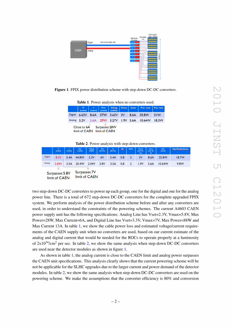
The current CMS Forward Pixel Tracker [2] has 4320 readout chips or ROCs. The upgraded CMSFPIX will host 10752 ROCs where each power group contains 224 ROCs arranged in 7 blades(each blade has two modules each of 16 ROCs). The power lines pass through several boards andup to 45 meters of cable to reach the pixel modules. For the step-down scheme, figure 1 illustratesthe global power distribution from the power supply to the blades.
In this scheme, each power supply unit (A4603 module [3] produced by CAEN, S.A. Italy)powers 224 ROCs which constitute 1/8th of the disk for the Forward pixel system. The plan is to use
– 1 –
2010 JINST 5 C12010
Figure 1. FPIX power distribution scheme with step-down DC-DC converters.
Table 1. Power analysis when no converters used.
Table 2. Power analysis with step-down converters.
two step-down DC-DC converters to power up each group, one for the digital and one for the analogpower line. There is a total of 672 step-down DC-DC converters for the complete upgraded FPIXsystem. We perform analysis of the power distribution scheme before and after any converters areused, in order to understand the constraints of the powering schemes. The current A4603 CAENpower supply unit has the following specifications: Analog Line has Vset=2.3V, Vmax=5.8V, MaxPower=28W, Max Current=6A, and Digital Line has Vset=3.3V, Vmax=7V, Max Power=88W andMax Current 13A. In table 1, we show the cable power loss and estimated voltage/current require-ments of the CAEN supply unit when no converters are used, based on our current estimate of theanalog and digital current that would be needed for the ROCs to operate properly at a luminosityof 2x1034/cm2 per sec. In table 2, we show the same analysis when step-down DC-DC convertersare used near the detector modules as shown in figure 1.
As shown in table 1, the analog current is close to the CAEN limit and analog power surpassesthe CAEN unit specifications. This analysis clearly shows that the current powering scheme will benot be applicable for the SLHC upgrades due to the larger current and power demand of the detectormodules. In table 2, we show the same analysis when step-down DC-DC converters are used on thepowering scheme. We make the assumptions that the converter efficiency is 80% and conversion
– 2 –
2010 JINST 5 C12010
(a) (b)
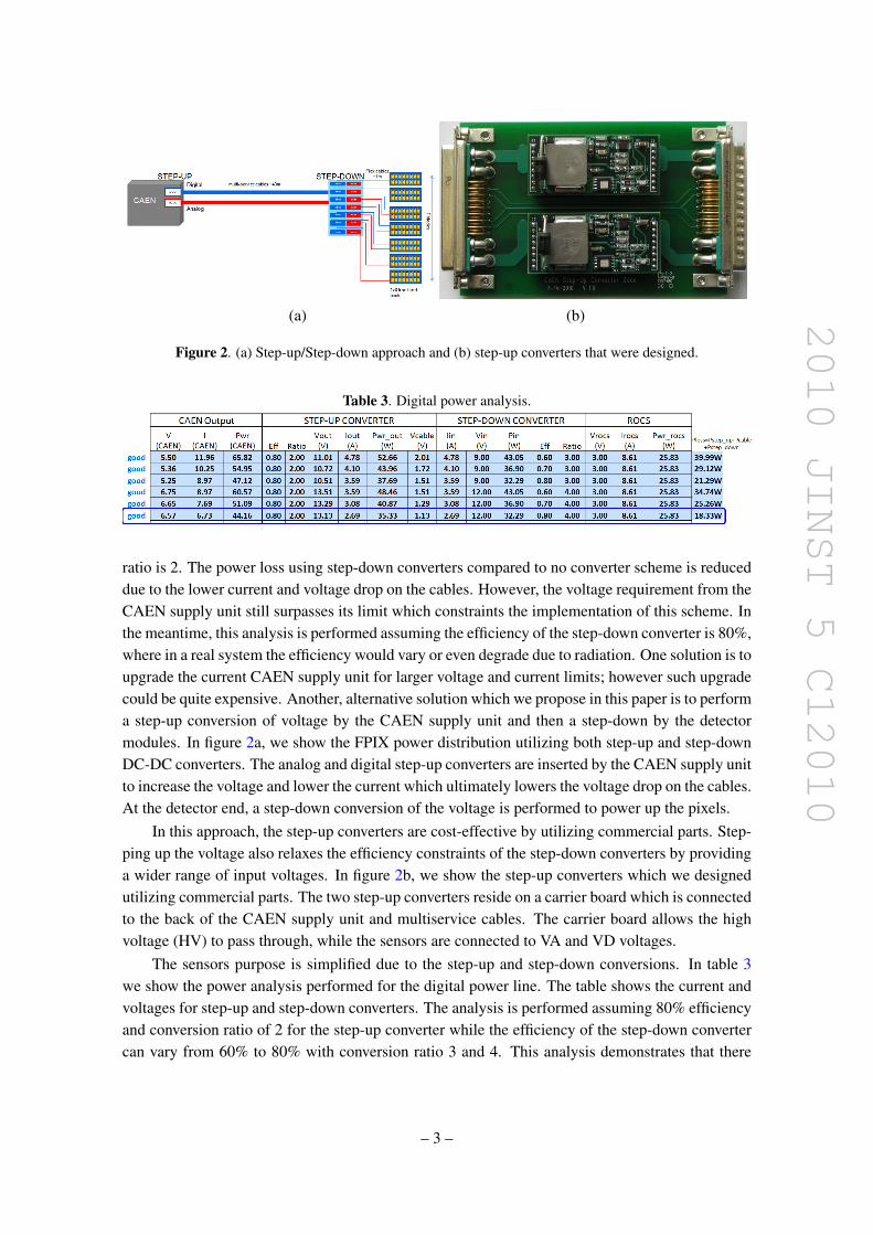
Figure 2. (a) Step-up/Step-down approach and (b) step-up converters that were designed.
Table 3. Digital power analysis.
ratio is 2. The power loss using step-down converters compared to no converter scheme is reduceddue to the lower current and voltage drop on the cables. However, the voltage requirement from theCAEN supply unit still surpasses its limit which constraints the implementation of this scheme. Inthe meantime, this analysis is performed assuming the efficiency of the step-down converter is 80%,where in a real system the efficiency would vary or even degrade due to radiation. One solution is toupgrade the current CAEN supply unit for larger voltage and current limits; however such upgradecould be quite expensive. Another, alternative solution which we propose in this paper is to performa step-up conversion of voltage by the CAEN supply unit and then a step-down by the detectormodules. In figure 2a, we show the FPIX power distribution utilizing both step-up and step-downDC-DC converters. The analog and digital step-up converters are inserted by the CAEN supply unitto increase the voltage and lower the current which ultimately lowers the voltage drop on the cables.At the detector end, a step-down conversion of the voltage is performed to power up the pixels.
In this approach, the step-up converters are cost-effective by utilizing commercial parts. Step-ping up the voltage also relaxes the efficiency constraints of the step-down converters by providinga wider range of input voltages. In figure 2b, we show the step-up converters which we designedutilizing commercial parts. The two step-up converters reside on a carrier board which is connectedto the back of the CAEN supply unit and multiservice cables. The carrier board allows the highvoltage (HV) to pass through, while the sensors are connected to VA and VD voltages.
The sensors purpose is simplified due to the step-up and step-down conversions. In table 3we show the power analysis performed for the digital power line. The table shows the current andvoltages for step-up and step-down converters. The analysis is performed assuming 80% efficiencyand conversion ratio of 2 for the step-up converter while the efficiency of the step-down convertercan vary from 60% to 80% with conversion ratio 3 and 4. This analysis demonstrates that there
– 3 –
2010 JINST 5 C12010
Table 4. Power comparisons between different schemes for digital line.
Table 5. Analog power analysis.
Table 6. Analog power comparisons between different powering schemes.
are various voltage ranges for which step-up powering scheme can operate while accommodatingdifferent efficiencies of the step-down converters which may degrade over time. We highlight thescenario for which the step-up/step-down approach has the minimum power loss. However, as theefficiency of the step-down converter degrades the power loss of the system increases as well. Simi-larly, we re-perform this analysis for the analog power line while keeping the same assumptions forthe efficiency and conversion ratio of the step-up converter. Table 5 shows the analog line poweranalysis. Table 4 and 6 show the power comparisons among different schemes. In comparison,step-up/step-down approach has the most reduced power loss and no need for CAEN unit upgrade.
3 Step-up converters
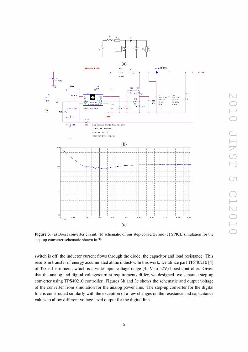
We utilize a boost dc-dc converter for stepping up the voltage. Boost converters are preferredfor stepping up voltage due to their low conduction loss and simplicity in the design. Figure 3ashows a simple schematic for boost converters. The principle behind the boost converter is theenergy accumulated at the inductor. When the inductor is being charged, it acts like a load andabsorbs energy and when being discharged, it is an energy source (like a battery) and it allowshigher voltages to be output. There are two operating stages of the boost converter depending onthe state of the NFET switch. When the switch is on, the inductor current increases, and when the
– 4 –
2010 JINST 5 C12010
(a)
(b)
(c)
Figure 3. (a) Boost converter circuit, (b) schematic of our step-converter and (c) SPICE simulation for thestep-up converter schematic shown in 3b.
switch is off, the inductor current flows through the diode, the capacitor and load resistance. Thisresults in transfer of energy accumulated at the inductor. In this work, we utilize part TPS40210 [4]of Texas Instrument, which is a wide-input voltage range (4.5V to 52V) boost controller. Giventhat the analog and digital voltage/current requirements differ, we designed two separate step-upconverter using TPS40210 controller. Figures 3b and 3c shows the schematic and output voltageof the converter from simulation for the analog power line. The step-up converter for the digitalline is constructed similarly with the exception of a few changes on the resistance and capacitancevalues to allow different voltage level output for the digital line.
– 5 –
2010 JINST 5 C12010
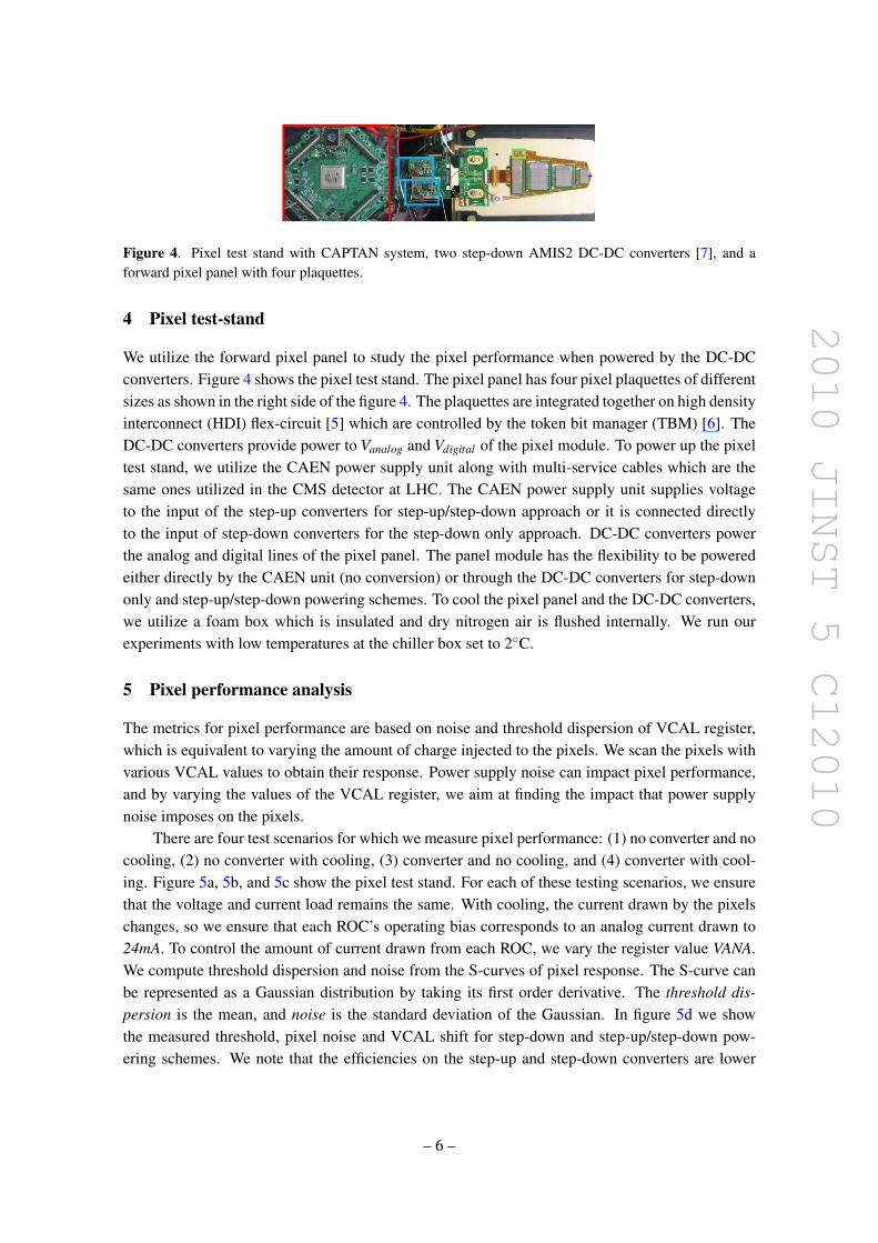
Figure 4. Pixel test stand with CAPTAN system, two step-down AMIS2 DC-DC converters [7], and aforward pixel panel with four plaquettes.
4 Pixel test-stand
We utilize the forward pixel panel to study the pixel performance when powered by the DC-DCconverters. Figure 4 shows the pixel test stand. The pixel panel has four pixel plaquettes of differentsizes as shown in the right side of the figure 4. The plaquettes are integrated together on high densityinterconnect (HDI) flex-circuit [5] which are controlled by the token bit manager (TBM) [6]. TheDC-DC converters provide power to Vanalog and Vdigital of the pixel module. To power up the pixeltest stand, we utilize the CAEN power supply unit along with multi-service cables which are thesame ones utilized in the CMS detector at LHC. The CAEN power supply unit supplies voltageto the input of the step-up converters for step-up/step-down approach or it is connected directlyto the input of step-down converters for the step-down only approach. DC-DC converters powerthe analog and digital lines of the pixel panel. The panel module has the flexibility to be poweredeither directly by the CAEN unit (no conversion) or through the DC-DC converters for step-downonly and step-up/step-down powering schemes. To cool the pixel panel and the DC-DC converters,we utilize a foam box which is insulated and dry nitrogen air is flushed internally. We run ourexperiments with low temperatures at the chiller box set to 2C.
5 Pixel performance analysis
The metrics for pixel performance are based on noise and threshold dispersion of VCAL register,which is equivalent to varying the amount of charge injected to the pixels. We scan the pixels withvarious VCAL values to obtain their response. Power supply noise can impact pixel performance,and by varying the values of the VCAL register, we aim at finding the impact that power supplynoise imposes on the pixels.
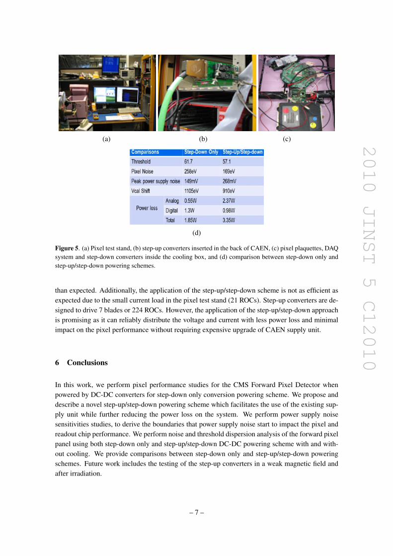
There are four test scenarios for which we measure pixel performance: (1) no converter and nocooling, (2) no converter with cooling, (3) converter and no cooling, and (4) converter with cool-ing. Figure 5a, 5b, and 5c show the pixel test stand. For each of these testing scenarios, we ensurethat the voltage and current load remains the same. With cooling, the current drawn by the pixelschanges, so we ensure that each ROC’s operating bias corresponds to an analog current drawn to24mA. To control the amount of current drawn from each ROC, we vary the register value VANA.We compute threshold dispersion and noise from the S-curves of pixel response. The S-curve canbe represented as a Gaussian distribution by taking its first order derivative. The threshold dis-persion is the mean, and noise is the standard deviation of the Gaussian. In figure 5d we showthe measured threshold, pixel noise and VCAL shift for step-down and step-up/step-down pow-ering schemes. We note that the efficiencies on the step-up and step-down converters are lower
– 6 –
2010 JINST 5 C12010
(a) (b) (c)
(d)
Figure 5. (a) Pixel test stand, (b) step-up converters inserted in the back of CAEN, (c) pixel plaquettes, DAQsystem and step-down converters inside the cooling box, and (d) comparison between step-down only andstep-up/step-down powering schemes.
than expected. Additionally, the application of the step-up/step-down scheme is not as efficient asexpected due to the small current load in the pixel test stand (21 ROCs). Step-up converters are de-signed to drive 7 blades or 224 ROCs. However, the application of the step-up/step-down approachis promising as it can reliably distribute the voltage and current with less power loss and minimalimpact on the pixel performance without requiring expensive upgrade of CAEN supply unit.
6 Conclusions
In this work, we perform pixel performance studies for the CMS Forward Pixel Detector whenpowered by DC-DC converters for step-down only conversion powering scheme. We propose anddescribe a novel step-up/step-down powering scheme which facilitates the use of the existing sup-ply unit while further reducing the power loss on the system. We perform power supply noisesensitivities studies, to derive the boundaries that power supply noise start to impact the pixel andreadout chip performance. We perform noise and threshold dispersion analysis of the forward pixelpanel using both step-down only and step-up/step-down DC-DC powering scheme with and with-out cooling. We provide comparisons between step-down only and step-up/step-down poweringschemes. Future work includes the testing of the step-up converters in a weak magnetic field andafter irradiation.
– 7 –
2010 JINST 5 C12010
References
[1] V. Radicci, CMS Pixel Detector Upgrade, 2009 JINST 4 P03022.
[2] S. Malik, The CMS Forward Pixel Detector, Nucl. Instrum. Meth. A 572 (2007) 87.
[3] CAEN, SY2527 User’s Manual, http://www.caen.it/getattach.php?mod=SY2527&obj=mn&id=1419(2005).
[4] TPS40210, Texas Instruments, http://focus.ti.com/lit/ds/symlink/tps40210.pdf.
[5] The CMS collaboration, The CMS Experiment at CERN LHC, 2008 JINST 3 S08004.
[6] E. Bartz, The Token Bit Manager for the CMS Pixel Readout, Proceedings of the Workshop onElectronics for LHC Experiments, 2003.
[7] S. Michelis et al., ASIC buck converter prototypes for LHC upgrades, Topical Workshop on Electronicsfor Particle Physics, 2009.
– 8 –