Design studies of n-in-p silicon strip sensors for the CMS Tracker
125
IEKP-KA/2012-22 Design studies of n-in-p silicon strip sensors for the CMS tracker Martin Strelzyk Diploma Thesis Referent: Prof. Dr. Thomas Müller, IEKP Korreferent: Prof. Dr. Wim de Boer, IEKP Institut für Experimentelle Kernphysik Fakultät für Physik Karlsruher Institut für Technologie Karlsruhe, den 30.11.2012
-
Upload
khangminh22 -
Category
Documents
-
view
1 -
download
0
Transcript of Design studies of n-in-p silicon strip sensors for the CMS Tracker

IEKP-KA/2012-22
Design studies ofn-in-p silicon strip sensors
for the CMS tracker
Martin Strelzyk
Diploma Thesis
Referent: Prof. Dr. Thomas Müller, IEKPKorreferent: Prof. Dr. Wim de Boer, IEKP
Institut für Experimentelle Kernphysik
Fakultät für PhysikKarlsruher Institut für Technologie
Karlsruhe, den 30.11.2012


Für meinen Paps...


Design studies of n-in-p silicon strip sensors for the CMS Tracker
Deutsche Zusammenfassung
Die geplante Aufrüstung des Large Hadron Collider LHC in zwei Phasen zum HL-LHC1 wird zehnfach höhere nominelle Luminositäten von ungefähr L = 5×1034cm−2s−1
[Tri08] erlauben, was eine enorme Leistungfähigkeit des CMS Teilchendetektors erfordernwird. Größere Teilchenspurdichten und höhere Anzahl an Teilchen erzeugen sowohl einehärtere Strahlungsumgebung für den Teilchendetektor als auch größere Datenmengen.Im Rahmen des CMS-Tracker-Upgrade für die Hochluminositätsphase werden Studienzum Design und Strahlenhärte von Siliziumstreifensensoren durchgeführt.Das IEKP am KIT ist im CMS-Experiment am CERN in Genf sowohl in der Anal-yse der Physik als auch in Entwicklung des Detektors involviert. Ein Teil der Modulefür den aktuellen CMS-Spurdetektor wurde am IEKP zusammengebaut und ans CERNausgeliefert. Zentraler Forschungsgegenstand der CMS Hardware Gruppe am KIT istmomentan die Qualifizierung von Siliziumsensoren für das Phase-2-Upgrade des CMSExperiments, welches für 2022 geplant ist. Intensive Bestrahlungskampagnen mit Pro-tonen und Neutronen werden durchgeführt, um möglichst effiziente und strahlenharteSensoren zu entwickeln. Dabei werden unterschiedliche Sensorgeometrien untersucht.Diese wurden auf Siliziumsubstraten unterschiedlicher Dotierung und Produktionstech-niken hergestellt und hinsichtlich ihrer Strahlenhärte untersucht.
Erste Ergebnisse präferieren die n-in-p-Technologie von Streifensensoren [Die12]. Dabeiwerden n-dotierte Streifen in einem p-dotierten Substrat implantiert. P-Typ dotierteSiliziumsubstrate weisen dabei mit steigender Fluenz eine gegenüber N-Typ erhöhteLadungssammlungseffizienz auf.Ein Nachteil von n-in-p-Sensoren jedoch ist eine Akkumulationsschicht von Elektronenan der Substratoberfläche, welche die n-dotierten Streifen kurzschließt. Diese wird aufGrund von fixen, positiv geladenen Defekten im Siliziumoxid an der Grenzfläche zwis-chen Siliziumsubstrat und Oxid erzeugt. Dieser Effekt verhindert eine hochauflösendeSignalzuordnung.Eine zusätzliche Implantation von P-Typ-Material zwischen den Auslesestreifen an derOberfläche unterbricht die Akkumulationsschicht und gewährleistet damit eine ordnungs-gemäße Funktionsweise. Die Isolationstechniken unterscheiden sich dabei in der Geome-trie der P-Typ-Implantate und der Dotierungskonzentration.Im Rahmen dieser Diplomarbeit wurden unter anderem neue n-in-p Sensorengeometrienmit unterschiedlichen Isolationstechniken mit einem Grafikprogramm nach Hersteller-regeln entworfen. Diese Designs mit insgesamt 17 verschiedenen Sensorgeometrien wur-den anschließend zwischen April und August 2012 am ITE Warschau prozessiert.Man unterscheidet zwischen zwei verschiedenen Arten, eine Unterbrechung der Akkumu-lationsschicht zu erreichen. Einerseits die p-spray-Technik, eine großflächige Auftragungvon P-Typ-Material auf die Oberfläche eines Wafers und andererseits die p-stop-Technik,dargetellt in Bild 0.1. Dabei wird mit Hilfe einer zusätzlichen Photolitigraphiemaskeeine Struktur mit P-Typ-Material zwischen den Streifenimplantaten auf der Oberfläche
1High Luminosity LHC
a

Design studies of n-in-p silicon strip sensors for the CMS Tracker
((a)) p-spray Schicht ((b)) p-stop Struktur
Figure 0.1: Veranschaulichung der beiden Isolationsmethoden, die untersucht wur-den. Angedeutet ist ein Sensor mit zwei Streifen. Links ist die p-spray-Methode zu sehen, welche als einheitliche Schicht auf dem ganzenWafer aufgebracht wird. Rechts sieht man die p-stop-Struktur. Dabeihandelt es sich um zwei P-Typ dotierte Streifen zwischen den Ausle-sestreifen, welche die Elektronenschicht unterbrechen.
erzeugt.Die zusätzliche Oberflächenimplantation von P-Typ-Material sollte dabei keine negativenAuswirkungen auf die elektrischen Eigenschaften von Sensoren, wie Durchbruchsverhal-ten oder Zwischenstreifenkapazität aufweisen. Insbesondere die Zwischenstreifenkapaz-ität trägt hauptsächlich zum Rauschen in der Ausleseelektronik bei und sollte daher imVergleich zur p-in-n-Technologie nicht merklich beeinträchtigt werden.Beide Streifen Isolationsmethoden wurden zuerst mit Hilfe von FEM-Simulationen aufelektrische Eigenschaften untersucht und qualifiziert. Hierbei wurden Substratschädendurch Bestrahlung und deren Auswirkung auf die Isolation nicht untersucht. Die Ergeb-nisse sind direkt in den Entwurf der Sensoren für die Produktion am ITE Warschaueingeflossen. Hinsichtlich der Dotierungskonzentration sind die Simulationsresultate beibeiden Methoden übereinstimmend. Je höher die Konzentrationen für p-spray- bzw.p-stop-Isolation gewählt werden, desto höhere elektrische Feldstärken treten an denImplantatseiten auf, welche die Durchbruchsspannungen reduzieren. Dabei steigen dieFeldstärken exponentiell mit der P-Typ-Materialkonzentration an. Andererseits musseine zuverlässige Streifenisolierung erreicht werden, welche auch nach Entstehung vonOberflächenschäden durch Bestrahlung funktionstüchtig bleibt. Diese kann nur durcheine Mindestkonzentration erreicht werden, was letztendlich die Kalkulation der P-Typ-Dotierung für Streifenisolation erschwert.Simulationsresultate deuten darauf hin, dass Konzentrationen von 8 × 1015 cm3 für p-spray und 5 × 1016 cm3 für die p-stop-Lösung sowohl das Kriterium der hinreichendenIsolation als auch niedrige Feldstärken und konstante Zwischenstreifenkapazitäten er-füllen. Diese Werte stimmen weitgehend mit Ergebnissen aus bereits erfolgten Studien
b

Design studies of n-in-p silicon strip sensors for the CMS Tracker
überein [PFC07].Bei der p-stop-Methode kommen zur Konzentration weitere Faktoren hinzu. Die p-stop-Streifenstruktur ist auf der rechten Seite in Bild 4.1 gekennzeichnet. Je nach Position undBreite der beiden P-Typ-Streifen, weist ein Sensor niedrigere oder höhere Feldstärkenauf, die Zwischenstreifenkapazität jedoch bleibt unbeeinträchtigt. Daher sollte der Ab-stand zwischen einem N-Typ Auslese- und einem P-Typ Isolationsimplantat mindestensein Viertel des Auslesestreifenabstands betragen.Diese qualitativen Erkenntnisse aus den FEM Simulationen wurden direkt auf die 17 De-signs des ITE-Wafers umgesetzt. Nach der Prozessierung wurden die Sensoren mit Hilfeexperimenteller Setups qualifiziert. Die elektrischen Eigenschaften der gelieferten Sen-soren, bestimmt durch die Messungen, deuten darauf hin, dass die p-stop-Konzentrationnicht ausreichend gewesen ist. Nach Rücksprache mit Ingenieuren am ITE hat sich her-ausgestellt, dass eine mögliche Erklärung die ungewünschte Diffusion von Boratomen ausder Isolierung in die Oxidschicht sei. Dadurch wurde die P-Typ-Konzentration derartgeschwächt, dass eine Akkumulationsschicht entsteht, welche die Streifen kurzschließt.Daher kann ein Vergleich mit Simulationen und eine Schlussfolgerung nicht gezogen wer-den.
Sensor 1
Sensor 2
CBC
Figure 0.2: Schema des 2S Moduls [Hal11].
Hinsichtlich des LHC-Upgradeszu höherer Luminosität undeiner höheren Schwerpunktsen-ergie von 14 TeV bei einer Kol-lisionsfrequenz von 40 MHz2,sollte der Tracker Informatio-nen zur Level-1 Triggerentschei-dung beitragen um weiterhinden Detektor trotz erhöhterZahl an Primärkollisionen perProtonenbunch-Kollision mit 100 kHzausgelesen zu werden. Dadurchkann die Kompatibilität zubestehenden Subdetektoren er-halten beleiben.Eine mögliche Umsetzung zumTriggerbeitrag ist das 2S-Modul[Abb11], welches erlauben soll,dass Spurpunkte von Teilchen mit hohem Transversalimpuls pT zur L1 Triggerentschei-dung beitragen können. Dieses besteht aus zwei Streifensensoren (10cm x 10cm mit5cm langen Streifen) in Sandwichkonfiguration und erlaubt eine leichtgewichtige Anord-nung, die mittels konventionellen Verbindungstechniken produziert werden kann. Eingeeignetes Streifendesign und eine passende Streifenanordnung sollen die Granularität
2aktuell√
s = 8 T eV bei 20 MHz
c

Design studies of n-in-p silicon strip sensors for the CMS Tracker
erhöhen und damit die Anforderungen an den Spurdetektor erfüllen.Die IEKP-Hardware-Gruppe erforscht dabei Sensoren auf deren Eignung für das Trigger-modul. Zur Erhöhung der Granularität sind die Streifen eines Sensors zweifach segmen-tiert und werden binär mit CMS Binary Chips (CBC) an den zwei gegenüberliegendenModulrändern ausgelesen. An den zwei Modulrändern werden je acht CBC auf einemHybrid gebondet sein. Jeder Chip wird sowohl mit dem oberen als auch mit dem unterenSensor über Drahtbonds verbunden. Dabei übernimmt der CBC die On-Detector Korre-lation zwischen getroffenen unteren und oberen Streifen und leitet dann Informationenzur L1-Triggerentscheidung weiter.Mit dem Ziel, eine noch höhere Granularität zu erreichen, wurde ein neuartiger Sensor in-nerhalb der IEKP-CMS-Hardware-Gruppe entwickelt, welcher alle Anforderungen an das2S-Modul für den Tracker-Upgrade erfüllt. Ein erster Prototyp des FOSTER (FOurfoldsegmented STripsensor with Edge Readout) wurde bereits produziert und qualifiziert.Abbildung 0.3 zeigt ein Schema des Sensors. Signale der inneren Streifen werden überMetallleiterbahnen, unter denen kein Implantat verläuft, zwischen den äußeren Streifenzum Rand geführt. Diese Konfiguration erlaubt die Auslese aller Streifen am Rand desSensors. Bei der experimentellen Qualifikation des FOSTER wurde eine unerwünschteSignalkopplung zwischen äußeren und inneren Streifen beobachtet, wodurch der Sensornicht effizient für Teilchendetektion eingesetzt werden kann [Hof12].Im Rahmen dieser Diplomarbeit wurde unter anderem eine mögliche Unterdrückungder Signalinduktion beim FOSTER untersucht. Simulationsstudien belegen, dass mitzunehmender Dotierungskonzentration von P-Typ-Material unter den Metallleiterbah-nen der inneren Streifen, die Signalkopplung auf diese nach und nach abnimmt. Dabeisollte die implantierte Struktur mindestens so breit sein wie die Leiterbahn und eine Min-
Figure 0.3: Schema des FOSTER. Die inneren Streifen werden mit Aluminiu-mauslesestreifen zum Sensorrand verlängert und außen ausgelesen.Dadurch wird die Granularität erhöht und es können konventionelleVerbindungstechniken angewendet werden.
d

Design studies of n-in-p silicon strip sensors for the CMS Tracker
destkonzentration von 4× 1015 cm3 für p-spray oder 9× 1015 cm3 für p-stop aufweisen.Im Vergleich mit den Werten für eine ausreichende Streifenisolierung, sind die Konzen-trationen für die Signalunterdrückung beim FOSTER sogar niedriger und daher ohneEinschränkung der elektrischen Eigenschaften der Sensoren umsetzbar. Zur Verifizierungder Resultate wurden FOSTER-Sensoren nach Herstellerkriterien designed, die Idee derP-Typ-Materialimplantation für das Verhindern der Kopplung implementiert und amITE Warschau prozessiert.Die ersten experimentellen Befunde deuten darauf hin, dass eine Implantation von P-Typ-Material an der Sensoroberfläche die Kopplung schwächt. Eindeutige Schlussfol-gerung und Bestätigung des Lösungsansatzes können jedoch auf Grund von Problemenbei der Prozessierung nicht gezogen werden. Mit dem ITE Warschau sowie einem weit-eren Hersteller laufen bereits Verhandlungen über die Produktion weiterer FOSTER-Prototypsensoren. Die Sensorgeomtrien wurden bereits in Form von GDS Dateien zurHerstellung der Photolitographiemasken an den Produzenten gesendet und werden zurZeit auf technologische Umsetzung überprüft.
Die vorliegende Arbeit bezeugt, dass FEM-Simulation ein hilfreiches Werkzeug zur vor-läufigen Charakterisierung der elektrischen Eigenschaften von Siliziumsensoren ist. MitHilfe von Simulationssoftware können neue Sensorideen auf elektrisches Verhalten über-prüft werden. Durch Analyse der Resultate können Erkenntnisse direkt umgesetzt undsomit Kosten gespart werden. Ein möglicher weiterer Schritt hinsichtlich der Simulationvon Isolationsmethoden der n-in-p-Technologie wäre die Verwendung von Trapmodellen,welche Defekte im Substrat nachbilden und somit Sensoren nach Bestrahlung approx-imieren.Nichtsdestotrotz ist eine experimentelle Charakterisierung von Sensoren unabdingbarund nur ein Vergleich von Simualtionsresultaten mit Messergebnissen lässt eine hinre-ichende Konklusion zu.Nach Betrachtung der Simulationsanalyse ist festzustellen, dass obwohl die n-in-p-Technologie im Vergleich zu p-in-n-Sensoren zusätzliche Prozessierungsschritte zum Her-stellen der Isolierung benötigt, diese die elektrischen Eigenschaften vor Bestrahlungnicht beeinflusst. Da diese Technologie, belegt durch intensive Bestrahlungsstudien,eine höhere Ladungssammlungseffizienz aufweist, sind weitere Untersuchungen nötig,um durchbruchsfeste und strahlenharte Sensoren für das Upgrade des CMS-Trackers zubestimmen. Die Untersuchungen in dieser Arbeit können dabei erste Geometrien der P-Typ-Isolationsmethode eingrenzen und Dotierungskonzentrationen abschätzen, welcheweitere Studien von n-in-p-Sensoren bestätigen [VBD+12].
e


Design studies of n-in-p silicon strip sensors for the CMS Tracker
Contents
Contents
List of abbreviations III
List of Figures V
List of Tables IX
Introduction 1
1 LHC and CMS experiment 31.1 Large Hadron Collider at CERN . . . . . . . . . . . . . . . . . . . . . . . 3
1.1.1 The four main experiments at CERN . . . . . . . . . . . . . . . . 41.1.2 Interaction of particles with a medium . . . . . . . . . . . . . . . . 5
1.2 The CMS Experiment . . . . . . . . . . . . . . . . . . . . . . . . . . . . . 71.3 LHC and CMS Upgrade . . . . . . . . . . . . . . . . . . . . . . . . . . . . 10
2 Working Principle of Silicon Detectors 132.1 Semiconductor physics . . . . . . . . . . . . . . . . . . . . . . . . . . . . . 132.2 Silicon properties . . . . . . . . . . . . . . . . . . . . . . . . . . . . . . . . 162.3 The p-n-junction . . . . . . . . . . . . . . . . . . . . . . . . . . . . . . . . 162.4 Silicon Strip Sensors . . . . . . . . . . . . . . . . . . . . . . . . . . . . . . 20
2.4.1 Noise . . . . . . . . . . . . . . . . . . . . . . . . . . . . . . . . . . 202.4.2 Leakage current . . . . . . . . . . . . . . . . . . . . . . . . . . . . 222.4.3 Depletion voltage Vfd and bulk capacitance . . . . . . . . . . . . . 232.4.4 Hit position measurement . . . . . . . . . . . . . . . . . . . . . . . 24
3 The 2S Module 273.1 CMS Tracker Upgrade . . . . . . . . . . . . . . . . . . . . . . . . . . . . . 273.2 Low pT -discrimination . . . . . . . . . . . . . . . . . . . . . . . . . . . . . 283.3 The 2S Module Concept . . . . . . . . . . . . . . . . . . . . . . . . . . . . 29
4 Sensor design aspects 334.1 p-Isolation Techniques . . . . . . . . . . . . . . . . . . . . . . . . . . . . . 33
4.1.1 p-spray isolation . . . . . . . . . . . . . . . . . . . . . . . . . . . . 344.1.2 p-stop isolation . . . . . . . . . . . . . . . . . . . . . . . . . . . . . 35
4.2 Wafer Processing . . . . . . . . . . . . . . . . . . . . . . . . . . . . . . . . 374.3 Software Layout Editor . . . . . . . . . . . . . . . . . . . . . . . . . . . . 424.4 Wafer ITE Warsaw . . . . . . . . . . . . . . . . . . . . . . . . . . . . . . . 44
4.4.1 BabyStandard geometry . . . . . . . . . . . . . . . . . . . . . . . . 444.4.2 Segmented Standard CMS sensors . . . . . . . . . . . . . . . . . . 46
I

Design studies of n-in-p silicon strip sensors for the CMS Tracker
Contents
4.4.3 FOSTER design . . . . . . . . . . . . . . . . . . . . . . . . . . . . 474.5 2S-Module Overlap region . . . . . . . . . . . . . . . . . . . . . . . . . . . 52
5 Device Simulation 575.1 Sentaurus T-CAD Software . . . . . . . . . . . . . . . . . . . . . . . . . . 575.2 Simulation of p-isolation techniques . . . . . . . . . . . . . . . . . . . . . . 64
5.2.1 General device parameter for simulation studies . . . . . . . . . . . 645.2.2 P-spray Isolation . . . . . . . . . . . . . . . . . . . . . . . . . . . . 655.2.3 P-stop Isolation . . . . . . . . . . . . . . . . . . . . . . . . . . . . . 715.2.4 Simulation of a modified FOSTER design preventing undesired
signal coupling . . . . . . . . . . . . . . . . . . . . . . . . . . . . . 775.2.5 Conclusion on isolation techniques . . . . . . . . . . . . . . . . . . 78
6 ITE Sensor Qualification and measurements 816.1 Sensor qualification . . . . . . . . . . . . . . . . . . . . . . . . . . . . . . . 816.2 FOSTER laser scan measurements . . . . . . . . . . . . . . . . . . . . . . 83
7 Summary and outlook 87
Software 89
A Appendix i
Bibliography ix
II

Design studies of n-in-p silicon strip sensors for the CMS Tracker
List of abbreviations
CERN Conseil Européen pour la Recherche Nucléaire
CMS Compact Muon Solenoid
FOSTER FOurfold segmented STrip sensor with Edge Readout
LHC Large Hadron Collider
ROCs Read Out Chips
SM Standard Model of Particle Physics
SNR Signal-to-Noise Ratio
TEC Tracker End Caps
TIB Tracker Inner Barrel
TID Tracker Inner Disk
TOB Tracker Outer Barrel
III


Design studies of n-in-p silicon strip sensors for the CMS Tracker
List of Figures
List of Figures0.1 Veranschaulichung der beiden Isolationsmethoden, die untersucht wur-
den. Angedeutet ist ein Sensor mit zwei Streifen. Links ist die p-spray-Methode zu sehen, welche als einheitliche Schicht auf dem ganzen Waferaufgebracht wird. Rechts sieht man die p-stop-Struktur. Dabei handelt essich um zwei P-Typ dotierte Streifen zwischen den Auslesestreifen, welchedie Elektronenschicht unterbrechen. . . . . . . . . . . . . . . . . . . . . . . b
0.2 Zoom into the FOSTER overlap region . . . . . . . . . . . . . . . . . . . . c0.3 Zoom into the FOSTER overlap region . . . . . . . . . . . . . . . . . . . . d
1.1 Accelerator chain at CERN . . . . . . . . . . . . . . . . . . . . . . . . . . 31.2 Mean energy loss rate . . . . . . . . . . . . . . . . . . . . . . . . . . . . . 61.3 Sketch of the CMS detector . . . . . . . . . . . . . . . . . . . . . . . . . . 71.4 Schematic cross-section of the CMS Tracker . . . . . . . . . . . . . . . . . 81.5 Transverse slice of the Compact Muon Solenoid detector . . . . . . . . . . 91.6 Long-term programme for the LHC . . . . . . . . . . . . . . . . . . . . . . 10
2.1 Energy band modell . . . . . . . . . . . . . . . . . . . . . . . . . . . . . . 132.2 Bond representation of n-type and p-type semiconductors . . . . . . . . . 142.3 Hole and electron mobilities . . . . . . . . . . . . . . . . . . . . . . . . . . 152.4 Formation of a p-n-junction . . . . . . . . . . . . . . . . . . . . . . . . . . 172.5 The p-n-junction . . . . . . . . . . . . . . . . . . . . . . . . . . . . . . . . 182.6 Sketch of CMS silicon sensor . . . . . . . . . . . . . . . . . . . . . . . . . 212.7 Working principle of an AC-coupled silicon microstrip detector . . . . . . 212.8 Leakage current . . . . . . . . . . . . . . . . . . . . . . . . . . . . . . . . . 222.9 Capacitance as a function of applied voltage of a standard sensor produced
at ITE Warsaw . . . . . . . . . . . . . . . . . . . . . . . . . . . . . . . . . 23
3.1 Transverse momentum spectrum of charged tracks in HL-LHC conditions 283.2 Illustration of the principle of selecting high transverse momentum tracks
in stacked layers . . . . . . . . . . . . . . . . . . . . . . . . . . . . . . . . 293.3 Scheme of the 2S Module . . . . . . . . . . . . . . . . . . . . . . . . . . . 303.4 3d Scheme of the 2S Module with components . . . . . . . . . . . . . . . . 303.5 Possible tracker layout after Phase 2 Upgrade . . . . . . . . . . . . . . . . 31
4.1 Section of the 2D schematic of the simulated 300 µm thick sensors withthe different insulation techniques: a) pspray layer, b) pstop pattern . . . 34
4.2 Illustration of the p-stop atoll pattern . . . . . . . . . . . . . . . . . . . . 354.3 Illustration of the p-stop common pattern . . . . . . . . . . . . . . . . . . 364.4 Sketch of wafer processing; backside diffusion of boron . . . . . . . . . . . 39
V

Design studies of n-in-p silicon strip sensors for the CMS Tracker
List of Figures
4.5 Sketch of wafer processing; oxide etching for n+ strips . . . . . . . . . . . 404.6 Sketch of wafer processing; n+ strip implantation . . . . . . . . . . . . . . 404.7 Sketch of wafer processing; resistor and contacts are defined . . . . . . . . 414.8 Sketch of wafer processing; intersection after processing is done . . . . . . 424.9 Macro script example for microstrip placement . . . . . . . . . . . . . . . 434.10 Wafer design for ITE Warsaw run taken from GDS file . . . . . . . . . . . 434.11 Processed wafer with the desired sensor designs . . . . . . . . . . . . . . . 444.12 Definition of the gap between pstop and implant . . . . . . . . . . . . . . 454.13 BabyStandard gds pstop . . . . . . . . . . . . . . . . . . . . . . . . . . . . 454.14 Illustration of a sensor with segmented strips . . . . . . . . . . . . . . . . 464.15 Illustration of a sensor with segmented strips, zoom into segmented region 464.16 Illustration of a the new FOSTER sensor . . . . . . . . . . . . . . . . . . 484.17 Layout design of a the new FOSTER sensor . . . . . . . . . . . . . . . . . 484.18 Zoom into the FOSTER overlap region . . . . . . . . . . . . . . . . . . . . 494.19 Laser scan of the FOSTER in 1µm steps in the far and in the near region
[Hof12] . . . . . . . . . . . . . . . . . . . . . . . . . . . . . . . . . . . . . . 504.20 Zoom into the FOSTER overlap region, illustration of the pcommon struc-
ture . . . . . . . . . . . . . . . . . . . . . . . . . . . . . . . . . . . . . . . 514.21 Illustration of particle hit in the 2S Module center region . . . . . . . . . 524.22 Illustration of overlap region with pstop atoll and common pattern . . . . 534.23 Illustration of high pT track . . . . . . . . . . . . . . . . . . . . . . . . . . 54
5.1 Typical tool flow of a device simulation . . . . . . . . . . . . . . . . . . . 575.2 Illustration of a sensor with two adjecent half-electrodes and mesh nodes. 585.3 Macro script example for microstrip sensor drawing in Sentaurus Struc-
ture Editor . . . . . . . . . . . . . . . . . . . . . . . . . . . . . . . . . . . 605.4 Example of a Sentaurus Device command file . . . . . . . . . . . . . . . . 635.5 Electric field as a function of the pspray concentration . . . . . . . . . . . 655.6 Electric field as a function of the p-spray concentration, slice underneath
the bulk-oxide interface . . . . . . . . . . . . . . . . . . . . . . . . . . . . 665.7 Electrostatic Potential as a function of the p-spray concentration . . . . . 675.8 Maximum electric fields as a function of the p-spray concentration . . . . 675.9 Electric field as a function of increasing oxide charge. . . . . . . . . . . . . 685.10 Electrical field as a function of increasing oxide charge; orthogonal slice. . 685.11 Interstrip capacitance on oxide charge concentration and low doped p-spray 695.12 Interstrip capacitance on oxide charge concentration and highly doped
p-spray . . . . . . . . . . . . . . . . . . . . . . . . . . . . . . . . . . . . . 705.13 Interstrip capacitance on p-spray concentration . . . . . . . . . . . . . . . 705.14 Simulation of a sensor with four strips and the p-stop atoll pattern be-
tween adjacent strips. The electron accumulation layer is cut by the p-stopdopants. The electron density reaches a value of 0 at the p-stop edges. . . 72
5.15 Simulation of pstop pattern . . . . . . . . . . . . . . . . . . . . . . . . . . 72
VI

Design studies of n-in-p silicon strip sensors for the CMS Tracker
List of Figures
5.16 Slice, 100 nm under bulk-oxide interface; the p-stop concentration is×1016 cm−3
and the distance and width have been varied. . . . . . . . . . . . . . . . . 735.17 Electric field strenght on p-stop doping concentration . . . . . . . . . . . 735.18 Eta distribution depending on pstop distance . . . . . . . . . . . . . . . . 745.19 Eta values depending on oxide charge . . . . . . . . . . . . . . . . . . . . 755.20 Interstrip capacitance dependency on p-stop distance . . . . . . . . . . . . 765.21 Interstrip capacitance dependency on interface oxide charge for a p-stop
concetration . . . . . . . . . . . . . . . . . . . . . . . . . . . . . . . . . . . 765.22 Drawing of the simulated FOSTER design . . . . . . . . . . . . . . . . . . 775.23 Charge on aluminum routing line for different p-common and p-spray
doping concentrations. Both techniques need a specific minimum concen-tration to suppress the signal couling. . . . . . . . . . . . . . . . . . . . . 78
6.1 CV and IV characteristics of a standard sensor geometry. The depletionvoltage is about 50 V and the sensor has a high current of 0.92 µA/cm2
at 1.2× VFD and 20°C . . . . . . . . . . . . . . . . . . . . . . . . . . . . . 816.2 Further quality measurements of the standard sensor design as a repre-
sentive for all senors at 60 V and 20°C. . . . . . . . . . . . . . . . . . . . 826.3 Laser scan of FOSTER far region . . . . . . . . . . . . . . . . . . . . . . . 846.4 Laser scan of FOSTER near region . . . . . . . . . . . . . . . . . . . . . . 84
VII


Design studies of n-in-p silicon strip sensors for the CMS Tracker
List of Tables
List of Tables
2.1 Silicon properties . . . . . . . . . . . . . . . . . . . . . . . . . . . . . . . . 16
4.1 pstop/pspray doping concentrations for the ITE Warsaw run . . . . . . . 374.2 Overlap dimensions depending on sensor spacing and position for the barrel 554.3 Overlap dimensions depending on sensor spacing and position for the
endcaps . . . . . . . . . . . . . . . . . . . . . . . . . . . . . . . . . . . . . 55
IX


Design studies of n-in-p silicon strip sensors for the CMS Tracker
Introduction
During the search for the fundamental structure of matter, physicists advanced againand yet again into smaller constituents. After decades of research, the Standard Modelof particles and interaction forces (SM) has been established, still there are open ques-tions like the asymmetry of matter and antimatter. The SM postulates the mechanismof electroweak symmetry breaking with the Higgs field as a possible explanation for themass of W ans Z bosons while the photon remains massless [Hig12].On July 4th 2012, the main experiments ATLAS3 and CMS4 at CERN5 announced thediscovery of a new boson with a mass between 125 and 127 GeV/c2. Its behaviour isconsistant with the predicted characteristics of the Higgs boson.
This achievement is only possible at high center-of-mass-energies√s, which are nec-
essary to advance into smaller structure of matter.Therefore, development and construction of particle accelerators and detectors becamean own field of research. Nowadays, the most powerful accelerator is the LHC6 at CERN,which after 30 years of planning and construction collides proton bunches at currently√s = 8 TeV .
An accelerator upgrade to high luminosity LHC (HL-LHC) scheduled for 2020 will allowten times higher nominal luminosities of approximately 5 × 1034 cm−2s−1 and a colli-sion energy of 14 TeV , which present a challenge for the CMS particle detector. Thehuge amount of dense particle tracks induce a harsh radiation environment and a largeamount of data. Within the CMS tracker upgrade project for the high luminosity phase,studies on design and radiation hardness of silicon microstrip detectors are performed.In addition, the tracker should contribute information to the Level-1 trigger decision at40 MHz in order to keep the read-out rate of the detector below 100 kHz for compati-bility with sub-detector systems. One proposal to achieve data reduction is to use justparticle tracks with a high transverse momentum7 for the trigger decision. This couldreduce the amount of data by one order of magnitude. A possibility to identify thesetracks is a proposed 2S Module (see chapter 3), which allows discrimination betweenparticle tracks with high and low transverse momentum. The module consists of twoidentical silicon sensors in sandwich configuration, which can be produced with conven-tional technologies.Within this diploma thesis, the n-in-p technology of silicon microstrip sensors has been
3A Toroidal LHC AparatuS4Compact Muon Solenoid5Conseil Européen pour la Recherche Nucléaire6Large Hadron Collider7≥ 2GeV/c
1

Design studies of n-in-p silicon strip sensors for the CMS Tracker
Introduction
investigated considering strip isolation techniques (p-spray and p-stop) and their impactson the sensor performance. For high irradiation, this technology offers better performancecompared to the n-in-p sensors. Isolation of n+ strips is necessary due to an electronaccumulation layer at the bulk/silicon dioxide interface caused by positively chargeddefects in the oxide. Furthermore, new sensor designs, which are of interest for the 2Smodule, especially the FOSTER design, a fourfold segmented strip sensor developed atthe KIT CMS Hardware group, were studied. On the basis of simulations with the soft-ware Synopsys Sentaurus T-CAD [7], sensor characteristics and performance have beeninvestigated. Analysis of simulation results constrained the choice of sensor geometrieswhich have been produced subsequently.
In chapter 1, the LHC and the four main experiments8, especially the CMS experimentand its tracker as well as the so-called Phase 2 Upgrade plans are presented. Chapter2 deals with the basic theory of semiconductor physics. On the basis of a pn-junction,the working principle of silicon microstrip sensors for particle detection is introduced.The 2S module geometry and functionality is described in chapter 3. A major part ofthis thesis was the design of new microstrip sensors. 17 different prototype sensors werecreated with the software package LayoutEditor [7] and placed on 4-inch wafers, whichhave been processed from April to August 2012 at ITE Warsaw. The design ideas andthe background for the decision on the presented variation of sensor geometries is de-scribed in chapter 4. For the purpose of keeping the costs of sensor development as lowas possible, FEM simulation tools are used to determine the best sensor designs and as-sumptions of electrical properties, before actually producing the sensors. The simulationapproach and the decisive results are presented in chapter 5. After delivery of the dicedwafers from ITE, electrical measurements have been done with the probestation in orderto characterize the sensors’ quality and to confirm simulation outcomes. Laser scans andSr90 source measurements in the ALiBaVa station [ALi12] have been done to assess thesensors’ performance. The experimental results are presented in chapter 6.
8ALICE, ATLAS, CMS, LHC-b
2

Design studies of n-in-p silicon strip sensors for the CMS Tracker
1 LHC and CMS experiment
1.1 Large Hadron Collider at CERN
The European Organization for Nuclear Research CERN9, founded 1954, is a majorresearch institution with currently 20 member states and is situated next to Genevain Switzerland. With about 3200 employees10 it is the world largest research centre forparticle physics [Hom08]. In 1994 the CERN council approved the project LHC11, themost powerful particle accelerator.
Figure 1.1: The LHC is the largest ring (dark grey line) as the last part in a com-plex chain of particle accelerators. The smaller machines are used ina chain to help boost the particles to their final energies [Hom12a].
The LHC is the last accelerator in a complex accelerating chain Figure 1.1 with 9600magnets to guide the protons along its total cicumference of 27 km. There are 1232
9Conseil Européen pour la Recherche Nucléaire10status: December 31st, 201111Large Hadron Collider
3

Design studies of n-in-p silicon strip sensors for the CMS Tracker
1 LHC and CMS experiment
superconducting dipole magnets keeping the proton bunches on circles cooled down to 1.9Kelvin with a peak magnetic dipole field of 8.3 Tesla. In addition 688 sextupole magnetscorrect the momentum drift of proton bunches caused by 392 quadrupol magnets whichare deployed for focusing them. This setup is designed for running at a centre-of-massenergy of 14 TeV12 with a design luminosity of 1034 cm−2s−1. The high energy collisionsof counter-rotating proton bunches inside the LHC provide an insight into the structureof matter with all-time intensity leading to new knowledge in physics, in particular theStandard Model of Particle Physics (SM) [Vir10]. This theoretical modell describes theelementary particles and their interactions and concerns the electromagnetic, the weakand the strong forces.Although the SM has been verified by various experiments to high precision, there arestill open questions which are not completely explained like the SM Higgs mechanismgenerating the mass of matter, the matter-antimatter asymmetry, the unification offorces, just to mention a couple of the highly sensitive points of interest.Running with a proton-proton collision rate at 40 MHz, the LHC is desinged to deliverevery 25 ns thousands of charged particles emerging from the proton-proton interactionregion resulting in a great experimental challenge for the particle detectors.
1.1.1 The four main experiments at CERN
There are four main experiments installed at CERN:
• ALICE13 : The main goal of ALICE, also called the Time Machine, is studyingthe Quark-Gluon Plasma QGP. The Big Bang theory predicts the confinementdissipation of quarks and gluons in the very first seconds of the universe. Thisspecial phase of matter is generated by interaction of heavy ions with high energies,in this case Pb-Pb collisions with
√s = 5.5 TeV , allowing ultra-relativistic heavy
ion physics [Sch11].
• ATLAS14: With 173 institutions, ATLAS is one of the largest particle experimentin the world and capable to fully exploit the physics of high-energy proton-protoncollisions. The detector design is different to the CMS design, ensuring direct ver-ification of detected particles and physics. A summarising paper of status andperformance of the experiment is given in [Ien10].
• CMS15: The general-purpose experiment CMS has the same function as the AT-LAS experiment. The KIT CMS Hardware group is involved in investigation ofradiation hard tracking devices based on silicon sensors and also participates inthe production of sensors and modules. Therefore the CMS detector will be pre-sented more detailed in the next section.
12current max. center-of-mass energy√
s = 8 T eV , status July 201213A Large Ion Collider Experiment14A Toroidal LHC AparatuS15Compact Muon Solenoid
4

Design studies of n-in-p silicon strip sensors for the CMS Tracker
1.1 Large Hadron Collider at CERN
• LHC-b16 : One of the very interesting topics of particle physics is the under-standing of antimatter or more precisely the difference in amount of matter andantimatter. Therefore LHC-b studies the bottom quark and its antimatter twinin a detector design different to the other three experiments. The particles collidenot in the centre of the detector but rather at the entry of it. The LHC-b recordsdecays of particles which contain B mesons. A characteristic of B mesons is thattheir tracks stay close to the beam pipe instead of passing of in all directions hencethere is no need of a collision point surrounding detector [Hom12b].
More than two decades of developing and construction of the four big particle physicsexperiments and the accelerator chain are performing efficiently. Nevertheless huge ef-forts are ongoing to improve the detectors performance and particularly to enhance thedetectors radiation hardness. Institutes all over the world are involved in the technicaldevelopment of detectors as well as the analysis of recorded physics creating the world’slargest experiment.
1.1.2 Interaction of particles with a medium
All experiments base on detecting particles interacting with a medium. The connectionbetween a massive crossing particle through a medium and its energy deposition due toionisation process is described by the Bethe-Bloch-formula [PRSZ06] :
− dE
dx= 4πmec2
nz2
β2
(e2
4πε0
)2 [ln
2mec2β2
I (1− β2) − β2]with β = v
c(1.1)
where ze is the charge and v the velocity of the ionizing particle, n the electron densityand I the excitation potential of atoms. It describes the mean rate of energy loss inthe region of 0.1 ≤ βγ ≤ 1000. Figure 1.2 shows the mean energy loss or stoppingpower for several intermediate-Z materials like carbon or aluminum. Concerning theBethe-Bloch-formula and Figure 1.2 one can see that for a given momentum and knownabsorber material particle identification is possible because the stopping power dE/dxonly depends only on the mass of the penetrating particle.
For high energy electons and positrons the dominating effect is Bremsstrahlung, wherean electron as well as a positron irradiates energy during decelerating in the atomicnucleus field. The interaction of photons with matter is described by following formula[PRSZ06] :
I = I0e−µl (1.2)
with the absorption coefficient µ which depends on energy and momentum, the thicknessof crossed material l and I0 the photon intensity.Knowledge of particle interaction physics with a medium enables the construction of16Large Hadron Collider beauty
5

Design studies of n-in-p silicon strip sensors for the CMS Tracker
1 LHC and CMS experiment
Figure 1.2: Mean energy loss rate in liquid hydrogen, gaseous helium, carbon, alu-minum, iron, tin and lead as a function of βγ = p/Mc [Que11].
6

Design studies of n-in-p silicon strip sensors for the CMS Tracker
1.2 The CMS Experiment
detectors for tracking particles, measuring their energies and momentum and identifyingthe particles by determining masses and charges. There are several possibilities to assignthese properties. As the characteristics of produced particles are widespread, severalparticle detection concepts are assembled in one experiment like the CMS.
1.2 The CMS Experiment
Figure 1.3: The CMS detector and its components [Rao11].
7

Design studies of n-in-p silicon strip sensors for the CMS Tracker
1 LHC and CMS experiment
The Compact Muon Solenoid (CMS) experiment at CERN is a general purpose exper-iment. Around 430017 people from 41 countries and 179 institutes are involved in thesearch of new physics. The detector is 21.6 m long, 16 m in diameter and weights ap-proximately 12500 tons. Its silicon tracker system with a high purity silicon surface of206m2 is the largest ever built. With several layers like an onion the experiment is ableto detect a wide range of particles created in collisions at high energies. Figure 1.3 showsa sketch of the CMS detector.
Figure 1.4: Schematic cross-section of the CMS Tracker. Each line represents adetector module [Dal07]
Each region has a specified function:
• Silicon Tracker: The tracker is assembled from pixel detectors BPIX and FPIX inthe inner layers around the beam pipe and microstrip sensors in the Tracker InnerBarrel TIB and Tracker Inner Disk TID, the Tracker Outer Barrel TOB and theTracker End Caps TEC (Figure 1.4).The three 53 cm long pixel barrel layers with 768 pixel modules and the pixelforward disks with 672 modules with a total surface of more than 1m2 silicon have66 million channels read out by 16000 ROCs.The CMS silicon microstrip tracker covers radii from 20 cm to 110 cm from in-teraction point and 120<z<280 cm in the forward and backward regions. 15148strip modules with 9316352 analogue readout channels are designed to operate at-10°C. The modules are build up from single sided p+ in n sensors (see section2.3) and are read out by 72784 APV25s. The pixel layers work with an efficiencyhigher than 95% and the strip layers with even higher than 99% [Har11][Civ07].
17status April 4th,2012
8

Design studies of n-in-p silicon strip sensors for the CMS Tracker
1.2 The CMS Experiment
• Electromagnetic Calorimeter ECAL: Electron, positron and photon energies aremeasured by 75848 scintillating lead tungstate crystals PbWO4. The crossing par-ticles generate cascades of secondary particles due to Bremsstrahlung and pairproduction leading to a light signal. The light is then amplified by photodetectorsand afterwards amplified and digitized [Bru07].
• Hadronic Calorimeter HCAL: Hadron energies are measured in a sampling calorime-ter HCAL. It is constructed of alternating layers of active organic scintillators andpassive absorber material like iron or steel. This configuration guarantees measur-ing of particle’s energy and arrival time. Like the ECAL, it is located inside thesolenoid magnet. It also enables indirect measurements of non-interacting parti-cles as for example neutrinos by conservation of the momentum in transverse plan[Hag99].
• Solenoid Magnet: To determine the particle’s mass and momentum the trackerand the calorimeters are inside a 13 m long solenoid magnet with 6 m in diameter.The operation magnetic field is 3.8 Tesla and forces charged particles on curvedtrajectories in the detector. The magnet is cooled down to almost absolute zeroleading to superconductivity, then extreme high electrical currents generate thestrong magnetic field [Cam97].
• The Muon Detectors: Muons are charged particles with a mass of about 200 timesthe electron mass and can penetrate matter with negligible interaction. Thereforethe muon detectors are placed outermost of the CMS detector. They consist eachof 250 drift tubes and 540 cathode strip chambers tracking the particles and 610resistive plate chambers contributing to the trigger. The iron structure also servesas the retune yoke of the magnetic field. [Rao11].
Figure 1.5: Transverse slice of the Compact Muon Solenoid detector [Rao11].
9

Design studies of n-in-p silicon strip sensors for the CMS Tracker
1 LHC and CMS experiment
Figure 1.5 shows a transverse slice of the CMS detector. Electrons and photons arecompletely absorbed in the electromagnetic calorimeter. Neutral and charged hadronsare absorbed in the hadronic calorimeter whereas charged muons traverse the wholedetector first bent by the magnetic field to one direction inside the solenoid and then inthe opposite direction outside the solenoid.
1.3 LHC and CMS Upgrade
This diploma thesis is motivated by the LHC upgrade to the high luminosity HL-LHC.In step-by-step upgrade phases the upgrade is scheduled for the years 2013 until approx-imately 2023 (Figure 1.6)[Sut12]. Studies showed that there is a possibility to increase
Figure 1.6: Long-term programme for the LHC. The first long shutdown will allowto reach the design parameters of energy and luminosity. The secondshutdown will increase luminosity up to two times the nominal designvalue and includes an injector upgrade [Sut12].
the nominal luminosity by factor 5-10 to about 1035 cm−2s1. Within an operation timeof 10 to 12 years, the detectors could collect a total intergrated luminosity of about3000 fb−1 extending the physics research because higher luminosity provides more ac-curate measurements. The goal is even 500 fb−1 per year. The current total integratedCMS luminosity for the year 2012 for proton proton collisions at a center-of-mass energy√s = 8 TeV is 12.05fb−1 18.
More luminosity is equivalent to more produced particles per collision time creating avery harsh operating environment for the experiments, notably for the trackers. Increaseof the number of particle tracks and hence higher radiation requires higher granularity.Simultanously the lowest possible material budget with stable power consumption mustbe achieved. Therefore the CMS collaboration started exhaustive campaigns to identifyradiation hard silicon sensors as well as radiation hard electronics.The main goal of the tracker upgrade is to raise the read out granularity to cope with18status August 18th, 2012
10

Design studies of n-in-p silicon strip sensors for the CMS Tracker
1.3 LHC and CMS Upgrade
the higher detector occupancy and to find materials for sensors which are radiation hardenough to guarantee a stable and efficient tracker operation during several years. Fur-thermore the CMS trigger rate of 100kHz should stay constant what can only be realizedif the tracker will contribute to the Level-1-trigger (see section ???).Currently under investigation are floatzone (FZ), magnetic Czochralski (MCz) and epi-taxial (Epi) silicon sensors with different geometries, thicknesses and types. A total of126 6-inch wafers with varying sensor designs were ordered. First the different sensorsare prequalified, then irradiated with expected HL-LHC fluences and afterwards againqualified. As it is important to investigate the materials behaviour on different particlefluences according to the radial placement in the detector, the sensors are irradiated justwith protons or neutrons and also with a mixture of both. After each irradiation stepseveral institutes qualify the change in significant parameters like capacitance, chargecollection efficiency or signal-to-noise [Hof11].
One of the first campaign results are slightly better post irradiation properties of n-in-ptechnology sensors. It seems that the charge collection efficiency is less affected than ofp-in-n types. The study of different post irradiated sensor’s behaviour depending on thebulk doping, p or n, are ongoing.A disadvantage of n-in-p technology is the requirement of strip insulation techniqueswith different properties depending on doping concentration and especially geometry,which for example influence negatively the sensors breakdown voltage. The study ofinsulation of adjacent strips in n-in-p silicon sensors is a main part of this work.In addition a possibility to achieve higher granularity is segmentation of the strips.A new sensor design layout from the KIT hardware group called FOSTER (FOurfoldsegmented STrip sensor with Edge Readout) is under investigation. This design ensureshigh granularity and low material budget and seems to be a promising candidate for the2S modules which will be introduced in the third chapter.
11


Design studies of n-in-p silicon strip sensors for the CMS Tracker
2 Working Principle of Silicon Detectors
The whole CMS Tracker system bases on silicon detectors only. The basic semiconductorphysics, principles of p-n junctions and finally the working principle of silicon stripsensors are explained in the following sections.
2.1 Semiconductor physics
In solid state physics there are three possible energy band structures defining the materialas an insulator, a conductor or semiconductor. These energy band structures describethe occupation of electronic energy states in crystals quantum mechanically. The bandstructure consists of the valance band with valance electrons as free charge carriersand the conduction band. At low temperatures the valence band is completely occupiedwhile the conduction band is empty. With increasing temperature the electrons becomethermally excited and are able to crossover from the valence band into the conductionband and operate then as conducting carriers. Between the conducting and the valancebands exists the energy band gap Eg. The conductivity dependes strongly on the bandgap width. If Eg ≥ 4 eV, the electrons cannot excite into the conduction band definingan insulator. In the semiconductor case, where Eg is between approximately 0.1 eV and 4eV the electrons can be excited into the conduction band by applying thermal energy orabsorbing a photon. In Figure 2.1b) obviously electrons were excited into the conduction
Figure 2.1: Energy band gaps for a) insulator, b) semiconductor and c)d) conduc-tors [Lut99].
band leaving holes in the valence band. Both the electrons and holes contribute in thesestates to the conductivity.Silicon crystal is of diamond structure with an energy band gap of 1.12 eV. Without any
13

Design studies of n-in-p silicon strip sensors for the CMS Tracker
2 Working Principle of Silicon Detectors
treatment, electron-hole pairs are in equilibrium and the semiconductor is all in all free ofimpurities (some impurities exist due to manufacturing). This is the intrinsic case wherethe intrinsic conductivity depends on the applied thermal energy. By selectively insertingspecified impurities into the silicon crystal, one can influence the electrical properties likecarrier densities, mobility or generation lifetimes in order to build devices at user-specificoptions. This extrinsic semiconductor characteristics are exploited in silicon strip devices[Lut99].
Figure 2.2: Bond representation of a) n-type and b) p-type semiconductor [Lut99].
Figure 2.2 shows the two possibilities of doping, namely injection of group V atoms likephosphorus with additonal electrons in the conduction band or injection of group IIIatoms with additonal holes in the valence band like boron. The controlled deposition ofimpurities into the crystal lattice generates additional energy levels in the band gap. Inboth cases the fermi energy EF moves towards the conduction band (n) or valence band(p). The density of free electrons and holes is than described with [Lut99] :
n = nieEF −Ei
kBT and p = nieEi−EF
kBT (2.1)
with intrinsic density ni and intrinsic energy Ei. Taking for example the case of n-type silicon with increase of electrons as majority carries, the holes as minority carriersdecrease fulfilling the mass-action law
n2i = n ∗ p = const (2.2)
With an electrical field E applied to the semiconductor the free charge carries driftwith
vn = −µnE and vp = µpE (2.3)
14

Design studies of n-in-p silicon strip sensors for the CMS Tracker
2.1 Semiconductor physics
with temperature dependent carrier drift mobilities µn = 1400cm2V −1s−1 and µp =450cm2V −1s−1 at T = 300K [LT77]. In addition the carriers diffuse due to concentration
Figure 2.3: Hole and electron mobilities as a function of temperature [LR09].
differences described by
Fn = −Dn∇n and Fp = −Dp∇p (2.4)
with F the flux of electrons respectively holes and D the diffusion constant. Consideringdrift and diffusion simultaneously one maintains following expressions for the currentdensities:
Jn = qµnnE + qDn∇n (2.5)
andJp = qµppE − qDp∇p (2.6)
Thermal treatment, electromagnetic radiation and ionizing radiation generate free chargecarriers in the semiconductor. This effect is exploited in silicon detectors which will beexplained more detailed in section 3 of this chapter.Besides charge carriers generation there is also recombination of holes and electrons.Silicon is an indirect semiconductor, so that direct band-to-band recombination of holesin the valence band and electrons in the conduction band is suppressed due to differentcrystal momentum. This implicates recombination through localized energy states inthe band gap. These additional energy states in the band gap are created by impuritiesand crystal defects which capture or emit charge carriers. Such defects are also calledtraps and the process is called trapping as the defects capture for instance electrons andemit them some time later again into the conduction band. Knowledge of generation orrecombination processes is important because the charge carrier lifetime is dependenton the defect concentration which increases with radiation [Lut99].
15

Design studies of n-in-p silicon strip sensors for the CMS Tracker
2 Working Principle of Silicon Detectors
Table 2.1: Silicon properties;Some values like the mobilities are not consistant in literature.The values taken are common ones.
Parameter Symbol Unit ValueAtomic number 14Structure diamondDensity ρ gcm−3 2.328Gap energy (300K/0K) Eg eV 1.124/1.170Dielectric constant εr 11.7Intrinsic carrier density ni cm−3 1.45 · 10−10
e mobility µe cm2/V s 1350h mobility µh cm2/V s 450Max. electrical field Emax V µm−1 30
2.2 Silicon properties
In high energy physics, silicon established as the standard semiconductor material fortracking detectors. Its characteristics are well studied. The energy band gap of 1.12 eVbetween the valence and conduction band at room temperature is relatively small. As anaverage energy of 3.6 eV is needed to create an electron-hole pair, lot of charge carriersare created by a penetrating ionizing particle per unit length. Furthermore its density2.33g/cm3 is quite high allowing easy absorption of radiation. Therefore it is possibleto save material by producing thin sensors and nevertheless to measure a high signal.Silicon detectors are quite fast. Charge can be collected within several Nanoseconds (ap-prox. 10ns), so a high particle flux can be detected [Lut99]. Some of the most relevantcharacteristics are summerized in table 2.1.
2.3 The p-n-junction
The working principle of a detector based on silicon is adapted from creating a p-n-junction by implanting p-type material in n-type and vica versa. Due to concentrationdifferences holes from p-type material diffuse into n-type, respectively electrons fromn-type material diffuse into p-type generating a region depleted from charges (see Figure2.4. This region extends more in p-type region when the n-type material is highly dopedcompared to the p-type and vice versa. The depleted region is of great relevance in orderto achieve a measurable signal induced by a penetrating ionizing particle which generatesabout 2.4 × 10⁴ charge carriers for a 300µm thick sensor compared to about 109 freecharge carriers which exist inside the bulk in the undepleted case [Har09].
16

Design studies of n-in-p silicon strip sensors for the CMS Tracker
2.3 The p-n-junction
In equillibrium, the separation of charge carriers results in an electrical field preventingfurther diffusion of charge carriers.
Figure 2.4: Formation of a p-n-junction. After contact of p-type and n-type semi-conductors, free electrons of the conduction band of the n-type materialdiffuse into the p-type region and free holes diffuse from p-type materialinto the n-type region [Har09].
17

Design studies of n-in-p silicon strip sensors for the CMS Tracker
2 Working Principle of Silicon Detectors
Figure 2.5: a) Donor, acceptor and charge carrier distribution. b) Profile of thedoping concentration. c) Profile of the resulting charge distribution. d)Resulting electrical field. e) Potential distribution. f) Band structureof the pn-junction. [Fur06].
18

Design studies of n-in-p silicon strip sensors for the CMS Tracker
2.3 The p-n-junction
The electrostatic potential and electrical field are calculated from the Poisson equation[LR09]:
d2Ψdx2 = −ρ(x)
ε(2.7)
with the silicon electric permittivity ε = ε0εSi = 1.054pF/cm. The charge density ρ(x)in the depleted region is given by:
ρ(x) =qNd, for 0 ≤ x ≤ xn−qNa, for − xp ≤ x ≤ 0
(2.8)
with xn and xp as the depletion depth on n-side and p-side. The donor and acceptordopants concentration are incorporated by Nd and Na.After integrating the Poisson equation (2.6) and attending the electrical field E boundaryconditions E(xn) = E(−xp) = 0, one obtains:
E(x) = −dΨdx
=En(x) = q(Nd/ε)(x− xn), for 0 ≤ x ≤ xnEp(x) = −q(Na/ε)(x+ xp), for − xp ≤ x ≤ 0
(2.9)
The described p-n-junction or more precisely the depleted region at the junction nowalready can serve as a particle detector. If an ionizing particle crosses this region, elec-trons and holes are generated,then seperated by the electrical field. The drifting chargesinduce a signal which can be read out. The minimum energy to create a electon holepair is 3.62 eV. Due to the electrical field opposite charges get separated.To get a more efficient detector, an outer voltage Vbias can be applied to the p-n-junctionleading to a non-equilibrium state (see Figure 2.5). If the bias voltage is reverse (the neg-ative terminal is connected to the p-type region and the positive terminal is connectedto the n-type region), the depleted region extends due to a growing intrinsic potentialbarrier at the p-n-junction. The tracker of CMS operates always with at reverse biasvoltage in order to fully deplete the sensors and hence detecting even lowest signals.Thep-side of the junction is reversed biased, hence −Vbias < 0 and the boundary conditionsfor potential get modified:
Ψ(−xp) = Ψp − Vbias and Ψ(xn) = Ψn, (2.10)
with Ψp and Ψn as integration constants. Futhermore the p-n-contact voltage is definedby:
V0 =∫E(x)dx = kBT
qln
(NaNd
n2int
), (2.11)
leading to a voltage at the junction of V0 = V0 + Vbias. With this results the totaldepletion depth X of the junction or detector can be calculated to:
X = xn + xp =√
2ε(V0 + Vbias)q
( 1Na
+ 1Nd
), (2.12)
19

Design studies of n-in-p silicon strip sensors for the CMS Tracker
2 Working Principle of Silicon Detectors
implying the dependence of depletion depth X on ~√Vbias. Silicon detectors are realized
by implanting highly doped p-type material (approx. 1e19 cm−3) in n doped bulk mate-rial (approx. 1e12 cm−3) and vice versa. Hence, in each case there is either xp << xn orxn << xp. Taking the first case as an example equation (2.11) can be expressed by:
X ≈ xn ≈√
2εqNd
(V0 + V bias) (2.13)
The full depletion voltage Vfd is defined by X = w, when the whole sensor is free fromcharges:
Vfd = w2
2εµρ, (2.14)
with the resistivity ρ = 1µq|Neff | and the effective doping concentration |Neff | = |Na −Nd|.
V0 can be neglected because it is small compared to the full depletion voltage. This rela-tion also implies a high full depletion voltage of low resistivity sensor materials and theother way around.
2.4 Silicon Strip Sensors
In the following section, a silicon strip sensor and the components are described. Figure2.5 shows a sketch of a detector as it is used in the CMS Experiment and figure 2.6shows the working principle of a AC-coupled strip detector.
The traversing ionizing particle generates in the depleted bulk electron hole pairs whichare then seperated by the applied bias voltage. Generally the implants are on ground andthe detector backplane sintered with aluminum is on high voltage. Due to the createdelectrical field the carriers move depending on the charge to the strips respectively thebackplane. In this case of n-bulk the p+-implants collect the holes and induce capaci-tively a signal to the aluminum strips through a coupling oxide19. This signal is thenpreamplified and read out by the APV25 front-end chip, fabricated in the 0.25µm deepsubmicron process [FBH+02].
2.4.1 Noise
One of the crucial parameters for detectors is the signal-to-noise ratio SNR. The signalheight depends naively only on the sensor thickness as a traversing minimal ionizingparticle generats about 80 electrons per 1µm path in the bulk. On the contrary noise ismanipulable by load capacity, leakage current induced by lattice defects and traps andresistances like polysilicon bias resistors. Hence the noise contribution relies on detector19=AC coupled device
20

Design studies of n-in-p silicon strip sensors for the CMS Tracker
2.4 Silicon Strip Sensors
Figure 2.6: Sketch of CMS sensor with n-bulk and p+-implant strips [Har09].
Figure 2.7: Working principle of an AC-coupled silicon microstrip detector[Har09].
21

Design studies of n-in-p silicon strip sensors for the CMS Tracker
2 Working Principle of Silicon Detectors
layout, since capacitances and resistors are influenced by sensor geometry and processingtechniques.
2.4.2 Leakage current
Two types of leakage currents appear in reverse biased detectors: leakage current in thebulk and surface currents. Bulk currents occure due to thermal electron hole generationwhich recombine with existing defects acting as traps. The sensors suffer from harshradiation which generates new traps in the bulk influencing the leakage currents. Surfaceleakage currents result from manufacturing processes and surface damage like scratches.Bulk and surface damage are both increased due to radiation. A detailed investigationof radiation damage considering properties of several traps and their respective effectsto silicon sensors is given in [Jun11] and [Die03].
Figure 2.8: Leakage current as a funtion of (left:) temperature and (right:) appliedvoltage.
Both, the bulk and the surface leakage currents, negatively alloy the sensor performanceby increasing noise contribution and power consumption. Generally leakage current de-pends on the square root of applied voltage and on temperature (see Figure 2.8). Withrising temperature the leakage current also increases. Therefore the whole CMS trackeris cooled down to about -10°C. After the upcoming two upgrades the CMS tracker willbe cooled down to even -20°C improving the sensor efficiency. Radiation creates bulkdefects which entail to apply a higher voltage to fully deplete a device. But the increaseof voltage also negatively influences the leakage current. This fact amongst others led toirradiation studies of different silicon growth methods (FZ. MCz and Epi).
22

Design studies of n-in-p silicon strip sensors for the CMS Tracker
2.4 Silicon Strip Sensors
Figure 2.9: Capacitance as a function of applied voltage of a standard sensor pro-duced at ITE Warsaw.
2.4.3 Depletion voltage Vfd and bulk capacitance
One of the sensor parameters which characterises the sensor’s performance is the fulldepletion voltage respectively the sensor bulk capacitance. A detector can be consideredas a plate capacitor, when the device is fully depleted. Taking equation (2.13) one candetermine the bulk capacitance assuming the p-n-junction beeing a capacitor:
Cbulk = εSiw
=√
ε
2µρVbias(2.15)
if the applied voltage is lower than the full depletion voltage, Vbias < Vfd and
Cbulk = εSiw
= constant (2.16)
for a bias voltage higher than the full depletion voltage, Vbias > Vfd [Har09]. The fulldepletion voltage Vfd is defined when Cbulk becomes constant. Figure 2.9 shows a ca-
23

Design studies of n-in-p silicon strip sensors for the CMS Tracker
2 Working Principle of Silicon Detectors
pacitance over voltage curve from a measurement of a standard strip sensor which wasproduced in summer 2012 at ITE20 Warsaw.
2.4.4 Hit position measurement
The measurement of the hit position in the detector stongly depends on the geometry,especially on the strip pitch p and on the read out electronics (analog or binary). Thestrip pitch is the distance of one strip to another between two adjacent strips and istypically in the order of 80 to 200 micrometers. The CMS tracker is currently readout by analog chips APV25s. The hit resolution σx can be approximately calculated by[Har09]:
σx ∝p
SNR. (2.17)
One assumes a gaussian charge distribution. The signal is mostly collected on more thanone strip leading to a higher precision of position measurement if the signal is determinedby e.g. the center of gravity method. In the case of binary read out the measurementprecision is given by [Lut99]:
< ∆x2 >= 1p
∫ p/2
−p/2x2dx = p2
12 (2.18)
and the center position of the nearest strip according to the hit position is the measuredcoordinate.Considering equation (2.18), a small pitch and a very large number of strips will improvethe precision of position measurement and hence the detector performance. But the pitchas well as the strip width also has a dominant contribution on the noise. These twogeometric parameters affect the total capacitance Ctot which is seen by the amplifier.The total capacitance can be calculated by the following formula depending on the widthw to pitch p ratio w/p [ea01]:
Ctot =(
0.8 + 1.6wp
)= Cint + Cbulk [pF/cm] (2.19)
for 0.1 ≤ w/p ≤ 0.55 and pitch p = 100µm and detector thickness 300µm.In (2.13) the full depletion voltage was calculated as well as the bulk capacitance in(2.14) and (2.15). Considering now the relative dimensions of the width to pitch ratio,the full depletion voltage has an additional term [LR09]:
V ′fd = Vfd
[1 + 2p
df(wp
)]. (2.20)
20Institute of Electron Technology
24

Design studies of n-in-p silicon strip sensors for the CMS Tracker
2.4 Silicon Strip Sensors
At full depletion the bulk capacitance also has to be recalculated to:
C ′bulk = εpd
1 + pdf(wp ) [pF/cm] (2.21)
where d is the depletion depth. At full depletion d is the detectors thickness.The function f is a universal function and is approximated by:
f(x) = −0.00111x−2 + 0.0586x−1 + 0.240− 0.651x+ 0.355x2. (2.22)
The interstrip capacitance Cint is restricted by two considerations:
• The value for Cint should not be too small because a certain interstrip capacitanceis desired for ensuring a signal coupling between two adjacent stips. This increasesthe spatial resolution.
• It shouldn’t be too large because it is a major noise load into the read out elec-tronics.
After several years of investigation a value of about Cint = 0.5− 1.0 pF/cm seems to beadequate and it is dependent of the width-to-pitch ratio w/p:
Cint =[0.8 + 1.6w
p− ε p
d+ pf(wp )
][pF/cm] (2.23)
The introduced current-voltage (IV) and capacitance-voltage (CV) correlations charac-terise the sensor performance. After processing, the delivered detectors are qualified bymeasuring depletion voltages, leakage currents, capacitances and resistivities. Both theinterplay of the sensor geometry and the applied processing steps have an impact on thesensor efficiency.
25


Design studies of n-in-p silicon strip sensors for the CMS Tracker
3 The 2S Module
3.1 CMS Tracker Upgrade
In section 1.3 it was mentioned that the luminosity of the HL-LHC will increase comparedto the design luminosity of LHC by about a factor of 10 to approximately 1035 cm−2s−1.This quoted instantaneous luminosity increases the number of pileup events per protonbunch collision up to 400 depending on the operation frequency which will be up to 40MHz [Tri08]. The consequence will be an enormous gain in particle flux and in order tocope with this situation, several requirements on the CMS detector system occur21.
First of all the tracker will be exposed to higher radiation, especially in the inner regionswith low radii and large pseudorapidity η. Hence the best performing silicon sensorswith high radiation tolerance have to be developed. There are currently several studieson silicon materials running, including investigation of different crystal growth methods,annealing and behaviour before and post irradiation with neutrons and protons.Second, with increasing number of crossing particles the granularity must be raised tokeep the occupancy at a low level. One proposed possibility to increase the granularityby a factor of two, is a twofold segmentation of 10 cm long strips into 5 cm long stripsof a 10× 10 cm2 sensor.The KIT CMS hardware group developed and investigated a new sensor geometry calledFOSTER22. This sensor design even quadruples the granularity and is complying withthe upgrade requirements. The FOSTER is presented and discussed more detailed in thefollowing chapters.
A further aspect for the tracker upgrade is the radiation length X0 of modules, whichshould stay as low as possible. Therefore a reduction of tracker material is essential. Inparticular this requirement means the reduction of electronics and services, which havethe main contribution to the material budget.Moreover, the tracker should contribute to the Level-1 trigger decision to keep the cur-rent read-out rate at 100 kHz. One possible concept is the 2S Module, in which twosilicon microstrip sensors are stacked in a certain distance of about 1-4 mm. This geom-etry allows the selection of interesting high transverse momentum (pt) particles above apredefined threshold, presented in the next section 3.2. Another option for pt trigger de-cision, especially for the inner layers of the tracker is the PS Module, which is a sandwichconfiguration of a microstrip sensor and a pixel sensor. The assembly of pixel and stripsensors allows reasonable position measurements in z direction compared to the limitedprecision of 2S modules. On the other hand, a negative feature of PS modules will be the21here: consideration of strip tracker system22FOurfold Segmented STrip Sensor with Edge Readout
27

Design studies of n-in-p silicon strip sensors for the CMS Tracker
3 The 2S Module
approximately four times higher power consumption of about 4 W per module comparedto the 2S option [Abb11].
3.2 Low pT -discrimination
Most generated particles in a collision have low transverse momentum and they producea large amount of data. Figure 3.1 shows the spectrum of the charged tracks underconditions of the HL-LHC. From the figure, one can estimate a reduction of data by oneorder of magnitude, if particles with a momentum threshold of 2 GeV/c are rejected.A stub is defined as a pair of hits which pass a selected criterion. The pT cut thresholdcan easily be tuned by varying the sensor spacing and the acceptance window. If thena stub is above the threshold, its coordinates are sent to the first level trigger. Afteracception all signals will be sent to readout electronics. Figure 3.2 demonstrates thebasic concept of low pt discrimination. This is a schematic illustration of two 200 µm
cou
nts
Figure 3.1: Transverse momentum spectrum of charged tracks in HL-LHC condi-tions [Hal11].
28

Design studies of n-in-p silicon strip sensors for the CMS Tracker
3.3 The 2S Module Concept
Figure 3.2: Illustration of the principle of selecting high transverse momentumtracks in stacked layers [Hal11].
thick sensors with a space of 1-2 mm. In this case one grey region corresponds to onestrip. The acceptance window can be tuned depending on the module placement in thetracker.In the left case (Pass) the track is of high momentum and hence less bent by the magneticfield of the solenoid. It first passes the lower sensor and hits the upper sensor also withinthe window. In the right case (Fail) the particle is of low transverse momentum pt andconstrained on curved trajectories. The correlation of the signals on the sensors in the2S module would result in a rejection of this particle as it does not fulfill the selectioncut23 and its coordinates would not be sent to the Level-1 trigger. This simple coherenceis the origin of the 2S module concept, which would provide further information to theLevel-1 trigger decision.
3.3 The 2S Module Concept
The 2S Module (Figures 3.3 and 3.4) consists of two identical sensors with a few Millime-ters spacing. The sensor geometry under study is 10 × 10 cm2. The strips are twofouldsegmented, hence one sensor has 2 × 10¹⁶ strips, each about 5 cm long with a strippitch of 90 µm. Both sensors, the upper and the lower one, are wire bonded on twoedges to 16 CBC chips with each 254 cannnels and binary read out. The spacing variesfrom 1 mm for the barrel to 4 mm for end caps. These values for spacing are currentlyunder investigation. Both sensors will be mounted on a support frame probably made of23in this case; the cut depends on the space and window width which on the other hand depend on the
module placement in the tracker
29

Design studies of n-in-p silicon strip sensors for the CMS Tracker
3 The 2S Module
Carbon-Fiber-Reinforced Polymer CFRP, because finite-element simulations of CFRPshow little effect on thermal stress [Mus12]. The CBC chips are bump bonded to thehybrid and each CBC side with 8 chips is connected to the concentrator ASIC. Bothsides together share one optical link and one DC-DC power converter. In addition thereis PGS24 foil under the hybrid, an ultrathin and lightweight graphite foil to augmentheat conductance.
Figure 3.3: Scheme of the 2S Module [Hal11].
Figure 3.4: Exploded 3d view of the 2S Module with components [Hal11].
24Pyrolytic Graphite Sheet
30

Design studies of n-in-p silicon strip sensors for the CMS Tracker
3.3 The 2S Module Concept
Figure 3.5: Possible tracker layout after Phase 2 Upgrade, PS modules are blue,2S modules are red [Mer12].
All components of a module are under investigation on thermal behaviour or mechanicalstress and power consumption. First estimates on the total weight prognosticate approx-imately 30.5 g per 2S module with 4 mm spacing and about 27 g for a spacing of 1 mm[Ste12].For evaluation of spacings, geometries and performance of 2S and PS modules in thetracker, a standalone software tkLayout was developed [Mer12]. The powerful softwareallows generation of tracker layouts with modules and all services like cooling and powersupply. It calculates for instance the amount of modules in the layers, total weight orpower consumption. Furthermore, the software allows studies of tracker performance andtrigger threshold. First results favor 4416 modules for the barrel and 5208 modules forthe endcaps. A possible configuration of the tracker after Phase 2 upgrade is illustratedin Figure 3.5. The proton proton collision point is at position (0,0). There will be 6 barreldouble layers and 7 endcap double layers in order to reduce the material budget. Fora good z position information and due to high occupancy below a radius of 50 cm, PSmodules (blue) are chosen for the inner layers. 2S modules (red) for low pt discriminationare chosen for the outer regions (R>50 cm).
31


Design studies of n-in-p silicon strip sensors for the CMS Tracker
4 Sensor design aspects
Within almost one year several sensor geometries of interest were designed, produced andmeasured in order to get a well performing device geometry which could be applied tothe microstrip sensors for 2S modules. This thesis contents three main parts consideringsensor production:
• Design of different sensor geometries in order to investigate isolation techniques ofn-in-p devices and the behaviour of 2S modules considering the region were stripsare segmented (section 4.4).
• FEM Simulation of designed geometries for a first evaluation of isolation techniques(chapter 5.2).
• Characterisation of manufactured sensor designs and comparison with FEM anal-ysis (chapter 6).
The sensors were processed at the Institute for Electron Technology (ITE) in Warsawin summer 2012 and the designs were all created with attention to the manufacturer’sdesign rules.
4.1 p-Isolation Techniques
Silicon microstrip detectors processed on wafers doped with boron (p-type) and stripsdoped with phosphorus25 (n-type) feature satisfactory performance after irradiation andshow great promise for the upcoming tracker upgrade. However, this detector technol-ogy offers the challenge of required isolation techniques. Furthermore, the p isolation ofadjacent n strips needs another step during processing, some techniques even need anadditional photolitography step making this detector types more expensive comparedto p-in-n detectors but cheaper than n-in-n since backside processing is not needed. Ageneral overview of the processing steps of silicon microstrip detectors for position mea-surement is given in section 4.2.
Silicon microstrip detectors are capacitavely read out and passivated with a silicon diox-ide layer(SiO2) for protection. The high density coupling oxide layer between bulk andaluminum strips as well as the passivation oxide on top of the strips are positively chargedin consequence of manufacturing technology. In particular, the interface of silicon bulkand passivation oxide contains a significant amount of charge carriers. This positivecharge attracts electrons from the bulk and a negative charged layer, the accumulationlayer, is generated underneath the bulk-oxide interface and shortens the n strips.25n-in-p sensor
33

Design studies of n-in-p silicon strip sensors for the CMS Tracker
4 Sensor design aspects
To avoid this accumulation layer, typically a p-type material like boron is implantedbetween adjacent strips. This p structure compensates the electron layer and prevents aconducting layer.There are two main approaches to achieve an isolation of strips. The p-stop patternis implanted between strips with a certain structure and reduced spacing and the p-spray, which is a layer that covers the whole area between strips. Both methods will beintroduced more exactly in the next sections.
4.1.1 p-spray isolation
The p-spray solution is a uniform layer, that covers the whole wafer. The layer is floatingand on same potential all over the wafer. This insulation technique offers the advantageof being less expensive than the p-stop solution, which needs addtional photolitographymask. First irradiation studies have already shown a marginal better performance com-pared to the p-stop pattern and a good high voltage stability. On the other hand, thep-spray dose has to be carefully adjusted as this layer has a direct contact to the n+strips creating a pn-junction. At this junction, high electrical fields occur, which lowerthe breakdown voltage (see sec. 5.2).In Figure 4.1 a section of the 2D schematic of a simulated microstrip sensors with thetwo different insulation techniques are illustrated. The sensor is a 300 µm thick with apitch of 90 µm, strip implant depth of 1 µm (red) and pspray implantation depth of 200nm (blue). In this case, the strip doping concentration is 1 × 19 cm−3 and the pspraydoping concentration is 2×15 cm−3. The dark red region is the positively charged oxidelayer which attracts the electrons towards the sensor surface.
((a)) pspray layer ((b)) pstop pattern
Figure 4.1: Section of the 2D schematic of the simulated 300 µm thick sensors withthe different insulation techniques: a) pspray layer, b) pstop pattern
34

Design studies of n-in-p silicon strip sensors for the CMS Tracker
4.1 p-Isolation Techniques
4.1.2 p-stop isolation
In contrast to the p-spray layer, the p-stop pattern is of special geometry and the implantis of higher dose. There is an additional photolitographic step needed to get a specifiedp-stop configuration. The p-stop implants surround the strip implants but never touchthem. Due to this fact, the p-stop can be doped with higher dose for consequent insulationbut hardly impacts the breakdown behavior.In general, there is always some space with no implantation left between the n+ stripimplants and p-stop depending on the p-stop pattern. Considering the p-stop insulation,we concentrated on two possible patterns:
• p-stop atoll: The p-stop atoll pattern is illustrated in Figure 4.2. One can seethat the highly doped p+ lines for insulation surround the n+ strips like rings. Inaddition there is one p-stop ring surrounding all microstrips, which is not shownin the figure.
DC pad AC pad
Implant
Pstop atoll
Figure 4.2: Illustration of the p-stop atoll pattern.
35

Design studies of n-in-p silicon strip sensors for the CMS Tracker
4 Sensor design aspects
• p-stop common: In Figure 4.3 the p-stop common pattern is illustrated. It ismore similar to the p-spray layer. It covers almost the whole sensor, just a fewspace between the n+ strips and p-stop common remains unimplanted.
Implant
AC pad DC pad
Pstop common
Figure 4.3: Illustration of the p-stop common pattern.
In both cases, p-stop and p-spray, the introduced structure between adjacent stripsshould not increase the interstrip capacitance to much because amongst others it repre-sents the input capacitance to the read out electronics and has a significant impact onthe noise.As an important part of this study, several p-stop geometries are under investigation con-sidering breakdown behaviour and interstrip capacitance. There are three possibilitiesto vary the parameters which directly influence the sensors performance:
• The electrical field distribution depends on the p-stop width. Therefore investiga-tion of p-stop line widths of w = 4 µm, w = 6 µm and w = 8 µm for the p-stopatoll configuration are done. Also the common pattern is varied with w = 15 µmand w = 27 µm.
• The electrical field distribution also depends on the gap between the n+ stripimplant and the p-stop structure. Under investigation are gaps of wgap = 16 µm,wgap = 20 µm and wgap = 25 µm.
• The doping concentrations for p-stop and p-spray were varied in order to investigatethe breakdown behaviour and strip insulation. The values of the concentrations aresummed up in table 4.1.
36

Design studies of n-in-p silicon strip sensors for the CMS Tracker
4.2 Wafer Processing
The values taken for the widths and gaps base on simulation studies which were partiallydone before processing (see chapter ??). After preliminary simulation results, whichprefer the introduced geometry parameters, sensors with different pstop patterns anddoping concentrations were designed and processed at ITE in Warsaw.The doping concentrations for pstop and pspray for altogether 10 wafers with a thicknessof 300 µm are summerized in table 4.1. The main goal of the variation is to find theoptimum doping value to ensure a satisfactory strip isolation and simultaneously to keepthe electrical fields at the implant edges as low as possible.
Table 4.1: Doping concentrations of pstop/pspray for the ITE run
Wafer nr. pstop/ cm−3 pspray/ cm−3
1 5e11 -2 1e12 -3 1e12 -4 1e12 -5 1e12 -6 1e12 -7 1e12 -8 1e12 -9 3e12 -10 - 2e11
Unfortunately four wafers (nr. 1,8,9 and 10) broke during processing. The machineryof the manufacturer is for standard 4-inch wafers with a thickness of 525 µm. Hencea detailed investigation of sensor characteristics considering the pstop/pspray dopingconcentrations is not possible. A further run is already under discussion.
4.2 Wafer Processing
For full understanding of how a sensor works and behaves after irradiation, it is crucialto deal with the semiconductor processing steps. Knowledge of the process technologiesallows a more detailed examination of possible sources of errors related with the sensorsperformance. A detailed Analysis of semiconductor device fabrication is presented in[Tre11]. In the following a process sketch of the run at ITE Warsaw is given. Some ofthe process details are company secret and cannot be publicated. All informations aboutthe ITE run are taken from [Mar05], [Tre11] and [Sie12].
37

Design studies of n-in-p silicon strip sensors for the CMS Tracker
4 Sensor design aspects
The delivered silicon wafers had following specifications:
• FloatZone; 4 inch; 300,00 ± 10,00 µm thickness
• Wafer orientation (1-0-0) ± 1 degree
• P-type (boron); high resistivity > 10000,0 Ohm-cm
Wafer processing (n-in-p technology) at ITE
• Initially the silicon wafer is oxidized in a quartz tube by heating in oxygen enrichedatmosphere at temperatures of about 1000°C. This initial oxidation will serve as amasking layer for further implantation step, hence the oxide has not to be of highquality. In this case, the oxide is grown by wet oxidation method:
Si+H2O → SiO2 + 2H2 (4.1)
Wet oxidation compared to dry oxidation is much faster and is used for thickoxides. The growing rate is about 400 nm/h resulting in a density of about 2.18g/cm3 [Hil04]. Dry oxidation has a growing rate of about 50 nm/h with a densityof 2.27 g/cm3 and is hence of much higher quality:
Si+O2 → SiO2 (4.2)
Growing in pure oxygen results in high densities and high breakthrough voltages,but it is very time consuming and is only used for coupling oxides [Hil04].
• Backside diffusion of boron to form an ohmic contact (p+ highly doped), Fig.4.4. The diffusion depth depends on technology is well manageable. At ITE thebackside diffusion depth is about 6 to 7 µm.
• After diffusion, the dopants have to be activated in the silicon lattice by a temper-ature of about 1100°C to 1250°C.
• Oxide etching for the p+ outer ring of the sensor, which is floating and avoids highelectrical fields inside the crack region which is caused at the sensor edges duringthe cutting process. It is the first photolitographic step.
• Screen oxidation (dry, 900°C, 20 nm). This screening oxide serves as a scatteringlayer for implantation. Thus the channeling effect is suppressed, which constraintsthe path of a charged particle in a crystal lattice.
• Again oxidation to protect the wafer backside against doping performed later inprocessing.
• P+ implantation of the outer ring.
• Oxide etching (removing of screening oxide).
38

Design studies of n-in-p silicon strip sensors for the CMS Tracker
4.2 Wafer Processing
Resistivity > 10000 Ohm-cmOrientation (1-0-0)Thickness 300um FZ p-Type
SiO2
p+
Figure 4.4: Sketch of wafer processing; backside diffusion of boron
• Oxidation wet.
• Oxide etching for the pstop region. Generally, pstop and pspray implantation isdone before strip implantation. This is a consequence of the thermal budget. Theachieved doping profiles of microstrips should be unchanged. Therefore as low aspossible thermal stress should be applied after n+ strip implantation, Fig. 4.5.
• Screening oxidation.
• Pstop implantation.
• Removing of the screening oxide.
• Oxidation wet.
• Oxide etching for the n+ strips.
• Screening oxidation.
• N+ strip implantation, Fig. 4.6.
• Oxidation wet.
• LPCVD26 for polysilicon layer.
• Wet etching to define the bias resistor shape.26Low Pressure Chemical Vapor Deposition
39

Design studies of n-in-p silicon strip sensors for the CMS Tracker
4 Sensor design aspects
SiO2
p+
Figure 4.5: Step: oxide etching for n+ strips and again oxidation
SiO2
p+
n+ strip
Figure 4.6: Step: n+ strip implantation
40

Design studies of n-in-p silicon strip sensors for the CMS Tracker
4.2 Wafer Processing
• Removing of the polysilicon layer from the backside with plasma etching.
• Photolitography defining contacts to the resistors.
• Annealing in nitrogen to tune the resistivity of bias resistors.
• Photolitography defining contacts to the n+ strips, Fig. 4.7.
SiO2
p+
n+ strip
Polysilicon
Figure 4.7: Step: resistor and contacts are defined
• Al-Si-Cu sputter deposition on both sides of wafer.
• Photolitography to define the pattern of metal layer on front side.
• Metal sintering.
• APCVD27 or PECVD28 (limited conformity and electrical quality) silicon dioxidedeposition with D=600 nm to create a passivation layer at about 220°C, Oxidationwet in two steps, 250 nm + 150 nm.
• Photolitography for opening windows in the passivation layer, Fig. 4.8.
The processing of silicon microstrip detectors is a challenging and complex operationsequence. There are more than 100 operation steps needed and a run takes at least threemonths. Several iterations between the client and the producer have to be done beforestarting the manufacturing. As all sensors on the processed wafer involve new geometry,27Atmospehric Pressure CVD28Plasma Enhanced CVD
41

Design studies of n-in-p silicon strip sensors for the CMS Tracker
4 Sensor design aspects
SiO2
p+
n+ strip
Polysilicon
Al-Si-CuAl-Si-CU
Figure 4.8: Sketch of wafer processing; intersection after processing is done
the author designed the photolitography masks following the manufacturer’s rules. Themask designs were delivered to the producer in GDS file format. In the case of n-in-ptechnology, 8 masks are needed to process the sensors. A general overview of creatingGDS files with help of the software LayoutEditor is given in the following section.
4.3 Software Layout Editor
The LayoutEditor is a software, which allows the grphical design of structures for inte-grated circuits (IC) fabrication. An important tool of LayoutEditor is the possibility ofusing macro scripting for creating any designs. The macro scripts can be programmedwith common languages like C++ or Python and allow fast redrawing of sensor designswith new geometries. In the case of microstrip sensors, once a microstrip with the n+strip, the aluminum routingline and biasresistor with contacts has to be designed. Thenthis created strip geometry can be placed with a desired quantity and pitch. Additionaly,the strip periphery has to be designed.Fig. 4.9 shows a example of placing strips. This section is a part of the main macro.Within the main macro, all variables are defined. Submacros like Strip.layout with pa-rameter passing are integrated. The for loop eventually defines the periphery size as theouter periphery is directly linked with the integer NumberOfStrips. Some more extensiveexamples of layout macros are in Appendix A.
42

Design studies of n-in-p silicon strip sensors for the CMS Tracker
4.3 Software Layout Editor
C:\Users\martin\Desktop\studies\Diplomarbeit\ITE\Std_CMSup_PS25W4\example.h Sonntag, 21. Oktober 2012 11:28
int i;
//--------------------------------------------------------------------------------------------
-----------------------------------------------------
//-----example of a strip programming-----
layout->executeMacro(rootpath+"parts/Strip.layout",rootpath,0,-Height/4,Height/2
-2*OuterRingHeight-2*InterRingHeight+2*YStripOverhang,StripPitch
,PStop_Strip_Gap,PStopWidth,0);
layout->drawing->setCell("Strip_0");
cell *local=layout->drawing->currentCell;
layout->drawing->setCell("Std_CMSup_PS25W4");
for(i=0;i<NumberOfStrips/2;i++)
p.setX(XCenter+Length/2+StripPitch+((2*i-NumberOfStrips)*StripPitch));
p.setY(YCenter);
element *e=layout->drawing->currentCell->addCellref(local,p);
-1-
Figure 4.9: Macro script example for microstrip placement
Figure 4.10: Wafer design for ITE Warsaw run taken from GDS file
43

Design studies of n-in-p silicon strip sensors for the CMS Tracker
4 Sensor design aspects
Figure 4.11: Processed wafer with the desired sensor designs. All pieces are cutout.
4.4 Wafer ITE Warsaw
Fig 4.10 shows the delivered GDS file of the created designs with 8 layers overall, eachcorresponding to one photolitographic step. Fig. 4.11 shows the processed wafer, whichwas already diced. There are 17 different sensor geometries included. Each sensor has aspecific p-stop structure depending on the sensor geometry. Furthermore there are somediodes and test strucures implemented. The FOSTER is placed four times per wafer, asit seems to be a very promising sensor design.
4.4.1 BabyStandard geometry
First of all, four BabyStandard sensors with two different pstop widths of 4µm and 6µmand different gaps between strips and pstop structure were placed in the outer region onthe wafer, Fig. 4.13. The sensor design is a standard microstrip sensor with 64 strips,which are 23 mm long with a pitch of 90 µm. The strips are 20 µm and the aluminum28 µm wide. It is a common sensor design, which is well studied and understood. Thesensor performance, especially the breakdown behaviour, shall be investigated by varyingthe p-stop dimensions. The decision fell on gaps with 18 µm and 21 µm. The gap is
44

Design studies of n-in-p silicon strip sensors for the CMS Tracker
4.4 Wafer ITE Warsaw
defined as the distance from the implant edge to the pstop edge, see Fig. 4.12. Simulationsof this p-stop dimensions show relatively small electrical fields at the p-stop edges andhence higher breakdown voltages, see section 5.2.
Implant
Aluminum
DC Pad
Contact Via
PStop
Pstop gap
Figure 4.12: Definition of the gap between p-stop and implant
Figure 4.13: Illustration of the p-stop atoll structure implemented on BabyStan-dard sensors. One can see the surrounding p-stop implant.
45

Design studies of n-in-p silicon strip sensors for the CMS Tracker
4 Sensor design aspects
4.4.2 Segmented Standard CMS sensors
In order to investigate the sensors with regard to the 2S Modul compatibility and per-formance, the BabyStandard geometry was taken with a new feature. The strips weresegmented. Now, each sensor has got two times 64 strips, each 10.7 mm long and ACand DC pads on both sensor edges, Fig 4.14. A zoom into the segmentation region is
Segmentation Bias resistors Bias resistors
AC/DC pads AC/DC pads
Figure 4.14: Illustration of a standard sensor with segmented strips
pitch
pit
ch
Pstop gap
Pstop width
Figure 4.15: Illustration of a standard sensor with segmented strips, zoom intosegmented region
46

Design studies of n-in-p silicon strip sensors for the CMS Tracker
4.4 Wafer ITE Warsaw
shown in Fig. 4.15. The strips in this case are seperated by 90 µm, hence the distancebetween two adjacent strips and two opposing strips is the same.There is also another sensor design on the wafer placed, where the distance between twoopposing strips is one a half times the pitch. The reason for varying this gap is the inves-tigation of signal coupling. As well as there is signal sharing among adjecent strips, thesame bahaviour is expected between opposed strips. But in this case, the signal sharingis nonessential and the main goal is to determine the ratio between signal sharing andstrip distance.Following pstop geometries were chosen for investigation of charge collection, noise andbreakdown behaviour:
• StdCMSup_PS25W4
• StdCMSup_PS25W6
• StdCMSup_PS25W8
• StdCMSup_PS20W6
• StdCMSup_PS16W6
• StdCMSup_PS16W6M135
The coding of the sensor names is subdivided into the type of sensor, the p-stop distancebetween implant edge and p-stop edge and the p-stop width.For example the StdCMSup_PS25W4 is a standard sensor with segmentation, the p-stop distance PS is 25 µm and the p-stop width W is 4 µm. The last sensor in theenumaration has a seperation of opposing strips, that is once and a half of the strippitch (135 µm).
4.4.3 FOSTER design
The wafer layout includes four times the layout of the promising sensor design FOSTER.This is a new idea of strip sensor design developed in the KIT Hardware group and itis a possible candidate for the proposed 2S Module for the tracker upgrade. A sketch ofthe sensor geometry is shown in Fig. 4.16 and Fig. 4.17.The main advantage of the FOSTER design is the fourfold segmentation of the strips,that increases the granularity. The connection of the strips via AC pads to readoutelectronics is placed at the sensor edges, hence conventional bonding techniques can beapplied. The fourfold segmentation can be achieved by an additional central bias line inthe sensor centre and routing lines from the centre to the outer region, were the AC padsfor bonding are placed. The FOSTER consists of two identical halves, each seperatedinto the far strip region and the near strip region.The near strips of the FOSTER arelike strips of standard silicon sensors. They are biased via poly resistors and read out atthe sensor edge. The far strips however, are biased via poly resistors at the additionalcentral bias line. In order to read out all strips from near and far region at the sensor
47

Design studies of n-in-p silicon strip sensors for the CMS Tracker
4 Sensor design aspects
edges, the far strips have got an extendend aluminum routing line to the sensor edge,Fig. 4.18.
DC pads Poly resistor Bias ring Guard ring AC pads
Figure 4.16: Illustration of a the new FOSTER sensor
Central bias line with poly resistors for far strips
Poly resistors for the near strips
ove
rlap
overlap
Figure 4.17: Layout design of the new FOSTER sensor.
48

Design studies of n-in-p silicon strip sensors for the CMS Tracker
4.4 Wafer ITE Warsaw
Extended aluminum routing line Far strip
Far strip
Near strip
Near strip
Near strip
Figure 4.18: Zoom into the FOSTER overlap region. The near strips are commonstrips with a aluminum overhang of 4µm. The far strips in contrasthave a extended aluminum routing line to the sensor edge.
The introduced FOSTER design was already once produced in the framework of theCentral Europe Consortium (CEC) and on behalf of the CMS Tracker Sensor WorkingGroup. The sensors were produced on FloatZone (FZ) p and n type substrates. The ptype substrates need an insulation of strips, hence a pspray and pstop insulation wasordered. But at the moment of production a pstop structure was not possible due tovery narrow pitch of just 50µm in the near region.After sensor qualification laser and source measurements were done. The laser measure-ment with a 1060nm laser at 300 volt in 1µm steps in the far region shows an expectedsignal sharing of two adjecent strips, Fig 4.19(a). The near region, were an aluminumrouting line from the far region lies between two adjecent near strips was also scannedand showed an unexpected signal distribution. Fig. 4.19 shows the scanned regions andthe corresponding detected signals. The blueish shaded regions represent the aluminumstrips which reflect the laser. Hence the signal at the aluminum strips vanishes. The rightpart of Fig. 4.19 shows the scan of the near region. There one can see, that on strip 183(red signal) from the far region, which is currently not scanned, also a signal is induced.This would imply a hit in the far region as the cluster algorithm is seeking for highestsignal values [Hof12].This sensor behaviour was crosschecked with a Sr90 source measurement, which con-firmed the reults from the laser measurement. The exact experimental setup and param-eters for both, laser and Sr90 source measurements are given in [Hof12].The signal distribution in near and far region was for all sensors (p-type and n-type)almost the same. Just the n-in-p sensor with a pspray layer for insulation, which coversthe whole wafer and hence is also implanted under the aluminum routinglines showedless signal coupling in the near region. In that case, the pspray layer forms the electricalfields at the interface of silicon and silicondioxide in a kind, that drifting charge carriers
49

Design studies of n-in-p silicon strip sensors for the CMS Tracker
4 Sensor design aspects
((a)) Laser scan in the far region, signal shar-ing like expected
((b)) Laser scan in the near region. A signalis also seen on the far strip 183.
Figure 4.19: Laser scan of the FOSTER in 1µm steps in the far and in the nearregion [Hof12]
are less seen by the aluminum routing line.This feature is a part of this work. From the hint, that the FOSTER with a pspraylayer seems to see less signal on the routing lines from the far region, the concept ofimplanting a p-type material under the aluminum was formed. Simulation studies withSentaurus T-CAD prove, that depending on the concentration of pspray/pstop underthe routing line, the signal is reduced and eventually it vanishes, see section 5.2.After simulation studies, the decision felt on pstop common and pspray insulation forthe FOSTER design, Fig. 4.20 (for comparison see Fig.4.18). The pstop common pat-tern is a proper insualtion technique for n-in-p strip sensors. As showed in Fig .??, itis centrally arranged between two adjecent strips. Two FOSTER designs were createdwith the difference, that one design has got a 18µm wide aluminum routing line and
50

Design studies of n-in-p silicon strip sensors for the CMS Tracker
4.4 Wafer ITE Warsaw
Near strip
Far strip
Near strip
Near strip
Far strip
Pstop common
Extended routing line
Figure 4.20: Zoom into the FOSTER overlap region. The near strips are commonstrips with a aluminum overhang of 4µm. The far strips in contrasthave a extended aluminum routing line to the sensor edge. In or-der to suppress signal induction a pcommon structure (dark red) isimplanted between adjecent strips. In the far region it is a commonsituation, in the near region, the pcommon is implanted under the alu-minum routing lines with two functions: insulation of adjecent stripsand suppresion of signal coupling to the far strips
the pcommon structure under the routing line is 27µm wide. The other design is thesame with the exception that the aluminum routing line is 10µm wide and the pcommon15µm. The idea is to investige, how the pstop structure with same concentration butdifferent widths affects the interstrip capacitance Cint and breakdown behaviour butalways keeping in mind, that it is necessary to reduce the signal coupling.
51

Design studies of n-in-p silicon strip sensors for the CMS Tracker
4 Sensor design aspects
22.03.2012 Martin Strelzyk, CEC meeting Aachen
Particle track #1 Particle track #2
CBC CBC
Sensor 1
Sensor 2
Segmentation gap
Sensor 1
Sensor 2
CBC
Figure 4.21: Illustration of particle hit in the 2S Module center region. The lightbluish shaded regions are the sensor silicon bulks. The grey shadowedareas illustrate the strips.
4.5 2S-Module Overlap region
The 2S Module seems to be an adequate candidate for high density particle tracking withthe feature of information contribution to the Level-1 Trigger. High density tracking isachieved by segmentation of the strips of each sensor. The gap will be in the magnitudeof the pitch. The segmented strips are wirebonded to the CBC. This arrangement isillustrated in Fig. 4.21. In the small exploded view of the 2S Module, the green rectanglesillustrate the CBC. The chips are connected to the strips in that way, that one CBCis wirebonded to the upper and lower sensor strips on one side. This means that theleft part of the strips are read out by the left CBC and the right side vica versa. Theconnection of upper and lower strips to one chip ensures the high transverse momentumdistribution inside the 2S Module, because the chip is able to correlate the hits. But thisconfiguration has one weak spot. In Fig. 4.21 the particle track number 2 won’t causeany problems. Both sensors, the upper and the lower one are hit on the right side andreadout by the right CBC.In contrary, particle track number one first hits the left lower sensor and than the rightupper sensor. Such a scenario will entail to signal loss because there is no correlationbetween the left and the right CBC.In chapter 3, it was mentioned, that depending on the barrel layer or endcap layer, thespacing between two sensors in one 2S Module will vary from 1mm to 4mm. This leadsto the problem, described above. Depending on the r and z position of the module in
52

Design studies of n-in-p silicon strip sensors for the CMS Tracker
4.5 2S-Module Overlap regionO
verl
ap r
egio
n
Pstop
atoll p
attern
Pstop
com
mo
n p
attern
Figure 4.22: Illustration of the overlap region, where both, the strip implant andaluminum are elongated; this configuration was designed with thepstop atoll and with the pstop common patter.
the tracker, track information will be lost.Therefore some more sensor geometries were designed and implemented in the ITE waferlayout. This sensors have an overlap region, meaning that the strips are elongated intothe opposite sensor side. Due to the overlap region, proper hit correlation between upperand lower sensors should be gauranteed also for particles with shallow track angles.There are several ideas to form an overlap region. The obviuos one is to displace one sideof the strips by a half pitch and just elongate all strips, including implant and aluminumby a desired value. After first design and iteration with the manufacturer, this idea wasdropped because there is no enough space betweeen the strips in the overlap region.First, due to lateral diffusion of implanted dopants, it is not possible to achieve thedesired implant concentrations and profiles and second, there is not enough space forthe necessary pstop isolation.Therefore one sensor geometry with thinned strips was designed. This configuration isshown in Fig. 4.22. Both p isolation patterns, the pstop atoll and pstop common were
53

Design studies of n-in-p silicon strip sensors for the CMS Tracker
4 Sensor design aspects
High pT track
2S Module
2S Module
Figure 4.23: Illustration of a high pT track. If the particle hits the left lower andthan the right upper sensor of a 2S module, the signal will be lost,because there is no correlation between the CBCs of both module sides.
implemented. In the outer region without overlap, the strip implant is 20µm wide andthe aluminum has an overhang of 4µm like all sensors on the wafer. In the overlap region,the strip implants are thinned to 10µm with a constant metal overhang of 4µm, henceproper sensor processing is possible.Another idea of an overlap region is very similar with the exception, that just the
aluminum of the strips is elongated. One advantage of this geometry is, that there isno implantation in the narrow overlap region needed and hence no isolaton pattern. Inthe case of elonging just the aluminum we want to use the effect of the first FOSTERmeasurements, where a signal was induced on the aluminum routing lines.
54

Design studies of n-in-p silicon strip sensors for the CMS Tracker
4.5 2S-Module Overlap region
Table 4.2: Overlap dimensions depending on sensor spacing and position for thebarrel
r/mm z/mm angle/DEG space/mm overlap/mm200 1000 78.7 2.6 13.0400 1000 68.2 2.6 6.5550 1000 61.2 1.2 2.2700 1000 55.0 1.2 1.7850 1000 49.6 1.2 1.41100 1000 42.3 1.2 1.1200 500 68.2 2.6 6.5400 500 51.3 2.6 3.3550 500 42.3 1.2 1.1700 500 35.5 1.2 0.9850 500 30.5 1.2 0.71100 500 24.4 1.2 0.5
Table 4.3: Overlap dimensions depending on sensor spacing and position for theendcaps
r/mm z/mm angle/DEG space/mm overlap/mm500 1350 69.7 4.0 1.5500 1500 71.6 4.0 1.3500 1700 73.6 4.0 1.2500 1900 75.3 4.0 1.1500 2100 76.6 4.0 1.0500 2400 78.2 4.0 0.8500 2650 79.3 4.0 0.81000 1350 53.5 1.2 0.91000 1500 56.3 1.2 0.81000 1700 59.5 1.2 0.71000 1900 62.2 1.2 0.61000 2100 64.5 1.2 0.61000 2400 67.4 1.2 0.51000 2650 69.3 1.2 0.5
55

Design studies of n-in-p silicon strip sensors for the CMS Tracker
4 Sensor design aspects
The dimension of the overlap region for all sensor designs for the ITE wafer is 5mm.Actually the dimension is dependend on the r and z position of the module in thetracker. Simulations of tracker performance with 2S modules prefer spacings of 2.6mmin the inner and 1.2mm in the outer barrel layers. For the endcaps, 4.0mm for innerand 1.2 mm for outer layers seem to be proper. Taking this spacings into account andregarding the particle tracks through the tracker, up to 13mm overlap region is neededto reduce signal loss due to correlation problems. The dimensions of the overlap regiondepending on r and z were calculated and are shown in table 4.2:
56

Design studies of n-in-p silicon strip sensors for the CMS Tracker
5 Device Simulation
Sensor processing is very expensive. In order to keep the costs as low as possible all sensordesign ideas, especially the p-stop pattern spacings and widths, have been investigatedby simulations before processing a promising selection of variations. The simulationsshow the sensor performance and signal distribution depending on the geometry and theresults were directly intergrated into the sensor designs. In the following, the simulationsoftware Synopsys Sentaurus T-CAD will be introduced. Then, simulation results of thep-stop and p-spray isolation techniques will be presented.
Sentaurus Structure Editor
Sentaurus Device
grid_msh.tdr
boundary_fps.tdr
build_dvs.cmd build_dvs.cmd
output_des.log
current _des.plt
plot _des.tdr
Figure 5.1: Typical tool flow of a device simulation.
5.1 Sentaurus T-CAD Software
The software Sentaurus Device allows numerical simulation of electrical behaviour ofsemiconductors and composed devices combined in a circuit. The silicon microstrip de-tectors can be represented virtually with predefined physical properties, which are dis-cretized onto a mesh of nodes. The mesh or grid, describes the different regions and
57

Design studies of n-in-p silicon strip sensors for the CMS Tracker
5 Device Simulation
Figure 5.2: Illustration of a sensor with two adjecent half-electrodes (red) and meshnodes. regions of interest, like the pn-junction need a finer mesh re-finement. The bluish shadowed region in the centre of the electrodes isthe p commom implant for isolation.
material types of the virtual device. The number of nodes always depends on the struc-ture, the device regions of interest and on the simulation mode, meaning 2D or 3D. Formost studies, 2D simulation is sufficient. In the case of 2D a total of 4000 to 6000 nodesare needed to simulate the electrical behaviour accurately. 3D simulation requires a con-siderably larger number of mesh points and hence lot of computing power and memory.The simulated sensors were all created inside Senstaurus Structure Editor. The Struc-ture Editor builds the mesh and creates after compiling a grid_msh.tdr file, which thenis used inside Sentaurus Device for numerical simulation.A tyical simulation tool flow is shown in Fig. 5.1.First of all, the device is created inside Sentaurus Structure Editor (SDE). The com-mand file build_dvs.cmd contains the drawing part, where the geometry of the sensorof interest is defined. Furthermore all necessary electrical contacts are set and dopingprofiles for every region are defined. After drawing the structure, the mesh grid has tobe defined. A simple example of creating a strip sensor inside SDE with two strips on asilicon bulk is presented in Fig. 5.3. The most challenging part is the mesh command.The more small elements, the more accurate simulation is possible but with increasingnumber of mesh points the simulation gets slower. Therefore one can use extra refine-ment statements. These define smallest spacings where needed, like regions with dopingprofiles (e.g. strip implantation) or high electrical fields (e.g. p-n-junction), see Fig. 5.2.There are several mesh design considerations. Simulation of microstrip detectors as wellas for other electrical devices delivers electric field distribution and potentials. Theseare repeating electrical properties and independent of the number of strips. Therefore
58

Design studies of n-in-p silicon strip sensors for the CMS Tracker
5.1 Sentaurus T-CAD Software
the simplest virtual microstrip device is a sensor with two adjacent half-electrodes. Thisconfiguration is symmetric and sufficient enough to plot electric fields and to studycharge sharing between the strips. Moreover it satisfies the Neumann boundary condi-tions which state, that electric fields and carrier currents perpendicular to the boundaryare zero [Pen].
After creating a virtual device, the meshing file is implemented in Sentaurus Device. Thesoftware takes the mesh and applies all relevant semiconductor equations and boundaryconditions in discrete form and solves them for each grid point.Mobile charge carriers and ionized dopants or traps in semiconductor devices deter-mine the electrostatic potential and are also affected themselves by the potential. Theelectrostatic potential is a solution of the Poisson equation, which is [Sen11]:
∇ ·(ε∇φ+
→P)
= −q (p− n+ND −NA)− ρtrap (5.1)
where:
• ε is the electrical permittivity.
•→P is the ferroelectric polarization.
• q is the elementary electronic charge.
• n and p are the electron and hole densities.
• ND is the concentration of ionized donors.
• NA is the concentration of ionized acceptors.
• ρtrap is the charge density contributed by traps and fixed charges.
Electron and hole densities are computed from the quasi-Fermi potentials and withBoltzmann statistics, the formulas read [Sen11]:
n = NCexp
(EF,n − EC
kBT
), (5.2)
p = NV exp
(EV − EF,p
kBT
)(5.3)
where:
• NC and NV are the effective density-of-states.
• EF,n = −qφn and EF,p = −qφp are the quasi-Fermi energies for electrons andholes.
• φn and φp are the electron and hole quasi-Fermi potentials.
• EC and EV are the conduction and valance band edges, defined as:
59

Design studies of n-in-p silicon strip sensors for the CMS Tracker
5 Device Simulation
C:\Users\martin\Desktop\studies\T-CAD\bspSDE\journal.jrl Dienstag, 30. Oktober 2012 10:44
;;#----------Draw Structure----------
(sdegeo:create-rectangle (position 0 0 0) (position 480 1 0) "Aluminum" "backplane" )
(sdegeo:create-rectangle (position 0 1 0) (position 480 120 0) "Silicon" "n-bulk" )
(sdegeo:create-rectangle (position 0 120 0) (position 480 121 0) "SiO2" "oxide" )
(sdegeo:create-rectangle (position 0 120.2 0) (position 10 121.2 0) "Aluminum" "strip_alu1")
(sdegeo:create-rectangle (position 0 121 0) (position 20 122 0) "Aluminum" "strip_alu1_top")
;;#----------Define Contacts----------
(sdegeo:define-contact-set "contactbackplane" 4 (color:rgb 1 1 1 ) "##" )
(sdegeo:define-contact-set "contactstrip_1" 4 (color:rgb 1 0 0 ) "##" )
(sdegeo:define-contact-set "contactp_1" 4 (color:rgb 1 1 0 ) "##" )
;;#----------Define Ref/Eval Window----------
(sdedr:define-refeval-window "dope_n++" "Line" (position 0 1 0) (position 480 1 0))
(sdedr:define-refeval-window "dope_p1" "Line" (position 0 120 0) (position 10 120 0))
(sdedr:define-refeval-window "refine_area" "Rectangle" (position 0 115 0) (position 480 120
0))
;;#----------Set Contacts----------
(sdegeo:set-current-contact-set "contactbackplane")
(sdegeo:define-2d-contact (list (car (find-edge-id (position 240 0 0)))) "contactbackplane")
(sdegeo:set-current-contact-set "contactstrip_1")
(sdegeo:define-2d-contact (list (car (find-edge-id (position 5 120.2 0)))) "contactstrip_1")
(sdegeo:set-current-contact-set "contactp_1")
(sdegeo:define-2d-contact (list (car (find-edge-id (position 5 120 0)))) "contactp_1")
;;#----------Define Dopingconcentrations----------
;;#----------Constant Doping Profile----------
(sdedr:define-constant-profile "ConstantProfileDefinition_1" "PhosphorusActiveConcentration"
1e12)
(sdedr:define-constant-profile-region "ConstantProfilePlacement_1"
"ConstantProfileDefinition_1" "n-bulk")
;;#----------Analytic Doping Profile----------
(sdedr:define-analytical-profile-placement "AnalyticalProfilePlacement_1"
"AnalyticalProfileDefinition_1" "dope_n++" "Both" "NoReplace" "Eval")
(sdedr:define-gaussian-profile "AnalyticalProfileDefinition_1"
"PhosphorusActiveConcentration" "PeakPos" 0.3 "PeakVal" 1e16 "ValueAtDepth" 1e12 "Depth" 5
"Erf" "Factor" 0.8)
(sdedr:define-analytical-profile-placement "AnalyticalProfilePlacement_2"
"AnalyticalProfileDefinition_2" "dope_p1" "Both" "NoReplace" "Eval")
(sdedr:define-gaussian-profile "AnalyticalProfileDefinition_2" "BoronActiveConcentration"
"PeakPos" 0.3 "PeakVal" 1e+16 "ValueAtDepth" 1e+12 "Depth" 0.5 "Erf" "Factor" 0.8)
;;#----------Refinement Placement----------
(sdedr:define-refinement-size "RefinementDefinition_1" 10 20 0.01 0.01)
(sdedr:define-refinement-material "RefinementPlacement_1" "RefinementDefinition_1" "Silicon" )
(sdedr:define-refinement-function "RefinementDefinition_1" "DopingConcentration"
"MaxTransDiff" 1)
(sdedr:define-refinement-size "RefinementDefinition_2" 0.1 0.05 )
(sdedr:define-refinement-material "RefinementPlacement_2" "RefinementDefinition_2" "SiO2" )
(sdedr:define-refinement-function "RefinementDefinition_2" "DopingConcentration"
"MaxTransDiff" 1)
;;#-------------------------------------------------------------------------------------------
----------------------------------
-1-
Figure 5.3: Macro script example for microstrip sensor drawing in SentaurusStructure Editor
60

Design studies of n-in-p silicon strip sensors for the CMS Tracker
5.1 Sentaurus T-CAD Software
EC = −χ− q(φ− φref ), (5.4)
EV = −χ− Eg,eff − q(φ− φref ) (5.5)
where χ is the electron affinity, Eg,eff is the effective band gap and φref is a constantreference potential. In the case of silicon microstrip detectors the intrinsic Fermi level ofsilicon is selected as reference: φref = φint(Si).For the presented equations Boltzmann statistics was used. For semiconductor physics,of course Fermi statistics can be used which are important for high carrier densities29
like in active regions of semiconductor devices.Furthermore, continuity equations, which describe the charge conservation must besolved at each mesh point [Sen11]:
∇→Jn= qRnet + q
∂n
∂t−∇
→Jp= qRnet + q
∂p
∂t(5.6)
where:
• Rnet is the net recombination rate.
• Jn and Jp are the electron current density and hole current density.
• n and p are the electron and hole densities.
The default carrier transport model in Sentaurus Device is the Drift-Diffusion-Model,where electron and hole current densities are calculated to [Sen11]:
→Jn= µn(n∇EC − 1.5nkBT ln(mn)) +Dn(∇n− n∇lnγn), (5.7)→Jp= µp(n∇EV + 1.5pkBT ln(mp)) +Dp(∇p− p∇lnγp) (5.8)
mn and mp denote the effective masses of electrons and holes and the diffusivities Dn
and Dp are given by the Einstein relations, Dn = kBTµn and Dp = kBTµp.
Fig. 5.4 shows an example of a Sentaurus Device command file. The command file hasa specific order and contains following sections:
• Electrode: in the electrode section all contacts of the device are listed. The deno-tation has to be the same as used in the Sentaurus Structure Editor.
• File: all input and output files are listed.
• Physics: in the physics section all physical models, which shall be used in thesimulation are defined. Beside the standard physics models, there are alternativemodels like mobility, recombination, avalanche, oxide charge etc. available.A very useful physics model is the Heavy Ion model, which is a flexible model forsimulating charge generation in semiconductor devices by penetrating particles.In the appendix, the command file for simulating charge generation in microstrip
29n > 1× 1019cm−3
61

Design studies of n-in-p silicon strip sensors for the CMS Tracker
5 Device Simulation
C:\Users\martin\Desktop\studies\T-CAD\Seminar\Introduction\StripDetector_CV_des.cmd Dienstag, 30. Oktober 2012 15:08
# Simulation within Synopsis
# n-on-p strip detector
Device strip
Electrode
Name="pplus1" Voltage=0.0
Name="nplus1" Voltage=0.0
Name="nplus2" Voltage=0.0
Name="nplus3" Voltage=0.0
File
Grid = "StripDetector_msh.grd"
Doping = "StripDetector_msh.dat"
Current = "StripDetector_CV_des.plt"
Plot = "StripDetector_CV_des.dat"
Physics
Temperature=300
Mobility( DopingDep HighFieldSaturation Enormal )
Recombination(SRH(DopingDep))
EffectiveIntrinsicDensity(Slotboom)
Physics(MaterialInterface="Oxide/Silicon")
Charge(Conc=4e11)
Plot
eDensity hDensity eCurrent/Vector hCurrent/Vector Potential
SpaceCharge ElectricField/Vector Doping
File
Output = "StripDetector_CV"
ACExtract = "StripDetector_CV"
System
strip sample (nplus1=c1 nplus2=c2 nplus3=c3 pplus1=cp)
Vsource_pset vc1 (c1 0) dc=0
Vsource_pset vc2 (c2 0) dc=0
Vsource_pset vc3 (c3 0) dc=0
Vsource_pset vcp (cp 0) dc=0
Math
Digits=5
Iterations=1000
Method=Blocked
Submethod=Pardiso
Extrapolate
Derivatives
RelErrControl
-1-
62

Design studies of n-in-p silicon strip sensors for the CMS Tracker
5.1 Sentaurus T-CAD Software
C:\Users\martin\Desktop\studies\T-CAD\Seminar\Introduction\StripDetector_CV_des.cmd Dienstag, 30. Oktober 2012 15:08
ErrRef(electron)=1e8
ErrRef(hole)=1e8
NewDiscretization
Solve
Poisson
CoupledPoisson Electron Hole
ACCoupled ( StartFrequency=1e4 EndFrequency=1e4
NumberOfPoints=1 Decade
Node(c1 c2 c3 cp) Exclude(vc1 vc2 vc3 vcp)
)
Poisson Electron Hole
Quasistationary (
InitialStep=1e-3 MaxStep=0.025 Minstep=3e-5 Increment=1.2
Goal Parameter=vcp.dc Voltage=-100
)
ACCoupled (
Iterations=10
StartFrequency=1e4 EndFrequency=1e4
NumberOfPoints=1 Decade
Node(c1 c2 c3 cp) Exclude(vc1 vc2 vc3 vcp)
)
Poisson Electron Hole
-2-
Figure 5.4: Example of a Sentaurus Device command file.
sensors due to a crossing minimum ionizing particle is attached, where the HeavyIon physics model was used.
• Plot: in the plot section, variables are included in output files, which can be plottedwith further software like Inspect.
• Math: in the math section, the controls for the simulation solver are defined.
• Solve: various different processes can be defined inside the solve section. First of all,the solver solves the basic poisson equations. In the Quasistationary part, globalparameter can be defined and ramped, like the applied bias voltage. The transientsection is needed for plotting simulations over time, like signal on strips due toparticle hit.
After simulation, Sentaurus Device creates *.plt files, which contain electrode voltages,currents, capacitances etc. as pair of data sets, which can be analysed with an analysingand graphical program of choice. Sentaurus T-CAD includes the software package In-spect, which is one possibilty to plot the data sets. Furthermore *.tdr files are createdand can be visualized with the general-purpose package Tecplot SV. The *.tdr data al-
63

Design studies of n-in-p silicon strip sensors for the CMS Tracker
5 Device Simulation
lows to analyse doping profiles etc. or visualizes generated charge carrier densities andany variable, which was defined inside the plot section.
5.2 Simulation of p-isolation techniques
Sensor devices processed on p-type substrates show better behaviour after high irradi-ation than p-in-n sensors. In particular, the charge collection efficiency CCE decreasesless after very high levels of irradiation compared to the p-in-n technology. Thereforeintensive studies of p isolation techniques are required, because introduction of any iso-lation technique (p-spray, p-stop and a combination of both), considerably can effect thesensors breakdown behaviour and the interstrip capacitance Cint.All introduced sensor designs were first simulated with different isolation techniques.Subsequent analysis of different p-stop widths and the distances between strip implantand p-stop clearly prefer certain geometries, which were realized on the ITE wafer lay-out.The simulation approaches to the final sensor designs are presented in the followingpassages.
5.2.1 General device parameter for simulation studies
The simulation studies concentrated on p isolation techniques. Due to this fact, most ofthe geometric parameters stayed constant ensuring comparability of simulation results.The virtual sensors were created on 300 µm thick p silicon substrate with a uniformdoping concentration N of 1× 1012 cm−3. The backside doping is an analytical gaussiandoping profile with a peak concentration of 1 × 1019 cm−3 and a total doping depth of9 µm. The depth is an assumption from spreading resistance measurements and afteriteration with the ITE process engineers it seems to be an adequate value.As a consequence of the Neumann boundary conditions, it is sufficient to simulate ageometry where the outer edges satisfy the condition of orthogonal null field and usethem as borders [Pie06]. Regarding this fact and the intention of studying interstripcapacitances, the smallest cell for strip sensor simulation consists of two adjacent half-electrodes because in the centre of each strip the orthogonal field is zero. The pitch ofall sensors is 90 µm with the exception of the FOSTER, which has a pitch of 100 µm.The 20 µm wide strips are implanted with a peak doping concentration of 1×1019 cm−3
or 1 × 1017 cm−3 at implantation depth of 1 µm. The metal overhang is 4 µm, hencethe aluminum strips are 28 µm wide.In order to investigate the sensors regarding breakdown voltage and interstrip capaci-tances, the p-stop doping concentrations were varied as well as the distances and width.Moreover, the fixed oxide charge density at the silicon-silicon dioxide interface is varied,starting from 1× 1011 cm−2 to the saturation value of 3× 1012 cm−2.In order to keep the computing time at a low level, the geometries were simulated in 2D
64
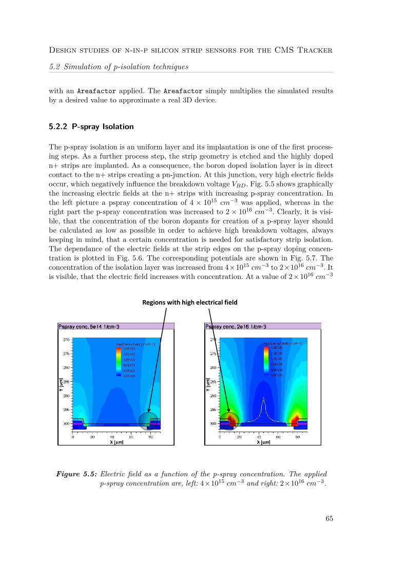
Design studies of n-in-p silicon strip sensors for the CMS Tracker
5.2 Simulation of p-isolation techniques
with an Areafactor applied. The Areafactor simply multiplies the simulated resultsby a desired value to approximate a real 3D device.
5.2.2 P-spray Isolation
The p-spray isolation is an uniform layer and its implantation is one of the first process-ing steps. As a further process step, the strip geometry is etched and the highly dopedn+ strips are implanted. As a consequence, the boron doped isolation layer is in directcontact to the n+ strips creating a pn-junction. At this junction, very high electric fieldsoccur, which negatively influence the breakdown voltage VBD. Fig. 5.5 shows graphicallythe increasing electric fields at the n+ strips with increasing p-spray concentration. Inthe left picture a pspray concentration of 4 × 1015 cm−3 was applied, whereas in theright part the p-spray concentration was increased to 2 × 1016 cm−3. Clearly, it is visi-ble, that the concentration of the boron dopants for creation of a p-spray layer shouldbe calculated as low as possible in order to achieve high breakdown voltages, alwayskeeping in mind, that a certain concentration is needed for satisfactory strip isolation.The dependance of the electric fields at the strip edges on the p-spray doping concen-tration is plotted in Fig. 5.6. The corresponding potentials are shown in Fig. 5.7. Theconcentration of the isolation layer was increased from 4×1015 cm−3 to 2×1016 cm−3. Itis visible, that the electric field increases with concentration. At a value of 2×1016 cm−3
Regions with high electrical field
Figure 5.5: Electric field as a function of the p-spray concentration. The appliedp-spray concentration are, left: 4×1015 cm−3 and right: 2×1016 cm−3.
65

Design studies of n-in-p silicon strip sensors for the CMS Tracker
5 Device Simulation
Figure 5.6: Electric field as a function of the p-spray concentration. Slice 0.1 µmunderneath the silicon-silicon dioxide interface.
the field even quadruples. The maximum electric fields at the n+ strip edges for thesimulated boron concentrations are plotted in Fig. 5.8. One can see, that the electric fieldstrength grows exponentially with increasing p-spray concentration. In order to producedetectors with high breakdown voltages VBD, exact calculation of doping concentrationis needed to keep the electric field strength at a low level and simultanously to ensuregood strip isolation. Another aspect considering p-spray isolation is the behaviour ofthe fields with increasing oxide charges QOx due to irradiation.The results so far presented, have been all simulated with a fixed initial interface oxidecharge of 1×1011 cm−2 with the exception of Fig. 5.9. With irradiation, the oxide chargeincreases and the p-spray is progressively depleted starting from the interface [PFC07].With increasing oxide charge, the breakdown performance improves significantly at avalue of around 4e11 cm−2 and then stays constant, because the oxide charge lowersthe fields at the implant edges, see Fig 5.9. In Fig. 5.10 a slice 100 nm underneath thesilicon bulk-silicon oxide interface shows the electric field depending on QOx and a p-spray concentration of 8 × 1015 cm−2. The black line with a high field of about 80 kVcorresponds to the initial QOx of 1 × 1011 cm−2. After increasing the oxide charge, thefields at the edges stay constant. The lines superpose because of no noticable difference.
66

Design studies of n-in-p silicon strip sensors for the CMS Tracker
5.2 Simulation of p-isolation techniques
Figure 5.7: Electrostatic potential as a function of the p-spray concentration. Thepotential determines the electric field distribution and electric fieldstrength.
4 . 0 x 1 0 1 5 8 . 0 x 1 0 1 5 1 . 2 x 1 0 1 6 1 . 6 x 1 0 1 6 2 . 0 x 1 0 1 65 . 0 x 1 0 4
1 . 0 x 1 0 5
1 . 5 x 1 0 5
2 . 0 x 1 0 5
2 . 5 x 1 0 5
3 . 0 x 1 0 5
3 . 5 x 1 0 5
4 . 0 x 1 0 5
4 . 5 x 1 0 5
max.
Electr
ic Field
[V/cm
]
p - s p r a y c o n c . [ c m ^ - 3 ]
V - B i a s = - 6 0 0 Vo x i d e c h a r g e = 1 e 1 1 c m ^ - 2Modell ExpDec1Gleichung y = A1*exp(-x/t1) + y0
Chi-Quadr Reduziert
8.41293E6
Kor. R-Quadrat 0.9996Wert Standardfehler
max. Electric Field
y0 66374.32111 5318.2669A1 18445.12674 3621.60482t1 -6.75345E15 4.16629E14
Figure 5.8: Maximum electric fields as a function of the p-spray concentration.The black line is a exponential fit function.
67

Design studies of n-in-p silicon strip sensors for the CMS Tracker
5 Device Simulation
0 . 0 5 . 0 x 1 0 1 1 1 . 0 x 1 0 1 2 1 . 5 x 1 0 1 2 2 . 0 x 1 0 1 2 2 . 5 x 1 0 1 2 3 . 0 x 1 0 1 2
3 x 1 0 4
4 x 1 0 4
5 x 1 0 4
6 x 1 0 4
7 x 1 0 4
8 x 1 0 4
9 x 1 0 4
V - B i a s = - 6 0 0 Vp - s p r a y c o n c . = 8 e 1 5 c m ^ - 3
max.
Electr
ic Field
[V/cm
]
Q _ O x [ 1 / c m ^ - 2 ]
Figure 5.9: Electric field as a function of increasing oxide charge.
Figure 5.10: Electrical field as a function of increasing oxide charge; orthogonalslice, 100 nm underneath the bulk-oxide interface. Increasing oxidecharge significantly lowers the electric field strength at the n+ strips.The p-spray concentration is 8× 1015 cm−3.
68

Design studies of n-in-p silicon strip sensors for the CMS Tracker
5.2 Simulation of p-isolation techniques
0 1 0 0 2 0 0 3 0 0 4 0 0 5 0 0 6 0 0
1 , 2 x 1 0 - 1 3
1 , 6 x 1 0 - 1 3
2 , 0 x 1 0 - 1 3
2 , 4 x 1 0 - 1 3
2 , 8 x 1 0 - 1 3
3 , 2 x 1 0 - 1 3
3 , 6 x 1 0 - 1 3
4 , 0 x 1 0 - 1 3
Inters
trip ca
pacita
nce [
F/cm]
- V _ B i a s [ V ]
Q _ O x 1 e 1 1 c m ^ - 2 Q _ O x 4 e 1 1 c m ^ - 2 Q _ O x 8 e 1 1 c m ^ - 2 Q _ O x 3 e 1 2 c m ^ - 2
P s p r a y c o n c = 4 e 1 5 c m ^ - 3
Figure 5.11: Interstrip capacitance on oxide charge concentration. The p-sprayconcentration is 4× 1015cm−2.
Interstrip capacitance Cint
The interstrip capacitance is affected by the integration of an isolation layer or iso-lation structure and has to be investigated, as it represents a major capacitance loadinto the readout electronics. Sentaurus Device T-CAD also provides small signal ACanalysis. First, a node list must be defined. The nodes represent circuit elements like DCand AC contacts. In the case of 2D strip sensors, the nodes are the defined contacts inthe contactlist of the simulation command file.As a reference, the interstrip capacitance value of Cint = 0.4 pF/cm is taken. This valueis the capacitance calculated from the sensor geometry (equation 2.23) and was con-firmed by experimental measurements of silicon microstrip sensors produced at differentcompanies [FdBH07]. Interstrip capacitance simulations of the sensors with 90 µm pitchand an implant width of 20 µm are presented in Fig. 5.11 and Fig. 5.12.Fig. 5.11 implicates, that the introduction of low doped p-spray layer does not increasethe interstrip capacitance. Also with increasing oxide charge Cint stays quite constant.Fig. 5.12 on the other hand shows the interstrip capacitance of a sensor with a p-spraylayer of 2 × 1016cm−3. Clearly, one can see, that higher introduction of boron dopants
69

Design studies of n-in-p silicon strip sensors for the CMS Tracker
5 Device Simulation
0 1 0 0 2 0 0 3 0 0 4 0 0 5 0 0 6 0 01 . 0 x 1 0 - 1 3
2 . 0 x 1 0 - 1 3
3 . 0 x 1 0 - 1 3
4 . 0 x 1 0 - 1 3
5 . 0 x 1 0 - 1 3
6 . 0 x 1 0 - 1 3
7 . 0 x 1 0 - 1 3Int
erstrip
capa
citanc
e [F/c
m]
- V _ B i a s [ V ]
Q _ O x 1 e 1 1 c m ^ - 2 Q _ O x 4 e 1 1 c m ^ - 2 Q _ O x 8 e 1 1 c m ^ - 2 Q _ O x 3 e 1 2 c m ^ - 2
P s p r a y c o n c = 2 e 1 6 c m ^ - 3
Figure 5.12: Interstrip capacitance on oxide charge concentration. The p-sprayconcentration is 2× 1016cm−2.
0 1 0 0 2 0 0 3 0 0 4 0 0 5 0 0 6 0 01 . 0 x 1 0 - 1 3
2 . 0 x 1 0 - 1 3
3 . 0 x 1 0 - 1 3
4 . 0 x 1 0 - 1 3
5 . 0 x 1 0 - 1 3
6 . 0 x 1 0 - 1 3
7 . 0 x 1 0 - 1 3
8 . 0 x 1 0 - 1 3
Inters
trip ca
pacita
nce [
F/cm]
- V _ B i a s [ V ]
p s p r a y c o n c 0 p s p r a y c o n c 1 e 1 5 c m ^ - 3 p s p r a y c o n c 4 e 1 5 c m ^ - 3 p s p r a y c o n c 8 e 1 5 c m ^ - 3 p s p r a y c o n c 2 e 1 6 c m ^ - 3
Figure 5.13: Interstrip capacitance on p-spray concentration. The interface oxidecharge is set to 1× 1011cm−3 for all curves.
70

Design studies of n-in-p silicon strip sensors for the CMS Tracker
5.2 Simulation of p-isolation techniques
between adjacent strips significantly rises Cint. A possible explanation is the higher ac-ceptor concentration NA, which determines a narrower lateral depletion region for agiven bias voltage and consequently a tighter coupling [Pie06]. But with increasing oxidecharge corresponding to irradiation of the sensors, the interstrip capacitance lowers withhigher values and reaches the capacitance of a sensor without a p-spray layer which isabout Cint = 0.4 pF/cm.This behaviour is also plotted in Fig. 5.13. The interface oxide charge was set to con-stant 1 × 1011cm−2 and the p-spray concentration was increased up to 2 × 1016cm−3.The dopant concentration influences Cint less than expected. Just the quite high valueof 2× 1016cm−3 increases Cint by almost a factor of two. This boron concentration alsodepicts a critical behaviour considering the electric fields at implant edges.The simulation results demonstrate the challange of achieving a satisfactory isolation ofstrips by a high enough concentration and simultanously to keep the dopants concentra-tion as low as possible in order to get low Cint and high breakdown voltages VBD.To sum up, a promising doping concentration seems to be about 8 × 1015 cm−3. Thisvalue generates relatively low electric fields at the strip implant edges and has no sig-nificant influence on the interstrip capacitance. Simulations also show a desired signalsharing between adjacent strips, hence the seperation of strips seems to work properlyfor this concentration when the sensors operate in overdepleted mode. Experimentalmeasurements have to be done to confirm this simulation approach.
5.2.3 P-stop Isolation
The p-stop pattern is another option to achieve an isolation by cutting the electron ac-cumulation layer, which would shorten the strips. The pattern has been introduced inchapter 4. Fig. 5.14 demonstrates the electron density at the silicon bulk/ silicon dioxideinterface. A sensor with four strips was simulated. Without any p-stop pattern, the elec-trons would uniformly distribute between adjacent strips and shorten them. The p-stopdopants push the electrons away and create electron poor regions between the n+ stripimplants (blue regions).As with the p-spray layer, also simulations with p-stops considering electric fields andinterstrip capacitances were done. A first outcome of the simulation is, that the distancebetween n+ strips and p-stop implants significantly affects the electric fields and elec-trostatic potentials, hence a convenient p-stop pattern geometry has to be encountered.In Fig. 5.15 the dependence of the electric field on the distance is plotted. There are
two aspects considered. First, how does the field strength depend on the gap width andsecond, how does the p-stop implant width affect the maximum electrical fields. Thep-stop distance has been varied from near to the n+ strips to almost in the middle oftwo strips . The doping concentration is 1 × 1017 cm−3. From the plot one can obtain,that a greater distance between strip and p-stop as well as a thinner p-stop implant lowerthe electric fields, what is important to achieve a reasonable breakdown voltage. Formerexperimantal studies on isolation techniques done at HEPHY Vienna also prefer widergaps between strip and p-stop considering the signal to noise ratio and charge collection
71

Design studies of n-in-p silicon strip sensors for the CMS Tracker
5 Device Simulation
((a)) electron density ((b)) slice at the interface
Figure 5.14: Simulation of a sensor with four strips and the p-stop atoll patternbetween adjacent strips. The electron accumulation layer is cut by thep-stop dopants. The electron density reaches a value of 0 at the p-stopedges.
dist = 0 dist = 1
Figure 5.15: The p-stop pattern was placed between adjacent strips with differentdistances to the implants. The electric field strength decreases withincreasing strip/p-stop distance. Value 0 corresponds to a distance of0 µm to the strip and 1 corresponds to maximum distance.
72

Design studies of n-in-p silicon strip sensors for the CMS Tracker
5.2 Simulation of p-isolation techniquesP
ote
ntia
l [V
]
dist 0.2 width 8 um
dist 0.2 width 4 um
dist 0.8 width 8 um
dist 0.8 width 4 um
((a)) Electrostatic potentialE
-Fie
ld [V
cm
^-1] pstop edge
implant edge
((b)) Electric field
Figure 5.16: Slice, 100 nm under bulk-oxide interface; the p-stop concentration is×1016 cm−3 and the distance and width have been varied.
Figure 5.17: Electric field strength on p-stop doping concentration. For higher p-stop concentration, higher field strength at the implant edges occur.The strip geometry is shown in Fig. 5.14.
efficiency [VBD+12]. The light bluish shadowed region at the distance from 0.6 to 0.85corresponds to the gaps, which were realized on the ITE wafer (16, 20 and 25 µm). Thep-stop widths of 4, 6 and 8 µm have also been chosen for the test samples from ITE toconfirm the simulation studies.A slice just 100 nm under the bulk-oxide interface is presented in Fig. 5.16. The highestelectric field strengths are, in contrary to the p-spray isolation technique, at the p-stop
73

Design studies of n-in-p silicon strip sensors for the CMS Tracker
5 Device Simulation
implant edges. Not only adjustment of the strip/p-stop gap is needed but also the p-stopdoping concentration to achieve a well performing microstrip sensor. As for the p-spraylayer, the breakdown voltage scales with the peak p-stop concentration. This fact isshown in Fig. 5.17. With increasing p-stop concentration, the maximum field strenghtalso increases. Comparing the concentrations of 1× 1016 cm−3 with 1× 1017 cm−3, thelater generates about 35% higher fields. As a consequence, the calculation of p-stop con-centration has also to be done as carefully as for the p-spray layer.
Eta distribution
The eta algorithm describes the charge distribution, when a particle hits the sensorbetween two adjacent strips. The signal height on the two strips depends on the col-lected charge. The proportion of the signal of one strip and the signal of both strips isdefined as the eta function [Nue09]:
η = PH(L)PH(L) + PH(R) (5.9)
PH(L) is the signal height on the left and PH(R) the signal height on the right strip.Hence, for η = 0.5 the charge was uniformly collected by both adjacent strips.The upgraded tracker will be read out binary by CBCs to cope with the higher datarates. This entails, that the eta distribution is less important for position measurement,because a strip will send a 1 (hit) or 0 (no hit) depending on a certain threshold. Nev-ertheless, the cluster size is of interest, hence charge sharing between strips dependingon the p-stop position plays a role and is presented in Fig. 5.18. In this simulated case,a particle hits the sensor at 59 µm, orthogonal to the surface and generates 24000 elec-trons. The right and the left strips collect charge depending on the p-stop position. Withincreasing gap between the n+ strip and the p+ implant the right strip collects more
Figure 5.18: Sharing of generated charge between two adjacent strips depends onthe p-stop position. The p-stop width is 6 µm.
74

Design studies of n-in-p silicon strip sensors for the CMS Tracker
5.2 Simulation of p-isolation techniques
Heavy Ion at 59 um
Figure 5.19: Eta values depending on the interface oxide charge Q_Ox.
charge.The charge sharing also depends on interface oxide charge concentration, Fig. 5.19. Inevidence, the proportion of collected charge described with the eta algorithm increaseswith higher oxide charge values. This means, that the eta function flattens and morecharge is collected by the left strip. As a consequence both, interface oxide charge andp-stop position between the strip implants, affect charge sharing. This correlation couldbe implement to the position measurement algorithm for even more precise hit assign-ment and the estimation of cluster sizes.
Interstrip capacitance Cint
Simulations of sensors with different p-stop patterns were also evaluated with regardto the interstrip capacitance. Influence of p-stop width, distance and oxide charge likefor the p-spray solution were investigated. The results are shown in the following fig-ures. The curves in Fig. 5.20 were all simulated with a p+ dopant peak concentration of5 × 1016 cm−3. Also the width of the isolation structure does not influence Cint signif-icantly, but has a remarkable impact on the electrical potentials. This fact is shown inFig. 5.16 and therefore a p-stop pattern structure with narrow p+ implants is prefered.As expected due to p-spray results, the introduction of a highly doped p-stop patternbetween strips also does hardly influence the interstrip capacitance.All interstrip capacitance curves for p-stop and p-spray decrease with increasing biasvoltage because the electrons from the inversion layer are removed steadily. When allelectrons are removed, the curves get constant.The p-stop technique offers, compared to the p-spray layer, a more significant influ-
75

Design studies of n-in-p silicon strip sensors for the CMS Tracker
5 Device Simulation
0 5 0 1 0 0 1 5 0 2 0 0 2 5 0 3 0 00
1 x 1 0 1 1
2 x 1 0 1 1
3 x 1 0 1 1
4 x 1 0 1 1
5 x 1 0 1 1
6 x 1 0 1 1
7 x 1 0 1 1
Inters
trip ca
pacita
nce [
F/cm]
- V _ B i a s [ V ]
d i s t 0 . 5 d i s t 0 . 6 d i s t 0 . 7 d i s t 0 . 8
Figure 5.20: Interstrip capacitance dependency on p-stop distance with a interfaceoxide charge of 1× 1011 cm−2. As expected, there is hardly influenceof the p-stop position.
0 1 0 0 2 0 0 3 0 0 4 0 0 5 0 0
2 , 0 x 1 0 - 1 3
4 , 0 x 1 0 - 1 3
6 , 0 x 1 0 - 1 3
8 , 0 x 1 0 - 1 3
1 , 0 x 1 0 - 1 2
1 , 2 x 1 0 - 1 2
1 , 4 x 1 0 - 1 2
Inters
trip ca
pacita
nce [
F/cm]
- V _ B i a s [ V ]
Q _ O x 1 e 1 1 c m ^ - 2 Q _ O x 4 e 1 1 c m ^ - 2 Q _ O x 8 e 1 1 c m ^ - 2 Q _ O x 2 e 1 2 c m ^ - 2
Figure 5.21: Interstrip capacitance dependency on interface oxide charge for a p-stop concetration of 5× 1016 cm−3.
76

Design studies of n-in-p silicon strip sensors for the CMS Tracker
5.2 Simulation of p-isolation techniques
ence on Cint with increasing oxide charge. The interstrip capacitance raises at QOx =2 × 1012 cm−2 more than two times from about Cint = 0.4 pF to Cint = 0.9 pF as aconsequence of more attracted electrons in the accumulation layer between n+ stripsand p+ isolation. Although Cint increases, signal on both strips in the simulation doesnot change. Therefore one can assume, that a sufficent strip isolation is still present.This assumption has to be confirmed by experiments.
5.2.4 Simulation of a modified FOSTER design preventing undesired signalcoupling
The implantion of a p+ structure under the aluminum routing lines of the FOSTERwas simulated with the main goal to find the minimum doping concentration, which isnecessery to avoid a signal coupling. The simulated structure is shown in Fig. 5.22. Inthe simulation a FOSTER design with a pitch of 100 µm was taken. The aluminumrouting line is 18 µm and the p-common implantation is 27 µm wide.
Near strip Near strip
Routing line far strip
p-common
Figure 5.22: Sketch of the simulated FOSTER design. The bluish shadowed regionunder the aluminum routing line from the far region is the p-stopcommon structure. This FOSTER design was also simulated with ap-spray layer.
77

Design studies of n-in-p silicon strip sensors for the CMS Tracker
5 Device Simulation
0 , 0 0 , 2 0 , 4 0 , 6 0 , 8 1 , 0
0 , 0
5 , 0 x 1 0 - 1 6
1 , 0 x 1 0 - 1 5
1 , 5 x 1 0 - 1 5
2 , 0 x 1 0 - 1 5
2 , 5 x 1 0 - 1 5
3 , 0 x 1 0 - 1 5
3 , 5 x 1 0 - 1 5
Charg
e [C]
P o s i t i o n
p - c o m m o n p e a kc o n c e n t r a t i o n :
1 e 1 5 c m ^ - 3 3 e 1 5 c m ^ - 3 5 e 1 5 c m ^ - 3 7 e 1 5 c m ^ - 3 9 e 1 5 c m ^ - 3
((a)) p-common technique ((b)) p-spray technique [Hof12]
Figure 5.23: Charge on aluminum routing line for different p-common and p-spraydoping concentrations. Both techniques need a specific minimum con-centration to suppress the signal couling.
The strip implant concentration is set to 1 × 1019 cm−3. Fig. 5.23 shows the resultsfor both, p-stop common and p-spray. One can see, that for the p-common techniquea minimum peak doping concentration of 9 × 1015 cm−3 is needed to suppress a signalcoupling on the routing lines of the far strip region. This is a quite low value for p-stopisolation, as a common doping concentration is about 5×1016 cm−3. Hence, a suppressionof undesired signal on the aluminum routing lines with the p-common structure seemsto be realisable.The p-spray layer concentration should be at least 4 × 1015 cm−3. This value is alsolower than the simulated concentrations in section 5.2.2. Summerising, implantation ofp+ dopants under the routing lines seems to be a promising solution to achieve a wellperforming FOSTER.
5.2.5 Conclusion on isolation techniques
This chapter described two possible isolation techniques of n-in-p silicon microstrip de-tectors (p-spray and p-stop). The interstrip capacitance seems to be not affected signifi-cantly by introduction of any isolation pattern. Until a certain value of p+ material con-centration, both techniques feature comparable potentials and electrical field strengths.The p-spray solution seems to have little lower electrical field strengths at the implantedges and therefore an improved breakdown voltage when the concentration is below1× 1016 cm−3. Nevertheless, this results from simulation give just an indication on theperformance of the introduced p+ patterns. All simulated results have to be proven byexperimental measurements of sensors with applied isolation techniques.Furthermore, any change of the sensor geometry like pitch or n+ implant width could
78

Design studies of n-in-p silicon strip sensors for the CMS Tracker
5.2 Simulation of p-isolation techniques
discard this simulation results.
All simulation results, especially the results of electrical field distribution in the p-stopconfigurations affected the design choice of the sensors on the ITE wafer. Implantationof p-stop patterns near to the n+ strip implants seems to lower the breakdown voltage,therefore just sensors with a relatively wide gap between strip and p-stop were designed.Comparing the results of p-spray and p-stop simulations is difficult. The problem is, thatthe p-spray concentration can be lower than the p-stop, because p-spray is uniformlydoped as a layer whereby the p-stop pattern is of less surface, hence it needs higherconcentration. A doping concentration between 2×1016 cm−3 and 5×1016 cm−3 for thep-stop solution seems to have almost no influence on the interstrip capacitance Cint withhigh oxide charge concentration as expected after irradiation with charged particles andrelatively low electric field strengths. Higher concentrations exponentially raise the fieldstrength.To achieve the same or lower electric field strength at the implants with the p-spraylayer, the doping concentration should not exceed 8 × 1015 cm−3. Moreover, both pro-posed concentrations have to ensure good strip isolation also with higher irradiation.Therefore it is essential to produce sensors with varying peak doping concentrations andextensive experiments before and after irradiation are needed.
79


Design studies of n-in-p silicon strip sensors for the CMS Tracker
6 ITE Sensor Qualification and measurements
6.1 Sensor qualification
In August 2012 six processed wafers from ITE Warsaw were delivered. First of all, thesensors were qualified with the probe-station and the results are shown in Fig. 6.1.These are representive results of an implemented standard sensor design. All sensors onthe wafers show comparable characteristics.
0 2 0 4 0 6 0 8 0 1 0 0 1 2 0 1 4 0 1 6 0 1 8 0 2 0 0 2 2 00 , 0
5 , 0 x 1 0 1 9
1 , 0 x 1 0 2 0
1 , 5 x 1 0 2 0
2 , 0 x 1 0 2 0
2 , 5 x 1 0 2 0
1/C^2
[F/cm
]
- V _ B i a s [ V ]
S t d C M S u p S e n s o r d e s i g n
(a) 1/C2 curve
0 2 0 4 0 6 0 8 0 1 0 0 1 2 0 1 4 0 1 6 0 1 8 0 2 0 0 2 2 0
1 E - 8
1 E - 7
1 E - 6
1 E - 5
1 E - 4Cu
rrent
[A]
- V _ B i a s [ V ]
(b) Total current over bias voltage
Figure 6.1: CV and IV characteristics of a standard sensor geometry. The de-pletion voltage is about 50 V and the sensor has a high current of0.92 µA/cm2 at 1.2× VFD and 20°C
The total current of the sensors is with 0.92 µA/cm2 quite high. Furthermore the deple-tion voltage VFD in the 1/C2 curve is aroung 50 V.Simulation results of p-isolation techniques, which were introduced in chapter 5, gave afirst indication, that it is difficult to calculate a reasonable p+ material doping concen-tration in order to achieve a sufficient strip isolation and low electric field strengths. Theexperimental results give a clear reference, that the doping concentration of p-stop, istoo low to provide a seperation between adjacent strips and the electron layer shortensthe n+ strips. The measurement results of the delivered ITE sensors are shown in Fig.6.2. The interstrip resistance Rint is about 6 kΩ, what is far to low, as a typical value isin the range of 10 GΩ. Moreover, the poly-silicon resistors have a resistance of 4 kΩ to6 kΩ. The wafer also includes some test structures, which are helpful for the producerduring processing and for first wafer characteristics. One of the test structures is a poly-silicon resistor with identical geometry like implemented in sensors and its measurementresulted in a poly-silicon resistance value of 2.7 MΩ. The specifications demanded aresitance between 2 MΩ and 4 MΩ. This result gives another hint, that the interstrip
81

Design studies of n-in-p silicon strip sensors for the CMS Tracker
6 ITE Sensor Qualification and measurements
0 1 0 2 0 3 0 4 0 5 0 6 0 7 0- 6 , 0 x 1 0 - 9
- 5 , 0 x 1 0 - 9
- 4 , 0 x 1 0 - 9
- 3 , 0 x 1 0 - 9
- 2 , 0 x 1 0 - 9
- 1 , 0 x 1 0 - 9
0 , 0
Leak
age c
urren
t [A]
S t r i p N u m b e r
(a) Leakage current
0 1 0 2 0 3 0 4 0 5 0 6 0 7 02 , 0 x 1 0 - 1 2
4 , 0 x 1 0 - 1 2
6 , 0 x 1 0 - 1 2
8 , 0 x 1 0 - 1 2
1 , 0 x 1 0 - 1 1
1 , 2 x 1 0 - 1 1
1 , 4 x 1 0 - 1 1
1 , 6 x 1 0 - 1 1
1 , 8 x 1 0 - 1 1
2 , 0 x 1 0 - 1 1 C o u p l i n g c a p a c i t a n c e
Coup
ling ca
pacita
nce [
F]
S t r i p n u m b e r
(b) Coupling capacictance
0 1 0 2 0 3 0 4 0 5 0 6 0
4 0 0 0
5 0 0 0
6 0 0 0
7 0 0 0
8 0 0 0
9 0 0 0
1 0 0 0 0
1 1 0 0 0
R_Po
ly [Oh
m]
S t r i p N u m b e r
(c) Polyresistance
0 1 0 2 0 3 0 4 0 5 0 6 0 7 01 0 3
1 0 4
1 0 5
1 0 6Int
erstrip
resis
tance
[Ohm
]
S t r i p N u m b e r
(d) Interstrip resistance
0 1 0 2 0 3 0 4 0 5 0 6 0 7 00 , 0
2 , 0 x 1 0 - 1 3
4 , 0 x 1 0 - 1 3
6 , 0 x 1 0 - 1 3
8 , 0 x 1 0 - 1 3
1 , 0 x 1 0 - 1 2
1 , 2 x 1 0 - 1 2
1 , 4 x 1 0 - 1 2
1 , 6 x 1 0 - 1 2
1 , 8 x 1 0 - 1 2
2 , 0 x 1 0 - 1 2 I n t e r s t r i p c a p a c i t a n c e
Inters
trip ca
pacita
nce [
F]
S t r i p n u m b e r
(e) Interstrip capacitance
Figure 6.2: Further quality measurements of the standard sensor design as a rep-resentive for all senors at 60 V and 20°C.
82

Design studies of n-in-p silicon strip sensors for the CMS Tracker
6.2 FOSTER laser scan measurements
resistance Rint is far too low and instead of measuring one resistor in the sensor, wemeasured all resistors in parallel. Therefore the value is orders of magnitude lower thanexpected.The leakage current Ileak for each strip is in the range of expectations and summed upover all strips, Ileak = 186 nA. But Ileak should be comparable with the total currentvalue, which is 0.92 µA/cm2. The sensors active surface is 1.38 cm2, therefore the totalsensor current is 1.27 µA. The difference current of about 1 µA is most likely generatedfrom boundary effects at the cutting edge, hence the guard ring does not work properly.
The coupling capacitance Ccoup is a little low, but the measured values could provide asufficient functionality of the sensors. The interstrip capacitance Cint is two times highercompared to other sensor productions with the same sensor geometry (Cint ≈ 0.4pF/cm).Some values were even beyond 2 pF/cm and were not plotted.After discussion with ITE engineers it seems, that the p-stop doping concentration wasat the limit, since segregation of boron during long oxidation always causes that boronatoms are drawn from silicon towards oxide and their concentration at the interfacebetween silicon and silicon dioxide gets reduced in the order of one magnitude [Mar]. Asa fact, the segregation of boron dopants into the oxide depends on technological details.Hence, a detailed discussion and understanding of all applied process technologies ofsensors is needed to prevent any misunderstandings between producer and client.
6.2 FOSTER laser scan measurements
Independent of the general sensor qualification results, laser scans of the FOSTER sensorwith the p-stop common implantation under the aluminum routing lines from far regionwere executed. The results don’t allow to draw final conclusions on the functionalityof the new FOSTER design but give a first indication, that the proposed solution ofp+ material implantation in fact suppresses the signal coupling. The measurements aredepicted in Fig. 6.3 and Fig. 6.4. The scan of the far region (Fig. 6.3) shows a signaldistribution over several far strips indicating a bad interstrip resistance. Nevertheless,there is no signal sharing to the near strips as expected.In contrary, in Fig 6.4 one can see the scan of the near region and a signal sharing withthe far region. Although there is a signal induced, it differs from the former measure-ments shown in Fig. 4.19. The signal peaks of the far region are not shifted to the peaksof the near region. This distribution signifies a coupling from neighbouring nearstripson the aluminum routing lines of far strips instead of direct induction through driftingcharge carriers under the aluminum. Hence, the p+ material implantation under therouting lines seems to work because there is no direct signal on the lines but on theother hand it is too low for strip isolation.Unfortunately the wafer with higher p-stop doping concentration broke during process-ing. A variation of p+ material concentration and simultanously a variation of signal
83

Design studies of n-in-p silicon strip sensors for the CMS Tracker
6 ITE Sensor Qualification and measurements
Figure 6.3: Laser scan of the far region. As expected, there is no signal couplingto the near region (strip 154) but a strong signal sharing over severalhundreds micrometer between far strips due to bad interstrip resistanceRint.
Figure 6.4: Laser scan of the near region. There is a signal coupling to the farstrip with the strip number 155, but the induced signal has the samedistribution as the near strips. This indicates a coupling not to thealuminum routing line, but coupling due to low interstrip resistance.
84

Design studies of n-in-p silicon strip sensors for the CMS Tracker
6.2 FOSTER laser scan measurements
coupling could likewise confirm simulation results.Consequently, a further wafer run with adjusted p+ material doping concentrations isneeded to guarentee full functionality of the FOSTER design. First iterations with IMB-CNM30 Barcelona were done and a run is scheduled for end of November 2012. Scientificfindings from ITE sensor measurements and technological know-how are integrated tothe next batch.
30Instituto de Microelectronica de Barcelona-Centre National de Microelectronica
85


Design studies of n-in-p silicon strip sensors for the CMS Tracker
7 Summary and outlook
The main goal of this thesis was the identification of an isolation technique (p-sprayand p-stop) for n-in-p technology sensors, which can guarantee sufficient strip isolationwithout any negative impact on the sensors performance. Furthermore, an implementedp+ doped structure under the routing lines should ensure a well performing FOSTERdesign. Due to technological problems, the delivered devices are not appropriate to char-acterise the isolation, hence the conclusions base on simulations.
Generally, finite-element device simulation software like Synopsys Sentaurus T-CADis a powerful tool for the determination of electrical characteristics and analysis of mi-crostrip sensors. The flow of simulation methods was described in detail in chapter 5.Considering the simulation results, it seems that the tuning of p-stop and p-spray dop-ing concentrations is a crucial factor for the final sensor functionality, as the maximumelectric fields in the bulk grow exponentially with the dopant concentration. Analysis ofelectrical characteristics assigned the maximum doping concentrations to 8 × 1015 cm3
for the p-spray layer and 5× 1016 cm3 for the p-stop solution, chapter 5.2.5. These con-centrations indicate a sufficient strip isolation and at the same time low electric fields atthe implant edges of the n+ strips and p+ isolation patterns, guaranteeing a high voltagestability of the sensors. The distance between strip implant and p-stop pattern shouldexceed a quarter of the pitch to meet the requirements of high breakdown voltages.Furthermore, the introduction of p+ material between adjacent strips in both meth-ods does not influence the interstrip capacitance significantly and as a consequence thenoise load into the read out electronics is not affected negatively, chapters 5.2.2 and 5.2.3.
Simulation of the FOSTER design, which was developed in-house, clearly indicates thatan implantation of p+ material under the aluminum routing lines successfully suppressesinduced signals of drifting charges to the far region, making the FOSTER a promisingcandidate for the proposed 2S module. Measurements of LASER induced signals in theALiBaVa station at Karlsruhe partially confirmed the simulation outcomes. A final con-clusion is not possible due to very low interstrip resistances on the produced structures,see chapter 6.2.
Studies of surface damage of silicon microstrip sensors indicate that the interstrip capac-itance is not affected noticably as long as the doping concentrations for both methods,p-spray and p-stop, stay under the above stated values. The next step could be the im-plementation of trap models to the simulations. These allow advanced studies of sensorcharacteristics and behaviour after irradiation.
The wafer masks for the ITE run have been designed using the software LayoutEditor.All designs were created with attention to the manufacturer’s design rules. The masks
87

Design studies of n-in-p silicon strip sensors for the CMS Tracker
7 Summary and outlook
are reusable and the possibility for another run at ITE in 2013 with better processknowledge is given. The simulations strongly affected the choice of the p-stop patternsand were directly implemented to the sensor designs. As the place on a wafer is limited,primary simulation studies are an indispensable tool to discard sensor geometries withexpected bad electrical characteristics.
The characterization of the ITE sensors showed how complex the processing of sili-con microstrip sensors for particle detection is. During long oxidation of the wafers, theboron atoms for strip isolation diffused into the oxide and the concentration at the in-terface of silicon and silicon dioxide was reduced. As a consequence, an accumulationlayer is created and the n+ implants are electrically shortened. This is reflected in themeasurements of the very low interstrip resistance.To confirm the introduced simulation studies regarding the choice of p-stop patternsand in order to determine the doping concentrations, a further run is necessary. Firstdiscussions and iterations with engineers from IMB-CNM Barcelona took place and thenext batches are scheduled for December 2012 and March 2013. The mask designs werealready delivered and are currently under investigation on manufacturer’s design rules.
In summary, strip isolation techniques on n-in-p sensors have been studied and an anal-ysis of the required doping concentrations have been perfomed. The results partiallyreflect published data. Finite-element device simulations are extremely useful to pre-dict relative sensor performance, but experimental measurements are indispensable forquantitative conclusions. The FOSTER design with an implantation of p+ dopants un-der the aluminum routing lines is a promising candidate for a 2S module as it fulfillsall requirements of this module concept and even raises the granularity by a factor oftwo.
88

Design studies of n-in-p silicon strip sensors for the CMS Tracker
Software
• Sentaurus T-CADVersion: F-2011.09,Website: http://www.synopsys.com/tools/tcad/Pages/default.aspx,Stand: 10.06.2012.
• Layout Editor,Website: http://www.layouteditor.net/,Stand: 10.06.2012.
itemize
89


Design studies of n-in-p silicon strip sensors for the CMS Tracker
A Appendix
On the following pages, the command files used for building a sensor device and forsimulation with Sentaurus T-CAD are presented. The first example command_file_SDEcreates after compiling an AC coupled silicon sensor with two half-electrodes. Thesecond command file command_file_SentaurusDevice includes sensor parametersand the physical models applied.
i

command_file_SDE
(define Pitch @pitch@)(define Pitch_2 (/ @pitch@ 2))(define Imp_width @Imp_width@)(define Imp_width_2 (/ @Imp_width@ 2))(define Al_width @Al_width@)(define Al_width_2 (/ @Al_width@ 2))(define P-stop_dist @Pstop_dist@)(define P-stop_width @Pstop_width@)(define P-stop_width_2 (/ @Pstop_width@ 2))(define P-stop_conc @Pstop_conc@)(define P-stop_conc2 (/ @Pstop_conc@ 100))(define Imp_conc @Implant_conc@)(define Imp_conc2 (/ @Implant_conc@ 100))
(define P-stop_pos1 (+ (* (- Pitch_2 (+ Imp_width_2 P-stop_width)) P-stop_dist) (+ Imp_width_2 P-stop_width_2)) )(define P-stop_pos2 (- Pitch P-stop_pos1) )
;;#-----------------------------------------------------------------------------------------------------------------------------;;#----------Draw Structure----------(sdegeo:create-rectangle (position 0 0 0) (position Pitch 300 0) "Silicon" "p-bulk" )(sdegeo:create-rectangle (position 0 300 0) (position Pitch 301 0) "SiO2" "oxide" )(sdegeo:create-rectangle (position Imp_width_2 301 0) (position (- Pitch Imp_width_2) 302 0) "SiO2" "oxide" )(sdegeo:create-rectangle (position 0 0 0) (position Pitch 1 0) "Aluminum" "backplane")
(sdegeo:create-rectangle (position 0 300.2 0) (position Imp_width_2 301 0) "Aluminum" "strip_alu1")(sdegeo:create-rectangle (position (- Pitch Imp_width_2) 300.2 0) (position Pitch 301 0) "Aluminum" "strip_alu2")
(sdegeo:create-rectangle (position 0 301 0) (position Al_width_2 302 0) "Aluminum" "strip_alu1_top")(sdegeo:create-rectangle (position (- Pitch Al_width_2) 301 0) (position Pitch 302 0) "Aluminum" "strip_alu2_top")
(sdegeo:insert-vertex (position Imp_width_2 300.0 0.0))(sdegeo:insert-vertex (position (- Pitch Imp_width_2) 300.0 0.0))
;;#-----------------------------------------------------------------------------------------------------------------------------;;#----------Define Contacts----------(sdegeo:define-contact-set "contactbackplane" 4 (color:rgb 1 1 1 ) "##" )(sdegeo:define-contact-set "contactstrip_1" 4 (color:rgb 1 0 0 ) "##" )(sdegeo:define-contact-set "contactstrip_2" 4 (color:rgb 1 0 0 ) "##" )(sdegeo:define-contact-set "contactn_1" 4 (color:rgb 1 1 0 ) "##" )(sdegeo:define-contact-set "contactn_2" 4 (color:rgb 1 1 0 ) "##" )
;;#-----------------------------------------------------------------------------------------------------------------------------;;#----------Define Ref/Eval Window----------(sdedr:define-refeval-window "dope_p++" "Line" (position 0 1 0) (position Pitch 1 0))(sdedr:define-refeval-window "dope_n1" "Line" (position 0 300 0) (position Imp_width_2 300 0))(sdedr:define-refeval-window "dope_n2" "Line" (position (- Pitch Imp_width_2) 300 0) (position Pitch 300 0))
(sdedr:define-refeval-window "dope_pstop1" "Line" (position (- P-stop_pos1 P-stop_width_2) 300 0) (position (+ P-stop_pos1 P-stop_width_2) 300 0))(sdedr:define-refeval-window "dope_pstop2" "Line" (position (- P-stop_pos2 P-stop_width_2) 300 0) (position (+ P-stop_pos2 P-stop_width_2) 300 0))
Seite 1

command_file_SDE;;#-----------------------------------------------------------------------------------------------------------------------------;;#----------Set Contacts----------(sdegeo:set-current-contact-set "contactbackplane")(sdegeo:define-2d-contact (list (car (find-edge-id (position (/ Pitch 2) 0 0))))"contactbackplane")(sdegeo:set-current-contact-set "contactstrip_1")(sdegeo:define-2d-contact (list (car (find-edge-id (position (/ Imp_width_2 2) 300.2 0)))) "contactstrip_1")(sdegeo:set-current-contact-set "contactstrip_2")(sdegeo:define-2d-contact (list (car (find-edge-id (position (- Pitch (/ Imp_width_2 2)) 300.2 0)))) "contactstrip_2")
(sdegeo:set-current-contact-set "contactn_1")(sdegeo:define-2d-contact (list (car (find-edge-id (position (/ Imp_width_2 2) 300 0)))) "contactn_1")(sdegeo:set-current-contact-set "contactn_2")(sdegeo:define-2d-contact (list (car (find-edge-id (position (- Pitch (/ Imp_width_2 2)) 300 0)))) "contactn_2")
;;#-----------------------------------------------------------------------------------------------------------------------------;;#----------Define Dopingconcentrations----------;;#----------Constant Doping Profile----------(sdedr:define-constant-profile "ConstantProfileDefinition_1" "BoronActiveConcentration" 2.52e12)(sdedr:define-constant-profile-region "ConstantProfilePlacement_1" "ConstantProfileDefinition_1" "p-bulk");;#----------Analytic Doping Profile----------(sdedr:define-analytical-profile-placement "AnalyticalProfilePlacement_1" "AnalyticalProfileDefinition_1" "dope_p++" "Both" "NoReplace" "Eval")(sdedr:define-gaussian-profile "AnalyticalProfileDefinition_1" "BoronActiveConcentration" "PeakPos" 0.3 "PeakVal" 1e19 "ValueAtDepth" 1e17 "Depth" 20 "Erf" "Factor" 0.8)
(sdedr:define-analytical-profile-placement "AnalyticalProfilePlacement_2" "AnalyticalProfileDefinition_2" "dope_n1" "Both" "NoReplace" "Eval")(sdedr:define-gaussian-profile "AnalyticalProfileDefinition_2" "PhosphorusActiveConcentration" "PeakPos" 0.3 "PeakVal" Imp_conc "ValueAtDepth"Imp_conc2 "Depth" 1.3 "Erf" "Factor" 0.8)(sdedr:define-analytical-profile-placement "AnalyticalProfilePlacement_3" "AnalyticalProfileDefinition_3" "dope_n2" "Both" "NoReplace" "Eval")(sdedr:define-gaussian-profile "AnalyticalProfileDefinition_3" "PhosphorusActiveConcentration" "PeakPos" 0.3 "PeakVal" Imp_conc "ValueAtDepth"Imp_conc2 "Depth" 1.3 "Erf" "Factor" 0.8)
(sdedr:define-analytical-profile-placement "AnalyticalProfilePlacement_7" "AnalyticalProfileDefinition_7" "dope_pstop1" "Both" "NoReplace" "Eval")(sdedr:define-gaussian-profile "AnalyticalProfileDefinition_7" "BoronActiveConcentration" "PeakPos" 0.3 "PeakVal" P-stop_conc "ValueAtDepth" P-stop_conc2 "Depth" 1.1 "Erf" "Factor" 0.8)(sdedr:define-analytical-profile-placement "AnalyticalProfilePlacement_8" "AnalyticalProfileDefinition_8" "dope_pstop2" "Both" "NoReplace" "Eval")(sdedr:define-gaussian-profile "AnalyticalProfileDefinition_8" "BoronActiveConcentration" "PeakPos" 0.3 "PeakVal" P-stop_conc "ValueAtDepth" P-stop_conc2 "Depth" 1.1 "Erf" "Factor" 0.8);;#-----------------------------------------------------------------------------------------------------------------------------;;#----------Refinement Placement----------(sdedr:define-refinement-size "RefinementDefinition_1" 10 20 0.01 0.01)(sdedr:define-refinement-material "RefinementPlacement_1" "RefinementDefinition_1" "Silicon" )(sdedr:define-refinement-function "RefinementDefinition_1" "DopingConcentration""MaxTransDiff" 1)(sdedr:define-refinement-size "RefinementDefinition_2" 0.1 0.05 )(sdedr:define-refinement-material "RefinementPlacement_2" "RefinementDefinition_2" "SiO2" )
Seite 2

command_file_SDE(sdedr:define-refinement-function "RefinementDefinition_2" "DopingConcentration""MaxTransDiff" 1);;#-----------------------------------------------------------------------------------------------------------------------------;;#----------- Build Mesh (sde:build-mesh "snmesh" " " "n@node@_msh")
Seite 3

command_file_SentaurusDevice# Simulation within Synopsis# n-on-p strip detector# 2d
Device n_on_p_strips
Electrode Name = "contactstrip_1" voltage=0.0 Name = "contactstrip_2" voltage=0.0
Name = "contactn_1" voltage=0.0 Name = "contactn_2" voltage=0.0
Name = "contactbackplane" voltage=0.0
File Grid = "@tdr@" Current = "@plot@" Plot = "@dat@"
Physics AreaFactor=10000 Temperature = 293 Fermi Mobility ( DopingDep eHighFieldSaturation hHighFieldSaturation #Enormal CarrierCarrierScattering (ConwellWeisskopf) ) Recombination ( SRH (DopingDep) Auger eAvalanche (vanOverstraeten Eparallel) hAvalanche (vanOverstraeten Eparallel) ) EffectiveIntrinsicDensity(Slotboom)
HeavyIon ( Direction=(0,1) Location=!(puts ([expr @<Position>@*@<pitch>@],0))! Time=1e-9 Length=[0 0.001 300 300.001] Wt_hi= [1.0 1.0 1.0 1.0] LET_f= [0 8.7176e-10 8.7176e-10 0] # 1.282E-5/10000*0.68 Gaussian PicoCoulomb ) Physics (MaterialInterface = "Silicon/SiO2") Traps( FixedCharge Conc=@<Q_Ox>@ )
Seite 1

command_file_SentaurusDeviceSystem
n_on_p_strips npp ( "contactn_1"=c1 "contactn_2"=c2 "contactbackplane"=bg"contactstrip_1"=s1 "contactstrip_2"=s2 ) Vsource_pset v (bg 0) dc = 0
Resistor_pset r1c (c1 0) resistance = 1500000 Resistor_pset r2c (c2 0) resistance = 1500000
Resistor_pset r1s (s1 0) resistance = 50 Resistor_pset r2s (s2 0) resistance = 50
File Output = "@log@" ACExtract = "@acplot@"
Plot eCurrent/Vector hCurrent/Vector Current/vector eDensity hDensity ElectricField ElectricField/Vector eEparallel hEparallel Potential SpaceCharge Doping DonorConcentration AcceptorConcentration Auger eAvalanche hAvalanche AvalancheGeneration eMobility hMobility SRHRecombination #BeamGeneration HeavyIonCharge HeavyIonGeneration
Math Method = pardiso Number_of_Threads = 4 Extrapolate Derivatives RelErrControl Digits=4 Notdamped=50 Iterations=25 RecBoxIntegr (5e-3 50 5000)
Solve Poisson
Coupled (iterations=50 notdamped=0) Poisson Coupled (iterations=50 notdamped=0) Poisson Electron Hole
ACCoupled ( StartFrequency=@<Frequency>@ EndFrequency=@<Frequency>@ NumberOfPoints=1 Decade Node (c1 c2 s1 s2 bg) Exclude (v) ) poisson electron hole contact circuit
QuasiStationary ( InitialStep=1e-5 Minstep = 1e-10
Seite 2

command_file_SentaurusDevice MaxStep = 0.2 Increment = 2 Decrement = 4 Goal Parameter =v.dc voltage = @<V_Bias>@ )
ACCoupled ( StartFrequency=@<Frequency>@ EndFrequency=@<Frequency>@ NumberOfPoints=1 Decade Node (c1 c2 s1 s2 bg) Exclude (v) ) poisson electron hole contact circuit
NewCurrentPrefix = "transient_"
Transient ( InitialTime = 0.0 FinalTime=30.0E-9 InitialStep=0.5E-11 MaxStep=0.5E-9 #Increment=1.1 #Decrement=1.5 ) Coupled (iterations=8, notdamped=15)Poisson Electron Hole Circuit Plot(Time=(0.5e-9;1e-9;2e-9;5e-9;10e-9;20e-9;30e-9) noOverwrite FilePrefix="MIP_n@node@")
Seite 3


Design studies of n-in-p silicon strip sensors for the CMS Tracker
Bibliography
[Abb11] Duccio Abbaneo. The 20th Anniversary International Workshop onVertex Detectors, June 19-24 2011. (document), 3.1
[ALi12] http://www.alibavasystems.com/solutions, November 26th, 2012. (doc-ument)
[Bru07] R. Bruneliere. Cms electromagnetic calorimeter performance andtest beam results. Nuclear Instruments and Methods in Physics Re-search Section A: Accelerators, Spectrometers, Detectors and AssociatedEquipment, 572(1):33 – 35, 2007. 1.2
[Cam97] D. Campi. The magnet project technical design report. TechnicalReport CMS TDR 1, CERN, Europeen Laboratory for Particle Physics,Geneva, Switzerland, May 2nd, 1997. 1.2
[Civ07] Carlo Civinini. The cms silicon strip tracker. Nuclear Instruments andMethods in Physics Research, 579(2):726 – 730, 2007. 1.2
[Dal07] Raffaello Dalessandro. The cms silicon strip tracker: Experience inintegration and commissioning. Nuclear Instruments and Methods inPhysics Research Section A: Accelerators, Spectrometers, Detectors andAssociated Equipment, 582(3):739 – 743, 2007. 1.4
[Die03] Alexander Dierlamm. Studies on the Radiation Hardness of siliconSensors. PhD thesis, University of Karlsruhe (TH), November 24th,2003. 2.4.2
[Die12] Alexander Dierlamm. VERTEX, Jeju, Korea, 2012. (document)
[ea01] S. Braibant et al. Investigation of design parameters for radiationhard silicon microstip detectors. Nuclear Instruments and Methods inPhysics Research Section A: Accelerators, Spectrometers, Detectors andAssociated Equipment, 485(1):343–3615, 2001. 2.4.4
[FBH+02] M Friedl, T Bauer, J Hrubec, M Krammer, and M Pernicka. Per-formance of a cms silicon strip detector module with apv25 readout.Nuclear Instruments and Methods in Physics Research Section A: Ac-celerators, Spectrometers, Detectors and Associated Equipment, 488(1-2):175 – 183, 2002. 2.4
ix

Design studies of n-in-p silicon strip sensors for the CMS Tracker
Bibliography
[FdBH07] Alexander J. Furgeri, W. de Boer, and F. Hartmann. Results of irradi-ation quality assurance of cms silicon microstrip detectors. NuclearInstruments and Methods in Physics Research Section A: Accelera-tors, Spectrometers, Detectors and Associated Equipment, 573(1â2):264– 267, 2007. 5.2.2
[Fur06] Alexander Furgeri. Qualitaetskontrolle und Bestrahlungsstudien an denCMS Siliziumstreifensensoren. PhD thesis, Universitaet Karlsruhe,2006. 2.5
[Hag99] Vasken Hagopian. The compact muon solenoid (cms) hadron calorime-ter. Nuclear Physics B - Proceedings Supplements, 78(1-3):182 – 185,1999. 1.2
[Hal11] G. Hall. Conceptual study of a trigger module for the cms tracker atslhc. Nuclear Instruments and Methods in Physics Research Section A,636(1, Supplement):S201 – S207, 2011. 0.2, 3.1, 3.2, 3.3, 3.4
[Har09] Frank Hartmann. Evolution of Silicon Sensor Technology in ParticlePhysics. Springer, 1st edition, 2009. 2.3, 2.4, 2.6, 2.7, 2.4.3, 2.4.4
[Har11] Frank Hartmann. CMS HW-Group meeting KIT, November 28th 2011.1.2
[Hig12] Search for the standard model higgs boson in the h to ww to lnujj decaychannel in pp collisions at the lhc. 2012. (document)
[Hil04] Ulrich Hilleringmann. Silizium-Halbleitertechnologie. Teubner B.G.GmbH, 2004. 4.2, 4.2
[Hof11] K.-H. Hoffmann. Campaign to identify the future cms tracker baseline.Nuclear Instruments and Methods in Physics Research, 658(1):30 – 35,2011. 1.3
[Hof12] Karl-Heinz Hoffmann. Investigation of radiation hard sensors and newsensor designs. PhD thesis, University of Karlsruhe (TH), 2012. (doc-ument), 4.4.3, 4.19, 5.23(b)
[Hom08] CERN Homepage. http://public.web.cern.ch/public/en/about/about-en.html, 2008. 1.1
[Hom12a] CDS Homepage. http://cdsweb.cern.ch/record/1260465l, July 25th,2012. 1.1
[Hom12b] LHCb Homepage. http://lhcb-public.web.cern.ch/lhcb-public/en/detector/detector-en.html, August 28th, 2012. 1.1.1
[Ien10] Paolo Iengo. Status and performace of the atlas experiment. NuclearPhysics B - Proceedings Supplements, 207-208(0):91 – 94, 2010. 1.1.1
x

Design studies of n-in-p silicon strip sensors for the CMS Tracker
Bibliography
[Jun11] Alexandra Junkes. Influence of radiation induced defect clusters onsilicon particle sensors. PhD thesis, University of Hamburg, 2011. 2.4.2
[LR09] Claude Leroy and Pier-Giorgio Rancoita. Principles of Radiation In-teraction in Matter and Detection. World Scientific, 2nd edition, 2009.2.3, 2.3, 2.4.4
[LT77] Sheng S. Li and W.Robert Thurder. The dopant density and temper-ature dependence of electron mobility and resistivity in n-type silicon.Solid-State Electronics, 20(7):609 – 616, 1977. 2.1
[Lut99] Gerhard Lutz. Semiconductor Radiation Detectors. Springer, 1st edi-tion, 1999. 2.1, 2.1, 2.2, 2.1, 2.1, 2.2, 2.4.4
[Mar] Jacek Marczewski. email conference. 6.1
[Mar05] Jacek Marczewski. Bulk Silicon Detectors of Ionizing Radiation-TheRole of the Depletion Layer. Institute of Electron Technology Warsaw,2005. 4.2
[Mer12] Stefano Mersi. 2S Module workshop for Phase 2 Upgrade, January 30th2012. 3.5, 3.3
[Mus12] Andreas Mussgiller. Tracker Upgrade Phase 2 meeting; 2S Moduledesign, September 22nd 2012. 3.3
[Nue09] Andreas Nuernberg. Studien zur ortsaufloesung bestrahlter silizium-streifensensoren mit geladenen teilchen der kosmischen hoehen-strahlung, 2009. 5.2.3
[Pen] David Pennicard. Workshop on Sentaurus T-CAD in Glasgow. 5.1
[PFC07] G. Pellegrini, C. Fleta, and F. Campabada. Technology of p-type mi-crostrip detectors with radiation hard p-spray, p-stop and moderatedp-spray insulations. Nuclear Instruments and Methods in Physics Re-search Section A: Accelerators, Spectrometers, Detectors and AssociatedEquipment, 579(2):599 – 603, 2007. (document), 5.2.2
[Pie06] Claudio Piemonte. Device simulation of isolation techniques for siliconmicrostrip detectors made on p-type substrates. IEEE Transactions onNuclear Science, 53:1694–1705, 2006. 5.2.1, 5.2.2
[PRSZ06] Bogdan Povh, Klaus Ritz, Christoph Scholz, and Frank Zetsche.Teilchen und Kerne. Springer, 7th edition, 2006. 1.1.2, 1.1.2
[Que11] L. Quertenmont. Particle identification with ionization energy loss inthe cms silicon strip tracker. Nuclear Physics B - Proceedings Supple-ments, 215(1):95 – 97, 2011. 1.2
xi

Design studies of n-in-p silicon strip sensors for the CMS Tracker
Bibliography
[Rao11] Achintya Rao. http://cms.web.cern.ch/news/upgrades-workshop-envisions-future-cms-experiments, November 30th, 2011. 1.3, 1.2, 1.5
[Sch11] J. Schukraft. First results from the alice experiment at the lhc. NuclearPhysics A, 862-863(0):78 – 84, 2011. 1.1.1
[Sen11] Sentaurus Device User Guide, Version F-2011.09, September 2011. 5.1,5.1, 5.1, 5.1
[Sie12] Andrzej Sierakowski. personal talk at ITE in Warsaw, April 20th-23rd2012. 4.2
[Ste12] Georg Steinbrueck. CEC meeting Aachen, March 21st 2012. 3.3
[Sut12] Christine Sutton, editor. CERN Courier, volume 52. IOP PublishingLtd, March 2012. 1.3, 1.6
[Tre11] Wolfgang Treberspurg. Manufacturing process of silicon strip sensorsand analysis of detectors structures, 2011. 4.2
[Tri08] Alessia Tricomi. Slhc: The lhc luminosity upgrade. Nuclear Instru-ments and Methods in Physics Research Section A: Accelerators, Spec-trometers, Detectors and Associated Equipment, 596(1):43 – 47, 2008.(document), 3.1
[VBD+12] M. Valentan, T. Bergauer, M. Dragicevic, M. Friedl, C. Irmler, E. Hue-mer, and W. Treberspurg. Optimization of strip isolation for siliconsensors. Physics Procedia, 37(0):891 – 898, 2012. (document), 5.2.3
[Vir10] T.S. Virdee. The lhc project: The accelerator and the experiments. Nu-clear Instruments and Methods in Physics Research Section A: Accel-erators, Spectrometers, Detectors and Associated Equipment, 623(1):1– 10, 2010. 1.1
xii

DanksagungDiese Diplomarbeit war nur möglich mit Hilfe von vielen Personen, die mich sowohlfachlich als auch persönlich begleitet und unterstützt haben.Mein großer Wunsch war es immer, eine Stelle zu finden, wo ich gerne zur Arbeitgehe. Dieser wurde mir hier erfüllt. Daher möchte ich im Folgendem allen danken,die zum Gelingen dieser Arbeit beigetragen haben.
Zuallererst Prof. Dr. Thomas Müller für die Möglichkeit der Diplomarbeit in seinerHardware Gruppe, das Vertrauen in meine Kenntnisse und der Anregung zur an-schließenden Promotion in einem persönlichem Gespräch.Prof. Dr. Wim de Boer für die Übernahme des Korreferats.
Ein besonderer Dank gilt Dr. Alexander Dierlamm. Seine Betreuung ist trotz dervielfältigen Aufgaben als Gruppenleiter vorbildlich. Durch Zuhören, Erklären undDiskussionen konnte ich aus meinen simulierten und gemessenen Ergebnissen derrichtigen Schluß ziehen und diese Arbeit verfassen. Beim Korrektur lesen hat ersowohl konstruktive Kritik geübt als auch Ausdauer bewiesen.
Meinen Zimmerkollegen Robert Eber, Karl-Heinz Hoffmann und Andreas Nürn-berg danke ich für das hervorragende Arbeitsklima, welches durch fachliche Diskus-sionen als auch durch ein stets offenes Ohr für privates Geschehen zustande kam.Hans-Jürgen Simonis für die Bewältigung der IT-Probleme als auch für die Möglich-keit als Praktikumsbetreuer zu wirken. Tobias Barvich, Felix Bögelsbacher und PiaSteck für alle technischen Fragestellungen und jeden gesetzten Bondkopf.Frau Diana Fellner-Thedens und Frau Brigitte Gering für die Hilfestellung undBearbeitung von bürokratischen Angelegenheiten.Ich danke allen Gruppenmitgliedern für die gemeinsamen Grillnachmittage undtägliche Kafferunden. Ich habe mich stets wohlgefühlt und habe jede gemeinsamverbrachte Minute genossen.
Zum Schluß danke ich ganz besonders meiner Familie. Meinen Eltern Gabrielaund Horst Strelzyk für die bedinungslose Unterstützung. Ohne Eure Hilfe wäre esmir nicht möglich gewesen, diese Arbeit einzureichen. Reinhild und Hans-JoachimPrintz danke ich für jede Minute, die Sie auf meine Kinder aufpassten während icham Lernen oder Arbeiten war.Und zu allerletzt Ilka Printz. Es ist mir ein Rätsel, woher Du die Kraft für deineAufgaben als Mutter, Partnerin und Studentin nimmst. Ich danke Dir für jedeaufmunternde Bemerkung und Unterstützung, vorallem während der schriftlichenAusarbeitungszeit.
This work is supported by the Initiative and Networking Fund of the HelmholtzAssociation, contract HA-101 ("Physics at the Terascale").


Design studies of n-in-p silicon strip sensors for the CMS Tracker
Affirmation
Ich, Martin Strelzyk, versichere hiermit, dass ich meine Diplomarbeit mit demThema
Design studies of n-in-p silicon strip sensors for the CMS Tracker
selbstständig verfasst und keine anderen als die angegebenen Quellen und Hilfs-mittel benutzt habe, wobei ich alle wörtlichen und sinngemäßen Zitate als solchegekennzeichnet habe. Die Arbeit wurde bisher keiner anderen Prüfungsbehördevorgelegt und auch nicht veröffentlicht.
Karlsruhe, den
Martin Strelzyk
xv