Performance of a nanoarchitectured tin oxide@reduced graphene oxide composite as a shield against...
8
Performance of a nanoarchitectured tin oxide@reduced graphene oxide composite as a shield against electromagnetic polluting radiation Monika Mishra, a Avanish Pratap Singh, a Bhanu Pratap Singh b and S. K. Dhawan * a Tin oxide nanoparticles architectured with a reduced graphene oxide composite (SnO 2 @RGO) have been synthesised by in situ reduction of graphene oxide in the presence of stannous chloride. The microwave shielding performance of SnO 2 @RGO has been evaluated over the X-band (8.2–12.4 GHz) range. XRD and TEM studies show that the tin oxide nanoparticles are anchored uniformly onto the surface of the reduced graphene oxide sheets. A total electromagnetic interference shielding effectiveness in the order of 62 dB was achieved, which is more than the required values (30 dB) desired for techno-commercial applications. 1. Introduction Graphene and graphene-based composites with electro- conductive properties are very promising materials for numerous uses in technological applications, such as energy storage, 1 electro-optical devices, 2,3 and electromagnetic shield- ing. 4,5 With the rapid growth of the electronics industry, most communication devices have shied towards a higher frequency range. For abundant electrical and electronic devices, electromagnetic interference (EMI) remains a technical task in terms of the proper matching of impedance. EMI tends to reduce the response in the performance of the equipment. The shielding of various electronic devices from mobile signals and EMI is important, and this is performed by microwave shielding materials. 6,7 Most of the electromagnetic shields are ferrites, 8–10 metallic magnetic materials, 11–14 and carbon nanotube (CNT) composites. 15–17 Usually, metals are used for this purpose, but the layers commonly stumbled upon in metal sheets tend to cause radiation seepages, which lessen the effectiveness of the shielding material. Graphene matrix composites that contain conductive llers are most promising EMI-shielding mate- rials. 18,19 Impedance matching, defect polarization relaxation and electronic dipole relaxation are present in reduced gra- phene oxide, which help to improve electromagnetic shield- ing. 20 Thus, reduced graphene oxide shows improved microwave shielding when compared with graphite and carbon nanotubes and is likely to show better absorption than that compared to high quality graphene, making it a promising candidate as a microwave shielding material. 21–23 Our previous efforts based on graphene encourage us to search more and more for new types of composites of graphene. 4,24–26 The present investigation is one of the most innovative efforts to discover new types of material for EMI shielding. Recent advances in architecting graphene with different materials such as Fe 3 O 4 , 25 TiO 2 (ref. 27) and gold nanoparticles 28 inspire us to design SnO 2 decorated reduced graphene oxide (RGO) sheets. RGO–SnO 2 composites have attracted signicant attention recently due to their potential applications. 29,30 The combination of the high conductivity of the RGO sheets and tin oxide nanoparticles make it a constructive candidate for the next generation of microwave absorbing materials. Special attention is dedicated to reducing the reinforced particle size and allowing environmentally friendly synthesis conditions. Small, as low as 3–5 nm, average crystallite sizes have already been reported. 31,32 Moreover, small size particles possess high anisotropy energy, which also contributes in the enhancement of their microwave shielding properties. In this study, we attempt to architect RGO sheets using tin oxide nanoparticles via an in situ reduction of graphene oxide (GO) in the presence of stannous chloride and hydrochloric acid, for high-performance EMI shielding applications. The facile method used in this study has several advantages over traditional GO reduction methods such as an extra reducing agent e.g. hydrazine hydrate is not required for the reduction of GO to RGO and the in situ genesis of nanoparticles leads to uniform size particles on individual RGO sheets. Such archi- tectured SnO 2 decorated RGO sheets exhibit enhanced shield- ing effectiveness when compared to conventional EMI shielding materials. The resulting composite possesses high dielectric properties with moderate conductivity, making it a next-gener- ation material for use in EMI shielding against electromagnetic pollution. The intended composite is promising and light- weight for a practical use of EMI shielding applications in the areas of stealth technology. a Polymeric & So Materials Section, CSIR-National Physical Laboratory, Dr K. S. Krishnan Road, New Delhi-110 012, India. E-mail: [email protected]. in; Fax: +91-11-25726938; Tel: +91-11-45609401 b Physics and Engineering of Carbon, CSIR-National Physical Laboratory, Dr K. S. Krishnan Road, New Delhi-110 012, India Cite this: RSC Adv. , 2014, 4, 25904 Received 3rd March 2014 Accepted 20th May 2014 DOI: 10.1039/c4ra01860e www.rsc.org/advances 25904 | RSC Adv. , 2014, 4, 25904–25911 This journal is © The Royal Society of Chemistry 2014 RSC Advances PAPER Published on 23 May 2014. Downloaded by Indian Institute of Technology New Delhi on 27/07/2014 07:18:14. View Article Online View Journal | View Issue
-
Upload
independent -
Category
Documents
-
view
5 -
download
0
Transcript of Performance of a nanoarchitectured tin oxide@reduced graphene oxide composite as a shield against...
RSC Advances
PAPER
Publ
ishe
d on
23
May
201
4. D
ownl
oade
d by
Ind
ian
Inst
itute
of
Tec
hnol
ogy
New
Del
hi o
n 27
/07/
2014
07:
18:1
4.
View Article OnlineView Journal | View Issue
aPolymeric & So Materials Section, CSIR
Krishnan Road, New Delhi-110 012, India.
in; Fax: +91-11-25726938; Tel: +91-11-4560bPhysics and Engineering of Carbon, CSIR
Krishnan Road, New Delhi-110 012, India
Cite this: RSC Adv., 2014, 4, 25904
Received 3rd March 2014Accepted 20th May 2014
DOI: 10.1039/c4ra01860e
www.rsc.org/advances
25904 | RSC Adv., 2014, 4, 25904–259
Performance of a nanoarchitectured tinoxide@reduced graphene oxide composite as ashield against electromagnetic polluting radiation
Monika Mishra,a Avanish Pratap Singh,a Bhanu Pratap Singhb and S. K. Dhawan*a
Tin oxide nanoparticles architectured with a reduced graphene oxide composite (SnO2@RGO) have been
synthesised by in situ reduction of graphene oxide in the presence of stannous chloride. The microwave
shielding performance of SnO2@RGO has been evaluated over the X-band (8.2–12.4 GHz) range. XRD and
TEM studies show that the tin oxide nanoparticles are anchored uniformly onto the surface of the reduced
graphene oxide sheets. A total electromagnetic interference shielding effectiveness in the order of 62 dB
was achieved, which is more than the required values (�30 dB) desired for techno-commercial applications.
1. Introduction
Graphene and graphene-based composites with electro-conductive properties are very promising materials fornumerous uses in technological applications, such as energystorage,1 electro-optical devices,2,3 and electromagnetic shield-ing.4,5 With the rapid growth of the electronics industry, mostcommunication devices have shied towards a higherfrequency range. For abundant electrical and electronic devices,electromagnetic interference (EMI) remains a technical task interms of the proper matching of impedance. EMI tends toreduce the response in the performance of the equipment. Theshielding of various electronic devices from mobile signals andEMI is important, and this is performed by microwave shieldingmaterials.6,7 Most of the electromagnetic shields are ferrites,8–10
metallic magnetic materials,11–14 and carbon nanotube (CNT)composites.15–17 Usually, metals are used for this purpose, butthe layers commonly stumbled upon in metal sheets tend tocause radiation seepages, which lessen the effectiveness of theshielding material. Graphene matrix composites that containconductive llers are most promising EMI-shielding mate-rials.18,19 Impedance matching, defect polarization relaxationand electronic dipole relaxation are present in reduced gra-phene oxide, which help to improve electromagnetic shield-ing.20 Thus, reduced graphene oxide shows improvedmicrowave shielding when compared with graphite and carbonnanotubes and is likely to show better absorption than thatcompared to high quality graphene, making it a promisingcandidate as a microwave shielding material.21–23 Our previous
-National Physical Laboratory, Dr K. S.
E-mail: [email protected].
9401
-National Physical Laboratory, Dr K. S.
11
efforts based on graphene encourage us to search more andmore for new types of composites of graphene.4,24–26 The presentinvestigation is one of the most innovative efforts to discovernew types of material for EMI shielding.
Recent advances in architecting graphene with differentmaterials such as Fe3O4,25 TiO2 (ref. 27) and gold nanoparticles28
inspire us to design SnO2 decorated reduced graphene oxide(RGO) sheets. RGO–SnO2 composites have attracted signicantattention recently due to their potential applications.29,30 Thecombination of the high conductivity of the RGO sheets and tinoxide nanoparticles make it a constructive candidate for thenext generation of microwave absorbing materials. Specialattention is dedicated to reducing the reinforced particle sizeand allowing environmentally friendly synthesis conditions.Small, as low as 3–5 nm, average crystallite sizes have alreadybeen reported.31,32 Moreover, small size particles possess highanisotropy energy, which also contributes in the enhancementof their microwave shielding properties.
In this study, we attempt to architect RGO sheets using tinoxide nanoparticles via an in situ reduction of graphene oxide(GO) in the presence of stannous chloride and hydrochloricacid, for high-performance EMI shielding applications. Thefacile method used in this study has several advantages overtraditional GO reduction methods such as an extra reducingagent e.g. hydrazine hydrate is not required for the reduction ofGO to RGO and the in situ genesis of nanoparticles leads touniform size particles on individual RGO sheets. Such archi-tectured SnO2 decorated RGO sheets exhibit enhanced shield-ing effectiveness when compared to conventional EMI shieldingmaterials. The resulting composite possesses high dielectricproperties with moderate conductivity, making it a next-gener-ation material for use in EMI shielding against electromagneticpollution. The intended composite is promising and light-weight for a practical use of EMI shielding applications in theareas of stealth technology.
This journal is © The Royal Society of Chemistry 2014
AVANISH
Typewriter
AVANISH
Typewriter
AVANISH
Typewriter
AVANISH
Typewriter
AVANISH
Typewriter
Paper RSC Advances
Publ
ishe
d on
23
May
201
4. D
ownl
oade
d by
Ind
ian
Inst
itute
of
Tec
hnol
ogy
New
Del
hi o
n 27
/07/
2014
07:
18:1
4.
View Article Online
2. Experimental section2.1 Materials
Natural graphite powder (purity 99.5%, particle size 50 mm)procured from Loba Chemie, India, has been used to synthesizeGO. Stannous(II) chloride dihydrate (SnCl2$2H2O) and NaNO3
were obtained from Qualigens Fine Chemicals, India; HCl fromRankem, India; ammonia and KMnO4 from Fisher scientic,India; and H2SO4 and ethanol were obtained fromMerck, India.Double distilled water with a specic resistivity of 106 U cm wasused for preparing aqueous solutions and for ltrationpurposes.
2.2 Preparation of materials
Synthesis of tin oxide. SnCl2$2H2O (112.81 g) was dissolvedin HCl (37 wt%, 10 mL) and diluted with distilled water (500mL) to give a SnCl2–HCl solution. In order to form a uniformsolution and maintain the pH at approximately 10, a certainamount of ammonia (25%) was added at a controlled rate (0.01–0.1 mL min�1) to the SnCl2$HCl solution with vigorous stirring.The resulting solution was then stirred at 90 �C for 6 h. Theprecipitate obtained was separated by centrifugation andwashed with distilled water to remove the excess chloride ions.
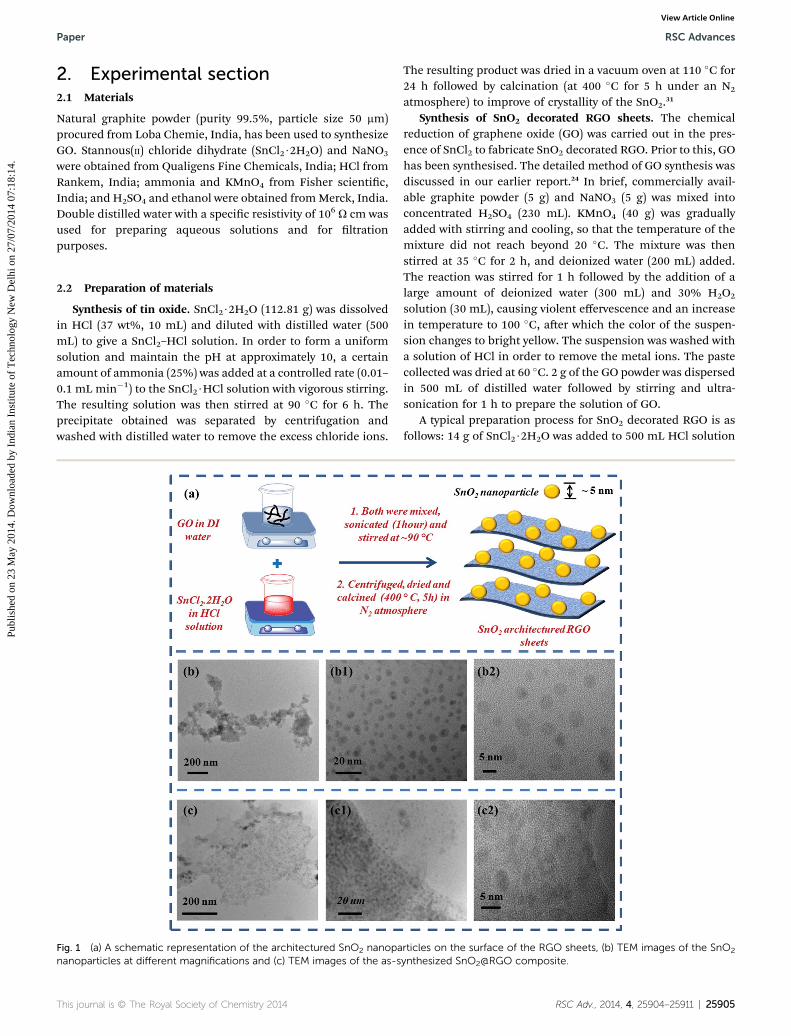
Fig. 1 (a) A schematic representation of the architectured SnO2 nanopananoparticles at different magnifications and (c) TEM images of the as-s
This journal is © The Royal Society of Chemistry 2014
The resulting product was dried in a vacuum oven at 110 �C for24 h followed by calcination (at 400 �C for 5 h under an N2
atmosphere) to improve of crystallity of the SnO2.31
Synthesis of SnO2 decorated RGO sheets. The chemicalreduction of graphene oxide (GO) was carried out in the pres-ence of SnCl2 to fabricate SnO2 decorated RGO. Prior to this, GOhas been synthesised. The detailed method of GO synthesis wasdiscussed in our earlier report.24 In brief, commercially avail-able graphite powder (5 g) and NaNO3 (5 g) was mixed intoconcentrated H2SO4 (230 mL). KMnO4 (40 g) was graduallyadded with stirring and cooling, so that the temperature of themixture did not reach beyond 20 �C. The mixture was thenstirred at 35 �C for 2 h, and deionized water (200 mL) added.The reaction was stirred for 1 h followed by the addition of alarge amount of deionized water (300 mL) and 30% H2O2
solution (30 mL), causing violent effervescence and an increasein temperature to 100 �C, aer which the color of the suspen-sion changes to bright yellow. The suspension was washed witha solution of HCl in order to remove the metal ions. The pastecollected was dried at 60 �C. 2 g of the GO powder was dispersedin 500 mL of distilled water followed by stirring and ultra-sonication for 1 h to prepare the solution of GO.
A typical preparation process for SnO2 decorated RGO is asfollows: 14 g of SnCl2$2H2O was added to 500 mL HCl solution
rticles on the surface of the RGO sheets, (b) TEM images of the SnO2
ynthesized SnO2@RGO composite.
RSC Adv., 2014, 4, 25904–25911 | 25905
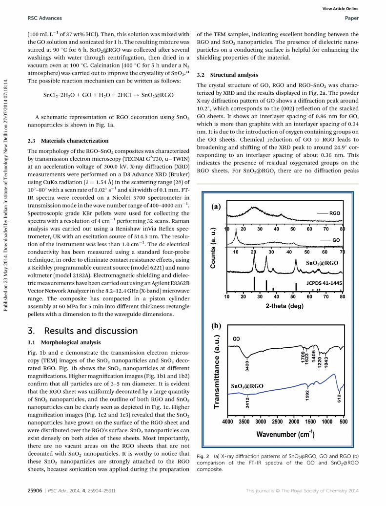
Fig. 2 (a) X-ray diffraction patterns of SnO2@RGO, GO and RGO (b)comparison of the FT-IR spectra of the GO and SnO2@RGOcomposite.
RSC Advances Paper
Publ
ishe
d on
23
May
201
4. D
ownl
oade
d by
Ind
ian
Inst
itute
of
Tec
hnol
ogy
New
Del
hi o
n 27
/07/
2014
07:
18:1
4.
View Article Online
(100 mL L�1 of 37 wt% HCl). Then, this solution was mixed withthe GO solution and sonicated for 1 h. The resultingmixture wasstirred at 90 �C for 6 h. SnO2@RGO was collected aer severalwashings with water through centrifugation, then dried in avacuum oven at 100 �C. Calcination (400 �C for 5 h under a N2
atmosphere) was carried out to improve the crystallity of SnO2.31
The possible reaction mechanism can be written as follows:
SnCl2$2H2O + GO + H2O + 2HCl / SnO2@RGO
A schematic representation of RGO decoration using SnO2
nanoparticles is shown in Fig. 1a.
2.3 Materials characterization
Themorphology of the RGO–SnO2 composites was characterizedby transmission electron microscopy (TECNAI G2T30, u�TWIN)at an acceleration voltage of 300.0 kV. X-ray diffraction (XRD)measurements were performed on a D8 Advance XRD (Bruker)using CuKa radiation (l ¼ 1.54 A) in the scattering range (2q) of10�–80� with a scan rate of 0.02� s�1 and slit width of 0.1mm. FT-IR spectra were recorded on a Nicolet 5700 spectrometer intransmissionmode in thewave number range of 400–4000 cm�1.Spectroscopic grade KBr pellets were used for collecting thespectra with a resolution of 4 cm�1 performing 32 scans. Ramananalysis was carried out using a Renishaw inVia Reex spec-trometer, UK with an excitation source of 514.5 nm. The resolu-tion of the instrument was less than 1.0 cm�1. The dc electricalconductivity has been measured using a standard four-probetechnique, in order to eliminate contact resistance effects, usinga Keithley programmable current source (model 6221) and nanovoltmeter (model 2182A). Electromagnetic shielding and dielec-tricmeasurementshavebeencarriedoutusing anAgilentE8362BVector Network Analyzer in the 8.2–12.4GHz (X-band)microwaverange. The composite has compacted in a piston cylinderassembly at 60 MPa for 5 min into different thickness rectanglepellets with a dimension to t the waveguide dimensions.
3. Results and discussion3.1 Morphological analysis
Fig. 1b and c demonstrate the transmission electron micros-copy (TEM) images of the SnO2 nanoparticles and SnO2 deco-rated RGO. Fig. 1b shows the SnO2 nanoparticles at differentmagnications. Higher magnication images (Fig. 1b1 and 1b2)conrm that all particles are of 3–5 nm diameter. It is evidentthat the RGO sheet was uniformly decorated by a large quantityof SnO2 nanoparticles, and the outline of both RGO and SnO2
nanoparticles can be clearly seen as depicted in Fig. 1c. Highermagnication images (Fig. 1c2 and 1c3) revealed that the SnO2
nanoparticles have grown on the surface of the RGO sheet andwere distributed over the RGO's surface. SnO2 nanoparticles canexist densely on both sides of these sheets. Most importantly,there are no vacant areas on the RGO sheets that are notdecorated with SnO2 nanoparticles. It is worthy to notice thatthese SnO2 nanoparticles are strongly attached to the RGOsheets, because sonication was applied during the preparation
25906 | RSC Adv., 2014, 4, 25904–25911
of the TEM samples, indicating excellent bonding between theRGO and SnO2 nanoparticles. The presence of dielectric nano-particles on a conducting surface is helpful for enhancing theshielding properties of the material.
3.2 Structural analysis
The crystal structure of GO, RGO and RGO–SnO2 was charac-terized by XRD and the results displayed in Fig. 2a. The powderX-ray diffraction pattern of GO shows a diffraction peak around10.2�, which corresponds to the (002) reection of the stackedGO sheets. It shows an interlayer spacing of 0.86 nm for GO,which is more than graphite with an interlayer spacing of 0.34nm. It is due to the introduction of oxygen containing groups onthe GO sheets. Chemical reduction of GO to RGO leads tobroadening and shiing of the XRD peak to around 24.9� cor-responding to an interlayer spacing of about 0.36 nm. Thisindicates the presence of residual oxygenated groups on theRGO sheets. For SnO2@RGO, there are no diffraction peaks
This journal is © The Royal Society of Chemistry 2014

Fig. 3 Raman spectra of RGO, GO, and SnO2 decorated RGO sheets.Inset image shows the Raman spectrum of the SnO2 nanoparticles.
Paper RSC Advances
Publ
ishe
d on
23
May
201
4. D
ownl
oade
d by
Ind
ian
Inst
itute
of
Tec
hnol
ogy
New
Del
hi o
n 27
/07/
2014
07:
18:1
4.
View Article Online
corresponding to GO, indicating the reduction of GO to RGO bystannous ions. The diffraction patterns and relative intensitiesof the synthesized SnO2 matched well with standard SnO2
(JCPDS 41-1445), demonstrating that the nanoparticles wereSnO2 and shows that the diffraction peaks of crystalline SnO2
nanoparticles are clearly distinguishable. It could be indexed tothe tetragonal SnO2 phase (JCPDS 41-1445). The XRD peaks ofthe composite appearing at about 2q ¼ 26.5, 33.9, and 51.6 canbe indexed to the diffraction planes of SnO2 (110), (101), and(211), respectively. The mean particle size (D) of the SnO2
nanoparticles was calculated by applying the Scherrer equationto the (110) plane diffraction peak and found to be 3–5 nm inthe SnO2@RGO composite.
3.3 FT-IR spectroscopy
Fig. 2b shows the FT-IR spectra of GO and SnO2@RGO. The FT-IR spectra of GO conrmed the presence of oxygen-containinggroups, such as C–OH at 3420 cm�1, C–O–C at 1220 cm�1, andC]O in the carboxylic acid moieties at 1709 cm�1. Othercharacteristic vibrations were the O–H deformation peak at1405 cm�1 and the C–O stretching peak at 1043 cm�1. The peakat 1623 cm�1 was assigned to the contributions from the skel-etal vibrations of the graphitic domains. For SnO2@RGO, thecarboxylic acid vibration band at 1709 cm�1 disappeared. Aweak signal for the C–OH stretching vibration at 3412 cm�1
could be ascribed to the vibrations of the adsorbed watermolecules which is assigned to the Eu mode of SnO2 (anti-symmetric O–Sn–O stretching). The presence of the Eu mode (aband located at 612 cm�1) in SnO2@RGO indicates the incor-poration of SnO2 particles on the RGO sheets. Additionally, thespectrum of the SnO2@RGO composite shows an absorptionband at 1592 cm�1 (C]C stretching), indicating the restorationof the graphene network on reduction. Therefore, it could beconcluded that GO was reduced by the stannous ions.
3.4 Raman spectroscopy
Raman spectroscopy is a very powerful tool for investigating theinteractions or bonding between two components.33 To eluci-date the graphitic structure of GO, RGO and the interactionsamong RGO, and SnO2 nanoparticles, Raman spectroscopy wasconducted in a spectral range of 100–3300 cm�1. Fig. 3 showsthe Raman spectra of GO, RGO, and SnO2@RGO composite.The Raman spectra of GO and RGO consist of three prominentcharacteristic peaks, namely the D band (disorder-inducedband), the G band (the tangential mode of graphitic structure),and the G0 (or 2D) band. The G and D bands are due to thedoubly degenerate zone centre E2g mode (�1580–1600 cm�1)and the breathing modes of six atom rings which appears at�1350 cm�1 due to the presence of defects in the graphite,respectively.34 In the Raman spectrum of RGO, the D, G and 2Dpeak position values conrm the formation of RGO. Ramanspectrum of pure SnO2 nanoparticles reveals all the character-istic bands of SnO2 in the low frequency region, i.e., 436, 479(Eg), 564 (S1), 633 (A1g).35 All these peaks are suppressed in theSnO2@RGO composite because of the highly intense graphiticpeaks present in the RGO sheets. Furthermore, the interactions
This journal is © The Royal Society of Chemistry 2014
between the RGO and SnO2 nanoparticles are clearly seen by thered shi in peaks of RGO from 1365 to 1353 cm�1 in the D bandand from 1600 to 1593 cm�1 in the G band. Slight shiing in thebands is an evidence of interaction between these components.Additionally, a slight shi was also observed in the G0 band. TheID/IG value of SnO2@RGO is higher (1.22) than RGO (1.02). Italso suggests the interaction of SnO2 into the RGO sheetbecause at the time of the synthesis of the SnO2@RGO, SnO2
interacts on the available defect sites of the RGO sheet or onfurther occurrence of defect sites at the time of architecturingthe SnO2 nanoparticles onto the RGO surface.
3.5 Shielding effectiveness measurement
EMI SE of any material is the sum of the contributions from theabsorption (SEA), reection (SER) and multiple reections (SEM)of the EM energy:36–38
SE ¼ �10 log(PT/PI) ¼ SER + SEA + SEM (1)
where: PI and PT are the power of incident and transmitted EMwaves, respectively.
According to Schelkunoff's theory, SEM can be ignored in allpractical applications where the shield is thicker than the skindepth (d). For a material, the skin depth (d) is the distance up towhich the intensity of the EM wave decreases to 1/e of its orig-inal strength. d is related to angular frequency, relative perme-ability and total conductivity:
sT ¼ (sdc + sac) (2)
Fig. 4a–d shows the variation of the SE with frequency in the8.2–12.4 GHz range. From Fig. 4a, the values of SE for theSnO2@RGO composite (45.8 dB) is signicantly higher thanthat of both RGO (32.5 dB) and SnO2 (14.2 dB) at a criticalthickness of 3 mm. It proposed that the addition of a dielectricller enhances the SE of RGO. Therefore, SnO2@RGO is a betteroption compared to the SnO2 and RGO composites indepen-dently. We also explored the effect of varying the thickness ofthe composites on the EMI shielding performance. For this,rectangular pallets of different thicknesses (1.0 mm, 2.0 mm,
RSC Adv., 2014, 4, 25904–25911 | 25907
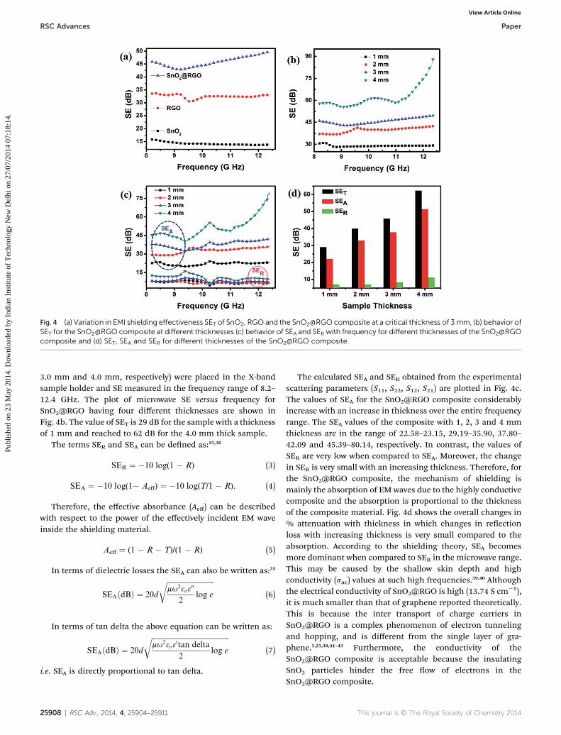
Fig. 4 (a) Variation in EMI shielding effectiveness SET of SnO2, RGO and the SnO2@RGO composite at a critical thickness of 3 mm, (b) behavior ofSET for the SnO2@RGO composite at different thicknesses (c) behavior of SEA and SER with frequency for different thicknesses of the SnO2@RGOcomposite and (d) SET, SEA and SER for different thicknesses of the SnO2@RGO composite.
RSC Advances Paper
Publ
ishe
d on
23
May
201
4. D
ownl
oade
d by
Ind
ian
Inst
itute
of
Tec
hnol
ogy
New
Del
hi o
n 27
/07/
2014
07:
18:1
4.
View Article Online
3.0 mm and 4.0 mm, respectively) were placed in the X-bandsample holder and SE measured in the frequency range of 8.2–12.4 GHz. The plot of microwave SE versus frequency forSnO2@RGO having four different thicknesses are shown inFig. 4b. The value of SET is 29 dB for the sample with a thicknessof 1 mm and reached to 62 dB for the 4.0 mm thick sample.
The terms SER and SEA can be dened as:25,38
SER ¼ �10 log(1 � R) (3)
SEA ¼ �10 log(1� Aeff) ¼ �10 log(T/1 � R). (4)
Therefore, the effective absorbance (Aeff) can be describedwith respect to the power of the effectively incident EM waveinside the shielding material.
Aeff ¼ (1 � R � T)/(1 � R) (5)
In terms of dielectric losses the SEA can also be written as:25
SEAðdBÞ ¼ 20d
ffiffiffiffiffiffiffiffiffiffiffiffiffiffiffiffiffiffiffiffiffiffiffiffiffiffiffimu23o3
00
2log e
r(6)
In terms of tan delta the above equation can be written as:
SEAðdBÞ ¼ 20d
ffiffiffiffiffiffiffiffiffiffiffiffiffiffiffiffiffiffiffiffiffiffiffiffiffiffiffiffiffiffiffiffiffiffiffiffiffiffiffiffiffiffiffiffimu23o3
0tan delta
2log e
r(7)
i.e. SEA is directly proportional to tan delta.
25908 | RSC Adv., 2014, 4, 25904–25911
The calculated SEA and SER obtained from the experimentalscattering parameters (S11, S22, S12, S21) are plotted in Fig. 4c.The values of SEA for the SnO2@RGO composite considerablyincrease with an increase in thickness over the entire frequencyrange. The SEA values of the composite with 1, 2, 3 and 4 mmthickness are in the range of 22.58–23.15, 29.19–35.90, 37.80–42.09 and 45.39–80.14, respectively. In contrast, the values ofSER are very low when compared to SEA. Moreover, the changein SER is very small with an increasing thickness. Therefore, forthe SnO2@RGO composite, the mechanism of shielding ismainly the absorption of EM waves due to the highly conductivecomposite and the absorption is proportional to the thicknessof the composite material. Fig. 4d shows the overall changes in% attenuation with thickness in which changes in reectionloss with increasing thickness is very small compared to theabsorption. According to the shielding theory, SEA becomesmore dominant when compared to SER in the microwave range.This may be caused by the shallow skin depth and highconductivity (sac) values at such high frequencies.39,40 Althoughthe electrical conductivity of SnO2@RGO is high (13.74 S cm�1),it is much smaller than that of graphene reported theoretically.This is because the inter transport of charge carriers inSnO2@RGO is a complex phenomenon of electron tunnelingand hopping, and is different from the single layer of gra-phene.5,25,38,41–43 Furthermore, the conductivity of theSnO2@RGO composite is acceptable because the insulatingSnO2 particles hinder the free ow of electrons in theSnO2@RGO composite.
This journal is © The Royal Society of Chemistry 2014
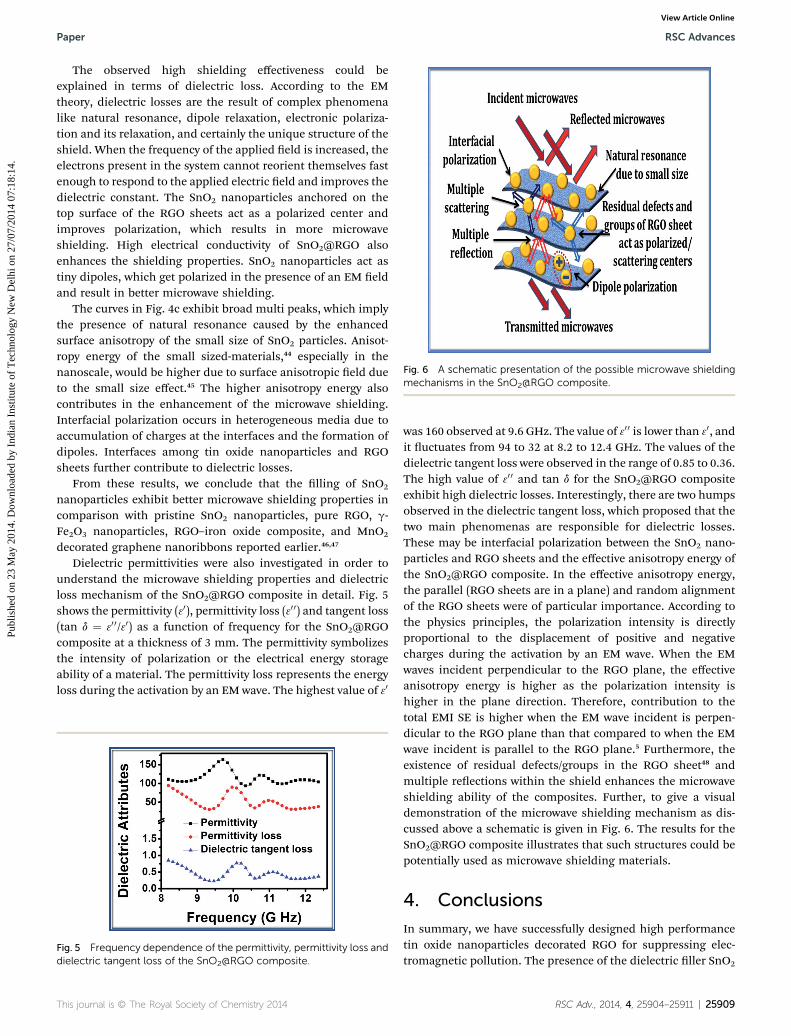
Fig. 6 A schematic presentation of the possible microwave shieldingmechanisms in the SnO2@RGO composite.
Paper RSC Advances
Publ
ishe
d on
23
May
201
4. D
ownl
oade
d by
Ind
ian
Inst
itute
of
Tec
hnol
ogy
New
Del
hi o
n 27
/07/
2014
07:
18:1
4.
View Article Online
The observed high shielding effectiveness could beexplained in terms of dielectric loss. According to the EMtheory, dielectric losses are the result of complex phenomenalike natural resonance, dipole relaxation, electronic polariza-tion and its relaxation, and certainly the unique structure of theshield. When the frequency of the applied eld is increased, theelectrons present in the system cannot reorient themselves fastenough to respond to the applied electric eld and improves thedielectric constant. The SnO2 nanoparticles anchored on thetop surface of the RGO sheets act as a polarized center andimproves polarization, which results in more microwaveshielding. High electrical conductivity of SnO2@RGO alsoenhances the shielding properties. SnO2 nanoparticles act astiny dipoles, which get polarized in the presence of an EM eldand result in better microwave shielding.
The curves in Fig. 4c exhibit broad multi peaks, which implythe presence of natural resonance caused by the enhancedsurface anisotropy of the small size of SnO2 particles. Anisot-ropy energy of the small sized-materials,44 especially in thenanoscale, would be higher due to surface anisotropic eld dueto the small size effect.45 The higher anisotropy energy alsocontributes in the enhancement of the microwave shielding.Interfacial polarization occurs in heterogeneous media due toaccumulation of charges at the interfaces and the formation ofdipoles. Interfaces among tin oxide nanoparticles and RGOsheets further contribute to dielectric losses.
From these results, we conclude that the lling of SnO2
nanoparticles exhibit better microwave shielding properties incomparison with pristine SnO2 nanoparticles, pure RGO, g-Fe2O3 nanoparticles, RGO–iron oxide composite, and MnO2
decorated graphene nanoribbons reported earlier.46,47
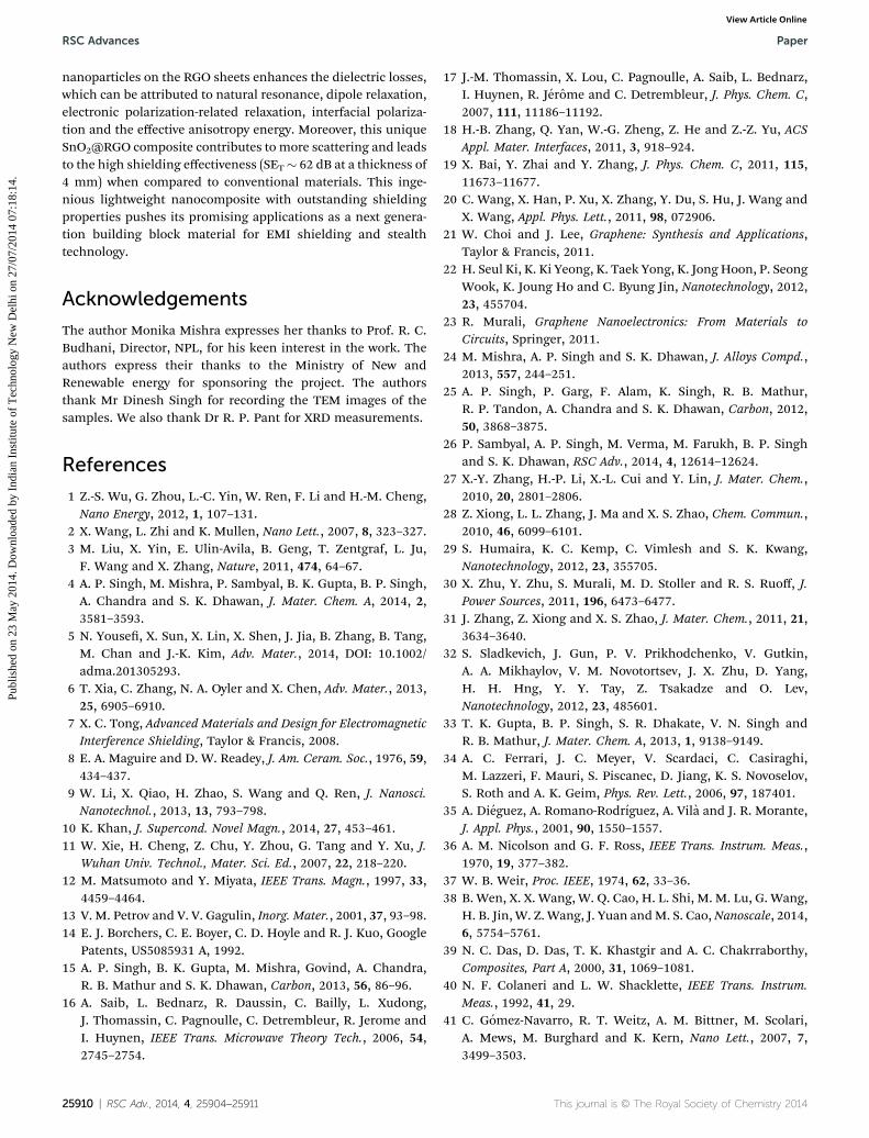
Dielectric permittivities were also investigated in order tounderstand the microwave shielding properties and dielectricloss mechanism of the SnO2@RGO composite in detail. Fig. 5shows the permittivity (30), permittivity loss (30 0) and tangent loss(tan d ¼ 30 0/30) as a function of frequency for the SnO2@RGOcomposite at a thickness of 3 mm. The permittivity symbolizesthe intensity of polarization or the electrical energy storageability of a material. The permittivity loss represents the energyloss during the activation by an EM wave. The highest value of 30
Fig. 5 Frequency dependence of the permittivity, permittivity loss anddielectric tangent loss of the SnO2@RGO composite.
This journal is © The Royal Society of Chemistry 2014
was 160 observed at 9.6 GHz. The value of 30 0 is lower than 30, andit uctuates from 94 to 32 at 8.2 to 12.4 GHz. The values of thedielectric tangent loss were observed in the range of 0.85 to 0.36.The high value of 30 0 and tan d for the SnO2@RGO compositeexhibit high dielectric losses. Interestingly, there are two humpsobserved in the dielectric tangent loss, which proposed that thetwo main phenomenas are responsible for dielectric losses.These may be interfacial polarization between the SnO2 nano-particles and RGO sheets and the effective anisotropy energy ofthe SnO2@RGO composite. In the effective anisotropy energy,the parallel (RGO sheets are in a plane) and random alignmentof the RGO sheets were of particular importance. According tothe physics principles, the polarization intensity is directlyproportional to the displacement of positive and negativecharges during the activation by an EM wave. When the EMwaves incident perpendicular to the RGO plane, the effectiveanisotropy energy is higher as the polarization intensity ishigher in the plane direction. Therefore, contribution to thetotal EMI SE is higher when the EM wave incident is perpen-dicular to the RGO plane than that compared to when the EMwave incident is parallel to the RGO plane.5 Furthermore, theexistence of residual defects/groups in the RGO sheet48 andmultiple reections within the shield enhances the microwaveshielding ability of the composites. Further, to give a visualdemonstration of the microwave shielding mechanism as dis-cussed above a schematic is given in Fig. 6. The results for theSnO2@RGO composite illustrates that such structures could bepotentially used as microwave shielding materials.
4. Conclusions
In summary, we have successfully designed high performancetin oxide nanoparticles decorated RGO for suppressing elec-tromagnetic pollution. The presence of the dielectric ller SnO2
RSC Adv., 2014, 4, 25904–25911 | 25909
RSC Advances Paper
Publ
ishe
d on
23
May
201
4. D
ownl
oade
d by
Ind
ian
Inst
itute
of
Tec
hnol
ogy
New
Del
hi o
n 27
/07/
2014
07:
18:1
4.
View Article Online
nanoparticles on the RGO sheets enhances the dielectric losses,which can be attributed to natural resonance, dipole relaxation,electronic polarization-related relaxation, interfacial polariza-tion and the effective anisotropy energy. Moreover, this uniqueSnO2@RGO composite contributes to more scattering and leadsto the high shielding effectiveness (SET� 62 dB at a thickness of4 mm) when compared to conventional materials. This inge-nious lightweight nanocomposite with outstanding shieldingproperties pushes its promising applications as a next genera-tion building block material for EMI shielding and stealthtechnology.
Acknowledgements
The author Monika Mishra expresses her thanks to Prof. R. C.Budhani, Director, NPL, for his keen interest in the work. Theauthors express their thanks to the Ministry of New andRenewable energy for sponsoring the project. The authorsthank Mr Dinesh Singh for recording the TEM images of thesamples. We also thank Dr R. P. Pant for XRD measurements.
References
1 Z.-S. Wu, G. Zhou, L.-C. Yin, W. Ren, F. Li and H.-M. Cheng,Nano Energy, 2012, 1, 107–131.
2 X. Wang, L. Zhi and K. Mullen, Nano Lett., 2007, 8, 323–327.3 M. Liu, X. Yin, E. Ulin-Avila, B. Geng, T. Zentgraf, L. Ju,F. Wang and X. Zhang, Nature, 2011, 474, 64–67.
4 A. P. Singh, M. Mishra, P. Sambyal, B. K. Gupta, B. P. Singh,A. Chandra and S. K. Dhawan, J. Mater. Chem. A, 2014, 2,3581–3593.
5 N. Youse, X. Sun, X. Lin, X. Shen, J. Jia, B. Zhang, B. Tang,M. Chan and J.-K. Kim, Adv. Mater., 2014, DOI: 10.1002/adma.201305293.
6 T. Xia, C. Zhang, N. A. Oyler and X. Chen, Adv. Mater., 2013,25, 6905–6910.
7 X. C. Tong, Advanced Materials and Design for ElectromagneticInterference Shielding, Taylor & Francis, 2008.
8 E. A. Maguire and D. W. Readey, J. Am. Ceram. Soc., 1976, 59,434–437.
9 W. Li, X. Qiao, H. Zhao, S. Wang and Q. Ren, J. Nanosci.Nanotechnol., 2013, 13, 793–798.
10 K. Khan, J. Supercond. Novel Magn., 2014, 27, 453–461.11 W. Xie, H. Cheng, Z. Chu, Y. Zhou, G. Tang and Y. Xu, J.
Wuhan Univ. Technol., Mater. Sci. Ed., 2007, 22, 218–220.12 M. Matsumoto and Y. Miyata, IEEE Trans. Magn., 1997, 33,
4459–4464.13 V. M. Petrov and V. V. Gagulin, Inorg. Mater., 2001, 37, 93–98.14 E. J. Borchers, C. E. Boyer, C. D. Hoyle and R. J. Kuo, Google
Patents, US5085931 A, 1992.15 A. P. Singh, B. K. Gupta, M. Mishra, Govind, A. Chandra,
R. B. Mathur and S. K. Dhawan, Carbon, 2013, 56, 86–96.16 A. Saib, L. Bednarz, R. Daussin, C. Bailly, L. Xudong,
J. Thomassin, C. Pagnoulle, C. Detrembleur, R. Jerome andI. Huynen, IEEE Trans. Microwave Theory Tech., 2006, 54,2745–2754.
25910 | RSC Adv., 2014, 4, 25904–25911
17 J.-M. Thomassin, X. Lou, C. Pagnoulle, A. Saib, L. Bednarz,I. Huynen, R. Jerome and C. Detrembleur, J. Phys. Chem. C,2007, 111, 11186–11192.
18 H.-B. Zhang, Q. Yan, W.-G. Zheng, Z. He and Z.-Z. Yu, ACSAppl. Mater. Interfaces, 2011, 3, 918–924.
19 X. Bai, Y. Zhai and Y. Zhang, J. Phys. Chem. C, 2011, 115,11673–11677.
20 C. Wang, X. Han, P. Xu, X. Zhang, Y. Du, S. Hu, J. Wang andX. Wang, Appl. Phys. Lett., 2011, 98, 072906.
21 W. Choi and J. Lee, Graphene: Synthesis and Applications,Taylor & Francis, 2011.
22 H. Seul Ki, K. Ki Yeong, K. Taek Yong, K. Jong Hoon, P. SeongWook, K. Joung Ho and C. Byung Jin, Nanotechnology, 2012,23, 455704.
23 R. Murali, Graphene Nanoelectronics: From Materials toCircuits, Springer, 2011.
24 M. Mishra, A. P. Singh and S. K. Dhawan, J. Alloys Compd.,2013, 557, 244–251.
25 A. P. Singh, P. Garg, F. Alam, K. Singh, R. B. Mathur,R. P. Tandon, A. Chandra and S. K. Dhawan, Carbon, 2012,50, 3868–3875.
26 P. Sambyal, A. P. Singh, M. Verma, M. Farukh, B. P. Singhand S. K. Dhawan, RSC Adv., 2014, 4, 12614–12624.
27 X.-Y. Zhang, H.-P. Li, X.-L. Cui and Y. Lin, J. Mater. Chem.,2010, 20, 2801–2806.
28 Z. Xiong, L. L. Zhang, J. Ma and X. S. Zhao, Chem. Commun.,2010, 46, 6099–6101.
29 S. Humaira, K. C. Kemp, C. Vimlesh and S. K. Kwang,Nanotechnology, 2012, 23, 355705.
30 X. Zhu, Y. Zhu, S. Murali, M. D. Stoller and R. S. Ruoff, J.Power Sources, 2011, 196, 6473–6477.
31 J. Zhang, Z. Xiong and X. S. Zhao, J. Mater. Chem., 2011, 21,3634–3640.
32 S. Sladkevich, J. Gun, P. V. Prikhodchenko, V. Gutkin,A. A. Mikhaylov, V. M. Novotortsev, J. X. Zhu, D. Yang,H. H. Hng, Y. Y. Tay, Z. Tsakadze and O. Lev,Nanotechnology, 2012, 23, 485601.
33 T. K. Gupta, B. P. Singh, S. R. Dhakate, V. N. Singh andR. B. Mathur, J. Mater. Chem. A, 2013, 1, 9138–9149.
34 A. C. Ferrari, J. C. Meyer, V. Scardaci, C. Casiraghi,M. Lazzeri, F. Mauri, S. Piscanec, D. Jiang, K. S. Novoselov,S. Roth and A. K. Geim, Phys. Rev. Lett., 2006, 97, 187401.
35 A. Dieguez, A. Romano-Rodrıguez, A. Vila and J. R. Morante,J. Appl. Phys., 2001, 90, 1550–1557.
36 A. M. Nicolson and G. F. Ross, IEEE Trans. Instrum. Meas.,1970, 19, 377–382.
37 W. B. Weir, Proc. IEEE, 1974, 62, 33–36.38 B. Wen, X. X. Wang, W. Q. Cao, H. L. Shi, M. M. Lu, G. Wang,
H. B. Jin, W. Z. Wang, J. Yuan andM. S. Cao, Nanoscale, 2014,6, 5754–5761.
39 N. C. Das, D. Das, T. K. Khastgir and A. C. Chakrraborthy,Composites, Part A, 2000, 31, 1069–1081.
40 N. F. Colaneri and L. W. Shacklette, IEEE Trans. Instrum.Meas., 1992, 41, 29.
41 C. Gomez-Navarro, R. T. Weitz, A. M. Bittner, M. Scolari,A. Mews, M. Burghard and K. Kern, Nano Lett., 2007, 7,3499–3503.
This journal is © The Royal Society of Chemistry 2014
Paper RSC Advances
Publ
ishe
d on
23
May
201
4. D
ownl
oade
d by
Ind
ian
Inst
itute
of
Tec
hnol
ogy
New
Del
hi o
n 27
/07/
2014
07:
18:1
4.
View Article Online
42 S. R. Pathipati, E. Pavlica, E. Treossi, R. Rizzoli,G. P. Veronese, V. Palermo, L. Chen, D. Beljonne, J. Caiand R. Fasel, Org. Electron., 2013, 14, 1787–1792.
43 P. Lian, X. Zhu, S. Liang, Z. Li, W. Yang and H. Wang,Electrochim. Acta, 2011, 56, 4532–4539.
44 D. L. Leslie-Pelecky and R. D. Rieke, Chem. Mater., 1996, 8,1770–1783.
45 Y.-J. Chen, P. Gao,R.-X.Wang,C.-L. Zhu, L.-J.Wang,M.-S. Caoand H.-B. Jin, J. Phys. Chem. C, 2009, 113, 10061–10064.
This journal is © The Royal Society of Chemistry 2014
46 K. Singh, A. Ohlan, V. H. Pham, B. R. S. Varshney, J. Jang,S. H. Hur, W. M. Choi, M. Kumar, S. K. Dhawan,B.-S. Kong and J. S. Chung, Nanoscale, 2013, 5, 2411–2420.
47 T. K. Gupta, B. P. Singh, V. N. Singh, S. Teotia, A. P. Singh,I. Elizabeth, S. R. Dhakate, S. K. Dhawan and R. B. Mathur,J. Mater. Chem. A, 2013, 2, 4256–4263.
48 X. Sun, J. He, G. Li, J. Tang, T. Wang, Y. Guo and H. Xue,J. Mater. Chem. C, 2013, 1, 765–777.
RSC Adv., 2014, 4, 25904–25911 | 25911