Monomethylamine–water vapour absorption refrigeration system

Thin Solid Films 519 (2010) 1334–1340
Contents lists available at ScienceDirect
Thin Solid Films
j ourna l homepage: www.e lsev ie r.com/ locate / ts f
Control of tin oxide film morphology by addition of hydrocarbons to the chemicalvapour deposition process
H.M. Yates a,⁎, P. Evans a, D.W. Sheel a, Z. Remes b, M. Vanecek b
a Engineering and Physical Sciences, University of Salford, Manchester, M5 4WT, UKb Institute of Physics of the ASCR, v. v. i. Cukrovarnicka 10, CZ-162 00 Praha 6, Czech Republic
⁎ Corresponding author. Tel.: +44 161 295 3115; faxE-mail address: [email protected] (H.M. Yates
0040-6090/$ – see front matter © 2010 Elsevier B.V. Adoi:10.1016/j.tsf.2010.09.037
a b s t r a c t
a r t i c l e i n f oArticle history:Received 26 March 2010Received in revised form 17 September 2010Accepted 20 September 2010Available online 29 September 2010
Keywords:Tin oxideChemical vapour depositionMorphologyAlcohol
In this paper we have shown that it is possible to modify and control the surface morphology of doped SnO2
transparent conducting oxide thin films deposited by atmospheric pressure chemical vapour deposition byuse of additives during the deposition process. A range of volatile organic compounds were explored, whichcaused changes of differing magnitude to the growth rates, crystallographic preferences, size and shape of thesurface features and optical transmittance. Of the additives tested methanol and tertiary butanol were foundto have the most significant influence allowing the surface to be modified from small, round features to muchmore elongated, sharp, pyramidal features.
: +44 161 295 5111.).
ll rights reserved.
© 2010 Elsevier B.V. All rights reserved.
1. Introduction
Transparent conductive oxide (TCO) films are widely used inmanyconsumer products with applications in flat screen high-definitiontelevisions, computer screens, low emissivity and electrochromicwindows [1], within thin film photovoltaic (PV) cells [2] and a widerange of other display type devices [3–5]. Surface morphology is animportant property in transparent conducting oxides, which cancritically affect the efficiency of the application. TCO's are used forboth low emissivity coatings (low scatter required) and for photo-voltaic applications where surface control can be used to improve thelight scattering properties of the front electrical contact on thin filmsolar cells and hence improve the efficiency of the cells.
One of the dominant materials is F-doped SnO2 which isextensively used for low emissivity windows (e.g. K GlassTM [6]),deposited inline by a chemical vapour deposition process. For thisprocess, the optimum film is highly transparent, has low visible lightscattering, low resistivity and low emissivity (0.16). For a differentindustrial area, for example, the thin film PV area (especially a-Sibased), the exact specifications for the TCO will be different. A keyobjective for the PV industry is to further reduce the cost per unit ofenergy generated. This can be achieved both by reducing themanufacturing costs—where atmospheric pressure chemical vapourdeposition (APCVD) has major potential and by increasing theefficiency of the PV cell. Transparent conducting oxide films have akey role in optimising efficiency, particularly in enhancing the light
collection performance of cells, whilst using the minimum amount ofabsorber material. For TCO films to maximise (thin film) solar cellconversion efficiency, they must satisfy three conditions: advancedlight trapping [7], high transparency and low resistance (10 Ω/sq). Allthree properties are linked via TCO film structure and composition, sooptimisation of performance requires a careful compromise. Forexample, increased thickness, would increase surface roughness andgenerally enhance total scattering of incident light (by changing,shaping or sizing of features), but would also reduce the transparencyand more importantly increase the optical absorbance of the TCO andhence lead to less light reaching the active part of the solar cell anddetract from the overall efficiency. It has been previously shown thatreducing the optical losses in the TCO is a decisive factor for ultimateefficiency due to light trapping [8,9].
In this paper we focus on producing thin films with specificmorphologies that would have the potential to improve the lightabsorption in the active absorber layers and hence efficiency of thinfilm PV cells. For this application the TCO acts as the front electricalcontact in the cell and has been previously found to be critical to theefficiency of the final solar cell [10].
As previously described, the film must be of high opticaltransparency and relatively low resistivity. In addition, an ability tocontrol the surface roughness and feature shape would be highlyadvantageous, by influencing the amount of light reaching theabsorber layers by introducing a transition layer, which acts similarlyto a graded refractive index layer and thereby reduces the reflectionlosses at the TCO interface. A further effect of increasing surfaceroughness is the enhancement of light scattering, leading to “lighttrapping” as a result of total internal reflections, which leads toenhanced absorption within the active part of the cell. Increased
1335H.M. Yates et al. / Thin Solid Films 519 (2010) 1334–1340
roughness is limited practically by initiation of defects in the overlyingactive absorber layers of the solar cell, which can lead to shunts,limiting cell performance. It has been shown both theoretically [8] andexperimentally [11] that the TCO surface features impinge on the cellefficiency and that certain types of feature are preferred. Generally, forthin film a-Si:H single junction solar cells a pyramidal shape, withsharp edged features has been preferred [12]. The precise morphologyrequired will also depend on the type of thin solar cell deposited [13].
Use of alcohols in the deposition of tin oxide was first reported inthe 1940s employing a spray pyrolysis method [14]. This method wasused to spray SnCl4 in a water and alcohol solution onto heated glassplates to form the tin oxide film. Alcohol was used as a solvent due toits high volatility and low surface tension. It also prevented the fumingof the SnCl4 and alcohol solution on addition of the required processwater [15]. Alcohols used included iso-propyl alcohol [16], ethanoland methanol [17]. Later, as vapour phase processes were introduced,use of alcohol as a tin precursor solvent was reported by variousresearchers [18] including Aitchison [19] and Jarzebski [20]. None ofthese reports mentioned use of alcohols for modifying the surfacemorphology. The first reference to methanol, other than as a solvent,was by the Asahi Glass Company Ltd, who used it to reduce theresistivity of their tin oxide thin films [21]. This research wascontinued by Matsui who more recently reported use of alcohols asadditives to the deposition process, to change the resistivity of thedeposited TCO [22].
To potentially improve the efficiency of solar cells, it would bebeneficial to produce the required morphology and roughness at alower thickness (so reducing the amount of light absorbed in the TCOand increasing the light scattering by the morphology). We show, inthis paper, that the use of small amounts of specific additives modifiesthe reaction chemistry and growth processes, leading to effectivecontrol of film morphology.
A range of potential additives were screened to study their effectson the morphology of the thin films. Each was selected as beingcompatible with (thermal) APCVD in terms of volatility and thermalstability. A series of screening experiments were carried out using theselected additives, before choosing two of the more promising forfurther study.
2. Experimental details
2.1. Growth
The SnO2:F was deposited by atmospheric pressurechemical vapour deposition (APCVD) using tin tetrachloride (TTC)(3.82×10⁻⁴ mol min−1), with an aqueous HF dopant (4%) deliveredto achieve a 1:5 molar ratio of SnCl4:H2O. Nitrogen was used as thecarrier gas with a total flow of 2 l/min. The susceptor temperaturewas 590 °C. Growth times were varied to achieve the target thickness,but were typically around 20 s. In addition, different additives(2 molar %) were used in the deposition process to influence thesurface morphology of the resulting material. Two of the mostpromising additives were chosen for further study at a range ofdifferent concentrations. Deposition was on 1 mm thick borosilicate(Corning Eagle 2000) glass. An APCVD gas handling system combinedwith an in-house designed coater head system was employed todeliver precursors to the surface of the substrate. This has beendescribed elsewhere [23]. The system uses a fast experimentalconcept, which allows a combinatorial chemistry approach toenhance studies. This system has replaced a standard CVD tubereactor for which it was possible only to run one single experimentaldeposition condition for each substrate placed inside the tube. In thepresent system it is possible to have multiple deposition areas,consisting of different experimental conditions across the samesubstrate. This reduces the time required to set up and heat eachindividual substrate for every experimental run. In practice, to reduce
errors and as a check on the reproducibility of each sample fouridentical runs are done for each set of experimental conditions.
2.2. Characterisation
Thickness was determined by partial etch and step heightmeasurements with a Dektak 3ST surface profiler (Veeco). Themorphology and surface roughness of the samples were obtained byatomic force microscopy (NanoScope IIIa, Digital Inst. Ltd). Thecrystallinity and structure of the samples were assessed by X-raydiffraction (Siemens D5000). X-ray photoelectron Spectroscopy (XPS;Kratos AXIS Ultra) with an Al (monochromated) Kα radiation sourcewas used to check the surface composition and stoichiometry of thefilms. Themeasurements were referenced to the residual C 1s signal at285 eV. The resistivity of the films was measured using a JandelUniversal four point probe. The initial reflectance and transmittancemeasurements used a spectrophotometer (nkd8000, Aquila Instru-ments Ltd) with p-polarised light at an incident angle of 30o. Theaverage value was over a wavelength range of 400 nm to 1000 nm.
The optical absorptance spectra were measured directly byPhotothermal deflection spectroscopy (PDS) [24]. The PDS signalwas normalized on the incident light intensity. Finally, the relativeabsorptance spectra measured by PDS in arbitary units were put intothe absolute scale using the spectral function 100%-T-R (measured inthe same transparent liquid) in IR region where the influence of thesurface scattering is negligible (the light scattering strongly decreasestowards longer wavelengths).
Angle resolved (light) scattering (ARS) measurements [25] werecarried out in the NIR (830 nm). The sample was illuminatedperpendicularly through the glass substrate side and the scatteredlight wasmeasured behind the samplewith the detector (avalanche Siphotodiode) facing the coated (TCO) side. The detector was rotatedwith a constant distance of 12 cm around the sample. All measure-ments were done at exactly the same configuration so they could bedirectly comparable, along with measurement of a standard com-mercial TCO (Asahi U). The substrate glass edges were blackened toreduce the parasitic light coming from these edges, as otherwise thislight would seriously influence the measurements at high angles.
3. Results and discussion
Un-doped SnO2 has high resistivity, which can be considerablyreduced on addition of a fluorine dopant. For example, for twoidentically produced films the resistivity dropped from 4.52×10⁻³
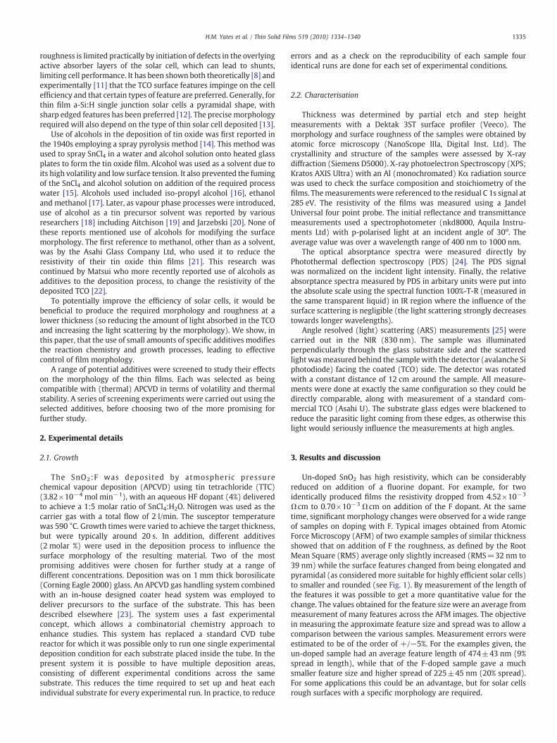
Ωcm to 0.70×10⁻³ Ωcm on addition of the F dopant. At the sametime, significant morphology changes were observed for a wide rangeof samples on doping with F. Typical images obtained from AtomicForce Microscopy (AFM) of two example samples of similar thicknessshowed that on addition of F the roughness, as defined by the RootMean Square (RMS) average only slightly increased (RMS=32 nm to39 nm) while the surface features changed from being elongated andpyramidal (as consideredmore suitable for highly efficient solar cells)to smaller and rounded (see Fig. 1). By measurement of the length ofthe features it was possible to get a more quantitative value for thechange. The values obtained for the feature size were an average frommeasurement of many features across the AFM images. The objectivein measuring the approximate feature size and spread was to allow acomparison between the various samples. Measurement errors wereestimated to be of the order of +/−5%. For the examples given, theun-doped sample had an average feature length of 474±43 nm (9%spread in length), while that of the F-doped sample gave a muchsmaller feature size and higher spread of 225±45 nm (20% spread).For some applications this could be an advantage, but for solar cellsrough surfaces with a specific morphology are required.
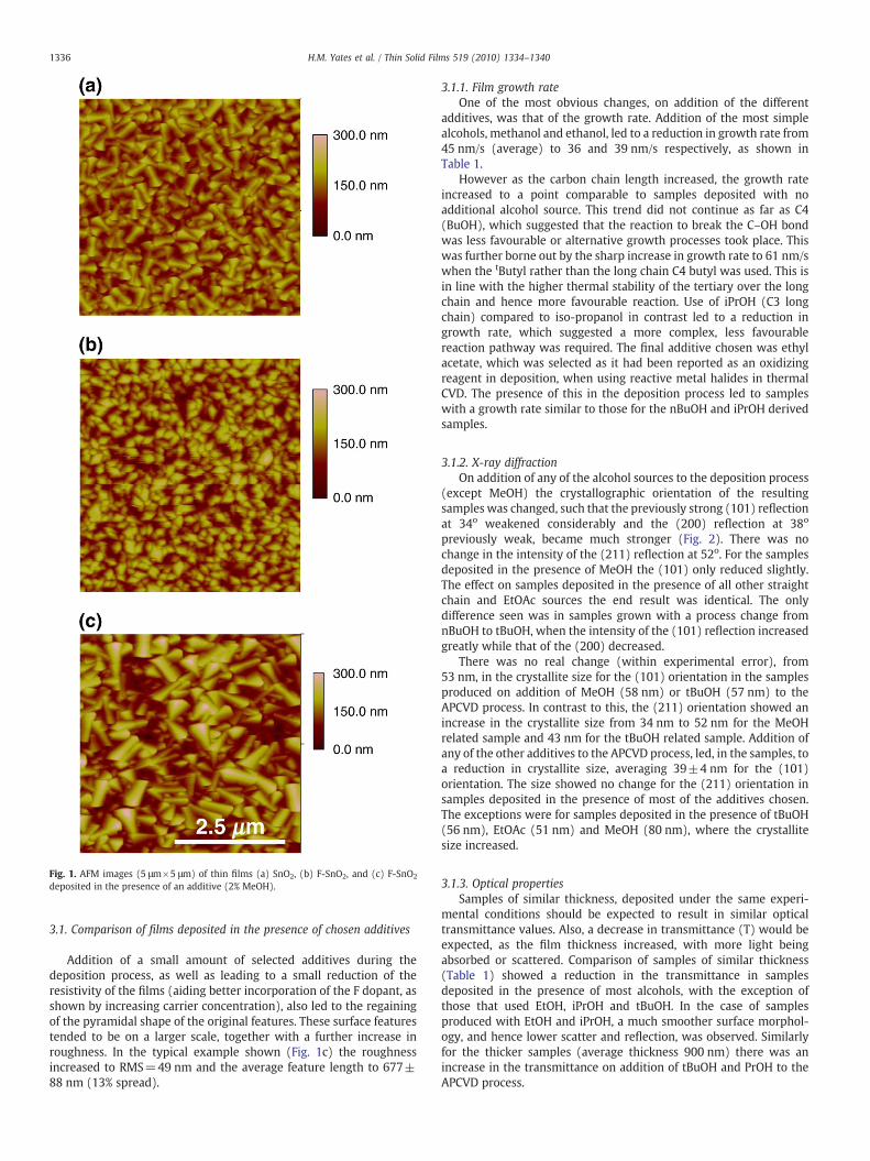
Fig. 1. AFM images (5 μm×5 μm) of thin films (a) SnO2, (b) F-SnO2, and (c) F-SnO2
deposited in the presence of an additive (2% MeOH).
1336 H.M. Yates et al. / Thin Solid Films 519 (2010) 1334–1340
3.1. Comparison of films deposited in the presence of chosen additives
Addition of a small amount of selected additives during thedeposition process, as well as leading to a small reduction of theresistivity of the films (aiding better incorporation of the F dopant, asshown by increasing carrier concentration), also led to the regainingof the pyramidal shape of the original features. These surface featurestended to be on a larger scale, together with a further increase inroughness. In the typical example shown (Fig. 1c) the roughnessincreased to RMS=49 nm and the average feature length to 677±88 nm (13% spread).
3.1.1. Film growth rateOne of the most obvious changes, on addition of the different
additives, was that of the growth rate. Addition of the most simplealcohols, methanol and ethanol, led to a reduction in growth rate from45 nm/s (average) to 36 and 39 nm/s respectively, as shown inTable 1.
However as the carbon chain length increased, the growth rateincreased to a point comparable to samples deposited with noadditional alcohol source. This trend did not continue as far as C4(BuOH), which suggested that the reaction to break the C–OH bondwas less favourable or alternative growth processes took place. Thiswas further borne out by the sharp increase in growth rate to 61 nm/swhen the tButyl rather than the long chain C4 butyl was used. This isin line with the higher thermal stability of the tertiary over the longchain and hence more favourable reaction. Use of iPrOH (C3 longchain) compared to iso-propanol in contrast led to a reduction ingrowth rate, which suggested a more complex, less favourablereaction pathway was required. The final additive chosen was ethylacetate, which was selected as it had been reported as an oxidizingreagent in deposition, when using reactive metal halides in thermalCVD. The presence of this in the deposition process led to sampleswith a growth rate similar to those for the nBuOH and iPrOH derivedsamples.
3.1.2. X-ray diffractionOn addition of any of the alcohol sources to the deposition process
(except MeOH) the crystallographic orientation of the resultingsamples was changed, such that the previously strong (101) reflectionat 34o weakened considerably and the (200) reflection at 38o
previously weak, became much stronger (Fig. 2). There was nochange in the intensity of the (211) reflection at 52o. For the samplesdeposited in the presence of MeOH the (101) only reduced slightly.The effect on samples deposited in the presence of all other straightchain and EtOAc sources the end result was identical. The onlydifference seen was in samples grown with a process change fromnBuOH to tBuOH, when the intensity of the (101) reflection increasedgreatly while that of the (200) decreased.
There was no real change (within experimental error), from53 nm, in the crystallite size for the (101) orientation in the samplesproduced on addition of MeOH (58 nm) or tBuOH (57 nm) to theAPCVD process. In contrast to this, the (211) orientation showed anincrease in the crystallite size from 34 nm to 52 nm for the MeOHrelated sample and 43 nm for the tBuOH related sample. Addition ofany of the other additives to the APCVD process, led, in the samples, toa reduction in crystallite size, averaging 39±4 nm for the (101)orientation. The size showed no change for the (211) orientation insamples deposited in the presence of most of the additives chosen.The exceptions were for samples deposited in the presence of tBuOH(56 nm), EtOAc (51 nm) and MeOH (80 nm), where the crystallitesize increased.
3.1.3. Optical propertiesSamples of similar thickness, deposited under the same experi-
mental conditions should be expected to result in similar opticaltransmittance values. Also, a decrease in transmittance (T) would beexpected, as the film thickness increased, with more light beingabsorbed or scattered. Comparison of samples of similar thickness(Table 1) showed a reduction in the transmittance in samplesdeposited in the presence of most alcohols, with the exception ofthose that used EtOH, iPrOH and tBuOH. In the case of samplesproduced with EtOH and iPrOH, a much smoother surface morphol-ogy, and hence lower scatter and reflection, was observed. Similarlyfor the thicker samples (average thickness 900 nm) there was anincrease in the transmittance on addition of tBuOH and PrOH to theAPCVD process.
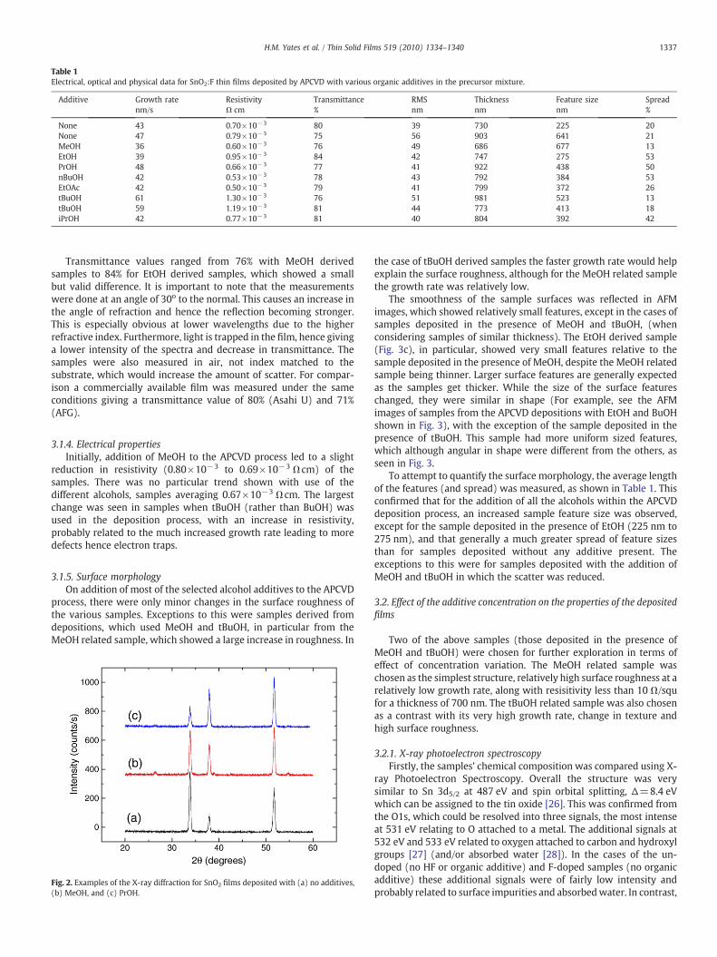
Table 1Electrical, optical and physical data for SnO2:F thin films deposited by APCVD with various organic additives in the precursor mixture.
Additive Growth ratenm/s
ResistivityΩ cm
Transmittance%
RMSnm
Thicknessnm
Feature sizenm
Spread%
None 43 0.70×10⁻³ 80 39 730 225 20None 47 0.79×10⁻³ 75 56 903 641 21MeOH 36 0.60×10⁻³ 76 49 686 677 13EtOH 39 0.95×10⁻³ 84 42 747 275 53PrOH 48 0.66×10⁻³ 77 41 922 438 50nBuOH 42 0.53×10⁻³ 78 43 792 384 53EtOAc 42 0.50×10⁻³ 79 41 799 372 26tBuOH 61 1.30×10⁻³ 76 51 981 523 13tBuOH 59 1.19×10⁻³ 81 44 773 413 18iPrOH 42 0.77×10⁻³ 81 40 804 392 42
1337H.M. Yates et al. / Thin Solid Films 519 (2010) 1334–1340
Transmittance values ranged from 76% with MeOH derivedsamples to 84% for EtOH derived samples, which showed a smallbut valid difference. It is important to note that the measurementswere done at an angle of 30o to the normal. This causes an increase inthe angle of refraction and hence the reflection becoming stronger.This is especially obvious at lower wavelengths due to the higherrefractive index. Furthermore, light is trapped in the film, hence givinga lower intensity of the spectra and decrease in transmittance. Thesamples were also measured in air, not index matched to thesubstrate, which would increase the amount of scatter. For compar-ison a commercially available film was measured under the sameconditions giving a transmittance value of 80% (Asahi U) and 71%(AFG).
3.1.4. Electrical propertiesInitially, addition of MeOH to the APCVD process led to a slight
reduction in resistivity (0.80×10⁻³ to 0.69×10⁻³ Ωcm) of thesamples. There was no particular trend shown with use of thedifferent alcohols, samples averaging 0.67×10⁻³ Ωcm. The largestchange was seen in samples when tBuOH (rather than BuOH) wasused in the deposition process, with an increase in resistivity,probably related to the much increased growth rate leading to moredefects hence electron traps.
3.1.5. Surface morphologyOn addition of most of the selected alcohol additives to the APCVD
process, there were only minor changes in the surface roughness ofthe various samples. Exceptions to this were samples derived fromdepositions, which used MeOH and tBuOH, in particular from theMeOH related sample, which showed a large increase in roughness. In
Fig. 2. Examples of the X-ray diffraction for SnO2 films deposited with (a) no additives,(b) MeOH, and (c) PrOH.
the case of tBuOH derived samples the faster growth rate would helpexplain the surface roughness, although for the MeOH related samplethe growth rate was relatively low.
The smoothness of the sample surfaces was reflected in AFMimages, which showed relatively small features, except in the cases ofsamples deposited in the presence of MeOH and tBuOH, (whenconsidering samples of similar thickness). The EtOH derived sample(Fig. 3c), in particular, showed very small features relative to thesample deposited in the presence of MeOH, despite the MeOH relatedsample being thinner. Larger surface features are generally expectedas the samples get thicker. While the size of the surface featureschanged, they were similar in shape (For example, see the AFMimages of samples from the APCVD depositions with EtOH and BuOHshown in Fig. 3), with the exception of the sample deposited in thepresence of tBuOH. This sample had more uniform sized features,which although angular in shape were different from the others, asseen in Fig. 3.
To attempt to quantify the surface morphology, the average lengthof the features (and spread) was measured, as shown in Table 1. Thisconfirmed that for the addition of all the alcohols within the APCVDdeposition process, an increased sample feature size was observed,except for the sample deposited in the presence of EtOH (225 nm to275 nm), and that generally a much greater spread of feature sizesthan for samples deposited without any additive present. Theexceptions to this were for samples deposited with the addition ofMeOH and tBuOH in which the scatter was reduced.
3.2. Effect of the additive concentration on the properties of the depositedfilms
Two of the above samples (those deposited in the presence ofMeOH and tBuOH) were chosen for further exploration in terms ofeffect of concentration variation. The MeOH related sample waschosen as the simplest structure, relatively high surface roughness at arelatively low growth rate, along with resisitivity less than 10 Ω/squfor a thickness of 700 nm. The tBuOH related sample was also chosenas a contrast with its very high growth rate, change in texture andhigh surface roughness.
3.2.1. X-ray photoelectron spectroscopyFirstly, the samples’ chemical composition was compared using X-
ray Photoelectron Spectroscopy. Overall the structure was verysimilar to Sn 3d5/2 at 487 eV and spin orbital splitting, Δ=8.4 eVwhich can be assigned to the tin oxide [26]. This was confirmed fromthe O1s, which could be resolved into three signals, the most intenseat 531 eV relating to O attached to a metal. The additional signals at532 eV and 533 eV related to oxygen attached to carbon and hydroxylgroups [27] (and/or absorbed water [28]). In the cases of the un-doped (no HF or organic additive) and F-doped samples (no organicadditive) these additional signals were of fairly low intensity andprobably related to surface impurities and absorbedwater. In contrast,
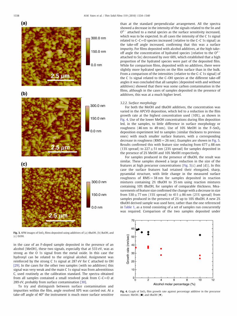
Fig. 3. AFM images of SnO2 films deposited using additives of (a) tBuOH, (b) BuOH, and(c) EtOH.
Fig. 4. Graph of SnO2 film growth rate against percentage additive in the precursormixture. MeOH. (■) and tBuOH (♦).
1338 H.M. Yates et al. / Thin Solid Films 519 (2010) 1334–1340
in the case of an F-doped sample deposited in the presence of analcohol (MeOH), these two signals, especially that at 533 eV, was asstrong as the O 1s signal from the metal oxide. In this case thehydroxyl can be related to the original alcohol. Assignment wasreinforced by the strong C 1s signal at 287 eV for C attached to OH[29]. In the cases for the other two samples (with no additives) thissignal was very weak and the main C 1s signal was from adventitiousC, used routinely as the calibration standard. The spectra obtainedfrom all samples contained a small resolved peak from C–C=O at289 eV, probably from surface contamination [30].
To try and distinguish between surface contamination andimpurities within the film, angle resolved XPS was carried out. At atake-off angle of 40o the instrument is much more surface sensitive
than at the standard perpendicular arrangement. All the spectrashowed a decrease in the intensity of the signals related to the Sn andO2− attached to a metal species as the surface sensitivity increased,which was to be expected. In all cases the intensity of the C 1s signalrelated to C–C=O species increased (relative to the C–C 1s signal) asthe take-off angle increased, confirming that this was a surfaceimpurity. For films deposited with alcohol additives, at the high take-off angle the concentration of hydrated species (relative to the O2−
attached to Sn) decreased by over 60%, which established that a highproportion of the hydrated species were part of the deposited film.While for comparison films, deposited with no additives, there wereslightly more hydrated species on the film surface than in the bulk.From a comparison of the intensities (relative to the C–C 1s signal) ofthe C 1s signal related to the C–OH species at the different take-offangles it was concluded that all samples (deposited with and withoutadditives) showed that there was some carbon contamination in thefilms, although in the cases of samples deposited in the presence ofadditives, this was at a much higher level.
3.2.2. Surface morphologyFor both the MeOH and tBuOH additives, the concentration was
varied in the APCVD deposition, which led to a reduction in the filmgrowth rate at the highest concentration used (10%), as shown inFig. 4. Use of the lower MeOH concentrations during film depositionled, in the samples, to little difference in surface morphology orroughness (46 nm to 49 nm). Use of 10% MeOH in the F–SnO2
deposition experiment led to samples (similar thickness to previousones) with much smaller surface features, with a correspondingdecrease in roughness (RMS=26 nm). Examples are shown in Fig. 5.Results confirmed this with feature size reducing from 677±88 nm(13% spread) to 227±51 nm (23% spread) for samples deposited inthe presence of 2% MeOH and 10% MeOH respectively.
For samples produced in the presence of tBuOH, the result wassimilar. These samples showed a large reduction in the size of thefeatures at high precursor concentrations (Fig. 5(c) and (d)). In thiscase the surface features had retained their elongated, sharp,pyramidal structure, with little change in the measured surfaceroughness of RMS=38 nm for samples deposited in reactionmixtures containing 2% tBuOH to 35 nm using reaction mixturescontaining 10% tBuOH, for samples of comparable thickness. Mea-surements of feature size confirmed the changewith a decrease in sizefrom 530±77 nm (15% spread) to 411±86 nm (21% spread) fromsamples produced in the presence of 2% up to 10% tBuOH. A new 2%tBuOH derived sample was used here, rather than the one referencedin Table 1, as a trend consisting of a set of samples run concurrentlywas required. Comparison of the two samples deposited under

Fig. 5. AFM images of SnO2 films deposited using varying concentrations of additives in the APCVD process (a) 2% MeOH (b) 10% MeOH, (c) 2% tBuOH, and (d) 10% tBuOH.
1339H.M. Yates et al. / Thin Solid Films 519 (2010) 1334–1340
different alcohols at low concentration (2%) showed similar surfacefeatures, although those from the sample deposited under MeOHwere slightly sharper and large, despite being thinner (670 nm to740 nm for tBuOH related sample).
Growth rate of TCO films (via changing the carrier gas flow via theTTC bubbler) as previously shown changed the resistivity [31] and canchange the surfacemorphologywith a reduction in the size of featuresas the concentration increased [10]. For the films deposited with theMeOH additive it was found that at growth rates, which matched thatof tBuOH (2%) derived samples, the samples lost their elongatedfeatures becomingmore rounded, unlike the samples deposited undertBuOH which retained the sharp, elongated pyramidal shape.
3.2.3. Electrical propertiesAddition of 2% MeOH to the APCVD process led in the samples to a
small reduction of the resistivity from 8×10⁻⁴ Ωcm (no additive) to6×10−4 Ωcm, with no further decrease in samples produced fromaddition of more MeOH to the deposition process. This reduction inresistivity has been previously attributed to the reducing effect ofMeOH on the tin oxide surface, so making it easier for the fluorine toincorporate into the tin oxide lattice [32]. Conversely, use of thetBuOH additive in the deposition process led to samples that showed agradual initial increase in resistivity to 13×10−4 Ωcm beforestabilising. The overall higher resistivity for the tBuOH derivedsamples over the MeOH derived samples, possibly being related tothe increased disorder stemming from the much faster growth rate.For a balance between low resistivity and large feature size in thesurface morphology (Fig. 5), 2%MeOH added to the APCVD depositionprocess was found to be the optimum, while for the tBuOH a lowervalue would be possible.
3.2.4. X-ray diffractionX-ray diffraction was obtained for all the samples and showed no
change in orientation preference until samples deposited using 4%MeOH in the precursor mix was reached. At this point, the (101)orientation decreased and the (200) increased. There was littledifference in calculated crystallite sizes for any of the samplesproduced from the series of experiments using MeOH as an additive.Changes in the tBuOH precursor concentration to 10% did not alter theproduced samples orientation preferences or show change incrystallite size.
3.2.5. Optical propertiesAs shown above, the methanol precursor concentration effected
the resistivity and the morphology of the deposited TCO. Opticalmeasurements (PDS) and subsequent calculations showed the effectthe concentration can have on the absorption coefficient (Fig. 6) of thedeposited films.
Optical measurements on a set of samples deposited usingdifferent concentrations of MeOH, showed an increase in absorbancecoefficient as the additive precursor concentration increased.
To study the ability of the samples to scatter light, angle resolvedscattering at 830 nmwas carried out on a selection of samples. Most ofthe light was scattered within a cone of +/−15o with only a smallfraction of light scattered into higher angles. Addition of a smallamount of an alcohol to the APCVD process was, in general, shown toincrease the sample scatter at high angles over that of a sampledeposited without the presence of alcohol (Fig. 7). The exception tothis was for EtOH derived samples, probably reflecting its morphologyof small surface features and comparably smoother surface. However,addition of larger amounts of alcohol to the APCVD process also led to
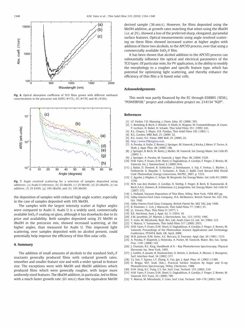
Fig. 6. Optical absorption coefficient of TCO films grown with different methanolconcentrations in the precursor mix 0.05% (#172), 2% (#170) and 4% (#164).
Fig. 7. Angle resolved scattering for a selection of samples deposited usingadditives. (a) Asahi U reference, (b) 2% tBuOH, (c) 2% MeOH, (d) 2% nBuOH, (e) noadditive, (f) 2% EtOH, (g) 10% tBuOH, and (h) 10% MeOH.
1340 H.M. Yates et al. / Thin Solid Films 519 (2010) 1334–1340
the deposition of samples with reduced high angle scatter, especiallyin the case of samples deposited with 10% MeOH.
The samples with the largest intensity scatter at higher angleswere compared to Asahi U. Asahi U is a widely used, commerciallyavailable SnO2:F coating on glass, although it has drawbacks due to itsprice and availability. Both samples deposited using 2% MeOH ortBuOH in the precursor mix, showed increased scattering, at thehigher angles, than measured for Asahi U. This improved lightscattering, over samples deposited with no alcohol present, couldpotentially help improve the efficiency of thin film solar cells.
4. Summary
The addition of small amounts of alcohols to the standard SnO2:Freactants generally produced films with reduced growth rates,smoother and smaller feature size and with a wider spread in featuresize. The exceptions were with MeOH and tBuOH additives whichproduced films which were generally rougher, with larger moreuniformly sized features. The tBuOH additive, in particular, led to filmswith a much faster growth rate (61 nm/s) than the equivalent MeOH
derived sample (36 nm/s). However, for films deposited using theMeOH additive, at growth rates matching that when using the tBuOH(i.e. at 2%), showed a loss of the preferred sharp, elongated, pyramidalsurface features. Optical measurements using angle resolved scatter-ing on these films showed increased scatter at higher angles withaddition of these two alcohols, to the APCVD process, over that using acommercially available SnO2:F film.
It has been shown that alcohol addition to the APCVD process cansubstantially influence the optical and electrical parameters of theTCO layer. Of particular note, for PV application, is the ability tomodifythe morphology to a rougher and specific feature type, which haspotential for optimizing light scattering, and thereby enhance theefficiency of thin film a-Si based solar cells.
Acknowledgements
This work was partly financed by the EC through 038885 (SES6),“POWERFOIL” project and collaborative project no. 214134 “N2P”.
References
[1] I.P. Parkin, T.D. Manning, J. Chem. Educ. 83 (2006) 393.[2] C. Beneking, B. Rech, S. Wieder, O. Kluth, H.Wagner, W. Frammelsberger, R. Geyer,
P. Lechner, H. Rubel, H. Schade, Thin Solid Films 351 (1999) 241.[3] K.L. Chopra, S. Major, D.K. Pandya, Thin Solid Films 102 (1983) 1.[4] R.G. Gordon, MRS Bull. 25 (2000) 52.[5] B.G. Lewis, D.C. Paine, MRS Bull. 25 (2000) 22.[6] http://www.Pilkington.com.[7] A. Poruba, A. Fejfar, Z. Remes, J. Springer, M. Vanecek, J. Kocka, J. Meier, P. Torres, A.
Shah, J. Appl. Phys. 88 (2000) 148.[8] J. Springer, B. Rech, W. Reetz, J. Muller, M. Vanecek, Sol. Energy Mater. Sol. Cells 85
(2005) 1.[9] J. Springer, A. Poruba, M. Vanecek, J. Appl. Phys. 96 (2004) 5329.
[10] H.M. Yates, P. Evans, D.W. Sheel, U. Dagkaldiran, A. Gordijn, F. Finger, Z. Remes, M.Vanecek, Int. J. Nanotechnol. 6 (2009) 816.
[11] J. Bailat, D. Dominé, R. Schlüchter, J. Steinhauser, S. Faÿ, F. Freitas, C. Bücher, L.Feitknecht, X. Niquille, T. Tschamer, A. Shah, C. Ballif, Conf. Record IEEE WorldConf. Photovoltaic Energy Conversion, WCPEC, 2007, p. 1533.
[12] C. Agashe, J. Hüpkes, G. Schpe, M. Berginski, Sol. Energy Mater. Sol. Cells 93 (2009)1256.
[13] M.N. van den Donker, A. Gordijn, H. Stiebig, F. Finger, B. Rech, B. Stannowski, R.Bartl, E.A.G. Hamers, R. Schlatmann, G.J. Jongerden, Sol. Energy Mater. Sol. Cells 91(2007) 572.
[14] L. Holland, Vacuum Deposition of Thin films, Wiley, New York, 1958 493 pp.[15] Libby-Owens-Ford Glass Company, H.A. McMasters, British Patent No. 632 256,
Oct. 1942.[16] Libby-Owens-Ford Glass Company, British Patent No. 682 342, July 1949.[17] R. Pommier, C. Gril, J. Marucchi, Thin Solid Films 77 (1981) 91.[18] J.L. Vossen, Phys. Thin Films 9 (1977) 1.[19] R.E. Aitchison, Aust. J. Appl. Sci. 5 (1954) 10.[20] Z.M. Jarzebski, J.P. Marton, J. Electrochem. Soc. 123 (1976) 199C.[21] Y. Goto, M. Mizuhashi, Rept. Res. Lab. Asahi Glass Co. Ltd. 34 (1984) 123.[22] Y. Matsui, Y. Yamamoto, Thin Solid Films 517 (2009) 2953.[23] H.M. Yates, P. Evans, D.W. Sheel, U. Dagkaldiran, A. Gordijn, F. Finger, Z. Remes, M.
Vanecek, Proceedings of the Photovoltaic Science Applications and TechnologyConference, PVSAT4, Bath, UK, April, 2008.
[24] W.B. Jackson, N.M. Amer, A.C. Boccara, D. Fournier, Appl. Opt. 20 (1981) 1333.[25] A. Poruba, P. Klapetek, J. Holovsky, A. Purkrt, M. Vanecek, Mater. Res. Soc. Symp.
Proc. 1101 (2008) 143.[26] J. Chastain, R.C. King, Handbook of X – Ray Photoelectron Spectroscopy, Physical
Electronic Inc, New York, 1995.[27] J. Guillot, A. Jouaiti, B. Domenichini, O. Heintz, S. Zerkout, A. Mosser, S. Bourgeois,
Surf. Interface Anal. 34 (2002) 577.[28] Y.J. Sun, T. Egawa, L.Y. Zhang, X. Yao, Jpn. J. Appl. Phys. 41 (2002) L1389.[29] D. Briggs, M.P. Seah (Eds.), Practical Surface Analysis by Auger and X-ray
Photoelectron Spectroscopy, Wiley, Chichester, 1988.[30] D.W. Zeng, K.C. Yung, C.S. Xie, Surf. Coat. Technol. 153 (2002) 210.[31] H.M. Yates, P. Evans, D.W. Sheel, U. Dagkaldiran, A. Gordijn, F. Finger, Z. Remes, M.
Vanecek, ECS Trans. 25 (2009) 789.[32] Y. Matsui, M. Mitsuhashi, Y. Goto, Surf. Coat. Technol. 169–170 (2003) 549.
Copyright © 2022 FDOKUMEN