Patent - METHOD FOR FORMING METAL FILM BY ALD USING BETA-DIKETONE METAL COMPLEX
25
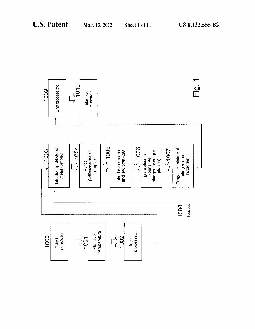
US008133555B2 (12) United States Patent (10) Patent N0.2 US 8,133,555 B2 Shinriki et a]. (45) Date of Patent: Mar. 13, 2012 (54) METHOD FOR FORMING METAL FILM BY 5,106,454 A 4/1992 Allardyce et a1. ALD USING BETA-DIKETONE METAL 2 $111919 er l , , e a os e a . COMPLEX 5,453,494 A 9/1995 Kirlin et al. _ _ _ _ _ _ _ 5,470,661 A 11/1995 Bailey et al. (75) Inventors: Hlroshl Shlnrlkl, Tama (JP); Kunltoshl 5,637,533 A 6/1997 (1110i Namba, Tama (JP); Daekyun Jeong, 5,695,810 A 12/1997 Dubin et al. Tama (JP) 5,711,811 A 1/1998 Suntola et al. 5,731,634 A 3/1998 Matsuo et al. - _ 5,820,664 A 10/1998 Gardiner et al. (73) Asslgnee~ ASM Japan K-K- (JP) 5,865,365 A 2/1999 Nishikawa et al. _ _ _ _ _ 5,884,009 A 3/1999 Okase ( * ) Not1ce: Subject to any d1scla1mer, the term of th1s 5,916,365 A 6/1999 Sherman er a1, patent is extended or adjusted under 35 5,923,056 A 7/1999 Lee et al. U.S.C. 154(b) by 364 days. (Continued) (21) APP1-NO-1 12/251343 FOREIGN PATENT DOCUMENTS (22) Filed: Oct. 14, 2008 DE 41 08 73 _ 3/1925 (Contmued) (65) Prior Publication Data OTHER PUBLICATIONS US 2010/0092696 A1 Apr. 15, 2010 Li et al; “Atomic Layer Depositio of Ultrathin Copper Metal Films 51 Int, C], from a Li uid Co er I Amidinate Precursor”; Journal of the ( ) 9 PP ( ) H05H 1/24 2006.01 Electorchemical Society, vol. 153 Issue 11 (pp. C787-C794); 2006.* ( ) C23C 16/] 8 (2006.01) (Continued) (52) US. Cl. 427/576; 427/96.8; 427/97.7; 118/723 E (58) Field of Classi?cation Search ........... .. 427/255.28, Primary Examiner i Dah_weiyuan S 1_ _ ?l f 127/968’ 97'7’ 576 Assistant Examiner * Jose HernandeZ-DiaZ ee app lcanon e or Comp ete Seam lstory' (74) Attorney, Agent, or Firm * Knobbe, Martens, Olson & (56) References Cited Bear LLP US. PATENT DOCUMENTS (57) A method of forming a single-metal ?lm on a substrate by ABSTRACT 4,058,430 A 11/1977 Suntola et al. _ _ _ 4,210,608 A 7/19g0 Pinke plasma ALD mcludes: contactmg a surface of a substrate W1th 4,477,296 A 10/ 1984 Nair a [3-diketone metal complex in a gas phase; exposing mol 4,604,118 A 8; 1986 B90111“) et 21151 ecule-attached surface to a nitrogen-hydrogen mixed plasma; 4’670’l 10 A 6 1987 W1? .ers et ' and repeating the above steps, thereby accumulating atomic 4,860,687 A 8/1989 Ffljllnk . 4,891,050 A V1990 Bowers et 31‘ layers to form a smgle-metal ?lm on the substrate. 4,902,551 A 2/1990 Nakaso et al. 4,965,656 A 10/1990 Koubuchi et al. 16 Claims, 11 Drawing Sheets 1000 l 1003 4% Take in lnlmduce p-diketone _“ End pmcessing substrate metal complex 3 B 1004 51010 1001 k Purge Take out |$d|ketone metal subsmage Stabilize complex temperature a U 1005 1 (10d ' 1002 annd 11331263332 Begin processing L1 1006 Ignite plasma (generate nitrogen/hydrogen plasma) @1007 P '10 1 1008 “111822188” Repeat hydmge"
Transcript of Patent - METHOD FOR FORMING METAL FILM BY ALD USING BETA-DIKETONE METAL COMPLEX

US008133555B2
(12) United States Patent (10) Patent N0.2 US 8,133,555 B2 Shinriki et a]. (45) Date of Patent: Mar. 13, 2012
(54) METHOD FOR FORMING METAL FILM BY 5,106,454 A 4/1992 Allardyce et a1. ALD USING BETA-DIKETONE METAL 2 $111919 er l
, , e a os e a .
COMPLEX 5,453,494 A 9/1995 Kirlin et al. _ _ _ _ _ _ _ 5,470,661 A 11/1995 Bailey et al.
(75) Inventors: Hlroshl Shlnrlkl, Tama (JP); Kunltoshl 5,637,533 A 6/1997 (1110i Namba, Tama (JP); Daekyun Jeong, 5,695,810 A 12/1997 Dubin et al. Tama (JP) 5,711,811 A 1/1998 Suntola et al.
5,731,634 A 3/1998 Matsuo et al. - _ 5,820,664 A 10/1998 Gardiner et al.
(73) Asslgnee~ ASM Japan K-K- (JP) 5,865,365 A 2/1999 Nishikawa et al. _ _ _ _ _ 5,884,009 A 3/1999 Okase
( * ) Not1ce: Subject to any d1scla1mer, the term of th1s 5,916,365 A 6/1999 Sherman er a1, patent is extended or adjusted under 35 5,923,056 A 7/1999 Lee et al.
U.S.C. 154(b) by 364 days. (Continued)
(21) APP1-NO-1 12/251343 FOREIGN PATENT DOCUMENTS
(22) Filed: Oct. 14, 2008 DE 41 08 73 _ 3/1925
(Contmued) (65) Prior Publication Data
OTHER PUBLICATIONS US 2010/0092696 A1 Apr. 15, 2010
Li et al; “Atomic Layer Depositio of Ultrathin Copper Metal Films 51 Int, C], from a Li uid Co er I Amidinate Precursor”; Journal of the ( ) 9 PP ( )
H05H 1/24 2006.01 Electorchemical Society, vol. 153 Issue 11 (pp. C787-C794); 2006.* ( ) C23C 16/] 8 (2006.01) (Continued)
(52) US. Cl. 427/576; 427/96.8; 427/97.7; 118/723 E (58) Field of Classi?cation Search ........... .. 427/255.28, Primary Examiner i Dah_weiyuan
S 1_ _ ?l f 127/968’ 97'7’ 576 Assistant Examiner * Jose HernandeZ-DiaZ ee app lcanon e or Comp ete Seam lstory' (74) Attorney, Agent, or Firm * Knobbe, Martens, Olson &
(56) References Cited Bear LLP
US. PATENT DOCUMENTS (57) A method of forming a single-metal ?lm on a substrate by
ABSTRACT
4,058,430 A 11/1977 Suntola et al. _ _ _ 4,210,608 A 7/19g0 Pinke plasma ALD mcludes: contactmg a surface of a substrate W1th 4,477,296 A 10/ 1984 Nair a [3-diketone metal complex in a gas phase; exposing mol 4,604,118 A 8; 1986 B90111“) et 21151 ecule-attached surface to a nitrogen-hydrogen mixed plasma; 4’670’l 10 A 6 1987 W1? .ers et ' and repeating the above steps, thereby accumulating atomic 4,860,687 A 8/1989 Ffljllnk . 4,891,050 A V1990 Bowers et 31‘ layers to form a smgle-metal ?lm on the substrate. 4,902,551 A 2/1990 Nakaso et al. 4,965,656 A 10/1990 Koubuchi et al. 16 Claims, 11 Drawing Sheets
1000 l 1003 4% Take in lnlmduce p-diketone _“ End pmcessing substrate metal complex
3 B 1004 51010 1001 k Purge Take out
|$d|ketone metal subsmage Stabilize complex
temperature
a U 1005 1 (10d '
1002 annd 11331263332 Begin
processing L1 1006 Ignite plasma (generate
nitrogen/hydrogen plasma)
@1007 P '10 1
1008 “111822188” Repeat hydmge"
US 8,133,555 B2 Page 3
2004/0192036 A1 9/2004 Koyanagietal. KR 10-2001-004718 1/2001 2004/0214354 A1 10/2004 Marsh etal. KR 10-2001-004719 1/2001 2004/0216668 A1 11/2004 Lindforsetal. KR 10-2001-96408 11/2001 2004/0224475 A1 11/2004 Lee etal. KR 10-2001-112889 12/2001 2005/0009325 A1 1/2005 Chung 61711. KR 10-2003-0011399 2/2003 2005/0020060 A1 1/2005 Aaltonen etal. KR 1020050103373 10/2005 2005/0048794 A1 3/2005 Brask 61711. W0 W0 93/10652 5/1993 2005/0082587 A1 4/2005 Marsh W0 W0 98/01890 1/1998 2005/0085031 A1 4/2005 Lopatin 61711. W0 W0 99/17343 4/1999 2005/0087879 A1 4/2005 Won 61711. W0 W0 00/03420 1/2000 2005/0089632 A1 4/2005 Vehkamaki 61711. W0 W0 00/38191 6/2000 2005/0092247 A1 5/2005 Schmidt etal. W0 W0 01/88972 5/2001 2005/0098440 A1 5/2005 Kailasan 61711. W0 W0 01/50502 7/2001 2005/0112509 A1 5/2005 Fairbairn 61711. W0 W0 02/09126 7/2001 2005/0118807 A1 6/2005 Kim 61711. W0 W0 02/09158 7/2001 2005/0124154 A1 6/2005 Park 61711. W0 W0 03/023835 3/2003 2005/0181555 A1 55/2005 Haukka 61711. W0 W0 03/040150 5/2003 2005/0208754 A1 9/2005 Kostamo etal. W0 W0 03/056612 A1 7/2003 2005/0229848 A1 10/2005 Shinrikietal. W0 W0 2004/035858 4/2004 2005/0238808 A1 10/2005 Gatineau 61711. W0 W0 2006/035281 4/2006 2005/0266700 A1 12/2005 Jursich 61711. 2005/0271812 A1 12/2005 Myo etal. OTHER PUBLICATIONS 2006/0013955 A1 2006/0035462 A1 2006/0073276 A1 2006/0084280 A1 2006/0093848 A1 2006/0118968 A1 2006/0121733 A1 2006/0128150 A1 2006/0137608 A1 2006/0165892 A1 2006/0177601 A1 2006/0211228 A1 2006/0216932 A1 2006/0223300 A1 2006/0263977 A1 2007/0014919 A1 2007/0026654 A1 2007/0036892 A1 2007/0059502 A1 2007/0082132 A1 2007/0128864 A1* 2007/0190782 A1 2007/0218705 A1 2007/0248767 A1 2007/0254488 A1
1/2006 SenZaki 2/2006 MillWard 4/2006 Antonissen 4/2006 Matsuki et al. 5/2006 Senkevich et al. 6/2006 Johnston et al. 6/2006 Kilpela et a1. 6/2006 Gandikota et al. 6/2006 Choi et al. 7/2006 Weidman 8/2006 Park et al. 9/2006 Matsuda 9/2006 Kumar et a1. 10/2006 Simka et al. 11/2006 Kim et a1. 1/2007 Hamalainen et al. 2/2007 Huotari et al. 2/2007 Haukka et al. 3/2007 Wang et a1. 4/2007 Shinriki et al. 6/2007 Ma et al. ..................... .. 438/680
8/2007 Park et al. 9/2007 Matsuki et al. 10/2007 Okura et al. 11/2007 Huotari et al.
2008/0038465 A1 2/2008 Dussurrat 2008/0054472 A1 3/2008 Shinriki et al. 2008/0102613 A1* 5/2008 Elers ........................... .. 438/680
2008/0124484 A1 5/2008 Shinriki et al. 2008/0146042 A1 6/2008 Kostamo et a1. 2008/0171436 A1 7/2008 Koh et al. 2008/0200019 A9 8/2008 Huotari et al. 2008/0206982 A1 8/2008 Suzuki 2008/0206985 A1 8/2008 Kim et al. 2008/0214003 A1 9/2008 Xia 2008/0296768 A1 12/2008 Chebiam 2008/0315418 A1 12/2008 Boyd 2008/0318417 A1 12/2008 Shinriki et al. 2009/0068832 A1 3/2009 Haukka et al. 2009/ 0087339 A1 4/ 2009 Shinriki 2009/0104777 A1 4/2009 Kim 2009/0155997 A1 6/2009 Shinriki 2009/0163024 A1 6/2009 Kim et al. 2009/0209101 A1 8/2009 Shinriki et al. 2010/0055433 A1 3/2010 Shinriki et al.
FOREIGN PATENT DOCUMENTS
EP 0 469 456 7/1991 EP 0 469 470 2/1992 EP 0 880 168 A2 11/1998 EP 1 688 923 A2 8/2006 GB 368850 12/1930 GB 1518243 7/1978 GB 2340508 A 2/2000 JP 1998-340994 12/1998 JP 2003-168738 A 6/2003 KR 10-2001-004717 1/2001
Arnal, V. et al., Materials and processes for high signal propagation performance and reliable 32 nm node BEOL., 2007 International
Interconnect Technology Conference, 2007 IEEE, pp. 1-3, ISBN 1-4244-1069-X/07. Namba, K. et al., “PEALD of Ru layer on WNC ALD barrier for Cu/porous low-k integration,” Proceedings of Advanced MetalliZa tion Conference 2006, p. 39. J eong, Seong-Jun et al., “Plasma enhanced atomic layer deposition of Ru-TaN thin ?lms for the application of Cu diffusion barrier,” ALD Conference 2006, pp. 1-23. Morisada et al., “Method of self-cleaning of carbon-based ?lm,” U.S. Appl. No. 11/868,437, ?led Oct. 5, 2007. Shao, I. et al., “An alternative lOW resistance MOL technology With electroplated rhodium as contact plugs for 32nm CMOS and beyond,” 2007 International Interconnect Technology Conference, 2007 IEEE, pp. 102-104, ISBN 1-4244-1070-3/07. Shinriki et al., “Atomic composition controlled ruthenium alloy ?lm formed by plasma-enhanced atomic layer depo sition,” U. S . Appl. No. 12/201,434, ?led Aug. 29, 2008. Shinriki et al., “Method for activating reactive oxygen species for cleaning carbon-based ?lm deposition,” U.S. Appl. No. 12/058,629, ?led Mar. 28, 2008. Shinriki, “Method for forming ruthenium complex ?lm using B-diketone coordinated ruthenium precursor,” U.S. Appl. No. 12/203,405, ?led on Sep. 3, 2008. Shinriki, H. et al., “Ruthenium alloy ?lm for copper interconnects,” U.S. Appl. No. 12/129,345, ?led May 29,2008. Yang, C.C. et al., “Physical, electrical, and reliability characteriza tion of Ru for Cu interconnects,” 2006 International Interconnect Technology Conference, 2006 IEEE, pp. 187-190, ISBN 1-4244 0103-8/06. Jung et al., “A Novel Ir/IrO2/Pt-PZT-Pt/IrO2/Ir Capacitor for a Highly Reliable Mega-Scale FRAM,” IEEE, IED 2000, Session 34 (2000). Kadota, Takumi et al., “Ruthenium Films Deposited under H2 by MOCVD using a Novel Liquid Precursor”. IEEE article, pp. 175 176, no date available. Kawaguchi, “MPEG1 Decoder LSI for video CD 11PD61012,” NEC Device Technology International. New Products 5 No. 48, pp. 4-8 (Jan. 1998). KaWamoto et al., “The Outlook for Semiconductor Processes and Manufacturing Technologies in the 0.1-um Age,” Hitachi Review 48(6): 334-339 (1999). Koh et al., US. Appl. No. 11/972,081, ?led Jan. 10, 2008. KWon et al., “Plasma-enhanced Atomic Layer Deposition of Ruthe nium Thin Films,” Electrochemical and Solid-State Letters, 7(4), C46-C48 (2004). KWon et al., “Plasma-enhanced Atomic Layer Deposition of RuTiN Thin Films for the Application of Copper Diffusion Barrier,” ALD Conference, 2004.

US 8,133,555 B2 Page 4
Kwon et al., “Ruthenium Bottom Electrode Prepared for Electroplat ing for a High Density DRAM Capacitor ,” J. Electrochem. Soc. 151(2): C127-C132 (2004.). Lee et al., “Electroless CoWP boosts copper reliability, device per formance,” Semiconductor International , Jul. 1, 2004, 5 pages. NEC Device Technology International, “Current state of leading edge ULSI process technology and future trends,” No. 48, pp. 4-8 (1998). Nilsen et al., “Thin Film Deposition of Lanthanum Manganite Perovskite by the ALE process,” Journal of Materials Chemistry, vol. 9,1781-1784(1999). Onda et al., “DC-Hydrogen Plasma Cleaning a Novel Process for IC-Packaging”, SEMICON WEST 97, Packaging Materials Confer ence, 1997, pp. D-1-D-10. Onda et al., “Hydrogen plasma cleaning a novel process for IC packaging,” SEMICON WEST 97, Packaging Materials Conference, 1997, pp. D-1-D-10. Pakrad, “Pure Tech: Growth of MIUGMR Head Materials,” World Wide Web, Puretechinc.com/techipapers/techipapers-4.htrn, pp. 1-2 (1999.). Paranj pe et al., “Atomic Layer Deposition of AIOx for thin Film Head Gap Applications,” Journal of Electrochemical Society, V 148(9), G 465-G471, Jul. 16, 2001. Park et al., “Metallorganic Chemical Vapor Deposition of Ru and RuO2 using Ruthenocene Precursor and Oxygen Gas,” J.Electrochem. Soc., 147[1], 203, 2000. Parsons et al., “Microcontact Patterning of Ruthenium Gate Elec trodes by Selective Area,”North Carolina State University, presenta tion at AVS conference on Atomic Layer Deposition (ALD 2004), Helsinki Finland, Aug. 16, 2004. Ritala et al., “Atomic Layer Deposition,” Handbook of Thin Film Materials vol. 1: Deposition and Processing of Thin Films, chapter 2, pp. 103-159 (2002). Rossnagel, “The latest on Ru-Cu interconnect technology,” Solid State Technology, Feb. 2005, Online, pp. 1-4. U.S. Appl. No. 10/728,126, ?led Dec. 3, 2003, Granneman. U.S. Appl. No. 10/782,727, ?led Feb. 18, 2004, Lindfors et al. US. Appl. No. 11/254,071, ?led Jun. 8, 2006, Kilpela. U.S. Appl. No. 11/367,177, ?led Mar. 3,2006, Shinriki et al. US. Appl. No. 11/469,828, ?led Sep. 1, 2009, Shinriki et al. US. Appl. No. 11/557,891, ?led Nov. 8,2006, Shinriki et al. US. Appl. No. 11/955,275, ?led Dec. 12, 2007, Shinriki. U.S. Appl. No. 11/972,081, ?led Jan. 10, 2008, Koh. U.S. Appl. No. 12/337,141, ?led Dec. 17, 2008, Kim et al. US. Appl. No. 60/976,378, ?led Sep. 28, 2007, Shinriki. U.S. Appl. No. 61/178,871, May 15, 2009, Hamalainen et al. Aaltonen et al., “Ruthenium Thin Film Grown by Atomic Layer Deposition,” Chem. Vap. Deposition, 9[1], 45, 2003. Aaltonen et al., “ALD of Rhodium Thin Films from RH (acac)3 and Oxygen,” Electrochem. Solid-State Lett. 8 (8): C99-C101 (2005). Aaltonen et al., “Atomic Layer Deposition of Iridium Thin Films,” J. Electrochem. Soc. 151(8): G489-G492 (2004). Aaltonen et al., “Atomic Layer Deposition of Noble Metal Thin Films,” dissertation presented at University of Helsinki, Helsinki, Finland, 2005. Aaltonen et al., “Atomic Layer Deposition of Noble Metals: Explo ration of the Low Limit of the Deposition Temperature,” J. Mat. Res. Soc. 19(11): 3353-3358 (2004). Aaltonen et al., “Atomic Layer Deposition of Platinum Thin Films,” Chem. Mater. 15:1924-1928 (2003). Aaltonen et al., “Atomic Layer Deposition of Ruthenium Thin Films from Ru(thd)3 and Oxygen,” Chem. Vap. Deposition, 2004, vol. 10, Issue 4, pp. 215-219. Aaltonen et al., “Reaction Mechanism Studies on Atomic Layer Deposition of Ruthenium and Platinum,” Electrochem. Solid-State Lett., (2003), vol. 6, pp. C130-C133. Addison et al., “The Vapour Pressure of Anhydrous Copper Nitrate and its Molecular Weight in the Vapour State,” J .Chem. Soc., pp. 3099-3106 (1958). Akerman et al., “Identifying Tunneling in Ferromagnetic-Insulator Ferromagnetic Thin Film Structures,” World Wide Web, physics. ucsd.eduiksgrp/Tunneling.htrnl, Sep. 10, 2008, pp. 1-6.
Aoyama et a1 ., “Chemical Vapor Deposition of Ru and Its Application in (Ba, Sr) TiO3 Capacitors for Future Dynamic Random Access Memories,” Jpn. J. Appl. Phys. 38(43): 2194-2199 (1999). Aoyama, et al., “Ruthenium Films Prepared by Liquid Source Chemical Vapor Deposition Using Bis (ethylcyclopentadienyl)ruthenium”. Jpn. J. Appl. Phys., vol. 38 (1999) pp. L1134-L1136. Baklanov et al., “Characterization of Cu surface cleaning by hydro gen plasma,” Journal Vac. Sci. Technol. 19(4): 1201-1211 (2001). Baliga, J ., Associate Editor, “New designs and materials tackle 1 Gb memory challenges,” Semiconductor International, World Wide Web address: semiconductor.net, Nov. 2000. Basceri, C. “Electrical and Dielectric Properties of (BA, SR) TiO3 Thin Film Capacitors for Ultra-High Density Dynamic Random Access Memories,” Ph.D. thesis, 1997, pp. 13-31, Raleigh, NC. State University. Bobo et al., Spin Dependent Tunneling Junctions with Hard Mag netic Layer Pinning, Journal of Applied Physics, 1998, vol. 83, No. 11, pp. 6685-6687. Bursky, “Hit Up IEDM for Gigabit and Denser DRAMs and Merged Logic/Memory,” Electronic Design, World Wide Web address: planetee.com, Dec. 1, 1998. Campbell et al., “Titanium dioxide (TiO2)-based gate insulators,”IBM J. Res. Develop., May 1999, pp. 383-392, vol. 43, No. 3. Daughton, “Advanced MRAM Concepts,” World Wide Web nve. com/otherbiz/mram2.pdf, Feb. 7, 2001, pp. 1-6. Dussarrat et al., “Precursor for ?lm formation and method for form ing ruthenium-containing ?lm,” Apr. 2006, WO 2006/035281 A1. Fereday et al., “Anhydrous Cobalt (III) Nitrate,” Chemical Commu nications, p. 271 (1968). Fukuzumi et al., “Liner-Supported Cylinder (LSC) Technology to Realize RU/Ta205/Ru Capacitor for Future DRAMs,” IEEE, IED 2000, Session 34 (2000). Fullerton et al., “Advanced Magnetic Recording Media for High Density Data,” Solid State Technology 44(i9): 87 (2001). Giant Magnetoresistance, World Wide Web, stoner.leeds.ac.uldre search/gmrhtm, pp. 1-6, (2004). Giant Magnetoresistive (GMR) Heads, The PC Guide, World Wide Web, pc.guide.com/ref/hdd/op/heads/techGMR-c.html, accessed Jul. 3, 2009, pp. 1-4. GMR Head Technology: Increased Areal Density and Improved Areal Density, WorldWide Web, magahaus.com/tech/westerndigital/ shitepapers/gmriwpshtml, pp. 1-4 (Feb. 2000). GMR Read-Write HeadsYield Data Storage Record, Semiconductor International, semiconductor.net/semiconductor/issues/Issues/1998/ feb98/docs/emerging.asp, p. 1 (Feb. 1998). Hones et al., “MOCVD of Thin Ruthenium Oxide Films: Properties and Growth Kinetics,” Chem. Vap. Deposition 6(4): 193-198 (2000). Hoyas et al., Growth and characterization of atomic layer deposited WCO.7N0.3 on polymer ?lms, Journal of Applied Physics, Jan. 1, 2004, vol. 95, Issue 1, pp. 381-388. Hu et al., “In situ rapid thermal oxidation and reduction of copper thin ?lms and their applications in ultralarge scale integration,” Journal of The Electrochemical Society 148(12): G669-G675 (2001). Hur’Yeva, Tetyana, et al., “Ruthenium Films Deposited by Liquid Delivery MOCVD using Bis(ethylcyclopentadienyl)ruthenium with Toulene as the Solvent”. Chemical Vapor Deposition 2006, 12, pp. 429-434. Imai, “100 Gbit/Inch HDD Just Around the Corner,” Nikkei Elec tronics Asia, nikkeibp.asiabiztech.com/nea/200008/108675.htrnl, p. 1-5 (Aug. 2000). Inoue et al., “Low thermal-budget fabrication of sputtered-PZT capacitor on multilevel interconnects for embedded FeRAM,” IEEE, IED 2000, 2000, Session 34. Integrated Circuit Engineering Corporation, Practical Integrated Cir cuit Fabrication Seminar (1998). Paranjpe et al., “Atomic Layer Deposition of AIOx for thin Film Head Gap Applications,” Journal of Electrochemical Society, V 148(9), G 465-G471, Jul. 17, 2001. Sakurai et al., “Adsorption of ruthenium tetroxide on metal surfaces,” J. Phys., Chem. American Chemical Society, 1985, vol. 89, pp. 1892 1896.

US 8,133,555 B2 Page 5
Satta et al., “The Removal of Copper Oxides by Ethyl Alcohol Moni tored in Situ by Spectroscopic Ellipsometry,” Journal of the Electro chemical Society, 2003, 150 (5), pp. 300-306. Singer, “Progress in Copper: A Look Ahead,” Semiconductor Inter national, May 1, 2002. S01 Technology: IBM’s Next Advance in Chip Design, 1998. Solanki et al., “Atomic Layer Deposition of Copper Seed Layers,” Electrochemical and Solid-State Letters 3(10): 479-480 (2000). Sundani et al., “Oral Presentation of Dual Damascene Process,” slides, Nov. 19, 1998. Suntola, “Atomic Layer Epitaxy,” Handbook of Crystal Growth, vol. 3, chapter 14, pp. 601-663 (1994). Tung et al., Atomic Layer Deposition of Noble Metals: Exploration of the low limit of the deposition temperature, J. Mater. Res, vol. 19, No. 11, p. 3353-3357 (Nov. 2004). Ueno et al., “Cleaning of the CHF3 plasma-etched SiO2/SiN/Cu via Structures Using a Hydrogen Plasma, an Oxygen Plasma and Hexa?uoracetylacetone vapors,” J. Vac. Sci. Technology B. vol. 16, No. 6, pp. 2986-2995 (1998). Utrianen et al., “Studies of metallic thin ?lm growth in an atomic layer epitaxy reactor using M(acac)2 (MINi, Cu, Pt) precursors,” Applied Surface Science 157: 151-158 (2000). Utrianen et al., “Studies of NiO thin ?lm formation by atomic layer epitaxy,” Materials Science and Engineering B54: 98-103 (1998).
Wang, “Advanced Materials for Extremely High Density Magnetic Recording Heads,” Center for Research on Information Storage Materials, Stanford University, presentation. 20 pages, (1999). Winbond News Release, “Successful development of capacitor tech nology for next generation memory,” winbond.com, Dec. 13, 2000. Won et al., “Conformal CVD-ruthenium process for MIM capacitor in giga-bit DRAMs,” IEEE, IED 2000, Session 34 (2000). Xu et al. “A breakthrough in low-k barrier/etch stop ?lms for copper damascene applications,” Semiconductor Fabtech, 2000, pp. 239 244, 11th Edtion. Yagishita et al., “Cleaning of Copper Surface Using Vapor-Phase Organic Acids,” MRS Proceedings, vol. 766, MRS Spring 2003 Meeting, Apr. 21-25, 2003, Symposium E, Session E3, Paper E3.28. Yoon et al., “Development of an RTA process for the enhanced crystallization of amorphous silicon thin ?lm,” Electrochemical Society Proceedings 2000-9: 337-343 (2000). Yoon et al., “Investigation of RuO2-incorporated Pt layer as a Bottom Electrode and Diffusion Barrier for High Epsilon Capacitor Appli cations,” Electrochemical and Solid-State Letters 3(8): 373-376 (2000). Yoon et al., “Tantalum-ruthenium dioxide as a diffusion barrier between Pt bottom electrode and TiSi2 ohmic contact layer for high density capacitors,” Journal of Applied Physics 86(5): 2544-2549 (1999).
* cited by examiner
US. Patent Mar. 13, 2012 Sheet 2 0f 11 US 8,133,555 B2
N .5
NNm 0mm
m6 owimmgf .3
wmm , mmm f ITIIIIII
mm wmm
wmm mom
ea, NZ NI

US. Patent Mar. 13, 2012 Sheet 3 0f 11 US 8,133,555 B2
US. Patent Mar. 13, 2012 Sheet 4 0f 11 US 8,133,555 B2
m5 NZ NI\ \ :m
bagsm 6:032 _..\m 3% bngzw mom
mém
POm

US. Patent Mar. 13, 2012 Sheet 5 0f 11 US 8,133,555 B2
US. Patent Mar. 13, 2012 Sheet 6 0f 11 US 8,133,555 B2
N .5
5%.“. NI
mwcmmi NZNI
0 0m o0 P
E061 awéwmmm
@ .mE
mEwmE NZxNI
mawmi NI 0 0m Om;
EGG 1 5255mm
US 8,133,555 B2 Sheet 7 0f 11 Mar. 13, 2012 US. Patent
w 5E Arcuowv 3E EOE 8m 08
o
I Q: , w
cw 9.. d.
om 09 k EGG: >§E$m
US. Patent Mar. 13, 2012 Sheet 8 0f 11 US 8,133,555 B2
l-é2/N2 Plasma Fig. 9
1 O 5 G
Plasma >5 :2: 35 4-: m0 (1)1 [I

US. Patent Mar. 13, 2012 Sheet 9 0f 11 US 8,133,555 B2
E .5
?w?mmwwh 2,3
ElilE O
* I2
352mm: :9:
$23
zommwoommwn mwmwaEoo mEwmE wI
Q23 95% NEW: M
W M
US. Patent Mar. 13, 2012 Sheet 10 0f 11 US 8,133,555 B2

US. Patent Mar. 13, 2012 Sheet 11 0111 US 8,133,555 B2
w
Q @Q Ae?vzoinsésééé? cozo?zu fawn E 2:95 coEmoQEoo
0110.1 ogwow
526A 5

US 8,133,555 B2 1
METHOD FOR FORMING METAL FILM BY ALD USING BETA-DIKETONE METAL
COMPLEX
BACKGROUND OF THE INVENTION
1. Field of the Invention The present invention, generally, relates to a method for
forming metal Wirings that can be used favorably in the cre ation of ?ne semiconductor elements. More speci?cally, the present invention relates to a method for forming a metal ?lm by atomic layer deposition using a [3-diketone metal complex.
2. Description of the Related Art Next-generation ?ne semiconductor elements require for
mation of semiconductor elements having not only tWo-di mensional structures, but also three-dimensional structures. Accordingly, the formation of metal Wirings for such ?ne semiconductor elements also requires the ratio of Wiring height to Wiring Width to be improved to a range of 5 to 10, and the ratio of height to hole diameter to a range of approx. 5 to 10 for connection holes used to connect top-layer Wirings and bottom-layer Wirings. For this reason, it becomes neces sary, When forming copper Wirings for use as these metal Wirings, to form a thin metal ?lm that not only provides a copper diffusion barrier to prevent diffusion of copper, but also achieves good shielding property.
To this end, Wiring structures having such high aspect ratios are creating a need to form metal ?lms using the CVD method and ALD method knoWn to achieve good shielding property, instead of forming metal ?lms using the conven tional PVD method. In particular, metal ?lms that serve as Cu diffusion barriers must be thin, loW in resistivity in order to prevent an increase of the Wiring resistance, and formed in a manner ensuring good shielding property in areas of high aspect ratios, and these requirements necessitate use of the CVD method and ALD method to form these metal ?lms. Among others, metal ?lms that serve as Cu diffusion barriers for Cu Wirings have traditionally used Ta/TaN ?lms produced by PVD. With the PVD method, hoWever, it is dif?cult to form barrier ?lms having a uniform thickness over Wirings of high aspect ratios or via holes and contact holes used for connect ing Wirings, and instead the PVD method tends to produce discontinuous ?lms on side faces of trenches, via holes and contact holes, especially on side faces at the bottom of height gaps, as the ?lm thickness decreases. As a result, Cu ?lms formed by the PVD method on top of these barrier ?lms also tend to become discontinuous. For this reason, voids are generated in electroplated copper layers Where these discon tinuous Cu ?lms are used as seeds, Which makes it dif?cult to form good Wirings. As a countermeasure, a method is currently reported in the
area of Cu ?lm forming using the PVD method, Where a CVD-Co ?lm is formed on top of a PVD-TaN ?lm, instead of forming a PVD-Ta/TaN ?lm under the traditional method, after Which a Cu ?lm is formed to form a continuous Cu ?lm (U.S. Pat. No. 6,365,502). Since a smoother PVD-Cu ?lm can be easily formed on a CVD-Ru ?lm compared to on a PVD Ta/TaN ?lm, good burying property can be achieved at the time of Cu plating. Even When a ?lm produced by the PVD Cu process is used as a seed layer, therefore, good Cu plating can be achieved by forming a Co ?lm or Ru ?lm as the foundation. Among the ?lm deposition methods using organic metal materials, the chemical vapor deposition (CVD) method produces ?lms having higher resistivity than bulk ?lms because of the effects of hydrocarbons, etc., break ing aWay from organic ligands and remaining in the ?lm. In the case of the CVD method, high impurities and consequent
20
25
30
35
40
45
50
55
60
65
2 loW surface smoothness make it generally dif?cult to form a continuous ?lm When the ?lm thickness is reduced. Further more, it is dif?cult to achieve good adhesion When a Cu ?lm is formed on top of the aforementioned ?lm lacking in con tinuity. Although the CVD method normally achieves good shielding property under general conditions, When ?ner ele ments are needed and thus the aspect ratios of Wiring trenches and connection holes must be increased substantially, it is dif?cult to shield the Wirings effectively. Accordingly, the atomic layer deposition (ALD) method is desirable in situa tions Where the ?lm thickness must be reduced but the required shielding property must also be achieved. Under the ALD method, material molecules are adsorbed onto the sur face in a uniform manner, after Which the adsorbed molecules are caused to react With a different gas to break doWn and thereby eliminate the ligands, in order to form a desired metal ?lm. With this method, hoWever, ?nding a proper combina tion of a type of molecule that can be adsorbed to achieve good shielding property on one hand, and a type of reactant gas capable of easily breaking doWn the ligands of such molecule on the other, is dif?cult, and normally the resulting ?lm tends to contain impurities such as residual carbon, oxy gen and nitrogen and its resistivity is also likely much higher than the intended level. Under US. Pat. No. 6,527,855, a method to form a Co ?lm using an organic metal material of Co and hydrogen gas is described, Wherein oxygen gas is supplied after hydrogen gas is supplied. Under this method, hoWever, the formed Co ?lm tends to contain residual carbon and oxygen from the organic metal material and it is therefore dif?cult to obtain a quality Co ?lm offering loW resistivity.
Also, a Cu ?lm required in electroplating as a seed layer must be formed thinly and continuously, just like a Co ?lm. Particularly When a ?ner element is needed and thus an attempt is made to form a Cu ?lm by the conventional PVD method inside a via hole of 20 to 30 nm in siZe, only a discontinuous Cu ?lm is formed inside the via hole. If con ditions are changed to form a continuous Cu ?lm, on the other hand, the opening of the via hole is buried by the Cu ?lm and voids generate inside the hole. These situations also present the need to form a thin, continuous Cu ?lm.
SUMMARY
An embodiment of the present invention provides a method for forming a ?lm at loW temperature and in a reducing atmosphere from a material that constitutes a metal element Where [3-diketone can be coordinated, such as any one of 8B, 1B and 2B family elements, or speci?cally Fe, Ni, Rh, Pd, Ir, Pt, Co, Ru and Cu in practical settings, Wherein the resulting metal ?lm exhibits loW resistivity and high shielding prop er‘ty. The basic principles of the present invention are achieved by tWo processes. When any of the aforementioned metal complexes coordinated by [3-diketone (hereinafter referred to as “[3-diketone metal complexes”) is supplied to a substrate, such [3-diketone metal complex has the property of easily adsorbing onto the substrate. Accordingly, the ?rst principle of the present invention is that the [3-diketone metal complex can be easily adsorbed onto the substrate surface in a uniform manner regardless of Whether a metal ?lm or oxide ?lm is formed. The second principle is that by exposing the metal complex coordinated by [3-diketone to a mixture gas of hydrogen and nitrogen that has been activated by plasma, [3-diketone groups can be eliminated from the metal element in an extremely quick and reliable manner. By alloWing the metal atoms to remain on the substrate surface this Way, a metal ?lm can be formed With ease. This quick and reliable elimination of [3-diketone groups from the metal element
US 8,133,555 B2 3
dramatically increases the atomic layer deposition rate and also dramatically improves the purity of the metal element in the formed atomic layer.
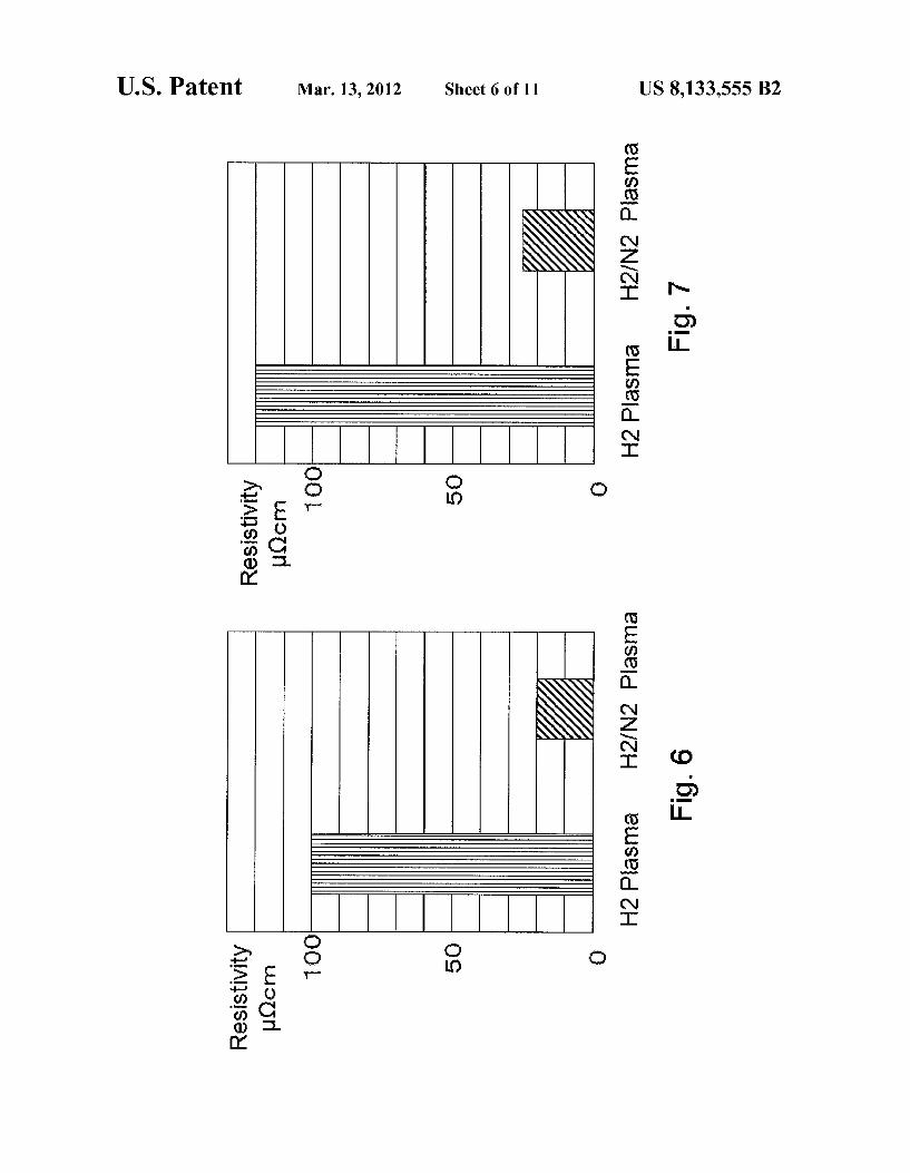
There have been no reports to date regarding the exposure of a [3-diketone metal complex to hydrogen/nitrogen plasma as mentioned above, and it has not been knoWn to date that [3-diketone ligands could be eliminated very easily this Way. For example, U.S. Pat. No. 6,527,855 B2 describes a process for forming a metal ?lm from an organic metal material containing [3-diketone, Wherein an organic metal material containing [3-diketone ligands is supplied to a substrate to be adsorbed onto the substrate surface, Which is folloWed by a hydrogen gas supply cycle and steps to purge the supplied hydrogen and then supply oxygen gas. This is because the step to supply oxygen gas breaks doWn the organic metal material containing [3-diketone ligands. Based on an experi ment conducted by the present inventors, only hi gh-resistivity Co ?lms could be achieved When hydrogen gas alone Was supplied. When oxygen gas Was supplied, the problem of oxidiZation of the TaN ?lm at the foundation occurred. Accordingly, after the supply of hydrogen gas the present inventors applied high-frequency poWer to the hydrogen gas to excite the gas and then implemented the ?lm forming process using the excited hydrogen. This loWered the resis tivity levels, but they Were still at least 20 times higher than the resistivity levels of bulk ?lms. Next, the present inventors introduced a mixture gas of hydrogen and nitrogen by adjust ing the nitrogen mixing ratio to a range of approx. 0.01 to 0.5 of the total gas ?oW rate, and then applied high-frequency poWer to this gas and implemented the ?lm forming process using the excited mixture gas of hydrogen and nitrogen, and ultimately found that the resistivity levels Were kept in a range of l to 5 times the resistivity levels of bulk ?lms. It should be noted that the resistivity levels ?uctuated someWhat depend ing on the plasma poWer output and plasma application time, Where raising the poWer output and increasing the application time reduced the resistivity. Under practical conditions of high-frequency poWer and plasma application time, hoWever, resistivity levels of not more than 5 times, or more desirably not more than tWice, the resistivity levels of bulk ?lms could be achieved. These results suggest that this production method can be used favorably in the formation of metal ?lms using organic metal materials.
Accordingly, in an embodiment of the present invention metal ?lms such as Co ?lm, Ru ?lm and Cu ?lm having loWer resistivity than those achievable under conventional methods can be formed by repeating the step to supply an organic metal material containing [3-diketone ligands, step to purge the organic metal material, step to supply a mixture gas of hydrogen and nitrogen and then implementing the ?lm form ing process using the mixture gas excited through application of high-frequency poWer, and step to purge the mixture gas. This method also causes organic metal materials of Co, Ru and Cu containing [3-diketone ligands to be adsorbed easily onto an oxide ?lm or metal ?lm, and therefore very good shielding property can be achieved even With Wirings having high aspect ratios such as those used in ?ne semiconductor Wirings. For a trench With an aspect ratio is 7, for example, shielding property of 90% or more can be achieved With ease. Likely reasons that explain this loWer resistance include the presence of activated excited species such as iNH and iNHZ generated by the excitation of a mixture gas of hydro gen and nitrogen, because these excited species sever the bond betWeen [3-diketone and metal and themselves bond With [3-diketone, With the [3-diketone-bonded excited species eventually gasifying and being discharged. These phenomena have never been reported before, and according to an embodi
20
25
30
35
40
45
50
55
60
65
4 ment of the present invention a metal ?lm can be easily formed from an organic metal material containing [3-diketone ligands. These principles can be applied to all metals that form a [3-diketone complex. All metals to Which [3-diketone can be coordinated are covered by the present invention, but speci?cally the present invention can be applied to the for mation of metal ?lms from such 8B, 1B and 2B family ele ments as Pt, Pd, Rh, Ru, Ir, Ni, Ag and Au, among others. The present invention can also be applied to other metals to Which [3-diketone coordinates, such as Ti, Ta, Hf, Nb, Mo, W, Mn, Mg, Sr, Ba and La, among others.
For purposes of summarizing the invention and the advan tages achieved over the related art, certain objects and advan tages of the invention are described in this disclosure. Of course, it is to be understood that not necessarily all such objects or advantages may be achieved in accordance With any particular embodiment of the invention. Thus, for example, those skilled in the art Will recogniZe that the inven tion may be embodied or carried out in a manner that achieves or optimiZes one advantage or group of advantages as taught herein Without necessarily achieving other objects or advan tages as may be taught or suggested herein.
Further aspects, features and advantages of this invention Will become apparent from the detailed description Which folloWs.
BRIEF DESCRIPTION OF THE DRAWINGS
These and other features of this invention Will noW be described With reference to the draWings of preferred embodiments Which are intended to illustrate and not to limit the invention. The drawings are oversimpli?ed for illustrative purposes and are not to scale.
FIG. 1 is an explanation draWing shoWing anALD process used in an embodiment of the present invention Where an organic metal complex containing [3-diketone ligands is used.
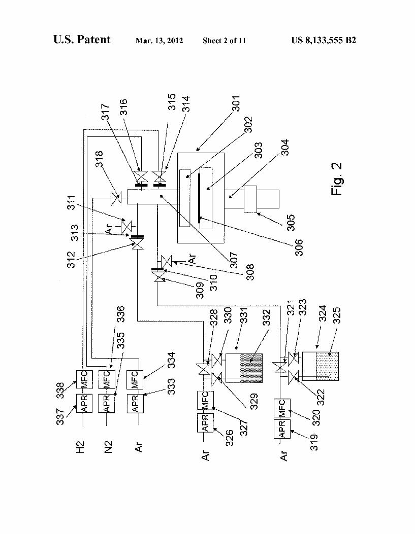
FIG. 2 is a schematic draWing shoWing anALD apparatus used in an embodiment of the present invention, capable of forming a ?lm from an organic metal complex containing [3-diketone.
FIGS. 3A to 3F are schematic cross-section vieWs shoWing steps to use the apparatus in FIG. 2 to form a lamination ?lm using a Co complex containing [3-diketone ligands over Cu Wirings of dual damascene structure, according to an embodi ment of the present invention.
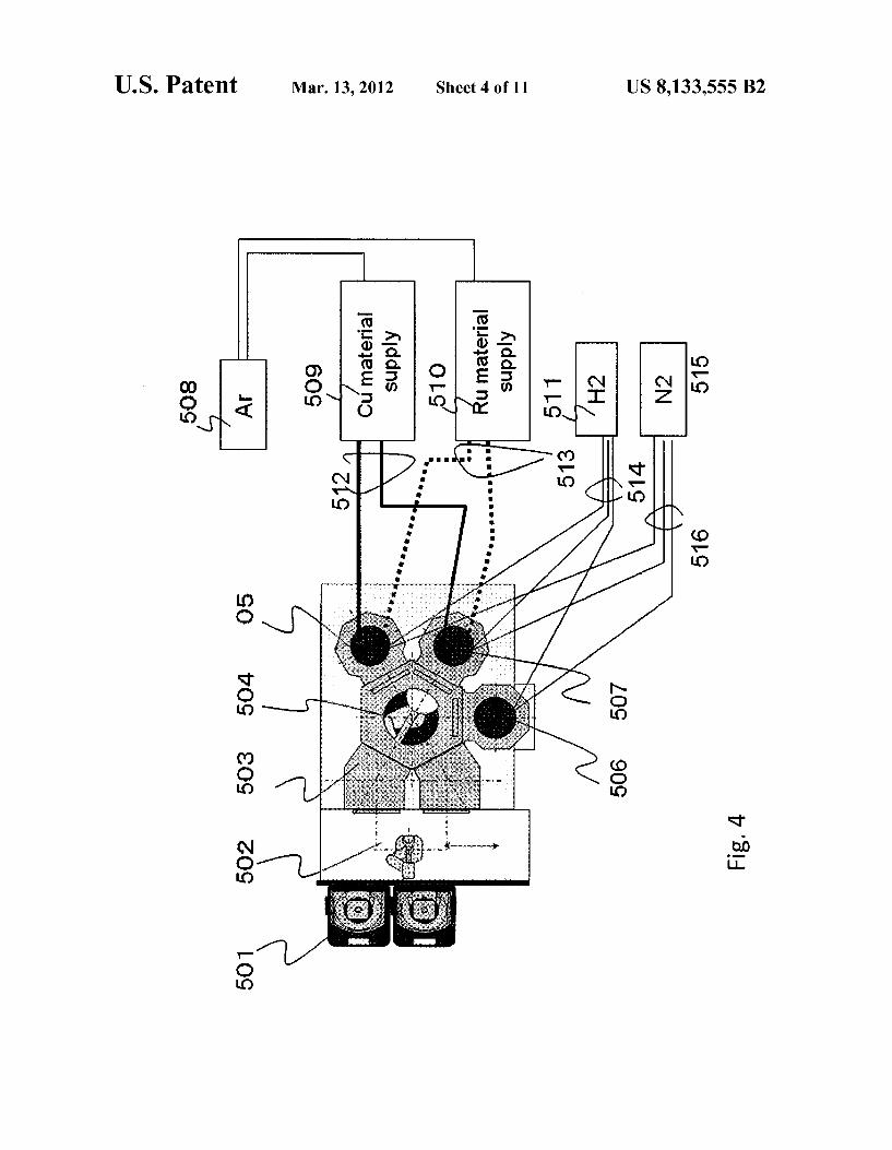
FIG. 4 is a schematic plan vieW shoWing the con?guration of an apparatus capable of forming Ru and Cu ?lms using Ru and Cu complexes containing [3-diketone ligands, according to an embodiment to the present invention.
FIGS. 5A to SF are schematic cross-section vieWs shoWing steps to use the apparatus in FIG. 2 to form a lamination ?lm of Ru and Cu ?lms using Ru and Cu complexes containing [3-diketone ligands over Cu Wirings of dual damascene struc ture, according to an embodiment of the present invention.
FIG. 6 is a graph shoWing the dependence of resistivity on plasma gas When a Co ?lm Was formed by the ALD method using a Co complex containing [3-diketone ligands according to an embodiment of the present invention.
FIG. 7 is a graph shoWing the dependence of resistivity on plasma gas When a Ru ?lm Was formed by the ALD method using a Ru complex containing [3-diketone ligands according to an embodiment of the present invention.
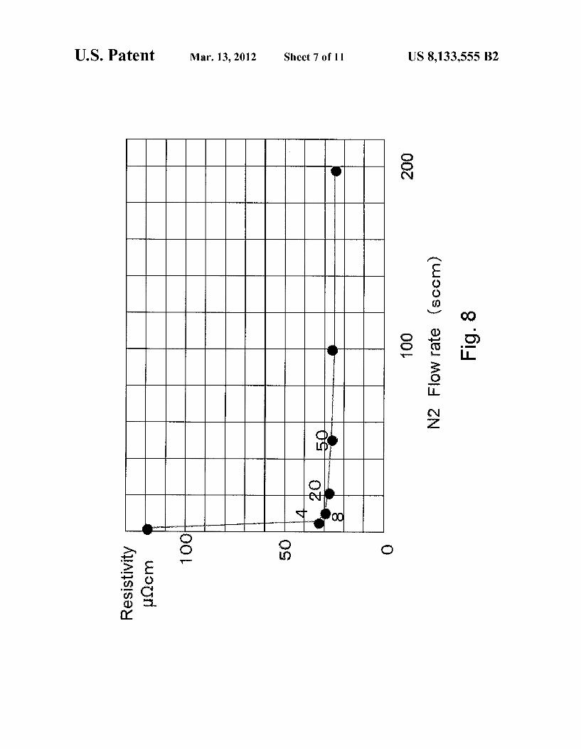
FIG. 8 is a graph shoWing the relationship of resistivity and nitrogen gas ?oW rate in an embodiment of the present inven tion.
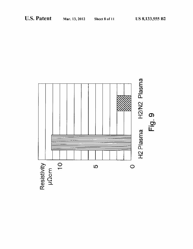
FIG. 9 is a graph shoWing the dependence of resistivity on reactant gas When a Cu ?lm Was formed by the ALD method
US 8,133,555 B2 5
using a Cu complex containing [3-diketone ligands according to an embodiment of the present invention.
FIG. 10 is a schematic explanation drawing shoWing the mechanism of hoW a single metal ?lm is formed from a metal complex containing [3-diketone ligands according to an embodiment of the present invention.
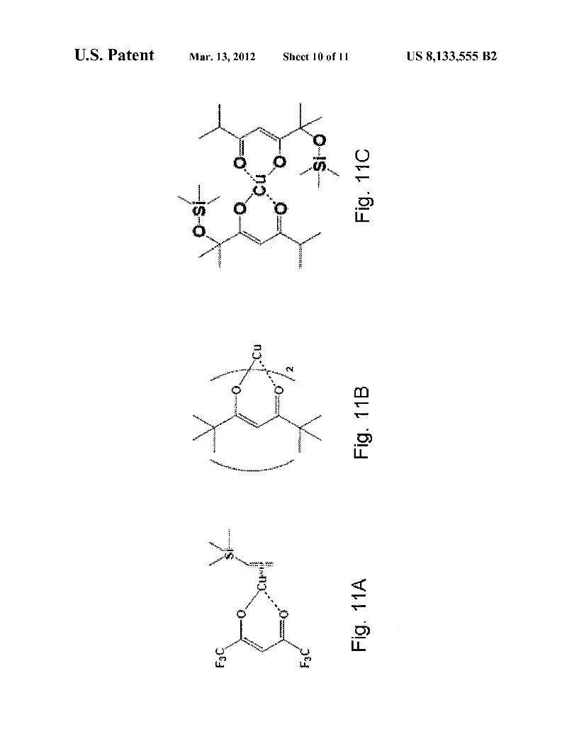
FIGS. 11A, 11B and 11C shoW the chemical structures of Cu complexes containing [3-diketone ligands that can be used in an embodiment of the present invention.
FIG. 12 is a graph shoWing the composition pro?le in the depth direction of a layer structure constituted by a TaN ?lm and a metal layer laminated on top formed by a Ru complex containing [3-diketone ligands according to an embodiment of the present invention.
BRIEF DESCRIPTION OF THE SYMBOLS
1000: Step to transfer substrate in 1001: Temperature stabiliZation step 1002: Process starting step 1003: Step to introduce organic metal complex containing
[3-diketone ligands 1004: Step to purge organic metal complex containing
[3-diketone ligands 1005: Step to introduce mixture gas of nitrogen and hydro
gen 1006: Application of plasma (generation of nitrogen/hy
drogen plasma) 1007: Purging of mixture gas of nitrogen and hydrogen 1008: Repeat of steps 1003 to 1007 1009: Process ending step 1010: Step to transfer substrate out 301: 302: 303: 304: 305: 306: 307: 308: 309: 310: 311: 312: 313: 314: 315: 316: 317: 318: 319: 320: 321: 322: 323: 324: 325: 326: 327: 328: 329: 330: 331: 332: 333: 334: 335:
Reactor ShoWer head Substrate heating base Evacuation Pres sure regulation valve Substrate Gas introduction pipe connected to shoWer head Valve for argon gas used for purge Cu material introduction valve Ori?ce Valve for argon gas used for purge Co material introduction valve Ori?ce Gas introduction valve
Gas introduction valve
Gas introduction valve APR MFC Bypass valve Ar gas introduction valve Cu material supply valve Cu material bottle Cu material APR MFC Bypass valve A carrier introduction valve Co material supply valve Co material bottle Co material APR MFC APR
20
25
30
35
40
45
55
60
65
6 336: MFC 337: APR 338: MFC 101: Bottom-layer copper Wiring 102: 103: 104: 105: 106: 107: 108: 109: 110: 111: 112: 113: 501: 502: 503: 504: 505: 506: 507:
?lm 508: 509: 510: 511: 512:
SiCN Cu diffusion barrieriInsulation ?lm Inter-layer insulation ?lm Etching stopper ?lm Inter-layer insulation ?lm Etching stopper layer Via hole in dual damascene structure Trench in dual damascene structure Cu diffusion barrier metal ?lm
Cu plating ?lm Cu Wiring Cassette loader Transfer robot Load lock chamber Vacuum robot Reaction chamber for Cu deposition Reaction chamber for Co deposition Reaction chamber for formation of Cu barrier metal
Ar gas supply Cu material supply Co material supply Hydrogen gas supply Cu material supply line
513: Co material supply line 514: H2 gas supply line 515: Nitrogen gas supply 516: Nitrogen gas supply line 401: Bottom-layer copper Wiring 402: SiCN Cu diffusion barrieriInsulation ?lm 403: Inter-layer insulation ?lm 404: Etching stopper ?lm 405: Inter-layer insulation ?lm 406: Etching stopper layer 407: Via hole in dual damascene structure 408: Trench in dual damascene structure 409: Cu diffusion barrier metal ?lm 410: Ru ?lm 411: Cu ?lm 412: Cu plating ?lm 413: Cu Wiring
DETAILED DESCRIPTION
The present invention Will be explained With reference to embodiments. HoWever, the embodiments are not intended to limit the present invention.
In the present disclosure Where conditions and/or struc tures are not speci?ed, the skilled artisan in the art can readily provide such conditions and/or structures, in vieW of the present disclosure, as a matter of routine experimentation. An embodiment of the present invention provides a method
of forming a single-metal ?lm on a substrate by plasma atomic layer deposition (ALD), comprising: (i) contacting a surface of a substrate With a [3-diketone metal complex in a gas phase, Whereby molecules of the [3-diketone metal com plex are attached to the surface of the substrate; (ii) exposing the molecule-attached surface to a nitrogen-hydrogen mixed plasma, thereby forming an atomic layer of the metal; and (iii) repeating steps (i) and (ii) for a next atomic layer on top of the atomic layer in step (ii), thereby accumulating the atomic layers to form the single-metal ?lm on the substrate. In an

US 8,133,555 B2 7
embodiment, the [3-diketone metal complex can easily be adsorbed onto any surface, and the nitrogen-hydrogen plasma can quickly and completely cleave the coordinate bonds betWeen the metal and the [3-diketone(s), thereby ef?ciently forming the single-metal ?lm. In an embodiment, no other ligand-supplying compounds are used, or no other plasma is used.
Further, embodiments include, but are not limited to, the followings:
In an embodiment, the single-metal ?lm is an elemental metal ?lm.
In an embodiment, the nitrogen-hydrogen mixed plasma may be produced by supplying a gas containing nitrogen and hydrogen, folloWed by applying RF poWer to the gas. In an embodiment, the gas containing nitrogen and hydrogen may be a mixture of nitrogen gas and hydrogen gas. Further, in an embodiment, a volumetric ratio of nitrogen to the gas mixture maybe 1/100 to 50/100.
In any of the foregoing embodiments, the metal constitut ing the [3-diketone metal complex may be selected from the group consisting of metals belonging to Group 8, 1B, and 2B in the periodic chart. In an embodiment, the metal may be selected from the group consisting of Ru, Co, Pd, Pt, and Ir. Alternatively, the metal may be Cu. In an embodiment, the [3-diketone metal complex may be constituted by three [3-diketones coordinated to a metal in its molecule. In an embodiment, the [3-diketone metal complex may have only [3-diketone(s) (optionally substituted) coordinated to a metal in its molecule.
In any of the foregoing embodiments, the method may further comprise forming a Cu ?lm on the single-metal ?lm. In an embodiment, the Cu ?lm may be formed using the single-metal ?lm formed by steps (i) to (iii) as a Cu seed layer.
In any of the foregoing embodiments, steps (i) and (ii) may be repeated at least 10 times.
In any of the foregoing embodiments, steps (i) and (ii) may be repeated until a thickness of the single-metal ?lm reaches at least 0.4 to 0.5 nm.
In any of the foregoing embodiments, the surface of the substrate on Which the single-metal ?lm is formed may be constituted by a Cu barrier layer.
In any of the foregoing embodiments, steps (i) and (ii) may be conducted at a temperature of 3000 C. or loWer.
In any of the foregoing embodiments, the method may further comprise purging the [3-diketone metal complex gas after step (i) and purging the gas containing nitrogen and hydrogen after step (ii).
In any of the foregoing embodiments, the nitrogen-hydro gen plasma may be the only plasma to Which the molecule attached surface is exposed in step (ii).
In any of the foregoing embodiments, the [3-diketone metal complex may be the only metal compound contacting the surface of the substrate in step (i).
In any of the foregoing embodiments, the single-metal ?lm may have a purity of 99% or higher.
In any of the foregoing embodiments, the surface of the substrate on Which the single-metal ?lm is formed may have trenches and the single-metal ?lm covers the trenches as a conformal coating.
Embodiments of the present invention are explained fur ther beloW. By causing an organic metal complex containing [3-dike
tone ligands to be adsorbed onto a substrate and then process ing this substrate using a gas containing at least hydrogen atoms and nitrogen atoms that have been activated by high frequency, [3-diketone ligands can be removed ef?ciently. These hydrogen atoms and nitrogen atoms can be supplied by
20
25
30
35
40
45
50
55
60
65
8 the same molecule, or by different molecules. Unless a spe cial circumstance exists, hoWever, even a normal mixture gas of hydrogen gas and nitrogen gas can remove [3-diketone ligands With suf?cient effect. As for metal elements that can be coordinated to [3-dike
tone and usable in an embodiment of the present invention, desirable examples include 8B, 1B and 2B family elements, or typically Fe, Ni, Rh, Pd, Ir, Pt, Co, Ru and Cu, among others, Where each of the foregoing metals can have least one, or even tWo, three or more [3-diketone coordinated to it. Using the aforementioned metals, a metal ?lm of high purity (such as 99% or more, or even 99.9% or more in Which case the ?lm
virtually consists of the applicable metal only) can be formed that does not easily produce nitrides When exposed to hydro gen/nitrogen plasma. Typical metal complexes coordinated to [3-diketone include tridipivaloylmathanatocobalt (DPM3CO), tridipivaloylmathanatoruthenium (DPM3Ru) and copper hexa?uoroacetylacetonate trimethylvinylsilane (Cu(hfac)tmvs) (FIG. 11A), among others, and other copper complexes having the structures shoWn in FIGS. 11B and 11C are also available. HoWever, the present invention is not lim ited in any Way to these metal complexes. Incidentally, basi cally organic metal complexes Where only [3-diketone is coor dinated are favorable because they can eliminate ligands more effectively through hydrogen/nitrogen plasma. HoW ever, Cu(hfac)tmvs and some other complexes having both [3-diketone and other ligands also undergo a change in molecular stability as [3-diketone in the organic metal com plex is eliminated, and consequently the molecule breaks doWn more easily. Accordingly, in an embodiment the organic metal complex can have a different ligand or ligands other than B-diketone. Those skilled in the art should be able to understand Which compounds are appropriate based on the descriptions provided herein, and obtain such compounds. For a Ru complex, etc., for example, the compounds described in Us. Patent Application Publication No. 2008/ 0054472 and No. 2008/0124484 and Us. patent application Ser. No. 12/203,405 oWned by the same assignee as in the present application (the disclosure of each of Which is herein incorporated by reference in its entirety With regard to metal complexes), among others, can be used in an embodiment, in addition to the compounds mentioned above.
Depending on the application, metal elements having one or more [3-diketone coordinated to them, other than the metal elements mentioned above, such as Ti, Ta, Hf, Nb, Mo, W, Mn, Mg, Sr, Ba and La, can be used in an embodiment.
In an embodiment of the present invention, a metal layer (single metal layer) constituted by a [3-diketone coordinated metal complex can be formed in combination With other metal layer, for example, by using a Cu barrier ?lm as the foundation layer. In an embodiment, a metal layer constituted by a [3-diketone coordinated copper complex can be formed as a Cu seed ?lm provided before a Cu ?lm is formed. For this Cu barrier ?lm, any knoWn Cu barrier ?lm or other appropri ate ?lm can be used. For example, PVD-TaN and CVD-Ru, as Well as other ?lms produced by ALD such as WNC, WN, TaN, RuTaN, RuTa, TaNC, RuTaNC, TiN, RuTiN and RuTi, can be used. In addition to the above, ?lms that can be com bined in a favorable manner With a metal layer constituted by [3-diketone coordinated metal complex (as the bottom layer or top layer) include, for example, the metal ?lms and alloy ?lms described in Us. patent application Ser. Nos. 12/203,405 and Ser. No. 12/201,434 oWned by the same assignee as in the present application (the disclosure of each of Which is herein incorporated by reference in its entirety With regard to metal ?lms). In particular, the aforementioned combinations With metal ?lms by ADL method are desirable because they alloW