
Parallel near-field optical micro/nanopatterning on curved surfaces by transported micro-particle...
8
1 Parallel near-field optical micro/nanopatterning on curved surfaces by transported micro-particle lens arrays Ashfaq Khan 1 , Zengbo Wang 1 , Mohammad A Sheikh 1 , David J Whitehead 1 , and Lin Li 1 1 Laser Processing Research Centre, School of Mechanical, Aerospace and Civil Engineering, The University of Manchester, Sackville Street, Manchester, M60 1QD, UK E-mail: [email protected] Abstract Although laser surface nanopatterning by particle-lens arrays, utilizing near field enhancement, has been extensively utilized previously, a suitable technique for the deposition of Particle Lens Arrays (PLA) on curved surface of cylinder was not available. In this paper, a novel technique for nano-patterning on curved surfaces using particle-lens arrays is demonstrated. In the proposed technique, a hexagonal closed pack monolayer of SiO 2 spheres is first formed by self assembly on a flat glass surface. The formed monolayer of particles is then picked up by a flexible optically transparent sticky surface and placed on the substrate to be patterned. A 532 nm wavelength Nd:YVO 4 laser was used to irradiate the substrate with the laser passing through the flexible, transparent surface and the particles. Experimental investigations are made to ascertain the properties of the patterns. In addition, the optical near-field distribution around the particles is numerically simulated. The proposed technique is validated for nanopatterning of curved surface of a cylinder. Keywords: Laser nanopatterning, Near-Field enhancement, Particle Lens Arrays (PLA). 1. Introduction The surge in the development of miniaturized devices over the last two decades has led to further research in novel manufacturing techniques on nano and even atomic scale. With the reducing size of devices, surface patterning is also gaining greater importance. Within the last 3 decades lasers have been extensively used for surface patterning at micron scale [1-3]. However, due to the diffraction limit, light cannot be confined to a lateral dimension smaller than half its wavelength [4] and this limits the direct use of laser in nano patterning. One method for overcoming this limitation is to utilize near field. Laser processing in the near field can generate features with sizes below 100 nm [5]. Several techniques for utilizing near field effects have been developed such as Near-field Scanning Optical Microscope (NSOM) patterning [5, 6], Laser in combination with Scanning Probe Microscopy (SPM) for tip patterning [5, 7, 8] and Plasmonic Lithography etc. [5, 9, 10]. However, all these techniques share the same disadvantages of low throughput and the sophisticated equipment required to control distances between optical components and the workpiece to within several hundred nanometers. Hence, there is an urgent need for low cost, high speed nano processing technique which could satisfy the industrial demands. One near field technique which was introduced recently is the PLA technique. With this technique features can be generated in parallel over large areas at a very high speed. In this technique particles are first deposited over the surface to be patterned in the form a monolayer array by self-assembly. The monolayer of particles is generated by drying a solution of the particles spread over the substrate. During the drying process, the particles arrange themselves in a monolayer array due to capillary forces [11]. The self assembly process is heavily dependent on the surface quality. Monolayer can only be generated on flat, smooth, hydrophilic surfaces [12, 13]. The surface with the monolayer array is then scanned by a laser. From the interaction Confidential: not for distribution. Submitted to IOP Publishing for peer review 5 June 2010 peer-00569662, version 1 - 25 Feb 2011 Author manuscript, published in "Journal of Physics D: Applied Physics 43, 30 (2010) 305302" DOI : 10.1088/0022-3727/43/30/305302
Transcript of Parallel near-field optical micro/nanopatterning on curved surfaces by transported micro-particle...

1
Parallel near-field optical micro/nanopatterning on curved
surfaces by transported micro-particle lens arrays
Ashfaq Khan1, Zengbo Wang1, Mohammad A Sheikh1, David J Whitehead1, and Lin Li1
1 Laser Processing Research Centre, School of Mechanical, Aerospace and Civil Engineering, The
University of Manchester, Sackville Street, Manchester, M60 1QD, UK
E-mail: [email protected]
AbstractAlthough laser surface nanopatterning by particle-lens arrays, utilizing near field enhancement, has beenextensively utilized previously, a suitable technique for the deposition of Particle Lens Arrays (PLA) on curvedsurface of cylinder was not available. In this paper, a novel technique for nano-patterning on curved surfacesusing particle-lens arrays is demonstrated. In the proposed technique, a hexagonal closed pack monolayer ofSiO2 spheres is first formed by self assembly on a flat glass surface. The formed monolayer of particles is thenpicked up by a flexible optically transparent sticky surface and placed on the substrate to be patterned. A 532 nmwavelength Nd:YVO4 laser was used to irradiate the substrate with the laser passing through the flexible,transparent surface and the particles. Experimental investigations are made to ascertain the properties of thepatterns. In addition, the optical near-field distribution around the particles is numerically simulated. Theproposed technique is validated for nanopatterning of curved surface of a cylinder.
Keywords: Laser nanopatterning, Near-Field enhancement, Particle Lens Arrays (PLA).
1. IntroductionThe surge in the development of miniaturizeddevices over the last two decades has led tofurther research in novel manufacturingtechniques on nano and even atomic scale.With the reducing size of devices, surfacepatterning is also gaining greater importance.Within the last 3 decades lasers have beenextensively used for surface patterning atmicron scale [1-3]. However, due to thediffraction limit, light cannot be confined to alateral dimension smaller than half itswavelength [4] and this limits the direct use oflaser in nano patterning. One method forovercoming this limitation is to utilize nearfield. Laser processing in the near field cangenerate features with sizes below 100 nm [5].Several techniques for utilizing near fieldeffects have been developed such as Near-fieldScanning Optical Microscope (NSOM)patterning [5, 6], Laser in combination withScanning Probe Microscopy (SPM) for tippatterning [5, 7, 8] and Plasmonic Lithographyetc. [5, 9, 10]. However, all these techniques
share the same disadvantages of lowthroughput and the sophisticated equipmentrequired to control distances between opticalcomponents and the workpiece to withinseveral hundred nanometers. Hence, there is anurgent need for low cost, high speed nanoprocessing technique which could satisfy theindustrial demands.One near field technique which was introducedrecently is the PLA technique. With thistechnique features can be generated in parallelover large areas at a very high speed. In thistechnique particles are first deposited over thesurface to be patterned in the form amonolayer array by self-assembly. Themonolayer of particles is generated by drying asolution of the particles spread over thesubstrate. During the drying process, theparticles arrange themselves in a monolayerarray due to capillary forces [11]. The selfassembly process is heavily dependent on thesurface quality. Monolayer can only begenerated on flat, smooth, hydrophilic surfaces[12, 13]. The surface with the monolayer arrayis then scanned by a laser. From the interaction
Confidential: not for distribution. Submitted to IOP Publishing for peer review 5 June 2010pe
er-0
0569
662,
ver
sion
1 -
25 F
eb 2
011
Author manuscript, published in "Journal of Physics D: Applied Physics 43, 30 (2010) 305302" DOI : 10.1088/0022-3727/43/30/305302

2
of the laser with the particles, evanescentwaves are generated in the near field [14]. Thehigh intensity evanescent waves in the nearfield are utilized for surface patterning. Thusthe laser is effectively split into hundreds ofhigh intensity spots with nano size diameters,each generating a feature on the substratesurface. These nano size features can begenerated in parallel on the substrate with avery high speed, typically several millionsimilar patterns in a few seconds. Moreover,angular beam scanning of the PLA can beutilized to create high density, user definedpatterns and features [15].Although patterning by PLA is an efficienttechnique, its industrial applications arelimited because the monolayer, and hence theprocess, can only be applied to ideal surfacesi.e. flat, smooth and hydrophilic. To the bestof authors’ knowledge, there is no knownmethod which could deposit particles on a non-ideal surface. To overcome this problem, it isproposed in this paper that a monolayer is firstdeposited on an ideal surface and thentransported to a non-ideal surface (curvedsurface of a cylinder) for patterning.Although attempts have been made previouslyby Burmeister et al. [12, 13] to transport amonolayer of PLA but the process requiredsophisticated equipment. Moreover, theprocess was applicable only to polystyreneparticles and patterning was not demonstrated.Recently, O'Connell et al. [16] devised amethod by which they transported a monolayerarray and utilized it for surface patterning buttheir procedure was only applicable to thepatterning of smooth and flat surface. In ourwork presented thin this paper, a monolayer ofsilica particles is first deposited on a flat,smooth and hydrophilic glass surface by usinga conventional method. A flexible stickysurface (referred to as the ‘Ribbon’) ispressed/superimposed on top of the monolayerand then peeled off in such a way that theparticles are mounted and adhered to the stickysurface. The sticky surface is then placedaround the curved surface of a Ti tube andirradiated by a laser which passes through theribbon. It is shown that good quality, large areanano patterns are generated which are theninvestigated by SEM and 3D opticalmicroscope.The novelty of the technique proposed in thispaper is that it is simple, fast, and allows large
area monolayer arrays to be transported, is notrestricted to low melting point materials (asinitially expected), is independent of thematerial of the particle. Also, it does notrequire long waiting periods for drying of theparticles solution on the surfaces to bepatterned. It is expected that with thistechnique surfaces that might be damaged bywater drying on it can also be textured. Also itis expected that surfaces with hydrophobiccharacteristic can also be patterned.
2. Experimental procedures
2.1. MaterialsThe curved surface of a high purity Titanium(Ti) tube (diameter = 1 cm, refractive index η= 1.8465+2.5365i) was chosen as the surfaceto be patterned. As a solution of the particlescannot stay on the curved surface of the tube,the formation of a monolayer of PLA by selfassembly is not possible. To the best ofauthors’ knowledge, there is no known methodby which a monolayer could be formed on thissurface. Moreover, the reason for choosing Tiin this study is to demonstrate that theproposed technique works for materials withhigh melting point and that the surface of suchmaterials can be textured without melting theRibbon (flexible surface). This demonstrationis essential as it is normally thought that formaterials with high melting point there maynot be a feasible window for the laser fluenceto pass through the Ribbon surface withoutdamaging it and still have sufficient intensityto texture the surface. Pure Ti has a meltingpoint of ~1870oC [17] which is 480oC higherthan that of one of the common Stainless steel,316L ~1387 °C [18]. Therefore, if thetechnique is successful for Ti patterning, it canbe expected to work satisfactorily for a widerange of materials.The PLA is formed from Silica Spheres (BangsLaboratories; approximate diameter 2a = 4.74µm, refractive index η = 1.51). A Glass slide(Agar Scientific, soda lime microscope glassslide) was used as the smooth surface for thepreparation of a PLA monolayer. The Ribbonused for the transportation of particles arraymonolayer is carefully chosen to be a flexible,thin, transparent (to a 532 nm laser) plastic(Biaxial oriented polypropylene, thickness 45µm) with an adhesive resin (polyolefin) forfirmly securing the particles monolayer array.
peer
-005
6966
2, v
ersi
on 1
- 25
Feb
201
1

3
The choice of the material of the ribbon isguided by the requirement that the maximumlaser intensity is transmitted through the ribbonand it is flexible to conform to the profile ofthe curved surface.
2.2. EquipmentA Spectrophotometer (Analytik Jena - Specord250, 200-1100 nm) was used for measuring theoptical properties of the Ribbon.The irradiation of the sample for patterningwas carried out by a diode pumped Nd:YVO4
laser (Laserline - Laserval Violino, wavelengthλ =532 nm, pulse duration τ =7 ns andrepetition rate from 1 to 30 kHz, S-polarized ).Characterization of the sample was conductedby Scanning Electron Microscopy (SEM)(Hitachi High Technologies - S-3400N) and a3D Optical Microscope (Alicona InfiniteFocus). SEM was used for surface topographyand the 3D optical Microscope was used formeasuring the depth of the patterns.
2.3. Glass cleaningThe glass slides were first cleaned by soapywater. In order to remove organic residue andoils, the glass was first sonicated in warmacetone (at 55oC) and then in methanolrespectively for 10 minutes each. The sampleswere rinsed with deionised (DI) water andtreated by a (1:3) solution of nitric acid andwater for 24 hours for making themhydrophilic. The samples were finally rinsedwith DI water and dried by flow of N2 gas[19].
2.4. PLA Monolayer Preparation andTransportationThe deposition of particles was carried outwith a slight modification in the methoddeveloped by Micheletto et al. [20] who used aPeltier cell for temperature control. As theyfound the change in results with temperature tobe very small so a Peltier cell was not used. Inthis work a diluted solution of contact particleswas used for monolayer deposition. Drops ofthe solution were applied on the cleanedsurface of the glass. The glass was then placedin an airtight box and slightly tilted (by 9o) foreasy nucleation. The solution was dried atroom conditions which normally takes 24 to 36hours. During the drying process, the particlesarranged themselves in hexagonal closed shapearray under capillary forces [11].
Figure 1: A schematic representation of thetransfer of the particles. (a) Monolayer formedon the surface of glass (b) Ribbon is placed on
monolayer array and pressed. (c) Ribbon islifted from the Glass Surface along with the
Monolayer. (d) Ribbon is wrapped around theTi tube.
The monolayer formed on the surface of theglass was transferred with the help of theRibbon. The Ribbon was placed on themonolayer array directly from above andpressed gently. The thin layer of glue securedthe particles to the Ribbon. The Ribbon wasthen gently lifted and with it the particles werealso lifted as a complete monolayer array.Even though the particles adhered strongly tothe glass, the resin was chosen to be ofsufficient adhesion quality to lift the particles[21]. The Ribbon was then wrapped around thecurved surface of the Ti tube for patterning.The surface of the tube was thus effectivelycovered by the particles monolayer array. A
Glass
SiO2 Particles
(a)
Glass
Ribbon
(b)
Ti tube+
(d)
Glass
(c)
peer
-005
6966
2, v
ersi
on 1
- 25
Feb
201
1
4
schematic representation of the procedure isshown in figure 1 and particles adhered to Titube with the ribbon are shown in figure 2.
Figure 2: Ti tube sample wrapped with ribbonbefore laser processing.
2.5. Laser PatterningAs the Ribbon cannot be removed after thetransfer of the particles to the curved surface,the properties of the Ribbon were chosen suchthat it was transparent to the laser. Thetransmission spectrum of the Ribbon measuredby the Spectrophotometer is shown in figure 3.The transmission of the ribbon remains above90% for wavelengths between 320 to 1100 nm.At a wavelength of 532 nm the transmission isobserved to be 93%.
0
1020
3040
50
6070
8090
100
0 200 400 600 800 1000 1200
WaveLength (nm)
Tra
nsm
issi
on
(%)
Figure 3: Transmission spectrum of light forthe ribbon.
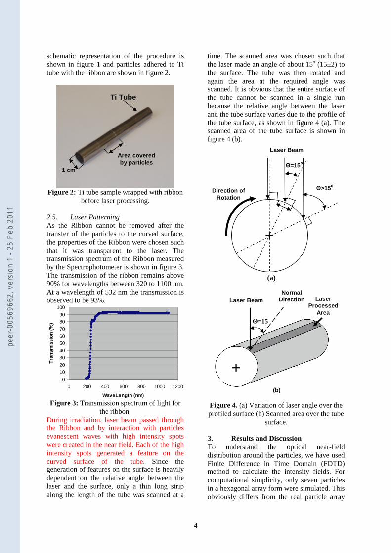
During irradiation, laser beam passed throughthe Ribbon and by interaction with particlesevanescent waves with high intensity spotswere created in the near field. Each of the highintensity spots generated a feature on thecurved surface of the tube. Since thegeneration of features on the surface is heavilydependent on the relative angle between thelaser and the surface, only a thin long stripalong the length of the tube was scanned at a
time. The scanned area was chosen such thatthe laser made an angle of about 15o (15±2) tothe surface. The tube was then rotated andagain the area at the required angle wasscanned. It is obvious that the entire surface ofthe tube cannot be scanned in a single runbecause the relative angle between the laserand the tube surface varies due to the profile ofthe tube surface, as shown in figure 4 (a). Thescanned area of the tube surface is shown infigure 4 (b).
Figure 4. (a) Variation of laser angle over theprofiled surface (b) Scanned area over the tube
surface.
3. Results and DiscussionTo understand the optical near-fielddistribution around the particles, we have usedFinite Difference in Time Domain (FDTD)method to calculate the intensity fields. Forcomputational simplicity, only seven particlesin a hexagonal array form were simulated. Thisobviously differs from the real particle array
Direction ofRotation
Θ=15o
+
Θ>15o
Laser Beam
(a)
+
Θ=15
Laser BeamNormal
Direction LaserProcessed
Area
(b)
Ti Tube
Area coveredby particles
1 cm
peer
-005
6966
2, v
ersi
on 1
- 25
Feb
201
1

5
system which contains millions of particles.However, the intensity enhancement resultingfrom the generation of evanescent waves in thenear field can be clearly identified in thesimulation. The s-polarized beam was incidentat an angle of 15o with an open boundarycondition applied to all boundaries. Aschematic representation of the simulatedconfiguration is shown in figure 5. Normalizedlocal field distribution (|E|2) underneath thehexagonal array of particles is shown in figure6. Intensity enhancement in the range of 130 is
predicted. It can be seen that the maximumfield intensity is just outside the particle anddecays along the incident path but due to asmall incident angle (15o), the intensity on thesurface of the substrate still remains close to130. Because of the small incident angle of thelaser, the holes are not located exactly at theparticle-substrate contact point but are a smalldistance away from it [15]. More informationon the near-field modelling can be found in thework done by Wang et al. [22].
Figure 5. Schematic diagram of the simulated configuration.
Figure 6. |E|2 Field distribution across three particles in XZ-plane.
The scanning of the sample is carried out by afocused Gaussian beam with a diameter of 55µm, pulse duration of τ = 7 ns, scan speed of0.8 m/s and a frequency of 30 kHz. Thescanning of the sample at a high fluence of0.97 J/cm2 resulted in damages to the Ribboneven though it had a transmission of 93%.Debris was deposited on the sample from thedamaged Ribbon surface, visible in figure 7(a).The laser fluence was reduced but debris wasdeposited at fluence above 0.379 J/cm2. Atfluence lower than 0.379 J/cm2 features weregenerated on Ti surface shown in figure 7(b)-7(c). Although the lowered laser fluence waskept below the damage threshold of theRibbon, it was still sufficient to texture thesurface after intensity enhancements by the
particles. It clearly shows that the lasereffectively passed through the transparentsurface which was holding the particles inplace and was enhanced (intensityenhancement) by the particles to generatepatterns on Ti surface. The spacing betweenthe features in figure 7(c) is about 4.74 µmwhich corresponds to the diameter of thegenerated features. The surface of Ti is alsonot ideally smooth. A 3D optical microscopewas used to determine the depth of the patternsgenerated on the Ti surface. The depth ofpatterns was found to between 200 to 250 nmand the diameter between 1 to 1.2 microns.The results are shown in figure 8. An area of100 mm2 was scanned and good qualityfeatures were generated on the entire scanned
E
XZ
peer
-005
6966
2, v
ersi
on 1
- 25
Feb
201
1

6
area. With a further reduction in laser fluenceto 0.223 J/cm2 features were generated on Tisurface with diameter around 437 nm shown inthe inset of figure 7c. No features wereobserved at fluence lower than 0.223 J/cm2.This was because the intensity enhancement byparticles at much reduced fluence was notsufficient to ablate the Ti surface.
Figure 7. (a) Debris on the Ti surface at afluence of 0.45 J/cm2 (b,c) SEM images ofpatterns generated on the Ti surface at 0.379J/cm2. Inset shows the pattern generated at
0.223 J/cm2.
Since the patterning of Ti has beensuccessfully demonstrated, it can be expectedthat the technique would work for materials
with a wide range of melting points. Inaddition, although patterning of only curvedsurface of a cylinder is demonstrated here, dueto the flexibility of the soft Ribbon used in theproposed technique, in principle, particles canbe attached to any types of surface includingspherical, pyramidal or pre-patterned surfaceand then irradiated by a laser beam to patternthe surface.
Figure 8. 3D Optical Microscope results (a)Depth projection across a sectional profile ofthe generated feature (b) Patterned surface.
4. ConclusionsA simple technique for the transportation ofPLA and its successful use for patterning ahigh melting point, curved surface of acylinder has been demonstrated. Acombination of conventional PLA depositiontechnique on an ideal surface and a Ribbon(sticky, flexible, transparent surface) fortransportation of monolayer array makes theproposed technique simple, fast and easy toimplement for patterning curved surface of acylinder. In this study, good quality array ofpatterns were generated and characterized bySEM and 3D Optical Microscope; the inter-feature spacing and the dimensions of the
(a)
(b) 20 µm
(c)
437 nm
0.223 J/cm2
0.379 J/cm2
(b)
0.379 J/cm2
(a)
0.45 J/cm2
peer
-005
6966
2, v
ersi
on 1
- 25
Feb
201
1

7
features correlated well with the dimensions ofparticles used.
AcknowledgementsOne of the authors (A.Khan) gratefullyacknowledges the support from the NWFP,University of Engineering and Technology(UET), Pakistan. The authors would like tothank the staff of the Laser ProcessingResearch Centre (LPRC), University ofManchester, UK, for their support.
References[1]. Bäuerle D Laser Processing and
Chemistry: (Springer) Berlin 2000.[2]. Hon K K B, Li L and Hutchings I M
2008 Direct writing technology-Advances and developments CIRPAnnals-Manufacturing Technology 57601-20
[3]. Pena A, Wang Z B, Whitehead D andLi L 2009 High speed laser micro-texturing of Si wafer for improvedlight trapping for photo-voltaicapplication 28th InternationalCongress on Applications of Lasers &Electro-Optics (ICALEO) . Orlando,Fl, USA.
[4]. Abbe E 1873 Beitrage zur Theorie desMikroskops und der mikroskopischenWahrnehmung Archiv Microskop.Anat 9 413.
[5]. Chong T C, Hong M H and Shi L P2009 Laser precision engineering:From microfabrication tonanoprocessing Laser and PhotonicsReviews 4 123-43
[6]. Betzig E, Trautman J K, Wolfe R,Gyorgy E M, Finn P L, Kryder M Hand Chang C H 1992 Near-fieldmagneto-optics and high density datastorage Applied Physics Letters 61142-4
[7]. Lu Y F, Mai Z H, Zheng Y W andSong W D 2000 Nanostructurefabrication using pulsed lasers incombination with a scanning tunnelingmicroscope: Mechanism investigationApplied Physics Letters 76 1200-2
[8]. Chimmalgi A, Choi T Y,Grigoropoulos C P and KomvopoulosK 2003 Femtosecond laser aperturlessnear-field nanomachining of metals
assisted by scanning probe microscopyApplied Physics Letters 82 1146-8
[9]. Liu Z-W, Wei Q-H and Zhang X 2005Surface plasmon interferencenanolithography Nano Letters 5 957-61
[10]. Srituravanich W, Fang N, Sun C, LuoQ and Zhang X 2004 Plasmonicnanolithography Nano Letters 4 1085-8
[11]. Denkov N, Velev O, Kralchevski P,Ivanov I, Yoshimura H and NagayamaK 1992 Mechanism of formation oftwo-dimensional crystals from latexparticles on substrates Langmuir 83183-90
[12]. Burmeister F, Schafle C, Matthes T,Bohmisch M, Boneberg J and LeidererP 1997 Colloid monolayers as versatilelithographic masks Langmuir 13 2983-7
[13]. Burmeister F, Schafle C, Bettina K,Clemens B, Johannes B and Paul L1998 From mesoscopic to nanoscopicsurface structures: Lithography withcolloid monolayers AdvancedMaterials 10 495-7
[14] Devilez A, Stout B, Bonod N, andPopov E 2008 Spectral analysis ofthree-dimensional photonic jets OpticsExpress 16 14200-212
[15]. Guo W, Wang Z B, Li L, Whitehead DJ, Luk'yanchuk B S and Liu Z 2007Near-field laser parallelnanofabrication of arbitrary-shapedpatterns Applied Physics Letters 90243101-3
[16]. O'Connell C, Sherlock R and Glynn TJ 2010 Fabrication of a reusablemicrolens array for laser-basedstructuring Optical Engineering 49014201-4
[17]. Park J, Ryu Y, Kim H and Yu C 2009Simple and fast annealing synthesis oftitanium dioxide nanostructures andmorphology transformation duringannealing processes Nanotechnology20 105608-15
[18]. Wang X, Lei M K and Zhang J S 2007Surface modification of 316L stainlesssteel with high-intensity pulsed ionbeams Surface and CoatingsTechnology 201 5884-90
peer
-005
6966
2, v
ersi
on 1
- 25
Feb
201
1

8
[19]. Wang Z B, Guo W, Pena A,Whitehead D J, Luk'yanchuk B S, LiL, Liu Z, Zhou Y and Hong M H 2008Laser micro/nano fabrication in glasswith tunable-focus particle lens arrayOptical Express 16 19706-11
[20]. Micheletto R, Fukuda H and Ohtsu M2002 A simple method for theproduction of a two-Dimensional,ordered array of small latex particlesLangmuir 11 3333-6
[21]. Guo W, Wang Z B, Li L, Liu Z andWhitehead D 2008 Generation ofnano-bumps on transparent quartzglass surface under femtosecond laserirradiation 27th InternationalCongress on Applications of Lasersand Electro-Optics (ICALEO),Temecula, CA, USA
[22]. Wang Z B, Hong M H, Luk'yanchuk BS, Lin Y, Wang Q F and Chong T C2004 Angle effect in lasernanopatterning with particle-maskJournal of Applied Physics 96 6845-50
peer
-005
6966
2, v
ersi
on 1
- 25
Feb
201
1