
Optimization of physical chemistry of the Pt/Ru/PbZrTiO3 ...
161
HAL Id: tel-02127036 https://tel.archives-ouvertes.fr/tel-02127036 Submitted on 13 May 2019 HAL is a multi-disciplinary open access archive for the deposit and dissemination of sci- entific research documents, whether they are pub- lished or not. The documents may come from teaching and research institutions in France or abroad, or from public or private research centers. L’archive ouverte pluridisciplinaire HAL, est destinée au dépôt et à la diffusion de documents scientifiques de niveau recherche, publiés ou non, émanant des établissements d’enseignement et de recherche français ou étrangers, des laboratoires publics ou privés. Optimization of physical chemistry of the Pt/Ru/PbZrTiO3 interface for future high capacitance density devices Ibrahima Gueye To cite this version: Ibrahima Gueye. Optimization of physical chemistry of the Pt/Ru/PbZrTiO3 interface for future high capacitance density devices. Micro and nanotechnologies/Microelectronics. Université Grenoble Alpes, 2017. English. NNT : 2017GREAT119. tel-02127036
-
Upload
khangminh22 -
Category
Documents
-
view
2 -
download
0
Transcript of Optimization of physical chemistry of the Pt/Ru/PbZrTiO3 ...

HAL Id: tel-02127036https://tel.archives-ouvertes.fr/tel-02127036
Submitted on 13 May 2019
HAL is a multi-disciplinary open accessarchive for the deposit and dissemination of sci-entific research documents, whether they are pub-lished or not. The documents may come fromteaching and research institutions in France orabroad, or from public or private research centers.
L’archive ouverte pluridisciplinaire HAL, estdestinée au dépôt et à la diffusion de documentsscientifiques de niveau recherche, publiés ou non,émanant des établissements d’enseignement et derecherche français ou étrangers, des laboratoirespublics ou privés.
Optimization of physical chemistry of thePt/Ru/PbZrTiO3 interface for future high capacitance
density devicesIbrahima Gueye
To cite this version:Ibrahima Gueye. Optimization of physical chemistry of the Pt/Ru/PbZrTiO3 interface for futurehigh capacitance density devices. Micro and nanotechnologies/Microelectronics. Université GrenobleAlpes, 2017. English. NNT : 2017GREAT119. tel-02127036

THÈSEPour obtenir le grade de
DOCTEUR DE L’UNIVERSITÉ DE GRENOBLESpécialité : Nano Electronique et Nano Technologies
Arrêté ministériel : 7 août 2006
Présentée par
Ibrahima GUEYE
Thèse dirigée par Nick BARRETT
préparée au sein Laboratoire d’électronique et de technologie del’informationet de L’Ecole Doctorale d’Electronique, Electrotechnique, Automa-tique, Télécommunications (EEATS)
Optimization of physical chemistry of thePt/Ru/PbZrTiO3 interface for future highcapacitance density devices
Thèse soutenue publiquement le 13/11/2017,devant le jury composé de :
Mr, Christophe ValléeProfesseur, université Grenoble-Alpes , PrésidentMr, Brice GautierProfesseur, Institut National des Sciences Appliquées de Lyon , RapporteurMr, Lucian PintilieDirecteur de recherche, National Institute of Materials Physics Bucharest,RapporteurMme, Nathalie Lemée-Le CalvezHdr, Université de Picardie Jules Verne, Amiens, ExaminatriceMr, Olivier RenaultIngénieur chercheur, CEA-Grenoble, ExaminateurMr, Nick BarrettChercheur sénior, CEA-Saclay, Directeur de thèseMr, Gwenaël Le RhunIngénieur chercheur, CEA-Grenoble , Invité

2

Contents
7
ACKNOWLEDGEMENTS 8
ABSTRACT 10
RESUME 12
PREFACE 15Bibliography . . . . . . . . . . . . . . . . . . . . . . . . . . . . . . . . . . . . . . 23
1 METAL/INSULATOR/METAL BASED ON Pb(Zr0.52Ti0.48)O3 THIN FILMS24
1.1 Overview of Metal-Insulator-Metal . . . . . . . . . . . . . . . . . . . . . . . 251.1.1 Electrical Parameters in Capacitors . . . . . . . . . . . . . . . . . . . 25
1.2 Dielectric Materials Investigations . . . . . . . . . . . . . . . . . . . . . . . . 261.2.1 Polarizability in Dielectric Materials . . . . . . . . . . . . . . . . . . 271.2.2 Ferroelectricity in Dielectric Materials . . . . . . . . . . . . . . . . . 29
1.3 Lead Zirconate Titanate Pb(Zr,Ti)O3 . . . . . . . . . . . . . . . . . . . . . . 311.4 Schottky Model of Metal/Semiconductor Contact . . . . . . . . . . . . . . . 351.5 Conclusion . . . . . . . . . . . . . . . . . . . . . . . . . . . . . . . . . . . . . 38Bibliography . . . . . . . . . . . . . . . . . . . . . . . . . . . . . . . . . . . . . . 39
2 EXPERIMENTAL METHODS 432.1 Capacitor Deposition . . . . . . . . . . . . . . . . . . . . . . . . . . . . . . 44
2.1.1 Bottom Electrode Deposition on the Silicon Substrate . . . . . . . . . 442.1.2 PZT Deposition . . . . . . . . . . . . . . . . . . . . . . . . . . . . . . 452.1.3 Top Electrodes . . . . . . . . . . . . . . . . . . . . . . . . . . . . . . 482.1.4 Post Metallization Annealing Conditions . . . . . . . . . . . . . . . . 49
2.2 X-rays Diraction . . . . . . . . . . . . . . . . . . . . . . . . . . . . . . . . . 502.3 Overview of Electronic Microscopes . . . . . . . . . . . . . . . . . . . . . . . 512.4 Characterizations of Surface and Interface . . . . . . . . . . . . . . . . . . . 52
2.4.1 Basic Principles of Photoemission . . . . . . . . . . . . . . . . . . . . 52
3

Contents
2.4.2 Experimental Set-up of XPS . . . . . . . . . . . . . . . . . . . . . . . 622.4.3 Synchrotron Beamline . . . . . . . . . . . . . . . . . . . . . . . . . . 66
2.5 Conclusion . . . . . . . . . . . . . . . . . . . . . . . . . . . . . . . . . . . . . 72Bibliography . . . . . . . . . . . . . . . . . . . . . . . . . . . . . . . . . . . . . . 73
3 ELECTRICAL RESPONSE OF Pt/Ru/PZT/Pt CAPACITOR 783.1 Electrical Measurement Processes . . . . . . . . . . . . . . . . . . . . . . . . 78
3.1.1 Capacitance Density and Loss Tangent . . . . . . . . . . . . . . . . . 793.1.2 Breakdown Voltage (Field) Measurement . . . . . . . . . . . . . . . . 81
3.2 Pb Excess and Post Metallization Annealing Eects . . . . . . . . . . . . . . 843.2.1 Dielectric Constant and Loss Tangent . . . . . . . . . . . . . . . . . . 853.2.2 Breakdown Field . . . . . . . . . . . . . . . . . . . . . . . . . . . . . 89
3.3 Conclusion . . . . . . . . . . . . . . . . . . . . . . . . . . . . . . . . . . . . . 90Bibliography . . . . . . . . . . . . . . . . . . . . . . . . . . . . . . . . . . . . . . 92
4 SURFACE CHEMISTRY IN Pb PRECURSOR-RICH Pb(Zr0.52Ti0.48)O3
SOL-GEL THIN FILMS 964.1 Pb(Zr0.52Ti0.48)O3 Surface with 30 % Pb Excess . . . . . . . . . . . . . . . . 974.2 X-ray Photoelectron Spectroscopy . . . . . . . . . . . . . . . . . . . . . . . . 984.3 Investigations of Surface Chemistry . . . . . . . . . . . . . . . . . . . . . . . 100
4.3.1 XPS Measurement at Normal Emission . . . . . . . . . . . . . . . . . 1014.3.2 Angle dependent XPS investigations . . . . . . . . . . . . . . . . . . 1034.3.3 Depth Prole by Ion Beam Etching . . . . . . . . . . . . . . . . . . . 1044.3.4 X-ray Diraction Analysis . . . . . . . . . . . . . . . . . . . . . . . . 1074.3.5 Discussion . . . . . . . . . . . . . . . . . . . . . . . . . . . . . . . . . 108
4.4 Nanostructures as a Function of the Pb Excess . . . . . . . . . . . . . . . . . 1124.4.1 Scanning Electron Microscopy . . . . . . . . . . . . . . . . . . . . . . 1124.4.2 X-ray Photoelectron Spectroscopy . . . . . . . . . . . . . . . . . . . 1134.4.3 X-ray Diraction . . . . . . . . . . . . . . . . . . . . . . . . . . . . . 1154.4.4 Discussion . . . . . . . . . . . . . . . . . . . . . . . . . . . . . . . . . 116
4.5 Conclusion . . . . . . . . . . . . . . . . . . . . . . . . . . . . . . . . . . . . . 118Bibliography . . . . . . . . . . . . . . . . . . . . . . . . . . . . . . . . . . . . . . 119
5 Pt/Ru/PbZr0.52Ti0.48O3 INTERFACES 1255.1 Hard X-ray Photoelectron Spectroscopy . . . . . . . . . . . . . . . . . . . . . 1265.2 PZT Bare with 10 % of Pb Excess . . . . . . . . . . . . . . . . . . . . . . . . 1265.3 Investigations of Pt/Ru/PZT10 Interfaces . . . . . . . . . . . . . . . . . . . 130
5.3.1 Survey of Buried Interface of Pt/Ru/PZT10 . . . . . . . . . . . . . . 1305.3.2 Dielectric Constant and Polarization of Pt/Ru/PZT/Pt . . . . . . . . 1315.3.3 Bias Correction After HAXPES Measurements . . . . . . . . . . . . . 1345.3.4 Background Subtraction . . . . . . . . . . . . . . . . . . . . . . . . . 1355.3.5 Analysis on Operando HAXPES Data Based on PZT10 . . . . . . . . 136
5.4 Interface Analysis of Pb Excess Content in PZT . . . . . . . . . . . . . . . . 1405.4.1 Pt/Ru/PZT30/Pt Electrical Measurements . . . . . . . . . . . . . . . 1405.4.2 Analysis on Operando HAXPES Data Based on PZT30 . . . . . . . . 142
5.5 Post Metallization Annealing of Pt/Ru/PZT10 Interface . . . . . . . . . . . 1445.5.1 Electrical Characterization After PMA . . . . . . . . . . . . . . . . . 145
4

Contents
5.5.2 Ru and Pt Chemical State Before and After PMA . . . . . . . . . . . 1455.5.3 Analysis on Operando HAXPES Data Based on PZT10 After PMA . 147
5.6 Conclusion . . . . . . . . . . . . . . . . . . . . . . . . . . . . . . . . . . . . . 150Bibliography . . . . . . . . . . . . . . . . . . . . . . . . . . . . . . . . . . . . . . 152
SUMMARY AND OUTLOOK 157
5

Contents
6

I would like to dedicate my thesis
to
my grand father
EL HADJI BABACAR GUEYE .
Death changes everything! Time changes nothing . . .
I still miss the sound of your voice, the wisdom in your advice, the stories of your life andjust being in your presence. So No, time changes nothing, I miss you as much today as I
did the day you are gone.
All my life I will keep with me memories of us two, and how lucky I have been to have aMAME smile like you.
Love!
7

ACKNOWLEDGEMENTS
After a long period of intense learning for me, this note of thanks is the nishing touch onmy Ph.D. study. This thesis has had a big impact on me, not only in the scientic arena,but also on a personal level. I would like to express the deepest appreciation to the peoplewho have supported and helped me so much throughout this period.
First and foremost, I would like to express my sincere gratitude to my advisor Dr. NickBARRETT from the Service of Condensed Matter (SPEC) in the IRAMIS institute of theFrench Atomic Energy Commission (CEA). He has been continuous support of my Ph.D.study and related research, for his patience, motivation, and immense knowledge. His guid-ance helped me in all the time of research and writing of this thesis. You denitely providedme with the tools that I needed to choose the right direction and successfully complete mydissertation. I could not have imagined having a better advisor and mentor for my Ph.D.study.
I would like to oer my special thanks to my major associate advisors Dr. Olivier RE-NAULT and Dr. Gwenaël LE RHUN for their valuable guidance and an inspiration in manyacademic & technological ways. You supported me greatly and were always willing to helpme during the most dicult times. You denitely provided me with the tools that I neededto choose the right direction and successfully complete my thesis. I am particularly gratefulfor the scientic and moral assistance given by Prof. Emmanuel DEFAY.
Besides my advisor, I would like to thank Prof. Brice GAUTIER and Dr. LucianPINTILIE for being part of my Generals committee and accepting the position of thesisreviewers. Also thank you for their insightful comments and encouragement, but also forthe hard question which incented me to widen my research from various perspectives. Iwould like to express the deepest appreciation to the other members of my thesis defensecommittee, Prof. Christophe VALLÉE, Dr. Nathalie LEMÉE-LE CALVEZ and once againDr. Nick BARRETT, Dr. Olivier RENAULT and Dr. Gwenaël LE RHUN for their adviceand comments.
My sincere thanks also goes to Stéphane FANGET who provided me an opportunityto join their team as Ph.D. student, and who gave access to the laboratory and researchfacilities. Without the precious support of Laboratoire de Composants Micro-Actionneur(LCMA) it would not be possible to conduct this research. I would also like to express mygratitude to LETI for their nancial support.
I am particularly grateful for the assistance given by Christel DIEPPEDALE, ClémenceBONNARD and Marjolaine ALLAIN for the preparation and deposition of samples. BrunoREIG gives me constructive comments and warm encouragement, Thank you. I wish tothank Christine COURTOIS and Beatrice ROSTAND for their support and help during mystay at LETI. I have greatly beneted from Veronika KOVACOVA and Marie BOUSQUET,thank you for your help!
My real thanks also goes to Mrs Jumana Boussey from doctoral school for Electronics,
8

Power Systems, Automatic Control and Signal Processing (EEATS)
I thank the Platform for Nano-characterization and Platform for electrical measure-ments. Advice and comments given by Anass, Eugénie, Eric, Nicolas and David have beena great help in my experiences. I thank Patrice GERGAUD and Nicolas VAXELAIRE. I amparticularly grateful for the technical assistance given by Irène PHENG, Patrick BRUNET-MANQUAT, Jennifer GUILLAUME and Henri BLANC for preparation and testing of sam-ples.
Thank you Thierry CHEVOLLEAU and all members of the Upstream TechnologicalPlatform for their help during the lithography and etching process.
I thank SOLEIL for provision of synchrotron radiation facilities and all members ofGALAXIES beamline. Special thanks also to Denis CEOLIN and Jean-Pascal RUEFF,without them help, our HAXPES operando project would not have materialized.
A special acknowledgement goes to my ocemates of many years, Luca, Marc, Thomas,Romain, Olivier, Georoy, Guillaume, Marie, Jaroslaw, Maxime, Federico, Rémy, Adrien,Gabrielle and Hadley for our long discussion at lunch time, afterwork and the outings aroundGrenoble, especially its beautiful mountains and lakes. Thanks to Luca and Marc for teach-ing me how to ski.
A big thank you to my friends Bilal and Sandrine who has always supported me duringthese three years. A big thank you to my friend Sylla for her support and help before andduring the thesis defense. Thank you, Agnes for having accompanied, supported and helpedme during the last straight line of my thesis
Last but not the least, I would like to thank all my African family: my parents, my broth-ers, my sisters my aunt, my uncle and my cousin, for supporting me spiritually throughoutthis thesis and my life in general.
Thank you very much, everyone!
9

ABSTRACT
The growing need for the integration of an increasing number of functions into the newgeneration of portable devices contributes to overcrowding of printed circuit boards. In thiscontext, the miniaturization of discrete components is imperative to maintain a manageablesize of the printed circuit boards. Decoupling capacitors are one of the most important suchdiscrete components. Miniaturization requires an increase of capacitance density, involvingthe integration of high-density capacitors. The success of such integration relies on the useof both high dielectric permittivity materials and a suitable stacking architecture. Lead zir-conate titanate (PZT) in decoupling multiple metal-insulator-metal (multi-MIM) stacks is agood candidate for the new generation of integrated capacitors. The multi-MIM technologyconsists in stacking two or more PZT lm-based MIM structures connected in parallel inorder to increase the density of the capacitance without any eective surface area change.Device performance is heavily aected by the quality of the interface with the electrodes,so it is important to engineer interface chemistry which does not degrade the multi-MIMperformance.
This thesis, supported by the French "Programme de l'économie numérique desinvestissements d'Avenir" addresses two aspects of development aiming to improve thequality of the Pt/Ru/PZT interfaces: the rst one concerns the optimization of Pb excesscontent in the PZT lm, while the second one investigates the Post Metallization Annealing(PMA) done after deposition of electrode/PZT multilayer.
The rst part of the thesis presents the capacitance density analysis performed onPt/Ru/PZT/Pt capacitors as a function of Pb excess in the sol-gel precursor solution (10,15, 20 and 30 % of excess Pb for PZT10, PZT15, PZT20 and PZT30, respectively). Pbexcess compensates the lead evaporation during calcination.
An increase of Pb excess from 10 to 20 % leads to an increase of the maximum dielectricconstant of 8.8 %, a decrease of the loss tangent from 4.36 to 3.08 % and breakdown eldfrom 1.68 to 1.26 MV/cm. PMA favors the enhancement of the maximum of dielectricconstant by 7.5 %, and the breakdown eld increases to 0.5 MV/cm.
The inuence of the surface chemistry is studied as a function of Pb precursor excess.X-ray photoelectron spectroscopy demonstrates that low level of Pb excess leads to the pres-ence of a ZrOX surface phase in the form of nanostructures. Higher Pb precursor contentallows the PZT synthesis to proceed to its end-point, fully consuming the ZrO2 precursorand eliminating the low dielectric constant ZrOX surface phase.
We have then studied the Pt/Ru/PZT interface as a function of Pb excess and PMA.TEM cross-sectional analysis shows that the crystalline ZrOX nanostructures are still presentat the electrode interface, constituting a dielectric layer which contributes to dening ca-pacitor performance. Operando hard X-ray photoelectron spectroscopy (HAXPES) analysisusing synchrotron radiation highlights a polarization-dependent electronic response, mostprobably due to imperfect screening of the depolarizing eld at the Pt/Ru/PZT10 interface.Furthermore, a new component (PbOX) is observed at the Pt/Ru/PZT30 due to the high
10

Pb excess. This component seems to induce a reduction in breakdown eld and capaci-tance density. Finally, PMA on the PZT10 suggests the creation of interface ZrRuOX andPbRuOX which could be at the origin of the improvement of electrical responses of PZTcapacitors after PMA.
In conclusion, this thesis has provided valuable information and methodology on thecorrelation between surface and interface physical chemistry of PZT and Pt/Ru/PZT andelectric characteristics of PZT based MIM capacitors.
11

RESUME
Le besoin croissant d'intégration de nouvelles fonctions dans les futures générations de dis-positifs portables contribue au surpeuplement des circuits imprimés. Dans ce contexte, laminiaturisation des composants discrets est impérative pour compenser l'augmentation deleur nombre et pour garder la taille des cartes de circuit imprimé gérable. L'un des com-posants les plus courants de ce type est le condensateur, qui peut être utilisé pour découplerune partie d'un réseau électrique d'un autre. Cependant, la miniaturisation des condensa-teurs nécessite une augmentation de leur densité de capacité, impliquant l'intégration decondensateurs haute densité. Le succès d'une telle intégration repose sur l'utilisation à lafois de matériaux à haute constante diélectrique et d'une architecture d'empilement. Dans cecontexte, les couches de titanate-zirconate de plomb (PZT) combinées aux piles multi-MIMsont de bons candidats pour la nouvelle génération de condensateurs. La technologie multi-MIM consiste à empiler deux ou plusieurs structures MIM en parallèle an d'augmenter ladensité de la capacité sans modication eective de la surface. Avec la géométrie multi-MIM,la performance de l'appareil est fortement aectée par la qualité de l'interface Métal/PZT,il est donc important d'élaborer une chimie d'interface qui ne dégrade pas les performancesdes multi-MIM.
Cette thèse soutenue par le projet français " Programme de l'économie numériquedes investissements d'Avenir " vise deux axes de développement pour laméliorer de laqualité des interfaces Pt/Ru/PZT: la première concerne l'optimisation du contenu de Pben excès dans la couche de PZT, tandis que le second étudie les eets du recuit de postmétallisation (PMA).
La première partie de la thèse est dédiée aux analyses de densité de capacité réaliséessur les condensateurs Pt/Ru/PZT/Pt en fonction de l'excès de précurseur du Pb dans lescouches de PZT déposées par voie sol-gel (10, 15, 20 et 30 % de Pb respectivement pourPZT10, PZT15, PZT20 et PZT30).
Nous montrons qu'une augmentation de l'excès de Pb de 10 à 20 % entraîne une aug-mentation de la constante diélectrique maximale (environ 8,8 %), ainsi qu'une diminutionde la tangente de perte (de 4,36 à 3,08 %) et du champ de claquage (de 1,68 à 1,26 MV/cm).La PMA favorise l'augmentation du maximum de constant diélectrique (jusqu'à 7,5 %) etle champ de claquage augmente de 0.5 MV/cm.
Ensuite, l'inuence de la chimie de surface des PZT est étudiée en fonction de l'excès deprécurseur de Pb. Cet excès de Pb permet de compenser l'évaporation du plomb pendant letraitement thermique successif. En utilisant la spectroscopie de photoélectrons par rayons X(XPS), nous montrons la présence d'une phase de surface ZrOX . Les faibles niveaux d'excèsde Pb conduisent à la formation de nanostructures ZrOX à la surface de la couche de PZT.Un taux plus élevé en Pb favorise la disparition totale nanostructures ZrOX en surface.
Enn, nous avons sondé l'interface Pt/Ru/PZT en fonction de l'excès de Pb et de laPMA. La microscopie électronique en transmission (TEM) montre que les nanostructuresde ZrOX sont présentes à l'interface du Ru/PZT10. Les nanostructures cristallines ZrOX
12

pourraient former une couche non ferroélectrique et ainsi aecter la densité de capacité.L'analyse en mode operando (sous polarisation in situ) par XPS haute-énergie montre uneréponse électronique dépendant de la polarisation appliquée, probablement grâce à lécran-tage imparfait du champ dépolarisant à l'interface Pt/Ru/PZT10. En outre, une nouvellephase (PbOX) est observée au niveau Pt/Ru/PZT30, probablement liée à la quantité de Pben excès dans le PZT30. Cette phase semble induire la diminution du champ de claquageet la densité de capacité observée au niveau du Pt/Ru/PZT30/Pt. Enn, PMA sur lePt/Ru/PZT10 montre la création d'alliage à base de ZrRuOX et PbRuOX qui pourrait êtreà l'origine de l'amélioration des réponses électriques des condensateurs PZT après PMA.
13

14

PREFACE
Driven by major technological progresses in the microelectronics, the market of portableequipments, especially smartphones, has experienced a rapid growth. Smartphones are nowthe most demanded electronic devices with an increase of about 200 million sales each year.With almost a total of 1.5 billion units sold in 2015, forecasts show that market will reacharound 2 billion units in 2019 [1]. This situation stems from the fact that smartphone manu-facturing technology has entered in a phase of sucient maturity. In fact, smartphones nowinclude multiple and varied functions such as internet browsing, data downloading, GlobalPositioning System (GPS), photography and even contactless payment.
However, the growth needs for integrating various functions (diversication) in portableequipments contributes generally to the overcrowding on printed circuit boards (PCB)through the increase of the number of discrete components and the downscaling process.Furthermore, this unrestrained race of miniaturization associated to these electronic devicesresponds to a consequence of Moore law called "More Moore" which planned to doublethe number of transistors in an integrated circuit every 18 months. This miniaturizationtherefore allows an increase of performance and a diversication ("More Than Moore") offunctionalities. In fact, by reducing the size of components, the freed up space makes itpossible to integrate new functionalities in the chip.
In fact, when the Discrete Surface Mount Devices (SMD) are encapsulated in individualpackages in order to ensure several tasks, they can occupy a signicant place at the PCBdue to components count and interconnections as shown in Figure 1(a). However, in orderto respond to the miniaturization and diversication aspects, new technologies called In-tegrated Passive Devices (IPD), which are much more compact than discrete components,are developed. The use of IPD technology to optimize space in microchips (by replacingSMD and reducing interconnections) can allow to achieve the set objectives as it can beseen Figure 1(b). Among the various components directly integrated in order to increasethe possible functionalities of electronic chip, we will focus on Metal-Insulator-Metal (MIM)capacitors, which are by far the most used.
Figure 1: Illustration of the occupancy rate of components (a) discrete Surface MountDevices (SMD) on a (PCB) and (b) Integrated Passive Devices (IPD) on a PCB [2]
15

PREFACE
Metal-Insulator-Metal Integration
MIM capacitors are essential components in many areas of microelectronic technologies.They are easily embeddable onto a PCB or integrated circuits as illustrated in Figure 2.Furthermore, the important use of MIM structures is related to the fact that capacitors canplay various roles in microelectronic devices.
Figure 2: Planar Ru/PZT/Pt capacitor manufactured at CEA-LETI
The main functions of capacitors in a mobile phone circuit concern mainly the decou-pling, ltering and coupling of signals, as illustrated below:
Decoupling CapacitorsThe most widespread application of MIM capacitors is to decouple a system, such as an
integrated circuit, from the quick voltage change within the power supply. These capaci-tors have the function of separating parasitic signals on the voltage supplies between twoblocks. They are connected in parallel with the supply circuit. The sinusoidal componentsare removed by ltering and only the DC voltage is recovered across the capacitors. For adecoupling capacitor, a high capacitance density and breakdown voltage (eld) are required.
Filtering CapacitorsThe second most common function is the ltering of signals from undesired frequencies.
By modulating the reactance of the capacitor which is inversely related to the frequency, itis possible to increase or decrease the impedance of the circuit (lter) at certain frequencies.There are various model of lters used in electronic circuits, such as LPF (Low Pass Filter),HPF (high Pass Filter) and BPF (Band Pass Filter).
Coupling CapacitorsThese capacitors have the reverse function of decoupling capacitors. Coupling capacitors
are used to eliminate the DC component of the signal and only the sinusoidal componentsare kept. They are mounted in series in the circuit. The specications are a high densityand a good frequency resistance in order to preserve the spectral component of the signal.
In many of these applications, capacitors occupy a large fraction of the chip area. Ad-ditionally, the capacitance density required in a mobile phone circuit is on the order of
16

several hundreds of nanofarads per square millimeter. Therefore, capacitors with highercapacitance density are very attractive. Several approaches have been used to improve thecapacitance density. The capacitance density can be mainly improved by modifying thearchitecture of capacitors and increase relative dielectric constant of the insulator used inMetal-Insulator-Metal structures.
Multiple and 3D Trench MIM Capacitors
In a Planar MIM architecture (Figure 2), the reduction of the insulator thickness allows toincrease the capacitance density. However, this option has drawbacks because the break-down voltage (eld) decreases with the reduction of the insulator thickness [3].
However, other alternatives are possible to increase the capacitance density withoutmodifying the thickness. In fact, in order to increase the capacitance density of capacitors,two principal architectures are developed: stacked metal-insulators-metal (Multiple-MIM orMulti-MIM) or three-dimensional (3D) structures as illustrated in Figure 3 (a) and Figure 3(b) respectively. The fabrication of Multi-MIM and 3D structures has drawn great interestsmainly at the research and development level in materials science and engineering.
Figure 3: Metal-Insulator-Metal (MIM) technologies (a)Multiple-MIM (Multi-MIM) basedPZT oxide [4] and (b) 3D trench MIM capacitor
Multi-MIM technology consists of two or more MIM structures to increase the capaci-tance density without increasing the eective area occupied by the capacitor as illustratedin Figure 3 (a). Furthermore, capacitors that are based on three-dimensional structuresoer increased capacitance densities for the same area occupied on smaller footprint viamodifying the geometry of the devices. Indeed, the idea of the trench structure (or 3D) is toincrease the surface area developed by creating holes in the substrate or in the interconnec-tion levels. Thus, the walls of the holes are then lled by a bottom electrode, on insulatorand a top electrode as illustrated in Figure 3 (b).
Dielectric Materials Used in MIM Technology
Beyond the modication of the architecture, the optimization of the capacitance densityof MIM capacitors can be obtained by the modication of the insulator used. Indeed, sci-entist have explored various dielectric materials in order to increase the permittivity value
17

PREFACE
while retaining certain other electrical characteristics such as the breakdown eld. Figure 4presents a non-exhaustive classication of dielectric materials as a function of their relativedielectric constant values.
Historically, a lot of research has been conducted to develop new materials that couldreplace silicon oxide (SiO2). Indeed, the rst dielectric used in microelectronics have beenproduced by thermal oxidation of silicon [5]. Although the insulator obtained SiO2 is reliable,robust and chemically stable, it now has considerable limitations. One of these limitationsis the high level of current leakage due to the reduction in the thickness of the oxide fromgeneration to generation.
Thus, from the simple SiO2 initially used in Metal Oxide Semiconductor (MOS) transis-tors, dierent categories of dielectrics are now available.
Low-k with values of relative dielectric constants lower than 10 is used as inter or intra-level insulators to reduce propagation delay and interferences along interconnections.
Medium-k mainly composed of binary materials with values of relative dielectric con-stants between 15 and 50 (HfO2, ZrO2, Ta2O5,. . . ) is used as gate dielectrics of MOStransistors or for linear MIM capacitors.
High-k includes mainly the ternary materials from the family of perovskites with valuesof relative dielectric constants greater than 100 as PbTiO3, SrTiO3, BaTiO3, PbZrTiO3 andBaSrTiO3. This group is rather intended for Micro Electro Mechanical Systems or non-linear MIM capacitors.
In addition to the high value of relative dielectric constant, the second main criterionfor thin selection of dielectrics in MIM technology concerns the breakdown voltage (eld)characteristic. The breakdown voltage is dened as the maximum permissible voltage acrossthe capacitor as we will discuss below.
Figure 4: Classication of dielectric materials as a function of relative dielectric constantvalues
Advantages of PZT Material in Microelectronic Devices
The development of mobile equipments requires the use of higher and higher capacitancedensities. Materials with a high dielectric constant (high-k) are the best candidate to be in-corporated into MIM structures. High-k materials provide an optimized dielectric constant
18

and breakdown eld. From the literature review proposed by McPherson et al. [6], it ispossible to establish a "universal" relationship describing the breakdown eld as a functionof the dielectric constant. More precisely, the breakdown eld decreases when the value ofthe dielectric constant increases as shown in Figure 5. The problem of selecting the appro-priate material therefore lies in the trade o between breakdown eld and dielectric constant.
However, recent published results show that better optimization of manufacturing andintegration processes could improve electrical performance. Indeed, Bouyssou et al. [7]mentions a "new" PZT (red square in Figure 5) whose breakdown eld is higher than theone of the PZT (blue square in Figure 5) aligned on the green line. Despite the best dielectricconstant values reported for the PZT, the associated breakdown elds reach more than 2MV/cm (red square). These breakdown eld values fully meet the specications imposedfor applications in the mobile phone circuits. According to these promising results of thePZT materials, our choice for the optimization of MIM structures is naturally focused onit. The choice of PZT gives the highest dielectric constant together with relatively highbreakdown eld.
Figure 5: Illustration of the universal law of the breakdown eld values as the function ofdielectric constants [6]. The green line (universal law) is a t through the data of the bestsamples. One more recent data point (red square) is added by Bouyssou et al. [7] andindicates an improvement of breakdown eld values of PZT (blue square)
Challenge of PZT Thin Film Integration
This thesis is part of a project supported by the French "Programme de l'économienumérique des investissements d'Avenir" aiming at developing a new generation ofdecoupling capacitors, based on Multi-MIM technology. This new technology allows to getan enhancement of capacitance density and breakdown voltage. The Multi-MIM technologydeveloped at CEA-LETI consists of two or more lead zirconate titanate (PZT) based MIMstructures connected in parallel in order to increase the capacitance density without anyeective surface area change as described by Klee et al. [4]. Starting from the experience
19

PREFACE
accumulated over the past years on PZT technology at CEA-LETI, two axes of developmenthave been identied to optimize PZT capacitors performances:
The rst one concerns the interface electrode/PZT, which can control the adhesion issuesin Multi-MIM capacitors as demonstrated with the investigation of Multi-MIM capacitorsat CEA-LETI as seen in Figure 6. In fact, the use of Ru interlayer between Pt and PZTinterfaces ensures better adhesion and avoid the delamination (or creation of cavity) observedin case of Pt/PZT interface (Figure 6 (a)). Additionally, electrode/PZT interfaces are knownto play a major role on the performances of capacitors such as polarization switching,dielectric permittivity, breakdown voltage, fatigue, reliability [8, 9, 10]. However, resultspresented in Figure 6 (b) show that Pt/Ru electrodes seem to be required for enhancingthe integration technology of Multi-MIM capacitor. From this investigation, we used duringthis thesis an interfacial layer of Ru between the Pt and PZT layers.
Figure 6: Investigation of adhesion issues in the Multi-MIM based on PZT thin lm (CEA-LETI)
The second one concerns the stoichiometry of Pb content in the PZT lm. Song [11]reported in Figure 7 (a), the relationship between the deposition temperature and the rela-tive amount of Pb in a PZT thin lm with the composition of 0.52 and 0.48 for Zr and Ticontent. Indeed, the volatility of Pb at high temperature makes the control of Pb composi-tion dicult, which is crucial for PZT properties. However, in order to adjust the Pb ratein the PZT layer, some amount of Pb excess is added in PZT precursors solution.
Further, this amount of Pb excess content in precursors solution to compensate the highvolatility of Pb during the successive thermal treatments might also act on the microstruc-tures of PZT layers or on the electric responses of thin lm PZT-based capacitors. Indeed,the investigation performed by Arai et al. [12] (presented in Figure 7 (b)) on a similar per-ovskite (Pb(Mg1/3Nb2/3)O3PbTiO3 (PMN-PT) thin lms) demonstrates that the dielectricconstant and the dielectric loss response on the excess lead content in the PZT precur-sor solution. According to these results, the control of the Pb excess used in the precursorssolution during the deposition process due to the high volatility of Pb seems to be necessary.
20

Figure 7: (a) The amount of Pb with the various deposition temperatures and (b) Dielec-tric constants and dielectric loss for Pb(Mg1/3Nb2/3)O3PbTiO3 (PMN-PT) thin lms onLSCO/CeO2/YSZ/Si at room temperature and 1 kHz as a function of the lead content
Objectives and Plan
Elucidate all Pb excess content eects and interface contributions in a single step by di-rectly using a Multi-MIM structure is beyond the scope of this thesis research. However,the goal of this thesis Consists to understand the properties of Metal/PZT/metal structures.
The general objective of this thesis is to understand the role of the interface and theeect of Pb precursor excess and post-metallization annealing (PMA) on the performancesof simple PZT-based MIM capacitors. To this end, the work was partitioned into two in-terdependent elds of activity: on the one hand, deposition and electrical characterization;on the other hand, physico-chemical characterization. For this reason, the work was per-formed within two research laboratories (CEA-LETI): the Laboratory of micro-actuatorcomponents (LCMA) and the platform for nanocharacterization (PFNC). Photoelectronspectroscopy was mainly used to investigate the PZT surface chemistry, the Pt/Ru/PZTinterfaces chemistry and the electronic structure. Correlations with electrical propertiessuch as the capacitance, the loss tangent and the breakdown eld (voltage) are drawn.
This thesis manuscript consists of ve dierent chapters:
Chapter 1 introduces the theoretical background related to this thesis. First, themetal-insulator-metal capacitors characteristic and their main properties required in themicroelectronic application are described. Then, the ferroelectric and dielectric materialproperties are presented with focus on PZT. In the last section, the review of some impactof surface and interface state on capacitor performance is detailed.
Chapter 2 presents the deposition process and characterization techniques used inthis work. The rst part is dedicated to the description of top and bottom electrodes andPZT material elaboration, by sputtering and sol-gel techniques, respectively. Following
21

PREFACE
that, the microstructural (X-ray diraction) and structural (electronic microscopies) toolsfor analyzing the bulk and the surface of PZT thin lm are described. The next section isdevoted entirely to the physical principles of photoelectron spectroscopy, which are used tostudy the physico-chemical properties of PZT thin layers and PZT-based capacitors. Thispart also points to the importance of using hard X-ray produced by synchrotron radiation,as opposed to softer, laboratory X-rays for studying buried interfaces. Finally, we describethe XPS analyzer, synchrotron equipment and HAXPES operando protocol.
Chapter 3 describes the results of electrical measurements relative to both the Pbexcess and post metallization annealing eect on the MIM structure based on PZT thinlms. First, we describe both electrical setups and theoretical aspects used for performingthe measurements of the capacitance density, the loss tangent and the breakdown voltage.Then, we present and discuss the electrical properties regarding the Pb excess contentand the eect of the thermal treatment after top electrodes deposition (post metallizationannealing).
Chapter 4 highlights rst the surface chemistry dependence of Pb excess amount inthe sol-gel precursors and the surface properties of PZT thin lms. Pb excess rangingfrom 10 % to 30 % is studied during this chapter. Surface-sensitive tools such as X-rayphotoelectron spectroscopy and scanning electron microscopy are used to study both thechemistry and the morphology of PZT thin lm surfaces. We also perform X-ray diractionmeasurements for understanding the texture modication as a function of Pb excess in thePZT lms synthesized by sol-gel method. The results obtained in this chapter have beencorrelated with the electrical characterization presented in chapter 3.
Chapter 5 is dedicated to the study of the Pt/Ru/PZT interface in a Pt/Ru/PZT/Pt-/TiO2/SiO2/Si stack, carried out with Hard X-ray photoelectron spectroscopy (HAXPES)under in-situ bias (operando conditions). This chapter is divided into four parts. First, wehave analyzed the PZT bare with 10 % of Lead excess content. Following that, the interfaceof Pt/Ru/PZT stack with 10 % of Lead excess has been probed under bias voltage using theHAXPES. The last two sections describe the chemistry and the electronic structure of thePt/Ru/PZT stacks depending on the eect of higher Pb excess and the thermal treatmentunder voltage.
This manuscript ends with the general conclusion followed by perspectivesfor future work.
22

Bibliography
Bibliography
[1] Mobile phone forecast from 2015 to 2019. http://www.ccsinsight.com/.
[2] Integrated Passive Components (IPC's). https://en.wikipedia.org/.
[3] P Jain and E. J. Rymaszewski. Embedded thin lm capacitors-theoretical limits. IEEETransactions on Advanced Packaging, 25(3):454458, 2002.
[4] M. Klee, H. Boots, B. Kumar, C. Van Heesch, R. Mauczok, W. Keur, M. De Wild, H. VanEsch, L. Roest, K. Reimann, L. Van Leuken, O. Wunnicke, J. Zhao, G. Schmitz, M. Mienkina,M. Mleczko, and M. Tiggelman. Ferroelectric and piezoelectric thin lms and their applicationsfor integrated capacitors, piezoelectric ultrasound transducers and piezoelectric switches. IOPConference Series: Materials Science and Engineering, 8:012008, 2010.
[5] T. H. Yeh. Thermal Oxidation of Silicon. Journal of Applied Physics, 33(9):2849, 1962.
[6] P Jain and E.J. Rymaszewski. Embedded thin lm capacitors-theoretical limits. IEEE Trans-actions on Advanced Packaging, (3):454458.
[7] E. Bouyssou, G. Guégan, S. Bruyère, R. Pezzani, L. Berneux, L. Dantas De Morais, J. P. Re-brassé, C. Anceau, and C. Nopper. Extended reliability study of high density PZT capacitors:Intrinsic lifetime determination and wafer level screening strategy. pages 433438. IEEE, 2007.
[8] J. F. Scott. Ferroelectric Memories, volume 3 of Springer Series in Advanced Microelectronics.Springer Berlin Heidelberg, 2000.
[9] F. Chen, R. Schafranek, A. Wachau, S. Zhukov, J. Glaum, T. Granzow, H. von Seggern,and A. Klein. Barrier heights, polarization switching, and electrical fatigue in Pb(Zr,Ti)O3
ceramics with dierent electrodes. Journal of Applied Physics, 108(10):104106, 2010.
[10] X. J. Lou. Polarization fatigue in ferroelectric thin lms and related materials. Journal ofApplied Physics, 105(2):024101, 2009.
[11] H. W. Song. The Eect of Deposition Temperature of Pb(Zr,Ti)O3;(PZT)Thin Films withThicknesses of around 100 nm on the Piezoelectric Response for Nano Storage Applications.World Journal of Condensed Matter Physics, 02(02):5156, 2012.
[12] T Arai, T Ohno, T Matsuda, N Sakamoto, N Wakiya, and H Suzuki. Synthesis and electri-cal properties of Pb(Mg1/3Nb2/3)O3-PbTiO3 epitaxial thin lms on Si wafers using chemicalsolution deposition. Thin Solid Films, 603:97102, 2016.
23

Chapter 1
METAL/INSULATOR/METAL BASED ONPb(Zr0.52Ti0.48)O3 THIN FILMS
Contents1.1 Overview of Metal-Insulator-Metal . . . . . . . . . . . . . . . . . 25
1.1.1 Electrical Parameters in Capacitors . . . . . . . . . . . . . . . . . . 25
1.2 Dielectric Materials Investigations . . . . . . . . . . . . . . . . . 26
1.2.1 Polarizability in Dielectric Materials . . . . . . . . . . . . . . . . . 27
1.2.2 Ferroelectricity in Dielectric Materials . . . . . . . . . . . . . . . . 29
1.3 Lead Zirconate Titanate Pb(Zr,Ti)O3 . . . . . . . . . . . . . . . 31
1.4 Schottky Model of Metal/Semiconductor Contact . . . . . . . . 35
1.5 Conclusion . . . . . . . . . . . . . . . . . . . . . . . . . . . . . . . . 38
Bibliography . . . . . . . . . . . . . . . . . . . . . . . . . . . . . . . . . . 39
The main purpose of this chapter is to introduce some characteristics related to the Metal-Insulator-Metal (MIM) capacitors based on the ferroelectric Pb(Zr0.52Ti0.48)O3 thin lms. For thisgoal, the chapter will be divided into four sections.
First section is dedicated to both the presentation of fundamental properties of the parallelplate capacitor and the denition of major properties required in microelectronic applications.
The second part is consecrated to the investigation of the polarizability and ferroelectricityproperties of the dielectric materials. This second part also exposes the main advantages of inte-grating the PZT material in microelectronic devices.
The third section deals with the crystallographic characteristics of the Lead zirconate titanatecalled PZT for Pb(Zr0.52Ti0.48)O3 and the p-type semiconductor behavior of the PZT thin lms.
In the last section, the major impact of the surface of PZT and the contact metal/PZT on theelectrical performances of capacitors is detailed.
24
1.1. Overview of Metal-Insulator-Metal
1.1 Overview of Metal-Insulator-Metal
A capacitor is a passive electronic component that store energy in the form of an electrostaticeld. Basically, a capacitor device consists of two conducting plates separated by an insulator likevacuum, air or dielectric materials. Physically, the capacity to store an electric charge for a givenpotential dierence ∆V between the conductor plates represents the capacitance C. In other words,capacitance is how much charge a capacitor can hold per voltage (i.e., how many coulombs per volt(C/V) or Farad (F).
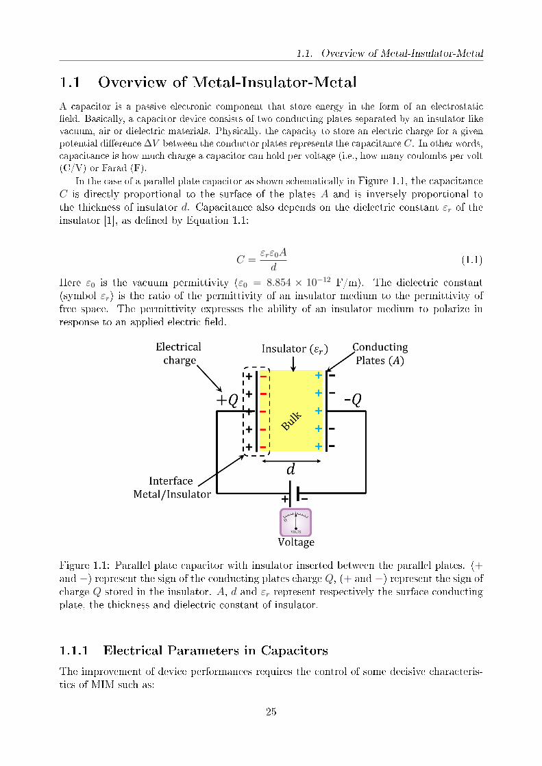
In the case of a parallel plate capacitor as shown schematically in Figure 1.1, the capacitanceC is directly proportional to the surface of the plates A and is inversely proportional tothe thickness of insulator d. Capacitance also depends on the dielectric constant εr of theinsulator [1], as dened by Equation 1.1:
C =εrε0A
d(1.1)
Here ε0 is the vacuum permittivity (ε0 = 8.854 × 10⁻¹² F/m). The dielectric constant(symbol εr) is the ratio of the permittivity of an insulator medium to the permittivity offree space. The permittivity expresses the ability of an insulator medium to polarize inresponse to an applied electric eld.
Figure 1.1: Parallel plate capacitor with insulator inserted between the parallel plates. (+and −) represent the sign of the conducting plates charge Q, (+ and −) represent the sign ofcharge Q stored in the insulator. A, d and εr represent respectively the surface conductingplate, the thickness and dielectric constant of insulator.
1.1.1 Electrical Parameters in Capacitors
The improvement of device performances requires the control of some decisive characteris-tics of MIM such as:
25

Chapter 1. METAL/INSULATOR/METAL BASED ON Pb(Zr0.52Ti0.48)O3 THINFILMS
• Surface capacitance: Miniaturization is required to increase the capacitance density(nF/mm2) in order to optimize the space occupied on the printed circuit boards. The neces-sity to increase the capacitance density promotes the use of new high-permittivity materials.For example, using PZT allows to achieve a capacitance density values up to 50 nF/mm2
[2, 3].
• Loss tangent: it is dened as the quantity used to indicate the energy loss characteristicof a material. This function characterizes the relation between the energy lost per cycleand the energy stored per cycle in the Metal-Insulator-Metal structure as dened by theexpression in Equation 1.2:
tanδ =ε′′(f)
ε′(f)(1.2)
Here, ε′represents the part of relative permittivity that increases capacitance, ε
′′represents
the loss and f the frequency. With a very good dielectric material, the loss tangent tendstowards zero (for the thin lm PZT a loss tangent < 4 % is often required) [4, 5].
• Breakdown Field (Voltage): The breakdown eld is the maximum permissible electriceld through the insulator prior to the destruction of MIM capacitors. Therefore, it is animportant electrical characteristic for assessing the intrinsic quality of an insulator. Appli-cations using capacitor with dielectric usually require high breakdown eld (typically 2-3MV/cm). Benhadjala et al. [6, 7] have reported breakdown eld values between 1.67 and2.5 MV/cm on PZT and PZT doped with Manganese and Niobium.
Thus, optimization of all these physical properties requires a better understanding ofinsulator and capacitor used. In this context, we will now discuss on the properties ofdielectric materials used in MIM capacitors.
1.2 Dielectric Materials Investigations
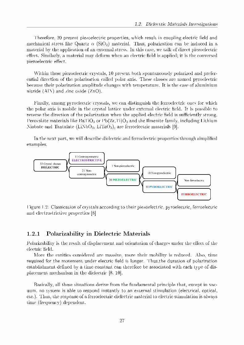
In crystal or polycrystalline materials with a specic symmetry of the unit cell, the dis-placement or the orientation of atoms can involve ferroelectric, piezoelectric or pyroelectriceects. On the basis of the symmetry elements of translational position and orientation,there are 230 space groups. Ignoring translational repetition, these 230 groups break downinto 32 classes, known as the 32 point groups. The 32 point groups can be classied accord-ing to their properties [8, 9] as illustrated schematically in Figure 1.2.
First, it can be seen that 11 of them are centrosymmetric, i.e. they have a center ofsymmetry implying that they cannot present polar properties. Among centrosymmetricclasses, certain electromechanical eects can also appear.
Out of the 21 non-centrosymmetric classes, one displays no piezoelectric eect becausethe movement of the charges during mechanical solicitation does not induce the appearanceof a dipole.
26
1.2. Dielectric Materials Investigations
Therefore, 20 present piezoelectric properties, which result in coupling electric eld andmechanical stress like Quartz α (SiO2) material. Thus, polarization can be induced in amaterial by the application of an external stress. In this case, we talk of direct piezoelectriceect. Similarly, a material may deform when an electric eld is applied; it is the conversedpiezoelectric eect.
Within these piezoelectric crystals, 10 present both spontaneously polarized and prefer-ential direction of the polarization called polar axis. These classes are named pyroelectricbecause their polarization amplitude changes with temperature. It is the case of aluminiumnitride (AlN) and zinc oxide (ZnO).
Finally, among pyroelectric crystals, we can distinguish the ferroelectric ones for whichthe polar axis is mobile in the crystal lattice under external electric eld. It is possible toreverse the direction of the polarization when the applied electric eld is suciently strong.Perovskite materials like BaTiO3 or Pb(Zr,Ti)O3 and the Ilmenite family, including LithiumNiobate and Tantalate (LiNbO3, LiTaO3), are ferroelectric materials [9].
In the next part, we will describe dielectric and ferroelectric properties through simpliedexamples.
Figure 1.2: Classication of crystals according to their piezoelectric, pyroelectric, ferroelectricand electrostrictive properties [8]
1.2.1 Polarizability in Dielectric Materials
Polarizability is the result of displacement and orientation of charges under the eect of theelectric eld.
More the entities considered are massive, more their mobility is reduced. Also, timerequired for the movement under electric eld is longer. Thus,the duration of polarizationestablishment dened by a time constant can therefore be associated with each type of dis-placement mechanism in the dielectric [8, 10].
Basically, all these situations derive from the fundamental principle that, except in vac-uum, no system is able to respond instantly to an external stimulation (electrical, optical,etc.). Thus, the response of a ferroelectric dielectric material to electric stimulation is alwaystime (frequency) dependent.
27

Chapter 1. METAL/INSULATOR/METAL BASED ON Pb(Zr0.52Ti0.48)O3 THINFILMS
Indeed, under a sinusoidal electric eld:−→E =
−→E0 · ei(2πf)t, the polarization (
−→P =
−→P0 ·
ei((2πf)t−δ)) displays a delay δ (depending on the frequency f). Thus, the electric induction−→D = ε0 ·εr ·
−→E will be necessarily sinusoidal with the same delay δ as illustrated by Equation
1.3:
−→D =
−→D0 · ei((2πf)t−δ) = ε0 · ε∗r ·
−→E (1.3)
It follows that, for a linearly homogeneous isotropic material, the permittivity is a complexquantity. It is related to the frequency f as seen in Equation 1.4:
ε∗r(f) = εr(f = 0) · eiδ = ε′(f) + ε
′′(f) (1.4)
ε′(f) = εr(f = 0) · cosδ
ε′′(f) = εr(f = 0) · sinδ
(1.5)
The ε′is the relative dielectric constant, ε
′′the dielectric losses (Equation 1.5). The fre-
quency, as shown in Figure 1.3, is an important parameter which can be used to separatethe dierent contributions of the polarization.
Given the establishment of the external electric eld, electronic polarization is due tothe displacement of the electron cloud with respect to the nucleus. Electronic polarizationdominates in the visible and ultraviolet ranges (from 1014 to 1016 Hz). Without exception,electronic polarization is present in all dielectric materials.
The atomic (or ionic) polarization related to the displacements of the ions with respectto each other is established more slowly than the electronic polarization. It occurs at fre-quencies between 1011 to 1014 Hz.
Under the eect of an external electric eld, materials with permanent dipole momentstend to line up. This results in a polarization called polarization by orientation (or dipolarpolarization). It occurs at frequencies between 106 to 1010 Hz.
Hopping polarization attributed to jumps of the carriers between two sites occurs atfrequencies between 102 to 106 Hz.
Interfacial polarization results from the local accumulation of charge carriers due to mi-gration phenomena around defects such as impurities, vacancies, grain boundaries, spacecharge at interfaces, etc. This polarization is characterized by rather long establishmenttime. It occurs at frequencies between 0.01 to 100 Hz.
Further, we can introduce the loss tangent δ, which is commonly used because it allowsto easily compare the ratio of the imaginary and real parts of the dielectric constant giving
28

1.2. Dielectric Materials Investigations
access directly to the delay δ. In other words, it represents the ratio of the energy dissipatedinto the dielectric on the accumulated energy [11].
Figure 1.3: Relative permittivity (dielectric constant and loss factor) as a function of fre-quency [8]
1.2.2 Ferroelectricity in Dielectric Materials
Ferroelectricity was rst discovered in Rochelle salt in 1920 [12]. It is present in mono orpoly-crystalline materials [13]. Ferroelectricity is a property which arises from the asym-metry of certain crystals like Lead Zirconate Titanate below Curie temperature TC . Fer-roelectricity occurs due to a phase transition from a paraelectric phase characterized by ahigher symmetry (cubic in the case of PZT) to a ferroelectric phase characterized by a lowersymmetry (e.g. tetragonal). The phase transition in PZT involves, primarily, permanention displacements from their equilibrium positions in the paraelectric cubic phase. Thesedisplacements lead to the temperature dependent of spontaneous polarization, characteris-tic to pyroelectrics. The ferroelectrics have the additional property that the spontaneouspolarization can be reversed by the application of a suitable external electric eld.
Under the application of an electric eld, positive and negative charges of a polarizablematerial move in the opposite direction, creating a dissymmetry responsible for an electricdipole moment
−→Pi in each unit cell as illustrated in Figure 1.4. Ferroelectric materials present
a displacement of atoms which remains after removing the applied electric eld. This is thestate of remanent polarization. By considering the polarization as an order parameter, thebehavior of ferroelectric can be modeled by the Landau-Ginzburg-Devonshire theory whichis based on the free energy F [14]. Furthermore, on the macroscopic scale, the electriceld applied over the entire volume V of the dielectric with a presence of all electric dipole
29

Chapter 1. METAL/INSULATOR/METAL BASED ON Pb(Zr0.52Ti0.48)O3 THINFILMS
moment−→Pi in each unit cell induces a macroscopic polarization. The polarization vector
−→P
is therefore dened by Equation 1.6:
−→P =
∑−→Pi/dV (1.6)
Below the Curie temperature TC and without external electric eld, a spontaneous polar-ization (Ps) develops along at least two symmetries which determine directions. In orderto minimize the depolarizing eld
−→E d energy which results from uncompensated polariza-
tion charges at the interface, the ferroelectric material tends to create several volume withuniform polarization called domain ferroelectric. This phenomenon constitutes the mostnatural means by which the system has recourse to remain ferroelectric and minimize itselectrostatic.
Figure 1.4: Illustration of the alignment of the dipoles in a dielectric under the eect of theapplied electric eld (+δ• − • − δ )
Now, when the external electric eld is initially increased from zero value, the polar-ization increases as more dipoles are lined up along the electric eld direction. When theelectric eld is strong enough, all dipoles are lined up with the electric eld, so the mate-rial is in a saturation state Psat+ as illustrated in Figure 1.5. If the applied electric elddecreases from the saturation point, the polarization also decreases. However, when theexternal electric eld reaches zero, the polarization does not reach zero. The polarizationat the zero electric eld is called the remanent polarization Pr+ (Pr−). When the direc-tion of the electric eld is reversed, the polarization decreases. When the reverse electriceld reaches a certain value, called the coercive eld EC− (EC+), the polarization becomesnull. By further increasing the electric eld in this reverse direction, the reverse saturationPsat−(Psat+) can be reached. When the electric eld is decreased from this saturation pointPsat−, the sequence just reverses itself and above EC+, the polarization can switch towardsPsat+.
30

1.3. Lead Zirconate Titanate Pb(Zr,Ti)O3
Figure 1.5: Typical ferroelectric hysteresis cycle showing saturation polarization Psat±, re-manent polarization Pr± and the coercive eld Ec± [9]
Finally, for ferroelectric dielectric materials, the variation of the dielectric constant (per-mittivity) and loss tangent with bias voltage present a buttery curve characteristic due tothe high non-linear nature as shown with PZT thin lm in Figure 1.6.
Figure 1.6: Variation of the dielectric constant and loss tangent with electric eld (biasvoltage)(The thickness of PZT lm is 1 µm)[15]
.
1.3 Lead Zirconate Titanate Pb(Zr,Ti)O3
Lead zirconate titanate Pb(Zr,Ti)O3 (PZT) crystallizes in a perovskite structure [9]. Thegeneral formula for perovskite-type oxide is ABO3. The unit cell is nearly cubic where
31

Chapter 1. METAL/INSULATOR/METAL BASED ON Pb(Zr0.52Ti0.48)O3 THINFILMS
Pb2+ cations with large ionic radius are at the pseudo-cubic corners (site A) , the Zr4+ orTi4+ cations with smaller radius are at the body center of the cube (site B), and the Oanions (O2−) are at the center of the faces as seen in Figure 1.7. The cations A and B arerespectively 12 and 6 coordinated. Thus, O atoms form octahedra around the B cation [16].
Figure 1.7: Perovskite structure of ABO3 with a cubic unit cell
PZT exhibits at the same time ferroelectricity, piezoelectricity, pyroelectricity and highdielectric permittivity properties [3]. The phase diagram of the PbZrO3-PbTiO3 (PZO-PTO) system in the temperature range of 0 to 500C in Figure 1.8 (a) shows the dierentcrystalline phases of PZT [17, 18].
Figure 1.8: (a) Phase diagram of PZT solid solution. Pc, cubic paraelectric phase; FTtetragonal ferroelectric phase; FRHT , High temperature rhombohedral ferroelectric phase;FRLT , low temperature ferroelectric rhombohedral phase; AO, orthorhombic antiferroelec-tric phase; AT , tetragonal antiferroelectric phase; [18] (b) Phase diagram of PZT solidsolution near MPB based on synchrotron X-ray powder diraction data [19]
When the temperature is above the Curie temperature Tc, the unit cell is cubic and thePZT has a paraelectric order. The cubic phase for PZT takes place above 230C , 400C
32

1.3. Lead Zirconate Titanate Pb(Zr,Ti)O3
and 495C for PZO, PZT (with Zr/Ti=0.52/0.48) and PTO respectively. Below the TC , thestructure depends on the percentage of Ti (x) in the solution and the temperature. Thesedistorsions of the ideal unit cell can be: the tilting of the oxygen octahedra, the displacementsof the cations (Pb2+, Ti4+ and Zr4+) or the distorsion of the octahedra. Thus, as can beremarked in Figure 1.8 (a), these modications lead to the change from paraelectric orderto ferroelectric order with presence of tetragonal, rhombohedral or orthorhombic phase.
At room temperature, the lattice parameters of PbZrO3 in the orthorhombic phase area=5.886 Å, b=11.749 Å and c=8.248 Å [20] wheras PbTiO3 in the tetragonal ferroelectricphase are a=b=3.904 Å, c=4.152 Å [21].
Futhermore, when x is between 0.45 and 0.5 as shown in Figure 1.8 (b), dielectricand piezoelectric responses of the PZT become optimal as presented in Figure 1.9. Thiszone is named Morphotropic Phase Boundary (MPB) [22, 23]. The word morphotropicis used to designate an abrupt structure change of a solid solution with the variation incomposition. With diraction measurements, it has been long believed that this phase issimply a mixture of tetragonal and rhombohedral phases [24]. In 2000, however, Noheda et
al. showed the presence of a monoclinic phase in this area of the phase diagram by usinghigh resolution Synchrotron X-ray diraction [25]. The presence of this monoclinic phasecould be at the origin of high dielectric constants and piezoelectric coecients properties ofPZT in this particular morphotropic zone. It may act as a bridge between the tetragonaland rhombohedral phases [26].
Figure 1.9: Dielectric constant (blue lines) and electromechanical coupling coecient (greenlines) of PZT depending on the zirconium and titanium ratio. Image adapted from Carterand Norton [27]
• PZT p-Type Semiconductor
Ferroelectric materials like PZT have been previously regarded as an insulator. This ap-proach has been successful to explain the phase transition and ferroelectric switching. Fer-roelectric performances of perovskites (ABO3) can be strongly attributed to the nature of
33

Chapter 1. METAL/INSULATOR/METAL BASED ON Pb(Zr0.52Ti0.48)O3 THINFILMS
chemical bonds [28]. Basically, chemical bonds of all perovskites were rather considered tobe ionic [29]. Recently, ferroelectricity in perovskites has been shown to be quite directlyrelated to the nature of the chemical bonds. First, Cohen gave an origin of the dierence offerroelectric behavior between the BaTiO3 (BTO) and the PbTiO3 (PTO) [30]. In fact, withBTO, the Ba-O bond is purely ionic, while in PTO the Pb-O bond is strongly hybridized(the bond is partially covalent) [28]. Furthermore, the Pb-O bonds in tetragonal PbTiO3
show rather strong covalency, while those in cubic PbTiO3 are ionic. From these results, wecan say that the type of bond constitutes a key factor on the ferroelectric properties of aperovskite materials.
Chen et al. [31] explain that the dierent ferroelectric behaviors of ATiO3 perovskitesare closely related to charges on A and A-O interaction. They also provide that Pb bondsto O mainly with its 6p AOs whereas Ba atoms link to oxygen atoms through the ns-2sbonding. Finally, they show that the bond order of Pb-O is larger than (between 3 and 4times more) that of Ba-O, indicating that Pb-O is more covalent than Ba-O. Miyazawa et al.
[32] describe that the Born eective charge (dened as the change of polarization associatedto a specic atomic displacement) of Ba is not enhanced as much as that of Pb becauseBa has no covalent bond with nearest oxygen ions. In fact, Born eective charge gives theimportance of the hybridization or the polarization of an atom and thus play a central role inthe study of Coulomb eects. Ghosez et al. [33] demonstrate that the covalence eect tendto increase the amplitude of the Born eective charge. Additionally, Born eective chargesdata from Zhong et al. are respectively 3.9 and 2.7 for Pb and Ba [34]. All these previousresults are conrmed by the comparison of the ionic states between Pb and Ba eectuatedby Kuroiwa et al. [35], which give a lower estimation of 1.1 for Pb and a high value of 1.9for Ba. Globally, these calculations have highlighted that the degree of covalence is higherin Pb-based ferroelectric perovskites than in BaTiO3.
Furthermore, this ferroelectric approach fails totally in describing the transport mecha-nisms or other properties that involve internal mobile charges. In fact, many works [36, 37]regard ferroelectrics as wide bandgap semiconductors, making it easy to adapt well foundedtheories for semiconductors. However, how to include the semiconductivity is still a dicultproblem when analyzing experimental data. Simplied models based on semiconductivitymay ignore important eects or limit the range of parameters.
Pintilie et al. [28] explain that the Pb-based materials should be regarded rather asa semiconductor than an insulator with a specication on the fact that of their electronicproperties might be inuenced by the ferroelectric polarization. This assertion have beensupported by the analysis performed on the capacitance and hysteresis data of the PZT thinlm. Indeed, results of capacitance and hysteresis are coherently explained using a modelbased on the conventional metal-semiconductor Schottky contact in which the eect of theferroelectric polarization on band-bending was also considered.
For ferroelectric perovskite oxides such as PZT, three mobile charge carrier participatein conduction: electrons, holes and oxygen vacancies by far the most mobile ionic species.Basically, acceptor dopants increase the concentration of holes and therefore promote thep-type conductivity. Donor dopants increase the concentration of electrons and thereforepromote the n-type conductivity.
In the case of PZT lm with band gap values in the range of 3.2 - 3.9 eV range (depending
34

1.4. Schottky Model of Metal/Semiconductor Contact
on the Zr/Ti ratio), the conduction type is still the subject of debate, with arguments bothfor p and n type conduction. In fact, PZTs should be p-type according to the defectchemistry, but often they are regarded as an n-type semiconductor due to a higher mobilityof the electrons.
According to Yarmarkin et al. [38] and Smyth [39], a variation of the semiconductor typewithin the lm thickness has been considered. Due to the oxygen vacancy accumulation, ann-type layer is supposed to occur at the surface whereas the bulk remains p type. Scott[40]stated that in all ferroelectric thin-lm capacitors, the conduction was predominantly dueto electrons injected from the cathode, not due to holes (the p-type character of the lm).It also pointed out that n-type perovskite ferroelectric lms could be formed when sampleswere deposited in reducing atmospheres. When oxygen is lost in the form of neutral O2, itleaves behind electrons, thus the vacancies turn out to be donors. In appearance, n-typeperovskite has a darker outlook compared to p-type.
Work of Stolichnov et al. [41] on Pt/PZT/Pt capacitors showed that the conduction issupported by holes. Wouters et al. [42] also found that the hole barrier is smaller than theelectron barrier in their study on Pt/PZT/Pt capacitors.
Following above description, it is important to recall the features of Schottky contactbased on the metal/semiconductor (p and n type) model.
1.4 Schottky Model of Metal/Semiconductor Contact
When metal and semiconductor (SC) materials are contacted such as to form an interface,the Fermi level of both materials at thermodynamic equilibrium are equal. Thus, the barrierheight ΦB between the metal and the semiconductor after contact is given by Equation 1.7[9]:
ΦB = ΦM − χ (1.7)
Here χ is the electron anity of the semiconductor which represents the dierence energybetween the conduction band of the semiconductor and the vacuum level. ΦM indicatesthe work function of the metal i.e. the dierence between the Fermi level of the metal andthe vacuum level. From the relation giving in Equation 1.7, three kind of contact can beobtained depending on the metal used and the semiconductor. The contacts can be neutral,ohmic (conducting) or rectifying (blocking for one polarity, conducting for the oppositepolarity as illustrated in Figure 1.10.
Figure 1.10 (a) presents an ohmic contact for electrons and a rectifying (blocking) contactfor holes. In fact, with ΦM < ΦSC electrons in the metal can encounter the least barrier totheir ow into the semiconductor. The electrons are injected into the semiconductor nearthe interface. Thus, an electric eld Ei oriented from the metal towards the semiconductordevelops, preventing further migration of electrons from the metal. This interface electriceld is described by an energy variation (or band bending) towards lower energies at thelevel of depletion layer width W . Here ECBm is the Conduction Band minimum, EV BM
Valance Band Maximum, (h+) is the hole, (e−) is electron and EF is the Fermi level. Thereverse situation ΦM > ΦSC can be observed in Figure 1.10 (b) which presents an ohmic
35

Chapter 1. METAL/INSULATOR/METAL BASED ON Pb(Zr0.52Ti0.48)O3 THINFILMS
contact for holes and a rectifying (blocking) contact for electrons. The two types of carrierscannot ow in the same direction when a certain external voltage is applied on the sample.
Figure 1.10: Schematics of band bending occurring at a metal/semiconductor interface [43].The work function of the metal is lower (a) or higher (b) than that of the semiconductor. Inthe rst case, the contact is ohmic for electrons and rectifying for holes. In the second case,the contact is rectifying for electrons and ohmic for holes. Schottky models of the metal-semiconductor ΦM < ΦSC with barriers width W . (h+) is the hole and (e−) is electron, EF
is the Fermi level
Furthermore with the presence of the depletion layer width W , the PZT thin lm isassumed to be divided into a layer depleted of charge, and an interior region of p-type side.The space charge region W , can be treated as a voltage dependent parallel plate capacitor,with capacitance. In fact, the depleted regions may present a capacitance, which are serialconnected to the capacitance of the bulk material if both metal-semiconductor interfacesbehave as Schottky contact and therefore may impact on the measured capacitance of MIMstructures.
By assuming that the ferroelectrics such as PZT are wide-gap p-type semiconductorsand by adapting the theories for metal-semiconductor rectifying contacts to the metal-ferroelectric contact, Pintilie and Alexe [44] gave the specic capacitance C of the depletedregion when an innite sheet of surface charge (A) is used in the depletion approxima-tion(Equation 1.8):
C =ε0εstW
=
√qε0εstNeff
2(V + V
′bi
) (1.8)
Where, Neff is the eective charge density in the depleted layer, V voltage bias ,V′
bi theapparent built-in potential.
36
1.4. Schottky Model of Metal/Semiconductor Contact
Thus, the presence of apparent built-in potential V′
bi will lead to the appearance of dier-ent values at the two interfaces of a MFM structure, even in the case of perfectly symmetricelectrodes. This implies dierent band bendings at the two electrodes. Additionally, thisserial capacitor can modify the total capacitance of MFM capacitor.
• Interfacial Layer Eects at the Level of Metal-Dielectric Interface
We have studied an ideal contact between the metal/semiconductor and the possible eectdue to the depleted region. However, band bendings will be always aected by the presenceof interfacial layer which often induces the additional eect and will tend to modify theresult. Interface eects can be induced by the interface ionized (defect) states, thin oxidelayers yielding to additional junctions or adsorbed molecules etc.
Apostol et al. showed that the band bending of Au/PZT [45] and Cu/PZT [46] are un-timely linked to the surface polarization. They demonstrated that the band bending at theelectrode interface depends on the polarization orientation. Pintilie et al. showed that thepolarization charges control the height of potential barriers at the electrode interfaces in thecase of Pb(Zr,Ti)O3 and BaTiO3 epitaxial lms [47]. Bardeen highlighted the importance ofinterface states in determining the barrier height [48]. Saravanan et al. [49] described thatthe surface states (which will participate to the interface formation) can emerge from chem-ical and physical imperfections. The use of high resolution transmission electron microscopyfor probing the atomic structure of the interface SrRuO3/Pb(Zr0.2Ti0.8)O3 [50] has showeda reduction of atomic displacements at the interface due to the eect of the interfacial layerwhich leads to the reduction of the spontaneous polarization.
Furthermore, in PZT lms, except the pyrochlore phase [51, 52], which is the mostknown undesired phase at the surface of the PZT thin lm, others authors suggested alsothe presence of the secondary phase base on the uorite [53], ZrO2 [54], PbO [55, 56, 57].These secondary phases can thus behave as a dead layer [58] at the metal-semiconductorinterface and induce a modication of the characteristics at the interface.
In fact, the dead layer is often used in the serial capacitor model to explain the thicknessdependence of the dielectric permittivity. Indeed, from the point of view of the dielectricperformances, MIM capacitors can be impacted by the presence of interfacial layer (ordead layer with a low dielectric constant) at the level of metal/dielectric interfaces. Thisadditional dead layer induces a capacitance Cinterface in series with the Chigh−k from thedielectric [59, 60]. The total capacitance Ctot formed by these two layers is determined bythe following relation (Equation 1.9):
1
Ctot
=∑i
(1
Ci
)=
1
Chigh−k
+1
Cinterface
=1
A.ε0
[dhigh−k
εhigh−k
+dinterfaceεinterface
](1.9)
Here A is the surface plate, ε0 is the vacuum permittivity, dhigh−k and dinterface are respec-tively the thickness of high-k material and dead layer at interface metal/high-k. From apurely capacitive point of view, the interface layer will dominate the value of total capaci-tance presented in Equation 1.9 if the thickness of structure decrease. Thus, the control ofthe presence of these secondary phases at the surface of PZT layer constitutes a real leverin order to broad and improve our knowledge on the electrode/PZT interface properties ofcapacitor devices.
37

Chapter 1. METAL/INSULATOR/METAL BASED ON Pb(Zr0.52Ti0.48)O3 THINFILMS
1.5 Conclusion
In this chapter, we have presented some of the basic properties of Metal-Insulator-Metalstructure followed by the presentation of crystalline materials and their properties. A largepart of this chapter has been devoted to the description of PZT near the morphotropic phaseboundary. Additionally, this chapter have pointed out the importance of both the PZTsurface and the electrode/PZT interface in the performance of MIM. Given the impact ofthe surface states in the real interface metal/semiconductor, this thesis will try to understandthe surface (and interface) PZT characteristics by associating the structural, microstructuraland physicochemical analyses as well as the electrical performances. Before presenting theelectrical response relative to the Pb excess and the post-annealing, in the next chapter, wewill rst present the dierent stages of the deposition and the characterization of the PZTbased metal/insulator/metal heterostructure and the principles of the main techniques usedto characterize the surface and interface chemistry and structure.
38

Bibliography
Bibliography
[1] C. R. Robertson. Fundamental Electrical and Electronic Principles. Elsevier Ltd, 3rd edition,2008.
[2] Ibrahima Gueye, Gwenael Le Rhun, Olivier Renault, Emmanuel Defay, and Nicholas Bar-rett. Electrical response of Pt/Ru/PbZr0.52Ti0.48O3/Pt capacitor as function of lead precursorexcess. Applied Physics Letters, 111(22):222902, nov 2017.
[3] Yole. Thin lm pzt for semiconductor: Application trends technology update (feram, ipds andmems). Yole Developpement SA, 2013.
[4] V. Koval, C. Alemany, J. Brianin, and H. Bruncková. Dielectric Properties and Phase Tran-sition Behavior of xPMN-(1-x)PZT Ceramic Systems. Journal of Electroceramics, 10:1929,2003.
[5] X. Chen, H. Fan, and S. Ke. Low-temperature synthesis of (Pb,La)(Zr,Ti)O3 thick lm onTi substrates by the hydrothermal method using oxide precursors. Applied Physics Letters,88(1):012901, 2006.
[6] W. Benhadjala, G. Le Rhun, C Dieppedale, F. Sonnerat, J. Guillaume, C. Bonnard, P. Re-naux, H. Sibuet, C. Billard, P. Gardes, and P. Poveda. Sol-gel doped-PZT thin lms forintegrated tunable capacitors. International Symposium on Microelectronics, 2015(1):000256000261, 2015.
[7] W. Benhadjala, F. Sonnerat, J. Guillaume, C. Dieppedale, P. Renaux, G. Le Rhun, H. Sibuet,and C. Billard. Highly tunable Mn-doped PZT thin lms for integrated RF devices. Ad-ditional Conferences (Device Packaging, HiTEC, HiTEN, & CICMT), 2015(DPC):002095002127, 2015.
[8] K. C. Kao. DIELECTRIC PHENOMENA IN SOLIDS With Emphasis on Physical Conceptsof Electronic Processes. Academic Press, 2004.
[9] E. Defa¸. Integration of Ferroelectric and Piezoelectric Thin Films. John Wiley & Sons, Inc,2011.
[10] C. Kittel. Introduction to Solid State Physics, EIGHTH EDITION. John Wiley & Sons, Inc,2005.
[11] C. Huber. Synthèse et caractérisation de nouveaux matériaux ferroélectriques accordables pourapplications hyperfréquences. . PhD thesis, 2003.
[12] J. Valasek. Piezo-Electric and Allied Phenomena in Rochelle Salt. Physical Review, 17(4):475481, 1921.
[13] K. M. Rabe, C. H. Ahn, and J. M. Triscone. Physics of Ferroelectrics A Modern Perspective,volume 105 of Topics in Applied Physics. Springer Berlin Heidelberg, 2007.
[14] C. Kittel. Introduction to Solid State Physics 7th Edition. 2010.
[15] M. D. Nguyen, H. Nazeer, M. Dekkers, D. H. A. Blank, and G. Rijnders. Optimized electrodecoverage of membrane actuators based on epitaxial PZT thin lms. Smart Materials andStructures, 22(8):085013, 2013.
39

Chapter 1. METAL/INSULATOR/METAL BASED ON Pb(Zr0.52Ti0.48)O3 THINFILMS
[16] R. W. Schwartz. Chemical solution deposition of perovskite thin lms. Chemistry of Materials,9(11):23252340, 1997.
[17] F. Cordero, F. Trequattrini, F. Craciun, and C. Galassi. Octahedral tilting, monoclinic phaseand the phase diagram of PZT. Journal of Physics: Condensed Matter, 23(41):415901, 2011.
[18] B. Jae, W. R. Cook, and H. Jae. Solid solutions of Pb(Ti, Zr, Sn, Hf)O3. In PiezoelectricCeramics, pages 135183. Elsevier, 1971.
[19] B. Noheda and D. E. Cox. Bridging phases at the morphotropic boundaries of lead oxide solidsolutions. Phase Transitions, 79(1-2):520, 2006.
[20] L. B. Kong, J. Ma, W. Zhu, and O. K. Tan. Preparation and characterization of lead zirconateceramics from high-energy ball milled powder. Materials Letters, 49(2):96101, 2001.
[21] K. Iijima, Y. Tomita, R. Takayama, and I. Ueda. Preparation of c-axis oriented PbTiO3 thinlms and their crystallographic, dielectric, and pyroelectric properties. Journal of AppliedPhysics, 60(1):361367, 1986.
[22] V.A.Isupov. Comments on the paper X-ray study of the PZT solid solutions near the mor-photropic phase transition. Solid State Communications, 17(11), 1975.
[23] S. K. Mishra, D. Pandey, and A. P. Singh. Eect of phase coexistence at morphotropic phaseboundary on the properties of Pb(ZrxTi1−x)O3 ceramics. Applied Physics Letters, 69(12):17071709, 1996.
[24] B. Noheda, J. A. Gonzalo, L. E. Cross, R. Guo, S. E. Park, D. E. Cox, and G. Shi-rane. Tetragonal-to-monoclinic phase transition in a ferroelectric perovskite: The structure ofPbZr0.52Ti0.48O3. Physical Review B, 61(13):86878695, 2000.
[25] B. Noheda, D. E. Cox, G. Shirane, R. Guo, B. Jones, and L. E. Cross. Stability of the mon-oclinic phase in the ferroelectric perovskite PbZr1−xTixO3. Physical Review B, 63(1):014103,2000.
[26] Z. Wu and H. Krakauer. First-principles calculations of piezoelectricity and polarization rota-tion in Pb(Zr0.5Ti0.5)O3. Physical Review B, 68(1):014112, 2003.
[27] C. B. Carter and M. G. Norton. Ceramic Materials: Science and Engineering. Springer NewYork, 2007.
[28] L. Pintilie, M. Lisca, and M. Alexe. Epitaxial-quality PZT: Insulator or semiconductor?Journal of Optoelectronics and Advanced Materials, 8:712, 2006.
[29] M. E. Lines and A. M. Glass. Principles and Applications of Ferroelectrics and Related Mate-rials. Oxford, Clarendon Press, 1977, 1977.
[30] R. E. Cohen. Origin of ferroelectricity in perovskite oxides. Nature, 358(6382):136138, 1992.
[31] Z. X. Chen, Y. Chen, and Y. S. Jiang. Comparative study of ABO3 perovskite compounds.1. ATiO3 (A = Ca, Sr, Ba, and Pb) perovskites. Journal of Physical Chemistry B, 106(39),2002.
[32] H. Miyazawa, F. Ishii, E. Natori, T. Shimoda, and T. Oguchi. Contribution of Pb to Ferro-electricity in Perovskite-Type Oxides. Ferroelectrics, 301(1):4953, 2004.
40

Bibliography
[33] Ph. Ghosez, J.-P. Michenaud, and X. Gonze. Dynamical atomic charges: The case of ABO3
compounds. Physical Review B, 58(10):62246240, 1998.
[34] W. Zhong, R. D. King-Smith, and D. Vanderbilt. Giant LO-TO splittings in perovskiteferroelectrics. Physical Review Letters, 72(22):36183621, 1994.
[35] Y. Kuroiwa, S. Aoyagi, A. Sawada, J. Harada, E. Nishibori, M. Takata, and M. Sakata.Evidence for Pb-O Covalency in Tetragonal PbTiO3. Physical Review Letters, 87(21):217601,2001.
[36] J. Robertson. Band osets of wide-band-gap oxides and implications for future electronicdevices. Journal of Vacuum Science Technology B, Nanotechnology and Microelectronics: Ma-terials, Processing, Measurement, and Phenomena 18, 1785, 2000.
[37] W. Doolittle, G. Namkoong, A. G. Carver, and A. S. Brown. Challenges and potential payofor crystalline oxides in wide bandgap semiconductor technology . Solid. State. Electron. 47(12), 2143, 2003.
[38] V. K. Yarmarkin, B. M. Goltsman, M. M. Kazanin, and V. V. Lemanov. Barrier photovoltaiceects in PZT ferroelectric thin lms. Phys. Solid State 42 (3), 522, 2000.
[39] D. M. Smyth. Defect structure in perovskite titanates . Curr. Opin. Solid State Mater. Sci. 1(5), 692, 1996.
[40] J. F. Scott. Ferroelectric Memories. Springer Seriesin Advanced Microelectronics, (SpringerBerlin Heidelberg, Berlin, Heidelberg), Vol. 3, 2000.
[41] I. Stolichnov, A. K. Tagantsev, E. L. Colla, and N. Setter. Cold-eld-emission test of thefatigued state of Pb(ZrxTi1x)O3 lms . Appl. Phys. Lett. 73 (10), 1361, 1998.
[42] D. J. Wouters, G. J. Willems, and H. E. Maes. Electrical conductivity in ferroelectric thinlms. Microelectron. Eng. 29 (1-4), 249, 1995.
[43] C. S. S. R. Kumar. Surface Science Tools for Nanomaterials Characterization. Springer BerlinHeidelberg, 2015.
[44] L. Pintilie and M. Alexe. Metal-ferroelectric-metal heterostructures with Schottky contacts.I. Inuence of the ferroelectric properties. Journal of Applied Physics, 98(12), 2005.
[45] N. G. Apostol, L. E. Stoea, G. A. Lungu, C Chirila, L. Trupina, R. F. Negrea, C. Ghica,L. Pintilie, and C. M. Teodorescu. Charge transfer and band bending at Au/Pb(Zr0.2Ti0.8)O3
interfaces investigated by photoelectron spectroscopy. Applied Surface Science, 273:415425,2013.
[46] L. E. Stoea, N. G. Apostol, C. Chirila, L. Trupina, R. Negrea, L. Pintilie, and C. M. Teodor-escu. Schottky barrier versus surface ferroelectric depolarization at Cu/Pb(Zr, T i)O3 inter-faces. Journal of Materials Science, 49(9):33373351, 2014.
[47] I. Pintilie, C. M. Teodorescu, C. Ghica, C. Chirila, A. G. Boni, L. Hrib, I. Pasuk, R. Ne-grea, N. Apostol, and L. Pintilie. Polarization-Control of the Potential Barrier at the Elec-trode Interfaces in Epitaxial Ferroelectric Thin Films. ACS Applied Materials & Interfaces,6(4):29292939, 2014.
[48] J. Bardeen. Surface states and rectication at a metal semi-conductor contact. PhysicalReview, 71(10):717727, 1947.
41

Chapter 1. METAL/INSULATOR/METAL BASED ON Pb(Zr0.52Ti0.48)O3 THINFILMS
[49] K. V. Saravanan and Raju K. C. J. Understanding the inuence of surface chemical states onthe dielectric tunability of sputtered Ba0.5Sr0.5TiO3 thin lms. Materials Research Express,1(1), 2014.
[50] C. Jia, V. Nagarajan, J. He, L. Houben, T. Zhao, R. Ramesh, K. Urban, and R. Waser. Unit-cell scale mapping of ferroelectricity and tetragonality in epitaxial ultrathin ferroelectric lms.Nature Materials, 6(1):6469, 2007.
[51] L. A. Bursill and K. G. Brooks. Crystallization of solgel derived leadzirconatetitanate thinlms in argon and oxygen atmospheres. Journal of Applied Physics, 75(9), 1994.
[52] M.A. Subramanian, G. Aravamudan, and G.V. Subba Rao. Oxide pyrochlores A review.Progress in Solid State Chemistry, 15(2), 1983.
[53] A. D. Polli, F. F. Lange, and C. G. Levi. Metastability of the Fluorite, Pyrochlore, andPerovskite Structures in the PbO − ZrO2 − TiO2 System. Journal of the American CeramicSociety, 83(4):873881, 2004.
[54] A. Etin, G. E. Shter, G. S. Grader, and G. M. Reisner. Interrelation of ferroelectricity,morphology, and thickness in sol-gel derived PbZrxTi1−xO3 lms. Journal of the AmericanCeramic Society, 90(1), 2007.
[55] J. Wang, J.M. Xue, D.M. Wan, and B.K. Gan. Mechanically Activating Nucleation andGrowth of Complex Perovskites. Journal of Solid State Chemistry, 154(2):321328, 2000.
[56] P. Muralt. PZT thin lms for microsensors and actuators: Where do we stand? IEEETransactions on Ultrasonics, Ferroelectrics and Frequency Control, 47(4), 2000.
[57] I. M. Reaney, K. Brooks, R. Klissurska, C. Pawlaczyk, and N. Setter. Use of TransmissionElectron Microscopy for the Characterization of Rapid Thermally Annealed, SolutionGel, LeadZirconate Titanate Films. Journal of the American Ceramic Society, 77(5), 1994.
[58] M. Stengel, D. Vanderbilt, and N. A. Spaldin. Enhancement of ferroelectricity at metaloxideinterfaces. Nature Materials, 8(5):392397, 2009.
[59] K. Amanuma, T. Mori, T. Hase, T. Sakuma, A. Ochi, and Y. Miyasaka. Ferroelectric Prop-erties of Sol-Gel Derived Pb(Zr, Ti)O3 Thin Films. Japanese Journal of Applied Physics,32(Part 1, No. 9B):41504153, 1993.
[60] M. Stengel and N. A. Spaldin. Origin of the dielectric dead layer in nanoscale capacitors.Nature, 443(7112):679682, 2006.
42

Chapter 2
EXPERIMENTAL METHODS
Contents2.1 Capacitor Deposition . . . . . . . . . . . . . . . . . . . . . . . . 44
2.1.1 Bottom Electrode Deposition on the Silicon Substrate . . . . . . . 44
2.1.2 PZT Deposition . . . . . . . . . . . . . . . . . . . . . . . . . . . . . 45
2.1.3 Top Electrodes . . . . . . . . . . . . . . . . . . . . . . . . . . . . . 48
2.1.4 Post Metallization Annealing Conditions . . . . . . . . . . . . . . . 49
2.2 X-rays Diraction . . . . . . . . . . . . . . . . . . . . . . . . . . . 50
2.3 Overview of Electronic Microscopes . . . . . . . . . . . . . . . . 51
2.4 Characterizations of Surface and Interface . . . . . . . . . . . . 52
2.4.1 Basic Principles of Photoemission . . . . . . . . . . . . . . . . . . . 52
2.4.2 Experimental Set-up of XPS . . . . . . . . . . . . . . . . . . . . . . 62
2.4.3 Synchrotron Beamline . . . . . . . . . . . . . . . . . . . . . . . . . 66
2.5 Conclusion . . . . . . . . . . . . . . . . . . . . . . . . . . . . . . . . 72
Bibliography . . . . . . . . . . . . . . . . . . . . . . . . . . . . . . . . . . 73
The second chapter divided into four sections is consecrated to the presentation of experimentalmethods used to elaborate and investigate the capacitors based on the PZT ferroelectric.
In the rst section, we will present the dierent steps of fabrication of Pt/Ru/PZT/Pt/TiO2/-SiO2 stacks on the silicon wafer. In order to achieve this goal, we will proceed rst the bottomelectrode fabrication, followed by the PZT thin lm elaboration and nally the top electrode depo-sition. The second section will be entirely consecrated to the detail of X-ray diraction and GrazingIncidence X-ray diraction tools mainly used to characterize the texture of PZT thin lms. Thethird chapter will be dedicated to the electron microscopy study, which is used to investigate thesurface and interface morphology. Finally, photoelectron spectroscopy used to characterize boththe surface and interface of capacitors based on the PZT thin lm will be largely addressed. Tonish, we will rst establish the basic principles of photoelectron, followed by the presentation ofthe X-ray photoelectron spectroscopy and Hard X-ray photoelectron spectroscopy tools used tostudy the physicochemical surface and the interface of Metal/PZT.
43

Chapter 2. EXPERIMENTAL METHODS
2.1 Capacitor Deposition
In order to select an appropriate deposition technology for a specic application, several criteriahave to be considered such as applications or material characteristics [1]. Thus, the procedureof Pt/Ru/PZT/substrates deposition used in this PhD is splitted into three parts which are themanufacture of Pt/TiO2/SiO2 on the silicon (Si) substrate then the deposition of the PZT bysol-gel method and nally the deposition of top electrode materials by sputtering.
2.1.1 Bottom Electrode Deposition on the Silicon Substrate
Silicon is the basic material used for manufacturing almost all electronic devices. Silicon is moreabundant, cheaper, stronger and presents a larger band-gap allowing it the ability to operate at quitehigh temperature. However, it is not possible to grow PZT directly on silicon because of interfacialreactions and Pb diusion into the silicon at elevated temperatures (> 500C). Thus the choiceof the bottom electrode is crucial for the growth and the properties of the PZT. Several electrodessuch as LaNiO3 [2], RuO2 [3], SrRuO3 [4] or iridium and iridium oxide [5] have been studied.However, the most commonly used bottom electrode to grow PZT is platinum (Pt) [6, 7] becauseit is chemically inert at elevated temperatures under oxidizing atmosphere (does not oxidize easily)and presents low resistivity. With Pb based materials, the Platinum displays lattice matching,chemical robustness and temperature stability. The standard substrate used for PZT depositionis Pt/TiO2/SiO2/Si heterostructures [8] as described in Figure 2.1. The manufacturing stepsbefore depositing PZT on the 200 mm diameter (8 inches) 750 µm thick standard Si (100)wafer will be described in the following part.
Figure 2.1: Schematic Pt/TiO2/SiO2/Si substrates
First, the silicon wafers are cleaned using a standard RCA cleaning process [9] in orderto remove any organic, particle and metallic contamination which may be present on thesurface. After cleaning, a layer of SiO2 [10] serving as a passivation is thermally grown. Thisstep is carried out at temperature of 1050C in a conventional furnace (Tempress) in thepresence of oxygen and water vapor. The cooling is carried out under inert atmosphere (N2).Furthermore, temperatures employed for the crystallization of PZT are greater than 500C(temperature at which the perovskite phase starts to form). At this temperature, there is asignicant risk of diusion of Pb from the PZT layer down to the substrate because Pt doesnot constitute a good diusion barrier. In order to prevent the diusion eect of Pb downto the Si substrate, a barrier layer, such as the TiO2 is deposited between the platinum andthe SiO2 layers.
Further, the adhesion of platinum or any metal on SiO2 is low [11]. This situation inducesthe use of a suitable adhesion layer between the platinum and the SiO2. Lots of materials
44
2.1. Capacitor Deposition
such as zirconium, tantalum and their oxides [12, 13, 14] are tested but TiO2 (addition tothe role of diusion barrier) is the material most frequently used as adhesion layer [15]. Thedeposition of 10 nm of titanium by sputtering is performed at 350C under argon. Thewafer is then annealed at 750C under O2 to form around 20 nm of TiO2. The layer isshown in orange in Figure 2.1.
Pt (100 nm) layer is then deposited at 450C. This temperature promotes the (111) Ptorientation and tensile stress in the Pt lm. The tensile stress is caused by the dierences inthermal expansion coecients of the Pt lm and the Si substrate [16]. In case of lower depo-sition temperature, for example 25C, both (111) and (100) orientations occur. Accordingto Cue et al. [17], Pt deposited at 25C undergoes a small compressive stress and when thedeposition temperature rises, Pt stress becomes more tensile [17]. The Pt orientation usedto be a crucial point, because it dened the orientation of PZT [18]. Nowadays, this issuehas been overcome with the single crystallized PZT layer acting as a seed layer. The latterguarantees the (100) orientation of the entire PZT lm (with 10 % Pb excess) fabricated inCEA-LETI cleanrooms. In this thesis, platinum layer was deposited at 450C.
2.1.2 PZT Deposition
Sol-gel method is one of the most employed method in the microelectronics industry forgrowing PZT lms [19, 20, 21]. The sol-gel process has the advantage of being easy toimplement at the foundry [21, 22]. In addition, this method easily allows to adjust theproportions of the dierent constituents of PZT solution. The PZT solution used in thisstudy is produced by Mitsubishi Materials Corporation from Japan. The solvent madeof 1-butanol [C4H9OH] and propylene glycol [CH3CH(OH)CH2OH] allows to stabilize thesolution over time and control the rheological properties of the sol [23]. The PZT precursorsused are lead acetate trihydrate [Pb(CH3CO2)2.3H2O], titanium tetra-iso-propoxide [Ti(i-OC3H7)4] and zirconium tetra-nbutoxide [Zr(n-OC4H9)4]. This metal-organic solution hasa very specic composition, in order to achieve the desired morphotropic composition ofthe PZT, which is 52 % of Zr and 48 % of Ti [24]. Note that during this research work,dierent proportion of lead acetate is added to the solution (Pb excess from 10 % to 30 %)in order to compensate the amount of Pb lost. These loss of Pb are mainly caused not onlyby the evaporation of Pb during the annealings but also the diusion of the Pb at Pt/TiO2
interface. The sol-gel method [25] used during this work to deposit four layers thick PZTlm is described hereafter:
Sol-Gel Deposition Process: During this work, 220 nm thick PZT lms were formedby stacking four layers of 55 nm each. The deposition process by sol-gel [26] is illustrated inFigure 2.2. The rst layer (55 nm), which serves as a seed layer is deposited by spin coating,drying, calcination (with n=1) and crystallization. Following that, the spin coating, dryingand calcination steps are again performed three times (n=3) in order to deposit the second,third and fourth layers. Finally, a re-crystallization step is performed after calcination ofthe fourth layer.
45

Chapter 2. EXPERIMENTAL METHODS
Figure 2.2: Sol-gel process ow used for PZT (4 layers of 55 nm) deposition
Spin Coating: The purpose of this step is to coat uniformly the wet solution containingthe precursors on the wafer (Pt/TiO2/SiO2/Si) as presented in Figure 2.3. First, a knownvolume of precursors is dispensed on the surface of the substrates by using a pipette orpipettor and the plate is then rotated. In contact with the water present in air, sol ishydrolyzed to form a gel on the surface of the wafer. Further, the thickness of a unit layerof PZT depends on centrifugal conditions. The parameters aecting the thickness are therotation speed, the acceleration and the rotation time. The typical spin coating parametersare set to 1000 rpm (revolution per minute) with 1500 rpm/s acceleration for 20s spin coatingduration for our PZT layers.
Figure 2.3: Coating processes of a solvent on a substrate by spin coating (a) First, thesubstrate is coated with the solution containing the precursors dissolved in a solvent byusing a pipette (b) The substrate is rotated at high speed and the majority of the excesssolution is ung o the side by the centrifugal force as shown by the arrows. Further,the centripetal force combined with the surface tension of the solution pulls the precursorscoating into an even covering.
Drying and Calcination: The purpose of these steps is to obtain a dry amorphous layerwithout any organic compounds. These two steps are achieved on hotplates. The drying isdone at 130C for 5 minutes. During this step, the remaining solvent in the gel is evaporated.The calcination is operated at 360C. During calcination, the remaining organic compoundsare eliminated. This step is critical because it is accomplished at a temperature at which
46

2.1. Capacitor Deposition
the PbO can evaporate ( T > 300C). This may lead to Pb deciencies and can impact theferroelectric properties of the lm, or even prevent crystallization into a perovskite phase.
Crystallization: This step is carried out in a Rapid Thermal Annealing (RTA) furnace.After calcination, the PZT is still in the amorphous state. To crystallize the PZT in theperovskite phase, the wafer has to reach at least 500C [1]. Infrared lights are used to heatthe wafer by radiation. This type of annealing is extremely fast. During this step, thethin layer of PZT crystallizes in perovskite phase. PZT is heated at 700C for 1 minuteunder an oxygen ow. The rise of the temperature is higher than 10C/sec and have to benely controlled in order to prevent the lm from cracking. The pressure of oxygen in RTAannealing chamber is at atmosphere.
In this thesis, four 200 mm wafers of PZT thin lms at the morphotropic phase bound-ary composition (Zr/Ti: 0.52/0.48) with 220 nm of total thickness were elaborated at theMINATEC High-Technologies Building cleanrooms at the CEA-LETI (Grenoble). Eachsample is composed with four layers of 55 nm of thickness as we can see in Figure 2.4.
Figure 2.4: SEM cross section of PZT/Pt/TiO2/SiO2/Si stack
Dierent composition of Pb excess to compensate the Pb lost during calcination wereused for fabricating these samples as presented schematically in Figure 2.5. Four samples,each with 2 sol-gel layers 10 % excess Pb sandwiched by two layers with 10, 15, 20 and 30 %excess Pb, hereafter referred to as PZT10, PZT15, PZT20 and PZT30 have been elaborated.This enables us to study structural microstructural and physico-chemical properties of PZTthin lms depending of the Pb excess eects. The use of Pb excess only in the 1st and 4th
layers of PZT lm is explained by the fact that, these two layers are more exposed to a hightemperature during the crystallization annealing phases (RTA). This leads to greater lossof Pb during RTA phases and therefore, we need to add an excess of Pb.
Figure 2.5: Stacking of PZT10, PZT15, PZT20 and PZT30 samples depending on the Leadexcess amount contained in the rst/second/third/fourth layers
47

Chapter 2. EXPERIMENTAL METHODS
2.1.3 Top Electrodes
In order to perform electrical characterizations (Capacitance, loss tangent and breakdownvoltage) at laboratory and operando hard X-ray photoelectron spectroscopy (HAXPES)measurements under biasing at synchrotron beamline, the deposition of top electrodes isrequired. Deposition of top electrode materials are carried out by sputtering at room tem-perature.
For electrical characterizations, top electrodes (Pt/Ru) are made with one layer of 5nm of Ru then followed of 100 nm of Pt as illustrated in Figure 2.6 (a.1). Following thesputtering deposition of top electrodes of Pt/Ru, PZT and Pt/Ru layers are patternedwith a specic design to obtain the desired devices. This step allows to access the bottomelectrode contact during electrical measurements.
Figure 2.6: Schematic ow process of Pt/Ru/PZT/Pt stack patterning: (a.1)Pt/Ru/PZT/Pt layers (a.2) Pt/Ru and PZT etching (a.3) patterning of capacitor (BE:Bottom electrode and TE: Top electrode) and (b)top view of the schematic devices
The rst step consists in removing (stripped) a part of PZT in order to obtain an accessto the bottom electrode. For that, we deposit a negative photosensitive chemical resist,then, carry out a photolithography process and nally perform a dry etching by Ion beametching (IBE) on the PZT layer until reach the Platinum layer localized underneath thePZT layer as illustrated in Figure 2.6 (a.2).
The last step of the patterning [9] is performed by depositing a positive photosensitivechemical resist on the Pt/Ru surface. The sample is then partially protected of UV lightby a mask containing the desired pattern. Therefore, after insolation, the parts of the resistprotected by the mask stay on the wafer after development. The parts exposed to the UVare disintegrated after development and reveal the Pt/Ru electrode. Pt/Ru electrodes isthen etching down to the PZT layer. Finally the resist is removed with acetone and isopropylalcohol (IPA) as seen in Figure 2.6 (a.3) and Figure 2.6 (b). Afterwards, capacitor with(80×80)µm2 of area is cut from the wafer. Now the process of device fabrication is nishedand MIM capacitors based on the PZT oxide are ready for testing as shown in Figure 2.6(b).
48

2.1. Capacitor Deposition
According to the very low values of inelastic mean free paths (IMFPs) of electrons inthe matter, during the operando HAXPES experiments, top electrodes consist of one layerof 5 nm Ru followed with thinner Pt (5 nm) layer (contrary to the thicker Pt (100 nm) usedfor electrical measurements) as illustrated in Figure 2.7 (a). Furthermore, even though thepatterning process of contact (Pr/Ru) is the same with the ones performed in Figure 2.6,larger area contact ((1× 1)mm2) is used here for operando HAXPES experiments as shownin Figure 2.7 (b).
Figure 2.7: Pt/Ru/PZT/Pt (a) Cross section of the Pt/Ru/PZT/Pt stack obtained bySTEM and (b) top view of the schematic and actual device
2.1.4 Post Metallization Annealing Conditions
In order to investigate the post metallization annealing (PMA) eect on the capacitor basedon the PZT with dierent Pb excess rate used in the rst and fourth layers, we annealed allPt/Ru/PZT/Pt samples. PMA were carried out at CEA-LETI with an annealing furnaceas schematically illustrated in Figure 2.8 with a top and bottom heating, sample and theprocess tubes. In order to prevent all contamination at high temperatures, a constant uxof pre-heated O2 passes over the annealing chamber before the introduction of samples.Samples are then annealed at 500C under O2 at atmospheric pressure during 30 min. Thisstep allows to analyze the evolution of electrical performances of capacitor and the chemistryof Pt/Ru/PZT top interfaces.
Figure 2.8: Schematic representation of the PMA furnace of Pt/Ru/PZT/Pt samples
49

Chapter 2. EXPERIMENTAL METHODS
2.2 X-rays Diraction
X-ray Diraction (XRD) is used to provide important information on the crystal orientation.Using θ/2θ scans, information about the growth axis perpendicular to the surface of thesubstrate can be determined. For this type of measurement, the incident X-ray beam isxed while the movements of the sample (θ) and the detector (2θ) are coupled. As shown inFigure 2.9 (a), this method consists in sending an X-rays beam with an angle of incidenceθ on the surface of the sample. In this way, the planes (hkl) parallel to the surface ofthe substrate will be successively brought into a diraction condition. According to theBragg condition, the dierent scattered beams interfere constructively only when the angleof diusion is equal to the angle of incidence, which results in the following Equation 2.1:
2dhklsin(θ) = nλ (2.1)
Where, dhkl, the distance between the planes of Miller indices hkl, n the order of the dirac-tion, λ the X-ray wavelength and θ, the incidence angle [27]. XRD (θ/2θ) measurement wasperformed during this PhD by using a XPER PRO MRD XL from PANALYTICAL withCukα radiation (λ = 0.15405nm).
Furthermore, surface texture can be obtained with Grazing Incidence X-Ray Diraction(GIXRD) [28, 29]. It was also carried out to obtain information regarding surface crys-tallography. The advantage of grazing incidence lies in the possibility of controlling thepenetration of X-rays into the material. It is thus possible to probe separately dierentdepths of a material. When the incident beam is close to or below the critical angle, thetotal external reection surface sensistivity is enhanced. The in-plane diraction measure-ments were performed on a Smartlab Rigaku 5-circles [30], using an incidence angle (αi = ω)of 0.5 as can be shown in Figure 2.9 (b). The diracted X-ray beam (2θχ) is recorded foran azimuthal range from 15 to 65 while keeping the angle ( αf = θ) of 0.5 constant withrespect to the sample surface.
Figure 2.9: Schematic illustration X-ray diraction in θ/2θ geometry with plane family(hkl), incident beam (1, 2, 3) and scattered beam (1′, 2′, 3′) and (b) A schematic illustrationof 5-circle goniometer system [30].
50
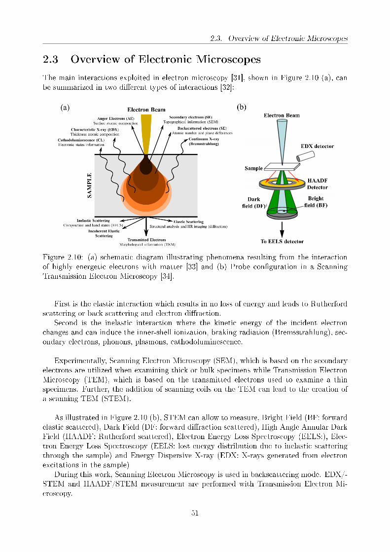
2.3. Overview of Electronic Microscopes
2.3 Overview of Electronic Microscopes
The main interactions exploited in electron microscopy [31], shown in Figure 2.10 (a), canbe summarized in two dierent types of interactions [32]:
Figure 2.10: (a) schematic diagram illustrating phenomena resulting from the interactionof highly energetic electrons with matter [33] and (b) Probe conguration in a ScanningTransmission Electron Microscopy [34].
First is the elastic interaction which results in no loss of energy and leads to Rutherfordscattering or back scattering and electron diraction.
Second is the inelastic interaction where the kinetic energy of the incident electronchanges and can induce the inner-shell ionization, braking radiation (Bremsstrahlung), sec-ondary electrons, phonons, plasmons, cathodoluminescence.
Experimentally, Scanning Electron Microscopy (SEM), which is based on the secondaryelectrons are utilized when examining thick or bulk specimens while Transmission ElectronMicroscopy (TEM), which is based on the transmitted electrons used to examine a thinspecimens. Further, the addition of scanning coils on the TEM can lead to the creation ofa scanning TEM (STEM).
As illustrated in Figure 2.10 (b), STEM can allow to measure, Bright Field (BF: forwardelastic scattered), Dark Field (DF: forward diraction scattered), High Angle Annular DarkField (HAADF: Rutherford scattered), Electron Energy Loss Spectroscopy (EELS:), Elec-tron Energy Loss Spectroscopy (EELS: lost energy distribution due to inelastic scatteringthrough the sample) and Energy Dispersive X-ray (EDX: X-rays generated from electronexcitations in the sample)
During this work, Scanning Electron Microscopy is used in backscattering mode. EDX/-STEM and HAADF/STEM measurement are performed with Transmission Electron Mi-croscopy.
51

Chapter 2. EXPERIMENTAL METHODS
2.4 Characterizations of Surface and Interface
Physicochemical properties of surfaces and interfaces can be substantially dierent fromthose encountered in bulk materials. Understanding the important role played by the surfaceand interface requires the use of specialized characterization processes. Although, methodsof analyzing materials are numerous. Surface-sensitive spectroscopies, such as photoemission(Photoelectron spectroscopy (PES)), have greatly advanced physicochemical knowledge ofsurfaces and interfaces. PES is based on the photoelectric discovered by Hertz in 1887 [35]and explained theoretically by Einstein in 1905 in terms of quantum physics [36]. This theoryallows him to obtain the Nobel Prize in 1921. According to the importance of the PES tool,in the next section, we will recall concepts and theories that describe the photoemissionprocesses, allowing to deduce the electronic structure of a material.
2.4.1 Basic Principles of Photoemission
Photoemission occurs when a light beam (photon for example) with energy hν greater thanthe work function ΦW of the material illuminates the sample [37]. For an electron withbinding energy Ebin, the photon with energy hν can cause the ejection of a photoelectron inthe vacuum level with kinetic energy Ekin. In fact, during the process of photoionization,the ejection of an electron will result in the formation of a positive ion (I+). The energyrequired to cause the ejection of an electron is known as ionization energy or electron bindingenergy. Overall, ionization energy will depend on the location of the electrons in preferenceto the nucleus of the atom. As electrons are arranged in orbitals surrounding the atomicnucleus, the ionization energy will be higher or lower depending on whether the electronsare located in the core or valence shell. Core electrons, which are closer to the nucleus,will require more energy to be ejected. Furthermore, each chemical element has a dierentnumber of protons in the nucleus, resulting in a unique set of ionization energies for everyelement. Thus, from that, energy conservation allows us to write (Equation 2.2):
Ekin = hν − Ebin − ΦW (2.2)
Further, experimentally the sample is electrically connected to the spectrometer. They havea common Fermi level. In this way, the kinetic energy measured is calibrated relatively toanalyzer ΦSp as seen in Figure 2.11 [37].
By using a common Fermi level, the measured kinetic energy can be obtained withEquation 2.3 and it may allow to determine the chemical elements within a sample.
Emeaskin = Ekin − Φanalyzer = hν − Ebin − ΦW − (ΦSp − ΦW ) = hν − Ebin − ΦSp (2.3)
However, the previous description of photoelectric emission in Equation 2.3 can not clarifyvery well the dierent phases of the photoemission process as we will detail later with thethree step model.
52

2.4. Characterizations of Surface and Interface
Figure 2.11: Energy level diagram from a sample to the spectrometer [38]. V L: VacuumLevel, ECBm Conduction Band minimum, EF Fermi Level, EV BM Valence Band Maximum,electron (blue circle) and empty orbital (red empty circle)
Three Step Model of Photoemission Process
Although, the photoemission process is a complex quantum mechanical process taking placein a single step, Berglund and Spicer in 1964 introduced a simpler more pedagogic modelallowing to describe the photoemission process in the material [39]. This approach calledthree step model, in which the photoemission process can be described in terms of threeindependent steps: (1) the probability of excitation in the bulk solid, (2) the probability ofscattering of the excited electron on its path to the surface by the atoms constituting thesolid, (3) the probability of transmission through the surface potential barrier into vacuumas sketched in Figure 2.12.
Figure 2.12: Illustration of the three-step model in PES [39].
53

Chapter 2. EXPERIMENTAL METHODS
• Step I: Photoexcitation of the Electron in the Solid
The photoionization of the atom results from an excitation of an electron in atom by aphoton with energy hν. This photoelectron can be localized either in valence band or thediscrete core levels. The process is subject to a certain transition probability determined bythe photoionization cross section (σ) of the electron. This photoionization cross section isassociated with the probability of interaction between the photon and the electron.
Photoionization Cross Section (σ): Experimentally, the transition probability is oftenestimated using the photoionization cross section (σ) of the electron. The photoionizationcross section (σ) depends on the type of material, the level of the electron considered and theenergy of the incident photons. However, the study of the angular distribution Ω of electronsejected from atoms in the photoionization process is signicance in the understanding of thetransition probability in the solids. Thus the photoelectron angular distribution for circularpolarized and unpolarized photon may be written as in Equation 2.4 [40]:
dσi
dΩ=
σi
4π
[1− β
2P2(cosθ) +
(γ2sin2θ + δ
)cosθ
](2.4)
Where β the dipole parameter, γ et δ are two nondipolar parameters, θ is the angle betweenthe vectors of propagation of photon and photoelectron. P2 is the second order Legendrepolynomial. For instance, cross sections for elements with Z = 1 to Z = 103 have been cal-culated using the Hartree-Fock one-electron central potential and the dipole approximation[41, 42].
• Step II: Travel of the Photoelectron to the Surface
Once that the electron is emitted, the probability for reaching the surface depends on boththe material and the kinetic energy of the electron. Indeed, during transport through thesample, the electron can undergo elastic and inelastic scattering by the Coulomb potentialof neighbouring atoms, which can modify its energy.
Inelastic Meam Free Path (λe): It represents the average length of an electron traveledbetween two successive inelastic scattering events. It strongly depends on the kinetic energyof the particle and the medium in which the particle moves. A predictive model proposedby Tanuma Powell and Coll [43] presented in Equation 2.5 can be used to determine theIMFP:
λe = E/E2p
[βln(γE)− (C/E) + (D/E2)
](2.5)
Where E is the kinetic energy of the electron considered, Ep the energy of the plasmons andβ, γ, C and D are adjustable parameters. This relation takes into account only inelasticelectron-electron interactions in atom and conduction plasmons. However, the data t so-called universal curve shown in Figure 2.13 is a good estimation of the free path for many
54

2.4. Characterizations of Surface and Interface
materials.
Indeed, depending on the energy range used, we can increase largely the IMFP. Utilizingphotons with high energies, the inelastic mean free depth of photoelectrons increase andallows to probe electronic structures depth in the bulk and buried interfaces with whichconventional XPS are dicult to cope. In fact, The probing depth of lab-based XPS can bejust a few angstroms according to the universal escape depth curve. However, low energylasers or high-energy photons available from the synchrotron facility can be used to probethe bulk or interface of materials. The low-energy approach is limited by the nite numberof available lasers and by the energy level excitable by the low-energy lasers (no access tothe core levels).On the other hand, it is becoming easier to probe the bulk structure at thehigh kinetic energy side of the curve because of the development of high-energy beamlinesat synchrotron facilities (tunable X-rays and high brightness can overcome the low crosssection at hard X-ray energy).
Figure 2.13: (a) Universal curve of dependence of the inelastic mean free path on the electronkinetic energy [44] [45].
• Step III: Penetration Through the Surface and Escape Into The Vacuum
Finally, the photoelectron can only escape from the surface if its kinetic energy is sucientto overcome the surface potential barrier of the sample ΦW . When this condition is fullled,the photoelectron can be emitted and then detected by the analyzer. The reduced resid-ual pressure in the spectrometer (< 10−9mbar) allows to minimize the additional inelasticscattering in the path of electron between the surface sample and the entrance of detector.In this context several types of photoelectrons can be distinguished as illustrated in Figure2.14:
55

Chapter 2. EXPERIMENTAL METHODS
Figure 2.14: Scattering processes involved in photoemission: (I) primary electron, (II) sec-ondary electrons and (III) reabsorbed electrons [46]
∗ Electrons that have no suered inelastic scattering are emitted with maximum kineticenergy and have the expected binding energy (case I in Figure 2.14). They are referred to asprimary electrons and contribute to the intensity of main photoelectron peak. They providechemical (from core levels) and electronic structure (from the valence band) informations .
∗ Due to inelastic scattering (case II in Figure 2.14), photoelectron lose kinetic energyby exciting its surroundings and will be currently detected with a higher binding energy.Thus, kinetic energy losses may arise due to electron-phonon or electron-electron interactionswhich inducing the presence of others peaks like satellites or plasmons. As for photoelec-trons having undergone inelastic interactions, photoelectrons are still emitted but have lostelectronic and chemical information. They are found in the energy-loss tail of the mainphotoelectric peak or in the secondary electrons background at low energy kinetic.
∗ The electrons which undergo so many inelastic scattering interactions will not leavethe surface of the material. They are readsorbed and do not contribute to the photoemissionsignal (case III in Figure 2.14)).
(a) Angle-Dependent Studies
Degree of surface sensitivity of an electron-based technique such as XPS may be varied bycollecting photoelectrons emitted at dierent emission angles to the surface plane. Thisapproach may be used to perform nondestructive analysis of the variation of surface com-position with depth (with chemical state specicity). The Beer-Lambert attenuation lawdescribes how the photoelectron intensity will decrease exponential as a function of depthinto the sample. In fact, the intensity of the no-loss peak as a function of the probing depthor electron escape depth d and a take-o angle θ (is the emission angle of the electrons ac-quired by the analyzer with respect to the surface normal) can thus be written in Equation2.6:
56

2.4. Characterizations of Surface and Interface
I(d) = I0e−(d/λesinθ) (2.6)
Here I0 is the intensity without attenuation. Overlayer lms of thickness λesinθ and 2λesinθcontribute respectively to 63% and 86% of the total signal. When the percentage of detectedphotoelectrons is 95 %, d is called sampling depth and is estimated to be 3λesinθ. Thiseect can be used to rapidly estimated if an element is localized at the surface or in the bulk.
According to the relation between the information depth and the take-o angle describedin Equation 2.6, it is possible to tune the depth prole. In fact, to enhance the surface signal,we can decrease the angle of electron emission relative to the surface by using the angle-resolved XPS [39] as shown in Figure 2.15. Thus, by tilting the sample from near normalemission to near grazing emission provides a method for depth proling the surface regionof a solid sample.
Near normal emission produces a spectrum in which, the bulk peak dominates while thesurface peak dominates in the spectrum from the grazing emission. According to Equation2.6, when photoelectrons are collected at angles other than 90 with respect to the surfacenormal, these depths decrease by a factor of sinθ relative to the intensity of the bulk peak.In fact, when the take-o angle (TOA) is at 90, the sample surface is perpendicular tothe line of acceptance of the analyzer, and sampling depth d = 3λesinθ is the maximum.Thus, By tilting the take-o angle (TOA) of 60 and 30 respectively, the sampling depthdecreases from approximately 0.87 and 0.5 relatively to the sampling depth of the TOA =90 [47].
Figure 2.15: Scheme of principle of angle-resolved XPS [47]
(b) Features of Photoelectron Spectrum
A photoemission spectrum contains informations from photoemitted electrons over a wideenergy range [39]. A typical XPS spectrum as a function of kinetic energy is shown in Figure2.16.
57

Chapter 2. EXPERIMENTAL METHODS
Figure 2.16: Typical photoemission spectrum with mainly two important regions: the core-level peaks (here Pb, Ti, Zr, O and carbon from the contamination) and the valence bandspectrum. SE stands for Secondary Electrons
Here we briey describe the main aspects of the XPS spectrum shown inFigure 2.16.
Continiuos Background:
An important aspect in the interpretation of photoemission results is the continuousbackground (Figure 2.16). The continuous background is dominated by electrons that haveundergone many inelastic scattering with their surroundings. The inelastically-scatteredelectrons or Secondary electrons (SE) have lost coherence with their initial state and consti-tuted therefore a background. However, an incorrectly subtraction of background can inducea misinterpretation of the recording data. Numerous background types are published buthowever, linear and Shirley background have been used during this thesis work [48]. Forexample Pb 4f and Pb 4d in Figure 2.16, Shirley background is the most sense according tothe fact that, the background decreases with increasing kinetic energy.
Core-Level Peaks:
Core level allows to obtain valuable information of electronic structure, chemical state,local geometric structure and nature of chemical bonding of the emitting atom (Pb, Zr, Tiand O in Figure 2.16). These are rather narrow and localized levels around a nucleus. Ac-cording to the fact that, each atom may have several signatures related to the environment,the understanding of characteristic of core level peaks become, therefore, essential in orderto extend our knowledge on the materials.
• Chemical Shifts: Core-electron chemical shift represents a very powerful way of de-tecting dierent variations of the chemical environment in a complex system. In fact, eventhough, core electrons do not participate directly on the chemical bonding, they are sensi-tive to the changes in valence-level charge distributions [49, 50]. Indeed, depending to the
58

2.4. Characterizations of Surface and Interface
electronegativity of the neighbors, the core electrons of the atom will present lower or higherbinding energies as described in more detail below in section 2.4.1, page 59.
• Multiplet Splitting and Spin-Orbit Splitting: Multiplet splitting can occur whenthe valence band levels are only partially occupied. In such cases, the valence electronscan couple with one another, such that, there is a net spin S and a net orbital angularmomentum L on a given site. Further, when an electron is emitted from a core level, thenew (N-1) electrons remaining and the partially lled valence band can be coupled. Thiscan lead to several nal states Sf and Lf . This is termed a multiplet splitting of core-levelbinding energies, and includes spin-orbit splitting.
Photoemission Valence Band:
The initial states of these photoelectrons are just below the Fermi level as presented inFigure 2.16. It is these electrons that participate in the band structure. In the case of semi-conductors or insulators, they participate in ionic and/or covalent bonds, often directional.In all cases, they determine the chemical, electrical and magnetic properties of the materials.Finally, valence electrons are most often studied using the UPS (Ultraviolet PhotoemissionSpectroscopy).
(c) Core-Level Chemical Shifts
The interpretation of photoelectron core-level spectra in terms of binding energy shifts isan essential task in photoemission data analysis. The exact binding energy of an electrondepends not only on the level from which photoemission is occurring, but also on the formaloxidation state of the atom, the local chemical and physical environment. Indeed, any changein the chemical environment generates dierences in electronic and atomic potentials, whichinduce a change of the core level binding energy. Thus, a general relation of the core-levelenergy shift referenced to the Fermi level of the spectrometer ∆EF
B can be summarized asfollows in Equation 2.7 [51]:
∆EFB = ∆ε−∆ER −∆V −∆ϕ (2.7)
In this simplied expression, rst two terms on the right account for initial state (chemicalshift ∆ε due for example to the oxidation state of the common ion) and nal state (withan extra and intra-atomic relaxation energies ∆ER) contributions respectively. ∆V is thedierence in crystal eld potential energy and ∆ϕ the work function correction or changesurface potential.
One of the most important core level shift eect can be highlighted with the investigationof the Surface Core Level Shift (SCLS). The SCLS [39, 52] is caused by the structuralenvironment modication of the atoms at the surface with respect to the bulk.
The fact that the atoms in the rst atomic layer of a solid (at the vacuum interface)must have electronic properties which are dierent from those of the atoms in the bulk hadlong been anticipated on theoretical grounds. Atoms at the surface have fewer neighborsthan those in the bulk and are in an environment of lower symmetry. One might expect tond changes in band width and crystal eld splitting due to the discontinuity at the surface.
59

Chapter 2. EXPERIMENTAL METHODS
Indeed, we consider three atomic environments as shown in Figure 2.17. The rst onein the bulk solid (c), the second one on the solid surface (b) and the third one is an isolatedatom (a). The situation of the atom localized at the surface is situated between the situationin the bulk and the situation of isolated atom as illustrated in the diagram in Figure 2.17.
In fact, the rise to degeneracy eect induced by the reducing of the coordination is toshrink the valence band of the surface. However, the number of electrons in the valenceband at the surface does not change with respect to the number of the valence band inthe volume (this is the condition for maintaining charge neutrality). However, it occupies awider energy range with the presence of energetic gap.
Figure 2.17: Diagram showing how the passage of the isolated atom to the solid state isaccompanied by degeneracy of energy levels.
Thus, theoretical binding energy core level shift relation between the bulk atoms andthe surface atoms is given by Equation 2.8:
∆SCLS =[ESurf (nc − 1)− ESurf (nc)
]−
[EBulk(nc − 1)− EBulk(nc)
](2.8)
where ESurf/Bulk(nc) is the total energy of the system considered as a function of the num-ber of electrons nc at the surface or in the bulk respectively [53, 54]. There are two modelsthat can explain the physical core level displacement, the microscopic model [50] and ther-modynamic model [55].
In the following, we will study the thermodynamic model that allows to describe accu-rately the SCLS contrary to the microscopic approach based on the Koopmans theory [56]which does not take into account the nal state eects due to the screening of the core-hole.
In fact, Koopmans theorem is based on the assumption that the orbitals of the otherelectrons of atom remain unchanged when the photoelectron is emitted. It is consequentlycalled the frozen-orbital approximation, and results in a nal state which is not an eigenstateof the system with the photo-hole. In other words, this theorem which freezes the electronorbitals during photoemission, states that the negative of the eigenvalue of an occupiedorbital from a Hartree-Fock calculation is equal to the ionization energy of the ion formedby the photoionization of the atom. However, there are limitations to Koopman's theorem.In fact, even if the photoelectron is removed in a time short compared to that characterizing
60

2.4. Characterizations of Surface and Interface
motion of the other electron, i.e. in the sudden approximation, a set of eigenstates is actuallyproduced. The ground state of atom with the hole has the same energy as obtained if thephotoelectron leaves the atom slowly enough. This process is called adiabatic description.In this limit the outer orbitals relax as the electron departs from the atom, leaving a holein an inner shell. This relaxation lowers the energy of the nal state well below that of thekoopmans state. For the isolated atom the dierence between the energy of the koopmansstate and that of the fully relation state is called the intra-atomic relation energy. If thecore electron is removed more rapidly, then the relaxation process will populate not only theground state of the hole-state atom, but also those of its excited states allowed by selectionrules. A sum rule shows that, in the sudden approximation the centroid of the populationof these nal eigenstates will coincide with Koopmans energy. The nal state with lowestenergy is usually the strongest and is called the main line, the rest are called shake-upsatellites, because they correspond to the excited states of hole state atom. Theoreticalvalues for the free-atom binding energies are obtained by calculating the total energy ofatom both with and without the core hole. The dierence corresponds to the bindingenergy measured in photoemission.
Thermodynamic Model: Thermodynamic models are based on the Equivalent CoreApproximation (ECA) [57]. ECA is based on the assumption that removing one of theinner electrons is felt by the outer electrons as on increase in the nuclear charge by one unit.This approximation is justied when electrons cannot reach the inner part of the atom, andtherefore, cannot make the distinction between the nuclear charge and the additional corehole. In this way it is reasonable to assume that the removal of a core electron is felt by thevalence electrons as a change in the nuclear charge from Z to Z+1. [53].
From the ECA one can build up a Born-Haber cycle [55, 58]. BornHaber cycles are usedprimarily as a means of calculating lattice energy (or more precisely enthalpy), which cannototherwise be measured directly. The lattice enthalpy is the enthalpy change involved in theformation of an ionic compound from gaseous ions (an exothermic process), or sometimesdened as the energy to break the ionic compound into gaseous ions (an endothermic pro-cess). A BornHaber cycle applies Hess's law to calculate the lattice enthalpy by comparingthe standard enthalpy change of formation of the ionic compound (from the elements) tothe enthalpy required to make gaseous ions from the elements.
Thus, the segregation energy for clean surfaces of material was split into two contribu-tions. The rst one is the dierence of surface energy between the elements [Z+1] and [Z]and the second one is a dilution term which was neglected. In fact, Born-Haber cycle inwhich surface eects arise from a reduction of the cohesive energy due to the lower coordi-nation number have been successfully used to interpret the Surface-atom core-level shifts onclean surfaces. This approach has been also generalized for adsorbate covered surfaces andit was shown that the presence of chemisorbed atoms introduces an additional contributionto SCLS (Equation 2.9).
∆SCLS = −p′/p [Eads(Z + 1)− Eads(Z)] (2.9)
where Eads(Z) is the (positive) adsorption energy of the adatoms at the surface of the[Z] crystal (here the element [Z+1] is assumed to have the same crystalline structure as
61

Chapter 2. EXPERIMENTAL METHODS
the element [Z]), p is the number of bonds (assumed to be geometrically equivalent) ofan adatom with the substrate atoms and p′ is the number of bonds (also assumed to begeometrically equivalent) between the substrate atom on which the SCLS is measured andthe adsorbates. In the usual cases where these bonds are not equivalent, the above formulacan still be used to get an approximate value of the additional SCLS due to adsorbate(s).This formalism also yields excellent estimates of binding energies in metals. It can be readilyextended to deal with the change in binding energy at the surface, as well as to relate bindingenergy shift in alloys to heats of solution.
Basically, the ability to discriminate between dierent oxidation states and chemicalenvironments is one of the major strengths of the XPS technique. In fact, all these shifts arereadily observable and interpretable in XPS spectra because this technique is of high intrinsicresolution. Furthermore, as shown in Figure 2.18, atoms of a higher positive oxidationstate exhibit a higher binding energy due to the extra coulombic interaction between thephotoemitted electron and the ion core. Reversely, atoms of a higher reduction state exhibita lower binding energy.
Figure 2.18: Photoelectron binding energy evolution depending on their oxidation states
(d) Practical Approach in the Case of Semiconductor
In addition to the binding energy shifts mentioned above, there are briey other possibleeects of binding energy shifts in the case of semiconductor material. Firstly, the variationof the Fermi level, whose position in the gap depends on the semiconductor type and level ofdoping. Secondly the band bending on the surface, due to the presence of a charge depletionlayer to the surface of the material related to surface states in the gap. Finally, an extrinsicphenomenon linked to the illumination of the material such as the surface charge eectduring analysis can act the binding energy.
2.4.2 Experimental Set-up of XPS
All surface studies during this thesis were carried out using ScientaOmicron Multi-probeXPS (M-XPS) illustrated in Figure 2.19. The M-XPS system [59] delivered by Scienta Omi-cron and installed at the Platform For Nanocharacterization of MINATEC (CEA-Grenoble,France) is designed to perform X-ray photoelectron spectroscopy (XPS), ultraviolet pho-toelectron spectroscopy (UPS), Angle-resolved XPS (ARXPS). The design allows an easysample transfer between the dierent chambers under ultrahigh vacuum pressure (10−10
62

2.4. Characterizations of Surface and Interface
mbar). The airlock and a high vacuum analysis chamber are connected to the sample stor-age chamber. The airlock is equipped with a sample docking station for three samples andcan be brought rapidly to atmospheric pressure using N2 gas in order to minimize the con-tamination gas upon sample insertion. The storage chamber with multi-samples carouselsystem is endowed with a heating stage for cleaning surface and heat-treating samples. Theanalysis chamber is equipped with a sample holder rotatable enabling to vary not only thetake-o angle but also a monochromatic X-ray source of aluminum and a hemisphericalelectron energy analyzer.
Figure 2.19: M-XPS equipment in MINATEC Nano-Characterization Centre
(a) Width and Shape of Core Level Photoemisssion Peaks:
The shape of photoemission peaks are not simply delta functions δ. Experimentally, photoe-mission peaks from semiconductors or insulators are described by the Gaussian-Lorentzian(Voigt) prole due to the symmetric peak shape, while asymmetric peaks from metal mate-rials are interpreted by the Doniach-Sunjic prole. This situation is linked to the fact that,the width and shape of photoemission peaks take into consideration several eects that willbe discuss below.
One of the rst contribution of the width of photoemission peak is the X-ray source.The linewidth of the X-ray line source used for the excitation is ∆EX . With a good energyresolution (∆EX ≃ 250 meV ), the M-XPS is equipped with a conventional X-ray labora-tory source with Alkα photon for core level excitation [60] having a line energy and widthof 1486.6 eV and 0.16 eV respectively [61].
63

Chapter 2. EXPERIMENTAL METHODS
A second contribution of the width of photoemission peak is the analyzer used (hemi-spherical analyzer in the case of the M-XPS). A hemispherical analyzer is constituted of amulti-elements: an electrostatic input lens, a hemispherical deector with entrance ωS, exitslits ωF , and an electron detector (i.e., a channeltron or a multi-channel detector) [61]. Ba-sically, a hemispherical analyzer is consisted of two concentric hemispherical electrodes heldat dierent potentials V = V2 − V1. In this case, the trajectory of the incoming electronsis bent into a curve as seen in Figure 2.20. Charged particles of only well-dened kineticenergy called the pass energy Ep, are able to complete their path along the median trajec-tory of radius R0 = (R1 + R2)/2 with R1 and R2 radii of the inner and outer hemisphereand emerge at the exit slit ωF . Particles at energies suciently lower or higher will hit thewalls. The system acts as a narrow band pass energy lter. The bandwidth is described byGaussian prole. The energy resolution of the analyzer ∆EA with an angular aperture ofthe analyzer α can be expressed by the formula in Equation 2.10:
∆EA = Ep
[ωF − ωS
2R0
+ α2
]; Ep = e∆V
(R1R2
R21 −R2
2
)(2.10)
Thus, by using a pass energy of 10 eV with an entrance slit (1 × 10) mm2, and accep-tance angle of ±3.1 (acceptance angle is the angle under which the majority of emittedphotoelectrons will be collected by analyzer and recognized by detector), the analyzer reso-lution ∆EA is 90 meV. The overall energy resolution of X-ray source and analyzer is 0.27 eV.
Finally, even though, the XPS tool has a high resolution, we can observe that in Figure2.16 some peak line-shapes are broad and others are sharp. We can understand these dier-ences by the consideration of the core-hole lifetime, which is very relevant in photoemissionprocess. The core-hole lifetime ∆t of the state which is instead a Lorentzian function can berelated to intrinsic or natural line-width ∆ELS = 2Γ by the Heisenberg uncertainty principleas shown in Equation 2.11:
∆ELS = 2Γ ∼ h
2π× 1
∆t(2.11)
Here h is the Planck constant, and ∆t the core-hole lifetime. Heisenberg uncertainty prin-ciple dened that the precision with which we can dene the energy of a state, depends onthe lifetime of electron in this state. The shorter the lifetime, the less the certainty withwhich we can dene the energy. In fact, if we suppose an electron in a ground state witha long lifetime and a precisely dened energy. It passes to an excited state with a shortlifetime. In this case, the uncertainty principle tells us that the energy of the excited statecannot be dened precisely. It will have an inherent uncertainty in its energy and thereforea widening of the full-width-at-half-maximum of the photoemission peak.
Additionally, we can also note that, the deeper the orbital, the shorter the lifetime ofthe core level remaining after photoemission and the broader the peak width because of the
64

2.4. Characterizations of Surface and Interface
very large number of electrons around the hole.
Thus, the total energy resolution dened as the full-width-at-half-maximum of the peakafter background subtraction can be approximated by a quadratic sum of the naturallinewidth, X-ray bandwidth and analyzer resolution as illustrated in Equation 2.12 [62]:
∆ETot =√
(2Γ)2 + (∆EX)2 + (∆EA)2 (2.12)
Figure 2.20: HemiSpherical Analyzer (HSA); S and F are the widths of the entrance andexit slit, respectively, and α is the angular spread of the electron beam. R0, R1 and R2 arethe radius of the median equipotential surface and the radii of the concentric hemispheresat potentials V1 and V2 and [62]
(b) Quantication Analysis
XPS signal intensity, measured for a xed kinetic energy Ek at a depth z from the surface,depends on several paramters as illustrated in Equation 2.13 [63]. I0 is the incident photon
65

Chapter 2. EXPERIMENTAL METHODS
intensity, n is the atomic density, λ(Ek) is the inelastic mean free path of electrons ofenergy Ek in the sample. D(Ek) is the eciency of the spectrometer detector for theelectrons of energy Ek, and σph(hν) is the photoionization cross section. L(γ) representsangular asymmetry of photoemission intensity from each atom and T (Ek) is the electronspectrometer transmission. θ is the angle formed by photoelectrons escape direction andthe normal to the sample.
I(Ek,z) = I0 n σph(hν) D(Ek) T (Ek) L(γ) exp[−(z/λ(Ek)cosθ] (2.13)
Now, we dene the atomic sensitivity factor S by:
S = I(Ek,z/n) = I0 σph(hν) D(Ek) T (Ek) L(γ) exp[−(z/λ(Ek)cosθ] (2.14)
In the case where, the incident photons intensity remains constant during the experiment,we can determine the atomic concentration ci of any element by using Equation 2.15 [37]:
ci =ni∑j nj
=Ii/Sii∑j(Ij/Sij)
(2.15)
This approach will provide semi-quantitative results for most situations, except where het-erogeneous samples are involved, or where serious contamination layers obscure the under-lying elements. During this thesis, CasaXPS software [64] was used for treatment all of theacquiring data. The transmission coecient (a, b) were extracted from the ScientaOmicrondatabase.
2.4.3 Synchrotron Beamline
The main interest of using Hard X-rays in photoemission (HAXPES) [65] is to increase theprobing depth, which allows to study deeply buried interfaces unlike to the classical XPS(limited only to the extreme surface). Synchrotron radiation used in HAXPES measurementis the electromagnetic light emitted from deviated or accelerated relativistic electrons. Themain interests of using synchrotron radiation for photoemission are the tunability of thephotons produced, the high photon ux and the high energy resolution that can be achieved[66, 67]. The energy range can be between infrared to hard x-rays, allowing to produce lowor high kinetic energy photoelectron.
Production of photons with a synchrotron source passes through various stages as illus-trated briey below in Figure 2.21. Electrons are produced by an electron gun in the linearparticle accelerator (LINAC) followed by the gain of energy from 100 MeV to 2.75 GeV inthe BOOSTER RING before nally entering the STORAGE RING. The storage ring (ofperimeter 354 m in the case of the SOLEIL synchrotron) is an assembly of components usedto conne and maintain a high energy electron beam in a closed orbit for periods of severalhours. Electrons produce synchrotron light at each successive orbital deviation for a wide
66

2.4. Characterizations of Surface and Interface
variety of experiments as illustrated in Figure 2.22. In the storage ring, electrons travelin a metal tube in which an ultra-high vacuum is maintained. Thus, there are almost nocollisions to slow down the relativistic electrons into the storage ring.
Figure 2.21: SOLEIL Synchrotron Radiation Center [68]
In the storage ring, electrons are kept on their circular path by the help of strongmagnetic elds applied by the several magnetic devices. These magnets devices behave likesynchrotron radiation sources as shown in Figure 2.22.
Figure 2.22: Comparative of the spectral brilliance of bending magnet and insertion devices(wiggler and undulator)[69]
The bending magnets are one of the sources of synchrotron light (Figure 2.22), wherea narrow cone of radiation is emitted as the electrons pass the bend. Between these circularbending magnets are inserted straight sections with multi-magnet devices called insertion
67

Chapter 2. EXPERIMENTAL METHODS
devices (Wiggler and Undulator presented in Figure 2.22). A wiggler generates a quasi-continuum, with a ux higher than a bending magnet roughly in proportion to the numberof wiggles (short period and large bend). In an undulator, the self-reinforcing aspect ofinteraction of the electron beam with the magnetic structure leads to increase a gain inbrightness. The undulator allows to get also a partially coherent point source, a highlycollimated, and a very highly structured energy spectrum (long period and small bend).The synchrotron light emitted by the electrons is directed to beamlines through the circularbeam ports.
(a) Undulator
The HAXPES experiments were done at the Galaxies beamline (SOLEIL synchrotron, SaintAubin, France). Here, we describe briey the photon source (undulator) and the beamline.The hard X-ray source during operando HAXPES measurements in this thesis is providedby U20 undulator with a 98 magnetic periods installed in a short straight section of theSOLEIL synchrotron. The length of each magnetic periods (N-S poles) called λ0 is 20mm.The maximum magnetic eld at a minimum gap of 5.5mm of the U20 undulator is 0.96Tesla [70].
Figure 2.23 (a) shows a schematic of the undulator. The magnetic pole successions forcethe electrons to move in a sinusoidal-like fashion around the central axis with spatial periodλ0. Thus each electron emits individual synchrotron radiation at each deviation. Theseradiation emissions will overlap and interfere with each other, sometimes constructivelywith narrow bands centered at the harmonics λ , λ/3 λ/5 . . . and sometimes destructivelywith λ/2 , λ/4 . . . As illustrated in the Figure 2.23 (b). Usually, harmonic curves or photonenergy can be promoted by tuning mechanically the magnetic gap between the magneticpoles. Indeed, by changing the gap the value of the magnetic eld is varied.
Figure 2.23: (a) Schematic description of the undulator and (b) U20 (from SOLEIL) spectralbrilliance of harmonics depending on the accessible energy
To favor the 3rd harmonic with a photon energy of 6.8936 keV, we xed the magnetic
68

2.4. Characterizations of Surface and Interface
gap to 6 mm. The radiation emitted from undulator is naturally linearly polarized becauseof the symmetry of the electron trajectory within each period of the insertion device.
(b) Double Crystal Monochromator
From the undulator, the beam of light enters in the optics hutch which contains severaloptical devices and the Silicon (Si) double crystal monochromator (DCM). The resolutionof the exit beam with desired energy is selected by a double-crystal Si liquid-nitrogen-cooledxed-exit monochromator (DCM). The energy will be selected by performing the angle ro-tation (for two crystals) and translational motions (parallel and perpendicular motions forsecond crystal) whilst keeping the crystals parallel to one another as illustrated in Figure2.24 (a).
During our experiment, the Si(333) reections of the double crystal monochromator[71, 72] were used to obtain monochromatized X-ray at 6.8936 keV with a bandwidth of 150meV as shown in the calculated energy resolution of Figure 2.24 (b).
Figure 2.24: (a) Schematic description of the Double Crystal Monochromator (DCM) and(b) calculated energy resolution Si double crystal monochromator [73]
(c) HAXPES Set-up
Finally, thanks to mirrors, photoelectrons are measured by a Scienta EW4000 hemisphericalphotoelectron analyzer installed on the HAXPES station illustrated in Figure 2.25. Thehemispherical photoelectron analyzer provides a high transmission thanks to the 60 totalopening angle of the lens. The instrument is optimized for the detection of electron kineticenergies up to 12 keV. The analyzer chamber is compatible with the manipulation of solidsamples which are mounted on a specically designed sample holder. The holder is attachedto a fully motorized 4 axes-manipulator located on top of the chamber. The sample holdercan host two sample plates that are electrically isolated from the sample holder ground.
69

Chapter 2. EXPERIMENTAL METHODS
Figure 2.25: HAXPES station at the GALAXIES beamline (Synchrotron SOLEIL) with anSCIENTA EW4000 hemispherical energy analyzer [71, 74]
From the photon resolution provided by the DCM (150 meV) presented in Figure 2.24(b) and the analyzer bandwidth (180 meV) from hemispherical analyzer (with a passingenergy of 200 eV and a slit size of 400 µm), the total resolution for an energy of 6.8936 keVis ≃ 235 meV.
(d) Advantages of Analysis for Operando HAXPES on the Metal/PZT Stacks
HAXPES in-situ technique provides the possibility to access to the chemical and electronicinformation from the bulk of capacitor devices based on the materials. It also allows toinvestigate the buried interfaces in layered material stacks. Additionally, with HAXPEStechnique, photoemission measurements can be performed without any surface cleaningprocedures (with the presence of surface contamination) or extra preparations contrary tothe XPS technique. However, HAXPES in-situ technique is often applied to materials atequilibrium, which does not allow to get a very accurate representation of interactions atthe atomic scale under normal (dynamic) operating conditions.
However, for the development of future high capacitance devices, it is crucial to determinethe chemical and electronic states of buried interface between the active layer and theelectrodes. The use of HAXPES measurement in-operando situation i.e. by applying in-situ
an electric eld between the electrodes of the capacitor is a very relevant means to studythe complexity of the actual devices under realistic condition. To achieve this experimentalchallenge, a specic protocol is implemented as described in the next section.
(e) Experimental Protocol for Operando HAXPES
Figure 2.26 shows a schematic of the sample conguration and the actual experimentalmeasuring device employed during this PhD. Two Omicron sample plates are used on the
70

2.4. Characterizations of Surface and Interface
manipulator. One for the sample mounting and top electrode bias and a second one to con-tact the bottom electrode via a Cu spring contact. The sample is mounted on the PrintedCircuit Board (PCB) by using a double-sided tape for UHV and the PCB is screwed ontothe sample holder. The electric contacts with the top and bottom electrodes are done bywires which contacting the sample plate (for the top electrode) and a second sample platevia a Cu spring for the bottom electrode. In this way, both top and bottom electrodes areoating with respect to the experiment ground. Therefore, capacitor can be poled by usingan Agilent E4980A capacimeter/voltage generator and its electrical characteristics measuredin-situ.
In Figure 2.27, we can see through the window of the analysis chamber, the sample ofPZT and supports. The sample plates used for operando HAXPES are attached to a fullymotorized 4 axes-manipulator. This device makes it possible to align the photon beam (witha beam spot of width of ∼ (100× 100)µm2) and the surface (1mm2) of capacitor that willbe analyzed. Angle conguration between analyzer and source is 90 on the HAXPES tool.We performed all measurements with a take-o angle (θ) of 60 during this beamtime.
Figure 2.26: Samples geometry of the operando HAXPES: First, the spring contact allowsto connect the bottom electrode (Platinum) of sample and the ground. The wire bondingjoints second sample holder under voltage and the top electrode (Pt/Ru). This created aclosed circuit which makes it possible to polarize the capacitor. Photon is focus on thecenter of the surface of capacitor (1mm2) and the electron extracted are analyzed by thehemispherical photoelectron analyzer and then detected by the detector. The inset presentsthe actual assembly [75]
71

Chapter 2. EXPERIMENTAL METHODS
Figure 2.27: Complete assembly of electrical measurements in the analyze chamber of HAX-PES station
2.5 Conclusion
In this chapter, we have reviewed the processes of deposition and characterization usedduring this thesis work. We rst presented the dierent phases of fabrication of our Pt/-Ru/PZT/Pt/substrates structures. In particular, we focused on the sol-gel technique, whichis very suitable for depositing thin lms. After that, we have described the microstructural(X-ray diraction) and structural (electronic microscopies) tools used for studing the PZTlayers. We have developed and explained the functioning of photoemission spectroscopy,which is an extremely eective technique in the physico-chemical study of materials. Italso largely allows to study the extreme surface of samples but also the buried interfaces ofstructures in stacks according to the sources of energy used. Finally, in this chapter, we havedescribed the synchrotron beamline working and the protocol used to perform the operando
HAXPES. In the next chapter, we will investigate the electrical performances of PZT thinlm depending both on the Pb excess content in the PZT lm and the post metallizationannealing Pt/Ru/PZT/Pt stacks.
72
Bibliography
Bibliography
[1] K. Seshan. Handbook of Thin-Film Deposition Processes and Techniques - Principles, Methods,Equipment and Applications (2nd Edition). William Andrew Publishing/Noyes, 2002.
[2] M. Chen, T. Wu, and J. Wu. Eect of textured LaNiO3 electrode on the fatigue improvementof Pb(Zr0.53Ti0.47)O3 thin lms. Applied Physics Letters, 68(10):1430, 1996.
[3] H.N. Al-Shareef, K.R. Bellur, O. Auciello, and A.I. Kingon. Phase evolution and annealingeects on the electrical properties of Pb(Zr0.53Ti0.47)O3 thin lms with RuO2 electrodes. ThinSolid Films, 256(1-2):7379, 1995.
[4] J. S. Cross, M. Fujiki, M. Tsukada, Y. Kotaka, and Y. Goto. Characterization of PZT capac-itors with SrRuO3 electrodes. Integrated Ferroelectrics, 21(1-4):263271, 1998.
[5] H. Fujisawa, K. Kita, M. Shimizu, and H. Niu. Low-Temperature Fabrication ofIr/Pb(Zr,Ti)O3/Ir Capacitors Solely by Metalorganic Chemical Vapor Deposition. JapaneseJournal of Applied Physics, 40(Part 1, No. 9B):55515553, 2001.
[6] K. KushidaAbdelghafar, H. Miki, K. Torii, and Y. Fujisaki. Electrode induced degradationof Pb(ZrxTi1−x )O3 (PZT) polarization hysteresis characteristics in Pt/PZT/Pt ferroelectricthinlm capacitors. Applied Physics Letters, 69(21):31883190, 1996.
[7] R. Bruchhaus, D. Pitzer, O. Eibl, U. Scheithauer, and W. Hoesler. Investigation of Pt BottomElectrodes for "In-Situ" Deposited Pb(Zr,Ti)O3 (PZT) thin Films. MRS Proceedings, 243:123,1991.
[8] E. Simo. Thin Films on Silicon. In Handbook of Silicon Based MEMS Materials and Tech-nologies, pages 124205. Elsevier, 2015.
[9] R. Gohdssi and L. Pinyen. MEMS Materials and Processes Handbook, volume 1. Springer US,2011.
[10] L. Pardo and J. Ricote. Multifunctional Polycrystalline Ferroelectric Materials: Processingand Properties. Springer Series in Materials Science. Springer Netherlands, 2011.
[11] E. A. Kneer, Dunbar P. Birnie, J. C. Podlesny, and G. Teowee. Evolution of surface reliefduring ring of PZT thin lms. Ferroelectrics, 152(1):6772, 1994.
[12] Y. Jeon, D. Kim, K. No, S. Kim, and J. Chung. Residual Stress Analysis of Pt BottomElectrodes on ZrO2/SiO2/Si and SiO2/Si Substrates for Pb(ZrTi)O3 Thick Films. JapaneseJournal of Applied Physics, 39(Part 1, No. 5A):27052709, 2000.
[13] T. Maeder, L. Sagalowicz, and P. Muralt. Stabilized Platinum Electrodes for FerroelectricFilm Deposition using Ti, Ta and Zr Adhesion Layers. Japanese Journal of Applied Physics,37(Part 1, No. 4A):20072012, 1998.
[14] C.C. Mardare, E. Joanni, A.I. Mardare, J.R.A. Fernandes, C.P.M. de Sá, and P.B. Tavares.Eects of adhesion layer (Ti or Zr) and Pt deposition temperature on the properties of PZTthin lms deposited by RF magnetron sputtering. Applied Surface Science, 243(1-4):113124,2005.
[15] G. Vélu and D. Rèmiens. Electrical properties of sputtered PZT lms on stabilized platinumelectrode. Journal of the European Ceramic Society, 19(11):20052013, 1999.
73

Chapter 2. EXPERIMENTAL METHODS
[16] G. A. C. M. Spierings, G. J. M. Dormans, W. G. J. Moors, M. J. E. Ulenaers, and P. K.Larsen. Stresses in Pt/Pb(Zr,Ti)O3/Pt thinlm stacks for integrated ferroelectric capacitors.Journal of Applied Physics, 78(3):19261933, 1995.
[17] M. Cue. Micro-actionneurs piézoélectriques. PhD thesis, 2011.
[18] M. Cue, M. Allain, J. Abergel, G. Le Rhun, M. Aid, E. Defay, and D. Faralli. Inuence ofthe crystallographic orientation of Pb(Zr,Ti)O3 lms on the transverse piezoelectric coecientd31. PhD thesis, 2011.
[19] C. Sudhama, A. C. Campbell, P. D. Maniar, R. E. Jones, R. Moazzami, C. J. Mogab, andJ. C. Lee. A model for electrical conduction in metalferroelectric-metal thin-lm capacitors.Journal of Applied Physics, 75(2):10141022, 1994.
[20] K. D. Budd, S. Y. Dey, and D. A. Payne. Sol-gel processing of PbTiO3, PbZrO3, PZT, andPLZT thin lms. British Ceramic Society Proceedings, 36(January 1985):107121, 1985.
[21] Yole. Thin lm pzt for semiconductor: Application trends technology update (feram, ipds andmems). Yole Developpement SA, 2013.
[22] U. C. Nwaogu and N. S. Tiedje. Foundry Coating Technology: A Review. Materials Sciencesand Applications, 02(08):11431160, 2011.
[23] A. Mirzaei, M. Bonyani, and S. Torkian. Synthesis and characterization of nanocrystallinePZT powders: From sol to dense ceramics. Processing and Application of Ceramics, 10(1):916, 2016.
[24] V. Kovacova. Study of correlations between microstructure and piezoelectric properties of PZTthin lms. PhD thesis, 2016.
[25] L. L. Hench and J. K. West. The sol-gel process. Chemical Reviews, 90(1):3372, 1990.
[26] G. Yi, Z. Wu, and M. Sayer. Preparation of Pb(Zr,Ti)O3 thin lms by sol gel processing:Electrical, optical, and electrooptic properties. Journal of Applied Physics, 64(5):27172724,1988.
[27] C. Kittel. Introduction to Solid State Physics 7th Edition. 2010.
[28] K. Vojisavljevi, G. Brankovi, T. Srekovi, A. Renik, and Z. Brankovi. Preparation of ultra-thin PZT lms by a chemical solution deposition method from a polymeric citrate precursor.Journal of the European Ceramic Society, 30(2):485488, 2010.
[29] K. K. Maurya, S. K. Halder, S. Sen, A. Bose, and S. Bysakh. High resolution X-ray andelectron microscopy characterization of PZT thin lms prepared by RF magnetron sputtering.Applied Surface Science, 313:196206, 2014.
[30] K. Inaba, S. Kobayashi, K. Uehara, A. Okada, S. L. Reddy, and T. Endo. High Resolution X-Ray Diraction Analyses of (La,Sr)MnO3/ZnO/Sapphire(0001) Double Heteroepitaxial Films.Advances in Materials Physics and Chemistry, 3(01):7289, 2013.
[31] FEI Company. An Introduction to Electron microscopy . Available from:https://www.fei.com/documents/introduction-to-microscopy-document/.
[32] F. Krumeich. Properties of electrons, their interactions with matter and applications in electronmicroscopy. . Available from: http://www.microscopy.ethz.ch/downloads/Interactions.pdf.
74

Bibliography
[33] Wikipedia. Electron microscope. Available from: https://en.wikipedia.org/wiki/Electron mi-croscope.
[34] S. Utsunomiya, M. Kogawa, E. Kamiishi, and R. C. Ewing. Scanning Transmission ElectronMicroscopy and Related Techniques for Research on Actinide and Radionuclide Nanomaterials.In Actinide Nanoparticle Research, pages 3362. Springer Berlin Heidelberg, 2011.
[35] H. Hertz. Ueber einen Einuss des ultravioletten Lichtes auf die electrische Entladung. Annalender Physik und Chemie, 267(8):9831000, 1887.
[36] A. B. Arons and M. B. Peppard. Einstein's Proposal of the Photon Concepta Translation ofthe Annalen der Physik Paper of 1905. American Journal of Physics, 33(5):367374, 1965.
[37] C. C. Chusuei and D.W. Goodman. X-Ray Photoelectron Spectroscopy. In Encyclopedia ofPhysical Science and Technology, pages 921938. Elsevier, 2003.
[38] C. S. Fadley. Basic Concepts of X-ray Photoelectron Spectroscopy, in Electron Spectroscopy:theory, experiments and applications. 2, 1978.
[39] S. Hüfner. Photoelectron Spectroscopy, volume 82. Springer Berlin Heidelberg, 1996.
[40] M.B. Trzhaskovskaya, V.K. Nikulin, V.I. Nefedov, and V.G. Yarzhemsky. Non-dipole sec-ond order parameters of the photoelectron angular distribution for elements Z=1100 in thephotoelectron energy range 110keV. Atomic Data and Nuclear Data Tables, 92(2):245304,2006.
[41] I.M. Band, Yu.I. Kharitonov, and M.B. Trzhaskovskaya. Photoionization cross sections andphotoelectron angular distributions for x-ray line energies in the range 0.1324.509 keV targets:1 ≤ Z ≤ 100. Atomic Data and Nuclear Data Tables, 23(5):443505, 1979.
[42] J.J. Yeh and I. Lindau. Atomic subshell photoionization cross sections and asymmetryparameters:1 ≤ Z ≤ 103. Atomic Data and Nuclear Data Tables, 32(1):1155, 1985.
[43] S. Tanuma, C. J. Powell, and D. R. Penn. Calculations of electorn inelastic mean free paths. II.Data for 27 elements over the 50-2000 eV range. Surface and Interface Analysis, 17(13):911926, 1991.
[44] Qunfeng Xiao, Xiaoyu Cui, Yinbo Shi, Yongfeng Hu, Tsun-Kong Sham, Hong Piao, and JamesMcMahon.
[45] B. Philippe, M. Hahlin, K. Edstro m, T. Gustafsson, H. Siegbahn, and H. Rensmo. Photo-electron Spectroscopy for Lithium Battery Interface Studies. Journal of the ElectrochemicalSociety, 163(2):A178A191, 2015.
[46] J. Rault. Structure chimique et electronique des interfaces metal/ferroelectrique en fonctionde la polarisation ferroelectrique. PhD thesis, 2013.
[47] T. Schneider, K. Artyushkova, J. E. Fulghum, A. Broadwater, L.and Smith, and O. D. Lavren-tovich. Oriented monolayers prepared from lyotropic chromonic liquid crystal. Langmuir,21(6):23002307, 2005.
[48] M. Repoux. Comparison of background removal methods for XPS. Surface and InterfaceAnalysis, 18(7):567570, 1992.
75

Chapter 2. EXPERIMENTAL METHODS
[49] C. S. Fadley, S. B. M. Hagstrom, M. P. Klein, and D. A. Shirley. Chemical Eects onCore-Electron Binding Energies in Iodine and Europium. The Journal of Chemical Physics,48(8):37793794, 1968.
[50] M.C. Desjonqueres, D. Spanjaard, Y. Lassailly, and C. Guillot. On the origin of the variationof the binding energy shifts of core levels between surface and bulk atoms in transition metals.Solid State Communications, 34(10):807810, 1980.
[51] K.S. Kim and N. Winograd. X-ray photoelectron spectroscopic binding energy shifts due tomatrix in alloys and small supported metal particles. Chemical Physics Letters, 30(1):9195,1975.
[52] P. H. Citrin, G. K. Wertheim, and Y. Baer. Core-Level Binding Energy and Density of Statesfrom the Surface Atoms of Gold. Physical Review Letters, 41(20):14251428, 1978.
[53] W.F. Egelho. Core-level binding-energy shifts at surfaces and in solids. Surface ScienceReports, 6(6-8):253415, 1987.
[54] D. Spanjaard, C. Guillot, M. C. Desjonquères, G. Tréglia, and J. Lecante. Surface core levelspectroscopy of transition metals: A new tool for the determination of their surface structure.Surface Science Reports, 5(1-2):185, 1985.
[55] B. Johansson and N. Mårtensson. Core-level binding-energy shifts for the metallic elements.Physical Review B, 21(10):44274457, 1980.
[56] Ulrich Gonser, editor. Microscopic Methods in Metals. Springer Berlin Heidelberg, 1986.
[57] G. Abramovici, M. Desjonqu, and D. Spanjaard. Oxygen Induced Surface Core Level Shifts ofW ( 110 ) Deduced From Surface Segregation Energies. Journal de Physique I, 5(110):907916,1995.
[58] A. Rosengren and B. Johansson. Calculated transition-metal surface core-level binding-energyshifts. Physical Review B, 22(8):37063709, 1980.
[59] E. Martinez, A. Herrera-Gomez, M. Allain, A. Renault, O. Faure, A. Chabli, and F. Bertin.Characterization of geometrical factors for quantitative angle-resolved photoelectron spec-troscopy. Journal of Vacuum Science & Technology A: Vacuum, Surfaces, and Films,30(4):040605, 2012.
[60] S. Hofmann. Auger- and X-Ray Photoelectron Spectroscopy in Materials Science, volume 49of Springer Series in Surface Sciences. Springer Berlin Heidelberg, 2013.
[61] J. F. Watts and J. Wolstenholme. An introduction of Surface Analysis and XPS, volume 27.John Wiley & Sons, Ltd, 2003.
[62] F. Allegretti. Characterization of Solid Surfaces and Thin Films by Photoelectron and AugerElectron Spectroscopy. Versuch Nr. 35 Lehrstuhl E20, Raum 229 F-Praktikum in den Master-studieng¨ angen Physik.
[63] M. P. Seah. XPS reference procedure for the accurate intensity calibration of electron spec-trometers? results of a BCR intercomparison co-sponsored by the VAMAS SCA TWA. Surfaceand Interface Analysis, 20(3):243266, 1993.
[64] Fairley, N. CasaXPS Manual 2.3.15 Rev 1.2 Casa Software Ltd., 2009.
76

Bibliography
[65] J. C. Woicik. Hard X-ray Photoelectron Spectroscopy (HAXPES), volume 59 of Springer Seriesin Surface Sciences. Springer International Publishing, 2016.
[66] W. Drube. Preface. Journal of Electron Spectroscopy and Related Phenomena, 190(PARTB):125126, 2013.
[67] K. Siegbahn. Preface to hard X-ray photo electron spectroscopy (HAXPES). Nuclear Instru-ments and Methods in Physics Research Section A: Accelerators, Spectrometers, Detectors andAssociated Equipment, 547(1):17, 2005.
[68] S. Kaiser, U. Das, Y. Lu, V. Kundapur, and Tim May. Synchrotron Radiation: Applications inDiagnosis and Treatment of Malignant Brain Tumors. In Diagnostic Techniques and SurgicalManagement of Brain Tumors. InTech, 2011.
[69] H. Kamitsubo. SPring-8 Program. Journal of Synchrotron Radiation, 5(3):162167, 1998.
[70] M.P. Level and P. Morin. SOLEIL : une source synchrotron multidisciplinaire. Cnrs, 2004.
[71] J.P. Rue, J. M. Ablett, D. Céolin, D. Prieur, Th. Moreno, V. Balédent, B. Lassalle-Kaiser,J. E. Rault, M. Simon, and A. Shukla. The GALAXIES beamline at the SOLEIL synchrotron:inelastic X-ray scattering and photoelectron spectroscopy in the hard X-ray range. 22(1):175179, 2015.
[72] J. M. Ablett, J.-M. Dubuisson, T. Moreno, D. Céolin, D. Prieur, E. Raimon, D. Corru-ble, J. Coquet, A. Lestrade, C. Bourgoin, and J.P. Rue. New Design Concept for a High-Resolution In-Vacuum 4-Bounce Hard X-Ray Monochromator at the GALAXIES Beamline atthe SOLEIL Synchrotron. Journal of Physics: Conference Series, 425(5):052007, 2013.
[73] GALAXIES Synchlotron Beamline. https://www.synchrotron-soleil.fr/fr/lignes-de-lumiere/galaxies.
[74] D. Céolin, J.M. Ablett, D. Prieur, T. Moreno, J.-P. Rue, T. Marchenko, L. Journel,R. Guillemin, B. Pilette, T. Marin, and M. Simon. Hard X-ray photoelectron spectroscopy onthe GALAXIES beamline at the SOLEIL synchrotron. Journal of Electron Spectroscopy andRelated Phenomena, 190(PART B):188192, 2013.
[75] I. Gueye, G. Le Rhun, O. Renault, D. Cooper, D. Ceolin, J-P. Rue, and N. Barrett. Operandohard X-ray photoelectron spectroscopy study of the Pt/Ru/PbZr 0.52 Ti 0.48 O 3 interface.Applied Physics Letters, 111(3):032906, 2017.
77

Chapter 3
ELECTRICAL RESPONSE OFPt/Ru/PZT/Pt CAPACITOR
Contents3.1 Electrical Measurement Processes . . . . . . . . . . . . . . . . . 78
3.1.1 Capacitance Density and Loss Tangent . . . . . . . . . . . . . . . . 79
3.1.2 Breakdown Voltage (Field) Measurement . . . . . . . . . . . . . . . 81
3.2 Pb Excess and Post Metallization Annealing Eects . . . . . . 84
3.2.1 Dielectric Constant and Loss Tangent . . . . . . . . . . . . . . . . 85
3.2.2 Breakdown Field . . . . . . . . . . . . . . . . . . . . . . . . . . . . 89
3.3 Conclusion . . . . . . . . . . . . . . . . . . . . . . . . . . . . . . . . 90
Bibliography . . . . . . . . . . . . . . . . . . . . . . . . . . . . . . . . . . 92
Properties of PZT lms highly depend on the composition, particularly Zr/Ti ratio [1, 2]. PZTgrown at the morphotropic phase boundary shows best electrical properties such as piezoelectriccoecients and dielectric constant [3, 4, 5]. In contrast to the Zr/Ti ratio, the lead (Pb) excesscontent eect has not been much addressed in the literature. We will therefore focus on the studyof lead content, which is dicult to control due to volatility of the PbO during heat treatments. Infact, tuning the Pb excess precursor during the growth of PZT, in order to compensate the loss ofPb, might also play a major role in the electric properties of PZT [6]. Further, the post metallizationannealing (PMA) of the whole metal-ferroelectric-metal stack might also modify electrical responsesof the capacitor [7]. Thus, the thermal treatment and the Lead excess content were considered inthis thesis work to optimize and to enhance the performances of PZT-based MIMs.
In this chapter, rst, we will describe the experimental procedures for electrical characterizationof PZT based capacitors.
Finally, electrical results (dielectric constant, loss tangent and breakdown eld) from Pt/Ru/PZT/Ptcapacitors depending on the rate of lead excess and the PMA will be reported and explained.
3.1 Electrical Measurement Processes
We detail the dierent electrical measurement methods used in this thesis to characterize thedielectric constant, loss tangent and breakdown voltage of Pt(100 nm)/Ru(5 nm)/PZT(220 nm)/-
78

3.1. Electrical Measurement Processes
Pt(100 nm)/TiO2/SiO2/Si stacks at room temperature. All capacitors studied are (80×80)µm2 ofarea. Electrical measurements are carried out with a probe station (cascade) and by applying thebias on the bottom electrode with the top electrode connected to the ground. The measurementtools are monitored by a computer with the software GAMME developped at LETI [8], as shown inFigure 3.1. For breakdown voltage tests, current measurements are performed with Keithley2400 source meter Voltage, while for the capacitance and loss tangent, it is plugged on theLCR-Meter HP4284A Agilent.
Figure 3.1: Schematic electrical measurements set up
3.1.1 Capacitance Density and Loss Tangent
The purpose of the capacitance-voltage measurement using impedance meters is to deter-mine the dielectric constant and the dielectric losses of PZT samples as a function of thevoltage applied. Experimentally, the properties of the actual capacitor dier from those ofthe ideal capacitor. Ideal capacitor is characterized by a pure capacitance denoted C (linkedto the dielectric constant), which is constant and independent of the source frequency. Inreality, the ideal capacitor does not exist. Indeed, with the actual capacitor, the energylosses are often present and the measured values of C always depend on the frequency.Hence, dierent models are used to describe the imperfections in the capacitor systems.
The most common and simplest model of a capacitor called the series-equivalent circuitmodel is schematically presented in Figure 3.2. With this model, Rs (which summarizes all
79
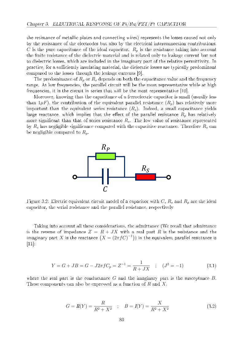
Chapter 3. ELECTRICAL RESPONSE OF Pt/Ru/PZT/Pt CAPACITOR
the resistance of metallic plates and connecting wires) represents the losses caused not onlyby the resistance of the electrodes but also by the electrical interconnection contributions.C is the pure capacitance of the ideal capacitor. Rp is the resistance taking into accountthe nite resistance of the dielectric material and is related only to leakage current but notto dielectric losses, which are included in the imaginary part of the relative permittivity. Inpractice, for a suciently insulating material, the dielectric losses are typically predominantcompared to the losses through the leakage currents [9].
The predominance of Rp or Rs depends on both the capacitance value and the frequencyrange. At low frequencies, the parallel circuit will be the most representative while at highfrequencies, it is the circuit in series that will be the most representative [10].
Moreover, knowing that the capacitance of a ferroelectric capacitor is small (usually lessthan 1µF ), the contribution of the equivalent parallel resistance (Rp) has relatively moreimportant than the equivalent series resistance (Rs). Indeed, a small capacitance yieldslarge reactance, which implies that the eect of the parallel resistance Rp has relativelymore signicant than that of series resistance Rs. The low value of resistance representedby Rs has negligible signicance compared with the capacitive reactance. Therefore Rs canbe negligible compared to Rp.
Figure 3.2: Electric equivalent circuit model of a capacitor with C, Rs and Rp are the idealcapacitor, the serial resistance and the parallel resistance, respectively
Taking into account all these considerations, the admittance (We recall that admittanceis the reverse of impedance Z = R + JX with a real part R is the resistance and theimaginary part X is the reactance
(X = (2πfC)−1)) in the equivalent parallel resistance is
[11]:
Y = G+ JB = G− J2πfCp = Z−1 =1
R + JX; (J2 = −1) (3.1)
where the real part is the conductance G and the imaginary part is the susceptance B.These components can also be expressed as a function of R and X.
G = R(Y ) =R
R2 +X2; B = I(Y ) =
X
R2 +X2(3.2)
80

3.1. Electrical Measurement Processes
Thus, by using the real and imaginary axes projections of the complex admittance Y (pha-sor diagram) and the relationship between the susceptance B and capacitance C, one candetermine respectively:
tanδ = R/X ; Cp = X/(2πf.
(R2 +X2
))(3.3)
From Cp, tanδ and geometric parameters of the capacitors (thickness d and surface A), itis possible to obtain the expressions of ε
′r and ε
′′r
ε′
r = Cp.d/ (ε0.A) ; ε′′
r = ε′
r.tanδ (3.4)
During this thesis, capacitance and loss tangent measurements using LCR-Meter HP4284AAgilent are performed by sweeping the bias between −10V and +10V , which superimposedan alternating signal with an amplitude of 100mV and frequency at 10kHz. In order toobtain reliable electric results, for each PZT (PZT10, PZT15, PZT20 and PZT30) samples,several capacitors (13 capacitors) have been studied. In the following, we will present theaverage result of these statistical studies.
3.1.2 Breakdown Voltage (Field) Measurement
Electrical shorting in FE capacitor i.e. breakdown, results in sudden and permanent dam-age of the dielectric. The breakdown is manifested by the formation of a conductive pathbetween the conducting parallel plates, which causes high current ow through the di-electric. The mechanism of breakdown is a complex phenomenon. Three mechanisms ofbreakdown are distinguished: intrinsic or electronic breakdown, thermal breakdown andavalanche breakdown [12]. However, in the case of dielectrics obtained under carefully con-trolled conditions without any defects, the breakdown strength called intrinsic breakdownoccurs at very high electric eld. However, real dielectrics often fail under electric eldstresses below intrinsic breakdown values due to the extrinsic defects, which are linked onexternal causes, particularly related to defects.
In real dielectrics two types of defect can be distinguished: the intrinsic defects, whichare related to the specic properties of the dielectric material (vacancies, dislocations, grainboundaries) and the extrinsic defect, which are based on external causes like particles con-tamination during material deposition or damages caused during integration process stepslike dry etching and passivation deposition.
Regarding to the intrinsic breakdown, two models have been developed to explain thismechanism. A qualitative model presented by Suñé et al. [13] is based on two parameters:critical number of defects and the area of unit cells. This statistical model is based on therandom generation of defects into the bulk of dielectric under the inuence of the appliedelectric eld. Thus, the breakdown process starts when a critical number of defects isreached in one of the elementary cells. To locally reach this critical number of defects,a total number of defects will be created throughout the volume of the oxide leading to
81

Chapter 3. ELECTRICAL RESPONSE OF Pt/Ru/PZT/Pt CAPACITOR
the breakdown of dielectric by the creation of the conduction path between the electrodes.However, the model of Suñé is limited by the fact that it considers only the cases where thedefects appear at the interface level.
Figure 3.3: Illustration of the percolation model. (a) As a rst step, the defects (emptycircle) are randomly generated in the dielectric. (b)Defects overlap or come into contact withthe electrodes agglomerates as referred by the black lled circle (c) Finally, the breakdownis triggered when a percolation path between the two electrodes is formed. [9]
The model proposed by Degraeve et al. [14] to supplement the Suñé model is basedon percolation model. In the percolation model, the defects are represented by sphereswith a constant radius. When electrical eld is applied, the defects are created in the di-electric at random positions. As soon as the two electrodes are connected by overlappingspheres (clusters creation), a conducting path is formed for electrons and the breakdowncondition is reached as illustrated in Figure 3.3. Parameters introduced in this quantitativemodel are the total density of defects generated in the dielectric until breakdown, the sizeof these defects, and the percentage of occupied defects. From percolation model, Chentiret al. [15] have established a direct correlation between the physical properties of defects(voids, interfaces defects, etc.) and the breakdown statistics of PZT capacitors. They showthat percolation defects, which appears under electric eld, participate in the creation ofthe breakdown path. Note that, in PZT thin lm the main defects take origin either theoxygen-vacancies (VO) or the Pb-vacancies (VPb) [16, 17, 18, 19].
During this thesis, breakdown eld (voltage) measurements was carried out using LinearRamp Voltage Stress (LRVS) [9] test (∆V=0.5 V and ∆t=0.5 s) and Weibull statisticalanalysis. As shown in Figure 3.4 (a-b), the current as a function of voltage for the PZT10before and after post metallization annealing were measured by using a Keithley 2400 sourcemeter unit interfaced with a computer to perform the measurement and record data. Withan appropriate trigger on the current, the voltage at which the capacitor has shorted canbe detected and recorded. Short Circuit is dened for an abrupt current increase, typicallygreater than a decade in a single voltage step. The criterion of the short Circuit chosenfor a capacitor of size (80 × 80)µm2 is 1 mA. As the breakdown eld follows a probabilitylaw (Weibull statistical analysis [20, 21, 22, 23]), by cumulating short Circuit data over 90capacitors tested per wafer, the repartition function can be tted and breakdown voltagecan be extracted.
82

3.1. Electrical Measurement Processes
It is very important to note that the choice of the voltage step and the delay time valuesused during this thesis is to determine the breakdown voltage (eld) values for each sampleand not for studying the dierent leakage current mechanisms in the samples. Indeed, forcurrent-voltage measurements, the voltage step (0.5 V) and the delay time (0.5 s) may benot very appropriate [9]. The voltage step is relatively large which may induce transientcurrents and the delay time may be not long enough to measure true leakage current,with no parasitic contributions from transient currents. However, a real current-voltagemeasurement, which requires time dependent current measurement to establish the rightdelay time and the real leakage current values, is not the main goal of this work.
Figure 3.4: The density of current of PZT10 as a function of electric eld: (a) before and (b)after post metallization annealing. Electric eld (Voltage) was applied to a certain value in asuccessive voltage step of 0.5 V with delay time of 0.5 s, until the leakage current increasedsharply and abruptly, indicating the occurrence of breakdown. (c) Determination of thebreakdown eld (voltage) before and after post metallization annealing of PZT10 throughWeibull distribution [21]. (Note: PZT10 means PZT with 10 % of lead excess)
For breakdown eld, experimental data are plotted according to a two-parameter Weibulldistribution. The cumulative failure probability is dened as
P (EBD) = 1− exp
[−(EBD
α
)β]
(3.5)
where P (EBD) is the cumulative probability of failure occurring at the electric eld lower orequal to EBD. EBD is the electric eld obtained by dividing the breakdown voltage by the
83

Chapter 3. ELECTRICAL RESPONSE OF Pt/Ru/PZT/Pt CAPACITOR
thickness of the sample. The α scale parameter of scale factor is the nominal eld, i.e. theeld corresponding to a 63.2 % breakdown cumulative probability for the sample and, whilethe shape parameter or shape factor β evaluates the scatter of data. The experimental plotmust be a straight line in a coordinate system:
X = EBD
Y = Ln
[Ln
(1
1− P
)](3.6)
From Figure 3.4 (c), linear regression was used to determine β which is 13.9 and 17.5for PZT10 before and after post metallization annealing respectively. According to thepercolation theory [24, 25, 26], the β value is related to the critical defect density that isnecessary to reach for triggering the breakdown. EBD is obtain when the Y reach zero whichcorrespond also to α = 63.2 % of breakdown cumulative probability for the sample. EBD
values are 1.60 and 2.09 MV/cm for PZT10 before and after PMA, respectively.
3.2 Pb Excess and Post Metallization Annealing Eects
Studies including eg Wang et al. [27], have shown that with below 10 % of Pb excesscontent in the target, ferroelectric and dielectric properties of PZT thin lms fall drastically,whereas with above 30 % of Pb excess content in the target, no dielectric constant responsesare obtained. Even though, no lead oxides were detected by XRD analyses for the lmsfabricated with 30 % and 40 % excess PbO. Wang et al. suggested that the residual Pbremains at the grain boundaries of PZT lm in the form of small particles of amorphousPbO. These amorphous PbOs seem to be at the origin of the poor properties. These resultscan be correlated with the data from Yanovskaya et al. [6] which show a decrease of thecapacitance when the Pb excess is below 10 % and above 30 %.
Furthermore, post metallization annealing shows very crucial importance in the perfor-mance of the MIM structures. Kim et al. [28] showed a better saturation of the polarizationafter post metallization annealing. Taylor et al. [29] described a possible electro-migrationof the Ruthenium from the top electrode down to the lm during thermal treatment. Al-Shareef et al. [7] observed that annealing the entire capacitor stack after the top electrodedeposition improved ferroelectric properties. It described also the possible creation of thePb2Ru2O7−X conductive layer under annealing ruthenium oxide and PZT interface. Thepresence of the Pb2Ru2O7−X between the Metal/PZT interface leads to the increase of theleakage current values but enhanced the ferroelectric properties [30, 31, 32, 33].
Based on the various results provided by Wang et al. [27], Vorotilov et al. [34] andYanovskaya et al. [6] but also on the impact of the thermal treatment of the entire capacitor,we will study the eects of Pb excess and the post metallization annealing in the electricalresponses of the Pt/Ru/PZT/Pt capacitors. Figure 3.5 (a) shows the measurement bench.
84

3.2. Pb Excess and Post Metallization Annealing Eects
Figure 3.5: Actual electrical measurements bench
3.2.1 Dielectric Constant and Loss Tangent
In this section, we will study the value of the capacitance density and Loss tangent as afunction of the lead excess content and the post metallization annealing eects.
(a) Dielectric Constant and Loss Tangent Before PMA
Using the electrical set up, capacitance measurements were carried out on Pt/Ru/PZT/-Pt stacks as shown in Figure 3.6. The experimental data from dielectric constant-voltagecurves are presented in Figure 3.6 (a)) with an oset for better clarity the presentation ofdata. Curves show the characteristic buttery loop of a ferroelectric. Buttery loop are notsymmetric about zero voltage but they display a high asymmetry along voltage axis with ashift toward the positive voltage relatively to the zero bias . This shift is 0.75 V for PZT30whereas it is at 0.875 V for PZT10, PZT15 and PZT20, indicating a downwards pointingimprint polarization for all grown lms. Note that the shift along the negative voltage axis isobtained when the bias is applied on the top electrode and the bottom electrode connectedto the ground as we will see in chapter 5 in section 5.5 page 132. Finally, like the dielectricconstant, loss tangent curves are shifted towards the positive voltage as seen in Figure 3.6(b)).
Maximum dielectric constant and maximum loss tangent values obtained on each sample(as a function of the Pb excess used on the rst and the fourth layers during the PZT thinlm deposition) are recorded and reported in Figure 3.7. Maximum dielectric constant valueshows a net increase (9 %) from 1126 to 1225 between PZT with 10 to 20 % lead excessrate. A maximum dielectric constant value of 1195 is registered for PZT with 15 % of Pbexcess. Beyond the 20 % of lead excess, the maximum dielectric constant decreases. Indeed,
85

Chapter 3. ELECTRICAL RESPONSE OF Pt/Ru/PZT/Pt CAPACITOR
introduction of 30 % of Pb excess leads to a dielectric constant of 1193. The variations ofpermittivity values as a function of Pb excess amount are signicant as seen in Figure 3.7.These results are consistent with the assertion that, the ne tuning of Pb content in PZTlms may participate in the optimization of the capacitance density of capacitors.
Figure 3.7 shows also that the increase of the excess of Pb in the PZT matrix presentsa positive aspect on the values of the maximum loss tangent. Indeed, the addition of Pbexcess from 10 to 15 % favors the decrease of the maximum dielectric losses from 4.53 to4.09 %. Another signicant drop in losses occurred between 20 and 30 % of Pb, from 4.04 to3.67 % is also noted. The variation of maximum loss tangent values might be attributed tothe energy loss due to the current displacement in the dielectric. This situation can stronglydepend on the thin lm microstructure such as grain boundaries and also the defects in thethin lm. According to the literature, the high amount of traps (VO and VPb) under voltagemight behave as a conduction channel. In Figure 3.7, the loss tangent decreases when thelead excess rate increases, which re-establish the stoichiometry of PZT by reducing thedefects density, vacancies or traps inside the PZT.
Figure 3.6: Dielectric constant and Loss tangent before post metallization annealing asfunction of voltage for dierent Pb excess rate used on the rst and the fourth layers duringthe PZT thin lm deposition
According to the data from literature, the Pb evaporation during thermal treatment ofsol-gel PZT induces the development of the secondary phase at the surface or in the bulkof PZT lm [27, 35, 36]. In fact, secondary or parasitic phases at the surface are oftendescribed as a non-FE phase such as pyrochlore [27] with a lower dielectric constant andare usually presumed to be at the origin of dead layers observed at the metal/insulatorinterface. These dead layers tend therefore to modify the electrical properties of capacitordevices. It is important to underline that the composition of the surface of the samples(mixture of PZT and secondary phase) obtained before deposit of the top electrodes shouldnot change after deposit of the top electrodes, except in the case where a thermal treatmentunder oxygen of the Metal/PZT interface is performed.
Furthermore, from results presented in Figure 3.7, we conclude that there exist an op-timum of Pb excess between 15 % and 20 %. This optimum of Pb excess allows to reachthe optimal value of εr. In fact, below the optimum of the Pb excess rate, parasitic phaseor dead layer might be created and above this optimum value of Pb content the thin lm
86

3.2. Pb Excess and Post Metallization Annealing Eects
might present a residual cluster of PbO because the Pb oxide is often accumulated in theintercrystalline and interface layers of the lms. Both situations favor the decrease of thecapacitance density of PZT as seen with the PZT in 10 % and 30 % of Pb excess.
Figure 3.7: Maximum of dielectric constant and maximum loss tangent values before postmetallization annealing as function of voltage for dierent Pb excess rate used on the rstand the fourth layers during the PZT thin lm deposition
The presence of strongly positive shift of buttery curve (dielectric constant-voltage andloss tangent-voltage) suggests the presence of the imprint eect [37, 38, 39, 40] in the MFMwhich is certainly linked to the creation of internal electrical elds. In fact, the internalelectric elds can be explained by several mechanisms [41], such as (i) defects domainspinning, which is due to the charge alignment or accumulation of charged defects, (ii)complex vacancies present at domain walls, that can screen the polarization state of PZT,and cause domain pinning, or by interface charge injection. Additionally, the use of dierentelectrode materials for bottom and top contacts, which induces two types of Schottky barrier(asymmetric barrier heights), might participate to the creation of the imprint eect. Thisinternal eld (or Imprint) is obtained by making the ratio between the dierence potentialon thickness of the PZT. However, by considering the large thickness of the PZT (220 nm),it is unlikely that this asymmetry plays an important role on the capacitors. Indeed, theImprints observed in samples are between 34.0 and 39.8 kV/cm in contrast to the eectdue to the asymmetry which is of the order of 10 kV/cm. Furthermore, if the asymmetryeects played an important role on capacitors, the value of the Imprint is expected to remainalmost identical for all samples.
Chen et al. [42] suggests that the shift of the dielectric constant-voltage curve observedon PZT can be caused by charge injection into defect states (traps), which modies thelocal potential of interface and shifts the buttery loop.
Furthermore, the presence of internal interfaces created inside the PZT sample duringthe dierent steps of PZT layer deposition (e.g. between the bulk with 10 % of Pb excessand the interface layers with higher Pb excess (10, 15, 20 and 30 % of Pb excess)) can
87

Chapter 3. ELECTRICAL RESPONSE OF Pt/Ru/PZT/Pt CAPACITOR
contributed to appearance of the internal eld and therefore to the imprint of butterycurves.
Considering PZT as a p-type semiconductor is equivalent to setting up a depletion layerwidth between the PZT and the electrode, resulting a non-zero internal electrical eld. Ithas been also suggested that a thin layer with low dielectric constant interfacial layer canbehave as the dead layer present at the interface , which can induce imprint behavior inthe ferroelectric capacitors [43]. Teowee et al. [44] showed that defects in PZT lms, suchas VO and VPb, play an important role since they are mobile under electrical stress and canmigrate to the PZT-electrode interface or grain domain boundaries. This assertion is inagreement with the results of Lee et al. [45], which shows the hysteresis ferroelectric curveshifted by the presence of oxygen vacancy at the interface metal/BaTiO3.
(b) Dielectric Constant and Loss Tangent After PMA
Figure 3.8 shows dielectric constant and loss tangent after post metallization annealing(550C for 30 min at room temperature) of each PZT (with Pb excess rate used on the rstand the fourth layers during the PZT thin lm deposition) based capacitor. We remark thatthe characteristics of ferroelectric buttery loop after post metallization annealing (PMA)showed a symmetric curves relative to 0 V. The fact that the dielectric constant and losstangent buttery curves become symmetrical is related to the impact of PMA because theother parameter have not been modied.
Maximum loss tangent values obtained after PMA of PZT10, PZT15, PZT20 and PZT30capacitors (Figure 3.8 (b)) are 4.51, 4.36, 3.72 and 3.08 %, respectively. These data showreduction of the maximum loss tangent values relative to the samples before PMA. However,these results are keeping the same trend as the function of the lead excess content in thePZT layers.
Figure 3.8: Dielectric constant and Loss tangent after post metallization annealing as func-tion of voltage for dierent Pb excess rate used on the rst and the fourth layers during thePZT thin lm deposition
Furthermore, after PMA of the Pt/Ru/PZT/Pt stack, maximum dielectric constant of1198, 1284, 1257 and 1227 have obtained respectively for PZT10, PZT15, PZT20 and PZT30(results from Figure 3.8 (a)). These values of maximum dielectric constant are compared
88

3.2. Pb Excess and Post Metallization Annealing Eects
with the maximum dielectric constant values obtained before PMA as illustrated in Figure3.9.
The enhancement of dielectric constant independently of the Pb excess after PMA canbe linked to several phenomena [46]. First, the eects of thermal annealing might inducehigher densication [47] of the PZT thin lm capacitors. Uhlmann [48] shows that thesize of the grain increases when the post metallization is performed from 100 to 700Cwhich tend to decrease the number of grain boundaries. This may favor an enhancementof capacitance (dielectric constant). Furthermore, PMA may favor the migration of theoxygen-vacancies (VO) or the Pb-vacancies (VPb) [16, 17, 18, 19] containing in the PZT thinlm towards the top electrode which induces a decrease of defect and therefore improvesthe performance. PMA might also favor diusion of residual PbO clusters at the interfacesbetween the polycrystalline PZT lm and the top electrode because up to 350C the leadoxide tends to evaporate as described by Uhlmann [48]. Bao et al. [49] explained thatthe dierence of the electrical performance can be linked by the fact that polarization maypenetrate more deeply into an oxide electrode than in the metal electrode. This results insmaller depolarizing elds at the interfaces with oxide electrodes than at the interfaces withmetal electrodes. In our case, post metallization annealing might also lead to oxidation ofRu top electrode [50, 51, 52].
Finally, observation of a symmetry of the buttery after PMA suggest the no-existenceof the imprint eect in the capacitors. This situation may be explained by the reductionof the internal electric eld either at the level of metal/PZT interfaces or at the level ofinternal interfaces inside the PZT samples (due to the multiple solgel deposition steps).This symmetry of the buttery may be also associated by the modication of the Schottkybarrier heights at the level of metal/PZT interfaces after PMA.
Figure 3.9: Comparison of maximum Dielectric constant values before and after post met-allization annealing (PMA) as a function of the Pb excess rate used on the rst and thefourth layers during the PZT thin lm deposition
3.2.2 Breakdown Field
The breakdown elds measured before and after PMA on PZT capacitors samples withdierent Pb excess rate are shown in Figure 3.10. Regardless the Pb excess content in the
89

Chapter 3. ELECTRICAL RESPONSE OF Pt/Ru/PZT/Pt CAPACITOR
precursor, there is an improvement of the breakdown voltage value after thermal treatmentunder O2 during 30 min at 550C relative to the results obtained before post metallizationannealing. Indeed, before post metallization annealing, the increase of the Pb excess contentin sol-gel precursors from 10 to 15 % leads to slight increase (from 1.60 to 1.68 MV/cm) ofthe breakdown eld. Then, higher excess of lead (for 20 % and 30 %) induces the decreaseof the breakdown eld to 1.57 and 1.26 MV/cm respectively. With annealing process (reddash line), there is a decrease of the breakdown eld from 2.09 MV/cm to 1.81 MV/cm for10 % and 30 % respectively. An intermediate value (1.94 MV/cm) is obtained for both 15and 20 % lead excess.
The results obtain in Figure 3.10, might be in agreement with the percolation theorydeveloped Degraeve et al. [14]. Indeed, with a lower rate of Pb excess such as in PZT10 caninduce a presence of high number of oxygen-vacancies (VO) or the Pb-vacancies (VPb) whichcan favor the creation of conduction path. Furthermore, increasing the lead excess contentin the precursors solution such as in PZT30, favors the generation of PbO clusters in thebulk at the level of grain boundaries which behaves as conduction way and thus favor thebreakdown process [53].
Figure 3.10: Breakdown Field as function of the Pb excess rate used on the rst andthe fourth layers during the PZT thin lm deposition: (Black) before post metallizationannealing and (Red) after post metallization annealing
3.3 Conclusion
In this chapter, both eects of Pb excess content and post metallization annealing on elec-trical properties of dielectric constant, loss tangent and breakdown eld from the Pt/Ru/-PZT/Pt were presented.
Permittivity results show an optimum between 15 and 20 % of Pb depending on boththe lead excess and the post metallization annealing. The decrease of the dielectric constantfor the PZT10 and PZT30 might be attributed to the presence of the secondary phase bothinterface metal/PZT and the bulk of PZT thin lm. Loss tangent reduction due to theincrease of the part of Pb excess in the precursor solution is observed. This might be linked
90

3.3. Conclusion
to the reduction of the defect (vacancies) which can favor the current conduction. With thepost metallization annealing, the lost tangent evolution shows the same behavior as the onebefore thermal treatment whereas the values of the dielectric constant increases. Finally,we have shown that the high content of lead excess leads to the reduction of the breakdowneld value. These situation might be linked with the high residual lead excess when the Pbexcess is very high.
In the subsequent chapters, we will try to understand how Pb precursor excess andPMA modied the electric results. This is achieved by using primarily photoelectron spec-troscopy to probe the PZT surface (XPS), interface (HAXPES) chemistry, and nally byusing SEM, TEM and XRD for better understanding the physicochemical, structural andmicrostructural changes.
91

Chapter 3. ELECTRICAL RESPONSE OF Pt/Ru/PZT/Pt CAPACITOR
Bibliography
[1] F. Calame and P. Muralt. Growth and properties of gradient free sol-gel lead zirconate titanatethin lms. Applied Physics Letters, 90(6):062907, 2007.
[2] V. PhD Universite Grenoble Alpes Kovacova. Study of correlations between microstructureand piezoelectric properties of PZT thin lms. 2015.
[3] H. D. Chen, K. R. Udayakumar, C. J. Gaskey, and L. E. Cross. Electrical properties maximain thin lms of the lead zirconatelead titanate solid solution system. Applied Physics Letters,67(23):34113413, 1995.
[4] C. B. Carter and M. G. Norton. Ceramic Materials-Science and Engineering. 53(9), 2013.
[5] S. Trolier-McKinstry and P. Muralt. Thin Film Piezoelectrics for MEMS. Journal of Electro-ceramics, 12(1/2):717, 2004.
[6] M. I. Yanovskaya, I. E. Obvintseva, L. I. Solovyova, E. P. Kovsman, K. A. Vorotilov, andV. A. Vasilyev. Alkoxy-derived ferroelectric PZT lms: The eect of lead acetate dehydrationtechniques and lead content in the electrochemically prepared solutions on the properties ofthe lms. Integrated Ferroelectrics, 19, 1998.
[7] H.N. Al-Shareef, K.R. Bellur, O. Auciello, and A.I. Kingon. Phase evolution and annealingeects on the electrical properties of Pb(Zr0.53Ti0.47)O3 thin lms with RuO2 electrodes. ThinSolid Films, 256(1-2):7379, 1995.
[8] D. Henry, F. Jacquet, M. Neyret, X. Baillin, T. Enot, V. Lapras, C. Brunet-Manquat, J. Char-bonnier, B. Aventurier, and N. Sillon. Through silicon vias technology for CMOS image sensorspackaging. In 2008 58th Electronic Components and Technology Conference, pages 556562.IEEE, 2008.
[9] E. Defay. Ferroelectric Dielectrics Integrated on Silicon . 2011.
[10] Y. A. Gagou . Etude du changement de phase dans le composé PbK2LiNb5O15 de la familledes TTB. PhD thesis, 2002.
[11] Ch. Huber. Synthèse et caractérisation de nouveaux matériaux ferroélectriques accordablespour applications hyperfréquences. (French). PhD thesis, 2003.
[12] J. F. Scott, B. M. Melnick, L. D. McMillan, and C. A. P. De Araujo. Dielectric breakdown inhigh-ϵ lms for ULSI DRAMs. Integrated Ferroelectrics, 3(3):225243, 1993.
[13] J. Suñé, I. Placencia, N. Barniol, E. Farrés, F. Martín, and X. Aymerich. On the breakdownstatistics of very thin SiO2 lms. Thin Solid Films, 185(2):347362, 1990.
[14] R. Degraeve, G. Groeseneken, R. Bellens, J.L. Ogier, M. Depas, P.J. Roussel, and H.E. Maes.New insights in the relation between electron trap generation and the statistical properties ofoxide breakdown. IEEE Transactions on Electron Devices, 45(4):904911, 1998.
[15] M. T. Chentir, J. B. Jullien, B. Valtchanov, E. Bouyssou, L. Ventura, and C. Anceau. Perco-lation theory applied to PZT thin lms capacitors breakdown mechanisms. MicroelectronicsReliability, 49(9-11):10741078, 2009.
[16] R. Moazzami, C. Hu, and W.H. Shepherd. Electrical characteristics of ferroelectric PZT thinlms for DRAM applications. IEEE Transactions on Electron Devices, 39(9):20442049, 1992.
92

Bibliography
[17] J. F. Scott, C. A. Araujo, B. M. Melnick, L. D. McMillan, and R. Zuleeg. Quantitativemeasurement of spacecharge eects in lead zirconatetitanate memories. Journal of AppliedPhysics, 70(1):382388, 1991.
[18] I. K. Yoo and S. B. Desu. Mechanism of Fatigue in Ferroelectric Thin Films. Physica StatusSolidi (a), 133(2):565573, 1992.
[19] H. M. Duiker, P. D. Beale, J. F. Scott, C. A. Paz de Araujo, B. M. Melnick, J. D. Cuchiaro,and L. D. McMillan. Fatigue and switching in ferroelectric memories: Theory and experiment.Journal of Applied Physics, 68(11):57835791, 1990.
[20] R. A. Schlitz, K. Yoon, L. A. Fredin, Y. Ha, M. A. Ratner, T. J. Marks, and L. J. Lauhon.Weibull Analysis of Dielectric Breakdown in a Self-Assembled Nanodielectric for Organic Tran-sistors. The Journal of Physical Chemistry Letters, 1(22):32923297, 2010.
[21] V. Tomer, E. Manias, and C. A. Randall. High eld properties and energy storage in nanocom-posite dielectrics of poly(vinylidene uoride-hexauoropropylene). Journal of Applied Physics,110(4):044107, 2011.
[22] K. Wu, Y. Wang, Y. Cheng, L. A. Dissado, and X. Liu. Statistical behavior of electricalbreakdown in insulating polymers. Journal of Applied Physics, 107(6):15, 2010.
[23] C. Chauvet and C. Laurent. Weibull Statistics in Short-term Dielectric Breakdown of ThinPolyehtylene Films. IEEE Transactions on Electrical Insulation, 28(1):1829, 1993.
[24] E.Y. Wu and R. P. Vollertsen. On the weibull shape factor of intrinsic breakdown of dielectriclms and its accurate experimental determination-part I: theory, methodology, experimentaltechniques. IEEE Transactions on Electron Devices, 49(12):21312140, 2002.
[25] J. H. Stathis. Percolation models for gate oxide breakdown. Journal of Applied Physics,86(10):57575766, 1999.
[26] R. Degraeve, G. Groeseneken, R. Bellens, J.L. Ogier, M. Depas, P.J. Roussel, and H.E. Maes.New insights in the relation between electron trap generation and the statistical properties ofoxide breakdown. IEEE Transactions on Electron Devices, 45(4):904911, 1998.
[27] Z. J. Wang, K. Kikuchi, and R. Maeda. Eect of Pb content in target on electrical properties oflaser ablation derived lead zirconate titanate thin lms. Japanese Journal of Applied Physics,Part 1: Regular Papers and Short Notes and Review Papers, 39(9 B):54135417, 2000.
[28] B. J. Kim, J. Lee, J. B. Yoo, and K. S. No. Pb(Zr,Ti)O3 lms fabrication by sol-gel methodfor piezoelectric actuated device. Ferroelectrics, 232(1):247252, 1999.
[29] D.J. Taylor, J. Geerse, and P.K. Larsen. Fatigue of organometallic chemical vapor depositedPbZrxTi1xO3 thin lms with Ru/RuO2 and Pt/Pt electrodes. Thin Solid Films, 263(2):221230, 1995.
[30] H.N. Al-Shareef, Y.L. Chen, O. Auciello, and A.I. Kingon. Microstructural and ElectricalProperties of Ferroelectric Capacitors with Pt/RuO2 Hybrid Electrodes. MRS Proceedings,361:229, 1994.
[31] H. L. Ee and W. L. Ee. Preparation and Characterization of Pb(Zr,Ti)O3 Films Deposited onPt/RuO2 Hybrid Electrode for Ferroelectric Random Access Memory Devices. Jpn. J. Appl.Phys., 40(11):65666573, 2001.
93

Chapter 3. ELECTRICAL RESPONSE OF Pt/Ru/PZT/Pt CAPACITOR
[32] N. J. Seong, K. J. Choi, and S. G. Yoon. Thickness eect of Pb2Ru2O7x conductive interfaciallayers on ferroelectric properties of Pt/Pb(Zr0.35Ti0.65)O3/Pt capacitors. Thin Solid Films,468(1-2):100104, 2004.
[33] S. Ryoo, S. Yoon, and S. Kim. Improvement in ferroelectric properties of Pb(Zr0.35Ti0.65)O3
thin lms using a Pb2Ru2O7−x conductive interfacial layer for ferroelectric random accessmemory application. Applied Physics Letters, 83(14):28802882, 2003.
[34] K.A. Vorotilov, M.I. Yanovskaya, L.I. Solovjeva, A.S. Valeev, V.I. Petrovsky, V.A. Vasiljev, andI.E. Obvinzeva. Ferroelectric capacitors for integrated circuits. Microelectronic Engineering,29(1-4):4144, 1995.
[35] J. Wang, J.M. Xue, D.M. Wan, and B.K. Gan. Mechanically Activating Nucleation andGrowth of Complex Perovskites. Journal of Solid State Chemistry, 154(2):321328, 2000.
[36] A. D. Polli, F. F. Lange, and C. G. Levi. Metastability of the Fluorite, Pyrochlore, and Per-ovskite Structures in the PbO-ZrO2-TiO2 System. Journal of the American Ceramic Society,83(4):873881, 2004.
[37] W. L. Warren, D. Dimos, G. E. Pike, B. A. Tuttle, R. Raymond, M. V. nad Ramesh, andJ. T. Evans. Applied Physics Letters.
[38] M. Grossmann, O. Lohse, D. Bolten, U. Boettger, T. Schneller, and R. Waser. The interfacescreening model as origin of imprint in PbZrxTi1−xO3 thin lms. I. Dopant, illumination, andbias dependence. Journal of Applied Physics, 92(5):26802687, 2002.
[39] J. J. Lee, C. L. Thio, and S. B. Desu. Retention and imprint properties of ferroelectric thinlms. Physica Status Solidi (a), 151(1):171182, 1995.
[40] A. Gruverman, B. J. Rodriguez, A. I. Kingon, R. J. Nemanich, A. K. Tagantsev, J. S. Cross,and M. Tsukada. Mechanical stress eect on imprint behavior of integrated ferroelectric ca-pacitors. Applied Physics Letters, 83(4):728730, 2003.
[41] Y. Zhou, H. K. Chan, C. H. Lam, and F. G. Shin. Mechanisms of imprint eect on ferroelectricthin lms. Journal of Applied Physics, 98(2):024111, 2005.
[42] H. Chen and J. Y. Lee. Electron trapping process in ferroelectric leadzirconatetitanate thin-lm capacitors. Applied Physics Letters, 73(3):309311, 1998.
[43] A. K. Tagantsev and G. Gerra. Interface-induced phenomena in polarization response offerroelectric thin lms. Journal of Applied Physics, 100(5):051607, 2006.
[44] G. Teowee, C. D. Baertlein, E. A. Kneer, J. M. Boulton, and D. R. Uhlmann. Eect of topmetallization on the fatigue and retention properties of Sol-gel PZT thin lms. IntegratedFerroelectrics, 7(1-4):149160, 1995.
[45] H. Lee, T. H. Kim, J. J. Patzner, H. Lu, J.W. Lee, H. Zhou, W. Chang, M. K. Mahanthappa,E. Y. Tsymbal, A. Gruverman, and C. B. Eom. Imprint Control of BaTiO3 Thin Films viaChemically Induced Surface Polarization Pinning. Nano Letters, 16(4):24002406, 2016.
[46] K. Kushida-Abdelghafar, M. Hiratani, and Y Fujisaki. Post-annealing eects on antireduc-tion characteristics of IrO2/Pb(ZrxTi1−x)O3/Pt ferroelectric capacitors. Journal of AppliedPhysics, 85(2):10691074, 1999.
94

Bibliography
[47] J. L. Cao, A. Solbach, Y. Fang, U. Boettger, P. J. Schorn, R. Waser, and U. Klemradt.Eects of Thermal Annealing on Lead Zirconate Titanate Thin Film Capacitors with PlatinumElectrodes. Journal of The Electrochemical Society, 154(11):G251, 2007.
[48] D. R. Professor Uhlmann. Air force oce of scientic research by university of arizona. Tech-nical report, 1994.
[49] P. Bao, T. J. Jackson, X. Wang, and M. J. Lancaster. Barium strontium titanate thin lmvaractors for room-temperature microwave device applications. Journal of Physics D: AppliedPhysics, 41(6):063001, 2008.
[50] K.J. Choi and S.G. Yoon. Eect of Pb2Ru2O7−x (PRO) conductive interfacial layers on ferro-electric properties of Pt/Pb(Zr0.35Ti0.65)O3/Pt capacitors for nonvolatile memory applications.Applied Physics A, 81(4):855859, 2005.
[51] S. Kim, D. Park, H. Woo, D. Lee, J. Ha, and C. S. Hwang. Eects of IrO2/Pt Hybrid Electrodeson the Crystallization and Ferroelectric Performances of Sol-gel-derived Pb(Zr,Ti)O3 ThinFilm Capacitors. Journal of Materials Research, 17(07):17351742, 2002.
[52] K.T. Jacob, V.S. Saji, and Y. Waseda. Standard Gibbs energy of formation of Pb2Ru2O6.5.Journal of Materials Research, 22(05):11741181, 2007.
[53] X. Tan and J. K. Shang. In-situ transmission electron microscopy study of electric-eld-inducedgrain-boundary cracking in lead zirconate titanate. Philosophical Magazine A, 82(8):14631478, 2002.
95

Chapter 4
SURFACE CHEMISTRY IN PbPRECURSOR-RICH Pb(Zr0.52Ti0.48)O3
SOL-GEL THIN FILMS
Contents4.1 Pb(Zr0.52Ti0.48)O3 Surface with 30 % Pb Excess . . . . . . . . . 97
4.2 X-ray Photoelectron Spectroscopy . . . . . . . . . . . . . . . . . 98
4.3 Investigations of Surface Chemistry . . . . . . . . . . . . . . . . 100
4.3.1 XPS Measurement at Normal Emission . . . . . . . . . . . . . . . 101
4.3.2 Angle dependent XPS investigations . . . . . . . . . . . . . . . . . 103
4.3.3 Depth Prole by Ion Beam Etching . . . . . . . . . . . . . . . . . . 104
4.3.4 X-ray Diraction Analysis . . . . . . . . . . . . . . . . . . . . . . . 107
4.3.5 Discussion . . . . . . . . . . . . . . . . . . . . . . . . . . . . . . . . 108
4.4 Nanostructures as a Function of the Pb Excess . . . . . . . . . 112
4.4.1 Scanning Electron Microscopy . . . . . . . . . . . . . . . . . . . . . 112
4.4.2 X-ray Photoelectron Spectroscopy . . . . . . . . . . . . . . . . . . 113
4.4.3 X-ray Diraction . . . . . . . . . . . . . . . . . . . . . . . . . . . . 115
4.4.4 Discussion . . . . . . . . . . . . . . . . . . . . . . . . . . . . . . . . 116
4.5 Conclusion . . . . . . . . . . . . . . . . . . . . . . . . . . . . . . . . 118
Bibliography . . . . . . . . . . . . . . . . . . . . . . . . . . . . . . . . . . 119
From chapter 3, the electrical responses of Pt/Ru/PZT/Pt capacitors have been strongly mod-ied by the Pb excess content and the post metallization annealing. Breakdown eld and losstangent are decreasing with the increase of the lead excess from 10 to 30 % and the maximum ofdielectric constant shows an optimum between 15 % and 20 % as the function of the post met-allization annealing. Electric data obtained on both dielectric constant and breakdown eld havebeen enhanced after post metallization annealing.
96

4.1. Pb(Zr0.52Ti0.48)O3 Surface with 30 % Pb Excess
In addition to the eects induced by the bulk, the electrical responses of Metal-ferroelectric-Metal capacitors can be strongly aected by the chemical composition of the interfaces as describedin the literature [1, 2, 3, 4]. In fact, the Metal-ferroelectric can present nonstoichiometric interfaciallayer or secondary phase with no ferroelectricity or low dielectric constant [5]. this can prevent theoptimal function of Metal-ferroelectric-Metal capacitors. However, for the ferroelectric capacitorbased on the PZT thin lm, the Pb excess content in the sol-gel solution during the depositionprocess can be used to control the amount of the secondary (or parasite) phase at the surface ofthe PZT thin lms.
In this context, the main objective of this chapter is to study the chemical composition of thesecondary phase and the mechanisms involved in its creation. By exploiting the extreme sensitivityand the relative ability to quantify the elements oered by X-ray photoelectron spectroscopy (asdescribed in Figure 4.1 and chapter 2 section 2.4.1 page 56), the characterization of the PZThave been performed.
In order to achieve this goal, rst we will analyze the surface of the deposited PZT barewith 30 % of Pb excess (PZT30) which should be without a secondary phase according tothe results published by Grader et al. [6]. Then, we will compare the surface states of thePZT thin lm bare for dierent Pb excess content (10 % and 30 %). Finally, we will expandthis characterization to the intermediate Pb excess content i.e. with 15 % and 20 % of Pbexcess.
Figure 4.1: Schematic description of the XPS probing with 90 take-o angle (angle betweenthe surface sample and the detector axe).
4.1 Pb(Zr0.52Ti0.48)O3 Surface with 30 % Pb Excess
The surface of PZT deposited with 30 % of Pb excess and its cross-sectional microstructurewere analyzed with a high-resolution scanning electron microscopy (SEM). As already shownby Grader et al. [6], our PZT30 sample (deposited at CEA-LETI) presents only large grains,distributed over the whole surface with well-dened grain boundaries as seen in Figure 4.2(a). The grain size varies from 40 nm to 250 nm. The surface is clean with no other visible
97

Chapter 4. SURFACE CHEMISTRY IN Pb PRECURSOR-RICH Pb(Zr0.52Ti0.48)O3
SOL-GEL THIN FILMS
grain types (dierent to the large PZT grains). Cross-sectional microstructure presented inFigure 4.2 (b) allows to demonstrate a perfect deposition process of the PZT30. We remarkalso a perfect adhesion of the PZT30 layer on the substrate. The PZT30 lm was ∼ 220nm thick and Pt bottom electrode ∼ 100 nm thick.
Figure 4.2: SEM images of PZT30 as deposited (or bare) (a) surface microstructure imageand (b) cross section image
4.2 X-ray Photoelectron Spectroscopy
The survey performed from 0 to 1200 eV in binding energy with energy step of 0.1 eV areshown in Figure 4.3 (a). Constant analyzer energy (CAE) mode is used to collect the elec-trons. The pass energy of the analyzer is held at a constant value of 30 eV. The energyresolution is 0.37 eV. All of the expected core level peaks for PZT are present. The surveyreveals several interesting region with Pb 4f, Zr 3d, Ti 2p3/2 and O 1s core levels, which aredetected at 137.5, 180.5, 457.2 and 528.7 eV, respectively. These values are in agreementwith data found in NIST X-ray Photoelectron Spectroscopy Database.
High resolution core level analysis of Pb 4f, Zr 3d, Ti 2p3/2 and O 1s presented in Fig-ure 4.3 (b - e) was carried out with the pass energy at 10 eV and the energy resolution of0.27 eV. Using the tabulated sensitivity factors of each element, the relative composition ofPb, Zr, Ti and O with a take-o angle of 90 are 21.9, 3.4, 15.6 and 59.1 %, respectively.From these results, we can see a relative dierence between the nominal composition (i.e.expected theoretical ratio of Pb1.3(Zr0.52Ti0.48)O3) and the real composition as shown inTable4.1. The amount of Pb and O at 21.9 and 59.1 %, respectively are almost identical tothe nominal composition. Contrary to the Pb and O, we have a high decrease of the amountof Ti and increase of the relative concentration of Zr compared to the nominal composition.We have a weak percent of Ti (3.4 rather than 9.6) conversely to the Zirconium which is at15.6 % rather than 10.4 %.
Shirley background and Gaussian-Lorentzian mixing line-shape functions were used fortting each core level. Respectively, we have used (30-70), (30-70), (50-50) and (40-60) forPb, Ti, Zr and O. Full width at half maximum (FWHM) for all spectra are also obtained
98

4.2. X-ray Photoelectron Spectroscopy
with 0.89, 0.73, 0.85 and 0.95 eV for the Pb 4f, Zr 3d, Ti 2p3/2 and O 1s, respectively.
Figure 4.3: XPS measurements of PZT30 (a) survey spectrum and core level spectra for b)Pb 4f; c) Ti 2p3/2 d) Zr 3d and e) O 1s
Further, except the components from the PZT30 thin lm (Pb 4f, Zr 3d, Ti 2p3/2 andO 1s), we can also observe in Figure 4.3 (a) the presence of carbon (C 1s). The mainC 1s peak at 284.4 eV reects the presence of adventitious surface carbon. In fact, byusing the Relative Sensitivity Factors (RSF, provided by ScientaOmicron) and data fromthe measured peak area with a takeo angle of 90 and 30 as illustrated in Figure 4.4, wesuccess to estimate the relative concentration of the carbon at the surface of PZT30 sampledepending on the takeo angle. These results are 22.1 and 30.3 % for the takeo angle of90 and 30, respectively. These data support that the carbon is localized at the surface of
99

Chapter 4. SURFACE CHEMISTRY IN Pb PRECURSOR-RICH Pb(Zr0.52Ti0.48)O3
SOL-GEL THIN FILMS
the sample rather than into the bulk.
Elementary composition of PZT30 (%)Nominal composition Real composition
Lead 20 (+ Pb excess content) 21.9Zirconium 9.6 3.4Titanium 10.4 15.6Oxygen 60 59.1
Table 4.1: Synthetic table of nominal and real composition of the PZT30
Following previous results from the SEM and XPS, for the PZT30 without any secondaryphases, in the next section, we will study the impact of Pb excess content on the surfacestate of samples [6]. For this purpose, we will begin by comparing the microstructures ofPZT containing 10 and 30 % of Pb excess.
Figure 4.4: XPS measurements of C 1s peak at the surface of the PZT30 as function of theTOA
4.3 Investigations of Surface Chemistry
Surface comparison of PZT10 and PZT30 by SEM is illustrated in Figure 4.5 (a - b). Thesurface of PZT10 has a similar underlying grain structure similar to that of PZT30. Inaddition, the PZT10 is covered by a large number of nanoparticles. The size of thesenanostructures or parasitic phase varies between 5 and 25 nm with an average size around15 nm. Using Image J, the nanostructures cover around 10 to 20 % of the total surfaceas the function of the basic threshold chosen. A closer inspection (Zoom of 1/4 of thesurface) suggests that the nanostructures tend to be predominantly located along the grainboundaries rather than in the center of the large grains. The XPS chemical analysis mightallow to elucidate the composition of the nanostructures.
100

4.3. Investigations of Surface Chemistry
Figure 4.5: SEM images of as deposited (a) PZT30 and (b) PZT10. The scale bar is thesame for both images.
4.3.1 XPS Measurement at Normal Emission
The Pb 4f, Zr 3d, Ti 2p3/2 and O 1s core level spectra recorded at normal emission (TOA= 90) on the PZT10 and PZT30 are shown in Figure 4.6 (a - d) and the results of the bestts to the data are given in Table4.2.
The Pb 4f7/2 binding energy (137.5 eV) is identical for both PZT10 and PZT30 as illus-trated in Figure 4.6 (a). The single Pb component is attributed to Pb2+ ions in the PZTperovskite structure. No other chemical state of Pb is observed. Similarly, the Ti 2p3/2binding energy (457.2 eV) is unchanged between PZT30 and PZT10 and is attributed toTi4+ ions in the PZT matrix as seen in Figure 4.6 (b). The FWHM of the Pb 4f7/2 and theTi 2p3/2 emission are 0.89 eV and 0.73 eV, respectively.
The Zr 3d core level spectrum, shown in Figure 4.6 (c), changes dramatically between10 % and 30 % Pb excess. For the PZT30 sample, it shows a single chemical state labelledZrI with a Zr 3d5/2 binding energy of 180.5 eV. In contrast, for 10 % Pb excess, there is anadditional component denoted ZrII at 181.5 eV binding energy. ZrI , common to both PZT30and PZT10, is related to Zr4+ ions in the PZT perovskite structure. ZrII , shifted by 1 eV tohigher binding energy, seems to be correlated with the appearance of nanostructures at thesurface of PZT10, as seen in Figure 4.5 (b). This suggests a dierent chemical compositionof nanostructures with respect to that of PZT.
101

Chapter 4. SURFACE CHEMISTRY IN Pb PRECURSOR-RICH Pb(Zr0.52Ti0.48)O3
SOL-GEL THIN FILMS
Figure 4.6: XPS core level spectra for a) Pb 4f; b) Ti 2p3/2 c) Zr 3d and d) O 1s. Open circlesare the experimental points, red lines the best t, colored peaks the dierent components.In each panel, the upper (lower) spectrum is that of PZT10 (PZT30). The main peak I (lightgray, turquoise online) is the perovskite structure; gray peak II (magenta online) surfacephase and low intensity, peaks green surface contaminations.
The O 1s shown in Figure 4.6 (d), has several distinct core level components. The mainpeak, OI at 528.70 eV is attributed to O2− in the PZT perovskite structure and is commonto both PZT10 and PZT30. For PZT10, there is a second peak at 529.40 eV. Finally, thegreen peak for O is present in both samples with weak shift. The green peaks are attributedto surface contamination [7, 8] which are linked to the presence of the carbon contaminationat the surface.
Core-Levels Gaussian-Lorentzian PZT30 PZT10BE (eV) FWHM (eV) BE (eV) FWHM (eV)
Pb 4f7/2 30-70 137.5 0.89 137.5 0.89Ti 2p3/2 30-70 457.2 0.73 457.2 0.73Zr 3d5/2 50-50 180.5 0.85 180.5 0.85Zr 3d5/2 - - 181.5 1.02O 1s (I) 40-60 528.7 0.95 528.7 0.95O 1s (II) - - 529.4 1.18
Table 4.2: Pb 4f, Zr 3d, Ti 2p3/2 and O 1s line shapes, binding energies and FWHM of thets shown in Figure 4.6 for PZT30 and PZT10
102

4.3. Investigations of Surface Chemistry
4.3.2 Angle dependent XPS investigations
In order to clarify the assignment of the ZrII component to a surface secondary phase, adepth prole of elements in near surface layers were performed from Angle Resolved XPS(chapter 2 section 2.4.1 page 56). PZT10 was analyzed at TOA of 90 and 30.
This Angle Resolved XPS measurement will enable us to highlight the components lo-cated at the extreme surface in relatively to the slightly buried elements. Results corre-sponding to Pb 4f, Zr 3d, Ti 2p3/2 and O 1s core level spectra at TOA of 30 are shown inFigure 4.7 (a - d), and compared with the normal emission case.
Figure 4.7: XPS ore level spectra of PZT10 as a function of take-o angle a) Pb 4f; b) Ti2p3/2 c) Zr 3d and d) O 1s. Symbols and color code as in Figure 4.6
The binding energy does not change as a function of take-o angle. Only a relativevariation of intensities of the Zr and O core level components I and II is remarked. At30 the ZrII intensities increase signicantly relative to the ZrI component (by 48 % withrespect to normal emission), which is in good agreement with the expected enhanced surfacesensitivity at 30 take-o angle (probing depth is halved). The same twofold increase isobserved for the OII peak as presented in Table4.3. At 30 take-o angle the OII intensityincreases by 49 % with respect to the intensity at normal emission. As the only eect ofchanging the take-o angle is to change the surface sensitivity, this is clear evidence thatboth Zr and O are related to a surface specic phase. We can therefore conclude that bothZrII and OII are surface-related peaks. These latter are also related with the appearanceof nanostructures observed at the surface of PZT10.
103

Chapter 4. SURFACE CHEMISTRY IN Pb PRECURSOR-RICH Pb(Zr0.52Ti0.48)O3
SOL-GEL THIN FILMS
PZT30 PZT1090 30 90 30
Pb 21.9 25.3 20.9 20.3Ti 3.4 2.8 4.3 3.6ZrI 15.6 14.8
11.3 7.3ZrII 6.8 8.3OI 36.7 34.5OII 59.1 57.1 12.4 15.7
O (green) 7.6 10.3
Table 4.3: PZT composition based on the XPS intensities at 90 and 30 take-o angles forboth as deposited PZT30 and PZT10
4.3.3 Depth Prole by Ion Beam Etching
In order to enhance the interpretation of additional ZrII and OII peaks and to demonstratethe link between the presence of secondary phases (SEM) and ZrII and OII peaks (XPS),another trick is used. Total etching of the surface of PZT10 has been carried out and allnanostructure phases have been removed. Ion beam etching (IBE) of the PZT10 (withnanostructures at the surface) was performed by utilizing the NEXUS 350A machine during45s. After the etching process using pure Ar gas, the measurement of thickness shows thatit has been removed around 20 nm thick of PZT. Moreover the nano-grains have vanishedand the surface has become perfectly smooth as reported in Figure 4.8. The etching damageand nanostructure removal are supported by the XPS results presented below.
Figure 4.8: SEM image of PZT10 after ion beam etching.
After IBE, the surface is smooth without any detectable nanostructure, as can be seen inFigure 4.8. Therefore the etching treatment has removed the additional surface phase. The
104

4.3. Investigations of Surface Chemistry
absence of a clear grain structure is due to the amorphization of the surface, well-knownin the literature [8, 9, 10, 11]. IBE can also reduce the surface [11, 12] in which case onewould expect a shift in the electronic levels similar to that induced by n-type doping ofsemiconductors. In order to compare the core level spectra before and after IBE, we haveto correct the energy scale and aligned the core level spectra by using the VBMs.
Figure 4.9 shows the valence band spectra before and after etching. The position of thevalence band maximum (VBM) is determined by a straight line extrapolation [13]. Afteretching, the VBM shifts from 1.17 to 1.94 eV and the density of states in the band gap ap-pear. The latter is associated with the creation of O vacancies which, schematically, donate2 free electrons to the PZT lattice, reducing neighboring B-type cations, usually Ti. Theresulting n-type doping pins the Fermi level near the bottom of the conduction band. Thisresult in a rigid shift of all electronic levels to higher binding energy.
In Figure 4.10, we compare the Pb 4f, Zr 3d, Ti 2p3/2 and O 1s core level spectra, beforeand after IBE. In the Pb 4f spectrum, a new component at lower binding energy appears,and corresponds to reduce Pb at 136.07 eV as described by Lu and Zhu [14]. Similarly, apartial reduction of Ti is evidenced with an additional component to lower binding energy(TiII at 456.64 eV), as also observed previously [12]. Both results provide chemical conr-mation of the surface reduction after IBE.
Figure 4.9: Valence band maxima of PZT10 before (blue) and after IBE (red)
More importantly, the surface related to the components ZrII and OII disappear afteretching. IBE removes 20 nm thickness of PZT, i.e, well above the photoelectron escape
105

Chapter 4. SURFACE CHEMISTRY IN Pb PRECURSOR-RICH Pb(Zr0.52Ti0.48)O3
SOL-GEL THIN FILMS
depth. We can conclude that the ZrII and OII components observed before etching aredirectly correlated with the surface nanostructures. Finally, we observe a broadening ofFWHM of about 0.2 eV for all spectra of PZT after etching as illustrated in Table4.4.
This is probably due to IBE induced surface amorphization, which is responsible forthe absence of the grain as can be observed in Figure 4.8. The broadening induced by theamorphization is mainly due to Ar ion bombardment. A morphology change leads to thecrystal damage and displacement of the lattice atoms [11, 15, 16] and thus to the transitionsfrom the crystal phase to the amorphous phases.
Figure 4.10: PZT10 a) Pb 4f; b) Ti 2p3/2 c) Zr 3d and d)O 1s core level spectra before andafter ion beam etching. Open circles are the experimental points, continuous (red) lines thebest t. Color coding of the core level components as for Figure 4.6.
Otherwise, with IBE, as can be seen in Table4.5 a large decrease of the Pb from 20.9to 8 and an increase of the Zr after etching are observed. The Ti and O increase slightly.This situation is strongly linked with dierence collision cross sections between argon ionsand target atoms (Pb, Ti, Zr and O) as a function of the target and the energy of theargon atoms. Indeed, using individual metal targets of Pb, Zr and Ti for deposition ofPZT thin lms, Krupanidhi et al. [17] showed that Pb has a higher Sputtering rate underargon bombardment than Zr and Ti, which induce a higher deposition rate on the substrate.These results are in agreement with lower concentration of Pb on the surface of the PZT10under argon bombardment during the IBE process.
106
4.3. Investigations of Surface Chemistry
Core Levels Before Etch After EtchBE (EV) FWHM (eV) BE (EV) FWHM (eV)
Pb 4f7/2 (I) 137.5 0.89 137.5 1.11Pb 4f7/2 (II) - - 136.07 0.89Ti 2p3/2 (I) 457.2 0.73 457.2 0.95Ti 2p3/2 (II) - - 456.64 0.95Zr 3d5/2 (I) 180.5 0.85 180.5 1.05Zr 3d5/2 (II) 181.5 1.02 - -O 1s (I) 528.7 0.95 528.7 1.14O 1s (II) 529.4 1.18 - -
Table 4.4: Pb 4f, Zr 3d, Ti 2p3/2 and O 1s line shapes, binding energies and FWHM ofPZT10 before and after ion beam etching
In addition to the angle resolved XPS and IBE experiment, grazing incidence X-raydiraction (GIXRD) was also carried out to obtain the texture information regarding nanos-tructures at the surface of PZT10. The link between surface microstructure and crystalorientation of PZT bulk has been studied by using standard X-ray diraction as will bepresented in the next part.
Pb Ti Zr OPZT30 before Etch 21.9 3.4 15.6 59.1PZT10 before Etch 20.9 4.3 18.1 56.7PZT10 after Etch 8 5.9 27 58.1
Table 4.5: Relative composition of PZT30 before etch, PZT10 before and after ion beametching as quantied by XPS using the tabulated RSFs
4.3.4 X-ray Diraction Analysis
The θ/2θ scans in Figure 4.11 (a) show peaks characteristic of PZT (at the level of the rst-order reexion), the Si substrate and the Pt electrode. The X-ray diraction XRD revealsseveral structural dierences between PZT10 and PZT30. With 10 % Pb excess content dur-ing deposition, the sample is almost fully (100) oriented. Increasing the Pb excess from 10to 30 % leads to a modication of the structure i.e. the PZT lm is strongly (111) oriented.Finally, the peak at 31.2 in Figure 4.11 (a) corresponds to the PZT (110) orientation. Bytaking into account only the area of diraction peaks and the data provided by the JointCommittee on Powder Diraction Standards [JCPDS] card for the PZT, the comparison ofpeaks from PZT10 and PZT30 lms showed that the (100), (110) and (111) orientation are93.2, 2.6 and 4.2 % for PZT10 and 18.4, 21.5 and 60.2 % for PZT30, respectively.
Moreover, electrical performances of PZT based capacitors show a crystallographic ori-entation dependence. Ehara et al. [18] demonstrated that the saturation polarization ofPZT can be modied by the simple tilting angle of the polar axis of the perovskite cellwhich depends on the crystallographic orientation. Furthermore, the variation dielectric
107

Chapter 4. SURFACE CHEMISTRY IN Pb PRECURSOR-RICH Pb(Zr0.52Ti0.48)O3
SOL-GEL THIN FILMS
constant values of capacitors as a function of the Pb excess may be partially attributedto the dierences of polarization states, including the growth mode of domains, the tiltingangle of the polar axis and the degree of polarization inversion of PZT thin lms when theorientation passes mainly from (100) to (111) as observed in the BaTiO3 [19].
In order to highlight the crystallographic composition of the surface of PZT10 and PZT30layer relative to the bulk, Grazing Incidence XRD (GIXRD) tool is used. GIXRD results arepresented in Figure 4.11 (b). Contrary to the θ/2θ scans, the GIXRD is carried out by xingboth the incoming x-ray beam and the detector of diracted beam at 0.5 relative to thesample surface as already illustrated in chapter 2 section 2.2 page 50. It allows to enhancethe sensibility of the surface relative to the bulk and therefore provides better informationof the surface texture.
Data from GIXRD show that in addition to the crystallographic orientation of the PZTfrom the rst-order reexion ((100), (110) and (111)), we also have the the second-orderreexion ((200), (201), (211) and (220)) when increasing the angle. Furthermore, we observethree peaks respectively at 34 (for (200)), 58 (for (-222)) and 61.5 (for (-302)) in PZT10which will be attributed to the surface phase (or nanostructures based on the ZrOX) [20][21]. These reection correspond to monoclinic ZrOX crystal phase [JCPDS Card No. 37-1484]. There is also one peak at 28 for both samples which corresponds to the relativelyintense kβ stimulated peak of the PZT (110).
Figure 4.11: XRD scans at (a) θ/2θ geometry of PZT10 (top, red) and PZT30 (bottom,blue) (b) XRD scans at grazing incidence of PZT10 (top, red) and PZT30 (bottom, blue)
4.3.5 Discussion
The comparative study between PZT10 and PZT30 reveals several very important aspects.The determination of the composition of nanostructures based on ZrOx and the variationof the crystallographic orientation as a function of the Pb level are highlighted. However,the origin of the presence of ZrOx on the surface of the PZT as seen in Figure 4.5 (b) is afairly complex process.
108

4.3. Investigations of Surface Chemistry
Using RSFs we can quantify the surface stoichiometry measured by XPS. The quantica-tion reveals several important features. First, a slight Pb enrichment at the surface for bothPZT10 and PZT30 is observed. This is expected since the excess Pb is used in both cases,which is greater than the stoichiometric value of 20 %. As expected, the surface enrichmentis stronger for PZT30. The higher Pb content at PZT30 surface appears, which is correlatedwith the complete disappearance of the nanostructures. This suggests that the addition ofPb allows completion of the PZT reaction which consumes all of the other precursors andinhibits the formation of the chemically distinct nanostructures. The O content is slightlydepleted, possibly as a result of the high annealing temperature for crystallization. As seenin Figure 4.7, both ZrI and OI decrease at the surface for PZT10 and at the same time theZrII and OII concentrations increase. O (green) is included to show that their weight alsoincreases at the surface, consistent with the assignment to the surface contamination.
The presence of the nanostructures at the grain boundaries can be understood by thefact that, the formation of the perovskite phase starts from a seed and proceeds by out-ward, lateral growth. It then enlarges by transforming the remaining precursors into theperovskite phase between 500C and 700C via three dimensional growth [22]. When the Pbprecursor is exhausted, the reaction stops abruptly. Any residual precursors remaining atthe grain boundaries become available to form a secondary phase since the TiO2 precursor isconsumed rst. Therefore, the resulting secondary phase nanostructures will be Zr-enriched[23, 24].
XRD shows that high Pb excess modies the preferential (100) orientation to a mixedstate dominated by (111), in agreement with previous results [25, 26]. Despite the dierenceof Pb excess, in both cases the reacted PbO has formed the perovskite which is dierentfrom the secondary phase which not includes Pb. Furthermore, the nanostructures appearonly at the surface (according to the prolometric analysis carried out by ion beam etchingtool). They are presumably formed at the end of the PZT growth and therefore do notinuence the crystallographic orientation.
The surface Zr content of PZT10 is 15.6 %, while for PZT30 is 14.8 %. This shows thatthere is slightly more Zr at the surface of PZT10. As can be seen from Table4.3, the Zrsurface enrichment is due to the ZrII component. On the basis of the ZrII and OII corelevel intensities, we can estimate the ZrOx composition. The OII/ZrII ratio for TOA at 90
gives x = 1.82 (i.e. ZrO1.82), whereas at 30 the OII/ZrII ratio gives x = 1.89 (i.e. ZrO1.89).The formal valence state of Zr in both PZT and ZrO2 is 4+. It is therefore surprising thata Zr rich surface oxide shows a distinct core level binding energy with respect to that of Zrin PZT.
Furthermore, the XPS data from the literature shows that the Zr binding energy is 181.4± 0.1 eV in PZT [10, 22, 27, 28, 29, 30, 31, 32, 33, 34, 35, 36, 37, 38, 39] and 182.4 ± 0.3 eVin ZrO2 [40, 41, 42, 43, 44, 45, 46, 47, 48, 49]. These results are in excellent agreement with1 eV shift measured here. Beyond the immediate chemical environment of the Zr emitter,two other eects may inuence the BE shift. First, in a simple picture of electron trans-fer following relative electronegativity, the second neighbor interactions, could modify theelectron transfer between ZrO-Ti. The electronegativity of Zr, Ti and O basis of Pauling's
109

Chapter 4. SURFACE CHEMISTRY IN Pb PRECURSOR-RICH Pb(Zr0.52Ti0.48)O3
SOL-GEL THIN FILMS
scale are 1.33, 1.54 and 3.44, respectively. For Zr-O, a charge transfer are produced fromthe outer core level of Zr to the O atom. Thus to compensate this charge transfer, the innercore level of the Zr are attracted towards the nucleus which leads the increase of the bindingenergy. Secondly, we are considering 15 nm nanostructures, with a much higher surface tovolume ratio and probable shorter interatomic distances. These might inuence the corelevel shift. Here some rst principles calculations or even tight binding cluster calculationswould be useful to conrm this interpretation.
The core level XPS analyses as a function of the precursor composition, emission angleand ion beam etching demonstrate that the nanostructures at the PZT10 surface are a Zir-conium oxide, ZrO1.82−1.89.
The XPS results are conrmed by XRD scans at grazing incidence (Figure 4.11 (b)). Theintensities centered on 34, 58 and 61.5 on the PZT10 sample are not visible on the PZT30sample and can be attributed to ZrO2-like monoclinic structure [20]. Using a Scherrer tto the 61.5 peak width, the diameter of grains is in the range of 15 nm, and is in goodagreement with the nanograin size estimated from the SEM image shown in Figure 4.5 (b).The Scherrer formula allows to relate the particle sizes or crystallite sizes in a material tothe broadening of a peak in a diraction pattern [50].
Furthermore, the presence of 10 % of Pb excess in PZT leads to the formation of surfacenanostructures, preferentially localized at the grain boundaries. This secondary phase hasbeen attributed to the incomplete reaction of ZrO2 precursor [51] resulting from the oppo-site slopes in the concentration gradients of Ti and Zr during the growth of sol-gel layers[23, 52]. The major portion of Ti incorporated into each layer is consumed at the beginningof nucleation, consistent with the known crystallization temperatures. This process leadsto a dramatic reduction of Ti surface concentration and increase of Zr as seen from thequantitative analysis of the XPS data in Table4.3. As a consequence of the gradient, thesurface of the layer is strongly Zr-enriched. The complete reaction for the growth of lead zir-conate titanate can be written in two stages: PbO + TiO2 → PbTiO3, followed by PbTiO3 +PbO + ZrO2 → Pb(Zr1−x,Tix)O3, where the initial precursors are PbO, TiO2 and ZrO2 [51].
ZrO2 is a good insulator with a static dielectric constant of 25 [53] and a band gapof 5.8 eV [54]. The presence of ZrO1.82−1.89 at the PZT/electrode interface of a capacitormight inuence electrical performance. Given the higher band gap with respect to PZT, adiscontinuous or continuous interfacial ZrO1.82−1.89 layer with lower dielectric constant [55]compared to PZT (dielectric constant > 1000) [56] will decrease device capacitance. ZrO2
is not ferroelectric, therefore a surface phase close to ZrO2 would act like a ferroelectricdead-layer (or paraelectric layer). In fact, with ZrO2 layer, several eects can take place.Indeed, a strong depolarization eld due to the uncompensated PZT surface charge by thetop electrode may occur due to the presence of ZrO2 layer and therefore reduce the ferroelec-tric polarization. For ideal metal, the polarization charges are perfectly compensated at theinterface and therefore no depolarization eld emerges in the ferroelectric lm. However, inreal case, the depolarization eld arising from the bound charges on the surface of the lmand at the interface with the metal is not fully compensated due to the insucient screeningby the free charges from the electrode and the presence of the non-ferroelectric layer. There-
110

4.3. Investigations of Surface Chemistry
fore, with the absence of sucient free charges from the electrode induce by the presenceof the paraelectric ZrO2 layer, the depolarization eld may increases and thus modify thecapacitor. Furthermore, according to Lichtensteiger et al. [57], the non-ferroelectric layersare also polarized in order to preserve the uniform polarization state and hence eliminatethe depolarization elds at the ferroelectric-paraelectric interface level. Thus taking intoaccount these probable impact of ZrO2 layer, we decided to analyze the eect of an ZrO2
layer at the interface Metal/PZT.
Dielectric constant and loss tangent measurements of PZT10 based capacitor were exe-cuted and presented in Figure 4.12. The PZT10 (PZT with 10 % of Pb excess) thicknessis 385 nm and top electrodes are 100 nm of Pt or Ru. Depending on the thickness ofthe interfacial layer of ZrO2 between the top electrode and the surface of PZT, electricalperformances are modied.
Figure 4.12: Dielectric constant depending on both ZrO2 thickness and top electrodes (fre-quency 10 kHz)
The dielectric constant and loss tangent curves are performed at room temperature be-tween -10 V to +10 V (superposed with a sinusoidal electric signal with amplitude of 100mV at the frequency of 10 kHz). The evolution of the maximum values of dielectric con-stant obtained in Figure 4.12 (a) is an interesting result. The Ru top electrode has a higherdielectric constant value than the Pt top electrode. Ru/PZT/Pt and Pt/PZT/Pt providea dielectric constant values of 1207 and 1159 respectively. The introduction of a 5 nm ofZrO2 interfacial layer induces a drop in the capacitance density of about 50 % relativelyto the sample without ZrO2 interfacial layer. Indeed, there are a decrease of the dielectricconstant of Ru/ZrO2/PZT and Pt/ZrO2/PZT up to 708.
However, positive eects are recorded with the presence of interfacial layer of ZrO2. Thisproduces a drastic reduction in the value of tangent of loss, which is a good advantage. In-deed, we observe a decrease from around 3.5 % to 2.5 %, i.e. a reduction of 50 % as can beseen in Figure 4.12 (b).
Figure 4.12 allows to underline three major conclusions. Firstly, the few dierence ofthe value of the dielectric constant between the PZT with Ru (100 nm) or Pt (100 nm) can
111

Chapter 4. SURFACE CHEMISTRY IN Pb PRECURSOR-RICH Pb(Zr0.52Ti0.48)O3
SOL-GEL THIN FILMS
be related to the electronic and chemistry bound at interfaces between top electrode-PZT[58, 59, 60].
Secondly, the low values of the constant dielectric of Zirconium oxide at the interface(Figure 4.12) can strongly aect the function of the top electrode-PZT/Pt structure withimpacts of almost 50 % of the dielectric constant. These results are in agreement with theexistence of a series capacitor model presented in section 1.4 page 37 chapter 1. Finally,ZrO2 as an interfacial layer can be considered as a barrier which reduces the energy loss(loss tangent) in the capacitor.
Thus, the formation of nanostructures is favored or inhibited by the Pb excess. However,the composition of these nanostructures has a more complex dependence on the processconditions. Systematic experiments as a function of several Pb excess content will be studiedin the last part of this chapter.
4.4 Nanostructures as a Function of the Pb Excess
The characterization of PZT10 surface chemistry by XPS reveals the presence of a parasiticphase of Zr oxide. Initial characterization of the PZT30 shows no surface nanostructures.However, the results presented in chapter 3 indicate a decrease of the dielectric constant(section 3.2.1 page 85) and breakdown voltage (section 3.2.2 page 89). In this section, weextend the study by varying the Pb excess content in order to manage mainly the surfacesecondary phase. We will analyze several PZT samples with 10, 15, 20 and 30 % of Pbexcess called PZT10, PZT15, PZT20 and PZT30, respectively. These samples with dierentPb excess are grown at mophotropic phase boundaries (Zr/Ti: 0.52/0.48) and in the samecondition as the PZT10 and PZT30 analyzed previously in this chapter.
4.4.1 Scanning Electron Microscopy
Figure 4.13 shows the surface microstructure of PZT depending to the Pb excess in sol-gelprecursors. From 10 to 30 % of Pb amount, SEM images show that the secondary phaseis strongly linked to the grain sizes and grain boundary numbers of PZT. The analysis ofPZT10 and PZT15 thin lms in Figure 4.13 (c-d) show the presence of small grains of ZrOx
which coexist with perovskite PZT grains. They also reveal that the shape of ZrOx is almostuniform and circular whereas the big grain sizes of PZT are inhomogeneous with a randomform. Diameter of parasitic phase can reached 40 nm caused by their gatherings. The meancrystallite size of secondary phase is always around 15 nm. These results are in agreementwith the average size determined by Epifani et al. [61]. Using Image J software, we noticedthat the proportions of the secondary structures at the surface are around 19.5 % and 15 %for PZT10 and PZT15, respectively.
112

4.4. Nanostructures as a Function of the Pb Excess
Figure 4.13: SEM images of as deposited (a) PZT30, (b) PZT20, (c) PZT15 and (d) PZT10.The scale bar is the same for all images.
PZT30 and PZT20 (Figure 4.13 (a-b)), show we have practically no Zr oxide at thesurface. The size of the large grains also increase with the Pb excess and the number ofgrain boundaries gradually decrease. Grain size of PZT are ranged from 40 nm to around350 nm. The average of PZT grains diameter are round 150 and 250 nm for PZT20 andPZT30 respectively. XPS can better quantify both the Zr oxide and PZT at the surfacerelatively to the Pb excess in the sol-gel solution.
4.4.2 X-ray Photoelectron Spectroscopy
The XPS analysis on PZT thin lm with 10, 15, 20 and 30 % Pb excess allows to follow thesecondary phase evolution and determine the optimum of the Pb excess, that, we shoulduse to vanish all ZrOx. All measurements are carried out with a TOA=70. Compositionof all elements (based on RSFs of each elements) are summarized in Table4.6.
Figure 4.14 (a-b) displays the Pb 4f5/2 (at 137.5 eV) and Ti 2p3/2 lines (at 457.2 eV)respectively and do not show any binding energy shift. The chemical state of Pb does notchange by passing from 10, 15, 20 and even up to 30 % excess of Pb. These data seem tobe in good agreement with the previous results from PZT10 and PZT30. From XPS, therelative concentration of Pb varies by 19.6, 24, 25.8 and 24.1 % for PZT10, PZT15, PZT20and PZT30 %, respectively. Figure 4.14 (b) reveals a low level of Ti at the surface of thePZT layers with 3.4, 2.8, 2.7 and 3.2 % for PZT10, PZT15, PZT20 and PZT30 respectively.The results of relative composition of PZT10 and PZT30 are dierent to section II of this
113
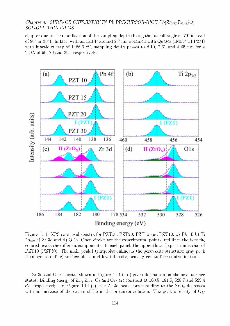
Chapter 4. SURFACE CHEMISTRY IN Pb PRECURSOR-RICH Pb(Zr0.52Ti0.48)O3
SOL-GEL THIN FILMS
chapter due to the modication of the sampling depth (xing the takeo angle at 70 insteadof 90 or 30). In fact, with an IMFP around 2.7 nm obtained with Quases (IMFP TPP2M)with kinetic energy of 1486.6 eV, sampling depth passes to 8.10, 7.61 and 4.05 nm for aTOA of 90, 70 and 30, respectively.
Figure 4.14: XPS core level spectra for PZT30, PZT20, PZT15 and PZT10. a) Pb 4f, b) Ti2p3/2 c) Zr 3d and d) O 1s. Open circles are the experimental points, red lines the best t,colored peaks the dierent components. In each panel, the upper (lower) spectrum is that ofPZT10 (PZT30). The main peak I (turquoise online) is the perovskite structure; gray peakII (magenta online) surface phase and low intensity, peaks green surface contaminations.
Zr 3d and O 1s spectra shown in Figure 4.14 (c-d) give information on chemical surfacestates. Binding energy of ZrI , ZrII , OI and OII are constant at 180.5, 181.5, 528.7 and 529.4eV, respectively. In Figure 4.14 (c), the Zr 3d peak corresponding to the ZrOx decreaseswith an increase of the excess of Pb in the precursor solution. The peak intensity of OII
114

4.4. Nanostructures as a Function of the Pb Excess
decreases during the variation of Pb excess rate as described in Table4.6. Regarding to thechemical states labeled ZrI and OI , any modication of the binding energy was registered.The relative concentration increases when the Pb concentration increases. The increasingintensities of Zr and O labeled I is correlated with a lowering of the secondary phase labeledII (ZrII and OII) at the surface. Finally, by associating the results on Zr and O shown inTable4.6 to nd the stoichiometry of the Zr oxide with TOA = 70, one have respectivelyZrO1.98, ZrO1.63 and ZrO1.61 for the PZT10, PZT15 and PZT20.
PZT30 PZT20 PZT15 PZT10Pb 24.1 25.8 24.0 19.6Ti 3.2 2.7 2.8 3.4ZrI 14.2 13.1 11.4 9.4ZrII - 2.6 5.2 7.1OI 50.3 43.1 38.7 35.9OII - 4.2 8.5 14.1
O (green) 8.2 8.5 9.4 10.5
Table 4.6: Composition of the PZT thin lms based on the XPS intensities at 70 take-oangle
4.4.3 X-ray Diraction
Even though secondary phase is based on the Zr oxide, the excess Pb content control stronglyzircon oxide concentration at the surface and the texturing of the PZT bulk. XRD mea-surements performed on all PZT thin lms reveal a mixed orientation between (100), (110)and (111) localized at 21.9, 31.0 and 38.3, respectively, as presented in Figure 4.15.
% Avarage orientationPZT30 PZT20 PZT15 PZT10
(100) 9.4 27.7 41.2 92.4(110) 3.3 2.2 1.9 0.4(111) 87.3 70.1 56.9 7.2
Table 4.7: Pb excess eect on the PZT crystallographic orientation
By increasing the Pb excess content from 10 to 30 % a gradual increase of (111) tex-ture and decrease of (100) are observed, which is in contrast with the resultsshowed byYanovskaya et al. [62], Cheng et al. [63], Tu et al. [64] and Wang et al. [65]. Compositionratios calculated according to the formula proposed by Harris [66] are summarized in Ta-ble4.7. From PZT10 to PZT15, an increase of orientation around 50 % (from 7.2 to 56.9 %)of (111) is observed. A decrease of more than 50 % for (100) texture with 92.4 % for PZT10and 41.2 % for the PZT15 is registered at the same time. The increase in (111) orientationas well as the decrease of (100) orientation are still observed on PZT15 and PZT20. Finally,(110) orientation observed in the MPB phase undergoes a continuous decrease from 3.3 to0.4 % when the Pb excess is reduced.
115

Chapter 4. SURFACE CHEMISTRY IN Pb PRECURSOR-RICH Pb(Zr0.52Ti0.48)O3
SOL-GEL THIN FILMS
Figure 4.15: XRD scans (θ−2θ) of PZT thin lms with dierent Pb excess content in sol-gelprecursors
4.4.4 Discussion
The large investigation of the Pb excess eect on the chemistry, microstructural surface andtexturing characteristics of PZT thin lms highlights several crucial points. Indeed, relativeto the high proceeding temperatures, Pb desorption remains high as long as sol-gel solutiondoes not crystallize into a compact lm of PZT. Therefore, solgel solution must contain Pbexcess to compensate its loss. Depending on the level of Pb excess used, PZT samples willexhibit important chemical and structural dierences after deposition.
XRD data reveals that the Pb excess inuences the nucleation process and determinetexture of PZT. This armation is based on the fact that the rst nanometers of PZT lmcontrol the phase and the texture (orientation) during the transition of PZT from amor-phous to perovskite phase. As observed by Seung-Hyun Kim et al. [67], the use of thin seedlayer of PbTiO3 allows to have a PZT with a preferred (100) texture.
The sol-gel PZT layer has a concentration of Zr and Ti as described by abergel et al.
[23] and Calame et al. [24]. The highest concentration of Ti is localized near the bottomof the layer and the Zr at the surface of the PZT layer. In others word, the major amountof TiO2 precursor reacts to PbO at the beginning of the sol-gel deposition (leading thecreation of PbTiO3) contrary to the ZrO2 precursor which is at the origin of the PbZrO3
perovskite. The phenomenon is linked to the crystallization temperature which increases inthe sequence PbTiO3 < PbZrO3 < Pb(ZrTi)O3 [68]. Furthermore, the favor (100) orienta-tion of PZT10 (PZT with 10 % of lead excess contain) is linked to preferential orientationof the rst layer of PbTiO3. These rst layers are often described to manage the thin lmsorientation as shown by Zeng et al. [69]. Additionally, for PZT with (100) orientation, thegrain nucleation energy is low, therefore, (100) phase was energetically favorable as reportedby Trolier-Mckinstry et al. [70].
116

4.4. Nanostructures as a Function of the Pb Excess
With the high Pb excess compensation in PZT30 presented in Figure 4.12 (a), a PtxPbintermetallic phase may be formed at the bottom interface (PZT/Pt). The PtxPb favors the(111) orientation. According to Wu et al. [71], the formation of the transient PtxPb phaseis related to the nature of the local thermodynamic conditions in the lm. Combustion ofthe organic groups of solgel precursors during pyrolysis may cause a temporary depletion ofO, causing locally reducing conditions. The reduction of Pb2+ to Pb and the reaction of Pbwith Pt to form the PtxPb phase is consequently favored.
Finally, Zhu et al. [72] showed that with the increase of Pb concentration, the preferredorientation of PZT lms changes from (100) for 0 %, (110) for 10 % and (111) for 20 %.They explain also that with 20 % of Pb excess, Pb−Pt intermetallic phase is easily formedand enhances (111) oriented lms. With PZT lm with 0 % of Pb excess, the compositionchanges quickly with the evaporation of (PbO), resulting to the formation (100) orientation.This situation is caused by the fact that with (100) orientation, the grain nucleation energywas energetically favorable as described by Tani et al. [73]. For Zhu et al. [72], the highpercentage of relative intensity of (110) is linked to the presence of moderate Pb excess (10%) and of annealing treatment near the quantum of PbO volatilization.
The parasite phase has its origin to the lack of Pb atom (PbO) for interacting with TiO2
or ZrO2 after a high evaporation process. With a gradient of Zr/Ti inside the lm, almostof Ti are already transformed at perovskite and the ZrO2 is found at the surface in the formof secondary phase. Pb loss process can stop the coalescence of the PZT grains [51]. This issupported by the decreasing of PZT grain size when the Pb excess in precursors pass from30 % to 10 %. For Hassold et al. [74] the decrease of PZT grain size is linked by the inertsecond-phase particles which is pinning grain boundaries and inhibit grain growth.
The presence of ZrO2 at the surface might behave as a lower permittivity dielectric inter-face layer and induce a reduction of the capacitance density when the Pb excess content istoo low like PZT10. However, with PZT30, the decline of the dielectric constant might alsobe linked with a high amount of Pb excess which is localized inside the PZT sample [62].In fact, under electrical stress, PbO might behave like the ZrO2 and reduce the capacitancevalue.
The loss tangent comportment can be attributed to the grain boundary which favor thecreation of defects or vacancies. The high number of grain boundaries allow to charge carri-ers to move from one electrode to another. This phenomenon induces dissipation of energyand increases the loss tangent. By increasing the Pb excess content, small grains aggregatereduces the number of grain boundary and decreases the loss tangent.
The decrease of the breakdown voltage of the PZT thin lm is linked to the presence ofthe PbO inside of the bulk as mentioned by Yanovskaya et al. [62]. In this context, withincreasing the Pb excess, the amount of the PbO increase and favor the generation of Pbcluster inside the ferroelectric which leads an early breakdown voltage. This situation leadsthe channels path as described by the percolation model and allows the current owingbetween one electrodes to another.
117
Chapter 4. SURFACE CHEMISTRY IN Pb PRECURSOR-RICH Pb(Zr0.52Ti0.48)O3
SOL-GEL THIN FILMS
Finally, the enhancement of the electric properties observed after PMA (referred chapter3) can be linked at several eects. The diusion (or the decrease) both the O/Pb vacanciesand residual PbO (often accumulated in the intercrystalline and interface layers of PZT)inside the PZT towards the Ru/PZT interface can allow to improve the electrical responses.
Furthermore, the modication of the internal interfaces inside the PZT samples (dueto the multiple solgel deposition steps) occurs at the level of the Ru/PZT interface withthe presence of the secondary phase (based on ZrO2−X) at the PZT surface under PMAprocess. This favors the improvement of the electrical performances of capacitors. Indeed,we can hypothesize the creation of alloy between the secondary phase ZrO2−X and the metalelectrode (Ru). This situation would lead to the disappearance of part of nanostructuresZrO2−X (with lower dielectric constant) at the interface and the creation of new phase whichmay be conductive. This conductive phase can improve the screening at the interface andthe shottky barrier. However, other studies at the level of the interfaces are necessary inorder to understand the evolution of the nanostructures and the interface Ru/PZT afterPMA process.
4.5 Conclusion
This chapter highlights the chemical composition of the PZT surface and the Pb excessdependence on the surface nanostructures. First part focuses on the determination of theparasitic phase composition. The photoemissions spectroscopy measurements of PZT10 andPZT30 are essential for the separation of the perovskite (PZT) and parasitic (ZrO1.82−1.89)phases. TOA study performed from 90 to 30 allows to distinguish the parasitic phase at thesurface and the PZT in the bulk. These results are supported by the grazing incidence X-raydiraction data. Ion beam etching study conrms that the ZrO1.82−1.89 is only localized atthe surface but not inside the PZT thin lms. Scanning electron microscopy increases thesize of PZT grain when the rate of Pb excess increase. X-ray diraction shows a change ofthe crystallographic orientation from mostly (111) to (100) when passing to 30 at 10 % ofPb excess.
The second part of this chapter is dedicated to the wide study of the evolution of PZTthin lm as the function of the Pb excess content. It is observed that with 10, 15, 20 and30 % of Pb excess, the secondary phase decreases and vanishes at the surface level. Fromscanning electron microscopy measurements, it is clear that the diminution of the para-sitic phase is followed by the increase of the grain size. Finally, the x-ray diraction showschange of the orientations respectively from (100) to (111) when the Pb excess rate increase.
In the next chapter, we will analyze the behavior of interface Metal-PZT stack dur-ing the switching polarization by using Hard x-ray photoelectron spectroscopy (HAXPES).This technique is a well-adaptable non-destructive method for the analysis of the electronicinterfaces buried of metal ferroelectric. These operando experiments provides importantinformations of the binding energies of all elements in the ferroelectric under the electricaleld.
118

Bibliography
Bibliography
[1] C. Zhou and D. M. Newns. Intrinsic dead layer eect and the performance of ferroelectric thinlm capacitors. Journal of Applied Physics, 82(6):30813088, 1997.
[2] C. K. Wong and F. G. Shin. Modeling of anomalous shift and asymmetric hysteresis behaviorof ferroelectric thin lms. Journal of Applied Physics, 96(11):66486656, 2004.
[3] M. Stengel and N. A. Spaldin. Origin of the dielectric dead layer in nanoscale capacitors.Nature, 443(7112):679682, 2006.
[4] L. J. Sinnamon, M. M. Saad, R. M. Bowman, and J. M. Gregg. Exploring grain size as a causefor dead-layer eects in thin lm capacitors. Applied Physics Letters, 81(4):703705, 2002.
[5] Q. Y. Xiang, K. Zhang, Y. Wang, X. J. Lou, W. Q. Yao, Y. Bai, D. W. Duan, X. P. Hu,J. Wang, Z. D. Luo, H. H. Wang, L. X. Zhang, U. Klemradt, and J. L. Cao. Insight intoMetalized Interfaces in Nano Devices by Surface Analytical Techniques. ACS Applied Materials& Interfaces, 7(49):2735127356, 2015.
[6] A. Etin, G. E. Shter, G. S. Grader, and G. M. Reisner. Interrelation of Ferroelectricity,Morphology, and Thickness in Sol-Gel-Derived PbZrxTi1−xO3 Films. Journal of the AmericanCeramic Society, 90(1):7783, 2007.
[7] J. L. Wang, F. Gaillard, A. Pancotti, B. Gautier, G. Niu, B. Vilquin, V. Pillard, G. L. M. P.Rodrigues, and N. Barrett. Chemistry and Atomic Distortion at the Surface of an EpitaxialBaTiO3 Thin Film after Dissociative Adsorption of Water. The Journal of Physical ChemistryC, 116(41):2180221809, 2012.
[8] J. D. Baniecki, M. Ishii, T. Shioga, K. Kurihara, and S. Miyahara. Surface core-level shifts ofstrontium observed in photoemission of barium strontium titanate thin lms. Applied PhysicsLetters, 89(16):162908, 2006.
[9] R.H. Liang, D. Rémiens, C. Soyer, N. Sama, X.L. Dong, and G.S. Wang. Etching characteris-tics and absence of electrical properties damage of PZT thin lms etched before crystallization.Microelectronic Engineering, 85(4):670674, 2008.
[10] J. K. Lee, T. Y. Kim, I. Chung, and S. B. Desu. Characterization and elimination of dryetching damaged layer in Pt/Pb(Z0.53Ti0.47)O3/Pt ferroelectric capacitor. Applied PhysicsLetters, 75(3):334336, 1999.
[11] J. N. Kim, K. S. Shin, D. H. Kim, B. O. Park, N. K. Kim, and S. H. Cho. Changes in chemicalbehavior of thin lm lead zirconate titanate during Ar+-ion bombardment using XPS. AppliedSurface Science, 206(1-4):119128, 2003.
[12] A. Bose and M. Sreemany. Inuence of processing conditions on the structure, compositionand ferroelectric properties of sputtered PZT thin lms on Ti-substrates. Applied SurfaceScience, 289:551559, 2014.
[13] S.A. Chambers, T. Droubay, T.C. Kaspar, M. Gutowski, and M. van Schilfgaarde. Accuratevalence band maximum determination for SrTiO3(001). 554(2-3):8189, 2004.
[14] T. J. Zhu and L. Lu. X-ray diraction and photoelectron spectroscopic studies of (001)-oriented Pb(Zr0.52Ti0.48)O3 thin lms prepared by laser ablation. Journal of Applied Physics,95(1):241247, 2004.
119

Chapter 4. SURFACE CHEMISTRY IN Pb PRECURSOR-RICH Pb(Zr0.52Ti0.48)O3
SOL-GEL THIN FILMS
[15] Y. Sakai, S. Ninomiya, and K. Hiraoka. XPS depth analysis of CuO by electrospray dropletimpact. Surface and Interface Analysis, 44(8):938941, 2012.
[16] A. M. Ektessabi and S. Hakamata. XPS study of ion beam modied polyimide lms. ThinSolid Films, 377-378:621625, 2000.
[17] S. B. Krupanidhi, H. Hu, and V. Kumar. Multiionbeam reactive sputter deposition of ferro-electric Pb(Zr,Ti)O3 thin lms. Journal of Applied Physics, 71(1):376388, 1992.
[18] Yoshitaka Ehara, Satoru Utsugi, Takahiro Oikawa, Tomoaki Yamada, and Hiroshi Funakubo.Crystal orientation dependency of ferroelectric property in rhombohedral Pb(Zr,Ti)O 3 lms.Japanese Journal of Applied Physics, 53, 2014.
[19] Wei Zhang, Hongbo Cheng, Qian Yang, Fangren Hu, and Jun Ouyang. Crystallographic orien-tation dependent dielectric properties of epitaxial BaTiO3 thin lms. Ceramics International,42(3):44004405, 2016.
[20] C. Lin, C. Zhang, and J. Lin. Phase Transformation and Photoluminescence Properties ofNanocrystalline ZrO2 Powders Prepared via the Pechini-type SolGel Process. The Journal ofPhysical Chemistry C, 111(8):33003307, 2007.
[21] Patricia María Perillo and Daniel Fabián Rodríguez. Anodization growth of self-organizedZrO2 nanotubes on zircaloy-4. Evaluation of the photocatalytic activity. Matéria (Rio deJaneiro), 20(3):627635, 2015.
[22] N. Wakiya, K. Kuroyanagi, Y. Xuan, K. Shinozaki, and N. Mizutani. An XPS study of thenucleation and growth behavior of an epitaxial Pb(Zr,Ti)O3/MgO(100) thin lm prepared byMOCVD. Thin Solid Films, 372(1-2):156162, 2000.
[23] J. Abergel, M. Allain, H. Michaud, M. Cue, T. Ricart, C. Dieppedale, G. Le Rhun, D. Faralli,S. Fanget, and E. Defay. Optimized gradient-free PZT thin lms for micro-actuators. In 2012IEEE International Ultrasonics Symposium, pages 972974. IEEE, 2012.
[24] F. Calame and P. Muralt. Growth and properties of gradient free sol-gel lead zirconate titanatethin lms. Applied Physics Letters, 90(6):062907, 2007.
[25] C. Soyer, E. Cattan, and D. Rèmiens. Ion beam etching of PZT thin lms : Inuence of grainsize on the damages induced. Journal of the European Ceramic Society, 25(12):22692272,2005.
[26] C. S. Park, J. W. Lee, S. M. Lee, S. H. Jun, and H. E. Kim. Eect of excess PbO onmicrostructure and orientation of PZT(60/40) lms. Journal of Electroceramics, 25(1):2025,2010.
[27] A. Sachdeva, M. Kumar, V. Luthra, and R. P. Tandon. Phase evolution studies of solgel derivedlead zirconate titanate (PZT) nanopowder using X-ray diraction and X-ray photoelectronspectroscopy. Applied Physics A, 104(1):103108, 2011.
[28] R. Vaidya, R. J. Simonson, J. Cesarano, D. Dimos, and G. P. López. Langmuir.
[29] N. G. Apostol, L. E. Stoea, G. A. Lungu, L. C. Tanase, C. Chirila, L. Frunza, L. Pintilie,and C. M. Teodorescu. Band bending in Au/Pb(Zr,Ti)O3 investigated by X-ray photoelectronspectroscopy: Dependence on the initial state of the lm. Thin Solid Films, 545:1321, 2013.
120

Bibliography
[30] N. G. Apostol, L. E. Stoea, G. A. Lungu, C. Chirila, L. Trupina, R. F. Negrea, C. Ghica,L. Pintilie, and C. M. Teodorescu. Charge transfer and band bending at Au/Pb(Zr0.2Ti0.8)O3
interfaces investigated by photoelectron spectroscopy. Applied Surface Science, 273:415425,2013.
[31] M. M. Zhu, Z. H. Du, and J. Ma. Defect enhanced optic and electro-optic properties of leadzirconate titanate thin lms. AIP Advances, 1(4):042144, 2011.
[32] M. H. Tang, J. Zhang, X. L. Xu, H. Funakubo, Y. Sugiyama, H. Ishiwara, and J. Li.Electrical properties and x-ray photoelectron spectroscopy studies of Bi(Zn0.5Ti0.5)O3 dopedPb(Zr0.4Ti0.6)O3 thin lms. Journal of Applied Physics, 108(8):084101, 2010.
[33] S. W. Lee, S. H. Joo, S. L. Cho, Y. H. Son, K. M. Lee, S. D. Nam, K. S. Park, Y. T. Lee,J. S. Seo, Y. D. Kim, H. G. An, H. J. Kim, Y. J. Jung, J. E. Heo, M. S. Lee, S. O. Park, U. I.Chung, and J. T. Moon. Plasma-Assisted Dry Etching of Ferroelectric Capacitor Modules andApplication to a 32M Ferroelectric Random Access Memory Devices with Submicron FeatureSizes. Japanese Journal of Applied Physics, 41(Part 1, No. 11B):67496753, 2002.
[34] Shinichiro Takatani, Hiroshi Miki, Keiko Kushida-Abdelghafar, and Kazuyoshi Torii.Pt/PbZrxTi1−xO3 interfacial reaction and Schottky barrier formation studied by x-ray photo-electron spectroscopy: Eect of H2 and O2 annealing. Journal of Applied Physics, (11):77847791.
[35] M. G. Kang, K. T. Kim, and C. I. Kim. Recovery of plasma-induced damage in PZT thin lmwith O2 gas annealing. Thin Solid Films, 398-399:448453, 2001.
[36] A.C. Galca, V. Stancu, M.A. Husanu, C. Dragoi, N.G. Gheorghe, L. Trupina, M. Enculescu,and E. Vasile. Substratetarget distance dependence of structural and optical properties incase of Pb(Zr,Ti)O3 lms obtained by pulsed laser deposition. Applied Surface Science,257(14):59385943, 2011.
[37] D.W. Zeng, K. Li, K.C. Yung, H.L.W. Chan, C.L. Choy, and C.S. Xie. UV laser micromachin-ing of piezoelectric ceramic using a pulsed Nd:YAG laser. Applied Physics A, 78(3):415421,2004.
[38] Y. Y. Lin, Q. Liu, T. A. Tang, and X. Yao. XPS analysis of Pb(Zr0.52Ti0.48)O3 thin lm afterdry-etching by CHF3 plasma. Applied Surface Science, 165(1):3437, 2000.
[39] C. Dragoi, N. G. Gheorghe, G. A. Lungu, L. Trupina, A. G. Ibanescu, and C. M. Teodorescu.X-ray photoelectron spectroscopy of pulsed laser deposited Pb(Zr,Ti)O3−δ . physica statussolidi (a), 209(6):10491052, 2012.
[40] Y. Gao, L. Zhang, Y. Pan, G. Wang, Y. Xu, W. Zhang, and J. Zhu. Epitaxial growth ofultrathin ZrO2(111) lms on Pt(111). Chinese Science Bulletin, 56(6):502507, 2011.
[41] H. S. Kim, J. Woo, Y. Joo, and C. Kim. The Use of Inductively Coupled CF4 / Ar Plasmato Improve the Etch Rate of ZrO2 Thin Films. Transactions on Electrical and ElectronicMaterials, 14(1):1215, 2013.
[42] G. I. Cubillos, J. J. Olaya, M. Bethencourt, G. Cifredo, and G. Blanco. Structural changesin ZrOx Ny / ZrO2 coatings deposited through spray pyrolisis-nitriding. Revista Mexicana deFísica, 60:233242, 2014.
121

Chapter 4. SURFACE CHEMISTRY IN Pb PRECURSOR-RICH Pb(Zr0.52Ti0.48)O3
SOL-GEL THIN FILMS
[43] G.I. Cubillos, M. Bethencourt, J.J. Olaya, J.E. Alfonso, and J.F. Marco. The inuence ofdeposition temperature on microstructure and corrosion resistance of ZrOxNy/ZrO2 coatingsdeposited using RF sputtering. Applied Surface Science, 309:181187, 2014.
[44] R. Brenier, J. Mugnier, and E. Mirica. XPS study of amorphous zirconium oxide lms preparedby solgel. Applied Surface Science, 143(1-4):8591, 1999.
[45] Y. Pan, Y. Gao, D. Kong, G. Wang, J. Hou, S. Hu, H. Pan, and J. Zhu. Interaction of Au withThin ZrO2 Films: Inuence of ZrO2 Morphology on the Adsorption and Thermal Stability ofAu Nanoparticles. Langmuir, 28(14):60456051, 2012.
[46] V. R. Chinchamalatpure, S. M. Chore, S. S. Patil, and G. N. Chaudhari. Synthesis and Electri-cal Characterization of ZrO2 Thin Films on Si(100). Journal of Modern Physics, 03(01):6973,2012.
[47] J. C. Woo, S. G. Kim, J. G. Koo, G. H. Kim, D. P. Kim, C. H. Yu, J. Y. Kang, and C. I.Kim. A study on dry etching for prole and selectivity of ZrO2 thin lms over Si by usinghigh density plasma. Thin Solid Films, 517(14):42464250, 2009.
[48] L. M. Eshelman, A. M. de Jong, and J. W. Niemantsverdriet. Preparation of ZrO2 on at,conducting SiO2/Si(100) model supports by wet chemical techniques; X-ray photoelectronspectroscopy and Auger depth proling. Catalysis Letters, 10(3-4):201209, 1991.
[49] J. C. Woo, C. A. Choi, W. S. Yang, Y. S. Chun, and C.I. Kim. Surface properties of ZrO2 thinlm under Cl2 / Ar plasma using angle-resolved X-ray photoelectron spectroscopy. JapaneseJournal of Applied Physics, 53(8S3):08NB05, 2014.
[50] B. M. Melnick, J. D. Cuchiaro, L. D. Mcmillian, C. A. P. de Araujo, and J. F. Scott. Pro-cess optimization and characterization of device worthy sol-gel based PZT for ferroelectricmemories. Ferroelectrics, 112(1):329351, 1990.
[51] A. Zomorrodian, A. Mesarwi, N.J. Wu, and A. Ignatiev. XPS oxygen line broadening in leadzirconium titanate and related materials. Applied Surface Science, 90(3):343348, 1995.
[52] S. A. Impey, Z. Huang, A. Patel, R. Beanland, N. M. Shorrocks, R. Watton, and R. W.Whatmore. Microstructural characterization of solgel leadzirconatetitanate thin lms. Journalof Applied Physics, 83(4):22022208, 1998.
[53] J . Robertson. High dielectric constant oxides. The European Physical Journal Applied Physics,28(3):265291, 2004.
[54] P. W. Peacock and J. Robertson. Band osets and Schottky barrier heights of high dielectricconstant oxides. Journal of Applied Physics, 92(8):47124721, 2002.
[55] C. Soyer, E. Cattan, D. Rèmiens, and M. Guilloux-Viry. Ion beam etching of leadzirconateti-tanate thin lms: Correlation between etching parameters and electrical properties evolution.Journal of Applied Physics, 92(2):10481055, 2002.
[56] R. Moazzami, C. Hu, and W.H. Shepherd. Electrical characteristics of ferroelectric PZT thinlms for DRAM applications. IEEE Transactions on Electron Devices, 39(9):20442049, 1992.
[57] Céline Lichtensteiger, Pavlo Zubko, Massimiliano Stengel, Pablo Aguado-Puente, Jean-MarcTriscone, Philippe Ghosez, and Javier Junquera. Ferroelectricity in ultrathin lm capacitors.Ch. 12 in Oxide Ultrathin Films, Science and Technology, Wiley (2011).
122

Bibliography
[58] L. A. Bursill, I. M. Reaney, D. P. Vijay, and S. B. Desu. Comparison of lead zirconatetitanate thin lms on ruthenium oxide and platinum electrodes. Journal of Applied Physics,75(3):15211525, 1994.
[59] Z. Jia, T. L. Ren, T. Z. Liu, H. Hu, Z. G. Zhang, D. Xie, and L. T. Liu. Study on oxidizationof Ru and its application as electrode of PZT capacitor for FeRAM. Materials Science andEngineering: B, 138(3):219223, 2007.
[60] J. Ze, R. Tian-Ling, L. Tian-Zhi, H. Hong, Z. Zhi-Gang, X. Dan, and L. Li-Tian. Comparison ofProperties of Pt/PZT/Pt and Ru/PZT/Pt Ferroelectric Capacitors. Chinese Physics Letters,23(4):10421045, 2006.
[61] M. Epifani, C. Giannini, L. Tapfer, and L. Vasanelli. Sol-Gel Synthesis and Characterizationof Ag and Au Nanoparticles in SiO2, TiO2, and ZrO2 Thin Films. Journal of the AmericanCeramic Society, 83(10):23852393, 2004.
[62] M. I. Yanovskaya, I. E. Obvintseva, L. I. Solovyova, E. P. Kovsman, K. A. Vorotilov, andV. A. Vasilyev. Alkoxy-derived ferroelectric PZT lms: The eect of lead acetate dehydrationtechniques and lead content in the electrochemically prepared solutions on the properties ofthe lms. Integrated Ferroelectrics, 19(1-4):193209, 1998.
[63] J. Cheng and Z. Meng. Orientation controlling of PZT thin lms derived from sol-gel tech-niques. Journal of Materials Science Letters, 19(21):19451949, 2000.
[64] Y. L. Tu and S. J. Milne. A study of the eects of process variables on the properties of PZTlms produced by a single-layer sol-gel technique. Journal of Materials Science, 30(10):25072516, 1995.
[65] Z. J. Wang, K. Kikuchi, and R. Maeda. Eect of Pb content in target on electrical properties oflaser ablation derived lead zirconate titanate thin lms. Japanese Journal of Applied Physics,Part 1: Regular Papers and Short Notes and Review Papers, 39(9 B):54135417, 2000.
[66] G.B. Harris. X. Quantitative measurement of preferred orientation in rolled uranium bars. TheLondon, Edinburgh, and Dublin Philosophical Magazine and Journal of Science, 43(336):113123, 1952.
[67] S. H. Kim, Y. S. Choi, C. E. Kim, and D. Y. Yang. The eects of PbTiO3 thin template layerand Pt/RuO2 hybrid electrode on the ferroelectric properties of sol-gel derived PZT thin lm.Thin Solid Films, 325(1-2):7278, 1998.
[68] A. P. Wilkinson, J. S. Speck, A. K. Cheetham, S. Natarajan, and J. M. Thomas. In situx-ray diraction study of crystallization kinetics in PbZr1−xTixO3, (PZT, x = 0.0, 0.55, 1.0).Chemistry of Materials, 6(6):750754, 1994.
[69] J. Zeng, M. Zhang, L. Wang, and C. Lin. Inuence of lead titanate seed layer on orientationbehaviour and ferroelectric characteristics of sol-gel derived PZT thin lms. Journal of Physics:Condensed Matter, 11(4):11391146, 1999.
[70] S. Trolier-McKinstry and P Muralt. Thin Film Piezoelectrics for MEMS. Journal of Electro-ceramics, 12(1/2):717, 2004.
[71] A. Wu, P. M. Vilarinho, I. M. M. Salvado, J. L. Baptista, Z. Zhou, I. M. Reaney, A. R. Ramos,and M. F. Silva. Eect of Lead Zirconate Titanate Seeds on PtxPb Formation during thePyrolysis of Lead Zirconate Titanate Thin Films. Journal of the American Ceramic Society,85(3):641646, 2004.
123

Chapter 4. SURFACE CHEMISTRY IN Pb PRECURSOR-RICH Pb(Zr0.52Ti0.48)O3
SOL-GEL THIN FILMS
[72] C. Zhu, Y. Chentao, L. Bo, and Y. Bangchao. Investigation on the eects of PbO content andseeding layers of TiO2 and ZrO2 on the orientation and microstructure of Pb(Zr0.52Ti0.48)O3
ferroelectric lms grown by reverse dip-coating method of solgel. Materials Letters, 60(13-14):15591564, 2006.
[73] T. Tani, Z. Xu, and D. A Payne. Preferred Orientations for Sol-Gel Derived Plzt Thin Layers.MRS Proceedings, 310(100):269, 1993.
[74] G.N. Hassold, E.A. Holm, and D.J. Srolovitz. Eects of particle size on inhibited grain growth.Scripta Metallurgica et Materialia, 24(1):101106, 1990.
124

Chapter 5
Pt/Ru/PbZr0.52Ti0.48O3 INTERFACES
Contents5.1 Hard X-ray Photoelectron Spectroscopy . . . . . . . . . . . . . . 126
5.2 PZT Bare with 10 % of Pb Excess . . . . . . . . . . . . . . . . . 126
5.3 Investigations of Pt/Ru/PZT10 Interfaces . . . . . . . . . . . . 130
5.3.1 Survey of Buried Interface of Pt/Ru/PZT10 . . . . . . . . . . . . . 130
5.3.2 Dielectric Constant and Polarization of Pt/Ru/PZT/Pt . . . . . . 131
5.3.3 Bias Correction After HAXPES Measurements . . . . . . . . . . . 134
5.3.4 Background Subtraction . . . . . . . . . . . . . . . . . . . . . . . . 135
5.3.5 Analysis on Operando HAXPES Data Based on PZT10 . . . . . . 136
5.4 Interface Analysis of Pb Excess Content in PZT . . . . . . . . 140
5.4.1 Pt/Ru/PZT30/Pt Electrical Measurements . . . . . . . . . . . . . 140
5.4.2 Analysis on Operando HAXPES Data Based on PZT30 . . . . . . 142
5.5 Post Metallization Annealing of Pt/Ru/PZT10 Interface . . . . 144
5.5.1 Electrical Characterization After PMA . . . . . . . . . . . . . . . . 145
5.5.2 Ru and Pt Chemical State Before and After PMA . . . . . . . . . 145
5.5.3 Analysis on Operando HAXPES Data Based on PZT10 After PMA 147
5.6 Conclusion . . . . . . . . . . . . . . . . . . . . . . . . . . . . . . . . 150
Bibliography . . . . . . . . . . . . . . . . . . . . . . . . . . . . . . . . . . 152
Electrical performances of PZT-based capacitors as a function of the Pb excess content inprecursor and the post metallization annealing (PMA) raise important questions. By far, the un-derstanding on how these parameters can modify the properties of Pt/Ru/PZT/Pt capacitors isnot clear yet.
The results presented in chapter 4 have pointed out the importance of Pb excess on the texture(XRD), microstructure (TEM) and surface chemistry by using mainly laboratory-based photoelec-tron spectroscopy. The XPS results (with low Inelastic Mean Free Path (IMFP) of electrons) were
125

Chapter 5. Pt/Ru/PbZr0.52Ti0.48O3 INTERFACES
crucial to understand the intrinsic chemistry and electronic at the surface of PZT layer.
Furthermore, Zircon oxide nanostructures formed at the surface of the PZT layer might lead tothe creation of undesired interfacial layer with a lower dielectric constant. This aects the perfor-mances of capacitors as already presented in chapter 4, section 4.3.5 (page 111).
In fact, the electrode/PZT interface plays a major role in polarization switching, permittiv-ity, breakdown voltage, fatigue and reliability [1, 2, 3]. The Schottky barrier height (SBH) atthe metal/PZT interface has an important inuence on leakage current [4] and depends on thepolarization [3, 5, 6, 7] at the interface. On a microscopic scale the electrode/PZT interface isdetermined by the local chemistry [7, 8]. The resulting interfacial layer has been described in termsof an additional capacitor in series [9] with specic bias dependent chemistry and screening of thedepolarizing eld [10]. However, XPS is a surface sensitive tool. Since a probing depth of XPS isbetween v 3 and 6 nm, this technique cannot give us any information on the evolution of nanos-tructures or the interactions at the electrode/PZT interface.
In order to overcome this limitation, the synchrotron radiation source was used. The higherphoton energy provided by synchrotron source, helps to balance out the eect of low IMFP electronobserved with XPS, yielding adequate counting rates [11].
In this chapter, we used Hard X-ray Photoelectron Spectroscopy (HAXPES) to probe theburied Pt/Ru/PbZr0.52Ti0.48O3 interface in a Pt(5 nm)/Ru(5 nm)/PZT(220 nm)/Pt/TiO2/SiO2-/Si stack. A customized sample-holder allows in-situ photoemission analysis while applying bias tothe capacitor. Thus, operando HAXPES measurements of the Pt/Ru/PbZr0.52Ti0.48O3 interfacewill allow to better understand both, the Pb excess eect and post metallization annealing eectsat the interface region.
5.1 Hard X-ray Photoelectron Spectroscopy
X-ray photoelectron spectroscopy (XPS) is an ideal tool to probe the chemical changes and the elec-tronic structure at the surface. However, the investigations of the actual behavior of dielectric underbias with X-ray photoelectron spectroscopy is very dicult due to the low IMFP and the presenceof metal electrode. Chen and Klein used XPS with in-situ bias to probe the interface between singlecrystal BTO and Pt or RuO2 electrodes [6]. Rault et al. measured the Pt/BTO/n-doped STOinterface band line-up as a function of the polarization [5]. However, standard XPS is very surfacesensitive, and requires ultra-thin electrodes which may be discontinuous [12] or poorly metallic [13].
HAXPES allows to access more deeply the buried interfaces [11] making the study of morerealistic device architectures possible. Zenkevich et al. [14] measured the barrier-height at thetop interface of a Pt/BTO/Cr tunnel junction after ex situ switching. Interestingly, it recentlyshowed that the applied bias gives rise to an additional core level shift due to the strain generatedin a relaxor ferroelectric [7]. Such eect is absent under zero eld, underlining the importance ofoperando experiments for a comprehensive understanding of the prototypical device operation.
5.2 PZT Bare with 10 % of Pb Excess
Photoionization cross sections of Pb, Zr, Ti and O elements are signicantly aected when photonenergies pass from 1486.6 eV ((Alkα) energy used in the laboratory) to 6893.6 eV used in the
126

5.2. PZT Bare with 10 % of Pb Excess
synchrotron. From a new NIST database for quantitative photoelectron spectroscopy Simulationof Electron Spectra for Surface Analysis (SESSA) based on the formula given by Cooper [15], thevalues of photoionization cross sections are obtained as shown in Table5.1. A photoionizationcross section is a physical quantity, corresponding to the probability of interaction betweenelectron (in the specic core level) in the material and the incident photon. The cross sec-tion has the dimension of a surface.
We observe that, by using a photon with energy of 6893.6 eV, the Photoionizationcross section of Pb 4d5/2 become higher than the one of the Pb 4f7/2. For the zirconium,the photoionization cross section of Zr 3p3/2 is more intense that that Zr 3d5/2 when asynchrotron radiation is employed. These variations of the photoionization cross sectionmight induce several modications in the survey of the PZT with photon energies of 1486.6and 6893.6 eV.
Cross section (Barn: 1 b = 10−28m2)1486.6 eV 6893.6 eV
Pb 4f7/2 1.901 10−3 8.284 10−6
Pb 4d5/2 1.839 10−3 4.928 10−5
Zr 3d5/2 5.799 10−4 2.502 10−6
Zr 3p3/2 7.004 10−4 1.560 10−5
Zr 3s 2.942 10−4 1.501 10−5
Ti 2p3/2 7.132 10−4 5.322 10−6
O 1s 4.003 10−4 4.482 10−6
Table 5.1: Photoionization cross section of electrons depending on the photon energy.
The survey of PZT bare with 10 % of Pb excess content (called as deposited PZT10)have been carried out and presented in Figure 5.1. By comparing the survey of PZT10 baredepending on the energy source, we observe several dierences. Relative intensity of all PZTemission lines change when energy is modied from laboratory to synchrotron as alreadyseen with the cross section data presented in Table5.1. The survey from HAXPES and XPSprovide all the expected emission lines from Pb, Zr, Ti and O. With 6893.6 eV, the relativeintensity of Pb 4f decreases, contrary to the Pb 4d and Pb 4p which become very intensefor the same peak line at 1486.6 eV. Further, it is more interesting to measure on the Zr3p peak instead of the Zr 3d peak when the energy is at 6893.6 eV. All these experimentalresults are in agreement with the tendency of the photoionization cross section calculatedwith SESSA.
Furthermore, by using IMFP (QUASES-IMFP-TPP2M) calculated by Tanuma et al.
[16], the as deposited PZT10 with a lm density ρ = 8g/cm3 provides a inelastic mean freepath electron inside the PZT layer of 8.8 nm for 6896.3 eV and 2.7 nm for 1486.6 eV.
Beside the variation of the photoionization cross section of electrons depending on thephoton energy, the prolonged exposures of the sample at high energy of photon source caninduce a reduction of element like the formation of metallic (reduced) Pb nanoparticle asdescribed by Popescu et al. [17] on the PZT thin lm.
127

Chapter 5. Pt/Ru/PbZr0.52Ti0.48O3 INTERFACES
Figure 5.1: PZT10 as deposited survey depending on the photon energy: Top (HAXPES:6893.6 eV) and Bottom (XPS: 1486.6 eV)
Otherwise, the surface charge which is due to the emission of electrons when X-ray pho-tons strike a sample, can also aect the photoelectron spectrum of elements. Indeed, whenthe surface is electrically insulating, the emission of electrons causes a positive charge accu-mulation at the surface. When a non-monochromated source is used for XPS or HAXPESanalysis, there are sucient number of electrons in the region of the sample to limit theeect of the charging. However, when using a monochromated X-ray source for XPS (orHAXPES) measurements, there are too few stray electrons to control the charging and theresulting positive charge severely aects the photoelectron spectrum. It causes the shiftof the peaks in the spectrum into high binding energies and becomes distorted. However,during all experiences at synchlotron SOLEIL, any surface charge eect is observed withthe PZT as deposited analysis.
In Figure 5.2(a-b), the Pb 4f and Zr 3p3/2 core level spectra from as deposited PZT10are shown. The results of the ts are given in Table5.2.
In Figure 5.2(a), the main component of Pb 4f (peak I at 137.5 eV) corresponds to Pb2+
in PZT. A spin-orbit (S-O) splitting of 4.8 eV and branching ratio of 1.33 were used and theFWHM was kept constant at 0.89 eV as described in chapter 4 in section 4.3.1 page 102.The Gaussian-Lorentzian line-shapes are 30/70. The low binding energy (LBE) component(peak II), shifted by 1.3 eV with respect to the main peak. The peak II represents for 5 %of the total intensity. The long exposure to X-rays is a possible source of the reduction ofPb. However, we exclude this eect since no evolution was observed on the spectra duringthe analysis (It occurs very rapidly at the beginning of photon exposure). In other wordthis peak does not come from the measurements, but already present in the lm before themeasurement Therefore, the small proportion of reduced Pb may be intrinsic to the sol-gellayer.
128

5.2. PZT Bare with 10 % of Pb Excess
Figure 5.2: (a) Pb 4f and (b) Zr 3p3/2 spectra. The Pb components are in cyan and the Zrcomponents are in green. The label I represents Pb/Zr in PZT, whereas label II identiesreduced Pb or Zr in surface nanostructures, respectively.
The Zr 3p3/2 spectrum has also two components as illustrated in Figure 5.2(b). BothFWHM peaks were kept constant at 2.3 eV and the Gaussian-Lorentzian line-shapes was80/20. The nanostructure contribution peak (II) accounts for 17 % of the total signal of Zr3p spectrum. The main peak (I) at 331.5 eV is the Zr emission from the PZT. The peak(II), shifted 1.0 eV to higher binding energy (HBE) due to the ZrO1.82−1.89 nanostructuresat the PZT surface has already been identied, see the discussion in chapter 4 in section 4.3page 100. As shown in chapter 4 in section 4.3.5 page 109, the binding energy shift of theZr in the ZrO1.82−1.89 nanostructures consistent with the electronegativity of next nearestneighbour species. As already mentioned, the electronegativity of the Zr, Ti and O basis ofPauling's scale are 1.33, 1.54 and 3.44, respectively. In the PZT layer, the presence of theTi in ZrO-Ti tends to modify the electron transfer between Zr-O while in the ZrO1.82−1.89
nanostructures the charge transfer is produced from the outer core level of Zr to the O atomwithout any others neighbor interactions.
In the following, the Pb and Zr core level shifts and intensity ratios of the as de-posited PZT10 lm will be transposed to the spectra obtained by operando analysis ofthe Pt/Ru/PZT10/Pt stack.
I II FWHM GLCore level BE (eV) RI (%) BE (eV) RI (%) (eV) (%)Pb 4f7/2 137.5 95 136.2 5 0.89 30Zr 3p3/2 331.4 83 332.4 17 2.3 80
Table 5.2: Core level binding energy (BE), Relative intensity (RI), Full width at half max-imum (FWHM) and percentage of Gaussian peak in the Gaussian-Lorentzian (GL) peakshapes of the PZT10 as deposited spectra.
129
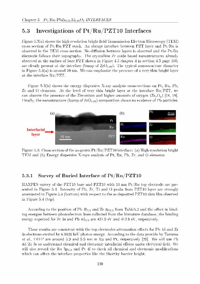
Chapter 5. Pt/Ru/PbZr0.52Ti0.48O3 INTERFACES
5.3 Investigations of Pt/Ru/PZT10 Interfaces
Figure 5.3(a) shows the high resolution bright eld Transmission Electron Microscopy (TEM)cross section of Pt/Ru/PZT stack. An abrupt interface between PZT layer and Pt/Ru isobserved in the TEM cross section. No diusion between layers is observed and the Pt-Ruelectrode follows their topography. The crystalline Zr oxide based nanostructures alreadyobserved at the surface of bare PZT shown in Figure 4.5 chapter 4 in section 4.3 page 100,are clearly present at the interface (bump of ZrO1.89). The typical nanostructure diameterin Figure 5.3(a) is around 10 nm. We can emphasize the presence of a very thin bright layerat the interface Ru/PZT.
Figure 5.3(b) shows the energy dispersive X-ray analysis cross-sections on Pt, Ru, Pb,Zr and O elements. At the level of very thin bright layer at the interface Ru/PZT, wecan observe the presence of the Zirconium and higher amounts of oxygen (ZrxOy) [18, 19].Finally, the nanostructure (bump of ZrO1.89) composition shows no evidence of Pb particles.
Figure 5.3: Cross section of the as-grown Pt/Ru/PZT10 interface: (a) High-resolution brightTEM and (b) Energy dispersive X-rays analysis of Pt, Ru, Pb, Zr, and O elements
5.3.1 Survey of Buried Interface of Pt/Ru/PZT10
HAXPES survey of the PZT10 bare and PZT10 with 10 nm Pt/Ru top electrode are pre-sented in Figure 5.4. Intensity of Pb, Zr, Ti and O peaks from PZT10 layer are stronglyattenuated in Figure 5.4 (bottom) with respect to the as deposited PZT10 thin lm observedin Figure 5.4 (top).
According to the position of Pb 4f7/2 and Zr 3p3/2 from Table5.2 and the oset in bind-ing energies between photoelectron lines collected from the literature database, the bindingenergy expected for Zr 3s and Pb 4d3/2 are 431.9 eV and 412.8 eV, respectively.
These results are consistent with the top electrodes attenuation eects for Pb 4d and Zr3s electrons excited by 6.8936 keV photon energy. According to the data provide by Tanumaet al., IMFP are around 5.9 and 5.5 nm in Ru and Pt, respectively [20]. We will use Pb4d/Zr 3s to understand chemical and electronic interfacial eects under electrical eld. Wewill also record the Ru 3p3/2 and Pt 4f to check all chemical and electronic modicationswhich can aect the interface properties like the Shottky barrier height.
130

5.3. Investigations of Pt/Ru/PZT10 Interfaces
Figure 5.4: Comparison of HAXPES Survey of as deposited PZT10 and Pt/Ru/PZT10stack
5.3.2 Dielectric Constant and Polarization of Pt/Ru/PZT/Pt
During the HAXPES measurements, the Pt/Ru/PZT/Pt structure was biased using anAgilent E4980A capacimeter/voltage generator [21]. All dielectric constant-voltage andpolarization-voltage curves presented in this chapter are performed on the capacitor with10 nm thick of top electrode(Pt 5 nm /Ru 5nm) contrary to what have already presentedin chapter 3 (Pt 100 nm /Ru 5nm). However, this Pt (5 nm) and Ru (5 nm) thicknesscannot induce any change on the electric responses. In fact, as observed in Figure 5.3(a),the thicknesses of Pt [22] and Ru [23] metals are higher than the coalescence thresholdwhich is dened as the thickness where the rst conducting link forms across the surface.This situation induces a rapid decrease of the resistivity of metal and favors the conductivity.
The maximum value of dielectric constant for the Pt(5 nm)/Ru(5 nm)/PZT10/Pt is1221.6. This value is dierent with the one of Pt(100 nm)/Ru(5 nm)/PZT10/Pt which is1126.6 (see Figure 3.7 chapter 3 in the section 3.2.1 page 85). Thickness dierence of thetop electrode could potentially be at the origin of this dierence. This dierence mightalso be partly related to the increase of the capacitor area respectively to (80 × 80)µm2
and (1 × 1)mm2. Buttery dielectric constant characteristic performed at 1 kHz is osetby -1.55 V and the coercive voltages are -2.0 and -1.2 V (Figure 5.5(a)). At zero appliedeld there is a strong, downwards pointing polarization, which we will call a P− imprint.The imprint in Figure 5.5(a) is much higher, more than double , than the one observedin Figure 3.6(a) chapter 3 in the section 3.2.1 page 85 which can be explained by the factthat more voltage was applied in the sample with 100 nm of Platinum (-10 V; +10 V)than the sample with 5 nm of platinum (-7 V; +3 V). Thus, the high voltage tends todecrease the imprint and reduce the oset value. The operando analysis was carried outat -7 V (negative voltage on top electrode, P+ polarization) and +3 V (positive voltage on
131

Chapter 5. Pt/Ru/PbZr0.52Ti0.48O3 INTERFACES
top electrode, P− polarization), i.e. symmetrically with respect to the center of the butteryloop of Figure 5.5(a). Remanence measurements are expected to show a similar result to+3 V since the imprint is P−. The high voltages relative to the coercive values ensuretrue saturation conditions whilst remaining below breakdown voltage which is 34.6 V (1.60MV/cm). Capacitance values at -7 and +3V do not change during the long exposure tohigh energy X-rays (6893.6 eV).
Figure 5.5: Electrical measurements Pt/Ru/PZT10/Pt stack: (a) Dielectric constant and(b) Polarization characteristic
Dynamic hysteresis loop measurement(DHM) at 1 kHz performed by using an AixacctTF2000 ferroelectric tester [24]. In this case, a succession of four triangular voltages of afew volts of amplitude is applied across the ferroelectric capacitor according to the timingdiagram presented in Figure 5.6. There are a prepol pulse and three bipolar excitationsignals (three pulses). Each signal is resaw by a relaxation time pause of 1 second. Themeasurement of the switching currents is carried out during pulses rst and third (in red).The prepol pulse and the second pulse (in black) of the excitation signal establish denedpolarization states. The prepol pulse has a negative state of relaxed remanent polarization.The second pulse ends in the positive state of relaxed remanent polarization. In this case,only the electrical response due to the switching of the ferroelectric domains is available.However, the measurement gives access to a great deal of information such as the positiveand negative coercive elds and the remanent, relaxed, and maximum positive and negativepolarizations.
Figure 5.6: Advanced DHM parameter with excitation signal
132
5.3. Investigations of Pt/Ru/PZT10 Interfaces
However, the hysteresis loop in Figure 5.5(b)) reveals a saturation polarization equal to23 µC/cm2. The ferroelectric hysteresis is also oset by 1.7 V towards the negative voltageand the coercive voltages are -2.2 for negative voltage on top electrode and -1.2 V for posi-tive voltage on top electrode (Figure 5.5(b)). Remanent polarization (Pr) are 10.4 and 7.9µC/cm2 for respectively P−
r and P+r . Zhou et al. [25] showed the same behavior of hysteresis
with both the horizontal shifting towards the negative and voltage and the presence of longtail at positive voltage. They explained that imprint phenomena may originate from :(i)stress induced by lm/electrode lattice mismatch or clamping, (ii) domain pinning inducedby, e.g., oxygen vacancies, or (iii) degradation of ferroelectric properties in lm/electrodesurface layers. Additionally, Zhou et al. [25] argued that the long tail of shape hysteresisloop for ferroelectric thin lms has been induced by the presence of the pseudo-non-switchinglayer. In fact, the hysteresis loop of the ferroelectric layer is completely cycled, while thepolarization of the nonswitching layer only stays in the upper part of the P-E loop so thatpolarization switching cannot occur.
The use of dierent metals between the bottom and top electrodes which induces twotypes of Schottky barrier (asymmetric barrier heights) might participate to the creation ofthe oset P-E curve. However, as we have already stated in the chapter 3 in section 3.2.1page 87, the eect of the asymmetry of the electrodes remains rather small compared to theshift observed on the dierent samples. Furthermore, the interface metal electrode/PZTcan be at the origin of the hysteresis oset. In fact, when a metal electrode is placed incontact with a semiconductor material, there may be a ow of charge carriers from thesemiconductor to the metal, depending on the work function of the metal. An accumulationof charge carriers results at the electrode/semiconductor interface, inducing an electrostaticpotential that depletes these carriers in adjacent regions. This space charge region or de-pletion layer is typically formed near interfaces such as grain boundaries and interfacesbetween heterophases [26]. With ferroelectric materials such as PZT, the presence of spacecharge region or depletion layer can aect the properties. It suppresses ferroelectricity inthe space charge regions. Furthermore, the domain pattern that is formed under the inu-ence of space charge can substantially dier from those without. Consequently when sucha sample is switched, the hysteresis loop constricts with a lowering of the coercive eld,and depending on the extent of the depletion layer, the remnant polarization as well. If thedistribution of charges in the sample is asymmetric, the resulting internal electric eld leadsto a preferred polarization direction, thereby shifting the hysteresis loop along the electriceld axis; this phenomena is called imprint. In our Pt/Ru/PZT/Pt a preference orientationof the polarization along the P− direction might be obtained. Finally, the presence of thevery thin bright layer at the top interface Ru/PZT observed in the Figure 5.3(a), can inducean oset characteristic of the hysteresis and buttery.
Figure 5.5(b) also shows that the hysteresis curve presents an asymmetric shape relativeto zero voltage bias. This variation of slim shape of the hysteresis at positive voltage mightbe attributed by a poor switching ferroelectric domains. In fact with the presence of theimprint, major of domains are orientated on the same direction as the electric eld whenthe bias is positive. Otherwise, when the voltage is negative, a large switching of ferro-electric domains will be observed, which is accompanied by the restoration of the characterferroelectric of the hysteresis shape. These assertions are supported by a supplementary
133

Chapter 5. Pt/Ru/PbZr0.52Ti0.48O3 INTERFACES
measure performed on the same sample but with a higher voltage as illustrated in the Fig-ure 5.7. In fact, when strong electric eld (voltage) is applied in the ferroelectric, the lockedferroelectric domains become more switchable that when the electric eld is low.
Figure 5.7: Polarization characteristic measurement Pt/Ru/PZT10/Pt stack at 1 kHz
5.3.3 Bias Correction After HAXPES Measurements
The raw Ru 3p, Pb 4d and Zr 3s spectral regions from the capacitor structure with -7 V(red curve) and +3 V (blue) on the top electrode are shown in Figure 5.8(a). The advantageof the Pb 4d/Zr 3s energy window is that the similar kinetic energies guarantee the samedepth sensitivity, despite the additional diculty that the Zr 3s peak partially overlaps thePb 4d3/2, making deconvolution more dicult.
The Ru 3p peak in the two bias states (with an absolute value of 10 V) is separated by10 eV, showing that there is very little parasitic resistance in the circuit as seen in Figure5.8( (a)top). Now, once corrected for bias, the spectra of Ru 3p3/2 are similar (see in Figure5.8((a)bottom)). The Ru 3p3/2 spectrum has only a single component at 461.5 eV (com-ponent I corresponding to the Ru0) for both bias states as shown in Figure 5.8(b). Theseresults are in agreement with the observation of the Figure 5.3 which show an unoxidizedelectrode layers.
Component (II) observed in Figure 5.8(b) is linked by the presence of the Ti 2p3/2. Shiftof the Ti 2p3/2 under voltage is equal at 1.4 eV with respectively 457.3 eV for +3V and 458.7eV for -7V. The residual dierences observed with Pb 4d & Zr 3s in Figure 5.8(a) and theshift of the Ti 2p3/2 in 6(b) are attributed to polarization-dependent changes.
Furthermore, correction of the bias states after operando HAXPES process, demon-strated also the presence of residual binding energy shift at the Pb 4d & Zr 3s core levelsbetween +3 V and -7 V. This residual shift is linked to the intrinsic polarization of PZTunder voltage bias and allows to the chemistry and electronic behaviors of sample.
134

5.3. Investigations of Pt/Ru/PZT10 Interfaces
Figure 5.8: (a) operando Ru 3p, Pb 4d and Zr 3s spectra with -7 (red curve) and +3 (bluecurve) on top electrode before (top) and after (bottom) correction for bias and (b) Ru3p3/2/Ti 2p3/2 depending on the bias.
5.3.4 Background Subtraction
Due to the energy loss tail of the Pt 4d emission from the Pt at top electrode, the back-ground increases with kinetic energy of photoelectron in the Pb 4d/Zr 3s region. Therefore,standard background subtraction like Shirley or Tougaard [27] cannot be used. We havetested polynomial and linear backgrounds and found that the latter gives better results asillustrated in Figure 5.9.
Figure 5.9: Comparison of the linear and polynomial background used for data treatmentsdepending on the bias: Top (-7V) and Bottom (+3V)
Table5.3 shows the dierent areas for each components depending to the background
135

Chapter 5. Pt/Ru/PbZr0.52Ti0.48O3 INTERFACES
model. Following that, the value of the relative error of each area peak is calculated bythe relation: % Relative error = (difference/Area peak) ∗ 100. Thus, by using the linearbackground model at +3 and -7 V, relative errors are between 16.1 and 12.2 % for the Pb4d and 7.6 and 8.2 % for the Zr 3s. Otherwise, the use of polynomial background favors anoverestimation of the area of the various components. Indeed, the relative error values arebetween 20.6 and 25.9 % for the Pb 4d and 25.6 and 34.5 % for the Zr 3s. Therefore, weuse the linear background subtraction.
Area of peaksPb 4d5/2 Pb 4d3/2 Zr 3s
V= +3V 442618 296554 166117Linear V= -7V 371167 248682 179747
Dierence 71451 47872 -13630
V= +3V 513106 343781 255491Polynomial V= -7V 407288 272883 190016
Dierence 105818 70898 65475
Table 5.3: Comparison of the Linear (at +3 and -7V) and polynomial (at +3 and -7V) areaof peaks
5.3.5 Analysis on Operando HAXPES Data Based on PZT10
Pb and Zr core level shifts and intensity ratios found in the PZT10 bare have been directlytransposed to the Pb 4d & Zr 3s spectra obtained during the operando measurements. Thefree parameters during the deconvolution of the spectra are the absolute binding energy,the intensity and any additional, interface-specic component. Figure 5.10 shows the bestts to the Pb 4d/Zr 3s spectrum for (a) the PZT10 bare and (b-d) the operando spectra ofPZT10 with the top electrode under bias. The binding energies and line-shape parametersare given in Table5.4.
The PZT10 bare spectrum (Figure 5.10(a)) has a high signal to noise ratio which is tobe expected in the absence of attenuation by the 10 nm Pt/Ru top electrode observed onthe capacitor structures. For the spectra with top electrode under bias, once the PZT Pb4d, PZT Zr 3s, reduced Pb and Zr oxide nanostructure components have been included,there are two important dierences with respect to the as deposited PZT10.
First, there is a 1.4 eV systematic shift of both Pb and Zr emission to higher BE goingfrom +3 V (P−) to -7 V (P+) whereas the Ru core level does not shift (as shown in Figure5.8). This suggests a change in electrostatic boundary conditions rather than the chemicalenvironment since the latter would also aect the rst layer or layers of the Ru electrode(except a change of local chemistry eect of PZT that would not aect the photoemissionsignals of Ru). However, the assumptions of a change in electrostatic boundary conditions issupported by results from Figure 5.3 which suggests any interdiusion between the Ru andPZT layers. The core level shift between +3.0 and 0.0 V is smaller than between 0 V and
136

5.3. Investigations of Pt/Ru/PZT10 Interfaces
-7.0 V consistent with the P− imprint measured electrically. Assuming that the polarization-dependent core level shift is equal to the potential drop across the lm. The residual internaleld is 65 kV/cm, approximately three times the coercive eld. This demonstrates that thepolarization charge is poorly screened. The Zr 3s component due to the nanostructures isxed since the nanostructures are above the PZT layer. They should be independent of thepolarization. However, the nanostructures might also show polarization due to the strayelds, and this remains an open question.
Figure 5.10: Pb 4d and Zr 3s spectra and best ts for (a) PZT10 as deposited lm comparedwith electrode under (b) +3 (c) 0 and (d) -7 V applied bias. The Pb and Zr componentshave been transposed from the as deposited PZT10 spectra and the color code is the sameas in Figure 5.2. Label III identies the interface related peak discussed in the text
Secondly, there is an additional component, labelled peak III at high binding energyas shown in Figure 5.10(b-d). This interface-related component shifts from 439.8 eV at -7V to 438.4 eV at +3 V bias, i.e. 1.4 eV like the other core levels. It is also possible tox the binding energy at 439 eV, which corresponds to an interface contribution, distinctfrom the PZT as illustrated in Figure 5.11. The single component suggests that it is dueto Zr 3s. However, 5-6 eV is too high to be a simple chemical shift of Zr which is alreadyin Zr4+ valence state in PZT. The absence of such component in the reference spectrumand in the XPS analysis of the bare PZT layer proves that it is related to the capacitorstructure. The exact origin of this component is therefore not clear. However given that itwas not observed on the as deposited PZT10, it probably come from the interface formedwith the top electrode (thin bright layer at the interface Ru/PZT reported in Figure 5.3(a)).Furthermore, we can notice that the peak III is not due to the bias voltage because thepeakIII is present when 0 V is applied on the capacitor as seen in Figure 5.10(c).
137

Chapter 5. Pt/Ru/PbZr0.52Ti0.48O3 INTERFACES
The existence of this interface component can be linked to the interface rumpling. Therelative intensity of peak III is 4.7 % of the total intensity of Pb 4d and Zr 3s spectra.Assuming an IMFP of 5.7 nm (average of values in Ru and Pt), the intensity corresponds tothat expected from some unit cell layer of PZT. First principles calculations have shown thatrumpling at electrode interface changes signicantly with polarization [9]. This explanationis in good agreement for the Pt-PbTiO3 interface of 0.11 Å [9, 28]. The rumpling variationwould induce a change in the local chemistry and might be responsible for an additional Zrcomponent. This has to be conrmed by further experiments with higher statistics and byacquiring the Pb 4f and Zr 3p.
Figure 5.11: Pb 4d and Zr 3s spectra and best ts for (a) reference lm without electrodecompared with electrode under (b) +3 (c) 0 and (d) -7 V applied bias. The Pb and Zrcomponents have been transposed from the as deposited PZT10 and the color code is thesame as in Figure 5.2. Label III identies the interface related peak is xed at 439 eV
Furthermore, Figure 5.12 illustrates a schematic of the localization of interface layer(based on the ZrxOy as seen in Figure 5.3) at the level of interface Ru/PZT. In fact, withthe presence of high rate of O2 at the interface, the Zr tends to oxidize at Zr2O5, ZrO3,ZrO4 [18, 19]. The presence of these zircon oxide phase (interfacial layer) can be probablyat the origin of the interface component (III) observed in Figure 5.10 and Figure 5.11.
The valence band oset at the interface is calculated using the expression of binding en-ergies: Ru 3p3/2 - (Ru 3p3/2-Pb 4d5/2)-(Pb 4d5/2-VBM) [29], where Ru 3p3/2 is the bindingenergy measured from the Pt/Ru/PZT10 stack. Pb 4d5/2 in the (Ru 3p3/2-Pb 4d5/2) termrepresents the binding energy measured from the Pt/Ru/PZT10 stack. Pb 4d5/2 and VBM(valence band maximum) in the (Pb 4d5/2-VBM) term are the binding energy measured onthe as deposited PZT10. The resulting oset obtained by switching the voltage from +3 to
138

5.3. Investigations of Pt/Ru/PZT10 Interfaces
-7V are 0.7 and 2.1 ± 0.1 eV, respectively. Assuming a 3.4 eV band gap, this gives a SBHfor electrons of 1.3(2.7)± 0.1 eV, consistent with the capacitive behavior in Figure 5.5(a).
From the dierence in Schottky barrier height∆Φ, we can estimate the eective screeninglength λeff in the metal/ferroelectric interface. The eective screening length takes intoaccount all microscopic details of the interface dipole response to the polarization (includingelectronic and chemical bonding eects). This is in contrast to the Thomas-Fermi model ofscreening [30] used on the metal/semiconductor interface.
Figure 5.12: Schematic cross section of Pt/Ru/PZT with interface phase (ZrxOy) and nanos-tructures (ZrO1.89)
In fact, with metal/semiconductor interface all the compensating (distribution of thescreening charges (Thomas-Fermi screening length δ)) reside in the electrodes. With theschematic model considering ideal insulator presented in Figure 5.13(a), we assume thatthe metal 1 (top electrode) and the metal 2 (bottom electrode) have dierent screeninglength, which leads to the asymmetric potential prole. Thus, the spatial distribution ofthe compensation charge induced by the presence of dissimilar electrodes materials canproduce dierent electric eld at each electrodes. This situation may be caused by the shiftobserved in both permittivity-voltage and polarization-voltage curves presented in Figure5.5.
Figure 5.13: Schematic distribution of the electrostatic potential Φ in the MFM structurewith ±P polarization direction, dF thickness of ferroelectric (a) Thomas-Fermi model ofscreening, δ1,2 screening length in the metal and (b) Eective screening length model (λeff ),DS is the spontaneous polarization
139

Chapter 5. Pt/Ru/PbZr0.52Ti0.48O3 INTERFACES
However, Stengel et al. [9] explained that the imperfect screening is a property of theinterface (the metal, the ferroelectric and the specic interfacial layer), which requires con-sideration of an eective screening length λeff , rather than the Thomas-Fermi model ofscreening one. These imperfections are described by assuming that the screening chargesseparated from the bound charges by an empty layer of thickness λeff as illustrated in Fig-ure 5.13(b).
This thickness λeff acts like a capacitor in series and induces a potential drop of Φ =λeff .DS/(ε0εr) where DS is the spontaneous polarization of the ferroelectric [28]. Thus,using the dierence Schottky barrier height ∆Φ = 2λeff .DS/(ε0εr) and the value of εr forthe interfacial layer ZrxOy (25 - 40), we can obtain the eective screening length whichis 0.575 - 0.920 nm. These results are in quite good agreement with the thickness of theinterfacial layer observed in Figure 5.3(a).
Binding energy (eV)PZT Bias on top electrode (V) FWHM GL
reference +3.0 0.0 -7.0 (eV) (%)Cyan Pb 4d5/2 (PZT) 412.5 412.4 413.0 413.8
3.6 82Pb 4d5/2 (Reduced) 411.2 411.1 411.7 412.5
Green Zr 3s (PZT) 432.0 432.0 432.6 433.46.0 70
Zr 3s (ZrO1.89) 433.0 433.0 433.6 434.4Wine III - 438.4 439.0 439.8 3.6 70
Table 5.4: Pb 4d5/2 and Zr 3s core level binding energies (eV), FWHM and percentage ofGaussian peak in the Gaussian-Lorentzian peak shapes as a function of applied bias on topelectrode of PZT reference capacitor
5.4 Interface Analysis of Pb Excess Content in PZT
According to the results in chapter 4, high proportion of Pb induces the disappearanceof nanostructures (ZrO1.89) at the surface. Considering the ZrO1.89 as a dead interfacelayer, their disappearance should enhance the dielectric properties. However, we observedin chapter 3, the dielectric constant and the breakdown eld decrease when the Pb excessreaches 30 % (PZT30). Yanovskaya et al. [31, 32] show a decrease of the breakdown voltagefrom 18.2 to 11.2V for PZT10 and PZT30, respectively. In this context, we will investigatethe eect of high amounts of Pb excess content on the chemical and electronic congurationof the interface Pt/Ru/PZT.
5.4.1 Pt/Ru/PZT30/Pt Electrical Measurements
Figure 5.14(a), shows that the dielectric constant-voltage of Pt/Ru/PZT30/Pt is shifted1.24 V towards the negative voltage. It also has a dissymmetric buttery shape. Values of adielectric constant at -5 and 1V are 670.3 and 899.3, respectively . The maximum value ofthe dielectric constant is 1181.7. Coercive voltages are -1.48 and -1V for polarization alongto the P+ and P−, respectively. According to this fact, the capacitor based on the PZT30
140

5.4. Interface Analysis of Pb Excess Content in PZT
exhibits a low dielectric constant relative to the Pt/Ru/PZT10/Pt capacitor.
From Figure 5.14(b), the maximum value of polarization obtained is 16.5 µC/cm2 withremanent polarization of 2.2 µC/cm2 for P−
r and 1.5 µC/cm2 for P+r . It presents an oset
of 0.58 V towards the negative voltage with coercive voltages of -0.74 and -0.42 at E−C and
E+C , respectively. The changes in the electrical properties might be correlated with the high
amount of Pb excess content in the PZT lm.
Figure 5.14(b) shows a slim hysteresis shape compared to the result obtained Pt/Ru-/PZT10/Pt capacitor. The curve is almost linear which can be probably linked to theferroelectric relaxor [33] behavior caused by high Pb excess residual. Furthermore, thisbehavior is observed in the PLZT lm when a high concentration of La3+ (La is used tosubstitute Pb atom) is incorporated in the PZT lm. Leclerc et al. [34], Park et al. [35] andPodgornyi et al. [36] showed the deterioration of the polarization properties of the samples.These can be linked either to the relaxor properties observed on the highly doped PZT thinlms or to the transformation of the PZT from ferroelectric state to paraelectric state withthe increase of La concentration. It is important to notice that even though the degradationof polarization is observed, Park et al. [35] reported that the dielectric was enhanced withthe introduction of a high amount of La dopant.
Figure 5.14: Electrical measurements Pt/Ru/PZT30/Pt stack: (a) Dielectric constant and(b) Polarization characteristic
Jin et al. [37] explained that the existence of the slim hysteresis loop can be induced bythe presence of the pseudocubic phase structure of relaxor ferroelectrics, micro-domains orpolar nano-grains. These lead to nonlinear (dielectric) responses under external eld whilethe ferroelectric domains switching give rise a hysteresis. In fact, the current from the con-ductivity of material can modify the shape of the hysteresis. Indeed, following Dawber et al.[38]: Q = 2PrA + σEAt (where σ is the electrical conductivity, t is the measuring time, Ais electrode area of a parallel plate capacitor, E is the applied eld and the switched chargeQ which can allow to get the remanent polarization value Pr). This relation shows that,the ferroelectric response can present two types of contribution: the currents from switching
141

Chapter 5. Pt/Ru/PbZr0.52Ti0.48O3 INTERFACES
domains and the current from loss (leakage current). According to Jin and Dawber, we cansuppose that, under electric eld, the response of these micro-domains may be much fasterthan macroscopic ferroelectric domains and therefore modify the shape of the hysteresis.
This assertion seems to be consistent, when we compare the hysteresis results of thePt/Ru/PZT30/Pt capacitor performed at 5 V (Figure 5.14(b)) and 20 V (Figure 5.15).These data show that the ferroelectric character of PZT30 seems to be recovered, when thevoltage become high (20 V) contrary to the linear response at low voltage (5 V). It is due tothe fast response of the micro-domains under polarization electric relative to the ferroelectricdomains. However more investigations like the analysis of the dielectric constant as thefunction of frequency and temperature will be necessary to make more denitive statementson the eect of high rate (30 %) of Pb excess.
Figure 5.15: Polarization characteristic measurement Pt/Ru/PZT30/Pt stack at 1 kHz
5.4.2 Analysis on Operando HAXPES Data Based on PZT30
Operando HAXPES measurement are carried out at -5V and +1V. Figure 5.16 shows thePb 4d/Zr 3s core level spectra (relative to the Pt/Ru/PZT30 stacks) as the function of thevoltage applied on the top electrode. The binding energy of the Pb2+ (cyan color) and theZr4+ (green color) from the PZT30 layer depending on the voltage are similar that obtainedwith a Pt/Ru/PZT10 in Figure 5.10 or Figure 5.11. In fact, we observe a global shift of1.4 eV of the Zr and Pb relative to the PZT30 perovskite. All binding energy results aresummarized in Table5.5.
Figure 5.16 demonstrates once again the presence of the interface component (peak(III)). For PZT10, peak III shifts from 439.8 eV at -5 V bias to 438.4 eV at +1 V bias. Eventhough, it was also possible to x the binding energy at 439 eV. With uncertainty aboutthe position of the interface component, it is very dicult to determine the exact origin ofthis component.
142

5.4. Interface Analysis of Pb Excess Content in PZT
Furthermore, Figure 5.16 shows an additional chemical state of lead Pbx+ with 2 < x <4 (blue color) between +1V and -5V. This additional chemical state can be attributed bythe residual lead oxide due to the high amount of lead excess content in PZT30. However,the exact formula of PbOx is not determined [33, 39, 40, 41]. Further, this latter componentundergoes a shift of 4.4 eV during the switch. It is important to remark that this phasewas not observed with laboratory XPS and XRD. In fact, the PbOx seems to be localizedin the bulk of PZT and therefore undetectable with the XPS tool. According to the X raydiraction patterns of PZT lms prepared from solutions with dierent Pb excess contentpublished by Yanovskaya et al. [31, 32], the component linked to the PbO appears only with50 % of Pb excess content but not at 30 % (as that is observed in chapter 4) even thoughthat act the electrical responses of PZT capacitors. However, it is easier and appropriatedto highlight the PbOx phase with Operando HAXPES measurement under bias.
Thus, the presence of the new component of lead oxide observed in HAXPES spectracan be correlated with the decrease of the dielectric constant value and the lowering ofthe breakdown voltage (Figure 3.10 chapter 3 in the section 3.2.2 page 89). The presenceof this lead oxide component is also in agreement with the hypothesis of the existence ofmicrodomains which leads to the slimming of the ferroelectric hysteresis curve as explainedby Jin et al. [37].
Figure 5.16: Pb 4d and Zr 3s spectra and best ts for Pt/Ru/PZT30 (a) +1 (b) -5 V appliedbias. The color code for cyan, green and wine peaks are the same as in Figure 5.10. Bluepeak corresponds to the additional lead component.
Furthermore, lead oxide presents low dielectric constant (25.9-35) [42] compared to PZT.It shows a high electronic polarizability (between 3.311 and 3.450) relatively to the ZrO2
(between 1.897 and 2.054)[43]. This high electronic polarizability can be explained by
143

Chapter 5. Pt/Ru/PbZr0.52Ti0.48O3 INTERFACES
the high shift observed during the switching polarization. The PbO can behave like Zroxide and reduce the capacitance density of MIM capacitors. When the PbO is at theinterface, it will behave as a dielectric layer in series with the PZT and induce a lowertotal capacitance density. Mukhin et al. [44] explained that the series layers of lead oxidedeposited between the PZT and the bottom electrode (Pt/PZT/PbO/Pt/Ti/SiO2/Si) aectthe electrical response by reducing the eective dielectric constant from 760 to 410 and theresidual polarization from 13 to 11 µC/cm2. However, Mukhin also reported an increaseof the coercive eld from 110 to 185 kV/cm. Yanovskaya et al. [32], Maria et al. [45] andAfanasev et al. [46] have studied the presence of PbO inside the PZT thin lms. Theyshowed a reduction of the polarization and the coercive eld with increasing Pb excess.
Binding energy (eV)Bias on top electrode (V) Relative FWHM GL
+1 -5 intensity (%) (eV) (%)Pb 4d5/2 (Pb2+) 412.4 413.8 57.9
3.6 82Pb 4d5/2 (PbOx) 413.1 417.5 22.4Zr 3s (Zr4+) 432.0 433.4 19.9 6.0 70
III 438.4 439.8 3.9 3.6 70
Table 5.5: Pb 4d5/2 and Zr 3s core level binding energies (eV), relative intensity, FWHMand percentage of Gaussian peak in the Gaussian-Lorentzian peak shapes as a function ofapplied bias on top electrode of Pt/Ru/PZT30/Pt capacitor.
In summary, PbO observed during the operando measurement can be at the origin ofthe creation of microdomains inside the PZT30 layer and induce the modication of thehysteresis shape as described by Jin et al. [37]. Further, the Pb excess can be localized atthe grain boundaries [47] and favor the ow of charge carriers consistent with the prematurebreakdown eld (voltage).
5.5 Post Metallization Annealing of Pt/Ru/PZT10 In-
terface
According to the results from the literature, the Post Metallization Annealing (PMA) underthe oxygen enhances the electric responses of MIM capacitors. Kushida-Abdelghafar et al.
[47] showed an increase of the spontaneous polarization of IrO2/PZT/Pt capacitor afterPMA. PMA makes the hysteresis curve symmetric and increases the polarization. The im-proved electrical properties have been also observed in other perovskites like Ba0.5Sr0.5TiO3
under PMA with O2 and N2 [48] such as an increase of the maximum of capacitance and areduction of the leakage current values. These data are in agreement with the improvementof the maximum dielectric constant and breakdown voltage after PMA presented in thechapter 3 in section 3.8 page 88 and section 3.2.2 page 89. However, the origins and thephysico-chemical impact of PMA were not really explored. Using operando HAXPES, wehave studied the interface chemistry as a function of the applied bias (switching polariza-tion).
144

5.5. Post Metallization Annealing of Pt/Ru/PZT10 Interface
5.5.1 Electrical Characterization After PMA
The dielectric constant and polarization data under voltage are presented in Figure 5.17.In contrast to PZT10 before PMA (Figure 5.5(a)), after PMA we observe an increase ofthe maximum dielectric constant from 1221.6 to 1234.9 and a saturation of the polarizationfrom 23 to 33 µC/cm2. In Figure 5.17(b), remanent polarization P−
r are 11.2 µC/cm2 (P+r
=-8.7 µC/cm2). The coercive voltages of -0.83 V and 0.76 V are register for E−C and E+
C ,respectively. The dielectric-voltage buttery and polarization-voltage hysteresis curves aresymmetric relative to zero voltage. The symmetric hysteresis loop might be attributed atthe thermal treatment of the top electrode. In fact, the two metal electrodes are dierent.The bottom electrode is annealed during the crystallization of the PZT layer while the topelectrode is unannealed (Figure 5.17(b)). After PMA a rectifying barrier at the top interfacefavors the symmetric hysteresis loop as presented in Figure 5.17(b).
Figure 5.17: Electrical measurements Pt/Ru/PZT reference with PMA/Pt stack: (a) Di-electric constant and (b) Polarization characteristic
5.5.2 Ru and Pt Chemical State Before and After PMA
The Ru 3p3/2/Ti 2p and Pt 4f/Ru 4s core level spectra are presented in Figure 5.18(a-b),respectively. Standard Shirley-type background subtraction is used for Ru 3p3/2 and Pt 4fspectra. Asymmetric peak-shapes based on the Lorentzian functional form convoluted witha Gaussian are used for tting the metallic Pt0 [49] and Ru0 components [50] as observedin Table5.6. Asymmetric line-shapes describe well the intrinsic energy losses due to theinteraction between the photoelectron and the conduction band of the metal [51]. Duringthis interaction, a certain part of the kinetic energy of photoelectron is lost. This leads toa trailing higher intensity at high binding energies.
In Figure 5.18(a) (bottom), Ru is only present in metallic form (Ru0) localized at 461.5eV [50, 52, 53] as already presented in Figure 5.8(b). After PMA, the oxidation of the Rulayer is illustrated in Figure 5.18(a) (top). Finally, Table5.7 shows a drastic decrease of
145

Chapter 5. Pt/Ru/PbZr0.52Ti0.48O3 INTERFACES
the Ru0 which is lower 10 % after PMA, in contrast to what was observed before PMA.This situation is induce by the large oxidation (higher 90 %) of the Ru under the form ofRuO2 and RuOx with x > 4. Ru metallic is only at 8.1 % after PMA. Majority of Ru istransformed (green component at 462.5 eV represents 48.3 % of Ru 3p3/2/Ti 2p area) in theform of RuO2 corresponding to the Ru4+. Part of the Ru shows a higher oxidation state(6 and/or 8) as suggested by the (orange) component at 464.8 eV. This HBE componentrepresents 41.8 % of the total Ru 3p3/2/Ti 2p intensity. Thus, PMA induces strong changesat the interface and modify the MIM capacitor behaviour.
Figure 5.18: Ru 3p3/2/Ti 2p and Pt 4f/Ru 4s core level spectra and best ts forPt/Ru/PZT10/Pt (bottom) before and (top) after post metallization annealing
Zhu et al. [54] highlighted the possibility to prepare an amorphous Ru0.48Zr0.52O2 lm insolid solution by thermal decomposition at 563 K. Under the thermal eect, the Pt/Ru/PZTcan undergo a strong change which can lead the appearance of the Ruthenium oxide. TheTi 2p3/2 (wine peak) is at 457.3 eV for before and after PMA.
Figure 5.18 shows the Pt 4f and Ru 4s core level spectra from the Pt/Ru/PZT10 beforeand after PMA. After deposition of Pt/Ru top electrode without annealing, only Pt0 isrecorded at 71 eV [55, 56] as illustrated by the cyan color in Figure 5.18. Similarly, thepresence of the Ru 4s at 74.8 eV is in agreement with the Ru0 binding energy according tothe NIST database and Handbook of X-ray Photoelectron Spectroscopy [57]. After anneal-ing, a large part of the Ru is oxidized as illustrated in Table5.7. Once again, oxidation ofthe Ru is evidenced by the presence of two new components of Ru 4s at high binding energy.
After the PMA process, 33.3 % of Pt is oxidized as Pt+2 (red) and Pt+4 (azure) at 71.9and 74 eV, respectively , [55, 56] as observed in the Table5.6). Thus, Pt oxidation can comefrom either the oxygen of the annealing chamber or diusion of oxygen from the PZT.
In summary, we can assume that the presence of oxygen (from the annealing chamberor the PZT layer) leads to the oxidation of Ru (RuOx) and Pt (PtOx).
146

5.5. Post Metallization Annealing of Pt/Ru/PZT10 Interface
Oxidation state Binding Energy (eV) FWHM Line shapeRu0 461.5 2.5 LF(1.1,1.2,25,5)
Figure 5.18(a) Ru4+ 462.5 2.8 GL(70)Rux+ (x > 4) 464.8 4.8 GL(80)
Ti4+ 457.3 1.5 GL(30)Pt0 71.0 0.6 LA(0.8,2,60)Pt+2 71.9 1.2 GL(70)
Figure 5.18(b) Pt+4 74.0 1.2 GL(70)Ru0 74.8 1.8 LF(1.1,1.2,25,5)Ru4+ 75.8 2.0 GL(70)
Rux+ (x > 4) 78.2 3.4 GL(80)
Table 5.6: Ru 3p3/2/Ti 2p and Pt 4f/Ru 4s core level binding energies (eV), FWHM and sym-metric Gaussian-Lorentzian and asymmetric LA(α, β,m) and LF (α, β, w,m) peak shapes(where LA is Lorentzian Asymmetric lineshape, LF is Lorentzian Asymmetric lineshapewith Tail Damping. The implementation of asymmetric parameters α and β enables thespread of the Lorentzian tail to be dierent either side of the Lorentzian component. Theinteger m is responsible for the control of the width of a Gaussian which allows to performa convolution between the Lorentzian Asymmetric lineshape and a Gaussian to adjust theactual shape of the photoemission peak. Finally, the damping parameter w which allows tolimit the range of the asymmetric tail by suppressing the extended tail.
Concentration (%)Oxidation state Before PMA After PMA (%)
Ru0 98.2 8.1Figure 5.18(a) Ru4+ - 48.3
Rux+ (x > 4) - 41.8Ti4+ 1.8 1.8Pt0 91.3 58.0Pt+2 - 11.4
Figure 5.18(b) Pt+4 - 21.9Ru0 8.7 0.7Ru4+ - 4.3
Rux+ (x > 4) - 3.7
Table 5.7: Relative composition of the Pt 4f/Ru 4s and Ru 3p3/2/Ti 2p before and afterPMA
5.5.3 Analysis on Operando HAXPES Data Based on PZT10 AfterPMA
The Pb 4d/Zr 3s core level spectra presented in Figure 5.19 provide a crucial informationon the HBE component (peak III). The t parameters and the Pb 4d and Zr 3s bindingenergies as a function of the bias are reported in Table5.8. The binding energy of peak III
147

Chapter 5. Pt/Ru/PbZr0.52Ti0.48O3 INTERFACES
remains x at 439 eV independently of the applied bias. The dierence of binding energybetween Zr4+ (from the PZT thin lm (cyan peak) at 432.0 eV for +5V (or 433.4 eV for-5V)) and the position of the peak III is too high (between 5.6 and 7 eV respectively). Anew Pb2+ component (red component) in Figure 5.19 is highlighted. This Pb2+ component(red) is to be xed at 412.1 eV and insensitive to the value of the applied electric eld. Twopossible assumptions can be used to discuss these results: the partial decomposition of thePZT lm or the creation of alloys at the interface level.
Figure 5.19: Pb 4d and Zr 3s spectra and best ts for Pt/Ru/PZT10 after PMA (a) +5 (b)-5 V applied bias. The color code for cyan and green peaks are the same as in Figure 5.10.Wine peak is linked to oxidation of the interface. Red peak corresponds to the additionallead component after PMA.
Results in Figure 5.19 can be explained by the alloys formation at the interface level.In fact, the creation of this red peak can be explained by a diusion of the lead oxide(during the PMA) to the ruthenium layer and the formation of alloy based on the lead-ruthenium oxide (PbRuOX) as already observed by Prakash et al. [58]. Hrovat et al. [59]demonstrated an incompatibility reaction between RuO2 based electrodes and PZT ceramicsat low temperature. However, at high ring temperature, a reaction between PZT layer andRuO2 is possible and can lead to the creation of Pb2Ru2O6.5 at the interface level (whichis a good conductor layer as described by Bobnar et al. [60]). Kushida-Abdelghafar et al.
[47] showed that under annealing (O2 at 600C), the Pb excess diuse through the grainboundaries and reaches the top electrodes. These results are in agreement with the study ofKennedy [61] which described the creation of decient oxygen structure (Pb2Ir2O6.5) afterthe diusion of Pb.
148

5.5. Post Metallization Annealing of Pt/Ru/PZT10 Interface
However, with the migration of Pb inside the Ruthenium layer, the presence of ZrOx
at the interface might also induce the creation of alloys based on the ZrRuOX . During thePMA process, zirconium can get a higher degree of oxidation (Zr2O5, ZrO3, ZrO4 [18, 19]),which leads to the increase of binding energy up to 439 eV. Thus, with the presence of theruthenium layer shown in Figure 5.18(a), we can assume a possibility of the creation of alloybetween the RuOx and ZrOx. These assumption are in agreement with the data from Zhuet al. [54], which showed a successful preparation of an amorphous Ru0.48Zr0.52O2 lm of asolid solution phase by a thermal decomposition at a low temperature (563K). Even though,they did not show the XPS result on this Ru0.48Zr0.52O2 lm. Additionally, Weizhen Li etal. [62] described that the RuO4 can be found in the form of Zr(RuO4)2 after interactionwith the ZrO2. Further, Yang et al. [63] mixed RuO2 with inert metal oxides ZrO2, inorder to maintain a high catalytic activity and stability of RuO2 during anodic polarization.These results demonstrate a possible reaction between the Zirconium oxide at the interfaceand the Ruthenium oxide during the PMA process. Depending to the concentration ofthe ZrO2 and RuO2, Kristof et al. [64] and Burke et al. [65] also investigated the alloysZrOX-RuOY . Finally, we can say that an eventual formation of ZrRuOX at the interfacecan explain the fact that the peak III remains x at 439 eV during the voltage bias switching.
In summary, beside the potential reduction of the oxygen-vacancies (VO) and the Pb-vacancies (VPb) inside the PZT bulk under high temperature annealing which can improvethe electrical performances, the modication of the interface chemistry also act to the elec-trical responses. In fact, the presence of the news Pb2+ (reb) and Zrx+ (wine) compo-nents shown in Figure 5.19 and Ruthenium (Ru2+ and Rux+ 2 < x < 4) components illus-trated in Figure 5.18 might induce a possible creation of interface PbRuOX and ZrRuOX
alloys under thermal treatment. These oxides alloys at the interface lead to the enhance-ment of electric performances (dielectric constant, breakdown voltage and ferroelectricity) ofPt/Ru/PZT10/Pt after PMA. In fact, the oxide phases observed at the interface before PMAwhich present a low dielectric constant and lead a formation of the ferroelectric/paraelectricinterface can potentially induce a detrimental screening with a higher depolarizing eld.Conversely, the formation of the interfacial PbRuOX and ZrRuOX alloys between the PZTand the top electrode leads to the better screening of bounds charge from the surface ofPZT due to the good conductivity of alloys and the absence of oxide phases at the interface.
Conversely to the supposition of the formation of interface alloys and according to theresults from Popescu et al. [17] which highlighted the progressive increase of intensity for alow binding energy component of Pb core levels (for both 5d and 4f) during the photoemis-sion process with intense synchrotron radiation beam, we can also suppose that the originof the new Pb2+ component at 412.1 eV (red component) in Figure 5.19 may be attributedwith the formation of metallic (reduced) Pb nanoparticles. This situation would be dueto a partial decomposition of the PZT lm at the interface which promotes the presenceof metallic Pb0. This nanoscopic separation of PZT structure is also in agreement withthe apparition of the peak III. In fact, we can say that with high intensity of source, thedecomposition of the perovskite can lead both the reduction of the Pb2+ into Pb0 and theZrO3 matrix [19]). Thus, the ZrO3 matrix with higher oxidation degree than the ZrO2 (inPZT) can explain the presence of the peak III at very high binding energy.
149

Chapter 5. Pt/Ru/PbZr0.52Ti0.48O3 INTERFACES
However, the assumption based on the partial decomposition of the PZT lm can notexplain why the red component is not observed with the Pt/Ru/PZT10 before PMA process.Even though these two samples are exposed to the same X-ray source during the sametime. The fact that the peak III is x at 439 eV is not explained by the decompositionpossess of PZT under photon source because under bias voltage the Zr component fromZrO3 (dielectric) should change a binding energy when the polarization switch from +5 V to-5 V. Additionally, the shoulder of the peak III was already remarked at the rst swept (rstminutes) not after all scans (several hours under synchlotron radiation). According to theseinformation and questions, we suppose that the possible creation upon annealing (PMA) ofinterface alloys PbRuOX and ZrRuOX seems more relevant to explain our observations thanthe partial decomposition of the PZT even though more experiments have to be performedin order to clear and understand the interface interaction under PMA process.
Binding energy (eV)Bias on top electrode (V) Relative FWHM GL
+5 -5 intensity (%) (eV) (%)Pb 4d5/2 (Pb2+) 412.4 413.8 46.12
3.6 82Pb 4d5/2 (Interface) 412.1 412.1 30.46
Zr 3s (Zr4+) 432.0 433.4 10.586.0 70
Zr 3s (ZrO1.89) 433.0 434.4 1.8III 439.0 439.0 11.04 3.6 70
Table 5.8: Pb 4d5/2 and Zr 3s core level binding energies (eV), relative intensity, FWHMand percentage of Gaussian peak in the Gaussian-Lorentzian peak shapes as a function ofapplied bias on top electrode of Pt/Ru/PZT10/Pt capacitor after PMA
5.6 Conclusion
In this chapter, we have carried out operando hard X-ray photoelectron spectroscopy of thetop interface in a Pt/Ru/PZT/Pt/TiO2/SiO2/Si capacitors.
The presence of ZrO1.89 nanostructures at the surface of the bare sol-gel lm can act as adead layer in the dielectric structure and reduce screening of the surface polarization chargein Pt/Ru/PZT10/Pt capacitor. The Schottky barrier height for electrons is 1.3 and 2.7eV for upwards and downwards pointing polarization, respectively, which is consistent withthe electrical characteristics and the eective screening length. However, further studies arenecessary to nd the real binding energy of the interface layer situated at the Ru/PZT10interface.
The impact of excess Pb in the precursor is studied by using the PZT with 30 % Pbexcess. Sample exhibits a new (PbOx) component. The presence of high Pb excess inducesa reduction of the capacitance due to the low dielectric constant of (PbOx) and a linearhysteresis loop linked to the micro-domains based on the creation of lead oxide clusters. Itseems that the addition of PbOx induces a decrease of breakdown voltage observed withcapacitor base on PZT30. These results show that the optimization of PZT via the elimina-
150

5.6. Conclusion
tion of parasitic ZrO1.89 and (PbOx) phases are needed to improve the dielectric responsesand breakdown voltage performance in view of an optimal use in FE capacitor application.Moreover, regarding the lead excess eect, other investigations are required to nd the de-gree of oxidation of the PbOx.
Finally, post metallization annealing on the PZT10 highlights a modication of theinterface by the creation of ZrRuOx and PbRuOx during the annealing process. However,more work is required to fully conrm the origin of the interface related to the signalsmanifest in the Pb 4d and Zr 3s spectra and to understand if these alloy are responsible forthe enhancement of the dielectric constant, the breakdown voltage and the imprint eecton the Pt/Ru/PZT/Pt capacitors.
151

Chapter 5. Pt/Ru/PbZr0.52Ti0.48O3 INTERFACES
Bibliography
[1] J. F. Scott. Ferroelectric Memories, volume 3 of Springer Series in Advanced Microelectronics.Springer Berlin Heidelberg, 2000.
[2] X. J. Lou. Polarization fatigue in ferroelectric thin lms and related materials. Journal ofApplied Physics, 105(2):024101, 2009.
[3] F. Chen, R. Schafranek, A. Wachau, S. Zhukov, J. Glaum, T. Granzow, H. von Seggern,and A. Klein. Barrier heights, polarization switching, and electrical fatigue in Pb(Zr,Ti)O3
ceramics with dierent electrodes. Journal of Applied Physics, 108(10):104106, 2010.
[4] L. Pintilie and M. Alexe. Metal-ferroelectric-metal heterostructures with Schottky contacts.I. Inuence of the ferroelectric properties. Journal of Applied Physics, 98(12), 2005.
[5] J. E. Rault, G. Agnus, T. Maroutian, V. Pillard, P. Lecoeur, G. Niu, B. Vilquin, M. G. Silly,A. Bendounan, F. Sirotti, and N. Barrett. Interface electronic structure in a metal/ferroelectricheterostructure under applied bias. Physical Review B - Condensed Matter and MaterialsPhysics, 87(15):19, 2013.
[6] F. Chen and A. Klein. Polarization dependence of Schottky barrier heights at interfacesof ferroelectrics determined by photoelectron spectroscopy. Physical Review B - CondensedMatter and Materials Physics, 86(9):17, 2012.
[7] E. Kroger, A. Petraru, A. Quer, R. Soni, M. Kallane, N. A. Pertsev, H. Kohlstedt, andK. Rossnagel. In situ hard x-ray photoemission spectroscopy of barrier-height control atmetal/PMN-PT interfaces. Physical Review B, 93(23):235415, 2016.
[8] I. Pintilie, C. M. Teodorescu, C. Ghica, C. Chirila, A. G. Boni, L. Hrib, I. Pasuk, R. Negrea,N. Apostol, and L. Pintilie. Polarization-control of the potential barrier at the electrodeinterfaces in epitaxial ferroelectric thin lms. ACS Applied Materials and Interfaces, 6(4):29292939, 2014.
[9] M. Stengel, D. Vanderbilt, and N. A. Spaldin. Enhancement of ferroelectricity at metaloxideinterfaces. Nature Materials, 8(5):392397, 2009.
[10] P. Zubko, J. C. Wojde, M. Hadjimichael, S. Fernandez-Pena, A. Sené, I. Lukyanchuk, J. M.Triscone, and J. Íñiguez. Negative capacitance in multidomain ferroelectric superlattices.Nature, 534(7608):524528, 2016.
[11] C.S. Fadley. X-ray photoelectron spectroscopy: Progress and perspectives. Journal of ElectronSpectroscopy and Related Phenomena, 178-179(C):232, 2010.
[12] G. Kaune, M. A. Ruderer, E. Metwalli, W. Wang, S. Couet, K. Schlage, R. Rohlsberger, S. V.Roth, and P. Muller-Buschbaum. In Situ GISAXS Study of Gold Film Growth on ConductingPolymer Films. ACS Applied Materials & Interfaces, 1(2):353360, 2009.
[13] A. Utkin and A. Yushkanov. The Model of the Thin Metal Layer Electrical Conductivityin the Case of Dierent Reection Coecients of its Surfaces. Universal Journal of AppliedMathematics, 1(2):127130, 2013.
[14] A. Zenkevich, Y. Matveyev, M. Minnekaev, Y. Lebedinskii, S. Thiess, and W. Drube. Elec-tronic and electrical properties of functional interfaces studied by hard X-ray photoemission.Journal of Electron Spectroscopy and Related Phenomena, 190(PART B):302308, 2013.
152

Bibliography
[15] J. W. Cooper. Photoelectron-angular-distribution parameters for rare-gas subshells. PhysicalReview A, 47(3):18411851, 1993.
[16] S. Tanurna and D. R. Penn. Calculations of Electron Inelastic Mean Free Paths. Surface andInterface Analysis, 17:927939, 1991.
[17] Dana Georgeta Popescu, Marius Adrian Huanu, Lucian Trupin, Luminia Hrib, Lucian Pin-tilie, Alexei Barinov, Silvano Lizzit, Paolo Lacovig, and Cristian Mihail Teodorescu. PhysicalChemistry Chemical Physics, (1):509520.
[18] L. A. Simpson, M. Thomsen, B. J. Alloway, and A. Parker. A dynamic reaction cell (DRC)solution to oxide-based interferences in inductively coupled plasma mass spectrometry (ICP-MS) analysis of the noble metals. Journal of Analytical Atomic Spectrometry, 16(12):13751380, 2001.
[19] J. Kristóf, S. Daolio, A. De Battisti, C. Piccirillo, J. Mihály, and E. Horváth. Investigationson the Formation of RuO2 / ZrO2 - Based Electrocatalytic Thin Films by Surface AnalysisTechniques. Langmuir, 15(4):14981502, 1999.
[20] H. Shinotsuka, S. Tanuma, C. J. Powell, and D. R. Penn. Calculations of electron inelasticmean free paths. X. Data for 41 elemental solids over the 50eV to 200keV range with therelativistic full Penn algorithm. Surface and Interface Analysis, 47(9):871888, 2015.
[21] Data Sheet. Agilent E4980A Precision LCR Meter How to Use Tables.
[22] J. S. Agustsson, U. B. Arnalds, A. S. Ingason, K. B. Gylfason, K. Johnsen, S. Olafsson, andJ. T. Gudmundsson. Electrical resistivity and morphology of ultra thin Pt lms grown by dcmagnetron sputtering on SiO2. Journal of Physics: Conference Series, 100(8):082006, 2008.
[23] K. Roodenko, S. K. Park, J. Kwon, L. Wielunski, and Y. J. Chabal. Characterization ofRu thin-lm conductivity upon atomic layer deposition on H-passivated Si(111). Journal ofApplied Physics, 112(11):113517, 2012.
[24] T F Analyzer. aixPlorer Software. aixACCT Systems GmbH, (aixPlorer Software Man-ual):Version 3.0.20.0 M1.
[25] Y. Zhou, H. K. Chan, C. H. Lam, and F. G. Shin. Mechanisms of imprint eect on ferroelectricthin lms. Journal of Applied Physics, 98(2):09, 2005.
[26] Wei Li Cheah, Nathaniel Ng, and Rajeev Ahluwalia. Inuence of space charge on domainpatterns and susceptibility in a rhombohedral ferroelectric lm. Acta Materialia, 100:323332,2015.
[27] M. Aronniemi, J. Sainio, and J. Lahtinen. Chemical state quantication of iron and chromiumoxides using XPS: the eect of the background subtraction method. Surface Science, 578(1-3):108123, 2005.
[28] M. Stengel, P. Aguado-Puente, N. A. Spaldin, and J. Junquera. Band alignment atmetal/ferroelectric interfaces: Insights and artifacts from rst principles. Physical ReviewB - Condensed Matter and Materials Physics, 83(23), 2011.
[29] E. A. Kraut, R. W. Grant, J. R. Waldrop, and S. P. Kowalczyk. Precise determinationof the valence-band edge in X-Ray photoemission spectra: Application to measurement ofsemiconductor interface potentials. Physical Review Letters, 44(24):16201623, 1980.
153

Chapter 5. Pt/Ru/PbZr0.52Ti0.48O3 INTERFACES
[30] N. W. Ashcroft and N. D. Mermin. Solid State Physics.W.B. Saunders Company, Philadelphia,1976.
[31] K.A. Vorotilov, M.I. Yanovskaya, L.I. Solovjeva, A.S. Valeev, V.I. Petrovsky, V.A. Vasiljev, andI.E. Obvinzeva. Ferroelectric capacitors for integrated circuits. Microelectronic Engineering,29(1-4):4144, 1995.
[32] M. I. Yanovskaya, I. E. Obvintseva, L. I. Solovyova, E. P. Kovsman, K. A. Vorotilov, andV. A. Vasilyev. Alkoxy-derived ferroelectric PZT lms: The eect of lead acetate dehydrationtechniques and lead content in the electrochemically prepared solutions on the properties ofthe lms. Integrated Ferroelectrics, 19(1-4):193209, 1998.
[33] J. M. Thomas and M. J. Tricker. Electronic structure of the oxides of lead. Part 2. An XPSstudy of bulk rhombic PbO, tetragonal PbO, β PbO2 and Pb3O4 . J. Chem. Soc., FaradayTrans. 2, 71:329336, 1975.
[34] G. Leclerc, G. Poullain, C. Yaicle, R. Bouregba, and A. Pautrat. Substrate and orientation in-uence on electrical properties of sputtered La-doped PZT thin lms. Applied Surface Science,254(13):38673872, 2008.
[35] Hyeong Ho Park, Woo Sik Kim, Jun Kyu Yang, Hyung Ho Park, and Ross H. Hill. Char-acterization of PLZT thin lm prepared by photochemical deposition using photosensitivemetal-organic precursors. Microelectronic Engineering, 71(2):215220, 2004.
[36] Yu. V. Podgornyi, A. S. Vishnevskii, K. A. Vorotilov, P. P. Lavrov, and A. N. Lantsev.Electrophysical properties of lead zirconate titanate lms doped with lanthanum. RussianMicroelectronics, 43(6):438444, 2014.
[37] L. Jin, F. Li, and S. Zhang. Decoding the Fingerprint of Ferroelectric Loops: Comprehension ofthe Material Properties and Structures. Journal of the American Ceramic Society, 97(1):127,2014.
[38] M. Dawber, K. M. Rabe, and J. F. Scott. Physics of thin- lm ferroelectric oxides. 77:10831130, 2005.
[39] S. Rondon and P. M. A. Sherwood. Core Level and Valence Band Spectra of PbO2 by XPS.Surface Science Spectra, 5(2):104110, 1998.
[40] S. Rondon and P. M. A. Sherwood. Core Level and Valence Band Spectra of Pb3O4 by XPS.Surface Science Spectra, 5(2):9096, 1998.
[41] S. Rondon and P. M. A. Sherwood. Core Level and Valence Band Spectra of Lead by XPS.Surface Science Spectra, 5(2):8389, 1998.
[42] 2 Mar 1972 New Change Limitation; AFSC USAF ltr. Lead oxide. 1972.
[43] V. Dimitrov and T. Komatsu. An Interpretation of Optical Properties of Oxides and Ox-ide Glasses in Terms of the Electronic Ion Polarizability and Average Single Bond Strength.Journal of the University of Chemical Technology and Metallurgy, 45(3):219250, 2010.
[44] N. V. Mukhin and D. A. Chigirev. Eect of the lead oxide content on the microstructure andproperties of PZT lms obtained by RF magnetron sputtering. Journal of Physics: ConferenceSeries, 872:012045, 2017.
154

Bibliography
[45] J. P. Maria, W. Hackenberger, and S. Trolier-McKinstry. Phase development and electricalproperty analysis of pulsed laser deposited Pb(Mg1/3Nb2/3)O3 PbTiO3 (70/30) epitaxial thinlms. Journal of Applied Physics, 84(9):51475154, 1998.
[46] V. P. Afanasev, G. N. Mosina, A. A. Petrov, I. P. Pronin, L. M. Sorokin, and E. A. Tarakanov.Specic properties of the PZT-based thin-lm capacitor structures with excess lead oxide.Technical Physics Letters, 27(6):467469, 2001.
[47] K. Kushida-Abdelghafar, M. Hiratani, and Y. Fujisaki. Post-annealing eects on antireduc-tion characteristics of IrO2/Pb(ZrxTi1−x)O3/Pt ferroelectric capacitors. Journal of AppliedPhysics, 85(2):10691074, 1999.
[48] P. C. Chen, H. Miki, Y Shimamoto, Y. Matsui, M. Hiratani, and Y. Fujisaki. Eects of Post-Annealing Temperatures and Ambient Atmospheres on the Electrical Properties of Ultrathin(Ba,Sr)TiO3 Capacitors. Japanese Journal of Applied Physics, 37(Part 1, No. 9B):51125117,1998.
[49] E. Skrzyska, A. Wondoowska-Grabowska, M. Capron, and F. Dumeignil. Crude glycerol as araw material for the liquid phase oxidation reaction. Applied Catalysis A: General, 482:245257, 2014.
[50] D. J. Morgan. Resolving ruthenium: XPS studies of common ruthenium materials. Surfaceand Interface Analysis, 47(11):10721079, 2015.
[51] S. Doniach and M. Sunjic. Many-electron singularity in X-ray photoemission and X-ray linespectra from metals. Journal of Physics C: Solid State Physics, 3(2):285291, 1970.
[52] K. Qadir, S. H. Joo, B. S. Mun, D. R. Butcher, F. Renzas, J. R. Aksoy, G. A. Liu, Z. Somorjai,and J. Y. Park. Intrinsic Relation between Catalytic Activity of CO Oxidation on Ru Nanopar-ticles and Ru Oxides Uncovered with Ambient Pressure XPS. Nano Letters, 12(11):57615768,2012.
[53] S. Kezilebieke, M. Ali, B. Shadeke, and R. Gunnella. Magnetic properties of ultrathin Ni81Fe19lms with Ta and Ru capping layers. Journal of Physics: Condensed Matter, 25(47):476003,2013.
[54] J. Zhu, X. Wang, Z. Yi, Z. Tang, B. Wu, D. Tang, and W. Lin. Stability of solid-solution phaseand the nature of phase separation in Ru-Zr-O ternary oxide. Journal of Physical ChemistryC, 116(49):2583225839, 2012.
[55] S. Axnanda, E. J. Crumlin, B. Mao, S. Rani, R. Chang, P. G. Karlsson, M. O. M. Edwards,M. Lundqvist, R. Moberg, P. Ross, Z. Hussain, and Z. Liu. Using Tender X-ray Ambient Pres-sure X-Ray Photoelectron Spectroscopy as A Direct Probe of Solid-Liquid Interface. ScienticReports, 5(1):9788, 2015.
[56] L. K. Ono and B. Roldan Cuenya.
[57] J. F. Moulder, W. F. Stickle, P. E. Sobol, and K. D. Bomben. Handbook of X-ray PhotoelectronSpectroscopy (1st Edition). Perkin-Elmer Corp. Physical Electronics Division, Eden Prairie,Minnesota, USA, 1992.
[58] J. Prakash, D. A. Tryk, and E. B. Yeager. Kinetic Investigations of Oxygen Reduction andEvolution Reactions on Lead Ruthenate Catalysts. Journal of The Electrochemical Society,146(11):4145, 1999.
155

Chapter 5. Pt/Ru/PbZr0.52Ti0.48O3 INTERFACES
[59] M. Hrovat, A. Benan, J. Holc, and M. Kosec. Subsolidus phase equilibria in the RuO2 - TiO2
- ZrO2 system. Journal of Materials Science Letters, 20(22):20052008, 2001.
[60] V. Bobnar, M. Hrovat, J. Holc, and M. Kosec. All-Ceramic Percolative Composites with aColossal Dielectric Response. In Ferroelectrics - Characterization and Modeling. InTech, 2011.
[61] Brendan J. K. Oxygen Vacancies in Pyrochlore Oxides: Powder Neutron Diraction Study ofPb2Ir2O6.5 and Bi2Ir2O7−y. Journal of Solid State Chemistry, 123(1):1420, 1996.
[62] W. Li, H. Liu, and E. Iglesia. Structures and properties of zirconia-supported ruthenium oxidecatalysts for the selective oxidation of methanol to methyl formate. The journal of physicalchemistry. B, 110(46):2333742, 2006.
[63] C.H. Yang, C. C. Lee, and T. C. Wen. Hypochlorite generation on RuPt binary oxide fortreatment of dye wastewater. Journal of Applied Electrochemistry, 30(9):10431051, 2000.
[64] J. Kristóf, S. Daolio, A. De Battisti, C. Piccirillo, J. Mihály, and E. Horváth. Investigationson the Formation of RuO2 / ZrO2 Based Electrocatalytic Thin Films by Surface AnalysisTechniques. Langmuir, 15(4):14981502, 1999.
[65] L.D. Burke and M. McCarthy. Oxygen gas evolution at, and deterioration of, RuO2 / ZrO2-coated titanium anodes at elevated temperature in strong base. Electrochimica Acta, 29(2):211216, 1984.
156

SUMMARY AND OUTLOOK
This thesis mainly aims at identifying and explaining certain physicochemical phenomena that couldinhibit the integration of Metal-Insulator-Metal (MIM) structures based on the Lead Zirconate Ti-tanate (PZT) thin lms. In particular, we correlate the electronic and chemical structures at thesurface level of PZT and at the top interfaces of Pt/Ru/PZT with the electrical results (dielectricconstant-voltage, loss tangent and breakdown eld) from Pt/Ru/PZT/Pt capacitors.
In this context, this work focused on both the importance of lead excess in the PZT layersand the eect of the post metallization annealing (PMA) at the metal/PZT interface. This studyallows us to extend our knowledge about MIM structures and to overcome certain technologicalobstacles so that the performances of the thin lms can approach to those of the bulk material inMulti-MIM architectures in microelectronics. This work has given rise to specic contributions indierent areas, which are now summarized.
Chapter 1 is dedicated to better understand the MIM structures. We have presented thefundamental properties of Metal-Insulator-Metal structure by introducing the capacitance, losstangent and breakdown eld. The origin of the texture of Lead Zirconium Titanium (PZT forPb(Zr0.52Ti0.48)O3), its ferroelectric and its dielectric properties have been largely discussed. Fur-ther, this chapter have pointed out the importance of the surface and interface which play a centralrole in the performance of MIM structures.
Chapter 2 begins by the description of the deposition process used during this thesis work. Themain steps for manufacturing our Pt/Ru/PZT/Pt structures are explained. An important placeis dedicated to the description of the sol-gel technique, which was used to deposit the PZT layers.Besides that, the goal of this chapter is also to relate all necessary tools used to understand theimpact of the structural, microstructural, electronical and physicochemical properties of Metal-PZT-Metal based on the PZT thin lms. We have described the microstructural (X-ray diractionsuch as XRD and GIXRD) and structural (electronic microscopies such as SEM, TEM, STEM)tools used for studying the PZT layers. We have also developed and explained the work principal ofphotoemission spectroscopy, which is an eective technique to study the physico-chemical and theelectronic properties of materials. Finally, the most important details of XPS setup is presentedand work principle of the synchrotron beamline and the protocol used to perform the operandoHAXPES are provided.
Chapter 3 provides results of the electrical measurements (dielectric constant-voltage, loss tan-gent and breakdown eld) performed on Pt/Ru/PZT/Pt capacitors depending on both the leadexcess and the post metallization annealing. The rst part of the chapter is devoted to present allcharacteristics of the electrical measurement setup. The permittivity results show the presence ofthe optimum between 15 and 20 % of lead excess content depending on both the lead excess andthe post metallization annealing. The decrease of the permittivity for PZT10 and PZT30 could beattributed to the presence of the secondary phase respectively at the interface metal/PZT and thebulk of PZT thin lm as shown in chapter 4 and 5. Finally, we have shown that the higher thelead excess content in the PZT thin lm, the lower the breakdown eld response of Pt/Ru/PZT/Ptcapacitors. This seems to be linked to the high residual lead excess in PZT as demonstrated inchapter 5.
Chapter 4 is dedicated to show all intrinsic contributions from the surface of PZT lm, which isresponsible for the variation in electrical performances as a function of the lead excess. In the rst
157

SUMMARY AND OUTLOOK
part, we focus on the determination of the parasitic phase composition. The comparative studiesmade between the as deposited PZT10 and PZT30 through the use of photoemissions spectroscopyare found to be essential for the separation of the perovskite (PZT) and parasitic (ZrO1.82−1.89)phases. Takeo angle study performed from 90 to 30 are essential to distinguish the parasitic phaseat the surface and at the bulk of the PZT. These results are supported by the grazing incidence X-ray diraction data. Ion beam etching study conrms that the ZrO1.82−1.89 is only localized at thesurface of PZT thin lms. Further, scanning electron microscopy shows the increase of size of PZTgrain when the rate of Pb excess increases. X-rays diraction shows a change of crystallographicorientation from mostly (111) to (100) when we pass to 30 % at 10 % of Pb excess content. Thetransformation of the crystallographic orientation is linked to the competition between the PbTiO3
and the PtxPb during the rst stage of the growth of the rst PZT layer. The second part of thischapter is dedicated to the investigation of the evolution of PZT thin lm as a function of the leadexcess content. It is observed that with 10, 15, 20 and 30 % of lead excess the secondary phasedecreases and vanishes at the surface level. From scanning electron microscopy results, it is clearthat the diminution of the parasitic phase is correlated with the increase of the grain size.
In the last chapter of this thesis, we analyze the behavior of interface of Pt/Ru/PZT stackduring the switching polarization using Hard X-ray photoelectron spectroscopy (HAXPES). Thistechnique is a well-suited non-destructive method for the analysis of electronic interfaces buried ofPt/Ru/PZT/Pt/TiO2/SiO2/Si capacitor. It also provides important information of the chemicalstates from the Pt/Ru/PZT interface under the electric eld.
With HAXPES, as deposited PZT10 have been analyzed. ZrO1.82−1.89 nanostructures, whichpresent at the surface of the bare sol-gel lm act as a dead layer in the capacitance structure andreduce the screening for PZT10. The Schottky barrier height for electrons is 1.3 and 2.7 eV forupwards and downwards pointing polarization, respectively, consistent with the electrical charac-teristics and the eective screening length.
The impact of the excess Pb in the precursor is also studied by using the PZT with 30 % of leadexcess. The sample exhibits a new component based on the lead oxide (PbOx) as shown by thephotoelectron spectroscopy. The presence of high lead excess in the capacitor induce the reductionof the capacitance due to the low dielectric constant of the lead oxide and the slimming of thehysteresis loop which is linked to the micro-domains based on the PbOx. We assume that theaddition of PbOx peak can induce the decrease of the breakdown eld observed with capacitor baseon PZT30, as seen in chapter 3. The results show that the optimization of PZT via eliminationof parasitic ZrO1.82−1.89 and lead oxide residual phase is needed to improve the dielectric responseand the breakdown eld performance which are important for the ferroelectric capacitor application.
Finally, The post metallization annealing on the PZT10 bare highlights an interface modi-cation. According to the results, the interface seems to be linked to the creation of ZrRuOx andPbRuOx during the annealing process. However, more work is required to fully characterize theorigin of the HBE peak in the Pb 4d and Zr 3s spectra, their creation process and the real conse-quences in terms of the interface dielectric responses.
To conclude, this study has enabled us to highlight several aspects such as the presence andthe composition of nanostructures, the variation in the texture and in the morphology of the PZTlayers depending on the lead excess and the presence of interface phases and residual Pb oxide insome Pt/Ru/PZT/Pt capacitors. However, additional characterizations are required to understandthe impact of the presence of interface phase layers as well as the dierent phase of manufactur-
158

ing processes. Additional TEM/EDX measurements at the Pt/Ru/PZT interface are necessary tocomplete the results obtained on the PZT with 30 % of lead excess and the PZT10 sample withpost metallization annealing.
Finally, operando HAXPES analysis methodology which allows to highlight several importantresults could be adapted to operando studies of active devices, for example, gate/channel interfacesin transistors based on the functional oxides in future.
159

SUMMARY AND OUTLOOK
160