Optical Spectroscopy of Novel Quantum Dot Structures
121
Optical Spectroscopy of Novel Quantum Dot Structures Romain Toro Department of Physics and astronomy University of Sheffield Thesis submitted for the degree of Doctor of Philosophy November 2013 Supervisor Dr A. Tartakovskii
-
Upload
khangminh22 -
Category
Documents
-
view
0 -
download
0
Transcript of Optical Spectroscopy of Novel Quantum Dot Structures

Optical Spectroscopy of Novel
Quantum Dot Structures
Romain Toro
Department of Physics and astronomy
University of Sheffield
Thesis submitted for the degree of Doctor of Philosophy
November 2013
Supervisor Dr A. Tartakovskii

Optical Spectroscopy of Novel Quantum Dot Structures
Romain Toro
Abstract
This thesis comprises works on novel quantum dot structures. New ways ofgrowing III-V semiconductor quantum dots by integrating a ternary element or bygrowing on top of a silicon wafer are optically characterized, opening the way tomore specific work on those new structures, while furthering our understanding ofthe epitaxy mechanisms behind them.
We study InGaAs/GaAs quantum dot structures monolithically grown on asilicon substrate, without use of germanium virtual substrate nor wafer bondingtechnique. Optical characterization of the sample with micro photoluminescence isperformed and shows very good single quantum dot emission lines. Single photonemission from the InGaAs dots is demonstrated with photon correlation experimentshowing clear anti-bunching. Photonic crystal cavities are fabricated for the firsttime with InGaAs dots monolithically grown on silicon and exhibit very high qualityfactor up to 13000 with a large percentage of cavities having Q-factors over 9000.This allows observation of Purcell effect for single photon emitting QDs and stronglight-matter coupling between InGaAs QDs and cavities.
We also investigate unexpected emission lines on the same sample. The linesare identified as interface fluctuations in a GaAs/AlGaAs short period superlat-tice, making them the first Interface fluctuation quantum dots grown directly onsilicon. Further optical characterization confirms the quantum dot nature of theemissions. Polarization measurements allow study of the fine structure splitting ofexciton/bi-exciton pairs and the single photon emission of the dots is demonstrated.
Finally in a subsequent chapter we investigate InP/GaInP quantum dots witharsenic deposited during the growth process. Magneto-optic PL of samples withdifferent concentrations of As allows to determine how the As changes the char-acteristics of the dots. Schottky diodes are fabricated and tested to show goodcharacteristics, and electric field experiments demonstrate charge control over thisnew kind of dots.
1

Acknowledgements
I’d like to thank all the people who supported me during this thesis, first of all
my family, my mom and dad and my sister Elsa, but also all my precious friends
Adeline, Alexandre aka Thaithai, Anne-Emmanuelle, Ariane, Aurelien, Damien,
Elodie, Gaetan, Matthieu, Mike, Thomas.
I’d like to thank my good friends from Sheffield, who made my stay all the more
pleasant: Youmna, Francois, Lore, Magda, Marin, Argyrios, Yue “Coco”, Wenzhou.
Of course, I want to acknowledge the support provided by the academic and tech-
nical staff here at University of Sheffield, particularly Pr. Mark Fox, Pr. Maurice
Skolnick, Pr. David Mowbray, Chris Vickers, Peter Robinson, Richard Nicholson,
Richard Webb, Steve Collins.
A particular regard is sent to my tutor Tim Richardson, who left us too soon. May
he rest in peace, and the charity he gave so much to, prosper.
I thank all my fellow PhD students and post-doc who provided help and made me
feel at home here, Osvaldo, Jorge, Daniel, Odilon, Claire, John Q, Rikki, Stefan,
Andreas, Robert B, Tim, Lloyd, Ehsaneh, Kenny, Scott, Andrew R, John B, Deivis,
Andrew F, Maksym, Maxim, Nikola, Ben, Jasmin, James, Robert S, plus all I for-
got.
Additionally, I’d like to thank all the people from the European network Spinop-
tronics and Clermont4, who were my second family during this thesis. Thank you
Feng, Petr, Fabio, Mladen, Elena, Jonas, Guillaume, Alexey, Maria, Jorge, Andrei
N, Andrei B, Dima and the other I forgot.
Finally I want to thank my examiners Pr. Richard Hogg and Pr. Raymond Murray
for their time, and particularly Pr. Hogg for the enlightened advices he gave me
about my thesis.
I also thank my supervisor Dr. Alexander Tartakovskii as is customary.
2

List of Publications
I. J. Luxmoore, R. Toro, O. Del Pozo-Zamudio, N. A. Wasley, E. A. Chekhovich,
A. M. Sanchez, R. Beanland, A. M. Fox, M. S. Skolnick, H. Y. Liu, A. I. Tartakovskii
“IIIV quantum light source and cavity-QED on Silicon”, Scientific Reports 3, 1239,
February 2013.
R. Toro, O. Del Pozo-Zamudio, M. N. Makhonin, A. M. Sanchez, R. Beanland,
H. Y. Liu, M. S. Skolnick, A. I. Tartakovskii “Visible light single photon emitters
monolithically grown on silicon”, soon to be submitted to Applied Physics Letters
O. Del Pozo-Zamudio, J. Puebla, E. A. Chekhovich, R. Toro, A. Krysa, R.
Beanland, A. M. Sanchez, M. S. Skolnick, A. I. Tartakovskii, “Growth and magneto-
optical characterization of InPAs/GaInP Quantum Dots”, soon to be submitted to
Physical Review B
R. Toro, I. J. Luxmoore, O. Del Pozo Zamudio, N. A. Wasley, H. Y. Liu, M. S.
Skolnick, A. I. Tartakovskii “Single-photon III-V quantum dot emitters and pho-
tonic crystal cavities monolithically grown on a Si substrate”, oral presentation at
UK Semiconductors 2012, Sheffield June 2012
R. Toro, I. J. Luxmoore, O. Del Pozo-Zamudio, N. A. Wasley, E. A. Chekhovich,
A. M. Sanchez, R. Beanland, A. M. Fox, M. S. Skolnick, H. Y. Liu, A. I. Tartakovskii
“IIIV quantum light source and cavity-QED on Silicon”, oral presentation at QD
Day 2013 Nottingham, Nottingham January 2013
3

Contents
1 Introduction 7
1.1 Low dimensional semiconductors . . . . . . . . . . . . . . . . . . . 7
1.1.1 Semiconductors and how they define our technology . . . . . 7
1.1.2 Low-dimensionality in semiconductors . . . . . . . . . . . . 8
1.1.3 Quantum dots . . . . . . . . . . . . . . . . . . . . . . . . . . 10
1.1.4 Basic optical process in quantum dots: photoluminescence . 12
1.2 Motivations: why are quantum dots desirable? . . . . . . . . . . . . 14
1.2.1 Quantum dot lasers . . . . . . . . . . . . . . . . . . . . . . . 14
1.2.2 Entangled photon emitters . . . . . . . . . . . . . . . . . . . 14
1.2.3 Quantum bit: a possible candidate? . . . . . . . . . . . . . . 15
1.3 Quantum dot fabrication . . . . . . . . . . . . . . . . . . . . . . . . 15
1.3.1 Epitaxial techniques . . . . . . . . . . . . . . . . . . . . . . 16
1.3.2 Self-assembled quantum dots . . . . . . . . . . . . . . . . . . 16
1.3.3 Interface fluctuations from quantum wells . . . . . . . . . . 18
1.3.4 Other types of quantum dots . . . . . . . . . . . . . . . . . 19
1.4 Experimental work on quantum dots . . . . . . . . . . . . . . . . . 20
1.4.1 Micro-photoluminescence . . . . . . . . . . . . . . . . . . . . 20
1.4.2 Measurement of fine structure splitting . . . . . . . . . . . . 23
1.4.3 Charge control using electric field . . . . . . . . . . . . . . . 24
1.5 Organization of the thesis . . . . . . . . . . . . . . . . . . . . . . . 26
2 Optical characterization and cavity coupling of InAs/GaAs quan-
tum dots monolithically grown on silicon substrate 34
2.1 Introduction . . . . . . . . . . . . . . . . . . . . . . . . . . . . . . . 34
2.2 Structural study . . . . . . . . . . . . . . . . . . . . . . . . . . . . . 35
2.2.1 Previous attempts at growing III-V on IV . . . . . . . . . . 35
2.2.2 Structure description . . . . . . . . . . . . . . . . . . . . . . 36
2.2.3 Structure discussion . . . . . . . . . . . . . . . . . . . . . . 38
2.3 Spectral landscape and optical properties . . . . . . . . . . . . . . . 42
4

2.3.1 Micro-photoluminescence experimental setup . . . . . . . . . 42
2.3.2 Micro-PL spectra of QD ensembles . . . . . . . . . . . . . . 43
2.4 Photonic crystal cavities . . . . . . . . . . . . . . . . . . . . . . . . 48
2.4.1 Principle . . . . . . . . . . . . . . . . . . . . . . . . . . . . . 49
2.4.2 Fabrication . . . . . . . . . . . . . . . . . . . . . . . . . . . 50
2.4.3 Characterization of the performances . . . . . . . . . . . . . 52
2.5 Single photon emission . . . . . . . . . . . . . . . . . . . . . . . . . 54
2.5.1 Experimental setup . . . . . . . . . . . . . . . . . . . . . . . 54
2.5.2 Results . . . . . . . . . . . . . . . . . . . . . . . . . . . . . . 56
2.6 Light-matter coupling . . . . . . . . . . . . . . . . . . . . . . . . . . 58
2.6.1 Principle . . . . . . . . . . . . . . . . . . . . . . . . . . . . . 58
2.6.2 Weak coupling . . . . . . . . . . . . . . . . . . . . . . . . . 59
2.6.3 Strong coupling . . . . . . . . . . . . . . . . . . . . . . . . . 62
2.7 Conclusion . . . . . . . . . . . . . . . . . . . . . . . . . . . . . . . . 66
3 GaAs/AlGaAs single photon emitters from interface fluctuations
of short period superlattice monolithically grown on silicon sub-
strate 72
3.1 Introduction . . . . . . . . . . . . . . . . . . . . . . . . . . . . . . . 72
3.2 Sample structure and experimental setup . . . . . . . . . . . . . . . 73
3.2.1 Sample structure . . . . . . . . . . . . . . . . . . . . . . . . 73
3.2.2 Experimental setup . . . . . . . . . . . . . . . . . . . . . . . 74
3.3 Optical identification of the internal layers . . . . . . . . . . . . . . 75
3.3.1 Principle . . . . . . . . . . . . . . . . . . . . . . . . . . . . . 75
3.3.2 Variable etching technique . . . . . . . . . . . . . . . . . . . 77
3.3.3 Interpretation of the results . . . . . . . . . . . . . . . . . . 78
3.3.4 Further confirmation with temperature dependence . . . . . 80
3.4 Polarization study and fine structure of the dots . . . . . . . . . . . 81
3.4.1 Principle of light polarization . . . . . . . . . . . . . . . . . 81
3.4.2 Observation of fine structure splitting . . . . . . . . . . . . . 83
3.4.3 Power dependence of exciton/bi-exciton pairs . . . . . . . . 85
3.5 Photon emission and lifetime properties . . . . . . . . . . . . . . . . 86
3.5.1 Experimental setup . . . . . . . . . . . . . . . . . . . . . . . 86
3.5.2 Lifetime of interface quantum dots . . . . . . . . . . . . . . 87
3.5.3 Single photon emission . . . . . . . . . . . . . . . . . . . . . 88
3.6 Conclusion . . . . . . . . . . . . . . . . . . . . . . . . . . . . . . . . 90
5

4 Effects of arsenic concentration in InPAs/GaInP self-assembled
quantum dots 95
4.1 Introduction . . . . . . . . . . . . . . . . . . . . . . . . . . . . . . . 95
4.2 Sample description . . . . . . . . . . . . . . . . . . . . . . . . . . . 96
4.3 Spectral distribution of quantum dot emissions . . . . . . . . . . . . 98
4.4 Study of excitonic complexes through charge-controlled PL . . . . . 100
4.4.1 Schottky diode fabrication . . . . . . . . . . . . . . . . . . . 101
4.4.2 Principle of charge control by electric field . . . . . . . . . . 102
4.4.3 Results . . . . . . . . . . . . . . . . . . . . . . . . . . . . . . 103
4.5 Study of the effect of As concentration on magneto-optical properties 106
4.5.1 Experimental setup . . . . . . . . . . . . . . . . . . . . . . . 106
4.5.2 Results . . . . . . . . . . . . . . . . . . . . . . . . . . . . . . 107
4.6 Conclusion . . . . . . . . . . . . . . . . . . . . . . . . . . . . . . . . 110
5 Conclusions 116
6

Chapter 1
Introduction
1.1 Low dimensional semiconductors
1.1.1 Semiconductors and how they define our technology
Materials can be classified in 3 categories, according to their electrical properties.
Metals have their Fermi level in the middle of an allowed energy band (the conduc-
tion band), which allows charge carriers to be generated easily at room temperature.
In the two other types of material, the Fermi level is in a forbidden band (band
gap) situated between two permitted energy bands, the conduction band and the
valence band. Due to the intermediate position of the Fermi level, without exter-
nal energy contribution (basically at a temperature of 0 K) the conduction band is
empty, and the valence band is completely filled, which means no bound electron
from the valence band can attain a higher level of energy within the band. It would
have to gain from an external excitation enough energy to “jump” from the valence
band to the upper empty states situated in the conduction band. In insulators, the
distance between the two bands, the band gap, is so big that it requires a lot of
energy for the electrons to be excited. Therefore insulators do not conduct electric-
ity easily. The third type of material is the semiconductor. Its band gap is of the
order of 0.5 to 5 eV (Ge 0.63 eV, GaP 2.26 eV, diamond 5.5 eV). The possibility to
engineer its energy diagram by doping it with different types of charge carriers has
made semiconductors a widely researched topic since the 1950s. The association of
two differently doped semiconductors (PN junction) is the basic building block of
transistor structures, which are the basics of modern computation; therefore semi-
conductors are at the very heart of our society and our science.
Many engineers prophesied the predominance of semiconductors in human tech-
7

Figure 1.1: The evolution of the number of semiconductor transistors per chip withtime. Black dots represent various micro processors manufactured by Intel, theblack line is the evolution of the number of transistors per chip as predicted byGordon Moore in 1965. Taken from [1].
nology, as suggested by the example of the law of Moore (figure 1.1): Gordon Moore,
engineer at Fairchild Semiconductor and co-founder of Intel, predicted in 1965 that
the number of transistors on semiconductor processor chips would double every two
years [2]. The exactness of this prediction so far only emphasized the fact that no
technology has ever overpowered semiconductors and more particularly silicon semi-
conductors in the past 50 years in the field of computation, which defines human
modern development.
1.1.2 Low-dimensionality in semiconductors
However decisive the semiconductor technology has been in human recent years, the
bulk semiconductor does not take advantage of the principles of quantum mechan-
ics. That is the reason why lower-dimensional semiconductor structures started
seeing a lot of interest [3, 4]. The quantization of energy levels in those structures
8

makes it possible to confine electrons and holes (virtual particles created by the
absence of electrons in the valence band of the material), thus yielding interesting
quantum properties. Figure 1.2 shows the form of the density of states functions for
different structures, respectively bulk (3 dimensions), quantum well (2 dimensions),
quantum wire (1 dimension) and quantum dot (0 dimension).
Figure 1.2: Form of the density of energy states for an electron in a semiconductor,represented for 3D (bulk), 2D (slab), 1D (wire) and 0D (dot) systems. Taken from[5].
As we can see on the lower part of the figure the density of states is asymptotic
of E1/2 for a bulk system, constant Heaviside function for a 2D system, proportional
to E−1/2 for 1D system and for a zero-dimensional system (namely a quantum dot)
is a Dirac function. The density of states is continuous for a bulk semiconductor
but starts to be quantized when the dimensionality is reduced in a quantum well.
We can see energy thresholds E1 and E2 corresponding to the discrete energy levels
that can be taken by electrons and holes in the direction of the quantization (the
growth direction in epitaxially made quantum wells). Those energy levels are of the
form En = h2π2n2/2m∗L where L is the width of the well and m∗ is the effective
mass of the particle. They are illustrated on figure 1.3.
In the case of the quantum wire and quantum dot, the discrete energy levels
are noted respectively with two and three indices (Eab and Eabc) corresponding to
the direction of quantization. If we take the example of a zero-dimensional cube
as represented on the far right of figure 1.2, an energy level labelled E121 would
correspond to the first level in the x direction, the second level in the y direction
and the first level again in z direction.
9

Figure 1.3: Diagram of the quantized energy levels in a quantum structure, forexample a quantum well.
It is interesting to note the effects produced by an electric field applied to the
direction of quantization. In a bulk semiconductor, an electric field would displace
the electrons and holes to opposite sides of the material. In a quantum well (or any
other quantum structure) the electron hole pair remains unseparated up to large
electric fields due to the potential barriers of the well. Nevertheless the electric field
decreases the energy of the electron and raises that of the hole, effectively redshifting
the emission energy of the structure. This is called the quantum-confined Stark
effect (QCSE) [6]. This ability to drag oppositely charged particles apart will be of
particular interest for the charge control experiments described in chapter 4. Also,
the total discretization of energy levels at 0D is a very interesting property that
opens the way to manipulation of quantum effects in solid state matter. It is on
this last structure, the zero-dimensional quantum dot, that the present thesis is
based.
1.1.3 Quantum dots
Basically what is a quantum dot? It is a nanostructure which size is comparable
to the electron wave-function. Its shape can be of a small ball, a square, a sec-
tion of cylinder, a lens, in any case none of its characteristic lengths is significantly
larger than the other (unlike wires or planes, which have ratios between their char-
acteristic lengths of more than 102). Quantum dots can be made from solid state
10

clusters of atoms obtained using epitaxial growth, from electric fields applied to a
two-dimensional electron gas (lateral QD or gated) or synthesized from chemical
compounds dissolved in solution (colloidal) (see section 1.3). One of the most stud-
ied quantum dots are epitaxially grown using the properties of strain caused by
lattice mismatch, phenomenon described in more details in the next section. Figure
1.4 gives a tunnelling electron microscope image of a lens shaped self-assembled
quantum dot.
Figure 1.4: Cross-sectional tunnelling electron microscopy of a self-assembled quan-tum dot. Figure taken from [7].
One of the fundamental properties of quantum dots, and which is one of the main
interests in working with those nanostructures, is their ability to confine charges
in all three directions, exhibiting a discrete spectrum of energy levels. It is this
discretized energy scale, similar to that of pure atoms, that earned quantum dots
the name of “artificial atoms”. Quantum dots have a size comparable to that of
the electron and hole wave-function, which allows effective spatial confinement of
these. The size is usually of the order of a few to a few tens of nanometres. The
materials used to grow them can be either elemental, comprised only of atoms from
group IV (silicon, germanium) or compound III-V (group III gallium, indium, group
V arsenic, phosphorus...) and II-VI (group II zinc, cadmium, group VI tellurium,
selenium...). For more general literature about quantum dot early growth and study,
see the following references [3, 8–14].
11

1.1.4 Basic optical process in quantum dots: photolumines-
cence
Excitation by a photon of the bulk semiconductor surrounding the dots will create
an electron-hole pair. This pair can undergo radiative or non-radiative relaxation.
Non-radiative relaxation includes dissipation of the energy in the form of heat by
emitting a phonon, or transmission of its energy to defects. In direct bandgap semi-
conductors, the non-radiative process rates are much smaller than radiative ones,
meaning materials such as GaAs are good light emitters. The radiative process in
semiconductors can be described by a four-step or four-regime process [15]. The ex-
citation pulse creates a coherent population of carriers having the same energy and
phase as the excitation photons. The coherence is destroyed through carrier-carrier
scattering, in a process occurring in a fast timescale of the order of 200 fs. The
carriers also thermalize to lower levels of energy by emitting longitudinal optical
phonons (LO phonon scattering) until they reach the lowest possible energy level.
The timescale of this regime being very fast, the probability that a recombination
happens before the carriers reach the lowest energy is negligible [6]. This leads to
the formation of a non-thermal carrier population at the bottom of the conduction
band (electrons) and the top of the valence band (holes). The thermalization of
the carrier population happens during the non-thermal regime where carrier-carrier
scattering redistributes the energies between carriers, and creates a population of
carriers characterized by a temperature higher than that of the lattice (this process
takes a few picoseconds). This is the hot-carrier regime. The population is by that
point said to be in quasi-equilibrium, that is to say there is more charge carriers
than would be only with the thermal excitation. More interactions between hot
carriers and phonons allow the population to reach the unified temperature of the
lattice (isothermal regime). It takes various times to reach thermal equilibrium,
depending on the population and on the density of carriers. Between 1 and 100
ps are necessary to reach the isothermal regime. Finally, to reach the thermody-
namic equilibrium the system was in before the excitation the carrier population
must be reduced either by phonon scattering or by recombining and emitting pho-
tons having the bandgap energy [6, 15]. It takes more than 100 ps to reach this state.
During the thermalization regimes an exciton can be trapped into a neighbouring
material with lower bandgap, namely one of the quantum dots (see figure 1.5). This
process takes place on a time scale of around ten picoseconds [7].
This “trapping” is made possible by the difference between the bandgap of
12
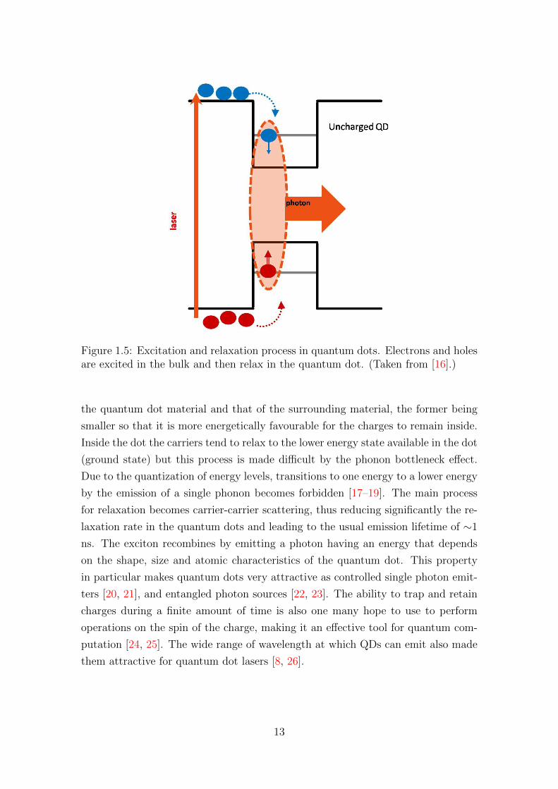
Figure 1.5: Excitation and relaxation process in quantum dots. Electrons and holesare excited in the bulk and then relax in the quantum dot. (Taken from [16].)
the quantum dot material and that of the surrounding material, the former being
smaller so that it is more energetically favourable for the charges to remain inside.
Inside the dot the carriers tend to relax to the lower energy state available in the dot
(ground state) but this process is made difficult by the phonon bottleneck effect.
Due to the quantization of energy levels, transitions to one energy to a lower energy
by the emission of a single phonon becomes forbidden [17–19]. The main process
for relaxation becomes carrier-carrier scattering, thus reducing significantly the re-
laxation rate in the quantum dots and leading to the usual emission lifetime of ∼1
ns. The exciton recombines by emitting a photon having an energy that depends
on the shape, size and atomic characteristics of the quantum dot. This property
in particular makes quantum dots very attractive as controlled single photon emit-
ters [20, 21], and entangled photon sources [22, 23]. The ability to trap and retain
charges during a finite amount of time is also one many hope to use to perform
operations on the spin of the charge, making it an effective tool for quantum com-
putation [24, 25]. The wide range of wavelength at which QDs can emit also made
them attractive for quantum dot lasers [8, 26].
13

1.2 Motivations: why are quantum dots desir-
able?
While the fabrication and optical properties of quantum dots are fascinating to
study as they bring valuable insight about the electronic behaviour of solids at a
quantum level, one might also be motivated by the prospect of finding for these
nanostructures a real life application. Though the work presented in this thesis
is mainly a work of observation and not oriented towards immediate industrial
application, it is still interesting to non-exhaustively review a few applications where
quantum dots have or are foreseen to have a significant role.
1.2.1 Quantum dot lasers
The laser, or Light Amplification by Stimulated Emission of Radiation is one of the
most important invention of the 20th century. It has a huge range of applications in
our everyday life, such as communications, medical probing and surgery, military,
and it is also an essential element for scientific research. The gain medium which
forms the main part of the laser can be made of various materials, the most used
being gas (like helium-neon), doped crystal (titanium-sapphire), or semiconductor
(diode lasers). Recently there has been interest in building lasers using quantum
dots as their amplification material. Performances of quantum dot lasers has been
investigated, and compare well to that of gas lasers. The advantages of QD lasers
compared to quantum well lasers dwell in the quantized energy levels of QDs. It
offers a high temperature stability of the threshold current density (up to 180 K),
as well as an optimized gain [27]. Since QDs have properties similar to atoms, QD
lasers avoid the negative aspects of bulk and quantum well semiconductor lasers,
while having the huge advantage that the wavelength of the emitted light depends
on the size and composition of the quantum dots. This widely opens the wavelength
operation range for this type of laser compared to other types [28–30].
1.2.2 Entangled photon emitters
Entanglement is a theoretical quantum state of two particles where the properties
of one can be measured through the other, independently of the physical distance
separating them. Many applications could ensue from this phenomenon, including
quantum computation [24, 25, 31], quantum teleportation for instant communica-
tion [32, 33], or superdense coding which consists in coding two classical bits of
information into one quantum bit [34].
14

Recently bi-excitons in quantum dots have been proposed as entangled photon
pair emitters [23], and later a system consisting of a quantum dot diode has been
implemented, providing a compact and controllable source of entangled photon
pairs [22]. Quantum dot emitters would prove an invaluable system for generating
entangled photons, as it can generate them on demand and trigger emissions one
by one, a feature not matched by other systems using optical parametric down
conversion[35, 36].
1.2.3 Quantum bit: a possible candidate?
Quantum information theory has been imagined as a possible enhancement of cur-
rent classical binary computation, by using the counter-intuitive properties of quan-
tum mechanics [37]. The principle is to consider in the place of classical bit assuming
values of only zero or one, a quantum bit (q-bit) that could not only take the values
|0〉 and |1〉, but also a linear combination |0〉+ |1〉 of both. By implementing circuits
with newly imagined logic gates likes Hadamard and Control-Not, it is possible for
certain computational operations like factorisation of large numbers or database
searching to be achieved much faster than with a classical method [25].
Though the theory has been well defined for a few decades now, we are still
looking to physically implement the system. Electron spins have been proposed
as q-bits due to their impressive coherence time (∼200 µs) [31]. The spin could
then be transmitted through photons emitted by quantum dots. Electron spins in
coupled quantum dots have also been considered as a possible quantum gate for
computation [38].
1.3 Quantum dot fabrication
A low dimensional structure can only be of use for large scale application if we
manage to reproduce it. For the last two decades various techniques have emerged
and evolved to produce high quality quantum dot structures. The present section
describes the main techniques used to obtain the samples the main chapters of this
thesis are based upon, as well as some other widely studied types of quantum dots.
15

1.3.1 Epitaxial techniques
The typical semiconductor sample is a disc comprised of a thin (less than 1 mm)
substrate with the active layers on top. The substrate is obtained from ingots of
highly pure semiconductor grown by crystallization of melted material. The in-
got is then sliced into thin discs by a wire saw. Wafers made of silicon are widely
used in industry but compound semiconductor wafers can also be obtained with the
same technique. The growth of the active layers on top of this wafer requires more
complex techniques, the two main ones being molecular beam epitaxy (MBE) and
metal-organic vapour phase epitaxy (MOVPE) also called metal-organic chemical
vapour deposition (MOCVD) [39, 40].
MBE has been developed in 1968 in Bell Telephone Laboratories [41], it is a
process by which elements (such as Gallium, Arsenic, Phosphorus...) are heated
up to sublimation and deposited on the surface of the wafer, maintained at a high
temperature of several hundreds of C. There the atoms assemble epitaxially (in
an ordered crystalline way). The operation relies primarily on high or ultra-high
vacuum (10−8 Pa) and slow deposition rate to achieve a very high level of material
purity. MOCVD on the other hand, is a different process that removes the need for
high vacuum. The material is grown by a chemical process rather than depositing
sublimated pure components. Elements like Indium or Phosphorus are provided
to the wafer through pure gases such as Trimethylindium (In(CH3)3) or Phosphine
(PH3), which react at the surface leaving the atom of interest ordered in the crystal
and a gaseous by-product of the reaction (like methane), later evacuated. For this
reaction to take place, the wafer needs to be heated at temperature of 500 or 600C, in order to break the atomic bonds of the gaseous reactants.
MOCVD is particularly useful for the growth of P-based materials, as phospho-
rus is difficult to evaporate through MBE. A more complete comparison of the two
techniques can be found in a 1984 work by Dapkus [42]. These techniques allow
growth of semiconductor material on a monolayer rate, and therefore have been
used extensively for the growth of thin layers (among which quantum wells) as well
as micro and nanostructures as we’ll see in the next paragraph.
1.3.2 Self-assembled quantum dots
The layer-by-layer growth process described in the previous paragraph is well adapted
for the formation of thin layers like quantum wells, but they can also be used to
16
grow more complicated nanostructures like quantum wires and quantum dots. The
formation of quantum dots uses interesting surface physics effects that will be qual-
itatively described in this paragraph.
It has been discovered in the late eighties that quantum dots formed natu-
rally during the growth of epitaxial layers [43]. This phenomenon called Stranski-
Krastanov regime has been studied and originates from lattice mismatch at the
interface of different materials. Since the growth of the material is epitaxial, the
atoms arrange themselves in a crystal lattice, but when a material is deposited on
top of a different one, with different lattice size, there is formation of strain at the
interface: the atoms of the new material have to adapt to the lattice size of the
material onto which they are grown, but physically they tend to arrange with their
own lattice size. Such situation occurs for example in the case when InAs is grown
on top of GaAs, the two materials having ∼7% mismatch between their respective
lattice characteristic sizes. After the deposition of the new material reaches a crit-
ical thickness (which depends on the amplitude of the mismatch) [44], the strain
becomes such that it is more energetically favourable for the atoms to form islands.
The process is described in figure 1.6.
After the islands have grown into pyramidal aggregates of the desired size (de-
pending on the concentration of material deposited, but generally between 5 and
100 nm on the side of the base), they are capped with the same material onto which
they have been grown. Those dots are levelled by the newly grown layers until they
reach a shape of truncated pyramid, or sometimes that of a lens, depending on how
the islands were formed. The layer below the critical thickness is similar to a quan-
tum well and is called wetting layer. Self-assembled quantum dots are composed of
104 to 106 atoms.
Such quantum dots are called self-assembled, due to the minimal human inter-
vention during their formation. As stated above, self-assembled quantum dots can
be made of silicon, germanium, or be compounded of III and V elements (GaAs,
InP, GaN) or II and VI elements (CdSe, ZnTe, etc...). The works depicted in this
thesis are focused exclusively on III-V quantum dots. Typical emission wavelengths
of III-V QDs span from 690 nm (InP) to 950 nm (InGaAs), this wavelength does
not only depend on the material used but also on the shape and size of the dot,
which can be controlled by varying growth parameters like substrate temperature
or deposition rate [44].
17

Figure 1.6: Illustration of the Stranski-Krastanov process: a) lattice mismatchbetween two materials causes strain (left) and dislocations (right) if it is largeenough. (Taken from [7].) b) After deposition of a critical thickness hc, strainrelaxation induces the formation of an island. (Taken from [45].)
1.3.3 Interface fluctuations from quantum wells
Some structures can present the same properties of charge confinement without ac-
tually being clearly limited in all three directions. It is the case for the so-called
interface quantum dots, formed by interface fluctuations of ultra-thin layers (usu-
ally quantum wells). In the growth direction the charges are confined due to the
difference in material bandgaps, and in the lateral directions the difference of one
monolayer of the material makes it more spatially confined, and therefore it requires
more energy for the trapped charge to escape. The principle is illustrated in the
image in figure 1.7.
It is noteworthy that the width of the well must be smaller than the exciton
radius in bulk material (of the order of 10 nm in GaAs [6]) in order for the exciton
to be confined and effectively trapped in the interface fluctuations. Such nanos-
tructures have been discovered in quantum wells in the early nineties [46] and have
been the first zero-dimensional semiconductor structures studied, shortly before the
18

Figure 1.7: Illustration of a lateral view of a quantum dot created by interfacefluctuation of thin layers of alternating semiconductor materials.
self-assembled kind. They present many differences with self-assembled. They are
not strained, which can be an advantage as their formation does not create dislo-
cations. Although they are well confined in the growth direction due to the small
thickness of the quantum wells, their confinement in the lateral direction is weaker
as it originates from a thickness fluctuation of the quantum well. The main reason
why they are much less attractive compared with self-assembled is that unlike the
latter, it is not possible to easily control their shape and size, and through that
their optical properties. Chapter 3 of this thesis is based on a sample exhibiting
interface fluctuations quantum dots.
1.3.4 Other types of quantum dots
There are other types of zero-dimensional nanostructures not addressed in this work,
a non-exhaustive list of which is provided in this paragraph:
• Colloidal quantum dots are semiconductor nanocrystals obtained by a
chemical synthesis. Precursor compounds are dissolved in a solution and start
agglomerating upon heating into clusters of 102 to 105 atoms. The particu-
larity of those quantum dots is that they are in liquid form, unlike the other
types which are in solid state form. Colloidal quantum dots are one of the
most promising methods for large-scale commercial applications, their synthe-
sis is also known to be the least toxic. Colloidal quantum dots are interesting
for biomedical applications, due to their free particle nature [47].
• Another way to obtain in a material the properties of quantum dots is to
electrically pattern a two-dimensional electron gas. An electrode is litho-
19
graphically designed on top of a 2D structure filled with charges, typically
a quantum well, and by applying a voltage between the gate and back elec-
trodes, the charges, already confined in one direction due to the nature of the
quantum well, are confined in the other two directions by the electric field.
This kind of structure is called gated quantum dot.
• Within the same material different kind of crystal structures can grow. It has
been demonstrated that when growing a nanowire of InP, the atoms could be
ordered as a zinc-blende structure, much similar to most bulk semiconductors,
but also as a wurtzite structure. Alternating the growth of both structures
in a quantum wire would confine the charges in the direction of the wire, due
to the difference in bandgap between the two types of crystal. Such quantum
dots have been dubbed crystal phase quantum dots [48].
1.4 Experimental work on quantum dots
As seen in section 1.2 quantum dots are attractive in a wide range of domains, but
they are not yet ready for large scale industrial applications. To this end, further
understanding of their optical properties and the different ways to fabricate them is
necessary. This section describes the main experimental techniques used to study
quantum dots and what informations we can gather from them.
1.4.1 Micro-photoluminescence
The quantum dots studied in this thesis are all III-V self-assembled or interface
fluctuations, emitting in the 700 nm or 950 nm regions. It has been said in the
previous sections that quantum dots were good photon emitters. Indeed because of
their direct band-gap, III-V materials can easily absorb and emit electromagnetic
energy. Studying quantum dot emissions using micro-photoluminescence is the most
direct way to obtain informations about their shape and size [49], energy levels [7],
and spin polarization [50]. The experiment consists in exciting the sample with a
laser while it is cooled at cryogenic temperature below 10 K and observe the resulting
photoluminescence. This photoluminescence is diffracted through a spectrometer
and directed at a charge-coupled device, providing a complete emission spectrum of
the sample. First we’ll go through the processes occurring under optical excitation,
and then we’ll describe the hardware used for the experiment.
20

Optical processes under excitation In our experiments the QD sample is
excited non resonantly, which means the energy of the laser is greater than the
bandgap of the semiconductor material surrounding the dots. Electrons and holes
are excited in the bulk and then can either recombine at any point to emit a pho-
ton, or be trapped in a quantum dot (see section 1.1.4). When an electron and
a hole relax into a quantum dot they form a Coulombic bond and result in an
electron-hole pair that is usually called exciton. The exciton eventually recombines
by emitting a photon with a frequency corresponding to the bandgap of the quan-
tum dot. This phenomenon is best observed at a low temperature of below 10
K. At higher temperatures thermal processes becomes non-negligible and dominate
optical emissions, resulting in a quenching of the photoluminescence. The average
recombination time or lifetime can vary depending on size and shape of the dot,
type of material and external factors but is generally of the order of the nanosecond
for InGaAs self-assembled quantum dots [51].
If the surrounding bulk is saturated with charge carriers (which happens when
the sample is excited with a high number of photons, or in other terms in the case
where we use a high power of laser excitation) additional carriers can relax into
the quantum dot before the first exciton recombines. The new electron and hole
each fill the next available energy states, following the Pauli exclusion principle.
The quantum dot then contains a bi-exciton, and with more electron-hole pairs a
tri-exciton, etc... [52, 53]. It can also happen that a single electron or a single
hole is trapped in the quantum dot. This can occur naturally due to the imperfect
shape of the dot but it is also possible to control the charge in the dot by using an
electric field. This technique is described in section 1.4.3 and in chapter 4. When an
electron-hole pair relaxes into the dot it produces a trion, negatively or positively
charged, depending on the nature of the particle present at ground state [52, 54, 55].
The study of charged exciton is very attractive for the purpose of implementing
spin q-bit with the spin of single electrons or holes [56, 57]. The hole being a
quasiparticle with a spin angular momentum of 3/2, unlike the electron whose spin
angular momentum is 1/2, the exciton can have either a total spin of ±1 (bright
exciton), a state which can emit or absorb a photon, or a total spin of ±2 (dark
exciton), which is a state having a low probability of emitting a photon. Charged
excitons can also be dark, it corresponds to the cases where the two electrons(holes)
have identical spin, and to the cases where the electrons(holes) have different spins
but the single hole(electron) has opposite spin from the electron(hole) at ground
state [58–60]. Dynamics of dark excitons will not be described further in this thesis.
21

Experimental setup The sample is placed into a cryostat filled or flowing with
liquid helium, decreasing its temperature to less than 10 K. It is excited with a
HeNe red laser emitting at 650 nm and collimated by a microscope objective. The
setup is described on figure 1.8.
Figure 1.8: Schematics of the experimental photoluminescence setup.
The radiative efficiency of the quantum dot is almost 100% but it can happen
in any direction upon a solid angle of 720. The fraction of that angle that is
not totally reflected at the interface between semiconductor and vacuum (around
2% for GaAs) is then collected through the microscope objective and directed at a
monochromator. A charge coupled device at the exit of the monochromator allows
to see a spectrum of light emitted by the sample. Such a spectrum is comprised
of an inhomogeneously broad emission from recombinations happening in the bulk
semiconductor (usually between 800 and 850 nm for GaAs), at lower energy we
find the broad emission of the wetting layer and on the higher energy side of this
emission the quantum dots. Studying the spectrum emitted by a sample containing
22
quantum dots would in principle allow the observation of specific lines of energy
corresponding to the various excitonic complexes that can be trapped inside quan-
tum dots. The intensity of those lines depends on the number of photons emitted
by the dots, which in turn depends on the quality of the growth, the nature of
the materials used, the quantum dots recombination rate and the intensity of the
excitation source. The dot lines are not exactly homogeneous because of electrical
noise, instead taking the form of a broad line with width spanning between 50 and
200 µeV [61, 62].
The microscope objective is a key element for the observation of single dot emis-
sion lines. Without it, due to the large sample area covered by the laser spot (of the
order of the hundreds of µm), and the high density of dots yielded by the Stranski-
Krastanov growth method (from 108 cm−2 to 1012 cm−2) the number of quantum
dots actually observed would be too high to be able to observe them individually,
resulting in an inhomogeneously broadened ensemble PL. The microscope objective
focuses the beam on the sample to a spot size as small as 1 µm of diameter. This
allows single quantum dots to be observed individually. To observe and fully study
single quantum dots it is desirable to have an even smaller density of lines. This
can be achieved by using a metal mask containing apertures with a diameter of a
few hundreds of nm. With this apparatus the lines are well isolated and can be
studied separately.
1.4.2 Measurement of fine structure splitting
When an electron in a neutral quantum dot becomes excited, it can have a spin
up or down (corresponding respectively to a |−1〉 and |+1〉 exciton). The same
is true for charged excitons: the spin of the single hole (electron) of the excited
state can have a spin up or down. Those are two states having the same energy
which means the spectral line observed by photoluminescence is actually two-fold
degenerate [55]. This degeneracy can be lifted using a magnetic field since it adds
a linear term depending on the total spin of the exciton to its energy. This lifting
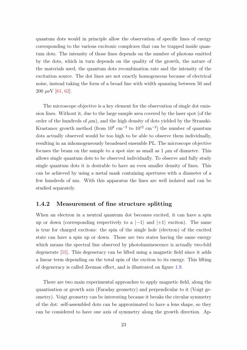
of degeneracy is called Zeeman effect, and is illustrated on figure 1.9.
There are two main experimental approaches to apply magnetic field, along the
quantisation or growth axis (Faraday geometry) and perpendicular to it (Voigt ge-
ometry). Voigt geometry can be interesting because it breaks the circular symmetry
of the dot: self-assembled dots can be approximated to have a lens shape, so they
can be considered to have one axis of symmetry along the growth direction. Ap-
23
Figure 1.9: Illustration of the Zeeman effect: the application of a magnetic field liftsthe degeneracy on energy levels (b), splitting the original spectral line into several(a). From Del Pozo-Zamudio et al. [63].
plying a magnetic field in the Faraday geometry conserves this symmetry whereas
a magnetic field in Voigt geometry creates an in-plane anisotropy. It allows for the
observation of dark excitons (fig. 1.9 (a) bottom and (b) left) [55]. Zeeman splitting
can give us information about the electronic and hole g-factor, as well as the diamag-
netic shift, a quantity useful for the determination of dot shape and dimensions [50].
The degeneracy can also be lifted naturally when the dot’s shape cannot be
approximated to be symmetric. The fine structure splitting that results is generally
of the order of 50 µeV [64, 65]. For neutral excitons the light emitted by the two
states is linearly polarized. If the fine structure splitting is smaller than the broad-
ening of the lines it is not possible to observe it, but since one state is horizontally
polarized and the other vertically, the shift in energy from one state to the other
can be observed using a linear polarizer. Such an experiment is described in chapter
3.
1.4.3 Charge control using electric field
To observe one specific excitonic complex can prove difficult if we have no way to
trigger them on demand. One of the main experimental approaches to tune the
24

charge occupancy of a dot is through an electric field. In a quantum dot sample
processed as a Schottky diode the electric field is applied between the quantum dot
region and a doped region and allows control over the resident charge in the dot [52].
This principle is described in figure 1.10: a gate contact and a back contact are fab-
ricated respectively on the surface of the sample and under the quantum dot region.
Figure 1.10: Illustration of electrically controlled charging of quantum dots. (a) Thelayer structure of the sample shows that a voltage applied at the gate (right) wouldcreate a current of charges between the dots and the back contact (left), modifyingthe energy diagram in (b). Depending on the applied voltage, the ground statelevel of the dot can be above or below the Fermi level, in which latter case electronswould be able to tunnel into the dot. Figure taken from [54].
The layer structure is illustrated in figure 1.10(a), the sample then acts as a
Schottky diode due to the presence of a doped (n or p) layer just below the back
contact. As can be seen in 1.10(b), a modification in the voltage applied on the
gate contact will change the energy level of the dot, bringing it on demand below
or above the Fermi level of charge carriers originating from the doped layer. If
the quantum dot level is brought below the Fermi level, electrons (or holes in the
case of p-doping) tunnel into the dot, allowing us to engineer a dot into a neutral,
positively or negatively charged dot. The barrier between the dots and the back
contact is usually of the order of 50 nm thick [52]. Schottky diode structures are
widely used in the study of quantum confined Stark effect [66, 67]. They are the
25

main topic of chapter 4.
1.5 Organization of the thesis
The present thesis is organized in the following way. Three projects are presented
in three different chapters. Though they can be only slightly correlated and not
always based on the same sample, they have in common to investigate the optical
properties of quantum dots grown in a way that has not been done before, or with
a material not widely studied before.
Chapter 2 relates to the study of self-assembled InAs quantum dots grown mono-
lithically on silicon, and their coupling with photonic crystal cavities. The quality of
the cavities, fabricated for the first time on a silicon substrate, is asserted as well as
the single photon emission ability of the dots. Chapter 3 is based on the same sam-
ple, but the investigation focuses on quantum dots formed by interface fluctuations
of GaAs/AlGaAs thin layer superlattices. Optical properties, fine structure split-
ting and photon anti-bunching are studied. Finally, in chapter 4 characterization
of quantum dots grown from a new combination of material, InPAs, is conducted.
Samples with various concentrations of arsenic have their emission spectra com-
pared, and Schottky diode fabrication allows for study of the dots under controlled
electric field.
26
References
[1] Wgsimon, “Transistor Count and Moore’s Law - 2011.” http:
//en.wikipedia.org/wiki/File:Transistor_Count_and_Moore%27s_
Law_-_2011.svg, May 2011.
[2] G. E. Moore, “Cramming more components into integrated circuits,” Electron-
ics, vol. 38, 1965.
[3] Michler, Peter, Single Quantum Dots. Topics in Applied Physics, Springer,
2003.
[4] M. S. Skolnick and D. J. Mowbray, “SELF-ASSEMBLED SEMICONDUCTOR
QUANTUM DOTS: Fundamental Physics and Device Applications,” Annual
Review of Materials Research, vol. 34, no. 1, pp. 181–218, 2004.
[5] D. leadley, “Electronic band structure.” http://www2.warwick.ac.uk/fac/
sci/physics/current/postgraduate/regs/mpags/ex5/bandstructure/,
Jul 2011.
[6] M. Fox, Optical Properties of Solids (Oxford Master Series in Physics, 3).
Oxford University Press, USA, 2001.
[7] A. N. Vamivakas and M. Atature, “Photons and (artificial) atoms: an overview
of optical spectroscopy techniques on quantum dots,” Contemporary Physics,
vol. 51, pp. 17–36, Dec. 2009.
[8] D. Bimberg, Quantum dot heterostructures. Berlin: John Wiley and Sons,
1999.
[9] Masumoto, Y and Takagahara, T, Semiconductor Quantum Dots. Nanoscience
and Technology, Springer, 2002.
[10] V. A. Shchukin and D. Bimberg, “Spontaneous ordering of nanostructures on
crystal surfaces,” Reviews of Modern Physics, vol. 71, pp. 1125+, July 1999.
27

[11] P. Reiss, M. Protiere, and L. Li, “Core/Shell Semiconductor Nanocrystals,”
Small, vol. 5, pp. 154–168, Jan. 2009.
[12] M. Bruchez, M. Moronne, P. Gin, S. Weiss, and A. P. Alivisatos, “Semiconduc-
tor Nanocrystals as Fluorescent Biological Labels,” Science, vol. 281, pp. 2013–
2016, Sept. 1998.
[13] S. Kumar and T. Nann, “Shape Control of II-VI Semiconductor Nanomateri-
als,” Small, vol. 2, pp. 316–329, Mar. 2006.
[14] I. A. Akimov, K. V. Kavokin, A. Hundt, and F. Henneberger, “Electron-hole
exchange interaction in a negatively charged quantum dot,” Physical Review
B, vol. 71, pp. 075326+, Feb. 2005.
[15] J. Shah, Ultrafast Spectroscopy of Semiconductors and Semiconductor Nanos-
tructures. Springer, 1999.
[16] A. I. Tartakovskii, “Nuclear magnetic resonance in quantum dots.” Symposium
on Semiconductor Nano-Photonics for Quantum Information Science, Sep 2013.
[17] U. Bockelmann and G. Bastard, “Phonon scattering and energy relaxation
in two-, one-, and zero-dimensional electron gases,” Phys. Rev. B, vol. 42,
pp. 8947–8951, Nov 1990.
[18] H. Benisty, C. M. Sotomayor-Torres, and C. Weisbuch, “Intrinsic mechanism
for the poor luminescence properties of quantum-box systems,” Phys. Rev. B,
vol. 44, pp. 10945–10948, Nov 1991.
[19] J. Urayama, T. B. Norris, J. Singh, and P. Bhattacharya, “Observation of
phonon bottleneck in quantum dot electronic relaxation,” Phys. Rev. Lett.,
vol. 86, pp. 4930–4933, May 2001.
[20] J. Kim, O. Benson, H. Kan, and Y. Yamamoto, “A single-photon turnstile
device,” Nature, vol. 397, pp. 500–503, Feb. 1999.
[21] A. J. Shields, “Semiconductor quantum light sources,” Nat Photon, vol. 1,
pp. 215–223, 2007.
[22] C. L. Salter, R. M. Stevenson, I. Farrer, C. A. Nicoll, D. A. Ritchie, and A. J.
Shields, “An entangled-light-emitting diode,” Nature, vol. 465, pp. 594–597,
June 2010.
28

[23] R. M. Stevenson, R. J. Young, P. Atkinson, K. Cooper, D. A. Ritchie, and
A. J. Shields, “A semiconductor source of triggered entangled photon pairs,”
Nature, vol. 439, pp. 179–182, Jan. 2006.
[24] D. Deutsch, “Quantum theory, the church-turing principle and the universal
quantum computer,” Proceedings of the Royal Society of London. A. Mathe-
matical and Physical Sciences, vol. 400, no. 1818, pp. 97–117, 1985.
[25] T. Hey, “Quantum computation: an introduction.” https://www.
researchgate.net/publication/3363605_Quantum_computing_an_
introduction?ev=srch_pub, Sept. 1999.
[26] D. Liang and J. E. Bowers, “Recent progress in lasers on silicon,” Nat Photon,
vol. 4, no. 8, pp. 511–517, 2010.
[27] N. N. Ledentsov, V. M. Ustinov, V. A. Shchukin, P. S. Kop’ev, Z. Alferov, and
D. Bimberg, “Quantum dot heterostructures: Fabrication, properties, lasers
(Review),” Semiconductors, vol. 32, no. 4, pp. 343–365, 1998.
[28] Y. Arakawa and H. Sakaki, “Multidimensional quantum well laser and tem-
perature dependence of its threshold current,” Applied Physics Letters, vol. 40,
no. 11, pp. 939–941, 1982.
[29] “Fujitsu, university of tokyo develop world’s first 10gbps quantum dot
laser featuring breakthrough temperature-independent output.” http://www.
fujitsu.com/global/news/pr/archives/month/2004/20040910-01.html.
[30] A. Banerjee, T. Frost, and P. Bhattacharya, “Nitride-based quantum dot visible
lasers,” Journal of Physics D: Applied Physics, vol. 46, pp. 264004+, July 2013.
[31] J. L. O’Brien, A. Furusawa, and J. Vuckovic, “Photonic quantum technologies,”
Nat Photon, vol. 3, pp. 687–695, Dec. 2009.
[32] C. H. Bennett, G. Brassard, C. Crepeau, R. Jozsa, A. Peres, and W. K. Woot-
ters, “Teleporting an unknown quantum state via dual classical and Einstein-
Podolsky-Rosen channels,” Physical Review Letters, vol. 70, pp. 1895–1899,
Mar. 1993.
[33] X.-S. Ma, T. Herbst, T. Scheidl, D. Wang, S. Kropatschek, W. Naylor,
B. Wittmann, A. Mech, J. Kofler, E. Anisimova, V. Makarov, T. Jennewein,
R. Ursin, and A. Zeilinger, “Quantum teleportation over 143 kilometres using
active feed-forward,” Nature, vol. 489, pp. 269–273, Sept. 2012.
29

[34] C. H. Bennett and S. J. Wiesner, “Communication via one- and two-particle
operators on Einstein-Podolsky-Rosen states,” Physical Review Letters, vol. 69,
pp. 2881–2884, Nov. 1992.
[35] Y. H. Shih and C. O. Alley, “New Type of Einstein-Podolsky-Rosen-Bohm Ex-
periment Using Pairs of Light Quanta Produced by Optical Parametric Down
Conversion,” Physical Review Letters, vol. 61, pp. 2921–2924, Dec. 1988.
[36] T. E. Kiess, Y. H. Shih, A. V. Sergienko, and C. O. Alley, “Einstein-Podolsky-
Rosen-Bohm experiment using pairs of light quanta produced by type-II para-
metric down-conversion,” Physical Review Letters, vol. 71, pp. 3893–3897, Dec.
1993.
[37] C. Cohen-Tannoudji, B. Diu, and F. Laloe, Mecanique quantique. Enseigne-
ment des sciences, Hermann, 1973.
[38] D. Loss and D. P. DiVincenzo, “Quantum computation with quantum dots,”
Physical Review A, vol. 57, pp. 120–126, Jan. 1998.
[39] Aixtron, How MOCVD works. Deposition Technology for Beginners. Aixtron
SE, 2011.
[40] P. M. Petroff and S. P. DenBaars, “MBE and MOCVD growth and proper-
ties of self-assembling quantum dot arrays in III-V semiconductor structures,”
Superlattices and Microstructures, vol. 15, pp. 15+, Jan. 1994.
[41] A. Y. Cho and J. R. Arthur, “Molecular beam epitaxy,” Progress in Solid State
Chemistry, vol. 10, pp. 157–191, Jan. 1975.
[42] P. D. Dapkus, “A critical comparison of MOCVD and MBE for heterojunction
devices,” Journal of Crystal Growth, vol. 68, pp. 345–355, Sept. 1984.
[43] P. M. Petroff, A. Lorke, and A. Imamoglu, “Epitaxially self-assembled quantum
dots,” Physicstoday, vol. 54, pp. 46+, May 2001.
[44] A. Baskaran and P. Smereka, “Mechanisms of Stranski-Krastanov growth,”
Journal of Applied Physics, vol. 111, pp. 044321–044321–6, Feb. 2012.
[45] Acarlso3, “Adsorbate island showing interfacial dislocations.” http://en.
wikipedia.org/wiki/File:DislocatedIsland.png, Dec 2007.
30

[46] A. Zrenner, L. V. Butov, M. Hagn, G. Abstreiter, G. Bohm, and G. Weimann,
“Quantum dots formed by interface fluctuations in AlAs/GaAs coupled quan-
tum well structures,” Physical Review Letters, vol. 72, pp. 3382–3385, May
1994.
[47] J. . M. Klostranec and W. . C. . W. Chan, “Quantum Dots in Biological and
Biomedical Research: Recent Progress and Present Challenges,” Adv. Mater.,
vol. 18, pp. 1953–1964, Aug. 2006.
[48] N. Akopian, G. Patriarche, L. Liu, J. C. Harmand, and V. Zwiller, “Crystal
Phase Quantum Dots,” Nano Lett., vol. 10, pp. 1198–1201, Mar. 2010.
[49] J. Shumway, A. J. Williamson, A. Zunger, A. Passaseo, M. DeGiorgi, R. Cin-
golani, M. Catalano, and P. Crozier, “Electronic structure consequences of
In/Ga composition variations in self-assembled InxGa1−xAs/GaAs alloy quan-
tum dots,” Physical Review B, vol. 64, pp. 125302+, Sept. 2001.
[50] M. N. Makhonin, K. V. Kavokin, P. Senellart, A. Lemaıtre, A. J. Ramsay, M. S.
Skolnick, and A. I. Tartakovskii, “Fast control of nuclear spin polarization in
an optically pumped single quantum dot,” Nat Mater, vol. 10, pp. 844–848,
Nov. 2011.
[51] I. J. Luxmoore, R. Toro, O. Del Pozo-Zamudio, N. A. Wasley, E. A.
Chekhovich, A. M. Sanchez, R. Beanland, A. M. Fox, M. S. Skolnick, H. Y.
Liu, and A. I. Tartakovskii, “III-V quantum light source and cavity-QED on
Silicon,” Sci. Rep., vol. 3, p. 1239, 2013.
[52] O. D. D. Couto, J. Puebla, E. A. Chekhovich, I. J. Luxmoore, C. J. Elliott,
N. Babazadeh, M. S. Skolnick, A. I. Tartakovskii, and A. B. Krysa, “Charge
control in InP/(Ga,In)P single quantum dots embedded in Schottky diodes,”
Physical Review B, vol. 84, pp. 125301+, Sept. 2011.
[53] N. A. J. M. Kleemans, J. van Bree, A. O. Govorov, J. G. Keizer, G. J. Hamhuis,
R. Notzel, Silov, and P. M. Koenraad, “Many-body exciton states in self-
assembled quantum dots coupled to a Fermi sea,” Nat Phys, vol. 6, pp. 534–538,
July 2010.
[54] R. J. Warburton, C. Schaflein, D. Haft, F. Bickel, A. Lorke, K. Karrai, J. M.
Garcia, W. Schoenfeld, and P. M. Petroff, “Optical emission from a charge-
tunable quantum ring,” Nature, vol. 405, pp. 926–929, June 2000.
31
[55] M. Bayer, G. Ortner, O. Stern, A. Kuther, A. A. Gorbunov, A. Forchel,
P. Hawrylak, S. Fafard, K. Hinzer, T. L. Reinecke, S. N. Walck, J. P. Rei-
thmaier, F. Klopf, and F. Schafer, “Fine structure of neutral and charged ex-
citons in self-assembled In(Ga)As/(Al)GaAs quantum dots,” Physical Review
B, vol. 65, pp. 195315+, May 2002.
[56] A. J. Ramsay, S. J. Boyle, R. S. Kolodka, J. B. B. Oliveira, J. Skiba-Szymanska,
H. Y. Liu, M. Hopkinson, A. M. Fox, and M. S. Skolnick, “Fast Optical Prepa-
ration, Control, and Readout of a Single Quantum Dot Spin,” Physical Review
Letters, vol. 100, pp. 197401+, May 2008.
[57] T. M. Godden, J. H. Quilter, A. J. Ramsay, Y. Wu, P. Brereton, S. J. Boyle,
I. J. Luxmoore, J. Puebla-Nunez, A. M. Fox, and M. S. Skolnick, “Coherent
Optical Control of the Spin of a Single Hole in an InAs/GaAs Quantum Dot,”
Physical Review Letters, vol. 108, pp. 017402+, Jan. 2012.
[58] C. Schuller, K. B. Broocks, C. Heyn, and D. Heitmann, “Oscillator strengths
of dark charged excitons at low electron filling factors,” Physical Review B,
vol. 65, pp. 081301+, Jan. 2002.
[59] D. Andronikov, “Charged exciton complexes (trions) in low dimensional struc-
tures,” conference paper, June 2005.
[60] A. J. Shields, M. Pepper, M. Y. Simmons, and D. A. Ritchie, “Spin-triplet neg-
atively charged excitons in GaAs quantum wells,” Physical Review B, vol. 52,
pp. 7841+, Sept. 1995.
[61] P. Borri, W. Langbein, S. Schneider, U. Woggon, R. L. Sellin, D. Ouyang, and
D. Bimberg, “Ultralong Dephasing Time in InGaAs Quantum Dots,” Physical
Review Letters, vol. 87, pp. 157401+, Oct. 2001.
[62] A. V. Kuhlmann, J. Houel, A. Ludwig, L. Greuter, D. Reuter, A. D. Wieck,
M. Poggio, and R. J. Warburton, “Charge noise and spin noise in a semicon-
ductor quantum device,” Nat Phys, vol. 9, pp. 570–575, Sept. 2013.
[63] O. Del Pozo-Zamudio, J. Puebla, E. Chekhovich, R. Toro, A. Krysa, R. Bean-
land, A. M. Sanchez, M. S. Skolnick, and A. I. Tartakovskii, “Growth and
magneto-optical characterization of InPAs/GaInP Quantum Dots,” Unpub-
lished, 2013.
32

[64] D. Gammon, E. S. Snow, B. V. Shanabrook, D. S. Katzer, and D. Park, “Fine
Structure Splitting in the Optical Spectra of Single GaAs Quantum Dots,”
Physical Review Letters, vol. 76, pp. 3005–3008, Apr. 1996.
[65] R. Toro, O. Del Pozo-Zamudio, M. N. Makhonin, J. Dixon, A. M. Sanchez,
R. Beanland, H.-Y. Liu, M. S. Skolnick, and A. I. Tartakovskii, “Visible light
single photon emitters monolithically grown on silicon,” Unpublished, 2013.
[66] P. W. Fry, I. E. Itskevich, D. J. Mowbray, M. S. Skolnick, J. J. Finley, J. A.
Barker, E. P. O’Reilly, L. R. Wilson, I. A. Larkin, P. A. Maksym, M. Hop-
kinson, M. Al-Khafaji, J. P. R. David, A. G. Cullis, G. Hill, and J. C. Clark,
“Inverted electron-hole alignment in InAs-GaAs self-assembled quantum dots,”
Physical Review Letters, vol. 84, pp. 733+, Jan. 2000.
[67] P. W. Fry, I. E. Itskevich, S. R. Parnell, J. J. Finley, L. R. Wilson, K. L. Schu-
macher, D. J. Mowbray, M. S. Skolnick, M. Al-Khafaji, A. G. Cullis, M. Hop-
kinson, J. C. Clark, and G. Hill, “Photocurrent spectroscopy of InAs/GaAs
self-assembled quantum dots,” Physical Review B, vol. 62, pp. 16784+, Dec.
2000.
33

Chapter 2
Optical characterization and
cavity coupling of InAs/GaAs
quantum dots monolithically
grown on silicon substrate
2.1 Introduction
Silicon chips have been used as our main computing technology for the last four
decades, with a number of transistors per chip doubling every two years as predicted
by Moore’s law. Since last decade though the scalability of bulk silicon technology
has reached a limitation, prompting the fake solution of dividing computational
tasks between multiple cores. To reach the next level of computing one must find a
way of making operations that differ from the usual open/closed electricity current
flow. Encoding bits of data into the spin of photons is one way of doing it that is
heavily investigated since the nineties [1]. It would also allow for entanglement of
particles (in this case photons) leading to a new, more effective way of computing,
the so-called quantum information processing (QIP) [2]. Photonic technology is also
of prime importance for domains such as quantum lithography and quantum cryp-
tography. To replace silicon complementary metal-oxide semiconductor (CMOS)
technology, the same type of material has been used, only in the form of nanostruc-
tures instead of bulk [3, 4]. Indeed a group IV semiconductor like silicon is praised
by industry for its low cost of fabrication, its robustness and the possibility to easily
create insulation layers by growing silicon oxide. Also being a state of the art tech-
nology, silicon processing is much more attractive for industry. On the other hand,
silicon’s indirect band gap makes it a mediocre light emitter, whereas compound
34

semiconductors like III-V have direct band gap providing best opto-electronic ca-
pabilities, and better electron mobility. Furthermore, single photon emission have
been demonstrated [5], a feature essential for any quantum manipulation.
A straightforward solution is to integrate III-V quantum emitters with existing
silicon technology, feasibility of which is demonstrated in this chapter through the
optical and structural study of InGaAs quantum dots monolithically grown on a
silicon substrate, and embedded in photonic crystal microcavities [6].
First the sample structure will be discussed, then the quantum dots and the
quality of cavities, then single photon emission demonstration, and finally strong
coupling opening door to quantum electrodynamics.
2.2 Structural study
2.2.1 Previous attempts at growing III-V on IV
As explained in the introduction, the integration of compound semiconductors (III-
V, or II-VI) with group IV is desirable among other things for quantum and classical
computation. Though the first attempts can be traced back as early as 1962, the
purpose there was to make hybrid heterojunctions with better characteristics for
electronic applications [7]. Also the growth of GaAs on an intermediate substrate
of germanium, due to the similar lattice constant of the two materials [8], does
not present the same challenges as with silicon, whose lattice mismatch with III-V
ranges from 4% to 8% (see paragraph 2.2.3). In later years, the need of bringing
III-V optical capabilities with the high efficiency of state of the art Si technology
became more apparent, and in 1984 Wang managed one of the first growths of
GaAs/AlGaAs on silicon [9]. Less than a year later Metze from MIT realized a
metal-semiconductor field-effect transistor (MESFET) with good device character-
istics from GaAs layers grown directly on silicon [10]. As more studies were being
made on the subject [11, 12], growth techniques started to emerge to overcome the
issues of semiconductor hybridization and make it more suitable for the growth of
complex structures like quantum wells or quantum dots [13]. For the past decade
quantum dots fabricated on Si allowed for semiconductor lasers with good character-
istics to be integrated with silicon technology, opening the way to the introduction
of III-V to silicon photonics [14–16] (see figure 2.1).
35

Figure 2.1: Illustration of hybrid III-V/Si technology: in this hybrid Si FabryProtlaser, the InP active layers are bonded on a Si waveguide. Adapted from “Recentprogress in lasers on silicon” from Di Liang and John E. Bowers [14]
Now that coherent light sources are implemented on silicon, the next step to-
wards optical devices on silicon is the single photon emitter. Only recently was that
feature achieved, on one hand by Cavigli et al. using the method of droplet epitaxy
dots, grown on top of a Ge-on-Si virtual substrate [17] and on the other hand by
our team at University of Sheffield [6] based on a InAs quantum dots sample mono-
lithically grown on Si substrate by Hui-Yun Liu at University College London [16].
The present chapter is based on this last work.
2.2.2 Structure description
Now we will explore the structure of the sample grown by Liu et al.. It consists of a
phosphorus-doped silicon substrate oriented in the (100) direction, with a 4 offcut
towards the [110] plane. To remove surface oxidation, sample was maintained at
a high temperature of 900 C for 10 minutes. After cooling down the wafer, the
III-V part of the sample has been realized using molecular beam epitaxy (MBE),
starting with a 30 nm nucleation layer grown at 400 C with a low growth rate of
0.1 monolayers per second (ML/s). The remaining 970 nm of the GaAs were grown
at high temperature at a rate of 0.7 ML/s, accounting for a total contact layer of 1
µm, as can be seen on figure 2.2.
Next layers to be grown were dislocation filters [11, 18]. The strain filters consist
of a fourfold repetition of a more complex structure, composed of five layers of 10
nm thick In0.15Al0.85As, alternating with five layers of 10 nm thick GaAs, all of this
36

Figure 2.2: Layer structure of the sample.
capped with 300 nm of GaAs. On top of that is grown a short period superlattice
comprised of 50 times a 2 nm layer of Al0.4Ga0.6As topped with a 2 nm layer of GaAs.
On top of all that after a capping layer of 300 nm GaAs is a 1 µm thick
Al0.6Ga0.4As sacrificial layer, which is used for the fabrication of photonic crys-
tals described in paragraph 2.4.2, and on which lay the active layer of InAs self-
assembled quantum dots embedded in 140 nm GaAs (70 nm below and 70 nm
above). The quantum dots height has been engineered through the indium flush
technique [19], thus three samples have been grown with heights of 2 nm, 2.5 nm
and 3 nm.
37

2.2.3 Structure discussion
Due to huge lattice mismatch between silicon and GaAs, one finds it very difficult
to obtain high quality quantum dots and other nanostructures. Indeed the lattice
mismatch, of near 4% between Si and GaAs and 8% for Si and InP, favours the
creation of threading dislocations (they can be seen clearly on fig. 2.4), which
act as non-radiative recombination sites, thus potentially dramatically lowering PL
efficiency. Many a feature of this complex growth structure (described above) is
aimed at reducing the natural drawbacks of the semiconductor hybridization, mainly
by reducing the density of dislocations.
Nucleation layer
First to be taken into account is the growth temperature of the GaAs nucleation
layer. On top of the silicon substrate is grown a 1 µm layer of GaAs, and to in-
troduce this layer, the first 30 nm of GaAs are grown at a low temperature and
slow rate of 0.1 MonoLayer per second (ML/s) against the faster 0.7 ML/s for the
rest of the GaAs. The temperature at which the nucleation layer is grown has been
specifically engineered to reduce strain. Test growths at different temperatures have
shown a distinct reduction in strain density at 400 C [16], as can be seen in fig.
2.3. Three different samples have been grown, with nucleation layer temperature of
380 C, 400 C and 420 C, cross-sectional TEM image of the samples revealed a
significantly smaller density of defects in the 400 C sample, prompting the growth
of all subsequent samples at this temperature.
Figure 2.3: cross-sectional TEM image of Si/GaAs interface. The nucleation layeris grown at different temperatures: (a) 380 C, (b) 400 C, (c) 420 C. Images takenfrom [16].
38

Strain filter
Though being an optimized parameter for the growth of the nucleation layer, this
temperature of 400 C does not prevent the formation of a high density of defects
propagating through the full thickness of III-V material and greatly lowering photon
emission. To reduce the number of such dislocations a strain filter is still necessary.
An InAlAs/GaAs strained layer superlattice (SLS) is grown for that purpose. The
SLS have started to see a lot of studies and applications from the 70s when interest
was growing on mismatched compound semiconductor growth [13, 18, 20]. The
principle is to create an array of thin layers, alternating materials of mismatched
lattice parameter. Because of this mismatch, strain is naturally created in the SLS,
though due to the small thickness of the layers it does not propagate to the upper
layers. These strains capture or deviate the dislocations coming from the lower
layers, eventually reducing them by a huge percentage.
Figure 2.4: TEM image of the layer structure. The clearer layer on the bottom ofthe image is Si, strain formation can be seen on the upper III-V layers.
Indeed the effect can clearly be seen on figure 2.4 representing a cross-sectional
TEM image of the sample realized by A. Sanchez and R. Beanland from University
39

of Warwick. In a clear color, is the Si substrate. On top of it is the 1 µm layer of
GaAs presenting a high density of dislocations, which propagate along the growth
axis. The four InAlAs/GaAs superlattices can be observed located one after the
other in the middle top of the TEM image. After each of these SLS a smaller
number of dislocations is observed, finally giving a density of ∼ 6× 106 cm-2 at the
sample surface (measured from etch-pit density).
Antiphase disorder
Another source of dislocations is caused by the polar nature of III-V semiconductor.
Indeed III-V lattice is formed of two poles, an anion (arsenic in the case of GaAs)
and a cation (gallium) whereas silicon is a non-polar substrate. Since there is no or
little preference as to which ion is bound to the surface during the early stages of
the growth, it can lead to situations where a region starts with the cation plane and
another region starts with the anion plane, leading to atom mismatch (see figure
2.5). This phenomenon is called anti-phase disorder [11], and as can be seen on the
figure can also be caused by steps on the surface of the substrate. It has been found
though that starting the III-V growth with a prelayer of only one of the elements
effectively suppresses the formation of anti-phase domains [12].
Figure 2.5: Antiphase boundary for GaAs grown on a Ge substrate. (a)The twoantiphase domains started on the same plane, but with different atom deposition.(b)The two antiphase domains started with the same atom, but on two differentplanes separated by a one atom step. Figure taken from [11].
40

Smoothing layers
Since the main purpose of this sample is to make photonic crystal with cavities
as small as a few hundreds of nm, a smooth surface is desired. This is realized
by growing a short period superlattice (SPL, see fig. 2.4), alternating super thin
layers of GaAs and AlGaAs. This technique, though not tested, has been inspired
from Fischer et al. [11]. In this work the growth front after the first GaAs layer on
top of Si is revealed (by TEM) to be not planar, but shaped in pyramids and val-
leys. It was demonstrated that a superlattice of 40-period GaAs/AlGaAs reduces
the undulation amplitude of the growth front. It is not at the moment possible to
objectively assert of the effectiveness of this technique, but the undeniable great
quality and bright emission of QD and photonic crystal cavities on this sample can-
not be attributed only to the reduction of threading dislocations.
Additionally, this superlattice is interesting for its ability to show single QD-like
emissions. This property will be studied in chapter 3.
Indium flush
QDs can grow in a variety of shapes and sizes. In order to homogenize their emis-
sion one can cap their height to a fixed value using a technique such as indium flush
[21]. Also, as this material is aimed at silicon photonics applications, it makes sense
to limit the emission wavelength to less than 1 µm so that it can efficiently work
with silicon photon detectors. Furthermore, the use of this method facilitates the
achievement of low dot density, which can prove critical for single dot study.
The QDs in this sample have been capped with a thickness of GaAs smaller than
the natural height of the dots. This layer stabilizes around the dots as the InAs
islands are energetically unfavourable sites for the growth of GaAs. The sample
has then been annealed in an indium environment which caused desorption of the
resident indium in the dot parts that still emerged from the GaAs capping. This
technique is called indium flush. This resulted in the levelling of the dots at the
desired height of the first capping layer. The QDs are then capped with a second
layer of GaAs as in the usual growth method.
Techniques consisting of interrupting the capping of the dot layer in the aim
of controlling the dots shapes and properties have been called double capping [22]
or partial capping and annealing [23], and can be used with desorption of other
41

elements as well [19]. In our study presented in this chapter, three samples have
been realized, with different QD heights, respectively 2 nm, 2.5 nm and 3 nm. The
3 nm sample was chosen due to relatively low and uniform dot densities achieved
across the wafer.
Thermal expansion
The lattice constant of silicon crystal is 5.431 A whereas for GaAs crystal it is
5.65325 A. (All the values are taken from [24].) The lattice mismatch is there-
fore 4.09%. This mismatch changes during the growth as both materials have a
different thermal expansion coefficient. The linear thermal expansion coefficient α
of a material represents how a characteristic length of said material changes with
temperature. The coefficient itself is not a constant, but we can approximate the
expansion of the materials during the growth. If we take an average α of 3.5× 10⁻⁶
parts per K between 300 K and 675 K (growth temperature) for Si, and 5.73×10⁻⁶
parts per K for GaAs, we obtain a lattice constant during growth of 5.317 A and
5.66556 A for Si and GaAs respectively. The lattice mismatch is then 6.56 %. It
has been demonstrated that a difference of lattice mismatch between growth and
room temperatures can be the source of dislocations unless cooling rate is reduced
[25], this phenomenon is yet another possible cause of the high density of threading
dislocations in the sample.
2.3 Spectral landscape and optical properties
2.3.1 Micro-photoluminescence experimental setup
The setup used for the optical characterization (µPL) of the sample is the one de-
scribed in the previous chapter (see paragraph 1.4.1), except light can pass through
either a single or a double spectrometer. A flipping mirror would allow the light
emitted from the sample to be directed at the suitable spectrometer, after which
the light is collected by a charge-coupled device. The complete setup used for all
PL measurements in this chapter is represented figure 2.6. All measurements are
performed at a temperature of 10 K.
The single spectrometer is mounted with three gratings, respectively 300, 600
and 1200 grooves per millimetre (g/mm). While those gratings provide a smaller
resolution than the double spectrometer, the single light diffraction also means
less signal loss, and the better performances of the new CCD accounts for a much
42
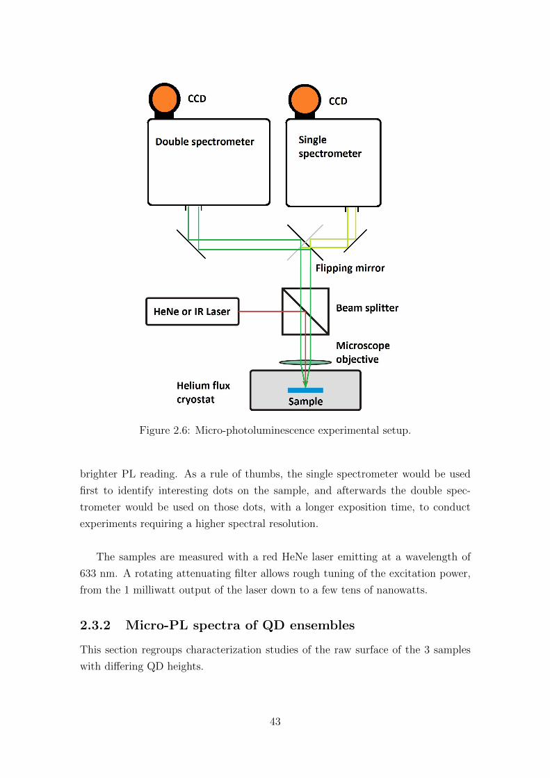
Figure 2.6: Micro-photoluminescence experimental setup.
brighter PL reading. As a rule of thumbs, the single spectrometer would be used
first to identify interesting dots on the sample, and afterwards the double spec-
trometer would be used on those dots, with a longer exposition time, to conduct
experiments requiring a higher spectral resolution.
The samples are measured with a red HeNe laser emitting at a wavelength of
633 nm. A rotating attenuating filter allows rough tuning of the excitation power,
from the 1 milliwatt output of the laser down to a few tens of nanowatts.
2.3.2 Micro-PL spectra of QD ensembles
This section regroups characterization studies of the raw surface of the 3 samples
with differing QD heights.
43
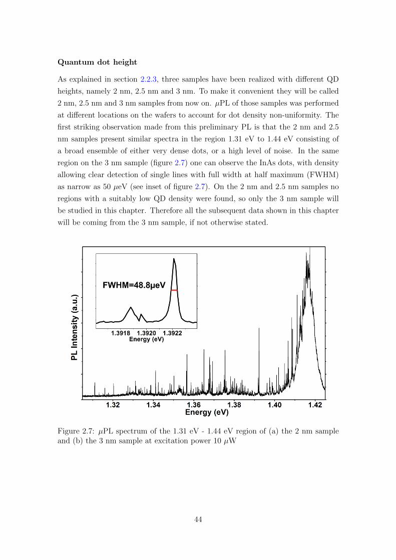
Quantum dot height
As explained in section 2.2.3, three samples have been realized with different QD
heights, namely 2 nm, 2.5 nm and 3 nm. To make it convenient they will be called
2 nm, 2.5 nm and 3 nm samples from now on. µPL of those samples was performed
at different locations on the wafers to account for dot density non-uniformity. The
first striking observation made from this preliminary PL is that the 2 nm and 2.5
nm samples present similar spectra in the region 1.31 eV to 1.44 eV consisting of
a broad ensemble of either very dense dots, or a high level of noise. In the same
region on the 3 nm sample (figure 2.7) one can observe the InAs dots, with density
allowing clear detection of single lines with full width at half maximum (FWHM)
as narrow as 50 µeV (see inset of figure 2.7). On the 2 nm and 2.5 nm samples no
regions with a suitably low QD density were found, so only the 3 nm sample will
be studied in this chapter. Therefore all the subsequent data shown in this chapter
will be coming from the 3 nm sample, if not otherwise stated.
Figure 2.7: µPL spectrum of the 1.31 eV - 1.44 eV region of (a) the 2 nm sampleand (b) the 3 nm sample at excitation power 10 µW
44

Description of the broad range PL spectrum
The broad range µPL spectrum represented on figure 2.8 allows observation of var-
ious features, most of which are expected from this kind of sample, but some of
unknown origin. InAs QD appear from 1.31 eV and up to 1.42 eV, followed by the
InAs wetting layer centred at 1.415 eV with slight variations of the order of the
tenth of meV depending on the position of the excitation spot on the surface of the
sample. The emission of GaAs bulk is located around 1.48 eV. Weaker PL features
can be observed at 1.445 eV and 1.465 eV. These are believed to come from the deep
strained layers of GaAs. Due to the structure of the sample (see figure 2.2), many
layers of bulk GaAs are grown between the strained layer superlattices besides the
GaAs capping layer, and each can have slightly different spectral properties.
Figure 2.8: Long range spectrum of the sample.
The last but not least feature of this full spectrum is the presence of undefined
sharp lines in the 1.81 eV - 1.82 eV region: those lines look identical to QD lines,
and also have narrow linewidth of 60 µeV. They are emitted by QD-like nanostruc-
tures formed by the interface fluctuations between the superthin GaAs/AlGaAs
superlattices. They have been extensively investigated in a study that is the topic
of chapter 3, and therefore will be left aside for the remnant of this chapter. It is
interesting to note that the interface dots appear with the same density and the
same PL brightness when the excitation spot is focused at any place on the surface
45

of the wafer, and as well on the 2 nm and 2.5 nm high dots wafers. Indeed those
dots being created by a process occurring in the lower layers have uniform charac-
teristics throughout the wafer, independent from the parameters used during the
growth of the InAs dots.
Density of dots
The density of dots is varying across the sample surface, following a gradient to-
ward the edge of the wafer. Figure 2.9 shows three different spectra representing
the characteristic densities of dots that can be found on the wafer.
Figure 2.9: µPL representation of dot density across the surface of the wafer. Insetleft: AFM image of the uncapped dots. Inset right: position of the measurementson the surface of the wafer.
From top to bottom the spectra are taken respectively in the centre of the
46

wafer, between the centre and the edge and at the top edge of the wafer. In the
inset of each spectrum is an atomic force microscope (AFM) image of the surface
of the sample at the corresponding place on the wafer, taken on uncapped test QDs
grown on the sample surface. The place onto which the AFM and µPL spectrum
have been acquired is represented in the right part of the inset, by a red point on
the blue wafer. The AFM pictures represent a 1 µm2 surface, where uncapped QDs
can be seen in a brighter colour. From the AFM data we can extract a dot density
of approximately 108 cm-2, 109 cm-2 and 1010 cm-2 for those places. Each spectrum
features a large and bright peak (1.435 eV for the top graph, 1.417 eV for the
bottom one) which is associated with the emission of the InAs wetting layer (WL).
On the lower energy side of the WL, single lines can be observed that grow more
numerous as the position on the wafer is close to the edge. An estimation of the
number of those QD lines ranges from a few units (top) to a few hundred (bottom),
which considering the laser excitation spot area of the order of 1 µm2 accounts for
a density of dot consistent with the AFM observations. One can notice by looking
at the PL intensity scale on the left that the intensity of the WL decreases with
increasing density of dot, and that the WL emission redshifts. The former can be
attributed to the higher number of carriers from the WL being captured by the
QDs to undergo radiative recombination, while the latter can be explained by a
higher In concentration. These observations are similar to the optical behaviour of
InGaAs/GaAs QD grown on III-V (GaAs) substrate [26].
Excitonic complexes characterization
Closer optical characterization has been brought to the sample to investigate exci-
tonic complexes and exciton binding energy. Particularly a study of PL intensity
of single lines with respect to excitation power allows determination of bi-excitons,
as their PL increases with power in a quadratic way, as opposed to neutral and
charged excitons increasing linearly. Figure 2.10 shows characterization of such a
neutral exciton/bi-exciton (X/XX) pair.
Fig. 2.10 (a) represents three PL spectra of two lines, here denoted X for the
exciton and XX for the bi-exciton. Each spectrum was acquired at a different exci-
tation power so the evolution of the photon count can be estimated: indeed it can
be seen that X appears and reaches saturation before the other line. The integrated
number of photon counts is plotted for each of the two lines against excitation power
in figure 2.10 (b). The X line is in black squares while the data representing XX are
red dots. Emission of the XX remains low up to 2 µW. Saturation of X peak is ob-
47

Figure 2.10: Optical characterization of a pair exciton/bi-exciton. (a) µPL mea-surement of the pair at three different excitation power, (b) integrated PL intensityof the same pair with respect to excitation power. The scales are logarithmic.
served at lower power than for XX: ∼ 3.5 µW and ∼ 8 µW, respectively. The scales
in figure 2.10 (b) being represented logarithmically, it is easy to observe the nature
of the power dependent PL: since X increases linearly and XX quadratically [27],
before saturation linear slopes can be expected on the logarithmic graph, with a
slope of 1 and 2 respectively for X and XX line. The two lines are fitted with a blue
straight line, whose slope is calculated to be respectively of 0.92 and 1.88, which
fits reasonably with the theory, and confirms the X/XX nature of this pair. Three
X/XX pairs measured across the sample exhibited binding energies of 1.18 meV,
1.56 meV and 2.43 meV. These results are reasonably in accordance with what can
be found in the literature for InGaAs QDs grown on GaAs substrate [26, 28]. The
disparity in binding energies can be explained by variations of quantum dot sizes
through the sample [28]. Such a variation in size can indeed be observed on the
AFM images in figure 2.9.
2.4 Photonic crystal cavities
Photonic crystal cavities (PCC) are microstructures that can be fabricated on the
sample to observe light-matter interactions. They have been fabricated on the sam-
ple by Isaac Luxmoore from our group in University of Sheffield. A more extensive
description of the device will be found in the next paragraph, after which the fabri-
cation process will be detailed. Finally, the performances of the PCC are revealed
through optical experimentation in the last paragraph of this section.
48

2.4.1 Principle
This paragraph is aimed at providing a general description of the principles of PCC.
A more in depth review of the mathematics involved will not be found in this thesis,
as the main domain of its author is semiconductor quantum dots, and the PCC are
merely used as a tool. The reader will be redirected to the corresponding literature:
[29].
The same way the goal of low dimensional semiconductors nanostructures like
quantum dots and quantum wells is to gain control over electric charges, photonic
crystals are a type of nanostructures that allow control over photons. In any bulk
material, the characteristics of the crystal lattice will dictate the behaviour of elec-
tron propagation in it. This phenomenon arises from the quantum nature of charges:
propagating as waves, their interaction with the periodic crystal of the medium will
be different depending on their wavelength characteristics. By extending this con-
cept, any medium can also block the propagation of certain wavelengths, leading
to band gaps in the energy band structure. By analogy, photons with specific
wavelengths can be trapped or directed within a periodic lattice, hence the name:
photonic crystal. In this case, the lattice would be formed of mediums with different
refractive indexes, this periodicity of refractive indexes would be to the photon what
the periodicity of crystal lattice atomic potential is to a charge carrier. A photonic
crystal could be periodic along one dimension, two or three (see figure 2.11).
Figure 2.11: Simple cases of one, two and three-dimensional photonic crystals. Thedifferent colors represent materials with different dielectric constant. Adapted from“Photonic Crystals: Molding the Flow of Light”, Joannopoulos 2008 [30]
49

By using the appropriate formation of materials, one can be able to confine
photons with specific wavelength, or to guide them in the same way a metallic
waveguide directs microwaves. These applications aim at using photons as spin
Q-bits. Another well-known application is to use a one-dimensional stack of al-
ternating layers of materials with different dielectric constants to block light with
a specific wavelength. This technique is commonly used in dielectric mirrors, di-
electric Fabry-Perot filters, and distributed Bragg reflectors. For a more extensive
review of the properties and applications of PCC, the reader is invited to read
“Photonic Crystals: Molding the Flow of Light” by John Joannopoulos [30].
The goal for this study is to have a QD physically placed inside a PCC, so that
an exciton inside the QD can enter in resonance with the photon that is trapped
in the cavity (cavity light mode). The interaction between photon and exciton will
then be studied in section 2.6.
2.4.2 Fabrication
The fabrication of PCC is enabled by the presence, below the GaAs layer that sur-
rounds the QD, of an AlGaAs sacrificial layer. The aim of this fabrication is to
obtain QDs embedded in a micrometric slab of GaAs surrounded by air in all three
directions (see figures 2.12, 2.13). The difference in dielectric constant between air
and GaAs would allow photons to reflect back into the slab and to interfere de-
structively with itself, unless its wavelength permits resonance with the cavity.
The fabrication procedure is the following: the cavities are first patterned over
the surface of the sample using electron beam lithography (EBL). For that purpose
a thin layer of resist is first deposited on the sample, and then the electron flux of
the EBL irradiates parts of the polymer, making it sensitive to solvent. The pattern
varies according to the type of cavity fabricated, for the L3 cavity represented in
the main part of figure 2.13 it consists in a triangular lattice of circular holes, with
lattice constant a = 255 nm to 260 nm and various hole radii of the order of 50 nm.
Within one cavity all holes have exactly the same radius. (It is interested to note
that by varying the exposure time of the EBL, the scattering of electrons on the
hard surface of the sample causes wider irradiation of the polymer film, resulting in
larger holes. The purpose of making holes with different radii will be explained in
paragraph 2.4.3.) The actual cavity is formed by the omission of three aligned holes,
effectively making an elongated bulk of GaAs surrounded with air holes (L3 cavity).
After solvent dipping, the holes are etched in the sample using inductively coupled
50
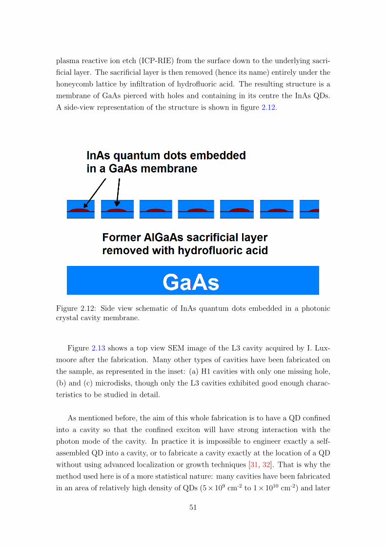
plasma reactive ion etch (ICP-RIE) from the surface down to the underlying sacri-
ficial layer. The sacrificial layer is then removed (hence its name) entirely under the
honeycomb lattice by infiltration of hydrofluoric acid. The resulting structure is a
membrane of GaAs pierced with holes and containing in its centre the InAs QDs.
A side-view representation of the structure is shown in figure 2.12.
Figure 2.12: Side view schematic of InAs quantum dots embedded in a photoniccrystal cavity membrane.
Figure 2.13 shows a top view SEM image of the L3 cavity acquired by I. Lux-
moore after the fabrication. Many other types of cavities have been fabricated on
the sample, as represented in the inset: (a) H1 cavities with only one missing hole,
(b) and (c) microdisks, though only the L3 cavities exhibited good enough charac-
teristics to be studied in detail.
As mentioned before, the aim of this whole fabrication is to have a QD confined
into a cavity so that the confined exciton will have strong interaction with the
photon mode of the cavity. In practice it is impossible to engineer exactly a self-
assembled QD into a cavity, or to fabricate a cavity exactly at the location of a QD
without using advanced localization or growth techniques [31, 32]. That is why the
method used here is of a more statistical nature: many cavities have been fabricated
in an area of relatively high density of QDs (5×109 cm-2 to 1×1010 cm-2) and later
51

Figure 2.13: SEM images of PCC structures fabricated on the sample. Main: L3cavity, (a) H1 cavity, (b) microdisk, (c) higher magnification of same microdisk.
in the laboratory environment measured until a suitable QD-in-cavity was found.
2.4.3 Characterization of the performances
A cavity can be characterized by two properties: its mode frequency and its quality
factor (Q-factor) [29]. The mode frequency is the frequency at which a photon is
in resonance with the cavity, which means the round trip of the photon trapped
into the cavity leads to constructive interference. The mode frequency depends on
the dimensions of the cavity and the dielectric constant (or refractive index) of the
medium. Since the latter is constant in the GaAs membrane, tuning of the cavity
mode frequency can be achieved through variations of characteristic lengths. For
that purpose the L3 cavities on the sample have been fabricated with various hole
radii, the clusters of cavities with a specific radius being sorted in columns on the
wafer surface for convenience. The cavities fabricated on the sample have mode
frequencies or energies ranging from 1.3 eV to 1.4 eV, effectively covering the range
of InAs QD energies (see figure 2.14).
The interesting characteristic here is the Q-factor that reflects the intrinsic qual-
ity of the cavity. It is a measurement of the how the cavity is not damped when it
52

Figure 2.14: PL spectra of three PCC with mode energy in the 1.31 eV region. Thefirst harmonic mode can be seen in the higher energy side, typically at 5.5 eV fromthe fundamental mode. Inset: PL of cavity with highest Q-factor measured fromPCC on the sample.
resonates, in other terms the higher the Q of an oscillator the longer it will resonate
[33, 34]. Indeed, in our case the Q is inversely proportional to the photon decay
rate of the cavity, which means the higher the Q, the longer a photon stays in the
cavity and have a chance to interact with the QD [29]. The properties of the Q-
factor and how it affects the performances of the cavity or its interaction with QDs
will be discussed in more detailed in the part concerning light-matter interaction,
in paragraph 2.6.1. Examples of the best Q-factors measured can be seen in figure
2.14 where they are measured by observing the cavity mode emission in µPL at low
temperature. The Q is estimated by the following formula:
Q =ω
∆ω(2.1)
where ω is the frequency of the cavity mode, and ∆ω is the FWHM of the cavity
mode emission. Among the 30 cavities investigated, Q-factors range from 6000 to a
maximum observed of 13000 (figure 2.14 inset), which is comparable with the best
quality cavities fabricated on III-V substrate over the last years. At this point it is
useful to remind that the whole structure that is studied in this chapter is grown
53

on silicon, making this quality very good indeed for a first attempt. More than 10%
of the observed cavities have Q of at least 10000, while the majority of the cavities
exhibit a Q over 9000, number widely accepted to be high enough to observe strong
coupling.
2.5 Single photon emission
As explained in the introductory section 2.1, one of the main goals of the study of
semiconductor nanostructures is to find a new way of computing, way that can be
achieved by manipulating exciton spins. While the electron and/or hole in a QD is
a potential good candidate for quantum operation, because of the solid state nature
of the material, to transport the information one needs a good carrier, and a photon
can accordingly fill this role. Therefore, the first essential ability researched in any
new semiconductor nanostructure material is the ability to emit single photons [35],
so that information can be passed reliably for example from one QD to another. This
study has been conducted on our sample based on auto-correlation data acquired by
our fellow group members N. Wasley and I. Luxmoore. It will be described in the
present section, first by its experimental procedure and then by the yielded results.
2.5.1 Experimental setup
The photon-correlation experiment, that measures the probability of any two pho-
tons to reach a detector at the same time, depending of the delay between their
emission, is conducted with a Hanbury Brown and Twiss interferometer (HBT).
Figure 2.15 represents a schematic of the HBT setup. The working principle is
the following: photons emitted from the sample, excited beforehand with a coher-
ent source, go through a beam splitter, and hit two avalanche photodiodes (APD)
placed on either ends of the beam splitter. An APD is a semiconductor device that
generates electrical current through photo-generation. It is constituted of a built-in
gain system using avalanche multiplication, meaning very low intensity light can
be converted into electricity, and therefore detected. This device is ideal for the
detection of photons, and that is the reason why it is a choice equipment for an
HBT setup. First, one has to make sure that all photons emitted from the sample
are coming from the same source, in this case a single QD. To achieve that, the best
way is to use a narrow bandpass filter tailored to the wavelength of the measured
QD, or to use a monochromator to separate the different frequencies of the light and
isolate the exact frequency at which the QD of interest emits. The latter solution
54

dramatically reduces the emission intensity though, and since photon-correlation
requires a lot of intensity to yield results in a timely manner, the former solution is
preferred. For this experiment a narrow band-pass filter centred around the source
QD emission wavelength and with transmission bandwidth of 2 nm has been used.
Figure 2.15: Hanbury Brown and Twiss experimental setup.
Upon reaching the separating beam splitter, photons have a 50% probability
of going one way or the other, and hit one of the two APDs. APDs are light
detectors sensitive enough to count accurately the number of photons. Each of them
is connected to a photon-counting module hardware in a computer onto which a
software draws the photon auto-correlation function using a method that will be
explained in the next paragraph.
55
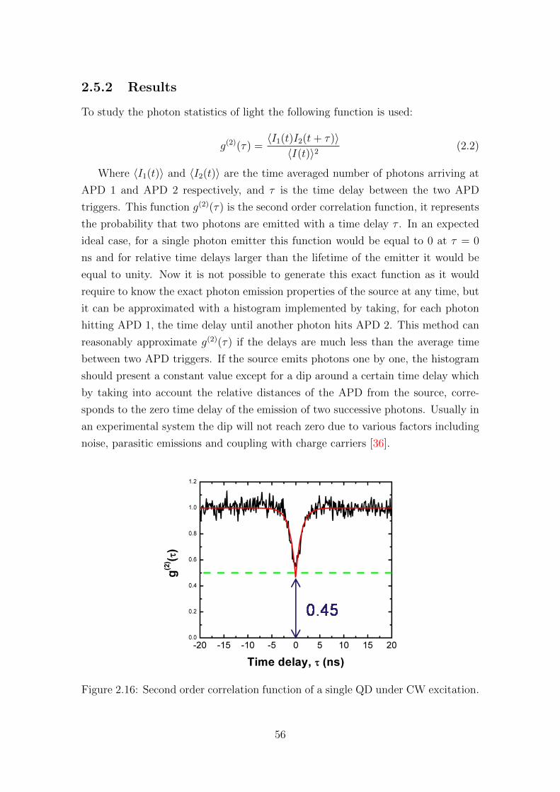
2.5.2 Results
To study the photon statistics of light the following function is used:
g(2)(τ) =〈I1(t)I2(t+ τ)〉〈I(t)〉2
(2.2)
Where 〈I1(t)〉 and 〈I2(t)〉 are the time averaged number of photons arriving at
APD 1 and APD 2 respectively, and τ is the time delay between the two APD
triggers. This function g(2)(τ) is the second order correlation function, it represents
the probability that two photons are emitted with a time delay τ . In an expected
ideal case, for a single photon emitter this function would be equal to 0 at τ = 0
ns and for relative time delays larger than the lifetime of the emitter it would be
equal to unity. Now it is not possible to generate this exact function as it would
require to know the exact photon emission properties of the source at any time, but
it can be approximated with a histogram implemented by taking, for each photon
hitting APD 1, the time delay until another photon hits APD 2. This method can
reasonably approximate g(2)(τ) if the delays are much less than the average time
between two APD triggers. If the source emits photons one by one, the histogram
should present a constant value except for a dip around a certain time delay which
by taking into account the relative distances of the APD from the source, corre-
sponds to the zero time delay of the emission of two successive photons. Usually in
an experimental system the dip will not reach zero due to various factors including
noise, parasitic emissions and coupling with charge carriers [36].
Figure 2.16: Second order correlation function of a single QD under CW excitation.
56

The result of the experiment realized on an InGaAs single QD located outside
the cavities and pumped with continuous-wave (CW) laser is represented figure
2.16. The measurement has been carried out with a HeNe laser at a low excitation
power of 2 µW, and took 1.4 hours to complete. The dip of 55% observed at time
delay τ = 0 ns accounts for clear anti-bunching. This demonstrates the single pho-
ton emitter nature of the InGaAs dots grown on silicon.
The result is further supported by the same experiment realized with pulsed
laser, this time on a QD located in a cavity (figure 2.17). The excitation used here
is a titanium-sapphire pulsed laser, with a 82 MHz pulse rate and a pulse duration
of 80 fs. The excitation power used for the experiment was 100 nW. The pulsed laser
experiment allows a more direct observation of the effect since the pulses are sepa-
rated in time (by 12 ns) so that only the central pulse (for time delay τ = 0 ns) is
affected by the quantum nature of the light. Here a clear reduction of the light field
of more than 80% achieves to prove single photon emission of the QD on the sample.
Figure 2.17: Second order correlation function of a single QD under pulsed excita-tion.
57
2.6 Light-matter coupling
This section, introduced by section 2.4 about photonic crystals, deals with the
most interesting results obtained with this sample: the coupling, at different levels,
of light and matter in InAs QD embedded in PCC fabricated directly on silicon
substrate. A more in-depth explanation of this phenomenon is to follow, then the
two levels of coupling observed will be displayed on subsequent paragraphs.
2.6.1 Principle
The coupling between a cavity mode and an atom (in our case a quantum dot)
situated in the centre of the cavity will happen if the transition energy of the atom
is in resonance with the photonic mode [29]. The level of coupling depends on
three parameters, the atom-photon coupling parameter g0, the photon decay rate
of the cavity κ and the non-resonant decay rate γ. The condition to have strong
coupling is that g0 Max(κ, γ), the condition to have weak coupling is g0 Max(κ, γ). Indeed, the atom-photon interaction represents the ability of the QD to
absorb or re-absorb a photon trapped in the cavity. If the QD can absorb a photon
faster than the photon being lost out of the cavity mode, there is a reversible
process of emission/absorption of photons from the QD. Reversely, if the atom-
photon interaction is not strong enough, the photon decays out of the cavity in
an irreversible manner. In the intermediate case where g0 is of the order of the
strongest leakage process rate of the cavity, strong coupling evidence can still be
seen though not as pronounced. The cavity decay rate is equal to the FWHM ∆ω of
the cavity mode, so as we’ve seen in paragraph 2.4.3 κ is related to Q by Q = ω/κ.
Now we can estimate the necessary Q-factor to observe strong coupling by using
the value of g0 (See chapter 10 from ref [29]):
g0 =
(µ212ω
2εhV0
)1/2
(2.3)
Where µ212 is the electric dipole moment of the quantum dot transition from
ground state to the first excited state, ε = ε0εr is the permittivity of the material,
h the reduced Planck constant and V0 the mode volume of the cavity. The mode
volume is the spatial integral over the electric field intensity [37], from previous
studies of properties of L3 cavities we can calculate it from:
V0 = 0.64(λ/n)3 (2.4)
With λ the wavelength of the photonic mode and n the refractive index of the
58

material [38]. By substituting g0 and κ, we find that the condition to be able to
observe strong coupling is:
Q ≈(
2ε0hωV0µ212
)1/2
(2.5)
By taking λ = 900nm and n = 3.598 for GaAs at this wavelength, we obtain
an estimate of the mode volume: V0 ≈ 9.99 × 10⁻²¹ m3. With a value for the
relative permittivity of GaAs of 12.9 and for an average value of µ212 ≈ 9 × 10⁻²⁹
Cm for the dipole moment, based on literature values both theoretical [39, 40] and
experimental [41], we obtain Q ≈ 7890.
As can be seen from the experimental results of section 2.4.3, the quality of
the cavities is good enough to observe strong coupling, provided the QD is located
relatively close to the maximum of the cavity mode. An off-centred QD would re-
sult in an increased non-resonant decay rate, and a regime of weak coupling instead.
At this point it is good to remind that the procedure for the fabrication of PCC
was to pattern them on the surface of the sample without any prior knowledge of
the position of the QD. Therefore, the position of QDs relative to cavities is the
limiting factor in the observation of any light-matter interaction, and a systematic
work had to be done to probe the cavities until an ideal system was found. The
next two sections will describe two such cavities, where weak and strong coupling
respectively has been observed.
2.6.2 Weak coupling
In the weak coupling regime, as seen in the previous section a photon emitted by
the QD quickly decays out of the cavity, making the process of emission irreversible.
But what is very interesting in this regime is that the spontaneous emission rate
of the QD is significantly modified by the cavity around it. This result has been
investigated by E. M. Purcell in 1946, and is therefore called Purcell effect (see E.
M. Purcell article on page 681 from ref. [42]). Indeed, the spontaneous emission
rate of the QD depends on the density of photon states available outside the dot,
density of states which has a different form based whether the QD is in free space
or inside a cavity. To calculate the effect of the cavity on the QD emission, we can
calculate the Purcell factor FP :
FP =W cav
W free(2.6)
59

W free and W cav are the spontaneous emission rates of the QD in free space and
inside the cavity respectively. The spontaneous emission rate has the following form
(calculated using Fermi’s Golden rule, see chapter 10.3 from ref. [29]):
W = ξ2πωµ2
12
hε0εrV0g(ω) (2.7)
ξ is a factor that evaluates the orientation of the dipole moment of the QD with
respect to the external electric field, and is equal to 1 when perfectly aligned. For a
QD that emits randomly in every directions (like in a free space) ξ2 will be averaged
to 1/3.
The main difference comes from the density of state function g(ω): for free space
the available states are a continuum which increases quadratically with ω:
gfree(ω) =ω2V0π2c3
(2.8)
Whereas in a cavity, the available states for the photon emitted by the QD are
reduced to the photonic mode of the cavity, which takes the form of a Lorentzian
function:
gcav(ω) =2
π∆ωc
∆ω2c
4(ω − ωc)2 + ∆ω2c
(2.9)
∆ωc and ωc are the FWHM and the frequency of the cavity mode, and are
related to the quality factor (equ. 2.1). When substituting into equation 2.6 we
obtain:
FP =3Q(λ/n)3
4π2V0ξ2
∆ω2c
4(ω − ωc)2 + ∆ω2c
(2.10)
As we can see, if the angular frequency ω of the QD emission is too far off
resonance with the cavity mode ωc, this factor rapidly decreases below unity and
close to 0. On the other hand, when the QD is in resonance with the cavity its
spontaneous emission rate can dramatically increase. Let’s estimate what would be
the Purcell factor for a cavity of 8000 Q factor: we assume the QD is in the centre
of the cavity, that its emission is perfectly in resonance and that its dipole is aligned
with the electric field in the cavity, we therefore have:
FP =3Q(λ/n)3
4π2V0(2.11)
Which for a Q = 8000, emission wavelength of 925 nm and refractive index and
60

mode volume as calculated in the previous section, gives a Purcell enhancement of
1034.71. Of course this is an ideal value, and is very unlikely to be observed in
our sample, due to the facts that it is very difficult to observe a QD located in the
maximum of the cavity mode, and that it is not possible to observe with µPL a dot
in resonance, its emission being completely covered by the photonic mode emission
line. This last issue can be overcome by using a dot coupled with a second or third-
order mode of a cavity. Lesser-order modes are broader and less bright than the
fundamental mode, so a QD emission in resonance with the mode can be visible on
PL. A reasonable Purcell enhancement has been observed by I. Luxmoore and is
illustrated on figure 2.18.
Figure 2.18: Time-resolved µPL of single dot emission in a photonic crystal cavity(red, lower curve) and in the unprocessed wafer (black, upper curve). The slightdifference in rise time could be explained by the difference of the complexes (excitonor bi-exciton) studied in each QD. The experimental conditions like laser pumppower were also not exactly the same for the two measurements, one of them havingits natural luminescence intensity enhanced by the cavity.
The figure represents a time-resolved µPL measurements of two dots, one being
taken on the raw surface of the wafer without cavity (denominated τbulk), and the
other being weakly coupled with the third-order mode of a cavity (τPC). The spon-
taneous emission rate of the QD in cavity is 1/τPC ≈ 1.54 × 10¹² s−1 is increased
compared to the one in the bulk 1/τbulk ≈ 0.91× 10¹² s−1, accounting for a Purcell
enhancement of ∼ 1.7, demonstrating weak coupling effect in the cavity. The huge
61

difference between the theoretical and experimental values of the Purcell enhance-
ment is partly due to the position of the dot off the maximum of the cavity mode,
but the main reason is the Q-factor of the third order mode, much smaller than
that of the fundamental mode (see equ. 2.1 and 2.11).
This result is important because increasing the photon emission rate of a QD
can be extremely useful for numerous applications, one of the main ones being
efficient single photon emitters. It is interesting to note that the results from section
2.5.2, figure 2.17 have been obtained on a QD in a cavity, exhibiting such Purcell
enhancement.
2.6.3 Strong coupling
When the QD-photon coupling is strong enough, a photon emitted by the QD is
reabsorbed before it can escape from the cavity, making the process reversible. This
regime of emission/absorption of the photon is called cavity quantum electrodynam-
ics (cavity-QED), a concept that has been studied for the first time by Jaynes and
Cummings in 1963 [43]. Such a complex phenomenon will not be mathematically
described here, as the aim of this thesis is the study of quantum dots.
Figure 2.19: The Jaynes-Cummings ladder describing the states of a coupled atom-photon system (right) and the same system without any coupling (left). Taken fromfigure 10.9 of ref. [29]
62

The principle can better be understood by looking at figure 2.19: the system
comprises an atom (in our case a quantum dot) with two states, ground labelled
|g〉 and excited |e〉, and a certain number of photons represented by the states |0〉,|1〉, ...|n〉 (in our system the only photon states we will consider will be |0〉 and
|1〉). The uncoupled states are represented on the left, the excited state of the total
system corresponds to either the state |g, 1〉 or the state |e, 0〉, which share the
energy (3/2)hω, making this first excited level degenerate. It would be the same
for each subsequent level if we had more than one photon in our cavity, the nth
energy level being contributed by both |g, n〉 and |e, n− 1〉. The effect of strong
coupling between the photon and the QD mixes the states and lifts the degeneracy
of energies, as depicted on the right part of figure 2.19 called the Jaynes-Cummings
ladder: the photon and QD are now one and only mixed system, where the first
excited state actually comprises two energies, separated by ∆E = 2hg0.
Such a system could be compared to the classical analogue, the coupled oscilla-
tors depicted figure 2.20: two oscillators with natural (uncoupled) frequencies of ω1
and ω2 respectively, linked by a spring giving a coupling strength Ω. The system
exhibit two frequencies:
ω± =(ω1 + ω2)
2±√
Ω2 + (ω1 − ω2)2 (2.12)
Which reduces when the natural frequencies of the two oscillators are equal (in
our case when the cavity is in resonance with the QD emission) to ω± = ω ± Ω,
where the frequency of the system is now “split” by the coupling strength of the
spring.
In our case we can estimate a possible splitting, provided we find a cavity with
a quantum dot strongly coupled to it and located reasonably close to the maximum
of the mode. This splitting is called the vacuum Rabi splitting, and we can calculate
it from the formula:
∆E = 2hg0 =
√2µ2
12hω
ε0εrV0(2.13)
With the values of our system and the same approximations made in paragraph
2.6.1, we obtain a value (ideal) of ∆E ≈ 349.8 µeV. This value of course is quite
high and would need perfect conditions to be obtained.
The observation of strong coupling in our work has been done experimentally
63

Figure 2.20: Schematics of coupled oscillators. Taken from figure 10.10 of ref. [29]
on the InGaAs QDs embedded in cavities and grown on silicon, by the following
method: first a cavity has to be found with a QD emission close enough to the
frequency of the fundamental mode of the cavity, on the higher energy side. As
mentioned earlier, the detected QD needs to be physically inside the cavity, but
since this information is impossible to verify, we have to probe cavities until we
find a suitable one (only one cavity exhibiting observable strong coupling has been
found, out of the 200 measured). The procedure is then to put the QD and mode
emission in resonance by raising the temperature, from 4 K and up to 50 K. Indeed,
the increase in temperature changes the refractive index of the cavity, redshifting
slightly its fundamental mode emission, whereas the quantum dot emission depend-
ing on the band gap of the semiconductor material is redshifted at a higher rate.
This leads at some point to the resonance of photonic mode and QD emission, such
an experiment is represented figure 2.21: the figure represents two µPL spectra of a
cavity mode with a QD emission slightly off-resonance (smaller peak on the higher
energy side, at 40 K), at multiple temperatures (increasing from bottom to top).
In fig. 2.21 (a) the QD and the cavity are not strongly coupled, we can see as
the temperature rises that the emission lines of the QD and the mode overlap. In
fig. 2.21 (b) the QD and the cavity mode are strongly coupled. Around T = 40 K
where the two emissions would be expected to overlap, instead we can see the lifting
of the degenerate energies of the mixed state as two peaks still appear. The QD
(mode) is represented at temperatures 35 K and 45 K with a red (blue) Lorentzian
fitting. The two peaks are clearly separated and never cross all along the temper-
ature sweep, this “anti-crossing” is the signature of strong coupling between the
64

Figure 2.21: µPL spectra at increasing temperature of a InAs QD slightly off-resonance with a cavity mode. (a) The QD and cavity are not strongly coupled.(b) The QD and cavity exhibit strong coupling.
photonic mode and the QD.
Figure 2.22 shows the plotted energies of the two lines from figure 2.21 (b) with
respect to temperature, where the anti-crossing is even more clearly depicted. The
red (blue) dashed lines represent the temperature dependence of the QD (cavity
mode) emission if they weren’t coupled. The upper and lower ensembles of plotted
values are fitted with the frequencies ω+ and ω− from equ. 2.12 of the classical
coupled oscillators (grey curves).
A reading of the energy splitting at the cross-section of the red and blue dashed
lines gives a vacuum Rabi splitting of: ∆E = 212 µeV, which is reasonably close
to the theoretical estimation of 350 µeV we have done earlier. This result is also
comparable to the highest Rabi splittings obtained with InGaAs QDs grown on
GaAs substrate [32, 44, 45], which is attributed to the high quality of our sample.
65

Figure 2.22: Energy dependence on temperature of the QD emission and photonicmode. The red (blue) dashed line represent the temperature dependence of theuncoupled QD (mode).
2.7 Conclusion
To summarize, we have studied InGaAs/GaAs quantum dot structures monolith-
ically grown on a silicon substrate, without use of germanium virtual substrate
nor wafer bonding technique. Optical characterization of the sample with micro-
photoluminescence showed very good single quantum dot emission lines with a
variable density across the wafer suitable both for single dot study and observation
of QD / photonic crystal cavity coupling, as well as unexpected but nevertheless
interesting high energy QD-like lines. Single photon emission from the InGaAs dots
have been demonstrated with photon correlation experiment showing clear anti-
bunching. Photonic crystal cavities fabricated on the sample exhibited very high
quality factor up to 13000 with a large percentage of cavities having Q-factors over
9000. This allowed observation of Purcell effect for single photon emitting QDs and
strong light-matter coupling between InGaAs QDs and cavities.
This work is one of the precursors in the study of single QDs grown on silicon,
and the first comprising photonic crystals, and is opening the way to future studies
in the fields of integration of III-V single photon emitters on silicon and cavity
quantum electrodynamics in hybrid III-V/Si structures.
66

References
[1] D. Deutsch, “Quantum theory, the church-turing principle and the universal
quantum computer,” Proceedings of the Royal Society of London. A. Mathe-
matical and Physical Sciences, vol. 400, no. 1818, pp. 97–117, 1985.
[2] T. Hey, “Quantum computation: an introduction.” https://www.
researchgate.net/publication/3363605_Quantum_computing_an_
introduction?ev=srch_pub, Sept. 1999.
[3] J. E. Sharping, K. F. Lee, M. A. Foster, A. C. Turner, B. S. Schmidt, M. Lipson,
A. L. Gaeta, and P. Kumar, “Generation of correlated photons in nanoscale
silicon waveguides,” Opt. Express, vol. 14, pp. 12388–12393, Dec 2006.
[4] D. Bonneau, E. Engin, K. Ohira, N. Suzuki, H. Yoshida, N. Lizuka, M. Ezaki,
C. M. Natarajan, M. G. Tanner, R. H. Hadfield, S. N. Dorenbos, V. Zwiller,
J. L. O’Brien, and M. G. Thompson, “Qantum interference and manipulation
of entanglement in silicon wire waveguide quantum circuits,” New J. of Phys.,
vol. 14, p. 045003, 2012.
[5] O. Benson, C. Santori, M. Pelton, and Y. Yamamoto, “Regulated and entan-
gled photons from a single quantum dot,” Phys. Rev. Lett., vol. 84, pp. 2513–
2516, Mar 2000.
[6] I. J. Luxmoore, R. Toro, O. Del Pozo-Zamudio, N. A. Wasley, E. A.
Chekhovich, A. M. Sanchez, R. Beanland, A. M. Fox, M. S. Skolnick, H. Y.
Liu, and A. I. Tartakovskii, “III-V quantum light source and cavity-QED on
Silicon,” Sci. Rep., vol. 3, p. 1239, 2013.
[7] R. Anderson, “Experiments on ge-gaas heterojunctions,” Solid-State Electron-
ics, vol. 5, no. 5, pp. 341 – 351, 1962.
[8] L. Knuuttila, A. Lankinen, J. Likonen, H. Lipsanen, X. Lu, P. McNally, J. Ri-
ikonen, and T. Tuomi, “Low Temperature Growth GaAs on Ge,” Japanese
Journal of Applied Physics, vol. 44, pp. 7777+, Nov. 2005.
67

[9] W. I. Wang, “Molecular beam epitaxial growth and material properties of GaAs
and AlGaAs on Si (100),” Applied Physics Letters, vol. 44, no. 12, pp. 1149–
1151, 1984.
[10] G. M. Metze, H. K. Choi, and B.-Y. Tsaur, “Metal-semiconductor field-effect
transistors fabricated in gaas layers grown directly on si substrates by molecular
beam epitaxy,” Applied Physics Letters, vol. 45, no. 10, pp. 1107–1109, 1984.
[11] R. Fischer, W. T. Masselink, J. Klem, T. Henderson, T. C. McGlinn, M. V.
Klein, H. Morkoc, J. H. Mazur, and J. Washburn, “Growth and properties of
GaAs/AlGaAs on nonpolar substrates using molecular beam epitaxy,” Journal
of Applied Physics, vol. 58, no. 1, pp. 374–381, 1985.
[12] R. Fischer, H. Morkoc, D. A. Neumann, H. Zabel, C. Choi, N. Otsuka,
M. Longerbone, and L. P. Erickson, “Material properties of high-quality GaAs
epitaxial layers grown on Si substrates,” Journal of Applied Physics, vol. 60,
no. 5, pp. 1640–1647, 1986.
[13] Z. Mi and Y.-L. Chang, “III-V compound semiconductor nanostructures on
silicon: Epitaxial growth, properties, and applications in light emitting diodes
and lasers,” J. Nanophoton., vol. 3, p. 031602, 2009.
[14] D. Liang and J. E. Bowers, “Recent progress in lasers on silicon,” Nat Photon,
vol. 4, no. 8, pp. 511–517, 2010.
[15] S. Sakai, T. Soga, M. Takeyasu, and M. Umeno, “Room-temperature laser
operation of algaas/gaas double heterostructures fabricated on si substrates
by metalorganic chemical vapor deposition,” Applied Physics Letters, vol. 48,
no. 6, pp. 413–414, 1986.
[16] T. Wang, H. Y. Liu, A. Lee, F. Pozzi, and A. Seeds, “1.3-m InAs/GaAs
quantum-dot lasers monolithically grown on Si Substrates,” Opt. Express,
vol. 19, p. 11381, 2011.
[17] L. Cavigli, S. Bietti, N. Accanto, S. Minari, M. Abbarchi, G. Isella, C. Frigeri,
A. Vinattieri, M. Gurioli, and S. Sanguinetti, “High temperature single photon
emitter monolithically integrated on silicon,” Applied Physics Letters, vol. 100,
no. 23, p. 231112, 2012.
[18] G. C. Osbourn, “Strained-Layer Superlattices: A Brief Review,” IEEE J.
Quantum Electron., vol. 9, p. 1677, 1986.
68

[19] C. Paranthoen, N. Bertru, O. Dehaese, A. L. Corre, S. Loualiche, B. Lam-
bert, and G. Patriarche, “Height dispersion control of InAs/InP quantum dots
emitting at 1.55 µm,” Applied Physics Letters, vol. 78, no. 12, pp. 1751–1753,
2001.
[20] J. W. Matthews and A. E. Blakeslee, “Defects in epitaxial multilayers, I: Misfit
dislocations,” J. Cryst. Growth, vol. 27, pp. 118–125, 1974.
[21] S. Fafard, Z. R. Wasilewski, C. N. Allen, D. Picard, M. Spanner, J. P. Mc-
Caffrey, and P. G. Piva, “Manipulating the energy levels of semiconductor
quantum dots,” Phys. Rev. B, vol. 59, pp. 15368–15373, Jun 1999.
[22] J. M. Ulloa, P. M. Koenraad, E. Gapihan, A. Letoublon, and N. Bertru, “Dou-
ble capping of molecular beam epitaxy grown InAs/InP quantum dots studied
by cross-sectional scanning tunneling microscopy,” Applied Physics Letters,
vol. 91, no. 7, p. 073106, 2007.
[23] L. Wang, A. Rastelli, and O. G. Schmidt, “Structural and optical properties of
in(ga)as/gaas quantum dots treated by partial capping and annealing,” Journal
of Applied Physics, vol. 100, no. 6, p. 064313, 2006.
[24] Ioffe Physical Technical Institute, “Characteristics of semiconductors.” http:
//www.ioffe.ru/SVA/NSM/Semicond/.
[25] M. Tachikawa and H. Mori, “Reduction of dislocation generation for heteroepi-
taxial III-V/Si by slow cooling,” Journal of Crystal Growth, vol. 183, p. 89,
1997.
[26] R. Oulton, Optical Spectroscopy of Single Self-Assembled InGaAs/GaAs Quan-
tum Dots. PhD thesis, The University of Sheffield, 2003.
[27] K. Brunner, G. Abstreiter, G. Bohm, G. Trankle, and G. Weimann, “Sharp-line
photoluminescence and two-photon absorption of zero-dimensional biexcitons
in a gaas/algaas structure,” Phys. Rev. Lett., vol. 73, pp. 1138–1141, Aug 1994.
[28] M. Bayer, V. D. Kulakovskii, T. Gutbrod, and A. Forchel, “Exciton complexes
in InGaAs/GaAs quantum dots,” Physica B: Condensed Matter, vol. 249-251,
pp. 620–623, June 1998.
[29] M. Fox, Quantum Optics: An Introduction (Oxford Master Series in Physics,
6). Oxford University Press, USA, June 2006.
69

[30] J. D. Joannopoulos, S. G. Johnson, J. N. Winn, and R. D. Meade, Photonic
Crystals: Molding the Flow of Light. Princeton University Press, second ed.,
February 2008.
[31] A. Badolato, K. Hennessy, M. Atature, J. Dreiser, E. Hu, P. M. Petroff,
and A. Imamoglu, “Deterministic Coupling of Single Quantum Dots to Sin-
gle Nanocavity Modes,” Science, vol. 308, pp. 1158–1161, May 2005.
[32] K. Hennessy, A. Badolato, M. Winger, D. Gerace, M. Atature, S. Gulde, S. Falt,
E. L. Hu, and A. Imamoglu, “Quantum nature of a strongly coupled single
quantum dot-cavity system,” Nature, vol. 445, pp. 896–899, Feb. 2007.
[33] J. H. Harlow, Electric Power Transformer Engineering. CRC Press, 2004.
[34] M. Tooley, Electronic Circuits : Fundamentals and Applications. Routledge,
2006.
[35] A. J. Shields, “Semiconductor quantum light sources,” Nat Photon, vol. 1,
pp. 215–223, 2007.
[36] A. Kiraz, S. Falth, C. Becher, B. Gayral, W. V. Schoenfeld, P. M. Petroff,
L. Zhang, E. Hu, and A. Imamoglu, “Photon correlation spectroscopy of a
single quantum dot,” Phys. Rev. B, vol. 65, p. 161303, Mar 2002.
[37] K. Vahala, Optical Microcavities (Advanced Series in Applied Physics, 5).
World Scientific Publishing Co Pte Ltd, Dec. 2004.
[38] A. R. A. Chalcraft, S. Lam, D. O’Brien, T. F. Krauss, M. Sahin, D. Szymanski,
D. Sanvitto, R. Oulton, M. S. Skolnick, A. M. Fox, D. M. Whittaker, H.-Y.
Liu, and M. Hopkinson, “Mode structure of the l3 photonic crystal cavity,”
Applied Physics Letters, vol. 90, no. 24, p. 241117, 2007.
[39] J. Wang, D. Shang, H. Mao, J. Yu, Q. Zhao, P. Yang, and H. Xing, “Influence
of strain on built-in dipole moment in asymmetric InxGa1−xAs quantum dot
molecules,” Applied Physics A, vol. 109, no. 2, pp. 391–394, 2012.
[40] F. Bernardot, E. Aubry, J. Tribollet, C. Testelin, M. Chamarro, L. Lombez, P.-
F. Braun, X. Marie, T. Amand, and J.-M. Gerard, “Linear and dynamical pho-
toinduced dichroisms of InAs/GaAs self-assembled quantum dots: Population
relaxation and decoherence measurements,” Phys. Rev. B, vol. 73, p. 085301,
Feb 2006.
70

[41] P. W. Fry, I. E. Itskevich, D. J. Mowbray, M. S. Skolnick, J. J. Finley, J. A.
Barker, E. P. O’Reilly, L. R. Wilson, I. A. Larkin, P. A. Maksym, M. Hop-
kinson, M. Al-Khafaji, J. P. R. David, A. G. Cullis, G. Hill, and J. C. Clark,
“Inverted electron-hole alignment in inas-gaas self-assembled quantum dots,”
Phys. Rev. Lett., vol. 84, pp. 733–736, Jan 2000.
[42] E. M. Purcell, “Spontaneous Emission Probabilities at radio Frequencies,”
Physical Review Online Archive (Prola), vol. 69, p. 681, June 1946.
[43] E. T. Jaynes and F. W. Cummings, “Comparison of quantum and semiclassical
radiation theories with application to the beam maser,” Proceedings of the
IEEE, vol. 51, pp. 89–109, Jan. 1963.
[44] A. Laucht, F. Hofbauer, N. Hauke, J. Angele, S. Stobbe, M. Kaniber, G. Bohm,
P. Lodahl, M. C. Amann, and J. J. Finley, “Electrical control of sponta-
neous emission and strong coupling for a single quantum dot,” New Journal of
Physics, vol. 11, pp. 023034+, Feb. 2009.
[45] M. Winger, A. Badolato, K. J. Hennessy, E. L. Hu, and A. Imamoglu, “Quan-
tum dot spectroscopy using cavity quantum electrodynamics,” Physical Review
letters, vol. 101, pp. 226808+, Nov. 2008.
71

Chapter 3
GaAs/AlGaAs single photon
emitters from interface
fluctuations of short period
superlattice monolithically grown
on silicon substrate
3.1 Introduction
Chapter 2 introduced the need to merge existing silicon technology with more ef-
ficient semiconductor photon emitters. Back then the single photon emitters in
question were self-assembled quantum dots, but although they are the most widely
studied quantum dots since 1993-1994 [1, 2], the first referenced study or predic-
tion of zero-dimensional nanostructures traces back to the early 80s [3–6], when
Weisbuch predicted that interface fluctuations in the well-known two-dimensional
quantum well structure could cause trapping of charges leading to exciton confine-
ment in all three directions. Later the phenomenon was experimentally observed
and described in AlGaAs/GaAs quantum wells by Zrenner et al. in 1994 [5], who
coined the “interface fluctuation quantum dot” term.
Discovering such nanostructures in our sample provides a very good and unex-
pected opportunity for two reasons: first III-V on silicon is getting a lot of attention,
and a more complete understanding and mastery of the techniques to grow such
structures can only be acquired through the study of various different combinations
72

of materials. Indeed research on quantum technologies is still at an early stage, and
no contender for physical implementation of quantum devices has taken a signifi-
cant lead over the others. Secondly, the usually higher energy emission of interface
dots (in the region of visible red light or near infrared) compared to InGaAs self-
assembled dots, make them good candidates for other applications like a new type
of free-space communication [7], and they are also in the higher sensitivity range of
Si detectors.
The present chapter is dedicated to the optical study of interface dots discovered
in a hybrid III-V on Si sample. We start with the description of the sample and
experimental setup, then continue with formal identification of the origin of the
unknown QD-like emission, that will demonstrate their interface nature. A more
comprehensive optical study of the emission lines with polarization detection is
to follow, and finally the ability to emit single photons will be demonstrated and
discussed.
3.2 Sample structure and experimental setup
3.2.1 Sample structure
The sample grown by H.-Y. Liu from UCL on which this study is based is the same
as in chapter 2, and the reader should be referred to section 2.2 for a more com-
plete review of the sample structure, the III-V-to-silicon merging history, and the
growth techniques employed. In this paragraph though we will emphasize on the
other parts of the sample that will be of interest. Figure 3.1 shows the same layer
structure drawing as figure 2.2 except the height of each layer is now depicted in
the scale. The silicon substrate is represented in green at the bottom, on top of it
a layer of 1000 nm of GaAs, then the four dislocation filters are represented in one
block in orange. These 10 nm InAlAs / 10 nm GaAs strained layer superlattices are
meant to capture and reduce the threading dislocations arising from the huge lattice
mismatch (∼4%) between Si and GaAs [8–10]. The small magenta slab above it
is the AlGaAs/GaAs short period superlattice composed of 50 alternating layers of
2 nm AlGaAs and GaAs. The purpose of those layers is to smooth the surface of
the sample to increase quality of subsequent growth [11]. The top layers contain
the InGaAs QDs, an intermediate 300 nm layer of GaAs and a sacrificial layer of
1000 nm AlGaAs. Represented in gray on the figure, they are not of interest to this
chapter, and will be ignored.
73

Figure 3.1: Schematics of the layer structure of the sample.
3.2.2 Experimental setup
The experimental setup used for micro-photoluminescence is the same as in chap-
ter 2, it is illustrated on fig. 2.6 and described in section 2.3.1. Only the single
spectrometer was used in experiments presented in this chapter, since it provided
sufficient spectral resolution.
74

3.3 Optical identification of the internal layers
3.3.1 Principle
The first micro-photoluminescence spectra of the sample showed, on top of the ex-
pected InGaAs quantum dot emissions in the 1.3 - 1.4 eV region, some unexpected
features in the higher energy region (see figure 3.2). Those single lines spread from
1.7 eV to 1.8 eV, are followed by a broad band similar to a quantum well emission,
and have a full width at half maximum as small as 50 µeV. They present all charac-
teristics of zero-dimensional quantum structures. Nevertheless, such quantum dots
were not intentionally included during the growth process of the sample.
Figure 3.2: Micro-photoluminescence spectrum of the sample in the 1.7 - 1.8 eVregion. Single lines with linewidth as narrow as 50 µeV appear in this region wherenothing would have been expected.
The first step in the study of these emission lines is to determine their source.
It is probable that the complex structure of the sample, comprising many super-
lattices, has allowed formation of nanostructures at some point. The two possible
origins are the strained layer superlattice, acting as dislocation filters (orange in fig-
ure 3.1) and the AlGaAs/GaAs short period superlattice (magenta on figure 3.1).
Indeed the other parts of the sample are all bulk, and cannot host any structure
75

exhibiting narrow lines.
The strained layer superlattice is formed of alternating 10 nm wide layers of In-
AlAs and GaAs, such structure has been known to produce self-assembled quantum
dots [12, 13]. Indeed the Stranski-Krastanov method relies on the strain between
the wetting layer material and the surrounding bulk material to induce self-creation
of quantum dots, the accumulated strain being released after a critical number of
layers by the formation of islands. Such a strained structure is ideal to capture
and eliminate threading dislocations propagating from deeper layers. Reversely,
the strain filters used in this sample to diffuse dislocations could very well have
released strain by forming nanostructures during growth.
Figure 3.3: Scanning tunnelling microscope image of the surface of a GaAs quantumwell layer. The differences in color represent fluctuations of one monolayer. Figuretaken from Gammon et al., PRL 1996 [14]
AlGaAs/GaAs short period superlattices, on the other hand, are comprised of
2 nm thick alternating layers, which is the average thickness of many reported
quantum wells, from which interface fluctuations formed quantum dot structures
[5, 6]. Quantum wells are two-dimensional slabs of semiconductor. Charges in
a quantum well encounter a potential barrier that hinders them from escaping
in adjacent layers, but are free to propagate in the two dimensions of the well.
But in some circumstances, mainly due to imperfect growth, thickness fluctuations
may appear at the interface between a well and a neighbouring layer, creating
76

terraced steps (see figure 3.3). The steps can form a finite area where the well is one
monolayer thicker than the surrounding, producing a lateral confinement that would
make the propagation of a charge carrier more difficult (though not as much as in
the growth direction of the quantum well). When those areas have a size comparable
with the exciton Bohr radius of ≈ 10 nm, they can effectively trap excitons, making
sharp quantum dot-like emission lines upon recombination. Those nanostructures
are called interface quantum dots [5]. The following experiment aims at determining
the source of the emission between the two possible candidates, through a basic idea
of variable etching.
3.3.2 Variable etching technique
The idea behind this experiment is quite simple: the layers where we suspect nanos-
tructures could have been formed are situated at different depths from the surface of
the sample, so by taking a certain number of pieces of the wafer and etching them
at different depths, we can observe micro-photoluminescence at different depths,
and see clearly which spectral features disappear and which remain.
The study focuses around five samples, four being etched at different depths,
and the last one being a raw piece of the wafer to measure photoluminescence of
the surface. The samples have been etched using a solution of sulphuric acid and
hydrogen peroxyde in a class 10000 clean room. Since this wet etching can be quite
non-uniform on the surface, the preferred technique has been to cover the sample
with photoresist and to pattern small holes a few hundreds microns wide. After
dipping the sample in the etchant, the depth was checked using a Dektak profilome-
ter, an equipment that can measure the surface of objects with a resolution of a few
nanometers.
Figure 3.4 depicts the layer structure of the sample (a) along with a transmission
electron microscope (TEM) image of a lateral view of the structure (b), provided
by A. Sanchez and R. Beanland from University of Warwick. The scale of the layer
structure schematic is so that layers correspond between the schematic and the
TEM. We can see red arrows numbered from 1 to 4, they represent the depths of
the 4 etched samples. For the first arrow the etching has been stopped into the
GaAs bulk layer immediately above the AlGaAs/GaAs superthin lattice. At this
point, the high energy emission is not expected to disappear yet. The second etch-
ing stops within the superthin layers, to check the evolution of the emission lines.
The third etching stops in the GaAs bulk layer above the InAlAs/GaAs strained
77

superlattices of the dislocation filters and the last in the middle of said dislocation
filters.
Figure 3.4: Corresponding representations of the structure of the sample. (a)schematic of the layer structure (b) cross-sectional TEM image of the sample. Thefour markers between part (a) and part (b) indicate the 4 depths at which thesample has been etched to determine the origin of the high energy emissions.
3.3.3 Interpretation of the results
Micro-photoluminescence of the five samples (4 etched plus 1 raw) allows us to see
the evolution of spectral features within the internal layers of the sample. Figure
3.5 represents the five spectra organized from top to bottom according to the depth
at which they have been measured, with the spectrum of the non-etched sample
on top and the one more deeply etched on the bottom (see figure 3.4). The low
energy part of the PL spectrum in part (a) gives us insight about the evolution of
the different bulk and active layers emissions with depth, while high energy end
PL represented on part (b) mainly allows us to determine at which point the high
energy QD emission disappear. PL measurements were performed at an excitation
power of 300 nW per µm2 (HeNe laser 633 nm).
78

Figure 3.5: PL spectra at low energy (a) and high energy (b) of the sample atdifferent depths after wet etching: from top to bottom: on the raw surface of thewafer, without etching; and at the numbered four depths represented figure 3.4.
On the top spectrum we can see bulk emission at 1.46 eV and 1.475 eV, the
presence of multiple bulk peaks is attributed to the several GaAs bulk layers in the
structure. The high density cluster of InAs QDs can be observed between 1.32 eV
and 1.42 eV, as expected, and the high energy region shows the weak yet unmistak-
able emission of QD lines (on top of figure 3.5 (b) enhanced 40 times) that interests
us. At first depth just above the AlGaAs/GaAs superthin layers we can see com-
plete disappearance of the InAs QDs as expected, and high energy spectrum shows
a clear enhancement of the high energy QD emission, justified by the fact that those
emissions have higher energy than the bandgap of bulk GaAs. Being closer to the
surface (that is, with less bulk GaAs covering their source) makes them less heavily
absorbed by the GaAs bulk, and so they appear brighter. In the same fashion, the
brighter GaAs bulk emission seen at 1.45 eV, 1.46 eV and 1.475 eV are believed to
come from the carrier recombination in the GaAs layer situated below the sacrificial
layer. It is confirmed by the disappearance of those emissions at the third depth
in the center of the superthin layers. At the two subsequent depths a broad PL
band emerges centred around 1.49 eV, probably generated by the heavily strained
GaAs layer grown directly on top of silicon. The third depth yields a high energy
79

dot emission even stronger, with a broad peak at 1.81 eV similar to what would be
expected of GaAs/AlGaAs quantum wells, as observed in previous work [5, 6]. The
two subsequent samples etched below the AlGaAs/GaAs superlattice do not show
any trace of high energy PL. This together with the peak at 1.81 eV constitute the
main proofs that the high energy PL lines observed originate from QDs formed by
interface fluctuations in the AlGaAs/GaAs superthin lattice.
3.3.4 Further confirmation with temperature dependence
Though the previous experiment shows in a pretty clear fashion that our dots orig-
inate from interface fluctuations and not self-assembled, the only way to have full
proof of the origin of the dots would be to grow the strain filter and short pe-
riod superlattice separately. The Dektak’s accuracy can vary, particularly when
the etching goes as deep as a few µm. To further ascertain our result, a simple
test is to observe micro-PL of the emission lines while raising the temperature of
the sample. Indeed, at cryogenic temperature, radiative recombination of excitons
trapped in dots is the main recombination process, but when temperature raises, a
process that was negligible becomes predominant: thermal escape of carriers from
the dots. This results in a quenching of the emissions, and as the interface dots
are less energetically confined than self-assembled dots, thermal escape becomes
effective at much lower temperature. A temperature dependence of both the InAs
self-assembled QDs and the high energy emissions would show us which quench the
fastest.
The results of this temperature dependent PL are plotted in figure 3.6. The
PL spectra at increasing temperature are represented from bottom to top, for low
energy InAs dots (a) and high energy interface dots (b). As expected, we can see
a much quicker quenching of the high energy emissions, around 40 K while for
the InAs dots broadened signal still appears after 70 K. This confirms the shallow
nature of the high energy dots, as thermal escape occurs at much lower temperature.
80

Figure 3.6: Temperature dependent PL of the raw surface of the sample at lowenergy (a) and high energy (b). Spectra at increasing temperature are representedfrom bottom to top.
3.4 Polarization study and fine structure of the
dots
A more comprehensive study of the optical properties of the dots follows in this
section. It will include the observation of the polarization of light emitted by the
sample, and dependence of the photoluminescence intensity on excitation power,
and will give us insight about the fine structure splitting and the bi-exciton binding
energy of the dots.
3.4.1 Principle of light polarization
Light can be polarized in many ways according to how its electric field vector evolves
with time. Since the light, in its wave form representation, is composed of a packet
of electromagnetic waves, any light coming from a single source can be defined by
the characteristic orientations of the electric fields that compose it. Those orienta-
tions can be classified into two main types, namely linear polarization and circular
polarization. Each other polarization can be seen as a combination of those two
components (for more details read about Stokes parameters and Jones calculus).
The excitation light will usually not be polarized, which means the ratio between
circular and linear polarization is unknown. For our experiment we need to have it
81

polarized in a certain way, this has been done by using a linear polarizer, a quarter-
wave plate and a half-wave plate. The experimental setup for this measurements is
illustrated on figure 3.7.
Figure 3.7: Schematic of the setup used to measure polarization dependent µPL.
The excitation beam first goes through the linear polarizer and then through a
quarter-wave plate. The quarter-wave plate inverts the linear and circular compo-
nents of the polarization, which allows to have a circularly polarized beam. The
process is described on figure 3.8. The half-wave plate is used to change the po-
larization from left-hand circular to right-hand circular. The beam then reaches
the sample, pumping it with horizontal, vertical, left-hand or right-hand circular
polarization depending on the orientation of the optical equipments on its path.
The light emitted from the sample then goes through another set of quarter-
wave plate, half-wave plate, and linear polarizer. This combination ensures that
we can filter any component of the polarization of the light emitted by the sample,
linear of circular. The filtered beam finally enters the spectrometer and CCD.
82

Figure 3.8: An example of light polarization modified by optical equipment: unpo-larized light (bottom right) enters a linear polarizer, keeping only the linear com-ponent that is aligned with the axis of the polarizer. The linearly polarized lightthen goes through a quarter-wave plate which changes the polarization to circular.Taken from [15].
3.4.2 Observation of fine structure splitting
The energy levels of a quantum dot are degenerate and can be studied through sev-
eral orders of precision, namely through the gross, fine and hyperfine structure of
the exciton. The gross structure is the zero-order description of energy and doesn’t
take into account any quantum effect, only relying on the first energy quantum
number n [16]. The fine structure is about the interaction between the electron and
the hole, and makes use of the spin and angular momentum of the particles [14, 17].
As for the hyperfine structure, it deals with the interaction of the exciton with the
nuclei forming the quantum dot [18, 19]. An entire description of the energy levels
will not be given in this chapter, but the fine structure behaviour of a quantum dot
being unique compared to that of a higher dimension structure, the observation of
the fine structure from energy emissions can give us further confirmation of their
quantum dot origin.
The exciton in a quantum dot is formed of an electron with spin ±1/2 and a hole
with spin ±3/2 (heavy holes) or ±1/2 (light holes). The light hole and heavy hole
energies presenting a difference of the order of tens of meV for quantum dots, the
former can be neglected, which gives us total angular momentum numbers of +1,
-1, +2 and -2. The last two are forbidden transitions that cannot interact with the
light field (i.e. emit photons) unless they are mixed with the former two (bright)
states by means of a strong non-symmetry of the dot or application of an external
83

magnetic field in the Voigt geometry [17], and therefore are very difficult to observe,
hence their name dark states or dark excitons. Such states are not studied nor ob-
served in this work. The bright states, on the other hand, are degenerate under
normal conditions and if the dot has a perfectly circular base. The degeneracy is
lifted when a magnetic field is applied in the Faraday geometry, when the +1 and
-1 exciton states split (Zeeman effect, see section 1.4.2). When no magnetic field is
applied, in the case of reduced symmetry (when the base of the dot is not circular) a
smaller fine structure splitting can be observed between the +1 and -1 energy levels
[14, 17, 20–22] (for a mathematical demonstration of this read ref.[17]). Further-
more, the two states will emit linearly polarized light, perpendicular to one another.
Figure 3.9: Fine structure splitting of a pair exciton (right)/bi-exciton (left) ob-served under horizontal linear polarization (top) and vertical linear polarization(bottom). The inset displays an energy diagram of the bi-exciton decay. S is thefine structure splitting.
This effect can be observed in figure 3.9, representing photoluminescence spectra
of an exciton/bi-exciton pair under different polarization detection. The line on the
right, assumed to be the exciton X, is separated from the other line that we assume
is the bi-exciton XX by a binding energy of 5 meV, which would be quite high
for a self-assembled quantum dot but has been previously observed in interface
84

fluctuation dots [6]. The top of figure 3.9 represents the horizontal polarization1
detected from the excitonic states. When detecting vertical polarization of the
same states (bottom), we can see a clear shift of the lines, to lower energy for the
exciton and higher energy for the bi-exciton. The fine structure splitting showing
here cannot be measured accurately as it is close to the best resolution of the
single spectrometer used for the experiment, but with the adequate fitting of the
lines using Lorentzian curves, we can have a good estimate of the splitting. This
particular dot shows the biggest splitting recorded on the sample with 120 µeV.
Throughout the sample fine structure splittings ranging from 40 µeV to 100 µeV
have been measured, as similarly observed in other works [14].
3.4.3 Power dependence of exciton/bi-exciton pairs
The lines studied in the previous paragraph have been subject to power dependence
measurements to confirm that they are indeed exciton and bi-exciton, as well as to
gather information on the dynamics of charge carriers. Figure 3.10 shows the result
of such an experiment, with photoluminescence integrated intensity of the exciton
(black squares) and the bi-exciton (red triangles) plotted against excitation power.
Excitation power ranges from 200 nW to 50 µW where phenomenon of saturation
begins to appear.
The axis are represented in a logarithmic scale to better understand the relation
between excitation power and number of photons emitted by the dot, in the same
fashion as in section 2.3.2. Slopes for the exciton and the bi-exciton are calculated
to be respectively 0.72 and 1.35, which denotes a sublinear dependence on power for
the exciton and super linear though not quadratic dependence for bi-exciton. Those
numbers, though related by a ratio of two as would be expected of an exciton/bi-
exciton pair, are below the expected values of 1 and 2 [6]. This phenomenon has
not been investigated in the present study, but a probable explanation can be given
considering the mechanisms involved are not uncommon. The main hypothesis
here is that charge carriers in delocalized states interact with charges trapped in
the quantum dot. As excitation power increases, so the number of free charge
carriers in the surrounding semiconductor, leading to a depletion of quantum dot
states and to a sublinear power dependence [23, 24].
1In this study the terms horizontal and vertical are arbitrary since it is difficult to know theorientation of the crystal lattice. Therefore the terms horizontal and vertical will be used to referto two linear polarizations normal to one another.
85

Figure 3.10: Excitation power dependent integrated PL intensity of an exciton(black squares) and a bi-exciton (red triangles).
3.5 Photon emission and lifetime properties
Complementary measurements have been realized to study single photon emission
ability of the interface fluctuation quantum dots. They are described in this section,
together with complementary information on the lifetime of the dots, based on
experiments conducted by J. Chana and M. Sich from our group in Sheffield.
3.5.1 Experimental setup
For the lifetime experiment the sample is pumped with a Titanium-Sapphire 800
nm pulsed laser, with a pulse frequency of 82 MHz and a pulse width of less than 3
ps. The beam goes through a frequency doubler to obtain a blue pulse at 400 nm.
Light collected from the sample is directed at a monochromator which is connected
to a Hamatsu C5680 streak camera. The aim of the experiment is to measure the
lifetime of an isolated quantum dot, and since the density of dots is not variable
throughout the sample, the isolation can be achieved only through a custom de-
signed 1 nm wide narrow band-pass filter. Two filters have been designed, based on
the wavelength of suitable dots with high intensity count, at 722.9 nm and 713.3
nm. The 722.9 nm one has been successfully used during all the experiments. The
86

monochromator was first used to verify that the filter was isolating the dot properly
(see fig. 3.11 (a) and (b)), and when we were certain that the only light coming
to the monochromator was from the dot of interest, the diffraction grating was re-
placed by a simple mirror to maximize the signal (indeed the grating causes a 50%
loss of signal compared to a mirror).
Figure 3.11: Illustration of the setup used to measure lifetime and photon corre-lation despite the low signal of the sample: (a) the whole spectrum is measuredusing a monochromator; (b) a narrow band-pass filter is applied to isolate the dotemission of interest and (c) the diffraction grating is replaced by a mirror to obtaina strong clear signal.
For the photon correlation experiment a Hanbury-Brown and Twiss experimen-
tal setup has been used, with a continuous excitation using He-Ne laser at 633
nm. The method to maximize the signal is the same as for the lifetime experiment,
described in figure 3.11.
3.5.2 Lifetime of interface quantum dots
The lifetimes of the interface fluctuation quantum dots of the sample have been
investigated to gain further knowledge of the dynamics of such structures. As ex-
plained in section 1.4.1, the lifetime is the average time an exciton exists in the
87

quantum dot before it recombines to emit a photon. The probability that the ex-
citon recombines is a decreasing exponential, with characteristic time τ being the
quantum dot lifetime. During the experiment, a laser pulse illuminates the sample
and an electron-hole pair relaxes into the quantum dot. It recombines and the emit-
ted photon is collected by the streak camera. After thousands of pulses the CCD
matrix behind the streak camera has reconstituted a histogram of the quantum dot
emission times (to obtain our result it took a typical time of 30 s), that can be
extracted and is plotted on figure 3.12.
Figure 3.12: Lifetime measurement of a single interface fluctuation quantum dot.The first peak comes from light scattered from the laser, so the fitting starts at thesecond peak caused by the emission of the QD.
The experiment yielded a lifetime of 1.1 ns, which is comparable to the lifetimes
measured in self-assembled InGaAs quantum dots from the same sample [25] and
is rather typical for QDs.
3.5.3 Single photon emission
As seen in the previous chapter, the ability to emit single photons is of prime im-
portance for the integration into silicon photonics and many quantum applications
of a material [26–29]. It has been demonstrated for the interface fluctuation dots
88

in the present section.
The experimental setup is a Hanbury-Brown and Twiss interferometer similar to
the one used to demonstrate single photon emission for the InAs self-assembled dots
on silicon (see paragraph 2.5.1). The time resolution of the avalanche photodiodes
used in the setup is 500 ps, which is half the lifetime of the dots in the sample. The
measurements has been conducted by exciting the sample with a continuous-wave
HeNe 633 nm laser, at 3 µW per cm2 power. The signal is sent to two avalanche
photodiodes using a beam splitter optical fiber. The emission of the quantum dot
of interest is isolated from the other emissions by the same narrow band-pass filter
used in the previous section.
Figure 3.13: Autocorrelation function of a GaAs/AlGaAs single quantum dot. Ata time delay of 0 s, a clear anti-bunching of 65% is observed.
Results of these experiments are demonstrated in figure 3.13. As can be seen
very clearly, autocorrelation function at a time delay of 0 s shows a 65% dip, thus
demonstrating strong anti-bunching. The anti-bunching has a decay time of t1 =
0.55 ns. It is determined by fitting the g(2)(τ) curve with the following decreasing
exponential function:
g(2)(τ) = 1− exp (−|τ |/t1) (3.1)
89

The fact that the anti-bunching dip doesn’t reach 0 at zero time delay is partly
due to background noise and the limitations due to the time response of the APDs.
The main cause is the intermittent charging occurring in the dot [30]. This charging
can be reduced by decreasing the intensity of the excitation laser, but it would also
reduce by too much the intensity of the dot photoluminescence. Another way of
avoiding trapping of charge carriers would be to use a pulsed laser and to excite the
sample closer to resonant excitation [31].
3.6 Conclusion
In conclusion, we have investigated unexpected emission lines on a InAs/GaAs quan-
tum dot sample monolithically grown on silicon. The lines have been identified as
originating from interface fluctuations in a GaAs/AlGaAs short period superlattice,
by a method of variable etching at different depths from the surface. Further optical
characterization confirmed the quantum dot nature of the emissions, and its single
photon emitting capabilities.
This work, though not combined with photonic crystals as the previous one
was, is interesting in the way that it presents a different way of growing zero-
dimensional structures that has not been attempted before, and which yet yielded
successful results. Particularly, the energy range of the dots situated in the far
visible (1.7 - 1.8 eV) makes them attractive for applications in fields such as free-
space communication [7] and provides single photon emitters in the range of high
sensitivity of Si detectors.
90

References
[1] D. Leonard, M. Krishnamurthy, C. M. Reaves, S. P. Denbaars, and P. M.
Petroff, “Direct formation of quantum-sized dots from uniform coherent islands
of InGaAs on GaAs surfaces,” Applied Physics Letters, vol. 63, no. 23, pp. 3203–
3205, 1993.
[2] P. M. Petroff and S. P. DenBaars, “MBE and MOCVD growth and proper-
ties of self-assembling quantum dot arrays in III-V semiconductor structures,”
Superlattices and Microstructures, vol. 15, pp. 15+, Jan. 1994.
[3] C. Weisbuch, R. Dingle, A. C. Gossard, and W. Wiegmann, “Optical charac-
terization of interface disorder in multi-quantum well structures,” Solid State
Communications, vol. 38, pp. 709–712, May 1981.
[4] D. Bimberg, “Cathodoluminescence atomic scale images of monolayer islands
at GaAs/GaAlAs interfaces,” Journal of Vacuum Science & Technology B:
Microelectronics and Nanometer Structures, vol. 5, pp. 1191+, July 1987.
[5] A. Zrenner, L. V. Butov, M. Hagn, G. Abstreiter, G. Bohm, and G. Weimann,
“Quantum dots formed by interface fluctuations in AlAs/GaAs coupled quan-
tum well structures,” Physical Review Letters, vol. 72, pp. 3382–3385, May
1994.
[6] K. Brunner, G. Abstreiter, G. Bohm, G. Trankle, and G. Weimann, “Sharp-line
photoluminescence and two-photon absorption of zero-dimensional biexcitons
in a gaas/algaas structure,” Phys. Rev. Lett., vol. 73, pp. 1138–1141, Aug 1994.
[7] K. D. Langer and J. Grubor, “Recent Developments in Optical Wireless Com-
munications using Infrared and Visible Light,” in 9th International Confer-
ence on Transparent Optical Networks, 2007. ICTON ’07., vol. 3, pp. 146–151,
IEEE, July 2007.
[8] Z. Mi and Y.-L. Chang, “III-V compound semiconductor nanostructures on
91

silicon: Epitaxial growth, properties, and applications in light emitting diodes
and lasers,” J. Nanophoton., vol. 3, p. 031602, 2009.
[9] G. C. Osbourn, “Strained-Layer Superlattices: A Brief Review,” IEEE J.
Quantum Electron., vol. 9, p. 1677, 1986.
[10] J. W. Matthews and A. E. Blakeslee, “Defects in epitaxial multilayers, I: Misfit
dislocations,” J. Cryst. Growth, vol. 27, pp. 118–125, 1974.
[11] R. Fischer, W. T. Masselink, J. Klem, T. Henderson, T. C. McGlinn, M. V.
Klein, H. Morkoc, J. H. Mazur, and J. Washburn, “Growth and properties of
GaAs/AlGaAs on nonpolar substrates using molecular beam epitaxy,” Journal
of Applied Physics, vol. 58, no. 1, pp. 374–381, 1985.
[12] J. Yang, P. Bhattacharya, and Z. Mi, “High-Performance In0.5Ga0.5As/GaAs
Quantum-Dot Lasers on Silicon With Multiple-Layer Quantum-Dot Disloca-
tion Filters,” Electron Devices, IEEE Transactions on, vol. 54, pp. 2849–2855,
Nov. 2007.
[13] Z. Mi, J. Yang, P. Bhattacharya, and D. L. Huffaker, “Self-organised quantum
dots as dislocation filters: the case of GaAs-based lasers on silicon,” Electronics
Letters, vol. 42, pp. 121–123, Jan. 2006.
[14] D. Gammon, E. S. Snow, B. V. Shanabrook, D. S. Katzer, and D. Park, “Fine
Structure Splitting in the Optical Spectra of Single GaAs Quantum Dots,”
Physical Review Letters, vol. 76, pp. 3005–3008, Apr. 1996.
[15] Dave3457, “Circular Polarization.” http://en.wikipedia.org/wiki/File:
Circular.Polarization.Circularly.Polarized.Light_Circular.
Polarizer_Creating.Left.Handed.Helix.View.svg, Apr 2010.
[16] C. Cohen-Tannoudji, B. Diu, and F. Laloe, Mecanique quantique. Enseigne-
ment des sciences, Hermann, 1973.
[17] M. Bayer, G. Ortner, O. Stern, A. Kuther, A. A. Gorbunov, A. Forchel,
P. Hawrylak, S. Fafard, K. Hinzer, T. L. Reinecke, S. N. Walck, J. P. Rei-
thmaier, F. Klopf, and F. Schafer, “Fine structure of neutral and charged ex-
citons in self-assembled In(Ga)As/(Al)GaAs quantum dots,” Physical Review
B, vol. 65, pp. 195315+, May 2002.
[18] A. V. Khaetskii, D. Loss, and L. Glazman, “Electron Spin Decoherence in
Quantum Dots due to Interaction with Nuclei,” Physical Review Letters,
vol. 88, pp. 186802+, Apr. 2002.
92

[19] B. Eble, C. Testelin, P. Desfonds, F. Bernardot, A. Balocchi, T. Amand, A. Mi-
ard, A. Lemaıtre, X. Marie, and M. Chamarro, “Hole-Nuclear Spin Interaction
in Quantum Dots,” Physical Review Letters, vol. 102, pp. 146601+, Apr. 2009.
[20] J. J. Finley, D. J. Mowbray, M. S. Skolnick, A. D. Ashmore, C. Baker, A. F. G.
Monte, and M. Hopkinson, “Fine structure of charged and neutral excitons in
InAs-Al0.6Ga0.4As quantum dots,” Physical Review B, vol. 66, pp. 153316+,
Oct. 2002.
[21] R. J. Young, R. M. Stevenson, A. J. Shields, P. Atkinson, K. Cooper, D. A.
Ritchie, K. M. Groom, A. I. Tartakovskii, and M. S. Skolnick, “Inversion of ex-
citon level splitting in quantum dots,” Physical Review B, vol. 72, pp. 113305+,
Sept. 2005.
[22] A. V. Gaisler, A. S. Yaroshevich, I. A. Derebezov, A. K. Kalagin, A. K.
Bakarov, A. I. Toropov, D. V. Shcheglov, V. A. Gaisler, A. V. Latyshev, and
A. L. Aseev, “Fine structure of the exciton states in InAs quantum dots,”
JETP Letters, vol. 97, no. 5, pp. 274–278, 2013.
[23] S. Khatsevich, D. H. Rich, E. T. Kim, and A. Madhukar, “Cathodolumines-
cence imaging and spectroscopy of excited states in InAs self-assembled quan-
tum dots,” Journal of Applied Physics, vol. 97, no. 12, pp. 123520+, 2005.
[24] J. Motohisa, J. J. Baumberg, A. P. Heberle, and J. Allam, “Anomalous ex-
citation intensity dependence of photoluminescence from InAs self-assembled
quantum dots,” Solid-State Electronics, vol. 42, pp. 1335–1339, July 1998.
[25] I. J. Luxmoore, R. Toro, O. Del Pozo-Zamudio, N. A. Wasley, E. A.
Chekhovich, A. M. Sanchez, R. Beanland, A. M. Fox, M. S. Skolnick, H. Y.
Liu, and A. I. Tartakovskii, “III-V quantum light source and cavity-QED on
Silicon,” Sci. Rep., vol. 3, p. 1239, 2013.
[26] T. Hey, “Quantum computation: an introduction.” https://www.
researchgate.net/publication/3363605_Quantum_computing_an_
introduction?ev=srch_pub, Sept. 1999.
[27] J. L. O’Brien, A. Furusawa, and J. Vuckovic, “Photonic quantum technologies,”
Nat Photon, vol. 3, pp. 687–695, Dec. 2009.
[28] C. H. Bennett and S. J. Wiesner, “Communication via one- and two-particle
operators on Einstein-Podolsky-Rosen states,” Physical Review Letters, vol. 69,
pp. 2881–2884, Nov. 1992.
93

[29] X.-S. Ma, T. Herbst, T. Scheidl, D. Wang, S. Kropatschek, W. Naylor,
B. Wittmann, A. Mech, J. Kofler, E. Anisimova, V. Makarov, T. Jennewein,
R. Ursin, and A. Zeilinger, “Quantum teleportation over 143 kilometres using
active feed-forward,” Nature, vol. 489, pp. 269–273, Sept. 2012.
[30] C. Santori, D. Fattal, J. Vuckovic, G. S. Solomon, E. Waks, and Y. Yamamoto,
“Submicrosecond correlations in photoluminescence from InAs quantum dots,”
Phys. Rev. B, vol. 69, p. 205324, May 2004.
[31] A. J. Shields, “Semiconductor quantum light sources,” Nat Photon, vol. 1,
pp. 215–223, 2007.
94

Chapter 4
Effects of arsenic concentration in
InPAs/GaInP self-assembled
quantum dots
4.1 Introduction
When quantum dots started getting a lot of attention, the main materials used for
their fabrication were GaAs/AlGaAs and InGaAs/GaAs. It was also known that
InP/GaInP could constitute a possible combination for self-assembled quantum
dots, but due to the difficulty of using phosphorus with molecular beam epitaxy,
such systems were fabricated using another epitaxy technique called metal-organic
chemical vapour deposition (MOCVD) (see section 1.3.1). InP quantum dots have
been studied since 1994 [1, 2], and soon displayed properties that made them ad-
vantageous comparably to InGaAs dots. The main one being that their emission
wavelength range is situated around 650 to 740 nm where lies the maximum ef-
ficiency of silicon photon detectors, as opposed to InGaAs dots that emit in the
near infrared region (950 nm). The growth of InP dots with MOCVD presents
the issue of having a multi-modal distribution of quantum dot sizes that leads to
multiple-charge trapping into big quantum dots [3, 4] but this has been addressed
by controlling the growth rate and temperature [5].
Recently there has been a growing interest towards incorporating arsenic to this
structure to produce InPAs quantum dots embedded in InP nanowires for pho-
tonic applications [6–8] or self-assembled for the short-wavelength infrared lasers
[9]. InPAs/GaInP self-assembled dots have a strong potential for tuning the emis-
sion wavelength by varying the As concentration, from the visible light emission
95
of InP to the near-infrared emission of InAs. Another interesting property is the
high energy confinement they provide, enabling a more effective trapping of charges
without necessarily maintaining the sample at a cryogenic temperature (≤ 20 K).
This feature makes this material ideal for the study and manipulation of charges,
particularly when combined with Schottky diode structures that allow control over
the resident charges of the quantum dots [10].
This chapter presents experimental study of such a structure, InPAs/InGaP
self-assembled quantum dots embedded in Schottky diodes. The samples have been
grown by A. krysa from the Electronic and Electrical Engineering dpt. The first
section offers a description of the samples and experimental setups used for the
project, then a second one describes how the concentration of arsenic in the samples
modifies the optical and electronic properties of the dots. The third section is about
charge control in the dots using Schottky diodes.
4.2 Sample description
Several samples have been grown by A. Krysa using metal-organic chemical vapour
deposition, having various arsenic concentrations, and grown at different substrate
temperature and deposition rates. These samples have been grown by using the
well-known recipe of InP/InGaP MOCVD growth and adding arsine (AsH3) re-
actant during the growth of the active quantum dot layer [10]. The samples can
basically be divided into two categories. The first category comprises a comparative
InP/InGaP sample and 5 samples using the same recipe with additional concen-
tration of As. Those samples can then be compared based only on their arsenic
concentration. The second category are two samples with different As concentra-
tion but more importantly having a n-doped layer, necessary for the fabrication of
Schottky diodes (further described in 4.4.1). The structure of samples from the first
category is shown figure 4.1.
The active layers have been grown on top of a GaAs substrate with a cutting
inclination of either 3 or 10. This means semiconductor ingot from which the
substrate originates has been cut so the growth direction of the substrate wafer is
not normal to the lattice but forms with it an angle of 87 or 80. Making the
substrate with a cutting angle of more than 0 enables to have a terraced surface
instead of a flat one, more favourable to the formation of atomic islands. A first
layer of 500 nm Ga0.5In0.5P is grown, followed by the dot layer capped by 300
96

Figure 4.1: Schematic of the structure of a regular InPAs quantum dot sample.
nm of bulk Ga0.5In0.5P. The quantum dot layer is grown by evaporating reactants
(trimethylindium In(CH3)3 and phosphine PH3) for 5 seconds, a technique already
successful for the growth of conventional InP quantum dot samples [10], except
AsH3 is introduced for 3 seconds in the process. The different InPAs samples have
been realized with respectively 1.5, 3, 6, 16.7 and 50 standard cubic centimetres
of AsH3 per second (sccm). Since the exact dynamic of InPAs growth as not been
studied of yet, it is difficult to accurately link the AsH3 sccm with the concentration
of As inside the dots.
Figure 4.2: Schematic of the structure of an InPAs quantum dot sample presentinga doped region.
The two doped samples have a different structure, represented figure 4.2. Under
the active quantum dots layer is 200 nm of Ga0.5In0.5P doped with 1018 atoms of
silicon per cm3 to provide a sea of negative charge carriers. The doped layer is
97

separated from the dots by a layer of 80 nm undoped InGaP, and a barrier layer of
AlInP is grown 200 nm above the quantum dots layer. The larger bandgap provided
by the aluminium helps maintaining the holes in the layers surrounding the dots.
The AsH3 deposition rates for those doped samples were 6 sccm and 13.2 sccm. The
doped samples are designed to be used with an electric field in order to manipulate
the charge carriers inside the dots. For that purpose a Schottky diode structure has
to be fabricated out of the sample. Their fabrication is described in section 4.4.1.
4.3 Spectral distribution of quantum dot emis-
sions
Micro-photoluminescence has been performed at cryogenic temperature on the five
InPAs samples as well as the test sample InP.
Figure 4.3: Micro-photoluminescence of the 5 InPAs samples along with the testInP sample. Labels on the graphs indicate the sccm level for each sample (exceptthe InP sample labelled “InP”). Inset gives an average FWHM of the quantum dotlines.
The experimental setup used to perform these measurements is the one described
in chapter 1 figure 1.8. The results of the experiment are represented on figure 4.3,
where we can see the six curves corresponding to the aforementioned six samples,
each labelled with the number of sccm of AsH3 used during growth (except for the
98

InP sample, labelled InP). All spectra exhibit single quantum dot emission lines,
with an typical linewidth of 100 µeV. Two features are striking when reviewing this
data. First the emission range changes with the increase in As concentration by
spreading on the low energy side (see fig. 4.4).
Figure 4.4: Energy range of the quantum dot emissions as a function as AsH3 sccmfor all 5 InPAs samples. The energy range of InP is represented on the left of thefigure.
Usual InP quantum dot emission is situated between 1.7 eV and 1.8 eV. With
3 sccm of As the dot PL are between 1.5 eV and 1.8 eV, while at higher As con-
centrations PL can be seen down to 1.4 eV. It is convenient to remind at this point
that the usual emission of InGaAs/GaAs quantum dots ranges between 1.05 eV
and 1.4 eV [11], so it makes good sense that the introduction of As into InP dots
would shift the emission energies more toward the InAs QD emission region. On
the other hand, the fact that the highest emission remains in the same region for all
InPAs samples and for InP denotes that there are dots in the InPAs samples that
are unaffected by As. The energy of the emission could depend on either the size of
the dot (it decreases as the dot is bigger) or the concentration of As (as with more
As the dots are assumed to have properties more similar to InAs dots). We can have
a rough estimation of the dot size by using magneto-optical characterization. This
experiment is described in section 4.5. The InPAs samples display a wide range
of evenly spread emission energies, which could signify either an inhomogeneous
99

distribution of As among dots, or a large range of dot sizes but it will be shown in
section 4.5 that the latter is more probable.
The second notable observation is that the emission intensity decreases dramat-
ically as the concentration of As increases. This phenomenon has been explained by
the formation of type-II (core-shell) quantum dots with increasing As concentration
[12]. Type-II quantum dots are comprised of a core wrapped in a shell of a different
material (InAs-rich core in InP-rich shell in this case [12]), and electrons (holes)
are confined in the InP (InAs) region, reducing the rate of radiative recombination.
The ideal concentrations of As to observe bright lines in the region from 1.6 eV to
1.8 eV are 3 sccm and 5.9 sccm.
Having emission lines in a range stretching from 1.4 eV to 1.8 eV is particularly
interesting as no previous self-assembled QDs provide such a wide range of emis-
sion energies. Wideband light sources are desirable for a range of applications and
particularly optical coherence tomography (OCT) [13, 14]. OCT is a non-invasive
imaging technique for biological and medical tissues used in ophthalmology. The
principle is to detect the interferences of infrared light scattered into the medium
(retina) with a micrometre resolution. Wide band light source would prove effective
as depth resolution of the technique is inversely proportional to the FWHM of the
source [15, 16].
4.4 Study of excitonic complexes through charge-
controlled PL
As previously seen in chapter 1, charged excitons are of prime interest due to the
prospect of using a single charge carrier as a spin q-bit [17, 18]. It is also desirable
to be able to control charges in single quantum dots to enable study of quantum
confined Stark effect [19, 20] as well as many-body interactions [21]. To achieve
charge control in InPAs quantum dots, a Schottky diode structure will be used.
The aim of this project is to determine whether the InPAs samples are suitable for
charge control, if Schottky diodes can be fabricated using this material and show
good I/V characteristics, and if different excitonic complexes can be observed and
isolated on demand.
100

4.4.1 Schottky diode fabrication
The fabrication of a diode structure is enabled by the doped layer below the InPAs
QDs layer (see fig. 4.2).
Figure 4.5: The ten steps of the fabrication of Schottky diodes.
The fabrication is a work of precision and must be carried out in a clean-room
environment. The device fabrication laboratory of the EPSRC National Centre for
III-V Technology in Sheffield is the ideal place to do it. The aim here is to make
an electrical connection between the doping layer and the dots. for that metallic
contacts need to be implemented on each of the two layers. The whole process is
described on figure 4.5. First the sample must be etched down to the doping layer.
101

To do that the etching zone is patterned on the sample using a layer of photoresist
covered with a shadow mask and irradiated using ultra-violet light (steps 1 to 5).
The sample is now entirely covered in photoresist except in the places where the
etching will be done. These places form the back contact, depicted on figure 4.6 (A).
Figure 4.6: Drawing of the Schottky diode patterns. (A) Back contact pattern,connected to the doping layer. (B) Top contact pattern, connected to the surfaceof the sample.
The sample is etched using a solution of diluted sulfuric acid and hydrogen
peroxyde until the doping layer is exposed (step 6). After that a metallic contact
consisting of gold, nickel and titanium is deposited on the surface of the sample using
a monolayer metal evaporator. The photoresist is removed using acetone, leaving
only the back contact parts covered with metal (steps 7, 8). The top contact is
evaporated from titanium and gold following the pattern on figure 4.6 (B) (step
9). The sample is now ready to be connected to a voltage controller using the
connectors plugged into the helium continuous flow cryostat (step 10).
4.4.2 Principle of charge control by electric field
The Schottky diode allows to exploit the benefits of the doping layer by applying a
gradient of electric potential between the surface of the sample and the sea of elec-
trons provided by the doping silicon. The effect of the electric field on the energy
diagram of the sample are illustrated in figure 4.7: in zero electric field condition
(a) the dot is hosting a certain number of positive and negative charges. When
a negative bias is applied (b) the electrons and holes tunnel out of the dot as the
102

potential barriers on either side become thinner.
Figure 4.7: Energy diagram of the sample submitted to an electric field. (a) withoutbias and (b) with an applied reverse bias.
The AlInP barrier layer provides a higher potential to limit the escape of negative
charge carriers, theoretically favouring the observation of singly (X−1), doubly (X−2)
and even triply (X−3) negatively charged excitons [10, 21]. In forward bias, the high
electrical current flowing into the diode results in a high number of charges, which
in turn decreases signal-to-noise ratio. For that reason, only reverse bias is used for
the observation of single dots.
4.4.3 Results
First the diodes have been tested at room temperature to assert that the cur-
rent/voltage (I/V) characteristic was suited for the charge control experiment. The
ideal behaviour of the diode is to have a current flow of 0 in reverse bias, an infinite
one in forward bias. In practice, the I/V slope in the reverse bias region is not
103

zero due to leakage current. A good diode should have a leakage of less than 10
µA.cm−2 over the voltage region used for the experiment, in our case from 0 V to
-1.7 V [17, 22].
Figure 4.8: J/V characteristic of the Schottky diode fabricated on the sample. Areasonably low leakage current density of 4.5 × 10⁻⁶ A.cm−2 over the first 2 V ofreverse bias is demonstrated.
The I/V curve depicted on figure 4.8 demonstrates the acceptability of the fab-
ricated diode with a current leakage of only 500 pA over the region we will use for
the experiment.
Experiments have been conducted on the sample grown with 13.2 sccm of AsH3.
Several dots have been measured, micro-photoluminescence of one of them is plot-
ted against energy and applied bias on figure 4.9.
First a strong negative bias of -1.7 V is applied, causing the tunneling of all
charge carriers out of the dot. Then the bias is gradually reduced. At -0.35 V
a line can be seen with an energy of 1.418 eV, and with further reduction of the
bias a second line appears on the low-energy side of the first. Considering the very
low density of QD lines, it is safe to assume that the two clear lines appearing are
emitted by the same quantum dot. The first line is believed to be a neutral exciton
X0 and the second line its associated negatively charged exciton X−1. The fact that
X−1 is on the low-energy side of X0 is in accordance with what has been previously
observed for InP/GaInP quantum dots [10]. The PL lines are represented for three
different biases in figure 4.10.
104

Figure 4.9: Micro-photoluminescence of a quantum dot on the Schottky diode sam-ple as a function of applied voltage bias.
The X0 and X−1 lines exhibit linewidths of 109 µeV and 142 µeV respectively,
and are separated by 2.8 meV. The same line switching behaviour is observed for
two additional dots emitting at 1.735 eV and 1.663 eV. The trion binding energy
for those two dots is respectively 7.9 and 9.7 meV. This is in the same order of
magnitude as the binding energies observed in InP [10] and also in previous charge-
tunable work done with InGaAs dots [23].
What we can gather from this result is that the fabrication of Schottky diodes
with InPAs/GaInP quantum dots is possible, and charge control works. This result
is important as this material combines the reduced QD bandgap enabled by the
introduction of As with the large bandgap of the GaInP surrounding bulk. The
enhanced confinement provided by InPAs/GaInP compared to previously studied
InAs/GaAs and InP/GaInP Schottky structures allows for a better trapping of
charges, making it a more effective material for the study of spin processes in
quantum dots.
105

Figure 4.10: PL spectrum of the X0 and X−1 lines for biases of -0.15, -0.1 and -0.05V.
4.5 Study of the effect of As concentration on
magneto-optical properties
This section describes how the concentration of arsenic of the samples changes the
photoluminescence features, as well as diamagnetic shift and exciton g-factor under
magnetic field. The magnetic field lifts degeneracy of the Zeeman energies, allowing
us to calculate the diamagnetic shift of the dots. The diamagnetic shift can then be
used to calculate shape and size properties of the dots. This will provide information
about how the concentration of As in the dots changes their size.
4.5.1 Experimental setup
To study the sample under magnetic field we have used the setup described on
figure 4.11.
To study the optical behaviour of the dots in a high magnetic field environment,
a superconducting magnet displaying magnetic field of as high as 10 T has been used.
The magnet is a cylinder 2 m tall and 60 cm wide containing superconducting coils
in a chamber filled with liquid helium. Inside the chamber the sample is mounted
106

Figure 4.11: (a) Schematic of the superconducting magnet and sample holder sys-tem. The sample can be mounted in Faraday (b) or Voigt (c) geometry.
in an exchange gas cryostat. This tube is put under vacuum then inserted with a
few mm3 of gaseous helium. The liquid helium acts as a cooling system for both the
superconducting coil and the sample. The low temperature is effectively conveyed
to the sample by the gaseous helium in the tube. For this experiment, excitation
light from the laser is brought to an optical table on top of the magnet via optical
fibre. The beam is directed along the central tube via a beam splitter and down to
the sample. The signal emitted from the sample is then collected through another
optical fibre linked to a single spectrometer and CCD. The sample can be placed
either in Faraday (fig. 4.11 (b)) or Voigt geometry (fig. 4.11 (c)).
4.5.2 Results
Applying a magnetic field to the sample allows for the extraction of useful informa-
tion about exciton g-factor and diamagnetic shift. These quantities in turn will give
us insight about the shape and size of the dots, so that the effects of the concentra-
tion of As over the properties of the dots are better understood. The g-factor, also
called dimensionless magnetic moment is a quantity that links the total magnetic
moment µS of a particle with its spin S and the Bohr magneton µB (equ. 4.1). It is
107

directly proportional to the Zeeman splitting that emission lines experience when
a quantum dot is placed in a magnetic field.
µS =gµB
hS (4.1)
The diamagnetic shift represents the particle’s response to an applied magnetic
field. Since the magnetic field is known to shrink the excitonic wavefunction and
to make it more confined, the emission line of the exciton shifts to higher energy
[24, 25]. The spectra represented on figure 4.12 (a), of a neutral quantum dot line
under different magnetic fields demonstrate modification of QD PL.
Figure 4.12: (a) Micro-photoluminescence of the InPAs sample containing 3 sccmof As. The luminescence is measured for various applied magnetic fields, appliedin Faraday geometry. The detection of two linear orthogonal polarizations allowsfor clear observation of a splitting of the QD line. (b) Energy splitting plottedagainst magnetic field. (c) Middle position of the two energy lines plotted againstthe square of the magnetic field.
At zero field the QD exhibits a single PL line, which splits due to Zeeman effect
under non-zero field. Six spectra are displayed, representing the same neutral dot
emission at six different magnetic fields, from bottom to top 0, 2, 4, 6, 8 and 10
T. The amplitude of the splitting is represented figure 4.12 (b) as a function of
108

the magnetic field. It appears clearly that the splitting is linear with the magnetic
field B, as it is expected. We can also see the diamagnetic shifts acting on the dot,
blue-shifting the median position between the two emissions of the dot quadratically
with B. This effect is observed on figure 4.12 (c) where the average between the
two energy lines is plotted as a function of B2 the square of the magnetic field.
Equation 4.2 explains the behaviour of the energy of the two lines E(B) with respect
to magnetic field B using the diamagnetic shift κ, the energy of the dot at zero-field
E0, the g-factor g and the Bohr magneton µB.
E(B) = E0 + κB2 ± 1
2gµBB (4.2)
The diamagnetic shift measured on 19 dots on the sample with 3 sccm of AsH3
do not show any trend of being dependent on the energy of the dot, though they
seem to be situated mostly in the region between 3 µeV/T2 and 4.5 µeV/T2 (see
figure 4.13).
Figure 4.13: Diamagnetic shift of 19 dots from the sample with 3 sccm of AsH3
plotted as a function of the energy emission of the dot. The magenta band representsthe region containing the most data plots.
The size of the measured dots can be estimated through the following formula
[25, 26]:
κ =e2
8µr2X (4.3)
109

Where κ is the diamagnetic shift, µ the reduced exciton mass and rX is the
exciton Bohr radius, from which we can deduce an estimate of the dot size. If
we take the reduced mass of the exciton to be µ ≈ 1.0 × 10⁻³¹ kg [27] we find a
range of exciton radii going from 3.9 to 4.7 nm. From the fact that the estimated
exciton radii (and thus quantum dot size) does not depend on emission energy, we
can deduce that in the InPAs samples the wide range of emission energies is less
due to an inhomogeneous size distribution of the dots than to a varying level of As
concentration in the dots throughout the sample.
Further knowledge could be extracted from the magneto-optical measurements
of the samples with other concentrations of As, as well as measurements in Voigt
geometry. Those measurements would allow us to obtain the electron and hole
g-factors and to see how they are modified with the change in As concentration.
Knowing the behaviour of electron and hole g-factor and comparing it to g-factors
for known structures like InP/GaInP and InAs/GaAs would provide useful insight
about the way the charge carriers are confined into the InPAs quantum dots. More
experiments have been carried out in a separate project, and reported by Del Pozo-
Zamudio et al. ([12], in the process of submission). The insight about dot structure
brought by this project is important because it could lead to a better growth control
of the material, and the ability to grow dots with uniform size and As concentration
for use in quantum communication [28] or wideband ensembles for OCT applications
[13, 15].
4.6 Conclusion
In this chapter we have investigated a new type of quantum dot, grown using an
optimized technique for InP but with arsenic deposited during the process. The
various concentrations of As in the different samples allowed for characterization of
the dependence of the dot characteristics with As. Among those characterizations,
micro-photoluminescence demonstrated a dependence of the emission lines energies
with As, with the minimum of emission being lower with higher concentration.
The application of a magnetic field up to 10 T helped understand how the As
concentration affects properties of the dots, through measurements of the exciton g-
factor and diamagnetic shift. Particularly, the dots exhibit a wide range of emission
energies not due to changes in size but more in As concentration. Finally, The
fabrication of Schottky diodes and good charge control have been proven possible
with this structure. The emission properties of these dots finally bring a way to
110

fill the gap in energy between the better studied InGaAs dots (1.05-1.4 eV region)
and the InP dots (1.7-1.8 eV). Furthermore, the magnetic field and electric field
experiments conducted on these samples were decisive in opening the way to the
exploration of InPAs spin properties, in work that will be based on similar projects
conducted on InP [10, 29, 30], some of which having already been concluded [12].
111

References
[1] S. P. DenBaars, C. M. Reaves, V. Bressler-Hill, S. Varma, W. H. Weinberg, and
P. M. Petroff, “Formation of coherently strained self-assembled InP quantum
islands on InGaP/GaAs(001),” Journal of Crystal Growth, vol. 145, pp. 721–
727, Dec. 1994.
[2] N. Carlsson, W. Seifert, A. Petersson, P. Castrillo, M. E. Pistol, and L. Samuel-
son, “Study of the two-dimensional–three-dimensional growth mode transition
in metalorganic vapor phase epitaxy of GaInP/InP quantum-sized structures,”
Applied Physics Letters, vol. 65, no. 24, pp. 3093–3095, 1994.
[3] D. Hessman, J. Persson, M. E. Pistol, C. Pryor, and L. Samuelson, “Electron
accumulation in single InP quantum dots observed by photoluminescence,”
Physical Review B, vol. 64, pp. 233308+, Nov. 2001.
[4] P. G. Blome, M. Wenderoth, M. Hubner, R. G. Ulbrich, J. Porsche, and
F. Scholz, “Temperature-dependent linewidth of single InP/GaxIn1−xP quan-
tum dots: Interaction with surrounding charge configurations,” Physical Re-
view B, vol. 61, pp. 8382–8387, Mar. 2000.
[5] C. J. Elliott, E. A. Chekhovich, M. S. Skolnick, A. I. Tartakovskii, and A. B.
Krysa, “Optimization of low density InP/GaInP quantum dots for single-dot
studies,” Journal of Physics: Conference Series, vol. 245, pp. 012093+, Sept.
2010.
[6] M. H. M. van Weert, N. Akopian, U. Perinetti, M. P. van Kouwen, R. E. Algra,
M. A. Verheijen, E. P. A. M. Bakkers, L. P. Kouwenhoven, and V. Zwiller, “Se-
lective Excitation and Detection of Spin States in a Single Nanowire Quantum
Dot,” Nano Lett., vol. 9, pp. 1989–1993, Apr. 2009.
[7] M. H. M. van Weert, M. den Heijer, M. P. van Kouwen, R. E. Algra, E. P.
A. M. Bakkers, L. P. Kouwenhoven, and V. Zwiller, “Surround-gated vertical
112

nanowire quantum dots,” Applied Physics Letters, vol. 96, no. 23, pp. 233112+,
2010.
[8] M. E. Reimer, M. P. van Kouwen, M. Barkelid, M. Hocevar, Maarten, R. E.
Algra, E. P. A. M. Bakkers, M. T. Bjork, H. Schmid, H. Riel, L. P. Kouwen-
hoven, and V. Zwiller, “Single photon emission and detection at the nanoscale
utilizing semiconductor nanowires,” Sept. 2010.
[9] A. Michon, R. Hostein, G. Patriarche, N. Gogneau, G. Beaudoin, A. Bever-
atos, I. R. Philip, S. Laurent, S. Sauvage, P. Boucaud, and I. Sagnes, “Metal
organic vapor phase epitaxy of InAsP/InP(001) quantum dots for 1.55 mu m
applications: Growth, structural, and optical properties,” Journal of Applied
Physics, vol. 104, no. 4, pp. 043504+, 2008.
[10] O. D. D. Couto, J. Puebla, E. A. Chekhovich, I. J. Luxmoore, C. J. Elliott,
N. Babazadeh, M. S. Skolnick, A. I. Tartakovskii, and A. B. Krysa, “Charge
control in InP/(Ga,In)P single quantum dots embedded in Schottky diodes,”
Physical Review B, vol. 84, pp. 125301+, Sept. 2011.
[11] V. A. Shchukin and D. Bimberg, “Spontaneous ordering of nanostructures on
crystal surfaces,” Reviews of Modern Physics, vol. 71, pp. 1125+, July 1999.
[12] O. Del Pozo-Zamudio, J. Puebla, E. Chekhovich, R. Toro, A. Krysa, R. Bean-
land, A. M. Sanchez, M. S. Skolnick, and A. I. Tartakovskii, “Growth and
magneto-optical characterization of InPAs/GaInP Quantum Dots,” Unpub-
lished, 2013.
[13] D. Huang, E. Swanson, C. Lin, J. Schuman, W. Stinson, W. Chang, M. Hee,
T. Flotte, K. Gregory, C. Puliafito, and J. Fujimoto, “Optical coherence to-
mography,” Science, vol. 254, p. 1178, 1991.
[14] A. Fercher, W. Drexler, C. Hitzenberger, and L. T., “Optical coherence to-
mography - principles and applications,” Rep. Prog. Phys., vol. 66, p. 239,
2003.
[15] S. Miyake, W. Lee, T. Ujihara, and T. Y., “The wideband light emission around
800 nm from ternary InAsP quantum dots with an intentionally broadened size
and composition distribution,” IPRM Conference Proceedings, p. 208, 2006.
[16] S. Fuchi, S. Miyake, S. Kawamura, W. Lee, T. Ujihara, and Y. Takeda, “Optical
coherence tomography,” Journal of Crystal Growth, vol. 310, p. 2239, 2008.
113

[17] A. J. Ramsay, S. J. Boyle, R. S. Kolodka, J. B. B. Oliveira, J. Skiba-Szymanska,
H. Y. Liu, M. Hopkinson, A. M. Fox, and M. S. Skolnick, “Fast Optical Prepa-
ration, Control, and Readout of a Single Quantum Dot Spin,” Physical Review
Letters, vol. 100, pp. 197401+, May 2008.
[18] T. M. Godden, J. H. Quilter, A. J. Ramsay, Y. Wu, P. Brereton, S. J. Boyle,
I. J. Luxmoore, J. Puebla-Nunez, A. M. Fox, and M. S. Skolnick, “Coherent
Optical Control of the Spin of a Single Hole in an InAs/GaAs Quantum Dot,”
Physical Review Letters, vol. 108, pp. 017402+, Jan. 2012.
[19] P. W. Fry, I. E. Itskevich, D. J. Mowbray, M. S. Skolnick, J. J. Finley, J. A.
Barker, E. P. O’Reilly, L. R. Wilson, I. A. Larkin, P. A. Maksym, M. Hop-
kinson, M. Al-Khafaji, J. P. R. David, A. G. Cullis, G. Hill, and J. C. Clark,
“Inverted electron-hole alignment in InAs-GaAs self-assembled quantum dots,”
Physical Review Letters, vol. 84, pp. 733+, Jan. 2000.
[20] P. W. Fry, I. E. Itskevich, S. R. Parnell, J. J. Finley, L. R. Wilson, K. L. Schu-
macher, D. J. Mowbray, M. S. Skolnick, M. Al-Khafaji, A. G. Cullis, M. Hop-
kinson, J. C. Clark, and G. Hill, “Photocurrent spectroscopy of InAs/GaAs
self-assembled quantum dots,” Physical Review B, vol. 62, pp. 16784+, Dec.
2000.
[21] N. A. J. M. Kleemans, J. van Bree, A. O. Govorov, J. G. Keizer, G. J. Hamhuis,
R. Notzel, Silov, and P. M. Koenraad, “Many-body exciton states in self-
assembled quantum dots coupled to a Fermi sea,” Nat Phys, vol. 6, pp. 534–538,
July 2010.
[22] R. Oulton, J. J. Finley, A. D. Ashmore, I. S. Gregory, D. J. Mowbray, M. S.
Skolnick, M. J. Steer, S.-L. Liew, M. A. Migliorato, and A. J. Cullis, “Manipu-
lation of the homogeneous linewidth of an individual In(Ga)As quantum dot,”
Physical Review B, vol. 66, pp. 045313+, July 2002.
[23] R. J. Warburton, C. Schaflein, D. Haft, F. Bickel, A. Lorke, K. Karrai, J. M.
Garcia, W. Schoenfeld, and P. M. Petroff, “Optical emission from a charge-
tunable quantum ring,” Nature, vol. 405, pp. 926–929, June 2000.
[24] G. Coli, K. K. Bajaj, J. L. Reno, and E. D. Jones, “Excitonic diamagnetic
shifts and magnetic field dependent linewidths in AlGaAs alloys,” Material
Research Society Sympozium Proceedings, vol. 692, pp. 343+, 2002.
[25] S. N. Walck and T. L. Reinecke, “Exciton diamagnetic shift in semiconductor
nanostructures,” Physical Review B, vol. 57, pp. 9088+, Apr. 1998.
114
[26] M. Erdmann, C. Ropers, M. Wenderoth, R. G. Ulbrich, S. Malzer, and G. H.
Dohler, “Diamagnetic shift of disorder-localized excitons in narrow GaAsAl-
GaAs quantum wells,” Physical Review B, vol. 74, pp. 125412+, Sept. 2006.
[27] N. Schildermans, M. Hayne, V. V. Moshchalkov, A. Rastelli, and O. G.
Schmidt, “Nonparabolic band effects in GaAs/AlxGa1−xAs quantum dots and
ultrathin quantum wells,” Phys. Rev. B, vol. 72, p. 115312, Sep 2005.
[28] H. kosaka, A. Kiselev, F. Baron, K. Kim, and E. Yablonovitch, “Electron
g-factor engineering in III-V semiconductors for quantum communications,”
Electronics Letters, vol. 37, p. 464, 2001.
[29] E. A. Chekhovich, A. B. Krysa, M. S. Skolnick, and A. I. Tartakovskii, “Di-
rect Measurement of the Hole-Nuclear Spin Interaction in Single InP/GaInP
Quantum Dots Using Photoluminescence Spectroscopy,” Physical Review let-
ters, vol. 106, pp. 027402+, Jan. 2011.
[30] J. Skiba-Szymanska, E. A. Chekhovich, A. E. Nikolaenko, A. I. Tartakovskii,
M. N. Makhonin, I. Drouzas, M. S. Skolnick, and A. B. Krysa, “Overhauser
effect in individual InP/GaxIn1−xP dots,” Phys. Rev. B, vol. 77, p. 165338,
Apr 2008.
115

Chapter 5
Conclusions
During the time of this PhD, many projects have been conducted. Some of them
yielded no results and have not even been mentioned in this thesis, some produced
impressive results that have been published in high profile journals [1, 2], but the
link between these projects is difficult to understand at first sight.
Right now the silicon semiconductor technology that defines our modern world
has reached a turning point, where the so much necessary power of processing de-
pends on miniaturization, which is no longer possible using bulk silicon materials
since quantum effects begin to be non-negligible. On the other hand the theoretical
and more recently experimental progress made in the field of quantum mechanics
[3–7] have lead us to envision new kinds of technologies, like quantum teleporta-
tion, quantum cryptography or quantum computation [8–12]. The quantum effects
from which these technologies originate are made possible in semiconductors by new
complex epitaxy techniques that allow for the growth of low-dimensional structures
like quantum wells or quantum dots [13, 14]. Semiconductor materials offer us a
wide range of properties and compound combinations. They are one of the main
contenders in the ever growing race for the title of successor to silicon technol-
ogy, but for that to happen we must understand their electronic properties at the
atomic level. The exploration of many different material compounds and structures
using a wide panel of experimental techniques is necessary to have a global view of
the most promising ones, and the work presented in this thesis achieves a step to-
ward this goal, with the optical investigation of three novel quantum dot structures.
The first two chapters offered results based on the same sample, comprising III-
V nanostructures monolithically grown on silicon. Our current technology being
silicon-based and III-V compounds having better optical properties, the integration
116

of the latter with the former is the next logical step for technological evolution.
Indeed the field of hybrid IV/III-V semiconductor materials have seen an increas-
ing amount of interest in the last decade, even though the epitaxial challenge is
difficult to overcome. In chapter 2 we have proven that it was possible to grow a
good quality InGaAs quantum dots system on top of a silicon substrate without
resorting to wafer bonding or intermediate germanium layers. The dots, grown
atop a complex system of InAlAs/GaAs strain filter layers showed excellent pho-
toluminescence emission. What is more, the ability to emit single photons which
is essential to any application in quantum optics has been demonstrated both with
continuous and pulsed laser. The measured g(2)(τ) at zero time delay is as low as
16%. The most exciting result though about this sample is certainly the successful
fabrication and characterization of photonic crystal cavities. The cavities exhibited
average Q-factors of 9000, with a maximum measured of 13000, emphasizing the
good quality of III-V-on-Si epitaxial growth. Light-matter interaction within the
cavities was also investigated, and weak coupling (effective Purcell enhancement
of 2) as well as strong coupling (vacuum Rabi splitting of 212 µeV) regimes are
demonstrated, opening the way to cavity quantum electrodynamics on silicon.
On top of the exciting results displayed in chapter 2, the silicon sample fea-
tured an unexpected yet interesting formation of quantum dots, originating from
interface fluctuations of GaAs/AlGaAs layers used to remove dislocations. Studied
in chapter 3, these dots were submitted to a simple experiment to confirm their
origin, where multiple slabs of the same sample were etched at various depths to
compare their emissions. After confirming that the emission lines originated from
GaAs/AlGaAs short-period superlattice, polarization selective photoluminescence
measurements gave us insight about the fine structure of the dots. Neutral excitons
and bi-excitons were identified, presenting a substantial binding energy of 5 meV
and a fine structure splitting ranging from 40 µeV to 100 µeV. Finally autocorre-
lation measurement under continuous-wave excitation demonstrated anti-bunching
of more than 65%. This will have proven that the growth of good quality interface
fluctuation dots is possible on a silicon substrate, and is made particularly interest-
ing by its emission energy in the 1.75-1.8 eV region, a visible region of the spectrum
widely considered for free-space communication applications [15].
The project related in chapter 4 deals with a new approach to grow InP quan-
tum dots, by introducing various levels of arsenic during the metal-organic chemical
vapour deposition process. The main idea behind this approach was to fill the emis-
117

sion energy gap between InP and the more classical InGaAs quantum dot systems,
and it was concluded in the experiments that indeed good intensity emission lines
spread from 1.8 eV and down to 1.4 eV as samples with higher As concentration
were measured. Magneto-optic characterization allowed us to extract exciton g-
factor and diamagnetic shift from 20 dots, a study that constituted the starting
point for another ongoing project. The last part of this project is the study of ex-
citonic complexes under electric field, made possible by the fabrication of Schottky
diode structures. The application of negative biases modifies the resident charges in
the dots, allowing for the observation on-demand of neutral and negatively charged
excitons from the same quantum dot. Now future work an be undertaken using
these Schottky structures like polarizability, characterization of the wave-function
or photocurrent [16].
118

References
[1] I. J. Luxmoore, R. Toro, O. Del Pozo-Zamudio, N. A. Wasley, E. A.
Chekhovich, A. M. Sanchez, R. Beanland, A. M. Fox, M. S. Skolnick, H. Y.
Liu, and A. I. Tartakovskii, “III-V quantum light source and cavity-QED on
Silicon,” Sci. Rep., vol. 3, p. 1239, 2013.
[2] R. Toro, O. Del Pozo-Zamudio, M. N. Makhonin, J. Dixon, A. M. Sanchez,
R. Beanland, H.-Y. Liu, M. S. Skolnick, and A. I. Tartakovskii, “Visible light
single photon emitters monolithically grown on silicon,” Unpublished, 2013.
[3] C. Cohen-Tannoudji, B. Diu, and F. Laloe, Mecanique quantique. Enseigne-
ment des sciences, Hermann, 1973.
[4] J. E. Sharping, K. F. Lee, M. A. Foster, A. C. Turner, B. S. Schmidt, M. Lipson,
A. L. Gaeta, and P. Kumar, “Generation of correlated photons in nanoscale
silicon waveguides,” Opt. Express, vol. 14, pp. 12388–12393, Dec 2006.
[5] R. M. Stevenson, R. J. Young, P. Atkinson, K. Cooper, D. A. Ritchie, and
A. J. Shields, “A semiconductor source of triggered entangled photon pairs,”
Nature, vol. 439, pp. 179–182, Jan. 2006.
[6] A. J. Ramsay, “A review of the coherent optical control of the exciton and spin
states of semiconductor quantum dots,” Semiconductor Science and Technol-
ogy, vol. 25, pp. 103001+, Oct. 2010.
[7] D. Bonneau, E. Engin, K. Ohira, N. Suzuki, H. Yoshida, N. Lizuka, M. Ezaki,
C. M. Natarajan, M. G. Tanner, R. H. Hadfield, S. N. Dorenbos, V. Zwiller,
J. L. O’Brien, and M. G. Thompson, “Qantum interference and manipulation
of entanglement in silicon wire waveguide quantum circuits,” New J. of Phys.,
vol. 14, p. 045003, 2012.
[8] D. Deutsch, “Quantum theory, the church-turing principle and the universal
quantum computer,” Proceedings of the Royal Society of London. A. Mathe-
matical and Physical Sciences, vol. 400, no. 1818, pp. 97–117, 1985.
119

[9] T. Hey, “Quantum computation: an introduction.” https://www.
researchgate.net/publication/3363605_Quantum_computing_an_
introduction?ev=srch_pub, Sept. 1999.
[10] J. L. O’Brien, A. Furusawa, and J. Vuckovic, “Photonic quantum technologies,”
Nat Photon, vol. 3, pp. 687–695, Dec. 2009.
[11] C. H. Bennett and S. J. Wiesner, “Communication via one- and two-particle
operators on Einstein-Podolsky-Rosen states,” Physical Review Letters, vol. 69,
pp. 2881–2884, Nov. 1992.
[12] X.-S. Ma, T. Herbst, T. Scheidl, D. Wang, S. Kropatschek, W. Naylor,
B. Wittmann, A. Mech, J. Kofler, E. Anisimova, V. Makarov, T. Jennewein,
R. Ursin, and A. Zeilinger, “Quantum teleportation over 143 kilometres using
active feed-forward,” Nature, vol. 489, pp. 269–273, Sept. 2012.
[13] P. D. Dapkus, “A critical comparison of MOCVD and MBE for heterojunction
devices,” Journal of Crystal Growth, vol. 68, pp. 345–355, Sept. 1984.
[14] P. M. Petroff, A. Lorke, and A. Imamoglu, “Epitaxially self-assembled quantum
dots,” Physicstoday, vol. 54, pp. 46+, May 2001.
[15] K. D. Langer and J. Grubor, “Recent Developments in Optical Wireless Com-
munications using Infrared and Visible Light,” in 9th International Confer-
ence on Transparent Optical Networks, 2007. ICTON ’07., vol. 3, pp. 146–151,
IEEE, July 2007.
[16] O. D. D. Couto, J. Puebla, E. A. Chekhovich, I. J. Luxmoore, C. J. Elliott,
N. Babazadeh, M. S. Skolnick, A. I. Tartakovskii, and A. B. Krysa, “Charge
control in InP/(Ga,In)P single quantum dots embedded in Schottky diodes,”
Physical Review B, vol. 84, pp. 125301+, Sept. 2011.
120