Optical Sensor Array based Nanospectrometer - KOBRA
226
Optical Sensor Array based Nanospectrometer: Fabrication of high resolution 3D NanoImprint master templates and bonding of Fabry-Pérot filter array onto photodetector array Dissertation for the acquisition of the academic degree Doktor der Ingenieurwissenschaften (Dr. –Ing.) Submitted to the Faculty of Electrical Engineering and Computer Science of the University of Kassel Germany By Muhammad Ikram Hafiz Kassel, Feb 2017
-
Upload
khangminh22 -
Category
Documents
-
view
0 -
download
0
Transcript of Optical Sensor Array based Nanospectrometer - KOBRA
Optical Sensor Array based Nanospectrometer:
Fabrication of high resolution 3D NanoImprint master templates
and bonding of Fabry-Pérot filter array onto photodetector array
Dissertation for the acquisition of the academic degree
Doktor der Ingenieurwissenschaften (Dr. –Ing.)
Submitted to the Faculty of Electrical Engineering and Computer Science
of the University of Kassel
Germany
By
Muhammad Ikram Hafiz
Kassel, Feb 2017

iii
Optisches Sensorarray basiertes Nanospektrometer:
Herstellung eines hochauflösenden 3D-NanoImprint Masterstempel und
Integration des Fabry-Pérot Filterarray auf das Photodetektorarray
Dissertation zur Erlangung des akademischen Grades
Doktor der Ingenieurwissenschaften (Dr. –Ing.)
Vorgelegt im Fachbereich Elektrotechnik/Informatik
der Universität Kassel
Deutschland
Von
Muhammad Ikram Hafiz
Kassel, Feb 2017


Declaration
v
Erklärung
Hiermit versichere ich, dass ich die vorliegende Dissertation selbständig, ohne unerlaubte Hilfe
Dritter angefertigt und andere als die in der Dissertation angegebenen Hilfsmittel nicht benutzt
habe. Alle Stellen, die wörtlich oder sinngemäß aus veröffentlichten oder unveröffentlichten
Schriften entnommen sind, habe ich als solche kenntlich gemacht. Dritte waren an der
inhaltlichen Erstellung der Dissertation nicht beteiligt; insbesondere habe ich nicht die Hilfe
eines kommerziellen Promotionsberaters in Anspruch genommen. Kein Teil dieser Arbeit ist in
einem anderen Promotions- oder Habilitationsverfahren durch mich verwendet worden.
Kassel, 21 Feb 2017 Muhammad Ikram Hafiz, M. Sc.
Eingereicht am:
21 Februar 2017
Tag der Disputation:
29 März 2017
Gutachter: Prof. Dr. rer. nat. Hartmut Hillmer
Prof. Dr.-Ing. habil. Peter Lehmann
Promotionskommission: Prof. Dr. rer. nat. Hartmut Hillmer
Prof. Dr.-Ing. habil. Peter Lehmann
Prof. Dr.-Ing. Axel Bangert
Prof. Dr.-Ing. habil. Peter Zacharias
© Muhammd Ikram Hafiz
2017

Abstract
vii
Titel: Optical sensor array based Nanospectrometer: Fabrication of high resolution 3D NanoImprint master templates and bonding of Fabry-Pérot filter array
onto photodetector array Author: Muhammad Ikram Hafiz
Department: Technological Electronics, Dept. of Electrical Engineering & Computer Science,
University of Kassel, Germany Reviewer: Prof. Dr. H. Hillmer
Prof. Dr. P. Lehmann
Abstract
Adapting to the emerging needs and to be ready for future realities, it is essential to stay with
fast paced technological world. More importantly, to lead changes in today’s rapid technological
developments of smart multifunctional devices, alternative and tailored approaches must be
complied with, which are industrially viable in order to serve its purpose and at the same time
being cost effective to keep up with these technological trends. A number of factors are driving
these developments and among them is the increase demand in miniaturization. When it comes
to optical sensor and sensing systems, its strong miniaturization is of particular interest that
provides a breakthrough in enabling its integration into modern mobile and wearable devices.
In the field of optical spectroscopy, spectrometers are high resolution optical sensors that have
emerged as a platform for a wide range of application fields. Commercially available
spectrometers are bulky and expensive. Hence, this limits its integration into modern mobile
and wearable devices. To overcome this limitation, miniaturization of spectrometers is an
interesting target for a wide range of emerging applications. The most attractive concept of
fabricating miniaturized spectrometers is the Fabry-Pérot filter (FP-filter) array based micro
spectrometer. To enable spectral selectivity, the main aim of a project at INA is to fabricate
miniaturized spectrometer with 64 static FP-filters in an array to cover the entire visible (VIS)
spectral range for sensing applications. In the production of multiple spectral FP-filter arrays, a
large number of 3D FP-cavities of precise and varying vertical heights are required which is
challenging to fabricate. The conventional photolithography technique is inefficient in achieving
this goal as a large number of processing steps are required, which increases the processing
time and fabrication cost. Therefore, this work implements a novel fabrication technology for
producing miniaturized and high resolution Nanospectrometer which is the NanoImprint
Lithography ( ). It is a non-conventional patterning technique where a deformable polymer
resist is mechanically molded to form 3D functional structures for a desired application. This
form of patterning technique, especially the ultraviolet curable ( ) is identified as
the Next Generation Lithography ( ) by the International Technology Roadmap for
Semiconductor (ITRS). is the most promising and cost-effective lithographic
technique that offers high-throughput nano structures at higher precision which is viable at the
industrial level for large scale production because they eliminate complex alignments and
multiple subsequent steps in a device fabrication process. A variant of is the Substrate
Conformal Imprint Lithography ( ), which has the ability to imprint on non-uniform
substrates and also improve the throughput in case of trapped dirt particles on the substrate.
This technique is adapted and implemented at INA to fabricate the FP-filter array for the
Nanospectrometer. The key and vital component of is the master template that contains the
patterns of the FP-cavities which is challenging to fabricate. In contrast to photolithography
where multiple FP-cavities in the array would be fabricated in N number of steps, it can be
fabricated in one single step by implementing a corresponding master template.
This dissertation focuses on two aspects; the fabrication of 3D master template for
filter array and the integration of filter array onto the photodetector array. In first part of the
work, the technological fabrication of the master template in the application of static
Nanospectrometer in visible (VIS) spectral region using various substrate materials is
investigated, i.e. Gallium Arsenide (GaAs), Silicon (Si) and various types of glasses. A series of
photolithographic and Reactive Ion Etching (RIE) processes are implemented to achieve the
master template containing 64 unique vertical FP-cavity heights. In order to achieve the
designed transmission-lines from the array of 64 unique FP-filters, a precise etching and
reproducibility of the master template material is essential. Therefore, investigation on the
etching process of a template material is studied. Various RIE etching recipes are investigated
for GaAs, Si and glass substrates using the available etching gases at INA. The effects of gas flow,
RF power, etching time on the etch rate of the three substrate materials are investigated. The
etching of GaAs, Si and glass is optimized for the desired controllable and reproducible etching
rates. Furthermore, the three materials are compared in terms of etch controllability, cost,
durability, ease of processing, and process cost to select the optimum material for the
development of 3D master templates for . Finally, a high vertical resolution 3D
Nanoimprint master template from Si substrate is fabricated and characterized using White
Light Interferometer (WLI) for the chip-size FP-filter array. The designed vertical height
difference among the 64 FP-cavities in the array is 1.71 nm that would result in a spectral
distance of 5 nm among the transmission-lines of the FP-filter array to cover the entire VIS
spectral region. A total variation in vertical structure between the designed and fabricated
master template is 2.6% with a surface roughness of <0.5 nm rms is achieved. The difference in
the vertical heights of the FP-cavities in the array range from 140.8 nm to 252.5 nm.
The second part of the work is the integration of the FP-filter array onto a photodetector array
in order to detect the optical signal and provide its electrical read-outs. Various wafer bonding
techniques are reviewed and among them adhesive bonding is found as the most optimum
technique to preserve the optical signal during its transit from FP-filter array to the PD array.
From a wide variety and categories of adhesives, acrylate based reactive polymer adhesives are
selected that provide high optical specification and sufficient bond strength. These adhesives
are thermoset polymers which do no flow (dissolve) with temperature increase. The micro
bond-lines of these adhesives are evaluated in terms of their transparency in VIS spectral
region, bond strength, resistant to heat and aggressive solvents used in the device fabrication
process and their aging. Finally, the FP-filter array is integrated onto the PD array using the
tested adhesives to produce a sensor array for its implementation in the Nanospectrometer. The
measured optical transmission is >90% and the measured average tensile bond strength is 5.1,
3.5 and 8.3 MPa, respectively for the selected reactive polymer adhesives. Furthermore, they
show good resistance against temperature increase and other fabrication processes.
Keywords: Miniaturization, Optical spectroscopy, Nanospectrometer, Fabry-Pérot filter array,
3D NanoImprint Lithography ( ), Master template, Surface Conformal Imprint
Lithography ( ), Hybrid integration, Wafer bonding, Adhesive bonding.
Abstract
ix
Titel: Optisches Sensorarray basiertes Nanospektrometer: Herstellung eines hochauflösenden 3D-NanoImprint Masterstempel und Integration des
Fabry-Pérot Filterarrays auf das Photodetektorarray Autor: Muhammad Ikram Hafiz
Fachgebiet: Technische Elektronik, Fachbereich Elektrotechnik/Informatik,
Universität Kassel, Deutschland Gutachter: Prof. Dr. H. Hillmer
Prof. Dr. P. Lehmann
Abstract
Um die aufkommenden Bedürfnissen zu befriedigen und für zukünftige Realitäten bereit zu
sein, ist es notwendig mit der schnell fortschreitenden technologischen Welt Schritt zu halten.
Vielmehr ist es wichtig alternative und maßgeschneiderte Herangehensweisen anzuwenden,
welche industriell umsetzbar und zugleich kostengünstig sind, um Veränderungen der schnell
voranschreitenden technologischen Entwicklung von multifunktionellen Geräten anzuführen.
Eine Reihe von Faktoren treiben diese Entwicklungen voran, unter anderen der steigende
Bedarf für Miniaturisierung. Für optische Sensortechnologien und Sensorsysteme ist ihre starke
Miniaturisierung von besonderem Interesse, die einen Durchbruch ihrer Integration in moderne
mobile und tragbare Geräte ermöglicht.
Im Bereich der optischen Spektroskopie sind Spektrometer auf der Basis hochauflösender
optischer Sensoren, die als Plattform für ein breites Anwendungsspektrum entwickelt worden.
Kommerziell erhältliche Spektrometer sind sperrig und teuer. Dies begrenzt ihre Integration in
moderne mobile und tragbare Geräte. Um diese Einschränkung zu überwinden, ist die
Miniaturisierung von Spektrometern ein interessantes Ziel für eine breite Palette von
auftauchenden Anwendungen. Das attraktivste Konzept zur Herstellung von miniaturisierten
Spektrometern ist das Fabry-Pérot Filter (FP-Filter) Array-basierte Mikrospektrometer. Um die
spektrale Selektivität zu ermöglichen, besteht das Ziel des Projekts im INA darin, ein
miniaturisiertes Spektrometer mit 64 statischen FP-Filtern in einem Array herzustellen, um den
gesamten sichtbaren Spektralbereich für Sensoranwendungen abzudecken. Bei der Herstellung
von mehreren spektralen FP-Filterarrays ist eine große Anzahl von 3D FP-Kavitäten von
präzisen und variierenden vertikalen Höhen erforderlich, welches eine Herausforderung für die
Herstellung darstellt. Die herkömmliche Photolithographietechnik in kombination mit
technologischen Ätz- oder Depositions-Techniken ist ineffizient, um dieses Ziel zu erreichen, da
eine große Anzahl von Verarbeitungsschritten erforderlich sind, was die Verarbeitungszeit und
Herstellungskosten erhöht. Daher setzt diese Arbeit eine neuartige Fertigungstechnologie zur
Herstellung von miniaturisierten und hochauflösenden Nanospektrometern ein, die die
NanoImprint Lithography ( ) darstellt. Es ist eine nicht konventionelle Abformung- und
Umformungstechnik, bei der ein deformierbares Material, üblicherweise Polymere, direkt
geprägt werden (mechanisch), um 3D-Funktionsstrukturen für einen gewünschten
Anwendungsbedarf zu erzeugen. Diese Art der Strukturierungstechnik, insbesondere die UV-
härtende NanoImprint-Lithographie ( ), wird von der Internationalen Technologie-
Roadmap für Halbleiter (ITRS) als Next Generation Lithography ( ) bezeichnet. ist
die vielversprechendste und kostengünstigste lithographische Technik, die Nanostrukturen mit
hohem Durchsatz bei höherer Präzision anbietet, die auf industrieller Ebene für die Herstellung
in großem Maßstab zur Verfügung stehen, da sie komplexe Justierungen und mehrere
nachfolgende Schritte im Herstellungsprozess der Vorrichtung eliminieren. Eine Variante von
ist die Substrate Conformal Imprint Lithography ( ), die in der Lage ist, auf
ungleichförmige Substrate zu prägen und den Durchsatz bei eingefangenen Schmutzpartikeln
auf dem Substrat zu verbessern. Dieses -Verfahren wird angepasst und implementiert, um
die FP-Filterarrays für das Nanospektrometer am INA herzustellen. Die Schlüssel- und
Vitalkomponente von ist der Masterstempel, der die Muster der funktionellen Strukturen
enthält, die die FP-Kavitäten bilden und die für die konventionelle Herstellung schwierig sind.
Im Gegensatz zu der Photolithographie, bei der mehrere FP-Kavitäten in dem Array mit einer
Anzahl von Schritten hergestellt werden, kann sie hier in einem einzigen Schritt hergestellt
werden, indem ein entsprechender -Masterstempel verwendet wird.
Diese Dissertation konzentriert sich auf zwei Aspekte: Die Herstellung der 3D
Masterstempel für die Filterarrays und die Integration der Filterarrays auf die
Photodetektorarrays. Im ersten Teil der Arbeit wird die technologische Herstellung der
Masterstempel für den Anwendungsbereich des statischen Nanospektrometers im
sichtbaren Spektralbereich (VIS) unter Verwendung verschiedener Substratmaterialien
untersucht, d.h. Gallium-Arsenid (GaAs), Silizium (Si) und verschiedene Arten von Gläsern. Eine
Reihe von photolithographischen und Reactive Ion Etching (RIE)-Prozessen werden
implementiert, um den Masterstempel mit 64 verschiedenen vertikalen FP-Kavitätshöhen zu
erreichen. Um die designten Transmissionslinien des Arrays aus 64 verschiedenen FP-Filtern zu
erreichen, ist eine genaue Ätzung und Reproduzierbarkeit des Master-Stempel-Materials
wesentlich. Daher werden Ätzprozesse eines jeden Stempelmaterials detailliert untersucht.
Verschiedene RIE-Ätzrezepte werden für GaAs-, Si- und Glassubstrate unter Verwendung der
am INA verfügbaren Ätzgase untersucht. Die Auswirkungen des Gasflusses, der HF-Leistung und
der Ätzzeit auf die Ätzrate der drei Substratmaterialien werden untersucht. Das Ätzen von GaAs,
Si und Glas ist für die gewünschten steuerbaren und reproduzierbaren Ätzraten optimiert.
Darüber hinaus werden die drei Materialien hinsichtlich der Steuerbarkeit des Ätzprozesses,
der Kosten, der Haltbarkeit, der Einfachheit der Verarbeitung und der Prozesskosten verglichen,
um das optimale Material für die Entwicklung von 3D-Mastervorlagen für
auszuwählen. Schließlich wird ein hochauflösender 3D-Nanoimprint-Masterstempel aus Si-
Substrat hergestellt und unter Verwendung des Weißlichtinterferometers (WLI) für die
miniaturisierte Chip-großen FP-Filterarrays charakterisiert. Der entworfene vertikale
Höhenunterschied zwischen den 64 FP-Kavitäten in dem Array beträgt 1,71 nm, was zu einem
spektralen Abstand von 5 nm zwischen den Transmissionslinien der FP-Filterarray führen wird.
Eine Gesamtveränderung der vertikalen Struktur zwischen der entworfenen und hergestellten
Masterstempel beträgt 2,6% mit einer Oberflächenrauigkeit von <0,5 nm rms wird erreicht. Die
Gesamtdifferenz der vertikalen Höhen der FP-Kavitäten im Array reicht von 140,8 nm bis
252,5 nm.
Der zweite Teil der Arbeit ist die Integration des FP-Filterarrays auf ein Photodetektorarray, um
das optische Signal zu detektieren und sein elektrisches Auslesen vorzusehen. Verschiedene
Wafer-Bonding-Techniken werden recherchiert und unter ihnen wird das Integrieren als die
optimale Technik gefunden, um das optische Signal während seines Transfers von der FP-
Abstract
xi
Filteranordnung zu der PD-array zu bewahren. Von einer Vielzahl von Klebstoffen und
Klebstoffkategorien werden auf Acrylat basierende reaktive Polymerklebstoffe ausgewählt, die
eine hohe optische Spezifikation und eine ausreichende Klebkraft bereitstellen. Diese Klebstoffe
sind „Thermoset“ Polymere, die unter einer Temperaturerhöhung nicht fließen (auflösen). Die
micro bond-line dieser Klebstoffe werden hinsichtlich ihrer Transparenz im VIS-
Spektralbereich, der Bindungsfestigkeit, der Wärmebeständigkeit und der Resistenz gegen
aggressiven Lösungsmittel, die bei dem Herstellungsverfahren und verwendet werden und
ihrem Alterungsverhalten bewertet. Schließlich wird die FP-Filteranordnung auf dem
Photodetektor-Array unter Verwendung der getesteten Klebstoffe integriert, um eine
Sensorarray für ihre Implementierung im Nanospektrometer zu erzeugen. Die gemessene
optische Transmission betrug >90% und die gemessene Zug-Bindungs-Festigkeit war 5.1, 3.5
und 8.3 MPa bzw. für die ausgewählten reaktiven Polymer-Klebstoffe. Darüber hinaus zeigen sie
eine gute Beständigkeit gegen Temperaturerhöhung und andere Herstellungsprozesse.
Schlüsselwörter: Miniaturisierung, Optische Spektroskopie, Nanospektrometer, Fabry-Pérot-
Filterarray, 3D NanoImprint Lithographie (3D-NIL), Masterstempel, Oberflächenkonforme
Lithografie (SCIL), Hybridintegration, Waferbonding.

Contents
1. Motivation and overview of dissertation .................................................................................... 1
1.1. Project background - Nanospectrometer ............................................................................................. 2
1.2. Research goal of the dissertation ........................................................................................................... 6
2. Introduction to optical spectrometers ....................................................................................... 11
2.1 Grating based spectrometer and its limitations ............................................................................ 12
2.2 Spectrometers based on Fabry-Pérot filters: future of miniaturization ............................ 14
2.3 Next Generation Lithography (NGL) for high resolution 3D master templates for
Nanospectrometer ..................................................................................................................................... 17
2.4 State of the art of miniaturized optical spectrometers ............................................................... 20
2.4.1 Advancements in the field of grating based microspectrometers .............................................. 20
2.4.2 Progress in Fabry-Pérot based microspectrometers ........................................................................ 26
2.4.3 Current state of investigations and developments at INA .............................................................. 29
3. Fundamental theory and fabrication technology of sensor array based
Nanospectrometer ............................................................................................................................ 33
3.1 Interference in optical thin-films ......................................................................................................... 33
3.2 Basics of Distributed Bragg Reflector ................................................................................................ 38
3.3 Optical properties of Fabry-Pérot filter ............................................................................................ 41
3.4 High resolution Nanospectrometer based on static FP-filter array ...................................... 44
3.5 Foundations of utilized lithography techniques ........................................................................... 45
3.5.1 Photolithography .............................................................................................................................................. 46
3.5.1.1 Classes of photolithography ……………………………………………………………………… 47
3.5.1.2 Resolution of photolithography classes ……………………………………………………. 48
3.5.2 NanoImprint Lithography ............................................................................................................................. 50
3.5.2.1 Thermal NanoImprint Lithography ........................................................................................ 51
3.5.2.2 Ultra-Violet NanoImprint Lithogrpahy ................................................................................. 52
3.5.2.3 Surface Conformal Imprint Lithography ............................................................................. 53
Part I: Fabrication of high resolution 3D NanoImprint master
templates for Fabry-Pérot filter array

3.6 Implemented fabrication and characterization technologies .................................................. 57
3.6.1 Mask Aligner ....................................................................................................................................................... 57
3.6.2 Plasma Enhanced Chemical Vapor Deposition .................................................................................... 58
3.6.3 Reactive Ion Etching ........................................................................................................................................ 59
3.6.4 White Light Interferometer .......................................................................................................................... 60
3.6.5 Scanning Electron Microscope .................................................................................................................... 61
4. Fabrication of high resolution 3D master templates based on SCIL NanoImprint for
the implementation of Nanospectrometer ............................................................................... 65
4.1 Investigation of substrate materials for 3D master template fabrication .......................... 66
4.1.1 Gallium Arsenide ............................................................................................................................................... 66
4.1.2 Glass ........................................................................................................................................................................ 68
4.1.3 Silicon ..................................................................................................................................................................... 69
4.1.3.1 Investigation of controllable and reproducible low etch recipes of silicon
in RIE ……………………………………………………………………………………………………… 69
4.1.3.2 Influence of the selected gas recipe on etching photoresist ……………………….. 72
4.1.3.3 Quality of surface profile, surface roughness and redeposition issue …………. 72
4.2 Comparison of the substrate materials for master template fabrication ........................... 75
4.3 Fabrication of 3D NanoImprint master template using silicon substrate .......................... 76
4.3.1 Calculation of FP-cavity array in visible spectral region ................................................................. 76
4.3.2 Design of photomask with distributed patterns to achieve master template providing
homogeneous residual layer ........................................................................................................................ 77
4.3.3 Process flow of 3D master template fabrication using digital etching technique ................ 79
4.3.4 Mapping of etching time to the corresponding etch depth of a FP-cavity ............................... 82
4.4 Characterization of 3D master template .......................................................................................... 83
5. Introduction and motivation ......................................................................................................... 91
5.1 Integration of photonic components .................................................................................................. 92
5.2 Hybrid Integration of Fabry-Pérot filter arrays to photodetector arrays focusing high
optical specification .................................................................................................................................. 94
5.3 Monolithic integration of Fabry-Pérot filter arrays on silicon photodetector arrays ... 95
Part II: Integration of Fabry-Pérot filter arrays onto the
Photodetector array

6. Review of wafer bonding technique for Nanospectrometer application ....................... 97
6.1 Essential bonding prerequisites for the integration of FP-filter arrays to PD arrays .... 97
6.2 Available bonding techniques for micro systems and photonic applications ................... 98
6.2.1 Direct bonding .................................................................................................................................................... 99
6.2.2 Bonding with inter-layers ........................................................................................................................... 100
6.3 Adhesive bonding as an optimum technique for Nanospectrometer ................................. 101
6.4 Classification of adhesive polymers and their adhesion methods for bonding
Nanospectrometer ................................................................................................................................... 102
7. Materials, Methodology and process optimization of optically clear reactive adhesive
for integration of Fabry-Pérot filter arrays to photodetector arrays .......................... 107
7.1 Selection of adhesive material for integration of FP- filter arrays to PD arrays ............ 107
7.1.1 Modified version of selected acrylate, urethane and epoxy based reactive polymer
adhesives ............................................................................................................................................................ 109
7.1.2 Dual-polymerization in modified reactive polymer adhesive .................................................... 110
7.2 Process flow of adhesive bonding of FP-filter chips to photodetector chips .................. 112
7.3 Methodology of adhesive bonding of FP-filter arrays to photodetector arrays ............. 113
7.3.1 Micro dispensing system ............................................................................................................................. 113
7.3.2 High power UV LED system for curing the adhesives .................................................................... 115
7.3.3 Optical characterization of transmission using spectrometer ................................................... 115
7.3.4 Debonding setup for bond strength measurement of micro bond-line .................................. 115
7.4 Optimization of the adhesive bonding process for integrating chips of FP-filter arrays
to photodetector arrays ......................................................................................................................... 117
7.4.1 Dispensing process optimization of the adhesive material ……………………………………. 118
7.4.1.1 Pressure adjustment on the DELO adhesive cartridge ……………………………….. 118
7.4.1.2 Temperature adjustment to jet a dot of adhesive from the micro valve ……… 118
7.4.2 UV dose optimization for curing the adhesive ................................................................................... 119
7.4.2.1 Power through a FP-filter with a central wavelength of 450 nm and 550 nm ..120
8. Optical and mechanical characterizations of the micro bond-line of the selected
polymer adhesives .......................................................................................................................... 123
8.1 Sample preparation for optical and mechanical characterization ....................................... 123
8.2 Visual Inspection of micro bond-line ............................................................................................... 125
8.3 Transmission spectra through the micro bond-line in visible spectral region .............. 127
8.4 Bond strength of the selected polymer adhesives ...................................................................... 128
8.4.1 Bond strength of GB368 ............................................................................................................................... 129

8.4.2 Bond strength of AD4950 ............................................................................................................................ 130
8.4.3 Bond strength of OC4911 ............................................................................................................................ 131
8.4.4 Comparison of bond strength of selected materials ........................................................................ 131
8.5 Stability of micro bond-line against temperature ...................................................................... 132
8.6 Stability of micro bond-line against of O2 plasma ....................................................................... 133
8.7 Failure mode analysis of the adhesive micro bond-lines ........................................................ 134
8.8 Wettability determination via contact angle measurement ................................................... 137
8.9 Accelerated aging test of adhesive micro bond-line .................................................................. 140
8.9.1 Visual inspection of the micro bond-line under accelerated thermal aging test ................ 141
8.9.2 Transmission spectra through the micro bond-line in accelerated thermal aging test ... 142
8.9.3 Influence of thermal aging on bond strength of the micro bond-line ...................................... 143
8.9.4 Life-time of the micro bond-line .............................................................................................................. 144
8.10 Polymerization under shadowed region of FP-filters using dual curing capabilities of
the selected adhesives ............................................................................................................................ 146
8.10.1 Transmission spectra through humidity cured micro bond-line .............................................. 147
8.10.2 Bond strength measurement of humidity cured bond-line ......................................................... 147
8.11 Transmission spectra through bonded FP-filters using the selected adhesives ............ 149
8.12 Integration of FP-filter chips onto photodetector chips .......................................................... 150
8.12.1 Gold wire bonding of photodetector chips to printed circuit board ........................................ 150
8.12.2 Bonding of FP-filter chips onto photodetector chips using fine placer .................................. 151
9. Monolithic integration of a single Fabry-Pérot filter onto a photodetector array … 155
9.1 Motivation: Challenges of hybrid integration of FP-Filters to PDs ...................................... 155
9.1.1 Alignment and filter dicing challenges .................................................................................................. 156
9.1.2 Covering the detector contact pads issue ............................................................................................ 157
9.1.3 UV power losses during adhesive curing process ............................................................................ 158
9.1.4 Material and equipment cost ..................................................................................................................... 159
9.2 Validation of PD array stability against fabrication process of FP-filters ......................... 159
9.2.1 Effect of organic solvents on photodetector array ........................................................................... 159
9.2.2 Effect of O2 plasma on PD array ............................................................................................................... 160
9.2.3 Effect of high temperature on photodetector array ........................................................................ 160
9.2.4 Electrical read out of Photodetector ...................................................................................................... 161
9.3 Fabrication and characterization of FP-filter on the PD array .............................................. 162
9.3.1 Photolithography process ........................................................................................................................... 162
9.3.2 Deposition of FP-filter in PECVD using silicon dioxide as cavity material ............................ 163
9.3.3 Deposition and structuring of Light protection layer ..................................................................... 164

9.3.4 Exposing the photodetector contact pads for wire bonding ....................................................... 164
9.4 Characterization of a bandpass filter, an LED and the photodetector with a
monolithically integrated single FP-filter ..................................................................................... 165
9.4.1 Spectrum of the LED and bandpass filter ………………………………………………………………...166
9.4.2 Electrical characterization of the photodetector after the monolithic integration of a
FP-filter .............................................................................................................................................................. 166
10. Conclusions and outlook ............................................................................................................... 171
Appendices .................................................................................................................................................. 175
Appendix A: Surface roughness measurement using Mask data function in MetroPro. .... 175
Appendix B : Photomask design of distributed FP-cavity (INA-SA5) .......................................... 177
Appendix C: Procedure & recipe for processing single mask in the fabrication of Si 3D NIL
master template. ....................................................................................................................................... 178
Appendix D: Etch height of each individual photomask .................................................................... 179
Appendix E: Adhesive drop size optimization and measured diameter of micro bond-line
.......................................................................................................................................................................... 182
Appendix F: O2 plasma tests for underetching of the FP-filter membranes ............................. 183
Appendix G: AZ nLOF 2070 lift-off recipe ................................................................................................ 184
References .................................................................................................................................................... 175
List of Figures .............................................................................................................................................. 199
List of Tables ............................................................................................................................................... 203
Acknowledgements ................................................................................................................................... 205
About the author ........................................................................................................................................ 207


1
1. Motivation and overview of dissertation
mission control from automobiles and industries is a major universal concern today to
fight against global warming which has adverse affect on the health of our planet’s eco-
system. Similarly, in medical and life science field, control and prevention of diseases
resulting in epidemics is a challenge in remote areas where people are unable to reach hospitals
on time. Also in natural disaster hit areas, which are very recently seen in many regions of the
world, challenges such as public safety and health are needed to be confronted. With today’s
emerging needs electronic and optoelectronic monitoring devices are bulky and hence their
handling and performance time exceed by far what is required in the modern day industry
where subjects such as measurement time, cost, ease of use, and size of the sample are of great
concern. Nor these bulky and power-hungry devices are feasible to launch for space
applications, where the launch costs are several thousand Euros per kg. To support the modern
day’s need and ensure mobile health (mHealth) monitoring and material detection in promoting
quality of life (QoL), it is desirable to develop a key enabling and productive monitoring system
with characteristics of being inexpensive, precise, simple and light weight to allow its portability
and self-assessment. Therefore, miniaturization of electronic and optoelectronic components
and systems are necessary.
Recent developments in nanotechnology have enabled the miniaturization of these components
into micro- and nano- scale and allowed their integration to deliver multiple functionalities
systems at higher performances. Due to these advances, the microelectronics industry has been
able to reduce the feature dimensions of circuits exponentially which has evolved to a high
density packaging of functional elements on a single chip in the form of Integrated Circuits (ICs)
and hence a miniaturized final product. Similarly optics and photonics have benefited from the
micro-fabrication resulting in miniaturized and integrated optical components and
optoelectronic systems into a single miniaturized chip. Integration of interdisciplinary
components enables multiple functionalities in a single compact and portable device. The
integrated optics and electronics constituting compact optoelectronic devices and systems has
the advantages of overall improved performance such as faster spectral scan, reduced analysis
E
Chapter 1 Motivation and overview of dissertation

Chapter 1: Motivation & overview of dissertation
2
time, reduced sample size, lower power consumption, increased sensitivities, higher analysis
throughput, and potential for new applications. [1-7]. Furthermore, they can be batch
processed, which provide significant potential in cost reduction. These achievements are
visualized in recent miniaturized and portable handheld devices such as smart phones, tablets,
eye wears, smart watches etc. Also the modern day cars, air planes and satellites have
revolutionized due to these progress in miniaturizations. The initial and general idea of micro
and nano scale fabrication was proposed by Richard Feynman in his famous lecture “There’s
Plenty of Room at the Bottom” in December 1959 [8]. Figure 1-1 illustrates the evolution of
historic bulk electronics and optoelectronic devices from immobile to a modern age
miniaturized and mobile devices.
Figure 1-1: Journey of bulk electronic and optoelectronic devices to miniaturized and mobile devices [9].
1.1. Project background - Nanospectrometer
pectrometer is an optical sensing device that is widely used in medical, environmental,
security and industrial applications for its non-contact and non-invasive metrology of a
target object, irrespective of being in gaseous, liquid or solid state. Due to their higher
sensitivity, high spectral resolution and faster scan speed for data acquisition, spectrometer has
great potential in sensing applications such as in the detection of toxic gases [10-12], accurate
color determination [13, 14], detection of trace fluids in human tissues[13, 15-17], detecting the
quality and authenticity of the food products [18, 19], chemical analysis [20, 21], pollution
measurement [19, 22], precise spectral analysis of biometrics [23], and disease diagnostics [24].
S
3
Miniaturized version of spectrometers will enable it to be integrated into handheld and
wearable devices. Easy to use, painless and rapid medical diagnostics at home and at the point-
of-care (POC)[7, 13, 25], to provide early detection and avoids danger to humans can be greatly
assisted by these miniaturized spectrometers. The already available mini- and micro-
spectrometers on the market [26-29] are grating based and in dimension of a few cm and have
relatively lower resolution (<100). Further reduction in their dimension comes at the cost of
their resolution which is not suitable for advanced modern sensing applications. Therefore, this
issue was addressed by an alternative state-of-the-art method of fabricating the miniaturized
spectrometer based on thin-film optical sensors [30-39]. However, the technological fabrication
of these spectrometers is complex, time consuming and hence applies a penalty on its cost.
These factors cause a bottleneck and restrict its competition in wide market applications.
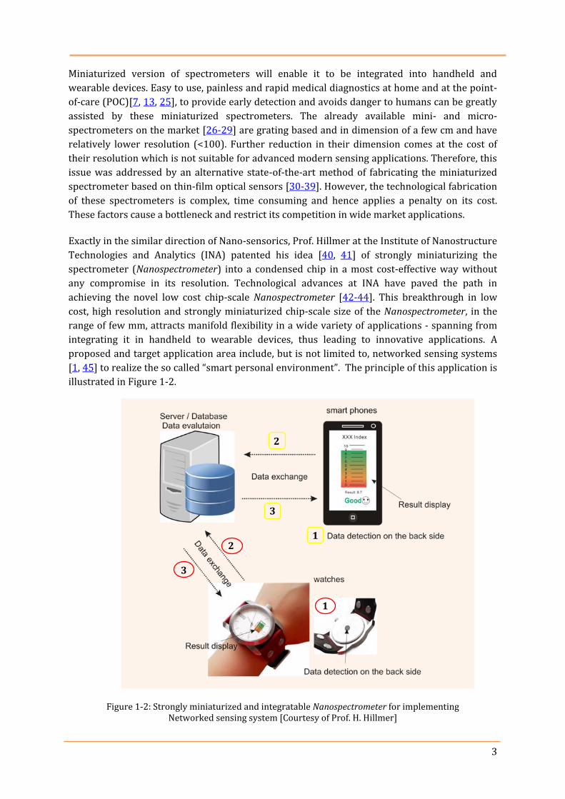
Exactly in the similar direction of Nano-sensorics, Prof. Hillmer at the Institute of Nanostructure
Technologies and Analytics (INA) patented his idea [40, 41] of strongly miniaturizing the
spectrometer (Nanospectrometer) into a condensed chip in a most cost-effective way without
any compromise in its resolution. Technological advances at INA have paved the path in
achieving the novel low cost chip-scale Nanospectrometer [42-44]. This breakthrough in low
cost, high resolution and strongly miniaturized chip-scale size of the Nanospectrometer, in the
range of few mm, attracts manifold flexibility in a wide variety of applications - spanning from
integrating it in handheld to wearable devices, thus leading to innovative applications. A
proposed and target application area include, but is not limited to, networked sensing systems
[1, 45] to realize the so called “smart personal environment”. The principle of this application is
illustrated in Figure 1-2.
Figure 1-2: Strongly miniaturized and integratable Nanospectrometer for implementing Networked sensing system [Courtesy of Prof. H. Hillmer]
1
2
3
1
2
3
Chapter 1: Motivation & overview of dissertation
4
In the above application of networked sensorics, the Nanospectrometer is in permanent and
continuous contact with the user where it scans and collects information on the human body as
well as on the surrounding environment. The collected data is sent automatically via a roaming
service to a remote server at regular intervals where it analyses the measurement. The
evaluated data is sent back to the user and a particular index value of the measured parameter
is displayed on the device screen as shown in
Figure 1-2. Therefore, the emergence of this real time remote medical care network can be
implemented for wireless health monitoring system which is a direct challenge to overcome
time and location. Another application is to realize a smart environment monitoring system, i.e.
a person can learn well in advance before entering a room if any possible volatile organic
compound (VOCs) or allergens are present which the person is sensitive (allergic) to. Similarly,
health-care oriented smart houses can be constructed for Ambient Assisted Living (AAL) in
improving the quality of life (QoL) [46].
The most influential factor of Prof. H. Hillmer’s patent [40, 41] is the significant reduction in the
fabrication cost of the Nanospectrometer which originates from implementing the Next
Generation Lithography ( ) technique, i.e. Nanoimprint Lithography ( ). At INA, this
technique is adapted and optimized to develop master templates for fabricating the
corresponding cavities of the optical filter array. These high vertical resolution master
templates are implemented to deliver the cost-effectivness of our Nanospectrometer. [45, 47-
52]. Compared to the state-of-the-art, multiple fabrication processes are replaced by one single
process using in achieving an array of cavities of the optical filter array (For details
see chapter 3). To detect the optical signal sensed by the fabricated optical filter array, it is
required to be integrated onto a photodetector (PD) array which converts the optical signal into
its electrical counterpart (electrical read-out). The integrated version of the filter array and the
PD array is known as sensor array. The optical filter array is implemented by highly selective
Fabry-Pérot filters for delivering high spectral resolution [53]. Additionally, it includes the lens
array with the bandpass filters to provide planar wave fronts to the FP-filter array. Since is
utilized in the fabrication of miniaturized optical spectrometer, it is introduced by researcher at
INA as Nanospectrometer. The complete device constituting the Nanospectrometer and its
corresponding parameter extraction circuitry and a final packaging is called the
Nanospectrometer system. A schematic illustration of the final device with its various
components that constitute the Nanospectrometer system is given in Figure 1-3. The first
prototype of the final strongly miniaturized and ready-to-be-integrated version of the
Nanospectrometer can be visualized in comparison to a one cent Euro coin as seen in Figure 1-4.
5
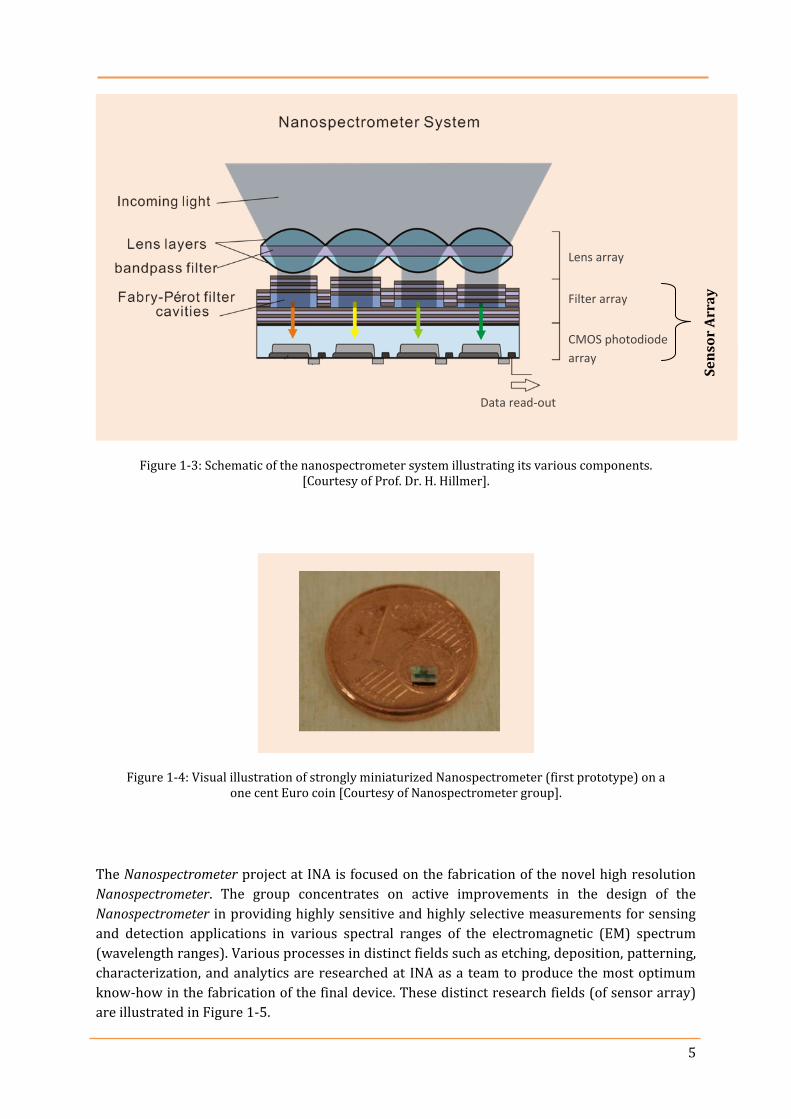
Figure 1-3: Schematic of the nanospectrometer system illustrating its various components. [Courtesy of Prof. Dr. H. Hillmer].
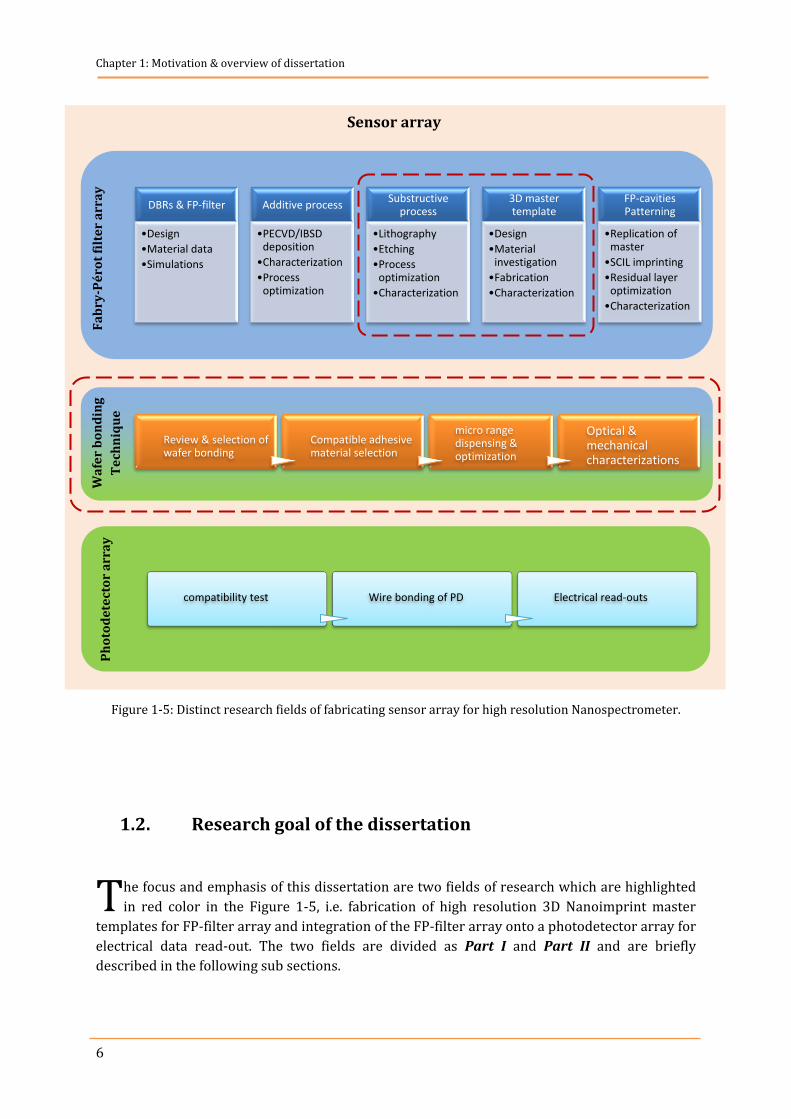
Figure 1-4: Visual illustration of strongly miniaturized Nanospectrometer (first prototype) on a one cent Euro coin [Courtesy of Nanospectrometer group].
The Nanospectrometer project at INA is focused on the fabrication of the novel high resolution
Nanospectrometer. The group concentrates on active improvements in the design of the
Nanospectrometer in providing highly sensitive and highly selective measurements for sensing
and detection applications in various spectral ranges of the electromagnetic (EM) spectrum
(wavelength ranges). Various processes in distinct fields such as etching, deposition, patterning,
characterization, and analytics are researched at INA as a team to produce the most optimum
know-how in the fabrication of the final device. These distinct research fields (of sensor array)
are illustrated in Figure 1-5.
Lens array
Filter array
CMOS photodiode
array
Data read-out
Se
nso
r A
rra
y
Chapter 1: Motivation & overview of dissertation
6
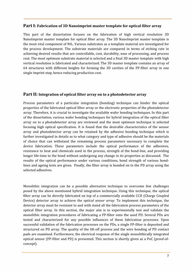
Figure 1-5: Distinct research fields of fabricating sensor array for high resolution Nanospectrometer.
1.2. Research goal of the dissertation
he focus and emphasis of this dissertation are two fields of research which are highlighted
in red color in the Figure 1-5, i.e. fabrication of high resolution 3D Nanoimprint master
templates for FP-filter array and integration of the FP-filter array onto a photodetector array for
electrical data read-out. The two fields are divided as Part I and Part II and are briefly
described in the following sub sections.
T
DBRs & FP-filter
•Design
•Material data
•Simulations
Additive process
•PECVD/IBSD deposition
•Characterization
•Process optimization
Substructive process
•Lithography
•Etching
•Process optimization
•Characterization
3D master template
•Design
•Material investigation
•Fabrication
•Characterization
FP-cavities Patterning
•Replication of master
•SCIL imprinting
•Residual layer optimization
•Characterization
compatibility test Wire bonding of PD Electrical read-outs
Review & selection of wafer bonding
Compatible adhesive material selection
micro range dispensing & optimization
Optical & mechanical characterizations
Fa
bry
-Pé
rot
filt
er
arr
ay
W
afe
r b
on
din
g
Te
chn
iqu
e
Ph
oto
de
tect
or
arr
ay
Sensor array
7
Part I: Fabrication of 3D Nanoimprint master template for optical filter array
This part of the dissertation focuses on the fabrication of high vertical resolution 3D
NanoImprint master template for optical filter array. The 3D NanoImprint master template is
the most vital component of NIL. Various substrates as a template material are investigated for
the process development. The substrate materials are compared in terms of etching rate in
achieving desired results that are controllable, cost, durability, ease of processing, and process
cost. The most optimum substrate material is selected and a final 3D master template with high
vertical resolution is fabricated and characterized. The 3D master template contains an array of
64 structures with different heights for forming the 3D cavities of the FP-filter array in one
single imprint step, hence reducing production cost.
Part II: Integration of optical filter array on to a photodetector array
Process parameters of a particular integration (bonding) technique can hinder the optical
properties of the fabricated optical filter array or the electronic properties of the photodetector
array. Therefore, it is crucial to investigate the available wafer bonding techniques. In this part
of the dissertation, various wafer bonding techniques for hybrid integration of the optical filter
array on to a photodetector array are reviewed and the most optimum technique is selected
focusing high optical specification. It is found that the desirable characteristics of the sensor
array and photodetector array can be retained by the adhesive bonding technique which is
further investigated in details as to what category and type of adhesive should be the materials
of choice that can withstand the remaining process parameters necessary to complete the
device fabrication. These parameters include the optical performance of the adhesives,
resistance to heat and chemicals used in the process, strength of the bond-line, and providing
longer life-time to the bond without undergoing any change in its properties as discussed. The
results of the optical performance under various conditions, bond strength of various bond-
lines and ageing tests are given. Finally, the filter array is bonded on to the PD array using the
selected adhesives.
Monolithic integration can be a possible alternative technique to overcome few challenges
posed by the above mentioned hybrid integration technique. Using this technique, the optical
filter array can be directly fabricated on top of a commercially available CCD (Charge Coupled
Device) detector array to achieve the optical sensor array. To implement this technique, the
detector array must be resistant to and with stand all the fabrication process parameters of the
optical filter array. In this section, the major aim is to experimentally test and validate the
monolithic integration procedures of fabricating a FP-filter onto the used PD. Several PDs are
tested and characterized for any possible influences of these fabrication processes. Upon
successful validation of the fabrication processes on the PDs, a single FP-filter is deposited and
structured on PD array. The quality of the lift-off process and the wire bonding of PD contact
pads are examined. Furthermore, the electrical response of the single monolithically integrated
optical sensor (FP-filter and PD) is presented. This section is shortly given as a PoC (proof-of-
concept).

Chapter 1: Motivation & overview of dissertation
8
9
Part I
Fabrication of high resolution 3D NanoImprint
master template for Fabry-Pérot filter array

10
11
2. Introduction to optical spectrometers
hen Electromagnetic (EM) waves interact with an atom or molecule or a surface of a
material, it can experience absorption, scattering, reflection or transmission. In
particular cases, when the material is excited by the absorbtion of EM waves or any
other energy sources (e.g. Electric field), photons are generated from the material (i.e. emission
process). The intensity of the absorbed, scattered, reflected, transmitted or emitted EM wave as
a function of its wavelength (or frequency) is called spectrum. The evaluation of this spectrum
to extract the information on the atoms or molecules of a material is known as spectroscopy.
The EM wave covers a wide wavelength range from radio waves to γ-rays and the material can
be in gas, liquid or solid phase. The focus of this work is in the visible spectral region of the EM
spectrum which is known as optical range and hence identified as optical spectroscopy [54, 55].
In other words, optical spectroscopy is the qualitative and quantitative analysis of the
interaction between light and matter which play an essential role in extracting the atomic and
molecular spectra (biomarker) that provide information on the structure, optical and chemical
properties and composition of a material [56-61]. Every biomarker has its own unique and
distinctive optical spectrum known as fingerprint. These fingerprints contain the constituents
and contaminants which can be used for molecular identification to provide information on a
material or medical diagnostics such as health status of a person and drug abuse, etc. [62]. The
key instrument used to measure the resulting spectrum is the spectrometer. Optical
spectrometers measures the ratio of absorbed to the incident light which is detected by a
photodetector. The fingerprint sensed by an optical spectrometer is compared to a library of
known fingerprints to identify a substance.
Optical spectroscopy is widely used to identify the chemical composition of a material in various
fields such as quality-control of agriculture and food products [63, 64], material
characterization for research and industrial application [65-67], monitoring of environment and
eco-system [68-71], analyzing of the spectral emission of LED and LASER [72-74], Acidity and
W
Chapter 2 Introduction to optical spectrometers
Chapter 2: Introduction to optical spectrometers
12
sugar content measurement of fruits and vegetables [75-77] and medical applications [78]. The
spectrometer senses the light intensity at each distinct wavelength (spectrally resolves it) and
converts it into an electrical signal for read-outs. Currently, the widely used light-diffraction
based spectrometers and the emerging light-filtering based spectrometers are discussed in the
following sections.
2.1 Grating based spectrometer and its limitations
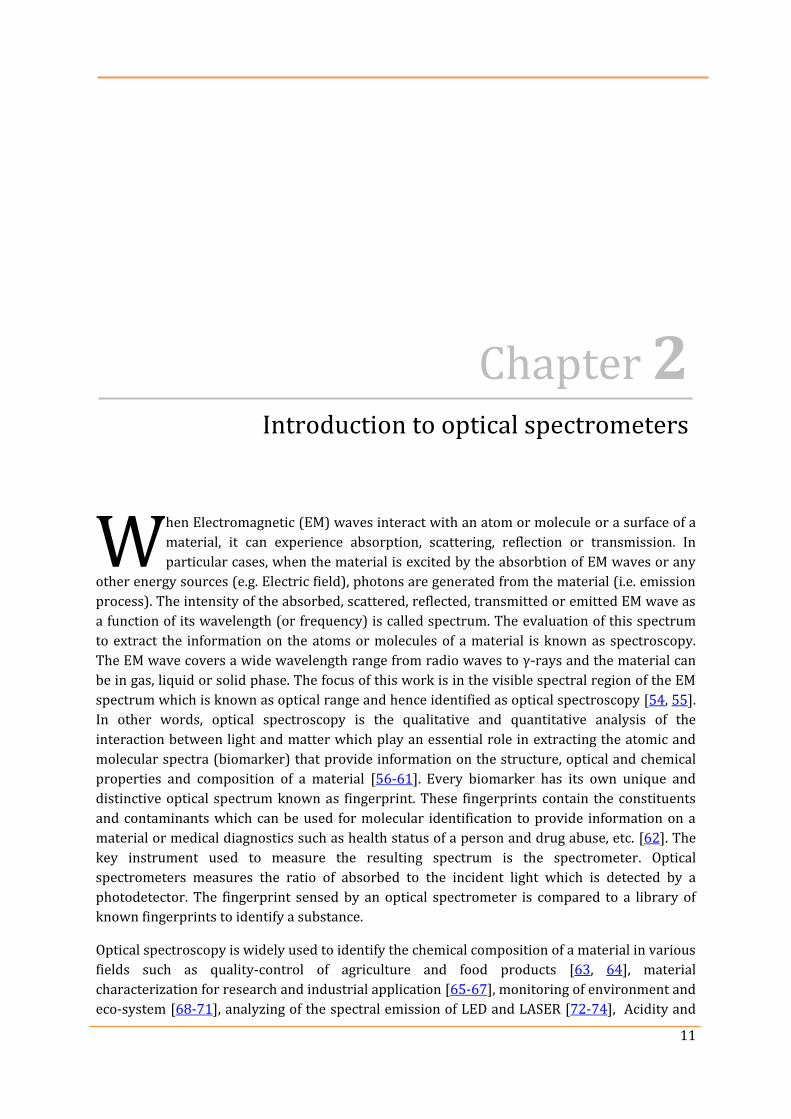
rating based spectrometers are conventionally used spectrometers in a wide range of
spectroscopic applications from UV to Infrared (IR) spectral regions. Light signal to be
resolved passes through the entrance slit of the spectrometer and collimated before hitting the
diffraction grating. The diffraction grating disperses the light signal into spatially separate
wavelength (i.e., diffracts it into its individual spectral component) which is collected by the
second lens and focused on the photodetector array (exit slit) as illustrated in Figure 2-1.
Figure 2-1: Principle working illustration of the optical components in a grating based spectrometer involving transmission grating. Original figure from [79].
Resolution and the spectral range of a spectrometer are the main specifications of interest for a
particular application. The resolution defines the minimum resolved width of the spectral line
(Full Width at Half Maximum, FWHM) while the spectral range defines the spectral detection
range of the spectrometer. Theoretically, the spectral resolution or the resolving power of the
spectrometer is limited by specifications of the gratings. The capability of the grating to
G
Input slit
Collimating lens Transmission grating Focus lens
Image sensor
13
separate light falling on it into its individual wavelength components is its resolving power ( )
which is defined in terms of the minimum resolution achieved by the grating as [80]:
(2-1)
The minimum spectral resolution achieved by the grating depends on the number of grooves
illuminated on the grating (N) and diffraction order (m) which is given as [80]:
(2-2)
However, additional phenomenal effects such as linear dispersion contribute to the degradation
in the resolution of the spectrometer. Therefore, the actual resolution of the spectrometer is
determined by another parameter called band-pass ( ). The band-pass is the minimum width
of the spectrum (FWHM) separated (dispersed) by the grating and collected at the exit slit (or
detector array) of the spectrometer. Usually, the grating spectrometers are 1:1 imaging systems,
where the input slit is almost equal to the exit slit. Therefore, the band-pass is defined as [80]:
(2-3)
Where, is the width of the input slits, is the reciprocal linear dispersion, which is the
measure of wavelength dispersion in nm/mm of the slit width, d is the spacing between the
grooves of the grating and is the focal length of the lens placed after the grating [81, 82].
Higher resolution can be achieved by the spectrometer by improving the above mentioned two
factors, i.e. the resolution limit of the grating (eq. (2-1) and band-pass (eq. (2-3). This implies
that the number of grooves (N) must be maximized to enhance the resolution. Spectrometer
with a smaller band-pass is able to resolve wavelength or spectral lines that are close together.
Therefore, higher resolution can be achieved by reducing the band-pass to a certain limit which
can be achieved by decreasing the slit widths but this comes at an expense of signal strength
(decreased light intensity). This limit of the band-pass is the resolution of the spectrometer [83].
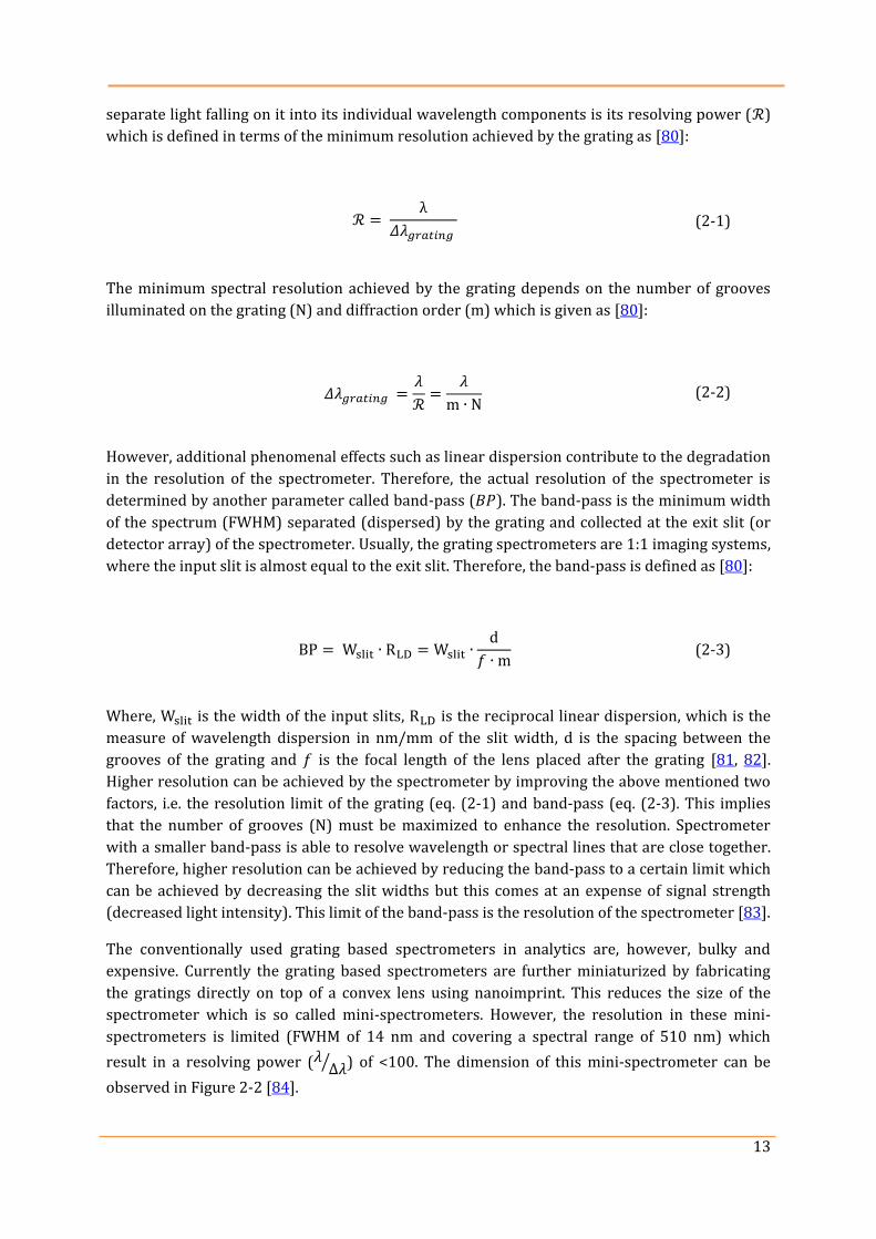
The conventionally used grating based spectrometers in analytics are, however, bulky and
expensive. Currently the grating based spectrometers are further miniaturized by fabricating
the gratings directly on top of a convex lens using nanoimprint. This reduces the size of the
spectrometer which is so called mini-spectrometers. However, the resolution in these mini-
spectrometers is limited (FWHM of 14 nm and covering a spectral range of 510 nm) which
result in a resolving power ( ) of <100. The dimension of this mini-spectrometer can be
observed in Figure 2-2 [84].
Chapter 2: Introduction to optical spectrometers
14
Figure 2-2: Grating based ultra-compact mini-spectrometer. Original figure from [84].
On one hand, the size of grating based spectrometers limits its integration into the modern
mobile and wearable devices. On the other hand, further reduction in its size comes at a cost of
its optical resolution as it is decided by the number of gratings (N). A reduction in its optical
resolution is not suitable for modern sensing and industrial applications. When the number of
gratings is increased, the lateral size increases and eventually the size of the spectrometer.
These limitations posed by the conventional grating based spectrometer in its further
miniaturization and cost can be overcome by implementing alternative fabrication technique
based on light filtering using thin-film optical filters as discussed in next section.
2.2 Spectrometers based on Fabry-Pérot filters: Future of
miniaturization
lthough the grating based spectrometer is a well established sensor technology and has
dominated various fields of applications, but due to its size it can not be integrated into
portable devices as it can not be further physically miniaturized while maintaining high spectral
resolution. Limitations in the dimension of the grating spectrometers encourages the modern
world for the necessity to focus on an alternative method in achieving high resolution
miniaturized optical spectrometers. A miniaturized and portable optical spectrometer is
envisaged to allow on-site measurement of materials and products rather than transporting
them to the lab where a bulky spectroscopic device is installed.
A

15
Alternative concept of fabricating miniaturized spectrometers is the optical filter based
spectrometers. The filter based spectrometer works on the principle of filtering of light from a
broadband spectrum. One of the most attractive approaches in fabricating the miniaturized
spectrometer is the Fabry-Pérot filter (FP-filter) based micro spectrometer. FP-Filter is thin-film
interference based optical filter. It consists of two highly reflecting mirrors called Distributed
Bragg Reflectors (DBRs) that are separated by a certain distance between them. This
sandwiched distance between two DBRs is called a FP-cavity which can be of a particular
material or of an air gap. In the application of Nanospectrometer, high optical quality DBRs are
deposited at low cost using PECVD [85]. The deposited DBRs are of of dielectric material
(Si3N4/SiO2) and the FP-cavity is structured by photolithographic process and etching
technology.
In contrast to grating based spectrometers, FP-filter based spectrometers can be fabricated as
compact, light weight and portable device in a form of condensed and miniaturized chip. Since
the spectral resolution of a FP-filter based spectrometer is given by the optical thickness
(product of physical thickness and ref. index) of the FP-cavity and the reflectivity of the DBRs.
Therefore, it is defined only by the thicknesses in the vertical direction and not in lateral
dimension. This allows minimization in lateral dimension, as opposed to grating based
spectrometers, and hence enabling strong miniaturization. This alternative approach of
fabricating miniaturized spectrometer invites large interest and open new fields of applications.
Transmission and filtering of wavelength can be achieved by two design approaches of the FP-
filter, i.e. tunable FP-filter and static FP-filter. Tunable FP-filter is MEMS (Micro-Electro-
Mechanical-System) based, where the thickness of the FP-cavity is actuated by applying external
thermal or electrostatic field [86-88]. By tuning the FP-cavity to a particular thickness, a
particular wavelength (also known as transmission-line) that satisfies the FP-cavity condition is
allowed to pass through a FP-filter. Hence, different wavelengths can be transmitted through a
single tunable FP-filter. In static FP-filter the FP-cavity is fixed and allows only a single resonant
wavelength to pass through it which satisfies its condition (see section 3.3 for details).
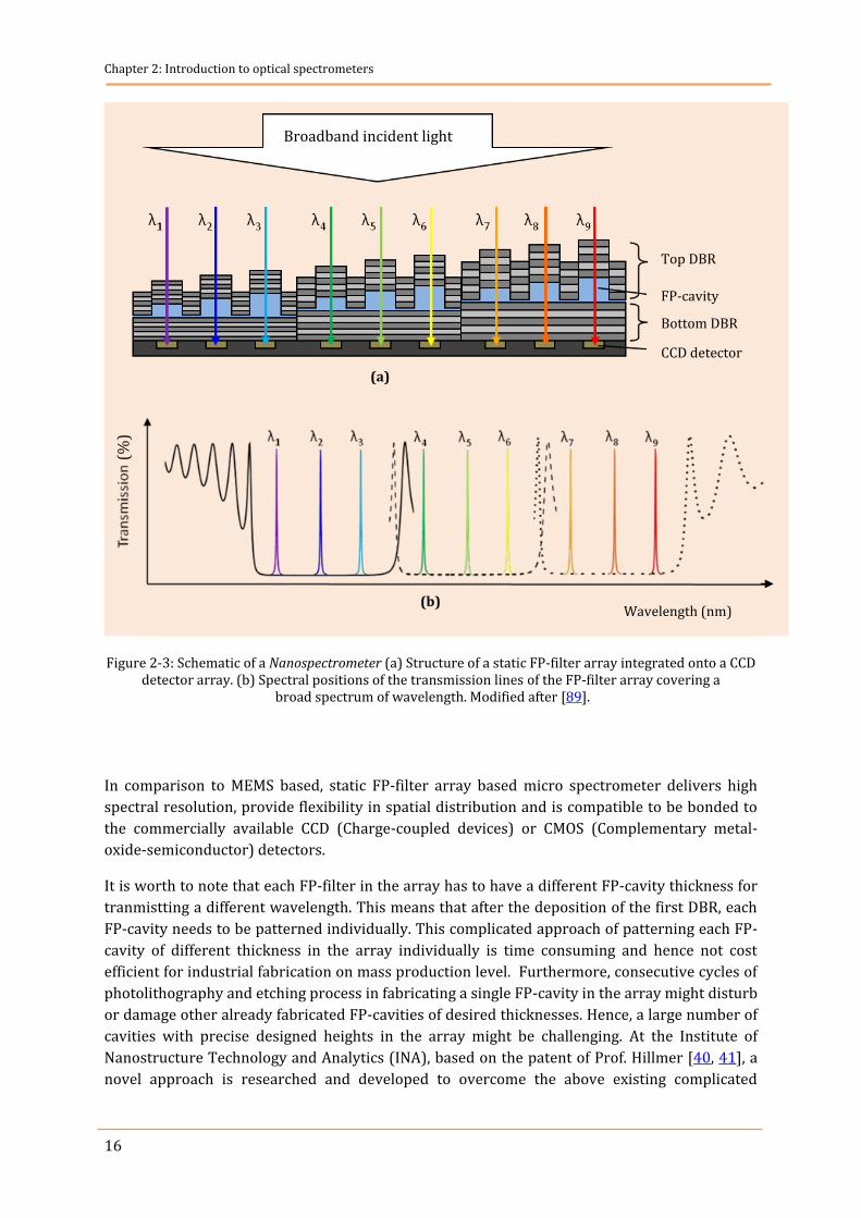
A single DBR covers a spectral range of approx. 100 – 150 nm. At INA, for wide spectral sensing
application three different DBRs with different central wavelengths are deposited such that they
cover the whole visible spectral region when they are overlapped. An array of FP-cavities with
unique vertical heights are patterened on the three DBRs to obtain FP-filter arrays. Each single
FP-filter in the array transmits a particular wavelength (i.e. unique transmission-line) which is
detected by its corresponding photodetector (PD) pixel of the bonded PD-array as illustrated in
Figure 2-3 (see section 3.4 for details).
Chapter 2: Introduction to optical spectrometers
16
Figure 2-3: Schematic of a Nanospectrometer (a) Structure of a static FP-filter array integrated onto a CCD detector array. (b) Spectral positions of the transmission lines of the FP-filter array covering a
broad spectrum of wavelength. Modified after [89].
In comparison to MEMS based, static FP-filter array based micro spectrometer delivers high
spectral resolution, provide flexibility in spatial distribution and is compatible to be bonded to
the commercially available CCD (Charge-coupled devices) or CMOS (Complementary metal-
oxide-semiconductor) detectors.
It is worth to note that each FP-filter in the array has to have a different FP-cavity thickness for
tranmistting a different wavelength. This means that after the deposition of the first DBR, each
FP-cavity needs to be patterned individually. This complicated approach of patterning each FP-
cavity of different thickness in the array individually is time consuming and hence not cost
efficient for industrial fabrication on mass production level. Furthermore, consecutive cycles of
photolithography and etching process in fabricating a single FP-cavity in the array might disturb
or damage other already fabricated FP-cavities of desired thicknesses. Hence, a large number of
cavities with precise designed heights in the array might be challenging. At the Institute of
Nanostructure Technology and Analytics (INA), based on the patent of Prof. Hillmer [40, 41], a
novel approach is researched and developed to overcome the above existing complicated
Broadband incident light
Top DBR
FP-cavity
Bottom DBR
CCD detector
Wavelength (nm)
(a)
(b)
(%)
17
fabrication process of the FP-filter based Nanospectrometer. Using this novel approach all the
different FP-cavities in the array can be fabricated in one single step.
2.3 Next Generation Lithography (NGL) for high resolution 3D
master templates for Nanospectrometer
ithography is the major work horse in fabricating micro electronics which enabled the
modern world of Integrated Circuits (IC) where its contribution is 30% - 35% of the total
device fabrication cost [90]. According to Moore’s law, the feature size decreases and the
complexity (features per chip) doubles every 18 – 24 months [91]. Increasing number of
features (transistors) and steadily reducing the size of the chip is a result of continuous
improvements in lithographic techniques. This has lead to ever increasing functionalities and
capacity within a miniaturized system. Miniaturization in micro and nano electronics is required
to have more components per chip, lower power consumption, larger storage capacity, faster
response, higher performance, and lower cost [92, 93]. In micro-system miniaturization is
desirable to save space, material, energy and hence lower cost, offers increased portability,
decrease in defects while increase in stability and life time, enables higher frequencies, and
provides several functions in one chip [94, 95]. As the wavelength of the used light source in
conventionally used photolithography is reaching its limit, alternative approaches are
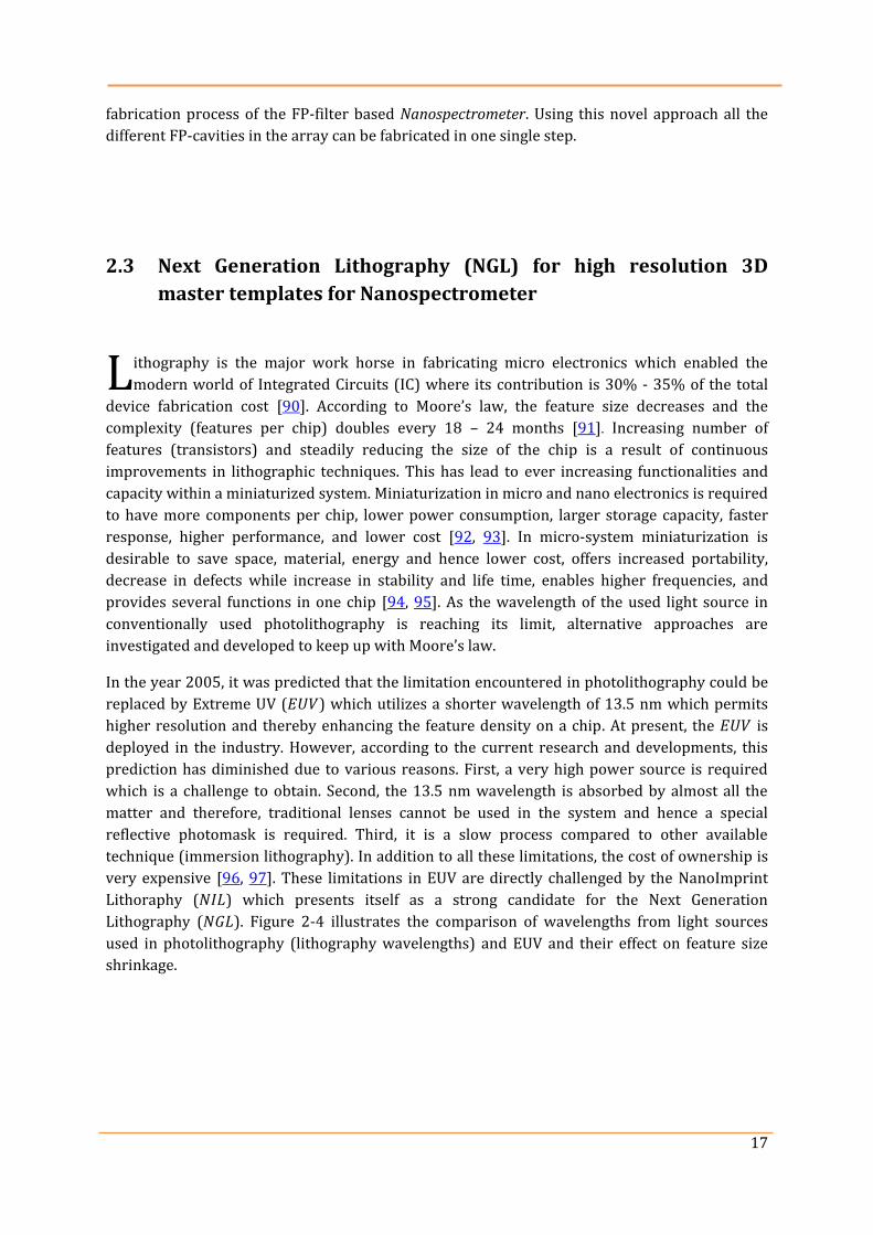
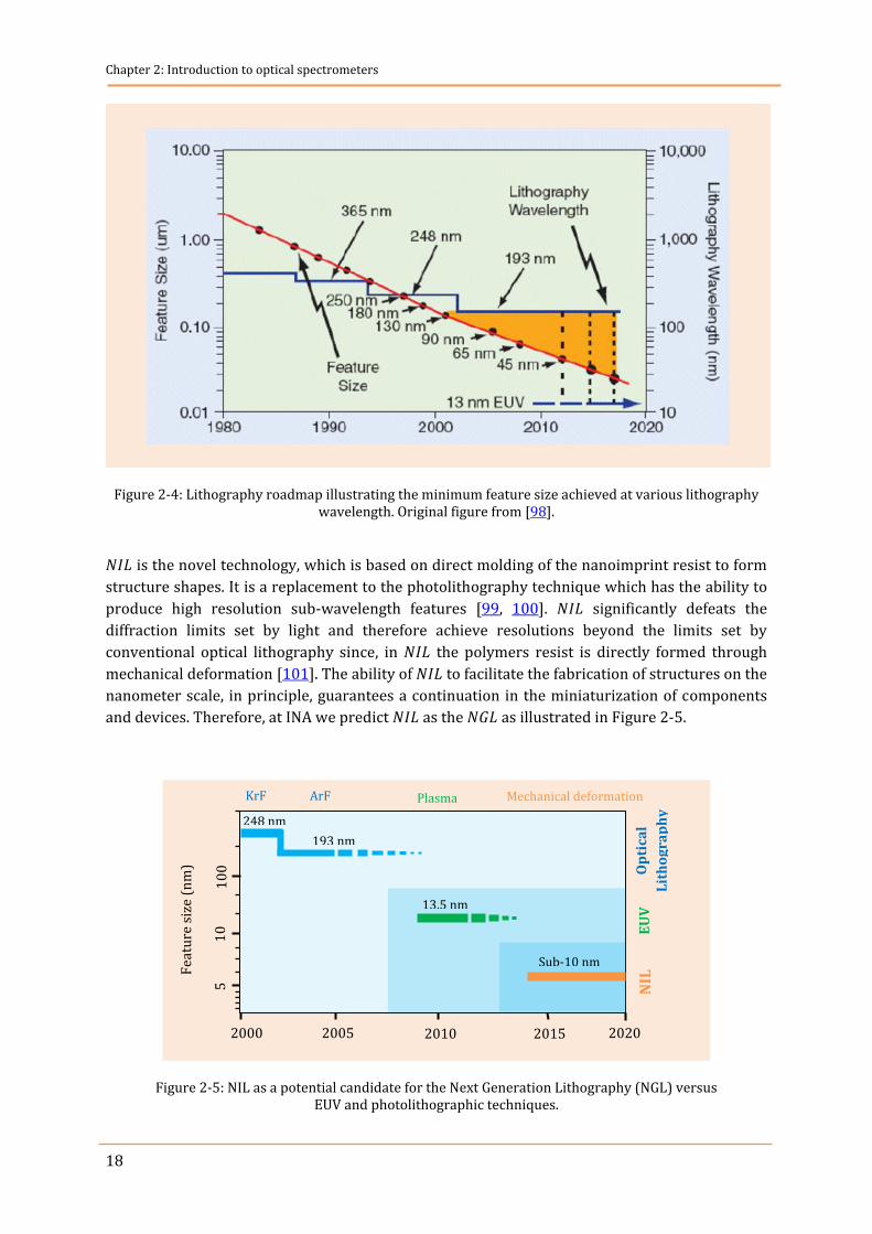
investigated and developed to keep up with Moore’s law.
In the year 2005, it was predicted that the limitation encountered in photolithography could be
replaced by Extreme UV ( ) which utilizes a shorter wavelength of 13.5 nm which permits
higher resolution and thereby enhancing the feature density on a chip. At present, the is
deployed in the industry. However, according to the current research and developments, this
prediction has diminished due to various reasons. First, a very high power source is required
which is a challenge to obtain. Second, the 13.5 nm wavelength is absorbed by almost all the
matter and therefore, traditional lenses cannot be used in the system and hence a special
reflective photomask is required. Third, it is a slow process compared to other available
technique (immersion lithography). In addition to all these limitations, the cost of ownership is
very expensive [96, 97]. These limitations in EUV are directly challenged by the NanoImprint
Lithoraphy ( ) which presents itself as a strong candidate for the Next Generation
Lithography ( ). Figure 2-4 illustrates the comparison of wavelengths from light sources
used in photolithography (lithography wavelengths) and EUV and their effect on feature size
shrinkage.
L
Chapter 2: Introduction to optical spectrometers
18
Figure 2-4: Lithography roadmap illustrating the minimum feature size achieved at various lithography wavelength. Original figure from [98].
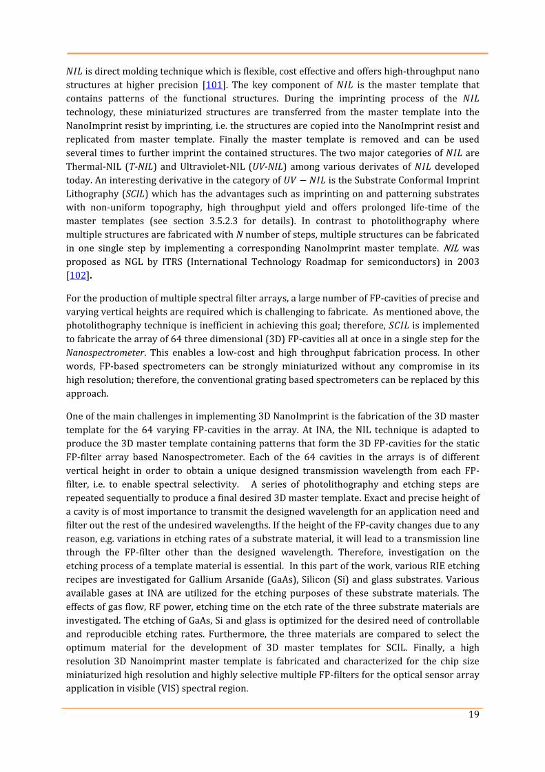
is the novel technology, which is based on direct molding of the nanoimprint resist to form
structure shapes. It is a replacement to the photolithography technique which has the ability to
produce high resolution sub-wavelength features [99, 100]. significantly defeats the
diffraction limits set by light and therefore achieve resolutions beyond the limits set by
conventional optical lithography since, in the polymers resist is directly formed through
mechanical deformation [101]. The ability of to facilitate the fabrication of structures on the
nanometer scale, in principle, guarantees a continuation in the miniaturization of components
and devices. Therefore, at INA we predict as the as illustrated in Figure 2-5.
Figure 2-5: NIL as a potential candidate for the Next Generation Lithography (NGL) versus EUV and photolithographic techniques.
EU
V
NIL
O
pti
cal
Lit
ho
gra
ph
y
2000 2005 2010 2015 2020
193 nm
248 nm
13.5 nm
Sub-10 nm
Fea
ture
siz
e (n
m)
10
1
00
5
KrF ArF Plasma Mechanical deformation
19
is direct molding technique which is flexible, cost effective and offers high-throughput nano
structures at higher precision [101]. The key component of is the master template that
contains patterns of the functional structures. During the imprinting process of the
technology, these miniaturized structures are transferred from the master template into the
NanoImprint resist by imprinting, i.e. the structures are copied into the NanoImprint resist and
replicated from master template. Finally the master template is removed and can be used
several times to further imprint the contained structures. The two major categories of are
Thermal-NIL (T-NIL) and Ultraviolet-NIL (UV-NIL) among various derivates of developed
today. An interesting derivative in the category of is the Substrate Conformal Imprint
Lithography (SCIL) which has the advantages such as imprinting on and patterning substrates
with non-uniform topography, high throughput yield and offers prolonged life-time of the
master templates (see section 3.5.2.3 for details). In contrast to photolithography where
multiple structures are fabricated with N number of steps, multiple structures can be fabricated
in one single step by implementing a corresponding NanoImprint master template. NIL was
proposed as NGL by ITRS (International Technology Roadmap for semiconductors) in 2003
[102].
For the production of multiple spectral filter arrays, a large number of FP-cavities of precise and
varying vertical heights are required which is challenging to fabricate. As mentioned above, the
photolithography technique is inefficient in achieving this goal; therefore, is implemented
to fabricate the array of 64 three dimensional (3D) FP-cavities all at once in a single step for the
Nanospectrometer. This enables a low-cost and high throughput fabrication process. In other
words, FP-based spectrometers can be strongly miniaturized without any compromise in its
high resolution; therefore, the conventional grating based spectrometers can be replaced by this
approach.
One of the main challenges in implementing 3D NanoImprint is the fabrication of the 3D master
template for the 64 varying FP-cavities in the array. At INA, the NIL technique is adapted to
produce the 3D master template containing patterns that form the 3D FP-cavities for the static
FP-filter array based Nanospectrometer. Each of the 64 cavities in the arrays is of different
vertical height in order to obtain a unique designed transmission wavelength from each FP-
filter, i.e. to enable spectral selectivity. A series of photolithography and etching steps are
repeated sequentially to produce a final desired 3D master template. Exact and precise height of
a cavity is of most importance to transmit the designed wavelength for an application need and
filter out the rest of the undesired wavelengths. If the height of the FP-cavity changes due to any
reason, e.g. variations in etching rates of a substrate material, it will lead to a transmission line
through the FP-filter other than the designed wavelength. Therefore, investigation on the
etching process of a template material is essential. In this part of the work, various RIE etching
recipes are investigated for Gallium Arsanide (GaAs), Silicon (Si) and glass substrates. Various
available gases at INA are utilized for the etching purposes of these substrate materials. The
effects of gas flow, RF power, etching time on the etch rate of the three substrate materials are
investigated. The etching of GaAs, Si and glass is optimized for the desired need of controllable
and reproducible etching rates. Furthermore, the three materials are compared to select the
optimum material for the development of 3D master templates for . Finally, a high
resolution 3D Nanoimprint master template is fabricated and characterized for the chip size
miniaturized high resolution and highly selective multiple FP-filters for the optical sensor array
application in visible (VIS) spectral region.
Chapter 2: Introduction to optical spectrometers
20
2.4 State of the art of miniaturized optical spectrometers
ptical spectrometers have gained attention from a wide range of applications due to its
non-invasive, contactless, fast and accurate measurement abilities. At present, interest is
laid in integrating the optical spectrometer into modern handheld and wearable devices. For
this purpose, it is wished to produce a miniaturized and high resolution optical spectrometer at
low cost. The beneficial properties of miniaturized spectrometers are already discussed in
Chapter 1. Conventionally used grating based microspectrometers are still big in size for its
integration into these modern devices and are expensive due to their fabrication cost.
Therefore, miniaturized spectrometers based on thin-film optical filters are researched as an
alternative approach which addresses these two limitations and hence, suits best for the desired
application needs. The differences between and limitations of these two optical spectrometers
are discussed in details in Chapter 2. In this section, a brief review of the grating based
microspectrometers published by various researchers and also commercially available
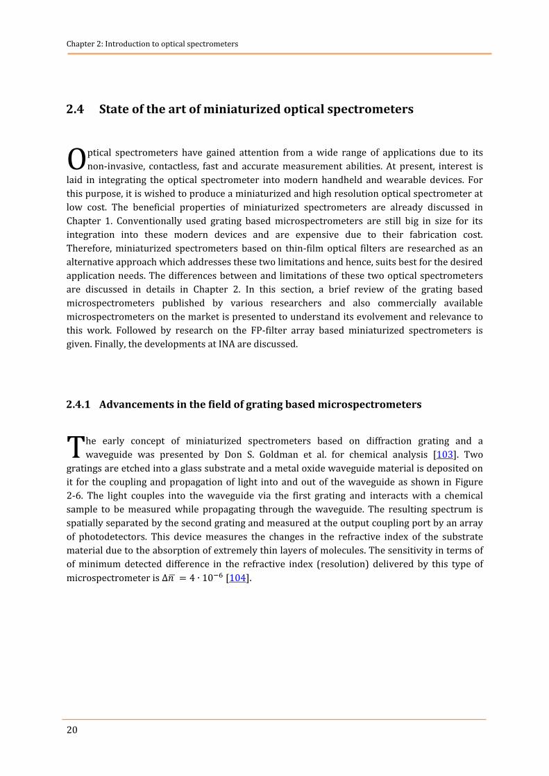
microspectrometers on the market is presented to understand its evolvement and relevance to
this work. Followed by research on the FP-filter array based miniaturized spectrometers is
given. Finally, the developments at INA are discussed.
2.4.1 Advancements in the field of grating based microspectrometers
he early concept of miniaturized spectrometers based on diffraction grating and a
waveguide was presented by Don S. Goldman et al. for chemical analysis [103]. Two
gratings are etched into a glass substrate and a metal oxide waveguide material is deposited on
it for the coupling and propagation of light into and out of the waveguide as shown in Figure
2-6. The light couples into the waveguide via the first grating and interacts with a chemical
sample to be measured while propagating through the waveguide. The resulting spectrum is
spatially separated by the second grating and measured at the output coupling port by an array
of photodetectors. This device measures the changes in the refractive index of the substrate
material due to the absorption of extremely thin layers of molecules. The sensitivity in terms of
of minimum detected difference in the refractive index (resolution) delivered by this type of
microspectrometer is [104].
O
T
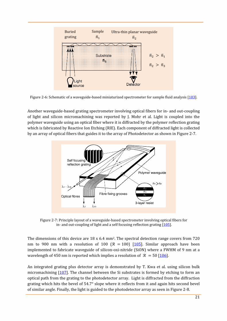
21
Figure 2-6: Schematic of a waveguide-based miniaturized spectrometer for sample fluid analysis [103].
Another waveguide-based grating spectrometer involving optical fibers for in- and out-coupling
of light and silicon micromachining was reported by J. Mohr et al. Light is coupled into the
polymer waveguide using an optical fiber where it is diffracted by the polymer reflection grating
which is fabricated by Reactive Ion Etching (RIE). Each component of diffracted light is collected
by an array of optical fibers that guides it to the array of Photodetector as shown in Figure 2-7.
Figure 2-7: Principle layout of a waveguide-based spectrometer involving optical fibers for in- and out-coupling of light and a self focusing reflection grating [105].
The dimensions of this device are 18 x 6.4 mm2. The spectral detection range covers from 720
nm to 900 nm with a resolution of 100 ( ) [105]. Similar approach have been
implemented to fabricate waveguide of silicon-oxi-nitride (SiON) where a FWHM of 9 nm at a
wavelength of 450 nm is reported which implies a resolution of [106].
An integrated grating plus detector array is demonstrated by T. Kwa et al. using silicon bulk
micromachining [107]. The channel between the Si substrates is formed by etching to form an
optical path from the grating to the photodetector array. Light is diffracted from the diffraction
grating which hits the bevel of 54.7° slope where it reflects from it and again hits second bevel
of similar angle. Finally, the light is guided to the photodetector array as seen in Figure 2-8.
Ultra-thin planar waveguide
Sample Buried
grating
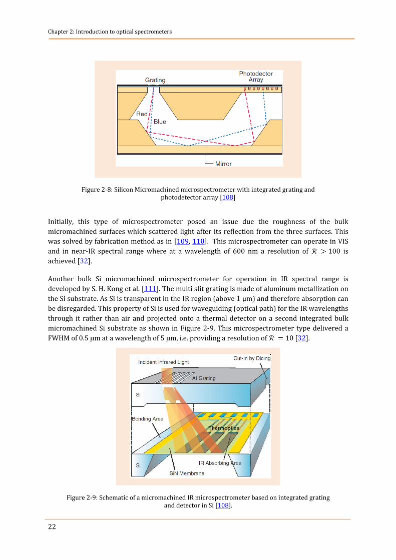
Chapter 2: Introduction to optical spectrometers
22
Figure 2-8: Silicon Micromachined microspectrometer with integrated grating and photodetector array [108]
Initially, this type of microspectrometer posed an issue due the roughness of the bulk
micromachined surfaces which scattered light after its reflection from the three surfaces. This
was solved by fabrication method as in [109, 110]. This microspectrometer can operate in VIS
and in near-IR spectral range where at a wavelength of 600 nm a resolution of is
achieved [32].
Another bulk Si micromachined microspectrometer for operation in IR spectral range is
developed by S. H. Kong et al. [111]. The multi slit grating is made of aluminum metallization on
the Si substrate. As Si is transparent in the IR region (above 1 µm) and therefore absorption can
be disregarded. This property of Si is used for waveguiding (optical path) for the IR wavelengths
through it rather than air and projected onto a thermal detector on a second integrated bulk
micromachined Si substrate as shown in Figure 2-9. This microspectrometer type delivered a
FWHM of 0.5 µm at a wavelength of 5 µm, i.e. providing a resolution of [32].
Figure 2-9: Schematic of a micromachined IR microspectrometer based on integrated grating and detector in Si [108].
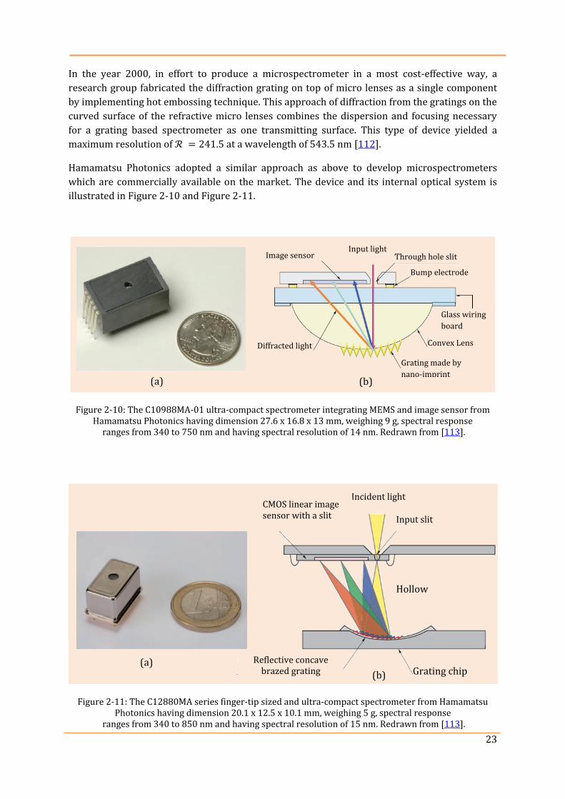
23
In the year 2000, in effort to produce a microspectrometer in a most cost-effective way, a
research group fabricated the diffraction grating on top of micro lenses as a single component
by implementing hot embossing technique. This approach of diffraction from the gratings on the
curved surface of the refractive micro lenses combines the dispersion and focusing necessary
for a grating based spectrometer as one transmitting surface. This type of device yielded a
maximum resolution of at a wavelength of 543.5 nm [112].
Hamamatsu Photonics adopted a similar approach as above to develop microspectrometers
which are commercially available on the market. The device and its internal optical system is
illustrated in Figure 2-10 and Figure 2-11.
Figure 2-10: The C10988MA-01 ultra-compact spectrometer integrating MEMS and image sensor from Hamamatsu Photonics having dimension 27.6 x 16.8 x 13 mm, weighing 9 g, spectral response
ranges from 340 to 750 nm and having spectral resolution of 14 nm. Redrawn from [113].
Figure 2-11: The C12880MA series finger-tip sized and ultra-compact spectrometer from Hamamatsu Photonics having dimension 20.1 x 12.5 x 10.1 mm, weighing 5 g, spectral response
ranges from 340 to 850 nm and having spectral resolution of 15 nm. Redrawn from [113].
Incident light
Input slit
CMOS linear image sensor with a slit
Hollow
Grating chip Reflective concave
brazed grating (a)
(b)
Diffracted light
Image sensor Input light
Through hole slit
Bump electrode
Convex Lens
Glass wiring
board
Grating made by
nano-imprint (a) (b)
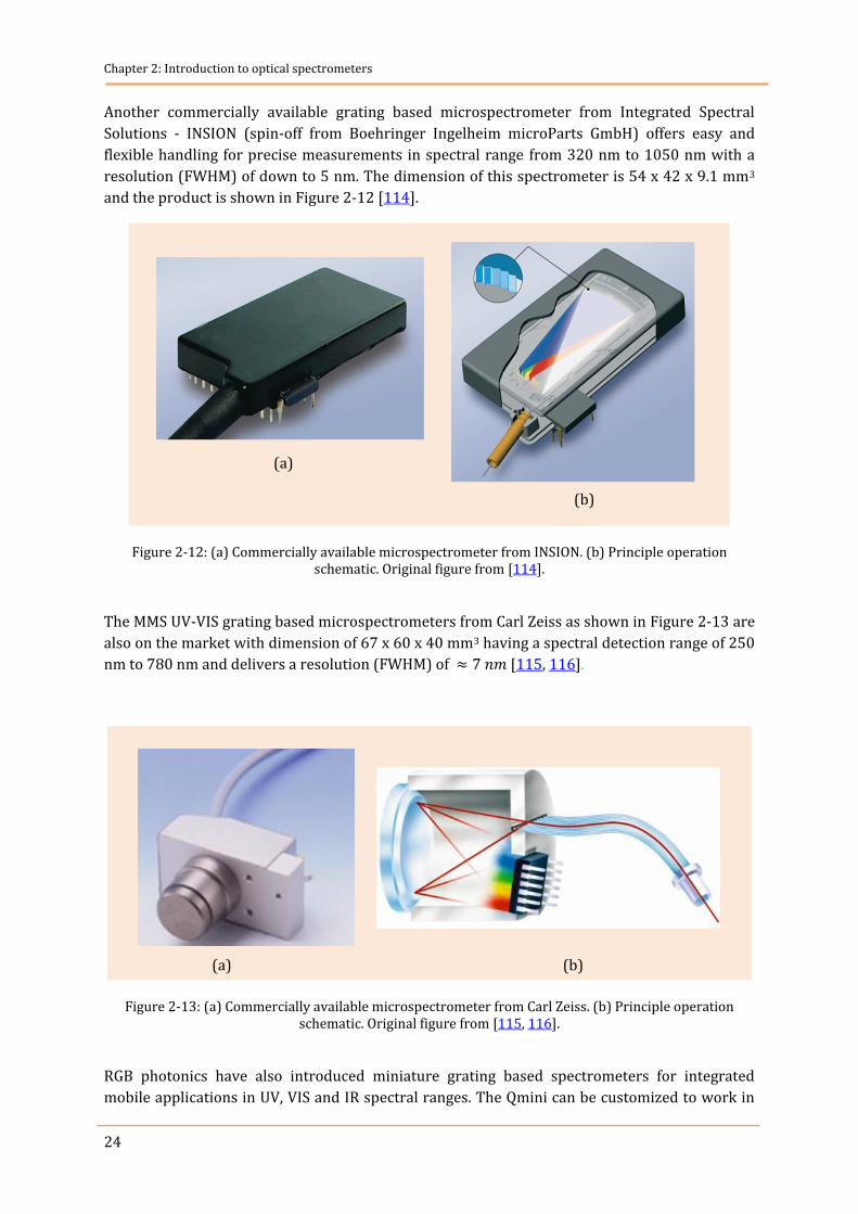
Chapter 2: Introduction to optical spectrometers
24
Another commercially available grating based microspectrometer from Integrated Spectral
Solutions - INSION (spin-off from Boehringer Ingelheim microParts GmbH) offers easy and
flexible handling for precise measurements in spectral range from 320 nm to 1050 nm with a
resolution (FWHM) of down to 5 nm. The dimension of this spectrometer is 54 x 42 x 9.1 mm3
and the product is shown in Figure 2-12 [114].
Figure 2-12: (a) Commercially available microspectrometer from INSION. (b) Principle operation schematic. Original figure from [114].
The MMS UV-VIS grating based microspectrometers from Carl Zeiss as shown in Figure 2-13 are
also on the market with dimension of 67 x 60 x 40 mm3 having a spectral detection range of 250
nm to 780 nm and delivers a resolution (FWHM) of [115, 116].
Figure 2-13: (a) Commercially available microspectrometer from Carl Zeiss. (b) Principle operation schematic. Original figure from [115, 116].
RGB photonics have also introduced miniature grating based spectrometers for integrated
mobile applications in UV, VIS and IR spectral ranges. The Qmini can be customized to work in
(a) (b)
(a)
(b)
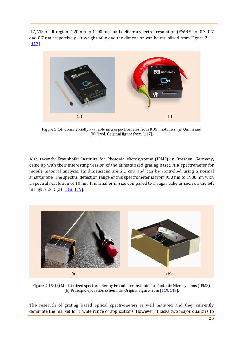
25
UV, VIS or IR region (220 nm to 1100 nm) and deliver a spectral resolution (FWHM) of 0.3, 0.7
and 0.7 nm respectively. It weighs 60 g and the dimension can be visualized from Figure 2-14
[117].
Figure 2-14: Commercially available microspectrometer from RBG Photonics. (a) Qmini and (b) Qred. Original figure from [117].
Also recently Fraunhofer Institute for Photonic Microsystems (IPMS) in Dresden, Germany,
came up with their interesting version of the miniaturized grating based NIR spectrometer for
mobile material analysis. Its dimensions are 2.1 cm3 and can be controlled using a normal
smartphone. The spectral detection range of this spectrometer is from 950 nm to 1900 nm with
a spectral resolution of 10 nm. It is smaller in size compared to a sugar cube as seen on the left
in Figure 2-15(a) [118, 119].
Figure 2-15: (a) Miniaturized spectrometer by Fraunhofer Institute for Photonic Microsystems (IPMS). (b) Principle operation schematic. Original figure from [118, 119].
The research of grating based optical spectrometers is well matured and they currently
dominate the market for a wide range of applications. However, it lacks two major qualities to
(a) (b)
(a) (b)
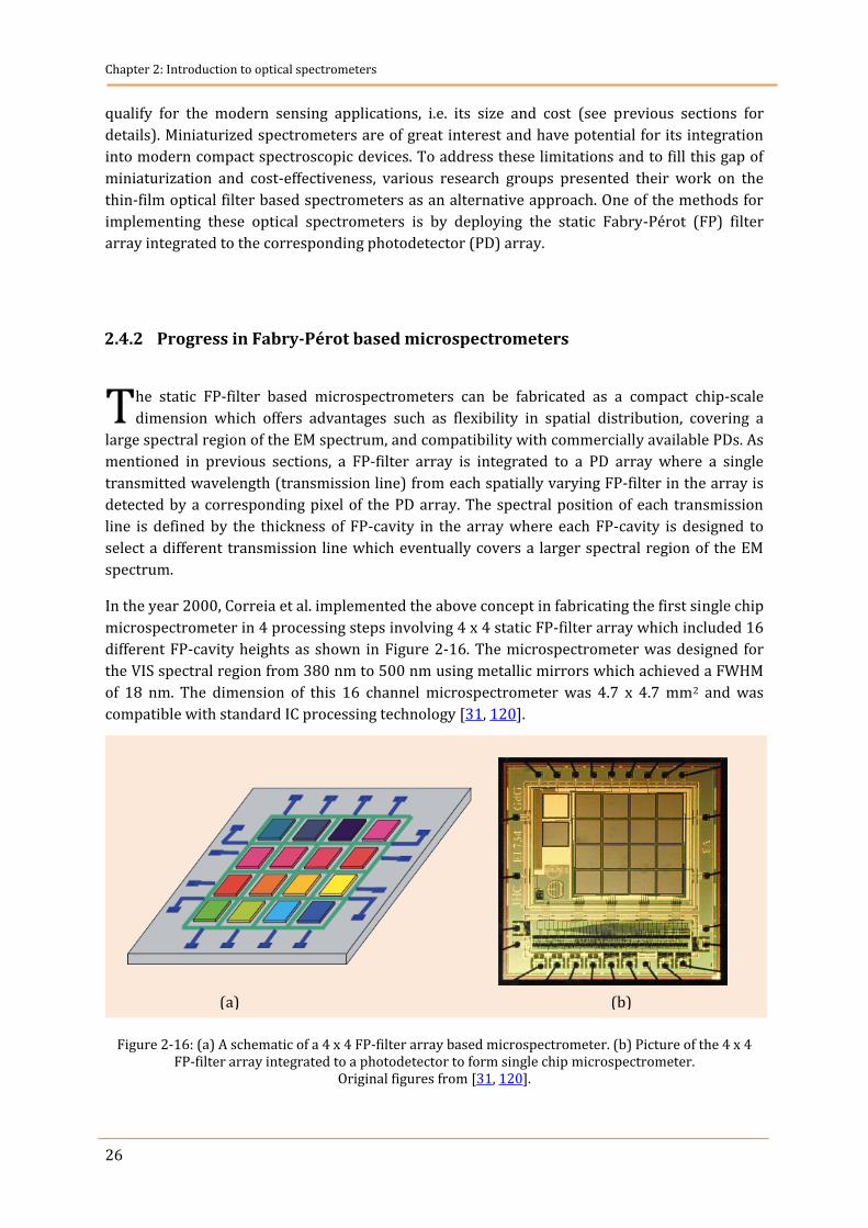
Chapter 2: Introduction to optical spectrometers
26
qualify for the modern sensing applications, i.e. its size and cost (see previous sections for
details). Miniaturized spectrometers are of great interest and have potential for its integration
into modern compact spectroscopic devices. To address these limitations and to fill this gap of
miniaturization and cost-effectiveness, various research groups presented their work on the
thin-film optical filter based spectrometers as an alternative approach. One of the methods for
implementing these optical spectrometers is by deploying the static Fabry-Pérot (FP) filter
array integrated to the corresponding photodetector (PD) array.
2.4.2 Progress in Fabry-Pérot based microspectrometers
he static FP-filter based microspectrometers can be fabricated as a compact chip-scale
dimension which offers advantages such as flexibility in spatial distribution, covering a
large spectral region of the EM spectrum, and compatibility with commercially available PDs. As
mentioned in previous sections, a FP-filter array is integrated to a PD array where a single
transmitted wavelength (transmission line) from each spatially varying FP-filter in the array is
detected by a corresponding pixel of the PD array. The spectral position of each transmission
line is defined by the thickness of FP-cavity in the array where each FP-cavity is designed to
select a different transmission line which eventually covers a larger spectral region of the EM
spectrum.
In the year 2000, Correia et al. implemented the above concept in fabricating the first single chip
microspectrometer in 4 processing steps involving 4 x 4 static FP-filter array which included 16
different FP-cavity heights as shown in Figure 2-16. The microspectrometer was designed for
the VIS spectral region from 380 nm to 500 nm using metallic mirrors which achieved a FWHM
of 18 nm. The dimension of this 16 channel microspectrometer was 4.7 x 4.7 mm2 and was
compatible with standard IC processing technology [31, 120].
Figure 2-16: (a) A schematic of a 4 x 4 FP-filter array based microspectrometer. (b) Picture of the 4 x 4 FP-filter array integrated to a photodetector to form single chip microspectrometer.
Original figures from [31, 120].
T
(a) (b)
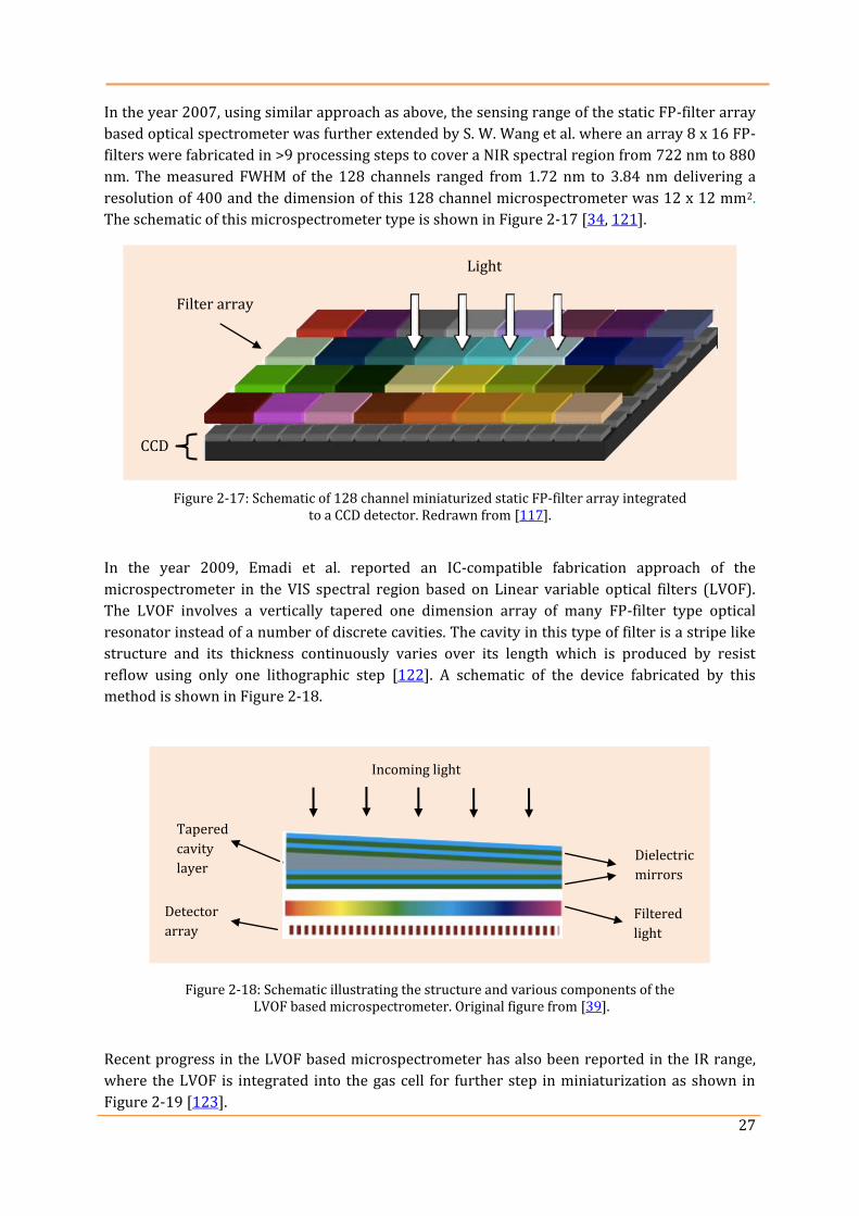
27
In the year 2007, using similar approach as above, the sensing range of the static FP-filter array
based optical spectrometer was further extended by S. W. Wang et al. where an array 8 x 16 FP-
filters were fabricated in >9 processing steps to cover a NIR spectral region from 722 nm to 880
nm. The measured FWHM of the 128 channels ranged from 1.72 nm to 3.84 nm delivering a
resolution of 400 and the dimension of this 128 channel microspectrometer was 12 x 12 mm2.
The schematic of this microspectrometer type is shown in Figure 2-17 [34, 121].
Figure 2-17: Schematic of 128 channel miniaturized static FP-filter array integrated to a CCD detector. Redrawn from [117].
In the year 2009, Emadi et al. reported an IC-compatible fabrication approach of the
microspectrometer in the VIS spectral region based on Linear variable optical filters (LVOF).
The LVOF involves a vertically tapered one dimension array of many FP-filter type optical
resonator instead of a number of discrete cavities. The cavity in this type of filter is a stripe like
structure and its thickness continuously varies over its length which is produced by resist
reflow using only one lithographic step [122]. A schematic of the device fabricated by this
method is shown in Figure 2-18.
Figure 2-18: Schematic illustrating the structure and various components of the LVOF based microspectrometer. Original figure from [39].
Recent progress in the LVOF based microspectrometer has also been reported in the IR range,
where the LVOF is integrated into the gas cell for further step in miniaturization as shown in
Figure 2-19 [123].
Tapered
cavity
layer Dielectric
mirrors
Filtered
light
Detector
array
Incoming light
CCD
Filter array
Light
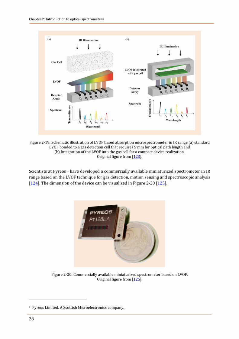
Chapter 2: Introduction to optical spectrometers
28
Figure 2-19: Schematic illustration of LVOF based absorption microspectrometer in IR range (a) standard LVOF bonded to a gas detection cell that requires 5 mm for optical path length and
(b) Integration of the LVOF into the gas cell for a compact device realization. Original figure from [123].
Scientists at Pyreos 1 have developed a commercially available miniaturized spectrometer in IR
range based on the LVOF technique for gas detection, motion sensing and spectroscopic analysis
[124]. The dimension of the device can be visualized in Figure 2-20 [125].
Figure 2-20: Commercially available miniaturized spectrometer based on LVOF. Original figure from [125].
1 Pyreos Limited. A Scottish Microelectronics company.
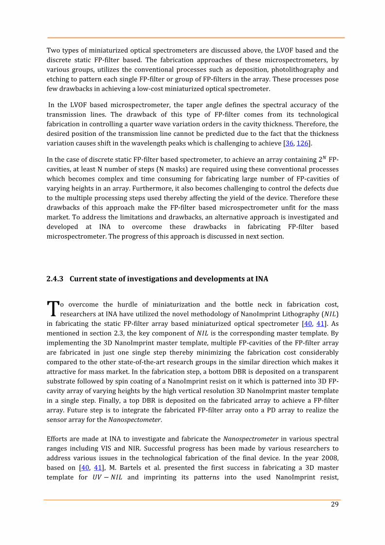
29
Two types of miniaturized optical spectrometers are discussed above, the LVOF based and the
discrete static FP-filter based. The fabrication approaches of these microspectrometers, by
various groups, utilizes the conventional processes such as deposition, photolithography and
etching to pattern each single FP-filter or group of FP-filters in the array. These processes pose
few drawbacks in achieving a low-cost miniaturized optical spectrometer.
In the LVOF based microspectrometer, the taper angle defines the spectral accuracy of the
transmission lines. The drawback of this type of FP-filter comes from its technological
fabrication in controlling a quarter wave variation orders in the cavity thickness. Therefore, the
desired position of the transmission line cannot be predicted due to the fact that the thickness
variation causes shift in the wavelength peaks which is challenging to achieve [36, 126].
In the case of discrete static FP-filter based spectrometer, to achieve an array containing FP-
cavities, at least number of steps ( masks) are required using these conventional processes
which becomes complex and time consuming for fabricating large number of FP-cavities of
varying heights in an array. Furthermore, it also becomes challenging to control the defects due
to the multiple processing steps used thereby affecting the yield of the device. Therefore these
drawbacks of this approach make the FP-filter based microspectrometer unfit for the mass
market. To address the limitations and drawbacks, an alternative approach is investigated and
developed at INA to overcome these drawbacks in fabricating FP-filter based
microspectrometer. The progress of this approach is discussed in next section.
2.4.3 Current state of investigations and developments at INA
o overcome the hurdle of miniaturization and the bottle neck in fabrication cost,
researchers at INA have utilized the novel methodology of NanoImprint Lithography ( )
in fabricating the static FP-filter array based miniaturized optical spectrometer [40, 41]. As
mentioned in section 2.3, the key component of is the corresponding master template. By
implementing the 3D NanoImprint master template, multiple FP-cavities of the FP-filter array
are fabricated in just one single step thereby minimizing the fabrication cost considerably
compared to the other state-of-the-art research groups in the similar direction which makes it
attractive for mass market. In the fabrication step, a bottom DBR is deposited on a transparent
substrate followed by spin coating of a NanoImprint resist on it which is patterned into 3D FP-
cavity array of varying heights by the high vertical resolution 3D NanoImprint master template
in a single step. Finally, a top DBR is deposited on the fabricated array to achieve a FP-filter
array. Future step is to integrate the fabricated FP-filter array onto a PD array to realize the
sensor array for the Nanospectometer.
Efforts are made at INA to investigate and fabricate the Nanospectrometer in various spectral
ranges including VIS and NIR. Successful progress has been made by various researchers to
address various issues in the technological fabrication of the final device. In the year 2008,
based on [40, 41], M. Bartels et al. presented the first success in fabricating a 3D master
template for and imprinting its patterns into the used NanoImprint resist,
T
Chapter 2: Introduction to optical spectrometers
30
2. The fabricated master templates were negative, i.e. the patterns of the FP-cavities
were etched into the substrate which eventually produced positive patterns by deforming the
NanoImprint resist. Both the vertical resolution and the surface roughness were measured to be
[127]. In the year 2010, X. Wang et al. presented their work on 3D NanoImprinted FP-
cavities for fabricating the sensor array for the Nanospectrometer. NanoImprint techniques of
and SCIL were investigated by using various NanoImprint resist. Dielectric DBRs of
Si02/Ti02 were deposited using IBSD which delivered a broader stop-band due to higher
refractive index contrast between the materials. The implementation of IBSD deposited DBRs to
fabricate FP-filter array with 64 varying FP-cavitiy heights by and NanoImprint resist,
, as a FP-cavity material covered a spectral range of in the VIS spectrum and
the of the transmission was measured to be with a transmittance of up to 97%
[128]. Also 9.5 periods of DBRs from Si02/Si3N4 material system were deposited using PECVD
which delivered a stop-band from 590 nm to 700 nm (110 nm) with a central transmission line
at 655 nm. The FP-cavity material was . The FWHM was 3.5 nm and the
transmittance was 58% [129].
Initially in , issue of resist filling into the patterns was encountered. Improvements in
technology yielded better results of the FP-filter array over the previous work. Using the similar
9.5 periods of DBRs from Si02/Si3N4 deposited in PECVD and Sol-gel3 as cavity material, a stop-
band of 100 nm with a central wavelength at 650 nm was achieved by A. Albrecht et al. The
lateral dimensions of the imprinted cavities were 40 x 40 µm and the vertical heights varied
from 30 nm to 130 nm measuring a surface roughness of 1 nm. The measured transmittance of
the transmission lines were up to 82% with a of 1.8 nm which delivers a resolution of
>360 [130]. For optical metrology of the FP-filter arrays, an efficient and precise optical bench
measurement setup is built as a reference and verified by comparing it to the compact
microscope spectrometer setup. The accuracy of the 3D NIL is verified in terms of structure
height and surface roughness comparison from master template to the imprinted FP-cavities
which is measured to be <1 nm. Hence reliable [53]. Improvements in the Reactive Ion Etching
(RIE) etching technique to fabricate a GaAs based 3D master template with control in vertical
height on the FP-cavity structures. The master template contained an array 64 varying heights
of FP-cavity patterns with lateral feature size of 100 µm x 100 µm. WLI measurements showed a
surface roughness of 0.2 nm (rms) and a vertical precision of 1 nm. The performance of various
NanoImprint resists as a FP-cavity material is investigated and characterized for and
technologies in the application of Nanospectrometer. AMONIL provides best results in the
process while in , best results are provided by Sol-gel. All filters in the array
delivered a transmittance of 60 – 80% and a 3 nm FWHM of the transmission line in the range of
640 nm – 690 nm (best measured of a single filter is 2 nm and a transmittance of >90%
is measured for a best single filter) [48].
A residual layer (RL) of 50 nm was measured by X. Wang et al. for and over 100 nm
for . These RL were non-uniform and both had air bubbles trapping issue. A
laterally non-uniform residual layer causes variations in the designed FP-cavity heights which
2 Nanoimprint resist commercially available at Micro resist technology GmbH
3 Inorganic Nanoimprint resist by Philips research.

31
lead to a spectral shift in the peak of transmission lines. Therefore, this drawback of was
optimized by I. Memon et al. to have maximum benefit of its potential to imprint on large area.
Based on Mohamed Salah’s idea [131], the design of photomask for the master template was
further improved to obtain a uniform filling of the NanoImprint resist per unit area of the FP-
cavities. The patterns of the 64 FP-cavities on the photomask were distributed in a way such
that each 4 FP-cavities were grouped into a unit where after etching, the average volume of all
the 16 units in the array would almost be equivalent. Based on this approach, a GaAs based
master template was fabricated having a step height of 2.4 nm among the 64 FP-cavity heights
to cover a spectral range from 400 nm to 700 nm. This yielded an array having vertical
dimensions ranging from 30 nm to 181.2 nm and lateral dimension of 40 µm x 40 µm for all the
patterns. Using as the cavity material in the imprinting process, a variation of
3% resulted between the designed and measured FP-cavities, i.e difference of 3 nm in the FP-
cavity heights [43].
To enable a totally residual-free 3D patterning, Kolli et al. has designed and characterized
hybrid soft templates for the application of FP-filters. These hybrid templates include a soft
template with metallic layer on areas where it is unwanted for the NanoImprint resist to
cure and polymerize during the imprinting process. The metallic layer protects light falling on
the NanoImprint resist under it. This unexposed area of the NanoImprint resist is washed away
in a development process which results in zero residual layer thickness in lateral dimension.
This selective curing of NanoImprint resist and removal of uncured residual layer in a single
step results in a further step in process cost reduction [50, 51].

32
33
3. Fundamental theory and fabrication technology of
sensor array based Nanospectrometer
This chapter introduces the necessary fundamental concepts behind the building block of the
sensor array based Nanospectrometer and the technological instruments and machines used to
fabricate and characterize them.
3.1 Interference in optical thin-films
hin-film is an extremely thin layer of a material having a thickness in the order of optical
wavelength of the EM wave, i.e. ranging from few hundreds of nanometers in the VIS
spectral region to a few microns in the mid-IR spectral region. When light interacts with
a thin-film, it does not only get reflected or pass through the thin-film but also another
phenomenon known as interference occurs. Incident light waves reflect back from the top and
bottom interface of the thin-film due to difference in refractive indices of the materials and
interfere each other. This interference can be constructive or destructive based on the
wavelength of the incident light and the film thickness. Common examples of the occurrence of
the interference phenomenon are observed in soap bubbles and a thin layer of oil on water as
shown in Figure 3-1, where a particular wavelength satisfying the condition for constructive
interference is reflected. The different colors seen at different areas are due to the variation in
the thickness of the thin film.
T
Chapter 3 Fundamental theory and fabrication technology of
sensor array based Nanospectrometer
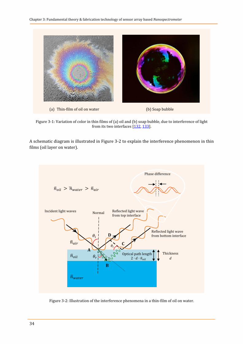
Chapter 3: Fundamental theory & fabrication technology of sensor array based Nanospectrometer
34
Figure 3-1: Variation of color in thin films of (a) oil and (b) soap bubble, due to interference of light from its two interfaces [132, 133].
A schematic diagram is illustrated in Figure 3-2 to explain the interference phenomenon in thin
films (oil layer on water).
Figure 3-2: Illustration of the interference phenomena in a thin-film of oil on water.
Thickness
d
Incident light waves Reflected light wave from top interface
Optical path length
Normal
Reflected light wave from bottom interface
Phase difference
A
B
C
D
(a) Thin-film of oil on water (b) Soap bubble

35
Here the refractive index of the oil ( ) is higher than the refractive indices of air ( ) and
water ( ). When a light wave is incident on air-oil interface (on low to high refractive
index interface), a portion of the wave will transmit and a portion will reflect with a phase shift
of 180˚ ( or ). The transmitted portion of wave will partially reflect from the oil-water
interface (from high to low refractive index interface) but without any phase shift. The first
wave is 180˚ out of phase with respect to the incident wave while the reflected wave from the
second interface travels an additional distance (optical path of ) compared to the reflected
wave from the first interface. The reflected waves from the two interfaces interfere with each
other and thus results in constructive or destructive interference based on their optical path
difference [134, 135], which can be derived as:
Optical path difference =
(3-1)
(3-2)
(3-3)
(3-4)
Substituting the value of from equation (3-2) and value of from equation (3-4) into
equation (3-1)
=
(3-5)
Now substituting the value of from equation (3-3) into equation (3-5)
=
(3-6)

Chapter 3: Fundamental theory & fabrication technology of sensor array based Nanospectrometer
36
As Snell’s law indicates that
(3-7)
With respect to Figure 3-2, it can be written as
(3-8)
Substituting the value of from equation (3-8) into equation (3-6)
=
(3-9)
=
–
(3-10)
As it is known that,
(3-11)
Substituting the above value in equation (3-10)
=
–
(3-12)
=
(3-13)
Plugging the following known identity in equation (3-13)
(3-14)
=
(3-15)

37
=
(3-16)
As mentioned earlier, the reflected wave from the first interface (air-oil) undergoes a phase
shift of 180˚ ( or ) and therefore, the path difference can be written as:
=
(3-17)
Hence, the condition for constructive interference based on the path difference between the two
waves can be written as
=
(3-18)
(3-19)
(3-20)
Under the above condition as in equation (3-20), the two waves interfere constructively and
thin-film appears bright.
The condition for destructive interference based on the path difference between the two waves
can be written as:
(3-21)
(3-22)
(3-23)
According to the above condition as in equation (3-23), the two waves will interfere
destructively and the thin-film will appear dark.
In the above , is the angle of the incident wave, is the angle of refracted wave, is the thickness of the oil film, is an integer number and is the wavelength of the wave inside the
oil film (
).
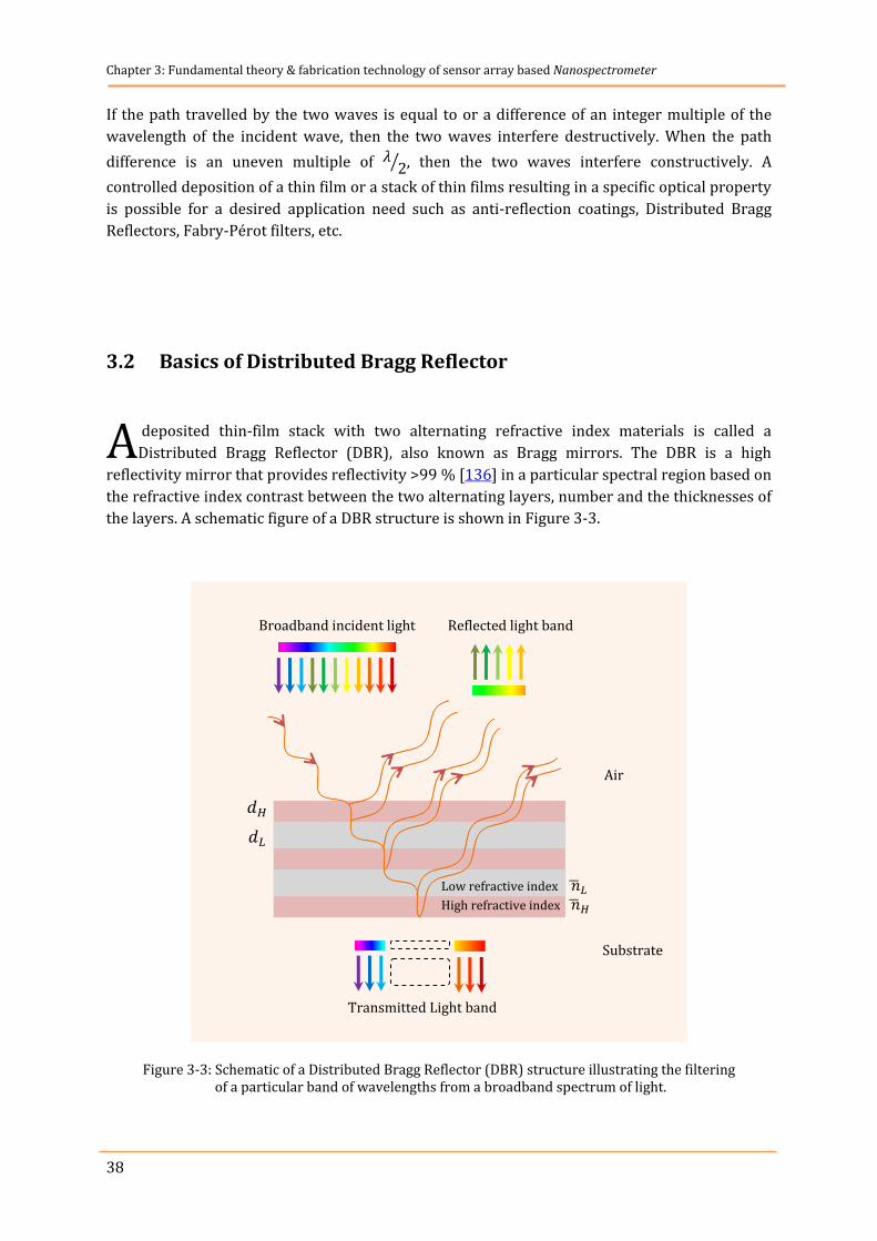
Chapter 3: Fundamental theory & fabrication technology of sensor array based Nanospectrometer
38
If the path travelled by the two waves is equal to or a difference of an integer multiple of the
wavelength of the incident wave, then the two waves interfere destructively. When the path
difference is an uneven multiple of , then the two waves interfere constructively. A
controlled deposition of a thin film or a stack of thin films resulting in a specific optical property
is possible for a desired application need such as anti-reflection coatings, Distributed Bragg
Reflectors, Fabry-Pérot filters, etc.
3.2 Basics of Distributed Bragg Reflector
deposited thin-film stack with two alternating refractive index materials is called a
Distributed Bragg Reflector (DBR), also known as Bragg mirrors. The DBR is a high
reflectivity mirror that provides reflectivity >99 % [136] in a particular spectral region based on
the refractive index contrast between the two alternating layers, number and the thicknesses of
the layers. A schematic figure of a DBR structure is shown in Figure 3-3.
Figure 3-3: Schematic of a Distributed Bragg Reflector (DBR) structure illustrating the filtering of a particular band of wavelengths from a broadband spectrum of light.
A
Broadband incident light Reflected light band
Transmitted Light band
Air
Low refractive index
High refractive index
Substrate
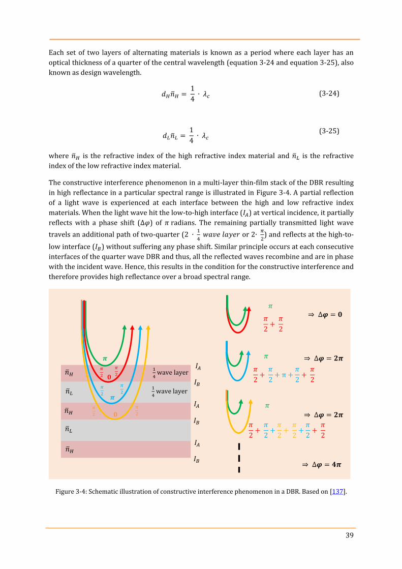
39
Each set of two layers of alternating materials is known as a period where each layer has an
optical thickness of a quarter of the central wavelength (equation 3-24 and equation 3-25), also
known as design wavelength.
(3-24)
(3-25)
where is the refractive index of the high refractive index material and is the refractive
index of the low refractive index material.
The constructive interference phenomenon in a multi-layer thin-film stack of the DBR resulting
in high reflectance in a particular spectral range is illustrated in Figure 3-4. A partial reflection
of a light wave is experienced at each interface between the high and low refractive index
materials. When the light wave hit the low-to-high interface ( ) at vertical incidence, it partially
reflects with a phase shift ( ) of radians. The remaining partially transmitted light wave
travels an additional path of two-quarter (
or 2
) and reflects at the high-to-
low interface ( ) without suffering any phase shift. Similar principle occurs at each consecutive
interfaces of the quarter wave DBR and thus, all the reflected waves recombine and are in phase
with the incident wave. Hence, this results in the condition for the constructive interference and
therefore provides high reflectance over a broad spectral range.
Figure 3-4: Schematic illustration of constructive interference phenomenon in a DBR. Based on [137].
0
0
wave layer
wave layer
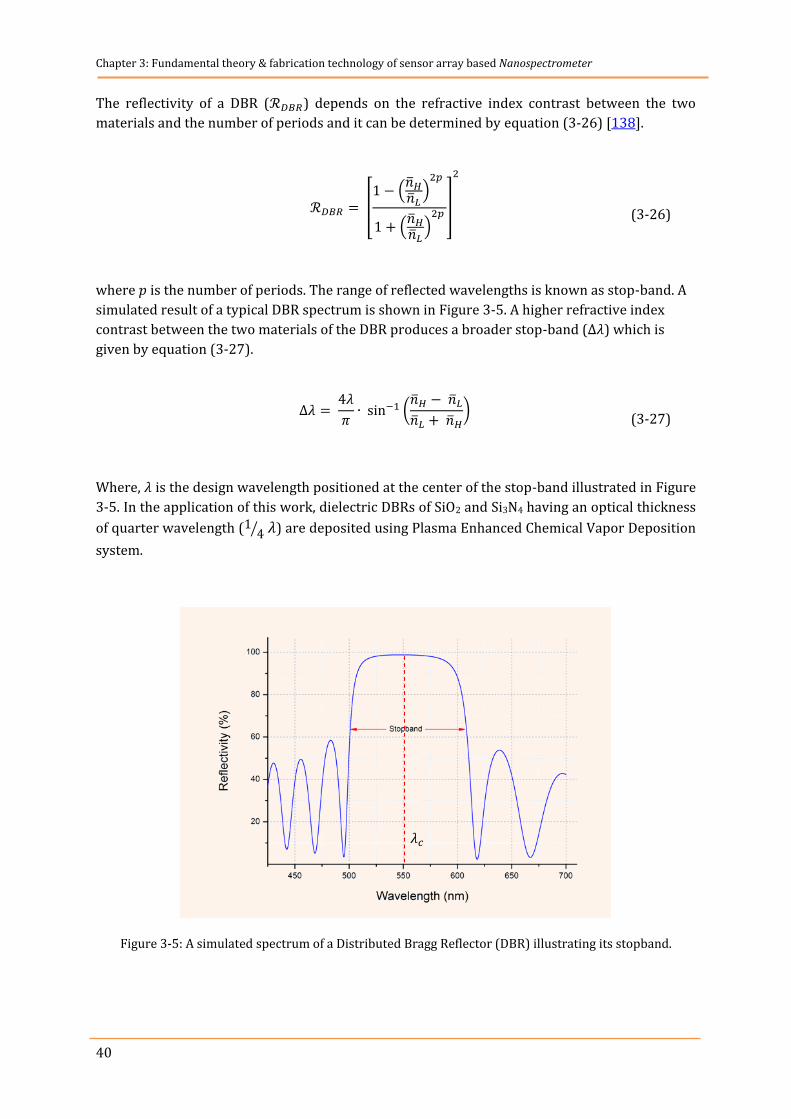
Chapter 3: Fundamental theory & fabrication technology of sensor array based Nanospectrometer
40
The reflectivity of a DBR ( ) depends on the refractive index contrast between the two
materials and the number of periods and it can be determined by equation (3-26) [138].
(3-26)
where is the number of periods. The range of reflected wavelengths is known as stop-band. A
simulated result of a typical DBR spectrum is shown in Figure 3-5. A higher refractive index
contrast between the two materials of the DBR produces a broader stop-band ( ) which is
given by equation (3-27).
(3-27)
Where, is the design wavelength positioned at the center of the stop-band illustrated in Figure
3-5. In the application of this work, dielectric DBRs of SiO2 and Si3N4 having an optical thickness
of quarter wavelength ( ) are deposited using Plasma Enhanced Chemical Vapor Deposition
system.
Figure 3-5: A simulated spectrum of a Distributed Bragg Reflector (DBR) illustrating its stopband.

41
3.3 Optical properties of Fabry-Pérot filter
abry-Pérot (FP) filter consist of two highly reflecting mirrors placed parallel to each other
and separated by a distance between them called cavity or Fabry-Pérot cavity (FP-cavity).
This filter type was first introduced by Charles Fabry and Alfred Pérot in 1899 [139]. Due to
their high reflectivity, the DBRs are generally preferred mirrors with a FP-cavity of a material or
air having a certain thickness. The sandwiched cavity between the two DBRs forms an optical
resonator. In the optical resonance cavity of the FP-filter, a particular wavelength (or
wavelengths) that fulfills the cavity condition (equation (3-28)) is in resonance mode and forms
a standing wave inside the cavity. These standing waves result in constructive interference and
are transmitted through the FP-filter while other wavelengths are reflected and hence, filtered
out. The thicknesses of the DBR layers define the spectral position of the stopband and the
thickness of the FP-cavity defines the transmitted wavelength (also known as transmission-line
or mode) within the stopband. Generally, the cavity thickness is selected to be a multiple of half
a wavelength of the desired wavelength ( ) to be transmitted. This results in a transmission-
line within the stopband, λc [140], [141]. A schematic illustrating the FP-filter structure is given
in Figure 3-6 (a) and a simulated example spectrum of the FP-filter is shown in Figure 3-6 (b).
(3-28)
Where is the refractive index of the cavity material at the designed wavelength ( ), is the
cavity thickness and is the cavity mode (mode number).
F
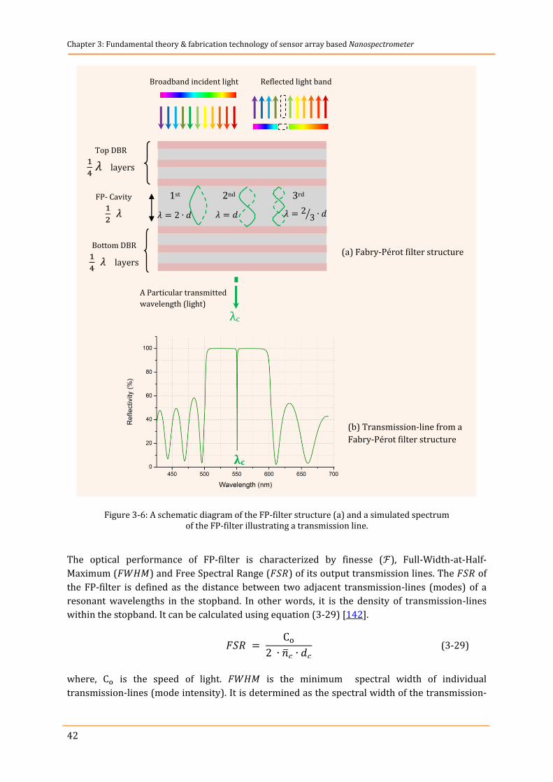
Chapter 3: Fundamental theory & fabrication technology of sensor array based Nanospectrometer
42
Figure 3-6: A schematic diagram of the FP-filter structure (a) and a simulated spectrum of the FP-filter illustrating a transmission line.
The optical performance of FP-filter is characterized by finesse ( ), Full-Width-at-Half-
Maximum ( ) and Free Spectral Range ( ) of its output transmission lines. The of
the FP-filter is defined as the distance between two adjacent transmission-lines (modes) of a
resonant wavelengths in the stopband. In other words, it is the density of transmission-lines
within the stopband. It can be calculated using equation (3-29) [142].
(3-29)
where, is the speed of light. is the minimum spectral width of individual
transmission-lines (mode intensity). It is determined as the spectral width of the transmission-
λc
A Particular transmitted
wavelength (light)
λc
Broadband incident light Reflected light band
Top DBR
layers
Bottom DBR
layers
FP- Cavity
1st 2nd 3rd
(b) Transmission-line from a
Fabry-Pérot filter structure
(a) Fabry-Pérot filter structure
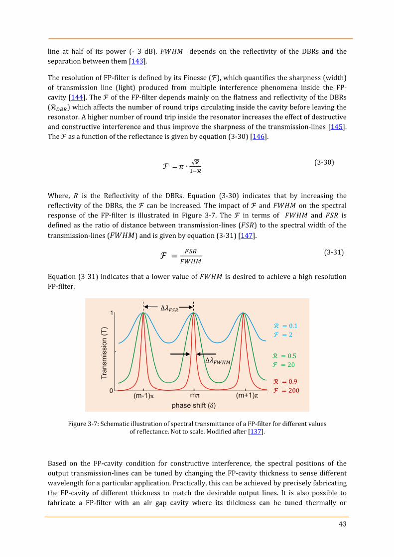
43
line at half of its power (- 3 dB). depends on the reflectivity of the DBRs and the
separation between them [143].
The resolution of FP-filter is defined by its Finesse ( ), which quantifies the sharpness (width)
of transmission line (light) produced from multiple interference phenomena inside the FP-
cavity [144]. The of the FP-filter depends mainly on the flatness and reflectivity of the DBRs
( ) which affects the number of round trips circulating inside the cavity before leaving the
resonator. A higher number of round trip inside the resonator increases the effect of destructive
and constructive interference and thus improve the sharpness of the transmission-lines [145].
The as a function of the reflectance is given by equation (3-30) [146].
(3-30)
Where, is the Reflectivity of the DBRs. Equation (3-30) indicates that by increasing the
reflectivity of the DBRs, the can be increased. The impact of and on the spectral
response of the FP-filter is illustrated in Figure 3-7. The in terms of and is
defined as the ratio of distance between transmission-lines ( ) to the spectral width of the
transmission-lines ( ) and is given by equation (3-31) [147].
(3-31)
Equation (3-31) indicates that a lower value of is desired to achieve a high resolution
FP-filter.
Figure 3-7: Schematic illustration of spectral transmittance of a FP-filter for different values of reflectance. Not to scale. Modified after [137].
Based on the FP-cavity condition for constructive interference, the spectral positions of the
output transmission-lines can be tuned by changing the FP-cavity thickness to sense different
wavelength for a particular application. Practically, this can be achieved by precisely fabricating
the FP-cavity of different thickness to match the desirable output lines. It is also possible to
fabricate a FP-filter with an air gap cavity where its thickness can be tuned thermally or
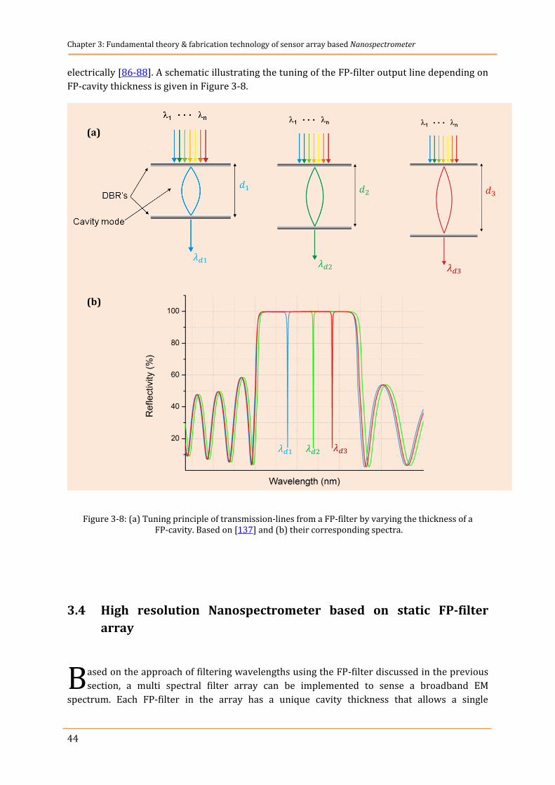
Chapter 3: Fundamental theory & fabrication technology of sensor array based Nanospectrometer
44
electrically [86-88]. A schematic illustrating the tuning of the FP-filter output line depending on
FP-cavity thickness is given in Figure 3-8.
Figure 3-8: (a) Tuning principle of transmission-lines from a FP-filter by varying the thickness of a FP-cavity. Based on [137] and (b) their corresponding spectra.
3.4 High resolution Nanospectrometer based on static FP-filter
array
ased on the approach of filtering wavelengths using the FP-filter discussed in the previous
section, a multi spectral filter array can be implemented to sense a broadband EM
spectrum. Each FP-filter in the array has a unique cavity thickness that allows a single
B
(a)
(b)
45
wavelength to transmit through it, which can be exploited to sense the spectra of various
materials in medical, industrial, environmental, etc. applications. It is necessary to detect this
transmitted wavelength which is done by a photodetector array. The integrated version of the
FP-filter array and the photodetector array forms the sensor array. Optical spectrometers based
on FP-filter arrays have been already reported by [30, 34]. FP-based spectrometers can be
strongly miniaturized without any compromise in its high resolution; therefore, other available
conventional grating based spectrometers can be replaced by this approach. Research at INA is
focused on developing a high resolution and miniaturized spectrometer based on FP-filter array
using the novel approach of NanoImpint technology, hence called the Nanospectrometer. The
principle of a Nanospectrometer based on FP-filter array and the corresponding photodetector
array is illustrated in Figure 2-3.
The number of FP-filters in the array defines the number of the sensed wavelengths. As
discussed in the previous sections, a stopband of particular spectral range (100 nm – 150 nm) is
obtained depending on the DBR materials and deposition techniques, where the transmission-
lines correlated to the FP-cavities are located within that stopband. However, this range of
spectrum covered by a single stopband is not sufficient for broadband sensing applications.
Therefore, three sets of DBRs with different central wavelength are deposited to define three
different stopbands in a different spectral position to cover a broad spectral range, e.g. the
complete visible wavelength range. The thickness of the FP-cavities defines the spectral
positions of the transmission-lines within the covered spectral range.
For a high resolution sensing, precise fabrication of cavities in the array is required such that
each FP-filter senses a particular designed wavelength depending on the thickness of its
resonant cavity. Not only the number of FP-filters is important but also a narrow of each
transmission-lines of FP-filter in the array is desired which can be achieved by a high reflective
DBRs.
3.5 Foundations of utilized lithography techniques
ithography is a pattern transfer method which is a Greek word meaning “stone-drawing”
and was first invented by Alois Senefelder in 1798 for book illustrations, posters, and
artist’s prints [148]. This lithography technique evolved into the so called photolithography,
also called optical lithography, which was first practiced by J. N. Niepce in 1852 where light is
used instead of ink to transfer the pattern onto a desired substrate material [149]. In the era of
Integrated Circuits (IC) revolution, the optical lithography developed and gained much
importance in the device fabrication.
Currently, the core of electronics, optoelectronics, photonics and microsystem devices
fabrication is the lithography process where its contribution is 30% - 35% of the total device
fabrication cost [90]. The optical lithography is widely used as a conventional lithography
technique due to its low cost and reduced complexity. However, each structure is fabricated as a
standalone in a single process which increases the fabrication cost and time. Therefore, the next
L
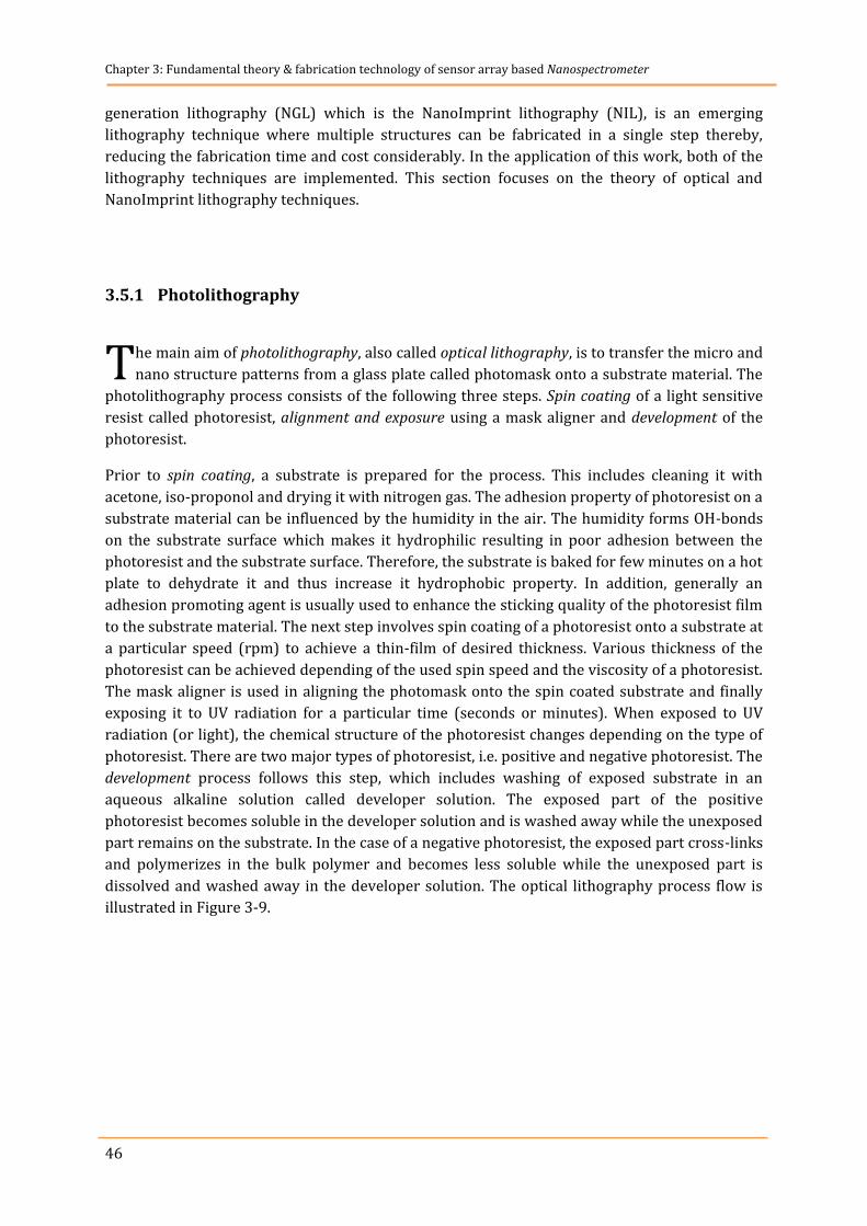
Chapter 3: Fundamental theory & fabrication technology of sensor array based Nanospectrometer
46
generation lithography (NGL) which is the NanoImprint lithography (NIL), is an emerging
lithography technique where multiple structures can be fabricated in a single step thereby,
reducing the fabrication time and cost considerably. In the application of this work, both of the
lithography techniques are implemented. This section focuses on the theory of optical and
NanoImprint lithography techniques.
3.5.1 Photolithography
he main aim of photolithography, also called optical lithography, is to transfer the micro and
nano structure patterns from a glass plate called photomask onto a substrate material. The
photolithography process consists of the following three steps. Spin coating of a light sensitive
resist called photoresist, alignment and exposure using a mask aligner and development of the
photoresist.
Prior to spin coating, a substrate is prepared for the process. This includes cleaning it with
acetone, iso-proponol and drying it with nitrogen gas. The adhesion property of photoresist on a
substrate material can be influenced by the humidity in the air. The humidity forms OH-bonds
on the substrate surface which makes it hydrophilic resulting in poor adhesion between the
photoresist and the substrate surface. Therefore, the substrate is baked for few minutes on a hot
plate to dehydrate it and thus increase it hydrophobic property. In addition, generally an
adhesion promoting agent is usually used to enhance the sticking quality of the photoresist film
to the substrate material. The next step involves spin coating of a photoresist onto a substrate at
a particular speed (rpm) to achieve a thin-film of desired thickness. Various thickness of the
photoresist can be achieved depending of the used spin speed and the viscosity of a photoresist.
The mask aligner is used in aligning the photomask onto the spin coated substrate and finally
exposing it to UV radiation for a particular time (seconds or minutes). When exposed to UV
radiation (or light), the chemical structure of the photoresist changes depending on the type of
photoresist. There are two major types of photoresist, i.e. positive and negative photoresist. The
development process follows this step, which includes washing of exposed substrate in an
aqueous alkaline solution called developer solution. The exposed part of the positive
photoresist becomes soluble in the developer solution and is washed away while the unexposed
part remains on the substrate. In the case of a negative photoresist, the exposed part cross-links
and polymerizes in the bulk polymer and becomes less soluble while the unexposed part is
dissolved and washed away in the developer solution. The optical lithography process flow is
illustrated in Figure 3-9.
T
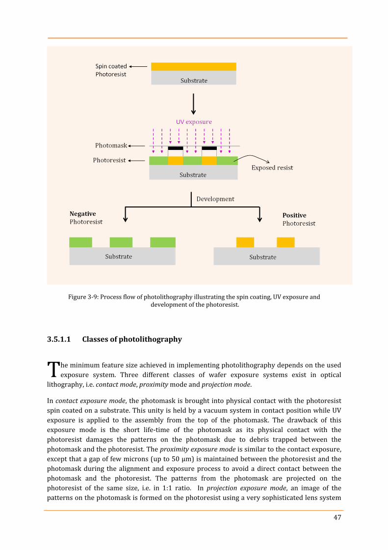
47
Figure 3-9: Process flow of photolithography illustrating the spin coating, UV exposure and development of the photoresist.
3.5.1.1 Classes of photolithography
he minimum feature size achieved in implementing photolithography depends on the used
exposure system. Three different classes of wafer exposure systems exist in optical
lithography, i.e. contact mode, proximity mode and projection mode.
In contact exposure mode, the photomask is brought into physical contact with the photoresist
spin coated on a substrate. This unity is held by a vacuum system in contact position while UV
exposure is applied to the assembly from the top of the photomask. The drawback of this
exposure mode is the short life-time of the photomask as its physical contact with the
photoresist damages the patterns on the photomask due to debris trapped between the
photomask and the photoresist. The proximity exposure mode is similar to the contact exposure,
except that a gap of few microns (up to 50 µm) is maintained between the photoresist and the
photomask during the alignment and exposure process to avoid a direct contact between the
photomask and the photoresist. The patterns from the photomask are projected on the
photoresist of the same size, i.e. in 1:1 ratio. In projection exposure mode, an image of the
patterns on the photomask is formed on the photoresist using a very sophisticated lens system
T
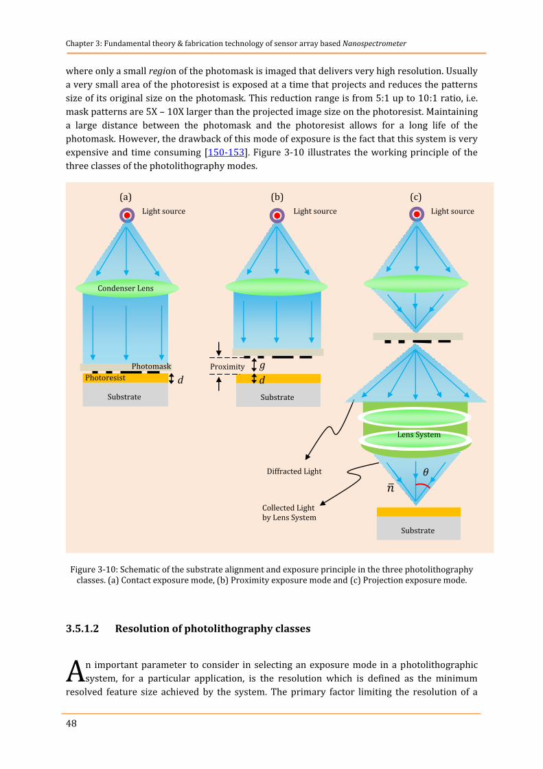
Chapter 3: Fundamental theory & fabrication technology of sensor array based Nanospectrometer
48
where only a small region of the photomask is imaged that delivers very high resolution. Usually
a very small area of the photoresist is exposed at a time that projects and reduces the patterns
size of its original size on the photomask. This reduction range is from 5:1 up to 10:1 ratio, i.e.
mask patterns are 5X – 10X larger than the projected image size on the photoresist. Maintaining
a large distance between the photomask and the photoresist allows for a long life of the
photomask. However, the drawback of this mode of exposure is the fact that this system is very
expensive and time consuming [150-153]. Figure 3-10 illustrates the working principle of the
three classes of the photolithography modes.
Figure 3-10: Schematic of the substrate alignment and exposure principle in the three photolithography classes. (a) Contact exposure mode, (b) Proximity exposure mode and (c) Projection exposure mode.
3.5.1.2 Resolution of photolithography classes
n important parameter to consider in selecting an exposure mode in a photolithographic
system, for a particular application, is the resolution which is defined as the minimum
resolved feature size achieved by the system. The primary factor limiting the resolution of a
A
Light source
Substrate
Photoresist
Photomask
d
Condenser Lens
Substrate
Proximity
d
g
Light source Light source
Collected Light by Lens System
Diffracted Light
Substrate
Lens System
(a) (b) (c)
49
lithographic exposure mode is the light diffraction. The achieved minimum feature size differs in
the selected exposure mode as summarized in Table 3-1. [150, 154-156].
Photolithographic system Equation of Resolution Resolved minimum feature size @ 365 nm exposure wavelength
Contact exposure mode
Proximity exposure mode
Projection exposure mode
Table 3-1: The resolution of the available lithographic systems. d is the thickness of the photoresist; g is the gap between the photoresist and the photomask; is the exposure wavelength, NA is the numerical
aperture of the lens system and is the resolution factor which depends on the used lens system, quality of photoresist and the photomask which has values typically between 0.25 and 0.8.
The resolution of all lithographic classes depends on the exposure wavelength. Therefore, using
shorter wavelength allows in achieving smaller feature size. Additionally, in projection
lithographic class, the minimum feature size depends on the Numerical Aperture ( ) and
value of the system. is a measure of how much of the diffracted light can be accepted by the
lens system and imaged. Improvements in lens design such as, large size lens that allows
collecting a larger amount of diffracted light (large range of angles), leads to improvements in
where a maximum value of 1 is the limit when air being a medium between the lens system
and the substrate. Mathematically it is given by [157]:
(3-32)
Where, is the acceptance angle of the lens and is the refractive index of the medium
surrounding the lens. Instead of air as a medium, of larger than 1 can be achieved by using
immersion fluid with higher values between the lens and substrate. This improves the
resolution as the angle inside the immersion fluid will be less compared to air used [153].
The value is described as lithography process constant (also called resolution or complexity
factor) that depends on several parameters such as the optical quality of photoresist and the use
of enhancement techniques such as phase shift masks. A higher resolution can be achieved by
decreasing the wavelength of the light source for exposure, decreasing the value or by
increasing [156, 158].
Although, the resolution of optical lithography is improved by techniques such as phased masks
[149, 159, 160], immersion lithography [161, 162] and increasing Numerical Aperture [149] of
the system, however, the Next Generation Lithography (NGL) discussed in next section, in
Chapter 3: Fundamental theory & fabrication technology of sensor array based Nanospectrometer
50
addition to improvements in resolution has other advantages too which makes it a successor to
this conventionally used optical lithography.
In this work, an adhesion promoter TI-prime, a positive photoresist AZ1518 and a negative
photoresist AZnLof 2070 from Micro chemicals GmbH are used in the fabrication of the 3D
master template for the implementation of the Nanospectrometer.
3.5.2 NanoImprint Lithography
he conventionally used optical lithography technique, discussed in the previous section,
lack the ability in assisting the fabrication of structures with feature size beyond the
diffraction limit of the used light source for resist exposure. In other word, the resolution of
optical lithography is limited by factors such as light diffraction, scattering and interference in
the used photoresist, back-scattering from the substrate and the chemistry of the Photoresist
[163].
Unlike the optical lithographic techniques that define nano structure patterns in a photoresist
through radiation such as photons, electrons or ions, non-radiated-based patterning relies on
mechanical or chemical or both the processes in defining patterns in a photoresist [101]. Non-
radiated-based patterning has various advantages over the optical lithographic techniques due
to the absence of radiation sources. These advantages are [163]:
Absence of light diffraction that limits the resolution, Possibility to form 3D patterns easily, Possibility to transfer and produce functional patterns with high fidelity.
The most interesting non-radiative lithographic technique, which is gaining popularity, is the
Nanoimprint Lithography ( ). NIL is a non-conventional patterning technique where a
deformable material, usually polymers, is directly molded (mechanically) to create functional
structures for a desired application need. This form of patterning technique, termed as NGL, is
the most promising and cost-effective lithographic technique that offers high-throughput nano
structures at higher precision [101]. Since the need of a complicated electromagnetic source and
sophisticated optical system is not required, the cost of ownership is also cheap [163]. It was
first invented and developed by Prof. Dr. Stephan Chou and his group in 1995 at University of
Minnesota [164]. NIL is capable of replicating feature sizes <10 nm over large area substrates
and is a promising technology to enable nanoscale manufacturing for nano photonics devices
and advanced IC [99, 100, 165]. At present various derivates of the Nanoimprint lithography are
invented at large scale and low cost application needs [166].
The most important component of NIL is the master template that contains the patterns of the
functional structures. The feature size of these structures ranges from few micrometers to sub-
nanometer range. The principle process of NIL is spin coating or dispensing a thin-film of the
soft polymer Nanoimprint resist on a substrate material. Then, the template that contains the
structures is pressed into the Nanoimprint resist which deforms or molds the resist material
(according to the surface topology of the template) and takes the shape of the template. This
T
51
step is followed by the curing process of the molded nanoimprint resist to harden and take up a
solid shape of the structures. Finally, the template is separated from the deformed imprint resist
termed as separation process. This curing process can be, majorly, conducted through either of
the 2 methods, i.e. thermally, termed as Thermal Nanoimprint or by exposing it to UV radiation,
termed as UV imprint. After the curing process, the master template is separated from the
patterned resist and it can be used several times. These two methods are briefly discussed in the
following sub sections.
3.5.2.1 Thermal NanoImprint Lithography
hermal NanoImprint Lithography ( ) is also known as hot imbossing lithography. In
, a thermally curable imprint resist (Thermoplastic polymer such as PMMA4) is spin
coated. Then, the template containing the nano structures is brought into intimate contact to it
and pressure is applied. Heat above glass transition temperature, , of the imprint resist is
applied to reduce the viscosity of the thermoplastic resist material. Therefore, it eases the flow
of the resist and allows it to fill the patterns in the template by the applied pressure. The unity is
cooled while the pressure is maintained to let harden the formed patterns. After a certain time
period, the master template is separated from the deformed imprint resist. The unwanted
residue of the resist material around the patterned structures is removed by etching process
[161, 167]. The process of is illustrated in Figure 3-11.
is cheaper as less stringent requirements are essential for the material of the master
template, e.g. the master template can be opaque and need not be highly transparent[168].
However, as a high pressure is applied in this process, a hard template material with low
thermal expansion coefficient is necessary [169].
4 Polymethyl methacrylate
T
Chapter 3: Fundamental theory & fabrication technology of sensor array based Nanospectrometer
52
Figure 3-11: Process flow of Thermal Nanoimprint Lithography (T-NIL).
3.5.2.2 Ultra-Violet NanoImprint Lithogrpahy
ltra-Violet NanoImprint Lithogrpahy ( ) is a derivative of NIL which addresses the
limitation of alignment, as in , by adopting a master template material which is
transparent to UV. Moreover, this technique is implemented at room temperature and does not
require higher pressures. A UV-curable imprint resist is coated on the substrate and a highly
transparent template (to UV radiation) is pressed into the imprint resist at a pressure of 1.7 bar
[130]. The imprint resist flows into the patterns in the template and fills it. The unity is exposed
to UV-radiation for a certain time to harden the imprint resist via cross-linking of the monomers
in the resist material. The patterned imprint resist is further etched to obtain a residual-free
structure [161, 167]. The process flow of is illustrated in Figure 3-12.
U
Substrate
(a) Spin coating of thermal sensitive imprint resist
(b) Aligning master template & applying pressure & heat
(d) Separation of master template from the imprinted nano structure patterns
(e) Etching of residue layer
(f) High resolution NanoImprinted nano structure patterns
(c) Cooling of master template & imprint resist
Heat & pressure
Substrate
Substrate Substrate
Substrate
Cooling
Residue Etching (RIE)
Substrate
53
Figure 3-12: Process flow of Ultra-Violet Nanoimprint Lithography ( ).
The advantages of are that it does not need high pressure and the process can be conducted at room temperature. Furthermore, it provides the possibility for high alignment accuracy [168] and large area imprinting on wafers up to 450 mm in diameter using step-and-repeat process [170].
3.5.2.3 Surface Conformal Imprint Lithography
he NanoImprint techniques discussed in previous sub-sections have, however, some
limitations. One of these limitations is that surfaces with only uniform and planar
topography can be imprinted since the master template is rigid which impairs its contact
throughout the non planar substrates as illustrated in Figure 3-13 (a). Secondly, the throughput
yield is highly influenced by an unwanted dirt particle that appears between the master
T
Substrate
(a) Spin coating of UV sensitive Imprint resist and aligning master template
(b) Pressing master template and polymerization of imprint resist with UV
(c) Separation of master template from the imprinted nano structure patterns
(d) Etching of residue layer
(e) Nano structure pattern transfer via high resolution UV-NIL
UV Radiation
Substrate
Substrate Substrate
Residue Etching (RIE)
Substrate
Chapter 3: Fundamental theory & fabrication technology of sensor array based Nanospectrometer
54
template and the imprint surfaces as illustrated in Figure 3-13 (b). Third, the life time of the
master template is limited as it is directly used for imprinting. These limitations are eliminated
by Surface Conformal Imprint Lithography ( ), also called soft NanoImprint lithography,
which is the next version of the UV-based Nanoimprint lithography developed by Philips and
SUSS MicroTec [171, 172].
Figure 3-13: Limitation of and (a) in imprinting on non-planar substrates and (b) reduced throughput due to trapped particles between master template and the imprint resist.
In , the master template is first copied into daughter templates during the so called
replication process. The daughter templates are hybrid templates, i.e. they are fabricated by a
combination of hard- and soft- Polydimethylsiloxane (h-PDMS and s-PDMS). The hybrid
template is held by a flexible glass sheet called carrier. These materials combination enables it
to be soft, flexible and transparent to UV. Further details can be found in [173, 174].It is to be
noted that, in the design of the master template, this additional inter-mediate step (replication
of master template) has to be considered in order to obtain the desired patterns from the
imprint process. For example, the master template for FP-cavity patterns based on is
fabricated such that the patterns (FP-cavities) are of positive shape. Once the soft daughter
templates are replicated, these patterns from the master template take a negative shape
(reverse order). During the imprint process, the negative patterns are transferred to the imprint
resist which again transforms into positive shape patterns. This process is illustrated in Figure
3-14.
Compared to previous mentioned NIL techniques, the NanoImprint resist in fills and raises
up into the 3D cavities due to the capillary forces between the NanoImprint resist and the
template, hence a very low pressure of 20 mbar is sufficient. However, patterning by capillary
forces limits the aspect-ratio of the imprinted cavities since the PDMS material has a low
Young’s modulus (<2 MPa) which leads to deformation of patterns in the imprint process [50].
(a) (b)
Substrate Substrate
55
Figure 3-14: Schematic of replication process of master template into PDMS daughter templates.
The major advantages of Nanoimprint are that it allows imprinting on non-planar
substrates over a large area. A schematic illustration of the flexible imprinting and the
imprinted results of this technology are shown in Figure 3-15. Moreover, the life-time of the
master template is prolonged since it is not directly used for the imprinting process where it
would physically and chemically come in contact to the polymer resist materials. has been
successfully implemented on large area patterning for realizing smaller feature sizes for the
mass production of biosensors [175]. Large area wafers of 6 inches have also been imprinted
which shows its great potential in the production of cost effective photonic crystal (PhC)
structures on LEDs [176].
(a) Master template
(b) Spin coating of h-PDMS on master
template
(c) Spin coating of s-PDMS
(d) Release & separate to form a soft &
flexible daughter template
Chapter 3: Fundamental theory & fabrication technology of sensor array based Nanospectrometer
56
Figure 3-15: (a) Schematic illustration of soft and flexible imprinting of SCIL on non-planar substrate. (b) and (c) Results while imprinting on a trapped dirt particle providing high throughput yield [177].
Substrate
SCIL Imprint process
Substrate
(b)
(a)
57
3.6 Implemented fabrication and characterization technologies
n the fabrication and characterization of 3D master template and deposition of FP-filters,
various technologies are implemented such as Mask aligner, Reactive Ion Etching, Plasma
Enhanced Chemical Vapor Deposition, White Light Interferometer, and Scanning Electron
Microscope. These technologies are briefly described in this chapter.
3.6.1 Mask Aligner
n optical Lithography, mask aligner is the key tool in the process of transferring the micro
range mesa structure patterns from a photomask on to a substrate. The photomask
containing the structure patterns is fixed between the UV lamp and the photoresist coated
substrate. On exposure, the UV radiation passes the photomask through some places and is
blocked at others. The radiation which passes through the photomask and strikes the
photoresist, interacts with the resist material and forms an image of the Photomask patterns on
the photoresist as discussed in section 3.5.1.
The used mask aligner in this work is MA4 from Suss MicroTec. It can work in contact or
proximity mode and provides an alignment accuracy in (x- and y-shift) of <0.1 µm. It can handle
4 inch substrates with up to 6 mm in thickness. The 350 W Hg lamp installed for exposure
offered a maximum intensity peak at 405 nm and offers a theoretical resolution of 1 – 2 µm
[178]. The mask aligner is installed in a Class 100 yellow room to block and prevent the
enterance of UV light (light of shorter wavelength) and avoid unnecessary exposure of the
Photoresist during processing. Due to its high resolution exposure optics and alignment
precision of mask to wafer, it is widely used in research and development for lithography
applications in the fields of MEMS, Wafer-Level optics, 3D packaging, photovoltaic, LED, power
devices, and Nanotechnology [179].
I
I
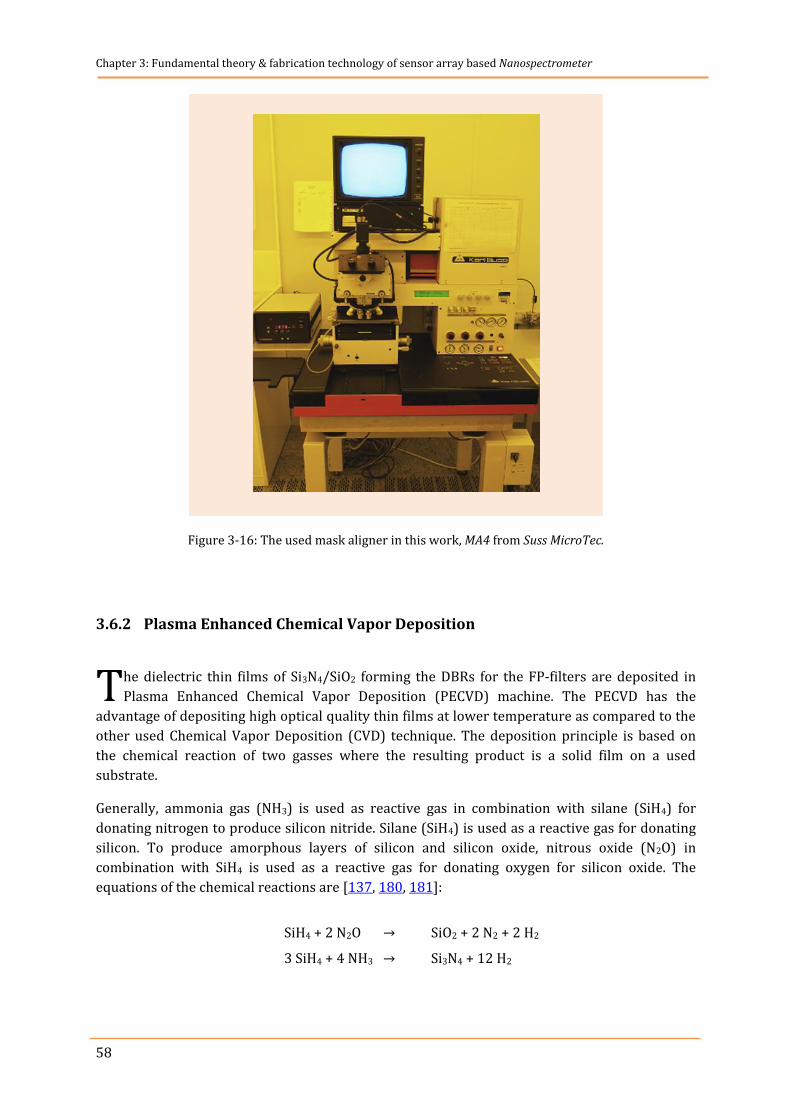
Chapter 3: Fundamental theory & fabrication technology of sensor array based Nanospectrometer
58
Figure 3-16: The used mask aligner in this work, MA4 from Suss MicroTec.
3.6.2 Plasma Enhanced Chemical Vapor Deposition
he dielectric thin films of Si3N4/SiO2 forming the DBRs for the FP-filters are deposited in
Plasma Enhanced Chemical Vapor Deposition (PECVD) machine. The PECVD has the
advantage of depositing high optical quality thin films at lower temperature as compared to the
other used Chemical Vapor Deposition (CVD) technique. The deposition principle is based on
the chemical reaction of two gasses where the resulting product is a solid film on a used
substrate.
Generally, ammonia gas (NH3) is used as reactive gas in combination with silane (SiH4) for
donating nitrogen to produce silicon nitride. Silane (SiH4) is used as a reactive gas for donating
silicon. To produce amorphous layers of silicon and silicon oxide, nitrous oxide (N2O) in
combination with SiH4 is used as a reactive gas for donating oxygen for silicon oxide. The
equations of the chemical reactions are [137, 180, 181]:
SiH4 + 2 N2O → SiO2 + 2 N2 + 2 H2
3 SiH4 + 4 NH3 → Si3N4 + 12 H2
T
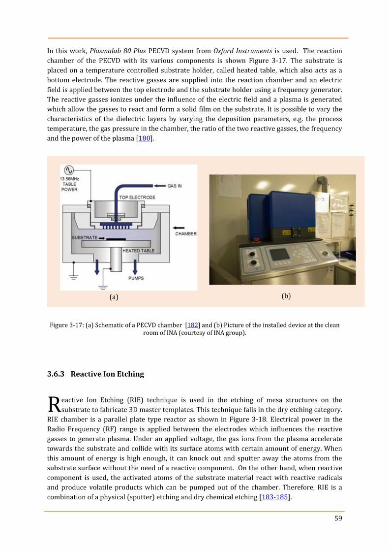
59
In this work, Plasmalab 80 Plus PECVD system from Oxford Instruments is used. The reaction
chamber of the PECVD with its various components is shown Figure 3-17. The substrate is
placed on a temperature controlled substrate holder, called heated table, which also acts as a
bottom electrode. The reactive gasses are supplied into the reaction chamber and an electric
field is applied between the top electrode and the substrate holder using a frequency generator.
The reactive gasses ionizes under the influence of the electric field and a plasma is generated
which allow the gasses to react and form a solid film on the substrate. It is possible to vary the
characteristics of the dielectric layers by varying the deposition parameters, e.g. the process
temperature, the gas pressure in the chamber, the ratio of the two reactive gasses, the frequency
and the power of the plasma [180].
Figure 3-17: (a) Schematic of a PECVD chamber [182] and (b) Picture of the installed device at the clean room of INA (courtesy of INA group).
3.6.3 Reactive Ion Etching
eactive Ion Etching (RIE) technique is used in the etching of mesa structures on the
substrate to fabricate 3D master templates. This technique falls in the dry etching category.
RIE chamber is a parallel plate type reactor as shown in Figure 3-18. Electrical power in the
Radio Frequency (RF) range is applied between the electrodes which influences the reactive
gasses to generate plasma. Under an applied voltage, the gas ions from the plasma accelerate
towards the substrate and collide with its surface atoms with certain amount of energy. When
this amount of energy is high enough, it can knock out and sputter away the atoms from the
substrate surface without the need of a reactive component. On the other hand, when reactive
component is used, the activated atoms of the substrate material react with reactive radicals
and produce volatile products which can be pumped out of the chamber. Therefore, RIE is a
combination of a physical (sputter) etching and dry chemical etching [183-185].
R
(a) (b)
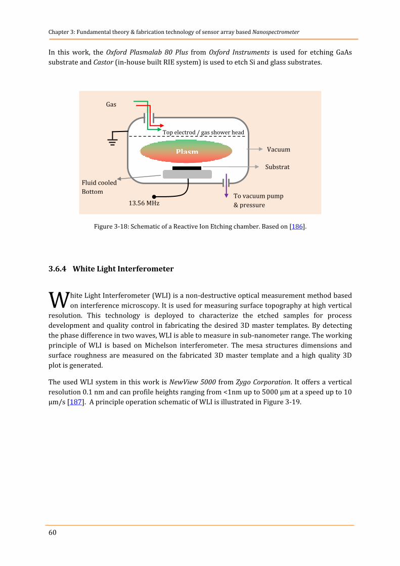
Chapter 3: Fundamental theory & fabrication technology of sensor array based Nanospectrometer
60
In this work, the Oxford Plasmalab 80 Plus from Oxford Instruments is used for etching GaAs
substrate and Castor (in-house built RIE system) is used to etch Si and glass substrates.
Figure 3-18: Schematic of a Reactive Ion Etching chamber. Based on [186].
3.6.4 White Light Interferometer
hite Light Interferometer (WLI) is a non-destructive optical measurement method based
on interference microscopy. It is used for measuring surface topography at high vertical
resolution. This technology is deployed to characterize the etched samples for process
development and quality control in fabricating the desired 3D master templates. By detecting
the phase difference in two waves, WLI is able to measure in sub-nanometer range. The working
principle of WLI is based on Michelson interferometer. The mesa structures dimensions and
surface roughness are measured on the fabricated 3D master template and a high quality 3D
plot is generated.
The used WLI system in this work is NewView 5000 from Zygo Corporation. It offers a vertical
resolution 0.1 nm and can profile heights ranging from <1nm up to 5000 µm at a speed up to 10
µm/s [187]. A principle operation schematic of WLI is illustrated in Figure 3-19.
W
13.56 MHz
Fluid cooled
Bottom
electrode
Substrat
e
Top electrod / gas shower head
Gas
inlet
Plasm
a
Vacuum
chamber
To vacuum pump
& pressure
control valve
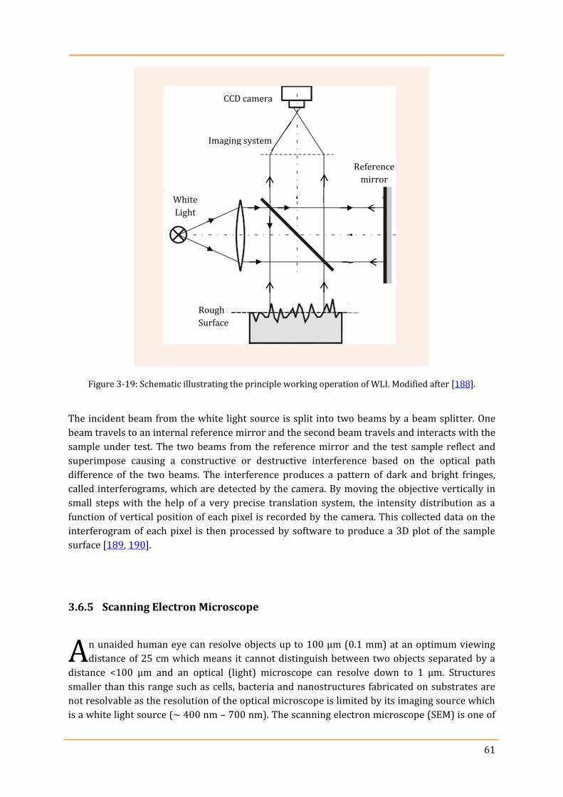
61
Figure 3-19: Schematic illustrating the principle working operation of WLI. Modified after [188].
The incident beam from the white light source is split into two beams by a beam splitter. One
beam travels to an internal reference mirror and the second beam travels and interacts with the
sample under test. The two beams from the reference mirror and the test sample reflect and
superimpose causing a constructive or destructive interference based on the optical path
difference of the two beams. The interference produces a pattern of dark and bright fringes,
called interferograms, which are detected by the camera. By moving the objective vertically in
small steps with the help of a very precise translation system, the intensity distribution as a
function of vertical position of each pixel is recorded by the camera. This collected data on the
interferogram of each pixel is then processed by software to produce a 3D plot of the sample
surface [189, 190].
3.6.5 Scanning Electron Microscope
n unaided human eye can resolve objects up to 100 µm (0.1 mm) at an optimum viewing
distance of 25 cm which means it cannot distinguish between two objects separated by a
distance <100 µm and an optical (light) microscope can resolve down to 1 µm. Structures
smaller than this range such as cells, bacteria and nanostructures fabricated on substrates are
not resolvable as the resolution of the optical microscope is limited by its imaging source which
is a white light source (~ 400 nm – 700 nm). The scanning electron microscope (SEM) is one of
A
White
Light
source
Reference
mirror
CCD camera
Imaging system
Rough
Surface
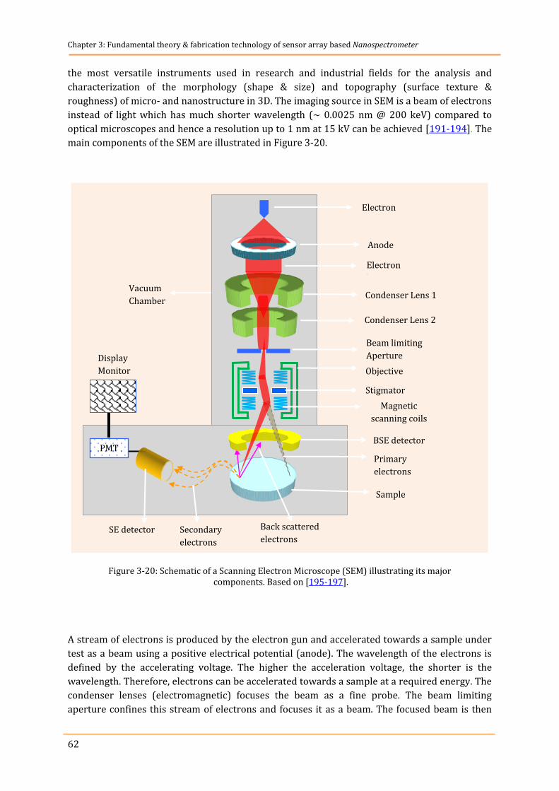
Chapter 3: Fundamental theory & fabrication technology of sensor array based Nanospectrometer
62
the most versatile instruments used in research and industrial fields for the analysis and
characterization of the morphology (shape & size) and topography (surface texture &
roughness) of micro- and nanostructure in 3D. The imaging source in SEM is a beam of electrons
instead of light which has much shorter wavelength (~ 0.0025 nm @ 200 keV) compared to
optical microscopes and hence a resolution up to 1 nm at 15 kV can be achieved [191-194]. The
main components of the SEM are illustrated in Figure 3-20.
Figure 3-20: Schematic of a Scanning Electron Microscope (SEM) illustrating its major components. Based on [195-197].
A stream of electrons is produced by the electron gun and accelerated towards a sample under
test as a beam using a positive electrical potential (anode). The wavelength of the electrons is
defined by the accelerating voltage. The higher the acceleration voltage, the shorter is the
wavelength. Therefore, electrons can be accelerated towards a sample at a required energy. The
condenser lenses (electromagnetic) focuses the beam as a fine probe. The beam limiting
aperture confines this stream of electrons and focuses it as a beam. The focused beam is then
PMT
Display
Monitor
Electron
gun
Anode
Beam limiting
Aperture
Condenser Lens 1
Condenser Lens 2
Magnetic
scanning coils
BSE detector
Sample
Electron
beam
SE detector Secondary
electrons
Primary
electrons
Vacuum
Chamber
Back scattered
electrons
Objective
Lens Stigmator

63
passed through the objective lens where the focal length can be varied by changing the magnetic
field strength in the coil of magnetic lenses which is achieved by changing the current. The
stigmator (metal aperture) blocks the stray electrons and exclude ones which are not on the
optical axis. This confines the electrons as a narrow beam which eventually improves the
resolution. This beam is then scanned across the surface of the sample with the help of the
deflector coils (scanning coils) where it interacts with it and a signal is generated (EM radiation)
from each scanned area. When the electron beam (Primary Electrons) interacts with the desired
area on the sample, loosely bounded electrons from the surface of the sample (valence shell of
the atoms) are ejected which are referred to as Secondary Electrons (SE). These SE are detected
by a SE detector and the resulted signal is amplified by a Photomultiplier Tube (PMT) which
provides an output voltage that is digitized to finally generate an image on the display monitor
of the SEM. Generally, SE provides the information on the topography of the sample. When the
primary electrons travel deeper into the sample and experience multiple scattering due to the
elastic collision with the nucleus of the target sample. This gives rise to the so called Back
scattered electrons (BSE). BSE provides details on features that are beneath the surface such as
composition of the sample [198, 199] .
In this work, S-4100 SEM system from Hitachi is used to analyze and examine various processed
samples such as the etched structures on the fabricated 3D master template.

64
65
4. Fabrication of high resolution 3D master
templates based on SCIL NanoImprint for the
implementation of Nanospectrometer
fforts are made at INA to realize a low cost and high resolution Nanospectrometer that
would have the capability to resolve sub-nm wavelength in spatial resolution (i.e. every few
nanometers) to enable highly selective sensing of the finger prints of various materials, gasses
and liquids in environmental, industrial, and medical science applications. This
Nanospectrometer is fabricated based on a FP-filter array approach, as discussed in section 3.4.
The Cost of the Nanospectrometer can be dramatically reduced by implementing the
NanoImprint lithography (NIL) technique as a cost-effective fabrication process. The main
component in fabricating the low cost Nanospectrometer is the corresponding NanoImprint
master template. In the frame of this work, the master template is fabricated for the Substrate
Conformal Imprint Lithography (SCIL) process which is mainly used and discussed in this
research work. The aim in this chapter is to fabricate high vertical resolution 3D NanoImprint
template containing 64 mesa structures of varying heights that will form an array of 64 FP-
cavities after the imprint process. To accomplish the array of vertically varying 3D FP-cavities,
various rigid substrate material such as gallium arsenide (GaAs), glass and silicon (Si) are
patterned by etching techniques. These substrates containing the FP-cavity array pattern is
called 3D master template in this work. Subsequently, the master templates are implemented
for the replication of 3D filter cavities in mirror symmetry on transparent soft materials for the
implementation of SCIL process. The templates based on transparent soft materials are called
SCIL templates in this work.
The optical, mechanical and chemical properties are important factors in choosing the substrate
material for a particular NIL technique, e.g. transparency, etch control, selectivity, hardness,
conductivity, roughness, and thermal expansion coefficient. The substrate cost and the 3D
master template fabrication cost are also important factor to consider. The resolution of the 3D
master template is defined by accurate and precise controllable etching of the 3D mesa
E
Chapter 4 Fabrication of high resolution 3D master templates
based on SCIL NanoImprint for the implementation
of Nanospectrometer
Chapter 4: Fabrication of high resolution 3D NanoImprint master templates
66
structures on a substrate material that will form the FP-cavities. Three major substrate
materials are investigated and compared to select the best suited material for 3D master
template fabrication. The low etching recipes of the selected substrate are investigated and
optimized to obtain a controllable etching of the master template. Furthermore, the calculation
of the thicknesses of the 64 FP-cavity array and its corresponding thicknesses in the 3D master
template are presented. Lastly, the fabricated 3D NanoImprint master template is characterized
and compared to the calculated design.
4.1 Investigation of substrate materials for 3D master template
fabrication
he work at INA has been progressed using Gallium Arsenide (GaAs), Glass and Silicon (Si)
substrates in the research towards fabricating 3D NanoImprint master templates for the
Nanospectrometer application. Therefore, in this section, the suited recipes from the previous
works are further investigated for low etching rate and implemented to achieve a low aspect
ratio etching of the FP-cavity patterns. However, comparison among these three materials is not
accounted. Therefore, this comparison is presented in order to select the best suited substrate
for the application of this work. Parts of the experimental work of this chapter were carried out
with the collaboration of master thesis students (Jone Azpillaga Olaizola, Rubén Fernández
Serrano, Urmee Nath and Ahmed Alghofaili) under the supervision of the author of this
dissertation.
4.1.1 Gallium Arsenide
ontrollable anisotropic low etching of GaAs is well known from literature [200-202].
Therefore, GaAs is chosen for the fabrication of the 3D nanoimprint master template. The
etching recipes of GaAs using available RIE gasses in the clean room are partially investigated in
INA [203]. From these investigations, the best suited recipe is further examined at a lower RF
power (50 W) to achieve low and controllable etch height of the master template. Two inch Si-
doped, n-type GaAs wafers with orientation of (100) and thickness of 350 25 µm from Wafer
Technology Ltd. are used and etched using the Oxford Plasmalab 80+ RIE. The etch depth of
GaAs as function of etching time are shown in Figure 4-1.
T
C
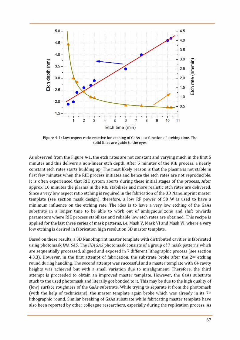
67
Figure 4-1: Low aspect ratio reactive ion etching of GaAs as a function of etching time. The solid lines are guide to the eyes.
As observed from the Figure 4-1, the etch rates are not constant and varying much in the first 5
minutes and this delivers a non-linear etch depth. After 5 minutes of the RIE process, a nearly
constant etch rates starts building up. The most likely reason is that the plasma is not stable in
first few minutes when the RIE process initiates and hence the etch rates are not reproducible.
It is often experienced that RIE system aborts during these initial stages of the process. After
approx. 10 minutes the plasma in the RIE stabilizes and more realistic etch rates are delivered.
Since a very low aspect ratio etching is required in the fabrication of the 3D NanoImprint master
template (see section mask design), therefore, a low RF power of 50 W is used to have a
minimum influence on the etching rate. The idea is to have a very low etching of the GaAs
substrate in a longer time to be able to work out of ambiguous zone and shift towards
parameters where RIE process stabilizes and reliable low etch rates are obtained. This recipe is
applied for the last three series of mask patterns, i.e. Mask V, Mask VI and Mask VI, where a very
low etching is desired in fabrication high resolution 3D master template.
Based on these results, a 3D NanoImprint master template with distributed cavities is fabricated
using photomask INA SA5. The INA SA5 photomask consists of a group of 7 mask patterns which
are sequentially processed, aligned and exposed in 7 different lithographic process (see section
4.3.3). However, in the first attempt of fabrication, the substrate broke after the 2nd etching
round during handling. The second attempt was successful and a master template with 64 cavity
heights was achieved but with a small variation due to misalignment. Therefore, the third
attempt is proceeded to obtain an improved master template. However, the GaAs substrate
stuck to the used photomask and literally got bonded to it. This may be due to the high quality of
(low) surface roughness of the GaAs substrate. While trying to separate it from the photomask
(with the help of technicians), the master template again broke which was already in its 7th
lithographic round. Similar breaking of GaAs substrate while fabricating master template have
also been reported by other colleague researchers, especially during the replication process. As
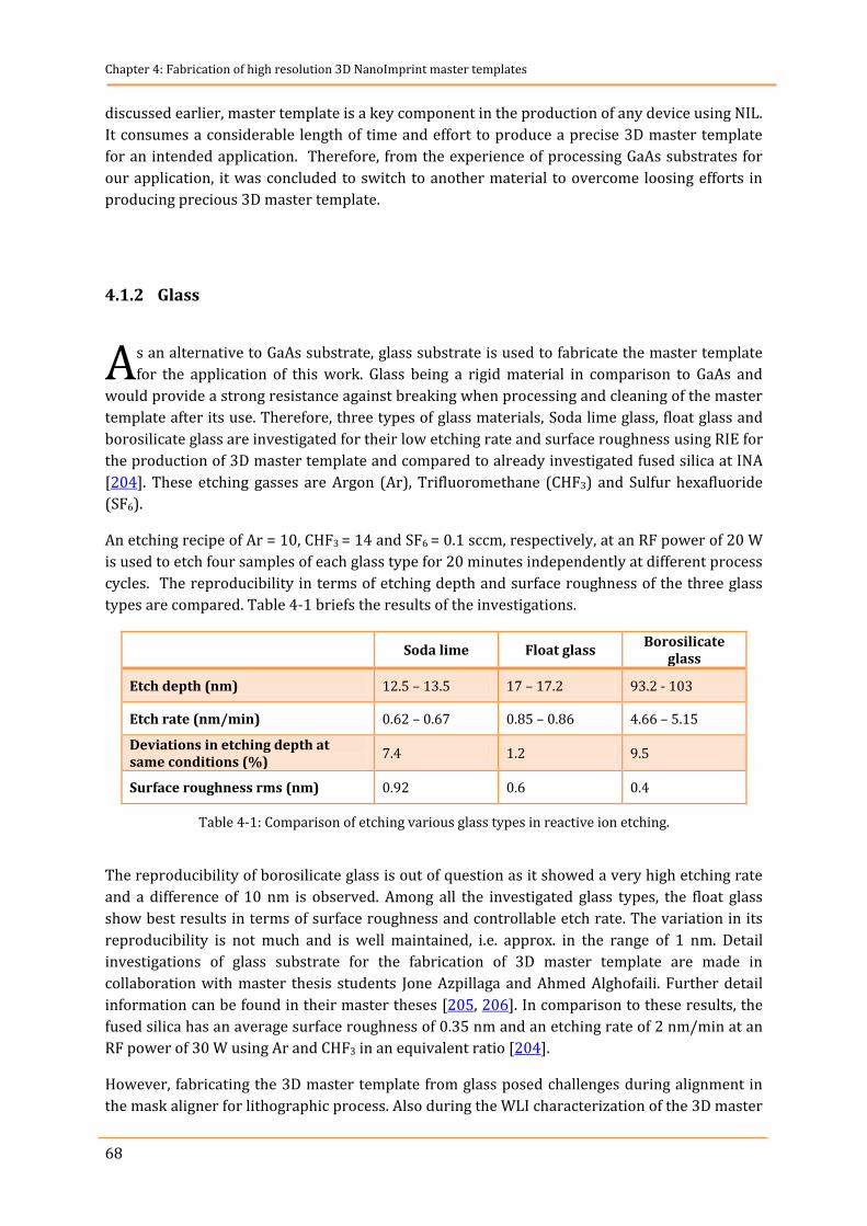
Chapter 4: Fabrication of high resolution 3D NanoImprint master templates
68
discussed earlier, master template is a key component in the production of any device using NIL.
It consumes a considerable length of time and effort to produce a precise 3D master template
for an intended application. Therefore, from the experience of processing GaAs substrates for
our application, it was concluded to switch to another material to overcome loosing efforts in
producing precious 3D master template.
4.1.2 Glass
s an alternative to GaAs substrate, glass substrate is used to fabricate the master template
for the application of this work. Glass being a rigid material in comparison to GaAs and
would provide a strong resistance against breaking when processing and cleaning of the master
template after its use. Therefore, three types of glass materials, Soda lime glass, float glass and
borosilicate glass are investigated for their low etching rate and surface roughness using RIE for
the production of 3D master template and compared to already investigated fused silica at INA
[204]. These etching gasses are Argon (Ar), Trifluoromethane (CHF3) and Sulfur hexafluoride
(SF6).
An etching recipe of Ar = 10, CHF3 = 14 and SF6 = 0.1 sccm, respectively, at an RF power of 20 W
is used to etch four samples of each glass type for 20 minutes independently at different process
cycles. The reproducibility in terms of etching depth and surface roughness of the three glass
types are compared. Table 4-1 briefs the results of the investigations.
Soda lime Float glass Borosilicate
glass
Etch depth (nm) 12.5 – 13.5 17 – 17.2 93.2 - 103
Etch rate (nm/min) 0.62 – 0.67 0.85 – 0.86 4.66 – 5.15
Deviations in etching depth at same conditions (%)
7.4 1.2 9.5
Surface roughness rms (nm) 0.92 0.6 0.4
Table 4-1: Comparison of etching various glass types in reactive ion etching.
The reproducibility of borosilicate glass is out of question as it showed a very high etching rate
and a difference of 10 nm is observed. Among all the investigated glass types, the float glass
show best results in terms of surface roughness and controllable etch rate. The variation in its
reproducibility is not much and is well maintained, i.e. approx. in the range of 1 nm. Detail
investigations of glass substrate for the fabrication of 3D master template are made in
collaboration with master thesis students Jone Azpillaga and Ahmed Alghofaili. Further detail
information can be found in their master theses [205, 206]. In comparison to these results, the
fused silica has an average surface roughness of 0.35 nm and an etching rate of 2 nm/min at an
RF power of 30 W using Ar and CHF3 in an equivalent ratio [204].
However, fabricating the 3D master template from glass posed challenges during alignment in
the mask aligner for lithographic process. Also during the WLI characterization of the 3D master
A
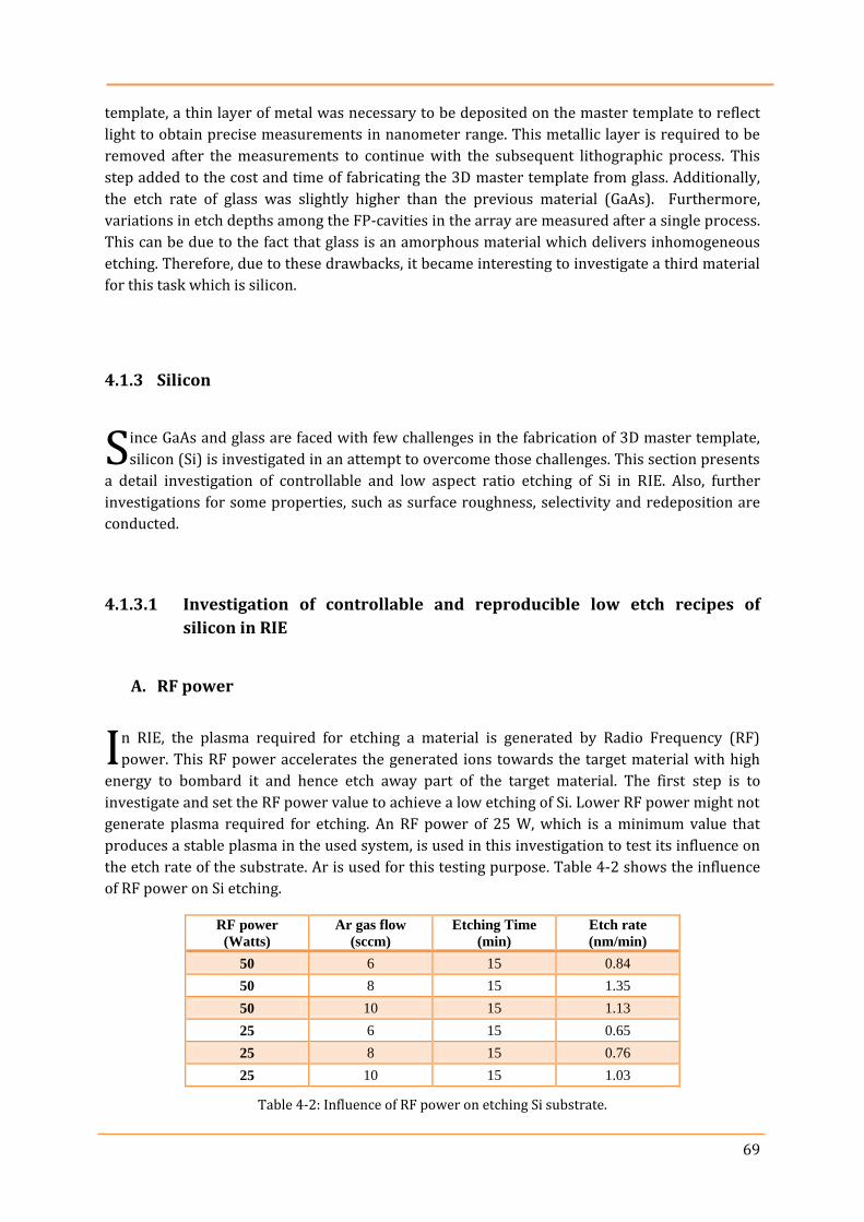
69
template, a thin layer of metal was necessary to be deposited on the master template to reflect
light to obtain precise measurements in nanometer range. This metallic layer is required to be
removed after the measurements to continue with the subsequent lithographic process. This
step added to the cost and time of fabricating the 3D master template from glass. Additionally,
the etch rate of glass was slightly higher than the previous material (GaAs). Furthermore,
variations in etch depths among the FP-cavities in the array are measured after a single process.
This can be due to the fact that glass is an amorphous material which delivers inhomogeneous
etching. Therefore, due to these drawbacks, it became interesting to investigate a third material
for this task which is silicon.
4.1.3 Silicon
ince GaAs and glass are faced with few challenges in the fabrication of 3D master template,
silicon (Si) is investigated in an attempt to overcome those challenges. This section presents
a detail investigation of controllable and low aspect ratio etching of Si in RIE. Also, further
investigations for some properties, such as surface roughness, selectivity and redeposition are
conducted.
4.1.3.1 Investigation of controllable and reproducible low etch recipes of
silicon in RIE
A. RF power
n RIE, the plasma required for etching a material is generated by Radio Frequency (RF)
power. This RF power accelerates the generated ions towards the target material with high
energy to bombard it and hence etch away part of the target material. The first step is to
investigate and set the RF power value to achieve a low etching of Si. Lower RF power might not
generate plasma required for etching. An RF power of 25 W, which is a minimum value that
produces a stable plasma in the used system, is used in this investigation to test its influence on
the etch rate of the substrate. Ar is used for this testing purpose. Table 4-2 shows the influence
of RF power on Si etching.
RF power
(Watts)
Ar gas flow
(sccm)
Etching Time
(min)
Etch rate
(nm/min)
50 6 15 0.84
50 8 15 1.35
50 10 15 1.13
25 6 15 0.65
25 8 15 0.76
25 10 15 1.03
Table 4-2: Influence of RF power on etching Si substrate.
S
I
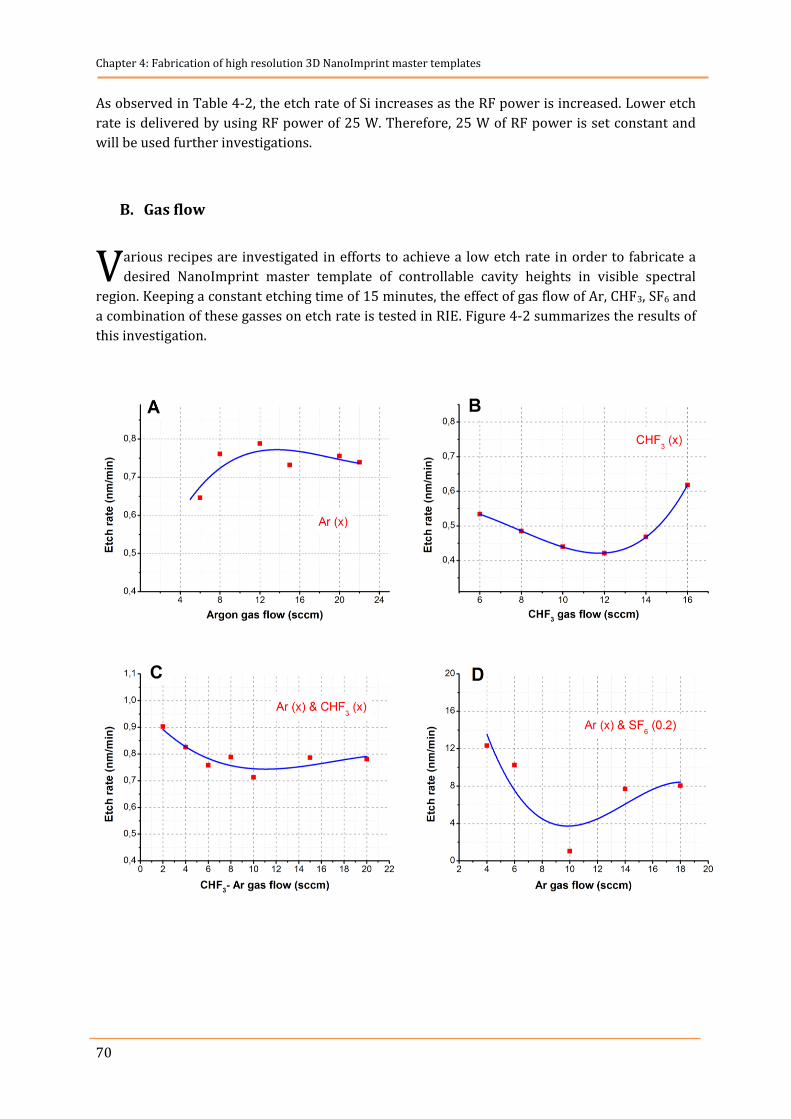
Chapter 4: Fabrication of high resolution 3D NanoImprint master templates
70
As observed in Table 4-2, the etch rate of Si increases as the RF power is increased. Lower etch
rate is delivered by using RF power of 25 W. Therefore, 25 W of RF power is set constant and
will be used further investigations.
B. Gas flow
arious recipes are investigated in efforts to achieve a low etch rate in order to fabricate a
desired NanoImprint master template of controllable cavity heights in visible spectral
region. Keeping a constant etching time of 15 minutes, the effect of gas flow of Ar, CHF3, SF6 and
a combination of these gasses on etch rate is tested in RIE. Figure 4-2 summarizes the results of
this investigation.
V
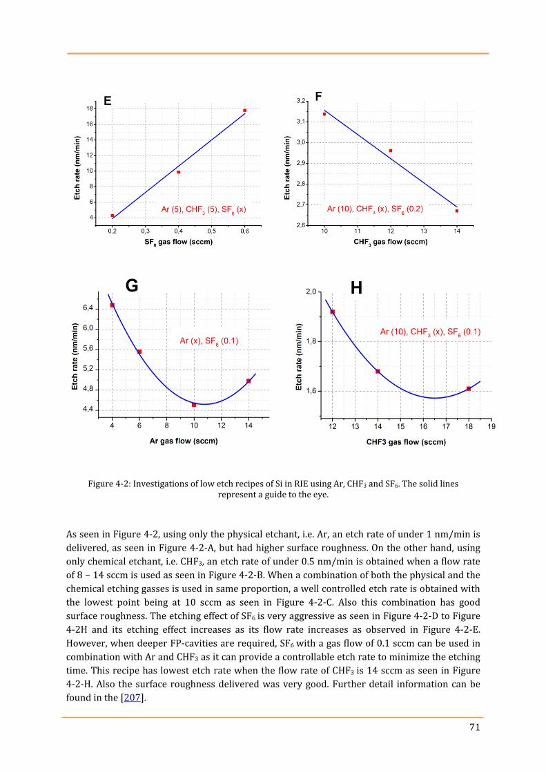
71
Figure 4-2: Investigations of low etch recipes of Si in RIE using Ar, CHF3 and SF6. The solid lines represent a guide to the eye.
As seen in Figure 4-2, using only the physical etchant, i.e. Ar, an etch rate of under 1 nm/min is
delivered, as seen in Figure 4-2-A, but had higher surface roughness. On the other hand, using
only chemical etchant, i.e. CHF3, an etch rate of under 0.5 nm/min is obtained when a flow rate
of 8 – 14 sccm is used as seen in Figure 4-2-B. When a combination of both the physical and the
chemical etching gasses is used in same proportion, a well controlled etch rate is obtained with
the lowest point being at 10 sccm as seen in Figure 4-2-C. Also this combination has good
surface roughness. The etching effect of SF6 is very aggressive as seen in Figure 4-2-D to Figure
4-2H and its etching effect increases as its flow rate increases as observed in Figure 4-2-E.
However, when deeper FP-cavities are required, SF6 with a gas flow of 0.1 sccm can be used in
combination with Ar and CHF3 as it can provide a controllable etch rate to minimize the etching
time. This recipe has lowest etch rate when the flow rate of CHF3 is 14 sccm as seen in Figure
4-2-H. Also the surface roughness delivered was very good. Further detail information can be
found in the [207].
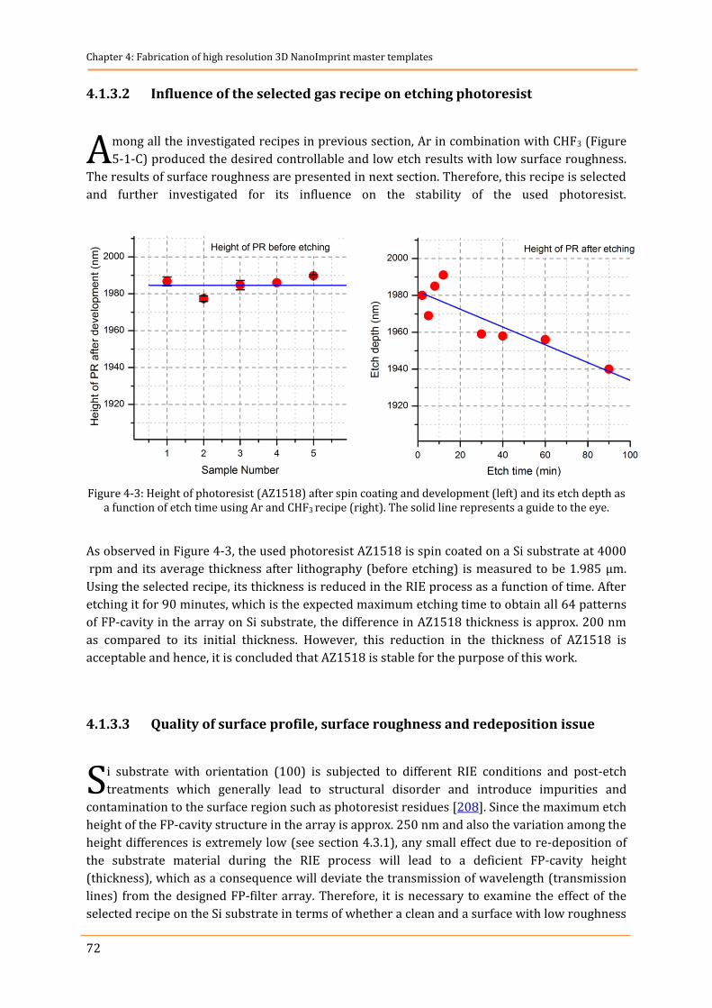
Chapter 4: Fabrication of high resolution 3D NanoImprint master templates
72
4.1.3.2 Influence of the selected gas recipe on etching photoresist
mong all the investigated recipes in previous section, Ar in combination with CHF3 (Figure
5-1-C) produced the desired controllable and low etch results with low surface roughness.
The results of surface roughness are presented in next section. Therefore, this recipe is selected
and further investigated for its influence on the stability of the used photoresist.
Figure 4-3: Height of photoresist (AZ1518) after spin coating and development (left) and its etch depth as a function of etch time using Ar and CHF3 recipe (right). The solid line represents a guide to the eye.
As observed in Figure 4-3, the used photoresist AZ1518 is spin coated on a Si substrate at 4000
rpm and its average thickness after lithography (before etching) is measured to be 1.985 µm.
Using the selected recipe, its thickness is reduced in the RIE process as a function of time. After
etching it for 90 minutes, which is the expected maximum etching time to obtain all 64 patterns
of FP-cavity in the array on Si substrate, the difference in AZ1518 thickness is approx. 200 nm
as compared to its initial thickness. However, this reduction in the thickness of AZ1518 is
acceptable and hence, it is concluded that AZ1518 is stable for the purpose of this work.
4.1.3.3 Quality of surface profile, surface roughness and redeposition issue
i substrate with orientation (100) is subjected to different RIE conditions and post-etch
treatments which generally lead to structural disorder and introduce impurities and
contamination to the surface region such as photoresist residues [208]. Since the maximum etch
height of the FP-cavity structure in the array is approx. 250 nm and also the variation among the
height differences is extremely low (see section 4.3.1), any small effect due to re-deposition of
the substrate material during the RIE process will lead to a deficient FP-cavity height
(thickness), which as a consequence will deviate the transmission of wavelength (transmission
lines) from the designed FP-filter array. Therefore, it is necessary to examine the effect of the
selected recipe on the Si substrate in terms of whether a clean and a surface with low roughness
A
S
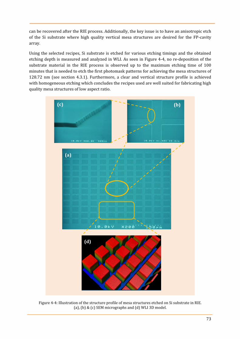
73
can be recovered after the RIE process. Additionally, the key issue is to have an anisotropic etch
of the Si substrate where high quality vertical mesa structures are desired for the FP-cavity
array.
Using the selected recipes, Si substrate is etched for various etching timings and the obtained
etching depth is measured and analyzed in WLI. As seen in Figure 4-4, no re-deposition of the
substrate material in the RIE process is observed up to the maximum etching time of 100
minutes that is needed to etch the first photomask patterns for achieving the mesa structures of
128.72 nm (see section 4.3.1). Furthermore, a clear and vertical structure profile is achieved
with homogeneous etching which concludes the recipes used are well suited for fabricating high
quality mesa structures of low aspect ratio.
Figure 4-4: Illustration of the structure profile of mesa structures etched on Si substrate in RIE. (a), (b) & (c) SEM micrographs and (d) WLI 3D model.
(d)
(a)
(b) (c)
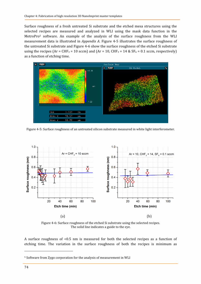
Chapter 4: Fabrication of high resolution 3D NanoImprint master templates
74
Surface roughness of a fresh untreated Si substrate and the etched mesa structures using the
selected recipes are measured and analyzed in WLI using the mask data function in the
MetroPro5 software. An example of the analysis of the surface roughness from the WLI
measurement data is illustrated in Appendix A. Figure 4-5 illustrates the surface roughness of
the untreated Si substrate and Figure 4-6 show the surface roughness of the etched Si substrate
using the recipes (Ar = CHF3 = 10 sccm) and (Ar = 10, CHF3 = 14 & SF6 = 0.1 sccm, respectively)
as a function of etching time.
Figure 4-5: Surface roughness of an untreated silicon substrate measured in white light interferometer.
Figure 4-6: Surface roughness of the etched Si substrate using the selected recipes. The solid line indicates a guide to the eye.
A surface roughness of <0.5 nm is measured for both the selected recipes as a function of
etching time. The variation in the surface roughness of both the recipes is minimum as
5 Software from Zygo corporation for the analysis of measurement in WLI
(a) (b)
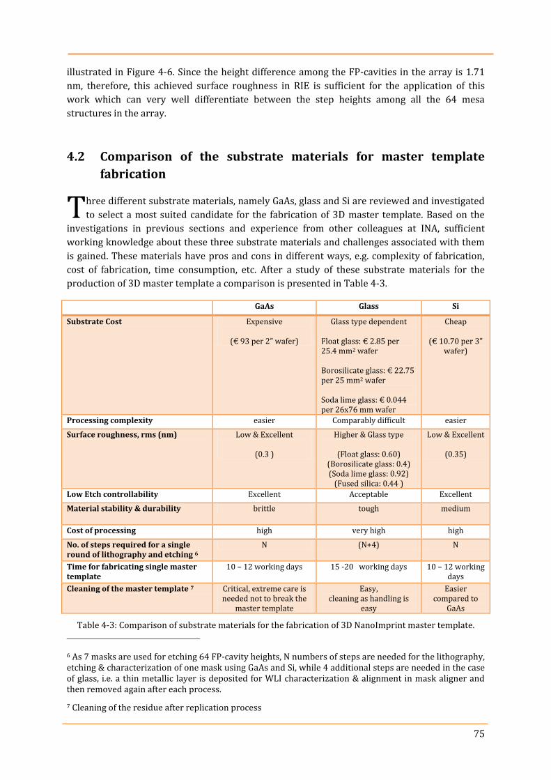
75
illustrated in Figure 4-6. Since the height difference among the FP-cavities in the array is 1.71
nm, therefore, this achieved surface roughness in RIE is sufficient for the application of this
work which can very well differentiate between the step heights among all the 64 mesa
structures in the array.
4.2 Comparison of the substrate materials for master template
fabrication
hree different substrate materials, namely GaAs, glass and Si are reviewed and investigated
to select a most suited candidate for the fabrication of 3D master template. Based on the
investigations in previous sections and experience from other colleagues at INA, sufficient
working knowledge about these three substrate materials and challenges associated with them
is gained. These materials have pros and cons in different ways, e.g. complexity of fabrication,
cost of fabrication, time consumption, etc. After a study of these substrate materials for the
production of 3D master template a comparison is presented in Table 4-3.
GaAs Glass Si
Substrate Cost Expensive
(€ 93 per 2” wafer)
Glass type dependent Float glass: € 2.85 per 25.4 mm2 wafer Borosilicate glass: € 22.75 per 25 mm2 wafer Soda lime glass: € 0.044 per 26x76 mm wafer
Cheap
(€ 10.70 per 3” wafer)
Processing complexity easier Comparably difficult easier
Surface roughness, rms (nm)
Low & Excellent
(0.3 )
Higher & Glass type
(Float glass: 0.60) (Borosilicate glass: 0.4) (Soda lime glass: 0.92)
(Fused silica: 0.44 )
Low & Excellent
(0.35)
Low Etch controllability Excellent Acceptable Excellent
Material stability & durability brittle tough medium
Cost of processing high very high high
No. of steps required for a single round of lithography and etching 6
N (N+4) N
Time for fabricating single master template
10 – 12 working days 15 -20 working days 10 – 12 working days
Cleaning of the master template 7 Critical, extreme care is needed not to break the
master template
Easy, cleaning as handling is
easy
Easier compared to
GaAs
Table 4-3: Comparison of substrate materials for the fabrication of 3D NanoImprint master template.
6 As 7 masks are used for etching 64 FP-cavity heights, N numbers of steps are needed for the lithography, etching & characterization of one mask using GaAs and Si, while 4 additional steps are needed in the case of glass, i.e. a thin metallic layer is deposited for WLI characterization & alignment in mask aligner and then removed again after each process.
7 Cleaning of the residue after replication process
T

Chapter 4: Fabrication of high resolution 3D NanoImprint master templates
76
4.3 Fabrication of 3D NanoImprint master template using silicon
substrate
he characterization and comparison of materials for templates in the previous sections, led
to the selection of Si substrate as the best choice for the fabrication of 3D nanoimprint
master template. Among the three substrate materials, Si is easy to process and in few numbers
of steps compared to glass. Also it is stronger and more stable and durable than GaAs and its
surface roughness is almost comparable to GaAs, which is very good. A 3D Si master template
containing 64 structures with different heights is desired to be etched in order to form the FP-
cavities. In this section, the calculation of the heights of the 64 FP-cavities in the array in a
visible spectral range, corresponding photomask design and characterizations of fabricated 3D
master template are presented.
4.3.1 Calculation of FP-cavity array in visible spectral region
t is desired to cover the visible spectral region from 400 nm to 700 nm with an array of 64
different FP-filters. The separation among the transmitted wavelengths in the array is desired
to be 5 nm. But this fabricated FP-cavity thickness is the physical thickness. It must be divided
with the refractive index of the used cavity material (mrUVcur068) to obtain the optical
thickness of the FP-cavity. Therefore, the refractive index of mrUVcur06 as a function of
wavelength is of at most importance to allow the desired wavelength to be transmitted through
the FP-filter.
Using the measured refractive index value at each desired wavelength to be transmitted, the
required FP-cavity thickness is calculated as:
(4-1)
An example calculation to obtain the corresponding FP-cavity height is given below. For the first
wavelength (400 nm) to be transmitted through the FP-filter, the required FP-cavity height has
to be,
(4-2)
Similarly, the next desired wavelength with a step height of 5 nm to be transmitted through the
FP-filter, the required FP-cavity thickness has to be,
8 UV imprint resist from Micro Resist Technology GmbH
T
I
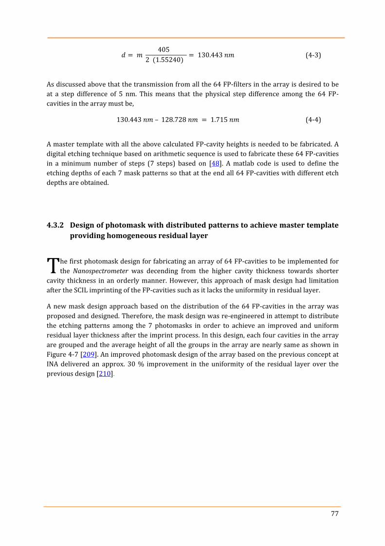
77
(4-3)
As discussed above that the transmission from all the 64 FP-filters in the array is desired to be
at a step difference of 5 nm. This means that the physical step difference among the 64 FP-
cavities in the array must be,
– (4-4)
A master template with all the above calculated FP-cavity heights is needed to be fabricated. A
digital etching technique based on arithmetic sequence is used to fabricate these 64 FP-cavities
in a minimum number of steps (7 steps) based on [48]. A matlab code is used to define the
etching depths of each 7 mask patterns so that at the end all 64 FP-cavities with different etch
depths are obtained.
4.3.2 Design of photomask with distributed patterns to achieve master template
providing homogeneous residual layer
he first photomask design for fabricating an array of 64 FP-cavities to be implemented for
the Nanospectrometer was decending from the higher cavity thickness towards shorter
cavity thickness in an orderly manner. However, this approach of mask design had limitation
after the SCIL imprinting of the FP-cavities such as it lacks the uniformity in residual layer.
A new mask design approach based on the distribution of the 64 FP-cavities in the array was
proposed and designed. Therefore, the mask design was re-engineered in attempt to distribute
the etching patterns among the 7 photomasks in order to achieve an improved and uniform
residual layer thickness after the imprint process. In this design, each four cavities in the array
are grouped and the average height of all the groups in the array are nearly same as shown in
Figure 4-7 [209]. An improved photomask design of the array based on the previous concept at
INA delivered an approx. 30 % improvement in the uniformity of the residual layer over the
previous design [210].
T
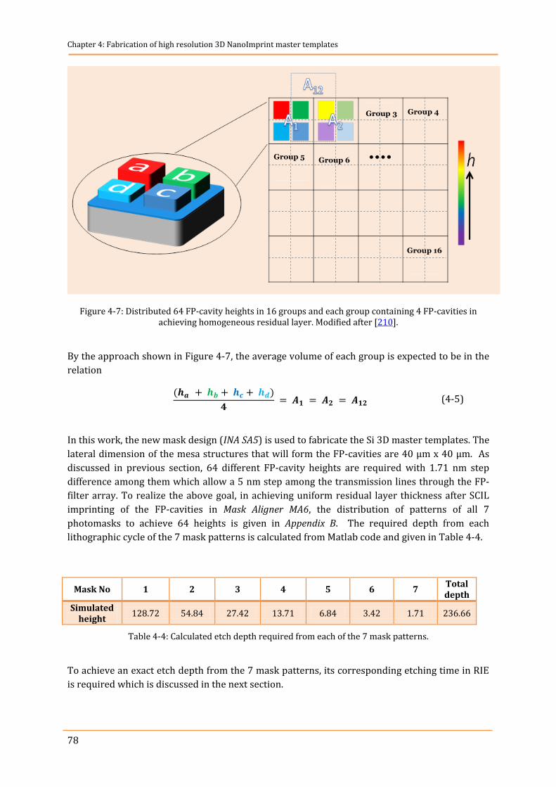
Chapter 4: Fabrication of high resolution 3D NanoImprint master templates
78
Figure 4-7: Distributed 64 FP-cavity heights in 16 groups and each group containing 4 FP-cavities in achieving homogeneous residual layer. Modified after [210].
By the approach shown in Figure 4-7, the average volume of each group is expected to be in the
relation
(4-5)
In this work, the new mask design (INA SA5) is used to fabricate the Si 3D master templates. The
lateral dimension of the mesa structures that will form the FP-cavities are 40 µm x 40 µm. As
discussed in previous section, 64 different FP-cavity heights are required with 1.71 nm step
difference among them which allow a 5 nm step among the transmission lines through the FP-
filter array. To realize the above goal, in achieving uniform residual layer thickness after SCIL
imprinting of the FP-cavities in Mask Aligner MA6, the distribution of patterns of all 7
photomasks to achieve 64 heights is given in Appendix B. The required depth from each
lithographic cycle of the 7 mask patterns is calculated from Matlab code and given in Table 4-4.
Mask No 1 2 3 4 5 6 7 Total depth
Simulated height
128.72 54.84 27.42 13.71 6.84 3.42 1.71 236.66
Table 4-4: Calculated etch depth required from each of the 7 mask patterns.
To achieve an exact etch depth from the 7 mask patterns, its corresponding etching time in RIE
is required which is discussed in the next section.
Group 3 Group 4
Group 5 Group 6
Group 16
….
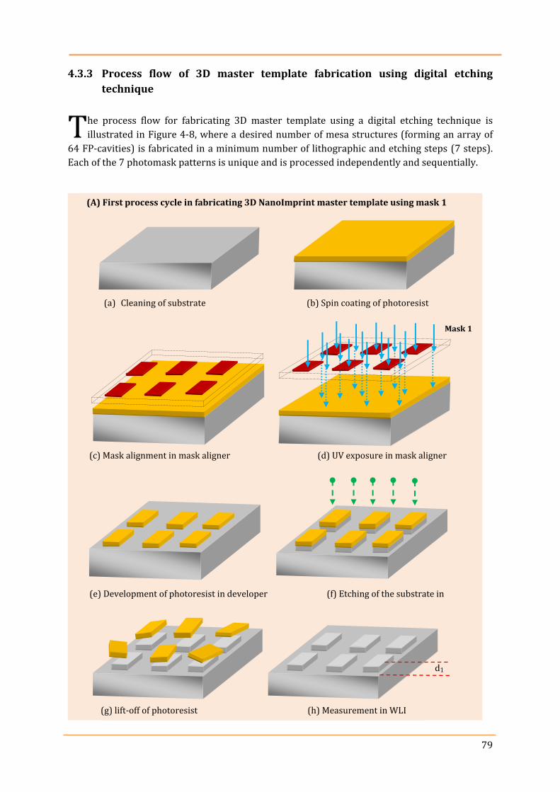
79
4.3.3 Process flow of 3D master template fabrication using digital etching
technique
he process flow for fabricating 3D master template using a digital etching technique is
illustrated in Figure 4-8, where a desired number of mesa structures (forming an array of
64 FP-cavities) is fabricated in a minimum number of lithographic and etching steps (7 steps).
Each of the 7 photomask patterns is unique and is processed independently and sequentially.
T
(e) Development of photoresist in developer (f) Etching of the substrate in
RIE
(a) Cleaning of substrate (b) Spin coating of photoresist
(g) lift-off of photoresist (h) Measurement in WLI
d1
(c) Mask alignment in mask aligner (d) UV exposure in mask aligner
(A) First process cycle in fabricating 3D NanoImprint master template using mask 1
Mask 1
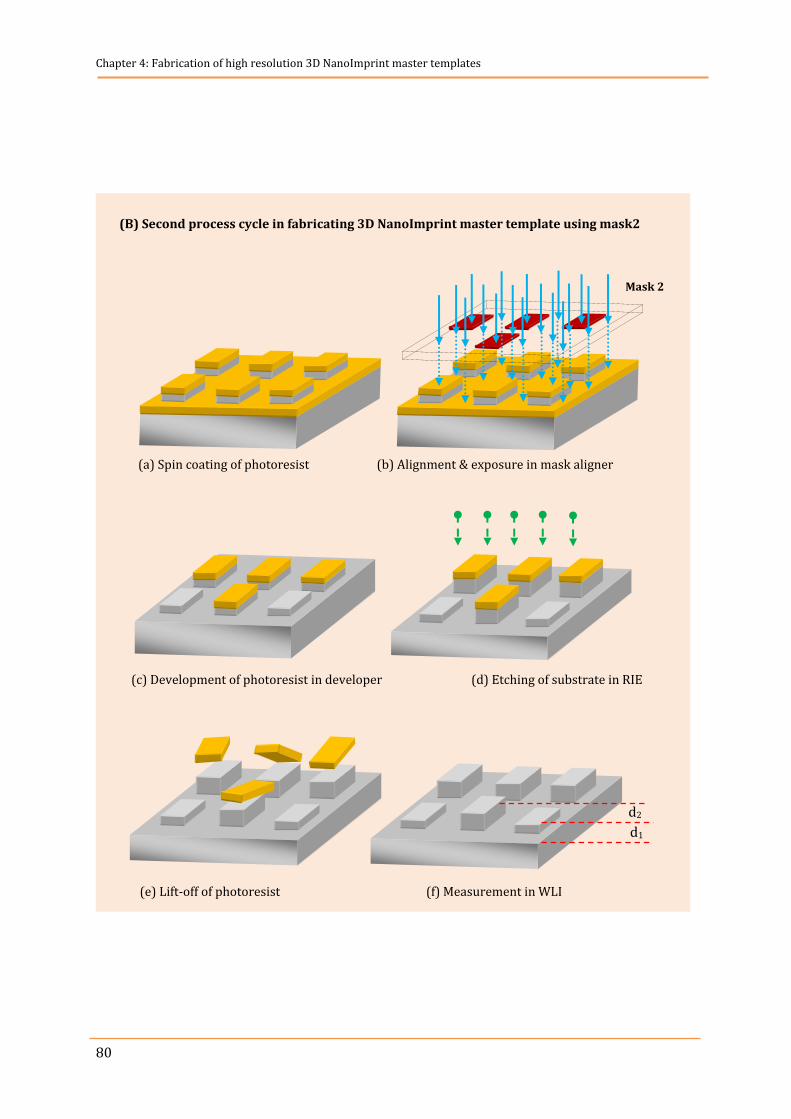
Chapter 4: Fabrication of high resolution 3D NanoImprint master templates
80
(a) Spin coating of photoresist (b) Alignment & exposure in mask aligner
(c) Development of photoresist in developer (d) Etching of substrate in RIE
(e) Lift-off of photoresist (f) Measurement in WLI
d2
d1
(B) Second process cycle in fabricating 3D NanoImprint master template using mask2
Mask 2
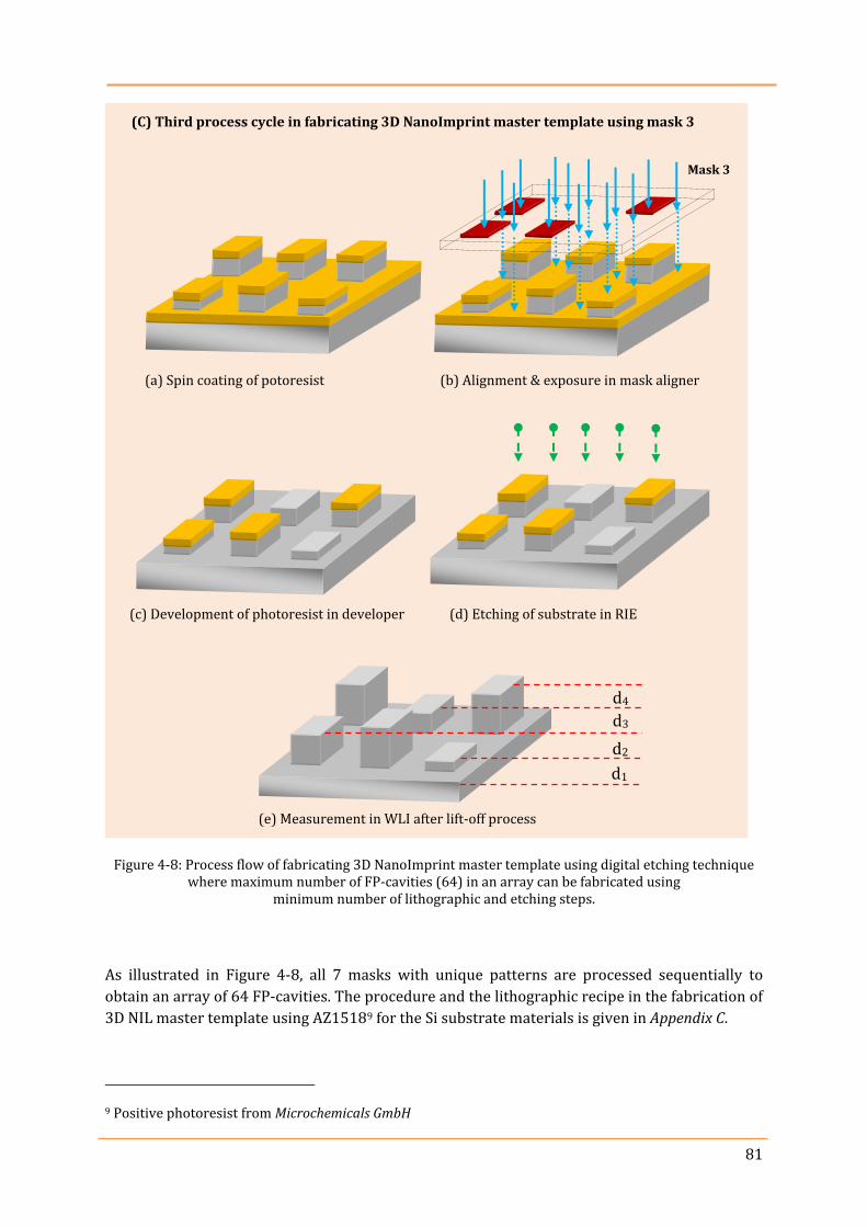
81
Figure 4-8: Process flow of fabricating 3D NanoImprint master template using digital etching technique where maximum number of FP-cavities (64) in an array can be fabricated using
minimum number of lithographic and etching steps.
As illustrated in Figure 4-8, all 7 masks with unique patterns are processed sequentially to
obtain an array of 64 FP-cavities. The procedure and the lithographic recipe in the fabrication of
3D NIL master template using AZ15189 for the Si substrate materials is given in Appendix C.
9 Positive photoresist from Microchemicals GmbH
d1
d4
d3
d2
(a) Spin coating of potoresist (b) Alignment & exposure in mask aligner
(c) Development of photoresist in developer (d) Etching of substrate in RIE
(e) Measurement in WLI after lift-off process
(C) Third process cycle in fabricating 3D NanoImprint master template using mask 3
Mask 3
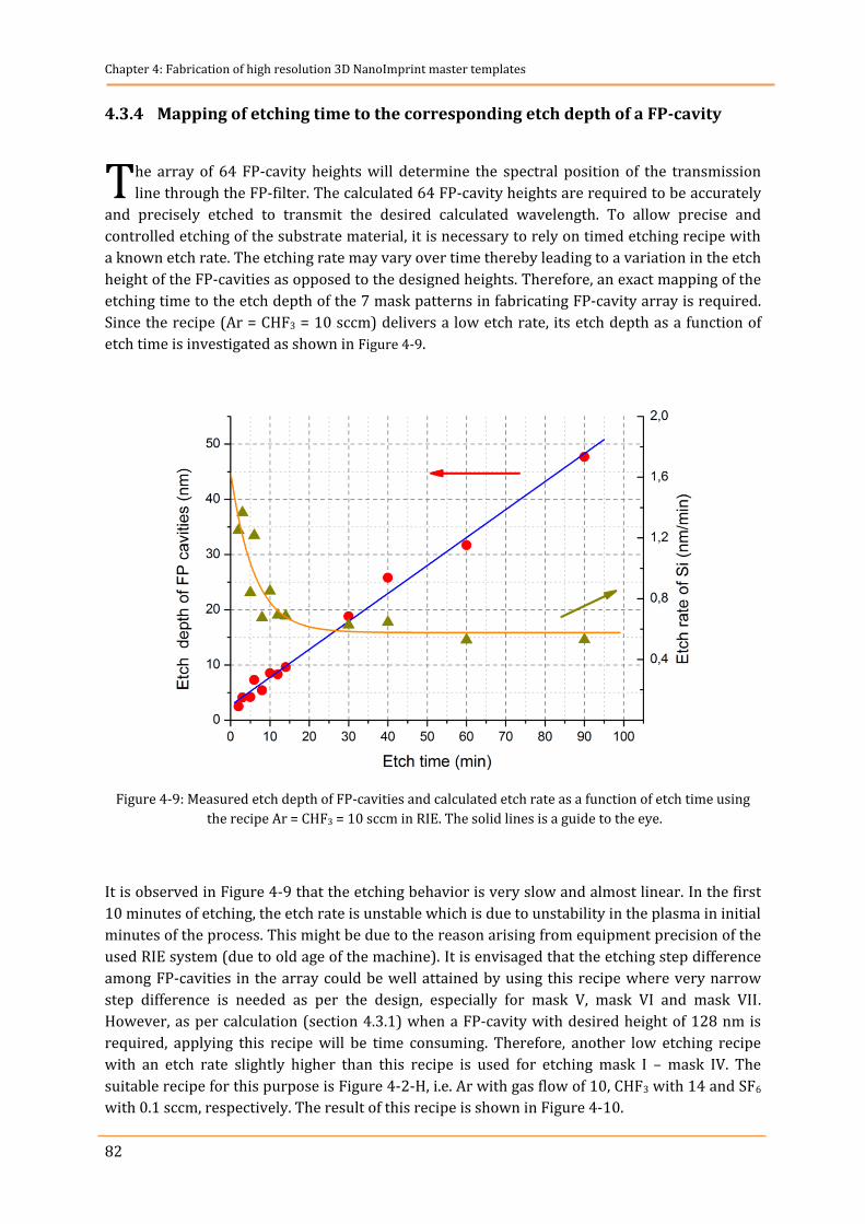
Chapter 4: Fabrication of high resolution 3D NanoImprint master templates
82
4.3.4 Mapping of etching time to the corresponding etch depth of a FP-cavity
he array of 64 FP-cavity heights will determine the spectral position of the transmission
line through the FP-filter. The calculated 64 FP-cavity heights are required to be accurately
and precisely etched to transmit the desired calculated wavelength. To allow precise and
controlled etching of the substrate material, it is necessary to rely on timed etching recipe with
a known etch rate. The etching rate may vary over time thereby leading to a variation in the etch
height of the FP-cavities as opposed to the designed heights. Therefore, an exact mapping of the
etching time to the etch depth of the 7 mask patterns in fabricating FP-cavity array is required.
Since the recipe (Ar = CHF3 = 10 sccm) delivers a low etch rate, its etch depth as a function of
etch time is investigated as shown in Figure 4-9.
Figure 4-9: Measured etch depth of FP-cavities and calculated etch rate as a function of etch time using
the recipe Ar = CHF3 = 10 sccm in RIE. The solid lines is a guide to the eye.
It is observed in Figure 4-9 that the etching behavior is very slow and almost linear. In the first
10 minutes of etching, the etch rate is unstable which is due to unstability in the plasma in initial
minutes of the process. This might be due to the reason arising from equipment precision of the
used RIE system (due to old age of the machine). It is envisaged that the etching step difference
among FP-cavities in the array could be well attained by using this recipe where very narrow
step difference is needed as per the design, especially for mask V, mask VI and mask VII.
However, as per calculation (section 4.3.1) when a FP-cavity with desired height of 128 nm is
required, applying this recipe will be time consuming. Therefore, another low etching recipe
with an etch rate slightly higher than this recipe is used for etching mask I – mask IV. The
suitable recipe for this purpose is Figure 4-2-H, i.e. Ar with gas flow of 10, CHF3 with 14 and SF6
with 0.1 sccm, respectively. The result of this recipe is shown in Figure 4-10.
T
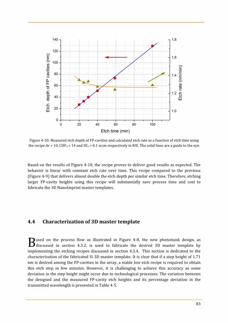
83
Figure 4-10: Measured etch depth of FP-cavities and calculated etch rate as a function of etch time using
the recipe Ar = 10, CHF3 = 14 and SF6 = 0.1 sccm respectively in RIE. The solid lines are a guide to the eye.
Based on the results of Figure 4-10, the recipe proves to deliver good results as expected. The
behavior is linear with constant etch rate over time. This recipe compared to the previous
(Figure 4-9) that delivers almost double the etch depth per similar etch time. Therefore, etching
larger FP-cavity heights using this recipe will substantially save process time and cost to
fabricate the 3D NanoImprint master templates.
4.4 Characterization of 3D master template
ased on the process flow as illustrated in Figure 4-8, the new photomask design, as
discussed in section 4.3.2, is used to fabricate the desired 3D master template by
implementing the etching recipes discussed in section 4.3.4. This section is dedicated to the
characterization of the fabricated Si 3D master template. It is clear that if a step height of 1.71
nm is desired among the FP-cavities in the array, a stable low etch recipe is required to obtain
this etch step in few minutes. However, it is challenging to achieve this accuracy as some
deviation in the step height might occur due to technological processes. The variation between
the designed and the measured FP-cavity etch heights and its percentage deviation in the
transmitted wavelength is presented in Table 4-5.
B

Chapter 4: Fabrication of high resolution 3D NanoImprint master templates
84
Mask no. I II III IV V VI VII Total height
Designed FP-cavity height (nm) 128.72 54.84 27.42 13.71 6.84 3.42 1.71 236.6
Fabricated & Measured FP-cavity height (nm)
135.42 55.14 26.51 13.77 6.85 3.48 1.75 242.9
Percentage deviation in FP-cavity height (%)
5.2 0.5 -3.3 0.4 0.1 1.7 2.3 2.6
Table 4-5: Measurements of the deviation between the designed and fabricated 3D NanoImprint master template for the 7 mask patterns.
A percentage deviation of very few degrees in the vertical precision of the fabricated 3D
NanoImprint master template from the designed one is observed from the above Table 4-5.
These deviations occur in the RIE process due to the aged machine where the etching rates are
not stable over time. However, these variations are minimum and therefore negligible.
Furthermore, the possibility to later calibrate the Nanospectrometer can overcome minor flaws
in the fabrication process, i.e. accuracy and precision in vertical resolution in the range of few
nanometers can be corrected if slight shift in the FP-cavity impairs the detection of a particular
wavelength. A detail WLI measurement results from each etching cycle is given in Appendix D.
By implementing the above etching parameters, an array of 64 mesa structures with different
vertical heights, which will form FP-cavities, is obtained. Using the WLI, an image of the
complete master template with 64 mesa structures in 2D as well as in 3D view is shown in
Figure 4-11. The mesa structures in the array range from 140.8 nm – 252.5 nm. The step heights
can be viewed from the difference in the shades of colors of the mesa structures.
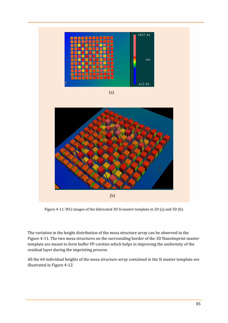
85
Figure 4-11: WLI images of the fabricated 3D Si master template in 2D (a) and 3D (b).
The variation in the height distribution of the mesa structure array can be observed in the
Figure 4-11. The two mesa structures on the surrounding border of the 3D NanoImprint master
template are meant to form buffer FP-cavities which helps in improving the uniformity of the
residual layer during the imprinting process.
All the 64 individual heights of the mesa structure array contained in the Si master template are
illustrated in Figure 4-12.
(a)
(b)
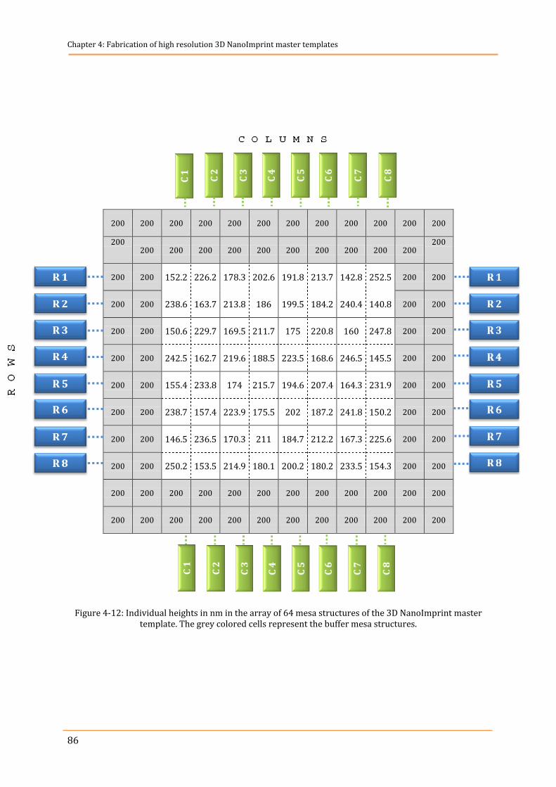
Chapter 4: Fabrication of high resolution 3D NanoImprint master templates
86
200 200 200 200 200 200 200 200 200 200 200 200
200 200 200 200 200 200 200 200 200 200 200
200
200 200 152.2 226.2 178.3 202.6 191.8 213.7 142.8 252.5 200 200
200 200 238.6 163.7 213.8 186 199.5 184.2 240.4 140.8 200 200
200 200 150.6 229.7 169.5 211.7 175 220.8 160 247.8 200 200
200 200 242.5 162.7 219.6 188.5 223.5 168.6 246.5 145.5 200 200
200 200 155.4 233.8 174 215.7 194.6 207.4 164.3 231.9 200 200
200 200 238.7 157.4 223.9 175.5 202 187.2 241.8 150.2 200 200
200 200 146.5 236.5 170.3 211 184.7 212.2 167.3 225.6 200 200
200 200 250.2 153.5 214.9 180.1 200.2 180.2 233.5 154.3 200 200
200 200 200 200 200 200 200 200 200 200 200 200
200 200 200 200 200 200 200 200 200 200 200 200
Figure 4-12: Individual heights in nm in the array of 64 mesa structures of the 3D NanoImprint master template. The grey colored cells represent the buffer mesa structures.
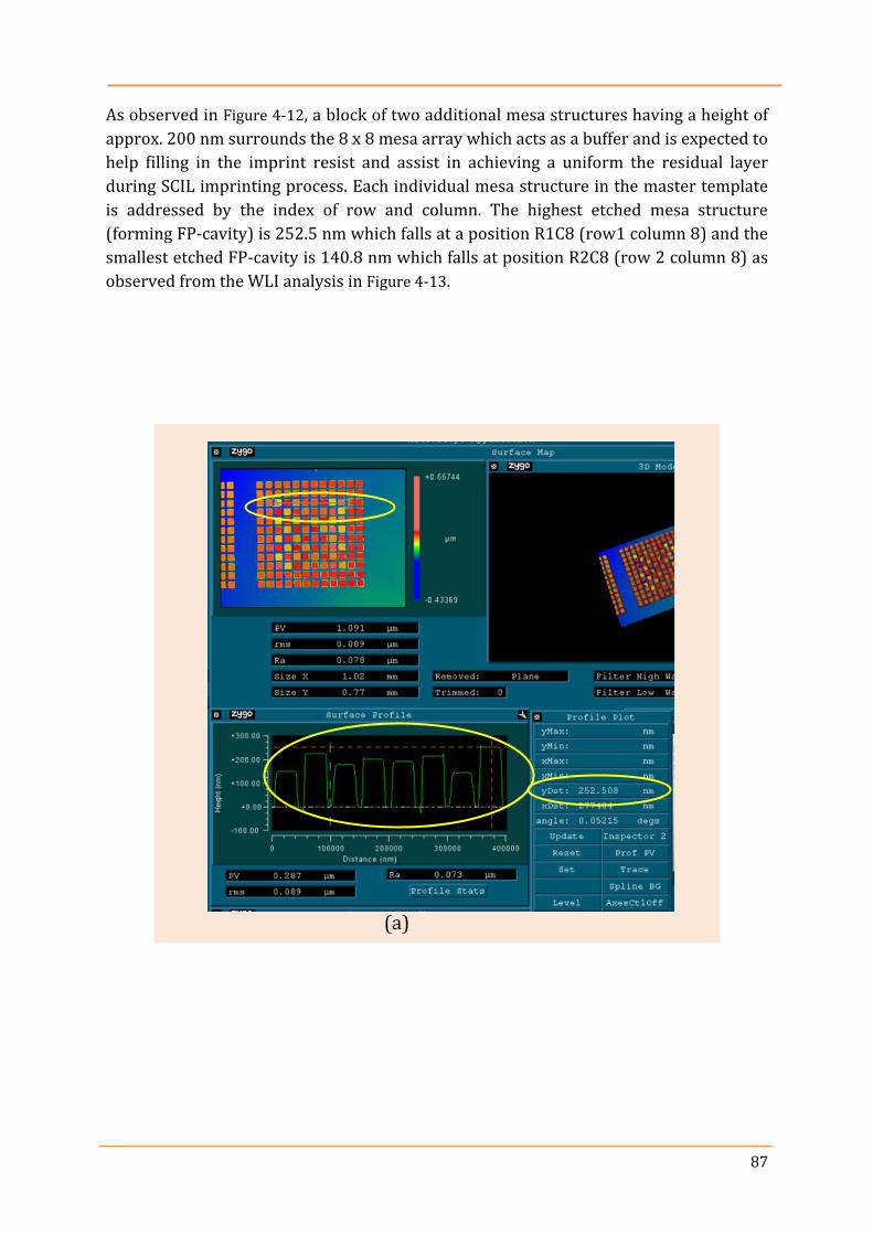
87
As observed in Figure 4-12, a block of two additional mesa structures having a height of
approx. 200 nm surrounds the 8 x 8 mesa array which acts as a buffer and is expected to
help filling in the imprint resist and assist in achieving a uniform the residual layer
during SCIL imprinting process. Each individual mesa structure in the master template
is addressed by the index of row and column. The highest etched mesa structure
(forming FP-cavity) is 252.5 nm which falls at a position R1C8 (row1 column 8) and the
smallest etched FP-cavity is 140.8 nm which falls at position R2C8 (row 2 column 8) as
observed from the WLI analysis in Figure 4-13.
(a)
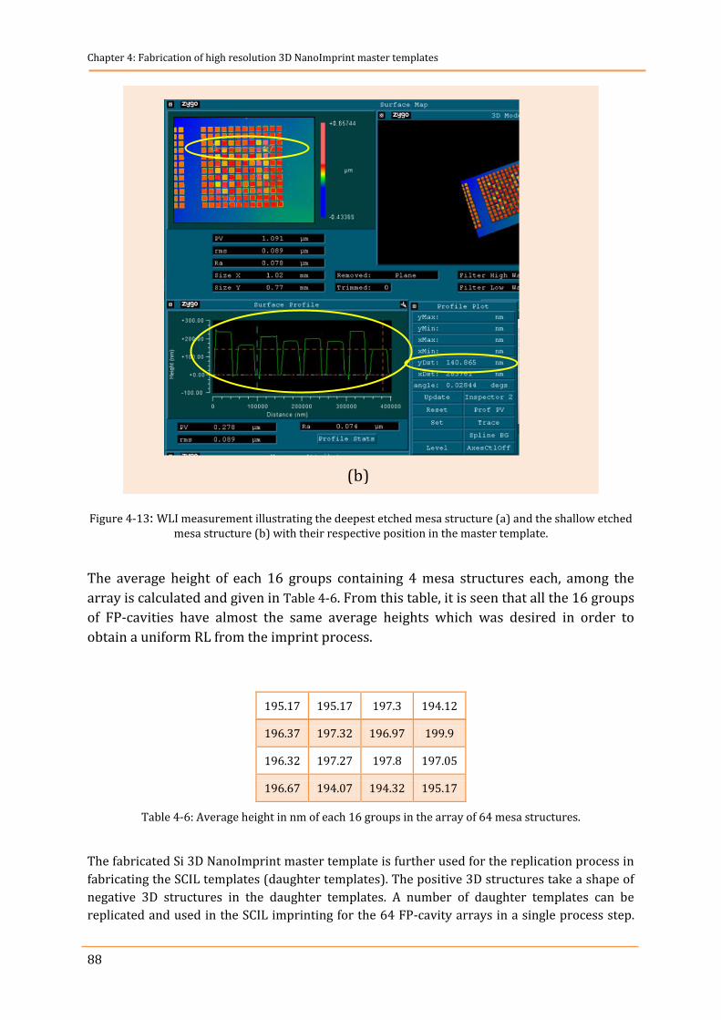
Chapter 4: Fabrication of high resolution 3D NanoImprint master templates
88
Figure 4-13: WLI measurement illustrating the deepest etched mesa structure (a) and the shallow etched mesa structure (b) with their respective position in the master template.
The average height of each 16 groups containing 4 mesa structures each, among the
array is calculated and given in Table 4-6. From this table, it is seen that all the 16 groups
of FP-cavities have almost the same average heights which was desired in order to
obtain a uniform RL from the imprint process.
195.17 195.17 197.3 194.12
196.37 197.32 196.97 199.9
196.32 197.27 197.8 197.05
196.67 194.07 194.32 195.17
Table 4-6: Average height in nm of each 16 groups in the array of 64 mesa structures.
The fabricated Si 3D NanoImprint master template is further used for the replication process in
fabricating the SCIL templates (daughter templates). The positive 3D structures take a shape of
negative 3D structures in the daughter templates. A number of daughter templates can be
replicated and used in the SCIL imprinting for the 64 FP-cavity arrays in a single process step.
(b)
89
Part II
Integration of Fabry-Pérot filter arrays onto the
photodetector array

90

91
5. Introduction and motivation
The demand for increasing number of functionality and enhanced performance in electronic
devices led to the technology of 3D chip-stacking with high I/O interconnections. This paved the
path for miniaturized and multi-function next generation portable consumer electronics with
low power consumption [211]. Similar to electronics devices, integrated photonic components
are a promising approach towards realizing highly integrated, robust, high performance,
compact and cost-effective photonic systems [212]. Two essential schemes exist to integrate
discrete components (IC chips) having different functionality. These include hybrid integration
of multiple chips and monolithic integration. The ITRS predicts these integration approaches of
interdisciplinary fields as an important technological building blocks for the “More-Than-
Moore” paradigm [213].
The aim in this part of the work is to pass the transmitted optical signal from the FP-filter array
to a photodetector (PD) array to be transformed into electronic form for electrical read-outs.
The optical signal on its transit must be preserved. In this part of the work, both of the
integration schemes are introduced briefly and implemented in the integration of the FP-filter
array onto the PD array to achieve the functioning sensor array for the Nanospectrometer.
Chapter 5 Introduction and motivation
Chapter 5: Introduction & motivation
92
5.1 Integration of photonic components
A major challenge is to integrate the optical and electronic components to perform intended
function. The integration must deliver best performance in terms of functionality, reliability,
stability, life time, cost, and resistance to external influences. Integrated photonic (IP)
components involve assembling of various optical, electronics and optoelectronic components
to provide a functioning device. This integration of discrete components can be realized based
on hybrid as well as monolithic approach material allowing [214].
Hybrid integration involves bonding full wafers or sometimes diced chips of dissimilar
materials which are usually of incompatible technologies such as silicon and glass by means of
physical or chemical processes to create [215]:
Advance 3D structures and cavities termed as “µ–channels” which produce a complete
functioning device [216, 217].
Integration of sensor chips fabricated on two different wafer materials, e.g. CMOS &
MEMS, to achieve higher performances [218, 219].
Encapsulation and packaging of sensor components to create closed environments for
protecting and safeguarding them from environmental influences [220, 221].
Silicon on Insulator (SOI) wafers for hybrid silicon photonics integration platform [222-
224].
Three bonding and stacking schemes exist in 3D integration, namely, wafer-to-wafer, chip-to-
wafer and chip-to-chip. All these schemes have pros and cons. Wafer-to-wafer bonding
technique suits best for homogenous integration of high yielding devices. This technique has
maximum throughput, simple process flow, and minimum cost. However, if the yield of
components on one wafer is not high enough or not stable, the stacking and integration of
wafers will produce minimum number of known-good-die (KGD) which is a major drawback of
wafer-to-wafer bonding scheme. Therefore, in such cases, chip-to-chip or chip-to-wafer stacking
and bonding techniques are preferred for vertical integration with only good dies [225].
Recent innovation in the integration of hybrid photonic components is the bonding of optical
fibers to detector chips. In conventional imaging optics, light reaches a CCD chip through the use
of lenses or mirror based optical system. This method of coupling light into CCD suffers from
loss of light in conventional systems. Photometrics10 innovation is to bond the imaging optical
fibers directly to the CCD chips to increase the efficiency of coupling light into the CCD thereby
preserving an image [226]. SCHOTT11 has also shown significant contribution in optical bonding
of optical fibers faceplates to Micro-OLED displays and CCD chips for imaging applications
[227]. Optical filter are also directly bonded to a focal-plane-array detectors for the application
10 A scientific company researching & developing imaging cameras for life science applications.
11 SCHOTT AG – a leading and innovative company in glass based smart products.
93
of two-color imaging for providing multicolor response by N.S. Gluck et al. [228] and integration
of filter array to CCD chip for multispectral imaging in visible and IR range is also reported by
Lai et. al. [229].
Another great motivation for hybrid photonics integration is to realize light sources (lasers)
based on silicon substrates since silicon is highly compatible to the mature and highly accurate
complementary-metal-oxide-semiconductor (CMOS) technology which is well known, well
established, and most cost effective. However, achievement of stimulated light emission lacks in
Si due to its indirect band gap [230]. Relatively expensive III-V semiconductor materials such as
gallium arsenide (GaAs) and indium phosphide (InP) are good candidates for photonic
applications due to their efficient light emission properties [231]. However, these two material
systems cannot be monolithically integrated due to their large lattice mismatch and thermal
expansion coefficient [232]. Therefore, to overcome this problem, wafer bonding technique
based on hybrid (also called heterogeneous) integration can be exploited as it is not limited by
lattice mismatch [233].
Wafer bonding is a key process in the integration of various electronic and photonic devices.
Various established techniques of semiconductor wafer bonding at chip level exists for
materials and components integration in microelectronics, optoelectronics, and micro-electro-
mechanical-systems (MEMS). L. Sanchez et al. demonstrated a chip-to-wafer direct bonding
technologies for high density 3D integration with the help of pick and place process that yield
high alignment accuracy [234-237]. Wafer bonding is also used for encapsulation and packaging
of MEMS devices. E.g. RF-MEMS switches, accelerometer and gyroscope MEMS sensors are
encapsulated to protect moving and fragile structures. This encapsulation also prevents dust
particle entering into the device to ensure stable and reliable performance [238]. In the
packaging of light emitting diodes (LEDs) chips various single electronic and optical
components are bonded together for the application of solid state lighting (SSL) [225].
Integration of miniaturized optoelectronic chips in polymer substrate has also been reported by
Y. Wang et al. to establish a high functional and flexible sensor network. To avoid damaging the
thermal sensitive polymers, UV cured adhesive was used to bond these chips of 1 mm x 1 mm
dimension onto a thin polymer sheets using flip-chip die bonding technique [235]. Integration
of CMOS biosensor in polymer substrate using laser-activated hot melt foil has been reported by
T. Brettschneider et al. to realize a lab-on-a-chip (LOC) detection system [239]. Integration of
III-V epitaxial layer and silicon to produce a hybrid silicon laser is obtained using low
temperature O2 plasma-assisted wafer bonding process [240] and adhesive bonding process
[241].
Fabrication of silicon based IPC involves first creation of Silicon-On-Insulator (SOI) substrate.
The SOI substrate constitute of 3 layers. A silicon base substrate acting as a mechanical support
for handling, a central insulating layer of SiO2 called the buried oxide and a top layer of single
crystal silicon. It allows an efficient optical mode confinement in silicon waveguide which
attracts high volumes of highly precise nanophotonic and optoelectronic systems on a single
wafer. This leads to large-sclae, high quality, cheap, highly integrated and miniaturized silicon
based photonic integrated circuits (PICs) [232, 242]. In the realization of all Si-based optical
communications, Fang et. al. showed InP-on-Si heterostructure. This is very attractive for the
monolithic integration of electronics and optoelectronics devices for the same platform [243].
Chapter 5: Introduction & motivation
94
The above discussions and implemented techniques based on hybrid integration is a serial
process, where optical and electronic components are assembled chip-by-chip, i.e. one module
at a time. As opposed to serial processing, monolithic integration is a parallel processing
technique carried out at wafer level which allows large scale integration. It simultaneously
integrates all the components of an optical system on a single substrate material [244].
Monolithic integration enables a very high level of integration with increased functionality. This
dense integration simplifies the optical and electrical packaging and testing. Furthermore,
monolithic integration, in some cases, proved to have lowest parasitic between the optical and
electronic device [245]. J. Alex Chediak et al. monolithically integrated a thin-film filter onto a
PIN photodetector using pulsed laser deposition technique to realize micro chemical detection
system-on-a-chip [246]. Monolithic integration of an infrared bicolor detector and two high pass
interference filters are also fabricated for smart detection of IR emitters [247]. Optical filters
directly deposited on the corresponding pixel of the detector chips are also reported in other
works [248].
Both the hybrid and monolithic integration of IPC has pros and cons. Based on the desired
application need, the suitable integration technique is selected. Hybrid integration is a simple
process compared to monolithic integration, however, its precision and optical efficiency is less
[229].
5.2 Hybrid Integration of Fabry-Pérot filter arrays to photodetector
arrays focusing high optical specification
In this work, the FP-filter arrays are fabricated on a glass substrate which filters light falling on
it and allows only a particular wavelength of light to pass through it. This transmitted light is
needed to be sensed and detected by a photodetector (PD). Therefore, a bonding method must
be explored to integrate the fabricated FP-filter arrays onto the PD arrays to constitute a sensor
array for the Nanospectrometer. The corresponding miniaturized photodetector array is
provided by Mazet12. This unity and integration of the two components is envisaged to provide
on-chip detection with high sensitivity over the entire visible (VIS) spectrum.
Each array of FP-filters and that of PDs are diced prior to their integration. The dimensions of
the diced chips are in a small range (approx. 2 mm x 1.5 mm). Therefore, the aim in this part of
the work is to investigate, optimize and characterize a bonding method that provides a die level
support in this miniaturized range to bond the two chips. In order to bond these two chips of
different wafer materials, various wafer bonding techniques used in the industry and research
are reviewed and an optimum and most suitable technique is selected for implementation. The
selected bonding process is further optimized to match the requirements for device
12 MAZeT GmbH. A microelectronic project partner company.
95
miniaturization. Various types of bond materials are investigated and characterized with
regards to the percentage of transmission through them, their bond strength, and their stability
against further clean room process, e.g. O2 plasma and temperature effects, in the fabrication of
Nanospectrometer.
5.3 Monolithic integration of Fabry-Pérot filter arrays on silicon
photodetector arrays
Monolithic integration method is implemented in the frame of this work by fabricating the FP-
filter directly on the corresponding pixels of the PD chip. Efforts are made to investigate various
parameters and establish a process to show a proof-of-concept (PoC) of this approach. It might
be challenging to process the mm dimension photodetector but once the process is established
this complexity will greatly be reduced in trade-off with simplified packaging of the device as
only one single chip will be dealt with. Furthermore, monolithic integration of FP-filters arrays
on photodetector arrays will also enhance the transmission efficiency and resolution of the
device as the devices are in contact mode (close proximity) with each other which will improve
the coupling of light from the FP-filter arrays to the photodetector arrays.

96
97
6. Review of wafer bonding technique for
Nanospectrometer application
his chapter focuses on review and comparison of various wafer bonding techniques. The
prerequisites to be considered for the application in this work are defined and the most
fitting and compatible technique is selected. Moreover, a detailed discussion on the final
selected bonding technique and its classifications is presented.
6.1 Essential bonding prerequisites for the integration of FP-filter
arrays to PD arrays
n the integration of the fabricated FP-filter arrays on top of the photodetector arrays to
achieve a functioning sensor array for the Nanospectrometer, various factors and
requirements involved in the bonding process must be considered to avoid any flaw or
degradation of the device. The essential prerequisites are defined which are as follows:
Low temperature processing (< 120 °C)
Void free integrity and bond
Good fill in any uneven space on the glass substrate and Si photodetector to avoid
Newton rings between them
Good bond strength between the millimeter dimension components
Cost-effective process
Easy and simple processing
T
I
Chapter 6
Review of wafer bonding technique for
Nanospectrometer application
Chapter 6: Review & selection of wafer bonding technique for Nanospectrometer application
98
Preserving the transmittance of light from FP-filter array to photodetector array, i.e. no
loss is transmission.
No influence of subsequent processing steps of the nanospectrometer fabrication
Resistant to environmental conditions and weathering
To implement the bonding process that fulfills the above prerequisites, a review of various
bonding processes is discussed in the following sections.
6.2 Available bonding techniques for micro systems and photonic
applications
everal established bonding techniques and processes exist today in research and in
industrial production. These bonding processes can be classified under different aspects and
have to be adapted to a particular application need or the technological environment.
The available wafer bonding technique can be divided into two main types as seen in Figure 6-1:
1) Direct bonding
2) Bonding with inter-layers
Both of these types are further classified into sub categories with respect to materials and
technique used to bond them.
Figure 6-1: Wafer bonding techniques for the integration of micro systems and photonic components. Modified after [249].
S
99
6.2.1 Direct bonding
n the direct bonding type, two wafers are brought into intimate contact to each other and
bonded directly via a weak inter-molecular adhesion such as van der Waals interaction and
hydrogen bonding. This weak bond can be converted to covalent bond at high temperature
under thermal annealing to obtain stronger bond strength [249, 250].
In Fusion bonding, two wafers with ultra smooth surfaces are pressed together and they
adhere to each other due to chemical bonds between the molecules on the two wafer surfaces
[251]. This technique is also known as molecular bonding [252]. The first wafer fusion bonding
was reported by Antypas and Edgecumbe in 1975. In this work, a highly polished GaAs and
silica wafers were bonded together via Van der Waals interactions. A temperature above 800°C
was applied to the bonded wafers to fuse them together, therefore the bonding process is
known as “wafer fusion bonding” [253]. Silicon-to-glass bonding is demonstrated by Y. T. Cheng
et al., using a pyrex glass. An input current of 31 mA is applied through micro heaters for about
5 min to facilitate localized heating that generate a temperature of about 1300 °C [254]. Another
variant of this type of bonding technique is known as hydrophilic fusion bonding, in which
several surface treatments are needed to be made to the silicon wafers to make it hydrophilic
(absorbing water) [255], thereby needing longer bonding time (few hours). The contacting of
the two silicon wafers is facilitated by hydrogen bonds between absorbed water molecules on
both wafer surfaces [250]. This process is usually performed at room temperature in ambient
atmosphere but this yields lower bond strength. However, higher bond strength which is
desirable for most practical applications is obtained by heating the bonded wafers at a high
temperature up to 1100 °C (in silicon bonding case) [256]. Bonding of glass to silicon has been
realized using this bonding technique at the annealing temperature of 450°C [255].
A high temperature of up to 450 °C [257] and high voltage of 700 V to 1200 V [258] is applied in
the case of Anodic bonding, also known as electrostatic or field-assisted bonding process [259].
Due to these high voltages, stronger electric field are created that pulls the wafer surfaces into
intimate contact and fuses them together. To bond Silicon to glass using this process, the glass
substrate must have similar thermal coefficients of expansion to that of silicon. Additionally, the
glass substrate must contain a sufficient concentration of mobile ions such as sodium. The
presenceof sodium ion in glass substrate will make it electrically conductive when heated. On
applying positive voltage at the silicon wafer, positive sodium ions (Na+) in glass drift far away
from silicon-glass interface causing high electrostatic field at the interface which creates local
narrow depletion region. The negative oxygen ions drift to the interface to react with silicon to
form silicon-oxide bond [260, 261].
Due to these high thermal processes, the device might be damaged, i.e. high temperature may
induce large thermal stress which might break down the thin-film stack of the FP-filter array
[259, 262]. Furthermore, higher temperatures may cause higher shrinkage of the polymer
material which is used as a cavity material in the sensor array fabrication. This shrinkage will
shift the transmission wavelength of the FP-filter array away from the designed wavelength.
Shrinkage of polymer used as a cavity material is studied and analyzed up to 120 °C by the other
members of the group [210]. The used high voltages in this technique may also alter the
properties of the silicon photodetector such as a shift in the threshold voltage [258]. Also, both
I
Chapter 6: Review & selection of wafer bonding technique for Nanospectrometer application
100
of these techniques require a very clean wafer surface and the bond quality is determined by the
waviness, smoothness and cleanliness of the wafer surface [255]. This bonding category
requires high vacuum equipment [263] to avoid air bubbles between the bonds [264], hence,
the cost of the equipment is another factor. Therefore, both sub categories of the direct wafer
bonding technique are not suitable for application in this work.
6.2.2 Bonding with inter-layers
his bonding type requires an intermediate layer to bond two wafers together. Flexibility in
surface topography of the wafers and less need of a clean room environment makes this
type as a low cost wafer bonding technique [263]. The sub categories of this bonding type are
discussed below.
As it can be expected from its name, the category of metallic bonding is used to bond wafers
using intermediate metal layers. For example, in Eutectic wafer bonding (sub-category of
metallic bonding), an intermediate metal layer that melts at low temperatures such as
aluminum (Al) or gold (Au) can alloy with and produce an eutectic system between glass and
silicon [265]. In case of Si – Au, an eutectic temperature of 363 °C is needed [266]. This process
is similar to soldering alloys. Eutectic bonding have high mechanical strength and high
resistance to thermal and chemical effects [267]. However, at the higher eutectic temperatures,
metal layers can diffuse into silicon detector and influence its electronic properties [250].
Moreover, when a metal is used as an intermediate layer for bonding, it will definitely degrade
the transmission of light from the FP-filters fabricated on the glass substrate to the silicon
photodetectors which is undesired [251].
Glass frit bonding, also referred to as glass soldering , is an intermediate layer bonding
technique that is based on low melting glass as a bond material between two wafers. Low
melting glass is milled into powder form and mixed with an organic binder to form a paste. This
paste can be easily controlled by printable dispensing [268]. A temperature in the range of
approx. 450 °C – 600 °C [269, 270] is required to reduce the viscosity of the powdered glass
between the wafers up to a certain point where the powdered glass flow on the substrate
(wetting temperature) and is able to bond the wafers. Due to its low cost, this type of bonding
technique recently has gained acceptance and is demanding in the industry and is an alternative
to anodic bonding [257]. The major advantage of glass frit bonding in micro system is that it
could bond surfaces with higher surface roughnesses [268] as the molten glass flows into and
fills the rough surfaces. However, this temperature is too undesired for this work as it might
disturb and damage the device as already discussed in the above sections. There is also a risk of
glass material flowing onto the contact pads of the photodetector that is needed to be free and
open for wire bonding for electrical read out, as discussed in section 9.3.4.
Adhesive bonding is another wafer bonding technique which utilizes adhesives polymers as a
bond material between two wafers. The adhesive is applied between two mating wafer surfaces
and it solidifies to produce an adhesive bond. These wafers do not need additional surface
T
101
treatments such as planarization and excessive cleaning and may also be of different materials
[271]. The adhesive paste fills into the gaps of any uneven surfaces of the used substrate
materials, thereby the necessity of using substrate with ultra low surface roughness is reduced.
This technique is relatively a low temperature bonding process, usually up to 250 °C, which
makes it invulnerable to be used with the semiconductor devices [272]. Various types of
adhesives based on their polymerization mechanism, chemical composition and physical
properties are commercially available. The adhesive used depends on characteristics such as the
substrate material, the function of the adhesive (e.g. bonding, sealing), bond strength
requirements, and environmental exposure [273]. Furthermore, for photonic applications, not
only the mechanical properties but also the optical properties of the adhesives are of most
importance.
6.3 Adhesive bonding as an optimum technique for Nanospectrometer
n accordance to the requirements of integrating the FP-filter arrays to PD arrays in realizing a
miniaturized sensor array for the Nanospectrometer (see section 6.1), the adhesive bonding
technique is the most suitable among all wafer bonding techniques (see section 6.2) for the
following reasons [250, 274, 275]:
Wide variety of adhesive materials exists offering various chemical, mechanical,
and optical properties.
Materials with various polymerization mechanisms such as temperature, UV,
humidity have been developed for various application needs.
The ability of adhesive polymers to bond most wafer materials used in micro-
systems and micro-electronics production.
Tolerances to wafer surface roughnesses.
Fast setting due to short curing time compared to the other bonding techniques.
Good affinity towards the used substrate without needing special treatments
such as corona treatment 13.
Polymer adhesives with maximum transmission in the visible spectral region,
which is essential in the application of this work, are available.
Reduction in reflection from the interfaces can be achieved when adhesive with
matching refractive index to that of used substrates is applied.
Sufficient bond strength is delivered by the available adhesive materials.
Cost effective and easy processing of the adhesive bonding technique.
Bonding process does not require an electric field or high temperature which
can damage or reduce the performance of the device.
13 A surface treatment technique using high voltage discharge to increase the wettability and adhesion of adhesives in bonding of dissimilar materials or of inks in printing on materials.
I
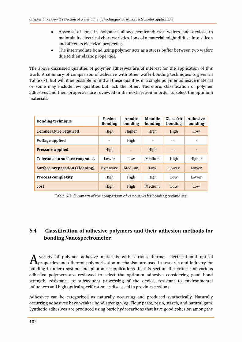
Chapter 6: Review & selection of wafer bonding technique for Nanospectrometer application
102
Absence of ions in polymers allows semiconductor wafers and devices to
maintain its electrical characteristics. Ions of a material might diffuse into silicon
and affect its electrical properties.
The intermediate bond using polymer acts as a stress buffer between two wafers
due to their elastic properties.
The above discussed qualities of polymer adhesives are of interest for the application of this
work. A summary of comparison of adhesive with other wafer bonding techniques is given in
Table 6-1. But will it be possible to find all these qualities in a single polymer adhesive material
or some may include few qualities but lack the other. Therefore, classification of polymer
adhesives and their properties are reviewed in the next section in order to select the optimum
materials.
Bonding technique Fusion
Bonding Anodic
bonding Metallic bonding
Glass frit bonding
Adhesive bonding
Temperature required High Higher High High Low
Voltage applied - High - - -
Pressure applied High - High - -
Tolerance to surface roughness Lower Low Medium High Higher
Surface preparation (Cleaning) Extensive Medium Low Lower Lower
Process complexity High High High Low Lower
cost High High Medium Low Low
Table 6-1: Summary of the comparison of various wafer bonding techniques.
6.4 Classification of adhesive polymers and their adhesion methods for
bonding Nanospectrometer
variety of polymer adhesive materials with various thermal, electrical and optical
properties and different polymerization mechanism are used in research and industry for
bonding in micro system and photonics applications. In this section the criteria of various
adhesive polymers are reviewed to select the optimum adhesive considering good bond
strength, resistance to subsequent processing of the device, resistant to environmental
influences and high optical specification as discussed in previous sections.
Adhesives can be categorized as naturally occurring and produced synthetically. Naturally
occurring adhesives have weaker bond strength, eg. Flour paste, resin, starch, and natural gum.
Synthetic adhesives are produced using basic hydrocarbons that have good cohesion among the
A
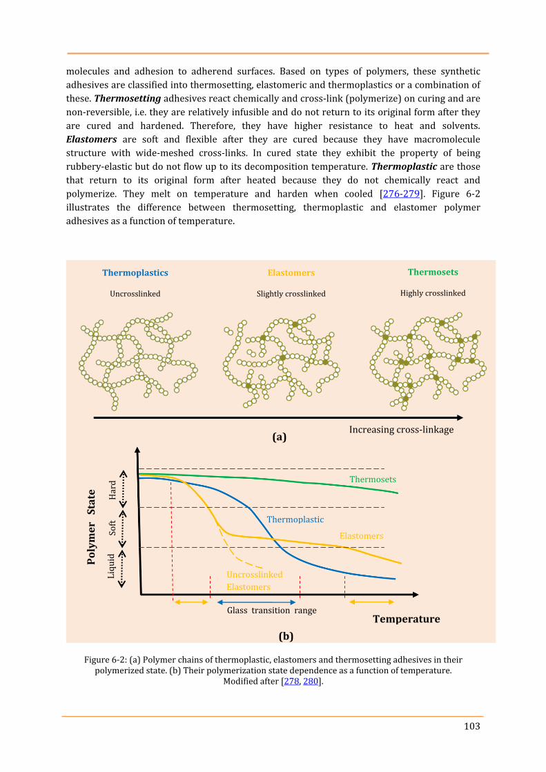
103
molecules and adhesion to adherend surfaces. Based on types of polymers, these synthetic
adhesives are classified into thermosetting, elastomeric and thermoplastics or a combination of
these. Thermosetting adhesives react chemically and cross-link (polymerize) on curing and are
non-reversible, i.e. they are relatively infusible and do not return to its original form after they
are cured and hardened. Therefore, they have higher resistance to heat and solvents.
Elastomers are soft and flexible after they are cured because they have macromolecule
structure with wide-meshed cross-links. In cured state they exhibit the property of being
rubbery-elastic but do not flow up to its decomposition temperature. Thermoplastic are those
that return to its original form after heated because they do not chemically react and
polymerize. They melt on temperature and harden when cooled [276-279]. Figure 6-2
illustrates the difference between thermosetting, thermoplastic and elastomer polymer
adhesives as a function of temperature.
Figure 6-2: (a) Polymer chains of thermoplastic, elastomers and thermosetting adhesives in their polymerized state. (b) Their polymerization state dependence as a function of temperature.
Modified after [278, 280].
Thermoplastics
Uncrosslinked
Elastomers
Slightly crosslinked
Thermosets
Highly crosslinked
Increasing cross-linkage (a)
(b)
Thermosets
Elastomers
Thermoplastic
Uncrosslinked
Elastomers
Temperature Glass transition range
Po
lym
er
Sta
te
Har
d
Soft
L
iqu
id
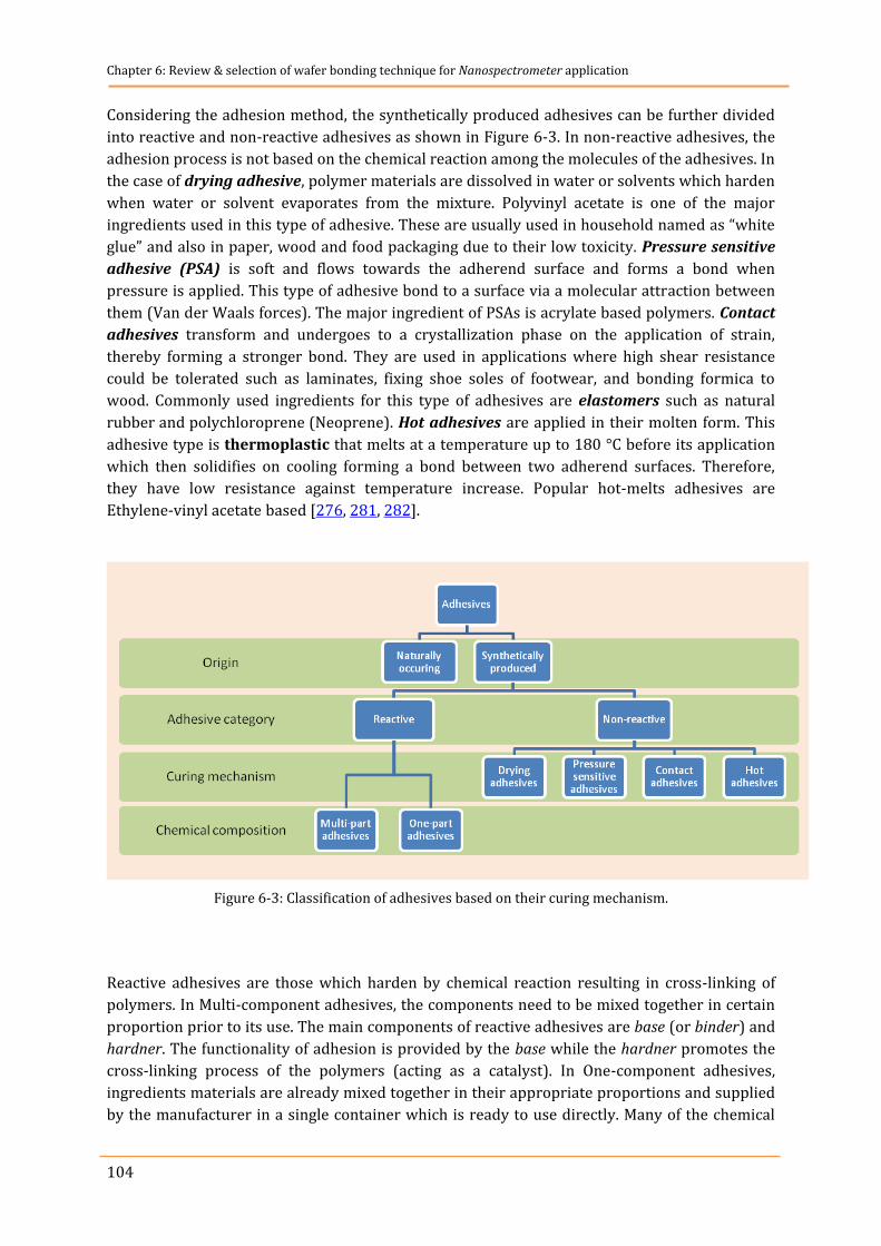
Chapter 6: Review & selection of wafer bonding technique for Nanospectrometer application
104
Considering the adhesion method, the synthetically produced adhesives can be further divided
into reactive and non-reactive adhesives as shown in Figure 6-3. In non-reactive adhesives, the
adhesion process is not based on the chemical reaction among the molecules of the adhesives. In
the case of drying adhesive, polymer materials are dissolved in water or solvents which harden
when water or solvent evaporates from the mixture. Polyvinyl acetate is one of the major
ingredients used in this type of adhesive. These are usually used in household named as “white
glue” and also in paper, wood and food packaging due to their low toxicity. Pressure sensitive
adhesive (PSA) is soft and flows towards the adherend surface and forms a bond when
pressure is applied. This type of adhesive bond to a surface via a molecular attraction between
them (Van der Waals forces). The major ingredient of PSAs is acrylate based polymers. Contact
adhesives transform and undergoes to a crystallization phase on the application of strain,
thereby forming a stronger bond. They are used in applications where high shear resistance
could be tolerated such as laminates, fixing shoe soles of footwear, and bonding formica to
wood. Commonly used ingredients for this type of adhesives are elastomers such as natural
rubber and polychloroprene (Neoprene). Hot adhesives are applied in their molten form. This
adhesive type is thermoplastic that melts at a temperature up to 180 °C before its application
which then solidifies on cooling forming a bond between two adherend surfaces. Therefore,
they have low resistance against temperature increase. Popular hot-melts adhesives are
Ethylene-vinyl acetate based [276, 281, 282].
Figure 6-3: Classification of adhesives based on their curing mechanism.
Reactive adhesives are those which harden by chemical reaction resulting in cross-linking of
polymers. In Multi-component adhesives, the components need to be mixed together in certain
proportion prior to its use. The main components of reactive adhesives are base (or binder) and
hardner. The functionality of adhesion is provided by the base while the hardner promotes the
cross-linking process of the polymers (acting as a catalyst). In One-component adhesives,
ingredients materials are already mixed together in their appropriate proportions and supplied
by the manufacturer in a single container which is ready to use directly. Many of the chemical

105
classes of adhesives such as acrylates, urethanes, silicone, and epoxies are supplied in one-
component as well as multi-component adhesive form. However, the mixed ingredients of one-
component adhesive react only under an external ignited polymerizing agent such as
temperature, UV radiation, or humidity which activate the hardner. Thermally polymerized
adhesives usually include polyimides, urethanes, and epoxies. UV polymerized adhesives, also
known as light curing adhesives, have an advantage of very short curing time, within seconds,
and delivering a very strong bond between a wide variety of materials. These are usually acrylic
based adhesives. Humidity polymerized adhesives react and cross-link in the presence of
humidity in the surrounding air. These usually include urethanes, cyanoacrylates [276, 278,
283, 284].

106
107
7. Materials, Methodology and process optimization of
optically clear reactive adhesive for integration of
Fabry-Pérot filter arrays to photodetector array
s
dhesive materials that satisfy the prerequisites for this work, described in section 6.1, is
intended to be studied and selected in this chapter. After selection it is required to be
dispensed in the desired quantity and cured. Different sizes of adhesive (spot like
droplet) are dispensed and cured forming to bond the FP-filter chip to the PD chip. However, to
dispense the selected adhesive materials in the required miniaturized range and cure it
properly to form a reliable micro bond-line, the process needs to be optimized for the
application of this work. The technology and methodology of dispensing method, curing system
and the de-bonding setup are described in this chapter.
7.1 Selection of adhesive material for integration of FP- filter arrays
to PD arrays
he major requirement in bonding the FP-filter arrays to PD arrays, that constitute a sensor
array, is to preserve the transmission lines from the FP-filter arrays in order not to degrade
the performance of the device. Finding adhesive materials that have good resistance against
temperature increase, solvents, weathering, provide hermetic properties, have good bond
strength and deliver high optical transmission is the main concern of this part of the work. After
A
T
Chapter 7
Materials, methodology and process optimization of
optically clear reactive adhesives for integration of
Fabry-Pérot filter arrays to photodetector arrays
Chapter 7: Materials, Methodology & Process optimization of optically clear reactive adhesives
108
bonding the FP-filter arrays to PD arrays some further processing is required in the case of
tunable FP-filter which includes underetching of the FP-filter membranes in O2 plasma and
deposition of light protection layer in PVD. Therefore, the adhesive material must also be
compatible to these proceeding steps, i.e. the bond-line must be resistant to all these chemical,
thermal & mechanical processes. Additionally, it must deliver a high optical performance which
is the most important factor.
Thermosetting polymer adhesives are known to provide majority of the above mentioned
primary requirements since they are irreversible and insoluble14 once cured [279]. This class of
polymer adhesive falls under the reactive adhesive category. For this work, one-component
reactive thermosetting adhesives are preferred over the multi-component reactive adhesives
due to the following reasons:
The mixing of various components in the multi-component reactive adhesives in exact
proportion is needed to deliver a strong bond. This mixing process is eliminated in one-
component reactive adhesive.
Upon mixing of the multi-component reactive adhesives, the curing reaction begins
instantly while the one-component reactive adhesives “cure on demand”, i.e. an external
agent such as temperature, UV radiation or humidity is needed to begin the
polymerization reaction. E.g. in this work, the FP-filter and photodetector could be
aligned and then exposed for UV radiation when ready. This allows maximum time for
precision alignment.
Various chemical classes of one-component reactive adhesive with various polymerization
mechanism (thermal, UV, or humidity) are commercially available. The polymerization
mechanism plays an important role in its selection depending on the application need. However,
adhesives with photo polymerization mechanism have several advantages over thermal
polymerization adhesives, e.g. low energy consumption, low equipment installation cost,
ambient temperature processing, and polymerizes very fast usually in seconds. Furthermore,
photo polymerization adhesives are solvent-free15 which provide environmental friendliness as
they do not emit volatile organic compounds (VOC), considerably reducing health and safety
risks [285-287]. Therefore, this work focuses on characterizing various UV-based
polymerization adhesives for bonding the sensor array. The main composition of UV
polymerization adhesives generally include of monomers, photoinitiators, and oligomers [288].
Acrylate monomers are the main candidates for majority of the UV-curing adhesives because of
its highly reactive double bond. Upon UV-exposure, the photoinitiators are subjected to fast
cleavage (fragmentation) which generates free radicals that initiate the polymerization of the
acrylate double bond. This is the reason behind fast UV polymerization of acrylate based
adhesives [279, 289].
Acrylate adhesives form strong bonds among various types of materials and are scratch
resistant. An extensive surface preparation is not required and they can also adhere through
certain amount of oil and grease surface. However, they polymerize to hard and brittle films,
14 Strong enough to resist dissolving in solvents or modification of its original composition
15 Adhesive contains no solvent
109
which is a drawback [290, 291]. Urethane is another category of polymer adhesive known to be
one of the most versatile classes of polymers having properties such as resistant to weathering,
yellowing and chemicals and forms an impact-resistant bond. They are good candidates for
bonding dissimilar substrate materials that might have different thermal expansion because
urethane adhesive provide flexibility for expansion and contraction, i.e. they are elastic but at
the same time provides a strong bond [290]. This property finds application in bonding flexible
plastic substrates. In its polymerized form, urethanes are lightly cross-linked thermoset resins
which give them the elastomeric characteristics of being flexible and rubbery [279]. Within the
acrylate family, UV curable urethane acrylates have been emerged that exhibit unique
properties such as they have high tensile strength and are resistant to abrasion, tear, oil,
solvent. They also provide the property of being printable [279, 286, 292-294]. Another UV
polymerizeable adhesive which differs from acrylate-based adhesive family in terms of
polymerization chemistry is epoxy-based adhesives. Epoxy-based adhesives polymerize under a
catalytic mechanism. A catalyst promotes a chemical reaction but is not consumed in the
reaction. The properties of epoxy based adhesives are resistant to solvents, environment and
high temperature conditions. They also have excellent adhesion to a wide variety of substrate
materials, provide high impact strength [295, 296].
7.1.1 Modified version of selected acrylate, urethane and epoxy based reactive
polymer adhesives
hese materials (acrylates, urethane & epoxies) have lower molecular weight, i.e. lower
molecular weight monomers cross-link densely while higher molecular weight monomers
reduces the density of double bond structure and hence less cross-linked networks [297]. These
high cross-linking densities make them applicable for scratch resistant coatings for mobile
phones, disc players, and other electronic devices [298]. However, these materials have some
inherent limitations in its properties which make them unsuitable for some specific
applications, thereby, restricting its widespread use. E.g. these high cross-linking densities in UV
curing materials causes internal stress which make them susceptible to cracking [298].
Therefore, modification of these materials using either physical form by adding organic or
inorganic fillers or chemical form is desirable in order to improve the properties of acrylate-
based and epoxy-based materials [279]. These desired modifications increase their resistance to
oil, temperature, environmental influences, and oxidation. Furthermore, wetting of the
substrates, viscosity to control the flow rate, brittleness after curing and their adhesion
properties on a wide variety of substrate materials are improved. These chemical modifications
also have the advantages such as high catalytic efficiency and less trigger time [288].
Modification to acrylate adhesives is usually made at the chemical level by changes in molecular
structure or by combining it with other base resins. Properties of these modified acrylate
adhesives include resistance to environment, impact, and surface insensitivity. This adhesive
family also provides solvent-free, transparent, and UV stable properties for optical applications
[290, 291, 299]. Modification of epoxy adhesives is relatively easy for special purposes, e.g.
T
Chapter 7: Materials, Methodology & Process optimization of optically clear reactive adhesives
110
silver or gold can be mixed into them to provide electrical conductivity. Providing thermal
conductivity while maintaining electrical insulation can be achieved by mixing other additives.
Modified epoxy adhesives are resistant to impact, chemical and moisture. They exhibit high
temperature strength, low shrinkage, and a high glass transition temperature [279].
Modifications to acrylate based polymer adhesives have been reported by various groups to
improve their adhesion properties with low polymerization shrinkage [297], enhancement in
thermal stability and in water resistance [288], enhancement in thermal, gas (oxygen) &
moisture barrier properties [285]. Also modifications to epoxy based adhesives for non-
yellowing effect, corrosion resistant properties have been reported [300].
7.1.2 Dual-polymerization in modified reactive polymer adhesive
thin layer of aluminum with thickness of ~ 100 nm with a small opening (12 – 60 µm)
exists as a top layer in FP-filters to allow the light enter only through the opening and block
the light entering from other directions. In this case, using UV polymerization adhesives is
critical because the aluminum layer might hamper the penetration of UV radiation needed for
its curing. Therefore, finding adhesives that can polymerize under different mechanism is
desired. Based on certain modifications, the polymer adhesives can support dual polymerization
mechanism, i.e. UV & humidity or UV & thermal. A mixture of multifunctional monomers or
oligomers that polymerize with different mechanism can provide two interpenetrating polymer
networks (IPN). This IPN can be obtained when the used monomers and polymers are
compatible to each other [279, 298]. This can provide an extended flexibility in bonding the FP-
filter arrays to PD arrays which is required for the following reasons:
UV curing of adhesive through the top aluminum layer of the FP-filter array (light
protection layer) will be prevented as the UV will be reflected [301].
The FP-filter itself might reflect a high percentage of UV light which makes curing of the
adhesive not 100%.
An example of UV & thermal dual polymerization adhesive is illustrated in Figure 7-1.
A
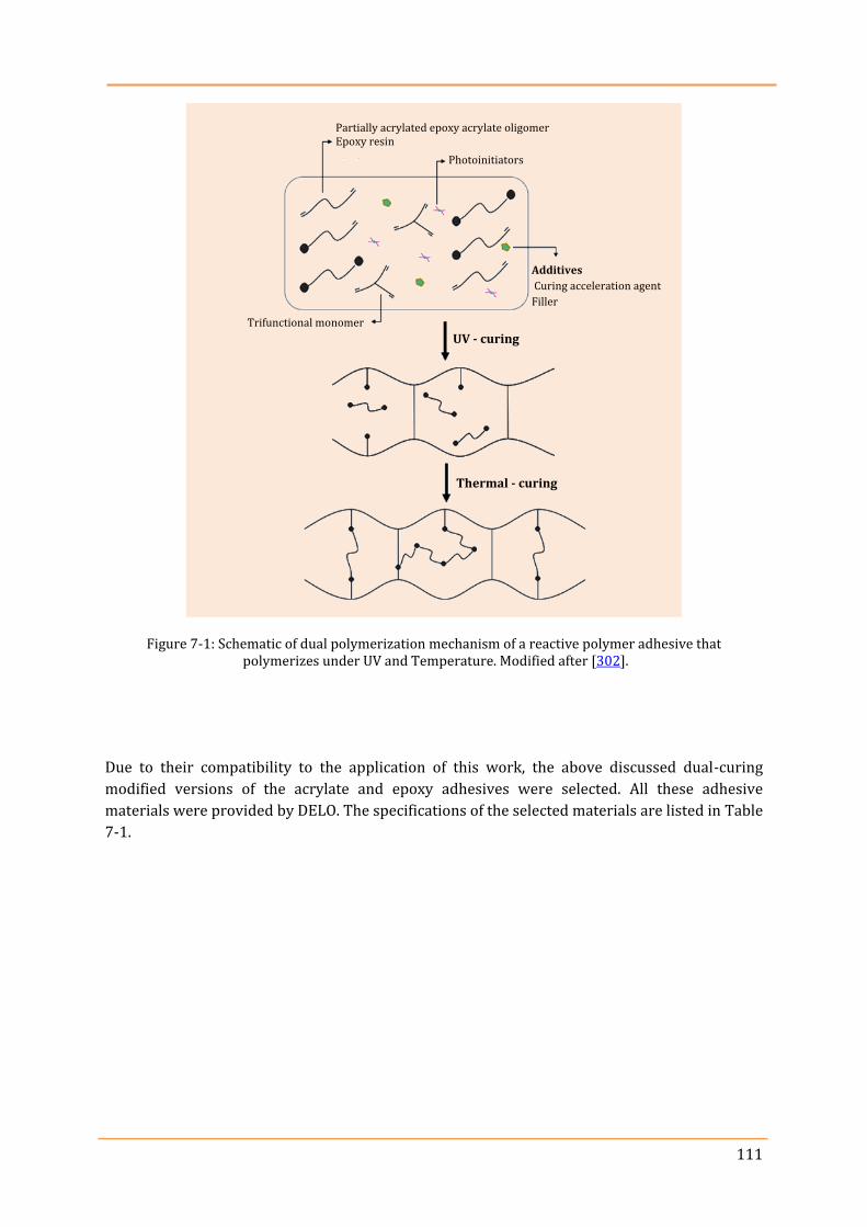
111
Figure 7-1: Schematic of dual polymerization mechanism of a reactive polymer adhesive that polymerizes under UV and Temperature. Modified after [302].
Due to their compatibility to the application of this work, the above discussed dual-curing
modified versions of the acrylate and epoxy adhesives were selected. All these adhesive
materials were provided by DELO. The specifications of the selected materials are listed in Table
7-1.
Partially acrylated epoxy acrylate oligomer Epoxy resin
Photoinitiators
Additives
Curing acceleration agent
Filler
Trifunctional monomer
UV - curing
Thermal - curing
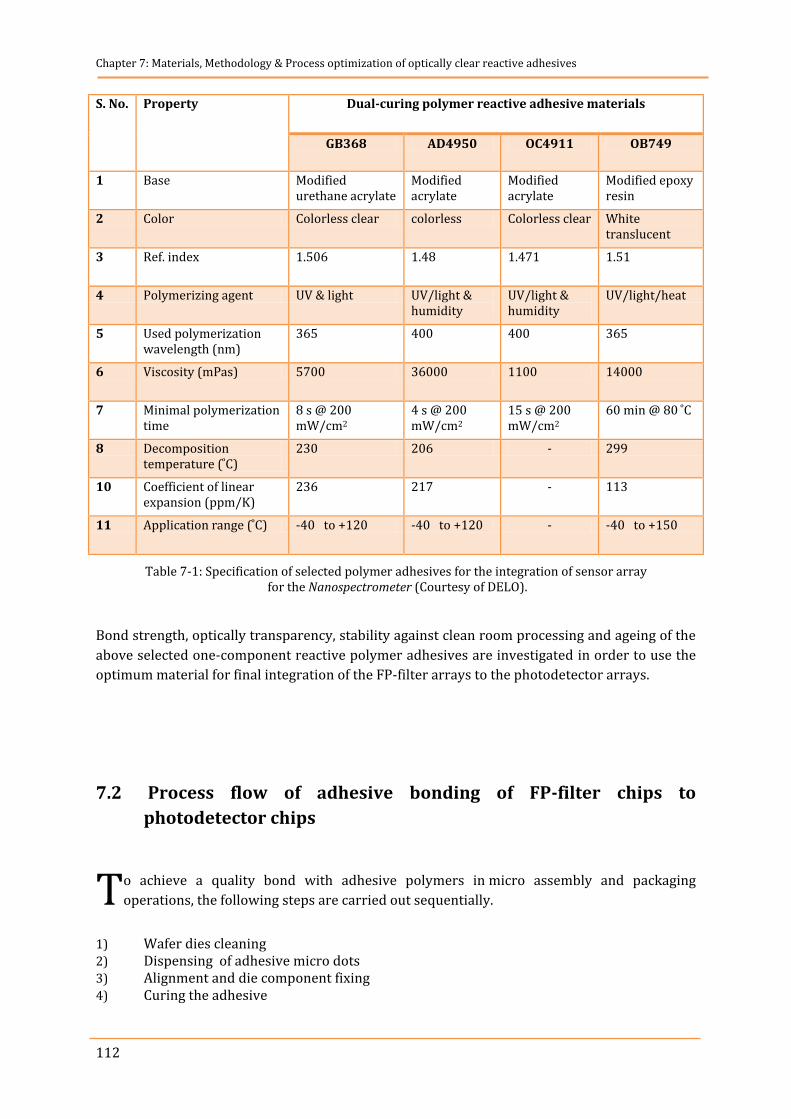
Chapter 7: Materials, Methodology & Process optimization of optically clear reactive adhesives
112
S. No. Property Dual-curing polymer reactive adhesive materials
GB368 AD4950 OC4911 OB749
1 Base Modified urethane acrylate
Modified acrylate
Modified acrylate
Modified epoxy resin
2 Color Colorless clear colorless Colorless clear White translucent
3 Ref. index 1.506 1.48 1.471 1.51
4 Polymerizing agent UV & light UV/light & humidity
UV/light & humidity
UV/light/heat
5 Used polymerization wavelength (nm)
365 400 400 365
6 Viscosity (mPas) 5700 36000 1100 14000
7 Minimal polymerization time
8 s @ 200 mW/cm2
4 s @ 200 mW/cm2
15 s @ 200 mW/cm2
0 min 80 C
8 Decomposition temperature ( C)
230 206 - 299
10 Coefficient of linear expansion (ppm/K)
236 217 - 113
11 Application range ( C) -40 to +120 -40 to +120 - -40 to +150
Table 7-1: Specification of selected polymer adhesives for the integration of sensor array for the Nanospectrometer (Courtesy of DELO).
Bond strength, optically transparency, stability against clean room processing and ageing of the
above selected one-component reactive polymer adhesives are investigated in order to use the
optimum material for final integration of the FP-filter arrays to the photodetector arrays.
7.2 Process flow of adhesive bonding of FP-filter chips to
photodetector chips
o achieve a quality bond with adhesive polymers in micro assembly and packaging
operations, the following steps are carried out sequentially.
1) Wafer dies cleaning 2) Dispensing of adhesive micro dots 3) Alignment and die component fixing 4) Curing the adhesive
T
113
To investigate the quality of the bond-line, following additional processes are required.
5) Optical measurement 6) Bond strength measurement 7) Stability against temperature and O2 plasma 8) Influence of aging factors
7.3 Methodology of adhesive bonding of FP-filter arrays to
photodetector arrays
7.3.1 Micro dispensing system
ispensing a consistent and correct amount of adhesive material is necessary depending on
the chip size to be bonded. The dimensions of the fabricated and diced dies of FP-filter
arrays and that of PD arrays are in the range of 1.5 mm x 2 mm. Hence, a very small amount of
adhesive bonding material, like a dot, is required to bond them together. For this purpose an
automated dispensing system comes into effect to achieve this precise range of adhesive dot.
This saves the adhesive material and time as well.
The system consists of a micro dispensing valve, a dispensing control unit and a temperature
controller which is provided by DELO16. The micro dispensing valve is compact and can deliver
variable drop sizes with the help interchangeable nozzles of different openings where an
adhesive dot is jetted out. The nozzles diameters used in this work are 200 µm, 300 µm and 400
µm. The size of the jetted adhesive droplet depends on its viscosity and the opening diameter of
the dispensing nozzle. The adhesive cartridge is fixed on the micro dispensing valve and a
pneumatic pressure is applied on top using a special pressure cap as shown in Figure 7-2. An
integrated heater, controlled by temperature controller exists in the micro dispensing valve
which can be used to ease the flow of the adhesives when necessary. The number of dots in a
certain time (per second), the dispensing pressure and delay time can be set at the micro
dispensing controller – PROTOR. Similar dispensing valves are also used in pharmaceutical
processes to integrate a liquid Active Pharmaceutical Ingredient (API) with very small amount
(4 – 10 µL) into a solid tablet, thus overcoming the challenge of processing at high speed [303].
16 Delo Industrie Klebstoffe GmbH & Co. KGaA
D
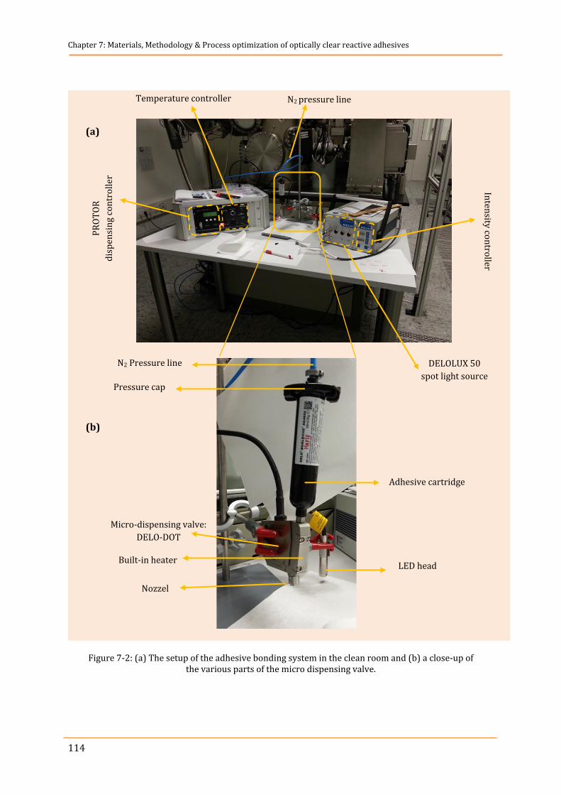
Chapter 7: Materials, Methodology & Process optimization of optically clear reactive adhesives
114
Figure 7-2: (a) The setup of the adhesive bonding system in the clean room and (b) a close-up of the various parts of the micro dispensing valve.
Temperature controller N2 pressure line P
RO
TO
R
dis
pen
sin
g co
ntr
oll
er
Inten
sity co
ntro
ller
DELOLUX 50
spot light source
(a)
Adhesive cartridge
Pressure cap
LED head Built-in heater
Nozzel
N2 Pressure line
Micro-dispensing valve:
DELO-DOT
(b)
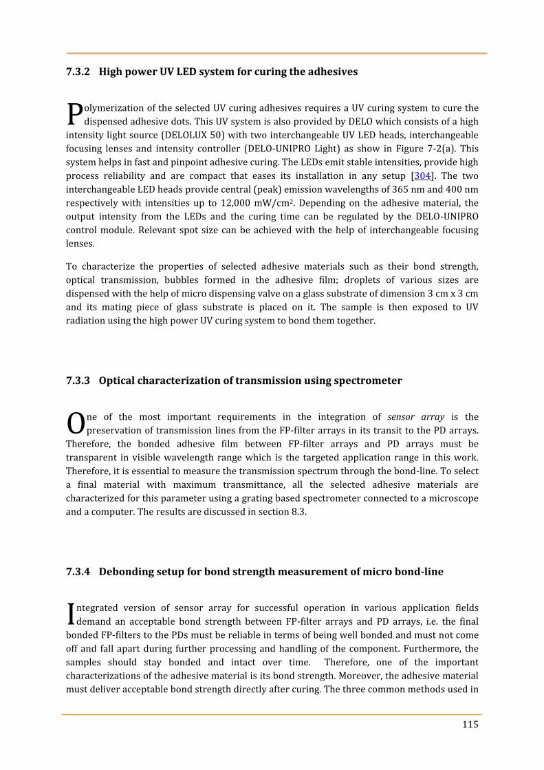
115
7.3.2 High power UV LED system for curing the adhesives
olymerization of the selected UV curing adhesives requires a UV curing system to cure the
dispensed adhesive dots. This UV system is also provided by DELO which consists of a high
intensity light source (DELOLUX 50) with two interchangeable UV LED heads, interchangeable
focusing lenses and intensity controller (DELO-UNIPRO Light) as show in Figure 7-2(a). This
system helps in fast and pinpoint adhesive curing. The LEDs emit stable intensities, provide high
process reliability and are compact that eases its installation in any setup [304]. The two
interchangeable LED heads provide central (peak) emission wavelengths of 365 nm and 400 nm
respectively with intensities up to 12,000 mW/cm2. Depending on the adhesive material, the
output intensity from the LEDs and the curing time can be regulated by the DELO-UNIPRO
control module. Relevant spot size can be achieved with the help of interchangeable focusing
lenses.
To characterize the properties of selected adhesive materials such as their bond strength,
optical transmission, bubbles formed in the adhesive film; droplets of various sizes are
dispensed with the help of micro dispensing valve on a glass substrate of dimension 3 cm x 3 cm
and its mating piece of glass substrate is placed on it. The sample is then exposed to UV
radiation using the high power UV curing system to bond them together.
7.3.3 Optical characterization of transmission using spectrometer
ne of the most important requirements in the integration of sensor array is the
preservation of transmission lines from the FP-filter arrays in its transit to the PD arrays.
Therefore, the bonded adhesive film between FP-filter arrays and PD arrays must be
transparent in visible wavelength range which is the targeted application range in this work.
Therefore, it is essential to measure the transmission spectrum through the bond-line. To select
a final material with maximum transmittance, all the selected adhesive materials are
characterized for this parameter using a grating based spectrometer connected to a microscope
and a computer. The results are discussed in section 8.3.
7.3.4 Debonding setup for bond strength measurement of micro bond-line
ntegrated version of sensor array for successful operation in various application fields
demand an acceptable bond strength between FP-filter arrays and PD arrays, i.e. the final
bonded FP-filters to the PDs must be reliable in terms of being well bonded and must not come
off and fall apart during further processing and handling of the component. Furthermore, the
samples should stay bonded and intact over time. Therefore, one of the important
characterizations of the adhesive material is its bond strength. Moreover, the adhesive material
must deliver acceptable bond strength directly after curing. The three common methods used in
P
O
I
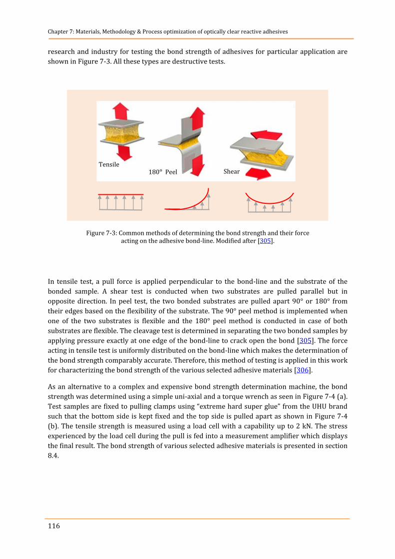
Chapter 7: Materials, Methodology & Process optimization of optically clear reactive adhesives
116
research and industry for testing the bond strength of adhesives for particular application are
shown in Figure 7-3. All these types are destructive tests.
Figure 7-3: Common methods of determining the bond strength and their force acting on the adhesive bond-line. Modified after [305].
In tensile test, a pull force is applied perpendicular to the bond-line and the substrate of the
bonded sample. A shear test is conducted when two substrates are pulled parallel but in
opposite direction. In peel test, the two bonded substrates are pulled apart 90° or 180° from
their edges based on the flexibility of the substrate. The 90° peel method is implemented when
one of the two substrates is flexible and the 180° peel method is conducted in case of both
substrates are flexible. The cleavage test is determined in separating the two bonded samples by
applying pressure exactly at one edge of the bond-line to crack open the bond [305]. The force
acting in tensile test is uniformly distributed on the bond-line which makes the determination of
the bond strength comparably accurate. Therefore, this method of testing is applied in this work
for characterizing the bond strength of the various selected adhesive materials [306].
As an alternative to a complex and expensive bond strength determination machine, the bond
strength was determined using a simple uni-axial and a torque wrench as seen in Figure 7-4 (a).
Test samples are fixed to pulling clamps using “extreme hard super glue” from the UHU brand
such that the bottom side is kept fixed and the top side is pulled apart as shown in Figure 7-4
(b). The tensile strength is measured using a load cell with a capability up to 2 kN. The stress
experienced by the load cell during the pull is fed into a measurement amplifier which displays
the final result. The bond strength of various selected adhesive materials is presented in section
8.4.
Tensile 180° Peel Shear
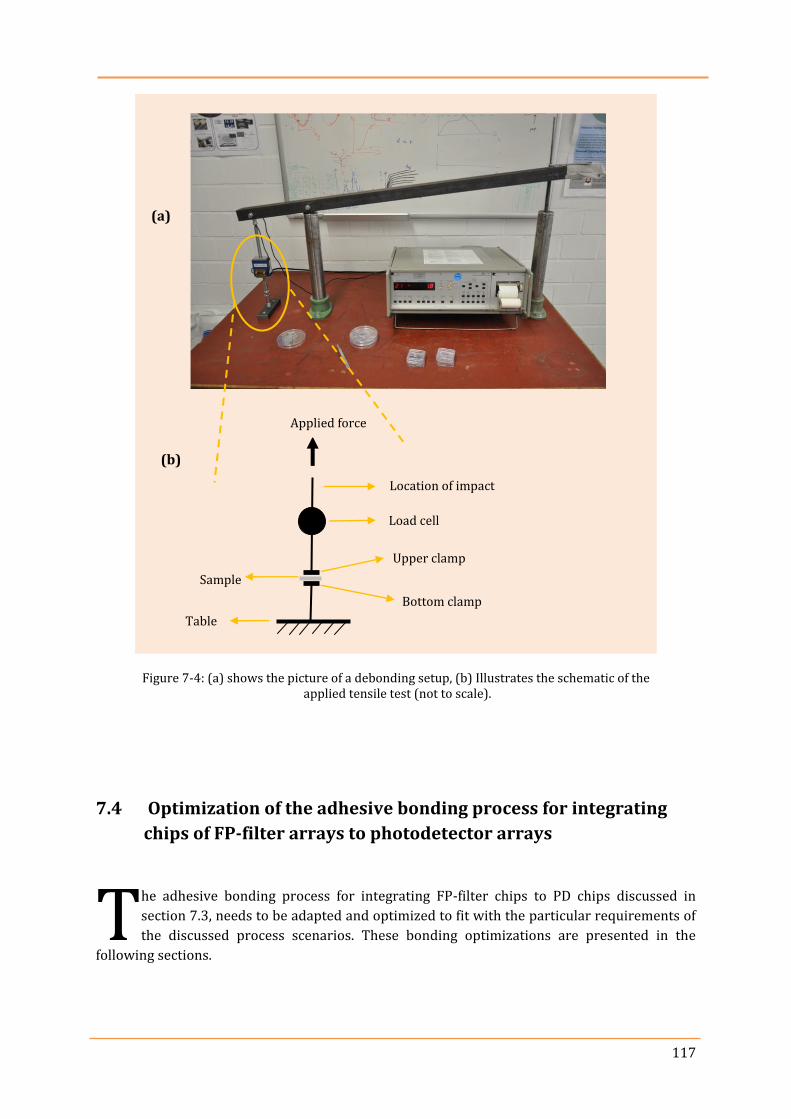
117
Figure 7-4: (a) shows the picture of a debonding setup, (b) Illustrates the schematic of the applied tensile test (not to scale).
7.4 Optimization of the adhesive bonding process for integrating
chips of FP-filter arrays to photodetector arrays
he adhesive bonding process for integrating FP-filter chips to PD chips discussed in
section 7.3, needs to be adapted and optimized to fit with the particular requirements of
the discussed process scenarios. These bonding optimizations are presented in the
following sections.
T
Load cell
Upper clamp
Sample
Table
Location of impact
Bottom clamp
Applied force
(a)
(b)
Chapter 7: Materials, Methodology & Process optimization of optically clear reactive adhesives
118
7.4.1 Dispensing process optimization of the adhesive material
he optimization of adhesive dispensing process to jet out the desired amount of adhesive
include pressure adjustment on the adhesive cartridge and Temperature adjustment at the
micro valve. These parameters are discussed in the following sub sections.
7.4.1.1 Pressure adjustment on the DELO adhesive cartridge
s discussed in section 7.3.1 that a very small amount of adhesive material, in the range of
the diced FP-filters and PD chips, is required. This can be achieved by the implemented
micro dispensing valve with interchangeable nozzles having opening diameter in micro meter
range (100 µm, 200 µm, 300 µm). But without applying pressure on top of the adhesive
cartridge, it is not possible to jet out viscous adhesive materials through the micro openings of
the nozzles.
In order to jet out the adhesive through the nozzles of micro dispensing valve, a recommended
pressure of 0.5 bars by the manufacturer is required to be applied on the adhesive cartridge. In
the absence of pneumatic pressure in the clean room, this pressure is applied by using a N2 line.
However, it is found that this amount of pressure is not sufficient for jetting out any of the
selected adhesives. Therefore, pressure is increased at the regulator knob gently and the jetting
process is repeated to obtain a continuous flow of drops through the micro nozzles. This trial-
and-error method is experimented with increment in pressure up to 4 bars but jetting was
unsuccessful through all the used nozzles. This might be due to the viscous adhesives used.
Therefore, its flow is investigated as a function of temperature applied to the micro valve as
explained in next section.
7.4.1.2 Temperature adjustment to jet a dot of adhesive from the micro valve
hen the adhesive jetting was unsuccessful up to a pressure of 4 bars, the integrated
heater in the micro valve was used. Temperature is gradually increased and the jetting
process is repeated. This procedure is successful in jetting out a continuous flow of dots for all
the selected adhesives. This could be due to the fact that the viscosity of the used adhesive
materials is reduced when the heating system is used, thereby easing the flow of adhesive
through micro range nozzles. Various combinations of temperature and pressure are tested and
the optimized combinations are used for all individual selected adhesives. Table 7-2
summarizes these optimized combinations.
T
A
W
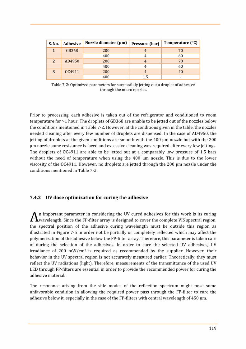
119
S. No. Adhesive Nozzle diameter (µm) Pressure (bar) Temperature (°C)
1 GB368 200 4 70
400 4 60
2 AD4950 200 4 70
400 4 60
3 OC4911 200 4 40
400 1.5 -
Table 7-2: Optimized parameters for successfully jetting out a droplet of adhesive through the micro nozzles.
Prior to processing, each adhesive is taken out of the refrigerator and conditioned to room
temperature for >1 hour. The droplets of GB368 are unable to be jetted out of the nozzles below
the conditions mentioned in Table 7-2. However, at the conditions given in the table, the nozzles
needed cleaning after every few number of droplets are dispensed. In the case of AD4950, the
jetting of droplets at the given conditions are smooth with the 400 µm nozzle but with the 200
µm nozzle some resistance is faced and excessive cleaning was required after every few jettings.
The droplets of OC4911 are able to be jetted out at a comparably low pressure of 1.5 bars
without the need of temperature when using the 400 µm nozzle. This is due to the lower
viscosity of the OC4911. However, no droplets are jetted through the 200 µm nozzle under the
conditions mentioned in Table 7-2.
7.4.2 UV dose optimization for curing the adhesive
n important parameter in considering the UV cured adhesives for this work is its curing
wavelength. Since the FP-filter array is designed to cover the complete VIS spectral region,
the spectral position of the adhesive curing wavelength must be outside this region as
illustrated in Figure 7-5 in order not be partially or completely reflected which may affect the
polymerization of the adhesive below the FP-filter array. Therefore, this parameter is taken care
of during the selection of the adhesives. In order to cure the selected UV adhesives, UV
irradiance of 200 mW/cm2 is required as recommended by the supplier. However, their
behavior in the UV spectral region is not accurately measured earlier. Theoretically, they must
reflect the UV radiations (light). Therefore, measurements of the transmittance of the used UV
LED through FP-filters are essential in order to provide the recommended power for curing the
adhesive material.
The resonance arising from the side modes of the reflection spectrum might pose some
unfavorable condition in allowing the required power pass through the FP-filter to cure the
adhesive below it, especially in the case of the FP-filters with central wavelength of 450 nm.
A
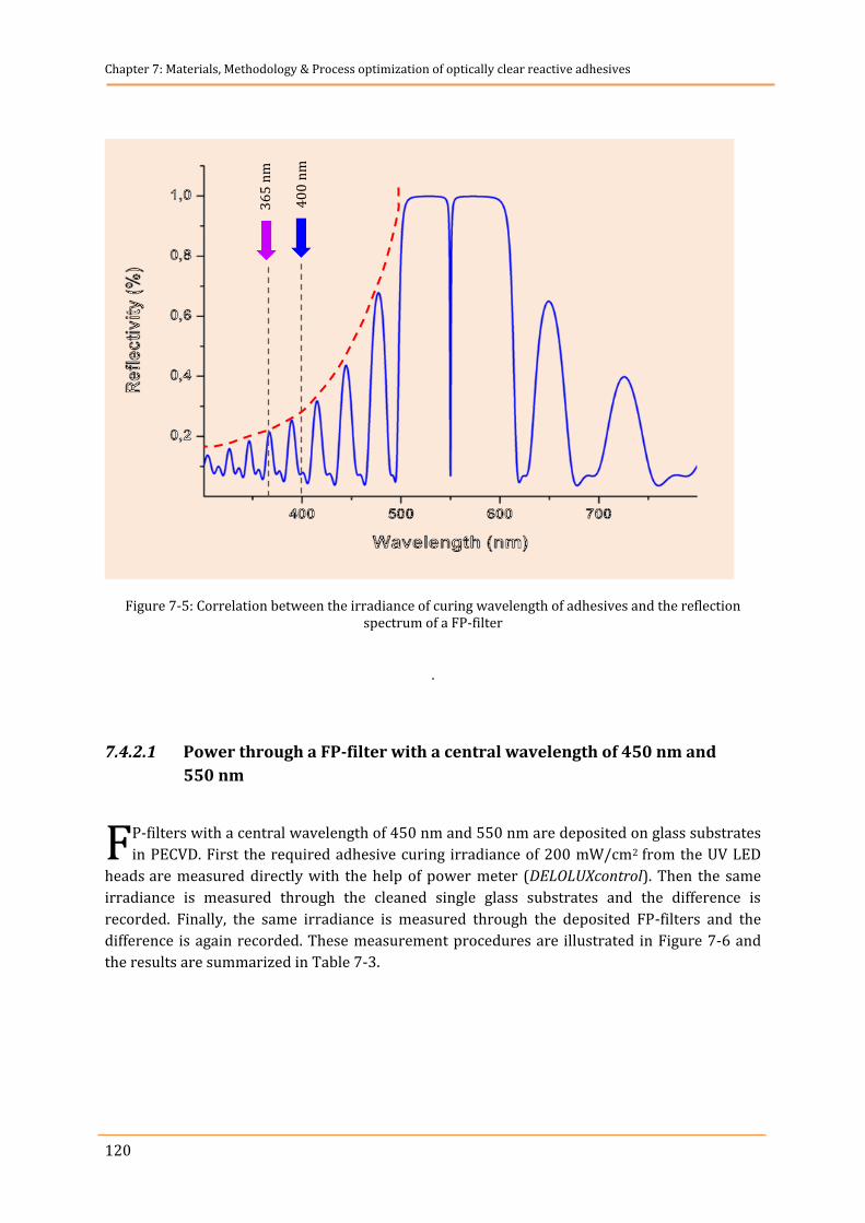
Chapter 7: Materials, Methodology & Process optimization of optically clear reactive adhesives
120
Figure 7-5: Correlation between the irradiance of curing wavelength of adhesives and the reflection spectrum of a FP-filter
.
7.4.2.1 Power through a FP-filter with a central wavelength of 450 nm and
550 nm
P-filters with a central wavelength of 450 nm and 550 nm are deposited on glass substrates
in PECVD. First the required adhesive curing irradiance of 200 mW/cm2 from the UV LED
heads are measured directly with the help of power meter (DELOLUXcontrol). Then the same
irradiance is measured through the cleaned single glass substrates and the difference is
recorded. Finally, the same irradiance is measured through the deposited FP-filters and the
difference is again recorded. These measurement procedures are illustrated in Figure 7-6 and
the results are summarized in Table 7-3.
F
36
5 n
m
40
0 n
m
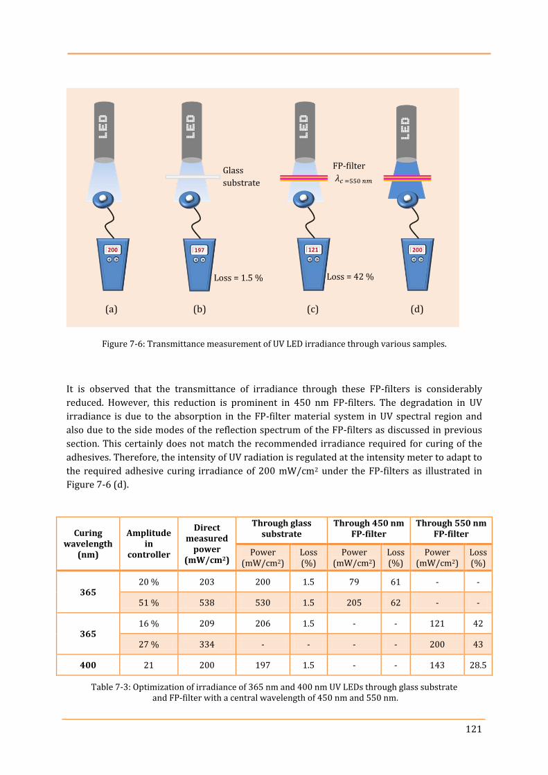
121
Figure 7-6: Transmittance measurement of UV LED irradiance through various samples.
It is observed that the transmittance of irradiance through these FP-filters is considerably
reduced. However, this reduction is prominent in 450 nm FP-filters. The degradation in UV
irradiance is due to the absorption in the FP-filter material system in UV spectral region and
also due to the side modes of the reflection spectrum of the FP-filters as discussed in previous
section. This certainly does not match the recommended irradiance required for curing of the
adhesives. Therefore, the intensity of UV radiation is regulated at the intensity meter to adapt to
the required adhesive curing irradiance of 200 mW/cm2 under the FP-filters as illustrated in
Figure 7-6 (d).
Curing wavelength
(nm)
Amplitude in
controller
Direct measured
power (mW/cm2)
Through glass substrate
Through 450 nm FP-filter
Through 550 nm FP-filter
Power
(mW/cm2) Loss (%)
Power (mW/cm2)
Loss (%)
Power (mW/cm2)
Loss (%)
365 20 % 203 200 1.5 79 61 - -
51 % 538 530 1.5 205 62 - -
365 16 % 209 206 1.5 - - 121 42
27 % 334 - - - - 200 43
400 21 200 197 1.5 - - 143 28.5
Table 7-3: Optimization of irradiance of 365 nm and 400 nm UV LEDs through glass substrate and FP-filter with a central wavelength of 450 nm and 550 nm.
(a) (b) (c) (d)
Loss = 1.5 % Loss = 42 %
Glass
substrate
FP-filter

122

123
8. Optical and mechanical characterizations of the
micro bond-line of the selected polymer a
dhesives
ptical transparency, bond strength, stability against various processing conditions and
the impact of environmental influences are the essential characterization parameters
that affect the quality of a bond-line. These characterizations are implemented on
various selected adhesive materials and their experimental results are compared to select the
best suited adhesive for the integration of sensor array for the Nanospectrometer. Based on the
performance of the adhesives from the determined results, the most optimum adhesive is used
in bonding the diced chips of FP-filter arrays on to the chips of photodetector (PD) array.
8.1 Sample preparation for optical and mechanical characterization
or experiments, several samples are prepared such that two glass substrates are bonded
together using each adhesive material mentioned in section 7.1.2 in order to inspect the
micro bond-line. A micro drop of each adhesive is jetted out on a glass samples with the help of
the micro dispensing setup discussed in section 7.3.1 and a second glass sample is placed on it
manually and very gently pressed without excessive force. The sample is then introduced under
the UV-LED head to cure the adhesive drops between the glass samples and form a micro bond-
line. In its cured state, the transmission through the micro bond-line in VIS spectral region is
measured using a microscope spectrometer. After these procedures, the samples are debonded
and their bond strength is measured using the setup discussed in section 7.3.4. To provide a
O
F
Chapter 8 Optical and mechanical characterization of the
micro bond-lines of selected polymer adhesives
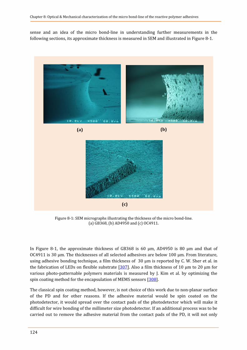
Chapter 8: Optical & Mechanical characterization of the micro bond-line of the reactive polymer adhesives
124
sense and an idea of the micro bond-line in understanding further measurements in the
following sections, its approximate thickness is measured in SEM and illustrated in Figure 8-1.
Figure 8-1: SEM micrographs illustrating the thickness of the micro bond-line. (a) GB368, (b) AD4950 and (c) OC4911.
In Figure 8-1, the approximate thickness of GB368 is 60 µm, AD4950 is 80 µm and that of
OC4911 is 30 µm. The thicknesses of all selected adhesives are below 100 µm. From literature,
using adhesive bonding technique, a film thickness of 30 μm is reported by C. W. Sher et al. in
the fabrication of LEDs on flexible substrate [307]. Also a film thickness of 10 µm to 20 µm for
various photo-patternable polymers materials is measured by J. Kim et al. by optimizing the
spin coating method for the encapsulation of MEMS sensors [308].
The classical spin coating method, however, is not choice of this work due to non-planar surface
of the PD and for other reasons. If the adhesive material would be spin coated on the
photodetector, it would spread over the contact pads of the photodetector which will make it
difficult for wire bonding of the millimeter size photodetector. If an additional process was to be
carried out to remove the adhesive material from the contact pads of the PD, it will not only
(b) (a)
(c)
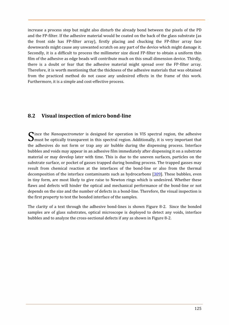
125
increase a process step but might also disturb the already bond between the pixels of the PD
and the FP-filter. If the adhesive material would be coated on the back of the glass substrate (as
the front side has FP-filter array), firstly placing and chucking the FP-filter array face
downwards might cause any unwanted scratch on any part of the device which might damage it.
Secondly, it is a difficult to process the millimeter size diced FP-filter to obtain a uniform thin
film of the adhesive as edge beads will contribute much on this small dimension device. Thirdly,
there is a doubt or fear that the adhesive material might spread over the FP-filter array.
Therefore, it is worth mentioning that the thickness of the adhesive materials that was obtained
from the practiced method do not cause any undesired effects in the frame of this work.
Furthermore, it is a simple and cost-effective process.
8.2 Visual inspection of micro bond-line
ince the Nanospectrometer is designed for operation in VIS spectral region, the adhesive
must be optically transparent in this spectral region. Additionally, it is very important that
the adhesives do not form or trap any air bubble during the dispensing process. Interface
bubbles and voids may appear in an adhesive film immediately after dispensing it on a substrate
material or may develop later with time. This is due to the uneven surfaces, particles on the
substrate surface, or pocket of gasses trapped during bonding process. The trapped gasses may
result from chemical reaction at the interfaces of the bond-line or also from the thermal
decomposition of the interface contaminants such as hydrocarbons [309]. These bubbles, even
in tiny form, are most likely to give raise to Newton rings which is undesired. Whether these
flaws and defects will hinder the optical and mechanical performance of the bond-line or not
depends on the size and the number of defects in a bond-line. Therefore, the visual inspection is
the first property to test the bonded interface of the samples.
The clarity of a text through the adhesive bond-lines is shown Figure 8-2. Since the bonded
samples are of glass substrates, optical microscope is deployed to detect any voids, interface
bubbles and to analyze the cross-sectional defects if any as shown in Figure 8-2.
S
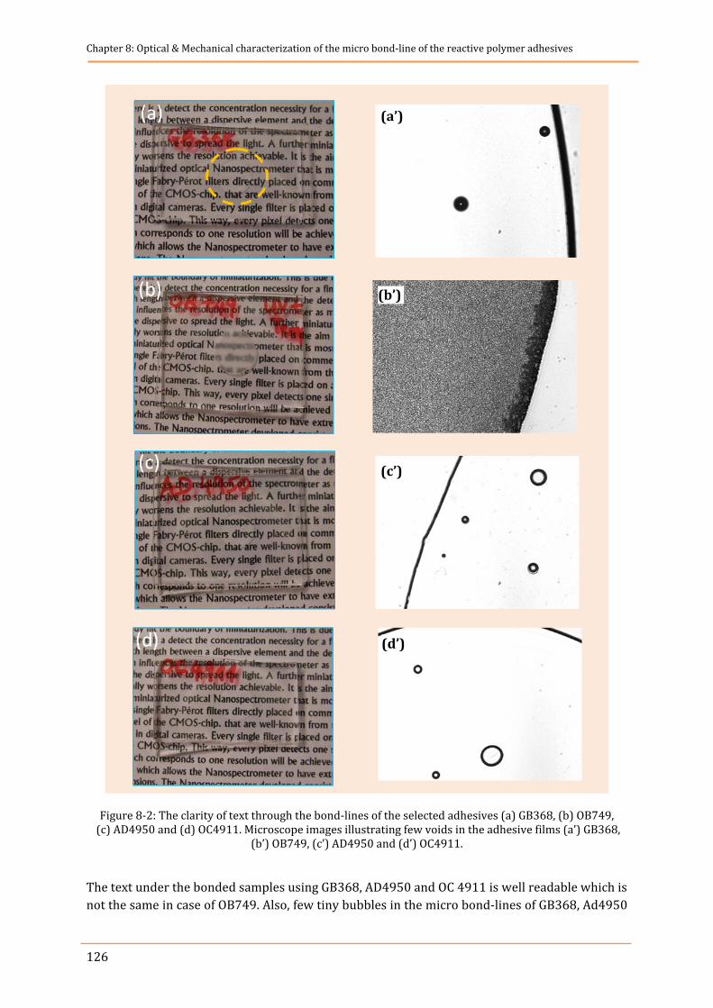
Chapter 8: Optical & Mechanical characterization of the micro bond-line of the reactive polymer adhesives
126
Figure 8-2: The clarity of text through the bond-lines of the selected adhesives (a) GB368, (b) OB749, (c) AD4950 and (d) OC4911. Microscope images illustrating few voids in the adhesive films (a’) GB3 8,
(b’) OB749, (c’) AD4950 and (d’) OC4911.
The text under the bonded samples using GB368, AD4950 and OC 4911 is well readable which is
not the same in case of OB749. Also, few tiny bubbles in the micro bond-lines of GB368, Ad4950
(a’)
(b’)
(c’)
(d’)
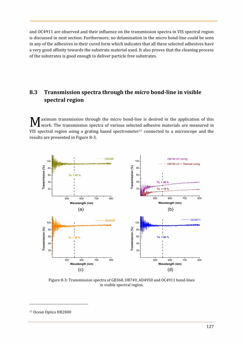
127
and OC4911 are observed and their influence on the transmission spectra in VIS spectral region
is discussed in next section. Furthermore, no delamination in the micro bond-line could be seen
in any of the adhesives in their cured form which indicates that all these selected adhesives have
a very good affinity towards the substrate material used. It also proves that the cleaning process
of the substrates is good enough to deliver particle free substrates.
8.3 Transmission spectra through the micro bond-line in visible
spectral region
aximum transmission through the micro bond-line is desired in the application of this
work. The transmission spectra of various selected adhesive materials are measured in
VIS spectral region using a grating based spectrometer17 connected to a microscope and the
results are presented in Figure 8-3.
Figure 8-3: Transmission spectra of GB368, OB749, AD4950 and OC4911 bond-lines in visible spectral region.
17 Ocean Optics HR2000
M
Chapter 8: Optical & Mechanical characterization of the micro bond-line of the reactive polymer adhesives
128
Figure 8-3 shows a measured transmittance of >90% through the micro bond-line of GB368,
AD4950 and OC4911 in VIS spectral region except OB749 (13 % - 30 %). Despite few tiny
bubbles noticed under microscope in the bond-lines of GB368, Ad4950 and OC4911, they have
no direct influence on the transmission sprectra. Although the dual-cured OB749 was selected
along with others for testing purposes as its refractive index was very much matching to the
desired need of this work but it delivered a milky and translucent film after polymerization and
showed a very poor transmittance as compared to other materials. Therefore, it was dropped at
this point onwards and excluded from further investigations.
Influence of age-time on the transmission spectra through the bond-line
The optical quality of the micro bond-line is desired to retain over time. However, it can be the
case that an adhesive material is optically clear and exhibits very good transmittance directly
after curing but degrade and reduce its performance on time. Therefore, their performance on
time is evaluated.
The transmission through each selected adhesive film is measured after 24 hours, 1 month and
1 year as given in Table 8-1. It is observed that all used adhesives are stable and their
transmission spectra did not degrade over time.
Adhesive material Curing method Transmission (%) after
24 hr 1 month 1 year
OB749 UV+ Thermal 13 - 30 13 - 30 ---
GB368 UV 92 92 92
AD4950 UV+ Humidity 91 92 92
OC4911 UV+ Humidity 94 94 94
Table 8-1: Transmission spectra of the selected adhesives at various age-times.
8.4 Bond strength of the selected polymer adhesives
ufficient bond strength between the FP-filter arrays and the PD arrays (to constitute a
sensor array) is necessary to sustain the performance of the Nanospectrometer.
Furthermore, it must also withstand the subsequent processing, handling, packaging and if
necessary wafer dicing of the component. The strength of the bond-line can highly be affected
due to the presence of flaws and defects that may arise due to inappropriate curing or
inaccurate assembling of the samples. These defects may lead to larger cracks and eventually a
complete failure under certain loading conditions. It is therefore necessary to characterize the
S
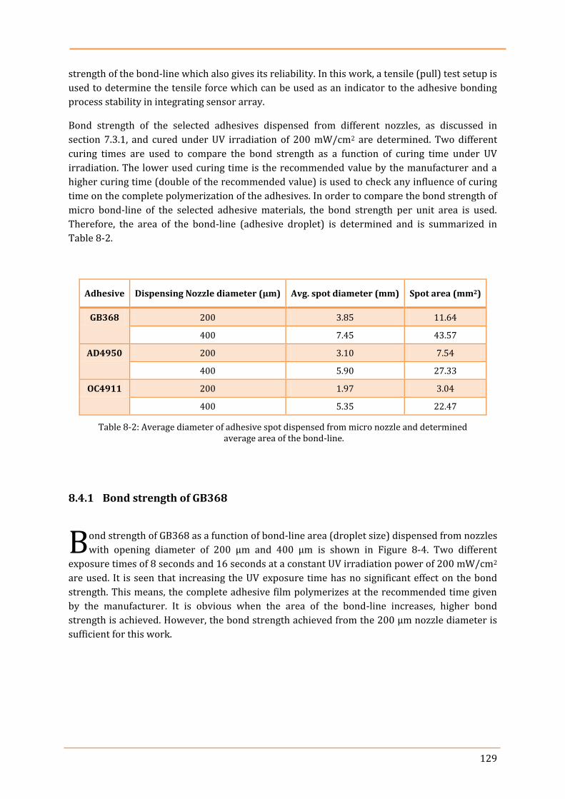
129
strength of the bond-line which also gives its reliability. In this work, a tensile (pull) test setup is
used to determine the tensile force which can be used as an indicator to the adhesive bonding
process stability in integrating sensor array.
Bond strength of the selected adhesives dispensed from different nozzles, as discussed in
section 7.3.1, and cured under UV irradiation of 200 mW/cm2 are determined. Two different
curing times are used to compare the bond strength as a function of curing time under UV
irradiation. The lower used curing time is the recommended value by the manufacturer and a
higher curing time (double of the recommended value) is used to check any influence of curing
time on the complete polymerization of the adhesives. In order to compare the bond strength of
micro bond-line of the selected adhesive materials, the bond strength per unit area is used.
Therefore, the area of the bond-line (adhesive droplet) is determined and is summarized in
Table 8-2.
Adhesive Dispensing Nozzle diameter (µm) Avg. spot diameter (mm) Spot area (mm2)
GB368 200 3.85 11.64
400 7.45 43.57
AD4950 200 3.10 7.54
400 5.90 27.33
OC4911 200 1.97 3.04
400 5.35 22.47
Table 8-2: Average diameter of adhesive spot dispensed from micro nozzle and determined average area of the bond-line.
8.4.1 Bond strength of GB368
ond strength of GB368 as a function of bond-line area (droplet size) dispensed from nozzles
with opening diameter of 200 µm and 400 µm is shown in Figure 8-4. Two different
exposure times of 8 seconds and 16 seconds at a constant UV irradiation power of 200 mW/cm2
are used. It is seen that increasing the UV exposure time has no significant effect on the bond
strength. This means, the complete adhesive film polymerizes at the recommended time given
by the manufacturer. It is obvious when the area of the bond-line increases, higher bond
strength is achieved. However, the bond strength achieved from the 200 µm nozzle diameter is
sufficient for this work.
B
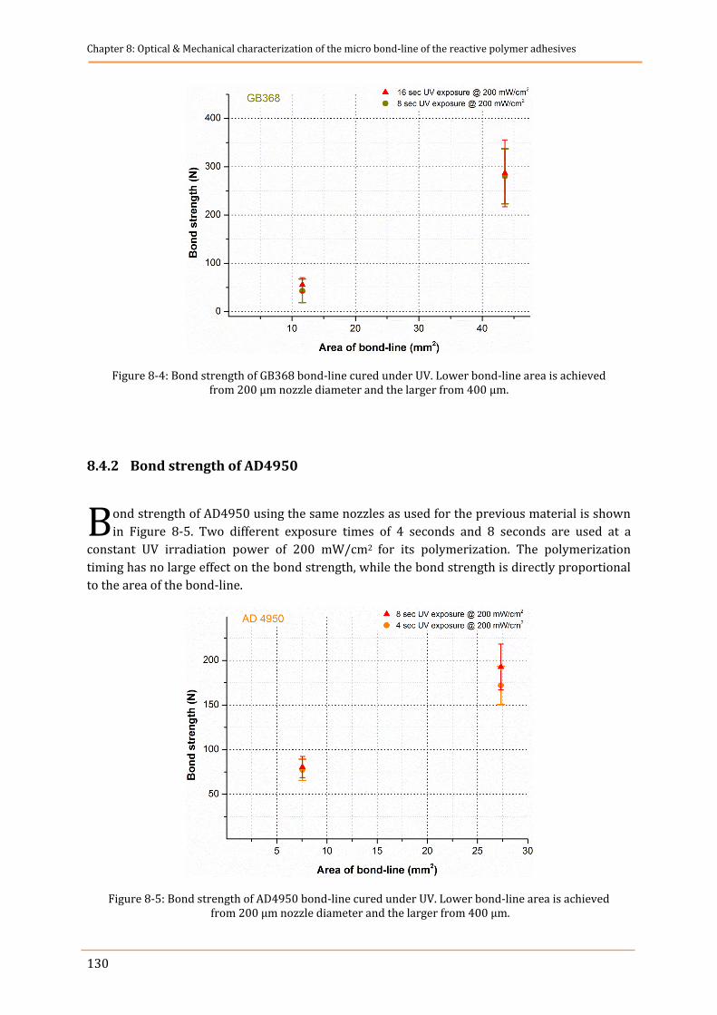
Chapter 8: Optical & Mechanical characterization of the micro bond-line of the reactive polymer adhesives
130
Figure 8-4: Bond strength of GB368 bond-line cured under UV. Lower bond-line area is achieved from 200 µm nozzle diameter and the larger from 400 µm.
8.4.2 Bond strength of AD4950
ond strength of AD4950 using the same nozzles as used for the previous material is shown
in Figure 8-5. Two different exposure times of 4 seconds and 8 seconds are used at a
constant UV irradiation power of 200 mW/cm2 for its polymerization. The polymerization
timing has no large effect on the bond strength, while the bond strength is directly proportional
to the area of the bond-line.
Figure 8-5: Bond strength of AD4950 bond-line cured under UV. Lower bond-line area is achieved from 200 µm nozzle diameter and the larger from 400 µm.
B

131
8.4.3 Bond strength of OC4911
ond strength of OC4911 at two different area of the bond-line achieved from using the same
nozzles as previous materials and two different polymerization timings of 20 seconds and
40 seconds is shown in Figure 8-6. The behavior of the bond strength is similar to the previous
materials however OC4911 delivers reduced bond strength.
Figure 8-6: Bond strength of OC4911 bond-line cured under UV. Lower bond-line area is achieved from 200 µm nozzle diameter and the larger from 400 µm.
8.4.4 Comparison of bond strength of selected materials
comparison of the bond strength per unit area of the three adhesives, i.e. GB368, AD4950
and OC4911 is shown in Figure 8-7.
B
A
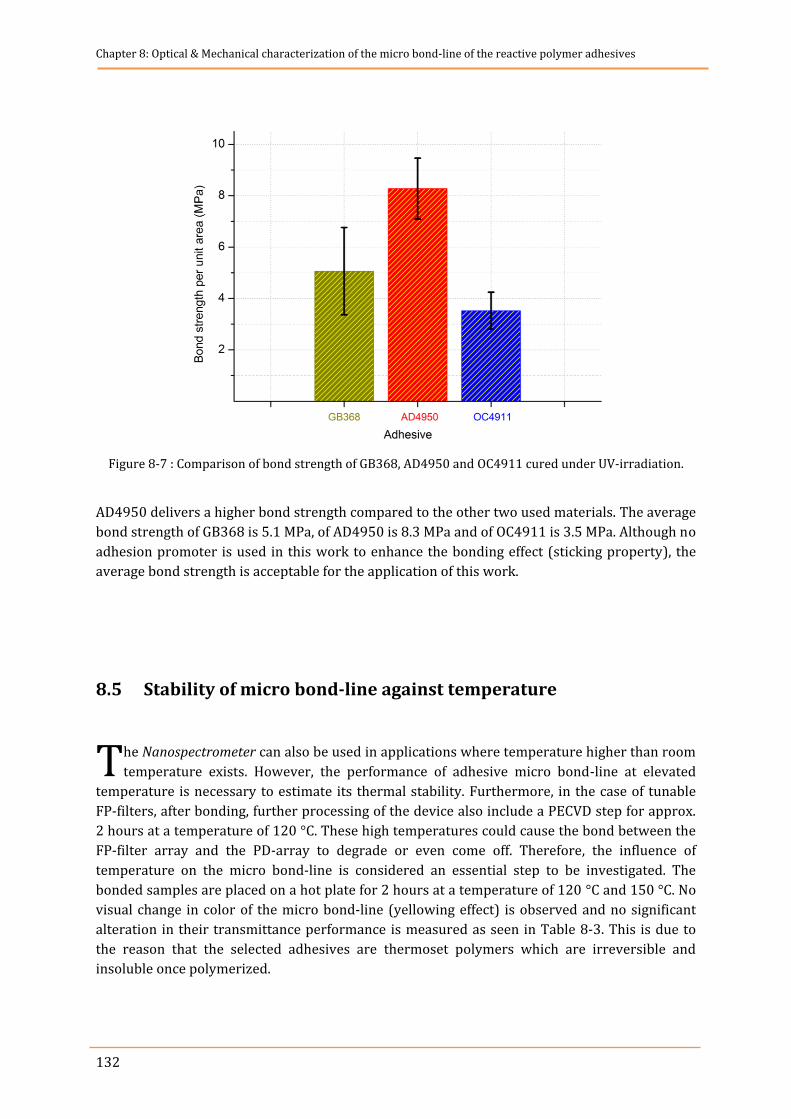
Chapter 8: Optical & Mechanical characterization of the micro bond-line of the reactive polymer adhesives
132
Figure 8-7 : Comparison of bond strength of GB368, AD4950 and OC4911 cured under UV-irradiation.
AD4950 delivers a higher bond strength compared to the other two used materials. The average
bond strength of GB368 is 5.1 MPa, of AD4950 is 8.3 MPa and of OC4911 is 3.5 MPa. Although no
adhesion promoter is used in this work to enhance the bonding effect (sticking property), the
average bond strength is acceptable for the application of this work.
8.5 Stability of micro bond-line against temperature
he Nanospectrometer can also be used in applications where temperature higher than room
temperature exists. However, the performance of adhesive micro bond-line at elevated
temperature is necessary to estimate its thermal stability. Furthermore, in the case of tunable
FP-filters, after bonding, further processing of the device also include a PECVD step for approx.
2 hours at a temperature of 120 °C. These high temperatures could cause the bond between the
FP-filter array and the PD-array to degrade or even come off. Therefore, the influence of
temperature on the micro bond-line is considered an essential step to be investigated. The
bonded samples are placed on a hot plate for 2 hours at a temperature of 120 °C and 150 °C. No
visual change in color of the micro bond-line (yellowing effect) is observed and no significant
alteration in their transmittance performance is measured as seen in Table 8-3. This is due to
the reason that the selected adhesives are thermoset polymers which are irreversible and
insoluble once polymerized.
T
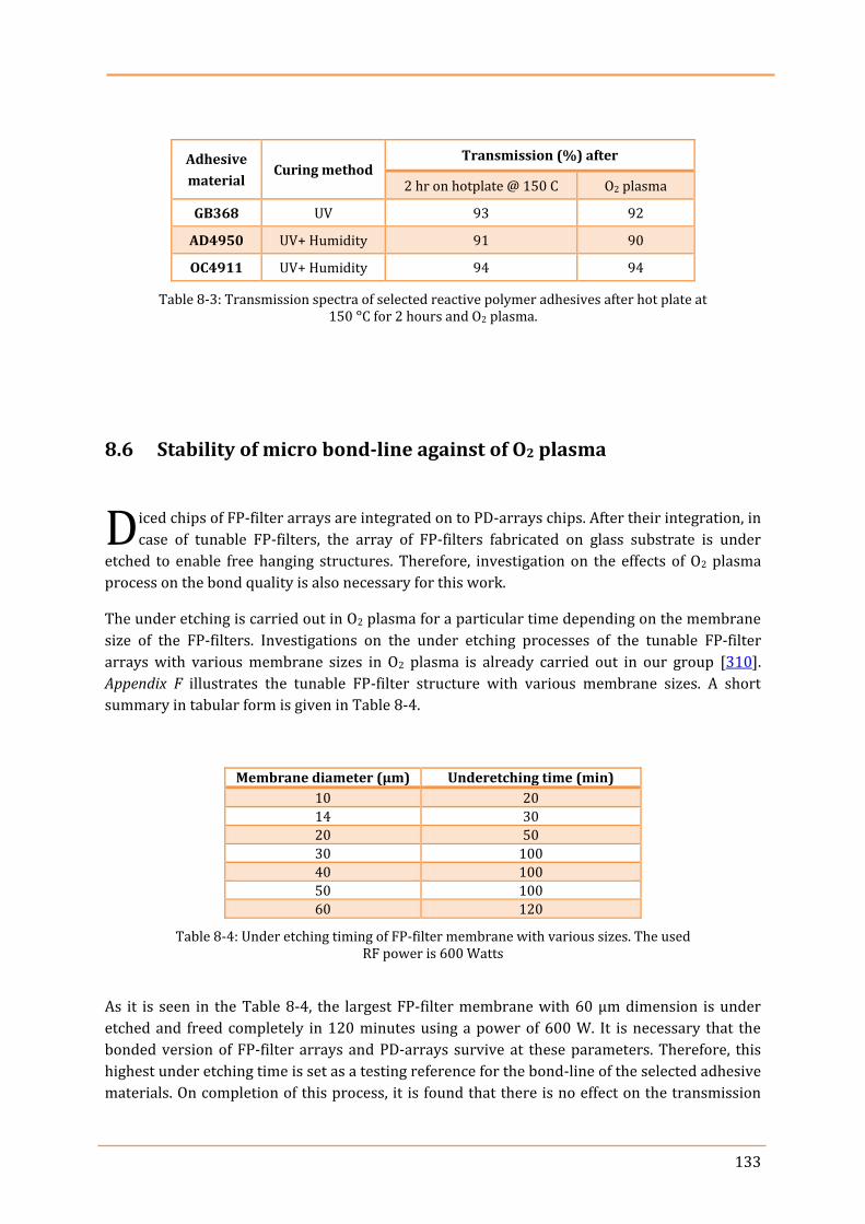
133
Adhesive
material Curing method
Transmission (%) after
2 hr on hotplate @ 150 C O2 plasma
GB368 UV 93 92
AD4950 UV+ Humidity 91 90
OC4911 UV+ Humidity 94 94
Table 8-3: Transmission spectra of selected reactive polymer adhesives after hot plate at 150 °C for 2 hours and O2 plasma.
8.6 Stability of micro bond-line against of O2 plasma
iced chips of FP-filter arrays are integrated on to PD-arrays chips. After their integration, in
case of tunable FP-filters, the array of FP-filters fabricated on glass substrate is under
etched to enable free hanging structures. Therefore, investigation on the effects of O2 plasma
process on the bond quality is also necessary for this work.
The under etching is carried out in O2 plasma for a particular time depending on the membrane
size of the FP-filters. Investigations on the under etching processes of the tunable FP-filter
arrays with various membrane sizes in O2 plasma is already carried out in our group [310].
Appendix F illustrates the tunable FP-filter structure with various membrane sizes. A short
summary in tabular form is given in Table 8-4.
Membrane diameter (µm) Underetching time (min)
10 20
14 30
20 50
30 100
40 100
50 100
60 120
Table 8-4: Under etching timing of FP-filter membrane with various sizes. The used RF power is 600 Watts
As it is seen in the Table 8-4, the largest FP-filter membrane with 60 µm dimension is under
etched and freed completely in 120 minutes using a power of 600 W. It is necessary that the
bonded version of FP-filter arrays and PD-arrays survive at these parameters. Therefore, this
highest under etching time is set as a testing reference for the bond-line of the selected adhesive
materials. On completion of this process, it is found that there is no effect on the transmission
D
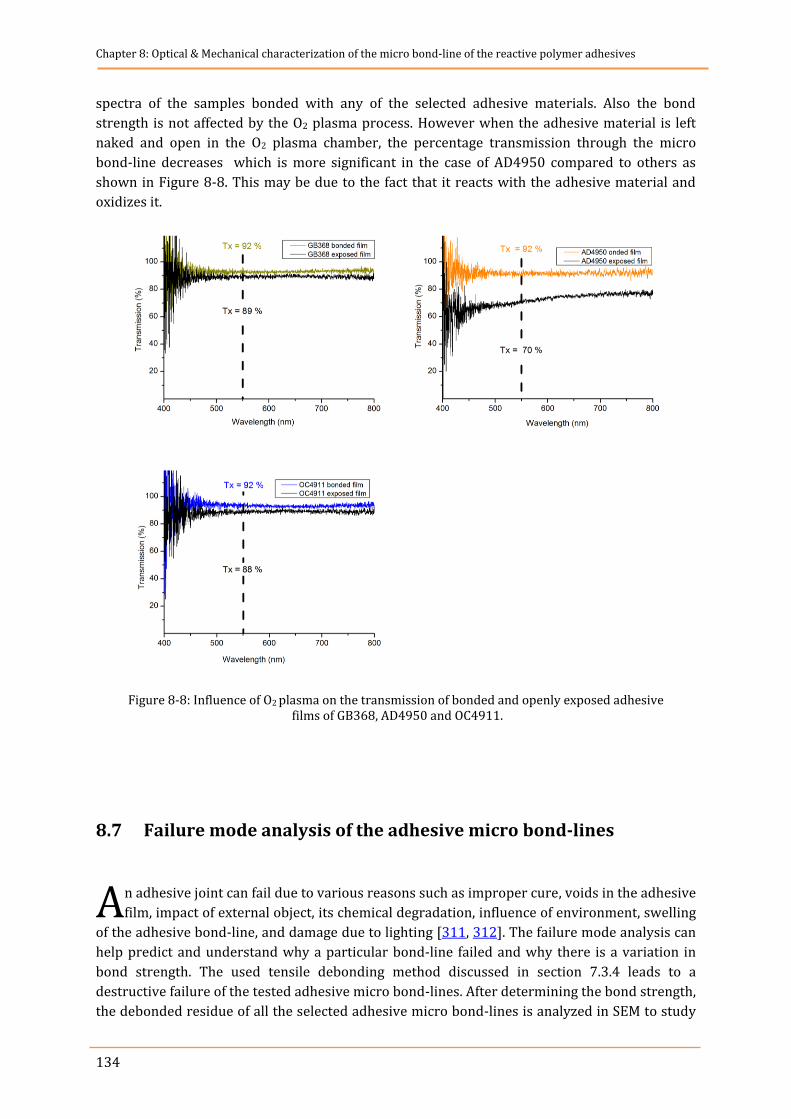
Chapter 8: Optical & Mechanical characterization of the micro bond-line of the reactive polymer adhesives
134
spectra of the samples bonded with any of the selected adhesive materials. Also the bond
strength is not affected by the O2 plasma process. However when the adhesive material is left
naked and open in the O2 plasma chamber, the percentage transmission through the micro
bond-line decreases which is more significant in the case of AD4950 compared to others as
shown in Figure 8-8. This may be due to the fact that it reacts with the adhesive material and
oxidizes it.
Figure 8-8: Influence of O2 plasma on the transmission of bonded and openly exposed adhesive films of GB368, AD4950 and OC4911.
8.7 Failure mode analysis of the adhesive micro bond-lines
n adhesive joint can fail due to various reasons such as improper cure, voids in the adhesive
film, impact of external object, its chemical degradation, influence of environment, swelling
of the adhesive bond-line, and damage due to lighting [311, 312]. The failure mode analysis can
help predict and understand why a particular bond-line failed and why there is a variation in
bond strength. The used tensile debonding method discussed in section 7.3.4 leads to a
destructive failure of the tested adhesive micro bond-lines. After determining the bond strength,
the debonded residue of all the selected adhesive micro bond-lines is analyzed in SEM to study
A
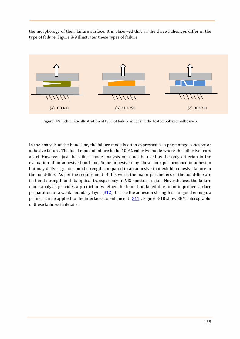
135
the morphology of their failure surface. It is observed that all the three adhesives differ in the
type of failure. Figure 8-9 illustrates these types of failure.
Figure 8-9: Schematic illustration of type of failure modes in the tested polymer adhesives.
In the analysis of the bond-line, the failure mode is often expressed as a percentage cohesive or
adhesive failure. The ideal mode of failure is the 100% cohesive mode where the adhesive tears
apart. However, just the failure mode analysis must not be used as the only criterion in the
evaluation of an adhesive bond-line. Some adhesive may show poor performance in adhesion
but may deliver greater bond strength compared to an adhesive that exhibit cohesive failure in
the bond-line. As per the requirement of this work, the major parameters of the bond-line are
its bond strength and its optical transparency in VIS spectral region. Nevertheless, the failure
mode analysis provides a prediction whether the bond-line failed due to an improper surface
preparation or a weak boundary layer [312]. In case the adhesion strength is not good enough, a
primer can be applied to the interfaces to enhance it [311]. Figure 8-10 show SEM micrographs
of these failures in details.
(a) GB368 (b) AD4950 (c) OC4911
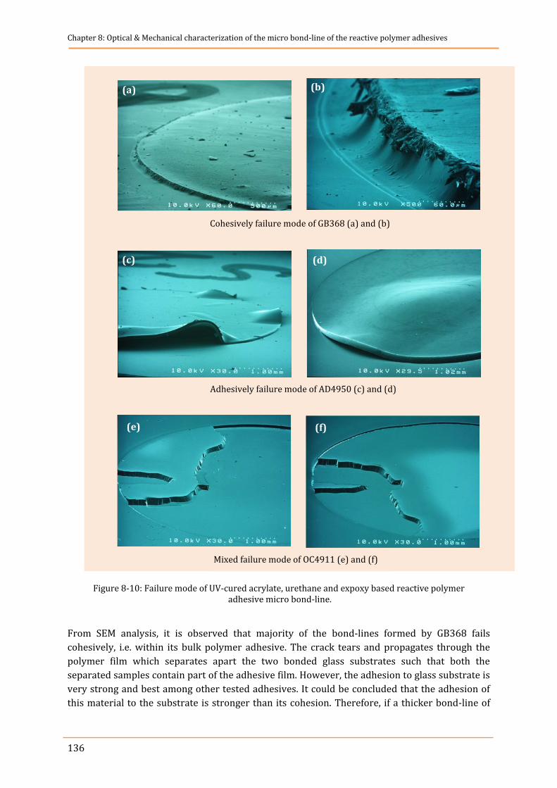
Chapter 8: Optical & Mechanical characterization of the micro bond-line of the reactive polymer adhesives
136
Figure 8-10: Failure mode of UV-cured acrylate, urethane and expoxy based reactive polymer adhesive micro bond-line.
From SEM analysis, it is observed that majority of the bond-lines formed by GB368 fails
cohesively, i.e. within its bulk polymer adhesive. The crack tears and propagates through the
polymer film which separates apart the two bonded glass substrates such that both the
separated samples contain part of the adhesive film. However, the adhesion to glass substrate is
very strong and best among other tested adhesives. It could be concluded that the adhesion of
this material to the substrate is stronger than its cohesion. Therefore, if a thicker bond-line of
Cohesively failure mode of GB368 (a) and (b)
(a)
(a) (b)
Adhesively failure mode of AD4950 (c) and (d)
(b)
(c) (d)
Mixed failure mode of OC4911 (e) and (f)
(c)
(e) (f)
137
this material is applied, it might tend to fail quickly, resulting in a weaker joint. As seen from the
SEM micrographs in Figure 8-10 (c) and (d), the AD4950 micro bond-line comes off from the
interface of adhesive film and the substrate. This type of failure is also known as interfacial
fracture, i.e. debonding takes place between the adhesive and the adherend. This shows that this
particular adhesive is cohesively very strong and stays intact on one piece of debonded sample.
This could also mean that its adhesion could be significantly increased when the substrate
material is very well cleaned in order to improve the affinity between them resulting in higher
bond strength. OC4911 shows a complete different failure mode. It has a mixed failure mode of
the two other discussed adhesives, i.e. it fails cohesively from its bulk film as well as adhesively
from the glass substrate. The crack changes its course and runs from one interface to another
through the bulk polymer as seen in Figure 8-10 (e) and (f).
All the three adhesive types follow and repeat similar failure pattern irrespective of ambient
environment effect, sunlight and their failure time, i.e. after 24 hour or after 1 month. Samples
from silicon substrate ware also bonded with these adhesives but many a times the silicon
samples would fracture and break. An exact cause of bond-line failure of the above adhesives
cannot be predicted. Factors such as internal stresses in the adhesive develop and cause it to
shrink during its curing and due to differences between the physical properties of the two
materials, i.e. adhesive and the substrate. Therefore, the thermal coefficient of expansion of both
the materials must be as close as possible to minimize these stresses that may develop during
any later stage, e.g. due to temperature increase. To compensate for stresses, an alternative
method is to use elastomeric polymer adhesives, such as OC4911. Also another reason is if a
particular adhesive is unable to wet the surface of the substrates, the bond-line is more likely to
fail without delivering optimal bond strength [312]. Wettability of an adhesive is discussed in
next section.
8.8 Wettability determination via contact angle measurement
ettability of an adhesive on a substrate is one of the important factors in adhesive
bonding. Wettability defines the spreading of a liquid on a solid surface based on the
surface tension of the liquid and the surface energy of the solid. The wetting behavior is
determined through the measurement of the contact angle of the adhesive droplet on the
substrate surface. The contact angle is the angle formed by the droplet at the intersection of the
three interfaces of liquid, solid and vapor. An adhesive (liquid) is said to spread well on a
substrate surface if it produces a low contact angle while high contact angle values indicate poor
spreading. This technique is useful in processes such as coating, printing and painting where
good wettability is required to ensure excellent adhesion. When the contact angle is under 90o,
it means that the surface is wetted by the used adhesive. When the contact angle is greater than
90o, it means that the surface is non-wetting with that particular liquid. This phenomenon is
illustrated in Figure 8-11.
W
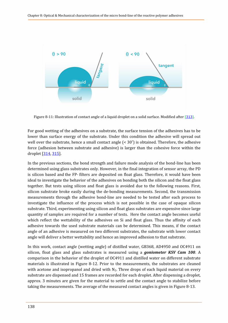
Chapter 8: Optical & Mechanical characterization of the micro bond-line of the reactive polymer adhesives
138
Figure 8-11: Illustration of contact angle of a liquid droplet on a solid surface. Modified after [313].
For good wetting of the adhesives on a substrate, the surface tension of the adhesives has to be
lower than surface energy of the substrate. Under this condition the adhesive will spread out
well over the substrate, hence a small contact angle (< 30˚) is obtained. Therefore, the adhesive
force (adhesion between substrate and adhesive) is larger than the cohesive force within the
droplet [314, 315].
In the previous sections, the bond strength and failure mode analysis of the bond-line has been
determined using glass substrates only. However, in the final integration of sensor array, the PD
is silicon based and the FP- filters are deposited on float glass. Therefore, it would have been
ideal to investigate the behavior of the adhesives on bonding both the silicon and the float glass
together. But tests using silicon and float glass is avoided due to the following reasons. First,
silicon substrate broke easily during the de-bonding measurements. Second, the transmission
measurements through the adhesive bond-line are needed to be tested after each process to
investigate the influence of the process which is not possible in the case of opaque silicon
substrate. Third, experimenting using silicon and float glass substrates are expensive since large
quantity of samples are required for a number of tests. Here the contact angle becomes useful
which reflect the wettability of the adhesives on Si and float glass. Thus the affinity of each
adhesive towards the used substrate materials can be determined. This means, if the contact
angle of an adhesive is measured on two different substrates, the substrate with lower contact
angle will deliver a better wettability and hence an improved adhesion to that substrate.
In this work, contact angle (wetting angle) of distilled water, GB368, AD4950 and OC4911 on
silicon, float glass and glass substrates is measured using a goniometer KSV Cam 100. A
comparison in the behavior of the droplet of OC4911 and distilled water on different substrate
materials is illustrated in Figure 8-12. Prior to the measurements, the substrates are cleaned
with acetone and isopropanol and dried with N2. Three drops of each liquid material on every
substrate are dispensed and 15 frames are recorded for each droplet. After dispensing a droplet,
approx. 3 minutes are given for the material to settle and the contact angle to stabilize before
taking the measurements. The average of the measured contact angles is given in Figure 8-13.
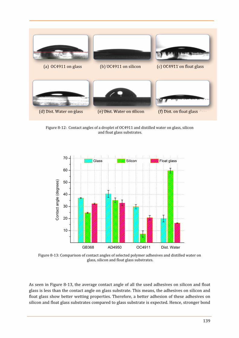
139
Figure 8-12: Contact angles of a droplet of OC4911 and distilled water on glass, silicon and float glass substrates.
Figure 8-13: Comparison of contact angles of selected polymer adhesives and distilled water on glass, silicon and float glass substrates.
As seen in Figure 8-13, the average contact angle of all the used adhesives on silicon and float
glass is less than the contact angle on glass substrate. This means, the adhesives on silicon and
float glass show better wetting properties. Therefore, a better adhesion of these adhesives on
silicon and float glass substrates compared to glass substrate is expected. Hence, stronger bond
(a) OC4911 on glass (b) OC4911 on silicon (c) OC4911 on float glass
(d) Dist. Water on glass (e) Dist. Water on silicon (f) Dist. on float glass
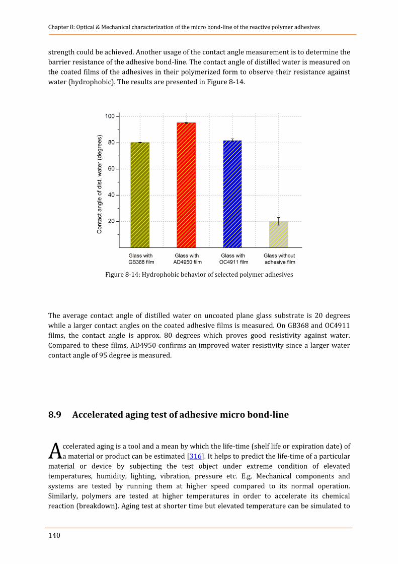
Chapter 8: Optical & Mechanical characterization of the micro bond-line of the reactive polymer adhesives
140
strength could be achieved. Another usage of the contact angle measurement is to determine the
barrier resistance of the adhesive bond-line. The contact angle of distilled water is measured on
the coated films of the adhesives in their polymerized form to observe their resistance against
water (hydrophobic). The results are presented in Figure 8-14.
Figure 8-14: Hydrophobic behavior of selected polymer adhesives
The average contact angle of distilled water on uncoated plane glass substrate is 20 degrees
while a larger contact angles on the coated adhesive films is measured. On GB368 and OC4911
films, the contact angle is approx. 80 degrees which proves good resistivity against water.
Compared to these films, AD4950 confirms an improved water resistivity since a larger water
contact angle of 95 degree is measured.
8.9 Accelerated aging test of adhesive micro bond-line
ccelerated aging is a tool and a mean by which the life-time (shelf life or expiration date) of
a material or product can be estimated [316]. It helps to predict the life-time of a particular
material or device by subjecting the test object under extreme condition of elevated
temperatures, humidity, lighting, vibration, pressure etc. E.g. Mechanical components and
systems are tested by running them at higher speed compared to its normal operation.
Similarly, polymers are tested at higher temperatures in order to accelerate its chemical
reaction (breakdown). Aging test at shorter time but elevated temperature can be simulated to
A
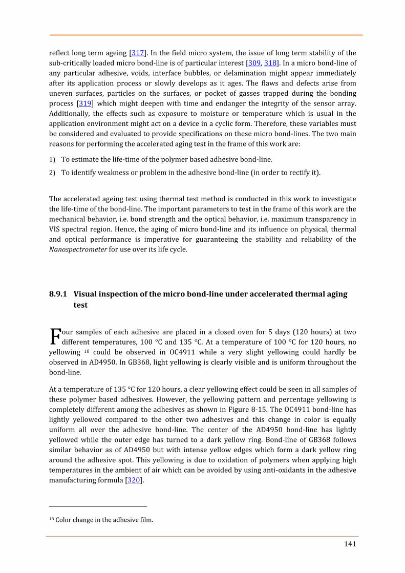
141
reflect long term ageing [317]. In the field micro system, the issue of long term stability of the
sub-critically loaded micro bond-line is of particular interest [309, 318]. In a micro bond-line of
any particular adhesive, voids, interface bubbles, or delamination might appear immediately
after its application process or slowly develops as it ages. The flaws and defects arise from
uneven surfaces, particles on the surfaces, or pocket of gasses trapped during the bonding
process [319] which might deepen with time and endanger the integrity of the sensor array.
Additionally, the effects such as exposure to moisture or temperature which is usual in the
application environment might act on a device in a cyclic form. Therefore, these variables must
be considered and evaluated to provide specifications on these micro bond-lines. The two main
reasons for performing the accelerated aging test in the frame of this work are:
1) To estimate the life-time of the polymer based adhesive bond-line.
2) To identify weakness or problem in the adhesive bond-line (in order to rectify it).
The accelerated ageing test using thermal test method is conducted in this work to investigate
the life-time of the bond-line. The important parameters to test in the frame of this work are the
mechanical behavior, i.e. bond strength and the optical behavior, i.e. maximum transparency in
VIS spectral region. Hence, the aging of micro bond-line and its influence on physical, thermal
and optical performance is imperative for guaranteeing the stability and reliability of the
Nanospectrometer for use over its life cycle.
8.9.1 Visual inspection of the micro bond-line under accelerated thermal aging
test
our samples of each adhesive are placed in a closed oven for 5 days (120 hours) at two
different temperatures, 100 °C and 135 °C. At a temperature of 100 °C for 120 hours, no
yellowing 18 could be observed in OC4911 while a very slight yellowing could hardly be
observed in AD4950. In GB368, light yellowing is clearly visible and is uniform throughout the
bond-line.
At a temperature of 135 °C for 120 hours, a clear yellowing effect could be seen in all samples of
these polymer based adhesives. However, the yellowing pattern and percentage yellowing is
completely different among the adhesives as shown in Figure 8-15. The OC4911 bond-line has
lightly yellowed compared to the other two adhesives and this change in color is equally
uniform all over the adhesive bond-line. The center of the AD4950 bond-line has lightly
yellowed while the outer edge has turned to a dark yellow ring. Bond-line of GB368 follows
similar behavior as of AD4950 but with intense yellow edges which form a dark yellow ring
around the adhesive spot. This yellowing is due to oxidation of polymers when applying high
temperatures in the ambient of air which can be avoided by using anti-oxidants in the adhesive
manufacturing formula [320].
18 Color change in the adhesive film.
F
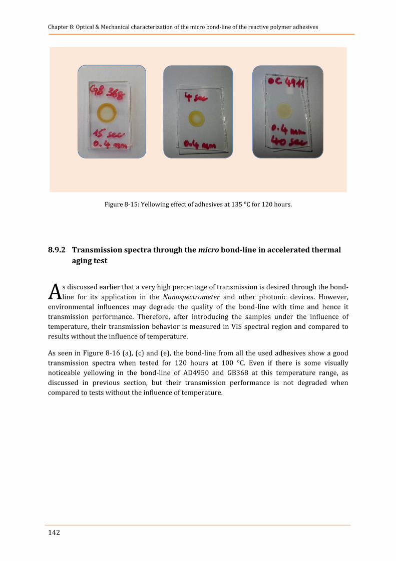
Chapter 8: Optical & Mechanical characterization of the micro bond-line of the reactive polymer adhesives
142
Figure 8-15: Yellowing effect of adhesives at 135 °C for 120 hours.
8.9.2 Transmission spectra through the micro bond-line in accelerated thermal
aging test
s discussed earlier that a very high percentage of transmission is desired through the bond-
line for its application in the Nanospectrometer and other photonic devices. However,
environmental influences may degrade the quality of the bond-line with time and hence it
transmission performance. Therefore, after introducing the samples under the influence of
temperature, their transmission behavior is measured in VIS spectral region and compared to
results without the influence of temperature.
As seen in Figure 8-16 (a), (c) and (e), the bond-line from all the used adhesives show a good
transmission spectra when tested for 120 hours at 100 °C. Even if there is some visually
noticeable yellowing in the bond-line of AD4950 and GB368 at this temperature range, as
discussed in previous section, but their transmission performance is not degraded when
compared to tests without the influence of temperature.
A
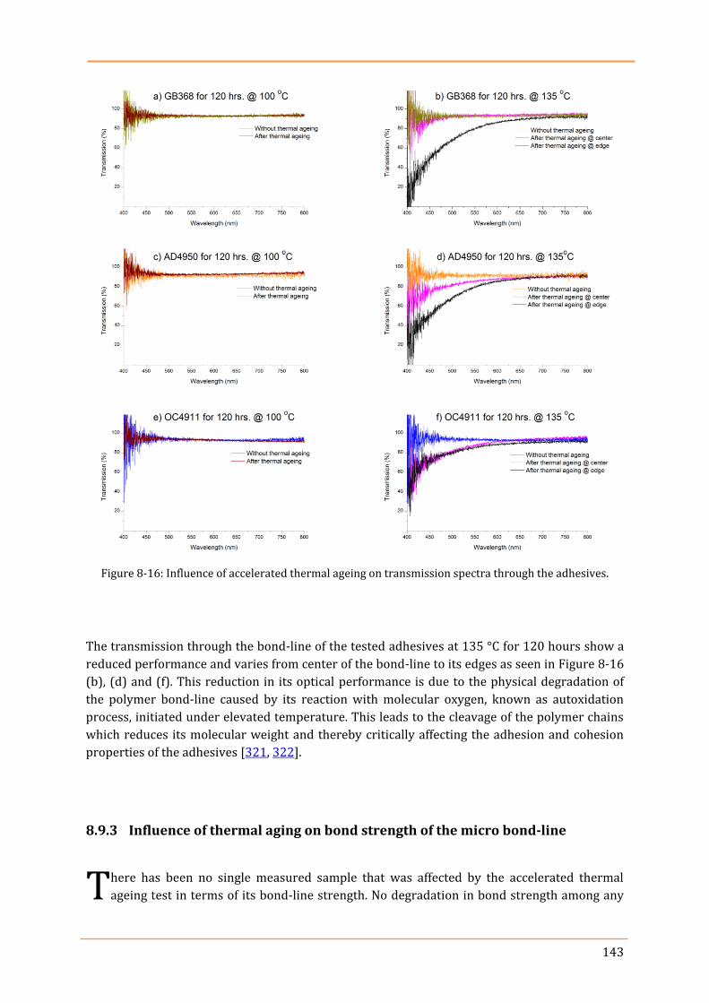
143
Figure 8-16: Influence of accelerated thermal ageing on transmission spectra through the adhesives.
The transmission through the bond-line of the tested adhesives at 135 °C for 120 hours show a
reduced performance and varies from center of the bond-line to its edges as seen in Figure 8-16
(b), (d) and (f). This reduction in its optical performance is due to the physical degradation of
the polymer bond-line caused by its reaction with molecular oxygen, known as autoxidation
process, initiated under elevated temperature. This leads to the cleavage of the polymer chains
which reduces its molecular weight and thereby critically affecting the adhesion and cohesion
properties of the adhesives [321, 322].
8.9.3 Influence of thermal aging on bond strength of the micro bond-line
here has been no single measured sample that was affected by the accelerated thermal
ageing test in terms of its bond-line strength. No degradation in bond strength among any T
Chapter 8: Optical & Mechanical characterization of the micro bond-line of the reactive polymer adhesives
144
of the three tested adhesives is observed. In fact, majority of the samples showed slightly higher
bond strengths compared to section 8.4. This indicates that the accelerated thermal ageing has
no adverse effect on the bond strength of the adhesives.
8.9.4 Life-time of the micro bond-line
nder different elevated temperature, the quality of the bond-line is measured to allow the
determination of the number of days it takes to reach a certain level of degradation [323].
The accelerated aging test is associated and described by the Arrhenius equation 19 which
relates the dependence of chemical reaction rate on temperature [324, 325].
(8-1)
Where, A is a rate constant, is the energy of activation and is a constant,
is the Boltzmann’s constant and is the absolute temperature in Kelvin.
The dependence of reaction rate on temperature according to Van t’ Hoff’s observations states
that an increment of every 10 °C in reaction temperature roughly doubles the rate of chemical
reaction (of the molecules) [326]. In other words, the failure rate doubles for every 10 °C
increase in temperature. Therefore, according to Arrhenius equation, if the rate of change in
temperature of the micro bond-line affects its rate of reaction, a change in the bond-line
material can be estimated. This is provided by the ratio between the rates of reaction (R1 and
R2) when the temperature is elevated (T1 and T2) by any arbitrary value. Since a 10 °C change is
the commonly used value, therefore, the ratio between the rates of reactions is known as Q10 or
aging factor which is give as [311, 327, 328].
(8-2)
According to the relation, a material will age faster at elevated temperature via a chemical
reaction compared to its service temperature [311]. Based on equation (8-1) and (8-2), the
accelerated aging rate (AAR) is derived as [317, 329]
(8-3)
19 Based on the work of Dutch chemist Jacobus van ‘t Hoff, this equation was proposed by Svante Arrhenius in 1889.
U

145
Where,
AAR = Accelerated Aging Rate
= Accelerated aging factor AAT = Accelerated Aging Temperature AT = Ambient Temperature
The factor commonly ranges from 1.8 to 2.5 with a value of being chosen for
a medical grade polymer [329-331]. The Accelerated Aging Time Duration (AATD) is
calculated as [317, 329, 332].
(8-4)
Where,
According to equation (8-3) and equation (8-4), the accelerated aging rate and life-time of the
micro bond-line introduced for 120 hours (5 days) at 100 °C can is calculated as
As it is observed in Figure 8-16, 120 hours (5 days) at 100 °C has no effect on either the optical
transmission or the bond strength. This means in 3 years time there is no adverse effect on the
integrity sensor array.
Similarly, If 120 hours (5 days) at 135 °C are considered,
Chapter 8: Optical & Mechanical characterization of the micro bond-line of the reactive polymer adhesives
146
It is concluded from the previous tests that in 35 years there is no effect on the bond strength,
however, the optical property of the bond-line degrades and shows different behavior among
the tested adhesives as given in Figure 8-16.
From the above tests, it is assumed that the integration of the sensor array using a bond-line
from the selected adhesives will provide promising optical and mechanical properties for well
>3 years.
8.10 Polymerization under shadowed region of FP-filters using dual
curing capabilities of the selected adhesives
V irradiation of certain amount is used as an external agent to polymerize the adhesives as
discussed in previous sections. However, in some cases, the UV irradiation is hindered or
blocked because of the presence of an opaque material like metal, plastic, etc. or other highly
reflective surfaces on top of the adhesive. This region where UV irradiation cannot reach the
adhesive is known as “shadowed region” and the adhesive will be poorly cured. This is due to
the fact that the curing mechanism of acrylate-based adhesive result from free radicals
produced by the photoinitiator when exposed to UV-radiation where these free radical are
consumed in the curing process. This means that acrylate-based adhesives will only cure in
areas where UV-radiation is focused [279]. Therefore, the dual-curing mechanism of adhesives
becomes a very effective means in this regard. In the adhesives, which support humidity curing
mechanism, there are free isocyanate groups (R–N=C=O). The free isocyanate groups react with
the hydroxide groups (OH) contained in water or humidity resulting in cross-linking of the
polymer adhesives [278].
In the case of tunable FP-filter array based Nanospectrometer at INA , an aluminum layer is used
to cover the entire top area of the filter and only the filter membrane is left uncovered. This
aluminum layer is used as a light protection layer which avoid stray-light entering into the FP-
filter from unwanted angles. Therefore, it is more likely that this aluminum layer will resist the
UV irradiation to cure the adhesive film below it. Additionally, the highly reflective DBRs in the
FP-filter itself may reflect some part of the UV-irradiance while curing the adhesives under them
(see setion 7.4.2).
The selected adhesives, OB749, AD4950 and OC4911, have dual polymerization capabilities.
OB749 is polymerized under UV and thermal curing mechanisms while AD4950 and OC4911 are
polymerized under UV and humidity curing mechanisms. Thermally polymerized adhesive
material OB749 is already omitted for this job due to a lower transmission through them as
explained in section 8.3. Humidity cured adhesives, AD4950 and OC4911, are further tested for
their transmission and bond strength in this section. The micro dots of these adhesives are
jetted from the micro dispensing valve and are sandwiched between two plane glass substrates.
These samples are not exposed to UV irradiation but kept in ambient room humidity. The
U
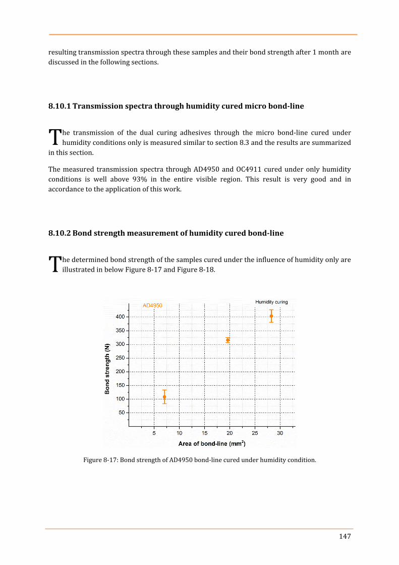
147
resulting transmission spectra through these samples and their bond strength after 1 month are
discussed in the following sections.
8.10.1 Transmission spectra through humidity cured micro bond-line
he transmission of the dual curing adhesives through the micro bond-line cured under
humidity conditions only is measured similar to section 8.3 and the results are summarized
in this section.
The measured transmission spectra through AD4950 and OC4911 cured under only humidity
conditions is well above 93% in the entire visible region. This result is very good and in
accordance to the application of this work.
8.10.2 Bond strength measurement of humidity cured bond-line
he determined bond strength of the samples cured under the influence of humidity only are
illustrated in below Figure 8-17 and Figure 8-18.
Figure 8-17: Bond strength of AD4950 bond-line cured under humidity condition.
T
T
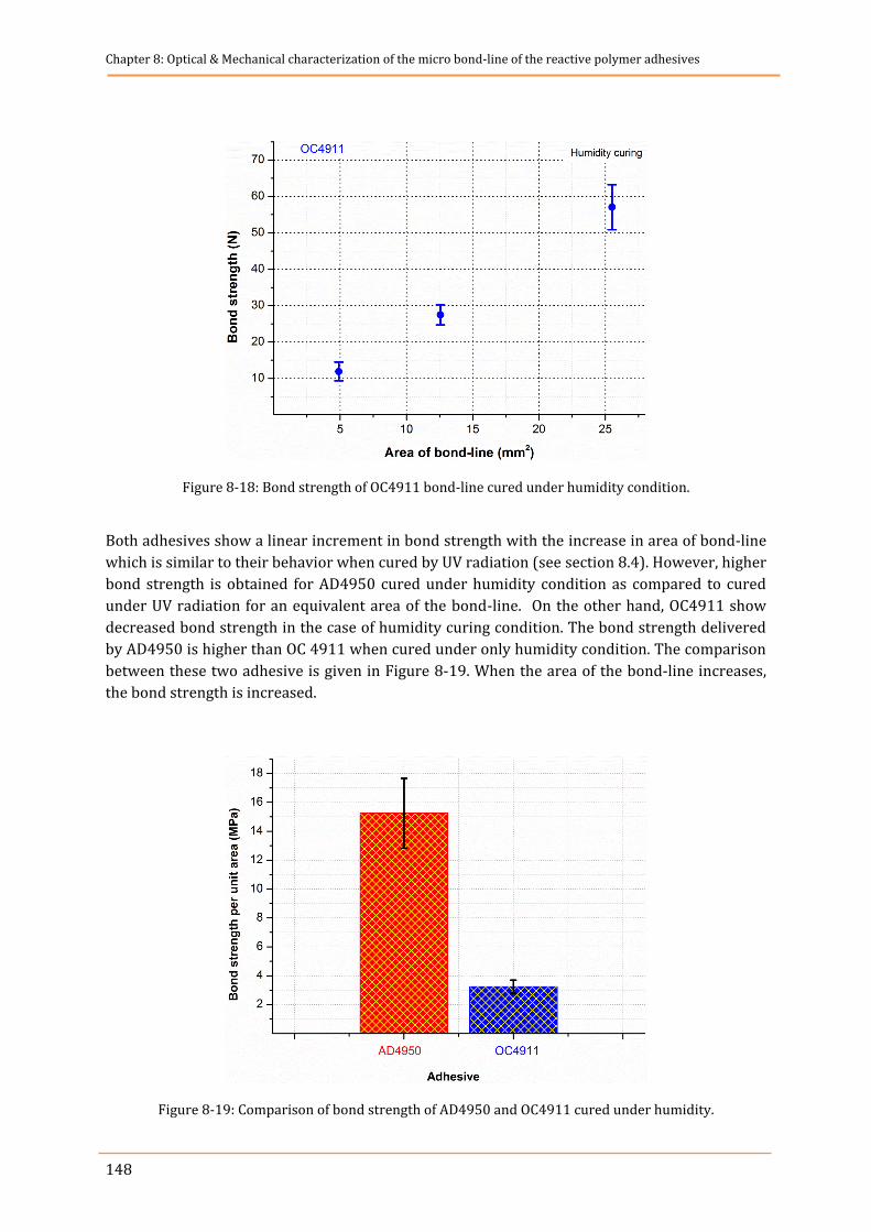
Chapter 8: Optical & Mechanical characterization of the micro bond-line of the reactive polymer adhesives
148
Figure 8-18: Bond strength of OC4911 bond-line cured under humidity condition.
Both adhesives show a linear increment in bond strength with the increase in area of bond-line
which is similar to their behavior when cured by UV radiation (see section 8.4). However, higher
bond strength is obtained for AD4950 cured under humidity condition as compared to cured
under UV radiation for an equivalent area of the bond-line. On the other hand, OC4911 show
decreased bond strength in the case of humidity curing condition. The bond strength delivered
by AD4950 is higher than OC 4911 when cured under only humidity condition. The comparison
between these two adhesive is given in Figure 8-19. When the area of the bond-line increases,
the bond strength is increased.
Figure 8-19: Comparison of bond strength of AD4950 and OC4911 cured under humidity.
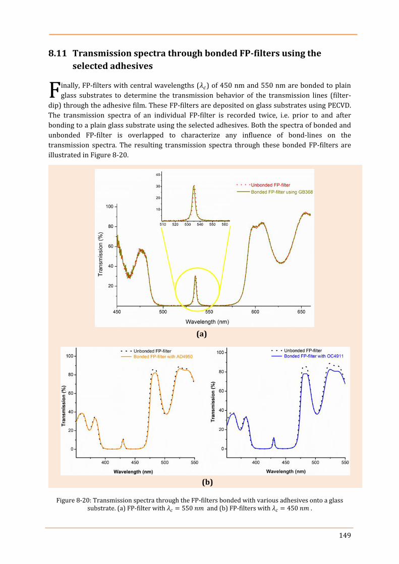
149
8.11 Transmission spectra through bonded FP-filters using the
selected adhesives
inally, FP-filters with central wavelengths ( ) of 450 nm and 550 nm are bonded to plain
glass substrates to determine the transmission behavior of the transmission lines (filter-
dip) through the adhesive film. These FP-filters are deposited on glass substrates using PECVD.
The transmission spectra of an individual FP-filter is recorded twice, i.e. prior to and after
bonding to a plain glass substrate using the selected adhesives. Both the spectra of bonded and
unbonded FP-filter is overlapped to characterize any influence of bond-lines on the
transmission spectra. The resulting transmission spectra through these bonded FP-filters are
illustrated in Figure 8-20.
Figure 8-20: Transmission spectra through the FP-filters bonded with various adhesives onto a glass substrate. (a) FP-filter with and (b) FP-filters with .
F
(a)
(b)
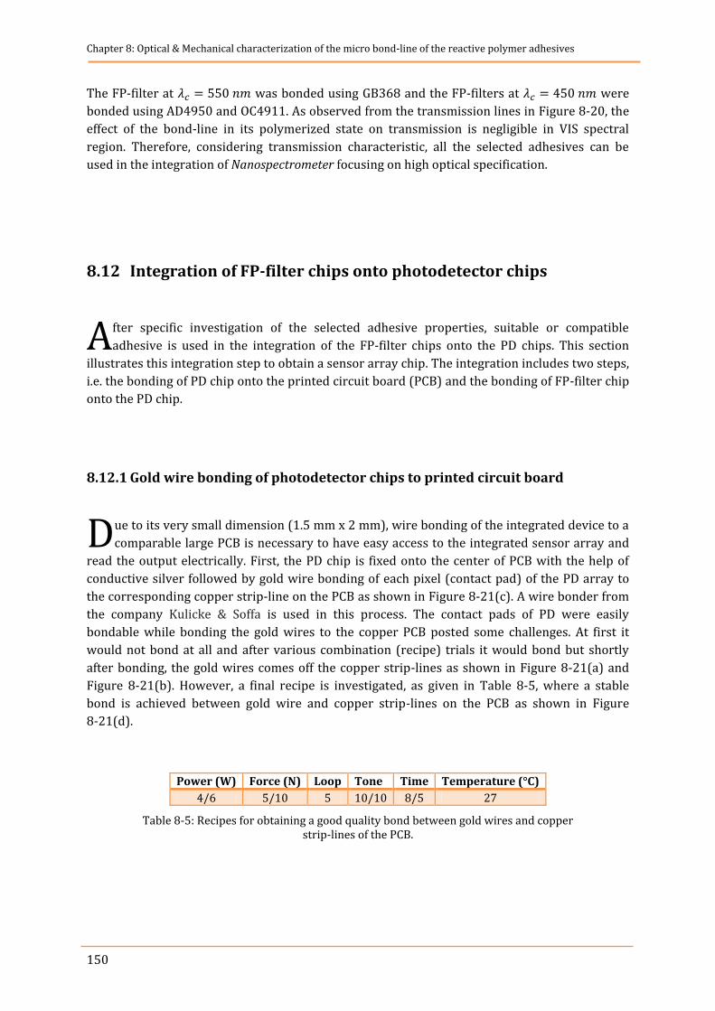
Chapter 8: Optical & Mechanical characterization of the micro bond-line of the reactive polymer adhesives
150
The FP-filter at was bonded using GB368 and the FP-filters at were
bonded using AD4950 and OC4911. As observed from the transmission lines in Figure 8-20, the
effect of the bond-line in its polymerized state on transmission is negligible in VIS spectral
region. Therefore, considering transmission characteristic, all the selected adhesives can be
used in the integration of Nanospectrometer focusing on high optical specification.
8.12 Integration of FP-filter chips onto photodetector chips
fter specific investigation of the selected adhesive properties, suitable or compatible
adhesive is used in the integration of the FP-filter chips onto the PD chips. This section
illustrates this integration step to obtain a sensor array chip. The integration includes two steps,
i.e. the bonding of PD chip onto the printed circuit board (PCB) and the bonding of FP-filter chip
onto the PD chip.
8.12.1 Gold wire bonding of photodetector chips to printed circuit board
ue to its very small dimension (1.5 mm x 2 mm), wire bonding of the integrated device to a
comparable large PCB is necessary to have easy access to the integrated sensor array and
read the output electrically. First, the PD chip is fixed onto the center of PCB with the help of
conductive silver followed by gold wire bonding of each pixel (contact pad) of the PD array to
the corresponding copper strip-line on the PCB as shown in Figure 8-21(c). A wire bonder from
the company Kulicke & Soffa is used in this process. The contact pads of PD were easily
bondable while bonding the gold wires to the copper PCB posted some challenges. At first it
would not bond at all and after various combination (recipe) trials it would bond but shortly
after bonding, the gold wires comes off the copper strip-lines as shown in Figure 8-21(a) and
Figure 8-21(b). However, a final recipe is investigated, as given in Table 8-5, where a stable
bond is achieved between gold wire and copper strip-lines on the PCB as shown in Figure
8-21(d).
Power (W) Force (N) Loop Tone Time Temperature (°C)
4/6 5/10 5 10/10 8/5 27
Table 8-5: Recipes for obtaining a good quality bond between gold wires and copper strip-lines of the PCB.
A
D
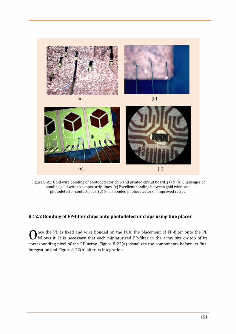
151
Figure 8-21: Gold wire bonding of photodetector chip and printed circuit board. (a) & (b) Challenges of bonding gold wire to copper strip-lines. (c) Excellent bonding between gold wires and
photodetector contact pads. (d) Final bonded photodetector on improved recipe.
8.12.2 Bonding of FP-filter chips onto photodetector chips using fine placer
nce the PD is fixed and wire bonded on the PCB, the placement of FP-filter onto the PD
follows it. It is necessary that each miniaturized FP-filter in the array sits on top of its
corresponding pixel of the PD array. Figure 8-22(a) visualizes the components before its final
integration and Figure 8-22(b) after its integration.
O
(a) (b)
(c) (d)
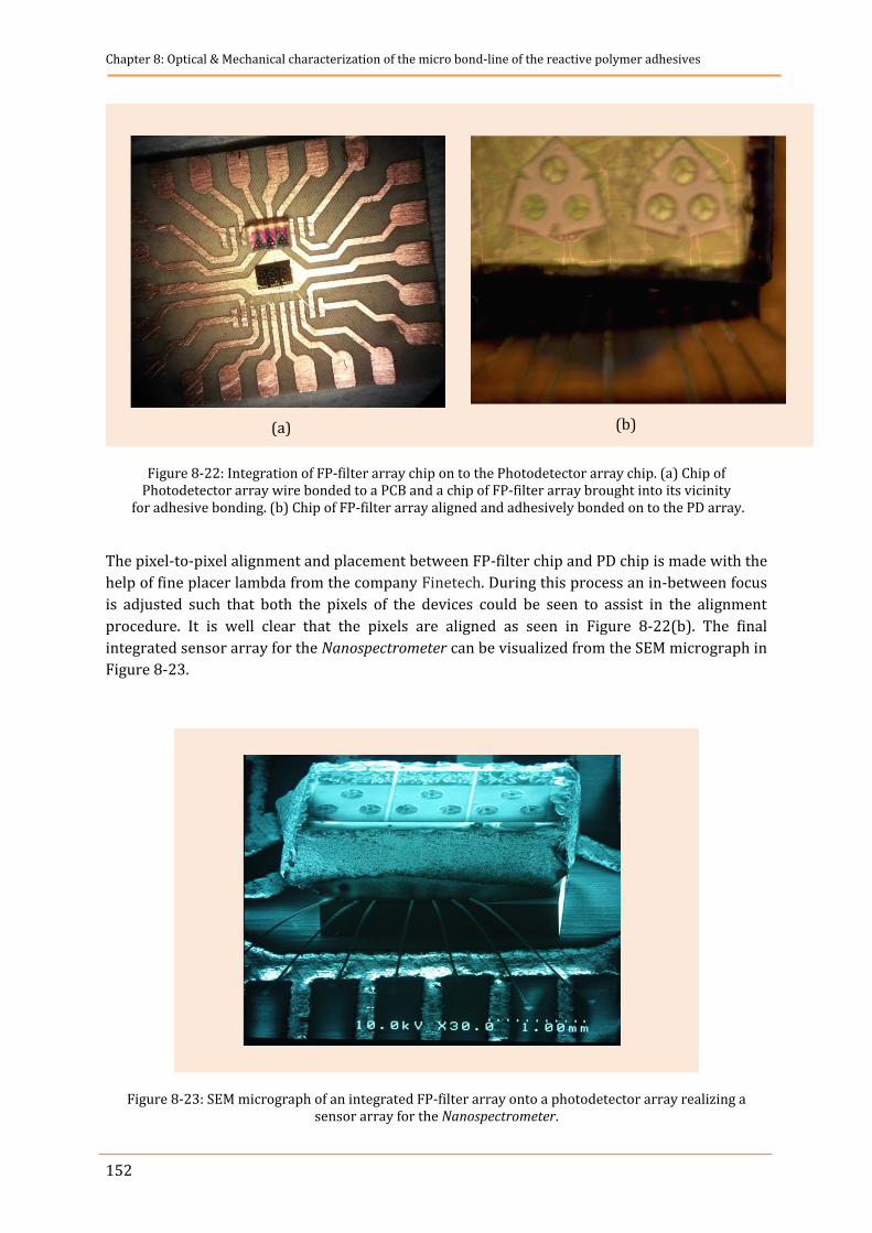
Chapter 8: Optical & Mechanical characterization of the micro bond-line of the reactive polymer adhesives
152
Figure 8-22: Integration of FP-filter array chip on to the Photodetector array chip. (a) Chip of Photodetector array wire bonded to a PCB and a chip of FP-filter array brought into its vicinity
for adhesive bonding. (b) Chip of FP-filter array aligned and adhesively bonded on to the PD array.
The pixel-to-pixel alignment and placement between FP-filter chip and PD chip is made with the
help of fine placer lambda from the company Finetech. During this process an in-between focus
is adjusted such that both the pixels of the devices could be seen to assist in the alignment
procedure. It is well clear that the pixels are aligned as seen in Figure 8-22(b). The final
integrated sensor array for the Nanospectrometer can be visualized from the SEM micrograph in
Figure 8-23.
Figure 8-23: SEM micrograph of an integrated FP-filter array onto a photodetector array realizing a sensor array for the Nanospectrometer.
Chip of FP-filter array
Chip of PD array
(a) (b)

153
Upon optimization of various process parameters and investigation of the adhesive properties
and compatibility to the application of this work, the sensor array is integrated and is ready for
the future work which is electrical read-out analysis.
The results in this chapter prove that among the selected adhesives, GB368, AD4950 and
OC4911 are compatible in the integration of the sensor array. Especially, the AD4950 and
OC4911 which have the dual curing capability that enables them to be used in cases of curing
under shadowed regions. Also the methodology of integration is successfully established which
can also be used for the integration and packaging of any other optics, photonics and
optoelectronic components and devices. Some reveal higher bond strength while show lower
transmission compared to others. Based on the field of the application of the Nanospectrometer,
any adhesive could be chosen.

154
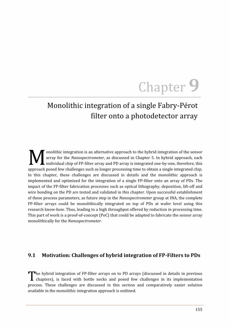
155
9. Monolithic integration of a single Fabry-Pérot filter
onto a photodtector array
onolithic integration is an alternative approach to the hybrid integration of the sensor
array for the Nanospectrometer, as discussed in Chapter 5. In hybrid approach, each
individual chip of FP-filter array and PD array is integrated one-by-one, therefore, this
approach posed few challenges such as longer processing time to obtain a single integrated chip.
In this chapter, these challenges are discussed in details and the monolithic approach is
implemented and optimized for the integration of a single FP-filter onto an array of PDs. The
impact of the FP-filter fabrication processes such as optical lithography, deposition, lift-off and
wire bonding on the PD are tested and validated in this chapter. Upon successful establishment
of these process parameters, as future step in the Nanospectrometer group at INA, the complete
FP-filter arrays could be monolithically integrated on top of PDs at wafer level using this
research know-how. Thus, leading to a high throughput offered by reduction in processing time.
This part of work is a proof-of-concept (PoC) that could be adapted to fabricate the sensor array
monolithically for the Nanospectrometer.
9.1 Motivation: Challenges of hybrid integration of FP-Filters to PDs
he hybrid integration of FP-filter arrays on to PD arrays (discussed in details in previous
chapters), is faced with bottle necks and posed few challenges in its implementation
process. These challenges are discussed in this section and comparatively easier solution
available in the monolithic integration approach is outlined.
M
T
Chapter 9 Monolithic integration of a single Fabry-Pérot
filter onto a photodetector array
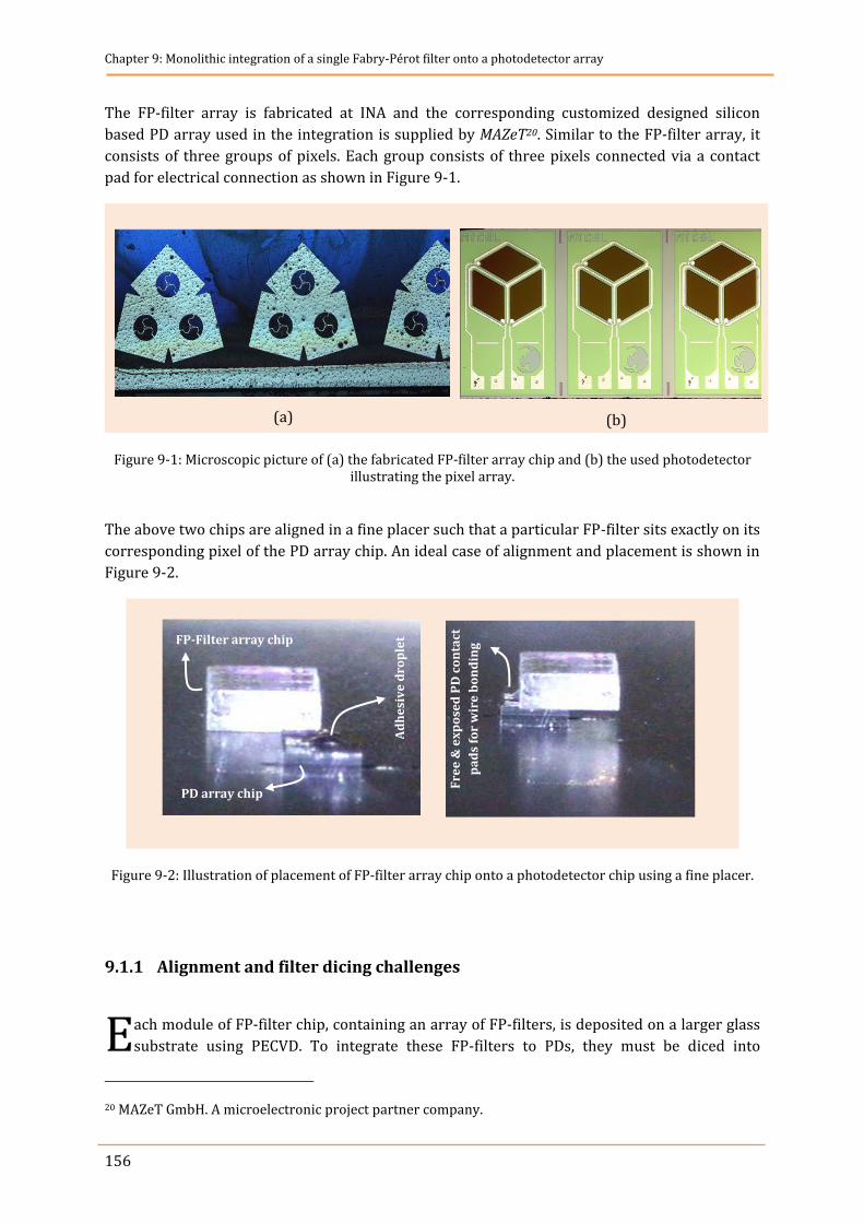
Chapter 9: Monolithic integration of a single Fabry-Pérot filter onto a photodetector array
156
The FP-filter array is fabricated at INA and the corresponding customized designed silicon
based PD array used in the integration is supplied by MAZeT20. Similar to the FP-filter array, it
consists of three groups of pixels. Each group consists of three pixels connected via a contact
pad for electrical connection as shown in Figure 9-1.
Figure 9-1: Microscopic picture of (a) the fabricated FP-filter array chip and (b) the used photodetector illustrating the pixel array.
The above two chips are aligned in a fine placer such that a particular FP-filter sits exactly on its
corresponding pixel of the PD array chip. An ideal case of alignment and placement is shown in
Figure 9-2.
Figure 9-2: Illustration of placement of FP-filter array chip onto a photodetector chip using a fine placer.
9.1.1 Alignment and filter dicing challenges
ach module of FP-filter chip, containing an array of FP-filters, is deposited on a larger glass
substrate using PECVD. To integrate these FP-filters to PDs, they must be diced into
20 MAZeT GmbH. A microelectronic project partner company.
E
FP-Filter array chip
PD array chip
Ad
he
siv
e d
rop
let
Fre
e &
ex
po
sed
PD
co
nta
ct
pa
ds
for
wir
e b
on
din
g
(a) (b)
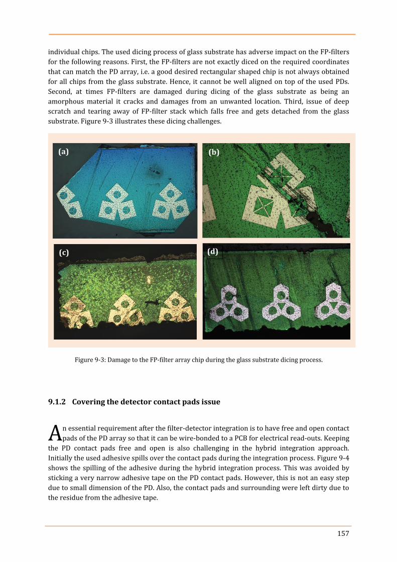
157
individual chips. The used dicing process of glass substrate has adverse impact on the FP-filters
for the following reasons. First, the FP-filters are not exactly diced on the required coordinates
that can match the PD array, i.e. a good desired rectangular shaped chip is not always obtained
for all chips from the glass substrate. Hence, it cannot be well aligned on top of the used PDs.
Second, at times FP-filters are damaged during dicing of the glass substrate as being an
amorphous material it cracks and damages from an unwanted location. Third, issue of deep
scratch and tearing away of FP-filter stack which falls free and gets detached from the glass
substrate. Figure 9-3 illustrates these dicing challenges.
Figure 9-3: Damage to the FP-filter array chip during the glass substrate dicing process.
9.1.2 Covering the detector contact pads issue
n essential requirement after the filter-detector integration is to have free and open contact
pads of the PD array so that it can be wire-bonded to a PCB for electrical read-outs. Keeping
the PD contact pads free and open is also challenging in the hybrid integration approach.
Initially the used adhesive spills over the contact pads during the integration process. Figure 9-4
shows the spilling of the adhesive during the hybrid integration process. This was avoided by
sticking a very narrow adhesive tape on the PD contact pads. However, this is not an easy step
due to small dimension of the PD. Also, the contact pads and surrounding were left dirty due to
the residue from the adhesive tape.
A
(a) (b)
(c) (d)
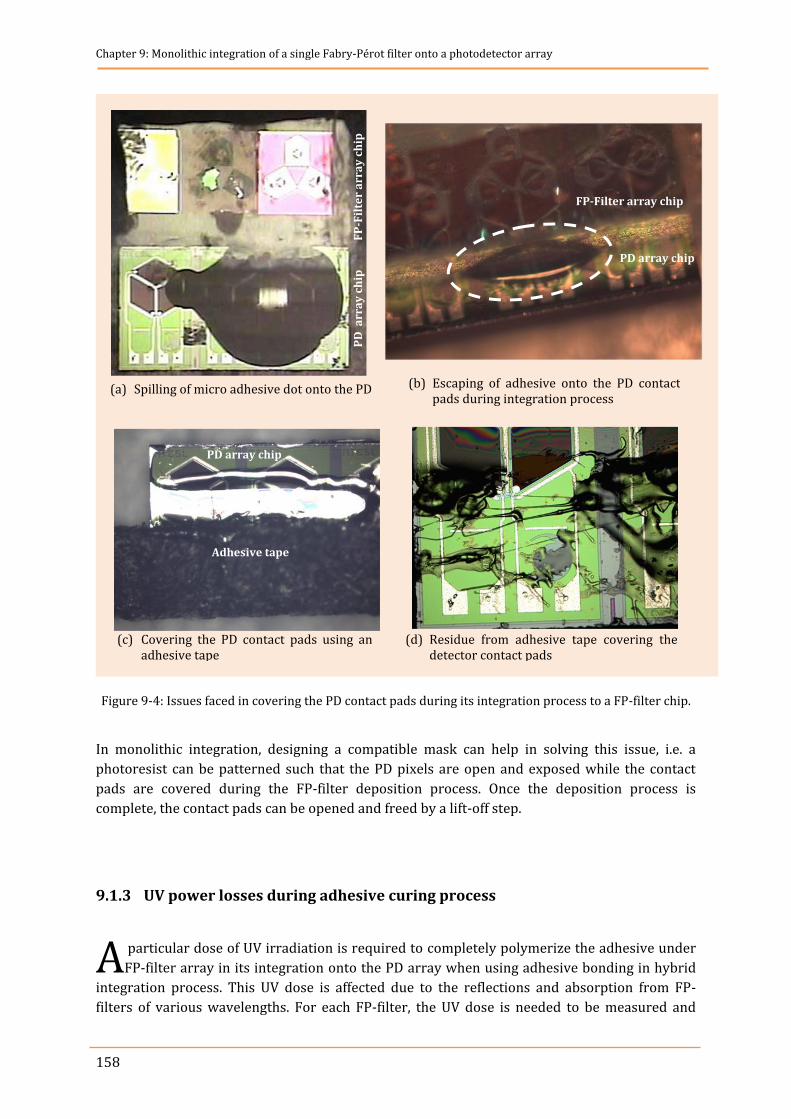
Chapter 9: Monolithic integration of a single Fabry-Pérot filter onto a photodetector array
158
Figure 9-4: Issues faced in covering the PD contact pads during its integration process to a FP-filter chip.
In monolithic integration, designing a compatible mask can help in solving this issue, i.e. a
photoresist can be patterned such that the PD pixels are open and exposed while the contact
pads are covered during the FP-filter deposition process. Once the deposition process is
complete, the contact pads can be opened and freed by a lift-off step.
9.1.3 UV power losses during adhesive curing process
particular dose of UV irradiation is required to completely polymerize the adhesive under
FP-filter array in its integration onto the PD array when using adhesive bonding in hybrid
integration process. This UV dose is affected due to the reflections and absorption from FP-
filters of various wavelengths. For each FP-filter, the UV dose is needed to be measured and
A
(a) Spilling of micro adhesive dot onto the PD (b) Escaping of adhesive onto the PD contact pads during integration process
(c) Covering the PD contact pads using an adhesive tape
(d) Residue from adhesive tape covering the detector contact pads
FP
-Fil
ter
arr
ay
ch
ip
PD
arr
ay
ch
ip
FP-Filter array chip
PD array chip
Adhesive tape
PD array chip
159
optimized before its integration process (for more details see section 7.4.2). Monolithic
approach is supposed to overcome this process as no adhesive is used in the integration
process. FP-filter arrays of various wavelengths could be directly deposited on top of the PD
arrays.
9.1.4 Material and equipment cost
n hybrid integration approach, FP-filter arrays are deposited on a glass substrate and then
diced into individual chips. These chips are then integrated onto the PD chips using adhesive
bonding technique. The dispensing equipment for precise amount of adhesive droplets, UV dose
measuring and curing equipment and fine placer for pixel-to-pixel alignment adds to the cost of
hybrid integration. Where as in monolithic integration, the lithographic steps and PECVD
process used to deposit FP-filters on glass substrate could be adapted to deposit arrays of FP-
filter on top of the PD arrays and avoid all the additional equipments for adhesive bonding.
9.2 Validation of PD array stability against fabrication process of
FP-filters
o obtain a successful monolithically integrated optical sensor array, various tests are
needed to be conducted in order to prove the resistance of the PD chip against the
fabrication process of FP-filters onto it. The technological process in fabricating the FP-filters
might be aggressive or intense for the PD pixels or its contact pads. Therefore, a number of PDs
are exposed to the influence of such technological process for investigations. This section
introduces the critical processing steps and examines the PD after each process for validation.
9.2.1 Effect of organic solvents on photodetector array
olvents such as acetone, iso-propanol and N-Methyl-2-pyrrolidone (NMP) are extensively
used in the cleaning process of substrates, sample containers, and other tools. Also these
solvents are aggressive towards photoresists and are used in its lift-off process. After
lithography, once the FP-filter deposition process on PD pixels is completed in the PECVD, the
lift-off process is needed to open and expose the contact pads of the PD for wire bonding. It
could be that these solvents also affect the pixels or the contact pads of the PD. Therefore, a few
PD chips are kept dipped in these solvents for over-night and then observed under the
microscope and also checked for the continuity of its contact lines using a digital multimeter
I
T
S
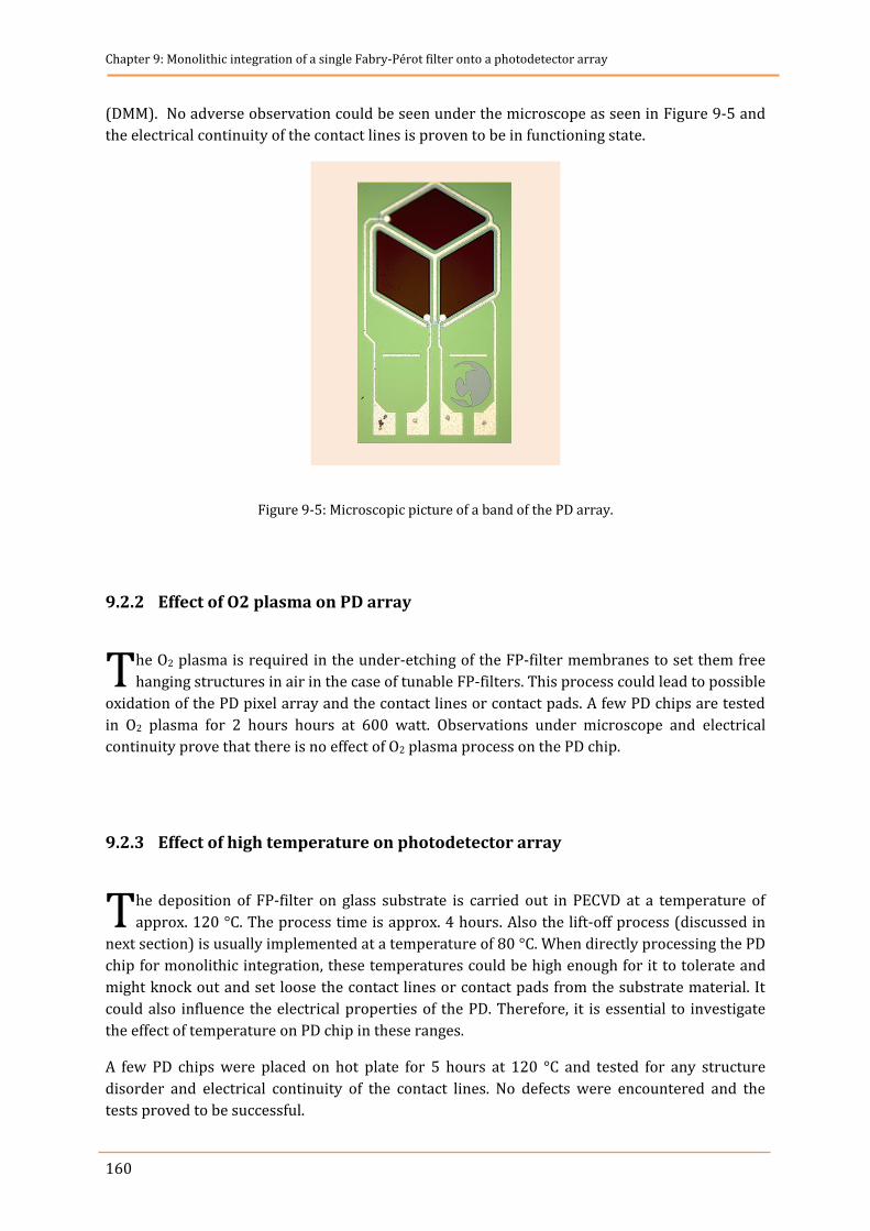
Chapter 9: Monolithic integration of a single Fabry-Pérot filter onto a photodetector array
160
(DMM). No adverse observation could be seen under the microscope as seen in Figure 9-5 and
the electrical continuity of the contact lines is proven to be in functioning state.
Figure 9-5: Microscopic picture of a band of the PD array.
9.2.2 Effect of O2 plasma on PD array
he O2 plasma is required in the under-etching of the FP-filter membranes to set them free
hanging structures in air in the case of tunable FP-filters. This process could lead to possible
oxidation of the PD pixel array and the contact lines or contact pads. A few PD chips are tested
in O2 plasma for 2 hours hours at 600 watt. Observations under microscope and electrical
continuity prove that there is no effect of O2 plasma process on the PD chip.
9.2.3 Effect of high temperature on photodetector array
he deposition of FP-filter on glass substrate is carried out in PECVD at a temperature of
approx. 120 °C. The process time is approx. 4 hours. Also the lift-off process (discussed in
next section) is usually implemented at a temperature of 80 °C. When directly processing the PD
chip for monolithic integration, these temperatures could be high enough for it to tolerate and
might knock out and set loose the contact lines or contact pads from the substrate material. It
could also influence the electrical properties of the PD. Therefore, it is essential to investigate
the effect of temperature on PD chip in these ranges.
A few PD chips were placed on hot plate for 5 hours at 120 °C and tested for any structure
disorder and electrical continuity of the contact lines. No defects were encountered and the
tests proved to be successful.
T
T
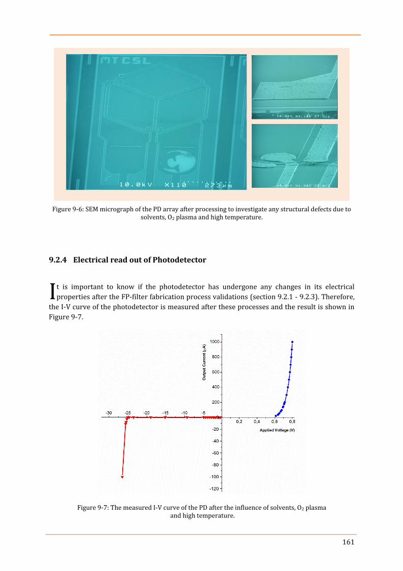
161
Figure 9-6: SEM micrograph of the PD array after processing to investigate any structural defects due to solvents, O2 plasma and high temperature.
9.2.4 Electrical read out of Photodetector
t is important to know if the photodetector has undergone any changes in its electrical
properties after the FP-filter fabrication process validations (section 9.2.1 - 9.2.3). Therefore,
the I-V curve of the photodetector is measured after these processes and the result is shown in
Figure 9-7.
Figure 9-7: The measured I-V curve of the PD after the influence of solvents, O2 plasma and high temperature.
I
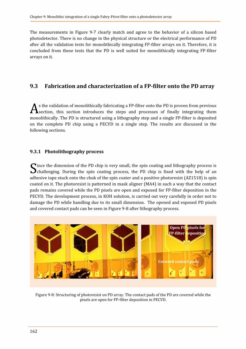
Chapter 9: Monolithic integration of a single Fabry-Pérot filter onto a photodetector array
162
The measurements in Figure 9-7 clearly match and agree to the behavior of a silicon based
photodetector. There is no change in the physical structure or the electrical performance of PD
after all the validation tests for monolithically integrating FP-filter arrays on it. Therefore, it is
concluded from these tests that the PD is well suited for monolithically integrating FP-filter
arrays on it.
9.3 Fabrication and characterization of a FP-filter onto the PD array
s the validation of monolithically fabricating a FP-filter onto the PD is proven from previous
section, this section introduces the steps and processes of finally integrating them
monolithically. The PD is structured using a lithography step and a single FP-filter is deposited
on the complete PD chip using a PECVD in a single step. The results are discussed in the
following sections.
9.3.1 Photolithography process
ince the dimension of the PD chip is very small, the spin coating and lithography process is
challenging. During the spin coating process, the PD chip is fixed with the help of an
adhesive tape stuck onto the chuk of the spin coater and a positive photoresist (AZ1518) is spin
coated on it. The photoresist is patterned in mask aligner (MA4) in such a way that the contact
pads remains covered while the PD pixels are open and exposed for FP-filter deposition in the
PECVD. The development process, in KOH solution, is carried out very carefully in order not to
damage the PD while handling due to its small dimension. The opened and exposed PD pixels
and covered contact pads can be seen in Figure 9-8 after lithography process.
Figure 9-8: Structuring of photoresist on PD array. The contact pads of the PD are covered while the pixels are open for FP-filter deposition in PECVD.
A
S
Covered contact pads
Open PD pixels for
FP-filter deposition
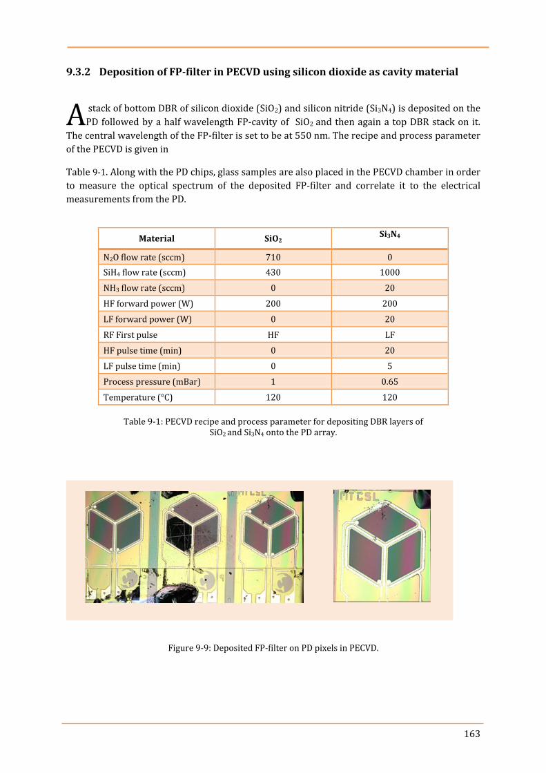
163
9.3.2 Deposition of FP-filter in PECVD using silicon dioxide as cavity material
stack of bottom DBR of silicon dioxide (SiO2) and silicon nitride (Si3N4) is deposited on the
PD followed by a half wavelength FP-cavity of SiO2 and then again a top DBR stack on it.
The central wavelength of the FP-filter is set to be at 550 nm. The recipe and process parameter
of the PECVD is given in
Table 9-1. Along with the PD chips, glass samples are also placed in the PECVD chamber in order
to measure the optical spectrum of the deposited FP-filter and correlate it to the electrical
measurements from the PD.
Material SiO2 Si3N4
N2O flow rate (sccm) 710 0
SiH4 flow rate (sccm) 430 1000
NH3 flow rate (sccm) 0 20
HF forward power (W) 200 200
LF forward power (W) 0 20
RF First pulse HF LF
HF pulse time (min) 0 20
LF pulse time (min) 0 5
Process pressure (mBar) 1 0.65
Temperature (°C) 120 120
Table 9-1: PECVD recipe and process parameter for depositing DBR layers of SiO2 and Si3N4 onto the PD array.
Figure 9-9: Deposited FP-filter on PD pixels in PECVD.
A
Chapter 9: Monolithic integration of a single Fabry-Pérot filter onto a photodetector array
164
9.3.3 Deposition and structuring of Light protection layer
fter the deposition of the FP-filter on the PD pixels in PECVD, a thin Al layer of approx. 100
nm is deposited on it using the Physical Vapor Deposition (PVD) to act as a light protection
layer. The Al layer on each PD pixel is structured with an opening of particular dimension using
the lithography process as seen in Figure 9-10. Various photomasks are used to structure and
obtain monolithic FP-filter and PD with openings of 12, 20, 30 and 60 µm, respectively to
investigate the effect of amount of light through these openings. Light passes through these
openings and reaches the FP-filter and outside these openings it is reflected by the Al layer to
allow a single straight path and avoid stray light from other directions.
9.3.4 Exposing the photodetector contact pads for wire bonding
ontact pads of PD are necessary to be free and open to have access to them for wire bonding
in order to allow electrical read-outs. For this purpose the lift-off process is optimized and
implemented. Initially, the PD contact pads are covered with photoresist during the lithography
process while the PD pixels are free and open for the deposition of FP-filter in the PECVD. For
lift-off process to be successful, the photoresist height must be higher than the deposited FP-
filter. Therefore, it is important to calculate the thickness of the FP-filter stack and choose the
photoresist accordingly that can provide a higher height. The total thickness of the FP-filter with
9.5 period DBR stacks and a half wavelength cavity was 3.6 µm. In this work, a negative
photoresist (AZnLof2070) is spin coated on the PD chip at a speed of 3000 rpm which provided
a double height that of the FP-filter. See Appendix G for the lift-off recipe using negative
photoresist. Once the FP-filter is fabricated on the PD chip, it is left in NMP at 80 °C for overnight
to lift-off the photoresist from the contact pads. Figure 9-10 illustrates the covered contact pads
of the PD array before lif-off and the free and open contact pads after lift-off process.
A
C
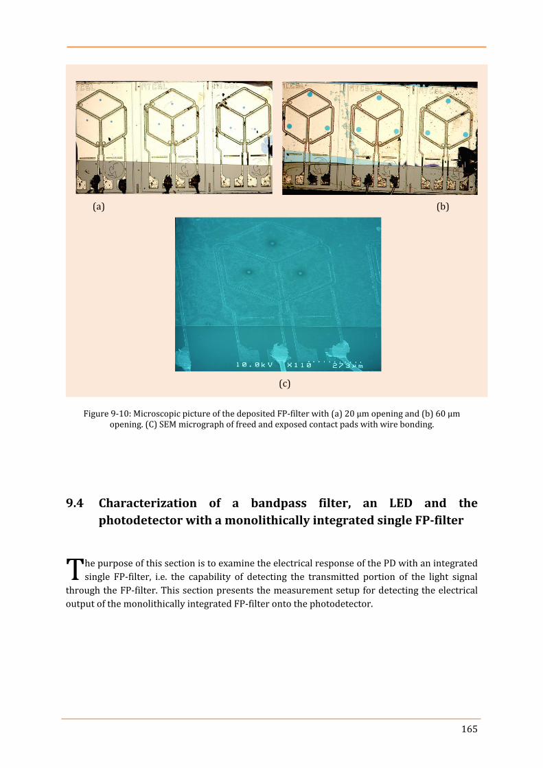
165
Figure 9-10: Microscopic picture of the deposited FP-filter with (a) 20 µm opening and (b) 60 µm opening. (C) SEM micrograph of freed and exposed contact pads with wire bonding.
9.4 Characterization of a bandpass filter, an LED and the
photodetector with a monolithically integrated single FP-filter
he purpose of this section is to examine the electrical response of the PD with an integrated
single FP-filter, i.e. the capability of detecting the transmitted portion of the light signal
through the FP-filter. This section presents the measurement setup for detecting the electrical
output of the monolithically integrated FP-filter onto the photodetector.
T
(c)
(a) (b)
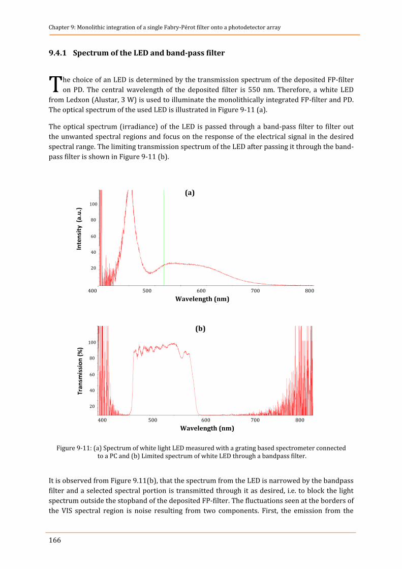
Chapter 9: Monolithic integration of a single Fabry-Pérot filter onto a photodetector array
166
9.4.1 Spectrum of the LED and band-pass filter
he choice of an LED is determined by the transmission spectrum of the deposited FP-filter
on PD. The central wavelength of the deposited filter is 550 nm. Therefore, a white LED
from Ledxon (Alustar, 3 W) is used to illuminate the monolithically integrated FP-filter and PD.
The optical spectrum of the used LED is illustrated in Figure 9-11 (a).
The optical spectrum (irradiance) of the LED is passed through a band-pass filter to filter out
the unwanted spectral regions and focus on the response of the electrical signal in the desired
spectral range. The limiting transmission spectrum of the LED after passing it through the band-
pass filter is shown in Figure 9-11 (b).
Figure 9-11: (a) Spectrum of white light LED measured with a grating based spectrometer connected to a PC and (b) Limited spectrum of white LED through a bandpass filter.
It is observed from Figure 9.11(b), that the spectrum from the LED is narrowed by the bandpass
filter and a selected spectral portion is transmitted through it as desired, i.e. to block the light
spectrum outside the stopband of the deposited FP-filter. The fluctuations seen at the borders of
the VIS spectral region is noise resulting from two components. First, the emission from the
T
(a)
Inte
nsi
ty (
a.u
.)
400 500 600 700 800
Wavelength (nm)
100
80
60
40
20
(b)
Tran
smis
sio
n (
%)
100
80
60
40
20
400 500 600 700 800
Wavelength (nm)
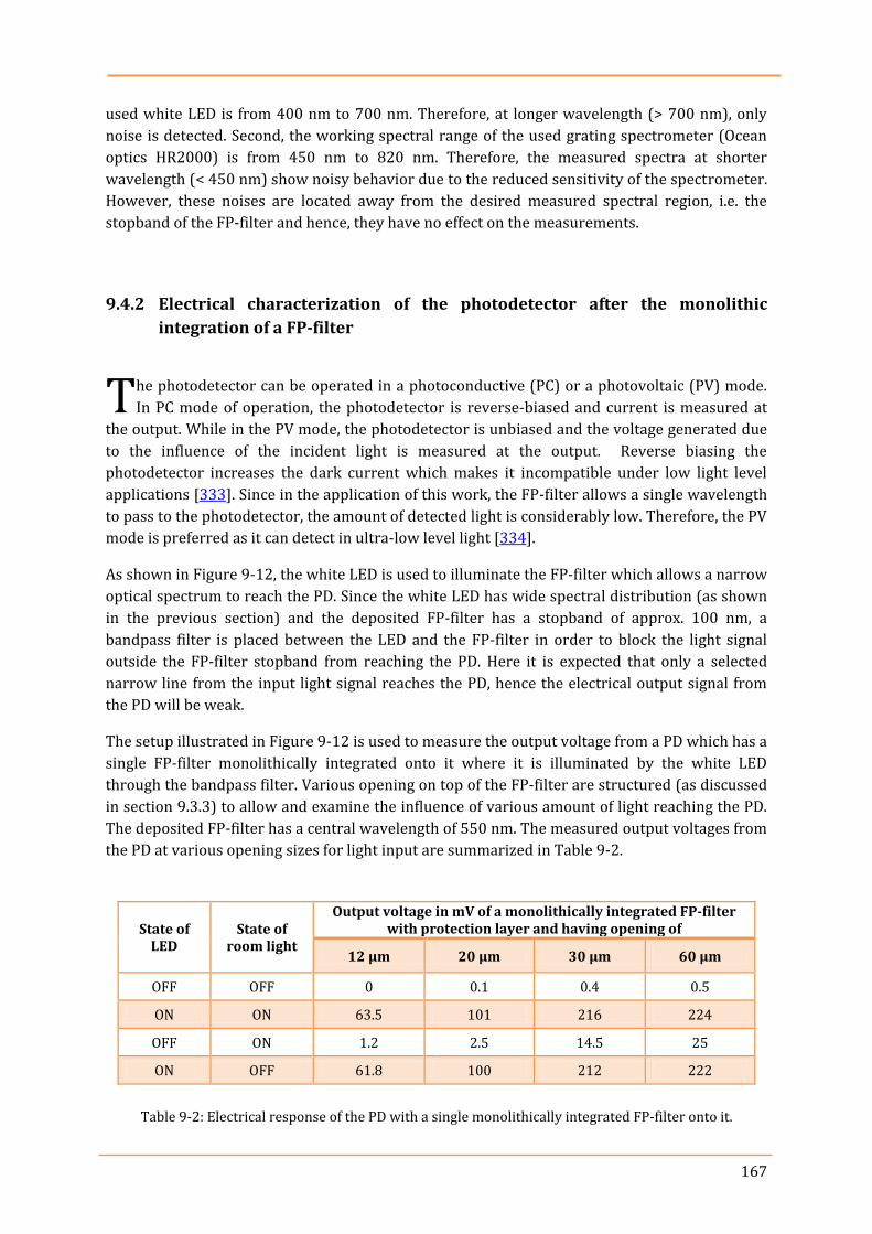
167
used white LED is from 400 nm to 700 nm. Therefore, at longer wavelength (> 700 nm), only
noise is detected. Second, the working spectral range of the used grating spectrometer (Ocean
optics HR2000) is from 450 nm to 820 nm. Therefore, the measured spectra at shorter
wavelength (< 450 nm) show noisy behavior due to the reduced sensitivity of the spectrometer.
However, these noises are located away from the desired measured spectral region, i.e. the
stopband of the FP-filter and hence, they have no effect on the measurements.
9.4.2 Electrical characterization of the photodetector after the monolithic
integration of a FP-filter
he photodetector can be operated in a photoconductive (PC) or a photovoltaic (PV) mode.
In PC mode of operation, the photodetector is reverse-biased and current is measured at
the output. While in the PV mode, the photodetector is unbiased and the voltage generated due
to the influence of the incident light is measured at the output. Reverse biasing the
photodetector increases the dark current which makes it incompatible under low light level
applications [333]. Since in the application of this work, the FP-filter allows a single wavelength
to pass to the photodetector, the amount of detected light is considerably low. Therefore, the PV
mode is preferred as it can detect in ultra-low level light [334].
As shown in Figure 9-12, the white LED is used to illuminate the FP-filter which allows a narrow
optical spectrum to reach the PD. Since the white LED has wide spectral distribution (as shown
in the previous section) and the deposited FP-filter has a stopband of approx. 100 nm, a
bandpass filter is placed between the LED and the FP-filter in order to block the light signal
outside the FP-filter stopband from reaching the PD. Here it is expected that only a selected
narrow line from the input light signal reaches the PD, hence the electrical output signal from
the PD will be weak.
The setup illustrated in Figure 9-12 is used to measure the output voltage from a PD which has a
single FP-filter monolithically integrated onto it where it is illuminated by the white LED
through the bandpass filter. Various opening on top of the FP-filter are structured (as discussed
in section 9.3.3) to allow and examine the influence of various amount of light reaching the PD.
The deposited FP-filter has a central wavelength of 550 nm. The measured output voltages from
the PD at various opening sizes for light input are summarized in Table 9-2.
State of LED
State of room light
Output voltage in mV of a monolithically integrated FP-filter with protection layer and having opening of
12 µm 20 µm 30 µm 60 µm
OFF OFF 0 0.1 0.4 0.5
ON ON 63.5 101 216 224
OFF ON 1.2 2.5 14.5 25
ON OFF 61.8 100 212 222
Table 9-2: Electrical response of the PD with a single monolithically integrated FP-filter onto it.
T
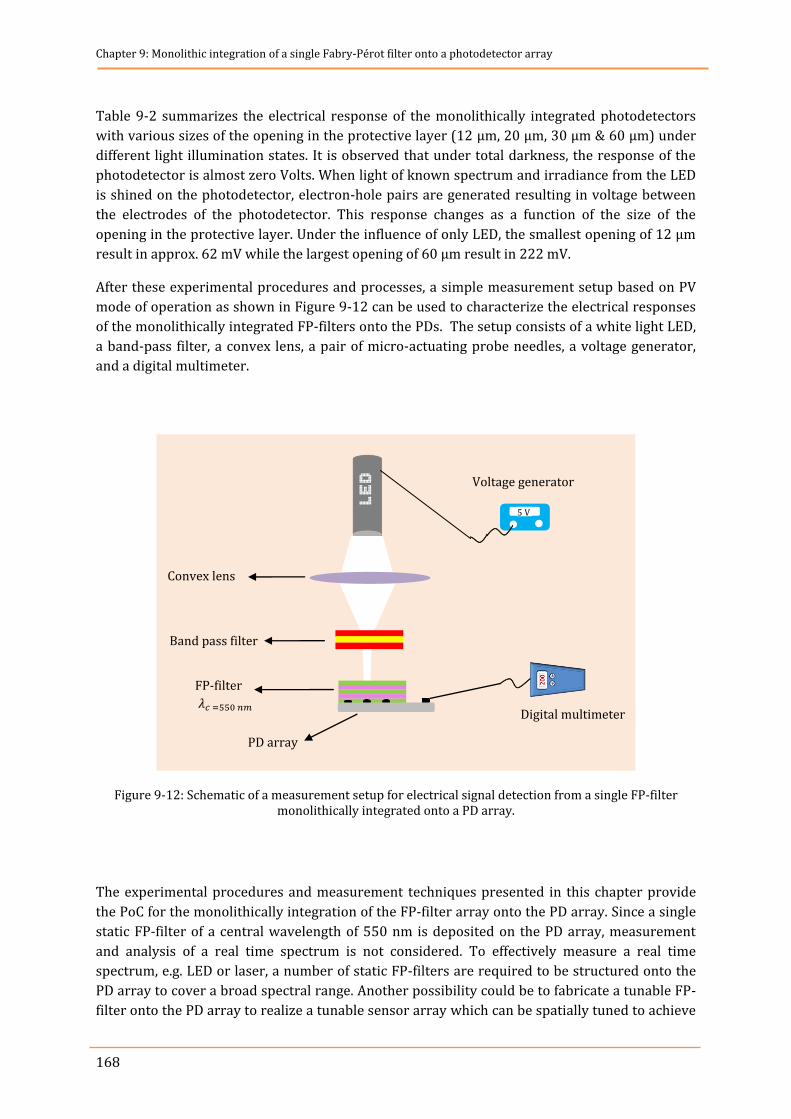
Chapter 9: Monolithic integration of a single Fabry-Pérot filter onto a photodetector array
168
Table 9-2 summarizes the electrical response of the monolithically integrated photodetectors
with various sizes of the opening in the protective layer (12 µm, 20 µm, 30 µm & 60 µm) under
different light illumination states. It is observed that under total darkness, the response of the
photodetector is almost zero Volts. When light of known spectrum and irradiance from the LED
is shined on the photodetector, electron-hole pairs are generated resulting in voltage between
the electrodes of the photodetector. This response changes as a function of the size of the
opening in the protective layer. Under the influence of only LED, the smallest opening of 12 µm
result in approx. 62 mV while the largest opening of 60 µm result in 222 mV.
After these experimental procedures and processes, a simple measurement setup based on PV
mode of operation as shown in Figure 9-12 can be used to characterize the electrical responses
of the monolithically integrated FP-filters onto the PDs. The setup consists of a white light LED,
a band-pass filter, a convex lens, a pair of micro-actuating probe needles, a voltage generator,
and a digital multimeter.
Figure 9-12: Schematic of a measurement setup for electrical signal detection from a single FP-filter monolithically integrated onto a PD array.
The experimental procedures and measurement techniques presented in this chapter provide
the PoC for the monolithically integration of the FP-filter array onto the PD array. Since a single
static FP-filter of a central wavelength of 550 nm is deposited on the PD array, measurement
and analysis of a real time spectrum is not considered. To effectively measure a real time
spectrum, e.g. LED or laser, a number of static FP-filters are required to be structured onto the
PD array to cover a broad spectral range. Another possibility could be to fabricate a tunable FP-
filter onto the PD array to realize a tunable sensor array which can be spatially tuned to achieve
Band pass filter
FP-filter
5 V
Convex lens
Voltage generator
Digital multimeter
PD array

169
spectrally tunable transmission lines from the FP-filter. The results learned from the fabrication
of a single FP-filter onto the PD could be further taken to the next level of fabricating an array of
FP-filter on the PD array. This would require designing a new photomask for the FP-array and
the corresponding PD array. The established technique in this chapter could be implemented as
a future work to achieve a monolithically fabricated sensor array for the Nanospectrometer.

Chapter 9: Monolithic integration of a single Fabry-Pérot filter onto a photodetector array
170
171
10. Conclusion
In this dissertation, two distinct fields are researched in the fabrication of a cost effective, highly
selective and strongly miniaturized FP-filter array based Nanospectrometer. The first area of
focus is the fabrication of high resolution 3D NanoImprint master templates based on
technique for the FP-filter array and the second is the integration of the FP-filter array onto the
PD array to obtain the final sensor array for the Nanospectrometer.
Part I
In order to fabricate the high resolution 3D NanoImprint master template containing 64 FP-
cavity structures (8 x 8 array) with each of unique heights, three substrate materials were
investigated, i.e. GaAs, Si and various types of glasses. These materials were compared in terms
of their controllable etching behavior, surface roughness, durability, process complexity, and
cost.
The cost of GaAs substrate is € 93 per 2” wafer. It showed an excellent etching control and a
lower surface roughness of 0.3 nm to produce a high resolution 3D master template. However,
this substrate material is brittle and excessive care was needed in order not to damage or break
the precious master template. Especially during the replication process, much care was needed
to separate the master templates from the daughter template. Various incidents were
experienced and reported in the Nanospectrometer group where the GaAs based 3D master
template damaged. Therefore, alternative substrate materials were investigated to achieve the
minimum step difference among the 64 FP-cavities in the array.
Various types of glasses were used for the investigations and compared to GaAs master
template. The optimized RIE recipe that was used to obtain the controllable low aspect ratio
mesa structures is Ar = 10, CHF3 = 14 and SF6 = 0.1 sccm, respectively, at an RF power of 20 W.
The borosilicate glass has the limitation of being very expensive (€ 22.75 per 25 mm2 wafer)
Chapter 10 Conclusions and outlook
Chapter 10: Conclusions & outlook
172
and lacked the etching reproducibility of mesa structures which is a major drawback. The soda
lime glass is cheaper (€ 0.044 per 2 x 7 mm wafer) however the deviation in its etching depth
at similar etching conditions is 7.4% which is not desired. Also this glass type showed a higher
surface roughness of 0.92 nm. The float glass is relatively cheaper (€ 2.85 per 25.4 mm2 wafer),
had a constant etch rate with 1.2% deviations at similar etching conditions and delivered a
surface roughness of 0.6 nm. Among the investigated glass types, the results offered by float
glass were acceptable for fabricating the 3D NIL master templates. The handling of glass
substrates was easier and had higher durability. However, additional processing steps were
required to fabricate the master templates from glass substrates. As 7 masks were used for
etching 64 FP-cavity heights in the array, compared to GaAs four (4) additional steps in the case
of glass substrates were required in processing each mask, i.e. a thin metallic layer was
deposited for WLI characterization & alignment in mask aligner and then removed again after
each process. This increased its processing complexity, time and eventually the cost of
fabrication.
Si substrate coasted € 10.70 per 3” wafer. Various RIE recipes were investigated in order to
obtain a controllable low aspect ratio mesa structures. The optimized and desired slow etching
recipe was obtained when a combination of both the physical and the chemical etching gasses
was used in same proportion, i.e. using Ar in combination with CHF3 with the lowest point being
at 10 sccm at an RF power of 25 W. A well controlled etch rate of 0.5 nm/min was measured in
WLI and produced a linear etch depth as a function of etch time. However, when etching deeper
FP-cavities with desired height of 128 nm, applying this recipe was time consuming. Therefore,
another low etching recipe with an etch rate slightly higher than this recipe was used for
etching mask I – mask IV. The suitable recipe for this purpose in providing a slightly higher etch
rate was Ar with gas flow of 10, CHF3 with 14 and SF6 with 0.1 sccm, respectively at an RF power
of 25 W. This recipe delivered an etch rate of 1.3 nm/min and also produced a desired linear
etch depth as a function of etch time. The measured surface roughness of the etched Si substrate
using both the recipes (Ar = CHF3 = 10 sccm) and (Ar = 10, CHF3 = 14 & SF6 = 0.1 sccm,
respectively) as a function of etching time was in the range of 0.5 nm. Since the height difference
among the FP-cavities in the array is 1.71 nm, therefore, this achieved surface roughness in RIE
is sufficient for the application of this work which can very well differentiate between the step
heights among all the 64 mesa structures in the array. Furthermore, using the SEM, a clear and
vertical structure profile was achieved with homogeneous etching which concludes the recipes
used were anisotropic without any redeposition issues and well suited for fabricating high
quality vertical mesa structures of low aspect ratio. The results of these recipes were
reproducible and the results of Si substrate were almost comparable to that of GaAs.
Additionally, Si substrate showed higher durability, had lower cost and processing was much
user friendly compared to GaAs. Hence Si substrate was chosen as the substrate material to
fabricate the final 3D NanoImprint master templates.
To fabricate a high resolution 3D master template from Si, it was proved that a minimum
step difference of 1.7 nm among the FP-cavities in the array can be achieved and reproduced to
allow a spacing of 5 nm among the transmission lines of the FP-filter array to cover the entire
VIS spectral range. Additionally, a new mask design consisting of individual 7 mask patterns
were used subsequently to fabricate the 3D master template for . An array of 64 FP-
cavity patterns on the 7 masks were distributed and each four FP-cavities in the array were
grouped in a way such that the average heights of all the 16 groups in the array were nearly
173
same to obtain a uniform residual layer during the imprinting of the process. To achieve
this, the etching recipes discussed above were implemented. Upon processing each individual
mask, it was characterized to investigate variation in the etch rate to account for the percentage
deviation from the designed FP-cavity height has resulted. A percentage deviation of very few
degrees in the vertical precision of the fabricated 3D NanoImprint master template from the
designed one was observed. The deviation in mask II to mask VII was under 3% when the low
etching recipe was used while the deviation in etching mask 1 was 5.2% when the slightly
higher etch rate recipe was used. The final deviation from all 7 masks between the designed and
fabricated 3D NIL master template was 2.6%. These deviations occur in the RIE process due to
the aged machine where the etching rates are not stable over time. The average height of each
16 groups in the 8 x 8 array (4 mesa structures in each group) was measured to be in the range
of 194.07 nm – 199.9 nm.
As an outlook to the fabrication of high resolution 3D NanoImprint templates, further low
aspect ratio etching recipes could be investigated using different etching gasses and modern RIE
technologies. This would lead to lower etching rates to achieve lower separation among the
transmission-lines of the FP-filter array and hence increase spectral selectivity. For future work,
high density array containing 128 cavities could be implemented to cover larger spectral range,
e.g. VIS and NIR. This would enable detect biomarkers, trace gases and chemical compositions in
the medical and industrial field with higher spectral quality. Another interesting future work is
to replicate the fabricated master template into the flexible daughter template and
measure any possible deviation in the FP-cavity heights and finally measure any possible
deviation in the imprinted cavity heights. This would allow make changes and rectify the
designed (desired) FP-cavity heights for a particular application.
Part II
The aim in this part of the work was to integrate the FP- filter arrays on top of the PD arrays to
achieve a sensor array for the Nanospectrometer. The major requirement was to preserve the
transmitted optical signal on its transit from the FP-filter array to a PD array in order to be
transformed into electronic form for electrical read-outs.
Various integration techniques were reviewed for its implementation in achieving the above
mentioned goal to avoid any flaw or degradation in the device. Among them the most optimum
and compatible integration technique was selected which was the adhesive bonding technique
for the following important reasons. The adhesive polymers has the ability to bond most wafers
from dissimilar materials used in micro-systems and micro-electronics production, tolerances
to wafer surface roughnesses and fast setting due to short curing time compared to the other
wafer bonding techniques. From a wide variety of adhesive polymers, a particular category of
adhesive was selected i.e., dual polymerization reactive adhesives, that have properties as
desired in the application of this work, i.e. high optical transparency in VIS spectral region,
curing-on-demand to allow time for alignment to the PD, void free integrity, sufficient bond
strength, tolerance to further processes in device fabrication such as aggressive solvents and
resistance to environmental conditions and weathering. These properties were found to be in
Chapter 10: Conclusions & outlook
174
the specially modified versions of the UV-cured acrylate (AD4950 and OC4911), urethane
acrylate (GB368) and epoxy adhesives (OB749). These adhesives were finally selected and
tested for their optical and mechanical properties in the required miniaturized range for their
application in this work.
The optical transmission through each adhesive micro bond-line was measured followed by its
mechanical bond strength using the tensile test method. The results demonstrated that all the
adhesives polymerized to an optically transparent micro bond-line except OB749 which
delivered milky like and translucent bond-line. Very few bubbles were visualized in the three
transparent adhesives micro bond-lines under the microscope with no other defects. The
measured transmittance through the micro bond-lines of GB368, Ad4950 and OC4911 using a
grating based spectrometer connected to a computer was >90% while that of OB749 was <30%.
From this point onwards OB749 was dropped from further testing as higher optical
specification was one of the most important parameter considered for this work. The average
measured bond strength of GB368 was 5.1 MPa, of AD4950 was 8.3 MPa and of OC4911 was 3.5
MPa. Also these three adhesive showed no yellowing effect and no alteration in their
transmittance performance after their stability test against a temperature upto 150 °C and
against O2 plasma upto 120 minutes at an RF power of 600 W. However, when the adhesive film
is left naked and exposed in the O2 plasma, the transmittance through it decreased. The failure
mode analysis using the SEM showed that majority of micro bond-lines formed by GB368 failed
cohesively, AD4950 failed adhesively and OC4911 followed a mixed failure mode. However, the
bond strength of all the three adhesives was sufficient for further processing and device
integrity. Furthermore, the aging of these adhesive micro bond-lines were determined using the
thermal accelerated aging test. It was concluded from this chapter that the selected adhesive
materials are compatible to be applied in this work, especially the AD4950 followed by OC4911
which are also dual curable. Also the method and procedure to integrate the FP-filter arrays and
PD arrays is successfully established which can be used to finally integrate the two hybrid chips.
These materials and process can also be used for the integration and packaging of other optics,
photonics and optoelectronic components and devices.
As an outlook to the hybrid integration approach, more tests runs are suggested for the
accelerated aging test that contains temperature cycling including humidity and to simulate the
effect of extreme lighting for a prolonged time. Also the monolithic integration technique of the
FP-filter array and PD array shows promising results and strongly supports the proof-of-
concept (PoC) of the FP-filter array based Nanospectrometer. Therefore, further research
investigations in this direction by designing a compatible photomask for the customized PD
array to deposit different FP-filters with unique transmission-lines and integrated band-pass
filters will lead to a further miniaturized, cost effective and an improved device. Especially, the
tunable FP-filters for the Nanospectrometer researched at INA could be directly deposited and
structured on these customized PD arrays.
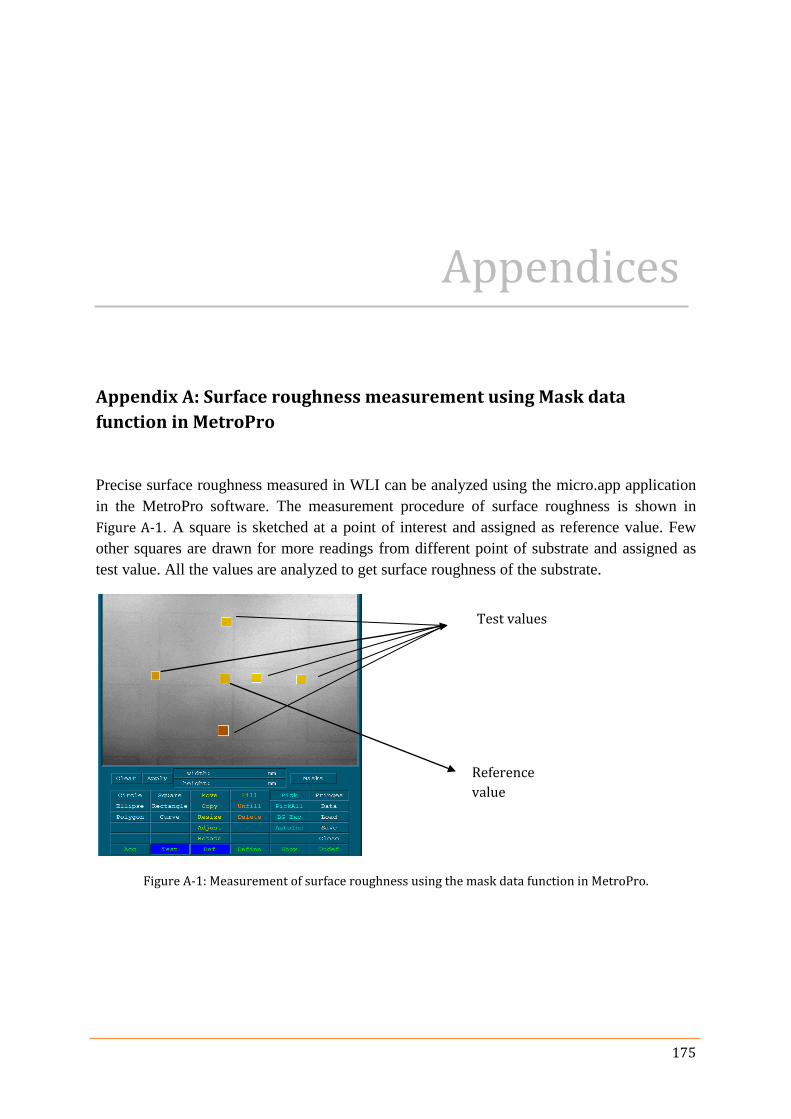
175
Appendices
Appendix A: Surface roughness measurement using Mask data
function in MetroPro
Precise surface roughness measured in WLI can be analyzed using the micro.app application
in the MetroPro software. The measurement procedure of surface roughness is shown in
Figure A-1. A square is sketched at a point of interest and assigned as reference value. Few
other squares are drawn for more readings from different point of substrate and assigned as
test value. All the values are analyzed to get surface roughness of the substrate.
Figure A-1: Measurement of surface roughness using the mask data function in MetroPro.
Test values
Reference
value
Appendices
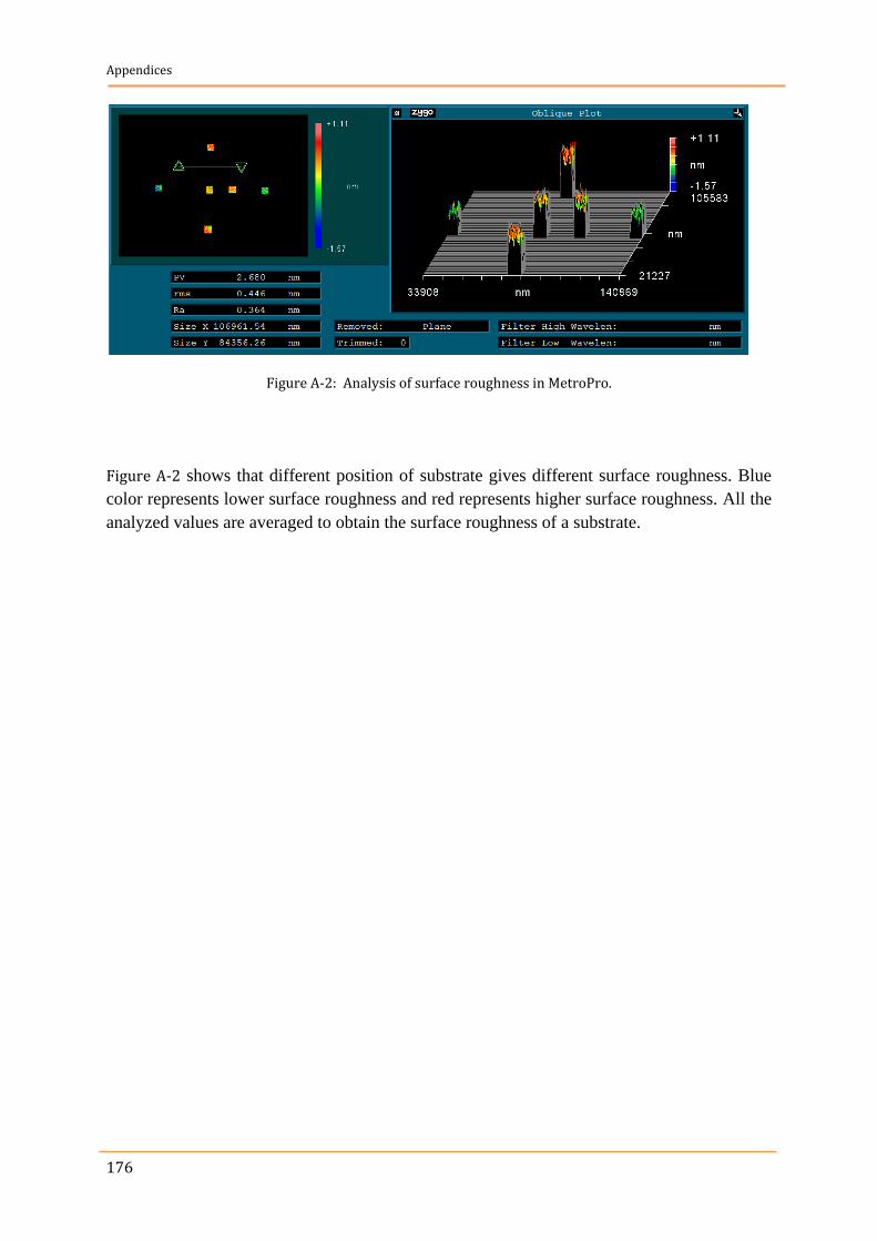
Appendices
176
Figure A-2: Analysis of surface roughness in MetroPro.
Figure A-2 shows that different position of substrate gives different surface roughness. Blue
color represents lower surface roughness and red represents higher surface roughness. All the
analyzed values are averaged to obtain the surface roughness of a substrate.
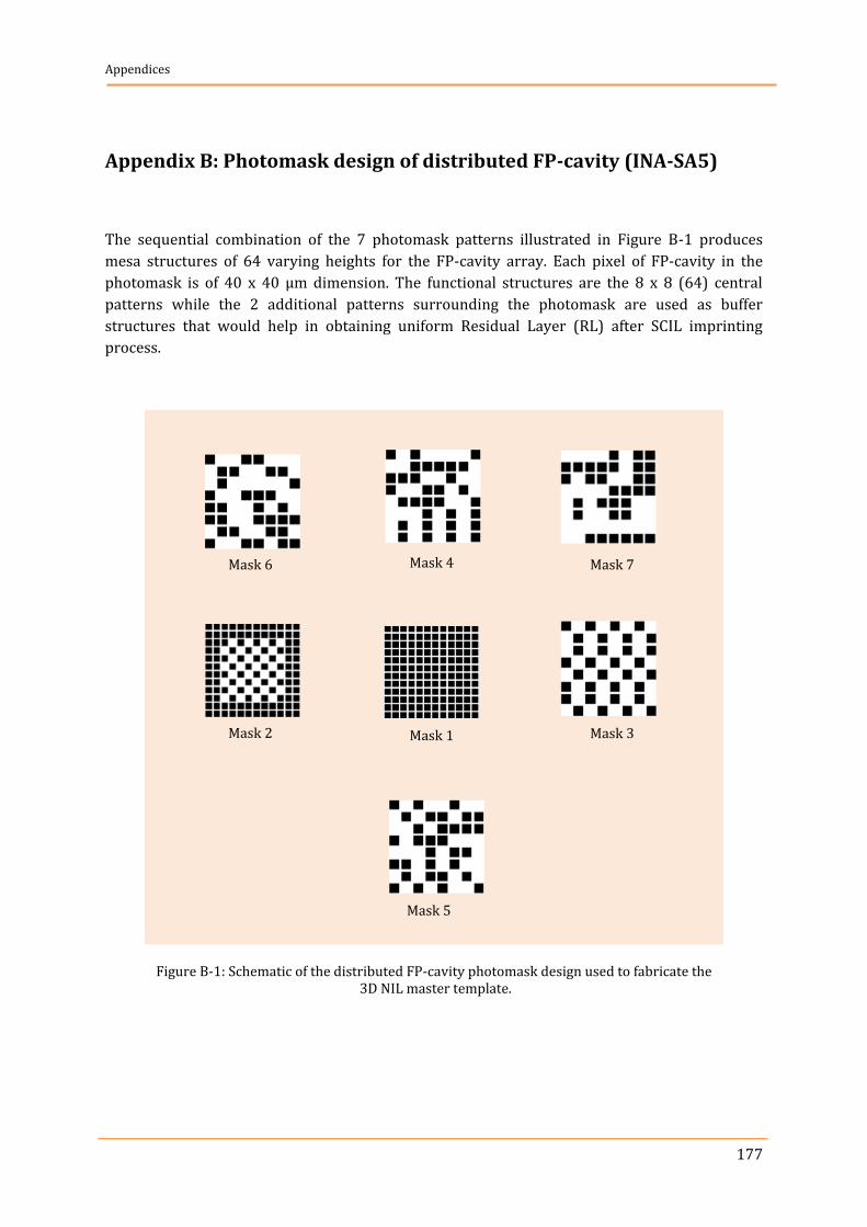
Appendices
177
Appendix B: Photomask design of distributed FP-cavity (INA-SA5)
The sequential combination of the 7 photomask patterns illustrated in Figure B-1 produces
mesa structures of 64 varying heights for the FP-cavity array. Each pixel of FP-cavity in the
photomask is of 40 x 40 µm dimension. The functional structures are the 8 x 8 (64) central
patterns while the 2 additional patterns surrounding the photomask are used as buffer
structures that would help in obtaining uniform Residual Layer (RL) after SCIL imprinting
process.
Figure B-1: Schematic of the distributed FP-cavity photomask design used to fabricate the 3D NIL master template.
Mask 1 Mask 2 Mask 3
Mask 4 Mask 7
Mask 5
Mask 6

Appendices
178
Appendix C: Procedure & recipe for processing single mask in the
fabrication of Si 3D NIL master template
The procedure and process flow of one lithographic and one RIE cycle in obtaining the 3D
master template containing FP-cavity structures is given below.
1. Cleaning: a) Rinse with acetone, iso-propanol and dry with N2. b) Clean with O2 plasma asher for 5 min at 250 W.
2. Lithography:
a) Bake Dry the substrate from H2O on Hotplate at 120 °C for 10 min. b) Apply adhesion promoter (Ti-prime) to substrate and spin coat at 4000 rpm for 40 s. c) Spin coat positive photoresist (AZ518) at 4000 rpm for 40 s (thickness = 1.8μm). d) Prebake the substrate with photoresist on hotplate for 5 min (exact) at 90 °C. e) Align & expose mask 1 (see Appendix B) using Karl-Suss MA-4 System for 6.6 s. f) Develop photoresist in KOH (0.8 %) solution for 30 s, rinse with H2O & dry with N2. g) Hard bake photoresist on substrate for approx. 5 min at 120 °C. h) Descum using O2 plasma asher for 2 – 3 min at 50 W.
3. Etching:
RIE-Castor with parameters; CHF3 flow (X) sccm, SF6 flow (X) sccm, Ar flow (X) sccm, pressure 0.025 mbar, power 25/50 W, temperature 12 ° C and the time is variable.
4. Photoresist Removal:
a) Dip the substrate in Acetone for 1 hour and rinse with iso-propanol. Sometimes MP at 80 C overnight is required for higher etching timings. b) Clean with O2 plasma asher for 15 min at 250 W.
5. Measurement:
White Light Interferometer to measure the structure height.
6. Repeat the steps 1 to 5 with Mask 2, 3, 4, 5, 6 and 7.
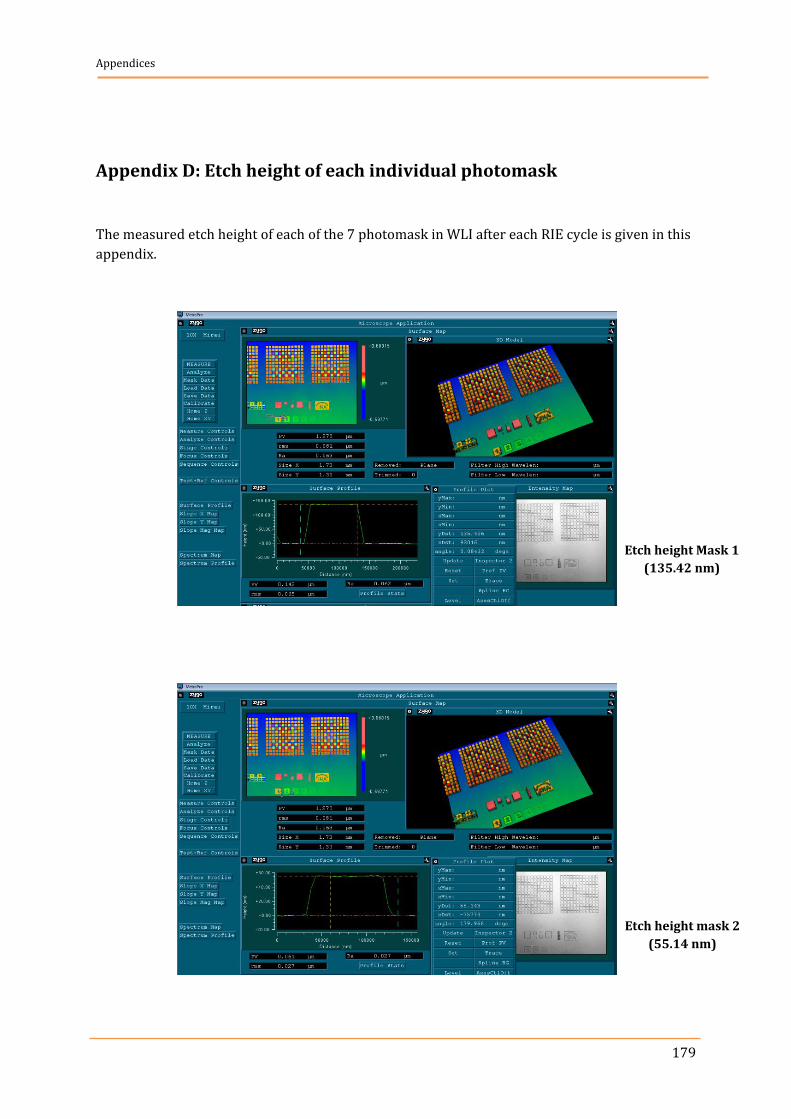
Appendices
179
Appendix D: Etch height of each individual photomask
The measured etch height of each of the 7 photomask in WLI after each RIE cycle is given in this
appendix.
Etch height Mask 1
(135.42 nm)
Etch height mask 2
(55.14 nm)
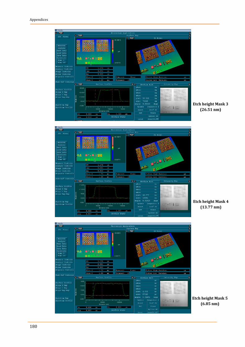
Appendices
180
Etch height Mask 3
(26.51 nm)
Etch height Mask 4
(13.77 nm)
Etch height Mask 5
(6.85 nm)
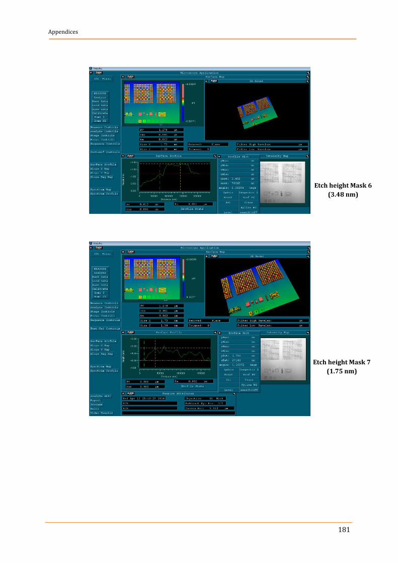
Appendices
181
Etch height Mask 6
(3.48 nm)
Etch height Mask 7
(1.75 nm)

Appendices
182
Appendix E: Adhesive drop size optimization and measured diameter
of micro bond-line
The weight of single jetted drop of used adhesives dispensed from different micro nozzles
openings and the diameter of their micro bond-lines in cured state are given in this appendix.
Nozzel diameter
(µm)
Weight of Glass
substrate (g)
Weight of Glass
substrate with jetted droplet (g)
Weight of droplet (g)
Average weight of
droplet (g) (OC4911)
Average (mg)
(OC4911)
400
1.0038 1.0051 0.0013
0.00120 1.20
0.9646 0.9662 0.0016
0.9115 0.9126 0.0011
1.0158 1.0167 0.0009
0.9136 0.9147 0.0011
0.9316 0.9322 0.0006
Nozzle diameter
(µm)
OC4911 (mg)
GB368 (mg)
AD4950 (mg)
OB678 (mg)
200 0.57 0.87 0.60 0.38
400 1.20 5.88 2.28 7.52
Table E-1: The weight of various tested reactive adhesives dispensed from
200 µm and 400µm nozzle.
Nozzle
diameter
(µm)
Diameter of micro bond-line (mm)
AD4950 GB368 OC4911
sample
1
sample
2
sample
3
Avg sample
1
sample
2
sample
3
Avg sample
1
sample
2
sample
3
Avg
200 2.95 3.50 2.85 3.10 3.85 3.85 - 3.85 1.90 1.80 2.20 1.97
400 5.90 5.90 5.90 7.10 7.80 - 7.45 5.50 5.20 5.35
Table E-2: Diameter of used adhesive bond-lines.
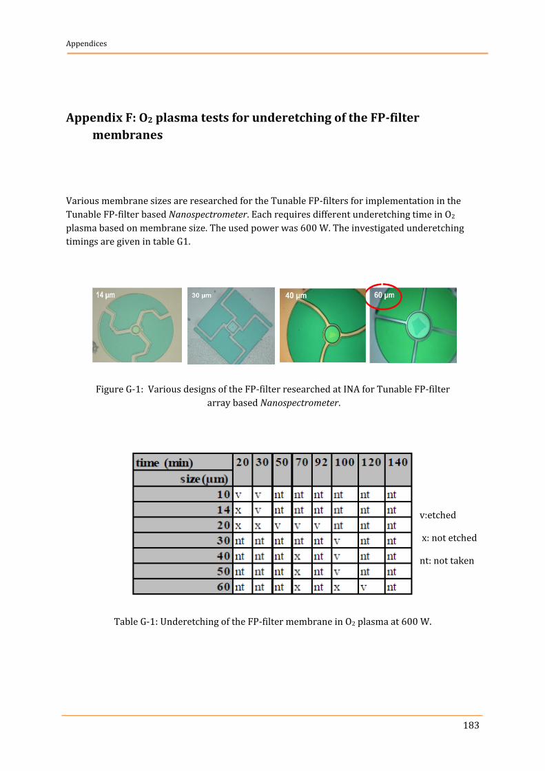
Appendices
183
Appendix F: O2 plasma tests for underetching of the FP-filter
membranes
Various membrane sizes are researched for the Tunable FP-filters for implementation in the
Tunable FP-filter based Nanospectrometer. Each requires different underetching time in O2
plasma based on membrane size. The used power was 600 W. The investigated underetching
timings are given in table G1.
Figure G-1: Various designs of the FP-filter researched at INA for Tunable FP-filter
array based Nanospectrometer.
Table G-1: Underetching of the FP-filter membrane in O2 plasma at 600 W.
v:etched
x: not etched
nt: not taken

Appendices
184
Appendix G: AZ nLOF 2070 lift-off recipe
• Clean the sample by rinsing it in acetone and iso-propanol followed by drying with N2. • Bake dry on hotplate for 10 minutes at 110 °C. • Spin coat adhesion promotor (Ti-prime) at a speed of 3000 rpm for 20 seconds. • Spin coat AZnLOF2070 at a speed of 3000 rpm for 20 seconds. • Prebake sample on a hotplate at a temperature of 110 °C for 1 minute. • Align & expose in MA4. • Hardbake sample on the hotplate for 3.5 minutes at a temperature of 100 °C. • Cool the sample for 2.5 minutes. • Develop the negative photoresist with AZ826 MIF. • Rinse the sample with DI-water and dry using N2.

185
References
[1] A. Albrecht, H. Mai, V. Daneker, X. Wang, S. Schudy, T. Woit, K. Schultz, C. Woidt, O. Setyawati, F. Koehler, S. Wittzack, M. Engenhorst, M. Bartels, and H. Hillmer, "Optical characterization of high-resolution optical nanospectrometers for networked sensing systems," in Networked Sensing Systems (INSS), 2010 Seventh International Conference on, 2010, pp. 175-178.
[2] W. A. Zortman, D. C. Trotter, A. L. Lentine, G. Robertson, and M. R. Watts, "Monolithic integration of silicon electronics and photonics," in Winter Topicals (WTM), 2011 IEEE, 2011, pp. 139-140.
[3] S. C. Roy, T. Kundu, and V. R. Rao, "Polymer-Based MEMS Photodetector With Spectral Response in UV-Vis-NIR and Mid-IR Region," Journal of Lightwave Technology, vol. 33, pp. 3345-3350, 2015.
[4] N. Morita and R. Sawada, "Optical micro sensors integration and application," in IEEE CPMT Symposium Japan 2014, 2014, pp. 3-6.
[5] V. Stojanovi, x, K. T. Settaluri, S. Lin, S. Moazeni, E. Timurdogan, C. Sun, M. Moresco, Z. Su, Y. H. Chen, G. Leake, D. LaTulipe, C. McDonough, J. Hebding, D. Coolbaugh, and M. Watts, "High-density 3D electronic-photonic integration," in Energy Efficient Electronic Systems (E3S), 2015 Fourth Berkeley Symposium on, 2015, pp. 1-2.
[6] D. Kita, H. Lin, A. Agarwal, K. Richardson, I. Luzinov, T. Gu, and J. Hu, "On-chip infrared spectroscopic sensing: redefining the benefits of scaling," IEEE Journal of Selected Topics in Quantum Electronics, vol. PP, pp. 1-1, 2016.
[7] T. Gessner, M. Vogel, C. Kaufmann, K. Hiller, S. Kurth, J. Nestler, and T. Otto, "Micro/nano technologies towards smart systems integration," in Solid-State and Integrated Circuit Technology (ICSICT), 2010 10th IEEE International Conference on, 2010, pp. 1396-1399.
[8] R. P. Feynman, "There's plenty of room at the bottom [data storage]," Journal of Microelectromechanical Systems, vol. 1, pp. 60-66, 1992.
[9] V. Kaushik, J. Lee, J. Hong, S. Lee, S. Lee, J. Seo, C. Mahata, and T. Lee, "Textile-Based Electronic Components for Energy Applications: Principles, Problems, and Perspective," Nanomaterials, vol. 5, p. 1493, 2015.
[10] H. Jane and P. T. Ralph, "Optical gas sensing: a review," Measurement Science and Technology, vol. 24, p. 012004, 2013.
[11] X. Liu, S. Cheng, H. Liu, S. Hu, D. Zhang, and H. Ning, "A Survey on Gas Sensing Technology," Sensors (Basel, Switzerland), vol. 12, pp. 9635-9665, 2012.
[12] N. P. Ayerden, M. Ghaderi, P. Enoksson, G. de Graaf, and R. F. Wolffenbuttel, "A miniaturized optical gas-composition sensor with integrated sample chamber," Sensors and Actuators B: Chemical, vol. 236, pp. 917-925, 2016.
[13] P. Hu, Y. Chen, and S. Sonkusale, "Low cost spectrometer accessory for cell phone based optical sensor," in 2015 IEEE Virtual Conference on Applications of Commercial Sensors (VCACS), 2015, pp. 1-5.
[14] K. Minolta. (12.10.2016). LCS-IV Spectrophotometer. Available: http://sensing.konicaminolta.us/ [15] R. A. Shaw and H. H. Mantsch, "Infrared Spectroscopy of Biological Fluids in Clinical and
Diagnostic Analysis," in Encyclopedia of Analytical Chemistry, ed: John Wiley & Sons, Ltd, 2006. [16] M. N. Uddin, V. F. Samanidou, and I. N. Papadoyannis, "An Overview on Total Analytical Methods
for the Detection of 1,4-Benzodiazepines," Pharmaceutica Analytica Acta, vol. 5, pp. 1 - 13, 2014.

References
186
[17] M. G. Angelova and A. N. Bozhinova, "Short Review on Spectral Methods for the Determination of Chromiun in Human Body Fluids and Tissues " Open Science Journal of Analytical Chemistry vol. 2, pp. 13 - 19, 2015.
[18] I. Raptis, K. Misiakos, E. Makarona, A. Salapatas, P. Petrou, S. Kakabakos, A. Botsialas, G. Jobst, W. Haasnoot, A. Fernandez-Alba, M. Lees, and E. Valamontes, "A miniaturized optoelectronic system for rapid quantitative label-free detection of harmful species in food," 2016, pp. 97250A-97250A-7.
[19] S. Hintschich, T. Pügner, K. Jens, J. Schröder, P. Reinig, H. Grüger, and H. Schenk, "MEMS-based miniature near-infrared spectrometer for application in environmental and food monitoring," in 8th International Conference on Sensing Technology, ICST 2014, Liverpool, UK, 2014, pp. 430 - 434.
[20] W. Z. Song, A. Q. Liu, C. S. Lim, and P. H. Yap, "A micro-optic-fluidic spectrometer with integrated 3D liquid-liquid waveguide," in 2007 IEEE/LEOS International Conference on Optical MEMS and Nanophotonics, 2007, pp. 161-162.
[21] S. Nosheen, S. Alam, M. Irfan, M. U. A. Qureshi, and S. Ahmad, "Optical Emission Spectrometer, Principle and Latest Industrial Applications," International Journal of Material Science (IJMSCI), vol. 3, pp. 139 - 144, 2013.
[22] J. Praks, M. Eskelinen, J. Pulliainen, T. Pyhalahti, and M. Hallikainen, "Detection of oil pollution on sea ice with airborne and spaceborne spectrometer," in Geoscience and Remote Sensing Symposium, 2004. IGARSS '04. Proceedings. 2004 IEEE International, 2004, pp. 1-276.
[23] W. J. Scheirer, S. R. Kirkbride, and T. E. Boult, "INSPECT: Inexpensive Spectrometer Color Camera Technology," in Applications of Computer Vision, 2008. WACV 2008. IEEE Workshop on, 2008, pp. 1-8.
[24] J. T. Smith, B. A. Katchman, Y. K. Lee, B. P. O. Brien, E. J. Bawolek, S. S. Shah, and J. B. Christen, "Disposable point-of-use optical biosensor for multiple biomarker detection," in 2014 IEEE Biomedical Circuits and Systems Conference (BioCAS) Proceedings, 2014, pp. 268-271.
[25] D. Issadore and R. M. Westervelt, Point-of-Care Diagnostics on a Chip: Springer-Verlag Berlin Heidelberg, 2013.
[26] H. Photonics, "Mini-Spectrometers," ed. Japan, 2016. [27] C. Zeiss. (14.10.2016). Spectrometer Modules. Available:
http://www.zeiss.com/spectroscopy/en_de/products/spectrometer-modules.html [28] O. Optics. (14.10.2016). Available: http://oceanoptics.com/ [29] Insion. (14.10.2016). The world of microoptics – integrated on a single chip. Available:
https://www.insion.de/products.html [30] J. H. Correia, M. Bartek, and R. F. Wolffenbuttel, "High-selectivity single-chip spectrometer for
operation at visible wavelengths," in Electron Devices Meeting, 1998. IEDM '98. Technical Digest., International, 1998, pp. 467-470.
[31] J. H. Correia, G. de Graaf, S. H. Kong, M. Bartek, and R. F. Wolffenbuttel, "Single-chip CMOS optical microspectrometer," Sensors and Actuators A: Physical, vol. 82, pp. 191-197, 2000.
[32] R. F. Wolffenbuttel, "State-of-the-art in integrated optical microspectrometers," IEEE Transactions on Instrumentation and Measurement, vol. 53, pp. 197-202, 2004.
[33] R. F. Wolffenbuttel, "MEMS-based optical mini- and microspectrometers for the visible and infrared spectral range," Journal of Micromechanics and Microengineering, vol. 15, p. S145, 2005.
[34] S.-W. Wang, M. Li, C.-S. Xia, H.-Q. Wang, X.-S. Chen, and W. Lu, "128 channels of integrated filter array rapidly fabricated by using the combinatorial deposition technique," Applied Physics B, vol. 88, pp. 281-284, 2007.
[35] A. Emadi, H. Wu, S. Grabarnik, G. De Graaf, and R. F. Wolffenbuttel, "IC-compatible fabrication of linear variable optical filters for microspectrometer," Procedia Chemistry, vol. 1, pp. 1143-1146, 2009/09/01 2009.
[36] A. Emadi, H. Wu, S. Grabarnik, G. De Graaf, K. Hedsten, P. Enoksson, J. H. Correia, and R. F. Wolffenbuttel, "Fabrication and characterization of IC-Compatible Linear Variable Optical Filters with application in a micro-spectrometer," Sensors and Actuators A: Physical, vol. 162, pp. 400-405, 2010.
[37] A. Emadi, H. Wu, G. de Graaf, and R. F. Wolffenbuttel, "IR Microspectrometers based on Linear-Variable Optical Filters," Procedia Engineering, vol. 25, pp. 1401-1404, 2011.
[38] J. P. Carmo, R. P. Rocha, M. Bartek, G. de Graaf, R. F. Wolffenbuttel, and J. H. Correia, "A review of visible-range Fabry–Perot microspectrometers in silicon for the industry," Optics & Laser Technology, vol. 44, pp. 2312-2320, 2012.

References
187
[39] A. Emadi, H. Wu, G. de Graaf, and R. Wolffenbuttel, "Design and implementation of a sub-nm resolution microspectrometer based on a Linear-Variable Optical Filter," Optics Express, vol. 20, pp. 489-507, 2012/01/02 2012.
[40] H. Hillmer, "Optisches Filter und Verfahren zu seiner Herstellung," DE 10 2006 039 071 B4, (2008), application granted 2012.
[41] H. Hillmer, "Verfahren und Anordnung zur Herstellung von Nanoimprint-Stempeln, sowie mikromechanisch durchstimmbaren Filter/Detektor Arrays," DE102007047598A1, 2007.
[42] A.Albrecht, X.Wang, H.H.Mai, T.Schotzko, I.Memon, M.Bartels, M.Hornung, and H.Hillmer, "High vertical resolution 3D NanoImprint Technology and its application in optical nanosensors," J. Nonlinear Optics and Quantum Optics, vol. 43, pp. 339 - 353, 2012.
[43] I. Memon, Y. Shen, A. Khan, C. Woidt, and H. Hillmer, "Highly uniform residual layers for arrays of 3D nanoimprinted cavities in Fabry–Pérot-filter-array-based nanospectrometers," Applied Nanoscience, vol. 6, pp. 599-606, 2016.
[44] D. T. Nguyen, M. Ababtain, I. Memon, A. Ullah, A. Istock, C. Woidt, W. Xie, P. Lehmann, and H. Hillmer, "3D nanoimprint for NIR Fabry-Pérot filter arrays: fabrication, characterization and comparison of different cavity designs," Applied Nanoscience, pp. 1-9, 2016.
[45] X. Wang, A. Albrecht, S. Schudy, T. Woit, V. Daneker, K. Schultz, H. H. Mai, K. F, x00F, hler, S. Wittzack, M. Bartels, and H. Hillmer, "High-resolution, low-cost microsensors for networked sensing systems: Optical nanospectrometers with nanoimprinted cavities of filter arrays," in Networked Sensing Systems (INSS), 2010 Seventh International Conference on, 2010, pp. 171-174.
[46] A. Lazakidou, Wireless Technologies for Ambient Assisted Living and Healthcare: Systems and Applications: Systems and Applications: IGI Global, 2010.
[47] M. Bartels, S. Wittzack, F. Kohler, X. Wang, A. Albrecht, S. Schudy, M. Engenhorst, H. H. Mai, O. Setyawati, T. Woit, C. Woidt, and H. Hillmer, "High vertical resolution 3D Nanoimprint technology for nanophotonic applications," in 2009 IEEE/LEOS International Conference on Optical MEMS and Nanophotonics, 2009, pp. 87-88.
[48] X. Wang, A. Albrecht, H. H. Mai, C. Woidt, T. Meinl, M. Hornung, M. Bartels, and H. Hillmer, "High resolution 3D NanoImprint technology: Template fabrication, application in Fabry–Pérot-filter-array-based optical nanospectrometers," Microelectronic Engineering, vol. 110, pp. 44-51, 2013.
[49] M. Bartels, X. Wang, T. Kusserow, F. Koehler, S. Wittzack, and H. Hillmer, "3D nanoimprint templates with ultra-high vertical precision," in International Conference on Materials for Advanced Technologies and International Union of Materials Research Societies International Conference in Asia, Singapore, 2009.
[50] V. R. Kolli, C. Woidt, and H. Hillmer, "Patterning of Polymer Arrays with Enhanced Aspect-Ratio Using Hybrid Substrate Conformal Imprint Lithography," Advanced Materials Research, vol. 1119, pp. 179 - 183, 2015.
[51] V. Kolli, C. Woidt, and H. Hillmer, "Residual-layer-free 3D nanoimprint using hybrid soft templates," Microelectronic Engineering, vol. 149, pp. 159-165, 2016.
[52] M.Bartels, F. Köhler, S. Wittzack, X.Wang, and H.Hillmer, "Ultra precise Nano Imprint templates," presented at the NanoS, 2008.
[53] H. H. Mai, A. Albrecht, C. Woidt, X. Wang, V. Daneker, O. Setyawati, T. Woit, K. Schultz, M. Bartels, and H. Hillmer, "3D nanoimprinted Fabry–Pérot filter arrays and methodologies for optical characterization," Applied Physics B, vol. 107, pp. 755-764, 2012.
[54] J. Solé, L. Bausa, and D. Jaque, An Introduction to the Optical Spectroscopy of Inorganic Solids: Wiley, 2005.
[55] E. L. Ivchenko, Optical Spectroscopy of Semiconductor Nanostructures: Alpha Science, 2005. [56] R. P. Prasankumar and A. J. Taylor, Optical Techniques for Solid-State Materials Characterization:
CRC Press, 2016. [57] B. D. Dunn, Materials and Processes: for Spacecraft and High Reliability Applications: Springer
International Publishing, 2015. [58] J. A. Räty, K. E. Peiponen, and T. Asakura, UV-Visible Reflection Spectroscopy of Liquids: Springer
Berlin Heidelberg, 2013. [59] B. K. Sharma, Spectroscopy: Krishna Prakashan, 1981. [60] S. Thomas, D. Rouxel, and D. Ponnamma, Spectroscopy of Polymer Nanocomposites: Elsevier
Science, 2016. [61] I. Pérez-Juste and O. Nieto Faza, "Interaction of Radiation with Matter," in Structure Elucidation in
Organic Chemistry, ed: Wiley-VCH Verlag GmbH & Co. KGaA, 2015, pp. 1-26.

References
188
[62] W. Song, Z. Mao, X. Liu, Y. Lu, Z. Li, B. Zhao, and L. Lu, "Detection of protein deposition within latent fingerprints by surface-enhanced Raman spectroscopy imaging," Nanoscale, vol. 4, pp. 2333-2338, 2012.
[63] A. Nawrocka and J. Lamorska. (2013). Determination of Food Quality by Using Spectroscopic Methods. Available: http://www.intechopen.com/books/advances-in-agrophysical-research/determination-of-food-quality-by-using-spectroscopic-methods
[64] G. Downey, Advances in Food Authenticity Testing: Elsevier Science, 2016. [65] Z. Yang, K. Li, M. Zhang, D. Xin, and J. Zhang, "Rapid determination of chemical composition and
classification of bamboo fractions using visible–near infrared spectroscopy coupled with multivariate data analysis," Biotechnology for Biofuels, vol. 9, p. 35, 2016.
[66] S. N. C. Ortiz, E. M. Ospino, and R. Cabanzo, "Spectroscopy characterization and quantum yield determination of quantum dots," Journal of Physics: Conference Series, vol. 687, p. 012097, 2016.
[67] R. Pavithra, S. Gunasekaran, E. Sailatha, and S. Kamatchi, "Investigations on Paper Making Raw Materials and Determination of Paper Quality by FTIR-UATR and UV-Vis DRS Spectroscopy," International Journal of Current Research and Academic Review, vol. 3, pp. 42 - 59, 2015.
[68] R. A. Viscarra Rossel, T. Behrens, E. Ben-Dor, D. J. Brown, J. A. M. Demattê, K. D. Shepherd, Z. Shi, B. Stenberg, A. Stevens, V. Adamchuk, H. Aïchi, B. G. Barthès, H. M. Bartholomeus, A. D. Bayer, M. Bernoux, K. Böttcher, L. Brodský, C. W. Du, A. Chappell, Y. Fouad, V. Genot, C. Gomez, S. Grunwald, A. Gubler, C. Guerrero, C. B. Hedley, M. Knadel, H. J. M. Morrás, M. Nocita, L. Ramirez-Lopez, P. Roudier, E. M. R. Campos, P. Sanborn, V. M. Sellitto, K. A. Sudduth, B. G. Rawlins, C. Walter, L. A. Winowiecki, S. Y. Hong, and W. Ji, "A global spectral library to characterize the world's soil," Earth-Science Reviews, vol. 155, pp. 198-230, 2016.
[69] Y. Kim and U. Platt, Advanced Environmental Monitoring: Springer Netherlands, 2007. [70] S. Pons, I. F. Aymerich, E. Torrecilla, and J. Piera, "Monolithic spectrometer for environmental
monitoring applications," in OCEANS 2007 - Europe, 2007, pp. 1-3. [71] J. F. Artiola, I. L. Pepper, and M. L. Brusseau, Environmental Monitoring and Characterization:
Elsevier Academic Press, 2004. [72] O. Optics. (2016, Characterizing LED Parameters using Spectroscopy. Available:
http://oceanoptics.com/radiometric-led-measurement/ [73] SHIMADZU. 11.11.2016). Emission Spectrum Measurement for LED Lamp by the UV-2600 UV-VIS
Spectrophotometer. Available: http://www.shimadzu.com/an/literature/uv/jpa112020.html [74] O. Optics. (2015, 11.11.2016). LED Color Measurement with Compact Spectral Sensor. Available:
http://oceanoptics.com/led-color-measurement-spark/ [75] H. Wang, J. Peng, C. Xie, Y. Bao, and Y. He, "Fruit Quality Evaluation Using Spectroscopy
Technology: A Review," Sensors, vol. 15, p. 11889, 2015. [76] S. P. and A. Gokul, "Nondestructive Quality Evaluation for Fruits and Vegetables," International
Journal of Modern Trends in Engineering and Research, vol. 3, 2016. [77] B. M. Nicolaï, K. Beullens, E. Bobelyn, A. Peirs, W. Saeys, K. I. Theron, and J. Lammertyn,
"Nondestructive measurement of fruit and vegetable quality by means of NIR spectroscopy: A review," Postharvest Biology and Technology, vol. 46, pp. 99-118, 2007.
[78] K. Kong, C. Kendall, N. Stone, and I. Notingher, "Raman spectroscopy for medical diagnostics — From in-vitro biofluid assays to in-vivo cancer detection," Advanced Drug Delivery Reviews, vol. 89, pp. 121-134, 2015.
[79] H. Photonics. (20.08.2016). mini-spectrometers. Available: http://www.hamamatsu.com/us/en/4016.html
[80] C. Palmer and E. Loewen. (2005, 10.09.2016). DIFFRACTION GRATING HANDBOOK (6 ed.). [81] J. Workman, The Handbook of Organic Compounds, Three-Volume Set: NIR, IR, R, and UV-Vis
Spectra Featuring Polymers and Surfactants: Elsevier Science, 2000. [82] J. Workman and A. Springsteen, Applied Spectroscopy: A Compact Reference for Practitioners:
Elsevier Science, 1998. [83] O. Optics. 11.09.2016). How does my choice of spectrometer slit size affect optical resolution?
Available: http://oceanoptics.com/faq/choice-slit-size-affect-resolution/ [84] HAMAMATSU. 12.09.2016). Mini-spectrometer. Available:
https://www.hamamatsu.com/jp/en/C10988MA-01.html [85] S. Irmer, K. Alex, J. Daleiden, I. Kommallein, M. Oliveira, F. Römer, A. Tarraf, and H. Hillmer,
"Surface micromachined optical low-cost all-air-gap filters based on stress-optimized Si 3 N 4 layers," Journal of Micromechanics and Microengineering, vol. 15, p. 867, 2005.

References
189
[86] S. Irmer, J. Daleiden, V. Rangelov, C. Prott, F. Romer, M. Strassner, A. Tarraf, and H. Hillmer, "Ultralow biased widely continuously tunable fabry-Perot filter," IEEE Photonics Technology Letters, vol. 15, pp. 434-436, 2003.
[87] A. Hasse, S. Irmer, J. Daleiden, N. Dharmarasu, S. Hansmann, and H. Hillmer, "Wide continuous tuning range of 221nm by InP / air-gap vertical-cavity filters," Electronics Letters, vol. 42, pp. 974-975, 2006.
[88] D. Hohlfeld and H. Zappe, "Thermally tunable optical thin-film filters with sub-nanometer resolution and 41.7 nm continuous tuning range," in 18th IEEE International Conference on Micro Electro Mechanical Systems, 2005. MEMS 2005., 2005, pp. 100-103.
[89] A. Albrecht, "Substrate Conformal Imprint Lithography als innovatives Verfahren zur Herstellung von Nanospektrometern im sichtbaren Spektralbereich," PhD thesis PhD thesis, University of Kassel, 2012.
[90] Y. Nishi and R. Doering, Handbook of Semiconductor Manufacturing Technology, Second Edition: CRC Press, 2007.
[91] D. A. Dana, The Nanotechnology Challenge: Creating Legal Institutions for Uncertain Risks: Cambridge University Press, 2011.
[92] W. Menz, J. Mohr, and O. Paul, Microsystem Technology: Wiley, 2008. [93] R. R. Schaller, "Moore's law: past, present and future," IEEE Spectrum, vol. 34, pp. 52-59, 1997. [94] T. R. Hsu, MEMS and Microsystems: Design, Manufacture, and Nanoscale Engineering: Wiley,
2008. [95] E. Suhir, Y. C. Lee, and C. P. Wong, Micro- and Opto-Electronic Materials and Structures: Physics,
Mechanics, Design, Reliability, Packaging: Volume I Materials Physics - Materials Mechanics. Volume II Physical Design - Reliability and Packaging: Springer US, 2007.
[96] B. W. Smith and K. Suzuki, Microlithography: Science and Technology, Second Edition: CRC Press, 2007.
[97] V. Bakshi, EUV Lithography: Society of Photo Optical, 2009. [98] S. Y. Borkar, "VLSI Design Challenges for Gigascale Integration," in VLSI Design, 2005, p. 27. [99] M. D. Austin, H. Ge, W. Wu, M. Li, Z. Yu, D. Wasserman, S. A. Lyon, and S. Y. Chou, "Fabrication of
5nm linewidth and 14nm pitch features by nanoimprint lithography," Applied Physics Letters, vol. 84, pp. 5299-5301, 2004.
[100] S. Y. Chou, P. R. Krauss, W. Zhang, L. Guo, and L. Zhuang, "Sub-10 nm imprint lithography and applications," Journal of Vacuum Science & Technology B, vol. 15, pp. 2897-2904, 1997.
[101] L. J. Guo, "Nanoimprint lithography: methods and material requirements," Advanced Materials, vol. 19, pp. 495-513, 2007.
[102] S. I. Association. (2003, 21.12.2016). 2003 International Technology Roadmap for Semiconductors (ITRS). Available: http://www.semiconductors.org/main/2003_international_technology_roadmap_for_semiconductors_itrs/
[103] D. S. Goldman, P. L. White, and N. C. Anheier, "Miniaturized spectrometer employing planar waveguides and grating couplers for chemical analysis," Applied Optics, vol. 29, pp. 4583-4589, 1990/11/01 1990.
[104] R. G. Heideman, R. P. H. Kooyman, and J. Greve, "Performance of a highly sensitive optical waveguide Mach-Zehnder interferometer immunosensor," Sensors and Actuators B: Chemical, vol. 10, pp. 209-217, 1993/02/01 1993.
[105] J. Mohr, B. Anderer, and W. Ehrfeld, "Fabrication of a planar grating spectrograph by deep-etch lithography with synchrotron radiation," Sensors and Actuators A: Physical, vol. 27, pp. 571-575, 1991/05/01 1991.
[106] D. Sander and J. Müller, "Selffocussing phase transmission grating for an integrated optical microspectrometer," Sensors and Actuators A: Physical, vol. 88, pp. 1-9, 2001.
[107] T. A. Kwa and R. F. Wolffenbuttel, "Integrated grating/detector array fabricated in silicon using micromachining techniques," Sensors and Actuators A: Physical, vol. 31, pp. 259-266, 1992/03/01 1992.
[108] K. Seong-Ho, J. H. Correia, G. d. Graaf, M. Bartek, and R. F. Wolffenbuttel, "Integrated silicon microspectrometers," IEEE Instrumentation & Measurement Magazine, vol. 4, pp. 34-38, 2001.
[109] T. A. Kwa, P. J. French, R. F. Wolffenbuttel, P. M. Sarro, L. Hellemans, and L. Snauwaert, "Anisotropically etched silicon mirrors for optical sensor applications," J. Electrochemical Society, vol. 142, pp. 1226 - 1233, 1995.
[110] R. F. Wolffenbuttel, Silicon Sensors and Circuits: On-chip compatibility: Springer, 1996.

References
190
[111] S. H. Kong, D. D. L. Wijngaards, and R. F. Wolffenbuttel, "Infrared micro-spectrometer based on a diffraction grating," Sensors and Actuators A: Physical, vol. 92, pp. 88-95, 2001.
[112] S. Traut, M. Rossi, and H. P. Herzig, "Replicated arrays of hybrid elements for application in a low-cost micro-spectrometer array," Journal of Modern Optics, vol. 47, pp. 2391-2397, 2000/11/01 2000.
[113] H. Photonics. (2016, 20.11.2016). Mini-spectrometers. Available: http://www.hamamatsu.com/jp/en/product/category/5001/4016/index.html
[114] INSION. (22.11.2016). UV/VIS microspectrometer. Available: https://www.insion.de/uvvis-microspectrometer.html
[115] C. Zeiss. (24.11.2016). Monolithic Miniature Spectrometer. Available: http://www.zeiss.com/spectroscopy/products/spectrometer-modules/monolithic-miniature-spectrometer-mms.html#specification
[116] C. Zeiss. (25.11.2016). Monolithic Miniature Spectrometer MMS UV-VIS. Available: www.hellma-analytics.com/html/seiten/output_adb_file.php?id=24679
[117] R. Photonics. (26.11.2016). Spectrometers. Available: http://www.rgb-photonics.com/ [118] T. Pügner, J. Knobbe, and H. Grüger, "Near-Infrared Grating Spectrometer for Mobile Phone
Applications," Applied Spectroscopy, vol. 70, pp. 734-745, 2016/05/01 2016. [119] F. IPMS. (2015, 27.11.2016). Fraunhofer IPMS develops MEMS technology for spectroscopy in the
medium infrared range. Available: http://www.ipms.fraunhofer.de/en/press-media/press/2015/2015-01-20.html
[120] J. H. Correia, M. Bartek, and R. F. Wolffenbuttel, "High-selectivity single-chip spectrometer for operation at visible wavelengths," in International Electron Devices Meeting 1998. Technical Digest (Cat. No.98CH36217), 1998, pp. 467-470.
[121] S.-W. Wang, C. Xia, X. Chen, W. Lu, M. Li, H. Wang, W. Zheng, and T. Zhang, "Concept of a high-resolution miniature spectrometer using an integrated filter array," Optics Letters, vol. 32, pp. 632-634, 2007/03/15 2007.
[122] A. Emadi, H. Wu, S. Grabarnik, G. d. Graaf, and R. F. Wolffenbuttel, "Vertically tapered layers for optical applications fabricated using resist reflow," Journal of Micromechanics and Microengineering, vol. 19, p. 074014, 2009.
[123] N. P. Ayerden, G. de Graaf, and R. F. Wolffenbuttel, "Compact gas cell integrated with a linear variable optical filter," Optics Express, vol. 24, pp. 2981-3002, 2016/02/08 2016.
[124] Pyreos. (29.11.2016). Line Array Components. Available: http://www.pyreos.com/line-array-components
[125] J. Wright. (2012, 30.11.2016). New Miniaturised Low Cost Mid IR Spectrometers for Portable and Continuous Monitoring Applications. Available: http://www.systems-eng.co.jp/dcms_media/other/pyreos_item02.pdf
[126] A. Emadi, H. Wu, G. de Graaf, K. Hedsten, P. Enoksson, J. H. Correia, and R. F. Wolffenbuttel, "An UV linear variable optical filter-based micro-spectrometer," Procedia Engineering, vol. 5, pp. 416-419, 2010/01/01 2010.
[127] M. Bartels, F. Köhler, S. Wittzack, X. Wang, and H. Hillmer, "Ultra precise Nanoimprint templates," presented at the NanoS, 2008.
[128] X. Wang, A. Albrecht, S. Schudy, T. Woit, V. Daneker, K. Schultz, H. H. Mai, F. Köhler, S. Wittzack, M. Bartels, and H. Hillmer, "High-resolution, low-cost microsensors for networked sensing systems: Optical nanospectrometers with nanoimprinted cavities of filter arrays," in 2010 Seventh International Conference on Networked Sensing Systems (INSS), 2010, pp. 171-174.
[129] A. Albrecht, H. Mai, V. Daneker, X. Wang, S. Schudy, T. Woit, K. Schultz, C. Woidt, O. Setyawati, F. Köhler, S. Wittzack, M. Engenhorst, M. Bartels, and H. Hillmer, "Optical characterization of high-resolution optical nanospectrometers for networked sensing systems," in 2010 Seventh International Conference on Networked Sensing Systems (INSS), 2010, pp. 175-178.
[130] A. Albrecht, W. Xiaolin, M. Hanh Hong, T. Schotzko, I. Memon, M. Bartels, M. Hornung, and H. Hillmer, "High Vertical Resolution 3D NanoImprint Technology and its Application in Optical Nanosensors," Nonlinear Optics, Quantum Optics: Concepts in Modern Optics, vol. 43, pp. 339-353, 2011.
[131] M. Salah, "Investigation of Imprint Materials and Improvement of Residual Layer for Optical Sensor Arrays," Master thesis, University of Kassel, 2011.
[132] Quora. (2016, 15.05.2016). Why does it show a spectrum when water is spread over oil? Available: https://www.quora.com/Why-does-it-show-a-spectrum-when-water-is-spread-over-oil

References
191
[133] Pixabay. (2016, 15.05.2016). Free High Quality Images. Available: https://pixabay.com/en/photos/?q=soap+bubbles&image_type=&cat=&min_width=&min_height=
[134] F. G. Smith and T. A. King, "Optics and photonics: an introduction," ed: IOP Publishing, 2001. [135] R. A. Serway and J. W. Jewett, Physics for scientists and engineers with modern physics: Nelson
Education, 2013. [136] H. Zappe, Laser Diode Microsystems: Springer Berlin Heidelberg, 2013. [137] H. Hillmer, "Manuscript of Optoelectronic Devices," ed. University of Kassel, Germany, 2015. [138] C. E. Webb and J. D. C. Jones, Handbook of Laser Technology and Applications: Laser design and
laser systems: Institute of Physics, 2004. [139] P. A and F. C, " Méthodes interférentielles pour la mesure des grandes épaisseurs et la
comparaison des longueurs d'onde," Ann. Chim. Phys., vol. 16, pp. 289-338, 1899. [140] J. M. Liu, Principles of Photonics: Cambridge University Press, 2016. [141] J. H. Moore, C. C. Davis, M. A. Coplan, and S. C. Greer, Building Scientific Apparatus: Cambridge
University Press, 2009. [142] C. DeCusatis, Fiber Optic Data Communication: Technology Advances and Futures: Elsevier
Science, 2002. [143] C. DeCusatis, Fiber Optic Data Communication: Technological Trends and Advances: Academic
Press, 2002. [144] J. F. Donnelly and N. M. Massa, Light: Introduction to Optics and Photonics: New England Board of
Higher Education, 2010. [145] D. Hohlfeld, "Silicon-based Tunable Optical Filters," PhD PhD thesis, Fakultät für Angewandte
Wissenschaften, Albert-Ludwigs Universität Freiburg im Breisgau, 2005. [146] W. Demtröder, Laser Spectroscopy: Vol. 1: Basic Principles: Springer Berlin Heidelberg, 2008. [147] R. S. Sirohi, Wave Optics And Its Applications: Orient BlackSwan, 1993. [148] V. S. Hans H. Gatzen, Jürg Leuthold, Micro and Nano Fabrication: Tools and Processes: Springer-
Verlag Berlin Heidelberg, 2015. [149] A. K. K. Wong, Resolution Enhancement Techniques in Optical Lithography: SPIE Press, 2001. [150] N. Maluf and K. Williams, Introduction to Microelectromechanical Systems Engineering: Artech
House, 2004. [151] L. Vivien and L. Pavesi, Handbook of Silicon Photonics: CRC Press, 2016. [152] S. Rizvi, Handbook of Photomask Manufacturing Technology: CRC Press, 2005. [153] Z. Cui, Nanofabrication: Principles, Capabilities and Limits: Springer International Publishing,
2016. [154] R. Waser, Nanoelectronics and Information Technology: Wiley, 2012. [155] C. Papadopoulos, Nanofabrication: Principles and Applications: Springer International
Publishing, 2016. [156] C. Mack, Fundamental Principles of Optical Lithography: The Science of Microfabrication: Wiley,
2011. [157] C. A. Mack, Field Guide to Optical Lithography: Society of Photo Optical, 2006. [158] R. Rubingh. (2007, An introduction to photolithography Imaging. 20 - 22. Available:
https://www.asml.com [159] F. W. Sven Bühling, Ernst-Bernhard Kley, A J M Nellissen, Lingli Wang and Maarten Dirkzwager,
"Resolution enhanced proximity printing by phase andamplitude modulating masks," Journal of Micromechanics and Microengineering, vol. Volume 11, p. 603, 2001.
[160] N. S. V. Marc D. Levenson, Robert A. Simpson, "Improving Resolution in Photolithography with a Phase-Shifting Mask " IEEE TRANSACTIONS ON ELECTRON DEVICES, vol. 29, pp. 1828-1836, 1982.
[161] M. Feldman, Nanolithography: The Art of Fabricating Nanoelectronic and Nanophotonic Devices and Systems: Elsevier Science, 2014.
[162] R. C. Dorf, Electronics, Power Electronics, Optoelectronics, Microwaves, Electromagnetics, and Radar: CRC Press, 2006.
[163] R. F. Pease and S. Y. Chou, "Lithography and Other Patterning Techniques for Future Electronics," Proceedings of the IEEE, vol. 96, pp. 248-270, 2008.
[164] S. Y. Chou, P. R. Krauss, and P. J. Renstrom, "Imprint lithography with 25-nanometer resolution," Science, vol. 272, p. 85, 1996.
[165] T. R. Albrecht, H. Arora, V. Ayanoor-Vitikkate, J. M. Beaujour, D. Bedau, D. Berman, A. L. Bogdanov, Y. A. Chapuis, J. Cushen, E. E. Dobisz, G. Doerk, H. Gao, M. Grobis, B. Gurney, W. Hanson, O. Hellwig, T. Hirano, P. O. Jubert, D. Kercher, J. Lille, Z. Liu, C. M. Mate, Y. Obukhov, K. C. Patel, K. Rubin, R.

References
192
Ruiz, M. Schabes, L. Wan, D. Weller, T. W. Wu, and E. Yang, "Bit-Patterned Magnetic Recording: Theory, Media Fabrication, and Recording Performance," IEEE Transactions on Magnetics, vol. 51, pp. 1-42, 2015.
[166] W. Zhou, Nanoimprint Lithography: An Enabling Process for Nanofabrication: Springer Berlin Heidelberg, 2013.
[167] J. Taniguchi, H. Ito, J. Mizuno, and T. Saito, Nanoimprint Technology: Nanotransfer for Thermoplastic and Photocurable Polymers: Wiley, 2013.
[168] H. Lan and Y. Ding, "Nanoimprint Lithography," in Lithography, M. W. (Ed.), Ed., ed: InTech, 2010. [169] D. Comoretto, Organic and Hybrid Photonic Crystals: Springer International Publishing, 2015. [170] "EV Group: Nano & Micro Imprint Technologies," vol. 14, ed, pp. 1 - 11. [171] M. Verschuuren and H. V. Sprang, "3D Photonic Structures by Sol-Gel Imprint Lithography," MRS
Proceedings, vol. 1002, 2007/001/001 2007. [172] R. Ji, M. Hornung, M. A. Verschuuren, R. v. d. Laar, J. v. Eekelen, U. Plachetka, M. Moeller, and C.
Moormann, "UV enhanced substrate conformal imprint lithography (UV-SCIL) technique for photonic crystals patterning in LED manufacturing," Microelectron. Eng., vol. 87, pp. 963-967, 2010.
[173] A. Albrecht, "Substrate Conformal Imprint Lithography als innovatives Verfahren zur Herstellung von Nanospektrometern im sichtbaren Spektralbereich," PhD Dissertation PhD Thesis, University of Kassel, Germany, 2012.
[174] I. Memon, "Herstellung und Charakterisierung von effizienten optischen Filter Arrays implementiert mittels 3D Nanoimprint," PhD Dissertation, University of Kassel, Germany, 2015.
[175] Z. Geng, X. Guo, Q. Kan, and H. Chen, "Optimization of substrate conformal imprint lithography (SCIL) and etching for nanostructure," AIP Advances, vol. 5, p. 041308, 2015.
[176] M. Hornung, R. Ji, M. Verschuuren, and R. v. d. Laar, "6 inch full field wafer size nanoimprint lithography for photonic crystals patterning," in Nanotechnology (IEEE-NANO), 2010 10th IEEE Conference on, 2010, pp. 339-342.
[177] R. Ji, M. Hornung, M. A. Verschuuren, R. van de Laar, J. van Eekelen, U. Plachetka, M. Moeller, and C. Moormann, "UV enhanced substrate conformal imprint lithography (UV-SCIL) technique for photonic crystals patterning in LED manufacturing," Microelectronic Engineering, vol. 87, pp. 963-967, 2010.
[178] K. S. K.-G. Co, "SUSS MA4 SUSS MA6," ed. W. Germany. [179] S. MicroTec. (15.02.2016). Mask Aligner. Available: https://www.suss.com [180] S. Franssila, Introduction to Microfabrication: Wiley, 2010. [181] D. Dobkin and M. K. Zuraw, Principles of Chemical Vapor Deposition: Springer Netherlands, 2013. [182] O. Instruments. (16.02.2016). Plasma Enhanced Chemical Vapour Deposition (PECVD). Available:
https://www.oxford-instruments.com [183] R. J. Shul and S. J. Pearton, Handbook of Advanced Plasma Processing Techniques: Springer, 2000. [184] B. V. Suresh, Solid State Devices and Technology: Pearson Education, 2010. [185] A. G. Baca, C. I. H. Ashby, and I. o. E. Engineers, Fabrication of GaAs Devices: Institution of
Engineering and Technology, 2005. [186] O. Instruments. (17.02.2016). Reactive Ion Etching (RIE). Available: https://www.oxford-
instruments.com [187] Z. Corporation. Precision Noncontact Three Dimensional Surface Profiling. Available:
http://www.lambdaphoto.co.uk/pdfs/nv5000ds1.pdf [188] v č k and O. Hýbl, "White-light interferometry on rough surfaces--measurement
uncertainty caused by surface roughness," Applied Optics, vol. 47, pp. 2941-2949, 2008/06/01 2008.
[189] K. Harding, Handbook of Optical Dimensional Metrology: CRC Press, 2016. [190] N. Katz. (1999, Zygo 3D Surface Profiler Sports Improved Data Acquisition and Scanning
Functionality. Available: http://www.metrologyworld.com/ [191] S. Ali, Cell organisation and Function. [192] D. SINGH, FUNDAMENTALS OF OPTICS, SECOND EDITION: Prentice-Hall of India Pvt.Limited,
2015. [193] D. B. Holt and D. C. Joy, SEM Microcharacterization of Semiconductors: Elsevier Science, 2013. [194] "Ultra-high Resolution Scanning Electron Microscope," in SU8000 Series, H. H.-T. Coorporation,
Ed., ed, 2011. [195] A. Khursheed, Scanning Electron Microscope Optics and Spectrometers: World Scientific, 2011. [196] H. Schatten, Scanning Electron Microscopy for the Life Sciences: Cambridge University Press,
2013.

References
193
[197] C. E. Lyman, D. E. Newbury, J. Goldstein, D. B. Williams, A. D. Romig, J. Armstrong, P. Echlin, C. Fiori, D. C. Joy, and E. Lifshin, Scanning Electron Microscopy, X-Ray Microanalysis, and Analytical Electron Microscopy: A Laboratory Workbook: Springer US, 2012.
[198] I. M. Watt, The Principles and Practice of Electron Microscopy: Cambridge University Press, 1997. [199] W. Zhou and Z. L. Wang, Scanning Microscopy for Nanotechnology: Techniques and Applications:
Springer New York, 2007. [200] R. Cheung, S. Thoms, S. P. Beamont, G. Doughty, V. Law, and C. D. W. Wilkinson, "Reactive ion
etching of GaAs using a mixture of methane and hydrogen," Electronics Letters, vol. 23, pp. 857-859, 1987.
[201] F. N. Dultsev and L. A. Nenasheva, "The effect of hydrogen as an additive in reactive ion etching of GaAs for obtaining polished surface," Applied Surface Science, vol. 253, pp. 1287-1290, 2006.
[202] E. Aperathitis, D. Cengher, M. Kayambaki, M. Androulidaki, G. Deligeorgis, K. Tsagaraki, Z. Hatzopoulos, and A. Georgakilas, "Evaluation of reactive ion etching processes for fabrication of integrated GaAs/AlGaAs optoelectronic devices," Materials Science and Engineering: B, vol. 80, pp. 77-80, 2001.
[203] X. Wang, "High Resolution 3D Nanoimprint Technology," PhD thesis, Dept. of Electrical Engineering & Computer Science, University of Kassel, Germany, Kassel, 2010.
[204] M. Abdel-Awwad, "Development, Optimization and Fabrication of 3D UV-transparent nanoimprint template," Master thesis, Dept. of Electrical engineering & Computer science, University of Kassel, Germany, 2008.
[205] J. A. Oliazola, "Investigation of surface roughness of various glass types in reactive ion etching technologies for application in Nanoimprint Lithography," Master thesis, Dept. of Electrical engineering & Computer science, University of Kassel, 2012.
[206] A. Alghofaili, "Fabrication of low aspect ratio 3D nanoimprint master templates on silicon and glass substrates," Master thesis, Dept. of Electrical engineering & Computer science, University of Kassel, 2014.
[207] R. F. Serrano, "Investigation of low etching recipes of silicon for the fabrication of 3D nanoimprint template," Master thesis, Dept. of electrical engineering & Computer science, University of Kassel, Germany, 2012.
[208] E.-Z. Liang, C.-J. Huang, and C.-F. Lin, "Use of SiO2 nanoparticles as etch mask to generate Si nanorods by reactive ion etch," Journal of Vacuum Science & Technology B, vol. 24, pp. 599-603, 2006.
[209] M. Salah, "Investigation of imprint materials and improvement of residual layer for optical sensor arrays," Master thesis, Dept. of Electrical engineering & Computer science, University of Kassel, Germany, Kassel, 2011.
[210] I. Memon, "Fabrication and characterization of efficient optical filter arrays implemented by 3D nanoimprint," PhD thesis, Dept. of electrical engineering & Computer science, University of Kassel, Germany, Kassel, 2015.
[211] Y. M. Lin, C. J. Zhan, K. S. Kao, C. W. Fan, S. C. Chung, Y. W. Huang, S. Y. Huang, J. Y. Chang, T. F. Yang, J. H. Lau, and T. H. Chen, "Low temperature bonding using non-conductive adhesive for 3D chip stacking with 30μm-pitch micro solder bump interconnections," in 2012 IEEE 62nd Electronic Components and Technology Conference, 2012, pp. 1656-1661.
[212] N. Pavarelli, J. S. Lee, and P. A. O'Brien, "Packaging challenges for integrated silicon photonic circuits," 2014, pp. 91330F-91330F-9.
[213] S. I. Association. (2011, 21.12.2016). International Technology Roadmap for Semiconductors (ITRS). Available: http://www.semiconductors.org/clientuploads/directory/DocumentSIA/ITRS_2011ExecSum.pdf
[214] M. Dagenais, R. F. Leheny, and J. Crow, Integrated Optoelectronics: Elsevier Science, 2013. [215] S. MicroTec. (13.2.2016). Wafer bonding. Available: http://www.suss.com/en/products-
solutions/technologies/wafer-bonding.html [216] S. Talebi Fard, S. M. Grist, V. Donzella, S. A. Schmidt, J. Flueckiger, X. Wang, W. Shi, A. Millspaugh,
M. Webb, D. M. Ratner, K. C. Cheung, and L. Chrostowski, "Label-free silicon photonic biosensors for use in clinical diagnostics," 2013, pp. 862909-862909-14.
[217] B. R. Watts, T. Kowpak, Z. Zhang, C.-Q. Xu, S. Zhu, X. Cao, and M. Lin, "Fabrication and Performance of a Photonic-Microfluidic Integrated Device," Micromachines, vol. 3, p. 62, 2012.
[218] R. Yarema, G. Deptuch, and R. Lipton, "Recent Results for 3D Pixel Integrated Circuits using Copper-Copper and Oxide-Oxide Bonding," Journal Name: Proceedings of Science; Conference: Presented at VERTEX 2014 - 23rd International Workshop on Vertex Detectors: VERTEX 2014 -

References
194
23rd International Workshop on Vertex Detectors. Doksy, Czech Republic, . p. Medium: ED; Size: 10 pages, 2014.
[219] M. Esashi and S. Tanaka, "Heterogeneous integration by adhesive bonding," Micro and Nano Systems Letters, vol. 1, pp. 1-10, 2013/08/06 2013.
[220] J. Sutanto, S. Anand, A. Sridharan, R. Korb, L. Zhou, M. S. Baker, M. Okandan, and J. Muthuswamy, "Packaging and Non-Hermetic Encapsulation Technology for Flip Chip on Implantable MEMS Devices," Journal of microelectromechanical systems : a joint IEEE and ASME publication on microstructures, microactuators, microsensors, and microsystems, vol. 21, pp. 882-896, 2012.
[221] H. Xu, T. Suni, V. Vuorinen, J. Li, H. Heikkinen, P. Monnoyer, and M. Paulasto-Kröckel, "Wafer-level SLID bonding for MEMS encapsulation," Advances in Manufacturing, vol. 1, pp. 226-235, 2013/09/01 2013.
[222] D. Liang, G. Kurczveil, C.-H. Chen, M. Fiorentino, Z. Peng, and R. Beausoleil, "Silicon photonic integrated devices for optical interconnects," in Asia Communications and Photonics Conference 2013, Beijing, 2013, p. AF1A.3.
[223] D. Bordel, M. Argoud, E. Augendre, J. Harduin, P. Philippe, N. Olivier, S. Messaoudène, K. Gilbert, P. Grosse, B. Ben Bakir, and J.-M. Fedeli, "Direct and Polymer Bonding of III-V to Processed Silicon-On-Insulator for Hybrid Silicon Evanescent Lasers Fabrication," ECS Transactions, vol. 33, pp. 403-410, October 1, 2010 2010.
[224] M. J. R. Heck, H. W. Chen, A. W. Fang, B. R. Koch, D. Liang, H. Park, M. N. Sysak, and J. E. Bowers, "Hybrid Silicon Photonics for Optical Interconnects," IEEE Journal of Selected Topics in Quantum Electronics, vol. 17, pp. 333-346, 2011.
[225] X. Fan, "Wafer level system packaging and integration for solid state lighting (SSL)," in 2012 13th International Thermal, Mechanical and Multi-Physics Simulation and Experiments in Microelectronics and Microsystems, 2012, pp. 1/6-6/6.
[226] Photometrics. (15.2.2016). Fiberoptics. Available: http://www.photometrics.com/resources/learningzone/fiberoptics.php
[227] S. AG. (2013, SCHOTT® Micro-Display and Sensor Bonding. Available: http://www.us.schott.com/lightingimaging/english/download/oled-bonding-med-us-december-2013.pdf
[228] N. S. Gluck, R. B. Bailey, R. de la Rosa, and R. L. Hall, "Two-color imaging by the use of patterned optical filters bonded to focal-plane-array detectors," Applied Optics, vol. 35, pp. 5520-5523, 1996/10/01 1996.
[229] L. Jian-Jun, L. Hua-Feng, Z. Zhi-Ping, F. Guo-Jia, and L. Li, "Patterning of visible/infrared dual-band microstrip filter arrays for multispectral imaging application," Journal of Micromechanics and Microengineering, vol. 19, p. 085004, 2009.
[230] H. Park, A. W. Fang, D. Liang, Y.-H. Kuo, H.-H. Chang, B. R. Koch, H.-W. Chen, M. N. Sysak, R. Jones, and J. E. Bowers, "Photonic Integration on the Hybrid Silicon Evanescent Device Platform," Advances in Optical Technologies, vol. 2008, p. 17, 2008.
[231] P. Bettotti, "Hybrid Materials for Integrated Photonics," Advances in Optics, vol. 2014, p. 24, 2014. [232] M. Heck and J. Bowers, "Hybrid and Heterogeneous Photonic Integration," in Handbook of Silicon
Photonics, ed: Taylor & Francis, 2013, pp. 553-610. [233] A. Black, A. R. Hawkins, N. M. Margalit, D. I. Babic, A. L. Holmes, Y. L. Chang, P. Abraham, J. E.
Bowers, and E. L. Hu, "Wafer fusion: materials issues and device results," IEEE Journal of Selected Topics in Quantum Electronics, vol. 3, pp. 943-951, 1997.
[234] L. Sanchez, L. Bally, B. Montmayeul, F. Fournel, J. Dafonseca, E. Augendre, L. Di Cioccio, V. Carron, T. Signamarcheix, R. Taibi, S. Mermoz, and G. Lecarpentier, "Chip to wafer direct bonding technologies for high density 3D integration," in Electronic Components and Technology Conference (ECTC), 2012 IEEE 62nd, 2012, pp. 1960-1964.
[235] Y. Wang and L. Overmeyer, "Low Temperature Optodic Bonding for Integration of Micro Optoelectronic Components in Polymer Optronic Systems," Procedia Technology, vol. 15, pp. 530-539, 2014.
[236] F. Xuejun, "Wafer level system packaging and integration for solid state lighting (SSL)," in Thermal, Mechanical and Multi-Physics Simulation and Experiments in Microelectronics and Microsystems (EuroSimE), 2012 13th International Conference on, 2012, pp. 1/6-6/6.
[237] W.-T. Park, R. Kotlanka, L. Lou, M. Hamidullah, and C. Lee, "MEMS tri-axial force sensor with an integrated mechanical stopper for guidewire applications," Microsystem Technologies, vol. 19, pp. 1005-1015, 2013/07/01 2013.
[238] A. Jourdain, P. D. Moor, S. Pamidighantam, and H. A. C. Tilmans, "Investigation of the hermeticity of BCB-sealed cavities for housing (RF-)MEMS devices," in Technical Digest. MEMS 2002 IEEE

References
195
International Conference. Fifteenth IEEE International Conference on Micro Electro Mechanical Systems (Cat. No.02CH37266), 2002, pp. 677-680.
[239] T. Brettschneider, C. Dorrer, H. Suy, T. Braun, E. Jung, R. Hoofman, M. Bründel, R. Zengerle, and F. Lärmer, "Integration of CMOS Biosensor into a Polymeric Lab-on-a-Chip System," International Journal of Electrical, Computer, Energetic, Electronic and Communication Engineering, vol. 80, pp. 1041 - 1045, 2013.
[240] D. Liang, M. Fiorentino, T. Okumura, H.-H. Chang, D. T. Spencer, Y.-H. Kuo, A. W. Fang, D. Dai, R. G. Beausoleil, and J. E. Bowers, "Electrically-pumped compact hybrid silicon microring lasers for optical interconnects," Optics Express, vol. 17, pp. 20355-20364, 2009/10/26 2009.
[241] D. Liang, G. Roelkens, R. Baets, and J. E. Bowers, "Hybrid integrated platforms for silicon photonics," Materials, vol. 3, pp. 1782-1802, 2010.
[242] M. J. R. Heck, M. L. Davenport, S. Srinivasan, J. Hulme, and J. E. Bowers, "Optimization of the hybrid silicon photonic integrated circuit platform," 2013, pp. 86400U-86400U-10.
[243] A. W. Fang, H. Park, Y.-h. Kuo, R. Jones, O. Cohen, D. Liang, O. Raday, M. N. Sysak, M. J. Paniccia, and J. E. Bowers, "Hybrid silicon evanescent devices," Materials Today, vol. 10, pp. 28-35, 2007.
[244] H. Zappe, Fundamentals of Micro-Optics: Cambridge University Press, 2010. [245] T. Wipiejewski, Y. A. Akulova, G. A. Fish, C. L. Schow, P. Koh, A. Karim, S. Nakagawa, A. Dahl, P.
Kozodoy, A. Matson, B. W. Short, C. M. Turner, S. Penniman, M. C. Larson, C. W. Coldren, and L. A. Coldren, "Integration of active optical components," 2003, pp. 1-12.
[246] J. A. Chediak, Z. Luo, J. Seo, N. Cheung, L. P. Lee, and T. D. Sands, "Heterogeneous integration of CdS filters with GaN LEDs for fluorescence detection microsystems," Sensors and Actuators A: Physical, vol. 111, pp. 1-7, 2004.
[247] M. C. Torquemada, V. Villamayor, L. J. Gómez, G. Vergara, M. T. Rodrigo, G. Pérez, I. Génova, I. Catalán, D. Fernández, R. M. Almazán, M. Álvarez, C. Sierra, C. M. Gutiérrez, M. T. Magaz, and J. Plaza, "Monolithic integration of uncooled PbSe bicolor detectors," Sensors and Actuators A: Physical, vol. 199, pp. 297-303, 2013.
[248] H. Liu, C. Song, A. Shen, M. Gao, Z. Wasilewski, and M. Buchanan, "GaAs/AlGaAs quantum-well photodetector for visible and middle infrared dual-band detection," Applied Physics Letters, vol. 77, pp. 2437-2439, 2000.
[249] V. Dragoi, "wafer bonding: key enabling technology for photonic integration," IEEE Photonics Society Newsletter, vol. 23, pp. 11 - 15, 2009.
[250] A. Plößl and G. Kräuter, "Wafer direct bonding: tailoring adhesion between brittle materials," Materials Science and Engineering: R: Reports, vol. 25, pp. 1 - 88, 1999.
[251] E. C. Viorel DRAGOI, Eric PABO, "Metal Wafer Bonding for MEMS Devices," Romanian Journal of Information Science and Technology, vol. 13, pp. 65 - 72, 2010.
[252] F. Fournel, H. Moriceau, B. Aspar, K. Rousseau, J. Eymery, J.-L. Rouvière, and N. Magnea, "Accurate control of the misorientation angles in direct wafer bonding," Applied Physics Letters, vol. 80, pp. 793-795, 2002.
[253] G J u b , "G G G h h ," Applied Physics Letters, vol. 26, pp. 371-372, 1975.
[254] Y. T. Cheng, L. Lin, and K. Najafi, "Localized silicon fusion and eutectic bonding for MEMS fabrication and packaging," Journal of Microelectromechanical Systems, vol. 9, pp. 3-8, 2000.
[255] Z. Xiao, G. Wu, Z. Li, G. Zhang, Y. Hao, and Y. Wang, "Silicon–glass wafer bonding with silicon hydrophilic fusion bonding technology," Sensors & Actuators: A. Physical, vol. 72, pp. 46 - 48, 1999.
[256] U. Gösele, Y. Bluhm, G. Kästner, P. Kopperschmidt, G. Kräuter, R. Scholz, A. Schumacher, S. Senz, Q.-Y. Tong, L.-J. Huang, Y.-L. Chao, and T. H. Lee, "Fundamental issues in wafer bonding," Journal of Vacuum Science & Technology A, vol. 17, pp. 1145-1152, 1999.
[257] L. Yu, F. E. H. Tay, D. P. Poenar, and C. Iliescu, "Using contact imprinting for adhesive wafer-to-wafer bonding," presented at the The International Society for Optical Engineering, 2007.
[258] S. v. d. Groen, M. Rosmeulen, K. Baert, P. Jansen, and L. Deferm, "Substrate bonding techniques for CMOS processed wafers," Journal of Micromechanics and Microengineering, vol. 7, p. 108, 1997.
[259] Y.-Q. Hu and Y.-P. Zhao, "Experiments on the mechanical behavior of anodically bonded interlayer of Pyrex glass/AL/Si," presented at the 13th International Conference on Fracture, Beijing, China, 2013.
[260] V. Masteika, J. Kowal, N. S. J. Braithwaite, and T. Rogers, "A Review of Hydrophilic Silicon Wafer Bonding," ECS J. Solid State Sci. Technol., vol. 3, pp. Q42 - Q54, 2014.
[261] (15.09). MEMS & Nanotechnology Exchange. Available: www.mems-exchange.org

References
196
[262] RASIRC. (2008, Silicon Dioxide Layer Key to High Efficiency Crystalline Solar Cells 1 - 9. Available: http://www.rasirc.com/resources/whitepapers/whitepaper_solarMC.pdf
[263] J. Wei, "Wafer Bonding Techniques for Microsystem Packaging," Journal of Physics: Conference Series, vol. 34, p. 943, 2006.
[264] J. B. Werkmeister and A. H. Slocum. Investigating Different Methods of Bonding Glass Substrates [265] G. Gerlach, W. Dotzel, and D. Müller, Introduction to Microsystem Technology: A Guide for
Students: Wiley, 2008. [266] M. Abouie, Q. Liu, and D. G. Ivey, "Eutectic and solid-state wafer bonding of silicon with gold,"
Materials Science and Engineering: B, vol. 177, pp. 1748-1758, 2012. [267] (2015, 07.07.2015). Wafer Bonding. Available: http://www.suss.com/en/products-
solutions/technologies/wafer-bonding.html [268] R. Knechtel, "Glass frit bonding: an universal technology for wafer level encapsulation and
packaging," Microsystem Technologies, vol. 12, pp. 63-68, 2005. [269] J. S. Mitchell, "LOW TEMPERATURE WAFER LEVEL VACUUM PACKAGING USING AU-SI EUTECTIC
BONDING AND LOCALIZED HEATING," Doctor of Philosophy PhD Dissertation, Mechanical Engineering, The University of Michigan, USA, 2008.
[270] K. N. Bhat, A. D. Gupta, P. R. S. Rao, N. D. Gupta, E. Bhattacharya, K. Sivakumar, V. V. Kumar, L. H. Anitha, J. D. Joseph, S. P. Madhavi, and K. Natarajan, "Wafer bonding – A powerful tool for MEMS," Indian Journal of Pure & Applied Physics, vol. 45, pp. 311 - 316, 2007.
[271] M. S. J. Hashmi, N. Bassim, S. Hashmi, C. J. Van Tyne, G. F. Batalha, B. Yilbas, S. T. Button, D. Cameron, S. Masood, and M. Rahman, Comprehensive Materials Processing: Elsevier, 2014.
[272] C.-T. Ko and K.-N. Chen, "Low temperature bonding technology for 3D integration," Microelectronics Reliability, vol. 52, pp. 302-311, 2012.
[273] A. Automation. (28.07.2015). Adhesive Bonding. Available: https://www.atsautomation.com/en/Technology/Joining/Adhesive%20Bonding.aspx
[274] N. Frank, E. Peter, K. Edvard, and S. Göran, "Low-temperature full wafer adhesive bonding," Journal of Micromechanics and Microengineering, vol. 11, p. 100, 2001.
[275] J. Oberhammer and G. Stemme, "BCB contact printing for patterned adhesive full-wafer bonded 0-level packages," Journal of Microelectromechanical Systems, vol. 14, pp. 419-425, 2005.
[276] M. Niaounakis, Biopolymers: Processing and Products: Elsevier Science, 2014. [277] S. Ebnesajjad and A. H. Landrock, Adhesives Technology Handbook: Elsevier Science, 2014. [278] G. Habenicht, Applied Adhesive Bonding: A Practical Guide for Flawless Results: Wiley, 2008. [279] S. Ebnesajjad, Handbook of Adhesives and Surface Preparation: Technology, Applications and
Manufacturing: Elsevier Science, 2010. [280] R. Schwalm, UV Coatings: Basics, Recent Developments and New Applications: Elsevier Science,
2006. [281] N. Analytical. (01.08.2015). Adhesive Materials Testing Services. Available:
http://www.nslanalytical.com/materials/adhesives [282] I. Skeist, Handbook of adhesives: Van Nostrand Reinhold Company, 1977. [283] W. Savage, Joining of Advanced Materials: Elsevier Science, 2013. [284] Bohle. (21.12.2015). Two-component Acrylate Adhesive. Available: https://www.bohle-
america.com/products/mirror-fixings/adhesives/ [285] D. Kim, M. Lim, I. Kim, J. Seo, and H. Han, "Preparation and properties of hydrophobic layered
silicate-reinforced UV-curable poly(urethane acrylate) nanocomposite films for packaging applications," Progress in Organic Coatings, vol. 77, pp. 1045-1052, 2014.
[286] M. Jalilian, H. Yeganeh, and M. N. Haghighi, "Preparation and characterization of polyurethane electrical insulating coatings derived from novel soybean oil-based polyol," Polymers for Advanced Technologies, vol. 21, pp. 118-127, 2010.
[287] C. Decker, "Photoinitiated crosslinking polymerisation," Progress in Polymer Science, vol. 21, pp. 593-650, 1996.
[288] K.-H. Nam, K. Seo, J. Seo, S. B. Khan, and H. Han, "Ultraviolet-curable polyurethane acrylate nanocomposite coatings based on surface-modified calcium carbonate," Progress in Organic Coatings, vol. 85, pp. 22-30, 2015.
[289] C. Decker, "Kinetic Study and New Applications of UV Radiation Curing," Macromolecular Rapid Communications, vol. 23, pp. 1067-1093, 2002.
[290] (20.09.2015). Methyl-methacrylate-adhesives. Available: http://www.adhesives.org [291] G. Gierenz and W. Karmann, Adhesives and Adhesive Tapes: Wiley, 2008.

References
197
[292] E. Andrzejewska, "Photopolymerization kinetics of multifunctional monomers," Progress in Polymer Science, vol. 26, pp. 605-665, 2001.
[293] W. D. Cook, "Photopolymerization kinetics of oligo(ethylene oxide) and oligo(methylene) oxide dimethacrylates," Journal of Polymer Science Part A: Polymer Chemistry, vol. 31, pp. 1053-1067, 1993.
[294] K. M. Dean, S. A. Bateman, and R. Simons, "A comparative study of UV active silane-grafted and ion-exchanged organo-clay for application in photocurable urethane acrylate nano- and micro-composites," Polymer, vol. 48, pp. 2231-2240, 2007.
[295] S. Ebnesajjad, Adhesives Technology Handbook: William Andrew Pub., 2008. [296] (21.12.2015). Permabond Engineering Adhesives. Available: http://www.permabond.com/ [297] L. Qin, Y. He, B. Liu, Y. Jian, C. Li, and J. Nie, "Preparation and properties of polyurethane acrylates
modified by saturated alcohols," Progress in Organic Coatings, vol. 76, pp. 1594-1599, 2013. [298] R. Schwalm. (2006). UV Coatings: Basics, Recent Developments and New Applications. [299] (21.02.2016). ADHESIVE TECHNOLOGIES. Available: http://www.adhesives.org/adhesives-
sealants/adhesives-sealants-overview/adhesive-technologies [300] L. Shen, Y. Li, J. Zheng, M. Lu, and K. Wu, "Modified epoxy acrylate resin for photocurable
temporary protective coatings," Progress in Organic Coatings, vol. 89, pp. 17-25, 2015. [301] G. Hass and J. E. Waylonis, "Optical Constants and Reflectance and Transmittance of Evaporated
Aluminum in the Visible and Ultraviolet*," Journal of the Optical Society of America, vol. 51, pp. 719-722, 1961/07/01 1961.
[302] Y.-J. Park, D.-H. Lim, H.-J. Kim, D.-S. Park, and I.-K. Sung, "UV- and thermal-curing behaviors of dual-curable adhesives based on epoxy acrylate oligomers," International Journal of Adhesion and Adhesives, vol. 29, pp. 710-717, 2009.
[303] A. Automation. (23.12.2015). Liquid Dosing Innovation Success Story. Available: www.atsautomation.com
[304] DELO. (23.12.2015). LED curing lamps for quick adhesive curing processes. Available: https://www.delo.de/
[305] (2016, 20.05.2016). Introduction to Adhesion, Bond, Weld and Peel Testing Available: http://www.adhesivetest.com/intro_at.htm
[306] (2016, 21.05.2016). Optimal bonding for industrial constructions. Available: https://www.plastech.biz/news/Optimal-bonding-for-industrial-constructions-5117
[307] C.-W. Sher, K.-J. Chen, C.-C. Lin, H.-V. Han, H.-Y. Lin, Z.-Y. Tu, H.-H. Tu, K. Honjo, H.-Y. Jiang, S.-L. Ou, R.-H. Horng, X. Li, C.-C. Fu, and H.-C. Kuo, "Large-area, uniform white light LED source on a flexible substrate," Optics Express, vol. 23, pp. A1167-A1178, 2015/09/21 2015.
[308] J. Kim, I. Kim, and K. W. Paik, "Investigation of various photo-patternable adhesive materials and their processing conditions for MEMS sensor wafer bonding," in 2011 IEEE 61st Electronic Components and Technology Conference (ECTC), 2011, pp. 1839-1846.
[309] A. Plößl and G. Kräuter, "Wafer direct bonding: tailoring adhesion between brittle materials," Materials Science and Engineering: R: Reports, vol. 25, pp. 1-88, 1999.
[310] J. B. Ramos, "To be verified," Bachelor Thesis Bachelor Thesis, Dept. of Electrical Engineering & Computer Science, University of Kassel, Germany, 2012.
[311] Y. N. Zhou and M. D. Breyen, Joining and Assembly of Medical Materials and Devices: Elsevier Science, 2013.
[312] S. Ebnesajjad and C. Ebnesajjad, Surface Treatment of Materials for Adhesive Bonding: Elsevier Science, 2013.
[313] (2016, 16.07.2016). Contact Angle Measurement. Available: http://www.biolinscientific.com/application/contact-angle-measurement/
[314] D. Dillard, Advances in Structural Adhesive Bonding: Elsevier Science, 2010. [315] S. Farina. (2014, 21.07.2016). Pretreatment of plastics. Available:
http://www.aipipromes.com/wp-content/uploads/2012/02/DELO-2-pretreatments-Compatibility-Mode.pdf
[316] P. Wagner and P. L. D. G. D. N. Paul Wagner, Techniques to Evaluate Long-Term Aging of Systems: Quanterion Solutions Incorporated, 2011.
[317] V. R. Sastri, Plastics in Medical Devices: Properties, Requirements, and Applications: Elsevier Science, 2013.
[318] S. Mack, Eine vergleichende Untersuchung der physikalisch-chemischen Prozesse an der Grenzschicht direkt und anodisch verbundener Festkörper: VDI-Verlag, 1997.

References
198
[319] K. Mitani, V. Lehmann, and U. Gosele, "Bubble formation during silicon wafer bonding: causes and remedies," in IEEE 4th Technical Digest on Solid-State Sensor and Actuator Workshop, 1990, pp. 74-77.
[320] J. Shields, B. S. I. R. Association, and G. B. M. o. Technology, Adhesives Handbook: CRC Press, 1970. [321] (2016, 22.12.2016). Product class. Available:
http://worldaccount.basf.com/wa/NAFTA~en_US/Catalog/PlasticAdditives/pi/BASF/industry/prod_class
[322] D. Ferrand, F. Käser, B. Roduit, and W. Schwotzer. (2008, Simulating the Aging of Adhesives. Available: http://www.adhesivesmag.com/articles/87025-simulating-the-aging-of-adhesives
[323] H. J. Porck, Rate of paper degradation : the predictive value of artificial aging tests. Amsterdam: European Commission on Preservation and Access, 2000.
[324] J. J. Licari and D. W. Swanson, Adhesives Technology for Electronic Applications: Materials, Processing, Reliability: Elsevier Science, 2011.
[325] H. Pham, Springer Handbook of Engineering Statistics: Springer, 2006. [326] R. Myers, The Basics of Chemistry: Greenwood Press, 2003. [327] P. Subramaniam and D. Kilcast, The Stability and Shelf-Life of Food: Elsevier Science, 2000. [328] (2015, 23.12.2016). Temperature Coefficient (Q10) Calculator. Available:
http://www.physiologyweb.com/calculators/q10_calculator.html [329] K. J. Hemmerich. (1998, General Aging Theory and Simplified Protocol for Accelerated Aging of
Medical Devices. Available: http://www.mddionline.com/article/general-aging-theory-and-simplified-protocol-accelerated-aging-medical-devices
[330] (23.12.2016). Accelerated Aging Medical Package Testing Services. Available: http://lso-inc.com/medical-package-testing/accelerated-aging.html
[331] (23.12.2016). Accelerated Aging Calculator. Available: http://www.medicalpackagetesting.com/page/accelerated-aging-calculator
[332] A. Booth, Sterilization Validation and Routine Operation Handbook: Radiation: Taylor & Francis, 2001.
[333] A. Yadav, Solid State Devices and Circuits: Laxmi Publications Pvt Limited, 2008. [334] J. Fraden, Handbook of modern sensors: physics, designs, and applications: Springer Science &
Business Media, 2004.

199
List of Figures
Figure 1-1: Journey of bulk electronic and optoelectronic devices to miniaturized and mobile devices ..... 2
Figure 1-2: Strongly miniaturized and integratable Nanospectrometer for implementing Networked
sensing system [Courtesy of Prof. H. Hillmer] .......................................................................................................................... 3
Figure 1-3: Schematic of the nanospectrometer system illustrating its various components. [Courtesy of
Prof. Dr. H. Hillmer] ............................................................................................................................................................................... 5
Figure 1-4: Visual illustration of strongly miniaturized Nanospectrometer (first prototype) on a one cent
Euro coin [Courtesy of Nanospectrometer group] . ................................................................................................................. 5
Figure 1-5: Distinct research fields of fabricating sensor array for high resolution Nanospectrometer ...... 6
Figure 2-1: Principle working illustration of the optical components in a grating based spectrometer
involving transmission grating ..................................................................................................................................................... 12
Figure 2-2: Grating based ultra-compact mini-spectrometer ...................................................................................... 14
Figure 2-3: Schematic of a Nanospectrometer (a) Structure of a static FP-filter array integrated onto a
CCD detector array. (b) Spectral positions of the transmission lines of the FP-filter array covering a broad
spectrum of wavelength . ................................................................................................................................................................. 16
Figure 2-4: Lithography roadmap illustrating the minimum feature size achieved at various lithography
wavelength ............................................................................................................................................................................................. 18
Figure 2-5: NIL as a potential candidate for the Next Generation Lithography (NGL) versus EUV and
photolithographic techniques . ..................................................................................................................................................... 18
Figure 2-6: Schematic of a waveguide-based miniaturized spectrometer for sample fluid analysis ........... 21
Figure 2-7: Principle layout of a waveguide-based spectrometer involving optical fibers for in- and out-
coupling of light and a self focusing reflection grating ....................................................................................................... 21
Figure 2-8: Silicon Micromachined microspectrometer with integrated grating and photodetector array
...................................................................................................................................................................................................................... 22
Figure 2-9: Schematic of a micromachined IR microspectrometer based on integrated grating and
detector in Si ......................................................................................................................................................................................... 22
Figure 2-10: The C10988MA-01 ultra-compact spectrometer integrating MEMS and image sensor from
Hamamatsu Photonics having dimension 27.6 x 16.8 x 13 mm, weighing 9 g, spectral response ranges
from 340 to 750 nm and having spectral resolution of 14 nm ....................................................................................... 23
Figure 2-11: The C12880MA series finger-tip sized and ultra-compact spectrometer from Hamamatsu
Photonics having dimension 20.1 x 12.5 x 10.1 mm, weighing 5 g, spectral response ranges from 340 to
850 nm and having spectral resolution of 15 nm ................................................................................................................. 23
Figure 2-12: (a) Commercially available microspectrometer from INSION. (b) Principle operation
schematic ................................................................................................................................................................................................ 24
Figure 2-13: (a) Commercially available microspectrometer from Carl Zeiss. (b) Principle operation
schematic ................................................................................................................................................................................................ 24
Figure 2-14: Commercially available microspectrometer from RBG Photonics. (a) Qmini and (b) Qred.. 25
Figure 2-15: (a) Miniaturized spectrometer by Fraunhofer Institute for Photonic Microsystems (IPMS).
(b) Principle operation schematic . .............................................................................................................................................. 25
Figure 2-16: (a) A schematic of a 4 x 4 FP-filter array based microspectrometer. (b) Picture of the 4 x 4
FP-filter array integrated to a photodetector to form single chip microspectrometer . ...................................... 26
Figure 2-17: Schematic of 128 channel miniaturized static FP-filter array integrated to a CCD detector. 27
Figure 2-18: Schematic illustrating the structure and various components of the LVOF based
microspectrometer . ............................................................................................................................................................................ 27

List of Figures
200
Figure 2-19: Schematic illustration of LVOF based absorption microspectrometer in IR range (a)
standard LVOF bonded to a gas detection cell that requires 5 mm for optical path length and (b)
Integration of the LVOF into the gas cell for a compact device realization ............................................................... 28
Figure 2-20: Commercially available miniaturized spectrometer based on LVOF .............................................. 28
Figure 3-1: Variation of color in thin films of (a) oil and (b) soap bubble, due to interference of light from
its two interfaces . ............................................................................................................................................................. 34
Figure 3-2: Illustration of the interference phenomena in a thin-film of oil on water. ....................................... 34
Figure 3-3: Schematic of a Distributed Bragg Reflector (DBR) structure illustrating the filtering of a
particular band of wavelengths from a broadband spectrum of light. ......................................................................... 38
Figure 3-4: Schematic illustration of constructive interference phenomenon in a DBR . ................................. 39
Figure 3-5: A simulated spectrum of a Distributed Bragg Reflector (DBR) illustrating its stopband. ......... 40
Figure 3-6: A schematic diagram of the FP-filter structure (a) and a simulated spectrum of the FP-filter
illustrating a transmission line. ..................................................................................................................................................... 42
Figure 3-7: Schematic illustration of spectral transmittance of a FP-filter for different values of
reflectance .............................................................................................................................................................................................. 43
Figure 3-8: (a) Tuning principle of transmission-lines from a FP-filter by varying the thickness of a FP-
cavity. Based on [137] and (b) their corresponding spectra. ........................................................................................... 44
Figure 3-9: Process flow of photolithography illustrating the spin coating, UV exposure and development
of the photoresist . ............................................................................................................................................................................... 47
Figure 3-10: Schematic of the substrate alignment and exposure principle in the three photolithography
classes. (a) Contact exposure mode, (b) Proximity exposure mode and (c) Projection exposure mode ..... 48
Figure 3-11: Process flow of Thermal Nanoimprint Lithography (T-NIL) .............................................................. 52
Figure 3-12: Process flow of Ultra-Violet Nanoimprint Lithography ( ) ............................................... 53
Figure 3-13: Limitation of and (a) in imprinting on non-planar substrates and (b)
reduced throughput due to trapped particles between master template and the imprint resist ................... 54
Figure 3-14: Schematic of replication process of master template into PDMS daughter templates ............ 55
Figure 3-15: (a) Schematic illustration of soft and flexible imprinting of SCIL on non-planar substrate. (b)
and (c) Results while imprinting on a trapped dirt particle providing high throughput yield [177]. ........... 56
Figure 3-16: The used mask aligner in this work, MA4 from Suss MicroTec. ........................................................... 58
Figure 3-17: (a) Schematic of a PECVD chamber [182] and (b) Picture of the installed device at the clean
room of INA (courtesy of INA group) ......................................................................................................................................... 59
Figure 3-18: Schematic of a Reactive Ion Etching chamber . .......................................................................................... 60
Figure 3-19: Schematic illustrating the principle working operation of WLI ........................................................ 61
Figure 3-20: Schematic of a Scanning Electron Microscope (SEM) illustrating its major components ..... 62
Figure 4-1: Low aspect ratio reactive ion etching of GaAs as a function of etching time. The solid lines are
guide to the eyes. .................................................................................................................................................................................. 67
Figure 4-2: Investigations of low etch recipes of Si in RIE using Ar, CHF3 and SF6. The solid lines
represent a guide to the eye. ........................................................................................................................................................... 71
Figure 4-3: Height of photoresist (AZ1518) after spin coating and development (left) and its etch depth
as a function of etch time using Ar and CHF3 recipe (right). The solid line represents a guide to the eye. .. 72
Figure 4-4: Illustration of the structure profile of mesa structures etched on Si substrate in RIE. (a), (b) &
(c) SEM micrographs and (d) WLI 3D model ........................................................................................................................ 73
Figure 4-5: Surface roughness of an untreated silicon substrate measured in white light interferometer
...................................................................................................................................................................................................................... 74
Figure 4-6: Surface roughness of the etched Si substrate using the selected recipes. The solid line
indicates a guide to the eye. ............................................................................................................................................................. 74
Figure 4-7: Distributed 64 FP-cavity heights in 16 groups and each group containing 4 FP-cavities in
achieving homogeneous residual layer. Modified after [210]. ......................................................................................... 78
Figure 4-8: Process flow of fabricating 3D NanoImprint master template using digital etching technique
where maximum number of FP-cavities (64) in an array can be fabricated using minimum number of
lithographic and etching steps. ...................................................................................................................................................... 81
List of Figures
201
Figure 4-9: Measured etch depth of FP-cavities and calculated etch rate as a function of etch time using
the recipe Ar = CHF3 = 10 sccm in RIE. The solid lines is a guide to the eye. ............................................................. 82
Figure 4-10: Measured etch depth of FP-cavities and calculated etch rate as a function of etch time using
the recipe Ar = 10, CHF3 = 14 and SF6 = 0.1 sccm respectively in RIE. The solid lines are a guide to the eye.
...................................................................................................................................................................................................................... 83
Figure 4-11: WLI images of the fabricated 3D Si master template in 2D (a) and 3D (b). ................................... 85
Figure 4-12: Individual heights in nm in the array of 64 mesa structures of the 3D NanoImprint master
template. The grey colored cells represent the buffer mesa structures. ..................................................................... 86
Figure 4-13: WLI measurement illustrating the deepest etched mesa structure (a) and the shallow etched
mesa structure (b) with their respective position in the master template. ............................................................... 88
Figure 6-1: Wafer bonding techniques for the integration of micro systems and photonic components . 98
Figure 6-2: (a) Polymer chains of thermoplastic, elastomers and thermosetting adhesives in their
polymerized state. (b) Their polymerization state dependence as a function of temperature . .................... 103
Figure 6-3: Classification of adhesives based on their curing mechanism. ............................................................ 104
Figure 7-1: Schematic of dual polymerization mechanism of a reactive polymer adhesive that
polymerizes under UV and Temperature ............................................................................................................................... 111
Figure 7-2: (a) The setup of the adhesive bonding system in the clean room and (b) a close-up of the
various parts of the micro dispensing valve. ......................................................................................................................... 114
Figure 7-3: Common methods of determining the bond strength and their force acting on the adhesive
bond-line . .............................................................................................................................................................................................. 116
Figure 7-4: (a) shows the picture of a debonding setup, (b) Illustrates the schematic of the applied
tensile test (not to scale). ................................................................................................................................................................ 117
Figure 7-5: Correlation between the irradiance of curing wavelength of adhesives and the reflection
spectrum of a FP-filter ..................................................................................................................................................................... 120
Figure 7-6: Transmittance measurement of UV LED irradiance through various samples. ........................... 121
Figure 8-1: SEM micrographs illustrating the thickness of the micro bond-line. (a) GB368, (b) AD4950
and (c) OC4911.................................................................................................................................................................................... 124
Figure 8-2: The clarity of text through the bond-lines of the selected adhesives (a) GB368, (b) OB749, (c)
AD4950 and (d) OC4911. Microscope images illustrating few voids in the adhesive films (a’) GB3 8, (b’)
OB749, (c’) AD4950 and (d’) OC4911. ...................................................................................................................................... 126
Figure 8-3: Transmission spectra of GB368, OB749, AD4950 and OC4911 bond-lines in visible spectral
region. ...................................................................................................................................................................................................... 127
Figure 8-4: Bond strength of GB368 bond-line cured under UV. Lower bond-line area is achieved from
200 µm nozzle diameter and the larger from 400 µm. ...................................................................................................... 130
Figure 8-5: Bond strength of AD4950 bond-line cured under UV. Lower bond-line area is achieved from
200 µm nozzle diameter and the larger from 400 µm. ...................................................................................................... 130
Figure 8-6: Bond strength of OC4911 bond-line cured under UV. Lower bond-line area is achieved from
200 µm nozzle diameter and the larger from 400 µm. ...................................................................................................... 131
Figure 8-7: Comparison of bond strength of GB368, AD4950 and OC4911 cured under UV-irradiation. 132
Figure 8-8: Influence of O2 plasma on the transmission of bonded and openly exposed adhesive films of
GB368, AD4950 and OC4911. ....................................................................................................................................................... 134
Figure 8-9: Schematic illustration of type of failure modes in the tested polymer adhesives. ...................... 135
Figure 8-10: Failure mode of UV-cured acrylate, urethane and expoxy based reactive polymer adhesive
micro bond-line. .................................................................................................................................................................................. 136
Figure 8-11: Illustration of contact angle of a liquid droplet on a solid surface. Modified after [313]. ..... 138
Figure 8-12: Contact angles of a droplet of OC4911 and distilled water on glass, silicon and float glass
substrates. ............................................................................................................................................................................................. 139
Figure 8-13: Comparison of contact angles of selected polymer adhesives and distilled water on glass,
silicon and float glass substrates. ................................................................................................................................................ 139
Figure 8-14: Hydrophobic behavior of selected polymer adhesives ......................................................................... 140
Figure 8-15: Yellowing effect of adhesives at 135 °C for 120 hours. ......................................................................... 142
List of Figures
202
Figure 8-16: Influence of accelerated thermal ageing on transmission spectra through the adhesives. .. 143
Figure 8-17: Bond strength of AD4950 bond-line cured under humidity condition. ........................................ 147
Figure 8-18: Bond strength of OC4911 bond-line cured under humidity condition. ......................................... 148
Figure 8-19: Comparison of bond strength of AD4950 and OC4911 cured under humidity. ........................ 148
Figure 8-20: Transmission spectra through the FP-filters bonded with various adhesives onto a glass
substrate. (a) FP-filter with and (b) FP-filters with . ............................................... 149
Figure 8-21: Gold wire bonding of photodetector chip and printed circuit board. (a) & (b) Challenges of
bonding gold wire to copper strip-lines. (c) Excellent bonding between gold wires and photodetector
contact pads. (d) Final bonded photodetector on improved recipe. ........................................................................... 151
Figure 8-22: Integration of FP-filter array chip on to the Photodetector array chip. (a) Chip of
Photodetector array wire bonded to a PCB and a chip of FP-filter array brought into its vicinity for
adhesive bonding. (b) Chip of FP-filter array aligned and adhesively bonded on to the PD array. .............. 152
Figure 8-23: SEM micrograph of an integrated FP-filter array onto a photodetector array realizing a
sensor array for the Nanospectrometer. ................................................................................................................................... 152
Figure 9-1: Microscopic picture of (a) the fabricated FP-filter array chip and (b) the used photodetector
illustrating the pixel array. ............................................................................................................................................................. 156
Figure 9-2: Illustration of placement of FP-filter array chip onto a photodetector chip using a fine placer.
.................................................................................................................................................................................................................... 156
Figure 9-3: Damage to the FP-filter array chip during the glass substrate dicing process. ............................. 157
Figure 9-4: Issues faced in covering the PD contact pads during its integration process to a FP-filter chip.
.................................................................................................................................................................................................................... 158
Figure 9-5: Microscopic picture of a band of the PD array. ............................................................................................ 160
Figure 9-6: SEM micrograph of the PD array after processing to investigate any structural defects due to
solvents, O2 plasma and high temperature. ............................................................................................................................ 161
Figure 9-7: The measured I-V curve of the PD after the influence of solvents, O2 plasma and high
temperature. ......................................................................................................................................................................................... 161
Figure 9-8: Structuring of photoresist on PD array. The contact pads of the PD are covered while the
pixels are open for FP-filter deposition in PECVD. .............................................................................................................. 162
Figure 9-9: Deposited FP-filter on PD pixels in PECVD. .................................................................................................. 163
Figure 9-10: Microscopic picture of the deposited FP-filter with (a) 20 µm opening and (b) 60 µm
opening. (C) SEM micrograph of freed and exposed contact pads with wire bonding. ...................................... 165
Figure 9-11: (a) Spectrum of white light LED measured with a grating based spectrometer connected to
a PC and (b) Limited spectrum of white LED through a bandpass filter. .................................................................. 166
Figure 9-12: Schematic of a measurement setup for electrical signal detection from a single FP-filter
monolithically integrated onto a PD array. ............................................................................................................................. 168

203
List of Tables
Table 3-1: The resolution of the available lithographic systems. d is the thickness of the photoresist; g is
the gap between the photoresist and the photomask; is the exposure wavelength, NA is the numerical
aperture of the lens system and is the resolution factor which depends on the used lens system, quality
of photoresist and the photomask which has values typically between 0.25 and 0.8. ......................................... 49
Table 4-1: Comparison of etching various glass types in reactive ion etching. ...................................................... 68
Table 4-2: Influence of RF power on etching Si substrate. ............................................................................................... 69
Table 4-3: Comparison of substrate materials for the fabrication of 3D NanoImprint master template. .. 75
Table 4-4: Calculated etch depth required from each of the 7 mask patterns. ....................................................... 78
Table 4-5: Measurements of the deviation between the designed and fabricated 3D NanoImprint master
template for the 7 mask patterns. ................................................................................................................................................. 84
Table 4-6: Average height in nm of each 16 groups in the array of 64 mesa structures. ................................... 88
Table 6-1: Summary of the comparison of various wafer bonding techniques. ................................................... 102
Table 7-1: Specification of selected polymer adhesives for the integration of sensor array for the
Nanospectrometer (Courtesy of DELO). ................................................................................................................................... 112
Table 7-2: Optimized parameters for successfully jetting out a droplet of adhesive through the micro
nozzles. .................................................................................................................................................................................................... 119
Table 7-3: Optimization of irradiance of 365 nm and 400 nm UV LEDs through glass substrate and FP-
filter with a central wavelength of 450 nm and 550 nm. ................................................................................................. 121
Table 8-1: Transmission spectra of the selected adhesives at various age-times. .............................................. 128
Table 8-2: Average diameter of adhesive spot dispensed from micro nozzle and determined average area
of the bond-line. .................................................................................................................................................................................. 129
Table 8-3: Transmission spectra of selected reactive polymer adhesives after hot plate at 150 °C for 2
hours and O2 plasma. ........................................................................................................................................................................ 133
Table 8-4: Under etching timing of FP-filter membrane with various sizes. The used RF power is 600
Watts ........................................................................................................................................................................................................ 133
Table 8-5: Recipes for obtaining a good quality bond between gold wires and copper strip-lines of the
PCB. ........................................................................................................................................................................................................... 150
Table 9-1: PECVD recipe and process parameter for depositing DBR layers of SiO2 and Si3N4 onto the PD
array. ........................................................................................................................................................................................................ 163
Table 9-2: Electrical response of the PD with a single monolithically integrated FP-filter onto it. ............. 167

204

205
Acknowledgements
It has been an amazing and rewarding experience to study and reach at the University of Kassel. In this
page, I would like to express my greatest pleasure and gratitude to all those who spurred, nurtured and
gave me the possibility to complete this PhD dissertation. Hereby I mention only a few of them.
I am very much obliged to my supervisor, Prof. H. Hillmer for his endless efforts in coaching me
throughout postgraduate studies since the first semester of my enrolment in the Master of Engineering
course in Oct 2007. I am very thankful for the opportunity to research under his supervision. Also I want
to express special thanks for having confidence in me and giving me a great chance to manage the
international master degree program in Optical Nano Technologies Engineering (ONTE) which enabled
me gain immense knowledge and great experience. I would like to appreciate Prof. Lehmann for being my
co-supervisor. Also I thank him very much for his friendly & kind hearted discussions and giving me the
opportunity to work at his optics lab as a student worker. As a valuable member of my PhD commission, I
would like to acknowledge Prof. Bangert who was also an active member of the ONTE program. He has
put great effort in making the program a success. I remember all those very late night emails on lecture
preparations during ONTE qualification semester (Thank you very much). Also I am very thankful to Prof.
Zacharias for being a member of PhD commission. I appreciate Dr. M. Abdel Awwad for his extensive
collaborations during my work. His dedicated help and valuable ideas helped look this document in the
current wonderful format (Ya akhi Jamoos). I appreciate the Nanospectrometer group for inspiring me
with cheerfulness and fruitful discussions on various topics. I would also like to thank all my project and
master thesis students for their cooperation in different processing steps of my work. Special thanks to
fellow researchers Taimoor Afridi and Basim Al-Qargholi for their help at the SEM and Mohsin Khan for
helping in the optics lab. I express thanks to all the members of the INA who helped & provided
suggestions during my work. Furthermore, I owe big thanks to all the technicians who keep it running
smoothly: Mr. D. Gutermuth, Mr. J. Krumpholz, Mrs. A. Dück, Mrs. I. Kommallein, Mr. M. Plätzer, Mrs. A.
Rippien, Mr. F. Schnabel and Mr. K. Steinbock. Also a big thanks goes to the secretaries at INA, Mrs. N.
D’Agostino and Mrs. J. Tischer for their administrative ads.
My earnest acknowledgement goes to one more person, Mr. M. Arif Khan, who supported my dream of
acquiring higher education in Germany by helping with valuable personal documents required for the
first step in realizing the dream. I am sincerely grateful to your unconditional help. Also a million thanks
to my family members back home and local friends for their advice, motivation and encouragement,
especially my “TP HS friend 4 ever group” – Thanks all for providing time and sharing valuable infos.
Last but not least, my sincere thanks go to my family members for their endless love, understanding,
support and prayers. Most importantly, I am indebted to my dear parents, my father’s hidden prayers and
visual pressure and mother who always asked me on phone
“kitna hoo gaya” (How much have you done?) and I had to hide from her.
Great patience by my wife Aaisha and our children, Waleed (9), Salwa (6) and Yusuf (3). They ever
motivated and pushed me in writing this document – where Salwa always used to say
“Baba! Apnay PhD ka likhoo”
Danke schön !

206
Additionally, I would like to copy the below letter & figures in this part as an acknowledgement to Waleed
and Salwa who wrote it to express their joy in my completion of the dissertation writing. They addressed
this letter to me on behalf of Prof. Hillmer without informing me prior to it and threw it in our post box
knowing that I check the post every day. Also during my writing days, I would chase them away from the
room so I could concentrate but they would peep into the room and come in with various excuses. During
their visits, they would see what I am doing (writing & drawing figures). The below figures are drawn by
them as a secret without my knowledge which they noticed while peeping into my room.
This was done to surprise me and I am very much impressed by their creativity.
Salw
a ex
pla
ined
, th
is is
bab
a si
ttin
g at
th
e ta
ble
& w
ork
ing
on
co
mp
ute
r
…. A
nd
in t
he
com
pu
ter
he
is d
raw
ing
bo
xes.
Bravo z
viele
Up
on
ask
ing
Wal
eed
ab
ou
t th
is d
raw
ing,
he
said
, “I
saw
on
ce t
hat
2 w
aves
are
co
min
g an
d 1
wav
e is
go
ing.”
Th
is is
exac
tly
op
po
site
to
wh
at h
e th
ou
ght
as in
Ch
apte
r 3
bu
t I
am v
ery
imp
ress
ed.
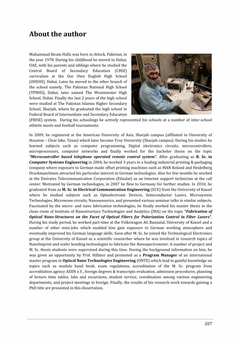
207
About the author
Muhammad Ikram Hafiz was born in Attock, Pakistan, in
the year 1978. During his childhood he moved to Dubai,
UAE, with his parents and siblings where he studied the
Central Board of Secondary Education (CBSE)
curriculum at the Our Own English High School
(OOEHS), Dubai. Later he moved to the other branch of
the school namely, The Pakistan National High School
(TPNHS), Dubai, later named The Westminster High
School, Dubai. Finally the last 2 years of the high school
were studied at The Pakistan Islamia Higher Secondary
School, Sharjah, where he graduated the high school in
Federal Board of Intermediate and Secondary Education
(FBISE) system. During his schoolings he actively represented his schools at a number of inter-school
athletic meets and football tournaments.
In 2009, he registered at the American University of Asia, Sharjah campus (affiliated to University of
Houston – Clear lake, Texas) which later became Troy University (Sharjah campus). During his studies he
learned subjects such as computer programming, Digital electronics circuits, microcontrollers,
microprocessors, computer networks and finally worked for the bachelor thesis on the topic
“Microcontroller based telephone operated remote control system”. After graduating as B. Sc. in
Computer Systems Engineering in 2004, he worked 3 years in a leading industrial printing & packaging
company where exposure to German made offset printing machines such as MAN Roland and Heidelberg
Druckmaschinen attracted his particular interest in German technologies. Also for few months he worked
at the Emirates Telecommunication Corporation (Etisalat) as an Internet support technician at the call
center. Motivated by German technologies, in 2007 he flew to Germany for further studies. In 2010, he
graduated from as M. Sc. in Electrical Communication Engineering (ECE) from the University of Kassel
where he studied subjects such as Optoelectronic Devices, Semiconductor Lasers, Microsystem
Technologies, Microwave circuits, Nanosensorics, and presented various seminar talks in similar subjects.
Fascinated by the micro- and nano fabrication technologies, he finally worked his master thesis in the
clean room of Institute of Nanostructure Technologies and Analytics (INA) on the topic “Fabrication of
Optical Nano-Structures on the Facet of Optical Fibers for Polarization Control in Fiber Lasers”.
During his study period, he worked part-time at the Volkswagon AG Baunatal, University of Kassel and a
number of other mini-jobs which enabled him gain exposure to German working atmosphere and
eventually improved his German language skills. Soon after M. Sc. he joined the Technological Electronics
group at the University of Kassel as a scientific researcher where he was involved in research topics of
NanoImprint and wafer bonding technologies to fabricate the Nanospectrometer. A number of project and
M. Sc. thesis students were supervised during this time. Having the background information on him, he
was given an opportunity by Prof. Hillmer and promoted as a Program Manager of an international
master program in Optical Nano Technologies Engineering (ONTE) which lead to gainful knowledge on
topics such as module hand book, exam regulations, accreditation of the M. Sc. program from
accreditation agency ASIIN e.V., foreign degrees & transcripts evaluation, admission procedures, planning
of lecture time tables, labs and excursions, student service, coordination among various engineering
departments, and project meetings in foreign. Finally, the results of his research work towards gaining a
PhD title are presented in this dissertation.

208