
Plasmon resonance absorption in sulfide-coated gold nanorods

This content has been downloaded from IOPscience. Please scroll down to see the full text.
Download details:
IP Address: 166.104.234.68
This content was downloaded on 29/05/2014 at 13:32
Please note that terms and conditions apply.
Optical nonlinearity in lead sulfide microtowers
View the table of contents for this issue, or go to the journal homepage for more
2010 J. Phys. D: Appl. Phys. 43 385402
(http://iopscience.iop.org/0022-3727/43/38/385402)
Home Search Collections Journals About Contact us My IOPscience

IOP PUBLISHING JOURNAL OF PHYSICS D: APPLIED PHYSICS
J. Phys. D: Appl. Phys. 43 (2010) 385402 (6pp) doi:10.1088/0022-3727/43/38/385402
Optical nonlinearity in lead sulfidemicrotowersV Tamilselvan1, Kishore Sridharan2, K Narasimha Rao1 and Reji Philip2,3
1 Department of Instrumentation and Applied Physics, Indian Institute of Science, Bangalore 560 012,India2 Light and Matter Physics Group, Raman Research Institute, C.V. Raman Avenue, Sadashivanagar,Bangalore 560 080, India
E-mail: [email protected]
Received 13 April 2010, in final form 29 July 2010Published 9 September 2010Online at stacks.iop.org/JPhysD/43/385402
AbstractLead sulfide (PbS) microtowers on silicon substrates, having the physical properties of bulkPbS, have been synthesized. Optical nonlinearity studies using the open aperture z-scantechnique employing 5 ns and 100 fs laser pulses reveal effective two-photon type absorption.For nanosecond excitation the nonlinear absorption coefficients (βeff ) are in the order of10−11 m W−1, two orders of magnitude less than the values reported for quantum confined PbSnanocrystals. For femtosecond excitation βeff is of the order of 10−14 m W−1. These resultsobtained in bulk PbS experimentally confirm the importance of quantum confinement in theenhancement of optical nonlinearities in semiconductor materials.
(Some figures in this article are in colour only in the electronic version)
1. Introduction
Mesoscopic systems are substantially investigated today dueto their unique physical and chemical properties. Nanocrystalproperties vary widely with changes in shape and size[1], and large confinement energies can be envisionedin nanocrystals with diameters less than the Bohr radius.Semiconductor nanostructures show outstanding electronicand optical properties, and are useful in the fabrication ofnanodevices such as light emitting diodes [2], solar absorbers[3], single electron transistors [4] and infrared detectors[5]. As a semiconductor compound, PbS is an importantπ–π semiconductor material with a narrow bandgap energy(0.41 eV at 300 K) [6]. This, and the impressive third ordernonlinear optical properties, make nanoscale PbS potentiallyuseful in electroluminescent devices like light-emitting diodesand optical devices such as optical switches [7]. Vigorousefforts have therefore been made on the synthesis of nanoscalePbS in polymers, zeolites, block copolymer nanoreactors,inverse micelles, microemulsions, polyols and ethanol systemthrough γ -irradiation [8–15].
The optical nonlinearity of nanoscale semiconductors inthe quantum confinement regime has been investigated in theliterature. Quantum confinement is found to enhance the
3 Author to whom any correspondence should be addressed.
nonlinear optical response, and a number of reports havediscussed the physical processes underlying the mechanism ofoptical nonlinearity in quantum dots (QDs) [16–20]. However,reports of similar studies in bulk semiconductors are very fewin number [21–23]. Therefore it would be an interestingtask to perform studies in the bulk form and compare theresults with those obtained in the quantum confinement regime.Towards this goal, we have synthesized PbS microtowers andinvestigated their nonlinear optical transmission at 532 nmusing 5 ns and 100 fs laser pulses, employing the open aperturez-scan technique. The results obtained are discussed andcompared with earlier results obtained in nanoscale PbS.
2. Experimental details
Lead sulfide microtowers with laterally grown PbS rod-likestructures were made on silicon substrates by the thermalevaporation technique under high vacuum (10−5 mbar) in ahigh vacuum chamber. The experimental setup used here issimilar to that employed by Zhou et al [24] for the growth ofMoO3 nanowires. A tantalum evaporation boat covered with aperforated tantalum cover was used as the evaporation sourcein which 1.5 g of PbS (Balzers coating material) precursorwas taken without the addition of any reacting agents andcatalysts. A silicon (1 0 0) substrate was ultrasonically cleaned
0022-3727/10/385402+06$30.00 1 © 2010 IOP Publishing Ltd Printed in the UK & the USA

J. Phys. D: Appl. Phys. 43 (2010) 385402 V Tamilselvan et al
using acetone and deionized water, and was placed above thetantalum boat at a height of approximately 2 cm. The chamberwas evacuated and a low pressure of about 10−4–10−5 mbarwas maintained, and the boat was heated by applying a voltagein the range 20–45 V for 7 min. After deposition the appliedvoltage was slowly decreased to zero and the sample wasallowed to cool. Evaporated PbS material condensed on thesilicon substrate as a black powder. The substrate was thenremoved from the evaporation chamber.
The XRD pattern of the as-grown microstructure wastaken using an X-ray Diffractometer (Philips) with Cu Kα1radiation with an x-ray wavelength of 1.5406 Å. Morphologystudies and compositional analysis were done by scanningelectron microscopy (SEM, FEI SERION), and transmissionelectron microscope (TEM, Tecnai F-30) equipped with energydispersive x-ray analysis (EDAX). The absorption spectrum ofthe sample (dissolved in ethylene glycol, taken in a quartz cell)was measured using a UV–Visible spectrometer (Perkin-Elmer,Lambda 35). Photoluminescence (PL) measurements werecarried out using a Spectrofluorometer (Fluoromax-4, HoribaJobin Yvon) at the excitation wavelength of 260 nm.
Optical nonlinearity measurements were carried out usinglaser pulses of 5 ns (λ = 532 nm, Nd : YAG laser) and100 fs (λ = 800 nm, Ti : Sapphire laser) durations (FWHM),respectively. The technique of open aperture z-scan [25] wasused which gives information on the nonlinear absorption ofthe sample. In the z-scan experiment, a laser beam is firstfocused using a lens, and the direction of beam propagation istaken as the z-axis. The sample is now placed in the beam ata position (z) between the lens and the focal point (z = 0),and the transmitted energy is measured. Then the sampleis moved in small steps towards the focus and beyond, andthe transmission is measured at each step. At each of thesepositions, the sample will experience a different laser intensity,and the intensity will be a maximum at the focus. Thus inpractice the open aperture z-scan is essentially a measurementof sample transmission, for different values of z. The graphplotted between position z and the normalized transmittanceof the sample is known as the open aperture z-scan curve.This graph will reveal the nature of the absorptive nonlinearityin the system. If a spatially Gaussian laser beam is used, theneach z-position will correspond to an input laser energy density(fluence) of 4(ln 2)1/2Ein/π
3/2ω(z)2, where Ein is the inputlaser pulse energy and ω(z) is the beam radius. ω(z) is givenby ω(0)∗[1 + (z/z0)
2]1/2, where ω(0) is the beam radius at thefocus and z0 = πω(0)2/λ is the Rayleigh range (diffractionlength), where λ is the excitation wavelength. Thus from theopen aperture z-scan data it is possible to draw a graph betweenthe input laser fluence and the sample transmission, which isknown as the nonlinear transmission curve.
In our experiment a planoconvex lens of 20 cm focal lengthwas used to focus the laser, and the focal spot radius wasabout 18 µm. Seven z-scans were done in total, where thelaser pulse energy was varied in steps from 20 to 200 µJ.Since the silicon substrate is not transparent to light, the filmwas carefully scraped out from the surface and dissolved inethylene glycol for performing the z-scan. The solution wastaken in a 1 mm glass cuvette (Hellma GmBH) and mounted on
Figure 1. XRD pattern of PbS microtowers.
a programmable linear translation stage. For the concentrationused it had a linear transmittance of 75% at the excitationwavelength. The input energy reaching the sample and theenergy transmitted by the sample were measured using twopyroelectric energy probes (RjP 735, Laser Probe Inc.). Theinterval between successive laser pulses was kept sufficientlylarge (about 1 s) to allow for complete thermal relaxation ofthe sample between adjacent laser pulses. The experiment wasautomated using a Labview program running in the WindowsXP environment.
3. Results and discussion
3.1. Sample characterization
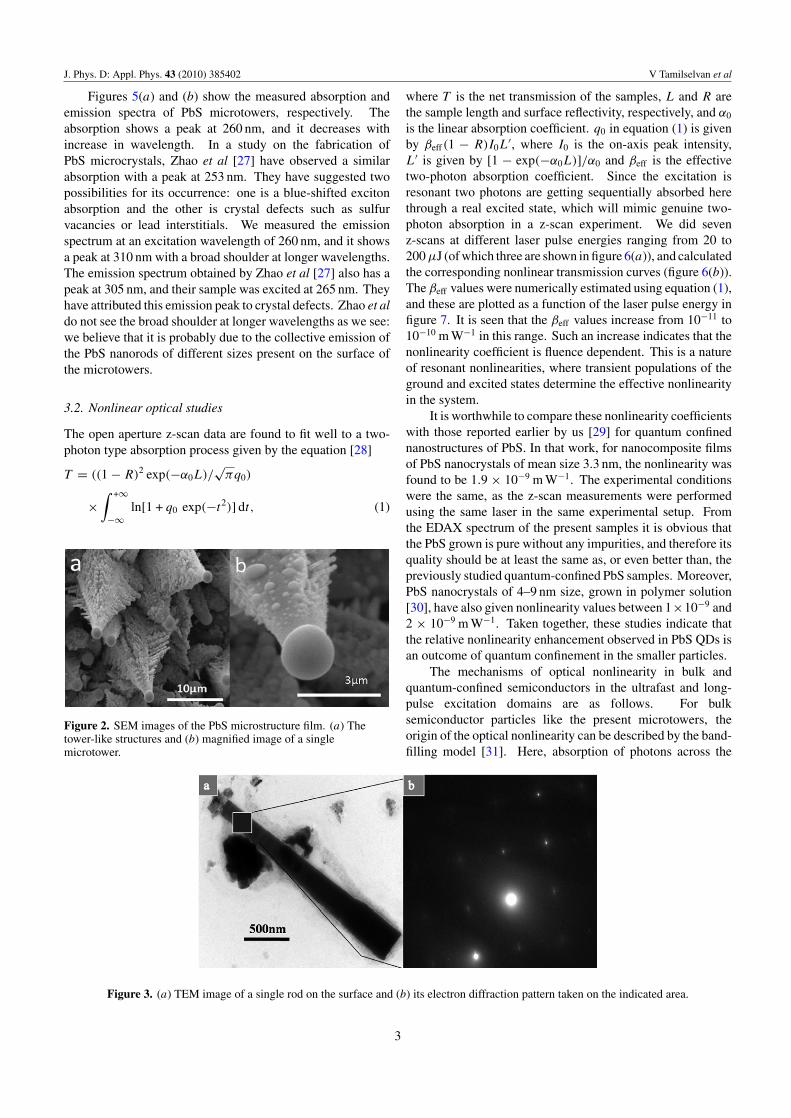
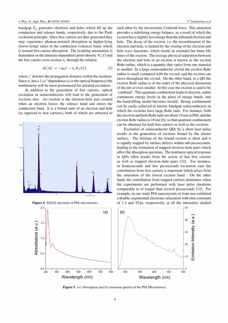
For sample preparation, pure lead sulfide was directlyevaporated without the addition of any other catalyst materials,to obtain lead sulfide microtowers. This catalyst-free metal-based vapour–liquid–solid (VLS) growth is called the self-catalytic VLS growth mechanism [26], and we believe ithas played an important role in the growth of tower-likemicrostructures of PbS. A typical x-ray diffraction (XRD)pattern of the as-prepared PbS microtower array shown infigure 1 reveals a pure metallic face-centred-cubic (fcc)structure with lattice constant a = 5.914 Å (JCPDS No: 78-1054). In order to determine the morphology, the as-depositedSi wafer from the chamber was directly transferred to ascanning electron microscope (SEM) without disturbing theoriginal nature of the deposited products. Figure 2(a)shows the microtowers, and the presence of several rod-likestructures over its surface is clearly visible. The growth ofthe microtowers terminates with the formation of a sphere-shaped tip as shown in figure 2(b). The TEM image andthe selected area electron diffraction (SAED) pattern of oneof the rods on a microtower are shown in figures 3(a) and(b), respectively, from which the preferential growth of therod in the (2 2 0) direction has been confirmed. The chemicalcomposition of the spherical tip was analysed using the EDAX(energy dispersive analysis of x-rays) equipment attached onthe TEM. The samples for TEM were prepared on a coppergrid, and therefore the EDAX spectrum shown in figure 4 hasa prominent Cu peak in addition to the lead and sulfur peaks.
2
J. Phys. D: Appl. Phys. 43 (2010) 385402 V Tamilselvan et al
Figures 5(a) and (b) show the measured absorption andemission spectra of PbS microtowers, respectively. Theabsorption shows a peak at 260 nm, and it decreases withincrease in wavelength. In a study on the fabrication ofPbS microcrystals, Zhao et al [27] have observed a similarabsorption with a peak at 253 nm. They have suggested twopossibilities for its occurrence: one is a blue-shifted excitonabsorption and the other is crystal defects such as sulfurvacancies or lead interstitials. We measured the emissionspectrum at an excitation wavelength of 260 nm, and it showsa peak at 310 nm with a broad shoulder at longer wavelengths.The emission spectrum obtained by Zhao et al [27] also has apeak at 305 nm, and their sample was excited at 265 nm. Theyhave attributed this emission peak to crystal defects. Zhao et aldo not see the broad shoulder at longer wavelengths as we see:we believe that it is probably due to the collective emission ofthe PbS nanorods of different sizes present on the surface ofthe microtowers.
3.2. Nonlinear optical studies
The open aperture z-scan data are found to fit well to a two-photon type absorption process given by the equation [28]
T = ((1 − R)2 exp(−α0L)/√
πq0)
×∫ +∞
−∞ln[1 + q0 exp(−t2)] dt, (1)
Figure 2. SEM images of the PbS microstructure film. (a) Thetower-like structures and (b) magnified image of a singlemicrotower.
Figure 3. (a) TEM image of a single rod on the surface and (b) its electron diffraction pattern taken on the indicated area.
where T is the net transmission of the samples, L and R arethe sample length and surface reflectivity, respectively, and α0
is the linear absorption coefficient. q0 in equation (1) is givenby βeff(1 − R)I0L
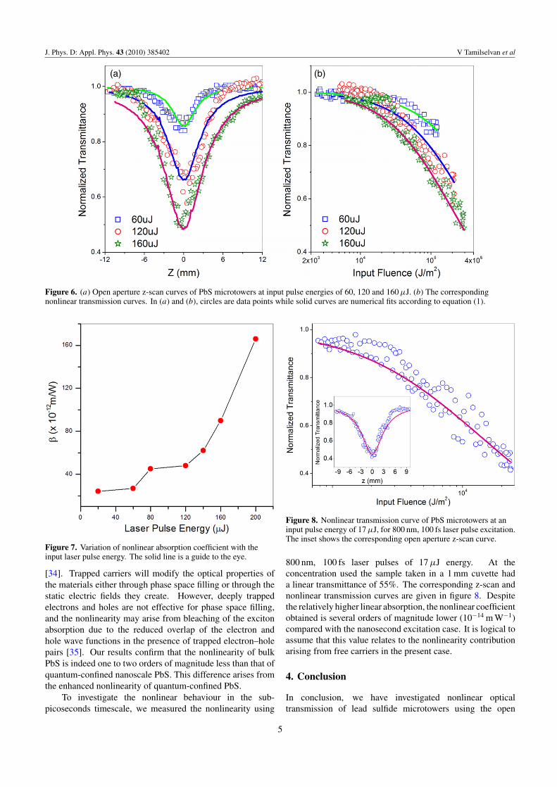
′, where I0 is the on-axis peak intensity,L′ is given by [1 − exp(−α0L)]/α0 and βeff is the effectivetwo-photon absorption coefficient. Since the excitation isresonant two photons are getting sequentially absorbed herethrough a real excited state, which will mimic genuine two-photon absorption in a z-scan experiment. We did sevenz-scans at different laser pulse energies ranging from 20 to200 µJ (of which three are shown in figure 6(a)), and calculatedthe corresponding nonlinear transmission curves (figure 6(b)).The βeff values were numerically estimated using equation (1),and these are plotted as a function of the laser pulse energy infigure 7. It is seen that the βeff values increase from 10−11 to10−10 m W−1 in this range. Such an increase indicates that thenonlinearity coefficient is fluence dependent. This is a natureof resonant nonlinearities, where transient populations of theground and excited states determine the effective nonlinearityin the system.
It is worthwhile to compare these nonlinearity coefficientswith those reported earlier by us [29] for quantum confinednanostructures of PbS. In that work, for nanocomposite filmsof PbS nanocrystals of mean size 3.3 nm, the nonlinearity wasfound to be 1.9 × 10⁻⁹ m W−1. The experimental conditionswere the same, as the z-scan measurements were performedusing the same laser in the same experimental setup. Fromthe EDAX spectrum of the present samples it is obvious thatthe PbS grown is pure without any impurities, and therefore itsquality should be at least the same as, or even better than, thepreviously studied quantum-confined PbS samples. Moreover,PbS nanocrystals of 4–9 nm size, grown in polymer solution[30], have also given nonlinearity values between 1×10⁻⁹ and2 × 10−9 m W−1. Taken together, these studies indicate thatthe relative nonlinearity enhancement observed in PbS QDs isan outcome of quantum confinement in the smaller particles.
The mechanisms of optical nonlinearity in bulk andquantum-confined semiconductors in the ultrafast and long-pulse excitation domains are as follows. For bulksemiconductor particles like the present microtowers, theorigin of the optical nonlinearity can be described by the band-filling model [31]. Here, absorption of photons across the
3
J. Phys. D: Appl. Phys. 43 (2010) 385402 V Tamilselvan et al
bandgap Eg generates electrons and holes which fill up theconduction and valence bands, respectively, due to the Pauliexclusion principle. Once free carriers are thus generated theymay experience phonon-assisted absorption to higher-lying(lower-lying) states in the conduction (valence) band, whichis termed free-carrier absorption. The resulting attenuation isdependent on the intensity dependent carrier density Nc(I ) andthe free carrier cross section σc through the relation
dI/dz′ = −α0I − σcNc(I )I, (2)
where z′ denotes the propagation distance within the medium.Since σc has a 1/ω2 dependence (ω is the optical frequency) thenonlinearity will be most pronounced for infrared excitation.
In addition to the generation of free carriers, opticalexcitation in semiconductors will lead to the generation ofexcitons also. An exciton is the electron–hole pair createdwhen an electron leaves the valence band and enters theconduction band. It is a bound state of an electron and hole(as opposed to free carriers), both of which are attracted to
Figure 4. EDAX spectrum of PbS microtowers.
Figure 5. (a) Absorption and (b) emission spectra of the PbS Microtowers.
each other by the electrostatic Coulomb force. This attractionprovides a stabilizing energy balance, as a result of which theexciton has a slightly less energy than the unbound electron andhole. The decay of the exciton, i.e. the recombination of theelectron and hole, is limited by the overlap of the electron andhole wave functions, which results in extended but finite lifetimes of the exciton. The average physical separation betweenthe electron and hole in an exciton is known as the excitonBohr radius, which is a quantity that varies from one materialto another. In a large semiconductor crystal the exciton Bohrradius is small compared with the crystal, and the exciton canmove throughout the crystal. On the other hand, in a QD theexciton Bohr radius is of the order of the physical dimensionof the dot or even smaller. In this case the exciton is said to be‘confined’. This quantum confinement leads to discrete, rathercontinuous energy levels in the place of energy bands, andthe band-filling model becomes invalid. Strong confinementcan be easily achieved in narrow bandgap semiconductors inwhich the excitons have large Bohr radii. For instance, boththe electron and hole Bohr radii are about 10 nm in PbS, and theexciton Bohr radius is 18 nm [6], so that quantum confinementcan be obtained for both free carriers as well as the excitons.
Excitation of semiconductor QDs by a short laser pulseresults in the generation of excitons bound by the clustersurface. The lifetime of the bound exciton is short and itis rapidly trapped by surface defects within sub-picoseconds,leading to the formation of trapped electron–hole pairs whichaffect the absorption spectrum. The nonlinear optical responsein QDs often results from the action of fast free carriersas well as trapped electron–hole pairs [32]. For instance,in femtoseconds and few picoseconds excitation case thecontribution from free carriers is important which arises fromthe saturation of the lowest exciton band. On the otherhand, the contribution from trapped carriers dominates whenthe experiments are performed with laser pulse durationscomparable to or longer than several picoseconds [33]. Forexample, in one study PbS nanocrystals of 4 nm size exhibiteda double-exponential electronic relaxation with time constantsof 1.2 and 45 ps, respectively, at all the intensities studied
4
J. Phys. D: Appl. Phys. 43 (2010) 385402 V Tamilselvan et al
Figure 6. (a) Open aperture z-scan curves of PbS microtowers at input pulse energies of 60, 120 and 160 µJ. (b) The correspondingnonlinear transmission curves. In (a) and (b), circles are data points while solid curves are numerical fits according to equation (1).
Figure 7. Variation of nonlinear absorption coefficient with theinput laser pulse energy. The solid line is a guide to the eye.
[34]. Trapped carriers will modify the optical properties ofthe materials either through phase space filling or through thestatic electric fields they create. However, deeply trappedelectrons and holes are not effective for phase space filling,and the nonlinearity may arise from bleaching of the excitonabsorption due to the reduced overlap of the electron andhole wave functions in the presence of trapped electron–holepairs [35]. Our results confirm that the nonlinearity of bulkPbS is indeed one to two orders of magnitude less than that ofquantum-confined nanoscale PbS. This difference arises fromthe enhanced nonlinearity of quantum-confined PbS.
To investigate the nonlinear behaviour in the sub-picoseconds timescale, we measured the nonlinearity using
Figure 8. Nonlinear transmission curve of PbS microtowers at aninput pulse energy of 17 µJ, for 800 nm, 100 fs laser pulse excitation.The inset shows the corresponding open aperture z-scan curve.
800 nm, 100 fs laser pulses of 17 µJ energy. At theconcentration used the sample taken in a 1 mm cuvette hada linear transmittance of 55%. The corresponding z-scan andnonlinear transmission curves are given in figure 8. Despitethe relatively higher linear absorption, the nonlinear coefficientobtained is several orders of magnitude lower (10−14 m W−1)compared with the nanosecond excitation case. It is logical toassume that this value relates to the nonlinearity contributionarising from free carriers in the present case.
4. Conclusion
In conclusion, we have investigated nonlinear opticaltransmission of lead sulfide microtowers using the open
5

J. Phys. D: Appl. Phys. 43 (2010) 385402 V Tamilselvan et al
aperture z-scan technique, in the nanosecond and femtosecondexcitation domains. The sample is found to behave as anoptical limiter in both cases. The micrometre-sized particlesshow a nonlinearity which is one to two orders of magnitudelower than that of quantum-confined nanoscale PbS. This isin agreement with calculations in the literature which predicthigher optical nonlinearities for QDs belonging to the strongconfinement regime. For excitation with nanosecond pulsesthe nonlinear absorption coefficient increases with the inputlaser pulse energy, indicating that the nonlinearity may bemostly arising from the long-lived surface-trapped excitons.For femtosecond irradiation the nonlinearity coefficient is threeto four orders of magnitude lower in comparison, and thismay be correlated with the contribution by free carriers in thematerial system.
Acknowledgments
The authors thank Mr Suchand Sandeep for help with the PLmeasurements, and the Nanocentre at the Indian Institute ofScience, Bangalore, for providing the SEM and TEM facilities.
References
[1] Yang P D and Lieber C M 1996 Science 273 1836[2] Colvin V L, Schlamp M C and Alivisatos A P 1994 Nature
370 354[3] Chaudhiri T K and Chatterjee S 1992 Proc. Int. Conf.
Thermoelectricity (Arlington, TX) 11 40[4] Klein D L, Roth R, Lim A K L, Alivasatos A P and
McEuen P L 1997 Nature 389 699[5] Gadenne P, Yagil Y and Deutscher G 1989 J. Appl. Phys.
66 3019[6] Machol J L, Wise F W, Patel R C and Tanner D B 1993 Phys.
Rev. B 48 2819[7] Kane R S, Cohen R E and Silbey R 1996 J. Phys. Chem.
100 7928[8] Wang Y, Suna A, Mahler W and Kasowski R 1987 J. Chem.
Phys. 87 7315[9] Wang S H and Yang S H 2000 Langmuir 16 389
[10] Wang Y and Herron N 1987 J. Phys. Chem. 91 257
[11] Kane R S, Cohen R E and Silbey R 1996 Chem. Mater. 8 1919[12] Liveri V T, Rossi M E, D’Arrigo G, Manno D and Micocci G
1999 Appl. Phys. A 69 369[13] Yang J P, Qadri S B and Ratna B R 1996 J. Phys. Chem.
100 17255[14] Peng Z, Jiang Y, Song Y, Wang C and Zhang H 2008 Chem.
Mater. 20 3153[15] Qiao Z, Xie Y, Xu J, Zhu Y and Qian Y 1999 J. Colloid
Interface Sci. 214 459[16] Fisher R A 1983 Optical Phase Conjugation (New York:
Academic)[17] Ya Zel’dovich B, Pilipetsky N F and Shkunov V V 2004
Principles of Phase Conjugation (Berlin: Springer)[18] Woggon U 1997 Optical Properties of Semiconductor
Quantum Dots (Berlin: Springer)[19] Banfi G P, Degiorgio V and Ricard D 1998 Adv. Phys. 47 447[20] Rustagi K C and Flytzanis C 1984 Opt. Lett. 9 344[21] Yuksek M, Elmali A, Karabulut M and Mamedov G M 2010
Appl. Phys. B 98 77[22] Allakhverdiev K R, Yetis M O, Baykara T K and Salaev E Yu
2009 Laser Phys. 19 1092[23] Bechtel J H and Smith W L 1976 Phys. Rev. B 13 3515[24] Zhou J, Xu N S, Deng S Z, Chen J, She J C and Wang Z L
2003 Adv. Mater. 15 1835[25] Sheik-Bahae M, Said A A, Wei T M, Hagan D J and
Van Stryland E W 1990 IEEE J. Quantum Electron. 26 760[26] Su Y, Liang X, Li S, Chen Y, Zhou Q, Yin S, Meng X and
Kong M 2008 Mater. Lett. 62 1010[27] Zhao P, Wang J, Cheng G and Huang K 2006 J. Phys. Chem. B
110 22400[28] Sutherland R L 2003 Handbook of Nonlinear Optics 2nd edn
(New York: Dekker)[29] Kurian P A, Vijayan C, Suchand Sandeep C S, Reji Philip and
Sathiyamoorthy K 2007 Nanotechnology 18 075708[30] Asunkis D J, Bolotin I L and Hanley L 2008 J. Phys. Chem. C
112 9555[31] Miller D A B, Seaton C T, Prise M E and Smith S D 1981
Phys. Rev. Lett. 47 197[32] Ghanassi M, Piveteau L, Saviot L, Schanne-Klein M C, Ricard
D and Flytzanis C 1995 Appl. Phys. B 61 17[33] Wang Y 1991 Acc. Chem. Res. 24 133[34] Patel A A, Wu F, Zhang J Z, Torres-Martinez C L, Mehra R K,
Yang Y and Risbud S H 2000 J. Phys. Chem. B104 11598
[35] Nandakumar P, Vijayan C and Murti Y V G S 2000 Opt.Commun. 185 457
6
Copyright © 2022 FDOKUMEN