Operations List Software Manual - Nuova Elva
98
Operations List Software Manual CL200 Edition 108
-
Upload
khangminh22 -
Category
Documents
-
view
0 -
download
0
Transcript of Operations List Software Manual - Nuova Elva

Operations ListSoftware Manual
CL200
Edition 108

CL200
Operations ListSoftware Manual
1070 072 151-108 (99.12) GB
1995-99
by Robert Bosch GmbH, Erbach / Germany.All rights reserved, including apllications for protective rights.
Reproduction or distribution by any means subject to our prior written permission.
Discretionary charge 20.00 DM


1070 072 151-108 (99.12) GB
Contents I
1 Safety Instructions..................................................................................................................................... 1-11.1 Standard Operation ............................................................................................................................... 1-11.2 Qualified Personnel ............................................................................................................................... 1-21.3 Safety Labels Affixed to Components.................................................................................................... 1-31.4 Safety Instructions in this Manual .......................................................................................................... 1-41.5 Safety Instructions for the Described Product ....................................................................................... 1-51.6 Documentation, Version and Trademarks............................................................................................. 1-6
2 Introduction................................................................................................................................................ 2-12.1 Programming Differences between “PROFI” and “WinSPS” Software ................................................. 2-1
3 Memory Management & Peripheral Operation.......................................................................................... 3-13.1 Memory Modes ...................................................................................................................................... 3-13.2 Operating Peripherals............................................................................................................................ 3-2
4 Startup Modes ........................................................................................................................................... 4-14.1 System Startup & Backup Copies.......................................................................................................... 4-14.1.1 System Startup in RAM and EPROM Memory Modes ................................................................... 4-14.1.2 System Startup in Mixed Memory Mode......................................................................................... 4-24.1.3 Forced Loading of MemoryCard and/or EPROM Contents into RAM ............................................ 4-24.1.4 Startup Routine following Mode-dependent System Start.............................................................. 4-34.1.5 Backing up Programs from RAM to EPROM or MemoryCard ....................................................... 4-4
5 Status Messages on the NT200 Power Supply......................................................................................... 5-1
6 Programming Basics ................................................................................................................................. 6-16.1 Representation Methods........................................................................................................................ 6-16.2 Program Structure ................................................................................................................................. 6-16.3 Module Types ........................................................................................................................................ 6-26.3.1 Organization Modules (OM) ........................................................................................................... 6-26.3.2 Program Modules (FC)................................................................................................................... 6-36.3.3 Data Modules (DM) ........................................................................................................................ 6-36.4 Application Program Structure............................................................................................................... 6-46.5 OM2 Initialization Module....................................................................................................................... 6-56.6 Reference List...................................................................................................................................... 6-126.7 OM5 & OM7 Startup Modules.............................................................................................................. 6-136.7.1 Programming within Startup Modules .......................................................................................... 6-136.7.2 Retriggering of Watchdog and Cycle Time .................................................................................. 6-136.8 OM9 Error Module ............................................................................................................................... 6-146.9 Remanence Characteristics ................................................................................................................ 6-156.10 Remanent Operation ........................................................................................................................... 6-156.11 Non-remanent operation...................................................................................................................... 6-156.12 Fixation ................................................................................................................................................ 6-166.12.1 Remanence of Fixation ................................................................................................................ 6-166.13 Interrupts.............................................................................................................................................. 6-176.13.1 Time Interrupts (time-controlled processing)................................................................................ 6-176.13.2 Peripheral Interrupts (interrupt inputs).......................................................................................... 6-186.13.3 Interrupt Handling Instructions...................................................................................................... 6-186.14 Application Stack ................................................................................................................................. 6-206.15 Setting the System Clock..................................................................................................................... 6-20

1070 072 151-108 (99.12) GB
II Contents
7 CL200 Addressing Conventions................................................................................................................ 7-17.1 Operand & Module Identifiers ................................................................................................................ 7-17.2 Module List............................................................................................................................................. 7-17.3 System Area .......................................................................................................................................... 7-27.3.1 System Area Assignment ............................................................................................................... 7-27.4 Data Formats ......................................................................................................................................... 7-67.5 Register Structure.................................................................................................................................. 7-77.6 Representing Constants ........................................................................................................................ 7-87.7 Program Module Calls ........................................................................................................................... 7-87.8 Jump Instructions................................................................................................................................... 7-87.9 Bit & Module Addresses......................................................................................................................... 7-87.10 Byte Addresses...................................................................................................................................... 7-97.11 Addressing Modes ............................................................................................................................... 7-107.11.1 Direct Addressing ......................................................................................................................... 7-107.11.2 Register-to-Register Addressing .................................................................................................. 7-107.11.3 Register-indirect addressing......................................................................................................... 7-107.11.4 Indirect addressing ....................................................................................................................... 7-11
7.11.4.1 Indirect Byte Addresses ........................................................................................................7-117.11.4.2 Indirect Bit Addresses ...........................................................................................................7-127.11.4.3 Indirect Module Addresses....................................................................................................7-12
7.12 Parameterized Modules....................................................................................................................... 7-13
8 Interfaces & Connectors............................................................................................................................ 8-18.1 X31 – Connector for Programming Unit or External Operator Terminal................................................ 8-18.2 X32 – Second Serial Interface Connector (ZE201 only) ........................................................................ 8-28.3 X71 – Interrupt & Counter Inputs ........................................................................................................... 8-38.3.1 Interrupt Inputs (ZE200xx standard version) .................................................................................. 8-38.3.2 High-speed Counters (onboard counters, standard on ZE200xx).................................................. 8-4
8.3.2.1 Sample Program – High-speed Counters onboard CL200 Basic Unit........................................8-78.4 X72 – Analog Inputs & Analog Output ................................................................................................. 8-118.4.1 Analog Inputs................................................................................................................................ 8-128.4.2 Analog Output............................................................................................................................... 8-13
8.4.2.1 Sample Program – Analog Processing on the CL200 Basic Unit .............................................8-14
9 CL200 Instruction List................................................................................................................................ 9-19.1 Structure of Controller Instructions ........................................................................................................ 9-19.2 Status Bits (Flags) ................................................................................................................................. 9-19.3 Key to Abbreviations .............................................................................................................................. 9-29.4 Binary Links & Parenthesized Instructions............................................................................................. 9-39.5 Time Programming ................................................................................................................................ 9-49.5.1 Time Instructions ............................................................................................................................ 9-59.5.2 Time Format ................................................................................................................................... 9-69.5.3 Time Diagrams ............................................................................................................................... 9-79.6 Counter Instructions............................................................................................................................... 9-89.6.1 Software Counter............................................................................................................................ 9-89.6.2 High-speed Counter (onboard counter).......................................................................................... 9-89.7 Digital Links............................................................................................................................................ 9-99.8 Swap Instruction .................................................................................................................................... 9-99.9 Compare Instruction ............................................................................................................................ 9-109.10 Load Instructions ................................................................................................................................. 9-119.11 Transfer Instructions............................................................................................................................ 9-119.12 Convert Instructions............................................................................................................................. 9-129.13 Increment / Decrement Instructions..................................................................................................... 9-139.14 Stack Instructions ................................................................................................................................ 9-139.15 No-operation Instructions & CARRY Manipulations............................................................................. 9-139.16 Shift Instructions .................................................................................................................................. 9-149.17 Rotate Instructions............................................................................................................................... 9-15

1070 072 151-108 (99.12) GB
Contents III
9.18 Arithmetic............................................................................................................................................. 9-169.18.1 Add Instructions............................................................................................................................ 9-169.18.2 Subtract Instructions..................................................................................................................... 9-179.18.3 Multiply Instructions ...................................................................................................................... 9-189.18.4 Divide Instructions ........................................................................................................................ 9-199.19 Parameter Assignments ...................................................................................................................... 9-209.20 Local Symbol Names & Auxiliary Flags for Program Tracking ............................................................ 9-209.21 System Variable................................................................................................................................... 9-209.22 Jump Instructions ................................................................................................................................ 9-219.23 Module Calls ........................................................................................................................................ 9-239.24 End Of Module Instructions ................................................................................................................. 9-239.25 Interrupt Instructions ............................................................................................................................ 9-249.26 Program Stop / End ............................................................................................................................. 9-24

1070 072 151-108 (99.12) GB
IV Contents

1070 072 151-108 (99.12) GB
Safety Instructions 1-1
1 Safety InstructionsBefore you start programming and working with the CL200 controller, werecommend that you thoroughly familiarize yourself with the contents ofthis instruction manual. Keep this manual in a place where it is always ac-cessible to all users.
1.1 Standard OperationThis instruction manual presents a comprehensive set of instructions andinformation required for the standard operation of the described products.The described products are used for programming and operating theCL200 control unit.
The products described hereunder• were developed, manufactured, tested and documented in accordance
with the relevant safety standards. In standard operation, and providedthat the specifications and safety instructions relating to the projectphase, installation and correct operation of the product are followed,there should arise no risk of danger to personnel or property.
The prerequisites for trouble-free service and safe operation of the prod-uct are proper transport, handling and storage, placement and installation,plus careful operation of the equipment.

1070 072 151-108 (99.12) GB
Safety Instructions1-2
1.2 Qualified PersonnelThe requirements pertaining to qualified personnel are based on the jobspecifications as outlined by the ZVEI (central association of the electricalindustry) and VDMA (association of German machine and plant builders)professional associations in Germany. Please refer to the following Ger-man-language publication:
Weiterbildung in der AutomatisierungstechnikHrsg.: ZVEI und VDMAMaschinenbauVerlagPostfach 71 08 6460498 Frankfurt
This instruction manual is specifically designed for PLC technicians. Theywill require specific knowledge of the CL200 controller.
Interventions in the hardware and software of our products which are notdescribed in this instruction manual may only be performed by speciallytrained Bosch personnel.
Unqualified interventions in the hardware or software or non-compliancewith the warnings listed in this instruction manual or indicated on theproduct may result in serious personal injury or damage of property.
Installation and maintenance of the products described hereunder is theexclusive domain of trained electricians as per VDE 1000-10, who arefamiliar with the contents of this manual.
Trained electricians are persons of whom the following is true:• They are capable, due to their professional training, skills and exper-
tise, and based upon their knowledge of and familiarity with applicabletechnical standards, of assessing the work to be carried out, and ofrecognizing possible hazards.
• They possess, subsequent to several years' experience in a compara-ble field of endeavour, a level of knowledge and skills that may bedeemed commensurate with that attainable in the course of a formalprofessional education in this area.
With regard to the foregoing, please read the information about our com-prehensive training program. You will find a listing of our seminars on thefront inside cover of this instruction manual. The professional staff at ourtraining centre will be pleased to provide detailed information. You maycontact the centre by telephone at (+49) 6062 78-258.

1070 072 151-108 (99.12) GB
Safety Instructions 1-3
1.3 Safety Labels Affixed to Components
Danger: High voltage!
Danger: Battery acid!
Electrostatically sensitive devices!
Disconnect at mains before opening!
Pin for connecting PE conductor only!
Functional earthing / low noise earth
For screened conductor only!

1070 072 151-108 (99.12) GB
Safety Instructions1-4
1.4 Safety Instructions in this Manual
DANGEROUS ELECTRICAL VOLTAGEThis symbol is used to warn of the presence of a dangerous electricalvoltage. Insufficient compliance with or failure to observe this warningmay result in personal injury.
DANGERThis symbol is used wherever insufficient or lacking compliance withinstructions may result in personal injury.
CAUTIONThis symbol is used whenever insufficient or lacking compliance withinstructions may result in damage to equipment or data files.
⇒⇒⇒⇒ This symbol is used to alert the user to an item of special interest.

1070 072 151-108 (99.12) GB
Safety Instructions 1-5
1.5 Safety Instructions for the Described Product
DANGERFatal injury hazard through ineffective Emergency-OFF safety de-vices!Emergency-OFF safety devices must remain effective and accessi-ble during all operating modes of the system.The release of functional locks imposed by Emergency-OFF de-vices must never be allowed to cause an uncontrolled system re-start! Before restoring power to the system, test the Emergency-OFF sequence!
DANGERDanger to Personnel and Equipment!Test every new program before operating the system!
DANGERRetrofits or modifications may interfere with the safety of the prod-ucts described hereunder!
The consequences may be severe personal injury, damage toequipment or environmental hazards. Therefore, any system retro-fitting or modification utilizing third-party components will requireexpress approval by Bosch.

1070 072 151-108 (99.12) GB
Safety Instructions1-6
1.6 Documentation, Version and Trademarks
DocumentationThe present instruction manual provides the user with comprehensive in-formation about programming the CL200, and about the instruction setused by the control unit.
List of instruction manuals:
Instruction manual Language Order no.
Die Welt der SPS German 1070 072 407
CL200 Manual English 1070 072 145
SFC Sequence Function Chart English 1070 072 186
KETTE200 Software module description English 1070 072 150
BT-MADAP Software manual English 1070 072 163
Catalogue, Programmable Logic Controllers English 1070 072 160
⇒ Throughout this instruction manual, the floppy disk drive shall al-ways have drive letter A:, and the hard disk drive shall have driveletter C:.
Special keys or keyboard shortcuts (key combinations) are enclosed inpointed brackets:• Special keys, example: <Enter>, <PgUp>, <Del>• Key combination (pressed simultaneously), e.g.: <Ctrl> + <PgUp>
TrademarksAll trademarks referring to software that is installed on Bosch productswhen shipped from the factory represent the property of the respectivemanufacturers.
When shipped from the factory, all installed software is protected by copy-right. It may therefore be duplicated only with prior permission by Boschor in accordance with the licensing agreements with the respectivemanufacturer or copyright owner.
MS-DOS and Windows are registered trademarks of Microsoft Corpo-ration.

1070 072 151-108 (99.12) GB
Introduction 2-1
2 Introduction
2.1 Programming Differences between “PROFI” and “WinSPS” SoftwareThe present documentation discusses the representation of constants,program module calls, and jump instructions in the notation generated bythe “WinSPS” programming unit software. However, when processed withthe “PROFI” programming unit software (an earlier, DOS-based pro-gramming device application), the representation of constants, programmodule calls and jump instructions will differ to some extent.
The referred differences are exemplified in the following side-by-sidecomparison:
Differences in programming and notation of word constantsData type PLC utility programs
Explanation Notation PROFI WinSPSUINT (unsigned integer) Binary / Dual K00000000 00000000B
K11111111 11111111B2#00000000000000002#1111111111111111
Decimal, word K00000D - K63535D 00000 - 65535Decimal, byte / byte K000/000 - K255/255 Not defined in IEC1131
Part 3Hexadecimal K0000H - KFFFFH 16#0000 - 16#FFFF
INT (integer) Decimal, word K-32768 - K+32767K-32768D - K+32767D
-32768 - +32767
Text, STRING(2) ASCII K'AB’ ‘AB’Time value, TVALUE Time val. (+timebase r)
r: 0=10ms, 1=100ms 2=1s, 3=10s
K0.r - K1023.rT#10ms - T#10230s
T#0.r - T#1023.r
Differences in programming and notation of module callsPLC utility programs
PROFI WinSPSProgram module / function call (IEC1131-3) CM PM CM FC
Differences in programming and notation of jump instructionsPLC utility programs
PROFI WinSPSJump instructionJump destination
JPx -label-label
JPx labellabel:

1070 072 151-108 (99.12) GB
Introduction2-2
1070 072 151-108 (99.12) GB
Memory Management & Peripheral Operation 3-1
3 Memory Management & Peripheral OperationIn their standard configuration, the CL200 central processing units areequipped with RAM and FLASH RAM memory modules. The applicationsoftware used by the programming unit determines the various memorymodes available for controller operation.
3.1 Memory Modes
RAM ModeAll data is stored in the volatile read-write memory, which requires abackup battery top ensure data security. The battery also powers thebuffers used by remanent markers, times, counters and the data field.
While operating in RAM Memory mode, program modules and currentdata modules can be copied from RAM and written directly to the internalFLASH memory, and to the MemoryCard. This ensures that, subsequentto a battery failure, the backed-up data can again be copied into RAMfrom either FLASH EPROM or MemoryCard.
To define this mode of operation, the software of the programming unit(PG) tags all modules with the “R” identifier (RAM).
EPROM ModeAll data is stored in non-volatile FLASH memory, which does not require abuffer battery to ensure data security. In EPROM Mode, the buffer batteryserves only to protect the remanent areas – and the data field, which isalways stored in internal RAM – against a sudden voltage loss.
In the event that, due to battery failure or operation without battery, theabsence of an executable PLC program in RAM is detected upon startup,unconditional loading from FLASH memory into RAM will occur. Whilestored in RAM, the program is executed, utilizing all benefits intrinsic toRAM Mode operation. It should be considered, however, that in the caseof battery-less operation or in the event of a buffer failure, each Off/Oncycling of the mains power will cause the data module contents stored inFLASH memory to be regenerated.
The battery-less operation that is possible in EPROM Mode requires thatno remanence is used and that the data field not contains data requiringbuffering.
⇒ For reasons of compatibility with other Bosch PLCs, this memorymode is designated EPROM Mode, although the non-volatile mem-ory used here is a FLASH memory module.
To define this mode of operation, the software of the programming unit(PG) tags all modules with the “E” identifier (EPROM).

1070 072 151-108 (99.12) GB
Memory Management & Peripheral Operation3-2
Mixed Memory ModeThis memory mode is set by the software of the programming unit incases where individual modules are defined as RAM, and other, testedmodules are defined as EPROM modules. The essential advantage ofthis mode of operation lies in the doubling of the memory capacity avail-able to the PLC program. As a prerequisite for Mixed Memory Mode, abattery for buffering the RAM area must always be present.
In addition, the following items should be noted:- Mixed Memory Mode can only be managed directly via the program-
ming unit (backing up to the MemoryCard is not possible).- After a battery failure, reloading via the programming unit is required.- Attempts to save to FLASH memory will be rejected.
To select Mixed Memory Mode, the software of the programming unit de-fines the memory area in which the individual modules are stored:
“R” identifier: storage in RAM
“E” identifier: storage in FLASH
3.2 Operating PeripheralsFollowing the end of the program, the operation of peripherals progressesonly up to the highest address that is hardware-equipped. This meansthat the I/O state is optimized automatically during the program executioninterval. To effect a further optimization of the I/O state, the number oftimes and counters in the OM2 initialization module can be reduced to therequired minimum.

1070 072 151-108 (99.12) GB
Startup Modes 4-1
4 Startup Modes
4.1 System Startup & Backup CopiesIn the event that errors are recognized during the system startup or copy-ing routine, an appropriate error message indicating the cause of the faultwill be generated. This message can be displayed by means of the pro-gramming unit.
4.1.1 System Startup in RAM and EPROM Memory ModesPower-ON
Battery fault yes Delete PLC programrecognized? and all operands!
no
COPY button pressed yes see Section, 4.1.3during Power-ON? "Forced Loading" (B)
no(A)
PLC program no PLC program noin RAM? in EPROM?
yes yesIs this program set to no
EPROM Mode?yes
CopyEPROM --> RAM
Start-up routine STOP

1070 072 151-108 (99.12) GB
Startup Modes4-2
4.1.2 System Startup in Mixed Memory ModePower-ON
Battery fault yes Delete PLC programrecognized? and all operands!
no
COPY button pressed yes see Section,4.1.3during Power-ON? "Forced Loading" (B)
no(A)
from 4.1.3
PLC program noin RAM?
yesPLC program modules
RAM EPROM
Startup routine STOP
4.1.3 Forced Loading of MemoryCard and/or EPROM Contents into RAM“Forced Loading”
MemoryCard / EPROM --> RAM
During Power-ON,press COPY button until
5V / 7.5V LED is ON!
Mode LED no Routine STOPflashing?
yesMemoryCard no PLC program no
present? in EPROM?yes yes
PLC program noin MemoryCard?
yesCopy PLC program:
MemoryCard --> EPROM!
PLC program noin EPROM?
Copy PLC program: Error: Stop LED flashes.EPROM --> RAM! Program not loadable.
(A) (B)

1070 072 151-108 (99.12) GB
Startup Modes 4-3
4.1.4 Startup Routine following Mode-dependent System StartStart-up routine
OM2 linked / integrated?yes no
Use OM2 Use defaultvalues! values!
Deleting nonremanent operands formarkers, times counters.
Remanence limits as per default, and/or OM2
Memory allocation yes Memory allocation nolists checked? OK?
no yes
Restart Restartafter Power-ON! after Stop/Run!
Call OM5! Call OM7!
RUN STOP

1070 072 151-108 (99.12) GB
Startup Modes4-4
4.1.5 Backing up Programs from RAM to EPROM or MemoryCard
⇒⇒⇒⇒ Notes on handling the MemoryCard:- MemoryCard must be firmly seated in slot!- Positive contact must be ensured.
Copy program from: RAM --> EPROM RAM --> MemoryCard
PressCOPY button!
Mode LED noflashing?
yes
Mixed Memory yes End current routineMode? Control remains at STOP
no
Copy PLC program:RAM --> EPROM !
MemoryCardpresent? no
yes
Copy PLC program:RAM --> MemoryCard !
LED's areextinguished!
Startup routinewith switch in RUN
position

1070 072 151-108 (99.12) GB
Status Messages on the NT200 Power Supply 5-1
5 Status Messages on the NT200 Power SupplyThe following status messages are indicated by LED's on the NT200power supply module:
The "5V / 7.5V" and "Battery Low" LED's are directly controlled by thepower supply module. They provide information about the supply status ofthe different voltages as well as possible buffer errors.
"5V/7.5V"
Green LED ON Power supply OK.
"Battery Low"
Red LED ON Buffer errorbatteryless operation
The "PG Mode" and "Stop" LED's are controlled by the central process-ing unit, and indicate various system statuses of the controller.
"PG Mode"
Red LED Steady ON: Outputs disabled, and/or
inputs/outputs fixed.
Flashing (2 Hz) Copying:
RAM → EPROM
RAM → MemoryCard, viaprogramming unit or COPY buttonpressed on NT200 power supply.
MemoryCard → EPROMduring startup.
"Stop"
Red LED Steady ON: Controller is in STOP mode(LED extinguishes in RUN mode).
Flashing (2 Hz) Copy error:MemoryCard → EPROM, duringstartup, with MemoryCard installed.RAM → MemoryCardRAM → EPROM
Additional system messages:
"PG Mode" and "Stop" LED's
Simultaneous flashing (2 Hz)No firmware loaded
Alternating flashing (2 Hz) Internal error→ Use programming unit to obtain
detailed information
Rapid flashing (8 Hz) Hardware fault→ Replace ZE200xx

1070 072 151-108 (99.12) GB
Status Messages on the NT200 Power Supply5-2

1070 072 151-108 (99.12) GB
Programming Basics 6-1
6 Programming BasicsProgrammable Logic Controllers execute a machine program describingthe tasks to be performed by the controller. To do this, a special pro-gramming language is used which may be displayed and printed out viavarious methods of representation or notations.
6.1 Representation Methods
Instruction List (IL)Structure of controller instructions
C o n t r o l l e r I n s t r u c t i o nOperationpart
Operandattribute
Sourceoperand
Destinationoperand
OPP OPA SRC , DEST
Examples:
A I0.0A W -Name , AL BY O0 , BT W C , M10MUL W K1234D , D
Ladder Diagram (LD)When using the LD representation method, the controller tasks are de-scribed by means of standard circuit diagram symbols.
Function Diagram (FUD)When using the FUD representation method, a graphical symbol display(flow chart) illustrates the logical links.
Sequential Function Chart (SFC)The SFC represents a graphical programming interface, which is used todescribe the sequentially processed machine tasks in the form of a cas-cade sequence. Before it can be loaded into the PLC, this representationis then translated into the executable IL programming language.
6.2 Program StructureTo attain a clear PLC program structure which is easily readable, Boschuses a consistent approach to structured programming for its program-mable logic controllers, i.e., the programs are divided into functionally in-terconnected program segments or modules. To support the referredstructuring, several module types performing various special functionsare available.

1070 072 151-108 (99.12) GB
Programming Basics6-2
6.3 Module TypesThe controllers utilize the following module types:Organization modulesProgram modulesData modules
All modules are enabled by being invoked and/or activated in the courseof program processing. Such a module call may occur either uncondition-ally or contingent on a binary link, on the result of a Compare function,and/or on an arithmetical operation.
6.3.1 Organization Modules (OM)The organization modules perform all administrative, or managementfunctions for the controller program. Although they are programmed in thesame manner as the program modules, only the system program invokesorganization modules. All organization modules make use of the full in-struction set of the PLC. There is no limitation to module size.
Organization modules may be divided into 6 function groups:
OM1 Module which is cyclically called by the system program, and whichmay be utilized as a distribution module for the entire program.
OM2 Non-executable definition module (initialization table), in whichspecifications (remanence limits) for the controller system are de-clared by modifying certain entries.
OM5, OM7 Startup modules for processing a variety of program sequencesduring a controller power-up or restart.
OM9 Error module which processes responses to program errors or faultconditions.
OM10-OM12 Interrupt module for immediate responses to peripheral events.
OM18 & OM19 Time-controlled processing (time matrix definable in OM2).
To ensure subsequent processing of the input/output cycle (I/O state), theOM1 must always be concluded with an End Of Program (EP) instruction.With the exception of OM2, and dependent upon the specific tasks towhich they are assigned, the remaining organisation modules may beconcluded with either the EP instruction or with End Of Module (EM). Forprogramming the OM9 error module, it is useful to insert a definite HALTinstruction (HLT) into the program immediately following the error re-sponse.

1070 072 151-108 (99.12) GB
Programming Basics 6-3
6.3.2 Program Modules (FC)The program modules (FC) contain program segments that are techni-cally and functionally interrelated. From within program modules, anynumber of additional program modules and data modules may be called.In addition, all program modules have access to the entire command setof the PLC. The modules are not subject to a size limit.
As a rule, program modules are concluded with an End of Module (EM)instruction. If the End of Program (EP) instruction is used, the programwill be aborted immediately after the instruction has been processed, theinput/output cycle activated, and further program processing again com-mence with the OM1 organization module.
Due to the option of parameterization, the program modules may be writ-ten independently of absolute operands. During the module call-up, theoperands required for the current processing task are transferred to theprogram module in the form of parameter values.
The following input and output parameters may be specified:- Input parameters: Operands, constants and modules- Output parameters: Operands
6.3.3 Data Modules (DM)The data modules (DM) serve as storage areas for all fixed and variablevalues and text blocks that are used by the program. Therefore, duringPLC program processing, there exists the option of always keeping twodata modules enabled, each of which provides up to 512 bytes of memorycapacity.
The following applies to the processing of data modules:
• Before their respective data may be accessed, the data modules must be enabled from within theprogram by means of module call instructions (i.e., CM for the 1st DM, and CX for the 2nd DM).
• Within a given organization module (OM) or program module (FC), the data modules remain currentuntil other data modules are enabled by the program.
• After the return to the primary module, the data modules active at the time of the call-up of the basemodule are again activated.
• When the OM1 (cyclical program processing), and the start-up modules OM5 and OM7 are called, nodata module is active.

1070 072 151-108 (99.12) GB
Programming Basics6-4
6.4 Application Program StructureWith the aim of providing a clear overview of the basic organization ofprogram management, the following diagram shows an example of theprogram structure.
Program start-up, one-time onlyOM5 / OM7
Program
EM
Program processing, cyclicalOM1
→ FC1↑ CM FC1
← CM 1st DM 1st DM
CM 2nd DM 2nd DM
EM
→ FC2CM FC2 → FC3
← CM FC3,2
P0 I1 U P0
P1 O1 = P1
←CM FC3,2 EM
P0 I10
P1 O10
←EM
→ FC4CM FC4 → FC5
← CM FC5 → FC6← CM FC6
EM ←EM
PE EM
↑ E/A-State← Module nesting depth →
Level 1 2 3 4 ...n... 32
Time-controlled program processingProcessing always commences subsequent to the change of module (not module call) that follows the expiry of the associ-ated time interval.OM18-OM19
Program
EM
Interrupt-controlled program processingProcessing always commences immediately after the triggering criterion (branching flag) has been detected.OM10-OM12
Program
EM
Program processing subsequent to PGM errorProcessing always commences immediately after the program error has been detected.OM9
Program
HLT
1070 072 151-108 (99.12) GB
Programming Basics 6-5
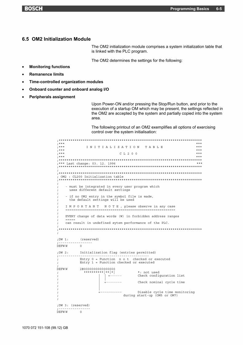
6.5 OM2 Initialization ModuleThe OM2 initialization module comprises a system initialization table thatis linked with the PLC program.
The OM2 determines the settings for the following:• Monitoring functions
• Remanence limits
• Time-controlled organization modules
• Onboard counter and onboard analog I/O
• Peripherals assignmentUpon Power-ON and/or pressing the Stop/Run button, and prior to theexecution of a startup OM which may be present, the settings reflected inthe OM2 are accepted by the system and partially copied into the systemarea.
The following printout of an OM2 exemplifies all options of exercisingcontrol over the system initialisation:
;*************************************************************************;*** ***;*** I N I T I A L I Z A T I O N T A B L E ***;*** ***;*** C L 2 0 0 ***;*** ***;*************************************************************************;*** Last change: 03. 12. 1996 ***;*************************************************************************;;*************************************************************************; OM2 : CL200 Initialization table;*************************************************************************;; - must be integrated in every user program which; uses different default settings;; - if no OM2 entry in the symbol file is made,; the default settings will be used;; I M P O R T A N T N O T E , please observe in any case; ========================================================;; EVERY change of data words (W) in forbidden address ranges; =====; can result in undefined sytem performance of the PLC.;;*************************************************************************;
;DW 1: (reserved);-----------------DEFW W 0
;DW 2: Initialization flag (entries permitted);----------------------------------------------; Entry 0 = Function n o t checked or executed; Entry 1 = Function checked or executed;DEFW W 2#0000000000000000; **********|**|*| *: not used; | | +------ Check configuration list; | |; | +-------- Check nominal cycle time; |; |; +----------- Disable cycle time monitoring; during start-up (OM5 or OM7);
;DW 3: (reserved);----------------DEFW W 0

1070 072 151-108 (99.12) GB
Programming Basics6-6
;DW 4: Maximum cycle time (entries permitted);---------------------------------------------; Entries as multiples of the time base 1 ms of K1D and K2000D; (1 ms - 2000 ms) for cycle time monitoring.; Function execution at DW1 / Bit 2 = 1.;DEFW W 2000;
;DW 5: Number of highest timer loop (entry permitted);-----------------------------------------------------; Entries from K0D through K127D are possible.; K10D = timer loops T0 - T10 exist in PLC program; K127D = any timer loops T0 - T127 exist;DEFW W 127;
;DW 6: Number of first remanent timer (entry permitted);-------------------------------------------------------; Entries from K0D through K128D are possible; K032D = Remanency for timer loops T32 - T127; K128D = no remanency;DEFW W 64;
;DW 7: Number of first remanent counter (entry permitted);---------------------------------------------------------; Entries from K0D through K64D are possible; K32D = Remanency for counters C32 - C63; K64D = no remanency;DEFW W 32;
;DW 8: Number of first remanent marker (entry permitted);--------------------------------------------------------; Entries from K0D through K192D are possible; K128D = Remanency from marker byte M128/marker bit M128.0,; definition of remanency boundary via byte addresses; K192D = no remanency;DEFW W 96;;
; Definition of Timer OMs (entries permitted); ===========================================; Entries as multipliers of time base 10 ms of K1D - K65535D; e.g. K0 = no timer-based processing; K11D = 11 x 10 ms = 110 ms interval of processing time;;DW 9: Timer OM18;-----------------DEFW W 0
;DW 10: Timer OM19;-----------------DEFW W 0
;DW 11: (reserved);-----------------DEFW W 0
;DW 12: (reserved);-----------------DEFW W 0;

1070 072 151-108 (99.12) GB
Programming Basics 6-7
; Definition of on-board counter (OC) (entries permitted); =======================================================; Entry 0 = Function n o t existing or executed; Entry 1 = Function existing or executed;DW 13: On-board Counter 0 settings (OC0);----------------------------------------DEFW W 2#0000000000000000; *******|*****||| *: not used; | |++------ Definition of transitions; | | 00 no transition; | | 01 positive transitions; | | 10 negative transitions; | | 11 both transitions; | +-------- allow external up/down switch-over; |; +-------------- Count downward
;DW 14/15: Actual value OC0 Low/High word;-----------------------------------------;DEFW W 0DEFW W 0
;DW 16/17: Nominal value1 OC0 Low/High word;-------------------------------------------;DEFW W 16#FFFFDEFW W 16#FFFF
;DW 18/19: Nominal value2 OC0 Low/High word;-------------------------------------------;DEFW W 16#FFFFDEFW W 16#FFFF;
;DW 20: Onboard Counter 1 settings (OC1);---------------------------------------;DEFW W 2#0000000000000000; |******|*****||| *: not used; | | |++------ Definition of transitions; | | | 00 no transition; | | | 01 positive transitions; | | | 10 negative transitions; | | | 11 both transitions; | | +-------- allow external up/down switch-over; | |; | +-------------- Count downward; |; +--------------------- incremental rotary position encoder
;DW 21/22: Actual value OC1 Low/High word;-------------------------------------------;DEFW W 0DEFW W 0
;DW 23/24: Nominal value1 OC1 Low/High word;-------------------------------------------;DEFW W 16#FFFFDEFW W 16#FFFF
;DW 25/26: Nominal value2 OC1 Low/High word;-------------------------------------------;DEFW W 16#FFFFDEFW W 16#FFFF
;DW 27: Number of output byte;----------------------------; Outputs are set automatically when nominal values are reached.; This address can be used to define the output byte used for; this purpose.; e.g. K0010D; Nominal value1 OC0 Bit 10.0; Nominal value2 OC0 Bit 10.1; Nominal value1 OC1 Bit 10.2; Nominal value2 OC1 Bit 10.3DEFW W 0
;DW 28 - DW 30 (reserved for fast counters);------------------------------------------DEFW W 0 ;DW 28DEFW W 0 ;DW 29DEFW W 0 ;DW 30

1070 072 151-108 (99.12) GB
Programming Basics6-8
;DW 31 Number of analog inputs used (entry permitted);----------------------------------------------------;; Entry of K0 through K4 possible; K0 = no analog input enabled; K2 = two analog inputs enabled (channel 0 and 1)
DEFW W 4
;DW 32 Selection of normalized analog channels (entries permitted);-----------------------------------------------------------------; Entry 0 = Function n o t existing or executed; Entry 1 = Function existing or executed;; The selected analog inputs are normalized to 2V - 10V,; and the enabled analog output is normalized to 2V - 10V; or to 4mA - 20mA,; respectively.
DEFW W 2#0000000000000000; *******|****|||| *: not used; | |||+------ Analog input Channel 0; | ||+------- Channel 1; | |+-------- Channel 2; | +--------- Channel 3; |; +-------------- Analog output Channel 0;; Entry K0 disables the normalization
;DW 33 - DW 35 (reserved);------------------------
DEFW W 0 ;DW 33DEFW W 0 ;DW 34DEFW W 0 ;DW 35
;DW 36: Entries of second serial interface (entries permitted);-------------------------------------------------------------; Entry 0 = Function n o t existing or executed; Entry 1 = Function existing or executed;DEFW W 2#0000000101110100; |*****||*|||*||* *: reserved; | || ||| |+------- Data bits; | || ||| | 0 8 bit; | || ||| | 1 7 bit; | || ||| |; | || ||| +-------- Parity; | || ||| 0 odd; | || ||| 1 even; | || |||; | || +++---------- Baudrate; | || 111 19200 Baud; | || 110 9600 Baud; | || 101 4800 Baud; | || 100 2400 Baud; | || 011 1200 Baud; | || 010 600 Baud; | || 001 reserved; | || 000 reserved; | ||; | ++-------------- select protocol; | 00 no protocol; | 01 BUEP19E; | 10 BUEP03E; | 11 reserved; |; +--------------------- set new entries
;DW 37 - DW 40 (reserved);------------------------
DEFW W 0 ;DW 37DEFW W 0 ;DW 38DEFW W 0 ;DW 39DEFW W 0 ;DW 40

1070 072 151-108 (99.12) GB
Programming Basics 6-9
; Definition of peripheral configuration lists; (entries permitted); ============================================; The configuration lists are used to enter the peripheral bytes; which are configured in the CL200 and for which a configuration; test shall be performed (see DW2, Bit 0). A test for mimimal; configuration is made upon start-up. Any additional; configuration is not checked.; Each I/O and EI/EO byte which is configured in the controller; and which shall be tested is marked with a "1" in the; corresponding data word. Byte which are not configured or shall; not be tested are to be marked "0".; 16 I/O or EI/EO bytes are to be marked in each data word.;
; Input configuration list; ------------------------;;DW 41: I-Byte 15 ..... 0;---------------------------DEFW W 2#0000000000000000;;DW 42: I-Byte 23 .... 16;---------------------------DEFW W 2#0000000000000000;;DW 43 - DW 48 (reserved);------------------------
DEFW W 0 ;DW 43DEFW W 0 ;DW 44DEFW W 0 ;DW 45DEFW W 0 ;DW 46DEFW W 0 ;DW 47DEFW W 0 ;DW 48
; Output configuration list; -------------------------;;DW 49: O-Byte 15 ..... 0;---------------------------DEFW W 2#0000000000000000;;DW 50 - DW 56 (reserved);------------------------
DEFW W 0 ;DW 50DEFW W 0 ;DW 51DEFW W 0 ;DW 52DEFW W 0 ;DW 53DEFW W 0 ;DW 54DEFW W 0 ;DW 55DEFW W 0 ;DW 56

1070 072 151-108 (99.12) GB
Programming Basics6-10
; Extended Input Range configuration list; ---------------------------------------;;DW 57: EI-Byte 15 .... 0;-------------------------DEFW W 2#0000000000000000;;DW 58: EI-Byte 31 ... 16;-------------------------DEFW W 2#0000000000000000;;DW 59: EI-Byte 47 ... 32;-------------------------DEFW W 2#0000000000000000;;DW 60: EI-Byte 63 ... 48;-------------------------DEFW W 2#0000000000000000;;DW 61: EI-Byte 79 .... 64;--------------------------DEFW W 2#0000000000000000;;DW 62: EI-Byte 95 .... 80;--------------------------DEFW W 2#0000000000000000;;DW 63: EI-Byte 111 .... 96;--------------------------DEFW W 2#0000000000000000;;DW 64: EI-Byte 127 ... 112;--------------------------DEFW W 2#0000000000000000
; Extended Output Range configuration list; ----------------------------------------
;DW 65: EO-Byte 15 .... 0;-------------------------DEFW W 2#0000000000000000;;DW 66: EO-Byte 31 ... 16;-------------------------DEFW W 2#0000000000000000;;DW 67: EO-Byte 47 ... 32;-------------------------DEFW W 2#0000000000000000;;DW 68: EO-Byte 63 ... 48;-------------------------DEFW W 2#0000000000000000;;DW 69: EO-Byte 79 .... 64;--------------------------DEFW W 2#0000000000000000;;DW 70: EO-Byte 95 .... 80;--------------------------DEFW W 2#0000000000000000;;DW 71: EO-Byte 111 .... 96;--------------------------DEFW W 2#0000000000000000;;DW 72: EO-Byte 127 ... 112;--------------------------DEFW W 2#0000000000000000

1070 072 151-108 (99.12) GB
Programming Basics 6-11
; !!! Internal system memory data !!!; =============================================;; The following default settings must not be changed.; ===================================================
;Default for data words DW 73 - DW 128 = K0;------------------------------------------DEFW W 0 ;DW73DEFW W 0 ;DW74DEFW W 0 ;DW75DEFW W 0 ;DW76DEFW W 0 ;DW77DEFW W 0 ;DW78DEFW W 0 ;DW79DEFW W 0 ;DW80DEFW W 0 ;DW81DEFW W 0 ;DW82DEFW W 0 ;DW83DEFW W 0 ;DW84DEFW W 0 ;DW85DEFW W 0 ;DW86DEFW W 0 ;DW87DEFW W 0 ;DW88DEFW W 0 ;DW89DEFW W 0 ;DW90DEFW W 0 ;DW91DEFW W 0 ;DW92DEFW W 0 ;DW93DEFW W 0 ;DW94DEFW W 0 ;DW95DEFW W 0 ;DW96DEFW W 0 ;DW97DEFW W 0 ;DW98DEFW W 0 ;DW99DEFW W 0 ;DW100DEFW W 0 ;DW101DEFW W 0 ;DW102DEFW W 0 ;DW103DEFW W 0 ;DW104DEFW W 0 ;DW105DEFW W 0 ;DW106DEFW W 0 ;DW107DEFW W 0 ;DW108DEFW W 0 ;DW109DEFW W 0 ;DW110DEFW W 0 ;DW111DEFW W 0 ;DW112DEFW W 0 ;DW113DEFW W 0 ;DW114DEFW W 0 ;DW115DEFW W 0 ;DW116DEFW W 0 ;DW117DEFW W 0 ;DW118DEFW W 0 ;DW119DEFW W 0 ;DW120DEFW W 0 ;DW121DEFW W 0 ;DW122DEFW W 0 ;DW123DEFW W 0 ;DW124DEFW W 0 ;DW125DEFW W 0 ;DW126DEFW W 0 ;DW127DEFW W 0 ;DW128;**************************************************************************EM

1070 072 151-108 (99.12) GB
Programming Basics6-12
6.6 Reference ListIn the program memory, three data words per module are reserved for thereference list.
The entries for a given module are structured as follows:
Word 0 Address offset of first instruction, and/or of first data word.Word 1 Number of memory segmentWord 2 Module size in words, exc. module header
A module that is available in the CL200 is identified by these entries.For modules that are not available, each word contains the entry FFFFH.
The reference list is structured as follows:
Start address (byte)Segment Offset Module2 0050H FC02 064AH FC2552 0650H DM02 0C4AH DM2552 0C50H OM02 0CC2H OM19
In the PLC program, for example, the reference list entries can be used tocheck whether modules are present or available and, helpful in the caseof data modules, to check the size of a module.
For the aforementioned purposes the CL200 uses the "LIMR" (Load IM-age Range) instruction, which is not associated with any other function.
Example:
;To check if DM120 is present/available through a;minimum of D420:
L W K120D,B ;DM no. 120L W K6D,A ;Offset module/module in bytesMUL W A,B ;DM no.* module offsetL W K0654H,A ;Address offset module length, DM0ADD W B,A ;Address offset module length, DM120L W K2H,B ;Memory segment numberLIMR W A,C ;Read DB120 module sizeCPLA W K420,C ;Available through D420?JPM -DM_nok ;Jump if < ERROR

1070 072 151-108 (99.12) GB
Programming Basics 6-13
6.7 OM5 & OM7 Startup ModulesTwo startup modules, OM5 and OM7, are available. If a startup module islinked with the PLC program, it will be automatically processed during thestartup routine of the controller.
The start-up is governed by the following criteria:
• OM5: Startup module following restart, always processed subsequent toPower-On. This applies also if, upon Power-On, the ZE200 is in STOPmode. In this case, the OM5 is processed upon changing the operatingmode via a Stop/Run command. OM5 is also processed after programloading.
• OM7: Startup module following restart. Unless the current restart comprisesthe first startup subsequent to Power-On, OM7 is always processed after achange of operating mode by means of Stop/Run.
6.7.1 Programming within Startup ModulesWithin the startup modules, the entire instruction set and, as a conse-quence, also the I/O operation, can be activated through direct access.
As a close instruction for the startup modules, both the EM and/or the EPinstruction can be used. Both have the same effect on the module.
In the event that, during the processing of startup OMs, program modulesare called, the close instructions of such program modules will have theestablished meaning:
EM: Return to startup module that included the call.
EP: Cancel, continue with OM1.
6.7.2 Retriggering of Watchdog and Cycle Time• In the OM2, the hardware watchdog function can be disabled for the duration
of the startup modules. As a consequence, very long startup routines (initiali-zation of peripheral modules) will not cause the controller to stop.
• The software watchdog time is set in the OM2, and cannot be changed oncethe program is operating.
• The cycle time is always measured from OM1 to OM2, and therefore alsocontains the time of the I/O state.
⇒⇒⇒⇒ In the case of peripheral operations with the hardware watchdogdisabled, faulty programming (endless loops) may create dangeroussystem conditions!

1070 072 151-108 (99.12) GB
Programming Basics6-14
6.8 OM9 Error ModuleOM9 is the error module. If this module is linked with the PLC program,any error occurrences which would normally cause an immediate Stop ofthe central processing unit, the OM9 will be called automatically.
The same happens in all cases of errors which are also designated bysetting a bit in the system range.
Exception: If no cycle time limit was designated, and the hardware-dependentcycle time limit is reached due to a programming error, the CL200will automatically enter Stop mode. In this case, enabling an errorOM will no longer be possible.
The error module can be programmed with remedial measures to belaunched in the event that an error occurs. For example, designated data,including the error bits in the system area, can be copied to nonvolatilememory areas.
A retriggering of programme execution with error acknowledgement is ex-cluded. This causes the CL200 to enter Stop mode after each time theOM9 has been processed, regardless whether the EM or EP instructionwas used as the close instruction for the module.

1070 072 151-108 (99.12) GB
Programming Basics 6-15
6.9 Remanence CharacteristicsUnless other limits are specified within the OM2, the remanence charac-teristics of the CL200 are subject to the range limits described below.These limits cannot be changed by means of the PLC program.
6.10 Remanent OperationIn remanent operation, the statuses of the designated remanent operandsare retained after a Stop/Run and Power-On/Off mode change. As a pre-condition, no battery failure may exist.
In the absence of specific designations in the OM2, this means that thefollowing areas are remanent:
• The upper half of the marker range, M96 through M191
• The upper half of the counters, C32 through C63
• The upper half of the timers, T64 through T127
• The entire data field, the data modules and the fixation are always re-manent. They will be deleted only in the case of a battery failure or, inthe case of fixations, upon request by the programming unit (PG).
6.11 Non-remanent operationThe non-remanent operation is set by shifting the remanence limits in theOM2 to the highest possible address.
The entire data field, the data modules and the fixation are always rema-nent. They will be deleted only in the case of a battery failure or, in thecase of fixations, upon request by the programming unit (PG).

1070 072 151-108 (99.12) GB
Programming Basics6-16
6.12 FixationThe ZE200 central processing unit offers the option of fixing the operandsby means of the programming unit.
In contrast to the "Control" command of the PG, operands can be perma-nently set to specific bit statuses and/or values.
The following data areas in the CL200 system are fixable:
Fixable data range CommentInputsOutputs
6.12.1 Remanence of FixationAn established fixation remains enabled under the following conditions:
• After a Stop/Run change of operating mode
• After reloading, provided this is defined in the OM2
• After Power-Off/On

1070 072 151-108 (99.12) GB
Programming Basics 6-17
6.13 InterruptsThe ZE200xx central processing unit utilizes several groups of interrupts:
TI Program interruption by means of time-controlled OMPI Program interruption by means of a peripheral event (interrupt in-
puts)
When an interrupt occurs, normal program execution is interrupted, andthe associated interrupt module is activated.
The lowest priority is assigned to the group of timed interrupts, and thehighest to the group of peripheral interrupts. Within individual groups, theinterrupt assigned to the lowest OM number has the highest priority.
6.13.1 Time Interrupts (time-controlled processing)For each time the time OM is called, the following must be true:
1. The designated time interval has expired, and
2. sequential processing has reached a change of module.
Neither a DM call-up nor an EP instruction is considered a change ofmodule!
The time interrupts are always enabled. Interrupt disabling / enablingfunctions are controlled by interrupt mask programming.
⇒⇒⇒⇒ Due to programmed module nesting within time OMs, additionaltime OMs can occur and be processed, with the understanding thatactive time modules are incapable of causing their own interruption.

1070 072 151-108 (99.12) GB
Programming Basics6-18
6.13.2 Peripheral Interrupts (interrupt inputs)The standard hardware configuration of all CL200 central processing unitsfeatures three interrupt inputs which are wired to the X71 interface con-nector, and which are used to trigger peripheral interrupts.
A peripheral interrupt is triggered by a 0→1 (LOW → HIGH) signalchange on the associated input of the ZE200 central processing unit, andis not linked to a module change. Instead, it branches into the respectiveinterrupt OM immediately after processing a suitable instruction in thePLC program.
In this process, the flag register, i.e., RES, etc., and the system registercontents are rescued.
The user is responsible for effecting a possible rescue of scratch mark-ers, etc.
The peripheral interrupts are always enabled. Interrupt disabling / ena-bling functions are controlled by interrupt mask programming.
⇒⇒⇒⇒ Active peripheral interrupts are neither capable of interruptingthemselves, nor can they be interrupted by time interrupts.
6.13.3 Interrupt Handling InstructionsThe central processing control unit (ZE) internally assigns one interruptmask each to all interrupt groups, time interrupts (TI) and peripheral inter-rupts (PI). The TIM and LIM instructions are used to read from and writeto these masks.
The mask associated with a given interrupt group contains one bit foreach interrupt.
Bit set HIGH: the respective interrupt is enabled.
Bit set LOW: the respective interrupt is disabled.
To effectively enable the interrupts assigned in the mask, the additionalEAI (Enable All Interrupts) instruction is required!
To generally disable an interrupt group without influencing the mask en-tries, the DAI (Disable All Interrupts) instruction is required.
Incoming interrupt signals cause an entry in the corresponding interruptregister, even though the corresponding interrupts are masked. Again,each interrupt is assigned one bit.
If the interrupt is executable, i.e., enabled, the bit in the interrupt registerwill be automatically cancelled by the call-up of the interrupt OM.
If the interrupt is disabled, the bit will remain in the interrupt register whilethe interrupt is waiting to be enabled.
The interrupt register can be read with the LAI (Load All Interrupts) in-struction, and waiting interrupts can be cancelled with the RAI (Reset AllInterrupts) instruction.

1070 072 151-108 (99.12) GB
Programming Basics 6-19
During a change of operating mode with the use of Stop/Run and Power-Off/On, all waiting interrupts are cancelled.
The PI masks are set to zero, and the peripheral interrupts disabled. Anyrequired interrupts must be enabled be the user with the TIM and EAI in-structions!
Time interrupts are enabled by default.
During startup, i.e., while processing OM5 and OM7, all interrupts remaindisabled.
1070 072 151-108 (99.12) GB
Programming Basics6-20
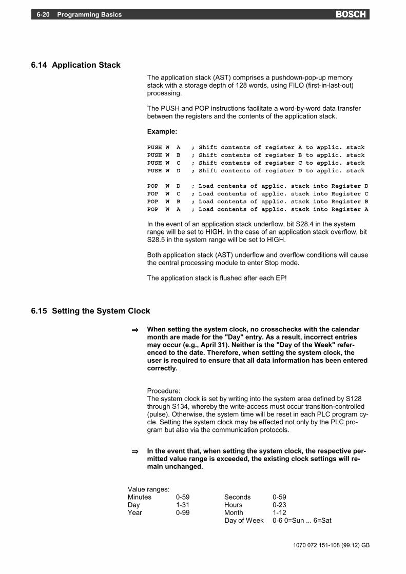
6.14 Application StackThe application stack (AST) comprises a pushdown-pop-up memorystack with a storage depth of 128 words, using FILO (first-in-last-out)processing.
The PUSH and POP instructions facilitate a word-by-word data transferbetween the registers and the contents of the application stack.
Example:
PUSH W A ; Shift contents of register A to applic. stackPUSH W B ; Shift contents of register B to applic. stackPUSH W C ; Shift contents of register C to applic. stackPUSH W D ; Shift contents of register D to applic. stack
POP W D ; Load contents of applic. stack into Register DPOP W C ; Load contents of applic. stack into Register CPOP W B ; Load contents of applic. stack into Register BPOP W A ; Load contents of applic. stack into Register A
In the event of an application stack underflow, bit S28.4 in the systemrange will be set to HIGH. In the case of an application stack overflow, bitS28.5 in the system range will be set to HIGH.
Both application stack (AST) underflow and overflow conditions will causethe central processing module to enter Stop mode.
The application stack is flushed after each EP!
6.15 Setting the System Clock
⇒⇒⇒⇒ When setting the system clock, no crosschecks with the calendarmonth are made for the "Day" entry. As a result, incorrect entriesmay occur (e.g., April 31). Neither is the "Day of the Week" refer-enced to the date. Therefore, when setting the system clock, theuser is required to ensure that all data information has been enteredcorrectly.
Procedure:The system clock is set by writing into the system area defined by S128through S134, whereby the write-access must occur transition-controlled(pulse). Otherwise, the system time will be reset in each PLC program cy-cle. Setting the system clock may be effected not only by the PLC pro-gram but also via the communication protocols.
⇒⇒⇒⇒ In the event that, when setting the system clock, the respective per-mitted value range is exceeded, the existing clock settings will re-main unchanged.
Value ranges:Minutes 0-59 Seconds 0-59Day 1-31 Hours 0-23Year 0-99 Month 1-12
Day of Week 0-6 0=Sun ... 6=Sat

1070 072 151-108 (99.12) GB
CL200 Addressing Conventions 7-1
7 CL200 Addressing Conventions
7.1 Operand & Module IdentifiersAbbr. Operand Peripheral access /
data widthImage update
I II
EI
Input with imageInterface inputsI physically equal to IIExtended input
Image/ bit, byte, worddirect/ byte, word
direct/ byte, word
in I/O stateduring PGM execution
./. O IO
EO
OutputInterface outputsO physically equal to IOExtended output
Image/ bit, byte, worddirect/ byte, word
direct/ byte, word
in I/O stateduring PGM execution
./. M Marker T Timer C Counter D DX
Data word, 1st curr. DMData word, 2nd curr. DM
DF Data field OC Onboard counter S System area K Constant DM Data module CM DMnn ; calls 1st active DM
CX DMnn ; calls 2nd active DM FC Program module
7.2 Module ListThe CL200 manages the following program modules:
• Organization modules
• Program modules
• Data modules
Name Function RemarkOM1 Cyclical program executionOM2 Initialization table refer to Section, "OM2 Initialization
module"OM5 Startup module after Power-ONOM7 Startup module after Stop/Run
:OM9 Error module e.g., cycle time errorOM10 Interrupt module assigned interrupt = I 0, priority 1OM11 Interrupt module assigned interrupt = I 1, priority 2OM12 Interrupt module assigned interrupt = I 2, priority 3
:OM18 Time-controlled module Raster definition in OM2 or S10,
priority 1OM19 Time-controlled module Raster definition in OM2 or S12,
priority 2FC0-FC255
Program modules
DM0-DM255
Data modules

1070 072 151-108 (99.12) GB
CL200 Addressing Conventions7-2
7.3 System AreaThe ZE200 central processing unit features a system area encompassing256 data words (S0 through S255).
This is the location of the configuration files of the CL200 system.
Essential specifications defined in the OM2 are copied into the systemarea, where they can be read by the PLC program.
To the extent deemed useful, system conventions related to cycle timecan be also changed. This includes also the time intervals of the time-controlled organization modules and the system clock.
In addition to the data relating to the ZE, the system area also containsconfiguration data of all intelligent modules encompassed by the CL200system.
Certain segments of the system range are utilized by standard functionmodules providing data that is also useful to other PLC program seg-ments.
The unassigned addresses in the system area are reserved for internalpurposes, and may not be modified.
7.3.1 System Area Assignment
Address Contents CommentsS0 Initialization flags, e.g., OM2_DW2 Read-onlyS2 ReservedS4 ReservedS6 ReservedS8 ReservedS10 Time value for time-controlled process-
ing, OM18S12 Time value for time-controlled process-
ing, OM19
Read and write-access, Accord-ingly, time values can also bechanged via PLC program
S14 ReservedS16 ReservedS18 ReservedS20 Counter, actual cycle time, factor = 1ms Interval length, OM1-OM1, Reset
on Stop/Run, Time refresh onerror-based jump or in I/O state.
S22 Max. cycle time, factor = 1ms Interval length, OM1-OM1,S24 Max. cycle time, factor = 1ms Reset on STOP/RUN

1070 072 151-108 (99.12) GB
CL200 Addressing Conventions 7-3
Address Contents CommentS26 Error word 1
Bit:S26.0 Addressing errorS26.1 Parameter errorS26.2S26.3 Module stack overflowS26.4S26.5S26.6 DM too smallS26.7 Error "Jump direct“ (JP [R])
S27.0 Illegal write-accessS27.1 Opcode errorS27.2 Battery failure/ battery missingS27.3 Timer no. too largeS27.4S27.5 DM not activeS27.6 Transfer error, peripheral busS27.7
S28 Error word 2Bit:S28.0S28.1S28.2 Nonexistent module calledS28.3S28.4 Underflow, application stackS28.5 Overflow, application stackS28.6S28.7 Cycle time error
S29.0S29.1S29.2S29.3S29.4S29.5S29.6S29.7
S30 Bit fieldBit:S30.0 Log. 0S30.1 Log. 1S30.2 Flashing marker (2 Hz)S30.3 Stop/Run trigger pulseS30.4 Power-On/Load Pgm trigger pulseS30.5 I/O fixedS30.6 Outputs disabledS30.7 Low Battery warning
S31.0 Fault, diagnosable periph. moduleS31.1 Cable break, analog inputsS31.2S31.3S31.4S31.5S31.6S31.7
Summary message (modulesunder development) Sum-mary message
S32 Reserved

1070 072 151-108 (99.12) GB
CL200 Addressing Conventions7-4
Address Contents Comment
S34S36S38S40S42S44
OC0 Onboard counterActual value LOW word
HIGH wordSpec'd value 1 LOW word
HIGH wordSpec'd value 2 LOW word
HIGH word
Upon reaching spec'd val-ues, outputs defined inOM2/DEFW27 will be set.
S46S48S50S52S54S56
OC1 Onboard counterActual value LOW word
HIGH wordSpec'd value 1 LOW word
HIGH wordSpec'd value 2 LOW word
HIGH word
Upon reaching spec'd val-ues, outputs defined inOM2/DEFW27 will be set.
S58 OC0 Onboard counter, control bitsS58.0 OC0 counting direction
0 = upward1 = downward
S58.1 Set OC0 actual valueS58.2 Set OC0 specified valueS58.3S58.4S58.5S58.6S58.7
OC1 Onboard counter, control bitsS59.0 OC1 counting direction
0 = upward1 = downward
S59.1 Set OC1 actual valueS59.2 Set OC1 specified valueS59.3S59.4S59.5S59.6S59.7
After the transfer, theCL200 will reset the bits.
After the transfer, theCL200 will reset the bits.
S60-S62 Reserved
S64S66S68S70
Analog inputsAnalog input, channel 0Analog input, channel 1Analog input, channel 2Analog input, channel 3
S72 ReservedS74 ReservedS76 ReservedS78 Reserved
S80Cable break reporting bitsS80.0 Analog input, channel 0S80.1 Analog input, channel 1S80.2 Analog input, channel 2S80.3 Analog input, channel 3
S82 Analog outputS84-S127 Reserved

1070 072 151-108 (99.12) GB
CL200 Addressing Conventions 7-5
System clock (High byte / Low byte)Minutes / SecondsDay / HoursYear / Month
Value range0-59 / 0-591-31 / 0-230-99 / 0-12
S128S130S132S134 Reserved / Day
of Week / 0-6 (0=Sun)
S136-S142
Reserved
Initialization values for ZE200S145/144 ------------------ / Typ ID 00=ZE200; 01=ZE200A
02=ZE200M, 03=ZE200AMS147/146 Boot firmware version / Hardware ver.S149/148 ------------------ / System firmware version Firmware loadable with PGS150 ReservedS152 ReservedS154 ReservedS156 ReservedS158 Reserved
Initialization values for intelligentmodules
S160-S175
Module 1
S176-S191
Module 2
S192-S207
Module 3
S208-S255
Reserved

1070 072 151-108 (99.12) GB
CL200 Addressing Conventions7-6
7.4 Data Formats
15 8 7 Bit 0Bit = X
15 8 7 0Byte = B
This addressing mode differentiates between load and transfer instructions:
Load instruction: The source operand may be either the even-numbered (LOW)byte or the odd-numbered (HIGH) byte.In the case of the destination operand (register), the LOW byteis always addressed.
Examples: L BY M1,A
M1
Register A
L BY M2,A
M2
Register A
Transfer instr.: The low byte in the source operand (SRC_OPD - register) isaddressed. The specified DEST_OPD may be both the even-numbered (LOW) byte and the odd-numbered (HIGH) byte.
Examples: T BY A,M1
Register A
M1
T BY A,M2
Register A
M2
15 8 7 0Word = W

1070 072 151-108 (99.12) GB
CL200 Addressing Conventions 7-7
7.5 Register StructureThe CL200 features 4 working registers, which can be addressed in a bit-wise, byte-wise or word-by-word fashion. In this context, it should benoted that byte/word addressing always addresses the LOW-byte word.
15 8 7 0Working registers HIGH byte LOW byteA, B, C and D Word
For operations that exceed the 16-bit format, the registers are combinedto form permanent register pairs.
15 8 7 0Working register pair Word 2 = LOW word BA + B Word 1 = LOW word A
15 8 7 0Working register pair Word 2 = LOW word DC + D Word 1 = LOW word C
Status bits N O C ZZero
CarryOverflow
Negative
⇒⇒⇒⇒ The negative flag always corresponds to the MSB (most significantbit) of the specified data format. Therefore, for byte operations, thisis Bit 7, and for word operations, it is Bit 15.

1070 072 151-108 (99.12) GB
CL200 Addressing Conventions7-8
7.6 Representing ConstantsThe representation of constants is contingent upon the programming unitsoftware being utilized. It has no functional bearing on the CL200.
Data Type PLC utility programsExplanation Notation PROFI WinSPS
UINT (unsigned integer) Binary / Dual K00000000 00000000BK11111111 11111111B
2#00000000000000002#1111111111111111
Decimal, word K00000D - K63535D 00000 - 65535Decimal, byte/byte K000/000 - K255/255 Not defined in IEC1131
Part 3Hexadecimal K0000H - KFFFFH 16#0000 - 16#FFFF
INT (signed integer) Decimal, word K-32768 - K+32767K-32768D - K+32767D
-32768 - +32767
Text, STRING(2) ASCII K'AB’ ‘AB’Time value, TVALUE Time val. (+timebase r)
r: 0=10ms, 1=100ms 2=1s, 3=10s
K0.r - K1023.rT#10ms - T#10230s
T#0.r - T#1023.r
7.7 Program Module Calls
PLC utility programsPROFI WinSPS
Program module / function call (IEC1131-3) CM PM CM FC
7.8 Jump Instructions
PLC utility programsPROFI WinSPS
Jump instructionJump destination
JPx -label-label
JPx labellabel:
7.9 Bit & Module AddressesOperand Addresses
(decimal)I 0.0-23.7O 0.0-15.7M 0.0-191.7T status 0-127C status 0-63
DM 0-255PM and/or FC 0-255

1070 072 151-108 (99.12) GB
CL200 Addressing Conventions 7-9
7.10 Byte AddressesOperand Address
(decimal)Comment
I, II
EI
0-23
0-127
I is physically identical to II!
externalO, IO
EO
0-15
0-127
O is physically identical to IO!
externalT actual valueT status
0-1270-127
Time range, 10 ms-1023 s(resolution 0.01; 0.1; 1; 10 s)
C actual valueC status
0-630-63
Counter range, 0-8191
M 0-191S 0-255 The system area manages the following:
- System initialization values- Analog onboard I/O- Onboard high-speed counters- System clock- Aux. bits (log1 / 0, RI, flasher, etc.)
P 0-31DF 0-8191D 0-511DX 0-511The even-numbered byte addresses are used as word addresses.

1070 072 151-108 (99.12) GB
CL200 Addressing Conventions7-10
7.11 Addressing Modes
7.11.1 Direct Addressing
Operands for absolute addressing
Byte/word readable I, O, M, T and CK, DF, D, DX, S, II, EI
Actual values apply to T/C
Byte/word writable O, MDF, D, DX, S, IO, EO
Direct addressing of all absolute-addressable operands
Register A
Register B
Register C
Register D
Operand Address
Examples:
L B I10,B ; Loads the status of input byte I10 into B.L W 100,C ; Loads the value 100 into register C.
7.11.2 Register-to-Register Addressing
Register A
Register B
Register C
Register D
Example:
L W C,B ; Loads the contents of register C into register B.
7.11.3 Register-indirect addressing
Register A
Register B
Register C
Register D
Indexed Address
Peripherals
Example:
L W 10,A ; Loads index address into A as a byte number.L W I[A],D ; Loads the status of I10 (addr. in A) into register D.

1070 072 151-108 (99.12) GB
CL200 Addressing Conventions 7-11
7.11.4 Indirect addressingThe indirect addressing method – whether "word/byte or bit-oriented" –uses an operand prefix containing the operand identifier and the operandaddress. This greatly facilitates the handling and monitoring of operandaddresses.
In addition, all data and program modules can be called up indirectly.
The operand prefix is structured as follows:
OPD[R] OPD = Operand identifier[R] = Operand address in register A, B, C or D
The following is a demonstration of the indirect addressing princi-ple, using the example of a block transfer:
Objective:Five input words on address I10 are to be transferred to marker wordsstarting with address M50.
L W 5,A ; Loading loop counterL W 10,B ; Loading I10 byte base addressL W 50,C ; Loading M50 byte base addresscontinue: ; Loop entry labelL W I[B],D ; Reading of contents (operand status)T W D,M[C] ; Writing of loaded statusINC W B,2 ; Next I-word (byte address + 2)INC W C,2 ; Next M-wordDEC W A,1 ; Loop counter -1JPN continue ; not all words processed so far
7.11.4.1 Indirect Byte AddressesOPD
IDByte address (dec.) Instructions
... [Reg]ExamplesOPD: see column 1
I, IIEI
0-230-127
L
O, IOEO
0-150-127
L, TIO and EO, T only
L 10,AL OPD[A],B
T actual val. 0-127 LC actual val. 0-63 L L 10,AM 0-191 L, T T B,OPD[A]S 0-255 L, TDF 0-8191 L, TD 0-511 L, TDX 0-511 L, T
To address the next byte and/or the next T/C when starting from an ad-dress, the address must be increased by 1. To address the next word,the address must be increased by 2.
In the event that an attempt is made to access a word by using an odd-numbered address (operand attribute = W), the controller will enter theStop mode.
The cause of the fault can then be displayed by means of the PG.
⇒⇒⇒⇒ The CL200 does not perform range monitoring. Accordingly, theprogrammer is responsible for staying within range limits. In thecase of write-access range violations, data will be destroyed, andthe controller will enter the STOP mode.

1070 072 151-108 (99.12) GB
CL200 Addressing Conventions7-12
7.11.4.2 Indirect Bit Addresses
OPDID
Bit address (dec.) Instructions ExamplesOPD: see co. 1.
I 0-191 A, AN, O, ONO 0-127 A, AN, O, ON
S, R, =L 10,AA B OPD[A]
M 0-1535 A, AN, O, ONS, R, =
= B OPD[A]
S 0-2047 A, AN, O, ONDF 0-65535 A, AN, O, ON
S, R, =T status 0-127 A, AN, O, ONC status 0-63 A, AN, O, ON
To address the next bit when starting from an address, the addressmust be increased by 1.
If a range limit violation is detected, the controller will enter the Stopmode. The cause of the fault can then be displayed by means of thePG.
7.11.4.3 Indirect Module Addresses
Operand Module Number Instructions... [Reg]
Example
DM 0-255 CMxCXx
L W 10,ACM DM[A]
FC 0-255 CMxCMx
L W 100,ACM FC[A]
To address the next module starting from a module number, the modulenumber must be increased by 1.
If a range limit violation is detected, or if the module is not available, thecontroller will enter the Stop mode. In both cases, the fault can subse-quently be displayed by means of the PG.

1070 072 151-108 (99.12) GB
CL200 Addressing Conventions 7-13
7.12 Parameterized ModulesWhen a program module is called up, up to 32 parameter values can betransferred. The number of parameter values to be transferred is statedas part of the module call-up instruction, followed by the actual parame-ters, starting with the number P0.
All parameters that are to be used as a byte or word in the program mod-ule being called up are transferred without operand attribute.
(Depending on the version of the programming unit (PG) being used, theoperand attribute B or W may be included, depicting that no operand at-tribute is being used.)
All parameters to be used as bits in the module being called up aretransferred with the operand attribute B!
Exception:If times and counters are transferred in the form of parameters withoutoperand attribute, they may be utilized as both a word function, i.e.,time/counter value, and/or a bit function, i.e., time/counter status in themodule being called up.
Example of parameter transfer:
CM FC100,7 ;Call up FC100 and transfer 7 parametersP0 43 ;Parameter P0: FC no. as decimal constant K43P1 4 ;Parameter P1: DM no. as decimal constant K4P2 O56 ;Parameter P2: Output word with byte address O56P3 I7.3 ;Parameter P3: Input bit I7.3P4 T2 ;Parameter P4: Time T2P5 C13 ;Parameter P5: Counter C13P6 O10.0 ;Parameter P6: Output bit O10.0
Utilization of parameters in called-up module FC100:
L P1,A ;Load DM no. 4CM DM[A] ;Open DM4CX DM5
L P0,A ;Load FC no. 43CM FC[A],2 ;Call up FC43 and transfer two parameter valuesP0 D2 ;Parameter P0: D2 of active 1st DM, this being DM4P1 DX6 ;Parameter P1: DX6 of active 2nd DM, this being DM5
L W P2,A ;Load output word O56
L W P4,B ;Load time value from T2 to B
A P3 ;I7.3A P4 ;Status of T2A P5 ;Status of C13= P6 ;O10.0

1070 072 151-108 (99.12) GB
CL200 Addressing Conventions7-14

1070 072 151-108 (99.12) GB
Interfaces & Connectors 8-1
8 Interfaces & Connectors
8.1 X31 – Connector for Programming Unit or External Operator TerminalThe X31 connector provides a combined V.24 / 20mA interface for con-necting the programming unit (PG) or other peripheral devices, such asthe BT20 operator terminal. This interface does not feature control lines,and only the 20mA section is electrically isolated.
The interface uses a female DB-25 connector.
Explanation Designation Pin no. Signal DirectionV.24Transmit data TxD 2 →Receive data RxD 3 ←Ref. & signal GND Sig. GND 720mA12 V out (active) 12 V out 10 For active mode, 9 ↔10
are bridged.12 V in (active) 12 V in 912 V Ref./GND 12 V GND 21Receive data +(passive/active)
RxD+22/12 ←
Receive data -(passive/active)
RxD-12/24
Transmit data +(passive/active)
TxD+23/13 →
Transmit data -(passive/active)
TxD-13/25
Shield Shield Housing
Cable lengths: Baud rate V.24 20mA 9600 15m 300m 19200 15m 150m 38400 15m 50m 57600 15m -
The interface uses the BUEP19E (PST) transmission protocol.
The baud rates are set with a four-segment DIP switch on the ZE200xxas follows:
Switch segment Fixed4 3 2 1 Baud settingOFF OFF OFF OFF 9600 Parity EvenOFF OFF OFF ON 19200 1 Stop bitOFF OFF ON OFF 38400 8 Data bitsOFF OFF ON ON 57600
reserved

1070 072 151-108 (99.12) GB
Interfaces & Connectors8-2
8.2 X32 – Second Serial Interface Connector (ZE201 only)The second serial interface on the ZE201 central processing unit is used,for example, to connect the PG programming unit in the event that aBT20 operator terminal is connected to the standard X31 connector.
The interface features a male DB-9 connector which uses the followingpin assignment:
Pin Signal Designation1 -2 RxD Receive Data3 TxD Transmit Data4 -5 GND Ground6 -7 -8 -9 -
Housing Shield
The maximum cable length for all baud rates is 15 metres.
The X32 serial interface supports the following transmission protocols:
BUEP19E (PST, similar to PG connector X31), and
BUEP03E.
In the same fashion as with the computer modules, the BUEP03E proto-col is handled via the R2REQ and R2CONV function modules. To trans-mit task requests via the second serial interface of the ZE201, only thefictional CXN (computer interface) number "FF" must be addressed.
The BUEP19E transmission protocol of the 2nd interface (X32) connectoris fully compatible with the X31 interface for the PG programming unit.The RST function is not available.
Basic transmission protocol and baud rate settings
Baud rate: 19200 BaudNumber of stop bits: 1 Stop BitParity: EVENNumber of information bits: 8Protocol: BUEP19E
In the event that the protocol and transmission speed settings mustdepart from the default setting, the desired declaration is made in theOM2, DW36.

1070 072 151-108 (99.12) GB
Interfaces & Connectors 8-3
8.3 X71 – Interrupt & Counter InputsThe interrupt and counter inputs are part of the standard equipment ofevery ZE200xx, and are connected by means of a female DB-9 connec-tor.
In both cases the inputs operate with 24 V signals.
Explanation Designation Pin no. Signal directionInterrupt I0 II0 1 ←GND 2Interrupt I1 II1 3 ←GND 4Interrupt I2 II2 5 ←Counter input, OC0 OCI0 6 ←Counting direct., OC0 OCD0 7 ←Counter input, OC1 OCI1 8 ←Counting direct., OC1 OCD1 9 ←Shield Housing
8.3.1 Interrupt Inputs (ZE200xx standard version)As described in the foregoing, the interrupt inputs are wired to the X71interface connector and, in the case of a transition from 0→1, trigger theassigned peripheral interrupt. The response to the interrupt is pro-grammed in the corresponding interrupt OM.
Interrupt I 0 OM10 Priority 1Interrupt I 1 OM11 Priority 2Interrupt I 3 OM12 Priority 3
Minimal programming required for interrupt detection and processing:
1. L W 7H,A ; Prepare all three interrupts for enable.TIM W A,PI ; Write peripheral interrupt mask.
2. EAI PI ; Enable interrupts.
In the event that a signal transition occurs on one of the interrupt inputs,the associated OM will be called. If this module has not been integratedinto the program, the controller will enter STOP mode while returning anappropriate error message. If several interrupts occur at the same time,they will be processed in accordance with the above listed priority ranking.
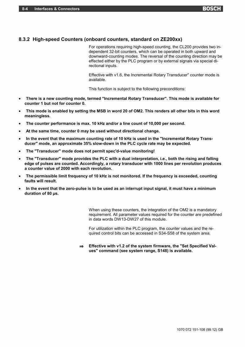
1070 072 151-108 (99.12) GB
Interfaces & Connectors8-4
8.3.2 High-speed Counters (onboard counters, standard on ZE200xx)For operations requiring high-speed counting, the CL200 provides two in-dependent 32-bit counters, which can be operated in both upward anddownward-counting modes. The reversal of the counting direction may beeffected either by the PLC program or by external signals via special di-rectional inputs.
Effective with v1.6, the Incremental Rotary Transducer" counter mode isavailable.
This function is subject to the following preconditions:
• There is a new counting mode, termed "Incremental Rotary Transducer". This mode is available forcounter 1 but not for counter 0.
• This mode is enabled by setting the MSB in word 20 of OM2. This renders all other bits in this wordmeaningless.
• The counter performance is max. 10 kHz and/or a line count of 10,000 per second.
• At the same time, counter 0 may be used without directional change.
• In the event that the maximum counting rate of 10 kHz is used in the "Incremental Rotary Trans-ducer" mode, an approximate 35% slow-down in the PLC cycle rate may be expected.
• The "Transducer" mode does not permit spec'd-value monitoring!
• The "Transducer" mode provides the PLC with a dual interpretation, i.e., both the rising and fallingedge of pulses are counted. Accordingly, a rotary transducer with 1000 lines per revolution producesa counter value of 2000 with each revolution.
• The permissible limit frequency of 10 kHz is not monitored. If the frequency is exceeded, countingfaults will result.
• In the event that the zero-pulse is to be used as an interrupt input signal, it must have a minimumduration of 80 µs.
When using these counters, the integration of the OM2 is a mandatoryrequirement. All parameter values required for the counter are predefinedin data words DW13-DW27 of this module.
For utilization within the PLC program, the counter values and the re-quired control bits can be accessed in S34-S58 of the system area.
⇒⇒⇒⇒ Effective with v1.2 of the system firmware, the "Set Specified Val-ues" command (see system range, S148) is available.

1070 072 151-108 (99.12) GB
Interfaces & Connectors 8-5
OM2 Preset values:
Onboard counter settings (OC0: DW 13 / OC1: DW 20)
13/20 DEFW W 2#0000000000000000*******|*****||| *: reserved| | |++------ Definition of transitions| | | 00 no transition| | | 01 positive transitions| | | 10 negative transitions| | | 11 both transitions| | +-------- Allow external up/down switchover| || +-------------- Downward-counting
not with DW 13 +---------------- increment. Rotary Trans. (V1.6)
Presetting actual values, LOW / HIGH word
OC0: DW 14/15 / OC1: DW 21/22
Values can be changed via the PLC program.
14/21 DEFW W 16#000015/22 DEFW W 16#0000
Presetting specified value 1, LOW / HIGH word (with DW17/24 not forTransducer mode).
OC0: DW 16/17 / OC1: DW 23/24
Values can be changed via the PLC program.
16/23 DEFW W 16#FFFF17/24 DEFW W 16#FFFF
Presetting specified value 1, LOW / HIGH word (with DW19/26 not forTransducer mode).
OC0: DW 18/19 / OC1: DW 25/26
Values can be changed via the PLC program.
18/25 DEFW W 16#FFFF19/26 DEFW W 16#FFFF
Output byte definition (no extended output permitted), not for Transducermode.
Upon achieving the specified values, the outputs are set automatically.After the response has been effected, outputs must be again reset by thePLC program.
⇒⇒⇒⇒ Since the output byte defined here is output via direct access, bits 4-7 are also always output in their current image status (during pro-gram processing). Accordingly, when using high-speed counters,these outputs should always remain unused in order to prevent thereturn of unwanted statuses!
Example: Entry 10 in word 27
OC0 Spec'd value1 = Bit O10.0 OC0 Spec'd value2 = Bit O10.1
OC1 Spec'd value1 = Bit O10.2 OC1 Spec'd value2 = Bit O10.3
27 DEFW W 0

1070 072 151-108 (99.12) GB
Interfaces & Connectors8-6
System area
Address Contents CommentOC0/OC1 onboard counter
S34/S46S36/S48
Actual value LOW wordHIGH word
Actual values can be modified via thePLC program (see Control Bits)
S38/S50S40/S52
Spec'd value 1 LOW wordHIGH word
Specified values can be modified viathe PLC program (see Control Bits)
S42/S54S44/S56
Spec'd value 2 LOW wordHIGH word
Upon reaching the spec'd values,defined outputs are set in DEFW 27of the OM2.
S58/S59 OC0/OC1 onboard counterControl bitsBit0 Counting direction
0 = upward1 = downward
Bit1 Set actual valueBit2 Set specified valueBit3Bit4Bit5Bit6Bit7
After the transfer, the CL200 will resetthe bits.
In the event that, during counting up (or counting down) the maximumvalue of FFFF FFFFH (or minimum value of 0H) is attained, the counterwill again start at 0 (or FFFF FFFFH).
Notes:
The process of setting new current/specified values is transition-controlled, and occurs in the following sequence:
• The "Set current/specified value" bit must be reset.
• The system word provides the new current/specified value, and the "Set current/specified value"control bit is set once (never cyclically).
• In the subsequent cycle, the value is transferred and the control bit reset. In the case of manipula-tions using the actual value, the system variable again serves the display of current actual values.
Without exception, the updating of actual values in the system range oc-curs in the I/O state. Independent of program processing, the outputs as-signed to the specified values are affected immediately.
⇒⇒⇒⇒ To prevent the loss of pulses, the default entry for change of direc-tion and the counting pulses must not occur simultaneously.

1070 072 151-108 (99.12) GB
Interfaces & Connectors 8-7
8.3.2.1 Sample Program – High-speed Counters onboard CL200 Basic Unit
; ************************************************************************; * High-speed Counters *; ************************************************************************
; Examples of onboard counters (high-speed counters) in the CL200; basic unit.
; The basic unit provides 2 high-speed counters, termed; "OC0 onboard counter" and "OC1 onboard counter" hereunder.
; The OM2 initialization module must be linked, and data words 13 to 32; in this module must be suitably modified.
; The OM2 entries for the high-speed counters are described below.;; Definition of onboard counters (OC) (entries permitted); =======================================================; Entry 0 = Function NOT available, and/or DO NOT execute; Entry 1 = Function available, and/or execute;;DW 13: Settings, on-board counter 0 (OC0);--------------------------------------------; 13 DEFW W 2#0000000000000110; *******|*****||| *: reserved; | |++------ Definition of transitions; | | 00 no transition; | | 01 positive transitions; | | 10 negative transitions; | | 11 both transitions; | +-------- allow external up/down switchover; |; +-------------- Downward-counting
;DW 14/15: OC0 actual value, LOW/HIGH word;-----------------------------------------; 14 DEFW W 16#0000; 15 DEFW W 16#0000
;DW 16/17: OC0 spec'd value1 LOW/HIGH word;-------------------------------------------; 16 DEFW W 16#FFFF; 17 DEFW W 16#FFFF
;DW 18/19: OC0 spec'd value2 LOW/HIGH word;-------------------------------------------; 18 DEFW W 16#FFFF; 19 DEFW W 16#FFFF
;DW 20: Settings for onboard counter 1 (OC1);-------------------------------------------; 20 DEFW W 2#0000000000000000; *******|*****||| *: reserved; | | |++------ Definition of transitions; | | | 00 no transition; | | | 01 positive transitions; | | | 10 negative transitions; | | | 11 both transitions; | | +-------- allow external up/down switchover; | |; | +-------------- Downward-counting; +--------------------- Incremental rotary transducers (v1.6)

1070 072 151-108 (99.12) GB
Interfaces & Connectors8-8
;DW 21/22: OC1 actual value, LOW/HIGH word;-----------------------------------------; 21 DEFW W 16#0000; 22 DEFW W 16#0000
;DW 23/24: OC1 spec'd value, LOW/HIGH word;------------------------------------------;; 23 DEFW W 16#FFFF; 24 DEFW W 16#FFFF
; ;DW 25/26: OC2 spec'd value, LOW/HIGH word;-----------------------------------------------; 25 DEFW W 16#FFFF; 26 DEFW W 16#FFFF
;DW 27: Number of output byte;-------------------------------; Outputs are set automatically upon reaching specified values.; This address can be used to set the output byte used for; this purpose.; e.g., K0010D; OC0 spec'd value1 = Bit 10.0 OC0 spec'd value2 = Bit 10.1; OC1 spec'd value1 = Bit 10.2 OC1 spec'd value2 = Bit 10.3; 27 DEFW W K0000D
;+++++++++++++++++++++++++++++++++++++++++++++++++++++++++++++++++++++++++
; Assignments in system area; ---------------------------DEF S34,-OC0_IwL ; OC0 onboard counter, actual value LOW wordDEF S36,-OC0_IwH ; OC0 onboard counter, actual value HIGH wordDEF S38,-OC0_Sw1L ; OC0 onboard counter, spec'd value1 LOW wordDEF S40,-OC0_Sw1H ; OC0 onboard counter, spec'd value1 HIGH wordDEF S42,-OC0_Sw2L ; OC0 onboard counter, spec'd value2 LOW wordDEF S44,-OC0_Sw2H ; OC0 onboard counter, spec'd value2 HIGH word
DEF S46,-OC1_IwL ; OC1 onboard counter, actual value LOW wordDEF S48,-OC1_IwH ; OC1 onboard counter, actual value HIGH wordDEF S50,-OC1_Sw1L ; OC1 onboard counter, spec'd value1 LOW wordDEF S52,-OC1_Sw1H ; OC1 onboard counter, spec'd value1 HIGH wordDEF S54,-OC1_Sw2L ; OC1 onboard counter, spec'd value2 LOW wordDEF S56,-OC1_Sw2H ; OC1 onboard counter, spec'd value2 HIGH word
DEF S58,-OC_StB ; Onboard counter, control bits;; S58.0 OC0 counting direction; 0 = upward; 1 = downward; S58.1 Set OC0 actual value; S58.2 Set OC0 spec'd values;; S59.0 OC1 counting direction; 0 = upward; 1 = downward; S59.1 Set OC1 actual value; S59.2 Set OC0 spec'd values

1070 072 151-108 (99.12) GB
Interfaces & Connectors 8-9
;+++++++++++++++++++++++++++++++++++++++++++++++++++++++++++++++++++++++++
; Connectors, pin assignments; ---------------------------
; OC0 counter input X71 connector, pin 6; OC0 counting direction X71 connector, pin 7; OC1 counter input X71 connector, pin 8; OC0 counting direction X71 connector, pin 9
;+++++++++++++++++++++++++++++++++++++++++++++++++++++++++++++++++++++++++
; Output byte assignment (specified in OM2, w27); ----------------------------------------------; Outputs are set automatically upon reaching specified values.; After the appropriate response has been received, outputs must again; be reset by the PLC program.
; Bit Axx.0 OC0 spec'd value1; Bit Axx.1 OC0 spec'd value2; Bit Axx.2 OC1 spec'd value1; Bit Axx.3 OC1 spec'd value2; Bit Axx.4 - 7 DO NOT USE
;========================================================================
; Example
; *** Set Specified Value ***
; Transition control for 'Set Specified Value' instruction - the loading; procedure for specified value will be enabled only; if a 0-to-1 transition is detected on input I0.0.
1 AN I0.0 ; 'Set Specified Value' input bit2 R M190.0 ; reset help marker3 A I0.04 AN M190.05 S M190.06 JPCI noload1
; Loading procedure for specified value; Load 0C0 specified value (on-board counter0) and enable control bit for; 'Set Specified Value' command. The control bit will be reset automatically; by the PLC once the value has been transferred.; Write spec'd value1 (S40, S38)
7 L W 10,D8 L W 0,C9 T W D,S38 ; OC0 onboard counter, spec'd value1 LOW word10 T W C,S40 ; OC0 onboard counter, spec'd value1 HIGH word
; Write spec'd value2 (S44, S42)11 L W 100,D12 L W 0,C13 T W D,S42 ; OC0 onboard counter, spec'd value2 LOW word14 T W C,S44 ; OC0 onboard counter, spec'd value1 HIGH word
; Enable 'Set Specified Value' control bit; Note: May be active during one cycle only (see Transition Control, above)
15 L W 2#00000000000100,A16 T W A,S58 ; Onboard counter, control bits
noload1:

1070 072 151-108 (99.12) GB
Interfaces & Connectors8-10
; *** Set Actual Value ***
; Transition control for 'Set Actual Value' instruction - the loading; procedure for actual value will be enabled only; if a 0-to-1 transition is detected on input I0.1.
17 AN I0.1 ; 'Set Actual Value' input bit18 R M190.1 ; Reset help marker19 A I0.120 AN M190.121 S M190.122 JPCI noload2
; Loading procedure for actual value; Load 0C0 actual value (onboard counter0) and enable control bit for; 'Set actual value'. The control bit will be reset automatically; by the PLC once the value has been transferred.; Write actual value (S36, S34)
23 L W 50,D24 L W 0,C25 T W D,S34 ; OC0 onboard counter, actual value LOW word26 T W C,S36 ; OC0 onboard counter, actual value HIGH word
; Enable 'Set Actual Value' control bit; Note: May be active during one cycle only (see Transition Control, above)
27 L W 2#00000000000010,A28 T W A,S58 ; Control bits, onboard counter
noload2:
; Read and reset output bits which are set by direct access by; the counter (specified in initialization module OM2, w27).
29 A O0.0 ; OC0 Spec'd value1 was reached; This location for programming additional responses as required.
30 R O0.0 ;
31 A O0.1 ; OC0 Spec'd value2 was reached; This location for programming additional responses as required.
32 R O0.1 ;
33 L W M180,A34 INC W A,135 T W A,M18036 A A.437 = O0.438 A I0.339 = O0.540 L W S34,A ; OC0 onboard counter, actual value LOW word41 L W S36,A ; OC0 onboard counter, actual value HIGH word42 L W S38,A ; OC0 onboard counter, spec'd value1 LOW word43 L W S40,A ; OC0 onboard counter, spec'd value1 HIGH word44 L W S42,A ; OC0 onboard counter, spec'd value2 LOW word45 L W S44,A ; OC0 onboard counter, spec'd value2 High word
46 EP

1070 072 151-108 (99.12) GB
Interfaces & Connectors 8-11
8.4 X72 – Analog Inputs & Analog OutputFor "simple" processing of analog values, the CL200 with its ZE200Axcentral processing control units provides four analog inputs and one ana-log input. They are connected by means of a female DB-15 connector.
The analog values and the cable-break messages of the analog inputsare accessible in system range S64-S82.
Explanation Designation Pin no. Signal directionAnalog input 0 AI0 1 ←Analog input 1 AI1 2 ←Analog input 2 AI2 3 ←Analog input 3 AI3 4 ←Analog output OP mode OM 5 open: Output I
AOI bridged: output UAnalog output, voltage AOU 10 →Analog output, current AOI 14 →reserved 6, 13GND 7, 8, 9, 11,
12, 15Shield Housing
When the controller is powered up without the OM2, the processing of allanalog inputs within a voltage range of 0-10 V is enabled.
OM2 Settings (OM2 is not an indispensable requirement)
To enable the control processor to restrict processing to channels actuallyin use, assigned analog inputs are specified in DW 31.
; Entries are possible from K00D through K04D; 0 = no analog input enabled; 2 = two analog inputs enabled (channels 0 and 1);
31 DEFW W 4
To select whether or not which analog input channels are to be enabled,and/or whether the analog output is to be standardized.
; The selected analog inputs are standardised to 2 V - 10 V, and; the enabled analog output is standardised to 2 V - 10 V; and/or to 4 mA - 20 mA;;
32 DEFW W 2#0000000000000000; *******|****|||| *: reserved; | |||+------ Analog input, channel 0; | ||+------- channel 1; | |+-------- channel; | +--------- channel 3; |; +-------------- Analog output, channel 0;; Entry 0 switches off standardization.

1070 072 151-108 (99.12) GB
Interfaces & Connectors8-12
8.4.1 Analog InputsThe voltage value present at the analog inputs is converted and subse-quently written into the system area for further processing in digital form.
If a cable break is detected during normal (default) operation (value < 4mA and/or < 2 V), this will be reported in word S80 of the system area.
SpecificationsNumber of analog inputs 4, pursuant to IEC 1131-2Electrical isolation noInput range 0 – 10 V
2 – 10 V, when standardized via OM2Permissible input voltage -10 V through 30 VDigital mapping 16-bitResolution 10-bitInput resistance 20.4 kΩConversion time 20 µsScanning interval 10 ms, value updating in system area
during subsequent I/O stateError tolerance 1% at 0 through 55 oCCable length max. 100 metres, screened
System areaAnalog inputs
S64 Analog input value, channel 0S66 Analog input value, channel 1S68 Analog input value, channel 2S70 Analog input value, channel 3S72 ReservedS74 ReservedS76 ReservedS78 Reserved
Cable break reporting bitsS80 S80.0 Analog input, channel 0
S80.0 Analog input, channel 1S80.0 Analog input, channel 2S80.0 Analog input, channel 3
Priority representationPriority Bit without significance
9 8 7 6 5 4 3 2 1 0 x x x x x xMSB LSB
LSB voltage value:
• Default operation: 10 V / 1024 = 9.8 mV
• With standardization: 8 V / 1024 = 7.8 mV
1070 072 151-108 (99.12) GB
Interfaces & Connectors 8-13
8.4.2 Analog OutputThe PLC program writes into the system area the digital representation ofthe voltage or current output value that will be sent to the analog output,and utilizes the I/O state to transfer it to the output.
SpecificationsNumber of analog outputs 1, pursuant to IEC 1131-2Electrical isolation noShort-circuit protection yes, unlimitedShort-circuit current 32 mAError tolerance 1% at 0 - 55 oCCable length max. 100 metres, screenedDigital mapping 16 bitResolution 12 bitConversion time 1 msValue output after writing to system area, value output
occurs during subsequent I/O-State.Output voltage
Output range 0 – 10 V2 – 10 V, with standardization via OM2
Load resistance ≥ 1 kΩ
Output current0 – 20 mA4 – 20 mA, with standardization via OM2
Load resistance ≤ 600 Ω
System area
S82 Analog output value
Priority representation
Priority bitwithout
significance11 10 9 8 7 6 5 4 3 2 1 0 x x x xMSB LSB
LSB voltage value
• Default operation: 10 V / 4096 = 2.4 mV
• With standardization: 8 V / 4096 = 2.0 mV
LSB current value
• Default operation: 20 mA / 4096 = 4.9 µA
• With standardization: 16 mA / 4096 = 3.9 µA

1070 072 151-108 (99.12) GB
Interfaces & Connectors8-14
8.4.2.1 Sample Program – Analog Processing on the CL200 Basic Unit; Examples of analog inputs and the analog output
; on the CL200A and CL200AM central processing units.;; Measuring ranges: analog inputs 0 - 10 V; 2 - 10 V; analog output 0 - 10 V; 0 - 20 mA; 2 - 10 V; 4 - 20 mA; Note: Whenever an example specifies standardized operation,; the OM2 initialization module must be linked to the program,; and data word 32 in the OM2 must be appropriately modified.
; **********************************************************************ag; * Analog inputs, CL200 Central Processing Unit *; ************************************************************************
DEF S64,-AnaKan0 ; = Analog value, channel 0, X72 connector, pin 0DEF S66,-AnaKan1 ; = Analog value, channel 1, X72 connector, pin 1DEF S68,-AnaKan2 ; = Analog value, channel 2, X72 connector, pin 2DEF S70,-AnaKan3 ; = Analog value, channel 3, X72 connector, pin 3
; GND X72 connector, pins 9,11,12,15DEF S80,-KaBruch ; Cable break message, channel 0 = Bit 0
; Cable break message, channel 1 = Bit 1; Cable break message, channel 2 = Bit 2; Cable break message, channel 3 = Bit 3
; Cable break is reported only during standardized; 2-10 V operation (as specified in OM2, w 32).
; Bit assignment:; +---+---+---+---+---+---+---+---+---+---+---+---+---+---+---+---+; | 15| 14| 13| 12| 11| 10| 9 | 8 | 7 | 6 | 5 | 4 | 3 | 2 | 1 | 0 |; +MSB+---+---+---+---+---+---+---+---+LSB|---+---+---+---+---+---+; |<============ Analog value ===========>|******* not used ******|
; Example: 1111111111xxxxxx = Analog value, 10 V; 0000000000xxxxxx = Analog value, 0 V

1070 072 151-108 (99.12) GB
Interfaces & Connectors 8-15
; ======================================================================ag; * Start of Sample Programs "Reading and Scaling Analog Values" *; ========================================================================
;Example 1;; Loading analog value from channel 0 (default operating mode / non-; standardized) on CL200 central processing unit, using 0-1023 scaling; over 0-10000 (mV). The value is filed in data module DM0, word 0.
1 CM DM02 L W S64,A ; = Analog value, channel 0, X72 connector, pin 0,3 SLR W A,6 ; and load into bits 0-11.
; Scale value 0-1023 over 0-10000 mV4 L W 9775,C ; at weighting: 1 bit = 0.9775 mV,5 MUL W C,A ; and multiply with loaded value.6 L W 1000,C ; --"--7 DIV W C,A ; --"--8 T W A,D0 ; Output scaled analog value in data word 0 of DM.
;Example 2
; Reading of analog value from channel 1 (standardized operating mode /; entry in OM2 DW32) on CL200 central processing unit, using 0-1023 scaling; over 2000-10000 (mV). The value is filed in data module DM0, word 2.
9 CM DM010 L W S66,A ; = Analog value, channel 1, X72 connector, pin 1,11 SLR W A,6 ; and load into bits 0-11.
; Scale value 0-1023 over 0-10000 mV12 L W 7820,C ; at weighting 1 bit = 0.7820 mV,13 MUL W C,A ; and multiply with loaded value.14 L W 1000,C ; --"--15 DIV W C,A ; --"--16 L W 2000,D ; Scale value 0-8000 over 2000-10000 mV.17 ADD W D,A ; --"--18 T W A,D2 ; Output scaled analog value in data word 2 of DM.
19 L W S80,B ; Cable break message, channel 0 = Bit 020 A B B.1 ; --"--21 = B O0.0 ; Response to cable break
; * End of sample programs "Reading and Scaling Analog Values" *
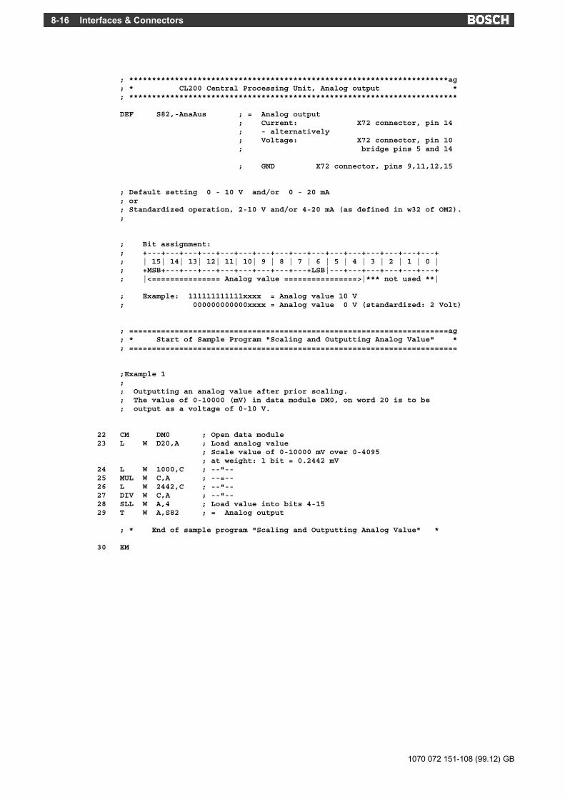
1070 072 151-108 (99.12) GB
Interfaces & Connectors8-16
; **********************************************************************ag; * CL200 Central Processing Unit, Analog output *; ************************************************************************
DEF S82,-AnaAus ; = Analog output; Current: X72 connector, pin 14; - alternatively; Voltage: X72 connector, pin 10; bridge pins 5 and 14
; GND X72 connector, pins 9,11,12,15
; Default setting 0 - 10 V and/or 0 - 20 mA; or; Standardized operation, 2-10 V and/or 4-20 mA (as defined in w32 of OM2).;
; Bit assignment:; +---+---+---+---+---+---+---+---+---+---+---+---+---+---+---+---+; | 15| 14| 13| 12| 11| 10| 9 | 8 | 7 | 6 | 5 | 4 | 3 | 2 | 1 | 0 |; +MSB+---+---+---+---+---+---+---+---+LSB|---+---+---+---+---+---+; |<=============== Analog value ================>|*** not used **|
; Example: 111111111111xxxx = Analog value 10 V; 000000000000xxxx = Analog value 0 V (standardized: 2 Volt)
; ======================================================================ag; * Start of Sample Program "Scaling and Outputting Analog Value" *; ========================================================================
;Example 1;; Outputting an analog value after prior scaling.; The value of 0-10000 (mV) in data module DM0, on word 20 is to be; output as a voltage of 0-10 V.
22 CM DM0 ; Open data module23 L W D20,A ; Load analog value
; Scale value of 0-10000 mV over 0-4095; at weight: 1 bit = 0.2442 mV
24 L W 1000,C ; --"--25 MUL W C,A ; --=--26 L W 2442,C ; --"--27 DIV W C,A ; --"--28 SLL W A,4 ; Load value into bits 4-1529 T W A,S82 ; = Analog output
; * End of sample program "Scaling and Outputting Analog Value" *
30 EM

1070 072 151-108 (99.12) GB
Instruction List 9-1
9 Instruction List
9.1 Structure of Controller InstructionsC o n t r o l l e r I n s t r u c t i o n
Operationpart
Operandattribute
Sourceoperand
Destinationoperand
OPP OPA SRC , DEST
Examples:
A I0.0A W -Name , AL B O0 , BT W C , M10MUL W K1234D , D
9.2 Status Bits (Flags)The status bits are influenced by the following instruction groups:
• Compare
• Convert
• Swap
• Increment
• Decrement
• Shift
• Rotate
• Add
• Subtract
• Multiply
• DivideInstructions belonging to these groups are equally applicable to programprocessing instructions (jumps, module instructions) and logical links (flagqueries).
Status bitsFlags PG display
readoutJP...CM...
Flag query Explanation
CY=1CY=0
C ...C...CN
A CYAN CY
CarryCarry Not
O=1O=0
O ...O...ON
A OAN O
OverflowOverflow Not
Z=1Z=0
Z ...Z...N
A ZAN Z
ZeroNot Zero
N=1N=0
N ...M...P
A NAN N
Negative / MinusPositive
AG=1 ...AG AN Z(AN OAN NO OA N)
Arithmetical greater
AG=0 N∨Z ...MZ A ZO NAN OON NA O
Minus / Zero
LG=1 ...LG AN ZAN CY
Logical greater
LG=0 C∨Z ...CZ A ZO CY
CarryZero

1070 072 151-108 (99.12) GB
Instruction List9-2
9.3 Key to AbbreviationsOPP Operation / operator
OPA Operand attributeX Bit (X may be omitted)B ByteW Word
SRC Source operand
DEST Destination operandI InputII Interface inputEI Extended inputO OutputIO Interface outputEO Extended outputM MarkerT Time (timer)C CounterD Data word (within data modules)DF Data fieldOC Onboard counterS System areaK ConstantDM Data moduleDX 2nd active data moduleFC Program module (function call)SYM Symbolic (max. 8 characters)R.bit Register bit, with R = A, B, C, D, and bit = 0 thru 15OPD[R] Register indirect, with operand prefixTI Timed interrupt (time-controlled processing)PI Peripheral interrupt
RG Program rungA Permitted operation at RG startE Operation concluding RG
AddrMode Addressing modeD DirectR Register (A, B, C or D)[R] Register indirect, with operand prefix
Status bits / Special markersV Result RESC CarryO OverflowZ ZeroN Negative

1070 072 151-108 (99.12) GB
Instruction List 9-3
9.4 Binary Links & Parenthesized Instructions
Control Instruction RG AddrMode
InfluencesFLAG Instr.
LengthProc.Time
Example CommentOPT OPA SRC DEST O I D R [R] V CY O N Z (Byte) (µs)
U I/O/M T/C/SYM R.bit P OPD[R] CY,Z,N,O
••••••
••
•
•
•
•
••••••
4*
10104*
0.3
11.08.30.3
A A A A A A
I0.0T0A.0P0M[O]CY
AND link, query for status '1'
4*: Length is valid for branch centre only; for start of branch, + 2 bytes.
UN I/O/M T/C/SYM R.bit P OPD[R] CY,Z,N,O
••••••
••
•
•
•
•
••••••
6*
10106*
0.6
11.08.30.6
AN AN AN AN AN AN
O0.0Z0B.0P1M[A]Z
AND link, query for status '0'
6*: Length is valid for start of branch only; for branch centre, + 2 bytes
O I/O/M T/C/SYM R.bit P OPD[R] CY,Z,N,O
••••••
••
•
•
•
•
••••••
8
10108
0.6
11.08.30.6
O O O O O O
M0.0-SYMBOLC.0P10M[A]N
OR link, query for status '1'
ON I/O/M T/C/SYM R.bit P OPD[R] CY,Z,N,O
••••••
••
•
•
•
•
••••••
8
10108
0.6
11.08.30.6
ON ON ON ON ON ON
M31.7-nameD.0P1M[A]O
OR link, query for status '0'
= O/M/SYM P R.bit OPD[R]
••••
••
••
810810
0.6110.68.3
= = = =
O0.0P0O.0M[A]
Assign result when RES = 1
S O/M/SYM P R.bit OPD[R]
••••
••
••
10101010
0.7511.00.758.3
S S S S
O0.0P0O.0M[A]
Set bit when RES = 1
R O/M/SYM P R.bit OPD[R]
••••
••
••
10101010
0.7511.00.758.3
R R R R
O0.0P0O.0M[A]
Reset bit when RES = 1
( 6 0.45 ( Parentheses facilitate 7-fold nesting AND open parenthesis
) 10 0.75 ) close parenthesis O( 10 0.75 O( OR open parenthesis )N 14 1.2 )N Negation of contents enclosed in parenthe-
ses

1070 072 151-108 (99.12) GB
Instruction List9-4
9.5 Time ProgrammingThe ZE200 provides 128 time circuits, T0 through T127.
These can be utilized in the following modes:
• SP Start time as pulse
• SPE Start pulse extended
• SR Start time as raising delay
• SF Start time as falling delay
• SRE Start time as raising delay extended
Starting non-remanent times (SP, SPE, SR and SRE) require a positivetransition of the time start condition to effect the timed start. The start willnot occur however, if the start condition is equal to "1" already during thefirst addressing (1st PLC cycle) subsequent to a start or restart.
Remanent times cause the transition marker to be retained; i.e., whetheror not a "1" in the first addressing (1st PLC cycle) after a start or restartwill start the timer will depend on the start condition prior to the STOPand/or Power-Off.
The timers are decremented in the I/O state. This means that a timeoutwill be recognized only during the I/O state, and not during the programcycle!
Because during each I/O state, a timer is decremented by multiples of thedefined time matrix, it is good practice to select a resolution that is as fineas possible.
⇒⇒⇒⇒ To effect a timed start, a positive transition and/or a negative transi-tion for the falling delay of the time start condition is required.
⇒⇒⇒⇒ A time start condition that is satisfied immediately upon Power-Ondoes not qualify as a transition!
Time start condition 0 and 1 may be programmed in different modules oralso in immediate succession.
Example:
A B -log0 ;Time start condition 0SR A,T5
A B -log1 ;Time start condition 1SR A,T5 ;Time start correct

1070 072 151-108 (99.12) GB
Instruction List 9-5
9.5.1 Time InstructionsTime starts are activated only when the RES signal undergoes a transitionfrom 0↑1. In advance of the time start, the time value is loaded into theregister being used. Reset and stop functions of times are always RESsignal-dependent. The time status for logical links is instruction-dependent, and may be taken from the time diagrams.
Control Instruction RG AddrMode
InfluencesFLAG Instr.
LengthProc.Time
Example CommentOPT OPA SRC DEST O I D R [R] V CY O N Z (Byte) (µs)
SP R ,,
,
TSYM
P
• •
•
8 5.11
8.02
8.91
12.02
SP SP
SP
A,T0A,-Symbol
A,P0
Start time as pulse
1 when RES = stable 2 when RES = 0↑↑↑↑1
SPE R ,,
,
TSYM
P
• •
•
8 5.11
8.02
8.91
12.02
SPE SPE
SPE
A,T0A,-Symbol
A,P0
Start pulse extended
1 when RES = stable 2 when RES = 0↑↑↑↑1
SR R ,,
,
TSYM
P
• •
•
8 5.11
8.02
8.91
12.02
SR SR
SR
A,T0A,-Symbol
A,P0
Start time as raising delay
1 when RES = stable 2 when RES = 0↑↑↑↑1
SF R ,,
,
TSYM
P
• •
•
8 5.11
8.02
8.91
12.02
SF SF
SF
A,T0A,-Symbol
A,P0
Start time as falling delay
1when RES = stable 2 when RES = 0↑↑↑↑1
SRE R ,,
,
TSYM
P
• •
•
8 5.11
8.02
8.91
12.0
SRESRE
SRE
A,T0A,-Symbol
A,P0
Start time as raising delay extended
1 when RES = stable 2 when RES = 0↑↑↑↑1
RT T SYM
P
• •
•
10 4.41
5.42
9.01
10.0
RT RT
RT
T0-Symbol
P0
Reset time when RES = 1
1 when RES = 0 2 when RES = 1
TH T SYM
P
• •
•
10 4.8
8.5
TH TH
TH
T0-Symbol
P0
Timer halt when RES = 1, Time continueswhen RES = 1

1070 072 151-108 (99.12) GB
Instruction List9-6
9.5.2 Time Format15 14 13 12 11 10 9 8 7 6 5 4 3 2 1 0x x x x R R W W W W W W W W W W
Time matrix Time value: 1 - 10230 0 0: 10 ms :0 1 1: 100 ms Program entry of time constant:1 0 2: 1 s Kw.r with time value w = 1 -10231 1 3: 10 s and time matrix r = 0 - 3
Example: Timer T100 shall be started at 15 sec:
L W t#15s,A ;15s declaration in 1-sec time matrix of CL200
A -start
SPE A,T100
Same function with higher matrix resolution, i.e., higher accuracy:
L W t#1500ms,A ;15s declaration in 1oo-ms time matrix of CL200
A -start
SPE A,T100
Timed start with the assistance of the PG time matrix:
L W t#15.2,A ;15s declaration in 1-ms time matrix of PG
A -start
SPE A,T100
Same function with higher matrix resolution, i.e., higher accuracy:
L W t#150.1,A ;15s declaration in 1oo-ms time matrix of PG
A B -start
SPE A,T100

1070 072 151-108 (99.12) GB
Instruction List 9-7
9.5.3 Time Diagrams
SP – Start time as pulse
Start condition
Reset condition
Time status ← t → < t
SPE – Start pulse extended
Start condition
Reset condition
Time status ← t → ← t → ← t → < t
SR – Start time as raising delay
Start condition
Reset condition
Time status ← t → < t
SF – Start time as falling delay
Start condition
Reset condition
Time status ← t → ← t →
SRE – Start time as raising delay extended
Start condition
Reset condition
Time status ← t → ← t → ← t → < t

1070 072 151-108 (99.12) GB
Instruction List9-8
9.6 Counter Instructions
9.6.1 Software CounterTimer resets and changes of direction of count (up/down) are activated only when the RES signalundergoes a transition from 0↑↑↑↑1.
In advance of the reset, the required counter content is loaded into the register being used.
Counter reset functions are statically RES signal-dependent.
The counter status for logical links depends on the counter content. For counter contents > 0,the status is = 1 (HIGH); counter content = 0 will have status = 0 (LOW).
Counter range: 0 – 8191
Control Instruction RG AddrMode
InfluencesFLAG Instr.
LengthProc.Time
Example CommentOPT OPA SRC DEST O I D R [R] V CY O N Z (Byte) (µs)
SC R ,,
,
ZSYM
P
• •
•
8 4.31
6.22
811
9.02
SC SC
SC
A,Z0A,-Symbol
A,P0
Set counter
1 when RES = stable 2 when RES = 0↑↑↑↑1
CU C SYM
P
• •
•
10 5.31
6.32
9.21
10.2
CU CU
CU
Z0-Symbol
P0
Count upward
1 when RES = stable 2 when RES = 0↑↑↑↑1
CD C SYM
P
• •
•
10 5.31
6.32
9.21
10.2
CD CD
CD
Z0-Symbol
P0
Count downward
1 when RES = stable 2 when RES = 0↑↑↑↑1
RC C SYM
P
• •
•
10 4.01
6.02
7.81
9.8
RC RC RC
Z0-SymbolP0
when RES = 1, reset counter
1 when RES = 0 2 when RES = 1
9.6.2 High-speed Counter (onboard counter)
Control Instruction RG AddrMode
InfluencesFLAG Instr.
LengthProc.Time
Example CommentOPT OPA SRC DEST O I D R [R] V CY O N Z (Byte) (µs)
CS OC • • 6 7.5 CS OC0 Onboard counter Stop when RES = 1

1070 072 151-108 (99.12) GB
Instruction List 9-9
9.7 Digital Links
Control Instruction RG AddrMode
InfluencesFLAG Instr.
LengthProc.Time
Example CommentOPT OPE Q-OPD Z-OPD O I D R [R] V CY O N Z (Byte) (µs)
A W,BW,B
R K
, R•
• 00
00
••
••
68
0.450.6
A A
WB
A,B10,A
Digital AND link between source anddestination. The result is written todestination.
AN W,BW,B
R K
, R•
• 00
00
••
••
810
0.60.75
AN AN
WB
A,B10,A
Digital AND NOT link between sourceand destination. The result is written todestination.
O W,BW,B
R K
, R•
• 00
00
••
••
68
0.450.6
O O
WB
A,B10,A
Digital OR link between source anddestination. The result is written todestination.
ON W,BW,B
R K
, R•
• 00
00
••
••
810
0.60.75
ON ON
WB
A,B10,A
Digital OR NOT link between sourceand destination. The result is written todestination.
XO W,BW,B
R K
, R•
• 00
00
••
••
68
0.450.6
XO XO
WB
A,B10,A
EXCLUSIVE OR link between sourceand destinationl. The result is written todestination.
XON W,BW,B
R K
, R•
• 00
00
••
••
810
0.60.75
XON XON
WB
A,B10,A
EXCLUSIVE OR NOT link betweensource and destinationl. The result iswritten to destination.
9.8 Swap Instruction
Control Instruction RG AddrMode
InfluencesFLAG Instr.
LengthProc.Time
Example CommentOPP OPA SRC DEST O I D R [R] V CY O N Z (Byte) (µs)
SWAP W R • 4 0.3 SWAP W A Byte swap in registers High-Byte ↔Low-Byte

1070 072 151-108 (99.12) GB
Instruction List9-10
9.9 Compare InstructionThe CPLA (Compare Logical and Arithmetical) instruction is available forCompare operations. As the name implies, the instruction facilitates bothlogical and arithmetical compare operations.
The logical compare operation regards the bytes and/or words to be com-pared as unsigned integers, i.e., as "unsigned 8" or "unsigned 16".
The arithmetical compare operation regards the bytes and/or words to becompared as signed integers, i.e., as "integer 8" or "integer 16".
Subsequent to a Compare operation, the flags provide information aboutthe Compare result.
Control Instruction RG AddrMode
InfluencesFLAG Instr.
LengthProc.Time
Example CommentOPP OPA SRC DEST O I D R [R] V CY O N Z (Byte) (µs)
CPLA W,BW,B
K R
, R ••
••
••
••
••
86
0.60.45
CPLA CPLA
WB
255,BB,C
Arithmetical Compare function. Theresult may be used for logical andarithmetical purposes. The result can beinterpreted logically and arithmetically.Compare values: logical: positive,integer arithmet.: two's complement,integer
Binary result evaluation of compare results occurs by means of jumpfunctions dependent upon status bits, and/or through status bit query.
Examples:
Compare CPLADestination (A) w/ Source (B) Logical Arithmetical
CPLA B,A Flag Status bit Flag Status bit
Equal A====B JPZ A Z JPZ A Z
Unequal A≠B JPN AN Z JPN AN Z
Less than A<<<<B JPCY A CY JPM AN NA OO NAN O
Less than or equal A≤B JPCZ A ZO CY
JPMZ A ZO NAN OON NA O
Greater A>>>>B JPLG AN CYAN Z
JPAG AN Z(AN OAN NO OA N)
Greater than orequal
A≥B JPCN AN CY JPP AN NAN OO NA O

1070 072 151-108 (99.12) GB
Instruction List 9-11
9.10 Load Instructions
Control Instruction RG AddrMode
InfluencesFLAG Instr.
LengthProc.Time
Example CommentOPP OPA SRC DEST O I D R [R] V CY O N Z (Byte) (µs)
L W,BY I/O/M T/Z/K/SYM DF D/DX II/EI R OPD[R] P
, R •••••
•
••
seebelow
*
seebelow
*
L L L L L L L L
WBYWBYWBYWBY
I0,A0,B0,CD0,DII0,AB,CM[C],DP0,A
Load contents of SRC operand intoDEST operand.
Read value
L DW K , R,R+1 • 12 0.75 L DW K20000H,A Load constant > 64k into registersR/R+1
LIMR W O , C • 6 5.8 LIMR W A,C Load contents of address in A/B to C. This instruction is used exclusively for the purpose of reference list verification. Example: Verification of whether or not a module is available, or whether a datamodule of sufficient size is linked!
* instruction lengths and processing times
direct indirect as parameterW BY W BY W BY
SRC Byte µs Byte µs Byte µs Byte µs Byte µs Byte µsK 4 0.3 4 0.3 8 8.8 8 8.8R 2 0.15 2 0.15I,O,M 4 0.3 4 0.3 8 0.6 8 0.6 8 9.0 8 9.0T 8 3.8 8 3.8 6 3.7 6 3.7 8 11.6 8 11.6C 4 0.3 4 0.3 12 0.8 12 0.8 8 9.0 8 9.6S 4 0.3 4 0.3 8 0.6 8 0.6 8 9.0 8 9.6DF 4 0.3 4 0.3 8 0.6 8 0.6 8 9.0 8 9.6D,Dx 8 5.0 8 4.7 6 4.8 6 4.5 8 12.9 8 11.6II 8 51.6 8 34.8 6 50.1 6 35.9 8 52.9 8 42.5EI 8 51.6 8 34.8 6 50.1 6 35.9 8 52.9 8 42.5
9.11 Transfer Instructions
Control Instruction RG AddrMode
InfluencesFLAG Instr.
LengthProc.Time
Example CommentOPP OPA SRC DEST O I D R [R] V CY O N Z (Byte) (µs)
T W,BY R ,,,,,,,
O/M/SYMS/DFD/DXIO/EOROPD[R]P
••••
•
••
seebelow
*
seebelow
*
T T T T T T T
WBYWBYWBYW
A,M0B,DF0C,D0D,IA0A,BB,M[C]D,P0
Transfer contents of SRC operand intoDEST operand.
Write value
* Instruction lengths and processing times
direct indirect as parameterW BY W BY W BY
SRC Byte µs Byte µs Byte µs Byte µs Byte µs Byte µsR 4 0.3O, M, S,DF
4 0.3 8 0.6 8 0.6 8 0.6 8 9.0 8 9.6
D, Dx 8 5.9 8 5.8 6 5.5 6 4.5 8 13.3 8 13.2IO, EO 8 49.4 8 33.3 6 46.1 6 30.0 8 52.2 8 39.0

1070 072 151-108 (99.12) GB
Instruction List9-12
9.12 Convert Instructions
Control Instruction RG AddrMode
InfluencesFLAG Instr.
LengthProc.Time
Example CommentOPP OPA SRC DEST O I D R [R] V CY O N Z (Byte) (µs)
BID W,BY R • 0 • 0 • 10 17.88.9
BID BID
WB
AB
Binary → BCD (decimal) Result > 9999 sets the overflow bit.
DEB W,BY R • 0 • 0 • 10 16.710.3
DEB DEB
WB
CD
BCD (decimal) → binary Incorrect BCD encoding sets the overflow bit.
TC W,BY R • • • • • 6 0.45 TC TC
WB
AB
Converts the register contents to the two'scomplement.
N W,BY R • 0 • 0 • 8 0.6 N N
WB
CD
Negates the register contents (one's comple-ment).
Representing of positive and negative numbers
A negative number corresponds to the two's complement of the positivenumber.
Example: 0 1 1 0 positive integer 61 0 0 1 Negation and/or one's complement
+ 11 0 1 0 two's complement = negative integer 6
In the case of word operations, the differentiation between positive andnegative integers is determined by Bit 15. In the case of byte operations,this is Bit 7.
Word:Bit 15 = 0 Byte: Bit 7 = 0 positive integerBit 15 = 1 Bit 7 = 1 negative integer
Integer value range
Positive integers Word:0 - 32767 Byte: 0 – 127Negative integers 0 - 32768 0 - 128
1111-1
00000
1110-2
0001+1
1101-3
0010+2
1100-4
0011+3
1011-5
negative positive 0100+4
1010-6
0101+5
1001-7
0110+6
1000-8
0111+7

1070 072 151-108 (99.12) GB
Instruction List 9-13
9.13 Increment / Decrement InstructionsIncrement / decrement the source operand (SRC_OPD, 1 to 7 in num-ber):
• by the number n
• when n=0 and when [C], by the number stored in C (max. 7).
Control Instruction RG AddrMode
InfluencesFLAG Instr.
LengthProc.Time
Example CommentOPP OPA SRC DEST O I D R [R] V CY O N Z (Byte) (µs)
INC W,BY R ,,,
n0
[C]
••
•
•••
•••
•••
•••
61010
0.450.750.75
INC INC INC
BYWW
A,5B,0B,[C]
Raise (increment) the contents of theSRC_OPD.
DEC W,BY R ,,,
n0
[C]
••
•
•••
•••
•••
•••
61010
0.450.750.75
DEC DEC DEC
BYWW
A,5B,0B,[C]
Lower (decrement) the contents of theSRC_OPD.
9.14 Stack Instructions
⇒⇒⇒⇒ The available stack size comprises 128 words. In the event of under-flow, bit S28.4 in the system area is set; overflow sets system areabit S28.5. The I/O state resets/deletes the entire application stack.
Control Instruction RG AddrMode
InfluencesFLAG Instr.
LengthProc.Time
Example CommentOPP OPA SRC DEST O I D R [R] V CY O N Z (Byte) (µs)
PUSH W R • 4 4.0 PUSH W A Saves the register contents to applicationstack, and lowers the stack address.
POP W R • 4 4.0 POP W B Raises the application stack address andreads the saved contents from the stack.
9.15 No-operation Instructions & CARRY Manipulations
Control Instruction RG AddrMode
InfluencesFLAG Instr.
LengthProc.Time
Example CommentOPP OPA SRC DEST O I D R [R] V CY O N Z (Byte) (µs)
NOP0 2 0.15 NOP0 No-operation with zeroes in the bufferlocation.
NOP1 2 0.15 NOP1 No-operation with ones in the bufferlocation.
SCY • 2 0.15 SCY Set CARRY bit absolutely to 1. RCY • 2 0.15 RCY Set CARRY bit absolutely to 0.

1070 072 151-108 (99.12) GB
Instruction List9-14
9.16 Shift InstructionsShift the contents of the source operand (SRC_OPD)
• by the number n
• when n=0, and when [C], by the number stored in C
• when OPA = W n: 1-15
• when OPA = BY n: 1-7
Control Instruction RG AddrMode
InfluencesFLAG Instr.
LengthProc.Time
Example CommentOPP OPA SRC DEST O I D R [R] V CY O N Z (Byte) (µs)
SLR W,BY R ,,,
n0
[C]
••
•
•••
000
•••
61010
0.451) SLR SLR
WBY
A,7B,[C]
SHIFT logical RIGHT
1) applies to W, BY + 0.3 µs SLL W,BY R ,
,,
n0
[C]
••
•
•••
000
•••
61212
0.451) SLL SLL
WBY
A,7B,[C]
SHIFT logical LEFT
1) applies to W, BY + 0.45 µs
SAR W,BY R ,,,
n0
[C]
••
•
000
•••
•••
•••
61010
0.451) SAR SAR
WBY
A,7B,[C]
SHIFT arithmetical RIGHT
1) applies to W, BY + 0.3 µs
Logical SHIFTMSB LSB Cy
SLR B, n 0→ 0 • → • → ο
MSB LSB Cy
SLL B, n • ← • 0 ←0 ο↓ → ↑
Arithmetical SHIFT (All bits being vacated are filled up with the contents of the MSB)MSB LSB Cy
SAR B, n • →• → • → οIn the case of shift operations exceeding one space, the overflow bit is setafter a "1" was shifted through Cy.

1070 072 151-108 (99.12) GB
Instruction List 9-15
9.17 Rotate InstructionsShift the contents of the source operand:
• by the number n
• when n=0, and when [C], by the number stored in Cwhen OPA = W n: 1-15
• when OPA = BY n: 1-7
Control Instruction RG AddrMode
InfluencesFLAG Instr.
LengthProc.Time
Example CommentOPP OPA SRC DEST O I D R [R] V CY O N Z (Byte) (µs)
ROR W,BY R ,,,
n0
[C]
••
•
•••
•••
•••
•••
61212
0.451) ROR ROR ROR
BYWW
A,7A,0B,[C]
Rotate RIGHT
1) applies to W, BY + 0.45 µs ROL W,BY R ,
,,
n0
[C]
••
•
•••
•••
•••
•••
61212
0.451) ROL ROL ROL
BYWW
A,7A,0B,[C]
Rotate LEFT
1) applies to W, BY + 0.45 µs
RCR W,BY R ,,
n0
[C]
••
•
•••
•••
•••
•••
8 4.351) RCR RCR RCR
BYWW
A,7A,0B,[C]
Rotate RIGHT through CARRY
1) applies to W, BY + 0.3 µs RCL W,BY R ,
,,
n0
[C]
••
•
•••
•••
•••
•••
8 4.81) RCL RCL RCL
BYWW
A,7A,0B,[C]
Rotate LEFT through CARRY
1) applies to W, BY + 0.6 µs
Rotate RIGHTMSB LSB Cy
ROR B, n ο • → • ο
↑ ← ↓ → ↑
Rotate LEFTMSB LSB Cy
ROL B, n • ← • ο ο↓ → ↑ → ↑
Rotate RIGHT through CARRYMSB LSB Cy
RCR B, n ο • → • → ο↑ ← ↓
Rotate LEFT through CARRYMSB LSB Cy
RCL B, n • ← • ο ← ο↓ → ↑
With Rotate instructions by more than one digit, the following occurs• The overflow bit is set when a "1" has passed through Cy.• The negative bit is set, when the MSB contains a "1".
MSB: Bit 7 when OPA = BYBit 15 when OPA = W

1070 072 151-108 (99.12) GB
Instruction List9-16
9.18 Arithmetic
9.18.1 Add Instructions
Control Instruction RG AddrMode
InfluencesFLAG Instr.
LengthProc.Time
Example CommentOPP OPA SRC DEST O I D R [R] V CY O N Z (Byte) (µs)
ADD W,BY K R
, R ••
••
••
••
••
81)
62)0.60.45
ADD ADD
WBY
255,BB,C
Fixed-point addition of signed integers Source + destination = DEST 1) applies to constant 2) applies to register
ADC W,BY K R
, R ••
••
••
••
••
121)
102)0.90.75
ADC ADC
WBY
255,BB,C
Fixed-point addition of signed integerswith consideration of CARRY. Source + destination + Cy = DEST 1) applies to constant 2) applies to register
Byte or Word addition7/15 0
ADD B/W B , A Sg A+
Sg B=
Sg A
ADC B/W C , A Sg A+
Sg C+Cy
=Sg A
Double-word addition: value 1 + value 2Value 1: LOW word in B, HIGH word in AValue 2: LOW word in D, HIGH word in C
LOW word 15 0
ADD W D , B Sg B+
Sg D=
Sg A
HIGH wordADC W C , A Sg A
+Sg C
+Cy
=Sg A

1070 072 151-108 (99.12) GB
Instruction List 9-17
9.18.2 Subtract Instructions
Control Instruction RG AddrMode
InfluencesFLAG Instr.
LengthProc.Time
Example CommentOPP OPA SRC DEST O I D R [R] V CY O N Z (Byte) (µs)
SUB W,BY K R
, R ••
••
••
••
••
86
0.61)
0.452) SUB SUB
WBY
255,BB,C
Fixed-point subtraction of signedintegers. Destination - source = DEST 1) applies to constant 2) applies to register
SBB W,BY K R
, R ••
••
••
••
••
1210
0.91)
0.752) SBB SBB
WBY
255,BB,C
Fixed-point subtraction of signedintegers with consideration of negativeCARRY. (- Carry = Borrow) Destination - source - Cy = DEST 1) applies to constant 2) applies to register
Byte or Word subtractionBit 7 when OPA = BY
MSB Bit 15 when OPA = W0
SUB OPA B , A Sg A-
Sg B=
Sg A
SBB OPA C , A Sg A-
Sg C-Cy
=Sg A
Double-word subtraction: value 1 – value 2Value 1: LOW word in B, HIGH word in AValue 2: LOW word in D, HIGH word in C
LOW word 15 0
SUB D D , B Sg B-
Sg D=
Sg A
HIGH wordSBB W C , A Sg A
-Sg C
-Cy
=Sg A

1070 072 151-108 (99.12) GB
Instruction List9-18
9.18.3 Multiply Instructions
Control Instruction RG AddrMode
InfluencesFLAG Instr.
LengthProc.Time
Example CommentOPP OPA SRC DEST O I D R [R] V CY O N Z (Byte) (µs)
MUL W,BY K R
, R ••
00
00
••
••
1010
5.31)
5.01) MUL MUL
BYW
100,AB,A
Fixed-point multiplication of signedintegers. Byte instruction: SRC BY x DEST BY = DEST W Word instruction: SRC W x DEST W = DEST W andDEST W +1. 1) applies to BY; if W = + 1.0µs
The product of all Multiply operations occupies twice the width of the starting op-erands.
Byte multiplication7 0
MUL B B , A ; SRC BY Sg Bx
; DEST BY Sg A15 =
; DEST W Sg A
Word multiplication15 0
MUL W B , A ; SRC W Sg Bx
; SRC BY Sg A
=; DEST W A
a n d; DESTW+1
Sg B

1070 072 151-108 (99.12) GB
Instruction List 9-19
9.18.4 Divide Instructions
Control Instruction RG AddrMode
InfluencesFLAG Instr.
LengthProc.Time
Example CommentOPP OPA SRC DEST O I D R [R] V CY O N Z (Byte) (µs)
DIV W,B K R
, R ••
00
••
••
••
1010
7.11) DIV DIV
BW
100,AB,A
Fixed-point division of signed integers. Byte instruction: DEST W : SRC BY = DEST W (RESremainder.) Word instruction: DEST DW : SRC W= DEST W and DEST W+1 RES remainder 1) applies to W; if BY = + 0.4µs
The dividend of all Divide operations occupies twice the width of the divi-sor.
Note: To simplify command entry, the instruction
L DW KhhhhllllH,A may be used.
Byte division15 0
DIV BY B , A ; DEST W Sg A7 : 0
; SRC BY Sg B15 = 0
; DEST W A: High BY = Rest Sg Low BY = Quotient
Word division31 32
DIV W C , A ; DESTW+1
Sg B
31 0
; DEST W A31 : 0
; SRC W Sg C=
; DEST W Sg A: Quotient
; DESTW+1
B: Rest
⇒⇒⇒⇒ In the case of a Divide operation by 0, the Divide instruction will notbe carried out, and the overflow bit will be set. The overflow bit willalso be set if the result is > 64k.
Example: L W K2,CL DW K20000H,ADIV W C,A ; O bit set
When overflow = 1, the status of the N bit is not defined.

1070 072 151-108 (99.12) GB
Instruction List9-20
9.19 Parameter Assignments
Control Instruction RG AddrMode
InfluencesFLAG Instr.
LengthProc.Time
Example CommentOPP OPA SRC DEST O I D R [R] V CY O N Z (Byte) (µs)
Pn W BY B
I/O/M/T/C/K II/IO/EI/EO S/SYM D/DX /DF
••••
8 - P0 P1 P2 P3
WW
E0.0IE0S0D0
Parameter definition for parameterizedmodule calls.
n: 0-31
9.20 Local Symbol Names & Auxiliary Flags for Program Tracking
Control Instruction RG AddrMode
InfluencesFLAG Instr.
LengthProc.Time
Example CommentOPP OPA SRC DEST O I D R [R] V CY O N Z (Byte) (µs)
DEF I/O/M/T/C/K II/IO/EI/EO S/SYM D/DX /DF FC/DM
, SYM - - DEF DEF
I0.0,-SymbolI0,-Name
Definition of symbolic names that are validonly within the module ("local") in whichthey have been entered (essential for thecreation of library modules).
* n
n = 0-63
6 6.6 * 1 Definition of auxiliary flags for programtracking. Processing of these aux. flags isentered only in the marker buffer, and isinterpretable only in the case of an error. *nhas no influence on the program.
9.21 System Variable
Control Instruction RG AddrMode
InfluencesFLAG Instr.
LengthProc.Time
Example CommentOPP OPA SRC DEST O I D R [R] V CY O N Z (Byte) (µs)
DEFW W K 4 - DEFW W 0 Definition of function for system variable inOM2. (Refer to related chapter.)

1070 072 151-108 (99.12) GB
Instruction List 9-21
9.22 Jump InstructionsJump operations may be executed unconditionally, and also in depend-ence of a binary link and/or mathematical operation. With one exception,Jump operations are programmed symbolically (exception: JP [R]). Theentry point may not be located within a program branch because thiswould cause the RES at the branching point to be included in the link.This dispenses with the necessity to observe the enter point because thatis calculated by the PG programming unit in any case.
Control Instruction RG AddrMode
InfluencesFLAG Instr.
LengthProc.Time
Example CommentOPP OPA SRC DEST O I D R [R] V CY O N Z (Byte) (µs)
JP SYM [R]
••
1212
113.8
JP JP
-LABEL1[A]
unconditional to -LABEL destination by jump distance (words), in register A
JPC SYM • • 1 12 1 JPC -LABEL2 conditional, see status bit JPCI SYM • • 0 12 1 JPCI -LABEL3 conditional, see status bit JPCY SYM • 1 12 1 JPCY -LABEL4 conditional, see status bit JPCN SYM • 0 12 1 JPCN -LABEL5 conditional, see status bit JPO SYM • 1 12 1 JPO -LABEL6 conditional, see status bit JPON SYM • 0 12 1 JPON -LABEL7 conditional, see status bit JPM SYM • 1 12 1 JPM -LABEL8 conditional, see status bit JPP SYM • 0 12 1 JPP -LABEL9 conditional, see status bit JPZ SYM • 1 12 1 JPZ -LABEL10 conditional, see status bit JPN SYM • 0 12 1 JPN -LABEL11 conditional, see status bit JPAG SYM • 12 1 JPAG -LABEL12 conditional, see status bits JPMZ SYM • 12 1 JPMZ -LABEL13 conditional, see status bits JPLG SYM • 12 1 JPLG -LABEL14 conditional, see status bits JPCZ SYM •
For binary flag query,refer to Section 9.2,
"Status Bits".
12 1 JPCZ -LABEL15 conditional, see status bits
The JP [R] instruction causes an unconditional jump whose destinationmust always be a jump instruction. This instruction variant was createdwith the objective to facilitate a simple implementation of jump distribu-tors. The controller monitors the instruction mnemonics of the enter pointand will enter STOP mode if the former fails to correspond to a valid jumpinstruction. Information regarding the origin of the error can subsequentlybe obtained via the error status of the PG programming unit.

1070 072 151-108 (99.12) GB
Instruction List9-22
Example:
PLC program interlude
Fixed program sequence
Jump distance calculation in register A for the following jump sequence:A may contain odd values (1, 3, 5, ...) only.The parameter n may not be smaller than the number of jumps to follow.
JP [A] ; 1-word instructionJP Dest1 ; 2-word instructionJP Dest2 ; 2-word instruction : :JP Destn ; 2-word instruction
Dest1: ; Partial program 1
PLC program
JP End
Dest2: ; Partial program 2
PLC program
JP End:::::Destn: ;Partial program n
PLC program
JP End::EndPLC successor program :

1070 072 151-108 (99.12) GB
Instruction List 9-23
9.23 Module CallsModule calls may be executed unconditionally and also in dependence ofa binary link and/or a mathematical operation.
The CL200 facilitates a nesting depth of 32 program modules.
Two data modules may be kept enabled at the same time. For this pur-pose the following module calls are available:
CM, CMC DMx: enables DMx as 1st DM
CX, CXC DMy: enables DMy as 2nd DM
Control Instruction RG AddrMode
InfluencesFLAG Instr.
LengthProc.Time
Example CommentOPP OPA SRC DEST O I D R [R] V CY O N Z (Byte) (µs)
CM DM FC FC OPD[R]
, n
• •••
•
6101010 ↓
CM CM CM CM
DM0FC0FC1,2FC[A]
Unconditional, direct
Parameterized, list to follow Indirect
CMC DM FC FC OPD[R]
, n
• •••
•
6101010 ↓
CMC CMC CMC CMC
DM0FC0FC1,2FC[A]
Conditional, RES-dependent Direct Parameterized, list to follow Indirect
CX DM OPD[R]
• ••
610 ↓
CX CX
DM0DM[A]
Unconditional, direct
CXC DM OPD[R]
• ••
610 ↓
CXC CXC
DM0DM[A]
Conditional, RES-dependent
Instruction not executed executed DM, FC(,n) 4.8 10.6 OPD[R] 4.8 20.0
9.24 End Of Module InstructionsEnd Of Module instructions may be executed unconditionally, and also in dependence of a binarylink and/or mathematical operation.
Control Instruction RG AddrMode
InfluencesFLAG Instr.
LengthProc.Time
Example CommentOPP OPA SRC DEST O I D R [R] V CY O N Z (Byte) (µs)
EM • 6↓
EM Unconditional
EMC • 6↓
EMC Conditional, RES-dependent
Instruction not executed executed4.5 18

1070 072 151-108 (99.12) GB
Instruction List9-24
9.25 Interrupt Instructions
Control Instruction RG AddrMode
InfluencesFLAG Instr.
LengthProc.Time
Example CommentOPP OPA SRC DEST O I D R [R] V CY O N Z (Byte) (µs)
TIM R , TI/PI • 8 6.8 TIM A,TI Transfer interrupt mask. Writes interruptmask for disabling or enabling interrupts.The masks were first loaded into a register.
LIM TI/PI , R • 8 6.8 LIM PI,B Load interrupt mask Define interrupt mask EAI TI/PI • 6 6.8 EAI PI Enable interrupt group (activate) DAI TI/PI • 6 6.8 DAI PI Disable interrupt group (deactivate) LI TI/PI , R • 8 6.8 LI PI,A Load interrupt register (Read statuses) RI R , TI/PI • 8 6.8 RI A,TI Resetting interrupts in accordance with
previously loaded mask.
9.26 Program Stop / End
Control Instruction RG AddrMode
InfluencesFLAG Instr.
LengthProc.Time
Example CommentOPP OPA SRC DEST O I D R [R] V CY O N Z (Byte) (µs)
HLT 6 - HLT HALT instruction. The controller entersSTOP mode, the program address isentered in error stack, and outputs arecleared (deleted).
EP 6 - EP Program End. The I/O state is initialized,and the program cycle start again at thebeginning. At least one EP must bepresent.

1070 072 151-108 (99.12) GB • HB SP • AT/PLS • Printed in Germany