on micromachining with a focus on miniature gears by non ...
41
ARCHIVE OF MECHANICAL ENGINEERING VOL. LXV 2018 Number 1 DOI: 10.24425/119413 Key words: WEDM, ECM, Micro-EDM, recast layer, micro-gear TINA CHAUDHARY 1 , ARSHAD NOOR SIDDIQUEE 2 , ARINDAM KUMAR CHANDA 3 , ZAHID AKHTAR KHAN 2 ON MICROMACHINING WITH A FOCUS ON MINIATURE GEARS BY NON CONVENTIONAL PROCESSES: A STATUS REPORT Recent developments in automation and technology have revolutionized the way products are made. It is directly seen in the evolution of part miniaturization in the sectors such as aerospace, electronics, biomedicine and medical implants. Microma- chining is a promising technology to fulfill the need of miniaturization. A review has been done on the micromachining processes such as micro electric discharge machining (micro-EDM) and wire EDM (WEDM), micro electrochemical machining (micro-ECM). Recent literature were studied and categorized in terms of materi- als, process parameters, performances, product manufactured, and miniature product generation. Starting with brief introduction to micromachining, classifications and applications, technical aspects of discussions from the literature have been presented on key factors such as parameters and the response variables. Important aspects of recast layer, heat effected zone, micro-hardness, micro cracks, residual stress, etc., have been given. A special focus is given to the status of the research on micro- gear manufacturing. Comparison has been made between other conventional process suitable for micro-gear manufacturing and WEDM. The miniature gear machined by WEDM shows the defect-free microstructure, better surface finish, thin recast layer and improved gear quality parameters such as profile and pitch. Finally, the research gaps and future research directions have been presented. 1. Micromachining Requirement of meso-scale (500 mm to 1000 mm) and micro-scale (1 mm to 500 mm) products is rapidly increasing in aeronautical, automobile, biomedical, nuclear, optical, and semiconductor field [1]. Micro-manufacturing facilitates the 1 Department of Mechanical and Automation Engineering, Indira Gandhi Delhi Technical Uni- versity for Women, Kashmere Gate, Delhi, India. Email: [email protected] 2 Department of Mechanical Engineering, Jamia Millia Islamia (a Central University), New Delhi, India 3 Department of Mechanical and Automation Engineering, G.B. Pant Engineering College, New Delhi, India
-
Upload
khangminh22 -
Category
Documents
-
view
2 -
download
0
Transcript of on micromachining with a focus on miniature gears by non ...

A R C H I V E O F M E C H A N I C A L E N G I N E E R I N G
VOL. LXV 2018 Number 1
DOI: 10.24425/119413Key words: WEDM, ECM, Micro-EDM, recast layer, micro-gear
TINA CHAUDHARY 1, ARSHAD NOOR SIDDIQUEE 2, ARINDAM KUMAR CHANDA 3,ZAHID AKHTAR KHAN 2
ON MICROMACHINING WITH A FOCUS ON MINIATURE GEARSBY NON CONVENTIONAL PROCESSES: A STATUS REPORT
Recent developments in automation and technology have revolutionized the wayproducts are made. It is directly seen in the evolution of part miniaturization in thesectors such as aerospace, electronics, biomedicine and medical implants. Microma-chining is a promising technology to fulfill the need of miniaturization. A reviewhas been done on the micromachining processes such as micro electric dischargemachining (micro-EDM) and wire EDM (WEDM), micro electrochemical machining(micro-ECM). Recent literature were studied and categorized in terms of materi-als, process parameters, performances, product manufactured, and miniature productgeneration. Starting with brief introduction to micromachining, classifications andapplications, technical aspects of discussions from the literature have been presentedon key factors such as parameters and the response variables. Important aspects ofrecast layer, heat effected zone, micro-hardness, micro cracks, residual stress, etc.,have been given. A special focus is given to the status of the research on micro-gear manufacturing. Comparison has been made between other conventional processsuitable for micro-gear manufacturing and WEDM. The miniature gear machined byWEDM shows the defect-free microstructure, better surface finish, thin recast layerand improved gear quality parameters such as profile and pitch. Finally, the researchgaps and future research directions have been presented.
1. Micromachining
Requirement of meso-scale (500 mm to 1000 mm) and micro-scale (1 mm to500 mm) products is rapidly increasing in aeronautical, automobile, biomedical,nuclear, optical, and semiconductor field [1]. Micro-manufacturing facilitates the
1Department of Mechanical and Automation Engineering, Indira Gandhi Delhi Technical Uni-versity for Women, Kashmere Gate, Delhi, India. Email: [email protected]
2Department of Mechanical Engineering, JamiaMillia Islamia (a Central University), NewDelhi,India
3Department of Mechanical and Automation Engineering, G.B. Pant Engineering College,New Delhi, India

130 T. CHAUDHARY, A.N. SIDDIQUEE, A.K. CHANDA, Z.A. KHAN
use of miniature features in products such as fuel injection nozzles, semiconduc-tor devices, biotechnology products, medical tools for investigation, and medicalsurgery [2]. Present day micro-manufacturing processes are broadly classified aslithographic and non-lithographic techniques [3]. Photolithography is evolving asan important technology that supports micro-manufacturing, but it has severallimitations for high aspect ratio structures, use of work materials and high initialinvestment etc. [4]. Non-lithographic techniques typically not only overcome suchlimitations but also have an advantage over lithography in terms of cost, materialschoice, relative accuracy and complexity of product geometry.
Non-lithographic techniques are broadly classified into three types, i.e., ad-vanced micromachining, mechanical micromachining, forming and moulding, andfinishing processes [5, 6]. Mechanical micromachining includes the micro-cuttingusing conventional micromachining tools. This includes processes such as micro-drilling,micro-turning andmicro-milling processes, etc. Based on source of energy,advanced micromachining techniques can be further subdivided into groups, i.e.,based on energy (i.e., mechanical, thermal and electrochemical energy). There arefurther subdivisions under each of these sub-categories.
Mechanical energy may be supplied in several forms such as ultrasonic vi-brations, abrasive jet, abrasive water jet, and water jet [3]. Use of thermal en-ergy during micromachining may comprise of high energy beams such as in ionbeam machining, electron beam machining, laser beam machining, plasma arcmachining etc.; and high energy sparks such as in electric discharge micromachin-ing, wire-electric discharge micromachining, and micro-wire electric dischargegrinding. Energy in chemical form is also used for the purpose of microma-chining such as in electrochemical micromachining, petrochemical micromachin-ing [3].
Electrochemical machining (ECM) which works on dissolution of metal elec-trochemically is also another advanced process which is used for micromachiningapplications. In ECM, the shape of electrode identifies the shape of machinedsurface and very high degree of finish is produced as the removal is throughatom by atom dissolution of material [7]. In some of the latest variant of theprocess, electrolyte jet has also been tried instead of a metallic tool [8]. A highspeed jet localizes the electrochemical dissolution easily and allows machining ofmicro indentations. Advanced finishing processes, such as micro/nano-finishing,include elastic emission finishing, abrasive flow finishing, magneto-rheologicalfinishing, magnetic float polishing, magnetic abrasive finishing and so on [3].Hybrid process is the combination of these micromachining processes to takethe advantages of constituent processes. Hybrid processes include electric dis-charge grinding, electrochemical discharge machining, chemical mechanical pol-ishing, electro chemical spark micromachining, electrolytic in process dressingand so on [9, 10]. Hybrid micromachining processes results in great improve-ments in responses such as MRR, SR, geometrical accuracy and tool life, etc.Hybrid micromachining process could be exceptionally beneficial to fabricate

ON MICROMACHINING WITH A FOCUS ON MINIATURE GEARS . . . 131
complex miniature parts with high machining efficiency. Combined hybrid mi-cro machining has great prospects in fabricating complex micro parts with goodaccuracy and surface quality. ECDM milling, for example, is a favorable pro-cess for fabricating complex shapes with non conductive, hard and brittle mate-rials. Furthermore, laser assisted micro milling can develop free form surfaceson non conductive hard and brittle materials. These micromachining processescan also combine with other sequential processes to improve machining rate,surface integrity and geometrical accuracy of the micro-parts [10]. Sequentialmicromachining process is the machining technique where two or more microma-chining processes are enacted in a sequence on same or different tools. A recentresearch is geared towards sequential micro machining processes over single ma-chine tool to reduce the realignment errors. The major advantages of sequentialmicromachining over the single machine tool are that it prevents the reposition-ing errors and enables higher levels of accuracy or tighter tolerances, and re-duces rejection of machined parts. Multifunctional micro machining processes areattracting the global attention due to precise, reconfigurable and flexible manu-facturing [6].
1.1. Major micromachining applications
One of the oldest and largest applications of micromachining is in the man-ufacturing of silicon-based semiconductor devices. Simply because these devicesare produced by detailing micro- features on wafers of semiconductors which arehard and fragile, machining of these becomes very important. The silicon micro-machining technology is based on three process, i.e., lithographic approach, directetching and deposing processes. Silicon wafers can be machined with physicaland chemical etching, and finally elements are released layer by layer from siliconsubstrate. This is non-contact method based on the masking and light exposure.The final components are obtained due to patterning of the workpiece surface withbidimensional approach [11–13].
Bulk micromachining of silicon products is a subtractive method employedin the silicon device fabrication using wet and dry etching. The material removalis obtained by chemical liquid solution in wet etching, while in dry etching it isobtained by chemical or physical plasma etching. In wet etching, isotropic andanisotropic etchants can be used. Etch of the stop methods are applied to controlmachining depth in silicon wafers. Dry etching uses physical methods such as ionmilling and sputtering, chemical approaches and both etch processes combinationlike reactive ion beam etching, reactive ion etching (RIE) and deep RIE [11–13]. Surface machining is used to obtain the moveable structure from substrate,on the basis of selective etches of the thin sacrificial and structural layers. Afterdeveloping sacrificial layer, the moveable component is released [12]. The mainlimits are process cost and two-dimensional based patterning. Materials and masksalignments are other problems.

132 T. CHAUDHARY, A.N. SIDDIQUEE, A.K. CHANDA, Z.A. KHAN
1.2. Micro machining of features possessing high aspect ratio
LIGA (abbreviation of Lithographie Galvanoformung Abformung) is an X-raysource based common technique and is generally used for single moulds productionfor the replication of mostly plastic components [11]. In this, a conductive substrateis coated with polymers such as a layer of polymethyl methacrylate (PMMA) andthen uncovered to X-ray synchrotron radiations for transfer of pattern from themask. Small wavelength and intense radiations are used to reach deep penetrations.Further, electroplating process is performed. Finally, a high aspect ratio part isproduced which can be used for applications such as in micro injection moulding,hot embossing or to replicate metallic or ceramic components [11]. Production costis one of its main limitations of this process.
Furthermore, laser-based systems are also efficient for micromachining of highaspect ratio features on a range of materials without any contact with workpiece[12]. Micro-holes, trenches, patterns and grooves can be produced on a workpiecewith high degree of precision [13]. A short pulsed beam spot of laser instantlyvaporizes thematerial andminimizes general problems related to heat affected zone(HAZ) and microcracks. It allows micro-drilling of holes [14] and achieves highaspect ratios up to 50 : 1. Femtosecond laser is the last step in laser micromachiningresearch, through this high precision can be achieved with ultra-short pulse laserssuitable formicron features [15, 16].Micro-ultrasonicmachining is another processwhich can be used to drill high aspect ratio holes in hard and brittle material. Ituses micro tool with ultrasonic vibration (less than 30–40 kHz) to mainly machinebrittle and hard materials like ceramics, silicon, quartz, etc. [17–19]. A flow ofabrasive slurry is often maintained between vibrating tool and workpiece. Micro-holes (15 µm) can be obtained in hard materials with ease by this technique. Holesof aspect ratios 10 : 1 one can achieve with greater tool diameters.
A versatile electric discharge machining (EDM) uses eroding action of dis-charge to removematerial between tool and conducting workpiece. Electro-thermalerosion produces tiny craters both on workpiece and tool that are kept at a pre-defined minute gap. The crater so formed increases the gap which is maintainedconstant by advancing tool or work, and gradually tool shape is duplicated onthe workpiece without any contact between micro-mechanical systems [20]. Thistechnique is suitable for difficult to cut metals, alloys and conducting materials.During EDM, tool wear control is a challenge; also the recast layer on surface andmicro-cracks are its major limitations. The EDM have common variants such aswire-EDM and sinking EDM, etc. Among other adaptations in the dielectric fluid,powder mixed dielectrics are becoming common, in which powder of various ma-terials are mixed with dielectric fluid.When the powder dispersed dielectric flushesthrough the spark gap, particles of powder are arranged in the sparking area andoften get collected forming cluster. The cluster formation bridges the gap betweenelectrodes and causes early explosion. Faster sparking takes place within dischargeand results in erosion from workpiece surface [21].

ON MICROMACHINING WITH A FOCUS ON MINIATURE GEARS . . . 133
1.3. Mechanical micro-fabrication technology
Available bulk fabrication processes such as machining, forming, mouldingand punching, etc., are in use to fabricate micro-parts. Active research in the fieldof micromachining is in optimization of processes for micro-turning, micro-millingmicro-drilling, and micro-grooving for a vast range of materials. Mechanical mi-cromachining can be used to produce parts of dimension as small as 100 µm.It is difficult to extend it up to 50 µm because of higher machining forces dueto size effect [22, 23]. Ultra-precise machines are used in micro-milling opera-tions with motions controlled by linear encoder or laser interferometer to attainsubmicron resolutions. Spindle speeds for micromachining is of the order of sev-eral tens of thousands of rpm and the tool needs to be chucked into the sophis-ticated precision bearing for minimization of radial errors. Similar approach isapplied during turning of cylindrical workpieces micro-grooving or micro- thread-ing and for circular grooving micromachining on the plane surfaces [24, 25].Burr formation, dynamics and tool wear/failure are pertinent problems in thesetechniques. The main problems to develop this technology are correct tool shap-ing, process control, and correct selection of the machining parameters in mi-cro level.
Drilling for micro-holes, turning for micro-pins, and miniature 3D shapesand fly cutting for micro-convex shapes are some typical mechanical microma-chining processes. Grooves, holes and 3D convex structures can be fabricatedusing a micro end-mill [26–30]. Fabrication of micro-pins is possible by micro-turning, but there are inherent difficulties due to deformation of workpiece. Sev-eral types of micro-parts with surfaces of revolution can be fabricated using theconventional ultra-precision turning. Thus, conventional micromachining meth-ods continue to be used to produce micro-parts with micro-steps [31, 32] andfly cutting is used for machining of grooves [33]. Fabrication of microgroovesand micro-pins, etc., are commonly produced by micro-grinding. The main re-quirement is reduction of thickness of grinding wheel up to the resolution ofproduct. For micro-grinding tools, very small grains are essential. Diamond andCBN grains of submicron-order are highly desirable for precise product geometry[27, 34, 35].
Metal and ceramic powder injectionmoldings are the recent developments usedto fabricate ready-to-use micro parts [36, 37]. These techniques use micro-moldinsert which are injected with a feed stock comprising of metals/alloys/ceramicsand suitable binder to produce green. The green is debinded selectively stepwiseto remove the binder. Debinded parts are then finally sintered to produce thefinished product [38]. A large number of micro-sized holes can be produced bymicro-punching. Fabrication of micro die and punch and setting them with theprecise clearance during operation are the major challenges of micro-punching. Noeffective method has been developed for multiple punches die set fabrication formicro-punching [39, 40].

134 T. CHAUDHARY, A.N. SIDDIQUEE, A.K. CHANDA, Z.A. KHAN
1.4. Mechanical micro-fabrication technology
Among most micro-sized features, micro-holes are most common. Parts withsuch small-sized hole are used in various products including biomedical filters,fluidic filters, suture needles [22], ink jet nozzles for printer, fuel injected nozzles,high pressure creating orifices, optical apertures, pneumatic sensors, micropipettesand guides for spinning nozzles, etc. Micro-holes are manufactured using micro-machining processes, as shown in Fig. 1 and Fig. 2.
Fig. 1. Micro-holes manufacturedby EDM
Fig. 2. Fuel injection nozzle cap holesmachined by FS laser [41]
Apart from micro-holes, micro-pins are finding huge applications and theiruse is rising steeply. The use of micro pins in products such as PCBs, micro-jacks,electronics parts, assembly of moulding and packaging, etc., is steeply increasing.These pins are fabricated from various materials including brass, stainless steel,titanium, etc. Pins of these types can be very easy to produce using recent tech-nologies such asWire Electric Discharge Grinding, as shown in Fig. 3 [42, 43], andthey have very good reproducibility. Parts such as ink jet nozzles for printers arethe products used in bulk and are fabricated from stainless steel sheet/foils as thismaterial is cost-effective and corrosion-resistant. Thickness of foil is of the orderof 100–200 µm with an aspect ratio of 2 to 4 for the 50 µm diameter holes [44].
Fig. 3. Micro pin fabricated by WEDG
Large-scale developments in the ICT enable sophisticated communication,and computing systems have given way for demand in the products with suchfeatures as micro slots, micro grooves and micro slits, etc. Parts with profiles such

ON MICROMACHINING WITH A FOCUS ON MINIATURE GEARS . . . 135
as micro-recesses and other such features are widely used in products such asspinneret orifices in textile industries, dies for fabrication of micro electrode for themicro EDM, etc., [33]. Grooves with micrometer cross section are manufacturedby ultra-precision single-point diamond turning [31]. Micro-sized structures canalso be produced with micro end-mill cutting [27]. Grooves and slits of the order of100 µm in width can be generated using FS lasers in different materials, like shapememory alloys (SMA) and copper [41], etc. Very precise beams and suspensionsare the extension of slit fabrication for sensor devices such as resonators andaccelerometers. Beams with 80 µm × 80 µm cross-section and suspensions 35 µmwide can be fabricated by EDM [45, 46]. Channels 60 µm wide and 900 µm deepfor micro reaction systems are produced by electro-discharge grinding [47].
There is a great future ahead for entire products being manufactured in its 3Dminiature form such asminiature power systems, driveswhich involve use of preciseinstrumentation, watches, micro-motors, micro gears and pumps. Such miniaturedevices categorized under micro electromechanical systems (MEMS) find largescale use of what is known as micro-bearing bracket employed for staying bearing[33]. Micro-gear pumps are being fabricated by LlGA subjected to EDM usingcopper electrode [47, 48]. Micro-turbine blades of diameter 600 µm and micro-turbine rotors are fabricated by SLS techniques [49, 50]. Air turbine rotor (diameter400 µm) is manufactured by EDM [51] and 3D curved (50 µm thick) ribs can beproduced by wire EDM [52, 53]. Micro-scissors and micro-forceps of Ni-Ti alloyhave been cut out using WEDM with a very thin wire electrode [54]. Steppedgears of carbonyl iron with details of 80 µm are produced using inserts made byLIGA [36].
Among most micro parts, micro-gears are most versatile and common compo-nents that are employed in several types of MEMS and NEMS, and other miniatureproducts [33] such as watches, pumps, turbines, harmonic drives, medical/den-tal devises and equipment, and RC vehicles, micro-motors, business machines,electronic home appliances, measuring instruments and timing devices. There areseveral processes which are used to produce micro-gears such as micro-powderinjection moulding, EDM and gear hobbing.
2. Electric Discharge Machining, a promising processfor micromachining
Going by the literature, it is evident that EDMprocess is a highly suited processfor micro-machining owing to relatively low cost of equipment, its ability to cuthard materials with ease, and process being accurate. EDM started with its initialequipment termed as sinker/sinking type EDM, which finds great application in dieand mould making. In sinking EDM, the workpiece can be produced either by threedimensional movements of electrode or by replication of a shaped electrode tool, orby combination of both. The electrode is generally made of highly-conducting ma-terial (electrically and thermally both) such as copper, graphite, etc., and a constant

136 T. CHAUDHARY, A.N. SIDDIQUEE, A.K. CHANDA, Z.A. KHAN
spark gap maintained through a numerical control [21]. While the conventionalEDMs are suitable for large productions which can be as large as weighing inseveral tens of kg, recent micro-EDMs are adapted to produce small/miniatureparts with micro-features. There are four types of micro EDMs: micro wire-EDM(WEDM), micro die sinking EDM, micro-Electric Discharge Milling and micro-Electric Discharge Drilling. In micro WEDM, wire of diameter of the order of0.02 mm is used as the electrode. In die sinking MEDM, a micro-feature contain-ing electrode is used to cut mirror image on the workpiece. In milling micro-EDM,5–10 µm diameter micro electrodes are used to generate 3D cavities. In drillingmicro-EDM, microelectrodes (10 µm diameter) are used to drill miniature holes inthe workpiece [21]. Incidentally, merits of EDM out weight its limitations and theprogress of this process is way ahead as compared to competing processes. This isthe reasons that this process has branched out in a large number of special purposevariants and finds very versatile applications. Because of its versatility, a detailedstate of the art of research in various aspects of the process is presented in thefollowing sections of this paper.
2.1. Wire Electric Discharge Machining (WEDM)
In WEDM, the material is removed from the job by supplying a string ofdiscontinuous sparks between the job and circulating wire electrode separated bya dielectric fluid, which is entered into the machining area continuously. DuringWEDMing, thin wire (0.1–0.3 mm diameter) electrode is used and the workpiece isplaced on CNC worktable. Wire electrode is supplied continuously by a micropro-cessor through the workpiece, which allows manufacturing complex shapes withextremely high accuracy. The wire has to perform a number of machining passesthrough the part to attain the higher surface quality and dimensional accuracy [21].The dynamic process forces often result in frequent breakage of micro-sized wireand require manual involvements. Other issues in micro-WEDM include produc-tion of micro-holes to thread wire in workpiece. Also, the accuracy should bevery high for positioning the holes. Wear and tear is another significant issue inmicro-WEDM, because it causes frequent wire breakage [55].
2.2. Microparts made by WEDM
A typical micro-part, a steel pattern/tool, shown in Fig. 4, is used to makepolymer product from DMMA monomer polymerized with 1.2% EGDM crosslinker (AIBN is used as a initiator) [56]. This pattern possesses pillar dimensionsof 23 × 42 × 400 µm and distance between the pillars of 450 µm.
Numerous other micro-parts are in use, such as gear wheel manufactured using30 µm tungsten wire electrode, as shown in Fig. 5. Gears like this are typically usedin micro-motors which work with high torque and low rotational speed. The gear

ON MICROMACHINING WITH A FOCUS ON MINIATURE GEARS . . . 137
having 1 mm outer diameter, 6 mm height and a total of 8 of teeth is made fromX38CrMoVS_1 steel [56].
Fig. 4. Wire EDM mould tool using steel [56] Fig. 5. Steel gear wheel [56]
Several other textured/micro-featured surface are shown in Figs 6–8. Fig. 6depicts a moulding fabricated from stainless steel. The micro-features in theseparts are machined with 100 µm zinc wire coated with brass [56].
Fig. 6. Micro-feature details of stainless steel [56]
Ceramic micro-parts manufactured by WEDM have very high hardness andhigh temperature resistance, excellent corrosion resistance and low surface abrasion[56].A typical gearwheelmade of siliconized silicon carbide ceramic andmachinedfrom 30 µmwire electrode is shown in Fig. 7. The wheel has a 10 mm height, outerdiameter of 1mm and a total of 8 numbers of teeth.
The WEDM has also been used in carbon paper structuring for miniature fuelcells as shown in Fig. 8. The channel of size 500 µm × 500 µm is machined with
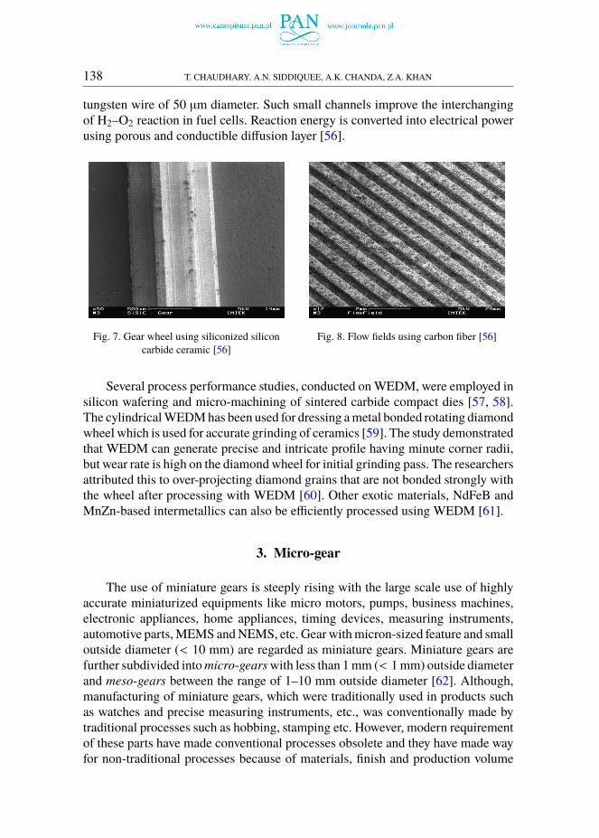
138 T. CHAUDHARY, A.N. SIDDIQUEE, A.K. CHANDA, Z.A. KHAN
tungsten wire of 50 µm diameter. Such small channels improve the interchangingof H2–O2 reaction in fuel cells. Reaction energy is converted into electrical powerusing porous and conductible diffusion layer [56].
Fig. 7. Gear wheel using siliconized siliconcarbide ceramic [56]
Fig. 8. Flow fields using carbon fiber [56]
Several process performance studies, conducted onWEDM, were employed insilicon wafering and micro-machining of sintered carbide compact dies [57, 58].The cylindricalWEDMhas been used for dressing ametal bonded rotating diamondwheel which is used for accurate grinding of ceramics [59]. The study demonstratedthat WEDM can generate precise and intricate profile having minute corner radii,but wear rate is high on the diamondwheel for initial grinding pass. The researchersattributed this to over-projecting diamond grains that are not bonded strongly withthe wheel after processing with WEDM [60]. Other exotic materials, NdFeB andMnZn-based intermetallics can also be efficiently processed using WEDM [61].
3. Micro-gear
The use of miniature gears is steeply rising with the large scale use of highlyaccurate miniaturized equipments like micro motors, pumps, business machines,electronic appliances, home appliances, timing devices, measuring instruments,automotive parts,MEMS andNEMS, etc. Gear withmicron-sized feature and smalloutside diameter (< 10 mm) are regarded as miniature gears. Miniature gears arefurther subdivided intomicro-gearswith less than 1mm (< 1mm) outside diameterand meso-gears between the range of 1–10 mm outside diameter [62]. Although,manufacturing of miniature gears, which were traditionally used in products suchas watches and precise measuring instruments, etc., was conventionally made bytraditional processes such as hobbing, stamping etc. However, modern requirementof these parts have made conventional processes obsolete and they have made wayfor non-traditional processes because of materials, finish and production volume

ON MICROMACHINING WITH A FOCUS ON MINIATURE GEARS . . . 139
requirements. A comparative view of miniature gear manufacturing processes isgiven in Table 1.
Apart frommethodsmentioned in Table 1, gears are alsomade by cold workingbased exclusive gear manufacturing technique known as gear rolling, which can beperformed in two ways, i.e., round rolling and flat rolling [63]. In flat rolling, thetwo rolling tools are flat in shape, move in opposite directions and mesh with gearblank being rolled [64].
Table 1.Conventional processes for gear manufacturing and their limitations [62]
Methods Limitations
Gear hobbing 1. Tool marks produce on gear teeth.2. Requires further polishing operations for the quality improvement.3. Requires more time for the setup.4. Tool wear is crucial problem.
Stamping 1. Shaving operation requires for the final finishing operation.2. Tooth thickness is limited.3. Wearing and tearing of the die-punch is major issue.4. Applicable only up to the medium-load duty gears.
Extrusion 1. Secondary operation requires after extrusion for the high accuracyof the gears.
2. Wear of extrusion die is one major problem.3. Fine-pitched gears cannot be manufactured.
Die casting 1. Extremely accurate gear cannot be manufactured.2. Trimming operations required after the removal of gear from dies.
Powder metallurgy 1. Finest metal powder is hard to arrange.2. It is not suitable for all the types of gears.3. Secondary operations are required for higher accuracy like sizing,
burnishing, shaving, grinding, and shaving.
Non-traditional advanced methods such as EDM, WEDM, WED Grinding(WEDG), micro-EDM and micro-WEDM are notable substitutes for conventionalprocesses and ideally preferred mainly because of excellent accuracy, repeatability,shorter set up time, better surface integrity, easiness to cut complex geometries andshapes, lesser residual stresses, ready to use final finish, etc. [65–67]. WEDM is animportant variant of EDM suitable for sustainable meso- or micro-gear manufac-turing. It eliminates the need of special tool and post machining finish operation,as well. It is able to machine any electrically-conductive material with high hard-ness and toughness. Moreover, gears manufactured by this process also have goodsurface finish, good dimensional accuracy, burr free surfaces and cost effective oncomparison to other processes [65].

140 T. CHAUDHARY, A.N. SIDDIQUEE, A.K. CHANDA, Z.A. KHAN
3.1. Materials for miniature gears
Commonly, rolled gears are made of alloy steels with <0.2% carbon, suchas 15CrNi6, 16MnCr5, and 20MoCrS5 steels [64]. The miniature parts includinggears are manufactured from a wide range of materials including bronze, brass,stainless steel, steels, aluminum, titanium and Ni based alloys, etc. [68]. Largenumber of materials has been machined and their machining performance has beeninvestigated by WEDM process. Various alloys of titanium, tungsten and nickelincluding Inconel are used widely and all these alloys typically belong to difficultto machine materials category [69, 70]. Inconel 718, Incoloy 800 superalloy, In-conel 601 and Inconel 825 are used in many researches [71–80]. Nimonic alloysare commonly used for many applications, but the use of this alloy for micro-gearmanufacturing has not been investigatedmuch [81–83]. Investigations onmicroma-chining of pure titanium and its alloys have also been performed widely [84–87]. Tiand its alloys have low density and high-temperature strength retention, good creepand oxidation resistance [88]. Nitinol shape memory alloys belong to difficult tomachinematerials category and find large applications in biomedical and aerospaceapplications [89]. Aluminum and its alloy like AA6061-T6, Al/SiC metal matrixcomposite, Al2O3 particle reinforced composites (based on 6061 alloy matrix),Al/SiC-MMC, etc., were widely used in machining investigation [90–93]. Steeland its alloy DC-53 die steel, SS-304, AISI-D3, ASTM A572-grade 50 HSLAsteel, AISI4140 and rolled armor steel were also studied during micromachininginvestigations [94–100].
3.2. Major process parameters
3.2.1. Dielectric fluids and electrodes
Apart from traditional dielectrics such as de-mineralized (DM) or de-ionized(DI) water, white spirit, kerosene, etc., several hybrid dielectrics have also beeninvestigated by the researchers. It is reported that kerosene mixed with various par-ticles such as silicon carbide (SiC) or aluminum powder when used in EDM resultsin increase in material removal rate as well as surface roughness. SiC addition inkerosene increases material removal depth as compared to the mixture of kerosenewith aluminum. In fact, an addition of aluminum or SiC in kerosene extends thespace between electrode and workpiece and scatters the discharge energy to securehigh level surface roughness. Findings of literature reveal that Al powder additionin kerosene is better than SiC additions [101]. Addition of surfactant like graphitereduces the surface tension of dielectric fluid which causes increase in materialremoval rate. Literature reveals that surface roughness is directly proportional andtool wear rate is inversely proportional to graphite surfactant concentration. Recastlayer thickness is directly proportional to the graphite powder concentration. Also,an increase in its concentration results in an initial increase in the recast layer

ON MICROMACHINING WITH A FOCUS ON MINIATURE GEARS . . . 141
thickness which subsequently starts to decrease [87]. The use of oxygen gas asa medium synergizes sparking with oxidation and results in enhanced metal re-moval and cutting velocity [92, 102]. Oxygen gas can cause expulsion in the innerelectrode gap and impact positively on cutting velocity [92]. Unlike oxygen, airwill result in cutting velocity higher than that for nitrogen, because of contributionof O2 gas in the air. Oxygen gas, however, also damages the surface quality anddimensions accuracy. Nitrogen gas has lower cutting velocity than other types ofgaseous medium [103].
Various materials are in use for making EDM electrodes, such as tool steels,brass, and materials based on Mo, W, etc. Researchers compared EN19 and EN8as electrode materials during EDM and reported that EN19 wears less than EN8[104]. Brass has high specific resistance and consequently results in an increase inefficiency of spark and electrostatic forces. Better surface integrity and accuracyare achieved in brass [105, 106]. As compared to high velocity brass wire, Zn-coated brass wire provides good surface finish and higher cutting speed, but at thesame time may cause Zn and Cu contaminations [79]. Undesirable zinc and coppercontamination can be reduced using nickel-coated wire. Uncoated wire developscracks and craters on machined surface [107]. Fine diameter molybdenum wirecan be used during precision machining of various materials, such as single-crystalgermanium. It achieves the fastest machining time, and since it can be used in finewire diameter, it produces smallest kerf losses. But, risk of micro cracks is highdue to requirement of high discharge energies [108].
3.2.2. Pulse on time
Material removal rate, wire wear ratio, surface roughness and crater formationall increase with the increase in pulse on time (PON) due to transfer of moredischarge energy. It produces deep discharge craters on the workpiece surface[78, 82, 93, 95, 96, 99, 103, 105, 108–113]. The effect of PON is most significanton most responses including surface roughness, material removal rate and kerfwidth, etc. [74, 82, 85, 91, 96–98, 102, 109]. The cutting rate increases withincrease in PON [78, 111] mainly because of higher thermal or discharge energywhich shifts from wire electrode to workpiece, so that more materials can meltand vaporize from workpiece. Therefore, the crater during process is deeper andproduces rougher surface [103, 105, 114]. The gap width is also greatly influencedby PON [108].
3.2.3. Pulse off time
Low pulse off time (POFF) damages the surface integrity and produces largecraters [96]. The results presented in the literature indicate thatmaterial removal andsurface roughness decrease with increment in the pulse-off time due to generationof shallower craters, which are the result of increment in non-cutting time, or low

142 T. CHAUDHARY, A.N. SIDDIQUEE, A.K. CHANDA, Z.A. KHAN
discharges happen for a particular period of time and cause the minor craters andmelted droplets on surface that indicate low surface roughness and kerf width[82, 103, 115]. Cutting rate falls with increase of POFF [78]. The POFF is highlysignificant for MRR and surface roughness [96]. An increase in POFF leads to lowcutting velocity because of increment in non-cutting duration [103, 105]. The lowPOFF duringmachining of ceramic reinforced composites is the cause of inefficientmolten material removal, which is covered by ceramic patches. The outcomes ofthis molten material are abnormal arcing and therefore wire breakage. The valueof POFF should be at relatively higher levels to avoid wire breakage [111]. POFFis the most significant factor for WEDM activity when achieving the targeted valueof micro-hardness and the minimization of average roughness are simultaneouslyconsidered. POFF in fact pauses the spark and allows time to remove the debrisproduced during spark on. During this period, quenching of the workpiece alsotakes place. Hardness decreases with the decrease of POFF because of little timebeing available for quenching process of the workpiece. Further, when the POFFis low, next spark will take place before the fully cooling and quenching of thework surface. This explains the reduction in hardness with the decrease in pulseoff time [99].
3.2.4. Discharge energy or current
Input energy increases the wear rate and wire breakage problem. Crater for-mation is the major problem at high discharge energy [95]. The material at highdischarge energy shows rough surface with lots of built-edge layers, whereas goodsurface quality is obtained at low-energy input conditions [79, 82, 116]. Higherpulse duration and discharge current is the reason for increment in discharge energyand surface roughness by increasing depth of the craters [74, 98, 99, 105, 113, 115].Increasing of discharge current indicates higher cutting velocity due to higher heatenergy transfer [97, 102]. It also results in coarser surface, kerf width also increaseswith increment in discharge duration and discharge current [100]. It is observed thathigher discharge energy causes higher material removal rates due to high thermalenergy transfer [112, 116].
3.2.5. Peak current
Peak current is a highly significant parameter for MRR, kerf width and surfaceroughness [75, 91, 97, 102]. Too high value of peak current leads to high surfaceroughness and kerf width [82, 95, 96, 99]. Discharge energy increases with peakcurrent which leads to bigger craters and increases the surface roughness [96]. Toobtain good surface finish, peak current should be set at low value, but this willcause lengthy machining time [97]. The metal removal rate and overcut increasewith the increase in peak current owing to transfer of more energy to the machiningregion [71, 75]. It has been reported that increasing peak current over a limit,

ON MICROMACHINING WITH A FOCUS ON MINIATURE GEARS . . . 143
decreases MRR and efficiency of machining. Tool wear ratio is high at high peakcurrent because of higher material removal [71].
3.2.6. Pulse duration or pulse width
Pulse duration is also significant factor followed by flushing pressure and pulseoff time [117]. Craters of greater size form with the increment in pulse duration[95] mainly on account of duration of energy discharge which is increased withpulse duration. This consequently results in increase in cutting speed. If pulsewidth increases, cutting speed improves, and cutting rate reduces with incrementin time between the pulses [106]. The value of surface roughness is observed toincrease with pulse duration, because discharge energy also increases which resultsin larger craters [106, 117]. Pulse width is the crucial parameter that affects wirerupture. Wire rupture increases when pulse width increases, and time between thepulses decreases. Number of discharges improves when time between the pulses isshorter and higher pulse duration leads to more discharge energy, which results inexcessive thermal load and breaks the wire [106].
3.2.7. Gap voltage
Gap voltage defines the space between the work-piece and wire electrode.Experimental results demonstrated that kerf width increased with the increment ingap voltage due to the presence of higher discharge energy. It is noticed that gapvoltage is more important than pulse duration when it comes to controlling kerf[84]. Gap voltage is a notable factor which significantly affects surface roughnessand material removal rate [82, 91, 93]. Surface roughness decreases with theincrease in gap voltage [78]. Increment in gap voltage results in larger electrostaticforces and leads to winding the wire during discharging process. That is why SR islower at higher gap voltage [105]. The surface roughness and oversize decrease byincreasing the gap voltage, this is due to the fact that increasing in the gap voltageleads to winding of the spark gap [103]. The consequence of increasing voltage ismore discharge energy, therefore it increases cutting speed [93, 111]. Some studies,however, report that enhancement in gap voltage causes low cutting speed but highkerf width under specified range. At a selected value of open circuit voltage, anincrease in gap voltage increases the dielectric strength of fluid causing dischargecurrent to decrease during processing, and consequently decreasing the meltingand evaporation, and cutting speed [114].
3.2.8. Wire tension
The wire tension, among other factors, controls the vibrations during sparkingand wire travel. High tension in wire is useful in overcoming wire rupture andvibrations [96, 109, 118] it also improves the surface finish [71]. Wire tension

144 T. CHAUDHARY, A.N. SIDDIQUEE, A.K. CHANDA, Z.A. KHAN
is a significant parameter for obtaining good surface finish because it diminishesvibration in the wire [84]. Generally, the wire breakage is more frequent when wiretension is high at high discharge energy. At low energy, increasing wire tensionreduces wire vibration [109]. Wire tension doesn’t affect cutting velocity and sur-face roughness, but oversize increases at higher tension of wire. The major reasonfor this inaccuracy are the forces acting on the electrode wire. Higher wire tensionleads to rigidity of the wire, so at certain values of discharge energy it does notexperience high impact and also does not act in reverse direction [103]. Incrementin the wire tension is found to result in low corner deviation. It is demonstrated thatstronger forces due to higher tension withstand against force component involvedwith corner cutting, therefore corner deviation is reduced [110].
3.2.9. Wire feed rate
Surface roughness is found to increase with increase in wire feed rate [96].When wire feed increases, the wire is quickly renewed and recovered during theprocess. So non-worn wire increases the spark efficiency and produces the deepercrater. This is the reason that higher wire feed results in rougher surface. It isperceived that wire feed and wire tension both are insignificant factors for cuttingvelocity [105]. The kerf width is found to reduce with increase of WFR [84].
3.2.10. Flushing pressure
Low flushing pressure is not desirable for dielectric, because it is insufficientto remove the debris and reinforced fibred composites from the machining region.The reinforced composites are settled together in cutting region and may causewire breakage during machining [93, 111].
3.3. Major response parameters
3.3.1. Cutting speed/velocity
Cutting speed during WEDM is a response which is significantly affected byseveral process parameters. High values of pulse on time (PON) and current andlow values of pulse off time (POFF) gap voltage will result in high cutting velocity.Bothwire feed andwire tension doesn’t affect cutting velocity [102, 105]. Typically,cutting speeds for composite materials are significantly lower as compared tounreinforced metals/alloys, mainly due to the presence of ceramic reinforcementparticles. These ceramic particles are highly non-metallic and steeply lower thethermal and electrical conductivity of the material [111]. The cutting speed alsodepends on factors such as corner radius, workpiece thickness and number offinished cuts when machining profile includes corners and intricate regions. Erroris reduced when the number of finished cuts is increased [118].

ON MICROMACHINING WITH A FOCUS ON MINIATURE GEARS . . . 145
3.3.2. Dimensional deviation
Accuracy ofmachined component and dimensional deviation ismostly affectedby pulse on time, peak current, spark gap voltage and wire feed. The deviation isreported to improve by increasing pulse off time and wire tension [74]. Investiga-tions report that dimensional overcut largely depends on peak voltage, peak currentand speed of electrode. The overcut, however, initially decreases and then increaseswith the peak voltage. It also decreases with increasing electrode speed [75].
3.3.3. Material removal rate
For material removal, peak current and pulse on time are more influencingfactors than others [81]. MRR closely relates to operating parameters in a waythat it increases with increase in pulse on time, input current and wire tension anddecreases in pulse off time, wire feed and gap voltage [82]. TheMRR also increaseswith increase in machine feed rate, on the other hand, wire speed and fluid flushingpressure are less effective on MRR [84]. It is reported that material removal rateincreases when the dielectric supply rate is reduced. MRR also reported to dependon the melting point. In a typical investigation it is reported that between AA7017and rolled homogeneous armor steel, the maximum material removal rate wasachieved for AA7017 than armor steel due to low melting point [95]. Oxidationand decomposition can also increase the material removal rate. Foamy structureappears due to gas bubbles formation. This is related to oxidation process bythermal energy which leads to higher material removal [96].
3.3.4. Surface roughness
Large number of investigations reported in literature have performed the para-metric studies and come out with conclusions based on statistical analysis. In onesuch investigation, it is reported that PON, servo voltage and peak current, andcombined effect of PON and peak current are more significant for SR than otherfactors [81]. Better surface finish can be secured at higher values of POFF, gap volt-age and wire tension and lower values of PON, input current and machine feed rate[74, 82, 84, 102, 105, 111]. Electrode polarity is also an important factor along withcurrent and PON. SR is reported to be low with negative electrode polarity. Whenelectrode is positive, the surface becomes unevenwith thick recast layer andmarkedwith the presence of globules. Carbon content on the machined surface is also re-ported to be more significant with positive polarity tool [83]. Brass wire coatedwith zinc yields smoother surface and high cutting speed in comparison with highspeed brass wire. Also, results show that uncoated wire generates craters, cracksand melted drops on surface [106]. Thermal effect is stronger on the material inthe case of aluminum alloy due to its high thermal conductivity and lower meltingpoint. Due to this fact, more material melts and cleaning of debris by dielectric fluid

146 T. CHAUDHARY, A.N. SIDDIQUEE, A.K. CHANDA, Z.A. KHAN
becomes less effective resulting in poor surface finish [91]. During the comparisonof Al/SiCp composite and unreinforced alloy, one finds that surface finishing ofAl/SiCp composite materials is superior as compared to unreinforced alloy be-cause the solid SiC particles prevent the removal of aluminum matrix. Moreover,these particles don’t get melted during machining. Hence, molten material is highlyviscous and further decrease the metal removal efficiency [111].
3.3.5. Surface integrity of recast layer
A thin, white and hard layer known as white layer or recast layer is observedon the machined surface. It is formed as a result of phase transformation (i.e., quickre-solidification of melted material) during machining and development of thermalstress on the solidified material [89, 119]. There are two possible ways for recastlayer formation, one is thermal-induced phase transformation and the other is severeplastic deformation. Due to the recast layer, the bulk machined material becomesweak due to inducing micro-cracks, tensile stresses and phase transformation [89].Researchers have identified four characteristic zones in surface affected by themachining process. Outermost zone is called the recast layer or white layer; this isformed as a result of rapid re-solidification of the material due to heat of machining.There is an area below the white layer which, although did not melt, was heatedand then cooled slowly. It creates annealed area which is softer and smoother thanthe parent material. Below this zone, the material properties are not affected bythe machining process and all properties of parent substrate are retained [119].Higher discharge energy is the main reason for a thicker recast layer [116]. Fig. 9shows the difference between the thickness of recast layer normalized, hardenedand tempered AISI4140. Dendritic solidification occurs in the recast layer. Thissolidificationmechanism takes place only if an under-cooledmelt exists for exampleduring high cooling rate [116].
Fig. 9. Recast layer of normalized hardened and tempered AISI4140 [116]
3.3.6. Thickness and composition of white layer
Thickness of white layer is proportional to the magnitude of energy introducedon the surface [119, 120]. It depends on all factors that affect the discharge energy,including polarity of wire electrode. Extensive investigations have been carried

ON MICROMACHINING WITH A FOCUS ON MINIATURE GEARS . . . 147
out on white layer on variety of materials. In case of steels, it is reported thatrecast layer is made up of very fine equiaxed martensitic grains (approximately200 nm) of very high dislocations density. Literature has also demonstrated thepresence of spherical deposits in white layer (appearing like bull’s eye, as shownin Fig. 10) which were confirmed to be made of electrode material. This surfacecontamination from the electrode material is due to melting, vaporization andsubsequent deposit of electrode material over the machined surface. Some of themget deposited on machined surface and get alloyed with the material to form anamorphous layer [121].
Fig. 10. Bull-eye structure formed due to the spray of molten electrode material during4th cutting and EDX-analysis of sites: A – spherical deposit; B – the oxide layer [121]
Steels are commonlymachined byWEDMusing hydrocarbon-based dielectrics.This involves typical chemistry and physics due to which specific elemental makeof the white layer is formed. It has been evident from one of such investigationsin which nine trim cuts were performed (as shown in Fig. 11). This study reportedthat the recast layer consisted of Cu and Zn electrode materials and also Mo fromthe molten material carbides. V and Cr were not identified in white layer/recastlayer. The researchers inferred that Fe and Mo need the equal amount of thermalenergy for melting while V requires higher amount of thermal energy with a factorof 1.3. That’s why Mo was assorted in white layer but V stayed localized [122].
Fig. 11. 9 trim cuts Rim zone pictured with EBSD [122]

148 T. CHAUDHARY, A.N. SIDDIQUEE, A.K. CHANDA, Z.A. KHAN
When machining is performed in presence of kerosene, water-oil emulsionand DI water, it is noticed that one finds an excessive oxide content on the ma-chined surface during machining under W/O emulsion and DI water. The carbonconcentration in recast layer under kerosene was greater than the one formed usingwater-oil emulsion and DI water because supply of carbon from hydrocarbon oildecomposition; whereas Cu was present in the recast layer when de-ionized waterwas used [123]. Thus, the composition of white layer in terms of its chemicalmakeup depends on several factors [123, 124]. Foreign elements, such as Cu andZn, were detected on main cut that were resettled from the brass wire electrode,but Cu gradually decreased in subsequent trim cut. This was due to poor dischargeenergy during trim cut causing less abrasion and decomposition of the electrodewire [124, 125]. Due to low evaporation temperature of Ni than Ti, Ni vaporizesand combines with melted electrode material resulting in higher Ni presence indebris than Ti [124]. Further, recast layer’s average thickness was found to dependon dielectric in such a way that its average thickness was higher in water-oil emul-sion dielectric than in de-ionized (DI) water and kerosene under the same pulseduration because it has higher viscosity than kerosene. Due to this reason, removalof molten material from the sparking zone was inefficient and resulted in deposi-tion on machined surface. The non-unified white layer produced in main cuts wasdemonstrated to be composed of a thick porous layer at the top, and the other onebeing a thin hard layer at bottom. The variation in thickness in white layer afterroughing trim cut are attributed to high pulse current and pulse on (PON) durationused during trim cut. Under finished trim cuts using both dielectrics, a very thinwhite layer is observed [126–128].
3.3.7. Heat-Affected Zone
The material adjacent to recast layer, which was not melted but affected bythe heat of machining, is regarded as heat-affected zone (HAZ). Depending on themetallurgy and heat treatment condition of the substrate, the material in the HAZmay experience phase change under the effect of high amount of tensile residualstress, porosity, micro-cracks and recrystallization and grain growth [121]. It isobserved that HAZ size increases with higher discharge energy. A lot of factorsdecide about the characteristics of this zonewhich includes heating and cooling rate,peak temperature and the presence of prior phases. For a typical case (Fig. 12), the
Fig. 12. Rim zone of final normalized material and hardened/tempered material [120]

ON MICROMACHINING WITH A FOCUS ON MINIATURE GEARS . . . 149
material was subjected to normalizing and two different phase structures consistingof ferrite and pearlite was observed.
3.3.8. Surface roughness of white layer
EDMed surface has a typical texture built by random arrays of overlappedcraters, due to severe heat generation that causes local melting and evaporation ofmaterial [119]. The energy dissipated during EDMing is found to be greater thanthe energy released during laser machining. Due to this fact, the white layer formedduring laser machining is uniformly distributed over the surface, whereas the whitelayer on the EDMed surface is non-uniform and consists of new phases and voids(as shown in Fig. 13).
Fig. 13. Laser and EDM white layer topography [119]
The white layer SR of laser machined surface is higher than EDMed surfaceand a texture consisting of columnar patterns resulting from molten material flowis generated in the laser-machined surface. White layer has a solid structure withoutany voids or cracks during laser cutting. During EDMing, foreign elements fromthe dielectric fluid enter into white layer and result in cracks and voids [89]. Eventhe electrode polarity leaves typical hallmarks on the machined surface and can becharacteristically distinguished. In an investigation performed to study the effectof polarity, the electrode negative was applied in initial four cutting passes andlater machining was performed with electrode positive in the last cutting pass (i.e.fifth pass). From the results, craters and martensite laths were noticed on finishedsurface after the fourth pass (Fig. 14). Spherical particles with composition similarto work material were observed on the brim of craters. Whereas, after the fifth passthe surface was found to be partly covered with loose deposit particles. They werecomparatively smoother and denser (better surface finish) than the other surfacescut with negative electrode polarity [121]. Martensitic transformation was notconfirmed after the fifth cutting pass because the temperature was not high enough.During multiple trimming, subsequent trim cut one and trim cut two reduce thedebris on surface. After the finish trim cut four, an isotropic surface along regularcraters was noticed. The debris are observed on surface after the fifth cut but theyare very small as compared to the main cut surface due to less thermal impact.Finish trim cut generates highly smooth surface [124, 126].

150 T. CHAUDHARY, A.N. SIDDIQUEE, A.K. CHANDA, Z.A. KHAN
Fig. 14. a) finished surface after 4th cutting pass with NPWE;and b) after 5th cutting pass with PPWE [121]
The surface obtained withW/O emulsion has larger and deeper craters than theone with DI water and kerosene due to high viscosity of W/O emulsion (Fig. 15).Dielectrics with high viscosity obstruct the discharge channel’s expansion causingimpulsive force accumulation within less area and resulting in large and deepcraters [123].
Fig. 15. Comparison of SR under different dielectricsand peak currents

ON MICROMACHINING WITH A FOCUS ON MINIATURE GEARS . . . 151
The effect of discharged energy on roughness is more or less similar on dif-ferent materials with peculiar deviations in texture, which is typically different indifferent materials. The surface and sub-surface modification of INCONEL 718,for example, were investigated in a study after machining by WEDM using brasswire. Effect of nominal energy per unit length of cut (sum of: 1. Energy required toeliminate material from workpiece, 2. Energy transmitted to the wire electrode and3. Energy transmitted to machine surface) was examined. In both the rougheningand finishing condition, the round shaped re-deposited material was demonstratedto be not equivalently deposited on the surface. Numerous bubbles were seen on themachining surface because of high nominal discharge energy per unit length andduty cycle. Some cracks were visible on the recast layer, as shown in Fig. 16 [129].
Fig. 16. SEM observation: a) roughing condition b) finishing condition [129]
Likewise, during comparison of trim cut surfaces for S390 and SKD11 afterthe fourth finish pass, pinholes and craters were observed on SKD11. Whereas, nosuch globules or cracks were seen on S390 except for a few tiny voids. The surfaceroughness decreases with the increase of number of cutting passes, since in eachsuccessive pass the discharge energy decreases. Thus, high discharge energy is usedin the rough cut, and this leads to more resolidified material being accumulated onthe surface, resulting in coral reef like microstructure with extremely rough surface.For succeeding trimming passes, very small coral reef, like microstructure andlower roughness, is obtained [120, 125, 127]. Finally, SR of multi-pass machinedS390 material is much better than SR of similarly machined SKD11 [127]. Theprior heat treatment condition also affect the SR of machined surface, such as incase of an annealed specimen the SR is higher than that of quenched or temperedsamples due to higher thermal conductivity of the annealed specimen [119].
3.3.9. Microhardness
The micro/nano hardness of machined surface may remain the same as that ofsubstrate, or may be higher or lower than that. This mainly depends on the mate-rial’s metallurgy, its initial heat treatment condition, the heating and cooling effects

152 T. CHAUDHARY, A.N. SIDDIQUEE, A.K. CHANDA, Z.A. KHAN
of the heat of machining and the presence of contaminants, if any. The heating andcooling effect, however, directly depends on the machining parameters. In case ofNitinol shape memory alloy, the nano-hardness of white layer is reported lowerthan the bulk material during laser cutting. In case of laser machining, there are nocontaminants, but when the same alloy is machined by EDM there are possibilitiesof oxidation, and contamination from carbon and other elements, as well as variedquenching rates that may lead to alloy’s hardening or white layer hardening [122].In case of steel, however, the white layer hardness is found to be doubled as com-pared to the parent material hardness. This could be due to high concentration ofcarbon and copper below the surface and also due to the presence of high-heat fluxand subsequent quenching by the dielectric [120]. Hardness of recast layer is higherin case of W/O emulsion because of the presence of carbon and higher coolingrate [123]. In case of multiple pass machining, there are repeated cycles of heatingand cooling that may result in variable surface properties, causing the white layerhardness to vary after ever subsequent pass. In the typical case of nitinol, averagemicrohardness of top layer was reported to first increase up to 50% from the maincut to the 1st trim cut, then moderately increase by the succeeding trim cut 2ndand the 4th trim cut. Discharge energy has a significant role to play in the whitelayer hardness. The white layer is more uniform and solid at low discharge energyand significant softening occurs in HAZ, attributed to minimization of thermaldegradation at low discharge energy [124]. Similarly, the dielectric composition(e.g., W/O and water, etc.) which affect cooling rate has its effect on the surfacemicrohardness, as well. A lower microhardness has been reported for trim cut sur-face during oil. The reason for lower microhardness is higher residual tensile stresson electric discharge machined surface in water verses oil, causing lower hardness[126]. In case of S390 and INCONEL718, microhardness is increased at the sur-face in the main cut specimen, because of hardness generated by the metallurgicaltransformations influenced by extreme temperatures and quenching rate during theWEDMed process. A soft layer of about 10–20 µm thickness is reported just underthe surface of each specimen for the first to third trim cut. The thermally influencedzone is decreased significantly from the rough cut mode to the 3rd trim cut mode,therefore, there is no variation of hardness at the last trim cut specimen [125, 127].In case of tempered and quenched sample, HAZ is smooth because of the over-tempered martensite that develops due to slow heating and cooling. It is observedexperimentally that the distribution of microhardness is not changed below thesurface by increasing the dielectric fluid pressure, but this increases the hardness ofthe surface slightly. [119]. Low carbon makes the white layer less hardened [120].
3.3.10. Micro-cracks, micro-voids and burrs
There are many types of burrs, like primary and secondary burr, minor andfeathery burr and needle like burr. Burr formation, in conventional machiningoperations, can be avoided by decreasing the feed rate and axial engagement [90].

ON MICROMACHINING WITH A FOCUS ON MINIATURE GEARS . . . 153
For an EDMed surface, micro cracks are formed because of very fast coolingof melting material, which results in thermal stress [119]. Rapid resolidificationof molten metal under flushing of the dielectric may also form micro-void dueto entrapment of gases and vapors. During the machining under W/O emulsion,the presence of surface cracks and micro-cracks is more evident as compared tomachining under kerosene oil, due to generation of extensive amount of gas, asshown in Fig. 17, which diminishes the recast layer strength. The results indicatethat surface micro-crack density decreases with higher peak current, no matterwhat is the type of dielectric [123].
Fig. 17. Micro-cracks on samples surface machining in diverse dielectrics
In case of Inconel 718, multiple cracks are noticed during EDMing due to thefact that the surface produces by Electric Discharge Machining has vast possiblesites for initiation of crack, as shown in Fig. 18. There are various causes for theloss in fatigue life in the case of EDMed specimens that exhibit high tendency forrecast layer formation, high tendency for recast layer cracking, large surface tensileresidual stresses and, finally, surface irregularities [130].
Micro-cracks are formed on white layer of main cut surface due to high tensileresidual stress, large heat energy release by discharge and rapid cooling. Thesubsequent trim cuts don’t show any micro-cracks and globules on the surface andproduce less coral reef microstructure due to gradually decreasing discharge energy[124, 127]. In case of IN718, the tendency of cracks formation is very low due tohigh toughness and high thermal conductivity which conducts the heat away fromthe heating region very quickly [125]. Crack density in the white layer grows with

154 T. CHAUDHARY, A.N. SIDDIQUEE, A.K. CHANDA, Z.A. KHAN
Fig. 18. Comparison of the fracture surface with different surface conditions. Multiple crack originsfrom the EDM cut surface, these are indicated by numbers in (b) [130]
increasing duration of pulse and open-circuit voltage [119]. Longer crack insidehole can sometimes also be observed when machining is done using EDM, asshown in Fig. 19 [44].
Fig. 19. Internal surface of the micro-hole and defects inside a micro-hole [44]
3.3.11. Residual stress
The reasons behind the residual stress are the strains developed by the met-allurgical transformations and non-uniform heat flow during WEDM machining[127]. Despite the high thermal loading, the peak of the residual stress is not lo-cated on the metal surface because a stress reduction mechanism is present there,it is located at the interface between white layer and heat affected zone. Peakresidual stress increases with spark energy due to higher current [119]. The higherresidual stress is reported in HAZ, because the molten material speedily quenchesand re-solidifies, and the contact of re-solidified materials on upper surface andbulk material just below restricts the contraction. The high quenched rate of DIwater dielectric generates higher residual stresses than those in oil during main

ON MICROMACHINING WITH A FOCUS ON MINIATURE GEARS . . . 155
cuts and finish trim cuts [126]. A comparison of residual stress between SKD11and S390 reported that S390 has higher residual stress than that of SKD11 due tothe difference in yield strength, and has a better finish, as well [126].
4. Research on micro-gear manufacturing
Although enormous amount of work has been reported on micromachining,yet there is limited literature in the area of micromachining of miniature gears.Machining of miniature gears assumes importance given that products such asinstruments, devices that are expected to employ them steeply bound upwards.Literature reporting various aspect of micro-gear manufacturing is very scarce. In atypical investigation, micro wire-EDMwas employed for profile roughing and finaldressing for miniature gear machining on polycrystalline diamond (PCD) wheel.As conventional WEDM provides higher discharge energy than micro WEDM, itis very likely to cause higher thermal damages, thick edge and craters over the PCDsurface, leading in turn to thick damaged layer and rougher surface, as shown inFigs 20–22 [131].
The geometrical deviations in macro- and micro-sized geometry of wireEDMed miniature external spur gear is a major issue. The basic dimensional pa-rameters, such as span, outside diameter and tooth thickness, are macro-geometry
Fig. 20. Edge of PCD surface obtained by Micro WEDM and WEDM
Fig. 21. SEM images of PCD surface by micro WEDM and WEDM [131]

156 T. CHAUDHARY, A.N. SIDDIQUEE, A.K. CHANDA, Z.A. KHAN
Fig. 22. SEM images of PCD wheels fabricated by micro wire-EDM and wire-EDM [131]
parameters, on the other side, profile, pitch run-out, lead and SR parameters aremicro-geometrical parameters [80, 132–134]. The profile error commonly affectsthe noise behavior and pairing, pitch and run-out error affect the motion transfercharacteristics, and the lead error controls the load carrying capacity, as shownin Fig. 23 [80]. The basic reasons for micro-geometrical deviations when usingWEDMed are asymmetrically shaped craters generated by the produced intensespark due to excessive discharge energy [134] and the divergence of wire from theplanned pathway, noted as wire-lag [135]. There aremany reasons for wire lag, suchas mechanical forces generated due to pressurized gas bubbles, electrostatic forcesacting on electrodes, hydraulic forces produced by flushing dielectric, electro-dynamic forces due to the spark generation and the axial forces that straighten thewire. One of the important factors for macro-geometrical deviations in miniaturegears are wire vibration, machine tolerance and gear blank.
Fig. 23. Effects of micro geometry errors on the performance of miniature gear [80]
Profile-related errors are caused by most of the EDM process parameters.Minimum values of the profile error and pitch error are observed at the low voltage,as high voltage and PON time develops greater forces owing to intense spark

ON MICROMACHINING WITH A FOCUS ON MINIATURE GEARS . . . 157
(discharge energy) and gas bubble pressure which causes poor surface finish andhigh MRR [135–137, 139, 140]. Surface finish becomes poorer if pulse-off time(POFF) is maintained at very low levels, consequently increasing chances for shortcircuit of wire. There should be an optimum range of the POFF and wire feed forgood quality micro-gear because, at lower POFF time and wire feed rate, there willbe wire vibrations due to the short circuit, while at higher values, there will beexcessive hydrostatic forces which result in wire lag and again increase the profileand pitch errors [136–140]. Higher voltage and PON and shorter POFF increasedischarge energy, and availability of time to transfer this energy to the tooth surfaceof gear and decrease the flushing time.All these factors produce deeper and irregularcraters on gear tooth surface and also increase the SR and profile and pitch error[136–138, 141, 142]. At low rate of wire feed, wire can tolerate high dischargeenergy, which increases the wire-lag, non-uniform wire wear and wire-breakage.All these factors result in high pitch and profile. Higher feed rate of wire decreasesduration of spark at a specific place on wire and therefore decreases wire-breakageand wire-lag, and thus, reduces profile and pitch error [137, 138]. In any case,as the discharge energy is significantly low and pulse frequency is very high, inthe case of micro-WEDM compared to conventional WEDM, the gears producedby micro-WEDM are better than WEDM in all respects, as it is clear from thephotographs of parts produced by the two methods (Fig. 24 and Fig. 25).
Fig. 24. Comparison of SR of conventional and micro-WEDM [139]
Fig. 25. Micro sized gear by WEDM and Micro WEDM [140]

158 T. CHAUDHARY, A.N. SIDDIQUEE, A.K. CHANDA, Z.A. KHAN
Most of materials which are used in fabricating miniature gears, such as AISI-304L and other austenitic stainless steels, beryllium copper, Nitronic 60 and ti-tanium and most of these, are difficult to machine, and machining micro-featureson them becomes even more difficult. Given this situation, micro-WEDM be-comes highly suitable to machine such parts. AISI 304 and titanium alloy offeran excellent profile tolerance. The titanium alloys have minimal re-cast layers andvery smooth features. Hence, it is noticed that micro-WEDM can develop highaspect ratio (HAR) and good tolerance in meso/micro scale parts [143]. The re-cast layer hardness is higher under micro-WEDM. This is because of the highquantity of cementites. These cementites result due to carbon absorption from py-rolysis of dielectric. [144]. It is practicable to manufacture miniature gear surfacewithout cracks, protrusion and pits. The surface can be generated with uniformlydistributed regular shaped craters using WEDM and Micro-WEDM method, asshown in Fig. 26 [68, 131, 138–144]. The miniature spur gear produced byWEDMshows the defect-free microstructure, good surface finish, very thin recast layer andgood gear quality up to DIN 5 for micro-geometry parameters such as profile andpitch, which is much better than the quality of miniature spur gears produced byother conventional processes [68, 136].
Fig. 26. Miniature gear manufactured by WEDMat optimal parameter [144]
5. Future directions
Previous sections have unwrapped the performance of micromachining taskusing various conventional and non-conventional processes. It is pertinent to men-tion that the desired levels of profile and dimensional accuracy and surface qualitiesexpected from the miniature parts are extremely difficult to obtain through conven-tional processes. Among non-traditional processes, WEDM and micro-WEDM arethe most suitable processes. Hybrid and sequential micro machining process canalso improve the machining quality of micro components. Hybrid micromachiningsuch as ECDMmilling and laser assisted micro-milling can be effective in fabricat-ing complex shapes from hard and brittle materials with high machining accuracy.

ON MICROMACHINING WITH A FOCUS ON MINIATURE GEARS . . . 159
Such type of approaches are specifically beneficial in reducing positioning errorsand improving dimensional inaccuracy. The expected level of part accuracy is veryhigh and depends on a complex mix of parameters including, electrical (pulsecurrent, pulse on off time, voltage, overcut voltage (OCV), frequency, etc.) andmechanical (wire feed speed, wire tension, type of dielectric, spark gap, flushingpressure etc.), as well. Most of the reported studies have been performed on somearbitrarily selected materials and reports concentrate on effect of most commonparameters on common responses, such as kerf width, surface finish, etc. Actu-ally, producing of miniature parts requires comprehensive regime of investigationsinvolving accuracy of micro profile, and various dimensional features of profile,mechanism of dielectrics in action, effect of tiny process forces on wire vibrationand in turn its effect on part accuracy, etc. Unfortunately, most of the researchwork was related to mere material selection, process parameters, performances,product manufactured, miniature product generation, and micro-tool fabrication.Little work has been performed in the area of manufacturing of proper miniatureproducts, such as micro gear, micro wheel, micro tools, MEMS, etc., using wireEDM, and concerned investigation of machined part’s quality through a compre-hensive measurement regime. Very few studies have been done on the liquid andpowder mixed dielectric fluid, spark energy, dielectric strength, and breakdownmechanism of dielectric fluid. Surface integrity and white layer characterization ofminiature products should also be investigated. Wire tension and deflection of theworkpiece are some major issues. Different dielectric fluids have different effectson the workpiece. The research work on different dielectric fluids may also be takenup. The effect and action of dielectric fluid on surface integrity, recast layer, HAZ,etc., may also be an area to focus on.
6. Conclusions
In this review, efforts have been made to bring out state of the art on micro-machining using non-conventional processes such as Micro-EDM, WEDM, etc.The literature revealed that extensive research has been done in the field of ma-terial selection, process parameters, performances, miniature product generation,and micro-tool fabrication. This report presents key discussions with a focus ondifferent parameters (discharge current, pulse on and off time, pulse duration, sparkgap voltage, cutting velocity, wire feed rate, and so on) and the response factors(material removal rate, surface roughness, dimensional deviation, cutting speed,surface integrity of recast layer and so on). In the study, the recast layer, heat ef-fected zone, microhardness, micro cracks, residual stress, etc., have been analyzedin the light of effect of important and relevant parameters. The study also has ashowcase status report on research done on micro-gear manufacturing till now.Various macro-geometry features (e.g., span, outside diameter and tooth thick-ness) and micro-geometry (profile, pitch run-out, lead and SR) of the micro-gearshave been studied and analyzed by the researchers. A comparative study has been

160 T. CHAUDHARY, A.N. SIDDIQUEE, A.K. CHANDA, Z.A. KHAN
done on other conventional processes for micro-gear manufacturing and WEDM.The study shows that WEDM is a better process for micro-gear manufacturingas compared to other manufacturing processes. There are many reasons behindthis fact, such as defect-free microstructure, good surface finish, better surfaceintegrity and good gear quality defined based on (micro-geometry parameters suchas profile and pitch). The errors related to macro and micro geometries can alsobe reduced by machining using WEDMwith optimized parameters. This is mainlyattributed to the fact that the conventional processes use heat and forces whichare applied on bulk of material, whereas during WEDM the energy is suppliedin microscopic volume and the affected volume is removed, hence the materialbulk remains less affected. Hybrid and sequential processes can also implementto fabricate micro-gears. These methods considerably improve the MRR, SR ge-ometrical accuracy and tool life. These processes are specifically advantageous todevelop the complex 3D miniature parts with high accuracy, surface quality andefficiency. Sequential processes reduce repositioning errors and achieve high levelof accuracy. It has been noticed that non conducting brittle materials are mostlymicro-machined using these processes. Research could also proceed for some othertypes of materials.
Further, it is also noticed that most research work is focused on the generalprocess parameters and their effects on response factors for the macro-sized prod-uct. The effect of these parameters has been less investigated on miniature productssuch as micro-gear, micro-tools, micro-channels, micro-electric boards, etc. Thefocus should also be directed, with a special focus, on micromachining, on howthese parameters affect spark energy, mechanism of energy dissipation at sparkgap, pulse wave form; as these features in turn translate into material removalrate, dimensional accuracy, surface integrity and dimensional accuracy of minia-ture products. Most of the research is done for some specific types of dielectricsand powder mixed dielectrics. There is very little research report on multiphasesystems comprising liquid and powder and gaseous additions. Different dielectricsshow different breakdown mechanism and multiphase systems may yield positiveeffect through synergy of constituents. No research has been observed in the fieldof mechanism of dielectric breakdown. Future research may be focused on thedielectric breakdown mechanism of liquid, powder, and combination of both liquidand powder dielectric and the effect of the dielectric breakdown mechanism onthe response factors. Spark energy plays important role in the field of accuracyof profile and material removal rate in micromachining; and also depends on thebreakdown mechanism of dielectric fluids. More research should be focused onthat area, as well. The effect of the dielectric constant or dielectric strength ofdifferent dielectric fluid should also be observed on the response factors such asMRR, SR. kerf width, etc. The focus should be given to energy consumptions anddissipation at the spark gap and its relevance for the input parameters such as effectof dielectric fluids, wire tension, effect of forces on surface integrity, accuracy ofprofile and dimension during micro-gear manufacturing using WEDM, etc.

ON MICROMACHINING WITH A FOCUS ON MINIATURE GEARS . . . 161
Manuscript received by Editorial Board, June 30, 2017;final version, February 06, 2018.
References
[1] T. Özel. Editorial: special section on micromanufacturing processes and applications.Materi-als and Manufacturing Processes. 24(12):1235, 2009. doi: 10.1080/10426910903129349.
[2] T. Masuzawa. State of the art of micromachining. CIRP Annals, 49(2):473–488, 2000.doi: 10.1016/S0007-8506(07)63451-9.
[3] S.P. Leo Kumar, J. Jerald, S. Kumanan, and R. Prabakaran. A Review on Current ResearchAspects in Tool-Based Micromachining Processes. Materials and Manufacturing Processes,29(11-12):1291–1337, 2014. doi: 10.1080/10426914.2014.952037.
[4] P. Piljek, Z. Karen, andM.Math. Micromachining – review of literature from 1980 to 2010. In-terdisciplinaryDescription of Complex Systems, 12(1):1–27, 2014. doi: 10.7906/indecs.12.1.1.
[5] V.K. Jain. Introduction to Micromachining, 1st ed.; Narosa Publishing House Pvt. Ltd: NewDelhi, India, 2011.
[6] S.Z. Chavoshi, S. Goel, and P. Morantz. Current trends and future of sequential micro-machining processes on a single machine tool. Materials & Design, 127:37–53, 2017.doi: 10.1016/j.matdes.2017.04.057.
[7] T. Masuzawa, C.-L. Kuo, and M. Fujino. A combined electrical machining processfor micronozzle fabrication. CIRP Annals, 43(1):189–192, 1994. doi: 10.1016/S0007-8506(07)62193-3.
[8] M. Kunieda, M. Yoshida, H. Yoshida, and Y. Akatmatsu. Influence of micro indents formed byelectro-chemical jet machining on rolling bearing fatigue life. ASME, Production EngineeringDivision (Publication) PED, 64:693–699, 1993.
[9] A.B.M.A. Asad, T. Masaki, M. Rahman, H.S. Lim, and Y.S. Wong. Tool-based mi-cromachining. Journal of Material Processing Technology, 192-193:204–211, 2007.doi: 10.1016/j.jmatprotec.2007.04.038.
[10] S.Z. Chavoshi and X. Luo. Hybrid micro-machining processes: A review. Precision Engineer-ing, 41:1–23, 2015. doi: 10.1016/j.precisioneng.2015.03.001.
[11] W. Lang. Silicon microstructuring technology. Materials Science and Engineering, 17(1):1–55, 1996. doi: 10.1016/0927-796X(96)00190-8.
[12] M. Mehregany and A.S. Dewa. MCNC Short Course Handbook. Case Western Reserve Uni-versity, Cleveland, USA, 1993.
[13] A beginner’s guide to MEMS processes. www.memsnet.org[14] S.S. Choi, M.Y. Jung, D.W. Kim, M.A. Yakshin, J.Y. Park, and Y. Kulk. Fabrication of micro-
electron gun array using laser micromachining.Microelectronic Engineering, 41/42:167–170,1998. doi: 10.1016/S0167-9317(98)00037-9.
[15] A. Semerok, C. Chaléard, V. Detalle, J.-L. Lacour, P. Mauchien, P. Meynadier, C. Nouvellon,B. Sallé, P. Palianov, M. Perdrix, and G. Petite. Experimental investigations of laser ablationefficiency of pure metals with femto, pico and nanosecond pulses. Applied Surface Science,138-139:311–314, 1999. doi: 10.1016/S0169-4332(98)00411-5.
[16] N.H. Rizvi. Femtosecond laser micromachining: Current status and applications. RIKENReview, 50:107–112, 2003.
[17] X.-Q.Sun, T. Masuzawa, and M. Fujino. Micro ultrasonic machining and its applicationsin MEMS. Sensors and Actuators A: Physical, 57(2):159–164, 1996. doi: 10.1016/S0924-4247(97)80107-0.

162 T. CHAUDHARY, A.N. SIDDIQUEE, A.K. CHANDA, Z.A. KHAN
[18] B.H. Yan, A.C. Wang, C.Y. Huang, and F.Y. Huang. Study of precision micro-holes inborosilicate glass using micro EDM combined with micro ultrasonic vibration machin-ing. International Journal of Machine Tools and Manufacture, 42(10):1105–1112, 2002.doi: 10.1016/S0890-6955(02)00061-5.
[19] A.C. Wang, B.H. Yan, X.T. Li, and F.Y. Huang. Use of micro ultrasonic vibration lapping toenhance the precision of microholes drilled by micro electro-discharge machining. Interna-tional Journal of Machine Tools and Manufacture, 42(8):915–923, 2002. doi: 10.1016/S0890-6955(02)00025-1.
[20] D.Reynaerts, P.H.Heeren, andH.VanBrussel.Microstructuring of silicon by electro-dischargemachining (EDM) – part I: theory. Sensors and Actuators A: Physical, 60(1-3):212–218, 1997.doi: 10.1016/S0924-4247(97)01359-9.
[21] R.K.Garg,K.K. Singh, andA. Sachdeva. Reviewof researchwork in sinkingEDMandWEDMon metal matrix composite materials. The International Journal of Advanced ManufacturingTechnology, 50(5-8):611–624, 2010. doi: 10.1007/s00170-010-2534-5.
[22] A.N. Siddiquee, Z.A. Khan, and J.S. Tomar. Investigation and optimisation of machining pa-rameters formicro-countersinking ofAISI 420 stainless steel. International Journal ofMachin-ing andMachinability ofMaterials, 14(3):230–256, 2013. doi: 10.1504/IJMMM.2013.056364.
[23] C. Friedrich. Precision Micromanufacturing Processes Applied to Miniaturization Technolo-gies, 1998. http://www.me.mtu.edu/~microweb.
[24] D.P. Adams, M.J. Vasile, and A.S.M. Krishnan. Microgrooving and microthreadingtools for fabricating curvilinear features. Precision Engineering, 24(4):347–356, 2000.doi: 10.1016/S0141-6359(00)00045-3.
[25] Y.N. Picard, D.P. Adams, M.J. Vasile, andM.B. Ritchey. Focused ion beam-shaped microtoolsfor ultra-precision machining of cylindrical components. Precision Engineering, 27(1):59–69,2003. doi: 10.1016/S0141-6359(02)00188-5.
[26] C. Van Osenbruggen, G. Luimes, A. van Dijk, J.G. Siekman, and N.V. Philips. Micro-sparkerosion as a technique in micro-miniaturization. IFAC Proceeding Volumes, 2(3):485–493,1965. doi: 10.1016/S1474-6670(17)68988-2.
[27] A. Wenda, M. Beck, V. Huntrup, M. Meisel, M. Rothenburg, O. Rubenach, J. Schmutz,C. Schwietering, and J. Gabler. Possibilities and limits of micro-machining. F und M. Fein-werktechnik, Mikrotechnik, Mikroelektronik, 107(11):64–67, 1999. (in German).
[28] T. Schaller, W. Bier, G. Linder, and K. Schubert. Mechanical microstructuring of metallicsurfaces. F und M. Feinwerktechnik, Mikrotechnik, Mikroelektronik, 102(5-6):274–278, 1994.(in German).
[29] K. Weinert, G. Guntermann, and Ch. Schwietering. Microfabration of difficult to processmaterials. Werkstattstechnik, 88(11/12):503–506, 1998. (in German).
[30] K. Weinert, M. Buschka, and Ch. Schwietering. Processing strategies for microsystems tech-nology – microframe processing NiTiNb shape memory alloy. Technica, 48(8):36–40, 1999.(in German).
[31] E. Brinksmeier, W. Preuss, and J. Schmutz. Manufacture of microstructures by diamondmachining. In Proceedings of 9th IPES/UME 4 International Conference, pages 503–507,Braunschweig, Germany, 1997.
[32] E. Brinksmeier, W. Preuss, O. Riemer, and R. Sigel. Manufacture of shock-wave target-foilsfor nuclear fusion research. In Proceedings of UME 3, pages 401–404, Aachen, Germany,1994.
[33] Shichun Di, Ruining Huang, and Guanxin Chi. Study on micro-machining by micro-WEDM.In Proceedings of the 1st IEEE International Conference on Nano/Micro Engineered andMolecular Systems. Zhuhai, China, 18–21 Jan. 2006. doi: 10.1109/NEMS.2006.334857.

ON MICROMACHINING WITH A FOCUS ON MINIATURE GEARS . . . 163
[34] N. Nebashi, K. Wakabayashi, M. Yamada, and T. Masuzawa. In-process truing dressing ofgrindingwheels byWEDGandELID. International Journal of ElectricalMachining, 3:59–64,1998.
[35] E. Westkamper, H.-W. Hoffmeister, and J. Gäbler. Manufacturing concepts for the productionof micromechanical metallic components. In Proceeding of Micro Engineering 96, Stuttgart,Germany, 1996.
[36] V. Piotter, T. Benzler, T. Hanemann, R. Ruprecht, and J. Hausselt. Manufacturing of mi-crostructures by micro injection molding. In Proceedings of Micro System Technologies,pages 343–348, Potsdam, Germany, 1998.
[37] V. Piotter, T. Benzler, R. Ruprecht, and J. Hausselt. Manufacturing of micro sized structuresby MIM and CIM. In Proceedings of the International Conference on Powder Metallurgy andParticulate Materials, pages 1–9, Las Vegas, USA, 31 May–4 June, 1998.
[38] H. Von Wollmer, R. Ruprecht R., and J. Hausselt. Precision casting of micro parts made ofmetal. Galvanotechnik, 90(6):1692–1696, 1999.
[39] T. Masuzawa, M. Yamamoto, and M. Fujino. A micro-punching system using wire-EDG andEDM. InProceedings of the 9th International Symposium for Electro-Machining, pages 86–89,Nagoya, Japan, 1989.
[40] K.Wakabayashi, A. Onishi, and T. Masuzawa. Micropiercing on stainless steel. Bulletin ofJapan Society of Precision Engineering, 24(4):277–278, 1990.
[41] H.K. Tonshoff, F. Von Atvendeben, A. Ostendorf, G. Kamlage, G., and S. Notte. Microma-chining of metals using ultrashort laser pulses. International Journal of Electrical Machining,4:1–6, 1999.
[42] T.Masaki, K. Kawata, T. Sato, T.Mizutani, K. Yonemoti, A. Shibuya, and T.Masuzawa.Microelectro discharge machining. In Proc. of International Symposium for Electro-Machining,ISEM–9, pages 28–29, Nagoya, Japan, 1989.
[43] T. Masuzawa, M. Fujino, K. Kobayashi, T. Suzuki, and N. Kinoshita. Wire electro-dischargegrinding for Micro-machining. CIRP Annals, 34(1):431–434, 1985. doi: 10.1016/S0007-8506(07)61805-8.
[44] D.M. Allen, H.J.A. Almond, J.S. Bhogal, A.E. Green, P.M. Logan, and X.X. Huang.Typical metrology of micro-hole arrays made in stainless steel foils by two-stage micro-EDM. CIRP Annals – Manufacturing Technology, 48(1):127–130, 1999. doi: 10.1016/S0007-8506(07)63147-3.
[45] D. Reynaerts, X. Song, W. Meeusen, and H. Van Brussel. Silicon bulk micromachining bymicro-EDM milling with electrode compensation. In Proceedings of the 9th InternationalFair and Congress for Sensors, Transducers and Systems, pages 249–254, Nurnberg, Germany18–20 May, 1999.
[46] X. Song, D. Reynaert W. Meeusen, and H. Van Brussel. Investigation of micro-EDM forsilicon microstructure fabrication. In Proceedings of SPIE Sympium on Micromachining andMicrofabrication, pages 792–799, 1999.
[47] K.-P. Kamper, W. Ehrfeld, J. Dopper, V. Hessel, H. Lehr, H. Lowe, and Th. Richter. Microflu-idic components for biological and chemical microreactors. In Proceeding of 10th AnnualInternational Workshop on Micro Electro Mechanical Systems, IEEE MEMS’97, Nagoya,Japan, 26–30 Jan, 1997. doi: 10.1109/MEMSYS.1997.581849.
[48] W. Ehrfeld, H. Lehr, F. Michel, A. Wolf, H.-P. Gruber, and A. Bertholds. Micro electro-discharge machining as a technology in micromachining. Proceedings of SPIE, 2879, Mi-cromachining and Microfabrication Process Technology II, pages 332–337, Austin, USA, 23Sept. 1996. doi: 10.1117/12.251221.
[49] A. Twt. Microtube lithography with dynamically changeable reflection mask. Proceedings of44th International Sci. Colloquium, Technical University Ilmenau, 1999. (in German).

164 T. CHAUDHARY, A.N. SIDDIQUEE, A.K. CHANDA, Z.A. KHAN
[50] K. Kawata, T. Masaki, T. Sato, and T. Masuzawa. Accuracy of micro-electrodischarge machin-ing. Proceedings of International Conference on Precision Engineering ’97, Taipei, Taiwan,1997.
[51] H. Li and T. Masaki. Micro-EDM. SME Technical Paper, MS91–485, 1991.[52] G. Spur, E. Uhlmann, U. Doll, and N.-A. Daus. WEDM of microstructured component parts
– heat conduction model. International Journal of Electrical Machining, 4:41–46, 1999.[53] E. Uhlmann, G. Spur, N.-A. Daus, and U. Doll. Application of p-EDM in the Machining of
Micro Structured Forming Tools. Proceedings of 3rd International Machining and GrindingConference, Cincinnati, USA, 1999.
[54] A.E. Guber, N. Giordano, M. Loser, and P. Wieneke. Mikroinstrumente aus Nickel Titan.F&M Feinwerktechnik, Mikrotechnik, Mikroelektronik, 105(4):247–251, 1997.
[55] D.T. Pham, S.S. Dimov, S. Bigot, A. Ivanov, and K. Popov. Micro-EDM – recent developmentsand research issues, Journal of Materials Processing Technology, 149(1-3):50–57, 2004.doi: 10.1016/j.jmatprotec.2004.02.008.
[56] A. Schoth, R. Förster, and W. Menz. Micro wire EDM for high aspect ratio 3D mi-crostructuring of ceramics and metals, Microsystem Technologies, 11(4-5):250–253, 2005.doi: 10.1007/s00542-004-0399-y.
[57] Y.F. Luo, C.G. Chen, and Z.F. Tong. Investigation of silicon wafering by wire EDM. Journalof Materials Science, 27(21): 5805–5810, 1992. doi: 10.1007/BF01119742.
[58] G.N. Levy and R. Wertheim. EDM-machining of sintered carbide compacting dies. CIRPAnnals, 37(1):175–178, 1988. doi: 10.1016/S0007-8506(07)61612-6.
[59] B.K. Rhoney, A.J. Shih, R.O. Scattergood, J.L. Akemon, D.J. Gust, andM.B. Grant.Wire elec-trical discharge machining of metal bond diamond wheels for ceramic grinding. InternationalJournal of Machine Tools and Manufacture, 42(12):1355–1362, 2002. doi: 10.1016/S0890-6955(02)00056-1.
[60] B.K. Rhoney, A.J. Shih, R.O. Scattergood, R. Ott, and S.B. McSpadden. Wear mechanismof metal bond diamond wheels trued by wire electrical discharge machining. Wear, 252(7-8):644–653, 2002. doi: 10.1016/S0043-1648(02)00019-4.
[61] A. Kruusing, S. Leppävuori, A. Uusimäki, B. Petrêtis, and O. Makarova. Micromachining ofmagnetic materials. Sensors Actuators A: Physical, 74(1–):45–51, 1999. doi: 10.1016/S0924-4247(98)00343-4.
[62] K. Gupta, R.F. Laubscher, J.P. Davim, and N.K. Jain. Recent developments in sustainablemanufacturing of gears: a review. Journal of Cleaner Production, 112(4):3320–3330, 2016.doi: 10.1016/j.jclepro.2015.09.133.
[63] R. Neugebauer, U. Hellfritzsch, M. Lahl, M. Milbrandt, S. Schiller, and T. Druwe. Gear rollingprocess. In: Denkena B., Hollmann F., editors, Process machine interactions. Lecture Notes inProduction Engineering, pages 475–490, Springer, Berlin Heidelberg, 2013. doi: 10.1007/978-3-642-32448-2_22.
[64] R. Neugebauer, M. Putz, and U. Hellfritzsch. Improved process design and quality forgear manufacturing with flat and round rolling. CIRP Annals, 56(1):307–312, 2007.doi: 10.1016/j.cirp.2007.05.071.
[65] K. Gupta and N.K. Jain. Comparative study of wire-EDM and hobbing for manufacturinghigh quality miniature gears.Materials and Manufacturing Processes, 29(11-12): 1470–1476,2014. doi: 10.1080/10426914.2014.941865.
[66] J.P.Davim.NontraditionalMachiningProcesses: ResearchAdvances. Springer, London, 2013.[67] M. Rahman, A.B.M.A. Asad, and Y.S. Wong. Introduction to advanced machining tech-
nologies. In Hashmi, S. (Ed.), Comprehensive Materials Processing, pages 1–13, Elsevier,Amsterdam, 2014.
[68] J.R. Davis (Ed.). Gear Materials, Properties, and Manufacture. ASM International, 2005.

ON MICROMACHINING WITH A FOCUS ON MINIATURE GEARS . . . 165
[69] S. Kuriakose, M.S. Shunmugam. Multi-objective optimization of wire-electro discharge ma-chining process by Non-Dominated Sorting Genetic Algorithm. Journal of Materials Process-ing Technology, 170(1-2):133–141, 2005. doi: 10.1016/j.jmatprotec.2005.04.105.
[70] H.-Ch. Chen, J.-Ch. Lin, Y.-K. Yang, and Ch.H. Tsai. Optimization of wire electrical dischargemachining for pure tungsten using a neural network integrated simulated annealing approach.Expert Systems with Applications, 37(10):7147–7153, 2010. doi: 10.1016/j.eswa.2010.04.020.
[71] M.S. Hewidy, T.A. El-Taweel, and M.F. El-Safty. Modelling the machining parameters of wireelectrical discharge machining of Inconel 601 using RSM. Journal of Materials ProcessingTechnology, 169(2):328–336, 2005. doi: 10.1016/j.jmatprotec.2005.04.078.
[72] P. Sengottuvel, S. Satishkumar, and D. Dinakaran. Optimization of multiple characteristics ofEDM parameters based on desirability approach and fuzzy modeling. Procedia Engineering,64:1069–1078, 2013. doi: 10.1016/j.proeng.2013.09.185.
[73] V. Muthukumar, N. Rajesh, R. Venkatasamy, A. Sureshbabu, and N. Senthilkumar.Mathematical modeling for radial overcut on electrical discharge machining of Incoloy800 by response surface methodology. Procedia Materials Science, 6:1674–1682, 2014.doi: 10.1016/j.mspro.2014.07.153.
[74] U.A. Dabadea, S.S. Karidkar. Analysis of response variables in WEDM of Inconel 718 usingTaguchi technique. Procedia CIRP, 41:886–891, 2016. doi: 10.1016/j.procir.2016.01.026.
[75] H. Dong, Y. Liu, Y. Shen, and X. Wang. Optimizing machining parameters of compoundmachining of Inconel718. Procedia CIRP, 42:51–56, 2016. doi: 10.1016/j.procir.2016.02.185.
[76] B.B. Nayak and S.S. Mahapatra. Optimization ofWEDM process parameters using deep cryo-treated Inconel 718 as work material. Engineering Science and Technology, an InternationalJournal, 19(1):161–170, 2016. doi: 10.1016/j.jestch.2015.06.009.
[77] G. Rajyalakshmi and P. Venkata Ramaiah. Multiple process parameter optimization of wireelectrical discharge machining on Inconel 825 using Taguchi grey relational analysis. TheInternational Journal of Advanced Manufacturing Technology, 69(5-8):1249–1262, 2013.doi: 10.1007/s00170-013-5081-z.
[78] V. Aggarwal, S.S. Khangura, and R.K. Garg. Parametric modeling and optimization forwire electrical discharge machining of Inconel 718 using response surface methodology.The International Journal of Advanced Manufacturing Technology, 79(1-4):31–47, 2015.doi: 10.1007/s00170-015-6797-8.
[79] F. Klocke, D. Welling, A. Klink, D. Veselovac, T. Nöthe, and R. Perez. Evaluation of advancedwire-EDM capabilities for the manufacture of fir tree slots in Inconel 718. Procedia CIRP,14:430–435, 2014. doi: 10.1016/j.procir.2014.03.039.
[80] D.P. Townsend.Dudley’sGearHandbook: TheDesign,Manufacture andApplication ofGears.2nd edition, Tata McGraw-Hill Publishing Company, New Delhi, 2011.
[81] M. Sreenivasa Rao and N. Venkaiah. Parametric optimization in machining of Nimonic-263alloy using RSM and particle swarm optimization. Procedia Materials Science, 10:70–79,2015. doi: 10.1016/j.mspro.2015.06.027.
[82] A. Goswami and J. Kumar. Optimization in wire-cut EDM of Nimonic-80A using Taguchi’sapproach and utility concept. Engineering Science and Technology, an International Journal,17(4):236–246, 2014. doi: 10.1016/j.jestch.2014.07.001.
[83] R. Choudhary, V.K. Gupta, Y. Batra, and A. Singh. Performance and surface integrity ofNimonic75 alloy machined by electrical discharge machining.Materials Today: Proceedings,2(4-5):3481–3490, 2015. doi: 10.1016/j.matpr.2015.07.324.
[84] A. Alias, B. Abdullah, and N.M. Abbas. Influence of machine feed rate in WEDM of titaniumTi-6Al-4V with constant current (6A) using brass wire. Procedia Engineering, 41:1806–1811,2012. doi: 10.1016/j.proeng.2012.07.387.

166 T. CHAUDHARY, A.N. SIDDIQUEE, A.K. CHANDA, Z.A. KHAN
[85] R. Chalisgaonkar and J. Kumar. Multi-response optimization and modeling of trim cutWEDM operation of commercially pure titanium (CPTi) considering multiple user’s prefer-ences. Engineering Science and Technology, an International Journal, 18(2):125–134, 2015.doi: 10.1016/j.jestch.2014.10.006.
[86] D. Amrish Raj and T. Senthilvelan. Empirical modelling and optimization of process param-eters of machining titanium alloy by wire-EDM using RSM. Materials Today: Proceedings,2(4-5):1682–1690, 2015. doi: 10.1016/j.matpr.2015.07.096.
[87] M. Kolli and A. Kumar. Effect of dielectric fluid with surfactant and graphite pow-der on Electrical Discharge Machining of titanium alloy using Taguchi method. En-gineering Science and Technology, an International Journal, 18(4):524–535, 2015.doi: 10.1016/j.jestch.2015.03.009.
[88] S. Sarkar, S. Mitra, and B. Bhattacharyya. Parametric optimisation of wire electrical dis-charge machining of γ titanium aluminide alloy through an artificial neural network model.The International Journal of Advanced Manufacturing Technology, 27(5-6):501–508, 2006.doi: 10.1007/s00170-004-2203-7.
[89] C.H. Fu, J.F. Liu, Y.B. Guo, and Q.Z. Zhao. A comparative study on white layer propertiesby laser cutting vs. electrical discharge machining of Nitinol shape memory alloy. ProcediaCIRP, 42:246–251, 2016. doi: 10.1016/j.procir.2016.02.280.
[90] G.L. Chern, Y.-J. Engin Wu, J.-C. Cheng, J.-C. Yao. Study on burr formation in micro-machining using micro-tools fabricated by micro-EDM. Precision Engineering, 31(1):122–129, 2007. doi: 10.1016/j.precisioneng.2006.04.001.
[91] P.S Rao, K. Ramji, B. Stayanarayana. Experimental investigation and optimization of WireEDM parameter for surface roughness, MRR and white layer in machining of aluminum alloy.Procedia Materials Science, 5:2197–2206, 2014. doi: 10.1016/j.mspro.2014.07.426.
[92] K.T. Chiang, F.P. Chang. Optimization of the WEDM process of particle-reinforced materialwith multiple performance characteristics using grey relational analysis. Journal of MaterialsProcessing Technology, 180(1-3):96–101, 2006. doi: 10.1016/j.jmatprotec.2006.05.008.
[93] A. Manna and B. Bhattacharyya. Taguchi and Gauss elimination method: A dual response ap-proach for parametric optimization ofCNCwire cut EDMofPRAlSiCMMC.The InternationalJournal of Advanced Manufacturing Technology, 28(1-2):67–75, 2006. doi: 10.1007/s00170-004-2331-0.
[94] R. Paetzel. Comparison Excimer Laser – Solid State Laser. InProceedings of 21st InternationalCongress on Applications of Lasers & Electro-Optics, ICALEO 2002, Scotsdale, Arizona,USA, 14–17 Oct. 2002.
[95] R. Bobbili, V. Madhu, and A.K. Gogia. Modelling and analysis of material removal rate andsurface roughness in wire-cut EDMof armourmaterials.Engineering Science and Technology,an International Journal, 18(4):664–668, 2015. doi: 10.1016/j.jestch.2015.03.014.
[96] B.K. Lodhi and S. Agarwal. Optimization of machining parameters in WEDM ofAISI D3 steel using Taguchi technique. Procedia CIRP, 14:194–199, 2014. doi:10.1016/j.procir.2014.03.080.
[97] K. Kanlayasiri and S. Boonmung. Effects of wire-EDM machining variables on sur-face roughness of newly developed DC 53 die steel: Design of experiments and re-gression model. Journal of Materials Processing Technology, 192-193:459–464, 2007.doi: 10.1016/j.jmatprotec.2007.04.085.
[98] Z.A.Khan,A.N. Siddiquee,N.Z.Khan,U.Khan, andG.A.Quadir.Multi response optimizationof wire electrical discharge machining process parameters using Taguchi based grey relationalanalysis. Procedia Materials Science, 6:1683–1695, 2014. doi: 10.1016/j.mspro.2014.07.154.

ON MICROMACHINING WITH A FOCUS ON MINIATURE GEARS . . . 167
[99] N.Z. Khan, Z.A. Khan, A.N. Siddiquee, and A.K. Chanda. Investigations on the effectof wire EDM process parameters on surface integrity of HSLA: a multi-performancecharacteristics optimization. Production & Manufacturing Research, 2(1):501–518, 2014.doi: 10.1080/21693277.2014.931261.
[100] S. Lal, S. Kumar, Z.A. Khan, and A.N. Siddiquee. Wire electrical discharge machining ofAA7075/SiC/Al2O3 hybrid composite fabricated by inert gas-assisted electromagnetic stir-casting process. Journal of the Brazilian Society of Mechanical Sciences and Engineering,36(2):335–346, 2014. doi: 10.1007/s40430-013-0087-x.
[101] H.-M.Chow,B.-H.Yan, F.-Y.Huang, and J.-C.Hung. Study of added powder in kerosene for themicro-slit machining of titanium alloy using electro-discharge machining. Journal ofMaterialsProcessing Technology, 101(1-3):95–103, 2000. doi: 10.1016/S0924-0136(99)00458-6.
[102] R. Bagherian Azhiri, R. Teimouri, M. Ghasemi Baboly, and Z. Leseman. Application ofTaguchi, ANFIS and grey relational analysis for studying, modeling and optimization of wireEDM process while using gaseous media. The International Journal of Advanced Manufac-turing Technology, 71(1-4):279–295, 2014. doi: 10.1007/s00170-013-5467-y.
[103] A.V. Shayan, R.A. Afza, and R. Teimouri. Parametric study along with selection of opti-mal solutions in dry wirecut machining of cemented tungsten carbide (WC-Co). Journal ofManufacturing Processes, 15(4):644–658, 2013. doi: 10.1016/j.jmapro.2013.05.001.
[104] G. Ugrasen, H.V. Ravindra, G.V. Naveen Prakash, and D.L. Vinay. Comparative study ofelectrode wear estimation in wire EDM using multiple regression analysis and group methoddata handling technique for EN-8 and EN-19. Bonfring International Journal of IndustrialEngineering and Management Science, 4(2):108–114, 2014. doi: 10.9756/BIJIEMS.6022.
[105] R.K. Fard, R.A. Afza, and R. Teimouri. Experimental investigation, intelligentmodeling and multi-characteristics optimization of dry WEDM process of Al–SiCmetal matrix composite. Journal of Manufacturing Processes, 15(4):483–494, 2013.doi: 10.1016/j.jmapro.2013.09.002.
[106] F. Nourbakhsh, K.P. Rajurkar, A.P. Malshe, and J. Cao. Wire electro-discharge machining oftitanium alloy. Procedia CIRP, 5:13–18, 2013. doi: 10.1016/j.procir.2013.01.003.
[107] E. Bamberg and D. Rakwal. Experimental investigation of wire electrical discharge machiningof gallium-doped germanium. Journal of Materials Processing Technology, 197(1-3):419–427, 2008. doi: 10.1016/j.jmatprotec.2007.06.038.
[108] J.T. Huang, and Y.S. Liao. Optimization of machining parameters ofWire-EDM based on greyrelational and statistical analyses. International Journal of Production Research, 41(8):1707–1720, 2003. doi: 10.1080/1352816031000074973.
[109] R. Ramakrishnan and L. Karunamoorthy. Multi response optimization of wire EDM opera-tions, using robust design of experiments. The International Journal of Advanced Manufac-turing Technology, 29(1-2):105–112, 2006. doi: 10.1007/s00170-004-2496-6.
[110] R.T. Yang, C.J. Tzeng, Y.K. Yang, and M.H. Hsieh. Optimization of wire electrical dischargemachining process parameters for cutting tungsten. The International Journal of AdvancedManufacturing Technology, 60(1-4):135–147, 2012. doi: 10.1007/s00170-011-3576-z.
[111] N.G. Patil and P.K. Brahmankar. Some investigationns into wire electro-discharge machiningperformance of Al/SiCp composites. International Journal of Machining and Machinabilityof Materials, 1(4):412–431, 2006. doi: 10.1504/IJMMM.2006.012350.
[112] R. Teimouri and H. Baser. Improvement of dry EDM process characteristics using arti-ficial soft computing methodologies. Production Engineering, 6(4-5):493–504, 2012. doi:10.1007/s11740-012-0398-2.
[113] V.K. Saini, Z.A. Khan, and A.N. Siddiquee. Optimization of wire electric discharge machin-ing of composite material (Al6061/SiCP) using Taguchi method. International Journal ofMechanical and Production Engineering, 2(1):61–64, 2013.

168 T. CHAUDHARY, A.N. SIDDIQUEE, A.K. CHANDA, Z.A. KHAN
[114] P. Saha, D. Trafdar, S.K. Pal, P. Saha, A.K. Srivastava, and K. Das. Modeling of wire electro-discharge machining of TiC/Fe in situ metal matrix composite using normalized RBFN withenhanced k-means clustering technique. The International Journal of Advanced Manufactur-ing Technology, 43(1-2):107–116, 2009. doi: 10.1007/s00170-008-1679-y.
[115] S. Lal, S. Kumar, Z.A. Khan, and A.N. Siddiquee. Multi-response optimization of wire elec-trical discharge machining process parameters for Al7075/Al2O3/SiC hybrid composite usingTaguchi-based grey relational analysis. Journal of EngineeringManufacture, 229(2):229–237,2015. doi: 10.1177/0954405414526382.
[116] F. Klocke, S. Schneider, L. Ehle, H.Meyer, L. Hensgen, and A. Klink. Investigations on surfaceintegrity of heat treated 42CrMo4 (AISI 4140) processed by sinking EDM. Procedia CIRP,42:580–585, 2016. doi: 10.1016/j.procir.2016.02.263.
[117] M. Manjaiah, S. Narendranath, S. Basavarajappa, and V.N Gaitonde. Wire electric dischargemachining characteristics of titanium nickel shape memory alloy. Transactions of NonferrousMetals Society of China, 24(10):3201–3209, 2014. doi: 10.1016/S1003-6326(14)63461-0.
[118] J.A. Sanchez, J.L. Rodil, A. Herrero, L.N. Lopez de Lacalle, and A. Lamikiz. On the influenceof cutting speed limitation on the accuracy of wire-EDM corner-cutting. Journal of MaterialsProcessing Technology, 182(1-3):574–579, 2007. doi: 10.1016/j.jmatprotec.2006.09.030.
[119] A. Hasçalýk and U. Çaydas. Experimental study of wire electrical discharge machining ofAISI D5 tool steel. Journal of Materials Processing Technology, 148(3):362–367, 2004.doi: 10.1016/j.jmatprotec.2004.02.048.
[120] L. Li, Y.B. Guo, X.T. Wei, and W. Li. Surface integrity characteristics in wire-EDM of Inconel 718 at different discharge energy. Procedia CIRP, 6:220–225, 2013.doi: 10.1016/j.procir.2013.03.046.
[121] C.A. Huang, F.Y. Hsu, and S.J. Yao. Microstructure analysis of the martensitic stainless steelsurface fine-cut by the wire electrode discharge machining (WEDM). Materials Science andEngineering: A, 371(1-2):119–126, 2004. doi: 10.1016/j.msea.2003.10.277.
[122] F. Klocke, L. Hensgen, A. Klink, L. Ehle, and A. Schwedt. Structure and composi-tion of the white layer in the wire-EDM process. Procedia CIRP, 42:673–678, 2016.doi: 10.1016/j.procir.2016.02.300.
[123] Y. Zhang, Y. Liu, R. Ji, and B. Cai. Study of the recast layer of a surface machined by sinkingelectrical discharge machining using water-in-oil emulsion as dielectric. Applied SurfaceScience, 257(14):5989–5997, 2011. doi: 10.1016/j.apsusc.2011.01.083.
[124] E. Atzeni, E. Basooli, A. Gatto, L. Luliano, P. Minetola, and A. Salmi. Surface and subsurfaceevaluation in coated wire-electric discharge machining (WEDM) of INCONEL alloy 718.Procedia CIRP, 33:388–393, 2015. doi: 10.1016/j.procir.2015.06.089.
[125] L. Li, X.T. Wei, and Z.Y. Li. Surface integrity evolution and machining efficiency anal-ysis of W-EDM of nickel-based alloy. Applied Surface Science, 313:138–143, 2014.doi: 10.1016/j.apsusc.2014.05.165.
[126] A. Klink, Y.B. Guo, and F. Klocke. Surface integrity evolution of powder metallurgical toolsteel by main cut and finishing trim cuts in wire-EDM. Procedia Engineering, 19:178–183,2011. doi: 10.1016/j.proeng.2011.11.098.
[127] C. Cao, X. Zhang, X. Zha, and C. Dong. Surface integrity of tool steels multi-cut by wire electrical discharge machining. Procedia Engineering, 81:1945–1951, 2014.doi: 10.1016/j.proeng.2014.10.262.
[128] E. Uhlmann, M. Reohner, and M. Langmack. Application of micro-EDM in the machining ofmicro structured forming tools. In Proceedings of 3rd International Machining and GrindingConference, Cincinnati,1999.
[129] J.F. Liu, L. Li, and Y.B. Guo. Surface integrity evolution from main cut to fin-ish trim cut in W-EDM of shape memory alloy. Procedia CIRP, 13:137–142, 2014.doi: 10.1016/j.procir.2014.04.024.

ON MICROMACHINING WITH A FOCUS ON MINIATURE GEARS . . . 169
[130] Z. Chen, J. Moverare, R.L. Peng, and S. Johansson. Surface integrity and fatigue performanceof Inconel 718 in wire electrical discharge machining. Procedia CIRP, 45:307–310, 2016.doi: 10.1016/j.procir.2016.02.053.
[131] M-T. Yan, G-R. Fang, Y-T. Liu, and J-R. Li. Fabrication of polycrystalline diamond wheelsby micro wire-EDM using a novel pulse generator. Procedia CIRP, 6:203–208, 2013.doi: 10.1016/j.procir.2013.03.013.
[132] V.P. Astakhov. Surface integrity – definition and importance in functional performance. InJ.P. Davim, editor, Surface Integrity in Machining, pages 1–35, Springer, London, 2010.doi: 10.1007/978-1-84882-874-2.
[133] G.P. Petropoulos, C.N. Pandazaras, and J.P.Davim. Surface texture characterization and evalu-ation related to machining. In J.P. Davim, editor, Surface Integrity in Machining, pages 37–66,Springer, London, 2010. doi: 10.1007/978-1-84882-874-2.
[134] G.F. Benedict. Nontraditional Manufacturing Processes, pages 207–254, Marcel Dekker, Inc.,New York, 1987.
[135] A.B. Puri and B. Bhattacharyya. An analysis and optimization of the geometrical inaccu-racy due to wire lag phenomenon in WEDM. International Journal of Machine Tools andManufacture, 43(2):151–159, 2003. doi: 10.1016/S0890-6955(02)00158-X.
[136] K. Gupta and N.K. Jain. Manufacturing of high quality miniature gears by wire elec-tric discharge machining. In B. Katalinic and Z. Tekic, editors: DAAAM InternationalScientific Book 2013, pages 679–696, DAAAM International, Vienna, Austria, 2013.doi: 10.2507/daaam.scibook.2013.40.
[137] K. Gupta and N.K. Jain. Analysis and optimization of micro-geometry of miniature spur gearmanufactured by wire electric discharge machining. Precision Engineering, 38(4):728–737,2014. doi: 10.1016/j.precisioneng.2014.03.009.
[138] K. Gupta, S.K. Chaube, and N.K. Jain. Exploring Wire-EDM for manufac-turing high quality meso-gear. Procedia Materials Science, 5:1755–1760, 2014.doi: 10.1016/j.mspro.2014.07.365.
[139] M.Y. Ali, A.N. Mustafizul Karim, E.Y.T. Adesta, A.F. Ismail, A.A. Abdullah, and M.N. Idris.Comparative study of conventional andmicroWEDMbased onmachining ofmeso/micro sizedspur gear. International Journal Of Precision Engineering And Manufacturing, 11(5):779–784, 2010. doi: 10.1007/s12541-010-0092-2.
[140] M.Y. Ali and A.S. Mohammad. Experimental study of conventional wire electrical dischargemachining for microfabrication. Materials and Manufacturing Processes, 23(7):641–645,2008. doi: 10.1080/10426910802316492.
[141] K. Gupta and N.K. Jain. Deviations in geometry of miniature gears fabricated by wireelectrical discharge machining. In Proceedings of the ASME 2013 International Mechani-cal Engineering Congress and Exposition, San Diego, California, USA, 15–21 Nov. 2013.doi: 10.1115/IMECE2013-66560.
[142] K. Gupta and N.K. Jain. On micro-geometry of miniature gears manufactured by wire electri-cal discharge machining. Materials and Manufacturing Processes, 28(10):1153–1159, 2013.doi: 10.1080/10426914.2013.792422.
[143] G.L. Benavides, L.F. Bieg, M.P. Saavedra, and E.A. Bryce. High aspect ratio meso-scale parts enabled by wire micro-EDM. Microsystem Technologies, 8(6):395–401, 2002.doi: 10.1007/s00542-002-0190-x.
[144] S. Di, R. Huang, and G. Chi. Study on micro-machining by micro-WEDM. In Proceedingsof the 1st IEEE International Conference on Nano/Micro Engineered and Molecular Systems,Zhuhai, China, 18–21 Jan. 2006. doi: 10.1109/NEMS.2006.334857.