On-Chip Variation Sensor for Systematic Variation ... - CiteSeerX
6
2012 12th IEEE International Conference on Nanotechnology (IEEE-NANO) The International Conference Centre Birmingham 20-23 August 20112, Birmingham, United Kingdom On-Chip Variation Sensor for Systematic Variation Estimation in Nanoscale Fabrics Jianfeng Zhang, Pritish Narayanan, Santosh Khasanvis, Jorge Kina, Chi On Chui and C. Andras Moritz Abstract- Parameter variations caused by manufacturing imprecision at the nanoscale are expected to cause large deviations in electrical characteristics of emerging nanodevices and nano-fabrics leading to performance deterioration and yield loss. Parameter variation is typically addressed pre-fabrication, with circuit design targeting worst-case timing scenarios. By contrast, if variation is estimated post-manufacturing, adaptive techniques or reconfiguration could be used to provide more optimal level of tolerance. This paper presents a new on-chip sensor design for nanoscale fabrics that from its own variation, can estimate the extent of systematic variation in neighboring regions. A Monte Carlo simulation framework is used to validate the sensor design. Known variation cases are injected and based on sensor outputs, the extent of systematic variation in physical parameters is calculated. Our results show that the sensor has less than 1.2% error in estimation of physical parameters in 100% of injected variation cases. Based on published experimental data, the sensor estimation is shown to be accurate to within 2% of the actual physical parameter value for a range of up to 7mm. Index Terms - Parameter Variation, Systematic Variation, On-chip Variation Sensor, NASIC, semiconductor nanowires, nanowire FETs I. INTRODUCTION E merging nanoscale computing systems based on novel nanostructures such as nanowires [1], [2], carbon nanotubes [3], [4], memristors [5] etc. have been proposed with density and performance potentially exceeding the capabilities of scaled CMOS. However, reliable and deterministic manufacturing of such systems continues to be very challenging. Unconventional manufacturing approaches (e.g. imprint or self-assembly based) as well as photolithography at feature sizes of tens of nanometers and below introduce significant levels of variations in physical parameters. This could potentially lead to performance deterioration and/or yield loss in next-generation ICs. This work was supported in part by the Focus Center Research Program (FCRP) Center on Functionally Engineering Nano Architectonics (FENA), the Center for Hierarchical Manufacturing (CHM) at UMass Amherst, and NSF awards CCR:0105516, NER:0508382, and CCR:051066. Jianfeng Zhang, Ptish Narayanan, Santosh Khasanvis and Csaba Andras Moritz are with the Department of Electrical and Computer Engineering at University of Massachusetts Amherst, Amherst MA 01003 USA (phone: 413-545-2442; email: [email protected]). Jorge Kina and Chi On Chui are with the Department of Electrical Engineering, University of Califoia, Los Angeles, CA 90095, USA (email: chui@ee,ucla.edu). Parameter variation is typically addressed pre-fabrication, with circuit design targeting various worst-case timing scenarios. However, this approach is inherently pessimistic and in nanoscale fabrics where the extent of variability can be high, optimizing for the worst-case would imply that much of the performance benefits can be lost. Alternatively, if variability could be estimated post-manufacturing, adaptive techniques (e.g. body-biasing [6]) could be used to adjust circuit timing and provide more optimal level of tolerance leading to areperformance benefits. In fabrics supporting reconfiguration, circuits can be re-mapped to meet system-level performance targets. In this paper we propose on-chip variability sensors for quantifying the extent and impact of systematic variations in physical parameters. We present a new resilience sensor design for the Nanoscale Application Specific Integrated Circuits (NASIC) fabric [7], [8], [9] that om its own variations, can estimate extent of variation in neighboring regions. This correspondence is possible because: 1) spatially correlated or 'systematic' behavior is well-known for several parameters (e.g. gate oxide [10], transistor channel and gate linewidths [11]); and 2) the uniform array-based organization of these fabrics with identical devices and no arbitrary sizing or doping that implies that sensor circuits designed using the same devices and circuit/logic styles can be representative of the fabric as a whole. This sensor design is also directly applicable to the Nanoscale 3-D Application Specific Integrated Circuits (N 3 ASICs) fabric [12], [13] that uses similar circuit styles. We present the sensor design, and describe the theory for variability sensing. In this sensor, signal fall times are used to extract the extent of physical parameter variation for different spatially correlated parameters. We discuss a methodology for evaluating this sensor design using Monte Carlo simulations, and show that in 100% of simulated cases, the relative error between the injected and estimated extent of variation in physical parameters is less than 1.2%. An additional contribution of the paper is to address the aspect of sensor distribution across a wafer. We use analytical arguments to derive expressions for sensor range as a function of sensor accuracy, cross-chip variation gradient and permissible error. We use these expressions in conjunction with well-characterized experimental data to calculate maximum sensor range for different values of permissible error. Our results show that for the given data, our sensor design can estimate the extent of systematic variation in the gate oxide parameter to within 2% of its actual value inside a 7 radius. The rest of the paper is organized as follows: Section II overviews the NASIC fabric with emphasis on physical
-
Upload
khangminh22 -
Category
Documents
-
view
5 -
download
0
Transcript of On-Chip Variation Sensor for Systematic Variation ... - CiteSeerX
2012 12th IEEE International Conference on Nanotechnology (IEEE-NANO)
The International Conference Centre Birmingham
20-23 August 20112, Birmingham, United Kingdom
On-Chip Variation Sensor for Systematic Variation Estimation in
Nanoscale Fabrics
Jianfeng Zhang, Pritish Narayanan, Santosh Khasanvis, Jorge Kina, Chi On Chui and C. Andras Moritz
Abstract- Parameter variations caused by manufacturing
imprecision at the nanoscale are expected to cause large
deviations in electrical characteristics of emerging nanodevices
and nano-fabrics leading to performance deterioration and
yield loss. Parameter variation is typically addressed
pre-fabrication, with circuit design targeting worst-case timing
scenarios. By contrast, if variation is estimated
post-manufacturing, adaptive techniques or reconfiguration
could be used to provide more optimal level of tolerance.
This paper presents a new on-chip sensor design for
nanoscale fabrics that from its own variation, can estimate the
extent of systematic variation in neighboring regions. A Monte
Carlo simulation framework is used to validate the sensor
design. Known variation cases are injected and based on sensor
outputs, the extent of systematic variation in physical
parameters is calculated. Our results show that the sensor has
less than 1.2% error in estimation of physical parameters in
100% of injected variation cases. Based on published
experimental data, the sensor estimation is shown to be accurate
to within 2 % of the actual physical parameter value for a range
of up to 7mm.
Index Terms - Parameter Variation, Systematic Variation, On-chip Variation Sensor, NASIC, semiconductor nanowires, nanowire FETs
I. INTRODUCTION
Emerging nanoscale computing systems based on novel nanostructures such as nanowires [1], [2], carbon
nanotubes [3], [4], memristors [5] etc. have been proposed
with density and performance potentially exceeding the
capabilities of scaled CMOS. However, reliable and
deterministic manufacturing of such systems continues to be very challenging. Unconventional manufacturing approaches (e.g. imprint or self-assembly based) as well as photolithography at feature sizes of tens of nanometers and
below introduce significant levels of variations in physical
parameters. This could potentially lead to performance
deterioration and/or yield loss in next-generation ICs.
This work was supported in part by the Focus Center Research Program (FCRP) Center on Functionally Engineering Nano Architectonics (FEN A), the Center for Hierarchical Manufacturing (CHM) at UMass Amherst, and NSF awards CCR:0105516, NER:0508382, and CCR:051066.
Jianfeng Zhang, Pritish Narayanan, Santosh Khasanvis and Csaba Andras Moritz are with the Department of Electrical and Computer Engineering at University of Massachusetts Amherst, Amherst MA 01003 USA (phone: 413-545-2442; email: [email protected]).
Jorge Kina and Chi On Chui are with the Department of Electrical Engineering, University of California, Los Angeles, CA 90095, USA (email: chui@ee,ucla.edu).
Parameter variation is typically addressed pre-fabrication,
with circuit design targeting various worst-case timing
scenarios. However, this approach is inherently pessimistic
and in nanoscale fabrics where the extent of variability can be
high, optimizing for the worst-case would imply that much of the performance benefits can be lost. Alternatively, if variability could be estimated post-manufacturing, adaptive techniques (e.g. body-biasing [6]) could be used to adjust
circuit timing and provide more optimal level of tolerance
leading to area/performance benefits. In fabrics supporting
reconfiguration, circuits can be re-mapped to meet
system-level performance targets. In this paper we propose on-chip variability sensors for
quantifying the extent and impact of systematic variations in
physical parameters. We present a new resilience sensor
design for the Nanoscale Application Specific Integrated
Circuits (NASIC) fabric [7], [8], [9] that from its own variations, can estimate extent of variation in neighboring regions. This correspondence is possible because: 1) spatially correlated or 'systematic' behavior is well-known for several
parameters (e.g. gate oxide [10], transistor channel and gate linewidths [11]); and 2) the uniform array-based organization of these fabrics with identical devices and no arbitrary sizing or doping that implies that sensor circuits designed using the
same devices and circuit/logic styles can be representative of
the fabric as a whole. This sensor design is also directly applicable to the Nanoscale 3-D Application Specific
Integrated Circuits (N3 ASICs) fabric [12], [13] that uses
similar circuit styles. We present the sensor design, and describe the theory for
variability sensing. In this sensor, signal fall times are used to extract the extent of physical parameter variation for different
spatially correlated parameters. We discuss a methodology for evaluating this sensor design using Monte Carlo
simulations, and show that in 100% of simulated cases, the relative error between the injected and estimated extent of variation in physical parameters is less than 1.2%.
An additional contribution of the paper is to address the aspect of sensor distribution across a wafer. We use analytical
arguments to derive expressions for sensor range as a function of sensor accuracy, cross-chip variation gradient and
permissible error. We use these expressions in conjunction
with well-characterized experimental data to calculate maximum sensor range for different values of permissible
error. Our results show that for the given data, our sensor design can estimate the extent of systematic variation in the gate oxide parameter to within 2% of its actual value inside a
7mm radius. The rest of the paper is organized as follows: Section II
overviews the NASIC fabric with emphasis on physical
parameter variation; Section III presents the new resilience
sensor design and discusses the theoretical framework for estimating extent of systematic variation in physical parameters; Section IV describes the Monte Carlo Simulation
methodology for evaluating the sensor circuits; Results for sensor accuracy and sensor range are shown in Section V; and
Section VI concludes the paper.
II. NASICs OVERVIEW
Nanoscale Application Specific Integrated Circuits
(NASICs) is a nanoscale computing fabric based on regular
grids of semiconductor nanowires with crossed nanowire
field-effect transistors (xnwFETs) at certain crosspoints (Fig.
1). In this fabric, design choices at all levels are targeted towards reducing manufacturing complexity. Devices and
interconnects are assembled together on 2-D nanowire grids
without the need for arbitrary and precise nanoscale
interconnections. Dynamic circuit styles that do not require complementary devices or arbitrary placement/sizing are
used for logic implementation. All devices on the grid are
identical, with customization limited to determining the
positions of crosspoint FETs. Peripheral microwires provide
VDD, GND and reliable control signals for streaming. An end-to-end manufacturing pathway for NASICs has
been described in [7], [14]. This pathway combines
unconventional (e.g. self-assembly or nano-imprint
lithography based) steps for assembly of nanostructures with
conventional (e.g. deposition, etch) fabrication steps.
Systematic variations can occur in both types of processes. For example, in Vapor-Liquid-Solid (VLS) growth [1][2],
diameter of nanowires is strongly correlated to the size of the
(a) [npoJts
(b)
""""" "
Figure 1. Nanoscale Application Specific Integrated Circuits with regular semiconductor nanowire grids, xnwFET devices and peripheral microscale control a) 3-D fabric view b) circuit schematic
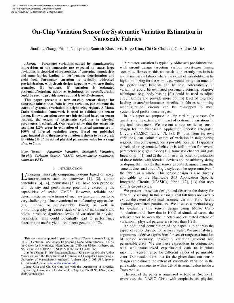
Gate OlClde (HfO,1 Channel Bottom Oxide (SiOl) BKk Gate
L, L.
Figure 2. n-type xnwFET device structure with orthogonal gate and channel nanowires.
eva inN in2 in, pre
� .... � GND
out VDD
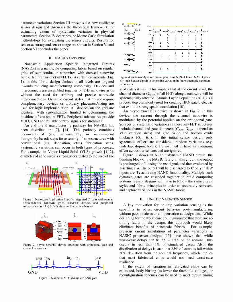
Figure 3. N-input NASIC dynamic NAND gate
a)prC-fil VDD ,OUI_I OUI_2 In!--I 1m, im-l
I I I I I I Ul"-In
11IN-I inNH-1 e"a� GND
Vin51 +-+-''i--''i-�I.:-�g---<':-�t Vin52+-+-+-'Ii!-�I.:-�g---<':---<t Vin5J+-+-+-+�I':-�':'--<':---<t Vin54+-+-+--+--+-�g---<':-�t Vin55+-+-+--+--+--+--<':-�t Vin56+-+-+--+--+--+--+�t
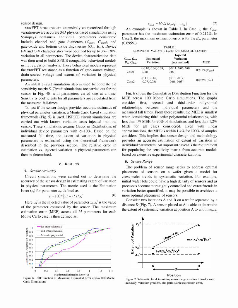
GND�_�_�_�_L--L_-L_L Figure 4. a) Sensor dynamic circuit pair using N, N+ 1 fan-in NAND gates b) 4-pair Sensor circuit to determine variation in four systematic variation parameters
seed catalyst used. This implies that at the circuit level, the
channel diameter (Cdiam) of all FETs along a nanowire will be systematically affected. Atomic-Layer Deposition (ALD) is a
process step commonly used for creating Hf02 gate dielectric that exhibits strong spatial correlation [10].
An n-type xnwFETs device is shown in Fig. 2. In this device, the current through the channel nanowire is
modulated by the potential applied on the orthogonal gate.
Sources of systematic variations in these xnwFET structures
include channel and gate diameters (CdiwlH Gdiam - depend on VLS catalyst sizes) and gate oxide and bottom oxide
thickness (Gox, Box). In this initial sensor design, only
systematic effects are considered; random variations (e.g.
underlap, doping levels) are assumed to have an averaging effect across our sensors and are ignored.
Figure 3 shows an N-input dynamic NAND circuit, the building block of the NASIC fabric. In this circuit, the output
is precharged to '1' using the pre signal, and then evaluated by asserting eva. The output will be discharged to '0' only if all N
inputs are '1 " achieving NAND functionality. Multiple such
dynamic gates are cascaded together to build computing systems. Sensor designs will have to follow the same circuit
styles and fabric principles in order to accurately represent and capture variations in the NASIC fabric.
III. ON-CHIP VARIATION SENSOR
A key motivation for on-chip variation sensing is the capability to adjust circuit behavior post-manufacturing
without pessimistic over-compensation at design time. While
designing for the worst case could guarantee that there are no timing faults in the design, this approach would likely
eliminate benefits of nanoscale fabrics. For example,
previous circuit simulations of parameter variations in
NASIC processor designs [15] have shown that while worst-case delays can be 2X - 2.5X of the nominal, this
occurs in less than 1 % of simulated cases. Also, the distribution of delays is such that 85% of samples fall within 30% deviation from the nominal frequency, which implies
that most fabricated chips would not need worst-case resilience.
If the extent of variation in fabricated chips can be estimated, body-biasing (to lower the threshold voltage), or reconfiguration schemes can be used to meet circuit timing

requirements and retain performance benefits. Variation
sensors can also be used for process feedback (e.g. to
determine, based on device parameters, which process steps need to be more carefully controlled).
In this section, we discuss a new on-chip sensor design for
the NASIC fabric. The sensor can be used to calculate extent of systematic variation in physical parameters based on the
measurement of fall time (1-to-O transitions) in dynamic
NAND gates. Fig. 4A shows the new sensor circuit, which uses the same
circuit styles as logic portions of the design. It consists of a pair of dynamic NAND gates with fan-in N and N+1. In
principle, if the switching characteristics of a single device
can be isolated, then information on the extent of variation in the device can be extracted using physics-based device models.
The sensor operates as follows: Outputs are initially
precharged by asserting the pre signal. During this time the
input in1 is switched off ensuring that intermediate
capacitances are not charged. All other inputs are asserted.
Subsequently, in1 and eva signals are asserted, leading to 1-to-0 transitions on both output nodes.
The difference in the falling times of the two output signals
in this sensor pair can be directly attributed to the behavior of the single 'additional' xnwFET if transient effects are near
identical. This is made possible through careful sensor design. Firstly, the output load capacitance is made much larger than the device parasitics, eliminating their effect.
Secondly, N must be large enough such that the net Vos drop
across the N+ 1 FET in the second dynamic NAND gate is
very small. Our simulations of NAND circuits employing
accurate physics-based device models show that for N249,
Vos drop is less than 0.02V. Ignoring transient effects, fall times are given by (1), (2).
t/,ouu = K*(R; + R; +" .. ,,+ R� + R�+I + R�va) *CLoad (1)
t(.OW_2 = K *(R1 + R2 +" .. ,,+ RN + Reva) *C Load (2)
where K is the number of time constants to discharge the output and CLoad is the output loading capacitance. RJ ... RN+J are xnwFET resistances. Subtracting (1) - (2), we get
t t -K*R' *C (3) /.ow_, - /,Ow_2 - N+' Load Next, RN+J can be expressed as a function of the individual
variation parameters. Assuming independent variation in M
different parameters (since each parameter is dependent on a separate process step), the resistance function can be decomposed into polynomial functions h;(x;) of the individual parameters Xi I, as shown in (4),
t / ,0uU - t / ,Ow_ 2 . (4) *
=RN+, =h,(x,)+h2(X2)+,,·+hM(XM) K CLoad
The above equation establishes a single relationship between measurable fall times, and the extent of physical
variation to be estimated. Considering different values of N
and N+ 1, a linear system of equations can be established and solved for the individual parameters. For example, if there are
I Interdependencies would introduce cross-terms that increase computational complexity, but the approach would still be applicable. 2 Higher order polynomials would imply that the S matrix incorporates additional dimensions.
4 systematic parameters being varied (M=4), then four
different sensor pairs are used to establish 4 fall-time
difference equations. Fig. 4B shows such a sensor, with 8 dynamic NAND gates, and (N, N+1) pairs varying from (49,
50) to (55, 56). For simplicity, the next set of equations consider first-order
(linear) relationships for h;(x;) polynomials. Results for 1st,
2nd and 3rd order polynomials will be discussed in the
following sections. Equation (5) shows the matrix representation for the linear system of equations that needs to be solved:
p = §-I *f
kM_l.l kM_1.2 kM.1 kM.2
k1.M-1 k,.M_I
kM-I.M-1 kM_1.M kM,M_l kM,M
g(""f.1) g(""f.2)
(5)
P is the vector representing extent of variation in individual parameters that needs to be determined, S lists the sensitivity
coefficients 2 of each parameter, and T contains measured
differences in fall-time. For M systematic vanatlOn
parameters, M pairs of sensor circuits are needed to establish M different linear equations. By solving this system of
equations, extent of variation in individual parameters is estimated.
IV. METHODOLOGY FOR EVALUATION
In this section, we describe a methodology for evaluating
the accuracy of the sensor design based on Monte Carlo
circuit simulations injecting known variation cases into the
Monte Carlo sampling of physical parameter variation
Sensitivity Coefficients (from device modeling)
Sensor Circuit Nellist
Measured fall-time difference in sensor pairs
Estimated extent of variation in physical parameters; Error
in estimation
No Iterations L-_____________ --( Complete?
Figure 5. Methodology for evaluating sensor designs based on Monte Carlo circuit simulations
sensor design.
xnwFET structures are extensively characterized through
variation-aware accurate 3-D physics based simulations using
Synopsys Sentaurus. Individual parameters considered
include channel and gate diameters (CdiwIH Gdiom), and
gate-oxide and bottom oxide thicknesses (Gox, Box). Device
I-V and C-V characteristics were obtained for up to 3u=±30% variation in all parameters. The device characterization data
was then used to build SPICE-compatible behavioral models
using regression analysis. These behavioral models represent
the xnwFET resistance as a function of gate-source voltage,
drain-source voltage and extent of variation in physical
parameters.
An initial circuit simulation step is used to populate the
sensitivity matrix S. Circuit simulations are carried out for the
sensor in Fig. 4B with parameters varied one at a time.
Sensitivity coefficients for all parameters are calculated from
the measured fall-times.
To test if the sensor design provides accurate estimates of
physical parameter variation, a Monte Carlo based simulation
framework (Fig. 5) is used. HSPICE circuit simulations are
carried out with known variation cases injected into the
sensor. These simulations assume Gaussian Distributions of
individual device parameters with u=lO%. Based on the
measured fall time, the extent of variation in physical
parameters is estimated using the theoretical framework
described in the previous section. The relative error in
estimation vs. injected variation in physical parameters can
then be determined.
V. RESULTS
A. Sensor Accuracy
Circuit simulations were carried out to determine the
accuracy of the sensor design in estimating extent of variation
in physical parameters. The metric used is the Estimation
Error (eJ for parameter Xi, defined as:
ej =100* I (x; -xO l lx/ (6)
Here, x/ is the injected value of parameter Xi, x/ is the value
of the parameter estimated by the sensor. The maximum
estimation error (MEE) across all M parameters for each
Monte Carlo case is then defined as:
" o <1 0.9 " &: 0.8 .2 0.7 � 0.6 ; 0.5 � 0.4 .� 0.3 1! 0.2 80.1
o o
-1st-order polynomial -2nd-order polynomial r"" � -3rd-order polynomial .-/-:::..---('
� J �� /'
� .-/ (/ �
(( � 0 /
/J/ f II
0.2 0.4 0.6 0.8 12 lA Maximum Estimation Error(%)
Figure 6. CDF function of Maximum Estimated Error across 100 Monte Carlo Simulations
eMAX =MAX(e"e2,",eM) (7)
An example is shown in Table I. In Case 1, the Cdiom parameter has the maximum estimation error of 0.212%. In
Case 2, the maximum estimation error is for the Box parameter
(0.695%). TABLE I
EXAMPLES OF VARIATION CASES AND MEE CALCULATION Injected
Cdiam, Gox, Estimated Variation BoX) G'iiam Variation (normalized) MEE
(-0.10, 0.06, 0.09, (-0.11, 0.06, 0.09, 0.2l2%(Cdiam)
Casel 0.08) 0.09)
(0.11, -0.16, (0.10, -0.17, 0.695% (Box)
Case2 -0.07, 0.03) -0.06, 0.03)
Fig. 6 shows the Cumulative Distribution Function for the
MEE across 100 Monte Carlo simulations. The graphs
consider first, second and third-order polynomial
relationships between individual parameters and the
measured fall times. From these results, the MEE is smallest
when considering third-order polynomial relationships, with
less than 1 % MEE for 90% of simulations, and less than 1.2% MEE for all cases considered. Even with linear
approximations, the MEE is within 1.4% for 100% of samples
considers. This implies that sensor design and methodology
provides an accurate estimation of extent of variation in
individual parameters. An important caveat is the requirement
for populating the sensitivity matrix from accurate models
based on extensive experimental characterizations.
B. Sensor Range
The problem of sensor range seeks to address optimal
placement of sensors on a wafer given a model for
cross-wafer trends in systematic variation. For example,
initial wafer lots could have a high density of sensors and as
processes become more tightly controlled and extent/trends in
variation better quantified, it may be possible to avchieve a
more optimal placement of sensors.
Consider two locations A and B on a wafer separated by a
distance D (Fig. 7). A sensor placed at A is able to determine
the extent of systematic variation at position A to within eMAX,
A B �.---------D---------..
Position Figure 7. Schematic for determining sensor range as a function of sensor accuracy, variation gradient, and permissible estimation error.

the sensor accuracy. Now, considering a suitable model for
the trend in systematic variation from location A to B, we
wish to estimate the error in the sensor estimation with
respect to the actual extent of systematic variation at location
B. Conversely, the sensor range D for which the sensor
accuracy is below a pre-defined permissible estimation error
can be estimated. This is demonstrated below:
Considering error in estimation at point A,
I (x� -x�)l/x� �eA (8)
where for simplicity the metric MEE has been replaced by
estimation error at point A, 'eA'. x/ represents the sensor
estimation value, x/ represents the unknown actual variation
at point A. Two cases are possible depending on whether the
sensor overestimates or underestimates the value of XA a; (9)
or x� � x� 1(l+eA) (10)
Consider a linear trend in systematic variation from point A
to B with slope m, x� =mD+x� (11)
Now, based on the 2 cases outlined above, and given a
maximum allowed imprecision eB at point B,
(12)
or x�=x�/(l+eB) (13)
Solving the inequalities (9) - (13) for the two cases, we get
D = (x: Im)*{(eB -eA)/[(l -eB)*(l -eA)]} (14)
or D = (x� I lml)* { (ell -eA)/[(l +ell)* (l + eA)]} (15)
Now, given that the information on whether the sensor
overestimated or underestimated the actual value of the
parameter is unknown, the smaller of the two D values (Eqn.
15) needs to be selected.
The following insights can be derived from this
relationship: 1) Sensor Accuracy: sensor range increases with
increased accuracy, reduced eA, 2) Permissible estimation error: range increases with increase in eB, larger estimation
H(51.2)
0(51.5). .1(51.2)
o N(51.3) .. -----< .. -+--��=�---4t-----e J(51 0) �
M(5o.s)-
K(5o.7)
L(5o.9)
.. 100mm •
3
Figure 8. Hf02 gate oxide thickness distribution across 100mm wafer for optimized ALD process from experimental data [10]. Values in brackets represent thickness in nanometers. Red shaded region represents locus of points for which sensor estimation error :os en.
error is permissible, 3) Slope: If there is a larger gradient in
systematic variation, sensors need to be placed closer
together, and 4) Parameter Value: A larger value for a
physical parameter means a smaller relative estimation error,
which implies that sensors can be spaced farther apart.
A key challenge in determining sensor distribution is that
the distance D depends on the estimated parameter value and
the slope, values that may only be available
post-manufacturing. In nanoscale fabrics supporting
reconfiguration, it may be possible to progressively design
sensors based on estimated values, since the sensor logic and
circuit style are identical to other functional blocks in the
design. Otherwise, estimations based on previous
experimental characterizations need to be used to determine
sensor spacing pre-manufacturing. An example is described
below.
In [10], an optimized ALD deposition process was shown
with high degree of uniformity for Hf02 gate oxide. Fig. 8
shows a schematic representation of cross-wafer ALD gate
oxide thickness distribution that was characterized [10] for a
100mm wafer. The smallest possible value for xe in this case
is (l-eMAX)* Xmina. From characterization data, Xmina = 50nm at
point 0, eA = 1.2% (sensor accuracy), and maximum slope
m=1.4nmI25mm (corresponding to segment AC). The shaded
circular region represents the locus of points B for which the
estimation error is less than or equal to eB' Table II shows the
sensor range for the above parameter and varying values of
eB' The results show that for an estimation error between
2%-4%, the sensor range varies from 7mm to 24mm. The
relatively high sensor range is primarily due to the high
degree of uniformity of the fabrication process, which implies
that the magnitude of slope m is very small. As expected,
sensor range increases if more imprecision can be tolerated.
TABLE II SENSOR RANGE vs. PERMISSIBLE ESTIMATION ERROR (en)
Sensor Range (D), in mm 2% 7
2.5% 11.3 3% 15.6
3.5% 19.8 4% 24
VI. CONCLUSIONS
A new on-chip variation sensor for the NASIC nano-fabric
was shown. A methodology for extracting the extent of
systematic variation in physical parameters from measured
sensor fall-times was presented. Using accurate physics-based device models and Monte Carlo simulations, sensor accuracy was quantified. Results show less than 1.2% error in estimation of physical parameters for 100% of the
samples considered. Analytical expressions for sensor range
as a function of sensor accuracy, gradient in systematic
parameter variation and permissible estimation error were derived. From experimental characterization data for an
optimized Hf02 ALD process, the sensor range was shown to be up to 7mm considering a permissible estimation error of
2% in gate oxide thickness. On-chip variation sensors could

be used in conjunction with adaptive body-bias, reconfiguration or other post-fabrication techniques to
ameliorate the impact of parameter variation and improve system-level performance for nanoscale computing fabrics.
REFERENCES
[1] Y. Huang, X. Duan. Y. Cui, L. J. Lauhon, K. Kim, and C. M. Lieber, "Logic gates and computation from assembled nanowire building blocks, " Science, vol. 294, no. 5545, pp. 1313 -1317, Nov. 2001.
[2] W. Lu and C. M. Lieber, "Semiconductor nanowires, " Journal of
Physics D: Applied Physics, vol. 39, no. 21, pp. R3S7-R406, 2006.
[3] S. lijima and T. Ichihashi, "Single-shell carbon nanotubes of I-nm
diameter," Nature, vol. 363, no. 6430, pp. 603-605, June 1993.
[4] R. Martel, T. Schmidt, H. R. Shea, T. Hertel, and P. Avouris, "Singleand multi-wall carbon nanotube field-effect transistors, " Applied
Physics Letters, vol. 73, no. 17, p. 2447, 1995.
[5] D. B. Strukov, G. S. Snider, D. R. Stewart, and R. S. Williams, "The missing memristor found, " Nature, vol. 453, no. 7191, pp. SO-S3, 200S.
[6] B. Ray, S. Mahapatra, "A New Threshold Voltage Model for Omega Gate Cylindrical Nanowire Transistor, " 21st International Conference
on VLSI Design, pp. 447-452, 200S. [7] c. A. Moritz, P. Narayanan, and C. O. Chui, "Nanoscale application
specific integrated circuits, " N. K. Jha and D. Chen, Eds. Springer New
York, pp. 215-275, 2011. [S] P. Narayanan, et aI., "Nanoscale Application Specific Integrated
Circuits, " IEEEIACM International Symposium on Nanoscale
Architectures (NANOARCH), pp.99-L06, 2011. [9] P. Narayanan, et aI., "CMOS Control Enabled Single-Type FET
NASIC, " in IEEE Computer Society Annual Symposium on VLSI, pp.
191-196, 200S. [10] D. W. McNeill, et aI., "Atomic Layer Deposition of Hafnium Oxide
Dielectrics on Silicon and Germanium Substrates, " in J Mater. Sci:
Mater Electron, pp. 119-123, 200S. [11] J. P. Cain, and C. J. Spanos, "Electrical linewidth metrology for
systematic CD variation characterization and causal analysis, " Proc.
SPIE Vol. 503S, 2003. [12] P. Panchapakeshan, P. Narayanan and C. A. Moritz, "N3 ASIC:
Designing Nanofabrics with Fine-Grained CMOS Integration, " IEEElACM International Symposium on Nanoscale
Architectures (NANOARCH), pp.196-202, S-9 June 2011. [13] M. Rahman, P. Narayanan and C. A. Moritz, "N3 ASIC Based
Nanowire Volatile RAM, " IEEE International Conference on
Nanotechnology (IEEE NANO 2011), pp.1097-ILOI, IS-IS Aug. 2011. [14] P. Narayanan, K. W. Park, C. O. Chui and C. A.
Moritz, "Manufacturing Pathway and Associated Challenges for Nanoscale Computational Systems, " 9th IEEE Nanotechnology
conference(NANO 2009), pp.119-122, Jul. 2009. [15] P. Narayanan, M. Leuchtenburg, J. Kina, P. Joshi, P. Panchapakeshan,
C. O. Chui and C. A. Moritz, "Parameter Variability in Nanoscale Fabrics: Bottom-Up Integrated Exploration, " IEEE 25th International
Symposium on Defect and Fault Tolerance in VLSI Systems (DFT),
pp.24-31, 2010.
978-1-4673-2200-3/12/$31.00 ©2012 IEEE