Building a Fab on a Chip
14
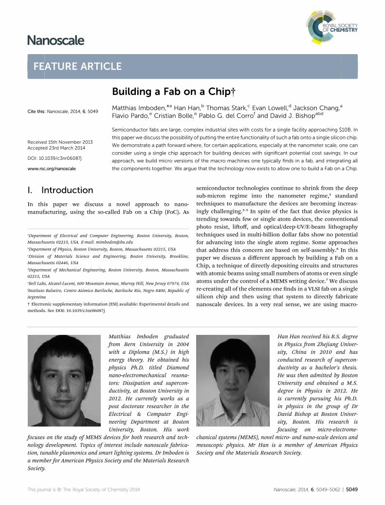
Building a Fab on a Chip† Matthias Imboden, * a Han Han, b Thomas Stark, c Evan Lowell, d Jackson Chang, a Flavio Pardo, e Cristian Bolle, e Pablo G. del Corro f and David J. Bishop abd Semiconductor fabs are large, complex industrial sites with costs for a single facility approaching $10B. In this paper we discuss the possibility of putting the entire functionality of such a fab onto a single silicon chip. We demonstrate a path forward where, for certain applications, especially at the nanometer scale, one can consider using a single chip approach for building devices with significant potential cost savings. In our approach, we build micro versions of the macro machines one typically finds in a fab, and integrating all the components together. We argue that the technology now exists to allow one to build a Fab on a Chip. I. Introduction In this paper we discuss a novel approach to nano- manufacturing, using the so-called Fab on a Chip (FoC). As semiconductor technologies continue to shrink from the deep sub-micron regime into the nanometer regime, 1 standard techniques to manufacture the devices are becoming increas- ingly challenging. 2–5 In spite of the fact that device physics is trending towards few or single atom devices, the conventional photo resist, lioff, and optical/deep-UV/E-beam lithography techniques used in multi-billion dollar fabs show no potential for advancing into the single atom regime. Some approaches that address this concern are based on self-assembly. 6 In this paper we discuss a different approach by building a Fab on a Chip, a technique of directly depositing circuits and structures with atomic beams using small numbers of atoms or even single atoms under the control of a MEMS writing device. 7 We discuss re-creating all of the elements one nds in a VLSI fab on a single silicon chip and then using that system to directly fabricate nanoscale devices. In a very real sense, we are using macro- a Department of Electrical and Computer Engineering, Boston University, Boston, Massachusetts 02215, USA. E-mail: [email protected] b Department of Physics, Boston University, Boston, Massachusetts 02215, USA c Division of Materials Science and Engineering, Boston University, Brookline, Massachusetts 02446, USA d Department of Mechanical Engineering, Boston University, Boston, Massachusetts 02215, USA e Bell Labs, Alcatel-Lucent, 600 Mountain Avenue, Murray Hill, New Jersey 07974, USA f Instituto Balseiro, Centro At´ omico Bariloche, Bariloche R´ ıo, Negro 8400, Republic of Argentina † Electronic supplementary information (ESI) available: Experimental details and methods. See DOI: 10.1039/c3nr06087j Matthias Imboden graduated from Bern University in 2004 with a Diploma (M.S.) in high energy theory. He obtained his physics Ph.D. titled Diamond nano-electromechanical resona- tors: Dissipation and supercon- ductivity, at Boston University in 2012. He currently works as a post doctorate researcher in the Electrical & Computer Engi- neering Department at Boston University, Boston. His work focuses on the study of MEMS devices for both research and tech- nology development. Topics of interest include nanoscale fabrica- tion, tunable plasmonics and smart lighting systems. Dr Imboden is a member for American Physics Society and the Materials Research Society. Han Han received his B.S. degree in Physics from Zhejiang Univer- sity, China in 2010 and has conducted research of supercon- ductivity as a bachelor's thesis. He was then admitted by Boston University and obtained a M.S. degree in Physics in 2012. He is currently pursuing his Ph.D. in physics in the group of Dr David Bishop at Boston Univer- sity, Boston. His research is focusing on micro-electrome- chanical systems (MEMS), novel micro- and nano-scale devices and mesoscopic physics. Mr Han is a member of American Physics Society and the Materials Research Society. Cite this: Nanoscale, 2014, 6, 5049 Received 15th November 2013 Accepted 23rd March 2014 DOI: 10.1039/c3nr06087j www.rsc.org/nanoscale This journal is © The Royal Society of Chemistry 2014 Nanoscale, 2014, 6, 5049–5062 | 5049 Nanoscale FEATURE ARTICLE
Transcript of Building a Fab on a Chip
Nanoscale
FEATURE ARTICLE
Building a Fab on
aDepartment of Electrical and Computer
Massachusetts 02215, USA. E-mail: mimbodbDepartment of Physics, Boston University, BcDivision of Materials Science and Eng
Massachusetts 02446, USAdDepartment of Mechanical Engineering, B
02215, USAeBell Labs, Alcatel-Lucent, 600 Mountain AvefInstituto Balseiro, Centro Atomico Bariloch
Argentina
† Electronic supplementary information (methods. See DOI: 10.1039/c3nr06087j
Mfwepntd2pEnU
focuses on the study of MEMS devnology development. Topics of inttion, tunable plasmonics and smara member for American Physics SoSociety.
Cite this: Nanoscale, 2014, 6, 5049
Received 15th November 2013Accepted 23rd March 2014
DOI: 10.1039/c3nr06087j
www.rsc.org/nanoscale
This journal is © The Royal Society of C
a Chip†
Matthias Imboden,*a Han Han,b Thomas Stark,c Evan Lowell,d Jackson Chang,a
Flavio Pardo,e Cristian Bolle,e Pablo G. del Corrof and David J. Bishopabd
Semiconductor fabs are large, complex industrial sites with costs for a single facility approaching $10B. In
this paper we discuss the possibility of putting the entire functionality of such a fab onto a single silicon chip.
We demonstrate a path forward where, for certain applications, especially at the nanometer scale, one can
consider using a single chip approach for building devices with significant potential cost savings. In our
approach, we build micro versions of the macro machines one typically finds in a fab, and integrating all
the components together. We argue that the technology now exists to allow one to build a Fab on a Chip.
I. Introduction
In this paper we discuss a novel approach to nano-manufacturing, using the so-called Fab on a Chip (FoC). As
Engineering, Boston University, Boston,
oston, Massachusetts 02215, USA
ineering, Boston University, Brookline,
oston University, Boston, Massachusetts
nue, Murray Hill, New Jersey 07974, USA
e, Bariloche Rıo, Negro 8400, Republic of
ESI) available: Experimental details and
atthias Imboden graduatedrom Bern University in 2004ith a Diploma (M.S.) in highnergy theory. He obtained hishysics Ph.D. titled Diamondano-electromechanical resona-ors: Dissipation and supercon-uctivity, at Boston University in012. He currently works as aost doctorate researcher in thelectrical & Computer Engi-eering Department at Bostonniversity, Boston. His workices for both research and tech-erest include nanoscale fabrica-t lighting systems. Dr Imboden isciety and the Materials Research
hemistry 2014
semiconductor technologies continue to shrink from the deepsub-micron regime into the nanometer regime,1 standardtechniques to manufacture the devices are becoming increas-ingly challenging.2–5 In spite of the fact that device physics istrending towards few or single atom devices, the conventionalphoto resist, lioff, and optical/deep-UV/E-beam lithographytechniques used in multi-billion dollar fabs show no potentialfor advancing into the single atom regime. Some approachesthat address this concern are based on self-assembly.6 In thispaper we discuss a different approach by building a Fab on aChip, a technique of directly depositing circuits and structureswith atomic beams using small numbers of atoms or even singleatoms under the control of a MEMS writing device.7 We discussre-creating all of the elements one nds in a VLSI fab on a singlesilicon chip and then using that system to directly fabricatenanoscale devices. In a very real sense, we are using macro-
Han Han received his B.S. degreein Physics from Zhejiang Univer-sity, China in 2010 and hasconducted research of supercon-ductivity as a bachelor's thesis.He was then admitted by BostonUniversity and obtained a M.S.degree in Physics in 2012. Heis currently pursuing his Ph.D.in physics in the group of DrDavid Bishop at Boston Univer-sity, Boston. His research isfocusing on micro-electrome-
chanical systems (MEMS), novel micro- and nano-scale devices andmesoscopic physics. Mr Han is a member of American PhysicsSociety and the Materials Research Society.
Nanoscale, 2014, 6, 5049–5062 | 5049
Nanoscale Feature Article
machines to build micro-machines and then using these micro-machines to produce nanostructures. Our approach advancesmanufacturing technology through the use of what is, inessence, a 3D printer at the atomic scale that allows us toassemble materials in a digitally programmable way. As we willshow, this can be used for creating NEMS devices as well aselectronic ones.
II. Background
The basic and most fundamental idea of modern semi-conductor processing is that of depositing or diffusing mate-rials onto or into a silicon substrate with areas of the substratemasked off with various types of photoresists or other layers.While materials, deposition tools, lithography tools, etchingtools, and lithography wavelengths keep changing, the basicfabrication technique remains the same; one deposits morematerial than is desired and then selectively removes theunwanted material. An extrapolation of Moore's law8 predictsthat the industry is moving into the regime of single atomdevices, where the standard manufacturing approach
Thomas Stark received his B.S. inPhysics from Middlebury Collegein 2011, where he conductedresearch on laser coolingrubidium vapor. He is currentlypurusing his Ph.D. in MaterialsScience and Engineering atBoston University, where he is amember of David Bishop's group.His research focuses on usingMEMS for tunable plasmonicsexperiments. Mr Stark is amember of the MaterialsResearch Society.
Evan Lowell is an undergraduateat Boston University studyingmechanical engineering. Heworks as an undergraduateresearcher in the Electrical andComputer Engineering Depart-ment at Boston University,Boston. His research involvesstudying MEMS devices foradaptive optics systems andnanolithography. He previouslyworked as an intern at MedicalVision Systems, a biomedical
engineering rm. Evan Lowell is a member of the MaterialsResearch Society and is a Brawerman Fellow.
5050 | Nanoscale, 2014, 6, 5049–5062
fundamentally breaks down. One answer to this technologicalchallenge is a bottom up approach, inspired by biology, thatrelies on self-assembly and stochastic processes, as today'scarbon nanotubes are grown.9 Single molecule10 and even singleatom1,11 transistors have already been manufactured andnetworks using carbon nanotubes to perform basic computa-tional operations12 have already been realized. For fabricatingsingle atom devices there is no known method for depositingmany atoms and then removing all but a single atom. If onewants only a single atom in a specic location on a silicon wafer,one will probably need a technique to be able to directly placethe single atom. This paper discusses such an approach, the Fabon a Chip. It is illustrated how the combination of MEMSdevices can be leveraged to deposit as few as a single atom at atime within a well-dened area.
The technique is inspired by research done at Bell Labora-tories in the mid 1980's by Bishop and Dolan.13 Their work usedstatic, nano-scale stencils and low temperature quenchcondensed evaporation. The advantages of directly evaporatingat low temperatures (�77 K or �4.2 K) are: (a) higher purity dueto a very good vacuum, (b) excellent sticking of the deposited
Jackson Chang is a ResearchEngineer at Boston University. Hereceived his M.Eng. in MaterialsScience and Engineering in 2012and was one of the foundingmembers of the Boston Universitychapter of ASM which helpsstudents advance their knowl-edge and careers through orga-nized talks with industry.
Dr Flavio Pardo received M.S.and Ph.D. degrees in Physics fromthe Intituto Balseiro, Bariloche,Argentina in 1992 and 1997,respectively. He is the technicalmanager of SLIMLine, a hybridphotonic integration prototypingcleanroom in Bell Labs, Alcatel-Lucent in New Jersey, USA. At BellLabs he conducted research onbiologically inspired micro-elec-tro-mechanical-systems (MEMS)acoustic transducers, high-sensi-
tivity magnetometers and seeded the MEMS design and testinggroup that realized the micromirror array in Lucent's pioneeringrst all-optical LambdaRouterTM cross-connect and wavelength-selective optical switches. He is a co-author on over 50 papers andholds 22 U.S. patents in the eld of MEMS and photonic devices.
This journal is © The Royal Society of Chemistry 2014
Feature Article Nanoscale
atoms, (c) the ability to use a wide range of materials, includinglithium and sodium, which are incompatible with conventionaltechniques and (d) circumvention of thermal cycling from thefabrication process, which is known to cause creep, balling up,etc. in room temperature depositions. For in situmeasurementsthis is particularly important as any change in temperature aerdeposition will result in a change of the material properties.
Pablo G. del Corro is an Elec-tronic Engineer from NationalUniversity of Santiago del Estero,Argentina. He is doing his Ph.D.in Engineering Sciences since2012 in the Instituto Balseiro,Argentina. He thesis is focused onelectrical signal detection andcontrol circuits for MEMS sensorand actuators.
Dr Cristian A. Bolle was born inBuenos Aires, Argentina in 1966.He received his M.S. and Ph.D. inphysics from the Instituto Bal-seiro, Argentina in 1990 and1995 respectively. Between 1995and 1997 he was a Post-DoctoralResearcher in the Charles Liebergroup in Harvard University. In1997 he joined the PhysicalSciences group in Lucent Tech-nologies' Bell Laboratories inNew Jersey. He worked on the
research of mesoscopic superconductors at low temperatures withHigh-Q micromechanical oscillators and later on the developmentof a micromachine based all optical switch. He is currently part ofthe Photonic Integration Technologies group.
This journal is © The Royal Society of Chemistry 2014
The approach we are proposing here is to combine lowtemperature, quench condensed evaporation with program-mable dynamic MEMS stencils, i.e. the ability to directly writestructures and patterns while evaporating in a controlled envi-ronment. Two technologies make our idea feasible: theextraordinary developments in MEMS technologies that enableaperture(s) to be moved with sub-nanometer precision andcontrol14 and the ability, using modern focused ion beam- andtransmission electron-microscopes (FIBs and TEMs), to createnm-sized holes in silicon wafers.15 Fig. 1 shows an example ofsuch a dynamic stencil controller. The basic idea is that one canwrite with a beam of atoms by using one or more sources to emitatoms while a MEMS plate follows a preprogrammed trajectory,tracing out a pattern. This approach has a number of advan-tages, including that it enables one to: (a) turn the atom beamon and off quickly by using the fast thermal response time of thesources and/or an integrated shutter, (b) create many devices inparallel by using arrays of apertures, (c) deposit single or fewatoms by using apertures on the order of tens of nanometers, (d)control the size and shape of deposited structures by millingdifferent size and shape apertures and by dynamically control-ling the aperture location, (e) deposit both insulating andconducting materials, allowing for the fabrication of complexinterconnects and wire junctions, (f) construct nano-mechan-ical devices, as well as electrical ones, and (g) conduct the entire
David J. Bishop became amember of the IEEE in 2011. Hereceived his BS in Physics fromSyracuse University in 1973 andhis MS in Physics in 1977 and hisPh.D. in Physics in 1978, bothfrom Cornell University. He iscurrently the Head of the Divisionof Materials Science and Engi-neering, Boston University andalso a Professor of Physics and aProfessor of Electrical Engi-neering. Previously he was the
Chief Technology Officer (CTO) and Chief Operating Officer (COO)of LGS, the wholly-owned subsidiary of Alcatel-Lucent dedicated toserving the U.S. federal government market with advanced R&Dsolutions. Before joining LGS, Dr Bishop was the President ofGovernment Research & Security Solutions for Bell Labs, LucentTechnologies. Dr. Bishop is a Bell Labs Fellow and in his previouspositions with Lucent served as Nanotechnology Research VP forBell Labs, Lucent Technologies; President of the New Jersey Nano-technology Consortium and the Physical Sciences Research VP. Hejoined AT&T-Bell Laboratories Bell Labs in 1978 as a postdoctoralmember of staff and in 1979 became aMember of the Technical Staff.In 1988 he was made a Distinguished Member of the Technical Staffand later that same year was promoted to Department Head, BellLaboratories. Professor Bishop is a member and fellow of the Amer-ican Physical Society, a member of theMRS and a recipient of the APSPake Prize.
Nanoscale, 2014, 6, 5049–5062 | 5051
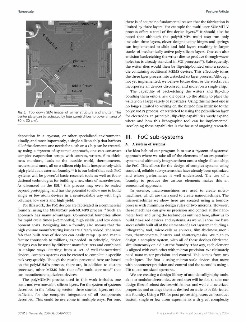
Fig. 1 Top down SEM image of writer structure and shutter. Thecenter plate can be actuated by four comb drives to cover an area of30 � 30 mm2.
Nanoscale Feature Article
deposition in a cryostat, or other specialized environment.Finally, and most importantly, a single silicon chip that harborsall of the elements one needs for a Fab on a Chip can be created.By using a “system of systems” approach, one can constructcomplex evaporation setups with sources, writers, lm thick-ness monitors, leads to the outside world, thermometers,heaters, and more, all on a silicon chip built inexpensively withhigh yield at an external foundry.16 It is our belief that such FoCsystems will be powerful basic research tools as well as foun-dational technologies for building a new class of nano-devices.As discussed in the ESI,† this process may even be scaledbeyond prototyping, and has the potential to allow one to buildsingle or few atom devices in a semi-scalable way with highvolumes, low costs and high yield.
For this work, the FoC devices are fabricated in a commercialfoundry, using the MEMSCAP polyMUMPS process.16 Such anapproach has many advantages. Commercial foundries allowfor rapid cycle times (�2 months), high yields, and low devel-opment costs. Designing into a foundry also means that thehigh volumemanufacturing issues are already solved. The samefab that built tens of devices can easily ramp up and manu-facture thousands to millions, as needed. In principle, devicedesigns can be used by different manufacturers and combinedin unique ways. Starting from a set of well-characterizeddevices, complex systems can be created to complete a specictask very quickly. Though the results presented here are basedon the polyMUMPs process, there are, in addition to customprocesses, other MEMS fabs that offer multi-user-runs17 thatcan manufacture equivalent devices.
The polyMUMPs process used in this work includes onestatic and twomoveable silicon layers. For the system of systemsdescribed in the following section, three stacked layers are notsufficient for the complete integration of all componentsdescribed. This could be overcome in multiple ways. For one,
5052 | Nanoscale, 2014, 6, 5049–5062
there is of course no fundamental reason that the fabrication islimited by three layers. For example the multi user SUMMiT Vprocess offers a total of ve device layers.17 It should also benoted that although the polyMUMPs multi user run onlyincludes three layers, clever designs using hinges and springscan implemented to slide and fold layers resulting in largerstacks of mechanically active poly-silicon layers. One can alsoenvision back-etching the writer dies to produce through-waverholes (as is already standard in SOI processes18). Subsequently,the writer dies would then be ip-chip-bonded onto a seconddie containing additional MEMS devices. This effectively turnsthe three layer process into a stacked six layer process. Althoughnot yet implemented, we believe future dies, or die stacks, canincorporate all devices discussed, and more, on a single chip.
The capability of back-etching the writers and ip-chipbonding them onto a new die opens up the ability to place thewriters on a large variety of substrates. Using this method one isno longer limited to writing on the nitride lm intrinsic to thepolyMUMPs process, or restricted to using the poly-silicon layerfor electrodes. In principle, ip-chip capabilities vastly expandwhere and how this lithographic tool can be implemented.Developing these capabilities is the focus of ongoing research.
III. FoC sub-systemsA. A system of systems
The idea behind our program is to use a “system of systems”approach where we take all of the elements of an evaporationsystem and ultimately integrate them onto a single silicon chip,the FoC. This allows for the design of complex systems usingstandard, reliable sub-systems that have already been optimizedand whose performance is well understood. The use of afoundry to produce the various elements makes this aneconomical approach.
In essence, macro-machines are used to create micro-machines, which are then used to create nano-machines. Themicro-machines we show here are created using a foundryprocess with minimum design rules of two microns. However,these machines can give us precision and control at the nano-meter level and using the techniques outlined here, allow us tobuild nm-sized devices and systems. As we will show, we havesuccessfully built all of the elements of a FoC system including alithography tool, micro-cells as sources, lm thickness moni-tors, thermometers, heaters and shutters/masks. We plan todesign a complete system, with all of these devices fabricatedsimultaneously on a die at the foundry. That way, each elementis aligned with each other with micron precision. We ultimatelyneed nano-meter precision and control. This comes from twotechniques. The rst is using micron-scale devices that movewith nanometer precision and control and the second is using aFIB to cut nm-sized apertures.
We are creating a design library of atomic calligraphy tools,akin to modular electronics. An end user will be able to take ourdesign les of robust devices with known and well-characterizedproperties and arrange them as desired on a die to be fabricatedat a foundry. Using a FIB for post processing, users can conductcustom single or few atom experiments with great complexity
This journal is © The Royal Society of Chemistry 2014
Feature Article Nanoscale
and have the devices built in a foundry with high yield and atlow costs.
Fig. 2 SEM images of apertures fabricated using a FIB.
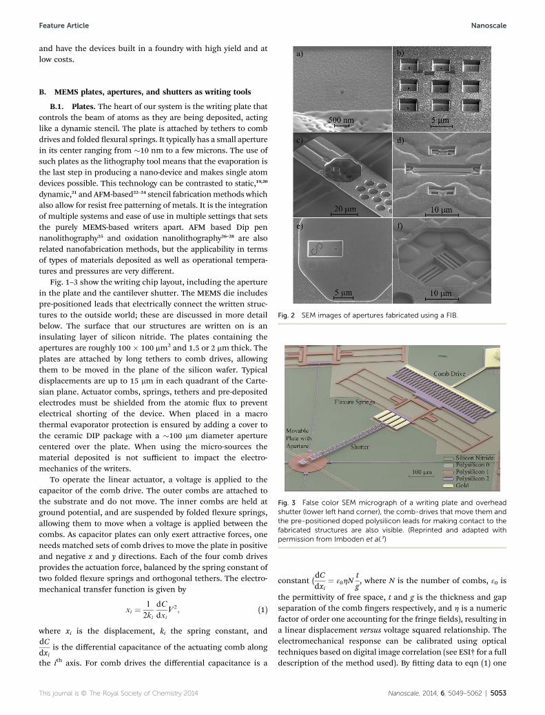
Fig. 3 False color SEM micrograph of a writing plate and overheadshutter (lower left hand corner), the comb-drives that move them andthe pre-positioned doped polysilicon leads for making contact to thefabricated structures are also visible. (Reprinted and adapted withpermission from Imboden et al.7)
B. MEMS plates, apertures, and shutters as writing tools
B.1. Plates. The heart of our system is the writing plate thatcontrols the beam of atoms as they are being deposited, actinglike a dynamic stencil. The plate is attached by tethers to combdrives and folded exural springs. It typically has a small aperturein its center ranging from �10 nm to a few microns. The use ofsuch plates as the lithography tool means that the evaporation isthe last step in producing a nano-device and makes single atomdevices possible. This technology can be contrasted to static,19,20
dynamic,21 and AFM-based22–24 stencil fabricationmethods whichalso allow for resist free patterning of metals. It is the integrationof multiple systems and ease of use in multiple settings that setsthe purely MEMS-based writers apart. AFM based Dip pennanolithography25 and oxidation nanolithography26–28 are alsorelated nanofabrication methods, but the applicability in termsof types of materials deposited as well as operational tempera-tures and pressures are very different.
Fig. 1–3 show the writing chip layout, including the aperturein the plate and the cantilever shutter. The MEMS die includespre-positioned leads that electrically connect the written struc-tures to the outside world; these are discussed in more detailbelow. The surface that our structures are written on is aninsulating layer of silicon nitride. The plates containing theapertures are roughly 100 � 100 mm2 and 1.5 or 2 mm thick. Theplates are attached by long tethers to comb drives, allowingthem to be moved in the plane of the silicon wafer. Typicaldisplacements are up to 15 mm in each quadrant of the Carte-sian plane. Actuator combs, springs, tethers and pre-depositedelectrodes must be shielded from the atomic ux to preventelectrical shorting of the device. When placed in a macrothermal evaporator protection is ensured by adding a cover tothe ceramic DIP package with a �100 mm diameter aperturecentered over the plate. When using the micro-sources thematerial deposited is not sufficient to impact the electro-mechanics of the writers.
To operate the linear actuator, a voltage is applied to thecapacitor of the comb drive. The outer combs are attached tothe substrate and do not move. The inner combs are held atground potential, and are suspended by folded exure springs,allowing them to move when a voltage is applied between thecombs. As capacitor plates can only exert attractive forces, oneneeds matched sets of comb drives to move the plate in positiveand negative x and y directions. Each of the four comb drivesprovides the actuation force, balanced by the spring constant oftwo folded exure springs and orthogonal tethers. The electro-mechanical transfer function is given by
xi ¼ 1
2ki
dC
dxi
V 2; (1)
where xi is the displacement, ki the spring constant, anddCdxi
is the differential capacitance of the actuating comb along
the ith axis. For comb drives the differential capacitance is a
This journal is © The Royal Society of Chemistry 2014
constant (dCdxi
¼ 30hNtg, where N is the number of combs, 30 is
the permittivity of free space, t and g is the thickness and gapseparation of the comb ngers respectively, and h is a numericfactor of order one accounting for the fringe elds), resulting ina linear displacement versus voltage squared relationship. Theelectromechanical response can be calibrated using opticaltechniques based on digital image correlation (see ESI† for a fulldescription of the method used). By tting data to eqn (1) one
Nanoscale, 2014, 6, 5049–5062 | 5053
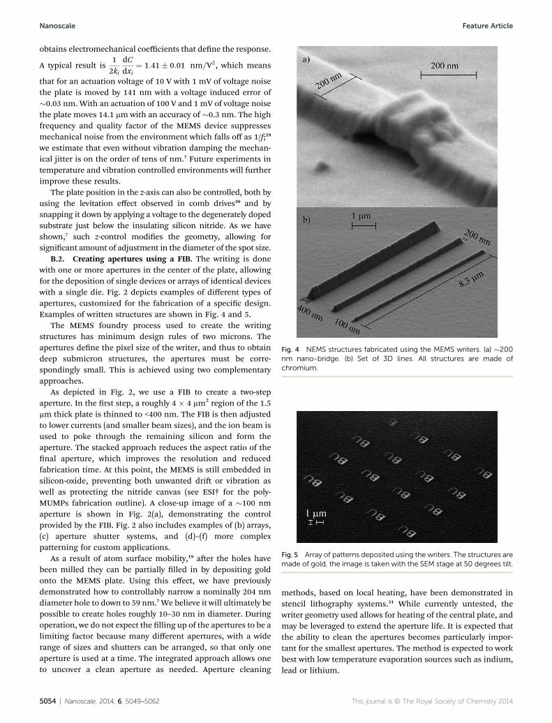
Fig. 4 NEMS structures fabricated using the MEMS writers. (a) �200nm nano-bridge. (b) Set of 3D lines. All structures are made ofchromium.
Fig. 5 Array of patterns deposited using the writers. The structures aremade of gold, the image is taken with the SEM stage at 50 degrees tilt.
Nanoscale Feature Article
obtains electromechanical coefficients that dene the response.
A typical result is12ki
dCdxi
¼ 1:41� 0:01 nm=V2, which means
that for an actuation voltage of 10 V with 1 mV of voltage noisethe plate is moved by 141 nm with a voltage induced error of�0.03 nm. With an actuation of 100 V and 1 mV of voltage noisethe plate moves 14.1 mm with an accuracy of �0.3 nm. The highfrequency and quality factor of the MEMS device suppressesmechanical noise from the environment which falls off as 1/f;29
we estimate that even without vibration damping the mechan-ical jitter is on the order of tens of nm.7 Future experiments intemperature and vibration controlled environments will furtherimprove these results.
The plate position in the z-axis can also be controlled, both byusing the levitation effect observed in comb drives30 and bysnapping it down by applying a voltage to the degenerately dopedsubstrate just below the insulating silicon nitride. As we haveshown,7 such z-control modies the geometry, allowing forsignicant amount of adjustment in the diameter of the spot size.
B.2. Creating apertures using a FIB. The writing is donewith one or more apertures in the center of the plate, allowingfor the deposition of single devices or arrays of identical deviceswith a single die. Fig. 2 depicts examples of different types ofapertures, customized for the fabrication of a specic design.Examples of written structures are shown in Fig. 4 and 5.
The MEMS foundry process used to create the writingstructures has minimum design rules of two microns. Theapertures dene the pixel size of the writer, and thus to obtaindeep submicron structures, the apertures must be corre-spondingly small. This is achieved using two complementaryapproaches.
As depicted in Fig. 2, we use a FIB to create a two-stepaperture. In the rst step, a roughly 4 � 4 mm2 region of the 1.5mm thick plate is thinned to <400 nm. The FIB is then adjustedto lower currents (and smaller beam sizes), and the ion beam isused to poke through the remaining silicon and form theaperture. The stacked approach reduces the aspect ratio of thenal aperture, which improves the resolution and reducedfabrication time. At this point, the MEMS is still embedded insilicon-oxide, preventing both unwanted dri or vibration aswell as protecting the nitride canvas (see ESI† for the poly-MUMPs fabrication outline). A close-up image of a �100 nmaperture is shown in Fig. 2(a), demonstrating the controlprovided by the FIB. Fig. 2 also includes examples of (b) arrays,(c) aperture shutter systems, and (d)–(f) more complexpatterning for custom applications.
As a result of atom surface mobility,19 aer the holes havebeen milled they can be partially lled in by depositing goldonto the MEMS plate. Using this effect, we have previouslydemonstrated how to controllably narrow a nominally 204 nmdiameter hole to down to 59 nm.7We believe it will ultimately bepossible to create holes roughly 10–30 nm in diameter. Duringoperation, we do not expect the lling up of the apertures to be alimiting factor because many different apertures, with a widerange of sizes and shutters can be arranged, so that only oneaperture is used at a time. The integrated approach allows oneto uncover a clean aperture as needed. Aperture cleaning
5054 | Nanoscale, 2014, 6, 5049–5062
methods, based on local heating, have been demonstrated instencil lithography systems.31 While currently untested, thewriter geometry used allows for heating of the central plate, andmay be leveraged to extend the aperture life. It is expected thatthe ability to clean the apertures becomes particularly impor-tant for the smallest apertures. The method is expected to workbest with low temperature evaporation sources such as indium,lead or lithium.
This journal is © The Royal Society of Chemistry 2014
Feature Article Nanoscale
For holes smaller than 10 nm a TEM could be used. Morecomplex plates with low stress nitride thin-lm windows can bemanufactured, through which the aperture is drilled postrelease.32 Feedback control of this process can result in nano-pores in the few nanometer diameter range.33 For this to berealized, two additional fabrication steps need to be imple-mented. First, the polyMUMPs process described here needs tobe expanded to include nitride deposition. Placing such a layeron top of the plate creates the opportunity for manufacturingapertures in much thinner windows, with thicknesses on theorder of 40–100 nm. Second, a deep reactive ion etch step can beadded to back-etch the wafer. Aer the standard release step,this results in a free standing nitride membrane typically usedfor TEM nano-pore drilling. The writers would then be used in aip-chip conguration.
B.3. MEMS shutters for high speed aperture selection.Simple devices can be written using one plate with one aperture.Devices with an integrated shutter, such as shown in Fig. 3, canalso be manufactured. This cantilever style shutter functions asan “on–off” switch for the atom ux. Other MEMS shutters,based on similar stacking of device layers, can be implemented.Alternatively, SOI based shutters or irises34 could be integratedwith the writer by ip chip binding. In its simplest imple-mentation the shutter response time is on the order of the
transient time of the resonant mode, given by s ¼ Q2pf0
. Quality
factors are on the range of 102–104 and the shutter resonancefrequency is on the order of 5 kHz, resulting in transient timesof s ¼ 2–200 ms. By including active feedback mechanisms, theshutter response time can be reduced considerably below thetransient time.35 Opening or closing an aperture can occurmuch faster by simply placing the shutter close to the apertureedge, for which case the transition can occur on the order of 10ms.7 Stacked plate designs function as a more complex shutterthat can move in the same plane as the writer plate to selectfrom multiple apertures. The size and speed of the shutterallows for the deposition of single atoms. For example, given a100 nm sized hole and evaporation rates of one monolayer persecond, roughly 105 atoms per second are transmitted onaverage through the aperture. The 10 ms response time of theshutter is fast enough to stochastically allow only one or a fewatoms to pass. It should be noted that the number of atoms canbe of order one, but the placement accuracy is dened by thearea of the aperture and the position control of the writers. TheMEMS plates themselves can typically be moved at speeds of�1m s�1, hence when travelling in opposite directions the shutter–aperture system can be open for roughly as little as 100 ns,through which only 0.01 atoms would pass on average. Inaddition to enabling single atom placement, two plates withapertures also allow for the velocity selection of the atoms in aparticular range of speeds. This may be achieved by timingthe overlap of the apertures in each plate and using the timeof ight of the atoms between plates as a velocity lter (see ESI†for details).
B.4. Examples of structures fabricated. Examples of struc-tures we have written are shown in Fig. 4 and 5. Fig. 4 shows aroughly 200 nm nano-bridge as well as three “3D” lines written
This journal is © The Royal Society of Chemistry 2014
with the MEMS writer. This demonstrates the ability to produceNEMS devices.
The NEMS bridges were manufactured in a two depositionprocess. Initially a gold sacricial layer was deposited through ashadow mask depicted in Fig. 2(f). During this evaporation theshutter protected the second, perpendicularly oriented aper-tures. Subsequently, the chromium device layer was evaporatedthrough the unobstructed apertures, now positioned above thegold traces. The release was accomplished using a gold wet-etch, removing the sacricial layer. Since the gold must beetched away, in this example deposition is not the last step ofthe fabrication process.
In Fig. 5, an experiment is shownwhere an array of gold “BU”sare printed. For this deposition the writer was swept line by line,akin to a typical printer. This demonstrates the high level ofpositional control that we have using our writing plates. Othermodes of operation follow a continuous line or, when using apredened stencil the writer is moved to set points and then heldsteady while the metal is deposited (examples are illustrated inFig. 4). Further examples, including a demonstration of thefunctionality of the shutter is given by Imboden et al.7
C. Atomic micro sources
So far we discussed a method for resist free patterning bycontrolling the location of an atom ux. Here we present apossible MEMS-based source of such a ux. The micro-source isable to controllably provide the materials needed for nano-fabrication. Examples include MEMS spray source36 and pico-liter dispensers for inkjet printing37 and wet nano-fabrication.38
The PVD approach presented here is based on thermal evapo-ration from a silicon micro-hotplate.
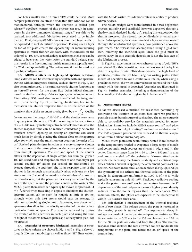
MEMS micro-plates can be uniformly heated in millisecondsto the temperatures needed to evaporate a large range of metalsand compounds. Such sources are shown in Fig. 6 and 7. Thecenter laments range from 50 � 50 to 150 � 150 mm2 in areaand are suspended off the substrate. Narrow attachmentsprovide the necessary mechanical stability and electrical prop-erties. When a current is applied, the attachment points act likeheaters. As shown in the simulation depicted in Fig. 6(b) and (c),the symmetry of the tethers and thermal isolation of the plateresults in temperature uniformity at 1000 K of �8 K whiletypically consuming only 50 mW. Blackbody radiative coolingmake the plates more uniform in temperature because the T4
dependence of the emitted power means a higher power densityradiates from the hotter regions than the cooler ones. Withradiation effects, the plates are expected to be isothermal towithin �4 K across their area.
Fig. 6(d) depicts a measurement of the thermal responsetime of two plates. The voltage across the plate is recorded asthe heating power is turned off. The exponential decay involtage is a result of the temperature-dependent resistance. Thetime constants s¼ 5.23 ms for the 150 mmplate and s¼ 0.70 msfor the 50 mm plate are extracted from the plots. The thermalresponse time dictates the rate at which we can modulate thetemperature of the plate and hence the on–off speed of theatomic ux.
Nanoscale, 2014, 6, 5049–5062 | 5055

Fig. 6 MEMS PVD (a) false color SEM image of micro-evaporation sources. (b) Finite element simulation of the temperature profile across thesource and heaters. (c) Temperature and calculated atomic flux of gold along the dotted trace of (b). (d) Measurements of the thermal timeconstants for two plate sizes.
Fi
Nanoscale Feature Article
Knowing the thermal characteristics of the micro source, wecan calculate the atomic ux using the Hertz–Knudsenequation:39
JðTÞ ¼ a jPðTÞ � P0jffiffiffiffiffiffiffiffiffiffiffiffiffiffiffiffiffiffi2pmkBT
p : (2)
J(T) is the number of atoms per unit area per unit time enteringthe vapor phase, a is the sticking coefficient, P0 is the partialpressure, and P(T) is the vapor pressure at temperature T. Thevapor pressure is calculated using the Clausius–Clapeyronequation and empirically determined constants40,41 and makingthe common assumption that the sticking coefficient is one.Fig. 6(c) depicts the predicted gold ux evaporating off a MEMSplate that is heated to 1000 K. The ESI Fig. (S5)† shows theatomic ux as a function of temperature for zinc, lead, indium,gold, iron, and silicon for partial pressures ranging from 0 to10�5 Torr. All these metals can be used to generate uxes on theorder of monolayers per second at temperatures well below1683 K, the melting temperature of the polysilicon plate. Forexample, gold at a nominal temperature of 1400 K generates aux of �4 � 107 atoms per s per mm2. Accounting for geometric
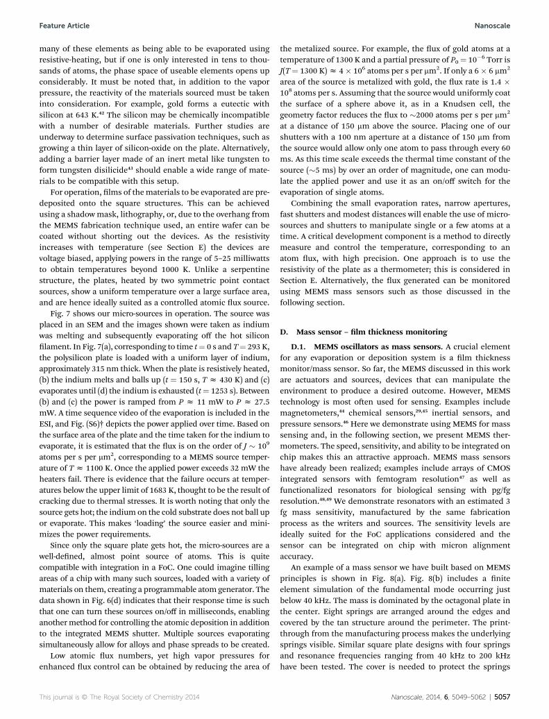
ig. 7 Micro-sources observed in an SEM as indium is evaporated from itsndium. (b) The indium melts and (c) evaporates until (d) the metal is exh
5056 | Nanoscale, 2014, 6, 5049–5062
effects, a 150 � 150 mm2 source would produce a ux of �107
atoms per s per mm2, or one monolayer per second, at a distanceof 150 mm from the source. The high temperature sensitivity ofthe ux makes it difficult to predict evaporation/depositionrates unless a high accuracy temperature measurement can bemade. Furthermore, as seen in the Fig. (S5) of the ESI,† thepartial pressure imposes a cutoff to the lowest ux that can beobtained. For gold at a partial pressure of P0 ¼ 10�6 Torr, thiscorresponds to a ux rate of J(T¼ 1300 K)z 4� 106 atoms per sper mm2. Not surprisingly, ultra-high vacuum as is typicallyfound in a cryostat, is needed when working with a low numberof atoms. For most metals the vapor pressure is sufficiently highthat the partial pressure can be set to zero; this approximation isespecially valid in a cryostat.
The low numbers of atoms desired make it possible tothermally evaporate materials typically not possible in macro-scopic systems. If we consider the list of elements that can beevaporated at rates of at least 1000 atoms per s per mm2 attemperatures below 1683 K the elements included are Zn, Mg,Li, Sr, Ca, Tl, Ba, Pb, In, Mn, Ag, Ga, Be, Al, Cr, Rh, V, La, Ti, Co,Pd, Ni, Fe, Au, Nd, Cu and Sn. One does not normally think of
surface. In panel (a) the plate is at room temperature, fully loaded withausted. The scale bar in each figure is 50 mm.
This journal is © The Royal Society of Chemistry 2014
Feature Article Nanoscale
many of these elements as being able to be evaporated usingresistive-heating, but if one is only interested in tens to thou-sands of atoms, the phase space of useable elements opens upconsiderably. It must be noted that, in addition to the vaporpressure, the reactivity of the materials sourced must be takeninto consideration. For example, gold forms a eutectic withsilicon at 643 K.42 The silicon may be chemically incompatiblewith a number of desirable materials. Further studies areunderway to determine surface passivation techniques, such asgrowing a thin layer of silicon-oxide on the plate. Alternatively,adding a barrier layer made of an inert metal like tungsten toform tungsten disilicide43 should enable a wide range of mate-rials to be compatible with this setup.
For operation, lms of thematerials to be evaporated are pre-deposited onto the square structures. This can be achievedusing a shadowmask, lithography, or, due to the overhang fromthe MEMS fabrication technique used, an entire wafer can becoated without shorting out the devices. As the resistivityincreases with temperature (see Section E) the devices arevoltage biased, applying powers in the range of 5–25 milliwattsto obtain temperatures beyond 1000 K. Unlike a serpentinestructure, the plates, heated by two symmetric point contactsources, show a uniform temperature over a large surface area,and are hence ideally suited as a controlled atomic ux source.
Fig. 7 shows our micro-sources in operation. The source wasplaced in an SEM and the images shown were taken as indiumwas melting and subsequently evaporating off the hot siliconlament. In Fig. 7(a), corresponding to time t¼ 0 s and T¼ 293 K,the polysilicon plate is loaded with a uniform layer of indium,approximately 315 nm thick. When the plate is resistively heated,(b) the indium melts and balls up (t ¼ 150 s, T z 430 K) and (c)evaporates until (d) the indium is exhausted (t¼ 1253 s). Between(b) and (c) the power is ramped from P z 11 mW to P z 27.5mW. A time sequence video of the evaporation is included in theESI, and Fig. (S6)† depicts the power applied over time. Based onthe surface area of the plate and the time taken for the indium toevaporate, it is estimated that the ux is on the order of J � 109
atoms per s per mm2, corresponding to a MEMS source temper-ature of Tz 1100 K. Once the applied power exceeds 32 mW theheaters fail. There is evidence that the failure occurs at temper-atures below the upper limit of 1683 K, thought to be the result ofcracking due to thermal stresses. It is worth noting that only thesource gets hot; the indium on the cold substrate does not ball upor evaporate. This makes ‘loading’ the source easier and mini-mizes the power requirements.
Since only the square plate gets hot, the micro-sources are awell-dened, almost point source of atoms. This is quitecompatible with integration in a FoC. One could imagine tillingareas of a chip with many such sources, loaded with a variety ofmaterials on them, creating a programmable atom generator. Thedata shown in Fig. 6(d) indicates that their response time is suchthat one can turn these sources on/off in milliseconds, enablinganothermethod for controlling the atomic deposition in additionto the integrated MEMS shutter. Multiple sources evaporatingsimultaneously allow for alloys and phase spreads to be created.
Low atomic ux numbers, yet high vapor pressures forenhanced ux control can be obtained by reducing the area of
This journal is © The Royal Society of Chemistry 2014
the metalized source. For example, the ux of gold atoms at atemperature of 1300 K and a partial pressure of P0¼ 10�6 Torr isJ(T¼ 1300 K)z 4� 106 atoms per s per mm2. If only a 6� 6 mm2
area of the source is metalized with gold, the ux rate is 1.4 �108 atoms per s. Assuming that the source would uniformly coatthe surface of a sphere above it, as in a Knudsen cell, thegeometry factor reduces the ux to �2000 atoms per s per mm2
at a distance of 150 mm above the source. Placing one of ourshutters with a 100 nm aperture at a distance of 150 mm fromthe source would allow only one atom to pass through every 60ms. As this time scale exceeds the thermal time constant of thesource (�5 ms) by over an order of magnitude, one can modu-late the applied power and use it as an on/off switch for theevaporation of single atoms.
Combining the small evaporation rates, narrow apertures,fast shutters and modest distances will enable the use of micro-sources and shutters to manipulate single or a few atoms at atime. A critical development component is a method to directlymeasure and control the temperature, corresponding to anatom ux, with high precision. One approach is to use theresistivity of the plate as a thermometer; this is considered inSection E. Alternatively, the ux generated can be monitoredusing MEMS mass sensors such as those discussed in thefollowing section.
D. Mass sensor – lm thickness monitoring
D.1. MEMS oscillators as mass sensors. A crucial elementfor any evaporation or deposition system is a lm thicknessmonitor/mass sensor. So far, the MEMS discussed in this workare actuators and sources, devices that can manipulate theenvironment to produce a desired outcome. However, MEMStechnology is most oen used for sensing. Examples includemagnetometers,44 chemical sensors,29,45 inertial sensors, andpressure sensors.46 Here we demonstrate using MEMS for masssensing and, in the following section, we present MEMS ther-mometers. The speed, sensitivity, and ability to be integrated onchip makes this an attractive approach. MEMS mass sensorshave already been realized; examples include arrays of CMOSintegrated sensors with femtogram resolution47 as well asfunctionalized resonators for biological sensing with pg/fgresolution.48,49 We demonstrate resonators with an estimated 3fg mass sensitivity, manufactured by the same fabricationprocess as the writers and sources. The sensitivity levels areideally suited for the FoC applications considered and thesensor can be integrated on chip with micron alignmentaccuracy.
An example of a mass sensor we have built based on MEMSprinciples is shown in Fig. 8(a). Fig. 8(b) includes a niteelement simulation of the fundamental mode occurring justbelow 40 kHz. The mass is dominated by the octagonal plate inthe center. Eight springs are arranged around the edges andcovered by the tan structure around the perimeter. The print-through from the manufacturing process makes the underlyingsprings visible. Similar square plate designs with four springsand resonance frequencies ranging from 40 kHz to 200 kHzhave been tested. The cover is needed to protect the springs
Nanoscale, 2014, 6, 5049–5062 | 5057

Fig. 8 (a) Colored SEM image of the integrated mass sensor. (b) Finiteelement simulation showing the amplitude of vibration of the funda-mental resonance mode.
Fig. 9 (a) Calibration of the MEMS mass sensor using a conventionalevaporator and film thickness monitor. (b) From the slope it is foundthat a change of 1 mHz in resonance frequency corresponds to 5 fgadded mass. (c) Temperature calibration reveals a �1.81437 Hz K�1
linear temperature dependence. Parentheses indicate the standardfitting error.
Nanoscale Feature Article
from the atom ux. This ensures that the deposited atoms onlyadd mass to the resonator and do not affect the restoring force.As a result the change in the resonance frequency is purely dueto the added mass and not dependent on other properties, suchas elasticity, of the deposited material. The frequency can bemonitored in a closed loop setup with an accuracy of <1 part in108. The shi corresponds to the mass loading according to
Df
f¼ � 1
2
Dmeff
meff
; (3)
where f is the resonance frequency andmeff the effective mass ofthe resonator, described in the ESI.†
The resonator is driven and detected capacitively and can bemodeled as a damped driven harmonic resonator.50 The reso-nator plate forms one capacitive plate and an underlying elec-trode separated by 2 mm forms the second capacitive plate.Open loop frequency sweeps are used to characterize the Lor-entzian response of the resonators and measure the qualityfactor, typically found in the range of 104–105 in high vacuumenvironments. When operating as a mass sensor, a lock-inamplier is used in a closed loop setup. This allows thefrequency to continuously adjust to the added mass while theresonator is driven in phase. A frequency counter keeps track ofthe resonance (a circuit diagram is included in the ESI†). Theaddedmaterial does not contribute to the spring constant of thedevice. This assumption holds as: (1) typical deposition mate-rials like gold have a much higher density and lower Young'smodulus than silicon, hence the mass effect is much larger thanthe mechanical stiffness effect; (2) the spring constant is mostlydetermined by the folded springs, which are unaffected by the
5058 | Nanoscale, 2014, 6, 5049–5062
mass added to the center plate; (3) for typical thicknessesdeposited, the lm is not continuous due to the rough surface ofthe polysilicon resonator. A measure of the frequency stabilityof an oscillator, and hence mass sensor accuracy, is given by theAllan deviation51
sf ðsÞ ¼ffiffiffiffiffiffiffiffiffiffiffiffiffiffiffiffiffiffiffiffiffiffiffiffiffiffiffiffiffiffiffiffiffiffiffiffiffiffiffiffiffiffiffiffi1
2N
XN/N
n¼1
ðf nþ1 � f nÞ2:vuut (4)
s is the averaging time for each measurement; �f n is the averagevalue of the n-th measurement. We nd sf(s ¼ 0.5 s) ¼ 5.1 mHz,as discussed in the next paragraph, this corresponding to amass change of 25.4 fg, or order 10�4 monolayers of gold atomsper second. The lowest Allan deviation measured was sf(s ¼ 10s) ¼ 0.5 mHz, corresponding to a mass sensitivity of 2.5 fg (seeESI† for details). This is better than the required sensitivity oforder one monolayer per second, needed for single atomexperiments.
The mass sensor is calibrated in a standard thermal evapo-rator. Using an Incon thickness monitor the deposition isrecorded independently of the frequency shi. The results areplotted in Fig. 9. For the mass loading, it is found that Df/Dm ¼201.1 � 0.1 Hz ng�1. The metal deposition will also change thetemperature of the MEMS device and introduce a frequencyshi due to the change in the Young's modulus.52 To take thiseffect into account, the temperature is cycled without addingmass. The temperature dependence of 1.8 Hz K�1, plotted inFig. 9(c), is used to subtract out thermal effects by measuring
This journal is © The Royal Society of Chemistry 2014
Feature Article Nanoscale
changes in temperature during evaporations. This function canalso be accomplished using on-chip silicon thermometers asdiscussed below. While the relative change in mass can bedetermined with high precision, the absolute mass sensitivity islimited by the calibration accuracy, which is on the order of 1%using the Incon crystal.
State of the art NEMS devices have reached single atommasssensitivity.53 While this level may not be achievable usingMEMSstructures it is believed that there is still room for orders ofmagnitude improvements resulting in sensitivities on the orderof 104–105 gold atoms. Given that we are targeting evaporationrates of a monolayer per s for our experiments, we currentlyhave ample sensitivity for our experiments. In operation, thisdevice will be used tomeasure both the evaporation rate and thetotal number of evaporated atoms emitted by the micro-sourcecells. By using the mass sensors in high ux areas and consid-ering geometric factors such as aperture size and distance fromthe source to the aperture, it will be possible to generate uxand monitor rates of a few atoms per second per aperture, andhence to fabricate structures comprised of single or few atoms.
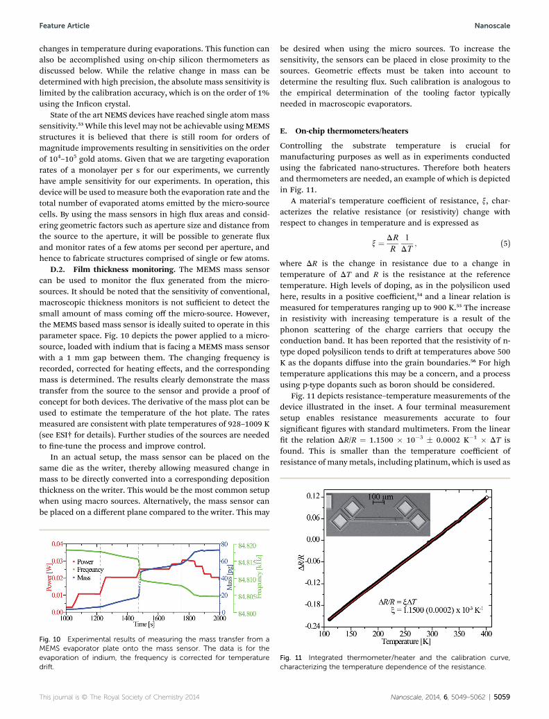
D.2. Film thickness monitoring. The MEMS mass sensorcan be used to monitor the ux generated from the micro-sources. It should be noted that the sensitivity of conventional,macroscopic thickness monitors is not sufficient to detect thesmall amount of mass coming off the micro-source. However,the MEMS based mass sensor is ideally suited to operate in thisparameter space. Fig. 10 depicts the power applied to a micro-source, loaded with indium that is facing a MEMS mass sensorwith a 1 mm gap between them. The changing frequency isrecorded, corrected for heating effects, and the correspondingmass is determined. The results clearly demonstrate the masstransfer from the source to the sensor and provide a proof ofconcept for both devices. The derivative of the mass plot can beused to estimate the temperature of the hot plate. The ratesmeasured are consistent with plate temperatures of 928–1009 K(see ESI† for details). Further studies of the sources are neededto ne-tune the process and improve control.
In an actual setup, the mass sensor can be placed on thesame die as the writer, thereby allowing measured change inmass to be directly converted into a corresponding depositionthickness on the writer. This would be the most common setupwhen using macro sources. Alternatively, the mass sensor canbe placed on a different plane compared to the writer. This may
Fig. 10 Experimental results of measuring the mass transfer from aMEMS evaporator plate onto the mass sensor. The data is for theevaporation of indium, the frequency is corrected for temperaturedrift.
This journal is © The Royal Society of Chemistry 2014
be desired when using the micro sources. To increase thesensitivity, the sensors can be placed in close proximity to thesources. Geometric effects must be taken into account todetermine the resulting ux. Such calibration is analogous tothe empirical determination of the tooling factor typicallyneeded in macroscopic evaporators.
E. On-chip thermometers/heaters
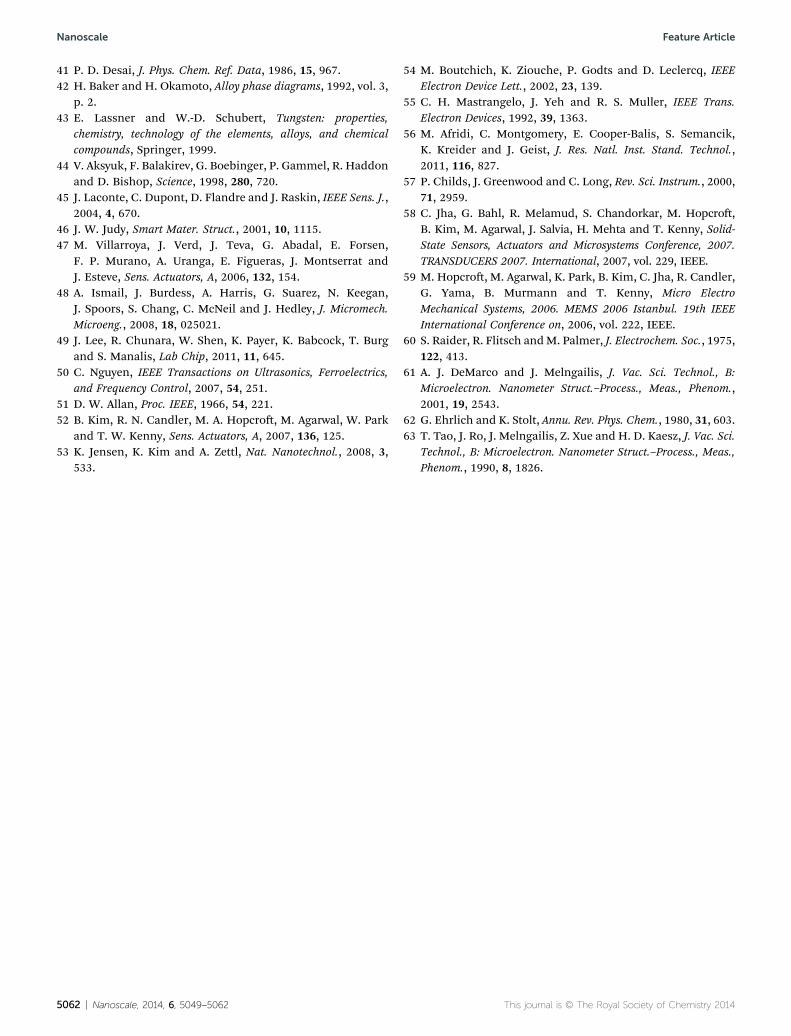
Controlling the substrate temperature is crucial formanufacturing purposes as well as in experiments conductedusing the fabricated nano-structures. Therefore both heatersand thermometers are needed, an example of which is depictedin Fig. 11.
A material's temperature coefficient of resistance, x, char-acterizes the relative resistance (or resistivity) change withrespect to changes in temperature and is expressed as
x ¼ DR
R
1
DT; (5)
where DR is the change in resistance due to a change intemperature of DT and R is the resistance at the referencetemperature. High levels of doping, as in the polysilicon usedhere, results in a positive coefficient,54 and a linear relation ismeasured for temperatures ranging up to 900 K.55 The increasein resistivity with increasing temperature is a result of thephonon scattering of the charge carriers that occupy theconduction band. It has been reported that the resistivity of n-type doped polysilicon tends to dri at temperatures above 500K as the dopants diffuse into the grain boundaries.56 For hightemperature applications this may be a concern, and a processusing p-type dopants such as boron should be considered.
Fig. 11 depicts resistance–temperature measurements of thedevice illustrated in the inset. A four terminal measurementsetup enables resistance measurements accurate to foursignicant gures with standard multimeters. From the lineart the relation DR/R ¼ 1.1500 � 10�3 � 0.0002 K�1 � DT isfound. This is smaller than the temperature coefficient ofresistance of many metals, including platinum, which is used as
Fig. 11 Integrated thermometer/heater and the calibration curve,characterizing the temperature dependence of the resistance.
Nanoscale, 2014, 6, 5049–5062 | 5059

Fig. 12 SEM image of FIB deposited platinum pads and indiumconnections deposited through (a) a static stencil and (b) a moving
Nanoscale Feature Article
a standard.57 The structures presented here can be used as boththermometers and heaters (one device for each function).Where the thermometers use the resistivity as a measure oftemperature, the same structure can be used as a resistiveheater. Typical room temperature resistances are on the orderof 300 Ohm. Consequently for 1 watt of power, the devices mustbe biased at a potential of 17.3 V.
One of the many advantages of these devices is that thestrong thermal coupling between the thermometer/heater andthe substrate allows for accurate measurements, as well as rapidresponse times. The dopant mobility may be a limiting factorwhen using the resistivity for thermometry of the MEMS evap-orators. The die as a whole is not signicantly heated aboveroom temperature during device fabrication, and the experi-ments envisioned tend to be at cryogenic temperatures. As thecalibration data shows, the thermometer performs linearlydown to 100 K. Depending on the measurement setup,temperature sensitivities of 10 mK should be readily attainable.Other on chip methods to precisely measure the temperaturecan be implemented. For example, the known temperaturedependence of the frequency shi58 (and as discussed above) orquality factor59 of a micro resonator can be used for millikelvinsensitive measurements, albeit requiring a considerably morecomplex measurement setup than for straight forward resis-tance measurements.
aperture onto the pre-positioned polysilicon leads.
F. Connecting to the outside world
To make the fabricated nano-devices electrically accessible,polysilicon leads are integrated on the die. The ends of theseleads are close to the center of the canvas and within reach ofthe writer's apertures. Conductive metal traces can be tracedfrom the poly leads to the nano-structures. In practice, one mayrst write the nano-structure and then use larger apertures toelectrically connect the device to the poly leads. This would alloccur during the same deposition session without breaking thevacuum or cycling the temperature.
Platinum pads are added to the end of the electrodes toimprove the electrical contact. These “access points” are man-ufactured using the FIB, during the same fabrication stepduring which the apertures are milled. The FIB rst mills thesurface of the silicon to remove any silicon oxide contaminationand is subsequently used to deposit the platinum pads. Theplatinum pads are important in three aspects: (1) to seal thepolysilicon from being oxidized;60 (2) to provide better electricalcontact between metal lines and polysilicon leads;61 and (3) tocreate a smooth transition from the 500 nm thick leads to thenitride canvas. Removing the surface contamination and seal-ing the poly leads with the platinum are all accomplished in asingle processing step.
Fig. 12 shows two examples of such sets of leads. In one case(Fig. 12(a)), a static stencil mask is used to deposit a four probestructure over the leads. Fig. 12(b) shows a structure fabricatedwith a moving aperture that connects two sets of poly leads withFIB deposited T-shaped platinum pads. For both depositionsthe die is cooled to 84 K, which suppresses surface diffusion,62
resulting in smoother traces. The polysilicon electrodes each
5060 | Nanoscale, 2014, 6, 5049–5062
have a resistance of �1.6 kOhm. The contacts are sensitive tothe deposition parameters63 as well as temperature, resulting ina diode-like behavior. Two probe measurements indicate a totalcircuit resistance on the order of 5 kOhm. Details, including I–Vcurves, are included in the ESI Fig. (S12).†
These experiments demonstrate that the writer can be usedto make nano-structures and the prefabricated electrodes canbe used to actuate as well as probe the fabricated devices. Thisenables experiments to be conducted with the deposition as thenal fabrication step, followed by in situ measurements. Workstill needs to be done to improve the contacts, where lowimpedance ohmic properties are desired. One may also imaginenon-contact coupling to the fabricated structures usingmagnets, capacitively, or even optically, enabling multipleexperiment methodologies. As mentioned previously, through-hole backside etching and ip-chip bonding methods can beused to place the writers above electrodes and pre-existingcircuits of far greater complexity than allowed by the poly-MUMPs process alone. Integrating this technology will greatlyexpand the capabilities of this technology.
IV. Conclusions and outlook
In this paper we have presented a methodology for creating afully integrated “Fab on a Chip”. We demonstrated all of thefunctioning elements needed to allow us to create micro-scalefactories for producing single or arrays of nano-scale devices.The heart of the approach is based on a dynamic stencil with
This journal is © The Royal Society of Chemistry 2014

Feature Article Nanoscale
FIB apertures for resist-free patterning of deep sub-micronstructures. In addition to the writers, MEMS based shutters,atom ux sources, mass sensors, and, thermometers are pre-sented. The results presented here demonstrate the precisionand control with which FoC systems can produce nano-scaledevices. It is argued, how combining multiple micro-machineswill enable patterning with individual atoms. This determin-istic, top-down fabrication method is proposed as an econom-ical method to create custom nano-devices.
This technology will enable the device fabrication made ofquench condensed lms at cryogenic temperatures. It should benoted, that while the intrinsic nitride substrate may not beparticularly clean, pre-depositing a buffer layer or using ip-chip methods described above may allow signicant control ofthe target substrate upon which the nanoscale fabricationoccurs. Furthermore, the low thermal–mechanical and –elec-trical noise provides an ideal setting for experiments, such aselectron transport studies. Predened polysilicon electrodesprovide electrical access to the fabricated structure for in situmeasurements. It is demonstrated how only three layers (onestatic two free) can be combined in practically limitless ways toactuate, sense, and probe with extraordinary sensitivity.
We believe that such Fabs on a Chip may be a viable tech-nique for both prototyping and large scale, nano-manufacturing. Such novel approaches are required to ensurethe continued validity of Moore's Law, and are hence both ofscientic and economic interest.
Acknowledgements
We would like to thank Ammar Tareen and Benjamin Cormanfor their contribution to developing the micro-sources. Thisresearch is funded in part by Boston University.
References
1 J. F. Rossier, Nat. Mater., 2013, 12, 480.2 K. Rupp and S. Selberherr, IEEE Trans. Semicond. Manuf.,2011, 24, 1.
3 TSMC Expands Investment in Taiwan with New Milestonefor Taichung GigaFab, 2013, http://www.tsmc.com/tsmcdotcom/PRListingNewsAction.do?action¼detail&language¼E&newsid¼6361.
4 T. Ito and S. Okazaki, Nature, 2000, 406, 1027.5 A. Grigorescu and C. Hagen, Nanotechnology, 2009, 20,292001.
6 J. A. Liddle and G. M. Gallatin, Nanoscale, 2011, 3, 2679.7 M. Imboden, H. Han, J. Chang, F. Pardo, C. A. Bolle,E. Lowell and D. J. Bishop, Nano Lett., 2013, 13, 3379.
8 G. Moore, Fairchild Semiconductor internal publication, 1964.9 X. Li, A. Cao, Y. J. Jung, R. Vajtai and P. M. Ajayan, Nano Lett.,2005, 5, 1997.
10 H. Park, J. Park, A. K. Lim, E. H. Anderson, A. P. Alivisatosand P. L. McEuen, Nature, 2000, 407, 57.
11 M. Fuechsle, J. A. Miwa, S. Mahapatra, H. Ryu, S. Lee,O. Warschkow, L. C. Hollenberg, G. Klimeck andM. Y. Simmons, Nat. Nanotechnol., 2012, 7, 242.
This journal is © The Royal Society of Chemistry 2014
12 M. M. Shulaker, G. Hills, N. Patil, H. Wei, H. Chen,H. P. Wong and S. Mitra, Nature, 2013, 501, 526.
13 D. Bishop and G. Dolan, Phys. Rev. Lett., 1985, 55, 2911.14 V. A. Aksyuk, B. P. Barber, P. L. Gammel and D. J. Bishop,
Micromachining and Microfabrication, International Societyfor Optics and Photonics, 1997, vol. 188.
15 M. Muranishi, K. Sato, S. Hosaka, A. Kikukawa, T. Shintaniand K. Ito, Jpn. J. Appl. Phys., Part 2, 1997, 36, L942.
16 A. Cowen, B. Hardy, R. Mahadevan and S. Wilcensk,MEMSCAP, 2013.
17 Sandia SUMMiT V, Sandia, 2012.18 A. Cowen, G. Hames, D. Monk, S. Wilcenski and B. Hardy,
PolyMUMPs design handbook, MEMSCAP Inc., 2009.19 M. M. Deshmukh, D. Ralph, M. Thomas and J. Silcox, Appl.
Phys. Lett., 1999, 75, 1631.20 M. Van Den Boogaart, G. Kim, R. Pellens, J. Van Den Heuvel
and J. Brugger, J. Vac. Sci. Technol., B: Microelectron.Nanometer Struct.–Process., Meas., Phenom., 2004, 22, 3174.
21 S. Egger, A. Ilie, Y. Fu, J. Chongsathien, D. Kang andM. E. Welland, Nano Lett., 2005, 5, 15.
22 R. Luthi, R. R. Schlittler, J. Brugger, P. Vettiger,M. E. Welland and J. K. Gimzewski, Appl. Phys. Lett., 1999,75, 1314.
23 A. Champagne, A. Couture, F. Kuemmeth and D. Ralph,Appl. Phys. Lett., 2003, 82, 1111.
24 V. Savu, S. Xie and J. Brugger, Nanoscale, 2011, 3, 2739.25 W. Lee, M. Yang, A. R. Laracuente, W. P. King, L. J. Whitman
and P. E. Sheehan, Beilstein J. Nanotechnol., 2012, 3, 52.26 A. Meister, M. Liley, J. Brugger, R. Pugin and
H. Heinzelmann, Appl. Phys. Lett., 2004, 85, 6260.27 R. Garcia, R. V. Martinez and J. Martinez, Chem. Soc. Rev.,
2005, 35, 29.28 A. A. Tseng, Nano Today, 2011, 6, 493.29 P. S. Waggoner and H. G. Craighead, Lab Chip, 2007, 7, 1238.30 M. Imboden, J. Morrison, E. Lowell, H. Han and D. J. Bishop,
JMEMS, 2014, 99, 1.31 S. Xie, V. Savu and J. Brugger, Solid-State Sensors, Actuators
and Microsystems Conference (TRANSDUCERS), 2011 16thInternational, 2011, vol. 998, IEEE.
32 A. Storm, J. Chen, X. Ling, H. Zandbergen and C. Dekker,Nat. Mater., 2003, 2, 537.
33 M. Aziz, J. Golovchenko, D. Branton, C. McMullan, D. Steinand J. Li, Nature, 2001, 412, 166.
34 R. Syms, H. Zou, J. Stagg and H. Veladi, J. Micromech.Microeng., 2004, 14, 1700.
35 B. Borovic, A. Liu, D. Popa, H. Cai and F. Lewis, J. Micromech.Microeng., 2005, 15, 1917.
36 R. Krpoun, K. L. Smith, J. P. Stark and H. Shea, Appl. Phys.Lett., 2009, 94, 163502.
37 B. d. Heij, C. Steinert, H. Sandmaier and R. Zengerle, Sens.Actuators, A, 2003, 103, 88.
38 P. Galambos, D. Czaplewski, R. Givler, K. R. Pohl, D. L. Luck,G. Benavides and B. Jokiel, Sens. Actuators, A, 2008, 141, 182.
39 M. W. Roberts and C. S. McKee, Chemistry of the metal-gasinterface, Oxford Univ. Press, Oxford, 1978.
40 C. Alcock, V. Itkin andM. Horrigan, Can. Metall. Q., 1984, 23,309.
Nanoscale, 2014, 6, 5049–5062 | 5061
Nanoscale Feature Article
41 P. D. Desai, J. Phys. Chem. Ref. Data, 1986, 15, 967.42 H. Baker and H. Okamoto, Alloy phase diagrams, 1992, vol. 3,
p. 2.43 E. Lassner and W.-D. Schubert, Tungsten: properties,
chemistry, technology of the elements, alloys, and chemicalcompounds, Springer, 1999.
44 V. Aksyuk, F. Balakirev, G. Boebinger, P. Gammel, R. Haddonand D. Bishop, Science, 1998, 280, 720.
45 J. Laconte, C. Dupont, D. Flandre and J. Raskin, IEEE Sens. J.,2004, 4, 670.
46 J. W. Judy, Smart Mater. Struct., 2001, 10, 1115.47 M. Villarroya, J. Verd, J. Teva, G. Abadal, E. Forsen,
F. P. Murano, A. Uranga, E. Figueras, J. Montserrat andJ. Esteve, Sens. Actuators, A, 2006, 132, 154.
48 A. Ismail, J. Burdess, A. Harris, G. Suarez, N. Keegan,J. Spoors, S. Chang, C. McNeil and J. Hedley, J. Micromech.Microeng., 2008, 18, 025021.
49 J. Lee, R. Chunara, W. Shen, K. Payer, K. Babcock, T. Burgand S. Manalis, Lab Chip, 2011, 11, 645.
50 C. Nguyen, IEEE Transactions on Ultrasonics, Ferroelectrics,and Frequency Control, 2007, 54, 251.
51 D. W. Allan, Proc. IEEE, 1966, 54, 221.52 B. Kim, R. N. Candler, M. A. Hopcro, M. Agarwal, W. Park
and T. W. Kenny, Sens. Actuators, A, 2007, 136, 125.53 K. Jensen, K. Kim and A. Zettl, Nat. Nanotechnol., 2008, 3,
533.
5062 | Nanoscale, 2014, 6, 5049–5062
54 M. Boutchich, K. Ziouche, P. Godts and D. Leclercq, IEEEElectron Device Lett., 2002, 23, 139.
55 C. H. Mastrangelo, J. Yeh and R. S. Muller, IEEE Trans.Electron Devices, 1992, 39, 1363.
56 M. Afridi, C. Montgomery, E. Cooper-Balis, S. Semancik,K. Kreider and J. Geist, J. Res. Natl. Inst. Stand. Technol.,2011, 116, 827.
57 P. Childs, J. Greenwood and C. Long, Rev. Sci. Instrum., 2000,71, 2959.
58 C. Jha, G. Bahl, R. Melamud, S. Chandorkar, M. Hopcro,B. Kim, M. Agarwal, J. Salvia, H. Mehta and T. Kenny, Solid-State Sensors, Actuators and Microsystems Conference, 2007.TRANSDUCERS 2007. International, 2007, vol. 229, IEEE.
59 M. Hopcro, M. Agarwal, K. Park, B. Kim, C. Jha, R. Candler,G. Yama, B. Murmann and T. Kenny, Micro ElectroMechanical Systems, 2006. MEMS 2006 Istanbul. 19th IEEEInternational Conference on, 2006, vol. 222, IEEE.
60 S. Raider, R. Flitsch andM. Palmer, J. Electrochem. Soc., 1975,122, 413.
61 A. J. DeMarco and J. Melngailis, J. Vac. Sci. Technol., B:Microelectron. Nanometer Struct.–Process., Meas., Phenom.,2001, 19, 2543.
62 G. Ehrlich and K. Stolt, Annu. Rev. Phys. Chem., 1980, 31, 603.63 T. Tao, J. Ro, J. Melngailis, Z. Xue and H. D. Kaesz, J. Vac. Sci.
Technol., B: Microelectron. Nanometer Struct.–Process., Meas.,Phenom., 1990, 8, 1826.
This journal is © The Royal Society of Chemistry 2014