off-State Degradation in Drain-Extended NMOS Transistors: Interface Damage and Correlation to...
10
IEEE TRANSACTIONS ON ELECTRON DEVICES, VOL. 54, NO. 10, OCTOBER 2007 2669 OFF -State Degradation in Drain-Extended NMOS Transistors: Interface Damage and Correlation to Dielectric Breakdown Dhanoop Varghese, Student Member, IEEE, Haldun Kufluoglu, Student Member, IEEE, Vijay Reddy, Hisashi Shichijo, Dan Mosher, Member, IEEE, Srikanth Krishnan, Associate Member, IEEE, and Muhammad Ashraful Alam, Fellow, IEEE Abstract—OFF-state degradation in drain-extended NMOS transistors is studied. Carefully designed experiments and well- calibrated simulations show that hot carriers, which are generated by impact ionization of surface band-to-band tunneling current, are responsible for interface damage during OFF-state stress. Classical ON-state hot carrier degradation has historically been associated with broken ≡ Si–H bonds at the Si/SiO 2 interface. In contrast, the OFF-state degradation in drain-extended devices is shown to be due to broken ≡ Si–O– bonds. The resultant degradation is universal, which enables a long-term extrapolation of device degradation at operating bias conditions based on short- term stress data. Time evolution of degradation due to broken ≡ Si–O– bonds and the resultant universal behavior is ex- plained by a bond-dispersion model. Finally, we show that, under OFF-state stress conditions, the interface damage that is measured by charge-pumping technique is correlated with dielectric break- down time, as both of them are driven by broken ≡ Si–O– bonds. Index Terms—Bond-dispersion (B-D) model, drain-extended devices, gate dielectric breakdown, hot carrier degradation, interface damage, OFF-state degradation, Si–O bonds, universal degradation. I. INTRODUCTION T HE DEVICE dimension and supply voltage for the core logic and memory transistors have been scaled down sys- tematically over the last few decades. This, however, is not the case for input/output (IO) devices (e.g., LDMOS, DeMOS, etc. [1]–[3]) that interface ICs to the outside world and, therefore, must continue to operate at supply voltages higher than that of core transistors. Such high operating biases often lead to unique reliability issues which are different from the core transistors and which cannot be understood in terms of uncorrelated combinations of classical theories of NBTI, hot carrier injec- tion (HCI), or time-dependent dielectric breakdown (TDDB) [4], [5]. This makes the lifetime estimations of IO transistors particularly difficult and sometimes overly conservative. Manuscript received April 24, 2007; revised June 26, 2007. The review of this paper was arranged by Editor J. Suehle. D. Varghese, H. Kufluoglu, and M. A. Alam are with Purdue University, West Lafayette, IN 47907 USA (e-mail: [email protected]). V. Reddy, H. Shichijo, D. Mosher, and S. Krishnan are with the Texas Instruments Inc., Dallas, TX 75243 USA. Color versions of one or more of the figures in this paper are available online at http://ieeexplore.ieee.org. Digital Object Identifier 10.1109/TED.2007.904587 Hot carrier degradation (HCI) has been a major issue for core transistors since the early 1980s, when the device dimensions started shrinking while the supply voltage (V DD ) remained at 5 V [6]. However, HCI is a voltage-driven (but not a field driven) phenomenon; therefore, by mid 1990s, it ceased being a dominant degradation mode as V DD was scaled down from 5 V. Classical hot carrier is an extensively studied topic, with the following well-known characteristics: 1) Hot carriers that are responsible for the damage are due to impact ionization (II) of source current, and the degradation is found to maximize at peak substrate current (I B ) stress conditions (V G ≈ V D /2) corresponding to peak hot carrier generation [7]–[11]. 2) Inter- face damage during the stress is known to have a power law behavior (∆N IT = At n ), with the time exponent n close to 0.5 [11]–[14]. 3) A fraction of damage that is generated during classical hot carrier stress is found to recover on the removal of the stress conditions [13], [14]. 4) The degradation is believed to be due to broken ≡ Si–H bonds at the Si/SiO 2 interface, as confirmed by the isotope effect observed during the stress [11], [15]. 5) The classical hot carrier degradation shows no cor- relation with the dielectric breakdown (TDDB, [16]–[18]), pre- sumably because TDDB results from broken ≡ Si–O– bonds. However, some recent reports show that oxide degradation can indeed occur during hot carrier stress conditions [19], [20]. In this paper (expanded version of the study in [21]), we study the reliability of drain-extended NMOS (DeNMOS) tran- sistors subjected to OFF-state hot carrier stress (V G = 0 V, V D > 5 V), and we find that the characteristics of this degra- dation are distinct and unique compared to classical ON-state HCI. It has been hypothesized that an interface damage during OFF-state operation is due to generation of hot carriers by the high electric field localized near the drain end, and their subsequent injection into the gate oxide. However, unlike the classical ON-state hot carrier degradation where hot carriers are generated by the II of source current, the source current that flows in OFF-state is just the subthreshold leakage and might not be a significant source for hot carriers. Second, the interface trap generation during OFF-state degradation is found to have high time exponents (n ≈ 0.7–0.8), which are higher compared to that obtained during classical ON-state studies (n ≈ 0.5). In addition, unlike the classical ON-state hot carrier stress, the interface traps that are generated during the OFF-state stress do not recover on the removal of the stress 0018-9383/$25.00 © 2007 IEEE
-
Upload
independent -
Category
Documents
-
view
2 -
download
0
Transcript of off-State Degradation in Drain-Extended NMOS Transistors: Interface Damage and Correlation to...
IEEE TRANSACTIONS ON ELECTRON DEVICES, VOL. 54, NO. 10, OCTOBER 2007 2669
OFF-State Degradation in Drain-Extended NMOSTransistors: Interface Damage and Correlation
to Dielectric BreakdownDhanoop Varghese, Student Member, IEEE, Haldun Kufluoglu, Student Member, IEEE, Vijay Reddy,
Hisashi Shichijo, Dan Mosher, Member, IEEE, Srikanth Krishnan, Associate Member, IEEE, andMuhammad Ashraful Alam, Fellow, IEEE
Abstract—OFF-state degradation in drain-extended NMOStransistors is studied. Carefully designed experiments and well-calibrated simulations show that hot carriers, which are generatedby impact ionization of surface band-to-band tunneling current,are responsible for interface damage during OFF-state stress.Classical ON-state hot carrier degradation has historically beenassociated with broken ≡ Si–H bonds at the Si/SiO2 interface.In contrast, the OFF-state degradation in drain-extended devicesis shown to be due to broken ≡ Si–O– bonds. The resultantdegradation is universal, which enables a long-term extrapolationof device degradation at operating bias conditions based on short-term stress data. Time evolution of degradation due to broken≡ Si–O– bonds and the resultant universal behavior is ex-plained by a bond-dispersion model. Finally, we show that, underOFF-state stress conditions, the interface damage that is measuredby charge-pumping technique is correlated with dielectric break-down time, as both of them are driven by broken ≡ Si–O– bonds.
Index Terms—Bond-dispersion (B-D) model, drain-extendeddevices, gate dielectric breakdown, hot carrier degradation,interface damage, OFF-state degradation, Si–O bonds, universaldegradation.
I. INTRODUCTION
THE DEVICE dimension and supply voltage for the corelogic and memory transistors have been scaled down sys-
tematically over the last few decades. This, however, is not thecase for input/output (IO) devices (e.g., LDMOS, DeMOS, etc.[1]–[3]) that interface ICs to the outside world and, therefore,must continue to operate at supply voltages higher than that ofcore transistors. Such high operating biases often lead to uniquereliability issues which are different from the core transistorsand which cannot be understood in terms of uncorrelatedcombinations of classical theories of NBTI, hot carrier injec-tion (HCI), or time-dependent dielectric breakdown (TDDB)[4], [5]. This makes the lifetime estimations of IO transistorsparticularly difficult and sometimes overly conservative.
Manuscript received April 24, 2007; revised June 26, 2007. The review ofthis paper was arranged by Editor J. Suehle.
D. Varghese, H. Kufluoglu, and M. A. Alam are with Purdue University, WestLafayette, IN 47907 USA (e-mail: [email protected]).
V. Reddy, H. Shichijo, D. Mosher, and S. Krishnan are with the TexasInstruments Inc., Dallas, TX 75243 USA.
Color versions of one or more of the figures in this paper are available onlineat http://ieeexplore.ieee.org.
Digital Object Identifier 10.1109/TED.2007.904587
Hot carrier degradation (HCI) has been a major issue for coretransistors since the early 1980s, when the device dimensionsstarted shrinking while the supply voltage (VDD) remained at5 V [6]. However, HCI is a voltage-driven (but not a fielddriven) phenomenon; therefore, by mid 1990s, it ceased beinga dominant degradation mode as VDD was scaled down from5 V. Classical hot carrier is an extensively studied topic, withthe following well-known characteristics: 1) Hot carriers thatare responsible for the damage are due to impact ionization (II)of source current, and the degradation is found to maximizeat peak substrate current (IB) stress conditions (VG ≈ VD/2)corresponding to peak hot carrier generation [7]–[11]. 2) Inter-face damage during the stress is known to have a power lawbehavior (∆NIT = Atn), with the time exponent n close to 0.5[11]–[14]. 3) A fraction of damage that is generated duringclassical hot carrier stress is found to recover on the removal ofthe stress conditions [13], [14]. 4) The degradation is believedto be due to broken ≡ Si–H bonds at the Si/SiO2 interface,as confirmed by the isotope effect observed during the stress[11], [15]. 5) The classical hot carrier degradation shows no cor-relation with the dielectric breakdown (TDDB, [16]–[18]), pre-sumably because TDDB results from broken ≡ Si–O– bonds.However, some recent reports show that oxide degradation canindeed occur during hot carrier stress conditions [19], [20].
In this paper (expanded version of the study in [21]), westudy the reliability of drain-extended NMOS (DeNMOS) tran-sistors subjected to OFF-state hot carrier stress (VG = 0 V,VD > 5 V), and we find that the characteristics of this degra-dation are distinct and unique compared to classical ON-stateHCI. It has been hypothesized that an interface damage duringOFF-state operation is due to generation of hot carriers bythe high electric field localized near the drain end, and theirsubsequent injection into the gate oxide. However, unlike theclassical ON-state hot carrier degradation where hot carriersare generated by the II of source current, the source currentthat flows in OFF-state is just the subthreshold leakage andmight not be a significant source for hot carriers. Second,the interface trap generation during OFF-state degradation isfound to have high time exponents (n ≈ 0.7–0.8), which arehigher compared to that obtained during classical ON-statestudies (n ≈ 0.5). In addition, unlike the classical ON-state hotcarrier stress, the interface traps that are generated during theOFF-state stress do not recover on the removal of the stress
0018-9383/$25.00 © 2007 IEEE
2670 IEEE TRANSACTIONS ON ELECTRON DEVICES, VOL. 54, NO. 10, OCTOBER 2007
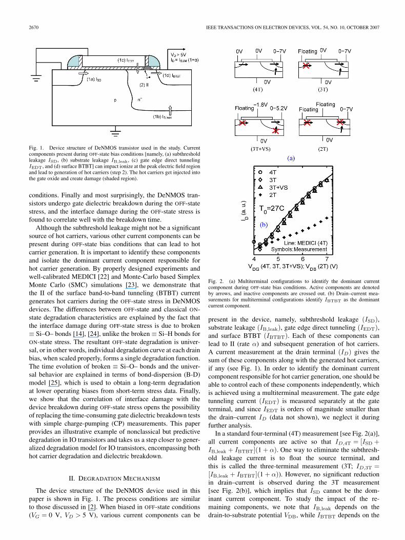
Fig. 1. Device structure of DeNMOS transistor used in the study. Currentcomponents present during OFF-state bias conditions [namely, (a) subthresholdleakage ISD, (b) substrate leakage IB,leak, (c) gate edge direct tunnelingIEDT, and (d) surface BTBT] can impact ionize at the peak electric field regionand lead to generation of hot carriers (step 2). The hot carriers get injected intothe gate oxide and create damage (shaded region).
conditions. Finally and most surprisingly, the DeNMOS tran-sistors undergo gate dielectric breakdown during the OFF-statestress, and the interface damage during the OFF-state stress isfound to correlate well with the breakdown time.
Although the subthreshold leakage might not be a significantsource of hot carriers, various other current components can bepresent during OFF-state bias conditions that can lead to hotcarrier generation. It is important to identify these componentsand isolate the dominant current component responsible forhot carrier generation. By properly designed experiments andwell-calibrated MEDICI [22] and Monte-Carlo based SimplexMonte Carlo (SMC) simulations [23], we demonstrate thatthe II of the surface band-to-band tunneling (BTBT) currentgenerates hot carriers during the OFF-state stress in DeNMOSdevices. The differences between OFF-state and classical ON-state degradation characteristics are explained by the fact thatthe interface damage during OFF-state stress is due to broken≡ Si–O– bonds [14], [24], unlike the broken ≡ Si–H bonds forON-state stress. The resultant OFF-state degradation is univer-sal, or in other words, individual degradation curve at each drainbias, when scaled properly, forms a single degradation function.The time evolution of broken ≡ Si–O– bonds and the univer-sal behavior are explained in terms of bond-dispersion (B-D)model [25], which is used to obtain a long-term degradationat lower operating biases from short-term stress data. Finally,we show that the correlation of interface damage with thedevice breakdown during OFF-state stress opens the possibilityof replacing the time-consuming gate dielectric breakdown testswith simple charge-pumping (CP) measurements. This paperprovides an illustrative example of nonclassical but predictivedegradation in IO transistors and takes us a step closer to gener-alized degradation model for IO transistors, encompassing bothhot carrier degradation and dielectric breakdown.
II. DEGRADATION MECHANISM
The device structure of the DeNMOS device used in thispaper is shown in Fig. 1. The process conditions are similarto those discussed in [2]. When biased in OFF-state conditions(VG = 0 V, VD > 5 V), various current components can be
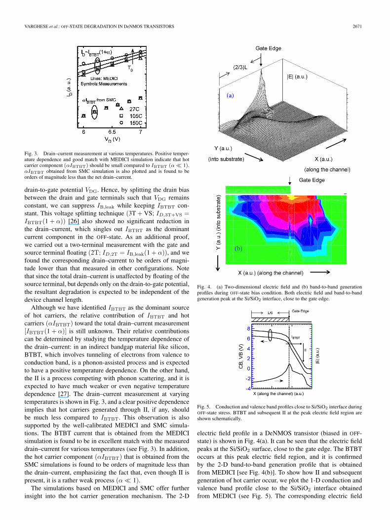
Fig. 2. (a) Multiterminal configurations to identify the dominant currentcomponent during OFF-state bias conditions. Active components are denotedby arrows, and inactive components are crossed out. (b) Drain–current mea-surements for multiterminal configurations identify IBTBT as the dominantcurrent component.
present in the device, namely, subthreshold leakage (ISD),substrate leakage (IB,leak), gate edge direct tunneling (IEDT),and surface BTBT (IBTBT). Each of these components canlead to II (rate α) and subsequent generation of hot carriers.A current measurement at the drain terminal (ID) gives thesum of these components along with the generated hot carriers,if any (see Fig. 1). In order to identify the dominant currentcomponent responsible for hot carrier generation, one should beable to control each of these components independently, whichis achieved using a multiterminal measurement. The gate edgetunneling current (IEDT) is measured separately at the gateterminal, and since IEDT is orders of magnitude smaller thanthe drain–current ID (data not shown), we neglect it duringfurther analysis.
In a standard four-terminal (4T) measurement [see Fig. 2(a)],all current components are active so that ID,4T = [ISD +IB,leak + IBTBT](1 + α). One way to eliminate the subthresh-old leakage current is to float the source terminal, andthis is called the three-terminal measurement (3T; ID,3T =[IB,leak + IBTBT](1 + α)). However, no significant reductionin drain–current is observed during the 3T measurement[see Fig. 2(b)], which implies that ISD cannot be the dom-inant current component. To study the impact of the re-maining components, we note that IB,leak depends on thedrain-to-substrate potential VDB, while IBTBT depends on the
VARGHESE et al.: OFF-STATE DEGRADATION IN DeNMOS TRANSISTORS 2671
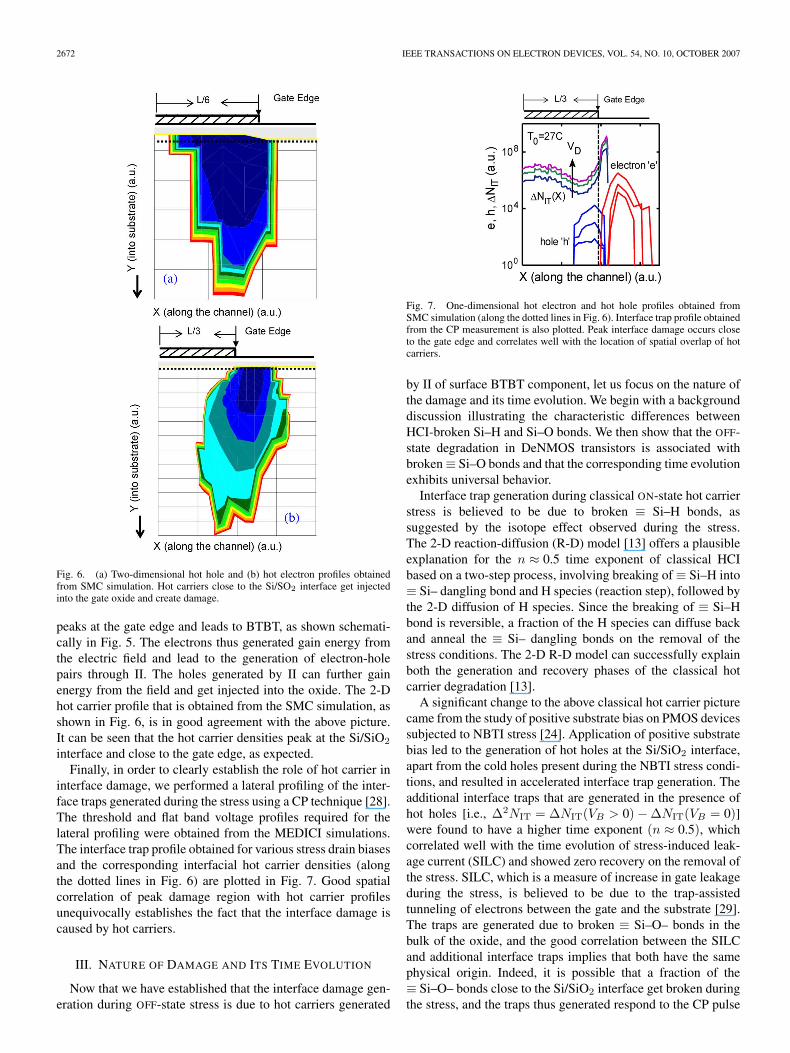
Fig. 3. Drain–current measurement at various temperatures. Positive temper-ature dependence and good match with MEDICI simulation indicate that hotcarrier component (αIBTBT) should be small compared to IBTBT (α � 1).αIBTBT obtained from SMC simulation is also plotted and is found to beorders of magnitude less than the net drain–current.
drain-to-gate potential VDG. Hence, by splitting the drain biasbetween the drain and gate terminals such that VDG remainsconstant, we can suppress IB,leak while keeping IBTBT con-stant. This voltage splitting technique (3T + VS; ID,3T+VS =IBTBT(1 + α)) [26] also showed no significant reduction inthe drain–current, which singles out IBTBT as the dominantcurrent component in the OFF-state. As an additional proof,we carried out a two-terminal measurement with the gate andsource terminal floating (2T; ID,2T = IB,leak(1 + α)), and wefound the corresponding drain–current to be orders of magni-tude lower than that measured in other configurations. Notethat since the total drain–current is unaffected by floating of thesource terminal, but depends only on the drain-to-gate potential,the resultant degradation is expected to be independent of thedevice channel length.
Although we have identified IBTBT as the dominant sourceof hot carriers, the relative contribution of IBTBT and hotcarriers (αIBTBT) toward the total drain–current measurement[IBTBT(1 + α)] is still unknown. Their relative contributionscan be determined by studying the temperature dependence ofthe drain–current: in an indirect bandgap material like silicon,BTBT, which involves tunneling of electrons from valence toconduction band, is a phonon-assisted process and is expectedto have a positive temperature dependence. On the other hand,the II is a process competing with phonon scattering, and it isexpected to have much weaker or even negative temperaturedependence [27]. The drain–current measurement at varyingtemperatures is shown in Fig. 3, and a clear positive dependenceimplies that hot carriers generated through II, if any, shouldbe much less compared to IBTBT. This observation is alsosupported by the well-calibrated MEDICI and SMC simula-tions. The BTBT current that is obtained from the MEDICIsimulation is found to be in excellent match with the measureddrain–current for various temperatures (see Fig. 3). In addition,the hot carrier component (αIBTBT) that is obtained from theSMC simulations is found to be orders of magnitude less thanthe drain–current, emphasizing the fact that, even though II ispresent, it is a rather weak process (α � 1).
The simulations based on MEDICI and SMC offer furtherinsight into the hot carrier generation mechanism. The 2-D
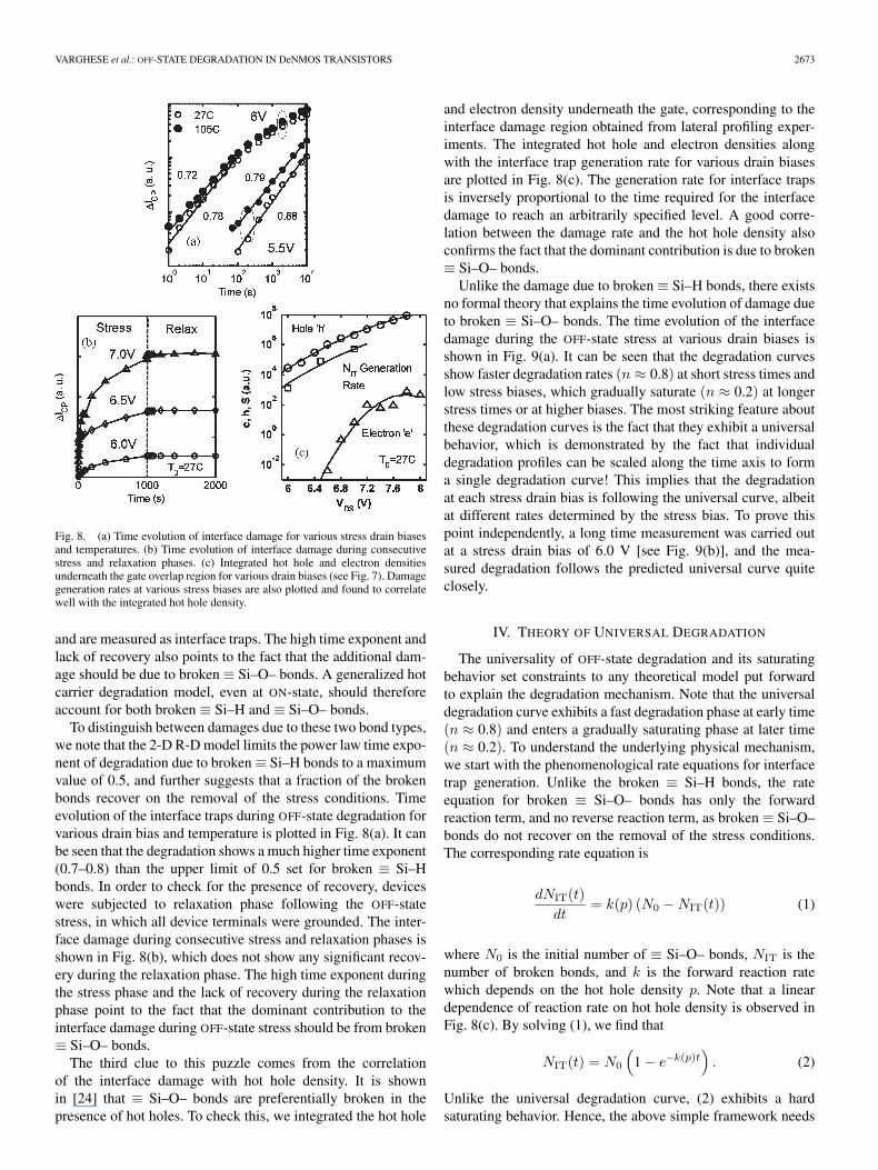
Fig. 4. (a) Two-dimensional electric field and (b) band-to-band generationprofiles during OFF-state bias condition. Both electric field and band-to-bandgeneration peak at the Si/SiO2 interface, close to the gate edge.
Fig. 5. Conduction and valence band profiles close to Si/SiO2 interface duringOFF-state stress. BTBT and subsequent II at the peak electric field region areshown schematically.
electric field profile in a DeNMOS transistor (biased in OFF-state) is shown in Fig. 4(a). It can be seen that the electric fieldpeaks at the Si/SiO2 surface, close to the gate edge. The BTBToccurs at this peak electric field region, and it is confirmedby the 2-D band-to-band generation profile that is obtainedfrom MEDICI [see Fig. 4(b)]. To show how II and subsequentgeneration of hot carrier occur, we plot the 1-D conduction andvalence band profile close to the Si/SiO2 interface obtainedfrom MEDICI (see Fig. 5). The corresponding electric field
2672 IEEE TRANSACTIONS ON ELECTRON DEVICES, VOL. 54, NO. 10, OCTOBER 2007
Fig. 6. (a) Two-dimensional hot hole and (b) hot electron profiles obtainedfrom SMC simulation. Hot carriers close to the Si/SO2 interface get injectedinto the gate oxide and create damage.
peaks at the gate edge and leads to BTBT, as shown schemati-cally in Fig. 5. The electrons thus generated gain energy fromthe electric field and lead to the generation of electron-holepairs through II. The holes generated by II can further gainenergy from the field and get injected into the oxide. The 2-Dhot carrier profile that is obtained from the SMC simulation, asshown in Fig. 6, is in good agreement with the above picture.It can be seen that the hot carrier densities peak at the Si/SiO2
interface and close to the gate edge, as expected.Finally, in order to clearly establish the role of hot carrier in
interface damage, we performed a lateral profiling of the inter-face traps generated during the stress using a CP technique [28].The threshold and flat band voltage profiles required for thelateral profiling were obtained from the MEDICI simulations.The interface trap profile obtained for various stress drain biasesand the corresponding interfacial hot carrier densities (alongthe dotted lines in Fig. 6) are plotted in Fig. 7. Good spatialcorrelation of peak damage region with hot carrier profilesunequivocally establishes the fact that the interface damage iscaused by hot carriers.
III. NATURE OF DAMAGE AND ITS TIME EVOLUTION
Now that we have established that the interface damage gen-eration during OFF-state stress is due to hot carriers generated
Fig. 7. One-dimensional hot electron and hot hole profiles obtained fromSMC simulation (along the dotted lines in Fig. 6). Interface trap profile obtainedfrom the CP measurement is also plotted. Peak interface damage occurs closeto the gate edge and correlates well with the location of spatial overlap of hotcarriers.
by II of surface BTBT component, let us focus on the nature ofthe damage and its time evolution. We begin with a backgrounddiscussion illustrating the characteristic differences betweenHCI-broken Si–H and Si–O bonds. We then show that the OFF-state degradation in DeNMOS transistors is associated withbroken ≡ Si–O bonds and that the corresponding time evolutionexhibits universal behavior.
Interface trap generation during classical ON-state hot carrierstress is believed to be due to broken ≡ Si–H bonds, assuggested by the isotope effect observed during the stress.The 2-D reaction-diffusion (R-D) model [13] offers a plausibleexplanation for the n ≈ 0.5 time exponent of classical HCIbased on a two-step process, involving breaking of ≡ Si–H into≡ Si– dangling bond and H species (reaction step), followed bythe 2-D diffusion of H species. Since the breaking of ≡ Si–Hbond is reversible, a fraction of the H species can diffuse backand anneal the ≡ Si– dangling bonds on the removal of thestress conditions. The 2-D R-D model can successfully explainboth the generation and recovery phases of the classical hotcarrier degradation [13].
A significant change to the above classical hot carrier picturecame from the study of positive substrate bias on PMOS devicessubjected to NBTI stress [24]. Application of positive substratebias led to the generation of hot holes at the Si/SiO2 interface,apart from the cold holes present during the NBTI stress condi-tions, and resulted in accelerated interface trap generation. Theadditional interface traps that are generated in the presence ofhot holes [i.e., ∆2NIT = ∆NIT(VB > 0) − ∆NIT(VB = 0)]were found to have a higher time exponent (n ≈ 0.5), whichcorrelated well with the time evolution of stress-induced leak-age current (SILC) and showed zero recovery on the removal ofthe stress. SILC, which is a measure of increase in gate leakageduring the stress, is believed to be due to the trap-assistedtunneling of electrons between the gate and the substrate [29].The traps are generated due to broken ≡ Si–O– bonds in thebulk of the oxide, and the good correlation between the SILCand additional interface traps implies that both have the samephysical origin. Indeed, it is possible that a fraction of the≡ Si–O– bonds close to the Si/SiO2 interface get broken duringthe stress, and the traps thus generated respond to the CP pulse
VARGHESE et al.: OFF-STATE DEGRADATION IN DeNMOS TRANSISTORS 2673
Fig. 8. (a) Time evolution of interface damage for various stress drain biasesand temperatures. (b) Time evolution of interface damage during consecutivestress and relaxation phases. (c) Integrated hot hole and electron densitiesunderneath the gate overlap region for various drain biases (see Fig. 7). Damagegeneration rates at various stress biases are also plotted and found to correlatewell with the integrated hot hole density.
and are measured as interface traps. The high time exponent andlack of recovery also points to the fact that the additional dam-age should be due to broken ≡ Si–O– bonds. A generalized hotcarrier degradation model, even at ON-state, should thereforeaccount for both broken ≡ Si–H and ≡ Si–O– bonds.
To distinguish between damages due to these two bond types,we note that the 2-D R-D model limits the power law time expo-nent of degradation due to broken ≡ Si–H bonds to a maximumvalue of 0.5, and further suggests that a fraction of the brokenbonds recover on the removal of the stress conditions. Timeevolution of the interface traps during OFF-state degradation forvarious drain bias and temperature is plotted in Fig. 8(a). It canbe seen that the degradation shows a much higher time exponent(0.7–0.8) than the upper limit of 0.5 set for broken ≡ Si–Hbonds. In order to check for the presence of recovery, deviceswere subjected to relaxation phase following the OFF-statestress, in which all device terminals were grounded. The inter-face damage during consecutive stress and relaxation phases isshown in Fig. 8(b), which does not show any significant recov-ery during the relaxation phase. The high time exponent duringthe stress phase and the lack of recovery during the relaxationphase point to the fact that the dominant contribution to theinterface damage during OFF-state stress should be from broken≡ Si–O– bonds.
The third clue to this puzzle comes from the correlationof the interface damage with hot hole density. It is shownin [24] that ≡ Si–O– bonds are preferentially broken in thepresence of hot holes. To check this, we integrated the hot hole
and electron density underneath the gate, corresponding to theinterface damage region obtained from lateral profiling exper-iments. The integrated hot hole and electron densities alongwith the interface trap generation rate for various drain biasesare plotted in Fig. 8(c). The generation rate for interface trapsis inversely proportional to the time required for the interfacedamage to reach an arbitrarily specified level. A good corre-lation between the damage rate and the hot hole density alsoconfirms the fact that the dominant contribution is due to broken≡ Si–O– bonds.
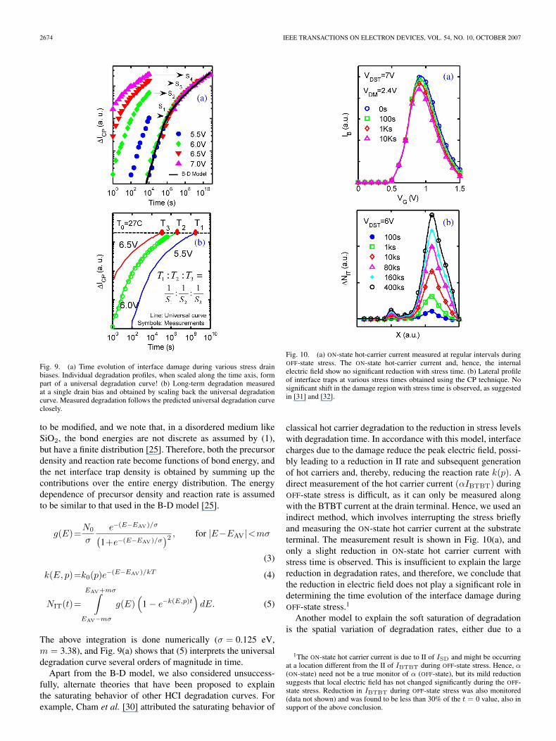
Unlike the damage due to broken ≡ Si–H bonds, there existsno formal theory that explains the time evolution of damage dueto broken ≡ Si–O– bonds. The time evolution of the interfacedamage during the OFF-state stress at various drain biases isshown in Fig. 9(a). It can be seen that the degradation curvesshow faster degradation rates (n ≈ 0.8) at short stress times andlow stress biases, which gradually saturate (n ≈ 0.2) at longerstress times or at higher biases. The most striking feature aboutthese degradation curves is the fact that they exhibit a universalbehavior, which is demonstrated by the fact that individualdegradation profiles can be scaled along the time axis to forma single degradation curve! This implies that the degradationat each stress drain bias is following the universal curve, albeitat different rates determined by the stress bias. To prove thispoint independently, a long time measurement was carried outat a stress drain bias of 6.0 V [see Fig. 9(b)], and the mea-sured degradation follows the predicted universal curve quiteclosely.
IV. THEORY OF UNIVERSAL DEGRADATION
The universality of OFF-state degradation and its saturatingbehavior set constraints to any theoretical model put forwardto explain the degradation mechanism. Note that the universaldegradation curve exhibits a fast degradation phase at early time(n ≈ 0.8) and enters a gradually saturating phase at later time(n ≈ 0.2). To understand the underlying physical mechanism,we start with the phenomenological rate equations for interfacetrap generation. Unlike the broken ≡ Si–H bonds, the rateequation for broken ≡ Si–O– bonds has only the forwardreaction term, and no reverse reaction term, as broken ≡ Si–O–bonds do not recover on the removal of the stress conditions.The corresponding rate equation is
dNIT(t)dt
= k(p) (N0 − NIT(t)) (1)
where N0 is the initial number of ≡ Si–O– bonds, NIT is thenumber of broken bonds, and k is the forward reaction ratewhich depends on the hot hole density p. Note that a lineardependence of reaction rate on hot hole density is observed inFig. 8(c). By solving (1), we find that
NIT(t) = N0
(1 − e−k(p)t
). (2)
Unlike the universal degradation curve, (2) exhibits a hardsaturating behavior. Hence, the above simple framework needs
2674 IEEE TRANSACTIONS ON ELECTRON DEVICES, VOL. 54, NO. 10, OCTOBER 2007
Fig. 9. (a) Time evolution of interface damage during various stress drainbiases. Individual degradation profiles, when scaled along the time axis, formpart of a universal degradation curve! (b) Long-term degradation measuredat a single drain bias and obtained by scaling back the universal degradationcurve. Measured degradation follows the predicted universal degradation curveclosely.
to be modified, and we note that, in a disordered medium likeSiO2, the bond energies are not discrete as assumed by (1),but have a finite distribution [25]. Therefore, both the precursordensity and reaction rate become functions of bond energy, andthe net interface trap density is obtained by summing up thecontributions over the entire energy distribution. The energydependence of precursor density and reaction rate is assumedto be similar to that used in the B-D model [25].
g(E)=N0
σ
e−(E−EAV)/σ
(1+e−(E−EAV)/σ
)2 , for |E−EAV|<mσ
(3)
k(E, p)=k0(p)e−(E−EAV)/kT (4)
NIT(t)=
EAV+mσ∫
EAV−mσ
g(E)(
1 − e−k(E,p)t)
dE. (5)
The above integration is done numerically (σ = 0.125 eV,m = 3.38), and Fig. 9(a) shows that (5) interprets the universaldegradation curve several orders of magnitude in time.
Apart from the B-D model, we also considered unsuccess-fully, alternate theories that have been proposed to explainthe saturating behavior of other HCI degradation curves. Forexample, Cham et al. [30] attributed the saturating behavior of
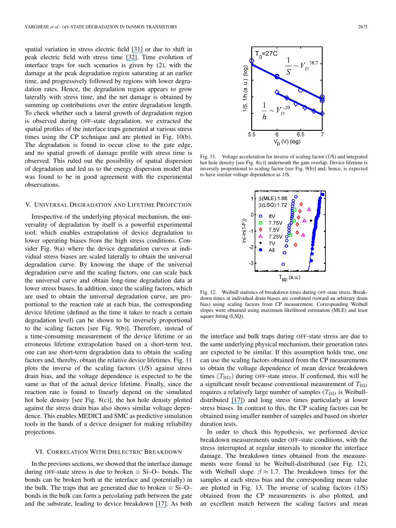
Fig. 10. (a) ON-state hot-carrier current measured at regular intervals duringOFF-state stress. The ON-state hot-carrier current and, hence, the internalelectric field show no significant reduction with stress time. (b) Lateral profileof interface traps at various stress times obtained using the CP technique. Nosignificant shift in the damage region with stress time is observed, as suggestedin [31] and [32].
classical hot carrier degradation to the reduction in stress levelswith degradation time. In accordance with this model, interfacecharges due to the damage reduce the peak electric field, possi-bly leading to a reduction in II rate and subsequent generationof hot carriers and, thereby, reducing the reaction rate k(p). Adirect measurement of the hot carrier current (αIBTBT) duringOFF-state stress is difficult, as it can only be measured alongwith the BTBT current at the drain terminal. Hence, we used anindirect method, which involves interrupting the stress brieflyand measuring the ON-state hot carrier current at the substrateterminal. The measurement result is shown in Fig. 10(a), andonly a slight reduction in ON-state hot carrier current withstress time is observed. This is insufficient to explain the largereduction in degradation rates, and therefore, we conclude thatthe reduction in electric field does not play a significant role indetermining the time evolution of the interface damage duringOFF-state stress.1
Another model to explain the soft saturation of degradationis the spatial variation of degradation rates, either due to a
1The ON-state hot carrier current is due to II of ISD and might be occurringat a location different from the II of IBTBT during OFF-state stress. Hence, α(ON-state) need not be a true monitor of α (OFF-state), but its mild reductionsuggests that local electric field has not changed significantly during the OFF-state stress. Reduction in IBTBT during OFF-state stress was also monitored(data not shown) and was found to be less than 30% of the t = 0 value, also insupport of the above conclusion.
VARGHESE et al.: OFF-STATE DEGRADATION IN DeNMOS TRANSISTORS 2675
spatial variation in stress electric field [31] or due to shift inpeak electric field with stress time [32]. Time evolution ofinterface traps for such scenarios is given by (2), with thedamage at the peak degradation region saturating at an earliertime, and progressively followed by regions with lower degra-dation rates. Hence, the degradation region appears to growlaterally with stress time, and the net damage is obtained bysumming up contributions over the entire degradation length.To check whether such a lateral growth of degradation regionis observed during OFF-state degradation, we extracted thespatial profiles of the interface traps generated at various stresstimes using the CP technique and are plotted in Fig. 10(b).The degradation is found to occur close to the gate edge,and no spatial growth of damage profile with stress time isobserved. This ruled out the possibility of spatial dispersionof degradation and led us to the energy dispersion model thatwas found to be in good agreement with the experimentalobservations.
V. UNIVERSAL DEGRADATION AND LIFETIME PROJECTION
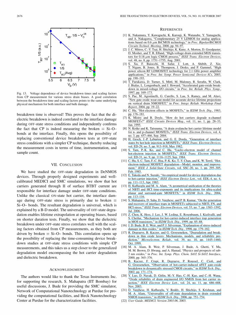
Irrespective of the underlying physical mechanism, the uni-versality of degradation by itself is a powerful experimentaltool, which enables extrapolation of device degradation tolower operating biases from the high stress conditions. Con-sider Fig. 9(a) where the device degradation curves at indi-vidual stress biases are scaled laterally to obtain the universaldegradation curve. By knowing the shape of the universaldegradation curve and the scaling factors, one can scale backthe universal curve and obtain long-time degradation data atlower stress biases. In addition, since the scaling factors, whichare used to obtain the universal degradation curve, are pro-portional to the reaction rate at each bias, the correspondingdevice lifetime (defined as the time it takes to reach a certaindegradation level) can be shown to be inversely proportionalto the scaling factors [see Fig. 9(b)]. Therefore, instead ofa time-consuming measurement of the device lifetime or anerroneous lifetime extrapolation based on a short-term test,one can use short-term degradation data to obtain the scalingfactors and, thereby, obtain the relative device lifetimes. Fig. 11plots the inverse of the scaling factors (1/S) against stressdrain bias, and the voltage dependence is expected to be thesame as that of the actual device lifetime. Finally, since thereaction rate is found to linearly depend on the simulatedhot hole density [see Fig. 8(c)], the hot hole density plottedagainst the stress drain bias also shows similar voltage depen-dence. This enables MEDICI and SMC as predictive simulationtools in the hands of a device designer for making reliabilityprojections.
VI. CORRELATION WITH DIELECTRIC BREAKDOWN
In the previous sections, we showed that the interface damageduring OFF-state stress is due to broken ≡ Si–O– bonds. Thebonds can be broken both at the interface and (potentially) inthe bulk. The traps that are generated due to broken ≡ Si–O–bonds in the bulk can form a percolating path between the gateand the substrate, leading to device breakdown [17]. As both
Fig. 11. Voltage acceleration for inverse of scaling factor (1/S) and integratedhot hole density [see Fig. 8(c)] underneath the gate overlap. Device lifetime isinversely proportional to scaling factor [see Fig. 9(b)] and, hence, is expectedto have similar voltage dependence as 1/S.
Fig. 12. Weibull statistics of breakdown times during OFF-state stress. Break-down times at individual drain biases are combined (toward an arbitrary drainbias) using scaling factors from CP measurement. Corresponding Weibullslopes were obtained using maximum likelihood estimation (MLE) and leastsquare fitting (LSQ).
the interface and bulk traps during OFF-state stress are due tothe same underlying physical mechanism, their generation ratesare expected to be similar. If this assumption holds true, onecan use the scaling factors obtained from the CP measurementsto obtain the voltage dependence of mean device breakdowntimes (TBD) during OFF-state stress. If confirmed, this will bea significant result because conventional measurement of TBD
requires a relatively large number of samples (TBD is Weibull-distributed [17]) and long stress times particularly at lowerstress biases. In contrast to this, the CP scaling factors can beobtained using smaller number of samples and based on shorterduration tests.
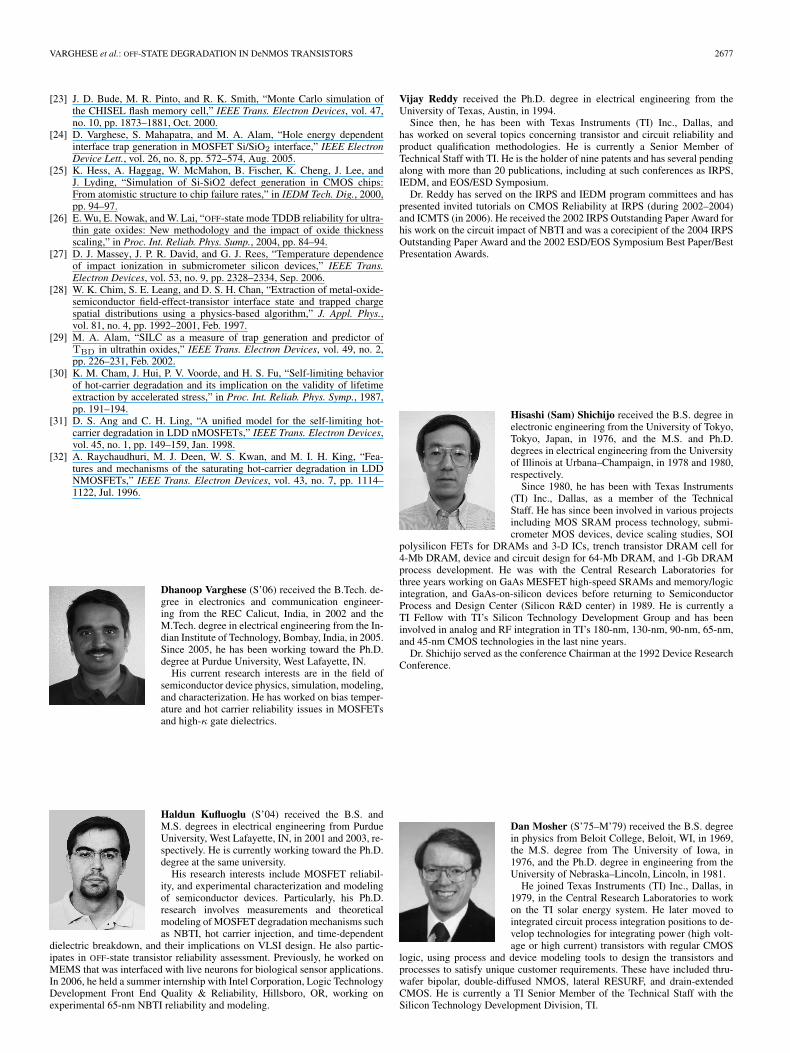
In order to check this hypothesis, we performed devicebreakdown measurements under OFF-state conditions, with thestress interrupted at regular intervals to monitor the interfacedamage. The breakdown times obtained from the measure-ments were found to be Weibull-distributed (see Fig. 12),with Weibull slope β ≈ 1.7. The breakdown times for thesamples at each stress bias and the corresponding mean valueare plotted in Fig. 13. The inverse of scaling factors (1/S)obtained from the CP measurements is also plotted, andan excellent match between the scaling factors and mean
2676 IEEE TRANSACTIONS ON ELECTRON DEVICES, VOL. 54, NO. 10, OCTOBER 2007
Fig. 13. Voltage dependence of device breakdown times and scaling factorsfrom CP measurement for various stress drain biases. A good correlationbetween the breakdown time and scaling factors points to the same underlyingphysical mechanism for both interface and bulk damage.
breakdown time is observed! This proves the fact that the di-electric breakdown is indeed correlated to the interface damageduring OFF-state stress conditions and independently confirmsthe fact that CP is indeed measuring the broken ≡ Si–O–bonds at the interface. Finally, this opens the possibility ofreplacing conventional device breakdown tests at OFF-statestress conditions with a simpler CP technique, thereby reducingthe measurement costs in terms of time, instrumentation, andsample count.
VII. CONCLUSION
We have studied the OFF-state degradation in DeNMOSdevices. Through properly designed experiments and well-calibrated MEDICI and SMC simulations, we show that hotcarriers generated through II of surface BTBT current areresponsible for interface damage under OFF-state conditions.Unlike the classical ON-state hot carrier, the interface dam-age during OFF-state stress is primarily due to broken ≡Si–O– bonds. The resultant degradation is universal, which isexplained by a B-D model. The universality of OFF-state degra-dation enables lifetime extrapolation at operating biases, basedon shorter duration tests. Finally, we show that the dielectricbreakdown under OFF-state stress correlates well with the scal-ing factors obtained from CP measurements, as they both aredriven by broken ≡ Si–O– bonds. This correlation opens upthe possibility of replacing the time-consuming device break-down studies at OFF-state stress conditions with simple CPmeasurements, and this takes us a step closer to the generalizeddegradation model encompassing the hot carrier degradationand dielectric breakdown.
ACKNOWLEDGMENT
The authors would like to thank the Texas Instruments Inc.for supporting the research, S. Mahapatra (IIT Bombay) foruseful discussions, J. Bude for providing the SMC simulator,Network of Computational Nanotechnology at Purdue for pro-viding the computational facilities, and Birck NanotechnologyCenter at Purdue for the characterization facilities.
REFERENCES
[1] K. Nakamura, Y. Kawaguchi, K. Karouji, K. Watanabe, Y. Yamaguchi,and A. Nakagawa, “Complementary 25 V LDMOS for analog applica-tions based on 0.6 µm BiCMOS technology,” in Proc. Bipolar/BiCMOSCircuits Technol. Meeting, 2000, pp. 94–97.
[2] J. C. Mitros, C.-Y. Tsai, H. Shichijo, K. Kunz, A. Morton, D. Goodpaster,D. Mosher, and T. R. Efland, “High-voltage drain extended MOS transis-tors for 0.18-µm logic CMOS process,” IEEE Trans. Electron Devices,vol. 48, no. 8, pp. 1751–1755, Aug. 2001.
[3] S. Xu, F. Baiocchi, H. Safar, J. Lott, A. Shibib, Z. Xie,T. Nigam, B. Jones, B. Thompson, J. Desko, and P. Gammel, “Highpower silicon RF LDMOSFET technology for 2.1 GHz power amplifierapplications,” in Proc. Int. Symp. Power Semicond. Devices ICs, 2003,pp. 190–193.
[4] T. Furukawa, D. Turner, S. Mittl, M. Maloney, R. Serafin, W. Clark,J. Bialas, L. Longenbach, and J. Howard, “Accelerated gate-oxide break-down in mixed-voltage I/O circuits,” in Proc. Int. Reliab. Phys. Symp.,1997, pp. 169–173.
[5] S. Pae, M. Agostinelli, G. Curello, S. Lau, S. Ramey, and M. Alavi,“New gate oxide wear-out model for accurate device lifetime projectionson vertical drain NMOSFET,” in Proc. Integr. Reliab. Workshop FinalReport, 2004, pp. 19–22.
[6] C. Hu, “Hot-electron effects in MOSFETs,” in IEDM Tech. Dig., 1983,pp. 176–181.
[7] K. Mistry and B. Doyle, “How do hot carriers degrade n-channelMOSFETs?” IEEE Circuits Devices Mag., vol. 11, no. 1, pp. 28–33,Jan. 1995.
[8] N. Koike and K. Tatsuuma, “A drain avalanche hot carrier lifetime modelfor n- and p-channel MOSFETs,” IEEE Trans. Electron Devices, vol. 4,no. 3, pp. 457–466, Sep. 2004.
[9] H. Gesch, J.-P. Leburton, and G. E. Dorda, “Generation of interfacestates by hot hole injection in MOSFETs,” IEEE Trans. Electron Devices,vol. ED-29, no. 5, pp. 913–918, May 1982.
[10] S. Tam, P.-K. Ko, and C. Hu, “Lucky-electron model of channelhot-electron injection in MOSFETs,” IEEE Trans. Electron Devices,vol. ED-31, no. 9, pp. 1116–1125, Sep. 1984.
[11] C. Hu, S. C. Tam, F.-C. Hsu, P.-K. Ko, T.-Y. Chan, and K. W. Terril, “Hot-electron-induced MOSFET degradation—Model, monitor, and improve-ment,” IEEE J. Solid-State Circuits, vol. SSC-20, no. 1, pp. 295–305,Feb. 1985.
[12] E. Takeda and N. Suzuki, “An empirical model for device degradation dueto hot-carrier injection,” IEEE Electron Device Lett., vol. EDL-4, no. 4,pp. 111–113, Apr. 1983.
[13] H. Kufluoglu and M. A. Alam, “A geometrical unification of the theoriesof NBTI and HCI time-exponents and its implications for ultra-scaledplanar and surround-gate MOSFETS,” in IEDM Tech. Dig., 2004,pp. 113–116.
[14] S. Mahapatra, D. Saha, D. Varghese, and P. B. Kumar, “On the generationand recovery of interface traps in MOSFETs subjected to NBTI, FN, andHCI stress,” IEEE Trans. Electron Devices, vol. 53, no. 7, pp. 1583–1592,Jul. 2006.
[15] Z. Chen, K. Hess, J. Lee, J. W. Lyding, E. Rosenbaum, I. Kizilyalli, andS. Chetlur, “Mechanism for hot-carrier-induced interface trap generationin MOS transistors,” in IEDM Tech. Dig., 1999, pp. 85–88.
[16] J. D. Bude, B. E. Weir, and P. J. Silverman, “Explanation of stress-induceddamage in thin oxides,” in IEDM Tech. Dig., 1998, pp. 179–182.
[17] R. Degraeve, B. Kaczer, and G. Groeseneken, “Degradation and break-down in thin oxide layers: Mechanisms, models, and reliability pre-diction,” Microelectron. Reliab., vol. 39, no. 10, pp. 1445–1460,Oct. 1999.
[18] M. A. Alam, B. Weir, P. Silverman, J. Bude, A. Ghetti, Y. Ma,M. M. Brown, D. Hwang, and A. Hamad, “Physics and prospects of sub-2 nm oxides,” in Proc. Int. Symp. Phys. Chem. SiO2 Si-SiO2 Interface,2000, pp. 365–376.
[19] B. Kaczer, F. Crupi, R. Degraeve, P. Roussel, C. Ciofi, andG. Groeseneken, “Observation of hot-carrier-induced nFET gate-oxidebreakdown in dynamically stressed CMOS circuits,” in IEDM Tech. Dig.,2002, pp. 171–174.
[20] Y. Luo, D. Nayak, D. Gitlin, M.-Y. Hao, C.-H. Kao, and C.-H. Wang,“Oxide reliability of drain engineered I/O NMOS from hot carrier in-jection,” IEEE Electron Device Lett., vol. 24, no. 11, pp. 686–688,Nov. 2003.
[21] D. Varghese, H. Kufluoglu, V. Reddy, H. Shichijo, S. Krishnan, andM. A. Alam, “Universality of off-state degradation in drain extendedNMOS transistors,” in IEDM Tech. Dig., 2006, pp. 751–754.
[22] User Guide, MEDICI, Version 2003.06, 2003.
VARGHESE et al.: OFF-STATE DEGRADATION IN DeNMOS TRANSISTORS 2677
[23] J. D. Bude, M. R. Pinto, and R. K. Smith, “Monte Carlo simulation ofthe CHISEL flash memory cell,” IEEE Trans. Electron Devices, vol. 47,no. 10, pp. 1873–1881, Oct. 2000.
[24] D. Varghese, S. Mahapatra, and M. A. Alam, “Hole energy dependentinterface trap generation in MOSFET Si/SiO2 interface,” IEEE ElectronDevice Lett., vol. 26, no. 8, pp. 572–574, Aug. 2005.
[25] K. Hess, A. Haggag, W. McMahon, B. Fischer, K. Cheng, J. Lee, andJ. Lyding, “Simulation of Si-SiO2 defect generation in CMOS chips:From atomistic structure to chip failure rates,” in IEDM Tech. Dig., 2000,pp. 94–97.
[26] E. Wu, E. Nowak, and W. Lai, “OFF-state mode TDDB reliability for ultra-thin gate oxides: New methodology and the impact of oxide thicknessscaling,” in Proc. Int. Reliab. Phys. Sump., 2004, pp. 84–94.
[27] D. J. Massey, J. P. R. David, and G. J. Rees, “Temperature dependenceof impact ionization in submicrometer silicon devices,” IEEE Trans.Electron Devices, vol. 53, no. 9, pp. 2328–2334, Sep. 2006.
[28] W. K. Chim, S. E. Leang, and D. S. H. Chan, “Extraction of metal-oxide-semiconductor field-effect-transistor interface state and trapped chargespatial distributions using a physics-based algorithm,” J. Appl. Phys.,vol. 81, no. 4, pp. 1992–2001, Feb. 1997.
[29] M. A. Alam, “SILC as a measure of trap generation and predictor ofTBD in ultrathin oxides,” IEEE Trans. Electron Devices, vol. 49, no. 2,pp. 226–231, Feb. 2002.
[30] K. M. Cham, J. Hui, P. V. Voorde, and H. S. Fu, “Self-limiting behaviorof hot-carrier degradation and its implication on the validity of lifetimeextraction by accelerated stress,” in Proc. Int. Reliab. Phys. Symp., 1987,pp. 191–194.
[31] D. S. Ang and C. H. Ling, “A unified model for the self-limiting hot-carrier degradation in LDD nMOSFETs,” IEEE Trans. Electron Devices,vol. 45, no. 1, pp. 149–159, Jan. 1998.
[32] A. Raychaudhuri, M. J. Deen, W. S. Kwan, and M. I. H. King, “Fea-tures and mechanisms of the saturating hot-carrier degradation in LDDNMOSFETs,” IEEE Trans. Electron Devices, vol. 43, no. 7, pp. 1114–1122, Jul. 1996.
Dhanoop Varghese (S’06) received the B.Tech. de-gree in electronics and communication engineer-ing from the REC Calicut, India, in 2002 and theM.Tech. degree in electrical engineering from the In-dian Institute of Technology, Bombay, India, in 2005.Since 2005, he has been working toward the Ph.D.degree at Purdue University, West Lafayette, IN.
His current research interests are in the field ofsemiconductor device physics, simulation, modeling,and characterization. He has worked on bias temper-ature and hot carrier reliability issues in MOSFETsand high-κ gate dielectrics.
Haldun Kufluoglu (S’04) received the B.S. andM.S. degrees in electrical engineering from PurdueUniversity, West Lafayette, IN, in 2001 and 2003, re-spectively. He is currently working toward the Ph.D.degree at the same university.
His research interests include MOSFET reliabil-ity, and experimental characterization and modelingof semiconductor devices. Particularly, his Ph.D.research involves measurements and theoreticalmodeling of MOSFET degradation mechanisms suchas NBTI, hot carrier injection, and time-dependent
dielectric breakdown, and their implications on VLSI design. He also partic-ipates in OFF-state transistor reliability assessment. Previously, he worked onMEMS that was interfaced with live neurons for biological sensor applications.In 2006, he held a summer internship with Intel Corporation, Logic TechnologyDevelopment Front End Quality & Reliability, Hillsboro, OR, working onexperimental 65-nm NBTI reliability and modeling.
Vijay Reddy received the Ph.D. degree in electrical engineering from theUniversity of Texas, Austin, in 1994.
Since then, he has been with Texas Instruments (TI) Inc., Dallas, andhas worked on several topics concerning transistor and circuit reliability andproduct qualification methodologies. He is currently a Senior Member ofTechnical Staff with TI. He is the holder of nine patents and has several pendingalong with more than 20 publications, including at such conferences as IRPS,IEDM, and EOS/ESD Symposium.
Dr. Reddy has served on the IRPS and IEDM program committees and haspresented invited tutorials on CMOS Reliability at IRPS (during 2002–2004)and ICMTS (in 2006). He received the 2002 IRPS Outstanding Paper Award forhis work on the circuit impact of NBTI and was a corecipient of the 2004 IRPSOutstanding Paper Award and the 2002 ESD/EOS Symposium Best Paper/BestPresentation Awards.
Hisashi (Sam) Shichijo received the B.S. degree inelectronic engineering from the University of Tokyo,Tokyo, Japan, in 1976, and the M.S. and Ph.D.degrees in electrical engineering from the Universityof Illinois at Urbana–Champaign, in 1978 and 1980,respectively.
Since 1980, he has been with Texas Instruments(TI) Inc., Dallas, as a member of the TechnicalStaff. He has since been involved in various projectsincluding MOS SRAM process technology, submi-crometer MOS devices, device scaling studies, SOI
polysilicon FETs for DRAMs and 3-D ICs, trench transistor DRAM cell for4-Mb DRAM, device and circuit design for 64-Mb DRAM, and 1-Gb DRAMprocess development. He was with the Central Research Laboratories forthree years working on GaAs MESFET high-speed SRAMs and memory/logicintegration, and GaAs-on-silicon devices before returning to SemiconductorProcess and Design Center (Silicon R&D center) in 1989. He is currently aTI Fellow with TI’s Silicon Technology Development Group and has beeninvolved in analog and RF integration in TI’s 180-nm, 130-nm, 90-nm, 65-nm,and 45-nm CMOS technologies in the last nine years.
Dr. Shichijo served as the conference Chairman at the 1992 Device ResearchConference.
Dan Mosher (S’75–M’79) received the B.S. degreein physics from Beloit College, Beloit, WI, in 1969,the M.S. degree from The University of Iowa, in1976, and the Ph.D. degree in engineering from theUniversity of Nebraska–Lincoln, Lincoln, in 1981.
He joined Texas Instruments (TI) Inc., Dallas, in1979, in the Central Research Laboratories to workon the TI solar energy system. He later moved tointegrated circuit process integration positions to de-velop technologies for integrating power (high volt-age or high current) transistors with regular CMOS
logic, using process and device modeling tools to design the transistors andprocesses to satisfy unique customer requirements. These have included thru-wafer bipolar, double-diffused NMOS, lateral RESURF, and drain-extendedCMOS. He is currently a TI Senior Member of the Technical Staff with theSilicon Technology Development Division, TI.
2678 IEEE TRANSACTIONS ON ELECTRON DEVICES, VOL. 54, NO. 10, OCTOBER 2007
Srikanth Krishnan (S’86–M’87–A’92) received theB.Tech. degree in electrical engineering from theIndian Institute of Technology, Madras, India, in1985, the M.S. and Ph.D. degrees in engineer-ing science from The Pennsylvania State Univer-sity, in 1988 and 1992, respectively, and the MBAfrom Southern Methodist University, UniversityPark, TX.
He later joined with the Plasma Etch Group,Semiconductor Process and Design Center, TexasInstruments Inc., Dallas, to work on plasma damage
effects on transistor performance. In 1998, he joined the Reliability Groupwithin Texas Instruments Inc. and, subsequently, led the 130-nm componentreliability effort. He is currently the Device Reliability Manager with theTexas Instruments Inc., who is responsible for component reliability of CMOStechnology nodes. During his 15-year career with the Texas Instruments Inc.,he has authored 30 papers (6 invited), 20 patents, and 1 trade secret.
Dr. Krishnan has served on the technical program committee for IRPS since1999. He has been appointed to the Management Committee of IRPS since2003. He served on the program committee of Plasma Process-Induced DamageSymposium (P2ID) and was the Vice-Chair and Chairman for the (P2ID) from2003 to 2004.
Muhammad Ashraful Alam (M’96–SM’01–F’06)received the B.S.E.E. degree in electrical engineer-ing from Bangladesh University of Engineering andTechnology, Dhaka, in 1988, the M.S. degree in elec-trical engineering from Clarkson University, Pots-dam, NY, in 1991, and the Ph.D. degree in electricalengineering from Purdue University, Lafayette, IN,in 1994.
From 1995 to 2001, he was with the SiliconULSI Research Department, Bell Laboratories,Lucent Technologies, Murray Hill, NJ, as a member
of Technical Staff. From 2001 to 2003, he was a Distinguished Member ofTechnical Staff and the Technical Manager of the IC Reliability Group, AgereSystems, Murray Hill. He joined Purdue University in 2004, where he iscurrently a Professor of electrical and computer engineering. He has publishedover 75 papers in international journals. His current research and teachingfocus on the physics, simulation, characterization, and technology of classicaland novel semiconductor devices. His current research interests include thetheory of oxide reliability, transport in nanocomposite thin-film transistors, andnanobio sensors.
Dr. Alam received the Outstanding Paper Award in 2001 and the Best PaperAward in the International Reliability Physics Symposium in 2003 for his workon gate oxide reliability. He also received the IEEE Kiyo Tomiyasu Awardfor his contributions to device technology for communication systems. He haspresented many invited and contributed talks in international conferences.