Novel Ring Resonator-Based Integrated Photonic Beamformer for Broadband Phased Array Receive...
16
JOURNAL OF LIGHTWAVE TECHNOLOGY, VOL. 28, NO. 1, JANUARY 1, 2010 3 Novel Ring Resonator-Based Integrated Photonic Beamformer for Broadband Phased Array Receive Antennas—Part I: Design and Performance Analysis Arjan Meijerink, Member, IEEE, Chris G. H. Roeloffzen, Member, IEEE, Roland Meijerink, Student Member, IEEE, Leimeng Zhuang, Student Member, IEEE, David A. I. Marpaung, Student Member, IEEE, Mark J. Bentum, Senior Member, IEEE, Maurizio Burla, Student Member, IEEE, Jaco Verpoorte, Pieter Jorna, Adriaan Hulzinga, and Wim van Etten, Senior Member, IEEE Abstract—A novel optical beamformer concept is introduced that can be used for seamless control of the reception angle in broadband wireless receivers employing a large phased array antenna (PAA). The core of this beamformer is an optical beam- forming network (OBFN), using ring resonator-based broadband delays, and coherent optical combining. The electro-optical con- version is performed by means of single-sideband suppressed carrier modulation, employing a common laser, Mach-Zehnder modulators, and a common optical sideband filter after the OBFN. The unmodulated laser signal is then re-injected in order to per- form balanced coherent optical detection, for the opto-electrical conversion. This scheme minimizes the requirements on the com- plexity of the OBFN, and has potential for compact realization by means of full integration on chip. The impact of the optical beamformer concept on the performance of the full receiver system is analyzed, by modeling the combination of the PAA and the beamformer as an equivalent two-port RF system. The results are illustrated by a numerical example of a PAA receiver for satel- lite TV reception, showing that—when properly designed—the beamformer hardly affects the sensitivity of the receiver. Index Terms—Noise analysis, optical beamforming, optical ring resonators, optical SSB modulation, phased array antennas, RF photonics. Manuscript received May 29, 2009; revised July 29, 2009. First published August 11, 2009; current version published December 16, 2009. This work was part of the Broadband Photonic Beamformer (BPB) project, the SMart Antenna systems for Radio Transceivers (SMART) project, and the Merging Electronics and Micro & nano PHotonics in Integrated Systems (MEMPHIS) project. The BPB project and the SMART project are supported by the Dutch Ministry of Economic Affairs, SenterNovem project numbers IS052081 and ISO53030, re- spectively. The SMART project is part of the Euripides project SMART. The MEMPHIS project is supported by the Dutch Ministry of Economic Affairs, and the Dutch Ministry of Education, Culture and Science, through the Smart Mix Programme. A. Meijerink, C. G. H. Roeloffzen, L. Zhuang, D. A. I. Marpaung, M. J. Bentum, and M. Burla are with the Telecommunication Engineering Group, Faculty of Electrical Engineering, Mathematics and Computer Sci- ence, University of Twente, 7500 AE Enschede, The Netherlands (e-mail: [email protected]; [email protected]; [email protected]; [email protected]; [email protected]; [email protected]). R. Meijerink was with the Telecommunication Engineering Group, Faculty of Electrical Engineering, Mathematics and Computer Science, University of Twente, 7500 AE Enschede, The Netherlands. He is now with the Herbert Vissers College, 2150 AC Nieuw-Vennep, The Netherlands (e-mail: r.mei- [email protected]). J. Verpoorte, P. Jorna, and A. Hulzinga are with the National Aerospace Lab- oratory NLR, Anthony Fokkerweg 2, 1006 BM Amsterdam, The Netherlands (e-mail: [email protected]; [email protected]; [email protected]). W. van Etten, retired, was with the Telecommunication Engineering Group, Faculty of Electrical Engineering, Mathematics and Computer Science, Univer- sity of Twente, 7500 AE Enschede, The Netherlands (e-mail: [email protected]). Digital Object Identifier 10.1109/JLT.2009.2029705 I. INTRODUCTION P HOTONIC beamforming in phased array antennas (PAAs) is an interesting example of applying optical technology in wireless transmission systems. A PAA consists of an array of multiple antenna elements (AEs), corresponding transmission and/or reception units, and a beamformer, en- abling direction-sensistive transmission and/or reception of electromagnetic waves [1]. In receive mode each individual AE signal consists of a time-delayed version of some desired signal, possible time-delayed versions of undesired signals (from different directions), and noise (sky noise and antenna noise). The values of these time delays are different for each AE, and depend on the geometrical distribution of the AEs and the direction(s) of the incoming wave front(s). The beam- former therefore consists of a delay-and-combine network that equalizes the delay values of the signal terms that correspond to the desired received signal, such that the desired signal terms add up in phase and are reinforced, whereas the undesired signal terms do not add up in phase and are hence suppressed. (Although some people would use the terms beamformer and beamforming network exclusively for PAAs in transmission mode, it is widely accepted to use them for receive mode as well, so we also do that in this paper.) In many applications it is desirable that the time delays are tunable, in order to be able to alter the reception angle of the PAA. When the amplitudes of the AE signals are also controlled, the shape of the beam pat- tern can be altered as well, for example to minimize sidelobes. PAAs offer several advantages when compared to mechanically steered antennas, such as agile beam steering, relatively low maintenance costs, reduced drag when applied in for instance vehicles or aircraft, and the possibiliy of supporting multiple antenna beams [1]. Implementing the beamformer in the optical domain shares many common advantages with other RF photonic signal processing techniques [2]–[4], such as compactness and low weight (particularly when integrated on a chip), low loss, large instantaneous bandwidth, and inherent immunity to elec- tromagnetic interference. Optical beamforming has regained interest recently as a result of several technological devel- opments in the last decade. Significant advances have been made in improving the performance and reducing the costs of analog optical modulators and detectors, because of widespread 0733-8724/$26.00 © 2009 IEEE Authorized licensed use limited to: UNIVERSITEIT TWENTE. Downloaded on January 11, 2010 at 09:32 from IEEE Xplore. Restrictions apply.
Transcript of Novel Ring Resonator-Based Integrated Photonic Beamformer for Broadband Phased Array Receive...
JOURNAL OF LIGHTWAVE TECHNOLOGY, VOL. 28, NO. 1, JANUARY 1, 2010 3
Novel Ring Resonator-Based Integrated PhotonicBeamformer for Broadband Phased Array Receive
Antennas—Part I: Design and Performance AnalysisArjan Meijerink, Member, IEEE, Chris G. H. Roeloffzen, Member, IEEE, Roland Meijerink, Student Member, IEEE,
Leimeng Zhuang, Student Member, IEEE, David A. I. Marpaung, Student Member, IEEE,Mark J. Bentum, Senior Member, IEEE, Maurizio Burla, Student Member, IEEE, Jaco Verpoorte, Pieter Jorna,
Adriaan Hulzinga, and Wim van Etten, Senior Member, IEEE
Abstract—A novel optical beamformer concept is introducedthat can be used for seamless control of the reception angle inbroadband wireless receivers employing a large phased arrayantenna (PAA). The core of this beamformer is an optical beam-forming network (OBFN), using ring resonator-based broadbanddelays, and coherent optical combining. The electro-optical con-version is performed by means of single-sideband suppressedcarrier modulation, employing a common laser, Mach-Zehndermodulators, and a common optical sideband filter after the OBFN.The unmodulated laser signal is then re-injected in order to per-form balanced coherent optical detection, for the opto-electricalconversion. This scheme minimizes the requirements on the com-plexity of the OBFN, and has potential for compact realizationby means of full integration on chip. The impact of the opticalbeamformer concept on the performance of the full receiversystem is analyzed, by modeling the combination of the PAA andthe beamformer as an equivalent two-port RF system. The resultsare illustrated by a numerical example of a PAA receiver for satel-lite TV reception, showing that—when properly designed—thebeamformer hardly affects the sensitivity of the receiver.
Index Terms—Noise analysis, optical beamforming, optical ringresonators, optical SSB modulation, phased array antennas, RFphotonics.
Manuscript received May 29, 2009; revised July 29, 2009. First publishedAugust 11, 2009; current version published December 16, 2009. This work waspart of the Broadband Photonic Beamformer (BPB) project, the SMart Antennasystems for Radio Transceivers (SMART) project, and the Merging Electronicsand Micro & nano PHotonics in Integrated Systems (MEMPHIS) project. TheBPB project and the SMART project are supported by the Dutch Ministry ofEconomic Affairs, SenterNovem project numbers IS052081 and ISO53030, re-spectively. The SMART project is part of the Euripides project SMART. TheMEMPHIS project is supported by the Dutch Ministry of Economic Affairs,and the Dutch Ministry of Education, Culture and Science, through the SmartMix Programme.
A. Meijerink, C. G. H. Roeloffzen, L. Zhuang, D. A. I. Marpaung, M.J. Bentum, and M. Burla are with the Telecommunication EngineeringGroup, Faculty of Electrical Engineering, Mathematics and Computer Sci-ence, University of Twente, 7500 AE Enschede, The Netherlands (e-mail:[email protected]; [email protected]; [email protected];[email protected]; [email protected]; [email protected]).
R. Meijerink was with the Telecommunication Engineering Group, Facultyof Electrical Engineering, Mathematics and Computer Science, University ofTwente, 7500 AE Enschede, The Netherlands. He is now with the HerbertVissers College, 2150 AC Nieuw-Vennep, The Netherlands (e-mail: [email protected]).
J. Verpoorte, P. Jorna, and A. Hulzinga are with the National Aerospace Lab-oratory NLR, Anthony Fokkerweg 2, 1006 BM Amsterdam, The Netherlands(e-mail: [email protected]; [email protected]; [email protected]).
W. van Etten, retired, was with the Telecommunication Engineering Group,Faculty of Electrical Engineering, Mathematics and Computer Science, Univer-sity of Twente, 7500 AE Enschede, The Netherlands (e-mail: [email protected]).
Digital Object Identifier 10.1109/JLT.2009.2029705
I. INTRODUCTION
P HOTONIC beamforming in phased array antennas(PAAs) is an interesting example of applying optical
technology in wireless transmission systems. A PAA consistsof an array of multiple antenna elements (AEs), correspondingtransmission and/or reception units, and a beamformer, en-abling direction-sensistive transmission and/or reception ofelectromagnetic waves [1]. In receive mode each individualAE signal consists of a time-delayed version of some desiredsignal, possible time-delayed versions of undesired signals(from different directions), and noise (sky noise and antennanoise). The values of these time delays are different for eachAE, and depend on the geometrical distribution of the AEsand the direction(s) of the incoming wave front(s). The beam-former therefore consists of a delay-and-combine network thatequalizes the delay values of the signal terms that correspondto the desired received signal, such that the desired signal termsadd up in phase and are reinforced, whereas the undesiredsignal terms do not add up in phase and are hence suppressed.(Although some people would use the terms beamformer andbeamforming network exclusively for PAAs in transmissionmode, it is widely accepted to use them for receive mode aswell, so we also do that in this paper.) In many applications itis desirable that the time delays are tunable, in order to be ableto alter the reception angle of the PAA. When the amplitudes ofthe AE signals are also controlled, the shape of the beam pat-tern can be altered as well, for example to minimize sidelobes.PAAs offer several advantages when compared to mechanicallysteered antennas, such as agile beam steering, relatively lowmaintenance costs, reduced drag when applied in for instancevehicles or aircraft, and the possibiliy of supporting multipleantenna beams [1].
Implementing the beamformer in the optical domain sharesmany common advantages with other RF photonic signalprocessing techniques [2]–[4], such as compactness and lowweight (particularly when integrated on a chip), low loss,large instantaneous bandwidth, and inherent immunity to elec-tromagnetic interference. Optical beamforming has regainedinterest recently as a result of several technological devel-opments in the last decade. Significant advances have beenmade in improving the performance and reducing the costs ofanalog optical modulators and detectors, because of widespread
0733-8724/$26.00 © 2009 IEEE
Authorized licensed use limited to: UNIVERSITEIT TWENTE. Downloaded on January 11, 2010 at 09:32 from IEEE Xplore. Restrictions apply.

4 JOURNAL OF LIGHTWAVE TECHNOLOGY, VOL. 28, NO. 1, JANUARY 1, 2010
interest in RF photonic links. Also, the worldwide deploymentof optical fiber backbones and the more recent developmentof fiber-to-the-home networks has driven the state-of-the-artin planar optical circuit technology to a mature level; rathercomplex optical chips with low insertion losses can now befabricated at relatively low costs [5].
Various optical beamformer concepts have been previouslyreported [6]. Among others, they are based on optical phaseshifters [7], switchable delay matrices (using fiber optics [8]or integrated devices [9]), liquid crystal polarization switchingdevices [10], [11], or a combination of a wavelength-tunablelaser and a dispersive optical element, such as a high-dispersionfiber [12], a fiber optic prism [13], [14], a fiber-bragg gratings(FBGs) prism [15], [16], or chirped FBGs [17]–[19]. However,phase shifters only provide the proper delay compensation atone particular frequency, and therefore result in a frequency-de-pendent beam angle (beam squint). This will be a problem whenthe PAA consists of a large number of AEs and operates over alarge instantaneous bandwidth. Switchable delay matrices pro-vide true time delays and are therefore inherently broadband,but they only allow tuning in discrete steps. In fact they show atrade-off between beam angle resolution and complexity. (This,however, could be solved using a hybrid analog-digital variablefiber-optic delay line [20], [21].) The beamformers based on theliquid crystal switching devices provide true time delays but therealized systems are bulky. The beamformers with dispersive el-ements offer both seamless tunability and broadband delay com-pensation but the delay tuning in these schemes requires bulkyoptical components (fibers and FBGs) and (relatively expensive)tunable lasers. The costs of these tunable lasers might not be anissue when each tunable laser illuminates multiple optical delayelements (as is done in the proposed schemes), but this results inan inherent linear relation between the tuned delays, hence lim-iting the applicability of the proposed schemes to linear arrays.
In this paper a seamlessly tunable optical beamformer con-cept for a PAA receiver system is proposed that can operatesquint-free within a wide frequency band, without requiring tun-able lasers. It is based on coherent optical combining in an op-tical beamforming network (OBFN) using cascades of opticalring resonators (ORRs) [21]–[36] as tunable delay elements. Adedicated system architecture for performing the electro-optical(E/O) and opto-electrical (O/E) conversions is proposed that re-laxes the requirements on the complexity of the OBFN. It willbe illustrated that the proposed concept has potential for full in-tegration of the optical beamformer.
A typical application of the presented beamformer concept isa broadband transceiver employing a PAA with a large numberof elements and stringent requirements on the beam angleaccuracy, for instance for radar or satellite communications. Anexample of such an application is an airborne satellite receiver,which can provide in-flight connectivity for flight crew infor-mation, and live TV and high-speed Internet connectivity forpassengers. Novel technology for such a receiver has recentlybeen developed within the framework of the SMart Antennasystems for Radio Transceivers (SMART) project [31], [32], bya Dutch consortium consisting of the Dutch National AerospaceLaboratory NLR, Cyner Substrates, the University of Twente,and LioniX B.V. It is based on a non-planar PAA (conformal to
the aircraft fuselage) consisting of novel broadband -bandstacked patch AEs, and a broadband optical beamformer em-ploying ORRs, integrated in CMOS-compatible waveguidetechnology [5]. The design of the PAA and the beamformerinvolves several challenges:
• The power received from the satellite will be relatively low.Hence, the complete antenna system should have a highgain and low noise temperature in order to achieve satisfac-tory carrier-to-noise ratio (CNR), which requires the PAAto consist of many AEs (more than 1000);
• The difference in receive angles from different -bandsatellites can be as low as 2 degrees, which requires a verynarrow antenna beam with a very high angle accuracy;
• In contrast to the situation in for instance a vehicle, whereonly one receiver needs to demodulate a single (relativelynarrowband) television channel at a time (which could forexample be done by means of digital beamforming), theairline passengers should be able to choose television chan-nels individually. This implies that the PAA should in thiscase be able to accommodate the entire band at once(i.e., 10.7–12.75 GHz).
For the beamformer this implies that it should have many in-puts, and that it should be able to accommodate relatively largedelays, a large bandwidth, and seamless tunability. In Part I ofthis paper it is explained how this can be achieved by meansof an ORR-based optical beamformer. Although the theory willbe presented in such a way that it is generally applicable, thepractical numerical examples will be based on the applicationthat is studied in the SMART project, i.e., satellite televisionreception. In Part II [36] the realization and testing of an experi-mental ORR-based optical beamformer setup will be described,including the design and fabrication of the optical devices. Thisbeamformer setup was realized as a part of an an experimentalsystem demonstrator that was developed in the SMART project[32].
Part I is organized as follows. In the next section, the the-oretical principles of ORR-based OBFNs will be summarized.After that, the design of the modulation and detection schemewill be be outlined in Section III. In Section IV the impact of theproposed optical beamformer on the noise performance of thereceiver is analyzed. Both the design and the performance anal-ysis are illustrated by a numerical example in Section V. Thepaper ends with conclusions in Section VI.
II. PRINCIPLES OF RING RESONATOR-BASED OPTICAL
BEAMFORMING NETWORKS
A. Optical Ring Resonator-Based Delay Elements
When an optical carrier is modulated by an RF signal, propa-gates through an optical waveguide, and is converted to the elec-trical domain by an optical detector, the effective time delay tothe RF signal is determined by the group delay of the opticalwaveguide. This group delay can be made tunable by putting anORR parallel to the waveguide [21]–[25], as illustrated in theinset of Fig. 1. The resulting structure has a time-discrete im-pulse response, and—as a result—a periodic transfer function.The period is called free spectral range (FSR), and is equal to theinverse of the round-trip time of the ring. When the losses in
Authorized licensed use limited to: UNIVERSITEIT TWENTE. Downloaded on January 11, 2010 at 09:32 from IEEE Xplore. Restrictions apply.

MEIJERINK et al.: PART I: DESIGN AND PERFORMANCE ANALYSIS 5
Fig. 1. Theoretical group delay response of the ring resonator-based delay el-ement shown at the inset, for different values of the power coupling coefficient�. The optical ring resonator (ORR) has a round-trip time � , a round-trip phaseshift � and a resonance frequency � .
the waveguide and in the ring can be neglected, all optical powerentering at the input port will eventually arrive at the output port,so the magnitude of the transfer function will be one. The groupdelay response will also be periodic, with the same FSR, andcan be found by differentiating the phase response with respectto frequency, resulting in [21]–[24]
(1)
where is the round-trip phase shift of the ring, and is thepower coupling coefficient between the waveguide and the ring.Each period of the group delay response is a symmetric, bell-shaped function of frequency, centered around the resonancefrequency of the ring. This resonance frequency can be variedby tuning the round-trip phase shift of the ring, and the max-imum delay value can be varied by tuning the power couplingcoefficient between the waveguide and the ring. This is illus-trated in Fig. 1, where one period of the group delay responseis plotted for a fixed value of and three different values of
. The value of should be tuned such that the bell shape isaligned with the spectrum of the modulated optical signal, and
should be tuned such that the desired delay value is achievedin the peak. The value of can be tuned by means of an opticalphase shifter, and the value of can be tuned by means of asymmetric Mach-Zehnder interferometer (MZI) with an opticalphase shifter in one of its arms. Optical phase shifters can beimplemented for instance using the electo-optic or thermo-opticeffect.
The peak value of the delay is more or less inversely propor-tional to the peak width. This is because the area underneath thedelay curve in one period is equal to times the phasetransition within one period. Since this phase transition is al-ways equal to , the area under the group delay response in oneperiod is always equal to one. Hence, when the peak delay valueof the ORR is increased, the bandwidth decreases, revealing aninherent tradeoff of the ORR-based delay element [21]–[25]. Asa result, a single ORR might not provide enough delay and band-width for a broadband RF signal.
B. Multi-Ring Delay Elements
The bandwidth of an ORR-based delay element can be en-hanced by cascading several ORR sections [21], [22], [24], [25],as illustrated in the inset of Fig. 2. The total group delay re-sponse of this cascade can be found by summing the individual
Fig. 2. Theoretical group delay response of three cascaded ORR sections(shown at the inset), with resonance frequencies � . The dashed curves denotethe group delay responses of the individual sections, whereas the solid curvedenotes their sum. In this case the round-trip phase shifts � and powercoupling coefficients � of the individual sections are tuned such that the totalresulting group delay response is flattened.
group delay responses of the constituting sections. Hence, a flat-tened group delay response can be obtained by tuning the indi-vidual sections to different resonance frequencies, and slightlydifferent peak delay values, as illustrated in Fig. 2. This flattenedpart will have a ripple, which may cause distortion to the RFsignal that is modulated onto the optical carrier. However, thisripple can be made arbitrarily small by either squeezing the res-onance frequencies closer to each other (although that would re-duce the bandwidth), or by adding more rings to the cascade (butthat will increase the complexity of the delay element). Hence,multi-ring delay elements show an inherent trade-off betweenpeak delay, bandwidth, delay ripple, and number of rings [21],[22], [24], [25]. In other words, for a specified maximum ripplethat can be tolerated, the complexity of the delay elements in-creases with increasing values of the required maximum delayand the required optical bandwidth. We will explain how thesecan be minimized in Section II-C and Section III, respectively.
In [25] we have presented group delay measurements on athree-ring optical delay device, showing good agreement withthe theory. This device was realized in CMOS-compatible op-tical waveguide technology [5], using thermal tuning by meansof chromium heaters.
C. Optical Beamforming Network Structure
A full OBFN is obtained by combining the ORR-baseddelay elements with tunable optical signal processing circuitry(power splitters or combiners). Integrating this into one devicerather than grouping multiple optical devices together, has sev-eral advantages such as compact size, lower loss, and reducedassembly costs. Moreover, it enables the optical signals to becombined coherently when the OBFN is operated in receivemode. This implies that the E/O and O/E conversions can beperformed by means of only one laser and detector (as will bediscussed in Section III), and it increases the efficiency fromthe point of view of optical power.
An example of a 4 1 OBFN is shown in Fig. 3. It is basedon a binary tree topology, consisting of two stages, four inputs,three tunable optical combiners, and one output. In this par-ticular case a total of four rings is involved. The rationale forusing such a topology is that, for a linear PAA, increasing delaytuning ranges are required for the four possible paths throughthe OBFN, where the upper path (from Input 1 to the output) is
Authorized licensed use limited to: UNIVERSITEIT TWENTE. Downloaded on January 11, 2010 at 09:32 from IEEE Xplore. Restrictions apply.
6 JOURNAL OF LIGHTWAVE TECHNOLOGY, VOL. 28, NO. 1, JANUARY 1, 2010
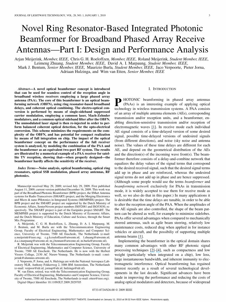
Fig. 3. Binary tree-based 4� 1 optical beamforming network (OBFN) con-sisting of four ORRs and three combiners.
considered as the reference path. On the other hand, two neigh-bouring AEs require similar delay values, so the correpondingpaths in the OBFN have only a small difference in delay. Fromthe considerations in Section II-B it follows that this differencecan therefore be tuned by a low number of rings in the firststage, whereas the (larger) common delay can be tuned by acommon delay element (requiring more rings) in a common partof these paths, in the next stage. This can be generalized to largerOBFNs, for example 8 1, 16 1, etcetera. This approach willresult in a minimum total required number of rings for the com-plete OBFN. The total number depends on
• the required delay tuning range per delay element (which isdetermined by the PAA geometry and the maximum scanangle);
• the required delay ripple (or, for example, the accuracy ofthe corresponding phase response);
• the required optical bandwidth.In this paper we will not go into further detail on the requireddelay values and their accuracy, but we will focus on approachesto build up the system around the OBFN in such a way that therequired optical bandwidth is minimized. This will be discussedin Section III.
In [26], [27] we presented group delay measurements on asingle-chip realization of such a 4 1 ORR-based OBFN, fab-ricated in CMOS-compatible waveguide technology. Later weextended these to an 8 1 OBFN [28]–[32]. We also presentedtime domain measurements on a 2 1 OBFN [33], and coherentcombining of multiple input signals [32], [34].
III. DESIGN OF THE OPTICAL MODULATION AND
DETECTION SCHEME
Several considerations have to be made when choosing theway in which the optical signals entering the OBFN are to bemodulated by the AE signals, and this will have consequencesfor the way in which the optical signal should be detected afteroptical beamforming. As discussed in Section II, an importantcriterion is that the bandwidth of the modulated optical signalsshould be minimized, in order to minimize the required com-plexity of the OBFN. Moreover, the optical beamformer shouldbe designed in such a way that its impact on the performanceof the full receiver system (in terms of dynamic range) is keptwithin acceptable bounds. This implies that the noise, loss, andnon-linear distortion in the optical modulation and detectionshould be minimized.
Fig. 4. Beamformer scheme with� inputs, using optical intensity modulation(IM) and direct optical detection. (AE � antenna element, LNA � low-noiseamplifier, OBFN � optical beamforming network).
A. Common Laser and Detector
A first consequence of the bandwidth requirement is that theoptical sources should be narrowband, i.e., the bandwidths of themodulated optical signals should be determined by the inherentspectral broadening due to the modulation, and not by the band-width of the source signal itself. In other words, the bandwidthof the source signal should be much smaller than the bandwidthof the modulating signals.
The most straightforward way of performing the E/O con-version would then be to use directly modulated lasers, but thishas three important drawbacks. First of all, directly modulatinga laser will cause frequency chirping [37], resulting in spectralbroadening. Secondly, direct modulation techniques suffer froma limited dynamic range due to the elevated noise and distortionlevels at high frequencies [38], [39]. Therefore, E/O conversionshould be performed by externally modulating continuous-wave(CW) light. A third problem is that using a separate laser foreach individual AE signal would lead to incoherent optical com-bining, resulting in optical beat interference (OBI) noise. Thebandwidth of this noise would be in the same order of mag-nitude as the source signal’s bandwidth. As discussed before,this bandwidth should be as low as possible, so the OBI noisewould be completely in the signal band. As a result, it would notbe possible to filter out the OBI noise, so it would completelycorrupt the output signal of the beamformer. This is preventedwhen a common CW laser and coherent optical combining isused. This requires the coherence time of the source to be muchlarger than the maximum difference between the group delaysof the different beamformer paths, in order to maintain correla-tion between the optical phases. Moreover, the signals that arecombined have to be synchronized in optical phase; this will befurther discussed in Section III-E.
B. Optical Intensity Modulation and Direct Optical Detection
First we consider the technique that should be used for theexternal modulation. The most straightforward choice wouldbe to use intensity modulation (IM)—for instance by means ofelectro-absorption modulators (EAMs) or Mach-Zehnder mod-ulators (MZMs)—and direct optical detection, using a photo-diode. This would result in a scheme as shown in Fig. 4.
As the optical intensity is proportional to the square of theoptical field, even perfectly linear IM would result in an op-tical field that has a square-root dependence on the modulating
Authorized licensed use limited to: UNIVERSITEIT TWENTE. Downloaded on January 11, 2010 at 09:32 from IEEE Xplore. Restrictions apply.

MEIJERINK et al.: PART I: DESIGN AND PERFORMANCE ANALYSIS 7
Fig. 5. Spectrum of the modulated optical signal (solid line) in case of op-tical intensity modulation by an RF bandpass signal, and corresponding desiredgroup delay response (dashed line) of a delay element in the OBFN. � denotesthe optical carrier frequency, and � and � denote the lower and upperbound of the frequency range of the modulating RF signal, respectively.
signal. As a result, the optical spectrum at the output of the mod-ulator consists of the optical carrier line and an infinite numberof sidebands, where the number of significant sidebands in-creases with increasing modulation depth. In order to keep therequired complexity and the linear distortion in the OBFN toa minimum, the modulation index should be such that only thefirst order sidebands are significant, and the OBFN should be de-signed so as to provide a flat group delay response covering theoptical carrier and the first order sidebands. This is illustrated inFig. 5. As a result, the minimum optical bandwidth required toperform optical beamforming in case of IM is equal to twice themaximum frequency of the modulating RF signal. Especiallyin case of high-frequency PAAs with large diameters, this willresult in an excessively complex OBFN. Moreover, large op-tical bandwidths require a large FSR of the ORRs, which cor-responds to a low round-trip time and hence a small physicalsize. This may introduce problems with the realizability of thecorresponding optical chips.
In the numerical example that will be presented in Section V,it will be shown that a PAA for receiving -band satellite sig-nals (10.7–12.75 GHz) requires the beamformer to provide de-lays up to roughly 4.3 ns. When IM is performed, the bandwidthof the modulated optical signals will be twice the maximum RFfrequency. As a result, in this case the delay elements in theOBFN would be required to provide delays in the order of 4.3ns over an optical bandwidth of 25.5 GHz, which correspondsto a (linear) phase transition of 110 times . Since the flat partof the group delay response should be within one period of theORRs, and one ORR can provide a phase transition of at most
within one period (see Section II-B), it follows that at least110 ORRs would be required to achieve this. (In practice thisnumber will be even higher, because no delay ripple was incor-porated in this lower bound.) For practical PAAs (with hundredsup till thousands of AEs), several thousands of ORRs would berequired in the OBFN. This is not practical, not only becauseof the required optical chip area (tens to hundreds of wafers),but especially because of the excessive wiring to all the tuningelements, and immense complexity of the tuning electronics.Moreover, the FSR of the ORRs would need to be more than25.5 GHz. This would be a problem for the technology in which
Fig. 6. Spectrum of the modulated optical signal (solid line) in case of opticalsingle-sideband suppressed-carrier (SSB-SC) modulation by an RF bandpasssignal (the suppressed sideband and optical carrier are represented by the dottedline), and corresponding desired group delay response (dashed line) of a delayelement in the OBFN.
our devices were fabricated [5], which can provide a maximumFSR in the order of 15 GHz; this is further considered in Part II[36].
C. Optical SSB-SC Modulation and Balanced CoherentOptical Detection
The required complexity and FSR of the OBFN can be re-duced by lowering the bandwidths of the modulated optical sig-nals at its inputs. Looking at Fig. 5 it should be noted that the twosidebands of the intensity-modulated optical signal in fact carrythe same information, while the optical carrier is only requiredfor O/E conversion. Hence, the required optical bandwidth ofthe OBFN is minimized by performing optical single-sidebandsuppressed-carrier (SSB-SC) modulation instead of optical IM.This results in an optical spectrum as shown in Fig. 6. The dottedline represents the suppressed sideband and optical carrier, andthe solid line represents the remaining sideband. The dashed linerepresents the shape of a possible group delay response. It illus-trates that both the required optical bandwidth and the FSR ofthe OBFN can be significantly reduced with respect to the thesituation with IM, shown in Fig. 5. For example, in the caseof the satellite receiver mentioned before, the required opticalbandwidth and FSR are reduced by more than 90%.
Note that removing the optical carrier is essential here. Thisis related to the fact that the phase relation between the opticalcarrier and the remaining sideband is lost when the group delayresponse is only optimized for the sideband frequency range.Hence, when the delayed optical SSB signals are combined suchthat the sidebands add up in phase, the optical carriers fromthe different branches might not add up in phase. Correctingthis would significantly increase the required bandwidth of theOBFN, and hence the number of ORRs.
In order to convert the delayed and combined optical SSB-SCsignals back to the electrical domain, the optical carrier needsto be re-inserted, but this should be done after the combining. Itcan be done by routing the unmodulated optical carrier aroundthe OBFN and combine it with the SSB-SC-modulated outputsignal of the OBFN by means of a directional coupler, as il-lustrated in Fig. 7. Optical detection should preferably be done
Authorized licensed use limited to: UNIVERSITEIT TWENTE. Downloaded on January 11, 2010 at 09:32 from IEEE Xplore. Restrictions apply.

8 JOURNAL OF LIGHTWAVE TECHNOLOGY, VOL. 28, NO. 1, JANUARY 1, 2010
Fig. 7. Beamformer scheme with� inputs, using optical single-sideband sup-pressed-carrier (SSB-SC) modulation and balanced optical detection.
using a balanced photodiode pair, as this considerably reducesthe effect of relative intensity noise (RIN) [40].
An additional advantage of this scheme when compared tothe scheme with IM and direct detection (Fig. 4) is that thephases of the RF signals that are combined can be tuned di-rectly by tuning the optical phases of the corresponding pathsin the optical beamformer. This is useful when the RF signalsare down-converted before they are fed into the optical modu-lators, in order to reduce the bandwidth requirements of the op-tical modulators and detectors. Down conversion can be doneby means of mixers, filters, and a common local oscillator (LO)signal. The latter is required in order to maintain correlation be-tween the down-converted signals. Normally this would also in-volve a correction of the LO phase for each beamformer path,but in this case this correction can be done in the optical domaininstead.
D. Implementation of Optical SSB-SC Modulation
The next design step is the choice for a suitable implementa-tion form of the optical SSB-SC modulation. Several techniquesare known for implementing optical SSB modulation. These canbe divided into three categories:
1) Filter-Based Techniques: the most straightforward wayof achieving optical SSB-SC modulation is to perform opticalIM, and filter out the optical carrier and one of the sidebands bymeans of an optical sideband filter (OSBF) [41];
2) Optical Heterodyning Techniques: these rely on a com-bination of two lasers with an optical frequency difference thatcorresponds to the desired RF frequency [7]. One of the twooptical carriers is first modulated with baseband data, so thatmixing it with the unmodulated optical carrier results in a mod-ulated RF signal. This technique is not applicable in our case,however, as the input signals to the modulators are already at RF;it would be more useful in cases where the RF signal is yet to begenerated, for example in optical beamformers for phased-arraytransmit antennas. Therefore it is not further considered here;
3) Techniques Based on the Phase-Shift Method: thesetechniques are based on the classical SSB generation technique,where two quadrature carriers are modulated by a modulatingsignal and its Hilbert transform, respectively. Several opticalimplementation forms are known, amongst others based ona dual-electrode MZM [42], hybrid amplitude and phasemodulation [43], two parallel MZMs [44], or a Sagnac loopwith a unidirectional [45] or bidirectional [46] travelling-waveMZM. The double MZM seems to be the only scheme that can
Fig. 8. Beamformer scheme with� inputs, in which the optical SSB-SC mod-ulation is implemented by means of Mach-Zehnder modulators (MZMs) and acommon optical sideband filter (OSBF).
support multi-octave SSB modulation with carrier suppression.(Sub-octave modulation can be a prohibitive restriction insome systems, for example when frequency down conversion isperformed prior to modulation, as we did in our experimentalsetup [36].) However, it has the disadvantage that it requirestwo MZMs per AE.
The most attractive way of performing SSB-SC modulationin this particular application (see Fig. 7) is by means of IM andoptical sideband filtering. It requires only one laser, and one in-tensity modulator per AE. The OSBFs could be put directly afterthe intensity modulator, but then every AE would require itsown OSBF. However, since the OSBF and OBFN are both lineardevices, their order can be reversed, so that only one commonOSBF is required. MZMs are used as intensity modulators, asthey are more linear than EAMs. This results in the system ar-chitecture that is shown in Fig. 8.
When the MZMs are operated anti-symmetrically (in push-pull mode), and properly biased, they will modulate chirp-free,and inherently suppress the optical carrier [47]. This will relaxthe slope requirements on the OSBF characteristic. Since theOSBF is placed after the OBFN, its phase response is not crit-ical, as long as dispersion in the filter passband does not distortthe RF signal. A relatively simple OSBF implementation thatprovides broad, flattened passbands and stopbands is an MZIwith an ORR in one of its arms [48]. Since such an OSBF con-sists of similar building blocks as the OBFN (ORRs and di-rectional couplers), both the OBFN and the OSBF can be inte-grated on the same chip. In [29]–[32] we presented magnituderesponse measurements on a chip in which such an OSBF wasintegrated together with a 4 1 OBFN. In [32], [34], [35] theseresults were extended to demonstrate that the filter successfullysuppresses the undesired sideband, and that—when the OBFNis also properly tuned—the RF-to-RF transfer from modulatorinput to detector output indeed has a linear phase response inthe RF range of interest, according to the desired delay. In PartII of this paper [36] measurements will be presented on an op-tical chip that was specifically designed for satellite televisionreception.
E. Optical Phase Synchronization
An essential property of the OBFN is that the optical inputsignals are combined in phase, as far as the contributions corre-sponding to AE input signals from the desired direction are con-cerned. This not only requires the ORR-based delay elements
Authorized licensed use limited to: UNIVERSITEIT TWENTE. Downloaded on January 11, 2010 at 09:32 from IEEE Xplore. Restrictions apply.
MEIJERINK et al.: PART I: DESIGN AND PERFORMANCE ANALYSIS 9
to compensate for differences in arrival time, but also involvessynchronization on the optical wavelength level. This was anissue in our experimental setup, because so far, in our implemen-tation, only the OBFN, OSBF and carrier re-insertion couplerhave been integrated on chip [36]. The splitting and modulationwere done by means of fiber-based commercial off-the-shelvecomponents, rendering the optical phase in which the signalsare combined very sensitive to changes in temperature and me-chanical stress, and to mechanical vibrations. Therefore, specialmeasures are required to stabilize the input-output behavior ofthe beamformer. Basically two approaches can be taken.
A first approach is to use a feedback loop from the outputsignal to phase shifters in the OBFN paths. This could be basedon the total power of the desired signal, which should be max-imized. Drawbacks of this feedback criterion are the compli-cated relation between the output power and all the phase off-sets—which hampers agile phase synchronization—and the factthat this approach might not result in proper phase-locking wheninterferers are present. A possible solution could be to use afrequency dithering scheme, as proposed within the frameworkof coherent optical code-division multiple access (OCDMA)techniques [49], but this has the disadvantage that it requiresa unique oscillator for each beamformer input, which consider-ably complicates the feeding circuit.
A second approach is to stabilize the entire system in tem-perature. In our fiber-based laboratory setup this was far fromstraightforward, and only effective for synchronization duringa few minutes (see [36] for more details). In the envisioned fu-ture implementation of the beamformer, however, the completeoptical circuit—i.e., all parts between the laser and the pho-todetectors, including the modulators—is expected to be inte-grated on a single chip (or at least in one package). Such a chipcan be stabilized to a pre-defined temperature with an accuracysmaller than 0.01 K, with local and temporal variations evenmuch smaller than that. To show that this is sufficient to stabi-lize the phases of the combined signals, we analyze the effect ofan ambient temperature change on the phase differences be-tween the paths. Temperature changes affect the effective indexof the waveguide. If we assume that the paths in the beamformerchip have equal physical lengths (which is in fact the case inthe chip that we demonstrate in [36]), the resulting phase differ-ences are mainly determined by the changes in phase transferof the ORR-based delay elements. These changes are in turnmainly determined by variations in the round-trip phase shift
of the ORRs, which are given by
(2)
where is the circumference of the ring, is the optical wave-length, and is the derivative of the effective index ofthe waveguide with respect to temperature. (Variations in thecoupling coefficients are neglected here, because the value of
is assumed to be tuned by means of a symmetric MZI, and thephase difference between two paths in a symmetric MZI is muchless sensitive to temperature variations than the round-trip phaseshift in an ORR.) Since the FSR of an ORR can be expressed as
, where is the effective group index of the
waveguide, such change in round-trip phase will result in a(horizontal) frequency shift of the phase response by a value
(3)
When the ORRs are properly tuned, the phase response of eachdelay element is linear with frequency, with a slope that is equalto , where is the group delay to which the delay ele-ment is tuned. The shift in frequency will hence result in a phasechange
(4)
(5)
Assuming a maximum group delay difference between the pathsof 4.3 ns (see the numerical example in Section V), an effectivegroup index of 1.55, an optical wavelength of 1550 nm, and
, we find that temperature fluctuationsbelow 0.01 K result in phase fluctuations below radians,which should be considered acceptable for this application.
Frequency fluctuations of the laser have a similar effect asthe frequency shift in the phase response, so it follows from(4) that fluctuations below 10 MHz (which are achievable usingtemperature control) will also result in phase errors belowradians.
Hence it is expected that the optical phase differences be-tween the different paths in the chip will be sufficiently stable,so that optical phase synchronization only requires an initial cal-ibration, and possibly on-the-fly phase corrections based on theremaining settings of the OBFN.
If we assume that the OSBF is realized as an asymmetric MZIwith an ORR in one of its arms, as we did in the chip that ispresented in Part II of this paper [36], a similar calculation canbe done to show that the transfer function of the OSBF (alsogiven in [36]) is even much less sensitive to temperature changesand laser drift than the OBFN.
IV. PERFORMANCE ANALYSIS
An important consideration in the design of the beamformeris the impact that it will have on the performance of the fullreceiver system, in terms of noise and/or distortion. In orderto analyze this, we first require a framework to describe thisimpact, in terms of system gain, system noise temperature,and the effect of non-linearities. This framework is basedon an equivalent two-port model of the complete receiversystem—including AEs and LNAs—and is further describedin Section IV-A. Then, in Section IV-B, the relation betweenthe input voltages and the output current of the beamformer isstudied. This relation is used to calculate the system gain andnoise temperature, in Sections IV-C and IV-D, respectively.The impact of non-linearities in the beamformer is studied inSection IV-E. In Section IV-F an expression is derived for theCNR at the output of the beamformer.
A. Analysis Framework
The PAA with optical beamformer is essentially an analogoptical signal processor, that can be described as a multiport
Authorized licensed use limited to: UNIVERSITEIT TWENTE. Downloaded on January 11, 2010 at 09:32 from IEEE Xplore. Restrictions apply.
10 JOURNAL OF LIGHTWAVE TECHNOLOGY, VOL. 28, NO. 1, JANUARY 1, 2010
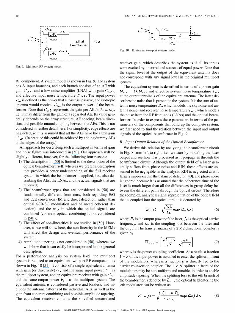
Fig. 9. Multiport RF system model.
RF component. A system model is shown in Fig. 9. The systemhas input branches, and each branch consists of an AE withgain , and a low-noise amplifier (LNA) with gainand effective input noise temperature . The input power
is defined as the power that a lossless, passive, and isotropicantenna would receive. is the output power of the beam-former. Note that represents the gain per AE in the array,i.e., it may differ from the gain of a separated AE. Its value gen-erally depends on the array structure, AE spacing, beam direc-tion, and possible mutual coupling between the AEs. This is notconsidered in further detail here. For simplicity, edge effects areneglected, so it is assumed that all the AEs have the same gain
. (In practice this could be achieved by adding dummy AEsat the edges of the array.)
An approach for describing such a multiport in terms of gainand noise figure was introduced in [50]. Our approach will beslightly different, however, for the following four reasons:
1) The description in [50] is limited to the description of theoptical beamformer itself, whereas we prefer a descriptionthat provides a better understanding of the full receiversystem in which the beamformer is applied, i.e., also de-scribing the AEs, the LNAs, and the actual signals that arereceived;
2) The beamformer types that are considered in [50] arefundamentally different from ours, both regarding E/Oand O/E conversion (IM and direct detection, rather thanoptical SSB-SC modulation and balanced coherent de-tection), and the way in which the optical signals arecombined (coherent optical combining is not consideredin [50]);
3) The effect of non-linearities is not studied in [50]. How-ever, as we will show here, the non-linearity in the MZMswill affect the design and eventual performance of thesystem;
4) Amplitude tapering is not considered in [50], whereas wewill show that it can easily be incorporated in the generaldescription.
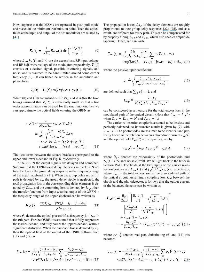
For a performance analysis on system level, the multiportsystem is reduced to an equivalent two-port RF component, asshown in Fig. 10 [51]. It consists of a single equivalent antennawith gain (or directivity) and the same input power asthe multiport system, and an equivalent receiver with gainand the same output power as the multiport system. Theequivalent antenna is considered passive and lossless, and in-cludes the antenna patterns of the individual AEs, as well as thegain from coherent combining and possible amplitude tapering.The equivalent receiver contains the so-called uncorrelated
Fig. 10. Equivalent two-port system model.
receiver gain, which describes the system as if all its inputswere excited by uncorrelated sources of equal power. Note thatthe signal level at the output of the equivalent antenna doesnot correspond with any signal level in the original multiportsystem.
The equivalent system is described in terms of a power gain, and effective system noise temperature
at the output terminals of the equivalent antenna. The latter de-scribes the noise that is present in the system. It is the sum of an-tenna noise temperature , which models the sky noise and an-tenna noise, and receiver noise temperature , which modelsthe noise from the RF front-ends (LNAs) and the optical beam-former. In order to express these parameters in terms of the pa-rameters of the components that build up the complete system,we first need to find the relation between the input and outputsignals of the optical beamformer in Fig. 9.
B. Input-Output Relation of the Optical Beamformer
We derive this relation by analyzing the beamformer circuitin Fig. 8 from left to right, i.e., we start by modeling the laseroutput and see how it is processed as it propagates through thebeamformer circuit. Although the output field of a laser gen-erally suffers from phase noise and RIN, these effects are as-sumed to be negligible in the analysis. RIN is neglected as it islargely suppressed in the balanced detector [40], and phase noiseis ignored because it is assumed that the coherence time of thelaser is much larger than all the differences in group delay be-tween the different paths through the optical circuit. Thereforethe (complex) analytical signal representation of the optical fieldthat is coupled into the optical circuit is denoted by
(6)
where is the output power of the laser, is the optical carrierfrequency, and is the coupling loss between the laser andthe circuit. The transfer matrix of a 2 2 directional coupler isgiven by
(7)
where is the power coupling coefficient. As a result, a fractionof the input power is assumed to enter the splitter in front
of the modulators, whereas a fraction is directly fed to thecarrier re-insertion coupler. The splitter in front of themodulators may be non-uniform and tunable, in order to enableamplitude tapering. When the splitting loss to the th branch ofthe beamformer is denoted by , the optical field entering the
th modulator can be written as
(8)
Authorized licensed use limited to: UNIVERSITEIT TWENTE. Downloaded on January 11, 2010 at 09:32 from IEEE Xplore. Restrictions apply.
MEIJERINK et al.: PART I: DESIGN AND PERFORMANCE ANALYSIS 11
Now suppose that the MZMs are operated in push-pull mode,and biased in the minimum transmission point. Then the opticalfields at the input and output of the th modulator are related by[47]
(9)
where , and are the excess loss, RF input voltage,and RF half-wave voltage of the modulator, respectively.consists of a desired signal, possible interfering signals, andnoise, and is assumed to be band-limited around some carrierfrequency . It can hence be written in the amplitude andphase form
(10)
When (8) and (10) are substituted in (9), and it is (for the timebeing) assumed that is sufficiently small so that a firstorder approximation can be used for the sine function, then wecan approximate the optical fields entering the OBFN as
(11)
The two terms between the square brackets correspond to theupper and lower sideband in Fig. 6, respectively.
In the OBFN the output signals are delayed and combined.Suppose that the ORR-based delay elements in the OBFN aretuned to have a flat group delay response in the frequency rangeof the upper sideband of (11). When the group delay in the thpath is denoted by , the group delay ripple is neglected, thetotal propagation loss in the corresponding delay elements is de-noted by , and the combining loss is denoted by , thenthe transfer function from Input to the output of the OBFN inthe frequency range of the upper sideband can be written as
(12)
where denotes the optical phase shift at frequency inthe th path. For the OSBF it is assumed that it fully suppressesthe lower sideband, and fully passes the upper sideband, withoutsignificant distortion. When the passband loss is denoted by ,then the optical field at the output of the OSBF follows from(11) and (12) as
(13)
The propagation losses of the delay elements are roughlyproportional to their group delay responses [22], [25], and, as aresult, are different for every path. This can be compensated forby properly tuning and , which also enables amplitudetapering. Hence, we can write
(14)
where the passive taper coefficients
(15)
are defined such that , and
(16)
can be considered as a measure for the total excess loss in themodulated path of the optical circuit. (Note thatwhen and .)
The carrier re-insertion coupler is assumed to be lossless andperfectly balanced, so its transfer matrix is given by (7), with
. The photodiodes are assumed to be identical and per-fectly linear, so the relation between a photodiode currentand the optical field at its input is given by
(17)
where denotes the responsivity of the photodiode, andis the shot noise current. We will get back to the latter in
Section IV-D. The fields at the two inputs of the carrier re-in-sertion coupler are and , respectively,where is the total excess loss in the unmodulated path ofthe optical circuit. Assuming a coupling loss between thecircuit and the photodetector, it follows that the output currentof the balanced detector can be written as
(18)
where denotes real part. Substituting (6) and (14) thisbecomes
(19)
Authorized licensed use limited to: UNIVERSITEIT TWENTE. Downloaded on January 11, 2010 at 09:32 from IEEE Xplore. Restrictions apply.
12 JOURNAL OF LIGHTWAVE TECHNOLOGY, VOL. 28, NO. 1, JANUARY 1, 2010
Now suppose that the optical phases of the signals that are com-bined are tuned such that . It can be verifiedthat (19) can then be simplified using (10), resulting in
(20)
The values of the delays should be chosen such that the de-sired terms in the delayed input voltages are time-synchronized. Properly tuning the values of is then a matterof optical phase synchronization (see Section III-E).
C. Gain
In order to find expressions for the gains that were introducedin Section IV-A, we need to relate the inputs and output of thecomplete receiver system in terms of power. The total gainof the equivalent system is equal to the coherent gain or signalgain [51], i.e., the gain that the input power in Fig. 9 seeswhen its contributions to the AE signals add up coherently inthe beamformer. This can be derived from (20), by noting thatthe input power to the th beamformer input can be expressedin terms of the PAA input power as , but alsoin terms of the modulator input voltage as ,where denotes mean value, and is the input impedanceof the MZMs. The actual output power depends on theway in which the photodiodes are connected to the next stageof the receiver. In this case, we simply assume that there isno matching circuit, and that the output current is dis-sipated in a load impedance , resulting in an output power
. (If a resistive matching circuit were in-cluded, this would simply decrease by 6 dB.) Assuming that theinput voltages add up coherently, it now follows from (20)that the coherent gain is given by
(21)
where is the taper efficiency
(22)
Note that for uniform tapering.The receiver gain is equivalent to the incoherent gain or
noise gain, i.e., the gain that the individual input (noise) powers(at the inputs of the LNAs, so excluding ) see when theyadd up incoherently in the beamformer. Using (20) this can beshown to result in
(23)
with
(24)
The latter can be considered as the intrinsic receiver gain ofthe beamformer, i.e., it is the equivalent receiver gain of thebeamformer excluding the LNAs. In other words, the equivalent
receiver could be modeled as a cascade of one LNA, with gain, and the equivalent receiver that would be obtained if
there were no LNAs, with gain .Since the total system gain can be written as
(see Fig. 10), we find for the equivalent antenna gain
(25)
D. Noise
The noise at the output of the beamformer is partly causedby the antenna noise that is already present at the input, andpartly by receiver noise. The effective noise temperature of theequivalent antenna is approximated by the brightness tempera-ture of the sky in the direction of the main lobe, so .Using Friis’ formula, the effective input noise temperature ofthe equivalent receiver can be written as
(26)
where is the effective input noise temperature of theLNAs, and is the effective input noise temperature of theequivalent two-port model of the beamformer without LNAs.Hence, is the contribution to the system noisetemperature due to noise in the optical beamformer. The latteris caused by thermal noise in the matching resistors in theMZMs, shot noise in the photodiodes, thermal receiver noise,RIN, and optical phase noise. Thermal noise in the matchingresistors is neglected here when compared to the LNA noise;in other words, it is assumed that is much largerthan the temperature of the matching resistors. As explained inthe beginning of Section IV-B, RIN and phase noise are alsoneglected in our analysis. The thermal noise generated in theoptical receiver is usually quantified in terms of the root meansquare (RMS) equivalent input noise current per , anddepends on the implementation of the receiver. If this is denotedby , then the power spectral density of the equivalent inputnoise current is equal to . The power spectral density ofthe shot noise current in (17) follows from Schottky’sformula:
(27)
where is the electron charge ( C). The power spectraldensity of the total shot noise current in (18) now fol-lows by summing the power spectral densities of the individualshot noise currents, resulting in
(28)
This can be evaluated by substituting (6) and (14). Whenis small, as assumed before, the first term inside the angle
Authorized licensed use limited to: UNIVERSITEIT TWENTE. Downloaded on January 11, 2010 at 09:32 from IEEE Xplore. Restrictions apply.

MEIJERINK et al.: PART I: DESIGN AND PERFORMANCE ANALYSIS 13
brackets can be neglected. Hence it follows that the spectraldensity of the power that is dissipated in the load due to thethermal noise and shot noise is given by
(29)
By definition, this is supposed to be equal to(where is Boltzmann’s constant, J/K). Hence,using (24), it follows that is given by
(30)
Preferably, the parameter values in the beamformer should bechosen in such a way that the resulting value ofis much smaller than and . Moreover, the total receivergain in (23) should be large enough to overcome noise thatis generated behind the beamformer. Otherwise the performanceof the complete system would be limited by the performance ofthe beamformer. This will be further illustrated by the numericalexample in Section V.
From (30) it also follows that the choice of a suitable valuefor the power coupling coefficient of the directional couplerdirectly behind the laser is a trade-off. In case the thermal noiseterm dominates (i.e., the second term in the numerator of (30)),its effect can be minimized by maximizing the intrinsic receivergain , by setting . In case the thermal noise doesnot dominate, the optimum value of is smaller than , asthe effect of shot noise (the first term in the numerator of (30))increases with increasing value of . This is not considered infurther detail here.
E. Compression
Apart from noise, the beamformer will also have an impacton the distortion in the receiver, because of the non-linearity inthe MZMs. In theory, this will result in an upper limit to theinput power that the PAA receiver can accommodate, becauseof the self-compression and intermodulation distortion (IMD) tothe incoming signal. This can, for instance, be expressed in theintercept point and/or 1-dB compression point of the receiver.A framework for performing such an analysis was introduced in[52], and we applied it to our beamformer in [53].
In practice, however, the upper limit to the input power ofthe receiver is not determined by what the receiver can accom-modate, but by the context of the receiver, i.e., there simplyis an upper limit to the power that the receiver will receive.(For instance, the satellite receiver considered in the numer-ical example in Section V is assumed to receive no more than
dBW from the satellite.) In that case the non-linearity willpose a limit to the maximum gain that the LNAs should have.
To analyze this we need to take a closer look at the MZM char-acteristic in (9), which shows the non-linear relation betweenRF inputs and the optical outputs . Suppose that the
input signal is written as a signal part plus a noise part. We can then rewrite (9) as
(31)
To study the effect of non-linearities in for example analog op-tical links, it is common to make third order approximations forthe terms containing , and first order approximations forthe terms containing , because the power of isusually much larger than the power of . This is also whatwe did in [53].
This is not necessarily realistic in a PAA receiver, however,since the CNR per AE might be very small. This is particu-larly the case for a PAA with a large number of AEs, and thatis exactly the application for which this type of beamformer issuitable. In this case, it is therefore more realistic to make firstorder approximations only for the terms in which ap-pears rather than , resulting in
(32)
so the signal is compressed by a (random) factor. In other words, the signal mainly suffers
from cross-compression with the noise, rather than self-com-pression and IMD, irrespective of the number of sub-carriers inthe desired signal. The (thermal) noise can be assumedto be Gaussian distributed with mean zero and variance
(33)
where is the average antenna noise temperature that is seenby the individual AEs, which is not necessarily equal to the an-tenna noise temperature that is seen by the complete PAA.
is the equivalent noise bandwidth of the LNA. Using theGaussian probability density function of , the mean valueof the compression factor can now be calculated as
(34)
This implies that the total system gain that was derived inSection IV-C is reduced by a factor
(35)
By calculating the autocorrelation function of the sine term in(32), it can be proven that the noise power at the output of thebeamformer due to sky noise and LNA noise is reduced by thesame factor (which should not be surprising). Therefore the neteffect of the non-linearity of the MZM is that both the totalsystem gain and the receiver gain are reduced by thesame factor , so the equivalent antenna gain remains un-changed. The contributions of the sky noise and LNA noise to
Authorized licensed use limited to: UNIVERSITEIT TWENTE. Downloaded on January 11, 2010 at 09:32 from IEEE Xplore. Restrictions apply.
14 JOURNAL OF LIGHTWAVE TECHNOLOGY, VOL. 28, NO. 1, JANUARY 1, 2010
the effective system noise temperature also remain unchanged.The beamformer’s contribution to the system noise tempera-ture is increased by the inverse of , however,since its contribution to the noise power at the output remainsunchanged, whereas is reduced.
F. Carrier-to-Noise Ratio
Now suppose the broadband signal that is beamformed by thePAA receiver is a multi-carrier signal, with information chan-nels with equivalent noise bandwidths . The CNR of onechannel at the output of the two-port device then follows fromFig. 10 and the equations derived before as
(36)
where and are given by (30) and (35), respec-tively. We stress once more that this result only applies tosystems where the AE signals have low CNRs, as explained inSection IV-E.
V. NUMERICAL EXAMPLE
As a numerical example, we consider a simplified versionof the PAA receiver system that was designed in the SMARTproject, which was mentioned in the introduction. More specifi-cally, consider the reception of television channels according tothe Digital Video Broadcasting by Satellite (DVB-S) standard.In Europe, the power received per channel from for examplethe Astra satellite is known to be in the order of dBW.Allowing a margin of 10 dB for fluctuating atmospheric con-ditions and changing location, we set the requirement forminimum detectable received power to dBW. TheCNR at the input of a DVB-S receiver is required to be in theorder of 8 dB. The brightness temperature of the sky aroundthis satellite is in the order of 50 K, so we take K.A single AE will have a much wider antenna pattern than thecomplete PAA, and will therefore see radiating bodies as well.We assume that this results in AE temperatures K.Suppose that commercial low-noise blocks (LNBs) are usedto filter, amplify, and down-convert the AE signals prior to op-tical modulation, with gains dB, equivalent noisetemperatures K, and equivalent noise bandwidths
GHz. It then follows that the system noise temper-ature has a lower limit of K. Assumingan equivalent noise bandwidth for the individual channels
MHz, we can derive from (36) that the minimum gainof the equivalent antenna should be in the order of 34.6 dBi.
Suppose that we assume a planar array consisting of a rectan-gular grid of equally weighted AEs (i.e., there is no amplitudetapering), with an inter-element spacing of half a wavelength.The latter is usually chosen in accordance with the highest fre-quency in the band of interest (12.75 GHz in our case), to avoidgrating lobes at the lower frequencies. Therefore we assume aninter-element spacing of 1.18 cm. According to [54], the direc-tivity of such an array is given by , where is
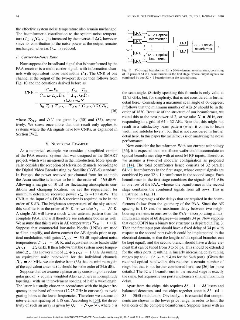
Fig. 11. Two-stage beamformer for a 2048-element antenna array, consistingof 32 parallel 64� 1 beamformers in the first stage, whose output signals arecombined by one 32� 1 beamformer in the second stage.
the scan angle. (Strictly speaking this formula is only valid at12.75 GHz, but, for simplicity, that is not considered in furtherdetail here.) Considering a maximum scan angle of 60 degrees,it follows that the minimum number of AEs should be in theorder of 1830. Because of the structure of our beamformer, weround this to the next power of 2, so we take , cor-responding to a grid of 64 32 AEs. Note that this might notresult in a satisfactory beam pattern (when it comes to beamwidth and sidelobe levels), but that is not considered in furtherdetail here. In this paper the main focus is on analyzing the noiseperformance.
Now consider the beamformer. With our current technology[36], it is expected that one silicon wafer could accomodate anoptical beamformer chip with at most 64 RF inputs. Therefore,we assume a two-level modular configuration as proposedin [14]. The total beamformer hence consists of 32 parallel64 1 beamformers in the first stage, whose output signals arecombined by one 32 1 beamformer in the second stage. Eachbeamformer in the first stage combines the signals of 64 AEsin one row of the PAA, whereas the beamformer in the secondstage combines the combined signals from all rows. This isillustrated in Fig. 11.
The tuning ranges of the delays that are required in the beam-formers follow from the geometry of the PAA. Since the AEspacing is 1.18 cm, the maximum delay between two neigh-bouring elements in one row of the PAA—incorporating a max-imum scan angle of 60 degrees—is roughly 34 ps. Now supposethat each OBFN has a binary tree structure as depicted in Fig. 3.Then the first input port should have a fixed delay of 34 ps withrespect to the second port (which could be implemented in theelectrical domain, so that the lengths of the optical branches canbe kept equal), and the second branch should have a delay ele-ment that can be tuned from 0 to 68 ps. This should be extendedfor the other ports, resulting in linearly increasing delay tuningranges (up to ns for the 64th port). (Given therequired optical bandwidth, this requires a certain number ofrings, but that is not further considered here; see [36] for moredetails.) The 32 1 beamformer in the second stage is exactlythe same, but requires fewer ports and hence a smaller maximumdelay.
Apart from the chips, this requires lasers andbalanced detectors, and the chips together contain
modulators. Obviously, it is essential that compo-nents are chosen in the lower price range, in order to limit thetotal costs of the complete beamformer. Suppose lasers with an
Authorized licensed use limited to: UNIVERSITEIT TWENTE. Downloaded on January 11, 2010 at 09:32 from IEEE Xplore. Restrictions apply.

MEIJERINK et al.: PART I: DESIGN AND PERFORMANCE ANALYSIS 15
output power of 10 dBm are used, so mW. For sim-plicity, the power coupling coefficient of the coupler behindthe laser is set to 1/2. Based on several recently reported re-sults on high-speed compact MZMs, we assume here that, inthe near future, it will be possible to integrate MZMs in ourbeamformers with a switching voltage in the order of 1 V,and an optical excess loss of roughly 2 dB. For the bal-anced detectors we assume photodiode responsivities of0.8 A/W, and load impedances of 50 , which are at roomtemperature K. If we ignore the noise of any suc-ceeding electronics, we find an RMS equivalent input noise cur-rent .
Further losses in the chip comprise the laser-chip and chip-de-tector losses, which we estimate to be in the order of 1 dB, so
. The losses inside the chip, in the modu-lated path and unmodulated path , are dominatedby the losses of the modulators (2 dB) and propagation lossesin the waveguides. Although higher losses were measured inthe chips that we present in [36], our partner, LioniX B.V., hasalready published optical chips with waveguide losses below0.1 dB/cm [5]. Recently they have even measured losses in theorder of 0.05 dB/cm, so we expect to realize beamformers withsuch loss characteristics in the very near future, and will there-fore use that number in the calculation here. If we assume thatthe length of the unmodulated path is in the order of 5 cm, wefind . The loss in the modulated path can be foundfrom (16), with some additional assumptions. First, we assumethat the splitters and combiners are lossless, so
. Furthermore it is assumed that ,as this minimizes the loss. It is also assumed that the opticalpower is distributed over the branches in such a way that the dif-ferences in losses between the delay elements are compensatedfor, and uniform tapering is achieved. This can be done using(15). The losses in the ORR-based delays (in dBs) can be provento be roughly equal to the effective optical path length times theloss coefficient [22], [25]. Hence, the worst case occurs when allthe ORRs are tuned to their maximum delays. For example, theORRs that are passed from the second input port of the 64 1OBFNs introduce a maximum delay of 68 ps, which—assumingan effective group index of 1.55—corresponds to 1.3 cm, or0.066 dB loss. This loss in dBs increases linearly for the otherdelay ports (resulting in 4.1 dB for the 64th port). Using (16)and the assumptions mentioned above, it can be proven thatthis gives a contribution of roughly 2.2 dB to the overall lossin the modulated path. For the 32 1 beamformer this becomesroughly 1.0 dB. If we use a filter structure as presented in [36],its size will be in the order of 5 cm, resulting in a passbandloss of roughly 0.25 dB, so . When the fixed parts inthe modulated paths (including the carrier re-insertion coupler)are also assumed to have a common length of roughly 5 cm,it follows that the total loss in the modulated path is roughly4.7 dB for the 64 1 beamformer and 3.5 dB
for the 32 1 beamformer.Let us first consider the 64 1 beamfomers in the first stage.
If we subsitute our parameters in (23), (24), (30), and (35), wefind (23 dB), K, and
( dB). Apparently, the compression in the mod-ulators is negligible, and the first beamformer stage gives a con-
tribution K to the system noise tempera-ture, which corresponds to an increase of 20%, or 0.8 dB re-duction of the CNR. This could be improved by increasing theoptical power (but this would require more expensive lasers), orby putting additional IF amplifiers behind the LNBs. The beam-former’s contribution to the system noise temperature can belowered to 1 K by inserting an IF gain of 13 dB. It can be veri-fied that this still results in less than 0.1 dB of compression.
Now consider the 32 1 beamformer in the second stage.We can calculate that this beamformer has an effective inputnoise temperature of K. First suppose that we wouldnot put amplifiers between the first and second stage. Since thefirst stage has a total receiver gain of 36 dB (including the IFamplifier), it follows that this would give a contribution to thesystem noise temperature of K. This can be decreasedto 1 K by inserting IF amplifiers between the first and secondstage with a gain of 33 dB (where the noise generated in theseamplifiers is neglected). It can be verified that the compressionis then still negligible.
Note that the assumption about the low optical losses is cru-cial here. Increasing them would decrease the intrinsic receivergains and hence increase the input noise temperatures
of the beamformers. This can be compensated for byincreasing the amplification, but then the compression in theMZMs can become an issue.
VI. CONCLUSION
A novel beamformer concept has been introduced thatenables squint-free, seamless steering of broadband receivePAAs, using integrated ORRs as broadband delay elements,filter-based optical SSB-SC modualtion for the E/O conversion,and balanced coherent optical detection for the O/E conversion.
The concept has potential for a very compact, low-weight im-plementation, by large-scale integration of the optical function-ality (splitters, OBFN, OSBF, and carrier re-insertion), and hy-brid integration with the laser, modulators, and the balanced de-tector. Hybrid integration of the modulators and the splitting andcombining circuitry is essential in order to stabilize the phaserelation between the optical signals that are combined in theOBFN.
Performance analysis has shown that the beamformer doesnot degrade the performance of the receiver system in which itis applied, provided that proper amplifiers are used, and that theoptical losses are kept sufficiently low.
The feasibility of the system is also illustrated by experi-mental results on a (partly integrated) 8 1 optical beamformersetup in Part II of this paper [36].
REFERENCES
[1] R. C. Hansen, Phased Array Antennas. New York: Wiley, 1998.[2] R. A. Minasian, “Photonical signal processing of microwave signals,”
IEEE Trans. Microwave Theory Tech., vol. 54, no. 2, pp. 832–846, Feb.2006.
[3] A. J. Seeds and K. J. Williams, “Microwave photonics,” J. LightwaveTechnol., vol. 24, no. 12, pp. 4628–4641, Dec. 2006.
[4] J. Capmany and D. Novak, “Microwave photonics combines twoworlds,” Nature Photonics, vol. 1, pp. 319–330, June 2007.
[5] F. Morichetti, A. Melloni, M. Martinelli, R. G. Heideman, A. Leinse, D.H. Geuzebroek, and A. Borreman, “Box-shaped dielectric waveguides:A new concept in integrated optics?,” J. Lightwave Technol., vol. 25,no. 9, pp. 2579–2589, Sept. 2007.
Authorized licensed use limited to: UNIVERSITEIT TWENTE. Downloaded on January 11, 2010 at 09:32 from IEEE Xplore. Restrictions apply.
16 JOURNAL OF LIGHTWAVE TECHNOLOGY, VOL. 28, NO. 1, JANUARY 1, 2010
[6] N. A. Riza, Selected Papers on Photonic Control Systems for PhasedArray Antennas, ser. SPIE Milestone. New York: SPIE, Jun. 1997,vol. MS 136.
[7] G. Grosskopf et al., “Photonic 60-GHz maximum directivity beamformer for smart antennas in mobile broad-band communications,”IEEE Photon. Technol. Lett., vol. 14, no. 8, pp. 1169–1171, Aug. 2002.
[8] A. P. Goutzoulis, D. K. Davies, and J. M. Zomp, “Hybrid electronicfiber optic wavelength-multiplexed system for true time-delay steeringof phased array antennas,” Opt. Eng., vol. 31, no. 11, pp. 2312–2322,1992.
[9] M. A. Piqueras et al., “Optically beamformed beam-switched adaptiveantennas for fixed and mobile broad-band wireless access networks,”IEEE Trans. Microwave Theory Tech., vol. 54, no. 2, pp. 887–899, Feb.2006.
[10] D. Dolfi, P. Joffre, J. Antoine, J. P. Huignard, D. Philipper, and P.Granger, “Experimental demonstration of a phased-array antenna op-tically controlled with phase and time delays,” Appl. Opt, vol. 35, no.26, pp. 5293–5300, 1996.
[11] N. Madamopoulos and N. A. Riza, “Demonstration of an all-digital7-bit 33-channel photonic delay line for phased-array radars,” Appl.Opt., vol. 39, no. 23, pp. 4168–4181, Aug. 2000.
[12] R. Soref, “Optical dispersion technique for time delay beam steering,”Appl. Opt., vol. 31, no. 35, pp. 7395–7397, Dec. 1992.
[13] R. D. Esman, M. Y. Frankel, J. L. Dexter, L. Goldberg, and M. G.Parent, “Fiber optic prism true time delay antenna feed,” IEEE Photon.Technol. Lett., vol. 5, no. 11, pp. 1347–1349, Nov. 1993.
[14] M. Y. Frankel, P. J. Matthews, and R. D. Esman, “Two-dimensionalfiber-optic control of a true time-steered array transmitter,” IEEE Trans.Microw. Theory Tech., vol. 44, no. 12, pp. 2696–2702, Dec. 1996.
[15] R. A. Soref, “Fiber grating prism for true time delay beamsteering,”Fiber Integr. Opt., vol. 15, no. 4, pp. 325–333, Oct. 1996.
[16] H. Zmuda, R. A. Soref, P. Payson, S. Johns, and E. N. Toughlian,“Photonic beamformer for phased array antennas using a fiber gratingprism,” IEEE Photon. Technol. Lett., vol. 9, no. 2, pp. 241–243, Feb.1997.
[17] J. L. Corral, J. Marti, J. M. Fuster, and R. I. Laming, “Dispersion-induced bandwidth limitation of variable true time delay lines basedon linearly chirped fibre gratings,” Electron. Lett., vol. 34, no. 2, pp.209–211, Jan. 1998.
[18] B. Ortega, J. L. Cruz, J. Capmany, M. V. Andrés, and D. Pastor,“Variable delay line for phased-array antenna based on a chirped fibergrating,” IEEE Trans. Microwave Theory Tech., vol. 48, no. 8, pp.1352–1360, Aug. 2000.
[19] D. B. Hunter, M. E. Parker, and J. L. Dexter, “Demonstration of a con-tinuously variable true-time delay beamformer using a multichannelchirped fiber grating,” IEEE Trans. Microwave Theory Tech., vol. 54,no. 2, pp. 861–867, Feb. 2006.
[20] N. A. Riza, M. A. Arain, and S. A. Khan, “Hybrid analog-digitalvariable fiber-optic delay line,” J. Lighw. Technol, vol. 22, no. 2, pp.619–624, Feb. 2004.
[21] M. S. Rasras et al., “Integrated resonance-enhanced variable opticaldelay lines,” IEEE Photon. Technol. Lett., vol. 17, no. 4, pp. 834–836,Apr. 2005.
[22] G. Lenz, B. J. Eggleton, C. K. Madsen, and R. E. Slusher, “Opticaldelay lines based on optical filters,” IEEE J. Quantum Electron., vol.37, no. 4, pp. 525–532, Apr. 2001.
[23] J. E. Heebner, V. Wong, A. Schweinsberg, R. W. Boyd, and D.J. Jackson, “Optical transmission characteristics of fiber ring res-onators,” IEEE J. Quantum Electron., vol. 40, no. 6, pp. 726–730,June 2004.
[24] L. Zhuang, C. G. H. Roeloffzen, and W. van Etten, “Continuously tun-able optical delay line,” in Proc. 12th IEEE/CVT Symp. Benelux, En-schede, The Netherlands, Nov. 3, 2005, paper P23.
[25] C. G. H. Roeloffzen, L. Zhuang, R. G. Heideman, A. Borreman, andW. van Etten, “Ring resonator-based tunable optical delay line inLPCVD waveguide technology,” in Proc. 10th IEEE/LEOS Symp.Benelux, Mons, Belgium, Dec. 1–2, 2005, pp. 79–82.
[26] L. Zhuang, C. G. H. Roeloffzen, R. G. Heideman, A. Borreman,A. Meijerink, and W. van Etten, “Single-chip optical beam formingnetwork in LPCVD waveguide technology based on optical ringresonators,” in Proc. Int. Topical Meeting on Microwave Photonics(MWP’2006), Grenoble, France, Oct. 3–6, 2006, paper F1.4.
[27] A. Meijerink, C. G. H. Roeloffzen, L. Zhuang, D. A. I. Marpaung, R.G. Heideman, A. Borreman, and W. van Etten, “Phased array antennasteering using a ring resonator-based optical beam forming network,” inProc. 13th IEEE/CVT Symp. Benelux, Liège, Belgium, Nov. 23, 2006,pp. 7–12.
[28] L. Zhuang, C. G. H. Roeloffzen, R. G. Heideman, A. Borreman, A.Meijerink, and W. van Etten, “Single-chip ring resonator-based 1� 8optical beam forming network in CMOS-compatible waveguide tech-nology,” IEEE Photon. Technol. Lett., vol. 15, no. 15, pp. 1130–1132,Aug. 2007.
[29] L. Zhuang, A. Meijerink, C. G. H. Roeloffzen, D. A. I. Marpaung,J. Peña Hevilla, W. van Etten, R. G. Heideman, A. Leinse, and M.Hoekman, “Phased array receive antenna steering system using a ringresonator-based optical beam forming network and filter-based opticalSSB-SC modulation,” in Proc. Int. Topical Meeting on Microwave Pho-tonics (MWP’2007), Victoria, BC, Canada, Oct. 3–5, 2007, pp. 88–91.
[30] L. Zhuang, A. Meijerink, C. G. H. Roeloffzen, D. A. I. Marpaung, R. G.Heideman, M. Hoekman, A. Borreman, A. Leinse, and W. van Etten,“Novel ring resonator-based optical beamformer system and experi-mental results,” in Proc. 11th IEEE/LEOS Symp. Benelux, Brussels,Belgium, Dec. 17–18, 2007, pp. 239–242.
[31] H. Schippers, J. Verpoorte, P. Jorna, A. Hulzinga, A. Meijerink, C. G.H. Roeloffzen, L. Zhuang, D. A. I. Marpaung, W. van Etten, R. G.Heideman, A. Leinse, A. Borreman, M. Hoekman, and M. Wintels,“Broadband conformal phased array with optical beamforming for air-borne satellite communication,” in Proc. IEEE Aerospace Conf. 2008,Big Sky, MT, Mar. 1–8, 2008, paper 3.0102.
[32] H. Schippers, J. Verpoorte, P. Jorna, A. Hulzinga, L. Zhuang, A. Mei-jerink, C. G. H. Roeloffzen, D. A. I. Marpaung, W. van Etten, R. G. Hei-deman, A. Leinse, and M. Wintels, “Broadband optical beam formingfor airborne phased array antenna,” in Proc. IEEE Aerospace Conf.2009, Big Sky, MT, Mar. 7–14, 2009, paper 3.0101.
[33] L. Zhuang, A. Meijerink, C. G. H. Roeloffzen, D. A. I. Marpaung, R. G.Heideman, M. Hoekman, A. Borreman, D. H. Geuzebroek, A. Leinse,and W. van Etten, “Experimental prototype of a novel ring resonator-based optical beamformer system,” in Proc. LEOS Ann. Mtg. 2007,Lake Buena Vista, FL, Oct. 21–25, 2007, pp. 112–113, paper MM3.
[34] L. Zhuang, A. Meijerink, C. G. H. Roeloffzen, D. A. I. Marpaung,R. G. Heideman, M. Hoekman, A. Leinse, and W. van Etten, “Broad-band phased array antenna steering by means of coherent signal com-bining in an integrated ring resonator-based optical beamformer,” inProc. 13th IEEE/LEOS Symp. Benelux, Enschede, The Netherlands,Nov. 27–28, 2008, pp. 71–74.
[35] L. Zhuang, A. Meijerink, C. G. H. Roeloffzen, D. A. I. Marpaung, R. G.Heideman, M. Hoekman, A. Leinse, and W. van Etten, “Novel ring res-onator-based optical beamformer for broadband phased array receiveantennas,” in Proc. LEOS Ann. Mtg. 2008, Newport Beach, CA, Nov.9–13, 2008, pp. 20–21, paper MB3.
[36] L. Zhuang, C. G. H. Roeloffzen, A. Meijerink, M. Burla, D. A. I.Marpaung, A. Leinse, M. Hoekman, R. G. Heideman, and W. vanEtten, “Novel ring resonator-based integrated photonic beamformer forbroadband phased array receive antennas—Part II: Experimental pro-totype,” J. Lightw. Technol., vol. 28, no. 1, pp. 19–31, Jan. 2010.
[37] G. P. Agrawal, Fiber-Optic Communication Systems. New York:Wiley, 1997.
[38] W. E. Stephens and T. R. Joseph, “System characteristics of directmodulated and externally modulated RF fiber-optic links,” J. Light-wave Technol., vol. 5, no. 3, pp. 380–387, Mar. 1997.
[39] C. H. Cox III, E. I. Ackerman, G. E. Betts, and J. L. Prince, “Limitson the performance of RF-over-fiber links and their impact on devicedesign,” IEEE Trans. Microwave Theory Tech., vol. 54, no. 2, pp.906–920, Feb. 2006.
[40] G. L. Abbas, V. W. S. Chan, and T. K. Yee, “A dual-detector opticalheterodyne receiver for local oscillator noise suppression,” J. Light-wave Technol., vol. 3, no. 5, pp. 1110–1122, Oct. 1985.
[41] J. Park, W. V. Sorin, and K. Y. Lau, “Elimination of the fibre chromaticdispersion penalty on 1550 nm millimetre-wave optical transmission,”Electron. Lett., vol. 33, no. 6, pp. 512–513, Mar. 1997.
[42] G. H. Smith, D. Novak, and Z. Ahmed, “Technique for optical SSBgeneration to overcome dispersion penalties in fibre-radio systems,”Electron. Lett., vol. 33, no. 1, pp. 74–75, Jan. 1997.
[43] M. Sieben, J. Conradi, D. Dodds, B. Davies, and S. Walklin, “10 Gbit/soptical single sideband system,” Electron. Lett., vol. 33, no. 11, pp.971–973, May 1997.
[44] S. Shimotsu, S. Oikawa, T. Saitou, N. Mitsugi, K. Kubodera, T.Kawanishi, and M. Izutsu, “Single side-band modulation performanceof a LiNbO integrated modulator consisting of four-phase modulatorwaveguides,” IEEE Photon. Technol. Lett., vol. 13, no. 4, pp. 364–366,Apr. 2001.
[45] M. Y. Frankel and R. D. Esman, “Optical single-sideband sup-pressed-carrier modulator for wide-band signal processing,” J.Lightwave Technol., vol. 16, no. 5, pp. 859–863, May 1998.
Authorized licensed use limited to: UNIVERSITEIT TWENTE. Downloaded on January 11, 2010 at 09:32 from IEEE Xplore. Restrictions apply.

MEIJERINK et al.: PART I: DESIGN AND PERFORMANCE ANALYSIS 17
[46] A. Loayssa, C. Lim, A. Nirmalathas, and D. Benito, “Design and per-formance of the bidirectional optical single-sideband modulator,” J.Lightwave Technol., vol. 21, no. 4, pp. 1071–1082, Apr. 2003.
[47] R. Montgomery and R. DeSalvo, “A novel technique for double side-band suprressed carrier modulation of optical fields,” IEEE Photon.Technol. Lett., vol. 7, no. 4, pp. 434–436, Apr. 1995.
[48] K. Oda, N. Takato, H. Toba, and K. Nosu, “A wide-band guided-waveperiodic multi/demultiplexer with ring resonator for optical FDM trans-mission systems,” J. Lightwave Technol., vol. 6, no. 6, pp. 1016–1023,June 1988.
[49] R. A. Griffin, D. D. Sampson, and D. A. Jackson, “Demonstrationof data-transmission using coherent correlation to reconstruct a codedpulse sequence,” IEEE Photon. Technol. Lett., vol. 4, pp. 513–515, May1992.
[50] N. M. Froberg, E. I. Ackerman, and C. H. Cox III, “Analysis of signal tonoise ratio in photonic beamformers,” in Proc. IEEE Aerospace Conf.2006, Big Sky, MT, Mar. 4–11, 2006, paper 3.0604.
[51] A. Waldman and G. J. Wooley, “Noise temperature of a phased arrayreceiver,” The Microwave Journal, pp. 89–96, Sept. 1966.
[52] E. L. Holzman, “Intercept points of active phased array antenna,” inIEEE Microwave Theory Tech. Soc. Int. Microwave Symp., San Fran-sisco, CA, June 1996, pp. 999–1002.
[53] R. Meijerink, A. Meijerink, D. A. I. Marpaung, C. G. H. Roeloffzen,and W. van Etten, “Performance study of a ring resonator-based op-tical beam forming system for phased array receive antennas,” in Proc.14th IEEE/CVT Symp. Benelux, Delft, The Netherlands, Nov. 15, 2007,paper P16.
[54] B. J. Forman, “Directivity characteristics of scannable planar arrays,”IEEE Trans. Antennas Propagat., vol. 20, no. 3, pp. 245–252, May1972.
Arjan Meijerink (S’00-M’06) was born in Almelo,The Netherlands, in 1976. He received the M.Sc. andPh.D. degrees (both with honours) in electrical en-gineering from the University of Twente, Enschede,The Netherlands, in January 2001 and November2005, respectively.
In 2000 he was a guest at Ericsson BusinessMobile Networks in Enschede, developing errorconcealment techniques for Bluetooth voice links.From 2001 to 2005 he carried out his Ph.D. researchon optical coherence multiplexing, in the Telecom-
munication Engineering Group at the University of Twente. He worked as aPostdoctoral Researcher in that same group from 2005 to 2007, carrying outresearch on RF photonic signal processing techniques, especially on the designand performance analysis of ring resonator-based optical beamformers. Since2007 he has been an Assistant Professor in the Telecommunication EngineeringGroup, where he teaches an undergraduate course on random signals and noise,and is involved in research on new short-range radio transmission techniquesfor wireless adhoc networks. In 2009 he was a Visiting Lecturer in the RadioCommunications Research Group at the Queen’s University Belfast, Belfast,UK, working on the performance analysis of noise-based transmitted-referencesystems in wideband fading channels.
Dr. Meijerink was a co-recipient of the Gauss Award for the best young re-searcher’s presentation during the 22nd Symposium on Information and Com-munication Theory in the Benelux, in May 2001, and in July 2001, he wasawarded the second prize in the IEEE Region 8 Student Paper Contest. He is amember of the Communication Society of the IEEE, and has acted as a reviewerfor IEEE Photonics Technology Letters, and various conferences and symposia.
Chris G. H. Roeloffzen (S’98-M’03) was born inAlmelo, The Netherlands, in 1973. He received theM.Sc. degree in applied physics and Ph.D. degreein electrical engineering from the University ofTwente, Enschede, The Netherlands, in 1998 and2002, respectively.
From 1998 to 2002 he was engaged with researchon integrated optical add-drop demultiplexers in sil-icon oxynitride waveguide technology, in the Inte-grated Optical MicroSystems Group at the Universityof Twente. In 2002 he became an Assistant Professor
in the Telecommunication Engineering Group at the University of Twente. Heis now involved with research and education on optical fiber communicationssystems. His current research interests include optical communications and RFphotonic signal processing techniques.
Roland Meijerink (S’04) was born in Almelo, TheNetherlands, in 1981. He received the M.Sc. degreein electrical engineering from the University ofTwente, Enschede, The Netherlands, in December2007. His master thesis was about the performanceanalysis of ring resonator-based optical beam-formers. In February 2009 he received the M.Sc.degree in science education (cum laude), also fromthe University of Twente.
In 2001 he was a guest at Lucent Bell Labs Twentein Enschede, The Netherlands, working on QoS in
rate-adaptive ADSL access networks, and in 2006 he was a guest at Ericsson Re-search in Research Triangle Park, NC, working on frequency domain adaptationin an OFDM system with channel feedback. In March 2009 he became a teacherin physics at the Herbert Vissers College in Nieuw-Vennep, The Netherlands.
Mr. Meijerink was a co-recipient of the 2000 Lucent Global Science Scholaraward.
Leimeng Zhuang (S’05) was born in Beijing, China,in 1980. He received the B.Sc. degree in telecom-munication engineering from the University of Elec-tronic Science and Technology of China, Chengdu,China, in June 2003, and the M.Sc. degree in elec-trical engineering (with honours) from the Universityof Twente, Enschede, The Netherlands, in June 2005.His master thesis was about the time delay propertiesof optical ring resonators.
He is now working towards the Ph.D. degree in theTelecommunication Engineering Group at the Uni-
versity of Twente. His research is related to the development of ring resonator-based optical beam forming networks for phased array antenna systems.
David A. I. Marpaung (S’05) was born in Balik-papan, Indonesia in 1979. He received the B.Sc.degree in physics (with honours) from InstitutTeknologi Bandung, Indonesia, in 2002, and theM.Sc. degree in applied physics and the Ph.D. degreein electrical engineering, both from the Universityof Twente, Enschede, The Netherlands, in 2003 and2009, respectively.
From 2005 to 2009 he was working on hisPh.D. research on performance enhancements ofanalog photonic links in the Telecommunication
Engineering group, University of Twente. From July to October 2008 he wasa guest researcher at the Netherlands Foundation for Research in Astronomy(ASTRON) working on gain enhancement and noise figure reduction ofexternally modulated analog photonic links, which will be used in a large-scalephased array antenna for radio astronomy purposes. He is now working as apostdoctoral researcher in the Telecommunication Engineering group, carryingout research on a large-scale photonic beamformer based on optical ringresonators.
Dr. Marpaung is a member of the Photonics Society of the IEEE, and hasserved as a reviewer for IEEE PHOTONICS TECHNOLOGY LETTERS.
Authorized licensed use limited to: UNIVERSITEIT TWENTE. Downloaded on January 11, 2010 at 09:32 from IEEE Xplore. Restrictions apply.

18 JOURNAL OF LIGHTWAVE TECHNOLOGY, VOL. 28, NO. 1, JANUARY 1, 2010
Mark J. Bentum (S’92–M’95–SM’09) was bornin Smilde, The Netherlands, in 1967. He receivedthe M.Sc. degree in electrical engineering (withhonours) from the University of Twente, Enschede,The Netherlands, in August 1991. In December1995 he received the Ph.D. degree for his thesis“Interactive Visualization of Volume Data” alsofrom the University of Twente.
From December 1995 to June 1996 he was a re-search assistant at the University of Twente in thefield of signal processing for mobile telecommuni-
cations and medical data processing. In June 1996 he joined the NetherlandsFoundation for Research in Astronomy (ASTRON). He was in various posi-tions at ASTRON. In 2005 he was involved in the eSMA project in Hawaii tocorrelate the Dutch JCMT mm-telescope with the Submillimeter Array (SMA)of Harvard University. From 2005 to 2008 he was responsible for the construc-tion of the first software radio telescope in the world, LOFAR (Low FrequencyArray). In 2008 he became an Associate Professor in the TelecommunicationEngineering Group at the University of Twente. He is now involved with re-search and education in mobile radio communications. His current research in-terests are short-range radio communications, novel receiver technologies (forinstance in the field of radio astronomy), and sensor networks.
Dr. Bentum is a member of the Dutch Electronics and Radio Society NERG,the Dutch Royal Institute of Engineers KIVI NIRIA, and the Dutch PatternRecognition Society. He has acted as a reviewer for various conferences andjournals.
Maurizio Burla (S’08) was born in Orvieto, Italy,in 1982. He received his B.Sc. and M.Sc. degrees(both cum laude) from the University of Perugia,Italy, in 2005 and 2007, respectively. His M.Sc.thesis was on the design and realization of planarmultiband antennas based on fractal architecture forWireless-over-Fiber transceiver applications.
From December 2006 to April 2007 he was in-tern at Delta-Utec Space Research & Consultancy,Leiden, The Netherlands, among the YES2 (YoungEngineers Satellite 2) project, in the RF subsystem
integration and testing. In December 2007 he joined the System Engineeringgroup at AleniaSIA S.p.A., Torino, Italy, working on the avionic system ofAlenia C-27J Spartan aircraft. Since July 2008 he has worked at the Telecommu-nication Engineering Group of the University of Twente, Enschede, the Nether-lands, as a Ph.D. student. His research focus is on advanced optical beamformersbased on integrated optical ring resonators, and is part of the MEMPHIS project.
Mr. Burla was a co-recipient of the second Best Student Team Award at theInternational Astronautical Congress 2008, Glasgow, Scotland, for his work inthe YES2 project.
Jaco Verpoorte was born in the Netherlands in 1966.He studied electrical engineering at the EindhovenUniversity of Technology, where he received theM.Sc. degree in 1991.
After his study he joined the National AerospaceLaboratory NLR in Marknesse, where he is stillworking as an R&D Manager in the field of electro-magnetic technology. His current research activitiesinclude electromagnetic compatibility, antennas, andsatellite navigation.
Pieter Jorna received the M.Sc. degree in appliedmathematics from the University of Twente, En-schede, The Netherlands, in 1999, and the Ph.D.degree from Delft University of Technology, Delft,The Netherlands, in 2005.
From 1999 to 2005 he was with the Laboratoryof Electromagnetic Research at Delft University ofTechnology, where he conducted research on thenumerical computation of electromagnetic fields instrongly inhomogeneous media. Since 2005 he hasbeen an R&D engineer with the National Aerospace
Laboratory NLR in the Netherlands.
Adriaan Hulzinga was born in Wolvega, TheNetherlands, in 1956. He received his B.Eng. degreein electronics from the Hogeschool Windesheim,Zwolle, The Netherlands.
Since 1996 he has been employed at the NationalAerospace Laboratory NLR as a senior applicationengineer. He is involved in projects concerning an-tennas and electromagnetic compatibility.
Wim van Etten (M’80-SM’91) was born in Zeven-bergen, The Netherlands, in 1942. He receivedthe M.Sc. and Ph.D. degrees in electrical engi-neering from Eindhoven University of Technology,Eindhoven, The Netherlands, in 1969 and 1976,respectively.
From 1969 to 1970, he was with Philips Elec-tronics, developing circuits for oscilloscopes. In1970, he became an Assistant Professor at EindhovenUniversity of Technology, Faculty of Electrical En-gineering. From 1970 to 1976, he was engaged in
research on the transmission of digital signals via coaxial and multiwire cables.Since 1976, he has been involved with research and education on optical fibercommunications. In 1985, he was appointed as an Associate Professor withEindhoven University of Technology. In 1994, he became a Full Professor oftelecommunications at the University of Twente, Enschede, The Netherlands,where he retired in 2007. His current interests include optical communications,mobile communications, detection, and simulation of communication systems.He is the author or coauthor of more than 140 papers in international journals,conferences, and symposia. He is the first author of Fundamentals of OpticalFiber Communications (Prentice Hall, 1991), and the author of Introductionto Random Signals and Noise (Wiley, 2005). Two of his papers were selectedfor a collection of 57 key papers on communications that appeared in the last50 years in IEEE ComSoc publications (The Best of the Best: Fifty Years ofCommunications and Networking Research, Wiley, 2007).
Prof. Van Etten is a member of the Dutch Institute of Electronic and RadioEngineers (NERG). He is a member of the executive committee of the IEEEBenelux joint Chapter on Communications and Vehicular Technology, and vice-chairman of the executive committee of the IEEE Benelux Section. He has beena member of organizing committees and program committees of various con-ferences and symposia.
Authorized licensed use limited to: UNIVERSITEIT TWENTE. Downloaded on January 11, 2010 at 09:32 from IEEE Xplore. Restrictions apply.