Noise-margin analysis of aSi:H digital circuits
9
Noise-margin analysis of a-Si:H digital circuits Zi Li Sameer Venugopal Rahul Shringarpure David R. Allee Lawrence T. Clark Abstract — The noise margin is one of the fundamental metrics in evaluating the viability and robust- ness of digital circuits. An analytical model of amorphous-silicon digital-circuit noise margin was developed, including the effects of circuit aging. The threshold voltage of a-Si:H transistors increases over time with electrical stress, degrading the performance and eventually leading to circuit wear-out. Since static and dynamic inverters are the basic digital-circuit design elements, they are the basis for this analysis. The analytical model is verified with experimental measurements. The lifetime of dynamic a-Si:H digital circuits is found to exceed the lifetime for static a-Si:H circuits by a factor of 2–3. Although the lifetimes are relatively short (~10 5 sec) and under continuous electrical stress, they are sufficient for low-duty-cycle applications. Keywords — Noise margin, amorphous-silicon thin-film transistors, circuit aging, threshold-voltage shift. 1 Introduction Amorphous-silicon thin-film transistors (a-Si TFTs) are widely used in active-matrix backplanes for liquid-crystal displays. The substrate is typically glass, but flexible displays are being developed on plastic and stainless-steel sub- strates. 1–3 To further reduce cost and improve reliability by decreasing the number of interconnections, it is advanta- geous to incorporate the row and column drivers on the backplane in a-Si. 4,5 In the longer term, the development of flexible, digital, a-Si:H electronics may enable large-area and low-cost distributed computing. 6 Promising applica- tions for digital a-Si:H circuitry include integrated column drivers for bistable displays, digital signage in particular, and flexible, “smart” medical bandages incorporating microcon- trollers and sensors. However, a-Si:H presents several design challenges. The electron mobility in a-Si:H is approximately 1000× smaller than in single-crystal silicon, resulting in a corre- sponding reduction in current drive and speed. An optimized a-Si:H process can achieve an electron mobility between 0.1 and 1.0 cm 2 /V-sec. Recent research on nanocrystalline sili- con holds promise for somewhat higher mobility. 7 Only NMOS devices can be readily fabricated in a-Si:H technology. Although NMOS devices are sufficient for active-matrix backplanes, the row and column driver cir- cuitry would benefit from the availability of PMOS devices and well-known CMOS design techniques. The use of only NMOS devices in the row and column driver designs results in circuit topologies not widely practiced for several dec- ades, but was dominant in conventional VLSI until super- seded by CMOS. Even more serious is the drift of a-Si:H threshold volt- age and subthreshold slope with electrical stress. A post-fab- rication anneal is essential in reducing this effect, but the drift is still substantial. DC electrical stress results in an increase in threshold voltage of several volts over a few hours. 8,9 Two mechanisms are thought to be responsible. Gate voltages below about 25 V create additional defect states in the a-Si bandgap. 10 Higher gate voltages cause electrons to be trapped in the gate insulator. 11,12 Applying a negative gate voltage can reverse charge trapping in the insulator but not the defect creation in the bandgap. 13 Fur- thermore, threshold-voltage drift depends on the frequency and duty cycle of the applied electrical stress. 4,14 Purely dynamic and low duty cycle circuits are com- monly used for integrated row drivers on a-Si:H and for active-matrix backplanes. Specific dynamic circuit topolo- gies for this application exhibit very low stress-induced V t degradation due to extremely low duty cycles. However, other circuits such as integrated column drivers or logic cir- cuits can be expected to require a mix of dynamic and static gates, just as both styles were simultaneously prevalent in NMOS LSI before CMOS became dominant. Much higher duty cycles approaching 50% will be typical for these appli- cations, implying faster threshold-voltage degradation. Any gate can be decomposed to an equivalent inverter for the purposes of determining performance and noise margins, and we focus on the performance of inverters here. In this paper, we analyze the noise margin of both static and dynamic a-Si:H inverters to determine the viabil- ity of building a-Si:H digital circuits. Digital circuits will function as long as there is sufficient noise margin (NM) as measured by the diagonal of the “eye” opening in a noise- margin plot (Figs. 1 and 2). 15 The worst-case noise margin can be found geometrically by considering the maximum possible square between the normal and mirrored transfer characteristic. The NM is affected by the change in transis- tor characteristics due to aging, primarily the V t shift. We developed an analytical equation for the noise margin as a function of device properties. Using a model for threshold- voltage drift, the lifetime that can be expected of a-Si:H The authors are with Arizona State University, Flexible Display Center, 7700 S. River Parkway, Tempe, AZ 85284; telephone 480/727-8957, e-mail: [email protected]. © Copyright 2007 Society for Information Display 1071-0922/07/1504-0251$1.00 Journal of the SID 15/4, 2007 251
-
Upload
independent -
Category
Documents
-
view
1 -
download
0
Transcript of Noise-margin analysis of aSi:H digital circuits
Noise-margin analysis of a-Si:H digital circuits
Zi LiSameer VenugopalRahul ShringarpureDavid R. AlleeLawrence T. Clark
Abstract — The noise margin is one of the fundamental metrics in evaluating the viability and robust-ness of digital circuits. An analytical model of amorphous-silicon digital-circuit noise margin wasdeveloped, including the effects of circuit aging. The threshold voltage of a-Si:H transistors increasesover time with electrical stress, degrading the performance and eventually leading to circuit wear-out.Since static and dynamic inverters are the basic digital-circuit design elements, they are the basis forthis analysis. The analytical model is verified with experimental measurements. The lifetime ofdynamic a-Si:H digital circuits is found to exceed the lifetime for static a-Si:H circuits by a factor of2–3. Although the lifetimes are relatively short (~105 sec) and under continuous electrical stress, theyare sufficient for low-duty-cycle applications.
Keywords — Noise margin, amorphous-silicon thin-film transistors, circuit aging, threshold-voltageshift.
1 IntroductionAmorphous-silicon thin-film transistors (a-Si TFTs) arewidely used in active-matrix backplanes for liquid-crystaldisplays. The substrate is typically glass, but flexible displaysare being developed on plastic and stainless-steel sub-strates.1–3 To further reduce cost and improve reliability bydecreasing the number of interconnections, it is advanta-geous to incorporate the row and column drivers on thebackplane in a-Si.4,5 In the longer term, the development offlexible, digital, a-Si:H electronics may enable large-areaand low-cost distributed computing.6 Promising applica-tions for digital a-Si:H circuitry include integrated columndrivers for bistable displays, digital signage in particular, andflexible, “smart” medical bandages incorporating microcon-trollers and sensors.
However, a-Si:H presents several design challenges.The electron mobility in a-Si:H is approximately 1000×smaller than in single-crystal silicon, resulting in a corre-sponding reduction in current drive and speed. An optimizeda-Si:H process can achieve an electron mobility between 0.1and 1.0 cm2/V-sec. Recent research on nanocrystalline sili-con holds promise for somewhat higher mobility.7
Only NMOS devices can be readily fabricated in a-Si:Htechnology. Although NMOS devices are sufficient foractive-matrix backplanes, the row and column driver cir-cuitry would benefit from the availability of PMOS devicesand well-known CMOS design techniques. The use of onlyNMOS devices in the row and column driver designs resultsin circuit topologies not widely practiced for several dec-ades, but was dominant in conventional VLSI until super-seded by CMOS.
Even more serious is the drift of a-Si:H threshold volt-age and subthreshold slope with electrical stress. A post-fab-rication anneal is essential in reducing this effect, but thedrift is still substantial. DC electrical stress results in an
increase in threshold voltage of several volts over a fewhours.8,9 Two mechanisms are thought to be responsible.Gate voltages below about 25 V create additional defectstates in the a-Si bandgap.10 Higher gate voltages causeelectrons to be trapped in the gate insulator.11,12 Applying anegative gate voltage can reverse charge trapping in theinsulator but not the defect creation in the bandgap.13 Fur-thermore, threshold-voltage drift depends on the frequencyand duty cycle of the applied electrical stress.4,14
Purely dynamic and low duty cycle circuits are com-monly used for integrated row drivers on a-Si:H and foractive-matrix backplanes. Specific dynamic circuit topolo-gies for this application exhibit very low stress-induced Vtdegradation due to extremely low duty cycles. However,other circuits such as integrated column drivers or logic cir-cuits can be expected to require a mix of dynamic and staticgates, just as both styles were simultaneously prevalent inNMOS LSI before CMOS became dominant. Much higherduty cycles approaching 50% will be typical for these appli-cations, implying faster threshold-voltage degradation. Anygate can be decomposed to an equivalent inverter for thepurposes of determining performance and noise margins,and we focus on the performance of inverters here.
In this paper, we analyze the noise margin of bothstatic and dynamic a-Si:H inverters to determine the viabil-ity of building a-Si:H digital circuits. Digital circuits willfunction as long as there is sufficient noise margin (NM) asmeasured by the diagonal of the “eye” opening in a noise-margin plot (Figs. 1 and 2).15 The worst-case noise margincan be found geometrically by considering the maximumpossible square between the normal and mirrored transfercharacteristic. The NM is affected by the change in transis-tor characteristics due to aging, primarily the Vt shift. Wedeveloped an analytical equation for the noise margin as afunction of device properties. Using a model for threshold-voltage drift, the lifetime that can be expected of a-Si:H
The authors are with Arizona State University, Flexible Display Center, 7700 S. River Parkway, Tempe, AZ 85284; telephone 480/727-8957,e-mail: [email protected].
© Copyright 2007 Society for Information Display 1071-0922/07/1504-0251$1.00
Journal of the SID 15/4, 2007 251
digital circuitry is predicted and then verified with experi-mental measurements on fabricated a-Si:H inverters.
Following a brief overview of the low-temperature a-Si:H process and TFT structure in Section 2, an analyticalmodel of the behavior of a-Si circuits is presented in Section3. In Section 4, this model is extended to allow calculationof the time dependence of NM. Section 5 comprises a com-parison of the model to measured circuit behavior.
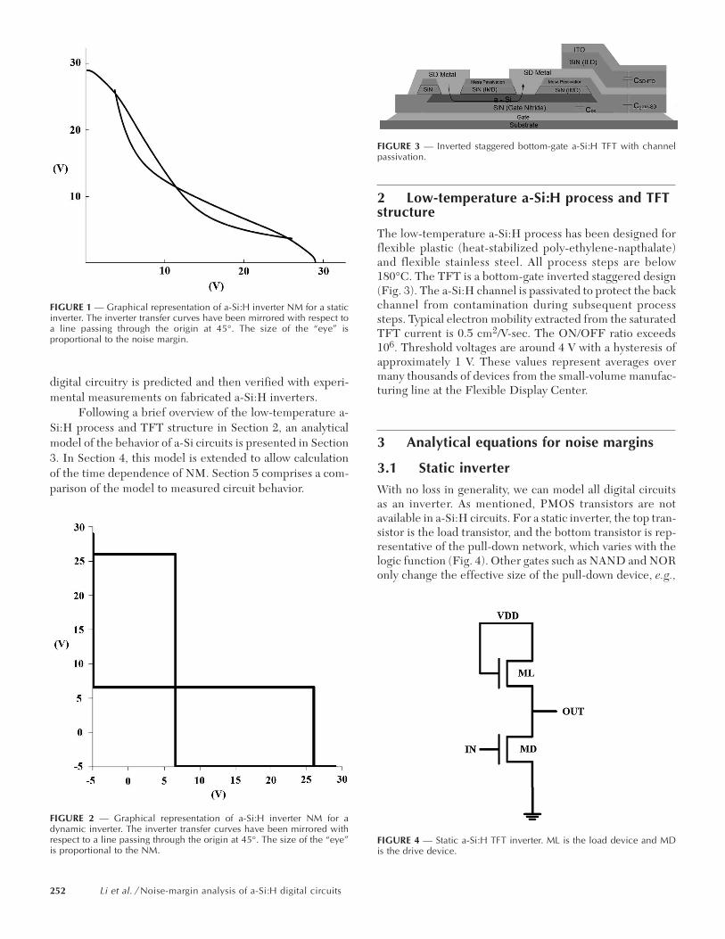
2 Low-temperature a-Si:H process and TFTstructureThe low-temperature a-Si:H process has been designed forflexible plastic (heat-stabilized poly-ethylene-napthalate)and flexible stainless steel. All process steps are below180°C. The TFT is a bottom-gate inverted staggered design(Fig. 3). The a-Si:H channel is passivated to protect the backchannel from contamination during subsequent processsteps. Typical electron mobility extracted from the saturatedTFT current is 0.5 cm2/V-sec. The ON/OFF ratio exceeds106. Threshold voltages are around 4 V with a hysteresis ofapproximately 1 V. These values represent averages overmany thousands of devices from the small-volume manufac-turing line at the Flexible Display Center.
3 Analytical equations for noise margins
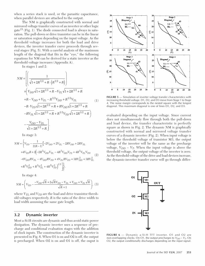
3.1 Static inverterWith no loss in generality, we can model all digital circuitsas an inverter. As mentioned, PMOS transistors are notavailable in a-Si:H circuits. For a static inverter, the top tran-sistor is the load transistor, and the bottom transistor is rep-resentative of the pull-down network, which varies with thelogic function (Fig. 4). Other gates such as NAND and NORonly change the effective size of the pull-down device, e.g.,
FIGURE 1 — Graphical representation of a-Si:H inverter NM for a staticinverter. The inverter transfer curves have been mirrored with respect toa line passing through the origin at 45°. The size of the “eye” isproportional to the noise margin.
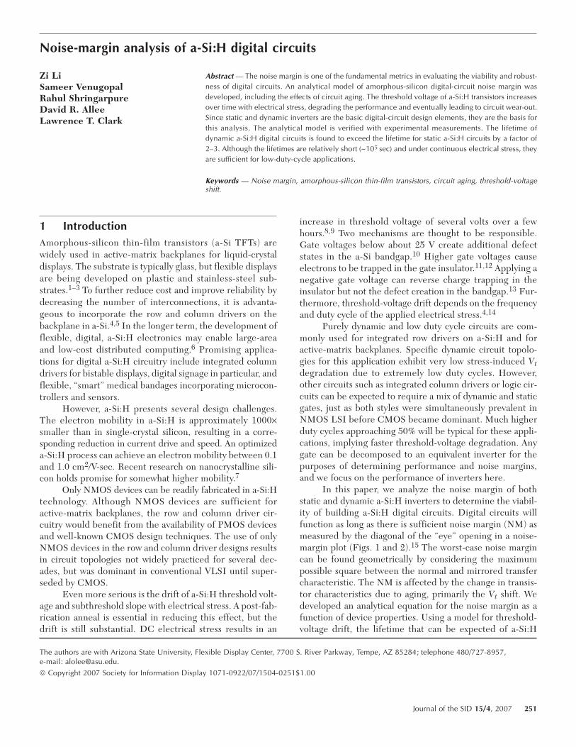
FIGURE 2 — Graphical representation of a-Si:H inverter NM for adynamic inverter. The inverter transfer curves have been mirrored withrespect to a line passing through the origin at 45°. The size of the “eye”is proportional to the NM.
FIGURE 3 — Inverted staggered bottom-gate a-Si:H TFT with channelpassivation.
FIGURE 4 — Static a-Si:H TFT inverter. ML is the load device and MDis the drive device.
252 Li et al. / Noise-margin analysis of a-Si:H digital circuits
when a series stack is used, or the parasitic capacitance,when parallel devices are attached to the output.
The NM is graphically constructed with normal andmirrored voltage transfer curves of an inverter or other logicgate15 (Fig. 1). The diode connected load is always in satu-ration. The pull-down or drive transistor can be in the linearor saturation region depending on the input voltage. As thethreshold voltage increases for both the load and drivedevices, the inverter transfer curve proceeds through sev-eral stages (Fig. 5). With a careful analysis of the maximumlength of the diagonal that fits in the “eye,” the followingequations for NM can be derived for a static inverter as thethreshold voltage increases (Appendix A).
In stages 1 and 2:
(1)
In stage 3:
(2)
In stage 4:
(3)
where VTL and VTD are the load and drive transistor thresh-old voltages respectively. R is the ratio of the drive width toload width assuming the same gate length.
3.2 Dynamic inverterMost a-Si:H circuits are dynamic and thus avoid static powerdissipation. The dynamic inverter uses a sequence of pre-charge and conditional evaluation stages with the additionof clock inputs. The construction of the dynamic inverter ispresented in Fig. 6. When O1 is on and O2 is off, the outputis precharged. When O2 is on and O1 is off, the ouput is
evaluated depending on the input voltage. Since currentdoes not simultaneously flow through both the pull-downand load device, the transfer characteristic is perfectlysquare as shown in Fig. 2. The dynamic NM is graphicallyconstructed with normal and mirrored voltage transfercurves of a dynamic inverter (Fig. 2). When input voltage isbelow the threshold voltage of transistor M3, the outputvoltage of the inverter will be the same as the prechargevoltage, VDD – VT. When the input voltage is above thethreshold voltage, the output voltage of the inverter is zero.As the threshold voltage of the drive and load devices increase,the dynamic-inverter transfer curve will go through differ-
NMR R R R
V R R V R R
R V V R V R V
R V R R RV R R
RV R R R V R R
V V
R R
DD TL
DD TL DD TL
TD DD
TL TD
DD TL
=+ + ◊ +
F
HGG
I
KJJ
L
N
MMM
¥ + + -FH + +
+ - + - +
- ◊ + + + + +
- + + + + + IK
--
+ +
O
QPP
1
1 2
1 2 1 2
1 2 1 2
1 2 1 2
1 2
3 2 3 2
3 2 3 2
3 2 3 2
3 2 1 2
3 2 3 2 3 2
3 2
e j
.
NM VR
V V RV RV
V R R V V R V V R V V
V RV V RV V RV RV RV
R V R V R V
TD DD TL DD TL
TD DD TL DD T TL TD
DD TL DD TD TL TD DD TL
DD TL TD
= --
- + - +
+ + - - +
- - + + +
+ + +
RST
OQPUVW
1
2 12 2 2 2
4 2 2 4 4
6 4 4 3 3
4
2 22
2
2 2
2 2 2 2 2 1 22
( )
.
e
j
NM VV R RV V V V R
RTD
DD TD TL DD TL= -- + - + +
+
FHG
IKJ
2
1,
FIGURE 5 — Simulation of inverter voltage transfer characteristics withincreasing threshold voltage. D1, D2, and D3 move from Stage 1 to Stage4. The noise margin corresponds to the nested square with the longestdiagonal. This maximum diagonal is one of lines D1, D2, and D3.
FIGURE 6 — Dynamic a-Si:H TFT inverter. O1 and O2 arenon-overlapping clocks. On O1, the output precharges to VDD – VT. OnO2, the output conditionally discharges depending on the input signal.
Journal of the SID 15/4, 2007 253
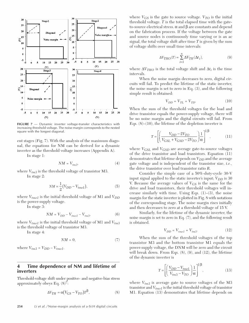
ent stages (Fig. 7). With the analysis of the maximum diago-nal, the equations for NM can be derived for a dynamicinverter as the threshold voltage increases (Appendix A).
In stage 1:
NM = Vtm3, (4)
where Vtm3 is the threshold voltage of transistor M3.In stage 2:
(5)
where Vtmo1 is the initial threshold voltage of M1 and VDDis the power-supply voltage.
In stage 3:
NM = VDD – Vtmo1 – Vtm3, (6)
where Vtmo1 is the initial threshold voltage of M1 and Vtm3is the threshold voltage of transistor M3.
In stage 4:
NM = 0, (7)
where Vtm3 = VDD – Vtmo1.
4 Time dependence of NM and lifetime ofinvertersThreshold-voltage shift under positive- and negative-bias stressapproximately obeys Eq. (8)7:
(8)
where VGS is the gate to source voltage. VTO is the initialthreshold voltage. T is the total elapsed time with the gate-to-source electrical stress. α and β are constants and dependon the fabrication process. If the voltage between the gateand source nodes is continuously time varying or is an acsignal, the total voltage shift after time T is given by the sumof voltage shifts over small time intervals:
(9)
where ∆VTHO is the total voltage shift and ∆ti is the timeintervals.
When the noise margin decreases to zero, digital cir-cuits will fail. To predict the lifetime of the static inverter,the noise margin is set to zero in Eq. (3), and the followingsimple result is obtained:
VDD = VTL + VTD. (10)
When the sum of the threshold voltages for the load anddrive transistor equals the power-supply voltage, there willbe no noise margin and the digital circuits will fail. FromEqs. (8)–(10), the lifetime of the depletion inverter is
(11)
where VGSL and VGSD are average gate-to-source voltagesof the drive transistor and load transistors. Equation (11)demonstrates that lifetime depends on VDD and the averagegate voltage and is independent of the transistor size, i.e.,the drive transistor over load transistor ratio R.
Consider the simple case of a 50%-duty-cycle 30-Vinput signal applied to the static inverter’s input; VDD is 30V. Because the average values of VGS is the same for thedrive and load transistors, their threshold voltages will in-crease similarly with time. Using Eqs. (1)–(3), the noisemargin for the static inverter is plotted in Fig. 8 with notationsof the corresponding stage. The noise margin rises initiallyand then decreases to zero at a threshold voltage of 15 V.
Similarly, for the lifetime of the dynamic inverter, thenoise margin is set to zero in Eq. (7), and the following resultis obtained.
VDD = Vtmo1 + Vtm3. (12)
When the sum of the threshold voltages of the toptransistor M3 and the bottom transistor M1 equals thepower-supply voltage, the DNM will be zero and the circuitwill break down. From Eqs. (8), (9), and (12), the lifetimeof the dynamic inverter is
(13)
where Vtm3 is average gate to source voltages of the M3transistor and Vtmo1 is the initial threshold voltage of transistorM1. Equation (13) demonstrates that lifetime depends on
NM V VDD tmo= -12 1b g ,
DV TTH GS TOV V= -a bb g ,
D D DV TTHO TH ii
nV t( ) ,( )=
=Â
1
TV V
V V VDD TO
GSL GSD TO=
-+ -
FHG
IKJ
LNMM
OQPP
22
11
a
b
,
TV VV VDD tmo
tm TO=
--
FHG
IKJ
LNMM
OQPP
1
3
11a
b
,
FIGURE 7 — Dynamic inverter voltage-transfer characteristics withincreasing threshold voltage. The noise margin corresponds to the nestedsquare with the longest diagonal.
254 Li et al. / Noise-margin analysis of a-Si:H digital circuits

power-supply voltage VDD and the average gate voltage andis independent of the transistor size.
Consider the same case for a 50%-duty-cycle 30-Vinput signal applied to the dynamic inverter’s input. Theclocks O1 and O2 are 30 V peak-to-peak non-overlappingsquare-wave signals. Since the threshold voltage of transis-tor M1 does not change much with time, we can assumeVtmo1 constant when calculating the lifetime of the circuit.On the other hand, the threshold voltage of transistor M3will increase similarly with time. By using Eqs. (4)–(7), thenoise margin for the dynamic inverter is plotted in Fig. 9with notations of the corresponding stage. The noise marginrises initially and then decreases to zero at a threshold volt-age of 30 – Vtmo1.
5 Experimental verification of noise-margindegradationa-Si:H static and dynamic inverters fabricated at the ASUFlexible Display Center are used to measure the degrada-tion of noise margin over time in the presence of electricalstress. When the input voltage is less than the thresholdvoltage, the output logic high voltage is VDD – VTH. WithVTO = 3 V, ∆VTH can be determined as a function of timefrom the degradation of the inverter transfer curve. Then, αand β can be obtained from Eq. (8).
For a static inverter, α = 0.0165, β = 0.31, and theinitial threshold voltage VTo = 3 V with the unit of time asseconds [Eq. (8)]. A dc voltage of 30 V is applied to thedepletion load inverter’s input and supply voltage VDD. Thevalues of VGS for drive and load transistors are the same.The inverter transfer curves are measured at 0, 30, 100, 300,
1000, 3000, 10,000, 30,000, and 62,220 sec. The NM plotsin Fig. 10 clearly show the inverter progressing through thevarious stages previously described. Noise margin still existsat the 30,000-sec measurement, but decreased to zero at the62,220-sec measurement. This is consistent with the theo-retical prediction from Eq. (11) by substituting for α, β, VTo,
FIGURE 8 — Noise margin varies with threshold voltage shift aspredicted with analytical model for a static inverter. S1, S2, S3, and S4correspond to stage 1, stage 2, stage 3, and stage 4, respectively.
FIGURE 9 — Noise margin varies with threshold-voltage shift aspredicted with analytical model for a dynamic inverter. S1, S2, S3, andS4 correspond to stage 1, stage 2, stage 3, and stage 4, respectively.
FIGURE 10 — Experimental results show the noise-margin plots takenat various times with constant electrical stress of 30 V on both the driveand load transistors. (a) 0 sec, (b) 3000 sec, (c) 10,000 sec, (d) 30,000sec.
Journal of the SID 15/4, 2007 255
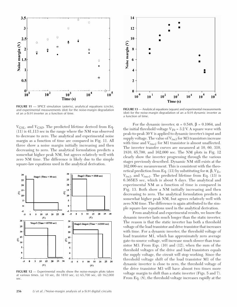
VGSL, and VGSD. The predicted lifetime derived from Eq.(11) is 41,113 sec in the range where the NM was observedto decrease to zero. The analytical and experimental noisemargin as a function of time are compared in Fig. 11. Allthree show a noise margin initially increasing and thendecreasing to zero. The analytical formulation predicts asomewhat higher peak NM, but agrees relatively well withzero NM time. The difference is likely due to the simplesquare-law equations used in the analytical derivation.
For the dynamic inverter, α = 0.548, β = 0.1064, andthe initial threshold voltage VT0 = 3.2 V. A square wave withpeak-to-peak 30 V is applied to dynamic inverter’s input andsupply voltage. The value of Vtm3 for M3 transistors increasewith time and Vtmo1 for M1 transistor is almost unaffected.The inverter transfer curves are measured at 10, 60, 310,1810, 65,700, and 162,000 sec. The NM plots in Fig. 12clearly show the inverter progressing through the variousstages previously described. Dynamic NM still exists at the162,000-sec measurement. This is consistent with the theo-retical prediction from Eq. (13) by substituting for α, β, VTo,Vtm3, and Vtmo1. The predicted lifetime from Eq. (13) is6.365E5 sec, which is about 8 days. The analytical andexperimental NM as a function of time is compared inFig. 13. Both show a NM initially increasing and thendecreasing to zero. The analytical formulation predicts asomewhat higher peak NM, but agrees relatively well withzero NM time. The difference is again attributed to the sim-ple square-law equations used in the analytical derivation.
From analytical and experimental results, we know thedynamic inverter lasts much longer than the static inverter.The reason is that the static inverter has both a thresholdvoltage of the load transistor and drive transistor that increaseswith time. For a dynamic inverter, the threshold voltage ofload transistor M1, which has approximately zero averagegate-to-source voltage, will increase much slower than tran-sistor M3. From Eqs. (10) and (12), when the sum of thethreshold voltages of the drive and load transistors equalsthe supply voltage, the circuit will stop working. Since thethreshold voltage shift of the load transistor M1 of thedynamic inverter is close to zero, the threshold voltage ofthe drive transistor M3 will have almost two times morevoltage margin to shift than a static inverter (Figs. 5 and 7).From Eq. (8), the threshold voltage increases rapidly at the
FIGURE 11 — SPICE simulation (asterix), analytical equations (circle),and experimental measurements (dot) for the noise-margin degradationof an a-Si:H inverter as a function of time.
FIGURE 12 — Experimental results show the noise-margin plots takenat various times. (a) 10 sec, (b) 1810 sec, (c) 65,700 sec, (d) 162,000sec.
FIGURE 13 — Analytical equations (square) and experimental measurements(dot) for the noise-margin degradation of an a-Si:H dynamic inverter asa function of time.
256 Li et al. / Noise-margin analysis of a-Si:H digital circuits

beginning and the rate of increase will slow down over time.Hence, doubling the allowable threshold-voltage shift rangeprovides much more than twice the lifetime.
The predicted lifetime of ~105 sec (~1 day) for a-Si:Hdigital circuits is relatively short under continuous 30-Velectrical stress. The degradation of threshold voltage withelectrical stress that we observe in our low-temperature(<180°C) a-Si:H process designed for flexible, plastic sub-strates is roughly consistent with similar processes devel-oped elsewhere.9 Better performance and less thresholdvoltage degradation is readily achievable for higher-tem-perature a-Si:H processes designed for glass substrates. Inaddition, flexible substrates compatible with higher tem-peratures and nano-crystalline silicon are under develop-ment, and they hold promise for longer lifetimes. However,even these relative short lifetimes are useful for certain ap-plications. One such application is digital signage with anelectrophoretic or cholesteric active-matrix display. Sincethese electro-optic materials are bistable, the column driveelectronics only needs to be activated momentarily whenchanging the image. Thousands of image updates would bepossible with digital a-Si:H drive circuitry integrated intothe backplane.16 A second application is conformal, “smart”bandages for medical applications. Flexible, lightweight, robustbandages could incorporate sensors and an a-Si:H micro-controller that is powered down most of the time. Onceevery few minutes, the circuitry would awake; take a meas-urement; perform simple calculations; display the result onan integrated, bistable flexible display; and return to sleepmode. Both of these applications can successfully utilizeflexible, digital a-Si:H circuits and have product lifetimes ofmonths or years.
6 ConclusionCharacteristics of inverter NM have been investigated withrespect to the maximum circuit lifetime of for both staticand dynamic a-Si circuitry. With threshold-voltage increaseson a-Si TFTs, the a-Si TFT inverter NM initially increasesand degrades after a certain point in time. The lifetime of ana-Si inverter has been derived in closed form to predict thepoint where the NM collapses to zero. At this point, thecircuit is rendered inoperable at any speed. An increase inNM may also occur during circuit aging. While the SNMincreases, the speed of the circuit is degrading the entiretime. As a practical matter, the effective circuit lifetime willbe limited, as defined by the required circuit operatingspeed, to a value below this bound.
AcknowledgmentThe Research was sponsored by the Army Research Labo-ratory (ARL) and was accomplished under CooperativeAgreement W911NG-04-2-0005. The views and conclu-sions contained in this document are those of the authorsand should not be interpreted as representing the official
policies, either expressed or implied, of the ARL or the U.S.Government. The U.S. Government is authorized to repro-duce and distribute reprints for Government purposes not-withstanding any copyright notation hereon.
References1 C C Wu, S D Theiuss, G Gu, M H Lu, J C Sturm, S Wagner, and S R
Forrest, “Integration of organic LEDs and amorphous Si TFTs ontoflexible and lightweight metal foil substrates,” IEEE Electron Dev Lett18, No. 12, 609–612 (Dec. 1997).
2 A Nathan, A Kumar, K Sakariya, P Servati, S Sambandan, and DStriakhilev, “Amorphous silicon thin film transistor integration for or-ganic LED displays on glass and plastic,” IEEE J Solid-State Circuits29, No. 9, 1477–1486 (September 2004).
3 Flexible Display Center, http://flexdisplay.asu.edu.4 H Lebrun, T Kretz, J Magarino, and N Szydlo, “Design of integrated
drivers with amorphous TFTs for small displays,” SID SymposiumDigest Tech Papers 36, 950–953 (2005).
5 (Handbook style) Self-Scanned Amorphous Silicon Integrated Displays(Sarnoff Co., Princeton, NJ, June 1999).
6 K R Wissmiller, J E Knudsen, T J Alward, Z P Li, D RAllee, and L TClark, “Reducing power in flexible a-Si:H digital circuits while preserv-ing state,” Proc Custom Integrated Circuits Conference, 219–222(2005).
7 I-C Cheng and S Wagner, “Nanocrystalline silicon thin film transis-tors,” IEEE Proc-Circuits Dev Syst 150, 339–344 (2003).
8 K S Karim, A Nathan, M Hack, and W I Milne, “Drain bias dependenceof threshold voltage stability of amorphous silicon TFTs,” IEEE Elec-tron Dev Lett 25, No. 4, 188–190 (April 2004).
9 H Gleskova and S Wagner, “DC-gate-bias stressing of a-Si:H TFTsfabricated at 150°C on polyimide foil,” IEEE Trans Electron Dev 48,No. 8, 1667–1671 (August 2001).
10 A R Hepburn, J M Marshall, and C Martin, “Metastable defects inamorphous silicon thin film transistors,” Phys Rev Lett 56, No. 20,2215–2218 (1986).
11 M J Powell, “Charge trapping instabilities in amorphous silicon-siliconnitride thin film transistors,” Appl Phys Lett 43, 597–599 (1983).
12 M J Powell, C van Berkel, A R Franklin, S C Deane, and W I Milne,“Defect pool in amorphous-silicon thin-film transistors” Phys Rev B45, 4160 (1992).
13 C van Berkel and M J Powell, “Resolution of amorphous silicon thinfilm transistor instability mechanisms using ambipolar transistors,”Appl Phys Lett 51, No. 14, 1094–1096 (1987).
14 C Chiang, J Kanicki, and K Takechi, “Electrical instability of hydrogen-tated amorphous silicon thin film transistors for active-matrix liquid-crystal displays,” Jpn J Appl Phys 37, 4704–4710 (1998).
15 J Lohstroh, E Seevinck, and J De Groot, “worst-case static noise margincriteria for logic circuits and their mathematical equivalence,” IEEE JSolid-State Circuits SC-18, No. 6, 803–807 (December 1983).
16 S M Venugopal and D R Allee, “Integrated a-Si:H source drivers for4-in. QVGA electrophoretic display on flexible stainless steel sub-strate,” IEEE J Display Technology (to be published).
Appendix A: Detailed derivation of noise mar-gin for static and dynamic inverters
A1 Static inverterThe current for the load transistor is
(14)
COX is the gate oxide. WLD is the width of the load transis-tor. Vout is output of inverter, and VIN is the input of theinverter. VTL is the threshold voltage of the load transistor.µo is the effective mobility of the transistor.
The current through the drive transistor is
I CL OXLD
O DD OUT TLW
LV V V= - -1
22m b g .
Journal of the SID 15/4, 2007 257
(15)
(16)
when the transistor is in the linear or saturation region,respectively. WDR and VTD are the width and threshold volt-age of the drive transistor, respectively.
The inverter transfer curve has three regions. In thefirst region, VIN is less than VTD, the drive transistor is cutoff and VOUT = VDD – VTL. As the input voltage rises, thedrive transistor enters saturation. By combining Eqs. (14)and (16), the output voltage is given by
(17)
where R equals the ratio of the drive width to the load width.As Vout decreases, the drive transistor enters the linearregion. Vout is now given by combining Eqs. (14) and (15) as
(18)
As previously mentioned, the worst-case SNM can befound geometrically by considering the maximum possiblesquare between the normal and mirrored transfer charac-teristic. Since the top and bottom eyes are identical, only thetop eye is studied. The “eye” can be viewed as three signifi-cant parts, which are the straight line on the right (RL)edge, the curvature line on the left (LL) edge, and the cor-ner on the right (labeled point d3 in Fig. 8). Depending onthe circuit and age of the circuit, the latter may not contrib-ute to the SNM eye, as shown below. The line RL has slopeof –√R (17). The line LL has two parts, which are Eqs. (17)and (18). The right corner is at point (VTD, VDD – VTL).
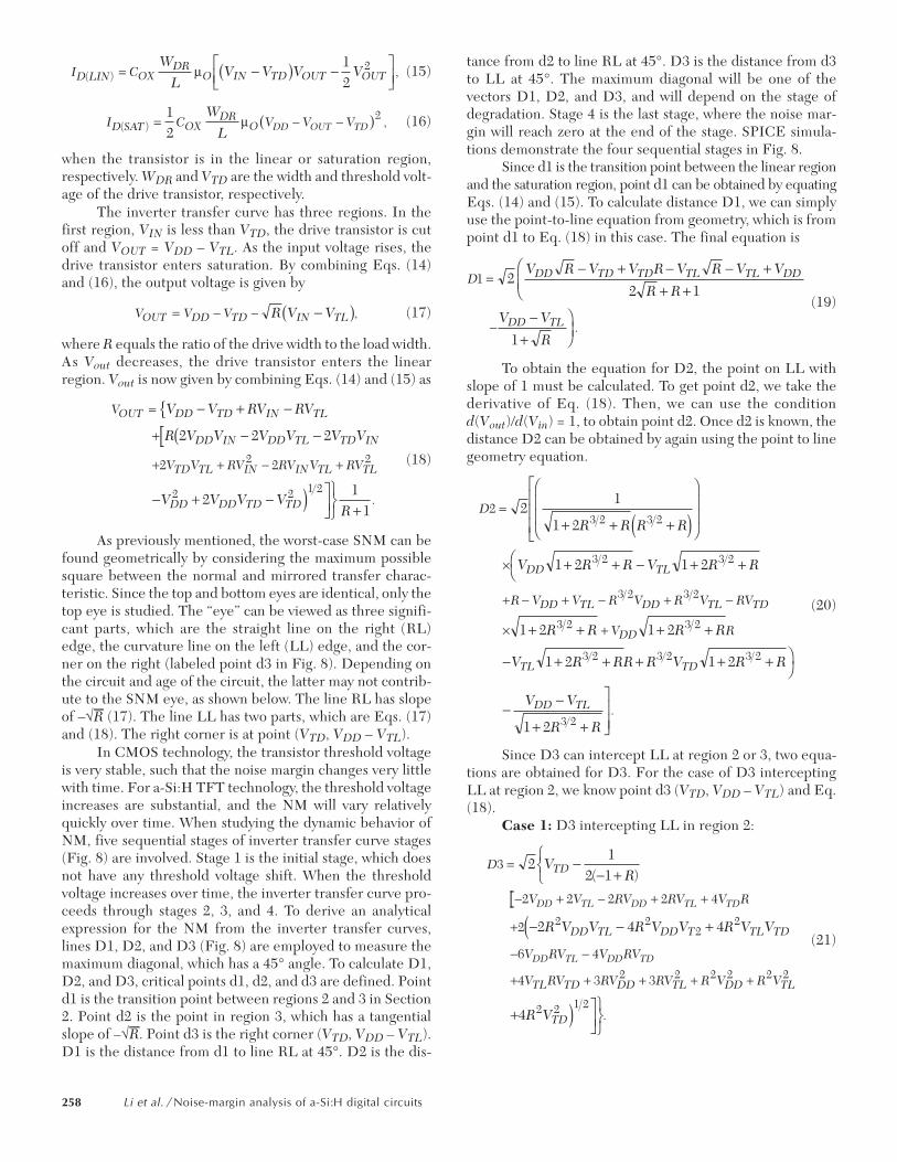
In CMOS technology, the transistor threshold voltageis very stable, such that the noise margin changes very littlewith time. For a-Si:H TFT technology, the threshold voltageincreases are substantial, and the NM will vary relativelyquickly over time. When studying the dynamic behavior ofNM, five sequential stages of inverter transfer curve stages(Fig. 8) are involved. Stage 1 is the initial stage, which doesnot have any threshold voltage shift. When the thresholdvoltage increases over time, the inverter transfer curve pro-ceeds through stages 2, 3, and 4. To derive an analyticalexpression for the NM from the inverter transfer curves,lines D1, D2, and D3 (Fig. 8) are employed to measure themaximum diagonal, which has a 45° angle. To calculate D1,D2, and D3, critical points d1, d2, and d3 are defined. Pointd1 is the transition point between regions 2 and 3 in Section2. Point d2 is the point in region 3, which has a tangentialslope of –√R. Point d3 is the right corner (VTD, VDD – VTL).D1 is the distance from d1 to line RL at 45°. D2 is the dis-
tance from d2 to line RL at 45°. D3 is the distance from d3to LL at 45°. The maximum diagonal will be one of thevectors D1, D2, and D3, and will depend on the stage ofdegradation. Stage 4 is the last stage, where the noise mar-gin will reach zero at the end of the stage. SPICE simula-tions demonstrate the four sequential stages in Fig. 8.
Since d1 is the transition point between the linear regionand the saturation region, point d1 can be obtained by equatingEqs. (14) and (15). To calculate distance D1, we can simplyuse the point-to-line equation from geometry, which is frompoint d1 to Eq. (18) in this case. The final equation is
(19)
To obtain the equation for D2, the point on LL withslope of 1 must be calculated. To get point d2, we take thederivative of Eq. (18). Then, we can use the conditiond(Vout)/d(Vin) = 1, to obtain point d2. Once d2 is known, thedistance D2 can be obtained by again using the point to linegeometry equation.
(20)
Since D3 can intercept LL at region 2 or 3, two equa-tions are obtained for D3. For the case of D3 interceptingLL at region 2, we know point d3 (VTD, VDD – VTL) and Eq.(18).
Case 1: D3 intercepting LL in region 2:
(21)
I CD LIN OXDR
O IN TD OUT OUTW
LV V V V( ) ,= - -L
NMOQPm b g 1
22
I C V V VD SAT OXDR
OW
L DD OUT TD( ) ,= - -12
2m a f
V V VOUT DD TD IN TLR V V= - - -b g,
V
V V RV RV V RV
OUT DD TD IN TL
DD IN DD TL TD IN
TD TL IN IN TL TL
DD DD TD TD
V V RV RV
R V V V V V V
V V V VR
=
+
+ + - +
- + -
- -
- + - OQPUVW +
lb
j
2 2 2
21
1
2 22 2
2 2 1 2.
DV R V V R V R V V
R R
V V
R
DD TD TD TL TL DD
DD TL
1 22 1
1
=
-
- + - - ++ +
FHG
-+
IKJ .
D
R V V R V R V RV
V R
R R R R
V R R V R R
R R R R
V R RR R V R R
V V
R R
DD TL
DD TL DD TL TD
DD
TL TD
DD TL
2 21
1 2
1 2 1 2
1 2 1 2
1 2 1 2
1 2
3 2 3 2
3 2 3 2
3 2 3 2
3 2 3 2
3 2 3 2 3 2
3 2
=
¥
+ - + - + -
¥ +
+ + +
F
HGG
I
KJJ
L
N
MMM
+ + - + +FH
+ + + +
- + + + + + IK
--
+ +
O
QPP
e j
.
D
V V RV RV V R
V RV V RV
V RV RV RV R V R V
VR
R V V R V V R V V
R V
TD
DD TL DD T TL TD
TL TD DD TL DD TL
TD
DD TL DD TL TD
DD TL DD TD
3
2 2 2 2 4
2
6 4
4 3 3
21
2 1
2 4 4
4
2 22
2
2 2 2 2 2 2
2 2 1 2
=
- + - + +
+
- -
+ + + + +
-- +
RST
- - +
+ OQPUVW
( )
.
e
j
258 Li et al. / Noise-margin analysis of a-Si:H digital circuits

Similarly, we can use point d3 (VTD, VDD – VTL) andEq. (17) to determine the diagonal D3 when D3 interceptsLL in region 3.
Case 2: D3 intercepting LL in region 3:
(22)
Since D1, D2, and D3 are diagonals of a square (Fig.5), the NM will be equal to the side of the largest square or1/√2 of the largest D1, D2, and D3. Since D1, D2, and D3are complicated equations, the result is not obvious. To sim-plify, we assume that R, the ratio of load and drive widths, isbetween 2 and 10 and VDD is between 10 and 40 V, which istrue for most a-Si:H circuit applications.
A2 Dynamic inverterThe derivation for dynamic NM is rather simpler than thatfor static NM. By inspection, at Stage 1, the dynamic NMwill be the threshold voltage of the drive transistor M3(Figs. 6 and 7). At stage 2, the dynamic NM will reach amaximum value of (VDD – Vtmo1)/2, where the thresholdvoltage of transistor M3 is (VDD – Vtmo1)/2. At stage 3, thenoise margin can easily be found. The difference betweenVDD – Vtmo1 and Vtm3 is the noise margin. At stage 4, whenthe threshold voltage of the drive transistor reaches VDD –Vtmo1, the NM vanishes. In other words, at this point thesum of the threshold voltages of drive transistor M3 and theload transistor M1 equals the power-supply voltage.
Zi Li received his B.S.E. degree in electrical engi-neer from Arizona State University, Tempe, Ari-zona, U.S.A., in 2005. He is currently workingtoward his M.S. degree in the Department of Elec-trical Engineering at Arizona State University,Tempe, Arizona, U.S.A. His current research inter-ests include a-Si:H TFT circuit design and optimi-zation of a-Si:H TFT circuit lifetime.
Sameer Venugopal received his B.S. degree fromBMS College of Engineering, Bangalore, India, in2000 and his M.S.E. degree in 2004 from ArizonaState University, Tempe, AZ, U.S.A., both in electri-cal engineering. He is currently working towardshis Ph.D. in the Department of Electrical Engi-neering at Arizona State University. His researchinterests include integrated gate and source driv-ers for reflective displays and digital circuits fab-ricated in amorphous-silicon technology onflexible substrates.
Rahul Shringarpure received his M.S. degree incomputer engineering and his M.S. degree inelectrical engineering in 1996 and 2000, fromWayne State University, Detroit, MI and OregonGraduate Institute, Portland, OR, respectively.Currently, he is working for HRL LLC, Malibu, CA,as a member of technical staff and is pursuing hisPh.D. degree in electrical engineering at ArizonaState University, Tempe, AZ. His research interestincludes device modeling of thin-film transistors,
design of digital and mixed-mode circuits, and flexible electronic sys-tems.
David R. Allee received his B.S. in electrical engi-neering from the University of Cincinnati in 1984and his M.S. and Ph.D. in electrical engineeringfrom Stanford University in 1986 and 1990, respec-tively. He was a post-doctoral fellow at Cam-bridge University in 1990 and 1991. While atStanford University, and as a Research Associateat Cambridge University, he fabricated scaledfield-effect transistors with ultra-short gate lengthsusing custom e-beam lithography. He also invented
several ultra-high-resolution lithography techniques including directe-beam irradiation of SiO2, and nanometer-scale patterning of variousorganic and inorganic films with scanning tunneling lithography (ASU).Since joining Arizona State University, his primary focus has been onmixed-signal integrated-circuit design. As a founding member of theNSF Center for Low Power Electronics and the Whitaker Center forNeuromechanical Control, he has designed several custom analog-to-digital converters and telemetry ICs. He is currently director of researchfor backplane electronics for the Flexible Display Center at Arizona StateUniversity is investigating a variety of flexible electronics applications.He has been a regular consultant with several semiconductor industrieson low-voltage low-power mixed-signal circuit design. He has co-authoredover 40 archival scientific publications and three U.S. patents.
Lawrence T. Clark received his B.S. degree incomputer science from Northern Arizona Univer-sity in 1984 and his M.S. and Ph.D. degrees inelectrical engineering from Arizona State Univer-sity in 1987 and 1992, respectively. He worked atIntel Corp. in 1982 and 1984–1985 in productand test engineering and at VLSI, Inc., from 1990to 1992 performing chipset design. From 1992 to2003, he worked at Intel Corp. in various capaci-ties including microprocessor design (participat-
ing in Pentium, Itanium, and XScale processor designs), compact mod-eling for circuit simulation, and CMOS imager design. Most recently, hewas a Principal Engineer and Circuit Design Manager for XScale Micro-processors. In 2003, he joined the University of New Mexico Electricaland Computer Engineering Dept. as an Associate Professor. In 2004, hejoined the electrical engineering department at Arizona State University.He is a senior Member of the IEEE and has been awarded over 50 pat-ents. He has co-authored approximately 40 journal and conferencepapers. His research interests are circuits, architectures, computer-aideddesign, and radiation hardening for high performance and low powerVLSI systems.
D
VV R RV V V V R
RTD
DD TD TL DD TL
3 2
2
1
=
-- + - + +
+
FHG
IKJ .
Journal of the SID 15/4, 2007 259