New 5-Lead SOT-23 Oscillator is Small, Very Stable and Easy ...
40
LINEAR TECHNOLOGY LINEAR TECHNOLOGY LINEAR TECHNOLOGY FEBRUARY 2001 VOLUME XI NUMBER 1 , LTC and LT are registered trademarks of Linear Technology Corporation. Adaptive Power, Burst Mode, C-Load, DirectSense, FilterCAD, Hot Swap, LinearView, Micropower SwitcherCAD, No Latency ∆Σ, No R SENSE , Operational Filter, OPTI-LOOP, Over-The-Top, PolyPhase, PowerSOT, SwitcherCAD and UltraFast are trademarks of Linear Technology Corporation. Other product names may be trademarks of the companies that manufacture the products. New 5-Lead SOT-23 Oscillator is Small, Very Stable and Easy to Use Introduction Generating a periodic waveform of arbitrary frequency is not always a trivial task. Low cost RC oscillators can be built using discrete compo- nents such as comparators, resistors and capacitors, or by using simple integrated circuits such as the indus- try-standard 555 timer in conjunction with several discrete components. These solutions are bulky and inac- curate, especially at frequencies above a few hundred kilohertz. Very accurate oscillators with a predetermined frequency may be realized using either crystals or ceramic resonators as stable fre- quency elements; crystal oscillators offer the highest performance, although they are costly. These cir- cuits are also bulky, sensitive to acceleration forces and tend to be less robust than RC oscillators. Generat- ing various frequencies from a single crystal or ceramic oscillator requires additional circuitry that will add to the component list and consume PC board space. Enter the LTC1799 The LTC1799 offers an alternative that combines the frequency stability and accuracy of a ceramic resonator with the flexibility and ease of use of an RC oscillator, while requiring less space than either. The LTC1799 is the only oscillator IC that can accurately generate a square wave signal at any frequency from 5kHz to 20MHz without the use of a crystal, ceramic element or exist- ing clock reference. A complete oscillator circuit requires only an LTC1799, a frequency-setting resis- tor (R SET ) and a bypass capacitor, as illustrated in Figure 1. With a 0.1% resistor, the frequency accuracy is typically better than ±0.6%. The LTC1799’s internal master oscillator is a resistance to frequency converter with an output range of 500kHz to 20MHz. A programmable on-chip fre- quency divider divides the frequency by 1, 10 or 100, extending the fre- quency range to greater than three decades (5kHz to 20MHz). V CC GND SET 5 4 OUT DIV 1 2 3 LTC1799 3V C1 0.1μF R SET 20k 0.1% 5MHz ±1.6%* (27°C) *INCLUDING ERROR CONTRIBUTION FROM RESISTOR Figure 1. A complete oscillator solution by Andy Crofts continued on page 3 IN THIS ISSUE… COVER ARTICLE New 5-Lead SOT-23 Oscillator is Small, Very Stable and Easy to Use .................................................... 1 Andy Crofts Issue Highlights ........................... 2 LTC ® in the News .......................... 2 DESIGN FEATURES Current-Limited DC/DC Converter Simplifies USB Power Supplies ..... 6 Bryan Legates 2.3MHz Monolithic, Continuous Time, Differential Lowpass Filter Provides Solutions for Wide Band CDMA Applications ....................... 8 Nello Sevastopoulos and Mike Kultgen Very Low Cost Li-Ion Battery Charger Requires Little Area and Few Components ........................ 12 David Laude Synchronous Buck Controller Extends Battery Life and Fits in a Small Footprint ......................... 13 Peter Guan New No R SENSE ™ Controllers Deliver Very Low Output Voltages .......... 16 Christopher B. Umminger New UltraFast™ Comparators: Rail-to-Rail Inputs and 2.4V Operation Allow Use on Low Supplies ..................................... 21 Glen Brisebois High Efficiency Synchronous PWM Controller Boosts 1V to 3.3V or 5V .................................................. 24 San-Hwa Chee DESIGN INFORMATION Rail-to-Rail 14-Bit Dual DAC in a Space Saving 16-Pin SSOP Package .................................................. 28 Hassan Malik DESIGN IDEAS ............................................ 29–37 complete list on page 29 New Device Cameos ................... 38 Design Tools ............................... 39 Sales Offices .............................. 40
-
Upload
khangminh22 -
Category
Documents
-
view
1 -
download
0
Transcript of New 5-Lead SOT-23 Oscillator is Small, Very Stable and Easy ...
LINEAR TECHNOLOGYLINEAR TECHNOLOGYLINEAR TECHNOLOGYFEBRUARY 2001 VOLUME XI NUMBER 1
, LTC and LT are registered trademarks of Linear Technology Corporation. Adaptive Power, Burst Mode, C-Load,DirectSense, FilterCAD, Hot Swap, LinearView, Micropower SwitcherCAD, No Latency ∆Σ, No RSENSE, Operational Filter,OPTI-LOOP, Over-The-Top, PolyPhase, PowerSOT, SwitcherCAD and UltraFast are trademarks of Linear TechnologyCorporation. Other product names may be trademarks of the companies that manufacture the products.
New 5-Lead SOT-23Oscillator is Small, VeryStable and Easy to Use
IntroductionGenerating a periodic waveform ofarbitrary frequency is not always atrivial task. Low cost RC oscillatorscan be built using discrete compo-nents such as comparators, resistorsand capacitors, or by using simpleintegrated circuits such as the indus-try-standard 555 timer in conjunctionwith several discrete components.These solutions are bulky and inac-curate, especially at frequencies abovea few hundred kilohertz.
Very accurate oscillators with apredetermined frequency may berealized using either crystals orceramic resonators as stable fre-quency elements; crystal oscillatorsoffer the highest performance,although they are costly. These cir-cuits are also bulky, sensitive toacceleration forces and tend to be lessrobust than RC oscillators. Generat-ing various frequencies from a singlecrystal or ceramic oscillator requiresadditional circuitry that will add tothe component list and consume PCboard space.
Enter the LTC1799The LTC1799 offers an alternativethat combines the frequency stabilityand accuracy of a ceramic resonatorwith the flexibility and ease of use ofan RC oscillator, while requiring lessspace than either.
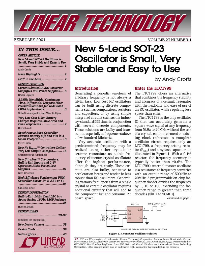
The LTC1799 is the only oscillatorIC that can accurately generate asquare wave signal at any frequencyfrom 5kHz to 20MHz without the useof a crystal, ceramic element or exist-ing clock reference. A completeoscillator circuit requires only anLTC1799, a frequency-setting resis-tor (RSET) and a bypass capacitor, asillustrated in Figure 1. With a 0.1%resistor, the frequency accuracy istypically better than ±0.6%. TheLTC1799’s internal master oscillatoris a resistance to frequency converterwith an output range of 500kHz to20MHz. A programmable on-chip fre-quency divider divides the frequencyby 1, 10 or 100, extending the fre-quency range to greater than threedecades (5kHz to 20MHz).
VCC
GND
SET
5
4
OUT
DIV
1
2
3
LTC17993V
C10.1µF
RSET20k
0.1%
5MHz ±1.6%* (27°C)
*INCLUDING ERROR CONTRIBUTION FROM RESISTOR
Figure 1. A complete oscillator solution
by Andy Crofts
continued on page 3
IN THIS ISSUE…COVER ARTICLENew 5-Lead SOT-23 Oscillator isSmall, Very Stable and Easy to Use....................................................1
Andy Crofts
Issue Highlights ...........................2
LTC® in the News ..........................2
DESIGN FEATURESCurrent-Limited DC/DC ConverterSimplifies USB Power Supplies .....6Bryan Legates
2.3MHz Monolithic, ContinuousTime, Differential Lowpass FilterProvides Solutions for Wide BandCDMA Applications .......................8Nello Sevastopoulos and Mike Kultgen
Very Low Cost Li-Ion BatteryCharger Requires Little Area andFew Components ........................12David Laude
Synchronous Buck ControllerExtends Battery Life and Fits in aSmall Footprint ......................... 13Peter Guan
New No RSENSE™ Controllers DeliverVery Low Output Voltages .......... 16Christopher B. Umminger
New UltraFast™ Comparators:Rail-to-Rail Inputs and 2.4VOperation Allow Use on LowSupplies .....................................21Glen Brisebois
High Efficiency Synchronous PWMController Boosts 1V to 3.3V or 5V..................................................24
San-Hwa Chee
DESIGN INFORMATIONRail-to-Rail 14-Bit Dual DAC in aSpace Saving 16-Pin SSOP Package..................................................28
Hassan Malik
DESIGN IDEAS............................................ 29–37
complete list on page 29
New Device Cameos ................... 38
Design Tools ...............................39
Sales Offices ..............................40
Linear Technology Magazine • February 20012
EDITOR’S PAGE
LTC in the News…On January 16, Linear TechnologyCorporation announced its fin-ancial results for the 2nd quarterof fiscal year 2001. Robert H.Swanson, Chairman & CEO,stated, “Once again we had a strongfinancial performance. We achievedrecord levels of sales and profitswith sales increasing 11% and prof-its 12% sequentially from theSeptember quarter. Our return onsales was a record 44.4%. As withother semiconductor companies,we have seen a slowdown in netbookings from the very robust levelsexperienced in previous quarters.Interestingly, gross bookings in thisquarter still exceeded our net bill-ings, however cancellations of somebookings from previous quarterscaused our net bookings to beslightly less than our net billings.Nevertheless, our backlog contin-ues to be strong and demand forproduct in the near term appearsto be firm. Consequently, we cur-rently estimate that we will growsales and profits sequentially inthe 8%–10% range for the Marchquarter.
The Company reported sales of$258,450,000, and net income of$114,758,000 for the 2nd quarter.Net sales were up 59% over thesame quarter last year. Dilutedearnings per share were $0.34, anincrease of 77% over the 2nd quar-ter last year.
Issue HighlightsHappy New Year and welcome to
our first issue of 2001, beginning theeleventh year of Linear Technologymagazine.
Our lead article in this issue intro-duces the LTC1799, a new oscillatorIC in a SOT-23 package. The LTC1799offers the frequency stability andaccuracy of a ceramic resonator withthe flexibility and ease of use of an RCoscillator, while requiring less spacethan either. It is the only oscillator ICthat can accurately generate a squarewave at any frequency from 5kHz to20MHz without the use of a crystal,ceramic element or existing clock ref-erence. A complete circuit requiresonly an LTC1799, a frequency-set-ting resistor and a bypass capacitor.With a 0.1% resistor, the frequencyaccuracy is typically better than±0.5%.
In the filter realm, we present theLTC1566-1, a new monolithic 7thorder continuous time lowpass filterfeaturing differential input and out-put terminals. The LTC1566-1operates from a single 5V supply anddual supplies of up to ±5V, comes inan SO-8 package and requires noexternal components other thanpower supply decoupling capacitors.The filter is designed to have a flatpassband from DC to 2MHz and asteep transition band. The filter cut-off is set at 2.3MHz to accommodatedifferential filtering needs in wide-band CDMA base stations.
Also introduced in this issue is thenew LT1711/12/13/14 family ofUltraFast comparators, which hasfully differential rail-to-rail inputs andoutputs and operates on supplies aslow as 2.4V, allowing unfetteredapplication on low voltages. TheLT1711 (single) and LT1712 (dual)are specified at 4.5ns of propagationdelay and 100MHz toggle frequency.The low power LT1713 (single) andLT1714 (dual) are specified at 7ns ofpropagation delay and 65MHz togglefrequency.
As usual, this issue introduces avariety of new power products. The
newly released LT1618 DC/DC con-verter provides USB devices withaccurate input current control. Sev-eral requirements must be met by adevice powered from the USB connec-tor: input capacitors smaller than10µF are required to minimize inrushcurrents at plug-in; upon power-up,the device must draw less than 100mAof current from the USB bus and canincrease its input current to 500mAonly when given permission by theUSB controller. These requirementscan be easily met using the LT1618.The part combines a traditional volt-age feedback loop with a uniquecurrent feedback loop to operate as aconstant-current, constant-voltagesource.
The LTC1734 is a precision, lowcost, single-cell, linear Li-Ion batterycharger with constant voltage andconstant current control. The smallquantity and low cost of external com-ponents results in a very low overallsystem cost and the part’s 6-pin SOT-23 package allows for a compactdesign solution. Previous productsusually required an external currentsensing resistor and blocking diodewhose functions are included in theLTC1734.
The LTC1773 is a synchronousDC/DC controller that packs highoutput current capability and lowoperating quiescent current in a smallMSOP-10 package. Its input voltagerange is from 2.65V to 8.5V, ideal for1- or 2-cell Li-Ion batteries as well as3- to 6-cell NiCd and NiMH batterypacks. A precise internal undervolt-age lockout circuit prevents deepdischarge of the battery below 2.5V.The LTC1773’s high operating fre-quency of 550kHz allows the use ofsmall, surface mount components toprovide a compact power supplysolution.
The LTC1778 and the LTC3711are buck regulators that deliver thelow output voltages and high effici-encies required by today’s portablesupplies. The LTC1778 is a step-downcontroller that provides synchronous
drive for two external N-channel MOS-FET switches. Its true current modearchitecture has an adjustable cur-rent limit, can be easily compensated,is stable with ceramic output capaci-tors and does not require a senseresistor. The LTC1778 operates oninput voltages from 4V to 36V andoutput voltages from 0.8V up to 90%of VIN. Switching frequencies up tonearly 2MHz can be chosen, allowingwide latitude in trading off efficiencyfor component size. The LTC3711 isessentially the same as the LTC1778but includes a 5-bit VID interface.
continued on page 5

Linear Technology Magazine • February 2001 3
DESIGN FEATURES
Selecting the proper resistor isstraightforward because the LTC1799follows a simple relationship betweenRSET and frequency:
fOSC = 10MHz • 10kΩ/(N • RSET)where N is the on-chip divider settingof 1, 10 or 100, depending on thestate of the DIV pin. A proprietaryfeedback loop maintains this accu-rate relationship over all operatingconditions, providing a temperaturecoefficient that is typically less than±0.004%/°C. The LTC1799 operatesover a 2.7V to 5.5V supply range, witha voltage coefficient of 0.05%/V. It
typically draws 1mA of supply cur-rent. Figure 1 shows a circuit thatgenerates a precision 5MHz signal.
LTC1799:Advantages in Precision,Resolution and SizeWith a frequency tolerance 0.5%typical and 1.5% worst-case, the per-formance of the LTC1799 is similar tothat of ceramic resonators and vastlysuperior to oscillators that use dis-crete resistors and capacitors. Itsstingy temperature and voltage coef-ficients (typically ±0.004%/°C and0.05%/V, respectively) maintainaccuracy over all operating conditions.
Unlike oscillators using crystals,the LTC1799 has infinite frequencyresolution; the output frequency canbe set to any value in the 5kHz to20MHz range. The programmed fre-quency is limited only by the choice ofRSET. This feature allows the clockfrequency to be changed late in adesign cycle by changing the value ofa resistor instead of stocking crystalsin many different frequencies.
The LTC1799’s SOT-23 packageand low component count (one resis-tor, one capacitor) result in an efficientuse of PCB space, requiring less spacethan any crystal, ceramic resonatoror discrete oscillator solution.
Frequency Set by SingleResistor and Ranged by anInternal Frequency DividerThe heart of the LTC1799 is a masteroscillator that performs a preciseresistance-to-frequency conversion.RSET can be any value from 3.32k to1M, generating master oscillator fre-quencies between 30MHz and 1kHzwith guaranteed 1.5% accuracy forresistors between 5k and 200k. Toextend its frequency range, the
LTC1799 includes a programmablefrequency divider. The DIV input pinmay be connected to GND to pass themaster oscillator output directly tothe OUT pin. When the DIV pin is leftfloating, the LTC1799 divides themaster oscillator frequency by 10before driving OUT. Connect DIV toV+ to divide the master oscillator by100 to generate frequencies below100kHz. Table 1 suggests the properDIV pin setting for the desired fre-quency. The frequency ranges overlapnear 100kHz and 1MHz, allowing achoice of settings. Since the supplycurrent increases with smaller valuesof RSET, the lower divider setting isusually preferred.
Once the divider setting has beenselected, calculate the proper resistorvalue using this simple equation:
RSET = 10kΩ • 10MHz/(N • fOSC)
Since the oscillator frequency, fOSC, isdependent on the resistor value, RSET,any error in the resistor will createerror in fOSC.
Performance RivalsCeramic ResonatorsThe LTC1799 obeys its frequency vsRSET equation within 1.5% at roomtemperature with any RSET from 10k
gnitteSrediviD noitcennoC)4niP(VID egnaRycneuqerF
1÷ DNG *zHk005>
01÷ gnitaolF zHM1otzHk05
001÷ +V zHk001≤
R(zHM01evobaseicneuqerftA* TES V.4nahtsselseilppusnoycaruccadecuderreffusyam9971CTLeht,)k01<
Table 1. Frequency range vs divider setting
3.53.02.52.01.51.00.5
0–0.5–1.0–1.5–2.0–2.5–3.0–3.5
1k 10k 100k 1MRSET (Ω)
GUARANTEED LIMITS APPLY TO 5k TO 200k ONLY
OUTP
UT F
REQU
ENCY
ERR
OR (%
)
TA = 27°CTYPICAL
HIGH
TYPICALLOWWORST-CASE
LOW
WORST-CASEHIGH
2.0
1.5
1.0
0.5
0.0
–0.5
–1.0
–1.5
–2.0–40 –30 –20 –10 0 10 20 30 40 50 60 70 80 90
TEMPERATURE (°C)
NORM
ALIZ
ED O
UTPU
T FR
EQUE
NCY
DRIF
T (%
)
TYPICALHIGH
WORST-CASELOW
TYPICALLOW
WORST-CASEHIGH
RSET = 31.6k
Figure 2. Accuracy of theoutput frequency equation
Figure 3. Output frequency temperature drift
VCC
GND
SET
5
4
OUT
DIV
1
2
3
LTC17995V
C10.1µF
RT100k
THERMISTOR
RT: YSI 44011 (800) 765-4974
OUT
1400
1200
1000
800
600
400
200
0–20 –10 0 10 20 30 40 50 60 70 80 90
TEMPERATURE (°C)
FREQ
UENC
Y (k
Hz)
MAX
TYP
MIN
Figure 4. Temperature-to-frequency converter
Figure 5. Output frequency vs temperaturefor Figure 4’s circuit
LTC1799, continued from page 1

Linear Technology Magazine • February 20014
DESIGN FEATURES
Figure 7. Scope capture for a 100kHz tone (RSET = 158k)
to 200k for a frequency range of 5kHzto 10MHz. With a 5V supply, thisrange is extended to resistors as lowas 5k, for frequencies up to 20MHz.Figure 2 shows the frequency devia-tion from the equation over the rangeof possible values for RSET. Figure 3shows the output frequency variationover the industrial temperature range.
Applications
Temperature-to-FrequencyConverterIn Figure 4, the frequency-settingresistor is replaced by a thermistor tocreate a temperature-to-frequencyconverter. The thermistor resistanceis 100k at 25°C, 333k at 0°C and16.3k at 70°C, a span that fits nicelyin the LTC1799’s permitted range forRSET. With its low tempco and highlinearity, the LTC1799 adds less than
±0.5°C of error to the output fre-quency. Figure 5 plots the typical andworst case output frequency vs tem-perature (error due to the thermistoris not shown).
80Hz to 8kHzSine Wave GeneratorFigure 6 shows the LTC1799 provid-ing both the clock source and theinput to a switched capacitor filter togenerate a low distortion sine waveoutput. The 74HC4520 counterdivides the frequency by 64 beforedriving the filter with a square wave.An ideal square wave will have onlyodd harmonics. The LTC1067-50 fil-ter building block is configured as alowpass filter with a stopband notchat the third harmonic of the desiredsine-wave frequency. The fifth andhigher-order harmonics are attenu-ated by 60dB or greater. The resulting
VCC
GND
SET
5
4
OUT
DIV
1
2
3
U1 LTC1799
3V
C10.1µFRSET
1
2
16
10
7
8
9
15
3
4
5
6
11
12
13
14
CLOCK A
ENABLE A
VDD
ENABLE B
RESET A
VSS
CLOCK B
RESET B
Q1A
Q2A
Q3A
Q4A
Q1B
Q2B
Q3B
Q4B
U2 74HC4520
÷2
÷4
÷8
÷16
÷32
÷64
÷128
÷256
1
2
3
4
5
6
7
8
16
15
14
13
12
11
10
9
V+
NC
V+
SA
LPA
BPA
HPA/NA
INV A
CLK
AGND
V–
SB
LPB
BPB
HPB/NB
INV B
U3 LTC1067-50
3V
SW1
C20.1µF
C30.1µF
C41µF
R61 10k
R51 5.11k
R31 51.1k
R21 20k
RH1 249k
RL1 51.1k
3V
R62 14k
R525.11k
R32 51.1k
R22 20k
OUT
R11100k
VSQUARE
Figure 6. 80Hz to 8kHz sine wave generator
sine wave has less than 0.1% distor-tion. This design can generate anytone from 78Hz (the LTC1799 mini-mum output frequency of 5kHz/64)to 8kHz, limited by maximum clock-ing frequency of the LTC1067-50 at a3V supply. Figure 7 shows a scopecapture for a 1kHz tone (RSET = 158kΩ).
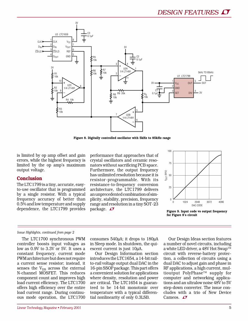
Digital Frequency ControlFigure 8 shows the details of anLTC1799 controlled by a 12-bit volt-age output D/A converter. Since theLTC1799 is a resistance-to-frequencyconverter, the input voltage betweenVCC and SET must be measured andused to create a current. Therefore,the DAC and op amps create a digi-tally controlled resistor between VCCand SET. Figure 9 shows the mea-sured output frequency vs input code.The linearity is excellent except at theendpoints; the low frequency accuracy
VSQUARE
OUT
Linear Technology Magazine • February 2001 5
DESIGN FEATURES
100
75
50
25
00 1024 2048 3072 4096
DAC CODE
f OUT
(kHz
)
VCC
GND
SET
5
4
OUT
DIV
1
2
3
U1 LTC1799
C10.1µF
C20.1µF
OUT
–
+
–
+
–
+
1
2
3
4
8
7
6
5
CLK
DIN
CS/LD
DOUT
VCC
VOUT
REF
GND
U3 LTC1659
CLK
DIN
CS/LD
C30.1µF
R510k
R610k
R710k
3V
3V
R110k
R210k
R310k
R4 10k
U2C1/4 LT1491
U2A1/4 LT1491
U2B1/4 LT1491
R9 20kR810k
RS10k
3V
3V
3V
10
9
8
3
2
1
4
11
7
5
6
5kHz TO 85kHz
Figure 8. Digitally controlled oscillator with 5kHz to 85kHz range
Figure 9. Input code vs output frequencyfor Figure 8’s circuit
is limited by op amp offset and gainerrors, while the highest frequency islimited by the op amp’s maximumoutput voltage.
ConclusionThe LTC1799 is a tiny, accurate, easy-to-use oscillator that is programmedby a single resistor. With a typicalfrequency accuracy of better than0.5% and low temperature and supplydependence, the LTC1799 provides
performance that approaches that ofcrystal oscillators and ceramic reso-nators without sacrificing PCB space.Furthermore, the output frequencyhas unlimited resolution because it isresistor-programmable. With itsresistance-to-frequency conversionarchitecture, the LTC1799 deliversan unprecedented combination of sim-plicity, stability, precision, frequencyrange and resolution in a tiny SOT-23package.
The LTC1700 synchronous PWMcontroller boosts input voltages aslow as 0.9V to 3.3V or 5V. It uses aconstant frequency, current modePWM architecture but does not requirea current sense resistor; instead, itsenses the VDS across the externalN-channel MOSFET. This reducescomponent count and improves highload current efficiency. The LTC1700offers high efficiency over the entireload current range. During continu-ous mode operation, the LTC1700
consumes 540µA; it drops to 180µAin Sleep mode. In shutdown, the qui-escent current is just 10µA.
Our Design Information sectionintroduces the LTC1654, a 14-bit rail-to-rail voltage output dual DAC in the16-pin SSOP package. This part offersa convenient solution for applicationswhere density, resolution and powerare critical. The LTC1654 is guaran-teed to be 14-bit monotonic overtemperature with a typical differen-tial nonlinearity of only 0.3LSB.
Our Design Ideas section featuresa number of novel circuits, includinga white LED driver, a 48V Hot Swap™circuit with reverse-battery protec-tion, a collection of circuits using adual DAC to adjust gain and phase inRF applications, a high current, mul-tioutput PolyPhase™ supply forcomputer and networking applica-tions and an ultralow noise 48V to 5Vstep-down converter. The issue con-cludes with a trio of New DeviceCameos.
Issue Highlights, continued from page 2

Linear Technology Magazine • February 20016
DESIGN FEATURES
Current-Limited DC/DC ConverterSimplifies USB Power Supplies
by Bryan Legates
IntroductionMany portable Universal Serial Bus(USB) devices power themselves fromthe USB host or hub power supplywhen plugged into the USB port. Sev-eral requirements must be met toensure the integrity of the bus: theUSB specification dictates that theinput capacitance of a device must beless than 10µF to minimize inrush
currents when the device is pluggedinto the USB port; when first pluggedin, the device must draw less than100mA from the port and, for highpower devices, the current drawn fromthe port can increase to 500mA onlyafter it is given permission to do so bythe USB controller. These require-ments can be easily met using the
LT1618 DC/DC converter, which pro-vides an accurate input currentcontrol ideal for USB applications.The LT1618 combines a traditionalvoltage feedback loop with a uniquecurrent feedback loop to operate as aconstant-current, constant-voltagesource.
SHDN
IADJ VC
VIN
VOUT12V
SWISN
ISP
FB
LT1618
R1909k
R2107k
VIN5V
C14.7µF
10nF
C24.7µF
D1L1
10µH
3
2
1
9
8
7
GND
5 104
C1: TAIYO YUDEN JMK212BJ475 (408) 573-4150 C2: TAIYO YUDEN EMK316BJ475 D1: ON SEMICONDUCTOR MBR0520 (602) 244-6600L1: SUMIDA CR43-100 (847) 956-0667
0.1Ω
2k13k
20k
OFF ON0V
3.3V
100mA 500mA3.3V
0VLOAD CURRENT (mA)
EFFI
CIEN
CY (%
)
90
85
80
75
70
65
600 40 80 10020 60 120 140 160
SHDN
IADJ VC
VIN
SWISN
ISP
FB
LT1618
R1316k
R2107k
VIN5V
C14.7µF
10nF
C210µF
D1L1
10µH
L210µH
3
2
1
9
8
7
GND
5 104
0.1Ω
2k
13k
20k
VOUT5V
C30.47µFIIN
C1: TAIYO YUDEN JMK212BJ475 (408) 573-4150C2: TAIYO YUDEN JMK316BJ106 (408) 573-4150C3: TAIYO YUDEN EMK212BJ474 (408) 573-4150D1: ON SEMICONDUCTOR MBR0520 (800) 282-9855L1: SUMIDA CR43-100 (847) 956-0666
OFF ON0V
3.3V
100mA 500mA3.3V
0V
1ms/DIV
VOUT2V/DIV
IIN50mA/DIV
1ms/DIV
VOUT2V/DIV
50mA/DIV
Figure 1. USB to 12V boost converter withselectable 100mA/500mA current limit
Figure 3. USB to 5V SEPIC converter
Figure 2. USB to 12V boost efficiency
Figure 4. USB to 5V SEPIC during start-up
Figure 5. USB to 5V SEPICstart-up with shorted output
Linear Technology Magazine • February 2001 7
DESIGN FEATURES
In addition to providing an accu-rate input current limit, the LT1618can also be used to provide an accu-rately regulated output current forcurrent-source applications. Drivingwhite LEDs is one application forwhich the device is ideally suited.With an input voltage range of 1.6V to18V, the LT1618 works from a varietyof input sources. The 36V switch rat-ing allows output voltages of up to35V to be generated, easily driving upto eight white LEDs in series. The1.4MHz switching frequency allowsthe use of low profile inductors andcapacitors, which, along with theLT1618’s MSOP-10 package, helps tominimize board area.
USB to 12V Boost ConverterFigure 1 shows a 5V to 12V boostconverter ideal for USB applications.The converter has a selectable100mA/500mA input current limit,allowing the device to be easilyswitched between the USB low andhigh power modes. Efficiency, shown
LOAD CURRENT (mA)0
EFFI
CIEN
CY (%
)
350100 250
80
75
70
65
6050 150 200 300
SHDN
IADJGND VC
VIN SW
ISN
ISP
FB
LT1618R12M
R2100k
VIN2.7V TO 5V
10kHz TO 50kHzPWM
BRIGHTNESSADJUST
C14.7µF
CC0.1µF
C21µF
2.49ΩD1L1
10µH 20mA
3
2
1
9
8 7
5 10
4R3
5.1k
C30.1µF
C1: TAIYO YUDEN JMK212BJ475 (408) 573-4150C2: TAIYO YUDEN TMK316BJ105 (408) 573-4150D1: ON SEMICONDUCTOR MBR0530 (800) 282-9855L1: SUMIDA CLQ4D10-100 (847) 956-0666
LED CURRENT (mA)0
EFFI
CIEN
CY (%
)
205 10 15
80
75
70
65
60
55
50
45
40
VIN = 3.3V
VIN = 4.2V
VIN = 2.7V
in Figure 2, exceeds 85%. If the loaddemands more current than the con-verter can provide with the inputcurrent limited to 100mA (or 500mA),the output voltage will simply decreaseand the LT1618 will operate in con-stant-current mode. For example,with an input current limit of 100mA,about 35mA can be provided to the12V output. If the load increases to50mA, the output voltage will reduceto approximately 8V to maintain aconstant 100mA input current.
USB to 5V SEPIC Converterwith Short-Circuit ProtectionUnlike boost converters, SEPICs(single-ended primary inductance)converters) have an output that isDC-isolated from the input, so aninput current limit not only helps softstart the output, but also providesexcellent short-circuit protection. The5V SEPIC converter shown in Figure3 is ideal for applications that needthe output voltage to go to zero dur-ing shutdown. The accurate inputcurrent limit ensures USB device com-pliance even under output faultconditions. Figure 4 shows the start-up characteristic of the SEPICconverter with a 50mA load. By lim-iting the input current to 100mA, theoutput is effectively soft started,smoothly increasing and not over-shooting its final 5V value. Figure 5shows that the input current doesnot exceed 100mA even with the out-
put shorted to ground (thus the flatoutput voltage waveform in the oscil-loscope photo). Efficiency is shown inFigure 6. This converter also has aselectable input current limit of either100mA or 500mA, making it ideal forhigh power USB applications.
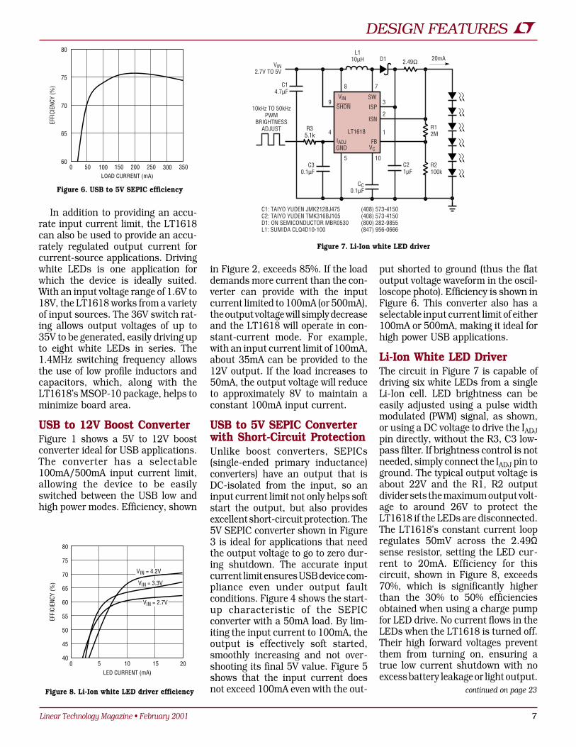
Li-Ion White LED DriverThe circuit in Figure 7 is capable ofdriving six white LEDs from a singleLi-Ion cell. LED brightness can beeasily adjusted using a pulse widthmodulated (PWM) signal, as shown,or using a DC voltage to drive the IADJpin directly, without the R3, C3 low-pass filter. If brightness control is notneeded, simply connect the IADJ pin toground. The typical output voltage isabout 22V and the R1, R2 outputdivider sets the maximum output volt-age to around 26V to protect theLT1618 if the LEDs are disconnected.The LT1618’s constant current loopregulates 50mV across the 2.49Ωsense resistor, setting the LED cur-rent to 20mA. Efficiency for thiscircuit, shown in Figure 8, exceeds70%, which is significantly higherthan the 30% to 50% efficienciesobtained when using a charge pumpfor LED drive. No current flows in theLEDs when the LT1618 is turned off.Their high forward voltages preventthem from turning on, ensuring atrue low current shutdown with noexcess battery leakage or light output.
Figure 6. USB to 5V SEPIC efficiency
Figure 7. Li-Ion white LED driver
Figure 8. Li-Ion white LED driver efficiency continued on page 23
Linear Technology Magazine • February 20018
DESIGN FEATURES
2.3MHz Monolithic, Continuous Time,Differential Lowpass Filter ProvidesSolutions for Wide Band CDMAApplications by Nello Sevastopoulos and Mike Kultgen
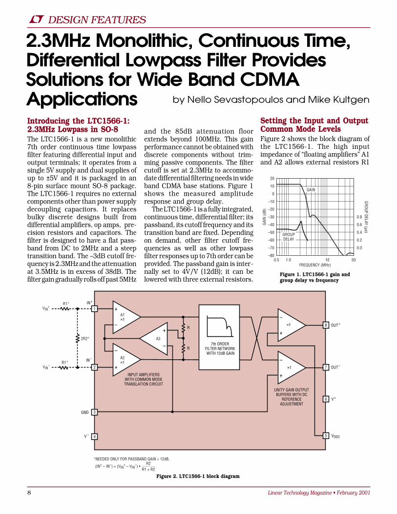
Introducing the LTC1566-1:2.3MHz Lowpass in SO-8The LTC1566-1 is a new monolithic7th order continuous time lowpassfilter featuring differential input andoutput terminals; it operates from asingle 5V supply and dual supplies ofup to ±5V and it is packaged in an8-pin surface mount SO-8 package.The LTC1566-1 requires no externalcomponents other than power supplydecoupling capacitors. It replacesbulky discrete designs built fromdifferential amplifiers, op amps, pre-cision resistors and capacitors. Thefilter is designed to have a flat pass-band from DC to 2MHz and a steeptransition band. The –3dB cutoff fre-quency is 2.3MHz and the attenuationat 3.5MHz is in excess of 38dB. Thefilter gain gradually rolls off past 5MHz
and the 85dB attenuation floorextends beyond 100MHz. This gainperformance cannot be obtained withdiscrete components without trim-ming passive components. The filtercutoff is set at 2.3MHz to accommo-date differential filtering needs in wideband CDMA base stations. Figure 1shows the measured amplituderesponse and group delay.
The LTC1566-1 is a fully integrated,continuous time, differential filter; itspassband, its cutoff frequency and itstransition band are fixed. Dependingon demand, other filter cutoff fre-quencies as well as other lowpassfilter responses up to 7th order can beprovided. The passband gain is inter-nally set to 4V/V (12dB); it can belowered with three external resistors.
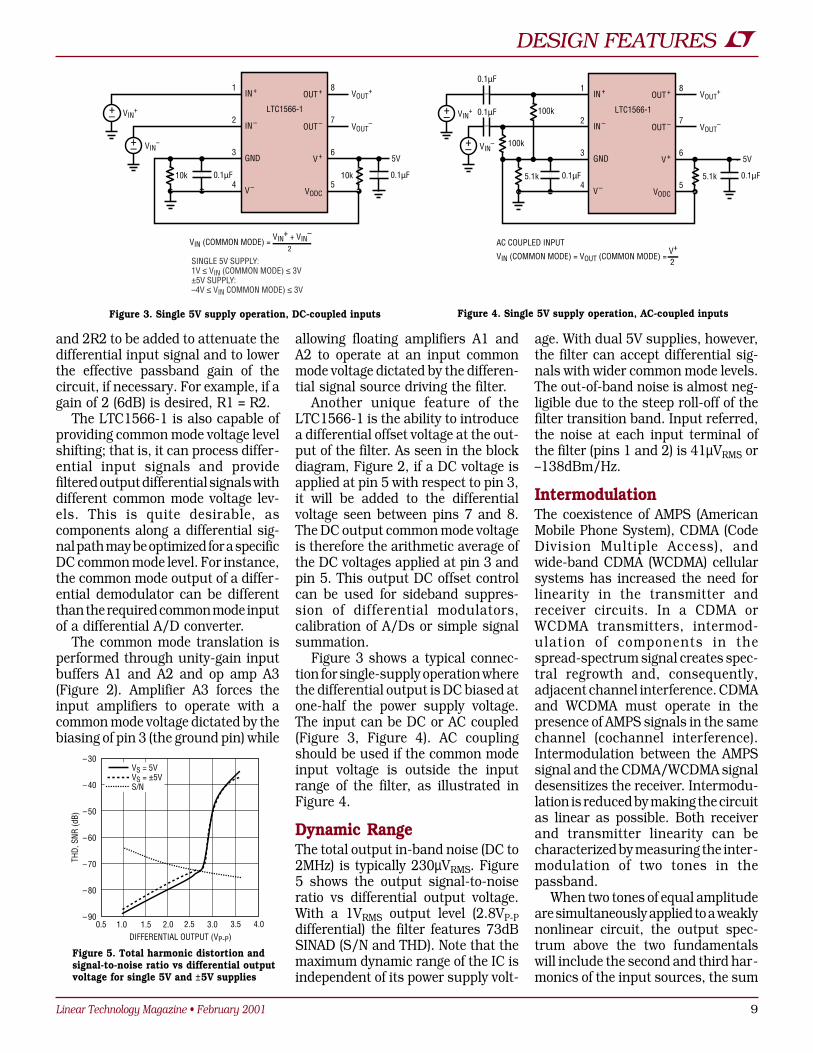
Setting the Input and OutputCommon Mode LevelsFigure 2 shows the block diagram ofthe LTC1566-1. The high inputimpedance of “floating amplifiers” A1and A2 allows external resistors R1
20
10
0
–10
–20
–30
–40
–50
–60
–70
–80
GAIN
(dB)
0.8
0.6
0.4
0.2
0.0
GROUP DELAY (µs)
0.5 1.0 10 50FREQUENCY (MHz)
GAIN
GROUPDELAY
–
+
–
–
+
–
+
–
+
7th ORDER FILTER NETWORK WITH 12dB GAIN
8
1
2
3
4
7
6
5
×1
×1
A1×1
A2×1
UNITY GAIN OUTPUTBUFFERS WITH DC
REFERENCEADJUSTMENT
INPUT AMPLIFIERSWITH COMMON MODETRANSLATION CIRCUIT
IN+
IN –
GND
V –
OUT +
OUT –
V +
VODC
R
R
+
A3
R1*
R1*
2R2*
VIN+
VIN–
*NEEDED ONLY FOR PASSBAND GAIN < 12dB,
(IN+ – IN–) = (VIN+ – VIN
–) •R2
R1 + R2
Figure 2. LTC1566-1 block diagram
Figure 1. LTC1566-1 gain andgroup delay vs frequency
Linear Technology Magazine • February 2001 9
DESIGN FEATURES
and 2R2 to be added to attenuate thedifferential input signal and to lowerthe effective passband gain of thecircuit, if necessary. For example, if again of 2 (6dB) is desired, R1 = R2.
The LTC1566-1 is also capable ofproviding common mode voltage levelshifting; that is, it can process differ-ential input signals and providefiltered output differential signals withdifferent common mode voltage lev-els. This is quite desirable, ascomponents along a differential sig-nal path may be optimized for a specificDC common mode level. For instance,the common mode output of a differ-ential demodulator can be differentthan the required common mode inputof a differential A/D converter.
The common mode translation isperformed through unity-gain inputbuffers A1 and A2 and op amp A3(Figure 2). Amplifier A3 forces theinput amplifiers to operate with acommon mode voltage dictated by thebiasing of pin 3 (the ground pin) while
allowing floating amplifiers A1 andA2 to operate at an input commonmode voltage dictated by the differen-tial signal source driving the filter.
Another unique feature of theLTC1566-1 is the ability to introducea differential offset voltage at the out-put of the filter. As seen in the blockdiagram, Figure 2, if a DC voltage isapplied at pin 5 with respect to pin 3,it will be added to the differentialvoltage seen between pins 7 and 8.The DC output common mode voltageis therefore the arithmetic average ofthe DC voltages applied at pin 3 andpin 5. This output DC offset controlcan be used for sideband suppres-sion of differential modulators,calibration of A/Ds or simple signalsummation.
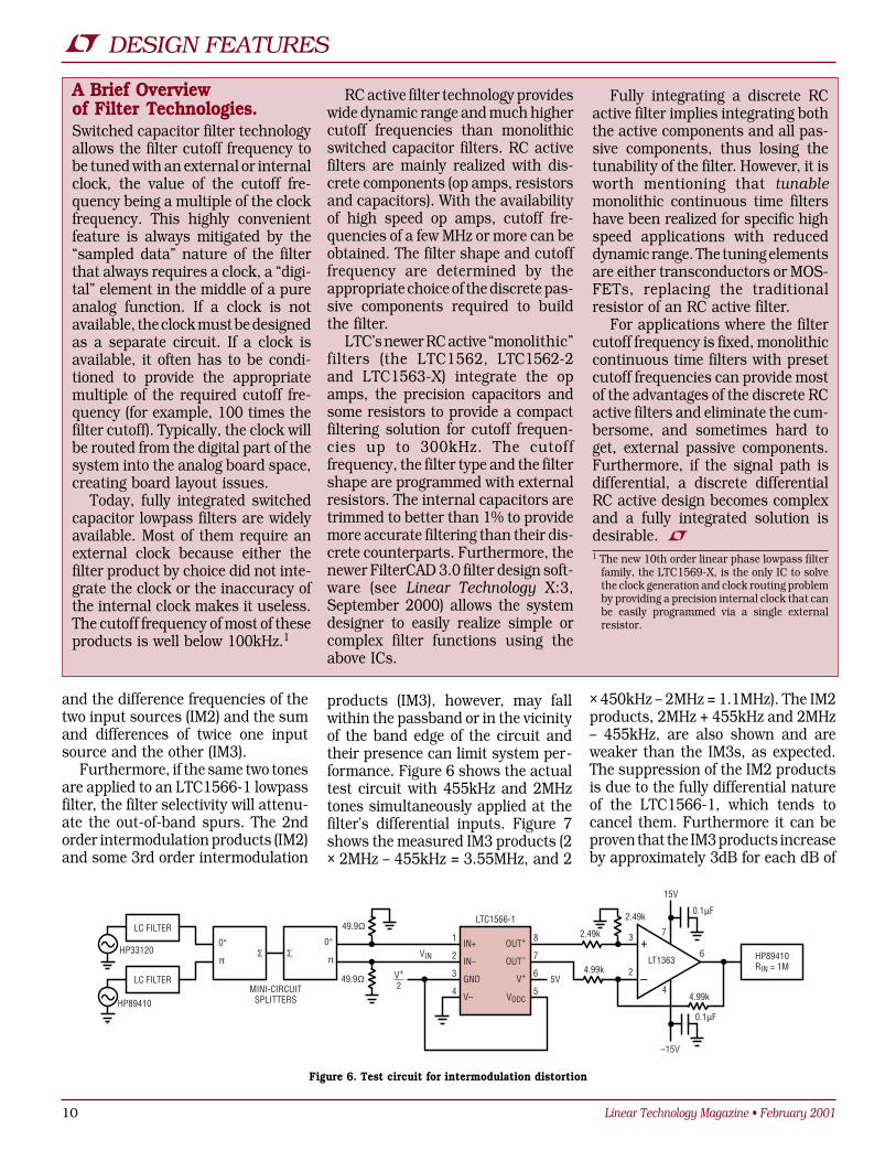
Figure 3 shows a typical connec-tion for single-supply operation wherethe differential output is DC biased atone-half the power supply voltage.The input can be DC or AC coupled(Figure 3, Figure 4). AC couplingshould be used if the common modeinput voltage is outside the inputrange of the filter, as illustrated inFigure 4.
Dynamic RangeThe total output in-band noise (DC to2MHz) is typically 230µVRMS. Figure5 shows the output signal-to-noiseratio vs differential output voltage.With a 1VRMS output level (2.8VP-Pdifferential) the filter features 73dBSINAD (S/N and THD). Note that themaximum dynamic range of the IC isindependent of its power supply volt-
age. With dual 5V supplies, however,the filter can accept differential sig-nals with wider common mode levels.The out-of-band noise is almost neg-ligible due to the steep roll-off of thefilter transition band. Input referred,the noise at each input terminal ofthe filter (pins 1 and 2) is 41µVRMS or–138dBm/Hz.
IntermodulationThe coexistence of AMPS (AmericanMobile Phone System), CDMA (CodeDivision Multiple Access), andwide-band CDMA (WCDMA) cellularsystems has increased the need forlinearity in the transmitter andreceiver circuits. In a CDMA orWCDMA transmitters, intermod-ulation of components in thespread-spectrum signal creates spec-tral regrowth and, consequently,adjacent channel interference. CDMAand WCDMA must operate in thepresence of AMPS signals in the samechannel (cochannel interference).Intermodulation between the AMPSsignal and the CDMA/WCDMA signaldesensitizes the receiver. Intermodu-lation is reduced by making the circuitas linear as possible. Both receiverand transmitter linearity can becharacterized by measuring the inter-modulation of two tones in thepassband.
When two tones of equal amplitudeare simultaneously applied to a weaklynonlinear circuit, the output spec-trum above the two fundamentalswill include the second and third har-monics of the input sources, the sum
1
2
3
4
8
7
6
5
VIN+
VIN–
VOUT+
VOUT–
5V
10k 10k0.1µF 0.1µF
+–
+–LTC1566-1
OUT +
OUT –
V +
VODC
IN +
IN –
GND
V –
VIN (COMMON MODE) = VIN
+ + VIN–
2
SINGLE 5V SUPPLY:1V ≤ VIN (COMMON MODE) ≤ 3V±5V SUPPLY:–4V ≤ VIN COMMON MODE) ≤ 3V
LTC1566-1
1
2
3
4
OUT +
OUT –
V +
VODC
IN +
IN –
GND
V –
8
7
6
5
VIN+
VIN–
VOUT+
VOUT–
5V
5.1k 5.1k0.1µF 0.1µF
+–
+–
100k
100k
AC COUPLED INPUT
VIN (COMMON MODE) = VOUT (COMMON MODE) = V+
2
0.1µF
0.1µF
DIFFERENTIAL OUTPUT (VP-P)0.5
THD,
SNR
(dB)
– 30
–40
–50
–60
–70
–80
–902.0 3.01.0 1.5 2.5 3.5 4.0
VS = 5VVS = ±5VS/N
Figure 3. Single 5V supply operation, DC-coupled inputs Figure 4. Single 5V supply operation, AC-coupled inputs
Figure 5. Total harmonic distortion andsignal-to-noise ratio vs differential outputvoltage for single 5V and ±5V supplies
Linear Technology Magazine • February 200110
DESIGN FEATURES
and the difference frequencies of thetwo input sources (IM2) and the sumand differences of twice one inputsource and the other (IM3).
Furthermore, if the same two tonesare applied to an LTC1566-1 lowpassfilter, the filter selectivity will attenu-ate the out-of-band spurs. The 2ndorder intermodulation products (IM2)and some 3rd order intermodulation
products (IM3), however, may fallwithin the passband or in the vicinityof the band edge of the circuit andtheir presence can limit system per-formance. Figure 6 shows the actualtest circuit with 455kHz and 2MHztones simultaneously applied at thefilter’s differential inputs. Figure 7shows the measured IM3 products (2× 2MHz – 455kHz = 3.55MHz, and 2
× 450kHz – 2MHz = 1.1MHz). The IM2products, 2MHz + 455kHz and 2MHz– 455kHz, are also shown and areweaker than the IM3s, as expected.The suppression of the IM2 productsis due to the fully differential natureof the LTC1566-1, which tends tocancel them. Furthermore it can beproven that the IM3 products increaseby approximately 3dB for each dB of
A Brief Overviewof Filter Technologies.Switched capacitor filter technologyallows the filter cutoff frequency tobe tuned with an external or internalclock, the value of the cutoff fre-quency being a multiple of the clockfrequency. This highly convenientfeature is always mitigated by the“sampled data” nature of the filterthat always requires a clock, a “digi-tal” element in the middle of a pureanalog function. If a clock is notavailable, the clock must be designedas a separate circuit. If a clock isavailable, it often has to be condi-tioned to provide the appropriatemultiple of the required cutoff fre-quency (for example, 100 times thefilter cutoff). Typically, the clock willbe routed from the digital part of thesystem into the analog board space,creating board layout issues.
Today, fully integrated switchedcapacitor lowpass filters are widelyavailable. Most of them require anexternal clock because either thefilter product by choice did not inte-grate the clock or the inaccuracy ofthe internal clock makes it useless.The cutoff frequency of most of theseproducts is well below 100kHz.1
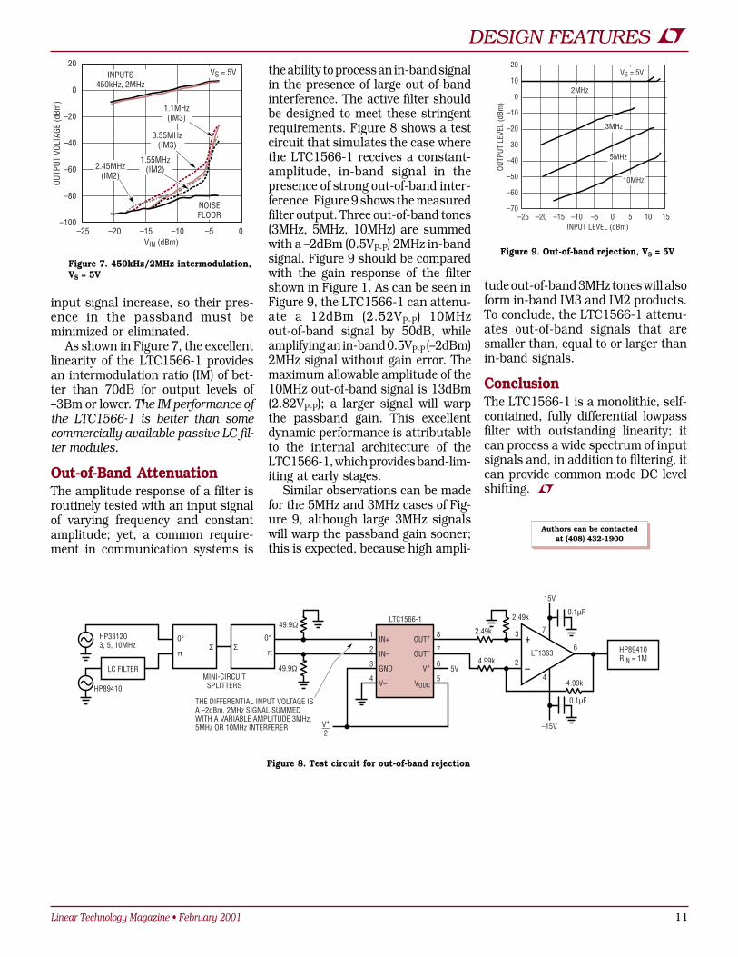
RC active filter technology provideswide dynamic range and much highercutoff frequencies than monolithicswitched capacitor filters. RC activefilters are mainly realized with dis-crete components (op amps, resistorsand capacitors). With the availabilityof high speed op amps, cutoff fre-quencies of a few MHz or more can beobtained. The filter shape and cutofffrequency are determined by theappropriate choice of the discrete pas-sive components required to buildthe filter.
LTC’s newer RC active “monolithic”filters (the LTC1562, LTC1562-2and LTC1563-X) integrate the opamps, the precision capacitors andsome resistors to provide a compactfiltering solution for cutoff frequen-cies up to 300kHz. The cutofffrequency, the filter type and the filtershape are programmed with externalresistors. The internal capacitors aretrimmed to better than 1% to providemore accurate filtering than their dis-crete counterparts. Furthermore, thenewer FilterCAD 3.0 filter design soft-ware (see Linear Technology X:3,September 2000) allows the systemdesigner to easily realize simple orcomplex filter functions using theabove ICs.
Fully integrating a discrete RCactive filter implies integrating boththe active components and all pas-sive components, thus losing thetunability of the filter. However, it isworth mentioning that tunablemonolithic continuous time filtershave been realized for specific highspeed applications with reduceddynamic range. The tuning elementsare either transconductors or MOS-FETs, replacing the traditionalresistor of an RC active filter.
For applications where the filtercutoff frequency is fixed, monolithiccontinuous time filters with presetcutoff frequencies can provide mostof the advantages of the discrete RCactive filters and eliminate the cum-bersome, and sometimes hard toget, external passive components.Furthermore, if the signal path isdifferential, a discrete differentialRC active design becomes complexand a fully integrated solution isdesirable.1 The new 10th order linear phase lowpass filter
family, the LTC1569-X, is the only IC to solvethe clock generation and clock routing problemby providing a precision internal clock that canbe easily programmed via a single externalresistor.
Figure 6. Test circuit for intermodulation distortion
–
+IN+
IN–
GND
V–
OUT+
OUT–
V+
VODC
1
2
3
4
8
7
6
5
LTC1566-1
HP89410RIN = 1M
LT1363
4.99k
4.99k
2.49k
2.49k
V+
2
VIN
0°
π
0°
πΣΣ
49.9Ω
49.9Ω
LC FILTER
LC FILTER
HP33120
HP89410
MINI-CIRCUITSPLITTERS
5V
15V
0.1µF
0.1µF
3
2
6
7
4
–15V
Linear Technology Magazine • February 2001 11
DESIGN FEATURES
OUTP
UT L
EVEL
(dBm
)
INPUT LEVEL (dBm)–25 –20 –15 –10 –5 0 5 10 15
20
10
0
–10
–20
–30
–40
–50
–60
–70
2MHz
3MHz
5MHz
10MHz
VS = 5V
15V
0.1µF
0.1µF
3
2
6
7
4
–15V
–
+IN+
IN–
GND
V–
OUT+
OUT–
V+
VODC
1
2
3
4
8
7
6
5
LTC1566-1
HP89410RIN = 1M
LT1363
4.99k
4.99k
2.49k
2.49k0°
π
0°
πΣΣ
49.9Ω
49.9ΩLC FILTER
HP331203, 5, 10MHz
HP89410
MINI-CIRCUITSPLITTERS
5V
V+
2
THE DIFFERENTIAL INPUT VOLTAGE IS A –2dBm, 2MHz SIGNAL SUMMED WITH A VARIABLE AMPLITUDE 3MHz, 5MHz OR 10MHz INTERFERER
input signal increase, so their pres-ence in the passband must beminimized or eliminated.
As shown in Figure 7, the excellentlinearity of the LTC1566-1 providesan intermodulation ratio (IM) of bet-ter than 70dB for output levels of–3Bm or lower. The IM performance ofthe LTC1566-1 is better than somecommercially available passive LC fil-ter modules.
Out-of-Band AttenuationThe amplitude response of a filter isroutinely tested with an input signalof varying frequency and constantamplitude; yet, a common require-ment in communication systems is
the ability to process an in-band signalin the presence of large out-of-bandinterference. The active filter shouldbe designed to meet these stringentrequirements. Figure 8 shows a testcircuit that simulates the case wherethe LTC1566-1 receives a constant-amplitude, in-band signal in thepresence of strong out-of-band inter-ference. Figure 9 shows the measuredfilter output. Three out-of-band tones(3MHz, 5MHz, 10MHz) are summedwith a –2dBm (0.5VP-P) 2MHz in-bandsignal. Figure 9 should be comparedwith the gain response of the filtershown in Figure 1. As can be seen inFigure 9, the LTC1566-1 can attenu-ate a 12dBm (2.52VP-P) 10MHzout-of-band signal by 50dB, whileamplifying an in-band 0.5VP-P (–2dBm)2MHz signal without gain error. Themaximum allowable amplitude of the10MHz out-of-band signal is 13dBm(2.82VP-P); a larger signal will warpthe passband gain. This excellentdynamic performance is attributableto the internal architecture of theLTC1566-1, which provides band-lim-iting at early stages.
Similar observations can be madefor the 5MHz and 3MHz cases of Fig-ure 9, although large 3MHz signalswill warp the passband gain sooner;this is expected, because high ampli-
20
0
–20
–40
–60
–80
–100–25 –20 –15 –10 –5 0
VIN (dBm)
OUTP
UT V
OLTA
GE (d
Bm)
INPUTS450kHz, 2MHz
1.55MHz(IM2)2.45MHz
(IM2)
1.1MHz(IM3)
NOISEFLOOR
3.55MHz(IM3)
VS = 5V
Figure 7. 450kHz/2MHz intermodulation,VS = 5V
Figure 9. Out-of-band rejection, VS = 5V
Figure 8. Test circuit for out-of-band rejection
tude out-of-band 3MHz tones will alsoform in-band IM3 and IM2 products.To conclude, the LTC1566-1 attenu-ates out-of-band signals that aresmaller than, equal to or larger thanin-band signals.
ConclusionThe LTC1566-1 is a monolithic, self-contained, fully differential lowpassfilter with outstanding linearity; itcan process a wide spectrum of inputsignals and, in addition to filtering, itcan provide common mode DC levelshifting.
Authors can be contactedat (408) 432-1900
Linear Technology Magazine • February 200112
DESIGN FEATURES
Very Low Cost Li-Ion Battery ChargerRequires Little Area andFew Components by David Laude
IntroductionThe LTC1734 is a precision, low cost,single-cell, linear Li-Ion batterycharger with constant voltage andconstant current control. The smallquantity and low cost of external com-ponents results in a very low overallsystem cost and the part’s 6-pin SOT-23 package allows for a compactdesign solution. Previous productsusually required an external currentsensing resistor and blocking diodewhose functions are included in theLTC1734. Other features include:
1% accurate float voltage optionsof 4.1V or 4.2V
Programmable constant currentrange of 200mA to 700mA
Charging current monitor outputand manual shutdown for usewith a microcontroller
Automated shutdown with nobattery drain after supplyremoval
Undervoltage lockout Self protection for overcurrent
and overtemperature
Applications include such compactdevices as cellular phones, digitalcameras and handheld computers.The LTC1734 can also be used as ageneral purpose current source or forcharging nickel-cadmium or nickel-metal-hydride batteries.
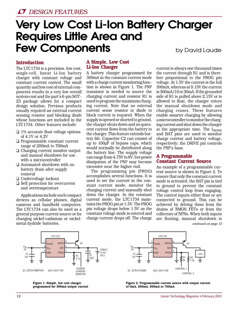
A Simple, Low CostLi-Ion ChargerA battery charger programmed for300mA in the constant current modewith a charge current monitoring func-tion is shown in Figure 1. The PNPtransistor is needed to source thecharging current and resistor R1 isused to program the maximum charg-ing current. Note that no externalcurrent sense resistor or diode toblock current is required. When thesupply is opened or shorted to ground,the charger shuts down and no quies-cent current flows from the battery tothe charger. This feature extends bat-tery life. Capacitor C2 can consist ofup to 100µF of bypass caps, whichwould normally be distributed alongthe battery line. The supply voltagecan range from 4.75V to 8V, but powerdissipation of the PNP may becomeexcessive near the higher end.
The programming pin (PROG)accomplishes several functions. It isused to set the current in the con-stant current mode, monitor thecharging current and manually shutdown the charger. In the constantcurrent mode, the LTC1734 main-tains the PROG pin at 1.5V. The PROGpin voltage drops below 1.5V as theconstant voltage mode is entered andcharge current drops off. The charge
current is always one thousand timesthe current through R1 and is there-fore proportional to the PROG pinvoltage. At 1.5V the current is the full300mA, whereas at 0.15V the currentis 300mA/10 or 30mA. If the groundedside of R1 is pulled above 2.15V or isallowed to float, the charger entersthe manual shutdown mode andcharging ceases. These featuresenable smarter charging by allowinga microcontroller to monitor the charg-ing current and shut down the chargerat the appropriate time. The ISENSEand BAT pins are used to monitorcharge current and battery voltage,respectively; the DRIVE pin controlsthe PNP’s base.
A ProgrammableConstant Current SourceAn example of a programmable cur-rent source is shown in Figure 2. Toensure that only the constant currentmode is activated, the BAT pin is tiedto ground to prevent the constantvoltage control loop from engaging.The control inputs either float or areconnected to ground. This can beachieved by driving them from thedrains of NMOS FETs or from thecollectors of NPNs. When both inputsare floating, manual shutdown is
Figure 1. Simple, low cost chargerprogrammed for 300mA output current
Figure 2. Programmable current source with output currentof 0mA, 200mA, 500mA or 700mA
ISENSE
VCC
GND
DRIVE
BAT
PROG
1
3
2
6
5
4
LTC1734
Q1
SINGLELi-IonCELLC2
10µFR15.1k
CHARGECURRENTMONITOR
VIN5V
C11µF
Q1: ZETEX FMMT549 (631) 543-7100
ISENSE
VCC
GND
DRIVE
BAT
PROG
1
3
2
6
5
4
LTC1734
Q1VIN5V
C11µF
LOAD
R13k
R27.5k
CONTROL 1
CONTROL 2Q1: ZETEX FCX589 (631) 543-7100
continued on page 15

Linear Technology Magazine • February 2001 13
DESIGN FEATURES
Synchronous Buck Controller ExtendsBattery Life and Fits in a Small Footprint
by Peter GuanIntroductionPortable electronic devices continueto decrease in size and their supplyvoltages are also falling, but load cur-rent requirements are increasing as aresult of higher processing speed andimproved features. This trend placesmore constraints on today’s portablepower supplies, but Linear Technol-ogy has the solution. The LTC1773 isa synchronous DC/DC controller thatpacks high output current capabilityand low operating quiescent currentin a small MSOP-10 package. Its inputvoltage range is from 2.65V to 8.5V;this is ideal for 1- or 2-cell Li-Ionbatteries as well as 3- to 6-cell NiCdand NiMH battery packs because itallows the batteries to operate nearend of charge. A precise internalundervoltage lockout circuit preventsdeep discharge of the battery below2.5V. Popular features such as OPTI-LOOP™ compensation, soft start andBurst Mode™ operation are alsoincluded. Combined with its smallMSOP package, the LTC1773’s highoperating frequency of 550kHz allowsthe use of small, surface mount com-ponents to provide a compact powersupply solution.
OperationFigure 1 shows a typical applicationof the LTC1773 in a 5V to 2.5V/3Astep-down converter. Figure 2 showsits efficiency vs load current. TheLTC1773 uses a constant frequency,current mode architecture to drive anexternal pair of complementary powerMOSFETs. An internal oscillator sets
the output voltage through an exter-nal resistive divider connected to theVFB pin. While the P-channel MOS-FET is off, the synchronous N-channelMOSFET turns on until either theinductor current starts to reverse, asindicated by the SW pin going belowground, or until the beginning of thenext cycle.
Synchronous,Burst Mode and ForcedContinuous OperationThree modes of operation can beselected through the SYNC/FCB pin.Tying it above 0.8V or leaving it float-ing will enable Burst Mode operation,which increases efficiency during lightload conditions. During Burst Modeoperation, the peak inductor currentlimit is clamped to about a third of themaximum value and the ITH pin ismonitored to determine whether thedevice will go into a power-savingSleep mode. The ITH level is inverselyproportional to the output voltageerror. When the inductor’s averagecurrent is higher than the loadrequirement, the output voltage riseswhile the ITH level drops. When ITHdips below 0.22V, the device goes intoSleep mode, turning off the external
+
+
30kRC
220pFCC
0.1µF
COUT180µF
CIN68µF
L13µH
VIN2.65V TO 8.5V
VOUT2.5V
RSENSE0.025Ω
3
2
1
4
5
8
9
7
10
6
LTC1773
RUN/SS
SYNC/FCB
GND
SENSE–
VIN
TGITH
VFB BG
SW
Si9801DY
R180.6k R2
169k
47pF
L1: SUMIDA CDRH6D28-3R0(847) 956-0667
OUTPUT CURRENT (mA)
EFFI
CIEN
CY (%
)
100
95
90
85
80
75
70
65
60
551 100 1000 500010
VIN = 3.3V
VIN = 5V
VIN = 8V
Figure 1. 5V to 2.5V/3A step-down converterFigure 2. Efficiency of Figure 1’s circuit withseveral input voltages
Portable electronic devicescontinue to decrease in sizeand their supply voltagesare also falling, but loadcurrent requirements areincreasing as a result of
higher processing speed andimproved features. This
trend places moreconstraints on today’s
portable power supplies, butLinear Technology has the
solution.
the operating frequency of the device.The P-channel MOSFET turns on withevery oscillator cycle and turns offwhen the internal current compara-tor trips, indicating that the inductorcurrent has reached a level set by theITH pin. An internal error amplifier, inturn, drives the ITH pin by monitoring

Linear Technology Magazine • February 200114
DESIGN FEATURES
power MOSFETs and most of theinternal circuitry; in this state, theLTC1773 consumes only 80µA of qui-escent current. At this point, the loadcurrent is being supplied by the out-put capacitor. As the output droops,ITH will be driven higher. When ITHrises above 0.27V, the device resumesnormal operation.
For frequency-sensitive applica-tions, Burst Mode operation can beinhibited by tying the SYNC/FCB pinto below 0.8V to force continuousoperation, which will continually drivethe external power MOSFETs syn-chronously regardless of the outputload. The inductor current is allowedto reverse in this case.
In addition to being a logic inputthreshold, the 0.8V threshold of theSYNC/FCB pin can also be used toregulate a secondary winding outputby forcing continuous synchronousoperation regardless of the primaryoutput load. A logic-level clock signalconnected to the SYNC/FCB pin syn-chronizes the operating frequency toan external source between 585kHzand 750kHz. Burst Mode operation isautomatically disabled during syn-chronization to reduce noise. Instead,cycle skipping occurs under light loadconditions because current reversalis not allowed. This boosts the lowcurrent efficiency while providing lowoutput ripple.
Run/Soft StartUpon power up, the RUN/SS pin ispulled high by an internal currentsource; an external capacitor can be
placed at the pin to program its risetime to ensure a soft start at theoutput by limiting the amount ofcharge current into the outputcapacitors. The RUN/SS pin alsoserves another function: if the pin istied below 0.65V, the part goes intoshutdown and consumes less than10µA of input current.
Fault ProtectionThe LTC1773 incorporates protectionfeatures such as programmable cur-rent limit, input undervoltage lockout,output overvoltage protection and fre-quency foldback when the output fallsout of regulation.
One of the advantages of a currentmode switching regulator is that cur-rent is regulated during every clockcycle, thus providing current over-load protection on a pulse-by-pulsebasis. Current limit is programmedthrough an external high-side senseresistor. The maximum sense voltageacross this resistor is 100mV. Buttaking into account current ripple,input noise and sense resistor toler-ance, 70mV should be used inchoosing the proper sense resistor(RSENSE = 70mV/IOUT).
To protect a battery power sourcefrom deep discharge near its end ofcharge, an internal undervoltage lock-out circuit shuts down the devicewhen VIN drops below 2.5V. Thisreduces the current consumption toabout 2µA. A built-in 150mV hyster-esis ensures reliable operation withnoisy supplies.
During transient overshoots andother more serious conditions thatmay cause the output to rise out ofregulation (>7.5%), an internal over-voltage comparator will turn off themain MOSFET and turn on thesynchronous MOSFET until the over-voltage condition is cleared. Duringthis time, if the main MOSFET isdefective or shorted to ground, cur-rent will flow directly from VIN toground, blowing the system fuse andsaving the other board components.
In addition, if the output is shortedto ground, the frequency of the oscil-lator is reduced to about 55kHz, 1/10of the nominal frequency. This fre-
quency foldback ensures that the in-ductor current has enough time todecay, thereby preventing runaway.The oscillator’s frequency will gradu-ally increase back to 550kHz whenthe VFB pin rises above 0.4V.
Dropout OperationDuring the discharging of a batterysource, when the input supply volt-age decreases toward the outputvoltage, the duty cycle increasestoward the maximum on-time. Theoutput voltage will then be deter-mined by VIN minus the I • R voltagedrops across the external P-channelMOSFET, the sense resistor and theinductor.
OPTI-LOOP CompensationTo meet stringent transient responserequirements, other switching regu-lators may need to use many largeand expensive output capacitors toreduce the output voltage droop dur-ing a load step. The LTC1773, withOPTI-LOOP compensation, requiresfewer output capacitors and alsoallows the use of inexpensive ceramiccapacitors. The ITH pin of the LTC1773allows users to choose the propercomponent values to compensate theloop so that the transient responsecan be optimized with the minimumnumber of output capacitors.
Line and Load RegulationThe current mode architecture of theLTC1773 ensures excellent line andload regulation without cumbersomecompensation and excessive output
IL2A/DIV
VOUT100mV/DIV
VIN = 5VVOUT = 2.5V100mA TO 5A LOAD STEP
10mV/DIV
IL2A/DIV
VOUT100mV/DIV
VIN = 5VVOUT = 2.5V100mA TO 5A LOAD STEP
10mV/DIV
Figure 3a. Load-step response,Burst Mode operation
Figure 3b. Load-step response,continuous mode operation

Linear Technology Magazine • February 2001 15
DESIGN FEATURES
capacitance. Figures 3a and 3b showthe response of the LTC1773 to a100mA to 5A load step during BurstMode and continuous mode opera-tions, respectively.
1.8V/7A ApplicationFigure 4 shows a step-down applica-tion from 3.3V to 1.8V at 7A. Whenoperating below 5V, care should betaken to choose the proper sublogic-level MOSFETs that have relativelylow gate charge. For high current(>3A) applications, single P-channeland N-channel MOSFETs should beused instead of complementary MOS-FETs in one package. A good figure ofmerit for MOSFETs is the RDS(ON) gate-charge product. The lower this valueis, the higher the application’sefficiency will be.
In addition to normal step-downapplications, the LTC1773 can alsobe used in a zeta converter configura-tion that will do both step-down andstep-up conversions, as shown in Fig-ure 5. This application is ideal forbattery-powered operation, in whicha regulated 3.3V output is maintainedduring the entire discharge cycle of aLi-Ion battery from 4.7V to 2.5V.
ConclusionThe LTC1773 offers flexibility, highefficiency and many other popularfeatures in a small MSOP-10 pack-age. For low voltage portable systemsthat require small footprint and highefficiency, the LTC1773 is the idealsolution.
+
1
2
3
4
5
10
9
8
7
6
RSENSE0.025Ω
33pF
200pF
0.1µF
30k
249k1%80.6k
1%
VOUT3.3V1A
2.7V ≤ VIN ≤ 4.2V
+
LTC1773
RUN/SS
SYNC/FCB
GND
SENSE–
VIN
TG
ITH
VFB
BG
SW
L12µH
L12µH
CIN150µF6.3V
COUT220µF6.3V
47µF
+
SANYO POSCAP 6TPA150M (714) 373-7334AVX TPSD227M006R0100 (207) 282-5111COILTRONICS CTX2-4 (561) 752-5000IRC LR1206-01-R033-F (361) 992-7900SILICONIX Si9803DY (800) 554-5565SILICONIX Si9804DY
VINM1
M2
CIN: COUT:
L1: RSENSE:
M1: M2:
1
2
3
4
5
10
9
8
7
6
RSENSE0.01Ω
47pF
220pF
0.1µF
0.1µF
30k
99k1%
80.6k1%
100pF
VOUT1.8V7A
2.7V ≤ VIN ≤ 6V
LTC1773
RUN/SS
SYNC/FCB
GND
SENSE–
VIN
TG
ITH
VFB
BG
SW
L11µH
CIN150µF6.3V
M2
M1
4.7µF6.3V
COUT680µF4V×2
100pFD2*MBRS340T3
*NOTE: D2 IS OPTIONAL. IF REMOVED, EFFICIENCY DROPS BY 1%
+
+
PANASONIC SPECIAL POLYMER (714) 737-7334KEMET T510687K004AS (408) 986-0424TOKO TYPE D104C 919AS-1RON (847) 699-3430IRC LR2512-01-R010-J (361) 992-7900FAIRCHILD FDS6375 (408) 822-2126SILICONIX Si9804DY (800) 554-5565
CIN: COUT:
L1: RSENSE:
M1: M2:
Figure 4. 3.3V to 1.8V/7A regulator
Figure 5. Single Li-Ion cell to 3.3V/1A synchronous zeta converter
entered. Connecting Control 1 toground causes 500mA of current toflow into the load, whereas Control 2results in 200mA of current. Whenboth control inputs are grounded thecurrent is 700mA. A voltage DAC,
connected to the PROG pin through aresistor, could also be used to controlthe current. Applications includecharging nickel-cadmium or nickel-metal-hydride batteries, driving LEDsor biasing bridge circuits.
ConclusionLow cost, small footprint, reducedcomponent count, precision and ver-satility make the LTC1734 an excellentsolution for implementing compactand inexpensive battery chargers orconstant current sources.
LTC1734, continued from page 12
Linear Technology Magazine • February 200116
DESIGN FEATURES
New No RSENSE Controllers Deliver VeryLow Output Voltages by Christopher B. Umminger
IntroductionDigital system voltages are droppingever lower, yet battery voltages arenot. This forces DC/DC step-downconverters in portable products tooperate at lower duty cycles. Unfortu-nately, low duty cycle operationdecreases efficiency due to bothincreased switching losses and theincreased importance of I2R losses atlow output voltages. Furthermore,conventional control architecturesoften have difficulty operating withvery short switch on-times. TheLTC1778 and LTC3711 with VIDaddress these problems with a newarchitecture for buck regulators thatdelivers the low output voltages andhigh efficiencies that modern por-table supplies require.
The LTC1778 is a step-down con-troller that provides synchronousdrive for two external N-channelMOSFET switches. It comes with avariety of features to ease the design
of very high efficiency DC/DC step-down converters. The true currentmode control architecture has anadjustable current limit, can be eas-ily compensated, is stable withceramic output capacitors and doesnot require a power-wasting senseresistor. An optional discontinuousmode of operation increases efficiencyat light loads. The LTC1778 operatesover a wide range of input voltagesfrom 4V to 36V and output voltagesfrom 0.8V up to 90% of VIN. Switchingfrequencies up to nearly 2MHz can bechosen, allowing wide latitude in trad-ing off efficiency for component size.Fault protection features include apower-good output, current limit fold-back, optional short-circuit shutdowntimer and an overvoltage soft latch.The LTC3711 is essentially the sameas the LTC1778 but includes a 5-bitVID interface.
Valley Current ControlEnables tON(MIN) < 100nsPower supplies for modern portablecomputers require that voltages ashigh as 24V from a battery pack orwall adapter be converted down tolevels from 2.5V to as low as 0.8V.Such a large ratio of input to outputvoltage means that a buck regulatormust operate with duty cycles downto 3%. At 300kHz operation, thisimplies a main switch on-time of only110ns. Conventional current moderegulators have difficulty achievingon-times this short, forcing lower fre-quency operation and the use of largercomponents.
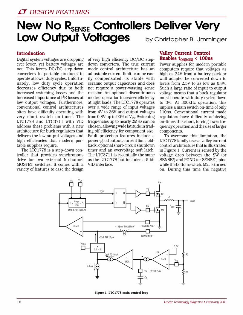
To overcome this limitation, theLTC1778 family uses a valley currentcontrol architecture that is illustratedin Figure 1. Current is sensed by thevoltage drop between the SW (orSENSE+) and PGND (or SENSE–) pinswhile the bottom switch, M2, is turnedon. During this time the negative
–
+
–
+
×0.5 – 2
+
1240k
1.7mS
0V TO 2.4VITH
CC
EA
0.8V
VFB
0µA TO 10µA
3.3µA
VRNG
–7µA TO 13µA
–133mV TO 267mVICMP
20kSW/SENSE+
PGND/SENSE–
BG
TG
M1
M2
L1
TOP
VIN
COUT
VOUTD =
VVONIION
• CT
S
R
Q
Q
R2
R1
ION VON
+ –
ONE SHOT DELAY
Figure 1. LTC1778 main control loop

Linear Technology Magazine • February 2001 17
DESIGN FEATURES
voltage across inductor L1 causes thecurrent flowing through it to decay.When it reaches the level set by thecurrent-control threshold (ITH) volt-age, the current comparator (ICMP)trips. This sets the latch, turning offthe bottom switch and turning on thetop (or main) switch, M1. After a con-trolled delay determined by a one-shottimer, the top switch turns off againand the cycle repeats. The current-control threshold is set by an erroramplifier (EA) that compares thedivided output voltage with a 0.8Vreference in order to keep the thresh-old at a level that matches the loadcurrent.
This control loop has severaladvantages compared to peak-cur-
rent controllers that use an internaloscillator. Because only a one-shottimer determines the top switchon-time, it can be made very short forlow duty cycle applications. Anotheradvantage is that slope compensa-tion is not required. Furthermore,response to a load step increase canbe very fast since the loop does nothave to wait for an oscillator pulsebefore the top switch is turned on andcurrent begins increasing.
Flexible One-Shot TimerKeeps Frequency ConstantAlthough the LTC1778 does not con-tain an internal oscillator, switchingfrequency is kept approximately con-stant through the use of a flexibleone-shot timer that controls the topswitch on-time. A current enteringthe ION pin (IION) charges an internaltiming capacitor (CT) to the voltageapplied at the VON pin (VVON) to deter-mine the on-time: tON = CT • VVON/IION.For a buck regulator running at aconstant frequency, the on-time isproportional to VOUT/VIN. By connect-ing a resistor (RON) from VIN to the IONpin and connecting VOUT to the VONpin (if available), the one-shot dura-tion can be made proportional to VOUTand inversely proportional to VIN. Theconverter will then operate at an ap-
proximately constant frequency equalto (RON • CT)–1. In most applications,the output voltage is not intended tochange. Thus, some versions of theLTC1778 do not make the VON pinavailable and it defaults internally to0.7V. By adjusting the value of RON, awide range of operating frequenciescan be selected. However, an impor-tant limit is set by the 500ns minimumoff-time of the top switch. This is theminimum time required by theLTC1778 to turn on the bottom switch,sense the current and then shut it off.At a given switching frequency, itplaces a limit on the maximum dutycycle as illustrated in Figure 2. Forexample, at 200kHz operation, theLTC1778 can accommodate dutycycles up to 90%. Attempting to
2.0
1.5
1.0
0.5
00 0.25 0.50 0.75 1.0
DROPOUTREGION
DUTY CYCLE (VOUT/VIN)
SWIT
CHIN
G FR
EQUE
NCY
(MHz
)100
90
80
70
600.01 0.1 1 10
LOAD CURRENT (A)
EFFI
CIEN
CY (%
)
VIN = 5V
VIN = 25V
VOUT = 2.5VEXTVCC = 5Vf = 250kHz
16
15
14
13
12
11
10
9
1
2
3
4
5
6
7
8
RUN/SS
PGOOD
VRNG
FCB
ITH
SGND
ION
VFB
BOOST
TG
SW
PGND
BG
INTVCC
VIN
EXTVCC
LTC1778
+
+
M2
M1
L1, 1.8µH
D1
COUT1-2180µF4V×2
COUT322µF6.3VX7R
CIN10µF50V×3
VIN5V TO 28V
VOUT2.5V10A
CSS0.1µF
CC1510pF
CC2100pF
CVCC4.7µF
CF0.1µF
CB0.22µF
RC20k
R114.0k
RON1.40MR2
30.1k
RF1Ω
DBCMDSH-3
RPG100kR3
11kR439k
UNITED CHEMICON THCR70E1H26ZT (847) 696-2000CORNELL DUBILIER ESRE181E04B (508) 996-8561SUMIDA CEP125-IR8MC-H (847) 956-0667SILICONIX Si4884 (800) 554-5565SILICONIX Si4874DIODES, INC. B340A (805) 446-4800
CIN:COUT1-2:
L1:M1:M2:D1:
Figure 2. Maximum switchingfrequency vs duty cycle
Figure 3. 2.5V/10A converter switches at 250kHz
Figure 4. Efficiency vs load currentfor Figure 3’s circuit
Linear Technology Magazine • February 200118
DESIGN FEATURES
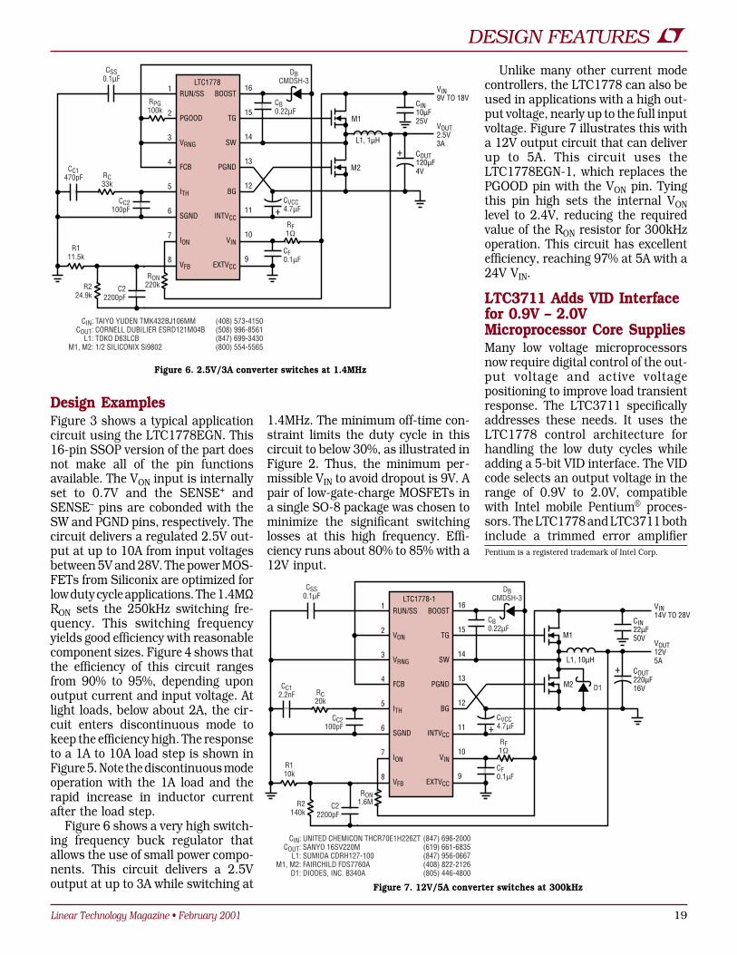
operate at duty cycles above this limitwill cause the output voltage to dropout of regulation, down to a value thatsatisfies the duty cycle limit.Thus, the LTC1778 can be used inexceptionally high frequency buckconverters, provided that the dutycycle is low enough. For example, a10V to 2.5V converter can be run atfrequencies as high as 1.5MHz.
No RSENSE Operation RaisesEfficiency at Low VOUTThe LTC1778 offers true current modecontrol without the need for a senseresistor, an expensive component thatis sometimes difficult to procure. Thecurrent comparator monitors the volt-age drop between the SW and PGNDpins, determining inductor currentusing the on-resistance of the bottomMOSFET. In addition to eliminatingthe sense resistor, this technique alsosimplifies the board layout andimproves efficiency. The efficiency gainis especially noticeable in low outputvoltage applications where the resis-tor sense voltage is a significantfraction of the output voltage. Forexample, a 50mV sense voltagereduces efficiency by 5% in a 1V out-put converter.
The LTC1778 allows the currentsense range to be adjusted using theVRNG pin to accommodate a variety ofMOSFET on-resistances. The powersupply designer can easily trade offefficiency and cost in the choice of
MOSFET on-resistance. The voltagepresented at the VRNG pin should beten times the nominal sense voltageat maximum load current, forexample, VRNG = 1V corresponds to anominal sense voltage of 100mV. Con-necting this pin to INTVCC or grounddefaults the nominal sense voltage to140mV or 70mV, respectively. Cur-rent is limited at 150% and –50% ofthe nominal level set by the VRNG pin.
For those applications that requiremore accurate current measurement,the LTC3711 and some versions ofthe LTC1778 make available one orboth of the current comparator inputsas separate SENSE+ and SENSE– pins.Connecting the inputs to a precisesense resistor placed in series withthe source of the bottom MOSFETswitch determines current more ac-curately. This is especially beneficialfor applications that need a moreaccurate current limit or seek to ac-tively position the output voltage asthe load current varies.
Output is Protectedfrom a Variety of FaultsThe LTC1778 comes with a number offault protection features. The outputvoltage is continuously monitored forout-of-range conditions. If it deviatesby more than ±7.5% from the regula-tion point, an open drain power-goodoutput will pull low to indicate theout-of-regulation condition. In anovervoltage situation, the top switch
will be turned off and the bottomswitch turned on until the output ispulled back below the power-goodthreshold. In an undervoltage condi-tion, if the output falls by 25%, ashort-circuit latch-off timer will bestarted. If the output has not recov-ered within this time, both switcheswill be shut off, stopping the con-verter. Undervoltage/short-circuitlatch-off can be overridden. In thiscase, if the output voltage continuesto fall below 50% of the regulationpoint, the current limit will be reduced,or folded back, to about one fourth ofits maximum value.
Popular Features fromOther Controllers RemainContinuous synchronous operationat light loads reduces efficiency due tothe large amount of current consumedby switching losses. Efficiency isimproved by operating the converterin discontinuous mode. In this mode,the bottom switch is turned off at theinstant that inductor current startsto reverse, even though the currentcontrol threshold (ITH) is below thatlevel. The top switch, however, is notturned on until the ITH level rises backto the point corresponding to zeroinductor current. During the time bothswitches are off, the output current isprovided solely by the output capaci-tor and switching losses are avoided.The switching frequency becomes pro-portional to the load current in thismode of operation.
The LTC1778 contains its owninternal low dropout regulator thatprovides the 5V gate drive required forlogic-level MOSFETs. However, it isalso able to accept an external 5V to7V supply if one is available. Connect-ing such a supply to the EXTVCC pindisables the internal regulator; allcontroller and gate drive power isthen drawn from the external supply.If the external drive comes from a highefficiency source, overall efficiency canbe improved. Furthermore, connect-ing the VIN and EXTVCC pins togetherto an external 5V supply allows thecontroller to convert low input volt-ages such as 3.3V and 2.5V.
VOUT50mV/DIV
IL5A/DIV
20µs/DIV
LOAD STEP = 1A TO 10AVIN = 15VVOUT = 2.5VFCB = INTVCC
Figure 5. Transient response of Figure 3’s circuit
Linear Technology Magazine • February 2001 19
DESIGN FEATURES
Design ExamplesFigure 3 shows a typical applicationcircuit using the LTC1778EGN. This16-pin SSOP version of the part doesnot make all of the pin functionsavailable. The VON input is internallyset to 0.7V and the SENSE+ andSENSE– pins are cobonded with theSW and PGND pins, respectively. Thecircuit delivers a regulated 2.5V out-put at up to 10A from input voltagesbetween 5V and 28V. The power MOS-FETs from Siliconix are optimized forlow duty cycle applications. The 1.4MΩRON sets the 250kHz switching fre-quency. This switching frequencyyields good efficiency with reasonablecomponent sizes. Figure 4 shows thatthe efficiency of this circuit rangesfrom 90% to 95%, depending uponoutput current and input voltage. Atlight loads, below about 2A, the cir-cuit enters discontinuous mode tokeep the efficiency high. The responseto a 1A to 10A load step is shown inFigure 5. Note the discontinuous modeoperation with the 1A load and therapid increase in inductor currentafter the load step.
Figure 6 shows a very high switch-ing frequency buck regulator thatallows the use of small power compo-nents. This circuit delivers a 2.5Voutput at up to 3A while switching at
1.4MHz. The minimum off-time con-straint limits the duty cycle in thiscircuit to below 30%, as illustrated inFigure 2. Thus, the minimum per-missible VIN to avoid dropout is 9V. Apair of low-gate-charge MOSFETs ina single SO-8 package was chosen tominimize the significant switchinglosses at this high frequency. Effi-ciency runs about 80% to 85% with a12V input.
Unlike many other current modecontrollers, the LTC1778 can also beused in applications with a high out-put voltage, nearly up to the full inputvoltage. Figure 7 illustrates this witha 12V output circuit that can deliverup to 5A. This circuit uses theLTC1778EGN-1, which replaces thePGOOD pin with the VON pin. Tyingthis pin high sets the internal VONlevel to 2.4V, reducing the requiredvalue of the RON resistor for 300kHzoperation. This circuit has excellentefficiency, reaching 97% at 5A with a24V VIN.
LTC3711 Adds VID Interfacefor 0.9V – 2.0VMicroprocessor Core SuppliesMany low voltage microprocessorsnow require digital control of the out-put voltage and active voltagepositioning to improve load transientresponse. The LTC3711 specificallyaddresses these needs. It uses theLTC1778 control architecture forhandling the low duty cycles whileadding a 5-bit VID interface. The VIDcode selects an output voltage in therange of 0.9V to 2.0V, compatiblewith Intel mobile Pentium® proces-sors. The LTC1778 and LTC3711 bothinclude a trimmed error amplifier
16
15
14
13
12
11
10
9
1
2
3
4
5
6
7
8
RUN/SS
PGOOD
VRNG
FCB
ITH
SGND
ION
VFB
BOOST
TG
SW
PGND
BG
INTVCC
VIN
EXTVCC
LTC1778
+
+
M2
M1
L1, 1µH
COUT120µF4V
CIN10µF25V
VIN9V TO 18V
VOUT2.5V3A
CSS0.1µF
CC1470pF
CC2100pF
C22200pF
CVCC4.7µF
CF0.1µF
CB0.22µF
RC33k
R111.5k
RON220kR2
24.9k
RF1Ω
DBCMDSH-3
RPG100k
TAIYO YUDEN TMK432BJ106MM (408) 573-4150CORNELL DUBILIER ESRD121M04B (508) 996-8561TOKO D63LCB (847) 699-34301/2 SILICONIX Si9802 (800) 554-5565
CIN:COUT:
L1:M1, M2:
16
15
14
13
12
11
10
9
1
2
3
4
5
6
7
8
RUN/SS
VON
VRNG
FCB
ITH
SGND
ION
VFB
BOOST
TG
SW
PGND
BG
INTVCC
VIN
EXTVCC
LTC1778-1
+M2
M1
L1, 10µHCOUT220µF16V
CIN22µF50V
VIN14V TO 28V
VOUT12V5A
CSS0.1µF
CC12.2nF
CC2100pF
C22200pF
CVCC4.7µF
CF0.1µF
CB0.22µF
RC20k
R110k
RON1.6MR2
140k
RF1Ω
DBCMDSH-3
D1
UNITED CHEMICON THCR70E1H226ZT (847) 696-2000SANYO 16SV220M (619) 661-6835SUMIDA CDRH127-100 (847) 956-0667FAIRCHILD FDS7760A (408) 822-2126DIODES, INC. B340A (805) 446-4800
CIN:COUT:
L1:M1, M2:
D1:
+
Figure 6. 2.5V/3A converter switches at 1.4MHz
Figure 7. 12V/5A converter switches at 300kHz
Pentium is a registered trademark of Intel Corp.

Linear Technology Magazine • February 200120
DESIGN FEATURES
CC1180pF
RVP112.4k
RVP240.2k
CSS0.1µF
CFB 100pF
RON330k
RRNG245.3k
RRNG14.99k
RF1Ω
RPG100k
1
2
3
4
5
6
7
8
9
10
11
12
24
23
22
21
20
19
18
17
16
15
14
13
VID2
RUN/SS
VON
PGOOD
VRNG
FCB
ITH
SGND
ION
VFB
VOSENSE
VID3
VID1
VID0
BOOST
TG
SW
SENSE+
PGND
BG
INTVCC
VIN
EXTVCC
VID4
CB0.33µF
M1
D1
L11µH
M2×2
DBCMDSH-3
CVCC4.7µF
CF0.1µF
CIN22µF50V×3
VIN7V TO 24V
VOUT1.5V15A
COUT270µF2V×3
LTC3711
RSENSE0.003Ω
UNITED CHEMICON THCR70E1H26ZT (847) 696-2000CORNELL DUBILIER ESRE271M02B (508) 996-8561SUMIDA CEP125-IR0MC-H (847) 956-0667INTERNATIONAL RECTIFIER IRF7811A (310) 332-3331MICROSEMI UPS840 (617) 926-0404
CIN:COUT:
L1:M1:D1:
+
+
transconductance that is constantover temperature. This feature allowsmore aggressive compensation of thecontrol loop for faster transientresponse as well as enabling accurateactive voltage positioning. Active volt-age positioning lowers the outputvoltage in a controlled manner as theload current increases. This is usefulin microprocessor power supplieswhere large load current transientsare the main cause of output voltageerror.
An example of a VID controlledLTC3711 application with active volt-age positioning is shown in Figure 8.
To facilitate the voltage positioning,the SENSE+ pin is used with a currentsense resistor at the source of M2.The voltage positioning gain is accu-rately set using resistors RVP1 andRVP2 along with the trimmed trans-conductance of the error amplifier.This circuit positions the output volt-age about 65mV above a 1.5V nominaloutput at no load, drooping to 65mVbelow the nominal output at full load.Voltage positioning allows the num-ber of output capacitors to be reducedfrom five to three and still maintain a±100mV specification on the outputvoltage.
ConclusionThe LTC1778/LTC3711 step-downDC/DC controllers are designed forpower supplies operating over a wideinput and output range. The valleycurrent control architecture enablesvery low voltage outputs to be obtainedfrom high input voltage sources suchas battery packs and wall adapters.Eliminating the sense resistorimproves efficiency and saves bothboard space and component cost.The LTC1778 and LTC3711 are excel-lent choices for delivering the lowoutput voltages and high efficienciesrequired by modern portable powersupplies.
Figure 8. 1.5V/15A CPU core voltage regulator with active voltage positioning
forthe latest information
on LTC products, visit
www.linear-tech.com

Linear Technology Magazine • February 2001 21
DESIGN FEATURES
New UltraFast Comparators: Rail-to-Rail Inputs and 2.4V Operation AllowUse on Low Supplies by Glen Brisebois
IntroductionThe new LT1711 family of UltraFastcomparators has fully differential rail-to-rail inputs and outputs andoperates on supplies as low as 2.4V,allowing unfettered application on lowvoltages. The LT1711 (single) andLT1712 (dual) are specified at 4.5nsof propagation delay and 100MHztoggle frequency. The low powerLT1713 (single) and LT1714 (dual)are specified at 7ns of propagationdelay and 65MHz toggle frequency.All of these comparators are fullyequipped to support multiple-supplyapplications, and have latch-enablepins and complementary outputs likethe popular LT1016, LT1671 andLT1394. They are available in MSOPand SSOP packages, fully specifiedover commercial and industrial tem-perature ranges on 2.7V, 5V and ±5Vsupplies.
Circuit DescriptionFigure 1 shows a simplified sche-matic of the LT1711 through LT1714.The front end consists of eight cur-
rent sources and sinks feeding theNPN and PNP differential pairs formedby Q3–Q4 (protected by fast diodesD11–D12) and Q1–Q2 (protected byD1–D2). This approach makes theinputs truly fully differential andnoninteracting, unlike approachesthat resort to resistors and diodeclamps. Even with the inputs atopposite rails, the input bias currentsare still a simple function of the inputtransistor base currents and remainin the µA region. Both input stagesfeed the level shifting transistors Q5–Q6, and the remainder of thedifferential voltage gain circuit flowswith a delightful symmetry towardsthe output. Note that the channelsare identical, with polarity yetunassigned, and are therefore inter-changeable in layout. The symmetry,broken only by the latch-enable cir-cuit, is enhanced by the fact that all ofthe transistors are well matched,complementary 6GHz fT BJTs. Eachoutput stage ends in two Baker-clamped common emitter transistors,
allowing full rail-to-rail output swing.All the comparators guarantee full 5VTTL output capability over tempera-ture, even when supplied with only3V. Output rise and fall times arefast, at 2ns for the LT1711 and LT1712and 4ns for the LT1713 and LT1714.Jitter is among the lowest for anymonolithic comparator, at 11psRMSfor the LT1711 and LT1712 and15psRMS for the LT1713 and LT1714.
Some Applications
Simultaneous Full-Duplex75MBaud Interfacewith Only Two WiresThe circuit of Figure 2 shows a simple,fully bidirectional, differential 2-wireinterface that gives good resultsto 75MBaud, using the lowpower LT1714. Eye diagrams underconditions of unidirectional andbidirectional communication areshown in Figures 3 and 4. Althoughnot as pristine as the unidirectional
BIAS
VCC
INA1
INB1
VEE
GND
D27
D28
D29
D30
D31
D32
D33
I1 I2 I3
I4
I5
I6 I7 I8
D1 D2
D3 D4
D9 D10
D11 D12
Q1
Q3
Q2
Q4
Q5Q6
R1 R2
R3 R4
Q7
Q8
D13
D14
I9
I10
LE1
D34
D35
Q11
Q9 Q10
D15
I12I13
R5 R6
I11
D17
D18
Q14
Q15
Q13
Q12
Q16
Q17
Q18
Q19
I18
I23 I24 I25
R8 R9
Q28
Q29
Q30
Q31
I14 I15
I20
I16 I21 I22
Q34
Q35
Q22
Q23
Q40
Q41
Q42
Q43
D36
D37
D38
D39
OUTB1
OUTA1
R11 R12
VEE
VEEVEE
VEE
VEE
VCC
VCC
VCC
VCC
VCC
VCC
VCC
GND
GND
Figure 1. LT1711–LT1714 simplified schematic

Linear Technology Magazine • February 200122
DESIGN FEATURES
per formance of Figure 3, theperformance under simultaneousbidirectional operation is still excel-lent. Because the LT1714 inputvoltage range extends 100mV beyondboth supply rails, the circuit workswith a full ±3V of ground potentialdifference.
The circuit works well with theresistor values shown, but other setsof values can be used. The startingpoint is the characteristic impedance,ZO, of the twisted-pair cable. The inputimpedance of the resistive networkshould match the characteristicimpedance and is given by:
2 • RO • (R1||(R2 + R3)(RO + 2 • (R1||(R2 + R3)))
RIN =
This comes out to 120Ω for thevalues shown. The Thevenin equiva-lent source voltage is given by:
VS • (R2 + R3 – R1)(R2 + R3 + R1)
VTh =
RO(RO + 2 • (R1||(R2 + R3)))
•
This amounts to an attenuationfactor of 0.0978 with the valuesshown. (The actual voltage on thelines will be cut in half again due tothe 120Ω ZO.) This attenuation factoris important because it is the key todeciding the ratio of the R2, R3 resis-tor divider in the receiver path. Thisdivider allows the receiver to rejectthe large signal of the local transmit-ter and instead sense the attenuatedsignal of the remote transmitter. Note
that in the above equations, R2 andR3 are not yet fully determinedbecause they only appear as a sum.This allows the designer to now placean additional constraint on their val-ues. The R2, R3 divider ratio shouldbe set to one-half of the attenuationfactor mentioned above or R3/R2 =1/2 • 0.0976.1
The author having already designedR2 + R3 to be 2.653kΩ (by allocatinginput impedance across RO, R1, andR2 + R3 to get the requisite 120Ω), R2and R3 then become 2529Ω and123.5Ω, respectively. The nearest 1%value for R2 is 2.55k and that for R3is 124Ω.
–
+
–
+
–
+
–
+RXD RXD
TXD TXD
1/2 LT1714 1/2 LT1714
1/2 LT17141/2 LT1714
3V
3V
14
13 163
15
2
1
7
8
96
1012
11
R3b124Ω
R3a124Ω
R2b2.55k
R3d124Ω
R2d2.55k
R2a2.55k
R3c124Ω
R2c2.55k
R1a499Ω
R1b499Ω
R0a140Ω
R1c499Ω
R1d499Ω
R0b140Ω
SIX FEETTWISTED PAIR
ZO 120Ω
5
4
7
8
3V5
11
12 610
9
2
1
3V4
14
131615
3
3V 3VALL DIODES = BAV99
–
+
–
+
VS
VS
VS
VS
R11k
R21k
LT1713
2
3
17
845
6
R31k
C10.1µF
C20.1µF1MHz AT CUT
R4210Ω
R92k
R82k
LT1806
SQUARE
SINE
R57.5k
R6162Ω
R7 15.8kC3100pF
C4100pF
2
3
7
4
6
VS = 2.7V TO 6V
5ns/DIV 5ns/DIV
Figure 2. 75MBaud full-duplex interface on two wires
Figure 3. Performance of Figure 1’scircuit operated unidirectionally; eye iswide open (cursors show bit interval of13.3ns or 75MBaud).
Figure 4. Performance of Figure 1’s circuitoperated simultaneous-bidirectionally;crosstalk appears as noise. Eye is slightlyshut but performance is still excellent.
Figure 5. LT1713 comparator configured as a series-resonant crystal oscillator;the LT1806 op amp is configured as a bandpass filter with a Q of 5 and fC of 1MHz.

Linear Technology Magazine • February 2001 23
DESIGN FEATURES
1MHz Series-Resonant CrystalOscillator with Square andSinusoid OutputsFigure 5 shows a classic 1MHz series-resonant crystal oscillator. At seriesresonance, the crystal is a low imped-ance and the positive feedbackconnection brings about oscillationat the series resonance frequency.The RC feedback to the – input ensuresthat the circuit does not find a stableDC operating point and refuse tooscillate. The comparator output is a1MHz square wave (top trace of Fig-ure 6), with jitter measured at 28psRMSon a 5V supply and 40 psRMS on a 3Vsupply. At pin 2 of the comparator, onthe other side of the crystal, is a cleansine wave except for the presence ofthe small high frequency glitch (middletrace of Figure 6). This glitch is causedby the fast edge of the comparatoroutput feeding back through crystalcapacitance. Amplitude stability ofthe sine wave is maintained by the
A3V/DIV
B1V/DIV
C1V/DIV
200ns/DIV
fact that the sine wave is basically afiltered version of the square wave.Hence, the usual amplitude-controlloops associated with sinusoidaloscillators are not necessary.2 Thesine wave is filtered and buffered bythe fast, low noise LT1806 op amp. Toremove the glitch, the LT1806 is con-figured as a bandpass filter with a Qof 5 and unity gain center frequencyof 1MHz. The final sinusoidal output
is the bottom trace of Figure 6. Dis-tortion was measured at –70dBc and–55dBc on the second and third har-monics, respectively.
ConclusionThe fully differential rail-to-rail inputsof the new LT1711 family of fast com-parators make them useful across awide variety of applications. The highspeed, low jitter performance of thisfamily, coupled with their small pack-age sizes and 2.4V operation, makesthem attractive where PCB real estateis at a premium and bandwidth-to-power ratios must be optimized.
1 Using the design value of R2 + R3 = 2.653k ratherthan the implementation value of 2.55k + 124Ω =2.674k.
2 Amplitude will be a linear function of comparatoroutput swing, which is supply dependent andtherefore adjustable. The important differencehere is that any added amplitude stabilization orcontrol loop will not be faced with the classicaltask of avoiding regions of nonoscillation vsclipping.
Figure 6. Oscillator waveforms with VS = 3V:Trace A = comparator output; Trace B =crystal feedback to pin 2 of the LT1713;Trace C = buffered, inverted and bandpassfiltered output of LT1806
SHDN
IADJ
GND VC
VIN SW
ISN
ISP
FB
LT1618R12M
R2121k
VIN2.7V TO 5V
10kHz TO 50kHzPWM
BRIGHTNESSADJUST
C14.7µF
CC0.1µF
C21µF
0.619ΩD1L1
10µH 80mA
3
2
1
9
8 7
5 10
4R3
5.1k
C30.1µF
51Ω 51Ω 51Ω 51Ω
C1: TAIYO YUDEN JMK212BJ475 (408) 573-4150C2: TAIYO YUDEN TMK316BJ105 (408) 573-4150D1: ON SEMICONDUCTOR MBR0530 (800) 282-9855L1: SUMIDA CR43-100 (847) 956-0666
Figure 9. High power white LED driver
Figure 10. High power whiteLED driver efficiency
High PowerWhite LED DriverFor larger LCD displays where agreater amount of light output isneeded, multiple strings of LEDs canbe driven in parallel. When drivingparallel strings, ballast resistorsshould be added to compensate forLED forward voltage variations. Theamount of ballasting needed dependson the LEDs used and how well they
are matched. The circuit in Figure 9 isideal for larger displays, providingconstant current drive for twenty whiteLEDs from a single Li-Ion cell. Effi-ciency reaches a respectable 82%, asseen in Figure 10.
ConclusionThe constant-current/constant-volt-age operation of the LT1618 makesthe device an ideal choice for a variety
of constant-current designs. Thedevice provides accurate output cur-rent regulation or input currentlimiting, along with excellent outputvoltage regulation. With a wide inputvoltage range and the ability toproduce outputs up to 35V, theLT1618 works well in many differentapplications.
References
1. Kim, Dave. “Tiny Regulators Drive White LEDBacklights.” Linear Technology Design Note 231(May 2000).
LED CURRENT (mA)10
EFFI
CIEN
CY (%
)
7030 50
90
85
80
75
70
65
60
55
5020 40 60 80
VIN = 5V
VIN = 3.3V
VIN = 2.8V
LT1618, continued from page 7
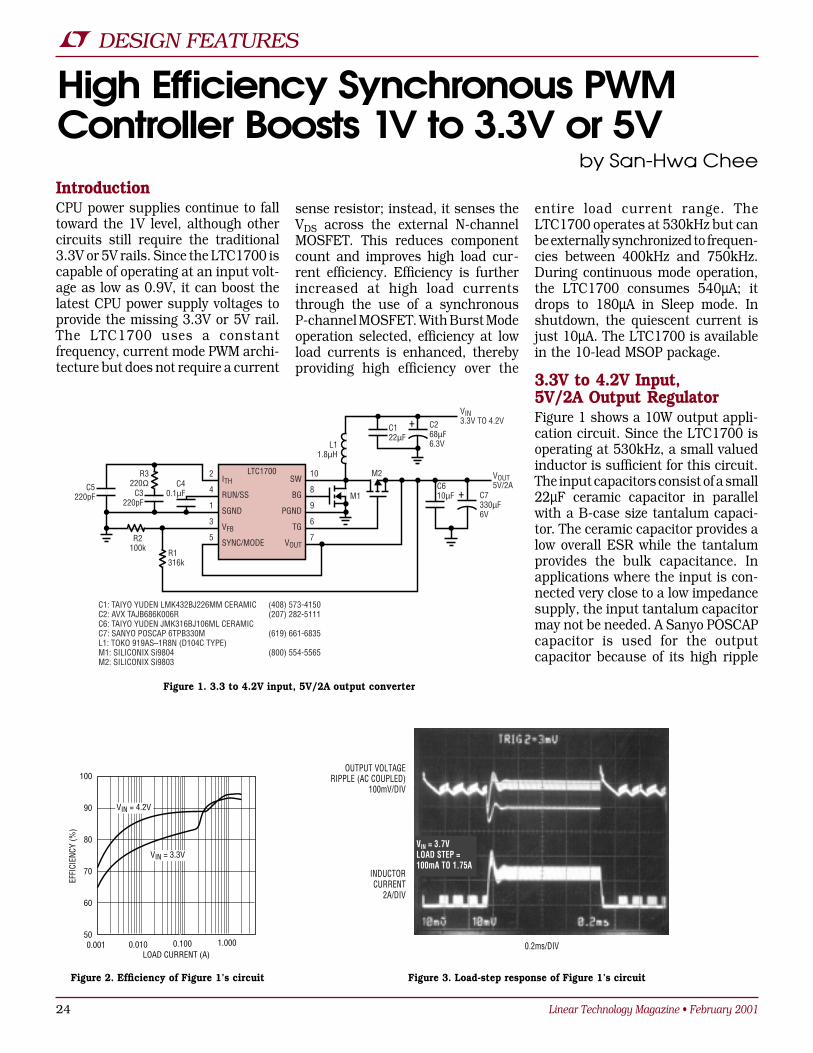
Linear Technology Magazine • February 200124
DESIGN FEATURES
High Efficiency Synchronous PWMController Boosts 1V to 3.3V or 5V
by San-Hwa CheeIntroductionCPU power supplies continue to falltoward the 1V level, although othercircuits still require the traditional3.3V or 5V rails. Since the LTC1700 iscapable of operating at an input volt-age as low as 0.9V, it can boost thelatest CPU power supply voltages toprovide the missing 3.3V or 5V rail.The LTC1700 uses a constantfrequency, current mode PWM archi-tecture but does not require a current
sense resistor; instead, it senses theVDS across the external N-channelMOSFET. This reduces componentcount and improves high load cur-rent efficiency. Efficiency is furtherincreased at high load currentsthrough the use of a synchronousP-channel MOSFET. With Burst Modeoperation selected, efficiency at lowload currents is enhanced, therebyproviding high efficiency over the
entire load current range. TheLTC1700 operates at 530kHz but canbe externally synchronized to frequen-cies between 400kHz and 750kHz.During continuous mode operation,the LTC1700 consumes 540µA; itdrops to 180µA in Sleep mode. Inshutdown, the quiescent current isjust 10µA. The LTC1700 is availablein the 10-lead MSOP package.
3.3V to 4.2V Input,5V/2A Output RegulatorFigure 1 shows a 10W output appli-cation circuit. Since the LTC1700 isoperating at 530kHz, a small valuedinductor is sufficient for this circuit.The input capacitors consist of a small22µF ceramic capacitor in parallelwith a B-case size tantalum capaci-tor. The ceramic capacitor provides alow overall ESR while the tantalumprovides the bulk capacitance. Inapplications where the input is con-nected very close to a low impedancesupply, the input tantalum capacitormay not be needed. A Sanyo POSCAPcapacitor is used for the outputcapacitor because of its high ripple
+
+
ITH
RUN/SS
SGND
VFB
SYNC/MODE
SW
BG
PGND
TG
VOUT
2
4
1
3
5
10
8
9
6
7
LTC1700
VIN3.3V TO 4.2V
VOUT5V/2A
C7330µF6V
C610µF
C268µF6.3V
C122µF
M2
M1C5
220pF
R3220Ω
C3220pF
C40.1µF
R2100k R1
316k
C1: TAIYO YUDEN LMK432BJ226MM CERAMIC (408) 573-4150C2: AVX TAJB686K006R (207) 282-5111C6: TAIYO YUDEN JMK316BJ106ML CERAMICC7: SANYO POSCAP 6TPB330M (619) 661-6835L1: TOKO 919AS–1R8N (D104C TYPE)M1: SILICONIX Si9804 (800) 554-5565M2: SILICONIX Si9803
L11.8µH
LOAD CURRENT (A)
60
EFFI
CIEN
CY (%
)
70
80
90
100
0.001 1.00050
0.010 0.100
VIN = 3.3V
VIN = 4.2V
Figure 1. 3.3 to 4.2V input, 5V/2A output converter
Figure 2. Efficiency of Figure 1’s circuit Figure 3. Load-step response of Figure 1’s circuit
OUTPUT VOLTAGERIPPLE (AC COUPLED)
100mV/DIV
INDUCTORCURRENT
2A/DIV
0.2ms/DIV
VIN = 3.7VLOAD STEP =100mA TO 1.75A

Linear Technology Magazine • February 2001 25
DESIGN FEATURES
current rating. Once again, a ceramiccapacitor is used in parallel with thePOSCAP for reduced ESR and highfrequency decoupling.
Figure 2 shows the efficiency curvesfor input voltages of 3.3V and 4.2V.Note that the maximum efficiencyreaches 95% at a load current of 2A.A load step from 100mA to 1.75A wasapplied and its response is shown inFigure 3.
Start-Up andMOSFET SelectionWhen the voltage at the VOUT pin isbelow 2.3V, the LTC1700 operates inthe start-up mode. In this mode, onlythe start-up circuitry in the LTC1700is active and both of the externalMOSFETs are turned off. Figure 4shows the components that controlstart-up. In this mode, the currentlimit is set at 60mA and the internalMOSFET is used to bring the outputvoltage up. The start-up oscillator,
+
– +
–
+
+
START-UPOSCILLATOR
1.205VREFERENCE
SC
7
S
R
QB
Q
L1
ICMP
SHDN
VOUT
60mV 1Ω
M1
10SW
TO TG
L1
PARASITICDIODE OFMOSFET
VIN
C1 C2
C6 C7
VOUT
LTC1700
= 1 WHEN VOUT = <2.3V
which is different from the main os-cillator, runs at 210kHz at a dutycycle of 50%. Due to the low currentlimit, the output should not be heavilyloaded during the start-up phase, asthis will cause the output to “hang.”Once the output rises above 2.3V, therest of the internal circuitry of theLTC1700 comes alive and the exter-nal MOSFETs begin switching. Thestart-up circuitry will then be shutdown.
In some applications, the inputvoltage is high enough that start-upmode is not needed, resulting in the
+
+
SGND
ITH
RUN/SS
VFB
SYNC/MODE
SW
BG
PGND
TG
VOUT
1
2
4
3
5
10
8
9
6
7
LTC1700
VIN3.3V
VOUT5V/3A
C4150µF6.3V×3
C322µF
C268µF6.3V
C110µF
M2
M1
R2100k R1
95.3k
C1: TAIYO YUDEN JMK316BJ106ML CERAMIC (408) 573-4150C2: AVX TAJB686K006R (207) 282-5111C3: TAIYO YUDEN JMK325BJ226M CERAMICC4: SANYO POSCAP 6TPA150M (619) 661-6835L1: SUMIDA CEP1234R6 (847) 956-0667M1: SILICONIX Si6466 (800) 554-5565M2: FAIRCHILD FDS6375 (408) 822-2126
220pF 2.2k
270pF 470pF
150pF
L14.6µH
LOAD CURRENT (A)
60
EFFI
CIEN
CY (%
)
70
80
90
100
0.001 1.00050
0.010 0.100
Figure 4. Start-up components of the LTC1700
Figure 5. 3.3V input to 5V/3A output regulator Figure 6. Efficiency of Figure 5’s circuit

Linear Technology Magazine • February 200126
DESIGN FEATURES
circuit being able to power up at fullload current. Figure 1 shows anexample of this. The required inputvoltage to power up with full loadcurrent is:
VIN > 2.3 + VF
where VF is the forward voltage of theparasitic diode across the externalP-channel MOSFET, which is depen-dent on the load current. For a loadcurrent less than 3A, a VF of 0.75Vcan be used.
Since the switchover from theinternal MOSFET to the externalMOSFETs occurs at VOUT = 2.3V, theMOSFETs selected should have a
+
+
SGND
ITH
RUN/SS
VFB
SYNC/MODE
SW
BG
PGND
TG
VOUT
1
2
4
3
5
10
8
9
6
7
LTC1700
VIN3.3V
VOUT5V/4A
C4150µF6.3V×2
C322µF
C268µF6.3V
C122µF
M2
M1
100k
316k
C1: TAIYO YUDEN JMK316BJ226ML CERAMIC (408) 573-4150C2: AVX TAJB686K006R (207) 282-5111C3: TAIYO YUDEN JMK325BJ226M CERAMICC4: PANASONIC EEUEOJ151R (714) 373-7334L1: SUMIDA CDEP134-0R6NC-H (847) 956-0667M1: SILICONIX Si9803 ×2 (800) 554-5565M2: INTERNATIONAL RECTIFIER IR7811 ×2 (408) 822-2126
220pF 2.2k
200pF 0.1µF
L10.68µH
C54.7µF
threshold of 2.5V or lower. This willguarantee a smooth transition out ofthe start-up mode.
3.3V Input,5V/3A Output RegulatorFigure 5 shows a 3.3V input to 5Voutput circuit that can provide amaximum of 3A output current. Likethe circuit in Figure 1, this circuit willbypass the start-up mode and there-fore is capable of starting up at fullload. Figure 6 shows that its effi-ciency reaches 88% at load currentsof 2A to 3A. Figure 7 shows the loadstep response.
3.3V Input, 5V/4AOutput RegulatorThe circuit shown in Figure 8 iscapable of supplying 4A of load cur-rent. To obtain this output currentcapability, two IRF7811A N-channelMOSFETs are paralleled to obtain therequired peak inductor current. TwoSi9803DY are used for the synchro-nous P-channel MOSFET because ofthe amount of RMS current throughthese devices. The Si9803DYs aremounted on an area of copperadequate to effectively remove themaximum amount of heat. Due to the
Figure 7. Load-step response of Figure 5’s circuit
Figure 8. 3.3V input, 5V/4A output regulator
OUTPUT VOLTAGERIPPLE (AC COUPLED)
100mV/DIV
INDUCTORCURRENT
2A/DIV
VIN = 3.3VLOAD STEP =300mA TO 2.6A
0.2ms/DIV
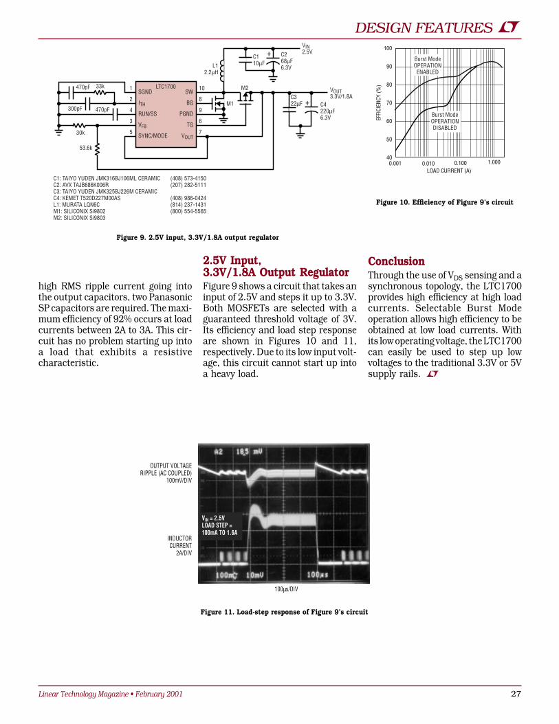
Linear Technology Magazine • February 2001 27
DESIGN FEATURES
+
SGND
ITH
RUN/SS
VFB
SYNC/MODE
SW
BG
PGND
TG
VOUT
1
2
4
3
5
10
8
9
6
7
LTC1700
VIN2.5V
VOUT3.3V/1.8A
C268µF6.3V
C110µF
M2
M1
30k
53.6k
C1: TAIYO YUDEN JMK316BJ106ML CERAMIC (408) 573-4150C2: AVX TAJB686K006R (207) 282-5111C3: TAIYO YUDEN JMK325BJ226M CERAMICC4: KEMET T520D227M00AS (408) 986-0424L1: MURATA LQN6C (814) 237-1431M1: SILICONIX Si9802 (800) 554-5565M2: SILICONIX Si9803
470pF 33k
300pF 470pF
L12.2µH
+ C4220µF6.3V
C322µF
LOAD CURRENT (A)
60EFFI
CIEN
CY (%
)
70
80
90
100
0.001 1.000
50
0.01040
0.100
Burst ModeOPERATIONENABLED
Burst ModeOPERATIONDISABLED
Figure 9. 2.5V input, 3.3V/1.8A output regulator
Figure 10. Efficiency of Figure 9’s circuit
Figure 11. Load-step response of Figure 9’s circuit
OUTPUT VOLTAGERIPPLE (AC COUPLED)
100mV/DIV
INDUCTORCURRENT
2A/DIV
VIN = 2.5VLOAD STEP =100mA TO 1.6A
100µs/DIV
high RMS ripple current going intothe output capacitors, two PanasonicSP capacitors are required. The maxi-mum efficiency of 92% occurs at loadcurrents between 2A to 3A. This cir-cuit has no problem starting up intoa load that exhibits a resistivecharacteristic.
2.5V Input,3.3V/1.8A Output RegulatorFigure 9 shows a circuit that takes aninput of 2.5V and steps it up to 3.3V.Both MOSFETs are selected with aguaranteed threshold voltage of 3V.Its efficiency and load step responseare shown in Figures 10 and 11,respectively. Due to its low input volt-age, this circuit cannot start up intoa heavy load.
ConclusionThrough the use of VDS sensing and asynchronous topology, the LTC1700provides high efficiency at high loadcurrents. Selectable Burst Modeoperation allows high efficiency to beobtained at low load currents. Withits low operating voltage, the LTC1700can easily be used to step up lowvoltages to the traditional 3.3V or 5Vsupply rails.
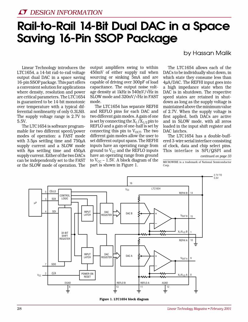
Linear Technology Magazine • February 200128
DESIGN INFORMATION
Rail-to-Rail 14-Bit Dual DAC in a SpaceSaving 16-Pin SSOP Package
Linear Technology introduces theLTC1654, a 14-bit rail-to-rail voltageoutput dual DAC in a space saving16-pin SSOP package. This part offersa convenient solution for applicationswhere density, resolution and powerare critical parameters. The LTC1654is guaranteed to be 14-bit monotonicover temperature with a typical dif-ferential nonlinearity of only 0.3LSB.The supply voltage range is 2.7V to5.5V.
The LTC1654 is software program-mable for two different speed/powermodes of operation: a FAST modewith 3.5µs settling time and 750µAsupply current and a SLOW modewith 8µs settling time and 450µAsupply current. Either of the two DACscan be independently set to the FASTor the SLOW mode of operation. The
output amplifiers swing to within450mV of either supply rail whensourcing or sinking 5mA and arecapable of driving over 300pF of loadcapacitance. The output noise volt-age density at 1kHz is 540nV/√Hz inSLOW mode and 320nV/√Hz in FASTmode.
The LTC1654 has separate REFHIand REFLO pins for each DAC andtwo different gain modes. A gain of oneis set by connecting the X1 /X1/2 pin toREFLO and a gain of one-half is set byconnecting this pin to VOUT. The twodifferent gain modes allow the user toset different output spans. The REFHIinputs have an operating range fromground to VCC and the REFLO inputshave an operating range from groundto VCC – 1.5V. A block diagram of thepart is shown in Figure 1.
The LTC1654 allows each of theDACs to be individually shut down, inwhich state they consume less than4µA/DAC. The REFHI input goes intoa high impedance state when theDAC is in shutdown. The respectivespeed states are retained in shut-down as long as the supply voltage ismaintained above the minimum valueof 2.7V. When the supply voltage isfirst applied, both DACs are activeand in SLOW mode, with all zerosloaded in the input shift register andDAC latches.
The LTC1654 has a double-buff-ered 3-wire serial interface consistingof clock, data and chip select pins.This interface is SPI/QSPI and
by Hassan Malik
DAC BVOUT B
REFHI B
VOUT A
X1/X1/2 B
REFHI A
–
+
POWER-ONRESET
DAC A
REFLO AREFLO B
X1/X1/2 A
–
+
INPUTLATCH
CONTROLLOGICSCK
SDO
SDI
INPUTLATCH
DACREGISTER
32-BITSHIFT
REGISTER
CLR
CS/LD
DACREGISTER
µP
5
3
4
7
2
DGND AGND6 13 11 12
8
9
10
1
15
14
16
VCC
VCC
2.7V TO5.5V
LTC1654
Figure 1. LTC1654 block diagram
continued on page 33
MICROWIRE is a trademark of National SemiconductorCorp.

Linear Technology Magazine • February 2001 29
DESIGN IDEAS
Charge Pump Powers White LEDsby Steven Martin
IntroductionMost of today’s portable equipmentuses a liquid crystal display to conveyinformation to its user. Until recently,those displays have been monochromeand have used a low voltage lightemitting diode (LED) such as red orgreen for backlighting. With the adventof color liquid crystal displays, a whitebacklight source is needed. Recently,a revolution in LED technology haslead to the long-coveted white LED.However, white LEDs, which areactually blue LEDs with a specialphosphor in the lens, operate at aconsiderably higher voltage than redor green LEDs. White LEDs canrequire anywhere from 3.5V to 3.9Vto operate at 15mA. In battery pow-ered systems, it’s impractical to drivethe LEDs directly from the batteryand still control the LED current. Toproperly control the LED current asomewhat larger voltage is needed,where the excess is used for control.
Figure 1 shows the LTC3200-5constant frequency voltage doublerused to drive five white LEDs. Figure2 is the schematic diagram of thiscircuit. The LTC3200-5 produces aregulated 5V output from an input aslow as 3V. Switching at 2MHz, theconstant frequency operation of thecharge pump is ideal for low noiseenvironments such as cellular tele-phones or internet communicationdevices.
Since it produces a regulated 5Voutput, the additional voltage droppedacross the resistors controls the LEDcurrent. The resistors also provideballasting to ensure that the LEDs
3V TO 4.4VLi-Ion
BATTERY
C– C+
VIN
4 6
VOUT
LTC3200-5
GNDSHDN
1
2
5
1µF
3
100Ω1µF 1µF 100Ω 100Ω 100Ω 100Ω
UP TO 5 LEDS
ON OFF
VSHDN(APPLY PWM WAVEFORM FOR
ADJUSTABLE BRIGHTNESS CONTROL) t
run at similar currents despite mod-erate differences in forward voltage.
Figure 3 shows how the adjustableLTC3200 can be used to control theLED current directly by controllingthe voltage on the ballast resistors.The LTC3200 regulates the anodes ofthe LEDs until the FB pin comes tobalance at 1.268V. The feedback LED’scurrent is precisely controlled andthe remaining LEDs are moderatelywell controlled by virtue of their simi-larity and the 1.268V ballast voltage.Since the current is more preciselycontrolled, up to six LEDs can bepowered by the adjustable LTC3200.
Figure 2. Li-Ion battery-powered 5V white or blue LED driver
Figure 1. LTC3200 evaluation circuit
continued on page 37
DESIGN IDEASCharge Pump Powers White LEDs................................................... 29
Steven Martin
48V Hot Swap Circuit Blocks ReverseBattery Voltage ........................... 30Mitchell Lee
Using the LTC1662 3µA DAC to CureRF Implementation Ills ................ 31Derek Redmayne
LTC1628-SYNC Minimizes InputCapacitors in a Multioutput, HighCurrent Power Supply ................. 34Wei Chen
Reduce EMI with Ultralow Noise 48Vto 5V, 10W DC/DC Converter ........ 36Rick Brewster
Authors can be contactedat (408) 432-1900
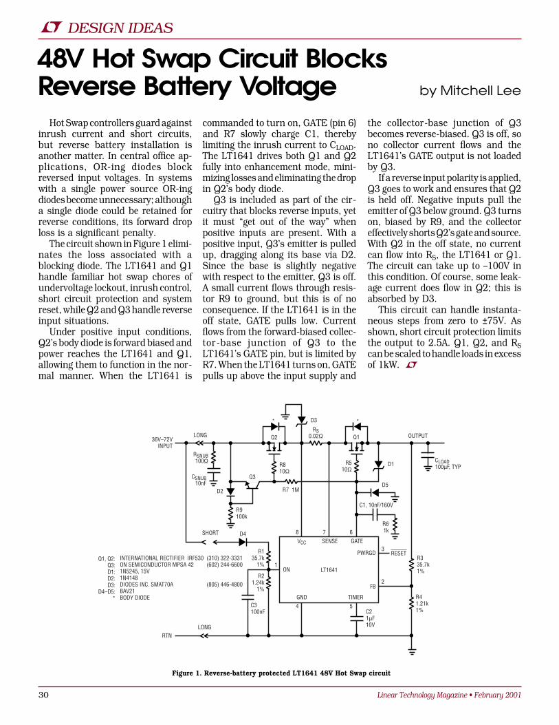
Linear Technology Magazine • February 200130
DESIGN IDEAS
48V Hot Swap Circuit BlocksReverse Battery Voltage by Mitchell Lee
Hot Swap controllers guard againstinrush current and short circuits,but reverse battery installation isanother matter. In central office ap-plications, OR-ing diodes blockreversed input voltages. In systemswith a single power source OR-ingdiodes become unnecessary; althougha single diode could be retained forreverse conditions, its forward droploss is a significant penalty.
The circuit shown in Figure 1 elimi-nates the loss associated with ablocking diode. The LT1641 and Q1handle familiar hot swap chores ofundervoltage lockout, inrush control,short circuit protection and systemreset, while Q2 and Q3 handle reverseinput situations.
Under positive input conditions,Q2’s body diode is forward biased andpower reaches the LT1641 and Q1,allowing them to function in the nor-mal manner. When the LT1641 is
commanded to turn on, GATE (pin 6)and R7 slowly charge C1, therebylimiting the inrush current to CLOAD.The LT1641 drives both Q1 and Q2fully into enhancement mode, mini-mizing losses and eliminating the dropin Q2’s body diode.
Q3 is included as part of the cir-cuitry that blocks reverse inputs, yetit must “get out of the way” whenpositive inputs are present. With apositive input, Q3’s emitter is pulledup, dragging along its base via D2.Since the base is slightly negativewith respect to the emitter, Q3 is off.A small current flows through resis-tor R9 to ground, but this is of noconsequence. If the LT1641 is in theoff state, GATE pulls low. Currentflows from the forward-biased collec-tor-base junction of Q3 to theLT1641’s GATE pin, but is limited byR7. When the LT1641 turns on, GATEpulls up above the input supply and
VCC SENSE GATE
GND TIMER
ON
PWRGD
FB
LT1641
RESETR335.7k1%
R135.7k
1%
8 7 6
3
2
54
1
R41.21k1%
R21.24k
1%
C3100nF C2
1µF10V
SHORT D4
D2
Q3
Q2 Q1
RSNUB100Ω
CSNUB10nF
R9100k
R810Ω
R510Ω
D3
CLOAD100µF, TYP
D5
C1, 10nF/160V
R61k
OUTPUTLONG
D1
36V–72VINPUT
RTN
Q1, Q2:Q3:D1:D2:D3:
D4–D5:*
INTERNATIONAL RECTIFIER IRF530 (310) 322-3331ON SEMICONDUCTOR MPSA 42 (602) 244-66001N5245, 15V1N4148DIODES INC. SMAT70A (805) 446-4800BAV21BODY DIODE
RS0.02Ω
R7 1M
* *
LONG
the collector-base junction of Q3becomes reverse-biased. Q3 is off, sono collector current flows and theLT1641’s GATE output is not loadedby Q3.
If a reverse input polarity is applied,Q3 goes to work and ensures that Q2is held off. Negative inputs pull theemitter of Q3 below ground. Q3 turnson, biased by R9, and the collectoreffectively shorts Q2’s gate and source.With Q2 in the off state, no currentcan flow into RS, the LT1641 or Q1.The circuit can take up to –100V inthis condition. Of course, some leak-age current does flow in Q2; this isabsorbed by D3.
This circuit can handle instanta-neous steps from zero to ±75V. Asshown, short circuit protection limitsthe output to 2.5A. Q1, Q2, and RScan be scaled to handle loads in excessof 1kW.
Figure 1. Reverse-battery protected LT1641 48V Hot Swap circuit
ccotta
ccotta

Linear Technology Magazine • February 2001 31
DESIGN IDEAS
Using the LTC1662 3µA DAC to CureRF Implementation Ills by Derek Redmayne
IntroductionThe small form factor and almostnonexistent power consumption ofthe LTC1662 dual 10-bit DAC make itattractive as a “tweak” to a designthat has already gone through initialqualifications and requires someadditional improvements. The smallsize may allow the system designer toadd it to a design without alteringthose areas that have already passedUL or FCC certification. In otherwords, the part is so small that it canbe added to a design without rippingup and rerouting the entire circuit.
The power consumption of theLTC1662 is so low that even veryrestricted power budgets in isolatedor solar powered applications remainintact, or even unchanged. Theexamples shown demonstrate only afew of many possible uses.
Minimizing CarrierFeedthrough in IQModulationIn Figure 1, the DAC adjusts biasvoltage in an I and Q modulator tominimize carrier feedthrough. Theoutput of the modulator is ideally onefrequency only, the sum of the carrierand the modulation. This frequencyis the upper sideband, where thecarrier and lower sideband are sup-pressed. The two channels of the DACallow I and Q to be adjusted indepen-dently. In addition to being suitablefor sealed, encapsulated, immersedor otherwise physically inaccessiblelocations, the LTC1662 does not havethe shock and vibration sensitivity ofpotentiometers and is less expensivethan a good potentiometer.
If the I and Q components areadded (the Q being a 90-degree-shiftedversion of both the carrier and themodulation), the lower sideband issuppressed and a single sideband(SSB) results. A single sideband isused in many RF applications, as it
allows all the transmitted energy tobe contained within the one side-band. Without the carrier present, atlow modulation depths, minimalenergy is required. Single sidebandalso occupies less spectrum for agiven bandwidth. This technique canalso be used to synthesize frequencies.
The balanced modulator/demodu-lator will produce carrier feedthroughif a DC offset is present at the modu-lation terminal. The sum anddifference of the carrier and the DC
In Figure 2a, the DAC adjusts gainand phase by use of a varactor diode.Because it is not a multiplying DAC,it is not readily adaptable for directDC or low frequency gain control, atleast not high precision gain controlover wide dynamic ranges. It can,however, be used to subtly adjustgain in cases where an excitationcurrent needs to be adjusted; in thecase of high frequencies, it can beused in conjunction with varactordiodes, PIN diodes or modulator/
0°90°
LTC1662
CS/LD
SCK
DIN
5V
20k
20k
0.1µF
0.1µF
1µF5V
R1100k
100k
2.74k1%
R22.74k
1%
2.74k1%
2.74k1%
2.74k1%
2.74k1%
2.74k1%
2.74k1%
I + Q MODULATOR RFLO
Q INPUT
I INPUT
5V
3µA DUAL DAC
OPTIONAL
OPTIONAL
5V
1
2
3
4
8
7
6
5
Figure 1. Using the LTC1662 to trimfor minimum carrier feedthrough
offset is fC, which is carrier feed-through. One section of the DACprovides an adjustment range for theI section, via an attenuator that isjust adequate to cover the worst-caseoffset of the modulator/demodulator.The other half of the DAC is used inthe same manner for the Q section.
Gain/Phase “Tweaks”Made EasyThe setting for these DACs can bedetermined in manufacturing, storedand simply initialized each time poweris applied. In a more complex design,the carrier feedthrough could be evalu-ated in the field and adjusted in realtime or as temperature changes.
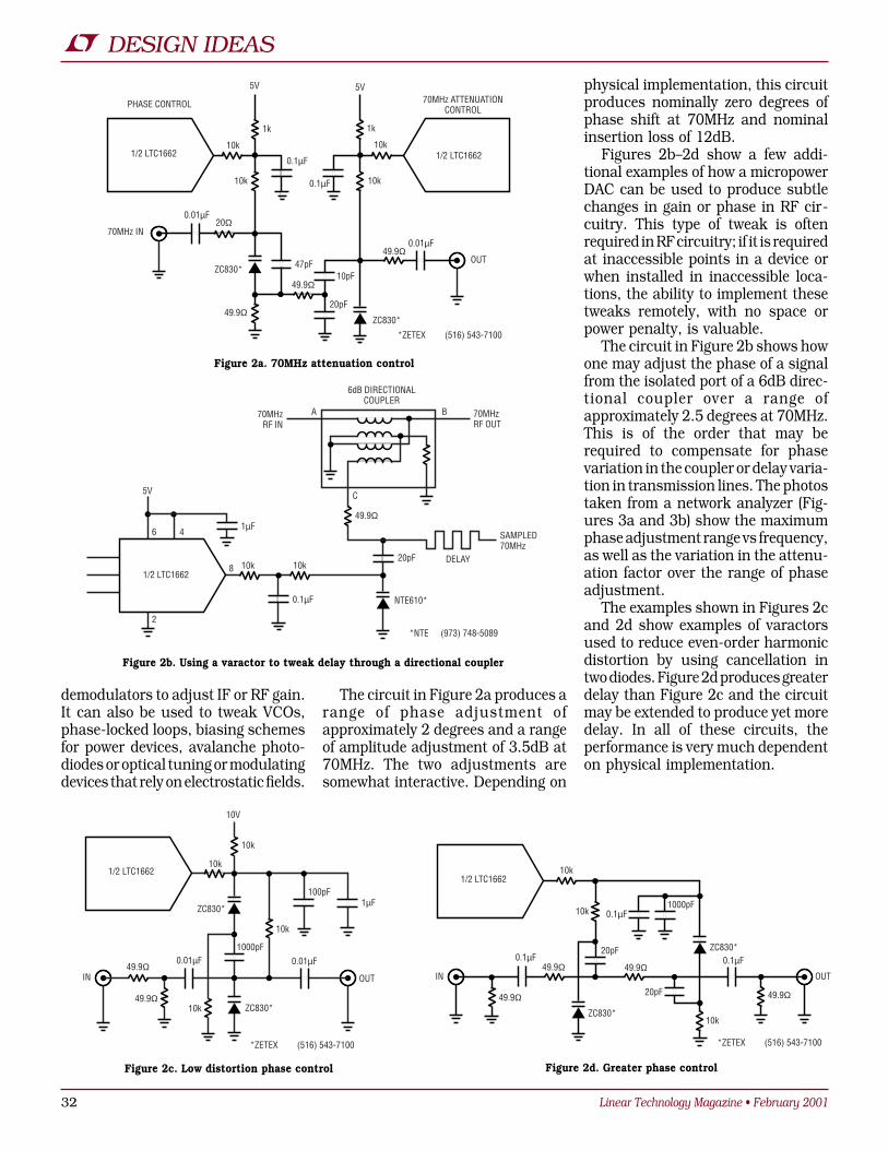
Linear Technology Magazine • February 200132
DESIGN IDEAS
demodulators to adjust IF or RF gain.It can also be used to tweak VCOs,phase-locked loops, biasing schemesfor power devices, avalanche photo-diodes or optical tuning or modulatingdevices that rely on electrostatic fields.
The circuit in Figure 2a produces arange of phase adjustment ofapproximately 2 degrees and a rangeof amplitude adjustment of 3.5dB at70MHz. The two adjustments aresomewhat interactive. Depending on
1/2 LTC1662 1/2 LTC1662
PHASE CONTROL 70MHz ATTENUATIONCONTROL
5V 5V
1k
10k
10k
1k
10k
10k
70MHz IN
OUT
0.1µF
0.1µF
0.01µF
0.01µF
20Ω
49.9Ω
49.9Ω
49.9Ω
ZC830*
ZC830* 47pF10pF
20pF
*ZETEX (516) 543-7100
physical implementation, this circuitproduces nominally zero degrees ofphase shift at 70MHz and nominalinsertion loss of 12dB.
Figures 2b–2d show a few addi-tional examples of how a micropowerDAC can be used to produce subtlechanges in gain or phase in RF cir-cuitry. This type of tweak is oftenrequired in RF circuitry; if it is requiredat inaccessible points in a device orwhen installed in inaccessible loca-tions, the ability to implement thesetweaks remotely, with no space orpower penalty, is valuable.
The circuit in Figure 2b shows howone may adjust the phase of a signalfrom the isolated port of a 6dB direc-tional coupler over a range ofapproximately 2.5 degrees at 70MHz.This is of the order that may berequired to compensate for phasevariation in the coupler or delay varia-tion in transmission lines. The photostaken from a network analyzer (Fig-ures 3a and 3b) show the maximumphase adjustment range vs frequency,as well as the variation in the attenu-ation factor over the range of phaseadjustment.
The examples shown in Figures 2cand 2d show examples of varactorsused to reduce even-order harmonicdistortion by using cancellation intwo diodes. Figure 2d produces greaterdelay than Figure 2c and the circuitmay be extended to produce yet moredelay. In all of these circuits, theperformance is very much dependenton physical implementation.
1/2 LTC1662
5V
1µF
10k 10k
0.1µF
20pF
NTE610*
DELAY
6dB DIRECTIONALCOUPLER
70MHzRF IN
70MHzRF OUT
49.9Ω
SAMPLED70MHz
6 4
8
2
A B
C
*NTE (973) 748-5089
1/2 LTC1662
10V
10k
10k
10k
10k
IN49.9Ω
49.9Ω
0.01µF 0.01µF
ZC830*
ZC830*
1000pF
OUT
1µF100pF
*ZETEX (516) 543-7100
1/2 LTC166210k
10k
10k
49.9Ω
49.9Ω
ZC830*
ZC830*
0.1µF
0.1µF
0.1µF
1000pF
20pF
20pF
OUTIN49.9Ω
49.9Ω
*ZETEX (516) 543-7100
Figure 2a. 70MHz attenuation control
Figure 2b. Using a varactor to tweak delay through a directional coupler
Figure 2c. Low distortion phase control Figure 2d. Greater phase control
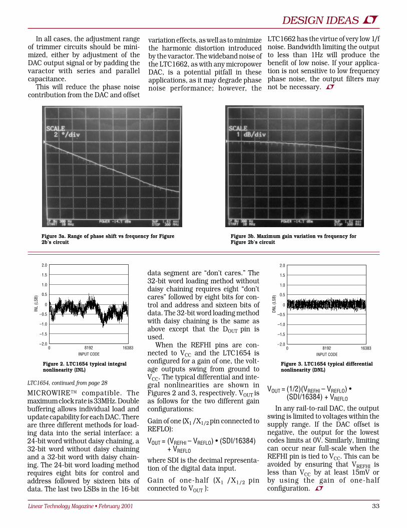
Linear Technology Magazine • February 2001 33
DESIGN IDEAS
In all cases, the adjustment rangeof trimmer circuits should be mini-mized, either by adjustment of theDAC output signal or by padding thevaractor with series and parallelcapacitance.
This will reduce the phase noisecontribution from the DAC and offset
variation effects, as well as to minimizethe harmonic distortion introducedby the varactor. The wideband noise ofthe LTC1662, as with any micropowerDAC, is a potential pitfall in theseapplications, as it may degrade phasenoise performance; however, the
MICROWIRE™ compatible. Themaximum clock rate is 33MHz. Doublebuffering allows individual load andupdate capability for each DAC. Thereare three different methods for load-ing data into the serial interface: a24-bit word without daisy chaining, a32-bit word without daisy chainingand a 32-bit word with daisy chain-ing. The 24-bit word loading methodrequires eight bits for control andaddress followed by sixteen bits ofdata. The last two LSBs in the 16-bit
INPUT CODE0
INL
(LSB
)
0
0.5
1.0
16383
–0.5
–1.0
–2.08192
–1.5
2.0
1.5
INPUT CODE0
DNL
(LSB
)
0
0.5
1.0
16383
–0.5
–1.0
–2.08192
–1.5
2.0
1.5data segment are “don’t cares.” The32-bit word loading method withoutdaisy chaining requires eight “don’tcares” followed by eight bits for con-trol and address and sixteen bits ofdata. The 32-bit word loading methodwith daisy chaining is the same asabove except that the DOUT pin isused.
When the REFHI pins are con-nected to VCC and the LTC1654 isconfigured for a gain of one, the volt-age outputs swing from ground toVCC. The typical differential and inte-gral nonlinearities are shown inFigures 2 and 3, respectively. VOUT isas follows for the two different gainconfigurations:
Gain of one (X1 /X1/2 pin connected toREFLO):
VOUT = (VREFHI – VREFLO) • (SDI/16384)+ VREFLO
where SDI is the decimal representa-tion of the digital data input.
Gain of one-half (X1 /X1/2 pinconnected to VOUT ):
VOUT = (1/2)(VREFHI – VREFLO) •(SDI/16384) + VREFLO
In any rail-to-rail DAC, the outputswing is limited to voltages within thesupply range. If the DAC offset isnegative, the output for the lowestcodes limits at 0V. Similarly, limitingcan occur near full-scale when theREFHI pin is tied to VCC. This can beavoided by ensuring that VREFHI isless than VCC by at least 15mV orby using the gain of one-halfconfiguration.
LTC1662 has the virtue of very low 1/fnoise. Bandwidth limiting the outputto less than 1Hz will produce thebenefit of low noise. If your applica-tion is not sensitive to low frequencyphase noise, the output filters maynot be necessary.
Figure 2. LTC1654 typical integralnonlinearity (INL)
Figure 3. LTC1654 typical differentialnonlinearity (DNL)
Figure 3a. Range of phase shift vs frequency for Figure2b’s circuit
Figure 3b. Maximum gain variation vs frequency forFigure 2b’s circuit
LTC1654, continued from page 28

Linear Technology Magazine • February 200134
DESIGN IDEAS
LTC1628-SYNC Minimizes InputCapacitors in a Multioutput,High Current Power Supply by Wei Chen
1
2
3
5
4
6
7
8
9
10
13
14
11
12
28
27
26
25
24
23
22
21
20
19
18
16
17
15
1
2
3
4
5
6
7
8
9
10
11
12
13
14
28
27
26
25
24
23
22
21
20
19
18
16
17
15
RUN/SS
SENSE1+
SENSE1–
PLLFLTR
EAIN
PLLIN
PHASMD
ITH
SGND
VDIFFOUT
SENSE2–
SENSE2+
VOS–
VOS+
CLKOUT
TG1
SW1
BOOST1
VIN
BG1
EXTVCC
INTVCC
PGND
BG2
BOOST2
TG2
SW2
AMPMD
LTC1629
RUN/SS1
SENSE1+
SENSE1–
VOSENSE1
PLLFLTR
PLLIN
FCB
ITH1
SGND
3.3VOUT
ITH2
VOSENSE2
SENSE2–
SENSE2+
PGOOD
TG1
SW1
BOOST1
VIN
BG1
EXTVCC
INTVCC
PGND
BG2
BOOST2
TG
SW2
RUN/SS2
LTC1628-SYNC
+
+
+
+
INTVCC1
0.1µF
0.01µF10k
2.7k 47pF
12.1k
10k
49.9k
680pF
56pF
R13 8.06k
100pF
R146.98k
10Ω
10Ω
10Ω10Ω
C20 1000pF
10Ω
10ΩC351000pF
47pF
10k
1nF
0.01µF56pF
0.1µF
10k 1000pF
100pF
R28 8.06k
C6647pF
R3217.4k
CLK1
470pF 10Ω10Ω
C591000pF
C600.1µF
1µF 16V 10Ω
PGOODR22 100k
0.47µF
C5210µF6.3V
C51 1µFD5
0.47µF1µF
Q1 L11.0µH
Q2–Q3
1µF
D1
R90.002Ω
10Ω10Ω
1µF
10Ω
CLK1
C21000pF
0.47µF
C111µF C12
10µF6.3V
D2
0.47µF
Q4
Q5–Q6
1µF
L21.0µH
D3
Q7
D4
Q8–Q9
L31.0µH
1µF
R230.002Ω
R150.002Ω
Q10
Q11–Q12 D6
L41.5µH
R260.003Ω
C62–C63180µF, 4V ×2
VOUT2+
2.5V/15A
VOUT2–
VO2SENSE+
CIN270µF16V ×3
VIN+
12V
VIN–
C22–C27270µF, 2V ×7
VOUT1+
1.5V/60AMAX
VOUT1–
10Ω
VO1SENSE–
VO1SENSE+
Q1–Q12:L1–L3:
L4:D1, D3, D4, D6:
D2, D5:
FAIRCHILD FDS7764A SUMIDA CEP125-1R0-MC-H SUMIDA CEP125-1R5-MC-H ON SEMICONDUCTOR MBRS340T3 (602) 244-6600 ON SEMICONDUCTOR BAT54A
Figure 1. LTC1628-Sync/LTC1629 2-output PolyPhase supply

Linear Technology Magazine • February 2001 35
DESIGN IDEAS
IntroductionIn broadband networking and highspeed computing applications, mul-tiple output, high current, low voltagepower supplies are needed to powerFPGAs, flash memories, DSPs andmicroprocessors. One such examplecalls for a maximum current of 60A topower the CPU and up to 15A topower the memory. A custom DC/DCmodule is usually expensive and theexternal circuitry for synchronizationfurther increases the cost of indi-vidual supplies.
This design idea presents a lowcost, high efficiency, dual-outputpower supply design using LTC’s latestPolyPhase products, the LTC1628-
SYNC and LTC1629. The input is 12Vand the outputs are 1.5V at 60A maxfor the CPU and 2.5V at 15A max forthe memory. The design uses theLTC1629 and one channel of theLTC1628-SYNC to configure the3-phase supply for the CPU powerand the remaining channel ofLTC1628-SYNC for the memory sup-ply. With only twelve SO-8 MOSFETsand two SSOP-28 controllers, the com-plete power supply occupies a footprintof only 3" × 3". Efficiencies of 85% and89% are achieved for outputs of 1.6V/60A and 2.5V/15A, respectively.
Design DetailsThe newly released LTC1628-SYNC isa dual-output, PolyPhase, currentmode controller. Unlike other ver-sions of the LTC1628, it has a PLLINpin that enables external synchroni-zation. In conjunction with theLTC1629, it can be used to imple-ment a true 3-phase circuit for CPUpower while the second output of theLTC1628-SYNC is used to generatethe memory power supply. Becausethe channel used for the memorypower switches at 300 degrees withrespect to the other three channelsused for CPU power, the net ripple
sesahPtupnIesaC-tsroW
A(tnerruCelppiR SMR )spaCtupnIforebmuN
)C°56ta)M072PS61NOCSO(
esahP-elgniS 4.32 7esahPyloP
)CNYS-8261CTL+9261CTL( 2.01 3
Table 1. Comparison of input ripple current and input capacitors for single-phase and PolyPhase configurations
current seen by the input bus is fur-ther reduced. In addition, thedifferential amp within the LTC1629enables true remote sensing to ensureaccurate voltage regulation at the CPUsupply pins.
Table 1 compares the input ripplecurrent requirements of the multi-phase design and a conventionalsingle-phase design. The multiphasetechnique reduces input capacitanceby almost 60%.
The complete schematic diagramand efficiency measurements areshown in Figures 1 and 2, respec-tively. With a 12V input and 250kHzswitching frequency, greater than 80%efficiency is maintained for both out-puts over most of the load range.
Other ApplicationsFor applications with more than twooutputs, several LTC1628-SYNCs canbe teamed with the LTC1629 forgreater than 2-phase operation. Fig-ure 3 shows an example using theLTC1629 and LTC1628-SYNC in a3-output, 4-phase application. Be-cause four synchronous buck circuitsare interleaved 90 degree out of phase,the net input ripple current is greatlyreduced.
ConclusionThe synchronization capability of theLTC1628-SYNC helps minimize in-put capacitance and avoid beatfrequencies. Teamed with LTC1629,it can effectively provide a 3-phasesolution for multiple output applica-tions and minimize the size and costof the complete power supply.
100
90
80
70
60
500 10 20 30 40 50 60
LOAD CURRENT (A)
EFFI
CIEN
CY (%
)
VIN = 12VVOUT = 1.5VfS = 200kHz
BUCK: 2.5V/15A
BUCK: 2.5V/15A
BUCK 1.5V/15A
BUCK 1.8V/15A
PHASMD
CLKOUT
PLLIN
TG1
TG2
TG1
TG2
OPEN
I4
I4
I3
I3
I2
I2
I1
I1
IIN
IIN
VIN = 12V
VOUT12.5V/30A
VOUT21.5V/15A
VOUT31.8V/15A
U1
LTC1629
U2
LTC1628-SYNC
Figure 2. Efficiency vs loadcurrent for Figure 1’s circuit
Figure 3. Block diagram of LTC1628-Sync/LTC1629 3-input, 4-phase application

Linear Technology Magazine • February 200136
DESIGN IDEAS
Reduce EMI with Ultralow Noise 48Vto 5V, 10W DC/DC Converter
by Rick Brewster
IntroductionIncreasingly, designers are usingultralow noise controllers to avoidEMI problems. Lower operatingvoltages and more sensitive measure-ments have created the need forquieter supplies. Extra filtering com-ponents and shielding are usuallyrequired, as is a careful board layout.Ultralow noise switching regulatorcontrollers such as the LT1683 reduceor eliminate the need for extra filter-ing. The LT1683 controller usesexternal MOSFETs to create ultralownoise DC/DC converters. Control ofthe switch voltage and switch currentslew rates reduces switcher noise.The LT1683’s use of external switchesallows for greater flexibility in theselection of voltage and current rat-ings of the supply. Circuit Details
Figure 1 shows the schematic of anultralow noise 48V to 5V converterusing a push-pull forward convertertopology. The output broadband noiseis a very low 200µV (bandwidth =
ABD1
T1
22µF
150µFOS-CON
D2
D3
22µF
OPTIONAL
2×100µFPOSCAP
5V/2A
3
101113
SHDN CAP A
NFB
LT1683
GND
VIN
17
14 2
GCL
SS
V5
SYNCGATE A
51
CT CAP B
6
19
RT GATE B
7
188
RCSL
16
VC
15
12
RVSL CS4
PGND20
FB9
5pF
5pF
0.1Ω
130k
2.7M
10nF
1.5k
3.6k
25k
25k
3.6k
16.9k
1.3nF
39µF63V
48V
68µF20V
11V
8.3
51k510Ω0.5W
2N3904
1N4148 10µF20V
30pF
22nF
0.22µF
7.5k
2.49k
FZT649
10pF200V
30pF
10pF200V
MIDCOM 31244 (605) 886-4385SILICONIX Si9422 (800) 554-5565ON SEMICONDUCTOR MBRS340 (602) 244-6600ON SEMICONDUCTOR MBR0530
T1: M1, M2: D1, D2:
D3:
M1
M2
+
+
+
++
100MHz) at 2A output (10W). TheLT1683 contains all the control cir-cuitry for the converter: oscillator,error amp, gate drivers and protec-tion circuitry. The low noise is achievedby controlling the voltage slew rate ofthe MOSFET drain and the currentslew rate of the MOSFET current. Thecapacitor divider network from thedrain to Cap A or Cap B yields aneffective 0.33pF capacitor that pro-vides the voltage slew rate feedbackinformation. The current slew feed-back occurs internal to the LT1683 bymeans of the 100mΩ sense resistor.
The resistors on the RVSL and RCSLpins allow the user to optimize theslew rates. The trade-off is betweennoise and converter efficiency. Dur-ing design, monitor the output supplynoise while slowing down the slewrates via the slew control resistors.Adjust the slew rate until the noiserequirement is satisfied. In general,the efficiency loss is only a few percent.
Figure 2 shows the voltage on thedrain of one of the MOSFETs and thevoltage across the sense resistor.
DRAIN20V/DIV
CS50mV/DIV
2µs/DIV
Figure 1. Ultralow noise 48V to 5V DC/DC converter
Figure 2. Voltage on one of the MOSFET drains and on the sense resistor
Linear Technology Magazine • February 2001 37
DESIGN IDEAS
Because of the voltage slew control,clamps or snubbers on the MOSFETdrains are not required and switchringing is greatly reduced. Figure 3shows the noise at the outputs. Theoutput noise is a very low 200µVP-P.
The SHDN pin provides the supply
A200µV/DIV
B20mV/DIV
5µs/DIV
200µVP-P
voltage. The CS pin provides the feed-back for pulse-by-pulse currentcontrol and slew control. A large sig-nal on CS, indicative of a fault, alsoshuts the MOSFETs off.
Converter efficiency is improvedby use of a bootstrap winding thatpowers the part when the converter isup and running. Efficiency at the lownoise setting is approximately 77%.
ConclusionThe LT1683 provides a unique way toproduce an efficient, ultralow noisesupply. Novel control circuitry quietsthe switcher, allowing a new supplysolution for sensitive electronic sys-tems. The use of external MOSFETswitches allows the voltage and cur-rent ratings of the supply to be tailoredto the application.
with undervoltage lockout, ensuringthat the input is up and runningbefore the converter is allowed to start.In addition, the GCL pin preventsexcessive gate voltage on the MOSFETand protects against the MOSFETsturning on without sufficient gate
In either constant voltage or cur-rent controlled applications of theLTC3200, the LED brightness can becontrolled by applying a PWM signal(approximately 100Hz) to the SHDNpin. Varying the pulse width from 4%to 100% gives the LEDs a linearappearance of brightness control fromfull-on to full-off.
ConclusionIn the tiny 6-pin SOT or 8-pin
MSOP packages, the LTC3200 familyof charge pumps provides a simplesolution for powering white LEDs. Itssmall size, low external parts countand low noise, constant frequencyoperation is ideally suited for bothcommunications and other portableproducts.
Figure 3. 5V output noise (bandwidth = 100MHz)
LTC3200, continued from page 29
1µF
LTC3200
C+ C–
VOUT
FB
ON OFF PGND
VIN
SHDN
8
1 3
7
4SGND
5
2
682Ω
1µF
82Ω
UP TO 6 LEDS
82Ω 82Ω 82Ω 82Ω
3V TO 4.4VLi-Ion
BATTERY1µF
VSHDN(APPLY PWM WAVEFORM
FOR ADJUSTABLE BRIGHTNESS CONTROL)
t
Figure 3. White or blue LED driver with LED current control
http://www.linear-tech.com/ezone/zone.htmlArticles, Design Ideas, Tips from the Lab…
Linear Technology Magazine • February 200138
NEW DEVICE CAMEOS
LTC1701B: Tiny Step-DownRegulator Switches at 1MHzFor low to medium power applica-tions that must fit in small spaces,the LTC1701B provides a DC/DCconverter that consumes less than0.3in2 of PC board space. The part’s1MHz switching frequency allows theuse of tiny, low cost capacitors andinductors, which, along with the tinySOT-23 package, results in a verycompact solution. The LTC1701Boperates continuously down to verylow load currents to provide low out-put ripple at the expense of light loadefficiency, while the LTC1701 incor-porates automatic power saving BurstMode operation to reduce gate chargelosses, providing better efficiency atlight loads.
The LTC1701/LTC1701B operatefrom an input supply from 2.5V to5.5V; the output voltage is adjustablefrom 1.25V to 5V. A built-in 0.28ΩP-channel MOSFET switch allows upto 500mA of output current at highefficiencies (up to 94%). In dropout,the internal switch can be turned oncontinuously, maximizing the usablebattery life.
Its combination of a high switchingfrequency, low ripple and an onboardP-channel MOSFET in a tiny SOT-23package makes the LTC1701B idealfor low noise, space-critical portableapplications.
LTC Releases Popular HighSpeed Amplifiers andComparators in the Space-Saving SOT-23 PackageIdeal for saving board space, the newSOT-23 versions of Linear Tech-nology’s high speed amplifiers andcomparators feature the same per-formance as their SO counterpartsbut require much less board area.
The 400MHz LT1395S5/LT1395S6current feedback amplifiers providethe bandwidth and output currentrequired for cable driver and videoapplications. A gain flatness of 0.1dBto 100MHz ensures signal fidelity and
the 80mA output current is sufficientfor cable drivers. The parts draw only4.6mA and operate on all suppliesfrom a single 4V to ±6V. A shutdownfeature is included in the LT1395S6.
The 100MHz LT1812S5/LT1812S6voltage feedback amplifiers have amaximum offset voltage of 1.5mV anda maximum input offset current of400nA. Drawing only 3mA supplycurrent, the devices have a slew rateof 750V/µs and can drive a 100Ω loadto ±3.5V with ±5V supplies. Theseeasy-to-use devices are stable withload capacitances as high as 1000pF.The LT1812S6 includes a power-sav-ing shutdown feature.
Operating from supplies as low as2.5V, the 325MHz LT1806S6 and the180MHz LT1809S6 amplifiers providethe distortion and noise performancerequired by low voltage signal condi-tioning systems. Rail-to-rail inputsand outputs allow the entire supplyrange to be used and the high outputcurrent capability, 60mA typical on a3V supply, is ideal for cable driverapplications. The LT1806S6 is opti-mized for noise and DC performance,featuring a low voltage noise of3.5nV/√Hz and a maximum offsetvoltage of 700µV. The LT1809S6 isoptimized for slew rate and distor-tion, featuring a slew rate of 350V/µsand low harmonic distortion of –90dBcat fC = 5MHz (VS = 5V, VO = 2VP-P).Both parts are fully specified for 3V,5V and ±5V operation. A shutdownfunction is included.
The LT1719S6 4.5ns comparatormakes fast comparisons painlesslyon 3V and 5V supplies while consum-
ing only 4.2mA. Internal hysteresisensures clean transitions even onslow-moving input signals. The inputcommon mode range extends to100mV below ground and the out-puts are rail-to-rail. The propagationtime is 4.5ns with 20mV overdriveand 7ns with 5mV overdrive. A shut-down pin reduces the supply currentto 80µA max.
LT1494 and LT1672/LT1673/LT1674 UltralowPower Rail-to-Rail Op AmpsThe LT1494 and LT1672/73/74 arethe newest members of the industry’slowest power, precision, rail-to-railop amp family. All devices have excel-lent amplifier specifications: 375µVmax input offset voltage, 100pA maxinput offset current and 0.4µV/°Ctypical drift while operating from amaximum of only 1.5µA supply cur-rent for the LT1494 and 2µA/amplifierfor the LT1672–74. A minimum open-loop gain (AVOL) of 100V/mV ensuresthat gain errors are small. Both thesupply rejection and the commonmode rejection ratios are greater than90dB. All devices exhibit little changein characteristics over the wide sup-ply range of 2.2V to ±15V. They featurereverse battery protection (–18V min)and Over-The-Top™ operation (theability to operate with the inputs abovethe positive supply).
The LT1494 is a single rail-to-railamplifier with a gain bandwidth prod-uct (GBW) of 3kHz and a slew rate(SR) of 0.4V/ms. The LT1672/73/74are single, dual and quad decompen-sated versions of the LT1494. Theyare stable with a gain of five and arefour times faster than the LT1494(GBW = 12kHz, SR = 1.6V/ms), withan increase in supply current of only500nA/amp.
The LT1494 and LT1672 singlecome in 8-lead MSOP, SO and PDIPpackages. The LT1673 dual comes in8-lead SO and PDIP packages and theLT1674 quad comes in 14-lead SOand PDIP packages.Information furnished by Linear Technology Corporationis believed to be accurate and reliable. However, noresponsibility is assumed for its use. Linear TechnologyCorporation makes no representation that the intercon-nection of its circuits as described herein will not infringeon existing patent rights.
New Device Cameos
For further information on anyof the devices mentioned in thisissue of Linear Technology, usethe reader service card or callthe LTC literature servicenumber:
1-800-4-LINEAR
Ask for the pertinent data sheetsand Application Notes.
Linear Technology Magazine • February 2001 39
DESIGN TOOLS
Technical Books1990 Linear Databook, Vol I —This 1440 page collec-tion of data sheets covers op amps, voltage regulators,references, comparators, filters, PWMs, data conver-sion and interface products (bipolar and CMOS), in bothcommercial and military grades. The catalog featureswell over 300 devices. $10.00
1992 Linear Databook, Vol II — This 1248 page supple-ment to the 1990 Linear Databook is a collection of allproducts introduced in 1991 and 1992. The catalogcontains full data sheets for over 140 devices. The 1992Linear Databook, Vol II is a companion to the 1990Linear Databook, which should not be discarded.
$10.00
1994 Linear Databook, Vol III —This 1826 page supple-ment to the 1990 and 1992 Linear Databooks is acollection of all products introduced since 1992. A totalof 152 product data sheets are included with updatedselection guides. The 1994 Linear Databook Vol III is acompanion to the 1990 and 1992 Linear Databooks,which should not be discarded. $10.00
1995 Linear Databook, Vol IV —This 1152 page supple-ment to the 1990, 1992 and 1994 Linear Databooks is acollection of all products introduced since 1994. A totalof 80 product data sheets are included with updatedselection guides. The 1995 Linear Databook Vol IV is acompanion to the 1990, 1992 and 1994 Linear Data-books, which should not be discarded. $10.00
1996 Linear Databook, Vol V —This 1152 page supple-ment to the 1990, 1992, 1994 and 1995 Linear Databooksis a collection of all products introduced since 1995. Atotal of 65 product data sheets are included with updatedselection guides. The 1996 Linear Databook Vol V is acompanion to the 1990, 1992, 1994 and 1995 LinearDatabooks, which should not be discarded. $10.00
1997 Linear Databook, Vol VI —This 1360 page supple-ment to the 1990, 1992, 1994, 1995 and 1996 LinearDatabooks is a collection of all products introducedsince 1996. A total of 79 product data sheets areincluded with updated selection guides. The 1997 LinearDatabook Vol VI is a companion to the 1990, 1992,1994, 1995 and 1996 Linear Databooks, which shouldnot be discarded. $10.00
1999 Linear Data Book, Vol VII — This 1968 pagesupplement to the 1990, 1992, 1994, 1995, 1996 and1997 Linear Databooks is a collection of all product datasheets introduced since 1997. A total of 120 productdata sheets are included, with updated selection guides.The 1999 Linear Databooks is a companion to theprevious Linear Databooks, which should not be dis-carded.$10.00
1990 Linear Applications Handbook, Volume I —928 pages full of application ideas covered in depth by40 Application Notes and 33 Design Notes. This catalogcovers a broad range of “real world” linear circuitry. Inaddition to detailed, systems-oriented circuits, this hand-book contains broad tutorial content together with liberaluse of schematics and scope photography. A specialfeature in this edition includes a 22-page section onSPICE macromodels. $20.00
1993 Linear Applications Handbook, Volume II —Continues the stream of “real world” linear circuitryinitiated by the 1990 Handbook. Similar in scope to the1990 edition, the new book covers Application Notes 40
through 54 and Design Notes 33 through 69. Referencesand articles from non-LTC publications that we havefound useful are also included. $20.00
1997 Linear Applications Handbook, Volume III —This 976 page handbook maintains the practical outlookand tutorial nature of previous efforts, while broadeningtopic selection. This new book includes ApplicationNotes 55 through 69 and Design Notes 70 through 144.Subjects include switching regulators, measurementand control circuits, filters, video designs, interface,data converters, power products, battery chargers andCCFL inverters. An extensive subject index referencescircuits in LTC data sheets, design notes, applicationnotes and Linear Technology magazines. $20.00
1998 Data Converter Handbook — This impressive 1360page handbook includes all of the data sheets, applica-tion notes and design notes for Linear Technology’sfamily of high performance data converter products.Products include A/D converters (ADCs), D/A convert-ers (DACs) and multiplexers—including the fastestmonolithic 16-bit ADC, the 3Msps, 12-bit ADC with thebest dynamic performance and the first dual 12-bit DACin an SO-8 package. Also included are selection guidesfor references, op amps and filters and a glossary of dataconverter terms. $10.00
Interface Product Handbook — This 424 page hand-book features LTC’s complete line of line driver andreceiver products for RS232, RS485, RS423, RS422,V.35 and AppleTalk® applications. Linear’s particularexpertise in this area involves low power consumption,high numbers of drivers and receivers in one package,mixed RS232 and RS485 devices, 10kV ESD protectionof RS232 devices and surface mount packages.
Available at no charge
Power Management Solutions Brochure — This 96page collection of circuits contains real-life solutions forcommon power supply design problems. There are over70 circuits, including descriptions, graphs and perfor-mance specifications. Topics covered include batterychargers, desktop PC power supplies, notebook PCpower supplies, portable electronics power supplies,distributed power supplies, telecommunications andisolated power supplies, off-line power supplies andpower management circuits. Selection guides are pro-vided for each section and a variety of helpful designtools are also listed for quick reference.
Available at no charge.
Data Conversion Solutions Brochure — This 64 pagecollection of data conversion circuits, products andselection guides serves as excellent reference for thedata acquisition system designer. Over 60 products areshowcased, solving problems in low power, small sizeand high performance data conversion applications—with performance graphs and specifications. Topicscovered include ADCs, DACs, voltage references andanalog multiplexers. A complete glossary defines dataconversion specifications; a list of selected applicationand design notes is also included.
Available at no charge
Telecommunications Solutions Brochure —This 76page collection of application circuits and selectionguides covers a wide variety of products targeted fortelecommunications. Circuits solve real life problemsfor central office switching, cellular phones, high speedmodems, base station, plus special sections covering
–48V and Hot SwapTM applications. Many applicationshighlight new products such as Hot Swap controllers,power products, high speed amplifiers, A/D converters,interface transceivers and filters. Includes a telecom-munications glossary, serial interface standards, protocolinformation and a complete list of key application notesand design notes. Available at no charge.
Applications on DiskFilterCAD™ 3.0 CD-ROM — This CD-ROM containsthe latest release of FilterCAD, version 3.0. FilterCAD isa powerful filter design tool that supports all of LinearTechnology’s high performance active RC and switchedcapacitor filters. You can run FilterCAD directly from theCD or install it on your computer’s hard disk for muchfaster operation. FilterCAD requires a PC running Win-dows® 95 or later.
The CD-ROM also contains a filter selection guide thatlists all of Linear Technology’s filter products, alongwith links to their data sheets. Adobe® Acrobat Reader,version 3.0 or later, is required to use the selectionguide. Available at no charge.
Noise Disk — This IBM-PC (or compatible) programallows the user to calculate circuit noise using LTC opamps, determine the best LTC op amp for a low noiseapplication, display the noise data for LTC op amps,calculate resistor noise and calculate noise using specsfor any op amp. Available at no charge
SPICE Macromodel Disk — This IBM-PC (or compat-ible) high density diskette contains the library of LTC opamp SPICE macromodels. The models can be used withany version of SPICE for general analog circuit simula-tions. The diskette also contains working circuit examplesusing the models and a demonstration copy of PSPICE™by MicroSim. Available at no charge
SwitcherCAD™ — The SwitcherCAD program is a pow-erful PC software tool that aids in the design andoptimization of switching regulators. The program cancut days off the design cycle by selecting topologies,calculating operating points and specifying componentvalues and manufacturer’s part numbers. 144 pagemanual included. $20.00
SwitcherCAD supports the following parts: LT1070 se-ries: LT1070, LT1071, LT1072, LT1074 and LT1076.LT1082. LT1170 series: LT1170, LT1171, LT1172 andLT1176. It also supports: LT1268, LT1269 and LT1507.LT1270 series: LT1270 and LT1271. LT1371 series:LT1371, LT1372, LT1373, LT1375, LT1376 and LT1377.
Micropower SwitcherCAD™ — The MicropowerSCADprogram is a powerful tool for designing DC/DC con-verters based on Linear Technology’s micropowerswitching regulator ICs. Given basic design parameters,MicropowerSCAD selects a circuit topology and offersyou a selection of appropriate Linear Technology switch-ing regulator ICs. MicropowerSCAD also performs circuitsimulations to select the other components which sur-round the DC/DC converter. In the case of a batterysupply, MicropowerSCAD can perform a battery lifesimulation. 44 page manual included. $20.00
MicropowerSCAD supports the following LTC micro-power DC/DC converters: LT1073, LT1107, LT1108,LT1109, LT1109A, LT1110, LT1111, LT1173, LTC1174,LT1300, LT1301 and LT1303.
continued on page 40
DESIGN TOOLS

Linear Technology Magazine • February 2001© 2001 Linear Technology Corporation/Printed in U.S.A./40K
LINEAR TECHNOLOGY CORPORATION1630 McCarthy BoulevardMilpitas, CA 95035-7417(408) 432-1900 FAX (408) 434-0507www.linear-tech.comFor Literature Only: 1-800-4-LINEAR
InternationalSales OfficesCHINA (HONG KONG)Linear Technology Corp. Ltd.Unit 2109, Metroplaza Tower 2223 Hing Fong RoadKwai Fong, N.T., Hong KongPhone: +852 2428-0303FAX: +852 2348-0885
FRANCELinear Technology S.A.R.L.Immeuble "Le Quartz"58 Chemin de la Justice92290 Chatenay MalabryFrancePhone: +33 (1) 41079555FAX: +33 (1) 46314613
GERMANYLinear Technology GmbHOskar-Messter-Str. 24D-85737 IsmaningGermanyPhone: +49 (89) 962455-0FAX: +49 (89) 963147
Haselburger Damm 4D-59387 AschebergGermanyPhone: +49 (2593) 9516-0FAX: +49 (2593) 951679
Zettachring 12D-70567 StuttgartGermanyPhone: +49 (711) 1329890FAX: +49 (711) 7285055
JAPANLinear Technology KK5F NAO Bldg.1-14 Shin-Ogawa-cho Shinjuku-kuTokyo, 162JapanPhone: +81 (3) 3267-7891FAX: +81 (3) 3267-8510
6F Tokyo Seimei Honmachi Bldg.1-6-13 Awaza, Nishi-kuOsaka-shi, 550-0011, JapanPhone: +81 (6) 6533-5880FAX: +81 (6) 6533-5885
KOREALinear Technology Korea Co., Ltd.Yundang Building, #1002Samsung-Dong 144-23Kangnam-Ku, Seoul 135-090KoreaPhone: +82 (2) 792-1617FAX: +82 (2) 792-1619
SINGAPORELinear Technology Pte. Ltd.507 Yishun Industrial Park ASingapore 768734Phone: +65 753-2692FAX: +65 752-0108
SWEDENLinear Technology ABSollentunavägen 63S-191 40 SollentunaSwedenPhone: +46 (8) 623-1600FAX: +46 (8) 623-1650
TAIWANLinear Technology CorporationRm. 602, No. 46, Sec. 2Chung Shan N. Rd.Taipei, Taiwan, R.O.C.Phone: +886 (2) 2521-7575FAX: +886 (2) 2562-2285
UNITED KINGDOMLinear Technology (UK) Ltd.The Coliseum, Riverside WayCamberley, Surrey GU15 3YLUnited KingdomPhone: +44 (1276) 677676FAX: +44 (1276) 64851
World HeadquartersLinear Technology Corporation1630 McCarthy Blvd.Milpitas, CA 95035-7417Phone: (408) 432-1900FAX: (408) 434-0507www.linear-tech.com
U.S. AreaSales OfficesNORTHEAST REGIONLinear Technology Corporation3220 Tillman Drive, Suite 120Bensalem, PA 19020Phone: (215) 638-9667 FAX: (215)638-9764
15 Research PlaceNorth Chelmsford, MA 01863Phone: (978) 656-4750FAX: (978) 656-4760
NORTHWEST REGIONLinear Technology Corporation720 Sycamore DriveMilpitas, CA 95035Phone: (408) 428-2050FAX: (408) 432-6331
SOUTHEAST REGIONLinear Technology Corporation17000 Dallas ParkwaySuite 219Dallas, TX 75248Phone: (972) 733-3071FAX: (972) 380-5138
9430 Research Blvd.Echelon IV Suite 400Austin, TX 78759Phone: (512) 343-3679FAX: (512) 343-3680
1080 West Sam Houston Pkwy., Suite 225Houston, TX 77043Phone: (713) 463-5001FAX: (713) 463-5009
15100 Weston Parkway, Suite 202Carey, NC 27513Phone: (919) 677-0066FAX: (919) 678-0041
CENTRAL REGIONLinear Technology Corporation2010 E. Algonquin RoadSuite 209Schaumburg, IL 60173Phone: (847) 925-0860FAX: (847) 925-0878
Kenosha, WI 53144Phone: (262) 859-1900FAX: (262) 859-1974
SOUTHWEST REGIONLinear Technology Corporation21243 Ventura Blvd., Suite 208Woodland Hills, CA 91364Phone: (818) 703-0835FAX: (818) 703-0517
15375 Barranca ParkwaySuite A-213Irvine, CA 92618Phone: (949) 453-4650FAX: (949) 453-4765
Acrobat is a trademark of Adobe Systems, Inc.; Windowsis a registered trademark of Microsoft Corp.; AppleTalk isa registered trademark of Apple Computer, Inc. Pentiumis a registered trademark of Intel Corp.; PSPICE is atrademark of MicroSim Corp.
CD-ROM CatalogLinearView — LinearView™ CD-ROM version 4.0 isLinear Technology’s latest interactive CD-ROM. It allowsyou to instantly access thousands of pages of productand applications information, covering LinearTechnology’s complete line of high performance analogproducts, with easy-to-use search tools.
The LinearView CD-ROM includes the complete productspecifications from Linear Technology’s Databook library(Volumes I–VII) and the complete Applications Hand-book collection (Volumes I–III). Our extensive collectionof Design Notes and the complete collection of LinearTechnology magazine are also included.
A powerful search engine built into the LinearView CD-ROM enables you to select parts by various criteria,such as device parameters, keywords or part numbers.All product categories are represented: data conversion,references, amplifiers, power products, filters and inter-face circuits. Up-to-date versions of Linear Technology’s
DESIGN TOOLS, continued from page 39 software design tools, SwitcherCAD, Micropower Switch-erCAD, FilterCAD, Noise Disk and Spice Macromodellibrary, are also included. Everything you need to knowabout Linear Technology’s products and applications isreadily accessible via LinearView. LinearView runs underWindows 95 or later.
Available at no charge.
World Wide Web SiteLinear Technology Corporation’s customers can nowquickly and conveniently find and retrieve the latesttechnical information covering the Company’s productson LTC’s Internet web site. Located at www.linear-tech.com, this site allows anyone with Internet accessand a web browser to search through all of LTC’stechnical publications, including data sheets, applica-tion notes, design notes, Linear Technology magazineissues and other LTC publications, to find informationon LTC parts and applications circuits. Other areaswithin the site include help, news and information aboutLinear Technology and its sales offices.
Other web sites usually require the visitor to downloadlarge document files to see if they contain the desiredinformation. This is cumbersome and inconvenient. Tosave you time and ensure that you receive the correctinformation the first time, the first page of each datasheet, application note and Linear Technology maga-zine is recreated in a fast, download-friendly format.This allows you to determine whether the document iswhat you need, before downloading the entire file.
The site is searchable by criteria such as part numbers,functions, topics and applications. The search is per-formed on a user-defined combination of data sheets,application notes, design notes and Linear Technologymagazine articles. Any data sheet, application note,design note or magazine article can be downloaded orfaxed back. (Files are downloaded in Adobe Acrobat PDFformat; you will need a copy of Acrobat Reader to viewor print them. The site includes a link from which youcan download this program.)