
NEUTRAL POINT VOLTAGE CONTROL OF ... - CORE
345
NEUTRAL POINT VOLTAGE CONTROL OF NEUTRAL POINT CLAMPED CONVERTERS A thesis submitted in fulfilment of the requirements for the degree of Doctorate of Philosophy Zaki Mohzani B. Eng. (Hons) School of Electrical and Computer Engineering College of Science, Engineering and Health RMIT University, Australia March 2014
-
Upload
khangminh22 -
Category
Documents
-
view
3 -
download
0
Transcript of NEUTRAL POINT VOLTAGE CONTROL OF ... - CORE

NEUTRAL POINT VOLTAGE CONTROL
OF NEUTRAL POINT CLAMPED
CONVERTERS
A thesis submitted in fulfilment of the requirements for
the degree of Doctorate of Philosophy
Zaki Mohzani
B. Eng. (Hons)
School of Electrical and Computer Engineering
College of Science, Engineering and Health
RMIT University, Australia
March 2014


COPYRIGHT NOTICE
iii
COPYRIGHT NOTICE
In return for freely distributing this PhD thesis, I kindly request that each time
another copy of this work (either in electronic or printed form) gets passed to another
entity, that the name, affiliation and email address of the new recipient be emailed to
myself at:
This thesis may not be placed electronically where public download access is
available without prior authorisation from the author.
Kind regards,
Zaki Mohzani

COPYRIGHT NOTICE
iv

DECLARATION
v
DECLARATION
I certify that except where due acknowledgement has been made, the work is that of
the author alone; the work has not been submitted previously, in whole or in part, to
qualify for any other academic award; the content of the thesis is the result of work
which has been carried out since the official commencement date of the approved
research program; and, any editorial work, paid or unpaid, carried out by a third party
is acknowledged.
Zaki Mohzani
31 March 2014
E00787
Typewritten Text
E00787
Typewritten Text

DECLARATION
vi

ACKNOWLEDGEMENTS
vii
ACKNOWLEDGEMENTS
Thank you to Prof. Grahame Holmes, Dr. Brendan McGrath, Mohzani Wahab and
Dalilah Matharsha, Dinesh Segaran, Wang Kong, Reza Davoodnezhad, Carlos A.
Texeira, Stewart Parker, Kavita Balasubramaniam and the fast food giants for their
guidance, support and love.

viii

TABLE OF CONTENTS
ix
TABLE OF CONTENTS
Copyright Notice .................................................................................................... iii
Declaration .............................................................................................................. v
Acknowledgements ............................................................................................... vii
Table of Contents ................................................................................................... ix
List of Figures ....................................................................................................... xv
List of Tables ...................................................................................................... xxiii
List of Symbols ................................................................................................... xxv
Glossary of Terms ............................................................................................. xxvii
Publications ........................................................................................................ xxix
Abstract .............................................................................................................. xxxi
1 INTRODUCTION .............................................................................................. 1
1.1 Background ............................................................................................... 1
1.2 Aim of the Research .................................................................................. 3
1.3 Structure of Thesis .................................................................................... 4
1.4 Identification of Original Contribution ..................................................... 5
2 REVIEW OF NEUTRAL POINT DRIFT AND CONTROL
STRATEGIES .................................................................................................... 7
2.1 Fundamentals of NPC Converters ............................................................. 7
2.2 Early NPC Publications ............................................................................. 9
2.3 Neutral Point Voltage Deviation Problem .............................................. 12
2.4 Impact of Space Vectors on the NP Voltage ........................................... 14
2.5 Early Neutral Point (NP) Control Strategies (1990 to 1997) .................. 15
2.6 Further Neutral Point (NP) Control Strategies (1997 Onwards) ............. 16
2.6.1 Calculation of the Duty of the Redundant States for SPWM......... 16
2.6.2 Calculation of the Duty of the Redundant States for SVM ............ 17
2.6.3 Limitation of Redundant State Control .......................................... 18
2.6.4 New Developments in Traditional Modulation Schemes .............. 18
2.6.5 Natural Balancing........................................................................... 20
2.6.6 Shift Towards Unconventional Modulation Schemes.................... 20
2.7 Existing Comparisons of NP Control Performance ................................ 24
2.8 Issues in the Literature ............................................................................ 25
2.9 Conclusion ............................................................................................... 26

TABLE OF CONTENTS
x
3 FUNDAMENTALS OF ACTIVE NP CONTROL .......................................... 27
3.1 NP Currents Produced by Space Vectors ................................................ 27
3.1.1 Medium Vectors – The Source of NP Current Disturbance ........... 28
3.1.2 Small Vectors – The Source of NP Current Control ...................... 29
3.2 NP Natural Control Limits ...................................................................... 31
3.2.1 Effect of Modulation Depth ........................................................... 32
3.2.2 Effect of Load Power Factor Angle ............................................... 33
3.2.3 Cumulative Effect .......................................................................... 34
3.3 Extending NP Controllability Beyond the Natural Limits ...................... 34
3.4 Vector Selection Analysis of Existing NP Control Strategies ................ 39
3.5 Strategies to be Compared in Chapter 4 .................................................. 46
3.6 Summary ................................................................................................. 47
4 QUANTITATIVE COMPARISON OF ACTIVE NP STRATEGIES............. 49
4.1 Methodology ........................................................................................... 49
4.2 Performance Metrics ............................................................................... 51
4.2.1 Steady-state NP Ripple ................................................................... 51
4.2.2 Measure of Output Distortion - NWTHD ...................................... 51
4.2.3 NP Dynamic Control Performance ................................................ 52
4.3 Simulation System ................................................................................... 52
4.4 Investigation Results ............................................................................... 53
4.4.1 High DC link Capacitance Case (4200µF) ..................................... 53
4.4.2 Low DC link Capacitance Case (840µF) ....................................... 60
4.5 Active Strategy Recommendation ........................................................... 65
4.6 Summary ................................................................................................. 66
5 NATURAL BALANCING OF A NPC PHASE LEG ...................................... 67
5.1 NP Voltage Variation with NPC Phase Leg Switching Commands ....... 67
5.2 Double Fourier Representation of NPC PD Modulation ......................... 71
5.3 Reduction of NPC Natural Balance Solution to Linear Form ................. 73
5.4 Natural Balancing Response and Balance Booster Contribution ............ 74
5.5 Design of Balance Booster ...................................................................... 78
5.6 Natural Balance Time Domain Simulation ............................................. 80
5.7 Summary ................................................................................................. 84
6 NATURAL BALANCING OF THREE PHASE NPC CONVERTERS ......... 85
6.1 Modelling the Three-phase NPC [82] ..................................................... 85

TABLE OF CONTENTS
xi
6.1.1 Modelling the NP Change when tVn is Floating (Case 1
(ZL-F) & 3 (ZL-F, BB-F)) ............................................................. 87
6.1.2 Modelling the NP Change when tVn is Connected to a DC
link (Case 6 (ZL-F, BB-VDC)) ..................................................... 90
6.1.3 Application of the Superposition of Phase Leg Models to
obtain D.E.s for the Different Cases of a 3-Phase NPC
Converter. ...................................................................................... 91
6.2 Matching Balance Booster Filter Losses. ................................................ 95
6.3 Analytically Calculated Natural Balancing Performance of 3-Phase
NPC Converter ........................................................................................ 96
6.4 Experimental Results ............................................................................ 102
6.4.1 Experimental Results for 3-Wire Load, 3-Phase NPC (Cases
1 (ZL-F) & 3 (ZL-F, BB-F)) ........................................................ 103
6.4.2 Experimental Results for 4-Wire Load, 3-Phase NPC (Case 2
(ZL-NP)) ...................................................................................... 108
6.4.3 Experimental Results for High-Loss Balance Booster with
Floating Neutral Load .................................................................. 112
6.5 Experimental Verification of Natural Balancing with CSVPWM ........ 112
6.6 Summary ............................................................................................... 117
7 PASSIVE NP CONTROL WITH DC LINK COMPENSATION ................. 119
7.1 CSVPWM with Feedforward DC Link Compensation ......................... 120
7.2 Influence of CSVPWM DC Link Compensation on Natural
Balancing ............................................................................................... 122
7.2.1 Generalised Harmonic Analysis of NP Voltage Control ............. 122
7.2.2 Evaluation of NP Control Gains for CSVPWM with DC Link
Compensation .............................................................................. 124
7.3 Experimental Verification ..................................................................... 132
7.4 Simulation Comparison with Active NP Balancing Controllers ........... 134
7.5 Summary ............................................................................................... 140
8 SIMULATION IMPLEMENTATIONS FOR QUANTITATIVE
COMPARISON .............................................................................................. 141
8.1 Simulation Environment ....................................................................... 141
8.1.1 NP Controller Gain Selection Considerations.............................. 144

TABLE OF CONTENTS
xii
8.2 Implementation - SPWM+P .................................................................. 145
8.2.1 Duty Cycle Calculation / Modulation. ......................................... 145
8.2.2 State Redundancy Calculation Method - 1k & 2k . ....................... 145
8.3 Implementation - SPWM+Song [17] .................................................... 146
8.4 Implementation - CSVPWM+P ............................................................ 148
8.4.1 Duty Calculation / Modulation ..................................................... 148
8.4.2 State Redundancy Calculation Method - 1k & 2k . ....................... 149
8.5 Implementation - Yamanaka SVM ........................................................ 149
8.5.1 Duty Calculation / Modulation ..................................................... 149
8.5.2 Verification of the Simulation Implementation ........................... 151
8.6 Implementation of NTVV ..................................................................... 155
8.6.1 Duty Calculation / Modulation ..................................................... 155
8.6.2 State Redundancy Calculation Method - 1k & 2k . ....................... 155
8.6.3 Verification of Simulation Implementation ................................. 157
8.7 Implementation of ONTVV .................................................................. 159
8.7.1 Duty Calculation / Modulation ..................................................... 159
8.7.2 State Redundancy Calculation Method - 1k & 2k . ....................... 159
8.8 Summary ............................................................................................... 160
9 EXPERIMENTAL SYSTEM ......................................................................... 161
9.1 Overview of the Experimental System .................................................. 161
9.2 Power Stage ........................................................................................... 162
9.3 Controller Boards .................................................................................. 165
9.4 Communications .................................................................................... 173
9.5 Load Bank ............................................................................................. 174
9.6 Balance Booster ..................................................................................... 176
9.7 Experimental Verification using the Preferred Active Strategy:
CSVPWM+P ......................................................................................... 177
10 CONCLUSION AND FUTURE WORK ....................................................... 181
10.1 Summary of Work ................................................................................. 181
10.1.2 Categorisation of Active Control Strategies ................................. 182
10.1.3 Quantitative Comparison of Practical Strategies ......................... 182
10.1.4 Derivation of the Natural Balancing Mechanism ......................... 183

TABLE OF CONTENTS
xiii
10.1.5 The Characterisation of Natural Balancing Performance with
Balance Booster for Three-phase Converters and their
Variants ........................................................................................ 183
10.1.6 Harmonic Modelling of the Combination of ‘Passive’ NP
Control and DC Bus Link Voltage compensation using
CSVPWM. ................................................................................... 183
10.2 Suggestions for Future work ................................................................. 184
10.2.1 Carrier-based Equivalent of Yamanaka’s SVM ........................... 184
10.2.2 Comparison involving Common-mode Currents ......................... 184
10.2.3 Derivation of Stable Combined Balance-booster-assisted
‘Active’ NP Controller ................................................................ 185
10.2.4 Model Predictive Control ............................................................. 185
10.2.5 Model Predictive Control with Balance boosters......................... 185
10.2.6 Optimised Balance-booster Design .............................................. 186
10.2.7 n-phase NPC ................................................................................ 186
10.3 Summary ............................................................................................... 186

TABLE OF CONTENTS
xiv

LIST OF FIGURES
xv
LIST OF FIGURES
Figure 1.1: Topology for 3-phase Neutral Point Clamped converter. .......................... 2
Figure 2.1: Topology for 3-level NPC converter. ........................................................ 7
Figure 2.2: Space Vector diagram of the NPC converter. ............................................ 8
Figure 2.3: Dipolar PWM. M=0.7 .............................................................................. 10
Figure 2.4: Phase Disposition (PD) modulation (top) and Phase leg a output of
unipolar form (bottom) M=1.0. ............................................................... 11
Figure 2.5: Demonstration of NP problems encountered with a Current controller
application with a NPC converter e.g. motor drive. ................................ 13
Figure 2.6: Space Vector diagram for Sector 1. The reference vector, VREF is
within subsector 2. .................................................................................. 14
Figure 2.7: Reference waveforms for CSVPWM for 3-level systems. M=0.7 .......... 19
Figure 2.8: Space Vector diagram for Sector 1. The reference vector, VREF is
within subsector 1. .................................................................................. 20
Figure 2.9: SV diagram for SVM – Medium vector elimination for Sector 1. .......... 21
Figure 2.10: SVM for Nearest Three Virtual Vector (NTVV) for Sector 1. ............. 22
Figure 3.1: Space Vector diagram for the NPC. ........................................................ 28
Figure 3.2: Space Vector diagram for Sector 1. ......................................................... 30
Figure 3.3: Approximate Medium and Small vector duty cycle variation versus
modulation depth [20]. ............................................................................ 33
Figure 3.4: Maximisation of NP disturbance and loss of NP control as load
power factor angle increases. .................................................................. 33
Figure 3.5: Time domain signals across Sector 1. Top: VSI Modulation
references. Middle: 3-phase load current with a load p.f. angle of 5
degrees. Bottom: 3-phase load current with a load p.f. angle of 85
degrees. .................................................................................................... 35
Figure 3.6: Time domain signals across a switching cycle when reference angle
is 30 degrees. Top: VSI Modulation references. Middle: 3-phase load
current with a load p.f. angle of 5 degrees. Bottom: 3-phase load
current with a load p.f. angle of 85 degrees. ........................................... 36
Figure 3.7: Region of NP controllability (black). Figure obtained from [20]. .......... 37
Figure 3.8: Space Vector diagram for Sector 1. The reference vector, VREF is
within subsector 2. .................................................................................. 41

LIST OF FIGURES
xvi
Figure 3.9: SVM for Nearest Three Virtual Vector (NTVV) for Sector 1. ................ 43
Figure 3.10: SV diagram for Medium vector elimination for Sector 1. ..................... 46
Figure 4.1: Maximum NP deviation versus Modulation depth for load power
factor angle of 1 degree during steady state operation. ........................... 54
Figure 4.2: Maximum NP deviation versus Modulation depth for load power
factor angle of 45 degree during steady state operation. ......................... 54
Figure 4.3: Maximum NP deviation versus Modulation depth for load power
factor angle of 85 degree during steady state operation.. ........................ 55
Figure 4.4: NWTHD versus Modulation depth for load p.f. angle of 1 degree. ........ 56
Figure 4.5: NWTHD versus Modulation depth for load p.f. angle of 45 degree. ...... 56
Figure 4.6: NWTHD versus Modulation depth for load p.f, angle of 85 degrees. ..... 57
Figure 4.7: NP control performance versus Modulation depth for load power
factor angle of 1 degree. .......................................................................... 58
Figure 4.8: NP control performance versus Modulation depth for load power
factor angle of 45 degree. ........................................................................ 58
Figure 4.9: NP control performance versus Modulation depth for load power
factor angle of 85 degree. ........................................................................ 59
Figure 4.10: Maximum NP deviation versus Modulation depth for load power
factor angle of 1 degree during steady state operation. ........................... 61
Figure 4.11: Maximum NP deviation versus Modulation depth for load power
factor angle of 45 degree during steady state operation. ......................... 61
Figure 4.12: Maximum NP deviation versus Modulation depth for load power
factor angle of 85 degree during steady state operation. ......................... 62
Figure 4.13: NWTHD versus Modulation depth for load power factor angle of 1
degree. ..................................................................................................... 62
Figure 4.14: NWTHD versus Modulation depth for load power factor angle of
45 degree. ................................................................................................ 63
Figure 4.15: NWTHD versus Modulation depth for load power factor angle of
85 degrees. ............................................................................................... 63
Figure 4.16: NP control performance versus Modulation depth for load power
factor angle of 1 degree. .......................................................................... 64
Figure 4.17: NP control performance versus Modulation depth for load power
factor angle of 45 degree. ........................................................................ 64

LIST OF FIGURES
xvii
Figure 4.18: NP control performance versus Modulation depth for load power
factor angle of 85 degree. ........................................................................ 65
Figure 5.1: Topology for a NPC phase leg. nV is connected to NPV to form the
half-bridge topology. ............................................................................... 67
Figure 5.2: Phase Disposition (PD) modulation strategy. The lower diagram
shows the ‘a’ switching signals and phase output voltage. ..................... 71
Figure 5.3: Harmonic spectra of Hmn. M=0.9, fsw = 2000Hz, fo = 50Hz .................... 76
Figure 5.4: Harmonic spectra of Fmn. M=0.9, fsw = 2000Hz, fo = 50Hz .................... 76
Figure 5.5: Harmonic spectra of phase voltage without and with 20% NP
unbalance, M=0.9, fs = 2000Hz, fo = 50Hz ............................................. 77
Figure 5.6: Topology for a NPC phase leg with a RLC network / balance booster
placed in parallel to the load. .................................................................. 78
Figure 5.7: Load and balance-booster impedance magnitude versus frequency. ...... 79
Figure 5.8: Load and balance-booster impedance phase angle versus frequency. ..... 79
Figure 5.9: PSIM Simulation Schematic for Natural Balance Investigation. ............ 80
Figure 5.10: Neutral Point voltage of simulation against models derived for
Configuration A. M=0.5, fo = 100Hz ...................................................... 82
Figure 5.11: Neutral Point voltage of simulation against models derived for
Configuration B without balance booster. M=1.0, fo = 50Hz ................. 82
Figure 5.12: Neutral Point voltage of simulation against models derived for
Configuration B with balance booster. M=1.0, fo = 50Hz ...................... 82
Figure 5.13: Fmn harmonics for Configuration A. M=0.5, fo = 100Hz. ..................... 83
Figure 5.14: Fmn harmonics for Configuration B. M=1.0, fo = 50Hz ......................... 83
Figure 6.1: 3-phase NPC converter with and without different balance booster
placement configurations . ...................................................................... 86
Figure 6.2: Balance booster currents versus modulation depth. ................................ 97
Figure 6.3: Balance booster power loss versus modulation depth. ............................ 97
Figure 6.4: Natural balancing time constant versus modulation depth. ..................... 98
Figure 6.5: Natural balancing time constant versus fundamental frequency. .......... 100
Figure 6.6: Natural balancing time constant versus capacitor size, C. .................... 100
Figure 6.7: Natural balancing time constant versus load power factor angle. ......... 101
Figure 6.8: Natural balancing time constant versus load magnitude. ...................... 101

LIST OF FIGURES
xviii
Figure 6.9: Experimental NPC - Switched Phase Leg Voltage, Case 1 (ZL-F) &
3 (ZL-F, BB-F) (M=0.9) ....................................................................... 104
Figure 6.10: Experimental NPC - Switched Line to Line voltage, Case 1 (ZL-F)
& 3 (ZL-F, BB-F) (M=0.9) ................................................................... 104
Figure 6.11: Experimental NPC - Switch and Phase leg currents for floating
neutral load with balance booster, Case 3 (ZL-F, BB-F) (M=0.9) ........ 105
Figure 6.12: Experimental NPC – steady state NP voltage for floating neutral
load without balance booster, Case 1 (ZL-F) & 3 (ZL-F, BB-F)
(M=0.9) ................................................................................................. 105
Figure 6.13: Experimental natural balance response with a floating neutral load
and without a balance booster, Case 1 (ZL-F) (M=0.9). ....................... 106
Figure 6.14: Combined 3-phase (dVa/dt+ dVb/dt+ dVc/dt) result of each
individual harmonic (1/tau) without a balance booster filter, Case 1
(ZL-F). ................................................................................................... 106
Figure 6.15: Experimental natural balance response with floating neutral load
and balance booster filter, Case 3 (ZL-F, BB-F) (M=0.9). .................. 107
Figure 6.16: The combined 3-phase (dVa/dt+ dVb/dt+ dVc/dt) result of each
individual harmonic (1/tau) with a balance booster filter, Case 1 (ZL-
F). .......................................................................................................... 107
Figure 6.17: Experimental NPC - Switched Phase Leg Voltage, Case 2 (ZL-NP)
(M=0.9) ................................................................................................. 109
Figure 6.18: Experimental NPC - Switched line to line voltage, Case 2 (ZL-NP)
(M=0.9) ................................................................................................. 109
Figure 6.19: Experimental NPC - Switch and Phase leg currents for 4-wire load
without balance booster, Case 2 (ZL-NP) (M=0.9) ............................... 110
Figure 6.20: Experimental NPC – Steady state NP voltage for 4-wire load
without balance booster, Case 2 (ZL-NP) (M=0.9) ............................... 110
Figure 6.21: Experimental natural balance response with 4-wire load without
balance booster filter, Case 2 (ZL-NP) (M=0.9). .................................. 111
Figure 6.22: The combined 3-phase (dVa/dt+ dVb/dt+ dVc/dt) result of each
individual harmonic or (1/tau) for a 4-wire load, Case 2 (ZL-NP). ...... 111
Figure 6.23: Experimental natural balance response with floating neutral load
with high loss balance booster filter, Case 3 (ZL-F, BB-F) (M=0.9). ... 113

LIST OF FIGURES
xix
Figure 6.24: Experimental NPC - Switch and Phase leg currents for floating
neutral load with high loss balance booster, Case 3 (ZL-F, BB-F)
(M=0.9) ................................................................................................. 113
Figure 6.25: Experimental Phase Leg Voltage (M=0.9) .......................................... 115
Figure 6.26: Experimental Switched Line to Line Voltage (M=0.9) ....................... 115
Figure 6.27: Switch and Phase leg currents for 3-phase NPC (M=0.9) ................... 116
Figure 6.28: Experimental NP voltage of the NPC converter (M=0.9) ................... 116
Figure 6.29: Balancing performance of CSVPWM for Case 3 (ZL-F, BB-F)
(M=0.9) ................................................................................................. 117
Figure 7.1: NPC Modulation references for CSVPWM with DC link
compensation with 0% unbalance. (M=0.9) ......................................... 121
Figure 7.2: Block diagram implementation of DC link compensation for NPC
[86] ........................................................................................................ 121
Figure 7.3: Modulation references for CSVPWM with DC link compensation
with 50% unbalance. (M=0.9) ............................................................... 121
Figure 7.4: Magnitudes of harmonics co-efficients mnF and mnH with 0% NP
voltage unbalance. (M=0.9) .................................................................. 126
Figure 7.5: Magnitudes of harmonics co-efficients mnF and mnH with 20% NP
voltage unbalance. (M=0.9) .................................................................. 126
Figure 7.6: Harmonic plot of mnmn HF . and 2
mnF with 0% unbalance. (M=0.9) ....... 127
Figure 7.7: Harmonic plot of mnmn HF . and 2
mnF with 20% unbalance. (M=0.9) ..... 127
Figure 7.8: 2
mnmn FK and mnmnmn HFK . without balance booster, 0% NP
voltage unbalance. M=0.9. .................................................................... 129
Figure 7.9: 2
mnmn FK and mnmnmn HFK . without balance booster, 20% NP
voltage unbalance, M=0.9. .................................................................... 129
Figure 7.10: 2
mnmnFK and mnmnmn HFK . with balance booster, 0% NP
voltage unbalance. M=0.9. .................................................................... 130
Figure 7.11: 2
mnmnFK and mnmnmn HFK . with balance booster, 20% NP
voltage unbalance, M=0.9. .................................................................... 130
Figure 7.12: Balancing performance of various natural balancing schemes,
M=0.9. ................................................................................................... 132

LIST OF FIGURES
xx
Figure 7.13: Balancing performance of various natural balancing schemes,
M=0.1 .................................................................................................... 132
Figure 7.14: Neutral Point balancing for CSVPWM with DC link compensation
with RL load only, M=0.9. .................................................................... 133
Figure 7.15: Neutral Point balancing for CSVPWM with DC link compensation
with RL load and balance booster filter, M=0.9.................................... 133
Figure 7.16: Maximum NP deviation versus Modulation depth for load power
factor angle of 1 degree during steady state operation. ......................... 135
Figure 7.17: Maximum NP deviation versus Modulation depth for load power
factor angle of 45 degree during steady state operation. ....................... 135
Figure 7.18: Maximum NP deviation versus Modulation depth for load power
factor angle of 85 degree during steady state operation. ....................... 136
Figure 7.19: NWTHD versus Modulation depth for load power factor angle of 1
degree. ................................................................................................... 137
Figure 7.20: NWTHD versus Modulation depth for load power factor angle of
45 degree. .............................................................................................. 137
Figure 7.21: NWTHD versus Modulation depth for load power factor angle of
85 degrees. ............................................................................................. 138
Figure 7.22: NP control performance versus Modulation depth for load power
factor angle of 1 degree. ........................................................................ 139
Figure 7.23: NP control performance versus Modulation depth for load power
factor angle of 45 degree. ...................................................................... 139
Figure 7.24: NP control performance versus Modulation depth for load power
factor angle of 85 degree. ...................................................................... 140
Figure 8.1: PSIM simulation (topology) .................................................................. 142
Figure 8.2: PSIM simulation (control) ..................................................................... 143
Figure 8.3: Phase Disposition (PD) modulation (top) and Phase leg A output of
unipolar form (bottom) M=1.0. ............................................................. 145
Figure 8.4: Reference waveforms for CSVPWM for 3-level systems. M=0.7 ........ 148
Figure 8.5: PWM for Yamanaka’s SVM. Image obtained from [8] ........................ 152
Figure 8.6: Modification of load to match author’s setup for Yamanaka SVM.
10000 ohm resistor is required for current source to be use within
this simulation. ...................................................................................... 153
Figure 8.7: Thesis simulation results for Yamanaka’s SVM. .................................. 154

LIST OF FIGURES
xxi
Figure 8.8: Balancing performance at different modulation depths for author’s
implementation of Yamanaka’s SVM. Image obtained from [8] ......... 154
Figure 8.9: Result of transformation of SPWM references to NTVV references
obtained from [68] ................................................................................. 155
Figure 8.10: Simulation of NTVV balancing performance at different
modulation depths. ................................................................................ 158
Figure 8.11: Benchmarking simulation results for different modulation depths.
Image obtained from [69] for comparison purposes. ............................ 158
Figure 9.1: Photo of the experimental NPC converter, power supply and loads. .... 161
Figure 9.2: Close up of experimental NPC converter. ............................................. 163
Figure 9.3: Power stage design of the converter. ..................................................... 164
Figure 9.4: One of the 4 capacitors used as the DC link within the converter......... 166
Figure 9.5: Two DC sources in series using Magna XR250-24. ............................. 166
Figure 9.6: Semikron module consisting of 2 IGBT switches with anti-parallel
diodes. ................................................................................................... 167
Figure 9.7: CPT’s Generalised Integrated Inverter Board (CPT-GIIB). .................. 168
Figure 9.8: Controller board wiring for Master GIIB. ............................................. 169
Figure 9.9: Controller board wiring for Slave GIIB 1. ............................................ 170
Figure 9.10: Controller board wiring for Slave GIIB 2. .......................................... 171
Figure 9.11: CPT-DA2810 on top of CPT-Mini2810. ............................................. 172
Figure 9.12: CPT-DA2810. ...................................................................................... 172
Figure 9.13: RMIT lab resistive load bank. ............................................................. 175
Figure 9.14: Inductive load bank. ............................................................................ 175
Figure 9.15: Dyne high frequency inductors............................................................ 176
Figure 9.16: Top view of the enclosure of the capacitors for balance booster. ....... 177
Figure 9.17: Bottom view of the enclosure of the capacitors for balance booster. .. 177
Figure 9.18: NP control performance of CSVPWM with Proportional controller
at M=0.9, fs=5000 Hz. ........................................................................... 178
Figure 9.19: Line current B during the NP control action transient. M=0.9,
fs=5000 Hz. ............................................................................................ 179
Figure 9.20: Line-to-line voltage during the NP control action. M=0.9, fs=5000
Hz. ......................................................................................................... 179
Figure A.1: NTV-based strategies PSIM simulation (topology) ............................. 196
Figure A.2: NTV-based strategies PSIM simulation (control) ................................ 197

LIST OF FIGURES
xxii
Figure A.3: Yamanaka’s SVM PSIM simulation (topology) ................................... 204
Figure A.4: Yamanaka’s SVM PSIM simulation (control) ...................................... 205
Figure A.5: NTVV’s PSIM simulation (topology) .................................................. 219
Figure A.6: NTVV’s PSIM simulation (control) ..................................................... 220
Figure A.7: ONTVV’s PSIM simulation (topology) ............................................... 228
Figure A.8: ONTVV’s PSIM simulation (control) .................................................. 229
Figure A.9: Song’s SPWM’s PSIM simulation (topology) ...................................... 237
Figure A.10: Song’s SPWM’s PSIM simulation (control) ...................................... 238
Figure A.11: Balance booster-based strategies’ PSIM simulation (topology) ......... 245

LIST OF TABLES
xxiii
LIST OF TABLES
Table 2-1: Phase leg output voltages and associated switching commands ................ 8
Table 2-2: Converter parameters for NP drift demonstration .................................... 12
Table 2-3: SVM Vector Classification with NP current for Sector 1. ....................... 14
Table 2-4: NTVV’s Virtual Vector Composition for Sector 1. ................................. 22
Table 3-1: NP current draw for SVM medium vector. .............................................. 29
Table 3-2: NTV SVM – (1 SV / 2 RS) / SPWM / CSVPWM ................................... 41
Table 3-3: NTV SVM – (2 SV / 4 RS) ...................................................................... 42
Table 3-4: NTV SVM – (2 SV / 4 RS) – Reduced Medium Vector .......................... 43
Table 3-5: Medium Vector Reduction ....................................................................... 44
Table 3-6: Dipolar PWM ........................................................................................... 45
Table 3-7: Medium Vector Elimination ..................................................................... 46
Table 3-8: Strategies to be compared. ........................................................................ 47
Table 4-1: NPC converter parameters. ....................................................................... 50
Table 4-2: Switching frequency of the various strategies. ......................................... 50
Table 5-1: Phase leg output voltages and associated switching commands .............. 70
Table 5-2: Parameters for phase leg’s balancing simulations. ................................... 81
Table 6-1: Variations of the 3-phase NPC converter. ................................................ 87
Table 6-2: 3-phase NPC converter parameters for balancing simulations. ................ 96
Table 6-3: Numerical values for significant harmonics shown in Figure 6.14 ........ 108
Table 6-4: Numerical values for significant harmonics shown in Figure 6.16. ....... 108
Table 6-5: Numerical values for significant harmonics shown in Figure 6.22 ........ 112
Table 7-1: Parameters of the NPC converter. .......................................................... 125
Table 7-2: Evaluation of NP D.E. balancing gains at M=0.9. ................................. 128
Table 7-3: Evaluation of NP D.E. balancing gains at M=0.1. ................................. 128
Table 8-1: Converter parameters for Yamanaka SVM validation ........................... 152
Table 8-2: Converter parameters for NTVV validation ........................................... 157
Table 9-1: NPC converter parameters. ..................................................................... 178

xxiv

LIST OF SYMBOLS
xxv
LIST OF SYMBOLS
DC voltage bus
Time domain phase current
Current reference in time domain
Phase current phase and
Phase current phase , , and
NPi NP current
)(RMSIBB RMS equivalent of the sum of balance booster
currents
BBi Harmonic current produced by a balance booster
Total inductive load of converter
BBL Balance booster’s inductance
Proportional gain
Output voltage levels of a multilevel converter
Total resistive load of converter
BBR Balance booster’s resistance
PWM gate signal of switch
Carrier period
Stationary three phase quantities
Common mode voltage offset
VNP Neutral Point voltage
VREF Reference vector in SVM
Integrator time constant
Fundamental reference frequency in rad/s
Cross over frequency of forward path loop gain in
rad/s
ZL Load impedance
ZBB Balance booster impedance

xxvi

GLOSSARY OF TERMS
xxvii
GLOSSARY OF TERMS
AC Alternating Current
ADC Analog Digital Converter
AFE Active Front End
APOD Alternative Phase Opposition Disposition
BB Balance Booster
CPLD Complex Programmable Logic Device
CPT-DA2810 Creative Power Technology DSP Process Card
CPT-Mini2810 Creative Power Technology DSP Controller Card
CS-GIIB Creative Power Technology General Integrated
Inverter Card
CSV Centred Space Vector
CSVPWM Centred Space Vector Pulse Width Modulation
DAC Digital to Analog Converter
DC Direct Current
DIGIO Digital Input / Output
DLL Dynamic Link Library
DPWM Discontinous Pulse Width Modulation
DSP Digital Signal Processor
DTC Direct Torque Control
FF Feed Forward
FFT Fast Fourier Transform
FPGA Field-Programmable Gate Array
GTO Gate Turn Off Thyristor
I/O Input / Output
IGBT Insulated Gate Bipolar Transistor
IGCT Integrated Gate-Commutated Thyristor
KCL Kirchoff Current Law
KVL Kirchoff Voltage Law
MiniBus Bus Structure for DSP Auxiliary Cards
MPC Model Predictive Control
NP Neutral Point
NPC Neutral Point Clamped
NTV Nearest Three Vectors
NTVV Nearest Three Virtual Vectors
NWTHD Normalised Weighted Total Harmonic Distortion
ONTVV Optimal Nearest Three Virtual Vectors
P+Resonant Proportional plus Resonant Regulator
PCB Printed Circuit Board
PD Phase Disposition
PEBB Power Electronics Building Block
PI Proportional plus Integral Regulator

GLOSSARY OF TERMS
xxviii
PLL Phase Locked Loop
POD Phase Opposition Disposition
PSCPWM Phase Shifted Carrier Pulse Width Modulation
PSIM Power electronics simulation software by
Powersim Inc
PWM Pulse Width Modulation
R-L Resistive Inductive
R-L-C Resistive Inductive Capacitive
RMS Root Mean Square
RS-232 Serial Interface
RSS Radial State Space Vector Modulation
SHEPWM Selective Harmonic Elimination PWM
SHRPWM Selective Harmonic Reduction PWM
SISO Single Input Single Output
SPI Serial Peripheral Interface Bus
SPWM Sinusoidal PWM
STATCOM Static Synchronous Compensator
SV Space Vector
SVM Space Vector Modulation
THD Total Harmonic Distortion
UPS Un-Interruptible Power Supply
VSC Voltage Source Converter
VSI Voltage Source Inverter

PUBLICATIONS
xxix
PUBLICATIONS
Several parts of the work presented in this thesis have been published by the author
during the course the research. These publications are listed below:
1. Z. Mohzani, B. P. McGrath, and D. G. Holmes, “Natural Balancing of the
Neutral Point Voltage for a 3-Phase NPC Multilevel Converter,” IECON
2011.
2. Z. Mohzani, B. P. McGrath, and D. G. Holmes, “DC-link Feedforward
Compensation as NP controller for 3-phase NPC Converter,” IPEMC 2012
3. B. P. McGrath, D. G. Holmes, and Z. Mohzani “A Generalised Natural
Balance Model And Balance Booster Filter Design For Three Level
Neutral Point Clamped Converters,” ECCE 2014, submitted 21/01/2014.

PUBLICATIONS
xxx

ABSTRACT
xxxi
ABSTRACT
The ever increasing consumption of electricity requires the development of electrical
conversion systems of higher voltage and power ratings. Such requirements
combined with new stricter power quality regulations are difficult to meet with
conventional 2-level converters due to their high voltage semiconductor switches
having slow switching speeds that cause a poor harmonic performance.
Multilevel converters are an elegant alternative to address this problem. Existing
semiconductor switches are arranged in series strings to increase the overall voltage
rating of the converter whilst ensuring that each semiconductor switch is not exposed
to voltages in excess of its rating. The multiple levels in the converter output enable
the synthesis of switched AC waveforms that more closely resemble the target AC,
therefore substantially improving its harmonic performance.
Amongst the major multilevel converter topologies, the simplest multilevel
topology in terms of construction and reliability is the 3-level Neutral Point Clamped
(NPC) converter. However, the 3rd
voltage level, also known as the Neutral Point
(NP), can deviate from its ideal value during transient events and certain operating
conditions such as high modulation depth and low load power factor angles. Such a
voltage deviation exposes the semiconductor switches to voltages above their limits
which can lead to converter failure. Three methods of controlling the deviation have
been introduced i.e. active modulation control, natural balancing and additional
hardware. The former is most commonly used in the industry due to its simple
implementation and lossless nature. In contrast, the latter methods are not well
established and they generally have poor adoption. Over the years, a number of
active modulation control strategies have been proposed which offer different
degrees of performance in terms of harmonics and NP control capability. However,
there is little consensus within the literature as to which strategy offers the best
performance, nor is there a guide to the differences between the strategies, and which
strategy is better suited to any particular application.
This thesis begins by presenting a literature review which details the major
developments in active modulation NP control methods chronologically. After
highlighting a large number of published strategies but only a relatively low number
of comparison studies, a common theoretical framework is then developed that
identifies the primary causes of NP unbalance and the control mechanisms that are

ABSTRACT
xxxii
available for active NP voltage control. Based on this understanding, the thesis then
groups common strategies and discusses their mechanisms to enhance NP control.
This understanding is however qualitative in nature. A simulation study across a
number of operating conditions is then performed to quantify the differences in
performance of the different groups i.e. NP control performance, maximum NP
ripple and harmonic output. The results show that the traditional and also the
simplest method of NP control (CSVPWM+P) offers the best NP control
performance. However, this strategy requires a substantial DC link capacitance to
reduce its harmonic distortion.
Next, the thesis explores natural NP balancing. It begins by modelling the natural
balancing process of a single-phase leg. More complex converter structures are then
modelled by superposition of multiple phase leg models. With this understanding of
how the natural NP balance mechanism works, the thesis progresses to explore the
dependence of natural balancing on load magnitude by reducing this magnitude at
the switching frequency using a RLC filter, to increase the balancing performance.
Various connection alternatives for this RLC filter on a 3-phase converter are then
investigated, taking into account their relative balancing performance and losses.
Recognising from the modelling process that natural NP balancing depends on the
harmonics of the modulator, the thesis now proceeds to explore whether natural
balancing can be enhanced by modulation adaptation. Feedforward compensation of
unbalanced DC bus voltages is identified as a promising alternative, and its
contribution to natural balancing within a CSVPWM strategy is then explored. Since
the natural balance model can accommodate both load and modulation modifications,
this combined method is implemented for 2 balance booster configurations.
Finally, a comparison is made between the active and natural NP balance
methods, to identify that while the traditional CSVPWM+P active method achieves
the fastest balancing response, it does require a high DC link capacitance to produce
an acceptable harmonic performance. On the other hand, the next fastest solution i.e.
combined Feedforward compensation & natural balancing, achieves an ideal
harmonic performance, at the cost however of a lower NP control performance.
The results of this thesis have been validated on an experimental 3-phase NPC
converter.

1 INTRODUCTION
1
1 INTRODUCTION
1.1 Background
Virtually every industry uses some form of electrical and electronic equipment.
However, there is no universal form of electrical supply that meets the requirements
of every possible application in the world. For example, consumer electronics require
a low voltage supply to energise low-power digital semiconductor devices. On the
other hand, high power applications such as motor drives and HVDC systems require
much higher voltages to reduce the size of the converters and also to reduce I2R
losses. In all cases, it is common to see electrical and electronic equipment bundled
with a power conversion system that converts the available electrical supply to a
form that is more suitable for its use. In recent decades, there has been a rapid
adoption of power electronic conversion equipment in place of traditional electro-
mechanical conversion systems. This can primarily be credited to the rapid
development of semiconductor devices since the 1960s. Power electronic conversion
is more efficient than electro-mechanical conversion, has a higher power to weight
ratio, and is also more flexible.
The standard power electronic conversion topology, the 2-level converter, is
limited by the voltage blocking capability of the semiconductor switches that it uses
[1][2][3]. This results in a finite limit on the power rating that 2-level converters can
achieve. To go past this limit, 2-level converters have to employ a series connection
of devices to increase their voltage rating. However, this method requires equal
distribution of the voltage exposed to each individual switch which is difficult to
achieve and usually requires additional hardware. Multilevel converters are an
attractive alternative because they limit the voltage exposed to each switch without
needing significant additional hardware. They achieve this by arranging the switches
and DC sources (or capacitors) of the converter along with optional diodes so as to
clamp the voltage exposed to the switches. A further positive benefit of these
converters is their multilevel (3 or more levels) switched output voltages that more
closely resemble the target AC waveform, thus making them harmonically superior
to 2-level converters.
Three major multilevel converter topologies can be found within the literature.
They are the diode clamped converter, flying capacitor converter and the cascaded
H-bridge converter [4]. Of the three topologies, the neutral point clamped (NPC) or

1.1 BACKGROUND
2
3-level diode clamped converter has gained the highest usage within the industry due
to its single DC bus requirement and simple construction [5].
The Neutral Point Clamped converter is shown in Figure 1.1. However, this
topology’s region of operation can be limited by fluctuations of the intermediate
voltage level, also known as the Neutral Point (NP). Ideally, the Neutral Point
voltage is the mid-point of the DC bus, but this voltage can deviate during both
steady state and transient operation. In steady state, the load charges/discharges the
NP in a manner that causes a 3 times fundamental frequency ripple. During transient
events, the converter can charge/discharge the NP to cause a drift towards either bus
voltage. This occurs during motor drive start/stop, grid frequency deviation etc.
These deviations can produce excessive voltage stresses on the semiconductor
switches and may consequently cause converter failure.
Three forms of NP control have been introduced to address this issue. Active
modulation control of the NP current is a well established method of controlling the
NP voltage. Many approaches have been proposed in this area since the introduction
of the NPC topology 30 years ago [6]-[31]. However, despite this work it still can be
difficult to assess the benefits and tradeoffs of the various strategies that have been
reported.
Two other methods of controlling the NP voltage are additional hardware, and
natural balancing [32][33][34]. Additional hardware methods use extra components
VDC
S1,a
S2,a
S1,a
S2,a
Ct
Cb
iNP
VDC
VNP
S1,b
S2,b
S1,b
S2,b
S1,c
S2,c
S1,c
S2,c
ZL
Vn
Ix
Figure 1.1: Topology for 3-phase Neutral Point Clamped converter.

1 INTRODUCTION
3
such as transformers and DC/DC converters. This method has largely been dismissed
in the literature since it increases both the size and cost of the converter. Natural
balancing is a phenomenon where the NP voltage returns to the ideal value during
steady state operation. Research into natural balancing has been very limited and it is
not often used due to poor understanding of its mechanism, limited quantification of
its performance and also its losses when a balance booster is added [32].
1.2 Aim of the Research
This thesis addresses the following research questions relating to the control of the
NP voltage of a NPC converter in two stages:
Stage 1 consolidates existing knowledge into a coherent understanding of NP
voltage control, to address the following fundamental research questions:
a) How does NP ripple / drift affect voltage quality?
NP control performance will dictate NP ripple and drift magnitudes. As a
result, it is important to identify the magnitude of NP unbalance that will
degrade a converter’s output.
b) What are the differences between modulation strategies? Is there a tradeoff
between a modulation strategy and its NP controller?
This thesis will examine the differences between various active NP control
modulation strategies. A comprehensive analysis of active strategies,
suited to a large range of applications, is conducted so as to compare their
performance in terms of NP control performance, steady state NP
deviation and harmonic production.
Stage 2 then extends this knowledge base with a comprehensive analysis of
natural balancing, to identify the best possible NP control strategy by comparing
natural balancing against active balancing strategies. It does so by addressing the
following research questions
c) What is the mechanism behind natural balancing?
This thesis will model the natural balancing mechanism. The model will
provide a thorough understanding of its operation and a prediction of its
control performance. It will then be used to answer question e).
d) Is there possibility of improving natural balancing with adaptation of the
primary modulation processes?

1.3 STRUCTURE OF THESIS
4
The thesis will explore if natural balancing can be improved with
particular modulation alternatives.
e) What is the performance difference between active NP control using
modulation strategies, and natural balancing with as much enhancement as
is possible?
The performance of all the strategies investigated will be compared and
evaluated.
1.3 Structure of Thesis
This thesis is divided into three main sections. The first section is a combined
literature review and critical analysis of active NP control strategies. The second
section guides the reader through the modelling of the natural balancing mechanism
of the 3-phase NPC converter topology and its variants. The third section is a
discussion of enhancing natural balancing solution with modulation variations.
Finally a discussion of future work for this field of research is presented. The
breakdown of work presented in each chapter is as follows:
Chapter 1 (this chapter) provides the context and overview for the research
performed. It then presents the research questions followed by the thesis structure.
Chapter 2 presents the literature review for the thesis topic. Firstly, it summarises
NPC modulation strategies. Next, it details chronologically the development of NP
control within the active and natural balancing schemes. Finally, it discusses the
issues within the literature and the challenge in comparing NP balancing strategies.
Chapter 3 presents the fundamentals of NP control. It shows the sources of
control and disturbance of NP current, the limits of NP control and their dependence
on operating conditions. Next, it shows the method of overcoming these limits and
their side effects. Finally, the chapter revisits active NP balancing strategies within
the literature to classify their performance.
Chapter 4 quantitatively compares the active NP control strategies chosen in
Chapter 3 to explore their differences. It also discusses the practical issues of
implementing the quantitative comparison.
Chapter 5 explores natural NP balancing for the NPC converter. A new harmonic
model is derived based on techniques previously developed for the Flying Capacitor
converter. An analysis of the results from the model is presented. Next, the operating
mechanism of a balance booster is presented followed by simulation verification.

1 INTRODUCTION
5
Chapter 6 applies the modular model of a NPC phase leg to a 3-phase NPC
converter. Analysis of the converter’s operation (and its variants) over a number of
operating points are then presented. An experimental converter is used to validate the
developed model, and confirm that the performance enhancing balance booster is an
effective way of improving the NP voltage balancing process. The results show that
most applications can benefit from a ‘floating balance booster’ configuration.
Chapter 7 explores a framework that enhances the natural balancing process to
achieve better performance, and identifies that Feedforward DC bus compensation
based modulation is an attractive candidate to explore. Next, a numerical analysis of
the harmonics behind the combined Feedforward-balance booster method is
presented. Finally the chapter compares the combined solution’s performance against
‘active’ methods, and shows that the combined method is excellent in particular for
low capacitance applications.
Chapter 8 details the implementations of the strategies that are compared in this
thesis, along with simulation verification to validate their implementations.
Chapter 9 describes the experimental system used to validate the results of the
analysis presented in this thesis.
Chapter 10 reviews the results of the whole thesis work, and identifies how NP
balancing strategies can be selected for particular applications and operating
conditions. It then concludes by presenting recommendations for future work for this
field of research.
1.4 Identification of Original Contribution
The work in this thesis explores the best practical methods to regulate the Neutral
Point of a NPC converter. For clarity, it is useful to highlight the major contributions
achieved.
The first contribution is an exploration of the fundamentals of NP control and its
limits, followed by a clear description of how these limits can be overcome and with
what penalty. It shows that all NP control strategies are limited by the same
fundamentals and eventually degrade to a 2-level converter-like behaviour, or move
to a middle ground that is undesirable due to higher switching losses.
The second contribution is a quantitative comparison between the state of the art
of the various NP balancing strategies over a number of operating conditions. The

1.4 IDENTIFICATION OF ORIGINAL CONTRIBUTION
6
results show that Centered Space Vector PWM (CSVPWM) with a Proportional or
FeedForward controller is the best choice for most applications. It also identifies that:
Virtual Vector-based strategies are harmonically worse than 2-level converters.
CSVPWM produces less NP voltage ripple than Sinusoidal PWM (SPWM).
CSVPWM and SPWM have a very similar NP control performance.
Yamanaka’s SVM [8] is only faster than CSVPWM+P in controlling the NP
voltage at extremely low load power factor angles.
The third contribution is the precise modelling of natural balancing for the 3-
phase NPC converter. The result allows the mechanism of natural balancing to be
better understood and shows how it is increased through the use of balance boosters.
With this model, critical conditions can be identified for which a balance booster
should be designed. The model also precisely predicts the balancing dynamics and
energy losses within the balance booster filter.
The fourth contribution is the demonstration of combining natural balancing with
Feedforward DC Bus compensation for the NPC modulator, to get a significantly
improved balancing performance. This combined strategy is excellent for converter
systems with small DC link capacitors as it achieves the fast performance of ‘active’
strategies while mitigating the harmonic degradation that is the result of high NP
ripple that is inevitable with low value DC link capacitances.

2 REVIEW OF NEUTRAL POINT DRIFT AND CONTROL STRATEGIES
7
2 REVIEW OF NEUTRAL POINT DRIFT AND CONTROL STRATEGIES
This chapter will chronologically present the development of the NPC converter
and its associated NP control. It will first outline the structure and modulation of the
NPC converter before reviewing the NP control attempts that have been published
within the literature. Finally, it will identify the issues encountered from the literature
review and reflect on how the limited comparison of NP strategies that is available
complicates the process of assessing the advantages and disadvantages of the various
strategies.
2.1 Fundamentals of NPC Converters
The topology of the NPC converter shown in Figure 2.1 was first introduced by
Nabae in 1981 [35]. It is preferred over a two level converter with series connected
switches because of its ability to limit the switches’ blocking voltage without
requiring additional circuitry, achieving a doubling of the volt-amp rating of the
converter while using conventional switches. An additional benefit is the improved
harmonic output of its three-level phase leg output voltage waveform [26].
The positive and negative buses are linked through two capacitors, tC and bC
placed in series. The midpoint of the capacitors is the Neutral Point (NP), with a
voltage NPV relative to earth. The NPC converter is made of three phase legs, each
consisting of 4 semiconductor switches and 2 diodes which are connected back to the
Figure 2.1: Topology for 3-level NPC converter.
VDC
S1,a
S2,a
S1,a
S2,a
Ct
Cb
iNP
VDC
VNP
S1,b
S2,b
S1,b
S2,b
S1,c
S2,c
S1,c
S2,c
ZL
Vn
Ix
Va Vb Vc

2.1 FUNDAMENTALS OF NPC CONVERTERS
8
Neutral Point (NP). The switches are controlled by two binary-valued switching
functions, 1,0, ,2,1 tStS xx where 0 and 1 correspond to OFF and ON states. The
switching function xS ,1 controls the first and third semiconductor switches as a
complementary pair where the third switch is labelled xS ,1
and cbax ,, . A second
switching signal controls the second and fourth switch as a complementary pair
labelled as xS ,2 and xS ,2
respectively. The states of these switches determine the
output voltage, tVx of each phase leg as shown in Table 2-1 where DCV represents
half of the DC bus voltage.
The 3 phase legs of the converter produce 33 = 27 switching states. These states if
translated to the 2 dimensional alpha-beta coordinate system through the following
Clarke transform [36]:
Table 2-1: Phase leg output voltages and associated switching commands
S1,x(t) S2,x(t) Vx(t) INP,x(t)
0 0 -VDC 0
0 1 VNP(t) Ix(t)
1 0 Not Applicable Not Applicable
1 1 VDC 0
Sector 1
Sector 6
Sector 2
Sector 5
Sector 3
Sector 4
220
210
200022
020 120
102 202002
012 201
211
100
212
101
112
001
122
011
121
010
221
110
222
111
000
021
beta
alpha
Figure 2.2: Space Vector diagram of the NPC converter.

2 REVIEW OF NEUTRAL POINT DRIFT AND CONTROL STRATEGIES
9
c
b
a
f
f
f
f
f
f
2
2
2
2
2
2
2
3
2
30
2
1
2
11
3
2
0
(2.1)
result in 19 Space Vectors (SV) with varying magnitudes and angles as shown in
Figure 2.2 (previous page). The SVs repeat every 60 degrees and can be split into 6
sectors. The voltages of each phase leg are denoted by 2, 1 and 0, corresponding to
DCV , 0 V and DCV respectively.
2.2 Early NPC Publications
The early publications surrounding the NPC converter were concerned with the
modulation techniques for high-power motor drive applications i.e. the determination
of the switching states and their duration in order to produce the required switched 3-
level output voltage. The three-level output of the NPC converter allowed for the
reduction of the torque pulsations when compared to a 2-level converter. Thus, many
of the existing motor drive control techniques for 2-level converters were adapted to
the NPC converter, most of which required current control.
Many examples can be found for direct torque control (DTC) or hysteresis control
of the NPC converter [26]. When hysteresis control is not used, many authors
focused on the technique called ‘optimal PWM’, which is in fact Selective Harmonic
Elimination PWM (SHEPWM), which calculates exact switching transitions in order
to eliminate low order harmonics such as the 5th
and 7th
harmonic [35][37]. The
advantage of this modulation technique was its low number of switching transitions
per fundamental cycle and thus lower switching losses. (The losses were large
because of the usage of Gate Turn Off Thyristor (GTO) devices which have slow
switching speeds [38].)
Other authors, utilising sine-triangular carrier PWM (SPWM) and Space Vector
Modulation (SVM), were mostly concerned with adapting the modulation process in
order to satisfy the minimum conduction times of the GTO switches. SVM strategies
were adapted easily because they select the nearest three vectors (NTV) surrounding
the reference vector.

2.2 EARLY NPC PUBLICATIONS
10
To summarise the basic steps behind Space Vector Modulation (SVM), it firstly
determines the location of the reference vector, REFV . The reference vector will lie
within one of the 24 triangles (see Figure 2.2) which identifies the nearest three
vectors (NTV) and thus the switching states that it should use. A vector
decomposition utilising the nearest 3 vectors then is conducted to determine their
duty cycles within a sampling time. Lastly, SVM rearranges the switching states to
ensure minimal switching transitions.
The first developments in SPWM relate to the Dipolar PWM technique,
introduced in [39]. Figure 2.3 shows how it compares two references against a
common triangular carrier that spans across DCV and DCV for a single phase leg,
which causes its output to traverse all three levels within a switching cycle. It was
originally developed in [39] to counteract the narrow pulses of SPWM, thus avoiding
the inability of SPWM to meet minimum conduction times of GTO switches at low
modulation depths. A benefit of this strategy is the low NP ripple it produces for low
frequency operation [14]. Dipolar PWM is harmonically at a disadvantage as shown
in [13] because if the reference waveform is in the positive half cycle, Dipolar PWM
has to produce more than the necessary positive voltage to compensate for any
negative voltage that it produces every switching cycle. [40] contradicts this by
showing that Dipolar PWM can produce lower distortion at the lower half of the
Figure 2.3: Dipolar PWM. M=0.7

2 REVIEW OF NEUTRAL POINT DRIFT AND CONTROL STRATEGIES
11
modulation range. This can be attributed to the high number of switching transitions
used by Dipolar PWM under these conditions. In terms of harmonics, most Dipolar
PWM authors tend to produce a 3-level line-to-line voltage output which is
suboptimal compared to the desired 5-level line-to-line that could be produced by the
NPC inverter [14].
The second, and currently today’s conventional SPWM strategy, Unipolar PWM
improves upon Dipolar by producing only 2 levels within a switching cycle as shown
in Figure 2.4. This approach is easier than SVM, as the technique compares the 3-
phase voltage references against 2 level-shifted carriers [27][41][42]. When the
reference is above both the carriers, it chooses +VDC. When it is in between the
carriers, it chooses the NP voltage and finally when it is below both carriers, it
chooses –VDC. This carrier arrangement is known as Phase Disposition (PD).
Research in [43] has shown that it is superior to other carrier arrangements that
alternate the polarity of the carriers e.g. APOD and POD. As a result, it has become
the standard carrier arrangement for NPC converters.
Other authors have proposed non-PWM techniques i.e. square wave modulation
or 8-step modulation in order to reduce high switching losses when operating at high
switching frequency [44].
Figure 2.4: Phase Disposition (PD) modulation (top) and Phase leg a output of
unipolar form (bottom) M=1.0.

2.3 NEUTRAL POINT VOLTAGE DEVIATION PROBLEM
12
2.3 Neutral Point Voltage Deviation Problem
Figure 2.5 demonstrates the NP voltage deviation problem when a current
controller is applied to a NPC converter. For illustrative purposes, the DC link
capacitance of the converter has been reduced to show a large NP ripple. The
parameters of this simulation are given in Table 2-2.
Figure 2.5 has 3 graphs. The top graph displays the commanded frequency of the
current controller. The middle graph shows the NP voltage and the line-to-neutral
voltage for phase leg A. Note that the 3-level output has the middle level varying
according to the voltage of the NP. The bottom graph shows the load current
produced by the converter.
Within this figure, 3 situations are presented. In between 0 and 0.02 seconds, the
NP is forced to the ideal value of 0 volts via a solid ground connection. This results
in the perfect 3-level line-to-neutral voltage output. At 0.02 seconds, a practical
converter situation is forced by disconnecting the NP from ground to allow the NP to
float. The NP voltage then starts to produce a 150 Hz ripple component which is
intrinsic to the way NP currents are produced by a NPC phase leg controlled by
traditional PWM (further explained in Chapter 3). At 0.05 seconds, a transient event
is induced where the current controller tries to reverse the frequency of the load
current from 50 to -50 Hz. During this process, the NP experiences a drift to the
negative DC bus voltage, thus potentially causing improper operation and even
converter failure.
In this case, the transient frequency change led to an unbalanced operation which
then causes the NP voltage drift. However, this is not the only form of unbalance that
can cause NP drift, as several studies have shown that effects such as: unbalanced
loads, different parasitic elements between phase legs caused by the physical
converter construction, unbalanced controller operation, transients in motor drives,
Table 2-2: Converter parameters for NP drift demonstration
Name Modulation Strategy
DC bus voltage 360 V
DC link capacitance 168 uF
Load resistance 3.56 ohms
Load inductance 11.34 mH
Peak current reference magnitude 20 A
Switching frequency 2000 Hz

2 REVIEW OF NEUTRAL POINT DRIFT AND CONTROL STRATEGIES
13
Figure 2.5: Demonstration of NP problems encountered with a Current controller
application with a NPC converter e.g. motor drive.

2.4 IMPACT OF SPACE VECTORS ON THE NP VOLTAGE
14
unbalanced switching times of the switches etc., can all cause steady state NP drift
[8][45][46]. Chapter 3 identifies that energy unbalance caused by the instrinsic
nature of the NP current created by switching the NPC phase leg using
uncompensated PWM, is the primary cause of steady state NP drift from these
effects, Chapter 3 also provides more clarification about the processes of ripple and
drift, and their influence on NP variation away from a balanced state.
2.4 Impact of Space Vectors on the NP Voltage
The selection of the switching states by the modulation strategies presented above
does not consider the effect the switching strategy has on the NP current and voltage.
This issue will now be explored. Sector 1 from the Space Vector diagram Figure 2.2
211
100
221
110
220
210
200
222
111
000
VSmall 1
VSmall 2
VZero
VMedium
VLarge 1
VLarge 2
VREF
2
1
3
4
Figure 2.6: Space Vector diagram for Sector 1. The reference vector, VREF is within
subsector 2.
Table 2-3: SVM Vector Classification with NP current for Sector 1.
Vector Type and Number State (SA SB SC) INP
Zero
222 0
111 0
000 0
Small 1 211 -IA
100 IA
Small 2 221 IC
110 -IC
Medium 210 IB
Large 1 200 0
Large 2 220 0

2 REVIEW OF NEUTRAL POINT DRIFT AND CONTROL STRATEGIES
15
denotes the region between 0 and 60 degrees, as shown in Figure 2.6. The six space
vectors in this region can be classified into groups of zero, small, medium and large
space vectors, as detailed in Table 2-3, together with their switching state. This table
also identifies the NP current caused by each of these switching states. Note that the
small and medium vectors connect one or two of the phase legs to the NP and since
the load then draws current from this node, it affects the NP voltage. The zero and
large vectors do not connect to the NP and thus do not cause any NP currents.
Further consideration identifies that the medium vector produces NP current in
only one direction whereas the two states of a small vector produce NP current in
opposite directions. These are called ‘redundant states’ because they produce the
same line-to-line voltage, and so either one of the states can be used in isolation or
used together by the modulation process.
2.5 Early Neutral Point (NP) Control Strategies (1990 to 1997)
Almost a decade after the introduction of the NPC converter, the Neutral Point
(NP) control problem was first mentioned in [41]. The author stated that the NP drift
occurs during “dynamic changes of the inverter’s load”. Since the load draws current
from the NP when its phase leg is connected to it, the author proposed to connect the
load to the neutral only if its load current will reduce the NP drift. However, this
causes the phase leg to produce two-level switching and thus poor harmonic
performance [27].
In 1991, two simultaneous publications introduced the NTV SVM strategy that
recognises the existence of redundant states which produce the same line-to-line
voltage but have opposite effects on the NP current and thus the NP voltage. This
improved on the previous NP control technique as it has the ability to control the NP
voltage whilst maintaining superior harmonic quality by obeying the NTV principle.
The authors did not specify the method of determining the duty cycle of the 2
redundant states [21][22], and similar work was presented in [47].
At the same time, a similar method was introduced by Steinke for (Unipolar)
SPWM where a common-mode offset of a fixed value is added to control the NP
voltage [27]. It was not until a year later that Ogasawara showed that the common-
mode or zero-sequence offset addition to all three modulation references actually
controls the duty cycle of the redundant states, and that it does not have to be of a
fixed magnitude as suggested by Steinke [45]. Ogasawara calculated the zero-

2.6 FURTHER NEUTRAL POINT (NP) CONTROL STRATEGIES (1997 ONWARDS)
16
sequence offset based on the operating conditions of the converter. Next, he showed
that limited control occurs at high modulation depths because of the small duty cycle
of the redundant states. Therefore, a 3 times fundamental NP voltage ripple can be
observed during a fundamental cycle of the NPC converter [45].
Soon after, many authors were updating their modulation strategies to incorporate
the NP control technique of utilising redundant states while trying to satisfy the
minimum commutation times for GTO devices. An example is the hysteresis
controller, where instead of varying the duty cycle of the redundant state, it chooses
one of the two redundant states depending on the polarity of the load current and the
state of the NP voltage. This can be said to be ‘hysteresis’ NP control [48].
A common feature amongst all the SVM based papers is the recognition that the
redundant states do not affect the NP voltage if they are switched equally and NP
deviations only occur because of the medium vector – i.e. the switching state that
connects the three phases to the three different voltage levels. Another common issue
is that the calculation of the ratio between the redundant states (or the duty cycle
split) is often not clearly identified and thus NP control performance cannot be
readily compared across the different publications.
2.6 Further Neutral Point (NP) Control Strategies (1997 Onwards)
Several branches of development occurred during this period and are presented
within their corresponding subsections.
2.6.1 Calculation of the Duty of the Redundant States for SPWM
After a long period with little new development in the NP voltage control area,
Newton & Sumner mathematically modelled the NP current of the NPC converter at
the fundamental frequency level and designed a PI controller to determine the zero-
sequence offset addition for SPWM . The model was used to detail the NP control
limits. Similar mathematical work was conducted in [6] albeit with a P or PI
controller instead. The author stated that zero average NP current is achieved when
no common-mode is added to SPWM. No comparison was made to previous
strategies. This is partly because the previous SVM strategies did not detail their
method of calculating the duty cycle split between the redundant states.
An alternative to this simple approach of addressing a non-linear control problem
with P/PI controllers, is the optimal calculation of the zero-sequence offset. Initially

2 REVIEW OF NEUTRAL POINT DRIFT AND CONTROL STRATEGIES
17
presented by Ogasawara, the method calculates the zero-sequence offset based on the
converter operating parameters [45]. Song identified a mistake in Ogasawara’s
assumptions about the post-zero-sequence offset addition and rectified it [49]. This is
because Ogasawara’s algorithm is dependent upon the sign of the voltage references
to determine the NP current and Ogasawara did not realise that the addition of a zero-
offset sequence may cause a change in the sign of the voltage references. Song’s
method recalculates the signs to ensure that the NP current was drawn in the correct
direction. A number of other authors wrote similar algorithms that further consider
the non-linearity of the problem [50]. The methods used include fuzzy logic or other
statistical quantitative methods e.g. neutral networks [31]. Neither publication
compares their performance against more conventional methods. In [51] the authors
proposed adding a 3rd
harmonic offset depending on load power factor angle; but
again its effectiveness is not quantified.
2.6.2 Calculation of the Duty of the Redundant States for SVM
Within the SVM group, the following calculation methods have been presented.
Earlier strategies implemented hysteresis control where only one of the redundant
states of the controllable small vector is switched depending on the value of NPV (1st
method in [52]). This is the easiest strategy for SVM implementations.
Other authors have used P/PI/P+R controllers to calculate the duty cycle split
[53][54]. However, information regarding gain calculation is one of the greatest
deficits within the literature. The bandwidth of the controller dictates whether the
linear controllers operate at the fundamental frequency or at the switching frequency
level. A disadvantage of this method is that it simplifies the problem of calculating
the appropriate value of the duty cycle split, since it is a complex calculation that
depends on operating conditions and the load value. These calculations are called
‘Optimal calculation’. The duty cycle split is usually calculated such that 0NPI (2nd
method in [52], 2nd
method in [55], 2nd
and 3rd
method in [56]). Other related
implementations are non-minimal switching transition (1st method in [55]), (1
st
method in [56]) and synchronous optimal SVM [56]. Regardless of the NP control
calculation method, the limited NP control performance at high modulation depths
and low load power factor angles does not change as will be discussed in the next
section.

2.6 FURTHER NEUTRAL POINT (NP) CONTROL STRATEGIES (1997 ONWARDS)
18
2.6.3 Limitation of Redundant State Control
The authors in [24] conducted an analysis which presented the limited control
ability of the redundant state method. It showed that the NP voltage will drift when
either one of the following conditions occur: 2nd
order harmonic currents, non-linear
load currents and highly reactive currents flow in the load circuit. It was mentioned
in [24] that an infinite increase in DC link capacitance cannot counteract this drift.
Another analysis [57] showed a limited control region for redundant states. The
analysis was conducted in the d-q frame and considered the use of additional
redundant states when possible. Note that these additional redundant states require
additional switching transitions and do not conform to traditional SVM / SPWM
strategies. Therefore, this analysis is not applicable to most of the literature described
thus far [58]. Pou et al. reiterated the work of Kyota et al. in order to derive
calculations for the appropriate capacitor size for the NPC converter [52].
2.6.4 New Developments in Traditional Modulation Schemes
In [59], the authors showed that SPWM can achieve the performance of SVM by
adding a non-linear common-mode offset. This enables the simple SPWM
implementation to achieve the same harmonic performance as SVM and also high
DC link utilisation. In [60] the authors then extended the work to show that the best
harmonic performance results from centering the intermediate vectors. In other
words, an equal split between the duties of the redundant states. This strategy was
termed Centered Space Vector PWM (CSVPWM) and is shown in Figure 2.7 which
shows how the addition of a non-linear common mode signal to the original 3-phase
references produces the CSVPWM references [61]. CSVPWM shares the exact same
mechanism of NP control as SPWM: zero-sequence offset addition. These works
show that SPWM and SVM/CSVPWM only differ in terms of duty cycle split
between the redundant states.
In terms of harmonic performance for a given constant loss, Bruckner showed that
SVM / CSVPWM is superior to Discontinuous PWM [62]. The loss of a switching
state results in greater harmonic distortion.
Although research into CSVPWM is limited, methods for the calculation of the
duty cycle of the redundant states are not. The easiest method is hysteresis
(maximum possible +ve or –ve) [63]. Due to its equivalence to SVM, the optimal

2 REVIEW OF NEUTRAL POINT DRIFT AND CONTROL STRATEGIES
19
calculation presented in [63] can be used. The P/PI controller strategy developed for
PD is yet to be published for CSVPWM, however it is easily applicable to
CSVPWM. One advantage of the P/PI method is that it does not require current
measurements, only knowledge of the direction of power flow.
On another front, several authors have produced SVM strategies that achieve
excellent harmonic performance by compensating for the NP fluctuation during
modulation. They are referred to in the literature primarily as ‘Feedforward
modulation’ and less commonly as DC link compensation. They come in the
following forms: SVM with a NP controller [11][64], SPWM with a NP controller
(a) Reference waveforms
(b) Common-mode offset
(c) Final reference waveform
Figure 2.7: Reference waveforms for CSVPWM for 3-level systems. M=0.7
0 0.002 0.004 0.006 0.008 0.01 0.012 0.014 0.016 0.018 0.02-1
-0.5
0
0.5
1
0 0.002 0.004 0.006 0.008 0.01 0.012 0.014 0.016 0.018 0.02-1
-0.5
0
0.5
1
0 0.002 0.004 0.006 0.008 0.01 0.012 0.014 0.016 0.018 0.02-1
-0.5
0
0.5
1
Time(s)

2.6 FURTHER NEUTRAL POINT (NP) CONTROL STRATEGIES (1997 ONWARDS)
20
[12], and SPWM without a NP controller [65]. Feedforward for CSVPWM has yet to
be published.
Recently introduced was the first NP controller for SHEPWM [9]. In order to
ensure good harmonic performance, the switching transitions are adjusted slightly to
control the NP current. As a result, it has a slow NP control performance.
2.6.5 Natural Balancing
The Neutral Point (NP) may naturally balance even if no NP controller is used.
This phenomenon was first analysed by Mouton [32], in the frequency domain.
Mouton then proposed the installation of a tuned RLC balance booster network in
order to increase the balancing performance. The analysis was repeated for the POD
modulation strategy in [33], although as stated earlier in the previous section, this
strategy is inferior to PD modulation [43]. Experimental results that model the
natural balancing mechanism were shown in [34].
2.6.6 Shift Towards Unconventional Modulation Schemes
2.6.6.1 Control of Additional Redundant States
In order to overcome the NP control limits of the redundant states, Yamanaka et
al. analysed the conventional SVM strategy as shown in Figure 2.8 (0 to 60 degrees)
and showed that while 2 small vectors exist, only the redundant states of one of these
211
100
221
110
220
210
200
222
111
000
VSmall 1
VSmall 2
VZero
VMedium
VLarge 1
VLarge 2
VREF
2
1
3
4
Figure 2.8: Space Vector diagram for Sector 1. The reference vector, VREF is within
subsector 1.

2 REVIEW OF NEUTRAL POINT DRIFT AND CONTROL STRATEGIES
21
small vectors are utilised. He demonstrated that it is possible to use 2 small vectors
when the reference vector is within subtriangle 2 and 4. As a result, this strategy
reduces NP imbalance faster than SPWM in the middle range of the modulation
depth [8]. A disadvantage of this strategy is the additional switching state and thus
losses that are incurred. Unfortunately, unlike other SVM strategies, there is no
equivalent carrier-based PWM implementation to encourage the use of this strategy.
2.6.6.2 Medium Vector Elimination
The NP control limitation analysis showed that the redundant states were
compensating for the medium vector, mediumV (refer to Figure 2.8) and that the control
limit is reached when the medium vector duty cycle is greater than the duty cycle of
the redundant states. This is true at high modulation depths. Consequently, strategies
presented by Gupta [58] and Bendre’s Radial State Space-Vector (RSS) [7] avoid the
medium vector, similar to Steinke’s rough implementation in 1992. The updated SV
diagram is shown in Figure 2.9. [58][7].
2.6.6.3 Virtual Vectors - Zero Average NP current SVM
Another set of authors had a similar idea, however they replaced vectors that
could potentially produce NP currents with virtual vectors that do not. The earliest
form of this idea can be found in [66]. The most prominent modulation strategy from
this group is called the Nearest Three Virtual Vector (NTVV) developed by
211
100
221
110
220
200
222
111
000
VSmall 1
VSmall 2
VZeroVLarge 1
VLarge 2
VREF1
3
4
Figure 2.9: SV diagram for SVM – Medium vector elimination for Sector 1.

2.6 FURTHER NEUTRAL POINT (NP) CONTROL STRATEGIES (1997 ONWARDS)
22
Busquets-Monge [67] which was then translated to a PWM implementation by Pou
[68]. Its Space Vector diagram is shown in Figure 2.10. As shown in the figure and
listed in Table 2-4, the virtual vectors are a weighted combination of real vectors
which when switched together on average produce a net-zero NP current. This
technique causes an increase in the switching frequency by 1.333.
As it guarantees average zero NP current, this strategy will never perturb the NP
for any load condition including non-linear loads. An advantage marketed by this
strategy is the ability to minimise the size of the bus capacitors. However, any
unbalance before converter operation will be preserved. Thus, a NP control algorithm
is required. An optimal controller for NP control was developed by Zaragoza [69].
Due to THD concerns, Busquets-Monge [70]-[71] developed Optimised NTVV
(ONTVV) which reduced the THD produced, however with little comparison with
the performance of conventional carrier-based Sinusoidal PWM (SPWM). No
optimal NP controller has ever been developed for the ONTVV strategy. Rather, a
2nd
order offset controller is used [70]. There is no material in the literature on how to
tune or design the controller.
0.5 (211+100)
0.5 (221+110)
220
0.3333(100+210+221)
200
222
111
000
VVirtual Small 1
VVirtual Small 2
VZero
VVirtual Medium
VLarge 1
VLarge 2
VREF
2
1
3
4
5
Figure 2.10: SVM for Nearest Three Virtual Vector (NTVV) for Sector 1.
Table 2-4: NTVV’s Virtual Vector Composition for Sector 1.
Virtual vector Actual states NP current
1SmallVirtualV 100211
2
1
2
1VV 0
2
1 AA II
2SmallVirtualV 110221
2
1
2
1VV 0
2
1 CC II
MediumVirtualV 221210100
3
1
3
1
3
1VVV 0
3
1 CBA III

2 REVIEW OF NEUTRAL POINT DRIFT AND CONTROL STRATEGIES
23
In [70], Busquets-Monge et al compared ONTVV, NTVV and SPWM with
Song’s controller. The comparison is made at a 30 degree load power factor angle
and at a low modulation depth, where the medium vector is utilised less. Therefore,
this test avoids the conditions that cause high harmonic distortion and should not be
used for a general comparison as it is favourable to ONTVV.
2.6.6.4 Control of Additional Redundant States with Reduced Medium Vector
Usage
Ustuntepe [30] proposed an extension to Yamanaka’s strategy (Section 2.6.6.1) by
introducing a virtual medium vector which is a combination of the large vectors.
Like Yamanaka, this strategy uses redundant state control throughout its operation
and only uses the virtual medium vector when it identifies that the redundant states
cannot compensate for the real medium vector. Instead of not switching the medium
vector, some of the medium vector duty cycle is allocated to the virtual medium
vector [30]. This grants Yamanaka’s strategy full NP control. A major drawback of
this technique is its high number switching transitions i.e. 6 per half switching cycle.
2.6.6.5 Hybrid Strategies
The hybrid strategies usually implement a combination of two or more of the
previously described strategies depending on the operating conditions of the
converter e.g. load power factor angle. This is because a particular strategy might
have an advantage for a particular operating region, whereas another is ineffective.
An example would be to use conventional SVM in the region where it can control
the NP for its superior THD output quality. When it is in an undesirable load
condition i.e. high modulation depths and low load power factor angles, NTVV is
then used [16][72]. Similarly, another example would be SPWM (unipolar in nature)
changing to Dipolar PWM for the same reason [14][73]. Another reason is to use
SPWM for high fundamental frequency operation and Dipolar PWM for low
fundamental frequency operation.
2.6.6.6 Predictive Controllers
Due to the fact that early researchers were adapting proven Carrier PWM and
SVM strategies to the 3-level NPC converter, NP control has always been regarded
as a post-modulation task until the invention of Model Predictive Control (MPC).

2.7 EXISTING COMPARISONS OF NP CONTROL PERFORMANCE
24
Recently, greater progress has been made in Model Predictive Control (MPC)
because it eliminates the unnecessary switching transitions that have to occur within
a switching cycle in SPWM and SVM. Its development is driven for low switching
losses in high power applications [74][75].
MPC also allows flexibility when tackling multiple variable problems such as
multilevel converter control. MPC, unlike PWM strategies, is not constrained to
specific switching sequences and thus allows the modulator to use states that are out
of the usual sequences at any instant in order to produce greater NP current if the NP
voltage control was more critical than the other objectives e.g. output quality at that
point in time.
Existing literature has shown that MPC for the NPC converter requires a balanced
tradeoff between NP control performance and harmonic output quality of the
converter. An example can be seen in the Predictive Feedforward SVM implemented
in [76]. The results in the paper show that the controller avoids the medium vector
thus producing more 3-level line-to-line switching patterns similar to the Dipolar
strategy. This is due to the MPC controller reacting to the low DC link capacitance of
the system and producing 2-level converter operation in order to prevent perturbation
of the NP potential.
2.7 Existing Comparisons of NP Control Performance
This section will list the results of existing comparisons within the literature
which could help to identify the best NP controller. It will show that these results
when collectively put together do not provide a coherent perspective for easy
comparison.
In [77], Wang describes the back to back NPC topology and its control. This
publication is not a comparison, but it does mention that hysteresis NP control, where
one of the redundant states is selected with 100% duty cycle, can overcompensate
when compared to linear control which varies the duty cycle split between the
redundant states. It also mentions that NP control requires current polarity detection
and that high accuracy is necessary for good performance, requiring high bandwidth
current transducers such as in Yamanaka’s strategy detailed in Section 2.6.6 [77].
In [52], Pou et al. compared hysteresis to linear control of the NP voltage for NTV
SVM. They showed how the ‘hysteresis’ method is faster at controlling the NP

2 REVIEW OF NEUTRAL POINT DRIFT AND CONTROL STRATEGIES
25
voltage. However, as with most of the previous authors, they did not detail the
algorithm used for calculating the duty cycle split for the linear controller.
In [8], Yamanaka et al. compared his modified NTV SVM against traditional
NTV SVM where his modified strategy showed improved NP control dynamic
performance within the middle range of modulation depths. However, no comparison
of the harmonics produced by these strategies was conducted.
In [72], Jiang et al. mentioned that Total Harmonic Distortion (THD) is higher for
NTVV compared to SPWM, but without detailing the operating condition. The
authors did not quantify the degradation in distortion and they didn’t consider
ONTVV.
In [69], Zaragoza et al. demonstrate that NTVV does not produce any NP voltage
deviation compared to NTV SVM. In [78], Busquets-Monge et al. compares NTVV
to NTV in terms of THD performance however, the THD is calculated up to 40 times
the switching frequency, which dilutes the importance of lower order harmonics.
Also, their analysis showed that conventional NTV SVM has lower switching losses
compared to NTVV. In [70], Busquets-Monge et al. showed that ONTVV produced
lower harmonics compared to NTVV. Then, the authors showed that the harmonic
performance of ONTVV is similar to SPWM with Song’s controller.
In [13], Behera et al. shows that Dipolar modulation produces higher THD than
both SPWM PD and POD. In [40], Fukuda et al. compared a number of SPWM
strategies to 2 Dipolar PWM strategies and concluded that PD SPWM is the best
approach at medium to high modulation depths, and a specific dipolar method is
better at low modulation depths.
In [10], Dong-Hyun Kim et al. conducts comparisons between various
discontinuous modulation schemes against continuous schemes, similar to the work
conducted in [62]. In addition, the authors show the NP currents generated by each
scheme. Continuous schemes produce more NP current than discontinuous schemes
at low load power factor conditions. However, the authors did not translate these
results into NP voltage deviation. Also, no active control is mentioned.
2.8 Issues in the Literature
These comparisons do not provide a comprehensive guide as to the NP control
performance, which is to be expected for the different strategies since most of the
individual comparisons are conducted at different loading conditions. Hence there

2.9 CONCLUSION
26
are multiple issues that need to be addressed to decide on the best NP controller for
any particular context. They are:
a) Existing Comparisons have Limited Criteria
Analysis of the literature shows that the various NP control strategies address
the issues of their predecessors at the cost of incurring other disadvantages. As
such, a comparison should monitor switching losses, harmonic performance, NP
ripple and NP dynamic performance. Yet, many of the comparisons lack detail
in this area.
b) Comparisons of NP Performance Are Not Conducted with Equal Load Currents
The next chapter will demonstrate how NP control performance is dependent
upon the DC link voltage (modulation depth) and load current. As a result, a
reader cannot usefully compare the results of different publications unless equal
loading conditions are used.
c) Usage of Total Harmonic Distortion as a Measurement
Real-world loads are usually inductive, and hence are sensitive to lower order
rather than higher order harmonics (i.e. a natural low pass filtering
characteristic). As a result, Normalised Weighted THD comparisons which give
greater weighting to low order harmonics should be used, instead of THD which
can be manipulated so that a modulation scheme producing mostly low order
harmonics can have the same THD result as another modulation scheme that
produces mostly high order harmonics [61].
2.9 Conclusion
This chapter has presented the large variety of NP control strategies, and the
limited comparison between them, that is available within the literature. The
difficulty of assessing modulation strategies is confirmed by the small section on this
issue in a recent NPC survey paper [5].
Although the literature has identified how strategies derive their higher NP control
performance, which is by either utilising more redundant states or reducing the
medium vector, the description fails to give a clear picture of the inner workings of
these strategies and their side effects. Hence, Chapter 3 will now re-explore the
fundamentals of NP control. This understanding shows that vector selection is both
the source of NP voltage disturbance, and also the basis of NP control capability.

3 FUNDAMENTALS OF ACTIVE NP CONTROL
27
3 FUNDAMENTALS OF ACTIVE NP CONTROL
This chapter revisits the fundamentals of NP control, analysing how the vectors
selected by any modulation strategy are both the disturbance source for NP voltage
variations and the control solution. Using this analysis, the chapter then explores the
limits of NP control, the options available to overcome these limits and their
implications on NP ripple and drift, switching frequency and losses, harmonic
distortion, and implementation complexity.
From this understanding, it can be identified how all NP control strategies are
intrinsically constrained by these fundamental limits. The chapter then shows that
attempts to achieve NP control beyond these limits cause a degradation from the
ideal 3-level operation to a 2-level converter-like operation, passing through a middle
ground that requires additional switching events. As a result, any new NP control
strategy can have its performance and position within the spectrum predicted
qualitatively by simply observing its vector selection.
Finally, the vector selection of all major existing strategies is assessed to
determine where they operate within the spectrum of possibilities mentioned above.
This analysis also serves as a method of reducing the number of strategies to be
compared quantitatively, the results of which are then presented in Chapter 4.
3.1 NP Currents Produced by Space Vectors
Section 2.4 has identified how the space vectors used by the modulation strategies
of a NPC modulator dictate the currents that enter/leave the Neutral Point (NP).
These vectors can be categorised as: zero, small, medium and large, and are
reproduced and shown in Figure 3.1, along with the NP current injection that they
produce. This figure shows that the zero and large vectors do not inject any NP
current because none of the phase legs are connected to the NP. In contrast, the
opposite is true for the small and medium vectors and hence they inject non-zero NP
currents. The small vectors each possess 2 redundant states which connect one
particular phase current to the NP, but with opposite polarity. For example, within
sector 1 of Figure 3.1, the states 211 (i.e. +VDC, 0, 0) and 100 (i.e. 0, -VDC, -VDC)
have the same line-to-line voltage, yet they inject the opposite NP currents: –IA and
IA respectively. On the other hand, the medium vector in Sector 1 only has one state
210 (i.e. +VDC, 0, -VDC) which injects NP currents in only one direction i.e. IB.

3.1 NP CURRENTS PRODUCED BY SPACE VECTORS
28
3.1.1 Medium Vectors – The Source of NP Current Disturbance
During the course of a fundamental cycle, a NPC modulator operating above the
middle of the modulation range will use the 6 medium vectors (These medium
vectors are listed in Table 3-1). From Table 3-1, an anticlock-wise AC reference
traversal from Sector 1 to 6 will connect the NP to the following phase currents in
turn IB, IA, IC, IB, IA, IC. This will cause a series of charge/discharge cycles for the
mid-point of the DC link. For steady state operation with a constant magnitude and
frequency reference, the traversal around the sectors averages to a net zero NP
current, i.e. if Sector 1 charges the NP with IB , then Sector 2 will discharge the NP
with IA , followed by Sector 3 charging the NP with IC , and then Sector 4 will
discharge the NP with IB. Hence the NP charging/discharging current IB in Sector 1 is
negated by the reverse charging current IB in Sector 4 (time displaced by 180
degrees), resulting in a net zero NP discharging/charging effect. Similar cancellation
occurs for the other phase currents, creating a 6 times charging/discharging cycle per
Sector 1
Sector 6
Sector 2
Sector 5
Sector 3
Sector 4
220 (0)
210 (IB)
200 (0)(0) 022
020 (0) 120 (IA)
102 (IA) (0) 202(0) 002
(IB) 012 201 (IC)
211 (-IA)
100 (IA)
212 (IB)
101 (-IB)
112 (-IC)
001 (IC)
(IA) 122
(-IA) 011
(-IB) 121
(IB) 010
221 (IC)
110 (-IC)
(0) 222
(0) 111
(0) 000
(IC) 021
Figure 3.1: Space Vector diagram for the NPC.
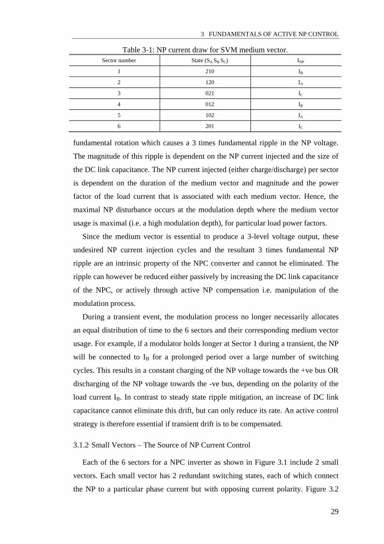
3 FUNDAMENTALS OF ACTIVE NP CONTROL
29
fundamental rotation which causes a 3 times fundamental ripple in the NP voltage.
The magnitude of this ripple is dependent on the NP current injected and the size of
the DC link capacitance. The NP current injected (either charge/discharge) per sector
is dependent on the duration of the medium vector and magnitude and the power
factor of the load current that is associated with each medium vector. Hence, the
maximal NP disturbance occurs at the modulation depth where the medium vector
usage is maximal (i.e. a high modulation depth), for particular load power factors.
Since the medium vector is essential to produce a 3-level voltage output, these
undesired NP current injection cycles and the resultant 3 times fundamental NP
ripple are an intrinsic property of the NPC converter and cannot be eliminated. The
ripple can however be reduced either passively by increasing the DC link capacitance
of the NPC, or actively through active NP compensation i.e. manipulation of the
modulation process.
During a transient event, the modulation process no longer necessarily allocates
an equal distribution of time to the 6 sectors and their corresponding medium vector
usage. For example, if a modulator holds longer at Sector 1 during a transient, the NP
will be connected to IB for a prolonged period over a large number of switching
cycles. This results in a constant charging of the NP voltage towards the +ve bus OR
discharging of the NP voltage towards the -ve bus, depending on the polarity of the
load current IB. In contrast to steady state ripple mitigation, an increase of DC link
capacitance cannot eliminate this drift, but can only reduce its rate. An active control
strategy is therefore essential if transient drift is to be compensated.
3.1.2 Small Vectors – The Source of NP Current Control
Each of the 6 sectors for a NPC inverter as shown in Figure 3.1 include 2 small
vectors. Each small vector has 2 redundant switching states, each of which connect
the NP to a particular phase current but with opposing current polarity. Figure 3.2
Table 3-1: NP current draw for SVM medium vector.
Sector number State (SA SB SC) INP
1 210 IB
2 120 IA
3 021 IC
4 012 IB
5 102 IA
6 201 IC

3.1 NP CURRENTS PRODUCED BY SPACE VECTORS
30
shows this relationship for Sector 1, the 2 small vectors that it includes and their
associated redundant states. It can be seen that small vector 1 connects the NP to
phase current IA while small vector 2 connects the NP to phase current IC.
Hence a NP voltage control strategy can control the total injected NP current by
measuring the polarities of the phase currents, and then selecting between the two
alternative redundant states (per small vector) to compensate for the middle vector
NP injection and achieve an overall zero current injection. Thus these small vectors
are the mechanism for ‘active’ NP control capability.
However, the number of controllable small vectors can vary depending on the
modulation strategy used. Although in principle a modulation strategy can choose
any available vector within the sector to reproduce a desired volt second reference,
current state of the art modulation strategies target to use only 3 vectors to reduce the
number of switching events. This typically results in only 1 or 2 controllable small
vectors depending on where the reference vector is within the space vector
framework.
Figure 3.2 illustrates this issue by breaking each major space vector sector into 4
subsectors. Subsectors 2 and 4 have 2 small vectors, and hence 4 redundant states to
control, whereas subsectors 1 and 3 only have 1 small vector, and hence only 2
redundant states to control. This difference in the number of available redundant
states can result in a variable switching frequency at medium to high modulation
depths. For example, a state of the modulation strategy that aims to maximise the use
211 (-IA)
100 ( IA)
221 ( IC)
110 (-IC)
220 (0)
210 (IB)
200 (0)
222(0)
111(0)
000(0)
VSmall 1
VSmall 2
VZero
VMedium
VLarge 1
VLarge 2
2
1
3
4
Sector 1
Figure 3.2: Space Vector diagram for Sector 1.

3 FUNDAMENTALS OF ACTIVE NP CONTROL
31
of small vectors, can switch through 4 states in subsector 1, 5 states in subsector 2,
and 4 states again in subsector 3. This variation from 4 to 5 to 4 states as the
modulation reference traverses across subsectors 1 to 3 causes a variable switching
frequency.
NOTE: this process does not occur if a strategy forces a constant switching
frequency by either forfeiting control of both small vectors (i.e. controlling only 1
small vector) to switch through 4 states only in every subsector, OR by introducing
an additional extra state to force 5 switching states for every subsector.
3.2 NP Natural Control Limits
The NP voltage is controllable when the small vectors’ NP current contributions
are greater than the medium vector’s NP current contributions throughout the cycle
of the NPC converter’s operation. The contributions of both vector types vary
depending on:
a) The modulation depth, which affects the amount of space vector selection and
b) The load power factor angle, which affects the instantaneous magnitude of
the phase currents at the time they are selected to inject current into the NP.
To illustrate, a NP injection calculation will be conducted over one switching
cycle ST within Sector 1. The net NP current per switching cycle is the sum of the
product of each vector’s duty cycle state
tyoed by the current that the vector connects to
the NP, given by:
….
BmediumCsmallCsmallAsmallAsmall
elelBmediumCsmall
CsmallAsmallAsmallzeroNP
IdIdIdIdId
ddIdId
IdIdIddI
210110
2
221
2
211
1
100
1
220
2arg
200
1arg
210110
2
221
2
211
1
100
1
222/111/000
00
0
(3.1)
As expected, only the small and medium vectors affect the NP current. Notice that
each small vector has 2 terms, one for each redundant state. The total time spent in
these states should be equal to the required duration of the small vector regardless of
how this duration is split across the redundant states, viz:
xxx
smallsmallsmall
xxx
smallsmallsmall
ddd
ddd
2
110
2
221
2
1
100
1
211
1
(3.2)
where ‘xxx’ superscript defines the all the redundant states belonging to a particular
vector. Each small vector’s duty cycle split ratio is now defined through the

3.2 NP NATURAL CONTROL LIMITS
32
parameter xk where 10 xk and where 2,1x identifies the corresponding small
vector that xk is associated with. Hence the redundant states’ durations as a fraction
of the small vector’s total duty cycle is:
xxx
smallsmall
xxx
smallsmall
xxx
smallsmall
xxx
smallsmall
dkd
dkd
dkd
dkd
22
110
2
22
221
2
11
100
1
11
211
1
1
1
(3.3)
These equations when substituted into Eqn. (3.1), result in an injected NP current
expression that is more common within the literature [20][8], i.e.:
…. BmediumC
xxx
smallA
xxx
smallNP IdIdkIdkI 210
2211 1221 (3.4)
In this form, it is clear that a NP controller can only manipulate the parameters 1k
and 2k to compensate for the medium vector’s NP current contribution, and in fact
this is the primary mechanism that is employed by every reported NP control
strategy. Note also that the effect of the small vectors on the NP voltage is negligible
when 1k and 2k are set to 0.5, since this represents equal switching of the redundant
vectors and thus equal NP current contribution in both directions.
Equation (3.4) also shows that the NP current is highly dependent on the duty
cycles of the vectors and the magnitude of the currents that are associated with these
vectors. The following 2 subsections will elaborate further on these issues.
3.2.1 Effect of Modulation Depth
The modulation depth dictates the magnitude of the space vector duty cycles. It is
desirable to have the small vectors’ duty cycles to be greater than the medium
vector’s duty cycle regardless of the modulation depth to be able to maintain full
control of the NP. However, in reality, as the modulation depth increases from 0.0 to
0.5 to 1.0, the duty cycles vary as shown in Figure 3.3 for a 30° voltage phasor. As
shown in [20], this figure can be obtained by vector decomposition of the target
reference into its nearest three space vectors as the reference rotates. It shows that
maximal control is achieved in the middle of the modulation range (0.5) and is lost as
the modulation depth increases up to 1.0.

3 FUNDAMENTALS OF ACTIVE NP CONTROL
33
3.2.2 Effect of Load Power Factor Angle
The effect of the load power factor angle on NP control has been thoroughly
explored in the d-q frame in reference [79], and is best demonstrated by observing
the phase currents at both low and high load power factor angles.
Figure 3.4 shows the space vectors of sector 1 as illustrative. The figure shows
two extreme conditions for the load power factor angle. At 0 degree load power
factor angle, the currents that the small vectors command i.e. IA and IC are in phase
with their voltage space vectors and hence their dot product is maximised. However,
the current BI used by the NP disturbing medium vector has its vector orthogonal to
MediumV , and thus there is no source for disturbance at this load power factor angle.
However, the opposite effect occurs at a 90 degree load power factor angle where the
small space vectors are orthogonal to the currents that they control (IA and IC) and the
NP disturbing medium vector is in phase with its current vector. This analysis
dSmall 1/2
dMedium
Duty
Modulation Depth1
Max
Figure 3.3: Approximate Medium and Small vector duty cycle variation versus
modulation depth [20].
Load angle = 0o
211[-IA]
100[IA]
221[IC]
110[-IC]
210[IB]
VSmall 1
VSmall 2
VMedium
IA
IB
IC
Load angle = 90o
211[-IA]
100[IA]
221[IC]
110[-IC]
210[IB]
VSmall 1
VSmall 2
VMedium
IA
IB
IC
Figure 3.4: Maximisation of NP disturbance and loss of NP control as load power
factor angle increases.

3.3 EXTENDING NP CONTROLLABILITY BEYOND THE NATURAL LIMITS
34
suggests that a 90 degree load power factor angle is a worst case condition for NP
control, which is in fact the case [20].
A numerical assessment is conducted to demonstrate this effect in the time
domain. Figure 3.5 shows the voltage references and phase currents for two load
power factor angle conditions: 5 degree and 85 degree. The figure shows the voltage
and current values for Sector 1 where the reference vector lies between 0 and 60
degrees. The best view is when the medium vector is at its maximal duty cycle i.e. 30
degrees. This view is provided in Figure 3.6. The simulations were conducted with a
modulation depth of 0.7 which corresponds to triangle #2 in the SV plot (Figure 3.2).
The medium vector is associated with the load current IB whereas the small vectors
are associated with the load currents of the other phases, IA and IC.. For both load
conditions, the vectors used are identical however, the magnitude of their associated
currents differ. When the load power factor angle is close to 0 degrees, the load
currents associated with the small vectors (IA and IC) are near their peaks, while the
disturbing load current (IB) is at the zero crossing. Thus, regardless of the usage of
the medium vector, IB is small and will not affect the NP voltage significantly.
However, this is no longer true when the load power factor angle is near 90 degrees.
The disturbing load current (IB) is maximal whereas the controllable currents are
around half of their peak value. As a result, the small vectors’ NP current
contributions are diminished when compared to the disturbance caused by the
medium vector when operating at this high load power factor angle.
3.2.3 Cumulative Effect
These limitations have been calculated in the d-q frame and their result is shown
in Figure 3.7 [20]. The NP voltage is fully controllable below a 0.55 modulation
depth. Above this level, the controllability region is limited by a linear relationship
with respect to the modulation depth and the system load power factor angle.
3.3 Extending NP Controllability Beyond the Natural Limits
Beyond the limits described in the Section 3.2, the only way to make the small
vectors’ NP current contributions greater than the medium vector’s NP current
contribution is for the modulator to reduce the medium vector’s NP current
contribution. This can only be achieved by reducing its duty cycle, which is a
fundamental change in the space vector selection principles, as will now be explored.

3 FUNDAMENTALS OF ACTIVE NP CONTROL
35
0 0.5 1 1.5 2 2.5 3 3.5 4
x 10-3
-1
-0.5
0
0.5
1
Time (s)
VSI Modulation References
Ref A Ref B Ref C
0 0.5 1 1.5 2 2.5 3 3.5 4
x 10-3
-8
-6
-4
-2
0
2
4
6
8
Time (s)
Load currents at 5 degree load angle
IA IB IC
0 0.5 1 1.5 2 2.5 3 3.5 4
x 10-3
-8
-6
-4
-2
0
2
4
6
8
Time (s)
Load currents at 85 degree load angle
IA IB IC
Figure 3.5: Time domain signals across Sector 1. Top: VSI Modulation references.
Middle: 3-phase load current with a load p.f. angle of 5 degrees. Bottom: 3-phase
load current with a load p.f. angle of 85 degrees.

3.3 EXTENDING NP CONTROLLABILITY BEYOND THE NATURAL LIMITS
36
1.9 1.95 2 2.05 2.1
x 10-3
-1
-0.5
0
0.5
1
Time (s)
VSI Modulation References
Ref A Ref B Ref C
1.9 1.95 2 2.05 2.1
x 10-3
-8
-6
-4
-2
0
2
4
6
8
Time (s)
Load currents at 5 degree load angle
IA IB IC
1.9 1.95 2 2.05 2.1
x 10-3
-8
-6
-4
-2
0
2
4
6
8
Time (s)
Load currents at 85 degree load angle
IA IB IC
Figure 3.6: Time domain signals across a switching cycle when reference angle is 30
degrees. Top: VSI Modulation references. Middle: 3-phase load current with a load
p.f. angle of 5 degrees. Bottom: 3-phase load current with a load p.f. angle of 85
degrees.
110 210 211 211 210 110

3 FUNDAMENTALS OF ACTIVE NP CONTROL
37
Recall that the first aim of any modulator is to recreate the target output voltage
by switching the available space vectors so that the average volt-second contribution
from these vectors over each switching cycle matches the target reference. Hence if
the medium vector usage is to be reduced, a NPC modulator has to use the large
vectors to replicate the effect of the medium vector. This means 2 large vectors are
required to recreate the volt-seconds of the medium vector.
There are significant implications to this change in vector selection. Before these
implications are explored, it should be noted that in principle there are 3 possible
modes of operation for varying the usage of the medium vector, as follows:
i. Least control: The duty cycle of the medium vector is not modified.
ii. Full control: This is the extreme where no medium vector is used. The
NPC modulator reverts to 2-level VSI type operation with the 2-level zero
vector replaced by a 3-level small vector.
iii. Medium control: This is the middle region between these two extremes
where the shift between uncontrollability to controllability occurs by some
degree of large vector substitution for the medium vectors.
The implications of this change in vector selection for each mode of operation are:
NP ripple and drift : The reduction of the medium vector usage results in a
reduced level of NP current injection. This reduces the magnitude of the
steady-state NP voltage ripple and also slows the rate of change when NP
Figure 3.7: Region of NP controllability (black). Figure obtained from [20].
This image has been removed from the digital edition of this thesis in order to comply with copyright statutes.
Please refer to Fig. 9 from ref. [20]

3.3 EXTENDING NP CONTROLLABILITY BEYOND THE NATURAL LIMITS
38
drift occurs. If the medium vector is totally eliminated, the NP voltage
ripple will be negligible and no drift will occur.
Modulation harmonic distortion: This distortion is caused by 2 factors.
The first factor is because the small vectors’ redundant state duration splits
are not equal i.e. 5.0, 21 kk when operating up to maximal NP
compensation. In fact the values of 1k and 2k will be at the extreme values
of 0 and 1 as they reach the limit of their NP control influence. Although
not directly analogous, this operation is similar to forcing 2-level SPWM
to operate in the discontinuous PWM mode, which is well known to
increase the WHTD of a 2-level modulated VSI. It is also against the
guidelines of the harmonically superior Centered Space Vector PWM
(CSVPWM) which identifies that the redundant duty cycle split should be
equal for the best possible WTHD result [59][60].
The second distortion factor is because the modulator no longer utilises
the Nearest Three Vectors (NTV) as the medium vector usage reduces.
This is because the reduction of the medium vector’s duty cycle has to be
compensated by large vector usage in order to produce the same volt-
second average as required by the modulator. Hence, the modulator will
now have to use 3-5 vectors which is against optimal harmonic production
practices [61]. Also, the fact that it has to rely on the large vectors causes
the harmonic performance to tend towards a 2-level VSI in any case.
Switching frequency: Since the modulator no longer operates according to
the NTV principle, the number of switching transitions has to increase.
Even without a reduction of the medium vector, the usage of 2 small
vectors alone will cause variable frequency operation. Then, as the number
and type of selected vectors change, this further increases the variability of
the switching frequency, with an outcome that is highly dependent on the
modulation strategy used. When the medium vector is totally eliminated,
the modulation reverts back to a 2-level mode that uses a small vector
rather than the zero vector, and this can cause a different switching
frequency yet again.
Controllability: Controllability is only guaranteed when the small vector’s
NP current injection can be greater than the medium vector’s contribution.

3 FUNDAMENTALS OF ACTIVE NP CONTROL
39
The process of loss of NP control for the ‘Least Control’ mode has been
explained in Section 3.2. Controllability of the extreme ‘full control’ mode
of operation is of course guaranteed because the medium vector is fully
eliminated. In the middle mode of operation, the NP controllability of a
particular modulation strategy is dependent on the method of duty cycle
calculation, which may or may not keep the small vector’s NP current
contribution greater than the medium vector’s contribution Hence, the
conditions of controllability loss in this region is non-deterministic and
highly dependent on the NP control strategy.
NP Control Speed: A modulation strategy may reduce the medium
vector’s duty cycle by a small amount to ensure controllability or in other
words, operate just at the edge of controllability. This may be due to the
strategy’s requirement of maintaining good harmonic performance.
On the other hand, a modulation strategy may arbitrarily reduce the
medium vector usage by a large amount at the cost of operating closer to a
2-level VSI. The result is a variation in the residue of the small vectors’
NP compensation minus the medium vector’s contribution. The magnitude
of this residue is important in determining the speed or ability by which a
modulation strategy can reduce an unexpected NP drift caused by a
transient event.
3.4 Vector Selection Analysis of Existing NP Control Strategies
All reported NP control strategies can be analysed using the general principles of
NP control identified above, and thus placed between the limits of ‘least control’ and
‘full control’. In fact by analysing the vector selection and duty cycle calculation of
these strategies, it can be shown that they only really differ in terms of:
a) Number of small vectors controlled/utilised. As will shortly be illustrated,
strategies may use only one small vector instead of 2 small vectors simply
because of the way they are implemented.
b) Different levels of reduction in the usage of the medium vector.
c) Duty cycle calculation of the vectors.
d) Methodology of calculating the duty cycle split of the redundant vectors, 1k
and 2k . A large number of publications can be attributed to this issue.

3.4 VECTOR SELECTION ANALYSIS OF EXISTING NP CONTROL STRATEGIES
40
Furthermore, for every duty cycle calculation method that has been proposed,
there are sets of papers published that demonstrate the application of either a
simple hysteresis controller, linear controllers or optimal calculation-based
controllers to this method.
The vector selection of a NP control strategy can be identified by either observing
the simulation output of the converter and/or by understanding its mathematical
implementation as presented within the strategy’s original publication. This is simple
to achieve for SVM because SVM strategies will always explicitly specify the
vectors to be chosen, their duty cycle calculation method, and also the sequence of
the states of their vectors. Unfortunately, the same is not true for carrier-based
strategies, since their published results generally do not give a good indication of
their vector selection. As a result, simulations are required to identify these vector
selection patterns. Within these simulations, controller gains (if they exist as part of
the NP control strategy) can be set to either achieve maximal NP control or as
specified by the publication’s recommendations.
To illustrate these concepts, the vector selections of the various modulation and
NP control strategies identified in the literature review in Chapter 2 will now be
explored. This exploration will firstly consider the ‘least control’ strategies that
incorporate full medium vector usage, and will then show how additional NP control
capability is gained by progressing towards a ‘full control’ strategy with essentially
no medium vector usage.
The most widely used NPC modulation strategy is conventional NTV SVM and
its carrier-based approximate equivalent Phase Disposition PWM (PD or SPWM).
An exact carrier-based equivalent can be obtained by implementing CSVPWM [61].
These strategies offer a ‘least control’ NP management capability. (Note that while
simple SPWM also falls into this ‘least control’ category, only CSVPWM produces a
modulation result that is directly equivalent to NTV SVM.)[60]
To illustrate the vectors selected by NTV SVM, Figure 3.8 shows the SV plot
when a reference vector is placed in subsector 2, where the NP disturbing medium
vector, mediumV is heavily used. The strategy chooses the nearest three vectors (NTV)
around this reference vector, as shown in Table 3-2. Note how the sequence of states
is arranged in such a manner as to minimise switching losses, shown only for the first
half of the switching cycle since it is mirrored in the second half to minimise

3 FUNDAMENTALS OF ACTIVE NP CONTROL
41
switching transitions. Note also the abbreviations used for the vector types of:. sm1
→ small 1, med → medium and lrg → large.
From this vector selection, it is clear that NTV SVM, and its matching carrier
strategies SPWM and CSVPWM, use the two redundant states (211 and 100) of
small vector 1, which injects AI into the NP, but only one redundant state (110) of
small vector 2, which injects CI . Hence these strategies only have one NP
controllable small vector (small vector 1) which can have its redundant state
alternatives varied by changing 1k . Thus NP control using these modulation strategies
is a ‘least control’ strategy because:
a) It becomes uncontrollable as the medium vector’s duty cycle becomes
greater than small vector 1’s duty cycle and the medium vector NP
injection cannot be fully compensated.
b) the other small vector (small vector 2) is not controllable and also becomes
Table 3-2: NTV SVM – (1 SV / 2 RS) / SPWM / CSVPWM
State 1 2 3 4 Vector Sm1 Med Sm2 Sm1 Duty 11 smdk
medd 2smd
1
11
smd
k
Phase output
211 210 110 100
NP current
AI BI
CI AI
211
100
221
110
220
210
200
222
111
000
VSmall 1
VSmall 2
VZero
VMedium
VLarge 1
VLarge 2
VREF
2
1
3
4
Figure 3.8: Space Vector diagram for Sector 1. The reference vector, VREF is within
subsector 2.

3.4 VECTOR SELECTION ANALYSIS OF EXISTING NP CONTROL STRATEGIES
42
an additional source of disturbance at high load power factor angles [8].
However, one benefit of this strategy is that it only uses 4 switching states.
A clever remedy to this uncontrolled second small vector was published as
Yamanaka’s NTV SVM [8] strategy. The strategy converts the uncontrollable second
small vector into a controllable small vector by adding the redundant state of the
second vector whenever possible, as shown in Table 3-3.
Here, the state 221 from the second small vector was added and hence the second
small vector and its current, CI , are now controllable through the parameter 2k . As a
result, this strategy has an improved performance compared to the previously
mentioned ‘least control’ strategy, since it only becomes uncontrollable as the
medium vector’s duty cycle becomes greater than both small vectors’ duty cycles.
This increases its NP controllable region to the middle of the modulation range.
However, it does create a variable switching frequency as discussed in Section 3.3,
since subsector 2 has 5 switching states whereas subsectors 1 and 3 have only 4
switching states, as shown in Figure 3.8.
To move beyond the natural limitations of these two NP control alternatives, the
medium vector’s duty cycle now has to be reduced. As this happens, the large vector
duty cycles must increase in order to satisfy the modulator volt-second production
requirement. The strategy proposed by Ustuntepe [30] is a progression of
Yamanaka’s approach that achieves this target, by calculating the controllability
condition i.e. if the small vector’s NP current injection is smaller than the medium
vector’s NP current injection, the medium vector’s duty cycle is reallocated to the
large vectors. The vector selection process is shown in Table 3-4.
The difference between Table 3-3 and Table 3-4 is the additional 2 states for the
large vectors (200 and 220). If the load conditions dictates a controllable situation,
this strategy does not require the large vectors ( 0, 21 lrglrg dd ) and it reverts back to
Table 3-3: NTV SVM – (2 SV / 4 RS)
State 1 2 3 4 5 Vector Sm2 Sm1 Med Sm2 Sm1 Duty 22 smdk
11 smdk medd
2
21
smd
k
1
11
smd
k
Phase output
221 211 210 110 100
NP current
CI AI BI
CI AI

3 FUNDAMENTALS OF ACTIVE NP CONTROL
43
Yamanaka’s vector selection i.e. Table 3-3. But Table 3-4 also shows that this
modulation strategy is no longer NTV and hence the inverter harmonic output will
degrade, particularly during uncontrollable NP conditions. It also shows that the
strategy has a high number of switching cycles and will most likely have a highly
variable switching frequency, particularly as load conditions vary.
A significant feature of this strategy is that its calculation method ONLY reduces
the medium vector’s duty cycle by the minimum amount required to maintain
controllability. In other words, it tries to maximise its usage of the medium vector
and minimise its dependence on the large vectors. Hence, it tries its best to produce a
good harmonic output and yet be fully controllable at the same time.
Another well known approach that reduces the medium vector’s duty is the
Nearest Three Virtual Vectors (NTVV) strategy [67]. Unlike Ustuntepe’s strategy,
this approach is based on virtual vectors that produce an on-average zero NP current,
As a result, its medium vector duty cycle reduction is pre-determined. Its SV diagram
is shown in Figure 3.9, where two virtual vectors can be seen that are created as
0.5 (211+100)
0.5 (221+110)
220
0.3333(100+210+221)
200
222
111
000
VVirtual Small 1
VVirtual Small 2
VZero
VVirtual Medium
VLarge 1
VLarge 2
VREF
2
1
3
4
5
Figure 3.9: SVM for Nearest Three Virtual Vector (NTVV) for Sector 1.
Table 3-4: NTV SVM – (2 SV / 4 RS) – Reduced Medium Vector
State 1 2 3 4 5 6 7 Vector Sm1 Sm2 Lrg2 Med Lrg1 Sm1 Sm2
Duty 11 smdk 22 smdk
2lrgd medd 1lrgd
1
11
smd
k
2
21
smd
k
Phase output
211 221 220 210 200 100 110
NP current
AI CI 0 BI 0
AI CI

3.4 VECTOR SELECTION ANALYSIS OF EXISTING NP CONTROL STRATEGIES
44
combinations of other real space vectors. For example, the virtual medium vector is a
combination of 33% of the following switching states 100, 210 and 221 which
corresponds to NP currents AI , BI and CI . The equal sum of the three phase current
injection into the NP node sums to a zero NP overall current injection. Similarly, the
virtual small vectors are equal contributions of their redundant states, thus equal and
opposite NP currents are injected into the NP node, again resulting in a zero NP
current overall.The vectors selected by this strategy are shown Table 3-5.
Unfortunately, the introduction of the virtual vectors cause the SV map to change.
The virtual medium vector is shorter and causes the reference vector to be placed in
subsector 1 which is not the worst case operating mode for NTVV. (Subsector 2 is
the worst operating mode because it switches through both the small vectors (100
and 221), the medium (210) and large vectors (220 and 200) simultaneously.) Table
3-5 shows that the vector selection in subsector 1 no longer abides by the NTV rule,
hence its harmonic performance must suffer. Furthermore, unlike previous strategies,
this strategy’s NP control methodology is not apparent by if one observes its space
vector selection and duty calculation. It varies the sinusoidal reference of one of the
phase legs which in turn varies the duty cycles of small vector 2, small vector 1 and
medium vector simultaneously [69].
The notable feature of this strategy is that it maintains constant switching
frequency with only 5 states per switching cycle. However, the strategy’s
predetermined medium vector duty cycle reduction is insensitive to load conditions
and does not focus on maximising harmonic performance. Hence it would be
anticipated that it will have a degraded harmonic performance. One variant of this
strategy is known as Optimised NTVV (ONTVV), which tries to achieve better
harmonic performance by varying the amount that the medium vector duty cycle is
reduced. But this strategy requires knowledge of the load current power factor angle.
Another strategy that reduces the medium vector duty cycle is Dipolar PWM [39].
Table 3-5: Medium Vector Reduction
State 1 2 3 4 5 Vector Sm2 Sm1 Med Lrg1 Sm1 Duty 221d
211d 210d 200d 100d
Phase output
221 211 210 200 100
NP current
CI AI BI 0
AI

3 FUNDAMENTALS OF ACTIVE NP CONTROL
45
Table 3-6 presents the space vectors selected by this modulation strategy. Immediate
observation suggests that this strategy is very similar to that of Ustuntepe’s, but only
one redundant state from each small vector is used. In principle, Dipolar PWM
assumes that one of the small vectors is more significant than the other and that a
common-mode addition can control both the redundant states of both small vectors.
But in practice, the actual NP control mechanism exercised by Dipolar PWM, either
by changing the distance between the two reference waveforms or by adding a zero-
sequence offset, serves to only change the distribution of duty cycle between 2smalld ,
2arg eld , mediumd , 1arg eld and
1smalld .
In fact this analysis highlights that Dipolar PWM does not have a clear NP control
methodology, and also highlights a major limitation of carrier-based design whereby
mistakes in the analysis of an NP control strategy’s ability to achieve a target
outcome can easily occur [14]. This is particularly important for hybrid NP control
strategies, where the entire strategy can be compromised if one particular sub-
strategy is ineffective. Note also that all medium vector duty cycle reduction
techniques achieve additional NP controllability at the expense of higher switching
frequency, poor harmonic production or both.
Finally, Table 3-7 shows the vector selection for the extreme fully controllable NP
strategy i.e. medium vector elimination. Figure 3.10 shows its corresponding SV
map. Essentially, this strategy tries to implement NTV without using the medium
vector. Its notable features are:
a) It is heavily dependent on the use of large vectors, leading to a 2-level
converter type harmonic output performance.
b) Phase leg B (in sector 1) experiences a full DC bus switching transition
between states 200 and 220. This loses a major benefit of a multilevel
converter, which is the dynamic voltage blocking capability and half DC
bus voltage protection of the semiconductor switches of the converter.
Table 3-6: Dipolar PWM
State 1 2 3 4 5 6 7 Vector Zero Sm2 Lrg2 Med Lrg1 Sm1 Zero
Duty
zerod
x)1(
2smd 2lrgd
medd 1lrgd 1smd
zeroxd
Phase output
222 221 220 210 200 100 000
NP current
0 CI 0 BI 0
AI 0

3.5 STRATEGIES TO BE COMPARED IN CHAPTER 4
46
c) The strategy has a constant switching frequency with 5 switching
transitions per switching cycle as opposed to 3 transitions for the ‘least
control’ strategy.
Hence this strategy also has some significant disadvantages.
3.5 Strategies to be Compared in Chapter 4
Using the qualitative analysis principles presented in this chapter, the following
NP control strategies can be identified as sub-optimal, and will now be eliminated
from further comparison. They are:
a) Ustuntepe (SVM – 2 Small Vector / 4 Redundant States with Medium
Vector Reduction). Although it should be the best compromise strategy for
the NPC converter, it will not be considered further because the high
number of switching transitions involved with this approach is
unacceptable for high power applications.
211
100
221
110
220
200
222
111
000
VSmall 1
VSmall 2
VZeroVLarge 1
VLarge 2
VREF1
3
4
Figure 3.10: SV diagram for Medium vector elimination for Sector 1.
Table 3-7: Medium Vector Elimination
State 1 2 3 4 Vector Sm1 Lrg1 Lrg2 Sm1
Duty 11 smdk 1lrgd 2lrgd
1
11
smd
k
Phase output
211 200 220 100
NP current
AI 0 0 AI

3 FUNDAMENTALS OF ACTIVE NP CONTROL
47
b) Dipolar PWM - This strategy will not be considered for future comparison
because of its uncertain and unstrategic nature in controlling the NP
current and voltage. It is also harmonically inferior to other strategies.
c) Hybrid Strategies – these strategies change their operation between
alternative NP control approaches depending on modulation and load
conditions. Hence their performance can be identified by considering the
originating strategies that are combined in the Hybrid formulation.
d) Medium Vector Elimination – The loss of the dynamic voltage blocking
capability is considered to be a major disadvantage for these strategies,
especially in high power applications. Secondly, the performance of this
extreme strategy is similar to an ideal 2-level converter which is already
well known in the literature.
Table 3-8 identifies the strategies that will therefore be quantitatively investigated
in the next chapter. The comparison will attempt to explore the dynamic NP control
performance, maximum steady-state NP ripple and steady-state harmonic output
distortion.
3.6 Summary
This chapter has qualitatively investigated the fundamentals of NP control. It has
shown how the intrinsic limits of NP control are due to the small vectors being
unable to compensate for the medium vector NP current injection. These limits occur
at higher modulation depths and low load power factor angles. In order to maintain
Table 3-8: Strategies to be compared.
Strategy Group Duty Calculation 1k & 2k calculation Label in figures
NTV SVM – 1SV/2RS /
CSVPWM / SPWM
SPWM
Proportional SPWM+P
Song’s analytical zero-
offset calculation SPWM+Song
SVM / CSVPWM Proportional CSVPWM+P
NTV SVM – 2SV/4RS Yamanaka’s Yamanaka’s Yamanaka SVM
SVM – Medium Vector
Reduction
NTVV Zaragoza’s optimal
calculation NTVV
ONTVV Second order controller (
PI was used) ONTVV

3.6 SUMMARY
48
controllability beyond these limits, the medium vector’s usage then has to be reduced
and replaced with large vectors. As a result, the pursuit of a greater range NP control
for the NPC converter pushes the converter from ideal 3-level modulation towards
performing closer to a 2-level converter. There is a middle ground where the medium
vector is reduced just enough to maintain controllability, however the analysis of
existing strategies (SVM – 2SV/4RS with Medium Vector Reduction) has shown that
this advantage is achieved at the cost of a high number of additional switching
transitions and as a result is not feasible for high power applications.
Finally, established NP control strategies were analysed by observing their vector
selection and arranged according to their expected NP control performance. A
number of strategies were then eliminated from further consideration because of their
identified disadvantages. This qualitative analysis however cannot quantify the
tradeoff that would be observed if one was to consider the Medium Vector Reduction
strategy compared to the conventional NTV SVM be it 1 or 2 Small Space Vector
control. As a result, a quantitative simulation comparison is now required, and will
be presented in the next chapter.
4 QUANTITATIVE COMPARISON OF ACTIVE NP STRATEGIES
49
4 QUANTITATIVE COMPARISON OF ACTIVE NP STRATEGIES
Chapter 3 has shown that the benefit of improved dynamic NP control performance
and hence lower NP ripple comes with the drawbacks of increased switching
frequency and a breakaway from the harmonically-optimal NTV vector selection
principle. This makes a qualitative assessment of these control strategies difficult
because the harmonic distortion produced by a strategy depends simultaneously on
both NP ripple and space vector (and redundant state) selection. In other words, a
strategy that strives to minimise its NP ripple may choose space vectors that may
produce high harmonic output distortion. Besides the issue of harmonic quality, the
qualitative assessment also does not indicate the effectiveness or magnitude of the
increase in dynamic NP control performance for a given change in space vector
selection. As a result, a quantitative simulation-based assessment is required to assess
both the effectiveness of changes in space vector selection and the tradeoff in terms
of harmonic distortions.
This chapter will devise and execute such a quantitative assessment of the
strategies presented in Table 3-8 in order to explore their harmonic performance, NP
ripple magnitude and dynamic NP control performance.
4.1 Methodology
Dynamic NP control performance of a NPC converter is affected by its DC link
capacitance size, load magnitude and angle, modulation depth, and finally the
modulation strategy’s space vector selection. Besides affecting the dynamic NP
control performance of a converter, a strategy’s space vector selection can also affect
the switching frequency of the converter, the NP ripple observed, and the harmonic
distortion produced at its line-to-line output voltage.
This quantitative assessment will simulate a NPC converter with the parameters
listed in Table 4-1. It will then manipulate the factors that affect dynamic NP control
performance by:
Varying the modulation depth continuously from 0.00 to 1.15.
Setting the load power factor angle to the 3 points: 1º, 45 º and 85 º.
Repeating the assessment at 2 DC link capacitance levels: 4200 and 840
µF. The 2 different capacitance levels are intended to highlight the
dependency of harmonic output distortion on both space vector selection
and NP ripple.

4.1 METHODOLOGY
50
The simulation is used to observe the following modes of converter operation:
Steady-state mode will measure the maximum NP ripple produced by a
strategy, and the resulting harmonic distortion assessed using a NWTHD
calculation method (defined in the next section).
Transient mode will measure the time it takes a strategy to reduce a NP
unbalance from an initial perturbation level to a minimum acceptable
deviation level (e.g. 20% to 5% and 25% to 6% of half the DC bus voltage,
DCV for 4200 and 840 µF DC link capacitance, respectively).
Each strategy produces a different switching frequency, since the switching
frequency is dependent firstly on the strategy’s space vector selection, and secondly,
on whether the converter is exercising maximum NP control, which may cause pulse
dropping or Discontinuous PWM. For example, the most conventional NTV-based
strategy will always use 3 vectors and switch through 4 switching states, with 2 of
these states belonging to a particular small space vector. However, when maximal
NP control is required, especially in regions beyond the natural NP control limit as
mentioned in Section 3.2, one of these 2 redundant states will be fully used and
hence the NTV-strategy will use only 3 switching states. This drop in switching
frequency must be accounted for. In this thesis the assessment process varies the
switching frequency for each strategy to guarantee that an equal number of switching
transitions also occur in the regions where pulse dropping doesn’t occur (i.e. between
0% to 70% of the modulation depth). These switching frequencies are listed in Table
Table 4-1: NPC converter parameters.
Parameter Values
Nominal DC link 360 V
Capacitor size 4200 µF (Case A)
840 µF (Case B)
Load magnitude 17.76
Load Resistance Dependent on load power factor angle of simulation
Load Inductance
Fundamental Frequency (fo) 50
Table 4-2: Switching frequency of the various strategies.
Switching frequency of NPC (fs) Value (Hz)
CSVPWM and SPWM variants 4000
NTVV variants 3000
Yamanaka SVM 2000 & 3000

4 QUANTITATIVE COMPARISON OF ACTIVE NP STRATEGIES
51
4-2.
Inherently, this comparison is suited to strategies that produce a fixed number of
switching transitions per switching cycle. However, this comparison includes the
variable switching frequency strategy: Yamanaka SVM. This strategy produces a
high number of switching transitions at low modulation depths compared to other
strategies. As a result, two simulation traces are shown for this strategy for the low
and high modulation depth ranges.
In order to compare these strategies to solutions that are usually used in industry,
two reference strategies are included for comparison with the state of the art. They
are used for NWTHD harmonic distortion plots but not for the NP voltage deviation
as these reference cases do not have any NP deviation as such. They are the ideal 2-
level and 3-level CSVPWM strategies. The latter case has its NP voltage fixed at 0V
to ensure that the only distortion mechanism is the vector selection process. These
reference cases are known to produce minimal harmonic distortion for 2-level and 3-
level converters in ideal cases. These are labelled within the figures as ‘Ideal 2L
CSVPWM’ and ‘Ideal 3L CSVPWM’.
4.2 Performance Metrics
4.2.1 Steady-state NP Ripple
The steady-state NP ripple (defined in this thesis as peak value) is measured in
order to determine the effect NP ripple has on the converter’s output harmonics. It is
also measured to highlight strategies that produce high NP voltage ripple, since this
may be unacceptable for applications with limited voltage headroom where the
likelihood of a switch overvoltage and thus converter damage is increased. Voltages
are measured in absolute terms, but can be readily converted to per-unit quantities by
scaling them by half of the DC link voltage, (i.e. 180V for this simulation
comparison).
4.2.2 Measure of Output Distortion - NWTHD
Harmonic distortion is measured as Normalised Weighted Total Harmonic
Distortion (NWTHD). The calculation depends on the spectrum of the switched
output line-to-line voltage of the converter, according to [80]:

4.3 SIMULATION SYSTEM
52
1
2
2
V
M
n
VNWTHD
n
n
(4.1)
where 1V is the fundamental harmonic magnitude, M is the modulation depth, and nV
is the magnitude of the nth
harmonic of the fundamental.
4.2.3 NP Dynamic Control Performance
The NP control performance of the various NP control strategies is compared
according to the time it takes to reduce the NP unbalance from an initial level of NP
voltage deviation to a target minimum acceptable level. For the large DC link
capacitance values, these levels are 20% and 5% of half the DC bus voltage, DCV ,
while for the small DC link capacitance value these levels are 25% and 6% of half
the DC bus voltage, DCV . Different initial conditions are used in order to ensure that
the time required to complete a simulation run is kept to manageable levels, since the
time constants for the large DC link capacitance are an order of magnitude slower
than for the small DC link capacitance case.
4.3 Simulation System
Details of the simulation system used for this investigation are presented in
Chapter 8.

4 QUANTITATIVE COMPARISON OF ACTIVE NP STRATEGIES
53
4.4 Investigation Results
4.4.1 High DC link Capacitance Case (4200µF)
4.4.1.1 Steady-State Operating Mode
Figure 4.1, Figure 4.2, and Figure 4.3 show how an increase in the load power
factor angle causes an increase in the NP ripple of NTV-based strategies i.e. SPWM,
CSVPWM (equivalent to NTV SVM), and Yamanaka. The increase generally occurs
above a 0.6 modulation depth as the limits of NP control are reached. A comparison
of the magnitude of NP ripple between Figure 4.2, and Figure 4.3 shows the increase
in load power factor angle causes greater NP current disturbance and hence greater
NP deviation.
In terms of redundant state calculation methods, the SPWM+Song method seems
to maintain the lowest NP ripple, unlike the simple P linear controller. Figure 4.2
highlights this very well, showing how the SPWM+Song strategy experiences a
dramatic increase in NP ripple as it reaches its NP control limits.
Strategies that reduce the medium vector duty cycle usage i.e. NTVV and
ONTVV show excellent control of the NP ripple, even with greater power factor load
power factor angles. This is because the reduced medium vector usage leads to a
lower NP current disturbance injection.
Figure 4.4, Figure 4.5, and Figure 4.6 show the measured harmonic output
distortion of the various strategies for all 3 load power factor angles.
Overall, the results show that NTV-based strategies produce low harmonic
distortion but this result degrades as the load’s power factor angle increases.
Interestingly, the medium vector duty cycle reducing strategies i.e. NTVV and
ONTVV produce greater harmonic distortions to the point of surpassing the
reference ideal 2-level CSVPWM converter. This is despite the fact that Figure 4.2
and Figure 4.3 demonstrate that NTVV and ONTVV produce the lowest NP ripple.
This asserts the importance of considering the THD produced by both the modulation
process and the NP deviation rather than either performance criteria alone.
NTV-based strategies are not exempt from this effect. The NTV-based strategies
favour one redundant state more than another when NP control limits are reached.

4.4 INVESTIGATION RESULTS
54
0 0.2 0.4 0.6 0.8 1 1.2
0
0.2
0.4
0.6
0.8
1
1.2
1.4
1.6
Modulation depth
Yamanaka 3kHz
Yamanaka 2kHz
NTVV
ONTVV
SPWM+P
SPWM+Song
CSVPWM+P
NTVV w/o controller
Figure 4.1: Maximum NP deviation versus Modulation depth for load power factor
angle of 1 degree during steady state operation.
0 0.2 0.4 0.6 0.8 1 1.2
0
0.2
0.4
0.6
0.8
1
1.2
1.4
1.6
Modulation depth
Yamanaka 3kHz
Yamanaka 2kHz
NTVV
ONTVV
SPWM+P
SPWM+Song
CSVPWM+P
Figure 4.2: Maximum NP deviation versus Modulation depth for load power factor
angle of 45 degree during steady state operation.

4 QUANTITATIVE COMPARISON OF ACTIVE NP STRATEGIES
55
This causes them to operate in Discontinuous PWM mode. Note that the maximum
NP ripple experienced in Figure 4.2 is only 0.5% (1/180V) of the DC link. Hence,
some of the distortion must be caused by the NTV-based strategies favouring one
redundant state over another.
NTVV and ONTVV’s dramatic rise in harmonic distortion from the medium to
high modulation depths is due to large reductions in the usage of the medium vector
duty cycle and its greater reliance on the large vectors. All 3 figures show that
NTVV produces the same harmonic output regardless of the load power factor angle
whereas ONTVV produce lower harmonic outputs at lower power factor angles.
ONTVV achieves this by increasing its medium vector duty cycle usage for these
power factor conditions.
The results for unity power factor (1o load angle) indicate that NTVV produces
high levels of harmonic distortion at low modulation depth ranges. This is due to the
fact that the optimal NP controller for NTVV is designed for reactive loads. To
illustrate, the ‘NTVV w/o controller’ result is presented to show how this strategy
produces harmonic distortion levels similar to other load power factor angles at low
modulation depths when the optimal calculation NP controller is disabled.
0 0.2 0.4 0.6 0.8 1 1.2
0
0.2
0.4
0.6
0.8
1
1.2
1.4
1.6
Modulation depth
Yamanaka 3kHz
Yamanaka 2kHz
NTVV
ONTVV
SPWM+P
SPWM+Song
CSVPWM+P
Figure 4.3: Maximum NP deviation versus Modulation depth for load power factor
angle of 85 degree during steady state operation..

4.4 INVESTIGATION RESULTS
56
0 0.2 0.4 0.6 0.8 1 1.2
-0.1
0
0.1
0.2
0.3
0.4
0.5
0.6
0.7
0.8
Modulation depth
Yamanaka 3kHz
Yamanaka 2kHz
NTVV
ONTVV
SPWM+P
SPWM+Song
CSVPWM+P
Ideal 2L CSVPWM
Ideal 3L CSVPWM
NTVV w/o controller
Figure 4.4: NWTHD versus Modulation depth for load p.f. angle of 1 degree.
0 0.2 0.4 0.6 0.8 1 1.2
-0.1
0
0.1
0.2
0.3
0.4
0.5
0.6
0.7
0.8
Modulation depth
Yamanaka 3kHz
Yamanaka 2kHz
NTVV
ONTVV
SPWM+P
SPWM+Song
CSVPWM+P
Ideal 2L CSVPWM
Ideal 3L CSVPWM
Figure 4.5: NWTHD versus Modulation depth for load p.f. angle of 45 degree.

4 QUANTITATIVE COMPARISON OF ACTIVE NP STRATEGIES
57
The figures also indicate the difference that centering of the redundant states i.e.
CSVPWM, has on producing better quality harmonic outputs versus non-centering
i.e. SPWM.
Although Yamanaka’s SVM has a variable switching frequency and uses an extra
redundant state, the results show it has good harmonic performance similar to 3-level
CSVPWM. This is because it follows the NTV principle of duty cycle calculation.
4.4.1.2 Transient Operating Mode
Figure 4.7, Figure 4.8, and Figure 4.9 show the dynamic NP control performance
of the various strategies. The test measures the time taken for the strategies to reduce
a 20% NP voltage unbalance to under 5%.
Figure 4.7 and Figure 4.8 shows that NTV-based strategies are the fastest at
reducing the unbalance. This is because these strategies have a greater small vector
duty cycle when compared to the Virtual Vector strategies. All the NTV-based
strategies achieve the same level of performance because they all have the same
small vector duty cycles. This duty cycle is almost always allocated to only one of
the redundant states to maximise NP control.
0 0.2 0.4 0.6 0.8 1 1.2
-0.1
0
0.1
0.2
0.3
0.4
0.5
0.6
0.7
0.8
Modulation depth
Yamanaka 3kHz
Yamanaka 2kHz
NTVV
ONTVV
SPWM+P
SPWM+Song
CSVPWM+P
Ideal 2L CSVPWM
Ideal 3L CSVPWM
Figure 4.6: NWTHD versus Modulation depth for load p.f, angle of 85 degrees.

4.4 INVESTIGATION RESULTS
58
0 0.2 0.4 0.6 0.8 1 1.2
-0.2
0
0.2
0.4
0.6
0.8
Modulation depth
Yamanaka 3kHz
Yamanaka 2kHz
NTVV
ONTVV
SPWM+P
SPWM+Song
CSVPWM+P
Figure 4.7: NP control performance versus Modulation depth for load power factor
angle of 1 degree.
0 0.2 0.4 0.6 0.8 1 1.2
-0.2
0
0.2
0.4
0.6
0.8
Modulation depth
Yamanaka 3kHz
Yamanaka 2kHz
NTVV
ONTVV
SPWM+P
SPWM+Song
CSVPWM+P
Figure 4.8: NP control performance versus Modulation depth for load power factor
angle of 45 degree.

4 QUANTITATIVE COMPARISON OF ACTIVE NP STRATEGIES
59
Figure 4.8 shows this difference where the optimal (SPWM+Song) calculation
method is slower than linear controller.
NTVV shows that its dynamic NP control performance increases as the load’s
power factor angle increases. However, the slow result in Figure 4.7 for the NTVV
strategy is again a result of the NP controller response breaking down under resistive
load conditions. However, Figure 4.9 shows that it is the fastest strategy for reactive
loads. The reason behind the slower performance of NTV-based strategies is because
the small vectors have to compensate for the greater NP current disturbance injection
caused by the medium vector for highly reactive loads. On the other hand, NTVV
has a low utilisation of the medium vector hence lowering the NP current disturbance
injected and relying less on the small vectors to compensate for it.
ONTVV shows that its NP control performance degrades as the load power factor
angle increases. This is because the linear NP controller for ONTVV has a weak
control response implemented using only a static limiter. Note that ONTVV does not
have an optimal NP calculation method.
A comparison between Figure 4.7 and Figure 4.8 against Figure 4.9 shows that the
NTV-based strategies with 1 controllable small space vector (with the exception of
0 0.2 0.4 0.6 0.8 1 1.2
-1
0
1
2
3
4
5
Modulation depth
Yamanaka 3kHz
Yamanaka 2kHz
NTVV
ONTVV
SPWM+P
SPWM+Song
CSVPWM+P
Figure 4.9: NP control performance versus Modulation depth for load power factor
angle of 85 degree.

4.4 INVESTIGATION RESULTS
60
SPWM+Song) have the same dynamic NP control performance, however at a slower
rate, at 85 degrees load power factor angle. This is because the other small vector is
now acting as a source of disturbance.
Yamanaka’s SVM with its ability to control the 2 small vectors is unaffected as it
produces a control performance that is similar to that of NTV-based strategies when
operating at lower power factor loads.
4.4.2 Low DC link Capacitance Case (840µF)
This section reduces the capacitance by a factor of 5 to assess the impact the NP
ripple has on THD output levels and dynamic NP control performance.
4.4.2.1 Steady-State Operating Mode
Figure 4.10, Figure 4.11, and Figure 4.12 show the NP ripple produced by the
various strategies for the 3 load power factor angles. Note that the axis scales have
been increased to reflect the greater NP ripple. Next, Figure 4.13, Figure 4.14, and
Figure 4.15 show the harmonic output quality of the various strategies for the 3 load
power factor angles.
The figures show that the NP ripple of the various strategies occupy the same
relative positions when compared to the high DC link capacitor case, but are scaled
by a factor of 5. This is as expected since their NP current injections have not
changed because their load phase currents are matched for both scenarios. All that
has changed is that the capacitance has been reduced by a factor of 5.
Figure 4.13 to Figure 4.15 show results that scale quite differently. The results
show that NTV-based strategies are not significantly different with resistive loads.
However, as the loads become more reactive, the increased NP ripple causes THD
levels to move closer to 2-level converters. As a result, any NPC converter built with
NTV-based modulation strategies must have adequate DC link capacitance. Figure
4.15 shows that most NTV-based strategies with 1 small vector control show very
similar THD curves because they produce Discontinuous PWM patterns. This is
because they are at their maximum NP control capabilities.
On the other hand, NTVV and ONTVV do not show any change in their THD
performance as their NP ripple has not changed dramatically.

4 QUANTITATIVE COMPARISON OF ACTIVE NP STRATEGIES
61
0 0.2 0.4 0.6 0.8 1 1.20
1
2
3
4
5
6
7
8
9
Modulation depth
Yamanaka 3kHz
Yamanaka 2kHz
NTVV
ONTVV
SPWM+P
SPWM+Song
CSVPWM+P
NTVV w/o controller
Figure 4.10: Maximum NP deviation versus Modulation depth for load power
factor angle of 1 degree during steady state operation.
0 0.2 0.4 0.6 0.8 1 1.20
1
2
3
4
5
6
7
8
9
Modulation depth
Yamanaka 3kHz
Yamanaka 2kHz
NTVV
ONTVV
SPWM+P
SPWM+Song
CSVPWM+P
Figure 4.11: Maximum NP deviation versus Modulation depth for load power
factor angle of 45 degree during steady state operation.

4.4 INVESTIGATION RESULTS
62
0 0.2 0.4 0.6 0.8 1 1.20
1
2
3
4
5
6
7
8
9
Modulation depth
Yamanaka 3kHz
Yamanaka 2kHz
NTVV
ONTVV
SPWM+P
SPWM+Song
CSVPWM+P
Figure 4.12: Maximum NP deviation versus Modulation depth for load power factor
angle of 85 degree during steady state operation.
0 0.2 0.4 0.6 0.8 1 1.2
-0.1
0
0.1
0.2
0.3
0.4
0.5
0.6
0.7
0.8
Modulation depth
Yamanaka 3kHz
Yamanaka 2kHz
NTVV
ONTVV
SPWM+P
SPWM+Song
CSVPWM+P
Ideal 2L CSVPWM
Ideal 3L CSVPWM
NTVV w/o controller
Figure 4.13: NWTHD versus Modulation depth for load power factor angle of 1
degree.

4 QUANTITATIVE COMPARISON OF ACTIVE NP STRATEGIES
63
0 0.2 0.4 0.6 0.8 1 1.2
-0.1
0
0.1
0.2
0.3
0.4
0.5
0.6
0.7
0.8
Modulation depth
Yamanaka 3kHz
Yamanaka 2kHz
NTVV
ONTVV
SPWM+P
SPWM+Song
CSVPWM+P
Ideal 2L CSVPWM
Ideal 3L CSVPWM
Figure 4.14: NWTHD versus Modulation depth for load power factor angle of 45
degree.
0 0.2 0.4 0.6 0.8 1 1.2
-0.1
0
0.1
0.2
0.3
0.4
0.5
0.6
0.7
0.8
Modulation depth
Yamanaka 3kHz
Yamanaka 2kHz
NTVV
ONTVV
SPWM+P
SPWM+Song
CSVPWM+P
Ideal 2L CSVPWM
Ideal 3L CSVPWM
Figure 4.15: NWTHD versus Modulation depth for load power factor angle of 85
degrees.

4.4 INVESTIGATION RESULTS
64
0 0.2 0.4 0.6 0.8 1 1.2
-0.05
0
0.05
0.1
0.15
0.2
0.25
Modulation depth
Yamanaka 3kHz
Yamanaka 2kHz
NTVV
ONTVV
SPWM+P
SPWM+Song
CSVPWM+P
Figure 4.16: NP control performance versus Modulation depth for load power factor
angle of 1 degree.
0 0.2 0.4 0.6 0.8 1 1.2
-0.05
0
0.05
0.1
0.15
0.2
0.25
Modulation depth
Yamanaka 3kHz
Yamanaka 2kHz
NTVV
ONTVV
SPWM+P
SPWM+Song
CSVPWM+P
Figure 4.17: NP control performance versus Modulation depth for load power factor
angle of 45 degree.

4 QUANTITATIVE COMPARISON OF ACTIVE NP STRATEGIES
65
4.4.2.2 Transient Operating Mode
Figure 4.16, Figure 4.17, and Figure 4.18 show the dynamic NP control
performance of the various strategies. The test measures the time taken for the
strategies to reduce a 25% NP voltage unbalance to under 6%.
As with the case of steady-state results, the relative performance of the various
strategies are the same. Note however the axis scales have changed. The times to
reduce the unbalance are much less due to the lower capacitance.
4.5 Active Strategy Recommendation
As expected, the NTV-based SVM or its equivalent CSVPWM with a
Proportional controller (CSVPWM+P) gives the best carrier-based PWM harmonic
and high overall NP control performance. It is adequate for most applications.
Another benefit of SPWM/CSVPWM+P is that it does not require current
measurement. However the power flow direction is required in order to set the
correct polarity of the NP controller gains.
0 0.2 0.4 0.6 0.8 1 1.2
-0.2
0
0.2
0.4
0.6
0.8
Modulation depth
Yamanaka 3kHz
Yamanaka 2kHz
NTVV
ONTVV
SPWM+P
SPWM+Song
CSVPWM+P
Figure 4.18: NP control performance versus Modulation depth for load power factor
angle of 85 degree.

4.6 SUMMARY
66
A further increase in NP control performance at high load power factor angles is
attainable by using the NTV-based 2 small vector control (Yamanaka’s SVM)
however the variable switching frequency nature of the strategy and the requirement
to program a Space Vector Modulator (SVM) must be taken into account.
While the Virtual Vectors variants (i.e. NTVV and ONTVV) control the NP
voltage quite well, the harmonic performance of these strategies are worse than a 2-
level converter. Hence 2-level operation of the 3-level NPC converter utilising 2-
level CSVPWM is preferable under these conditions when compared to (O)NTVV.
Finally, these results identify that the NTV-based strategies i.e. NTV SVM
1SV/2RS and NTV SVM 2SV/4RS, achieve a better performance than any other
strategy provided that sufficient DC link capacitance is used to ensure reduction of
the harmonic distortion that is caused by both the active NP control mechanism and
the NP ripple mechanism.
4.6 Summary
This chapter has analysed the performance of various NPC converter modulation
strategies and demonstrated the tradeoff between increased harmonics, switching
losses and implementation complexity when further NP control performance is
demanded.
Simulation results show that NTV-based strategies, especially conventional SVM
/ CSVPWM with a P controller, are the best for most applications. They also confirm
that the Yamanaka SVM strategy does not provide significant additional
performance at the 1 and 45 degree load power factor angle conditions. However, the
result of its extra implementation complexity is beneficial at the extreme load power
factor angle of 90 degrees. As a result, applications that work in this region will
benefit from using this strategy.
Regardless of the strategy chosen, the THD and transient control response have
shown that adequate DC link capacitance must be provided in order to ensure
reduction of the harmonic distortion that is caused by both the active NP control and
the NP ripple mechanisms.
NTVV produces harmonic levels greater than a 2-level converter in the regions
where most of the converters would run. It also has shown that ONTVV performs
similarly to NTVV as the load power factor angle increases. However, neither
strategy compares well to the NTV-based variants.

5 NATURAL BALANCING OF A NPC PHASE LEG
67
5 NATURAL BALANCING OF A NPC PHASE LEG
The previous two chapters have explored various strategies for active manipulation
of the modulation of a NPC converter to control the NP voltage, comparing their
performance in terms of harmonic distortion caused by NP fluctuation, non-optimal
space vector utilisation, and speed of unbalance recovery. An alternative approach to
control the NP voltage of a NPC converter is ‘natural balancing’, which can
potentially keep the NP voltage at its ideal (zero) value without requiring
modifications to the modulation switching patterns. However, natural balancing is
not yet fully understood [32], and its static and dynamic NP voltage control
capability has never been compared to the more common ‘active’ methods.
This chapter fully explores the fundamental principles of natural balancing of a
NPC converter. It begins by developing a mathematical model of NP voltage
variation as a function of the converter switching processes, and then uses harmonic
substitution of the modulation signals to resolve non-linearities within the model.
This results in a simple first-order differential equation that describes the natural
balancing response very accurately. The outcome of this modelling then allows the
use of natural balancing to be evaluated as a possible substitute for (or at least to
enhance) the existing better established ‘active’ NP voltage control strategies.
5.1 NP Voltage Variation with NPC Phase Leg Switching Commands
Figure 5.1 shows the structure of a NPC half-bridge phase-leg. As identified in
VDC
S1
S2
S1
S2
Ct
Cb
iNP
VDC
VNP
ZL
Vn
Io
Vo
Figure 5.1: Topology for a NPC phase leg. nV is connected to NPV to form the half-
bridge topology.

5.1 NP VOLTAGE VARIATION WITH NPC PHASE LEG SWITCHING COMMANDS
68
previous chapters, the converter DC bus supply is split using two series connected
DC capacitors that share the DC bus voltage. The mid-point of these capacitors is the
converter Neutral Point (NP) voltage, labelled as tVNP in Figure 5.1. The NPC half-
bridge phase leg has 4 switches, and 2 diodes that connect to the Neutral Point. These
diodes provide voltage blocking to ensure that the switches do not experience
excessive voltage stresses that could lead to their failure.
For the analysis in this chapter, the phase leg output voltage tVo feeds a load
impedance LZ that has its return connection tied to tVNP to complete the current
return path. Note that this connection will be rearranged in Chapter 6 to consider
more general three phase NPC structures.
To begin modelling the natural NP voltage balancing process, a relationship
between the capacitor voltages tVtV CbCt , and neutral point current, tI NP is
required. Figure 5.1 identifies that the neutral point current flowing out of the middle
point of the DC bus capacitors can be determined using KCL, as follows:
tItItI CbCtNP (5.1)
The capacitor currents are related to their voltages by the following equations:
dt
dVCtI Ct
tCt (5.2)
dt
dVCtI Cb
bCb (5.3)
These voltages in turn can be related using Kirchoff’s voltage law around the mesh
containing the DC bus voltage and the top and bottom capacitor voltages, resulting
in:
tVVtV NPDCCt (5.4)
tVVtV NPDCCb (5.5)
Substituting Eqns. (5.2) to (5.5) into Eqn. (5.1) identifies that the time-derivative
of the NP voltage directly drives the NP current according to:
tVVdt
dCtVV
dt
dCtI NPDCbNPDCtNP
(5.6)
Equation (5.6) can now be simplified by assuming that the DC bus voltage is
constant and that the two DC bus capacitors have equal capacitance, i.e. CCC bt
, to give:

5 NATURAL BALANCING OF A NPC PHASE LEG
69
dt
dVC
dt
dVCCtI NPNP
btNP 2 (5.7)
Using Kirchoff’s current law again on the right hand side of the NP node, the NP
current tI NP must always match the outgoing current flowing through the clamping
diodes, minus the load current returning from the external load connection, i.e.
tIo . Now, if the phase leg switching device states are defined by tS1 and tS2 ,
where tSx can only have two states; either ON or OFF denoted by the number 1
and 0 respectively, current can only flow through the clamping diodes when
01 tS and 12 tS . This is because when 121 tStS , the load current is
supplied from the upper positive DC bus, when 021 tStS the load current is
supplied from the lower negative DC bus, and the switch combination
0,1 21 tStS creates an open circuit output state that is not allowed for a NPC
converter.
With this logic definition, the NP current can be characterised as a function of
switching signals and the load current as:
tItStS
tItItStStI
o
ooNP
1
)(
12
12
(5.8)
Substituting Eqn. (5.8) into Eqn. (5.7) results in a differential equation that relates
the NP voltage to the converter output load current and the phase leg switching states
according to:
tItStSCdt
dVo
NP 12
112
(5.9)
In turn, the phase leg output current depends on the voltage applied across the R-L
load (note that any type of load impedance is applicable here, as will be used later
with a Balance Boost impedance load when the model is in its harmonic form).
Hence applying Ohm’s law:
tVtIdt
dLRtVtI
dt
dLRtV NPoLLnoLLo
(5.10)
where the load voltage point tVn is identified as a generalised node voltage for
later use in Chapter 6, and as the Neutral Point voltage in this chapter to reflect the
way in which the load current is returned to the phase leg, i.e.:
tVtV NPn (5.11)

5.1 NP VOLTAGE VARIATION WITH NPC PHASE LEG SWITCHING COMMANDS
70
Rearranging the second form of Eqn. (5.10) for the load current results in:
tVtV
dt
dLR
tI NPo
LL
o
1
(5.12)
Finally, substituting Eqn. (5.12) into Eqn. (5.9) produces a differential equation
for the NP voltage that only includes the switched phase leg output voltage tVo as
an independent variable, viz:
tVtV
dt
dLR
tStSCdt
dVNPo
LL
NP
1
12
112
(5.13)
The three possible values of the phase leg output voltage tVo with respect to the
DC bus are given by Table 5-1 below. Using this table, the phase leg voltage can be
expressed mathematically as
tVtStSVtStStV NPDCo 1221 1)( (5.14)
where tS1 and tS2 are the switching states of the four phase leg switches as
defined earlier. Note that DCV represents half the DC bus voltage in the usual way.
Substituting the phase leg output voltage expression (5.14) into Eqn. (5.13)
creates a differential equation that defines the change in the NP voltage of the NPC
converter solely as a function of the phase leg switch modulation signals.
tVtVtStSVtStS
dtdLRtStS
Cdt
dV
NPNPDC
LL
NP
1221
12
1
11
2
1
(5.15)
Eqn. (5.15) is non-linear, since it includes a multiplication of the phase leg
switching signals and the derivative R-L load term. However previous work that has
analysed the natural balancing characteristics of a Flying Capacitor converter
resolved this complexity by replacing the time domain switching functions with
Table 5-1: Phase leg output voltages and associated switching commands
S1(t) S2(t) Vo(t) INP(t)
0 0 -VDC 0 - Io(t)
0 1 VNP(t) Io(t) - Io(t)
1 0 Not Applicable Not Applicable
1 1 VDC 0 - Io(t)

5 NATURAL BALANCING OF A NPC PHASE LEG
71
equivalent harmonic components derived using Double Fourier analysis, to create a
linear voltage balance model [81]. A similar approach will now be applied to the
NPC converter to achieve the same level of simplification.
5.2 Double Fourier Representation of NPC PD Modulation
Irrespective of the modulation strategy used for the NPC phase leg, any PWM
switching signal produced by a periodic reference waveform can be represented by
the Double Fourier series given by [61]:
1
1
000
1
cos
cos2
)(
m n
ooccmn
n
oon
tntmA
tnAA
tS
(5.16)
where c and o , c and o are the carrier and reference frequencies and phase
shifts respectively. The coefficients mnA are the harmonic magnitudes of the
baseband, carrier and sideband harmonics, and are found through evaluation of the
Double Fourier integral.
For the specific case of PD modulation for a NPC converter shown in Figure 5.2,
the harmonic coefficients for tS1 are determined in [61] as follows:
MA
200 2
01
MA (5.17)
S2,a
(t)
S1,a
(t)
Va(t)
Refa(t)
Figure 5.2: Phase Disposition (PD) modulation strategy. The lower diagram shows
the ‘a’ switching signals and phase output voltage.

5.2 DOUBLE FOURIER REPRESENTATION OF NPC PD MODULATION
72
11
2cos20
nn
nMA n
n > 1 (5.18)
Mm
k
Jkm
A km
1 12
1
2
4120
m > 0 (5.19)
12
121212
2cos12
1
4
2sin
1
kn
knmnknkn
nk
Mm
k
JnMmJm
A
(5.20)
where M is the modulation depth and m and n are the coefficients of the carrier and
the fundamental frequency.
The harmonic coefficients for tS2 can be obtained by adding 180 degrees to
both the values of carrier and fundamental phase offset of tS1 i.e. 1801S
cc
and 1801S
o o , and adding an offset of 2 to the DC coefficient of tS1 , to give:
1 1
10
002
cos
cos2
)(
m nooccmn
noon
tntmD
tnDD
tS
(5.21)
where 20000 AD 0101 AD (5.22)
nn AnD 00 cos mnmn AnmD cos (5.23)
Using these solutions, the switching sum and difference terms in Eqn. (5.15),
namely 112 tStS and 121 tStS can now be expressed as a set of
harmonic components with co-efficients given by:
omnmn ntFtStS cos112 (5.24)
where mnmnmn ADF , ocmn nm (5.25)
and omnmn ntHtStS cos121 (5.26)
where mnmnmn ADH , ocmn nm (5.27)
Note that the -1 constant term within the sum and difference switching functions
can be readily incorporated into their DC harmonic components. For example, for the
switching function (5.24), 00F is made equal to:
1000000 ADF (5.28)

5 NATURAL BALANCING OF A NPC PHASE LEG
73
Also, the carrier phase shift c in Eqn. (5.16) can be set to zero without any loss of
generality because any NPC topology that is controlled by PD modulation will use
the same carrier waveforms for all phase legs.
5.3 Reduction of NPC Natural Balance Solution to Linear Form
In phasor form, the load impedance at mn is given by:
mnjmnLmnmnmnmnL eZLjRZ
,, (5.29)
Substituting Eqn. (5.24) to (5.27) and Eqn. (5.29) into Eqn. (5.15), and solving
using AC phasor arithmetic, gives after some manipulation for each switching
harmonic, the differential equation of:
tVntFVntH
ntZ
F
Cdt
tdV
NPomnmnDComnmn
mnomn
mnL
mnmnNP
coscos
cos2
1
,
,
(5.30)
Equation (5.30) can be simplified by recognising that its cosine multiplications
produce both DC and double harmonic frequency terms. Since it is only the low
frequency deviation of tVNP that is of interest, the double frequency terms in (5.30)
can be neglected, yielding:
tVFVHFZCdt
dVNPmnDCmnmnmn
mnL
mnNP 2
,
,cos
1
4
1 (5.31)
This equation can be simplified by recognising that the harmonic coefficients of
the open-loop PD modulation process are orthogonal, and hence their cross product
is zero, i.e.
01cos2222
nmAAD
ADADHF
mnmnmn
mnmnmnmnmnmn (5.32)
With this simplification, Eqn. (5.31) reduces to:
tV
tVFZCdt
dV
NP
mnNP
NPmnmn
mnL
mnNP
,
2
,
,
1
cos1
4
1
(5.33)
which is a simple first order linear differential equation that links the change in the
NP centre point voltage tVNP caused by a particular harmonic mn to the magnitude
of this centre point voltage, via a single time constant. The combined effect on the

5.4 NATURAL BALANCING RESPONSE AND BALANCE BOOSTER CONTRIBUTION
74
NP voltage of all harmonics created by the phase leg switching processes can then be
determined by summing (5.33) over all switching harmonics, to give:
tVtVdt
dV
dt
dVNP
NPm n
NP
mnNPm n
mnNPNP
11
1 ,1
,
(5.34)
Eqn. (5.34) shows how the natural transient response of the centre point voltage of
a NPC converter is determined by a simple first order differential equation with a
time constant that is determined by the parallel summation of the time constants for
the significant harmonics created by the modulation process at any particular
modulation depth M. The magnitudes of each of these harmonic time constants are
each inversely proportional to the magnitude of the converter switching harmonic
terms, and directly proportional to the load impedance magnitude, at their particular
frequency. Furthermore, since there is no offset term in this differential equation, the
centre point voltage of a NPC converter must naturally balance to a final value of 0V
(i.e. midway between the two DC bus voltages), with a time constant of NP .
From this analysis, it can be seen that the NPC converter natural balancing time
constant is determined ONLY by the magnitude of the switching harmonics created
by the PD PWM process (i.e. mnF explained in the next section), and the load
impedance magnitude at these harmonic frequencies (i.e. mnLZ ,
). It is not affected by
DC bus voltage fluctuations, device voltage drops and other similar second order
factors that might in the first place have been expected to have some influence.
5.4 Natural Balancing Response and Balance Booster Contribution
Equation (5.34) has identified that the natural balancing response of a NPC
converter is determined by the summation of the inverse of the time constants
associated with each harmonic frequency created by the modulation processes.
Hence achieving a significant reduction in any one of these harmonic time constants
will substantially increase the magnitude of the inverse summation result, and thus
significantly improve the overall balancing response of the converter. Equation
(5.33) has identified that the magnitude of each harmonic time constant component is
inversely proportional to the square of the harmonic co-efficient mnF divided by the
load impedance at that harmonic frequency. Furthermore the power factor angle of
the load impedance mn at that frequency must be near to unity, so that 1cos mn .
Thus to determine the natural balance time constant of a particular NPC system, it is

5 NATURAL BALANCING OF A NPC PHASE LEG
75
necessary to firstly identify at what frequencies mnF has significant values, and then
to determine the load impedance magnitude and angle at these frequencies.
For optimum PD modulation of a NPC converter, the harmonic co-efficients of
the PWM process are explicitly determined by the target fundamental magnitude
(modulation index M) and frequency. Consequently there is no opportunity to vary
the magnitude of the mnF components to improve the converter’s natural balance
response while still achieving the same fundamental output.
Figure 5.3 and Figure 5.4 show values for both the mnH and the mnF harmonic co-
efficients for a particular converter operating condition. These co-efficients are in
fact interesting in their own right, since they identify the DCV and NPV voltage
contribution to the inverter output voltage through the switched phase leg, as follows:
From Eqn. (5.14):
tVtStSVtStStV NPDCo 1221 1)( (5.35)
while from Eqns. (5.24) and (5.26)
omnmn
omnmn
ntFtStS
ntHtStS
cos1
cos1
12
21
(5.36)
Substituting (5.36) into (5.35) gives, neglecting the summation of the harmonics:
omnNPmnomnDCmno nttVFntVHtV coscos)( (5.37)
which clearly identifies the harmonic components of the output voltage that derive
from the (constant) DC link voltage, and the additional output voltage harmonic
components that derive from the (variable) NP voltage. Figure 5.3 and Figure 5.4
confirm this understanding, where the harmonic spectra for mnH shown in Figure 5.3
has the anticipated zero baseband distortion, large carrier component and decaying
sidebands that are expected from PD modulation. In contrast, the spectra for mnF
shown in Figure 5.4 has significant decaying baseband harmonic components, plus
additional interleaved carrier sideband components. From this spectra it is clear that a
varying NP voltage will significantly increase the overall output distortion of a NPC
converter, as was identified in Chapter 4 in relation to active balancing strategies,
and that only the ideal condition of 0NPV will achieve the theoretical harmonic
performance predicted by PD PWM of a NPC converter. Figure 5.5 confirms this
understanding, showing the phase leg output voltage spectra for the ideal condition

5.4 NATURAL BALANCING RESPONSE AND BALANCE BOOSTER CONTRIBUTION
76
of no NP unbalance voltage, and a 20% NP unbalance condition. The addition of the
unwanted mnF components into the output voltage for the unbalanced NP voltage
condition can be clearly seen.
0 10 20 30 40 50 60 70 80 90 10010
-3
10-2
10-1
100
Harmonic number
Harmonics of Hmn
Figure 5.3: Harmonic spectra of Hmn. M=0.9, fsw = 2000Hz, fo = 50Hz
0 10 20 30 40 50 60 70 80 90 10010
-3
10-2
10-1
100
Harmonic number
Harmonics of Fmn
Figure 5.4: Harmonic spectra of Fmn. M=0.9, fsw = 2000Hz, fo = 50Hz

5 NATURAL BALANCING OF A NPC PHASE LEG
77
From Figure 5.4 also, it is clear that the load impedance magnitude and phase angle
must be small either near the fundamental output frequency, or near the carrier
frequency, since these are the only regions where the mnF harmonic co-efficients
which have a significant magnitude. However, the load impedance will generally be
determined by the external load system, and furthermore may vary its impedance as
load conditions change. Also, a typical inductive load will always have a magnitude
that continuously increases with frequency. Hence an additional load impedance is
required to make natural balancing an effective NP control strategy.
Figure 5.6 shows how this can be done by placing a “balance-booster” RLC notch
filter in parallel with the load that is tuned to the carrier frequency of the converter,
as proposed by Mouton [32]. Figure 5.7 and Figure 5.8 show an example load,
balance booster and load+balance-booster impedance magnitude and phase as a
function of harmonic frequency, where a dramatic reduction in impedance
magnitude, with a corresponding load phase angle of zero, can be seen at the first
carrier harmonic frequency of 2000 Hz (the designed carrier frequency).
0 10 20 30 40 50 60 70 80 90 10010
-3
10-2
10-1
100
Harmonic number
Harmonics of Vx(t) without NP unbalance (Also F
mn)
0 10 20 30 40 50 60 70 80 90 10010
-3
10-2
10-1
100
Harmonic number
Harmonics of Vx(t) with 20% NP unbalance
Figure 5.5: Harmonic spectra of phase voltage without and with 20% NP unbalance,
M=0.9, fs = 2000Hz, fo = 50Hz
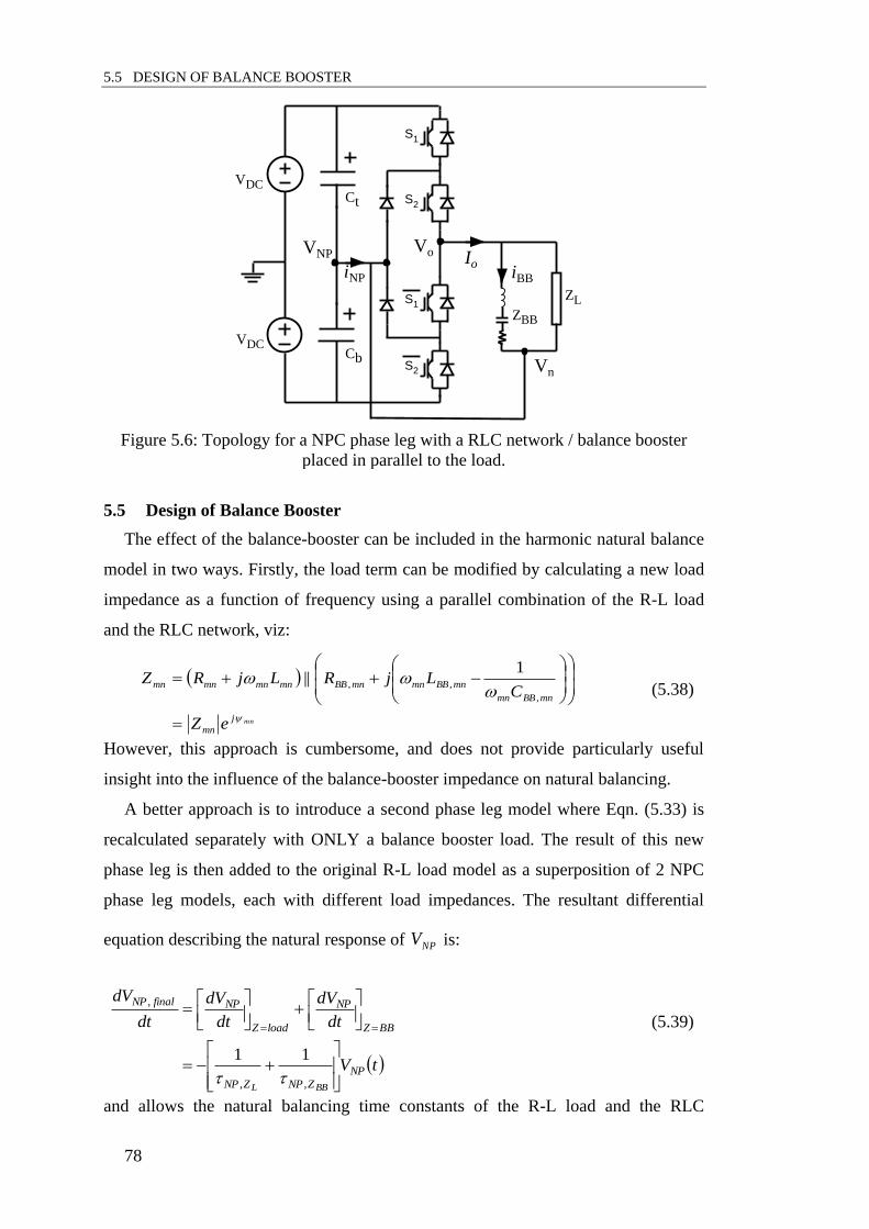
5.5 DESIGN OF BALANCE BOOSTER
78
5.5 Design of Balance Booster
The effect of the balance-booster can be included in the harmonic natural balance
model in two ways. Firstly, the load term can be modified by calculating a new load
impedance as a function of frequency using a parallel combination of the R-L load
and the RLC network, viz:
mnj
mn
mnBBmn
mnBBmnmnBBmnmnmnmn
eZ
CLjRLjRZ
,
,,
1||
(5.38)
However, this approach is cumbersome, and does not provide particularly useful
insight into the influence of the balance-booster impedance on natural balancing.
A better approach is to introduce a second phase leg model where Eqn. (5.33) is
recalculated separately with ONLY a balance booster load. The result of this new
phase leg is then added to the original R-L load model as a superposition of 2 NPC
phase leg models, each with different load impedances. The resultant differential
equation describing the natural response of NPV is:
tV
dt
dV
dt
dV
dt
dV
NP
ZNPZNP
BBZ
NP
loadZ
NPfinalNP
BBL
,,
,
11
(5.39)
and allows the natural balancing time constants of the R-L load and the RLC
VDC
S1
S2
S1
S2
Ct
Cb
iNP
VDC
VNP
ZBB
ZL
Vn
iBB
Io
Vo
Figure 5.6: Topology for a NPC phase leg with a RLC network / balance booster
placed in parallel to the load.

5 NATURAL BALANCING OF A NPC PHASE LEG
79
balance-booster filter to be clearly separately identified. In principle, the balance-
booster filter creates a low impedance in the switching frequency region and thus a
flow of harmonic currents, mnBBi that increase the natural balancing action. The
magnitude of these currents can be readily calculated as follows:
mnBB
mnomnBB
Z
Vi
)(
(5.40)
Unfortunately, not all of the harmonic currents contribute to the balancing
process, since (5.37) has identified that the converter output voltage contains both
mnF and mnH harmonic components. As identified earlier in Section 5.4, only the
mnF components contribute to the balancing process and disappear as 0tVNP .
The mnH components on the other hand are always present in the output voltage, and
cause steady state carrier group harmonic currents to always flow through the
balance-booster impedance, with a resultant power loss in the filter resistance.
The ideal balancing impedance solution to avoid this penalty would be a set of
very narrow bandwidth notch filters that only interact with the mnF harmonic
components, but this is very difficult to achieve in practice. A more practical method
0 500 1000 1500 2000 2500 3000 3500 4000 4500 500010
0
105
Frequency (Hz)
RL
BB
RL+BB
Figure 5.7: Load and balance-booster impedance magnitude versus frequency.
0 500 1000 1500 2000 2500 3000 3500 4000 4500 5000-100
-50
0
50
100
Frequency (Hz)
RL
BB
RL+BB
Figure 5.8: Load and balance-booster impedance phase angle versus frequency.

5.6 NATURAL BALANCE TIME DOMAIN SIMULATION
80
may be to disconnect the balance-booster filter during steady state operation when
the NP voltage is zero. Balance-booster power losses and other such practical issues
will be discussed further in Chapter 7.
5.6 Natural Balance Time Domain Simulation
The theoretical NP natural balancing concepts were verified using a detailed time
domain simulation with the PSIM 9.0.3 simulation package, as shown in Figure 5.9.
Note that the node labelled ‘BUS’ is used to tie the load return connection to the NP
of the converter. Table 5-2 shows the parameters of the simulation for the two
operating configurations that are presented here, viz: Configuration A operates with
half the modulation depth and double the fundamental frequency of Configuration B.
Figure 5.10 shows natural balance response of the converter Neutral Point voltage
for operating configuration A, returning to zero quite quickly after an initial
unbalance offset condition. There is an almost exact match between the time domain
simulation solution, a numerical calculation of the non-linear switched differential
Eqn. (5.15), and the linearised first order harmonic solution of Eqn. (5.39), which
validates the analysis of this chapter.
A similar comparison result is shown in Figure 5.11 for operating configuration B,
where once again there is an almost exact match between the three analysis
Figure 5.9: PSIM Simulation Schematic for Natural Balance Investigation.

5 NATURAL BALANCING OF A NPC PHASE LEG
81
approaches. However, the natural balancing response for configuration B is much
slower, taking more than 1.2 seconds to reach a steady state NP condition. This
slower response is directly a result of the different operating conditions for
configuration B, where the increased modulation index significantly reduces the
number and magnitude of the mnF harmonic components that drive the natural
balance response, as shown in Figure 5.13 and Figure 5.14.
Figure 5.12 shows the dramatic improvement in natural balancing that is achieved
for configuration B when a balance-booster filter is installed. However, there is a
penalty of an increased NP voltage ripple because of the additional carrier group
frequency harmonic currents that now flow continuously through the balance-booster
filter even when the NP voltage is zero.Experimental results to support these
simulation validations will be presented in the next chapter for a three phase NPC.
Table 5-2: Parameters for phase leg’s balancing simulations.
Parameter Value
(Config A)
Value
(Config B)
Nominal DC link (V) 100
Capacitor size (µF) 4200
Load Resistance (ohms) 1
Load Inductance (mH) 2e-3
Modulation depth 0.5 1
Fundamental Frequency (fo) (Hz) 100 50
Carrier Frequency (fc) (Hz) 5000
Number of carriers considered, m 3
Number of sidebands considered, n 20
Balance Booster Resistance, RBB 2.3
Balance Booster Capacitance 992µH
Balance Booster Inductance 970mH

5.6 NATURAL BALANCE TIME DOMAIN SIMULATION
82
Figure 5.10: Neutral Point voltage of simulation against models derived for
Configuration A. M=0.5, fo = 100Hz
Figure 5.11: Neutral Point voltage of simulation against models derived for
Configuration B without balance booster. M=1.0, fo = 50Hz
Figure 5.12: Neutral Point voltage of simulation against models derived for
Configuration B with balance booster. M=1.0, fo = 50Hz
0 0.1 0.2 0.3 0.4 0.5 0.6 0.7 0.8 0.9 1-20
0
20
40
60
80
100Natural balancing
Time (s)
NP
voltage (
V)
Simulation
D. E.
Harmonic D.E.
0 0.1 0.2 0.3 0.4 0.5 0.6 0.7 0.8 0.9 1-20
0
20
40
60
80
100Natural balancing
Time (s)
NP
voltage (
V)
Simulation
D. E.
Harmonic D.E.
0 0.1 0.2 0.3 0.4 0.5 0.6 0.7 0.8 0.9 1-20
0
20
40
60
80
100Natural balancing with balance booster
Time (s)
NP
voltage (
V)
Simulation
Harmonic D.E.

5 NATURAL BALANCING OF A NPC PHASE LEG
83
0 1000 2000 3000 4000 5000 6000 7000 8000 9000 1000010
-3
10-2
10-1
100
Fmn
harmonics
Frequency (Hz)
Figure 5.13: Fmn harmonics for Configuration A. M=0.5, fo = 100Hz.
0 1000 2000 3000 4000 5000 6000 7000 8000 9000 1000010
-3
10-2
10-1
100
Fmn
harmonics
Frequency (Hz)
Figure 5.14: Fmn harmonics for Configuration B. M=1.0, fo = 50Hz

5.7 SUMMARY
84
5.7 Summary
This chapter has modelled the natural balancing mechanism of a NPC phase leg.
The resulting model is a simple summation of harmonic time constants that only
depend on the harmonics of the modulation process and the phase leg load
impedance. The natural balancing process is caused by the unbalanced NP voltage
producing harmonic currents which generate self-eliminating currents that return the
NP to its balanced state. These currents, and hence the balancing response, can be
enhanced by a balance-booster output filter, tuned to the carrier group frequencies.
The modelling concepts have been verified through simulation and analytical
solutions, and are readily extended to three phase converters, as will be presented in
the next chapter.

6 NATURAL BALANCING OF THREE PHASE NPC CONVERTERS
85
6 NATURAL BALANCING OF THREE PHASE NPC CONVERTERS
Chapter 5 has developed a linear model that predicts the balancing performance of a
NPC phase leg, achieved by combining a non-linear transient circuit model of the
NPC converter with a Double Fourier series representation of the converter switching
functions. The chapter also showed how additional balance booster elements can be
modelled, either through modification of the load term directly or by superposition of
multiple phase leg models to account for the primary load and the additional balance
booster elements.
This chapter now extends these concepts to demonstrate how a three phase NPC
converter can be broken up into individual phase leg models which can then be
superimposed to predict the behaviour of the overall converter. The design of balance
booster filters is then explored to consider which topological configuration results in
the best balancing performance, and to also assess the overall power loss of the
balance booster in these different configurations. This investigation is confirmed by
detailed simulation and experimental verification of the concepts.
6.1 Modelling the Three-phase NPC [82]
The physical construction and modulation of a 3-phase NPC converter has been
thoroughly introduced in Chapters 2 and 3, and hence is not repeated here. However,
the 3-phase NPC converter load has several possible topological options because
there are several approaches available to connect the 3-phase load’s neutral point,
LnV ,, and the neutral point, BBnV , , of the balance booster filter (if it is used).
Various configurations of the 3-phase converter are shown in Figure 6.1 and
summarised in Table 6-1. Case 1 (ZL-F) is the ‘standard’ NPC converter
configuration with a simple ‘3-wire’ load that has a floating neutral. Case 3 (ZL-F,
BB-F) extends Case 1 (ZL-F) with the addition of a balance booster. Case 2 (ZL-NP)
is a 4-wire configuration typically used in Flexible AC Transmission Systems
(FACTS). In this configuration the load’s neutral is connected to the NP of the
converter. It is also known as ‘4th
wire to NP’ [83][84]. Case 4 (ZL-NP, BB-NP)
extends Case 2 (ZL-NP) by adding a balance booster that has its 4th
wire also
connected to the NP. Cases 5 (ZL-F, BB-NP) and 6 (ZL-F, BB-VDC) are extensions
of Case 1 (ZL-F) with balance booster filters that are connected to the NP and the
negative rail of the DC link respectively.

6.1 MODELLING THE THREE-PHASE NPC [82]
86
In Chapter 5 it was demonstrated that the principle of superposition can be applied
to model the natural balancing process for a NPC converter. This superposition
approach will now be applied to the three phase topologies shown in Figure 6.1. The
development of a natural balance model for any particular topological configuration
proceeds by superposing individual phase leg natural balance models which account
for the (a,b,c) phase legs, and also the load and balance booster filter configurations.
In this way the generic phase leg natural balance model developed in Chapter 5 can
be used, with minor modifications required to account for the different phase leg
modulation phase shifts, as well as the different load and filter connection
VDC
S1,a
S2,a
S1,a
S2,a
Ct
Cb
iNP
VDC
VNP
S1,b
S2,b
S1,b
S2,b
S1,c
S2,c
S1,c
S2,c
ZL
Vn,L
VDC
S1,a
S2,a
S1,a
S2,a
Ct
Cb
iNP
VDC
VNP
S1,b
S2,b
S1,b
S2,b
S1,c
S2,c
S1,c
S2,c
ZL
Vn,L
Case 1 (ZL-F) Case 2 (ZL-NP)
VDC
S1,a
S2,a
S1,a
S2,a
Ct
Cb
iNP
VDC
VNP
S1,b
S2,b
S1,b
S2,b
S1,c
S2,c
S1,c
S2,c
ZL ZBB
Vn,L Vn,BB
VDC
S1,a
S2,a
S1,a
S2,a
Ct
Cb
iNP
VDC
VNP
S1,b
S2,b
S1,b
S2,b
S1,c
S2,c
S1,c
S2,c
ZL ZBB
Vn,L Vn,BB
Case 3 (ZL-F, BB-F) Case 4 (ZL-NP, BB-NP)
VDC
S1,a
S2,a
S1,a
S2,a
Ct
Cb
iNP
VDC
VNP
S1,b
S2,b
S1,b
S2,b
S1,c
S2,c
S1,c
S2,c
ZL ZBB
Vn,L Vn,BB
VDC
S1,a
S2,a
S1,a
S2,a
Ct
Cb
iNP
VDC
VNP
S1,b
S2,b
S1,b
S2,b
S1,c
S2,c
S1,c
S2,c
ZL ZBB
Vn,L Vn,BB
Case 5 (ZL-F, BB-NP) Case 6 (ZL-F, BB-VDC)
Figure 6.1: 3-phase NPC converter with and without different balance booster
placement configurations .

6 NATURAL BALANCING OF THREE PHASE NPC CONVERTERS
87
arrangements.
Common to all the variations is the fundamental reference phase shift of 1200 and
2400 in the phases b and c. Also, before the superposition of the phase leg models to
obtain the overall D.E.s for each case in Figure 6.1 can proceed, it is first necessary
to derive the phase leg models when nV is:
a) the floating neutral of a 3-phase load for Cases 1 (ZL-F) and 3 (ZL-F, BB-F)
(Section 6.1.1), and
b) connected to the negative DC rail for Case 6 (ZL-F, BB-VDC) in (Section
6.1.2).
6.1.1 Modelling the NP Change when tVn is Floating (Case 1 (ZL-F) & 3 (ZL-F,
BB-F))
A floating 3-phase wye-connected load means the phase leg models are no longer
independent because tVn now depends on the switched voltages of the three phase
legs, tVa , tVb and tVc . Also care must be exercised in modelling each NPC
phase leg to keep the phase legs separate. Hence for this analysis, the variables
associated with a particular phase leg will be labelled with the subscripts },,{ cbax .
This section will now model the NPC phase leg A, recognising that the model of
the other phase legs are just an adaptation of this model. The first variation from
Chapter 5 that is required is to adjust the neutral point current, since the load current
no longer returns to the NP. Hence the NP current summation of Eqn. (5.8) becomes
tItStSti aaaaNP ,1,2, )( (6.1)
Table 6-1: Variations of the 3-phase NPC converter.
Case Load. Balance Booster
1 (ZL-F) floating NP Not used
2 (ZL-NP) 4th
wire to NP Not used
3 (ZL-F, BB-F) floating NP floating NP
4 (ZL-NP, BB-NP) 4th
wire to NP 4th
wire to NP
5 (ZL-F, BB-NP) floating NP 4th
wire to NP
6 (ZL-F, BB-VDC) floating NP 4th
wire to DC rail

6.1 MODELLING THE THREE-PHASE NPC [82]
88
The subscript notation of this equation is for the NP current component attributed to
phase leg A, and its value is dependent upon the switching states for this phase leg
and its load current. Substituting Eqn. (6.1) into Eqn. (5.7) from Chapter 5 thus leads
to the revised NP voltage D.E. for the contribution of phase leg A of :
tItStSC
iCdt
dVaaaaNP
aNP ,1,2,
,
2
1
2
1
(6.2)
The phase A load current tIa is dependent upon the switched voltage of phase
leg A and the 3-phase load’s floating neutral, nV . This floating neutral voltage is the
average of the 3 switched phase leg voltages and can be described by:
tVtVtVtV cban 3
1 (6.3)
Ohm’s law then gives the phase A current relationship of:
tVtVtV
dt
dLR
tVtVtVtV
dt
dLR
VtV
dt
dLR
tI
cba
LL
cbaa
LL
na
LL
a
23
11
3
11
1
(6.4)
The switched output voltage for a NPC inverter phase leg were established in
Chapter 5 as the sum and difference of the individual switching functions in Eqn.
(5.14), and hence can be simply rewritten here for each of the three phase legs as
tVtStSVtStStV NPxxDCxxx ,1,2,2,1 1 (6.5)
Substituting Eqn. (6.5) into the load current equation, Eqn. (6.4), and then into the
per-phase D.E., Eqn. (6.2), results in the following NP voltage transient circuit model
for the contribution of the phase leg A current:
tVtStSVtStS
tVtStSVtStS
tVtStSVtStS
dtdLRtStS
Cdt
dV
NPcbDCbc
NPbbDCbb
NPaaDCaa
aaaNP
,1,2,2,1
,1,2,2,1
,1,2,2,1
,1,2,
1
1
212
3
1
/
1
2
1
(6.6)
This result is more complex than the transient relationship derived in Chapter 5
because it has switching functions from all three phase legs. However the switching

6 NATURAL BALANCING OF THREE PHASE NPC CONVERTERS
89
functions are still very similar to Eqns. (5.24) and (5.26), differing essentially only
because of the loss of the ‘-1’ in the difference expression. Of course the switching
functions also have different fundamental reference offset values depending on
which phase leg they are associated with, but this is not difficult to accommodate in
the detailed evaluation. Using the “x” subscript phase leg notation, the switching
sum and difference expressions in Eqn. (6.6) thus develop from Eqns. (5.24) and
(5.26) to become:
xmnmnxx ntFtStS cos,1,2 (6.7)
where mnmnmn ADF , ocmn nm (6.8)
and
xmnmnxx ntHtStS cos1,2,1 (6.9)
where mnmnmn DAH , ocmn nm (6.10)
Substitution of these Double Fourier representations, Eqns. (6.7) and (6.9) into
Eqn. (6.6) results in the following individual harmonic D.E for the phase A current:
tVntFVntH
tVntFVntH
tVntFVntH
ZntF
Cdt
tdV
NPcmnmnDCcmnmn
NPbmnmnDCbmnmn
NPamnmnDCamnmn
mn
mnamnmn
mnaNP
coscos
coscos
cos2cos2
3
1
1cos
2
1,,
(6.11)
The cosine multiplications in Eqn. (6.11) produce both DC and double harmonic
frequency terms, but since again only the low frequency deviation of tVNP is of
interest, the double frequency terms in Eqn. (6.11) can be neglected once more, to
give, after some manipulation:
tVFVHF
nn
ZCdt
tdV
NPmnDCmnmn
mncamnbamn
mn
mnaNP
2
,,
coscoscos2
1
12
1
(6.12)
From Chapter 5, Eqn. (5.32) identified that mnF and mnH harmonics are
orthogonal. Thus Eqn. (6.12) simplifies to a result that is only dependent on mnF
harmonics, i.e.

6.1 MODELLING THE THREE-PHASE NPC [82]
90
tV
tVFnn
ZCdt
tdV
NP
mnaNP
NPmnmncamnbamn
mn
mnaNP
,,
2
,,
1
coscoscos2
12
1
(6.13)
This is the first order D.E. for the NP voltage variation caused by phase leg A of a
NPC inverter feeding into a 3-phase floating wye load. A similar relationship can be
readily developed for the other two phase legs using the same approach, to give
tV
tVFnn
ZCdt
tdV
NP
mnbNP
NPmnmnabmncbmn
mn
mnbNP
,,
2
,,
1
coscoscos2
12
1
(6.14)
tV
tVFnn
ZCdt
tdV
NP
mncNP
NPmnmnbcmnacmn
mn
mncNP
,,
2
,,
1
coscoscos2
12
1
(6.15)
The overall NP voltage variation caused by all three phase legs feeding into a 3-
phase floating wye load is then given by the superposition of Eqns. (6.13), (6.14) and
(6.15).
6.1.2 Modelling the NP Change when tVn is Connected to a DC link (Case 6 (ZL-
F, BB-VDC))
For Case 6 (ZL-F, BB-VDC), the neutral of the balance booster filter, BBnV , , is
connected to the DC link instead of the NP voltage. This causes two changes, viz:
a) The filter current no longer returns to the NP node. As a result, Eqn. (5.8)
becomes:
tItStSti oNP 12)( (6.16)
where once again the switching function has lost the ‘-1’ term.
b) The filter load current is now dependent upon the difference between the
switched voltage and the negative DC link potential. Eqn. (5.12) therefore
adapts to become:
6 NATURAL BALANCING OF THREE PHASE NPC CONVERTERS
91
DCo
f
ff
o VtV
dtCdt
dLR
tI
1
1
(6.17)
A similar modelling process is again used where the filter current, Eqn. (6.17), is
substituted into the switched NP current equation, Eqn. (6.16), which is then
substituted into the D.E. relating the NP current to the NP voltage, Eqn. (5.7), to
produce the following transient circuit model:
tVtStSVtStS
dtCdt
dLR
tStSCdt
dV
NPDC
f
ff
NP
1221
12
1
1
2
1
(6.18)
This resulting D.E. again differs from those in Chapter 5 by the removal of the ‘-1’
term in both switching functions, thus causing a change in DC term of both of mnF
and mnH harmonics. The new forms of Eqn. (5.24) and (5.26) are:
omnmn ntFtStS cos12 (6.19)
where mnmnmn ADF , ocmn nm (6.20)
and
omnmn ntHtStS cos21 (6.21)
where mnmnmn DAH , ocmn nm (6.22)
Eqn. (5.33) can again be used to model the NPC phase leg when the balance booster
filter is connected to the lower DC link by removing the DC offset within mnF and
mnH harmonics. Note also that the connection of nV to the top DC rail results in a
different change in the DC term of mnH harmonics. However, the end result is similar
and will not be explored further in this chapter.
6.1.3 Application of the Superposition of Phase Leg Models to obtain D.E.s for the
Different Cases of a 3-Phase NPC Converter.
The differential equation for the topological cases shown in Table 6-1 can be
obtained by applying the superposition principle as shown below for the various
cases:

6.1 MODELLING THE THREE-PHASE NPC [82]
92
Case 1 (ZL-F): The phase legs of this case are connected to a floating 3-phase wye-
connected load. As a result, the overall D.E. uses the summation of 3 ‘floating load’
phase leg models derived from Section 6.1.1 (denoted by the subscript ‘flt’), viz:
LZZ
cfltNPbfltNPafltNPtotalNP
dt
tdV
dt
tdV
dt
tdV
dt
tdV
,,,,,,_ (6.23)
where each phase leg’s D.E. is a summation of individual D.E.s representing each
particular harmonic frequency. Their evaluation results in time constants for every
harmonic of:
1 ,,,,,,,,,,,,
_ 111
m
NP
n ZcfltmnNPZbfltmnNPZafltmnNP
totalNPtV
dt
tdV
LLL
(6.24)
The time constants are then summed across all the harmonic frequencies and phase
legs to derive a final time constant. Note that if the phase leg’s load elements are
identical, the balancing time constants produced will be the same. Hence the analysis
process can be simplified by multiplying the result of one phase leg by 3, viz:
tV
tVdt
tdV
NP
ZfltphaseNP
m
NP
n ZafltmnNP
totalNP
L
L
,,3,
1 ,,,,
_
1
13
(6.25)
Case 2 (ZL-NP): The phase legs of this case are connected to the NP. As a result, the
overall D.E. uses the ‘NP’ phase leg model derived from Chapter 5 (denoted by the
subscript ‘4w’), and summed across the phases, to give:
tV
tV
dt
tdV
dt
tdV
dt
tdV
dt
tdV
NP
ZwphaseNP
m
NP
n ZcwmnNPZbwmnNPZawmnNP
ZZ
cwNPbwNPawNPtotalNP
L
LLL
L
,4,3,
1 ,,4,,,,4,,,,4,,
,4,,4,,4,_
1
111
(6.26)
Case 3 (ZL-F, BB-F): The phase legs of this case are connected to a floating 3-phase
wye-connected load along with a floating 3-phase wye-connected balance booster.
As a result, the overall D.E. superpositions are: a) the ‘floating load’ phase leg model

6 NATURAL BALANCING OF THREE PHASE NPC CONVERTERS
93
derived from Section 6.1.1 with a RL load and b) the same ‘floating load’ model with
only a balance booster, viz:
tV
tV
tV
dt
tdV
dt
tdV
dt
tdV
dt
tdV
dt
tdV
dt
tdV
dt
tdV
NP
ZfltphaseNPZfltphaseNP
m
NP
n ZcfltmnNPZbfltmnNPZafltmnNP
m
NP
n ZcfltmnNPZbfltmnNPZafltmnNP
ZZ
cfltNPbfltNPafltNP
ZZ
cfltNPbfltNPafltNPtotalNP
BBL
BBBBBB
LLL
BB
L
,,3,,,3,
1 ,,,,,,,,,,,,
1 ,,,,,,,,,,,,
,,,,,,
,,,,,,_
11
111
111
(6.27)
Case 4 (ZL-NP, BB-NP): In this case a 4th
wire is used to connect the star-points of
the load and balance booster to the NP. As a result, the overall D.E. superpositions
are:
a) the ‘NP’ phase leg model derived from Chapter 5 with a RL load ( LZZ ) and
b) the same ‘NP’ model with only a balance booster ( BBZZ ), viz:
tV
tV
tV
dt
tdV
dt
tdV
dt
tdV
dt
tdV
dt
tdV
dt
tdV
dt
tdV
NP
ZwphaseNPZwphaseNP
mNP
n ZcwmnNPZbwmnNPZawmnNP
mNP
n ZcwmnNPZbwmnNPZawmnNP
ZZ
cwNPbwNPawNP
ZZ
cwNPbwNPawNPtotalNP
BBL
BBBBBB
LLL
BB
L
,4,3,,4,3,
1 ,,4,,,,4,,,,4,,
1 ,,4,,,,4,,,,4,,
,4,,4,,4,
,4,,4,,4,_
11
111
111
(6.28)
Case 5 (ZL-F, BB-NP): The phase legs of this case are connected to a floating 3-
phase wye-connected load along with a 3-phase wye-connected balance booster with
its neutral connected to the NP. As a result, the overall D.E. superpositions are:

6.1 MODELLING THE THREE-PHASE NPC [82]
94
a) the ‘floating load’ phase leg model from Section 6.1.1 with a RL load ( LZZ )
and
b) the ‘NP’ model with only a balance booster from Chapter 5 ( BBZZ ), viz:
tV
tV
tV
dt
tdV
dt
tdV
dt
tdV
dt
tdV
dt
tdV
dt
tdV
dt
tdV
NP
ZwphaseNPZfltphaseNP
mNP
n ZcwmnNPZbwmnNPZawmnNP
mNP
n ZcfltmnNPZbfltmnNPZafltmnNP
ZZ
cwNPbwNPawNP
ZZ
cfltNPbfltNPafltNPtotalNP
BBL
BBBBBB
LLL
BB
L
,4,3,,,3,
1 ,,4,,,,4,,,,4,,
1 ,,,,,,,,,,,,
,4,,4,,4,
,,,,,,_
11
111
111
(6.29)
Case 6 (ZL-F, BB-VDC): The phase legs of this case are connected to a floating 3-
phase wye-connected load along with a 3-phase wye-connected balance booster with
its neutral connected to the lower DC rail. As a result, the overall D.E. superpositions
are:
a) the ‘floating load’ phase leg model derived from Section 6.1.1 for the RL load and
b) the DC-link-connected balance booster (denoted by the subscript ‘DC’) from
Section 6.1.2 for the balance booster ( BBZZ ), viz:
tV
tV
tV
dt
tdV
dt
tdV
dt
tdV
dt
tdV
dt
tdV
dt
tdV
dt
tdV
NP
ZDCphaseNPZfltphaseNP
m
NP
n ZcDCmnNPZbDCmnNPZaDCmnNP
m
NP
n ZcfltmnNPZbfltmnNPZafltmnNP
ZZ
cDCNPbDCNPaDCNP
ZZ
cfltNPbfltNPafltNPtotalNP
BBL
BBBBBB
LLL
BB
L
,,3,,,3,
1 ,,,,,,,,,,,,
1 ,,,,,,,,,,,,
,,,,,,
,,,,,,_
11
111
111
(6.30)

6 NATURAL BALANCING OF THREE PHASE NPC CONVERTERS
95
6.2 Matching Balance Booster Filter Losses.
The above analytical model now allows the natural balancing performance of the
3-phase topology variants to be explored in terms of modulation depth, carrier
frequency, fundamental frequency, load power factor angle and load magnitude. The
nominal parameters for the 3-phase NPC investigated are listed in Table 6-2. The
design of the balance boosters has been presented earlier in Section 5.5 where the
inductance, L, and capacitance, C, parameters were varied to achieve resonance at
the switching frequency of the converter, while the resistance, R of the balance
booster was varied according to the performance desired.
However, before proceeding with this analysis, the balance booster losses for the
alternative configurations of a floating neutral and a DC linked balance booster
impedance need to be matched, to provide a consistent baseline for the balancing
comparison. These losses were balanced by iteratively varying the balance booster’s
resistance, BBR and then numerically evaluating the balance booster currents to
determine the balance booster power loss.
The balance booster RMS currents were calculated by evaluating:
2)( 0
m nmnBB
BB
i
RMSI
(6.31)
where the balance booster currents, mnBBi at a particular harmonic frequency, mn
are dependent on the topology, and are defined as:
a) Floating Neutral,
mnBB
mncmnbmnamnBB
Z
VVVi
3
)()()(2 (6.32)
b) Linked Balance Boosters i.e. 4-wire and balance booster linked to the DC link.
mnBB
mnomnBB
Z
Vi
)( (6.33)
Table 6-2 shows the results of these calculations by specifying the resistance of
the balance boosters for each case. Figure 6.2 shows the resulting balance booster
currents per phase leg as a function of converter modulation depth for the same filter
loss. From this figure, it can be seen that the ‘4-wire’ linked configurations requires
less balance booster currents for the same power loss. This means the ‘4-wire’ is a
more lossy topology and hence a higher resistance is required to equalise its losses. A
lossier balance booster will generally improve balancing performance, however

6.3 ANALYTICALLY CALCULATED NATURAL BALANCING PERFORMANCE OF 3-
PHASE NPC CONVERTER
96
further numerical studies are required to determine the best ‘balancing
performance/watt’ or ‘balancing performance/efficiency loss’. For example,
eventually, there is a tradeoff point where the semiconductor size has to be increased
to accommodate the higher balancing currents caused by a lossier balance booster.
Using the parameters listed in Table 6-2, the apparent power, S, of the RL load
was calculated as 2215 VA. The balance booster filters were then targeted to
consume less than 5% of the load (as a reasonable choice). Consequently, they were
required to consume less than 130W, and their resistances were set accordingly.
Figure 6.3 shows the overall balance booster losses for the 3-phase NPC converter
with resistances set as per Table 6-2, as a function of converter modulation depth.
With the losses of the two alternative balance booster arrangements now equalised as
shown in Figure 6.3 the investigation of the natural balancing performance of the
various load alternatives in Figure 6.1 can proceed.
6.3 Analytically Calculated Natural Balancing Performance of 3-Phase NPC
Converter
Figure 6.4 shows how the natural balancing time constant varies with modulation
depth for all the load alternatives listed in Figure 6.1, where a larger time constant
represents a poorer natural balancing response (note also the log scale on the vertical
axis). From these results it can be seen that the most common ‘3-wire’ load (Case 1
(ZL-F)) for a 3-phase converter has the slowest balancing response. If the load’s
Table 6-2: 3-phase NPC converter parameters for balancing simulations.
Parameter Value
Nominal DC link 360 V
Capacitor size 4200 µF
Load Resistance 11 ohms
Load Inductance 44.4 mH
Fundamental Frequency (fo) 50 Hz
Carrier Frequency (fc) 5000 Hz
Balance Booster Resistance
13.8 ohms (Floating)
138 ohms (4-wire & DC linked)
15.1 ohms (experimental Floating)
Balance Booster Inductance 992µH
Balance Booster Capacitance 970nF
Total number of carriers considered, m 3
Total number of sidebands considered, n 20
Modulation depth 0.9

6 NATURAL BALANCING OF THREE PHASE NPC CONVERTERS
97
neutral point, LnV , is available and can be connected to the converter’s NP node
(Case 2 (ZL-NP)), the natural balancing response increases by more than an order of
magnitude.
Figure 6.2: Balance booster currents versus modulation depth.
Figure 6.3: Balance booster power loss versus modulation depth.
0 0.1 0.2 0.3 0.4 0.5 0.6 0.7 0.8 0.9 110
-2
10-1
100
101
Modulation depth
IBB
(A
)
Floating
Linked
0 0.1 0.2 0.3 0.4 0.5 0.6 0.7 0.8 0.9 110
-1
100
101
102
103
X: 0.4407
Y: 128.9
Modulation depth
Plo
ss (
W)
Floating
Linked

6.3 ANALYTICALLY CALCULATED NATURAL BALANCING PERFORMANCE OF 3-
PHASE NPC CONVERTER
98
Alternatively, if the load’s neutral point is unavailable, for loads such as motors, a
balance booster with a floating neutral can be used (Case 3 (ZL-F, BB-F)) to achieve
a similar improvement in balancing response, albeit with a reduced benefit at
modulation depths above 0.7. The performance at higher modulation depths can be
also be improved by connecting both the load’s and balance booster’s neutral point to
the converter’s NP (Case 4 (ZL-NP, BB-NP)). However, the improvement over Case
2 (ZL-NP) is small, because the load impedance magnitude is already small relative
to the balance booster’s impedance, thus rendering the balance booster less effective.
Alternatively, only the balance booster’s NP can be either connected to the
converter’s NP (Case 5 (ZL-F, BB-NP)) or either of the DC rails (Case 6 (ZL-F, BB-
VDC)), to gain a moderate improvement in balancing performance (both alternatives
have a mathematically identical response).
Note that in all cases, the balancing performance degrades at very low modulation
depths. This is because low modulation depths produce low voltages and hence low
balancing currents. Thus there is little restorative force available to return the NP
voltage to zero. Furthermore it should be remembered that the balance booster
resistance for Case 3 (ZL-F, BB-F) has a significantly smaller resistance to maintain
0 0.1 0.2 0.3 0.4 0.5 0.6 0.7 0.8 0.9 1
10-1
100
101
102
Modulation depth
Case 1 (ZL-F)
Case 2 (ZL-NP)
Case 3 (ZL-F, BB-F)
Case 4 (ZL-NP, BB-NP)
Case 5 (ZL-F, BB-NP)
Case 6 (ZL-F, BB-VDC)
Figure 6.4: Natural balancing time constant versus modulation depth.
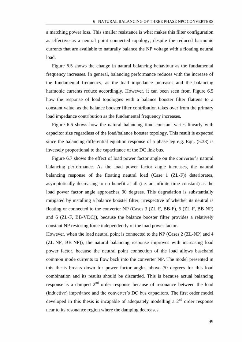
6 NATURAL BALANCING OF THREE PHASE NPC CONVERTERS
99
a matching power loss. This smaller resistance is what makes this filter configuration
as effective as a neutral point connected topology, despite the reduced harmonic
currents that are available to naturally balance the NP voltage with a floating neutral
load.
Figure 6.5 shows the change in natural balancing behaviour as the fundamental
frequency increases. In general, balancing performance reduces with the increase of
the fundamental frequency, as the load impedance increases and the balancing
harmonic currents reduce accordingly. However, it can been seen from Figure 6.5
how the response of load topologies with a balance booster filter flattens to a
constant value, as the balance booster filter contribution takes over from the primary
load impedance contribution as the fundamental frequency increases.
Figure 6.6 shows how the natural balancing time constant varies linearly with
capacitor size regardless of the load/balance booster topology. This result is expected
since the balancing differential equation response of a phase leg e.g. Eqn. (5.33) is
inversely proportional to the capacitance of the DC link bus.
Figure 6.7 shows the effect of load power factor angle on the converter’s natural
balancing performance. As the load power factor angle increases, the natural
balancing response of the floating neutral load (Case 1 (ZL-F)) deteriorates,
asymptotically decreasing to no benefit at all (i.e. an infinite time constant) as the
load power factor angle approaches 90 degrees. This degradation is substantially
mitigated by installing a balance booster filter, irrespective of whether its neutral is
floating or connected to the converter NP (Cases 3 (ZL-F, BB-F), 5 (ZL-F, BB-NP)
and 6 (ZL-F, BB-VDC)), because the balance booster filter provides a relatively
constant NP restoring force independently of the load power factor.
However, when the load neutral point is connected to the NP (Cases 2 (ZL-NP) and 4
(ZL-NP, BB-NP)), the natural balancing response improves with increasing load
power factor, because the neutral point connection of the load allows baseband
common mode currents to flow back into the converter NP. The model presented in
this thesis breaks down for power factor angles above 70 degrees for this load
combination and its results should be discarded. This is because actual balancing
response is a damped 2nd
order response because of resonance between the load
(inductive) impedance and the converter’s DC bus capacitors. The first order model
developed in this thesis is incapable of adequately modelling a 2nd
order response
near to its resonance region where the damping decreases.

6.3 ANALYTICALLY CALCULATED NATURAL BALANCING PERFORMANCE OF 3-
PHASE NPC CONVERTER
100
0 50 100 150 200 250
10-1
100
101
102
Fundamental Frequency (Hz)
Case 1 (ZL-F)
Case 2 (ZL-NP)
Case 3 (ZL-F, BB-F)
Case 4 (ZL-NP, BB-NP)
Case 5 (ZL-F, BB-NP)
Case 6 (ZL-F, BB-VDC)
Figure 6.5: Natural balancing time constant versus fundamental frequency.
0 0.001 0.002 0.003 0.004 0.005 0.006 0.007 0.008 0.009 0.010
0.2
0.4
0.6
0.8
1
1.2
1.4
1.6
1.8
2
Capacitor size (F)
Case 1 (ZL-F)
Case 2 (ZL-NP)
Case 3 (ZL-F, BB-F)
Case 4 (ZL-NP, BB-NP)
Case 5 (ZL-F, BB-NP)
Case 6 (ZL-F, BB-VDC)
Figure 6.6: Natural balancing time constant versus capacitor size, C.

6 NATURAL BALANCING OF THREE PHASE NPC CONVERTERS
101
0 10 20 30 40 50 60 70 80 9010
-2
10-1
100
101
102
103
Load angle (Deg)
Case 1 (ZL-F)
Case 2 (ZL-NP)
Case 3 (ZL-F, BB-F)
Case 4 (ZL-NP, BB-NP)
Case 5 (ZL-F, BB-NP)
Case 6 (ZL-F, BB-VDC)
Figure 6.7: Natural balancing time constant versus load power factor angle.
100
101
102
103
104
10-1
100
101
102
103
Load magnitude (ohm)
Case 1 (ZL-F)
Case 2 (ZL-NP)
Case 3 (ZL-F, BB-F)
Case 4 (ZL-NP, BB-NP)
Case 5 (ZL-F, BB-NP)
Case 6 (ZL-F, BB-VDC)
Figure 6.8: Natural balancing time constant versus load magnitude.

6.4 EXPERIMENTAL RESULTS
102
Finally, Figure 6.8 shows how the natural balancing time constant varies with load
magnitude. The relationship is initially linear, until the load impedance becomes
larger than the balance booster filter impedance (where this filter is included).
Beyond this point, the balancing/impedance relationship flattens to a flat line.
In general, a ‘4-wire’ load where load/balance booster’s neutral is connected to
the converter’s NP (Cases 2 (ZL-NP) and 4 (ZL-NP, BB-NP)) provides the fastest
balancing performance, provided this connection is allowable for the application.
Otherwise, a balance booster filter connected in parallel with the load with a floating
neutral (Case 3 (ZL-F, BB-F)) provides the next best balancing performance,
providing the filter resistance is sized to have the same power losses as its NP
connected counterpart.
6.4 Experimental Results
The natural balancing concepts and simulation results presented in this chapter
were confirmed on an experimental NPC converter with the parameters listed in
Table 6-2. The system is described in Chapter 9 and was operated in open loop
constant voltage mode using PD modulation. Two load configurations were
experimentally investigated, being
a) a ‘3-wire’ load with floating neutral, initially without a balance booster (Case 1
(ZL-F)), and subsequently with a balance booster (Case 3 (ZL-F, BB-F)).
b) a ‘4-wire’ load with neutral returned to NP, without the balance booster (Case 2
(ZL-NP)). This alternative was chosen because the low power balance booster
does not provide much improvement in balancing performance (i.e. Case 4 (ZL-
NP, BB-NP)’s calculated performance as presented in Section 6.3).
The experimental balance booster was tuned to 5100 Hz, just off centre from the first
carrier group harmonics at 5000 Hz.
The natural balancing response was tested by connecting a resistance between the
NP and the lower DC bus voltage rail to create an unbalanced voltage across the bus
capacitors as a starting point. The balancing response was then initiated by removing
the resistance from the circuit.

6 NATURAL BALANCING OF THREE PHASE NPC CONVERTERS
103
6.4.1 Experimental Results for 3-Wire Load, 3-Phase NPC (Cases 1 (ZL-F) & 3 (ZL-
F, BB-F))
Figure 6.9 to Figure 6.12 show the NPC converter voltages and currents under
steady state continuous operation for Cases 1 & 3. Figure 6.9 shows the switched
output voltage of one phase leg of the inverter, where the expected three switched
voltage levels can be clearly seen. Figure 6.10 shows the switched line-to-line output
voltage, with the characteristic 5 level switched voltage pattern produced by PD
modulation of a NPC converter. Figure 6.11 shows the current flowing out of one
switched phase leg, together with the three load phase currents. The additional
harmonic currents flowing through the switch because of the balance booster filter
load can be clearly seen in this result. Figure 6.12 shows the residual steady state
triplen ripple in the NP caused by the modulation strategy, which cannot be
eliminated by the natural balancing strategy.
Figure 6.13 shows the resultant natural balancing response for a floating neutral
load without a balance booster filter (Case 1 (ZL-F)), while Figure 6.15 shows the
matching response with a floating neutral balance booster filter (Case 3 (ZL-F, BB-
F)). In both cases there is a very close match between theory, simulation and
experimental results. The results also confirm the extremely long natural balancing
time constant of the floating neutral load without the balancing filter, with the bus
capacitor voltages taking nearly 10 seconds to restore to a balanced condition. This
response is unacceptably slow for most practical applications. On the other hand, the
inclusion of the balancing filter, has improved the natural balance response to less
than 1.5 seconds, which is a much more attractive result.
Figure 6.14 and Figure 6.16 show the inverse time constants for each of the
individual harmonics for Case 1 (ZL-F) and Case 3 (ZL-F, BB-F). Matching numeric
values are listed in Table 6-3 and Table 6-4. These time constants are calculated by
evaluating Eqn. (6.13) across all three phase legs for each individual harmonic. It can
clearly be seen from Figure 6.14 how natural balancing depends only on the main R-
L load, since the only significant inverse time constants are in the baseband harmonic
region. In contrast, as shown in Figure 6.16, the balance booster creates additional
inverse time constants near to the switching frequency. The overall time constants
determined by summing the individual harmonic inverse time constants match well
with the experimental results, as also shown in Table 6-3 and Table 6-4.

6.4 EXPERIMENTAL RESULTS
104
Figure 6.9: Experimental NPC - Switched Phase Leg Voltage, Case 1 (ZL-F) & 3
(ZL-F, BB-F) (M=0.9)
Figure 6.10: Experimental NPC - Switched Line to Line voltage, Case 1 (ZL-F) &
3 (ZL-F, BB-F) (M=0.9)
0 0.005 0.01 0.015 0.02 0.025 0.03 0.035 0.04-200
-150
-100
-50
0
50
100
150
200P
hase V
oltage (
V)
Time (s)
0 0.005 0.01 0.015 0.02 0.025 0.03 0.035 0.04-400
-300
-200
-100
0
100
200
300
400
Lin
e t
o lin
e V
oltage (
V)
Time (s)

6 NATURAL BALANCING OF THREE PHASE NPC CONVERTERS
105
Figure 6.11: Experimental NPC - Switch and Phase leg currents for floating neutral
load with balance booster, Case 3 (ZL-F, BB-F) (M=0.9)
Figure 6.12: Experimental NPC – steady state NP voltage for floating neutral load
without balance booster, Case 1 (ZL-F) & 3 (ZL-F, BB-F) (M=0.9)
0 0.005 0.01 0.015 0.02 0.025 0.03 0.035 0.04-15
-10
-5
0
5
10
15
Curr
ent
(A)
Time (s)
Switch B current
Load current A
Load current B
Load current C
0 0.005 0.01 0.015 0.02 0.025 0.03 0.035 0.04-0.8
-0.6
-0.4
-0.2
0
0.2
0.4
0.6
0.8
NP
Voltage (
V)
Time (s)

6.4 EXPERIMENTAL RESULTS
106
Figure 6.13: Experimental natural balance response with a floating neutral load and
without a balance booster, Case 1 (ZL-F) (M=0.9).
0 1000 2000 3000 4000 5000 6000 7000 8000 9000 1000010
-4
10-3
10-2
10-1
100
The (dV/dt) = 1/tau of individual harmonics
Figure 6.14: Combined 3-phase (dVa/dt+ dVb/dt+ dVc/dt) result of each individual
harmonic (1/tau) without a balance booster filter, Case 1 (ZL-F).
0 2 4 6 8 10 12 14 16 18 20-30
-25
-20
-15
-10
-5
0
5
10
Time (seconds)
Neutr
al P
oin
t V
oltage
Without BB
Experimental
Simulation
Analytical
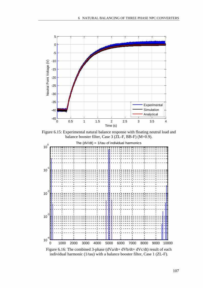
6 NATURAL BALANCING OF THREE PHASE NPC CONVERTERS
107
Figure 6.15: Experimental natural balance response with floating neutral load and
balance booster filter, Case 3 (ZL-F, BB-F) (M=0.9).
0 1000 2000 3000 4000 5000 6000 7000 8000 9000 1000010
-4
10-3
10-2
10-1
100
The (dV/dt) = 1/tau of individual harmonics
Figure 6.16: The combined 3-phase (dVa/dt+ dVb/dt+ dVc/dt) result of each
individual harmonic (1/tau) with a balance booster filter, Case 1 (ZL-F).
0 0.5 1 1.5 2 2.5 3 3.5 4-45
-40
-35
-30
-25
-20
-15
-10
-5
0
5
Neutr
al P
oin
t V
oltage (
V)
Time (s)
Experimental
Simulation
Analytical

6.4 EXPERIMENTAL RESULTS
108
6.4.2 Experimental Results for 4-Wire Load, 3-Phase NPC (Case 2 (ZL-NP))
Figure 6.17 to Figure 6.22 show matching experimental results for the 4-wire load
with the neutral connected back to the NP point (Case 2 (ZL-NP)). The switched
voltage waveforms in Figure 6.17 and Figure 6.18 are the same as for Cases 1 (ZL-F)
& 3 (ZL-F, BB-F), reflecting that the same open loop PD modulation strategy has
been used. Figure 6.19 shows the phase load currents and the harmonic current that
returns through the 4th
wire to the NP. This harmonic current is the primary natural
balancing driver. Figure 6.20 shows a similar unavoidable level of NP voltage ripple
as before.
The very fast balancing response of Case 2 (ZL-NP) can be seen in Figure 6.21,
where the unbalanced voltage is reduced within 0.25s. Note that this balancing
response is now so strong that the initial unbalance voltage deviates to only -9V with
the same unbalancing resistor as before. Figure 6.22 and Table 6-5 identify the
individual harmonic balancing time constants, where it can be seen that the 4-wire
connection creates a very strong DC balancing component which dominates the
balancing response of this load connection and explains its excellent performance.
The overall calculated time constant again matches well with the experimental result,
as listed in as listed in Table 6-5.
Table 6-3: Numerical values for significant harmonics shown in Figure 6.14
Harmonic frequency Magnitude (1/tau) Time constant, tau (s)
100 0.3187
200 0.003545
Sum of harmonics 0.322245 3.103
Table 6-4: Numerical values for significant harmonics shown in Figure 6.16.
Harmonic frequency Magnitude (1/tau) Time constant, tau (s)
100 0.3188
200 0.003568
4750 0.004844
4950 0.7516
5050 0.7655
5250 0.005311
Sum of harmonics 1.9108 0.5233

6 NATURAL BALANCING OF THREE PHASE NPC CONVERTERS
109
Figure 6.17: Experimental NPC - Switched Phase Leg Voltage, Case 2 (ZL-NP)
(M=0.9)
Figure 6.18: Experimental NPC - Switched line to line voltage, Case 2 (ZL-NP)
(M=0.9)
0 0.005 0.01 0.015 0.02 0.025 0.03 0.035 0.04-200
-150
-100
-50
0
50
100
150
200
Phase V
oltage (
V)
Time (s)
0 0.005 0.01 0.015 0.02 0.025 0.03 0.035 0.04-400
-300
-200
-100
0
100
200
300
400
Lin
e t
o lin
e V
oltage (
V)
Time (s)

6.4 EXPERIMENTAL RESULTS
110
Figure 6.19: Experimental NPC - Switch and Phase leg currents for 4-wire load
without balance booster, Case 2 (ZL-NP) (M=0.9)
Figure 6.20: Experimental NPC – Steady state NP voltage for 4-wire load without
balance booster, Case 2 (ZL-NP) (M=0.9)
0 0.005 0.01 0.015 0.02 0.025 0.03 0.035 0.04-15
-10
-5
0
5
10
15
Curr
ent
(A)
Time (s)
4th wire current
Load current A
Load current B
Load current C
0 0.005 0.01 0.015 0.02 0.025 0.03 0.035 0.04
-1
-0.8
-0.6
-0.4
-0.2
0
0.2
0.4
0.6
0.8
1
NP
Voltage (
V)
Time (s)

6 NATURAL BALANCING OF THREE PHASE NPC CONVERTERS
111
Figure 6.21: Experimental natural balance response with 4-wire load without balance
booster filter, Case 2 (ZL-NP) (M=0.9).
0 1000 2000 3000 4000 5000 6000 7000 8000 9000 1000010
-4
10-3
10-2
10-1
100
101
102
X: 0
Y: 10.66
The (dV/dt) = 1/tau of individual harmonics
Figure 6.22: The combined 3-phase (dVa/dt+ dVb/dt+ dVc/dt) result of each
individual harmonic or (1/tau) for a 4-wire load, Case 2 (ZL-NP).
0 0.1 0.2 0.3 0.4 0.5 0.6 0.7 0.8 0.9 1-10
-8
-6
-4
-2
0
2
Neutr
al P
oin
t V
oltage (
V)
Time (s)
Experimental
Simulation
Analytical

6.5 EXPERIMENTAL VERIFICATION OF NATURAL BALANCING WITH CSVPWM
112
6.4.3 Experimental Results for High-Loss Balance Booster with Floating Neutral
Load
An additional experiment was conducted with a high-loss balance booster for
Case 3 (ZL-F, BB-F), where the balance booster’s resistance, RBB was set to 2.3
ohms. The results are shown in Figure 6.23 and Figure 6.24. Figure 6.23 now shows
the very fast balancing response of 0.2 seconds. However, the disadvantage of this
booster filter design is shown in Figure 6.24 where the significant balance booster
harmonic currents that flow from the switched phase leg substantially overshadow
the 3-phase load currents. These large currents are simply due to the low balance
booster resistance.
6.5 Experimental Verification of Natural Balancing with CSVPWM
It is well known that CSVPWM and SVM causes the neutral of the 3-phase load,
LnV , to oscillate at 3 times the fundamental frequency with respect to the positive and
negative DC bus voltages, in order to obtain a 15 per cent increase in the modulation
depth [61]. Consequently, a 4-wire load configuration such as Case 2 (ZL-NP) & 4
(ZL-NP, BB-NP)cannot be used with CSVPWM because the 4th
wire connection will
prevent this triplen oscillation. However, CSVPWM should be compatible with
Cases 1 (ZL-F), 3 (ZL-F, BB-F), 5 (ZL-F, BB-NP) and 6 (ZL-F, BB-VDC), since
these load configurations all have a load with a floating neutral.
To confirm this expectation, further experimental tests were conducted for Case 3
(ZL-F, BB-F) when the NPC inverter was modulated with CSVPWM. Figure 6.25 to
Figure 6.29 show the results. Note that a theoretical analytical solution was not
derived for this modulation strategy because of the additional complexity of the
harmonic solution.
Table 6-5: Numerical values for significant harmonics shown in Figure 6.22
Harmonic frequency Magnitude (1/tau) Time constant, tau (s)
0 10.66
100 0.3187
Sum of harmonics 10.9813 0.09106

6 NATURAL BALANCING OF THREE PHASE NPC CONVERTERS
113
Figure 6.23: Experimental natural balance response with floating neutral load with
high loss balance booster filter, Case 3 (ZL-F, BB-F) (M=0.9).
Figure 6.24: Experimental NPC - Switch and Phase leg currents for floating neutral
load with high loss balance booster, Case 3 (ZL-F, BB-F) (M=0.9)
0 0.2 0.4 0.6 0.8 1 1.2 1.4 1.6 1.8 2-30
-25
-20
-15
-10
-5
0
5
10
Time (seconds)
Neutr
al P
oin
t V
oltage
With BB
Experimental
Analytical
0 0.005 0.01 0.015 0.02 0.025 0.03 0.035 0.04-20
-15
-10
-5
0
5
10
15
20
Time (s)
Curr
ent
(A)
Switch A current
Load A current
Load B current
Load C current

6.5 EXPERIMENTAL VERIFICATION OF NATURAL BALANCING WITH CSVPWM
114
Figure 6.25 and Figure 6.26 show the phase leg and line-to-line switched output
voltages of the inverter, which are very similar to those of direct PD modulation as
shown earlier. Indeed, the differences between PD PWM and CSVPWM are very
slight, and usually cannot be identified from the time domain switched waveforms.
Figure 6.27 shows the switched phase leg output current and the load currents, which
are also very similar to those shown previously for Case 3 (ZL-F, BB-F) in Figure
6.11. Once again, this is entirely expected since the switching harmonics for
CSVPWM are essentially the same as for direct PD, differing only slightly in
magnitude. Figure 6.28 shows the unavoidable residual triplen NP ripple for
CSVPWM, which is also much the same as before.
Figure 6.29 is the more interesting result, showing the natural balancing response
for CSVPWM with a floating neutral balance booster filter. The settling time has
now reduced to about 1.1 seconds, in contrast to the result for PD PWM of 1.6
seconds shown in Figure 6.15 with the same load situation. This improvement is
directly because of the changes in switching harmonic magnitudes caused by
CSVPWM, which slightly increase the harmonic currents flowing through the
balance booster filter, and hence improve the natural balancing response for this
modulation strategy. So, in summary, CSVPWM is compatible with 3-wire floating
neutral loads only, and has a faster balancing performance than PD PWM when
integrated with the same balance booster filter.

6 NATURAL BALANCING OF THREE PHASE NPC CONVERTERS
115
Figure 6.25: Experimental Phase Leg Voltage (M=0.9)
Figure 6.26: Experimental Switched Line to Line Voltage (M=0.9)
0 0.005 0.01 0.015 0.02 0.025 0.03 0.035 0.04-200
-150
-100
-50
0
50
100
150
200
Phase V
oltage (
V)
Time (s)
0 0.005 0.01 0.015 0.02 0.025 0.03 0.035 0.04-400
-300
-200
-100
0
100
200
300
400
Lin
e t
o lin
e V
oltage (
V)
Time (s)

6.5 EXPERIMENTAL VERIFICATION OF NATURAL BALANCING WITH CSVPWM
116
Figure 6.27: Switch and Phase leg currents for 3-phase NPC (M=0.9)
Figure 6.28: Experimental NP voltage of the NPC converter (M=0.9)
0 0.005 0.01 0.015 0.02 0.025 0.03 0.035 0.04-15
-10
-5
0
5
10
15
Curr
ent
(A)
Time (s)
Switch B current
Load current A
Load current B
Load current C
0 0.005 0.01 0.015 0.02 0.025 0.03 0.035 0.04
-1
-0.8
-0.6
-0.4
-0.2
0
0.2
0.4
0.6
0.8
1
NP
Voltage (
V)
Time (s)

6 NATURAL BALANCING OF THREE PHASE NPC CONVERTERS
117
6.6 Summary
This chapter has used superposition of the NPC phase-leg model to successfully
predict the balancing performance of 3-phase converter and its variants, with and
without a balance booster filter. The results have been experimentally verified. The
model shows a very poor natural balancing performance as the load power factor
angle approaches 90 degrees with only a load connected, but this result can be
significantly improved by including a balance booster filter. A further improved
balancing response can also be achieved by connecting the load’s or/and balance
booster’s neutral node to the converter neutral point. Note also that there is no
difference between connecting the balance booster’s neutral to either the NP or one
of the DC link buses.
Note that unbalanced loads can also produce natural balancing, since they are
identical to the 4-wire case except that the three loads have different balancing time
constants. Alternatively, they be analysed as three single-phase configurations.
The chapter concludes by exploring the natural balancing response of CSVPWM ,
identifying that it is only compatible with a 3-wire load configuration, but does
achieve an improved natural balancing response compared to PD modulation when a
balance booster filter is used.
Figure 6.29: Balancing performance of CSVPWM for Case 3 (ZL-F, BB-F)
(M=0.9)
0 0.2 0.4 0.6 0.8 1 1.2 1.4 1.6 1.8 2-40
-35
-30
-25
-20
-15
-10
-5
0
5
Neutr
al P
oin
t V
oltage (
V)
Time (s)
Experimental
Simulation

6.6 SUMMARY
118

7 PASSIVE NP CONTROL WITH DC LINK COMPENSATION
119
7 PASSIVE NP CONTROL WITH DC LINK COMPENSATION
Chapters 4 to 6 of this thesis have examined the performance of both active and
passive (natural balancing) NP control strategies. The results presented in these
chapters show that while the natural balancing response can be quite strong with a
balance booster filter, it is still typically slower than what can be achieved with an
active balancing strategy. However, both strategies have their advantages and
disadvantages. For example, active balancing strategies perform worse at low power
factor loads and with smaller DC link capacitances, whereas the passive balancing
response is much less affected by such parameters since it is primarily driven by the
switching voltage harmonics (particularly when a balance booster filter is added).
A further issue associated with NP control is that irrespective of the NP control
strategy that is used, there will always be some degree of cyclic NP voltage
disturbance in any practical system. This disturbance can range from NP fluctuation
at the primary switching frequency, to low frequency variations caused by the
medium space vector usage. Preferably, such variations should be accommodated by
the modulation strategy to minimise output voltage distortion because of unbalanced
DC link voltages.
Recent work has shown how NP voltage variations can be accommodated by
rescaling the PWM reference signals to instantaneously take account of unbalanced
DC link voltages [85][12][86][87]. Of these schemes, the last three are vector
modulation approaches that vary the available modulation vector magnitudes to
match the DC link voltages, and then apply these vectors to achieve NP control in
their particular ways. Hence they are not relevant to passive NP balancing. However,
ref [85] describes a means of varying the references for SPWM to compensate for
unbalanced DC link voltages. This chapter now explores how this SPWM
compensation strategy can be adapted to suit CSVPWM and then used to improve
the natural NP voltage balancing process itself. The resulting performance is then
compared against the performance of the active NP balancing strategies presented in
Chapter 4, to show that under many conditions, natural NP balancing can achieve a
performance that is very similar to active NP balancing.

7.1 CSVPWM WITH FEEDFORWARD DC LINK COMPENSATION
120
7.1 CSVPWM with Feedforward DC Link Compensation
Centered Space Vector PWM (CSVPWM) extends SPWM to replicate the
modulation produced by a centered space vector modulator. It achieves this by
adding a non-linear zero-offset [59], as shown in Figure 7.1.
The process of generating the CSVPWM offset for a 3-level system is as follows:
Initially, the sinusoidal references are generated identically to SPWM:
3
2cos
3
2cos
cos
tMV
tMV
tMV
C
B
A
(7.1)
Then, according to [59], the 2-level CSVPWM offset is calculated and applied, viz:
CBACBAshift VVVVVVV ,,min,,max5.00.1 (7.2)
shiftCC
shiftBB
shiftAA
VVV
VVV
VVV
'
'
'
(7.3)
where max() and min() functions find the maximum and minimum of their three
arguments respectively. The references ''' ,, CBA VVV are applicable to a 2-level
converter, but they do not produce the required equal duty cycle split when applied to
a 3-level converter. To solve this an additional offset calculation and is employed as
follows. Firstly, shifted phase voltages are calculated:
0.1mod
0.1mod
0.1mod
'''
'''
'''
CC
BB
AA
VV
VV
VV
(7.4)
where mod is the remainder after division process. This result is used to calculate the
additional zero sequence required, as:
''''''''''''_ ,,min,,max5.05.0 CBACBAshiftadd VVVVVVV (7.5)
The final reference waveform sent to the modulator is defined as:
shiftaddCref
C
shiftaddBrefB
shiftaddArefA
VVV
VVV
VVV
_'
_'
_'
(7.6)

7 PASSIVE NP CONTROL WITH DC LINK COMPENSATION
121
Using CSVPWM as defined in this way, the balancing properties of DC link
compensation will now be explored.
From Figure 7.1, it can be seen how the zero crossing transitions of the CSVPWM
references transit across the NP zero voltage of the converter when the DC link
voltages are balanced. When the DC link voltages become unbalanced, ref [85]
Figure 7.1: NPC Modulation references for CSVPWM with DC link compensation
with 0% unbalance. (M=0.9)
vx* +
1 vCt
+-
vDC
1vCb
+-
Top
+-
1 Bottom
S2,x
S1,x
+
1
+
-
vDC
1
+
1
+
Figure 7.2: Block diagram implementation of DC link compensation for NPC [86]
Figure 7.3: Modulation references for CSVPWM with DC link compensation with
50% unbalance. (M=0.9)
0 0.002 0.004 0.006 0.008 0.01 0.012 0.014 0.016 0.018 0.02-1
-0.5
0
0.5
1
Time (s)
0% unbalance
0 0.002 0.004 0.006 0.008 0.01 0.012 0.014 0.016 0.018 0.02-1
-0.5
0
0.5
1
Time (s)
50% unbalance

7.2 INFLUENCE OF CSVPWM DC LINK COMPENSATION ON NATURAL BALANCING
122
proposes how the modulation process should be adjusted by the algorithm shown in
Figure 7.2, by level shifting the references to unipolar values, scaling them by the
unbalanced DC link voltages, and shifting them back to bipolar values for the carrier
comparison. Figure 7.3 shows how this strategy changes the CSVPWM references
for a 50% voltage unbalance between the upper and lower bus capacitors (upper
capacitor voltage is higher). From this figure, it can be seen how the zero crossing
transitions of the references are now well into the upper modulation region, and how
this region now modulates for much more than 50% of the fundamental cycle. It can
also be seen how the lower voltage region reference has significantly increased offset
steps, which reflect the rescaling of this part of the reference to attempt to better use
the available modulation capability of the reduced lower voltage region.
7.2 Influence of CSVPWM DC Link Compensation on Natural Balancing
7.2.1 Generalised Harmonic Analysis of NP Voltage Control
The 3-phase NPC model derived in the previous chapter will now be used to
investigate the implications for natural NP balancing using the DC link compensated
CSVPWM. In principle, the following analysis could be applied to any of the load
variations shown in Figure 6.1, but in practice only wye load combinations with a
floating neutral are viable for CSVPWM because of the triplen baseband harmonics
that this modulation strategy introduces. Case 3 (ZL-F, BB-F) for the balance booster
filter connection is then chosen because this has been identified as the most effective
natural balancing filter connection in Chapter 6, once the filter resistance is adjusted
for matching power loss for the different connection alternatives.
Adapting from (6.23), the overall natural NP balancing relationship for a wye
connected load driven from a three phase NPC is given by
c
ax m n
nmxNPtotalNP
dt
tdV
dt
tdV
1
,,,_ (7.7)
where x is the phase leg label and the individual harmonic D.E. is defined according
to (results for phase leg a shown, the other phase legs can be readily derived by
adjusting subscript labels) (note that this equation is the same as Eqn. (6.12) and is
simply repeated here for reference):

7 PASSIVE NP CONTROL WITH DC LINK COMPENSATION
123
tVFVHF
nn
ZCdt
tdV
NPmnDCmnmn
mncamnbamn
mnL
mnaNP
2
,
,,
.
coscoscos2
12
1
(7.8)
where mnF and mnH are the magnitudes of the harmonic representations of the sum
and difference of the phase leg switching signals as defined in Eqns. (6.7) and (6.9),
i.e. tStS xx ,1,2 and 1,2,1 tStS xx.
The DC link capacitance C, load impedance at a particular harmonic frequency,
and the associated cosine terms in the first part of Eqn. (7.8), can now be equated to a
fixed constant mnaK ,
for each particular harmonic frequency ocmn nm ,
creating the reduced version of:
tVFVHFKdt
tdVNPmnDCmnmnmna
mnaNP
2
,
,,. (7.9)
which identifies that the derivative of the NP voltage contributed by phase leg a is
determined by the harmonic co-efficient product term mnmn HF . times the DC link
voltage DCV , and the harmonic co-efficient product term 2
mnF times the deviation of
the neutral point voltage away from zero tVNP (recall that the nominal value of
tVNP is zero). Note that the alternative balance booster filter arrangements shown
in Figure 6.1 only cause the value of mnaK ,
to change, and do not affect the primary
relationships between mnF , mnH ,
tVNP and DCV .
Similar expressions can be developed for the matching contributions of phase legs
‘b’ and ‘c’ to the derivative of the NP voltage, so that across all three phases, the NP
overall voltage derivative can be expressed as
tVVdt
dVNPDC
NP (7.10)
where the gain coefficients and are the summation of the harmonic co-
efficient product terms across all three phase legs, viz:
c
ax m nmnmnmnx HFK
1, (7.11)
c
ax m nmnmnx FK
1
2, (7.12)

7.2 INFLUENCE OF CSVPWM DC LINK COMPENSATION ON NATURAL BALANCING
124
Equation (7.9) identifies that the derivative of the NP voltage is controlled by mnF
and mnH harmonic representations of the modulation sum and difference signals,
tStS xx ,1,2 and 1,2,1 tStS xx multiplied by the DC bus voltage term, DCV
and the NP voltage term, tVNP , respectively. This result shows that NP voltage
control (i.e. a non-zero derivative) can be achieved either by the multiplication of
mnmn HF . with DCV , or 2
mnF with tVNP . Of these two alternatives, the first product
term is likely to be more significant, since tVV NPDC , and provides a harmonic
explanation for the way in which “active” NP balancing strategies operate – they
continually change the value of mnmn HF . depending on the NP voltage error and
hence drive the error back to zero. On the other hand, the second product term in
Eqn. (7.9) identifies the natural balancing process, where any unbalanced NP voltage
(i.e. 0tVNP ) creates a derivative term that naturally reduces this unbalance.
Furthermore, regardless of how any particular modulation or NP control strategy
manipulates the values of mnmn HF . to achieve a balanced NP voltage, adding a
balance booster will always reduce the load magnitude and angle in Eqn. (7.8) thus
increasing the constant term, mnaK , and the and gains in Eqn. (7.10).
7.2.2 Evaluation of NP Control Gains for CSVPWM with DC Link Compensation
Unlike the work presented in Chapters 5 and 6, where an analytical form of the
phase leg switching signals can be obtained for PD PWM, it is much more difficult
to derive analytical solutions for the phase leg switching signals, tS x,1 and tS x,2
when the DC link voltages are not constant. Hence in this chapter, the time varying
switching signals from a detailed simulation are processed using a Fast Fourier
Transformation (FFT) evaluation, to determine values of mnF and mnH at various
operating points. Table 7-1 shows the parameters of the NPC used for this simulation
investigation, which are the same as has been used in previous chapters.
Figure 7.4 and Figure 7.5 show the numerical evaluation of the mnF and mnH
harmonic summations for CSVPWM generated phase leg switching functions
representing mnF and mnH with 0% and 20% NP unbalance respectively. The red
crosses within these figures identify harmonics with negative values magnitudes, to

7 PASSIVE NP CONTROL WITH DC LINK COMPENSATION
125
allow productive and counterproductive harmonic product terms to be recognised.
(Unproductive product terms will have a negative product value for mnmn HF . . These
terms make a positive derivative contribution to Eqn. (7.10) and thus drive the NP
voltage away from balance.) Figure 7.5 shows the presence of significant additional
baseband and sideband harmonic components for both mnF and mnH , caused by
incomplete harmonic cancellation between the positive and negative half cycle PWM
comparison processes because of the adaptation of the modulation references to
accommodate the unbalanced DC link voltages.
Figure 7.6 and Figure 7.7 show the product result of mnmn HF . and 2
mnF with 0%
and 20% NP unbalance respectively, and a modulation depth of M=0.9. Figure 7.6
confirms that as identified in Section 5.3, Eqn. (5.32), the orthogonal cross-product
mnmn HF . is essentially zero for balanced DC link voltages, but develops significant
harmonic components as the link voltages unbalance, as shown in Figure 7.7.
Furthermore, some of these cross product terms are negative as identified by the red
crosses in Figure 7.7, creating an unbalancing NP driving force as noted above. In
contrast, the 2
mnF product terms are essentially unchanged without and with NP
voltage unbalance, identifying these terms as providing a relatively constant natural
balancing NP restorative force determined primarily by the NP voltage error itself.
Table 7-1: Parameters of the NPC converter.
Parameter Value
Nominal DC link 360 V
Capacitor size 4200 µF
Load Resistance 11 ohms
Load Inductance 44.4 mH
Fundamental Frequency (fo) 50
Carrier Frequency (fc) 5000
Balance Booster Resistance 15.1 ohms
Balance Booster Inductance 992µH
Balance Booster Capacitance 970nF
Total number of carriers considered, m 3
Total number of sidebands considered, n 20
Modulation depth 0.9

7.2 INFLUENCE OF CSVPWM DC LINK COMPENSATION ON NATURAL BALANCING
126
Figure 7.4: Magnitudes of harmonics co-efficients mnF and mnH with
0% NP voltage unbalance. (M=0.9)
Figure 7.5: Magnitudes of harmonics co-efficients mnF and mnH with
20% NP voltage unbalance. (M=0.9)
0 1000 2000 3000 4000 5000 6000 7000 8000 900010
-3
10-2
10-1
100
Frequency (Hz)
Real Fmn 0% @ M = 0.9
0 1000 2000 3000 4000 5000 6000 7000 8000 900010
-3
10-2
10-1
100
Frequency (Hz)
Imag Fmn 0% @ M = 0.9
0 1000 2000 3000 4000 5000 6000 7000 8000 900010
-3
10-2
10-1
100
Frequency (Hz)
Real Hmn 0% @ M = 0.9
0 1000 2000 3000 4000 5000 6000 7000 8000 900010
-3
10-2
10-1
100
Frequency (Hz)
Imag Hmn 0% @ M = 0.9
0 1000 2000 3000 4000 5000 6000 7000 8000 900010
-3
10-2
10-1
100
Frequency (Hz)
Real Fmn 20% @ M = 0.9
0 1000 2000 3000 4000 5000 6000 7000 8000 900010
-3
10-2
10-1
100
Frequency (Hz)
Imag Fmn 20% @ M = 0.9
0 1000 2000 3000 4000 5000 6000 7000 8000 900010
-3
10-2
10-1
100
Frequency (Hz)
Real Hmn 20% @ M = 0.9
0 1000 2000 3000 4000 5000 6000 7000 8000 900010
-3
10-2
10-1
100
Frequency (Hz)
Imag Hmn 20% @ M = 0.9

7 PASSIVE NP CONTROL WITH DC LINK COMPENSATION
127
Figure 7.6: Harmonic plot of mnmn HF . and 2
mnF with 0% unbalance. (M=0.9)
0 1000 2000 3000 4000 5000 6000 7000 8000 900010
-3
10-2
10-1
100
Frequency (Hz)
Real FHmn 20% @ M = 0.9
0 1000 2000 3000 4000 5000 6000 7000 8000 900010
-3
10-2
10-1
100
Frequency (Hz)
Real FFmn 20% @ M = 0.9
Figure 7.7: Harmonic plot of mnmn HF . and 2
mnF with 20% unbalance. (M=0.9)
0 1000 2000 3000 4000 5000 6000 7000 8000 900010
-3
10-2
10-1
100
Frequency (Hz)
Real FHmn 0% @ M = 0.9
0 1000 2000 3000 4000 5000 6000 7000 8000 900010
-3
10-2
10-1
100
Frequency (Hz)
Real FFmn 0% @ M = 0.9

7.2 INFLUENCE OF CSVPWM DC LINK COMPENSATION ON NATURAL BALANCING
128
Figure 7.8 to Figure 7.11 show the effect of a balance booster filter on the NP
balancing gains. Figure 7.8 and Figure 7.9 show the scaling effect of the load
impedance on the gain co-efficient components mn and mn as the harmonic
frequency increases. As could be anticipated, the increasing inductive load
impedance with frequency rapidly rolls off the magnitude of the gain co-efficient
harmonic terms, so that only the baseband harmonics make a significant contribution
to the NP balancing process. In contrast, as shown in Figure 7.10 and Figure 7.11,
the low impedance of the balance booster filter at the first carrier group harmonic
frequencies creates significant gain co-efficient components at these frequencies,
which would be expected to significantly improve the NP balancing process as a
consequence.
Table 7-2 and Table 7-3 shows these effects on the overall and gains for the
NP balancing D.E. Eqn. (7.10), for the two modulation depths of M=0.9 and M=0.1.
From Table 7-2 it can be seen how the active balancing gain increases at high
modulation depths as the NP voltage unbalance increases, even without the presence
of a balance booster filter. In fact, the table shows that the balance booster filter
Table 7-2: Evaluation of NP D.E. balancing gains at M=0.9.
M = 0.9
DC link comp. DC link comp. and balance booster
% unbalance VNP dt
dVNP
dt
dVNP
20.00% -36 0.423 -0.177 82.5 0.235 -2.605 136.0
15.00% -27 0.320 -0.161 61.9 0.183 -2.558 102.0
10.00% -18 0.221 -0.147 42.4 0.129 -2.523 68.6
5.00% -9 0.123 -0.137 23.3 0.069 -2.504 35.0
0.00% 0 0.024 -0.133 4.4 0.005 -2.495 0.8
Table 7-3: Evaluation of NP D.E. balancing gains at M=0.1.
M = 0.1
DC link comp. DC link comp. and balance booster
% unbalance VNP dt
dVNP
dt
dVNP
20.00% -36 0.042 -0.042 9.1 0.164 -0.164 35.3
15.00% -27 0.046 -0.046 9.6 0.198 -0.198 40.9
10.00% -18 0.048 -0.045 9.4 0.222 -0.232 44.2
5.00% -9 0.035 -0.021 6.4 0.167 -0.247 32.2
0.00% 0 0.000 -0.001 0.0 -0.005 -0.238 -0.9

7 PASSIVE NP CONTROL WITH DC LINK COMPENSATION
129
Figure 7.8: 2
mnmn FK and mnmnmn HFK . without balance booster,
0% NP voltage unbalance. M=0.9.
0 1000 2000 3000 4000 5000 6000 7000 8000 9000 10000
10-2
100
Frequency (Hz)
-K*FFmn - 20% unbalance
0 1000 2000 3000 4000 5000 6000 7000 8000 9000 10000
10-2
100
Frequency (Hz)
-K*FHmn - 20% unbalance
Figure 7.9: 2
mnmn FK and mnmnmn HFK . without balance booster,
20% NP voltage unbalance, M=0.9.
0 1000 2000 3000 4000 5000 6000 7000 8000 9000 10000
10-2
100
Frequency (Hz)
Rate
of
change (
1/s
)
-K*FFmn - 0% unbalance
0 1000 2000 3000 4000 5000 6000 7000 8000 9000 10000
10-2
100
Frequency (Hz)
Rate
of
change (
1/s
)
-K*FHmn - 0% unbalance

7.2 INFLUENCE OF CSVPWM DC LINK COMPENSATION ON NATURAL BALANCING
130
Figure 7.10: 2
mnmnFK and mnmnmn HFK . with balance booster,
0% NP voltage unbalance. M=0.9.
Figure 7.11: 2
mnmnFK and mnmnmn HFK . with balance booster,
20% NP voltage unbalance, M=0.9.
0 1000 2000 3000 4000 5000 6000 7000 8000 9000 10000
10-2
100
Frequency (Hz)
Rate
of
change (
1/s
)-K*FFmn - 0% unbalance
0 1000 2000 3000 4000 5000 6000 7000 8000 9000 10000
10-2
100
Frequency (Hz)
Rate
of
change (
1/s
)
-K*FHmn - 0% unbalance
0 1000 2000 3000 4000 5000 6000 7000 8000 9000 10000
10-2
100
Frequency (Hz)
Rate
of
change (
1/s
)
-K*FFmn - 20% unbalance
0 1000 2000 3000 4000 5000 6000 7000 8000 9000 10000
10-2
100
Frequency (Hz)
Rate
of
change (
1/s
)
-K*FHmn - 20% unbalance

7 PASSIVE NP CONTROL WITH DC LINK COMPENSATION
131
actually reduces the active balancing gain under these conditions, because several of
the additional carrier group harmonic gain co-efficients mn are counterproductive as
shown by the sign of the mnmnmn HFK . terms in Figure 7.11 (note that as presented
in this figure, a positive co-efficient term is unproductive). In contrast, the natural
balancing gain is essentially constant irrespective of the NP voltage unbalance,
and simply increases with the presence of the balance booster filter as could be
expected.
Table 7-3 shows matching results for the D.E balancing gains at the low
modulation depth of M=0.1. Without the balance booster filter, the influence of the
active balancing gain is very small, and in this case it is significantly improved by
the addition of the balance booster filter. Once again the natural balancing gain is
constant irrespective of the NP voltage unbalance, but in this case the benefit of the
balance booster filter in increasing the natural balancing gain is less.
Table 7-2 and Table 7-3 also list the overall dt
dV mnxNP ,, restoring driving force for
the nominal DC link bus voltages and the various listed levels of NP unbalance
ranging from 0% to 20%. From these results, it can be seen that the overall restoring
balance force increases with the level of NP voltage unbalance, and is also
significantly increased when a balance booster filter is added to the load.
Furthermore, since a substantial part of this restoring force comes from the active
balancing response of the unbalanced harmonics created by the DC Link
compensation strategy for CSVPWM, it could be expected that the balancing
response for this system will be significantly better than for the simple passive
balancing response presented in Chapter 6.
Figure 7.12 and Figure 7.13 show the resulting NP voltage balancing response for
the various combinations of natural balancing only, natural balancing with a balance
booster filter, and these two alternatives with the addition of DC link compensation
included into the CSVPWM algorithm. The improvement with DC link
compensation is clear, with a slightly faster settling time at a high modulation depth
(the DC link compensation provides most of the restoring force for this condition,
with the balance booster filter adding a small benefit) and a much faster settling time
at a low modulation depth (where the combination of DC link compensation and a
balance booster filter is much more effective than either alternative individually).

7.3 EXPERIMENTAL VERIFICATION
132
7.3 Experimental Verification
The same experimental system as was used for the results presented in Chapter 6
was used to verify the improved natural balancing response achieved by including
DC link compensation into the CSVPWM algorithm. Figure 7.14 and Figure 7.15
show the resulting balancing responses for a modulation depth of M=0.9 without and
with a balance booster filter. The excellent match achieved between simulation and
experiment fully confirms the analysis and understanding presented in this chapter.
Figure 7.12: Balancing performance of various natural balancing schemes, M=0.9.
0 1 2 3 4 5 6 7 8 9 10-30
-25
-20
-15
-10
-5
0
5
Time (s)
Simulation comparison at M=0.1
Natural
Balance booster
DC link comp.
Balance booster + DC link comp.
Figure 7.13: Balancing performance of various natural balancing schemes, M=0.1
0 1 2 3 4 5 6 7 8 9 10-30
-25
-20
-15
-10
-5
0
5
Time (s)
Neutr
al poin
t voltage (
V)
Simulation comparison at M=0.9
Natural
Balance booster
DC link comp.
Balance booster + DC link comp.

7 PASSIVE NP CONTROL WITH DC LINK COMPENSATION
133
Figure 7.14: Neutral Point balancing for CSVPWM with DC link compensation
with RL load only, M=0.9.
Figure 7.15: Neutral Point balancing for CSVPWM with DC link compensation
with RL load and balance booster filter, M=0.9
0 0.2 0.4 0.6 0.8 1 1.2 1.4 1.6 1.8 2-30
-25
-20
-15
-10
-5
0
5
Neutr
al P
oin
t V
oltage (
V)
Time (s)
Experimental
Simulation
0 0.2 0.4 0.6 0.8 1 1.2 1.4 1.6 1.8 2-25
-20
-15
-10
-5
0
5
Neutr
al P
oin
t V
oltage (
V)
Time (s)
Experimental
Simulation

7.4 SIMULATION COMPARISON WITH ACTIVE NP BALANCING CONTROLLERS
134
7.4 Simulation Comparison with Active NP Balancing Controllers
To complete this chapter, the natural balancing performance of CSVPWM with
the various combinations of a balance booster filter and DC link voltage
compensation, is now compared against the best “active” strategies that were
explored in Chapter 4. The same methodology and operating conditions as were
presented in Chapter 4 will be used, except that the DC link capacitance is reduced
by a factor of 5 to increase the steady NP voltage ripple, and hence the output voltage
distortion if compensation is not included into the balancing algorithm (as is the case
for the active NP balancing strategies). The various natural balancing strategies
identified from this chapter are:
a) CSVPWM+FF – Feedforward
b) CSVPWM+NB – Natural balancing (Case 1 (ZL-F))
c) CSVPWM+FBB – Floating Balance Booster (Case 3 (ZL-F, BB-F))
d) CSVPWM+LBB – Linked Balance Booster (Case 5 (ZL-F, BB-NP) / Case
6 (ZL-F, BB-VDC))
e) CSVPWM+FF+FBB – Combined Feedforward-Floating Balance Booster
f) CSVPWM+FF+LBB – Combined Feedforward-Linked Balance Booster
Figure 7.16, Figure 7.17, and Figure 7.18 show the NP ripple produced by the
various strategies for three load power factor angles. For all these load power factor
angles, the NP ripple produced by CSVPWM with passive damping strategies is very
similar to the ‘active’ strategies that belong to NTV-based / ‘least control’ group.
This is entirely expected because the passive strategies and these active strategies all
use same modulation strategy - CSVPWM.
Figure 7.19, Figure 7.20, and Figure 7.21 shows the harmonic performance
(NWTHD) of the various NP balancing strategies at 1, 45 and 85 degree load power
factor angles respectively. From these results it can be seen that:
a) Feedforward-based CSVPWM has the best harmonic performance of all the
NP strategies evaluated, and in fact matches the ideal performance of
CSVPWM despite the NP ripple voltage that is present. Once again, this
result is to be expected, since the primary purpose of DC link compensation
for CSVPWM is to eliminate any output voltage distortion that may be
caused by operating with unbalanced DC link voltages.

7 PASSIVE NP CONTROL WITH DC LINK COMPENSATION
135
0 0.2 0.4 0.6 0.8 1 1.20
1
2
3
4
5
6
7
8
9
Modulation depth
Yamanaka 3kHz
Yamanaka 2kHz
SPWM+P
CSVPWM+P
CSVPWM+FF
CSVPWM+NB
CSVPWM+FBB
CSVPWM+LBB
CSVPWM+FF+FBB
CSVPWM+FF+LBB
Figure 7.16: Maximum NP deviation versus Modulation depth for load power
factor angle of 1 degree during steady state operation.
0 0.2 0.4 0.6 0.8 1 1.20
1
2
3
4
5
6
7
8
9
Modulation depth
Yamanaka 3kHz
Yamanaka 2kHz
SPWM+P
CSVPWM+P
CSVPWM+FF
CSVPWM+NB
CSVPWM+FBB
CSVPWM+LBB
CSVPWM+FF+FBB
CSVPWM+FF+LBB
Figure 7.17: Maximum NP deviation versus Modulation depth for load power
factor angle of 45 degree during steady state operation.

7.4 SIMULATION COMPARISON WITH ACTIVE NP BALANCING CONTROLLERS
136
b) Non-Feedforward based strategies show an increasing level of NWTHD as
the load power factor angle increases. This is also to be expected because
these strategies do not compensate for the increasing NP voltage ripple that
occurs as the load power factor reduces, as shown in Figure 7.16 , Figure 7.17
and Figure 7.18.
c) Both ‘active’ CSVPWM+P and CSVPWM+NB strategies create a similar
level of NP ripple However, the active CSVPWM+P method produces a
greater harmonic distortion at lower power factor loads, because it reduces to
Discontinuous PWM (DPWM) under these conditions.
Figure 7.22, Figure 7.23 and Figure 7.24 shows the NP balancing time constant of
both active and passive strategies for load power factor angles of 1, 45 and 85 degree
respectively. Overall, the performance of the ‘passive’ strategies is generally still
slower than their active strategy counterparts, reflecting the fact that they have no
direct objective to reduce the NP unbalance. Closer analysis of these results also
identifies a few more specific features:
0 0.2 0.4 0.6 0.8 1 1.20
1
2
3
4
5
6
7
8
9
Modulation depth
Yamanaka 3kHz
Yamanaka 2kHz
SPWM+P
CSVPWM+P
CSVPWM+FF
CSVPWM+NB
CSVPWM+FBB
CSVPWM+LBB
CSVPWM+FF+FBB
CSVPWM+FF+LBB
Figure 7.18: Maximum NP deviation versus Modulation depth for load power
factor angle of 85 degree during steady state operation.

7 PASSIVE NP CONTROL WITH DC LINK COMPENSATION
137
0 0.2 0.4 0.6 0.8 1 1.2
-0.1
0
0.1
0.2
0.3
0.4
0.5
0.6
0.7
0.8
Modulation depth
Yamanaka 3kHz
Yamanaka 2kHz
SPWM+P
CSVPWM+P
CSVPWM+FF
CSVPWM+NB
CSVPWM+FBB
CSVPWM+LBB
CSVPWM+FF+FBB
CSVPWM+FF+LBB
Ideal 2L CSVPWM
Ideal 3L CSVPWM
Figure 7.19: NWTHD versus Modulation depth for load power factor angle of 1
degree.
0 0.2 0.4 0.6 0.8 1 1.2
-0.1
0
0.1
0.2
0.3
0.4
0.5
0.6
0.7
0.8
Modulation depth
Yamanaka 3kHz
Yamanaka 2kHz
SPWM+P
CSVPWM+P
CSVPWM+FF
CSVPWM+NB
CSVPWM+FBB
CSVPWM+LBB
CSVPWM+FF+FBB
CSVPWM+FF+LBB
Ideal 2L CSVPWM
Ideal 3L CSVPWM
Figure 7.20: NWTHD versus Modulation depth for load power factor angle of 45
degree.

7.4 SIMULATION COMPARISON WITH ACTIVE NP BALANCING CONTROLLERS
138
a) Natural balancing (CSVPWM+NB) and CSVPWM with Linked BB
(CSVPWM+LBB) is the slowest and 2nd
slowest strategy. Both their
performances get worse as the load power factor angle increases.
b) The third slowest strategy is standalone Feedforward CSVPWM
(CSVPWM+FF) is 10 times slower than CSVPWM+P at a 1 degree load
power factor angle. Furthermore its performance further worsens as the
load power factor angle is increased.
c) The fourth slowest strategy is CSVPWM with a floating balance booster
filter (CSVPWM+FBB). It is also around 10 to 15 times slower than active
CSVPWM+P at 1 and 45 degree load power factor angles. However, at an
85 degree load power factor angle, its performance is faster than
CSVPWM+P. The faster Yamanaka’s result should treated with some
caution as it requires the designer to program the strategy in SVM.
d) For all load power factor angles, the combined feedforward and balance
booster configurations are faster than their individual constituents. In fact,
combined Feedforward-Floating BB (CSVPWM+FF+FBB) is the fastest
of all the strategies presented in Chapters 5-7, and is quite competitive to
0 0.2 0.4 0.6 0.8 1 1.2
-0.1
0
0.1
0.2
0.3
0.4
0.5
0.6
0.7
0.8
Modulation depth
Yamanaka 3kHz
Yamanaka 2kHz
SPWM+P
CSVPWM+P
CSVPWM+FF
CSVPWM+NB
CSVPWM+FBB
CSVPWM+LBB
CSVPWM+FF+FBB
CSVPWM+FF+LBB
Ideal 2L CSVPWM
Ideal 3L CSVPWM
Figure 7.21: NWTHD versus Modulation depth for load power factor angle of 85
degrees.

7 PASSIVE NP CONTROL WITH DC LINK COMPENSATION
139
0 0.2 0.4 0.6 0.8 1 1.2
-0.05
0
0.05
0.1
0.15
0.2
0.25
Modulation depth
Yamanaka 3kHz
Yamanaka 2kHz
SPWM+P
CSVPWM+P
CSVPWM+FF
CSVPWM+NB
CSVPWM+FBB
CSVPWM+LBB
CSVPWM+FF+FBB
CSVPWM+FF+LBB
Figure 7.22: NP control performance versus Modulation depth for load power factor
angle of 1 degree.
0 0.2 0.4 0.6 0.8 1 1.2
-0.05
0
0.05
0.1
0.15
0.2
0.25
Modulation depth
Yamanaka 3kHz
Yamanaka 2kHz
SPWM+P
CSVPWM+P
CSVPWM+FF
CSVPWM+NB
CSVPWM+FBB
CSVPWM+LBB
CSVPWM+FF+FBB
CSVPWM+FF+LBB
Figure 7.23: NP control performance versus Modulation depth for load power factor
angle of 45 degree.

7.5 SUMMARY
140
active balancing strategies at low to medium modulation ranges and at 1
and 45 degree load power factor angles. At an 85 degree load power factor
angle, its performance becomes better than CSVPWM+P. This is
particularly attractive because it does not produce any harmonic distortion
for this performance.
7.5 Summary
This chapter has shown how passive NP balancing including a balance booster
filter, can be combined with DC Link Compensation using the CSVPWM strategy, to
create a passive NP balancing response that is quite comparable with active NP
balancing controllers under a useful range of operating conditions. One particular
benefit of this strategy is the excellent NP balancing performance that it achieves at
low modulation depths or at low load currents. It also provides very low levels of
harmonic distortion, but still with a quite acceptable level of NP dynamic control
performance, for systems with low DC link capacitances.
0 0.2 0.4 0.6 0.8 1 1.2
-0.2
0
0.2
0.4
0.6
0.8
Modulation depth
Yamanaka 3kHz
Yamanaka 2kHz
SPWM+P
CSVPWM+P
CSVPWM+FF
CSVPWM+NB
CSVPWM+FBB
CSVPWM+LBB
CSVPWM+FF+FBB
CSVPWM+FF+LBB
Figure 7.24: NP control performance versus Modulation depth for load power factor
angle of 85 degree.

8 SIMULATION IMPLEMENTATIONS FOR QUANTITATIVE COMPARISON
141
8 SIMULATION IMPLEMENTATIONS FOR QUANTITATIVE
COMPARISON
Simulation models of NPC converters have been developed in this thesis to achieve
two objectives. The first of these is to enable a fair comparative evaluation of the
numerous active NP balancing strategies to be conducted, as detailed in Chapter 4,
while the second is to validate the theoretical natural balance models developed in
Chapters 5 to 7. The purpose of this chapter is to describe the simulation models that
were developed to achieve these objectives.
For the comparative evaluation of active balancing strategies presented in Chapter
4, a critical issue was to ensure that the simulation models produced results that were
consistent with the established literature. This chapter will briefly outline the steps
that were adopted to achieve this, and in particular includes:
A description of how the vector duty cycle calculation method (i.e. the base
modulation process) was implemented.
A description of the implementation of the vector redundancy calculation
process (i.e. the determination of the 1k and 2k parameters).
Results showing the simulated performance of a particular strategy against the
original author’s own results for the same conditions as presented in the
published paper.
8.1 Simulation Environment
All of the NPC converter simulation models developed in this thesis utilised the
PSIM power electronics simulator. Figure 8.1 and Figure 8.2 show PSIM schematics
for the primary power stage and the modulator/controller respectively (note that each
schematic is constrained within the same *.psim model file).
The power stage of the NPC converter consists of three phase legs, each of which
uses four IGBT switching devices arranged as complementary switch pairs and two
NP clamping diodes. The DC link is constructed from two separate DC sources (with
a mid-point ground connection), and a capacitive divider is then used to form the NP
node. A third DC source connected between the negative rail and the NP node
through a controlled ideal switch enables an initial unbalanced NP voltage to be set
so that the NP controller dynamic response can be observed. The converter feeds a
three phase RL load, and all phase currents, phase voltages and the DC link capacitor
voltages are measured with sensors for control purposes.
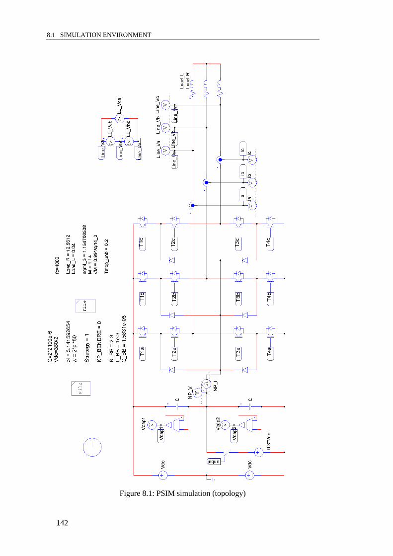
8.1 SIMULATION ENVIRONMENT
142
Figure 8.1: PSIM simulation (topology)

8 SIMULATION IMPLEMENTATIONS FOR QUANTITATIVE COMPARISON
143
Figure 8.2: PSIM simulation (control)

8.1 SIMULATION ENVIRONMENT
144
Figure 8.2 shows the architecture of the controller utilised in the simulation. On
the left hand side of the schematic is a (DLL) control block with 20 input and 20
output pins. This block includes a Dynamic Linked Library (DLL) file which is
programmed with the same C-source code as the DSP micro-controller used in the
experimental NPC converter. This ensures that the simulation model developed will
replicate the same functional behaviour as the experimental system. All modulation
calculations are conducted with floating-point numbers within the DLL, and current
and voltage sensor inputs to the DLL enable all closed loop NP regulatory functions
to also be programmed in the DLL source code. Finally the DLL also includes the
code to drive the switch on the DC bus which is responsible for the initial NP voltage
unbalance condition.
To the right of the DLL function block are three sets of dual comparators which
are used to implement the PD modulation process. These function blocks are
bypassed if a SVM strategy is implemented as the switches would be directly
controlled by the DLL in this case. The implementation of the PD modulator utilises
two carrier waveforms, one occupying the upper band with the second occupying the
lower band. These carrier waveforms are fed into the three sets of dual comparators,
which are also fed with the phase-leg reference waveforms from the DLL. The
comparator outputs then feed into a set of logic inverters and switch drivers to
generate the four gate drive signals for each phase leg.
To ensure that all the modulation and NP control strategies are compared on a fair
and equivalent basis, only the control section of each PSIM model is changed, with
the loading and converter supply conditions matched for each scenario. The primary
changes to the simulation model therefore occur within the DLL function block.
8.1.1 NP Controller Gain Selection Considerations.
One of the key issues that arose from the literature review of active NP control
strategies is that many of the reported techniques do not describe methodologies to
select the controller gains or parameters (e.g. the proportional and/or integral gain
constants of the linear NP voltage regulators). Only the SPWM and SVM strategies
have quantitative methods (i.e. ‘optimal’ methods) which specify exactly how the
gains should be designed. To ensure that the comparative evaluation of NP
controllers is fair the strategy that has been adopted in this thesis is to select
controller gain constants that maximise the dynamic response of each NP regulator.

8 SIMULATION IMPLEMENTATIONS FOR QUANTITATIVE COMPARISON
145
8.2 Implementation - SPWM+P
8.2.1 Duty Cycle Calculation / Modulation.
SPWM is implemented by comparing three phase waveforms against a double
triangular carrier arrangement as shown in Figure 8.3. As discussion in Section 8.1,
the basic PSIM model already includes the base PD modulator implemented with
dual carrier/comparator function blocks, and as such all the DLL must generate is the
three phase reference waveforms, viz.:
3
2cos
3
2cos
cos
tMV
tMV
tMV
C
B
A
(8.1)
where M is the modulation depth where 0.10 M .
8.2.2 State Redundancy Calculation Method - 1k & 2k .
As discussed in Chapter 3, the SPWM method with an NP controller can only
control 1 small vector within a switching cycle by varying the split-ratio (i.e. 1k and
2k ) of the redundant switching states for that particular small vector. This control
action is achieved via the addition of a common-mode / zero-sequence-offset to the
three phase reference waveforms. This zero-sequence is generated using a high gain
Figure 8.3: Phase Disposition (PD) modulation (top) and Phase leg A output of
unipolar form (bottom) M=1.0.

8.3 IMPLEMENTATION - SPWM+SONG [17]
146
proportional (P) controller [6] according to:
Offset = K * (Vtop capacitor – Vbottom capacitor) (8.2)
where K is the controller gain constant, which is set to 0.1 in this thesis. Note that
this system will not produce dynamic instability, despite the high gain, because a
dynamic limiter is used. This is achieved by first identifying upper and lower offset
limits, defined by:
Max_limit = min(1.0- AV , 1.0- BV , 1.0- CV ) (8.3)
Min_limit = -min(1.0+ AV , 1.0+ BV , 1.0+ CV ) (8.4)
The desired offset defined by the proportional controller is then limited in
accordance with the following pseudo-code:
if ( Offset > Max_limit)
limited_Offset = Max_limit
else if ( Offset < Min_limit)
limited_Offset = Min_limit
else
limited_Offset = Offset;
Finally, the limited offset is added to all three reference waveforms, according to:
fsetlimited_Of3
2cos
fsetlimited_Of3
2cos
fsetlimited_Ofcos
tMV
tMV
tMV
C
B
A
(8.5)
8.3 Implementation - SPWM+Song [17]
This strategy employs the same PD modulator as detailed in Section 8.2.1, with
the only difference being the methodology used to determine the split ratio of the
redundant states of the controllable small vector. As with the SPWM+P controller, a
zero-sequence injection strategy is used, with the zero-sequence determined as
follows:
1) The first step is to calculate the average NP current that would be required to
eliminate the NP voltage unbalance, based on the measured difference
between the upper and lower capacitor voltages, according to:

8 SIMULATION IMPLEMENTATIONS FOR QUANTITATIVE COMPARISON
147
s
CbCt
T
VVC
NPconi
(8.6)
2) The second step is to calculate an initial test zero-sequence offset, defined as:
c
b
a
Vsignc
Vsignb
Vsigna
sgn
sgn
sgn
(8.7)
cba
ccbbaaNPcontst
icibia
iVciVbiVaiv
sgnsgnsgn
sgnsgnsgn)(0 (8.8)
3) Verify and Revise
It is now required to test whether the addition of this offset to the three voltage
references will cause the sign of any one reference to change. This is achieved
by first calculating CBAmid VVVmidv ,, .
Then if midtstmid vvsignvsign )(0 , the offset is valid, otherwise the offset
calculation must be revised.
4) Revision
To revise the offset calculation, first identify midv , change its sign, and then
repeat the offset calculation defined in step 2.
5) Saturation limit of the offset 0v :
As in other zero-sequence offset based strategies, a limit has to be applied to
ensure that overmodulation does not occur. This is done as follows:
if ( 1,,max0 CBA vvvv
CBA vvvv ,,max10
else if ( 1,,max0 CBA vvvv
CBA vvvv ,,max10
6) Final application of the offset 0v :
0
0
0
3
2cos
3
2cos
cos
vtMV
vtMV
vtMV
C
B
A
(8.9)

8.4 IMPLEMENTATION - CSVPWM+P
148
8.4 Implementation - CSVPWM+P
8.4.1 Duty Calculation / Modulation
CSVPWM extends SPWM to replicate the modulation produced by a centered
space vector modulator. It achieves this by adding a non-linear zero-offset [59], as
shown in Figure 8.4
The process of generating the CSVPWM offset for a 3-level system is as follows:
Initially, the sinusoidal references are generated identically to SPWM:
3
2cos
3
2cos
cos
tMV
tMV
tMV
C
B
A
(8.10)
Then, according to [59], the 2-level CSVPWM offset is calculated and applied, viz:
CBACBAshift VVVVVVV ,,min,,max5.00.1 (8.11)
shiftCC
shiftBB
shiftAA
VVV
VVV
VVV
'
'
'
(8.12)
where max() and min() functions find the maximum and minimum of their three
arguments respectively. The references ''' ,, CBA VVV are applicable to a 2-level
converter, but they do not produce the required equal duty cycle split when applied to
Figure 8.4: Reference waveforms for CSVPWM for 3-level systems. M=0.7

8 SIMULATION IMPLEMENTATIONS FOR QUANTITATIVE COMPARISON
149
a 3-level converter. To solve this an additional offset calculation and is employed as
follows. Firstly, shifted phase voltages are calculated:
0.1mod
0.1mod
0.1mod
'''
'''
'''
CC
BB
AA
VV
VV
VV
(8.13)
where mod is the remainder after division process. This result is used to calculate the
additional zero sequence required, as:
''''''''''''_ ,,min,,max5.05.0 CBACBAshiftadd VVVVVVV (8.14)
The final reference waveform sent to the modulator is defined below:
shiftaddCref
C
shiftaddBrefB
shiftaddArefA
VVV
VVV
VVV
_'
_'
_'
(8.15)
8.4.2 State Redundancy Calculation Method - 1k & 2k .
As with SPWM, the CSVPWM method only has 1 small vector that can be
controlled by utilising dual redundant switching states with a duty cycle split ratio
defined by the constants 1k and 2k . Hence the same proportional controller approach
defined in Section 8.2.2. For the sake of brevity this control algorithm will not be
repeated here, but for CSVPWM the calculation process follows the same procedure
albeit based on the PWM reference set refC
refB
refA VVV ,, as opposed to CBA VVV ,, .
8.5 Implementation - Yamanaka SVM
8.5.1 Duty Calculation / Modulation
As with any SVM strategy, the first step requires the identification of the location
of the reference vector. Since the SV diagram of Yamanaka’s SVM is identical to
those of conventional SVM (see Figure 2.2), a simplifying technique such as ,
coordinate to g,h coordinate transformation can be used [88], as was done in this
thesis. With this strategy, the following steps are followed with the full simulation
code provided in Appendix A.1.5.3:
1) Firstly, the sector where the reference vector lies in is identified. It is simply
obtained by dividing the reference vector’s angle by 60 degrees and adding
one to the result.

8.5 IMPLEMENTATION - YAMANAKA SVM
150
2) Nearest Three Vector determination
Next, the reference vector is converted from , to gh coordinates in order
to determine which of the 4 subsectors it lies within. The process is detailed in
[88]. The result of this transformation gives the nearest three vectors and their
duty cycles.
3) State Redundancy Calculation Method - 1k & 2k .
Yamanaka recommends equating the two redundant split vectors i.e.
21 kk and the optimal calculation of 1k is based on the following equation:
21
*
12
1
smallysmallx
mediumzn
tRitRi
tRiik (8.16)
where Rix and Riy are the phase currents associated to small vector 1 and
2 respectively. They are a function of R, the sector where the reference vector
resides. Riz is the phase current for the medium vector. 1smallt , 2smallt and
mediumt are the time during a switching cycle for the each of the vectors. *ni is
the reference NP current that is commanded.
A major issue with the paper is that Yamanaka left the reader to determine
the value of *ni . Obviously in steady state, a value of 0 is ideal however during
transients, it is dependent upon the converter’s parameters. Yamanaka set this
to the peak output current value, which is then reduced instantly to zero once
the unbalance is eliminated.
In this thesis this approach is replicated by commanding the maximum
possible NP current, by explicitly setting k to 1 or 0 depending on the
unbalance. Pseudo-code to implement this is as follows:
if ( 1.0NPV )
NPVk *15.0
else
1k
This method forces k to the extreme value to obtain maximum
performance when the NP unbalance is greater than 5V.
4) Maximisation of NP control based on current polarity
The current controlled by each small vector changes depending the sector that
the reference vector is located within (e.g. in the first sector {00 to 60
0} the

8 SIMULATION IMPLEMENTATIONS FOR QUANTITATIVE COMPARISON
151
small vectors can control IA and IC, whereas in the second sector {600 to 120
0}
the small vectors can control IB and IC – see Figure 3.2). This is accounted for
by assigning the calculated duty cycle split ratio, k , to either 1k or 2k , based
on the sector and also the sign of the relevant phase current since this
determines whether the NP current will either reinforce or subtract from the
current NP voltage disturbance. This step is essential to obtain maximum
performance at high load power factor angles.
5) Switching sequence determination
Each possible switching sequence has been manually coded, based on both the
sector and sub-region that the reference vector is located, and also accounting
for the vector reversal in the next half-carrier equivalent switching cycle. This
approach ensures that each possible variation in sequence has been correctly
catered for, and the only input required is the variation to the duty cycle split
ratio determined in accordance with steps 3 and 4.
The end result of this process is the replication of the sequences required by
Yamanaka’s SVM as shown in Figure 8.5. Within the picture, 4 sequences
representing 4 subsectors are shown. In each sequence, the vector notations ‘ap’,
‘an’, ‘bp’, ‘bn’ denote the redundant states of the small vector. ‘a’ and ‘b’ denote the
large vectors whereas the medium vector is denoted by ‘c’.
8.5.2 Verification of the Simulation Implementation
The conditions within the authors’ paper were replicated in this simulation [8].
The parameters are listed in Table 8-1. A current source was used in the author’s
simulation and the worse case load power factor angle (i.e. 900) was specified. As a
result the power stage of the simulation within this thesis was changed to match the
author’s paper as shown in Figure 8.6
The simulation results are shown in Figure 8.7 The figure shows how the NP
controller attempts to reduce the NP drift (initially set to 10V) at the beginning of the
simulation run. The dynamic features of the NP recovery shows an identical
performance to that reported by Yamanaka et al. as shown in Figure 8.8 This
validates this thesis’s implementation of the SVM strategy proposed by Yamanaka et
al. and provides confidence that the comparative performance reported in Chapter 4
is valid and correct.

8.5 IMPLEMENTATION - YAMANAKA SVM
152
Table 8-1: Converter parameters for Yamanaka SVM validation
Name Modulation Strategy
DC bus voltage 560 V
DC link capacitance 4500 uF
Load frequency 50 Hz
Load magnitude 10 A
Load power factor angle 90 degrees
Switching frequency 3000 Hz
Figure 8.5: PWM for Yamanaka’s SVM. Image obtained from [8]
This image has been removed from the digital edition of this thesis in order to comply with copyright statutes.
Please refer to Fig. 4 from ref. [8]

8 SIMULATION IMPLEMENTATIONS FOR QUANTITATIVE COMPARISON
153
Figure 8.6: Modification of load to match author’s setup for Yamanaka SVM. 10000
ohm resistor is required for current source to be use within this simulation.

8.5 IMPLEMENTATION - YAMANAKA SVM
154
Figure 8.7: Thesis simulation results for Yamanaka’s SVM.
This image has been removed from the digital edition of this thesis in order to comply with copyright statutes.
Please refer to Fig. 10 from ref. [8]
Figure 8.8: Balancing performance at different modulation depths for author’s
implementation of Yamanaka’s SVM. Image obtained from [8]
0 0.01 0.02 0.03 0.04 0.05 0.06-5
0
5
10
15
Time (s)
NP
voltage (
V)
M = 0.1
M = 0.5
M = 0.8
M = 1.0

8 SIMULATION IMPLEMENTATIONS FOR QUANTITATIVE COMPARISON
155
8.6 Implementation of NTVV
8.6.1 Duty Calculation / Modulation
The carrier-based version of NTVV has been implemented in this thesis, since it
has now been demonstrated to be equivalent to an explicit space vector formulation
[68]. The process translates SPWM references to two references; one each for the top
and bottom carrier. The references are calculated based on the typical 3-phase
references cba VVV ,, , as defined according to Eqns (8.17) and (8.18), with the
resulting reference waveforms shown in Figure 8.9.
2
,,min cbaxxp
VVVVV
(8.17)
2
,,max cbaxxn
VVVVV
(8.18)
where cbax ,, .
8.6.2 State Redundancy Calculation Method - 1k & 2k .
The process to determine the duty cycle split ratio parameters proceeds as follows:
1) Firstly, the required current to discharge the unbalance is calculated according
to:
s
CtCb
T
VVC
oi
(8.19)
where C is the parallel combination of the DC bus capacitance, CbV and CtV
Figure 8.9: Result of transformation of SPWM references to NTVV references
obtained from [68]
This image has been removed from the digital edition of this thesis in order to comply with copyright statutes.
Please refer to Fig. 4 from ref. [68]

8.6 IMPLEMENTATION OF NTVV
156
are the voltages of the bottom and top capacitors respectively, and sT
represents the sampling period.
2) Next the duty cycles which represent the fraction of time each phase is
connected to the NP must be calculated to enable the determination of the
required zero-sequence offsets. These duty cycles are based on the two
reference waveforms defined in Eqns. (8.17) and (8.18) according to:
1
1
1
cpcnc
bpbnb
apana
VVd
VVd
VVd
(8.20)
3) The required zero-sequence offsets can then be calculated based on the duty
cycle information, the NP voltage error, the target NP current and the top and
bottom reference waveforms, according to:
ccbb
apano
aCtCboffaidid
VViiVVsignv
1
2
1_
(8.21)
ccaa
bpbno
bCtCboffbidid
VViiVVsignv
1
2
1_
(8.22)
bbaa
cpcno
cCtCboffcidid
VViiVVsignv
1
2
1_
(8.23)
where cba iii ,, are the phase leg currents.
4) The actual offset applied must be limited to prevent further NP imbalance
from occurring. This condition occurs when xpxn VV 1 . Hence the following
algorithm is used to limit the actual offset used:
if ( 0.0_ offxv )
limit = xpxn VV 15.0
if ( offxv _ > limit ) offxv _ = limit
else
top_limit = xpV
bot_limit = xnV
limit = -min(top_limit,bot_limit)
if ( offxv _ < limit ) offxv _ = limit
end

8 SIMULATION IMPLEMENTATIONS FOR QUANTITATIVE COMPARISON
157
5) Note that the three offsets are not applied simultaneously. Zaragoza applies
the offsets when both phase leg references are non-zero in order to prevent
additional unwanted switching transitions. shows that this region of operation
occurs in two locations for phase leg A i.e. 600 to 120
0 and 240
0 to 300
0. As a
result, the algorithm applies the following offsets:
if (eq. ref. vector angle is between 600 → 120
0 and 240
0 → 300
0)
offaapap vVV _
offaanan vVV _
if (eq. ref. vector angle is between 00 → 60
0 and 180
0 → 240
0)
offbbpbp vVV _
offbbnbn vVV _
if (eq. ref. vector angle is between 1200 → 180
0 and 300
0 → 360
0)
offccpcp vVV _
offccncn vVV _
8.6.3 Verification of Simulation Implementation
The parameters of NTVV are replicated within this simulation and their values are
listed in Table 8-2. The results of the simulation are shown in Figure 8.10. The
results correlate well with those from the authors as shown in Figure 8.11.
Table 8-2: Converter parameters for NTVV validation
Name Modulation Strategy
DC bus voltage 1200 V
DC link capacitance 1100 uF
Switching frequency 5000 Hz
Load frequency 50 Hz
Load resistance 10 ohms
Load inductance 12 mH
Load configuration Wye
Modulation index 0.8

8.6 IMPLEMENTATION OF NTVV
158
Figure 8.10: Simulation of NTVV balancing performance at different modulation
depths.
This image has been removed from the digital edition of this thesis in order to comply with copyright statutes.
Please refer to Fig. 8 from ref. [69]
Figure 8.11: Benchmarking simulation results for different modulation depths. Image
obtained from [69] for comparison purposes.
0 0.01 0.02 0.03 0.04 0.05 0.06 0.07 0.08 0.09 0.1450
500
550
600
650
700
750
Time (s)
Voltage (
V)
Vcap top @ M = 0.3
Vcap bot @ M = 0.3
Vcap top @ M = 0.6
Vcap bot @ M = 0.6
Vcap top @ M = 1.0
Vcap bot @ M = 1.0
m=1
m=0.6
m=0.3
8 SIMULATION IMPLEMENTATIONS FOR QUANTITATIVE COMPARISON
159
8.7 Implementation of ONTVV
8.7.1 Duty Calculation / Modulation
This modulation strategy is very similar to NTVV and as defined in [19]. The
strategy executes the following steps:
1) Region of operation identification.
2) Approximation of medium vector usage scaling based on region.
3) Calculation of duty cycles in d-q-0 domain.
4) Translation from d-q-0 domain to a-b-c references.
The steps are outlined explicitly in their paper and detailed in Appendix A.1.5.7.
8.7.2 State Redundancy Calculation Method - 1k & 2k .
The method of NP control for ONTVV is described in [71]. The NP controller is a
second order system, because the authors state within their paper that ‘This
compensator must have a low-pass characteristic, in order to only react to
perturbations in the dc-link voltage balance with frequencies lower than the
switching frequency.’ The output of this controller is then limited through a static
limiter.
Unfortunately, the information presented in this paper describes the 2nd
order
controller qualitatively and without parameters nor design rules. As such there is
insufficient information presented to enable the reader to replicate the documented
performance within this paper. In this thesis the following approach has been applied
to overcome this short-fall of information:
1) Given the absence of information on tuning the parameters of the 2nd
order
compensator, a PI controller has been used instead, with gains selected to be
Kp = 0.01 and Ki = 0.001. These are relatively small gain values but were
selected based on the observation of the offset was produced by the ONTVV’s
NP controller in simulation. [Note :For PI controller gains set well above these
values additional NP imbalance can result, and the output harmonic
performance degrade because the static limiter proposed by the authors in [71]
does not take into account the possibility of overmodulation.]
2) The output of this compensator is then passed through a static limiter where
the thresholds are set at [-0.1 and 0.1].

8.8 SUMMARY
160
3) Since the offset can be applied to either reference waveform per phase leg. An
algorithm recommended by the paper is used and it is not repeated due to its
clearly defined nature.
8.8 Summary
This chapter has detailed the implementation of the various NPC converter
modulation and NP control strategies in the PSIM simulation environment. These
simulation models were used to perform the comparative evaluation of the different
NP regulation approaches in Chapter 4, and to validate the natural balancing
responses throughout the remainder of the thesis. Selected benchmarking simulation
results have been presented to provide confidence and validation of the simulation
models developed.

9 EXPERIMENTAL SYSTEM
161
9 EXPERIMENTAL SYSTEM
The natural balance models developed in Chapters 5 and 6, and the enhanced natural
balance NP controller of Chapter 7, have been validated in two ways. The first
validation is by comparing the analytical models with the full-switched simulation
models described in Chapter 8. The second is by comparing simulation results
against experimentally measured time-domain NP balancing responses obtained
using a prototype NPC converter. This experimental verification is a critical aspect of
this thesis since it ensures that all pertinent factors of the theoretical models of the
natural balancing process that may impact on the NP voltage response, have been
properly accounted for. This chapter describes the experimental system that was
developed to obtain the experimental results presented throughout this thesis.
9.1 Overview of the Experimental System
Figure 9.1 shows a photo of the overall experimental arrangement used in this
investigation, including the NPC converter (centre of the work-bench), two series-
connected DC power supplies (bottom of the image) and three phase resistive loads
and filter networks (to the right of the image). The mid-point of the series connected
DC supplies creates a virtual earth potential to which the NP voltage can be
Figure 9.1: Photo of the experimental NPC converter, power supply and loads.

9.2 POWER STAGE
162
measured. An additional load bank (shown under the main work-bench) is used in
conjunction with a static switch to create the initial NP voltage unbalance. The load
bank to the upper-most right is the primary converter load, with the series connected
inductor to its’ immediate left. The load bank to the lower right is used for the
balance booster (note that this is significantly over-rated for this purpose). On the
lower right portion of the diagram is the balance booster placed with parallel to the
R-L load where the load bank is used to emulate the balance booster’s resistance. In
front of it are the inductors and capacitors that make up the other parts of the balance
booster, tuned at the switching frequency.
Figure 9.2 shows a close up of the experimental 3-phase NPC converter. The next
sections of this chapter will now discuss the different groups of components that
make up this 3-phase Active NPC converter.
9.2 Power Stage
The power stage of the converter was built in the lab. It uses an active NPC
topology as shown in Figure 9.3. From this diagram, three alternatives are available
to feed the DC input side of the converter.
a) Rectified 3-phase supply. The diode rectifier used is Semikron SKD 82/12.
b) One DC source connected across the nodes: BUS_TOP and BUS_BOT.
c) Two DC sources in series connected across the nodes BUS_TOP and
BUS_BOT. The node BUS_MID may or may not be connected to the mid-
point of the two DC sources depending on the requirements of the user. If the
user requires a 3-level source, the mid-point of the DC source has to be
connected to BUS_MID. A 2-level source would mean the disconnection of
this point.
The design decisions made in this thesis for the DC input to the power stage were:
a) DC sources were chosen over a rectified 3-phase supply because this allows
short circuit currents to be limited.
b) A two DC sources configuration were chosen over a single DC source
because:
a. This thesis follows the convention used in [62] to formulate the
mathematical expressions of PWM signals and their Double Fourier
expressions. These expressions assume 2 DC sources. These structure
is used in Chapter 5 onwards to model the NPC phase leg(s).

9 EXPERIMENTAL SYSTEM
163
b. NP voltage deviation is easy to measure electrically when it is
measured w.r.t. to its ideal value i.e. the mid-point of the DC sources.
Both DC sources are set to produce the exact same voltage.
Figure 9.2: Close up of experimental NPC converter.

9.2 POWER STAGE
164
Figure 9.3: Power stage design of the converter.
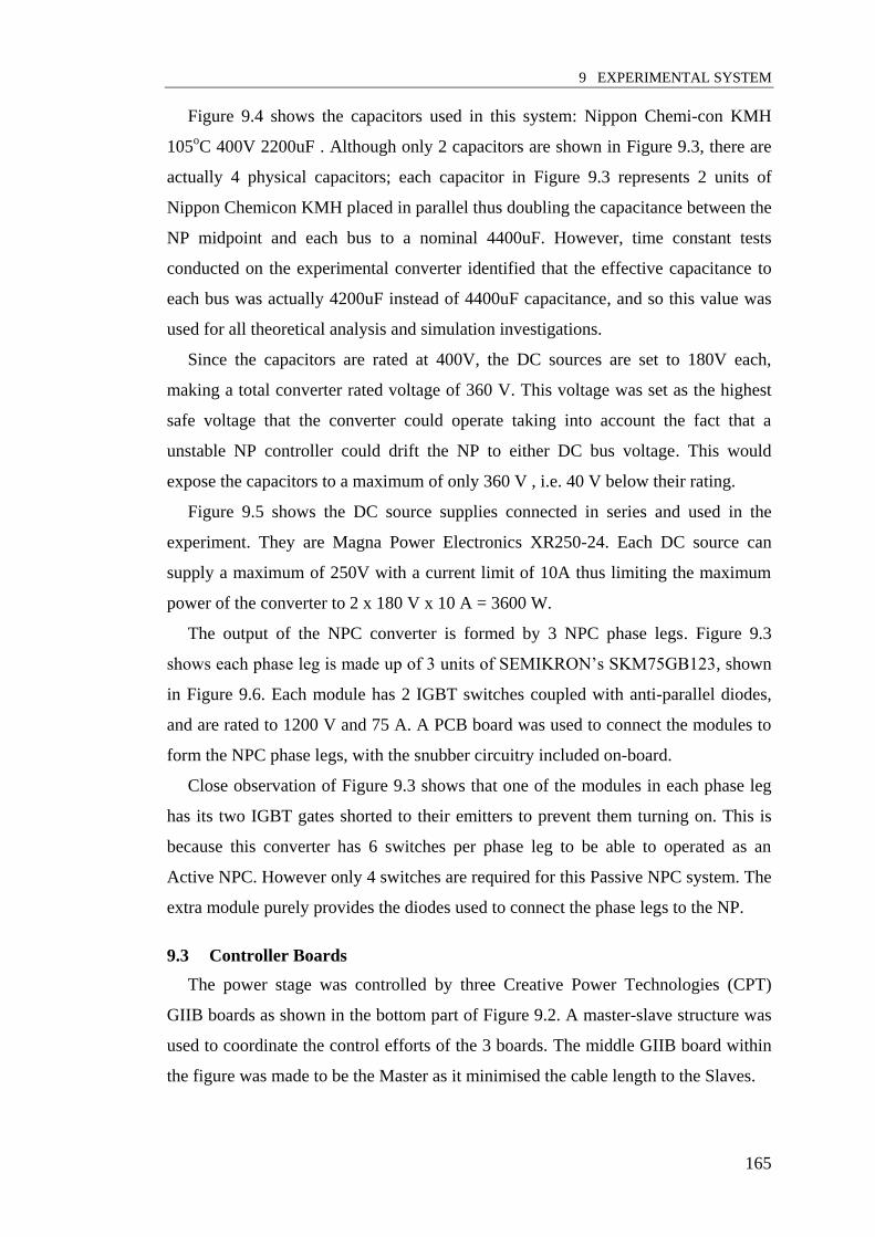
9 EXPERIMENTAL SYSTEM
165
Figure 9.4 shows the capacitors used in this system: Nippon Chemi-con KMH
105oC 400V 2200uF . Although only 2 capacitors are shown in Figure 9.3, there are
actually 4 physical capacitors; each capacitor in Figure 9.3 represents 2 units of
Nippon Chemicon KMH placed in parallel thus doubling the capacitance between the
NP midpoint and each bus to a nominal 4400uF. However, time constant tests
conducted on the experimental converter identified that the effective capacitance to
each bus was actually 4200uF instead of 4400uF capacitance, and so this value was
used for all theoretical analysis and simulation investigations.
Since the capacitors are rated at 400V, the DC sources are set to 180V each,
making a total converter rated voltage of 360 V. This voltage was set as the highest
safe voltage that the converter could operate taking into account the fact that a
unstable NP controller could drift the NP to either DC bus voltage. This would
expose the capacitors to a maximum of only 360 V , i.e. 40 V below their rating.
Figure 9.5 shows the DC source supplies connected in series and used in the
experiment. They are Magna Power Electronics XR250-24. Each DC source can
supply a maximum of 250V with a current limit of 10A thus limiting the maximum
power of the converter to 2 x 180 V x 10 A = 3600 W.
The output of the NPC converter is formed by 3 NPC phase legs. Figure 9.3
shows each phase leg is made up of 3 units of SEMIKRON’s SKM75GB123, shown
in Figure 9.6. Each module has 2 IGBT switches coupled with anti-parallel diodes,
and are rated to 1200 V and 75 A. A PCB board was used to connect the modules to
form the NPC phase legs, with the snubber circuitry included on-board.
Close observation of Figure 9.3 shows that one of the modules in each phase leg
has its two IGBT gates shorted to their emitters to prevent them turning on. This is
because this converter has 6 switches per phase leg to be able to operated as an
Active NPC. However only 4 switches are required for this Passive NPC system. The
extra module purely provides the diodes used to connect the phase legs to the NP.
9.3 Controller Boards
The power stage was controlled by three Creative Power Technologies (CPT)
GIIB boards as shown in the bottom part of Figure 9.2. A master-slave structure was
used to coordinate the control efforts of the 3 boards. The middle GIIB board within
the figure was made to be the Master as it minimised the cable length to the Slaves.

9.3 CONTROLLER BOARDS
166
Figure 9.4: One of the 4 capacitors used as the DC link within the converter.
Figure 9.5: Two DC sources in series using Magna XR250-24.

9 EXPERIMENTAL SYSTEM
167
Figure 9.7 shows a detailed view of the GIIB board, identifying the various circuit
sections. The gate driver outputs were connected to the IGBTs according to the net
labels shown in Figure 9.3, Figure 9.8, Figure 9.9 and Figure 9.10.
Since the CPT-GIIB and other CPT products were initially designed to operate
with an earlier version controller card and not a CPT-DA2810 which has a newer
Texas Instrument DSP, a interposing CPT-Mini2810 board is required to interface
the CPT-DA2810 and CPT-GIIB. This card uses an Altera CPLD to route signals
between the CPT-DA2810 and various parts of the CPT-IIB power board, including
clock, gate driver signals, MINIBUS, digital data (e.g. SPI), and protection signals.
Additional features of the board are deadband generation for one 2 gate drivers / one
phase leg and hysteresis signal generation. The CPT-Mini2810 is controlled by the
CPT-DA2810 through SPI signals. Figure 9.11 shows the CPT-DA2810 assembled
with onto CPT-Mini2810 board, while Figure 9.12 shows an individual CPT-
DA2810 board.
Figure 9.6: Semikron module consisting of 2 IGBT switches with anti-parallel
diodes.

9.3 CONTROLLER BOARDS
168
Figure 9.7: CPT’s Generalised Integrated Inverter Board (CPT-GIIB).
POWER SUPPLY
GATE
DRIVERS
CURRENT
SENSORS
VOLTAGE SENSORS
PLUG-IN
CONTROLLER
BOARD

9 EXPERIMENTAL SYSTEM
169
Figure 9.8: Controller board wiring for Master GIIB.

9.3 CONTROLLER BOARDS
170
Figure 9.9: Controller board wiring for Slave GIIB 1.

9 EXPERIMENTAL SYSTEM
171
Figure 9.10: Controller board wiring for Slave GIIB 2.

9.3 CONTROLLER BOARDS
172
The CPLD on the CPT-Mini2810 was reprogrammed for this thesis to provide a
SPI communications channel in between the 3 CPT-DA2810 boards. This involved
controlling the direction of the bidirectional SPI communications. 2 pins are
necessary to indicate the direction of SPI data (towards/away the DSP) and the mode
of the DSP (Master/Slave). The sequence of operation of the three GIIBs is as
follows:
Figure 9.11: CPT-DA2810 on top of CPT-Mini2810.
Figure 9.12: CPT-DA2810.

9 EXPERIMENTAL SYSTEM
173
Step # MASTER GIIB SLAVE GIIB
1 Turn ON
2 Initialise DSP variables
3 Set DSP’s SPI module to MASTER mode
4 Set control pins to ensure CPLD only communicates with DSP
5 Initialise / Configure CPLD
6 Set DSP’s SPI module to MASTER
mode
Set DSP’s SPI module to SLAVE
mode
7 Set CPLD’s control pins to send
data from DSP to output buffer pins
Set CPLD’s control pins to receive
data from input buffer pins to DSP
8 Send synchronisation pulse Receive synchronisation pulse and
realign PWM carrier.
9 Calculate value of PWM signals Do nothing
10 Transmit data if it has been 1
second after turning on DSP Receive data
11 Set value of PWM compare logic.
12 Continously repeat steps 8 to 11.
9.4 Communications
The communication between MASTER and SLAVE GIIBs were conducted
through a shielded ribbon cable. The following signals were transmitted:
MASTER pin Communication direction SLAVE pin
Synchronisation (GPIO) → Capture port
SPI CLOCK → SPI CLOCK
SPI DATA → SPI DATA
SPI Chip Select ?* SPI Chip Select
Slave error (2 pins for 2
slaves) ←
Converter fault (1 pin for
each GIIB)
* GPIO is General Purpose Input/Output.
* Chip select is controlled manually by the DSP and CPLD.

9.5 LOAD BANK
174
The shielded ribbon cable is connected to the Digital I/O connector of each GIIB.
The pins of the Digital I/O are partially controlled by the CPLD. The CPLD has been
modified to route the synchronisation and SPI communications.
The MASTER sends the following SPI data at 7.5 Mhz; byte 0 is the first byte
transmitted:
Byte 0 – Status bit where the bit 0 designates whether the SLAVE GIIB should
enable switching.
Byte 1 – Upper 8-bits of the 16-bit COMPARE value for SLAVE 1’s switches S1
and S3.
Byte 2 – Lower 8-bits of the 16-bit COMPARE value for SLAVE 1’s switches S1
and S3.
Byte 3 – Upper 8-bits of the 16-bit COMPARE value for SLAVE 1’s switches S2
and S4.
Byte 4 – Lower 8-bits of the 16-bit COMPARE value for SLAVE 1’s switches S2
and S4.
Byte 5 – Upper 8-bits of the 16-bit COMPARE value for SLAVE 2’s switches S1
and S3.
Byte 6 – Lower 8-bits of the 16-bit COMPARE value for SLAVE 2’s switches S1
and S3.
Byte 7 – Upper 8-bits of the 16-bit COMPARE value for SLAVE 2’s switches S2
and S4.
Byte 8 – Lower 8-bits of the 16-bit COMPARE value for SLAVE 2’s switches S2
and S4.
Byte 9 – Checksum. Its value is the lower 8-bit of the result of the sum of byte 0 to
byte 8.
9.5 Load Bank
The equipment used to form the R-L load is shown in Figure 9.13 and Figure
9.14. The specification of the RMIT resistive load bank is 240V, 5.25kW per phase.
The loads can be varied in steps by turning parallel loads on and off using switches
on the front panel of the load bank.
The 240V, 10A 3-leg 3-phase inductors are made by IRONCORE
TRANSFORMERS PTY. LTD. Their multiple taps offer 80mH, 64mH, 40mH and
16mH alternative inductances.

9 EXPERIMENTAL SYSTEM
175
Figure 9.13: RMIT lab resistive load bank.
Figure 9.14: Inductive load bank.

9.6 BALANCE BOOSTER
176
9.6 Balance Booster
The equipment used to form the balance booster is shown in Figure 9.13 (a second
matching load bank), Figure 9.15 and Figure 9.16. Figure 9.15 shows the high
frequency 20mH inductor, rated at 12A per coil. This unit has multiple taps allowing
various inductances to be set using up to 10 coils. For this work, Figure 9.15 shows
the wiring configuration used to get the required inductance of 1mH.
Figure 9.16 and Figure 9.17 show the high-frequency WIMA MKS 4 1.0 uF 630V
capacitors used for the balance booster filter, mounted in a plastic enclosure.
The Dyne inductors were placed in series with the WIMA capacitors and the each
phase of the load bank, to form the RLC balance booster. The combined resistance of
the inductor and capacitor gives the experimental resistance of 2.3 ohms, determined
using a spectrum analyser.
Figure 9.15: Dyne high frequency inductors.

9 EXPERIMENTAL SYSTEM
177
9.7 Experimental Verification using the Preferred Active Strategy:
CSVPWM+P
The operation of the experimental system was confirmed by comparing it against
the results of the simulation of a NPC converter using CSVPWM with Proportional
controller. The operational parameters for the simulation and experimental converter
were made identical of course for this test, with parameters as given in Table 9-1.
Figure 9.16: Top view of the enclosure of the capacitors for balance booster.
Figure 9.17: Bottom view of the enclosure of the capacitors for balance booster.

9.7 EXPERIMENTAL VERIFICATION USING THE PREFERRED ACTIVE STRATEGY:
CSVPWM+P
178
Figure 9.18 to Figure 9.20 demonstrate the close match of the experimental and
simulation results during a transient event, confirming the validity of the simulation
model and its excellent correlation with physical reality. Note in particular in Figure
9.20 how the line-to-line voltage of the converter recovers to a much better looking
symmetrical waveform as the NP unbalance reduces during the test.
This close match between simulation and experiment gives strong confidence that
the simulation results presented in the earlier chapters are in fact reasonable and
physically achievable.
Table 9-1: NPC converter parameters.
Parameter Value
Nominal DC link 360 V
Capacitor size 4200 µF
Load Resistance 11 ohms
Load Inductance 44.4 mH
Fundamental Frequency (fo) 50 Hz
Switching frequency 5000 Hz
Figure 9.18: NP control performance of CSVPWM with Proportional controller at
M=0.9, fs=5000 Hz.
0 0.02 0.04 0.06 0.08 0.1 0.12 0.14 0.16 0.18 0.2-40
-35
-30
-25
-20
-15
-10
-5
0
5
Time (s)
NP
voltage (
V)
Dynamic performance of CSVPWM with P controller
Experimental
Simulation
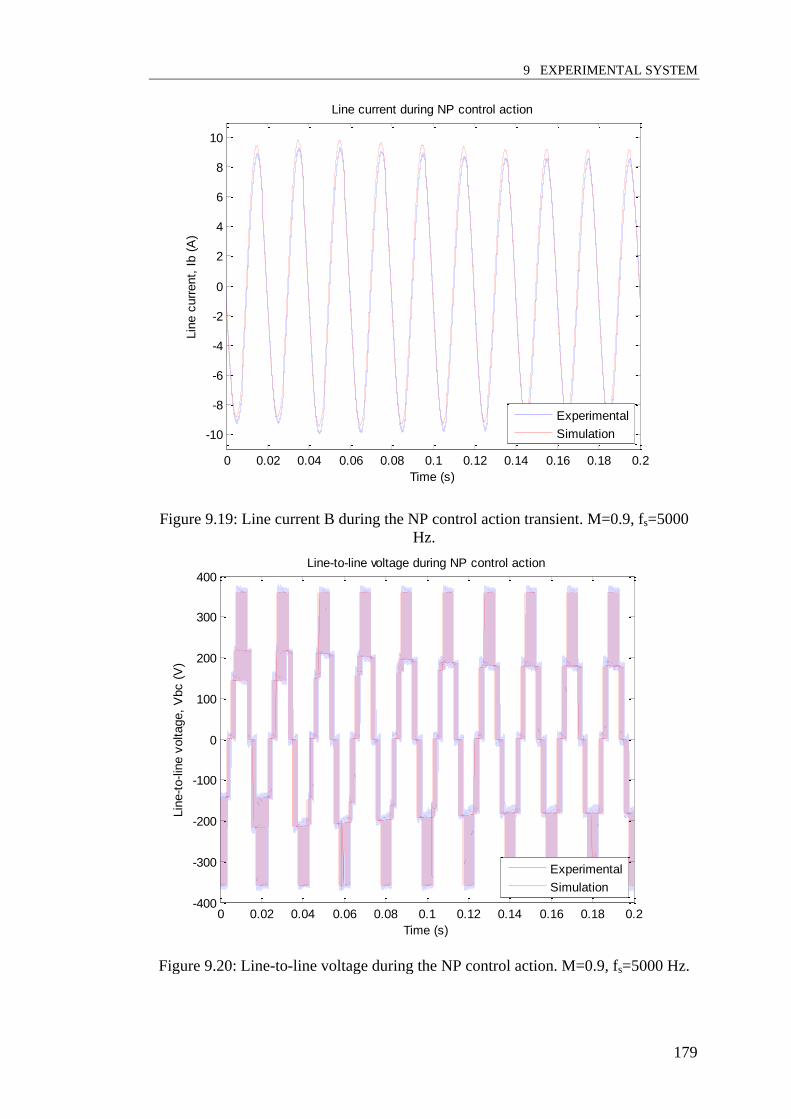
9 EXPERIMENTAL SYSTEM
179
Figure 9.19: Line current B during the NP control action transient. M=0.9, fs=5000
Hz.
Figure 9.20: Line-to-line voltage during the NP control action. M=0.9, fs=5000 Hz.
0 0.02 0.04 0.06 0.08 0.1 0.12 0.14 0.16 0.18 0.2
-10
-8
-6
-4
-2
0
2
4
6
8
10
Time (s)
Lin
e c
urr
ent,
Ib (
A)
Line current during NP control action
Experimental
Simulation
0 0.02 0.04 0.06 0.08 0.1 0.12 0.14 0.16 0.18 0.2-400
-300
-200
-100
0
100
200
300
400
Time (s)
Lin
e-t
o-lin
e v
oltage,
Vbc (
V)
Line-to-line voltage during NP control action
Experimental
Simulation

9.7 EXPERIMENTAL VERIFICATION USING THE PREFERRED ACTIVE STRATEGY:
CSVPWM+P
180

10 CONCLUSION AND FUTURE WORK
181
10 CONCLUSION AND FUTURE WORK
One major concern for a Neutral Point Clamped (NPC) converter is drift of the
central Neutral Point (NP) voltage away from zero, particularly if it drifts to voltage
levels that can cause semiconductor failure. This drift occurs during both steady state
and transient operation and NP control is essential to manage it in any practical NPC
application. Three NP control methodologies are available. The most popular is
direct control of NP currents using modulation strategies, termed ‘active’ control. A
major challenge is the large amount of literature covering this concept. The next
methodology is the old and expensive method of using ‘additional hardware’. The
third alternative, ‘natural balancing’, is the least explored and understood.
This thesis has categorised and compared different ‘active’ control strategies to
identify that the CSVPWM with Proportional is usually the best choice for most
applications. Next, it explored the ‘passive’ method and the different load
configurations that are possible for the 3-phase NPC converter. An analysis of an
enhanced ‘passive’ balancing strategy in combination with Feedforward DC Link
compensation is also presented. Finally, this chapter summaries the results from the
previous chapters and proposes a list of future research areas to pursue.
10.1 Summary of Work
10.1.1.1 Fundamentals of NP control and Analysis of Existing ‘Active’ NP Control
Strategies
Chapter 3 has presented the fundamentals of NP control and its limiting
conditions. In particular it has shown that an increase in NP control performance
requires a reduction of the NP disturbing mediumV vector which causes multiple side-
effects, and usually degrades the converter’s operation to that of a 2-level converter
at maximum control action. In between ideal 3-level operation and the 2-level-like
operation is a middle ground that incurs an increase in implementation complexity,
switching transitions and creates poorer harmonic distortion.
Based on the analysis presented in this thesis, any NP control strategy can be
classified by observing its vector selection. This analysis also reveals disadvantages
of the various strategies. Dipolar PWM was shown to have an unclear NP control
strategy, thus being unpractical and consequently neglected for comparison in
Chapter 4. Ustepente SVM, which offers the best compromise between NP control

10.1 SUMMARY OF WORK
182
performance and harmonic degradation, was eliminated due to its high number of
switching transitions. Medium Vector Elimination is also eliminated because it
causes double switching transitions, and in any case degrades to a performance that
is similar to 2-level converters.
10.1.2 Categorisation of Active Control Strategies
The analysis of a strategy’s vector selection reveals its NP control methodology.
Hence, strategies that share similar vector selection can be grouped. The differences
within a group lie in two factors. The first is how it calculates the duty cycles for all
the vectors. The second is how it calculates the split of the small vectors’ duty cycles
across the redundant states. As a result of this understanding, this thesis has
contributed to a coherent classification of NP control strategies.
10.1.3 Quantitative Comparison of Practical Strategies
The qualitative analysis presented in Chapter 3 does not provide a good indicator
of the precise performance differences between various NP strategies. A
quantification of their various attributes is required to identify the ‘best’ strategy.
The research has conducted a detailed comparison to quantify the harmonic
performance, NP control performance and NP deviation in the search for the most
practical NP control strategy for the NPC converter. A list of carrier-based strategies
including ones that have been translated from their SVM form were compared. A
SVM strategy (Yamanaka SVM) from a group that is expected to produce a good
balance between harmonic distortion and NP control performance was also included.
The results show that the Centered Space Vector (CSV) PWM, a carrier-based
equivalent of conventional Nearest Three Vector (NTV) SVM, combined with a
proportional controller zero-offset addition, provides excellent performance in high
DC link capacitance converters while being simple to implement. It works well
except for regions of high modulation depth and low load power factor angle, where
the Yamanaka SVM strategy offers better performance whilst still maintaining good
harmonic performance. However, this strategy does not perform better than
CSVPWM with a proportional controller for other regions. The Virtual Vectors
method also offers exceptional NP control performance in these conditions however
its harmonic performance is worse than a 2-level converter. It also is not able to
perform better than CSVPWM at other conditions.

10 CONCLUSION AND FUTURE WORK
183
Unsurprisingly, both the CSVPWM and SPWM strategy i.e. Phase Disposition
(PD), have the same NP control performance although this is not reported within the
literature. However, SPWM should be only recommended for applications where the
neutral of the load does not float i.e. grid-based 4-wire converters. This is because
SPWM causes more distortion than CSVPWM for the same amount of NP ripple.
10.1.4 Derivation of the Natural Balancing Mechanism
This thesis has modelled the NPC converter’s phase leg and shows how a tuned
RLC network placed in parallel with the load, also known as a balance booster, can
be used to increase its balancing performance. Simulation results were used to verify
the validity of the model. The balance booster’s performance varies linearly with the
amount of energy consumed. Thus, a high performance balance booster may reduce
the efficiency of a converter.
10.1.5 The Characterisation of Natural Balancing Performance with Balance Booster
for Three-phase Converters and their Variants
The phase leg model developed in Chapter 5 was then extended to model 3-phase
variants of the NPC converter, and it was found that the natural balancing
performance is typically three times faster than that of a single phase leg, even with a
floating load. The inclusion of an additional balance booster filter also further
increases the balancing performance by a considerable amount.
The chapter also compares various topological variations of the balance booster
network, identifying that a floating neutral filter connection gives the better natural
balancing response when the floating neutral and NP connected filters are matched
on a power loss basis. It concludes by exploring the variation in natural balancing
performance as various operating parameters are changed.
10.1.6 Harmonic Modelling of the Combination of ‘Passive’ NP Control and DC
Bus Link Voltage compensation using CSVPWM.
Chapter 7 demonstrated that the driving forces for NP balancing come from two
sources – a strong ‘active’ driving force deriving from the product of the unbalanced
modulation harmonics and the main DC link voltage DCV , and weaker ‘passive’
natural driving force deriving also from the product of the balanced modulation

10.2 SUGGESTIONS FOR FUTURE WORK
184
harmonics and the NP voltage deviation NPV . From this understanding, it was
recognised and confirmed that combining a balance booster filter with the additional
unbalanced harmonic distortion created by DC Link Compensation integrated into
CSVPWM, significantly improved the natural NP balancing response. The resulting
system almost matches the balancing performance of many direct active strategies at
all load power factor angles. In particular it provides an excellent NP control
performance midway between Yamanaka’s SVM, the fastest active method for an 85
degree load power factor angle, and CSVPWM+P, the second fastest active method,
while still maintaining an ideal 3-level THD output. This result is something that
most active controllers cannot achieve.
This new mathematical modelling approach opens up a new area of research for
NP controllers which incorporate a balance booster to improve their NP balancing
performance.
10.2 Suggestions for Future work
10.2.1 Carrier-based Equivalent of Yamanaka’s SVM
Yamanaka’s SVM offers the best harmonic performance and NP control
performance at the cost of variable switching frequency and high switching losses at
low modulation depth. The latter problem can be eliminated by reducing the
unnecessary switching transitions at low modulation depth. A carrier-based
equivalent of Yamanaka’s SVM is available in the form of ‘1-phase dipolar 2-phase
unipolar’ hybrid carrier-based modulation.
The difficulty is the analytical calculation required in order to choose the phase
leg that will perform dipolar modulation and the amount of offset between the
references within dipolar modulation. Nonetheless, the calculation can be translated
from the SVM to carrier-based form.
10.2.2 Comparison involving Common-mode Currents
High-frequency switched common-mode currents produced by the NPC converter
can cause premature failure of motor bearings and also insulation of long cables.
Unfortunately, there is little consistancy in measuring common-mode current in the
literature, and as a result it has not been included in the comparisons conducted
within this thesis. This is important because CSVPWM/SVM is known to inject

10 CONCLUSION AND FUTURE WORK
185
common-mode in order to increase the modulation depth of the converter. Also, NP
controllers adjust the split of redundant states to control the NP current, and this is
effectively changing the common-mode currents too. As a result, an investigation is
required to not only understand these effects but to also compare the common-mode
voltages and currents produced by the different active NP balancing strategies.
10.2.3 Derivation of Stable Combined Balance-booster-assisted ‘Active’ NP
Controller
This thesis has developed an analysis tool that can be used to explore new active
strategies to take advantage of the balance boosters in order to achieve high-
efficiency and improved performance NP control. One major advantage of this
approach is the ability to control the NP voltage in the regions where ‘active’
controllers fail.
10.2.4 Model Predictive Control
This thesis has shown that any NP control strategy will lie in between the ‘least
control’ solution and the ‘full control’ solution. This is especially true for the Model
Predictive Control method. However, it has an added advantage to existing NP
control i.e. it is well suited to this multi-variable problem whereas existing NP
control solutions are not. Thus, it can better find an optimal point of operation.
Another advantage is that MPC can adapt its operation depending on whether
there is a transient event or not. During steady state, it can operate in a ‘least control’
mode to maximise harmonic performance. When a transient event occurs, the
converter can shift into a mode in between the middle mode and ‘full control’ mode
(depending on the severity of the NP drift) to counteract any NP drifts. This ability to
temporarily sacrifice quality is a good advantage to minimise converter overdesign.
10.2.5 Model Predictive Control with Balance boosters
The harmonic model framework can assist a designer to produce ‘active’ MPC
strategies that can be tailored to work with the balance booster to produce very high
performance NP controllers. This could be achieved by adapting the modulation
strategy in such a manner as to deliberately produce harmonics of the correct polarity
in order to reduce the NP unbalance.

10.3 SUMMARY
186
10.2.6 Optimised Balance-booster Design
A major drawback of a balance booster on a 3-phase NPC converter is the high
energy loss produced in order to obtain high balancing performance. This loss is
apparent during steady-state operation when the NP is balanced. This is because the
balance booster also interacts with the balanced harmonics produced by the Phase
Disposition modulation technique, which is undesirable. A high performance balance
booster has a low resistance and causes large balance booster currents and losses. On
the other hand, a low performance filter has a high resistance causing small balance
booster currents and losses. There are 2 solutions:
Firstly, an extremely narrow notch filter could be produced acting like a comb
filter that only interacts with the harmonics produced by NP unbalance. The result
would be a filter that only consumes energy when an unbalance occurs. The physical
construction of these extremely narrow notch filters can be produced by cascading
filters to derive n-order filters.
Secondly, variable loss performance could be obtained by varying the resistance
of the RLC network. Switching multiple resistors in parallel can produce stepwise
changes in resistance. However the several switches and resistors required could be
costly. An alternative could be to use semiconductors operating in the linear region,
acting as a variable resistor.
10.2.7 n-phase NPC
Chapter 6.1 has illustrated the ability to model a NPC converter with 3 phase legs
each having a common modulation signals phase shifted by 120 degrees. It has also
shown that the superposition technique can be used to simulate phase legs having
different load and balance booster configuration. This approach could be extended to
an arbitrary number of phase legs with each phase leg having different modulation
switching signals and different load and balance booster topologies.
10.3 Summary
The NP drift problem occurs as a result of modulation, topological structure,
physical construction and load asymmetries. Various modulation-based NP current
control strategies, termed ‘active’ control, have been proposed but few comparisons
have been conducted between them.
10 CONCLUSION AND FUTURE WORK
187
This thesis has analysed different ‘active’ strategies, to identify CSVPWM with
Proportional zero-offset control as the most attractive alternative due to its simple
implementation and high performance. A higher performance at the cost of higher
implementation complexity can be found using Yamanaka’s SVM implementation,
however its performance advantage is only observable for low load power factor
angle applications.
The thesis work then showed that an NPC converter with low DC link capacitance
/ high NP ripple is best paired with a Feedforward / DC link compensation PWM
strategy coupled with a balance booster filter. This combination provides a NP
control performance that is only slightly less than CSVPWM with Proportional
controller while providing an improved harmonic performance because the latter
solution’s harmonic performance can degrade to 2-level converter levels.
Finally, the natural balancing harmonic analysis strategy presented in this thesis
opens up a new research area for providing extremely fast NP controllers by adding
balance booster filters to other control strategies.

10.3 SUMMARY
188

SIMULATION SOFTWARE 189
189
APPENDIX A SIMULATION SOFTWARE
This section will detail the software code used to conduct simulations of the various
‘active’ strategies. The following section will group together code from MATLAB
and PSIM used to simulate a particular strategy.
A. 1 MATLAB scripts to run simulations in Chapter 4
Common to all the modulation strategies tested are these high-level MATLAB
scripts. These scripts run a PSIM simulation file containing the topology and
modulation strategy. They store the results of the PSIM simulation and reiterate the
process across the whole modulation range.
A.1.1 MATLAB script – steady state NP deviation and NWTHD harmonic
calculation
This MATLAB script is to repeat the PSIM simulations across the whole range of
modulation depth while the NPC converter operates in steady state where NP is
allowed to float. As such, it will vary at 3 times the fundamental frequency for
conventional carrier-based PWM strategies. The resulting output voltage will contain
this NP variation and it is used for the NWTHD calculations.
clc
clear
%% Power converter simu settings calculator
load_angle = 1;
Z = 11 + 1j*2*pi*50*44.4e-3;
R = abs(Z) * cosd(load_angle);
X = abs(Z) * sind(load_angle) ;
L = X / (2*pi*50);
Load_R = R
Load_L = L
res = 40 % number of points in THD curve
step_M = 1/res;
vec_M = step_M:step_M:1;;
vec_M(size(vec_M,2)) = vec_M(size(vec_M,2)) - 0.001;
%vec_M = vec_M(find(vec_M == 0.5));
%% Automator
% Outer loop to cycle through the Ms
% Inner loop to increment frequencies until we find the required number of
% transitions.
for j=1:length(vec_M) % cycle through M
%% User-changable system variables
M = vec_M(j) * sqrt(4/3);

190 SIMULATION SOFTWARE
190
fc = 3950;
Tstop_unb = 0;
n_transitions = 0;
i = 1;
% while (n_transitions < 165) % increment frequencies
%% PSIM simulation preparation
ipath = [cd,'\','a.psimsch'];
%ipath = ['a.sch'];
ipath = ['"',ipath,'"']; % because there are spaces
opath = [cd,'\','a.txt'];
%opath = ['a.txt'];
opath = ['"',opath,'"']; % because there are spaces
M_s = sprintf('%g',M);
fc_s = sprintf('%g',fc);
Load_L_s = sprintf('%g',Load_L);
Load_R_s = sprintf('%g',Load_R);
load_angle_s = sprintf('%g',load_angle);
Tstop_unb_s = sprintf('%g',Tstop_unb);
variable1 = [' -v "M=',M_s,'" '];
variable2 = [' -v "fc=',fc_s,'" '];
variable3 = [' -v "Load_L=',Load_L_s,'" '];
variable4 = [' -v "Load_R=',Load_R_s,'" '];
variable5 = [' -v "Tstop_unb=',Tstop_unb_s,'" '];
cmd = ['"C:\Program Files (x86)\Powersim\PSIM9.0.3\PsimCmd.exe" -i ',...
ipath,' -o ',opath, variable1, variable2, variable3,...
variable4, variable5];
%% PSIM simulation execution
tic
disp(['Starting PSIM simulation M=', M_s, ' fc=', fc_s])
dos(cmd);
toc
%% Post PSIM simulation
% Load data
tic
disp('## txt2mat');
data = txt2mat('a.txt','InfoLevel',0);
toc
% Truncate the data for one fundamental cycle
% starting from 0.05 seconds
z_t_step = data(1,1);
z_n_elements = 0.02 / z_t_step;
z_n_start = 0.3 / z_t_step;
z_n_end = z_n_start+z_n_elements-1;
z_t_start = z_n_start * z_t_step;
z_t_end = z_n_end * z_t_step;
data = data(z_n_start:z_n_end,:);
% Pick off parts of the data
disp('## picking data');
Carrier = data(:,3);
Transitions = data(:,27);
Vab = data(:,13);
NP_V = data(:,16);
% # of carrier edges
disp('## carrierCount');
[pos, neg] = carrierCount(Carrier);
% Error checking
if (pos ~= neg)

SIMULATION SOFTWARE 191
191
ME = MException('A', ...
'Check please');
throw(ME);
end
if (pos ~= fc/50)
ME = MException('A', ...
'Check please');
throw(ME);
end
% # of transitions
n_transitions = Transitions(length(Transitions)) - Transitions(1);
n_transitions = round(n_transitions);
disp('## wthdCalc');
wthd = wthdCalc(Vab);
nwthd = wthd*M;
fprintf(1,'\n');
disp(['fc=', fc_s, ' n=', sprintf('%g',n_transitions), ' wthd=' sprintf('%g',wthd)]);
fprintf(1,'\n');
result(j,1) = M;
result(j,2:6) = [ fc n_transitions wthd nwthd max(abs(NP_V)) ];
j = j + 1;
end
result = sortrows(result,1)
disp('Game over, yeah!')
csvwrite('result.csv',result);
A.1.2 MATLAB script – Dynamic NP performance test
This MATLAB script is to repeat the PSIM simulations across the whole range of
modulation depth while the NPC converter reduces the NP unbalance from 20% to
5% of VDC, half the DC bus voltage. The initial NP unbalance is set using a DC bus
voltage and then disconnected once the load currents reach steady-state values. The
PSIM simulation time is 1second for both 1 degree and 45 degree load angle. 5
seconds is used for 90 degree load angle.
clc
clear
%% Power converter simu settings calculator
load_angle = 1;
Z = 11 + 1j*2*pi*50*44.4e-3;
R = abs(Z) * cosd(load_angle);
X = abs(Z) * sind(load_angle) ;
L = X / (2*pi*50);
Load_R = R
Load_L = L
res = 40 % number of points in THD curve
step_M = 1/res;
vec_M = step_M:step_M:1;

192 SIMULATION SOFTWARE
192
vec_M(size(vec_M,2)) = vec_M(size(vec_M,2)) - 0.001;
%vec_M = vec_M(find(vec_M <= 0.95));
%vec_M = vec_M(find(vec_M <= 0.051));
%% Automator
% Outer loop to cycle through the Ms
% Inner loop to increment frequencies until we find the required number of
% transitions.
for j=1:length(vec_M) % cycle through M
%% User-changable system variables
M = vec_M(j) * sqrt(4/3);
fc = 3950;
Tstop_unb = 0.02;
n_transitions = 0;
i = 1;
% while (n_transitions < 165) % increment frequencies
%% PSIM simulation preparation
ipath = [cd,'\','a.psimsch'];
%ipath = ['a.sch'];
ipath = ['"',ipath,'"']; % because there are spaces
opath = [cd,'\','a.txt'];
%opath = ['a.txt'];
opath = ['"',opath,'"']; % because there are spaces
M_s = sprintf('%g',M);
fc_s = sprintf('%g',fc);
Load_L_s = sprintf('%g',Load_L);
Load_R_s = sprintf('%g',Load_R);
load_angle_s = sprintf('%g',load_angle);
Tstop_unb_s = sprintf('%g',Tstop_unb);
variable1 = [' -v "M=',M_s,'" '];
variable2 = [' -v "fc=',fc_s,'" '];
variable3 = [' -v "Load_L=',Load_L_s,'" '];
variable4 = [' -v "Load_R=',Load_R_s,'" '];
variable5 = [' -v "Tstop_unb=',Tstop_unb_s,'" '];
cmd = ['"C:\Program Files (x86)\Powersim\PSIM9.0.3\PsimCmd.exe" -i ',...
ipath,' -o ',opath, variable1, variable2, variable3,...
variable4, variable5];
%% PSIM simulation execution
tic
disp(['Starting PSIM simulation M=', M_s, ' fc=', fc_s])
dos(cmd);
toc
%% Post PSIM simulation
% Load data
tic
disp('## txt2mat');
data = txt2mat('a.txt','InfoLevel',0);
toc
% Truncate the data for one fundamental cycle
% starting from 0.05 seconds
z_t_step = data(1,1);
% z_n_elements = 0.02 / z_t_step;
% z_n_start = 0.3 / z_t_step;
% z_n_end = z_n_start+z_n_elements-1;
% z_t_start = z_n_start * z_t_step;
% z_t_end = z_n_end * z_t_step;
%
% data = data(z_n_start:z_n_end,:);
% Pick off parts of the data
disp('## picking data');

SIMULATION SOFTWARE 193
193
Carrier = data(:,3);
Transitions = data(:,27);
Vab = data(:,13);
NP_V = data(:,16);
% # of carrier edges
disp('## carrierCount');
[pos, neg] = carrierCount(Carrier);
% Error checking
if (pos ~= neg)
ME = MException('A', ...
'Check please');
throw(ME);
end
if (pos ~= fc/50)
ME = MException('A', ...
'Check please');
throw(ME);
end
% # of transitions
n_transitions = Transitions(length(Transitions)) - Transitions(1);
n_transitions = round(n_transitions);
disp('## wthdCalc');
wthd = wthdCalc(Vab);
nwthd = wthd*M;
% tfinal
tfinal_percent = 0.04;
outside = find ( abs(NP_V) > tfinal_percent*225);
tfinal = outside(size(outside,1))*z_t_step;
tfinal = tfinal - Tstop_unb;
fprintf(1,'\n');
disp(['fc=', fc_s, ' n=', sprintf('%g',n_transitions), ' wthd=' sprintf('%g',wthd)]);
fprintf(1,'\n');
result(j,1) = M;
result(j,2:7) = [ fc n_transitions wthd nwthd max(abs(NP_V)) tfinal];
j = j + 1;
end
result = sortrows(result,1)
disp('Game over, yeah!')
csvwrite('result.csv', result)
A.1.3 Supporting MATLAB script – txt2mat
The ‘txt2mat’ MATLAB script is used to read comma-separated values (CSV)
files quickly. A copy of the script can be found at
http://www.mathworks.com/matlabcentral/fileexchange/18430-txt2mat .

194 SIMULATION SOFTWARE
194
A.1.4 Supporting MATLAB script – wthdCalc
The ‘wthdCalc’ MATLAB function is used to calculate the weighted THD of the
data presented to it.
function wthd = wthdCalc(data)
fo=50; % fundamental frequency
fc=5000; % carrier frequency
harmax=240; % the number of harmonics you want to take into account
cycles=1; % the number of cycles your data contains
spectrum = abs(fft(data)); % - V_load contains the data in question
swfreq = fc; % - fc is the carrier frequency
% - cycles must be the number of cycles
% of the 50Hz sine wave
% - harmax must be the maximum harmonic
% of interest
for i = 1:harmax*cycles,
if (fo ~= 0),
harmag(i*2-1) = spectrum(i)/spectrum(cycles+1);
else,
harmag(i*2-1) = spectrum(i)/spectrum(1);
end,
if (harmag(i*2-1) < 1.e-4), harmag(i*2-1) = 1.e-4; end,
harmag(i*2) = 1.e-4;
if (fo ~= 0),
harm(i*2-1) = (2*i-1)*fo/cycles;
harm(i*2) = (2*i)*fo/cycles;
else,
harm(i*2-1) = (2*i-1)*fi/cycles;
harm(i*2) = (2*i)*fi/cycles;
end,
end
thd = 0;
wthd = 0;
if (fo ~= 0),
for i=cycles+2: harmax*cycles+1,
thd = thd + spectrum(i)^2;
wthd = wthd + (spectrum(i)*cycles/(i-1))^2;
end,
thd = 100*sqrt(thd)/spectrum(cycles+1);
wthd = 100*sqrt(wthd)/spectrum(cycles+1);
else,
for i=2: harmax*cycles+1,
thd = thd + spectrum(i)^2;
wthd = wthd + (spectrum(i)*cycles/(i-1))^2;
end,
thd = 100*sqrt(thd)/spectrum(1);
wthd = 100*sqrt(wthd)/spectrum(1);
end

SIMULATION SOFTWARE 195
195
A.1.5 PSIM files
The MATLAB scripts presented in the previous section is used to control the
PSIM files presented here. The PSIM simulation software contains the topology of
the NPC converter and the control logic of the modulation strategy. The PSIM files
are also accompanied by DLLs compiled with Visual Studio 2010 Express which
contain C code implementing the modulation strategy’s calculations.
A.1.5.1 Multi-modulation code (SPWM, CSVPWM with either Proportional or
Feedforward controller)
This PSIM file is a configurable file which can either produce SPWM or
CSVPWM modulation signals. It can then be coupled with either a zero-offset
Proportional or Feedforward NP controller. Both can also be used at the same time.
The choice of strategy is controlled by setting the variables
a) IN_SAMP_EN – Enables asymmetric sampling if set to 1. Else, natural
sampling is used.
b) IN_CSV_EN – Enables CSVPWM if set to 1.
c) IN_KP_OFFSET_EN – Enables Proportional zero-offset control if set to 1.
d) IN_FF_EN – Enables Feedforward if set to 1.

196 SIMULATION SOFTWARE
196
Figure A.1: NTV-based strategies PSIM simulation (topology)

SIMULATION SOFTWARE 197
197
Figure A.2: NTV-based strategies PSIM simulation (control)

198 SIMULATION SOFTWARE
198
A.1.5.2 Code
The following lists the C used within each PSIM block
A.1.5.2.1 Level determination
This code is part of the PSIM’s C simplified block
if ( x1 > 0.5 && x2 > 0.5)
y1 = 1.0;
else if (x1 > -0.5 && x2 > 0.5)
y1 = 0.0;
else
y1 = -1.0;
A.1.5.2.2 Transition counter
This code is a DLL used in PSIM to ensure the correct number of cycles are
captured for any THD calculation. DLL is compiled with Microsoft Visual Studio
2010 Express.
/*
This transition counter assumes that the input is constructed in such a
way that the difference between 2 voltage buses in absolute number is 1.0.
E.g. for a 3-level inverter, the levels are 1 , 0 , -1 that corresponds to Vdc, 0, -Vdc
Thus, if the phase leg travels from Vdc to -Vdc, the divider should be
set to Vdc. This produces 1.0 to -1.0, and since the distance between
1.0 and -1.0 is 2.0, there is 2 transitions.
*/
#include <math.h>
int round(double i)
{
if ( i >= floor(i) + 0.5)
return (int) ceil(i);
else
return (int) floor(i);
}
__declspec(dllexport) void simuser (double t,double delt,double* in,double* out)
{
// Define "sum" as "static" in order to retain its value
static double first_run=0.0;
static int prev, c;
static int transition=0;
double a,b,divider;
a = in[0];
divider = in[1];
b = a / divider;
c = round(b);
if (t == delt)
{

SIMULATION SOFTWARE 199
199
transition = 0;
}
else if (prev != c)
{
transition += ( prev-c );
}
prev = c;
//out[0] = round(a);
out[0] = transition;
}
A.1.5.2.3 Modulator (x.dll)
This code is a DLL used in PSIM to execute modulation calculations. The DLL is
compiled with Microsoft Visual Studio 2010 Express.
/*
Zaki Mohzani
27th Nov 2010
Combined SPWM and CSVPWM
with Proportional or/and Feedforward
*/
#include <math.h>
// function prototypes
double max(double a, double b, double c);
double min(double a, double b, double c);
double rads (double angle);
// defines
#define TRUE 1
#define FALSE 0
#define CONST_PI 3.14159265
// input output aliases
#define IN_FLOW in[ 0]
#define IN_SW_PERIOD in[ 1]
#define IN_VLINE_A in[ 2]
#define IN_VLINE_B in[ 3]
#define IN_VLINE_C in[ 4]
#define IN_IA in[ 5]
#define IN_IB in[ 6]
#define IN_IC in[ 7]
#define IN_VCAP1 in[ 8]
#define IN_VCAP2 in[ 9]
#define IN_STRATEGY in[10]
#define IN_M in[11]
#define IN_KP_BENDRE in[12]
#define IN_STOP_UNB in[13]
#define IN_FFVDC in[14]
#define IN_SAMP_EN in[15]
#define IN_CSV_EN in[16]
#define IN_KP_0FFSET_EN in[17]
#define IN_FF_EN in[18]
__declspec(dllexport) void simuser (double t,double delt,double* in,double* out)
{
// For PSIM
static double prev_flow = 0.0;

200 SIMULATION SOFTWARE
200
static double sw_period;
// For Controller
// static double sw_period = 0.0;
// static int error = 0;
// static double buffer_out[11];
static double SQRT3;
static int i;
static double DC_BUS,delta_NP,
omega,angle,Deg120,
Ref_Va,Ref_Vb,Ref_Vc,
I,P,FF,PI,
vo_max,vo_min,
limited_offset,
Ref_Va_offset,Ref_Vb_offset,Ref_Vc_offset,
a,b,c,
ap,bp,cp,
offset,offsetp,
VDC,
v1n,v2n,v3n,
vdcff,
RVa_top, RVa_bot,
RVb_top, RVb_bot,
RVc_top, RVc_bot;
static double bout[20];
/*-----------------------------------------------
Initialisation of Controller simulator
void init_of_2810()
-----------------------------------------------*/
if ( t == delt )
{
sw_period = IN_SW_PERIOD;
SQRT3=sqrt(3);
I = 0.0;
P = 0.0;
}
/*-----------------------------------------------
Start of Controller simulator
void start_of_2810()
-----------------------------------------------*/
// check if we have an overflow / underflow condition
if ( (IN_SAMP_EN == 0.0) || (prev_flow == 0.0 && IN_FLOW != 0.0) )
{
for (i=0;i<20;i++)
out[i] = bout[i];
DC_BUS = IN_VCAP1 + IN_VCAP2;
if ( t > IN_STOP_UNB)
delta_NP = IN_VCAP1 - IN_VCAP2; // Upper - Lower
else
delta_NP = IN_VCAP1 - (IN_VCAP2+0.1*DC_BUS); // Upper - Lower
omega = 2*CONST_PI*50;
angle = omega*t;
Deg120 = (2.0/3.0)*CONST_PI;
// Generate centered Refs
a = IN_M*cos(angle);

SIMULATION SOFTWARE 201
201
b = IN_M*cos(angle - Deg120);
c = IN_M*cos(angle + Deg120);
if ( IN_CSV_EN == 1.0)
{
offset = - ( max(a,b,c) + min(a,b,c) )/2;
VDC = 1.0;
ap = fmod(a + offset + VDC, VDC);
bp = fmod(b + offset + VDC, VDC);
cp = fmod(c + offset + VDC, VDC);
offsetp = VDC/2 - ( max(ap,bp,cp) + min(ap,bp,cp) )/2;
Ref_Va = a + offset + offsetp;
Ref_Vb = b + offset + offsetp;
Ref_Vc = c + offset + offsetp;
}
else
{
Ref_Va = a;
Ref_Vb = b;
Ref_Vc = c;
}
// NP Controller
if (IN_KP_0FFSET_EN == 1.0)
{
//I += IN_KI_BENDRE * deltaNP * sw_period/2;
P = IN_KP_BENDRE * delta_NP;
FF = 0;
//PI = P + I;
// Calculate limits
vo_max = min(1.0-Ref_Va, 1.0-Ref_Vb, 1.0-Ref_Vc);
vo_min = -1.0*min(1.0+Ref_Va, 1.0+Ref_Vb, 1.0+Ref_Vc);
if (P>vo_max) limited_offset = vo_max;
else if (P<vo_min) limited_offset = vo_min;
else limited_offset = P;
}
else
{
limited_offset = 0.0;
}
Ref_Va_offset = Ref_Va + limited_offset;
Ref_Vb_offset = Ref_Vb + limited_offset;
Ref_Vc_offset = Ref_Vc + limited_offset;
if (IN_FF_EN == 1.0)
{
v3n = 0;
v2n = v3n + IN_VCAP2;
v1n = v2n + IN_VCAP1;
vdcff = IN_FFVDC;
RVa_top = ( Ref_Va_offset+1 - v2n/vdcff ) / ( v1n/vdcff - v2n/vdcff );
RVa_bot = ( Ref_Va_offset+1 - v3n/vdcff ) / ( v2n/vdcff - v3n/vdcff );
RVb_top = ( Ref_Vb_offset+1 - v2n/vdcff ) / ( v1n/vdcff - v2n/vdcff );
RVb_bot = ( Ref_Vb_offset+1 - v3n/vdcff ) / ( v2n/vdcff - v3n/vdcff );
RVc_top = ( Ref_Vc_offset+1 - v2n/vdcff ) / ( v1n/vdcff - v2n/vdcff );
RVc_bot = ( Ref_Vc_offset+1 - v3n/vdcff ) / ( v2n/vdcff - v3n/vdcff );
// Accomodate the normal PD carrier arrangement

202 SIMULATION SOFTWARE
202
RVa_bot -= 1.0;
RVb_bot -= 1.0;
RVc_bot -= 1.0;
}
else
{
RVa_top = Ref_Va_offset;
RVa_bot = Ref_Va_offset;
RVb_top = Ref_Vb_offset;
RVb_bot = Ref_Vb_offset;
RVc_top = Ref_Vc_offset;
RVc_bot = Ref_Vc_offset;
}
bout[ 0] = Ref_Va;
bout[ 1] = Ref_Vb;
bout[ 2] = Ref_Vc;
bout[ 3] = limited_offset;
bout[ 4] = Ref_Va_offset;
bout[ 5] = Ref_Vb_offset;
bout[ 6] = Ref_Vc_offset;
bout[ 7] = RVa_top;
bout[ 8] = RVa_bot;
bout[ 9] = RVb_top;
bout[10] = RVb_bot;
bout[11] = RVc_top;
bout[12] = RVc_bot;
// Disable asymmetric sampling
if (IN_SAMP_EN == 0.0)
{
for (i=0;i<20;i++)
out[i] = bout[i];
}
}
/*-----------------------------------------------
End of Controller simulator
void end_of_2810()
-----------------------------------------------*/
// FOR PSIM: remember this iteration
prev_flow = IN_FLOW;
}
double max(double a, double b, double c)
{
if ( a >= b )
{ // a is greater
if ( a >= c )
return a;
else
return c;
}
if ( a <= b )
{ // b is greater
if ( b >= c )
return b;
else
return c;
}
return 100.0;
}

SIMULATION SOFTWARE 203
203
double min(double a, double b, double c)
{
if ( a <= b )
{ // a is smaller
if ( a <= c )
return a;
else
return c;
}
if ( b <= a )
{ // b is smaller
if ( b <= c )
return b;
else
return c;
}
return 100.0;
}
double rads (double angle)
{
return CONST_PI * (angle / 180.0);
}

204 SIMULATION SOFTWARE
204
A.1.5.3 Yamanaka SVM
Figure A.3: Yamanaka’s SVM PSIM simulation (topology)

SIMULATION SOFTWARE 205
205
Figure A.4: Yamanaka’s SVM PSIM simulation (control)

206 SIMULATION SOFTWARE
206
A.1.5.4 Code
The following lists the C used within each PSIM block
A.1.5.4.1 Alpha control block
This code is used in the simplified C code block. The code functions to calculate
the action of the NP controller.
if ( x1 > -5 )
y1 = 0.5 - 0.1*x1;
else
y1 = 1;
A.1.5.4.2 Modulator (x.dll)
This code is a DLL used in PSIM to execute modulation calculations. The DLL is
compiled with Microsoft Visual Studio 2010 Express.
/*
31/12/2011
Yamanaka SVM
Verified
- Sector 1 , Subsector 4
- Sector 2 , Subsector 4
- Sector 3 , Subsector 4
- Sector 4 , Subsector 4
- Sector 5 , Subsector 4
- Sector 6 , Subsector 4
- Sector 1 , Subsector 1
- Sector 2 , Subsector 1
- Sector 3 , Subsector 1
- Sector 4 , Subsector 1
- Sector 5 , Subsector 1
- Sector 6 , Subsector 1
- Sector 1 , Subsector 3
- Sector 2 , Subsector 3
- Sector 3 , Subsector 3
- Sector 4 , Subsector 3
- Sector 5 , Subsector 3
- Sector 6 , Subsector 3
- Sector 1 , Subsector 2
- Sector 2 , Subsector 2
- Sector 3 , Subsector 2
- Sector 4 , Subsector 2
- Sector 5 , Subsector 2
- Sector 6 , Subsector 2
Sequence and duty cycles are correct.
*/
#include <math.h>
// function prototypes
void output_to_phase_legs(double *out, int seq);
int vec_to_no_of_states(double *vec);

SIMULATION SOFTWARE 207
207
void vec_to_states(double *vec, int *states);
int sw_count(int s1, int s2);
double rads (double angle);
double vecs_to_sector(double *vec_uu, double *vec_ul, double *vec_lu, double *vec_ll);
// defines
#define TRUE 1
#define FALSE 0
#define PI 3.14159265
// input output aliases
#define IN_FLOW in[0]
#define IN_M in[1]
#define IN_ANGLE in[2]
#define IN_FSWITCHING in[3]
#define IN_IA in[4]
#define IN_IB in[5]
#define IN_IC in[6]
#define IN_ALPHA in[7]
#define OUT_A_UP out[10]
#define OUT_A_LOW out[11]
#define OUT_B_UP out[12]
#define OUT_B_LOW out[13]
#define OUT_C_UP out[14]
#define OUT_C_LOW out[15]
__declspec(dllexport) void simuser (double t,double delt,double* in,double* out)
{
// Define "sum" as "static" in order to retain its value
static double prev_flow=0.0;
//static int under_over=0;
static double sw_period=0.0;
static int error=0;
static double M;
static double ref_angle=0.0;
static double ref_ab[2];
static double ref_gh[2];
static double vec_ul[2];
static double vec_lu[2];
static double vec_uu[2];
static double vec_ll[2];
static int duplicates;
static double *vec1, *vec2, *vec3;
static double d1,d2,d3;
static double t1,t2,t3;
static double final_duty[4];
int nX1=0;
int nX2=0;
int nX3=0;
double *Xtmp;
double Dtmp;
static int states1[4];
static int states2[4];
static int states3[4];
static int seq[7];
int sw_transitions;
static double prev_vector[]={1,0};

208 SIMULATION SOFTWARE
208
static int prev_state=100;
static double sector = -1.0;
static double subsector = -1.0;
static double alphaC,alpha1,alpha2;
static double dsmall_1, dsmall_2, dlarge_1, dlarge_2, dmedium, dzero;
static double d[7], ds1p, ds1n, ds2p, ds2n;
static double Ix, Iy;
static double y[12];
static double tmp;
int lowest, best_i, best_j, reversed;
int i,j;
static int fail = 0;
// check if we have an overflow / underflow condition
if (prev_flow == 0.0 && IN_FLOW != 0.0)
{
// FOR PSIM ONLY
sw_period = 1 / IN_FSWITCHING;
// Simulate DSP controller from this point onwards
// only now should we do sampling and calculation
/*
Step 1
Calculate sector
*/
sector = 1+(((int)IN_ANGLE)/60);
if (sector == -1.0) fail = 1;
if (fail == 1) return;
/*
Step 2
Calculate subsector
*/
// Take the reference and convert it into the alpha & beta coordinates
M = IN_M;
M *= 2.0;// Times 2 to scale according to the size of the large vectors.
ref_angle = rads(IN_ANGLE-60*(sector-1));
ref_ab[0] = M * cos(ref_angle);
ref_ab[1] = M * sin(ref_angle);
// Convert the ref from alpha & beta to g & h
ref_gh[0] = 1*ref_ab[0] + -1/sqrt(3) * ref_ab[1];
ref_gh[1] = 2/sqrt(3) * ref_ab[1];
duplicates = TRUE;
while ( duplicates == TRUE )
{
// Do the rounding process to identify the vectors we require
vec_ul[0] = ceil(ref_gh[0]);
vec_ul[1] = floor(ref_gh[1]);
vec_lu[0] = floor(ref_gh[0]);
vec_lu[1] = ceil(ref_gh[1]);
vec_uu[0] = ceil(ref_gh[0]);
vec_uu[1] = ceil(ref_gh[1]);

SIMULATION SOFTWARE 209
209
vec_ll[0] = floor(ref_gh[0]);
vec_ll[1] = floor(ref_gh[1]);
if ( (vec_uu[0] == vec_ul[0]) && (vec_uu[1] == vec_ul[1]) )
{
ref_gh[0] += 0.000001;
ref_gh[1] += 0.000001;
}
else if ( (vec_uu[0] == vec_lu[0]) && (vec_uu[1] == vec_lu[1]) )
{
ref_gh[0] += 0.000001;
ref_gh[1] += 0.000001;
}
else duplicates = FALSE;
}
// Determine first 2 vectors and duty cycles
vec1 = vec_ul;
vec2 = vec_lu;
// Determine the third vector and duty cycle
if ( (ref_gh[0] + ref_gh[1] - vec_ul[0] - vec_ul[1]) >= 0)
{
vec3 = vec_uu;
d1 = vec_uu[1] - ref_gh[1];
d2 = vec_uu[0] - ref_gh[0];
d3 = 1 - d1 - d2;
}
else
{
vec3 = vec_ll;
d1 = ref_gh[0] - vec_ll[0];
d2 = ref_gh[1] - vec_ll[1];
d3 = 1 - d1 - d2;
}
out[0] = vec1[0];
out[1] = vec1[1];
out[2] = vec2[0];
out[3] = vec2[1];
out[4] = vec3[0];
out[5] = vec3[1];
if ( vec1[0] == 1.0 && vec1[1] == 0.0 &&
vec2[0] == 0.0 && vec2[1] == 1.0 &&
vec3[0] == 0.0 && vec3[1] == 0.0 )
subsector = 4.0;
else if ( vec1[0] == 2.0 && vec1[1] == 0.0 &&
vec2[0] == 1.0 && vec2[1] == 1.0 &&
vec3[0] == 1.0 && vec3[1] == 0.0 )
subsector = 1.0;
else if ( vec1[0] == 1.0 && vec1[1] == 0.0 &&
vec2[0] == 0.0 && vec2[1] == 1.0 &&
vec3[0] == 1.0 && vec3[1] == 1.0 )
subsector = 2.0;
else if ( vec1[0] == 1.0 && vec1[1] == 1.0 &&
vec2[0] == 0.0 && vec2[1] == 2.0 &&
vec3[0] == 0.0 && vec3[1] == 1.0 )
subsector = 3.0;
else
subsector = -1.0;
/*
Step 3
Calculate common alpha

210 SIMULATION SOFTWARE
210
*/
alphaC = IN_ALPHA;
if (alphaC >= 1.0)
alphaC = 1.0;
else if (alphaC <= 0.0)
alphaC = 0.0;
/*
Step 4
Calculate vectors and sequence and timing
*/
if (subsector == 1.0)
{
dsmall_1 = d3;
dsmall_2 = 0;
dlarge_1 = d1;
dlarge_2 = 0;
dmedium = d2;
dzero = 0;
}
else if (subsector == 2.0)
{
dsmall_1 = d1;
dsmall_2 = d2;
dlarge_1 = 0;
dlarge_2 = 0;
dmedium = d3;
dzero = 0;
}
else if (subsector == 3.0)
{
dsmall_1 = 0;
dsmall_2 = d3;
dlarge_1 = 0;
dlarge_2 = d2;
dmedium = d1;
dzero = 0;
}
else if (subsector == 4.0)
{
dsmall_1 = d1;
dsmall_2 = d2;
dlarge_1 = 0;
dlarge_2 = 0;
dmedium = 0;
dzero = d3;
}
// Calculate the individual alphas
if (sector == 1.0) { Ix = IN_IA; Iy = IN_IC; }
else if (sector == 2.0) { Ix = IN_IB; Iy = IN_IC; }
else if (sector == 3.0) { Ix = IN_IB; Iy = IN_IA; }
else if (sector == 4.0) { Ix = IN_IC; Iy = IN_IA; }
else if (sector == 5.0) { Ix = IN_IC; Iy = IN_IB; }
else if (sector == 6.0) { Ix = IN_IA; Iy = IN_IB; }
if ( Ix >= 0.0 )
alpha1 = alphaC;
else
alpha1 = (1.0-alphaC);
if ( Iy >= 0.0 )
alpha2 = (1.0-alphaC);
else
alpha2 = alphaC;

SIMULATION SOFTWARE 211
211
// Because I implemented it my way where my definition for small vector 1 is always at the 0 degree mark
// and small vector 2 is always at the 60 degree mark\
// Yet Yamanaka didnt so I have to swap it every 120 degrees
if ((sector==2.0)||(sector==4.0)||(sector==6.0))
{
tmp = alpha1;
alpha1 = alpha2;
alpha2 = tmp;
}
ds1p = alpha1*dsmall_1;
ds1n = dsmall_1 - ds1p;
ds2p = alpha2*dsmall_2;
ds2n = dsmall_2 - ds2p;
if (subsector == 1.0)
{
if (sector == 1.0)
{
seq[0] = 211; d[0] = ds1p; //small 1p
seq[1] = 210; d[1] = dmedium;
seq[2] = 200; d[2] = dlarge_1;
seq[3] = 100; d[3] = ds1n;
}
else if (sector == 2.0)
{
seq[0] = 221; d[0] = ds1p;
seq[1] = 220; d[1] = dlarge_1;
seq[2] = 120; d[2] = dmedium;
seq[3] = 110; d[3] = ds1n;
}
else if (sector == 3.0)
{
seq[0] = 121; d[0] = ds1p;
seq[1] = 21; d[1] = dmedium;
seq[2] = 20; d[2] = dlarge_1;
seq[3] = 10; d[3] = ds1n;
}
else if (sector == 4.0)
{
seq[0] = 122; d[0] = ds1p;
seq[1] = 22; d[1] = dlarge_1;
seq[2] = 12; d[2] = dmedium;
seq[3] = 11; d[3] = ds1n;
}
else if (sector == 5.0)
{
seq[0] = 112; d[0] = ds1p;
seq[1] = 102; d[1] = dmedium;
seq[2] = 2; d[2] = dlarge_1;
seq[3] = 1; d[3] = ds1n;
}
else if (sector == 6.0)
{
seq[0] = 212; d[0] = ds1p;
seq[1] = 202; d[1] = dlarge_1;
seq[2] = 201; d[2] = dmedium;
seq[3] = 101; d[3] = ds1n;
}
}
else if (subsector == 2.0)
{
if (sector == 1.0)
{

212 SIMULATION SOFTWARE
212
seq[0] = 221; d[0] = ds2p;
seq[1] = 211; d[1] = ds1p;
seq[2] = 210; d[2] = dmedium;
seq[3] = 110; d[3] = ds2n;
seq[4] = 100; d[4] = ds1n;
}
else if (sector == 2.0)
{
seq[0] = 221; d[0] = ds1p;
seq[1] = 121; d[1] = ds2p;
seq[2] = 120; d[2] = dmedium;
seq[3] = 110; d[3] = ds1n;
seq[4] = 10; d[4] = ds2n;
}
else if (sector == 3.0)
{
seq[0] = 122; d[0] = ds2p;
seq[1] = 121; d[1] = ds1p;
seq[2] = 21; d[2] = dmedium;
seq[3] = 11; d[3] = ds2n;
seq[4] = 10; d[4] = ds1n;
}
else if (sector == 4.0)
{
seq[0] = 122; d[0] = ds1p;
seq[1] = 112; d[1] = ds2p;
seq[2] = 12; d[2] = dmedium;
seq[3] = 11; d[3] = ds1n;
seq[4] = 1; d[4] = ds2n;
}
else if (sector == 5.0)
{
seq[0] = 212; d[0] = ds2p;
seq[1] = 112; d[1] = ds1p;
seq[2] = 102; d[2] = dmedium;
seq[3] = 101; d[3] = ds2n;
seq[4] = 1; d[4] = ds1n;
}
else if (sector == 6.0)
{
seq[0] = 212; d[0] = ds1p;
seq[1] = 211; d[1] = ds2p;
seq[2] = 201; d[2] = dmedium;
seq[3] = 101; d[3] = ds1n;
seq[4] = 100; d[4] = ds2n;
}
}
else if (subsector == 3.0)
{
if (sector == 1.0)
{
seq[0] = 221; d[0] = ds2p;
seq[1] = 220; d[1] = dlarge_2;
seq[2] = 210; d[2] = dmedium;
seq[3] = 110; d[3] = ds2n;
}
else if (sector == 2.0)
{
seq[0] = 121; d[0] = ds2p;
seq[1] = 120; d[1] = dmedium;
seq[2] = 20; d[2] = dlarge_2;
seq[3] = 10; d[3] = ds2n;
}
else if (sector == 3.0)
{
seq[0] = 122; d[0] = ds2p;
seq[1] = 22; d[1] = dlarge_2;

SIMULATION SOFTWARE 213
213
seq[2] = 21; d[2] = dmedium;
seq[3] = 11; d[3] = ds2n;
}
else if (sector == 4.0)
{
seq[0] = 112; d[0] = ds2p;
seq[1] = 12; d[1] = dmedium;
seq[2] = 2; d[2] = dlarge_2;
seq[3] = 1; d[3] = ds2n;
}
else if (sector == 5.0)
{
seq[0] = 212; d[0] = ds2p;
seq[1] = 202; d[1] = dlarge_2;
seq[2] = 102; d[2] = dmedium;
seq[3] = 101; d[3] = ds2n;
}
else if (sector == 6.0)
{
seq[0] = 211; d[0] = ds2p;
seq[1] = 201; d[1] = dmedium;
seq[2] = 200; d[2] = dlarge_2;
seq[3] = 100; d[3] = ds2n;
}
}
else if (subsector == 4.0)
{
if (sector == 1.0)
{
seq[0] = 222; d[0] = dzero/3.0;
seq[1] = 221; d[1] = ds2p;
seq[2] = 211; d[2] = ds1p;
seq[3] = 111; d[3] = dzero/3.0;
seq[4] = 110; d[4] = ds2n;
seq[5] = 100; d[5] = ds1n;
seq[6] = 0; d[6] = dzero/3.0;
}
else if (sector == 2.0)
{
seq[0] = 222; d[0] = dzero/3.0;
seq[1] = 221; d[1] = ds1p;
seq[2] = 121; d[2] = ds2p;
seq[3] = 111; d[3] = dzero/3.0;
seq[4] = 110; d[4] = ds1n;
seq[5] = 10; d[5] = ds2n;
seq[6] = 0; d[6] = dzero/3.0;
}
else if (sector == 3.0)
{
seq[0] = 222; d[0] = dzero/3.0;
seq[1] = 122; d[1] = ds2p;
seq[2] = 121; d[2] = ds1p;
seq[3] = 111; d[3] = dzero/3.0;
seq[4] = 11; d[4] = ds2n;
seq[5] = 10; d[5] = ds1n;
seq[6] = 0; d[6] = dzero/3.0;
}
else if (sector == 4.0)
{
seq[0] = 222; d[0] = dzero/3.0;
seq[1] = 122; d[1] = ds1p;
seq[2] = 112; d[2] = ds2p;
seq[3] = 111; d[3] = dzero/3.0;
seq[4] = 11; d[4] = ds1n;
seq[5] = 1; d[5] = ds2n;
seq[6] = 0; d[6] = dzero/3.0;
}

214 SIMULATION SOFTWARE
214
else if (sector == 5.0)
{
seq[0] = 222; d[0] = dzero/3.0;
seq[1] = 212; d[1] = ds2p;
seq[2] = 112; d[2] = ds1p;
seq[3] = 111; d[3] = dzero/3.0;
seq[4] = 101; d[4] = ds2n;
seq[5] = 1; d[5] = ds1n;
seq[6] = 0; d[6] = dzero/3.0;
}
else if (sector == 6.0)
{
seq[0] = 222; d[0] = dzero/3.0;
seq[1] = 212; d[1] = ds1p;
seq[2] = 211; d[2] = ds2p;
seq[3] = 111; d[3] = dzero/3.0;
seq[4] = 101; d[4] = ds1n;
seq[5] = 100; d[5] = ds2n;
seq[6] = 0; d[6] = dzero/3.0;
}
}
// Translate the duty to time
if (subsector == 1.0)
{
/*
| seq[0] | seq[1] | seq[2] | seq[3] | seq[2] | seq[1] | seq[0] |
t -> y[0] -> y[1] -> y[2] -> y[3] -> y[4] -> y[5]
*/
y[0] = t + 0.5*d[0]*sw_period;
y[1] = y[0] + 0.5*d[1]*sw_period;
y[2] = y[1] + 0.5*d[2]*sw_period;
y[3] = y[2] + 1.0*d[3]*sw_period;
y[4] = y[3] + 0.5*d[2]*sw_period;
y[5] = y[4] + 0.5*d[1]*sw_period;
}
else if (subsector == 3.0)
{
/*
| seq[0] | seq[1] | seq[2] | seq[3] | seq[2] | seq[1] | seq[0] |
t -> y[0] -> y[1] -> y[2] -> y[3] -> y[4] -> y[5]
*/
y[0] = t + 0.5*d[0]*sw_period;
y[1] = y[0] + 0.5*d[1]*sw_period;
y[2] = y[1] + 0.5*d[2]*sw_period;
y[3] = y[2] + 1.0*d[3]*sw_period;
y[4] = y[3] + 0.5*d[2]*sw_period;
y[5] = y[4] + 0.5*d[1]*sw_period;
}
else if (subsector == 2.0)
{
/*
| seq[0] | seq[1] | seq[2] | seq[3] | seq[4] | seq[3] | seq[2] | seq[1] | seq[0] |
t -> y[0] -> y[1] -> y[2] -> y[3] -> y[4] -> y[5] -> y[6] -> y[7]
*/
y[0] = t + 0.5*d[0]*sw_period;
y[1] = y[0] + 0.5*d[1]*sw_period;
y[2] = y[1] + 0.5*d[2]*sw_period;
y[3] = y[2] + 0.5*d[3]*sw_period;
y[4] = y[3] + 1.0*d[4]*sw_period;
y[5] = y[4] + 0.5*d[3]*sw_period;
y[6] = y[5] + 0.5*d[2]*sw_period;
y[7] = y[6] + 0.5*d[1]*sw_period;
}
else if (subsector == 4.0)

SIMULATION SOFTWARE 215
215
{
/*
| seq[0] | seq[1] | seq[2] | seq[3] | seq[4] | seq[5] | seq[6] | seq[5] | seq[4] | seq[3] | seq[2] | seq[1] | seq[0]
t -> y[0] -> y[1] -> y[2] -> y[3] -> y[4] -> y[5] -> y[6] -> y[7] -> y[8] -> y[9] -> y[10] -> y[11]
*/
y[0] = t + 0.5*d[0]*sw_period;
y[1] = y[0] + 0.5*d[1]*sw_period;
y[2] = y[1] + 0.5*d[2]*sw_period;
y[3] = y[2] + 0.5*d[3]*sw_period;
y[4] = y[3] + 0.5*d[4]*sw_period;
y[5] = y[4] + 0.5*d[5]*sw_period;
y[6] = y[5] + 1.0*d[6]*sw_period;
y[7] = y[6] + 0.5*d[5]*sw_period;
y[8] = y[7] + 0.5*d[4]*sw_period;
y[9] = y[8] + 0.5*d[3]*sw_period;
y[10] = y[9] + 0.5*d[2]*sw_period;
y[11] = y[10] + 0.5*d[1]*sw_period;
}
//out[6] = vec_ll[0];
//out[7] = vec_ll[1];
//out[0] = vec1[0];
//out[1] = vec1[1];
//out[2] = vec2[0];
//out[3] = vec2[1];
//out[4] = vec3[0];
//out[5] = vec3[1];
out[6] = seq[0];
out[7] = seq[1];
out[8] = seq[2];
out[9] = seq[3];
out[16] = sector;
out[17] = subsector;
out[18] = d[0];
out[19] = d[1];
out[20] = d[2];
out[21] = d[3];
}
// FOR PSIM: remember this iteration
prev_flow = IN_FLOW;
if ((subsector == 1.0) || (subsector == 3.0))
{
if ( t <= y[0] ) output_to_phase_legs(out, seq[0]);
if ( t > y[0] && t <= y[1] ) output_to_phase_legs(out, seq[1]);
if ( t > y[1] && t <= y[2] ) output_to_phase_legs(out, seq[2]);
if ( t > y[2] && t <= y[3] ) output_to_phase_legs(out, seq[3]);
if ( t > y[3] && t <= y[4] ) output_to_phase_legs(out, seq[2]);
if ( t > y[4] && t <= y[5] ) output_to_phase_legs(out, seq[1]);
if ( t > y[5] ) output_to_phase_legs(out, seq[0]);
}
else if (subsector == 2.0)
{
if ( t <= y[0] ) output_to_phase_legs(out, seq[0]);
if ( t > y[0] && t <= y[1] ) output_to_phase_legs(out, seq[1]);
if ( t > y[1] && t <= y[2] ) output_to_phase_legs(out, seq[2]);
if ( t > y[2] && t <= y[3] ) output_to_phase_legs(out, seq[3]);
if ( t > y[3] && t <= y[4] ) output_to_phase_legs(out, seq[4]);
if ( t > y[4] && t <= y[5] ) output_to_phase_legs(out, seq[3]);
if ( t > y[5] && t <= y[6] ) output_to_phase_legs(out, seq[2]);
if ( t > y[6] && t <= y[7] ) output_to_phase_legs(out, seq[1]);
if ( t > y[7] ) output_to_phase_legs(out, seq[0]);
}
else if (subsector == 4.0)
{

216 SIMULATION SOFTWARE
216
if ( t <= y[ 0] ) output_to_phase_legs(out, seq[0]);
if ( t > y[ 0] && t <= y[ 1] ) output_to_phase_legs(out, seq[1]);
if ( t > y[ 1] && t <= y[ 2] ) output_to_phase_legs(out, seq[2]);
if ( t > y[ 2] && t <= y[ 3] ) output_to_phase_legs(out, seq[3]);
if ( t > y[ 3] && t <= y[ 4] ) output_to_phase_legs(out, seq[4]);
if ( t > y[ 4] && t <= y[ 5] ) output_to_phase_legs(out, seq[5]);
if ( t > y[ 5] && t <= y[ 6] ) output_to_phase_legs(out, seq[6]);
if ( t > y[ 6] && t <= y[ 7] ) output_to_phase_legs(out, seq[5]);
if ( t > y[ 7] && t <= y[ 8] ) output_to_phase_legs(out, seq[4]);
if ( t > y[ 8] && t <= y[ 9] ) output_to_phase_legs(out, seq[3]);
if ( t > y[ 9] && t <= y[10] ) output_to_phase_legs(out, seq[2]);
if ( t > y[10] && t <= y[11] ) output_to_phase_legs(out, seq[1]);
if ( t > y[11] ) output_to_phase_legs(out, seq[0]);
}
}
void output_to_phase_legs(double *out, int seq)
{
int a,b,c;
a = abs( seq/100 );
b = abs( (seq - 100*a)/10 );
c = abs( seq - 100*a - 10*b );
switch (a)
{
case 2:
OUT_A_UP = 1;
OUT_A_LOW = 1;
break;
case 1:
OUT_A_UP = 0;
OUT_A_LOW = 1;
break;
case 0:
OUT_A_UP = 0;
OUT_A_LOW = 0;
break;
}
switch (b)
{
case 2:
OUT_B_UP = 1;
OUT_B_LOW = 1;
break;
case 1:
OUT_B_UP = 0;
OUT_B_LOW = 1;
break;
case 0:
OUT_B_UP = 0;
OUT_B_LOW = 0;
break;
}
switch (c)
{
case 2:
OUT_C_UP = 1;
OUT_C_LOW = 1;
break;
case 1:
OUT_C_UP = 0;
OUT_C_LOW = 1;
break;
case 0:
OUT_C_UP = 0;

SIMULATION SOFTWARE 217
217
OUT_C_LOW = 0;
break;
}
}
int vec_to_no_of_states(double *vec)
{
int g = (int) vec[0];
int h = (int) vec[1];
int n;
// null
if (g == 0 && h == 0) n = 3;
// smalls
else if (g == 1 && h == 0) n = 2;
else if (g == 0 && h == 1) n = 2;
else if (g == -1 && h == 1) n = 2;
else if (g == -1 && h == 0) n = 2;
else if (g == 0 && h == -1) n = 2;
else if (g == 1 && h == -1) n = 2;
// medium
else if (g == 1 && h == 1) n = 1;
else if (g == -1 && h == 2) n = 1;
else if (g == -2 && h == 1) n = 1;
else if (g == -1 && h == -1) n = 1;
else if (g == 1 && h == -2) n = 1;
else if (g == 2 && h == -1) n = 1;
// large
else if (g == 2 && h == 0) n = 1;
else if (g == 0 && h == 2) n = 1;
else if (g == -2 && h == 2) n = 1;
else if (g == -2 && h == 0) n = 1;
else if (g == 0 && h == -2) n = 1;
else if (g == 2 && h == -2) n = 1;
else n = 0; // error
return n;
}
void vec_to_states(double *vec, int *states)
{
// C compiler didn't like the idea of 010.
// It wanted it to just be 10
int g = (int) vec[0];
int h = (int) vec[1];
// null
if (g == 0 && h == 0)
{
states[0] = 3;
states[1] = 000; states[2] = 111; states[3] = 222;
}
// smalls
else if (g == 1 && h == 0) { states[0] = 2; states[1] = 100; states[2] = 211; }
else if (g == 0 && h == 1) { states[0] = 2; states[1] = 110; states[2] = 221; }
else if (g == -1 && h == 1) { states[0] = 2; states[1] = 121; states[2] = 10; }
else if (g == -1 && h == 0) { states[0] = 2; states[1] = 122; states[2] = 11; }
else if (g == 0 && h == -1) { states[0] = 2; states[1] = 112; states[2] = 1; }
else if (g == 1 && h == -1) { states[0] = 2; states[1] = 101; states[2] = 212; }
// medium
else if (g == 1 && h == 1) { states[0] = 1; states[1] = 210; }
else if (g == -1 && h == 2) { states[0] = 1; states[1] = 120; }
else if (g == -2 && h == 1) { states[0] = 1; states[1] = 21; }

218 SIMULATION SOFTWARE
218
else if (g == -1 && h == -1) { states[0] = 1; states[1] = 12; }
else if (g == 1 && h == -2) { states[0] = 1; states[1] = 102; }
else if (g == 2 && h == -1) { states[0] = 1; states[1] = 201; }
// large
else if (g == 2 && h == 0) { states[0] = 1; states[1] = 200; }
else if (g == 0 && h == 2) { states[0] = 1; states[1] = 220; }
else if (g == -2 && h == 2) { states[0] = 1; states[1] = 20; }
else if (g == -2 && h == 0) { states[0] = 1; states[1] = 22; }
else if (g == 0 && h == -2) { states[0] = 1; states[1] = 002; }
else if (g == 2 && h == -2) { states[0] = 1; states[1] = 202; }
else { states[0] = 0; } // error
}
int sw_count(int x1, int x2)
{
int na1,nb1,nc1;
int na2,nb2,nc2;
int count;
count = 100;
na1 = x1/100;
nb1 = (x1 - 100*na1)/10;
nc1 = x1 - 100*na1 - 10*nb1;
na2 = x2/100;
nb2 = (x2 - 100*na2)/10;
nc2 = x2 - 100*na2 - 10*nb2;
count = abs(na1 - na2) + abs(nb1 - nb2) + abs(nc1 - nc2);
return count;
}
double rads (double angle)
{
return PI * (angle / 180.0);
}
double vecs_to_sector(double *vec_uu, double *vec_ul, double *vec_lu, double *vec_ll)
{
if ( vec_uu[0] == 1.0 && vec_uu[1] == 1.0 &&
vec_ul[0] == 1.0 && vec_ul[1] == 0.0 &&
vec_lu[0] == 0.0 && vec_lu[1] == 1.0 &&
vec_ll[0] == 0.0 && vec_ll[1] == 1.0)
return 4.0;
else if ( vec_uu[0] == 2.0 && vec_uu[1] == 1.0 &&
vec_ul[0] == 2.0 && vec_ul[1] == 0.0 &&
vec_lu[0] == 1.0 && vec_lu[1] == 1.0 )
return 1.0;
else if ( vec_uu[0] == 1.0 && vec_uu[1] == 1.0 &&
vec_ul[0] == 1.0 && vec_ul[1] == 0.0 &&
vec_lu[0] == 0.0 && vec_lu[1] == 1.0 &&
vec_ll[0] == 0.0 && vec_ll[1] == 0.0 )
return 2.0;
else if ( vec_uu[0] == 1.0 && vec_uu[1] == 2.0 &&
vec_ul[0] == 1.0 && vec_ul[1] == 1.0 &&
vec_lu[0] == 0.0 && vec_lu[1] == 2.0 )
return 3.0;
else
return -1.0;
}

SIMULATION SOFTWARE 219
219
A.1.5.5 NTVV
Figure A.5: NTVV’s PSIM simulation (topology)

220 SIMULATION SOFTWARE
220
Figure A.6: NTVV’s PSIM simulation (control)

SIMULATION SOFTWARE 221
221
A.1.5.6 Code
The following lists the C used within each PSIM block
A.1.5.6.1 Modulator (x.dll)
This code is a DLL used in PSIM to execute modulation calculations. The DLL is
compiled with Microsoft Visual Studio 2010 Express.
/*
Zaki Mohzani
27th Nov 2010
PLL in C code
*/
#include <math.h>
// function prototypes
double max(double a, double b, double c);
double min(double a, double b, double c);
double rads (double angle);
double sgn(double a);
// defines
#define TRUE 1
#define FALSE 0
#define CONST_PI 3.14159265
// input output aliases
#define IN_FLOW in[ 0]
#define IN_SW_PERIOD in[ 1]
#define IN_VLINE_A in[ 2]
#define IN_VLINE_B in[ 3]
#define IN_VLINE_C in[ 4]
#define IN_IA in[ 5]
#define IN_IB in[ 6]
#define IN_IC in[ 7]
#define IN_VCAP1 in[ 8]
#define IN_VCAP2 in[ 9]
#define IN_STRATEGY in[10]
#define IN_M in[11]
#define IN_KP_BENDRE in[12]
#define IN_STOP_UNB in[13]
#define IN_C in[14]
#define IN_KP in[15]
#define IN_KI in[16]
__declspec(dllexport) void simuser (double t,double delt,double* in,double* out)
{
// For PSIM
static double prev_flow = 0.0;
static double sw_period;
// For Controller
// static double sw_period = 0.0;
// static int error = 0;
// static double buffer_out[11];
static double SQRT3;
static int i;

222 SIMULATION SOFTWARE
222
static double DC_BUS,delta_NP,
omega,angle,angle_deg,Deg120,Deg30,
Ref_Va,Ref_Vb,Ref_Vc,
I,P,FF,PI,
vo_max,vo_min,
limited_offset,
Ref_Va_offset,Ref_Vb_offset,Ref_Vc_offset,
a,b,c,
ap,bp,cp,
offset,offsetp,
VDC,
Ref_Va_top, Ref_Va_bot,
Ref_Vb_top, Ref_Vb_bot,
Ref_Vc_top, Ref_Vc_bot,
Ref_Va_top_offset, Ref_Va_bot_offset,
Ref_Vb_top_offset, Ref_Vb_bot_offset,
Ref_Vc_top_offset, Ref_Vc_bot_offset,
vap, vbp, vcp,
van, vbn, vcn,
da,db,dc,
va_offset, vb_offset, vc_offset,
M_tmp,
I_NP_ref,
limit,top_limit,bot_limit;
static double bout[20];
/*-----------------------------------------------
Initialisation of Controller simulator
void init_of_2810()
-----------------------------------------------*/
if ( t == delt )
{
sw_period = IN_SW_PERIOD;
SQRT3=sqrt(3);
I = 0.0;
P = 0.0;
}
/*-----------------------------------------------
Start of Controller simulator
void start_of_2810()
-----------------------------------------------*/
// check if we have an overflow / underflow condition
if (prev_flow == 0.0 && IN_FLOW != 0.0)
{
for (i=0;i<20;i++)
out[i] = bout[i];
DC_BUS = IN_VCAP1 + IN_VCAP2;
if ( t > IN_STOP_UNB)
delta_NP = IN_VCAP1 - IN_VCAP2; // Upper - Lower
else
delta_NP = IN_VCAP1 - (IN_VCAP2+0.2*DC_BUS); // Upper - Lower
// Paper wants Lower - Upper
delta_NP = -delta_NP;
omega = 2*CONST_PI*50;
angle = omega*t;
Deg120 = (2.0/3.0)*CONST_PI;
Deg30 = CONST_PI/6;
SIMULATION SOFTWARE 223
223
angle_deg = angle * (180/CONST_PI);
while (angle_deg>=360)
angle_deg -= 360;
// Generate Refs
vap = 0; vbp = 0; vcp = 0;
van = 0; vbn = 0; vcn = 0;
M_tmp = IN_M;
a = M_tmp * cos(angle);
b = M_tmp * cos(angle - Deg120);
c = M_tmp * cos(angle + Deg120);
vap = 0.5*(a - min(a,b,c));
van = 0.5*(a - max(a,b,c));
vbp = 0.5*(b - min(a,b,c));
vbn = 0.5*(b - max(a,b,c));
vcp = 0.5*(c - min(a,b,c));
vcn = 0.5*(c - max(a,b,c));
Ref_Va_top = vap;
Ref_Va_bot = van;
Ref_Vb_top = vbp;
Ref_Vb_bot = vbn;
Ref_Vc_top = vcp;
Ref_Vc_bot = vcn;
if (sw_period == 0.0)
sw_period = 0.0000001;
I_NP_ref = IN_C*delta_NP/sw_period;
da = fabs(van - vap + 1);
db = fabs(vbn - vbp + 1);
dc = fabs(vcn - vcp + 1);
va_offset = I_NP_ref*fabs(van-vap+1);
va_offset = va_offset / (-db*IN_IB-dc*IN_IC);
va_offset = 0.5*fabs(va_offset);
va_offset = -1 * sgn(delta_NP*IN_IA)*va_offset;
vb_offset = I_NP_ref*fabs(vbn-vbp+1);
vb_offset = vb_offset / (-da*IN_IA-dc*IN_IC);
vb_offset = 0.5*fabs(vb_offset);
vb_offset = -1 * sgn(delta_NP*IN_IB)*vb_offset;
vc_offset = I_NP_ref*fabs(vcn-vcp+1);
vc_offset = vc_offset / (-da*IN_IA-db*IN_IB);
vc_offset = 0.5*fabs(vc_offset);
vc_offset = -1 * sgn(delta_NP*IN_IC)*vc_offset;
Ref_Va_top_offset = Ref_Va_top; //+ limited_offset;
Ref_Va_bot_offset = Ref_Va_bot; //+ limited_offset;
Ref_Vb_top_offset = Ref_Vb_top; //+ limited_offset;
Ref_Vb_bot_offset = Ref_Vb_bot; //+ limited_offset;
Ref_Vc_top_offset = Ref_Vc_top; //+ limited_offset;
Ref_Vc_bot_offset = Ref_Vc_bot; //+ limited_offset;
if ( 60.0 <= angle_deg && angle_deg <= 120.0 )
{
// Apply to phase A

224 SIMULATION SOFTWARE
224
if( va_offset > 0.0 )
{
limit = ((van+1)-vap)/2.0;
if (va_offset > limit)
va_offset = limit;
}
else
{
top_limit = vap-0;
bot_limit = 0-van;
limit = -min(top_limit,bot_limit,1);
if (va_offset < limit)
va_offset = limit;
}
limited_offset = va_offset;
Ref_Va_top_offset = Ref_Va_top + va_offset;
Ref_Va_bot_offset = Ref_Va_bot - va_offset;
}
if ( 240.0 <= angle_deg && angle_deg <= 300.0 )
{
// Apply to phase A
if( va_offset > 0.0 )
{
limit = ((van+1)-vap)/2.0;
if (va_offset > limit)
va_offset = limit;
}
else
{
top_limit = vap-0;
bot_limit = 0-van;
limit = -min(top_limit,bot_limit,1);
if (va_offset < limit)
va_offset = limit;
}
limited_offset = va_offset;
Ref_Va_top_offset = Ref_Va_top + va_offset;
Ref_Va_bot_offset = Ref_Va_bot - va_offset;
}
if ( 180.0 <= angle_deg && angle_deg <= 240.0 )
{
// Apply to phase B
if( vb_offset > 0.0 )
{
limit = ((vbn+1)-vbp)/2.0;
if (vb_offset > limit)
vb_offset = limit;
}
else
{
top_limit = vbp-0;
bot_limit = 0-vbn;
limit = -min(top_limit,bot_limit,1);
if (vb_offset < limit)
vb_offset = limit;
}

SIMULATION SOFTWARE 225
225
limited_offset = vb_offset;
Ref_Vb_top_offset = Ref_Vb_top + vb_offset;
Ref_Vb_bot_offset = Ref_Vb_bot - vb_offset;
}
if ( 0.0 <= angle_deg && angle_deg <= 60.0 )
{
// Apply to phase B
if( vb_offset > 0.0 )
{
limit = ((vbn+1)-vbp)/2.0;
if (vb_offset > limit)
vb_offset = limit;
}
else
{
top_limit = vbp-0;
bot_limit = 0-vbn;
limit = -min(top_limit,bot_limit,1);
if (vb_offset < limit)
vb_offset = limit;
}
limited_offset = vb_offset;
Ref_Vb_top_offset = Ref_Vb_top + vb_offset;
Ref_Vb_bot_offset = Ref_Vb_bot - vb_offset;
}
if ( 300.0 <= angle_deg && angle_deg <= 360.0 )
{
// Apply to phase C
if( vc_offset > 0.0 )
{
limit = ((vcn+1)-vcp)/2.0;
if (vc_offset > limit)
vc_offset = limit;
}
else
{
top_limit = vcp-0;
bot_limit = 0-vcn;
limit = -min(top_limit,bot_limit,1);
if (vc_offset < limit)
vc_offset = limit;
}
limited_offset = vc_offset;
Ref_Vc_top_offset = Ref_Vc_top + vc_offset;
Ref_Vc_bot_offset = Ref_Vc_bot - vc_offset;
}
if ( 120.0 <= angle_deg && angle_deg <= 180.0 )
{
// Apply to phase C
if( vc_offset > 0.0 )
{
limit = ((vcn+1)-vcp)/2.0;
if (vc_offset > limit)
vc_offset = limit;
}
else
{

226 SIMULATION SOFTWARE
226
top_limit = vcp-0;
bot_limit = 0-vcn;
limit = -min(top_limit,bot_limit,1);
if (vc_offset < limit)
vc_offset = limit;
}
limited_offset = vc_offset;
Ref_Vc_top_offset = Ref_Vc_top + vc_offset;
Ref_Vc_bot_offset = Ref_Vc_bot - vc_offset;
}
bout[ 0] = Ref_Va_top;
bout[ 1] = Ref_Va_bot;
bout[ 2] = Ref_Vb_top;
bout[ 3] = Ref_Vb_bot;
bout[ 4] = Ref_Vc_top;
bout[ 5] = Ref_Vc_bot;
bout[ 6] = limited_offset;
bout[ 7] = Ref_Va_top_offset;
bout[ 8] = Ref_Va_bot_offset;
bout[ 9] = Ref_Vb_top_offset;
bout[10] = Ref_Vb_bot_offset;
bout[11] = Ref_Vc_top_offset;
bout[12] = Ref_Vc_bot_offset;
}
/*-----------------------------------------------
End of Controller simulator
void end_of_2810()
-----------------------------------------------*/
// FOR PSIM: remember this iteration
prev_flow = IN_FLOW;
}
double max(double a, double b, double c)
{
if ( a >= b )
{ // a is greater
if ( a >= c )
return a;
else
return c;
}
if ( a <= b )
{ // b is greater
if ( b >= c )
return b;
else
return c;
}
return 100.0;
}
double min(double a, double b, double c)
{
if ( a <= b )
{ // a is smaller
if ( a <= c )
return a;
else

SIMULATION SOFTWARE 227
227
return c;
}
if ( b <= a )
{ // b is smaller
if ( b <= c )
return b;
else
return c;
}
return 100.0;
}
double rads (double angle)
{
return CONST_PI * (angle / 180.0);
}
double sgn(double a)
{
if (a >= 0.0)
return 1;
else
return -1;
}

228 SIMULATION SOFTWARE
228
A.1.5.7 ONTVV
Figure A.7: ONTVV’s PSIM simulation (topology)

SIMULATION SOFTWARE 229
229
Figure A.8: ONTVV’s PSIM simulation (control)

230 SIMULATION SOFTWARE
230
A.1.5.8 Code
The following lists the C used within each PSIM block
A.1.5.8.1 Modulator (x.dll)
This code is a DLL used in PSIM to execute modulation calculations. The DLL is
compiled with Microsoft Visual Studio 2010 Express.
/*
Zaki Mohzani
27th Nov 2010
PLL in C code
*/
#include <math.h>
// function prototypes
double max(double a, double b, double c);
double min(double a, double b, double c);
double rads (double angle);
// defines
#define TRUE 1
#define FALSE 0
#define CONST_PI 3.14159265
// input output aliases
#define IN_FLOW in[ 0]
#define IN_SW_PERIOD in[ 1]
#define IN_VLINE_A in[ 2]
#define IN_VLINE_B in[ 3]
#define IN_VLINE_C in[ 4]
#define IN_IA in[ 5]
#define IN_IB in[ 6]
#define IN_IC in[ 7]
#define IN_VCAP1 in[ 8]
#define IN_VCAP2 in[ 9]
#define IN_STRATEGY in[10]
#define IN_M in[11]
#define IN_STOP_UNB in[12]
#define IN_KP_NP in[13]
#define IN_KI_NP in[14]
#define IN_LOAD_ANGLE in[15]
__declspec(dllexport) void simuser (double t,double delt,double* in,double* out)
{
// For PSIM
static double prev_flow = 0.0;
static double sw_period;
// For Controller
// static double sw_period = 0.0;
// static int error = 0;
// static double buffer_out[11];
static double SQRT3;
static int i;
static double DC_BUS,delta_NP,
omega,angle,angle_deg,Deg120,Deg30,

SIMULATION SOFTWARE 231
231
Ref_Va,Ref_Vb,Ref_Vc,
I,P,FF,PI,
vo_max,vo_min,
limited_offset,
Ref_Va_offset,Ref_Vb_offset,Ref_Vc_offset,
a,b,c,
ap,bp,cp,
offset,offsetp,
VDC,
Ref_Va_top, Ref_Va_bot,
Ref_Vb_top, Ref_Vb_bot,
Ref_Vc_top, Ref_Vc_bot,
Ref_Va_top_offset, Ref_Va_bot_offset,
Ref_Vb_top_offset, Ref_Vb_bot_offset,
Ref_Vc_top_offset, Ref_Vc_bot_offset,
M_tmp;
static double
load_angle, abs_load_angle,
region, K,
dpd, dpq, dp0,
dnd, dnq, dn0,
dap, dbp, dcp,
dan, dbn, dcn,
doffset,
dpap, dpbp, dpcp,
dpan, dpbn, dpcn,
denum,wt,L,
overmodulation;
static double bout[20];
/*-----------------------------------------------
Initialisation of Controller simulator
void init_of_2810()
-----------------------------------------------*/
if ( t == delt )
{
sw_period = IN_SW_PERIOD;
SQRT3=sqrt(3);
I = 0.0;
P = 0.0;
}
/*-----------------------------------------------
Start of Controller simulator
void start_of_2810()
-----------------------------------------------*/
// check if we have an overflow / underflow condition
if (prev_flow == 0.0 && IN_FLOW != 0.0)
{
for (i=0;i<20;i++)
out[i] = bout[i];
DC_BUS = IN_VCAP1 + IN_VCAP2;
if ( t > IN_STOP_UNB)
delta_NP = IN_VCAP1 - IN_VCAP2; // Upper - Lower
else
delta_NP = IN_VCAP1 - (IN_VCAP2+0.1*DC_BUS); // Upper - Lower
delta_NP = delta_NP/2.0;
omega = 2*CONST_PI*50;
angle = omega*t;

232 SIMULATION SOFTWARE
232
Deg120 = (2.0/3.0)*CONST_PI;
Deg30 = CONST_PI/6;
angle_deg = angle * (180/CONST_PI);
while (angle_deg>=360)
angle_deg -= 360;
M_tmp = IN_M / sqrt(4.0/3.0);
/*/////////////////////////////////////////////////////////////////////////////
Generate Refs
/////////////////////////////////////////////////////////////////////////////*/
// Find the region of K based on M and load angle
load_angle = IN_LOAD_ANGLE * (CONST_PI/180); // input is in degrees
abs_load_angle = fabs(load_angle);
#define REGION_A 1.0
#define REGION_B 2.0
#define REGION_C 3.0
if ( M_tmp <= 0.5 )
{
region = REGION_A;
}
else if (M_tmp <= (0.75 + 0.213*(1-sin(abs_load_angle))))
{
region = REGION_B;
}
else
{
region = REGION_C;
}
//out[0] = 0.75 + 0.213*(1-sin(abs_load_angle));
//out[1] = region;
// Calculate K
if ( region == REGION_A )
K = 0.25 * M_tmp*M_tmp * cos(load_angle);
else if ( region == REGION_B )
K = 0.25 * M_tmp * (1 - abs_load_angle/(CONST_PI/2));
else
K = 1.53 * (1-M_tmp) * (1-sin(abs_load_angle)) / (abs_load_angle+0.24);
// Calculate dpq, dpd
dpq = -K * sin(3*angle);
dpd = tan(load_angle) * dpq + M_tmp/sqrt(2.0);
// Calculate dnd, dnq
dnd = dpd - sqrt(2.0) * M_tmp;
dnq = dpq;
// Calculate dp0
if ( 0.0 <= angle_deg && angle_deg <= 120.0 )
dp0 = sqrt(2.0) * (-dpd*cos(angle+Deg120) + dpq*sin(angle+Deg120));
else if ( 120.0 < angle_deg && angle_deg <= 240.0 )
dp0 = sqrt(2.0) * (-dpd*cos(angle) + dpq*sin(angle));
else if ( 240.0 < angle_deg && angle_deg <= 360.0 )
dp0 = sqrt(2.0) * (-dpd*cos(angle-Deg120) + dpq*sin(angle-Deg120));
// Calculate dn0
if ( 0.0 <= angle_deg && angle_deg <= 60.0)
dn0 = sqrt(2.0) * (-dnd*cos(angle) + dnq*sin(angle));

SIMULATION SOFTWARE 233
233
else if ( 60.0 < angle_deg && angle_deg <= 180.0 )
dn0 = sqrt(2.0) * (-dnd*cos(angle-Deg120) + dnq*sin(angle-Deg120));
else if ( 180.0 < angle_deg && angle_deg <= 300.0 )
dn0 = sqrt(2.0) * (-dnd*cos(angle+Deg120) + dnq*sin(angle+Deg120));
else if ( 300.0 < angle_deg && angle_deg <= 360.0 )
dn0 = sqrt(2.0) * (-dnd*cos(angle) + dnq*sin(angle));
//out[0] = dpd;
//out[1] = dpq;
//out[2] = dp0;
//out[3] = dnd;
//out[4] = dnq;
//out[5] = dn0;
denum = sin(2*Deg120) - 2*sin(Deg120);
L = 1.0/sqrt(2.0);
wt = angle;
// Calculate dap
dap = dpq*(cos(Deg120 - wt) - cos(Deg120 + wt)) - dpd*(sin(Deg120 - wt) + sin(Deg120 + wt)) +
dp0*sin(2*Deg120)/L;
dap = (sqrt(3.0/2.0)) / denum * dap;
dbp = dpd*(sin(Deg120 + wt) - sin(wt)) + dpq*(cos(Deg120 + wt) - cos(wt)) - dp0*sin(Deg120)/L;
dbp = (sqrt(3.0/2.0)) / denum * dbp;
dcp = dpd*(sin(wt) + sin(Deg120 - wt)) + dpq*(cos(wt) - cos(Deg120 - wt)) - dp0*sin(Deg120)/L;
dcp = (sqrt(3.0/2.0)) / denum * dcp;
dan = dnq*(cos(Deg120 - wt) - cos(Deg120 + wt)) - dnd*(sin(Deg120 - wt) + sin(Deg120 + wt)) +
dn0*sin(2*Deg120)/L;
dan = (sqrt(3.0/2.0)) / denum * dan;
dbn = dnq*(cos(Deg120 + wt) - cos(wt)) + dnd*(sin(Deg120 + wt) - sin(wt)) - dn0*sin(Deg120)/L;
dbn = (sqrt(3.0/2.0)) / denum * dbn;
dcn = dnq*(cos(wt) - cos(Deg120 - wt)) + dnd*(sin(wt) + sin(Deg120 - wt)) - dn0*sin(Deg120)/L;
dcn = (sqrt(3.0/2.0)) / denum * dcn;
Ref_Va_top = dap;
Ref_Va_bot = -dan;
Ref_Vb_top = dbp;
Ref_Vb_bot = -dbn;
Ref_Vc_top = dcp;
Ref_Vc_bot = -dcn;
bout[ 0] = Ref_Va_top;
bout[ 1] = Ref_Va_bot;
bout[ 2] = Ref_Vb_top;
bout[ 3] = Ref_Vb_bot;
bout[ 4] = Ref_Vc_top;
bout[ 5] = Ref_Vc_bot;
/*/////////////////////////////////////////////////////////////////////////////
NP Control
/////////////////////////////////////////////////////////////////////////////*/
I += IN_KI_NP * delta_NP * sw_period/2;
P = IN_KP_NP * delta_NP;
FF = 0;
PI = P + I;
doffset = PI;
if (doffset > 0.1)
doffset = 0.1;

234 SIMULATION SOFTWARE
234
if (doffset < -0.1)
doffset = -0.1;
// Phase A
if (doffset >= 0)
{
if (dan > doffset)
{
dpan = dan - doffset;
dpap = dap;
}
else
{
dpan = 0;
dpap = dap + (doffset - dan);
}
}
else
{
if (dap > fabs(doffset))
{
dpap = dap - fabs(doffset);
dpan = dan;
}
else
{
dpap = 0;
dpan = dan + (fabs(doffset) - dap);
}
}
// Phase B
if (doffset >= 0)
{
if (dbn > doffset)
{
dpbn = dbn - doffset;
dpbp = dbp;
}
else
{
dpbn = 0;
dpbp = dbp + (doffset - dbn);
}
}
else
{
if (dbp > fabs(doffset))
{
dpbp = dbp - fabs(doffset);
dpbn = dbn;
}
else
{
dpbp = 0;
dpbn = dbn + (fabs(doffset) - dbp);
}
}
// Phase C
if (doffset >= 0)
{
if (dcn > doffset)
{

SIMULATION SOFTWARE 235
235
dpcn = dcn - doffset;
dpcp = dcp;
}
else
{
dpcn = 0;
dpcp = dcp + (doffset - dcn);
}
}
else
{
if (dcp > fabs(doffset))
{
dpcp = dcp - fabs(doffset);
dpcn = dcn;
}
else
{
dpcp = 0;
dpcn = dcn + (fabs(doffset) - dcp);
}
}
overmodulation = 0;
if (dpap>1.0 || dpbp>1.0 || dpcp>1.0) overmodulation = 1;
if (dpan>1.0 || dpbn>1.0 || dpcn>1.0) overmodulation = 1;
Ref_Va_top_offset = dpap;
Ref_Va_bot_offset = -dpan;
Ref_Vb_top_offset = dpbp;
Ref_Vb_bot_offset = -dpbn;
Ref_Vc_top_offset = dpcp;
Ref_Vc_bot_offset = -dpcn;
bout[ 6] = doffset;
bout[ 7] = Ref_Va_top_offset;
bout[ 8] = Ref_Va_bot_offset;
bout[ 9] = Ref_Vb_top_offset;
bout[10] = Ref_Vb_bot_offset;
bout[11] = Ref_Vc_top_offset;
bout[12] = Ref_Vc_bot_offset;
bout[13] = overmodulation;
}
/*-----------------------------------------------
End of Controller simulator
void end_of_2810()
-----------------------------------------------*/
// FOR PSIM: remember this iteration
prev_flow = IN_FLOW;
}
double max(double a, double b, double c)
{
if ( a >= b )
{ // a is greater
if ( a >= c )
return a;
else
return c;
}
if ( a <= b )
{ // b is greater

236 SIMULATION SOFTWARE
236
if ( b >= c )
return b;
else
return c;
}
return 100.0;
}
double min(double a, double b, double c)
{
if ( a <= b )
{ // a is smaller
if ( a <= c )
return a;
else
return c;
}
if ( b <= a )
{ // b is smaller
if ( b <= c )
return b;
else
return c;
}
return 100.0;
}
double rads (double angle)
{
return CONST_PI * (angle / 180.0);
}

SIMULATION SOFTWARE 237
237
A.1.5.9 Song PWM
Figure A.9: Song’s SPWM’s PSIM simulation (topology)

238 SIMULATION SOFTWARE
238
Figure A.10: Song’s SPWM’s PSIM simulation (control)

SIMULATION SOFTWARE 239
239
A.1.5.10 Code
The following lists the C used within each PSIM block
A.1.5.10.1 Modulator (x.dll)
This code is a DLL used in PSIM to execute modulation calculations. The DLL is
compiled with Microsoft Visual Studio 2010 Express.
/*
Zaki Mohzani
27th Nov 2010
PLL in C code
*/
#include <math.h>
// function prototypes
double max(double a, double b, double c);
double min(double a, double b, double c);
double rads (double angle);
double sgn(double a);
double mid(double a, double b, double c);
double midPH(double a, double b, double c);
// defines
#define TRUE 1
#define FALSE 0
#define CONST_PI 3.14159265
// input output aliases
#define IN_FLOW in[ 0]
#define IN_SW_PERIOD in[ 1]
#define IN_VLINE_A in[ 2]
#define IN_VLINE_B in[ 3]
#define IN_VLINE_C in[ 4]
#define IN_IA in[ 5]
#define IN_IB in[ 6]
#define IN_IC in[ 7]
#define IN_VCAP1 in[ 8]
#define IN_VCAP2 in[ 9]
#define IN_STRATEGY in[10]
#define IN_M in[11]
#define IN_KP_BENDRE in[12]
#define IN_STOP_UNB in[13]
#define IN_CAP in[14]
#define IN_T_EN_CONT in[15]
#define IN_KI in[16]
// Internal usage defines
#define PhA 1
#define PhB 2
#define PhC 3
__declspec(dllexport) void simuser (double t,double delt,double* in,double* out)
{
// For PSIM
static double prev_flow = 0.0;
static double sw_period;

240 SIMULATION SOFTWARE
240
// For Controller
// static double sw_period = 0.0;
// static int error = 0;
// static double buffer_out[11];
static double SQRT3;
static int i;
static double DC_BUS,delta_NP,
omega,angle,Deg120,
Ref_Va,Ref_Vb,Ref_Vc,
I,P,FF,PI,
vo_max,vo_min,
limited_offset,
Ref_Va_offset,Ref_Vb_offset,Ref_Vc_offset,
a,b,c,
a1,b1,c1,
ap,bp,cp,
offset,offsetp,
VDC;
static double iNPcon,sgn_a,sgn_b,sgn_c,
offset_tst,denum_offset_tst,
middle, middlePh,
tst_rslt,error,
vmax,vmin;
static double bout[20];
/*-----------------------------------------------
Initialisation of Controller simulator
void init_of_2810()
-----------------------------------------------*/
if ( t == delt )
{
sw_period = IN_SW_PERIOD;
SQRT3=sqrt(3);
I = 0.0;
P = 0.0;
}
/*-----------------------------------------------
Start of Controller simulator
void start_of_2810()
-----------------------------------------------*/
// check if we have an overflow / underflow condition
if (prev_flow == 0.0 && IN_FLOW != 0.0)
{
for (i=0;i<20;i++)
out[i] = bout[i];
DC_BUS = IN_VCAP1 + IN_VCAP2;
if ( t > IN_STOP_UNB)
delta_NP = IN_VCAP1 - IN_VCAP2; // Upper - Lower
else
delta_NP = IN_VCAP1 - (IN_VCAP2+0.1*DC_BUS); // Upper - Lower
omega = 2*CONST_PI*50;
angle = omega*t;
Deg120 = (2.0/3.0)*CONST_PI;
iNPcon = -IN_CAP*delta_NP/(sw_period); // /2);
// Generate centered Refs

SIMULATION SOFTWARE 241
241
a1 = IN_M*cos(angle);
b1 = IN_M*cos(angle - Deg120);
c1 = IN_M*cos(angle + Deg120);
sgn_a = sgn(a1); sgn_b = sgn(b1); sgn_c = sgn(c1);
offset_tst = -iNPcon - (sgn_a*a1*IN_IA + sgn_b*b1*IN_IB + sgn_c*c1*IN_IC);
denum_offset_tst = (sgn_a*IN_IA + sgn_b*IN_IB + sgn_c*IN_IC);
//if (denum_offset_tst == 0.0)
// denum_offset_tst = 0.0000000001;
offset_tst = offset_tst / denum_offset_tst;
middle = mid(a1,b1,c1);
middlePh = midPH(a1,b1,c1);
tst_rslt = 0;
offset = 0;
if (sgn(middle) == sgn(middle + offset_tst))
{
tst_rslt = 1;
offset = offset_tst;
}
if ((sgn(middle) == -sgn(middle + offset_tst)))
{
tst_rslt = -1;
// Revise calculation
if (middlePh == PhA) sgn_a = -sgn_a;
if (middlePh == PhB) sgn_b = -sgn_b;
if (middlePh == PhC) sgn_c = -sgn_c;
offset_tst = -iNPcon - (sgn_a*a1*IN_IA + sgn_b*b1*IN_IB + sgn_c*c1*IN_IC);
denum_offset_tst = (sgn_a*IN_IA + sgn_b*IN_IB + sgn_c*IN_IC);
//if (denum_offset_tst == 0.0)
// denum_offset_tst = 0.0000000001;
offset = offset_tst / denum_offset_tst;
}
if (middlePh < 0 || tst_rslt == 0)
error = 1;
Ref_Va = a1;// + offset;
Ref_Vb = b1;// + offset;
Ref_Vc = c1;// + offset;
// Restriction of v0
vmax = max(a1,b1,c1);
vmin = min(a1,b1,c1);
if ( (offset+vmax) > 1.0 ) offset = 1 - vmax;
if ( (offset+vmin) < -1.0 ) offset = -1 - vmin;
//I += IN_KI_BENDRE * deltaNP * sw_period/2;
//P = IN_KP_BENDRE * delta_NP;
//FF = 0;
//PI = P + I;
// Calculate limits
//vo_max = min(1.0-Ref_Va, 1.0-Ref_Vb, 1.0-Ref_Vc);
//vo_min = -1.0*min(1.0+Ref_Va, 1.0+Ref_Vb, 1.0+Ref_Vc);
//if (P>vo_max) limited_offset = vo_max;

242 SIMULATION SOFTWARE
242
//else if (P<vo_min) limited_offset = vo_min;
//else limited_offset = P;
if ( t > IN_T_EN_CONT)
limited_offset = offset;
else
limited_offset = 0;
Ref_Va_offset = Ref_Va + limited_offset;
Ref_Vb_offset = Ref_Vb + limited_offset;
Ref_Vc_offset = Ref_Vc + limited_offset;
bout[ 0] = Ref_Va;
bout[ 1] = Ref_Vb;
bout[ 2] = Ref_Vc;
bout[ 3] = limited_offset;
bout[ 4] = Ref_Va_offset;
bout[ 5] = Ref_Vb_offset;
bout[ 6] = Ref_Vc_offset;
bout[ 7] = sgn(a);
bout[ 8] = mid(a1,b1,c1);
bout[ 9] = tst_rslt;
bout[10] = middlePh;
bout[11] = error;
bout[12] = denum_offset_tst;
bout[13] = sgn_a;
bout[14] = sgn_b;
bout[15] = sgn_c;
}
/*-----------------------------------------------
End of Controller simulator
void end_of_2810()
-----------------------------------------------*/
// FOR PSIM: remember this iteration
prev_flow = IN_FLOW;
}
double max(double a, double b, double c)
{
if ( a >= b )
{ // a is greater
if ( a >= c )
return a;
else
return c;
}
if ( a <= b )
{ // b is greater
if ( b >= c )
return b;
else
return c;
}
return 100.0;
}
double min(double a, double b, double c)
{
if ( a <= b )
{ // a is smaller
if ( a <= c )
return a;

SIMULATION SOFTWARE 243
243
else
return c;
}
if ( b <= a )
{ // b is smaller
if ( b <= c )
return b;
else
return c;
}
return 100.0;
}
double rads (double angle)
{
return CONST_PI * (angle / 180.0);
}
double sgn(double a)
{
if (a >= 0.0)
return 1;
else
return -1;
}
double mid(double a, double b, double c)
{
if ( a > b && a > c ) // a is max
{
// its either b or c
if ( b > c )
return b;
else
return c;
}
if ( b > a && b > c ) // b is max
{
// its either a or c
if ( a > c )
return a;
else
return c;
}
if ( c > a && c > b ) // c is max
{
// its either a or b
if ( a > b )
return a;
else
return b;
}
return -100.0;
}
double midPH(double a, double b, double c)
{
if ( a > b && a > c ) // a is max

244 SIMULATION SOFTWARE
244
{
// its either b or c
if ( b > c )
return PhB;
else
return PhC;
}
if ( b > a && b > c ) // b is max
{
// its either a or c
if ( a > c )
return PhA;
else
return PhC;
}
if ( c > a && c > b ) // c is max
{
// its either a or b
if ( a > b )
return PhA;
else
return PhB;
}
return -3;
}
}
A.1.5.11 Strategies using Balance booster
The usage of balance booster only requires the removal of any NP controller. The
simplest method is to set the Proportional gain of a zero-offset addition controller to
0. Then the balance booster is placed in the PSIM file as shown below:

SIMULATION SOFTWARE 245
245
Figure A.11: Balance booster-based strategies’ PSIM simulation (topology)

246 SIMULATION SOFTWARE
246

EXPERIMENTAL SOFTWARE 247
247
APPENDIX B EXPERIMENTAL SOFTWARE
Code Composer 4 is used to program the Texas Instrument TMSC240F2810 DSP.
The code below is used to implement the different modulation strategies.
B. 1 Common library files
B.1.1 CPT libraries
Creative Power Technologies C library are used to provide low-level hardware
support. They are not listed here in the thesis.
B.1.2 cas_cpld.h
This library is used to provide functions to control the CPLD which is partly
responsible for communications between the three CPT-GIIB boards.
#define ADD_EVB 0xCA
#define ADD_MAS_SLAVE 0xCC
#define ADD_TX_RX 0xCE
#define ADD_SWAP_PWM34 0xDC
#define ADD_CAS_ENABLE 0xDE
void CAS_init();
void CAS_enable();
void CAS_disable();
void CAS_master_mode();
void CAS_slave_mode();
void CAS_tx_mode();
void CAS_rx_mode();
void CAS_SWAP_PWM34_ENABLE();
void CAS_SWAP_PWM34_DISABLE();
void CAS_reset_pin();
B.1.3 cas_cpld.c
// processor standard include files
#include <DSP281x_Device.h>
#include <DSP281x_Examples.h>
// board standard include files
//#include <lib_da2810.h>
#include <lib_mini2810.h>
#include <lib_cpld.h>
#include <dac_ad56.h>
#include <lib_giib.h>
#include "cas_cpld.h"
extern int16 wait, tmp2, SPI_TRASH;
void CAS_init()
{
cpld_write(ADD_SPECIAL,0x01); // special function = 1
cpld_write(ADD_GPIO,0x00); // set gpios to input
CPLD.SCIBMODE.bit.SPD = 1;

248 EXPERIMENTAL SOFTWARE
248
cpld_write(ADD_SCIBMODE, CPLD.SCIBMODE.all);
// Enable the pins to control BIDIR SPI
EALLOW;
GpioMuxRegs.GPFMUX.bit.CANRXA_GPIOF7 = 0; // disabled
GpioMuxRegs.GPDMUX.bit.T2CTRIP_SOCA_GPIOD1 = 0; //disabled
GpioMuxRegs.GPFDIR.bit.GPIOF7 = 1;
GpioMuxRegs.GPDDIR.bit.GPIOD1 = 1;
EDIS;
}
void CAS_enable()
{
GpioDataRegs.GPFSET.all = BIT7;
}
void CAS_disable()
{
GpioDataRegs.GPFCLEAR.all = BIT7;
}
void CAS_master_mode()
{
CAS_disable();
cpld_write(ADD_MAS_SLAVE,0x01);
}
void CAS_slave_mode()
{
CAS_disable();
cpld_write(ADD_MAS_SLAVE,0x00);
}
void CAS_tx_mode()
{
SET_TP11();
}
void CAS_rx_mode()
{
CLEAR_TP11();
}
void CAS_SWAP_PWM34_ENABLE()
{
CAS_disable();
cpld_write(ADD_EVACOMCON,0x19); // 0001 1001 assuming PWM outputs were enabled.
}
void CAS_SWAP_PWM34_DISABLE(){
CAS_disable();
cpld_write(ADD_EVACOMCON,0x01); // 0000 0001 assuming PWM outputs were enabled.
}
void CAS_reset_pin()
{
int wait;
GpioDataRegs.GPDSET.all = BIT1;
for(wait = 0; wait < 3; wait++);
GpioDataRegs.GPDCLEAR.all = BIT1;
}

EXPERIMENTAL SOFTWARE 249
249
B.1.4 main.h
/**
\file
\brief Main system definitions
\par Developed By:
Creative Power Technologies, (C) Copyright 2009
\author A.McIver
\par History:
\li 23/04/09 AM - initial creation
*/
/* =========================================================================
__Definitions()
============================================================================ */
#define __SQRT2 1.4142135624
#define __SQRT3 1.7320508075
#define __PI 3.1415926535
#define SYSCLK_OUT (150e6)
#define HSPCLK (SYSCLK_OUT)
#define LSPCLK (SYSCLK_OUT/4)
/* =========================================================================
__State_Simple_Definitions()
============================================================================ */
/** Simple State Machine Type */
typedef void (* funcPtr)(void);
typedef struct
{
funcPtr f;
unsigned int call_count;
unsigned char first;
} type_state;
/* Simple State Handling Macros */
#define SS_NEXT(_s_,_f_) { _s_.f = (funcPtr)_f_; \
_s_.call_count = 0; \
_s_.first = 1; }
#define SS_IS_FIRST(_s_) (_s_.first == 1)
#define SS_DONE(_s_) { _s_.first = 0; }
#define SS_DO(_s_) { _s_.call_count++; \
((*(_s_.f))()); }
#define SS_IS_PRESENT(_s_,_f_) (_s_.f == (funcPtr)_f_)
/* =========================================================================
__Grab_Code_Definitions()
============================================================================ */
/**/
#define GRAB_INCLUDE
#ifdef GRAB_INCLUDE
// grab array size
#define GRAB_LENGTH 200
#define GRAB_WIDTH 6
// modes
#define GRAB_GO 0
#define GRAB_WAIT 1

250 EXPERIMENTAL SOFTWARE
250
#define GRAB_TRIGGER 2
#define GRAB_STOPPED 3
#define GRAB_SHOW 4
// macros
#define GrabStart() grab_mode = GRAB_TRIGGER;
#define GrabStop() grab_mode = GRAB_STOPPED;
#define GrabRun() grab_mode = GRAB_GO;
#define GrabShow() grab_mode = GRAB_SHOW;
#define GrabClear() { grab_mode = GRAB_WAIT; \
grab_index = 0; }
#define GrabTriggered() (grab_mode == GRAB_TRIGGER)
#define GrabRunning() (grab_mode == GRAB_GO)
#define GrabStopped() (grab_mode == GRAB_STOPPED)
#define GrabAvail() (grab_mode >= GRAB_STOPPED)
#define GrabShowTrigger() (grab_mode == GRAB_SHOW)
#define GrabStore(_loc_,_data_) grab_array[grab_index][_loc_] = _data_;
#define GrabStep() { grab_index++; \
if (grab_index >= GRAB_LENGTH) \
grab_mode = GRAB_STOPPED; }
// variables
extern int16
grab_mode,
grab_index,
grab_array[GRAB_LENGTH][GRAB_WIDTH];
// functions
void GrabDisplay(int16 index);
void GrabInit(void);
#endif
/* * * * * * * * * * * * * * * * * * * * * * * * * * * * * * * * * * * * * * */
void print_help(void);
B.1.5 main.c
/**
\file
\brief System software for the DA-2810 Demo code
\par Developed By:
Creative Power Technologies, (C) Copyright 2009
\author A.McIver
\par History:
\li 23/04/09 AM - initial creation
*/
// compiler standard include files
#include <stdlib.h>
#include <stdio.h>
// processor standard include files
#include <DSP281x_Device.h>
#include <DSP281x_Examples.h>
// board standard include files

EXPERIMENTAL SOFTWARE 251
251
//#include <lib_da2810.h>
#include <lib_mini2810.h>
#include <lib_cpld.h>
#include <lib_giib.h>
// common project include files
//#define AD5624
#define DAC_SHIFT 4
#include <dac_ad56.h>
// common project include files
// local include files
#include "main.h"
#include "conio.h"
#include "vsi.h"
/* =========================================================================
__Definitions()
============================================================================ */
#define LCD_CTRL (ADD_MINICS2_BASE+MINIBUS_MA1)
#define TRUE 1
#define FALSE 0
/* =========================================================================
__Typedefs()
============================================================================ */
/// Time related flag type
/** This structure holds flags used in background timing. */
typedef struct
{
Uint16
msec:1, ///< millisecond flag
msec10:1, ///< 10ms flag
sec0_1:1, ///< tenth of a second flag
sec:1, ///< second flag
sec5:1;
} type_time_flag;
/* =========================================================================
__Variables()
============================================================================ */
#ifndef BUILD_RAM
// These are defined by the linker (see F2812.cmd)
extern Uint16 RamfuncsLoadStart;
extern Uint16 RamfuncsLoadEnd;
extern Uint16 RamfuncsRunStart;
#endif
// Background variables
Uint16
quit = 0; ///< exit flag
/// timing variable
type_time_flag
time =
{
0,0,0,0 // flags
};
Uint32
idle_count = 0, ///< count of idle time in the background
idle_count_old = 0, ///< previous count of idle time

252 EXPERIMENTAL SOFTWARE
252
idle_diff = 0; ///< change in idle time btwn low speed tasks
char
str[40]; // string for displays
extern signed int
ZX_time;
extern int16
loop_back_character;
/* =========================================================================
__Serial_input_variable()
============================================================================ */
int mod_depth_serial =0; //In 2810 modulation depth go from 0 to 1000 (0-100%)
int step_mod_depth_serial = 100;
int final_mod_depth_serial = 0;
int mod_depth_max = MOD_DEPTH_MAX;
double mod_f_freq_serial = INIT_FF; //Fundamental modulation frequency in Hz
double step_f_freq_serial = 0.5;
double mod_f_freq_max = 100.0;
Uint16 sw_freq_serial = 15000;
Uint16 step_sw_freq_serial = 50;
#define KP_INIT 0
#define TINT_INIT 0
double
real_Kp_serial = KP_INIT,
real_Tint_serial = TINT_INIT;
long
step_at_phase_serial = 0;
int
step_enable_flag = FALSE,
step_direction = 1;
extern int16
ctrl_latch;
/* =========================================================================
__Local_Function_Prototypes()
============================================================================ */
/* 1 second interrupt for display */
interrupt void isr_cpu_timer0(void);
/// display operating info
void com_display(void);
/* process keyboard input */
void com_keyboard(void);
void init_dac1_mini(void);
/* =========================================================================
__Grab_Variables()
============================================================================ */
#ifdef GRAB_INCLUDE

EXPERIMENTAL SOFTWARE 253
253
//#pragma DATA_SECTION(grab_array, "bss_grab")
int16
grab_mode = GRAB_STOPPED,
grab_index,
grab_array[GRAB_LENGTH][GRAB_WIDTH];
#endif
/*=============================================================================
zaki_defines()
=============================================================================*/
#include <math.h>
#define TABLE_SIZE 400
#define PI 3.14159265359
int zphase,zphase_step;
extern int16 transmission_en;
void put_bin(unsigned int num);
void PREVENT_BUFFER_OVERRUN(void);
int16 master_slave_mode = 0;
int16 Unit_number = 0;
extern unsigned int failures;
void zaki_vsi_init(void);
void sine_table_gen(float *start, int table_size);
float sine_table[TABLE_SIZE];
extern Uint16 is_switching;
extern float mod_depth;
extern Uint16 gtransmit;
int16 cause_unbalance=0;
/* ========================================================================= */
/* Main */
/* ========================================================================= */
/* Idle time benchmark:
\li Ram based program with only bios interrupt and an empty main loop gives an
idle_diff of 4.69M (4,685,900)
\li 23/03/09 V1.02 1.23M with no modbus running
*/
void main(void)
{
static int i = 0;
int date = 0;
Uint32 waste_time = 0;
Uint16 count;
// Zaki's addition
Uint16 read_no = 0;
static int j = 0;
double k;
float y;
int yint;
// Disable CPU interrupts
DINT;
// Initialise DSP for PCB
lib_mini2810_init(150/*MHz*/,37500/*kHz*/,150000/*kHz*/,LIB_EVAENCLK
|LIB_EVBENCLK|LIB_ADCENCLK|LIB_SCIAENCLK|LIB_SCIBENCLK|LIB_MCBSPENCLK);
// Initialize the PIE control registers to their default state.
InitPieCtrl();
// Disable CPU interrupts and clear all CPU interrupt flags:
IER = 0x0000;
IFR = 0x0000;
// Initialize the PIE vector table with pointers to the shell Interrupt

254 EXPERIMENTAL SOFTWARE
254
// Service Routines (ISR).
// This will populate the entire table, even if the interrupt
// is not used in this example. This is useful for debug purposes.
// The shell ISR routines are found in DSP281x_DefaultIsr.c.
// This function is found in DSP281x_PieVect.c.
InitPieVectTable();
#ifndef BUILD_RAM
// Copy time critical code and Flash setup code to RAM
// The RamfuncsLoadStart, RamfuncsLoadEnd, and RamfuncsRunStart
// symbols are created by the linker. Refer to the F2810.cmd file.
MemCopy(&RamfuncsLoadStart, &RamfuncsLoadEnd, &RamfuncsRunStart);
// Call Flash Initialization to setup flash waitstates
// This function must reside in RAM
InitFlash();
#endif
InitAdc();
InitCpuTimers();
// Initialise COM port
bios_init(9600L);
// Configure CPU-Timer 0 to interrupt every millisecond:
// 150MHz CPU Freq, 1ms Period (in uSeconds)
ConfigCpuTimer(&CpuTimer0, 150.0/*MHz*/, 1000.0/*us*/);
StartCpuTimer0();
// Interrupts that are used in this example are re-mapped to
// ISR functions found within this file.
EALLOW; // This is needed to write to EALLOW protected register
PieVectTable.TINT0 = &isr_cpu_timer0;
EDIS; // This is needed to disable write to EALLOW protected registers
// Enable TINT0 in the PIE: Group 1 interrupt 7
PieCtrlRegs.PIEIER1.bit.INTx7 = 1;
IER |= M_INT1; // Enable CPU Interrupt 1
EnableInterrupts();
// Initialise DAC before I do anything with normal SPI
init_dac1_mini();
spi_init(MODE_CPLD);
cpld_reg_init();
giib_init();
#ifdef GRAB_INCLUDE
GrabInit();
#endif
/*
END OF CPT's INITIALISATION
LETS DO SOME WORK!
Zaki 4/10/2010
*/
for (j=0; j<=4000000000;j++)
{
if ( j == 4000000000-1)
put_str("\nlets roll\n");
}
// This is must be done first
// before we set the SPI to SLAVE mode
CPLD.EVACOMCON.bit.ENA = 1; // CPLD: Enable EVA PWM outputs
cpld_write(ADD_EVACOMCON,CPLD.EVACOMCON.all);

EXPERIMENTAL SOFTWARE 255
255
//SpiaRegs.SPICCR.bit.SPILBK = 1; //Set SPI on loop back for testing
put_str("\nZaki\n");
//Read the DIP switch on GIIB to determine the unit number of the unit
Unit_number = ReadDigIn();
/* Unit 0 is always the master module of the network responsible for sending sync pulse and master message */
put_str("Unit number: ");
putxx(Unit_number);
put_str("\n");
if(Unit_number == 0)
{
master_slave_mode = 1;
put_str("MASTER");
}
else
{
master_slave_mode = 0;
put_str("SLAVE");
}
put_str("\n");
// Force DIGIN5-6 to CAP1-2
CPLD.CAPQEP.bit.CP = 1;
cpld_write(ADD_CAPQEP,CPLD.CAPQEP.all);
/*
NOTE:
The code below assumes that SPISTE is not connected
or 3-wire SPI.
The slave's SPISTE is driven low permanently so that
SPI comms work.
Please ensure that there is no bus contention.
*/
EALLOW;
//Enable test pins on EVA
GpioMuxRegs.GPAMUX.bit.T1PWM_GPIOA6 = 0; // disabled
GpioMuxRegs.GPAMUX.bit.T2PWM_GPIOA7 = 0; //disabled
GpioMuxRegs.GPADIR.bit.GPIOA6 = 1;
GpioMuxRegs.GPADIR.bit.GPIOA7 = 1;
//Enable test pin on EVB
GpioMuxRegs.GPBMUX.bit.T3PWM_GPIOB6 = 0;
GpioMuxRegs.GPBMUX.bit.T4PWM_GPIOB7 = 0;
GpioMuxRegs.GPBDIR.bit.GPIOB6 = 1;
GpioMuxRegs.GPBDIR.bit.GPIOB7 = 1;
EDIS;
CAS_init();
if (master_slave_mode == 0)
{
CAS_slave_mode();
CAS_rx_mode();
}
else
{
CAS_master_mode();
CAS_tx_mode();
}
DISABLE_CPLD();
EALLOW;
GpioDataRegs.GPFDAT.bit.GPIOF3 = 0;

256 EXPERIMENTAL SOFTWARE
256
GpioMuxRegs.GPFMUX.bit.SPISTEA_GPIOF3 = 0;
GpioMuxRegs.GPFDIR.bit.GPIOF3 = 1;
EDIS;
if (master_slave_mode == 0)
// Set SPI to slave mode
SpiaRegs.SPICTL.bit.MASTER_SLAVE = 0;
// 3rd DIGIO socket pin is fault
// Routed to master through NPC SPI Comms board
EALLOW;
GpioDataRegs.GPBDAT.bit.GPIOB2 = 0;
GpioMuxRegs.GPBMUX.bit.PWM9_GPIOB2 = 0;
GpioMuxRegs.GPBDIR.bit.GPIOB2 = 1;
EDIS;
sine_table_gen(sine_table, TABLE_SIZE);
CAS_enable();
vsi_disable();
if (master_slave_mode == 1)
{
PREVENT_BUFFER_OVERRUN();
put_str("DSP Initialisation complete\n\n");
PREVENT_BUFFER_OVERRUN();
put_str("This system will automatically synchronise\n");
PREVENT_BUFFER_OVERRUN();
put_str("provided NPC SPI Comm's board is used.\n");
PREVENT_BUFFER_OVERRUN();
put_str("1. Ensure SPI cables are connected\n");
PREVENT_BUFFER_OVERRUN();
put_str("2. Ensure slaves are correctly receiving\n");
PREVENT_BUFFER_OVERRUN();
}
else
{
PREVENT_BUFFER_OVERRUN();
put_str("DSP Initialisation complete\n\n");
PREVENT_BUFFER_OVERRUN();
put_str("This system will automatically synchronise\n");
PREVENT_BUFFER_OVERRUN();
put_str("provided NPC SPI Comm's board is used.\n");
PREVENT_BUFFER_OVERRUN();
put_str("1. Ensure SPI cables are connected\n");
PREVENT_BUFFER_OVERRUN();
put_str("2. Ensure slaves are correctly receiving\n");
PREVENT_BUFFER_OVERRUN();
}
zaki_vsi_init();
/*
void main_loop(void)
*/
while(quit == 0)
{
com_keyboard(); // process keypresses
if (time.msec != 0) // millisecond events
{
time.msec = 0;
vsi_state_machine();

EXPERIMENTAL SOFTWARE 257
257
}
else if (time.msec10 != 0) // ten millisecond events
{
time.msec10 = 0;
}
else if (time.sec0_1 != 0) // tenth of second events
{
time.sec0_1 = 0;
if(GrabShowTrigger() && i < GRAB_LENGTH){
GrabDisplay(i);
i++;
}
else if(GrabShowTrigger() && i == GRAB_LENGTH){
GrabStop();
i = 0;
}
}
else if (time.sec != 0) // one second events
{
time.sec = 0;
idle_diff = idle_count - idle_count_old;
idle_count_old = idle_count;
com_display(); // one second display
}
else if (time.sec5 != 0){ //five second events
time.sec5 = 0;
if(step_enable_flag == TRUE){
if(step_direction == 1){ //Stepping the reference to final value
step_direction = 0;
step_ref_setup(step_at_phase_serial, final_mod_depth_serial);
}
else{ //Stepping the reference to initial value
step_direction = 1;
step_ref_setup(step_at_phase_serial, mod_depth_serial);
}
}
}
else // low priority events
{
idle_count++;
}
} /* end while quit == 0 */
// DISABLE_PWM();
EvaRegs.T1CON.bit.TENABLE = 0;
EvaRegs.ACTRA.all = 0x0000;
DINT;
} /* end main */
/* =========================================================================
__Local_Functions()
============================================================================ */
/* * * * * * * * * * * * * * * * * * * * * * * * * * * * * * * * * * * * * * */
/**
Display operating information out COM1.
\author A.McIver
\par History:
\li 22/06/05 AM - initial creation
\param[in] mode Select whether to start a new display option
*/
void com_display(void)
{
Uint16

258 EXPERIMENTAL SOFTWARE
258
status;
//If system is displaying grab data do nothing otherwise display normal status stuff
if(GrabShowTrigger()){
}
else{
if(master_slave_mode ==1){
put_str("M");
}
else{
put_str("S");
}
putu(Unit_number);
put_str(" ");
if (is_switching == 1)
put_str(" En");
else
put_str("Dis");
put_str(" ");
put_str("M ");
putdbl(mod_depth,2);
put_str(" ");
put_str("F ");
putu(failures);
put_str(" ");
put_str("FFRX ");
putu(0x1F & (SpiaRegs.SPIFFRX.all >> 8));
put_str(" ");
put_str("D ");
//putu(detected_faults);
put_str(" ");
put_str("Grab mode: ");
putu(grab_mode);
put_str(" ");
put_str("Grab index: ");
putu(grab_index);
put_str(" ");
put_str("\n");
}
} /* end com_display */
/* * * * * * * * * * * * * * * * * * * * * * * * * * * * * * * * * * * * * * */
/* void com_keyboard
Parameters: none
Returns: nothing
Description: Process characters from COM0.
Notes:
History:
22/06/05 AM - initial creation
\li 27/11/07 PM - added in testing of the digital I/O
*/
void com_keyboard(void)
{
char c;
Uint16 next = 0;
Uint16 original = 0;

EXPERIMENTAL SOFTWARE 259
259
// ZAKI
Uint16 a;
static Uint16 b=0;
// ZAKI
// put_str("KEY");
if (Kbhit())
{
c = get_char();
switch (c)
{
// case 'q': quit = 1;
// break;
/* Template
case 'a':
put_str("Letter a\n");
break;
*/
case 'u':
if(cause_unbalance) cause_unbalance = 0;
else cause_unbalance = 1;
break;
case 'e':
put_str("Enabled VSI\n");
vsi_enable();
break;
case 'd':
put_str("Disabled VSI\n");
vsi_disable();
break;
case '+':
mod_depth += 0.01;
if (mod_depth < 0.0)
mod_depth = 0.0;
break;
case '-':
mod_depth -= 0.01;
if (mod_depth < 0.0)
mod_depth = 0.0;
break;
case 'T':
put_str(" Transmitting\n");
gtransmit = 1;
break;
case 't':
put_str("NOT Transmitting\n");
gtransmit = 0;
break;
//Setting switching frequency
case '>':
if((sw_freq_serial+10*step_sw_freq_serial) < 20000){ sw_freq_serial +=10*step_sw_freq_serial;}
else{ sw_freq_serial = 20000; }
break;
case '<':
if((sw_freq_serial-10*step_sw_freq_serial) > 50){ sw_freq_serial -=10*step_sw_freq_serial;}
else{ sw_freq_serial = 50;}
break;
case '.':
if((sw_freq_serial+step_sw_freq_serial) < 20000){ sw_freq_serial +=step_sw_freq_serial;}
else{ sw_freq_serial = 20000; }
break;
case ',':
if((sw_freq_serial-step_sw_freq_serial) > 50){ sw_freq_serial -=step_sw_freq_serial;}
else{ sw_freq_serial = 50;}
break;

260 EXPERIMENTAL SOFTWARE
260
#ifdef GRAB_INCLUDE
case '1': /* grab interrupt data */
GrabClear();
GrabStart();
GrabRun();
break;
case '2':
GrabShow();
break;
case '3': /* stop grab display */
GrabClear();
break;
#endif
}
}
} /* end com_keyboard */
/* * * * * * * * * * * * * * * * * * * * * * * * * * * * * * * * * * * * * * */
/**
1 second CPU timer interrupt.
\author A.McIver
\par History:
\li 22/06/05 AM - initial creation (derived from k:startup.c)
*/
#ifndef BUILD_RAM
#pragma CODE_SECTION(isr_cpu_timer0, "ramfuncs");
#endif
interrupt void isr_cpu_timer0(void)
{
static struct
{
Uint16
msec,
msec10,
msec100,
sec;
} i_count =
{
0, 0, 0, 0
};
/*for (ii=0; ii<WD_TIMER_MAX; ii++)
{
if (wd_timer[ii] > 0)
wd_timer[ii]--;
}*/
i_count.msec++;
if (i_count.msec >= 10)
{
i_count.msec = 0;
i_count.msec10++;
if (i_count.msec10 >= 10)
{
i_count.msec10 = 0;
i_count.msec100++;
if (i_count.msec100 >= 10)
{
i_count.msec100 = 0;
i_count.sec++;
if(i_count.sec >= 5){
time.sec5 = 1;
}
time.sec = 1;

EXPERIMENTAL SOFTWARE 261
261
}
time.sec0_1 = 1;
}
time.msec10 = 1;
}
time.msec = 1;
// Acknowledge this interrupt to receive more interrupts from group 1
PieCtrlRegs.PIEACK.all = PIEACK_GROUP1;
} /* end isr_cpu_timer0 */
/* =========================================================================
__Exported_Functions()
============================================================================ */
/* =========================================================================
__Grab_Functions()
============================================================================ */
#ifdef GRAB_INCLUDE
void GrabInit(void)
{
Uint16
i,j;
for (i=0; i<GRAB_LENGTH; i++)
{
for (j=0; j<GRAB_WIDTH; j++)
{
grab_array[i][j] = 0;
}
}
GrabClear();
}
/* call with index == 0xFFFF for title line
else index = 0..GRAB_LENGTH-1 for data */
void GrabDisplay(int16 index)
{
Uint16
i;
if (index == 0xFFFF)
{
put_str("\nindex");
for (i=0; i<GRAB_WIDTH; i++)
{
put_str("\tg");
put_d(i);
}
}
else
{
put_d(index);
put_char(',');
for (i=0; i<GRAB_WIDTH; i++)
{
//put_char('');
put_d(grab_array[index][i]);
put_char(',');
}
}
put_str("\n");
}

262 EXPERIMENTAL SOFTWARE
262
#endif
/* * * * * * * * * * * * * * * * * * * * * * * * * * * * * * * * * * * * * * */
void print_help(void)
{
/* put_str("\th\thelp\n");
put_str("\tq\tquit\n");
put_str("\te/d\tenable/disable switching\n");
put_str("\ti/m\treference magnitude increase/decrease\n");
put_str("\tl/j\tref freq increase/decrease\n");
put_str("\t>/<\tswitching freq increase/decrease\n");
put_str("\tt/T\tintegral reset time slow/fast increase\n");
put_str("\tv/V\tintegral reset time slow/fast decrease\n");
put_str("\tr/R\tproportional constant slow/fast increase\n");
put_str("\tc/C\tproportional constant slow/fast decrease\n");
//puts("\tg\tto enable grab code and print grab data\n");
put_str("\tu/b\tincrease/decrease magnitude of step change in reference\n");
put_str("\ta/s\tincrease/decrease phase where step is applied\n");
put_str("\tp\tenable/disable step change in reference every 5 sec\n");
put_str("\tf\tenable/disable feed forward\n");
put_str("\t0\tDC current regulator (using leg A&B)\n");
put_str("\t1\tSingle phase PI regulator mode (using leg A&B)\n");
put_str("\t2\tSingle phase PI regulator mode (using leg A&B) with back EMF\n");
put_str("\t3\tSingle phase PR regulator mode (using leg A&B) with back EMF\n");
put_str("\t4\t3 phase PI regulator mode \n");
put_str("\t5\t3 phase PI regulator mode with back EMF\n");
put_str("\t6\t3 phase DQ regulator mode with back EMF\n");
put_str("\t7\t3 phase PR regulator mode with back EMF\n");
*/
} /* end print_help */
/*Reza DAC initialization function */
void init_dac1_mini(void)
{
// Set SPI mode
spi_init(MODE_DAC);
// Initialise DAC
dac_init();
// Set internal reference
dac_set_ref(DAC_MODULE_D1,DAC_INT_REF);
// Power up DAC
dac_power_down(DAC_MODULE_D1,0x0F);
// Write to half voltage
dac_write(DAC_MODULE_D1,DAC_WRn_UPDn,DAC_ADDR_ALL,2047);
//set up for fast dac code
//GpioDataRegs.GPDCLEAR.all = nDAC1;
/* GpioDataRegs.GPASET.all = OC_SPI_EN;
GpioDataRegs.GPASET.all = M_nS;
GpioDataRegs.GPDCLEAR.all = nDAC1;
spi_putc(DAC_WRn_UPDn|DAC_ADDR_ALL); //set up dac for dac
*/
//dac_write_FAST(DAC_MODULE_D1,DAC_WRn_UPDn,DAC_ADDR_ALL,2047);
}
void put_bin(unsigned int num)
{
put_char(num & 0x01);
}
void PREVENT_BUFFER_OVERRUN(void)
{

EXPERIMENTAL SOFTWARE 263
263
int i;
int j;
for (i=0;i<1000;i++)
{
for(j=0;j<500;j++);
}
}
void sine_table_gen(float *start, int table_size)
{
int i;
for (i=0;i<table_size;i++)
{
start[i] = sin(2.0*PI*(float)i/(float)table_size);
}
}
B.1.6 vsi.h
/**
\file
\brief VSI definitions
\par Developed By:
Creative Power Technologies, (C) Copyright 2009
\author A.McIver
\par History:
\li 23/04/09 AM - initial creation
*/
/* ========================================================================= */
/* Definitions */
/* ========================================================================= */
/// ADC sampling and VSI switching freq in Hz (initial value)
#define SW_FREQ 5000.0
#define MAX_SW_FREQ 20000.0
#define MIN_SW_FREQ 2000.0
#define INIT_FF 0.0 //Initial fundamental frequency
/// Boot ROM sine table size for VSI and DFT
#define ROM_TABLE_SIZE 512
/// Boot ROM sine table peak magnitude for VSI and DFT
#define ROM_TABLE_PEAK 16384
/// Maximum fundamental frequency
#define F_FREQ_MAX 100.0
/// Minimum fundamental frequency
#define F_FREQ_MIN 0.1
/// Carrier timer half period in clock ticks
#define PERIOD_2 (Uint16)(HSPCLK/SW_FREQ)/2.0
/// Carrier timer period in clock ticks
#define PERIOD (Uint16)(PERIOD_2*2)
/// Maximum VSI switching time in clock ticks
//#define MAX_TIME (int16)(PERIOD_2-6)
/** @name VSI Status bit definitions */
//@{

264 EXPERIMENTAL SOFTWARE
264
#define VSI_RUNNING 0x0001 ///< VSI is running
#define VSI_SETTLED 0x0002 ///< set when target reached
#define VSI_FAULT 0x0004 ///< set when fault present in VSI system
//@}
/** @name Fault Codes */
//@{
#define FAULT_VSI_IAC_OL 0x0001
#define FAULT_VSI_IAC_OC 0x0002
#define FAULT_VSI_VDC_OV 0x0004
#define FAULT_VSI_VDC_UV 0x0008
#define FAULT_VSI_PDPINT 0x0010
#define FAULT_VSI_SPI 0x0020
//@}
/// Maximum modulation depth in tenths of a percent
#define MOD_DEPTH_MAX 20000
/* =========================================================================
__Exported_Variables()
============================================================================ */
typedef long long signed int int64;
/* =========================================================================
__Function_Prototypes()
============================================================================ */
/// Core interrupt initialisation
void vsi_init(void);
/// Core interrupt VSI state machine for background processing
void vsi_state_machine(void);
/// Enables vsi switching (assuming no faults)
void vsi_enable(void);
/// Disable vsi switching
void vsi_disable(void);
/// Set the target output modulation depths in tenths of a percent
void vsi_set_mod(Uint16 m);
/// Set the target output modulation depths in tenths of a percent immediately bypassing ramping function
/// Used to create step change in reference
void vsi_set_mod_immediate(Uint16 m);
/// Returns the target output modulation depths in tenths of a percent
Uint16 vsi_get_mod(void);
/// Set the target output frequency in Hz
double vsi_set_freq(double f);
/// Returns the VSI fundamental frequency
double vsi_get_freq(void);
/// Returns the status of the VSI
Uint16 vsi_get_status(void);
/// Report what faults are present in the VSI
Uint16 vsi_get_faults(void);
/// Clear some detected faults and re-check.
void vsi_clear_faults(void);

EXPERIMENTAL SOFTWARE 265
265
// Print the current state of the state machine
void get_state(void);
/* Retrieve filtered and scaled analog measurements. */
//Uint16 vsi_get_vdc(void); /* returns V */
//Uint16 vsi_get_vout(Uint16 scale); /* returns scaled Vout */
//Uint16 vsi_get_iout(Uint16 scale); /* returns scaled Aout */
/* * * * * * * * * * * * * * * * * * * * * * * * * * * * * * * * * * * * * * */
B. 2 CSVPWM with Feedforward
B.2.1 vsi.c
/**
\file
\brief VSI Interrupt Service Routine
This file contains the code for the core interrupt routine for the CVT system.
This interrupt is the central system for the signal generation and
measurement. The carrier timer for the VSI generation also triggers the
internal ADC conversion at the peak of the carrier. The end of conversion then
triggers this interrupt. Its tasks are:
- Read internal ADC results
- Perform internal analog averaging and RMS calculations
- Update VSI phase and switching times
\par Developed By:
Creative Power Technologies, (C) Copyright 2009
\author A.McIver
\par History:
\li 23/04/09 AM - initial creation
*/
// compiler standard include files
#include <math.h>
// processor standard include files
#include <DSP281x_Device.h>
#include <DSP281x_Examples.h>
//#include <lib_da2810.h>
#include <lib_mini2810.h>
#include <lib_cpld.h>
#include <lib_giib.h>
// common project include files
//#define AD5624
#define DAC_SHIFT 4
#include <dac_ad56.h>
// local include files
#include "main.h"
#include "conio.h"
#include "vsi.h"
#include "curreg.h"
#include "cas.h"
/* =========================================================================

266 EXPERIMENTAL SOFTWARE
266
__Definitions()
============================================================================ */
/// Shift from internal modulation depth scaling
#define MOD_SHIFT 14
/* the phase is scaled so that one fundamental is 2^32 counts. */
//#define PHASE_STEP_SC_D (65536.0*65536.0/SW_FREQ) //Synchronous switching
sampling freq
#define PHASE_STEP_SC_D (65536.0*65536.0/SW_FREQ) //Asynchronous switching sampling
#define PHASE_STEP (Uint32)(PHASE_STEP_SC_D*F_FREQ_MIN)
/// ADC calibration time
#define ADC_CAL_TIME 0.1 // seconds
#define ADC_COUNT_CAL (Uint16)(ADC_CAL_TIME * SW_FREQ)
/// DC averaging time
#define ADC_DC_TIME 0.1 // seconds
#define ADC_COUNT_DC (Uint16)(ADC_DC_TIME * SW_FREQ)
#define ADC_REAL_SC 1
/* * * * * * * * * * * * * * * * * * * * * * * * * * * * * * * * * * * * * * */
/// RMS scaling
#define ADC_RMS_PS 4
#define GRAB_INCLUDE
#define ON 1
#define OFF 0
/* =========================================================================
__Macros()
============================================================================ */
/// Disable VSI switching
#define VSI_DISABLE() EvaRegs.ACTRA.all = 0x0000
/// Enable VSI switching
//#define VSI_ENABLE() EvaRegs.ACTRA.all = 0x0066;
#define VSI_ENABLE() EvaRegs.ACTRA.all = 0x0999
/// Enable VSI for single phase operation
#define VSI_ENABLE_1P() EvaRegs.ACTRA.all = 0x0066
// output pin 1 CMPR1 - active high
// output pin 2 CMPR1 - active low
// output pin 3 CMPR2 - active high
// output pin 4 CMPR2 - active low
// output pin 5 force low
// output pin 6 force low
/// Turn low side devices on full for charge pump starting
#define VSI_GATE_CHARGE() EvaRegs.ACTRA.all = 0x00CC
}
/* =========================================================================
__Types()
============================================================================ */
/// Internal ADC channel type
/** This structure hold variables relating to a single ADC channel. These

EXPERIMENTAL SOFTWARE 267
267
variables are used for filtering, averaging, and scaling of this analog
quantity. */
typedef struct
{
int16
raw, ///< raw ADC result from last sampling
filt; ///< decaying average fast filter of raw data
int32
rms_sum, ///< interrupt level sum of data
rms_sum_bak, ///< background copy of sum for averaging
dc_sum, ///< interrupt level sum
dc_sum_bak; ///< background copy of sum for processing
double
real; ///< background averaged and scaled measurement
} type_adc_ch;
/// Internal ADC storage type
/** This structure holds all the analog channels and some related variables
for the averaging and other processing of the analog inputs. There are also
virtual channels for quantities directly calculated from the analog inputs.
The vout and iout channels are for DC measurements of the VSI outputs when it
is producing a DC output. */
typedef struct
{
Uint16
count_cal, ///< counter for low speed calibration summation
count_rms, ///< counter for full fund. period for RMS calculations
count_rms_bak, ///< background copy of RMS counter
count_dc, ///< counter for DC averaging
count_dc_bak, ///< background copy of DC counter
flag_cal, ///< flag set to trigger background calibration averaging
flag_rms, ///< flag set to trigger background RMS averaging
flag_dc; ///< flag set to trigger background DC averaging
type_adc_ch
A0, ///< ADC channel A0
// A1, ///< ADC channel A1
// A2, ///< ADC channel A2
// A3, ///< ADC channel A3
// A4, ///< ADC channel A4
// A5, ///< ADC channel A5
B0, ///< ADC channel B0
// B1, ///< ADC channel B1
// B2, ///< ADC channel B2
Vdc1,// B3, ///< ADC channel B3
// B4, ///< ADC channel B4
// B5, ///< ADC channel B5
yHA, ///< bank A high reference
yLA, ///< bank A low reference
yHB, ///< bank B high reference
yLB; ///< bank B low reference
} type_adc_int;
/* =========================================================================
__Variables()
============================================================================ */
// state machine level variables
Uint16
vsi_status = 0, /// Status of VSI system
int_count = 0,
is_switching = 0, // flag set if PWM switching is active
vsi_counter = 0; // counter for timing VSI regulation events
//Timer period and switching frequency related variable
//Initialized to default value as set by #define values at top of this file
Uint16

268 EXPERIMENTAL SOFTWARE
268
period_2 = PERIOD_2, //sw_freq = SW_FREQ,
period = PERIOD;
Uint32
PHASE_STEP_SC = PHASE_STEP_SC_D ;
/// Maximum VSI switching time in clock ticks
int16
MAX_TIME = (int16)(PERIOD_2-6) ;
int16
V_Asat=0, V_Bsat=0, V_Csat=0;
double
Ref_freq_float = INIT_FF;
// PWM Timer interrupt variables
// Boot ROM sine table starts at 0x003FF000 and has 641 entries of 32 bit sine
// values making up one and a quarter periods (plus one entry). For 16 bit
// values, use just the high word of the 32 bit entry. Peak value is 0x40000000
// WYK note: Sin table contain 1024 entire with peak value of +-16384
int16
*sin_table = (int16 *)0x003FF000, // pointer to sine table in boot ROM
*cos_table = (int16 *)0x003FF100, // pointer to cos table in boot ROM
phase_offset, // round off amount from sine lookup
val_diff, // interpolation temp variable
val_lo, // interpolation temp variable
sin_val, // interpolated sine table value
cos_val, // interpolated cosine table value
sin_PI_on_3_val,
sin_PI_on_6_val,
sin_4PI_on_3_val,
cos_PI_on_3_val,
DC_val;
Uint32
phase_step = PHASE_STEP,// change in phase angle each interrupt
phase = 0L; // running phase angle (2^32 == 360degrees)
//Calculate phase offset to initialized phase value to enable reading of sin table to generate various differernt
trignometrey lookup needed
Uint32
phase_sin = (long)65536.0*0.0* 65536.0,
phase_sin_PI_on_3 = (long) 65536.0*(1.0/6.0) * 65536.0,
phase_sin_PI_on_6 = (long)65536.0*(1.0/12.0) * 65536.0,
phase_sin_2PI_on_3 = (long) 65536.0/3.0 * 65536.0,
phase_sin_4PI_on_3 = (long) 65536.0*(2.0/3.0) * 65536.0,
phase_cos = (long) 65536.0*(0.25) * 65536.0,
phase_cos_PI_on_3 = (long) 65536.0*(0.25+1.0/6.0) * 65536.0;
Uint16 // index into sine look-up table (phase >> 22), this give a 10 bit number which can be used to
read sin table
index = 0,
index_sin = 0,
index_sin_PI_on_3 = 0,
index_sin_PI_on_6 = 0,
index_sin_4PI_on_3 = 0,
index_cos = 0,
index_cos_PI_on_3 = 0;
int16
V_A, // demanded voltages
t_A, // switching times
t_B,
t_C,

EXPERIMENTAL SOFTWARE 269
269
Voff, //3rd harmonic offset
mod_targ = 0, // target modulation depth
mod_ref = 0; // background reference mod depth
/// fault variables
Uint16
detected_faults = 0; // bits set for faults detected (possibly cleared)
/** @name Internal ADC Variables */
//@{
type_adc_int
adc_int =
{
0, // count_cal
0, // count_rms
0, // count_rms_bak
0, // count_dc
0, // count_dc_bak
0, // flag_cal
0, // flag_rms
0, // flag_dc
{ 0, // raw
0, // filt
0L, // rms_sum
0L, // rms_sum_bak
0L, // dc_sum
0L, // dc_sum_bak
0.0 // real
}, // #A0
// { 0, 0, 0L, 0L, 0L, 0L, 0.0 }, // #A1
// { 0, 0, 0L, 0L, 0L, 0L, 0.0 }, // #A2
// { 0, 0, 0L, 0L, 0L, 0L, 0.0 }, // #A3
// { 0, 0, 0L, 0L, 0L, 0L, 0.0 }, // #A4
// { 0, 0, 0L, 0L, 0L, 0L, 0.0 }, // #A5
{ 0, 0, 0L, 0L, 0L, 0L, 0.0 }, // #B0
// { 0, 0, 0L, 0L, 0L, 0L, 0.0 }, // #B1
// { 0, 0, 0L, 0L, 0L, 0L, 0.0 }, // #B2
// { 0, 0, 0L, 0L, 0L, 0L, 0.0 }, // #B3
// { 0, 0, 0L, 0L, 0L, 0L, 0.0 }, // #B4
// { 0, 0, 0L, 0L, 0L, 0L, 0.0 }, // #B5
{ 0, 0, 0L, 0L, 0L, 0L, 0.0 }, // yHA
{ 0, 0, 0L, 0L, 0L, 0L, 0.0 }, // yLA
{ 0, 0, 0L, 0L, 0L, 0L, 0.0 }, // yHB
{ 0, 0, 0L, 0L, 0L, 0L, 0.0 }, // yLB
};
// ADC calibration variables
int16
cal_gainA = 1<<14, // calibration gain factor for A channel
cal_gainB = 1<<14, // calibration gain factor for B channel
cal_offsetA = 0, // calibration offset for A channel
cal_offsetB = 0; // calibration offset for B channel
double
cal_gain_A, cal_gain_B,
cal_offset_A, cal_offset_B;
//@}
//ADC value holder
int16
I_res_A,
I_res_B,
VAC_A, //Voltage measuremnet of phase A of grid to natural
VAC_B, //Voltage measuremnet of phase B of grid to natural
Vdc;

270 EXPERIMENTAL SOFTWARE
270
//Reference mode for current regulator
int16 refMode = SINGLE_AC_OL;
signed int I_ref_Peak_AB = 0;
//Control loop variables
//Stationary frame PI regulator internal variables
int16
I_ref_A = 0,
I_ref_B = 0;
int32
err_i_prop_A=0,
err_i_int_now_A=0,
err_i_int_total_A=0;
int32
err_i_prop_B=0,
err_i_int_now_B=0,
err_i_int_total_B=0;
int16
Error_I_A,
Error_I_B,
Command_A, //Controller output variable
Command_B; //Controller output variable
//Controller tuning in integer form used by controller calculation
int16
Kp_i = 0, //Proportional constant in ADC count and timer count
Ki_i = 0, //Integral constant in ADC count and timer count
MODMAX = 8191, //Maximum modulation index 100% modulation
ADC_offset = ADC_OFFSET,
// add_phase is the size of step jump in phase, the extra_phase should be added to
// the phase for reading the sintable, as it is a record of all the step change in phase
// requested so far
add_phase = 0;
//Delta transform variables
double
delta, one_on_delta, w_c, w_0, Ts;
//S domain transfer function of P+Resonant controller
//Function of form H(s) = (bs_0*s^2 + bs_1*s + bs_2)/(as_0*s^2 + as_1*s + as_0)
double
bs_0, bs_1, bs_2, as_0, as_1, as_2;
//Z domain transfer function of P+Resonant controller
//Function of form H(z) = (bz_0 + bz_1*z^-1 +bz_0*z^-2)/(az_0 + az_1*z^-1 +az_0*z^-2)
double
bz_0, bz_1, bz_2, az_0, az_1, az_2;
//Delta domain transfer function of P+Resonant controller in floating point form
//Function of form H(d) = (beta_0_f + beta_1_f*d^-1 + beta_2_f*d^-2)/(1 + alpha_1_f*d^-1 + alpha_2_f*d^-2)
double
alpha_1_f, alpha_2_f, beta_0_f, beta_1_f, beta_2_f;
int16
beta_0, beta_1, beta_2, alpha_0, alpha_1, alpha_2;
double
Ki_i_f, Kp_i_f;
//Interal variables for phase A of P+R controller
long
Error_I_L_A=0;
int
s0_1_fp_A = 0, s0_0_fp_A = 0,
s1_1_fp_A = 0, s1_0_fp_A = 0,
s2_1_fp_A = 0, s2_0_fp_A = 0;
long
branch1_A=0, branch2_A=0, branch3_A=0, branch4_A=0, branch5_A=0;

EXPERIMENTAL SOFTWARE 271
271
Uint16
togg = 0,
sw = 0, Inom,
step_tog=0; //Toggle channel 2 of Dig IO for step change in reference
//Interface variables used to recieve controller loop parameters from background
//Controller loop turning parameters in real floating pointer number from background
double
real_KP =KP_INIT,
real_TINT =TINT_INIT;
//For step change in reference in AC reference modes
int16 count_from_zero_for_step = 0;
int16 new_mod_targ = 0;
int16 step_ref_request = 0;
int16 step_phase_request = 0;
int16 prev_sin_table_sign = 0;
int16 step_0_ref_A = 0;
//Feedforward + bus compensation related variables
int FFenable = DISABLE; //Feedforward status
long FF_amount_A = 0;
long FF_amount_B = 0;
long ZERO = 0;
int count_per_A = ADC_I1_SC_SCALED; //Scaled version of Amp per count used in calculation
int VBUS = 0; //DC bus voltage
int cond = 0;
int one_on_vbus =0;
int inverse_INOM = (int)((1.0/(float)I_NOM)*(long)(1l<<16));
int DAC_out = 0;
int fundament_frequency = 0; //Fundamental frequency multiple by 256
//int inverse_bus_v_array[BUS_ARRAY_SIZE]; //Array contain the inverse of bus voltage multiple
by a constant for bus compensation calculation
/* Zero crossing variables */
unsigned int
in_sync,
ZX_in_sync,
ZX_state,
ZX_count,
ZX_seen,
ZX_cycles,
ZX_sum;
signed int
ZX_time,
ZX_time_phase,
ZX_phase_scale,
ZX_phase_err,
ZX_err_sum;
int phase_trim = 0;
extern int16 Unit_number;
extern int16 cause_unbalance;
/* =========================================================================
__Local_Function_Prototypes()
============================================================================ */
/// ADC and VSI interrupt
interrupt void isr_adc(void);
/// Gate fault (PDPINT) interrupt
interrupt void isr_gate_fault(void);
/// Calibrates the adc for gain and offset using the reference inputs.
void calibrate_adc(void);

272 EXPERIMENTAL SOFTWARE
272
/// Scales the RMS summations to real volts and amps
void scale_adc_rms(void);
/// Scales the DC summations to real volts and amps
void scale_adc_dc(void);
// Timer 1 underflow interrupt
//interrupt void isr_T1UF(void);
// Timer 1 period interrupt
//interrupt void isr_T1P(void);
// Capture port interrupt
interrupt void isr_CAP1(void);
interrupt void isr_CAP2(void);
interrupt void isr_T2P(void);
interrupt void isr_SPIRX(void);
interrupt void isr_pwm(void);
interrupt void isr_pwm2(void);
interrupt void isr_T1CINT(void);
int transmission_en; // ZAKI
/* vsi state machine state functions */
void
st_vsi_init(void), // initialises CFPP regulator
st_vsi_stop(void), // waiting for start trigger
st_vsi_gate_charge(void), // delay to charge the high side gate drivers
st_vsi_ramp(void), // ramping to target mod depth
st_vsi_run(void), // maintaining target mod depth
st_vsi_fault(void); // delay after faults are cleared
/* ========================================================================= */
/* State Machine Variable */
/* ========================================================================= */
type_state
vsi_state =
{
&st_vsi_init,
1
};
/* =========================================================================
__Exported_ADC_Functions()
============================================================================ */
/**
This function initialises the ADC and VSI interrupt module. It sets the
internal ADC to sample the DA-2810 analog inputs and timer1 to generate a PWM
carrier and the event manager A to generate the VSI switching. It also
initialises all the relevant variables and sets up the interrupt service
routines.
This functions initialises the ADC unit to:
- Trigger a conversion sequence from timer 1 overflow
- Convert the appropriate ADC channels
Result registers as follows:
- ADCRESULT0 = ADCINA0
- ADCRESULT1 = ADCINB0

EXPERIMENTAL SOFTWARE 273
273
- ADCRESULT2 = ADCINA1
- ADCRESULT3 = ADCINB1
- ADCRESULT4 = ADCINA2
- ADCRESULT5 = ADCINB2
- ADCRESULT6 = ADCINA3
- ADCRESULT7 = ADCINB3
- ADCRESULT8 = ADCINA4
- ADCRESULT9 = ADCINB4
- ADCRESULT10 = ADCINA5
- ADCRESULT11 = ADCINB6
- ADCRESULT12 = ADCINA6 yHA
- ADCRESULT13 = ADCINB6 yHB
- ADCRESULT14 = ADCINA7 yLA
- ADCRESULT15 = ADCINB7 yLB
It initialises the Evant Manager A unit to:
- drive PWM1-4 as PWM pins not GPIO
- a 0.48ns deadtime between the high and low side pins
- Timer 1 as an up/down counter for the PWM carrier
It initialises the PIE unit to:
- Take PDPINTA as a power stage interrupt
- Use the internal ADC completion interrupt to trigger the main ISR
\author A.McIver
\par History:
\li 12/10/07 AM - initial creation
*/
void vsi_init(void)
{
DINT;
EALLOW;
PieVectTable.T1UFINT = &isr_pwm2;
PieVectTable.T1PINT = &isr_pwm2;
EDIS;
EvaRegs.EVAIMRA.bit.T1UFINT = 1;
EvaRegs.EVAIMRA.bit.T1PINT = 1;
// Enable T1UFINT in PIE: Group 2 interrupt 6.
PieCtrlRegs.PIEIER2.bit.INTx6 = 1;
// Enable T1PINT in PIE: Group 2 interrupt 4.
PieCtrlRegs.PIEIER2.bit.INTx4 = 1;
// Acknowledge interrupt to PIE
PieCtrlRegs.PIEACK.all = PIEACK_GROUP2;
IER |= M_INT2;
EINT;
} /* end vsi_init */
/*
* After successfully initialising this DSP
* I'd like to follow the vsi_init format
*/
void zaki_vsi_init(void)
{
EvaRegs.GPTCONA.all = 0x0000;
EvaRegs.EVAIMRA.all = 0x0000;
EvaRegs.EVAIFRA.all = BIT0; // Resets PDPINTA FLAG

274 EXPERIMENTAL SOFTWARE
274
EvaRegs.COMCONA.all = 0x0000;
EvaRegs.ACTRA.all = 0x0000;
// Set up ISRs
EALLOW;
//PieVectTable.ADCINT = &isr_adc;
PieVectTable.PDPINTA = &isr_gate_fault;
PieVectTable.T1UFINT = &isr_pwm2;
PieVectTable.T1PINT = &isr_pwm2;
/* SPI interrupt test code */
//PieVectTable.SPIRXINTA = &isr_SPIRX;
EDIS;
/*--------------------------------
Set the GPIO MUX to enable the EVA
--------------------------------*/
EALLOW;
GpioMuxRegs.GPAMUX.bit.PWM1_GPIOA0 = 1;
GpioMuxRegs.GPAMUX.bit.PWM2_GPIOA1 = 1;
GpioMuxRegs.GPAMUX.bit.PWM3_GPIOA2 = 1;
GpioMuxRegs.GPAMUX.bit.PWM4_GPIOA3 = 1;
GpioMuxRegs.GPAMUX.bit.PWM5_GPIOA4 = 1;
GpioMuxRegs.GPAMUX.bit.PWM6_GPIOA5 = 1;
//Enable test pins on EVA
GpioMuxRegs.GPAMUX.bit.T1PWM_GPIOA6 = 0; // disabled
GpioMuxRegs.GPAMUX.bit.T2PWM_GPIOA7 = 0; //disabled
GpioMuxRegs.GPADIR.bit.GPIOA6 = 1;
GpioMuxRegs.GPADIR.bit.GPIOA7 = 1;
//Enable test pin on EVB
GpioMuxRegs.GPBMUX.bit.T3PWM_GPIOB6 = 0;
GpioMuxRegs.GPBMUX.bit.T4PWM_GPIOB7 = 0;
GpioMuxRegs.GPBDIR.bit.GPIOB6 = 1;
GpioMuxRegs.GPBDIR.bit.GPIOB7 = 1;
//Enable PDPINTA
GpioMuxRegs.GPDMUX.all = BIT0;
GpioMuxRegs.GPDQUAL.bit.QUALPRD = 6; // 500ns qualification period
//Enable first pin of EVB as digout pins for outputing sync signal
GpioMuxRegs.GPBMUX.bit.PWM7_GPIOB0 = 0;
GpioMuxRegs.GPBDIR.bit.GPIOB0 = 1;
EDIS;
//Enabling Capture port pins
EALLOW;
GpioMuxRegs.GPAMUX.bit.CAP1Q1_GPIOA8 = 1;
GpioMuxRegs.GPAMUX.bit.CAP2Q2_GPIOA9 = 1;
EDIS;
/*-------------------
Capture port setting
-------------------*/
EvaRegs.CAPCONA.all = 0x0000;
// EvaRegs.CAPCONA.bit.CAPRES = 0; //Reset capture unit
EvaRegs.CAPCONA.bit.CAP12EN = 1; //Enable capture port 1 and 2
EvaRegs.CAPCONA.bit.CAP1EDGE = 1; //Detect rising edge in capture port 1
EvaRegs.CAPCONA.bit.CAP2EDGE = 1; //Detect rising edge in capture port 2
EvaRegs.CAPCONA.bit.CAP12TSEL=0; // GP timer selection for CAP1 and CAP2
EvaRegs.EVAIMRC.all = 0; //Disable all capture port interrupt
EvaRegs.EVAIFRC.all = 0; //Clearing interrupt flag for capture port
// EvaRegs.EVAIMRC.bit.CAP1INT = 1; //Enabling capture port 1 interrupt

EXPERIMENTAL SOFTWARE 275
275
// EvaRegs.EVAIMRC.bit.CAP2INT = 1;
/*-----------------
Set up deadband
-----------------*/
/* DBT DBTPS time
9 2 0.48
9 3 0.96
9 4 1.92
12 3 1.28
*/
//1.8us deadtime
EvaRegs.DBTCONA.bit.DBT = 8;
EvaRegs.DBTCONA.bit.EDBT1 = 1;
EvaRegs.DBTCONA.bit.EDBT2 = 1;
EvaRegs.DBTCONA.bit.EDBT3 = 1;
EvaRegs.DBTCONA.bit.DBTPS = 6;
EvaRegs.CMPR1 = PERIOD_2;
EvaRegs.CMPR2 = PERIOD_2;
EvaRegs.CMPR3 = PERIOD_2;
// Setup and load COMCONA
EvaRegs.COMCONA.bit.CENABLE = 1; // Enable compare operation
EvaRegs.COMCONA.bit.CLD = 1; // Reload CMPRx on underflow and period match
EvaRegs.COMCONA.bit.SVENABLE = 0; // Disable SV mode
EvaRegs.COMCONA.bit.ACTRLD = 2; // Reload ACTR immediately
// EvaRegs.COMCONA.bit.ACTRLD = 1; // Reload ACTR on underflow and period match
EvaRegs.COMCONA.bit.FCOMPOE = 1; // Enable all outputs
// EvaRegs.COMCONA.bit.PDPINTASTATUS; // Read-only
// EvaRegs.COMCONA.bit.FCMP3OE = 0; // Hi-Z PWM5/6
// EvaRegs.COMCONA.bit.FCMP2OE = 0; // Hi-Z PWM5/6
// EvaRegs.COMCONA.bit.FCMP1OE = 0; // Hi-Z PWM5/6
// EvaRegs.COMCONA.bit.C3TRIPE = 0; // C3TRIP disabled
// EvaRegs.COMCONA.bit.C2TRIPE = 0; // C2TRIP disabled
// EvaRegs.COMCONA.bit.C1TRIPE = 0; // C1TRIP disabled
/*----------------
Set up Timer 1
----------------*/
EvaRegs.T1CON.all = 0x0000;
EvaRegs.T1CON.bit.FREE = 1; // Not sure what this does yet
EvaRegs.T1CON.bit.SOFT = 1; // Not sure what this does yet
EvaRegs.T1CON.bit.TMODE = 1; // Count up/down
EvaRegs.T1CON.bit.TPS = 0;
EvaRegs.T1CON.bit.TENABLE = 0;
EvaRegs.T1CON.bit.TCLKS10 = 0;
EvaRegs.T1CON.bit.TCLD10 = 1; // Reload when CNT == 0 or Period
EvaRegs.T1CON.bit.TECMPR = 1; // Enable Timer Compare
EvaRegs.T1PR = 0xFFFF;
EvaRegs.T1CMPR = 300; // 65535;
EvaRegs.T1CNT = 0;
/*----------------
Set up Timer 2
----------------*/
EvaRegs.T2CON.all = 0x0000;
EvaRegs.T2CON.bit.FREE = 1; // Not sure what this does yet
EvaRegs.T2CON.bit.SOFT = 1; // Not sure what this does yet
EvaRegs.T2CON.bit.TMODE = 2; // Count up

276 EXPERIMENTAL SOFTWARE
276
EvaRegs.T2CON.bit.TPS = 0; // Prescale by HSP/1
EvaRegs.T2CON.bit.T2SWT1 = 1; // Use TENABLE bit of GP Timer 1
EvaRegs.T2CON.bit.TENABLE = 0; // Enable timer
EvaRegs.T2CON.bit.TCLKS10 = 0; // Internal clock source
EvaRegs.T2CON.bit.TCLD10 = 0; // Reload when counter is 0
EvaRegs.T2CON.bit.TECMPR = 1; // Enable timer compare operation
EvaRegs.T2CON.bit.SET1PR = 0; // Use own period register
EvaRegs.T2PR = 0xFFFF;
EvaRegs.T2CMPR = 300; // 65535;
EvaRegs.T2CNT = 0;
/*-------------------------
Set the EVA GP CON register
-------------------------*/
// EvaRegs.GPTCONA.bit.T2STAT;
// EvaRegs.GPTCONA.bit.T1STAT;
// EvaRegs.GPTCONA.bit.T2CTRIPE = 0; // I'm not sure. Check CPT defaults please.
// EvaRegs.GPTCONA.bit.T1CTRIPE = 0; // I'm not sure. Check CPT defaults please.
EvaRegs.GPTCONA.bit.T2TOADC = 2; // Start ADC on Period match
EvaRegs.GPTCONA.bit.T1TOADC = 2; // Start ADC on Period match
EvaRegs.GPTCONA.bit.TCMPOE = 1;
// EvaRegs.GPTCONA.bit.T2CMPOE = 1;
// EvaRegs.GPTCONA.bit.T1CMPOE = 1;
/* Zaki: The pins below are set to Active Low
So that I know when UF starts for masters and Slave */
EvaRegs.GPTCONA.bit.T2PIN = 1;
EvaRegs.GPTCONA.bit.T1PIN = 1;
// Set up ADC
AdcRegs.ADCMAXCONV.all = 0x0007; // Setup 8 conv's on SEQ1
AdcRegs.ADCCHSELSEQ1.bit.CONV00 = 0x0; // Setup ADCINA/B0 as 1st SEQ1 conv.
AdcRegs.ADCCHSELSEQ1.bit.CONV01 = 0x1; // Setup ADCINA/B1 as 2nd SEQ1 conv.
AdcRegs.ADCCHSELSEQ1.bit.CONV02 = 0x2; // Setup ADCINA/B0 as 3rd SEQ1 conv.
AdcRegs.ADCCHSELSEQ1.bit.CONV03 = 0x3; // Setup ADCINA/B1 as 4th SEQ1 conv.
AdcRegs.ADCCHSELSEQ2.bit.CONV04 = 0x4; // Setup ADCINA/B0 as 5th SEQ1 conv.
AdcRegs.ADCCHSELSEQ2.bit.CONV05 = 0x5; // Setup ADCINA/B6 as 6th SEQ1 conv.
AdcRegs.ADCCHSELSEQ2.bit.CONV06 = 0x6; // Setup ADCINA/B0 as 7th SEQ1 conv.
AdcRegs.ADCCHSELSEQ2.bit.CONV07 = 0x7; // Setup ADCINA/B7 as 8th SEQ1 conv.
AdcRegs.ADCTRL1.bit.ACQ_PS = 1; // lengthen acq window size
AdcRegs.ADCTRL1.bit.SEQ_CASC = 1; // cascaded sequencer mode
AdcRegs.ADCTRL2.bit.EVA_SOC_SEQ1 = 1; // EV manager start
AdcRegs.ADCTRL2.bit.INT_ENA_SEQ1 = 0; // disable interrupt
AdcRegs.ADCTRL2.bit.INT_MOD_SEQ1 = 1; // int at end of every SEQ1
AdcRegs.ADCTRL2.bit.INT_MOD_SEQ2 = 1;
AdcRegs.ADCTRL3.bit.SMODE_SEL = 1; // simultaneous sampling mode
AdcRegs.ADCTRL3.bit.ADCCLKPS = 0x04; // ADCLK = HSPCLK/8 (9.375MHz)
// Enable interrupts
DINT;
EvaRegs.EVAIMRA.all = 0; // disable all interrupts
// Enable PDPINTA: clear PDPINT flag and T1PINT flag
//EvaRegs.EVAIFRA.all = BIT0|BIT7;
EvaRegs.EVAIMRA.bit.PDPINTA = 1; //Disable for testing WYK 2009/05/20
EvaRegs.EVAIFRA.bit.PDPINTA = 1;
// EvaRegs.EVAIFRA.all = BIT0|BIT7|BIT9|BIT8; //PDPINTA, T1UFINT, T1PINT, T1CINTenabled
EvaRegs.EVAIMRA.bit.T1UFINT = 1;
EvaRegs.EVAIMRA.bit.T1PINT = 1;
// EvaRegs.EVAIMRA.bit.T1CINT = 1;
// EvaRegs.EVAIMRB.bit.T2PINT = 1;
// Enable PDPINTA in PIE: Group 1 interrupt 1

EXPERIMENTAL SOFTWARE 277
277
PieCtrlRegs.PIEIER1.bit.INTx1 = 1;
// Enable ADC interrupt in PIE: Group 1 interrupt 6
//PieCtrlRegs.PIEIER1.bit.INTx6 = 1;
// Enable T1UFINT in PIE: Group 2 interrupt 6.
PieCtrlRegs.PIEIER2.bit.INTx6 = 1;
// Enable T1PINT in PIE: Group 2 interrupt 4.
PieCtrlRegs.PIEIER2.bit.INTx4 = 1;
// Enable T1CINT in PIE: Group 2 interrupt 5. WYK 20091207
//PieCtrlRegs.PIEIER2.bit.INTx5 = 1;
// Enable CAPINT1 in PIE: Group 3 interrupt 5
//PieCtrlRegs.PIEIER3.bit.INTx5 = 1;
// Enable CAPINT2 in PIE: Group 3 interrupt 6
//PieCtrlRegs.PIEIER3.bit.INTx6 = 1;
// Enable T2PINT in PIE: Group 3 interrupt 1
//PieCtrlRegs.PIEIER3.bit.INTx1 = 1;
IER |= M_INT1 | M_INT2; // Enable CPU Interrupts 1,2,3,6
//IER |= M_INT1|M_INT2|M_INT3|M_INT6; // Enable CPU Interrupts 1,2,3,6
EINT;
// AdcRegs.ADCST.bit.INT_SEQ1_CLR = 1; // clear interrupt flag
PieCtrlRegs.PIEACK.all = PIEACK_GROUP1; // Acknowledge interrupt to PIE
PieCtrlRegs.PIEACK.all = PIEACK_GROUP2; // Acknowledge interrupt to PIE
// PieCtrlRegs.PIEACK.all = PIEACK_GROUP3; // Acknowledge interrupt to PIE
// Zaki:
// Now, I want them both to have the same period.
// Max value of period_load is 32768.
EvaRegs.T1PR = PERIOD_2;
EvaRegs.T2PR = PERIOD_2*2-1;
EvaRegs.T1CMPR = PERIOD_2/2;
EvaRegs.T2CMPR = PERIOD_2/2;
putxx(EvaRegs.T1CMPR);
putxx(EvaRegs.T2CMPR);
EvaRegs.T1CON.bit.TENABLE = 1;
// Initialise state machine
// vsi_state.first = 1;
// vsi_state.f = &st_vsi_init;
}
/* * * * * * * * * * * * * * * * * * * * * * * * * * * * * * * * * * * * * * */
/**
This function is called from the main background loop once every millisecond.
It performs all low speed tasks associated with running the core interrupt
process, including:
- checking for faults
- calling the VSI state functions
- calling internal analog scaling functions
\author A.McIver
\par History:
\li 13/10/07 AM - derived from 25kVA:vsi:vsi.c
*/
void vsi_state_machine(void)
{
//SS_DO(vsi_state);
if (adc_int.flag_rms != 0) // rms flag synched to VSI fundamental
{
adc_int.flag_rms = 0;
scale_adc_rms();
}
else if (adc_int.flag_dc != 0) // ADC_DC_TIME flag
{
adc_int.flag_dc = 0;
scale_adc_dc();

278 EXPERIMENTAL SOFTWARE
278
}
else if (adc_int.flag_cal != 0)
{
adc_int.flag_cal = 0;
calibrate_adc();
}
} /* end vsi_state_machine */
/* =========================================================================
__Exported_VSI_Functions()
============================================================================ */
/* * * * * * * * * * * * * * * * * * * * * * * * * * * * * * * * * * * * * * */
/**
This function switches the VSI from the stopped state to a running state.
\author A.McIver
\par History:
\li 13/10/07 AM - derived from 25kVA:vsi:vsi.c
*/
void vsi_enable(void)
{
if (detected_faults == 0)
is_switching = 1;
EvaRegs.ACTRA.bit.CMP4ACT = 1; // Active high
EvaRegs.ACTRA.bit.CMP3ACT = 2; // Active low
EvaRegs.ACTRA.bit.CMP2ACT = 1; // Active high
EvaRegs.ACTRA.bit.CMP1ACT = 2; // Active low
} /* end vsi_enable */
/* * * * * * * * * * * * * * * * * * * * * * * * * * * * * * * * * * * * * * */
/**
This function switches the VSI from the running state to a stop state.
The ramp down process has the side effect of resetting the reference to zero.
\author A.McIver
\par History:
\li 13/10/07 AM - derived from 25kVA:vsi:vsi.c
*/
void vsi_disable(void)
{
is_switching = 0;
EvaRegs.ACTRA.all = 0x0000;
} /* end vsi_disable */
/* * * * * * * * * * * * * * * * * * * * * * * * * * * * * * * * * * * * * * */
/**
This function sets the target output modulation depth.
The target is passed in tenths of a percent, so a value of 1000 corresponds to
100% modulation depth.
\author A.McIver
\par History:
\li 24/04/09 AM - initial creation
\param[in] m Target output modulation depth
*/
void vsi_set_mod(Uint16 m)
{
int32
temp;

EXPERIMENTAL SOFTWARE 279
279
if (m > MOD_DEPTH_MAX)
{
m = MOD_DEPTH_MAX;
}
temp = (((int32)m) << MOD_SHIFT) / ((int32)MOD_DEPTH_MAX);
mod_ref = (int16)temp;
} /* end vsi_set_mod */
void vsi_set_mod_immediate(Uint16 m)
{
int32
temp;
if (m > MOD_DEPTH_MAX)
{
m = MOD_DEPTH_MAX;
}
temp = (((int32)m) << MOD_SHIFT) / ((int32)MOD_DEPTH_MAX);
mod_ref = (int16)temp;
mod_targ = mod_ref;
//Shift left of 1 introduce to deal with the fact that mod_targ 200% at full range
I_ref_Peak_AB = ((long)I_NOM*((long)mod_targ<<1))>>MOD_SHIFT;
} /* end vsi_set_mod */
/* * * * * * * * * * * * * * * * * * * * * * * * * * * * * * * * * * * * * * */
/**
This function returns the target output modulation depth.
\author A.McIver
\par History:
\li 24/04/09 AM - initial creation
\returns The VSI target output modulation depth in tenths of a percent
*/
Uint16 vsi_get_mod(void)
{
int32
temp;
temp = ((int32)mod_ref * (int32)MOD_DEPTH_MAX + (1L<<(MOD_SHIFT-1)) )
>> MOD_SHIFT;
return (Uint16)temp;
} /* end vsi_get_mod */
/* * * * * * * * * * * * * * * * * * * * * * * * * * * * * * * * * * * * * * */
/**
Set the target output frequency in Hz.
\author A.McIver
\par History:
\li 12/10/07 AM - initial creation
\li 04/03/08 AM - added return of new frequency
\returns The new frequency in Hz
\param[in] f Target fundamental frequency in Hz
*/
double vsi_set_freq(double f)
{

280 EXPERIMENTAL SOFTWARE
280
if (f == 0.0||refMode == DC_REF) // DC output
{
phase_step = 0L;
phase = 32768uL*65536uL;
}
else
{
if (f > F_FREQ_MAX)
{
f = F_FREQ_MAX;
}
else if (f < F_FREQ_MIN)
{
f = F_FREQ_MIN;
}
phase_step = (Uint32)(PHASE_STEP_SC * f + 0.5); // atomic load
}
Ref_freq_float = f;
return (double)phase_step/PHASE_STEP_SC;
} /* end vsi_set_freq */
/* * * * * * * * * * * * * * * * * * * * * * * * * * * * * * * * * * * * * * */
/**
This function returns the VSI fundamental frequency.
\author A.McIver
\par History:
\li 19/06/08 AM - initial creation
\returns The VSI fundamental frequency
*/
double vsi_get_freq(void)
{
return (double)phase_step/PHASE_STEP_SC;
} /* end vsi_get_freq */
/* * * * * * * * * * * * * * * * * * * * * * * * * * * * * * * * * * * * * * */
/**
This function returns the status of the VSI output system. It returns
- stopped or running
- fault code
- ramping or settled
\author A.McIver
\par History:
\li 13/10/07 AM - derived from 25kVA:vsi:vsi.c
\retval VSI_RUNNING VSI system switching with output
\retval VSI_SETTLED Output has reached target
\retval VSI_FAULT VSI system has detected a fault
*/
Uint16 vsi_get_status(void)
{
return vsi_status;
} /* end vsi_get_status */
/* * * * * * * * * * * * * * * * * * * * * * * * * * * * * * * * * * * * * * */
/**
This function returns the fault word of the VSI module.
\author A.McIver
\par History:
\li 04/03/08 AM - initial creation

EXPERIMENTAL SOFTWARE 281
281
\returns The present fault word
*/
/// Report what faults are present in the VSI
Uint16 vsi_get_faults(void)
{
return detected_faults;
} /* end vsi_get_faults */
/* * * * * * * * * * * * * * * * * * * * * * * * * * * * * * * * * * * * * * */
/* void vsi_clear_faults(void)
Parameters: none
Returns: nothing
Description: Clear the detected faults.
Notes:
History:
13/10/05 AM - initial creation
\li 28/04/08 AM - added event reporting
*/
void vsi_clear_faults(void)
{
Uint16
i;
if (detected_faults & FAULT_VSI_PDPINT)
{
for (i=0; i<100; i++)
i++; // delay for fault to clear
EvaRegs.COMCONA.all = 0;
EvaRegs.COMCONA.all = 0xAA00;
}
detected_faults = 0;
} /* end vsi_clear_faults */
/* * * * * * * * * * * * * * * * * * * * * * * * * * * * * * * * * * * * * * */
/* Uint16 vsi_get_vdc(void)
Parameters: none
Returns: DC bus voltage in Volts
Description: Retrieves filtered and scaled Vh measurements.
Notes:
History:
13/10/05 AM - initial creation
*/
/*
Function is commented out until scaling is set up
Uint16 vsi_get_vdc(void)
{
return (Uint16)(adc_int.vdc.real + 0.5);
}*/ /* end vsi_get_vdc */
/* ========================================================================= */
/* Interrupt Routines */
/* ========================================================================= */
#ifndef BUILD_RAM
#pragma CODE_SECTION(isr_adc, "ramfuncs");
#endif
interrupt void isr_adc(void){
SET_TP10();
EvaRegs.EVAIFRA.all = BIT7; // clear interrupt flag
AdcRegs.ADCST.bit.INT_SEQ1_CLR = 1; // clear interrupt flag
PieCtrlRegs.PIEACK.all = PIEACK_GROUP1; // Acknowledge interrupt to PIE
//adc_ready_flag = 1;

282 EXPERIMENTAL SOFTWARE
282
CLEAR_TP10();
}
/**
\fn interrupt void isr_adc(void)
\brief Updates VSI and stores ADC results
This interrupt is triggered by the completion of the internal ADC conversions.
It then:
- stores the internal ADC results
- applies the internal ADC calibration factors
- sums the calibration measurements
- applies a fast decaying average filter to the analog signals
- checks for fault conditions
- performs low speed averaging and rms calculations on internal ADC quantities
- updates phase angle
- calculates switching times
- loads compare registers with switching times
- sets up analogs for next interrupt
/*=============================================================================
* CSVPWM Helper functions
* ==========================================================================*/
inline float max(float a, float b, float c)
{
if ( a >= b )
{ // a is greater
if ( a >= c )
return a;
else
return c;
}
else
{ // b is greater
if ( b >= c )
return b;
else
return c;
}
}
inline float min(float a, float b, float c)
{
if ( a <= b )
{ // a is smaller
if ( a <= c )
return a;
else
return c;
}
else
{ // b is smaller
if ( b <= c )
return b;
else
return c;
}
}
/*=============================================================================
zaki_defines()
=============================================================================*/
#include <math.h>
#define TABLE_SIZE 400
#define PI 3.14159265359
#define PHASE 0

EXPERIMENTAL SOFTWARE 283
283
#define PHASE_4PI3 (0.666667 * TABLE_SIZE)
#define PHASE_STEP 2
unsigned int failures=0;
int rxfail = 0;
extern int16 master_slave_mode;
extern float sine_table[TABLE_SIZE];
extern int16 Unit_number;
Uint16 status = 0xFF;
Uint16 gtransmit;
extern int sw_freq_serial;
#define MOD_DEPTH 0.90
float mod_depth = MOD_DEPTH;
#define CYCLES_50HZ (2.0*SW_FREQ/50.0)
/*===========================================================================*/
#ifndef BUILD_RAM
#pragma CODE_SECTION(isr_pwm2, "ramfuncs");
#endif
interrupt void isr_pwm2(void)
{
//Find out the direction which the timer is going, used to update timer 1 compare to
//get ADC to trigger at right point.
int timer1_dir = EvaRegs.GPTCONA.bit.T1STAT;
Uint16 i,j;
int wait = 0;
Uint16 CAP1_read;
int carrier, carrier_adjust;
Uint16 spibuf[15];
Uint16 waste;
Uint16 checksum;
float ya,yb,yc;
float ap,bp,cp,offset,offsetp,VDC,Ref_Va,Ref_Vb,Ref_Vc,
P,vo_max,vo_min,limited_offset,Ref_Va_offset,Ref_Vb_offset,Ref_Vc_offset;
float delta_NP,Vdc_float,Vhigher_float,Vlower_float,useless,rmd_tmp,
v1n,v2n,v3n,
vdcff,
RVa_top, RVa_bot,
RVb_top, RVb_bot,
RVc_top, RVc_bot,
inv_denum_top,inv_denum_bot,
vdcff_Ref_Va_1,vdcff_Ref_Vb_1,vdcff_Ref_Vc_1;
int16 cmprtmp,cmprtmp2;
// Fixed
int32 F_Ref_Va,F_Ref_Vb,F_Ref_Vc;
int32 F_Vdc,F_Vhigher,F_Vlower;
int32 F_v1n,F_v2n,F_v3n;
int32 F_vdcff, F_inv_denum_top, F_inv_denum_bot;
int32 F_vdcff_Ref_Va_1,F_vdcff_Ref_Vb_1,F_vdcff_Ref_Vc_1;
int32 F_RVa_top,F_RVa_bot,F_RVb_top,F_RVb_bot,F_RVc_top,F_RVc_bot;
int32 F_holder;
// End Fixed
int16 ta,tb,tc;
int16 cmpratop, cmprabot, cmprbtop, cmprbbot, cmprctop, cmprcbot;
static Uint16 period_4 = PERIOD_2/2;
static Uint16 counter_50hz = 0;
static Uint16 phase = PHASE;
static Uint16 phase_n4PI3 = TABLE_SIZE - PHASE_4PI3;
static Uint16 phase_4PI3 = PHASE_4PI3;

284 EXPERIMENTAL SOFTWARE
284
static Uint16 cmprval, prev_CMPR1_sat, CMPR1_sat, prev_CMPR2_sat, CMPR2_sat;
static Uint32 loop_no = 0;
static Uint16 sqwv_count = 0;
static Uint16 sqwv_period = 1;
static Uint16 sqwv_toggle = 0;
int16 Vdc, Vlower, Vhigher,deltaV;
/*==============================================================================
isr_pwm2_MASTER()
==============================================================================*/
if (master_slave_mode == 1)
{
// Code was copied from Wang.
// Master sends the sync pulse to synchronise the carriers
// Only sent at underflow.
if (timer1_dir == 1)
{
// Send the sync pulse through B4
SET_TP13();
GpioDataRegs.GPBDAT.bit.GPIOB4 = 1;
GpioDataRegs.GPBDAT.bit.GPIOB5 = 1;
for (i=0;i<3;i++)
wait++;
CLEAR_TP13();
GpioDataRegs.GPBDAT.bit.GPIOB4 = 0;
GpioDataRegs.GPBDAT.bit.GPIOB5 = 0;
SET_TP12();
}
else
CLEAR_TP12();
/*
void isr_pwm2_MASTER_read_adc()
*/
/* Read and scale ADC values */
// Wait for ADC to be finished
while(AdcRegs.ADCST.bit.SEQ1_BSY);
// store ADC results
adc_int.Vdc1.raw = (AdcRegs.ADCRESULT7>>4);
// gain correction factor
// STEWARTS
adc_int.Vdc1.raw = (int16)( ((int32)adc_int.Vdc1.raw*(int32)cal_gainB) >> 14) - cal_offsetB -
ADC_ZERO;
// WANGS
//adc_int.Vdc1.raw = (int16)((((int32)(adc_int.Vdc1.raw -ADC_ZERO -cal_offsetB))*(int32)cal_gainB) >>
14);
// Vdc = (int16)((((int32)(Vdc- ADC_OFFSET - cal_offsetB))*(int32)cal_gainB) >> 14);
// ZAKI
//adc_int.Vdc1.raw -= ADC_ZERO;
// GIIB's diff amp is inverted
adc_int.Vdc1.raw *= -1;
// store ADC results
adc_int.B0.raw = (AdcRegs.ADCRESULT1>>4);
// gain correction factor
adc_int.B0.raw = (int16)( ((int32)adc_int.B0.raw*(int32)cal_gainB) >> 14) - cal_offsetB - ADC_ZERO;
// GIIB's diff amp is inverted
adc_int.B0.raw *= -1;
// calibration from references
adc_int.yHA.dc_sum += (Uint32)(AdcRegs.ADCRESULT12>>4);
adc_int.yLA.dc_sum += (Uint32)(AdcRegs.ADCRESULT14>>4);

EXPERIMENTAL SOFTWARE 285
285
adc_int.yHB.dc_sum += (Uint32)(AdcRegs.ADCRESULT13>>4);
adc_int.yLB.dc_sum += (Uint32)(AdcRegs.ADCRESULT15>>4);
adc_int.count_cal++;
if (adc_int.count_cal > ADC_COUNT_CAL)
{
adc_int.count_cal = 0;
adc_int.yHA.dc_sum_bak = adc_int.yHA.dc_sum;
adc_int.yLA.dc_sum_bak = adc_int.yLA.dc_sum;
adc_int.yHB.dc_sum_bak = adc_int.yHB.dc_sum;
adc_int.yLB.dc_sum_bak = adc_int.yLB.dc_sum;
adc_int.yHA.dc_sum = 0;
adc_int.yLA.dc_sum = 0;
adc_int.yHB.dc_sum = 0;
adc_int.yLB.dc_sum = 0;
adc_int.flag_cal = 1;
}
// Reinitialise for next ADC sequence
AdcRegs.ADCTRL2.bit.RST_SEQ1 = 1; // Reset SEQ1
Vdc = adc_int.Vdc1.raw;
Vlower = adc_int.B0.raw;
/*===========================================================================
Compare register calculations
===========================================================================*/
// Open loop 3-phase
// y range => -1.0 to 1.0
//y = sin(2.0*PI*(float)phase/(float)TABLE_SIZE);
ya = mod_depth * sine_table[phase];
yb = mod_depth * sine_table[phase_4PI3];
yc = mod_depth * sine_table[phase_n4PI3]; //yc = 1.0 - ya - yb;
//yb = -ya;
//yc = -ya;
// 2-level switching
// y range => -0.5*period_2 to 0.5*period_2
//ya = ya * (float) period_4;
//yb = yb * (float) period_4;
//yc = yc * (float) period_4;
// CSVPWM
offset = - ( max(ya,yb,yc) + min(ya,yb,yc) )*0.5;
VDC = 1.0;
// ap = fmod(ya + offset + VDC, VDC);
// bp = fmod(yb + offset + VDC, VDC);
// cp = fmod(yc + offset + VDC, VDC);
rmd_tmp = ya + offset + VDC;
ap = rmd_tmp - ((int)rmd_tmp);
rmd_tmp = yb + offset + VDC;
bp = rmd_tmp - ((int)rmd_tmp);
rmd_tmp = yc + offset + VDC;
cp = rmd_tmp - ((int)rmd_tmp);
offsetp = 0.5 - ( max(ap,bp,cp) + min(ap,bp,cp) )*0.5;
Ref_Va = ya + offset + offsetp;
Ref_Vb = yb + offset + offsetp;
Ref_Vc = yc + offset + offsetp;
// FIXED POINT CALCS START HERE
// FORMAT int32 -> 16.16 fixed
F_Ref_Va = (int32)(Ref_Va*65536);
F_Ref_Vb = (int32)(Ref_Vb*65536);

286 EXPERIMENTAL SOFTWARE
286
F_Ref_Vc = (int32)(Ref_Vc*65536);
// Vdc_float = Vdc*0.2673796791;
F_Vdc = (int32)Vdc*17523;
// Vlower_float = Vlower*0.272479564;
F_Vlower = (int32)Vlower*17857;
// if (cause_unbalance) Vlower_float += 36;
if (cause_unbalance) F_Vlower += (int32)36<<16;
// Vhigher_float = Vdc_float-Vlower_float;
F_Vhigher = F_Vdc-F_Vlower;
// delta_NP = Vhigher_float - Vlower_float;
// P = 0.1 * delta_NP; // NP CONTROLLER GAIN
//
// // Calculate limits
// vo_max = min(1.0-Ref_Va, 1.0-Ref_Vb, 1.0-Ref_Vc);
// vo_min = -1.0*min(1.0+Ref_Va, 1.0+Ref_Vb, 1.0+Ref_Vc);
//
// if (P>vo_max) limited_offset = vo_max;
// else if (P<vo_min) limited_offset = vo_min;
// else limited_offset = P;
//
// ya = Ref_Va + limited_offset;
// yb = Ref_Vb + limited_offset;
// yc = Ref_Vc + limited_offset;
// END OF CSVPWM
// DC BUS COMPENSATION
// v3n = 0;
F_v3n = 0;
// v2n = v3n + Vlower_float;
F_v2n = F_v3n + F_Vlower;
// v1n = v2n + Vhigher_float;
F_v1n = F_v2n + F_Vhigher;
// vdcff = Vdc_float;
F_vdcff = ((int64)F_Vdc * 32768)>>16;
// RVa_top = ( Ref_Va+1 - v2n/vdcff ) / ( v1n/vdcff - v2n/vdcff );
// RVa_bot = ( Ref_Va+1 - v3n/vdcff ) / ( v2n/vdcff - v3n/vdcff );
// RVb_top = ( Ref_Vb+1 - v2n/vdcff ) / ( v1n/vdcff - v2n/vdcff );
// RVb_bot = ( Ref_Vb+1 - v3n/vdcff ) / ( v2n/vdcff - v3n/vdcff );
// RVc_top = ( Ref_Vc+1 - v2n/vdcff ) / ( v1n/vdcff - v2n/vdcff );
// RVc_bot = ( Ref_Vc+1 - v3n/vdcff ) / ( v2n/vdcff - v3n/vdcff );
// inv_denum_top = 1.0/( v1n - v2n );
F_inv_denum_top = ((int64)1<<32)/(F_v1n - F_v2n); //(int64)((1<<16 * 1<<16)/ (F_v1n - F_v2n)));
// inv_denum_bot = (1.0/( v2n - v3n ));
F_inv_denum_bot = ((int64)1<<32)/(F_v2n - F_v3n);
// vdcff_Ref_Va_1 = vdcff*(Ref_Va+1);
F_vdcff_Ref_Va_1 = ((int64)F_vdcff * (F_Ref_Va+65536))>>16;
// vdcff_Ref_Vb_1 = vdcff*(Ref_Vb+1);
F_vdcff_Ref_Vb_1 = ((int64)F_vdcff * (F_Ref_Vb+65536))>>16;
// vdcff_Ref_Vc_1 = vdcff*(Ref_Vc+1);
F_vdcff_Ref_Vc_1 = ((int64)F_vdcff * (F_Ref_Vc+65536))>>16;
// RVa_top = ( vdcff_Ref_Va_1 - v2n ) * inv_denum_top;
F_RVa_top = ((int64)(F_vdcff_Ref_Va_1 - F_v2n) * F_inv_denum_top)>>16;
// RVa_bot = ( vdcff_Ref_Va_1 - v3n ) * inv_denum_bot;

EXPERIMENTAL SOFTWARE 287
287
F_RVa_bot = ((int64)(F_vdcff_Ref_Va_1 - F_v3n) * F_inv_denum_bot)>>16;
// RVb_top = ( vdcff_Ref_Vb_1 - v2n ) * inv_denum_top;
F_RVb_top = ((int64)(F_vdcff_Ref_Vb_1 - F_v2n) * F_inv_denum_top)>>16;
// RVb_bot = ( vdcff_Ref_Vb_1 - v3n ) * inv_denum_bot;
F_RVb_bot = ((int64)(F_vdcff_Ref_Vb_1 - F_v3n) * F_inv_denum_bot)>>16;
// RVc_top = ( vdcff_Ref_Vc_1 - v2n ) * inv_denum_top;
F_RVc_top = ((int64)(F_vdcff_Ref_Vc_1 - F_v2n) * F_inv_denum_top)>>16;
// RVc_bot = ( vdcff_Ref_Vc_1 - v3n ) * inv_denum_bot;
F_RVc_bot = ((int64)(F_vdcff_Ref_Vc_1 - F_v3n) * F_inv_denum_bot)>>16;
// END OF DC BUS COMPENSATION
// 3-level switching
// for CMPR1 => 0 to 1.0 => 0 to period_2
// for CMPR2 => -1.0 to 1 => -period_2 to 0
// ya = ya * (float) period_2;
// yb = yb * (float) period_2;
// yc = yc * (float) period_2;
// ta = (int) (ya*period_2);
// tb = (int) (yb*period_2);
// tc = (int) (yc*period_2);
if (F_RVb_top >= 65536)
cmprbtop = period_2;
else if(F_RVb_top <= -65536)
cmprbtop = 0;
else
cmprbtop = period_2*(F_RVb_top/65536.0);
if (F_RVb_bot >= 65536)
cmprbbot = period_2;
else if(F_RVb_bot <= -65536)
cmprbbot = 0;
else
cmprbbot = period_2*(F_RVb_bot/65536.0);
if (F_RVc_top >= 65536)
cmprctop = period_2;
else if(F_RVc_top <= -65536)
cmprctop = 0;
else
cmprctop = period_2*(F_RVc_top/65536.0);
if (F_RVc_bot >= 65536)
cmprcbot = period_2;
else if(F_RVc_bot <= -65536)
cmprcbot = 0;
else
cmprcbot = period_2*(F_RVc_bot/65536.0);
// END OF COMPARE REGISTER CALC
/*===========================================================================
isr_pwm2_M2S_comms()
Master to Slave SPI communications
===========================================================================*/
status = is_switching;
DISABLE_CPLD();
spibuf[0] = (status); //STATUS;
spibuf[1] = (cmprbtop)>>8; //SLAVE1_TOPC_HI;
spibuf[2] = (cmprbtop); //SLAVE1_TOPC_LO;
spibuf[3] = (cmprbbot)>>8; //SLAVE1_BOTC_HI;
spibuf[4] = (cmprbbot); //SLAVE1_BOTC_LO;
spibuf[5] = (cmprctop)>>8; //SLAVE2_TOPC_HI;
spibuf[6] = (cmprctop); //SLAVE2_TOPC_LO;

288 EXPERIMENTAL SOFTWARE
288
spibuf[7] = (cmprcbot)>>8; //SLAVE2_BOTC_HI;
spibuf[8] = (cmprcbot); //SLAVE2_BOTC_LO;
checksum = 0;
for (i=0;i<9;i++)
checksum += spibuf[i] & 0x00FF;
checksum = checksum & 0x00FF;
spibuf[9] = checksum; //CHECKSUM;
// gtransmit == 1)
if (loop_no > 30000) // 1.5 secs * 10kHz * 2 ISRs per cycle
{
// ZAKI NPC Comms: Enable the external buffers
GpioDataRegs.GPBDAT.bit.GPIOB1 = 0;
for (i=0;i<9;i++)
{
SpiaRegs.SPITXBUF = spibuf[i] << 8;
}
SpiaRegs.SPITXBUF = checksum << 8;
}
// END OF MASTER TO SLAVE SPI COMMS
// Calc ON time for A is done here to speed up the comms process
phase += PHASE_STEP; // BUG: AUTOMATE THIS
phase_4PI3 += PHASE_STEP; // BUG: AUTOMATE THIS
phase_n4PI3 += PHASE_STEP; // BUG: AUTOMATE THIS
if ( phase >= TABLE_SIZE )
phase = 0;
if ( phase_4PI3 >= TABLE_SIZE )
phase_4PI3 = 0;
if ( phase_n4PI3 >= TABLE_SIZE )
phase_n4PI3 = 0;
if (F_RVa_top >= 65536)
{
cmpratop = period_2;
cmprtmp = 1;
}
else if(F_RVa_top <= -65536)
{
cmpratop = 0;
cmprtmp = 2;
}
else
{
cmpratop = period_2*(F_RVa_top/65536.0);
//cmpratop = (int64)((int64)(F_RVa_top)*(period_2<<16))>>32;
cmprtmp = 3;
}
if (F_RVa_bot >= 65536)
cmprabot = period_2;
else if(F_RVa_bot <= -65536)
cmprabot = 0;
else
cmprabot = period_2*(F_RVa_bot/65536.0);
// Threshold check for cmpra
if (cmpratop > (0.98*period_2))
cmpratop = period_2;
else if (cmpratop < (0.02*period_2))
cmpratop = 0;
if (cmprabot > (0.98*period_2))

EXPERIMENTAL SOFTWARE 289
289
cmprabot = period_2;
else if (cmprabot < (0.02*period_2))
cmprabot = 0;
// Calculate OFF time
// Assuming ACTR for CMPR1 is set active high
cmpratop = period_2-cmpratop;
cmprabot = period_2-cmprabot;
/*==================================
isr_pwm2_MASTER_missing_transition()
Fixes DSP2810 Missing transition problem
Please implement before setting EvaRegs.CMPRx
==================================*/
// Change line below for EvaRegs.CMPR1
cmprval = cmpratop;
prev_CMPR1_sat = CMPR1_sat;
if ( cmprval >= period_2)
CMPR1_sat = TRUE;
else
CMPR1_sat = FALSE;
if ( timer1_dir == 1 && prev_CMPR1_sat == FALSE && CMPR1_sat == TRUE )
// Fix for entering saturation --->>> Case 3 & 6
// (please refer to the missing transition document by Zaki)
{
// Force the second transition
EvaRegs.CMPR1 = period_2-1;
}
else if ( timer1_dir == 1 && prev_CMPR1_sat == TRUE && CMPR1_sat == FALSE )
// Fix for leaving saturation --->>> Case 7 & 8
{
// Change from shadow CMPR to immediate CMPR
EvaRegs.COMCONA.bit.CLD = 2;
// Force the first transition
EvaRegs.CMPR1 = period_2-1;
// Change back to shadow mode
EvaRegs.COMCONA.bit.CLD = 1;
// Set CMPR for count down
EvaRegs.CMPR1 = cmprval;
}
else
// Normal
{
EvaRegs.CMPR1 = cmprval;
}
// Change line below for EvaRegs.CMPR2
cmprval = cmprabot;
prev_CMPR2_sat = CMPR2_sat;
if ( cmprval >= period_2)
CMPR2_sat = TRUE;
else
CMPR2_sat = FALSE;
if ( timer1_dir == 1 && prev_CMPR2_sat == FALSE && CMPR2_sat == TRUE )
// Fix for entering saturation --->>> Case 3 & 6
// (please refer to the missing transition document by Zaki)
{
// Force the second transition
EvaRegs.CMPR2 = period_2-1;

290 EXPERIMENTAL SOFTWARE
290
}
else if ( timer1_dir == 1 && prev_CMPR2_sat == TRUE && CMPR2_sat == FALSE )
// Fix for leaving saturation --->>> Case 7 & 8
{
// Change from shadow CMPR to immediate CMPR
EvaRegs.COMCONA.bit.CLD = 2;
// Force the first transition
EvaRegs.CMPR2 = period_2-1;
// Change back to shadow mode
EvaRegs.COMCONA.bit.CLD = 1;
// Set CMPR for count down
EvaRegs.CMPR2 = cmprval;
}
else
// Normal
{
EvaRegs.CMPR2 = cmprval;
}
/* ====
fault()
=====*/
if ( GpioDataRegs.GPBDAT.bit.GPIOB11 == 1 )
{
vsi_disable();
put_str("\nFail 1\n");
// BUG : Please set it as fault
//isr_gate_fault();
}
if ( GpioDataRegs.GPADAT.bit.GPIOA11 == 1 )
{
vsi_disable();
put_str("\nFail 2\n");
// BUG : Please set it as fault
//isr_gate_fault();
}
}
// END OF MASTER()
/*============================================================================
isr_pwm2_SLAVE()
==============================================================================*/
if (master_slave_mode == 0)
{
//SET_TP11();
if (timer1_dir == 1)
{
// Send the sync pulse through T1PWM
SET_TP13(); // GpioDataRegs.GPBDAT.bit.GPIOB0 = 1;
for (i=0;i<5;i++)
wait++;
CLEAR_TP13(); //GpioDataRegs.GPBDAT.bit.GPIOB0 = 0;
}
// Slave tries to sync to the value in the capture port
if (timer1_dir == 0)
{
/*
CAP1_read = EvaRegs.CAP1FIFO;
Line above commented out because DIGIN5_5 is not going through the header correct
Could be a bus contention somewhere
*/
CAP1_read = EvaRegs.CAP2FIFO;
if (CAP1_read > period_2)

EXPERIMENTAL SOFTWARE 291
291
carrier = CAP1_read - 2*period_2;
else
carrier= CAP1_read;
if(carrier < 60 )
{
// We are lagging the master
// Reduce the period to catch up
carrier_adjust = -1;
}
else if (carrier > 65 )
{
// We are leading the master
// Increase the period to catch up
carrier_adjust = 1;
}
else
carrier_adjust = 0;
// We want it to wobble around the original FSW
period_2 = PERIOD_2 + carrier_adjust;
period_4 = period_2/2;
period = period_2*2;
EvaRegs.T1PR = period_2;
EvaRegs.T2PR = period_2*2-1;
}
/*======================================
Clear SPI buffers so that the information
we are receiving is current.
Only for slave, but it doesn't matter for the master
======================================*/
//SpiaRegs.SPIFFRX.bit.RXFIFORESET = 0;
//SpiaRegs.SPIFFRX.bit.RXFIFORESET = 1;
/*
RECEIVING DATA FROM MASTER
*/
// Let the machines sync first before we wait for reliable info
if (loop_no > 60000) // 3 secs * 10kHz * 2 ISRs per cycle
{
// Wait until we receive the info
// while ( (((SpiaRegs.SPIFFRX.all>>8)&0x1F) != 10) )
// wait++;
}
for (i=0;i<9;i++)
{
spibuf[i] = SpiaRegs.SPIRXBUF;
}
checksum = SpiaRegs.SPIRXBUF;
for (i=0;i<9;i++)
{
spibuf[i] = spibuf[i] & 0x00FF;
}
checksum = checksum & 0x00FF;
// Checksum check
j = 0;
for (i=0;i<9;i++)
j += spibuf[i] & 0x00FF;

292 EXPERIMENTAL SOFTWARE
292
j = j & 0x00FF;
if ( j != checksum )
{
failures++;
SET_TP10();
}
// END OF RECEIVING FROM MASTER
/*======================================
Extract the numbers and use em
======================================*/
//spibuf[1] = (period_4+tb)>>8; //SLAVE1_TOPC_HI;
//spibuf[2] = (period_4+tb); //SLAVE1_TOPC_LO;
//spibuf[3] = (period_4+tb)>>8; //SLAVE1_BOTC_HI;
//spibuf[4] = (period_4+tb); //SLAVE1_BOTC_LO;
//spibuf[5] = (period_4+tc)>>8; //SLAVE2_TOPC_HI;
//spibuf[6] = (period_4+tc); //SLAVE2_TOPC_LO;
//spibuf[7] = (period_4+tc)>>8; //SLAVE2_BOTC_HI;
//spibuf[8] = (period_4+tc); //SLAVE2_BOTC_LO;
status = spibuf[0]; //STATUS;
if ((status & 0x01) == 1)
vsi_enable();
else
vsi_disable();
if (Unit_number == 1)
{
cmprbtop = (spibuf[1] << 8) | spibuf[2];
cmprbbot = (spibuf[3] << 8) | spibuf[4];
// Thresholding
if (cmprbtop > (0.98*period_2))
cmprbtop = period_2;
else if (cmprbtop < (0.02*period_2))
cmprbtop = 0;
if (cmprbbot > (0.98*period_2))
cmprbbot = period_2;
else if (cmprbbot < (0.02*period_2))
cmprbbot = 0;
// Calculate OFF time
// Assuming ACTR for CMPR1 is set active high
cmprbtop = period_2-cmprbtop;
cmprbbot = period_2-cmprbbot;
}
if (Unit_number == 2)
{
cmprctop = (spibuf[5] << 8) | spibuf[6];
cmprcbot = (spibuf[7] << 8) | spibuf[8];
// Thresholding
if (cmprctop > (0.98*period_2))
cmprctop = period_2;
else if (cmprctop < (0.02*period_2))
cmprctop = 0;
if (cmprcbot > (0.90*period_2))
cmprcbot = period_2;
else if (cmprcbot < (0.02*period_2))
cmprcbot = 0;

EXPERIMENTAL SOFTWARE 293
293
// Calculate OFF time
// Assuming ACTR for CMPR1 is set active high
cmprctop = period_2-cmprctop;
cmprcbot = period_2-cmprcbot;
}
// END OF EXTRACTING NUMBERS
/*==================================
isr_pwm2_SLAVE_missing_transition()
Fixes DSP2810 Missing transition problem
Please implement before setting EvaRegs.CMPRx
==================================*/
// Change line below for EvaRegs.CMPR1
if (Unit_number == 1)
cmprval = cmprbtop;
if (Unit_number == 2)
cmprval = cmprctop;
prev_CMPR1_sat = CMPR1_sat;
if ( cmprval >= period_2)
CMPR1_sat = TRUE;
else
CMPR1_sat = FALSE;
if ( timer1_dir == 1 && prev_CMPR1_sat == FALSE && CMPR1_sat == TRUE )
// Fix for entering saturation --->>> Case 3 & 6
// (please refer to the missing transition document by Zaki)
{
// Force the second transition
EvaRegs.CMPR1 = period_2-1;
}
else if ( timer1_dir == 1 && prev_CMPR1_sat == TRUE && CMPR1_sat == FALSE )
// Fix for leaving saturation --->>> Case 7 & 8
{
// Change from shadow CMPR to immediate CMPR
EvaRegs.COMCONA.bit.CLD = 2;
// Force the first transition
EvaRegs.CMPR1 = period_2-1;
// Change back to shadow mode
EvaRegs.COMCONA.bit.CLD = 1;
// Set CMPR for count down
EvaRegs.CMPR1 = cmprval;
}
else
// Normal
{
EvaRegs.CMPR1 = cmprval;
}
// Change line below for EvaRegs.CMPR2
if (Unit_number == 1)
cmprval = cmprbbot;
if (Unit_number == 2)
cmprval = cmprcbot;
prev_CMPR2_sat = CMPR2_sat;
if ( cmprval >= period_2)
CMPR2_sat = TRUE;
else
CMPR2_sat = FALSE;
if ( timer1_dir == 1 && prev_CMPR2_sat == FALSE && CMPR2_sat == TRUE )
// Fix for entering saturation --->>> Case 3 & 6
// (please refer to the missing transition document by Zaki)
{
// Force the second transition

294 EXPERIMENTAL SOFTWARE
294
EvaRegs.CMPR2 = period_2-1;
}
else if ( timer1_dir == 1 && prev_CMPR2_sat == TRUE && CMPR2_sat == FALSE )
// Fix for leaving saturation --->>> Case 7 & 8
{
// Change from shadow CMPR to immediate CMPR
EvaRegs.COMCONA.bit.CLD = 2;
// Force the first transition
EvaRegs.CMPR2 = period_2-1;
// Change back to shadow mode
EvaRegs.COMCONA.bit.CLD = 1;
// Set CMPR for count down
EvaRegs.CMPR2 = cmprval;
}
else
// Normal
{
EvaRegs.CMPR2 = cmprval;
}
// SET PIN ON END OF ISR ROUTINE ON SLAVE
//SET_TP11();
}
// END OF isr_pwm2_SLAVE()
/*======================================
50 Hz counter
======================================*/
counter_50hz++;
if (counter_50hz >= CYCLES_50HZ ) // 400 because this ISR runs at 20kHz
{
counter_50hz = 0;
if (master_slave_mode == 1)
{
SET_TP10();
wait=0;
while(wait++ < 2);
}
}
// Set the CMPR values for next count up/down
if (timer1_dir == 1)
{
EvaRegs.T1CMPR = 0;
}
else
{
EvaRegs.T1CMPR = period_2-1;
}
// FOR AUTO SYNCHRONIZING
if (loop_no < 220000 ) // 11secs*2ISR/cycle*10000cycles
loop_no++;
else
; // Stop incrementing
if (GrabRunning())
{
GrabStore(0, cmpratop );
GrabStore(1, cmprabot );
GrabStore(2, cmprbtop );
GrabStore(3, cmprbbot );
GrabStore(4, cmprctop );
GrabStore(5, cmprcbot );
GrabStep();

EXPERIMENTAL SOFTWARE 295
295
}
// Write to DAC
CLEAR_TP10(); // for 50 Hz counter
//CLEAR_TP11(); // for end of slave ISR
// Clear T1UFINT flag (BIT9) and T1PINT (BIT7)
EvaRegs.EVAIFRA.all = BIT9|BIT7; // clear interrupt flag
PieCtrlRegs.PIEACK.all = PIEACK_GROUP2; // Acknowledge interrupt to PIE
} /* end isr_adc */
#ifndef BUILD_RAM
#pragma CODE_SECTION(isr_T2P, "ramfuncs");
#endif
interrupt void isr_T2P(void){
/*
if(master_slave_mode == 1){
SET_SYNC_PIN();
}
*/
EvaRegs.EVAIFRB.all = BIT0; //Clear interrupt flag
PieCtrlRegs.PIEACK.all = PIEACK_GROUP3; // Acknowledge interrupt to PIE
}
#ifndef BUILD_RAM
#pragma CODE_SECTION(isr_T1CINT, "ramfuncs");
#endif
interrupt void isr_T1CINT(void){
SET_TP10();
//loop_no++;
//timer1_cmp_flag = 1;
EvaRegs.EVAIFRA.all = BIT8; //Clear interrupt flag
PieCtrlRegs.PIEACK.all = PIEACK_GROUP2; // Acknowledge interrupt to PIE
CLEAR_TP10();
}
#ifndef BUILD_RAM
#pragma CODE_SECTION(isr_CAP1, "ramfuncs");
#endif
interrupt void isr_CAP1(void){
//ZX_seen = TRUE;
//Read bottom of capture port FIFO, this causes the FIFO status to think the FIFO got 1 entry already,
//there it will trigger the interrupt next time there is an entry. (Capture port trigger interrupt
//only when there are two entries in the FIFO
//ZX_seen = TRUE;
//Read bottom of capture port FIFO, this causes the FIFO status to think the FIFO got 1 entry already,
//there it will trigger the interrupt next time there is an entry. (Capture port trigger interrupt
//only when there are two entries in the FIFO
//ZX_time = (period)-EvaRegs.CAP1FBOT;
ZX_time = EvaRegs.CAP1FBOT;
EvaRegs.EVAIFRC.all = BIT0; //Clear interrupt flag
PieCtrlRegs.PIEACK.all = PIEACK_GROUP3; // Acknowledge interrupt to PIE
}
#ifndef BUILD_RAM

296 EXPERIMENTAL SOFTWARE
296
#pragma CODE_SECTION(isr_CAP2, "ramfuncs");
#endif
interrupt void isr_CAP2(void){
static int toggle = 0;
//ZX_seen = TRUE;
//Read bottom of capture port FIFO, this causes the FIFO status to think the FIFO got 1 entry already,
//there it will trigger the interrupt next time there is an entry. (Capture port trigger interrupt
//only when there are two entries in the FIFO
if(toggle == 0){
toggle = 1;
}
else if(toggle == 1){
toggle = 0;
}
//ZX_time = (period)-EvaRegs.CAP2FBOT;
EvaRegs.EVAIFRC.all = BIT1; //Clear interrupt flag
PieCtrlRegs.PIEACK.all = PIEACK_GROUP3; // Acknowledge interrupt to PIE
}
/*
#ifndef BUILD_RAM
#pragma CODE_SECTION(isr_SPIRX, "ramfuncs");
#endif
interrupt void isr_SPIRX(void){
static int i = 0;
if(i == 1){
i = 0;
}
else{
i = 1;
}
SpiaRegs.SPIFFRX.bit.RXFFINTCLR = 1; // interrupt on 3 bytes in fifo
PieCtrlRegs.PIEACK.all = PIEACK_GROUP6; // Acknowledge interrupt to PIE
}
*/
/* * * * * * * * * * * * * * * * * * * * * * * * * * * * * * * * * * * * * * */
/**
Handles the PDPINT interrupt caused by a gate fault.
\author A.McIver
\par History:
\li 02/05/07 AM - initial creation
*/
#ifndef BUILD_RAM
#pragma CODE_SECTION(isr_gate_fault, "ramfuncs");
#endif
interrupt void isr_gate_fault(void)
{
is_switching = 0;
vsi_disable();
// SET_TP12();
// mod_targ = 0;
detected_faults |= FAULT_VSI_PDPINT;
// Notify the MASTER of fault
GpioDataRegs.GPBDAT.bit.GPIOB2 = 1;
put_str("\n GATE FAULT\n");
// Acknowledge this interrupt to receive more interrupts from group 1
PieCtrlRegs.PIEACK.all = PIEACK_GROUP1;
EvaRegs.EVAIFRA.all = BIT0;
} /* end isr_gate_fault */

EXPERIMENTAL SOFTWARE 297
297
/* =========================================================================
__VSI_State_Functions()
============================================================================ */
/* * * * * * * * * * * * * * * * * * * * * * * * * * * * * * * * * * * * * * */
/**
This function initialises the VSI system. It resets the target modulation
depth to zero.
It is followed by the stop state.
\author A.McIver
\par History:
\li 12/10/07 AM - initial creation
*/
void st_vsi_init(void)
{
mod_ref = 0;
mod_targ = 0;
//SetSwFreq(sw_freq);
SS_NEXT(vsi_state,st_vsi_stop);
} /* end st_vsi_init */
/* * * * * * * * * * * * * * * * * * * * * * * * * * * * * * * * * * * * * * */
/**
This is the state where the VSI is stopped. There is no switching. It waits
for a start trigger.
\author A.McIver
\par History:
\li 12/10/07 AM - initial creation
*/
void st_vsi_stop(void)
{
if (SS_IS_FIRST(vsi_state))
{
SS_DONE(vsi_state);
VSI_DISABLE();
mod_targ = 0;
vsi_status &= ~(VSI_RUNNING|VSI_SETTLED);
}
if (detected_faults != 0)
{
SS_NEXT(vsi_state,st_vsi_fault);
return;
}
if (is_switching != 0) // start trigger
{
SS_NEXT(vsi_state,st_vsi_gate_charge);
}
} /* end st_vsi_stop */
/* * * * * * * * * * * * * * * * * * * * * * * * * * * * * * * * * * * * * * */
/**
In this state the VSI gates are enabled and the low side gates held on to
charge the high side gate drivers. The next state is either the ramp state.
\author A.McIver
\par History:

298 EXPERIMENTAL SOFTWARE
298
\li 12/10/07 AM - initial creation
*/
void st_vsi_gate_charge(void)
{
if (SS_IS_FIRST(vsi_state))
{
SS_DONE(vsi_state);
vsi_counter = 0;
//VSI_GATE_CHARGE();
vsi_status |= VSI_RUNNING;
}
if (detected_faults != 0)
{
SS_NEXT(vsi_state,st_vsi_fault);
return;
}
// check for stop signal
if (is_switching == 0)
{
SS_NEXT(vsi_state,st_vsi_stop);
return;
}
vsi_counter++;
if (vsi_counter > 200)
{
SS_NEXT(vsi_state,st_vsi_ramp);
}
} /* end st_vsi_gate_charge */
/* * * * * * * * * * * * * * * * * * * * * * * * * * * * * * * * * * * * * * */
/**
This state ramps up the target modulation depth to match the reference set by
the background. It only changes the target every 100ms and synchronises the
change with a zero crossing to avoid step changes in the output.
\author A.McIver
\par History:
\li 12/10/07 AM - initial creation
\li 28/04/08 AM - added event reporting
*/
void st_vsi_ramp(void)
{
if (SS_IS_FIRST(vsi_state))
{
SS_DONE(vsi_state);
vsi_counter = 0;
if(refMode == DC_REF|| refMode == SINGLE_AC || refMode == SINGLE_AC_G || refMode ==
SINGLE_AC_PR){
VSI_ENABLE_1P();
}
else{
VSI_ENABLE();
}
}
if (detected_faults != 0)
{
SS_NEXT(vsi_state,st_vsi_fault);
return;
}
// check for stop signal
if (is_switching == 0)
{
SS_NEXT(vsi_state,st_vsi_stop);
return;
}
// check for target reached

EXPERIMENTAL SOFTWARE 299
299
if (mod_targ == mod_ref)
{
SS_NEXT(vsi_state,st_vsi_run);
return;
}
// ramp reference towards target
if (mod_ref > mod_targ + 5)
{
mod_targ += 5;
//Shift left of 1 introduce to deal with the fact that mod_targ 200% at full range
I_ref_Peak_AB = ((long)I_NOM*((long)mod_targ<<1))>>MOD_SHIFT;
}
else if (mod_ref < mod_targ - 5)
{
mod_targ -= 5;
//Shift left of 1 introduce to deal with the fact that mod_targ 200% at full range
I_ref_Peak_AB = ((long)I_NOM*((long)mod_targ<<1))>>MOD_SHIFT;
}
else
{
mod_targ = mod_ref;
//Shift left of 1 introduce to deal with the fact that mod_targ 200% at full range
I_ref_Peak_AB = ((long)I_NOM*((long)mod_targ<<1))>>MOD_SHIFT;
}
} /* end st_vsi_ramp */
/* * * * * * * * * * * * * * * * * * * * * * * * * * * * * * * * * * * * * * */
/**
This state has the VSI running with the target voltage constant. The output is
now ready for measurements to begin. If the reference is changed then the
operation moves back to the ramp state.
\author A.McIver
\par History:
\li 12/10/07 AM - initial creation
*/
void st_vsi_run(void)
{
if (SS_IS_FIRST(vsi_state))
{
SS_DONE(vsi_state);
vsi_status |= VSI_SETTLED;
}
if (detected_faults != 0)
{
SS_NEXT(vsi_state,st_vsi_fault);
return;
}
// check for stop signal
if (is_switching == 0)
{
SS_NEXT(vsi_state,st_vsi_stop);
}
// check for changes in reference
if (mod_targ != mod_ref)
{
vsi_status &= ~VSI_SETTLED;
SS_NEXT(vsi_state,st_vsi_ramp);
}
} /* end st_vsi_run */
/* * * * * * * * * * * * * * * * * * * * * * * * * * * * * * * * * * * * * * */
/* void st_vsi_fault(void)
Parameters: none
Returns: nothing

300 EXPERIMENTAL SOFTWARE
300
Description: Delays for a while after faults are cleared.
Notes:
History:
03/11/05 AM - initial creation
\li 04/03/08 AM - set vsi_status with fault bit
\li 28/04/08 AM - added event reporting
*/
void st_vsi_fault(void)
{
if (SS_IS_FIRST(vsi_state))
{
SS_DONE(vsi_state);
VSI_DISABLE();
vsi_counter = 0;
vsi_status |= VSI_FAULT;
vsi_status &= ~(VSI_RUNNING|VSI_SETTLED);
putxx(detected_faults);
put_str("->VSI faults\n");
}
if (detected_faults == 0)
vsi_counter++;
else
vsi_counter = 0;
if (vsi_counter > 100)
{
vsi_status &= ~VSI_FAULT;
SS_NEXT(vsi_state,st_vsi_stop);
}
} /* end st_vsi_fault */
/* =========================================================================
__Local_Functions()
============================================================================ */
/* * * * * * * * * * * * * * * * * * * * * * * * * * * * * * * * * * * * * * */
/**
This function is called every fundamental period to perform the RMS
calculations and scale the analog quantities to Volts and Amps for use in the
background.
\author A.McIver
\par History:
\li 12/10/07 AM - derived from IR25kVA:vsi:adc_scale
\li 21/08/08 AM - added VSI DC offset compensation
\li 12/09/08 AM - added stop_count and moved to floating point data
*/
void scale_adc_rms(void)
{
double
val,
temp;
// calculate A0 RMS quantity
temp = (double)adc_int.A0.dc_sum_bak/(double)adc_int.count_rms_bak;
val = (double)adc_int.A0.rms_sum_bak*(double)(1<<ADC_RMS_PS)
/ (double)adc_int.count_rms_bak - temp*temp;
if (val < 0.0) val = 0.0;
adc_int.A0.real = ADC_REAL_SC * sqrt(val);
} /* end scale_adc_rms */
/* * * * * * * * * * * * * * * * * * * * * * * * * * * * * * * * * * * * * * */
/**
This function is called every ADC_DC_TIME to perform the DC calculations and

EXPERIMENTAL SOFTWARE 301
301
scale the analog quantities to Volts and Amps for use in the background.
\author A.McIver
\par History:
\li 12/10/07 AM - derived from IR25kVA:vsi:adc_scale
*/
void scale_adc_dc(void)
{
double
val;
// calculate B0 DC quantity
val = (double)adc_int.B0.dc_sum_bak/(double)ADC_COUNT_DC;
adc_int.B0.real = ADC_REAL_SC * val;
} /* end scale_adc_dc */
/* * * * * * * * * * * * * * * * * * * * * * * * * * * * * * * * * * * * * * */
/**
Calibrates the adc for gain and offset using the reference inputs.
See spra989a.pdf for calibration details
\author A.McIver
\par History:
\li 07/10/05 AM - initial creation
*/
void calibrate_adc(void)
{
// char
// str[60];
double
yHA = 0.0,
yLA,
yHB,
yLB;
yHA = (double)adc_int.yHA.dc_sum_bak/(double)ADC_COUNT_CAL;
yLA = (double)adc_int.yLA.dc_sum_bak/(double)ADC_COUNT_CAL;
yHB = (double)adc_int.yHB.dc_sum_bak/(double)ADC_COUNT_CAL;
yLB = (double)adc_int.yLB.dc_sum_bak/(double)ADC_COUNT_CAL;
cal_gain_A = (xH - xL)/(yHA - yLA);
cal_offset_A = yLA * cal_gain_A - xL;
cal_gain_B = (xH - xL)/(yHB - yLB);
cal_offset_B = yLB * cal_gain_B - xL;
// sanity check on gains
if ( ( (cal_gain_A > 0.94) && (cal_gain_A < 1.05) )
&& ( (cal_gain_B > 0.94) && (cal_gain_B < 1.05) )
&& ( (cal_offset_A > -80.0) && (cal_offset_A < 80.0) )
&& ( (cal_offset_B > -80.0) && (cal_offset_B < 80.0) ) )
{
cal_gainA = (int16)(cal_gain_A*(double)(1<<14));
cal_gainB = (int16)(cal_gain_B*(double)(1<<14));
cal_offsetA = (int16)cal_offset_A;
cal_offsetB = (int16)cal_offset_B;
}
// sprintf(str,"cal:gA=%.3f,oA=%5.1f, gB=%.3f,oB=%5.1f\n",cal_gain_A,
// cal_offset_A,cal_gain_B,cal_offset_B);
// put_str(str);
} /* end calibrate_adc */
/* * * * * * * * * * * * * * * * * * * * * * * * * * * * * * * * * * * * * * */

302 EXPERIMENTAL SOFTWARE
302
void get_state(void){
if(vsi_state.f == st_vsi_init){
put_str("INIT ");
}
else if(vsi_state.f == st_vsi_stop){
put_str("STOP ");
}
else if(vsi_state.f == st_vsi_gate_charge){
put_str("GATE ");
}
else if(vsi_state.f == st_vsi_ramp){
put_str("RAMP ");
}
else if(vsi_state.f == st_vsi_run){
put_str("RUN ");
}
else if(vsi_state.f == st_vsi_fault){
put_str("FAU ");
}
}
/* sets the switching frequency : returns switching frequency achieved */
/* fsw is in Hz */
int SetSwFreq(int fsw)
{
unsigned int half_period;
half_period = (unsigned int)((HSPCLK/4.0/fsw));
//if (half_period > MAX_PER_2) half_period = MAX_PER_2;
//else if (half_period < MIN_PER_2) half_period = MIN_PER_2;
period_2 = half_period;
period = period_2*2;
//sw_freq = fsw; /* Write new switching freq to global variable */
MAX_TIME = (int16)(period_2-6) ;
//Recalculate phase advance speed for sin table read
PHASE_STEP_SC = (65536.0*65536.0/(fsw*2.0));
vsi_set_freq(Ref_freq_float);
//If switching frequency is changed re-calculate controller parameters
set_KI();
set_KP();
return (int)((HSPCLK/2/(long)half_period + 1)/2);
} /* end SetSwFreq */
void step_toggle(int direction){
if(direction == ON){
step_tog = ON;
}
else if (direction == OFF){
step_tog = OFF;
}
}
void set_KP_var(double KP){
real_KP = KP;
set_KP();
}
void set_TINT_var(double TINT){
real_TINT = TINT;
set_KI();
}

EXPERIMENTAL SOFTWARE 303
303
void set_KP(void){
//The division by 1<<PROP_DISCARD_BITS allow for the use of higher proportional constant
//then otherwise possible, there should not be significant loss to accuracy provided
//that the number for PROP_DISCARD_BITS is smallish, the calculation for lost of accuracy
//is listed in comment above
//All together shifted left by 13 , which is then multiple by error and shifted back right by 16 in the PI
calculation
//leaving net shift of right by 3 after that calculation
//The period_2 multiplication with result of PI calculation to get Command then also introduce a shift by 3
left, so it balance out, hence
//the need for multplication by 1<<13 in the PI constant calculation
//The division by I_NOM give kind of a effect of getting the multiplication with error to become a per unit
number(i.e. below 1), that is scaled by
//power of 2, as this give a more useful no(bigger then 1) The result then multiple by period_2 to give the
required count
//Multiplicaiton by 65536 is there so that the number become 1 after shifted back by 16, otherwise the result
of this calculation become smaller
//then 1, as the real_KP is a number that is rather small (i.e. in real scale, not 2^16 == 1 scale used in DSP
calculations)
Kp_i = (real_KP*(double)1.0/(double)I_NOM)*(double)65536.0/(1l<<PROP_DISCARD_BITS)*(1l<<13);
set_PResonant();
}
void set_KI(void){
//Old controller form
//Ki_i =
((double)1.0/((double)sw_freq*2.0)/real_TINT/(double)I_NOM)*(double)65536.0*(double)(1l<<13)/((double)(1
l<<INT_DISCARD_BITS));
//Controller form in lecture
//Ki_i =
((double)real_KP/((double)sw_freq*2.0)/real_TINT/(double)I_NOM)*(double)65536.0*(double)(1l<<13)/((doub
le)(1l<<INT_DISCARD_BITS));
set_PResonant();
// Ki_i = ((float)period*2/(float)sw_freq/real_TINT/(float)I_NOM)*(float)I_SCALE;
}
void set_ref_mode(unsigned int mode){
refMode = mode;
}
int get_phase_step(void){
return phase_step;
}
void step_ref_setup(unsigned long int phase, unsigned int req_new_mag){
count_from_zero_for_step = phase / phase_step;
new_mod_targ = req_new_mag;
//mod_ref = new_mod_targ;
step_ref_request = 1;
}
void step_phase_setup(unsigned long int phase, unsigned int step_size){
count_from_zero_for_step = phase / phase_step;
add_phase = step_size;
step_phase_request = 1;
}
void set_Feedforward(int status){
FFenable = status;
}

304 EXPERIMENTAL SOFTWARE
304
int get_Feedforward_status(void){
return FFenable;
}
/*
//Store in an array the inverse of bus voltage multiple by 2^13, these numbers are used in feed forward
calculations
//and bus compensation calculations
//Multiplication by 2^13 is because the actual calculation for duty cycle contain a left shift by 3 which must
//be taken into account.
void inverse_bus_v_array_setup(void){
int i = 0;
for(i=0; i<= BUS_ARRAY_SIZE; i++){
inverse_bus_v_array[i] = (int)(((double)1/((double)(LOWER_BUS_V+i)))*(double)(1<<13));
// putd(inverse_bus_v_array[i]); puts(" ");
}
}
*/
/******************************************************************************************
*******************************
* Function: set_PResonant
* Use: Calculate the fix point coefficient used in P+Resoant controller. These coefficients are competitable with
the
* function DELTA_FILTER_2ND_ORDER.
* Note:
* The P+Resonant transfer function implemented here is of the form:
* H{s} = Kp*(1 + (1/Tr)*(2*w_c*s)/(s^2 + 2*w_c*s + w_0^2))
* This transfer function is transformed into the following form:
* H{s} = (bs_0*s^2 + bs_1*s + bs_0)/(as_0*s^2 + as_1*s + as_2)
* with the varibles bs_0, bs_1, bs_0, as_0, as_1, as_2 being different coefficient of the transfer function, as define
in code
* This S domain transfer function is then transformed into a Z domain form in floating point using Tustin
transfrom
* H{z} = (bz_0 + bz_1*z^-2 + bz_2*z^-2)/(1 + az_1*z^-1 + az_2*z^-2)
* Using conversion formula outline in P135 of Michael's thesis, the Z domain function is first transformed to
delta domain form,
* then converted to fix point.
* Delta domain transfer function is of the form:
* H{d}=(beta_0 + beta_1*d^-1 + beta_2*d^-2)/(1 + alpha_1*d^-1 + alpha_2*d^-2)
*******************************************************************************************
*******************************/
void set_PResonant(void){
Kp_i_f = real_KP;
Ki_i_f = 1/real_TINT;
//Variables for P+Resonant controller, used in both S to Z domain transform, and Z to Delta domain
transform
delta = 1.0/((1<<LOG2_1_ON_DELTA));
one_on_delta = 1/delta;
w_c = w_c_f * 2.0*PI;
w_0 = ((double)fundament_frequency/256.0)* 2.0*PI;
//Ts = 1.0/(sw_freq*2.0);
//Defining S domain transfer function of P+Resonant controller, the form of controller is:
//H(s) = (bs_0*s^2 + bs_1*s + bs_0)/(as_0*s^2 + as_1*s + as_2)
//Transfer function define in floating point form
bs_0 = Kp_i_f;
bs_1 = 2.0*(Ki_i_f*Kp_i_f+w_c*Kp_i_f);
bs_2 = Kp_i_f * w_0*w_0;
as_0 = 1.0;
as_1 = 2.0*w_c;
as_2 = w_0*w_0;

EXPERIMENTAL SOFTWARE 305
305
//Defining Z domain transfer function of P+Resonant controller, the form of controller is:
//H(z) = (bz_0 + bz_1*z^-2 + bz_2*z^-2)/(1 + az_1*z^-1 + az_2*z^-2)
//The S to Z transform is done using Tustin transform
//Transfer function define in floating point form
az_0 = (4.0/(Ts*Ts)*as_0 + as_1 *2.0/Ts + as_2);
bz_0 = (4.0/(Ts*Ts)*bs_0 + bs_1 * 2.0/Ts + bs_2)/az_0;
bz_1 = (2.0*bs_2 - bs_0 * 8.0/(Ts*Ts))/az_0;
bz_2 = (4.0/(Ts*Ts)*bs_0 - bs_1 * 2.0/Ts + bs_2)/az_0;
az_1 = (2*as_2 - as_0 * 8.0/(Ts*Ts))/az_0;
az_2 = (4.0/(Ts*Ts)*as_0 - as_1 *2.0/Ts + as_2)/az_0;
//Z to Delta domain transformation
beta_0_f = bz_0;
beta_1_f = (2.0*bz_0 + bz_1)/delta;
beta_2_f = (bz_0 + bz_1 + bz_2)/(delta * delta);
alpha_1_f = (2.0 + az_1)/delta;
alpha_2_f = (1.0 + az_1 + az_2)/(delta*delta);
//Delta transform from floating point to fix point
alpha_0 = 1<<LOG2_ALPHA_0;
beta_0 = beta_0_f * (double)alpha_0+0.5;
beta_1 = beta_1_f * (double)alpha_0+0.5;
beta_2 = beta_2_f * (double)alpha_0+0.5;
alpha_1 = alpha_1_f * (double)alpha_0+0.5;
alpha_2 = alpha_2_f * (double)alpha_0+0.5;
}
void set_RefMode(int mode){
refMode = mode;
}
int get_Ref_mode(void){
return refMode;
}
void display_ref_mode(void){
if(refMode == DC_REF){
put_str("DC PI ");
}
else if(refMode == SINGLE_AC){
put_str("1P PI ");
}
else if(refMode == THREE_PHASE_PI){
put_str("3P PI ");
}
else if(refMode == SINGLE_AC_G){
put_str("1 PI G ");
}
else if(refMode == SINGLE_AC_OL){
put_str("1P OL ");
}
else if(refMode == THREE_PHASE_DQ){
put_str("3P DQ ");
}
else if(refMode == THREE_PHASE_PI_G){
put_str("3P G ");
}
else if(refMode == SINGLE_AC_PR){
put_str("1P PR ");

306 EXPERIMENTAL SOFTWARE
306
}
else if(refMode == THREE_PHASE_PR){
put_str("3P PR ");
}
else if(refMode == THREE_PHASE_VF){
put_str("3P VF ");
}
else if(refMode == SQUARE_WAVE){
put_str("SQ WV ");
}
else if(refMode == THREE_PHASE_OL){
put_str("3P OL ");
}
else if(refMode == PHASE_A){
put_str("P_A ");
}
else if(refMode == PHASE_B){
put_str("P_B ");
}
else if(refMode == PHASE_C){
put_str("P_C ");
}
}

BIBLIOGRAPHY 307
307
BIBLIOGRAPHY
[1] J. Rodriguez, J.-S. Lai, and F. Z. Peng, “Multilevel inverters: a survey of
topologies, controls, and applications,” IEEE Transactions on Industrial
Electronics, vol. 49, no. 4, pp. 724–738, 2002.
[2] R. Teichmann and S. Bernet, “A comparison of three-level converters versus
two-level converters for low-voltage drives, traction, and utility applications,”
Industry Applications, IEEE Transactions on DOI -
10.1109/TIA.2005.847285, vol. 41, no. 3, pp. 855–865, 2005.
[3] M. D. Manjrekar, P. K. Steimer, and T. A. Lipo, “Hybrid multilevel power
conversion system: a competitive solution for high-power applications,” IEEE
Transactions on Industry Applications, vol. 36, no. 3, pp. 834–841, 2000.
[4] J. Rodriguez, L. G. Franquelo, S. Kouro, J. I. Leon, R. C. Portillo, M. A. M.
Prats, and M. A. Perez, “Multilevel Converters: An Enabling Technology for
High-Power Applications,” Proceedings of the IEEE DOI -
10.1109/JPROC.2009.2030235, vol. 97, no. 11, pp. 1786–1817, 2009.
[5] J. Rodriguez, S. Bernet, P. K. Steimer, and I. E. Lizama, “A Survey on
Neutral-Point-Clamped Inverters,” IEEE Trans. Ind. Electron., vol. 57, no. 7,
pp. 2219–2230, 2010.
[6] A. Bendre, G. Venkataramanan, D. Rosene, and V. Srinivasan, “Modeling and
design of a neutral-point voltage regulator for a three-level diode-clamped
inverter using multiple-carrier modulation,” Industrial Electronics, IEEE
Transactions on DOI - 10.1109/TIE.2006.874424, vol. 53, no. 3, pp. 718–726,
2006.
[7] A. Bendre, S. Krstic, J. Vander Meer, and G. Venkataramanan, “Comparative
evaluation of modulation algorithms for neutral-point-clamped converters,”
Industry Applications, IEEE Transactions on DOI -
10.1109/TIA.2005.844374, vol. 41, no. 2, pp. 634–643, 2005.
[8] K. Yamanaka, A. M. Hava, H. Kirino, Y. Tanaka, N. Koga, and T. Kume, “A
novel neutral point potential stabilization technique using the information of
output current polarities and voltage vector,” Industry Applications, IEEE
Transactions on DOI - 10.1109/TIA.2002.804761, vol. 38, no. 6, pp. 1572–
1580, 2002.
[9] S. R. Pulikanti, M. S. A. Dahidah, and V. G. Agelidis, “Voltage Balancing
Control of Three-Level Active NPC Converter Using SHE-PWM,” Power
Delivery, IEEE Transactions on DOI - 10.1109/TPWRD.2010.2063718, vol.
26, no. 1, pp. 258–267, 2011.
[10] Dong-Hyun Kim, Dae-Wook Kang, Yo-Han Lee, and Dong-Seok Hyun, “The
analysis and comparison of carrier-based PWM methods for 3-level inverter,”
in Industrial Electronics Society, 2000. IECON 2000. 26th Annual
Confjerence of the IEEE, 2000, vol. 2, pp. 1316–1321 vol.2.
[11] Jae Hyeong Seo and Chang Ho Choi, “Compensation for the neutral-point
potential variation in three-level space vector PWM,” in Applied Power
Electronics Conference and Exposition, 2001. APEC 2001. Sixteenth Annual
IEEE, 2001, vol. 2, pp. 1135–1140 vol.2.
[12] N. Celanovic, I. Celanovic, and D. Boroyevich, “The feedforward method of
controlling three-level diode clamped converters with small DC-link
capacitors,” in Power Electronics Specialists Conference, 2001. PESC. 2001
IEEE 32nd Annual, 2001, vol. 3, pp. 1357–1362 vol. 3.

308 BIBLIOGRAPHY
308
[13] R. K. Behera, T. V. Dixit, and S. P. Das, “Analysis of Experimental
Investigation of Various Carrier-based Modulation Schemes for Three Level
Neutral Point Clamped Inverter-fed Induction Motor Drive,” in Power
Electronics, Drives and Energy Systems, 2006. PEDES ’06. International
Conference on, 2006, pp. 1–6.
[14] R. M. Tallam, R. Naik, and T. A. Nondahl, “A carrier-based PWM scheme for
neutral-point voltage balancing in three-level inverters,” Industry Applications,
IEEE Transactions on DOI - 10.1109/TIA.2005.858283, vol. 41, no. 6, pp.
1734–1743, 2005.
[15] L. Ben-Brahim, “A Discontinuous PWM Method for Balancing the Neutral
Point Voltage in Three-Level Inverter-Fed Variable Frequency Drives,”
Energy Conversion, IEEE Transactions on DOI - 10.1109/TEC.2008.2001435,
vol. 23, no. 4, pp. 1057–1063, 2008.
[16] J. Zaragoza, J. Pou, S. Ceballos, E. Robles, P. Ibaez, and J. L. Villate, “A
Comprehensive Study of a Hybrid Modulation Technique for the Neutral-
Point-Clamped Converter,” Industrial Electronics, IEEE Transactions on DOI
- 10.1109/TIE.2008.2005132, vol. 56, no. 2, pp. 294–304, 2009.
[17] Qiang Song, Wenhua Liu, Qingguang Yu, Xiaorong Xie, and Zhonghong
Wang, “A neutral-point potential balancing algorithm for three-level NPC
inverters using analytically injected zero-sequence voltage,” in Eighteenth
Annual IEEE Applied Power Electronics Conference and Exposition, 2003.
APEC ’03, 2003, vol. 1, pp. 228– 233 vol.1.
[18] C. Newton and M. Sumner, “Neutral point control for multi-level inverters:
theory, design and operational limitations,” in , Conference Record of the 1997
IEEE Industry Applications Conference, 1997. Thirty-Second IAS Annual
Meeting, IAS ’97, 1997, vol. 2, pp. 1336–1343 vol.2.
[19] S. Busquets-Monge, S. Somavilla, J. Bordonau, and D. Boroyevich,
“Capacitor Voltage Balance for the Neutral-Point- Clamped Converter using
the Virtual Space Vector Concept With Optimized Spectral Performance,”
IEEE Transactions on Power Electronics, vol. 22, no. 4, pp. 1128–1135, Jul.
2007.
[20] N. Celanovic and D. Boroyevich, “A comprehensive study of neutral-point
voltage balancing problem in three-level neutral-point-clamped voltage source
PWM inverters,” IEEE Transactions on Power Electronics, vol. 15, no. 2, pp.
242–249, Mar. 2000.
[21] S. Ogasawara and K. Akagi, “A vector control system using a neutral-point-
clamped voltage source PWM inverter,” in , Conference Record of the 1991
IEEE Industry Applications Society Annual Meeting, 1991, 1991, pp. 422–427
vol.1.
[22] H. L. Liu, N. S. Choi, and G. H. Cho, “DSP based space vector PWM for
three-level inverter with DC-link voltage balancing,” in , 1991 International
Conference on Industrial Electronics, Control and Instrumentation, 1991.
Proceedings. IECON ’91, 1991, pp. 197–203 vol.1.
[23] K. Shinohara and E. Sakasegawa, “A new PWM method with suppressed
neutral point potential variation of three level inverter for AC servo motor
drive,” in Proceedings of the IEEE 1999 International Conference on Power
Electronics and Drive Systems, 1999. PEDS ’99, 1999, vol. 2, pp. 668–672
vol.2.
[24] Dong Ho Lee, S. R. Lee, and F. C. Lee, “An analysis of midpoint balance for
the neutral-point-clamped three-level VSI,” in 29th Annual IEEE Power

BIBLIOGRAPHY 309
309
Electronics Specialists Conference, 1998. PESC 98 Record, 1998, vol. 1, pp.
193–199 vol.1.
[25] R. Maheshwari, S. Munk-Nielsen, and S. Busquets-Monge, “Neutral-point
current modeling and control for Neutral-Point Clamped three-level converter
drive with small DC-link capacitors,” in Energy Conversion Congress and
Exposition (ECCE), 2011 IEEE, 2011, pp. 2087–2094.
[26] J. K. Steinke, “Control strategy for a three phase AC traction drive with three-
level GTO PWM inverter,” in Power Electronics Specialists Conference,
1988. PESC ’88 Record., 19th Annual IEEE, 1988, pp. 431–438 vol.1.
[27] J. K. Steinke, “Switching frequency optimal PWM control of a three-level
inverter,” Power Electronics, IEEE Transactions on DOI -
10.1109/63.145136, vol. 7, no. 3, pp. 487–496, 1992.
[28] Wang Chenchen, Zhang Can, and You Xiaojie, “An improved voltage
balancing compensator for three-level NPC converters,” in Electrical
Machines and Systems (ICEMS), 2011 International Conference on, 2011, pp.
1–6.
[29] J. Pou, J. Zaragoza, S. Ceballos, M. Saeedifard, and D. Boroyevich, “A
Carrier-Based PWM Strategy With Zero-Sequence Voltage Injection for a
Three-Level Neutral-Point-Clamped Converter,” Power Electronics, IEEE
Transactions on DOI - 10.1109/TPEL.2010.2050783, vol. 27, no. 2, pp. 642–
651, 2012.
[30] B. Ustuntepe and A. M. Hava, “A Novel Two-Parameter Modulation and
Neutral Point Potential Control Method for The Three-Level Neutral Point
Clamped Inverter,” in Electric Machines & Drives Conference, 2007. IEMDC
’07. IEEE International, 2007, vol. 1, pp. 742–747.
[31] Enli Du, Ligao He, Xu Li, and Yanlin Ma, “Neutral point potential balance of
three-level inverter based on parameters self-tuning fuzzy logic control
strategy,” in IECON 2010 - 36th Annual Conference on IEEE Industrial
Electronics Society, 2010, pp. 2863–2867.
[32] H. du Toit Mouton, “Natural balancing of three-level neutral-point-clamped
PWM inverters,” IEEE Trans. Ind. Electron., vol. 49, no. 5, pp. 1017–1025,
2002.
[33] I. M. Salagae and H. du T Mouton, “Natural balancing of neutral-point-
clamped converters under POD pulsewidth modulation,” in Power Electronics
Specialist Conference, 2003. PESC ’03. 2003 IEEE 34th Annual, 2003, vol. 1,
pp. 47–52 vol.1.
[34] D. Drennan and H. T. Mouton, “An experimental investigation into natural
balancing of three level neutral point clamped multi-level inverters,” in
Africon Conference in Africa, 2002. IEEE AFRICON. 6th, 2002, vol. 2, pp.
749–754 vol.2.
[35] A. Nabae, I. Takahashi, and H. Akagi, “A New Neutral-Point-Clamped PWM
Inverter,” Industry Applications, IEEE Transactions on DOI -
10.1109/TIA.1981.4503992, vol. IA-17, no. 5, pp. 518–523, 1981.
[36] E. Clarke, Circuit analysis of A-C power systems... J. Wiley & sons, inc.,
1943.
[37] P. Enjeti and R. Jakkli, “Optimal power control strategies for neutral point
clamped (NPC) inverter topology,” in Industry Applications Society Annual
Meeting, 1989., Conference Record of the 1989 IEEE, 1989, pp. 924–930
vol.1.

310 BIBLIOGRAPHY
310
[38] H. L. Liu and G. H. Cho, “Three-level space vector PWM in low index
modulation region avoiding narrow pulse problem,” Power Electronics, IEEE
Transactions on DOI - 10.1109/63.321033, vol. 9, no. 5, pp. 481–486, 1994.
[39] B. Velaerts, P. Mathys, E. Tatakis, and G. Bingen, “A novel approach to the
generation and optimization of three-level PWM wave forms for induction
motor inverters,” in Power Electronics Specialists Conference, 1988. PESC
’88 Record., 19th Annual IEEE, 1988, pp. 1255–1262 vol.2.
[40] S. Fukuda and K. Suzuki, “Using harmonic distortion determining factor for
harmonic evaluation of carrier-based PWM methods,” in Industry Applications
Conference, 1997. Thirty-Second IAS Annual Meeting, IAS ’97., Conference
Record of the 1997 IEEE, 1997, vol. 2, pp. 1534–1541 vol.2.
[41] J. K. Steinke, “PWM control of a three-level inverter-principles and practical
experience,” in Power Electronics and Variable-Speed Drives, 1991., Fourth
International Conference on, 1990, pp. 98–103.
[42] S. Tadakuma, S. Tanaka, K. Miura, H. Inokuchi, and H. Ikeda, “Fundamental
approaches to PWM control based GTO inverters for linear synchronous
motor drives,” in , Conference Record of the 1991 IEEE Industry Applications
Society Annual Meeting, 1991, 1991, pp. 847–853 vol.1.
[43] G. Carrara, S. Gardella, M. Marchesoni, R. Salutari, and G. Sciutto, “A new
multilevel PWM method: a theoretical analysis,” Power Electronics, IEEE
Transactions on DOI - 10.1109/63.145137, vol. 7, no. 3, pp. 497–505, 1992.
[44] A. I. Alolah, L. N. Hulley, and W. Shepherd, “A three-phase neutral point
clamped inverter for motor control,” Power Electronics, IEEE Transactions on
DOI - 10.1109/63.17960, vol. 3, no. 4, pp. 399–405, 1988.
[45] S. Ogasawara and H. Akagi, “Analysis of variation of neutral point potential in
neutral-point-clamped voltage source PWM inverters,” in Industry
Applications Society Annual Meeting, 1993., Conference Record of the 1993
IEEE, 1993, pp. 965–970 vol.2.
[46] T. A. Meynard and H. Foch, “Multi-level conversion: high voltage choppers
and voltage-source inverters,” in Power Electronics Specialists Conference,
1992. PESC ’92 Record., 23rd Annual IEEE, 1992, pp. 397–403 vol.1.
[47] M. Koyama, T. Fujii, R. Uchida, and T. Kawabata, “Space voltage vector-
based new PWM method for large capacity three-level GTO inverter,” in
Industrial Electronics, Control, Instrumentation, and Automation, 1992.
Power Electronics and Motion Control., Proceedings of the 1992
International Conference on, 1992, pp. 271–276 vol.1.
[48] R. Rojas, T. Ohnishi, and T. Suzuki, “An improved voltage vector control
method for neutral-point-clamped inverters,” Power Electronics, IEEE
Transactions on DOI - 10.1109/63.471286, vol. 10, no. 6, pp. 666–672, 1995.
[49] Qiang Song, Wenhua Liu, Qingguang Yu, Xiaorong Xie, and Zhonghong
Wang, “A neutral-point potential balancing algorithm for three-level NPC
inverters using analytically injected zero-sequence voltage,” in Applied Power
Electronics Conference and Exposition, 2003. APEC ’03. Eighteenth Annual
IEEE, 2003, vol. 1, pp. 228–233 vol.1.
[50] Chenchen Wang and Yongdong Li, “Analysis and Calculation of Zero-
Sequence Voltage Considering Neutral-Point Potential Balancing in Three-
Level NPC Converters,” Industrial Electronics, IEEE Transactions on DOI -
10.1109/TIE.2009.2024093, vol. 57, no. 7, pp. 2262–2271, 2010.
[51] K. R. M. N. Ratnayake, Y. Murai, and T. Watanabe, “Novel PWM scheme to
control neutral point voltage variation in three-level voltage source inverter,”

BIBLIOGRAPHY 311
311
in Industry Applications Conference, 1999. Thirty-Fourth IAS Annual
Meeting. Conference Record of the 1999 IEEE, 1999, vol. 3, pp. 1950–1955
vol.3.
[52] J. Pou, R. Pindado, D. Boroyevich, and P. Rodriguez, “Evaluation of the low-
frequency neutral-point voltage oscillations in the three-level inverter,” in
Industrial Electronics Society, 2003. IECON ’03. The 29th Annual
Conference of the IEEE, 2003, vol. 3, pp. 2179–2184 Vol.3.
[53] K. Rafal, M. Bobrowska-Rafal, S. Piasecki, and M. Jasinski, “Coordinated
control of grid-connected three-level NPC converter under distorted grid
voltage,” in Industrial Electronics (ISIE), 2011 IEEE International Symposium
on, 2011, pp. 1011–1016.
[54] Xinchun Lin, Shan Gao, J. Li, He Lei, and Yong Kang, “A new control
strategy to balance neutral-point voltage in three-level NPC inverter,” in
Power Electronics and ECCE Asia (ICPE & ECCE), 2011 IEEE 8th
International Conference on, 2011, pp. 2593–2597.
[55] Jae Hyeong Seo, Chang Ho Choi, and Dong Seok Hyun, “A new simplified
space-vector PWM method for three-level inverters,” Power Electronics,
IEEE Transactions on DOI - 10.1109/63.931078, vol. 16, no. 4, pp. 545–550,
2001.
[56] J. Holtz and N. Oikonomou, “Neutral Point Potential Balancing Algorithm at
Low Modulation Index for Three-Level Inverter Medium-Voltage Drives,”
Industry Applications, IEEE Transactions on DOI -
10.1109/TIA.2007.895767, vol. 43, no. 3, pp. 761–768, 2007.
[57] N. Celanovic and D. Boroyevich, “A comprehensive study of neutral-point
voltage balancing problem in three-level neutral-point-clamped voltage source
PWM inverters,” Power Electronics, IEEE Transactions on DOI -
10.1109/63.838096, vol. 15, no. 2, pp. 242–249, 2000.
[58] A. K. Gupta and A. M. Khambadkone, “A Simple Space Vector PWM
Scheme to Operate a Three-Level NPC Inverter at High Modulation Index
Including Overmodulation Region, With Neutral Point Balancing,” Industry
Applications, IEEE Transactions on DOI - 10.1109/TIA.2007.895766, vol. 43,
no. 3, pp. 751–760, 2007.
[59] Yo-Han Lee, Dong-Hyun Kim, and Dong-Seok Hyun, “Carrier based
SVPWM method for multi-level system with reduced HDF [harmonic
distortion factor],” in Industry Applications Conference, 2000. Conference
Record of the 2000 IEEE, 2000, vol. 3, pp. 1996–2003 vol.3.
[60] B. P. McGrath, D. G. Holmes, and T. Lipo, “Optimized space vector switching
sequences for multilevel inverters,” Power Electronics, IEEE Transactions on
DOI - 10.1109/TPEL.2003.818827, vol. 18, no. 6, pp. 1293– 1301, 2003.
[61] D. Holmes and T. Lipo, Principles and Practice. 2003.
[62] T. Bruckner and D. G. Holmes, “Optimal pulse-width modulation for three-
level inverters,” Power Electronics, IEEE Transactions on DOI -
10.1109/TPEL.2004.839831(410) 20, vol. 20, no. 1, pp. 82–89, 2005.
[63] Yo-Han Lee, Rae-Young Kim, and Dong-Seok Hyun, “A novel SVPWM
strategy considering DC-link balancing for a multi-level voltage source
inverter,” in Applied Power Electronics Conference and Exposition, 1999.
APEC ’99. Fourteenth Annual, 1999, vol. 1, pp. 509–514 vol.1.
[64] J. Pou, D. Boroyevich, and R. Pindado, “New feedforward space-vector PWM
method to obtain balanced AC output voltages in a three-level neutral-point-

312 BIBLIOGRAPHY
312
clamped converter,” Industrial Electronics, IEEE Transactions on DOI -
10.1109/TIE.2002.803207, vol. 49, no. 5, pp. 1026–1034, 2002.
[65] S. Kouro, P. Lezana, M. Angulo, and J. Rodriguez, “Multicarrier PWM With
DC-Link Ripple Feedforward Compensation for Multilevel Inverters,” Power
Electronics, IEEE Transactions on DOI - 10.1109/TPEL.2007.911834, vol.
23, no. 1, pp. 52–59, 2008.
[66] Zhuohui Tan, Yongdong Li, and Min Li, “A direct torque control of induction
motor based on three-level NPC inverter,” in Power Electronics Specialists
Conference, 2001. PESC. 2001 IEEE 32nd Annual, 2001, vol. 3, pp. 1435–
1439 vol. 3.
[67] S. Busquets-Monge, J. Bordonau, D. Boroyevich, and S. Somavilla, “The
nearest three virtual space vector PWM - a modulation for the comprehensive
neutral-point balancing in the three-level NPC inverter,” Power Electronics
Letters, IEEE, vol. 2, no. 1, pp. 11–15, 2004.
[68] J. Pou, J. Zaragoza, P. Rodriguez, S. Ceballos, V. M. Sala, R. P. Burgos, and
D. Boroyevich, “Fast-Processing Modulation Strategy for the Neutral-Point-
Clamped Converter With Total Elimination of Low-Frequency Voltage
Oscillations in the Neutral Point,” Industrial Electronics, IEEE Transactions
on DOI - 10.1109/TIE.2007.894788, vol. 54, no. 4, pp. 2288–2294, 2007.
[69] J. Zaragoza, J. Pou, S. Ceballos, E. Robles, C. Jaen, and M. Corbalan,
“Voltage-Balance Compensator for a Carrier-Based Modulation in the
Neutral-Point-Clamped Converter,” IEEE Trans. Ind. Electron., vol. 56, no. 2,
pp. 305–314, 2009.
[70] S. Busquets-Monge, S. Somavilla, J. Bordonau, and D. Boroyevich,
“Capacitor Voltage Balance for the Neutral-Point- Clamped Converter using
the Virtual Space Vector Concept With Optimized Spectral Performance,”
Power Electronics, IEEE Transactions on DOI - 10.1109/TPEL.2007.900547,
vol. 22, no. 4, pp. 1128–1135, 2007.
[71] S. Busquets-Monge, J. D. Ortega, J. Bordonau, J. A. Beristain, and J.
Rocabert, “Closed-Loop Control Design for a Three-Level Three-Phase
Neutral-Point-Clamped Inverter Using the Optimized Nearest-Three Virtual-
Space-Vector Modulation,” in Power Electronics Specialists Conference,
2006. PESC ’06. 37th IEEE, 2006, pp. 1–7.
[72] Wei-dong Jiang, Shao-wu Du, Liu-chen Chang, Yi Zhang, and Qin Zhao,
“Hybrid PWM Strategy of SVPWM and VSVPWM for NPC Three-Level
Voltage-Source Inverter,” Power Electronics, IEEE Transactions on DOI -
10.1109/TPEL.2010.2041254, vol. 25, no. 10, pp. 2607–2619, 2010.
[73] A. Saengseethong and S. Sangwongwanich, “A new modulation strategy for
capacitor voltage balancing in three-level NPC inverters based on matrix
converter theory,” in Power Electronics Conference (IPEC), 2010
International, 2010, pp. 2358–2365.
[74] R. Vargas, P. Cortes, U. Ammann, J. Rodriguez, and J. Pontt, “Predictive
Control of a Three-Phase Neutral-Point-Clamped Inverter,” Industrial
Electronics, IEEE Transactions on DOI - 10.1109/TIE.2007.899854, vol. 54,
no. 5, pp. 2697–2705, 2007.
[75] S. Kouro, P. Cortes, R. Vargas, U. Ammann, and J. Rodriguez, “Model
Predictive Control—A Simple and Powerful Method to Control Power
Converters,” Industrial Electronics, IEEE Transactions on DOI -
10.1109/TIE.2008.2008349, vol. 56, no. 6, pp. 1826–1838, 2009.
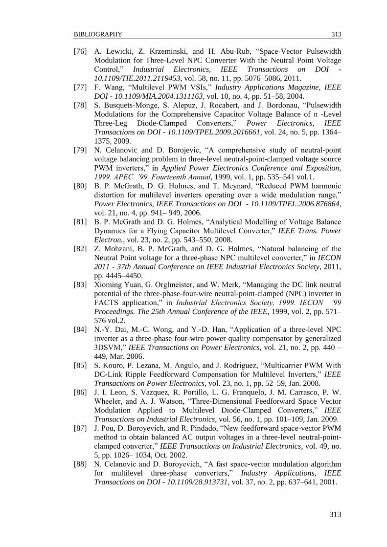
BIBLIOGRAPHY 313
313
[76] A. Lewicki, Z. Krzeminski, and H. Abu-Rub, “Space-Vector Pulsewidth
Modulation for Three-Level NPC Converter With the Neutral Point Voltage
Control,” Industrial Electronics, IEEE Transactions on DOI -
10.1109/TIE.2011.2119453, vol. 58, no. 11, pp. 5076–5086, 2011.
[77] F. Wang, “Multilevel PWM VSIs,” Industry Applications Magazine, IEEE
DOI - 10.1109/MIA.2004.1311163, vol. 10, no. 4, pp. 51–58, 2004.
[78] S. Busquets-Monge, S. Alepuz, J. Rocabert, and J. Bordonau, “Pulsewidth
Modulations for the Comprehensive Capacitor Voltage Balance of n -Level
Three-Leg Diode-Clamped Converters,” Power Electronics, IEEE
Transactions on DOI - 10.1109/TPEL.2009.2016661, vol. 24, no. 5, pp. 1364–
1375, 2009.
[79] N. Celanovic and D. Borojevic, “A comprehensive study of neutral-point
voltage balancing problem in three-level neutral-point-clamped voltage source
PWM inverters,” in Applied Power Electronics Conference and Exposition,
1999. APEC ’99. Fourteenth Annual, 1999, vol. 1, pp. 535–541 vol.1.
[80] B. P. McGrath, D. G. Holmes, and T. Meynard, “Reduced PWM harmonic
distortion for multilevel inverters operating over a wide modulation range,”
Power Electronics, IEEE Transactions on DOI - 10.1109/TPEL.2006.876864,
vol. 21, no. 4, pp. 941– 949, 2006.
[81] B. P. McGrath and D. G. Holmes, “Analytical Modelling of Voltage Balance
Dynamics for a Flying Capacitor Multilevel Converter,” IEEE Trans. Power
Electron., vol. 23, no. 2, pp. 543–550, 2008.
[82] Z. Mohzani, B. P. McGrath, and D. G. Holmes, “Natural balancing of the
Neutral Point voltage for a three-phase NPC multilevel converter,” in IECON
2011 - 37th Annual Conference on IEEE Industrial Electronics Society, 2011,
pp. 4445–4450.
[83] Xioming Yuan, G. Orglmeister, and W. Merk, “Managing the DC link neutral
potential of the three-phase-four-wire neutral-point-clamped (NPC) inverter in
FACTS application,” in Industrial Electronics Society, 1999. IECON ’99
Proceedings. The 25th Annual Conference of the IEEE, 1999, vol. 2, pp. 571–
576 vol.2.
[84] N.-Y. Dai, M.-C. Wong, and Y.-D. Han, “Application of a three-level NPC
inverter as a three-phase four-wire power quality compensator by generalized
3DSVM,” IEEE Transactions on Power Electronics, vol. 21, no. 2, pp. 440 –
449, Mar. 2006.
[85] S. Kouro, P. Lezana, M. Angulo, and J. Rodriguez, “Multicarrier PWM With
DC-Link Ripple Feedforward Compensation for Multilevel Inverters,” IEEE
Transactions on Power Electronics, vol. 23, no. 1, pp. 52–59, Jan. 2008.
[86] J. I. Leon, S. Vazquez, R. Portillo, L. G. Franquelo, J. M. Carrasco, P. W.
Wheeler, and A. J. Watson, “Three-Dimensional Feedforward Space Vector
Modulation Applied to Multilevel Diode-Clamped Converters,” IEEE
Transactions on Industrial Electronics, vol. 56, no. 1, pp. 101–109, Jan. 2009.
[87] J. Pou, D. Boroyevich, and R. Pindado, “New feedforward space-vector PWM
method to obtain balanced AC output voltages in a three-level neutral-point-
clamped converter,” IEEE Transactions on Industrial Electronics, vol. 49, no.
5, pp. 1026– 1034, Oct. 2002.
[88] N. Celanovic and D. Boroyevich, “A fast space-vector modulation algorithm
for multilevel three-phase converters,” Industry Applications, IEEE
Transactions on DOI - 10.1109/28.913731, vol. 37, no. 2, pp. 637–641, 2001.