Near/Far-Field Investigations of the Interaction between Surface Waves and Nanoparticles
12
Near/Far-Field Investigations of the Interaction between Surface Waves and Nanoparticles V. A. Sterligov (a, b), P. Cheyssac (a), R. Kofman (a), S. I. Lysenko (b), P. M. Lytvyn (b), B. Vohnsen (c), S. I. Bozhevolnyi (c), and A. A. Maradudin (d) (a) Physique de la Matie `re Condense ´e, Universite ´ de Nice, 06108 Nice Cedex 2, France (b) Institute of Semiconductor Physics, Prospekt Nauki 45, 03028 Kiev-28, Ukraine (c) Aalborg University, Pontoppidanstræde 103, DK-9220 Aalborg Øst, Denmark (d) University of California, Irvine, California 92697, USA (Received March 6, 2001; in revised form June 7, 2001; accepted September 13, 2001) Subject classification: 61.46.+w; 73.20.Mf; 78.35.+c; 78.67.Bf; S4; S10.1 Results of experimental studies of the scattering of electromagnetic surface waves by metal nano- particles (NPs) located at different distances of a silver film and carried out by both near- and far- field optical techniques are presented for the first time, as far as we know. SNOM and AFM tech- niques were applied to investigate near-field scattering and topographical images of the outer inter- face. In the far-field, the half-space distribution of the normalized scattered light intensity has been measured and shows, as well as SNOM, an increase of the scattered intensity with NPs–silver dis- tance. These results can be attributed to the variation of the space distribution of the electric field of the surface wave. 1. Introduction Extended investigations of metal nanoparticles (NPs) are relatively new; the properties [1, 2] of NPs, including their optical properties [3], are the subject of numerous studies, and show significant differences from the properties of the corresponding bulk materi- als. Although the size of NPs is very small compared to the light wavelength, the effi- ciency of interaction with the electromagnetic field depends on their interaction length [4]. This length is increased when one uses surface waves [5, 6]. Far- and near-field scattering occurs from the topographical structure of interfaces [7–11]. One can modify the intrinsic roughness of an interface by creating a controlled one in its vicinity. For this purpose, NPs are a powerful tool. On a perfect interface, they realize a plane distribution, and their shape and size are well defined; moreover, their distance to the interface that supports the waves propagation can be varied. The main purpose of this article is to present (for the first time as far as we know) results of experimental studies of the scattering of surface electromagnetic waves (sur- face plasmon-polaritons: SPPs) by NPs, carried out in both the near and far-fields. In- vestigations have been performed in which the NP distance d to the interface is varied, and also the polarization of the incident beam creating two different evanescent waves: P-polarized incident light excites a SPP while S-polarization creates an evanescent wave. The influence of the substrate has been eliminated, yielding the proper effect of NPs onto scattering. Three different techniques have been applied on the same sample, and the results obtained are compared. The far-field intensity of the scattered light has been measured phys. stat. sol. (b) 229, No. 3, 1283–1294 (2002) # WILEY-VCH Verlag Berlin GmbH, 13086 Berlin, 2002 0370-1972/02/22902-1283 $ 17.50þ.50/0
Transcript of Near/Far-Field Investigations of the Interaction between Surface Waves and Nanoparticles
Near/Far-Field Investigations of the Interactionbetween Surface Waves and Nanoparticles
V. A. Sterligov (a, b), P. Cheyssac (a), R. Kofman (a), S. I. Lysenko (b),P. M. Lytvyn (b), B. Vohnsen (c), S. I. Bozhevolnyi (c),and A. A. Maradudin (d)
(a) Physique de la Matiere Condensee, Universite de Nice, 06108 Nice Cedex 2, France
(b) Institute of Semiconductor Physics, Prospekt Nauki 45, 03028 Kiev-28, Ukraine
(c) Aalborg University, Pontoppidanstræde 103, DK-9220 Aalborg Øst, Denmark
(d) University of California, Irvine, California 92697, USA
(Received March 6, 2001; in revised form June 7, 2001; accepted September 13, 2001)
Subject classification: 61.46.+w; 73.20.Mf; 78.35.+c; 78.67.Bf; S4; S10.1
Results of experimental studies of the scattering of electromagnetic surface waves by metal nano-particles (NPs) located at different distances of a silver film and carried out by both near- and far-field optical techniques are presented for the first time, as far as we know. SNOM and AFM tech-niques were applied to investigate near-field scattering and topographical images of the outer inter-face. In the far-field, the half-space distribution of the normalized scattered light intensity has beenmeasured and shows, as well as SNOM, an increase of the scattered intensity with NPs–silver dis-tance. These results can be attributed to the variation of the space distribution of the electric fieldof the surface wave.
1. Introduction
Extended investigations of metal nanoparticles (NPs) are relatively new; the properties[1, 2] of NPs, including their optical properties [3], are the subject of numerous studies,and show significant differences from the properties of the corresponding bulk materi-als. Although the size of NPs is very small compared to the light wavelength, the effi-ciency of interaction with the electromagnetic field depends on their interaction length[4]. This length is increased when one uses surface waves [5, 6].
Far- and near-field scattering occurs from the topographical structure of interfaces[7–11]. One can modify the intrinsic roughness of an interface by creating a controlledone in its vicinity. For this purpose, NPs are a powerful tool. On a perfect interface,they realize a plane distribution, and their shape and size are well defined; moreover,their distance to the interface that supports the waves propagation can be varied.
The main purpose of this article is to present (for the first time as far as we know)results of experimental studies of the scattering of surface electromagnetic waves (sur-face plasmon-polaritons: SPPs) by NPs, carried out in both the near and far-fields. In-vestigations have been performed in which the NP distance d to the interface is varied,and also the polarization of the incident beam creating two different evanescent waves:P-polarized incident light excites a SPP while S-polarization creates an evanescentwave. The influence of the substrate has been eliminated, yielding the proper effect ofNPs onto scattering.
Three different techniques have been applied on the same sample, and the resultsobtained are compared. The far-field intensity of the scattered light has been measured
phys. stat. sol. (b) 229, No. 3, 1283–1294 (2002)
# WILEY-VCH Verlag Berlin GmbH, 13086 Berlin, 2002 0370-1972/02/22902-1283 $ 17.50þ.50/0
in half a sphere and it will be referred as Hemispherical Elastic Light Scattering(HELS). Topographical images of the outer interface have been obtained by AFMmeasurements. Near-field scattering, in the close vicinity of the outer interface, hasbeen investigated with scanning near-field optical microscopy (SNOM).
When the NP’s distance to the interface supporting the surface waves increases, anincreased scattering in the near as well as in the far-field has been observed. A tenta-tive interpretation is presented. Future development in the direction of a wider rangeof distance and also the influence of self-organized systems is to be considered.
2. Experiment and Results
2.1 The sample
The optical substrate is a right angle silica prism with a roughness, as given by themanufacturers, lower than 1.5 nm rms. Evaporation of the various layers takes placeunder UHV: the thickness of the silver film is monitored via a quartz micro-balancelocated very close to the samples; its value: (52 � 0.5) nm is chosen experimentally torealize a good coupling of the incident wave to the surface plasmon-polaritons. Thenone introduces a SiOx (0 < x < 1) spacer, with thickness d varying between 2 and 8 nm,onto which the gallium NPs are evaporated at room temperature and their growthoccurs in the liquid state. Then, the NP’s shape is a truncated sphere determined by thewetting angle �120� of Ga onto SiOx. Before a final SiOx layer covers the distribution,the NPs are solidified; the amorphous matrix that surrounds the NPs behaves as a veryhigh viscosity fluid [12] that retains their quasi-spherical shape and their positions. Thewhole thickness of SiOx, NPs and again SiOx deposited on top of silver is 20 nm. Analy-sis of electron micrographs allows the determination of the mean radius of the particles:4 nm with a standard deviation 0.8 nm; the mean distance between their centers is12.9 nm.
The area of the hypotenuse face is divided into five zones. The first one is the bareprism, the second is without NPs. The three others realize different distances d ¼ 2, 4,and 8 nm of the NPs to the silver film, however we have maintained the whole struc-ture to a constant thickness by adjusting the thickness of the final SiOx layer.
2.2 AFM
The sample surface morphology and its features were studied with an atomic forcemicroscope (D3000 Nanoscope IIIa, Digital Instruments) [13]. Etched silicon tips, witha radius of curvature of about 7 nm were used, and achieved 1 nm lateral resolution onthe surface and 0.2 nm resolution normal to it (scanner with 100 mm maximal scan sizewhere used).
Interaction forces between tip and surface were reduced, and improvement of thesensitivity of AFM measurements were achieved using the tapping mode: the tip oscil-lates over the sample surface at the resonance frequency, and has mechanical contactwith the sample surface. We have noticed that, due to the mechanical contact, the mea-suring tip had a tendency to stick to the surface of the sample for the d ¼ 8 nm zone,where the NPs are very close to the outer interface.
The surface relief can be characterized along the normal to the surface or inthe plane of the surface. Along the normal its roughness is quantified by Ra:
1284 V. A. Sterligov et al.: Interaction between Surface Waves and Nanoparticles
Ra ¼ 1LxLy
ÐLy
0
ÐLx
0jz x; yð Þj dx dy, where z(x, y) is the deviation from the mean plane and
Lx, Ly are the dimensions of the analyzed area. The AFM data have been treated tocompensate the tilt and macro relief of the surface under study. In our case, roughnesswas measured on 250 250 nm2 sized areas over 1 1 mm2 scans. The roughness of thevarious zones covered by silver and SiOx has been determined.
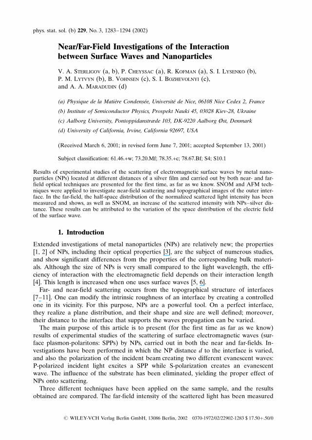
The bare surface of the prism exhibits (Figs. 1a, 2a) an intrinsic roughness: 0.3 nmrms lower than that given by the manufacturers. Some small rounded hillocks emergeand may correspond to traces of the evaporated silver that have bounced onto thewalls of the vacuum chamber and were unfortunately condensed there.
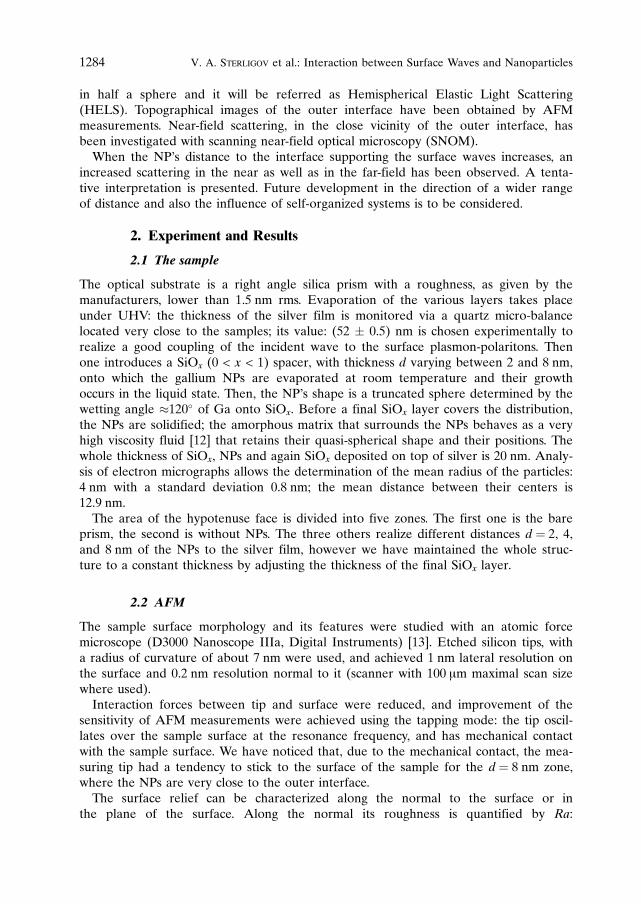
When silver is present, the surface roughness (Figs. 1b, 2a) is higher than the bareglass ones (see Fig. 2a). The highest value of Ra corresponds to the area for which theNPs are at d ¼ 2 nm, then Ra decreases when d increases. Apart from the glass areas,the roughness of the outer interface for these zones does not show significant differ-ences. On the contrary, the surface inhomogeneity shown in Fig. 2a, namely the relative
phys. stat. sol. (b) 229, No. 3 (2002) 1285
a bFig. 1. a) AFM image of a bare glass substrate. b) AFM image of a zone without NP. AFM imagesof zones with NP look similar, but numerical parameters of relief are different
Fig. 2. a) Roughness Ra and surface inhomogeneity for different zones. b) Average grains sizes forvarious zones of the prism obtained as a result of numerical analysis of AFM data
deviation of Ra from its mean value over 1 1 mm2 scans, shows a strong maximum forthe zone without NPs and a minimum for a d = 2 nm spacing of NPs.
The deposit creates some roughness; due to the different scales, the zones with silverlook like a set of what we refer as “grains” (Fig. 1b). In the plane of the surface, thesegrains have been characterized by the main diameter of the ellipses that realize the bestfit (Fig. 2b).
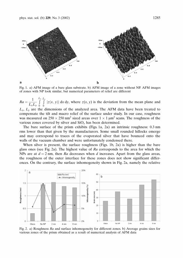
Assuming that the SiOx layer reproduced the roughness of silver, Fig. 3 presents areconstructed cross-section of the sample. The influence of NPs on the profile is not sovisible, due to the covering by thermal evaporation; this point is specifically addressedin the interpretation.
2.3 SNOM
Different near-field techniques can be employed to investigate SPP scattering by nano-structured surfaces and interfaces. Photon tunneling SNOM [14], in which an uncoatedfiber tip is used to probe the evanescent field of the light being totally internally re-flected at the sample surface, seems to be the most suitable technique for local andunobtrusive probing of the SPP field. Due to the relatively low refractive index of anoptical fiber, such a tip within certain approximations can be considered as a passiveprobe of the electric field intensity [15]; an uncoated fiber tip does not affect signifi-cantly the space distribution of the electromagnetic field [16]. Detailed experimentalinvestigations have also demonstrated that, for the SPP being resonantly excited at arelatively smooth surface, near-field optical images can indeed be directly related to theintensity distributions of the total SPP field, i.e., the field of the excited and scatteredSPPs [17].
The SNOM configuration used to obtain the experimental results presented in thissection consists of a stand alone type SNOM scanner combined with a shear forcebased feedback system and an arrangement for SPP excitation in the usual Kretsch-mann configuration, and is described in detail elsewhere [16]. A schematic representa-
1286 V. A. Sterligov et al.: Interaction between Surface Waves and Nanoparticles
Fig. 3. Reconstruction of the cross-section of different zones of the sample. Profile of glass–Aginterface and SiOx–vacuum interface as given by AFM measurements. The spherical NPs are dis-torted to an elliptical shape because of the different x and z scales. Their size and distance be-tween them correspond to the parameters of the sample
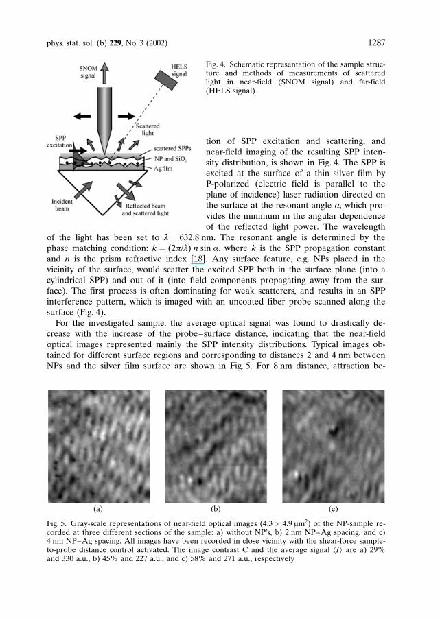
tion of SPP excitation and scattering, andnear-field imaging of the resulting SPP inten-sity distribution, is shown in Fig. 4. The SPP isexcited at the surface of a thin silver film byP-polarized (electric field is parallel to theplane of incidence) laser radiation directed onthe surface at the resonant angle a, which pro-vides the minimum in the angular dependenceof the reflected light power. The wavelength
of the light has been set to l ¼ 632.8 nm. The resonant angle is determined by thephase matching condition: k ¼ (2p/l) n sin a, where k is the SPP propagation constantand n is the prism refractive index [18]. Any surface feature, e.g. NPs placed in thevicinity of the surface, would scatter the excited SPP both in the surface plane (into acylindrical SPP) and out of it (into field components propagating away from the sur-face). The first process is often dominating for weak scatterers, and results in an SPPinterference pattern, which is imaged with an uncoated fiber probe scanned along thesurface (Fig. 4).
For the investigated sample, the average optical signal was found to drastically de-crease with the increase of the probe–surface distance, indicating that the near-fieldoptical images represented mainly the SPP intensity distributions. Typical images ob-tained for different surface regions and corresponding to distances 2 and 4 nm betweenNPs and the silver film surface are shown in Fig. 5. For 8 nm distance, attraction be-
phys. stat. sol. (b) 229, No. 3 (2002) 1287
film
Fig. 4. Schematic representation of the sample struc-ture and methods of measurements of scatteredlight in near-field (SNOM signal) and far-field(HELS signal)
(a) (b) (c)
Fig. 5. Gray-scale representations of near-field optical images (4.3 4.9 mm2) of the NP-sample re-corded at three different sections of the sample: a) without NP’s, b) 2 nm NP–Ag spacing, and c)4 nm NP–Ag spacing. All images have been recorded in close vicinity with the shear-force sample-to-probe distance control activated. The image contrast C and the average signal hIi are a) 29%and 330 a.u., b) 45% and 227 a.u., and c) 58% and 271 a.u., respectively
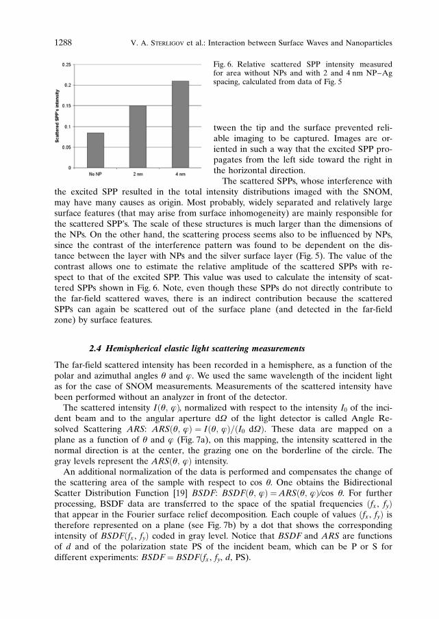
tween the tip and the surface prevented reli-able imaging to be captured. Images are or-iented in such a way that the excited SPP pro-pagates from the left side toward the right inthe horizontal direction.
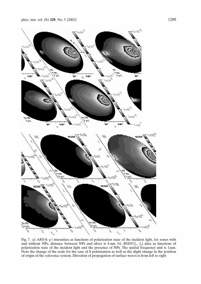
The scattered SPPs, whose interference withthe excited SPP resulted in the total intensity distributions imaged with the SNOM,may have many causes as origin. Most probably, widely separated and relatively largesurface features (that may arise from surface inhomogeneity) are mainly responsible forthe scattered SPP’s. The scale of these structures is much larger than the dimensions ofthe NPs. On the other hand, the scattering process seems also to be influenced by NPs,since the contrast of the interference pattern was found to be dependent on the dis-tance between the layer with NPs and the silver surface layer (Fig. 5). The value of thecontrast allows one to estimate the relative amplitude of the scattered SPPs with re-spect to that of the excited SPP. This value was used to calculate the intensity of scat-tered SPPs shown in Fig. 6. Note, even though these SPPs do not directly contribute tothe far-field scattered waves, there is an indirect contribution because the scatteredSPPs can again be scattered out of the surface plane (and detected in the far-fieldzone) by surface features.
2.4 Hemispherical elastic light scattering measurements
The far-field scattered intensity has been recorded in a hemisphere, as a function of thepolar and azimuthal angles q and j. We used the same wavelength of the incident lightas for the case of SNOM measurements. Measurements of the scattered intensity havebeen performed without an analyzer in front of the detector.
The scattered intensity Iðq; jÞ, normalized with respect to the intensity I0 of the inci-dent beam and to the angular aperture dW of the light detector is called Angle Re-solved Scattering ARS: ARSðq; jÞ ¼ Iðq; jÞ=ðI0 dWÞ. These data are mapped on aplane as a function of q and j (Fig. 7a), on this mapping, the intensity scattered in thenormal direction is at the center, the grazing one on the borderline of the circle. Thegray levels represent the ARSðq; jÞ intensity.
An additional normalization of the data is performed and compensates the change ofthe scattering area of the sample with respect to cos q. One obtains the BidirectionalScatter Distribution Function [19] BSDF: BSDFðq; jÞ ¼ARSðq; jÞ/cos q. For furtherprocessing, BSDF data are transferred to the space of the spatial frequencies ðfx , fyÞthat appear in the Fourier surface relief decomposition. Each couple of values ðfx , fyÞ istherefore represented on a plane (see Fig. 7b) by a dot that shows the correspondingintensity of BSDFðfx , fyÞ coded in gray level. Notice that BSDF and ARS are functionsof d and of the polarization state PS of the incident beam, which can be P or S fordifferent experiments: BSDF ¼ BSDFðfx , fy, d, PS).
1288 V. A. Sterligov et al.: Interaction between Surface Waves and Nanoparticles
Fig. 6. Relative scattered SPP intensity measuredfor area without NPs and with 2 and 4 nm NP–Agspacing, calculated from data of Fig. 5
phys. stat. sol. (b) 229, No. 3 (2002) 1289
Fig. 7. a) ARSðq, jÞ intensities as functions of polarization state of the incident light, for zones withand without NPs; distance between NPs and silver is 4 nm. b): BSDFðfx , fy) data as functions ofpolarization state of the incident light and the presence of NPs. The spatial frequency unit is 1/mm.Note the change of the scale for the case of S polarization as well as the slight change in the positionof origin of the reference system. Direction of propagation of surface waves is from left to right
2.4.1 Processing of the scattering data
Substrate and layers are necessarily present and influence the experimental results.Their effect is removed by a subtraction, and this specific point will be discussed later.From BSDF(fx , fy, d, PS) data, we subtract BSDF(fx , fy, NoNP, PS) data from an areawithout NPs. Of course, the angles of incidence for the excitation of SPPs on differentzones of the sample are different (see Appendix A). Then, the same directions of scat-tering correspond to different components in the 2D surface relief decomposition in thespace of the spatial frequencies [20]. For correctness, the subtracted scattered intensitiesmust be associated with equal values of the spatial frequencies.
The scattered intensity is represented on a 2D ARS(q, j) mapping. It shows a max-imum, located in a narrow range of angles, in the plane of incidence and directed to-ward the direction of the surface wave’s propagation. The bright and small spots lo-cated in the left parts of each circle originate from scattering taking place at theoutgoing face of the prism. One clearly sees in Fig. 7a that the scattered intensity de-pends on the polarization of the incident beam, and the presence or not of NPs. Oneorder of magnitude separates the results from P- and S-polarization.
Electron microscopy graphs show that NPs are azimuthally symmetrical objects aswell in the liquid and solid state [21]. For the scattered light, a consequence of such asymmetry should leave BSDF(fx , fy) unchanged during a rotation around the origin ofthe reference system. This property is illustrated by the experimental results in Fig. 7bwhere the drawn BSDF(fx , fy) shows the rotational symmetry centered at the origin.Therefore, averaging of BSDF(fx , fy) data over (fx , fy) becomes possible and leads to anincrease of the signal/noise ratio. The result of this operation gives DBSDF(f, d, PS)¼ BSDF(fx , fy, d, PS) � BSDF(fx , fy, NoNP, PS) where � expresses the above proce-
dure of subtraction and averaging of BSDF data as a function of f ¼ffiffiffiffiffiffiffiffiffiffiffiffiffiffiffif 2x þ f 2
y
qand one
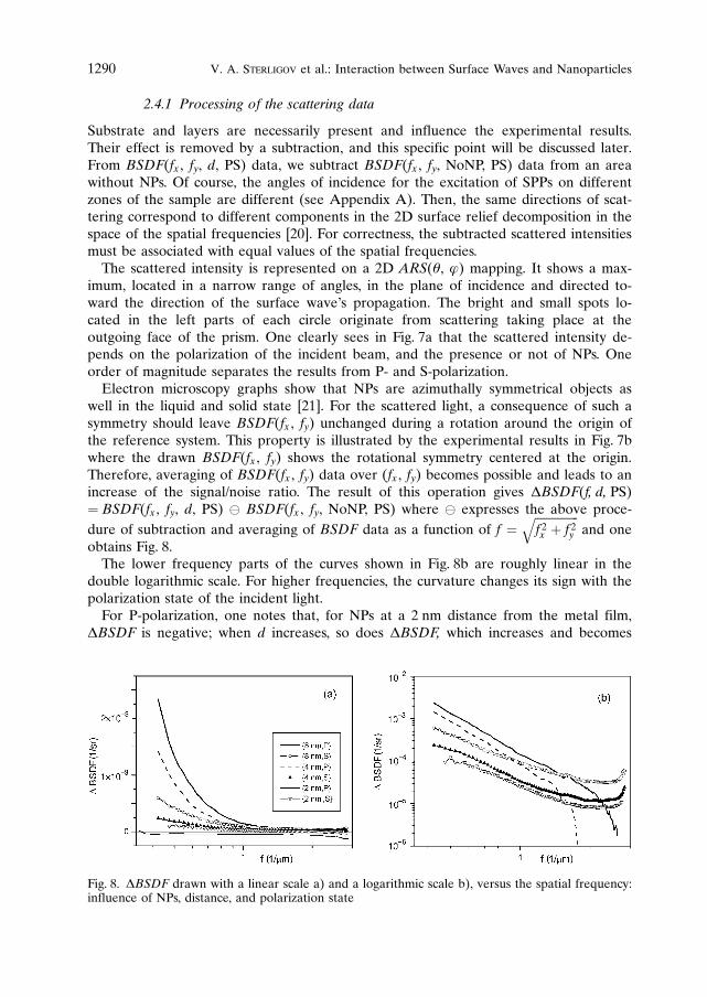
obtains Fig. 8.The lower frequency parts of the curves shown in Fig. 8b are roughly linear in the
double logarithmic scale. For higher frequencies, the curvature changes its sign with thepolarization state of the incident light.
For P-polarization, one notes that, for NPs at a 2 nm distance from the metal film,DBSDF is negative; when d increases, so does DBSDF, which increases and becomes
1290 V. A. Sterligov et al.: Interaction between Surface Waves and Nanoparticles
Fig. 8. DBSDF drawn with a linear scale a) and a logarithmic scale b), versus the spatial frequency:influence of NPs, distance, and polarization state

positive. For S-polarization, DBSDF is positive whatever d is but increases with increas-ing d.
In the linear part of the curves, the slopes associated with P-polarization and S-polar-ization differ significantly. The polarization of the surface wave and the interaction be-tween surface waves and nanoparticles are involved in various results.
3. Interpretation
Our interpretation will take into account roughness, field amplitude and polarization,presence and location of NPs as a cause of scattering.
According to a model of semi infinite media, the amplitude of the electric field of asurface wave should decrease when one goes away from the metal interface towardvacuum. Here, the experimental situation is different: the silver film is not semi infiniteand is not in contact with vacuum; a finite dielectric layer covers it and modifies theelectromagnetic field boundary conditions [22]. Moreover, the dielectric film embeds ornot a 2D distribution of NPs. The distribution of the electric field amplitude inside themetal and the dielectric films is sensitive to this configuration. So is scattering as aconsequence. The field distribution caused by a single defect interacting with a SPP hasalready been calculated [7]. The field scattered by the roughness or inhomogeneity ofthe interface that supports the SPP may be calculated, but such a calculation is notapplicable in our case because the strong scattered field created by the high density ofscatterers cannot be neglected. Unfortunately, an exact calculation of the field distribu-tion that occurs in our complicated system, and involving multiple scattering, is not yetavailable. For this reason, the interpretation will remain on a qualitative level.
In fact, our results show an increase of the scattering with an increase of the distanced between the interface that supports the propagation of the surface waves and theNPs. This is not a result expected a priori. At this point we have to remark that ourcalculations are performed using a subtraction of the scattering from a zone of thesubstrate, layers and interfaces without NPs to the ones coming from a zone with NPs.In what follows, we show that the roughness of the various interfaces is not so influ-enced by the presence or location of the NPs.
The intrinsic roughness of our silica prism is low. Silver, as deposited, exhibits its ownroughness known for his high value compared to the prism and other metals. Accordingto [23], the roughness of bare silver deposited onto a BK7 prism has been determinedby SPP measurements in the same configuration as ours and has been found to be4.5 nm. Our AFM measurements show that the outer SiOx interface has a smoothersurface (2–3 nm) that we could have expected from the topography of the internallayers and silver (Fig. 2a). In other words, roughness of the superimposed layers is notcumulative. This is indirectly supported by transmission electron microscopy examina-tion of a cross-section of embedded NPs in SiOx [24] showing that the outer interfaceremains flat and does not reproduce the relief of the NPs. SiOx has a tendency to fill inthe hollow parts and to leave the peaks uncovered. The effect of SiOx deposition is tosmoothen the various roughness. However, each non-perfect interface gives rise to scat-tering: part of it is caused by the prism-metal and metal-dielectric roughness.
After NPs are embedded in SiOx, electron microscopy shows that their mean diam-eter is 8 nm and the distance between them is 12.9 nm. There is a slight increase(0.1 nm) of the outer roughness Ra, which cannot be thought as an addition of those of
phys. stat. sol. (b) 229, No. 3 (2002) 1291
silver and the NPs. We explain this effect as follows. The lateral size of the grains thatdescribe the roughness of silver and its associated upper layers is larger than theseparameters, and NPs preferably grow in their hollow parts. Now, Ra decreases when dincreases, so the relief of the SiOx–vacuum interface does not seem significantly af-fected by the position of the NP’s distribution inside the dielectric medium. The pre-vious explanation still remains valid: the growth process of SiOx has a tendency to pre-ferably fill in the hollow parts, which gives rise to a slight decrease of Ra versus d. As aconsequence, the decrease of Ra for the last interface should lead to a decrease of thecorresponding part of the scattering. An indirect proof of this hypothesis has alreadybeen obtained [24] in the case of larger lead NPs embedded in SiOx: a transmissionelectron microscopy examination of a sample cross-section clearly shows that rough-nesses do not add, but in fact the evaporation process yields a smoothing of the outerinterface. Moreover, dielectrics of small thickness are considered like a high viscosityfluid [12] that can be shaped by stress. In our case the outer SiOx interface minimizesits interfacial energy with vacuum, and this decreases the apparent roughness.
We extend this reasoning to the case of NPs located 2 nm from the metal film. Thesize of NPs is of the order of the depth of the silver relief, therefore in this zone theaddition of NPs acts as a decrease of the effective roughness of this interface comparedto the zone without NPs. This interface that shows a reduced roughness gives rise to alower scattering in P-polarized light, and this is effectively the case: DBSDF(f, 2 nm, P)is negative.
When d reaches 4 and 8 nm, scattering increases and DBSDF(f, 4 nm, P),DBSDF(f, 8 nm, P) become positive while Ra decreases. This surprising increase can beattributed to the interaction of NPs located at various distances with the distribution ofthe electric field amplitude in the dielectric layer. The coating of the metal by a dielec-tric layer instead of vacuum increases the amplitude of the electric field at the surfaceof the metal, and the field amplitude increases inside the dielectric. Preliminary calcula-tions of the space distribution of the electric field inside the metal film covered by atransparent dielectric layer support this explanation.
The previous conclusion is correct for both polarizations of the incident beam.
4. Conclusion
A new insight about the results of the interaction of surface electromagnetic waves withinterfaces is provided by the introduction of NPs located in their close vicinity. Surfaceplasmons and light scattering have been combined with an AFM topographical descrip-tion of the interface, giving possibility to find new physical parameters and features ofinteraction between NP and surface electromagnetic waves.
It has been shown that, in both near and far-field measurements, an increase of theNPs–Ag distance causes an increase of the scattered intensity. It has been related to adecrease of the apparent roughness felt by the waves. It can also been related to thespace variation of the local electric field that the NPs experience; NPs act as a probe ofsuch variations.
Future studies should go toward smoother films (Au instead of Ag), in order to re-duce their intrinsic roughness. Then, ordering of NPs along a lattice structure wouldlead to a possible study of the interaction between surface plasmon-polaritons, andwould include larger NP–Ag distances, and a decreased density of NPs.
1292 V. A. Sterligov et al.: Interaction between Surface Waves and Nanoparticles
Appendix A
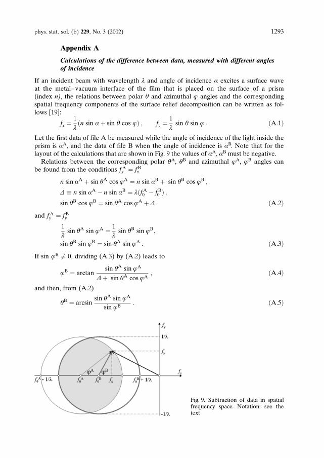
Calculations of the difference between data, measured with different anglesof incidence
If an incident beam with wavelength l and angle of incidence a excites a surface waveat the metal–vacuum interface of the film that is placed on the surface of a prism(index n), the relations between polar q and azimuthal j angles and the correspondingspatial frequency components of the surface relief decomposition can be written as fol-lows [19]:
fx ¼1lðn sin a þ sin q cos jÞ ; fy ¼
1l
sin q sin j : ðA:1Þ
Let the first data of file A be measured while the angle of incidence of the light inside theprism is aA, and the data of file B when the angle of incidence is aB. Note that for thelayout of the calculations that are shown in Fig. 9 the values of aA, aB must be negative.
Relations between the corresponding polar qA, qB and azimuthal jA, jB angles canbe found from the conditions fA
x ¼ fBx
n sin aA þ sin qA cos jA ¼ n sin aB þ sin qB cos jB ;
D n sin aA � n sin aB ¼ lðfA0 � fB
0 Þ ;sin qB cos jB ¼ sin qA cos jA þ D : ðA:2Þ
and fAy ¼ fB
y
1l
sin qA sin jA ¼ 1l
sin qB sin jB;
sin qB sin jB ¼ sin qA sin jA : ðA:3Þ
If sin jB 6¼ 0, dividing (A.3) by (A.2) leads to
jB ¼ arctansin qA sin jA
D þ sin qA cos jA; ðA:4Þ
and then, from (A.2)
qB ¼ arcsinsin qA sin jA
sin jB: ðA:5Þ
phys. stat. sol. (b) 229, No. 3 (2002) 1293
Fig. 9. Subtraction of data in spatialfrequency space. Notation: see thetext
These relations are not correct along the OX axis because, for this case, sin jB
¼ sin jA ¼ 0 and hence the relations should be calculated for the particular casefAy ¼ fB
y ¼ 0.Such a relation can be established using the condition fA
x ¼ fBx and, on multiplying
both sides by l, yields:
n sin aA þ sin qA cos jA ¼ n sin aB þ sin qB cos jB
sin qB cos jB ¼ D + sin qA cos jA
qB ¼ arcsinD þ sin qA cos jA
cos jB: ðA:6Þ
For the case of the OX axis and the point defined by fx ¼ fA0 , for all values of jA one
gets qA = 0� and jB ¼ 180�.
References
[1] J.-M. Bonard and A. Chatelain (Eds.), Proc. 9th Internat. Symp. Small Particles and InorganicClusters, Lausanne (Switzerland), Sept. 1–5, 1998;Eur. Phys. J. D 9 (1999).
[2] C. E. Bottani, C. Mantini, P. Milani, M. Manfredini, A. Stella, P. Tognini, P. Cheyssac, andR. Kofman, Appl. Phys. Lett. 69, 2409 (1996).
[3] U. Kreibig and M. Vollmer, Optical Properties of Metal Clusters, Springer-Verlag, Berlin1995.
[4] P. Cheyssac, V. A. Sterligov, S. I. Lysenko, and R. Kofman, Opt. Commun. 175, 383 (2000).[5] V. A. Sterligov, P. Cheyssac, S. I. Lysenko, and R. Kofman, phys. stat. sol. (a) 175, 259
(1999).[6] P. Cheyssac, V. A. Sterligov, S. I. Lysenko, and R. Kofman, phys. stat. sol. (a) 175, 253
(1999).[7] A. V. Shchegrov, I. V. Novikov, and A. A. Maradudin, Phys. Rev. Lett. 78, 4296 (1997).[8] J. A. Sanchez-Gil, Appl. Phys. Lett. 73, 3509 (1998).[9] I. M. Fuks and A. G. Voronovich, Waves in Random Media 10, 253 (2000).
[10] M. A. Paesler and P. J. Moyer, Near-Field Optics: Theory, Instrumentation, and Applications,Wiley, New York 1996.
[11] V. M. Agranovich and D. L. Mills (Eds.), Surface Polaritons, North-Holland Publ. Co., Am-sterdam 1982.
[12] H. Gleiter, Europhys. News 20, 130 (1989).[13] T. Ohmi and S. Aoyama, Appl. Phys. Lett. 61, 2479 (1992).[14] R. C. Reddick, R. J. Warmack, and T. L. Ferrell, Phys. Rev. B 39, 767 (1989).
D. Courjon, K. Sarayeddine, and M. Spajer, Opt. Commun. 71, 23 (1989).F. de Fornel, J.P. Goudonnet, L. Salomon, and E. Lesniewska, Proc. SPIE 1139, 77 (1989).
[15] S. I. Bozhevolnyi, B. Vohnsen, and E. A. Bozhevolnaya, Opt. Commun. 172, 171 (1999).[16] S. I. Bozhevolnyi, I. I. Smolyaninov, and A. V. Zayats, Phys. Rev. B 51, 17916 (1995).[17] V. Coello, S. I. Bozhevolnyi, and F. A. Pudonin, Proc. SPIE 3098, 536 (1999).[18] H. Raether, Surface Plasmons, Springer Tracts in Modern Physics Vol. 111, Springer-Verlag,
Berlin 1988.[19] J. C. Stover, Optical Scattering: Measurements and Analysis, SPIE Optical Engineering Press,
Bellingham (Washington) 1995.[20] V. A. Sterligov, P. Cheyssac, S. I. Lysenko, and R. Kofman, Opt. Commun. 177, 1 (2000).[21] E. Sondergaard, R. Kofman, P. Cheyssac, and A. Stella, Surf. Sci. 364, 467 (1996).[22] I. Pockrand, Surf. Sci. 72, 577 (1978).[23] C. C. Lee and Y.J. Jen, Appl. Opt., 38, 6029 (1999).[24] R. Kofman, P. Cheyssac, A. Aouaj, Y. Lereah, G. Deutscher, T. Ben-David, J. M. Penisson,
and A. Bourret, Surf. Sci. 303, 231 (1994).
1294 V. A. Sterligov et al.: Interaction between Surface Waves and Nanoparticles