Nanostructural and electrical properties of functionally terminated self-assembled monolayers on...
7
Nanostructural and electrical properties of functionally terminated self-assembled monolayers on silicon surfaces M. Rittner 4. Physikalisches Institut, Universitaet Stuttgart, Pfaffenwaldring 57, 70550 Stuttgart, Germany M. S. Martin-Gonzalez Consejo Superior de Investigaciones Cientificas, Centro Nacional de Microelectronica, C/Isaac Newton 8, 28760 Tres Cantos, Madrid, Spain A. Flores Consejo Superior de Investigaciones Cientificas, Instituto de Estructura de la Materia, C/Serrano 121, 28006 Madrid, Spain H. Schweizer 4. Physikalisches Institut, Universitaet Stuttgart, Pfaffenwaldring 57, 70550 Stuttgart, Germany F. Effenberger Institut fuer Organische Chemie und Isotopenforschung, Universitaet Stuttgart, Pfaffenwaldring 55, 70550 Stuttgart, Germany M. H. Pilkuhn a 4. Physikalisches Institut, Universitaet Stuttgart, Pfaffenwaldring 57, 70550 Stuttgart, Germany and Consejo Superior de Investigaciones Cientificas, Instituto de Estructura de la Materia, C/Serrano 121, 28006 Madrid, Spain Received 28 July 2004; accepted 25 July 2005; published online 12 September 2005 Self-assembled monolayers SAMs having alkyl chains with typically 18 CH 2 units and with different functional end groups methyl, thiol, thiophene, phenoxy, and biphenyl have been attached to hydroxylated 100 silicon surfaces. Their layer structure has been studied using grazing incidence x-ray reflectometry. An excellent data analysis is possible on the basis of a two layer model. One layer with constant thickness about 10.8 Å for all the SAMs investigated is associated with the alkyl chain/silicon interface, whereas the second layer is associated with the functional end group. Its dimension changes with the size and nature of the end group. The layer dimension increases from about 22 Å for the smallest end group methyl to about 32 Å for the largest one biphenyl. The experimental layer thickness values are in good agreement with those expected from molecular modeling. The electrical properties of the SAM layers have been studied using Au/ Al contacts deposited on the functional end groups. Of particular interest are the insulating properties of the alkyl chain and the breakdown voltages which exhibit very high values of typically 16 MV/ cm. A lateral in-plane conductance along the end groups has been measured in the case of an I 2 -doped biphenyl end group. Iodine doping can increase the conductivity by a factor of 12–14. This suggests the possibility of a nanomolecular transistor with the functional end group as an active layer without any additional deposition of an organic conducting layer on the SAM dielectric layer. © 2005 American Institute of Physics. DOI: 10.1063/1.2035309 I. INTRODUCTION Ultrathin organic self-assembling monolayers SAMs on semiconductor or metal surfaces have received consider- able attention as nanostructures in recent years. 1,2 In the case of metal substrates, thiols on Au have become a representa- tive key system 2 with the occurrence of long-range order, for instance, in organic octanethiol molecules on Au 111 surfaces. 3 In the case of semiconductor substrates, silicon surfaces with their potential for combining semiconductor nanoelec- tronics with organic molecular electronics are of particular interest. Frequently studied systems are OTS octadecyl- trichlorosilane: CH 3 – CH 2 18 – SiCl 3 reacting with hydroxy- lated Si surfaces. 4–8 The reaction of the SiCl 3 “anchor group” leads to a chemical bond between the organic molecules and the substrate. The molecules are also bound to each other according to the Si–O–Si network of the substrate 9 by van der Waals forces. In general, the entropy loss during ordering should be compensated by an enthalpy gain. This enthalpy gain is given by the reaction of the anchor group with the substrate and the van der Waals interaction between neigh- boring alkyl chains which leads to typical CH 2 n chain lengths with 12 n 18. 10 Whether a complete full large area monolayer coverage with ordered molecules can be reached depends on experi- mental conditions. 11,27 Because of a possible steric hindrance, 12,13 long-range ordering of molecules may be lim- ited to domainlike smaller areas. But there are examples, for instance, that phenoxy terminated monolayers PhO-OTS a Electronic mail: [email protected] JOURNAL OF APPLIED PHYSICS 98, 054312 2005 0021-8979/2005/985/054312/7/$22.50 © 2005 American Institute of Physics 98, 054312-1 Downloaded 26 Oct 2010 to 161.111.180.191. Redistribution subject to AIP license or copyright; see http://jap.aip.org/about/rights_and_permissions
-
Upload
independent -
Category
Documents
-
view
0 -
download
0
Transcript of Nanostructural and electrical properties of functionally terminated self-assembled monolayers on...

JOURNAL OF APPLIED PHYSICS 98, 054312 �2005�
Downlo
Nanostructural and electrical properties of functionally terminatedself-assembled monolayers on silicon surfaces
M. Rittner4. Physikalisches Institut, Universitaet Stuttgart, Pfaffenwaldring 57, 70550 Stuttgart, Germany
M. S. Martin-GonzalezConsejo Superior de Investigaciones Cientificas, Centro Nacional de Microelectronica, C/Isaac Newton 8,28760 Tres Cantos, Madrid, Spain
A. FloresConsejo Superior de Investigaciones Cientificas, Instituto de Estructura de la Materia, C/Serrano 121,28006 Madrid, Spain
H. Schweizer4. Physikalisches Institut, Universitaet Stuttgart, Pfaffenwaldring 57, 70550 Stuttgart, Germany
F. EffenbergerInstitut fuer Organische Chemie und Isotopenforschung, Universitaet Stuttgart, Pfaffenwaldring 55,70550 Stuttgart, Germany
M. H. Pilkuhna�
4. Physikalisches Institut, Universitaet Stuttgart, Pfaffenwaldring 57, 70550 Stuttgart, Germany andConsejo Superior de Investigaciones Cientificas, Instituto de Estructura de la Materia, C/Serrano 121,28006 Madrid, Spain
�Received 28 July 2004; accepted 25 July 2005; published online 12 September 2005�
Self-assembled monolayers �SAMs� having alkyl chains with typically 18 CH2 units and withdifferent functional end groups �methyl, thiol, thiophene, phenoxy, and biphenyl� have been attachedto hydroxylated �100� silicon surfaces. Their layer structure has been studied using grazingincidence x-ray reflectometry. An excellent data analysis is possible on the basis of a two layermodel. One layer with constant thickness �about 10.8 Å� for all the SAMs investigated is associatedwith the alkyl chain/silicon interface, whereas the second layer is associated with the functional endgroup. Its dimension changes with the size and nature of the end group. The layer dimensionincreases from about 22 Å for the smallest end group �methyl� to about 32 Å for the largest one�biphenyl�. The experimental layer thickness values are in good agreement with those expected frommolecular modeling. The electrical properties of the SAM layers have been studied using Au/Alcontacts deposited on the functional end groups. Of particular interest are the insulating propertiesof the alkyl chain and the breakdown voltages which exhibit very high values of typically16 MV/cm. A lateral in-plane conductance along the end groups has been measured in the case ofan I2-doped biphenyl end group. Iodine doping can increase the conductivity by a factor of 12–14.This suggests the possibility of a nanomolecular transistor with the functional end group as an activelayer without any additional deposition of an organic conducting layer on the SAM dielectriclayer. © 2005 American Institute of Physics. �DOI: 10.1063/1.2035309�
I. INTRODUCTION
Ultrathin organic self-assembling monolayers �SAMs�on semiconductor or metal surfaces have received consider-able attention as nanostructures in recent years.1,2 In the caseof metal substrates, thiols on Au have become a representa-tive key system2 with the occurrence of long-range order, forinstance, in organic octanethiol molecules on Au �111�surfaces.3
In the case of semiconductor substrates, silicon surfaceswith their potential for combining semiconductor nanoelec-tronics with organic molecular electronics are of particularinterest. Frequently studied systems are OTS �octadecyl-trichlorosilane: CH3– �CH2�18–SiCl3� reacting with hydroxy-
a�
Electronic mail: [email protected]0021-8979/2005/98�5�/054312/7/$22.50 98, 05431
aded 26 Oct 2010 to 161.111.180.191. Redistribution subject to AIP lic
lated Si surfaces.4–8 The reaction of the SiCl3 “anchor group”leads to a chemical bond between the organic molecules andthe substrate. The molecules are also bound to each otheraccording to the Si–O–Si network of the substrate9 by vander Waals forces. In general, the entropy loss during orderingshould be compensated by an enthalpy gain. This enthalpygain is given by the reaction of the anchor group with thesubstrate and the van der Waals interaction between neigh-boring alkyl chains which leads to typical �CH2�n chainlengths with 12�n�18.10
Whether a complete full large area monolayer coveragewith ordered molecules can be reached depends on experi-mental conditions.11,27 Because of a possible sterichindrance,12,13 long-range ordering of molecules may be lim-ited to domainlike smaller areas. But there are examples, for
instance, that phenoxy terminated monolayers �PhO-OTS© 2005 American Institute of Physics2-1
ense or copyright; see http://jap.aip.org/about/rights_and_permissions

054312-2 Rittner et al. J. Appl. Phys. 98, 054312 �2005�
Downlo
SAMs� are continuous and defect �pin-hole�-free over largeareas without exhibiting domain boundaries.27 In general, tiltangles between the substrate and the molecules have to beassumed.6,14 In the case of OTS on hydroxylated Si�100�surfaces, they seem to be small, i.e., between 10° and 20°.2,6
SAM layers can be also obtained on oxide-free H terminatedSi�111� surfaces.14,15 In this case, the monolayers form aC–Si bond at the surface.
In view of possible applications, OTS-type SAMshave excellent insulating properties, which makes them at-tractive for nanoelectronic field-effect devices as gatedielectrics.16–18,27
In this paper, SAM layers on hydroxylated Si surfaceswith molecules having functional aromatic end groups at theend of the alkyl chain are studied. The reaction of a SiCl3anchor group connects the alkyl chain, which is typically�CH2�18, with the silicon surface.
The end groups could be varied, and they were thiol,thiophene, phenoxy, and biphenyl �Fig. 1�a��. The methylterminated �CH2�18 system, for simplicity also called OTS,served as a reference.
These systems allowed the evaporation of Au and Alcontacts on the functional end groups which, like in the case
FIG. 1. �a� Attachment of SAM layers through a CH3 anchor group to ahydroxylated silicon �100� surface. The SAM molecules contain an alkylchain with constant length �CH2�18 and different functional end groupswhich are �from left to right� thiol, thiophene, phenoxy, and biphenyl. �b�Transistorlike structure for electrical characterization.
of the biphenyl end groups, tightly closed off the ordered
aded 26 Oct 2010 to 161.111.180.191. Redistribution subject to AIP lic
alkyl chains. Migration of metal atoms between the chainswas not noticed, and in this way the insulating property ofthe chains can be maintained. With a lateral in-plane conduc-tivity along the biphenyl functional end group, a new type ofnanotransistor without additional conducting layers such aspentacene as an active layer27 is possible. This is schemati-cally shown in Fig. 1�b�, where the functional end groupserves as an active layer, the two gold contacts as source anddrain, and the silicon wafer as a gate electrode.
II. EXPERIMENT
A. SAM preparation on hydroxylated silicon surfaces
Clean silicon surfaces with low surface roughness wereessential for the SAM preparation.
The following two step wet etching procedure on pol-ished �100� oriented Si wafers was used: H2SO4 �96%�:H2O2 �31%� with ratio 4:1 �Piranha acid� for 30–60 min at90 °C followed by HF �0.5%� and isopropyl alcohol�0.1%�.19 This resulted in hydroxylated surfaces. Alterna-tively, OH groups on the silicon surface were obtained byexposing the surface to an oxygen plasma. A surface rough-ness of 2–4 Å as determined by grazing incidence x-rayreflectometry.
Molecular ordering of the alkyltrichlorosilane molecules�with appropriate aromatic end groups� was achieved eitherfrom solution or from the vapor phase.14
After chemisorption, the SiCl3 anchor groups reactedwith the OH groups of the hydroxylated surfaces under de-velopment of HCl leading to the configuration shown in Fig.1�a�. In the case of the solution process, an anhydrous tolu-ene solution was used, and molecular self-assembly occurredwithin a short time at room temperature. A higher tempera-ture was used for the vapor phase process. In that case, thesubstrate was kept with the organic molecules in a low-pressure inert gas.14,27 The resulting SAM layer had a thick-ness of approximately 2.5 nm.
For lateral in-plane conductivity investigation, SAMswith biphenyl endgroups were chosen because the �-� inter-action of neighboring molecules leads to close packaging atthe surface. Both iodine and FeCl3 doping experiments weremade. In the case of iodine doping, I2 was placed togetherwith the sample into a closed quartz tube. The tube washeated to 70 °C for 1 h allowing the I2 to evaporate to areactive atmosphere, and to react with the surface layer. Al-though the exact iodine concentration in the biphenyl toplayer is not known, this doping procedure qualitatively leadsto reproducible conductivity �cf. Fig. 5�.
The FeCl3 experiments, where an evaporated layer wasdeposited on the sample surface, were not so successful.
B. Structural investigation
The structural characterization of the various SAM lay-ers in the direction normal to the surface layer was carriedout by means of grazing incidence x-ray diffraction, using aPhilips X-PERT four cycle diffractometer. The 2� /� scans
were performed in the range 2�=−0.4° –10°. The reflectanceense or copyright; see http://jap.aip.org/about/rights_and_permissions

054312-3 Rittner et al. J. Appl. Phys. 98, 054312 �2005�
Downlo
spectra obtained were fitted with a simulation softwarewhich includes a fit optimization algorithm to determine thelayer thickness and the surface roughness.
C. Electrical characterization and contacts
Great care was taken in producing suitable microstruc-tured contacts by lithography or shadow mask deposition. Aucontact layers were deposited by e-beam evaporation atbackground pressures of �10−7 mbar. Al contacts were madeby thermal evaporation at background pressures of �2�10−6 mbar at an evaporation rate of about 8 Å/s. For im-provement of the gold contact adherence, a 5-nm-thick Crbuffer layer was introduced which was promising in the caseof the biphenyl terminated SAM. The distance between Aucontacts could be reduced to about 5 �m. For the electricalmeasurements it was essential to avoid contact damage by acontact needle. Good results were obtained with a “soft”tungsten contact needle with a spherical tip of typically20-�m diameter.
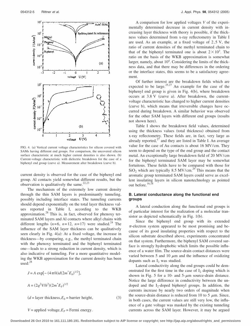
An identical reference metal contact was always madeon the uncovered hydroxylated silicon surface, and itscurrent-voltage characteristic was compared with that of acontact on the SAM covered surface �compare Fig. 4�a��.The very much lower current densities for SAM coveredsurfaces suggest that tunneling is the prevailing mechanismand not “leakage currents” via pin holes or a shunt currentpath via metal atoms which have migrated between the alkylchains.
For contacting the back side of the Si wafer, the SAMlayer deposited there had to be, first mechanically removedand then, treated with HF.
For dc measurements, the samples were attached to asample holder with controlled temperature �down to −60 °C�which was at zero ground potential. A screened Kelvin-typesetup allowed dark current measurements down to 10 fA.Various integration times were used with a HP 4156B sys-tem, the longest ��320 ms� for sensitive lateral conductivitymeasurements.
III. STRUCTURAL PROPERTIES
A. Grazing incidence x-ray reflectometry
X-ray reflectometry based on total reflection character-izes the electron density profile normal to the sample surface.For this reason, this technique was employed to study thestructural properties of the SAM layers, with different func-tional end groups, chemically attached to a hydroxylated Si�100� surface. A computer data analysis yields data aboutlayer thicknesses,20 surface roughness, and real and imagi-nary parts of the complex refractive index n
n = 1 − � − i , �1�
where � is related to the electron density, and to the massabsorption coefficient.
For all layers with different end groups, � is positive andvery small, which implies that the critical angle for totalreflection, �C, is also very small
�C = �2� � 0.1 ° . �2�
aded 26 Oct 2010 to 161.111.180.191. Redistribution subject to AIP lic
Figure 2�a� shows a comparison between the grazing in-cidence x-ray reflection scan of a reference silicon surfacewith that of a Si surface covered with a SAM layer having abiphenyl end group. The latter exhibits a pronounced inter-ference pattern due to Kiessig interferences of the SAM layeron top of the substrate, while only Fresnel reflectivity is ob-served for the bare substrate.
Figure 2�b� illustrates the x-ray reflection scans of thedifferent SAM layers with various end groups: biphenyl,phenoxy, thiophene, and OTS �methyl end group�. One cansee that there is a surprising and very systematic change inthe structure of the reflection curves which seems to be re-lated with the size and/or nature of the end group molecule:the larger the end group molecule, the more pronounced theinterferences are.
Analysis of the spectra shown in Fig. 2�b� revealed thatthe data could not be fitted by assuming a one layer model.An excellent fit, however, was obtained with a two layermodel, considering that the layers display two different re-fractive indices n1 and n2.
Table I collects the thickness values for both layers,layer 1 and layer 2, obtained from the computer analysis. Thethinner of the two layers �called layer 1, with n1� is nearlyconstant in its dimension, independent of the type of the endgroup molecule, and its average value is about 10.8 Å. Thislayer is the closest to the substrate.
On the other hand, the thickness of layer 2 �with n2�varies in the range of 22–32 Å �see Table I�. Its dimensiondepends on the type and size of the end group molecule.Hence, the sum of the two layer thicknesses changes accord-ingly �see Table I�.
The surface roughness obtained from the data analysis inthe two layer model varied between 2.9 and 4.5 Å for thethinner layer 1, and between 2.3 and 3.8 Å for the thicker
FIG. 2. �a� Grazing incidence x-ray reflectometry: comparison between asilicon substrate with a SAM covered surface having a biphenyl end group.�b� Systematic change of x-ray reflection curves for different SAM coveredsurfaces: influence of the functional end group.
layer 2.
ense or copyright; see http://jap.aip.org/about/rights_and_permissions
054312-4 Rittner et al. J. Appl. Phys. 98, 054312 �2005�
Downlo
The real part of the refractive index, �, takes values of��69�10−6 for layer 1, and ��30�10−6 for layer 2. Cor-responding typical values for the imaginary part, , are �3�10−6 for layer 1 and ��5–7��10−6 for layer 2.
B. Theoretical model and discussion
Since the x-ray reflection data of the silicon surface donot exhibit Kiessig interferences �compare the two scans in-cluded in Fig. 2�a��, the following model is proposed whichassociates the two layers of the SAM covered surface withthe structure of the SAM molecule and an interface:
Layer 1, with a thickness value of �11 Å �see Table I� isassociated with the interface between the hydroxylated sili-con surface and the alkyl chain �“interface layer”�. As onewould expect, the thickness of this layer does not signifi-cantly vary between the different SAMs.
Layer 2, with a thickness value within the range of22–33 Å depending on the type of the SAM �see Table I�, isassociated with the organic monolayer itself, including thefunctional end group and the alkyl chain or part of it. In thiscase, the layer thickness increases as the size of the endgroup increases.
In order to check the validity of this model, we haveindependently estimated the thickness of each SAM usingmolecular modeling �MOPAC VI: AM1 package, availablethrough Cerius 2�. The simulation of the film thickness isbased on the optimization of the geometrical variables of anisolated molecule. As a first approximation, we have as-sumed that the tilt angle between the molecular axis and thesilicon surface is approximately zero. Figure 3 illustrates, asan example, the optimized molecular conformation for thecase of the biphenyl end group. The alkyl sequence adoptsthe all-trans conformation, in agreement with the generallyaccepted conformation of OTS on oxidized silicon.2 Table Icollects the molecular length values �measured in the direc-tion of the alkyl sequence chain axis� for each SAM, calcu-lated using molecular modeling.
A good agreement is found between the simulated layer2 values and the experimental layer 2 thicknesses shown inTable I. Moreover, the delta values determined for layer 2���30�10−6� are substantially different from those ob-tained for layer 1 ���69�10−6�. The latter ones are in the
−6
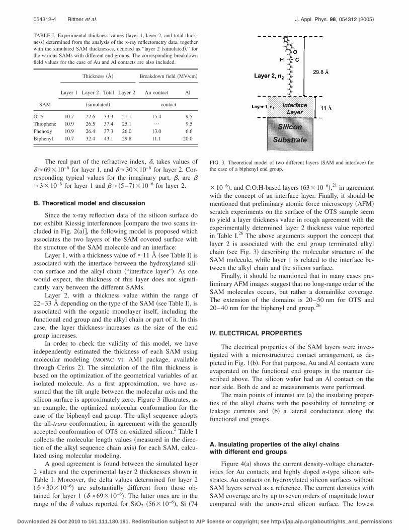
TABLE I. Experimental thickness values �layer 1, layer 2, and total thick-ness� determined from the analysis of the x-ray reflectometry data, togetherwith the simulated SAM thicknesses, denoted as “layer 2 �simulated�,” forthe various SAMs with different end groups. The corresponding breakdownfield values for the case of Au and Al contacts are also included.
SAM
Thickness �� Breakdown field �MV/cm�
Layer 1 Layer 2 Total Layer 2 Au contact Al
�simulated� contact
OTS 10.7 22.6 33.3 21.1 15.4 9.5Thiophene 10.9 26.5 37.4 25.1 ¯ 9.5Phenoxy 10.9 26.4 37.3 26.0 13.0 6.6Biphenyl 10.7 32.4 43.1 29.8 11.1 20.0
range of the � values reported for SiO2 �56�10 �, Si �74
aded 26 Oct 2010 to 161.111.180.191. Redistribution subject to AIP lic
�10−6�, and C:O:H-based layers �63�10−6�,21 in agreementwith the concept of an interface layer. Finally, it should bementioned that preliminary atomic force microscopy �AFM�scratch experiments on the surface of the OTS sample seemto yield a layer thickness value in rough agreement with theexperimentally determined layer 2 thickness value reportedin Table I.26 The above arguments support the concept thatlayer 2 is associated with the end group terminated alkylchain �see Fig. 3� describing the molecular structure of theSAM molecule, while layer 1 is related to the interface be-tween the alkyl chain and the silicon surface.
Finally, it should be mentioned that in many cases pre-liminary AFM images suggest that no long-range order of theSAM molecules occurs, but rather a domainlike coverage.The extension of the domains is 20–50 nm for OTS and20–40 nm for the biphenyl end group.26
IV. ELECTRICAL PROPERTIES
The electrical properties of the SAM layers were inves-tigated with a microstructured contact arrangement, as de-picted in Fig. 1�b�. For that purpose, Au and Al contacts wereevaporated on the functional end groups in the manner de-scribed above. The silicon wafer had an Al contact on therear side. Both dc and ac measurements were performed.
The main points of interest are �a� the insulating proper-ties of the alkyl chains with the possibility of tunneling orleakage currents and �b� a lateral conductance along thefunctional end groups.
A. Insulating properties of the alkyl chainswith different end groups
Figure 4�a� shows the current density-voltage character-istics for Au contacts and highly doped n-type silicon sub-strates. Au contacts on hydroxylated silicon surfaces withoutSAM layers served as a reference. The current densities withSAM coverage are by up to seven orders of magnitude lower
FIG. 3. Theoretical model of two different layers �SAM and interface� forthe case of a biphenyl end group.
compared with the uncovered silicon surface. The lowest
ense or copyright; see http://jap.aip.org/about/rights_and_permissions
054312-5 Rittner et al. J. Appl. Phys. 98, 054312 �2005�
Downlo
current density is observed for the case of the biphenyl endgroup. Al contacts yield somewhat different results, but theobservation is qualitatively the same.22,23
The mechanism of the extremely low current densitythrough the thin SAM layers is predominantly tunneling,possibly including interface states. The tunneling currentsshould depend exponentially on the total layer thickness val-ues reported in Table I, according to the WKBapproximation.28 This is, in fact, observed for phenoxy ter-minated SAM layers and Al contacts where alkyl chains withdifferent lengths �n=6, n=12, n=17� were studied.24 Theinfluence of the SAM layer thickness can be qualitativelyseen clearly in Fig. 4�a�: At a fixed voltage, the increase inthickness—by comparing, e.g., the methyl terminated chainwith the phenoxy terminated and the biphenyl terminatedone—leads to a strong reduction in current density, which isalso indicative of tunneling. For a more quantitative model-ing the WKB approximation for the current density has beenused:28
J = A exp�− �4�/h�d�2m*Eb�1/2� ,
A = �2q2V/h2��2m*EF�1/2
�d = layer thickness,Eb = barrier height, �3�
FIG. 4. �a� Vertical current voltage characteristics for silicon covered withSAMs having different end groups. For comparison, the uncovered siliconsurface characteristic at much higher current densities is also shown. �b�Current-voltage characteristic with dielectric breakdown for the case of abiphenyl end group �curve a�. Measurement after breakdown �curve b�.
V = applied voltage,EF = Fermi energy.
aded 26 Oct 2010 to 161.111.180.191. Redistribution subject to AIP lic
A comparison for low applied voltages V of the experi-mentally determined decrease in current density with in-creasing layer thickness with theory is possible, if the thick-ness values determined from x-ray reflectometry in Table Iare used. As an example, at a fixed voltage of 2 ,5 V, theratio of current densities of the methyl terminated chain tothat of the biphenyl terminated one is about 2�103. Theratio on the basis of the WKB approximation is somewhatlarger, namely, about 104. Considering the limits of the thick-ness data, and that there may be differences in the orderingor the interface states, this seems to be a satisfactory agree-ment.
Of further interest are the breakdown fields which areexpected to be large.25,27 An example for the case of thebiphenyl end group is given in Fig. 4�b�, where breakdownoccurs at 3.8 V �curve a�. After breakdown, the current-voltage characteristic has changed to higher current densities�curve b�, which means that irreversible changes have oc-curred during breakdown. A similar behavior was observedfor the other SAM layers with different end groups �resultsnot shown here�.
Table I shows the breakdown field values, determinedusing the thickness values �total thickness� obtained fromx-ray reflectometry. These fields are, in fact, very large asalready reported,27 and they are listed in Table I. An averagevalue for the case of Au contacts is about 16 MV/cm. Theyseem to depend on the type of the end group and the contactmetal. An exceptionally large breakdown field of 20 MV/cmfor the biphenyl terminated SAM layer may be somewhatfortuitous. These fields have to be compared with those forSiO2 which are typically 8.5 MV/cm.29 This means that thearomatic group terminated SAM layers could serve as excel-lent insulating layers in silicon nanotechnology as pointedout before.16,18
B. Lateral conductance along the functional endgroups
A lateral conduction along the functional end groups isof particular interest for the realization of a molecular tran-sistor as depicted schematically in Fig. 1�b�.
Since the biphenyl end group with its extended�-electron system appeared to be most promising and be-cause of its good insulating properties with respect to thesilicon substrate described above, experiments concentratedon that system. Furthermore, the biphenyl SAM covered sur-face is strongly hydrophobic which limits the possible influ-ence of a water film. The source-drain contact distances werevaried between 5 and 10 �m and the influence of oxidizingdopants such as I2 was studied.
Lateral conductivity along the end groups could be dem-onstrated for the first time in the case of I2 doping which isshown in Fig. 5 for a 10- and 5-�m source-drain distance.Notice the large difference in conductivity between the un-doped and the I2-doped biphenyl groups. In addition, thecurrents increase by nearly two orders of magnitude whenthe source-drain distance is reduced from 10 to 5 �m. Since,in both cases, the current values are still very low, the influ-ence of a gate voltage was masked by the existing tunneling
currents across the SAM layer. However, it may be arguedense or copyright; see http://jap.aip.org/about/rights_and_permissions

054312-6 Rittner et al. J. Appl. Phys. 98, 054312 �2005�
Downlo
that competitive current contributions through a parallelshunt path along the silicon surface including tunnelingthrough the SAM layer would not be influenced by the io-dine doping. Therefore, possible parallel shunt currentsthrough the silicon substrate are assumed to be small.
V. CONCLUSION AND OUTLOOK
�1� Self-assembling monolayers �SAM� appear to be an in-teresting approach towards molecular nanostructures. Inthis paper, SAM layers on silicon surfaces are examined,because of the silicon nanoelectronic potential as a pe-riphery for organic molecular systems.
�2� Through a chemical reaction of a SiCl3 anchor groupwith a hydroxylated silicon surface, the organic mol-ecules consisting of an alkyl �CH2�18 chain with differ-ent functional end groups were attached to the siliconsurface. The surprising result of grazing incidence x-rayreflectivity is that only a two layer model pertaining totwo layers with different refractive indices �electrondensities� can explain experimental data analysis. Onelayer of nearly constant thickness is associated with theinterface between the hydroxylated silicon surface andthe alkyl chain, the other with the actual SAM molecule,
FIG. 5. Current-voltage characteristics demonstrating lateral conductionalong the biphenyl end group doped with iodine, for two different source-drain contact distances.
i.e., the alkyl chain and the functional end groups.
aded 26 Oct 2010 to 161.111.180.191. Redistribution subject to AIP lic
�3� The electrical properties, exploring the potential for mo-lecular electronic devices, seem to be very promising:SAM layers can serve as excellent gate insulators.16,18
Breakdown voltages are very high �typically16 MV/cm�, favorably comparing them with the valuesfor SiO2 layers. However, in that case, a conductive ac-tive layer such as pentacene27 is still needed on top ofthe SAM.
�4� A lateral in-plane conductivity along the SAM endgroups could be demonstrated in the case of an iodine-doped biphenyl end group in an organic field-effect tran-sistor �OFET�-like experimental structure. This opensthe possibility to obtain molecular transistors withoutdeposition of an additional conductive active layer. For astill fairly large contact distance of 5 �m, the in-planecurrents are still very small. For a functioning molecularSAM nanotransistor, the source-drain distance has to bereduced considerably, i.e., into the 30-nm range.
ACKNOWLEDGMENTS
The authors wish to thank F. Baltá Calleja, Madrid, forscientific discussions, and R. García �Madrid, Spain� as wellas R. Adhikari �Halle, Germany� for taking AFM images.Financial support of the German Research Association�DFG�, Bonn, and the Ministerio de Educación, Cultura yDeporte, Madrid, under Contract No. SAB 2002-2007, isgratefully acknowledged. One of the authors �A.F.� thanksfor the financial support of the Dirección General de Inves-tigación �Grant No. BFM 2000-1474�, MCYT, Spain. An-other author �M.S.M.G.� acknowledges a fellow award bythe MCYT �Spain� in the Ramón y Cajal Program.
1A. Ulman, An Introduction to Ultrathin Organic Films: From Langmuir-Blodgett to Self Assembly �Academic, San Diego, 1991�.
2F. Schreiber, Prog. Surf. Sci. 65, 151 �2000�.3G. E. Poirier and M. J. Tarlov, Langmuir 10, 2853 �1994�.4S. Heid, F. Effenberger, K. Bierbaum, and M. Grunze, Langmuir 12, 2118�1996�.
5P. Harder, K. Bierbaum, C. Woell, M. Grunze, S. Heid, and F. Effenberger,Langmuir 13, 445 �1997�.
6K. Bierbaum, M. Kinzler, C. Woell, M. Grunze, G. Haehner, S. Heid, andF. Effenberger, Langmuir 11, 512 �1995�.
7F. Effenberger, G. Goetz, B. Bidlingmaier, and M. Wezstein, Shore Beach110, 2651 �1998�.
8J. S. R. Muenter, thesis, Stuttgart University, 2001.9M. M. Sung, G. J. Kluth, and R. Maboudian, J. Vac. Sci. Technol. A 17,540 �1999�.
10S. Seifritz, thesis Stuttgart University, 2001.11K. Bierbaum, M. Grunze, A. A. Baski, L. F. Chi, W. Schrepp, and H.
Fuchs, Langmuir 11, 2143 �1995�.12R. Moaz, J. Sagiv, D. Degenhardt, H. Moehwald, and P. Quint, Supramol.
Sci. 2, 9 �1995�.13M. J. Stevens, Langmuir 15, 2773 �1999�.14M. Schuetz, thesis, Stuttgart University, 2002.15M. R. Linford and C. E. D. Chidsey, J. Am. Chem. Soc. 115, 12631
�1993�.16J. Collet and D. Vuillaume, Appl. Phys. Lett. 73, 2681 �1998�.17J. Collet, O. Tharaud, A. Chapoton, and D. Vuillaume, Appl. Phys. Lett.
76, 1941 �2000�.18J. Collet, S. Lenfant, D. Vuillaume, O. Bouluossa, F. Rondelez, J. M. Gay,
K. Kham, and C. Chevrot, Appl. Phys. Lett. 76, 1339 �2000�.19M. M. Heynes et al., Mater. Res. Soc. Symp. Proc. 315, 35 �1993�.20N. Tillman, A. Ulman, J. S. Schildkraut, and T. L. Penner, J. Am. Chem.
Soc. 110, 6136 �1988�.
ense or copyright; see http://jap.aip.org/about/rights_and_permissions

054312-7 Rittner et al. J. Appl. Phys. 98, 054312 �2005�
Downlo
21B. L. Henke, E. M. Gullikson, and J. C. Davis, At. Data Nucl. Data Tables54, 181 �1993�.
22C. Boulas, J. V. Davidovits, F. Rondelez, and D. Vuillaume, Phys. Rev.Lett. 76, 4797 �1996�.
23D. Vuillaume, C. Boulas, J. Collet, J. V. Davidovitis, and F. Rondelez,Appl. Phys. Lett. 69, 1646 �1996�.
24M. Rittner �unpublished�.
aded 26 Oct 2010 to 161.111.180.191. Redistribution subject to AIP lic
25P. Fontaine, D. Goguenheim, D. Deresmes, D. Vuillaume, M. Garet, and F.Rondelez, Appl. Phys. Lett. 62, 2256 �1993�.
26�unpublished�.27M. Halik et al., Nature �London� 431, 963 �2004�.28G. Horowitz, Synth. Met. 138, 101 �2003�.29K. Sekine, Y. Saito, M. Hirayama, and T. Ohmi, IEEE Trans. Electron
Devices 48, 1550 �2000�.
ense or copyright; see http://jap.aip.org/about/rights_and_permissions