Nanoscale Gate Stacks: From Atomic Defects to Device Performance
7
Nanoscale Gate Stacks: From Atomic Defects to Device Performance G. Bersuker, C. S. Park, J. Price, P. Lysaght, P. Kirsch, and R. Jammy SEMATECH, 2706 Montopolis Dr., Austin TX 78741 Concerted physical and electrical characterization of the gate stacks, which includes high dielectric constant materials and metal electrodes, has been performed in order to link atomic defects to the specific device electrical characteristics. It has been shown that defects in the SiO 2 layer formed at the interface of the dielectric stack and the substrate plays a critical role in defining both performance and reliability of the high-k devices. Introduction Relentless device scaling challenges the traditional reliability paradigm: increasing variability adversely affects the predictive capability of well-established statistical evaluation methods while new materials and complex multi-component gate stack structures may result in long-term instabilities due to process-related defects (rather than stress-generated ones, which are usually associated with the time dependency of device characteristics). These factors point to a growing need to extend reliability evaluations in the “micro” direction - towards identifying the atomic defects that would allow developing physics-based degradation models, as well as provide helpful feedback to process optimization efforts. In this paper, we discuss several case studies linking atomic- level defects in the interfacial layer in the metal/high-k gate stacks to device performance and reliability. The quality of the interfacial SiO 2 layer is known to be strongly affected by processing conditions, which determines to what degree the stoichiometry of this layer is affected by its interaction to the overlaying HK/metal films. Indeed, as has been demonstrated by the electrical, physical (STEM/EELS, ESR, XPS (1 ) –(5 )), and modeling studies, Hf-based high-k films modify the stoichiometry of the underlying SiO 2 layer by rendering it oxygen-deficient. This leads to an increase in its dielectric constant, and a higher density of fixed charges in this layer, thereby degrading the mobility of the channel carriers. Specifically, we show that in the devices with the high-k/metal gate stacks Negative Bias Temperature Instability (NBTI) exhibits a fast component associated with the Hf related defects near the Si substrate interface, while Time- Dependent Dielectric Breakdown (TDDB) and a so-called V fb roll-off phenomenon are affected by the oxygen vacancy defects in the interfacial SiO 2 layer. Control over the SiO 2 layer composition and stoichiometry is critical for meeting reliability requirements for future technology nodes. Physical Characterization The electrically detected electron spin resonance (ESR) technique called spin dependent recombination (SDR) (6 ), has about seven orders of magnitude greater sensitivity than (ESR) and allows measurements in fully processed transistors. SDR utilizes the fact that recombination in semiconductors is spin dependent. By simultaneously exposing a device appropriately biased (for maximum recombination) to a large magnetic field and microwave irradiation, one can observe magnetic resonance ECS Transactions, 22 (1) 3-9 (2009) 10.1149/1.3152957 © The Electrochemical Society 3 ) unless CC License in place (see abstract). ecsdl.org/site/terms_use address. Redistribution subject to ECS terms of use (see 186.88.93.73 Downloaded on 2014-10-13 to IP
-
Upload
independent -
Category
Documents
-
view
4 -
download
0
Transcript of Nanoscale Gate Stacks: From Atomic Defects to Device Performance
Nanoscale Gate Stacks: From Atomic Defects to Device Performance
G. Bersuker, C. S. Park, J. Price, P. Lysaght, P. Kirsch, and R. Jammy SEMATECH, 2706 Montopolis Dr., Austin TX 78741
Concerted physical and electrical characterization of the gate stacks, which includes high dielectric constant materials and metal electrodes, has been performed in order to link atomic defects to the specific device electrical characteristics. It has been shown that defects in the SiO2 layer formed at the interface of the dielectric stack and the substrate plays a critical role in defining both performance and reliability of the high-k devices.
Introduction
Relentless device scaling challenges the traditional reliability paradigm: increasing
variability adversely affects the predictive capability of well-established statistical evaluation methods while new materials and complex multi-component gate stack structures may result in long-term instabilities due to process-related defects (rather than stress-generated ones, which are usually associated with the time dependency of device characteristics). These factors point to a growing need to extend reliability evaluations in the “micro” direction - towards identifying the atomic defects that would allow developing physics-based degradation models, as well as provide helpful feedback to process optimization efforts. In this paper, we discuss several case studies linking atomic-level defects in the interfacial layer in the metal/high-k gate stacks to device performance and reliability. The quality of the interfacial SiO2 layer is known to be strongly affected by processing conditions, which determines to what degree the stoichiometry of this layer is affected by its interaction to the overlaying HK/metal films. Indeed, as has been demonstrated by the electrical, physical (STEM/EELS, ESR, XPS (1) –(5)), and modeling studies, Hf-based high-k films modify the stoichiometry of the underlying SiO2 layer by rendering it oxygen-deficient. This leads to an increase in its dielectric constant, and a higher density of fixed charges in this layer, thereby degrading the mobility of the channel carriers. Specifically, we show that in the devices with the high-k/metal gate stacks Negative Bias Temperature Instability (NBTI) exhibits a fast component associated with the Hf related defects near the Si substrate interface, while Time-Dependent Dielectric Breakdown (TDDB) and a so-called Vfb roll-off phenomenon are affected by the oxygen vacancy defects in the interfacial SiO2 layer. Control over the SiO2 layer composition and stoichiometry is critical for meeting reliability requirements for future technology nodes.
Physical Characterization
The electrically detected electron spin resonance (ESR) technique called spin
dependent recombination (SDR) (6), has about seven orders of magnitude greater sensitivity than (ESR) and allows measurements in fully processed transistors. SDR utilizes the fact that recombination in semiconductors is spin dependent. By simultaneously exposing a device appropriately biased (for maximum recombination) to a large magnetic field and microwave irradiation, one can observe magnetic resonance
ECS Transactions, 22 (1) 3-9 (2009)10.1149/1.3152957 © The Electrochemical Society
3 ) unless CC License in place (see abstract). ecsdl.org/site/terms_use address. Redistribution subject to ECS terms of use (see 186.88.93.73Downloaded on 2014-10-13 to IP
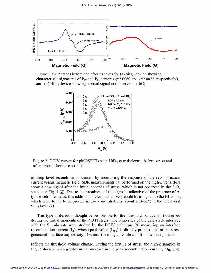
of deep level recombination centers by monitoring the response of the recombination current versus magnetic field. SDR measurements (7) performed on the high-k transistors show a new signal after the initial seconds of stress, which is not observed in the SiO2 stack, see Fig. 1 (8). Due to the broadness of this signal, indicative of the presence of d-type electronic states, this additional defects tentatively could be assigned to the Hf atoms, which were found to be present in low concentrations (about E13/cm2) in the interfacial SiO2 layer (2).
This type of defect is thought be responsible for the threshold voltage shift observed
during the initial moments of the NBTI stress. The properties of the gate stack interface with the Si substrate were studied by the DCIV technique (9) measuring an interface recombination current (IB), whose peak value (IBpk) is directly proportional to the stress generated interface trap density, DIT, near the midgap, while a shift in the peak position
reflects the threshold voltage change. During the first 1s of stress, the high-k samples in Fig. 2 show a much greater initial increase in the peak recombination current, ∆IBpk(1s),
-0.6 -0.5 -0.4 -0.3 -0.2 -0.1 0.00
1x10³
2x10³
3x10³
4x10³
5x10³
1.1 nm SiO2 + 3 nm HfO2
EOT ≅ 1.2 nm 125 °C, VG = −1.8 V Eo ≅ 3.4 MV/cm
∆IB
-PK (p
A)
VG (V)
t = 10 s 5 s 2 s 1 s 0 s
3430 3440 3450 3460 3470 3480Magnetic Field (G)
SDR
Inte
nsity
(Arb
. Uni
ts)
g = 2.0060 ± 0.0003
g = 2.0033 ± 0.0003
Possible E' Center0
3
6
9
12
3360 3375 3390 3405 3420 3435Magnetic Field (G)
SDR
Am
plitu
de (A
rb S
cale
)
g = 1.9998
Magnetic Field (G) Magnetic Field (G)
Figure 1. SDR traces before and after 5s stress for (a) SiO2 device showing characteristic signatures of Pb0 and Pb1 centers (g=2.0060 and g=2.0033, respectively), and (b) HfO2 device showing a broad signal not observed in SiO2.
Figure 2. DCIV curves for pMOSFETs with HfO2 gate dielectric before stress and after several short stress times
ECS Transactions, 22 (1) 3-9 (2009)
4 ) unless CC License in place (see abstract). ecsdl.org/site/terms_use address. Redistribution subject to ECS terms of use (see 186.88.93.73Downloaded on 2014-10-13 to IP
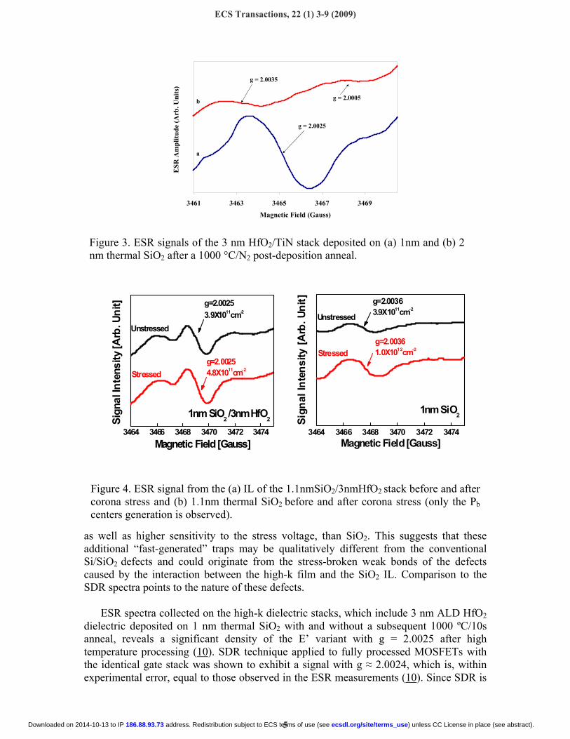
as well as higher sensitivity to the stress voltage, than SiO2. This suggests that these additional “fast-generated” traps may be qualitatively different from the conventional Si/SiO2 defects and could originate from the stress-broken weak bonds of the defects caused by the interaction between the high-k film and the SiO2 IL. Comparison to the SDR spectra points to the nature of these defects.
ESR spectra collected on the high-k dielectric stacks, which include 3 nm ALD HfO2 dielectric deposited on 1 nm thermal SiO2 with and without a subsequent 1000 ºC/10s anneal, reveals a significant density of the E’ variant with g = 2.0025 after high temperature processing (10). SDR technique applied to fully processed MOSFETs with the identical gate stack was shown to exhibit a signal with g ≈ 2.0024, which is, within experimental error, equal to those observed in the ESR measurements (10). Since SDR is
3464 3466 3468 3470 3472 3474
Unstressed
Sign
al In
tens
ity [A
rb. U
nit]
Magnetic Field [Gauss]
Stressed
g=2.00253.9X1011cm-2
g=2.00254.8X1011cm-2
1nm SiO2 /3nm HfO
2
3464 3466 3468 3470 3472 3474
Unstressed
Sign
al In
tens
ity [A
rb. U
nit]
Magnetic Field [Gauss]
Stressed
g=2.00363.9X1011cm-2
g=2.00361.0X1012cm-2
1nm SiO2
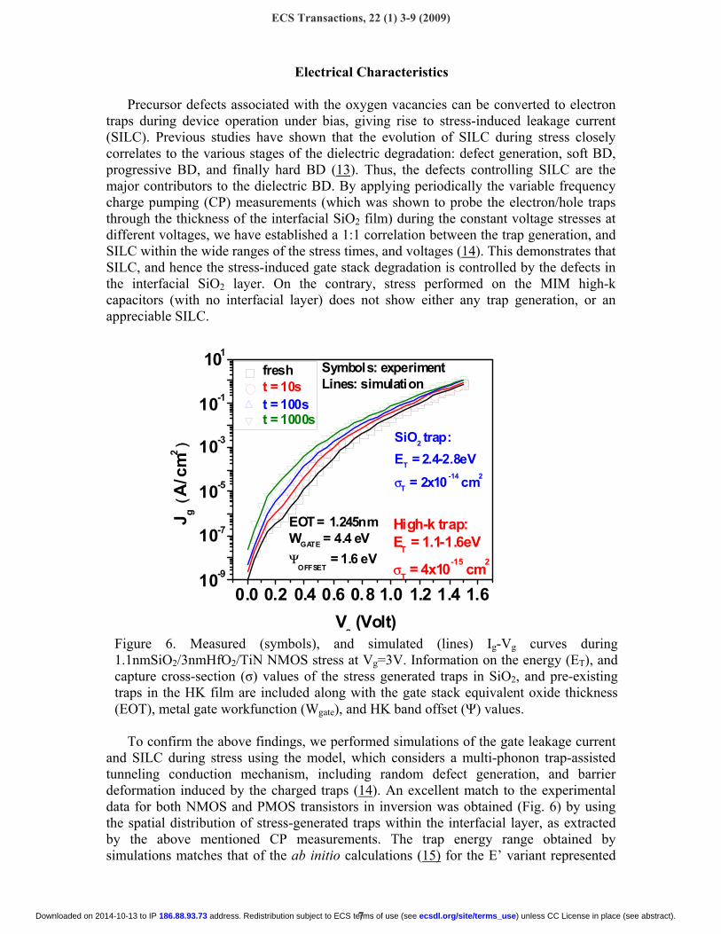
Figure 4. ESR signal from the (a) IL of the 1.1nmSiO2/3nmHfO2 stack before and after corona stress and (b) 1.1nm thermal SiO2 before and after corona stress (only the Pbcenters generation is observed).
3461 3463 3465 3467 3469Magnetic Field (Gauss)
ESR
Am
plitu
de (A
rb. U
nits
)
g = 2.0025
g = 2.0035
g = 2.0005
a
b
Figure 3. ESR signals of the 3 nm HfO2/TiN stack deposited on (a) 1nm and (b) 2 nm thermal SiO2 after a 1000 °C/N2 post-deposition anneal.
ECS Transactions, 22 (1) 3-9 (2009)
5 ) unless CC License in place (see abstract). ecsdl.org/site/terms_use address. Redistribution subject to ECS terms of use (see 186.88.93.73Downloaded on 2014-10-13 to IP
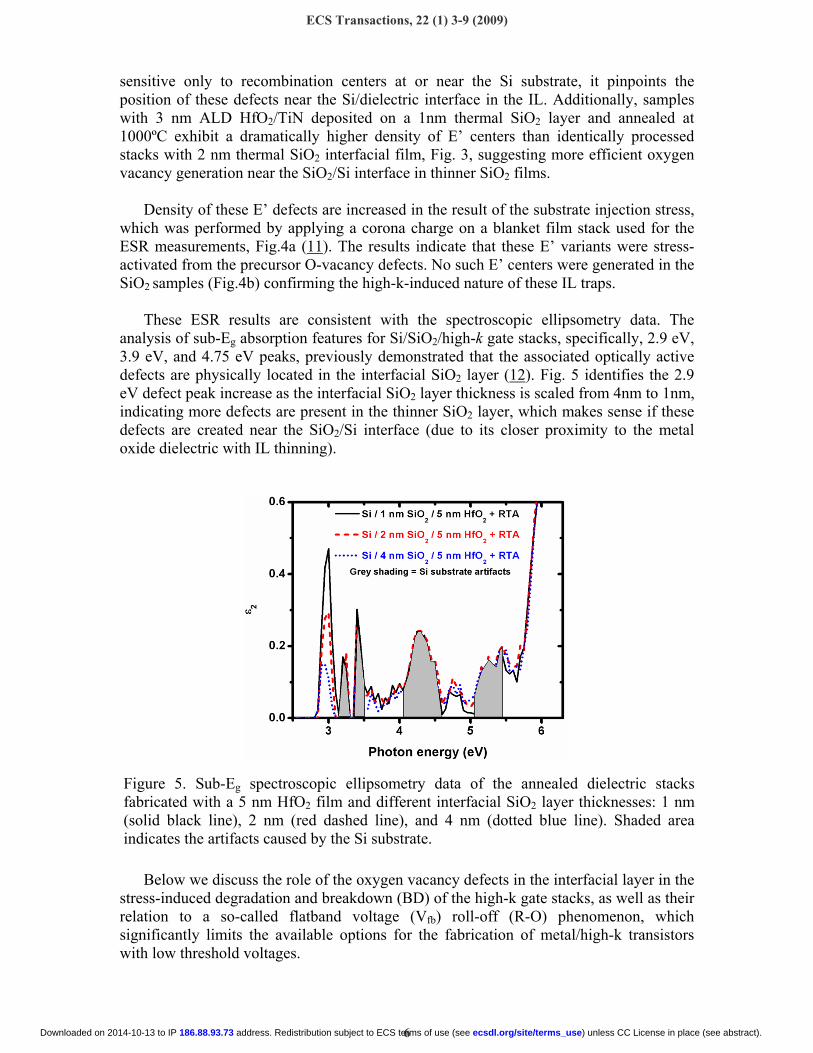
sensitive only to recombination centers at or near the Si substrate, it pinpoints the position of these defects near the Si/dielectric interface in the IL. Additionally, samples with 3 nm ALD HfO2/TiN deposited on a 1nm thermal SiO2 layer and annealed at 1000ºC exhibit a dramatically higher density of E’ centers than identically processed stacks with 2 nm thermal SiO2 interfacial film, Fig. 3, suggesting more efficient oxygen vacancy generation near the SiO2/Si interface in thinner SiO2 films.
Density of these E’ defects are increased in the result of the substrate injection stress,
which was performed by applying a corona charge on a blanket film stack used for the ESR measurements, Fig.4a (11). The results indicate that these E’ variants were stress-activated from the precursor O-vacancy defects. No such E’ centers were generated in the SiO2 samples (Fig.4b) confirming the high-k-induced nature of these IL traps.
These ESR results are consistent with the spectroscopic ellipsometry data. The analysis of sub-Eg absorption features for Si/SiO2/high-k gate stacks, specifically, 2.9 eV, 3.9 eV, and 4.75 eV peaks, previously demonstrated that the associated optically active defects are physically located in the interfacial SiO2 layer (12). Fig. 5 identifies the 2.9 eV defect peak increase as the interfacial SiO2 layer thickness is scaled from 4nm to 1nm, indicating more defects are present in the thinner SiO2 layer, which makes sense if these defects are created near the SiO2/Si interface (due to its closer proximity to the metal oxide dielectric with IL thinning).
Below we discuss the role of the oxygen vacancy defects in the interfacial layer in the
stress-induced degradation and breakdown (BD) of the high-k gate stacks, as well as their relation to a so-called flatband voltage (Vfb) roll-off (R-O) phenomenon, which significantly limits the available options for the fabrication of metal/high-k transistors with low threshold voltages.
Figure 5. Sub-Eg spectroscopic ellipsometry data of the annealed dielectric stacks fabricated with a 5 nm HfO2 film and different interfacial SiO2 layer thicknesses: 1 nm (solid black line), 2 nm (red dashed line), and 4 nm (dotted blue line). Shaded area indicates the artifacts caused by the Si substrate.
ECS Transactions, 22 (1) 3-9 (2009)
6 ) unless CC License in place (see abstract). ecsdl.org/site/terms_use address. Redistribution subject to ECS terms of use (see 186.88.93.73Downloaded on 2014-10-13 to IP
Electrical Characteristics
Precursor defects associated with the oxygen vacancies can be converted to electron traps during device operation under bias, giving rise to stress-induced leakage current (SILC). Previous studies have shown that the evolution of SILC during stress closely correlates to the various stages of the dielectric degradation: defect generation, soft BD, progressive BD, and finally hard BD (13). Thus, the defects controlling SILC are the major contributors to the dielectric BD. By applying periodically the variable frequency charge pumping (CP) measurements (which was shown to probe the electron/hole traps through the thickness of the interfacial SiO2 film) during the constant voltage stresses at different voltages, we have established a 1:1 correlation between the trap generation, and SILC within the wide ranges of the stress times, and voltages (14). This demonstrates that SILC, and hence the stress-induced gate stack degradation is controlled by the defects in the interfacial SiO2 layer. On the contrary, stress performed on the MIM high-k capacitors (with no interfacial layer) does not show either any trap generation, or an appreciable SILC.
To confirm the above findings, we performed simulations of the gate leakage current and SILC during stress using the model, which considers a multi-phonon trap-assisted tunneling conduction mechanism, including random defect generation, and barrier deformation induced by the charged traps (14). An excellent match to the experimental data for both NMOS and PMOS transistors in inversion was obtained (Fig. 6) by using the spatial distribution of stress-generated traps within the interfacial layer, as extracted by the above mentioned CP measurements. The trap energy range obtained by simulations matches that of the ab initio calculations (15) for the E’ variant represented
0.0 0.2 0.4 0.6 0.8 1.0 1.2 1.4 1.610-9
10-7
10-5
10-3
10-1
101
SiO2 trap:ET = 2.4-2.8eVσT = 2x10-14 cm2
EOT = 1.245nmWGATE = 4.4 eVΨ
OFFSET = 1.6 eV
fresh t = 10s t = 100s t = 1000s
J g (A
/cm
2)
Vg (Volt)
High-k trap:ET = 1.1-1.6eV
σT = 4x10-15 cm2
Symbols: experimentLines: simulation
Figure 6. Measured (symbols), and simulated (lines) Ig-Vg curves during 1.1nmSiO2/3nmHfO2/TiN NMOS stress at Vg=3V. Information on the energy (ET), and capture cross-section (σ) values of the stress generated traps in SiO2, and pre-existing traps in the HK film are included along with the gate stack equivalent oxide thickness (EOT), metal gate workfunction (Wgate), and HK band offset (Ψ) values.
ECS Transactions, 22 (1) 3-9 (2009)
7 ) unless CC License in place (see abstract). ecsdl.org/site/terms_use address. Redistribution subject to ECS terms of use (see 186.88.93.73Downloaded on 2014-10-13 to IP
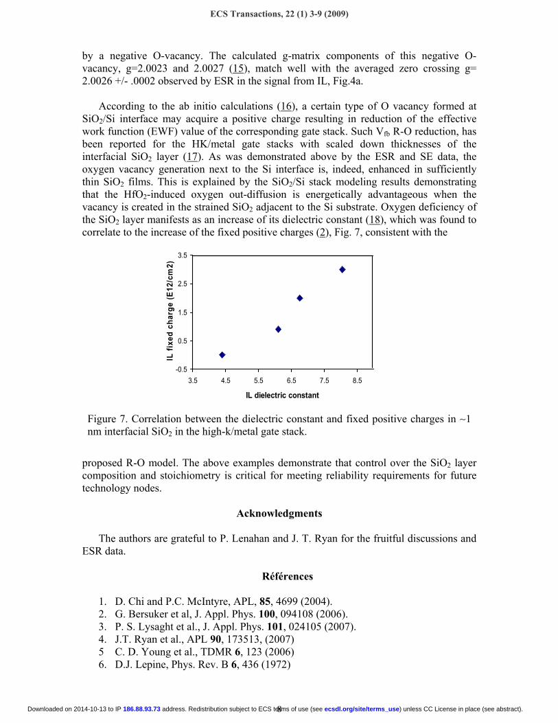
by a negative O-vacancy. The calculated g-matrix components of this negative O-vacancy, g=2.0023 and 2.0027 (15), match well with the averaged zero crossing g= 2.0026 +/- .0002 observed by ESR in the signal from IL, Fig.4a.
According to the ab initio calculations (16), a certain type of O vacancy formed at
SiO2/Si interface may acquire a positive charge resulting in reduction of the effective work function (EWF) value of the corresponding gate stack. Such Vfb R-O reduction, has been reported for the HK/metal gate stacks with scaled down thicknesses of the interfacial SiO2 layer (17). As was demonstrated above by the ESR and SE data, the oxygen vacancy generation next to the Si interface is, indeed, enhanced in sufficiently thin SiO2 films. This is explained by the SiO2/Si stack modeling results demonstrating that the HfO2-induced oxygen out-diffusion is energetically advantageous when the vacancy is created in the strained SiO2 adjacent to the Si substrate. Oxygen deficiency of the SiO2 layer manifests as an increase of its dielectric constant (18), which was found to correlate to the increase of the fixed positive charges (2), Fig. 7, consistent with the
proposed R-O model. The above examples demonstrate that control over the SiO2 layer composition and stoichiometry is critical for meeting reliability requirements for future technology nodes.
Acknowledgments
The authors are grateful to P. Lenahan and J. T. Ryan for the fruitful discussions and ESR data.
Références
1. D. Chi and P.C. McIntyre, APL, 85, 4699 (2004). 2. G. Bersuker et al, J. Appl. Phys. 100, 094108 (2006). 3. P. S. Lysaght et al., J. Appl. Phys. 101, 024105 (2007). 4. J.T. Ryan et al., APL 90, 173513, (2007) 5 C. D. Young et al., TDMR 6, 123 (2006) 6. D.J. Lepine, Phys. Rev. B 6, 436 (1972)
-0.5
0.5
1.5
2.5
3.5
3.5 4.5 5.5 6.5 7.5 8.5
IL dielectric constant
IL fi
xed
char
ge (E
12/c
m2)
-0.5
0.5
1.5
2.5
3.5
3.5 4.5 5.5 6.5 7.5 8.5
IL dielectric constant
IL fi
xed
char
ge (E
12/c
m2)
-0.5
0.5
1.5
2.5
3.5
3.5 4.5 5.5 6.5 7.5 8.5
IL dielectric constant
IL fi
xed
char
ge (E
12/c
m2)
Figure 7. Correlation between the dielectric constant and fixed positive charges in ∼1 nm interfacial SiO2 in the high-k/metal gate stack.
ECS Transactions, 22 (1) 3-9 (2009)
8 ) unless CC License in place (see abstract). ecsdl.org/site/terms_use address. Redistribution subject to ECS terms of use (see 186.88.93.73Downloaded on 2014-10-13 to IP
7. J.P. Campbell et al., TDMR, 6, 117 (2005) 8. A. Neugroschel et al., EDM, p. 317 (2006) 9. A. Neugroschel et al., TED, 42. 1657 (1995). 10 J. T. Ryan et al. Appl. Phys. Lett., 90, 173513 (2007) 11 G. Bersuker et al., IEDM, (2008) 12. J. Price, G. Bersuker, and P. S. Lysaght, J. Vac. Sci. Technol. B, 27, 310 (2009) 13. G. Bersuker et al., IEEE-IRPS, p. 49, (2007) 14. G. Bersuker et al., IEEE-IEDM, p. 791, (2008) 15. P.V.Sushko et al., Microel. Eng., 80, 292, (2005) 16. G. Bersuker et al., ESSDECR, 134, (2008) 17. B. H. Lee et al., Materials Today, 9, 36 (2006) 18 F. Giustino and A. Pasquarello, in Proc. NATO Adv. Research Workshop, 397 (2005). .
ECS Transactions, 22 (1) 3-9 (2009)
9 ) unless CC License in place (see abstract). ecsdl.org/site/terms_use address. Redistribution subject to ECS terms of use (see 186.88.93.73Downloaded on 2014-10-13 to IP