
Multi-channel WDM RZ-to-NRZ format conversion at 50 Gbit/s based on single silicon microring...
10
Multi-channel WDM RZ-to-NRZ format conversion at 50 Gbit/s based on single silicon microring resonator Yunhong Ding, 1,2, Christophe Peucheret, 2 Minhao Pu, 2 Beata Zsigri, 2 Jorge Seoane, 2 Liu Liu, 2 Jing Xu, 2 Haiyan Ou, 2 Xinliang Zhang, 1 and Dexiu Huang 1,* 1 Wuhan National Laboratory for Optoelectronics, School of Optoelectronics Science and Engineering, Huazhong University of Science and Technology, Wuhan, 430074, Hubei, China 2 Department of Photonics Engineering, Technical University of Denmark, 2800 Kgs. Lyngby, Denmark * [email protected] Abstract: We comprehensively analyze multiple WDM channels RZ-to- NRZ format conversion using a single microring resonator. The scheme relies on simultaneous suppression of the first order harmonic components in the spectra of all the RZ channels. An optimized silicon microring resonator with free spectral range of 100 GHz and Q value of 7900 is designed and fabricated for this purpose. Multi-channel RZ-to-NRZ format conversion is demonstrated experimentally at 50 Gbit/s for WDM channels with 200 GHz channel spacing using the fabricated device. Bit error rate (BER) measurements show very good conversion performances for the scheme. ©2010 Optical Society of America OCIS codes: (060.2330) Fiber optics communications; (250.4745) Optical processing devices; (230.5750) Resonators; (130.3120) Integrated Optics devices. References and links 1. Y. Yu, X. L. Zhang, J. B. Rosas-Fernández, D. X. Huang, R. V. Penty, and I. H. White, “Simultaneous multiple DWDM channel NRZ-to-RZ regenerative format conversion at 10 and 20 Gb/s,” Opt. Express 17(5), 3964–3969 (2009). 2. Y. Yu, X. L. Zhang, J. B. Rosas-Fernández, D. X. Huang, R. V. Penty, and I. H. White, “Single SOA based 16 DWDM channels all-optical NRZ-to-RZ format conversions with different duty cycles,” Opt. Express 16(20), 16166–16171 (2008). 3. Y. Yu, X. L. Zhang, D. X. Huang, L. J. Li, and W. Fu, “20-Gb/s All-optical format conversions from RZ signals with different duty cycles to NRZ signals,” IEEE Photon. Technol. Lett. 19(14), 1027–1029 (2007). 4. X. Lei, B. C. Wang, V. Baby, I. Glesk, and P. R. Prucnal, “All-optical data format conversion between RZ and NRZ based on a Mach-Zehnder interferometric wavelength converter,” IEEE Photon. Technol. Lett. 15(2), 308– 310 (2003). 5. Y. Zhang, E. M. Xu, D. X. Huang, and X. L. Zhang, “All-optical format conversion from RZ to NRZ utilizing microfiber resonator,” IEEE Photon. Technol. Lett. 21(17), 1202–1204 (2009). 6. A. Yariv, “Universal relations for coupling of optical power between microresonators and dielectric waveguides,” Electron. Lett. 36(4), 321–322 (2000). 7. M. Popovic, “Theory and design of high-index-contrast microphotonic circuits,” Ph.D. thesis (MIT, 2008). 8. Y. H. Ding, X. L. Zhang, and D. X. Huang, “Elastic polarization converter based on dual microring resonators,” IEEE J. Quantum Electron. 45(8), 1033–1038 (2009). 9. X. L. Cai, D. X. Huang, and X. L. Zhang, “Numerical analysis of polarization splitter based on vertically coupled microring resonator,” Opt. Express 14(23), 11304–11311 (2006). 10. F. P. Payne, and J. P. R. Lacey, “A theoretical analysis of scattering loss from planar optical waveguides,” Opt. Quantum Electron. 26(10), 977–986 (1994). 11. W. Y. Chen, R. Grover, T. A. Ibrahim, V. Van, W. N. Herman, P. T. Ho, T. A. Ibrahim, V. Van, W. N. Herman, and P.-T. Ho, “High-finesse laterally coupled single-mode benzocyclobutene microring resonators,” IEEE Photon. Technol. Lett. 16(2), 470–472 (2004). 12. Y. A. Vlasov, and S. J. McNab, “Losses in single-mode silicon-on-insulator strip waveguides and bends,” Opt. Express 12(8), 1622–1631 (2004). 13. R. Stoffer, K. R. Hiremath, M. Hammer, L. Prkna, and J. Ctyroky, “Cylindrical integrated optical microresonators: Modeling by 3-D vectorial coupled mode theory,” Opt. Commun. 256(1-3), 46–67 (2005). #127740 - $15.00 USD Received 28 Apr 2010; revised 29 Jun 2010; accepted 7 Jul 2010; published 22 Sep 2010 (C) 2010 OSA 27 September 2010 / Vol. 18, No. 20 / OPTICS EXPRESS 21121
Transcript of Multi-channel WDM RZ-to-NRZ format conversion at 50 Gbit/s based on single silicon microring...

Multi-channel WDM RZ-to-NRZ format
conversion at 50 Gbit/s based on single silicon
microring resonator
Yunhong Ding,1,2,
Christophe Peucheret,2 Minhao Pu,
2 Beata Zsigri,
2 Jorge Seoane,
2
Liu Liu,2 Jing Xu,
2 Haiyan Ou,
2 Xinliang Zhang,
1 and Dexiu Huang
1,*
1Wuhan National Laboratory for Optoelectronics, School of Optoelectronics Science and Engineering, Huazhong
University of Science and Technology, Wuhan, 430074, Hubei, China 2Department of Photonics Engineering, Technical University of Denmark, 2800 Kgs. Lyngby, Denmark
Abstract: We comprehensively analyze multiple WDM channels RZ-to-
NRZ format conversion using a single microring resonator. The scheme
relies on simultaneous suppression of the first order harmonic components
in the spectra of all the RZ channels. An optimized silicon microring
resonator with free spectral range of 100 GHz and Q value of 7900 is
designed and fabricated for this purpose. Multi-channel RZ-to-NRZ format
conversion is demonstrated experimentally at 50 Gbit/s for WDM channels
with 200 GHz channel spacing using the fabricated device. Bit error rate
(BER) measurements show very good conversion performances for the
scheme.
©2010 Optical Society of America
OCIS codes: (060.2330) Fiber optics communications; (250.4745) Optical processing devices;
(230.5750) Resonators; (130.3120) Integrated Optics devices.
References and links
1. Y. Yu, X. L. Zhang, J. B. Rosas-Fernández, D. X. Huang, R. V. Penty, and I. H. White, “Simultaneous multiple
DWDM channel NRZ-to-RZ regenerative format conversion at 10 and 20 Gb/s,” Opt. Express 17(5), 3964–3969
(2009).
2. Y. Yu, X. L. Zhang, J. B. Rosas-Fernández, D. X. Huang, R. V. Penty, and I. H. White, “Single SOA based 16
DWDM channels all-optical NRZ-to-RZ format conversions with different duty cycles,” Opt. Express 16(20),
16166–16171 (2008).
3. Y. Yu, X. L. Zhang, D. X. Huang, L. J. Li, and W. Fu, “20-Gb/s All-optical format conversions from RZ signals
with different duty cycles to NRZ signals,” IEEE Photon. Technol. Lett. 19(14), 1027–1029 (2007).
4. X. Lei, B. C. Wang, V. Baby, I. Glesk, and P. R. Prucnal, “All-optical data format conversion between RZ and
NRZ based on a Mach-Zehnder interferometric wavelength converter,” IEEE Photon. Technol. Lett. 15(2), 308–
310 (2003).
5. Y. Zhang, E. M. Xu, D. X. Huang, and X. L. Zhang, “All-optical format conversion from RZ to NRZ utilizing
microfiber resonator,” IEEE Photon. Technol. Lett. 21(17), 1202–1204 (2009).
6. A. Yariv, “Universal relations for coupling of optical power between microresonators and dielectric
waveguides,” Electron. Lett. 36(4), 321–322 (2000).
7. M. Popovic, “Theory and design of high-index-contrast microphotonic circuits,” Ph.D. thesis (MIT, 2008).
8. Y. H. Ding, X. L. Zhang, and D. X. Huang, “Elastic polarization converter based on dual microring resonators,”
IEEE J. Quantum Electron. 45(8), 1033–1038 (2009).
9. X. L. Cai, D. X. Huang, and X. L. Zhang, “Numerical analysis of polarization splitter based on vertically coupled
microring resonator,” Opt. Express 14(23), 11304–11311 (2006).
10. F. P. Payne, and J. P. R. Lacey, “A theoretical analysis of scattering loss from planar optical waveguides,” Opt.
Quantum Electron. 26(10), 977–986 (1994).
11. W. Y. Chen, R. Grover, T. A. Ibrahim, V. Van, W. N. Herman, P. T. Ho, T. A. Ibrahim, V. Van, W. N. Herman,
and P.-T. Ho, “High-finesse laterally coupled single-mode benzocyclobutene microring resonators,” IEEE
Photon. Technol. Lett. 16(2), 470–472 (2004).
12. Y. A. Vlasov, and S. J. McNab, “Losses in single-mode silicon-on-insulator strip waveguides and bends,” Opt.
Express 12(8), 1622–1631 (2004).
13. R. Stoffer, K. R. Hiremath, M. Hammer, L. Prkna, and J. Ctyroky, “Cylindrical integrated optical
microresonators: Modeling by 3-D vectorial coupled mode theory,” Opt. Commun. 256(1-3), 46–67 (2005).
#127740 - $15.00 USD Received 28 Apr 2010; revised 29 Jun 2010; accepted 7 Jul 2010; published 22 Sep 2010(C) 2010 OSA 27 September 2010 / Vol. 18, No. 20 / OPTICS EXPRESS 21121
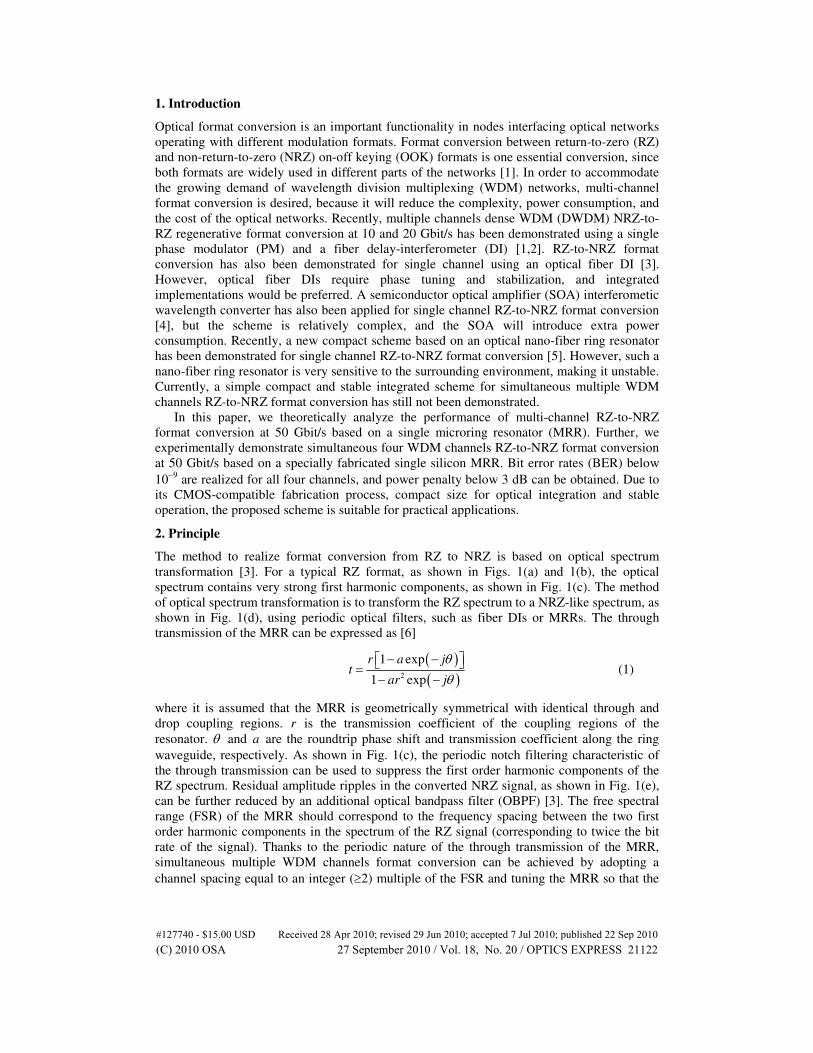
1. Introduction
Optical format conversion is an important functionality in nodes interfacing optical networks
operating with different modulation formats. Format conversion between return-to-zero (RZ)
and non-return-to-zero (NRZ) on-off keying (OOK) formats is one essential conversion, since
both formats are widely used in different parts of the networks [1]. In order to accommodate
the growing demand of wavelength division multiplexing (WDM) networks, multi-channel
format conversion is desired, because it will reduce the complexity, power consumption, and
the cost of the optical networks. Recently, multiple channels dense WDM (DWDM) NRZ-to-
RZ regenerative format conversion at 10 and 20 Gbit/s has been demonstrated using a single
phase modulator (PM) and a fiber delay-interferometer (DI) [1,2]. RZ-to-NRZ format
conversion has also been demonstrated for single channel using an optical fiber DI [3].
However, optical fiber DIs require phase tuning and stabilization, and integrated
implementations would be preferred. A semiconductor optical amplifier (SOA) interferometic
wavelength converter has also been applied for single channel RZ-to-NRZ format conversion
[4], but the scheme is relatively complex, and the SOA will introduce extra power
consumption. Recently, a new compact scheme based on an optical nano-fiber ring resonator
has been demonstrated for single channel RZ-to-NRZ format conversion [5]. However, such a
nano-fiber ring resonator is very sensitive to the surrounding environment, making it unstable.
Currently, a simple compact and stable integrated scheme for simultaneous multiple WDM
channels RZ-to-NRZ format conversion has still not been demonstrated.
In this paper, we theoretically analyze the performance of multi-channel RZ-to-NRZ
format conversion at 50 Gbit/s based on a single microring resonator (MRR). Further, we
experimentally demonstrate simultaneous four WDM channels RZ-to-NRZ format conversion
at 50 Gbit/s based on a specially fabricated single silicon MRR. Bit error rates (BER) below
10−9
are realized for all four channels, and power penalty below 3 dB can be obtained. Due to
its CMOS-compatible fabrication process, compact size for optical integration and stable
operation, the proposed scheme is suitable for practical applications.
2. Principle
The method to realize format conversion from RZ to NRZ is based on optical spectrum
transformation [3]. For a typical RZ format, as shown in Figs. 1(a) and 1(b), the optical
spectrum contains very strong first harmonic components, as shown in Fig. 1(c). The method
of optical spectrum transformation is to transform the RZ spectrum to a NRZ-like spectrum, as
shown in Fig. 1(d), using periodic optical filters, such as fiber DIs or MRRs. The through
transmission of the MRR can be expressed as [6]
( )( )2
1 exp
1 exp
r a jt
ar j
θ
θ
− − =− −
(1)
where it is assumed that the MRR is geometrically symmetrical with identical through and
drop coupling regions. r is the transmission coefficient of the coupling regions of the
resonator. θ and a are the roundtrip phase shift and transmission coefficient along the ring
waveguide, respectively. As shown in Fig. 1(c), the periodic notch filtering characteristic of
the through transmission can be used to suppress the first order harmonic components of the
RZ spectrum. Residual amplitude ripples in the converted NRZ signal, as shown in Fig. 1(e),
can be further reduced by an additional optical bandpass filter (OBPF) [3]. The free spectral
range (FSR) of the MRR should correspond to the frequency spacing between the two first
order harmonic components in the spectrum of the RZ signal (corresponding to twice the bit
rate of the signal). Thanks to the periodic nature of the through transmission of the MRR,
simultaneous multiple WDM channels format conversion can be achieved by adopting a
channel spacing equal to an integer (≥2) multiple of the FSR and tuning the MRR so that the
#127740 - $15.00 USD Received 28 Apr 2010; revised 29 Jun 2010; accepted 7 Jul 2010; published 22 Sep 2010(C) 2010 OSA 27 September 2010 / Vol. 18, No. 20 / OPTICS EXPRESS 21122

notches of the through transmission coincide with the first harmonic components of all
channels. The residual intensity ripples can be suppressed for all channels using a wavelength
demultiplexer such as an arrayed waveguide grating (AWG). Therefore multi-channel RZ-to-
NRZ format conversion can be achieved, as shown in Figs. 1(f) and 1(g).
10 20 30 400
0.5
1
time (ps)P
ow
er(
mW
)10 20 30 40
0
0.5
1
time (ps)
Pow
er(
mW
)
-400 -300 -200 -100 0 100 200-80
-40
0
40
f (GHz)
Level (d
B)
-400 -300 -200 -100 0 100 200-80
-40
0
40
f (GHz)
Level (d
B)
10 20 30 40
0
0.1
0.2
time (ps)
Pow
er(
mW
)
10 20 30 40
0
0.1
0.2
time (ps)
Pow
er(
mW
)
10 20 30 400
0.1
0.2
0.3
0.4
time (ps)
Pow
er(
mW
)
Fig. 1. Principle of the multi-channel RZ-to-NRZ format conversion, illustrated here for two
channels. (a) and (b) show the eye diagrams of two different input RZ signals at 50 Gbit/s with
200 GHz channel spacing. (c) Spectrum transformation of the RZ-to-NRZ format conversion
for the two channels utilizing the through transmission of the MRR. (d) Transformed converted
NRZ spectra. (e) to (g) show the eye diagrams of the converted NRZ channels for single
channel format conversion without AWG, as well as two channels operation after the MRR and
ripples suppression by the AWG. In this illustration, 2 0.35r = and 0.94a = for the MRR
and the 3 dB bandwidth of the Gaussian AWG is 65 GHz.
The presence of amplitude ripples and pattern effects for the converted NRZ format
impacts the performance of the format conversion [3]. Figures 2(a) and 2(b) analyze the Q
factor and amplitude ripples of the converted NRZ signal for different Q values of the MRR
and the OBPF 3 dB bandwidths at a bit-rate of 50 Gbit/s. The OBPF is modeled as a 1st order
Gaussian type filter. The amplitude ripple is defined as the ratio between the maximum power
deviation r
P and the average power of the high level 1
P . For good format conversion, both
high Q factor and low amplitude ripples are required for the converted signal. One can find
that if the bandwidth of the filter is narrower than 50 GHz, the amplitude ripple of the
converted NRZ signal is as low as 0.2, and independent of the Q value of the MRR (Fig. 2(b)).
However, in this region, the Q factor of the converted NRZ signal is as low as 5 (Fig. 2(a)),
which will lead to a poor bit error rate. The regions denoted by the white ellipses in Figs. 2(a)
and 2(b) illustrate the optimized bandwidths of the OBPF and Q values of the MRR. A MRR
with Q value around 8000, and an OBPF with a bandwidth around 65 GHz will result in the
best RZ-to-NRZ format conversion with high Q factor and low amplitude ripples.
#127740 - $15.00 USD Received 28 Apr 2010; revised 29 Jun 2010; accepted 7 Jul 2010; published 22 Sep 2010(C) 2010 OSA 27 September 2010 / Vol. 18, No. 20 / OPTICS EXPRESS 21123

Fig. 2. (a) Q factor and (b) amplitude ripples of the converted NRZ signal versus Q value of the
MRR and bandwidth of the OBPF for 50 Gbit/s format conversion.
In real applications, the exact location of the notches in the MRR through transmission
will depend on temperature. The thermo-optical coefficient of silicon can be described by [7]
( )( )
2
0 0 0
0.01587 0.002392n T T T
n T T T
∆ ∆ ∆ ∆≈ +
(2)
where 0
298.15T K≈ is the room temperature and ( )03.48n T ≈ is the silicon refractive index
at room temperature. n∆ is the deviation of the silicon refractive index induced by a
temperature deviation T∆ . Such temperature-induced refractive index change will lead to a
shift of the through transmission, hence to a frequency detuning ∆f between the notches of the
through transmission and the first harmonic components of the RZ spectrum, as shown in
Fig. 3(a). Figure 3(b) illustrates the Q factor and amplitude ripples of the converted NRZ
format as a function of the frequency detuning (or equivalent temperature deviation for a
MRR with 100 GHz FSR) at optimum conditions (Q = 8000, FWHM = 65 GHz). One can
find a frequency detuning tolerance of about 8 GHz (or equivalent temperature deviation
tolerance of 0.8°C), where both the Q factor and amplitude ripples are not degraded
noticeably. If the frequency detuning keeps increasing, the Q factor and amplitude ripples of
the converted NRZ signal will be degraded significantly. This effect could be circumvented by
temperature control of the chip.
0 5 10 15 200
10
20
30
Frequency detuning (GHz)
Q facto
r
0 5 10 15 200.2
0.3
0.4
0.5
Am
plit
ude rip
ple
0 0.5 1.0 1.5 2.0Temperature deviation (
0C)
-100 0 100-80
-60
-40
-20
0
20
f (GHz)
Level (d
B)
RZ spectrum
Through transmission of MRR
Fig. 3. (a) Illustration of the detuning between the notches of the through transmission and the
first order harmonic components of the RZ spectrum. (b) Q factor and amplitude ripple of the
converted NRZ signal as a function of frequency detuning ∆f (or equivalent temperature
deviation). Q = 8000, FWHM = 65 GHz.
3. MRR design and fabrication
3.1 Design
A silicon MRR with a FSR of 100 GHz and high extinction ratio is designed for RZ-to-NRZ
format conversion at 50 Gbit/s. A silicon-on-insulator (SOI) wafer with top silicon layer of
#127740 - $15.00 USD Received 28 Apr 2010; revised 29 Jun 2010; accepted 7 Jul 2010; published 22 Sep 2010(C) 2010 OSA 27 September 2010 / Vol. 18, No. 20 / OPTICS EXPRESS 21124

250 nm is selected for the design. The cross section of the waveguide is designed as illustrated
in Fig. 4(a). The waveguide width and height are designed to be 430 nm and 250 nm,
respectively. A layer of benzocyclobutene (BCB) is used to cover the waveguide and form the
upper cladding layer. A Ti heater is deposited on top of the BCB for thermally tuning the
transmission of the MRR.
Ti heater
BCB
SiO2
Si 250nm
430nm R
Fig. 4. (a) Cross section and (b) corresponding TE0 mode profile of the electric field of the
designed waveguide calculated by the full vectorial mode matching method [8,9].
To precisely design the FSR of the MRR, the group index of the waveguide should be
calculated accurately. The wavelength dependence of the material refractive index of silicon is
considered as follows [7]
( ) ( ) ( )2 3.476-0.07805 -1.55 +0.082 -1.55
sin λ λ λ= (3)
where λ is the wavelength. Figure 5(a) shows the effective index dispersion of the designed
waveguide calculated by the full vectorial mode matching method (FVMM). The
corresponding group index is estimated by ( ) ( ) 4.2971g eff eff
n n nλ λ λ λ= − ⋅∂ ∂ = at 1550
nm. To obtain a FSR of 100 GHz around 1550 nm, the radius of the MRR should be 111 µm.
To obtain the target Q value and ER of the MRR, the scattering loss should also be
estimated. The scattering loss can be simply evaluated by extending the 2D planar waveguide
model [10] to 3D waveguide structures, and can be calculated as
( )2 2
32
2 2 0
24
inner side outer sidecore side
core
E dy E dyk
S n nn E da
απ
− −
+
= −∫ ∫
∫∫ (4)
( )2
22 2
0 0
21 cos
c
c eff side
dS L
L k n n
π θσ
θ=
+ −∫ (5)
where the two integrations in the numerator in Eq. (4) are along the inner and outer sides of
the waveguide, respectively. The surface roughness is characterized by its roughness standard
deviation σ and its correlation length c
L . core
n , side
n and eff
n are the refractive indices of the
silicon core and BCB side cladding (taken equal to 1.56 according to [11]) and the effective
mode refractive index, respectively. E is the mode profile of the electric field, as represented
in Fig. 4(b), and 0
2k π λ= is the wave number. With typical surface roughness parameters
2 nmσ = and 50 nmc
L = [12], a total propagation loss of 8.2 dB/cm is predicted for the TE0
mode. Combined with the coupling coefficient calculated by the coupled mode theory (CMT)
[8,13], the Q value of the designed MRR can be estimated. Figure 5(b) illustrates the
calculated power coupling coefficient and estimated Q value as a function of the coupling gap
of the MRR for TE0 mode operation. According to the optimization of Sect. 2, a Q value
around 8000 is preferred for our application. In consequence, a coupling gap of 180 nm is
selected, corresponding to an estimated Q value of 8600 and an ER of about 20 dB.
#127740 - $15.00 USD Received 28 Apr 2010; revised 29 Jun 2010; accepted 7 Jul 2010; published 22 Sep 2010(C) 2010 OSA 27 September 2010 / Vol. 18, No. 20 / OPTICS EXPRESS 21125

1.535 1.54 1.545 1.55 1.555 1.56 1.5652.39
2.4
2.41
2.42
2.43
2.44
Effe
ctive
refr
active
in
de
x n
eff
100 120 140 160 180 200 220 240 260 280 300 3200
0.5
1
Gap (nm)
Po
we
r co
up
lin
g c
oe
ffic
ien
t
100 120 140 160 180 200 220 240 260 280 300 3200
10000
20000
30000
40000
50000
Q v
alu
e
Fig. 5. (a) Calculated effective index dispersion of the designed waveguide for the TE0 mode.
(b) Calculated power coupling coefficient and Q value of the MRR as a function of the
coupling gap for the TE0 mode.
3.2 Fabrication and device characterization
The fabricated device is shown in Figs. 6 (a) and 6(b). It is fabricated on a SOI wafer with top
silicon thickness of 250 nm and buried silicon dioxide of 3 µm. First, diluted (1:1 in anisole)
electron-beam resist ZEP520A is spin-coated on the wafer to form a ~110 nm-thick mask
layer. The MRR structure is then defined using electron-beam lithography (JEOL JBX-
9300FS). After that, the sample is etched by inductively coupled plasma reactive ion etching
(ICP-RIE) to transfer the patterns to the top silicon layer. A layer of 550 nm BCB is spin-
coated afterwards as top cladding, and a layer of 400 nm ZEP520A is spin-coated in sequence
as the mask layer for the micro heater. Electron-beam lithography is used again to define the
patterns of the heater and pads. Finally, 100 nm thick titanium heater and pads are formed by
evaporation and lift-off processes. The radius of the MRR is 110 µm, with the waveguide
width of 435 nm and coupling gap of 178 nm for both through and drop coupling regions, as
shown in Fig. 6(a). The output waveguide is tapered to 4 µm to increase the coupling
efficiency to the lensed fiber. Figure 6(c) represents the measured transmission of the MRR.
The ER of the transmission is as high as 20 dB, the measured FSR is 0.8 nm, corresponding to
100 GHz at 1550 nm, and the Q value is 7900, which all agree very well with our design
target. The insertion loss of the device is about 16 dB, including the propagation loss in the
silicon waveguide and the coupling loss between the lensed fibers and the device.
1535 1540 1545 1550 1555 1560 1565-40
-35
-30
-25
-20
-15
-10
Wavelength (nm)
Rela
tive T
ransm
issio
n (d
B)
Fig. 6. (a) Scanning electron microscope (SEM) top view image of the fabricated device before
BCB spinning. The inset is a close-up view of the coupling area between the ring and the
straight waveguide. (b) Optical microscope picture of the fabricated device. The MRR is under
the micro heater. (c) Measured transmission of the fabricated MRR.
4. Experiment and results
The experimental setup for WDM format conversion is represented in Fig. 7. Four channels of
continuous wave (CW) laser light with wavelengths of 1548.16 nm, 1549.76 nm, 1551.36 nm,
#127740 - $15.00 USD Received 28 Apr 2010; revised 29 Jun 2010; accepted 7 Jul 2010; published 22 Sep 2010(C) 2010 OSA 27 September 2010 / Vol. 18, No. 20 / OPTICS EXPRESS 21126

and 1552.97 nm, respectively, are combined in a coupler, amplified by an erbium-doped fiber
amplifier (EDFA), and simultaneously modulated at 50 Gbit/s in the 33% RZ-OOK format in
two Mach-Zehnder modulators (MZMs), which are used as pulse carver (driven by a 25 GHz
radio frequency clock) and data modulator, respectively. The four modulated RZ channels are
amplified using a second EDFA to compensate for the modulators loss and further de-
correlated by 50 m dispersion-compensating fiber (DCF) with total dispersion of −5.8 ps/nm
at 1550 nm. Due to the high insertion loss of the device, the de-correlated multiple WDM RZ
signal is amplified again by another EDFA. In order to ensure that all WDM channels are
optimally coupled to the MRR, a polarization controller (PC) followed by a polarizer is first
used to align all channels to the same polarization state. A second PC is then used to align the
input polarization to the TE mode of the waveguide. The WDM RZ signal is then converted to
a WDM NRZ signal by the MRR, and amplified by another EDFA afterward. Finally, the
amplified converted WDM NRZ signal is wavelength demultiplexed by an AWG with
channel spacing of 100 GHz and 3 dB bandwidth of 62 GHz, which is close to the optimum
value of 65 GHz. The demultiplexed signal is finally detected in a preamplified receiver.
Fig. 7. Experimental setup for the multiple WDM channels RZ-to-NRZ format conversion.
4.1 Single channel operation
For single channel operation, channels 1, 3 and 4 are switched off, and only channel 2 at a
wavelength of 1549.76 nm is switched on. The wavelength of channel 2 is fine tuned to align
the two first order harmonic components of the RZ spectrum to the notches of the through
transmission of the MRR. Figure 8(a) shows the spectrum transformation during the format
conversion process. The first harmonics of the RZ spectrum are suppressed effectively by the
MRR. The converted NRZ spectrum is very similar to that of an optical NRZ signal generated
directly using a single MZM. The corresponding eye diagrams at the output of the RZ
transmitter and of a NRZ modulated signal are also represented in Figs. 8(b) and 8(c)
respectively. The RZ-to-NRZ format converted eye diagram (Fig. 8(d)) shows very little
amplitude ripple and looks almost the same as the reference NRZ eye diagram (Fig. 8(c)).
Figure 8(e) shows the BER measurement for single channel format conversion with a
pseudorandom binary sequence (PRBS) length of 27-1. The power penalty (at a BER of 10
−9)
of the converted NRZ signal at the MRR output is about 4 dB compared to the original RZ
signal, while it is only 0.2 dB compared to the electrically generated NRZ reference signal. An
extra power penalty of 1.3 dB is induced by the AWG.
#127740 - $15.00 USD Received 28 Apr 2010; revised 29 Jun 2010; accepted 7 Jul 2010; published 22 Sep 2010(C) 2010 OSA 27 September 2010 / Vol. 18, No. 20 / OPTICS EXPRESS 21127

-31 -30 -29 -28 -27 -26 -25 -24 -23 -22 -21 -2011
10
9
8
7
6
5 33% RZ-OOK
After MRR
After MRR + OBPF
NRZ-OOK (electrical)
-lo
g(B
ER
)
Average received power (dBm)
1549 1549.5 1550 1550.5-60
-50
-40
-30
-20
-10
0
10
Wavelength (nm)
Po
we
r (d
Bm
)
33% RZ-OOK
After MRR
After MRR + AWG
NRZ-OOK (electrical)
33% RZ-OOK
After MRR
After MRR + AWG
NRZ OOK (electrical)
Fig. 8. (a) Spectra of the RZ signal at the transmitter and converted NRZ signals at the MRR
and AWG outputs. The spectrum of a NRZ modulated signal is also shown as a reference. Eye
diagrams of the input RZ (b), reference NRZ (c) and converted NRZ (d) signals. (e) BER
measurements of the original RZ and of the converted NRZ signals after the MRR and the
AWG, as well as of an electrically generated reference NRZ-OOK signal.
4.2 WDM operation
For WDM operation, all four channels are switched on. The wavelength of each channel is
then fine tuned to align its first order harmonic components to the notches of the through
transmission. Figures 9(a) and 9(b) illustrate the spectra of the WDM RZ and converted WDM
NRZ signals, respectively. The first harmonic components of all four RZ channels are
suppressed effectively, resulting in an effective spectrum transformation from WDM RZ to
WDM NRZ. The AWG is used to demultiplex the converted WDM NRZ signal. The eye
diagrams for WDM format conversion are represented in Fig. 10. The RZ signal (Fig. 10(a)) is
first decorrelated by the DCF. Figure 10(b) shows the signal detected directly after the
decorrelation DCF (without wavelength demultiplexing) when all four channels are present.
The amount of dispersion of the decorrelation fiber is chosen such that the bit patterns of the
four channels are no longer synchronized when they enter the MRR, while the introduced
dispersion itself does not significantly degrade each channel, making dispersion compensation
unnecessary after the MRR. After format conversion, very clear NRZ format eye diagrams are
obtained for all four channels (Figs. 10(d)~10(g)), which are very close to the reference
electrically modulated NRZ signal (Fig. 10(c)).
#127740 - $15.00 USD Received 28 Apr 2010; revised 29 Jun 2010; accepted 7 Jul 2010; published 22 Sep 2010(C) 2010 OSA 27 September 2010 / Vol. 18, No. 20 / OPTICS EXPRESS 21128

1547 1548 1549 1550 1551 1552 1553 1554
-40
-20
0
Wavelength (nm)
Po
we
r (d
Bm
)
1547 1548 1549 1550 1551 1552 1553 1554
-40
-20
0
Wavelength (nm)
Po
we
r (d
Bm
)
(a)
(b)
Fig. 9. Spectra of the four WDM channel signal. (a) WDM RZ signal. (b) Converted WDM
NRZ signal.
Fig. 10. Measured eye diagrams of (a) single RZ signal, (b) WDM RZ signals after
decorrelation, (c) original reference NRZ signal, and (d)~(g) converted NRZ signals for
channels 1 to 4.
Figures 11(a) and 11(b) show the results of BER measurements with a 27-1 PRBS for
multiple WDM channels format conversion. BER values below 10−9
are obtained for all the
four converted NRZ channels. Figures 11(c) and 11(d) show the corresponding power penalty
at a BER of 10−9
. A power penalty of 2.5 to 3.5 dB is found for the RZ channels in the WDM
configuration when only one channel is turned on compared to the single channel case without
AWG. This penalty is attributed to strong filtering by the AWG demultiplxer. An extra
penalty of 1.5 dB is measured in the WDM configuration when all channels are turned on.
Crosstalk between the channels due to the fact that a passive coupler (therefore without
filtering functionality) is used as wavelength multiplexer is believed to be responsible for this
extra penalty (see Fig. 11(a)). For the converted NRZ signals, the measured power penalty is
very low for channels 1~3 compared to the reference NRZ modulated signal for single
channel operation. Further power penalties from 2 dB to 3 dB, which are caused by the
crosstalk, are obtained for WDM channel operation. The power penalties for channels 2 and 3
are a little higher than channel 1, due to the difference in the number of directly adjacent
channels. The BER performance is however somehow degraded for the fourth channel. It is
speculated that a larger laser linewidth may be mostly responsible for this increased penalty
after conversion to intensity noise by the MRR through transmission. Additionally, one can
find that the power penalty is as high as 4.4 dB for the RZ signal of the fourth channel, which
is the worst of the four channels (See Fig. 11(c)). This also leads to signal degradation for the
#127740 - $15.00 USD Received 28 Apr 2010; revised 29 Jun 2010; accepted 7 Jul 2010; published 22 Sep 2010(C) 2010 OSA 27 September 2010 / Vol. 18, No. 20 / OPTICS EXPRESS 21129

fourth converted NRZ signal for both single and WDM channel operation. However, the
power penalty could be improved by using a real multiplexer, instead of a coupler, to
multiplex the different channels and reduce the crosstalk. Improving the insertion loss of the
MRR can also improve the power penalty thanks to an expected reduction of the induced
optical signal-to-noise ratio (OSNR) degradation.
1 2 3 42
2.5
3
3.5
4
4.5
5
Channel
Pow
er
penalty (
dB
)
1 ch. ON
All chs. ON
1 2 3 4-2
0
2
4
6
8
Channel
Pow
er
penalty (
dB
)
1 ch. ON
All chs. ON
-30 -28 -26 -24 -22 -20 -18 -16 -14 -1211
10
9
8
7
6
5
4 Ch. 1 - WDM
Ch. 1 - single ch.
Ch. 2 - WDM
Ch. 2 - single ch.
Ch. 3 - WDM
Ch. 3 - single ch.
Ch. 4 - WDM
Ch. 4 - single ch.
NRZ-OOK (electrical)
-log
(BE
R)
Average received power (dBm)
-30 -28 -26 -24 -22 -20 -18 -16 -14 -1211
10
9
8
7
6
5
4 Ch. 1 - (WDM, with AWG)
Ch. 1 - (single ch., with AWG)
Ch. 2 - (WDM, with AWG)
Ch. 2 - (single ch., with AWG)
Ch. 3 - (WDM, with AWG)
Ch. 3 - (single ch., with AWG)
Ch. 4 - (WDM, with AWG)
Ch. 4 - (single ch., with AWG)
Laser 1 (without AWG)
Laser 2 (without AWG)
Laser 3 (without AWG)
Laser 4 (without AWG)
-lo
g(B
ER
)
Average received power (dBm)
Fig. 11. (a) Back-to-back BER measurement of the RZ channels (single channel operation, with
and without AWG, as well as WDM operation) (b) BER measurement of the converted NRZ
channels in single channel and WDM operation, as well as an electrically generated reference
NRZ signal. (c) Power penalties of the RZ signal output from the AWG for single and multiple
WDM channels cases, compared to the original RZ signals without AWG. (d) Power penalty of
the output converted NRZ signal for single and multiple WDM channels cases, compared to the
reference electrically modulated NRZ signal. Power penalties are measured at BER of 10−9.
5. Conclusion
We have comprehensively analyzed, and further demonstrated both single and multiple WDM
channels RZ-to-NRZ format conversion at 50 Gbit/s utilizing a single silicon MRR with FSR
of 100 GHz and Q value of 7900. Bit error measurements show the very good performance of
the scheme. Due to its CMOS-compatible fabrication process, our scheme is very promising
for practical implementations.
Acknowledgement
This research was sponsored by the National Natural Science Foundation of China (Grant No.
60577007), the National Basic Research Program of China (Grant No. 2006CB302805), and
the Program for New Century Excellent Talents in University of Ministry of Education of
China (Grant No. NCET-04-0715). Yunhong Ding would like to thank the support of the
Chinese Scholar Council (CSC). Support from the Villum Kann Rasmussen foundation
through the Nanophotonics for Terabit Communications (NATEC) centre of excellence is
acknowledged.
#127740 - $15.00 USD Received 28 Apr 2010; revised 29 Jun 2010; accepted 7 Jul 2010; published 22 Sep 2010(C) 2010 OSA 27 September 2010 / Vol. 18, No. 20 / OPTICS EXPRESS 21130