Comparison of Seizure Detection Algorithms in Continuously Monitored Pediatric Patients
Upload
independentCategory
view
1download
0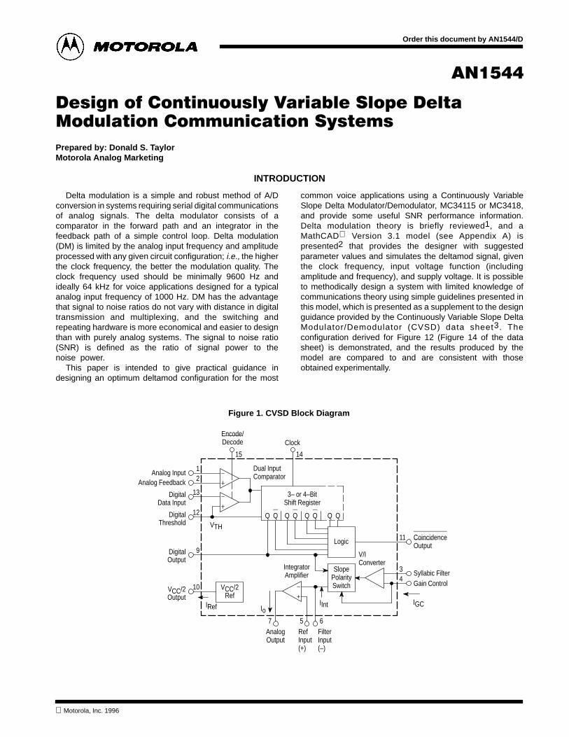
1MOTOROLA ANALOG IC DEVICE DATA
Prepared by: Donald S. TaylorMotorola Analog Marketing
INTRODUCTION
Delta modulation is a simple and robust method of A/Dconversion in systems requiring serial digital communicationsof analog signals. The delta modulator consists of acomparator in the forward path and an integrator in thefeedback path of a simple control loop. Delta modulation(DM) is limited by the analog input frequency and amplitudeprocessed with any given circuit configuration; i.e., the higherthe clock frequency, the better the modulation quality. Theclock frequency used should be minimally 9600 Hz andideally 64 kHz for voice applications designed for a typicalanalog input frequency of 1000 Hz. DM has the advantagethat signal to noise ratios do not vary with distance in digitaltransmission and multiplexing, and the switching andrepeating hardware is more economical and easier to designthan with purely analog systems. The signal to noise ratio(SNR) is defined as the ratio of signal power to thenoise power.
This paper is intended to give practical guidance indesigning an optimum deltamod configuration for the most
common voice applications using a Continuously VariableSlope Delta Modulator/Demodulator, MC34115 or MC3418,and provide some useful SNR performance information.Delta modulation theory is briefly reviewed1, and aMathCAD Version 3.1 model (see Appendix A) ispresented2 that provides the designer with suggestedparameter values and simulates the deltamod signal, giventhe clock frequency, input voltage function (includingamplitude and frequency), and supply voltage. It is possibleto methodically design a system with limited knowledge ofcommunications theory using simple guidelines presented inthis model, which is presented as a supplement to the designguidance provided by the Continuously Variable Slope DeltaModulator/Demodulator (CVSD) data sheet3. Theconfiguration derived for Figure 12 (Figure 14 of the datasheet) is demonstrated, and the results produced by themodel are compared to and are consistent with thoseobtained experimentally.
Figure 1. CVSD Block Diagram
Analog Input
QQ QQ QQ QQ
3– or 4–BitShift Register
Logic
1 Dual InputComparator
SlopePolaritySwitch
IInt
VCC/2Ref
Analog Feedback
DigitalData Input
DigitalThreshold
DigitalOutput
VCC/2Output
2
13
12
9
10
Encode/Decode Clock
15 14
VTH
IRef Io7 5 6
AnalogOutput
RefInput(+)
FilterInput(–)
IGC
11
34
CoincidenceOutput
Syllabic FilterGain Control
V/IConverter
IntegratorAmplifier
Order this document by AN1544/D
Motorola, Inc. 1996
2 MOTOROLA ANALOG IC DEVICE DATA
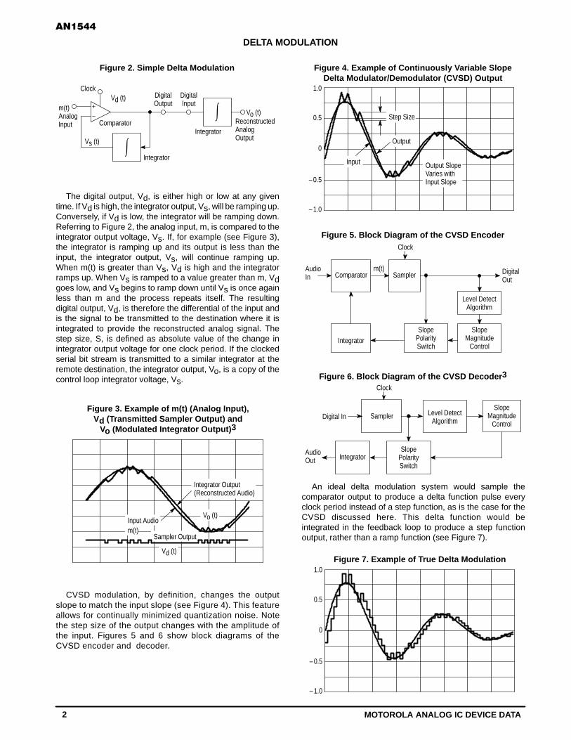
DELTA MODULATION
Figure 2. Simple Delta Modulation
m(t)AnalogInput
Vo (t)ReconstructedAnalogOutput
ClockVd (t)
Vs (t)
Comparator
Integrator
Integrator
DigitalOutput
DigitalInput
The digital output, Vd, is either high or low at any giventime. If Vd is high, the integrator output, Vs, will be ramping up.Conversely, if Vd is low, the integrator will be ramping down.Referring to Figure 2, the analog input, m, is compared to theintegrator output voltage, Vs. If, for example (see Figure 3),the integrator is ramping up and its output is less than theinput, the integrator output, Vs, will continue ramping up.When m(t) is greater than Vs, Vd is high and the integratorramps up. When Vs is ramped to a value greater than m, Vdgoes low, and Vs begins to ramp down until Vs is once againless than m and the process repeats itself. The resultingdigital output, Vd, is therefore the differential of the input andis the signal to be transmitted to the destination where it isintegrated to provide the reconstructed analog signal. Thestep size, S, is defined as absolute value of the change inintegrator output voltage for one clock period. If the clockedserial bit stream is transmitted to a similar integrator at theremote destination, the integrator output, Vo, is a copy of thecontrol loop integrator voltage, Vs.
Figure 3. Example of m(t) (Analog Input),Vd (Transmitted Sampler Output) and
Vo (Modulated Integrator Output) 3
Integrator Output(Reconstructed Audio)
Vo (t)
m(t)Input Audio
Sampler Output
Vd (t)
CVSD modulation, by definition, changes the outputslope to match the input slope (see Figure 4). This featureallows for continually minimized quantization noise. Notethe step size of the output changes with the amplitude ofthe input. Figures 5 and 6 show block diagrams of theCVSD encoder and decoder.
Figure 4. Example of Continuously Variable SlopeDelta Modulator/Demodulator (CVSD) Output
– 0.5
– 1.0
0
0.5
1.0
Output SlopeVaries withInput Slope
Step Size
Output
Input
Figure 5. Block Diagram of the CVSD Encoder
AudioIn Comparator Sampler
Integrator
SlopePolaritySwitch
SlopeMagnitude
Control
Level DetectAlgorithm
DigitalOut
m(t)
Clock
Figure 6. Block Diagram of the CVSD Decoder 3
Digital In Sampler
Clock
Level DetectAlgorithm
SlopePolaritySwitch
IntegratorAudioOut
SlopeMagnitude
Control
An ideal delta modulation system would sample thecomparator output to produce a delta function pulse everyclock period instead of a step function, as is the case for theCVSD discussed here. This delta function would beintegrated in the feedback loop to produce a step functionoutput, rather than a ramp function (see Figure 7).
Figure 7. Example of True Delta Modulation
– 0.5
– 1.0
0
0.5
1.0
3MOTOROLA ANALOG IC DEVICE DATA
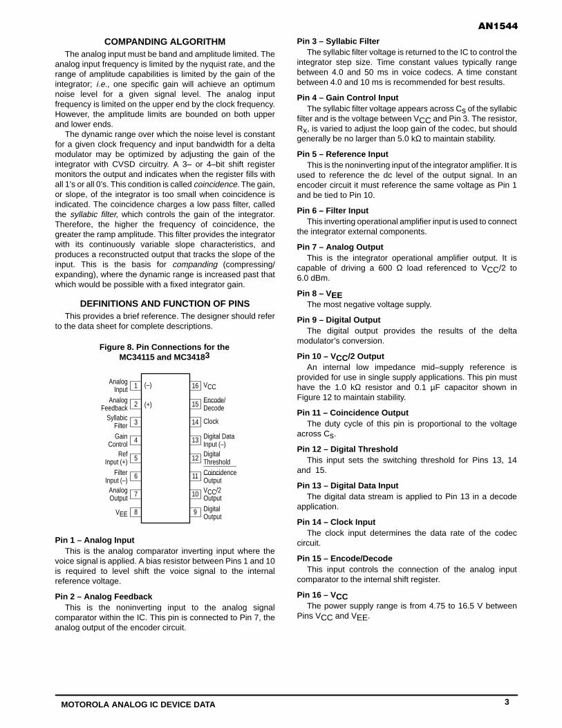
COMPANDING ALGORITHMThe analog input must be band and amplitude limited. The
analog input frequency is limited by the nyquist rate, and therange of amplitude capabilities is limited by the gain of theintegrator; i.e., one specific gain will achieve an optimumnoise level for a given signal level. The analog inputfrequency is limited on the upper end by the clock frequency.However, the amplitude limits are bounded on both upperand lower ends.
The dynamic range over which the noise level is constantfor a given clock frequency and input bandwidth for a deltamodulator may be optimized by adjusting the gain of theintegrator with CVSD circuitry. A 3– or 4–bit shift registermonitors the output and indicates when the register fills withall 1’s or all 0’s. This condition is called coincidence. The gain,or slope, of the integrator is too small when coincidence isindicated. The coincidence charges a low pass filter, calledthe syllabic filter, which controls the gain of the integrator.Therefore, the higher the frequency of coincidence, thegreater the ramp amplitude. This filter provides the integratorwith its continuously variable slope characteristics, andproduces a reconstructed output that tracks the slope of theinput. This is the basis for companding (compressing/expanding), where the dynamic range is increased past thatwhich would be possible with a fixed integrator gain.
DEFINITIONS AND FUNCTION OF PINSThis provides a brief reference. The designer should refer
to the data sheet for complete descriptions.
Figure 8. Pin Connections for theMC34115 and MC34183
16
15
14
13
12
11
10
1
2
3
4
5
6
7
8 9
AnalogInput
AnalogFeedback
SyllabicFilterGain
ControlRef
Input (+)Filter
Input (–)AnalogOutput
VEE
VCC
Encode/Decode
Clock
Digital DataInput (–)DigitalThresholdCoincidenceOutputVCC/2Output
DigitalOutput
(–)
(+)
Pin 1 – Analog InputThis is the analog comparator inverting input where the
voice signal is applied. A bias resistor between Pins 1 and 10is required to level shift the voice signal to the internalreference voltage.
Pin 2 – Analog FeedbackThis is the noninverting input to the analog signal
comparator within the IC. This pin is connected to Pin 7, theanalog output of the encoder circuit.
Pin 3 – Syllabic FilterThe syllabic filter voltage is returned to the IC to control the
integrator step size. Time constant values typically rangebetween 4.0 and 50 ms in voice codecs. A time constantbetween 4.0 and 10 ms is recommended for best results.
Pin 4 – Gain Control InputThe syllabic filter voltage appears across Cs of the syllabic
filter and is the voltage between VCC and Pin 3. The resistor,Rx, is varied to adjust the loop gain of the codec, but shouldgenerally be no larger than 5.0 kΩ to maintain stability.
Pin 5 – Reference InputThis is the noninverting input of the integrator amplifier. It is
used to reference the dc level of the output signal. In anencoder circuit it must reference the same voltage as Pin 1and be tied to Pin 10.
Pin 6 – Filter InputThis inverting operational amplifier input is used to connect
the integrator external components.
Pin 7 – Analog OutputThis is the integrator operational amplifier output. It is
capable of driving a 600 Ω load referenced to VCC/2 to6.0 dBm.
Pin 8 – VEEThe most negative voltage supply.
Pin 9 – Digital OutputThe digital output provides the results of the delta
modulator’s conversion.
Pin 10 – VCC/2 OutputAn internal low impedance mid–supply reference is
provided for use in single supply applications. This pin musthave the 1.0 kΩ resistor and 0.1 µF capacitor shown inFigure 12 to maintain stability.
Pin 11 – Coincidence OutputThe duty cycle of this pin is proportional to the voltage
across Cs.
Pin 12 – Digital ThresholdThis input sets the switching threshold for Pins 13, 14
and 15.
Pin 13 – Digital Data InputThe digital data stream is applied to Pin 13 in a decode
application.
Pin 14 – Clock InputThe clock input determines the data rate of the codec
circuit.
Pin 15 – Encode/DecodeThis input controls the connection of the analog input
comparator to the internal shift register.
Pin 16 – VCCThe power supply range is from 4.75 to 16.5 V between
Pins VCC and VEE.
4 MOTOROLA ANALOG IC DEVICE DATA
DELTA MODULATION DESIGN
A MathCAD Version 3.1 program was developed toprovide guidance to the user in designing applications for theMotorola Continuously Variable Slope Delta Modulator/Demodulator (CVSD) MC34115 and MC3418. This programcalculates the delta modulation function, given the inputamplitude and frequency and sampling frequency. The mostimportant design considerations involved in the configurationof the CVSD into a specific codec application are as follows:
1. Selection of clock rate and analog input function2. Required number of shift register bits3. Design of integration filter transfer function4. Design of syllabic filter transfer function5. Selection of minimum idle channel step size6. Design of low pass filter at the receiver
Selection of Clock Rate and Analog Input FunctionFor voice applications, it is recommended the CVSD be
designed for an analog input frequency of 1000 Hz and 1.0 Vamplitude (2.0 Vpp). The higher the clock frequency that canbe afforded, the better the SNR performance (up to about64 kHz). The performance of the signal transmission will bemaximized if the clock inputs of the transmitter and receiverare phase–locked to avoid the introduction of error bits. Inpractice, the useful dynamic range extends about 6.0 dBabove the design level. The companding ratio should notexceed 30% in any system.
Required Number of Shift Register BitsThe MC34115 is designed for low bit rate systems and the
MC3418 is designed for high performance, high bit ratesystems. The MC34115 has a 3–bit algorithm and theMC3418 has a 4–bit algorithm. For clock rates of 16 kHz andbelow, the 3–bit algorithm is well suited. For clock rates of 32kHz and above, the 4–bit algorithm is preferred.
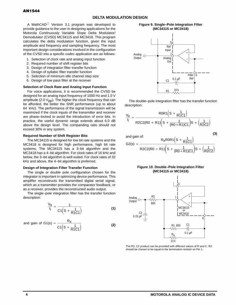
Design of Integration Filter Transfer FunctionThe single or double pole configuration chosen for the
integrator is important in optimizing device performance. Thisamplifier reconstructs the transmitted digital serial signal,which as a transmitter provides the comparator feedback, oras a receiver, provides the reconstructed audio output.
The single–pole integration filter has the transfer functiondescription:
(1)VoIi 1
C1S 1R1C1
(2)and gain of G1(s) Rx
C1S 1R1C1
Figure 9. Single–Pole Integration Filter(MC34115 or MC3418)
–
+AnalogOutput
RefInput
AnalogOut
5
7
6FilterRef0.1 µF
C1
10 kR1
The double–pole integration filter has the transfer functiondescription:
(3)
VoIi
R0R1S 1R1C1
R2C2(R0R1)S 1(R0R1)C1
S 1R2C2
G2(s) RxR0R1S 1
R1C1
R2C2(R0R1)S 1(R0R1)C1
S 1R2C2
and gain of:
Figure 10. Double–Pole Integration Filter(MC34115 or MC3418)
The R2, C2 product can be provided with different values of R and C. R2should be chosen to be equal to the termination resistor on Pin 1.
–
+AnalogOutput
R2
600
C20.15 µF
R1 600
Ro
13 k
C1
0.1 µF
6
7
5
MC34115or
MC3418
5MOTOROLA ANALOG IC DEVICE DATA
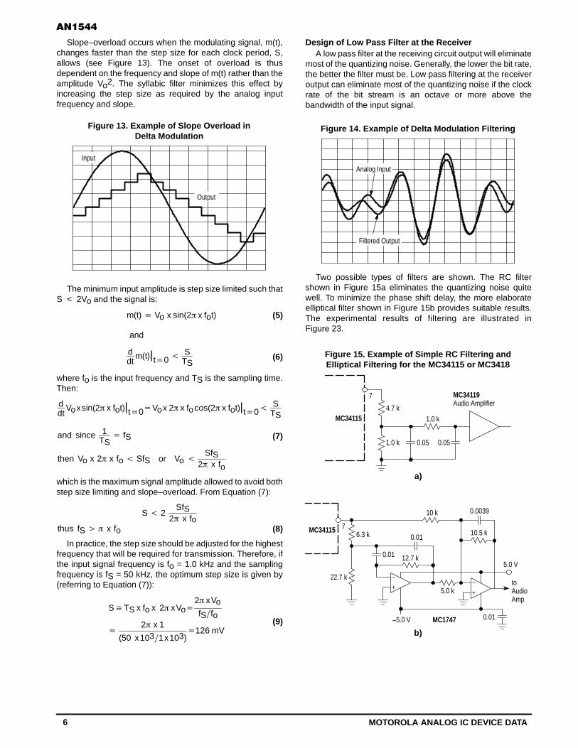
Design of Syllabic Filter Transfer FunctionThe syllabic filter is a simple single–pole (see Figure 11) or
two–pole network that produces a time constant for theaveraging of the coincidence output signal. The voltageacross the capacitor determines the integrator current whichin turn establishes the step size. The integrator current andthe resulting step size determine the companding ratio andthe SNR performance. The companding ratio is defined asthe voltage across Cs/VCC.
The gain of the circuit is set by the resistor Rx, which mustbe selected to provide the proper integrator step size for highlevel signals such that the companding ratio does not exceedabout 25%. The companding ratio is the active low duty cycleon Pin 11 of the codec circuit. The system gain isdependent on:
1. The maximum level and frequency of the input signal2. The transfer function of the integration filter
The syllabic filter in Figure 11 is a simple single–polesyllabic filter network of 18 kΩ and 0.33 µF. This produces a6.0 ms time constant for the averaging of the coincidenceoutput signal. Typically, the syllable is between 5.0 and 10ms, depending on the sound quality of the individualapplication. Note that Vs in Figure 11 is the syllabic filtervoltage and not the power supply voltage, VSS.
Minimum Idle Channel Step SizeThe final design parameter to be selected is the idle
channel step size, or the step size of the output with noanalog input. The digital output becomes a one–zeroalternating pattern and the analog output becomes a smalltriangle wave. The idle channel step size, DVo, must be twicethe specified total loop offset if a one–zero idle pattern isdesired.
Figure 11. Syllabic Filter Circuit Diagram(MC34115 or MC3418)
Slope PolaritySwitch GC
Syl In
Coin Out
4
3
11Logic
Rmin
Vs8VEE
1.3 k Rx
2.4 Meg
0.33 µF
3.3 k
Cs
RP
18 kRs
VCC
The value of Rmin must be selected to set the idle channelstep size. The slope control algorithm is inactive with no inputsignal. A long series of ones and zeros never occurs. Thus,the voltage across the syllabic filter capacitor (Cs) woulddecay to zero. However, the voltage divider of RP, Rs andRmin sets the minimum allowed voltage across the syllabicfilter capacitor. As the input amplitude increases from zero,the step size of the output, DV, will in turn increase and itsslope will continuously vary to match the slope of the input atthe zero crossing. The designer should ensure theseparameters are within minimum allowed tolerances to ensureproper circuit configurations are achieved.
(4)IiVoR1C
dVodt Cs
VoT
D–
Figure 12. Simplex Voice Codec(Using MC34115 or MC3418, Single–Pole Companding and Single Integration)
Push toTalk Key
5.0
(Normopen)
10 k
AnalogInput
A+
A–4.0 µF
600600
0.1 µF 1.0 k 10 k
AnalogOutput Analog
Out
RefInput
0.1 µF
10 k
C1
R1
Filter Ref VEE
Vs
Rx1.3 k
Cs0.33 µF
3.3 k
Rs18 k
Syl In
GC
2.4 Meg
Coin Out
Slope PolaritySwitch
4
3
11Logic
86
VCC/2Ref
10
12
13
2
1
5
7
–
+
–
+
+
–
Shift Register
Comp
Encode/Decode Clock 14
VTH
VCC 169Digital
Out
5.0
15
Digital InputDigital Output16 k Bits
Clock16 kHz
RP
+
VCC/2Out
Rmin
6 MOTOROLA ANALOG IC DEVICE DATA
Slope–overload occurs when the modulating signal, m(t),changes faster than the step size for each clock period, S,allows (see Figure 13). The onset of overload is thusdependent on the frequency and slope of m(t) rather than theamplitude Vo2. The syllabic filter minimizes this effect byincreasing the step size as required by the analog inputfrequency and slope.
Figure 13. Example of Slope Overload inDelta Modulation
Input
Output
The minimum input amplitude is step size limited such thatS < 2Vo and the signal is:
(5)m(t) Vo x sin(2 x fot)
and
ddt
m(t)|t0S
TS(6)
where fo is the input frequency and TS is the sampling time.Then:
(7)
ddt
Voxsin(2 x fot)|t0Vox 2 x focos(2 x fot)|t0S
TS
and since 1TS fS
then Vo x 2 x fo SfS or Vo SfS
2 x fo
which is the maximum signal amplitude allowed to avoid bothstep size limiting and slope–overload. From Equation (7):
(8)
S 2SfS
2 x fothus fS x fo
In practice, the step size should be adjusted for the highestfrequency that will be required for transmission. Therefore, ifthe input signal frequency is fo = 1.0 kHz and the samplingfrequency is fS = 50 kHz, the optimum step size is given by(referring to Equation (7)):
(9)
STS x fo x 2 xVo2 xVofSfo
2 x 1
(50 x1031x103)126 mV
Design of Low Pass Filter at the ReceiverA low pass filter at the receiving circuit output will eliminate
most of the quantizing noise. Generally, the lower the bit rate,the better the filter must be. Low pass filtering at the receiveroutput can eliminate most of the quantizing noise if the clockrate of the bit stream is an octave or more above thebandwidth of the input signal.
Figure 14. Example of Delta Modulation Filtering
Analog Input
Filtered Output
Two possible types of filters are shown. The RC filtershown in Figure 15a eliminates the quantizing noise quitewell. To minimize the phase shift delay, the more elaborateelliptical filter shown in Figure 15b provides suitable results.The experimental results of filtering are illustrated inFigure 23.
Figure 15. Example of Simple RC Filtering andElliptical Filtering for the MC34115 or MC3418
b)
MC34115 7
MC34115
7
4.7 k
1.0 k
1.0 k 0.05 0.05
MC34119Audio Amplifier
a)
6.3 k
22.7 k
0.01
0.01
10 k 0.0039
10.5 k
5.0 V
toAudioAmp
0.01–5.0 V
5.0 k
12.7 k
MC1747
7MOTOROLA ANALOG IC DEVICE DATA
MODELING DELTA MODULATION
This section demonstrates numerically modeled deltamodulation given the variables provided for the designconfiguration using MathCAD Version 3.1. The designermust minimally provide the model with the clock frequency,analog input voltage function (including amplitude andfrequency), and the supply voltage. The model provides thedesigner with suggested resistance and capacitance values
(Figure 12), the reconstructed analog output signal(Figure 16), the gain and frequency response for single–pole(Figure 17) and double–pole (Figure 18) integration filters, thesimulated continuously variable slope of input signal (dV/dt)(Figure 19), the transmitted digital signal (Figure 20), thequantizing noise (Figure 21), and a Fourier analysis of theoutput (Figure 22).
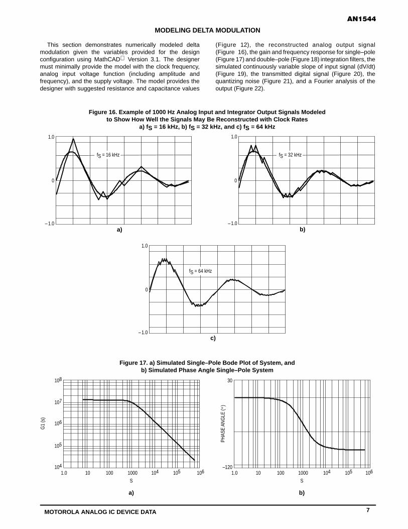
Figure 16. Example of 1000 Hz Analog Input and Integrator Output Signals Modeledto Show How Well the Signals May Be Reconstructed with Clock Rates
a) fS = 16 kHz, b) f S = 32 kHz, and c) f S = 64 kHz
a)– 1.0
0
1.0
b)– 1.0
0
1.0
c)– 1.0
0
1.0
fS = 16 kHz fS = 32 kHz
fS = 64 kHz
Figure 17. a) Simulated Single–Pole Bode Plot of System, andb) Simulated Phase Angle Single–Pole System
a)
108
107
106
105
1041061051041000100101.0
S
G1
(s)
b)
30
–1201061051041000100101.0
S
PHAS
E AN
GLE
( °)
8 MOTOROLA ANALOG IC DEVICE DATA
PHAS
E AN
GLE
( °)
a)
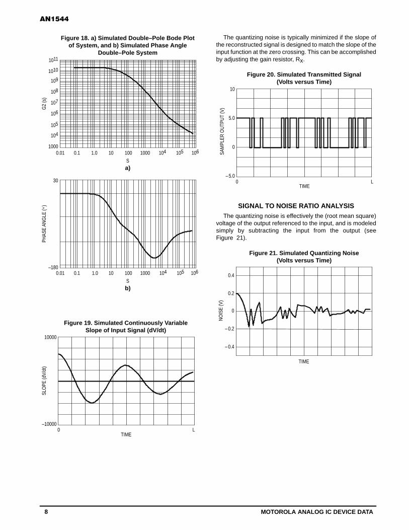
Figure 18. a) Simulated Double–Pole Bode Plotof System, and b) Simulated Phase Angle
Double–Pole System
106105104100010010
S
G2
(s)
1.00.10.01
b)
30
–1801061051041000100100.01
S
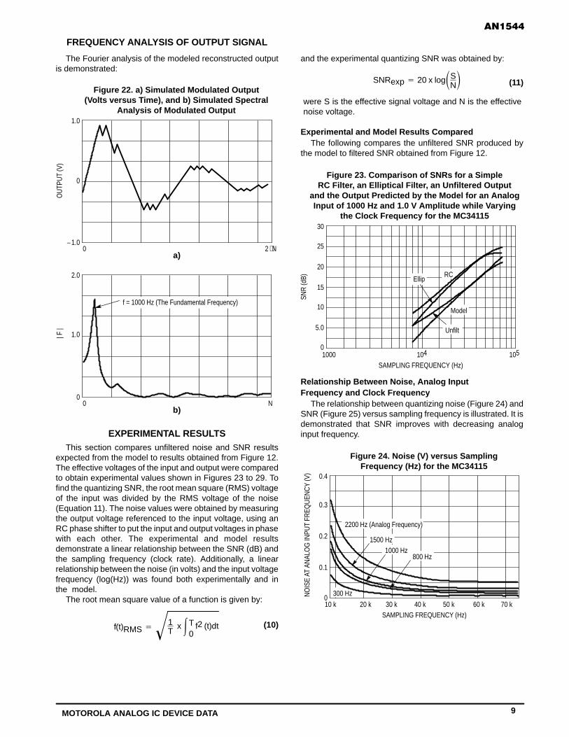
Figure 19. Simulated Continuously VariableSlope of Input Signal (dV/dt)
10000
–10000L0
TIME
SLO
PE (d
V/dt
)
106
105
1000
1011
1010
109
108
107
104
0.1 1.0
The quantizing noise is typically minimized if the slope ofthe reconstructed signal is designed to match the slope of theinput function at the zero crossing. This can be accomplishedby adjusting the gain resistor, Rx.
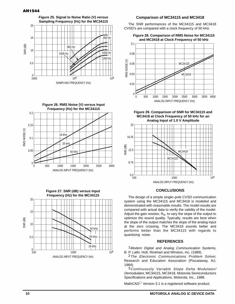
Figure 20. Simulated Transmitted Signal(Volts versus Time)
10
– 5.0L0
TIME
SAM
PLER
OU
TPU
T (V
)
5.0
0
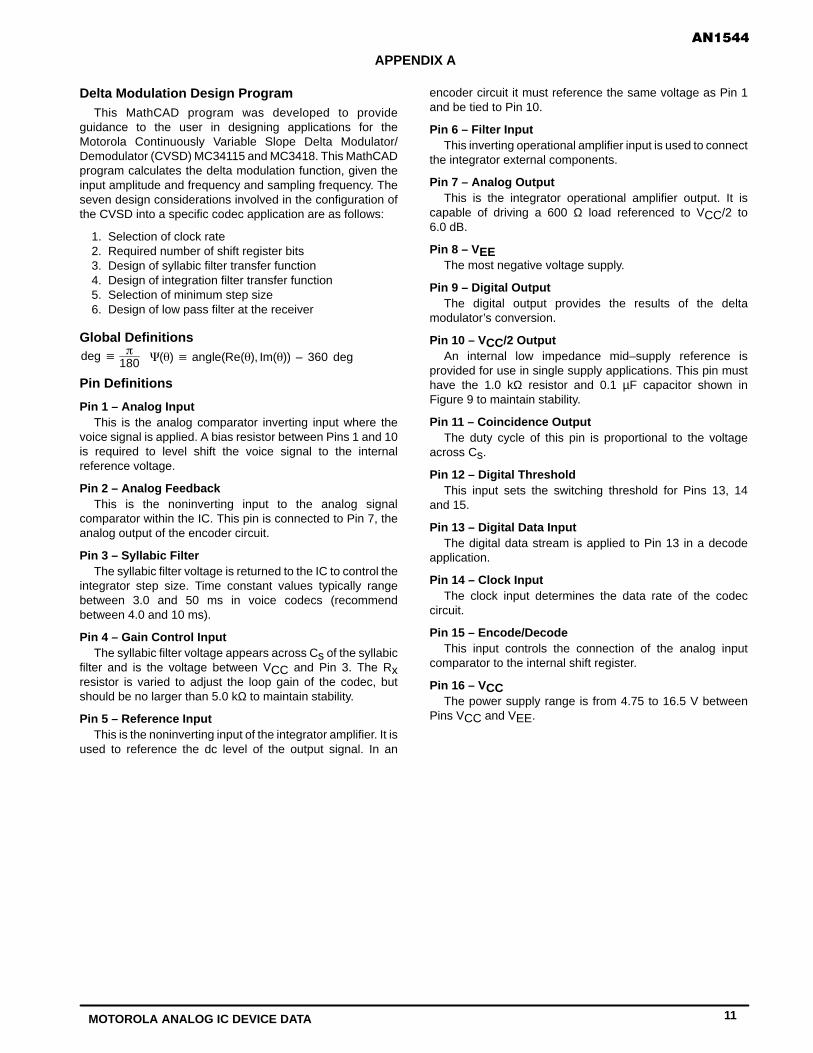
SIGNAL TO NOISE RATIO ANALYSISThe quantizing noise is effectively the (root mean square)
voltage of the output referenced to the input, and is modeledsimply by subtracting the input from the output (seeFigure 21).
Figure 21. Simulated Quantizing Noise(Volts versus Time)
0.4
– 0.4
TIME
NO
ISE
(V)
0.2
0
– 0.2
9MOTOROLA ANALOG IC DEVICE DATA
FREQUENCY ANALYSIS OF OUTPUT SIGNAL
The Fourier analysis of the modeled reconstructed outputis demonstrated:
Figure 22. a) Simulated Modulated Output(Volts versus Time), and b) Simulated Spectral
Analysis of Modulated Output
a)
OU
TPU
T (V
)
1.0
0
– 1.0
b)
2.0
1.0
00 N
0 2 ⋅ N
f = 1000 Hz (The Fundamental Frequency)
| F |
EXPERIMENTAL RESULTSThis section compares unfiltered noise and SNR results
expected from the model to results obtained from Figure 12.The effective voltages of the input and output were comparedto obtain experimental values shown in Figures 23 to 29. Tofind the quantizing SNR, the root mean square (RMS) voltageof the input was divided by the RMS voltage of the noise(Equation 11). The noise values were obtained by measuringthe output voltage referenced to the input voltage, using anRC phase shifter to put the input and output voltages in phasewith each other. The experimental and model resultsdemonstrate a linear relationship between the SNR (dB) andthe sampling frequency (clock rate). Additionally, a linearrelationship between the noise (in volts) and the input voltagefrequency (log(Hz)) was found both experimentally and inthe model.
The root mean square value of a function is given by:
(10)f(t)RMS 1T
xT0
f2 (t)dt
and the experimental quantizing SNR was obtained by:
(11)SNRexp 20 x logSN
were S is the effective signal voltage and N is the effectivenoise voltage.
Experimental and Model Results ComparedThe following compares the unfiltered SNR produced by
the model to filtered SNR obtained from Figure 12.
Figure 23. Comparison of SNRs for a SimpleRC Filter, an Elliptical Filter, an Unfiltered Output
and the Output Predicted by the Model for an AnalogInput of 1000 Hz and 1.0 V Amplitude while Varying
the Clock Frequency for the MC34115
SNR
(dB)
30
20
01000 105
25
15
10
5.0
104
SAMPLING FREQUENCY (Hz)
RCEllip
Unfilt
Model
Relationship Between Noise, Analog InputFrequency and Clock Frequency
The relationship between quantizing noise (Figure 24) andSNR (Figure 25) versus sampling frequency is illustrated. It isdemonstrated that SNR improves with decreasing analoginput frequency.
Figure 24. Noise (V) versus SamplingFrequency (Hz) for the MC34115
NO
ISE
AT A
NAL
OG
INPU
T FR
EQU
ENC
Y (V
) 0.4
0.2
010 k
0.3
0.1
SAMPLING FREQUENCY (Hz)20 k 30 k 40 k 50 k 60 k 70 k
2200 Hz (Analog Frequency)
1500 Hz1000 Hz
800 Hz
300 Hz
10 MOTOROLA ANALOG IC DEVICE DATA
Figure 25. Signal to Noise Ratio (V) versusSampling Frequency (Hz) for the MC34115
SNR
(dB)
20
10
01000 105
15
5.0
104
SAMPLING FREQUENCY (Hz)
1500 Hz
2200 Hz
300 Hz
800 Hz
1000 Hz
Figure 26. RMS Noise (V) versus InputFrequency (Hz) for the MC34115
RM
S N
OIS
E (V
)
0.2
0.1
00 3000
0.15
0.05
500ANALOG INPUT FREQUENCY (Hz)
1000 1500 2000 2500
16 kHz
25 kHz
50 kHz
Figure 27. SNR (dB) versus InputFrequency (Hz) for the MC34115
SNR
(dB)
20
10
0100 104
15
5.0
1000ANALOG INPUT FREQUENCY (Hz)
16 kHz
25 kHz
50 kHz
Comparison of MC34115 and MC3418
The SNR performances of the MC34115 and MC3418CVSD’s are compared with a clock frequency of 50 kHz.
Figure 28. Comparison of RMS Noise for MC34115and MC3418 at Clock Frequency of 50 kHz
RM
S N
OIS
E (V
)
0.1
0.06
00 4000
0.08
0.04
500ANALOG INPUT FREQUENCY (Hz)
1000 1500 2000 2500
MC34115
MC3418
0.02
3000 3500
Figure 29. Comparison of SNR for MC34115 andMC3418 at Clock Frequency of 50 kHz for an
Analog Input of 1.0 V AmplitudeSN
R (d
B)20
12.5
5.0100 104
16.25
8.75
ANALOG INPUT FREQUENCY (Hz)1000
MC34115
MC3418
CONCLUSIONS
The design of a simple single–pole CVSD communicationsystem using the MC34115 and MC3418 is modeled anddemonstrated with reasonable results. The model results arecompared with actual data to verify the validity of the model.Adjust the gain resistor, Rx, to vary the slope of the output tooptimize the sound quality. Typically, results are best whenthe slope of the output matches the slope of the analog inputat the zero crossing. The MC3418 sounds better andperforms better than the MC34115 with regards toquantizing noise.
REFERENCES
1Modern Digital and Analog Communication Systems,B. P. Lathi, Holt, Rinehart and Winston, Inc. (1989).
2The Electronic Communications Problem Solver,Research and Education Association (Piscataway, NJ,1984).
3Continuously Variable Slope Delta Modulator/Demodulator, MC34115, MC3418, Motorola SemiconductorsSpecifications and Applications, Motorola, Inc., 1988.
MathCAD Version 3.1 is a registered software product.
11MOTOROLA ANALOG IC DEVICE DATA
APPENDIX A
Delta Modulation Design ProgramThis MathCAD program was developed to provide
guidance to the user in designing applications for theMotorola Continuously Variable Slope Delta Modulator/Demodulator (CVSD) MC34115 and MC3418. This MathCADprogram calculates the delta modulation function, given theinput amplitude and frequency and sampling frequency. Theseven design considerations involved in the configuration ofthe CVSD into a specific codec application are as follows:
1. Selection of clock rate2. Required number of shift register bits3. Design of syllabic filter transfer function4. Design of integration filter transfer function5. Selection of minimum step size6. Design of low pass filter at the receiver
Global Definitionsdeg
180 () angle(Re(), Im()) – 360 deg
Pin Definitions
Pin 1 – Analog InputThis is the analog comparator inverting input where the
voice signal is applied. A bias resistor between Pins 1 and 10is required to level shift the voice signal to the internalreference voltage.
Pin 2 – Analog FeedbackThis is the noninverting input to the analog signal
comparator within the IC. This pin is connected to Pin 7, theanalog output of the encoder circuit.
Pin 3 – Syllabic FilterThe syllabic filter voltage is returned to the IC to control the
integrator step size. Time constant values typically rangebetween 3.0 and 50 ms in voice codecs (recommendbetween 4.0 and 10 ms).
Pin 4 – Gain Control InputThe syllabic filter voltage appears across Cs of the syllabic
filter and is the voltage between VCC and Pin 3. The Rxresistor is varied to adjust the loop gain of the codec, butshould be no larger than 5.0 kΩ to maintain stability.
Pin 5 – Reference InputThis is the noninverting input of the integrator amplifier. It is
used to reference the dc level of the output signal. In an
encoder circuit it must reference the same voltage as Pin 1and be tied to Pin 10.
Pin 6 – Filter InputThis inverting operational amplifier input is used to connect
the integrator external components.
Pin 7 – Analog OutputThis is the integrator operational amplifier output. It is
capable of driving a 600 Ω load referenced to VCC/2 to6.0 dB.
Pin 8 – VEEThe most negative voltage supply.
Pin 9 – Digital OutputThe digital output provides the results of the delta
modulator’s conversion.
Pin 10 – VCC/2 OutputAn internal low impedance mid–supply reference is
provided for use in single supply applications. This pin musthave the 1.0 kΩ resistor and 0.1 µF capacitor shown inFigure 9 to maintain stability.
Pin 11 – Coincidence OutputThe duty cycle of this pin is proportional to the voltage
across Cs.
Pin 12 – Digital ThresholdThis input sets the switching threshold for Pins 13, 14
and 15.
Pin 13 – Digital Data InputThe digital data stream is applied to Pin 13 in a decode
application.
Pin 14 – Clock InputThe clock input determines the data rate of the codec
circuit.
Pin 15 – Encode/DecodeThis input controls the connection of the analog input
comparator to the internal shift register.
Pin 16 – VCCThe power supply range is from 4.75 to 16.5 V between
Pins VCC and VEE.
12 MOTOROLA ANALOG IC DEVICE DATA
Selection of Clock Rate and Analog Input Function
* * * * * * * * * * * * * * * * * * * * * *Designer’s Input
supply voltage: VCC := 5.0 V
sampling frequency: fS := 32 x 103 Hz (vary between 9600 Hz to 64 kHz)
input amplitude: Vo := 1.0 V (a 0 dBmo sine wave has a peakVO = 1.0 V value of 1.095 V)
analog input frequency: f := 1000 Hz
input damping factor: ζ := ln(3) (set to zero for no damping)
input waveform: m(t) := Vo x sin(2 x π x f x t) x e–(t x ζ x f) V
*************
*************
* * * * * * * * * * * * * * * * * * * * * *
input period: T = 1 x 10⁻³ secT : 1f
sampling interval: ∆TS = 3.125 x 10⁻⁵ secTS : 1fS
length of sample: L : 2 x T sec
number of samples: : ceillog(fS x L)
log(2) α = 6 2α = 64 k := 0.. 2α –1
* * * * * * * * * * * * * * * * * * * * * * * * * * * * * * * * * * * * * * * * * * * * * * * * * * * * * * * * * * * * * * * * *
Required Number of Shift Register BitsThe MC34115 is designed for low bit rate systems and the MC3418 is designed for high performance, high bit rate systems. TheMC34115 has a 3–bit algorithm and the MC3418 has a 4–bit algorithm. For clock rates of 16 kHz and below, the 3–bit algorithmis well suited. For clock rates of 32 kHz and above, the 4–bit algorithm is preferred.
Design of Integration Filter Transfer FunctionThe gain of the circuit is set by the resistor Rx. Rx must be selected to provide the proper integrator step size for high level signalssuch that the companding ratio does not exceed about 25%. The companding ratio is the active low duty cycle on Pin 11 of thecodec circuit. The system gain is dependent on:
1. The maximum level and frequency of the input signal2. The transfer function of the integration filter
For voice codecs the typical input signal is taken to be a sine wave at 1.0 kHz of 0 dBmo level. In practice, the useful dynamic rangeextends about 6.0 dB above the design level. The companding ratio should not exceed 30% in any system.
Single–Pole
To calculate the required step size current, the transfer function of the integration filter must be described.
Choose the pole frequency in Hz (recommend under 300 Hz to provide 1/s voice content curve).
fp : 160 Hz
Design of Syllabic Filter Transfer Function
Choose a syllabic filter time constant much larger than the maximum input signal period. Choose a value with 3.0 ms being theminimum in voice band communications. The time constant for the averaging of the coincidence output signal is given by:
s : 1160
syllabic filter time constant (recommended somewhere between 5.0 and 10 ms)s 6.25 x 10⁻³ sec
To achieve this time constant, choose a capacitor with a reasonable value:
Cs : .33 x 10–6 F syllabic filter capacitance
13MOTOROLA ANALOG IC DEVICE DATA
Rs :sCs
Rs 1.894 x 10⁴ The syllabic filter resistance is then:
Rs : 18 x 103 Using a standard resistor value:
p : 2 x x fp p 1.005 x 10³secThe single–pole break frequency in radians is given by:
Design of Integration Filter Transfer Function
C1 : 0.1 x 10⁻⁶ FChoose a reasonable capacitance value:
R1 : 1p x C1
R1 9.947 x 10³The resistance value, R1, is given by:
R1 : 10 x 103Using a standard resistor value for R1:
The CVSD step should trace the change of a sine wave centered around the zero crossing at 1/8 of a cycle, where the wavechanges by approximately its peak value. Thus:
dVo : Vo dt : 18
x T dt 1.25 x 10⁻⁴ sec
Ii :Vo
2 x R1C1 x
dVodt Ii 8.5 x 10⁻⁴ AThe integrator filter input current is given by:
Note: The maximum voltage across R1 when maximum slew is required is Vo/2.0 V.
The voltage range of the syllabic filter is the power supply voltage, thus:
Rx : .25 x VCC x 1Ii
Rx 1.471 x 10³
Rx : 1.3 x 10³Using a standard resistor value for Rx (<5.0 kΩ):
Minimum Step Size
The final design parameter to be selected is the idle channel step size. With no input signal, the digital output becomes a one–zeroalternating pattern and the analog output becomes a small triangle wave. The idle channel step size, ∆Vo, must be twice thespecified total loop offset if a one–zero idle pattern is desired.
To set the idle channel step size, the value of Rmin must be selected. With no input signal, the slope control algorithm is inactive.A long series of ones and zeros never occurs. Thus, the voltage across the syllabic filter capacitor (Cs) would decay to zero.However, the voltage divider of Rs and Rmin sets the minimum allowed voltage across the syllabic filter capacitor. As the inputamplitude increases from zero, the step size of the output, ∆V, will in turn increase and its slope will continuously vary to match theslope of the input at the zero crossing. The designer should ensure these parameters are within minimum allowed tolerances toensure proper circuit configurations are achieved.
It can be derived that the minimum step size, ∆V, required to avoid slope overload for the full amplitude of the input is:
V : Vo x 2 x x ffS V 0.196 Minimum step size required
Vo : 20 x 10–3 VDefine the minimum idle channel step size:
Set ∆Vo = 0.02 V to match design parameters of Figure 14 of the MC34115 data sheet.
Ii1 : C1 xVoTS
Ii1 6.4 x 10⁻⁵ AFor values of Vo near ∆Vo/2:
The voltage on Cs which produces current Ii1 is determined by Rx:
Vs(min) : Ii1 x Rx Vs(min) 8.32 x 10⁻² V
Rmin : Rs x VCCVs(min)
– 1 Rmin 1.064 x 10⁶The value suggested for Rmin is:
14 MOTOROLA ANALOG IC DEVICE DATA
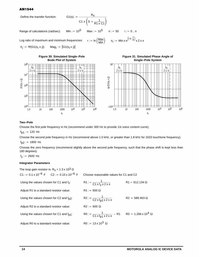
G1(s) :Rx
C1 x S 1R1 x C1
Define the transfer function:
Min : 100 Max : 105 n : 50 i : 0 .. nRange of calculations (rad/sec):
r : ln MaxMin si : Min x e
i x rn
x 2 x Log ratio of maximum and minimum frequencies:
i : (G1(si x j)) Magi : |G1(si x j)|
Figure 30. Simulated Single–PoleBode Plot of System
Figure 31. Simulated Phase Angle ofSingle–Pole System
108
107
106
105
1041061051041000100101.0
si
|G1(
s ix
j)|
s02 x π
(G1(
s ix
j))ψ
30°
–120°1061051041000100101.0
si
sn2 x π
s02 x π
sn2 x π
Two–Pole
Choose the first pole frequency in Hz (recommend under 300 Hz to provide 1/s voice content curve).
fp1 : 120 Hz
Choose the second pole frequency in Hz (recommend above 1.0 kHz, or greater than 1.8 kHz for 1633 touchtone frequency).
fp2 : 1800 Hz
Choose the zero frequency (recommend slightly above the second pole frequency, such that the phase shift is kept less than180 degrees).
fz : 2600 Hz
Integrator Parameters
The loop gain resistor is: Rx = 1.3 x 10³ Ω
C1 : 0.1 x 10⁻⁶ F C2 : 0.15 x 10⁻⁶ F Choose reasonable values for C1 and C2
Using the values chosen for C1 and fz: R1 : 1C1 x fz x 2 x
R1 612.134
Adjust R1 to a standard resistor value: R1 : 600
Using the values chosen for C2 and fp2: R2 : 1C2 x fp2 x 2 x
R2 589.463
Adjust R2 to a standard resistor value: R2 : 600
Using the values chosen for C1 and fp1: R0 : 1C1 x fp1 x 2 x
– R1 R0 1.266 x 10⁴
Adjust R0 to a standard resistor value: R0 : 13 x 103
15MOTOROLA ANALOG IC DEVICE DATA
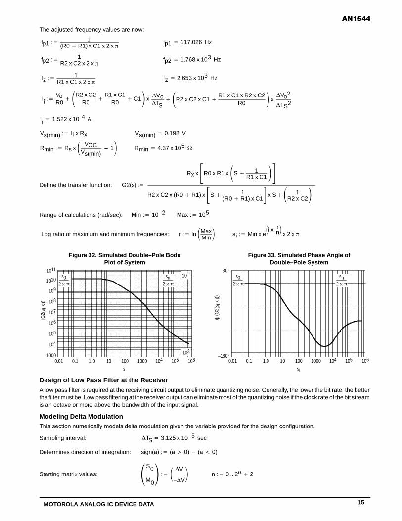
The adjusted frequency values are now:
fp1 : 1(R0R1) x C1 x 2 x
fp1 117.026 Hz
fp2 : 1R2 x C2 x 2 x
fp2 1.768 x 10³ Hz
fz : 1R1 x C1 x 2 x
fz 2.653 x 10³ Hz
Ii :VoR0
R2 x C2R0
R1 x C1
R0C1 x Vo
TSR2 x C2 x C1
R1 x C1 x R2 x C2R0
xVo2
TS2
Ii 1.522 x 10⁻⁴ A
Vs(min) : Ii x Rx Vs(min) 0.198 V
Rmin : Rs x VCCVs(min)
– 1 Rmin 4.37 x 10⁵
Define the transfer function: G2(s) :=
Rx x R0 x R1 x S 1R1 x C1
R2 x C2 x (R0R1) x S 1
(R0R1) x C1 x S 1
R2 x C2
Range of calculations (rad/sec): Min : 10–2 Max : 105
Log ratio of maximum and minimum frequencies: r : ln MaxMin si : Min x e
i x rn
x 2 x
Figure 32. Simulated Double–Pole BodePlot of System
Figure 33. Simulated Phase Angle ofDouble–Pole System
108
107
106
105
1000106105104101.00.01
si
30°
–180°
si
0.1 100 1000
1011
104
109
1010
1011
106105104101.00.01 0.1 100 1000
|G2(
s ix
j)|
(G2(
s ix
j))ψ
103
s02 x π
sn2 x π
s02 x π
sn2 x π
Design of Low Pass Filter at the ReceiverA low pass filter is required at the receiving circuit output to eliminate quantizing noise. Generally, the lower the bit rate, the betterthe filter must be. Low pass filtering at the receiver output can eliminate most of the quantizing noise if the clock rate of the bit streamis an octave or more above the bandwidth of the input signal.
Modeling Delta ModulationThis section numerically models delta modulation given the variable provided for the design configuration.
Sampling interval: TS 3.125 x 10⁻⁵ sec
Determines direction of integration: sign(a) : (a 0) (a 0)
Starting matrix values: S0
M0 : V
–V n : 0 .. 2 2
16 MOTOROLA ANALOG IC DEVICE DATA
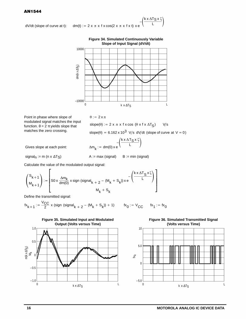
dV/dt (slope of curve at t): dm(t) : 2 x x f x cos(2 x x f x t) x e–k x TS x
L
Figure 34. Simulated Continuously VariableSlope of Input Signal (dV/dt)
10000
–10000L0 k x ∆TS
dm(k
x
T S)
∆
Point in phase where slope ofmodulated signal matches the inputfunction. θ = 2 π yields slope thatmatches the zero crossing.
: 2 x
slope() : 2 x x f x cos ( x f x TS) Vs
slope() 6.162 x 10³ Vs dVdt (slope of curve at V0)
Gives slope at each point: mk : dm(0) x e–k x TS x
L
signaln := m (n x ∆TS) A := max (signal) B := min (signal)
Calculate the value of the modulated output signal:
Sk1
Mk1 :
S0 x
mkdm(0)
x sign (signalk 2 – (Mk Sk)) x e–k x TS x
L
Mk Sk
Define the transmitted signal:
fxk1 :VCC
2x (sign (signalk 2 – (Mk Sk)) 1) fx0 : VCC fx1 : fx0
Figure 35. Simulated Input and ModulatedOutput (Volts versus Time)
Figure 36. Simulated Transmitted Signal(Volts versus Time)
10
– 5.0L0 k x ∆TS
fx
5.0
0
k
1.0
– 1.0L0 k x ∆TS
0.5
0
– 0.5
m(k
xT S
)∆
Mk
17MOTOROLA ANALOG IC DEVICE DATA
Noise Analysis
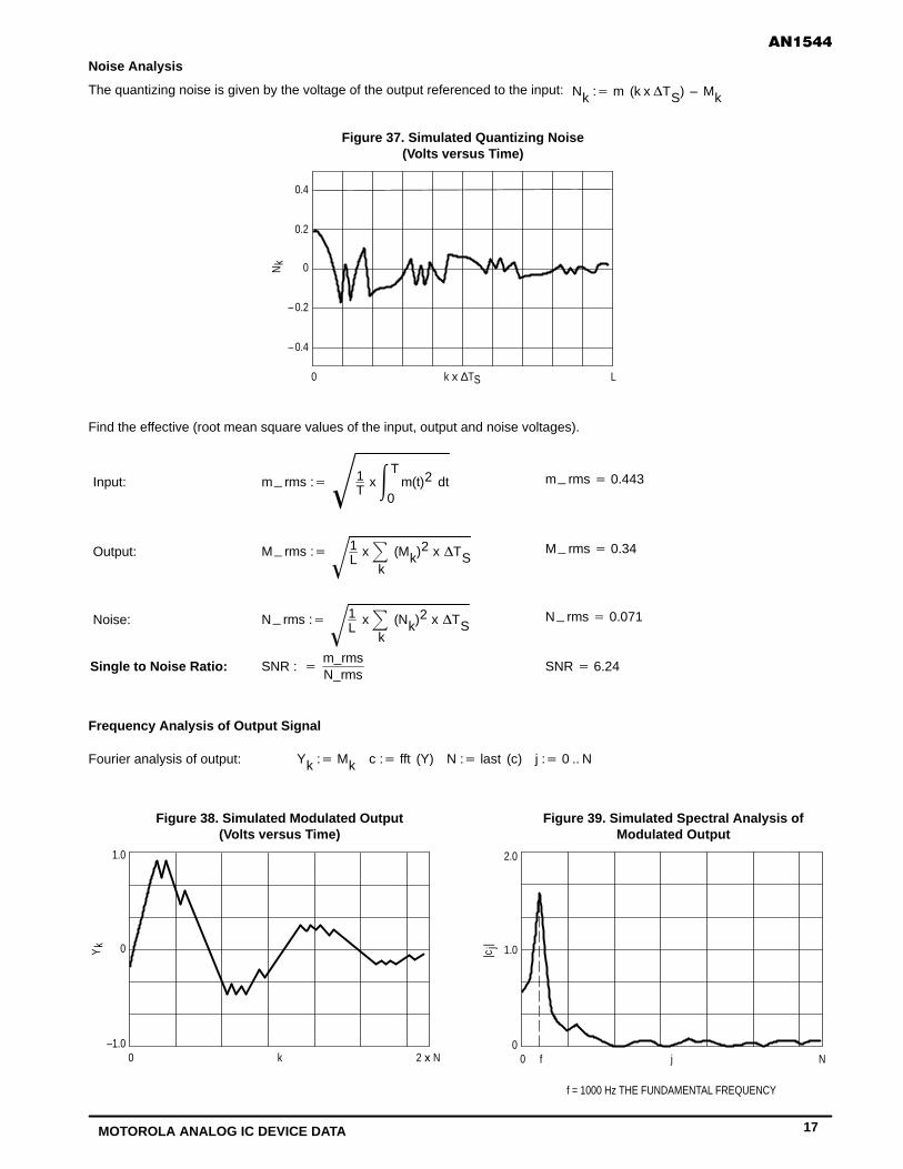
The quantizing noise is given by the voltage of the output referenced to the input: Nk : m (k x TS) – Mk
0.4
– 0.4
k x ∆TS
0.2
0
– 0.2
Figure 37. Simulated Quantizing Noise(Volts versus Time)
Nk
L0
Find the effective (root mean square values of the input, output and noise voltages).
mrms : 1T
xT
0m(t)2 dt mrms 0.443Input:
Mrms : 1L
xk
(Mk)2 x TS Mrms 0.34Output:
Nrms : 1L
xk
(Nk)2 x TS Nrms 0.071Noise:
SNR : m_rmsN_rms
SNR 6.24Single to Noise Ratio:
Frequency Analysis of Output Signal
Fourier analysis of output: Yk : Mk c : fft (Y) N : last (c) j : 0 .. N
Figure 38. Simulated Modulated Output(Volts versus Time)
Figure 39. Simulated Spectral Analysis ofModulated Output
–1.0
0
1.0
Yk
2N0 k0
1.0
2.0
|cj
N0 j
|
f = 1000 Hz THE FUNDAMENTAL FREQUENCY
f

18 MOTOROLA ANALOG IC DEVICE DATA
NOTES

19MOTOROLA ANALOG IC DEVICE DATA
NOTES
20 MOTOROLA ANALOG IC DEVICE DATA
Motorola reserves the right to make changes without further notice to any products herein. Motorola makes no warranty, representation or guarantee regardingthe suitability of its products for any particular purpose, nor does Motorola assume any liability arising out of the application or use of any product or circuit, andspecifically disclaims any and all liability, including without limitation consequential or incidental damages. “Typical” parameters can and do vary in differentapplications. All operating parameters, including “Typicals” must be validated for each customer application by customer’s technical experts. Motorola doesnot convey any license under its patent rights nor the rights of others. Motorola products are not designed, intended, or authorized for use as components insystems intended for surgical implant into the body, or other applications intended to support or sustain life, or for any other application in which the failure ofthe Motorola product could create a situation where personal injury or death may occur. Should Buyer purchase or use Motorola products for any suchunintended or unauthorized application, Buyer shall indemnify and hold Motorola and its officers, employees, subsidiaries, affiliates, and distributors harmlessagainst all claims, costs, damages, and expenses, and reasonable attorney fees arising out of, directly or indirectly, any claim of personal injury or deathassociated with such unintended or unauthorized use, even if such claim alleges that Motorola was negligent regarding the design or manufacture of the part.Motorola and are registered trademarks of Motorola, Inc. Motorola, Inc. is an Equal Opportunity/Affirmative Action Employer.
How to reach us:USA / EUROPE: Motorola Literature Distribution; JAPAN : Nippon Motorola Ltd.; Tatsumi–SPD–JLDC, Toshikatsu Otsuki,P.O. Box 20912; Phoenix, Arizona 85036. 1–800–441–2447 6F Seibu–Butsuryu–Center, 3–14–2 Tatsumi Koto–Ku, Tokyo 135, Japan. 03–3521–8315
MFAX: [email protected] – TOUCHTONE (602) 244–6609 HONG KONG: Motorola Semiconductors H.K. Ltd.; 8B Tai Ping Industrial Park, INTERNET: http://Design–NET.com 51 Ting Kok Road, Tai Po, N.T., Hong Kong. 852–26629298
AN1544/D
◊
Copyright © 2022 FDOKUMEN