Morphological Analysis of Laser Surface Texturing Effect on ...
19
Citation: Moldovan, E.R.; Concheso Doria, C.; Ocaña, J.L.; Istrate, B.; Cimpoesu, N.; Baltes, L.S.; Stanciu, E.M.; Croitoru, C.; Pascu, A.; Munteanu, C.; et al. Morphological Analysis of Laser Surface Texturing Effect on AISI 430 Stainless Steel. Materials 2022, 15, 4580. https:// doi.org/10.3390/ma15134580 Academic Editor: Federico Mazzucato Received: 30 May 2022 Accepted: 28 June 2022 Published: 29 June 2022 Publisher’s Note: MDPI stays neutral with regard to jurisdictional claims in published maps and institutional affil- iations. Copyright: © 2022 by the authors. Licensee MDPI, Basel, Switzerland. This article is an open access article distributed under the terms and conditions of the Creative Commons Attribution (CC BY) license (https:// creativecommons.org/licenses/by/ 4.0/). materials Article Morphological Analysis of Laser Surface Texturing Effect on AISI 430 Stainless Steel Edit Roxana Moldovan 1 , Carlos Concheso Doria 2 , José Luis Ocaña 3 , Bogdan Istrate 4 , Nicanor Cimpoesu 5 , Liana Sanda Baltes 1, * , Elena Manuela Stanciu 1 , Catalin Croitoru 1 , Alexandru Pascu 1 , Corneliu Munteanu 4,6 and Mircea Horia Tierean 1, * 1 Materials Engineering and Welding Department, Transilvania University of Brasov, 29 Eroilor Blvd., 500036 Brasov, Romania; [email protected] (E.R.M.); [email protected] (E.M.S.); [email protected] (C.C.); [email protected] (A.P.) 2 BSH Electrodomésticos España, S.A., Avda. de la Industria 49, 50016 Zaragoza, Spain; [email protected] 3 Departamento de Física Aplicada e Ingeniería de Materiales, Universidad Politecnica de Madrid, C/José Gutiérrez Abascal 2, 28006 Madrid, Spain; [email protected] 4 Mechanical Engineering Department, Gheorghe Asachi Technical University of Ias , i, 43 Dimitrie Mangeron Blvd., 700050 Ias , i, Romania; [email protected] (B.I.); [email protected] (C.M.) 5 Materials Science Department, Gheorghe Asachi Technical University of Ias , i, 43 Dimitrie Mangeron Blvd., 700050 Ias , i, Romania; [email protected] 6 Technical Sciences Academy of Romania, 26 Dacia Blvd., 030167 Bucharest, Romania * Correspondence: [email protected] (L.S.B.); [email protected] (M.H.T.); Tel.: +40-724-546929 (L.S.B.); +40-744-482284 (M.H.T.) Abstract: Laser surface texturing (LST) is a method to obtain micro-structures on the material’s surface for improving tribological performances, wetting tuning, surface treatment, and increasing adhesion. The material selected for LST is AISI 430 ferritic stainless steel, distinguished by the low cost in manufacturing, corrosion resistance, and high strength at elevated temperature. The present study addresses the morphology of new pattern designs (crater array, ellipse, and octagonal shapes). The patterns are applied on the stainless-steel surface by a non-contact method with high quality and precision nanosecond pulsed laser equipment. The investigation of laser parameter influence on thermal affected area and micro-structures is accomplished by morphological and elemental analysis (SEM + EDX). The parameters of the laser micro-patterning have a marked influence on the morphology, creating groove-type sections with different depths and recast material features. From the SEM characterization, the highest level of recast material is observed for concentric octagon LST design. Its application is more recommended for the preparation of the metal surface before hybrid welding. Additionally, the lack of the oxygen element in the case of this design suggests the possible use of the pattern in hybrid joining. Keywords: ferritic stainless steel; laser surface texturing; surface patterns; morphological analysis 1. Introduction Laser surface texturing (LST) is a widely used method worldwide for surface func- tionalization [1–4], being used in various fields: medical implants [5–11], wettability tun- ing [12], optical properties [13,14], hybrid joining [15–17], increasing adhesion [18], or cutting tools [19–22]. The materials that are the object of microtexturing are varied, from dentin and enamel materials, to polymers, ceramics, ferrous and non-ferrous metallic mate- rials, and finally composite materials, in various domains such as engineering, medicine, bioengineering, etc. The most widespread LST patterns used are dimples [4,5,12,17], lines (parallel, crosshatch) [4,5,8–10,12,20,22], square [6,12], conical [19,22], rhombic [12,22], rip- ple texture (riblet texture inspired from the sharkskin, U-shapes (waviness texture) [8,18], Materials 2022, 15, 4580. https://doi.org/10.3390/ma15134580 https://www.mdpi.com/journal/materials
-
Upload
khangminh22 -
Category
Documents
-
view
3 -
download
0
Transcript of Morphological Analysis of Laser Surface Texturing Effect on ...

Citation: Moldovan, E.R.; Concheso
Doria, C.; Ocaña, J.L.; Istrate, B.;
Cimpoesu, N.; Baltes, L.S.; Stanciu,
E.M.; Croitoru, C.; Pascu, A.;
Munteanu, C.; et al. Morphological
Analysis of Laser Surface Texturing
Effect on AISI 430 Stainless Steel.
Materials 2022, 15, 4580. https://
doi.org/10.3390/ma15134580
Academic Editor: Federico
Mazzucato
Received: 30 May 2022
Accepted: 28 June 2022
Published: 29 June 2022
Publisher’s Note: MDPI stays neutral
with regard to jurisdictional claims in
published maps and institutional affil-
iations.
Copyright: © 2022 by the authors.
Licensee MDPI, Basel, Switzerland.
This article is an open access article
distributed under the terms and
conditions of the Creative Commons
Attribution (CC BY) license (https://
creativecommons.org/licenses/by/
4.0/).
materials
Article
Morphological Analysis of Laser Surface Texturing Effect onAISI 430 Stainless SteelEdit Roxana Moldovan 1, Carlos Concheso Doria 2, José Luis Ocaña 3 , Bogdan Istrate 4 , Nicanor Cimpoesu 5,Liana Sanda Baltes 1,* , Elena Manuela Stanciu 1 , Catalin Croitoru 1 , Alexandru Pascu 1,Corneliu Munteanu 4,6 and Mircea Horia Tierean 1,*
1 Materials Engineering and Welding Department, Transilvania University of Brasov, 29 Eroilor Blvd.,500036 Brasov, Romania; [email protected] (E.R.M.); [email protected] (E.M.S.);[email protected] (C.C.); [email protected] (A.P.)
2 BSH Electrodomésticos España, S.A., Avda. de la Industria 49, 50016 Zaragoza, Spain;[email protected]
3 Departamento de Física Aplicada e Ingeniería de Materiales, Universidad Politecnica de Madrid,C/José Gutiérrez Abascal 2, 28006 Madrid, Spain; [email protected]
4 Mechanical Engineering Department, Gheorghe Asachi Technical University of Ias, i,43 Dimitrie Mangeron Blvd., 700050 Ias, i, Romania; [email protected] (B.I.);[email protected] (C.M.)
5 Materials Science Department, Gheorghe Asachi Technical University of Ias, i, 43 Dimitrie Mangeron Blvd.,700050 Ias, i, Romania; [email protected]
6 Technical Sciences Academy of Romania, 26 Dacia Blvd., 030167 Bucharest, Romania* Correspondence: [email protected] (L.S.B.); [email protected] (M.H.T.); Tel.: +40-724-546929 (L.S.B.);
+40-744-482284 (M.H.T.)
Abstract: Laser surface texturing (LST) is a method to obtain micro-structures on the material’ssurface for improving tribological performances, wetting tuning, surface treatment, and increasingadhesion. The material selected for LST is AISI 430 ferritic stainless steel, distinguished by the lowcost in manufacturing, corrosion resistance, and high strength at elevated temperature. The presentstudy addresses the morphology of new pattern designs (crater array, ellipse, and octagonal shapes).The patterns are applied on the stainless-steel surface by a non-contact method with high qualityand precision nanosecond pulsed laser equipment. The investigation of laser parameter influenceon thermal affected area and micro-structures is accomplished by morphological and elementalanalysis (SEM + EDX). The parameters of the laser micro-patterning have a marked influence on themorphology, creating groove-type sections with different depths and recast material features. Fromthe SEM characterization, the highest level of recast material is observed for concentric octagon LSTdesign. Its application is more recommended for the preparation of the metal surface before hybridwelding. Additionally, the lack of the oxygen element in the case of this design suggests the possibleuse of the pattern in hybrid joining.
Keywords: ferritic stainless steel; laser surface texturing; surface patterns; morphological analysis
1. Introduction
Laser surface texturing (LST) is a widely used method worldwide for surface func-tionalization [1–4], being used in various fields: medical implants [5–11], wettability tun-ing [12], optical properties [13,14], hybrid joining [15–17], increasing adhesion [18], orcutting tools [19–22]. The materials that are the object of microtexturing are varied, fromdentin and enamel materials, to polymers, ceramics, ferrous and non-ferrous metallic mate-rials, and finally composite materials, in various domains such as engineering, medicine,bioengineering, etc. The most widespread LST patterns used are dimples [4,5,12,17], lines(parallel, crosshatch) [4,5,8–10,12,20,22], square [6,12], conical [19,22], rhombic [12,22], rip-ple texture (riblet texture inspired from the sharkskin, U-shapes (waviness texture) [8,18],
Materials 2022, 15, 4580. https://doi.org/10.3390/ma15134580 https://www.mdpi.com/journal/materials
Materials 2022, 15, 4580 2 of 19
and ring (bulge, smooth staked) [11]. The possibility of using the laser equipment toobtain texturing patterns with different geometries of high-quality surfaces to improvethe materials’ performances in a single step of a technological process represents a specialadvantage. That is why ultrashort laser ablation is an ideal solution in creating structureswith known dimensions and perfectly repeatable, on a nanoscale and beyond. Approach-ing this technique is a challenge, but at the same time it offers real solutions in terms ofmaterial removal.
Zhao Y. et al. [23] present Si and Cu samples laser ablated with the following char-acteristics of an X-ray laser: energy 50 µJ, wavelength 46.9 nm, and focused by meansof a toroidal mirror at grazing incidence. Two hundred shots were applied to each ofthe samples, with a power density of ~2 × 10⁷ W/cm2. The results obtained and therelated conclusion that the laser fluence is directly influenced by ablation, is consistent withthe results obtained in relation with this research and presented in a previous paper ofMoldovan E. et al. [24].
In value, the fluence is different, depending on the material. For example, for polymersit is between 0.1 to 1 J/cm2, while for inorganic insulators it is between 0.5 and 2.0 J/cm2 [2].Related to the present study, Moldovan E. et al. [24] showed a decrease in fluence valuesfrom 8.49 J/cm2 to 2.55 J/cm2, in the frequency range of 30–100 kHz. The materials havea different behavior under the action of the laser. For example, the absorption of energyfrom a laser beam strongly influences the ablation mechanism. Thus, polymers absorb in anon-linear manner the laser energy compared to metals [2].
The literature provides information on the possibility of using nanosecond, picosecond,and femtosecond laser equipment for texturing. Pou-Álvarez P. et al. [25] studied thedifference between the three variants, applying pulse lengths of 20 ns (in present study9 ns pulse duration), 800 ps, and 266 fs on AZ31B magnesium alloy. In the nanosecond andpicosecond lasers, the wavelength was 1064 nm (as in the present study) and 520 nm for thefemtosecond one. The power was 6.4 W, 6.2 W, and 5.9 W (in the present study 20 W). Thespot size in the nanosecond case was 163 µm (compared to 100 µm in the current study).All parameters can be analyzed comparatively in the papers [24–26]. SEM analysis showsuniform Mg matrix with dispersed Al-Mn-Fe particles. It is important to consider whathappens due to the reduction of pulse duration. Groove profiles differ from nanosecond tofemtosecond, as does the position for the recast layer. The molten material is drasticallyreduced with the reduction of the pulse length, the same as recast material. In the case ofrecast material in nanosecond situation, this is present as a uniform and thicker layer. Byreducing the pulse length, an increase in width and depth of grooves is obtained.
The ablation was also studied by Cui H. et al. [27] on copper samples, using a laserwith a grazing incidence angle of 7◦ (in the present study 3◦), wavelength 46.9 nm, energy50 µJ and 100 µJ with a pulse width of 1.7 ns. The pulse numbers were 1 to 6. By increasingthe energy, the evaporation on the surface increased. At 100 µJ the average fluence werecalculated at 250 mJ/cm2. The explanation of the mechanism was as follows: the laserenergy was absorbed by the surface and after melting/evaporation the material wasresolidified into nanoparticles. The placement of the sample is very important, because thevertical positioning allows, due to gravity, the nano particles to fall. The interesting resultsobtained encourage further research into the phenomenon.
Microtexturing also finds its place in the field of hip implants, and the couple bearingbetween the acetabular cup and the femoral head is very important. The combinationof materials can be varied, from metal–metal to metal–ceramic and to metal–polymer.The appropriate choice of the combination of materials translates into the reduction ofunwanted effects, such as aseptic loosening, tissue constraints in the body, etc. Using thefinite element simulation model presented by Jamari J. et al. [28] for the combination ofUHMWPE as material for acetabular cup and SS316L, CoCrMo and Ti6Al4V as metallicmaterials for femoral head, the contact pressure can be established for other combinationsof materials.

Materials 2022, 15, 4580 3 of 19
Delgado-Ruiz R. A. et al. [5] studied zirconium dioxide for dental implants microtex-tured with a femtosecond laser device. They applied 120 fs pulses at 795 wavelengths, witha repetition rate of 1 kHz, a pulse energy that can reach a maximum of 1.1 mJ. As a resultof surface modification, all roughness parameters significantlyincrease. Concerning thesurface morphology, the pores have a conical section and the grooves a pyramidal one. Theelemental analysis reveals the diminishing presence of carbon and aluminum and a largerproportion of oxygen and zirconium. The SEM analysis of surfaces showed the presence ofcrests and valleys and microcracks areas.
To improve osteoblastic bond of human stem cells, Cunha A. et al. [6] investigated lasersurface texturing of Ti-6Al-4V alloy. The laser wavelength was 1030 nm and pulse duration500 fs. The surface texture consisted in nanoripples, nanopillars, and microcolumns. SEManalysis shows the differences between the three types of texturing and is supplementedby X-ray photoelectron spectroscopy (XPS). Nanoripples and microcolumns induce cellstretching. Nanopillars tend to increase the formation of filopodia. After seeding and cellgrowth, the first two microstructures appear to be suitable for use.
In dentistry and orthodontics, it is necessary to ensure adhesion properties. Maria Dela Cruz Lorenzo et al. [7] studied the microstructuring of the dentin and enamel surfaceswith ultrashort pulsed laser microstructuring (wavelength: 795 nm, pulse duration 120 fsand repetition rate 1 kHz). SEM observations of the processed and failure surfaces revealthat the bonding strength is similar to other techniques and in some cases even increased.
For biomedical materials, including magnesium and titanium, laser microprocessingis beneficial. Thus, for Hu G. et al. [8], the study material was hot-extruded Mg–6Gd–0.6Caalloy bars and Ti6Al4V. SEM images were performed on the samples after cell seeding onlaser-melted and laser-melted and LIPSS technique. The wavelength of 1064 nm, the pulsewidth of 800 fs, and the repetition rate of 400 kHz were considered for the laser. The cellspreading was anisotropic on the laser melted and LIPSS surfaces, observing many focaladhesions (filopodia). The ossification is accelerated due to good adhesion.
Implantation of stem cells cultured in bio-resorbable polymeric scaffolds requiresmicrostructuring technologies, useful in regenerative medicine. Poly-L-Lactide (PLLA) wastested by Rocio Ortiz et al. [9], applying grooves on the samples surfaces with a picosecondpulse laser, UV wavelength 355 nm applying an energy of 0.9 µJ at a frequency of 100 kHz,and 5 µm of pulse distance. As a result, the SEM images reveal a depression caused bymaterial removal and protrusions of the recast material at the grooves’ ends and edges.The protrusion is the consequence of the first pulse effect. The conclusion is that groovesinfluence cell orientation and grooves’ edges promote cell adherence and provide guidance.The authors recommend ways to functionalize biomaterials.
Laser microprocessing using high repetition rate of a femtosecond lasers was used bySchille J. [12] for stainless steel, aluminum, and copper. SEM analysis on stainless steel, forexample, reveals the hydrophobic behavior of high volumes of microcones, with contactangles of up to 150◦. The reflectivity in this situation is less than 5%. The decreasing ofvolumes causes the abatement of hydrophobic behavior. Thermal conductivity and highlyrepetitive laser pulses influence the morphology of the surface materials. Around theirradiated area, a high temperature determined a higher ablation rate.
Calcium fluorite as transparent material was microstructured with a femto laser deviceby Rupasov A.E. et al. [13]. Nanogratings were produced at the wavelength of 515 nmand at a wavelength of 1030 nm. The doubling of the period of the nanostructures from200–250 nm to 400–450 nm can be related with the appearance of a crater on the surface ofthe material showed by SEM images and the redistribution of energy in the volume.
Hybrid joints metal-polymers were of interest for Van der Straeten K. et al. [15] usingX5CrNi18-10 (1.4301) stainless steel and glass fiber reinforced PA6 composite polymer.The pulse duration was about 6 ps at a wavelength of 1030 nm. SEM images revealedcone-like protrusions (CLP) which show dots and holes partially connected with bridges.The structure seems to have no predominant orientation direction. The surface roughnesscan be growth by increasing pulse energy and fluency.

Materials 2022, 15, 4580 4 of 19
One condition of the joint improvement is the modification of the surface roughness.Nguyen, A.T.T. et al. [16] studied metal-composite joints using adhesive, the surface be-ing microstructured with outward/inward dimples or outward/inward grooves. It wasrevealed that surface irregularities ensure improved mechanical interlocking, the resinflowing through the relief being observed in SEM characterization.
Surface microtexturing has been broadly applied for improving the tribological prop-erties of cutting tools, such as improving the friction behavior and anti-wear. The typesof fabricated patterns on the cutting tool surfaces were most often micro-grooves, micro-holes, micro-stripe grooves, and micro-pools. Su Y. et al. [20] studied the influence ofmicro-grooved polycrystalline diamond tools manufactured with a fiber laser (scanningspeed: 2 mm/s, pulse repetition rate: 20 kHz, average output power: 12 W) on Ti6Al4V,which is the workpiece material. Three cutting speeds were investigated: 16.485 m/min,56.52 m/min, and 125.6 m/min. For the first speed the results show that the low cut-ting speed generates low cutting temperature and causes slight adhesion. The resultsfor the other two speeds show excellent anti-adhesive effects compared with those ofthe untextured PCD tools, even without lubricants. Low tool-chip contact length can beobtained by the micro-grooved PCD tools which also determines the improvement of thefriction behavior.
Nickel-based alloys have special properties, such as high corrosion resistance andhigh temperature resistance, but their big problem is the difficult machining. Among thematerials with suitable cutting possibilities is polycrystalline cubic boron nitride (CBN),although it encounters difficulties at high cutting speeds. Sugihara T. et al. [21] choseInconel 718 as the workpiece material and cubic boron nitride (CBN) as cutting tools, whichare among the hardest materials. Grooves (grooves parallel and orthogonal to the maincutting edge, microgrooves orthogonal to the main cutting edge and placed 30 µm awayfrom the main cutting edge) with a depth of 5 µm and width and separation of 20 µm werefabricated on the flank face of the CBN cutting tool with a femtosecond laser (wavelength800 nm, pulse width 150 fs, cyclic frequency 1 kHz, pulse energy 300 µJ). The purposewas to stabilize the adhesion layer on the flank face and prevent it from flaking. A cuttingtool with micro grooves orthogonal to the cutting edge and set back from the cutting edgesignificantly reduced the amount of tool retreat. This proves that microgrooving is a helpfulmethod in machining special alloys.
The research in this article is a response to the challenge demanded by industry,namely microstructuring using nanosecond pulsed industrial laser source. Experimentalresearch has generally shown better results in picoseconds and femtoseconds laser, butthe encouraging results in the case of nanoseconds, and especially the applications forindustrial and economic reasons, determined our choice in the study of the latest technicalsolution. The goal is to perform the morphological and elemental analysis of the lasersurface texture patterns on AISI 430 stainless steel, continuing the studies completedin [24,26] for geometry, wettability, and roughness characterization.
2. Materials and Methods
AISI 430 ferritic stainless steel was supplied by Acerinox (ACX 500, Madrid, Spain)in the form of a large sheet, from which the samples were cut to size 80 × 25 × 0.5 mm.The material selected for the present research has a low content of carbon and nitrogen(improving the weldability, toughness, and ductility) and a good resistance in corrosiveenvironment and exposure. Ferritic stainless steel has an elongation at room temperature(20 ◦C) higher than 20%, a nominal yield strength 0.2% offset greater than 260 MPa, andtensile strength between 450 MPa and 600 MPa. With low carbon and chromium between16.00–18.00% content (Table 1), the material has a body-centered cubic (BCC) crystallinestructure. After welding, the 430 ferritic stainless steel can propound corrosion at theintergranular level or/and an oxidation layer. The oxidation layer (chromium oxide) canbehave as a protective layer.

Materials 2022, 15, 4580 5 of 19
Table 1. Chemical composition of AISI 430 stainless steel, provided by manufacturer (Acerinox,Madrid, Spain).
Chemical Element C Cr N Mn Si P S
Concentration (%) ≤0.08 16.00–18.00 ≤0.045 ≤1.00 ≤1.00 ≤0.040 ≤0.015
The equipment used to achieve the microtexturing patterns on the surface of theferritic stainless steel was a nanosecond pulsed laser TruMark 5020 (Trumpf Laser undSystemtechnik GmbH, Ditzingen, Germany). The laser beam is generated by an activemedium Nd: Fiber Diode-pumped, with average power of 20 W, beam quality M2~2,1064 nm wavelength, and 100 µm spot (at 254 mm focal distance). The 3.8 kW pulsed peakpower at 20 W constant mean power ensures the highest pulse energy (>400 µJ) whenfrequency varies from 30 kHz to 50 kHz. The equipment has an integrated computer-aided design software (AutoCAD, version 23.0) that offers the possibility to acquire a widevariety of geometrical shapes’ design and a facile transfer between working stations. Themaximum marking area is 180 × 180 mm at 254 mm focal distance and a pulse frequencyfrom 5 kHz to 1000 kHz (9 ns pulse duration). Because of the specular reflection (surfacefinish of the ferritic stainless steel is bright annealed), the laser beam axis was settled at3◦ angle to prevent possible damage of the laser optical fiber. Throughout the experiments,the constant parameters were: spot diameter 100 µm, power density 2.55 × 10⁵ W/cm2,impulses per point 1, track width of the spot 0.5 mm, overlap of the spot 99% (thereis a correlation between the speed and frequency: if the speed increases/decreases thefrequency increases/decreases too, to not affect the overlapping of the laser beam spot),a pulsed power of 30.5 kW at 19 kHz, and hatch distance center-to-center 0.25 mm (1stdesign-octagonal shape-design type A [23,24]), 0.5 mm (2nd design-two ellipses at 90◦
angle-type B [23,24]), and 2 mm (3rd design-crater array–type C [23,24]). The variableparameters of LST are frequency, speed, and number of repetitions. Repeatability waschosen randomly, starting from five passes, then every five repetitions up to a maximumof 15 repetitions. The maximum number of repetitions was chosen after observing theintensity of the splashes and burrs. Increasing the amount of expulsed material will increasethe influenced thermal area and amount of recast material.
The laser density profile was investigated prior the laser processing to ensure thatproper laser absorption into material will be obtained. The intensity distribution profile(Figure 1a) of the laser radiation on the surface plane can be described as Gaussian, whichprovides an image on the future groove’s shape. During the laser beam-surface interactions,a high intensity plasma surrounded by an electron charged field is formed which leadsto material melting-recasting phenomena and even to delamination of the surface layer.Figure 1b shows an almost perfect outcome for the laser beam: perfect beam and real beamare almost identical.
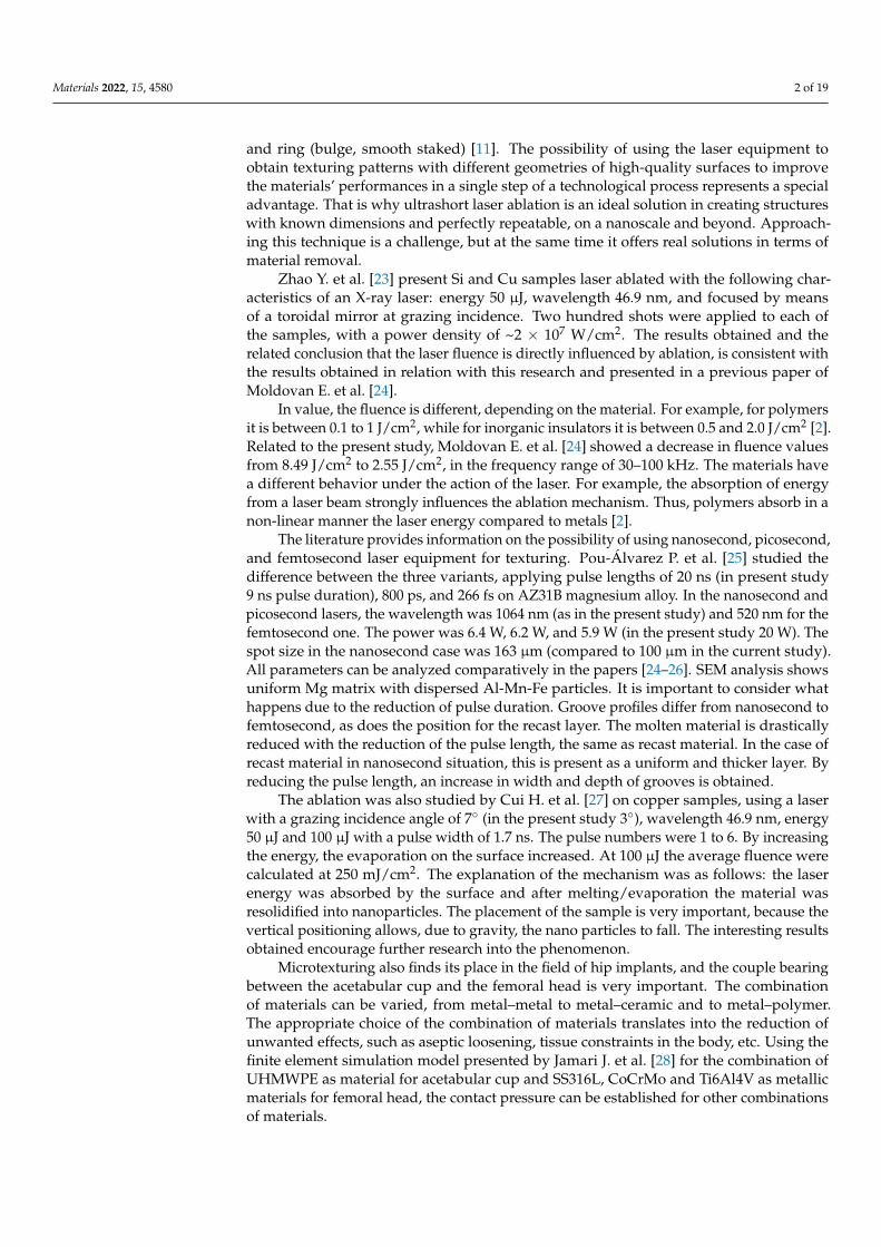
The time cycle refers to a single sequence of repetition, decreasing with increasingfrequency (Figure 2). The time cycle is an important parameter, as it can indicate the timerequired to perform micro-texturing. The importance comes from the influence on thecapacity and volume of production that can be achieved, thus being able to influence theautomation of the LST process.
The surface morphology of the samples was investigated by scanning electron mi-croscopy (SEM FEI Quanta 200 3D Dual beam, equipped with energy-dispersive X-rayspectroscopy analysis unit-X flash Bruker, Billerica, MA, USA). The working distance isset-up at 15 mm in low vacuum mode, with a spot size 5, high voltage (20 kV), and detectorLFD (Large Field Detector). Scanning electron microscopy and energy-dispersive X-rayspectroscopy provide non-destructive, rapid, qualitative, and quantitative analysis.
The microscopic analysis for sectional images and measurements (Figure 3) was per-formed with an optical microscope high-quality phase contrast Leica (Leica Microsystems,Heerbrugg, Switzerland, Ltd., model DMIL M LED). AutoCAD software was used tomeasure the ablated and recast areas.
Materials 2022, 15, 4580 6 of 19Materials 2022, 15, 4580 6 of 20
(a)
(b)
Figure 1. Intensity distribution profile of laser beam (a) and beam simulation (b) of TruMark 5020 laser equipment.
The time cycle refers to a single sequence of repetition, decreasing with increasing frequency (Figure 2). The time cycle is an important parameter, as it can indicate the time required to perform micro-texturing. The importance comes from the influence on the ca-pacity and volume of production that can be achieved, thus being able to influence the automation of the LST process.
Figure 2. Time cycle vs. frequency.
Figure 1. Intensity distribution profile of laser beam (a) and beam simulation (b) of TruMark 5020laser equipment.
Materials 2022, 15, 4580 6 of 20
(a)
(b)
Figure 1. Intensity distribution profile of laser beam (a) and beam simulation (b) of TruMark 5020 laser equipment.
The time cycle refers to a single sequence of repetition, decreasing with increasing frequency (Figure 2). The time cycle is an important parameter, as it can indicate the time required to perform micro-texturing. The importance comes from the influence on the ca-pacity and volume of production that can be achieved, thus being able to influence the automation of the LST process.
Figure 2. Time cycle vs. frequency.
Figure 2. Time cycle vs. frequency.
Materials 2022, 15, 4580 7 of 19
Materials 2022, 15, 4580 7 of 20
The surface morphology of the samples was investigated by scanning electron mi-croscopy (SEM FEI Quanta 200 3D Dual beam, equipped with energy-dispersive X-ray spectroscopy analysis unit-X flash Bruker, Billerica, MA, USA). The working distance is set-up at 15 mm in low vacuum mode, with a spot size 5, high voltage (20 kV), and detec-tor LFD (Large Field Detector). Scanning electron microscopy and energy-dispersive X-ray spectroscopy provide non-destructive, rapid, qualitative, and quantitative analysis.
The microscopic analysis for sectional images and measurements (Figure 3) was per-formed with an optical microscope high-quality phase contrast Leica (Leica Microsystems, Heerbrugg, Switzerland, Ltd., model DMIL M LED). AutoCAD software was used to measure the ablated and recast areas.
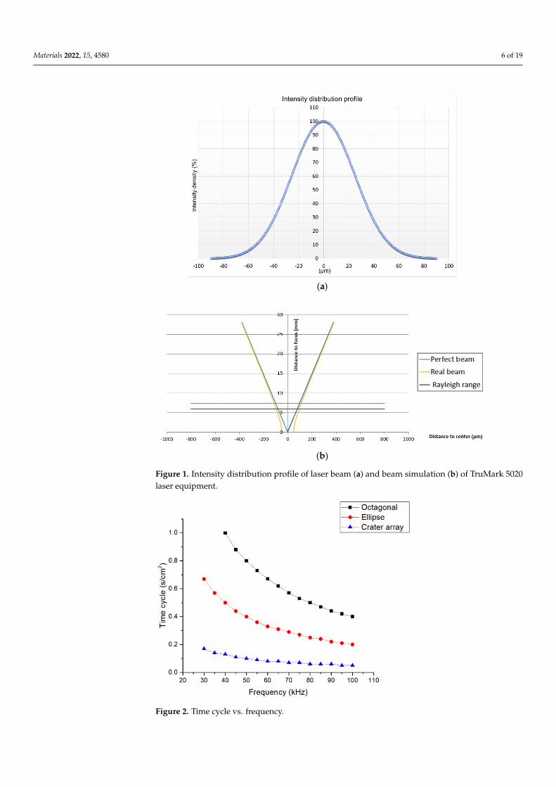
Figure 3. Geometry characterization after LST on ferritic stainless steel AISI 430.
When LST was applied on the surface of the AISI 430, a minimum of 3 mm distance was maintained from the start edge in the speed direction of each sample to mitigate the characteristic predisposition for a thermally influenced area of the ferritic stainless steel.
3. Results and Discussion 3.1. Octagonal Donuts Micro Texturing Geometry Design A
LST was applied to carve an area of 20 mm × 19.5 mm, with an edge distance of 2.75 mm in the hatch direction and 3 mm in the speed direction. The pattern applied consists of three concentric octagons, with 0.25 mm distance between contours and 1 mm twice apothem of the smallest octagon. The distance between the patterns is 0.5 mm on the hatch direction and 0.25 mm in the speed direction. For the morphological analysis, samples were selected for a low frequency and speed and an average of the number of repetitions of microtexturing (Table 2).
Table 2. Variable parameters used for microtexturing design octagonal donut shape (design type A).
Sample Frequency [kHz] Speed [mm/s] No. of Repetition A3 30 300 10 A13 40 400 10
Figure 3. Geometry characterization after LST on ferritic stainless steel AISI 430.
When LST was applied on the surface of the AISI 430, a minimum of 3 mm distancewas maintained from the start edge in the speed direction of each sample to mitigate thecharacteristic predisposition for a thermally influenced area of the ferritic stainless steel.
3. Results and Discussion3.1. Octagonal Donuts Micro Texturing Geometry Design A
LST was applied to carve an area of 20 mm × 19.5 mm, with an edge distance of2.75 mm in the hatch direction and 3 mm in the speed direction. The pattern appliedconsists of three concentric octagons, with 0.25 mm distance between contours and 1 mmtwice apothem of the smallest octagon. The distance between the patterns is 0.5 mm onthe hatch direction and 0.25 mm in the speed direction. For the morphological analysis,samples were selected for a low frequency and speed and an average of the number ofrepetitions of microtexturing (Table 2).
Table 2. Variable parameters used for microtexturing design octagonal donut shape (design type A).
Sample Frequency [kHz] Speed [mm/s] No. of Repetition
A3 30 300 10A13 40 400 10
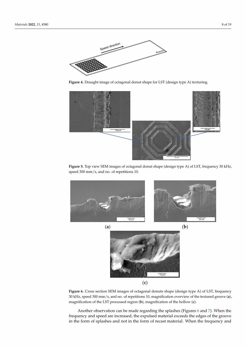
Draught images point out the speed direction and the positioning on the sample forLST octagonal patterns (Figure 4). A computer aided-design software (Auto-CAD) wasused because it offers a wide variety of geometrical shapes, with ability to render withoutdifficulty, and easy transfer towards processing equipment. From the top view images(Figure 5), acquired with scanning electron microscopy, one may observe a difference insize of the heat affected zone and recast material (right side is larger), caused by the angleof laser beam (3◦ to the left). In the right view of Figure 5, one may notice the continuousgroove (successive contours), similar to the seam weld, which is due to the 99% overlappingof the laser spot. Average measurements of microtextures created with LST for patterntype A, frequency 30 kHz, 300 mm/s speed, and 10 repetitions, are 13.658 µm depth and47.245 µm width (at the surface of the sample) with an area of 390.011 µm2. The recastmaterial (the material expelled from the crevice on the edge measured in section view) has10.479 µm height for left side and 6.735 µm for right side, with 234.194 µm2 area for leftside and 118.017 µm2 for right side.
Materials 2022, 15, 4580 8 of 19
Materials 2022, 15, 4580 8 of 20
Draught images point out the speed direction and the positioning on the sample for LST octagonal patterns (Figure 4). A computer aided-design software (Auto-CAD) was used because it offers a wide variety of geometrical shapes, with ability to render without difficulty, and easy transfer towards processing equipment. From the top view images (Figure 5), acquired with scanning electron microscopy, one may observe a difference in size of the heat affected zone and recast material (right side is larger), caused by the angle of laser beam (3° to the left). In the right view of Figure 5, one may notice the continuous groove (successive contours), similar to the seam weld, which is due to the 99% overlap-ping of the laser spot. Average measurements of microtextures created with LST for pat-tern type A, frequency 30 kHz, 300 mm/s speed, and 10 repetitions, are 13.658 µm depth and 47.245 µm width (at the surface of the sample) with an area of 390.011 µm2. The recast material (the material expelled from the crevice on the edge measured in section view) has 10.479 µm height for left side and 6.735 µm for right side, with 234.194 µm2 area for left side and 118.017 µm2 for right side.
Figure 4. Draught image of octagonal donut shape for LST (design type A) texturing.
Figure 5. Top view SEM images of octagonal donut shape (design type A) of LST, frequency 30 kHz, speed 300 mm/s, and no. of repetitions 10.
Another observation can be made regarding the splashes (Figures 6 and 7). When the frequency and speed are increased, the expulsed material exceeds the edges of the groove in the form of splashes and not in the form of recast material. When the frequency and speed increase, the average values of measurements of the samples are: 66.171 µm depth, 43.012 µm width, and 1878.447 µm2 of area. The height of the recast material averages 25.784 µm for the left side and 26.832 µm for the right side. The area of recast material is 945.407 µm2 on the left side and 791.677 µm2 for right side of the hollow. The increase of frequency and speed outlines the growth trend of all geometrical mean measurements of the microstructures created by LST.
Figure 4. Draught image of octagonal donut shape for LST (design type A) texturing.
Materials 2022, 15, 4580 8 of 20
Draught images point out the speed direction and the positioning on the sample for LST octagonal patterns (Figure 4). A computer aided-design software (Auto-CAD) was used because it offers a wide variety of geometrical shapes, with ability to render without difficulty, and easy transfer towards processing equipment. From the top view images (Figure 5), acquired with scanning electron microscopy, one may observe a difference in size of the heat affected zone and recast material (right side is larger), caused by the angle of laser beam (3° to the left). In the right view of Figure 5, one may notice the continuous groove (successive contours), similar to the seam weld, which is due to the 99% overlap-ping of the laser spot. Average measurements of microtextures created with LST for pat-tern type A, frequency 30 kHz, 300 mm/s speed, and 10 repetitions, are 13.658 µm depth and 47.245 µm width (at the surface of the sample) with an area of 390.011 µm2. The recast material (the material expelled from the crevice on the edge measured in section view) has 10.479 µm height for left side and 6.735 µm for right side, with 234.194 µm2 area for left side and 118.017 µm2 for right side.
Figure 4. Draught image of octagonal donut shape for LST (design type A) texturing.
Figure 5. Top view SEM images of octagonal donut shape (design type A) of LST, frequency 30 kHz, speed 300 mm/s, and no. of repetitions 10.
Another observation can be made regarding the splashes (Figures 6 and 7). When the frequency and speed are increased, the expulsed material exceeds the edges of the groove in the form of splashes and not in the form of recast material. When the frequency and speed increase, the average values of measurements of the samples are: 66.171 µm depth, 43.012 µm width, and 1878.447 µm2 of area. The height of the recast material averages 25.784 µm for the left side and 26.832 µm for the right side. The area of recast material is 945.407 µm2 on the left side and 791.677 µm2 for right side of the hollow. The increase of frequency and speed outlines the growth trend of all geometrical mean measurements of the microstructures created by LST.
Figure 5. Top view SEM images of octagonal donut shape (design type A) of LST, frequency 30 kHz,speed 300 mm/s, and no. of repetitions 10.
Materials 2022, 15, 4580 9 of 20
(a) (b)
(c)
Figure 6. Cross section SEM images of octagonal donuts shape (design type A) of LST, frequency 30 kHz, speed 300 mm/s, and no. of repetitions 10, magnification overview of the textured groove (a), magnification of the LST processed region (b), magnification of the hollow (c).
The SEM image of the cross section from [15] outlines the different sizes obtained for microstructure shapes as nanoripples and drops, with variations of depths (50–150 µm) and widths (10–50 µm). This variation was achieved with a picosecond pulsed laser (using 50W laser power) by increasing the number of repetitions. The difference in the outcome after LST is obtaining regular shapes of approximately the same size (13–66 µm variations of depths and 47–43 µm of width). Similar results in terms of laser grooves, created by ablation, were also obtained in [25] in the case of nanosecond laser on magnesium sam-ples. After the absorption of energy, the material is melted and ejected. One can thus dis-tinguish recast material, melted and then resolidified near the ablated area. The same ob-servation, melting, and re-solidification of the material was made by Rauh S. et al. [29] who studied nanosecond microstructuring of aluminum, with 6 ns pulse duration, 1064 nm wavelength, pulse energy 50 mJ, and laser fluence of J = 9.80 J/cm2 at 20 Hz repetition rate.
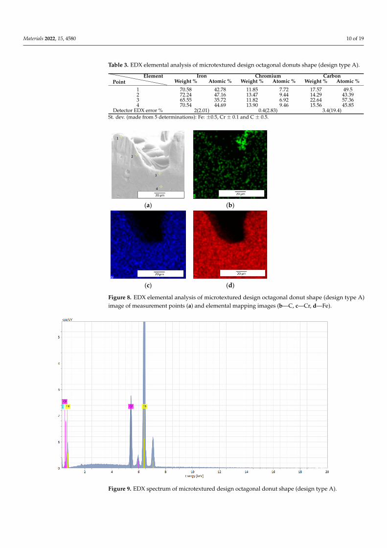
The EDX (Energy Dispersive X-Ray) elemental analysis displays a low variation (from recast material to the deepest point of the hollow and to heat affected zone) of the elements regarding the weight and atomic percentage (Table 3). The elemental analysis shows a zero-weight percentage for oxygen, which does not apply for the ellipse and crater array patterns. The elemental analysis of octagonal microstructuring from cross-sectional images (Figure 8) shows a uniform spread outside the hollow area, excepting carbon which is also present in the cavity area. Figure 9 shows the main elements on the EDX spectrum (Cr, Fe, C).
(a) (b)
Figure 6. Cross section SEM images of octagonal donuts shape (design type A) of LST, frequency30 kHz, speed 300 mm/s, and no. of repetitions 10, magnification overview of the textured groove (a),magnification of the LST processed region (b), magnification of the hollow (c).
Another observation can be made regarding the splashes (Figures 6 and 7). When thefrequency and speed are increased, the expulsed material exceeds the edges of the groovein the form of splashes and not in the form of recast material. When the frequency and

Materials 2022, 15, 4580 9 of 19
speed increase, the average values of measurements of the samples are: 66.171 µm depth,43.012 µm width, and 1878.447 µm2 of area. The height of the recast material averages25.784 µm for the left side and 26.832 µm for the right side. The area of recast material is945.407 µm2 on the left side and 791.677 µm2 for right side of the hollow. The increase offrequency and speed outlines the growth trend of all geometrical mean measurements ofthe microstructures created by LST.
Materials 2022, 15, 4580 10 of 20
(a) (b)
(c)
Figure 7. Cross section SEM images of octagonal donut shape (design type A) of LST, frequency 40 kHz, speed 400 mm/s, and no. of repetitions 10, magnification overview of the textured groove (a), magnification of the LST processed region (b), magnification of the hollow (c).
Table 3. EDX elemental analysis of microtextured design octagonal donuts shape (design type A).
Element Point
Iron Chromium Carbon Weight % Atomic % Weight % Atomic % Weight % Atomic %
1 70.58 42.78 11.85 7.72 17.57 49.5 2 72.24 47.16 13.47 9.44 14.29 43.39 3 65.55 35.72 11.82 6.92 22.64 57.36 4 70.54 44.69 13.90 9.46 15.56 45.85
Detector EDX er-ror %
2(2.01) 0.4(2.83) 3.4(19.4)
St. dev. (made from 5 determinations): Fe: ±0.5, Cr ± 0.1 and C ± 0.5.
(a) (b)
(c) (d)
Figure 7. Cross section SEM images of octagonal donut shape (design type A) of LST, frequency40 kHz, speed 400 mm/s, and no. of repetitions 10, magnification overview of the textured groove (a),magnification of the LST processed region (b), magnification of the hollow (c).
The SEM image of the cross section from [15] outlines the different sizes obtained formicrostructure shapes as nanoripples and drops, with variations of depths (50–150 µm)and widths (10–50 µm). This variation was achieved with a picosecond pulsed laser (using50 W laser power) by increasing the number of repetitions. The difference in the outcomeafter LST is obtaining regular shapes of approximately the same size (13–66 µm variationsof depths and 47–43 µm of width). Similar results in terms of laser grooves, created byablation, were also obtained in [25] in the case of nanosecond laser on magnesium samples.After the absorption of energy, the material is melted and ejected. One can thus distinguishrecast material, melted and then resolidified near the ablated area. The same observation,melting, and re-solidification of the material was made by Rauh S. et al. [29] who studiednanosecond microstructuring of aluminum, with 6 ns pulse duration, 1064 nm wavelength,pulse energy 50 mJ, and laser fluence of J = 9.80 J/cm2 at 20 Hz repetition rate.
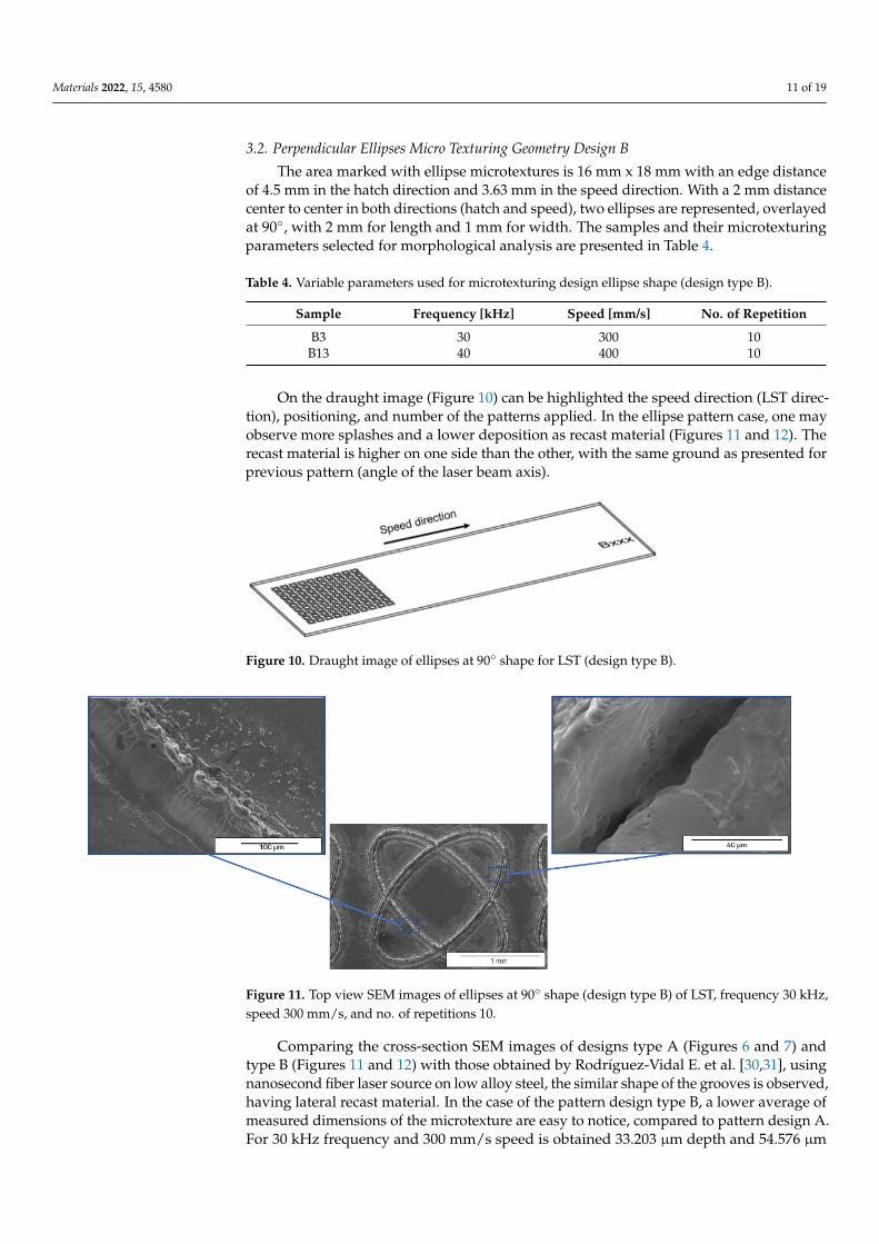
The EDX (Energy Dispersive X-ray) elemental analysis displays a low variation (fromrecast material to the deepest point of the hollow and to heat affected zone) of the elementsregarding the weight and atomic percentage (Table 3). The elemental analysis shows a zero-weight percentage for oxygen, which does not apply for the ellipse and crater array patterns.The elemental analysis of octagonal microstructuring from cross-sectional images (Figure 8)shows a uniform spread outside the hollow area, excepting carbon which is also present inthe cavity area. Figure 9 shows the main elements on the EDX spectrum (Cr, Fe, C).
Materials 2022, 15, 4580 10 of 19
Table 3. EDX elemental analysis of microtextured design octagonal donuts shape (design type A).
PointElement Iron Chromium Carbon
Weight % Atomic % Weight % Atomic % Weight % Atomic %
1 70.58 42.78 11.85 7.72 17.57 49.52 72.24 47.16 13.47 9.44 14.29 43.393 65.55 35.72 11.82 6.92 22.64 57.364 70.54 44.69 13.90 9.46 15.56 45.85
Detector EDX error % 2(2.01) 0.4(2.83) 3.4(19.4)St. dev. (made from 5 determinations): Fe: ±0.5, Cr ± 0.1 and C ± 0.5.
Materials 2022, 15, 4580 10 of 20
(c)
Figure 7. Cross section SEM images of octagonal donut shape (design type A) of LST, frequency 40 kHz, speed 400 mm/s, and no. of repetitions 10, magnification overview of the textured groove (a), magnification of the LST processed region (b), magnification of the hollow (c).
Table 3. EDX elemental analysis of microtextured design octagonal donuts shape (design type A).
Element Point
Iron Chromium Carbon Weight % Atomic % Weight % Atomic % Weight % Atomic %
1 70.58 42.78 11.85 7.72 17.57 49.5 2 72.24 47.16 13.47 9.44 14.29 43.39 3 65.55 35.72 11.82 6.92 22.64 57.36 4 70.54 44.69 13.90 9.46 15.56 45.85
Detector EDX er-ror %
2(2.01) 0.4(2.83) 3.4(19.4)
St. dev. (made from 5 determinations): Fe: ±0.5, Cr ± 0.1 and C ± 0.5.
(a) (b)
(c) (d)
Figure 8. EDX elemental analysis of microtextured design octagonal donut shape (design type A) image of measurement points (a) and elemental mapping images (b—C, c—Cr, d—Fe). Figure 8. EDX elemental analysis of microtextured design octagonal donut shape (design type A)image of measurement points (a) and elemental mapping images (b—C, c—Cr, d—Fe).
Materials 2022, 15, 4580 11 of 20
Figure 9. EDX spectrum of microtextured design octagonal donut shape (design type A).
3.2. Perpendicular Ellipses Micro Texturing Geometry Design B The area marked with ellipse microtextures is 16 mm x 18 mm with an edge distance
of 4.5 mm in the hatch direction and 3.63 mm in the speed direction. With a 2 mm distance center to center in both directions (hatch and speed), two ellipses are represented, over-layed at 90°, with 2 mm for length and 1 mm for width. The samples and their microtex-turing parameters selected for morphological analysis are presented in Table 4.
Table 4. Variable parameters used for microtexturing design ellipse shape (design type B).
Sample Frequency [kHz] Speed [mm/s] No. of Repetition B3 30 300 10 B13 40 400 10
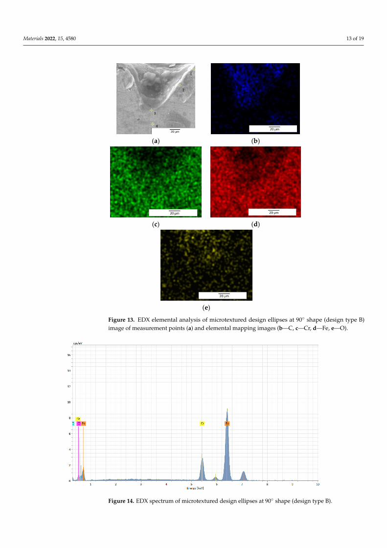
On the draught image (Figure 10) can be highlighted the speed direction (LST direc-tion), positioning, and number of the patterns applied. In the ellipse pattern case, one may observe more splashes and a lower deposition as recast material (Figures 11 and 12). The recast material is higher on one side than the other, with the same ground as presented for previous pattern (angle of the laser beam axis).
Figure 10. Draught image of ellipses at 90° shape for LST (design type B).
Figure 9. EDX spectrum of microtextured design octagonal donut shape (design type A).
Materials 2022, 15, 4580 11 of 19
3.2. Perpendicular Ellipses Micro Texturing Geometry Design B
The area marked with ellipse microtextures is 16 mm x 18 mm with an edge distanceof 4.5 mm in the hatch direction and 3.63 mm in the speed direction. With a 2 mm distancecenter to center in both directions (hatch and speed), two ellipses are represented, overlayedat 90◦, with 2 mm for length and 1 mm for width. The samples and their microtexturingparameters selected for morphological analysis are presented in Table 4.
Table 4. Variable parameters used for microtexturing design ellipse shape (design type B).
Sample Frequency [kHz] Speed [mm/s] No. of Repetition
B3 30 300 10B13 40 400 10
On the draught image (Figure 10) can be highlighted the speed direction (LST direc-tion), positioning, and number of the patterns applied. In the ellipse pattern case, one mayobserve more splashes and a lower deposition as recast material (Figures 11 and 12). Therecast material is higher on one side than the other, with the same ground as presented forprevious pattern (angle of the laser beam axis).
Materials 2022, 15, 4580 11 of 20
Figure 9. EDX spectrum of microtextured design octagonal donut shape (design type A).
3.2. Perpendicular Ellipses Micro Texturing Geometry Design B The area marked with ellipse microtextures is 16 mm x 18 mm with an edge distance
of 4.5 mm in the hatch direction and 3.63 mm in the speed direction. With a 2 mm distance center to center in both directions (hatch and speed), two ellipses are represented, over-layed at 90°, with 2 mm for length and 1 mm for width. The samples and their microtex-turing parameters selected for morphological analysis are presented in Table 4.
Table 4. Variable parameters used for microtexturing design ellipse shape (design type B).
Sample Frequency [kHz] Speed [mm/s] No. of Repetition B3 30 300 10 B13 40 400 10
On the draught image (Figure 10) can be highlighted the speed direction (LST direc-tion), positioning, and number of the patterns applied. In the ellipse pattern case, one may observe more splashes and a lower deposition as recast material (Figures 11 and 12). The recast material is higher on one side than the other, with the same ground as presented for previous pattern (angle of the laser beam axis).
Figure 10. Draught image of ellipses at 90° shape for LST (design type B). Figure 10. Draught image of ellipses at 90◦ shape for LST (design type B).
Materials 2022, 15, 4580 12 of 20
Figure 11. Top view SEM images of ellipses at 90° shape (design type B) of LST, frequency 30 kHz, speed 300 mm/s, and no. of repetitions 10.
(a) (b)
(c)
Figure 12. Cross section SEM images of ellipses at 90° shape (design type B) of LST, frequency 30 kHz, speed 300 mm/s, and no. of repetitions 10, magnification overview of the textured groove (a), magnification of the LST processed region (b), magnification of the hollow (c).
Comparing the cross-section SEM images of designs type A (Figures 6 and 7) and type B (Figures 11 and 12) with those obtained by Rodríguez-Vidal E. et al. [30,31], using nanosecond fiber laser source on low alloy steel, the similar shape of the grooves is ob-served, having lateral recast material. In the case of the pattern design type B, a lower average of measured dimensions of the microtexture are easy to notice, compared to pat-tern design A. For 30 kHz frequency and 300 mm/s speed is obtained 33.203 µm depth and 54.576 µm width. The average area of the hollow is 1812.087 µm2. The missing recast material can be noticed in Figure 12, but the resulting height of average measurements is 20.152 µm for the left side and 23.259 µm for the right side of the edges. Compared to the previous pattern applied as LST (design type A) the design type B offers lower values of measurements, showing a differentiation in terms of applied geometry.
For ellipse pattern, a difference is the appearance of oxygen for the measurement point 2 and 3, indicating the absence of the oxygen element in the recast material and heat
Figure 11. Top view SEM images of ellipses at 90◦ shape (design type B) of LST, frequency 30 kHz,speed 300 mm/s, and no. of repetitions 10.
Comparing the cross-section SEM images of designs type A (Figures 6 and 7) andtype B (Figures 11 and 12) with those obtained by Rodríguez-Vidal E. et al. [30,31], usingnanosecond fiber laser source on low alloy steel, the similar shape of the grooves is observed,having lateral recast material. In the case of the pattern design type B, a lower average ofmeasured dimensions of the microtexture are easy to notice, compared to pattern design A.For 30 kHz frequency and 300 mm/s speed is obtained 33.203 µm depth and 54.576 µm

Materials 2022, 15, 4580 12 of 19
width. The average area of the hollow is 1812.087 µm2. The missing recast material can benoticed in Figure 12, but the resulting height of average measurements is 20.152 µm for theleft side and 23.259 µm for the right side of the edges. Compared to the previous patternapplied as LST (design type A) the design type B offers lower values of measurements,showing a differentiation in terms of applied geometry.
Materials 2022, 15, 4580 12 of 20
Figure 11. Top view SEM images of ellipses at 90° shape (design type B) of LST, frequency 30 kHz, speed 300 mm/s, and no. of repetitions 10.
(a) (b)
(c)
Figure 12. Cross section SEM images of ellipses at 90° shape (design type B) of LST, frequency 30 kHz, speed 300 mm/s, and no. of repetitions 10, magnification overview of the textured groove (a), magnification of the LST processed region (b), magnification of the hollow (c).
Comparing the cross-section SEM images of designs type A (Figures 6 and 7) and type B (Figures 11 and 12) with those obtained by Rodríguez-Vidal E. et al. [30,31], using nanosecond fiber laser source on low alloy steel, the similar shape of the grooves is ob-served, having lateral recast material. In the case of the pattern design type B, a lower average of measured dimensions of the microtexture are easy to notice, compared to pat-tern design A. For 30 kHz frequency and 300 mm/s speed is obtained 33.203 µm depth and 54.576 µm width. The average area of the hollow is 1812.087 µm2. The missing recast material can be noticed in Figure 12, but the resulting height of average measurements is 20.152 µm for the left side and 23.259 µm for the right side of the edges. Compared to the previous pattern applied as LST (design type A) the design type B offers lower values of measurements, showing a differentiation in terms of applied geometry.
For ellipse pattern, a difference is the appearance of oxygen for the measurement point 2 and 3, indicating the absence of the oxygen element in the recast material and heat
Figure 12. Cross section SEM images of ellipses at 90◦ shape (design type B) of LST, frequency30 kHz, speed 300 mm/s, and no. of repetitions 10, magnification overview of the textured groove (a),magnification of the LST processed region (b), magnification of the hollow (c).
For ellipse pattern, a difference is the appearance of oxygen for the measurementpoint 2 and 3, indicating the absence of the oxygen element in the recast material and heataffected zone (Table 5). When oxygen is part of the measurement point a decreasing of ironand chromium and carbon increasing is observed.
Table 5. EDX elemental analysis of microtextured design ellipses at 90◦ shape (design type B).
PointElement Iron Chromium Carbon Oxygen
Weight % Atomic % Weight % Atomic % Weight % Atomic % Weight % Atomic %
1 75.22 54.18 14.43 11.16 10.35 34.66 - -2 57.79 28.61 12.12 6.45 22.56 51.93 7.53 13.013 58.98 29.16 10.70 5.68 22.41 51.51 7.91 13.654 76.52 57.35 14.62 11.76 8.86 30.88 - -
Detector EDXerror % 1.68(2.6) 0.34(2.95) 7.98(16.52) 1.18(34.37)
St. dev. (made from five determinations): Fe: ±0.5, Cr ± 0.1, O ± 0.2, and C ± 0.5.
The carbon is only spread where the cavity is (see the cross-section images of EDXanalysis from Figure 13) and the spreading of the other elements (Cr, Fe, and O) is wide.Figure 14 shows the main elements on the EDX spectrum (Cr, O, Fe, C).
Materials 2022, 15, 4580 13 of 19
Materials 2022, 15, 4580 13 of 20
affected zone (Table 5). When oxygen is part of the measurement point a decreasing of iron and chromium and carbon increasing is observed.
Table 5. EDX elemental analysis of microtextured design ellipses at 90° shape (design type B).
Element Point
Iron Chromium Carbon Oxygen Weight
% Atomic
% Weight
% Atomic
% Weight
% Atomic
% Weigh
t % Atomi
c % 1 75.22 54.18 14.43 11.16 10.35 34.66 - - 2 57.79 28.61 12.12 6.45 22.56 51.93 7.53 13.01 3 58.98 29.16 10.70 5.68 22.41 51.51 7.91 13.65 4 76.52 57.35 14.62 11.76 8.86 30.88 - -
Detector EDX error %
1.68(2.6) 0.34(2.95) 7.98(16.52) 1.18(34.37)
St. dev. (made from five determinations): Fe: ±0.5, Cr ± 0.1, O ± 0.2, and C ± 0.5.
The carbon is only spread where the cavity is (see the cross-section images of EDX analysis from Figure 13) and the spreading of the other elements (Cr, Fe, and O) is wide. Figure 14 shows the main elements on the EDX spectrum (Cr, O, Fe, C).
(a) (b)
(c) (d)
(e)
Figure 13. EDX elemental analysis of microtextured design ellipses at 90° shape (design type B) image of measurement points (a) and elemental mapping images (b—C, c—Cr, d—Fe, e—O). Figure 13. EDX elemental analysis of microtextured design ellipses at 90◦ shape (design type B)image of measurement points (a) and elemental mapping images (b—C, c—Cr, d—Fe, e—O).
Materials 2022, 15, 4580 14 of 20
Figure 14. EDX spectrum of microtextured design ellipses at 90° shape (design type B).
For type B design, a promising future is in applications in coatings processes, because of an increased area resulting from LST. This is the same as presented in [8], where tests were made on a magnesium alloy using a continuous-wave laser fiber, with gas protection (argon) and 400 kHz repetition rate of, at least, ten times higher than in the present re-search. The top view SEM images offer a wavy microstructure [8], with average value of periodicity of 30 µm and 14 µm for depth. The depth for pattern type B was an average of 33 µm and 55 µm for width. The presence of oxygen after LST was also highlighted in [25], where EDS analysis showed that due to the laser irradiation, an oxidation of the outer layer appeared, demonstrated by the oxygen map.
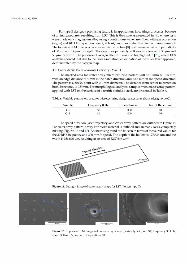
3.3. Crater Array Micro Texturing Geometry Design C The marked area for crater array microtexturing pattern will be 17mm × 19.5 mm,
with an edge distance of 4 mm in the hatch direction and 3.63 mm in the speed direction. The pattern is a circle/point with 0.1 mm diameter. The distance from center to center, on both directions, is 0.5 mm. For morphological analysis, samples with crater array pattern, applied with LST on the surface of a ferritic stainless steel, are presented in Table 6.
Table 6. Variable parameters used for microtexturing design crater array shape (design type C).
Sample Frequency [kHz] Speed [mm/s] No. of Repetition C3 30 300 10
C11 40 400 10
The speed direction (laser trajectory) and crater array pattern are outlined in Figure 15. For crater array pattern, a very low recast material is outlined and, in many cases, completely missing (Figures 16 and 17). An increasing trend can be seen in terms of meas-ured values for the 30 kHz frequency and 300 mm/s speed. The depth of the hollow is 127.636 µm and the width is 156.646 µm, resulting in an area of 3297.649 µm2.
Figure 14. EDX spectrum of microtextured design ellipses at 90◦ shape (design type B).
Materials 2022, 15, 4580 14 of 19
For type B design, a promising future is in applications in coatings processes, becauseof an increased area resulting from LST. This is the same as presented in [8], where testswere made on a magnesium alloy using a continuous-wave laser fiber, with gas protection(argon) and 400 kHz repetition rate of, at least, ten times higher than in the present research.The top view SEM images offer a wavy microstructure [8], with average value of periodicityof 30 µm and 14 µm for depth. The depth for pattern type B was an average of 33 µm and55 µm for width. The presence of oxygen after LST was also highlighted in [25], where EDSanalysis showed that due to the laser irradiation, an oxidation of the outer layer appeared,demonstrated by the oxygen map.
3.3. Crater Array Micro Texturing Geometry Design C
The marked area for crater array microtexturing pattern will be 17mm × 19.5 mm,with an edge distance of 4 mm in the hatch direction and 3.63 mm in the speed direction.The pattern is a circle/point with 0.1 mm diameter. The distance from center to center, onboth directions, is 0.5 mm. For morphological analysis, samples with crater array pattern,applied with LST on the surface of a ferritic stainless steel, are presented in Table 6.
Table 6. Variable parameters used for microtexturing design crater array shape (design type C).
Sample Frequency [kHz] Speed [mm/s] No. of Repetition
C3 30 300 10C11 40 400 10
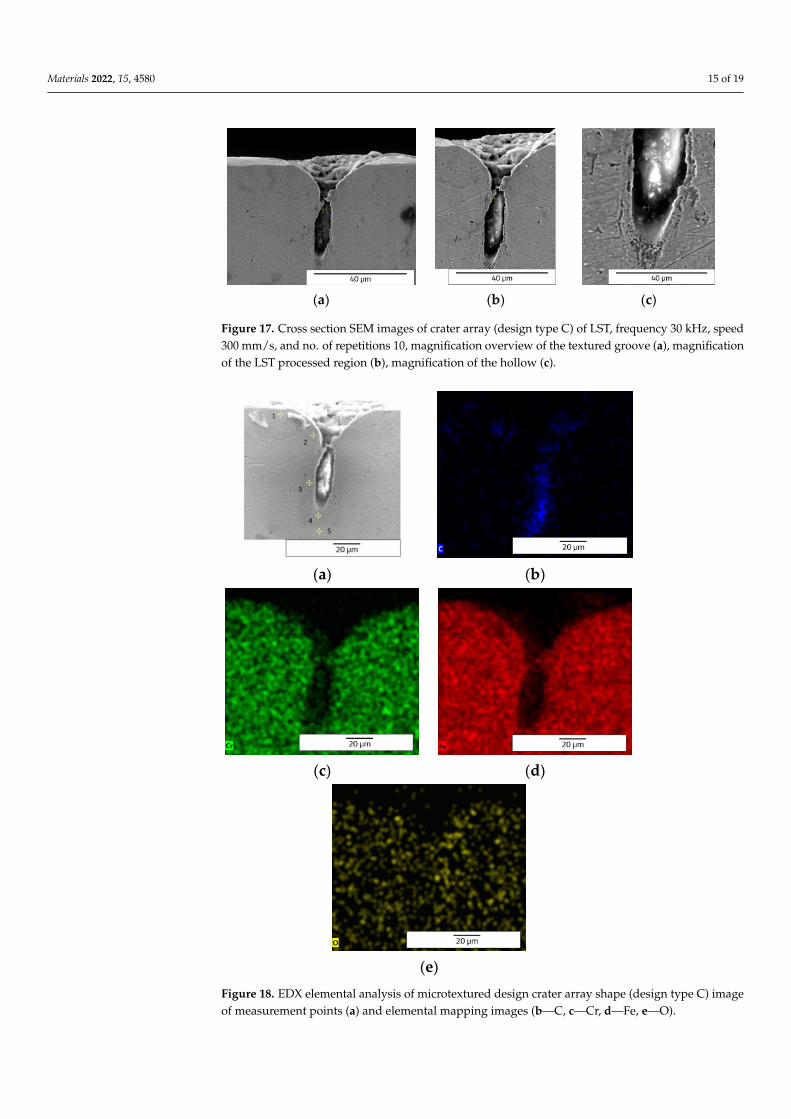
The speed direction (laser trajectory) and crater array pattern are outlined in Figure 15.For crater array pattern, a very low recast material is outlined and, in many cases, completelymissing (Figures 16 and 17). An increasing trend can be seen in terms of measured values forthe 30 kHz frequency and 300 mm/s speed. The depth of the hollow is 127.636 µm and thewidth is 156.646 µm, resulting in an area of 3297.649 µm2.
Materials 2022, 15, 4580 15 of 20
Figure 15. Draught image of crater array shape for LST (design type C).
The dimple pattern was also created in [7] using a commercial Ti: Sapphire laser with 120 fs polarized pulse at 795 nm and 1 kHz repetition rate. The measured diameter of the hole was 30 µm, but there are no data on the depth. For the type C model in this research, the width is larger (at least five times larger) due to the nanosecond pulsed laser beam, which interacts more with the surface of the material than femtosecond lasers and dam-ages the adjacent structure and creates ripples due to the shockwave.
Figure 16. Top view SEM images of crater array shape (design type C) of LST, frequency 30 kHz, speed 300 mm/s, and no. of repetitions 10.
(a) (b) (c)
Figure 17. Cross section SEM images of crater array (design type C) of LST, frequency 30 kHz, speed 300 mm/s, and no. of repetitions 10, magnification overview of the textured groove (a), magnifica-tion of the LST processed region (b), magnification of the hollow (c).
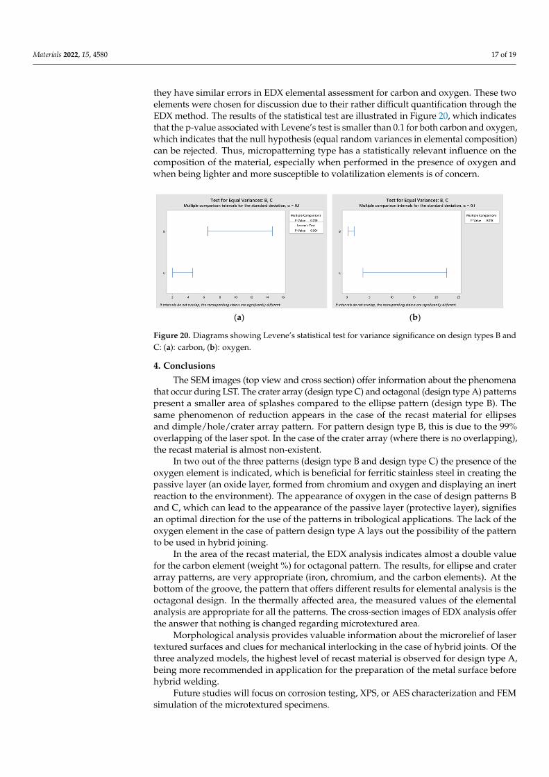
One can notice that the keyhole shape of the crater array shape (design type C) (Fig-ures 17 and 18) is different to that of V grooves of the designs type A and type B. This keyhole shape is specific to laser welding, described in [32,33].
The crater array model required more EDX measurement points due to the larger gaps created by the LST (Table 7). The same result as the ellipse model was observed for the carbon element (only in the cavity area). The highest percentage by weight of carbon is at the bottom of the crater (Figure 18), and the lowest percentage by weight is in the area affected by heat. Oxygen is less widespread than in previous models. Figure 19 shows the main elements on the EDX spectrum (Cr, O, Fe, C).
Figure 15. Draught image of crater array shape for LST (design type C).
Materials 2022, 15, 4580 15 of 20
Figure 15. Draught image of crater array shape for LST (design type C).
The dimple pattern was also created in [7] using a commercial Ti: Sapphire laser with 120 fs polarized pulse at 795 nm and 1 kHz repetition rate. The measured diameter of the hole was 30 µm, but there are no data on the depth. For the type C model in this research, the width is larger (at least five times larger) due to the nanosecond pulsed laser beam, which interacts more with the surface of the material than femtosecond lasers and dam-ages the adjacent structure and creates ripples due to the shockwave.
Figure 16. Top view SEM images of crater array shape (design type C) of LST, frequency 30 kHz, speed 300 mm/s, and no. of repetitions 10.
(a) (b) (c)
Figure 17. Cross section SEM images of crater array (design type C) of LST, frequency 30 kHz, speed 300 mm/s, and no. of repetitions 10, magnification overview of the textured groove (a), magnifica-tion of the LST processed region (b), magnification of the hollow (c).
One can notice that the keyhole shape of the crater array shape (design type C) (Fig-ures 17 and 18) is different to that of V grooves of the designs type A and type B. This keyhole shape is specific to laser welding, described in [32,33].
The crater array model required more EDX measurement points due to the larger gaps created by the LST (Table 7). The same result as the ellipse model was observed for the carbon element (only in the cavity area). The highest percentage by weight of carbon is at the bottom of the crater (Figure 18), and the lowest percentage by weight is in the area affected by heat. Oxygen is less widespread than in previous models. Figure 19 shows the main elements on the EDX spectrum (Cr, O, Fe, C).
Figure 16. Top view SEM images of crater array shape (design type C) of LST, frequency 30 kHz,speed 300 mm/s, and no. of repetitions 10.
Materials 2022, 15, 4580 15 of 19
Materials 2022, 15, 4580 15 of 20
Figure 15. Draught image of crater array shape for LST (design type C).
The dimple pattern was also created in [7] using a commercial Ti: Sapphire laser with 120 fs polarized pulse at 795 nm and 1 kHz repetition rate. The measured diameter of the hole was 30 µm, but there are no data on the depth. For the type C model in this research, the width is larger (at least five times larger) due to the nanosecond pulsed laser beam, which interacts more with the surface of the material than femtosecond lasers and dam-ages the adjacent structure and creates ripples due to the shockwave.
Figure 16. Top view SEM images of crater array shape (design type C) of LST, frequency 30 kHz, speed 300 mm/s, and no. of repetitions 10.
(a) (b) (c)
Figure 17. Cross section SEM images of crater array (design type C) of LST, frequency 30 kHz, speed 300 mm/s, and no. of repetitions 10, magnification overview of the textured groove (a), magnifica-tion of the LST processed region (b), magnification of the hollow (c).
One can notice that the keyhole shape of the crater array shape (design type C) (Fig-ures 17 and 18) is different to that of V grooves of the designs type A and type B. This keyhole shape is specific to laser welding, described in [32,33].
The crater array model required more EDX measurement points due to the larger gaps created by the LST (Table 7). The same result as the ellipse model was observed for the carbon element (only in the cavity area). The highest percentage by weight of carbon is at the bottom of the crater (Figure 18), and the lowest percentage by weight is in the area affected by heat. Oxygen is less widespread than in previous models. Figure 19 shows the main elements on the EDX spectrum (Cr, O, Fe, C).
Figure 17. Cross section SEM images of crater array (design type C) of LST, frequency 30 kHz, speed300 mm/s, and no. of repetitions 10, magnification overview of the textured groove (a), magnificationof the LST processed region (b), magnification of the hollow (c).
Materials 2022, 15, 4580 16 of 20
Table 7. EDX elemental analysis of microtextured design crater array shape (design type C).
Element Point
Iron Chromium Carbon Oxygen Weight
% Atomic
% Weight
% Atomic
% Weight
% Atomic
% Weigh
t % Atomi
c % 1 76.42 56.67 14.33 11.41 9.26 31.92 - - 2 78.41 62.50 14.92 12.77 6.67 24.73 - - 3 72.10 47.98 13.61 9.73 11.79 36.47 2.50 5.82 4 59.96 30.50 11.32 6.19 20.91 49.45 7.81 13.87 5 77.56 60.92 15.27 12.88 7.17 26.20 - -
Detector EDX error %
1.68(2.6) 0.34(2.95) 7.98(16.52) 1.18(34.37)
St. dev. (made from 5 determinations): Fe: ±0.5, Cr ± 0.1, O ± 0.2, and C ± 0.5.
(a) (b)
(c) (d)
(e)
Figure 18. EDX elemental analysis of microtextured design crater array shape (design type C) image of measurement points (a) and elemental mapping images (b—C, c—Cr, d—Fe, e—O). Figure 18. EDX elemental analysis of microtextured design crater array shape (design type C) imageof measurement points (a) and elemental mapping images (b—C, c—Cr, d—Fe, e—O).

Materials 2022, 15, 4580 16 of 19
The dimple pattern was also created in [7] using a commercial Ti: Sapphire laser with120 fs polarized pulse at 795 nm and 1 kHz repetition rate. The measured diameter of thehole was 30 µm, but there are no data on the depth. For the type C model in this research,the width is larger (at least five times larger) due to the nanosecond pulsed laser beam,which interacts more with the surface of the material than femtosecond lasers and damagesthe adjacent structure and creates ripples due to the shockwave.
One can notice that the keyhole shape of the crater array shape (design type C)(Figures 17 and 18) is different to that of V grooves of the designs type A and type B. Thiskeyhole shape is specific to laser welding, described in [32,33].
The crater array model required more EDX measurement points due to the larger gapscreated by the LST (Table 7). The same result as the ellipse model was observed for thecarbon element (only in the cavity area). The highest percentage by weight of carbon isat the bottom of the crater (Figure 18), and the lowest percentage by weight is in the areaaffected by heat. Oxygen is less widespread than in previous models. Figure 19 shows themain elements on the EDX spectrum (Cr, O, Fe, C).
Table 7. EDX elemental analysis of microtextured design crater array shape (design type C).
PointElement Iron Chromium Carbon Oxygen
Weight % Atomic % Weight % Atomic % Weight % Atomic % Weight % Atomic %
1 76.42 56.67 14.33 11.41 9.26 31.92 - -2 78.41 62.50 14.92 12.77 6.67 24.73 - -3 72.10 47.98 13.61 9.73 11.79 36.47 2.50 5.824 59.96 30.50 11.32 6.19 20.91 49.45 7.81 13.875 77.56 60.92 15.27 12.88 7.17 26.20 - -
Detector EDXerror % 1.68(2.6) 0.34(2.95) 7.98(16.52) 1.18(34.37)
St. dev. (made from 5 determinations): Fe: ±0.5, Cr ± 0.1, O ± 0.2, and C ± 0.5.
Materials 2022, 15, 4580 17 of 20
Figure 19. EDX spectrum of microtextured design crater array shape (design type C).
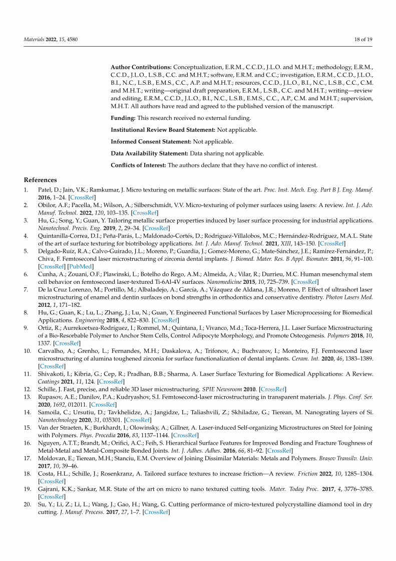
To assess whether there is a significant difference between the EDX elemental values for carbon and oxygen for design types B and C (i.e., if the elemental concentration values are statistically significant), Levene’s test was used, with a confidence level of 90% (signif-icance level α = 0.1). If the p-value of Levene’s test is lower than 0.1, then obtained differ-ences in concentration variances are unlikely to have occurred based on random sampling from a population with equal variances [34]. The design types B and C were chosen be-cause they have similar errors in EDX elemental assessment for carbon and oxygen. These two elements were chosen for discussion due to their rather difficult quantification through the EDX method. The results of the statistical test are illustrated in Figure 20, which indicates that the p-value associated with Levene’s test is smaller than 0.1 for both carbon and oxygen, which indicates that the null hypothesis (equal random variances in elemental composition) can be rejected. Thus, micropatterning type has a statistically rel-evant influence on the composition of the material, especially when performed in the pres-ence of oxygen and when being lighter and more susceptible to volatilization elements is of concern.
(a) (b)
Figure 20. Diagrams showing Levene’s statistical test for variance significance on design types B and C: (a): carbon, (b): oxygen.
Figure 19. EDX spectrum of microtextured design crater array shape (design type C).
To assess whether there is a significant difference between the EDX elemental values forcarbon and oxygen for design types B and C (i.e., if the elemental concentration values arestatistically significant), Levene’s test was used, with a confidence level of 90% (significancelevel α = 0.1). If the p-value of Levene’s test is lower than 0.1, then obtained differencesin concentration variances are unlikely to have occurred based on random sampling froma population with equal variances [34]. The design types B and C were chosen because
Materials 2022, 15, 4580 17 of 19
they have similar errors in EDX elemental assessment for carbon and oxygen. These twoelements were chosen for discussion due to their rather difficult quantification through theEDX method. The results of the statistical test are illustrated in Figure 20, which indicatesthat the p-value associated with Levene’s test is smaller than 0.1 for both carbon and oxygen,which indicates that the null hypothesis (equal random variances in elemental composition)can be rejected. Thus, micropatterning type has a statistically relevant influence on thecomposition of the material, especially when performed in the presence of oxygen andwhen being lighter and more susceptible to volatilization elements is of concern.
Materials 2022, 15, 4580 17 of 20
Figure 19. EDX spectrum of microtextured design crater array shape (design type C).
To assess whether there is a significant difference between the EDX elemental values for carbon and oxygen for design types B and C (i.e., if the elemental concentration values are statistically significant), Levene’s test was used, with a confidence level of 90% (signif-icance level α = 0.1). If the p-value of Levene’s test is lower than 0.1, then obtained differ-ences in concentration variances are unlikely to have occurred based on random sampling from a population with equal variances [34]. The design types B and C were chosen be-cause they have similar errors in EDX elemental assessment for carbon and oxygen. These two elements were chosen for discussion due to their rather difficult quantification through the EDX method. The results of the statistical test are illustrated in Figure 20, which indicates that the p-value associated with Levene’s test is smaller than 0.1 for both carbon and oxygen, which indicates that the null hypothesis (equal random variances in elemental composition) can be rejected. Thus, micropatterning type has a statistically rel-evant influence on the composition of the material, especially when performed in the pres-ence of oxygen and when being lighter and more susceptible to volatilization elements is of concern.
(a) (b)
Figure 20. Diagrams showing Levene’s statistical test for variance significance on design types B and C: (a): carbon, (b): oxygen.
Figure 20. Diagrams showing Levene’s statistical test for variance significance on design types B andC: (a): carbon, (b): oxygen.
4. Conclusions
The SEM images (top view and cross section) offer information about the phenomenathat occur during LST. The crater array (design type C) and octagonal (design type A) patternspresent a smaller area of splashes compared to the ellipse pattern (design type B). Thesame phenomenon of reduction appears in the case of the recast material for ellipsesand dimple/hole/crater array pattern. For pattern design type B, this is due to the 99%overlapping of the laser spot. In the case of the crater array (where there is no overlapping),the recast material is almost non-existent.
In two out of the three patterns (design type B and design type C) the presence of theoxygen element is indicated, which is beneficial for ferritic stainless steel in creating thepassive layer (an oxide layer, formed from chromium and oxygen and displaying an inertreaction to the environment). The appearance of oxygen in the case of design patterns Band C, which can lead to the appearance of the passive layer (protective layer), signifiesan optimal direction for the use of the patterns in tribological applications. The lack of theoxygen element in the case of pattern design type A lays out the possibility of the patternto be used in hybrid joining.
In the area of the recast material, the EDX analysis indicates almost a double valuefor the carbon element (weight %) for octagonal pattern. The results, for ellipse and craterarray patterns, are very appropriate (iron, chromium, and the carbon elements). At thebottom of the groove, the pattern that offers different results for elemental analysis is theoctagonal design. In the thermally affected area, the measured values of the elementalanalysis are appropriate for all the patterns. The cross-section images of EDX analysis offerthe answer that nothing is changed regarding microtextured area.
Morphological analysis provides valuable information about the microrelief of lasertextured surfaces and clues for mechanical interlocking in the case of hybrid joints. Of thethree analyzed models, the highest level of recast material is observed for design type A,being more recommended in application for the preparation of the metal surface beforehybrid welding.
Future studies will focus on corrosion testing, XPS, or AES characterization and FEMsimulation of the microtextured specimens.
Materials 2022, 15, 4580 18 of 19
Author Contributions: Conceptualization, E.R.M., C.C.D., J.L.O. and M.H.T.; methodology, E.R.M.,C.C.D., J.L.O., L.S.B., C.C. and M.H.T.; software, E.R.M. and C.C.; investigation, E.R.M., C.C.D., J.L.O.,B.I., N.C., L.S.B., E.M.S., C.C., A.P. and M.H.T.; resources, C.C.D., J.L.O., B.I., N.C., L.S.B., C.C., C.M.and M.H.T.; writing—original draft preparation, E.R.M., L.S.B., C.C. and M.H.T.; writing—reviewand editing, E.R.M., C.C.D., J.L.O., B.I., N.C., L.S.B., E.M.S., C.C., A.P., C.M. and M.H.T.; supervision,M.H.T. All authors have read and agreed to the published version of the manuscript.
Funding: This research received no external funding.
Institutional Review Board Statement: Not applicable.
Informed Consent Statement: Not applicable.
Data Availability Statement: Data sharing not applicable.
Conflicts of Interest: The authors declare that they have no conflict of interest.
References1. Patel, D.; Jain, V.K.; Ramkumar, J. Micro texturing on metallic surfaces: State of the art. Proc. Inst. Mech. Eng. Part B J. Eng. Manuf.
2016, 1–24. [CrossRef]2. Obilor, A.F.; Pacella, M.; Wilson, A.; Silberschmidt, V.V. Micro-texturing of polymer surfaces using lasers: A review. Int. J. Adv.
Manuf. Technol. 2022, 120, 103–135. [CrossRef]3. Hu, G.; Song, Y.; Guan, Y. Tailoring metallic surface properties induced by laser surface processing for industrial applications.
Nanotechnol. Precis. Eng. 2019, 2, 29–34. [CrossRef]4. Quintanilla-Correa, D.I.; Peña-Parás, L.; Maldonado-Cortés, D.; Rodriguez-Villalobos, M.C.; Hernández-Rodríguez, M.A.L. State
of the art of surface texturing for biotribology applications. Int. J. Adv. Manuf. Technol. 2021, XIII, 143–150. [CrossRef]5. Delgado-Ruíz, R.A.; Calvo-Guirado, J.L.; Moreno, P.; Guardia, J.; Gomez-Moreno, G.; Mate-Sánchez, J.E.; Ramirez-Fernández, P.;
Chiva, F. Femtosecond laser microstructuring of zirconia dental implants. J. Biomed. Mater. Res. B Appl. Biomater. 2011, 96, 91–100.[CrossRef] [PubMed]
6. Cunha, A.; Zouani, O.F.; Plawinski, L.; Botelho do Rego, A.M.; Almeida, A.; Vilar, R.; Durrieu, M.C. Human mesenchymal stemcell behavior on femtosecond laser-textured Ti-6Al-4V surfaces. Nanomedicine 2015, 10, 725–739. [CrossRef]
7. De la Cruz Lorenzo, M.; Portillo, M.; Albaladejo, A.; García, A.; Vázquez de Aldana, J.R.; Moreno, P. Effect of ultrashort lasermicrostructuring of enamel and dentin surfaces on bond strengths in orthodontics and conservative dentistry. Photon Lasers Med.2012, 1, 171–182.
8. Hu, G.; Guan, K.; Lu, L.; Zhang, J.; Lu, N.; Guan, Y. Engineered Functional Surfaces by Laser Microprocessing for BiomedicalApplications. Engineering 2018, 4, 822–830. [CrossRef]
9. Ortiz, R.; Aurrekoetxea-Rodríguez, I.; Rommel, M.; Quintana, I.; Vivanco, M.d.; Toca-Herrera, J.L. Laser Surface Microstructuringof a Bio-Resorbable Polymer to Anchor Stem Cells, Control Adipocyte Morphology, and Promote Osteogenesis. Polymers 2018, 10,1337. [CrossRef]
10. Carvalho, A.; Grenho, L.; Fernandes, M.H.; Daskalova, A.; Trifonov, A.; Buchvarov, I.; Monteiro, F.J. Femtosecond lasermicrostructuring of alumina toughened zirconia for surface functionalization of dental implants. Ceram. Int. 2020, 46, 1383–1389.[CrossRef]
11. Shivakoti, I.; Kibria, G.; Cep, R.; Pradhan, B.B.; Sharma, A. Laser Surface Texturing for Biomedical Applications: A Review.Coatings 2021, 11, 124. [CrossRef]
12. Schille, J. Fast, precise, and reliable 3D laser microstructuring. SPIE Newsroom 2010. [CrossRef]13. Rupasov, A.E.; Danilov, P.A.; Kudryashov, S.I. Femtosecond-laser microstructuring in transparent materials. J. Phys. Conf. Ser.
2020, 1692, 012011. [CrossRef]14. Samoila, C.; Ursutiu, D.; Tavkhelidze, A.; Jangidze, L.; Taliashvili, Z.; Skhiladze, G.; Tierean, M. Nanograting layers of Si.
Nanotechnology 2020, 31, 035301. [CrossRef]15. Van der Straeten, K.; Burkhardt, I.; Olowinsky, A.; Gillner, A. Laser-induced Self-organizing Microstructures on Steel for Joining
with Polymers. Phys. Procedia 2016, 83, 1137–1144. [CrossRef]16. Nguyen, A.T.T.; Brandt, M.; Orifici, A.C.; Feih, S. Hierarchical Surface Features for Improved Bonding and Fracture Toughness of
Metal-Metal and Metal-Composite Bonded Joints. Int. J. Adhes. Adhes. 2016, 66, 81–92. [CrossRef]17. Moldovan, E.; Tierean, M.H.; Stanciu, E.M. Overview of Joining Dissimilar Materials: Metals and Polymers. Bras, ov Transilv. Univ.
2017, 10, 39–46.18. Costa, H.L.; Schille, J.; Rosenkranz, A. Tailored surface textures to increase friction—A review. Friction 2022, 10, 1285–1304.
[CrossRef]19. Gajrani, K.K.; Sankar, M.R. State of the art on micro to nano textured cutting tools. Mater. Today Proc. 2017, 4, 3776–3785.
[CrossRef]20. Su, Y.; Li, Z.; Li, L.; Wang, J.; Gao, H.; Wang, G. Cutting performance of micro-textured polycrystalline diamond tool in dry
cutting. J. Manuf. Process. 2017, 27, 1–7. [CrossRef]

Materials 2022, 15, 4580 19 of 19
21. Sugihara, T.; Nishimoto, Y.; Enomoto, T. Development of a novel cubic boron nitride cutting tool with a textured flank face forhigh-speed machining of Inconel 718. Precis. Eng. 2017, 48, 75–82. [CrossRef]
22. Zheng, K.; Yang, F.; Zhang, N.; Liu, Q.; Jiang, F. Study on the Cutting Performance of Micro Textured Tools on Cutting Ti-6Al-4VTitanium Alloy. Micromachines 2020, 11, 137. [CrossRef] [PubMed]
23. Zhao, Y.; Cui, H.; Zhang, W.; Li, W.; Jiang, S.; Li, L. Si and Cu ablation with a 46.9-nm laser focused by a toroidal mirror. Opt.Express 2015, 23, 14126–14134. [CrossRef] [PubMed]
24. Moldovan, E.R.; Concheso Doria, C.; Ocaña, J.L.; Baltes, L.S.; Stanciu, E.M.; Croitoru, C.; Pascu, A.; Roata, I.C.; Tierean, M.H.Wettability and Surface Roughness Analysis of Laser Surface Texturing of AISI 430 Stainless Steel. Materials 2022, 15, 2955.[CrossRef]
25. Pou-Álvarez, P.; Riveiro, A.; Nóvoa, X.R.; Fernández-Arias, M.; del Val, J.; Comesaña, R.; Boutinguiza, M.; Lusquiños, F.; Pou, J.Nanosecond, picosecond and femtosecond laser surface treatment of magnesium alloy: Role of pulse length. Surf. Coat. Technol.2021, 427, 12780. [CrossRef]
26. Moldovan, E.R.; Concheso Doria, C.; Ocaña Moreno, J.L.; Baltes, L.S.; Stanciu, E.M.; Croitoru, C.; Pascu, A.; Tierean, M.H.Geometry Characterization of AISI 430 Stainless Steel Microstructuring Using Laser. Arch. Metall. Mater. 2022, 67, 645–652.
27. Cui, H.; Zhao, Y.; Khan, M.U.; Zhao, D.; Fan, Z. Study of Thermal Effect in the Interaction of Nanosecond Capillary DischargeExtreme Ultraviolet Laser with Copper. Appl. Sci. 2020, 10, 214. [CrossRef]
28. Jamari, J.; Ammarullah, M.I.; Santoso, G.; Sugiharto, S.; Supriyono, T.; Prakoso, A.T.; Basri, H.; van der Heide, E. ComputationalContact Pressure Prediction of CoCrMo, SS 316L and Ti6Al4V Femoral Head against UHMWPE Acetabular Cup under GaitCycle. J. Funct. Biomater. 2022, 13, 64. [CrossRef]
29. Rauh, S.; Wöbbeking, K.; Li, M.; Schade, W.; Hübner, E.G. From Femtosecond to Nanosecond Laser Microstructuring of ConicalAluminum Surfaces by Reactive Gas Assisted Laser Ablation. Chem. Phys. Chem. 2020, 21, 1644–1652. [CrossRef]
30. Rodríguez-Vidal, E.; Sanz, C.; Soriano, C.; Leunda, J.; Verhaeghe, G. Effect of metal micro-structuring on the mechanical behaviorof polymer–metal laser T-joints. J. Mater. Process. Technol. 2016, 229, 668–677. [CrossRef]
31. Rodríguez-Vidal, E.; Sanz, C.; Lambarri, J.; Quintana, I. Experimental investigation into metal micro-patterning by laser onpolymer-metal hybrid joining. Opt. Laser Technol. 2018, 104, 73–82. [CrossRef]
32. Stanciu, E.M.; Păvălache, A.C.; Dumitru, G.M.; Dontu, O.G.; Besnea, D.; Vasile, I.M. Mechanism of keyhole formation in laserwelding. Rom. Rev. Precis. Mech. Opt. Mechatron. 2010, 38, 171–176.
33. Feng, Y.; Gao, X.; Zhang, Y.; Peng, C.; Gui, X.; Sun, Y.; Xiao, X. Simulation and experiment for dynamics of laser welding keyholeand molten pool at different penetration status. Int. J. Adv. Manuf. Technol. 2021, 112, 2301–2312. [CrossRef]
34. Gastwirth, J.L.; Gel, Y.R.; Miao, W. The Impact of Levene’s Test of Equality of Variances on Statistical Theory and Practice. Stat.Sci. 2009, 24, 343–360. [CrossRef]