Modified one-cycle controlled load compensator
10
Published in IET Power Electronics Received on 27th February 2010 Revised on 9th November 2010 doi: 10.1049/iet-pel.2010.0070 ISSN 1755-4535 Modified one-cycle controlled load compensator K. Chatterjee 1 D.V. Ghodke 1,2 A. Chandra 3 K. Al-Haddad 3 1 Department of Electrical Engineering, Indian Institute of Technology Bombay, Mumbai 400076, India 2 Raja Ramanna Centre for Advanced Technology, Laser System Engineering Division, Indore 452013, India 3 Department of Electrical Engineering, Ecole de Technologie Superieur, Montreal, Que ´ bec, Canada H3C 1K3 E-mail: [email protected] Abstract: Load compensators based on one-cycle control (OCC) exhibit instability in current control when real power involved with the load to be compensated is low. Instability in current control is also encountered when the load to be compensated is of regenerative type. A modified OCC-based load compensator is proposed. A fictitious current component in phase with the utility voltage is synthesised. The sum of this current component and the source current is compared with the saw-tooth waveform to generate the gating pulses for the switches. This modification significantly improves the stability margin of its operation so that it can compensate loads having low real current component as well as can compensate regenerative type of loads. Detailed simulation studies are carried out to verify the effectiveness of the proposed scheme. To validate the viability of the scheme, detailed experimental studies are carried out on a 2 kVA laboratory prototype developed for the purpose. 1 Introduction Over the years there has been a steady growth in non-linear type of loads owing to extensive use of power electronic systems by industry as well as by general consumers of electricity. As a result, large reactive power has to be provided by the utility catering to these loads. Also, the utility has to bear the brunt of getting itself polluted by the harmonics generated by these loads. To put a check on the aforementioned problems, utilities have started levying punitive tariffs on consumers for drawing excessive var and also for causing harmonic pollution. This has led to extensive research in the field of load compensation. Basic objectives of compensation process are to provide reactive power required by the load with fast response time, without exciting resonance, and online elimination of the harmonics generated by load. To accomplish the aforementioned criteria, conventional methods of compensation, consisting of switched capacitor or fixed capacitor and phase controlled reactor coupled with passive filters, have been replaced by converter-based approach known as STATCOM [1]. The dc to ac converter of the STATCOM can be either controlled as a variable current source or as a variable pulse-width modulation (PWM) voltage source. For applications involving load compensation, operation of the converter as a controlled PWM voltage source is not preferred as these schemes based on indirect current control technique have a poor transient response [2, 3]. Therefore for these applications, the dc to ac converter of the STATCOM is controlled as a variable current source employing typical control methods, such as linear current control, digital dead- beat control and hysteresis current control [4–6]. To realise the aforementioned control algorithms, either a current template is required to be generated or a PWM voltage waveform needs to be synchronised with that of the utility voltage, and to accomplish this, the service of a phase locked loop (PLL) is required. Assistance of PLL is not required for schemes based on instantaneous reactive power concept [7], but then they fail to perform if the utility voltages are distorted and/or unbalanced [8]. Hence, one-cycle controlled systems, which do not require the assistance of PLL or do not require generation of a reference current template, are gaining significance [9–16]. However, one-cycle controlled systems may enter into unstable operating mode while negotiating certain type of loads. This happens if the load to be compensated is of regenerative type or if the real component of the load current falls below a certain magnitude. This issue of instability has been discussed and a solution to extend the stability margin is proposed in [9]. However, the scheme cannot overcome the problem of instability when the system is negotiating regenerative type of load or when the system is encountering no load condition. In this paper, a load compensator based on a modified one-cycle control (OCC) scheme is proposed. The proposed compensation technique does not exhibit instability in operation during no load condition or while negotiating loads having zero real current component as well as it can compensate for regenerative type of loads. Detailed simulation studies are carried out to verify the effectiveness of the proposed scheme. The viability of the scheme has been ascertained by performing extensive experimental studies on a 2 kVA laboratory prototype developed for the purpose. 2 One-cycle controlled load compensator The working principle of the basic OCC (B-OCC)-based single-phase load compensator is presented in [9], however, IET Power Electron., 2011, Vol. 4, Iss. 4, pp. 481–490 481 doi: 10.1049/iet-pel.2010.0070 & The Institution of Engineering and Technology 2011 www.ietdl.org
-
Upload
independent -
Category
Documents
-
view
0 -
download
0
Transcript of Modified one-cycle controlled load compensator

www.ietdl.org
Published in IET Power ElectronicsReceived on 27th February 2010Revised on 9th November 2010doi: 10.1049/iet-pel.2010.0070
ISSN 1755-4535
Modified one-cycle controlled load compensatorK. Chatterjee1 D.V. Ghodke1,2 A. Chandra3 K. Al-Haddad3
1Department of Electrical Engineering, Indian Institute of Technology Bombay, Mumbai 400076, India2Raja Ramanna Centre for Advanced Technology, Laser System Engineering Division, Indore 452013, India3Department of Electrical Engineering, Ecole de Technologie Superieur, Montreal, Quebec, Canada H3C 1K3E-mail: [email protected]
Abstract: Load compensators based on one-cycle control (OCC) exhibit instability in current control when real power involvedwith the load to be compensated is low. Instability in current control is also encountered when the load to be compensated is ofregenerative type. A modified OCC-based load compensator is proposed. A fictitious current component in phase with the utilityvoltage is synthesised. The sum of this current component and the source current is compared with the saw-tooth waveform togenerate the gating pulses for the switches. This modification significantly improves the stability margin of its operation so thatit can compensate loads having low real current component as well as can compensate regenerative type of loads. Detailedsimulation studies are carried out to verify the effectiveness of the proposed scheme. To validate the viability of the scheme,detailed experimental studies are carried out on a 2 kVA laboratory prototype developed for the purpose.
1 Introduction
Over the years there has been a steady growth in non-lineartype of loads owing to extensive use of power electronicsystems by industry as well as by general consumers ofelectricity. As a result, large reactive power has to beprovided by the utility catering to these loads. Also, theutility has to bear the brunt of getting itself polluted bythe harmonics generated by these loads. To put a check onthe aforementioned problems, utilities have started levyingpunitive tariffs on consumers for drawing excessive var andalso for causing harmonic pollution. This has led toextensive research in the field of load compensation. Basicobjectives of compensation process are to provide reactivepower required by the load with fast response time, withoutexciting resonance, and online elimination of the harmonicsgenerated by load. To accomplish the aforementionedcriteria, conventional methods of compensation, consistingof switched capacitor or fixed capacitor and phase controlledreactor coupled with passive filters, have been replaced byconverter-based approach known as STATCOM [1]. Thedc to ac converter of the STATCOM can be either controlledas a variable current source or as a variable pulse-widthmodulation (PWM) voltage source. For applicationsinvolving load compensation, operation of the converter as acontrolled PWM voltage source is not preferred as theseschemes based on indirect current control technique have apoor transient response [2, 3]. Therefore for theseapplications, the dc to ac converter of the STATCOM iscontrolled as a variable current source employing typicalcontrol methods, such as linear current control, digital dead-beat control and hysteresis current control [4–6]. To realisethe aforementioned control algorithms, either a currenttemplate is required to be generated or a PWM voltage
IET Power Electron., 2011, Vol. 4, Iss. 4, pp. 481–490doi: 10.1049/iet-pel.2010.0070
waveform needs to be synchronised with that of the utilityvoltage, and to accomplish this, the service of a phase lockedloop (PLL) is required. Assistance of PLL is not required forschemes based on instantaneous reactive power concept [7],but then they fail to perform if the utility voltages aredistorted and/or unbalanced [8]. Hence, one-cycle controlledsystems, which do not require the assistance of PLL or donot require generation of a reference current template, aregaining significance [9–16]. However, one-cycle controlledsystems may enter into unstable operating mode whilenegotiating certain type of loads. This happens if the load tobe compensated is of regenerative type or if the realcomponent of the load current falls below a certainmagnitude. This issue of instability has been discussed anda solution to extend the stability margin is proposed in [9].However, the scheme cannot overcome the problem ofinstability when the system is negotiating regenerative typeof load or when the system is encountering no loadcondition. In this paper, a load compensator based on amodified one-cycle control (OCC) scheme is proposed. Theproposed compensation technique does not exhibit instabilityin operation during no load condition or while negotiatingloads having zero real current component as well as itcan compensate for regenerative type of loads. Detailedsimulation studies are carried out to verify the effectivenessof the proposed scheme. The viability of the scheme hasbeen ascertained by performing extensive experimentalstudies on a 2 kVA laboratory prototype developed for thepurpose.
2 One-cycle controlled load compensator
The working principle of the basic OCC (B-OCC)-basedsingle-phase load compensator is presented in [9], however,
481
& The Institution of Engineering and Technology 2011

www.ietdl.org
for the sake of completeness, it is briefly explained here. Thesingle-phase version of the load compensator proposed in [9]is shown in Fig. 1a. The dc-link capacitor voltage, Vdc issensed and compared with the reference voltage Vdc(ref).The error generated is compensated by a proportionalintegral (PI) controller to generate a signal, Vm. Therefore atsteady state, when Vdc is equal to Vdc(ref), the signal Vm isproportional to real component of source current drawn bythe combination of compensator and load. Using signal, Vm,a bipolar saw-tooth waveform of amplitude Vm and havinga time period of Ts is synthesised. This is achieved byintegrating the signal Vm with a time constant Ti such that
Ti =Ts
2
where Ts is the time period of clock pulses which resets theintegrator. The switching frequency of converter devices isthe same as that of the frequency of clock pulses. At everyrising edge of the clock pulse, switches S2 and S4 areturned on and the compensator current, ic increases. Asswitching frequency of devices is high, it can be assumedthat the load current remains almost constant during aswitching cycle. Hence, the slope of source current, is in aswitching cycle can be assumed to be same as that of thecompensator current, ic. The expression for the rising slope,K1 of the sensed source current signal is given in (1), wherevs is the utility voltage, L is the magnitude of the filterinductor and Rs is the gain of the current sensor. The sourcecurrent, is is compared with the saw-tooth waveform. At theinstant when is intersects the saw-tooth waveform, switchesS2, S4 are turned off and S1, S3 are turned on and thesensed source current signal decreases with a slope, K2. Theduty cycle of switching operation is d. The expression forK2 is given in (2). Fig. 1b shows the logic used to generatethe switching signals by comparing the saw-tooth waveformwith source current. The control equation for thecompensator as given in [9] is presented in (3).
K1 = Rs
(vs + Vdc)
L(1)
K2 = Rs
(vs − Vdc)
L(2)
Vm(1 − 2d) = Rsis (3)
482
& The Institution of Engineering and Technology 2011
It is shown in [11] that the expression for the peak value ofcurrent in each switching cycle would be as presented in(4). It can be inferred from (4) that source current isproportional to the source voltage and hence is in phasewith it. The approximate value of average power drawn bythe combined compensator and load is given in (5)
is ≃(Vmvs)
(VdcRs)(4)
PO ≃ (Vm V 2s )
VdcRs
(5)
where Vs is the rms value of source voltage. As Vm, Vdc and Rs
are constants for a given steady-state condition, therefore
is =vs
Re
(6)
where
Re =(RsVdc)
Vm
(7)
Hence, Re represents the effective or emulated resistancethat the combined compensator and the load offered to theutility. The principle of operation of the controller for three-phase compensator is similar to that of the single-phasecompensator [10]. In this case, the phase currents are givenby (8) and the approximate magnitude of average powerhandled by the combined three-phase compensator and loadis given by (9)
in ≃(Vm vn)
(2 VdcRs), (n = A, B, C) (8)
PO ≃ (3Vm V 2s )
(2 VdcRs)(9)
where Vs is the rms magnitude of phase voltage. It can beconcluded from (8) that respective phase currents and voltagesare in phase. The beauty of the scheme lies in the fact that thecontroller requires information of the source current and thedc-link voltage only. No information regarding the magnitude,
Fig. 1 OCC based load compensator
a Schematic control block diagram of OCC-based load compensator proposed in [9]b Source current along with the saw-tooth waveform for the OCC-based load compensator
IET Power Electron., 2011, Vol. 4, Iss. 4, pp. 481–490doi: 10.1049/iet-pel.2010.0070

www.ietdl.org
frequency or the zero-crossing instants of the source voltage arenecessary.
3 Issue of stability
It can be inferred from Fig. 1b that if the falling slope, K2, ofsource current is greater than the slope, K3, of the saw-toothwaveform, source current fails to intersect with the saw-tooth waveform in the subsequent cycles and the systembecomes unstable. From Fig. 1b
K1(1 − dN ) Ts + K3 dN Ts = K1 dN+1 Ts + K3dN+1Ts (10)
where the subscript N represents the Nth cycle and N + 1represents the (N + 1)th cycle, and
K3 = Vm
Ti
= 2 Vm
Ts
= 2 Vdc Rs
Re Ts
(11)
where Ti is the time constant of the integrator and d is theduty cycle.
Therefore
dN+1 = K2
K1 + K3
− K2 − K3
K1 + K3
dN (12)
When |(K2 2 K3)/(K1 + K3)| , 1, the control function isconvergent. Combination of 10(12), 11(13) and 12(14)along with (1) and (2) lead to
|vs| ,LVm
Ti Rs
(13)
or
Vm .TiRs
Lvs(PEAK) (14)
The signal Vm is proportional to the magnitude of real powernegotiated by the combined load and the compensator, asshown in (5) and (9). Therefore when power negotiated bythe combined load and compensator falls below the limitingvalue so that the inequality of (14) is no longer beingsatisfied, the operation becomes unstable. Therefore
IET Power Electron., 2011, Vol. 4, Iss. 4, pp. 481–490doi: 10.1049/iet-pel.2010.0070
combining (14) and (5), the criterion for stable operationcan be expressed as
P0 .��
2√ V 3
s Ti
LVdc
(15)
The criterion for stability depicted in (15) remains the samefor three-phase case, wherein vs would represent individualphase voltages. To demonstrate this phenomenon ofunstable operation, the compensating system, shown inFig. 1a, has been simulated on Matlab/Simulink platformutilising the parameters given in Table 1. The linear load tobe compensated is considered to be (2.0 + j4.7) kVA fedfrom a 110 V, 50 Hz system. The steady-state operation ofthe system is shown in Fig. 2. It can be observed in Fig. 2athat the source current is uncontrollable as the magnitude ofthe signal, Vm has become negative as depicted in Fig. 2b.The three-phase load compensator has also been simulatedusing the parameters given in Table 1. The response of thesystem when a non-linear load is step changed from fullload to no load at 40 ms is shown in Fig. 3. It can beinferred that once the load to be compensated is reduced,the dc-link voltages of the compensator as well as thecompensator current have become uncontrollable.
Table 1 Parameters used in the simulation model of the
proposed compensator
Single-phase
system
Three-phase
system
per-phase source voltage 110 V, 50 Hz 110 V, 50 Hz
source impedance R ¼ 0.01 V,
L ¼ 2.5 mH
R ¼ 0.01 V,
L ¼ 2.5 mH
dc-link voltage 400 V 400 V
dc-link filter capacitor 10 000 mF 2000 mF
filter inductor R ¼ 0.001 V,
L ¼ 0.5 mH
R ¼ 0.01 V,
L ¼ 0.5 mH
switching frequency 10 kHz 10 kHz
constants of the PI regulator KP ¼ 40,
KI ¼ 2500
KP ¼ 5, KI ¼ 25
Rf 5 V 22 V
Fig. 2 OCC-based single-phase system compensating a linear load of (2.0 + j4.7) kVA
a Source voltage along with the load current and source currentb Amplitude of the saw-tooth waveform, Vm
483
& The Institution of Engineering and Technology 2011

www.ietdl.org
Fig. 3 Transient operation of OCC-based three-phase system compensating a non-linear load, wherein the load is step changed from full loadto no load condition
4 Enhancement of stability
It has been shown in the previous section that instabilityoccurs as the magnitude of Vm falls below the levelstipulated by the inequality of (14) and the sensed sourcecurrent fails to intersect with saw-tooth waveform. Thissituation is encountered for applications where realcomponent of the source current of the combinedcompensator and load current happens to be low. This alsooccurs when the compensator is compensating aregenerative type of load wherein the real component of thesource current of the combined compensator and loadcurrent is negative. Therefore if by some means themagnitude of Vm is increased to satisfy (14) for a given realpower associated with the combined compensator and theload, an otherwise unstable system can be rendered to bestable. To increase the magnitude of Vm and hence toincrease the stability margin, a resistive load is mimicked tobe connected in parallel to the compensator along with theactual load as shown in Fig. 4. A current signal, irf,proportional to the source voltage, vs is generated bymultiplying the sensed source voltage by a gain, 1/Rf so that
irf =vs
Rf
(16)
The system still draws the current, is from the utility but to thecontroller it appears that the system is drawing a current ieff
from the utility, wherein
ieff = is + irf (17)
484
& The Institution of Engineering and Technology 2011
Signal, irf is multiplied with the same gain, Rs of the currentsensor of the source current and is added to the sensed sourcecurrent, Rsis to obtain the signal, Rsieff. The signal, Rsieff
is then compared to the saw-tooth waveform to obtainthe switching instants for S1–S4. Therefore instead ofcomparing sensed source current, Rsis with the saw-toothwaveform, the proposed controller compares the signal,
Fig. 4 Schematic control block diagram of modified one-cyclecontrolled single-phase load compensator
IET Power Electron., 2011, Vol. 4, Iss. 4, pp. 481–490doi: 10.1049/iet-pel.2010.0070

www.ietdl.org
Rsieff with the saw-tooth waveform to generate switchinginstants. Hence, the control equations of (3) and (4) of theB-OCC-based controller [9] get modified for the proposedcontroller as follows
Vm(1 − 2d) = Rsieff (18)
ieff = is + irf ≃(Vm vs)
(VdcRs)(19)
Combining (6) and (16) with (19)
vs
Re
+ vs
Rf
= (Vm vs)
(VdcRs)(20)
Therefore
Vm = Rs
Re
Vdc +Rs
Rf
Vdc (21)
Fig. 5 Modified one-cycle controlled three-phase load compensator
Fig. 6 Steady-state operation of the modified system compensating a single-phase linear load of (2 + j4.71) kVA
a Source voltage at the point of common coupling (vp) along with the load current (iL) and source current (is)b Source voltage at the point of common coupling (vp) along with the compensator current (ic) and ieff
c dc-link voltaged vm
IET Power Electron., 2011, Vol. 4, Iss. 4, pp. 481–490 485doi: 10.1049/iet-pel.2010.0070 & The Institution of Engineering and Technology 2011

www.ietdl.org
Fig. 7 Steady-state operation of the modified system compensating a single-phase non-linear regenerative load
a Voltage at the common coupling (vp) along with the load current (iL) and source current (is)b Voltage at the common coupling (vp) along with the compensator current (ic) and ieff
c dc-link voltaged vm
Combining (14) and (21) the criterion for stable operation canbe derived as expressed in (22)
1
Rf
.Ti
LVdc
vs(PEAK) −1
Re
(22)
Hence by choosing proper value for Rf based on (22), thesystem can be made to operate stably even when the systemis drawing very small amount of real component of currentto replenish its losses (Re being high) or when it is
486
& The Institution of Engineering and Technology 2011
compensating rated regenerative type of load (Re beingnegative).
4.1 Three-phase case
Referring to the schematic power circuit diagram of the three-phase var generator shown in Fig. 5 and assuming the averagevalue of the voltage across filter inductor in a switchingperiod to be zero, it can be shown that average voltages at
Fig. 8 Transient operation of the modified OCC-based three-phase system compensating a non-linear load, wherein the load is step changedfrom full load to no load condition
IET Power Electron., 2011, Vol. 4, Iss. 4, pp. 481–490doi: 10.1049/iet-pel.2010.0070

www.ietdl.org
nodes A, B and C with respect to node N are given by [9].
Vdc(1 − dn) = vn (n = A, B, C) (23)
where dA, dB and dC are the duty ratios for S2, S4 and S6, andvn is the instantaneous ac voltage. The control equation for theproposed controller is
Vm(1 − dn) = Rs isn + Rsirfn (n = A, B, C) (24)
where
Vm = Rs
Rel
Vdc +Rs
Rf
Vdc (25)
The emulated resistance, Rel represents the effective or emulatedper phase resistance that the combined compensator and the loadis offering to the three-phase system. Therefore the stability
criterion remains the same as that of (22), wherein vs(peak) is tobe replaced by vn(peak) and Re is to be replaced by Rel.
5 Simulation studies
To validate the performance of the proposed compensator,detailed simulation studies are carried out for single-phaseand three-phase modified OCC-based systems on Matlab/Simulink platform. Parameters chosen for simulating themodified OCC-based single-phase system are provided inTable 1. The steady-state operation of the single-phasesystem is shown in Fig. 6. It can be noted that although themodified system is compensating the same load as that ofbeing compensated by the B-OCC-based system (refer toFig. 2), the modified system is operating without showingany instability in current and dc-link voltage (Fig. 6c).Inclusion of the parameter, Rf has increased the level ofVm as can be seen from Fig. 6d. It can be argued that as
Fig. 9 Simulated steady state response of modified load compensator
a Steady-state operation of the modified system compensating a non-linear rectifying type of loadb Steady-state operation of the modified system compensating a non-linear regenerative type of load
IET Power Electron., 2011, Vol. 4, Iss. 4, pp. 481–490 487doi: 10.1049/iet-pel.2010.0070 & The Institution of Engineering and Technology 2011

www.ietdl.org
instantaneous value of the source voltage is sensed and utilisedby the controller to generate irf, distortions present in the utilityvoltage may affect the operation the system. To emulate this
situation, instead of vs, the voltage at the point of commoncoupling, vp is sensed and utilised to generate irf. Simulatedresponse of the single-phase modified system compensatinga non-linear load of regenerative type is shown in Fig. 7. Thethree-phase modified load compensator has also beensimulated utilising the parameters given in Table 1. Theresponse of the system when a non-linear load is stepchanged from full load to no load at 40 ms is shown inFig. 8. The non-linear load considered here remains the sameas that of considered in Fig. 3. It can be observed that theregion of instability in current at light load condition isabsent and the dc-link voltage remains regulated. Theresponse of the modified OCC-based three-phase schemecompensating a phase controlled converter type of loadoperating in rectifying mode is shown in Fig. 9a and itsresponse while compensating a phase controlled convertertype of load operating in inverting mode is shown in Fig. 9b.
Table 2 Salient parameters of the laboratory prototype
switching frequency 22 kHz
inductance of filter inductors
(LA, LB and LC)
0.5 mH
dc-link capacitor (CF) 990 mF/450 V electrolytic
per-phase utility voltage (VA,
VB and VC)
100 Volt
frequency of utility voltages 50 Hz
dc-link voltage (VO) 300 V
inverter switches (S1, S2, S3,
S4, S5 and S6)
APT50GP60B2DQ2
Fig. 10 Measured steady state response of modified load compensator
a Steady-state operation of the compensator for non-linear rectifier type of load current, CH-1 phase-A non-linear load current (20 A/div.), CH-2 phase-A sourcecurrent (20 A/div.), CH-3 phase-A voltage (50 V/div.), CH-4 compensator phase-A current (5 A/div.) and CH-M harmonic spectrum of phase-A source currentb Steady-state operation of the compensator for non-linear inverting type of load current, CH-1 phase-A non-linear load current (20 A/div.), CH-2 phase-A sourcecurrent (20 A/div.), CH-3 phase-A voltage (50 V/div.), CH-4 compensator phase-A current (5 A/div.) and CH-M harmonic spectrum of phase-A source current
488 IET Power Electron., 2011, Vol. 4, Iss. 4, pp. 481–490
& The Institution of Engineering and Technology 2011 doi: 10.1049/iet-pel.2010.0070
www.ietdl.org
From these results, it can be inferred that the modifiedcompensator works satisfactorily while negotiating no loadcondition and regenerative type of loads.
6 Experimental studies
To confirm the viability of the proposed scheme, a scaled downlaboratory prototype has been developed for the purpose. It hasbeen tested on a three-phase, 50 Hz system having 100 Vphase to neutral voltage. The reference dc-link capacitorvoltage is maintained at 300 V. The other parameters of theprototype are provided in Table 2. Detailed experimentalstudies are carried out on the laboratory prototype developedfor the purpose. Some of the key oscillogram recordsobtained are shown in Figs. 10 and 11. Fig. 10a depicts thesteady-state behaviour of the proposed scheme while
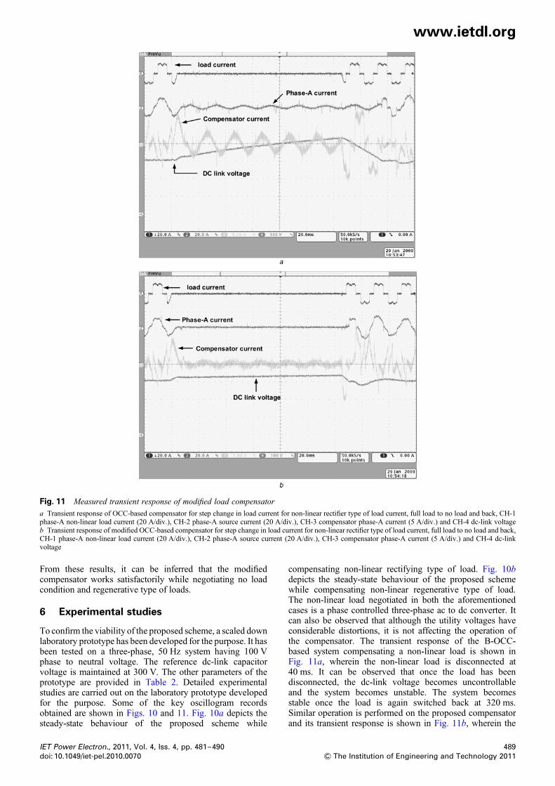
compensating non-linear rectifying type of load. Fig. 10bdepicts the steady-state behaviour of the proposed schemewhile compensating non-linear regenerative type of load.The non-linear load negotiated in both the aforementionedcases is a phase controlled three-phase ac to dc converter. Itcan also be observed that although the utility voltages haveconsiderable distortions, it is not affecting the operation ofthe compensator. The transient response of the B-OCC-based system compensating a non-linear load is shown inFig. 11a, wherein the non-linear load is disconnected at40 ms. It can be observed that once the load has beendisconnected, the dc-link voltage becomes uncontrollableand the system becomes unstable. The system becomesstable once the load is again switched back at 320 ms.Similar operation is performed on the proposed compensatorand its transient response is shown in Fig. 11b, wherein the
Fig. 11 Measured transient response of modified load compensator
a Transient response of OCC-based compensator for step change in load current for non-linear rectifier type of load current, full load to no load and back, CH-1phase-A non-linear load current (20 A/div.), CH-2 phase-A source current (20 A/div.), CH-3 compensator phase-A current (5 A/div.) and CH-4 dc-link voltageb Transient response of modified OCC-based compensator for step change in load current for non-linear rectifier type of load current, full load to no load and back,CH-1 phase-A non-linear load current (20 A/div.), CH-2 phase-A source current (20 A/div.), CH-3 compensator phase-A current (5 A/div.) and CH-4 dc-linkvoltage
IET Power Electron., 2011, Vol. 4, Iss. 4, pp. 481–490 489doi: 10.1049/iet-pel.2010.0070 & The Institution of Engineering and Technology 2011

www.ietdl.org
non-linear load being compensated by the system isdisconnected at t ¼ 30 ms. It can be observed that the dc-link voltage remains controllable and the operation of thesystem remains stable.
7 Conclusion
The issue of reduced stability margin in case of one-cyclecontrolled load compensator has been demonstrated. Amodification in the basic one-cycle controller is proposedso that the stability margin can be considerably improvedwhile the compensator is required to compensate loadshaving low real power component or while compensatingregenerative type of loads. To achieve this, a fictitiouscurrent component in phase with the utility voltage issynthesised. The sum of this current component and theactual load current is compared with the saw-toothwaveform to generate the gating pulses for the switches.Detailed simulation studies are carried out to verify theeffectiveness of the proposed scheme. The viability of thescheme has been ascertained by performing extensiveexperimental studies on a 2 kW laboratory prototype.
8 References
1 Hingorani, N.G., Gyugi, L.: ‘Understanding facts’ (IEEE Press, NJ,USA, 2000)
2 Moran, L.T., Ziogas, P.D., Joos, G.: ‘Analysis and design of a three-phase synchronous solid-state var compensator’, IEEE Trans. Ind.Appl., 1989, IA-25, (4), pp. 598–608
3 Joos, G., Moran, L.T., Ziogas, P.D.: ‘Performance analysis of a PWMinverter var compensator’, IEEE Trans. Power Electron., 1991, PE-6,(3), pp. 380–391
490
& The Institution of Engineering and Technology 2011
4 Buso, S., Malesani, L.: ‘Comparison of current control techniquesfor active filter applications’, IEEE Trans. Ind. Electron., 1998, 45,pp. 722–729
5 Chatterjee, K., Fernandes, B.G., Dubey, G.K.: ‘An instantaneousreactive volt-ampere compensator and harmonic suppressor system’,IEEE Trans. Power Electron., 1999, PE-14, (2), pp. 381–392
6 Singh, B., Al-Haddad, K., Chandra, A.: ‘A review of active power filtersfor power quality improvement’, IEEE Trans. Ind. Electron., 1999, 45,(5), pp. 960–971
7 Akagi, H., Kanazawa, Y., Nabae, A.: ‘Instantaneous reactive powercompensators comprising switching devices without energy storagecomponents’, IEEE Trans Ind. Appl., 1984, IA-20, pp. 625–630
8 Bhattacharya, S., Divan, D.: ‘Synchronous frame based controllerimplementation for a hybrid series active filter system’, IEEE/IASAnnu. Meet., 1995, 3, pp. 2531–2540
9 Smedley, K.M., Zhou, L., Qiao, C.: ‘Unified constant-frequencyintegration control of active power filters steady-state and dynamics’,IEEE Trans. Power Electron., 2001, 16, (3), pp. 429–436
10 Qiao, C., Smedley, K.M.: ‘Three-phase bipolar mode active powerfilters’, IEEE Trans. Ind. Appl., 2002, PE-38, (1), pp. 149–158
11 Chongming, Q., Smedley, K.M., Maddaleno, F.: ‘A single-phase activepower filter with one-cycle control under unipolar operation’, IEEETrans. Circuits Syst.-I, 2004, IA-51, (8), pp. 1623–1630
12 Ghosh, R., Narayanan, G.: ‘Generalized feed forward control of single-phase PWM rectifiers using disturbance observers’, IEEE Trans. Ind.Electron., 2007, 54, (2), pp. 985–993
13 Chen, Y., Ma Smedley, K.: ‘Parallel operation of one-cycle controlledthree-phase PFC rectifiers’, IEEE Trans. Ind. Electron., 2007, 54, (6),pp. 3217–3224
14 Chongming, Q., Smedley, K.M.: ‘Unified constant-frequencyintegration control of three-phase standard bridge boost rectifier’.Proc. IEEE Power Electronics Congress, CIEP, 2000, pp. 131–135
15 Chongming, Q., Smedley, K.M., Maddaleno, F.: ‘A single-phase activepower filter with one-cycle control under unipolar operation’, IEEETrans. Circuits Syst.-I, 2004, 51, (8), pp. 1623–1630
16 Chattopadhyay, S., Ramanarayanan, V.: ‘Digital implementation of aline current shaping algorithm for three phase high power factor boostrectifier without input voltage sensing’, IEEE Trans. Power Electron.,2004, 19, (3), pp. 709–721
IET Power Electron., 2011, Vol. 4, Iss. 4, pp. 481–490doi: 10.1049/iet-pel.2010.0070