
Modelling and Control of Inverter Sources within a Low ...
211
Modelling and Control of Inverter Sources within a Low Voltage Distributed Generation System Michaela Nicole Griffiths B.Eng (Comp) A thesis submitted for the degree of Doctor of Philosophy Discipline of Electrical Engineering School of Electrical Engineering and Computer Science The University of Newcastle Callaghan, N.S.W. 2308 Australia November 2012
-
Upload
khangminh22 -
Category
Documents
-
view
3 -
download
0
Transcript of Modelling and Control of Inverter Sources within a Low ...
Modelling and Control of InverterSources within a Low Voltage Distributed
Generation System
Michaela Nicole GriffithsB.Eng (Comp)
A thesis submitted for the degree of
Doctor of PhilosophyDiscipline of Electrical Engineering
School of Electrical Engineeringand Computer Science
The University of NewcastleCallaghan, N.S.W. 2308
Australia
November 2012

This thesis contains no material which has been accepted for the award of any other degreeor diploma in any university or other tertiary institution and, to the best of my knowledgeand belief, contains no material previously published or written by another person, exceptwhere due reference has been made in the text. I give consent to this copy of my thesis,when deposited in the University Library, being made available for loan and photocopyingsubject to the provisions of the Copyright Act 1968.

Acknowledgements
This research was jointly funded by Australia’s Commonwealth Scientific and IndustrialResearch Organisation (CSIRO) Energy Centre, Newcastle; and the University of New-castle, Australia.
It would not have been possible without the support of my husband and technical support,Ian, my family, and my supervisor, Dr Colin Coates.
Contents
Abstract xi
1 Distributed Generation and Microgrids 1
1.1 Project Context and Description . . . . . . . . . . . . . . . . . . . . . . . . 1
1.2 Distributed Generation - An Historical Perspective . . . . . . . . . . . . . . 2
1.3 The Microgrid Concept - Technical Challenges . . . . . . . . . . . . . . . . 6
1.4 Microgrid Models . . . . . . . . . . . . . . . . . . . . . . . . . . . . . . . . . 8
1.5 Control Algorithms . . . . . . . . . . . . . . . . . . . . . . . . . . . . . . . 10
1.6 Other Research . . . . . . . . . . . . . . . . . . . . . . . . . . . . . . . . . . 14
1.7 Thesis Overview . . . . . . . . . . . . . . . . . . . . . . . . . . . . . . . . . 16
2 Microgrid Transient Modelling 17
2.1 Overview . . . . . . . . . . . . . . . . . . . . . . . . . . . . . . . . . . . . . 17
2.2 Source Structure and Models . . . . . . . . . . . . . . . . . . . . . . . . . . 19
2.2.1 Inverter Model . . . . . . . . . . . . . . . . . . . . . . . . . . . . . . 20
2.2.1.1 D-Q Transform . . . . . . . . . . . . . . . . . . . . . . . . . 22
2.2.1.2 The Per-Unit System . . . . . . . . . . . . . . . . . . . . . 24
2.2.2 Output Filter . . . . . . . . . . . . . . . . . . . . . . . . . . . . . . . 25
2.2.3 Coupling Inductance . . . . . . . . . . . . . . . . . . . . . . . . . . . 26
2.2.4 Measurement Block . . . . . . . . . . . . . . . . . . . . . . . . . . . 27
2.3 Modelling of Other Circuit Elements . . . . . . . . . . . . . . . . . . . . . . 28
2.3.1 Load Resistors . . . . . . . . . . . . . . . . . . . . . . . . . . . . . . 28
2.3.2 Inverter Coupling Inductances . . . . . . . . . . . . . . . . . . . . . 29
2.3.3 Non-linear Loads . . . . . . . . . . . . . . . . . . . . . . . . . . . . . 30
Contents v
2.4 SimPowerSystems . . . . . . . . . . . . . . . . . . . . . . . . . . . . . . . . . 33
2.5 Summary . . . . . . . . . . . . . . . . . . . . . . . . . . . . . . . . . . . . . 34
3 Inverter Control 35
3.1 Principles of Droop Control . . . . . . . . . . . . . . . . . . . . . . . . . . . 35
3.2 Controller Implementation . . . . . . . . . . . . . . . . . . . . . . . . . . . . 38
3.2.1 Voltage Control . . . . . . . . . . . . . . . . . . . . . . . . . . . . . . 38
3.2.1.1 Voltage Limits . . . . . . . . . . . . . . . . . . . . . . . . . 40
3.2.2 Power Control . . . . . . . . . . . . . . . . . . . . . . . . . . . . . . 42
3.2.3 Power Sharing . . . . . . . . . . . . . . . . . . . . . . . . . . . . . . 42
3.2.3.1 Power Source Block . . . . . . . . . . . . . . . . . . . . . . 44
3.3 Problems with Droop Control . . . . . . . . . . . . . . . . . . . . . . . . . . 44
3.3.1 Simulation Overview . . . . . . . . . . . . . . . . . . . . . . . . . . . 46
3.3.2 Different Voltage Setpoints . . . . . . . . . . . . . . . . . . . . . . . 46
3.3.3 Reactive Power Sharing . . . . . . . . . . . . . . . . . . . . . . . . . 48
3.3.4 Harmonics . . . . . . . . . . . . . . . . . . . . . . . . . . . . . . . . . 48
3.3.5 Resistive Line Impedances . . . . . . . . . . . . . . . . . . . . . . . . 51
3.3.6 Unbalanced Grid Voltages . . . . . . . . . . . . . . . . . . . . . . . . 52
3.3.7 Unbalanced Loads . . . . . . . . . . . . . . . . . . . . . . . . . . . . 53
3.4 Variations on Droop Control . . . . . . . . . . . . . . . . . . . . . . . . . . 57
3.4.1 Reactive Power Sharing . . . . . . . . . . . . . . . . . . . . . . . . . 58
3.4.1.1 Q-E Droop . . . . . . . . . . . . . . . . . . . . . . . . . . . 58
3.4.1.2 Virtual Output Impedance . . . . . . . . . . . . . . . . . . 62
3.4.2 Frequency Restoration . . . . . . . . . . . . . . . . . . . . . . . . . . 64
3.4.3 Harmonic Current Sharing . . . . . . . . . . . . . . . . . . . . . . . 67
3.4.4 Resistive Line Impedance . . . . . . . . . . . . . . . . . . . . . . . . 67
3.5 Evaluation . . . . . . . . . . . . . . . . . . . . . . . . . . . . . . . . . . . . . 68
Contents vi
4 Unbalanced Loads 70
4.1 Unbalance Compensation . . . . . . . . . . . . . . . . . . . . . . . . . . . . 70
4.1.1 Symmetrical Components Theory . . . . . . . . . . . . . . . . . . . . 73
4.1.2 Sequence Representation of Grid . . . . . . . . . . . . . . . . . . . . 75
4.2 Unbalance Controller Design . . . . . . . . . . . . . . . . . . . . . . . . . . 81
4.3 Simulation Details . . . . . . . . . . . . . . . . . . . . . . . . . . . . . . . . 84
4.3.1 Performance of Unbalance Control . . . . . . . . . . . . . . . . . . . 86
4.4 Power Sharing and voltage regulation . . . . . . . . . . . . . . . . . . . . . 88
4.4.1 Controller Performance . . . . . . . . . . . . . . . . . . . . . . . . . 88
4.4.2 Frequency Issues with the Sequence Analyzer . . . . . . . . . . . . . 90
4.4.3 Variable Frequency Sequence Analyzer . . . . . . . . . . . . . . . . . 93
4.4.4 Performance of Control with Variable Frequency Sequence Analyzer 96
4.5 Sharing of Negative Sequence Generation . . . . . . . . . . . . . . . . . . . 98
4.6 Grid Connection . . . . . . . . . . . . . . . . . . . . . . . . . . . . . . . . . 98
5 Proposed Controller Design 101
5.1 Controller Components . . . . . . . . . . . . . . . . . . . . . . . . . . . . . 101
5.1.1 Power-frequency Droop Control . . . . . . . . . . . . . . . . . . . . . 102
5.1.2 Voltage Regulation . . . . . . . . . . . . . . . . . . . . . . . . . . . . 104
5.1.3 Unbalance Control . . . . . . . . . . . . . . . . . . . . . . . . . . . . 105
5.2 Results . . . . . . . . . . . . . . . . . . . . . . . . . . . . . . . . . . . . . . . 106
5.2.1 Reference Case . . . . . . . . . . . . . . . . . . . . . . . . . . . . . . 109
5.2.2 Different Power Setpoints . . . . . . . . . . . . . . . . . . . . . . . . 112
5.2.3 Large Load Change . . . . . . . . . . . . . . . . . . . . . . . . . . . 112
5.2.4 Different Sized Sources . . . . . . . . . . . . . . . . . . . . . . . . . . 114
5.2.5 Different Voltage Setpoints . . . . . . . . . . . . . . . . . . . . . . . 115
5.2.6 Different Coupling Inductances . . . . . . . . . . . . . . . . . . . . . 117
Contents vii
5.2.7 Reactive Load . . . . . . . . . . . . . . . . . . . . . . . . . . . . . . 120
5.2.8 Unbalanced Load . . . . . . . . . . . . . . . . . . . . . . . . . . . . . 121
5.2.9 Unbalanced Reactive Load . . . . . . . . . . . . . . . . . . . . . . . 121
5.2.10 Unbalanced Load and Different Coupling Inductances . . . . . . . . 124
5.3 Controller Parameters . . . . . . . . . . . . . . . . . . . . . . . . . . . . . . 128
5.4 Conclusion . . . . . . . . . . . . . . . . . . . . . . . . . . . . . . . . . . . . 128
6 Power Sources and Storage 130
6.1 Power Source Block . . . . . . . . . . . . . . . . . . . . . . . . . . . . . . . 131
6.1.1 Transfer Function Models . . . . . . . . . . . . . . . . . . . . . . . . 132
6.1.1.1 Ideal DC Source (Infinite Capacity Battery) . . . . . . . . 132
6.1.1.2 Microturbines . . . . . . . . . . . . . . . . . . . . . . . . . 132
6.1.1.3 Fuel Cells . . . . . . . . . . . . . . . . . . . . . . . . . . . . 134
6.1.1.4 Renewable Power Sources . . . . . . . . . . . . . . . . . . . 135
6.1.2 Behaviour of Power Source Blocks . . . . . . . . . . . . . . . . . . . 135
6.2 Modifications to Source Models . . . . . . . . . . . . . . . . . . . . . . . . . 138
6.2.1 Forcing Drop in Voltage when Power is not Available . . . . . . . . 139
6.2.2 Shifting the Droop Characteristic . . . . . . . . . . . . . . . . . . . 141
6.3 Directly Connected Storage . . . . . . . . . . . . . . . . . . . . . . . . . . . 145
6.3.1 Controller Design and Performance . . . . . . . . . . . . . . . . . . . 146
6.3.2 The Parameter k . . . . . . . . . . . . . . . . . . . . . . . . . . . . . 149
6.3.3 Controller Limitations . . . . . . . . . . . . . . . . . . . . . . . . . . 150
7 Summary and Further Work 151
7.1 Modelling Techniques . . . . . . . . . . . . . . . . . . . . . . . . . . . . . . 151
7.1.1 Further Work . . . . . . . . . . . . . . . . . . . . . . . . . . . . . . . 151
7.2 Pf-droop . . . . . . . . . . . . . . . . . . . . . . . . . . . . . . . . . . . . . . 152

Contents viii
7.3 Controller Design . . . . . . . . . . . . . . . . . . . . . . . . . . . . . . . . . 152
7.3.1 Further Work . . . . . . . . . . . . . . . . . . . . . . . . . . . . . . . 152
7.4 Grid Connected Storage . . . . . . . . . . . . . . . . . . . . . . . . . . . . . 153
7.4.1 Further Work . . . . . . . . . . . . . . . . . . . . . . . . . . . . . . . 153
A MATLAB/Simulink Diagrams 154
A.1 Simulation using Developed Model Library . . . . . . . . . . . . . . . . . . 154
A.1.1 Top Level Simulation . . . . . . . . . . . . . . . . . . . . . . . . . . 155
A.1.2 Source Block . . . . . . . . . . . . . . . . . . . . . . . . . . . . . . . 156
A.1.2.1 Calculations Block . . . . . . . . . . . . . . . . . . . . . . . 156
A.1.2.2 Power-frequency Droop . . . . . . . . . . . . . . . . . . . . 156
A.1.2.3 Voltage Control . . . . . . . . . . . . . . . . . . . . . . . . 157
A.1.2.4 Inverter . . . . . . . . . . . . . . . . . . . . . . . . . . . . . 158
A.1.3 Coupling Inductance . . . . . . . . . . . . . . . . . . . . . . . . . . . 158
A.1.4 Voltage Magnitude Calculation . . . . . . . . . . . . . . . . . . . . . 158
A.1.5 Frequency Calculation . . . . . . . . . . . . . . . . . . . . . . . . . . 159
A.1.6 Reactive Load . . . . . . . . . . . . . . . . . . . . . . . . . . . . . . 160
A.2 Harmonic Simulation using Developed Model Library . . . . . . . . . . . . . 161
A.2.1 Top Level Simulation . . . . . . . . . . . . . . . . . . . . . . . . . . 161
A.2.2 Source Block . . . . . . . . . . . . . . . . . . . . . . . . . . . . . . . 162
A.2.2.1 Calculations Block . . . . . . . . . . . . . . . . . . . . . . . 162
A.2.2.2 Inverter . . . . . . . . . . . . . . . . . . . . . . . . . . . . . 163
A.2.3 Coupling Inductance . . . . . . . . . . . . . . . . . . . . . . . . . . . 164
A.2.4 Rectifier Load . . . . . . . . . . . . . . . . . . . . . . . . . . . . . . . 164
A.3 SimPowerSystems Unbalanced Load Simulation . . . . . . . . . . . . . . . . 165
A.3.1 Top Level Simulation . . . . . . . . . . . . . . . . . . . . . . . . . . 165
A.3.2 Source Block . . . . . . . . . . . . . . . . . . . . . . . . . . . . . . . 166
Contents ix
A.3.2.1 Voltage Magnitude Calculation . . . . . . . . . . . . . . . 166
A.3.2.2 Voltage Control . . . . . . . . . . . . . . . . . . . . . . . . 167
A.3.2.3 Ideal Inverter . . . . . . . . . . . . . . . . . . . . . . . . . . 167
A.3.3 Signal to Voltage Conversion . . . . . . . . . . . . . . . . . . . . . . 168
A.3.4 Load Block . . . . . . . . . . . . . . . . . . . . . . . . . . . . . . . . 168
A.4 Power Control Comparison . . . . . . . . . . . . . . . . . . . . . . . . . . . 170
A.4.1 Top Level Simulation . . . . . . . . . . . . . . . . . . . . . . . . . . 170
A.4.2 Source Block . . . . . . . . . . . . . . . . . . . . . . . . . . . . . . . 171
A.4.2.1 Power-Frequency Droop Control Block . . . . . . . . . . . 171
A.5 Simulation with Unbalance Control . . . . . . . . . . . . . . . . . . . . . . . 172
A.5.1 Top Level Simulation . . . . . . . . . . . . . . . . . . . . . . . . . . 172
A.5.2 Source Block . . . . . . . . . . . . . . . . . . . . . . . . . . . . . . . 173
A.5.2.1 Power-Frequency Droop . . . . . . . . . . . . . . . . . . . . 173
A.5.2.2 Voltage Control . . . . . . . . . . . . . . . . . . . . . . . . 174
A.5.2.3 Unbalance Control . . . . . . . . . . . . . . . . . . . . . . . 174
A.5.2.4 Ideal Inverter . . . . . . . . . . . . . . . . . . . . . . . . . . 175
A.5.3 Frequency Calculation Block . . . . . . . . . . . . . . . . . . . . . . 175
A.5.4 Symmetrical Components Calculation Block . . . . . . . . . . . . . . 176
A.6 New Voltage Source . . . . . . . . . . . . . . . . . . . . . . . . . . . . . . . 177
A.6.1 Top Level Simulation . . . . . . . . . . . . . . . . . . . . . . . . . . 177
A.6.1.1 Power-Frequency Droop . . . . . . . . . . . . . . . . . . . . 178
A.6.1.2 Voltage Control . . . . . . . . . . . . . . . . . . . . . . . . 179
A.6.1.3 Unbalance Control . . . . . . . . . . . . . . . . . . . . . . . 179
A.6.1.4 Load Block . . . . . . . . . . . . . . . . . . . . . . . . . . . 180
A.7 Simulation to Investigate Power Sources using Developed Model Library . . 181
A.7.1 Top Level Simulation . . . . . . . . . . . . . . . . . . . . . . . . . . 181

Contents x
A.7.2 Source Block (Micro-turbine and Ideal) . . . . . . . . . . . . . . . . 182
A.7.2.1 Power-frequency Droop . . . . . . . . . . . . . . . . . . . . 182
A.7.2.2 Microturbine and Ideal Source Block . . . . . . . . . . . . 183
A.7.2.3 Inverter . . . . . . . . . . . . . . . . . . . . . . . . . . . . . 183
A.7.3 AC Storage . . . . . . . . . . . . . . . . . . . . . . . . . . . . . . . . 183
A.7.3.1 Power-frequency Droop for AC Storage Block . . . . . . . . 183
A.7.3.2 DC Source . . . . . . . . . . . . . . . . . . . . . . . . . . . 184
A.7.4 Load Block . . . . . . . . . . . . . . . . . . . . . . . . . . . . . . . . 185
Bibliography 186

Abstract
The Microgrid has been proposed as a way of combining distributed generation which can
have a positive impact on power quality. To solve many of the challenges a microgrid
presents, transient modelling is important. This work develops a library for creating a
transient model of a microgrid based on transfer function representations of microgrid
components, and drawing from techniques to implement simple models of inverters. The
developed library allows for the fast, accurate simulation of multiple parallel sources con-
nected to a single load through coupling inductances.
Typically, in a microgrid, a controller with a power-frequency droop is used in the sources.
This allows for power sharing when the microgrid is in island mode. In this work, the model
library was used to develop simulations which illustrated the known problems with the
basic droop control implementation and some of the solutions proposed in the literature.
One area which had not been addressed in detail in relation to droop control, was the high
likelihood of unbalanced loads in a stand-alone system. In this work, a modification to the
droop controller was developed which allowed for the reduction of voltage imbalance in the
presence of unbalanced loads. The controller calculates the amount of negative sequence
voltage at the load, and compensates for this at the source. This unbalance controller was
then integrated into a new controller developed to address many of the weaknesses of the
standard droop control configuration.
Due to the lack of inertia in the power sources, the typical droop controller setup requires
storage on the DC side of the inverter (typically a battery) in order to allow for step changes
in load demand. In this work, a controller was developed for an AC grid connected storage
device (such as a flywheel) which was effective in reducing the need for individual storage
for each source. The advantage to this approach is that the grid connected storage device
can be chosen to be more environmentally friendly than the batteries which are typically
used for the DC storage.
Chapter 1
Introduction to Distributed
Generation and Microgrids
This thesis presents a method for modelling inverter sources within a low voltage dis-
tributed generation system. A control strategy is developed that addresses the major
challenges unique to low voltage distributed generation systems. These include the high
likelihood of unbalanced loads, small impedances between sources and the need for power
sharing, voltage regulation and storage in island operation.
1.1 Project Context and Description
This research has been performed in conjunction with Australia’s Commonwealth Scientific
and Industrial Research Organisation (CSIRO) Energy Centre, Newcastle. The Energy
Centre has a small low voltage distributed generation system which provides power for the
Energy Centre buildings [1]. It consists of microturbines (120kW), photovoltaics (90kW)
and wind turbines (60kW) and can operate both connected to the main power grid, or in
stand-alone mode.
The motivation for installing this generation was to facilitate research into microgrids. Due
to the large number of inverters contained in the PV arrays, a particular area of interest
is the interactions between the controllers of these inverters. In order to investigate this,
models were developed which allowed simulation of a simple microgrid containing several
sources, in a realistic timeframe. These models were then used to examine the system
behaviour when using droop control techniques. This particular type of control was chosen
1. Distributed Generation and Microgrids 2
as it is the most common technique proposed for use in microgrids, due to its ability to
share power amongst different sized sources, and regulate voltage levels, without the need
for communications between devices [2–6]. This investigation led to the development of an
improved droop controller which incorporates a technique for minimising voltage imbalance
at the load. This research also investigated the feasibility of reducing the dependence on
batteries in microgrid sources by directly connecting centralised storage to the microgrid.
A controller for a centralised storage device was designed to achieve this aim.
The following sections provide an overview of distributed generation and microgrids, with
more specific information on modelling and inverter control techniques.
1.2 Distributed Generation - An Historical Perspective
Distributed Generation (DG) is defined as “electric power generation within the distribu-
tion network or on the customer side of the network” [7]. It is generally in the form of
small sources such as wind turbines, solar cells, fuel cells and microturbines or gas tur-
bines, with generation typically in the kW to MW range. This contrasts with traditional
power generation that usually occurs at centralised power plants which produce power in
the hundreds of MW to GW range. This research focusses on low voltage distributed gen-
eration (LVDG) where the sources connect to the low voltage (< 1000Vrms) distribution
network.
DG is becoming increasingly important as demand for power grows, and solutions are
sought that are less harmful to the environment, and produce better quality power. Typ-
ically DG has been deployed as stand alone units connected directly to the grid (possibly
through power electronics), or groups of sources (such as a wind park) combined to pro-
duce higher voltages. The focus has been on providing power in remote areas, or increasing
the overall capacity of the power grid.
DG potentially has several advantages over standard power generation [8]. These include:
1. Distributed Generation and Microgrids 3
• The possibility of combined heat and power (CHP) applications, increasing overall
efficiency
• Reduction in transmission losses and lower capacity requirements in lines, trans-
formers and other transmission system components due to the reduction in power
being supplied from centralised generators
• Low cost and quicker implementation meaning major distribution network upgrades
can be delayed
• Peak power shaving
• Environmental benefits if renewable, or low emissions technologies are used
• Provision of power to remote areas
Conversely, DG can lead to problems which degrade the quality of the power supply
[9]. DG can interfere with protection mechanisms [10], decrease system stability [11] and
increase harmonic levels [12]. DG has typically been seen as a “problem” to be solved, and
researchers have calculated maximum penetration levels before grid instability was likely
to occur [11–13]. In an attempt to overcome these issues, researchers in the US [14, 15]
have proposed grouping different microsources together with local loads as a unit which
can operate in stand alone or grid-connected mode. This concept has been termed a
‘microgrid’.
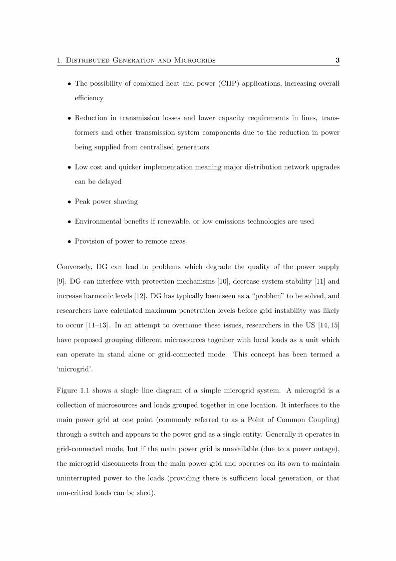
Figure 1.1 shows a single line diagram of a simple microgrid system. A microgrid is a
collection of microsources and loads grouped together in one location. It interfaces to the
main power grid at one point (commonly referred to as a Point of Common Coupling)
through a switch and appears to the power grid as a single entity. Generally it operates in
grid-connected mode, but if the main power grid is unavailable (due to a power outage),
the microgrid disconnects from the main power grid and operates on its own to maintain
uninterrupted power to the loads (providing there is sufficient local generation, or that
non-critical loads can be shed).

1. Distributed Generation and Microgrids 4
SensitiveLoad
SensitiveLoad Source
SensitiveLoad
Switch(to IsolateSensitiveLoads)
Source
Main Power Grid
Non-Senstive
Load
Non-Sensitive
Load
Point ofCommonCoupling
Figure 1.1: Simple microgrid
The potential advantages of the microgrid are [14,15]:
• Microgrids offer a solution to provide power to remote areas.
• The scale of the generation units means that the customer can own his own power
generation, which can offer financial savings if the technology can be operated more
cheaply than the market price of electricity.
• The microgrid can be set up with sufficient capacity that it can offer Uninterruptible
Power Supply (UPS) type functionality.
• The power electronics that are used to interface microsources to the microgrid are
such that they can be controlled to offer superior power quality in terms of limiting
voltage sags, phase imbalances and harmonics, for customers with sensitive loads.
The most common proposal is to use droop characteristics to allow independent
control of each of the microsources.
• The proximity of generation to loads means that combined heat and power applica-
tions are possible, increasing the overall efficiency of the generators.
The microgrid is not an entirely new concept. Stand-alone low voltage distributed genera-
tion has been around for decades, particularly in remote areas where extensions to existing
1. Distributed Generation and Microgrids 5
power grids were not considered feasible. This was most commonly in the form of wind
turbines, which have been around since the late 1800s [16]. In the US, wind turbines were
used to provide power on many remote rural properties until the rural electrification of the
1930s. More recently, systems have been built which combine several types of generation
with some form of storage [17, 18]. What differentiates the microgrid from these systems
is that it is designed to work in conjunction with the main power grid most of the time, to
seamlessly disconnect in the case of a fault, and to provide high quality power to sensitive
loads.
The microgrid concept has generated significant interest and several research groups have
formed projects to further develop the concept. International groups working in this area
include the Consortium for Electric Reliability Technology Solutions (CERTS) [19], and
the IRED (“Integration of Renewable Energy Sources and Distributed Generation into the
European Electricity Grid”) cluster [20].
CERTS is a group of co-operating universities, commercial companies and research labo-
ratories in the US sponsored by the US Department of Energy and the California Energy
Commission. CERTS has performed considerable work outlining the need for microgrids,
and their proposal for the basic structure of the microgrid [21, 22]. Some of the areas
they have looked at include control strategies [3], protection [23] and customer adoption
models [24]. CERTS has placed a lot of importance on implementing a working microgrid
and have made significant progress towards this goal, including a working demonstration
system operated by American Electric Power [25]. Understandably this means a lot of
their energy has focussed on single solutions rather than investigating a wide range of
possibilities. Detailed descriptions are available for many aspects of the project, and for
this reason, the CERTS project is frequently referred to in this work.
The IRED cluster is a series of projects funded by the European Commission and co-
ordinated by the Institut fuer Solare Energieversorgungstechnik e.V (ISET). Of interest
to this research is the now completed ‘Microgrids’ [26] and ‘More Microgrids’ [27] projects.

1. Distributed Generation and Microgrids 6
Like the CERTS project, the initial Microgrids project was primarily focussed on achieving
a prototype microgrid which can be demonstrated in a laboratory. To this end, research
was performed in a wide range of areas including modelling and simulation [28], con-
trol [2,29,30], protection [31,32], communications requirements, laboratory testing [33,34]
and regulatory, commercial, economic and environmental issues [35]. Further to this, the
More Microgrids project expands on this research and investigates alternative solutions
(e.g DC microgrids, centralised vs. decentralised control). Unlike the CERTS project,
these projects focussed more on research of various alternatives than on building a spe-
cific solution. Rather than focus on a single large scale implementation of a microgrid,
the projects include several pilot installations, both in the laboratory, and in real world
distribution networks.
1.3 The Microgrid Concept - Technical Challenges
Researchers quickly discovered that the nature of the microgrid is such that its behaviour
is not like that of the main power grid [36]:
• Different types of power sources are likely to be used [37]. These sources are gener-
ally small distributed generation sources which connect to the grid through power
electronics such as inverters. As such they have little or no rotating inertia, meaning
that they cannot quickly adjust their power output to provide for load changes. For
stand-alone microgrid operation this means that some form of storage is required
to provide the transient power during load changes. To compound this problem,
renewable sources such as wind turbines or photovoltaic arrays are not dispatchable,
meaning they cannot be relied upon to produce power on demand.
• The power electronics interfaces require different control strategies than in a non-
microgrid environment - in stand-alone mode, the inverter controllers will be required
to regulate the voltage and to share power amongst the sources. The smaller sources
also affect protection strategies, because generally the fault currents are not high

1. Distributed Generation and Microgrids 7
enough for over current protection, so alternatives are needed [38].
• The nature of the loads present may differ [39, 40]. Unbalanced loads are far more
likely, since the usual approach of apportioning loads between the phases such that
the loads are virtually the same on each phase, relies on the large number of loads
in a typical power grid.
• Significant harmonics are a possibility, as many office loads, such as computer equip-
ment, lighting and motors, produce high levels of harmonics. The converters used
to interface distributed generation with the grid also produce harmonics.
• Transmission lines are different in a microgrid [2,41]. This is due to both the shorter
distances involved, and different physical cabling used in low voltage distribution
networks. Small line impedances between sources can allow sizeable reactive currents
to circulate between the sources, and other interactions are possible between the line
impedances and the reactances in the inverters. The line impedances also tend to
be more resistive than reactive.
• If the microgrid is to operate in stand-alone mode, then there needs to be systems
for disconnecting from the main power grid, and resynchronising when a fault event
is over [42]. The safety of line maintenance staff needs to be considered by making
sure lines are not active when they shouldn’t be.
• There are challenges in the relationship between the owner of the microgrid and the
power distributor, both regulatory, and financial.
These differences mean that the behaviour of a microgrid is not fully understood. There
are a number of challenges to be met before widespread adoption of the concept is possible.
Microgrid research can be broken up into the following areas:
• Regulatory constraints
• Market strategies

1. Distributed Generation and Microgrids 8
• Protection
• Technologies, including power sources and storage
• Transient and steady state models
• Control algorithms
• Load management (also known as demand side management)
• Systems for disconnecting and reconnecting to main power grid
This research will focus on issues surrounding the modelling and control of microgrids.
1.4 Microgrid Models
In order to evaluate the performance of microgrids both transient and steady state models
are required. Transient models are more applicable when considering inverter controllers,
however steady state modelling will be briefly discussed for completeness.
The challenges for developing steady state models of microgrids include sources which
interface via power electronic devices, load unbalance and the combination of single phase
and 3-phase generation and loads [43]. Meliopoulos et al. [44] propose a model which
addresses these concerns using multiphase power flow analysis. A distributed slack bus
model is proposed to model distributed generation in the distribution system [45].
Transient modelling is important when it comes to examining problems like the production
of harmonics, voltage sags and spikes and other short lived phenomenon. The major focus
of transient modelling work has been on the various components of a microgrid. Wind
turbines, both with doubly-fed induction generators [46] and self-excited induction gener-
ators [47] have been modelled in several papers. Photovoltaics have also been modelled
significantly. The most common method are the single diode [48, 49] or double diode [50]
equivalent circuit models. Models can be found for inverters [22], rectifiers, microturbines,
1. Distributed Generation and Microgrids 9
fuel cells [51], loads and transmission lines. There have also been quite a few efforts to
model partial systems (see [52] for a model of a system with diesel, microturbine and
fuel cell). The problem with the majority of these models, however, is that they are too
detailed to allow simulation of reasonably sized systems.
CERTS has proposed several simplifications which go some way to addressing this problem.
In [22], a technique is outlined for modelling a simplified inverter. The model is designed
assuming balanced 3 phase operation and no inverter switching dynamics. The document
also outlines a technique for creating simplified models of microturbines and fuel cells.
These maximum power models are based on the idea that the sources can be assumed to
behave like fixed DC sources except during changes to power demands i.e. during load
transients. At these times the models differ depending on the specific source. A further
simplification is to assume sufficient battery capacity on the DC side of the inverter so
that the source can be modelled as an ideal DC power source.
Noticeably lacking in current models is a way of modelling the main grid. One of the pos-
sible benefits of a microgrid is that it provides a way of connecting distributed generation
to the main power grid without degrading the power quality. Therefore the effects of the
microgrid on the main power grid need to be modelled in some way. Generally the main
power grid is assumed to be a stiff voltage, with fixed magnitude and frequency. This
model does not allow for any observation of possible problems that the microgrid may
cause to the main power grid, particularly in the case of a weak grid.
There are software and libraries available that can be used for transient modelling such as
the MATLAB/Simulink SimPowerSystems library and RPM-SIM which were investigated
as possible modelling platforms.
RPM-SIM [53] was created by The National Renewable Energy Laboratory and is a library
of components in a program called VisSim. This library includes the following components:
Point of Common Coupling, Diesel Generator, Rotary Converter with Battery Bank, Wind
Turbine, Village Load, Dump Load, PV Array, Transmission Line Impedance and Power
1. Distributed Generation and Microgrids 10
Factor Correction measures.
MATLAB/Simulink was chosen, as it is a platform which is commonly available and
familiar to a lot of people, along with possessing the required flexibility. Some SimPow-
erSystems components were incorporated into the model as these simplified some aspects
of the modelling.
1.5 Control Algorithms
A key area in microgrid research is the development of new control techniques. Since
most of the technologies being considered for use in microgrids connect through power
electronics, these techniques are generally aimed at inverter control.
Control algorithms for parallel inverters can be categorised into two main types - those
that use a communications medium (either wired or wireless) to carry control signals to
each of the inverters, and those that operate without external control signals, using only
information that is locally available [54]. The majority of systems which utilise communi-
cations have some kind of central controller, which introduces a single point of failure in
the system. Also this kind of control is only as reliable as the system carrying the signals.
If the system is sufficiently distributed geographically, the delay in communications could
become significant. In some cases [55], the electrical power system itself is used to carry
control signals. This removes an extra point of failure from the system, however, power
lines with inverter based sources are not an ideal communication environment.
To avoid the problems with communications and the single point of failure in a system,
control algorithms which only require local information and allow sources to act indepen-
dently are therefore desirable. In some cases it is beneficial to employ the two types of
control in conjunction with each other, provided the individual units can still function in-
dependently in the event of a communications failure. In this case a centralised controller
would provide slow transients like power and voltage setpoints, and the fast transients
1. Distributed Generation and Microgrids 11
(the inverter voltage magnitude and phase) would be determined independently by the
source. In this case the purpose of the external control would be to provide the cheapest,
most fuel efficient, or most environmentally friendly power, depending on the aims of the
producer. Algorithms have been proposed to achieve some of these aims [56].
The main approach to achieving independent, local control is to use variations of the droop
control method. Droop control is based on the idea that when the output impedance is
mainly inductive, reactive power and voltage magnitude are strongly coupled, as are real
power and voltage angle [3]. The standard droop relationships are based on controlling real
and reactive power and employ power vs frequency (P-f) droop (Equation 1.1) and reactive
power vs inverter voltage (Q-V) droop (Equation 1.2), where ωi(t) is the frequency output
by the ith inverter at time t, w∗ is the nominal or base system frequency (generally 50Hz or
60Hz), Pi(t) is the power output of the source i at time t, and mi is the droop co-efficient,
or the gradient of the power-frequency droop characteristic, for source i. Vi(t) is the desired
RMS inverter voltage magnitude at time t, V ∗ is the inverter voltage magnitude setpoint
(or the desired RMS voltage at the load), ni is the reactive power droop co-efficient, and
Qi(t) is the reactive power output by the source at time t.
ωi(t) = ω∗ −miPi(t)) (1.1)
Vi(t) = V ∗ − niQi(t) (1.2)
In a microgrid environment it is necessary to regulate the system voltage and so a voltage
regulator (e.g. Equation 1.4) needs to be employed, wherekps+ki
s is a PI controller, Ei(t)
is the measured RMS load voltage magnitude at time t, and E∗ is the desired RMS
load voltage setpoint. Equation 1.3 shows the controller using the power-frequency droop
relationship, where δvi(t) is the desired inverter voltage phasor angle at time t. The
1. Distributed Generation and Microgrids 12
addition of the P ∗i term provides for a power setpoint in grid-connected mode.
δvi(t) =
ˆ(ω∗ −mi(Pi(t)− P ∗i )) (1.3)
Vi(t) =kps+ ki
s(E∗ − Ei(t)) (1.4)
CERTS has chosen to use an inverter controller with voltage and frequency droop (P-V
droop control) with the addition of a Q-E droop (reactive power vs grid voltage magnitude)
to the voltage controller in order to improve reactive power sharing. This is essentially a
combination of Equation 1.2 and Equation 1.4. The EU Microgrids project also chose a
droop controller for the inverter control, however in a slightly different configuration to
the CERTS controller. In this case the inverter output voltage was regulated to control
the flows of reactive power and prevent reactive currents from exceeding inverter ratings.
Voltage control is achieved by suitable layout of the low voltage grid, and by chokes. Power
sharing was achieved with a power frequency droop, similar to the CERTS controller.
Droop control has the advantage that it is compatible with standard synchronous generator
control. Problems with droop control include steady state error in the frequency output
by the inverter, slow transient response, the possibility of circulating reactive currents,
amplitude variations, poor unbalanced harmonic current sharing, high dependency on
output impedance and lack of compensation for unbalanced loads or grid voltages [57].
Several controllers have been proposed to alleviate these problems. To solve the prob-
lem of the steady state frequency error, Lasseter and Piagi [3] have added a frequency
restoration loop that restores frequency once power sharing has been achieved. The fre-
quency restoration must operate much slower than the power sharing loop (typically 10s
of seconds), so the frequency spends significant amounts of times deviated from the base
frequency. In order to address the problem of sharing harmonic power between different
sized sources, Lee and Cheng [58] have introduced a droop between harmonic conductance
and harmonic VAr consumption (G-H droop).

1. Distributed Generation and Microgrids 13
Another approach to droop control is to use a control loop to alter the output impedance.
A parallel combination of resistor and inductor allows good sharing of linear and non-
linear loads. Guerrero et al. have developed a variation on this idea which they claim
provides good output impedance response, good power sharing, fast transient response and
stable output voltage frequency and amplitude [4]. Their design consists of a transient
frequency droop loop for controlling active power and an adaptive output impedance
loop for controlling reactive power. This output impedance loop also gives improved
performance when ‘hot swapping’ components and provides non-linear load sharing.
One area that has received little attention is dealing with load unbalance while using a
droop controller. CERTS’ approach to unbalance [21] is to filter the voltage and current
signals so that the second harmonic oscillations caused by the negative sequence com-
ponents (i.e. the unbalance) do not affect the inverter controller. If the grid unbalance
becomes too large then the microgrid simply disconnects itself. The possibility of injecting
negative sequence currents to address imbalance is mentioned, but is discarded as requiring
additional complexity in the controller. While the former solution is effective for dealing
with unbalanced grid voltages, it does nothing to address unbalanced voltages which oc-
cur due to load imbalance within the microgrid itself. Even small amounts of unbalance
can decrease the lifespan of motors due to large negative sequence currents, and create
a need for oversized components in non-linear loads such as static converters due to the
low frequency harmonics. Several solutions for improving unbalance have been proposed,
most of which are based around measuring the negative sequence components generated
by the unbalance. Solutions include static VAR generators [59], active power filters [60–62]
and measures which use current and voltage source inverters [63]. Controllers have been
proposed to improve the performance of 3 phase PWM converters in the presence of un-
balanced input voltages [64, 65]. A combination of series/shunt inverters is proposed [66]
to correct for unbalance at the point of connection to the power grid in a microgrid. A
lot of the focus is on inverters which compensate for unbalanced supplies. There are some
solutions which address unbalanced loads/line voltages, however, until recently [67] these
1. Distributed Generation and Microgrids 14
had not been applied to droop controlled inverters, and so lacked the voltage regulation
and power sharing functionality required in a microgrid. Cheng et al. [67] have proposed
using a Q−-G droop (the reactive power produced by the negative sequence current vs
conductance) in conjunction with standard droop control to achieve these three aims.
In the case where energy storage devices (e.g. flywheels, battery banks, supercapacitors)
are connected directly to the common AC bus in the microgrid, control techniques are
needed for these devices. This is a separate problem to controlling power sources as the
storage device needs to supply power quickly during load transients, but should supply no
power during steady state. Jayawarna et al. [68] propose a controller for a flywheel which
allows the flywheel to supply sufficient fault currents when the microgrid is in islanded
mode. This controller is effective, but other techniques are required to apply to storage
devices generally, and for the simpler case where fault currents are not supplied by the
energy storage.
1.6 Other Research
There are several other areas of microgrid research which are outside the scope of this
work, but are mentioned here in brief.
One of these research areas is the connection with the main power grid. In [69] the
transients which occur when the microgrid switches to stand-alone mode are examined,
along with the ability of properly controlled power electronics to minimise the effect of
these transients. Other issues include when to disconnect the microgrid from the main
power grid and how to resynchronise the microgrid voltages with the power grid when the
fault has been removed. CERTS proposes exploiting the frequency difference between the
main grid and the microgrid, which is introduced by the power-frequency droop control,
in order to minimise the voltage across the switch as the connection is re-established [21].
Several authors have discussed the applicability of various types of technologies to the
1. Distributed Generation and Microgrids 15
microgrid concept. In [70] the benefits of using a mini gas turbine with high speed axial
flux generator in a microgrid are examined and the gas turbine is compared to a micro-
turbine. Mini gas turbines are suitable for combined heat and power (CHP) applications
and can provide electricity much cheaper than a microturbine and at a higher efficiency.
In [71] fuel cells are discussed including their impact on protection schemes. Fuel cells
are also suitable for CHP. A disadvantage of fuel cells however, is that changes in power
output cannot be achieved instantaneously so they generally are used in conjunction with
some form of storage. In [72] the suitability of wind and PV for stand-alone applications
are examined. These renewable sources offer the advantage that no fuel is needed, and
minimal environmental damage is caused. The disadvantage is that renewable resources
cannot be controlled and substantial storage, or backup generation is required for reli-
able generation. Also renewable sources can only be situated where the environment is
suitable i.e. locations with sufficient wind, sun etc. The storage requirements of these
various technologies can be met in various ways, including various types of batteries [73],
supercapacitors [74] and AC storage such as flywheels [75,76].
Load control is important in a microgrid in order to minimise storage requirements. The
idea is that non-essential loads can be interrupted in the case of a fault in the main
power grid where the microgrid is forced to operate in stand-alone mode. The loads may
then stay disconnected until the connection to the main power grid is restored, or may
be reconnected as generating capability comes online in the microgrid. What defines a
non-essential load may differ depending on the situation. Standard refrigeration, heating
and cooling can be switched off for minutes at a time with no noticeable effect, an office
environment using laptops and with sufficient natural lighting might consider standard
office lighting and power non-essential. The main focus on load control and load shedding
has been on increasing the stability of the main power grid by shedding loads based on
grid frequency [77] or voltage levels [78]. These measures are designed to prevent the grid
from shutting down under high load conditions, and should the grid shut down, to increase
effectiveness of cold starts. There is, however, some research which focusses on minimising

1. Distributed Generation and Microgrids 16
storage in stand-alone systems [79].
Protection in microgrids is another issue which needs investigation. Standard protection
strategies generally utilise overcurrent protection to detect and isolate a fault. This relies
on the fault current being substantially higher than normal current levels, which is unlikely
when dealing with the smaller sources proposed in a microgrid. The reason for this is that
protection measures in the power electronics generally limit the output current to about
twice the rated output current. In [80] Al-Nasseri et al. outline a fault detection scheme,
based on converting signals to the d-q reference frame, which can overcome this problem
and also detect whether a fault lies inside or outside a pre-defined zone. Other options for
protection in a microgrid include differential protection and zero sequence detection.
1.7 Thesis Overview
Chapter 2 outlines the techniques used to develop a model library in MATLAB/Simulink to
address the problem of simulating multiple parallel inverters in a reasonable timeframe. In
Chapter 3 this model is used to examine the droop controller in detail, including significant
weaknesses and possible solutions. Chapter 4 addresses the absence of solutions for dealing
with unbalanced loads in distributed generation by developing a controller which works
alongside a droop controller to minimise voltage imbalance in the presence of unbalanced
loads. In Chapter 5, the unbalance controller is incorporated into a new controller design
which draws ideas from various existing techniques to address many of the weaknesses with
the basic droop controller. This new controller is evaluated by simulation and performs
well under a wide range of conditions. Chapter 6 examines the need for storage in stand-
alone systems due to the low inertia of typical distributed generation systems. Techniques
are outlined for modelling these limitations, and a controller developed for a grid-connected
storage device which reduces the requirement for storage on the DC bus of each source.
Chapter 7 provides a summary of this work, and examines areas where further work is
required.

Chapter 2
Microgrid Transient Modelling
2.1 Overview
This chapter examines the typical structure of a microgrid and the characteristics of
the sources found within a microgrid. It then describes the method in which MAT-
LAB/Simulink has been utilised to create a simple microgrid model. This model is for the
purposes of testing control strategies for inverters, which are typically used to connect the
sources to the microgrid. An important part of this work has been to create an inverter
source model simple enough that it can be used to simulate a large system with several
inverters. To this end, the techniques outlined in [81], [82] and [5] have been used. Another
aspect of this work has been the unique approach of modelling coupling/line impedances
and loads as transfer functions relating voltages and currents in the d-q reference frame.
The benefit of the d-q reference frame is that it allows sinusoidal voltages and currents to
be represented as DC quantities, providing a further increase in simulation speeds.
SensitiveLoad
SensitiveLoad Source
SensitiveLoad
Switch(to IsolateSensitiveLoads)
Source
Main Power Grid
Non-Senstive
Load
Non-Sensitive
Load
Point ofCommonCoupling
Figure 2.1: Typical microgrid system
2. Microgrid Transient Modelling 18
Source/Inverter 1
Source/Inverter 3 L
oad
Source/Inverter 2
Source/Inverter 4
Source/Inverter 5
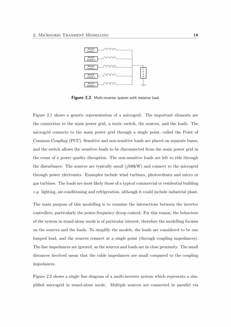
Figure 2.2: Multi-inverter system with resistive load.
Figure 2.1 shows a generic representation of a microgrid. The important elements are
the connection to the main power grid, a static switch, the sources, and the loads. The
microgrid connects to the main power grid through a single point, called the Point of
Common Coupling (PCC). Sensitive and non-sensitive loads are placed on separate buses,
and the switch allows the sensitive loads to be disconnected from the main power grid in
the event of a power quality disruption. The non-sensitive loads are left to ride through
the disturbance. The sources are typically small (¡500kW) and connect to the microgrid
through power electronics. Examples include wind turbines, photovoltaics and micro or
gas turbines. The loads are most likely those of a typical commercial or residential building
e.g. lighting, air-conditioning and refrigeration, although it could include industrial plant.
The main purpose of this modelling is to examine the interactions between the inverter
controllers, particularly the power-frequency droop control. For this reason, the behaviour
of the system in stand-alone mode is of particular interest, therefore the modelling focuses
on the sources and the loads. To simplify the models, the loads are considered to be one
lumped load, and the sources connect at a single point (through coupling impedances).
The line impedances are ignored, as the sources and loads are in close proximity. The small
distances involved mean that the cable impedances are small compared to the coupling
impedances.
Figure 2.2 shows a single line diagram of a multi-inverter system which represents a sim-
plified microgrid in stand-alone mode. Multiple sources are connected in parallel via
2. Microgrid Transient Modelling 19
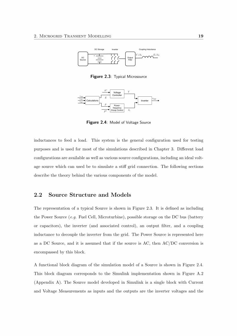
DC Source
+OutputFilter
DC Storage Inverter Coupling Inductance
V ∠δV E∠δE
Figure 2.3: Typical Microsource
Voltage Controller
Power-frequency
Droop Control
Inverter
δv
V
E vdq0Calculationsidq0
vdq0
E∗
P ∗
P
edq0
Figure 2.4: Model of Voltage Source
inductances to feed a load. This system is the general configuration used for testing
purposes and is used for most of the simulations described in Chapter 3. Different load
configurations are available as well as various source configurations, including an ideal volt-
age source which can used be to simulate a stiff grid connection. The following sections
describe the theory behind the various components of the model.
2.2 Source Structure and Models
The representation of a typical Source is shown in Figure 2.3. It is defined as including
the Power Source (e.g. Fuel Cell, Microturbine), possible storage on the DC bus (battery
or capacitors), the inverter (and associated control), an output filter, and a coupling
inductance to decouple the inverter from the grid. The Power Source is represented here
as a DC Source, and it is assumed that if the source is AC, then AC/DC conversion is
encompassed by this block.
A functional block diagram of the simulation model of a Source is shown in Figure 2.4.
This block diagram corresponds to the Simulink implementation shown in Figure A.2
(Appendix A). The Source model developed in Simulink is a single block with Current
and Voltage Measurements as inputs and the outputs are the inverter voltages and the
2. Microgrid Transient Modelling 20
source real and reactive power measurements (for display only). This model represents the
physical components of the Source shown in Figure 2.3, excluding the coupling inductance
which is modelled in a separate block. Voltages and currents are fed to a Calculations
block, which calculates the feedback values required by the controllers. These controllers
determine the desired inverter output voltage magnitude and phase. These values are
then used by the inverter to produce the output voltages for the source. The simplifying
assumption being made here is that the inverter is able to produce the exact voltage
requested by the control. This ignores the inverter switching harmonics. This assumption
is made as the switching frequency (generally in the kHz range) is much greater than the
line frequencies (50, 60Hz) under consideration, meaning the harmonic content is mostly
removed by the inverter output filter. The inverter output voltages then feed into the
coupling inductance (not shown). The Power Source and DC Storage are modelled as
part of the Power-frequency Droop Control block. These are examined in more detail in
Chapter 6. For most of this work, the assumption is made that the DC source is ideal, aside
from a limit on the maximum amount of power available from the source. This assumption
relies on the presence of sufficient storage on the DC bus to provide the transient power
demand in the event of a load change.
2.2.1 Inverter Model
An inverter is used to convert DC voltages and currents into AC by rapidly switching
power electronic devices. Since most distributed generation sources produce either DC
voltages, or AC voltages at a frequency incompatible with the grid, inverters are key
to interfacing DG to the grid. The inverter switching electronics can be controlled to
give the desired voltage waveform in terms of magnitude and phase, allowing control of
load voltage and power. In this work, only voltage source inverters are being considered.
Current source inverters are not considered here as they are not as well suited to the
application. A current source inverter cannot act independently of other sources, and
thus cannot perform the desired voltage regulation in stand alone mode.
2. Microgrid Transient Modelling 21
Time domain voltageCalculation abc - dq transform
V
!v
va
vb
vc
vd
vq
v0
Figure 2.5: Ideal Inverter
It is possible to simulate an inverter down to the component level [81] in electronic sim-
ulators such as SABRE or SPICE. However, this generally results in a model which is
relatively slow to simulate. Since this work is concerned with simulating several inverters
in parallel, and is mainly interested in the interactions between the inverter controllers, a
simplified model is used instead. In a physical inverter system, measurements are used to
calculate feedback values (e.g. voltage magnitude) required by the control system. Using
these calculated values, the control system generates desired values of voltage magnitude
and phase which the inverter switching algorithm uses to create a voltage waveform. The
proposed model ignores the switching process in the inverter, assuming it to be ideal in
the respect that the inverter can generate the exact voltages requested by the controllers.
These voltages are assumed to be balanced (i.e. of the same magnitude and 1200 out
of phase). This assumption means that a different model is necessary if the inverter is
required to generate unbalanced voltages. The inverter output is limited by the amount
of power available from the power source and in that respect the inverter differs from an
ideal voltage source. This model is based on the CERTS model [81], however the flux
quantities have been replaced with voltages. The CERTS model is a simplified version
of a full inverter model based on a voltage flux control strategy and so the use of flux
quantities was carried through to their simplified model. Voltage quantities are used here
instead, because these are more easily recognised.
The ideal inverter block (labelled as Inverter in Figure 2.4) takes as inputs the voltage
magnitude and angle requested by the control, and outputs voltages in the d-q reference
frame (see Section 2.2.1.1 for an explanation of the d-q transform). It theoretically consists
of two blocks (see Figure 2.5), one which calculates the time domain voltages from voltage
magnitude and phase, and system frequency (as given in Equations 2.1, 2.2 and 2.3) and
2. Microgrid Transient Modelling 22
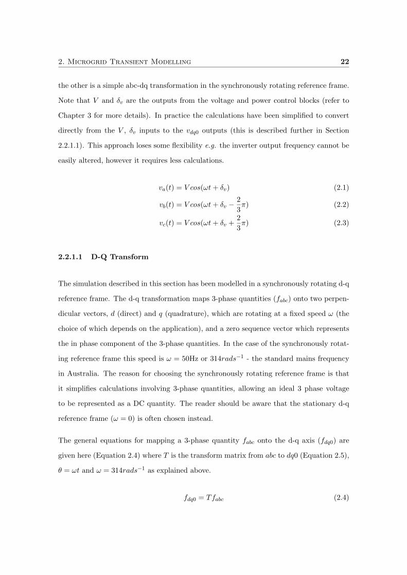
the other is a simple abc-dq transformation in the synchronously rotating reference frame.
Note that V and δv are the outputs from the voltage and power control blocks (refer to
Chapter 3 for more details). In practice the calculations have been simplified to convert
directly from the V , δv inputs to the vdq0 outputs (this is described further in Section
2.2.1.1). This approach loses some flexibility e.g. the inverter output frequency cannot be
easily altered, however it requires less calculations.
va(t) = V cos(ωt+ δv) (2.1)
vb(t) = V cos(ωt+ δv −2
3π) (2.2)
vc(t) = V cos(ωt+ δv +2
3π) (2.3)
2.2.1.1 D-Q Transform
The simulation described in this section has been modelled in a synchronously rotating d-q
reference frame. The d-q transformation maps 3-phase quantities (fabc) onto two perpen-
dicular vectors, d (direct) and q (quadrature), which are rotating at a fixed speed ω (the
choice of which depends on the application), and a zero sequence vector which represents
the in phase component of the 3-phase quantities. In the case of the synchronously rotat-
ing reference frame this speed is ω = 50Hz or 314rads−1 - the standard mains frequency
in Australia. The reason for choosing the synchronously rotating reference frame is that
it simplifies calculations involving 3-phase quantities, allowing an ideal 3 phase voltage
to be represented as a DC quantity. The reader should be aware that the stationary d-q
reference frame (ω = 0) is often chosen instead.
The general equations for mapping a 3-phase quantity fabc onto the d-q axis (fdq0) are
given here (Equation 2.4) where T is the transform matrix from abc to dq0 (Equation 2.5),
θ = ωt and ω = 314rads−1 as explained above.
fdq0 = Tfabc (2.4)
2. Microgrid Transient Modelling 23
a
c
b
d
q
Figure 2.6: 3 phase and d-q vectors
T =2
3
cosθ cos(θ − 2π
3 ) cos(θ + 2π3 )
−sinθ −sin(θ − 2π3 ) −sin(θ + 2π
3 )
12
12
12
(2.5)
Note that the direction of the d and q vectors is somewhat arbitrary, but the transform
equations will differ for a different choice of vectors. The abc and dq vectors corresponding
to these equations when θ = 0, can be seen in Figure 2.6.
The synchronously rotating d-q reference frame has several advantages over the standard
abc reference frame. In simulation, less frequent calculations are required because the d-q
quantities change more slowly than the 3-phase voltages they represent; the transform
separates the abc quantities into two independent vectors simplifying the design of the
model; and since the vectors change much more slowly, changes in frequency or magnitude
are much more easily observed. One disadvantage of using d-q transforms is that when
it comes to implementing the controller in hardware, extra calculations are required to
perform the transform. Another issue, when using d-q transforms in conjunction with
droop control, is that the system frequency may alter from ω = 50Hz, which causes the
d-q quantities to slowly oscillate. This can be fixed by allowing the transform frequency ω
to change so that it matches the current system frequency, however, the voltage magnitude
and frequency calculations are not affected, so this was not considered necessary for this
2. Microgrid Transient Modelling 24
work. Further information on the d-q reference frame can be found in many books on
power systems or electric machinery including [83].
Equations 2.6, 2.7 and 2.8 show the conversion from the time domain inverter voltages to
the d-q synchronously rotating reference frame, where θ = ωt.
vd =2
3(vacos(θ) + vbcos(θ −
2π
3) + vccos(θ +
2π
3) (2.6)
vq = −2
3(vasin(θ) + vbsin(θ − 2π
3) + vcsin(θ +
2π
3) (2.7)
v0 =1
3(va + vb + vc) (2.8)
The frequency ω in the time domain voltage equations (2.1, 2.2 and 2.3) is fixed at 50Hz
(since δv is controlled to change the frequency of the voltage waveforms as desired), and
the d-q axes also rotate at 50Hz, therefore the time domain voltage equations (2.1, 2.2 and
2.3) can be substituted into the dq voltage equations (2.6, 2.7 and 2.8), which simplifies
to Equations 2.9, 2.10 and 2.11. This is the form of the inverter equations implemented
in the simulation (Appendix A.1.2.4).
vd = V cos(δv) (2.9)
vq = V sin(δv) (2.10)
v0 = 0 (2.11)
2.2.1.2 The Per-Unit System
The per-unit system converts measurements from an absolute value (e.g. 5kW) to a
relative value which represents the fraction of the maximum value (e.g. 0.5pu). Per-unit
values are calculated by dividing the actual value by a base value which is generally the
rating of the source.
In this model, the per-unit system is used for the power signal required by the controller,
2. Microgrid Transient Modelling 25
Figure 2.7: Inverter Output Filter
and also for the display of real and reactive power values. The advantage of using the per-
unit system in this case is that it makes the controller scalable, i.e. the same controller can
be used for sources with different power ratings. It also gives more meaningful information
when viewing power outputs than the actual power in kW would. Generally when using
the per-unit system, all values in a system would be converted to per-unit values, including
currents, voltages and loads. While the per-unit system is useful for the real and reactive
power measurements, no advantage is gained from converting the rest of the system to
per-unit values and it was decided to leave the currents, voltages and loads as their actual
values.
Equation 2.12 gives the conversion from power in kW to per-unit power. To allow the
controller to be scalable, Pbase must be chosen as the rated power of the individual source.
If the sources have different power ratings then this value will differ for each source.
Ppu =PactualPbase
(2.12)
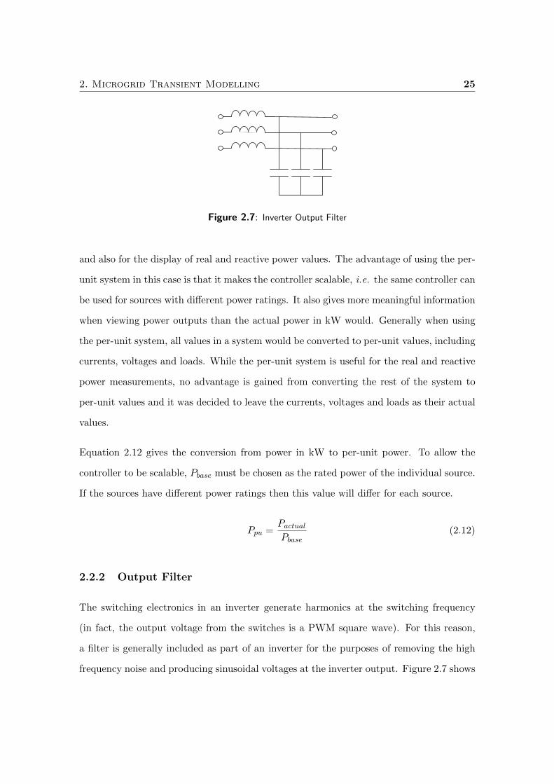
2.2.2 Output Filter
The switching electronics in an inverter generate harmonics at the switching frequency
(in fact, the output voltage from the switches is a PWM square wave). For this reason,
a filter is generally included as part of an inverter for the purposes of removing the high
frequency noise and producing sinusoidal voltages at the inverter output. Figure 2.7 shows
2. Microgrid Transient Modelling 26
the typical configuration for an inverter output filter. The inductance and capacitance
values are chosen so as to give a suitable cutoff frequency for the filter, one which filters
out the switching harmonics, but has minimal effect on the output sine wave. For a 50Hz
system with a 10kHz switching frequency this would typically be around 500Hz.
Due to the use of a simplified model for the inverter, the output filter is omitted from the
model. This ignores any phase shift caused by the filter, however, it is assumed that this
will be negligible compared to the phase shift due to the coupling inductance.
2.2.3 Coupling Inductance
The coupling inductance connects the output of the inverter filter to the microgrid. It
decouples the source from the microgrid allowing the source to independently set the
voltage magnitude and phase and thus allows the operation of the voltage regulation and
power sharing control.
The size of the coupling inductance needs to be chosen based on the power output of
the source. If δP , the voltage angle across the inductor, is assumed to be small, and the
magnitudes of the inverter voltage magnitude, V , and the common bus voltage magnitude,
E, are close together, then the power transfer relationship across the coupling inductance
can be approximated as Equation 2.13 [3].
P =3
2
V E
ωLsin(δP ) (2.13)
The maximum size of the inductor is based on the requirement that the P , δP relationship
remains close to linear. This means that the maximum power output (in Watts) should
be obtainable given the maximum δP allowable. The minimum size of the inductor is
governed by the accuracy with which the inverter can synthesize the voltage angle. This
is not a hard limit, rather, the performance degrades once the inductance becomes too
small.
2. Microgrid Transient Modelling 27
If we assume V and E are approximately 230V and δPmax = 300 and ω = 50 ∗ 2π radians
then the maximum inductance can be calculated as:
Lmax =3
2× 2302 × 1
2
50× 2π × Pmax=
2302
400πPmax(2.14)
For a 1kW source Lmax 1kW = 126mH. This means that a good choice of L is something
close to, but not larger than, 126mH, e.g. 100mH. For larger sources, the maximum
inductance can be obtained by dividing Lmax 1kW by the maximum power output in kW.
This is a simplified analysis, with restrictions on Q, V , I etc. ignored, but since a precise
value is not required, this method will suffice for the purposes of this research.
2.2.4 Measurement Block
The detail for the control blocks will be outlined in Chapter 3, however there are some
aspects of the controllers which are common and these will be dealt with here.
The general structure of the controller consists of a Calculations block, which feeds values
into separate power and voltage controllers (Figure 2.4). The output of these controllers is
fed to the inverter which then generates the required voltages. The required calculations
are real and reactive power (Equations 2.15 and 2.16), and the load voltage magnitude
and phase angle (Equations 2.17 and 2.18). Technically, the latter two terms are the mag-
nitude and phase of the load voltage space vector, and the terms are used interchangeably
throughout this thesis. The form of the d-q transform used in this work is not power
2. Microgrid Transient Modelling 28
invariant resulting in the 32 term in the power calculations.
P =3
2(vdid + vqiq) (2.15)
Q =3
2(vqid − vdiq) (2.16)
E =√e2d + e2
q (2.17)
δe = tan−1(eqed
) (2.18)
Note that the range of the inverse tan function is −π2 < δe <
π2 , however the actual angle
δe is not restricted at all. To accommodate this, some code has been written to allow the
angle δe to continue rotating beyond these limits. This avoids problems with calculations
of frequency, since the frequency is calculated as the rate of change of the angle δe. In a
real system, the frequency is not calculated this way and it is desirable for the range of δe
to be limited since this prevents the register containing the value of δe from overflowing.
Also, as mentioned previously, the power control is performed using the per unit system,
so the power needs to be divided by the base power of the source before being fed into the
power control block. i.e. Ppu = PactualPbase
.
2.3 Modelling of Other Circuit Elements
2.3.1 Load Resistors
Resistors are governed by the equation V = IR, therefore, assuming that the load is
balanced i.e. Ra = Rb = Rc = R, a resistive load can be modelled as a gain R, with
current as the input and voltage as the output. In the case where unbalanced loads are
required, the model is a little more complicated. Equation 2.19 gives the dq0 resistance
for a general 3 phase load Rabc, where T is the transform matrix from abc to dq0 defined
earlier in Equation 2.5.
Rdq0 = TRabcT−1 (2.19)
2. Microgrid Transient Modelling 29
To convert from currents to voltages the equation V = IR is again used. Equations 2.20,
2.21 and 2.22 give the resulting dq0 voltages. Note that Rdq0 is shortened to R for clarity.
The subscripts on R indicate the position in the matrix.
vd = R11id +R12iq +R13i0 (2.20)
vq = R21id +R22iq +R23i0 (2.21)
v0 = R31id +R32iq +R33i0 (2.22)
2.3.2 Inverter Coupling Inductances
Inductances are governed by the relationship that vL = L δiδt . They are slightly more com-
plicated to model in the d-q reference frame as they are frequency dependent components
and thus the rotating reference frame needs to be taken into account.
It can be shown [83] that in a rotating reference frame the equations relating voltages to
flux linkages are 2.23, 2.24 and 2.25, where s represents a derivative, ω is the frequency of
the rotating reference frame, and λd, λq, λ0 are the flux linkages.
vd = −ωλq + sλd (2.23)
vq = ωλd + sλq (2.24)
v0 = sλ0 (2.25)
Now λdq0s = TL(T )−1idq0 and for a diagonal matrix (i.e. balanced 3 phase inductance)
TL(T )−1 = L =
L 0 0
0 L 0
0 0 L
therefore substituting these two relationships into Equations 2.23, 2.24 and 2.25, and
2. Microgrid Transient Modelling 30
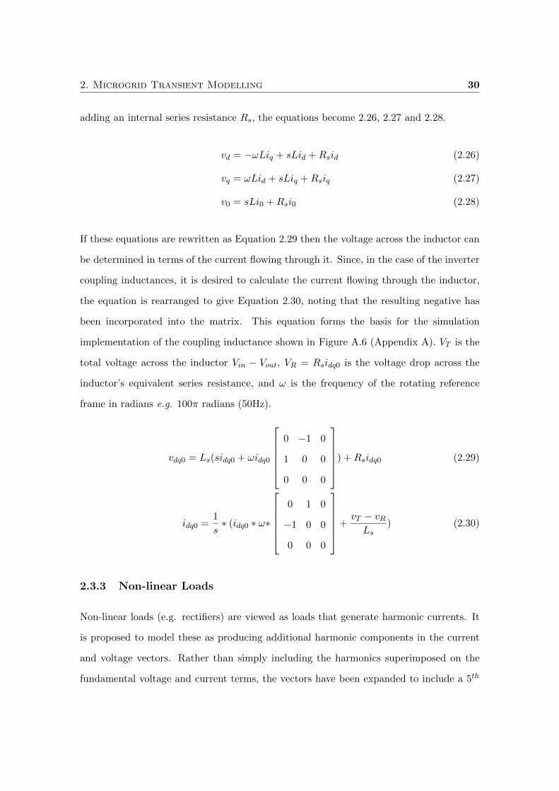
adding an internal series resistance Rs, the equations become 2.26, 2.27 and 2.28.
vd = −ωLiq + sLid +Rsid (2.26)
vq = ωLid + sLiq +Rsiq (2.27)
v0 = sLi0 +Rsi0 (2.28)
If these equations are rewritten as Equation 2.29 then the voltage across the inductor can
be determined in terms of the current flowing through it. Since, in the case of the inverter
coupling inductances, it is desired to calculate the current flowing through the inductor,
the equation is rearranged to give Equation 2.30, noting that the resulting negative has
been incorporated into the matrix. This equation forms the basis for the simulation
implementation of the coupling inductance shown in Figure A.6 (Appendix A). VT is the
total voltage across the inductor Vin − Vout, VR = Rsidq0 is the voltage drop across the
inductor’s equivalent series resistance, and ω is the frequency of the rotating reference
frame in radians e.g. 100π radians (50Hz).
vdq0 = Ls(sidq0 + ωidq0
0 −1 0
1 0 0
0 0 0
) +Rsidq0 (2.29)
idq0 =1
s∗ (idq0 ∗ ω∗
0 1 0
−1 0 0
0 0 0
+vT − vRLs
) (2.30)
2.3.3 Non-linear Loads
Non-linear loads (e.g. rectifiers) are viewed as loads that generate harmonic currents. It
is proposed to model these as producing additional harmonic components in the current
and voltage vectors. Rather than simply including the harmonics superimposed on the
fundamental voltage and current terms, the vectors have been expanded to include a 5th
2. Microgrid Transient Modelling 31
harmonic terms e.g. Equation 2.31. Note that the term v05 is not strictly necessary, as
the zero sequence terms are independent of frequency, (see Equation 2.4), however the
inclusion of this term allows for the re-use of simulation component blocks for the 5th
harmonic calculations.
V =
vd1
vq1
v01
vd5
vq5
v05
(2.31)
The d-q reference frame for the 5th harmonic terms rotates at 250Hz, or the 5th harmonic
frequency. To calculate voltage magnitude, angle, and real and reactive power the har-
monics are then converted back to a 50Hz reference frame and then the standard d-q
equations are used. The transform between the two reference frames can be performed
by converting the 5th harmonic terms back to the abc reference frame, and then into the
50Hz rotating reference frame. If these two steps are simplified the resulting equations are
2.32 and 2.33 where θ = ∆ωt and ∆ω is the frequency difference between the two rotating
reference frames, in this case 200Hz or 400π radians. Note that these equations do not
include the original fundamental quantities.
vd = vd5cosθ + vq5sinθ (2.32)
vq = vd5sinθ − vq5cosθ (2.33)
The final 50Hz dq quantities (2.34, 2.35) are the sum of the original 50Hz quantities (vd1
and vq1) and the converted 5th harmonics (2.32, 2.33). Since the zero sequence quantities
are independent of the speed of rotation of the d-q reference frame (the f0 term in Equation
2.4 only involves the original abc vectors and no terms in ω or θ) the final zero sequence

2. Microgrid Transient Modelling 32
voltage is just the sum of the two zero sequence voltages (Equation 2.36).
vd = vd1 + vd5cosθ + vq5sinθ (2.34)
vq = vq1 + vd5sinθ − vq5cosθ (2.35)
v0 = v01 + v05 (2.36)
Another approach would be to alter the calculations so that they could directly deal with
the fundamental and harmonic terms, however it is unclear if there is any benefit to this,
and so it has not been implemented.
Clearly this work can be extended to include further harmonics by introducing further
terms in the current and voltage vectors, and applying equations 2.34, 2.35 and 2.36 to
the different harmonic terms. The terms vd5 and vq5 will need to be replaced by the
relevant harmonic terms (i.e. vdn and vqn for nth harmonics) and the frequency of ω will
need to be changed to the harmonic frequency - 50Hz (i.e. (50n−50)Hz for nth harmonics).
A typical load is demonstrated in Equation 2.37. Fundamental components of the load
voltage are generated in proportion to the fundamental components of the load current.
Harmonic components of the load voltage are importantly generated in proportion to both
the harmonic and fundamental components of the current. This is typical of non-linear
loads (e.g. rectifiers) where harmonic currents are generated in response to the applied
fundamental voltages.
V =
10 0 0 0
0 10 0 0
1 0 3 0
0 1 0 3
id1
iq1
id5
iq5
(2.37)
Separating the harmonics in this manner has two major advantages: in most sections of
the model 5th harmonics are represented as DC quantities, simplifying the calculations;
and it makes it much easier to observe the behaviour of the harmonics when they are

2. Microgrid Transient Modelling 33
considered separately.
2.4 SimPowerSystems
Due to mathematical constraints it proved too difficult to incorporate transformers into
the model described in this chapter. For this reason, the unbalanced load simulations
have been implemented using MATLAB/Simulink’s SimPowerSystems library. This con-
tains model blocks for the line inductances, transformers and loads. SimPowerSystems is
significantly slower than the library developed in this work. The developed library has
consequently been used in preference to SimPowerSystems in some situations.
SimPowerSystems is a Simulink library which allows simulation of electrical systems. Since
the connections between the SimPowerSystems electrical components are representing elec-
trical wiring rather than the simple signal connections of standard Simulink, SimPower-
Systems uses different connections to standard Simulink. This means it is necessary to
interface the Voltage Source blocks (which have been created in the standard Simulink
format) with the SimPowerSystems connectors. The simplest way to achieve this is to use
the Controlled Voltage Source, which generates an output voltage based on a standard
Simulink signal input.
The circuit is configured with three single phase Controlled Voltage Sources connected
in a Y configuration (the library doesn’t contain a 3 phase Controlled Voltage Source).
These voltages feed into the coupling inductance (with internal series resistance) which
is represented using a 3 Phase Series RLC Branch block configured as an inductor and
resistor. This is then connected to a ∆ − Y n configured Three-Phase Transformer (Two
Windings) block, which feeds a star connected load (three single-phase Series RLC Branch
blocks connected in star). The neutral of the load is connected to the neutral of the
transformer Y . The source neutral is floating. Simulation details can be found in Appendix
A.3.

2. Microgrid Transient Modelling 34
2.5 Summary
The model outlined above has been designed to analyse the behaviour of multiple inverters
running in parallel. It can be adjusted to account for any number of different sources, and
the load profile can be adjusted in various ways including reactive, unbalanced, and non-
linear loads (in fact any load that can be described with a transfer function relating voltage
to current). The magnitude or type of the load could also be configured to change during
the simulation. Multiple loads can be included, provided they are modelled as a single
lumped element. Line impedances can be included by modifying the coupling inductances.
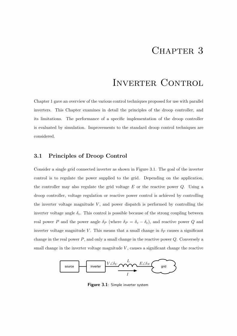
Chapter 3
Inverter Control
Chapter 1 gave an overview of the various control techniques proposed for use with parallel
inverters. This Chapter examines in detail the principles of the droop controller, and
its limitations. The performance of a specific implementation of the droop controller
is evaluated by simulation. Improvements to the standard droop control techniques are
considered.
3.1 Principles of Droop Control
Consider a single grid connected inverter as shown in Figure 3.1. The goal of the inverter
control is to regulate the power supplied to the grid. Depending on the application,
the controller may also regulate the grid voltage E or the reactive power Q. Using a
droop controller, voltage regulation or reactive power control is achieved by controlling
the inverter voltage magnitude V , and power dispatch is performed by controlling the
inverter voltage angle δv. This control is possible because of the strong coupling between
real power P and the power angle δP (where δP = δv − δe), and reactive power Q and
inverter voltage magnitude V . This means that a small change in δP causes a significant
change in the real power P , and only a small change in the reactive power Q. Conversely a
small change in the inverter voltage magnitude V , causes a significant change the reactive
source inverter gridV !!V E!!E
L
I
Figure 3.1: Simple inverter system

3. Inverter Control 36
power, but only a small change to the real power. This can be shown by substituting
appropriate values into Equations 3.1 and 3.2. These equations are the real and reactive
power transfer from the inverter assuming (V −E) and δP are small. Since reactive power
can be used to control the system voltage E, the inverter voltage V can also be used to
regulate E.
P3φ =3
2
V E
ωLsin(δP ) (3.1)
Q3φ =3
2
V
ωL(V − EcosδP ) (3.2)
Now consider a stand-alone system with multiple inverters (Figure 3.2). The aim of the
power control changes from dispatching a pre-determined amount of power, to sharing the
load between the sources. Load sharing is achieved by adjusting each source’s frequency in
response to load power. As real output power is increased the system frequency is reduced.
The power-frequency droop characteristic is based on Equation 3.3, where ωi(t) is the
frequency output by the ith inverter at time t, w∗ is the nominal or base system frequency
(generally 50 or 60Hz), Pi(t) is the 3 phase power output of the source i at time t, and mi
is the droop co-efficient, or the gradient of the power-frequency droop characteristic, for
source i. Note that this equation represents the steady-state characteristic. The dynamic
behaviour may deviate from this.
ωi(t) = ω∗ −miPi(t) (3.3)
Another form of the droop characteristic is also common. This second form (Equation
3.4) introduces the term P ∗, called the power setpoint, which allows an operating point to
be specified for the source when the system is operating at nominal frequency. Essentially
this allows the user to specify a power output level for the source when the grid is con-
nected. For this reason, this second form would generally be chosen for a grid-connected
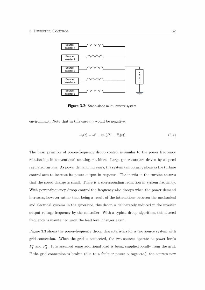
3. Inverter Control 37
Source/Inverter 1
Source/Inverter 3 L
oad
Source/Inverter 2
Source/Inverter 4
Source/Inverter 5
Figure 3.2: Stand-alone multi-inverter system
environment. Note that in this case mi would be negative.
ωi(t) = ω∗ −mi(P∗i − Pi(t)) (3.4)
The basic principle of power-frequency droop control is similar to the power frequency
relationship in conventional rotating machines. Large generators are driven by a speed
regulated turbine. As power demand increases, the system temporarily slows as the turbine
control acts to increase its power output in response. The inertia in the turbine ensures
that the speed change is small. There is a corresponding reduction in system frequency.
With power-frequency droop control the frequency also droops when the power demand
increases, however rather than being a result of the interactions between the mechanical
and electrical systems in the generator, this droop is deliberately induced in the inverter
output voltage frequency by the controller. With a typical droop algorithm, this altered
frequency is maintained until the load level changes again.
Figure 3.3 shows the power-frequency droop characteristics for a two source system with
grid connection. When the grid is connected, the two sources operate at power levels
P ∗1 and P ∗2 . It is assumed some additional load is being supplied locally from the grid.
If the grid connection is broken (due to a fault or power outage etc.), the sources now
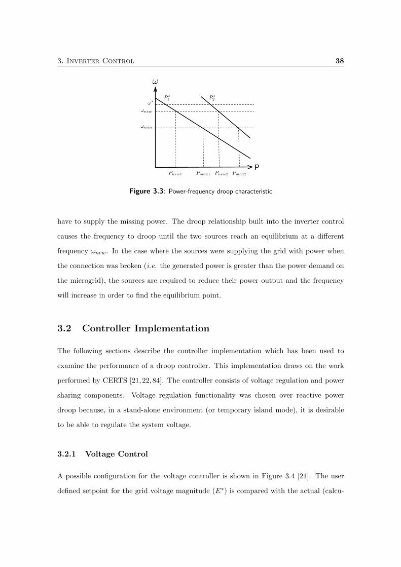
3. Inverter Control 38
P
!min
!
P !1 P !
2
Pmax1 Pmax2
!!
!new
Pnew1 Pnew2
Figure 3.3: Power-frequency droop characteristic
have to supply the missing power. The droop relationship built into the inverter control
causes the frequency to droop until the two sources reach an equilibrium at a different
frequency ωnew. In the case where the sources were supplying the grid with power when
the connection was broken (i.e. the generated power is greater than the power demand on
the microgrid), the sources are required to reduce their power output and the frequency
will increase in order to find the equilibrium point.
3.2 Controller Implementation
The following sections describe the controller implementation which has been used to
examine the performance of a droop controller. This implementation draws on the work
performed by CERTS [21,22,84]. The controller consists of voltage regulation and power
sharing components. Voltage regulation functionality was chosen over reactive power
droop because, in a stand-alone environment (or temporary island mode), it is desirable
to be able to regulate the system voltage.
3.2.1 Voltage Control
A possible configuration for the voltage controller is shown in Figure 3.4 [21]. The user
defined setpoint for the grid voltage magnitude (E∗) is compared with the actual (calcu-
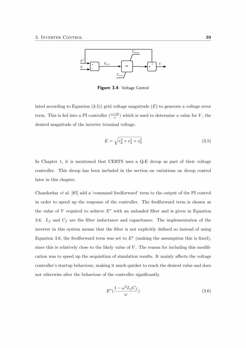
3. Inverter Control 39
+- PI
Vmax
E!Eerr
Vmin
VE
++
Figure 3.4: Voltage Control
lated according to Equation (3.5)) grid voltage magnitude (E) to generate a voltage error
term. This is fed into a PI controller ( s+10s ) which is used to determine a value for V , the
desired magnitude of the inverter terminal voltage.
E =√e2d + e2
q + e20 (3.5)
In Chapter 1, it is mentioned that CERTS uses a Q-E droop as part of their voltage
controller. This droop has been included in the section on variations on droop control
later in this chapter.
Chandorkar et al. [85] add a ‘command feedforward’ term to the output of the PI control
in order to speed up the response of the controller. The feedforward term is chosen as
the value of V required to achieve E∗ with an unloaded filter and is given in Equation
3.6. Lf and Cf are the filter inductance and capacitance. The implementation of the
inverter in this system means that the filter is not explicitly defined so instead of using
Equation 3.6, the feedforward term was set to E∗ (making the assumption this is fixed),
since this is relatively close to the likely value of V . The reason for including this modifi-
cation was to speed up the acquisition of simulation results. It mainly affects the voltage
controller’s startup behaviour, making it much quicker to reach the desired value and does
not otherwise alter the behaviour of the controller significantly.
E∗(1− ω2LfCf
ω) (3.6)
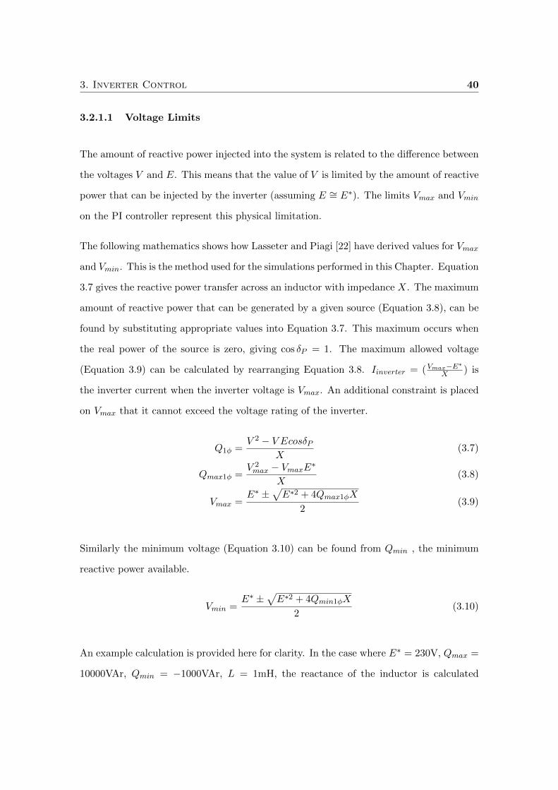
3. Inverter Control 40
3.2.1.1 Voltage Limits
The amount of reactive power injected into the system is related to the difference between
the voltages V and E. This means that the value of V is limited by the amount of reactive
power that can be injected by the inverter (assuming E ∼= E∗). The limits Vmax and Vmin
on the PI controller represent this physical limitation.
The following mathematics shows how Lasseter and Piagi [22] have derived values for Vmax
and Vmin. This is the method used for the simulations performed in this Chapter. Equation
3.7 gives the reactive power transfer across an inductor with impedance X. The maximum
amount of reactive power that can be generated by a given source (Equation 3.8), can be
found by substituting appropriate values into Equation 3.7. This maximum occurs when
the real power of the source is zero, giving cos δP = 1. The maximum allowed voltage
(Equation 3.9) can be calculated by rearranging Equation 3.8. Iinverter = (Vmax−E∗
X ) is
the inverter current when the inverter voltage is Vmax. An additional constraint is placed
on Vmax that it cannot exceed the voltage rating of the inverter.
Q1φ =V 2 − V EcosδP
X(3.7)
Qmax1φ =V 2max − VmaxE∗
X(3.8)
Vmax =E∗ ±
√E∗2 + 4Qmax1φX
2(3.9)
Similarly the minimum voltage (Equation 3.10) can be found from Qmin , the minimum
reactive power available.
Vmin =E∗ ±
√E∗2 + 4Qmin1φX
2(3.10)
An example calculation is provided here for clarity. In the case where E∗ = 230V, Qmax =
10000VAr, Qmin = −1000VAr, L = 1mH, the reactance of the inductor is calculated
3. Inverter Control 41
according to Equation 3.11. Values can then be substituted into Equations 3.9 and 3.10
as given in Equations 3.12 and 3.13.
|XL| = ωL = 2π ∗ 50 ∗ 0.001 = 0.3Ω (3.11)
Vmax =230±
√2302 + 4 ∗ 10000 ∗ 0.3
2= 242,−12 (3.12)
Vmin =230±
√2302 + 4 ∗ (−10000) ∗ 0.3
2= 216, 14 (3.13)
Since Vmax = −12 and Vmin = 14 are clearly not sensible values, the solutions are Vmax =
242 and Vmin = 216. Note that this calculation is for single phase. Q values will needed
to be adjusted to per phase values for 3 phase calculations.
This method of calculating voltage limits makes some assumptions. The first is that
the measured grid voltage E is always closely matched to the setpoint E∗, which may
not always be the case (Australian standards allow voltages to deviate by +10, -6% AS
60038). Secondly it assumes that the inverter can always supply reactive power Q = Qmax
regardless of the real power being supplied. The first problem can be solved by making
Vmax and Vmin change dynamically depending on the measured value E rather than being
statically calculated using the setpoint E∗. This can be approximated by calculating the
maximum allowed deviation of V from E∗ (e.g. Vmax and Vmin are 12V and 14V away
from E∗ in the example above) and instead allowing V to deviate that amount from the
measured E. This would result in Equations 3.14 and 3.15.
Vmax adj = (Vmax − E∗) + E (3.14)
Vmin adj = (E∗ − Vmin) + E (3.15)
The second problem could be solved by intelligent selection of Qmax and Qmin (for example
set them based on the current ratings on the inverter).

3. Inverter Control 42
+-
0
!Pmax
!V
P !
P
+-
!EPowerSource
PI
0
Pmax
Figure 3.5: Power dispatch
3.2.2 Power Control
If power sharing is not required for a particular source, then power control can be achieved
as shown in Figure 3.5 [22]. This controller is not used in the testing, but is described
here for completeness. As with the voltage controller, an error term is calculated from
the power setpoint and the actual power (as calculated by Equation (3.16) or (3.17)). An
additional constraint is that the power setpoint P ∗ is limited to being between 0 and Pmax
(shown on the diagram as the Power Source block). Note that the Power Source block
only models the limit in the power available, not the dynamics of the source. Power Source
blocks are covered in more detail in Chapter 6. The power error is fed into a PI controller
which calculates the required value of δP . The PI controller has limits placed on the angle
δPmax. This is generally between 00 and 300 to satisfy the requirement that the P (δP )
function be close to linear.
P = vaia + vbib + vcic (3.16)
P =3
2(vdid + vqiq) (3.17)
3.2.3 Power Sharing
When the microgrid is disconnected from the main power grid for whatever reason, the
power sources in the microgrid need to share the load between them. Power-frequency
droop control can be used to achieve this. Figure 3.6 shows an implementation of a power-
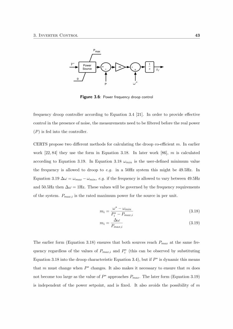
3. Inverter Control 43
m
P
!V
Pmax
0
PowerSource
+- +
-1s
!!
P!
Figure 3.6: Power frequency droop control
frequency droop controller according to Equation 3.4 [21]. In order to provide effective
control in the presence of noise, the measurements need to be filtered before the real power
(P ) is fed into the controller.
CERTS propose two different methods for calculating the droop co-efficient m. In earlier
work [22, 84] they use the form in Equation 3.18. In later work [86], m is calculated
according to Equation 3.19. In Equation 3.18 ωmin is the user-defined minimum value
the frequency is allowed to droop to e.g. in a 50Hz system this might be 49.5Hz. In
Equation 3.19 ∆ω = ωmax−ωmin, e.g. if the frequency is allowed to vary between 49.5Hz
and 50.5Hz then ∆ω = 1Hz. These values will be governed by the frequency requirements
of the system. Pmax,i is the rated maximum power for the source in per unit.
mi =ω∗ − ωminP ∗i − Pmax,i
(3.18)
mi =∆ω
Pmax,i(3.19)
The earlier form (Equation 3.18) ensures that both sources reach Pmax at the same fre-
quency regardless of the values of Pmax,i and P ∗i (this can be observed by substituting
Equation 3.18 into the droop characteristic Equation 3.4), but if P ∗ is dynamic this means
that m must change when P ∗ changes. It also makes it necessary to ensure that m does
not become too large as the value of P ∗ approaches Pmax. The later form (Equation 3.19)
is independent of the power setpoint, and is fixed. It also avoids the possibility of m
3. Inverter Control 44
becoming too large. Since Pmax is in per unit form, it is generally the same for all sources
(although it would be possible to define Pmax < 1 for a particular source, if desired),
meaning m is also the same for all sources. This form of the equation does not ensure that
all sources reach Pmax at the same frequency if Pmax is not the same for all sources.
For this work, P ∗ is chosen to be fixed and the same value for each of the sources, so the
form chosen isn’t important.
3.2.3.1 Power Source Block
Part of the power controller described in Figure 3.6 is the Power Source block. The
detail for the Power Source blocks is in Chapter 6, but a brief summary is provided here.
The basic idea of the Power Source block is to provide limits for P ∗ such that P ∗ doesn’t
exceed the maximum power output of the source. These so called Maximum Power Output
models simplify the dynamics of the power source into a transfer function which describes
the change in the maximum power available from the source over time. Various source
models are discussed, including an ideal source, microturbine, fuel cell and renewable
sources.
3.3 Problems with Droop Control
Chapter 1 briefly mentions several known problems with droop controllers. The following
gives more details of these problems.
1. Power-frequency droop control gives rise to an unavoidable steady-state frequency
error. The value of the droop co-efficient m can be adjusted to decrease this er-
ror, however this leads to slower responses from the controller, and the error cannot
be eliminated altogether. In most cases this is not a significant issue, and a fre-
quency difference between the microgrid and the main power grid can aid in resyn-
chronisation with the main grid once the problem that caused the disconnection is

3. Inverter Control 45
corrected [22].
2. Reactive currents can circulate between inverters due to small errors in voltage
setpoints, differences in the line voltages measured at different inverters, or different
output inductances. This problem is exacerbated by the close proximity of sources
to each other. This means that the line impedances between sources can be quite
small. These circulating currents can consequently be quite large, causing inverter
ratings to be exceeded, possibly damaging equipment.
3. The droop controller does not share the generation of reactive power in the presence
of different output inductances. If reactive power is not shared, this could lead to
inverter ratings being exceeded in the source taking the greater share of the reactive
load.
4. Droop control is not designed to perform well with non-linear loads, and makes no
attempt to minimise or share harmonic currents. This is important, because in some
situations loads can be highly non-linear and contain a high proportion of harmonic
currents. If these are not shared, then the ratings of the systems would need to be
reduced to make allowances for this. The harmonic current drawn by the inverter
can cause resonance and undesirable interactions in the microgrid, which can have
a serious effect on the power quality [87].
5. The relationship between P and δP , and Q and V indicated in Equations 3.1 and
3.2 assumes that the overall impedance between the inverter and the load is mainly
inductive. In a low voltage system this is not necessarily the case, and in some
circumstances the line impedance is mainly resistive [6]. In the case of pure resistive
impedance, the real power would be linked with the voltage magnitude, and the
reactive power with the voltage angle. This is completely opposite to the assumption
which is made in droop control and could render the controller ineffective.
6. The standard droop controller does not attempt to alleviate voltage imbalance caused
by unbalanced loads. This imbalance has been shown to decrease the lifespan of
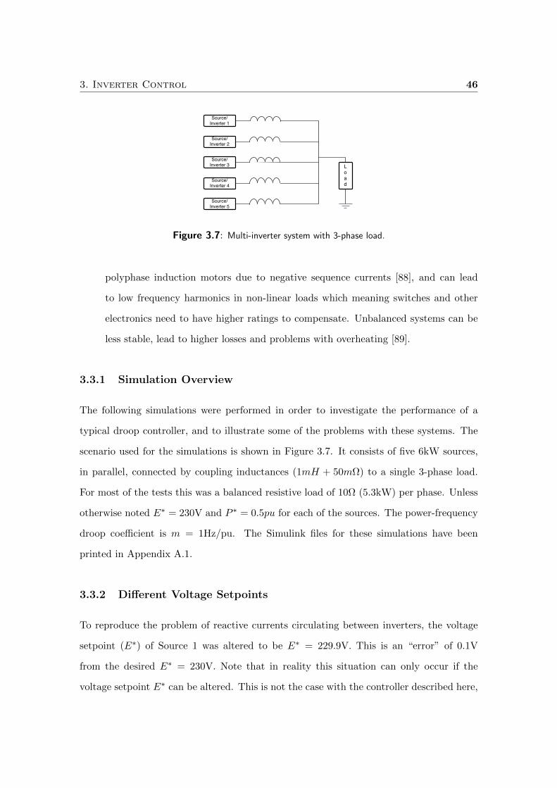
3. Inverter Control 46
Source/Inverter 1
Source/Inverter 3 L
oad
Source/Inverter 2
Source/Inverter 4
Source/Inverter 5
Figure 3.7: Multi-inverter system with 3-phase load.
polyphase induction motors due to negative sequence currents [88], and can lead
to low frequency harmonics in non-linear loads which meaning switches and other
electronics need to have higher ratings to compensate. Unbalanced systems can be
less stable, lead to higher losses and problems with overheating [89].
3.3.1 Simulation Overview
The following simulations were performed in order to investigate the performance of a
typical droop controller, and to illustrate some of the problems with these systems. The
scenario used for the simulations is shown in Figure 3.7. It consists of five 6kW sources,
in parallel, connected by coupling inductances (1mH + 50mΩ) to a single 3-phase load.
For most of the tests this was a balanced resistive load of 10Ω (5.3kW) per phase. Unless
otherwise noted E∗ = 230V and P ∗ = 0.5pu for each of the sources. The power-frequency
droop coefficient is m = 1Hz/pu. The Simulink files for these simulations have been
printed in Appendix A.1.
3.3.2 Different Voltage Setpoints
To reproduce the problem of reactive currents circulating between inverters, the voltage
setpoint (E∗) of Source 1 was altered to be E∗ = 229.9V. This is an “error” of 0.1V
from the desired E∗ = 230V. Note that in reality this situation can only occur if the
voltage setpoint E∗ can be altered. This is not the case with the controller described here,
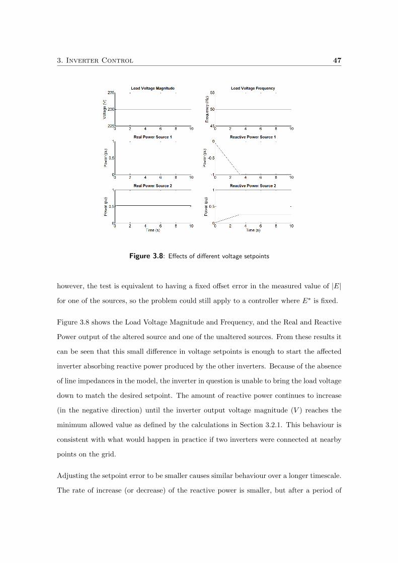
3. Inverter Control 47
Figure 3.8: Effects of different voltage setpoints
however, the test is equivalent to having a fixed offset error in the measured value of |E|
for one of the sources, so the problem could still apply to a controller where E∗ is fixed.
Figure 3.8 shows the Load Voltage Magnitude and Frequency, and the Real and Reactive
Power output of the altered source and one of the unaltered sources. From these results it
can be seen that this small difference in voltage setpoints is enough to start the affected
inverter absorbing reactive power produced by the other inverters. Because of the absence
of line impedances in the model, the inverter in question is unable to bring the load voltage
down to match the desired setpoint. The amount of reactive power continues to increase
(in the negative direction) until the inverter output voltage magnitude (V ) reaches the
minimum allowed value as defined by the calculations in Section 3.2.1. This behaviour is
consistent with what would happen in practice if two inverters were connected at nearby
points on the grid.
Adjusting the setpoint error to be smaller causes similar behaviour over a longer timescale.
The rate of increase (or decrease) of the reactive power is smaller, but after a period of

3. Inverter Control 48
time, the reactive power for at least one of the sources will still reach its maximum (or
minimum) value as dictated by the voltage limits.
3.3.3 Reactive Power Sharing
The aim of this simulation was to test the reactive power sharing in the presence of
coupling inductances with different impedances. The coupling inductance of Source 2
is changed to 0.9mH + 50mΩ, with the coupling inductances for the other four sources
remaining at 1mH + 50mΩ. The load used was 22.8kW + 15.5kV Ar (7.6kW + 5.2kV Ar
per phase) configured as a 15Ω resistor in parallel with an inductor (20mH) . The load
inductor contained a series resistance (5Ω).
Figure 3.9 shows the Voltage Magnitude and Frequency for the load, and the Real and
Reactive Power outputs for Sources 1 and 2, where Source 1 has the standard 1mH+50mΩ
coupling inductance, and Source 2 has the altered (0.9mH+50mΩ) inductance. The results
show that the reactive power output for Source 1 is lower than that for Source 2. This
confirms that differences in the coupling inductances do affect the reactive power sharing
amongst the sources. Coupling a source to the load through a larger inductor means
that source will provide less of the reactive load, while a source with a smaller coupling
inductance will provide more of the reactive load.
3.3.4 Harmonics
This test aims to examine the performance of the controller when the source is supplying
non-linear loads, such as a rectifier. The Simulink files for these simulations have been
printed in Appendix A.2. The non-linear load is modelled as a resistor (10Ω / 5.3kW per
phase) plus an injection of 5th harmonic current which is 23% of the magnitude of the
fundamental current. This value was chosen by simulating the performance of an actual
rectifier load and looking at the current harmonic components.
Figure 3.10 shows the baseline performance when an ideal source is supplying the load.
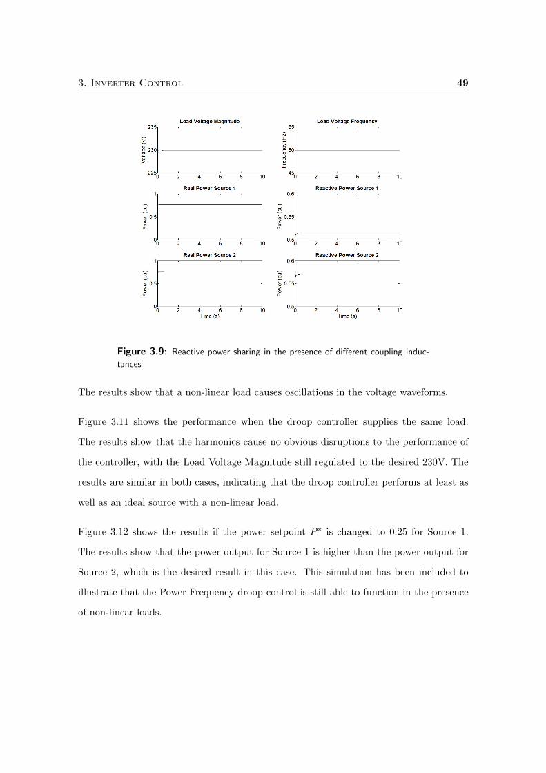
3. Inverter Control 49
Figure 3.9: Reactive power sharing in the presence of different coupling induc-
tances
The results show that a non-linear load causes oscillations in the voltage waveforms.
Figure 3.11 shows the performance when the droop controller supplies the same load.
The results show that the harmonics cause no obvious disruptions to the performance of
the controller, with the Load Voltage Magnitude still regulated to the desired 230V. The
results are similar in both cases, indicating that the droop controller performs at least as
well as an ideal source with a non-linear load.
Figure 3.12 shows the results if the power setpoint P ∗ is changed to 0.25 for Source 1.
The results show that the power output for Source 1 is higher than the power output for
Source 2, which is the desired result in this case. This simulation has been included to
illustrate that the Power-Frequency droop control is still able to function in the presence
of non-linear loads.
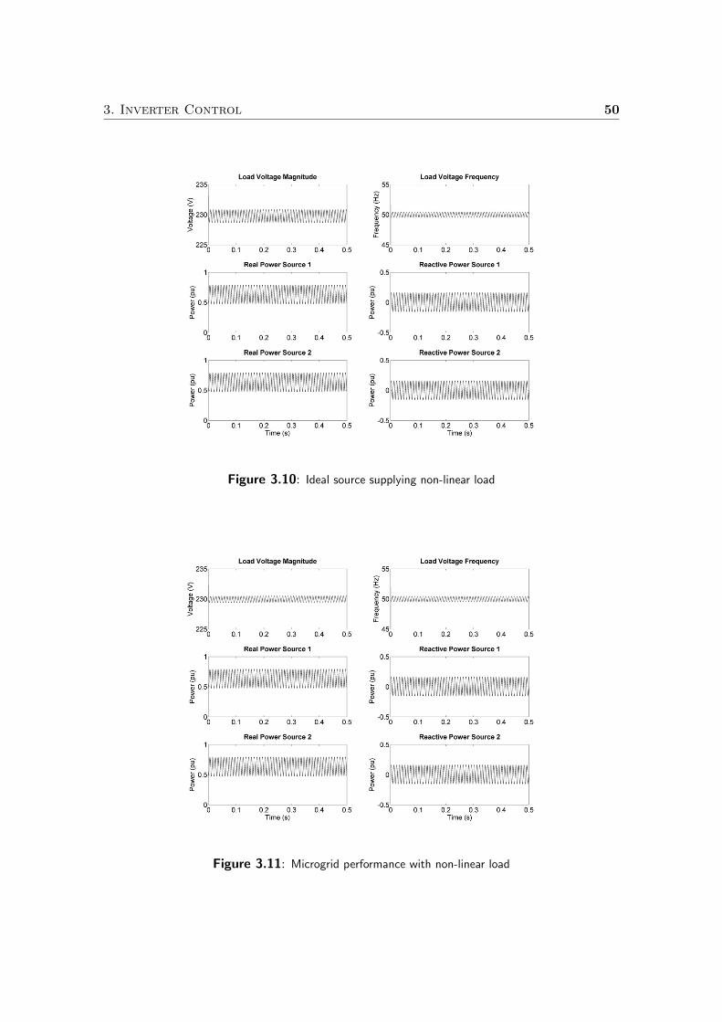
3. Inverter Control 50
Figure 3.10: Ideal source supplying non-linear load
Figure 3.11: Microgrid performance with non-linear load
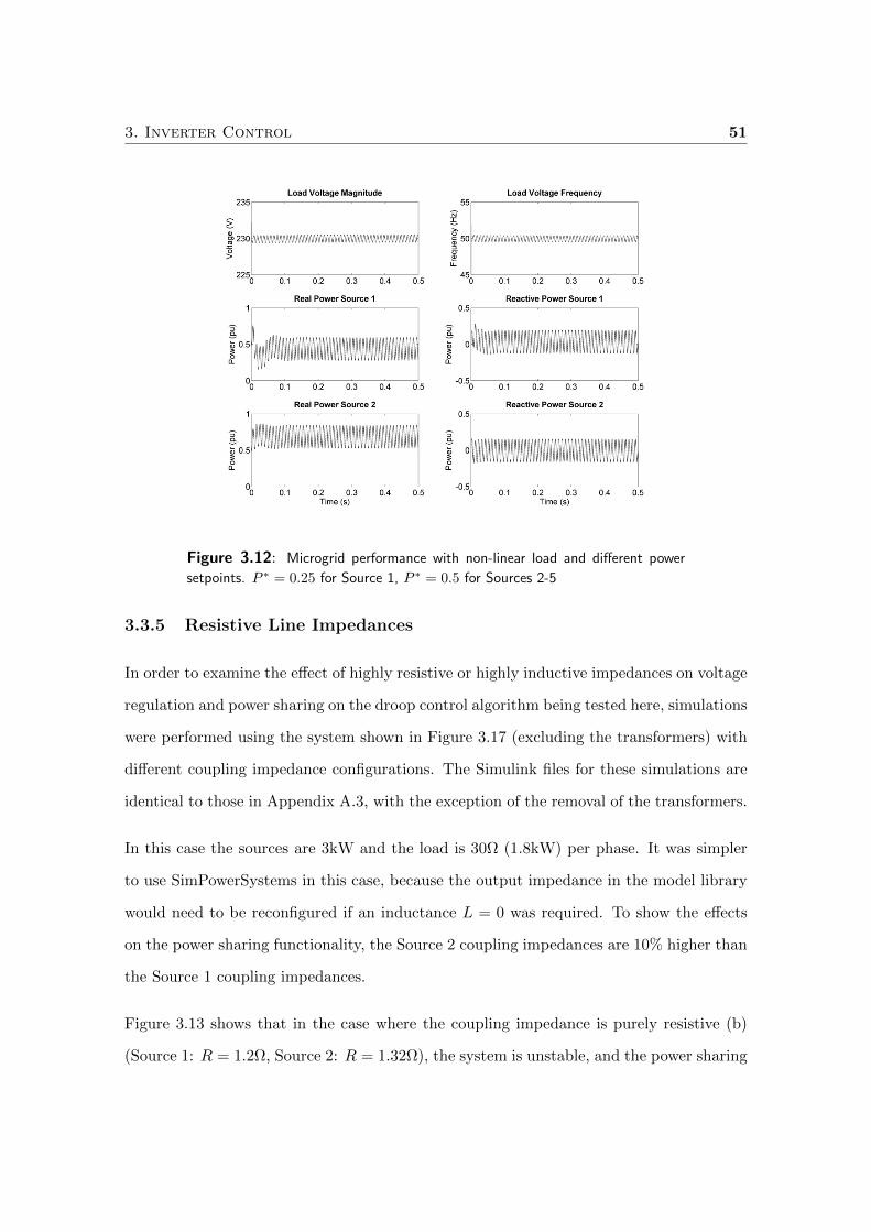
3. Inverter Control 51
Figure 3.12: Microgrid performance with non-linear load and different power
setpoints. P ∗ = 0.25 for Source 1, P ∗ = 0.5 for Sources 2-5
3.3.5 Resistive Line Impedances
In order to examine the effect of highly resistive or highly inductive impedances on voltage
regulation and power sharing on the droop control algorithm being tested here, simulations
were performed using the system shown in Figure 3.17 (excluding the transformers) with
different coupling impedance configurations. The Simulink files for these simulations are
identical to those in Appendix A.3, with the exception of the removal of the transformers.
In this case the sources are 3kW and the load is 30Ω (1.8kW) per phase. It was simpler
to use SimPowerSystems in this case, because the output impedance in the model library
would need to be reconfigured if an inductance L = 0 was required. To show the effects
on the power sharing functionality, the Source 2 coupling impedances are 10% higher than
the Source 1 coupling impedances.
Figure 3.13 shows that in the case where the coupling impedance is purely resistive (b)
(Source 1: R = 1.2Ω, Source 2: R = 1.32Ω), the system is unstable, and the power sharing
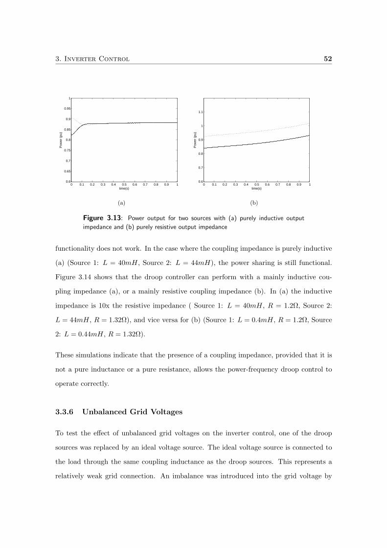
3. Inverter Control 52
0 0.1 0.2 0.3 0.4 0.5 0.6 0.7 0.8 0.9 10.6
0.65
0.7
0.75
0.8
0.85
0.9
0.95
1
time(s)
Pow
er (
pu)
(a)
0 0.1 0.2 0.3 0.4 0.5 0.6 0.7 0.8 0.9 10.6
0.7
0.8
0.9
1
1.1
time(s)
Pow
er (
pu)
(b)
Figure 3.13: Power output for two sources with (a) purely inductive output
impedance and (b) purely resistive output impedance
functionality does not work. In the case where the coupling impedance is purely inductive
(a) (Source 1: L = 40mH, Source 2: L = 44mH), the power sharing is still functional.
Figure 3.14 shows that the droop controller can perform with a mainly inductive cou-
pling impedance (a), or a mainly resistive coupling impedance (b). In (a) the inductive
impedance is 10x the resistive impedance ( Source 1: L = 40mH, R = 1.2Ω, Source 2:
L = 44mH, R = 1.32Ω), and vice versa for (b) (Source 1: L = 0.4mH, R = 1.2Ω, Source
2: L = 0.44mH, R = 1.32Ω).
These simulations indicate that the presence of a coupling impedance, provided that it is
not a pure inductance or a pure resistance, allows the power-frequency droop control to
operate correctly.
3.3.6 Unbalanced Grid Voltages
To test the effect of unbalanced grid voltages on the inverter control, one of the droop
sources was replaced by an ideal voltage source. The ideal voltage source is connected to
the load through the same coupling inductance as the droop sources. This represents a
relatively weak grid connection. An imbalance was introduced into the grid voltage by
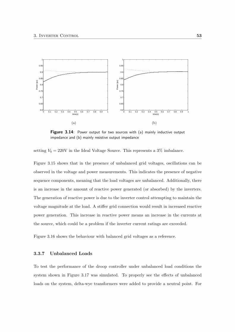
3. Inverter Control 53
0 0.1 0.2 0.3 0.4 0.5 0.6 0.7 0.8 0.9 10.6
0.65
0.7
0.75
0.8
0.85
0.9
0.95
1
time(s)
Pow
er (
pu)
(a)
0 0.1 0.2 0.3 0.4 0.5 0.6 0.7 0.8 0.9 10.6
0.65
0.7
0.75
0.8
0.85
0.9
0.95
1
time(s)P
ower
(pu
)
(b)
Figure 3.14: Power output for two sources with (a) mainly inductive output
impedance and (b) mainly resistive output impedance
setting Vb = 220V in the Ideal Voltage Source. This represents a 3% imbalance.
Figure 3.15 shows that in the presence of unbalanced grid voltages, oscillations can be
observed in the voltage and power measurements. This indicates the presence of negative
sequence components, meaning that the load voltages are unbalanced. Additionally, there
is an increase in the amount of reactive power generated (or absorbed) by the inverters.
The generation of reactive power is due to the inverter control attempting to maintain the
voltage magnitude at the load. A stiffer grid connection would result in increased reactive
power generation. This increase in reactive power means an increase in the currents at
the source, which could be a problem if the inverter current ratings are exceeded.
Figure 3.16 shows the behaviour with balanced grid voltages as a reference.
3.3.7 Unbalanced Loads
To test the performance of the droop controller under unbalanced load conditions the
system shown in Figure 3.17 was simulated. To properly see the effects of unbalanced
loads on the system, delta-wye transformers were added to provide a neutral point. For
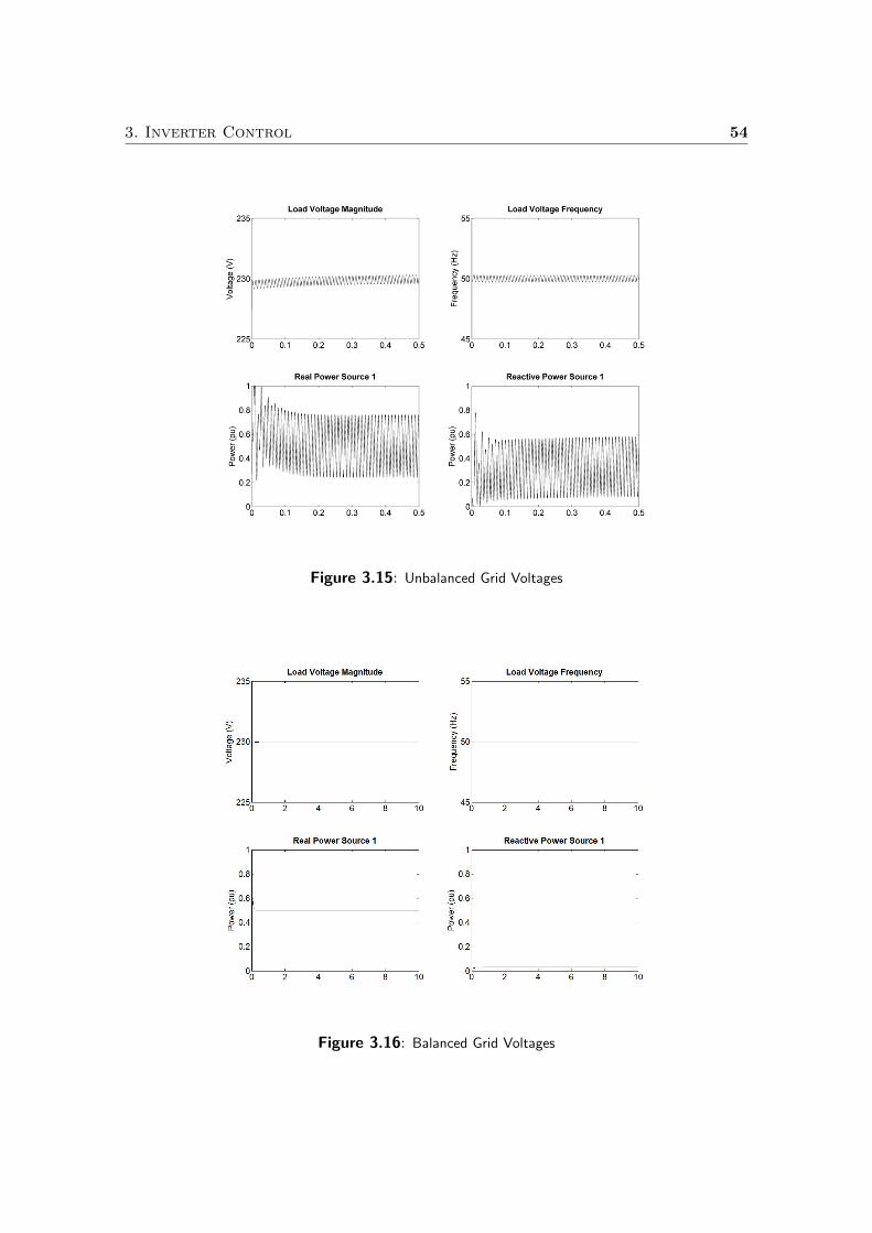
3. Inverter Control 54
Figure 3.15: Unbalanced Grid Voltages
Figure 3.16: Balanced Grid Voltages
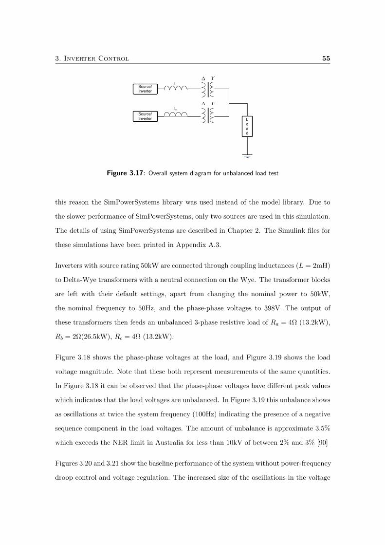
3. Inverter Control 55
Source/Inverter
Load
Source/Inverter
L
L! Y
! Y
Figure 3.17: Overall system diagram for unbalanced load test
this reason the SimPowerSystems library was used instead of the model library. Due to
the slower performance of SimPowerSystems, only two sources are used in this simulation.
The details of using SimPowerSystems are described in Chapter 2. The Simulink files for
these simulations have been printed in Appendix A.3.
Inverters with source rating 50kW are connected through coupling inductances (L = 2mH)
to Delta-Wye transformers with a neutral connection on the Wye. The transformer blocks
are left with their default settings, apart from changing the nominal power to 50kW,
the nominal frequency to 50Hz, and the phase-phase voltages to 398V. The output of
these transformers then feeds an unbalanced 3-phase resistive load of Ra = 4Ω (13.2kW),
Rb = 2Ω(26.5kW), Rc = 4Ω (13.2kW).
Figure 3.18 shows the phase-phase voltages at the load, and Figure 3.19 shows the load
voltage magnitude. Note that these both represent measurements of the same quantities.
In Figure 3.18 it can be observed that the phase-phase voltages have different peak values
which indicates that the load voltages are unbalanced. In Figure 3.19 this unbalance shows
as oscillations at twice the system frequency (100Hz) indicating the presence of a negative
sequence component in the load voltages. The amount of unbalance is approximate 3.5%
which exceeds the NER limit in Australia for less than 10kV of between 2% and 3% [90]
Figures 3.20 and 3.21 show the baseline performance of the system without power-frequency
droop control and voltage regulation. The increased size of the oscillations in the voltage
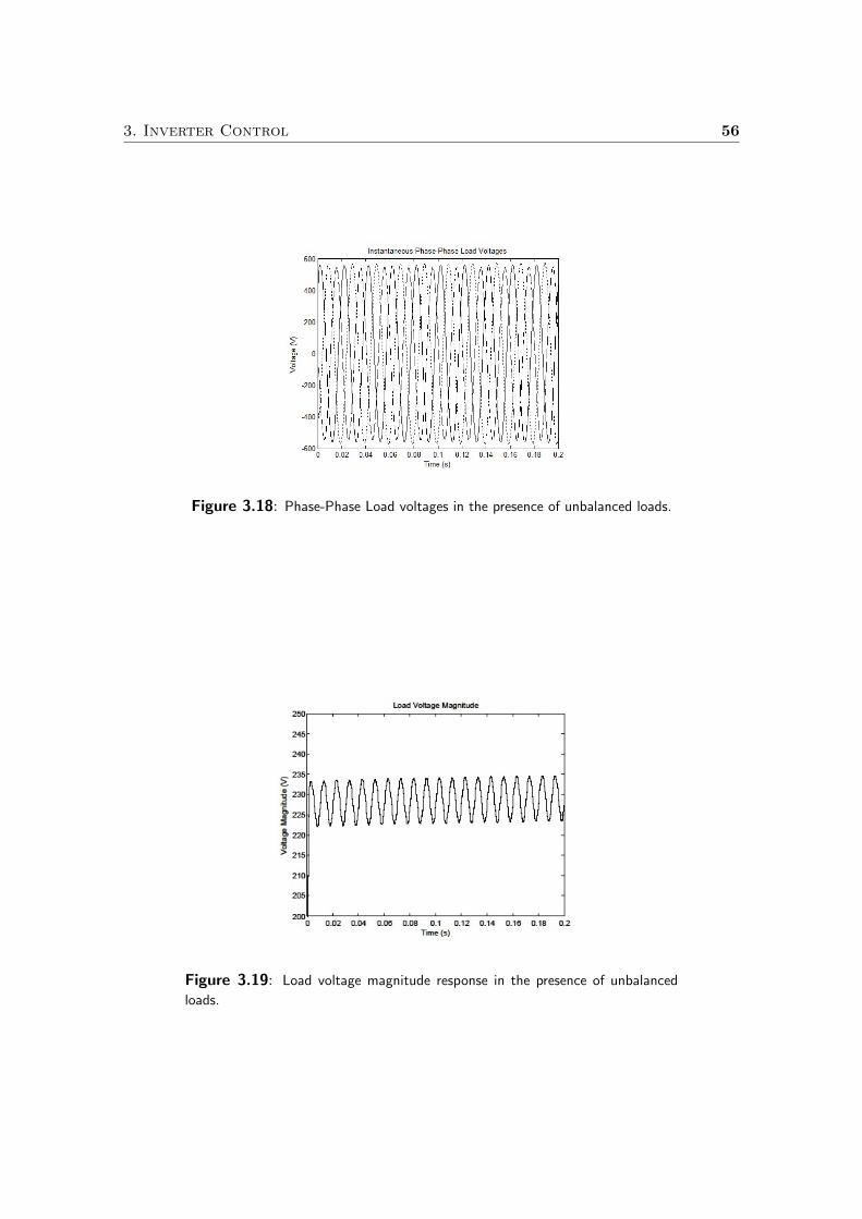
3. Inverter Control 56
Figure 3.18: Phase-Phase Load voltages in the presence of unbalanced loads.
Figure 3.19: Load voltage magnitude response in the presence of unbalanced
loads.
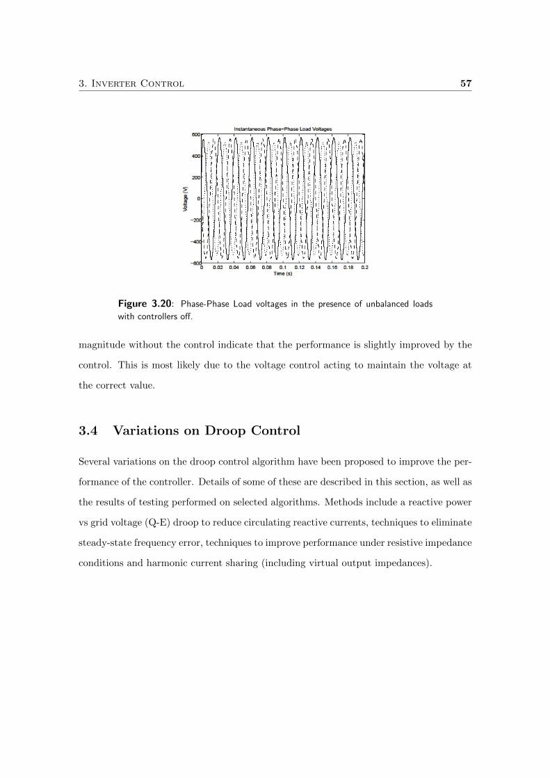
3. Inverter Control 57
Figure 3.20: Phase-Phase Load voltages in the presence of unbalanced loads
with controllers off.
magnitude without the control indicate that the performance is slightly improved by the
control. This is most likely due to the voltage control acting to maintain the voltage at
the correct value.
3.4 Variations on Droop Control
Several variations on the droop control algorithm have been proposed to improve the per-
formance of the controller. Details of some of these are described in this section, as well as
the results of testing performed on selected algorithms. Methods include a reactive power
vs grid voltage (Q-E) droop to reduce circulating reactive currents, techniques to eliminate
steady-state frequency error, techniques to improve performance under resistive impedance
conditions and harmonic current sharing (including virtual output impedances).
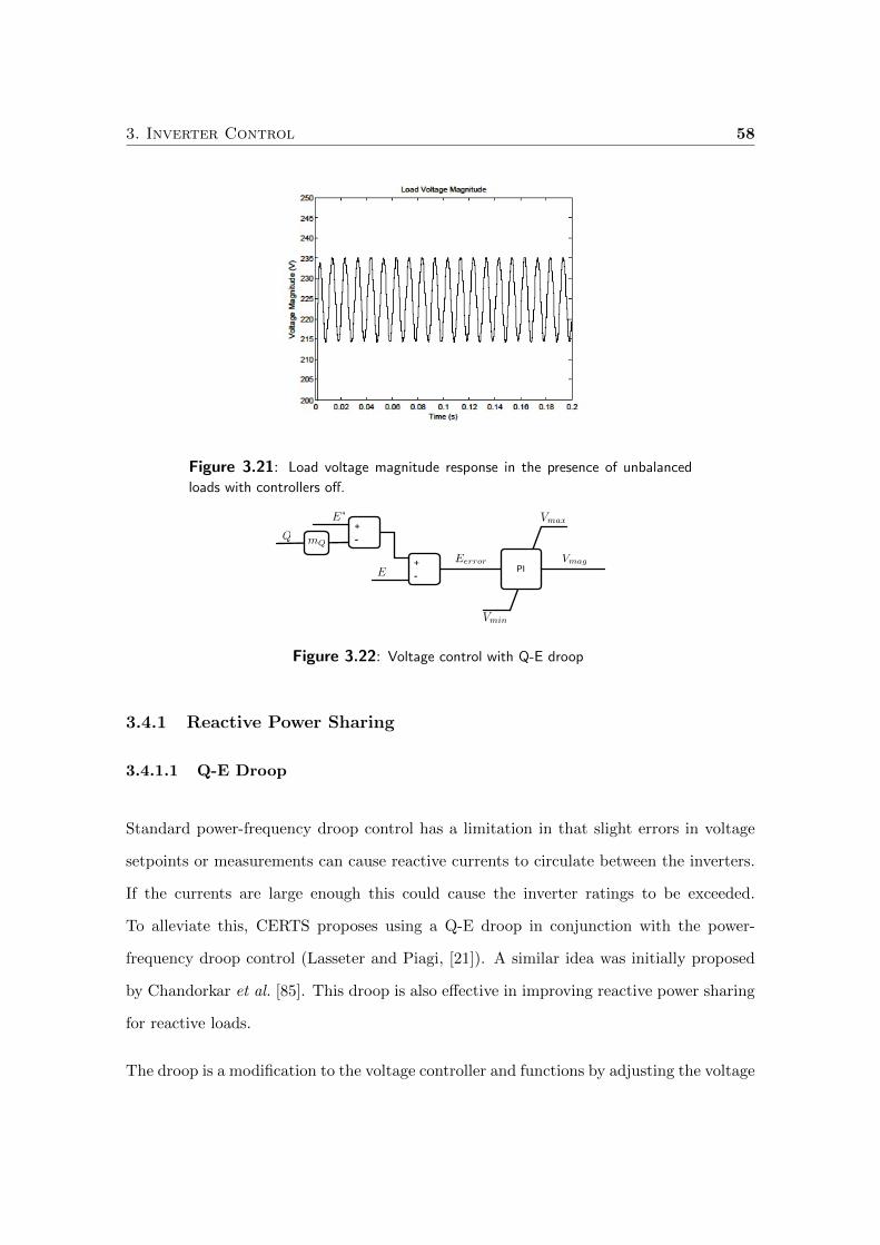
3. Inverter Control 58
Figure 3.21: Load voltage magnitude response in the presence of unbalanced
loads with controllers off.
+- PI
Vmag
Vmax
Vmin
Eerror
E!
E
+-Q mQ
Figure 3.22: Voltage control with Q-E droop
3.4.1 Reactive Power Sharing
3.4.1.1 Q-E Droop
Standard power-frequency droop control has a limitation in that slight errors in voltage
setpoints or measurements can cause reactive currents to circulate between the inverters.
If the currents are large enough this could cause the inverter ratings to be exceeded.
To alleviate this, CERTS proposes using a Q-E droop in conjunction with the power-
frequency droop control (Lasseter and Piagi, [21]). A similar idea was initially proposed
by Chandorkar et al. [85]. This droop is also effective in improving reactive power sharing
for reactive loads.
The droop is a modification to the voltage controller and functions by adjusting the voltage
3. Inverter Control 59
setpoint E∗ in proportion to the amount of reactive power. This simple measure is able
to significantly reduce the amount of reactive current between the inverters. The droop
relationship is given in Equation 3.20 where Eadj is the adjusted voltage setpoint fed to
the voltage controller, E∗ is the actual voltage setpoint desired in the system, mQ is the
Q-E droop co-efficient and Q is the reactive power output of the source (in per unit for
this implementation). The overall voltage controller is shown in Figure 3.22. As with all
droops, Q-E droop contains a trade-off: more effective suppression of circulating currents
requires an increase in the Q-E droop co-efficient mQ which leads to less accurate voltage
regulation. If the net amount of reactive power in the system is negligible (i.e. most of
the reactive power is flowing between the sources), then the effect of this trade-off will be
negligible, since more effective suppression of circulating currents will reduce the value of
Q.
Eadj = E∗ −mQQ (3.20)
To illustrate the trade-offs inherent in Q-E droop, consider two sources with voltage Equa-
tions 3.21 and 3.22.
E1adj = E∗1 −mQQ1 (3.21)
E2adj = E∗2 −mQQ2 (3.22)
Since E∗ is the desired voltage level, the terms mQQ1 and mQQ2 represent the voltage
error due to the Q-E droop.
The system is designed so that E∗1 = E∗2 . Substituting in Equations 3.21 and 3.22 gives
Equation 3.23. Rearranging this gives Equation 3.24 , soE2adj−E1adj
mQis the Q error term,
or the error in the reactive power sharing. These error terms show that a larger mQ will
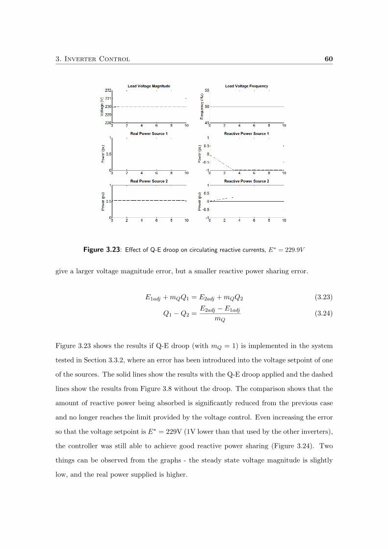
3. Inverter Control 60
Figure 3.23: Effect of Q-E droop on circulating reactive currents, E∗ = 229.9V
give a larger voltage magnitude error, but a smaller reactive power sharing error.
E1adj +mQQ1 = E2adj +mQQ2 (3.23)
Q1 −Q2 =E2adj − E1adj
mQ(3.24)
Figure 3.23 shows the results if Q-E droop (with mQ = 1) is implemented in the system
tested in Section 3.3.2, where an error has been introduced into the voltage setpoint of one
of the sources. The solid lines show the results with the Q-E droop applied and the dashed
lines show the results from Figure 3.8 without the droop. The comparison shows that the
amount of reactive power being absorbed is significantly reduced from the previous case
and no longer reaches the limit provided by the voltage control. Even increasing the error
so that the voltage setpoint is E∗ = 229V (1V lower than that used by the other inverters),
the controller was still able to achieve good reactive power sharing (Figure 3.24). Two
things can be observed from the graphs - the steady state voltage magnitude is slightly
low, and the real power supplied is higher.
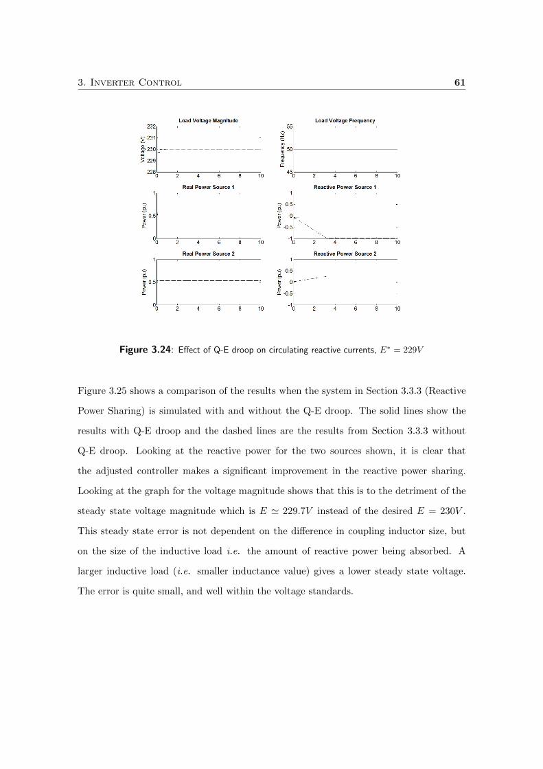
3. Inverter Control 61
Figure 3.24: Effect of Q-E droop on circulating reactive currents, E∗ = 229V
Figure 3.25 shows a comparison of the results when the system in Section 3.3.3 (Reactive
Power Sharing) is simulated with and without the Q-E droop. The solid lines show the
results with Q-E droop and the dashed lines are the results from Section 3.3.3 without
Q-E droop. Looking at the reactive power for the two sources shown, it is clear that
the adjusted controller makes a significant improvement in the reactive power sharing.
Looking at the graph for the voltage magnitude shows that this is to the detriment of the
steady state voltage magnitude which is E ' 229.7V instead of the desired E = 230V .
This steady state error is not dependent on the difference in coupling inductor size, but
on the size of the inductive load i.e. the amount of reactive power being absorbed. A
larger inductive load (i.e. smaller inductance value) gives a lower steady state voltage.
The error is quite small, and well within the voltage standards.
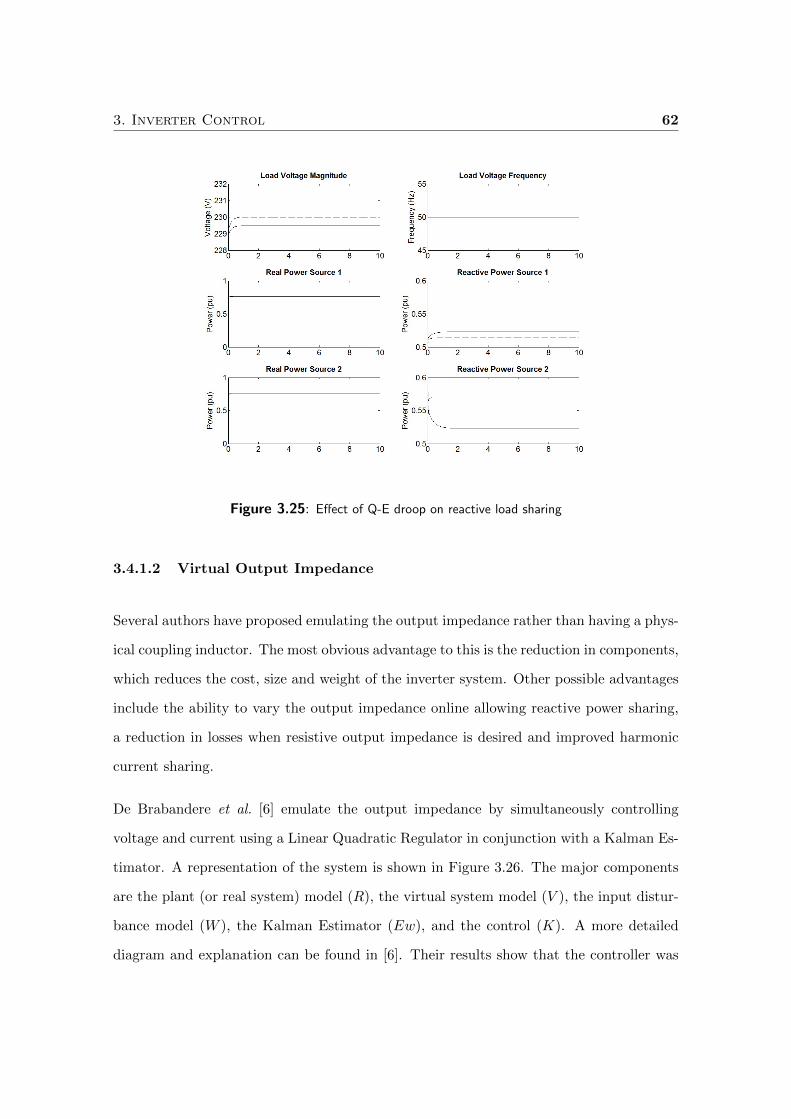
3. Inverter Control 62
Figure 3.25: Effect of Q-E droop on reactive load sharing
3.4.1.2 Virtual Output Impedance
Several authors have proposed emulating the output impedance rather than having a phys-
ical coupling inductor. The most obvious advantage to this is the reduction in components,
which reduces the cost, size and weight of the inverter system. Other possible advantages
include the ability to vary the output impedance online allowing reactive power sharing,
a reduction in losses when resistive output impedance is desired and improved harmonic
current sharing.
De Brabandere et al. [6] emulate the output impedance by simultaneously controlling
voltage and current using a Linear Quadratic Regulator in conjunction with a Kalman Es-
timator. A representation of the system is shown in Figure 3.26. The major components
are the plant (or real system) model (R), the virtual system model (V ), the input distur-
bance model (W ), the Kalman Estimator (Ew), and the control (K). A more detailed
diagram and explanation can be found in [6]. Their results show that the controller was
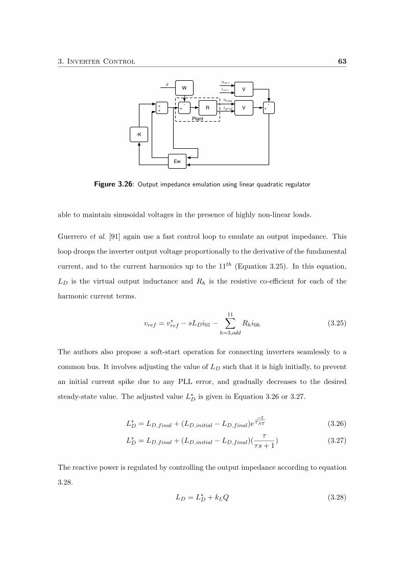
3. Inverter Control 63
Plant
-K
Ew
++
-+
W
R V
V
-+
usrc
isrc
ucap
igrid
d
Figure 3.26: Output impedance emulation using linear quadratic regulator
able to maintain sinusoidal voltages in the presence of highly non-linear loads.
Guerrero et al. [91] again use a fast control loop to emulate an output impedance. This
loop droops the inverter output voltage proportionally to the derivative of the fundamental
current, and to the current harmonics up to the 11th (Equation 3.25). In this equation,
LD is the virtual output inductance and Rh is the resistive co-efficient for each of the
harmonic current terms.
vref = v∗ref − sLDi01 −11∑
h=3,odd
Rhi0h (3.25)
The authors also propose a soft-start operation for connecting inverters seamlessly to a
common bus. It involves adjusting the value of LD such that it is high initially, to prevent
an initial current spike due to any PLL error, and gradually decreases to the desired
steady-state value. The adjusted value L∗D is given in Equation 3.26 or 3.27.
L∗D = LD final + (LD initial − LD final)e−tτST (3.26)
L∗D = LD final + (LD initial − LD final)(τ
τs+ 1) (3.27)
The reactive power is regulated by controlling the output impedance according to equation
3.28.
LD = L∗D + kLQ (3.28)
3. Inverter Control 64
The results in [91] show that this method is effective in sharing reactive power and pre-
venting circulating reactive currents.
The disadvantage of these virtual impedance methods is that they are quite complex and
require more computing power due to the fast calculations involved.
3.4.2 Frequency Restoration
It is desirable that the steady state frequency in a system be as close to ω∗ as possible.
To achieve this, Lasseter and Piagi [21] propose modifying Equation (3.3) to introduce a
parameter P ∗c.i resulting in Equation 3.29.
ωi(t) = ω∗ −mi(P∗c,i − Pi(t)) (3.29)
P ∗c,i is gradually adjusted so that at steady state its value is such that ωi(t) = ω∗. This
frequency restoration loop works over a longer time scale than the power sharing loop in
order to allow the power sharing to reach steady state before the frequency is restored.
Figure 3.27 shows the implementation of the power-frequency droop controller with fre-
quency restoration loop. The constants k′ and k′′ are chosen to ensure that the rate of
change of frequency of each of the sources remains the same in order to maintain the same
power angle between the sources. Changing the power angle will change the power output
which is undesirable once a steady state has been reached. In [84] it is shown that this
requirement leads to the conclusion that mk′′ and k′
m must be the same for all sources.
Another option to improve steady-state frequency performance is proposed by Sao and
Lehn [92]. The authors suggest adding a gain on the integrator which calculates the
inverter angle (Equation 3.30).
δ1 − δcom = Kp1
ˆ(ω1 − ωcom)dt (3.30)
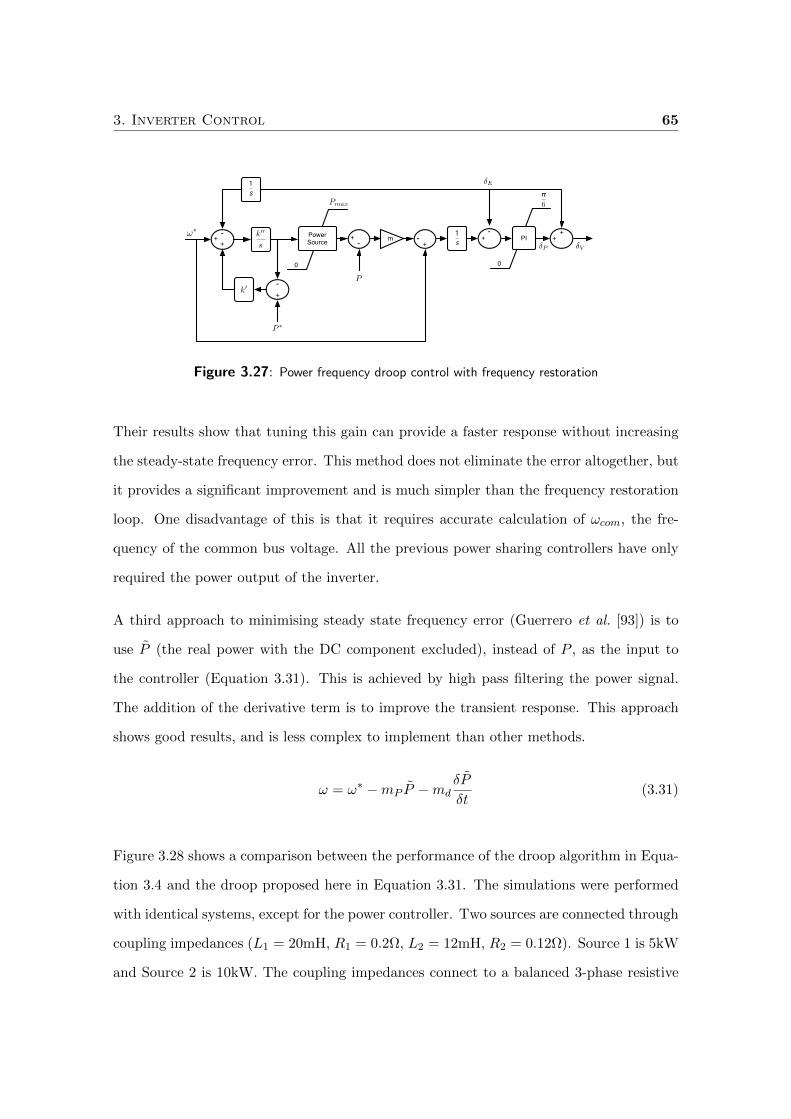
3. Inverter Control 65
m
0
PowerSource
+- +
-+
++-1
s
0
PI!!k!!
s
+-
k!
+ -
1s
!P !V
!E
!6
+
P
P !
Pmax
Figure 3.27: Power frequency droop control with frequency restoration
Their results show that tuning this gain can provide a faster response without increasing
the steady-state frequency error. This method does not eliminate the error altogether, but
it provides a significant improvement and is much simpler than the frequency restoration
loop. One disadvantage of this is that it requires accurate calculation of ωcom, the fre-
quency of the common bus voltage. All the previous power sharing controllers have only
required the power output of the inverter.
A third approach to minimising steady state frequency error (Guerrero et al. [93]) is to
use P (the real power with the DC component excluded), instead of P , as the input to
the controller (Equation 3.31). This is achieved by high pass filtering the power signal.
The addition of the derivative term is to improve the transient response. This approach
shows good results, and is less complex to implement than other methods.
ω = ω∗ −mP P −mdδP
δt(3.31)
Figure 3.28 shows a comparison between the performance of the droop algorithm in Equa-
tion 3.4 and the droop proposed here in Equation 3.31. The simulations were performed
with identical systems, except for the power controller. Two sources are connected through
coupling impedances (L1 = 20mH, R1 = 0.2Ω, L2 = 12mH, R2 = 0.12Ω). Source 1 is 5kW
and Source 2 is 10kW. The coupling impedances connect to a balanced 3-phase resistive
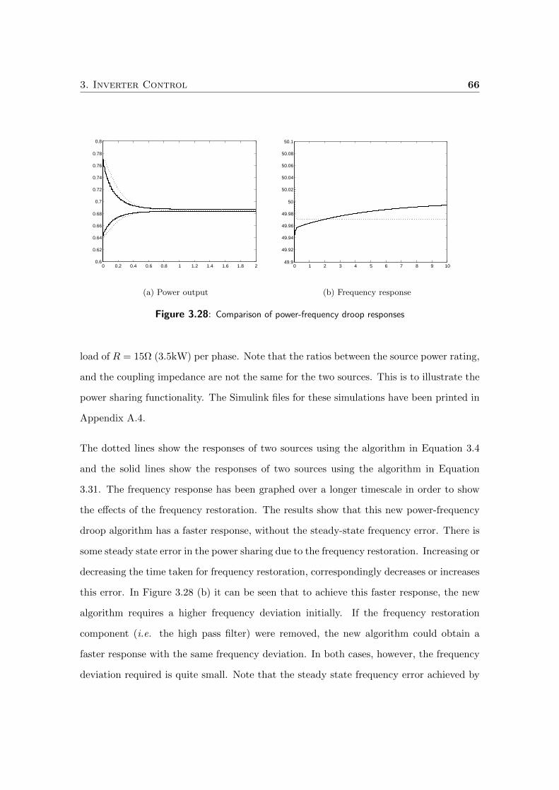
3. Inverter Control 66
0 0.2 0.4 0.6 0.8 1 1.2 1.4 1.6 1.8 20.6
0.62
0.64
0.66
0.68
0.7
0.72
0.74
0.76
0.78
0.8
(a) Power output
0 1 2 3 4 5 6 7 8 9 1049.9
49.92
49.94
49.96
49.98
50
50.02
50.04
50.06
50.08
50.1
(b) Frequency response
Figure 3.28: Comparison of power-frequency droop responses
load of R = 15Ω (3.5kW) per phase. Note that the ratios between the source power rating,
and the coupling impedance are not the same for the two sources. This is to illustrate the
power sharing functionality. The Simulink files for these simulations have been printed in
Appendix A.4.
The dotted lines show the responses of two sources using the algorithm in Equation 3.4
and the solid lines show the responses of two sources using the algorithm in Equation
3.31. The frequency response has been graphed over a longer timescale in order to show
the effects of the frequency restoration. The results show that this new power-frequency
droop algorithm has a faster response, without the steady-state frequency error. There is
some steady state error in the power sharing due to the frequency restoration. Increasing or
decreasing the time taken for frequency restoration, correspondingly decreases or increases
this error. In Figure 3.28 (b) it can be seen that to achieve this faster response, the new
algorithm requires a higher frequency deviation initially. If the frequency restoration
component (i.e. the high pass filter) were removed, the new algorithm could obtain a
faster response with the same frequency deviation. In both cases, however, the frequency
deviation required is quite small. Note that the steady state frequency error achieved by
3. Inverter Control 67
Equation 3.4 is dependent on the value of P ∗. In cases where the power required by the
load is close to P ∗, the steady state frequency error will be minimal.
3.4.3 Harmonic Current Sharing
Lee and Cheng [94] suggest a G-H droop, (harmonic conductance vs harmonic var con-
sumption) in order to ensure harmonic current sharing between the sources without com-
munications (Equation 3.32). The harmonic conductance is the conductance ( 1R) seen by
the harmonic voltages and currents. The harmonic var consumption is that component of
the reactive power due to harmonic voltages and currents. This droop is designed to work
in conjunction with standard P − f and Q− V (or Q− E) droops.
G(t) = G∗ − bi(H∗i −Hi(t)) (3.32)
Results show that this method can effectively share harmonic current and reduce total
harmonic distortion (THD) while maintaining real and reactive power sharing.
3.4.4 Resistive Line Impedance
Standard droop control relies on the impedance between the inverter and the load being
mainly inductive. In a low voltage network, this is not necessarily the case. It should be
noted that the use of inductive coupling impedances, as is proposed in this thesis, will tend
to ensure this, however not all droop control algorithms require a coupling impedance.
De Brabandere et al. ( [6]) propose a transform matrix (Equation 3.33) which uses the
ratio between the resistance and reactance of the line impedance. This matrix is used to
transform the quantities in the droop equations to allow the control to work with any line
impedance. The authors have chosen to control the real and reactive currents instead of
the real and reactive power, although it should be noted that the transform matrix can
equally be applied to real and reactive power.
3. Inverter Control 68
The droop equations are 3.34 and 3.35, where I ′a is the modified active current, I ′r is
the modified reactive current, I ′a,0 and I ′r,0 are the modified setpoints for the active and
reactive currents, and ka and kr are the droop co-efficients for the active and reactive
currents. I ′a
I ′r
=
XZ −R
Z
RZ
XZ
Ia
Ir
(3.33)
ωi(t)− ω∗ = −ka(I ′a − I ′a,0) (3.34)
V − E∗ = −kr(I ′r − I ′r,0) (3.35)
T =
XZ −R
Z
RZ
XZ
is the transform matrix. According to the authors, the benefit of
controlling the currents rather than the voltages is that current can be limited in the
event of a short circuit. Additionally, power sharing and voltage regulation is improved
in the presence of non-zero line resistance, and the controller is able to mitigate voltage
harmonics.
Note that, as shown in Section 3.3.5, the inclusion of a coupling impedance means that
correction for resistive line impedances is unnecessary.
3.5 Evaluation
The literature, and the tests performed here, show that there are several limitations to
basic droop control, including circulating reactive currents, steady-state frequency and
voltage magnitude errors, lack of harmonic current sharing, poor performance under un-
balanced load, and poor short circuit performance. Solutions, or at least improvements,
have been found for many of these areas, with the notable exception of techniques for cor-
recting voltage unbalance in the presence of unbalanced loads. In addition to this, most
of these techniques address only one or two of the several problems, and a combination of

3. Inverter Control 69
techniques could result in an improved controller.
Chapter 4
Unbalanced Loads
Unbalanced loads are a problem as they can lead to unbalanced phase voltages. This is of
particular interest in Low Voltage Distributed Generation systems because the likelihood
of unbalanced loads is increased. Chapter 3 showed the possible effects of unbalanced loads
on a system employing droop control. None of the proposed implementations of droop
control outlined in Chapter 3 are designed to improve performance under unbalanced
conditions. This Chapter details a method of limiting voltage imbalance at the load.
4.1 Unbalance Compensation
In the literature, the most common solution to unbalanced voltages in any system is to
measure and compensate for the negative sequence components caused by the voltage
imbalance [95–97].
These solutions typically have been designed for grid connected applications [95, 96], or
single source stand-alone systems [97] and therefore lack the power sharing and voltage
regulation functionality necessary in microgrids.
Recently, some authors have addressed the problem of correcting for unbalanced loads in
microgrids. Li et al. [98] have proposed a power quality compensator which minimises the
impact of unbalanced utility grid voltages on sensitive loads in microgrids. The power
quality compensator uses two inverters. A shunt inverter ensures balanced voltages, and
a series inverter balances the line currents. The basic principle of the control is to can-
cel the negative sequence components of the voltages coming from the grid by injecting
negative sequence components of the opposite sign. The disadvantage of this system is
4. Unbalanced Loads 71
that it cannot be implemented only by modifying the source inverter as it requires the two
inverters.
Another approach is to use instantaneous p-q theory to compensate for unbalanced volt-
ages [99]. This theory allows for the calculation of instantaneous values of real and reactive
power. It is similar in concept to using sequence components, in that voltages and currents
are measured and then transformed into other values (in this case real and reactive power)
which are then used by the controller. Watanabe et al. outline how instantaneous p-q
theory can be used for harmonic, reactive power or unbalance compensation, and voltage
regulation. This solution utilises a shunt inverter, so again it cannot be implemented only
by using the source inverter.
Cheng et al. [67] have proposed using a Q−-G droop (the reactive power produced by the
negative sequence current vs conductance) in conjunction with standard droop control.
This is similar to the approach developed here and first reported in [100], except that their
controller takes the negative sequence reactive power as the input rather than the negative
sequence voltage, requiring several extra calculations.
Hojo et al. [101] have proposed another similar approach, instead using d-q transforms
rather than symmetrical components.
In this work, the principle of negative sequence control is adapted to operate in conjunction
with a standard droop controller in a Voltage Source Inverter. The aim is to compensate
for the unbalanced voltages within the microgrid caused by unbalanced loads, while still
providing voltage regulation and power sharing functionality. Using this approach, un-
balanced voltages which occur as a result of unbalanced loads can be minimised without
requiring additional hardware. It is designed to improve power quality in stand-alone
operation rather than compensate for unbalanced utility grid voltages.
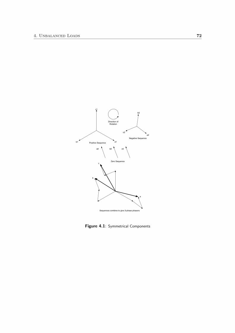
4. Unbalanced Loads 72
a1
c1
b1
a2
b2
c2
a0 b0 c0
Positive Sequence
Negative Sequence
Zero Sequence
a
b
c
Sequences combine to give 3-phase phasors
Direction of Rotation
Figure 4.1: Symmetrical Components
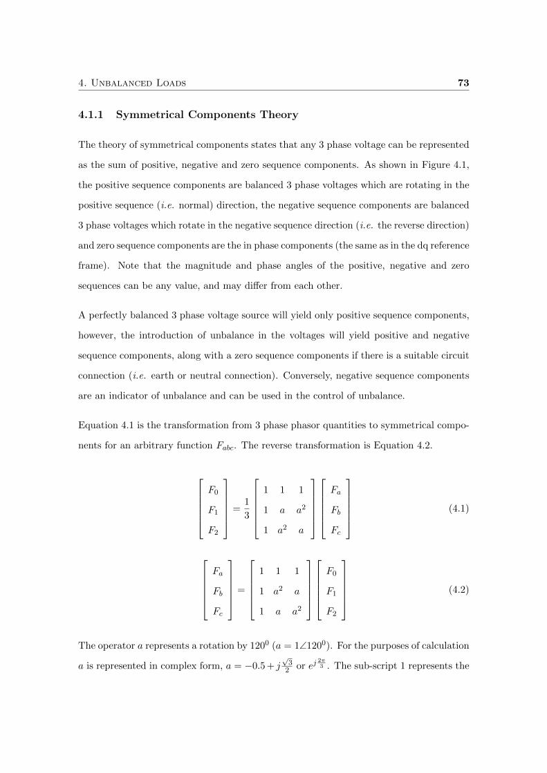
4. Unbalanced Loads 73
4.1.1 Symmetrical Components Theory
The theory of symmetrical components states that any 3 phase voltage can be represented
as the sum of positive, negative and zero sequence components. As shown in Figure 4.1,
the positive sequence components are balanced 3 phase voltages which are rotating in the
positive sequence (i.e. normal) direction, the negative sequence components are balanced
3 phase voltages which rotate in the negative sequence direction (i.e. the reverse direction)
and zero sequence components are the in phase components (the same as in the dq reference
frame). Note that the magnitude and phase angles of the positive, negative and zero
sequences can be any value, and may differ from each other.
A perfectly balanced 3 phase voltage source will yield only positive sequence components,
however, the introduction of unbalance in the voltages will yield positive and negative
sequence components, along with a zero sequence components if there is a suitable circuit
connection (i.e. earth or neutral connection). Conversely, negative sequence components
are an indicator of unbalance and can be used in the control of unbalance.
Equation 4.1 is the transformation from 3 phase phasor quantities to symmetrical compo-
nents for an arbitrary function Fabc. The reverse transformation is Equation 4.2.
F0
F1
F2
=1
3
1 1 1
1 a a2
1 a2 a
Fa
Fb
Fc
(4.1)
Fa
Fb
Fc
=
1 1 1
1 a2 a
1 a a2
F0
F1
F2
(4.2)
The operator a represents a rotation by 1200 (a = 1∠1200). For the purposes of calculation
a is represented in complex form, a = −0.5 + j√
32 or ej
2π3 . The sub-script 1 represents the
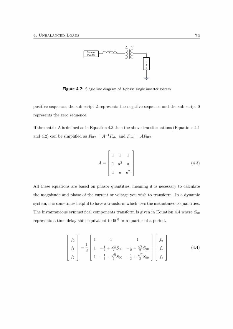
4. Unbalanced Loads 74
Source/Inverter
Load
L! Y
Figure 4.2: Single line diagram of 3-phase single inverter system
positive sequence, the sub-script 2 represents the negative sequence and the sub-script 0
represents the zero sequence.
If the matrix A is defined as in Equation 4.3 then the above transformations (Equations 4.1
and 4.2) can be simplified as F012 = A−1Fabc and Fabc = AF012.
A =
1 1 1
1 a2 a
1 a a2
(4.3)
All these equations are based on phasor quantities, meaning it is necessary to calculate
the magnitude and phase of the current or voltage you wish to transform. In a dynamic
system, it is sometimes helpful to have a transform which uses the instantaneous quantities.
The instantaneous symmetrical components transform is given in Equation 4.4 where S90
represents a time delay shift equivalent to 900 or a quarter of a period.
f0
f1
f2
=1
3
1 1 1
1 −12 +
√3
2 S90 −12 −
√3
2 S90
1 −12 −
√3
2 S90 −12 +
√3
2 S90
fa
fb
fc
(4.4)

4. Unbalanced Loads 75
Va V !a
V !b
V !cVc
Vb
N
ZL
ZL
ZLIa
Ib
Ic
Figure 4.3: Three phase coupling inductance
4.1.2 Sequence Representation of Grid
Symmetrical components are not only used to transform voltages and currents. By trans-
forming each of the elements in a system (e.g. impedances, transformers), they can be used
to create sequence representations of networks. This approach is typically used for fault
analyses, as it allows a balanced system to be represented by three independent sequence
circuits, simplifying the calculations. In an unbalanced system, the sequence networks are
no longer independent, but the technique is useful to show the system as it appears to the
sequence voltages and currents.
Consider the single line diagram of a three-phase, single inverter system shown in Fig-
ure 4.2. The impedances can be transformed into symmetrical components form using the
relationship in Equation 4.5.
Z012 = A−1ZabcA (4.5)
Coupling Inductance The coupling inductance consists of a series connected impedance
of ZL in each phase as shown in Figure 4.3. Calculating the voltage/current relation-
ship in the circuit results in Equation 4.6, where ZLabc is the impedance matrix given
in Equation 4.7. Applying the transform in Equation 4.5 gives the symmetrical compo-
nents impedance matrix ZL012 given in Equation 4.8. This means that for the coupling
inductance, the impedance transform results in a series impedance of ZL for each of the
4. Unbalanced Loads 76
sequences.
Vabc − V ′abc =
Va − V ′aVb − V ′bVc − V ′c
= ZLabc
Ia
Ib
Ic
(4.6)
ZLabc =
ZL 0 0
0 ZL 0
0 0 ZL
(4.7)
ZL012 =
ZL 0 0
0 ZL 0
0 0 ZL
(4.8)
Delta-Wye Transformer Transformers can be represented by their equivalent circuit
as shown in Figure 4.4 (single line diagram) or Figure 4.5 (three phase diagram). RP and
LP are the primary side impedance, R′S and L′S are the secondary impedance referred to
the primary side, and Rm and Lm are the magnetising impedance (also called the exci-
tation branch). In this case the turns ratio of the transformerN1N2
is 1, so R′S and L′S are
the same as RS and LS . The primary and secondary impedances model the effects of
leakage inductance and winding resistance,and the magnetising impedance models mag-
netising inductance and core losses due to magnetic hysteresis and eddy currents. The
ideal transformer with ratio 1 : ej30 represents the phase shift which occurs in a delta-wye
transformer.
The simplest way to convert this equivalent circuit model into symmetrical components
is to consider the primary, secondary and shunt magnetising impedances individually.
By inspection it can be seen that the primary and secondary referred impedances are of
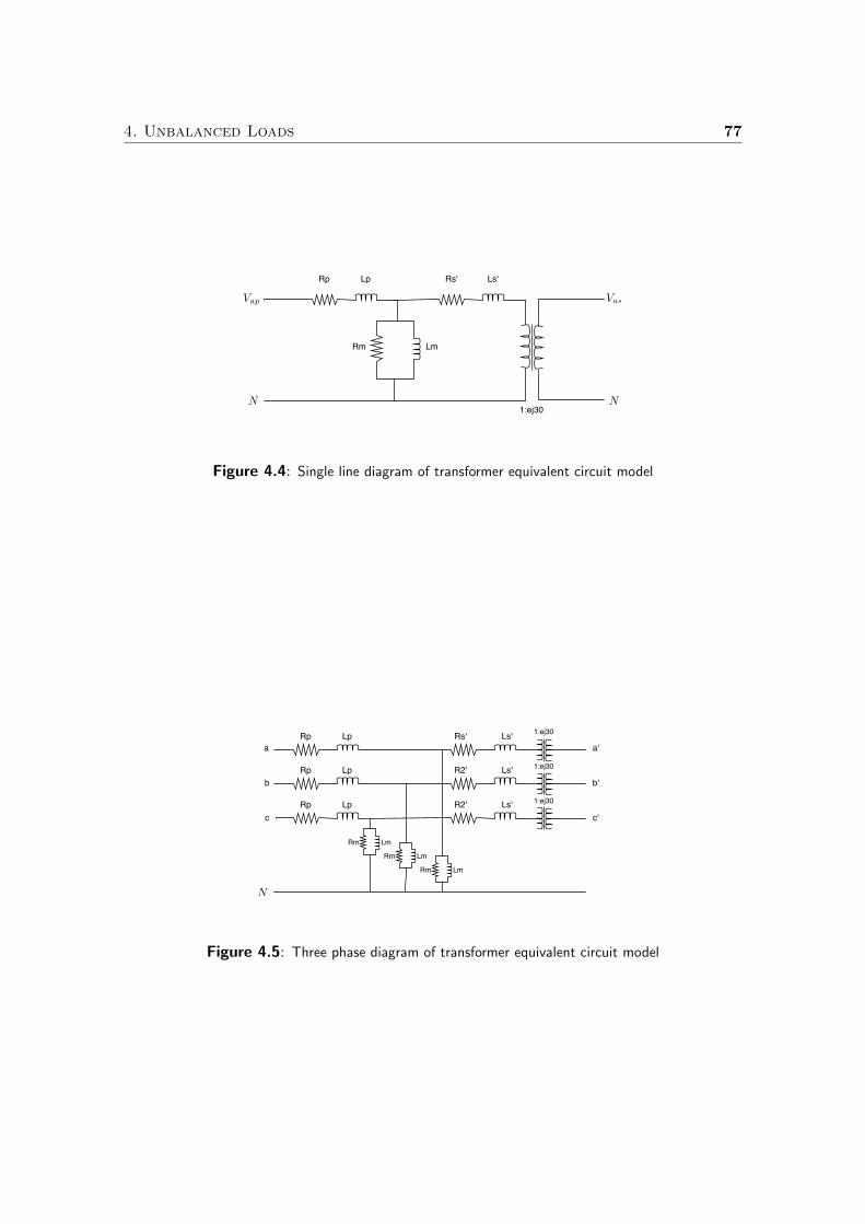
4. Unbalanced Loads 77
N
Rm Lm
Rp Lp Rs' Ls'
1:ej30
Vap Vas
N
Figure 4.4: Single line diagram of transformer equivalent circuit model
N
Rm Lm
1:ej30Rp Lp Rs' Ls'
Rp Lp R2' Ls'
Rp Lp R2' Ls'
1:ej30
1:ej30
Rm Lm
Rm Lm
a
b
c
a'
b'
c'
Figure 4.5: Three phase diagram of transformer equivalent circuit model
4. Unbalanced Loads 78
the same form as the coupling impedance and the sequence impedances are ZP012 for the
primary (Equation 4.9) and ZS012 for the secondary (Equation 4.10), where ZP = RP +LP
and ZS = R′S + L′S .
ZP012 =
ZP 0 0
0 ZP 0
0 0 ZP
(4.9)
ZS012 =
ZS 0 0
0 ZS 0
0 0 ZS
(4.10)
To transform the magnetising resistance the phase-neutral voltages VaN , VbN and VcN
are considered. This results in Equation 4.11. It can be observed that the magnetising
impedance matrix Zmabc (Equation 4.12) is of the same form as the previous impedance
matrices. Transforming this matrix results in Equation 4.13 which means there is an
impedance of Zm between the positive sequence and the neutral, and negative sequence
and the neutral. There is no path for zero sequence currents in the primary of a delta-wye
transformer, so the zero sequence is open circuited at the transformer.
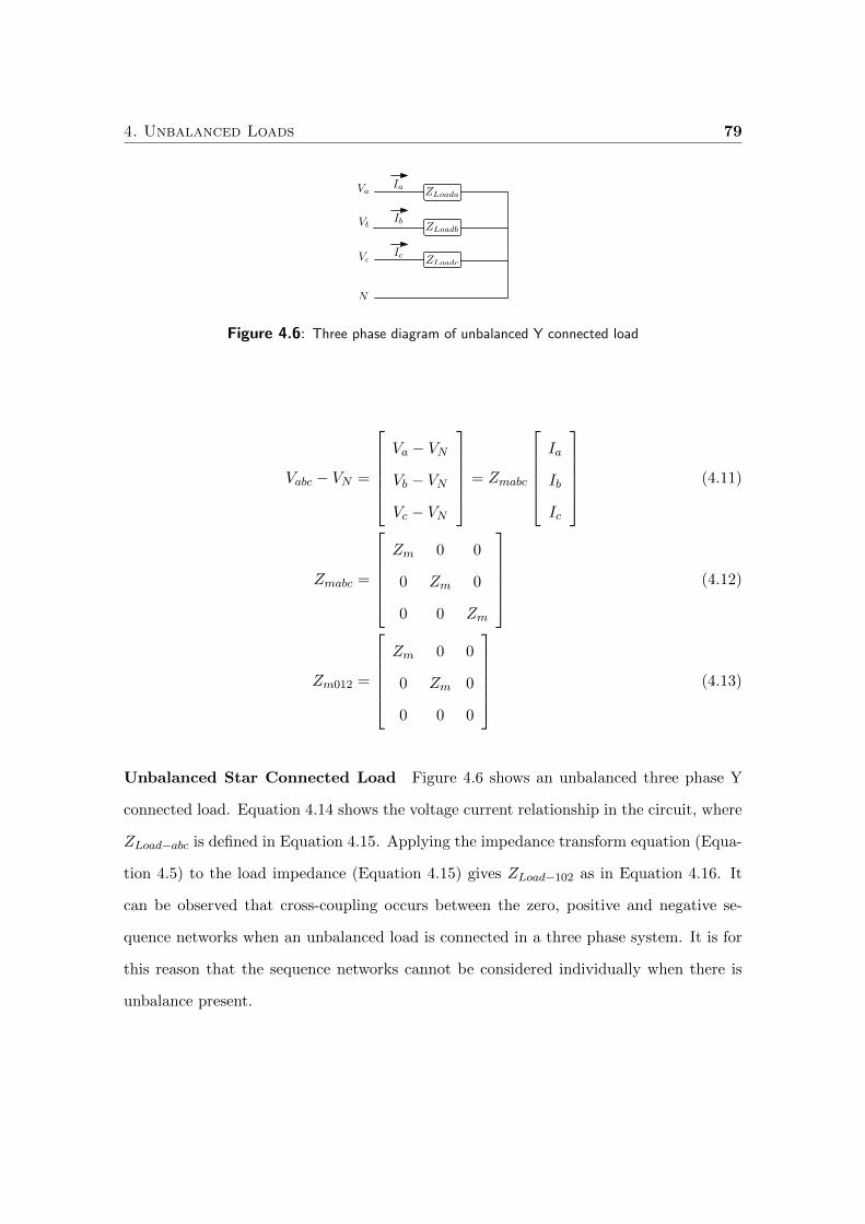
4. Unbalanced Loads 79
Va
Vc
Vb
N
Ia
Ib
Ic
ZLoada
ZLoadb
ZLoadc
Figure 4.6: Three phase diagram of unbalanced Y connected load
Vabc − VN =
Va − VNVb − VNVc − VN
= Zmabc
Ia
Ib
Ic
(4.11)
Zmabc =
Zm 0 0
0 Zm 0
0 0 Zm
(4.12)
Zm012 =
Zm 0 0
0 Zm 0
0 0 0
(4.13)
Unbalanced Star Connected Load Figure 4.6 shows an unbalanced three phase Y
connected load. Equation 4.14 shows the voltage current relationship in the circuit, where
ZLoad−abc is defined in Equation 4.15. Applying the impedance transform equation (Equa-
tion 4.5) to the load impedance (Equation 4.15) gives ZLoad−102 as in Equation 4.16. It
can be observed that cross-coupling occurs between the zero, positive and negative se-
quence networks when an unbalanced load is connected in a three phase system. It is for
this reason that the sequence networks cannot be considered individually when there is
unbalance present.
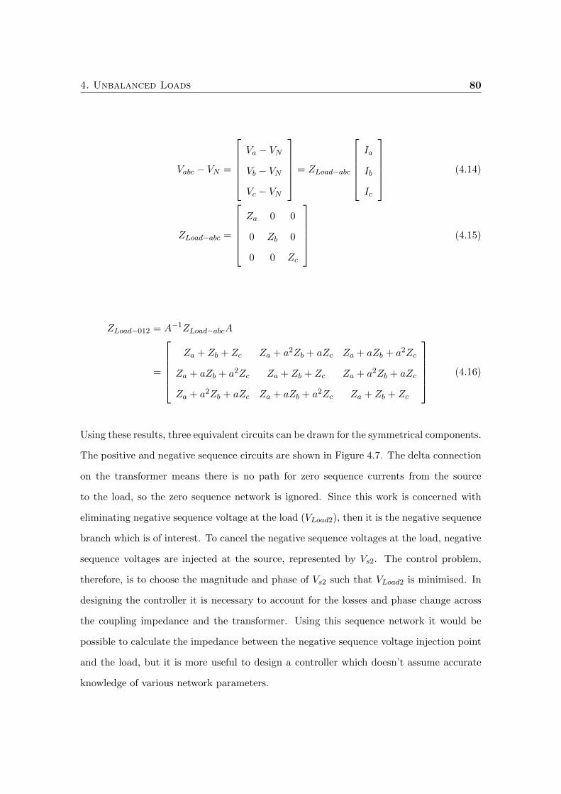
4. Unbalanced Loads 80
Vabc − VN =
Va − VNVb − VNVc − VN
= ZLoad−abc
Ia
Ib
Ic
(4.14)
ZLoad−abc =
Za 0 0
0 Zb 0
0 0 Zc
(4.15)
ZLoad−012 = A−1ZLoad−abcA
=
Za + Zb + Zc Za + a2Zb + aZc Za + aZb + a2Zc
Za + aZb + a2Zc Za + Zb + Zc Za + a2Zb + aZc
Za + a2Zb + aZc Za + aZb + a2Zc Za + Zb + Zc
(4.16)
Using these results, three equivalent circuits can be drawn for the symmetrical components.
The positive and negative sequence circuits are shown in Figure 4.7. The delta connection
on the transformer means there is no path for zero sequence currents from the source
to the load, so the zero sequence network is ignored. Since this work is concerned with
eliminating negative sequence voltage at the load (VLoad2), then it is the negative sequence
branch which is of interest. To cancel the negative sequence voltages at the load, negative
sequence voltages are injected at the source, represented by Vs2. The control problem,
therefore, is to choose the magnitude and phase of Vs2 such that VLoad2 is minimised. In
designing the controller it is necessary to account for the losses and phase change across
the coupling impedance and the transformer. Using this sequence network it would be
possible to calculate the impedance between the negative sequence voltage injection point
and the load, but it is more useful to design a controller which doesn’t assume accurate
knowledge of various network parameters.
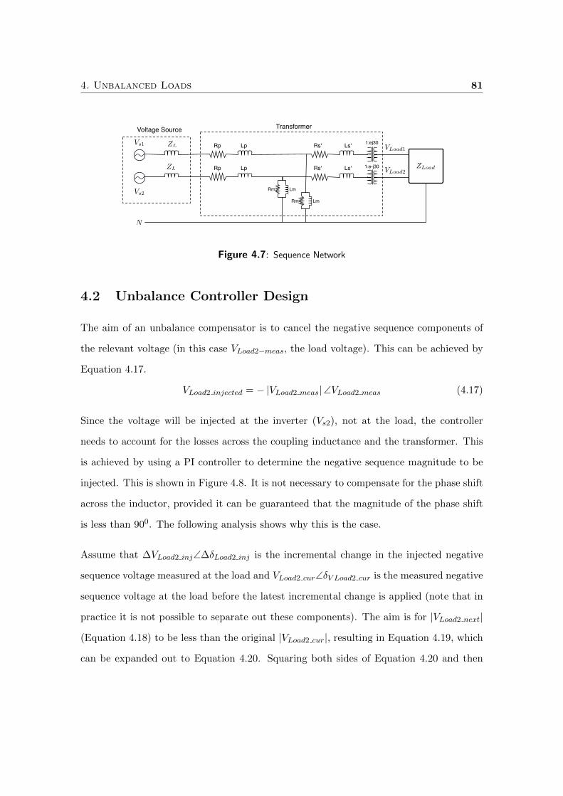
4. Unbalanced Loads 81
N
1:ej30Rp Lp Rs' Ls'
Rp Lp Rs' Ls' 1:e-j30
Rm Lm
Rm Lm
Vs1
Vs2
ZLoad
TransformerVoltage Source
VLoad1ZL
ZL VLoad2
Figure 4.7: Sequence Network
4.2 Unbalance Controller Design
The aim of an unbalance compensator is to cancel the negative sequence components of
the relevant voltage (in this case VLoad2−meas, the load voltage). This can be achieved by
Equation 4.17.
VLoad2 injected = − |VLoad2 meas|∠VLoad2 meas (4.17)
Since the voltage will be injected at the inverter (Vs2), not at the load, the controller
needs to account for the losses across the coupling inductance and the transformer. This
is achieved by using a PI controller to determine the negative sequence magnitude to be
injected. This is shown in Figure 4.8. It is not necessary to compensate for the phase shift
across the inductor, provided it can be guaranteed that the magnitude of the phase shift
is less than 900. The following analysis shows why this is the case.
Assume that ∆VLoad2 inj∠∆δLoad2 inj is the incremental change in the injected negative
sequence voltage measured at the load and VLoad2 cur∠δV Load2 cur is the measured negative
sequence voltage at the load before the latest incremental change is applied (note that in
practice it is not possible to separate out these components). The aim is for |VLoad2 next|
(Equation 4.18) to be less than the original |VLoad2 cur|, resulting in Equation 4.19, which
can be expanded out to Equation 4.20. Squaring both sides of Equation 4.20 and then
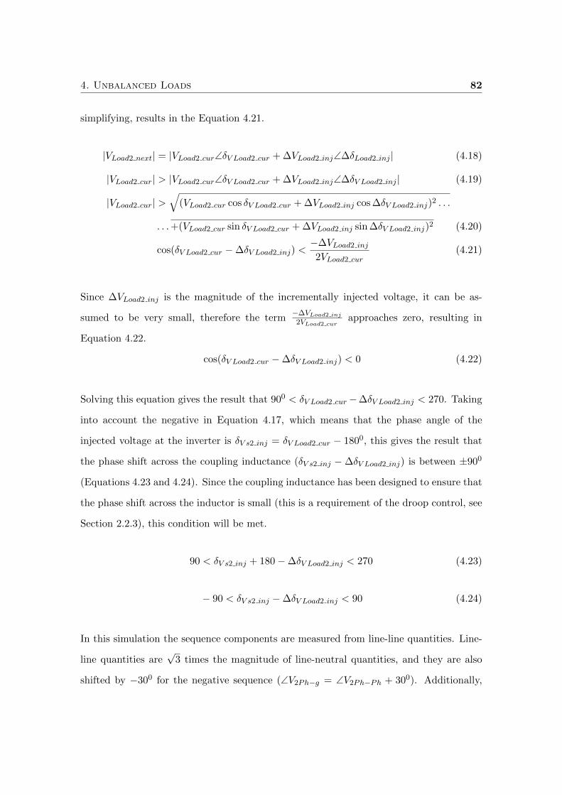
4. Unbalanced Loads 82
simplifying, results in the Equation 4.21.
|VLoad2 next| = |VLoad2 cur∠δV Load2 cur + ∆VLoad2 inj∠∆δLoad2 inj | (4.18)
|VLoad2 cur| > |VLoad2 cur∠δV Load2 cur + ∆VLoad2 inj∠∆δV Load2 inj | (4.19)
|VLoad2 cur| >√
(VLoad2 cur cos δV Load2 cur + ∆VLoad2 inj cos ∆δV Load2 inj)2 . . .
. . .+(VLoad2 cur sin δV Load2 cur + ∆VLoad2 inj sin ∆δV Load2 inj)2 (4.20)
cos(δV Load2 cur −∆δV Load2 inj) <−∆VLoad2 inj
2VLoad2 cur(4.21)
Since ∆VLoad2 inj is the magnitude of the incrementally injected voltage, it can be as-
sumed to be very small, therefore the term−∆VLoad2 inj2VLoad2 cur
approaches zero, resulting in
Equation 4.22.
cos(δV Load2 cur −∆δV Load2 inj) < 0 (4.22)
Solving this equation gives the result that 900 < δV Load2 cur−∆δV Load2 inj < 270. Taking
into account the negative in Equation 4.17, which means that the phase angle of the
injected voltage at the inverter is δV s2 inj = δV Load2 cur − 1800, this gives the result that
the phase shift across the coupling inductance (δV s2 inj −∆δV Load2 inj) is between ±900
(Equations 4.23 and 4.24). Since the coupling inductance has been designed to ensure that
the phase shift across the inductor is small (this is a requirement of the droop control, see
Section 2.2.3), this condition will be met.
90 < δV s2 inj + 180−∆δV Load2 inj < 270 (4.23)
− 90 < δV s2 inj −∆δV Load2 inj < 90 (4.24)
In this simulation the sequence components are measured from line-line quantities. Line-
line quantities are√
3 times the magnitude of line-neutral quantities, and they are also
shifted by −300 for the negative sequence (∠V2Ph−g = ∠V2Ph−Ph + 300). Additionally,
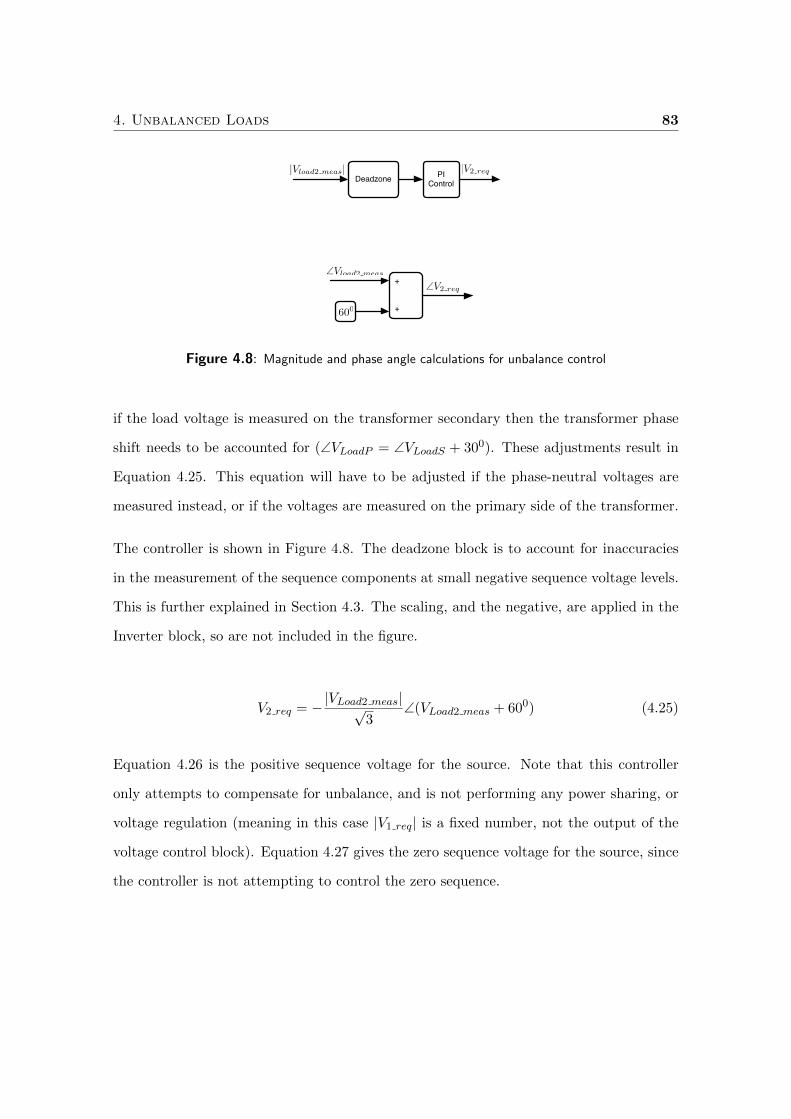
4. Unbalanced Loads 83
+
|V2 req|PIControlDeadzone
|Vload2 meas|
+600
∠Vload2 meas
∠V2 req
Figure 4.8: Magnitude and phase angle calculations for unbalance control
if the load voltage is measured on the transformer secondary then the transformer phase
shift needs to be accounted for (∠VLoadP = ∠VLoadS + 300). These adjustments result in
Equation 4.25. This equation will have to be adjusted if the phase-neutral voltages are
measured instead, or if the voltages are measured on the primary side of the transformer.
The controller is shown in Figure 4.8. The deadzone block is to account for inaccuracies
in the measurement of the sequence components at small negative sequence voltage levels.
This is further explained in Section 4.3. The scaling, and the negative, are applied in the
Inverter block, so are not included in the figure.
V2 req = −|VLoad2 meas|√3
∠(VLoad2 meas + 600) (4.25)
Equation 4.26 is the positive sequence voltage for the source. Note that this controller
only attempts to compensate for unbalance, and is not performing any power sharing, or
voltage regulation (meaning in this case |V1 req| is a fixed number, not the output of the
voltage control block). Equation 4.27 gives the zero sequence voltage for the source, since
the controller is not attempting to control the zero sequence.
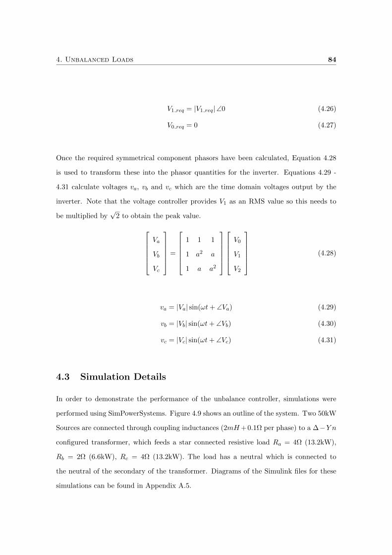
4. Unbalanced Loads 84
V1 req = |V1 req|∠0 (4.26)
V0 req = 0 (4.27)
Once the required symmetrical component phasors have been calculated, Equation 4.28
is used to transform these into the phasor quantities for the inverter. Equations 4.29 -
4.31 calculate voltages va, vb and vc which are the time domain voltages output by the
inverter. Note that the voltage controller provides V1 as an RMS value so this needs to
be multiplied by√
2 to obtain the peak value.
Va
Vb
Vc
=
1 1 1
1 a2 a
1 a a2
V0
V1
V2
(4.28)
va = |Va| sin(ωt+ ∠Va) (4.29)
vb = |Vb| sin(ωt+ ∠Vb) (4.30)
vc = |Vc| sin(ωt+ ∠Vc) (4.31)
4.3 Simulation Details
In order to demonstrate the performance of the unbalance controller, simulations were
performed using SimPowerSystems. Figure 4.9 shows an outline of the system. Two 50kW
Sources are connected through coupling inductances (2mH+0.1Ω per phase) to a ∆−Y n
configured transformer, which feeds a star connected resistive load Ra = 4Ω (13.2kW),
Rb = 2Ω (6.6kW), Rc = 4Ω (13.2kW). The load has a neutral which is connected to
the neutral of the secondary of the transformer. Diagrams of the Simulink files for these
simulations can be found in Appendix A.5.
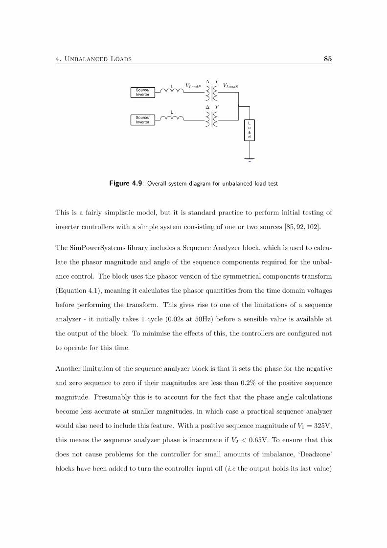
4. Unbalanced Loads 85
Source/Inverter
Load
Source/Inverter
L
L∆ Y
∆ YVLoadP VLoadS
Figure 4.9: Overall system diagram for unbalanced load test
This is a fairly simplistic model, but it is standard practice to perform initial testing of
inverter controllers with a simple system consisting of one or two sources [85,92,102].
The SimPowerSystems library includes a Sequence Analyzer block, which is used to calcu-
late the phasor magnitude and angle of the sequence components required for the unbal-
ance control. The block uses the phasor version of the symmetrical components transform
(Equation 4.1), meaning it calculates the phasor quantities from the time domain voltages
before performing the transform. This gives rise to one of the limitations of a sequence
analyzer - it initially takes 1 cycle (0.02s at 50Hz) before a sensible value is available at
the output of the block. To minimise the effects of this, the controllers are configured not
to operate for this time.
Another limitation of the sequence analyzer block is that it sets the phase for the negative
and zero sequence to zero if their magnitudes are less than 0.2% of the positive sequence
magnitude. Presumably this is to account for the fact that the phase angle calculations
become less accurate at smaller magnitudes, in which case a practical sequence analyzer
would also need to include this feature. With a positive sequence magnitude of V1 = 325V,
this means the sequence analyzer phase is inaccurate if V2 < 0.65V. To ensure that this
does not cause problems for the controller for small amounts of imbalance, ‘Deadzone’
blocks have been added to turn the controller input off (i.e the output holds its last value)
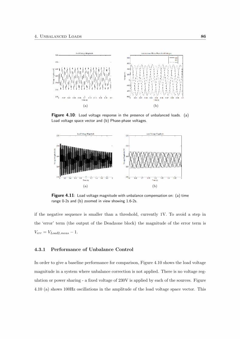
4. Unbalanced Loads 86
(a) (b)
Figure 4.10: Load voltage response in the presence of unbalanced loads. (a)
Load voltage space vector and (b) Phase-phase voltages.
(a) (b)
Figure 4.11: Load voltage magnitude with unbalance compensation on: (a) time
range 0-2s and (b) zoomed in view showing 1.6-2s.
if the negative sequence is smaller than a threshold, currently 1V. To avoid a step in
the ‘error’ term (the output of the Deadzone block) the magnitude of the error term is
Verr = VLoad2 meas − 1.
4.3.1 Performance of Unbalance Control
In order to give a baseline performance for comparison, Figure 4.10 shows the load voltage
magnitude in a system where unbalance correction is not applied. There is no voltage reg-
ulation or power sharing - a fixed voltage of 230V is applied by each of the sources. Figure
4.10 (a) shows 100Hz oscillations in the amplitude of the load voltage space vector. This
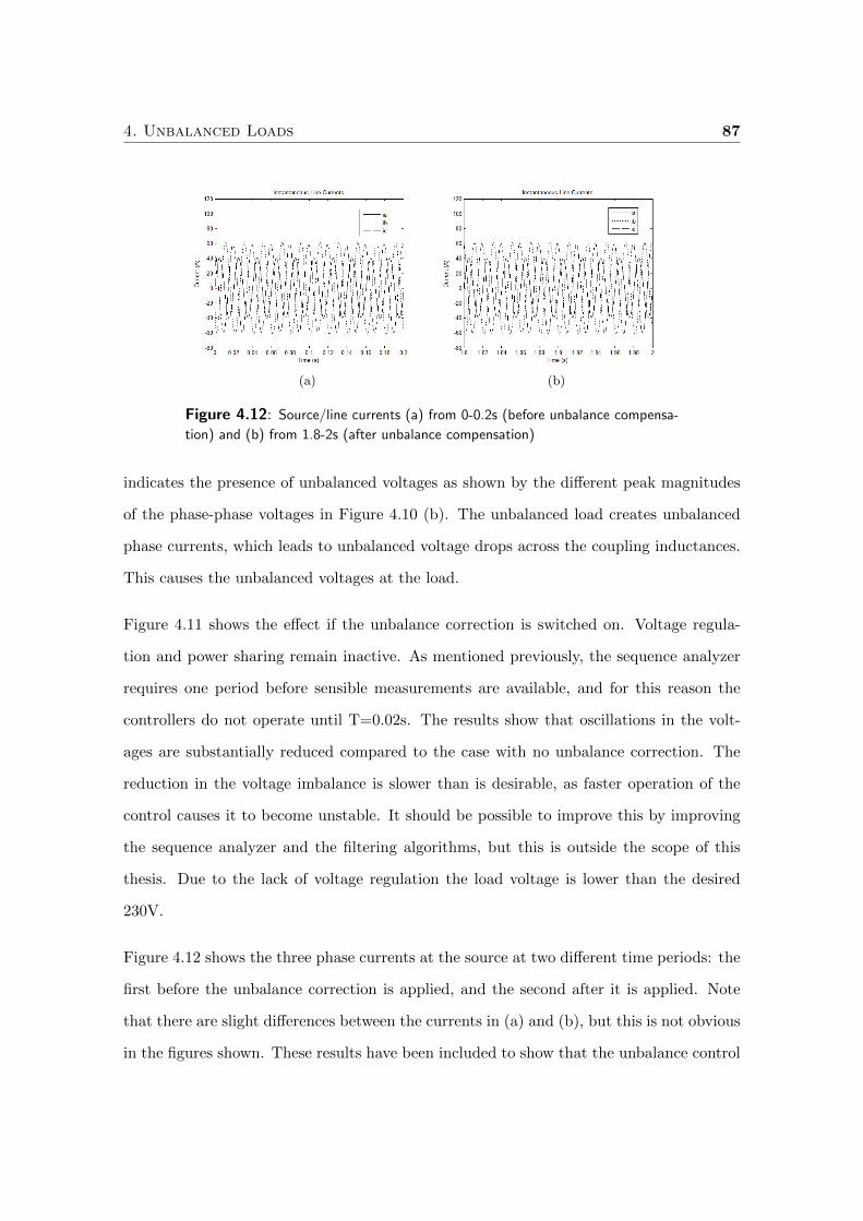
4. Unbalanced Loads 87
(a) (b)
Figure 4.12: Source/line currents (a) from 0-0.2s (before unbalance compensa-
tion) and (b) from 1.8-2s (after unbalance compensation)
indicates the presence of unbalanced voltages as shown by the different peak magnitudes
of the phase-phase voltages in Figure 4.10 (b). The unbalanced load creates unbalanced
phase currents, which leads to unbalanced voltage drops across the coupling inductances.
This causes the unbalanced voltages at the load.
Figure 4.11 shows the effect if the unbalance correction is switched on. Voltage regula-
tion and power sharing remain inactive. As mentioned previously, the sequence analyzer
requires one period before sensible measurements are available, and for this reason the
controllers do not operate until T=0.02s. The results show that oscillations in the volt-
ages are substantially reduced compared to the case with no unbalance correction. The
reduction in the voltage imbalance is slower than is desirable, as faster operation of the
control causes it to become unstable. It should be possible to improve this by improving
the sequence analyzer and the filtering algorithms, but this is outside the scope of this
thesis. Due to the lack of voltage regulation the load voltage is lower than the desired
230V.
Figure 4.12 shows the three phase currents at the source at two different time periods: the
first before the unbalance correction is applied, and the second after it is applied. Note
that there are slight differences between the currents in (a) and (b), but this is not obvious
in the figures shown. These results have been included to show that the unbalance control
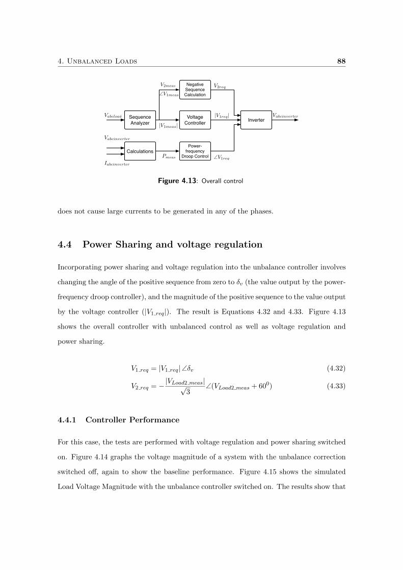
4. Unbalanced Loads 88
Sequence Analyzer
Voltage Controller
Power-frequency
Droop Control
Inverter
Negative SequenceCalculation
!V1req
|V1req|
V2req
|V1meas|
!V1meas
Vabcinverter
V2meas
Calculations
Vabcload
Iabcinverter
Pmeas
Vabcinverter
Figure 4.13: Overall control
does not cause large currents to be generated in any of the phases.
4.4 Power Sharing and voltage regulation
Incorporating power sharing and voltage regulation into the unbalance controller involves
changing the angle of the positive sequence from zero to δv (the value output by the power-
frequency droop controller), and the magnitude of the positive sequence to the value output
by the voltage controller (|V1 req|). The result is Equations 4.32 and 4.33. Figure 4.13
shows the overall controller with unbalanced control as well as voltage regulation and
power sharing.
V1 req = |V1 req|∠δv (4.32)
V2 req = −|VLoad2 meas|√3
∠(VLoad2 meas + 600) (4.33)
4.4.1 Controller Performance
For this case, the tests are performed with voltage regulation and power sharing switched
on. Figure 4.14 graphs the voltage magnitude of a system with the unbalance correction
switched off, again to show the baseline performance. Figure 4.15 shows the simulated
Load Voltage Magnitude with the unbalance controller switched on. The results show that
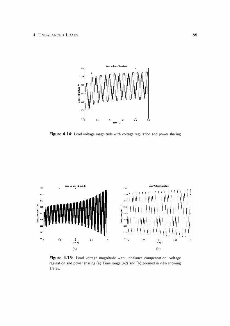
4. Unbalanced Loads 89
Figure 4.14: Load voltage magnitude with voltage regulation and power sharing
(a) (b)
Figure 4.15: Load voltage magnitude with unbalance compensation, voltage
regulation and power sharing (a) Time range 0-2s and (b) zoomed in view showing
1.8-2s.
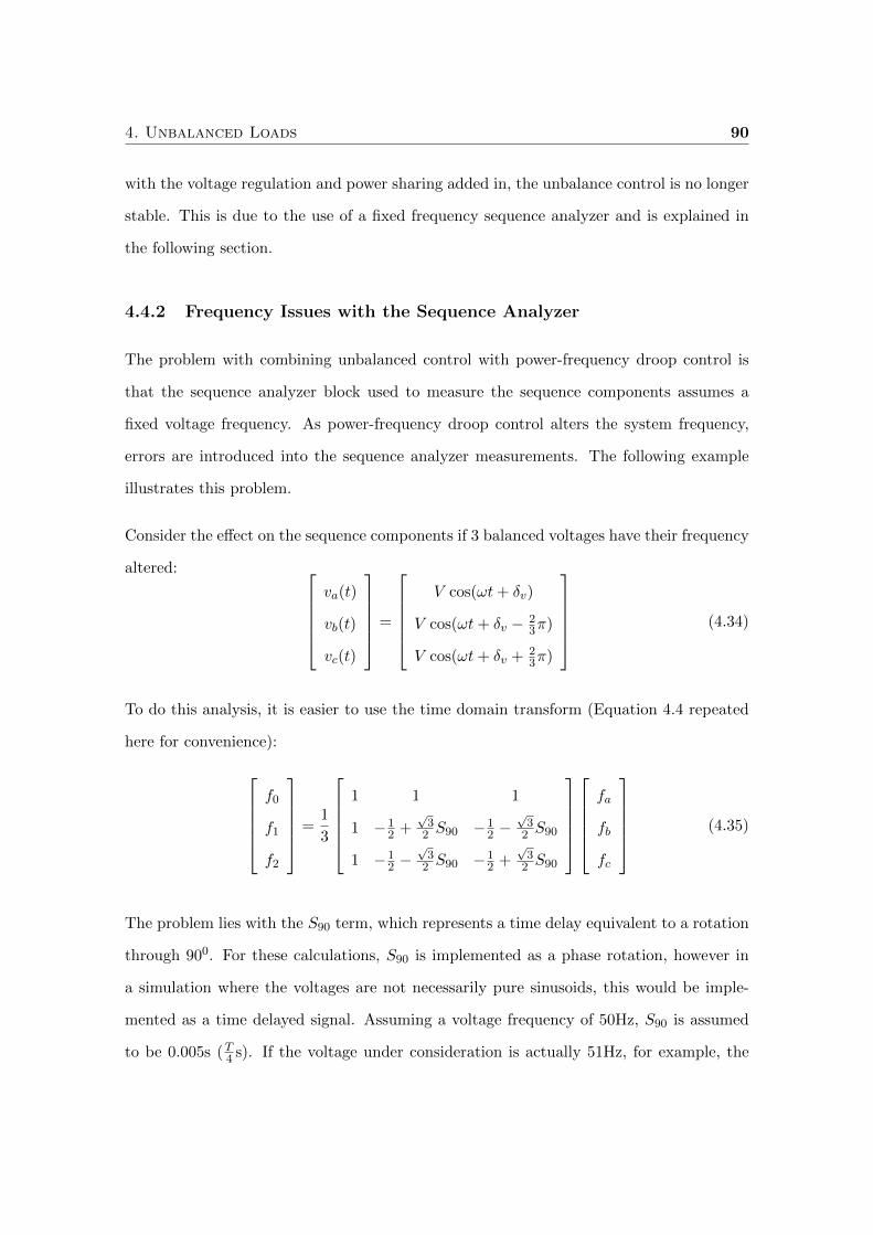
4. Unbalanced Loads 90
with the voltage regulation and power sharing added in, the unbalance control is no longer
stable. This is due to the use of a fixed frequency sequence analyzer and is explained in
the following section.
4.4.2 Frequency Issues with the Sequence Analyzer
The problem with combining unbalanced control with power-frequency droop control is
that the sequence analyzer block used to measure the sequence components assumes a
fixed voltage frequency. As power-frequency droop control alters the system frequency,
errors are introduced into the sequence analyzer measurements. The following example
illustrates this problem.
Consider the effect on the sequence components if 3 balanced voltages have their frequency
altered: va(t)
vb(t)
vc(t)
=
V cos(ωt+ δv)
V cos(ωt+ δv − 23π)
V cos(ωt+ δv + 23π)
(4.34)
To do this analysis, it is easier to use the time domain transform (Equation 4.4 repeated
here for convenience):
f0
f1
f2
=1
3
1 1 1
1 −12 +
√3
2 S90 −12 −
√3
2 S90
1 −12 −
√3
2 S90 −12 +
√3
2 S90
fa
fb
fc
(4.35)
The problem lies with the S90 term, which represents a time delay equivalent to a rotation
through 900. For these calculations, S90 is implemented as a phase rotation, however in
a simulation where the voltages are not necessarily pure sinusoids, this would be imple-
mented as a time delayed signal. Assuming a voltage frequency of 50Hz, S90 is assumed
to be 0.005s (T4 s). If the voltage under consideration is actually 51Hz, for example, the
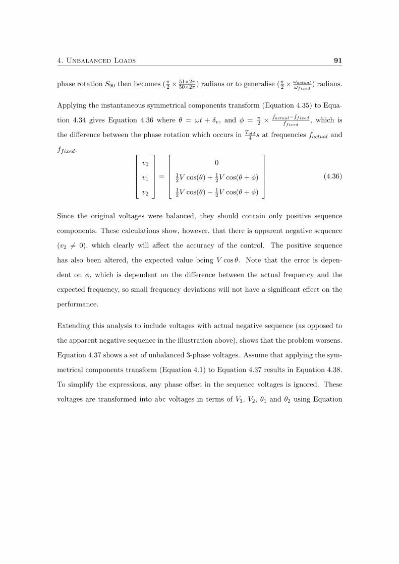
4. Unbalanced Loads 91
phase rotation S90 then becomes (π2 × 51×2π50×2π ) radians or to generalise (π2 ×
ωactualωfixed
) radians.
Applying the instantaneous symmetrical components transform (Equation 4.35) to Equa-
tion 4.34 gives Equation 4.36 where θ = ωt + δv, and φ = π2 ×
factual−ffixedffixed
, which is
the difference between the phase rotation which occurs in Told4 s at frequencies factual and
ffixed. v0
v1
v2
=
0
12V cos(θ) + 1
2V cos(θ + φ)
12V cos(θ)− 1
2V cos(θ + φ)
(4.36)
Since the original voltages were balanced, they should contain only positive sequence
components. These calculations show, however, that there is apparent negative sequence
(v2 6= 0), which clearly will affect the accuracy of the control. The positive sequence
has also been altered, the expected value being V cos θ. Note that the error is depen-
dent on φ, which is dependent on the difference between the actual frequency and the
expected frequency, so small frequency deviations will not have a significant effect on the
performance.
Extending this analysis to include voltages with actual negative sequence (as opposed to
the apparent negative sequence in the illustration above), shows that the problem worsens.
Equation 4.37 shows a set of unbalanced 3-phase voltages. Assume that applying the sym-
metrical components transform (Equation 4.1) to Equation 4.37 results in Equation 4.38.
To simplify the expressions, any phase offset in the sequence voltages is ignored. These
voltages are transformed into abc voltages in terms of V1, V2, θ1 and θ2 using Equation
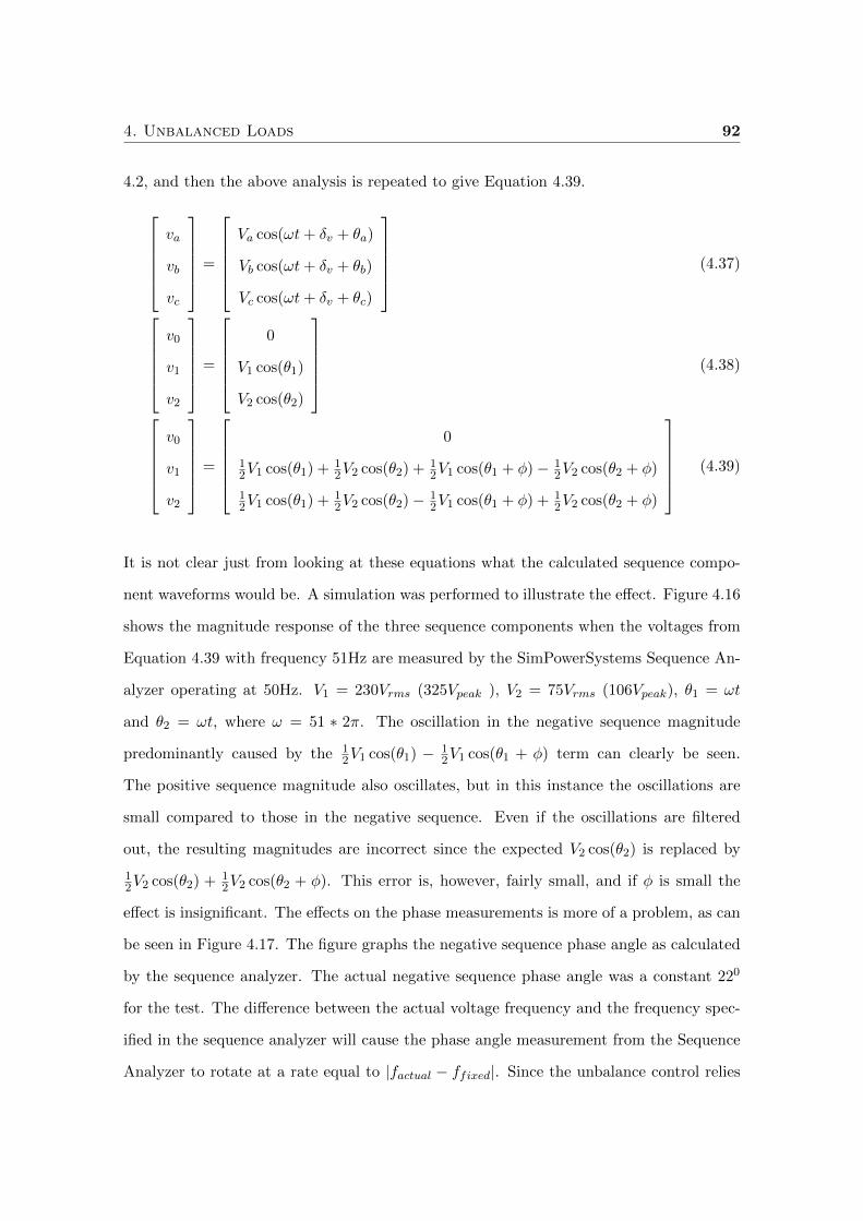
4. Unbalanced Loads 92
4.2, and then the above analysis is repeated to give Equation 4.39.
va
vb
vc
=
Va cos(ωt+ δv + θa)
Vb cos(ωt+ δv + θb)
Vc cos(ωt+ δv + θc)
(4.37)
v0
v1
v2
=
0
V1 cos(θ1)
V2 cos(θ2)
(4.38)
v0
v1
v2
=
0
12V1 cos(θ1) + 1
2V2 cos(θ2) + 12V1 cos(θ1 + φ)− 1
2V2 cos(θ2 + φ)
12V1 cos(θ1) + 1
2V2 cos(θ2)− 12V1 cos(θ1 + φ) + 1
2V2 cos(θ2 + φ)
(4.39)
It is not clear just from looking at these equations what the calculated sequence compo-
nent waveforms would be. A simulation was performed to illustrate the effect. Figure 4.16
shows the magnitude response of the three sequence components when the voltages from
Equation 4.39 with frequency 51Hz are measured by the SimPowerSystems Sequence An-
alyzer operating at 50Hz. V1 = 230Vrms (325Vpeak ), V2 = 75Vrms (106Vpeak), θ1 = ωt
and θ2 = ωt, where ω = 51 ∗ 2π. The oscillation in the negative sequence magnitude
predominantly caused by the 12V1 cos(θ1) − 1
2V1 cos(θ1 + φ) term can clearly be seen.
The positive sequence magnitude also oscillates, but in this instance the oscillations are
small compared to those in the negative sequence. Even if the oscillations are filtered
out, the resulting magnitudes are incorrect since the expected V2 cos(θ2) is replaced by
12V2 cos(θ2) + 1
2V2 cos(θ2 + φ). This error is, however, fairly small, and if φ is small the
effect is insignificant. The effects on the phase measurements is more of a problem, as can
be seen in Figure 4.17. The figure graphs the negative sequence phase angle as calculated
by the sequence analyzer. The actual negative sequence phase angle was a constant 220
for the test. The difference between the actual voltage frequency and the frequency spec-
ified in the sequence analyzer will cause the phase angle measurement from the Sequence
Analyzer to rotate at a rate equal to |factual − ffixed|. Since the unbalance control relies
4. Unbalanced Loads 93
Figure 4.16: Frequency effects on sequence analyzer magnitude (From top:
positive, negative and zero sequence)
Figure 4.17: Frequency effects on sequence analyzer phase (negative sequence
only)
on having knowledge of the negative sequence phase angle, this error from the Sequence
Analyzer will eventually cause the controller to become unstable and explains the results
shown in Figure 4.15.
4.4.3 Variable Frequency Sequence Analyzer
The solution to this issue is to build a sequence analyzer block which calculates the se-
quence components based on the measured frequency of the input signals, instead of
assuming a fixed frequency.
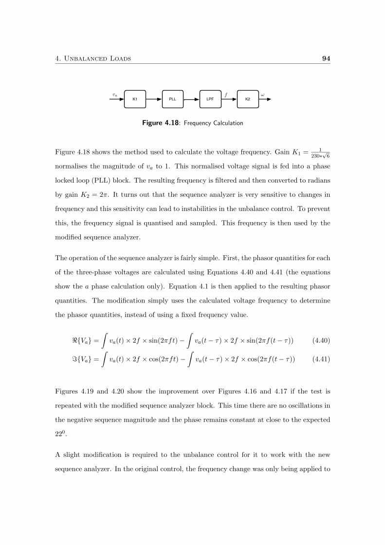
4. Unbalanced Loads 94
K1 PLL LPF K2va !f
Figure 4.18: Frequency Calculation
Figure 4.18 shows the method used to calculate the voltage frequency. Gain K1 = 1230∗
√6
normalises the magnitude of va to 1. This normalised voltage signal is fed into a phase
locked loop (PLL) block. The resulting frequency is filtered and then converted to radians
by gain K2 = 2π. It turns out that the sequence analyzer is very sensitive to changes in
frequency and this sensitivity can lead to instabilities in the unbalance control. To prevent
this, the frequency signal is quantised and sampled. This frequency is then used by the
modified sequence analyzer.
The operation of the sequence analyzer is fairly simple. First, the phasor quantities for each
of the three-phase voltages are calculated using Equations 4.40 and 4.41 (the equations
show the a phase calculation only). Equation 4.1 is then applied to the resulting phasor
quantities. The modification simply uses the calculated voltage frequency to determine
the phasor quantities, instead of using a fixed frequency value.
<Va =
ˆva(t)× 2f × sin(2πft)−
ˆva(t− τ)× 2f × sin(2πf(t− τ)) (4.40)
=Va =
ˆva(t)× 2f × cos(2πft)−
ˆva(t− τ)× 2f × cos(2πf(t− τ)) (4.41)
Figures 4.19 and 4.20 show the improvement over Figures 4.16 and 4.17 if the test is
repeated with the modified sequence analyzer block. This time there are no oscillations in
the negative sequence magnitude and the phase remains constant at close to the expected
220.
A slight modification is required to the unbalance control for it to work with the new
sequence analyzer. In the original control, the frequency change was only being applied to
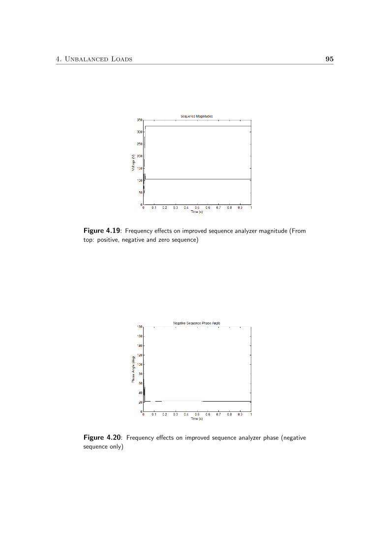
4. Unbalanced Loads 95
Figure 4.19: Frequency effects on improved sequence analyzer magnitude (From
top: positive, negative and zero sequence)
Figure 4.20: Frequency effects on improved sequence analyzer phase (negative
sequence only)
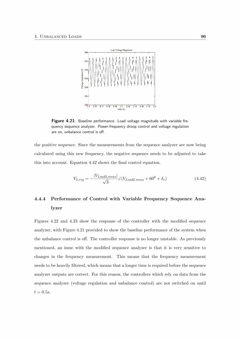
4. Unbalanced Loads 96
Figure 4.21: Baseline performance: Load voltage magnitude with variable fre-
quency sequence analyzer. Power-frequency droop control and voltage regulation
are on, unbalance control is off.
the positive sequence. Since the measurements from the sequence analyzer are now being
calculated using this new frequency, the negative sequence needs to be adjusted to take
this into account. Equation 4.42 shows the final control equation.
V2 req = −|VLoad2 meas|√3
∠(VLoad2 meas + 600 + δv) (4.42)
4.4.4 Performance of Control with Variable Frequency Sequence Ana-
lyzer
Figures 4.22 and 4.23 show the response of the controller with the modified sequence
analyzer, with Figure 4.21 provided to show the baseline performance of the system when
the unbalance control is off. The controller response is no longer unstable. As previously
mentioned, an issue with the modified sequence analyzer is that it is very sensitive to
changes in the frequency measurement. This means that the frequency measurement
needs to be heavily filtered, which means that a longer time is required before the sequence
analyzer outputs are correct. For this reason, the controllers which rely on data from the
sequence analyzer (voltage regulation and unbalance control) are not switched on until
t = 0.5s.
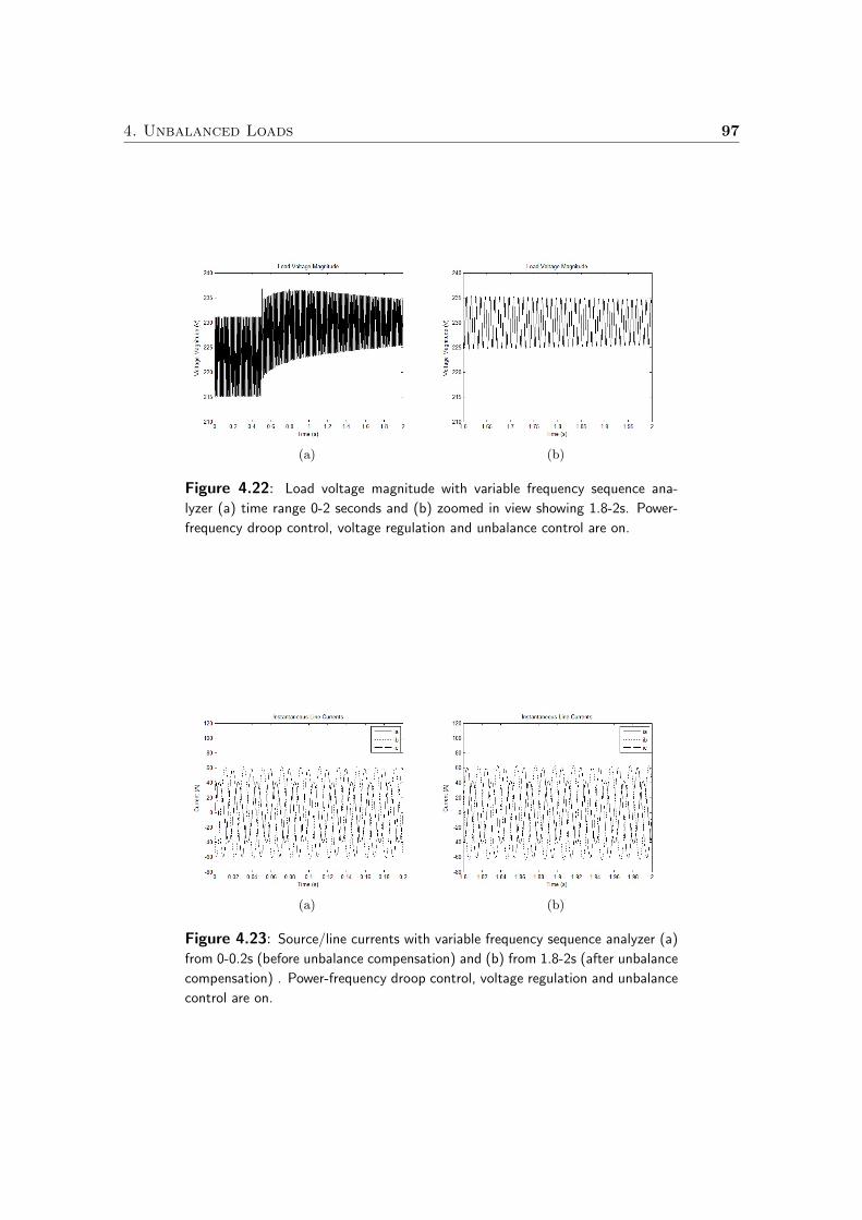
4. Unbalanced Loads 97
(a) (b)
Figure 4.22: Load voltage magnitude with variable frequency sequence ana-
lyzer (a) time range 0-2 seconds and (b) zoomed in view showing 1.8-2s. Power-
frequency droop control, voltage regulation and unbalance control are on.
(a) (b)
Figure 4.23: Source/line currents with variable frequency sequence analyzer (a)
from 0-0.2s (before unbalance compensation) and (b) from 1.8-2s (after unbalance
compensation) . Power-frequency droop control, voltage regulation and unbalance
control are on.
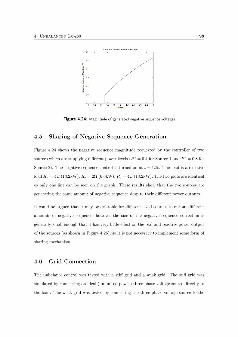
4. Unbalanced Loads 98
Figure 4.24: Magnitude of generated negative sequence voltages
4.5 Sharing of Negative Sequence Generation
Figure 4.24 shows the negative sequence magnitude requested by the controller of two
sources which are supplying different power levels (P ∗ = 0.4 for Source 1 and P ∗ = 0.8 for
Source 2). The negative sequence control is turned on at t = 1.5s. The load is a resistive
load Ra = 4Ω (13.2kW), Rb = 2Ω (6.6kW), Rc = 4Ω (13.2kW). The two plots are identical
so only one line can be seen on the graph. These results show that the two sources are
generating the same amount of negative sequence despite their different power outputs.
It could be argued that it may be desirable for different sized sources to output different
amounts of negative sequence, however the size of the negative sequence correction is
generally small enough that it has very little effect on the real and reactive power output
of the sources (as shown in Figure 4.25), so it is not necessary to implement some form of
sharing mechanism.
4.6 Grid Connection
The unbalance control was tested with a stiff grid and a weak grid. The stiff grid was
simulated by connecting an ideal (unlimited power) three phase voltage source directly to
the load. The weak grid was tested by connecting the three phase voltage source to the
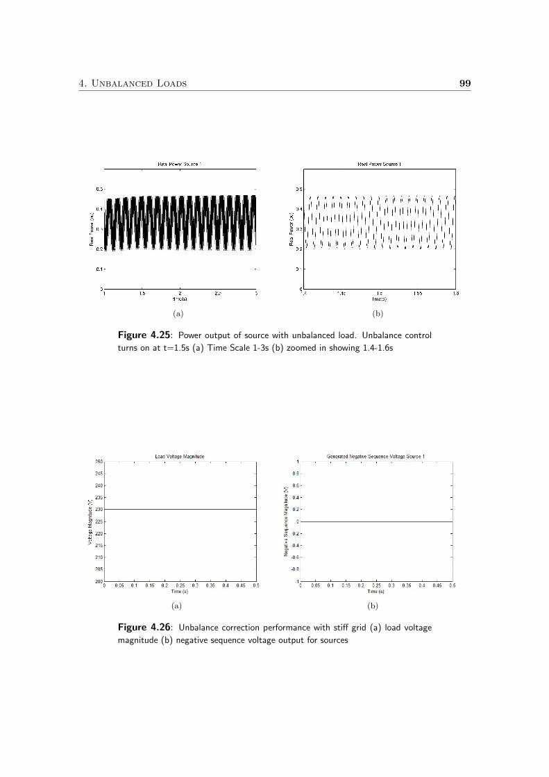
4. Unbalanced Loads 99
(a) (b)
Figure 4.25: Power output of source with unbalanced load. Unbalance control
turns on at t=1.5s (a) Time Scale 1-3s (b) zoomed in showing 1.4-1.6s
(a) (b)
Figure 4.26: Unbalance correction performance with stiff grid (a) load voltage
magnitude (b) negative sequence voltage output for sources
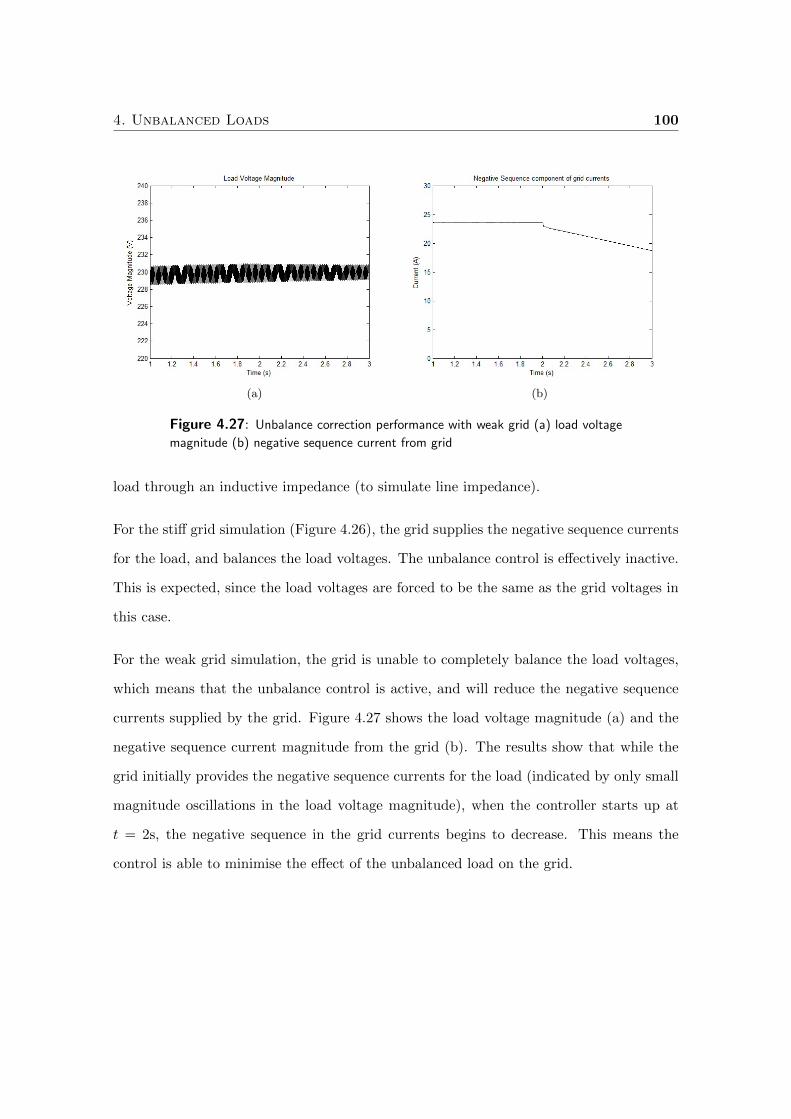
4. Unbalanced Loads 100
(a) (b)
Figure 4.27: Unbalance correction performance with weak grid (a) load voltage
magnitude (b) negative sequence current from grid
load through an inductive impedance (to simulate line impedance).
For the stiff grid simulation (Figure 4.26), the grid supplies the negative sequence currents
for the load, and balances the load voltages. The unbalance control is effectively inactive.
This is expected, since the load voltages are forced to be the same as the grid voltages in
this case.
For the weak grid simulation, the grid is unable to completely balance the load voltages,
which means that the unbalance control is active, and will reduce the negative sequence
currents supplied by the grid. Figure 4.27 shows the load voltage magnitude (a) and the
negative sequence current magnitude from the grid (b). The results show that while the
grid initially provides the negative sequence currents for the load (indicated by only small
magnitude oscillations in the load voltage magnitude), when the controller starts up at
t = 2s, the negative sequence in the grid currents begins to decrease. This means the
control is able to minimise the effect of the unbalanced load on the grid.

Chapter 5
Proposed Controller Design
In Chapter 3 the historical development of droop controller design and its variants were
examined. In Chapter 4, the controller was further developed to improve performance un-
der unbalanced load conditions. In this Chapter, a complete controller is outlined which
combines the developed unbalance controller with modified power-frequency droop and
voltage control. This complete controller performs well under a wider range of condi-
tions than previous designs. The performance of this new controller will be evaluated by
simulation.
5.1 Controller Components
There are 4 main aspects to the controller
• Power-frequency droop control with fast response, low transient frequency deviation
and zero steady-state frequency error
• Simple voltage magnitude regulation
• Reactive power sharing even under conditions with different output or line impedances,
and
• Unbalance correction to minimise voltage imbalance in the presence of unbalanced
loads
The controller is split into three main components which are outlined below: Power-
frequency droop control, Voltage Regulation (including reactive power sharing functional-
ity) and Unbalance Control. Figure 5.1 shows the overall controller.
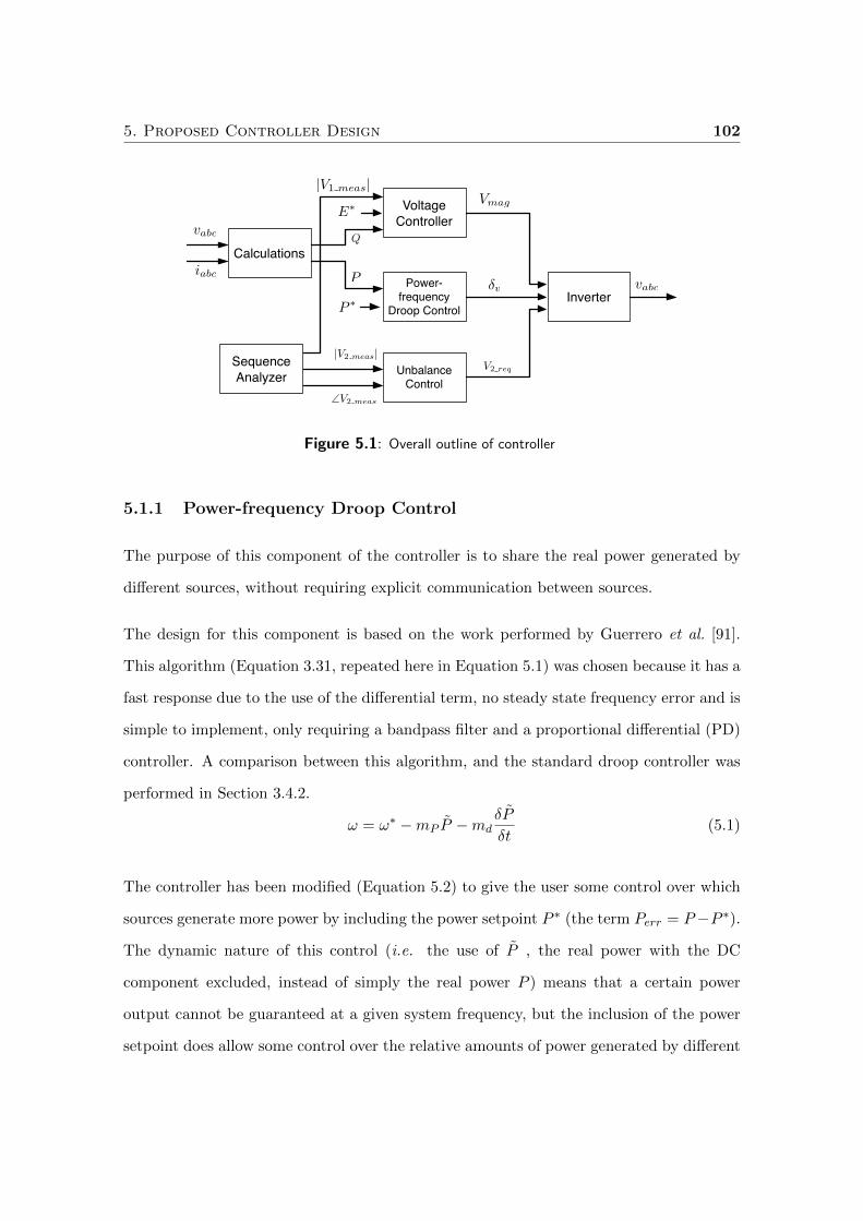
5. Proposed Controller Design 102
Voltage Controller
Power-frequency
Droop ControlInverter
δv
Vmag
|V1 meas|
vabc
Calculationsiabc
vabc
E∗
P ∗
P
Q
Unbalance Control
|V2 meas|
∠V2 meas
V2 reqSequenceAnalyzer
Figure 5.1: Overall outline of controller
5.1.1 Power-frequency Droop Control
The purpose of this component of the controller is to share the real power generated by
different sources, without requiring explicit communication between sources.
The design for this component is based on the work performed by Guerrero et al. [91].
This algorithm (Equation 3.31, repeated here in Equation 5.1) was chosen because it has a
fast response due to the use of the differential term, no steady state frequency error and is
simple to implement, only requiring a bandpass filter and a proportional differential (PD)
controller. A comparison between this algorithm, and the standard droop controller was
performed in Section 3.4.2.
ω = ω∗ −mP P −mdδP
δt(5.1)
The controller has been modified (Equation 5.2) to give the user some control over which
sources generate more power by including the power setpoint P ∗ (the term Perr = P−P ∗).
The dynamic nature of this control (i.e. the use of P , the real power with the DC
component excluded, instead of simply the real power P ) means that a certain power
output cannot be guaranteed at a given system frequency, but the inclusion of the power
setpoint does allow some control over the relative amounts of power generated by different
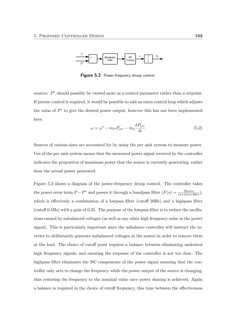
5. Proposed Controller Design 103
+-
δV
P ∗
PPD
ControlBandpassFilter
1
s
ω
Figure 5.2: Power frequency droop control
sources. P ∗ should possibly be viewed more as a control parameter rather than a setpoint.
If precise control is required, it would be possible to add an extra control loop which adjusts
the value of P ∗ to give the desired power output, however this has not been implemented
here.
ω = ω∗ −mP˜Perr −md
δ ˜Perrδt
(5.2)
Sources of various sizes are accounted for by using the per unit system to measure power.
Use of the per unit system means that the measured power signal received by the controller
indicates the proportion of maximum power that the source is currently generating, rather
than the actual power generated.
Figure 5.2 shows a diagram of the power-frequency droop control. The controller takes
the power error term P −P ∗ and passes it through a bandpass filter (F (s) = 10∗π∗s(s+π)(s+40π)),
which is effectively a combination of a lowpass filter (cutoff 20Hz) and a highpass filter
(cutoff 0.5Hz) with a gain of 0.25. The purpose of the lowpass filter is to reduce the oscilla-
tions caused by unbalanced voltages (as well as any other high frequency noise in the power
signal). This is particularly important since the unbalance controller will instruct the in-
verter to deliberately generate unbalanced voltages at the source in order to remove them
at the load. The choice of cutoff point requires a balance between eliminating undesired
high frequency signals, and ensuring the response of the controller is not too slow. The
highpass filter eliminates the DC components of the power signal ensuring that the con-
troller only acts to change the frequency while the power output of the source is changing,
thus restoring the frequency to the nominal value once power sharing is achieved. Again
a balance is required in the choice of cutoff frequency, this time between the effectiveness
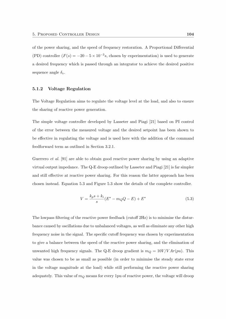
5. Proposed Controller Design 104
of the power sharing, and the speed of frequency restoration. A Proportional Differential
(PD) controller (F (s) = −20− 5× 10⁻³s, chosen by experimentation) is used to generate
a desired frequency which is passed through an integrator to achieve the desired positive
sequence angle δv.
5.1.2 Voltage Regulation
The Voltage Regulation aims to regulate the voltage level at the load, and also to ensure
the sharing of reactive power generation.
The simple voltage controller developed by Lasseter and Piagi [21] based on PI control
of the error between the measured voltage and the desired setpoint has been shown to
be effective in regulating the voltage and is used here with the addition of the command
feedforward term as outlined in Section 3.2.1.
Guerrero et al. [91] are able to obtain good reactive power sharing by using an adaptive
virtual output impedance. The Q-E droop outlined by Lasseter and Piagi [21] is far simpler
and still effective at reactive power sharing. For this reason the latter approach has been
chosen instead. Equation 5.3 and Figure 5.3 show the details of the complete controller.
V =kps+ ki
s(E∗ −mQQ− E) + E∗ (5.3)
The lowpass filtering of the reactive power feedback (cutoff 2Hz) is to minimise the distur-
bance caused by oscillations due to unbalanced voltages, as well as eliminate any other high
frequency noise in the signal. The specific cutoff frequency was chosen by experimentation
to give a balance between the speed of the reactive power sharing, and the elimination of
unwanted high frequency signals. The Q-E droop gradient is mQ = 10V/V Ar(pu). This
value was chosen to be as small as possible (in order to minimise the steady state error
in the voltage magnitude at the load) while still performing the reactive power sharing
adequately. This value of mQ means for every 1pu of reactive power, the voltage will droop
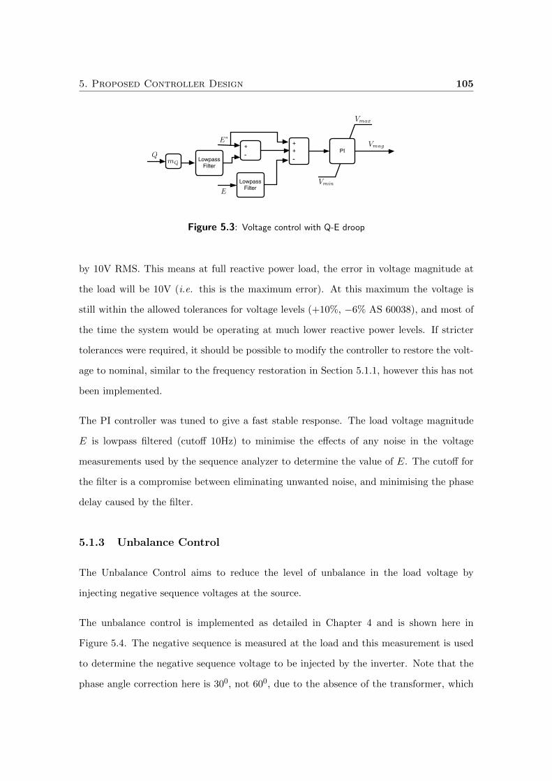
5. Proposed Controller Design 105
PIVmag
Vmax
Vmin
E∗
E
+-Q
LowpassFilter
mQ
LowpassFilter
+-
+
Figure 5.3: Voltage control with Q-E droop
by 10V RMS. This means at full reactive power load, the error in voltage magnitude at
the load will be 10V (i.e. this is the maximum error). At this maximum the voltage is
still within the allowed tolerances for voltage levels (+10%, −6% AS 60038), and most of
the time the system would be operating at much lower reactive power levels. If stricter
tolerances were required, it should be possible to modify the controller to restore the volt-
age to nominal, similar to the frequency restoration in Section 5.1.1, however this has not
been implemented.
The PI controller was tuned to give a fast stable response. The load voltage magnitude
E is lowpass filtered (cutoff 10Hz) to minimise the effects of any noise in the voltage
measurements used by the sequence analyzer to determine the value of E. The cutoff for
the filter is a compromise between eliminating unwanted noise, and minimising the phase
delay caused by the filter.
5.1.3 Unbalance Control
The Unbalance Control aims to reduce the level of unbalance in the load voltage by
injecting negative sequence voltages at the source.
The unbalance control is implemented as detailed in Chapter 4 and is shown here in
Figure 5.4. The negative sequence is measured at the load and this measurement is used
to determine the negative sequence voltage to be injected by the inverter. Note that the
phase angle correction here is 300, not 600, due to the absence of the transformer, which
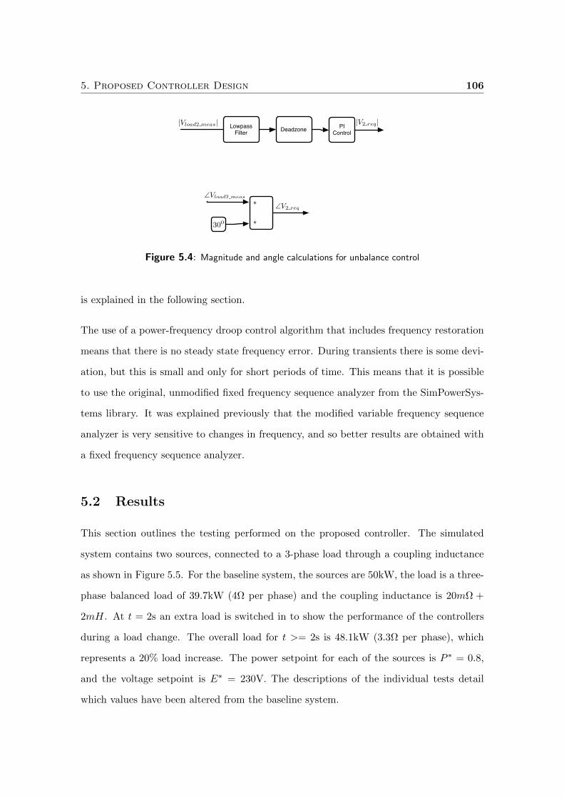
5. Proposed Controller Design 106
+
|V2 req|PIControlDeadzone
|Vload2 meas|
+300
∠Vload2 meas
∠V2 req
LowpassFilter
Figure 5.4: Magnitude and angle calculations for unbalance control
is explained in the following section.
The use of a power-frequency droop control algorithm that includes frequency restoration
means that there is no steady state frequency error. During transients there is some devi-
ation, but this is small and only for short periods of time. This means that it is possible
to use the original, unmodified fixed frequency sequence analyzer from the SimPowerSys-
tems library. It was explained previously that the modified variable frequency sequence
analyzer is very sensitive to changes in frequency, and so better results are obtained with
a fixed frequency sequence analyzer.
5.2 Results
This section outlines the testing performed on the proposed controller. The simulated
system contains two sources, connected to a 3-phase load through a coupling inductance
as shown in Figure 5.5. For the baseline system, the sources are 50kW, the load is a three-
phase balanced load of 39.7kW (4Ω per phase) and the coupling inductance is 20mΩ +
2mH. At t = 2s an extra load is switched in to show the performance of the controllers
during a load change. The overall load for t >= 2s is 48.1kW (3.3Ω per phase), which
represents a 20% load increase. The power setpoint for each of the sources is P ∗ = 0.8,
and the voltage setpoint is E∗ = 230V. The descriptions of the individual tests detail
which values have been altered from the baseline system.
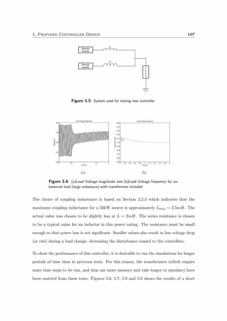
5. Proposed Controller Design 107
Source/Inverter
Load
Source/Inverter
L
L
Figure 5.5: System used for testing new controller
0 0.5 1 1.5 2215
220
225
230
235Load Voltage Magnitude
Vol
tage
(V
)
Time (s)
(a)
0 0.2 0.4 0.6 0.8 1 1.2 1.4 1.6 1.8 249.5
49.6
49.7
49.8
49.9
50
50.1
50.2
50.3
50.4
50.5Load Voltage Frequency
Time (s)
Fre
quen
cy (
Hz)
(b)
Figure 5.6: (a)Load Voltage magnitude and (b)Load Voltage frequency for un-
balanced load (large unbalance) with transformers included
The choice of coupling inductance is based on Section 2.2.3 which indicates that the
maximum coupling inductance for a 50kW source is approximately Lmax = 2.5mH. The
actual value was chosen to be slightly less at L = 2mH. The series resistance is chosen
to be a typical value for an inductor in this power rating. The resistance must be small
enough so that power loss is not significant. Smaller values also result in less voltage drop
(or rise) during a load change, decreasing the disturbance caused to the controllers.
To show the performance of this controller, it is desirable to run the simulations for longer
periods of time than in previous tests. For this reason, the transformers (which require
more time steps to be run, and thus use more memory and take longer to simulate) have
been omitted from these tests. Figures 5.6, 5.7, 5.8 and 5.9 shows the results of a short
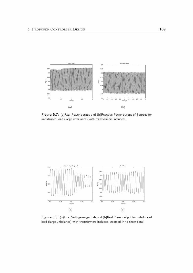
5. Proposed Controller Design 108
0 0.5 1 1.5 20.3
0.35
0.4
0.45
0.5
0.55
0.6
0.65
Real Power
Time (s)
P (
pu)
(a)
0 0.2 0.4 0.6 0.8 1 1.2 1.4 1.6 1.8 2−0.1
−0.05
0
0.05
0.1
0.15
0.2
0.25
0.3Reactive Power
Time (s)
Q (
pu)
(b)
Figure 5.7: (a)Real Power output and (b)Reactive Power output of Sources for
unbalanced load (large unbalance) with transformers included.
0.4 0.45 0.5 0.55 0.6215
220
225
230
235Load Voltage Magnitude
Vol
tage
(V
)
Time (s)
(a)
0.4 0.45 0.5 0.55 0.60.3
0.35
0.4
0.45
0.5
0.55
0.6
0.65
Real Power
Time (s)
P (
pu)
(b)
Figure 5.8: (a)Load Voltage magnitude and (b)Real Power output for unbalanced
load (large unbalance) with transformers included, zoomed in to show detail
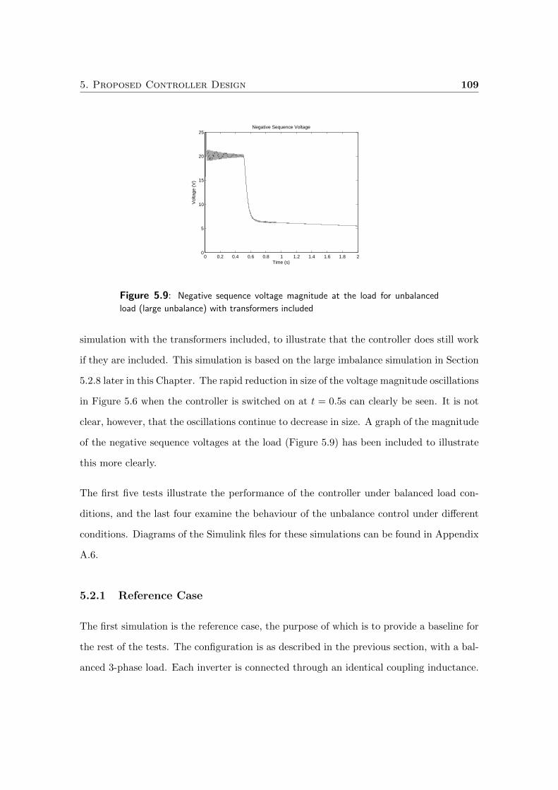
5. Proposed Controller Design 109
0 0.2 0.4 0.6 0.8 1 1.2 1.4 1.6 1.8 20
5
10
15
20
25Negative Sequence Voltage
Time (s)
Vol
tage
(V
)
Figure 5.9: Negative sequence voltage magnitude at the load for unbalanced
load (large unbalance) with transformers included
simulation with the transformers included, to illustrate that the controller does still work
if they are included. This simulation is based on the large imbalance simulation in Section
5.2.8 later in this Chapter. The rapid reduction in size of the voltage magnitude oscillations
in Figure 5.6 when the controller is switched on at t = 0.5s can clearly be seen. It is not
clear, however, that the oscillations continue to decrease in size. A graph of the magnitude
of the negative sequence voltages at the load (Figure 5.9) has been included to illustrate
this more clearly.
The first five tests illustrate the performance of the controller under balanced load con-
ditions, and the last four examine the behaviour of the unbalance control under different
conditions. Diagrams of the Simulink files for these simulations can be found in Appendix
A.6.
5.2.1 Reference Case
The first simulation is the reference case, the purpose of which is to provide a baseline for
the rest of the tests. The configuration is as described in the previous section, with a bal-
anced 3-phase load. Each inverter is connected through an identical coupling inductance.
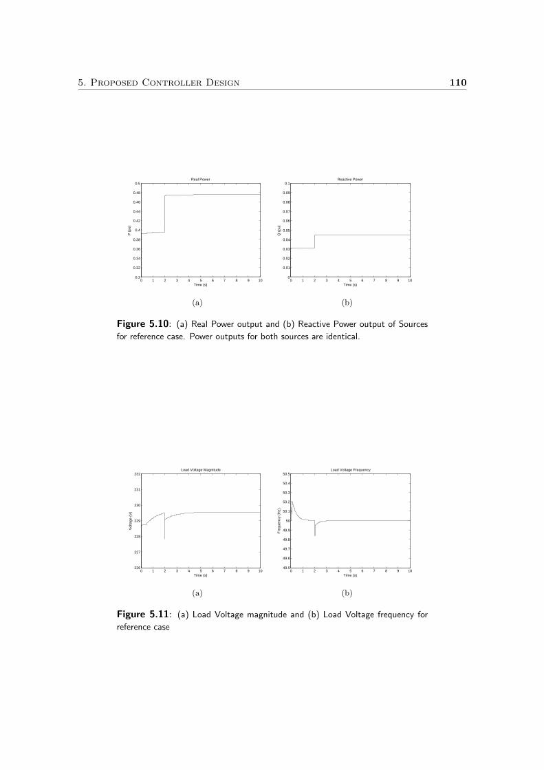
5. Proposed Controller Design 110
0 1 2 3 4 5 6 7 8 9 100.3
0.32
0.34
0.36
0.38
0.4
0.42
0.44
0.46
0.48
0.5Real Power
Time (s)
P (
pu)
(a)
0 1 2 3 4 5 6 7 8 9 100
0.01
0.02
0.03
0.04
0.05
0.06
0.07
0.08
0.09
0.1Reactive Power
Time (s)
Q (
pu)
(b)
Figure 5.10: (a) Real Power output and (b) Reactive Power output of Sources
for reference case. Power outputs for both sources are identical.
0 1 2 3 4 5 6 7 8 9 10226
227
228
229
230
231
232Load Voltage Magnitude
Vol
tage
(V
)
Time (s)
(a)
0 1 2 3 4 5 6 7 8 9 1049.5
49.6
49.7
49.8
49.9
50
50.1
50.2
50.3
50.4
50.5Load Voltage Frequency
Time (s)
Fre
quen
cy (
Hz)
(b)
Figure 5.11: (a) Load Voltage magnitude and (b) Load Voltage frequency for
reference case
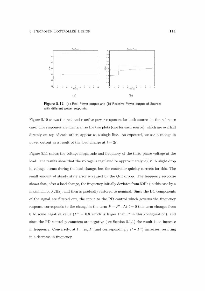
5. Proposed Controller Design 111
0 1 2 3 4 5 6 7 8 9 100.1
0.2
0.3
0.4
0.5
0.6
Real Power
Time (s)
P (
pu)
(a)
0 1 2 3 4 5 6 7 8 9 100
0.01
0.02
0.03
0.04
0.05
0.06
0.07
0.08
0.09
0.1Reactive Power
Time (s)
Q (
pu)
(b)
Figure 5.12: (a) Real Power output and (b) Reactive Power output of Sources
with different power setpoints.
Figure 5.10 shows the real and reactive power responses for both sources in the reference
case. The responses are identical, so the two plots (one for each source), which are overlaid
directly on top of each other, appear as a single line. As expected, we see a change in
power output as a result of the load change at t = 2s.
Figure 5.11 shows the voltage magnitude and frequency of the three phase voltage at the
load. The results show that the voltage is regulated to approximately 230V. A slight drop
in voltage occurs during the load change, but the controller quickly corrects for this. The
small amount of steady state error is caused by the Q-E droop. The frequency response
shows that, after a load change, the frequency initially deviates from 50Hz (in this case by a
maximum of 0.2Hz), and then is gradually restored to nominal. Since the DC components
of the signal are filtered out, the input to the PD control which governs the frequency
response corresponds to the change in the term P − P ∗. At t = 0 this term changes from
0 to some negative value (P ∗ = 0.8 which is larger than P in this configuration), and
since the PD control parameters are negative (see Section 5.1.1) the result is an increase
in frequency. Conversely, at t = 2s, P (and correspondingly P − P ∗) increases, resulting
in a decrease in frequency.
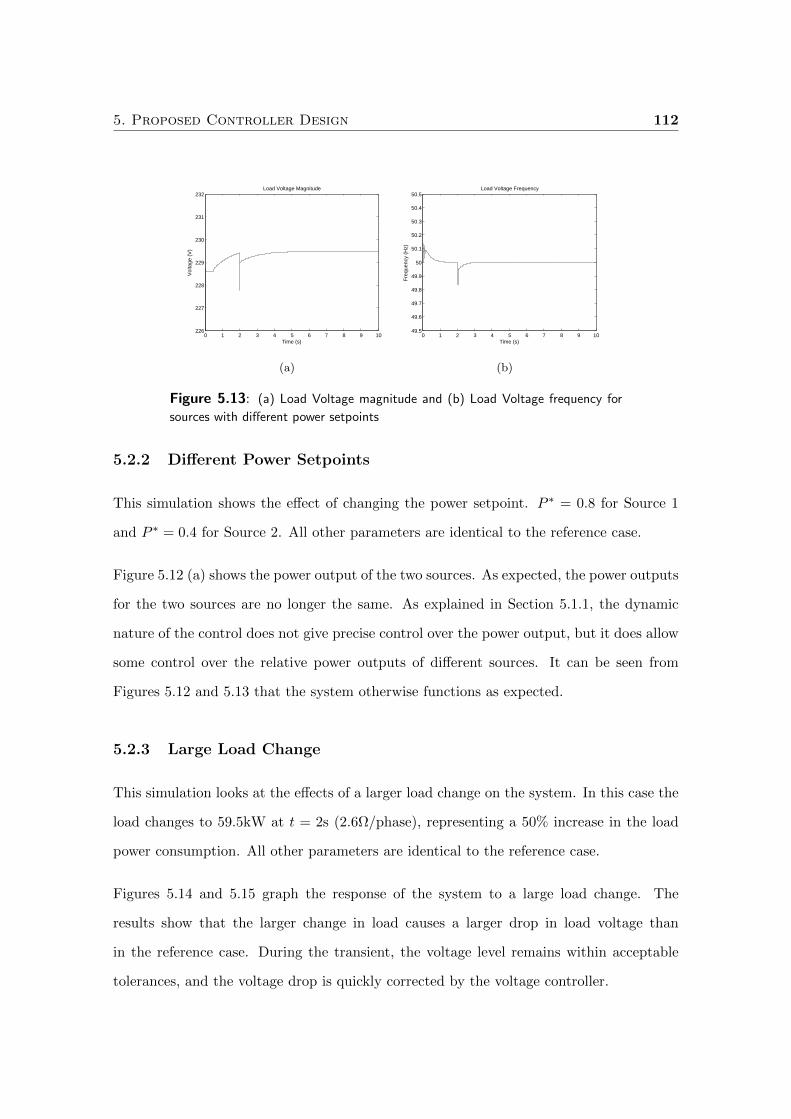
5. Proposed Controller Design 112
0 1 2 3 4 5 6 7 8 9 10226
227
228
229
230
231
232Load Voltage Magnitude
Vol
tage
(V
)
Time (s)
(a)
0 1 2 3 4 5 6 7 8 9 1049.5
49.6
49.7
49.8
49.9
50
50.1
50.2
50.3
50.4
50.5Load Voltage Frequency
Time (s)
Fre
quen
cy (
Hz)
(b)
Figure 5.13: (a) Load Voltage magnitude and (b) Load Voltage frequency for
sources with different power setpoints
5.2.2 Different Power Setpoints
This simulation shows the effect of changing the power setpoint. P ∗ = 0.8 for Source 1
and P ∗ = 0.4 for Source 2. All other parameters are identical to the reference case.
Figure 5.12 (a) shows the power output of the two sources. As expected, the power outputs
for the two sources are no longer the same. As explained in Section 5.1.1, the dynamic
nature of the control does not give precise control over the power output, but it does allow
some control over the relative power outputs of different sources. It can be seen from
Figures 5.12 and 5.13 that the system otherwise functions as expected.
5.2.3 Large Load Change
This simulation looks at the effects of a larger load change on the system. In this case the
load changes to 59.5kW at t = 2s (2.6Ω/phase), representing a 50% increase in the load
power consumption. All other parameters are identical to the reference case.
Figures 5.14 and 5.15 graph the response of the system to a large load change. The
results show that the larger change in load causes a larger drop in load voltage than
in the reference case. During the transient, the voltage level remains within acceptable
tolerances, and the voltage drop is quickly corrected by the voltage controller.
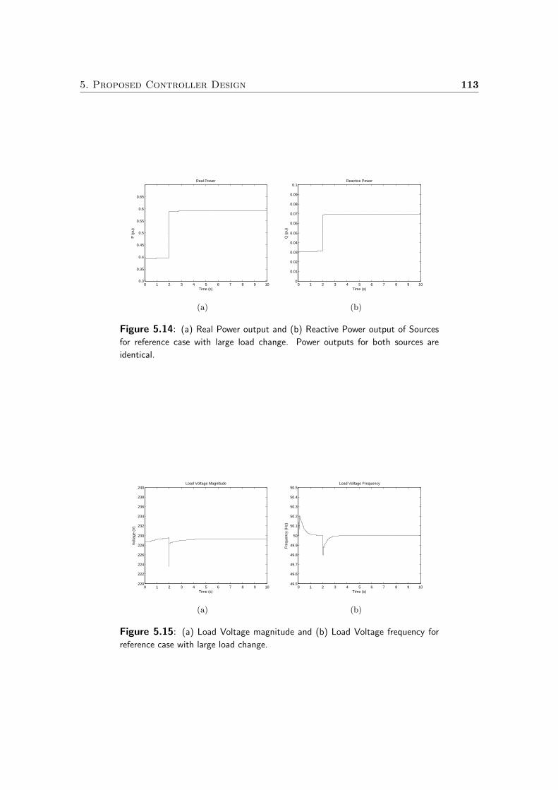
5. Proposed Controller Design 113
0 1 2 3 4 5 6 7 8 9 100.3
0.35
0.4
0.45
0.5
0.55
0.6
0.65
Real Power
Time (s)
P (
pu)
(a)
0 1 2 3 4 5 6 7 8 9 100
0.01
0.02
0.03
0.04
0.05
0.06
0.07
0.08
0.09
0.1Reactive Power
Time (s)Q
(pu
)
(b)
Figure 5.14: (a) Real Power output and (b) Reactive Power output of Sources
for reference case with large load change. Power outputs for both sources are
identical.
0 1 2 3 4 5 6 7 8 9 10220
222
224
226
228
230
232
234
236
238
240Load Voltage Magnitude
Vol
tage
(V
)
Time (s)
(a)
0 1 2 3 4 5 6 7 8 9 1049.5
49.6
49.7
49.8
49.9
50
50.1
50.2
50.3
50.4
50.5Load Voltage Frequency
Time (s)
Fre
quen
cy (
Hz)
(b)
Figure 5.15: (a) Load Voltage magnitude and (b) Load Voltage frequency for
reference case with large load change.
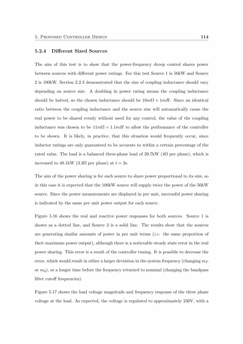
5. Proposed Controller Design 114
5.2.4 Different Sized Sources
The aim of this test is to show that the power-frequency droop control shares power
between sources with different power ratings. For this test Source 1 is 50kW and Source
2 is 100kW. Section 2.2.3 demonstrated that the size of coupling inductance should vary
depending on source size. A doubling in power rating means the coupling inductance
should be halved, so the chosen inductance should be 10mΩ + 1mH. Since an identical
ratio between the coupling inductance and the source size will automatically cause the
real power to be shared evenly without need for any control, the value of the coupling
inductance was chosen to be 11mΩ + 1.1mH to allow the performance of the controller
to be shown. It is likely, in practice, that this situation would frequently occur, since
inductor ratings are only guaranteed to be accurate to within a certain percentage of the
rated value. The load is a balanced three-phase load of 39.7kW (4Ω per phase), which is
increased to 48.1kW (3.3Ω per phase) at t = 2s.
The aim of the power sharing is for each source to share power proportional to its size, so
in this case it is expected that the 100kW source will supply twice the power of the 50kW
source. Since the power measurements are displayed in per unit, successful power sharing
is indicated by the same per unit power output for each source.
Figure 5.16 shows the real and reactive power responses for both sources. Source 1 is
shown as a dotted line, and Source 2 is a solid line. The results show that the sources
are generating similar amounts of power in per unit terms (i.e. the same proportion of
their maximum power output), although there is a noticeable steady state error in the real
power sharing. This error is a result of the controller tuning. It is possible to decrease the
error, which would result in either a larger deviation in the system frequency (changing mP
or md), or a longer time before the frequency returned to nominal (changing the bandpass
filter cutoff frequencies).
Figure 5.17 shows the load voltage magnitude and frequency response of the three phase
voltage at the load. As expected, the voltage is regulated to approximately 230V, with a
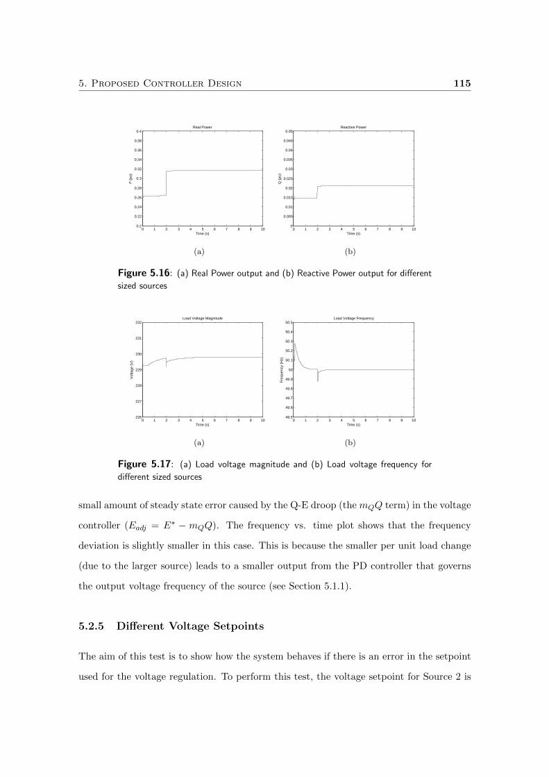
5. Proposed Controller Design 115
0 1 2 3 4 5 6 7 8 9 100.2
0.22
0.24
0.26
0.28
0.3
0.32
0.34
0.36
0.38
0.4Real Power
Time (s)
P (
pu)
(a)
0 1 2 3 4 5 6 7 8 9 100
0.005
0.01
0.015
0.02
0.025
0.03
0.035
0.04
0.045
0.05Reactive Power
Time (s)
Q (
pu)
(b)
Figure 5.16: (a) Real Power output and (b) Reactive Power output for different
sized sources
0 1 2 3 4 5 6 7 8 9 10226
227
228
229
230
231
232Load Voltage Magnitude
Vol
tage
(V
)
Time (s)
(a)
0 1 2 3 4 5 6 7 8 9 1049.5
49.6
49.7
49.8
49.9
50
50.1
50.2
50.3
50.4
50.5Load Voltage Frequency
Time (s)
Fre
quen
cy (
Hz)
(b)
Figure 5.17: (a) Load voltage magnitude and (b) Load voltage frequency for
different sized sources
small amount of steady state error caused by the Q-E droop (the mQQ term) in the voltage
controller (Eadj = E∗ − mQQ). The frequency vs. time plot shows that the frequency
deviation is slightly smaller in this case. This is because the smaller per unit load change
(due to the larger source) leads to a smaller output from the PD controller that governs
the output voltage frequency of the source (see Section 5.1.1).
5.2.5 Different Voltage Setpoints
The aim of this test is to show how the system behaves if there is an error in the setpoint
used for the voltage regulation. To perform this test, the voltage setpoint for Source 2 is
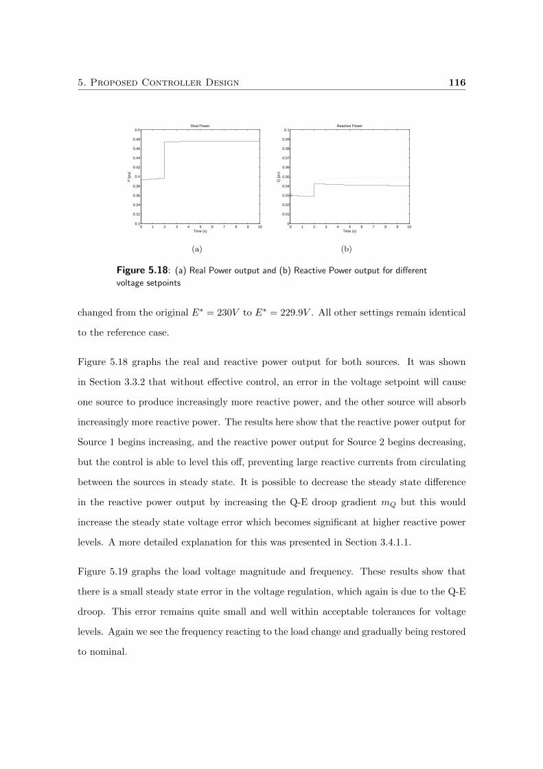
5. Proposed Controller Design 116
0 1 2 3 4 5 6 7 8 9 100.3
0.32
0.34
0.36
0.38
0.4
0.42
0.44
0.46
0.48
0.5Real Power
Time (s)
P (
pu)
(a)
0 1 2 3 4 5 6 7 8 9 100
0.01
0.02
0.03
0.04
0.05
0.06
0.07
0.08
0.09
0.1Reactive Power
Time (s)
Q (
pu)
(b)
Figure 5.18: (a) Real Power output and (b) Reactive Power output for different
voltage setpoints
changed from the original E∗ = 230V to E∗ = 229.9V . All other settings remain identical
to the reference case.
Figure 5.18 graphs the real and reactive power output for both sources. It was shown
in Section 3.3.2 that without effective control, an error in the voltage setpoint will cause
one source to produce increasingly more reactive power, and the other source will absorb
increasingly more reactive power. The results here show that the reactive power output for
Source 1 begins increasing, and the reactive power output for Source 2 begins decreasing,
but the control is able to level this off, preventing large reactive currents from circulating
between the sources in steady state. It is possible to decrease the steady state difference
in the reactive power output by increasing the Q-E droop gradient mQ but this would
increase the steady state voltage error which becomes significant at higher reactive power
levels. A more detailed explanation for this was presented in Section 3.4.1.1.
Figure 5.19 graphs the load voltage magnitude and frequency. These results show that
there is a small steady state error in the voltage regulation, which again is due to the Q-E
droop. This error remains quite small and well within acceptable tolerances for voltage
levels. Again we see the frequency reacting to the load change and gradually being restored
to nominal.
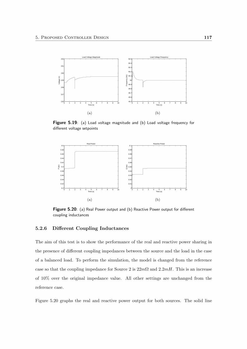
5. Proposed Controller Design 117
0 1 2 3 4 5 6 7 8 9 10226
227
228
229
230
231
232Load Voltage Magnitude
Vol
tage
(V
)
Time (s)
(a)
0 1 2 3 4 5 6 7 8 9 1049.5
49.6
49.7
49.8
49.9
50
50.1
50.2
50.3
50.4
50.5Load Voltage Frequency
Time (s)
Fre
quen
cy (
Hz)
(b)
Figure 5.19: (a) Load voltage magnitude and (b) Load voltage frequency for
different voltage setpoints
0 1 2 3 4 5 6 7 8 9 100.3
0.32
0.34
0.36
0.38
0.4
0.42
0.44
0.46
0.48
0.5Real Power
Time (s)
P (
pu)
(a)
0 1 2 3 4 5 6 7 8 9 100
0.01
0.02
0.03
0.04
0.05
0.06
0.07
0.08
0.09
0.1Reactive Power
Time (s)
Q (
pu)
(b)
Figure 5.20: (a) Real Power output and (b) Reactive Power output for different
coupling inductances
5.2.6 Different Coupling Inductances
The aim of this test is to show the performance of the real and reactive power sharing in
the presence of different coupling impedances between the source and the load in the case
of a balanced load. To perform the simulation, the model is changed from the reference
case so that the coupling impedance for Source 2 is 22mΩ and 2.2mH. This is an increase
of 10% over the original impedance value. All other settings are unchanged from the
reference case.
Figure 5.20 graphs the real and reactive power output for both sources. The solid line
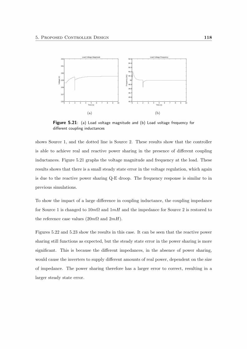
5. Proposed Controller Design 118
0 1 2 3 4 5 6 7 8 9 10226
227
228
229
230
231
232Load Voltage Magnitude
Vol
tage
(V
)
Time (s)
(a)
0 1 2 3 4 5 6 7 8 9 1049.5
49.6
49.7
49.8
49.9
50
50.1
50.2
50.3
50.4
50.5Load Voltage Frequency
Time (s)
Fre
quen
cy (
Hz)
(b)
Figure 5.21: (a) Load voltage magnitude and (b) Load voltage frequency for
different coupling inductances
shows Source 1, and the dotted line is Source 2. These results show that the controller
is able to achieve real and reactive power sharing in the presence of different coupling
inductances. Figure 5.21 graphs the voltage magnitude and frequency at the load. These
results shows that there is a small steady state error in the voltage regulation, which again
is due to the reactive power sharing Q-E droop. The frequency response is similar to in
previous simulations.
To show the impact of a large difference in coupling inductance, the coupling impedance
for Source 1 is changed to 10mΩ and 1mH and the impedance for Source 2 is restored to
the reference case values (20mΩ and 2mH).
Figures 5.22 and 5.23 show the results in this case. It can be seen that the reactive power
sharing still functions as expected, but the steady state error in the power sharing is more
significant. This is because the different impedances, in the absence of power sharing,
would cause the inverters to supply different amounts of real power, dependent on the size
of impedance. The power sharing therefore has a larger error to correct, resulting in a
larger steady state error.
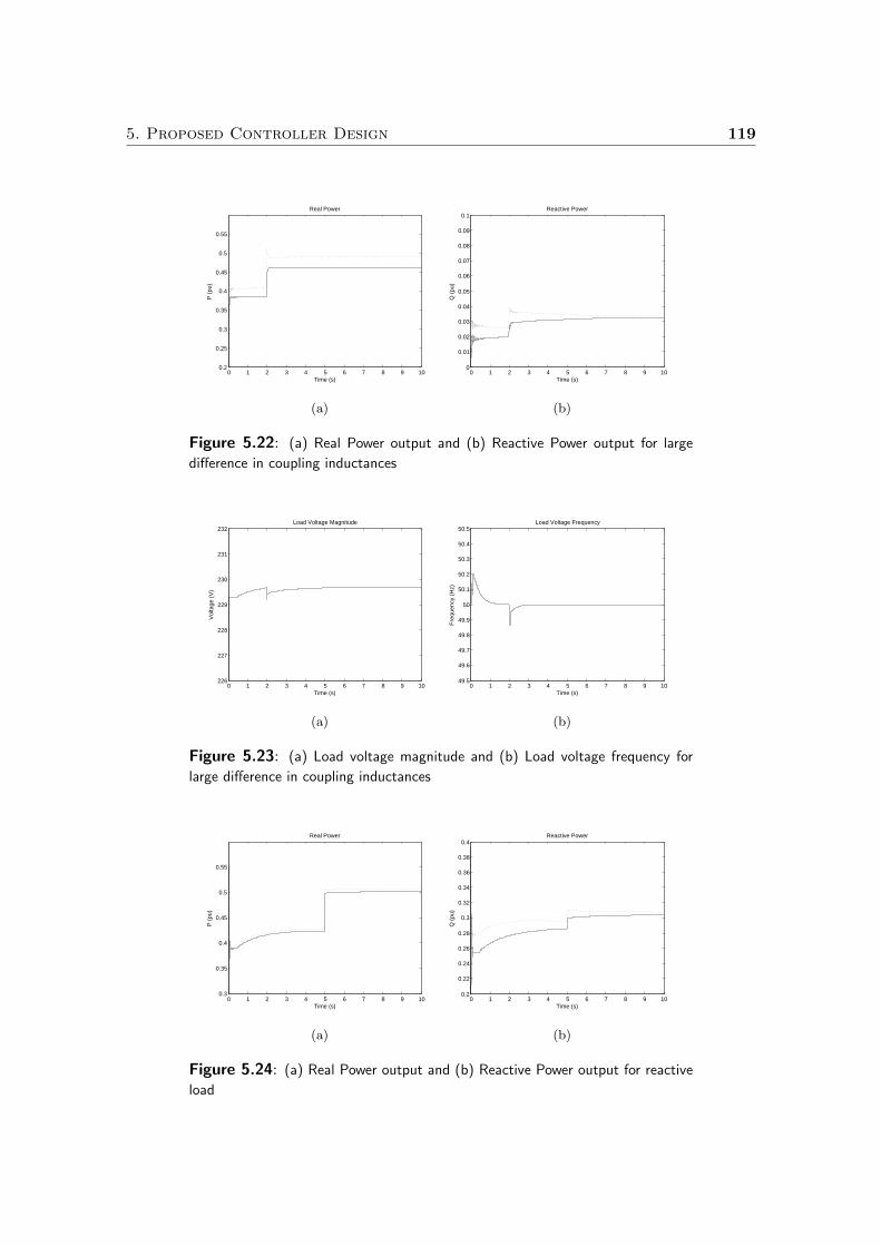
5. Proposed Controller Design 119
0 1 2 3 4 5 6 7 8 9 100.2
0.25
0.3
0.35
0.4
0.45
0.5
0.55
Real Power
Time (s)
P (
pu)
(a)
0 1 2 3 4 5 6 7 8 9 100
0.01
0.02
0.03
0.04
0.05
0.06
0.07
0.08
0.09
0.1Reactive Power
Time (s)
Q (
pu)
(b)
Figure 5.22: (a) Real Power output and (b) Reactive Power output for large
difference in coupling inductances
0 1 2 3 4 5 6 7 8 9 10226
227
228
229
230
231
232Load Voltage Magnitude
Vol
tage
(V
)
Time (s)
(a)
0 1 2 3 4 5 6 7 8 9 1049.5
49.6
49.7
49.8
49.9
50
50.1
50.2
50.3
50.4
50.5Load Voltage Frequency
Time (s)
Fre
quen
cy (
Hz)
(b)
Figure 5.23: (a) Load voltage magnitude and (b) Load voltage frequency for
large difference in coupling inductances
0 1 2 3 4 5 6 7 8 9 100.3
0.35
0.4
0.45
0.5
0.55
Real Power
Time (s)
P (
pu)
(a)
0 1 2 3 4 5 6 7 8 9 100.2
0.22
0.24
0.26
0.28
0.3
0.32
0.34
0.36
0.38
0.4Reactive Power
Time (s)
Q (
pu)
(b)
Figure 5.24: (a) Real Power output and (b) Reactive Power output for reactive
load
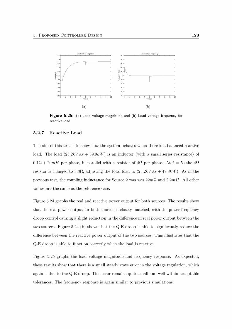
5. Proposed Controller Design 120
0 1 2 3 4 5 6 7 8 9 10210
212
214
216
218
220
222
224
226
228
230Load Voltage Magnitude
Vol
tage
(V
)
Time (s)
(a)
0 1 2 3 4 5 6 7 8 9 1049.5
49.6
49.7
49.8
49.9
50
50.1
50.2
50.3
50.4
50.5Load Voltage Frequency
Time (s)
Fre
quen
cy (
Hz)
(b)
Figure 5.25: (a) Load voltage magnitude and (b) Load voltage frequency for
reactive load
5.2.7 Reactive Load
The aim of this test is to show how the system behaves when there is a balanced reactive
load. The load (25.2kV Ar + 39.9kW ) is an inductor (with a small series resistance) of
0.1Ω + 20mH per phase, in parallel with a resistor of 4Ω per phase. At t = 5s the 4Ω
resistor is changed to 3.3Ω, adjusting the total load to (25.2kV Ar + 47.8kW ). As in the
previous test, the coupling inductance for Source 2 was was 22mΩ and 2.2mH. All other
values are the same as the reference case.
Figure 5.24 graphs the real and reactive power output for both sources. The results show
that the real power output for both sources is closely matched, with the power-frequency
droop control causing a slight reduction in the difference in real power output between the
two sources. Figure 5.24 (b) shows that the Q-E droop is able to significantly reduce the
difference between the reactive power output of the two sources. This illustrates that the
Q-E droop is able to function correctly when the load is reactive.
Figure 5.25 graphs the load voltage magnitude and frequency response. As expected,
these results show that there is a small steady state error in the voltage regulation, which
again is due to the Q-E droop. This error remains quite small and well within acceptable
tolerances. The frequency response is again similar to previous simulations.
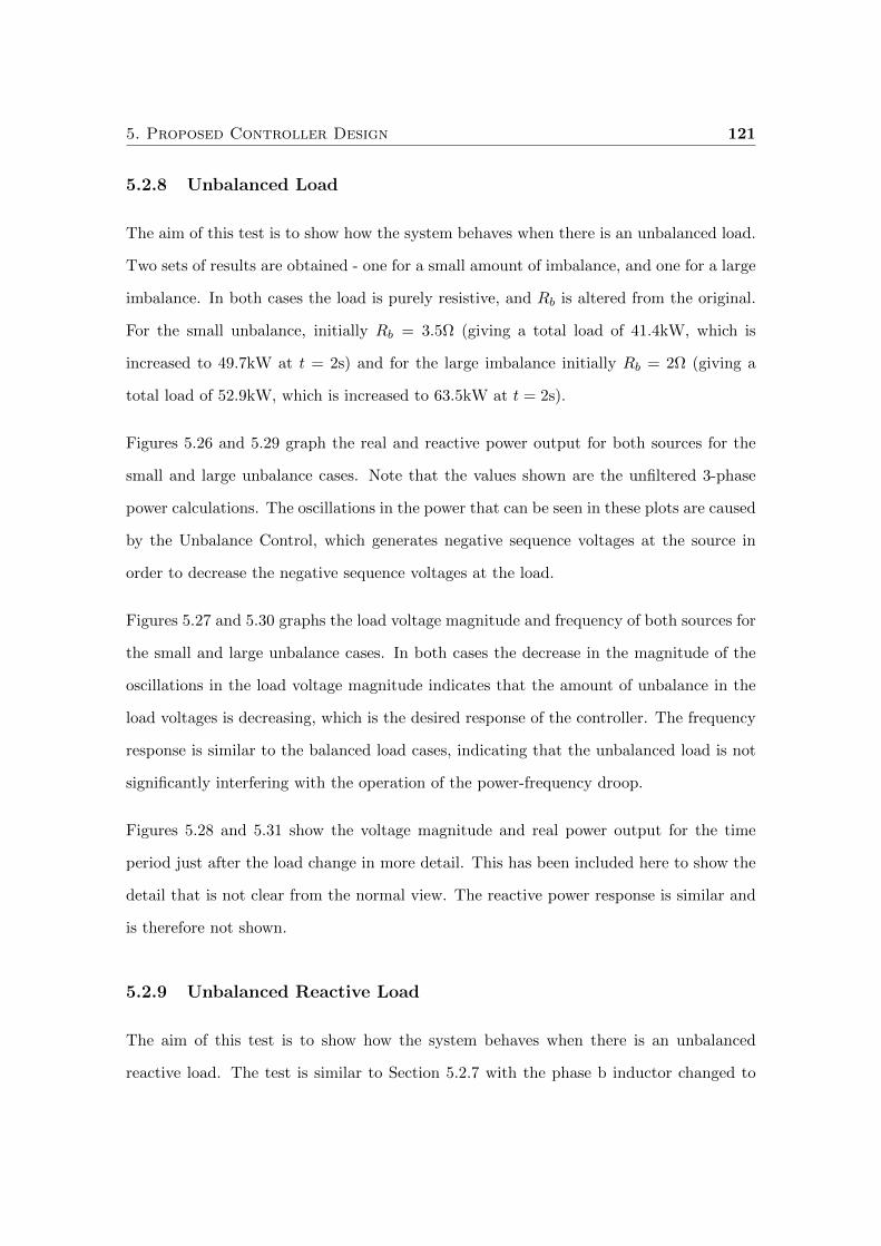
5. Proposed Controller Design 121
5.2.8 Unbalanced Load
The aim of this test is to show how the system behaves when there is an unbalanced load.
Two sets of results are obtained - one for a small amount of imbalance, and one for a large
imbalance. In both cases the load is purely resistive, and Rb is altered from the original.
For the small unbalance, initially Rb = 3.5Ω (giving a total load of 41.4kW, which is
increased to 49.7kW at t = 2s) and for the large imbalance initially Rb = 2Ω (giving a
total load of 52.9kW, which is increased to 63.5kW at t = 2s).
Figures 5.26 and 5.29 graph the real and reactive power output for both sources for the
small and large unbalance cases. Note that the values shown are the unfiltered 3-phase
power calculations. The oscillations in the power that can be seen in these plots are caused
by the Unbalance Control, which generates negative sequence voltages at the source in
order to decrease the negative sequence voltages at the load.
Figures 5.27 and 5.30 graphs the load voltage magnitude and frequency of both sources for
the small and large unbalance cases. In both cases the decrease in the magnitude of the
oscillations in the load voltage magnitude indicates that the amount of unbalance in the
load voltages is decreasing, which is the desired response of the controller. The frequency
response is similar to the balanced load cases, indicating that the unbalanced load is not
significantly interfering with the operation of the power-frequency droop.
Figures 5.28 and 5.31 show the voltage magnitude and real power output for the time
period just after the load change in more detail. This has been included here to show the
detail that is not clear from the normal view. The reactive power response is similar and
is therefore not shown.
5.2.9 Unbalanced Reactive Load
The aim of this test is to show how the system behaves when there is an unbalanced
reactive load. The test is similar to Section 5.2.7 with the phase b inductor changed to
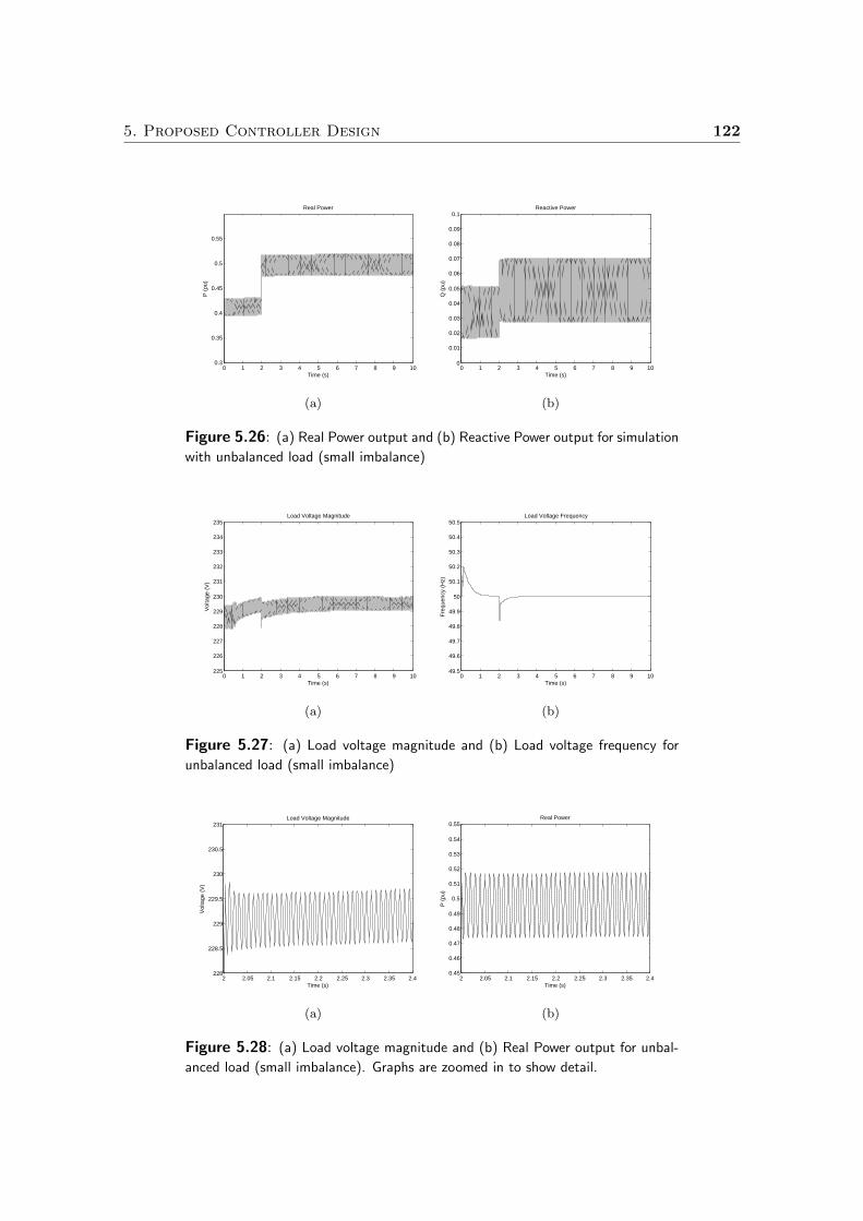
5. Proposed Controller Design 122
0 1 2 3 4 5 6 7 8 9 100.3
0.35
0.4
0.45
0.5
0.55
Real Power
Time (s)
P (
pu)
(a)
0 1 2 3 4 5 6 7 8 9 100
0.01
0.02
0.03
0.04
0.05
0.06
0.07
0.08
0.09
0.1Reactive Power
Time (s)
Q (
pu)
(b)
Figure 5.26: (a) Real Power output and (b) Reactive Power output for simulation
with unbalanced load (small imbalance)
0 1 2 3 4 5 6 7 8 9 10225
226
227
228
229
230
231
232
233
234
235Load Voltage Magnitude
Vol
tage
(V
)
Time (s)
(a)
0 1 2 3 4 5 6 7 8 9 1049.5
49.6
49.7
49.8
49.9
50
50.1
50.2
50.3
50.4
50.5Load Voltage Frequency
Time (s)
Fre
quen
cy (
Hz)
(b)
Figure 5.27: (a) Load voltage magnitude and (b) Load voltage frequency for
unbalanced load (small imbalance)
2 2.05 2.1 2.15 2.2 2.25 2.3 2.35 2.4228
228.5
229
229.5
230
230.5
231Load Voltage Magnitude
Vol
tage
(V
)
Time (s)
(a)
2 2.05 2.1 2.15 2.2 2.25 2.3 2.35 2.40.45
0.46
0.47
0.48
0.49
0.5
0.51
0.52
0.53
0.54
0.55Real Power
Time (s)
P (
pu)
(b)
Figure 5.28: (a) Load voltage magnitude and (b) Real Power output for unbal-
anced load (small imbalance). Graphs are zoomed in to show detail.

5. Proposed Controller Design 123
0 1 2 3 4 5 6 7 8 9 100.2
0.3
0.4
0.5
0.6
0.7
0.8Real Power
Time (s)
P (
pu)
(a)
0 1 2 3 4 5 6 7 8 9 10−0.2
−0.15
−0.1
−0.05
0
0.05
0.1
0.15
0.2
0.25
0.3Reactive Power
Time (s)
Q (
pu)
(b)
Figure 5.29: (a) Real Power output and (b) Reactive Power output for unbal-
anced load (large imbalance)
0 1 2 3 4 5 6 7 8 9 10220
222
224
226
228
230
232
234
236
238
240Load Voltage Magnitude
Vol
tage
(V
)
Time (s)
(a)
0 1 2 3 4 5 6 7 8 9 1049.5
49.6
49.7
49.8
49.9
50
50.1
50.2
50.3
50.4
50.5Load Voltage Frequency
Time (s)
Fre
quen
cy (
Hz)
(b)
Figure 5.30: (a) Load voltage magnitude and (b) Real Power output for unbal-
anced load (large unbalance)
2 2.05 2.1 2.15 2.2 2.25 2.3 2.35 2.4225
226
227
228
229
230
231
232
233
234
235Load Voltage Magnitude
Vol
tage
(V
)
Time (s)
(a)
2 2.05 2.1 2.15 2.2 2.25 2.3 2.35 2.40.4
0.45
0.5
0.55
0.6
0.65
0.7
0.75
0.8Real Power
Time (s)
P (
pu)
(b)
Figure 5.31: (a) Load voltage magnitude and (b) Real Power output for unbal-
anced load (large unbalance). Graphs are zoomed in to show detail.
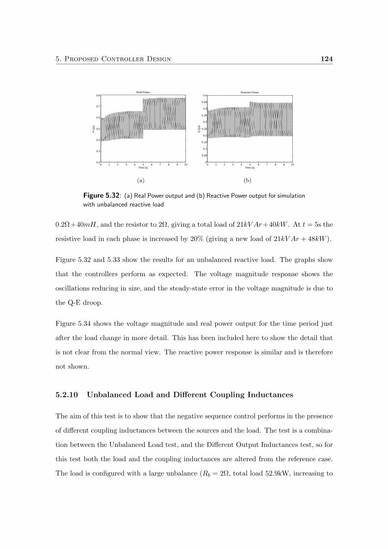
5. Proposed Controller Design 124
0 1 2 3 4 5 6 7 8 9 100.2
0.3
0.4
0.5
0.6
0.7
0.8Real Power
Time (s)
P (
pu)
(a)
0 1 2 3 4 5 6 7 8 9 100
0.05
0.1
0.15
0.2
0.25
0.3
0.35
0.4
0.45
0.5Reactive Power
Time (s)
Q (
pu)
(b)
Figure 5.32: (a) Real Power output and (b) Reactive Power output for simulation
with unbalanced reactive load
0.2Ω+40mH, and the resistor to 2Ω, giving a total load of 21kV Ar+40kW . At t = 5s the
resistive load in each phase is increased by 20% (giving a new load of 21kV Ar + 48kW ).
Figure 5.32 and 5.33 show the results for an unbalanced reactive load. The graphs show
that the controllers perform as expected. The voltage magnitude response shows the
oscillations reducing in size, and the steady-state error in the voltage magnitude is due to
the Q-E droop.
Figure 5.34 shows the voltage magnitude and real power output for the time period just
after the load change in more detail. This has been included here to show the detail that
is not clear from the normal view. The reactive power response is similar and is therefore
not shown.
5.2.10 Unbalanced Load and Different Coupling Inductances
The aim of this test is to show that the negative sequence control performs in the presence
of different coupling inductances between the sources and the load. The test is a combina-
tion between the Unbalanced Load test, and the Different Output Inductances test, so for
this test both the load and the coupling inductances are altered from the reference case.
The load is configured with a large unbalance (Rb = 2Ω, total load 52.9kW, increasing to
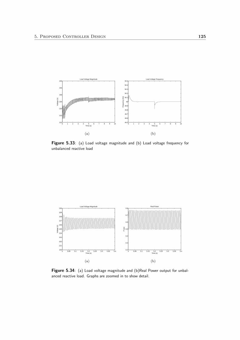
5. Proposed Controller Design 125
0 1 2 3 4 5 6 7 8 9 10210
215
220
225
230
235
240Load Voltage Magnitude
Vol
tage
(V
)
Time (s)
(a)
0 1 2 3 4 5 6 7 8 9 1049.5
49.6
49.7
49.8
49.9
50
50.1
50.2
50.3
50.4
50.5Load Voltage Frequency
Time (s)
Fre
quen
cy (
Hz)
(b)
Figure 5.33: (a) Load voltage magnitude and (b) Load voltage frequency for
unbalanced reactive load
5 5.05 5.1 5.15 5.2 5.25 5.3 5.35 5.4220
221
222
223
224
225
226
227
228
229
230Load Voltage Magnitude
Vol
tage
(V
)
Time (s)
(a)
5 5.05 5.1 5.15 5.2 5.25 5.3 5.35 5.40.2
0.3
0.4
0.5
0.6
0.7
0.8Real Power
Time (s)
P (
pu)
(b)
Figure 5.34: (a) Load voltage magnitude and (b)Real Power output for unbal-
anced reactive load. Graphs are zoomed in to show detail.
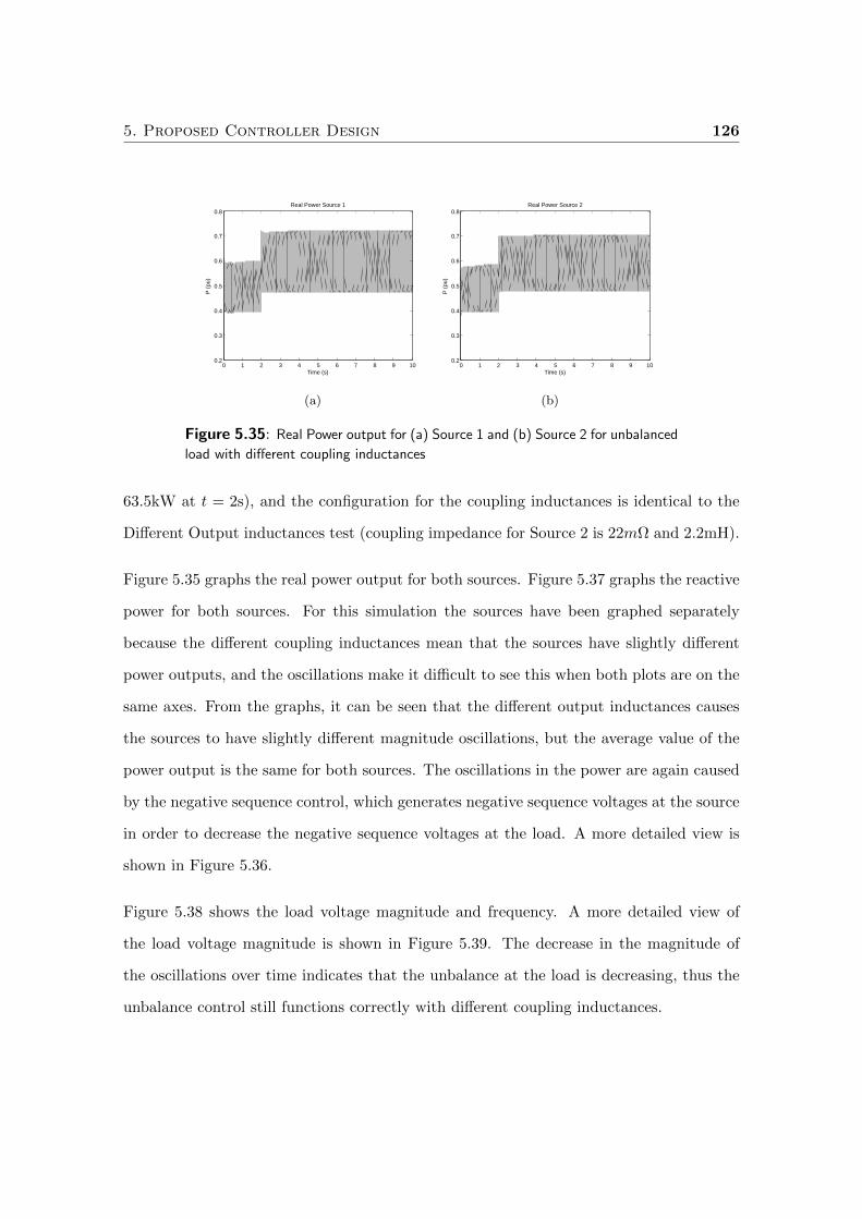
5. Proposed Controller Design 126
0 1 2 3 4 5 6 7 8 9 100.2
0.3
0.4
0.5
0.6
0.7
0.8Real Power Source 1
Time (s)
P (
pu)
(a)
0 1 2 3 4 5 6 7 8 9 100.2
0.3
0.4
0.5
0.6
0.7
0.8Real Power Source 2
Time (s)
P (
pu)
(b)
Figure 5.35: Real Power output for (a) Source 1 and (b) Source 2 for unbalanced
load with different coupling inductances
63.5kW at t = 2s), and the configuration for the coupling inductances is identical to the
Different Output inductances test (coupling impedance for Source 2 is 22mΩ and 2.2mH).
Figure 5.35 graphs the real power output for both sources. Figure 5.37 graphs the reactive
power for both sources. For this simulation the sources have been graphed separately
because the different coupling inductances mean that the sources have slightly different
power outputs, and the oscillations make it difficult to see this when both plots are on the
same axes. From the graphs, it can be seen that the different output inductances causes
the sources to have slightly different magnitude oscillations, but the average value of the
power output is the same for both sources. The oscillations in the power are again caused
by the negative sequence control, which generates negative sequence voltages at the source
in order to decrease the negative sequence voltages at the load. A more detailed view is
shown in Figure 5.36.
Figure 5.38 shows the load voltage magnitude and frequency. A more detailed view of
the load voltage magnitude is shown in Figure 5.39. The decrease in the magnitude of
the oscillations over time indicates that the unbalance at the load is decreasing, thus the
unbalance control still functions correctly with different coupling inductances.
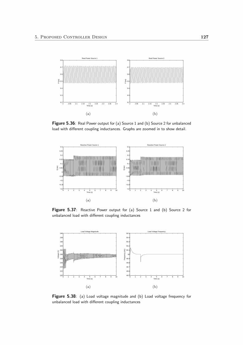
5. Proposed Controller Design 127
2 2.05 2.1 2.15 2.2 2.25 2.3 2.35 2.40.2
0.3
0.4
0.5
0.6
0.7
0.8Real Power Source 1
Time (s)
P (
pu)
(a)
2 2.05 2.1 2.15 2.2 2.25 2.3 2.35 2.40.2
0.3
0.4
0.5
0.6
0.7
0.8Real Power Source 2
Time (s)
P (
pu)
(b)
Figure 5.36: Real Power output for (a) Source 1 and (b) Source 2 for unbalanced
load with different coupling inductances. Graphs are zoomed in to show detail.
0 1 2 3 4 5 6 7 8 9 10−0.2
−0.15
−0.1
−0.05
0
0.05
0.1
0.15
0.2
0.25
0.3Reactive Power Source 1
Time (s)
Q (
pu)
(a)
0 1 2 3 4 5 6 7 8 9 10−0.2
−0.15
−0.1
−0.05
0
0.05
0.1
0.15
0.2
0.25
0.3Reactive Power Source 2
Time (s)
Q (
pu)
(b)
Figure 5.37: Reactive Power output for (a) Source 1 and (b) Source 2 for
unbalanced load with different coupling inductances
0 1 2 3 4 5 6 7 8 9 10220
222
224
226
228
230
232
234
236
238
240Load Voltage Magnitude
Vol
tage
(V
)
Time (s)
(a)
0 1 2 3 4 5 6 7 8 9 1049.5
49.6
49.7
49.8
49.9
50
50.1
50.2
50.3
50.4
50.5Load Voltage Frequency
Time (s)
Fre
quen
cy (
Hz)
(b)
Figure 5.38: (a) Load voltage magnitude and (b) Load voltage frequency for
unbalanced load with different coupling inductances
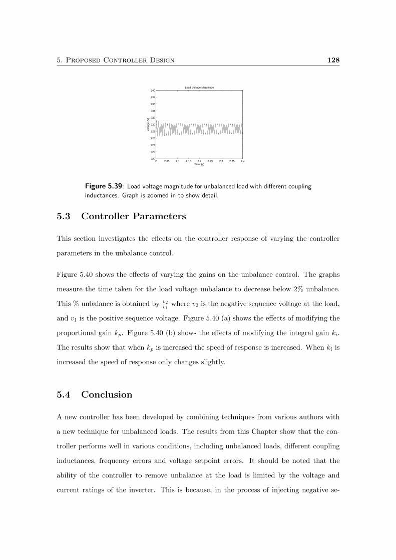
5. Proposed Controller Design 128
2 2.05 2.1 2.15 2.2 2.25 2.3 2.35 2.4220
222
224
226
228
230
232
234
236
238
240Load Voltage Magnitude
Vol
tage
(V
)
Time (s)
Figure 5.39: Load voltage magnitude for unbalanced load with different coupling
inductances. Graph is zoomed in to show detail.
5.3 Controller Parameters
This section investigates the effects on the controller response of varying the controller
parameters in the unbalance control.
Figure 5.40 shows the effects of varying the gains on the unbalance control. The graphs
measure the time taken for the load voltage unbalance to decrease below 2% unbalance.
This % unbalance is obtained by v2v1
where v2 is the negative sequence voltage at the load,
and v1 is the positive sequence voltage. Figure 5.40 (a) shows the effects of modifying the
proportional gain kp. Figure 5.40 (b) shows the effects of modifying the integral gain ki.
The results show that when kp is increased the speed of response is increased. When ki is
increased the speed of response only changes slightly.
5.4 Conclusion
A new controller has been developed by combining techniques from various authors with
a new technique for unbalanced loads. The results from this Chapter show that the con-
troller performs well in various conditions, including unbalanced loads, different coupling
inductances, frequency errors and voltage setpoint errors. It should be noted that the
ability of the controller to remove unbalance at the load is limited by the voltage and
current ratings of the inverter. This is because, in the process of injecting negative se-
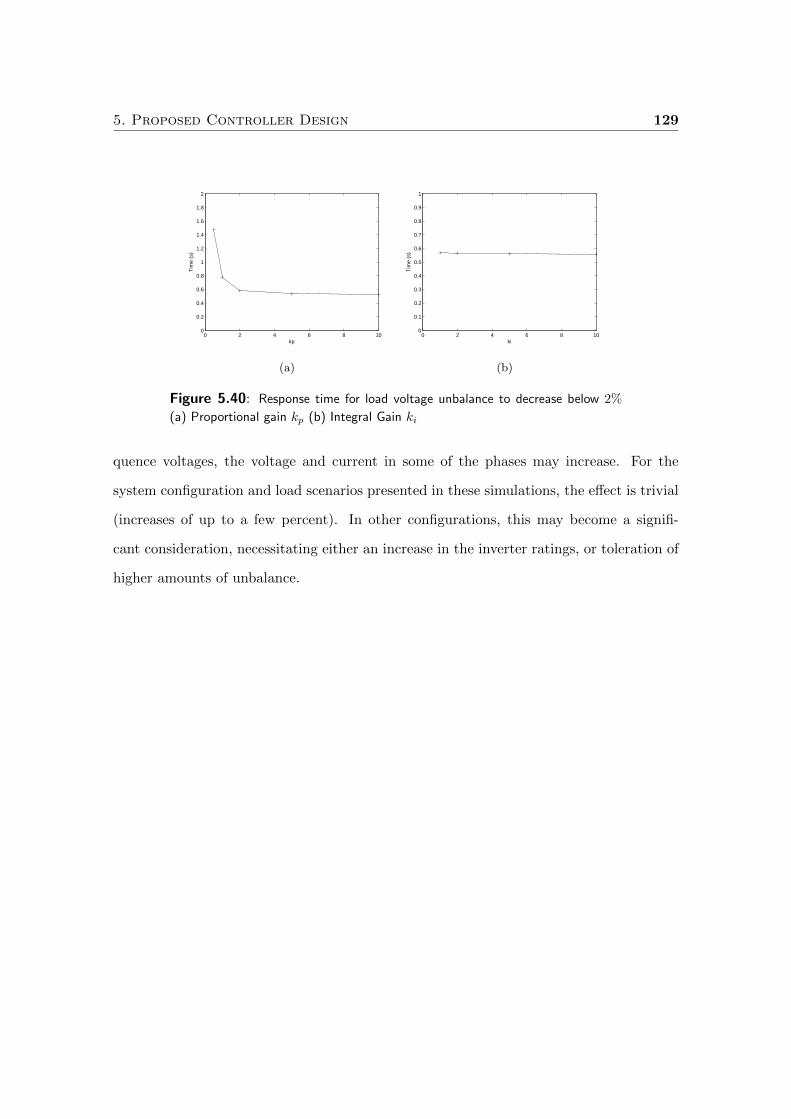
5. Proposed Controller Design 129
0 2 4 6 8 100
0.2
0.4
0.6
0.8
1
1.2
1.4
1.6
1.8
2T
ime
(s)
kp
(a)
0 2 4 6 8 100
0.1
0.2
0.3
0.4
0.5
0.6
0.7
0.8
0.9
1
Tim
e (s
)
ki
(b)
Figure 5.40: Response time for load voltage unbalance to decrease below 2%
(a) Proportional gain kp (b) Integral Gain ki
quence voltages, the voltage and current in some of the phases may increase. For the
system configuration and load scenarios presented in these simulations, the effect is trivial
(increases of up to a few percent). In other configurations, this may become a signifi-
cant consideration, necessitating either an increase in the inverter ratings, or toleration of
higher amounts of unbalance.
Chapter 6
Power Sources and Storage
Different power sources (e.g. microturbines, fuel cells and batteries) exhibit different
responses to changing load demands. A limitation of the previous work in this thesis,
and in much of the body of work concerned with power sharing algorithms, is that the
dynamics of these power sources are ignored.
For the purposes of this research, most of these dynamics can be assumed to have little
effect on the common AC bus due to the high frequency switching of the inverter. One
effect that does need to be allowed for, however, is the limit on the amount of power that
can be supplied by a power source. Most of the power sources of interest in a microgrid
have little or no “inertia” and are thus incapable of instantaneously supplying increases
in power.
Generally this problem is solved by placing storage (i.e. a battery) on the DC bus of
each voltage source (a voltage source consists of a power source, DC storage and power
electronics), however this can be an expensive and inefficient solution. A better solution
is to place storage devices on the AC bus and minimise the DC storage required for
each voltage source. In order for these AC storage devices to operate correctly alongside
droop controlled sources, a control algorithm is required which does not interfere with the
power-frequency droops.
In this Chapter, transfer function models of these power limits are examined, and issues
with these models are discussed. Several methods are then outlined which try to prevent
voltage sources from exceeding these power limits in steady state. Finally, these models
are used in the development of a controller for a system based storage device connected to
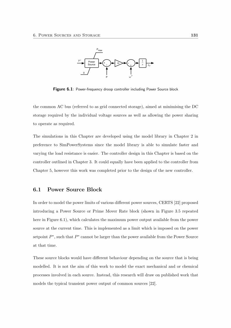
6. Power Sources and Storage 131
m
P
!V
Pmax
0
PowerSource
+- +
-1s
!!
P!
Figure 6.1: Power-frequency droop controller including Power Source block
the common AC bus (referred to as grid connected storage), aimed at minimising the DC
storage required by the individual voltage sources as well as allowing the power sharing
to operate as required.
The simulations in this Chapter are developed using the model library in Chapter 2 in
preference to SimPowerSystems since the model library is able to simulate faster and
varying the load resistance is easier. The controller design in this Chapter is based on the
controller outlined in Chapter 3. It could equally have been applied to the controller from
Chapter 5, however this work was completed prior to the design of the new controller.
6.1 Power Source Block
In order to model the power limits of various different power sources, CERTS [22] proposed
introducing a Power Source or Prime Mover Rate block (shown in Figure 3.5 repeated
here in Figure 6.1), which calculates the maximum power output available from the power
source at the current time. This is implemented as a limit which is imposed on the power
setpoint P ∗, such that P ∗ cannot be larger than the power available from the Power Source
at that time.
These source blocks would have different behaviour depending on the source that is being
modelled. It is not the aim of this work to model the exact mechanical and or chemical
processes involved in each source. Instead, this research will draw on published work that
models the typical transient power output of common sources [22].
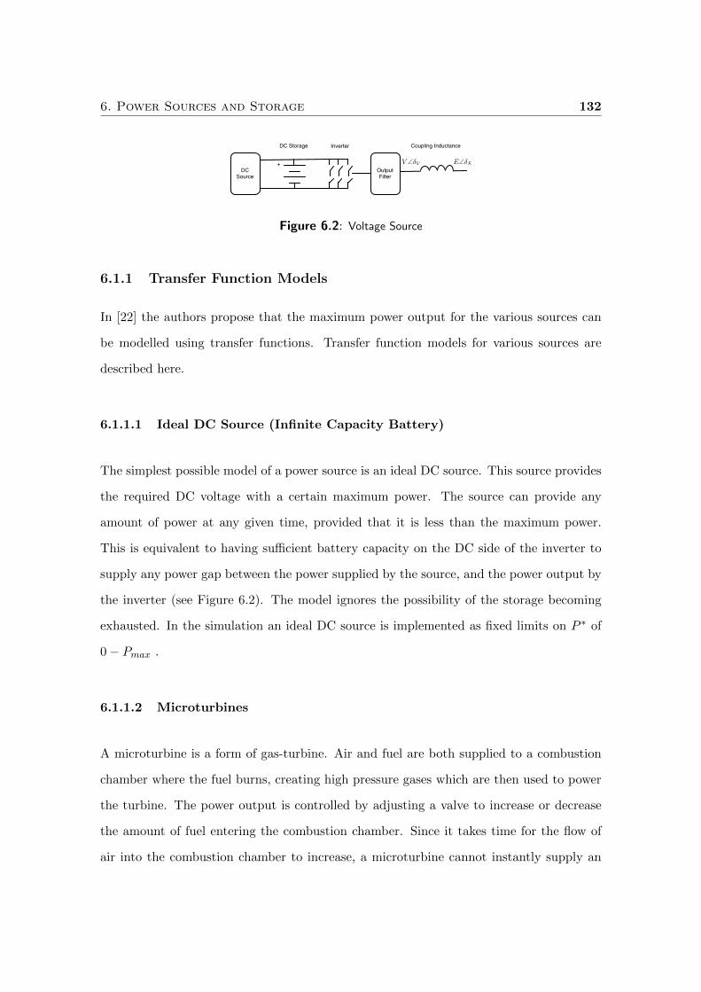
6. Power Sources and Storage 132
DC Source
+OutputFilter
DC Storage Inverter Coupling Inductance
V ∠δV E∠δE
Figure 6.2: Voltage Source
6.1.1 Transfer Function Models
In [22] the authors propose that the maximum power output for the various sources can
be modelled using transfer functions. Transfer function models for various sources are
described here.
6.1.1.1 Ideal DC Source (Infinite Capacity Battery)
The simplest possible model of a power source is an ideal DC source. This source provides
the required DC voltage with a certain maximum power. The source can provide any
amount of power at any given time, provided that it is less than the maximum power.
This is equivalent to having sufficient battery capacity on the DC side of the inverter to
supply any power gap between the power supplied by the source, and the power output by
the inverter (see Figure 6.2). The model ignores the possibility of the storage becoming
exhausted. In the simulation an ideal DC source is implemented as fixed limits on P ∗ of
0− Pmax .
6.1.1.2 Microturbines
A microturbine is a form of gas-turbine. Air and fuel are both supplied to a combustion
chamber where the fuel burns, creating high pressure gases which are then used to power
the turbine. The power output is controlled by adjusting a valve to increase or decrease
the amount of fuel entering the combustion chamber. Since it takes time for the flow of
air into the combustion chamber to increase, a microturbine cannot instantly supply an
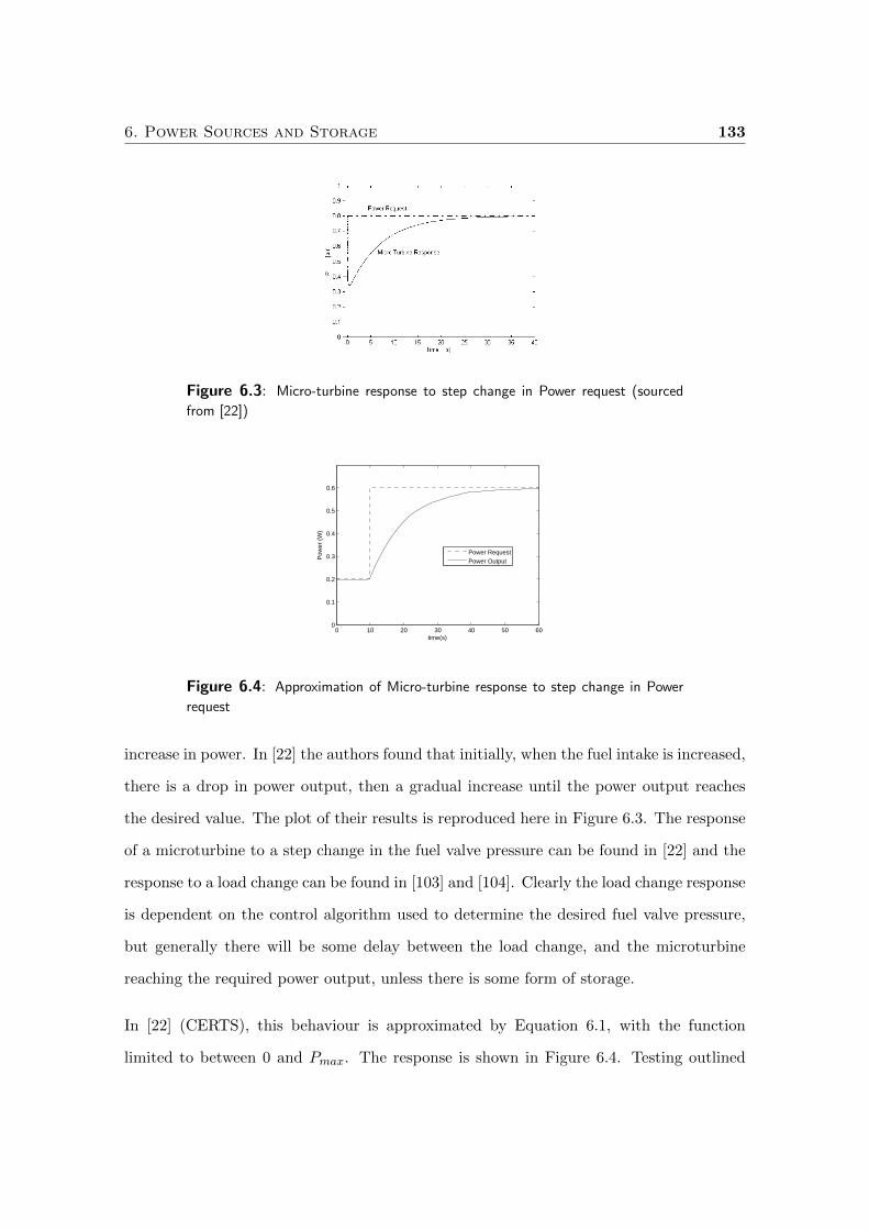
6. Power Sources and Storage 133
Figure 6.3: Micro-turbine response to step change in Power request (sourced
from [22])
0 10 20 30 40 50 600
0.1
0.2
0.3
0.4
0.5
0.6
time(s)
Pow
er (
W)
Power RequestPower Output
Figure 6.4: Approximation of Micro-turbine response to step change in Power
request
increase in power. In [22] the authors found that initially, when the fuel intake is increased,
there is a drop in power output, then a gradual increase until the power output reaches
the desired value. The plot of their results is reproduced here in Figure 6.3. The response
of a microturbine to a step change in the fuel valve pressure can be found in [22] and the
response to a load change can be found in [103] and [104]. Clearly the load change response
is dependent on the control algorithm used to determine the desired fuel valve pressure,
but generally there will be some delay between the load change, and the microturbine
reaching the required power output, unless there is some form of storage.
In [22] (CERTS), this behaviour is approximated by Equation 6.1, with the function
limited to between 0 and Pmax. The response is shown in Figure 6.4. Testing outlined
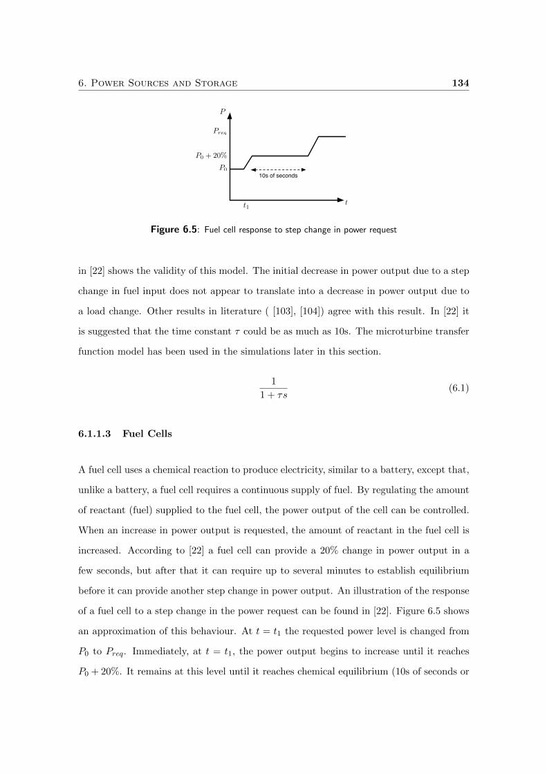
6. Power Sources and Storage 134
P
t
P0
P0 + 20%
Preq
t1
10s of seconds
Figure 6.5: Fuel cell response to step change in power request
in [22] shows the validity of this model. The initial decrease in power output due to a step
change in fuel input does not appear to translate into a decrease in power output due to
a load change. Other results in literature ( [103], [104]) agree with this result. In [22] it
is suggested that the time constant τ could be as much as 10s. The microturbine transfer
function model has been used in the simulations later in this section.
1
1 + τs(6.1)
6.1.1.3 Fuel Cells
A fuel cell uses a chemical reaction to produce electricity, similar to a battery, except that,
unlike a battery, a fuel cell requires a continuous supply of fuel. By regulating the amount
of reactant (fuel) supplied to the fuel cell, the power output of the cell can be controlled.
When an increase in power output is requested, the amount of reactant in the fuel cell is
increased. According to [22] a fuel cell can provide a 20% change in power output in a
few seconds, but after that it can require up to several minutes to establish equilibrium
before it can provide another step change in power output. An illustration of the response
of a fuel cell to a step change in the power request can be found in [22]. Figure 6.5 shows
an approximation of this behaviour. At t = t1 the requested power level is changed from
P0 to Preq. Immediately, at t = t1, the power output begins to increase until it reaches
P0 + 20%. It remains at this level until it reaches chemical equilibrium (10s of seconds or
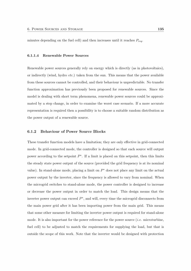
6. Power Sources and Storage 135
minutes depending on the fuel cell) and then increases until it reaches Preq.
6.1.1.4 Renewable Power Sources
Renewable power sources generally rely on energy which is directly (as in photovoltaics),
or indirectly (wind, hydro etc.) taken from the sun. This means that the power available
from these sources cannot be controlled, and their behaviour is unpredictable. No transfer
function approximation has previously been proposed for renewable sources. Since the
model is dealing with short term phenomena, renewable power sources could be approxi-
mated by a step change, in order to examine the worst case scenario. If a more accurate
representation is required then a possibility is to choose a suitable random distribution as
the power output of a renewable source.
6.1.2 Behaviour of Power Source Blocks
These transfer function models have a limitation; they are only effective in grid-connected
mode. In grid-connected mode, the controller is designed so that each source will output
power according to the setpoint P ∗. If a limit is placed on this setpoint, then this limits
the steady state power output of the source (provided the grid frequency is at its nominal
value). In stand-alone mode, placing a limit on P ∗ does not place any limit on the actual
power output by the inverter, since the frequency is allowed to vary from nominal. When
the microgrid switches to stand-alone mode, the power controller is designed to increase
or decrease the power output in order to match the load. This design means that the
inverter power output can exceed P ∗, and will, every time the microgrid disconnects from
the main power grid after it has been importing power from the main grid. This means
that some other measure for limiting the inverter power output is required for stand-alone
mode. It is also important for the power reference for the power source (i.e. microturbine,
fuel cell) to be adjusted to match the requirements for supplying the load, but that is
outside the scope of this work. Note that the inverter would be designed with protection
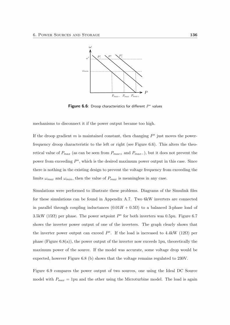
6. Power Sources and Storage 136
!min
!
P ! P !+
Pmax! Pmax+
!! P !"
Pmax
P
Figure 6.6: Droop characteristics for different P ∗ values
mechanisms to disconnect it if the power output became too high.
If the droop gradient m is maintained constant, then changing P ∗ just moves the power-
frequency droop characteristic to the left or right (see Figure 6.6). This alters the theo-
retical value of Pmax (as can be seen from Pmax+ and Pmax−), but it does not prevent the
power from exceeding P ∗, which is the desired maximum power output in this case. Since
there is nothing in the existing design to prevent the voltage frequency from exceeding the
limits ωmax and ωmin, then the value of Pmax is meaningless in any case.
Simulations were performed to illustrate these problems. Diagrams of the Simulink files
for these simulations can be found in Appendix A.7. Two 6kW inverters are connected
in parallel through coupling inductances (0.01H + 0.5Ω) to a balanced 3-phase load of
3.5kW (15Ω) per phase. The power setpoint P ∗ for both inverters was 0.5pu. Figure 6.7
shows the inverter power output of one of the inverters. The graph clearly shows that
the inverter power output can exceed P ∗. If the load is increased to 4.4kW (12Ω) per
phase (Figure 6.8(a)), the power output of the inverter now exceeds 1pu, theoretically the
maximum power of the source. If the model was accurate, some voltage drop would be
expected, however Figure 6.8 (b) shows that the voltage remains regulated to 230V.
Figure 6.9 compares the power output of two sources, one using the Ideal DC Source
model with Pmax = 1pu and the other using the Microturbine model. The load is again
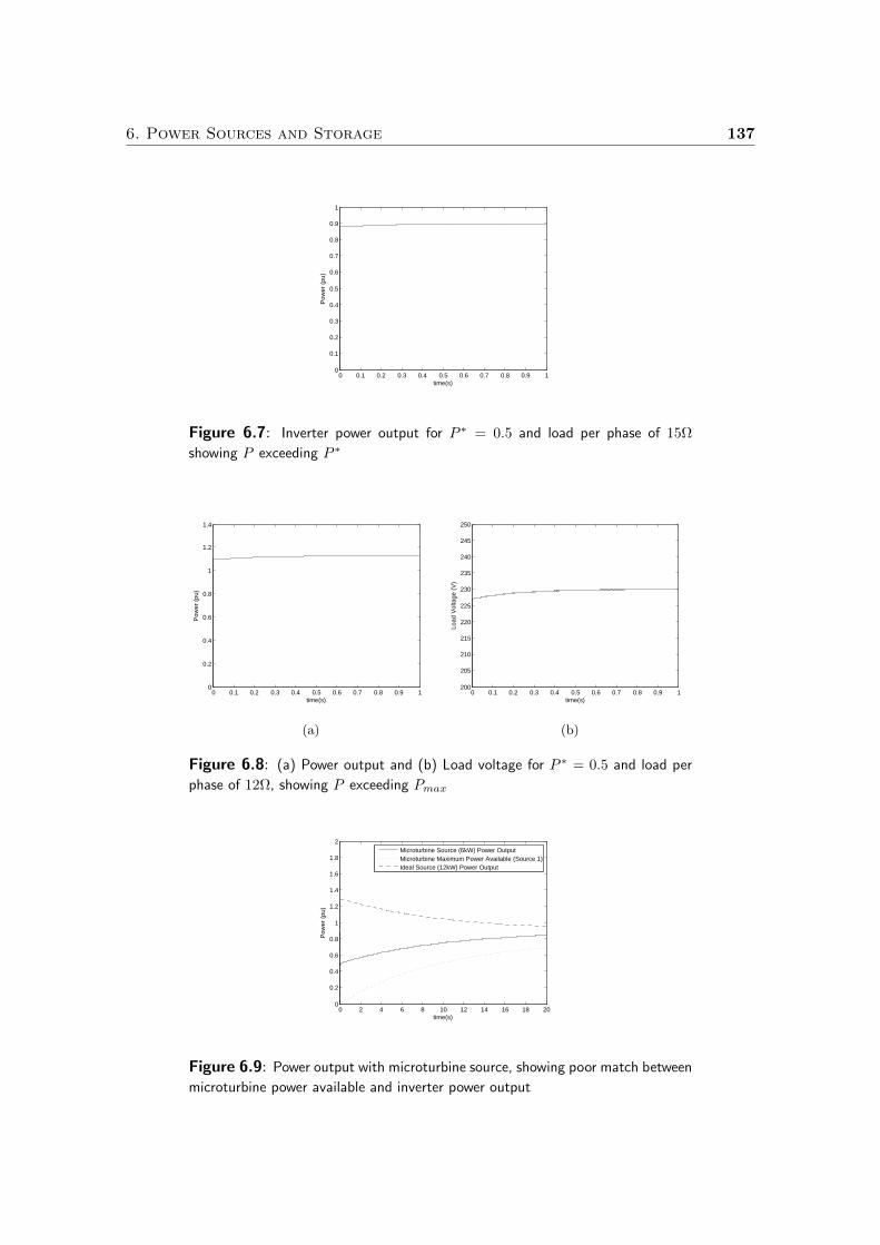
6. Power Sources and Storage 137
0 0.1 0.2 0.3 0.4 0.5 0.6 0.7 0.8 0.9 10
0.1
0.2
0.3
0.4
0.5
0.6
0.7
0.8
0.9
1
time(s)
Pow
er (
pu)
Figure 6.7: Inverter power output for P ∗ = 0.5 and load per phase of 15Ω
showing P exceeding P ∗
0 0.1 0.2 0.3 0.4 0.5 0.6 0.7 0.8 0.9 10
0.2
0.4
0.6
0.8
1
1.2
1.4
time(s)
Pow
er (
pu)
(a)
0 0.1 0.2 0.3 0.4 0.5 0.6 0.7 0.8 0.9 1200
205
210
215
220
225
230
235
240
245
250
time(s)
Load
Vol
tage
(V
)
(b)
Figure 6.8: (a) Power output and (b) Load voltage for P ∗ = 0.5 and load per
phase of 12Ω, showing P exceeding Pmax
0 2 4 6 8 10 12 14 16 18 200
0.2
0.4
0.6
0.8
1
1.2
1.4
1.6
1.8
2
time(s)
Pow
er (
pu)
Microturbine Source (6kW) Power OutputMicroturbine Maximum Power Available (Source 1)Ideal Source (12kW) Power Output
Figure 6.9: Power output with microturbine source, showing poor match between
microturbine power available and inverter power output
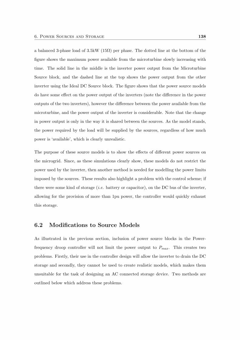
6. Power Sources and Storage 138
a balanced 3-phase load of 3.5kW (15Ω) per phase. The dotted line at the bottom of the
figure shows the maximum power available from the microturbine slowly increasing with
time. The solid line in the middle is the inverter power output from the Microturbine
Source block, and the dashed line at the top shows the power output from the other
inverter using the Ideal DC Source block. The figure shows that the power source models
do have some effect on the power output of the inverters (note the difference in the power
outputs of the two inverters), however the difference between the power available from the
microturbine, and the power output of the inverter is considerable. Note that the change
in power output is only in the way it is shared between the sources. As the model stands,
the power required by the load will be supplied by the sources, regardless of how much
power is ‘available’, which is clearly unrealistic.
The purpose of these source models is to show the effects of different power sources on
the microgrid. Since, as these simulations clearly show, these models do not restrict the
power used by the inverter, then another method is needed for modelling the power limits
imposed by the sources. These results also highlight a problem with the control scheme; if
there were some kind of storage (i.e. battery or capacitor), on the DC bus of the inverter,
allowing for the provision of more than 1pu power, the controller would quickly exhaust
this storage.
6.2 Modifications to Source Models
As illustrated in the previous section, inclusion of power source blocks in the Power-
frequency droop controller will not limit the power output to Pmax. This creates two
problems. Firstly, their use in the controller design will allow the inverter to drain the DC
storage and secondly, they cannot be used to create realistic models, which makes them
unsuitable for the task of designing an AC connected storage device. Two methods are
outlined below which address these problems.
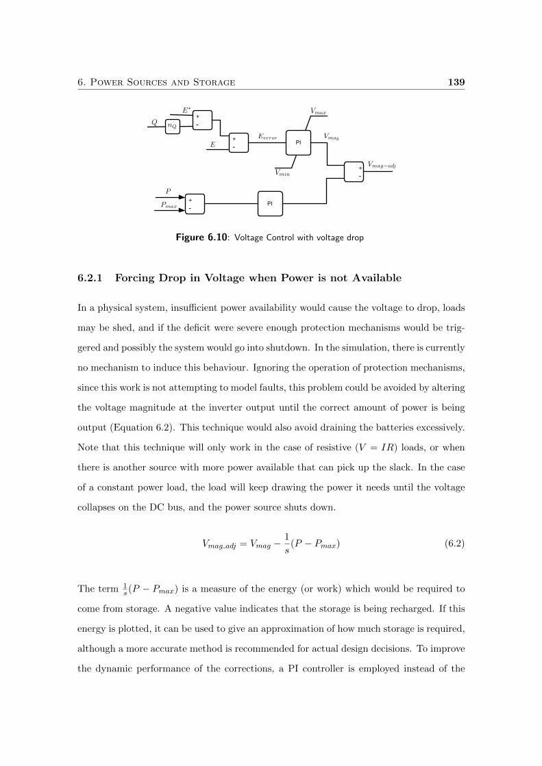
6. Power Sources and Storage 139
+- PI
Vmag
Vmax
Vmin
Eerror
E!
E
+-nQ
Q
+-
+-
P
Pmax PI
Vmag!adj
Figure 6.10: Voltage Control with voltage drop
6.2.1 Forcing Drop in Voltage when Power is not Available
In a physical system, insufficient power availability would cause the voltage to drop, loads
may be shed, and if the deficit were severe enough protection mechanisms would be trig-
gered and possibly the system would go into shutdown. In the simulation, there is currently
no mechanism to induce this behaviour. Ignoring the operation of protection mechanisms,
since this work is not attempting to model faults, this problem could be avoided by altering
the voltage magnitude at the inverter output until the correct amount of power is being
output (Equation 6.2). This technique would also avoid draining the batteries excessively.
Note that this technique will only work in the case of resistive (V = IR) loads, or when
there is another source with more power available that can pick up the slack. In the case
of a constant power load, the load will keep drawing the power it needs until the voltage
collapses on the DC bus, and the power source shuts down.
Vmag adj = Vmag −1
s(P − Pmax) (6.2)
The term 1s (P − Pmax) is a measure of the energy (or work) which would be required to
come from storage. A negative value indicates that the storage is being recharged. If this
energy is plotted, it can be used to give an approximation of how much storage is required,
although a more accurate method is recommended for actual design decisions. To improve
the dynamic performance of the corrections, a PI controller is employed instead of the
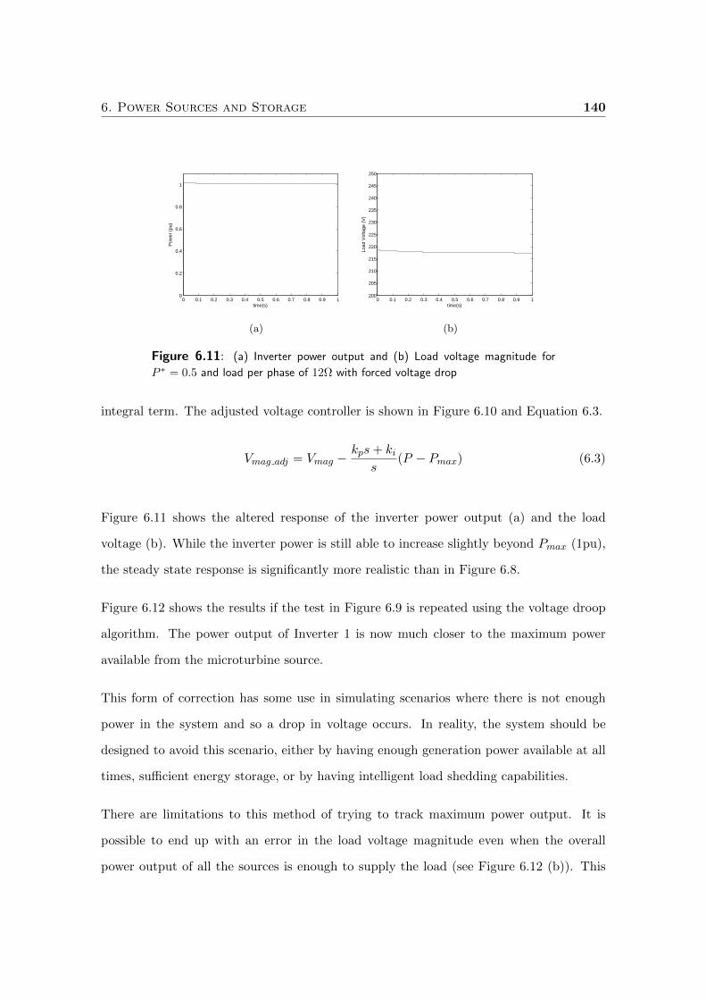
6. Power Sources and Storage 140
0 0.1 0.2 0.3 0.4 0.5 0.6 0.7 0.8 0.9 10
0.2
0.4
0.6
0.8
1
time(s)
Pow
er (
pu)
(a)
0 0.1 0.2 0.3 0.4 0.5 0.6 0.7 0.8 0.9 1200
205
210
215
220
225
230
235
240
245
250
time(s)
Load
Vol
tage
(V
)
(b)
Figure 6.11: (a) Inverter power output and (b) Load voltage magnitude for
P ∗ = 0.5 and load per phase of 12Ω with forced voltage drop
integral term. The adjusted voltage controller is shown in Figure 6.10 and Equation 6.3.
Vmag adj = Vmag −kps+ ki
s(P − Pmax) (6.3)
Figure 6.11 shows the altered response of the inverter power output (a) and the load
voltage (b). While the inverter power is still able to increase slightly beyond Pmax (1pu),
the steady state response is significantly more realistic than in Figure 6.8.
Figure 6.12 shows the results if the test in Figure 6.9 is repeated using the voltage droop
algorithm. The power output of Inverter 1 is now much closer to the maximum power
available from the microturbine source.
This form of correction has some use in simulating scenarios where there is not enough
power in the system and so a drop in voltage occurs. In reality, the system should be
designed to avoid this scenario, either by having enough generation power available at all
times, sufficient energy storage, or by having intelligent load shedding capabilities.
There are limitations to this method of trying to track maximum power output. It is
possible to end up with an error in the load voltage magnitude even when the overall
power output of all the sources is enough to supply the load (see Figure 6.12 (b)). This
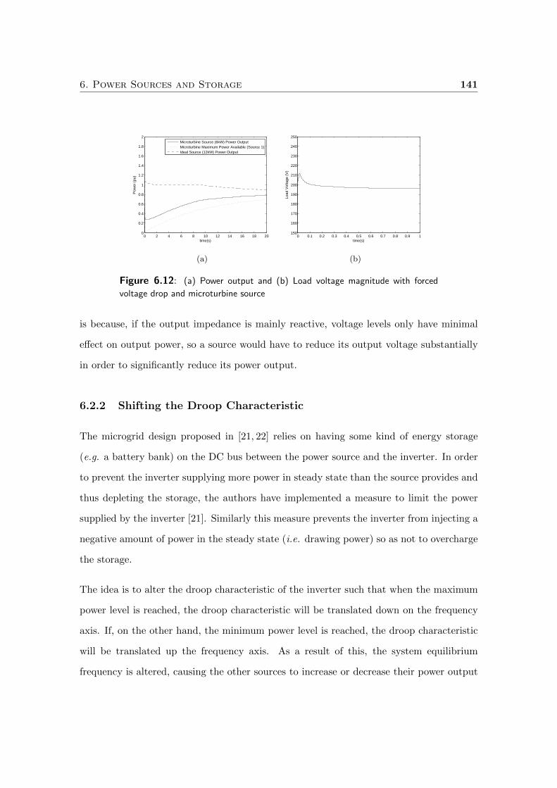
6. Power Sources and Storage 141
0 2 4 6 8 10 12 14 16 18 200
0.2
0.4
0.6
0.8
1
1.2
1.4
1.6
1.8
2
time(s)
Pow
er (
pu)
Microturbine Source (6kW) Power OutputMicroturbine Maximum Power Available (Source 1)Ideal Source (12kW) Power Output
(a)
0 0.1 0.2 0.3 0.4 0.5 0.6 0.7 0.8 0.9 1150
160
170
180
190
200
210
220
230
240
250
time(s)
Load
Vol
tage
(V
)
(b)
Figure 6.12: (a) Power output and (b) Load voltage magnitude with forced
voltage drop and microturbine source
is because, if the output impedance is mainly reactive, voltage levels only have minimal
effect on output power, so a source would have to reduce its output voltage substantially
in order to significantly reduce its power output.
6.2.2 Shifting the Droop Characteristic
The microgrid design proposed in [21, 22] relies on having some kind of energy storage
(e.g. a battery bank) on the DC bus between the power source and the inverter. In order
to prevent the inverter supplying more power in steady state than the source provides and
thus depleting the storage, the authors have implemented a measure to limit the power
supplied by the inverter [21]. Similarly this measure prevents the inverter from injecting a
negative amount of power in the steady state (i.e. drawing power) so as not to overcharge
the storage.
The idea is to alter the droop characteristic of the inverter such that when the maximum
power level is reached, the droop characteristic will be translated down on the frequency
axis. If, on the other hand, the minimum power level is reached, the droop characteristic
will be translated up the frequency axis. As a result of this, the system equilibrium
frequency is altered, causing the other sources to increase or decrease their power output
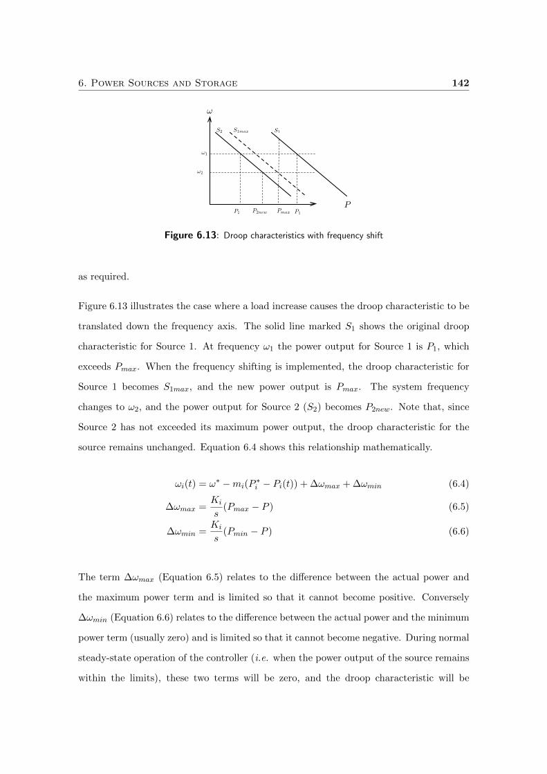
6. Power Sources and Storage 142
!2
!
S1
!1
Pmax
PP2newP2 P1
S2 S1max
Figure 6.13: Droop characteristics with frequency shift
as required.
Figure 6.13 illustrates the case where a load increase causes the droop characteristic to be
translated down the frequency axis. The solid line marked S1 shows the original droop
characteristic for Source 1. At frequency ω1 the power output for Source 1 is P1, which
exceeds Pmax. When the frequency shifting is implemented, the droop characteristic for
Source 1 becomes S1max, and the new power output is Pmax. The system frequency
changes to ω2, and the power output for Source 2 (S2) becomes P2new. Note that, since
Source 2 has not exceeded its maximum power output, the droop characteristic for the
source remains unchanged. Equation 6.4 shows this relationship mathematically.
ωi(t) = ω∗ −mi(P∗i − Pi(t)) + ∆ωmax + ∆ωmin (6.4)
∆ωmax =Ki
s(Pmax − P ) (6.5)
∆ωmin =Ki
s(Pmin − P ) (6.6)
The term ∆ωmax (Equation 6.5) relates to the difference between the actual power and
the maximum power term and is limited so that it cannot become positive. Conversely
∆ωmin (Equation 6.6) relates to the difference between the actual power and the minimum
power term (usually zero) and is limited so that it cannot become negative. During normal
steady-state operation of the controller (i.e. when the power output of the source remains
within the limits), these two terms will be zero, and the droop characteristic will be
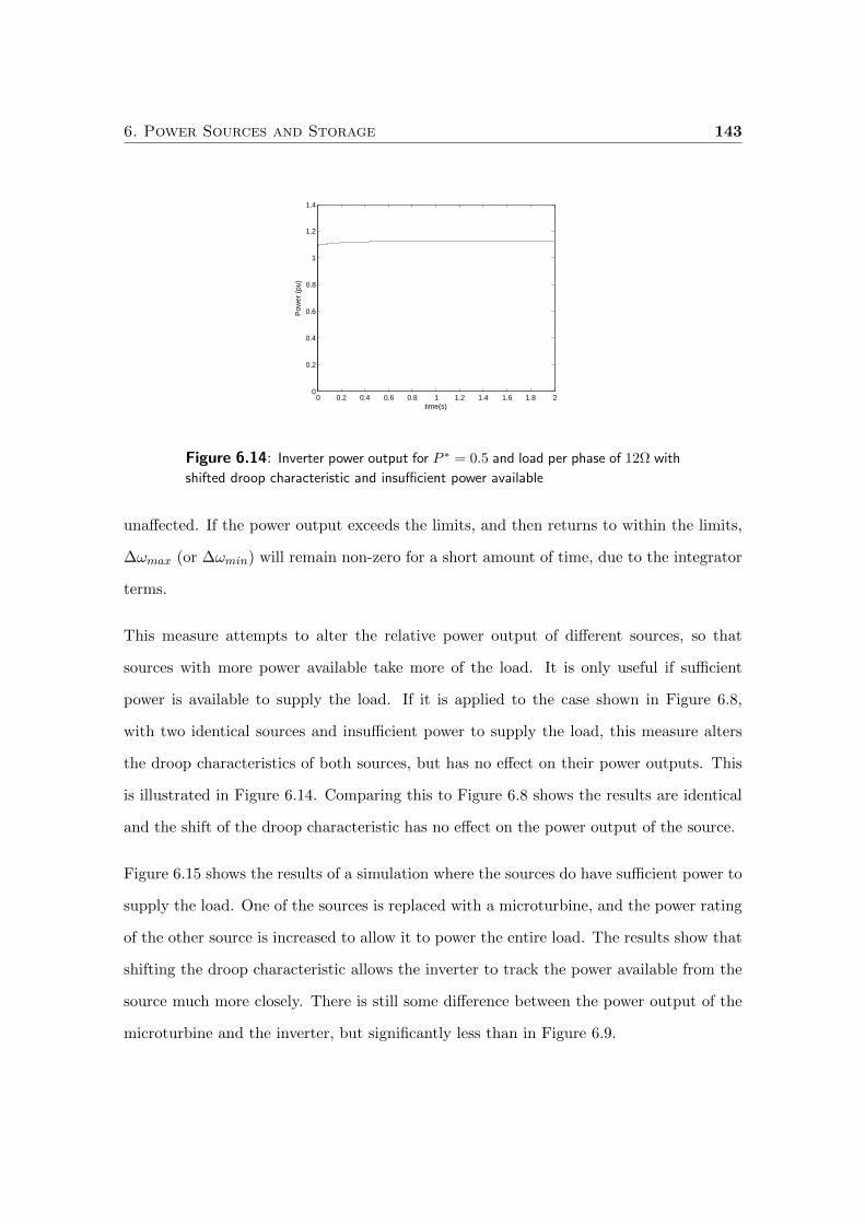
6. Power Sources and Storage 143
0 0.2 0.4 0.6 0.8 1 1.2 1.4 1.6 1.8 20
0.2
0.4
0.6
0.8
1
1.2
1.4
time(s)
Pow
er (
pu)
Figure 6.14: Inverter power output for P ∗ = 0.5 and load per phase of 12Ω with
shifted droop characteristic and insufficient power available
unaffected. If the power output exceeds the limits, and then returns to within the limits,
∆ωmax (or ∆ωmin) will remain non-zero for a short amount of time, due to the integrator
terms.
This measure attempts to alter the relative power output of different sources, so that
sources with more power available take more of the load. It is only useful if sufficient
power is available to supply the load. If it is applied to the case shown in Figure 6.8,
with two identical sources and insufficient power to supply the load, this measure alters
the droop characteristics of both sources, but has no effect on their power outputs. This
is illustrated in Figure 6.14. Comparing this to Figure 6.8 shows the results are identical
and the shift of the droop characteristic has no effect on the power output of the source.
Figure 6.15 shows the results of a simulation where the sources do have sufficient power to
supply the load. One of the sources is replaced with a microturbine, and the power rating
of the other source is increased to allow it to power the entire load. The results show that
shifting the droop characteristic allows the inverter to track the power available from the
source much more closely. There is still some difference between the power output of the
microturbine and the inverter, but significantly less than in Figure 6.9.
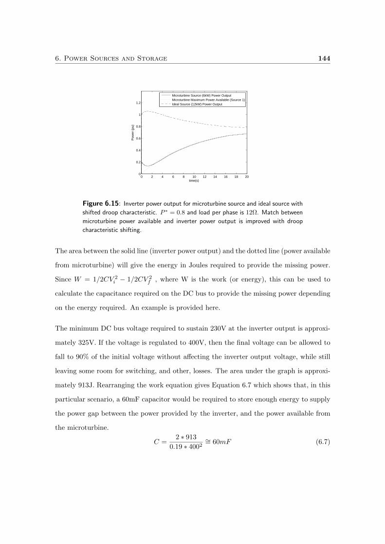
6. Power Sources and Storage 144
0 2 4 6 8 10 12 14 16 18 200
0.2
0.4
0.6
0.8
1
1.2
time(s)
Pow
er (
pu)
Microturbine Source (6kW) Power OutputMicroturbine Maximum Power Available (Source 1)Ideal Source (12kW) Power Output
Figure 6.15: Inverter power output for microturbine source and ideal source with
shifted droop characteristic. P ∗ = 0.8 and load per phase is 12Ω. Match between
microturbine power available and inverter power output is improved with droop
characteristic shifting.
The area between the solid line (inverter power output) and the dotted line (power available
from microturbine) will give the energy in Joules required to provide the missing power.
Since W = 1/2CV 2i − 1/2CV 2
f , where W is the work (or energy), this can be used to
calculate the capacitance required on the DC bus to provide the missing power depending
on the energy required. An example is provided here.
The minimum DC bus voltage required to sustain 230V at the inverter output is approxi-
mately 325V. If the voltage is regulated to 400V, then the final voltage can be allowed to
fall to 90% of the initial voltage without affecting the inverter output voltage, while still
leaving some room for switching, and other, losses. The area under the graph is approxi-
mately 913J. Rearranging the work equation gives Equation 6.7 which shows that, in this
particular scenario, a 60mF capacitor would be required to store enough energy to supply
the power gap between the power provided by the inverter, and the power available from
the microturbine.
C =2 ∗ 913
0.19 ∗ 4002∼= 60mF (6.7)
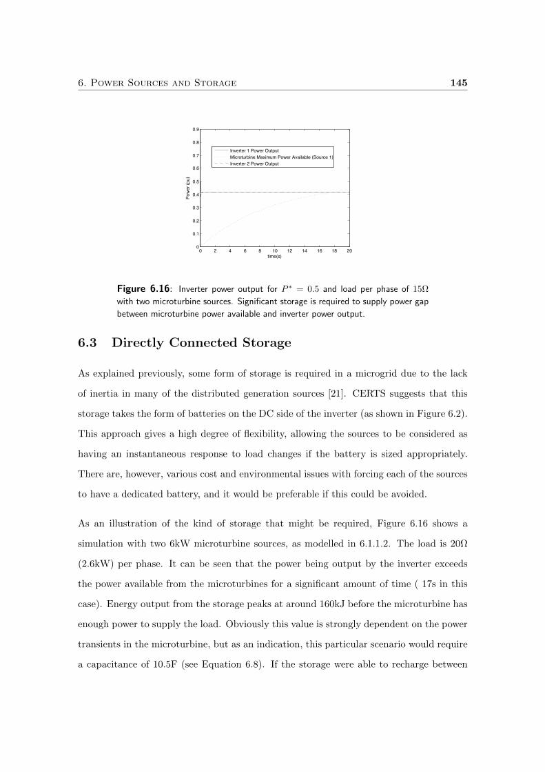
6. Power Sources and Storage 145
0 2 4 6 8 10 12 14 16 18 200
0.1
0.2
0.3
0.4
0.5
0.6
0.7
0.8
0.9
time(s)
Pow
er (p
u)
Inverter 1 Power OutputMicroturbine Maximum Power Available (Source 1)Inverter 2 Power Output
Figure 6.16: Inverter power output for P ∗ = 0.5 and load per phase of 15Ω
with two microturbine sources. Significant storage is required to supply power gap
between microturbine power available and inverter power output.
6.3 Directly Connected Storage
As explained previously, some form of storage is required in a microgrid due to the lack
of inertia in many of the distributed generation sources [21]. CERTS suggests that this
storage takes the form of batteries on the DC side of the inverter (as shown in Figure 6.2).
This approach gives a high degree of flexibility, allowing the sources to be considered as
having an instantaneous response to load changes if the battery is sized appropriately.
There are, however, various cost and environmental issues with forcing each of the sources
to have a dedicated battery, and it would be preferable if this could be avoided.
As an illustration of the kind of storage that might be required, Figure 6.16 shows a
simulation with two 6kW microturbine sources, as modelled in 6.1.1.2. The load is 20Ω
(2.6kW) per phase. It can be seen that the power being output by the inverter exceeds
the power available from the microturbines for a significant amount of time ( 17s in this
case). Energy output from the storage peaks at around 160kJ before the microturbine has
enough power to supply the load. Obviously this value is strongly dependent on the power
transients in the microturbine, but as an indication, this particular scenario would require
a capacitance of 10.5F (see Equation 6.8). If the storage were able to recharge between
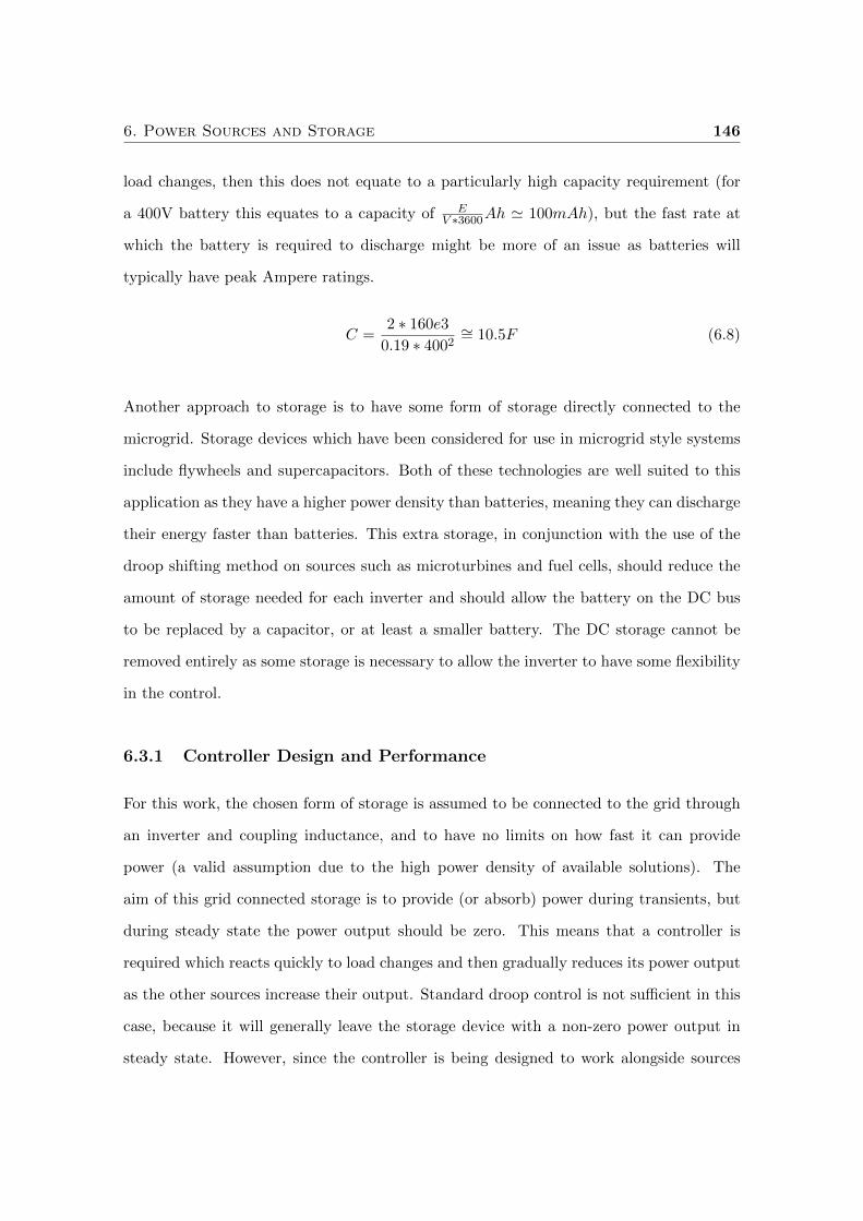
6. Power Sources and Storage 146
load changes, then this does not equate to a particularly high capacity requirement (for
a 400V battery this equates to a capacity of EV ∗3600Ah ' 100mAh), but the fast rate at
which the battery is required to discharge might be more of an issue as batteries will
typically have peak Ampere ratings.
C =2 ∗ 160e3
0.19 ∗ 4002∼= 10.5F (6.8)
Another approach to storage is to have some form of storage directly connected to the
microgrid. Storage devices which have been considered for use in microgrid style systems
include flywheels and supercapacitors. Both of these technologies are well suited to this
application as they have a higher power density than batteries, meaning they can discharge
their energy faster than batteries. This extra storage, in conjunction with the use of the
droop shifting method on sources such as microturbines and fuel cells, should reduce the
amount of storage needed for each inverter and should allow the battery on the DC bus
to be replaced by a capacitor, or at least a smaller battery. The DC storage cannot be
removed entirely as some storage is necessary to allow the inverter to have some flexibility
in the control.
6.3.1 Controller Design and Performance
For this work, the chosen form of storage is assumed to be connected to the grid through
an inverter and coupling inductance, and to have no limits on how fast it can provide
power (a valid assumption due to the high power density of available solutions). The
aim of this grid connected storage is to provide (or absorb) power during transients, but
during steady state the power output should be zero. This means that a controller is
required which reacts quickly to load changes and then gradually reduces its power output
as the other sources increase their output. Standard droop control is not sufficient in this
case, because it will generally leave the storage device with a non-zero power output in
steady state. However, since the controller is being designed to work alongside sources
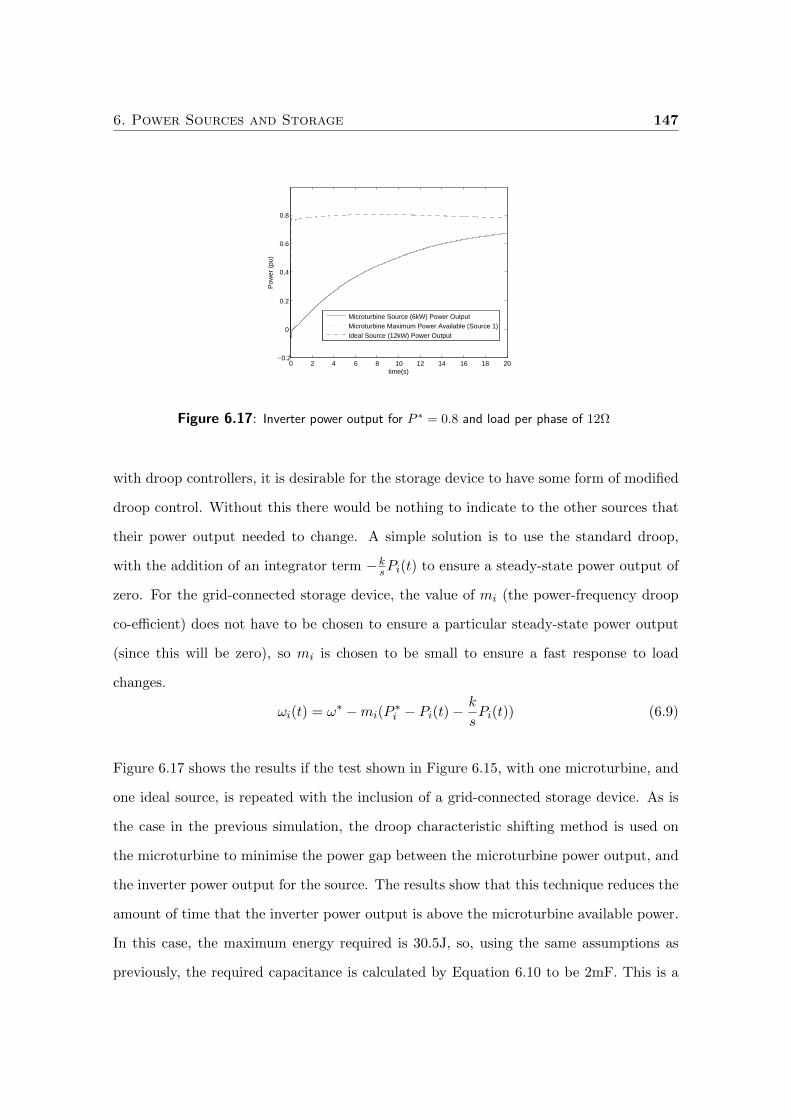
6. Power Sources and Storage 147
0 2 4 6 8 10 12 14 16 18 20−0.2
0
0.2
0.4
0.6
0.8
time(s)
Pow
er (
pu)
Microturbine Source (6kW) Power OutputMicroturbine Maximum Power Available (Source 1)Ideal Source (12kW) Power Output
Figure 6.17: Inverter power output for P ∗ = 0.8 and load per phase of 12Ω
with droop controllers, it is desirable for the storage device to have some form of modified
droop control. Without this there would be nothing to indicate to the other sources that
their power output needed to change. A simple solution is to use the standard droop,
with the addition of an integrator term −ksPi(t) to ensure a steady-state power output of
zero. For the grid-connected storage device, the value of mi (the power-frequency droop
co-efficient) does not have to be chosen to ensure a particular steady-state power output
(since this will be zero), so mi is chosen to be small to ensure a fast response to load
changes.
ωi(t) = ω∗ −mi(P∗i − Pi(t)−
k
sPi(t)) (6.9)
Figure 6.17 shows the results if the test shown in Figure 6.15, with one microturbine, and
one ideal source, is repeated with the inclusion of a grid-connected storage device. As is
the case in the previous simulation, the droop characteristic shifting method is used on
the microturbine to minimise the power gap between the microturbine power output, and
the inverter power output for the source. The results show that this technique reduces the
amount of time that the inverter power output is above the microturbine available power.
In this case, the maximum energy required is 30.5J, so, using the same assumptions as
previously, the required capacitance is calculated by Equation 6.10 to be 2mF. This is a
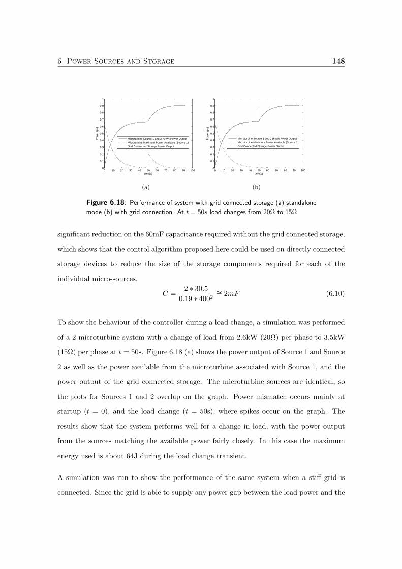
6. Power Sources and Storage 148
0 10 20 30 40 50 60 70 80 90 1000
0.1
0.2
0.3
0.4
0.5
0.6
0.7
0.8
0.9
1
time(s)
Pow
er (
pu)
Microturbine Source 1 and 2 (6kW) Power OutputMicroturbine Maximum Power Available (Source 1)Grid Connected Storage Power Output
(a)
0 10 20 30 40 50 60 70 80 90 1000
0.1
0.2
0.3
0.4
0.5
0.6
0.7
0.8
0.9
1
time(s)
Pow
er (
pu)
Microturbine Source 1 and 2 (6kW) Power OutputMicroturbine Maximum Power Available (Source 1)Grid Connected Storage Power Output
(b)
Figure 6.18: Performance of system with grid connected storage (a) standalone
mode (b) with grid connection. At t = 50s load changes from 20Ω to 15Ω
significant reduction on the 60mF capacitance required without the grid connected storage,
which shows that the control algorithm proposed here could be used on directly connected
storage devices to reduce the size of the storage components required for each of the
individual micro-sources.
C =2 ∗ 30.5
0.19 ∗ 4002∼= 2mF (6.10)
To show the behaviour of the controller during a load change, a simulation was performed
of a 2 microturbine system with a change of load from 2.6kW (20Ω) per phase to 3.5kW
(15Ω) per phase at t = 50s. Figure 6.18 (a) shows the power output of Source 1 and Source
2 as well as the power available from the microturbine associated with Source 1, and the
power output of the grid connected storage. The microturbine sources are identical, so
the plots for Sources 1 and 2 overlap on the graph. Power mismatch occurs mainly at
startup (t = 0), and the load change (t = 50s), where spikes occur on the graph. The
results show that the system performs well for a change in load, with the power output
from the sources matching the available power fairly closely. In this case the maximum
energy used is about 64J during the load change transient.
A simulation was run to show the performance of the same system when a stiff grid is
connected. Since the grid is able to supply any power gap between the load power and the
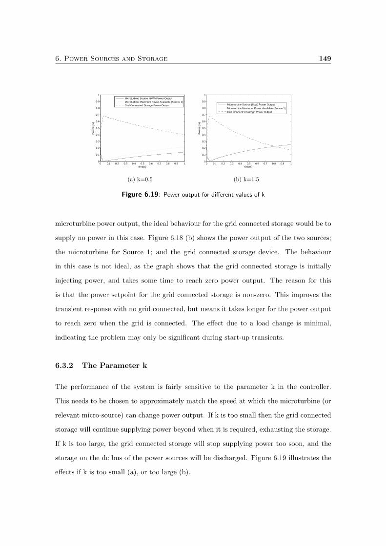
6. Power Sources and Storage 149
0 0.1 0.2 0.3 0.4 0.5 0.6 0.7 0.8 0.9 10
0.1
0.2
0.3
0.4
0.5
0.6
0.7
0.8
0.9
1
time(s)
Pow
er (
pu)
Microturbine Source (6kW) Power OutputMicroturbine Maximum Power Available (Source 1)Grid Connected Storage Power Output
(a) k=0.5
0 0.1 0.2 0.3 0.4 0.5 0.6 0.7 0.8 0.9 10
0.1
0.2
0.3
0.4
0.5
0.6
0.7
0.8
0.9
1
time(s)
Pow
er (
pu)
Microturbine Source (6kW) Power OutputMicroturbine Maximum Power Available (Source 1)Grid Connected Storage Power Output
(b) k=1.5
Figure 6.19: Power output for different values of k
microturbine power output, the ideal behaviour for the grid connected storage would be to
supply no power in this case. Figure 6.18 (b) shows the power output of the two sources;
the microturbine for Source 1; and the grid connected storage device. The behaviour
in this case is not ideal, as the graph shows that the grid connected storage is initially
injecting power, and takes some time to reach zero power output. The reason for this
is that the power setpoint for the grid connected storage is non-zero. This improves the
transient response with no grid connected, but means it takes longer for the power output
to reach zero when the grid is connected. The effect due to a load change is minimal,
indicating the problem may only be significant during start-up transients.
6.3.2 The Parameter k
The performance of the system is fairly sensitive to the parameter k in the controller.
This needs to be chosen to approximately match the speed at which the microturbine (or
relevant micro-source) can change power output. If k is too small then the grid connected
storage will continue supplying power beyond when it is required, exhausting the storage.
If k is too large, the grid connected storage will stop supplying power too soon, and the
storage on the dc bus of the power sources will be discharged. Figure 6.19 illustrates the
effects if k is too small (a), or too large (b).

6. Power Sources and Storage 150
6.3.3 Controller Limitations
The controller presented in this chapter is based on simplified source models. It is designed
to show how a grid connected storage device can work alongside sources interfaced with
inverters using droop control to minimise storage on the DC bus of the source, while
allowing correct operation of the source inverter controllers. The controller assumes that
the storage can provide any amount of power, provided it has not been exhausted, and
does not take into account the nature of the storage device, or any limitations on the
storage. A more complete controller would need to take into account mechanical stresses
on devices such as flywheels, charging cycles on batteries, and provide intelligent control
to ensure that storage did not become exhausted, or overcharged.
Chapter 7
Summary and Further Work
7.1 Modelling Techniques
Historically, power system modelling focuses on steady state or slow dynamic behaviours.
In distributed generation systems, modelling needs to take into account faster dynamic
behaviours. Modelling techniques developed for this are typically processor intensive and
slow to simulate. A modelling approach has been developed that:
• treats the inverter as an ideal controllable source
• approximates the inverter power source as a transfer function
• considers power system components in a d-q reference frame allowing for more effi-
cient simulation of parallel inverters.
This model allows for the simulation of different load types, and dynamic load behaviours.
The modelling approach has also been integrated with components available in the MAT-
LAB SimPowerSystems library. This allowed the incorporation of standard power system
components (transformers, circuit breakers) into the developed models. It should be noted
that SimPowerSystems models are in phase variables which does lead to slower simulations.
7.1.1 Further Work
While the new modelling system shows potential as a fast method for simulating dis-
tributed generations systems, there is still some further development required before it is
suitable for widespread use. In particular, the components that are currently utilised from

7. Summary and Further Work 152
the SimPowerSystems library could be modelled using the d-q modelling approach.
A fast model could be used to investigate the effect of many inverters in parallel, as in
PV systems. This would include investigating the assumption that inverter switching and
other source dynamics can be ignored, and developing a source model which reflects the
behaviour of PV sources.
7.2 Pf-droop
Power-frequency droop control is presented as the solution to power sharing between
sources in a distributed generation system without requiring fast communications, how-
ever in the literature, several problems have been found with the standard droop control
algorithm. The model library was used to perform simulations which verified these prob-
lems. The proposed solutions in the literature were outlined and key ones evaluated. It
was found that the area in which research is lacking is solutions to limit voltage unbalance
at the load.
7.3 Controller Design
A controller was designed to limit voltage unbalance at the load by injecting negative
sequence at the source. Initially the controller was designed to work with the CERTS
droop controller, then the unbalance controller was incorporated into a new controller
which takes ideas from several authors in order to create something to work in a wide
range of conditions. The previous tests were revisited to ensure that new controller is able
to solve the problems present in standard droop control.
7.3.1 Further Work
The component design for the system is fairly simplistic. There is potential for performance
improvements through more sophisticated control techniques in the unbalance controller,
7. Summary and Further Work 153
better filters throughout the system, and an improved algorithm for the sequence analyzer.
Also, harmonic current sharing is not addressed in the new controller.
In this work the controller performance has been evaluated by simulation. The next step
is experimental validation of the controller design.
There is potential for applying the technique used for unbalance control to the problem of
improving zero sequence behaviour. The complexity of this problem is considerable and
has not been investigated as part of this work.
7.4 Grid Connected Storage
An issue with the kinds of sources usually used in distributed generation is that they have
little or no inertia and cannot instantly supply changes in load. The typical solution to
this is to supply storage (i.e. a battery) on the DC bus of the power source. Another
possibility is to provide a grid-connected AC storage device (such as a flywheel) with the
aim of reducing, or eliminating, the DC storage required for addressing the gap between
the power required by the load, and the power supplied by the source. With this aim, a
simple controller based on power-frequency droop control was designed for a grid-connected
storage device. As a part of this work, the literature on simple Power Source models was
examined. Simulation shows that the controller is able to reduce the amount of storage
required on the DC bus, although not eliminate it.
7.4.1 Further Work
The simple controller is able to reduce DC storage requirements significantly, but it is likely
that with fine tuning, or a different control scheme, better results can be achieved. Also
of interest is the effect of non-dispatchable sources such as PV and wind. To investigate
this, Power Source models are required for these.

Appendix A
MATLAB/Simulink Diagrams
This Appendix contains screen captures of the Simulink files used throughout this thesis.
A.1 Simulation using Developed Model Library
This Section contains the Simulink diagrams for the simulations performed in Chapter 3
based on the model library outlined in Chapter 2. The model represents five inverters in
parallel each connected to a single load through coupling inductances.
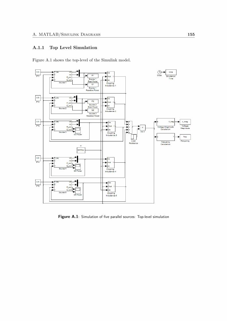
A. MATLAB/Simulink Diagrams 155
A.1.1 Top Level Simulation
Figure A.1 shows the top-level of the Simulink model.
Figure A.1: Simulation of five parallel sources: Top-level simulation
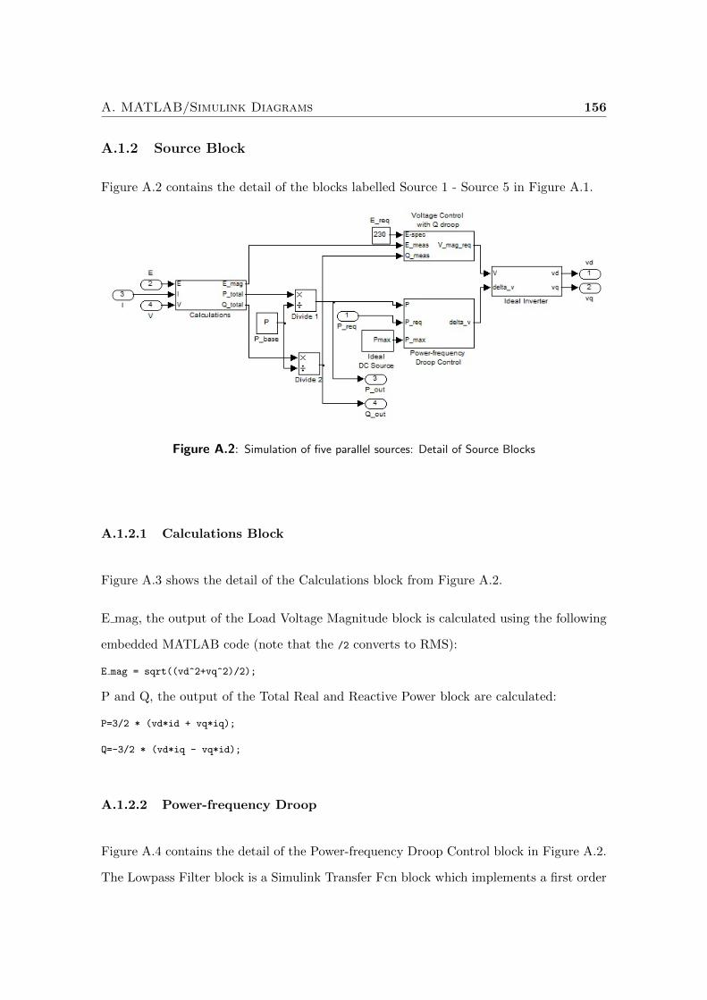
A. MATLAB/Simulink Diagrams 156
A.1.2 Source Block
Figure A.2 contains the detail of the blocks labelled Source 1 - Source 5 in Figure A.1.
Figure A.2: Simulation of five parallel sources: Detail of Source Blocks
A.1.2.1 Calculations Block
Figure A.3 shows the detail of the Calculations block from Figure A.2.
E mag, the output of the Load Voltage Magnitude block is calculated using the following
embedded MATLAB code (note that the /2 converts to RMS):
E mag = sqrt((vd^2+vq^2)/2);
P and Q, the output of the Total Real and Reactive Power block are calculated:
P=3/2 * (vd*id + vq*iq);
Q=-3/2 * (vd*iq - vq*id);
A.1.2.2 Power-frequency Droop
Figure A.4 contains the detail of the Power-frequency Droop Control block in Figure A.2.
The Lowpass Filter block is a Simulink Transfer Fcn block which implements a first order
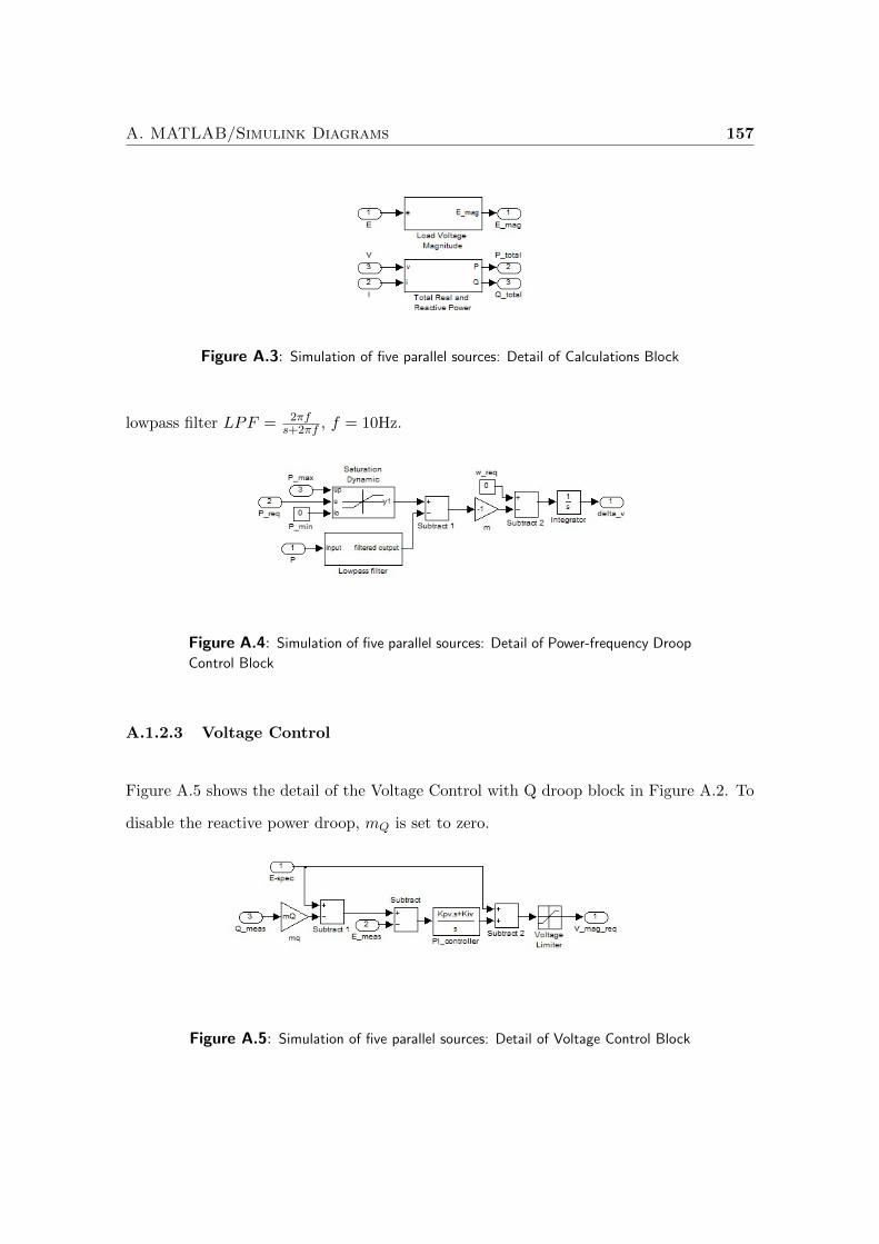
A. MATLAB/Simulink Diagrams 157
Figure A.3: Simulation of five parallel sources: Detail of Calculations Block
lowpass filter LPF = 2πfs+2πf , f = 10Hz.
Figure A.4: Simulation of five parallel sources: Detail of Power-frequency Droop
Control Block
A.1.2.3 Voltage Control
Figure A.5 shows the detail of the Voltage Control with Q droop block in Figure A.2. To
disable the reactive power droop, mQ is set to zero.
Figure A.5: Simulation of five parallel sources: Detail of Voltage Control Block
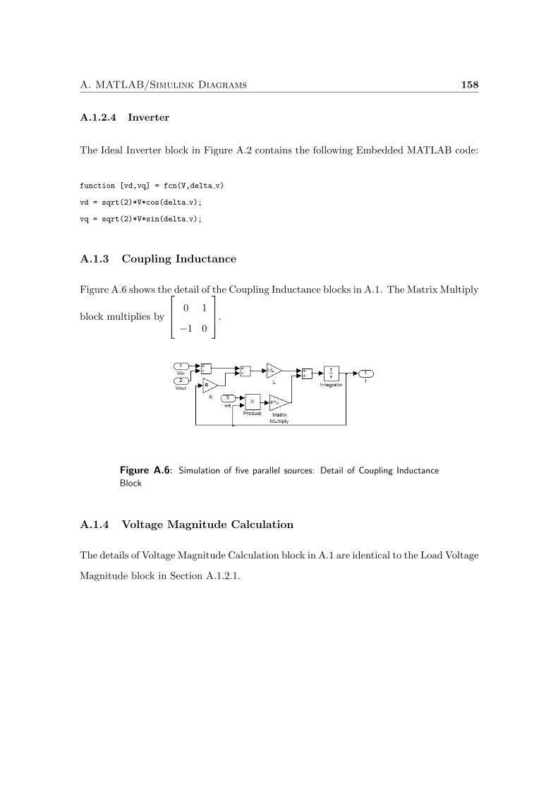
A. MATLAB/Simulink Diagrams 158
A.1.2.4 Inverter
The Ideal Inverter block in Figure A.2 contains the following Embedded MATLAB code:
function [vd,vq] = fcn(V,delta v)
vd = sqrt(2)*V*cos(delta v);
vq = sqrt(2)*V*sin(delta v);
A.1.3 Coupling Inductance
Figure A.6 shows the detail of the Coupling Inductance blocks in A.1. The Matrix Multiply
block multiplies by
0 1
−1 0
.
Figure A.6: Simulation of five parallel sources: Detail of Coupling Inductance
Block
A.1.4 Voltage Magnitude Calculation
The details of Voltage Magnitude Calculation block in A.1 are identical to the Load Voltage
Magnitude block in Section A.1.2.1.

A. MATLAB/Simulink Diagrams 159
Figure A.7: Simulation of five parallel sources: Detail of Frequency Calculation
Block
A.1.5 Frequency Calculation
Figure A.7 shows the detail of the Frequency Calculation block in A.1. The delta e Cal-
culation block contains the following Embedded MATLAB code:
function delta e = fcn(vd,vq)
persistent sum1;
persistent last;
%Initialse sum1
ifisempty(sum1)
sum1=0;
end
%Initialise last
if isempty(last)
last=0;
end
%Avoid divide by zero
if vd==0
if vq==0
delta e=0;
else
delta e=pi/2+sum1;
end
else %vd is non-zero
temp= atan(vq/vd)+sum1;
%Discontinuity in atan function would lead to errors in frequency measurement
%Correct for discontinuity
if (last - temp>2)
sum1=sum1+pi;
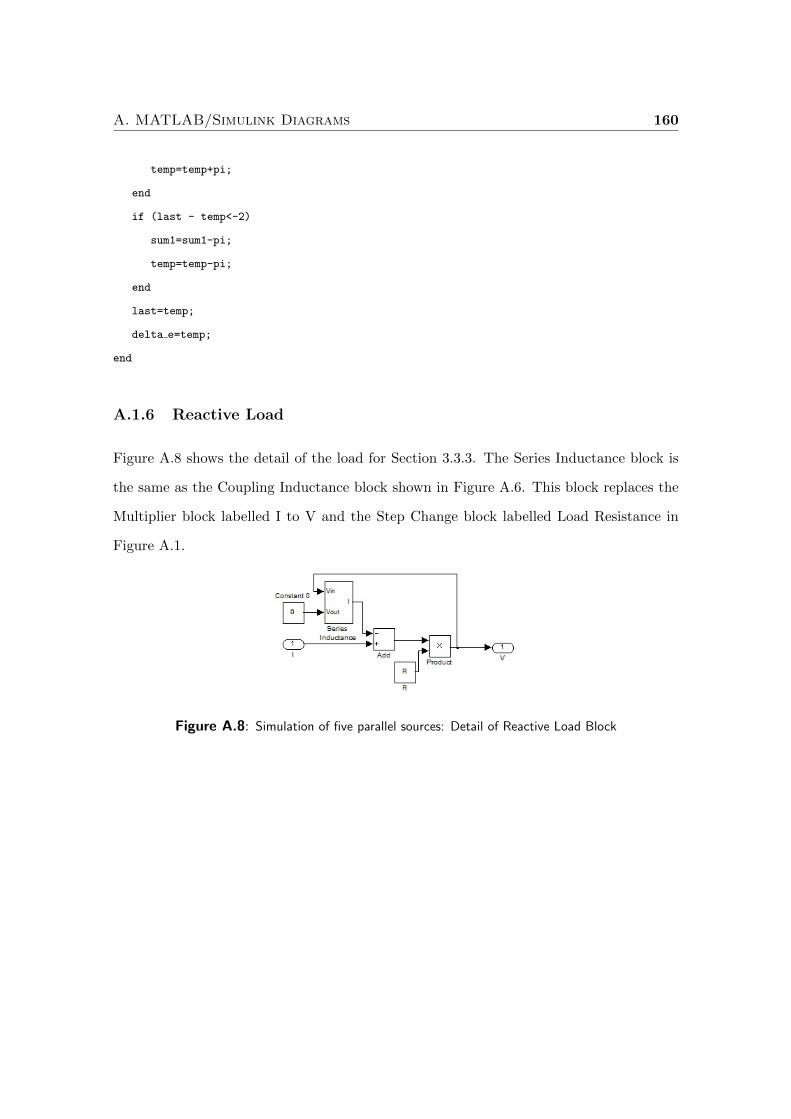
A. MATLAB/Simulink Diagrams 160
temp=temp+pi;
end
if (last - temp<-2)
sum1=sum1-pi;
temp=temp-pi;
end
last=temp;
delta e=temp;
end
A.1.6 Reactive Load
Figure A.8 shows the detail of the load for Section 3.3.3. The Series Inductance block is
the same as the Coupling Inductance block shown in Figure A.6. This block replaces the
Multiplier block labelled I to V and the Step Change block labelled Load Resistance in
Figure A.1.
Figure A.8: Simulation of five parallel sources: Detail of Reactive Load Block
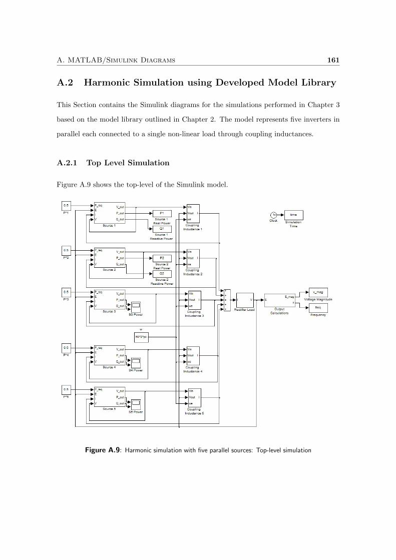
A. MATLAB/Simulink Diagrams 161
A.2 Harmonic Simulation using Developed Model Library
This Section contains the Simulink diagrams for the simulations performed in Chapter 3
based on the model library outlined in Chapter 2. The model represents five inverters in
parallel each connected to a single non-linear load through coupling inductances.
A.2.1 Top Level Simulation
Figure A.9 shows the top-level of the Simulink model.
Figure A.9: Harmonic simulation with five parallel sources: Top-level simulation
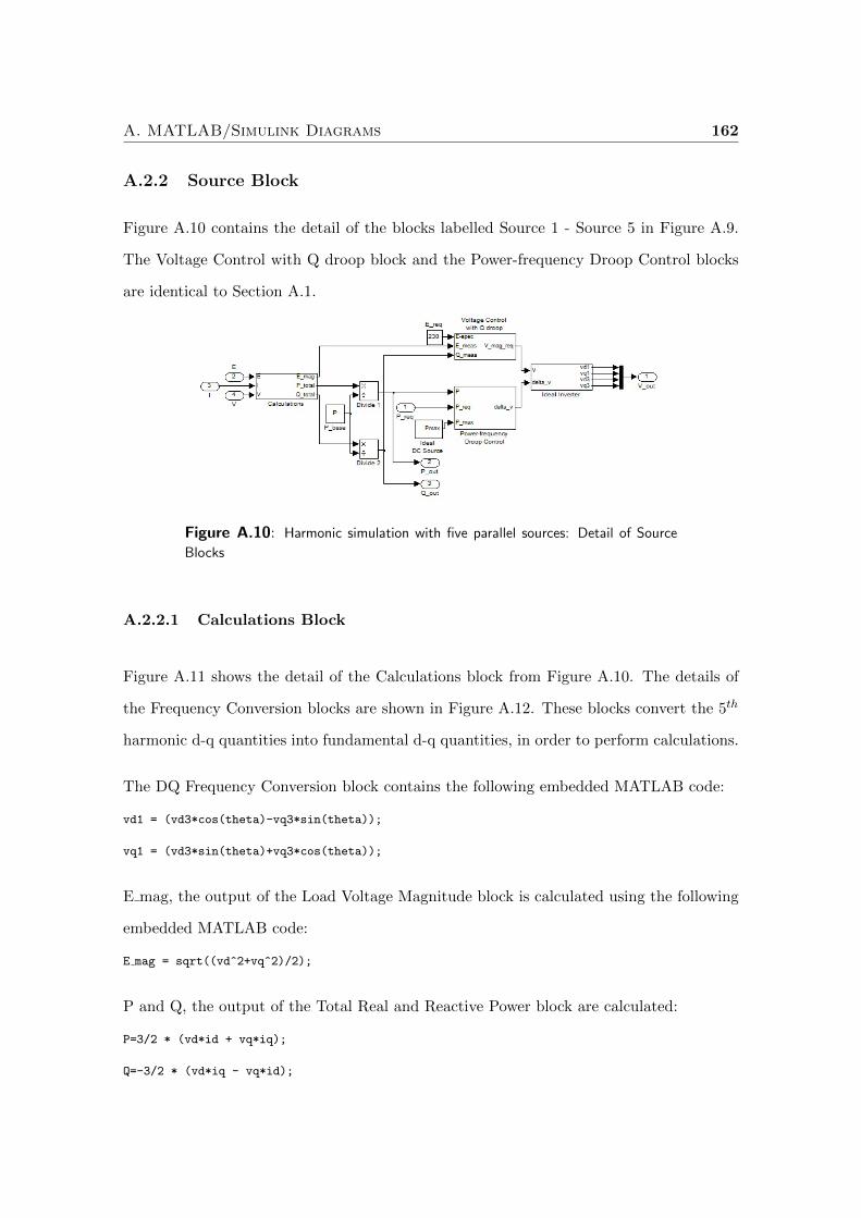
A. MATLAB/Simulink Diagrams 162
A.2.2 Source Block
Figure A.10 contains the detail of the blocks labelled Source 1 - Source 5 in Figure A.9.
The Voltage Control with Q droop block and the Power-frequency Droop Control blocks
are identical to Section A.1.
Figure A.10: Harmonic simulation with five parallel sources: Detail of Source
Blocks
A.2.2.1 Calculations Block
Figure A.11 shows the detail of the Calculations block from Figure A.10. The details of
the Frequency Conversion blocks are shown in Figure A.12. These blocks convert the 5th
harmonic d-q quantities into fundamental d-q quantities, in order to perform calculations.
The DQ Frequency Conversion block contains the following embedded MATLAB code:
vd1 = (vd3*cos(theta)-vq3*sin(theta));
vq1 = (vd3*sin(theta)+vq3*cos(theta));
E mag, the output of the Load Voltage Magnitude block is calculated using the following
embedded MATLAB code:
E mag = sqrt((vd^2+vq^2)/2);
P and Q, the output of the Total Real and Reactive Power block are calculated:
P=3/2 * (vd*id + vq*iq);
Q=-3/2 * (vd*iq - vq*id);
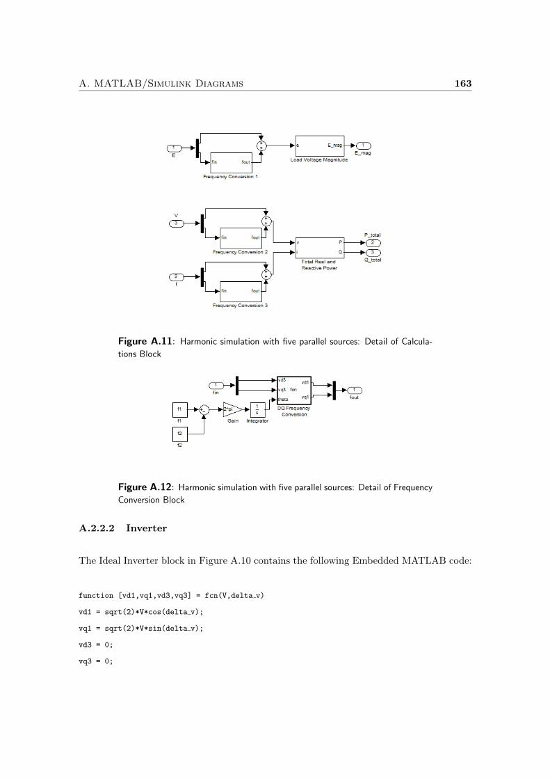
A. MATLAB/Simulink Diagrams 163
Figure A.11: Harmonic simulation with five parallel sources: Detail of Calcula-
tions Block
Figure A.12: Harmonic simulation with five parallel sources: Detail of Frequency
Conversion Block
A.2.2.2 Inverter
The Ideal Inverter block in Figure A.10 contains the following Embedded MATLAB code:
function [vd1,vq1,vd3,vq3] = fcn(V,delta v)
vd1 = sqrt(2)*V*cos(delta v);
vq1 = sqrt(2)*V*sin(delta v);
vd3 = 0;
vq3 = 0;
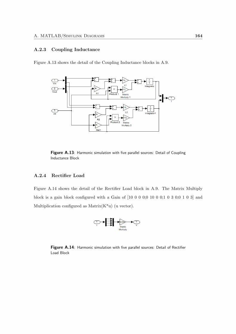
A. MATLAB/Simulink Diagrams 164
A.2.3 Coupling Inductance
Figure A.13 shows the detail of the Coupling Inductance blocks in A.9.
Figure A.13: Harmonic simulation with five parallel sources: Detail of Coupling
Inductance Block
A.2.4 Rectifier Load
Figure A.14 shows the detail of the Rectifier Load block in A.9. The Matrix Multiply
block is a gain block configured with a Gain of [10 0 0 0;0 10 0 0;1 0 3 0;0 1 0 3] and
Multiplication configured as Matrix(K*u) (u vector).
Figure A.14: Harmonic simulation with five parallel sources: Detail of Rectifier
Load Block
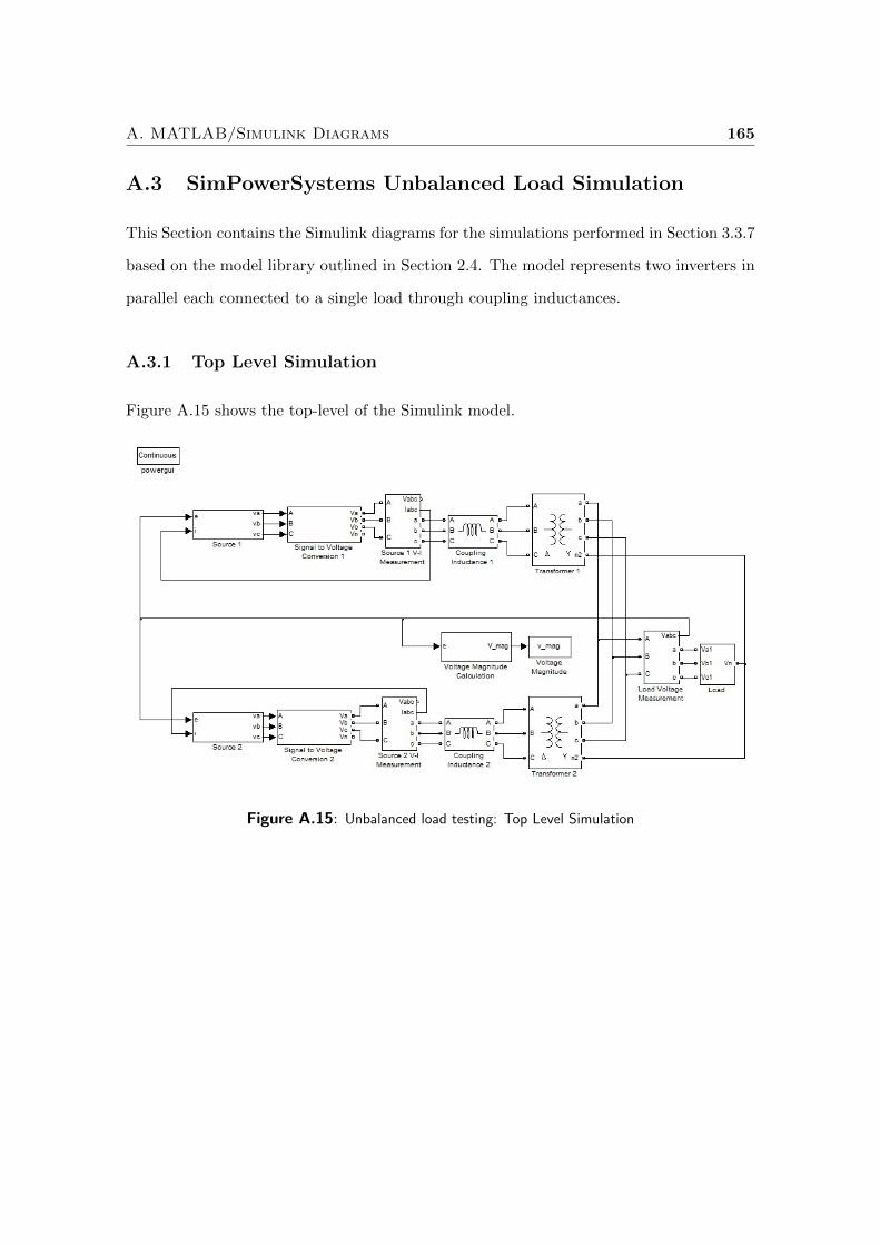
A. MATLAB/Simulink Diagrams 165
A.3 SimPowerSystems Unbalanced Load Simulation
This Section contains the Simulink diagrams for the simulations performed in Section 3.3.7
based on the model library outlined in Section 2.4. The model represents two inverters in
parallel each connected to a single load through coupling inductances.
A.3.1 Top Level Simulation
Figure A.15 shows the top-level of the Simulink model.
Figure A.15: Unbalanced load testing: Top Level Simulation
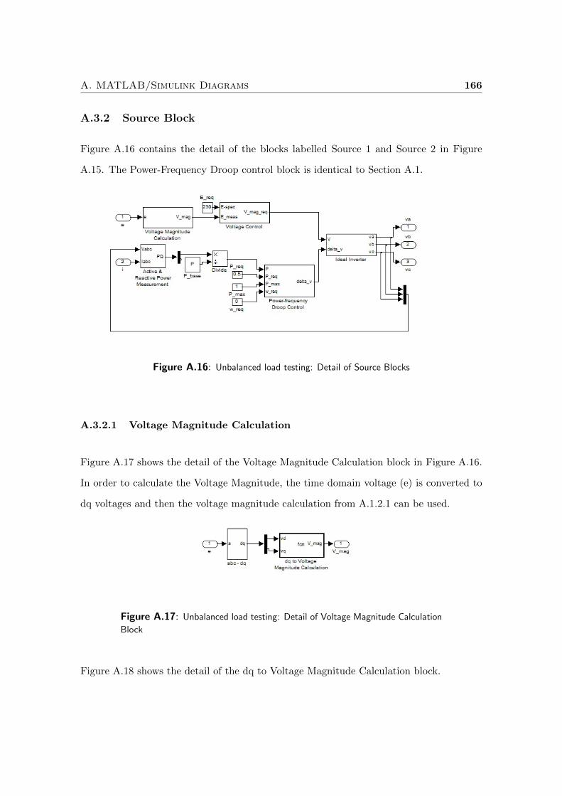
A. MATLAB/Simulink Diagrams 166
A.3.2 Source Block
Figure A.16 contains the detail of the blocks labelled Source 1 and Source 2 in Figure
A.15. The Power-Frequency Droop control block is identical to Section A.1.
Figure A.16: Unbalanced load testing: Detail of Source Blocks
A.3.2.1 Voltage Magnitude Calculation
Figure A.17 shows the detail of the Voltage Magnitude Calculation block in Figure A.16.
In order to calculate the Voltage Magnitude, the time domain voltage (e) is converted to
dq voltages and then the voltage magnitude calculation from A.1.2.1 can be used.
Figure A.17: Unbalanced load testing: Detail of Voltage Magnitude Calculation
Block
Figure A.18 shows the detail of the dq to Voltage Magnitude Calculation block.
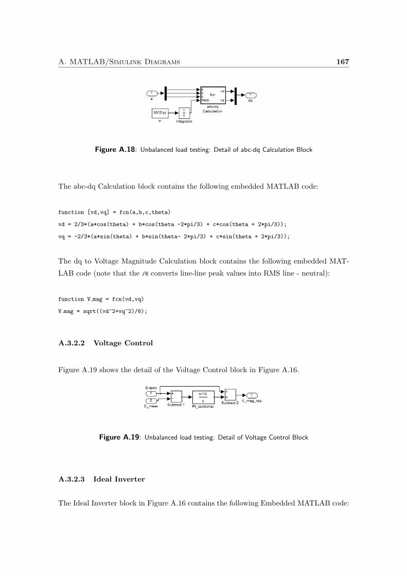
A. MATLAB/Simulink Diagrams 167
Figure A.18: Unbalanced load testing: Detail of abc-dq Calculation Block
The abc-dq Calculation block contains the following embedded MATLAB code:
function [vd,vq] = fcn(a,b,c,theta)
vd = 2/3*(a*cos(theta) + b*cos(theta -2*pi/3) + c*cos(theta + 2*pi/3));
vq = -2/3*(a*sin(theta) + b*sin(theta- 2*pi/3) + c*sin(theta + 2*pi/3));
The dq to Voltage Magnitude Calculation block contains the following embedded MAT-
LAB code (note that the /6 converts line-line peak values into RMS line - neutral):
function V mag = fcn(vd,vq)
V mag = sqrt((vd^2+vq^2)/6);
A.3.2.2 Voltage Control
Figure A.19 shows the detail of the Voltage Control block in Figure A.16.
Figure A.19: Unbalanced load testing: Detail of Voltage Control Block
A.3.2.3 Ideal Inverter
The Ideal Inverter block in Figure A.16 contains the following Embedded MATLAB code:
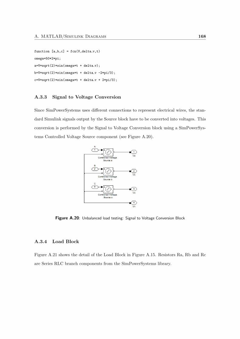
A. MATLAB/Simulink Diagrams 168
function [a,b,c] = fcn(V,delta v,t)
omega=50*2*pi;
a=V*sqrt(2)*sin(omega*t + delta v);
b=V*sqrt(2)*sin(omega*t + delta v -2*pi/3);
c=V*sqrt(2)*sin(omega*t + delta v + 2*pi/3);
A.3.3 Signal to Voltage Conversion
Since SimPowerSystems uses different connections to represent electrical wires, the stan-
dard Simulink signals output by the Source block have to be converted into voltages. This
conversion is performed by the Signal to Voltage Conversion block using a SimPowerSys-
tems Controlled Voltage Source component (see Figure A.20).
Figure A.20: Unbalanced load testing: Signal to Voltage Conversion Block
A.3.4 Load Block
Figure A.21 shows the detail of the Load Block in Figure A.15. Resistors Ra, Rb and Rc
are Series RLC branch components from the SimPowerSystems library.
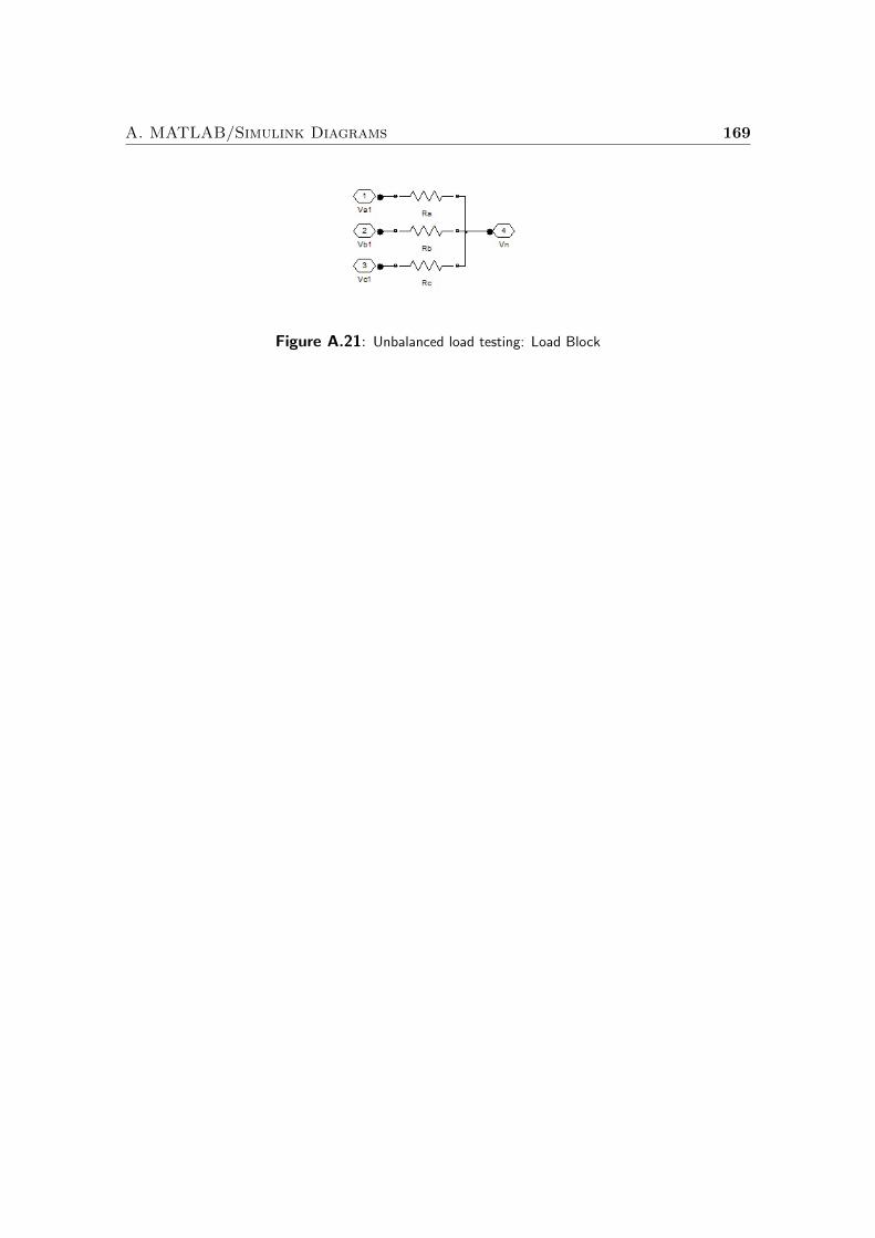
A. MATLAB/Simulink Diagrams 169
Figure A.21: Unbalanced load testing: Load Block
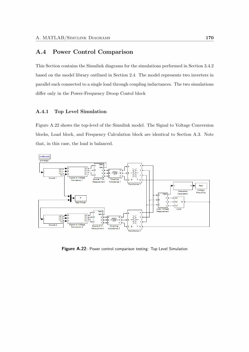
A. MATLAB/Simulink Diagrams 170
A.4 Power Control Comparison
This Section contains the Simulink diagrams for the simulations performed in Section 3.4.2
based on the model library outlined in Section 2.4. The model represents two inverters in
parallel each connected to a single load through coupling inductances. The two simulations
differ only in the Power-Frequency Droop Contol block
A.4.1 Top Level Simulation
Figure A.22 shows the top-level of the Simulink model. The Signal to Voltage Conversion
blocks, Load block, and Frequency Calculation block are identical to Section A.3. Note
that, in this case, the load is balanced.
Figure A.22: Power control comparison testing: Top Level Simulation
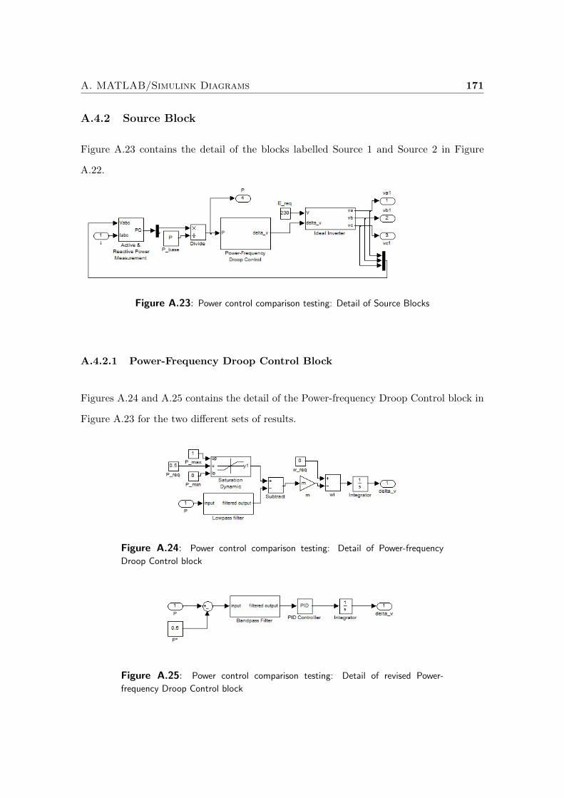
A. MATLAB/Simulink Diagrams 171
A.4.2 Source Block
Figure A.23 contains the detail of the blocks labelled Source 1 and Source 2 in Figure
A.22.
Figure A.23: Power control comparison testing: Detail of Source Blocks
A.4.2.1 Power-Frequency Droop Control Block
Figures A.24 and A.25 contains the detail of the Power-frequency Droop Control block in
Figure A.23 for the two different sets of results.
Figure A.24: Power control comparison testing: Detail of Power-frequency
Droop Control block
Figure A.25: Power control comparison testing: Detail of revised Power-
frequency Droop Control block
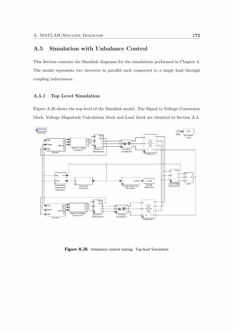
A. MATLAB/Simulink Diagrams 172
A.5 Simulation with Unbalance Control
This Section contains the Simulink diagrams for the simulations performed in Chapter 4.
The model represents two inverters in parallel each connected to a single load through
coupling inductances.
A.5.1 Top Level Simulation
Figure A.26 shows the top-level of the Simulink model. The Signal to Voltage Conversion
block, Voltage Magnitude Calculation block and Load block are identical to Section A.3.
Figure A.26: Unbalance control testing: Top-level Simulation
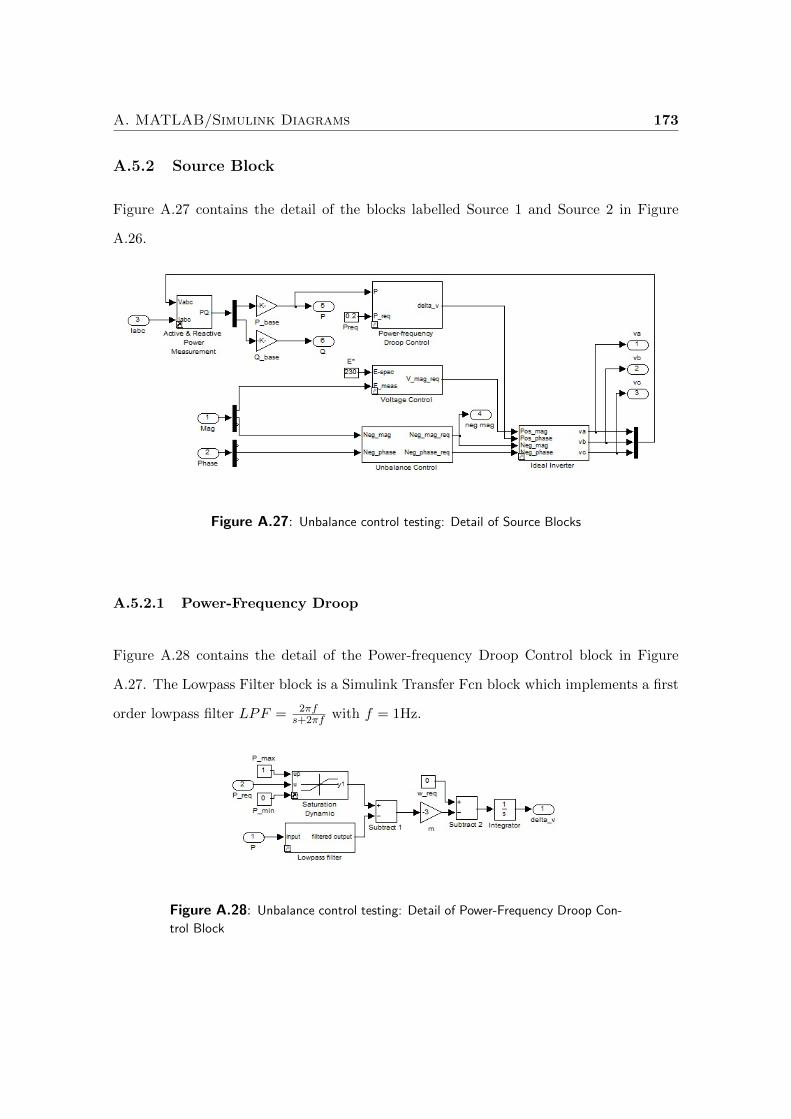
A. MATLAB/Simulink Diagrams 173
A.5.2 Source Block
Figure A.27 contains the detail of the blocks labelled Source 1 and Source 2 in Figure
A.26.
Figure A.27: Unbalance control testing: Detail of Source Blocks
A.5.2.1 Power-Frequency Droop
Figure A.28 contains the detail of the Power-frequency Droop Control block in Figure
A.27. The Lowpass Filter block is a Simulink Transfer Fcn block which implements a first
order lowpass filter LPF = 2πfs+2πf with f = 1Hz.
Figure A.28: Unbalance control testing: Detail of Power-Frequency Droop Con-
trol Block
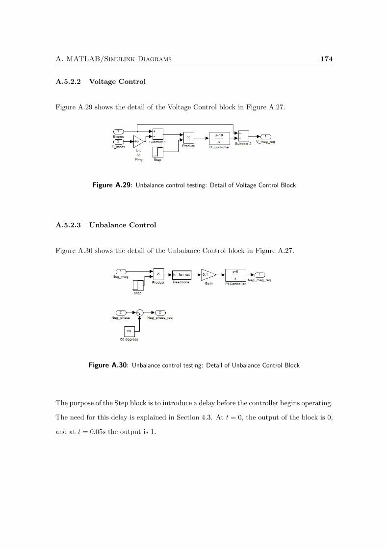
A. MATLAB/Simulink Diagrams 174
A.5.2.2 Voltage Control
Figure A.29 shows the detail of the Voltage Control block in Figure A.27.
Figure A.29: Unbalance control testing: Detail of Voltage Control Block
A.5.2.3 Unbalance Control
Figure A.30 shows the detail of the Unbalance Control block in Figure A.27.
Figure A.30: Unbalance control testing: Detail of Unbalance Control Block
The purpose of the Step block is to introduce a delay before the controller begins operating.
The need for this delay is explained in Section 4.3. At t = 0, the output of the block is 0,
and at t = 0.05s the output is 1.
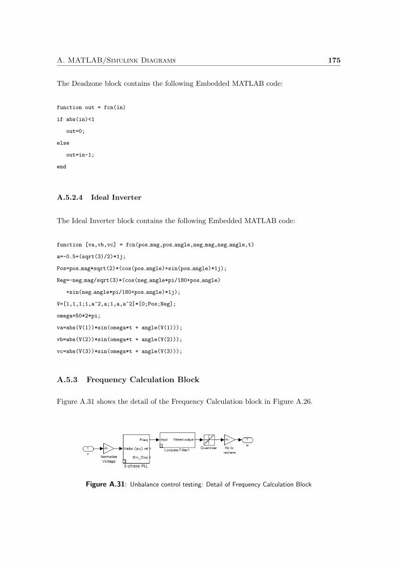
A. MATLAB/Simulink Diagrams 175
The Deadzone block contains the following Embedded MATLAB code:
function out = fcn(in)
if abs(in)<1
out=0;
else
out=in-1;
end
A.5.2.4 Ideal Inverter
The Ideal Inverter block contains the following Embedded MATLAB code:
function [va,vb,vc] = fcn(pos mag,pos angle,neg mag,neg angle,t)
a=-0.5+(sqrt(3)/2)*1j;
Pos=pos mag*sqrt(2)*(cos(pos angle)+sin(pos angle)*1j);
Neg=-neg mag/sqrt(3)*(cos(neg angle*pi/180+pos angle)
+sin(neg angle*pi/180+pos angle)*1j);
V=[1,1,1;1,a^2,a;1,a,a^2]*[0;Pos;Neg];
omega=50*2*pi;
va=abs(V(1))*sin(omega*t + angle(V(1)));
vb=abs(V(2))*sin(omega*t + angle(V(2)));
vc=abs(V(3))*sin(omega*t + angle(V(3)));
A.5.3 Frequency Calculation Block
Figure A.31 shows the detail of the Frequency Calculation block in Figure A.26.
Figure A.31: Unbalance control testing: Detail of Frequency Calculation Block
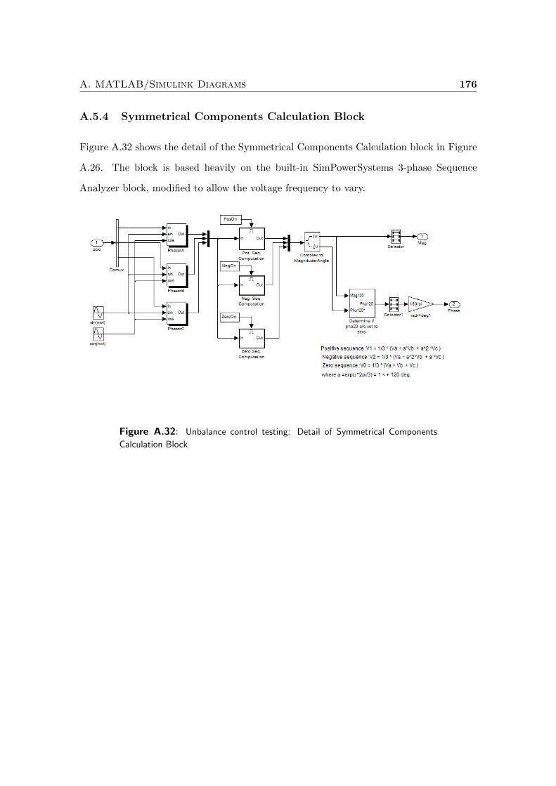
A. MATLAB/Simulink Diagrams 176
A.5.4 Symmetrical Components Calculation Block
Figure A.32 shows the detail of the Symmetrical Components Calculation block in Figure
A.26. The block is based heavily on the built-in SimPowerSystems 3-phase Sequence
Analyzer block, modified to allow the voltage frequency to vary.
Figure A.32: Unbalance control testing: Detail of Symmetrical Components
Calculation Block
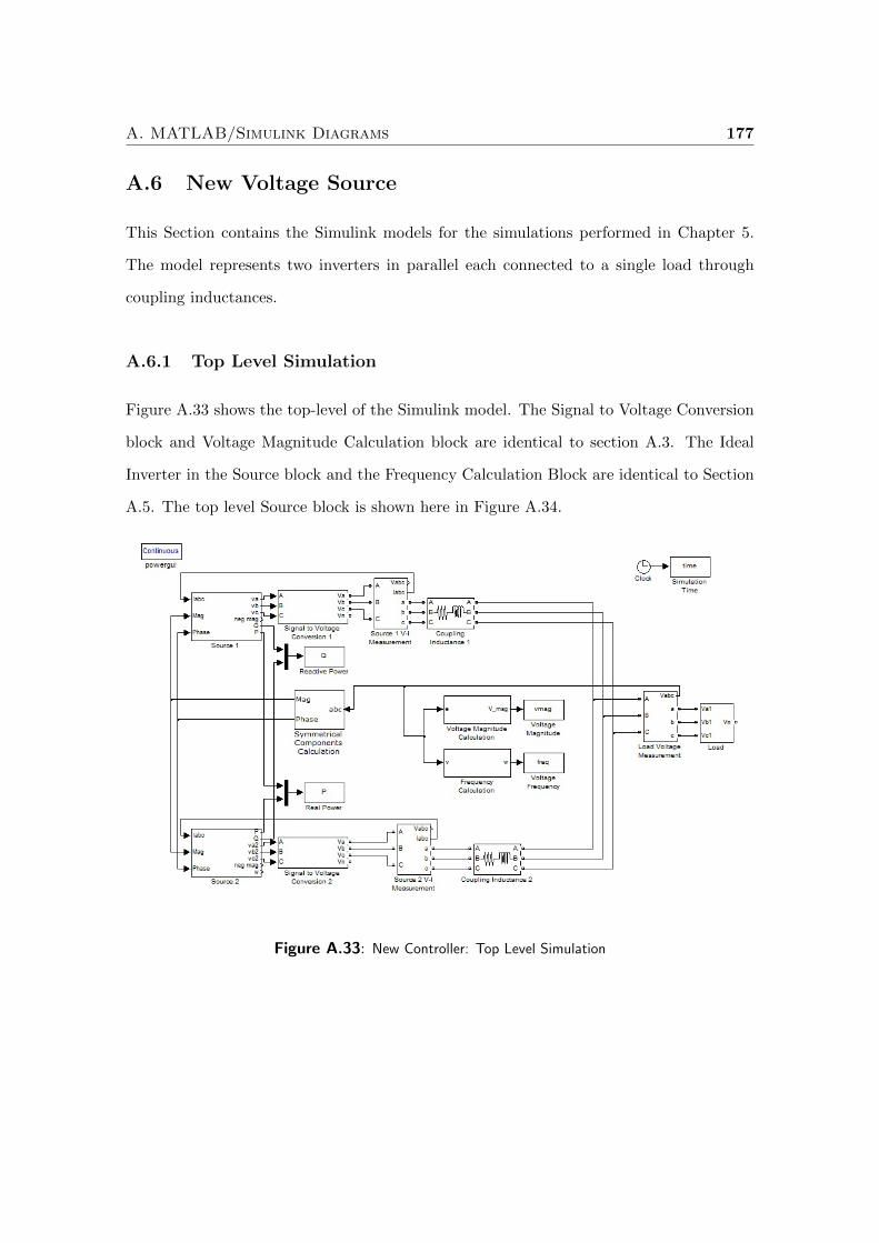
A. MATLAB/Simulink Diagrams 177
A.6 New Voltage Source
This Section contains the Simulink models for the simulations performed in Chapter 5.
The model represents two inverters in parallel each connected to a single load through
coupling inductances.
A.6.1 Top Level Simulation
Figure A.33 shows the top-level of the Simulink model. The Signal to Voltage Conversion
block and Voltage Magnitude Calculation block are identical to section A.3. The Ideal
Inverter in the Source block and the Frequency Calculation Block are identical to Section
A.5. The top level Source block is shown here in Figure A.34.
Figure A.33: New Controller: Top Level Simulation
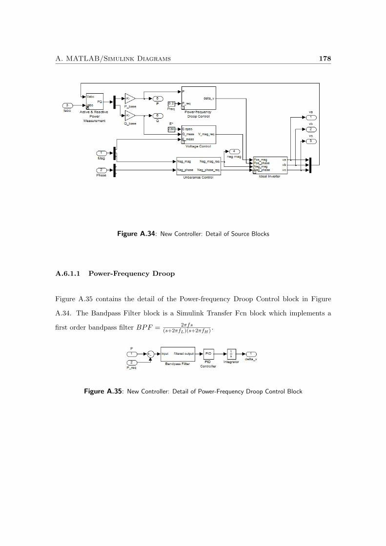
A. MATLAB/Simulink Diagrams 178
Figure A.34: New Controller: Detail of Source Blocks
A.6.1.1 Power-Frequency Droop
Figure A.35 contains the detail of the Power-frequency Droop Control block in Figure
A.34. The Bandpass Filter block is a Simulink Transfer Fcn block which implements a
first order bandpass filter BPF = 2πfs(s+2πfL)(s+2πfH) .
Figure A.35: New Controller: Detail of Power-Frequency Droop Control Block

A. MATLAB/Simulink Diagrams 179
A.6.1.2 Voltage Control
Figure A.36 shows the detail of the Voltage Control block in Figure A.34.
Figure A.36: New Controller: Detail of Voltage Control Block
A.6.1.3 Unbalance Control
Figure A.37 shows the detail of the Unbalance Control block in Figure A.34. Note that
the Gain block is not necessary (as it could be incorporated in the PI controller) and was
included for tuning purposes.
Figure A.37: New Controller: Detail of Unbalance Control Block
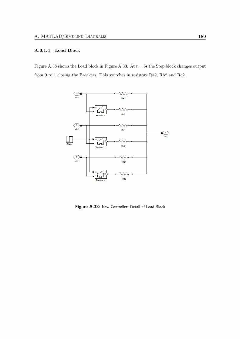
A. MATLAB/Simulink Diagrams 180
A.6.1.4 Load Block
Figure A.38 shows the Load block in Figure A.33. At t = 5s the Step block changes output
from 0 to 1 closing the Breakers. This switches in resistors Ra2, Rb2 and Rc2.
Figure A.38: New Controller: Detail of Load Block
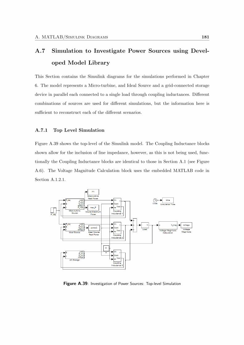
A. MATLAB/Simulink Diagrams 181
A.7 Simulation to Investigate Power Sources using Devel-
oped Model Library
This Section contains the Simulink diagrams for the simulations performed in Chapter
6. The model represents a Micro-turbine, and Ideal Source and a grid-connected storage
device in parallel each connected to a single load through coupling inductances. Different
combinations of sources are used for different simulations, but the information here is
sufficient to reconstruct each of the different scenarios.
A.7.1 Top Level Simulation
Figure A.39 shows the top-level of the Simulink model. The Coupling Inductance blocks
shown allow for the inclusion of line impedance, however, as this is not being used, func-
tionally the Coupling Inductance blocks are identical to those in Section A.1 (see Figure
A.6). The Voltage Magnitude Calculation block uses the embedded MATLAB code in
Section A.1.2.1.
Figure A.39: Investigation of Power Sources: Top-level Simulation
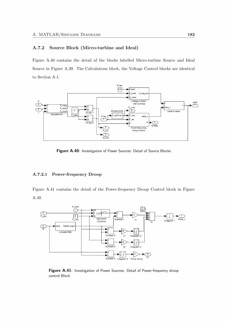
A. MATLAB/Simulink Diagrams 182
A.7.2 Source Block (Micro-turbine and Ideal)
Figure A.40 contains the detail of the blocks labelled Micro-turbine Source and Ideal
Source in Figure A.39. The Calculations block, the Voltage Control blocks are identical
to Section A.1.
Figure A.40: Investigation of Power Sources: Detail of Source Blocks
A.7.2.1 Power-frequency Droop
Figure A.41 contains the detail of the Power-frequency Droop Control block in Figure
A.40.
Figure A.41: Investigation of Power Sources: Detail of Power-frequency droop
control Block
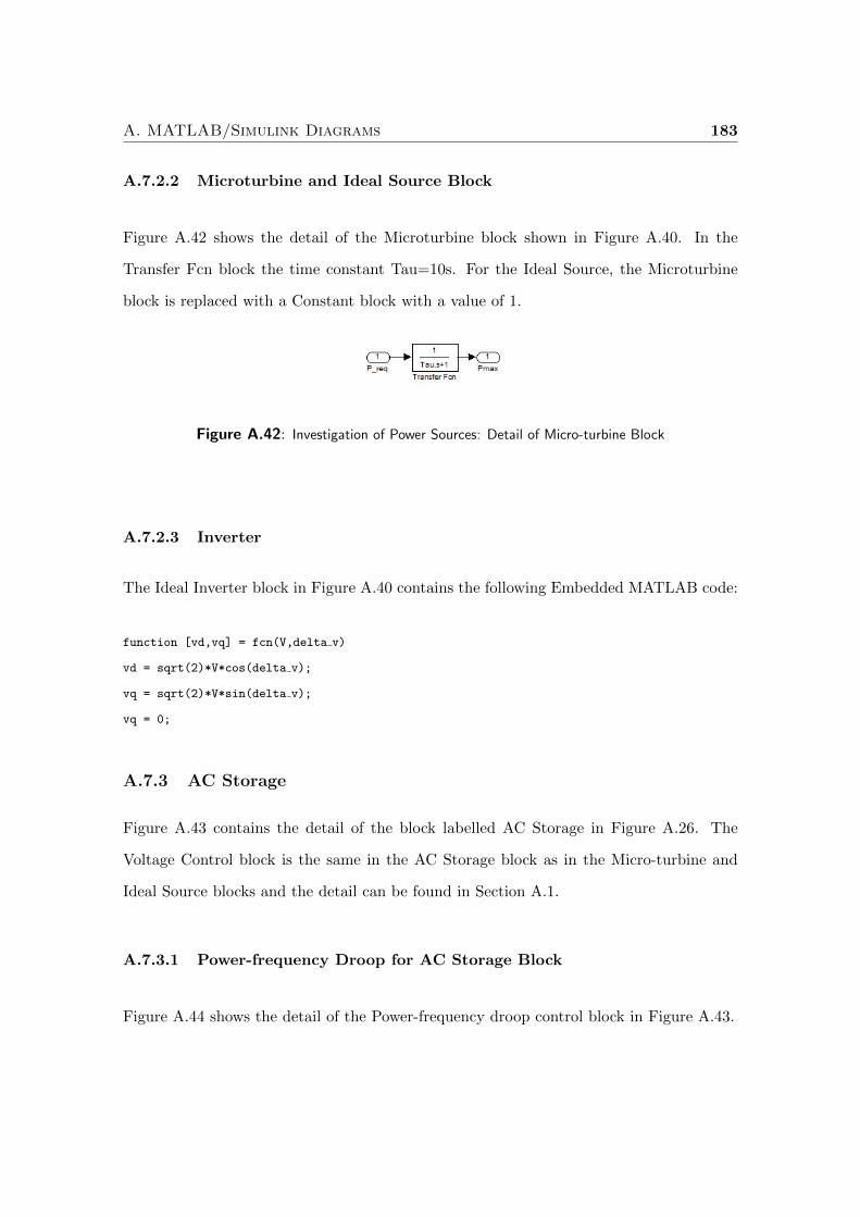
A. MATLAB/Simulink Diagrams 183
A.7.2.2 Microturbine and Ideal Source Block
Figure A.42 shows the detail of the Microturbine block shown in Figure A.40. In the
Transfer Fcn block the time constant Tau=10s. For the Ideal Source, the Microturbine
block is replaced with a Constant block with a value of 1.
Figure A.42: Investigation of Power Sources: Detail of Micro-turbine Block
A.7.2.3 Inverter
The Ideal Inverter block in Figure A.40 contains the following Embedded MATLAB code:
function [vd,vq] = fcn(V,delta v)
vd = sqrt(2)*V*cos(delta v);
vq = sqrt(2)*V*sin(delta v);
vq = 0;
A.7.3 AC Storage
Figure A.43 contains the detail of the block labelled AC Storage in Figure A.26. The
Voltage Control block is the same in the AC Storage block as in the Micro-turbine and
Ideal Source blocks and the detail can be found in Section A.1.
A.7.3.1 Power-frequency Droop for AC Storage Block
Figure A.44 shows the detail of the Power-frequency droop control block in Figure A.43.
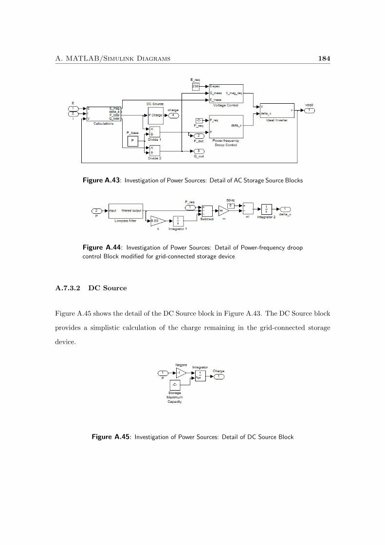
A. MATLAB/Simulink Diagrams 184
Figure A.43: Investigation of Power Sources: Detail of AC Storage Source Blocks
Figure A.44: Investigation of Power Sources: Detail of Power-frequency droop
control Block modified for grid-connected storage device
A.7.3.2 DC Source
Figure A.45 shows the detail of the DC Source block in Figure A.43. The DC Source block
provides a simplistic calculation of the charge remaining in the grid-connected storage
device.
Figure A.45: Investigation of Power Sources: Detail of DC Source Block
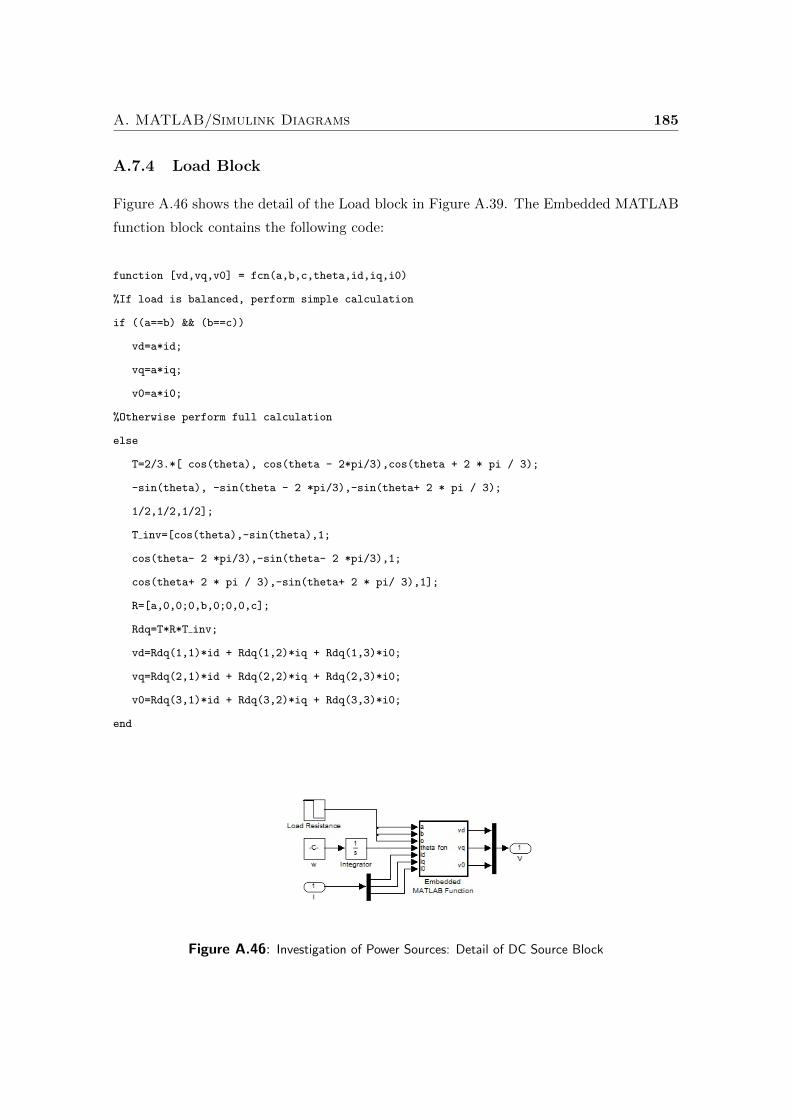
A. MATLAB/Simulink Diagrams 185
A.7.4 Load Block
Figure A.46 shows the detail of the Load block in Figure A.39. The Embedded MATLAB
function block contains the following code:
function [vd,vq,v0] = fcn(a,b,c,theta,id,iq,i0)
%If load is balanced, perform simple calculation
if ((a==b) && (b==c))
vd=a*id;
vq=a*iq;
v0=a*i0;
%Otherwise perform full calculation
else
T=2/3.*[ cos(theta), cos(theta - 2*pi/3),cos(theta + 2 * pi / 3);
-sin(theta), -sin(theta - 2 *pi/3),-sin(theta+ 2 * pi / 3);
1/2,1/2,1/2];
T inv=[cos(theta),-sin(theta),1;
cos(theta- 2 *pi/3),-sin(theta- 2 *pi/3),1;
cos(theta+ 2 * pi / 3),-sin(theta+ 2 * pi/ 3),1];
R=[a,0,0;0,b,0;0,0,c];
Rdq=T*R*T inv;
vd=Rdq(1,1)*id + Rdq(1,2)*iq + Rdq(1,3)*i0;
vq=Rdq(2,1)*id + Rdq(2,2)*iq + Rdq(2,3)*i0;
v0=Rdq(3,1)*id + Rdq(3,2)*iq + Rdq(3,3)*i0;
end
Figure A.46: Investigation of Power Sources: Detail of DC Source Block

Bibliography
[1] CSIRO Energy Centre information: http://www.csiro.au/multimedia/csiro-energy-
centre-video.html
[2] Engler, A.; Soultanis, N., “Droop control in LV-Grids,” Future Power Systems, 2005
International Conference on , vol., no.pp. 1- 6, 16-18 Nov. 2005
[3] Lasseter, R.; Piagi, P., “Providing premium power through distributed resources,”
System Sciences, 2000. Proceedings of the 33rd Annual Hawaii International Con-
ference on , vol., no.pp. 9 pp.-, 4-7 Jan. 2000
[4] Guerrero, J.M.; de Vicuna, L.G.; Matas, J.; Miret, J.; Cruz, J., “Steady-state in-
variant frequency and amplitude droop control using adaptive output impedance
for parallel-connected UPS inverters,” Applied Power Electronics Conference and
Exposition, 2005. APEC 2005. Twentieth Annual IEEE , vol.1, no.pp. 560- 566 Vol.
1, 6-10 March 2005
[5] Chandorkar, M.C.; Divan, D.M.; Adapa, R., “Control of parallel connected inverters
in standalone AC supply systems,” Industry Applications, IEEE Transactions on ,
vol.29, no.1pp.136-143, Jan/Feb 1993
[6] De Brabandere, K.; Bolsens, B.; Van den Keybus, J.; Woyte, A.; Driesen, J.; Bel-
mans, R.; Leuven, K.U., “A voltage and frequency droop control method for paral-
lel inverters,” Power Electronics Specialists Conference, 2004. PESC 04. 2004 IEEE
35th Annual , vol.4, no.pp. 2501- 2507 Vol.4, 2004
[7] Thomas Ackermann, Goran Andersson and Lennart Soder, “Distributed generation:
a definition”, Electric Power Systems Research, Volume 57, Issue 3, 20 April 2001,
Pages 195-204.
Bibliography 187
[8] Daly, P.A.; Morrison, J., “Understanding the potential benefits of distributed gen-
eration on power delivery systems,” Rural Electric Power Conference, 2001, vol.,
no.pp.A2/1-A213, 2001
[9] Puttgen, H.B.; MacGregor, P.R.; Lambert, F.C., “Distributed generation: Semantic
hype or the dawn of a new era?,” Power and Energy Magazine, IEEE, vol.1, no.1pp.
22- 29, Jan-Feb 2003
[10] Kumpulainen, L.K.; Kauhaniemi, K.T., “Analysis of the impact of distributed gen-
eration on automatic reclosing,” Power Systems Conference and Exposition, 2004.
IEEE PES, vol., no.pp. 603- 608 vol.1, 10-13 Oct. 2004
[11] Slootweg, J.G.; Kling, W.L., “Impacts of distributed generation on power system
transient stability,” Power Engineering Society Summer Meeting, 2002 IEEE , vol.2,
no.pp. 862- 867 vol.2, 2002
[12] Bhowmik, A.; Maitra, A.; Halpin, S.M.; Schatz, J.E., “Determination of allowable
penetration levels of distributed generation resources based on harmonic limit con-
siderations,” Power Delivery, IEEE Transactions on , vol.18, no.2pp. 619- 624, April
2003
[13] Vu Van Thong; Van Dommelen, D.; Belmans, R., “Penetration level of distributed
energy resources with anti-islanding criteria and secure operation of power system,”
Power Engineering Society General Meeting, 2006. IEEE , vol., no., pp. 7 pp.-, 18-22
June 2006
[14] Marnay, C.; Robio, F.J.; Siddiqui, A.S.; , “Shape of the microgrid,” Power Engi-
neering Society Winter Meeting, 2001. IEEE , vol.1, no., pp.150-153 vol.1, 28 Jan-1
Feb 2001
[15] Lasseter, R.H., “MicroGrids,” Power Engineering Society Winter Meeting, 2002.
IEEE , vol.1, no.pp. 305- 308 vol.1, 2002
Bibliography 188
[16] Danish Wind Industry Association website:
http://guidedtour.windpower.org/en/pictures/brush.htm
[17] O’Neill, W., “Remote photovoltaic, standalone systems,” Aerospace and Electronic
Systems Magazine, IEEE , vol.6, no.10, pp.15-19, Oct 1991
[18] Mendez, L.; Narvarte, L.; Marsinach, A.G.; Izquierdo, P.; Carrasco, L.M.; Eyras, R.,
“Centralized stand alone PV system in microgrid in Morocco,” Photovoltaic Energy
Conversion, 2003. Proceedings of 3rd World Conference on , vol.3, no., pp. 2326-2328
Vol.3, 12-16 May 2003
[19] Consortium for Electric Reliability Technology Solutions website:
http://certs.lbl.gov/
[20] Integration of Renewable Energy Sources and Distributed Generation into the Eu-
ropean Electricity Grid website: http://www.ired-cluster.org/
[21] Lasseter, R.; Piagi, P., “Control and Design of Microgrid Components” January
2006, Available at http://certs.lbl.gov/pdf/microgrid-control.pdf
[22] Lasseter, R.; Tomsovic, K.; Piagi, P., “Scenarios for Distributed Technology Appli-
cations with Steady State and Dynamic Models of Loads and Micro-Sources” April
2000, Available at: http://certs.lbl.gov/pdf/pserc-deri.pdf
[23] Nikkhajoei, H.; Lasseter, R.H.; , “Microgrid Protection,” Power Engineering Society
General Meeting, 2007. IEEE , vol., no., pp.1-6, 24-28 June 2007
[24] Marnay, C.; Venkataramanan, G.; Stadler, M.; Siddiqui, A.S.; Firestone, R.; Chan-
dran, B.; , “Optimal Technology Selection and Operation of Commercial-Building
Microgrids,” Power Systems, IEEE Transactions on , vol.23, no.3, pp.975-982, Aug.
2008
[25] Eto, J.; Lasseter, R.; Schenkman, B.; Stevens, J.; Klapp, D.; Volkommer, H.; Linton,
E.; Hurtado, H.; Roy, J.; , “Overview of the CERTS Microgrid laboratory Test Bed,”
Bibliography 189
Integration of Wide-Scale Renewable Resources Into the Power Delivery System,
2009 CIGRE/IEEE PES Joint Symposium , vol., no., pp.1-1, 29-31 July 2009
[26] ‘Microgrids’ Project website: http://www.microgrids.eu/micro2000/index.php
[27] ‘More Microgrids’ Project website: http://www.microgrids.eu/index.php
[28] Kariniotakis, G.N.; Soultanis, N.L.; Tsouchnikas, A.I.; Papathanasiou, S.A.;
Hatziargyriou, N.D., “Dynamic Modeling of MicroGrids,” Future Power Systems,
2005 International Conference on , vol., no.pp. 1- 7, 16-18 Nov. 2005
[29] Dimeas, A.L.; Hatziargyriou, N.D., “A MAS architecture for microgrids control,”
Intelligent Systems Application to Power Systems, 2005. Proceedings of the 13th
International Conference on , vol., no.pp. 5 pp.-, 6-10 Nov. 2005
[30] Hatziargyriou, N.D.; Dimeas, A.; Tsikalakis, A.G.; Pecas Lopes, J.A.; Kariniotakis,
G.; Oyarzabal, J., “Management of Microgrids in Market Environment,” Future
Power Systems, 2005 International Conference on , vol., no.pp. 1- 7, 16-18 Nov.
2005
[31] Pecas Lopes, J.A.; Moreira, C.L.; Madureira, A.G.; Resende, F.O.; Wu, X.;
Jayawarna, N.; Zhang, Y.; Jenkins, N.; Kanellos, F.; Hatziargyriou, N., “Control
Strategies for MicroGrids Emergency Operation,” Future Power Systems, 2005 In-
ternational Conference on , vol., no.pp. 1- 6, 16-18 Nov. 2005
[32] Matos, M.A.; Hatziargriou, N.D.; Pecas Lopes, J.A., “Multicontingency steady state
security evaluation using fuzzy clustering techniques,” Power Systems, IEEE Trans-
actions on , vol.15, no.1pp.177-183, Feb 2000
[33] Barnes, M.; Dimeas, A.; Engler, A.; Fitzer, C.; Hatziargyriou, N.; Jones, C.; Pap-
athanassiou, S.; Vandenbergh, M., “MicroGrid Laboratory Facilities,” Future Power
Systems, 2005 International Conference on , vol., no.pp. 1- 6, 16-18 Nov. 2005
Bibliography 190
[34] Georgakis, D.; Papathanassiou, S.; Hatziargyriou, N.; Engler, A.; Hardt, C., “Op-
eration of a prototype microgrid system based on micro-sources quipped with fast-
acting power electronics interfaces,” Power Electronics Specialists Conference, 2004.
PESC 04. 2004 IEEE 35th Annual , vol.4, no.pp. 2521- 2526 Vol.4, 2004
[35] Pudjianto, D.; Strbac, G.; van Overbeeke, F.; Androutsos, A.I.; Larrabe, Z.; Tome
Saraiva, J., “Investigation of Regulatory, Commercial, Economic and Environmental
Issues in MicroGrids,” Future Power Systems, 2005 International Conference on ,
vol., no.pp. 1- 6, 16-18 Nov. 2005
[36] Limei Zhang; Shaolin Wang; Yunjun Zhao; Wei Tang; , “Prospects for and Ap-
plications to Microgrid Technology,” Power and Energy Engineering Conference
(APPEEC), 2010 Asia-Pacific , vol., no.,
[37] Lasseter, B.; , “Microgrids [distributed power generation],” Power Engineering So-
ciety Winter Meeting, 2001. IEEE , vol.1, no., pp.146-149 vol.1, 28 Jan-1 Feb 2001
[38] Sortomme, E.; Mapes, G.J.; Foster, B.A.; Venkata, S.S.; , “Fault analysis and pro-
tection of a microgrid,” Power Symposium, 2008. NAPS ’08. 40th North American
, vol., no., pp.1-6, 28-30 Sept. 2008
[39] Asano, H.; Bando, S.; , “Load fluctuation analysis of commercial and residential
customers for operation planning of a hybrid photovoltaic and cogeneration system,”
Power Engineering Society General Meeting, 2006. IEEE , vol., no., pp.6 pp., 0-0 0
[40] Amjady, N.; Keynia, F.; Zareipour, H.; , “Short-Term Load Forecast of Microgrids
by a New Bilevel Prediction Strategy,” Smart Grid, IEEE Transactions on , vol.PP,
no.99, pp.1-1
[41] Chiradeja, P.; , “Benefit of Distributed Generation: A Line Loss Reduction Anal-
ysis,” Transmission and Distribution Conference and Exhibition: Asia and Pacific,
2005 IEEE/PES , vol., no., pp.1-5, 2005
Bibliography 191
[42] Kroposki, B.; Pink, C.; Lynch, J.; John, V.; Daniel, S.M.; Benedict, E.; Vihinen, I.;
, “Development of a High-Speed Static Switch for Distributed Energy and Microgrid
Applications,” Power Conversion Conference - Nagoya, 2007. PCC ’07 , vol., no.,
pp.1418-1423, 2-5 April 2007
[43] Meliopoulos, A.P.S., “Challenges in simulation and design of /spl mu/Grids,” Power
Engineering Society Winter Meeting, 2002. IEEE , vol.1, no.pp. 309- 314 vol.1, 2002
[44] Meliopoulos, A.P.S.; Cokkinides, G.J.; Lasseter, R., “A multiphase power flow model
for /spl mu/grid analysis,” System Sciences, 2003. Proceedings of the 36th Annual
Hawaii International Conference on , vol., no., pp. 7 pp.-, 6-9 Jan. 2003
[45] Shiqiong Tong; Miu, K.N., “A network-based distributed slack bus model for DGs
in unbalanced power flow studies,” Power Systems, IEEE Transactions on , vol.20,
no.2, pp. 835-842, May 2005
[46] Slootweg, J.G.; Polinder, H.; Kling, W.L., “Dynamic modelling of a wind turbine
with doubly fed induction generator,” Power Engineering Society Summer Meeting,
2001. IEEE , vol.1, no.pp.644-649 vol.1, 2001
[47] Chellapilla, S.R.; Chowdhury, B.H., “A dynamic model of induction generators for
wind power studies,” Power Engineering Society General Meeting, 2003, IEEE ,
vol.4, no.pp.- 2344 Vol. 4, 13-17 July 2003
[48] Nakanishi, F.; Ikegami, T.; Ebihara, K.; Kuriyama, S.; Shiota, Y., “Modeling and
operation of a 10 kW photovoltaic power generator using equivalent electric cir-
cuit method,” Photovoltaic Specialists Conference, 2000. Conference Record of the
Twenty-Eighth IEEE , vol., no.pp.1703-1706, 2000
[49] Ching-Tsan Chiang; Tung-Sheng Chiang; Hou-Sheng Huang, “Modeling a photo-
voltaic power system by CMAC-GBF,” Photovoltaic Energy Conversion, 2003. Pro-
ceedings of 3rd World Conference on , vol.3, no.pp. 2431- 2434 Vol.3, 12-16 May
2003
Bibliography 192
[50] Gow, J.A.; Manning, C.D., “Development of a photovoltaic array model for
use in power-electronics simulation studies,” Electric Power Applications, IEE
Proceedings- , vol.146, no.2pp.193-200, Mar 1999
[51] Miao, Z.; Choudhry, M.A.; Klein, R.L.; Fan, L., “Study of a fuel cell power plant in
power distribution system. Part I. Dynamic ,” Power Engineering Society General
Meeting, 2004. IEEE , vol., no.pp. 2220- 2225 Vol.2, 6-10 June 2004
[52] Zoka, Y.; Sasaki, H.; Yorino, N.; Kawahara, K.; Liu, C.C., “An interaction problem
of distributed generators installed in a MicroGrid,” Electric Utility Deregulation,
Restructuring and Power Technologies, 2004. (DRPT 2004). Proceedings of the 2004
IEEE International Conference on , vol.2, no.pp. 795- 799 Vol.2, 5-8 April 2004
[53] Bialasiewicz, J.T.; Muljadi, E., “Analysis of Renewable-Energy Systems Using RPM-
SIM Simulator,” Industrial Electronics, IEEE Transactions on , vol.53, no.4pp. 1137-
1143, June 2006
[54] Coelho, E.A.A.; Cortizo, P.C.; Garcia, P.F.D.; , “Small signal stability for single
phase inverter connected to stiff AC system,” Industry Applications Conference,
1999. Thirty-Fourth IAS Annual Meeting. Conference Record of the 1999 IEEE ,
vol.4, no., pp.2180-2187 vol.4, 1999
[55] Tuladhar, A.; Hua Jin; Unger, T.; Mauch, K., “Control of parallel inverters in
distributed AC power systems with consideration of line impedance effect,” Industry
Applications, IEEE Transactions on , vol.36, no.1, pp.131-138, Jan/Feb 2000
[56] Hernandez-Aramburo, C.A.; Green, T.C.; Mugniot, N., “Fuel consumption mini-
mization of a microgrid,” Industry Applications, IEEE Transactions on , vol.41,
no.3pp. 673- 681, May-June 2005
[57] Mihalache, L.; , “Paralleling control technique with no intercommunication signals
for resonant controller-based inverters,” Industry Applications Conference, 2003.
Bibliography 193
38th IAS Annual Meeting. Conference Record of the , vol.3, no., pp. 1882- 1889
vol.3, 12-16 Oct. 2003
[58] Tzung-Lin Lee; Po-Tai Cheng, “Design of a new cooperative harmonic filtering strat-
egy for the distributed generation systems,” Industry Applications Conference, 2005.
Fourtieth IAS Annual Meeting. Conference Record of the 2005 , vol.1, no.pp. 549-
556 Vol. 1, 2-6 Oct. 2005
[59] Kuang Li; Jinjun Liu; Biao Wei; Zhaoan Wang, “Comparison of two control ap-
proaches of static VAr generators for compensating source voltage unbalance in
three-phase three-wire systems,” Power Electronics and Motion Control Conference,
2004. IPEMC 2004. The 4th International , vol.3, no., pp. 1213-1218 Vol.3, 14-16
Aug. 2004
[60] Moran, L.; Werlinger, P.; Dixon, J.; Wallace, R., “A series active power filter which
compensates current harmonics and voltage unbalance simultaneously,” Power Elec-
tronics Specialists Conference, 1995. PESC ’95 Record., 26th Annual IEEE , vol.1,
no., pp.222-227 vol.1, 18-22 Jun 1995
[61] Sanghoon Lee; Jaesig Kim; Jaeho Choi, “A new control algorithm for instantaneous
voltage sag corrector using series compensator,” Power Electronics and Drive Sys-
tems, 2001. Proceedings., 2001 4th IEEE International Conference on , vol.2, no.,
pp. 789-795 vol.2, 22-25 Oct. 2001
[62] Escobar, G.; Stankovic, A.M.; Cardenas, V.; Mattavelli, P.; , “An adaptive con-
troller for a series active filter to compensate voltage sags, unbalance and harmonic
distortion,” Power Electronics Congress, 2002. Technical Proceedings. CIEP 2002.
VIII IEEE International , vol., no., pp. 275- 280, 20-24 Oct. 2002
[63] Vechiu I; Camblong, H.; Tapia, G.; Curea, O.; Dakyo, B., “Modelling and control
of four-wire voltage source inverter under unbalanced voltage condition for hybrid
power system applications,” Power Electronics and Applications, 2005 European
Conference on , vol., no., pp. 10 pp.-, 11-14 Sept. 2005

Bibliography 194
[64] Jun-Koo Kang; Seung-Ki Sul, “Control of unbalanced voltage PWM converter us-
ing instantaneous ripple power feedback,” Power Electronics Specialists Conference,
1997. PESC ’97 Record., 28th Annual IEEE , vol.1, no., pp.503-508 vol.1, 22-27 Jun
1997
[65] In-Won Joo; Hong-Seok Song; Kwanghee Nam, “Source-voltage-sensorless scheme
for PWM rectifier under voltage unbalance condition,” Power Electronics and Drive
Systems, 2001. Proceedings., 2001 4th IEEE International Conference on , vol.1, no.,
pp. 33-38 vol.1, 22-25 Oct. 2001
[66] Yun Wei Li; Vilathgamuwa, D.M.; Poh Chiang Loh, “A grid-interfacing power qual-
ity compensator for three-phase three-wire microgrid applications,” Power Electron-
ics, IEEE Transactions on , vol.21, no.4, pp. 1021-1031, July 2006
[67] Po-Tai Cheng; Chien-An Chen; Tzung-Lin Lee; Shen-Yuan Kuo; , “A Cooperative
Imbalance Compensation Method for Distributed-Generation Interface Converters,”
Industry Applications, IEEE Transactions on , vol.45, no.2, pp.805-815, March-april
2009
[68] Jayawarna, N.; Barnes, M.; Jones, C.; Jenkins, N.; , “Operating MicroGrid Energy
Storage Control during Network Faults,” System of Systems Engineering, 2007. SoSE
’07. IEEE International Conference on , vol., no., pp.1-7, 16-18 April 2007
[69] Katiraei, F.; Iravani, M.R.; Lehn, P.W., “Micro-grid autonomous operation during
and subsequent to islanding process,” Power Delivery, IEEE Transactions on , vol.20,
no.1pp. 248- 257, Jan. 2005
[70] Davis, M.W., “Mini gas turbines and high speed generators a preferred choice for
serving large commercial customers and microgrids. I. Generating system,” Power
Engineering Society Summer Meeting, 2002 IEEE , vol.2, no.pp. 669- 676 vol.2, 2002
Bibliography 195
[71] Audring, D.; Balzer, G., “Operating stationary fuel cells on power system and mi-
crogrids,” Power Tech Conference Proceedings, 2003 IEEE Bologna , vol.4, no.pp. 6
pp. Vol.4-, 23-26 June 2003
[72] Nehrir, M.H.; Lameres, B.J.; Venkataramanan, G.; Gerez, V.; Alvarado, L.A., “An
approach to evaluate the general performance of stand-alone wind/photovoltaic gen-
erating systems,” Energy Conversion, IEEE Transactions on , vol.15, no.4pp.433-
439, Dec 2000
[73] Venkataramanan, G.; Illindala, M., “Microgrids and sensitive loads,” Power Engi-
neering Society Winter Meeting, 2002. IEEE , vol.1, no.pp. 315- 322 vol.1, 2002
[74] Yun Zhong; Jiancheng Zhang; Gengyin Li; Aiguo Liu, “Research on Energy Effi-
ciency of Supercapacitor Energy Storage System,” Power System Technology, 2006.
PowerCon 2006. International Conference on , vol., no., pp.1-4, Oct. 2006
[75] Boyes, J.D.; Clark, N.H., “Technologies for energy storage. Flywheels and super
conducting magnetic energy storage,” Power Engineering Society Summer Meeting,
2000. IEEE , vol.3, no., pp.1548-1550 vol. 3, 2000
[76] Coombs, T.; Campbell, A.M.; Storey, R.; Weller, R., “Superconducting magnetic
bearings for energy storage flywheels,” Applied Superconductivity, IEEE Transac-
tions on , vol.9, no.2, pp.968-971, Jun 1999
[77] Parniani, M.; Nasri, A., “SCADA Based Under Frequency Load Shedding Integrated
with Rate of Frequency Decline,” Power Engineering Society General Meeting, 2006.
IEEE , vol., no.pp. 1- 6, 18-22 June 2006
[78] Moors, C.; Lefebvre, D.; Van Cutsem, T., “Design of load shedding schemes against
voltage instability,” Power Engineering Society Winter Meeting, 2000. IEEE , vol.2,
no.pp.1495-1500 vol.2, 2000
Bibliography 196
[79] Thompson, J.G.; Fox, B., “Adaptive load shedding for isolated power systems,”
Generation, Transmission and Distribution, IEE Proceedings- , vol.141, no.5pp.491-
496, Sep 1994
[80] Al-Nasseri, H.; Redfern, M.A.; O’Gorman, R., “Protecting micro-grid systems con-
taining solid-state converter generation,” Future Power Systems, 2005 International
Conference on , vol., no.pp. 5 pp.-, 16-18 Nov. 2005
[81] Lasseter, R.; Tomsovic, K.; Piagi, P., “Scenarios for Distributed Technology Appli-
cations with Steady State and Dynamic Models of Loads and Micro-Sources” April
2000, Available at: http://certs.lbl.gov/pdf/pserc-deri.pdf
[82] Lasseter, R.; Piagi, P., “Providing premium power through distributed resources,”
System Sciences, 2000. Proceedings of the 33rd Annual Hawaii International Con-
ference on , vol., no.pp. 9 pp.-, 4-7 Jan. 2000
[83] Krause, P.C.; Wasynczuk, O; Sudhoff, S.D., “Analysis of Electric Machinery and
Drive Systems Second Edition” Wiley-Interscience 2002
[84] Lasseter, R.; Piagi, P., “Providing premium power through distributed resources,”
System Sciences, 2000. Proceedings of the 33rd Annual Hawaii International Con-
ference on , vol., no.pp. 9 pp.-, 4-7 Jan. 2000
[85] Chandorkar, M.C.; Divan, D.M.; Adapa, R., “Control of parallel connected inverters
in standalone AC supply systems,” Industry Applications, IEEE Transactions on ,
vol.29, no.1pp.136-143, Jan/Feb 1993
[86] Nikkhajoei, H.; Lasseter, R.H.; , “Distributed Generation Interface to the CERTS
Microgrid,” Power Delivery, IEEE Transactions on , vol.24, no.3, pp.1598-1608, July
2009
[87] Enslin, J.H.R.; Heskes, P.J.M., “Harmonic interaction between a large number of
distributed power inverters and the distribution network,” Power Electronics, IEEE
Transactions on , vol.19, no.6, pp. 1586-1593, Nov. 2004
Bibliography 197
[88] Woll, R. F., “Effect of Unbalanced Voltage on the Operation of Polyphase Induction
Motors,” Industry Applications, IEEE Transactions on , vol.IA-11, no.1, pp.38-42,
Jan. 1975
[89] von Jouanne, A.; Banerjee, B., “Assessment of voltage unbalance,” Power Delivery,
IEEE Transactions on , vol.16, no.4, pp.782-790, Oct 2001
[90] Australian Energy Market Commission, “National Electricity Rules
Version 51, Chapter 5, Table S5.1a.1” August 2012, Available at
http://aemc.gov.au/Electricity/National-Electricity-Rules/Current-Rules.html
[91] Guerrero, J.M.; de Vicuna, L.G.; Matas, J.; Miret, J.; Cruz, J., “Steady-state in-
variant frequency and amplitude droop control using adaptive output impedance
for parallel-connected UPS inverters,” Applied Power Electronics Conference and
Exposition, 2005. APEC 2005. Twentieth Annual IEEE , vol.1, no.pp. 560- 566 Vol.
1, 6-10 March 2005
[92] Sao, C.K.; Lehn, P.W., “Autonomous load sharing of voltage source converters,”
Power Delivery, IEEE Transactions on , vol.20, no.2pp. 1009- 1016, April 2005
[93] Guerrero, J.M.; Matas, J.; de Vicuna, L.G.; Castilla, M.; Miret, J., “Wireless-
Control Strategy for Parallel Operation of Distributed-Generation Inverters,” In-
dustrial Electronics, IEEE Transactions on , vol.53, no.5, pp.1461-1470, Oct. 2006
[94] Tzung-Lin Lee; Po-Tai Cheng, “Design of a new cooperative harmonic filtering strat-
egy for the distributed generation systems,” Industry Applications Conference, 2005.
Fourtieth IAS Annual Meeting. Conference Record of the 2005 , vol.1, no.pp. 549-
556 Vol. 1, 2-6 Oct. 2005
[95] Campos, A.; Joos, G.; Ziogas, P.D.; Lindsay, J.F.;, “Analysis and design of a series
voltage unbalance compensator based on a three-phase VSI operating with unbal-
anced switching functions,” Power Electronics, IEEE Transactions on, vol.9, no.3,
pp.269-274, May 1994
Bibliography 198
[96] Vincenti, D.; Ziogas, P.D.; Patel, R.V.; , “An analysis and design of a force commu-
tated three-phase PWM AC controller with input unbalance correction capability,”
Applied Power Electronics Conference and Exposition, 1992. APEC ’92. Conference
Proceedings 1992., Seventh Annual , vol., no., pp.487-493, 23-27 Feb 1992
[97] Zhang, R.; Boroyevich, D.; Prasad, V.H.; Mao, H.-C.; Lee, F.C.; Dubovsky, S.; , “A
three-phase inverter with a neutral leg with space vector modulation,” Applied Power
Electronics Conference and Exposition, 1997. APEC ’97 Conference Proceedings
1997., Twelfth Annual , vol.2, no., pp.857-863 vol.2, 23-27 Feb 1997
[98] Yun Wei Li; Vilathgamuwa, D.M.; Poh Chiang Loh., “A grid-interfacing power
quality compensator for three-phase three-wire microgrid applications”, Power Elec-
tronics, IEEE Transactions on, Vol.21, Iss.4, July 2006 Pages: 1021- 1031
[99] Watanabe, E.H.; Aredes, M.; Afonso, J.L.; Pinto, J.G.; Monteiro, L.F.C.; Akagi,
H.; , “Instantaneous p-q power theory for control of compensators in micro-grids,
”,Nonsinusoidal Currents and Compensation (ISNCC), 2010 International School on
, vol., no., pp.17-26, 15-18 June 2010
[100] Griffiths, M.; Coates, C.; , “Behaviour of microgrids in the presence of unbalanced
loads,” Power Engineering Conference, 2007. AUPEC 2007. Australasian Universi-
ties , vol., no., pp.1-5, 9-12 Dec. 2007
[101] Hojo, M.; Iwase, Y.; Funabashi, T.; Ueda, Y.; , “A method of three-phase balanc-
ing in microgrid by photovoltaic generation systems”,Power Electronics and Motion
Control Conference, 2008. EPE-PEMC 2008. 13th , vol., no., pp.2487-2491, 1-3 Sept.
2008
[102] Mihalache, L.; , “Paralleling control technique with no intercommunication sig-
nals for resonant controller-based inverters,”Industry Applications Conference, 2003.
38th IAS Annual Meeting. Conference Record of the , vol.3, no., pp. 1882- 1889 vol.3,
12-16 Oct. 2003
Bibliography 199
[103] Al-Hinai, A.; Feliachi, A.; , “Microturbines load following controller design in dereg-
ulated power distribution systems,” Power and Energy Society General Meeting -
Conversion and Delivery of Electrical Energy in the 21st Century, 2008 IEEE , vol.,
no., pp.1-6, 20-24 July 2008
[104] Zhou Yunhai; Stenzel, J.; , “Simulation of a Microturbine Generation System for
Grid Connected and Islanding Operations,” Power and Energy Engineering Confer-
ence, 2009. APPEEC 2009. Asia-Pacific , vol., no., pp.1-5, 27-31 March 2009
Related Publications
Griffiths, M.; Coates, C.; , “Modelling and Performance of Low Voltage Distributed Gen-
eration Systems,” Power Engineering Conference, 2006. AUPEC 2006. Australasian Uni-
versities, vol., no., pp., 10-13 Dec. 2006
Griffiths, M.; Coates, C.; , “Behaviour of microgrids in the presence of unbalanced loads,”
Power Engineering Conference, 2007. AUPEC 2007. Australasian Universities , vol., no.,
pp.1-5, 9-12 Dec. 2007