Modeling solutions and simulations for advanced III-V ...
162
Rochester Institute of Technology Rochester Institute of Technology RIT Scholar Works RIT Scholar Works Theses 12-1-2008 Modeling solutions and simulations for advanced III-V Modeling solutions and simulations for advanced III-V photovoltaics based on nanostructures photovoltaics based on nanostructures Ryan Aguinaldo Follow this and additional works at: https://scholarworks.rit.edu/theses Recommended Citation Recommended Citation Aguinaldo, Ryan, "Modeling solutions and simulations for advanced III-V photovoltaics based on nanostructures" (2008). Thesis. Rochester Institute of Technology. Accessed from This Thesis is brought to you for free and open access by RIT Scholar Works. It has been accepted for inclusion in Theses by an authorized administrator of RIT Scholar Works. For more information, please contact [email protected].
-
Upload
khangminh22 -
Category
Documents
-
view
0 -
download
0
Transcript of Modeling solutions and simulations for advanced III-V ...

Rochester Institute of Technology Rochester Institute of Technology
RIT Scholar Works RIT Scholar Works
Theses
12-1-2008
Modeling solutions and simulations for advanced III-V Modeling solutions and simulations for advanced III-V
photovoltaics based on nanostructures photovoltaics based on nanostructures
Ryan Aguinaldo
Follow this and additional works at: https://scholarworks.rit.edu/theses
Recommended Citation Recommended Citation Aguinaldo, Ryan, "Modeling solutions and simulations for advanced III-V photovoltaics based on nanostructures" (2008). Thesis. Rochester Institute of Technology. Accessed from
This Thesis is brought to you for free and open access by RIT Scholar Works. It has been accepted for inclusion in Theses by an authorized administrator of RIT Scholar Works. For more information, please contact [email protected].
i
Modeling Solutions and Simulations for
Advanced III-V Photovoltaics Based on Nanostructures
by
Ryan Aguinaldo
A Thesis Submitted
in Partial Fulfillment
of the Requirements for the Degree of
Master of Science
in
Materials Science & Engineering
Approved by:
Prof. ________________________________________
Dr. Ryne P. Raffaelle (Thesis Co-Advisor)
Prof. ________________________________________
Dr. Seth M. Hubbard (Thesis Co-Advisor)
Prof. ________________________________________
Dr. Sean L. Rommel (Thesis Committee Member)
Center for Materials Science & Engineering
College of Science
Rochester Institute of Technology
Rochester, NY
December 2008

ii
Modeling Solutions and Simulations for
Advanced III-V Photovoltaics Based on Nanostructures
by
Ryan Aguinaldo
I, Ryan Aguinaldo, hereby grant permission to the Wallace Memorial Library of the
Rochester Institute of Technology to reproduce this document in whole or in part that any
reproduction will not be for commercial use or profit
____________________________
Ryan Aguinaldo

iii
To Mimi and Mom, loving mothers.
Grandpa and grandma too.

iv
Acknowledgements
First and foremost I must acknowledge my advisors Dr. Seth Hubbard and Dr. Ryne
Raffaelle for their support and guidance over the past couple of years. Dr. Hubbard has been
especially helpful in providing advice regarding the directions that this work has gone. I am
also extremely grateful to the other member of my thesis committee, Dr. Sean Rommel.
Dr. Rommel has been a wonderful source of guidance and assistance throughout both my
undergraduate and graduate experiences.
I would also like to thank Dr. Cory Cress for always seeming more than willing to
lend a helping hand wherever possible as well as Mr. Christopher Bailey for our many
illuminating discussions and also for the many journal articles he has randomly brought to
my attention. I also express gratitude to Dr. John Andersen and Dr. Christopher Collison for
their assistance in academic matters and for the interactions I have had with them.
The numerical computations performed in this work could not have been possible
without the resources provided by the Department of Research Computing. Additional work
was performed at the computing facilities in the Center for Microelectronic and Computer
Engineering. Device simulations were made possible by the donation of the Silvaco tools by
Simucad Design Automation to the Department of Microelectronic Engineering.
This work has been partially supported by the United States Department of Energy,
Solar Energy Technologies Program (Grant #DE-FG3608GO18012) and other government
agencies.

v
Abstract
It is the purpose of the work to develop methods for and present on the computational
analyses of advanced III-V photovoltaic devices and their enhancement by the incorporation
of semiconductor nanostructures. Such devices are currently being fabricated as part of the
research efforts at the Nanopower Research Laboratories; therefore, this work aims to
supplement and ground the experimental undertakings with a strong theoretical basis. This is
accomplished by numerical calculations based on the detailed balance model and by physics-
based device simulation. The specific materials focus of this work is on the enhancement of
the GaAs solar cell. The aforementioned methodologies are applied to this device and to
distinct enhancement schemes.
The detailed balance formalism is applied to the single-junction solar cell as an
introduction leading up to the triple-junction device. A thorough analysis shows how the
InGaP-GaAs-Ge triple-junction solar cell may be enhanced by the incorporation of
nanostructures. The intermediate band solar cell is introduced as it may be realized by the
coupling of a nanostructured array. The detailed balance analysis of this device is performed
using the usual blackbody spectrum as well as the more realistic scenarios of illumination by
the AM0 and AM1.5 solar spectra. Current research endeavors into placing an InAs quantum
dot array in a GaAs solar cell are put into the context of these calculations. It is determined
that, although the InAs/GaAs system is not ideal, it does exhibit a significant enhancement in
performance over the standard single-junction device.
The evaluation of a commercially available, physics-based, device simulation
software package for use in advanced photovoltaics analysis is also performed. The
application of this tool on the single-junction GaAs solar cell indicates that the current design
used in experimental work is optimized. Recommendations are made, however, in the
optimized design of the InGaP-GaAs dual-junction cell. The device simulator is shown to
exhibit difficulties in evaluating the complete operation of advanced solar devices; however,
the software is used to compute fundamental quantum mechanical variables in a
nanostructured solar cell.

vi
Table of Contents
Acknowledgements ……………………………………………………………………. iv
Abstract …………………………………………………………………………………. v
Chapter 1 Introduction …………………………………………………………… 1
1.1 Motivation …………………………………………………………….. 1
1.2 Organization of This Work …………………………………………… 2
1.3 Solar Cell Fundamentals ……………………………………………… 3
1.4 Nanostructures ………………………………………………………. 10
Chapter 2 Detailed Balance Models ……………………………………………. 14
2.1 General Theory ……………………………………………………… 14
2.2 Single-Junction Solar Cell …………………………………………... 20
2.3 Triple-Junction Solar Cell …………………………………………… 27
2.4 Intermediate Band Solar Cell ………………………………………... 33
Chapter 3 Device Simulations with Silvaco ATLAS …………………………... 43
3.1 Basic Equations ……………………………………………………… 43
3.2 Carrier Statistics ……………………………………………………... 44
3.3 Finite Element Analysis ……………………………………………... 46
3.4 Additional Models …………………………………………………... 47
3.5 Shockley-Read-Hall Recombination ………………………………... 48
3.6 Surface Recombination ……………………………………………… 49
3.7 Radiative Recombination ……………………………………………. 51
3.8 Thermionic Emission ………………………………………………... 52
3.9 Luminous Module …………………………………………………… 54
3.10 Fresnel Coefficients …………………………………………………. 55
3.11 Photogeneration ……………………………………………………... 57
3.12 Quantum Effects …………………………………………………….. 58
3.13 Spontaneous Emission ………………………………………………. 60
3.14 Band-to-Band Tunneling ……………………………………………. 62
3.15 Material Parameters …………………………………………………. 63
3.16 General Simulation Methodology …………………………………… 65

vii
3.17 Unoptimized Single-Junction Cell …………………………………... 67
3.18 Optimized Single-Junction Cell ……………………………………... 71
3.19 Dual-Junction Solar Cell …………………………………………….. 79
3.20 Nanostructured Device ………………………………………………. 89
Chapter 4 Conclusion …………………………………………………………... 95
Appendix I Justification of the Effective Mass Schrödinger Equation ………… . 101
Appendix II Bandstructure Calculations with a Kronig-Penney–Like Model ….. . 104
Appendix III Bandstructure Calculations (MATLAB Code) .…………………… . 111
Appendix IV Detailed Balance Model for a Single-Junction Solar Cell
(MATLAB Code) .………………………………………………… . 114
Appendix V Detailed Balance Model for a Triple-Junction Solar Cell
(MATLAB Code) .………………………………………………… . 117
Appendix VI Detailed Balance Model for an Intermediate Band Solar Cell
(MATLAB Code) .………………………………………………… . 124
Appendix VII Single-Junction Solar Cell Device Model (ATLAS Code) ……….. . 132
Appendix VIII Dual-Junction Solar Cell Device Model (ATLAS Code) …………. . 140
Appendix IX Nanostructured Solar Cell Device Model (ATLAS Code) ………... . 146
References …………………………………………………………………………… . 151

viii

1
Chapter 1
Introduction
1.1 – Motivation
Solar power has become a topic of great focus in the past several years as the
necessity for alternative energy schemes have become increasingly important. Recent reports
indicate the global energy consumption to grow from 13 TW-yr currently to as high as
30 TW-yr by the year 2050 [1]. Indeed, nations around the world are quickly accepting the
reality of dwindling fossil fuel reserves as well as the reality of global climate change [2, 3].
With approximately 125 PW of solar power striking the Earth at any one time, photovoltaic
energy conversion easily lends itself as being a logical approach for the world’s energy
needs. The aerospace industry also has a vested interest in solar power since it represents a
free and readily available source of energy for space applications. Approximately 20-30 % of
the total mass and cost of present Earth-orbiting satellites is due to their electric power
systems. Improved photovoltaic technology can clearly decrease these figures.
Part of the current research efforts at the Nanopower Research Laboratories focuses
on the enhancement of photovoltaic conversion efficiency by the use of low-dimensional
nanostructures. Specific to this work, the incorporation of quantum dots in an otherwise
conventional III-V photovoltaic device has been proposed as a viable method to increase
conversion efficiency [4, 5]. Direct bandgap III-V materials are chosen because they
represent the current state-of-the-art in high efficiency photovoltaics [6] and thus may lead
the way for the jump from efficiencies barely breaking 20 % for the best commercial silicon
cells today to efficiency percentages in the 40’s and 50’s as promised by the so-called third

2
generation photovoltaics [7, 8]. Additionally, for space applications, III-V materials and
devices have shown an affinity towards increased radiation tolerance [9].
Proper design and fabrication of novel nanostructured photovoltaic devices requires
keen knowledge of the underlying physics governing solar cell performance. Fabrication runs
are costly and time consuming, so it is beneficial to have a firm theoretical foundation on
which to base future work. Therefore, it is the purpose of this work to develop and present
methodologies by which novel devices may be computationally analyzed and simulated.
Routines are developed to ascertain the limiting performance of novel devices based on
detailed balance considerations. Additionally, the use of a commercial device simulator is
evaluated for the ability to model devices that are currently being fabricated or are planned to
be fabricated. Such analyses provides for an avenue to supplement experimental work in the
analysis of nanostructured solar cells.
1.2 – Organization of this Work
The remainder of this chapter gives a brief introduction to the fundamental principles
of solar cell device physics necessary to make this work self-contained. A brief discussion on
nanostructures and the pertinent physics is also included. This serves as a logical segue into
Chapter 2 where the detailed balance analysis of photovoltaic conversion efficiency is
introduced. This theory is used to further elaborate on solar cell fundamentals. The theory is
then applied to the analysis of multi-junction and intermediate band solar cells. The routines
used for this analysis were written in the MATLAB language and are contained in the
Appendix.

3
Chapter 3 evaluates the ability to use the commercially-available Silvaco ATLAS
software packing for the physics-based device simulation of novel solar cells. The GaAs
single-junction cell and the InGaP-GaAs tandem cell are the focus of this analysis.
Additionally, the use of InAs quantum confined regions is explored. An overview of the
pertinent device models that were invoked for the device simulations is given. This should
allow the reader rapid assimilation into the methodology followed in this work. Pertinent
code, written with the ATLAS syntax, is provided in the Appendix.
Chapter 4 gives concluding remarks and summary as well as recommendations for
future endeavors to extend this work. Conversational knowledge of device physics [10], solar
cell operation [11], quantum mechanics [12], and the physics of the solid state is assumed
[13]; knowledge of thermodynamics [14] is beneficial although not absolutely necessary.
1.3 – Solar Cell Fundamentals
The classic design of a solar cell, or photovoltaic device, is by the use of inorganic
semiconductor materials. In this sense, the photovoltaic device is essentially a glorified p-n
junction diode. The p-n junction is realized by bringing a p-type semiconductor into intimate
contact with an n-type semiconductor. From an energy band perspective, the Fermi levels on
either side of the junction must equilibrate assuming no external applied bias. This gives rise
to the well-known contact, or built-in, potential that causes bending of the conduction and
valence bands in the vicinity of the metallurgical junction. The spatial extent of over which
this band bending occurs is the so-called space charge, or depletion, region. The energy band
diagram of this situation under zero applied bias is displayed in Fig. 1.a.

4
V
I
V
I
Ec
Ev
EF
a) b)
Fig. 1. a) Energy band diagram of the standard p-n junction at equilibrium. b) Current-voltage relation of the
ideal diode as given by the Shockley equation.
The operation of an ideal diode is given by the celebrated Shockley equation [15]:
( )1/0 −= nkTqV
eII (1)
which gives the current I though the p-n junction as a function of the applied voltage V; this
is the ideal diode law. In the foregoing, I0 is the reverse bias saturation current, q is the
elementary charge, n is the diode ideality factor, k is the Boltzmann constant, and T is the
temperature. A representative plot of (1) is drawn in Fig. 1.b; note that for a good device, I0
tends to be on the order of femto- or picoampères.
When the diode is illuminated by light with photon energy hν such that hν is greater
than the semiconductor bandgap, then photon absorption occurs and the diode is perturbed
from equilibrium. The band diagram during this event is drawn in Fig. 2.a for zero applied
bias. On the p-side of the junction, electrons are pumped from the valence band to the
conduction band where they significantly increase the minority carrier population. Similarly,
on the n-side of the junction, holes are pumped from the conduction band to the valence band
where they significantly increase the minority carrier population. This perturbation from

5
equilibrium causes a split of the Fermi level into two quasi-Fermi levels, one each for the two
carrier types. The splitting of the quasi-Fermi levels causes a small forward voltage to appear
across the junction; this is the photovoltaic effect.
Ec
Ev
hν
V
I
IL
a) b)
Fig. 2. a) The band diagram of the illuminated p-n junction such that the light has sufficient energy to induce
photogeneration of charge carriers. The diagram is drawn for the case of zero applied bias; however, the device
is in a non-equilibrium state due to the solar illumination. Photogenerated minority carriers on either side of the
junction are swept across by the contact potential leading to a reverse current. b) The current-voltage relation of
the illuminated diode. The curve is shifted downward from that of the unilluminated diode by an amount IL; this
is the reverse current at zero bias resulting from minority carrier photogeneration.
At zero applied bias, the increased minority carrier concentrations on either side of
the junction causes a reverse current to flow due to the presence of the contact potential; this
is implied by Fig. 2.a. The effect is to shift the current-voltage curve in Fig. 1.b downward by
an amount IL. This is indicated in Fig. 2.b. Thus the Shockley equation is modified:
( ) LnkTqV
IeII −−= 1/0 . (2)

6
The distinct operational difference between the standard diode and the illuminated cell is that
the former only allows operation in either the first or third quadrants (Fig. 1.b) while the
latter also adds fourth quadrant operation (Fig. 2.b). Joule’s law for electric power is simply
VIP = . (3)
Therefore, fourth quadrant operation distinctly gives rise to negative power, i.e. power is
being supplied by the device to the external circuit rather than the device absorbing power.
This is the operating mode of the photovoltaic device. Equation (2) is therefore the ideal
model of the p-n junction solar cell.
As a matter of convenience, the photovoltaic community prefers to flip the current-
voltage plot about the voltage axis so that the fourth quadrant is transferred to the position of
the first quadrant as in Fig. 3. This is preferred because the vast majority of photovoltaic
analyses occur in the quadrant of power generation. The standard figures of merit for a solar
cell are the open-circuit voltage Voc, short-circuit current Isc, maximum power point Pm,
efficiency η, and fill factor FF.
V
I
Isc
Voc
Pm
FF
Fig. 3. Standard way of displaying the solar cell current-voltage plot; the power generation section of the I-V
curve is placed is the first quadrant for convenient analysis. The standard solar cell device metrics are also
displayed.
7
The short-circuit current Isc is the current that flows at zero applied bias due to the
conversion of incident photons. It indicates the amount of current that may be driven through
the device. The open-circuit voltage is the applied bias that is necessary to return the device
to a quasi-equilibrium, i.e. it is the point at which the current no longer flows even though the
device is illuminated.
The maximum power point Pm is the point at which (3) is at a maximum. This is the
maximum deliverable power from the solar cell. The ratio of this quantity to the incident
power Pinc falling upon the cell from the illuminating source gives the solar cell device
efficiency
inc
m
P
P=η . (4)
This is perhaps the most often cited of the solar cell parameters. Indeed, much of the sought
after advancement in the field focuses on the increase of this quantity. Clearly, from Fig. 3,
an increase in either Isc or Voc from some reference value would lead to an increase in
efficiency.
Then the final device metric is the fill factor:
ocsc
m
VI
PFF = . (5)
This quantity is a measure of the “rectangularity” of the current-voltage relation. It is a useful
indicator of the ideality of a solar cell as non-ideal effects, such as intrinsic series resistances
or shunt conductances, will tend to skew the current-voltage curve thus diminishing the value
of the fill factor. Good solar cells will tend to exhibit fill factor percentages in the mid-80’s.
From (4) and (5), the efficiency may also be represented as
8
FFP
VI
inc
ovsc=η . (6)
As will be shown in Chapter 2, the operational response of a solar cell is dependent
on the spectrum of light that illuminates the device. In the literature, the sun is often modeled
as a 6000 K blackbody. Therefore, it is appropriate to approximate the illuminating spectrum
with the blackbody spectrum of a 6000 K body. Realistically though, the sun’s temperature
varies across the solar disc. Additionally, light originating from the sun will be attenuated by
the solar atmosphere. Therefore the blackbody approximation may be questioned.
In the year 2000, the American Society for Testing and Materials (ASTM) developed
the AM0 solar spectrum [16]. This is the current standard used by the photovoltaics
community to represent the solar spectrum just outside of the Earth’s atmosphere. The data
was tabulated based on a combination of sources including Earth-based telescopes, high-
altitude aircraft, rocket soundings, space shuttle missions, satellites, and solar modeling. The
reason for the naming of the spectrum will become apparent.
It is well known that incoming solar radiation is attenuated and scattered by the
Earth’s atmosphere. These effects are increased for longer optical path lengths traversed
through the atmosphere. It is therefore convenient to define a nomenclature, called the air
mass number, to account for this. The air mass number is abbreviated as AMn where n is the
relative air mass. The parameter n is defined as the secant of the angle subtended by the sun
and the local zenith (n = sec θ). Therefore, AM1 corresponds to when the sun is directly
overhead. This is the minimum possible optical path length introduced by the Earth’s
atmosphere. By definition, AM0 corresponds to observation from outside the Earth’s
atmosphere.

9
The AM0 spectrum, while useful for space-based photovoltaics, overestimates the
solar radiance received by terrestrial photovoltaics due to the attenuation and scattering of the
Earth’s atmosphere. For terrestrial applications, the ASTM standards are the AM1.5-global
(AM1.5G) and AM1.5-direct (AM1.5D) solar spectra [16]. The 48.19° angle subtended by
the sun for these spectra is, by standard, taken to be the mean location of the sun. These
spectra are used by the photovoltaics community for terrestrial based applications. The
AM1.5D spectrum accounts for solar radiation as it is received directly from the sun after
experiencing loss through the atmosphere. The AM1.5G spectrum adds extra solar radiance
to the AM1.5D spectrum to account for additional light received from a 2π steradian field-of-
view due to Rayleigh scattering.
The blackbody, AM0, AM1.5G, and AM1.5D spectra are plotted in Fig. 4. These are
the usual spectra used in the analysis of photovoltaic devices. The blackbody spectrum is
most often used in theoretical analysis. The AM0 spectrum is useful for space-based
photovoltaics. The AM1.5G spectrum is often used for non-concentration solar cells while
the AM1.5D spectrum is used for concentration devices.

10
0
500
1000
1500
2000
0.0 0.5 1.0 1.5 2.0 2.5
Wavelength (µm)
Sp
ectr
al
Ra
dia
nce
(W
/m2/µ
m)
Blackbody
AM0
AM1.5D
AM1.5G
0
500
1000
1500
2000
0.2 0.3 0.4 0.5 0.6 0.7 0.8 0.9 1.0
Fig. 5. Comparison of the 6000 K blackbody radiancy with the ASTM solar spectra [16].
1.4 – Nanostructures
A nanostructure can be thought of as some structure that has at least one spatial
dimension small enough such that quantum confinement effects become significant. It should
be noted that “small” is a relative term and that what may be small enough for one material
may very well be too large for another material. Therefore, it is the significance of the
quantum effects that determine whether one may call some device structure a nanostructure
as it has been defined here.
Perhaps the classic example of a nanostructure is the quantum well. In this example,
the material is confined in one spatial dimension while the other two spatial dimensions are
of bulk size. One way of realizing such a structure is to grow a thin film of some
semiconductor material in-between two other semiconductors of bulk size. This structure is
diagramed in Fig. 5.a where the bulk regions are made of the same material which differs

11
from the quantum well material. Additionally, the quantum well material should exhibit a
smaller bandgap than the bulk material; the associated energy band diagram is drawn in
Fig. 5.b.
Ec
Ev
t
Ec
Ev
ttt
a) b)
Fig. 5. a) Schematic of a quantum well of thickness t dividing a bulk semiconductor of larger bandgap. b) The
corresponding energy band diagram. Due to the small value of t, quantized energy levels are realized thus
making a quantum well.
Referring to Fig. 5, the requirement for a nanostructured quantum well is that the
thickness t of the well be thin enough for quantization effects to become significant. Usually,
this requirement may be observed in the energetics of the system. If t is small enough then, as
in Fig. 5.b, quantized energy levels will be realized in the well. A consequence of this is that
the conduction band minimum and the valence band maximum are no longer realizable states
in the quantum well. Instead, the lowest possible energy level in the quantum well for free
electrons corresponds with the first quantized eigenstate in the conduction band. Similarly,
the highest possible energy level for holes becomes the first quantized eigenstate in the
valence band. Following from this discussion, due to the modification of the conduction and
valence band ground states, the bandgap of the quantum well is clearly increased to some
effective value.

12
Another low-dimensional nanostructure relevant to this work is the quantum dot.
Whereas the quantum well can be thought of as a two-dimensional structure, the quantum dot
can be thought of as a zero-dimensional structure. For the quantum dot, all three spatial
dimensions are taken to be confined. A single quantum dot placed within a bulk material
would exhibit a similar band diagram as in Fig. 5.b. An atomic force micrograph of InAs
quantum dots grown atop a GaAs substrate is given in Fig. 6 [71].
Fig. 6. Atomic force micrograph of 6 nm tall InAs quantum dots epitaxially grown on a GaAs substrate.
The benefit of incorporating nanostructures into solar cells comes due to the
superlattice. The superlattice structure is realized by making an array of closely spaced
quantum wells [17] or quantum dots; Fig. 7.a shows the energy band diagram for this
scheme. If a sufficient amount of wavefunction overlap occurs, i.e. the occurrence of
coupling, between adjacent well regions then minibands may form as in Fig. 7.b. These
minibands form because the quantum wells or quantum dots form a periodic potential for
charge carriers not unlike the periodic potential formed by the crystal lattice. So just as the
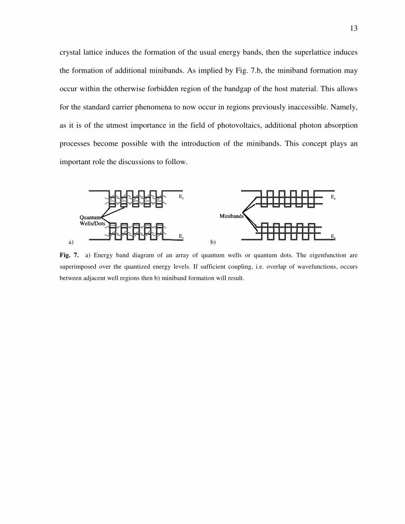
13
crystal lattice induces the formation of the usual energy bands, then the superlattice induces
the formation of additional minibands. As implied by Fig. 7.b, the miniband formation may
occur within the otherwise forbidden region of the bandgap of the host material. This allows
for the standard carrier phenomena to now occur in regions previously inaccessible. Namely,
as it is of the utmost importance in the field of photovoltaics, additional photon absorption
processes become possible with the introduction of the minibands. This concept plays an
important role the discussions to follow.
QuantumWells/Dots
Ec
Ev
QuantumWells/Dots
Ec
Ev
Minibands
Ec
Ev
Minibands
Ec
Ev
a) b)
Fig. 7. a) Energy band diagram of an array of quantum wells or quantum dots. The eigenfunction are
superimposed over the quantized energy levels. If sufficient coupling, i.e. overlap of wavefunctions, occurs
between adjacent well regions then b) miniband formation will result.

14
Chapter 2
Detailed Balance Models
2.1 – General Theory
The treatment of solar energy conversion by a p-n junction presented by Shockley
and Queisser [18] represents the fundamental limits attainable by semiconductor solar cells.
This formulation accounts for the blackbody properties of the solar cell and invokes the
principle of detailed balance to derive an expression for the operation of a solar cell at the
fundamental limit. The theory easily propagates through for use in the analysis of advanced
photovoltaic designs and thus serves as the basis for continued research in the field.
Planck’s law for blackbody radiation [19], expressed as a photon flux per unit energy
flowing out of a blackbody cavity, is
1
12/23
2
−=
ΦkTE
ech
E
dE
d π (1)
where E is the energy, h is Planck’s constant, c is the speed of light, k is Boltzmann’s
constant, and T is the temperature of the blackbody. In this work, (1) shall be known as the
spectral photon flux. Integration of this equation through some energy interval gives the
photon flux Φ. Treating the sun as an ideal blackbody, and since the solar absorption of a
semiconductor is limited by the bandgap energy Eg, the solar flux that is actually absorbable
is
( ) ∫∞
=
Φ=∞Φ
g sE TT
gsdE
ddEE , (2)
15
where Ts is the temperature of the sun. Actually, since (1) represents the spectral flux flowing
out of the cavity, then (2) represents the absorbed flux at the sun’s surface. For the common
sun-solar cell system, the solar cell is located near Earth and impingent radiation on the
device takes the form of plane waves incident on a planar absorber. Therefore the photon flux
absorbed by the solar cell is actually decreased by a factor of
π/Ω=sf (3)
where Ω is the solid angle subtended by the sun and the factor of π-1
accounts for plane
waves impingent on a planar surface [18]. A currently accepted standard value for fs is
2.1646×10⁻⁵
[8].
Similarly, the solar cell may be treated as an ideal blackbody at some temperature Tc.
Then at thermodynamic equilibrium, the direct recombination of electron-hole pairs gives
rises to photon emission with a flux given by
( ) ∫∞
=
Φ=∞Φ
g cE TT
gcdE
ddEE , . (4)
When perturbed from equilibrium by an applied bias V, the p-n junction will see an increase
in radiative recombination proportional to the Boltzmann factor [15, 20]; the expression for
radiative recombination is thus given as
ckTqVceAU
/Φ= (5)
where A is the surface area of the device and q is the elementary charge. Note that the
quantity qV is equal to the amount of splitting in the quasi-Fermi levels [15, 18]. Similarly,
the recombination rate due to non-radiative transitions is [15, 20]:
ckTqVeRR
/0= (6)

16
where R0 is the thermal generation rate. Finally, it is convenient to introduce the inverse of
the fraction of the amount of the recombination-generation current that is due to radiative
transitions:
1
0
−
+Φ
Φ=
RA
Af
c
cc . (7)
The principle of detailed balance states that, at equilibrium, a time-rate process must
be balanced by its inverse; therefore the process and its inverse must proceed at equal
rates [21]. Applied to a photovoltaic device, the principle of detailed balance implies that the
sum of the time-variances of the electron-hole pair populations must vanish; thus [18]:
( ) qIRRUAAAf
qIRRUAf
ccss
ss
/
/0
0
0
−−+−Φ+Φ−Φ=
−−+−Φ= (8)
where I is the current. The term in parentheses is the net generation rate of electron hole pairs
when the device is at thermal equilibrium with its surroundings. Substituting the quantity
(AΦc–R0) by (7) into (8) and solving for I yields the expression for the current density of the
solar cell:
( ) ( )1/ −Φ−Φ−Φ= ckTqV
cccss effq
J. (9)
It is instructive to compare this result with the photovoltaic form of the Shockley
equation [10-11]:
( )1/0 −−= kTqV
sc eIII (10)
where Isc is the short-circuit current and I0 is the reverse bias saturation current. It is evident
that the first term in parentheses in (9) is the short circuit current while the quantity fc-1Φc is
the saturation current. Equation (9) is the fundamental result of the detailed balance

17
formulation; it is an integral solution that directly gives the current-voltage characteristics of
a solar cell. From it, the solar conversion efficiency can be directly extracted.
Although the foregoing theory is thermodynamic by the invocation of the Planck
distribution and the principle of detailed balance, no thermodynamics has actually been
applied directly to the quantum electronics at play; i.e. the thermodynamics of the electron-
photon interaction is not completely considered. By the definition of the chemical potential µ:
dNdE µ= , (11)
the chemical potential of photons has been considered to be zero since the conservation of
photon number N is not required. The notion of a vanishing chemical potential is actually
correct for thermal radiation; hence the Planck law. The argument, however, is not
compelling in general since photon-photon interaction is non-existent; therefore photons
equilibrate by means of atomic interactions that give rise to the possibility of a non-zero
chemical potential [22]. Luminescent photon emission, i.e. photon emission due to some
other means than thermal, can be shown to exhibit a non-zero chemical potential. This is due
to the fact that luminescent radiation is observed to have a threshold frequency, i.e. energy,
below which no light emission occurs. Therefore, the presence of a non-zero chemical
potential can be thought of as a consequence of this high-pass energy gap. A thorough
thermodynamic formulation based on these principles leads to a generalization of (1) [22]:
1
12/)(23
2
−=
Φ− kTE
ech
E
dE
dµ
π. (12)
This formula gives the spectral photon flux exiting from a blackbody cavity; it contains the
effects of both blackbody and luminescent radiation. In the limit of a vanishing chemical
potential, (12) reduces to the conventional form of the Planck distribution.

18
The derivation leading to the Shockley-Queisser result can be claimed to be semi-
empirical in that the assumptions invoked in (5)-(8) come from inserting blackbody
properties in such a way that fits the rectifier model. With the result of (12) and invoking the
principles of statistical mechanics, the Shockley-Queisser result is superseded [23-25]:
( ) ∫∞
=
Φ−Φ−+Φ=
g cE TT
ccscssdE
ddEffff
q
J, (13)
where the spectral flux in the last term is given by the generalized Planck distribution in (12)
and where it turns out that the chemical potential of luminescent photons is equivalent to the
applied bias:
qV=µ . (14)
It should be noted that, except for extreme cases and novel design schemes, both (9) and (13)
give almost identical results. Equation (13) has the reassuring property that at the short-
circuit condition (V = 0), if the solar cell and the sun were at thermal equilibrium, then no
current would flow; this is generally lacking from (9).
To compare (9) and (13), the current-voltage results for a 1.46 eV bandgap
semiconductor are plotted in Fig. 1.a. The cell is illuminated by a 6000 K blackbody at one-
sun and 1000-sun concentrations; fc is taken to be unity and the cell is at a temperature of
300 K. In Fig. 1.a, there are actually two sets of curves for each concentration level
corresponding to either (9) or (13); however, these curves overlap and are not individually
visible. The relative error of using (9) instead of (13) is plotted for the two concentration
levels in Fig. 1.b. From this plot, it is clear that maximum error occurs at the open-circuit
voltage and increases as the open-circuit voltage increases. Note that the data in Fig. 1.b is
only plotted for voltages greater than ~0.9 V for the one-sun case and greater than ~1 V for

19
the 1000-sun case. This is because any error corresponding to smaller voltage values are
smaller than the numerical machine precision. Note that the models discussed above require
the integration of Bose-Einstein distributions. Care must be taken in handling these functions
as singularities are not uncommon. The method used herein makes use of a Gauss-Kronrod
quadrature method [26].
a)
0
10
20
30
40
50
0 0.5 1 1.5
Voltage (V)
Cu
rren
t D
ensi
ty
1 Sun Concentration
[mA/cm2]
1000 Sun
Concentration
[A/cm2]
0
10
20
30
40
50
0 0.5 1 1.5
Voltage (V)
Cu
rren
t D
ensi
ty
1 Sun Concentration
[mA/cm2]
1000 Sun
Concentration
[A/cm2]
b)
1.E-131.E-121.E-111.E-101.E-091.E-081.E-071.E-061.E-051.E-041.E-031.E-021.E-01
1.E+001.E+011.E+02
0.8 1 1.2 1.4
Voltage (V)
Rel
ati
ve
Err
or
(%)
10-12
10-10
10-8
10-6
10-4
10-2
100
102
1 Sun Concentration
1000 Sun Concentration
1.E-131.E-121.E-111.E-101.E-091.E-081.E-071.E-061.E-051.E-041.E-031.E-021.E-01
1.E+001.E+011.E+02
0.8 1 1.2 1.4
Voltage (V)
Rel
ati
ve
Err
or
(%)
10-12
10-10
10-8
10-6
10-4
10-2
100
102
1 Sun Concentration
1000 Sun Concentration
Fig. 1. a) Detailed balance model using the original (9) and statistical (13) formulations at two different
concentration levels (Eg = 1.46 eV). The curves corresponding to the different formulations overlap at both
concentrations. b) Relative errors at both concentration levels of using (9) instead of (13).
The plot in Fig. 2 shows the 1000-sun case but at an elevated device temperature of
600 K. As with the foregoing case, the I-V curves corresponding to (9) and (13) overlap
enough to not be individually resolvable. In comparison to Fig 1.b, the relative error of using
(9) instead of (13) is significantly increased although not to the point to cause great deviation
between the results of the two models. Even though the maximum error is somewhat large
(~100 %), this occurs at a point where the current levels are very small and vary
exponentially. It is clear from Figs. 1-2 that at normal operating conditions either use of (9)
or (13) will suffice. Although this is the case, the remainder of this work will concentrate on

20
the expression in (13) to make sure the results follow from the soundest physical grounds
possible. This is also important for the advanced designs to be considered.
0
10
20
30
40
50
0 0.5 1 1.5
Voltage (V)
Cu
rren
t (A
/cm
2)
1.E-09
1.E-08
1.E-07
1.E-06
1.E-05
1.E-04
1.E-03
1.E-02
1.E-01
1.E+00
1.E+01
1.E+02
1.E+03
Rel
ati
ve
Err
or
(%)
10-8
10-6
10-4
10-2
100
102
0
10
20
30
40
50
0 0.5 1 1.5
Voltage (V)
Cu
rren
t (A
/cm
2)
1.E-09
1.E-08
1.E-07
1.E-06
1.E-05
1.E-04
1.E-03
1.E-02
1.E-01
1.E+00
1.E+01
1.E+02
1.E+03
Rel
ati
ve
Err
or
(%)
10-8
10-6
10-4
10-2
100
102
Fig. 2. Detailed balance model using the original (9) and statistical (13) formulations at 1000-sun concentration
and at an elevated device temperature of 600 K (Eg = 1.46 eV). The curves corresponding to the different
formulations overlap at both concentrations but the relative error is significantly increased from the
corresponding plots in Fig. 1.
2.2 – Single-Junction Solar Cell
In simulating the detailed balance limits of a solar cell, it is common to take the
temperature of the sun to be 6000 K and that of the device to be 300 K. The regime of
interest is the radiative limit, i.e. fc = 1. At this limit, it is possible to analyze the maximum
possible performance of a photovoltaic device without having to consider the confounding of
non-idealities brought about by materials growth, device design, etc. Additionally, the
geometric parameter fs has been previously defined to be equal to 2.1646×10⁻⁵
[8]. This
implies that the maximum possible concentration factor is 46,198 suns. Thus the product of fs

21
and the maximum concentration factor is unity therefore corresponding to the equivalent case
of a solar cell placed at the suns surface.
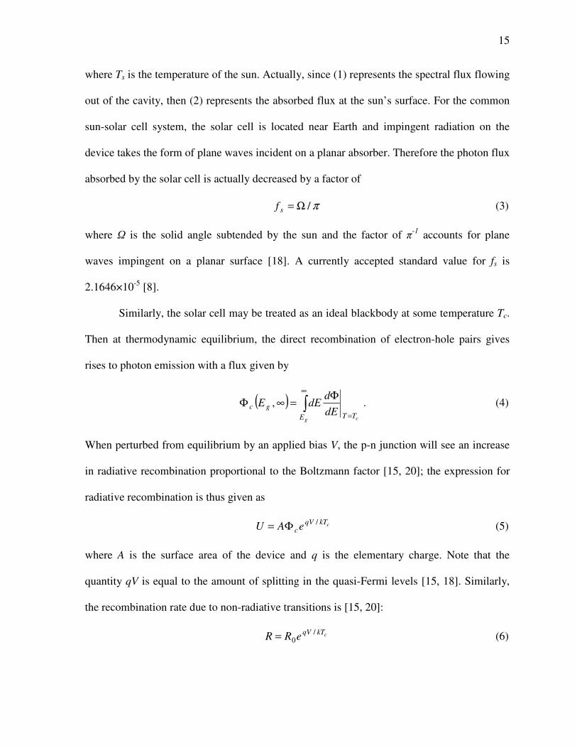
The detailed balance performance of several of the elemental and binary
semiconductors is plotted in Fig. 3 as a set of I-V characteristics. By inputting each
individual material’s bandgap into the detailed balance model, the fundamental limiting
performance is determined. This figure helps to illustrate the tradeoffs inherent in materials
selection. The smaller bandgap semiconductors allow for a larger short-circuit current
because they are able to absorb a larger portion of the solar spectrum; however, their small
bandgap places a fundamental limit on the open-circuit voltage. Therefore it makes sense that
there will be an optimum bandgap such that the corresponding I-V characteristic gives the
maximum attainable efficiency. As discussed in Section 1.3, the efficiency is defined as the
ratio of the maximum power to the irradiance falling upon the solar cell form the sun. In this
blackbody analysis, the irradiance Ps is determined by the Stefan-Boltzmann law:
4TPs σ= ; (15)
which gives a solar constant of 1590.7 W/m2 when including a prefactor of fs. σ is the Stefan-
Boltzmann constant.
The issue of determining an optimum bandgap corresponding to maximum attainable
efficiency is addressed in Fig. 4. Here, the detailed balance efficiency limits are plotted as a
function of material bandgap at several different solar concentrations. For each curve, a
maximum occurs indicating the optimum bandgap leading to maximized solar efficiency.
This plot directly gives the detailed balance limit of 31.0 % efficiency corresponding to a
bandgap of 1.31 eV at one sun illumination. For maximum concentration, the detailed
balance limit rises to 40.8 % efficiency corresponding to a decreased bandgap of 1.11 eV.
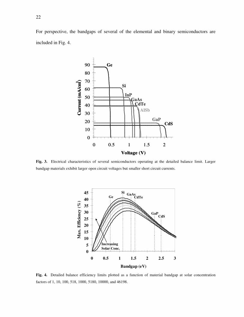
22
For perspective, the bandgaps of several of the elemental and binary semiconductors are
included in Fig. 4.
0
10
20
30
40
50
60
70
80
90
0 0.5 1 1.5 2
Voltage (V)
Cu
rren
t (m
A/c
m2)
Ge
Si
InPGaAs
CdTe
AlSb
GaPCdS
0
10
20
30
40
50
60
70
80
90
0 0.5 1 1.5 2
Voltage (V)
Cu
rren
t (m
A/c
m2)
Ge
Si
InPGaAs
CdTe
AlSb
GaPCdS
Fig. 3. Electrical characteristics of several semiconductors operating at the detailed balance limit. Larger
bandgap materials exhibit larger open circuit voltages but smaller short circuit currents.
0
5
10
15
20
25
30
35
40
45
0 0.5 1 1.5 2 2.5 3
Bandgap (eV)
Ma
x.
Eff
icie
ncy
(%
)
GaAsSi
Ge CdTe
GaPCdS
Increasing
Solar Conc.
Fig. 4. Detailed balance efficiency limits plotted as a function of material bandgap at solar concentration
factors of 1, 10, 100, 518, 1000, 5180, 10000, and 46198.

23
Although the treatment of the sun as a perfect blackbody in the foregoing discussions
provides for an excellent approximation in the analysis for solar efficiency, it is of interest to
study the same scenarios but with a more accurate model of the solar flux. This is made
possible by the existence of standard data detailing the actual solar spectrum outside the
Earth’s atmosphere and on its surface [16]. The AM0 and AM1.5 solar spectra were
discussed in Section 1.3 and are compared with the 6000 K blackbody spectrum in Fig. 5.
0
500
1000
1500
2000
0.0 0.5 1.0 1.5 2.0 2.5
Wavelength (µm)
Sp
ectr
al
Ra
dia
nce
(W
/m2/µ
m)
Blackbody
AM0
AM1.5D
AM1.5G
0
500
1000
1500
2000
0.2 0.3 0.4 0.5 0.6 0.7 0.8 0.9 1.0
Fig. 5. Comparison of the 6000 K blackbody radiancy with the ASTM solar spectra [16]. The Planck law used
to generate the blackbody curve includes fs as a prefactor.
The blackbody curve in Fig. 5 is the Planck distribution (1) multiplied by fs and
expressed as a spectral radiance. For more realistic modeling of detailed balance
performance, the actual solar spectra may be invoked instead of the Planck distribution.
Therefore the data plotted in Fig. 5, expressed as a spectral photon flux, may be used directly
to determine the absorbed photon flux by quadrature of (2); the remainder of the process to
24
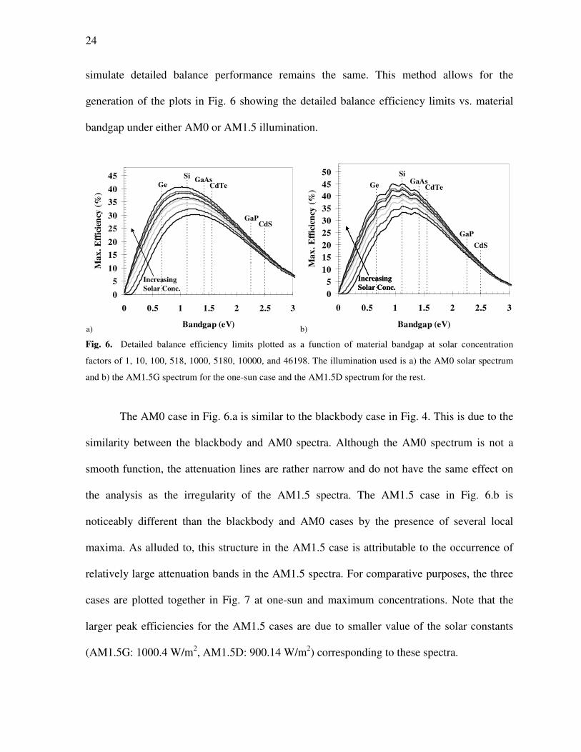
simulate detailed balance performance remains the same. This method allows for the
generation of the plots in Fig. 6 showing the detailed balance efficiency limits vs. material
bandgap under either AM0 or AM1.5 illumination.
a)
0
5
10
15
20
25
30
35
40
45
0 0.5 1 1.5 2 2.5 3
Bandgap (eV)
Ma
x.
Eff
icie
ncy
(%
)
GaAsSi
Ge CdTe
GaPCdS
Increasing
Solar Conc.
b)
0
5
10
15
20
25
30
35
40
45
50
0 0.5 1 1.5 2 2.5 3
Bandgap (eV)
Ma
x.
Eff
icie
ncy
(%
)
GaAsSi
Ge CdTe
GaP
CdS
Increasing
Solar Conc.
Increasing
Solar Conc.
Fig. 6. Detailed balance efficiency limits plotted as a function of material bandgap at solar concentration
factors of 1, 10, 100, 518, 1000, 5180, 10000, and 46198. The illumination used is a) the AM0 solar spectrum
and b) the AM1.5G spectrum for the one-sun case and the AM1.5D spectrum for the rest.
The AM0 case in Fig. 6.a is similar to the blackbody case in Fig. 4. This is due to the
similarity between the blackbody and AM0 spectra. Although the AM0 spectrum is not a
smooth function, the attenuation lines are rather narrow and do not have the same effect on
the analysis as the irregularity of the AM1.5 spectra. The AM1.5 case in Fig. 6.b is
noticeably different than the blackbody and AM0 cases by the presence of several local
maxima. As alluded to, this structure in the AM1.5 case is attributable to the occurrence of
relatively large attenuation bands in the AM1.5 spectra. For comparative purposes, the three
cases are plotted together in Fig. 7 at one-sun and maximum concentrations. Note that the
larger peak efficiencies for the AM1.5 cases are due to smaller value of the solar constants
(AM1.5G: 1000.4 W/m2, AM1.5D: 900.14 W/m
2) corresponding to these spectra.

25
0
5
10
15
20
25
30
35
40
45
0 1 2 3 4 5
Bandgap (eV)
Ma
x.
Eff
icie
ncy
(%
)
AM1.5
BlackbodyAM0
Fig. 7. Comparison of the maximum efficiencies attainable under the detailed balance limit for the three
different spectra at one-sun and maximum concentrations. AM1.5G is used for the one-sun case while AM1.5D
is used for the maximum concentration case.
From Fig. 7, the detailed balance efficiency limits are summarized in Table I with
their respective optimum bandgaps at one-sun and maximum concentrations for the three
standard spectra. AM1.5G is used at one-sun while AM1.5D is used at maximum
concentration. Plots of this data taken over the entire concentration range are displayed in
Fig. 8. These sets of data clearly indicate very different design spaces based on the spectrum
of interest. What is an optimum design point under one spectrum is not, in general, an
optimum design point under another spectrum. The data in Fig. 8.b is particularly of interest
as it indicates a major difference in the analysis using a blackbody spectrum compared to that
using an actual spectrum. For the blackbody case, the optimum bandgap, i.e. the design
space, follows a logarithmically dependent continuum. For either the AM0 or AM1.5 cases,
the optimum bandgap remains relatively constant throughout large ranges of solar
concentrations and exhibits step discontinuities at several points. This is attributable to the

26
irregular roughness of the actual spectra compared to the smoothness of the blackbody
spectrum (Fig. 5). It should be noted that, as seen in Fig. 6.b, the maximum efficiency as a
function of bandgap for the AM1.5 spectrum exhibits several local maxima. The data used to
generate Fig. 8.b considers only the global maximum. Note that in Fig. 6.b, the global
maximum eventually shifts from one local maximum to another with increased
concentration. This contributes to the relative consistency of the optimum bandgap for the
AM1.5 spectrum.
Table I
Detailed Balance Efficiency Limits
No Concentration Max. Concentration
Illumination
Spectrum
Opt.
Bandgap
Max.
Efficiency
Opt.
Bandgap
Max.
Efficiency
Blackbody 1.31 eV 31.0 % 1.11 eV 40.8 %
AM0 1.26 eV 30.2 % 1.03 eV 40.6 %
AM1.5 1.12 eV 33.2 % 1.11 eV 45.0 %
a)
30
32
34
36
38
40
42
44
1 10 100 1000 10000 100000
Solar Concentration
Ma
x.
Eff
icie
ncy
(%
)
6000 K
Blackbody
AM0
AM1.5
b)
1.00
1.05
1.10
1.15
1.20
1.25
1.30
1.35
1 10 100 1000 10000 100000
Solar Concentration
Op
t. B
an
dg
ap
(eV
)
6000 K
Blackbody
AM0
AM1.5
Fig. 8. Comparison between the three standard spectra of a) maximum efficiency and b) corresponding
optimum bandgap throughout the range of solar concentrations. This indicates vastly different device design
spaces depending on the spectrum of interest.

27
2.3 – Triple-Junction Solar Cell
From the discussions in the forgoing section, it is clear that the material bandgap
plays an essential role in determining the performance of a solar cell. In Fig. 3, this is
manifested as different materials exhibiting different open-circuit voltages and different
short-circuit currents. Clearly, any single device exhibited in Fig. 3 would be made more
efficient simply by extending the I-V curve such that a larger open-circuit voltage is attained.
This is the general idea behind the multi-junction solar cell.
As a specific case of the multi-junction solar cell, a triple-junction device is
diagramed in Fig. 9.a; this is the InGaP-GaAs-Ge triple junction cell and represents the state-
of-the-art in basic multi-junction approaches. This device is grown monolithically by
epitaxial means. The materials are chosen to conform to the constraint of lattice matching. In
this device, there are actually three separate p-n junctions, each composed of a different
material. This constitutes an equivalent circuit of three solar cells connected in series as seen
in Fig. 9.b. The materials are placed such that the one with the largest bandgap is located at
the top of the stack; the remaining materials follow the trend of decreasing bandgap towards
the bottom of the stack. This design allows for the most efficient conversion of higher energy
photons by the top cell. The top cell is transparent to sub-bandgap light; this light is then
absorbed by one of the remaining cells underneath. This allows for the splitting of the
absorption of the solar spectrum into more efficient means; this is diagramed in Fig. 10.
Efficiency of this device is enhanced from the single-junction cell due to the photogeneration
occurring over several junctions at once. In general, a separate photovoltage will be dropped
across each junction at any given time; these voltages add giving the total voltage across the
multi-junction device. This is the mechanism which leads to an increased open-circuit

28
voltage, i.e. the I-V curve is stretched along the voltage axis. The only caveat is that the
current will be limited to the lowest output due to the constraint of current matching, i.e. the
conservation of charge dictates that the currents running through each junction must be equal.
Finally, it should be noted that an actual device will include a backwards connected tunnel
junction in-between each sub-cell to properly drive current (this is discussed in further detail
in Section 3.18). This reality is not necessary in the analysis that follows thus it suffices to
assume that an ideal short exists between each sub-cell as drawn in Fig. 9.b.
a)
Ge p-n Junction
GaAs p-n Junction
InGaP p-n Junction
Ge p-n Junction
GaAs p-n Junction
InGaP p-n Junction
b)
1
2
3
hν
1
2
3
hν
Fig. 9. InGaP-GaAs-Ge triple-junction solar cell a) diagramed to show the proper placement of each layer such
that the smallest bandgap material is placed at the bottom with increasing bandgaps towards the top of the stack.
The device is b) diagramed as an equivalent circuit with three individual solar cells connected in series
representing each of the individual junctions.
A detailed balance analysis of the triple-junction cell in Fig. 9.a. has been previously
reported [27]. The remainder of this section elucidates on the mathematical details necessary
to perform such an analysis and verifies the published results. Additionally, the solutions
obtained in this section give insight to the detailed analysis to follow in Section 2.4 on the
intermediate band solar cell.

29
0
200
400
600
800
1000
1200
1400
1600
1800
2000
2200
0.2 0.6 1 1.4 1.8
Wavelength (µm)
Spec
tral R
adia
nce
(W
/m2/µ
m)
0
200
400
600
800
1000
1200
1400
1600
1800
2000
2200
0.2 0.6 1 1.4 1.8
Wavelength (µm)
Spec
tral R
adia
nce
(W
/m2/µ
m)
InGaP Absorption
GaAs Absorption
Ge Absorption
Fig. 10. AM0 solar spectrum split into separate absorption regions corresponding each of the sub-cells in the
triple-junction InGaP-GaAs-Ge stack.
The task at hand is to determine the efficiency of the InGaP-GaAs-Ge triple-junction
solar cell and to determine which layers should be modified to increase this efficiency. In
referencing to Fig. 9.b, the current through cell n, where n runs from 1 to 3, is given by (13).
As in the single-junction example, fc may be taken to be unity. Additionally, the middle term
in (13) is only significant as the temperature of the device approaches that of the illuminating
body; therefore, it may be ignored. Explicitly, the current through cell n is then
∫∫ −−
−=−=
−n cnn s E kTEE kTEsDnLnn
e
dEE
ch
q
e
dEE
ch
qfJJJ
1
2
1
2/)(
2
23/
2
23 µ
ππ (16)
where the first term can be considered to be the short-circuit current JL of the single-junction
cell and the second term can be considered to be the dark current JD. By (14), µn is
determined from the voltage that is dropped across cell n. The integrations in (16) are
performed over the energy interval ranging from the bandgap of the specified sub-cell up to
the bandgap of the next sub-cell such that there is no overlap in the integrated energy ranges
of any two sub-cells. Referring to Fig. 9.b, the energy intervals are

30
],[
],[
),[
233
122
11
gg
gg
g
EEE
EEE
EE
=
=
∞=
(17)
recalling that the multi-junction design requires that Eg1 > Eg2 > Eg3.
The power of the stack is then
nVJP = (18)
where V is the voltage dropped across the entire stack. In principle, since the currents
throughout each sub-cell are equal, any value of n may be chosen. Arbitrarily choosing n = 1
and due to the direct relationship between voltage and the chemical potential given by (14),
the power may be rewritten as
∑=n
n
qJP
µ1 . (19)
The condition for maximum power, thus giving cell efficiency, is met by maximizing this
expression with respect to the chemical potentials but subject to the following constraints:
( )
( ) 01
01
322
211
=−=Φ
=−=Φ
JJq
JJq
(20)
where the factor of q-1
has been placed for convenience. Then by the method of Lagrange
multipliers, the maximization of (19) is determined by solving the following:
02211 =Φ∇+Φ∇+∇ µµµ λλP (21)
where λ are the Lagrange multipliers.
Expanding the pertinent gradients,

31
( ) ∑
+=∇
n
nd
dJ
qJJJ
qP µ
µµ 00
11
1
1111
−=Φ∇ 0
1
2
2
1
11
µµµ
d
dJ
d
dJ
q (22)
−=Φ∇
3
3
2
22 0
1
µµµ
d
dJ
d
dJ
q,
allows for (21) to be written as a set of simultaneous equations:
0
0
0
3
321
2
22
2
211
1
111
1
1
=−
=+−
=++
∑
µλ
µλ
µλ
µλ
µµ
d
dJJ
d
dJ
d
dJJ
d
dJJ
d
dJ
n
n
(23)
Therefore, the solution is
01 =
+∑
n ddJn
n
n
J
µ
µ . (24)
This gives the operating condition of the multi-junction cell at which maximum power is
achieved. All that remains is to evaluate the derivative occurring in (24):
( )
∫
∫
−−=
−−=
−=
−
−
n
n cn
cn
Ec
n
c
E kTE
kTE
c
n
Dn
n
n
dEkT
EE
kTch
q
e
dEeE
kTch
q
d
dJ
d
dJ
2csch
4
12
1
12
22
23
2/)(
/)(2
23
µπ
π
µµ
µ
µ
(25)
It should be noted that even though the example of a triple-junction cell has been chosen for
this derivation, the solution may be generalized for any number of N sub-cells. This would
increase the number of constraints in (20) to a total number of N-1 with the general form
( ) 01
1 =−=Φ +nnn JJq
(26)
32
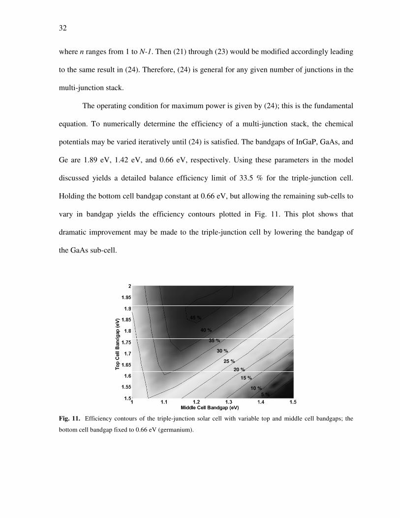
where n ranges from 1 to N-1. Then (21) through (23) would be modified accordingly leading
to the same result in (24). Therefore, (24) is general for any given number of junctions in the
multi-junction stack.
The operating condition for maximum power is given by (24); this is the fundamental
equation. To numerically determine the efficiency of a multi-junction stack, the chemical
potentials may be varied iteratively until (24) is satisfied. The bandgaps of InGaP, GaAs, and
Ge are 1.89 eV, 1.42 eV, and 0.66 eV, respectively. Using these parameters in the model
discussed yields a detailed balance efficiency limit of 33.5 % for the triple-junction cell.
Holding the bottom cell bandgap constant at 0.66 eV, but allowing the remaining sub-cells to
vary in bandgap yields the efficiency contours plotted in Fig. 11. This plot shows that
dramatic improvement may be made to the triple-junction cell by lowering the bandgap of
the GaAs sub-cell.
45 %
40 %
35 %
30 %
20 %
25 %
15 %
10 %
5 %
Fig. 11. Efficiency contours of the triple-junction solar cell with variable top and middle cell bandgaps; the
bottom cell bandgap fixed to 0.66 eV (germanium).

33
From Fig. 11, with a top cell bandgap of 1.89 eV (InGaP) and a middle cell bandgap
of 1.42 eV (GaAs), the detailed balance efficiency limit of the triple-junction cell is 33.5 %.
By decreasing only the middle cell bandgap to 1.20 eV, the detailed balance limit is
increased to the maximum point at 47.5 %. The problem that arises is that no material exists
that both has this desired bandgap and is latticed matched to InGaP and Ge. As discussed in
Section 1.4, the incorporation of a nanostructured array in a host material may induce
miniband formation. This can therefore give rise to otherwise sub-bandgap photoconversion
of light. A quantum well or quantum dot array placed in the GaAs middle cell may therefore
induce an effective bandgap lowering such that the overall triple-junction efficiency limit
increases from 33.5 % to 47.5 %.
2.4 – Intermediate Band Solar Cell
The present concept of the intermediate band solar cell was first reported by Luque
and Martí [28] while an earlier, related concept was reported by Wolf [29]. The standard
concept of the intermediate band solar cell is shown schematically in Fig. 12 as a
semiconductor band diagram where the bandgap is represented by ECV = EC – EV. The
standard solar cell would therefore only be able to absorb photons with energy equal to or
greater than ECV. Suppose now that an accessible band is located at an intermediate level EI
between EC and EV as indicated in Fig. 12. This intermediate band is simply the miniband
discussed in Section 1.4. The electronic states in the intermediate band should be accessible
via direct transitions. Then the absorption of photon energy EIV will pump an electron from
the valence band to the intermediate band. A subsequent photon of energy ECI then pumps an
electron from the intermediate band to the conduction band. The increased performance of
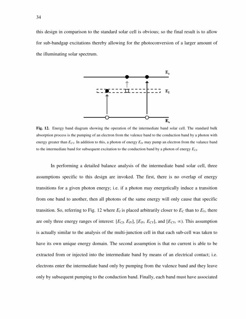
34
this design in comparison to the standard solar cell is obvious; so the final result is to allow
for sub-bandgap excitations thereby allowing for the photoconversion of a larger amount of
the illuminating solar spectrum.
Ev
Ec
EI
Ev
Ec
EI
Fig. 12. Energy band diagram showing the operation of the intermediate band solar cell. The standard bulk
absorption process is the pumping of an electron from the valence band to the conduction band by a photon with
energy greater than ECV. In addition to this, a photon of energy EIV may pump an electron from the valance band
to the intermediate band for subsequent excitation to the conduction band by a photon of energy ECI.
In performing a detailed balance analysis of the intermediate band solar cell, three
assumptions specific to this design are invoked. The first, there is no overlap of energy
transitions for a given photon energy; i.e. if a photon may energetically induce a transition
from one band to another, then all photons of the same energy will only cause that specific
transition. So, referring to Fig. 12 where EI is placed arbitrarily closer to EC than to EV, there
are only three energy ranges of interest: [ECI, EIV], [EIV, ECV], and [ECV, ∞). This assumption
is actually similar to the analysis of the multi-junction cell in that each sub-cell was taken to
have its own unique energy domain. The second assumption is that no current is able to be
extracted from or injected into the intermediate band by means of an electrical contact; i.e.
electrons enter the intermediate band only by pumping from the valence band and they leave
only by subsequent pumping to the conduction band. Finally, each band must have associated

35
with it, its own quasi-Fermi level; so the difference in chemical potentials between any two
bands is simply the difference between the quasi-Fermi levels of the two bands.
Following from (16), the spectral flux from the sun giving rise to the short-circuit
current is
1
2/
2
23 −=
ΦskTEs
s
e
E
chf
dE
d π (27)
while the spectral flux leaving the solar cell, thus giving rise to the dark current, is
( )
1
2/)(
2
23 −=
Φ− ckTE
c
e
E
chdE
dµ
πµ. (28)
An equivalent circuit of the intermediate band solar cell may be constructed, as in Fig. 13,
based on the stated assumptions. As in previous analyses, the chemical potentials correspond
to voltage drops across the equivalent circuit elements. In Fig. 13, photodiode 1 corresponds
to the standard effect of an electronic transition across the bandgap, photodiode 2A
corresponds to the effect of the intermediate-to-conduction band transition, and photodiode
2B corresponds to the valence-to-intermediate band transition. The currents through each of
the circuit elements are therefore:
( )
( )
( )∫∫
∫∫
∫∫
Φ−
Φ=
Φ−
Φ=
Φ−
Φ=
∞∞
CV
IV
CV
IV
IV
CI
IV
CI
CVCV
E
E
IVc
E
E
sB
E
E
CIc
E
E
sA
E
CVc
E
s
dEdE
dqdE
dE
dqJ
dEdE
dqdE
dE
dqJ
dEdE
dqdE
dE
dqJ
µ
µ
µ
2
2
1
(29)

36
J
J2A
J2
J1
J2B
µCV
+
-
µCI
+
-
µIV
+
-
2B
2A
1
J
J2A
J2
J1
J2B
µCV
+
-
µCI
+
-
µIV
+
-
2B
2A
1
Fig. 13. Equivalent circuit of the intermediate band solar cell. Current J1 is due to the standard valence-to-
conduction band photoabsorption process while current J2 accounts for the enhancement due to the presence of
the intermediate band. These currents add to give the total current J of the intermediate band solar cell. The
voltage applied to the device corresponds to the chemical potentials by V = µCV / q.
From Fig. 13, the currents J2A and J2B must be equal; these may be simply referred to
as current J2. The current J2 adds with J1 to give the total current J. As in previous analyses,
the applied voltage is dropped such that it corresponds to the chemical potential difference
between the conduction and valence bands. This energy splitting then determines the values
of the chemical potential differences with respect to the intermediate band. So the current-
voltage characteristics of the intermediate band solar cell can be determined by considering
the total current
( ) 21 JJVJ += (30)
which is fundamentally a function of the chemical potential such that
qVCV =µ . (31)
The contribution of current J1 is straightforward to calculate. The current J2 must meet the
condition

37
( ) ( )IVBCIA JJJ µµ 222 == (32)
where the respective chemical potentials are determined at each operation point by
qVCVIVCI ==+ µµµ . (33)
The methodology outlined here is algorithmically solved by iteration throughout a range of
voltages. This allows a maximum power point to be determined thus giving photovoltaic
efficiency.
Following the methodology outlined above allows for the generation of efficiency
contours as plotted in Fig. 14. These plots show the detailed balance efficiency limit, under
6000 K blackbody illumination, of the intermediate band solar cell as a function of the
intermediate band location. In other words, referring to Fig. 12, the values of ECI and EIV
determine the limiting efficiency of the photovoltaic device. This is explicitly presented in
Fig. 14 for the physically relevant illumination factors of 1, 10, 100, and 1000-sun
concentrations. Note that specified values of ECI and EIV set the bulk bandgap ECV.
From Fig. 14.a, the detailed balance efficiency limit under blackbody illumination is
46.8 %. This corresponds to intermediate bandgaps of EIV = 1.49 eV and ECI = 0.92 eV; the
complete bandgap ECV is therefore 2.41 eV. As the solar concentration is increased to 1000
suns, the optimum values of both EIV and ECI decrease monotonically to 1.31 eV and
0.77 eV, respectively. The efficiency at this point is 57.3 %. The corresponding total bandgap
is therefore also decreased at 1000 suns to 2.08 eV. This behavior of decreased optimum
bandgap with increased solar concentration is comparable to Figs. 4 and 8.b, both of which
demonstrate similar behavior for the single junction solar cell. Table II lists the limiting
efficiencies and corresponding bandgaps for the plots in Fig. 14.

38
a) b)
c) d)
Fig. 14. Contour plots showing the detailed balance efficiency limit of the intermediate band solar cell as it
varies with the spacings between the conduction and intermediate bands and between the intermediate and
valence bands. The illuminating spectrum is that of a 6000 K blackbody with concentration factors of a) 1 sun,
b) 10 suns, c) 100 suns, and d) 1000 suns.
Table II
Detailed Balance Efficiency Limits Under 6000 K Blackbody Illumination
Solar Concentration 1 10 100 1000
Efficiency Limit 46.8 % 50.1 % 53.6 % 57.3 %
EIV (eV) 1.49 1.43 1.36 1.31
ECI (eV) 0.92 0.87 0.81 0.77
ECV (eV) 2.41 2.30 2.17 2.08
Similar to the generation of Fig. 6, the detailed balance analysis of the intermediate
band solar cell can be made more realistic by invoking the actual AM0 and AM1.5 solar
spectrums which are plotted in Fig. 5. In doing so, the analytic form of (27) is replaced with
numerical data from Fig. 5. Efficiency contours for the intermediate band solar cell subject to

39
AM0 illumination are plotted in Fig. 15 for 1, 10, 100, and 1000-sun concentrations. These
plots are similar to those in Fig. 14 due to the similarity between the blackbody and AM0
spectra. Some roughness is seen in the AM0 contours due to the roughness of the AM0
spectrum. The corresponding efficiency limits and optimum bandgaps are listed in Table III.
a) b)
c) d)
Fig. 15. Contour plots showing the detailed balance efficiency limit of the intermediate band solar cell as it
varies with the spacings between the conduction and intermediate bands and between the intermediate and
valence bands. The AM0 solar spectrum is used with concentration factors of a) 1 sun, b) 10 suns, c) 100 suns,
and d) 1000 suns.
Table III
Detailed Balance Efficiency Limits Under AM0 Illumination
Solar Concentration 1 10 100 1000
Efficiency Limit 45.8 % 49.5 % 53.3 % 57.4 %
EIV (eV) 1.38 1.27 1.27 1.22
ECI (eV) 0.85 0.77 0.77 0.73
ECV (eV) 2.23 2.04 2.04 1.95

40
The AM1.5 detailed balance efficiency contours are plotted in Fig. 16 for 1, 10, 100,
and 1000-sun concentrations. The 1-sun case makes use of the AM1.5G spectrum while the
remainder uses the AM1.5D spectrum. The contours in Fig. 16 exhibit a much more irregular
structure when compared to the previous examples under blackbody and AM0 illumination.
This is due to the large degree of roughness and attenuation lines in the AM1.5 spectra. Of
particular interest is the presence of several local maxima in the AM1.5 efficiency contours.
This is comparable to Fig. 6.b where the efficiency vs. bandgap plot of the single junction
solar cell illuminated by the AM1.5 spectrum exhibited similar behavior. The AM1.5
detailed balance efficiency limits and corresponding optimum bandgaps are listed in
Table IV.
Table IV
Detailed Balance Efficiency Limits Under AM1.5 Illumination
Solar Concentration 1 10 100 1000
Efficiency Limit 49.4 % 52.2 % 56.3 % 60.8 %
EIV (eV) 1.50 1.34 1.23 1.22
ECI (eV) 0.93 0.74 0.70 0.69
ECV (eV) 2.43 2.08 1.93 1.91
The vast majority of research work occurring today for the intermediate band solar
cell makes use of an InAs quantum dot array placed in the space charge region of a bulk
GaAs solar cell [4, 27, 71, 77]. The InAs dot array, being of smaller bulk bandgap than the
GaAs host, induces the intermediate band by coupling of confined electronic states in the
InAs conduction band; this design scheme is discussed in further detail in Chapter 3. The
InAs/GaAs system has the advantage that it is relatively well-studied, it makes use of only
binary semiconductors (as opposed to technologically-difficult ternary or higher alloys), and
it uses a commercially utilized solar cell material (GaAs).

41
a) b)
c) d)
Fig. 16. Contour plots showing the detailed balance efficiency limit of the intermediate band solar cell as it
varies with the spacings between the conduction and intermediate bands and between the intermediate and
valence bands. In (a), the AM1.5G solar spectrum is used under 1-sun concentration. The remainder makes use
of the AM1.5D solar spectrum with concentration factors of b) 10 suns, c) 100 suns, and d) 1000 suns.
This InAs/GaAs (dot/host) system, however, is disadvantaged in that the values of ECI
and EIV are approximately 0.4 eV and 1 eV, respectively (see: Section 3.19 and [77]). These
intermediate bandgap energies are clearly far from the ideal values determined from Figs. 14-
16. Using the models that generated these plots, the detailed balance efficiency limits for the
aforementioned system are determined and listed in Table V. A proposed solution is to use a
more ideal system based off of technologically difficult antimonide-based ternary systems
[78]. This solution, however, only slightly tends towards the optimum intermediate bandgap
combinations and does not correspond with the maximum point.
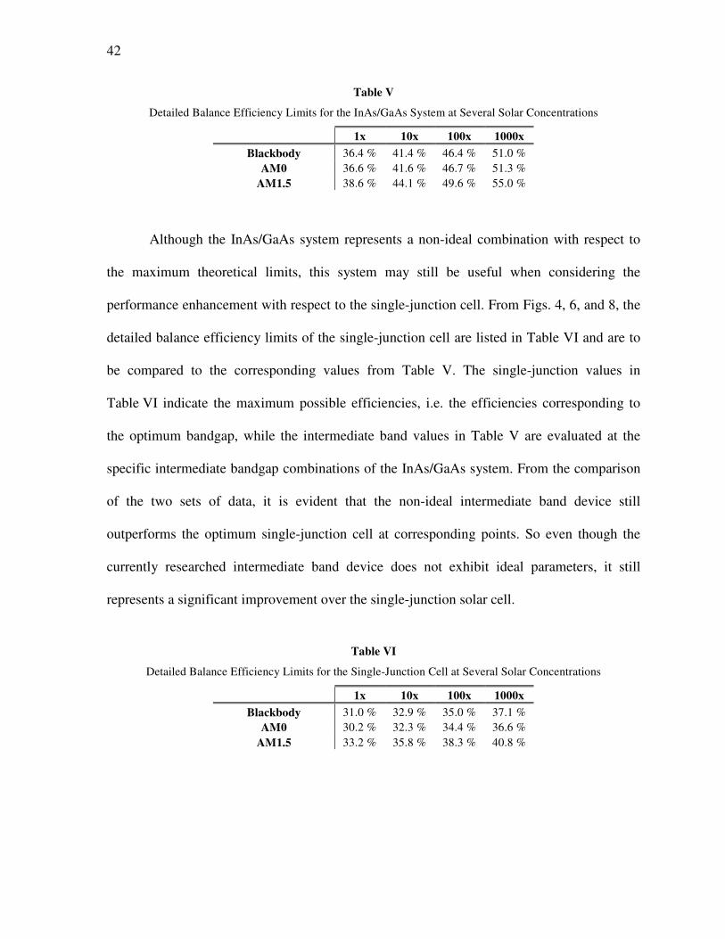
42
Table V
Detailed Balance Efficiency Limits for the InAs/GaAs System at Several Solar Concentrations
1x 10x 100x 1000x
Blackbody 36.4 % 41.4 % 46.4 % 51.0 %
AM0 36.6 % 41.6 % 46.7 % 51.3 %
AM1.5 38.6 % 44.1 % 49.6 % 55.0 %
Although the InAs/GaAs system represents a non-ideal combination with respect to
the maximum theoretical limits, this system may still be useful when considering the
performance enhancement with respect to the single-junction cell. From Figs. 4, 6, and 8, the
detailed balance efficiency limits of the single-junction cell are listed in Table VI and are to
be compared to the corresponding values from Table V. The single-junction values in
Table VI indicate the maximum possible efficiencies, i.e. the efficiencies corresponding to
the optimum bandgap, while the intermediate band values in Table V are evaluated at the
specific intermediate bandgap combinations of the InAs/GaAs system. From the comparison
of the two sets of data, it is evident that the non-ideal intermediate band device still
outperforms the optimum single-junction cell at corresponding points. So even though the
currently researched intermediate band device does not exhibit ideal parameters, it still
represents a significant improvement over the single-junction solar cell.
Table VI
Detailed Balance Efficiency Limits for the Single-Junction Cell at Several Solar Concentrations
1x 10x 100x 1000x
Blackbody 31.0 % 32.9 % 35.0 % 37.1 %
AM0 30.2 % 32.3 % 34.4 % 36.6 %
AM1.5 33.2 % 35.8 % 38.3 % 40.8 %

43
Chapter 3
Device Simulations with Silvaco ATLAS
3.1 – Basic Equations
Silvaco ATLAS is a physics-based simulator which has been explicitly designed for
the purpose of modeling semiconductor devices [30]. The simulation methodology is
physics-based in that the models invoked by the software tend to be derived from first
principles or at least empirically derived with careful attention placed to relating such models
to the underlying physics. Fundamentally, device operation is governed by and described in a
set of two coupled, partial differential equations: the Poisson equation and the equation of
continuity.
One may consider two of the axioms to the theory of electrodynamics to be Gauss’
law
ε
ρ=⋅∇ E (1)
and the Ampère-Maxwell law
tv ∂
∂+=×∇
EJB
2
1µ ; (2)
these are two of the four Maxwell equations for linear, isotropic media. In the foregoing, E is
the electric field, ρ is the charge density, ε is the material permittivity, B is the magnetic field,
µ is the material permeability, J is the current density, and v is the speed of light in the
medium. Following (1), the relation of the electric field as the negative gradient of the
electric potential V yields the Poisson equation:

44
ε
ρ−=∇ V
2 . (3)
Taking the divergence of (2) yields the equation of continuity:
t∂
∂−=⋅∇
ρJ . (4)
In semiconductor applications, it is customary to modify (4) to include the cumulative effects
of the generation G and recombination R of charge carriers [10]. Additionally, separate
continuity equations are written for the electron concentration n and the hole concentration p,
respectively:
nnnq
RGt
nJ⋅∇+−=
∂
∂ 1 (5)
pppq
RGt
pJ⋅∇−−=
∂
∂ 1 (6)
where q is the elementary charge. Equations (3), (5), and (6) are the governing laws of
semiconductor devices. These equations are solved iteratively by ATLAS to obtain a
modeled solution of device operation.
3.2 – Carrier Statistics
Additional models that modify the variables in the equations above, or add additional
phenomena not yet discussed, may be incorporated; these shall be discussed as necessary.
One such model is that of carrier statistics. According to Fermi-Dirac statistics, the electron
concentration in the conduction band is given as an integral over energy:
∫∞
−+=
C
F
E
kTEEe
dEENn
/)(1
)( (7)
where the density of states is

45
3
2/12/3*
2
)(2)(
h
CnC
EEmMEN
−=
π. (8)
In the above, EF is the Fermi level, EC is the bottom of the conduction band, k is Boltzmann’s
constant, T is the temperature, MC is the number of equivalent minima in the conduction band
dispersion, mn* is the density of states effective mass for electrons, and ħ is the reduced
Planck’s constant. By defining an effective density of states in the conduction band as
Cn
C Mh
kTmN
2/3
2
*22
=
π, (9)
where h is the original Planck’s constant, (7) may be written as
[ ]∫∞
−+
−=
C
F
E
kTEE
CC
kT
dE
e
kTEENn
/)(
2/1
1
/)(2
π. (10)
Although the Fermi-Dirac integral cannot be solved analytically, the form of the integral
given in (10) is known as the Fermi-Dirac integral of order one-half and is a well-studied
function [31-32]. Solutions to this integral are readily available through look-up tables or by
rational Chebyshev approximations [30]. Similarly for holes in the valence band of
maximum value EV with a density of states effective mass mp*, the effective density of states
in the valence band is defined as
2/3
2
*22
=
h
kTmN
p
V
π (11)
and the hole concentration is
[ ]∫∞−
−+
−=
V
F
E
kTEE
VV
kT
dE
e
kTEENp
/)(
2/1
1
/)(2
π. (12)

46
Equilibrium electron and hole concentrations are therefore directly determined by (10) and
(12), respectively, and subsequently give the charge density to be used in (3).
For completeness, it should be noted that (10) and (12) are often listed under the
Boltzmann approximation:
kTEE
CFCeNn
/)( −−= kTEE
VVFeNp
/)( −−= . (13)
These expressions tend to be valid as long as the Fermi level lies within the bandgap and is
not within ~3kT of either band edge. Due to the relatively large dopings used in this work,
the Boltzmann approximation is not invoked. By default, the Boltzmann approximation is
assumed by ATLAS; the Fermi-Dirac expressions are invoked in the ATLAS syntax by
calling FERMI in the MODELS statement.
3.3 – Finite Element Analysis
The simulation methodology used by ATLAS is a form of finite element analysis. A
device structure is defined throughout a rectangular mesh consisting of gridlines that vary in
their spatial separation. At each nodal point (i.e. at each intersection of two gridlines), (3),
(5), and (6) are iteratively solved until a self-consistent solution is obtained. Any other
pertinent models are also included at each nodal point and supplement the fundamental
equations.
As an example of a device mesh, a simple p-i-n diode, as created in ATLAS, is shown
in Fig. 1. The p-, i-, and n-regions are explicitly shown in Fig. 1.a and the device’s
underlying mesh is shown in Fig. 1.b. The line spacings within the mesh must be fine enough
to adequately resolve the device structure; however, a greater number of nodal points leads to
a greater amount of computation time. Typically, the computation time is proportional to Nm
,

47
where N is the number of nodes and m ranges from 2 to 3 depending on the complexity of the
problem [30]. The maximum number of nodes allowed by ATLAS is 20,000. In Fig. 1, the
mesh spacing is made finer in regions of large electric fields (i.e. near junctions) and is made
especially coarse in the quasi-neutral region of the base. This scheme allows for the
maximum compromise between computational accuracy and speed.
a) b)
Fig. 1. Device structure of a) a simple homojunction p-i-n diode as created in ATLAS and b) the same structure
with an overlaid mesh used for finite element analysis. The top layer represents the emitter, the thin middle
layer represents the intrinsic region, and the larger bottom layer represents the base. This shows an example of
abrupt junctions as can be realized through epitaxy. The mesh spacings become finest in the high-field area of
the space charge region and much coarser in the quasi-neutral region of the base. Fine mesh spacings near the
top and bottom of the device are due to foresight in creating an optimized p-i-n structure as discussed in
Section 3.17. Fine mesh spacing of vertical gridlines near the middle account for current transport to the top
contact.
3.4 – Additional Models
Although the Poisson and continuity equations represent the fundamental laws
governing the operation of a semiconductor device, additional models are often necessary to
properly account for the dynamic nature of electrons and holes and to elaborate on the rich
theory of device physics. These models supplement the Poisson and continuity equations by
determining or modifying the variables contained in those laws. An example of this,

48
previously discussed, is the carrier statistics model based off of the Fermi-Dirac distribution.
In this model, carrier concentrations are determined from the Fermi-Dirac theory and are
directly used in the charge density portion of Poisson’s equation (3). Other models usually
dictate specific values of carrier generation and recombination or place modifiers into the
current densities of (5) and (6), the continuity equations.
3.5 – Shockley-Read-Hall Recombination
According to the Shockley-Read-Hall hall model [33-35], the recombination of
charge carriers can be treated as the separate capture of electrons and holes by trap centers
and their subsequent annihilation at the trap center. This recombination mechanism,
diagramed in Fig. 2.a, is indirect in k-space and occurs due to the presence of a bulk trap
density Nt energetically located at a value Et within the semiconductor bandgap. Statistically,
the net recombination rate may be expressed as
)()(
)(
/)(/)(
2
kTEEip
kTEEin
itthpn
SRHtiit enpenn
nnpNvR
−− +++
−=
σσ
σσ, (14)
where σn and σp are the capture cross-sections for electrons and holes, respectively, ni is the
intrinsic carrier concentration, and vth is the thermal velocity. From an experimental and
modeling perspective, it may be difficult to determine several of the parameters in (14);
however, the difficulty is resolved by defining electron and hole lifetimes, respectively:
tthn
nNvσ
τ1
= tthp
pNvσ
τ1
= ; (15)
so that the net recombination rate may be expressed as
)()(
/)(/)(
2
kTEEin
kTEEip
iSRH
tiit enpenn
nnpR
−− +++
−=
ττ. (16)

49
This form of the Shockley-Read-Hall model is utilized by ATLAS by calling SRH in the
MODELS statement; it acts as an input into the carrier continuity equations (5) and (6). The
carrier lifetimes may be regarded as empirical parameters and are set in the MATERIALS
statement by the TAUN0 and TAUP0 parameters for electrons and holes, respectively. Unless
otherwise noted, these two parameters are both universally set to 50 ns. This lifetime
represents a mediocre value that allows for a realistic device simulation. The quantity Et-Ei is
set in the MATERIALS statement by the parameter ETRAP; in this work, this parameter is set
equal to zero because mid-gap traps represent the most effective, and hence most relevant,
trapping centers [10, 30].
a)EV
EC
E
k
Et
b)EV
EC
E
k
hν
Fig. 2. Electron energy dispersions diagramming a) an indirect electron-hole recombination via a trap state
and b) a direct electron-hole recombination culminating in a photon emission.
3.6 – Surface Recombination
In addition to the recombination process due to bulk trapping discussed in the
previous section, there also exist the propensity for an additional trapping mechanism due to
surface states; this additional process is termed surface recombination. The term “surface” is
used to mean any aerial region where the semiconductor lattice terminates. This puts

50
different general situations on an equal theoretical basis, e.g. insulator-semiconductor
interfaces and semiconductor-semiconductor hetero-interfaces.
Simplifications may be made to the carrier continuity equations and give rise to the
well-known transport equations [30]; these are sometimes referred to in the literature as the
minority carrier diffusion equations [37]. Solutions to these equations for surface
recombination due to an aerial surface state density Nst’ yields the concept of surface
recombination velocities for electrons and holes, respectively:
'stthnn NvS σ= '
stthpp NvS σ= . (17)
The standard method for modeling the effects of surface recombination [30, 38] is then given
by an expression very similar to (16):
)()(
/)(/)(
2
kTEEi
effn
kTEEi
effp
isurf
tiit enpenn
nnpR
−− +++
−=
ττ. (18)
The parameters in (18) are the same as in (16) except for the effective lifetimes which are
modeled by ATLAS for electrons and holes, respectively, as
n
m
m
neffn
SA
d+=
ττ
11 p
m
m
peffp
SA
d+=
ττ
11, (19)
where τn and τp are the bulk Shockley-Read-Hall lifetimes and dm and Am are the length and
area, respectively, of the surface corresponding to node m.
This model adds to the recombination terms of the continuity equations and is
invoked by including the INTERFACE statement in the ATLAS deck. In this statement, Sn
and Sp are set by the parameters S.N and S.P, respectively. At heterojunction interfaces, these
parameters are found to be on the order of unity [56, 58, 61]. At the free surfaces of AlAs,
GaAs, and InGaP, these parameters are set to 108 cm/s. This number is somewhat large
51
compared to reported values [56, 57, 61]. This increased value, however, seems to give the
best simulation results with ATLAS when comparing to experiment; a similar effect has been
observed using another device simulator [59].
3.7 – Radiative Recombination
The recombination models discussed in the foregoing section dealt with the indirect
process by which electrons and holes recombine due to the presence of traps within the
semiconductor bandgap (Fig. 2.a). The other recombination process that tends to be very
prevalent in semiconductor work is that of radiative recombination. In this process, an
electron in the conduction band directly recombines with a hole in the valence band with no
aiding agent nor variance in wavevector as diagramed in Fig. 2.b. This process releases a
photon with energy equal to the bandgap and is strongest in direct-gap semiconductors.
Although a formal treatment of this process is best done by considering Einstein’s theory of
spontaneous emission, in practice it is often preferred to use an empirically determined
radiative recombination coefficient C [30, 36] such that the radiative recombination rate is
then
)( 2irad nnpCR −= . (20)
This process is invoked in ATLAS in the MODELS statement by calling OPTR and by
defining COPT in the MATERIALS statement. The COPT parameter is defined in this work
for GaAs as 7.2×10⁻¹⁰
cm3/s [60]. The only other direct-gap semiconductor considered in this
work, InAs, makes use of a separate model discussed in Section 3.13.
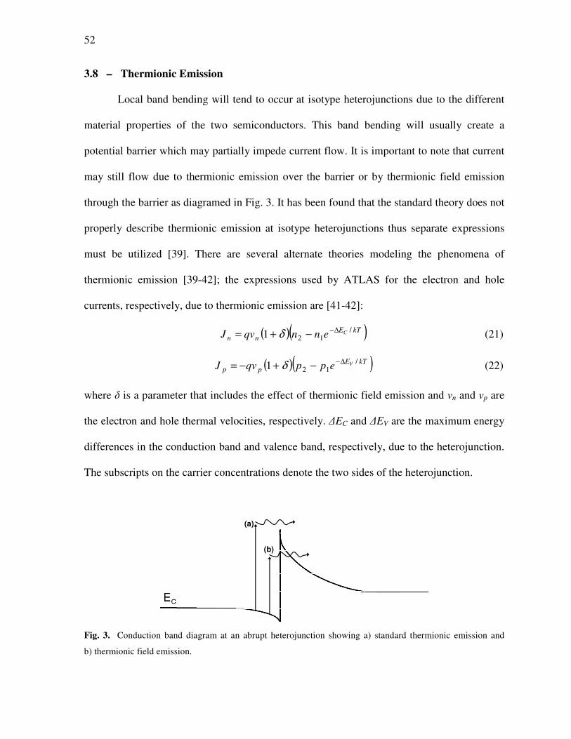
52
3.8 – Thermionic Emission
Local band bending will tend to occur at isotype heterojunctions due to the different
material properties of the two semiconductors. This band bending will usually create a
potential barrier which may partially impede current flow. It is important to note that current
may still flow due to thermionic emission over the barrier or by thermionic field emission
through the barrier as diagramed in Fig. 3. It has been found that the standard theory does not
properly describe thermionic emission at isotype heterojunctions thus separate expressions
must be utilized [39]. There are several alternate theories modeling the phenomena of
thermionic emission [39-42]; the expressions used by ATLAS for the electron and hole
currents, respectively, due to thermionic emission are [41-42]:
( )( )kTEnn
CennqvJ/
121∆−−+= δ (21)
( )( )kTEpp
VeppqvJ/
121∆−−+−= δ (22)
where δ is a parameter that includes the effect of thermionic field emission and vn and vp are
the electron and hole thermal velocities, respectively. ∆EC and ∆EV are the maximum energy
differences in the conduction band and valence band, respectively, due to the heterojunction.
The subscripts on the carrier concentrations denote the two sides of the heterojunction.
(a)
(b)
Fig. 3. Conduction band diagram at an abrupt heterojunction showing a) standard thermionic emission and
b) thermionic field emission.

53
Usually the thermal velocities follow from the equipartition theorem [10, 30];
however, in this thermionic emission model, the thermal velocities are determined by
C
nn
qN
TAv
2*
= V
p
pqN
TAv
2*
= , (23)
where
3
*2* 4
h
mqkA n
n
π=
3
*2
*4
h
mqkA
p
p
π= (24)
are the electron and hole effective Richardson’s constants, respectively. The minimum
valued Richardson’s constants between region 1 and region 2 are used in the determination of
the thermal velocities [42].
Finally, if the barrier width is thin enough, then field emission may supplement the
thermionic emission, i.e. thermionic field emission is said to occur. This is included in the
thermionic emission model by the δ-parameter:
( )∫ ∫+
−−
−= +
+)0(
0
* )()0(22
exp)0(
exp1 C
m
EE
E
x
CnC xEEmdx
kT
EEdE
kT hδ , (25)
which follows from the Wentzel-Kramers-Brillouin approximation. The parameters in (25)
are schematically described in Fig. 4 and Em = maxEC(0+), EC(W). A similar expression
exists for holes by making use of the valence band and hole effective mass instead of the
conduction band and electron effective mass.
Use of this thermionic emission model determines the current densities at
heterojunction interfaces for subsequent use in the continuity equations. This model is
invoked in the ATLAS deck in the INTERFACE statement by specifying THERMIONIC S.S
for standard thermionic emission or THERMIONIC TUNNEL S.S for thermionic field
emission.

54
Fig. 4. Conduction band diagram of an isotype heterojunction. The parameters schematically define those used
in (25). ∆EC is the same as that used in (21). (After [30].)
3.9 – Luminous Module
The operation of a solar cell is heavily dependant on the light that impinges onto it as
well as the subsequent propagation of electromagnetic radiation throughout the device. How
much light is able to transmit through each layer of the device and the propensity for that
light to be absorbed and induce carrier photogeneration all play important roles in a solar
cell’s ultimate performance. Therefore it is paramount to device modeling that the
electrodynamics of the incident light as well as its interaction with the semiconductor are
properly accounted for.
The Luminous module supplements the ATLAS framework by including ray tracing
and photoabsorption algorithms [30]. After inputting any variant of a monochromatic or
spectral light source, Luminous determines the intensity of the optical field throughout the
device and determines photogeneration rates for use in the carrier continuity equations.
Luminous is invoked by specifying a light source in the BEAM statement. This light source is
monochromatic; its wavelength is determined by setting a value to the LAMBDA parameter
of the SOLVE statement. The light source can be made spectral in the BEAM statement by
including a data file specified by the POWER.FILE parameter. In this chapter the AM0 solar

55
spectrum (Fig. 5), as discussed in Section 1.3, is utilized to obtain device I-V characteristics.
A spectrally varying monochromatic source is used to obtain a short-circuit current spectral
response.
0
200
400
600
800
1000
1200
1400
1600
1800
2000
2200
0.2 0.7 1.2 1.7 2.2 2.7 3.2 3.7
Wavelength (µm)
Spec
tral R
adia
nce
(W
/m2/µ
m)
Fig. 5. The ASTM standard air mass zero (AM0) solar spectrum [16]; this is used as the spectral illumination
source in the device simulations.
3.10 – Fresnel Coefficients
An electrodynamic treatment of the reflection and transmission of light at an interface
gives rise to the Fresnel equations [43]:
)sin(
)sin(
ti
tisr
θθ
θθ
+
−−= (26)
)tan(
)tan(
ti
tipr
θθ
θθ
+
−= (27)
)sin(
cossin2
ti
itst
θθ
θθ
+= (28)
)cos()sin(
cossin2
titi
itpt
θθθθ
θθ
−+= (29)

56
where r and t are the amplitude coefficients of the reflected and transmitted light,
respectively; i.e. these values multiplied by the amplitude of the incident optical field gives
the amplitudes of the reflected and transmitted optical fields. The subscripts s and p indicate
the polarization. θi is the angle of incidence and θt is the angle of transmission, both with
respect to the surface normal (Fig. 6) and related by Snell’s law
ttii nn θθ sinsin = . (30)
In (30), ni is the index of refraction in the medium of the incident wave and nt is the index of
refraction in the medium of the transmitted wave; both of which may either be real or
complex quantities.
θi
θt
θi
θt
Fig. 6. Diagram of a light ray incident on a surface and refracting at the interface; this defines the angles used
in (26)-(30).
The square of each of (26)-(29) gives the corresponding intensity coefficients; i.e. the
square of these values multiplied by the intensity of the incident light wave gives the
intensities of the reflected and transmitted light waves. For the special case of normal
incidence θi = θt and the reflection and transmission intensity coefficients, respectively, are

57
2
22
+
−===
it
itps
nn
nnrrR (31)
( )2
22 4
it
itps
nn
nnttT
+=== . (32)
The Fresnel model is automatically solved by ATLAS at every material interface
whenever light propagation is included [30]. It gives a physics-based modification to the light
beam as it traverses through the device structure and impinges upon an interface. The model
does not take into account the wave nature of electromagnetic radiation as the material
dimensions approach the wavelength of light culminating in the phenomenon of interference.
3.11 – Photogeneration
When photons with sufficient energy impinge onto a semiconductor, those photons
may excite valence electrons up to the conduction band thus photogenerating an electron-
hole pair. This is the basis on which a solar cell operates upon. The photogeneration rate is
modeled in ATLAS as [30]:
yph e
hc
PG
ααλ
η −= 0 (33)
where η0 is the internal quantum efficiency of an absorbed photon, λ is the optical
wavelength, α is the absorption coefficient, y is the relative distance for the ray in question,
and P is a coefficient that tracks the cumulative effects of transmission, reflection, and loss
throughout the device. The absorption coefficient, sometimes called the attenuation
coefficient, is given as [30, 43]:
λ
πα
k4= . (34)

58
In (34) k is the extinction coefficient; it is the imaginary part of the complex index of
refraction.
The model for photogeneration is solved by ATLAS at every node located in a
semiconductor material; it is automatically invoked whenever a light source is included. The
value determined at each node for (33) then becomes an input for the carrier continuity
equations.
As light propagates through a material, a loss in the optical intensity will usually be
incurred. This is given by a simple exponential law [43]:
yeIyI α−= )0()( (35)
where I is the optical intensity. Application of this law is explicitly seen in (33). ATLAS also
accounts for (35) by the P factor which modifies the optical ray as it traverses the device
through any type of material.
3.12 – Quantum Effects
Additional models are necessary to account for the quantum effects that occur in
nanostructures. InAs quantum wells will be considered as an approximation to InAs quantum
dots. In this work, the epitaxial growth direction is taken to be along the y-axis; this is the
axis along which quantum confinement is considered.
The defining feature of a quantum well is the realization of a two-dimensional
electron gas (2DEG); this is in contrast to the three-dimensional electron gas of a bulk
material. Due to quantum confinement of the 2DEG, the carrier statistics theory represented
by (8)-(13) breaks down and must be superseded by a two-dimensional model.

59
In two-dimensions the density of states is constant at each energy eigenvalue Ei and is
given as [44]:
∑ −Θ=i
in EE
mEN )(2)(
2
*
hπ (36)
where Θ is the Heaviside step function. Substituting into (7) yields the two-dimensional
electron concentration
( )∑ −−+=i
kTEEn FiekTm
n/)(
2
*
1ln2hπ
. (37)
To account for charge localization throughout the width of the quantum well, and assuming
uniformity in the growth plane, (37) is modified to include the corresponding
eigenfunctions Ψi [30]:
( )∑ −−+Ψ=i
kTEEi
n FieykTm
yn/)(2
2
*
1ln)(2)(hπ
. (38)
Similarly for the two-dimensional hole concentration:
( )∑−−
+Ψ=j
kTEE
j
p jFeykTm
yp/)(2
2
*
1ln)(2)(hπ
. (39)
Evaluation of (38) and (39) requires knowledge of the conduction band and valence
band eigenstates; this obtained by solving the effective mass Schrödinger equation for
electrons
iiiCi
n
EEm
Ψ=Ψ+Ψ∇⋅∇−*
2 1
2
h (40)
and for holes
jjjVj
p
EEm
Ψ=Ψ−Ψ∇⋅∇−*
2 1
2
h. (41)

60
Justification for these equations is given in Appendix I. Note that there will actually be two
sets of solutions for (41); one for heavy holes and one for light holes, with the appropriate
use of effective mass. Although not considered in this work, it is mentioned for completeness
that multiple sets of solutions will occur for (40) when considering indirect band
semiconductors to account for the directionality of the effective mass.
3.13 – Spontaneous Emission
The radiative recombination model described by (20) only accounts for the reduction
of electron-hole pairs for use in the continuity equations. In reality, the direct relaxation of an
electron to the valence band culminates in the emission of light. Analysis of this feature can
be very enlightening; this is even more so for quantum wells since quantization of energy
levels will lead to an emission spectrum differing from the bulk scenario.
Following from Fermi’s golden rule, an A·p analysis leads to a spectrally-dependent
spontaneous emission rate [45]:
( ))(1)()()()(2
0
2
EfEfEDEMEm
qEr ji −= ρ
ε
πh (42)
where E refers to the emitted photon energy, m0 is the free electron mass, and the electron
relaxation occurs between the ith
conduction band eigenlevel and the jth
valence band
eigenlevel. The optical density of modes is [46]:
332
23
)(c
EnED
hπ= (43)
where n is the index of refraction and c is the speed of light. The reduced mass density of
states is given as [30]:

61
t
mr
2hπ
ρ = (44)
where t is the quantum well thickness and the reduced mass is
**
**
pn
pn
rmm
mmm
+= . (45)
The Fermi-Dirac distribution in the quantum well for electrons in the conduction band is
( )
1
*
exp1
−
−−−+=
kT
EEEE
fFijm
m
i
in
r
(46)
and similarly for holes,
( )1
*
exp1
−
−−−
+=kT
EEEE
fFijm
m
j
j
p
r
(47)
where Eij = Ei - Ej is the transition energy from the ith
conduction band eigenlevel to the jth
valence band eigenlevel.
In (42), the momentum matrix element M(E) is used instead of the electric dipole
moment matrix element as a result of the A·p derivation [45]. This quantity is calculated
as [30, 47]:
jiAMEM ΨΨ= 0)( (48)
where A is an anisotropy factor and M0 is the bulk momentum matrix element. Models exist
to calculate M0 [30, 45]; however, empirically tabulated values exist for the common direct-
gap semiconductors [36]. The anisotropy factors are dependent on the type of holes being
considered as well as the polarization of the electromagnetic field; for heavy holes subject to
TE polarization:

62
<
>+
=
ij
ij
ij
EE
EEEE
A
2/34
/33
, (49)
for light holes and TE polarization:
<
>−
=
ij
ij
ij
EE
EEEE
A
2/14
/35
, (50)
for heavy holes and TM polarization:
<
>−
=
ij
ij
ij
EE
EEEE
A
02
/33
, (51)
and for light holes and TM polarization:
<
>+
=
ij
ij
ij
EE
EEEE
A
22
/31
. (52)
Note that (42) remains valid for bulk material; however, M(E) is substituted by M0,
the energy eigenvalues are replaced by the conduction and valence band edges, Eij becomes
the bandgap Eg, and (44) is replaced by
3
2/12/3
2
)(2)(
h
gr EEmE
−=
πρ . (53)
3.14 – Band-to-Band Tunneling
In the presence of sufficiently large electric fields or sufficiently thin potential
barriers, band to band tunneling may occur. This effect is modeled in ATLAS as an additive
generation term to the carrier continuity equations as [30, 69, 70]:
EBeAEG
/−= γ (54)

63
where E is the magnitude of the local electric field and A, B, and γ are adjustable fitting
parameters. For direct-gap semiconductors, A, B, and γ are usually given as
9.6615×10¹⁸
V-1
-s-1
-cm-2
, 30 MV/cm, and 2, respectively [66]. For indirect-gap
semiconductors, these parameters are usually given as 4×10¹⁴
V-1
-s-1
-cm-2
, 19 MV/cm, and
2.5, respectively [69-70].
It should be noted that in ATLAS this model is outside the framework of and separate
from the quantum effects module. It is invoked in the MODELS statement by specifying
BBT.STD for direct-gap transitions and BBT.KL for indirect-gap transitions.
3.15 – Material Parameters
To accurately simulate a semiconductor device, the correct fundamental material
parameters must be provided for use in the models previously discussed. ATLAS contains a
vast library of the most recently accepted values of many of these parameters [30]; these
have been compared to the literature for correctness [10, 36, 48, 49]. The majority of the
fundamental parameters are listed in Table I for AlAs, GaAs, Ge, In0.48Ga0.52P, and InAs;
these semiconductors will be the focus for the remainder of this chapter.
Table I
Material Parameters for Selected Semiconductors
εr Eg
(eV)
χ
(eV)
NC
(cm-3
)
NV
(cm-3
)
ni
(cm-3
) mn
*/m0 mp
*/m0
An*
(A/cm2-K
2)
Ap*
(A/cm2-K
2)
AlAs 10.3 2.16 3.50 1.50×10¹⁹
1.81×10¹⁹
11.6 0.710 0.804 85.3 96.6
GaAs 13.2 1.42 4.07 4.35×10¹⁷
1.29×10¹⁹
2.67×10⁶ 0.0670 0.642 6.29 105
Ge 16.0 0.663 4.00 1.05×10¹⁹
3.95×10¹⁸
1.73×10¹³
0.559 0.292 67.4 35.0
InGaP 11.8 1.89 4.08 9.26×10¹⁷
8.87×10¹⁸
391 0.111 0.500 13.3 60.1
InAs 14.6 0.350 4.67 9.33×10¹⁶
8.12×10¹⁸
1.00×10¹⁵
0.0240 0.471 2.88 56.6
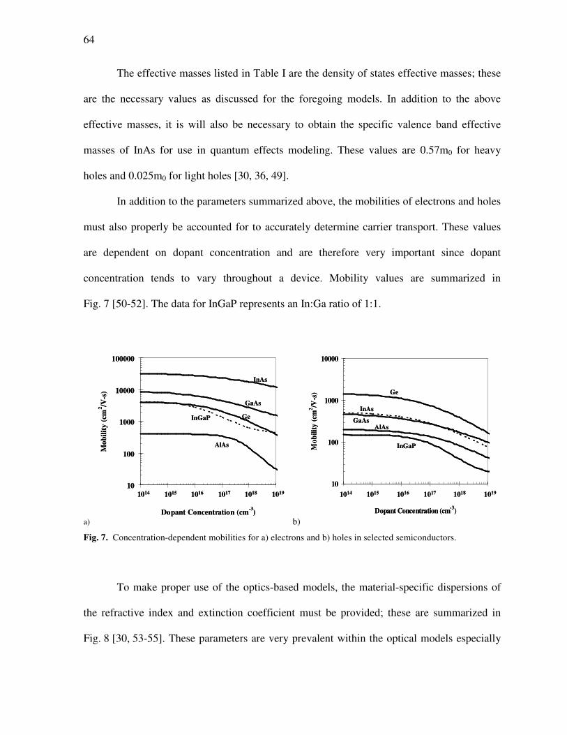
64
The effective masses listed in Table I are the density of states effective masses; these
are the necessary values as discussed for the foregoing models. In addition to the above
effective masses, it is will also be necessary to obtain the specific valence band effective
masses of InAs for use in quantum effects modeling. These values are 0.57m0 for heavy
holes and 0.025m0 for light holes [30, 36, 49].
In addition to the parameters summarized above, the mobilities of electrons and holes
must also properly be accounted for to accurately determine carrier transport. These values
are dependent on dopant concentration and are therefore very important since dopant
concentration tends to vary throughout a device. Mobility values are summarized in
Fig. 7 [50-52]. The data for InGaP represents an In:Ga ratio of 1:1.
a)
10
100
1000
10000
100000
1E+14 1E+15 1E+16 1E+17 1E+18 1E+19
Dopant Concentration (cm-3
)
Mo
bil
ity
(cm
2/V
-s)
1014 1015 1016 1017 1018 1019
InGaP
AlAs
Ge
GaAs
InAs
10
100
1000
10000
100000
1E+14 1E+15 1E+16 1E+17 1E+18 1E+19
Dopant Concentration (cm-3
)
Mo
bil
ity
(cm
2/V
-s)
1014 1015 1016 1017 1018 1019
InGaP
AlAs
Ge
GaAs
InAs
b)
10
100
1000
10000
1E+14 1E+15 1E+16 1E+17 1E+18 1E+19
Dopant Concentration (cm-3
)
Mo
bil
ity
(cm
2/V
-s)
1014 1015 1016 1017 1018 1019
InGaP
AlAs
Ge
GaAs
InAs
10
100
1000
10000
1E+14 1E+15 1E+16 1E+17 1E+18 1E+19
Dopant Concentration (cm-3
)
Mo
bil
ity
(cm
2/V
-s)
1014 1015 1016 1017 1018 1019
InGaP
AlAs
Ge
GaAs
InAs
Fig. 7. Concentration-dependent mobilities for a) electrons and b) holes in selected semiconductors.
To make proper use of the optics-based models, the material-specific dispersions of
the refractive index and extinction coefficient must be provided; these are summarized in
Fig. 8 [30, 53-55]. These parameters are very prevalent within the optical models especially

65
in dictating light transmission and reflection at an interface and in determining the photo-
generation of charge carriers. The data for InGaP represents an In:Ga ratio of 1:1.
a)
1
2
3
4
5
6
0.2 0.3 0.4 0.5 0.6 0.7 0.8
Wavelength (µm)
Ind
ex o
f R
efra
ctio
n
InGaP
AlAs
GeGaAs
InAs
1
2
3
4
5
6
0.2 0.3 0.4 0.5 0.6 0.7 0.8
Wavelength (µm)
Ind
ex o
f R
efra
ctio
n
InGaP
AlAs
GeGaAs
InAs
b)
0
1
2
3
4
5
0.2 0.3 0.4 0.5 0.6 0.7 0.8
Wavelength (µm)C
oef
fici
ent
of
Ex
tin
ctio
n
InGaPAlAs
Ge
GaAs
InAs
0
1
2
3
4
5
0.2 0.3 0.4 0.5 0.6 0.7 0.8
Wavelength (µm)C
oef
fici
ent
of
Ex
tin
ctio
n
InGaPAlAs
Ge
GaAs
InAs
Fig. 8. Optical parameter dispersions for selected semiconductors: a) index of refraction and b) coefficient of
extinction.
3.16 – General Simulation Methodology
As previously discussed, the ATLAS simulation methodology is a form of finite
element analysis. A mesh defines the device structure and the physical models are solved at
each nodal point throughout that mesh. The mesh must be spatially fine enough to adequately
resolve the device structure and accurately determine the physics thereof; however, an
extremely large number of nodes will greatly slow down computation time and there is also a
maximum limit programmed into ATLAS.
The issue of mesh resolution poses a problem for solar cell modeling. ATLAS was
originally designed for traditional microelectronics such as the transistors used in integrated
circuits. In such devices, the dimensions under consideration tend to all be of the same order
of magnitude; this is ideal for finite element meshing. In solar cells, however, the top wafer

66
area may be several square-centimeters, if not larger, while the actual device may only
extend several microns deep into the wafer. Add to this the fact that the feature size of the
contact grid may also be on the order of micron width but have centimeter lateral extent.
Also, even though the actual device depth may only be several microns, these devices are
usually fabricated on the top portion of a substrate with a thickness of hundreds of microns.
Clearly, the varying dimensions in the common solar cell are not well-suited for finite
element meshing. Due to this, careful thought must be put into the simulation methodology.
The device design considered in this work is a rectangular solar cell with regularly
spaced contact grid fingers; these grid fingers run parallel to two edges of the solar cell. This
device is modeled in ATLAS as a two-dimensional structure consisting of only a portion of
the width of an actual device as shown in Fig. 9.a. Note that this model contains the cross-
section of one full finger of the contact grid. The substrate is also truncated so that its
thickness is on the order of that of the other layers (this is allowed because photogeneration is
negligible in this region; a lumped series resistance may be added to the model to account of
transport through the substrate if necessary).
The structure as shown in Fig. 9.a is what is actually simulated in ATLAS. Results
that are geometry dependent (e.g. current) are normalized to 1 µm of depth into the page.
Such results may then be multiplied by appropriate scaling factors so that they are
comparable to the results from actual devices. Multiplying by the actual length of the grid
finger scales the results as if they were for a three-dimensional structure as in Fig. 9.b.
Finally, multiplying by the number of similar regions that make up an actual device scales
the results so that they are comparable to experiment; Fig. 9 summarizes this methodology.

67
Using this method allows for the simulation of a solar cell without running into the problems
arising due to the varying dimensions within an actual device.
x
y
z
x
y
z
Fig. 9. The solar cell is modeled as a) a two-dimensional structure using only one grid finger. These
approximations keep computation time to a minimum. Final results that are dependent on geometry, e.g.
current, are modified by a scaling factor to account for b) the three-dimensional nature of an actual device. An
additional factor is included to c) account for the desired number of grid fingers to make the model comparable
to an actual device. The coordinate axes are those referenced by ATLAS.
3.17 – Unoptimized Single-Junction Solar Cell
Although the solar cell device structure diagramed in Fig. 9 represents the main focus
of this work, it is instructional and worthwhile to introduce photovoltaic device simulation
with a relatively unoptimized and simple device structure. The device discussed in this
section is a simple GaAs p-i-n solar cell as shown in Fig. 10. The i-layer is actually not
necessary for this specific device but is included because it will become a necessity in the
discussion to follow. The emitter is doped at 1018
acceptors/cm3 and the base at 10
17
donors/cm3. The analyzed structure is 400 µm wide with an 8 µm contact centered atop. The
nominal layer thicknesses are 500 nm, 100 nm, and 2,000 nm for the emitter, i-layer, and
base, respectively. This structure is scaled, post-processing, to simulate a 25 grid finger,
1x1 cm2 solar cell.

68
n-GaAs Base
i-GaAs
p-GaAs Emitter
n-GaAs Base
i-GaAs
p-GaAs Emitter
Fig. 10. Simulated GaAs p-i-n solar cell.
The main device characterization methods for a solar cell are to analyze its current-
voltage characteristics under illumination and also to determine the cell’s spectral response to
pertinent wavelengths. These tests are therefore simulated for the defined dive structure;
important device metrics are also extracted from the I-V curve. Simulated results for the
open-circuit voltage Voc, short-circuit current Isc, maximum power Pm, fill factor FF, and
device efficiency η are summarized in Table II. The significant digits of the reported values
are taken so as to be comparable to experimental data [4, 71]. This data indicates a relatively
low efficiency due primarily to the small amounts of current being driven through the device.
The poor performance indicated here is due to the fact that the device structure is
unoptimized.
Table II
Device Metrics for the Unoptimized p-i-n Device
Voc Isc Pm FF η
0.93 V 9.4mA 7.5 mW 86 % 5.5 %
Although the optimization of the device structure in Fig. 10 is not of great importance
for this work, it is exemplary to perform further analysis for the sake of illustrating the power
of device simulation. Current-voltage characteristics are shown in Figs. 11.a-c for cases of
varying the individual layer thicknesses from the nominal values. In all three cases, there is

69
negligible variance in the open-circuit voltage. Increasing the thicknesses of either the i-layer
(Fig. 11.b) or base (Fig. 11.c) leads to very small enhancements in device performance. This
indicates that the increased thicknesses allow for the increased photogeneration of charge
carriers; however, the increase is minute. It can be inferred from this observation that the vast
majority of light incident on to the cell is absorbed since the increased base or i-layer
thicknesses do not lead to large increases in device performance.
In sharp contrast to the behavior of varying the thicknesses of the base and i-layer, it
is rather a decrease in the emitter thickness that leads to increased device performance. Also
in contrast to the previous discussion, the increased device performance due to the decreased
emitter thickness is much more prominent as indicated by Fig. 11.a. From this data, it is clear
that the smaller emitter thicknesses allow for a larger amount of current to be extracted from
the device. The interpretation of these results is that the effect of the thinner emitter is to
mask the effect of surface recombination. As the emitter becomes thinner, more photons are
able to reach the base, where surface recombination is not an issue, thus leading to the
increased currents. More explicitly, after the photogeneration of an electron-hole pair in the
n-type base, the electron will preferentially stay in the base and propagate towards the
cathode while the hole will be swept by the contact potential to the p-type emitter and
towards the anode. For either the electron or the hole, surface recombination becomes a non-
issue since they are majority carriers in their current respective locations. The dramatic
increase in device performance due to the emitter variation is compared to the small increase
observed for base variation in Fig. 11.d.

70
a)
0
2
4
6
8
10
12
14
16
18
0 0.2 0.4 0.6 0.8 1
Voltage (V)
Cu
rren
t (m
A/c
m2)
100 nm
300 nm
500 nm
700 nm
900 nm
b)
0
2
4
6
8
10
0 0.2 0.4 0.6 0.8 1
Voltage (V)
Cu
rren
t (m
A/c
m2) 50 nm
150 nm
c)
0
2
4
6
8
10
0 0.2 0.4 0.6 0.8 1
Voltage (V)
Cu
rren
t (m
A/c
m2) 1.5 µm
2.5 µm
d)
0
2
4
6
8
10
-500 -250 0 250 500
Change in Layer Thickness (nm)
Eff
icie
ncy
(%
)Emitter
Base
Fig. 11. Current-voltage characteristics for deviations from the nominal thicknesses: a) varying emitter
thickness, b) varying i-layer thickness, and c) varying base thickness. d) Simulated efficiencies comparing the
effect of varying the base and emitter thicknesses from nominal values.
Also analyzed was the spectral response under the conditions of varied layer
thicknesses; this data is plotted as quantum efficiency as a function of wavelength in Fig. 12.
The results back up the previously drawn conclusions as well as serve to elucidate on the
wavelength-dependent performance of the device. This data shows that the slight increase in
device performance due to the increased i-layer or base thicknesses is due to increased
absorption at longer wavelengths (Figs. 12.b-c). In distinct contrast to this, the decreased
emitter thickness leads to an increased quantum efficiency throughout the super-bandgap part

71
of the spectrum (Fig. 12.a). In addition, the peak photogeneration shifts from near the
bandgap wavelength to shorter wavelengths. These observations indicate that, for decreased
emitter thicknesses, a larger amount of photons throughout the entire spectrum are able to
reach the base as previously hypothesized; this includes higher energy photons which are
often readily absorbed by thicker emitters.
a)
0
0.1
0.2
0.3
0.4
0.5
0.6
0.3 0.4 0.5 0.6 0.7 0.8 0.9 1Wavelength (µm)
Qu
an
tum
Eff
icie
ncy
100 nm
300 nm
500 nm
700 nm
900 nm
b)
0
0.1
0.2
0.3
0.4
0.3 0.4 0.5 0.6 0.7 0.8 0.9 1Wavelength (µm)
Qu
an
tum
Eff
icie
ncy
50 nm
150 nm
c)
0
0.1
0.2
0.3
0.4
0.3 0.4 0.5 0.6 0.7 0.8 0.9 1Wavelength (µm)
Qu
an
tum
Eff
icie
ncy
1.5 µm
2.5 µm
Fig. 12. Spectral responses for varied a) emitter thicknesses, b) i-layer thicknesses, and c) base thicknesses.
These results give spectral information lacking in the I-V characteristics and further elaborate on conclusions
drawn from those characteristics.
3.18 – Optimized Single-Junction Solar Cell
The device structure shown in Fig. 13 represents a p-i-n solar cell optimized with
respect to the device considered in the foregoing section. The device is optimized by the
inclusion of two In0.48Ga0.52P layers; one acting as a back surface field (BSF) and the other as
the top window (sometimes called a front surface field). These two layers, being of larger
bandgap than GaAs and appropriately doped, provide for large electric fields at the two ends
of the active portion of the device. These electric fields reflect and accelerate minority
carriers towards the junction thus reducing surface recombination effects and increasing solar
efficiency. Conversely, one may speak of the potential that arises due to the electric field.
From this point of view, the window and BSF layers introduce large potential barriers for

72
minority carriers thus reflecting them towards the junction. This is clearly seen in the
simulated band diagram in Fig. 14. Note that the larger bandgap of InGaP with respect to
GaAs allows for the most pertinent portion of the incident light spectrum to reach the GaAs
layers unattenuated.
n+GaAs Substrate
n-InGaP BSF
n-GaAs Base
i-GaAs
p-GaAs Emitterp-InGaP Windowp+GaAs Contact
n+GaAs Substrate
n-InGaP BSF
n-GaAs Base
i-GaAs
p-GaAs Emitterp-InGaP Windowp+GaAs Contact
Fig. 13. Simulated GaAs p-i-n solar cell; the device is optimized with respect to that of Fig. 10.
The emitter, i-layer, and base retain the nominal thicknesses and dopings from the
foregoing discussion of the unoptimized device. The InGaP layers are both 50 nm thick with
a 2×10¹⁸
cm-3
acceptor concentration in the window and 1×10¹⁸
cm-3
donor concentration in
the BSF layer. The contact layer is highly doped at an acceptor concentration of 1×10¹⁹
cm-3
and with a thickness of 10 nm. This layer is etched away to exist only under the metal finger;
this allows incident light to proceeded to the remainder of the device unattenuated. The
purpose of the i-layer is to eventually host a nanostructure array as discussed in Section 3.19.

73
-2
-1.5
-1
-0.5
0
0.5
1
1.5
2
0 0.5 1 1.5 2 2.5
Device Depth (µm)
En
erg
y (
eV)
EC
EV
EF
-2
-1.5
-1
-0.5
0
0.5
1
1.5
2
0 0.5 1 1.5 2 2.5
Device Depth (µm)
En
erg
y (
eV)
EC
EV
EF
Fig. 14. Simulated band diagram of the optimized p-i-n GaAs cell at thermodynamic equilibrium. The window
and BSF layers introduce large potential barriers for minority carriers at either end of the device; this causes
photogenerated minority carriers to preferentially traverse towards the junction. The energy axis is taken with
reference to the Fermi level.
In simulating the optimized p-i-n solar cell, it was found that the results were very
dependent on the optical parameters of the materials considered. This was especially noted in
comparing the complex index of refraction of InGaP from a commercial database [55] and
from another device simulator [59] as shown in Fig. 15. Although the data from these two
sources follow similar trends, they are fundamentally different. Additionally, a slight
modification to the commercial data was made at long wavelengths in order to create a more
accurate model. The physical effect of this modification, as seen in Fig. 15, is to reduce the
long wavelength reflection at the InGaP surface but to increase the reflection at the InGaP-
GaAs interface. The modification of such a fundamental material property is justified
because InGaP is not a simple chemical compound but rather a more complex alloyed
material. The variable ordering of Ga and In atoms will very well have an effect on the bulk

74
properties of the alloyed material. Long range ordering may even lead to InP-GaP
superlattices [62-65].
0
1
2
3
4
5
0.2 0.3 0.4 0.5 0.6 0.7
Wavelength (µm)
n, k
Refractive
Index
Extinction
Coefficient
0
1
2
3
4
5
0.2 0.3 0.4 0.5 0.6 0.7
Wavelength (µm)
n, k
Refractive
Index
Extinction
Coefficient
Fig. 15. Index of refraction and coefficient of extinction of In0.5Ga0.5P from two sources: sold curve [55], dark
dashed curve [59]. The lighter dashed curve shows a modification made to the data from [55] in order to more
accurately model the device.
Simulated results comparing the use of the two sets of InGaP optical parameters are
summarized in Table III and Fig. 16 along with experimental data. Following from Fig. 16.a,
between all three examples, the open-circuit voltages Voc and the fill factors FF are
approximately equal. The only discrepancy that arises is in the short circuit currents Isc (i.e.
although some deviation also arises in the maximum powers Pm and in the efficiencies η,
these quantities may be derived from the three foregoing metrics). Additional information,
directly relating to Isc can be obtained from the spectral response in Fig. 16.b. This clearly
indicates that the use of the database values [55] for InGaP leads to device simulations that
accurately model the spectrally-dependent nature of the solar cell considered here. It has also
been acknowledged that the three short-circuit currents listed in Table III are all within the

75
experimental error observed in testing solar cells at two different test sites. Additional error
may be present in experimentally simulating the AM0 solar spectrum by a Xe arc lamp
whereas modeling results make use of standard accepted data for the actual spectrum. Details
of the fabrication of the experimental device are found in Ref. [71].
Table III
Device Metrics of the Optimized p-i-n Cell
Ref. for
InGaP n, k Voc Isc Pm FF η
[55] (Modified) 1.04 V 23.7 mA 20.3 mW 82.4 % 14.9 %
[59] (As Is) 1.04 V 24.5 mA 21.4 mW 83.9 % 15.7 %
N/A (Experiment) 1.04 V 24.7 mA 21.6 mW 83.7 % 15.8 %
a)
0
5
10
15
20
25
0 0.2 0.4 0.6 0.8 1
Voltage (V)
Cu
rren
t (m
A/c
m2)
b)
0
0.2
0.4
0.6
0.8
0.3 0.4 0.5 0.6 0.7 0.8 0.9 1
Wavelength (µm)
Qu
an
tum
Eff
icie
ncy
Fig. 16. Electrical results of the optimized p-i-n solar cell. In both plots, the solid curves use the InGaP optical
data from [59] while the dashed curves use the modified data from [55]; the individual data points represent
experimentally obtained data.
Part of the allure of using a device simulator is to look at physical properties not
easily investigated under experimental conditions. As an example of this, Fig. 17.a shows a
surface plot of the photogeneration rate throughout the device under AM0 illumination and at
zero bias. The plot indicates that the majority of photogeneration does, in fact, occur within

76
the first micron of depth. To better see the photogeneration throughout the device, Fig. 17.b
plots this data as a function of depth on a logarithmic scale. Discontinuities in this plot occur
at GaAs-InGaP interfaces. Additionally, the substantial decrease in photogeneration at the
BSF layer indicates that the vast majority of photons of 656 nm wavelength and shorter have
already been absorbed by that point. In Fig. 17.a, it appears that no photogeneration occurs
down the center of the device; this is because the metal finger screens most of the light that
impinges onto that area (cf. Fig. 13).
a)
9×1020 cm-3-s-1
1×1022 cm-3-s-1
2×1021 cm-3-s-1
9×1020 cm-3-s-1
1×1022 cm-3-s-1
2×1021 cm-3-s-1
9×1020 cm-3-s-1
1×1022 cm-3-s-1
2×1021 cm-3-s-1
9×1020 cm-3-s-1
1×1022 cm-3-s-1
2×1021 cm-3-s-1
b)
1E+16
1E+17
1E+18
1E+19
1E+20
1E+21
1E+22
1E+23
0.0 0.5 1.0 1.5 2.0 2.5
Relative Depth (µm)
Ph
oto
gen
era
tio
n
Ra
te (
cm
-3-s
-1)
1016
1017
1018
1019
1020
1021
1022
1023
1E+16
1E+17
1E+18
1E+19
1E+20
1E+21
1E+22
1E+23
0.0 0.5 1.0 1.5 2.0 2.5
Relative Depth (µm)
Ph
oto
gen
era
tio
n
Ra
te (
cm
-3-s
-1)
1016
1017
1018
1019
1020
1021
1022
1023
Fig. 17. Carrier photogeneration rate plotted a) as a surface plot throughout the device structure and b)
logarithmically as a function of device depth. The device layer shown in the surface plot, from top to bottom,
are the window, emitter, i-layer, base, and BSF layer. No photogeneration occurs down the center of the device
because impingent light is blocked by the metal finger. Discontinuities occur in the semi-log plot at GaAs-
InGaP interfaces.
Device simulations also allow for the analysis of device performance under non-ideal
or degraded conditions. This allows one to determine possible process tolerances and also
enables the testing of hypotheses regarding possible degradation mechanisms. The effect on
the I-V characteristics of a non-negligible contact resistance is shown in Fig. 18.a. In these
simulations, a non-zero contact resistance was placed on each electrode to show the
importance of good metallization. This data indicates that the negative effects of a non-zero

77
contact resistance, namely an increased solar cell series resistance, become non-negligible
when this value is on the order of 10-2
Ω–cm2. Increased contact resistances above that value
lead to even more dramatic degradations in device performance. Device metrics extracted
form the data in Fig. 18.a are listed in Table IV.
Device degradation due to increased carrier recombination is shown in Fig. 18.b. In
these simulations, carrier recombination is increased by decreasing the lifetimes used in the
Shockley-Read-Hall recombination model. In contrast to Fig. 18.a where the degradation
originally occurs at the knee of the I-V curve, the increased carrier recombinations in
Fig. 18.b immediately begin to degrade both Isc and Voc; this is indicative of a shunting
mechanism. Pertinent device metrics are listed in Table V. The numerical values in
Tables IV-V are taken out to several significant digits for fine comparison and are within the
limits of computer precision.
a)
0
5
10
15
20
25
0 0.2 0.4 0.6 0.8 1
Voltage (V)
Cu
rren
t (m
A/c
m2)
0.001 Ω-cm2
0.0
1 Ω
-cm2
0.1 Ω-cm
2
0.5 Ω-cm 20.9 Ω
-cm 2
0
0
5
10
15
20
25
0 0.2 0.4 0.6 0.8 1
Voltage (V)
Cu
rren
t (m
A/c
m2)
0.001 Ω-cm2
0.0
1 Ω
-cm2
0.1 Ω-cm
2
0.5 Ω-cm 20.9 Ω
-cm 2
0
b)
0
5
10
15
20
25
0 0.2 0.4 0.6 0.8 1
Voltage (V)
Cu
rren
t (m
A/c
m2)
1 ns
10 ns
30 ns
20 ns
50 ns
0
5
10
15
20
25
0 0.2 0.4 0.6 0.8 1
Voltage (V)
Cu
rren
t (m
A/c
m2)
1 ns
10 ns
30 ns
20 ns
50 ns
Fig. 18. Current-voltage characteristics showing device degradation due to a) non-negligible contact resistance
and b) increased carrier recombination. Increases in contact resistance, placed on both electrodes, leads to an
increase in the series resistance of the solar cell thus affecting the overall shape of the I-V characteristics.
Increased carrier recombination, modeled as a decrease in Shockley-Read-Hall carrier lifetime, immediately hits
both Isc and Voc indicating a shutting mechanism.

78
Table IV
Device Metrics for Different Contact Resistances
ρc Voc Isc Pm FF η
0 1.043 V 23.65 mA 20.32 mW 82.38 % 14.87 %
0.001 Ω-cm2
1.043 V 23.69 mA 19.98 mW 80.86 % 14.63 %
0.01 Ω-cm2 1.043 V 23.69 mA 19.74 mW 79.89 % 14.45 %
0.1 Ω-cm2 1.043 V 23.69 mA 17.27 mW 69.89 % 12.64 %
0.5 Ω-cm2 1.043 V 23.67 mA 8.935 mW 36.19 % 6.541 %
0.9 Ω-cm2 1.043 V 20.25 mA 5.390 mW 25.52 % 3.956 %
Table V
Device Metrics for Different Carrier Lifetimes
τn, τp Voc Isc Pm FF η
50 ns 1.043 V 23.65 mA 20.32 mW 82.38 % 14.87 %
30 ns 1.037 V 23.64 mA 19.67 mW 80.24 % 14.40 %
20 ns 1.030 V 23.58 mA 19.43 mW 80.00 % 14.22 %
10 ns 1.015 V 23.42 mA 18.63 mW 78.37 % 13.64 %
1 ns 0.9318 V 22.13 mA 15.45 mW 74.92 % 11.31 %
Finally, as was done in Section 3.16, it is important to check that the device structure
is, in fact, optimized for device performance. By varying the emitter and base thicknesses,
simulations showed very little change in device performance. To best show this, variations in
device efficiency due to varied layer thicknesses is plotted in Fig. 19. In regards to emitter
thickness, the nominal value is clearly the optimum value; however, it is noted that the
degraded performance due to either an increased or decreased thickness occurs over a very
small range. With regards to the base, the device efficiency is much less sensitive to
thickness variation in this layer. A small increase in the base thickness will actually lead to
an increase in efficiency; however, the performance gain is small and negligible. From
Fig. 19, the nominal device design can be considered to be optimized. Comparing this to the
device design in Section 3.16, it is evident that the InGaP window and BSF play a large role
in improving the performance of a solar cell.

79
14
14.5
15
-500 -300 -100 100 300 500
Change in Layer Thickness (nm)
Eff
icie
ncy
(%
)
Base
Emitter
Fig. 19. Simulated efficiencies comparing the effect of varying the base and emitter thicknesses from nominal
values. This indicates that the nominal design is already an optimized device.
3.19 – Dual-Junction Solar Cell
Although the purpose of studying the p-i-n solar cell in the previous discussions was
for the eventual incorporation of nanostructures in the i-layer, it is beneficial to first evaluate
the ability to model a dual-junction solar cell. As discussed in Section 2.3, the dual-junction
device, or more generally a multi-junction device, increases solar efficiency by enabling
additional and more efficient absorption throughout the solar spectrum. In regards to
nanostructured photovoltaics, the incorporation of nanostructures in the multi-junction device
may also allow for an effective bandgap tuning as discussed in Section 2.3. Therefore the
ability to model such devices would prove useful in the analysis of both present and future
solar cell designs.
The device considered in this section is the dual-junction, InGaP-GaAs, tandem solar
cell as diagramed in Fig. 20. This design places an InGaP solar cell atop the GaAs solar cell
studied in Section 3.17. From top to bottom, the InGaP design is a 100 nm GaAs contact
layer doped at 1×10¹⁹
acceptors/cm3, 30 nm AlAs window doped at 1×10
18 acceptors/cm
3,

80
100 nm InGaP emitter doped at 1×10¹⁸
acceptors/cm3, 1 µm InGaP base doped at 1×10
17
donors/cm3, and a 100 nm InGaP BSF doped at 1×10
18 donors/cm
3. In between the InGaP
and GaAs solar cells is an n-on-p GaAs tunnel junction; 5×10¹⁹
cm-3
donor concentration and
2×10¹⁹
cm-3
acceptor concentration. This layer allows for electrons in the top cell to
recombine with holes in the bottom cell by means of internal field emission thus driving the
current; this is easily seen in the device’s band diagram (Fig. 21). Similar to the design of the
bottom cell, the AlAs window and InGaP BSF of the top cell serve to reflect and accelerate
minority carriers towards the top cell junction.
n+GaAs Substrate
n-InGaP BSF
n-GaAs Base
i-GaAs
p-GaAs Emitterp-InGaP Window
GaAs Tunnel Junctionn-InGaP BSF
n-InGaP Base
p-InGaP Emitter
p+AlAs Window
p+GaAs Contact
n+GaAs Substrate
n-InGaP BSF
n-GaAs Base
i-GaAs
p-GaAs Emitterp-InGaP Window
GaAs Tunnel Junctionn-InGaP BSF
n-InGaP Base
p-InGaP Emitter
p+AlAs Window
p+GaAs Contact
Fig. 20. Device structure of the InGaP-GaAs tandem solar cell considered in this work. The InGaP top cell
more efficiently collects short-wavelength light while remaining transparent to the light more efficiently
collected by the GaAs bottom cell.

81
-2.5
-1.5
-0.5
0.5
1.5
2.5
0 1 2 3 4
Device Depth (µm)
En
erg
y (
eV)
GaAs CellInGaP Cell
EF
EC
EV
Fig. 21. Band diagram of the InGaP-GaAs solar cell drawn in Fig. 22. This clearly shows how the window and
BSF layers act as potential barriers that reflect minority carriers towards their respective junctions. Also
observable from this diagram, at ~1.35 µm, is the tunneling region that drives current between the two sub-cells.
A challenge simulating the device as shown in Fig. 20 arises due to the presence of
the tunnel junction. As previously reported [67-68], the ATLAS framework is not well suited
to handle tunneling problems. Even though such a model exists, as described in Section 3.13,
the model is semi-empirical at best and fails to extend upon that quantum effects simulator
described in Section 3.11. In practice, this model has been found to be unstable and tends to
cause the device solutions to diverge.
Due to the issue of a poorly implemented tunneling model, a convergent simulation
was unable to be obtained using the pertinent material parameters described in Section 3.14.
However, a simulation did converge by modifying the material parameters of the tunnel
junction layer as summarized in Table VI. Optical properties were kept the same; however,
the donor and acceptor concentrations were both modified to 1×10¹⁹
cm-3
. These
modifications do not imply actual physical conditions but rather are imposed simply to obtain
a convergent solution. The purpose of the tunnel junction is simply to drive current between

82
the two sub-cells. In an equivalent circuit, this can be replaced by a perfect conductor.
Therefore the modifications made in order to converge onto a solution are justified.
Table VI
Modified Material Parameters in the Tunnel Junction
εr Eg
(eV)
χ
(eV)
NC
(cm-3
)
NV
(cm-3
)
ni
(cm-3
) mn
*/m0 mp
*/m0
GaAs 13.2 1.42 4.07 4.35×10¹⁷
1.29×10¹⁹
2.67×10⁶ 0.0670 0.642
Modified 14.6 0.350 4.67 9.33×10¹⁶
8.12×10¹⁸
1.00×10¹⁵
0.0240 0.471
Another possible method to get around the problems with the tunneling model is to
replace the tunnel junction with a perfect conductor. From an equivalent circuit perspective,
this would allow current to flow freely between the two sub-cells. This is, however,
unfeasible in ATLAS. The ATLAS framework requires that all conductor regions be defined
as electrodes; therefore placing a conductor instead of the tunnel junction would not lead to
valid results.
The results of simulating the tandem cell with the discussed modifications are shown
in Fig. 22 along with experimentally obtained results. Extracted device metrics are listed in
Table VII. The data indicates that the modifications made in the tunnel junction yield results
that serve as an excellent approximation for actual devices.
Table VII
Device Metrics of the Simulated InGaP-GaAs Solar Cell
Voc Isc Pm FF η
2.474 V 10.65 mA 22.87 mW 86.80 % 16.74 %

83
0
2
4
6
8
10
12
0.0 0.3 0.6 0.9 1.2 1.5 1.8 2.1 2.4
Voltage (V)
Cu
rren
t (m
A/c
m2)
0.0
2.0
4.0
6.0
8.0
10.0
12.0
0 0.5 1 1.5 2 2.5
Task 5 Improved TandemTask 4 Baseline Tandem
Cu
rre
nt
De
nsity (
mA
/cm
2)
Voltage (V)
Fig. 22. Simulated I-V characteristic of the InGaP-GaAs tandem cell. The inset shows two separate
experimental results of the same type of device thus verifying the simulation method.
Due to the instability of the tunneling model, it proved to be difficult to run
optimization tests on the device structure as in the previous discussions. However, a different
method, in which the tunneling model may be disregarded, does prove useful. Based upon
the analyses in Sections 3.16 and 3.17, it is clear that variations in the thicknesses of the
device layers, as long as they are not overly dramatic, have a much larger effect on Isc than on
Voc. Therefore, to a very good approximation, it is sufficient to gauge relative variations in
device efficiency by relative variations in Isc. One such way to do this, while not having to
worry about the troublesome tunneling model, is to look at the spectral response of each sub-
cell in the tandem device. The general scheme for doing this is diagramed in Fig. 23. The
GaAs tunnel junction is replaced by a void in the form of a “pseudomaterial” of the same
thickness but with the refractive index and extinction coefficient of GaAs. The optical
parameters are kept to properly account for attenuation of the light ray as it traverses through
the space and for reflections at the interfaces. The device in Fig. 23 is then spectrally
illuminated with different currents individually extracted from each sub-cell; this leads to the

84
spectral response in Fig. 24 for the nominal design. Note that interference effects are not
observed since they are not accounted for in the physical models.
n+GaAs Substrate
n-InGaP BSF
n-GaAs Base
i-GaAs
p-GaAs Emitterp-InGaP Window
n-InGaP BSF
n-InGaP Base
p-InGaP Emitter
p+AlAs Window
p+GaAs Contact
GaAs CellSpectral Response
InGaP Cell
Spectral Response
n+GaAs Substrate
n-InGaP BSF
n-GaAs Base
i-GaAs
p-GaAs Emitterp-InGaP Window
n-InGaP BSF
n-InGaP Base
p-InGaP Emitter
p+AlAs Window
p+GaAs Contact
GaAs CellSpectral Response
InGaP Cell
Spectral Response
Fig. 23. Simulation scheme for analyzing the spectral response due to either sub-cell. A void replaces the GaAs
tunnel junction; however, light traverses through the void as if GaAs were present. Currents are then
individually extracted from each sub-cell while illuminated.
In comparing Fig. 24 to Fig.16.b, it is clear that the tandem cell is better suited to
perform photoconversion throughout a wider range of wavelengths. This is by virtue of each
sub-cell being situated such that they are able to more effectively convert a certain section of
the solar spectrum. The photogeneration throughout the device is displayed in Fig. 25.a for a
550 nm light source. This indicates that, at this wavelength, the vast majority of
photogeneration occurs due to the InGaP cell; this corresponds with Fig. 24. Similarly, at

85
800 nm, as shown in Fig. 25.b, InGaP is transparent to the incident light thus allowing the
GaAs cell to be the primary current source.
0
0.2
0.4
0.6
0.8
0.2 0.4 0.6 0.8 1
Wavelength (µm)
Qu
an
tum
Eff
icie
ncy
InGaP Cell GaAs Cell
Fig. 24. Spectral response of the InGaP-GaAs tandem cell showing the contributions of each sub-cell.
a)
1019 cm-3-s-1
1013 cm-3-s-1
1010 cm-3-s-1
1016 cm-3-s-1
1021 cm-3-s-1
b)
1021 cm-3-s-1
1019 cm-3-s-1
1017 cm-3-s-1
0
105 cm-3-s-1105 cm-3-s-1
Fig. 25. Photogeneration rate throughout the device for a) a 550 nm and b) 800 nm light source. For the 550 nm
illumination, the photogeneration occurs primarily in the InGaP sub-cell; no photogeneration occurs in that cell
at 800 nm.

86
As stated, the spectral response in Fig. 24, being free from the troubles presented by
the tunneling model, becomes the primary analysis tool in this section. In fact, the short-
circuit current density Jsc can be determined from the spectral response as the overlap integral
between the wavelength-dependent quantum efficiency QE(λ) and the spectral photon flux
from the sun dΦ/dλ [10-11]:
∫Φ
= λλ
λ dd
dQEqJ sc )( (55)
where dΦ/dλ can be determined from the ASTM solar spectrum (Fig. 5). For the 1 cm × 1 cm
cell characterized by Fig. 24, this gives a short-circuit current of 14.67 mA due to the InGaP
cell and 9.615 mA due to the GaAs cell. Therefore, due to the physical constraint of current-
matching, the GaAs sub-cell is the current limiting cell under this design.
The effects on the spectral response due to variations in the InGaP base and emitter
thicknesses are plotted in Fig. 26. This data indicates that an increase in either layer thickness
will lead to a slight improvement in the InGaP spectral response. This improvement,
however, is not helpful for the tandem cell because the overall current will be limited by the
current generated by the GaAs cell. It is important to note though, as best seen in Fig. 26.b,
that a decrease in either the InGaP emitter or base thicknesses, although decreasing the near-
bandgap response of the InGaP cell, will lead to a slight increase in the spectral response of
the GaAs cell in the same spectral region. This alludes to the possibility of degrading the
InGaP current response in favor for boosting that for the current-limited GaAs cell.
Although the isolated GaAs device was determined to already be optimized in
Section 3.17, it is worth it to take a look at the GaAs cell as a component of the tandem cell
since the absorption primarily occurs in a somewhat narrower portion of the spectrum when
compared to Section 3.17. The effect on the spectral response due to variations in the GaAs

87
sub-cell base and emitter are plotted in Fig. 27. From Fig. 27.a, it can be seen that an increase
in the emitter thickness to 750 nm would give an increase in device performance, albeit very
small. The base already seems to be at an optimum thickness (Fig. 27.b).
a)
0
0.2
0.4
0.6
0.8
0.2 0.4 0.6 0.8 1
0.60
0.65
0.70
0.45 0.50 0.55 0.60 0.65
Wavelength (µm)
Qu
an
tum
Eff
icie
ncy
50 nm
100 nm
150 nm
200 nm
500 nm
900 nm
b)
0
0.2
0.4
0.6
0.8
0.2 0.4 0.6 0.8 1
0.60
0.65
0.70
0.45 0.50 0.55 0.60 0.65
Wavelength (µm)
Qu
an
tum
Eff
icie
ncy
1 µm
500 nm3 µm
1.5 µm
2 µm
Fig. 26. Effects on the spectral response due to varying the a) emitter thickness and b) base thickness of the
InGaP sub-cell. The insets show the full spectral response.
a)
0
0.2
0.4
0.6
0.55 0.65 0.75 0.85 0.95
0.56
0.57
0.58
0.59
0.60
0.61
0.65 0.70 0.75 0.80 0.85
Wavelength (µm)
Qu
an
tum
Eff
icie
ncy 500 nm
250 nm
750 nm
1000 nm
b)
0
0.2
0.4
0.6
0.55 0.65 0.75 0.85 0.95
0.56
0.57
0.58
0.59
0.6
0.61
0.65 0.70 0.75 0.80 0.85
Wavelength (µm)
Qu
an
tum
Eff
icie
ncy
1.5 µm
2 µm
3 µm
2.5 µm
Fig. 27. Effects on the spectral response due to varying the a) emitter thickness and b) base thickness of the
GaAs sub-cell. The insets show the full spectral response of the GaAs sub-cell; the InGaP sub-cell is not
included because it is not dependent on the properties of the layers below it.

88
Based on the foregoing analysis from this section, it is apparent that a boost in the
spectral response of the GaAs cell may be advantageous to the overall device performance
albeit at the expense of a portion of the InGaP spectral response. Modifying the thickness of
the InGaP emitter to 50 nm and the GaAs emitter to 750 nm, the InGaP base thickness was
varied to find an optimum design. As seen in Fig. 28, the thinner InGaP layers allow for more
light to reach the GaAs cell; this culminates in less photogeneration in the InGaP cell but
more in the GaAs cell. Table VIII lists the short circuit currents extracted from Fig. 28 by use
of (55). The first entry in Table VIII refers to the nominal device. From this data, it would
seem that the optimal InGaP base thickness is between 100-250 nm. Such a design would
allow for the largest possible current drive with the constraint of a current-limiting sub-cell.
0
0.2
0.4
0.6
0.8
0.2 0.4 0.6 0.8 1
Wavelength (µm)
Qu
an
tum
Eff
icie
ncy
500 nm
250 nm100 nm
Nom.
250
nm
100
nm
500 nm
Nom.0
0.2
0.4
0.6
0.8
0.2 0.4 0.6 0.8 1
Wavelength (µm)
Qu
an
tum
Eff
icie
ncy
500 nm
250 nm100 nm
Nom.
250
nm
100
nm
500 nm
Nom.
Fig. 28. Effects on the spectral response due to varying the InGaP base thickness compared to the nominal
device design. The modified designs use a 50 nm InGaP emitter and 750 nm GaAs emitter.

89
Table VIII
Short-Circuit Currents Extracted from Fig. 28
Sub-Cell Isc InGaP
Emitter
Thickness
InGaP
Base
Thickness InGaP Cell GaAs Cell
100 nm 1 µm 14.57 mA 9.615 mA
50 nm 500 nm 13.91 mA 10.17 mA
50 nm 250 nm 12.63 mA 10.94 mA
50 nm 100 nm 10.71 mA 11.98 mA
3.20 – Nanostructured Device
Returning to the p-i-n cell of Section 3.17, the proposed scheme for increasing device
efficiency is by the incorporation of a nanostructured array in the i-layer. Such nanostructures
may come in the form of planar quantum wells or three-dimensional quantum dots. A
nanostructured array of a material with smaller bandgap than the host material (in this case
GaAs) would allow for additional absorption of and photogeneration by light of sub-host-
bandgap energy. This has two possible outcomes: 1) this would lead to an effective bandgap
tuning as is necessary to increase the efficiency of the multi-junction solar cell (Section 2.3)
and 2) the nanostructured array may lead to the realization of the intermediate band solar cell
as discussed in Section 2.4. For these reasons, it is beneficial to evaluate the abilities and
limitations of simulating such a device in ATLAS.
The current research effort at the Nanopower Research Laboratories is in the
fabrication of InAs quantum dot GaAs solar cells [4, 27, 71]. In this device, an InAs quantum
dot array is placed in the i-layer of a GaAs p-i-n cell. Unfortunately the ability to simulate
quantum dots is not present in ATLAS; however, quantum wells may be simulated.
Therefore InAs quantum wells were placed in the i-layer of the device presented in Section
3.17 as an approximation for the quantum dots in the experimental device. As an
approximation, this is justifiable since the main dimension of interest is the growth axis

90
which is also the direction of current flow. Since the quantum well model solves for
quantization in this direction, use of the model gives an excellent approximation to the
experimental situation.
An array of 6 nm InAs quantum wells with 7 nm barrier spacing was placed
symmetrically in the center of the i-layer of the p-i-n device. The band diagram of this region
in plotted in Fig. 29.a with a close-up of two of the wells plotted in Fig. 29.b. Also displayed
in Fig. 29 are the energy eigenvalues that arise due to quantization in the wells; accordingly,
one electron eigenstate is realized in the conduction band while in the valence band there are
five heavy hole eigenstates and one light hole eigenstate. The corresponding eigenfunctions
are plotted in Fig. 30.
a)
-1.5
-1.0
-0.5
0.0
0.5
1.0
1.5
1.51 1.52 1.53 1.54 1.55 1.56 1.57 1.58Device Depth (µm)
En
er
gy
(e
V)
-1.500
-1.000
-0.500
0.000
0.500
1.000
1.500
Conduction
Band
Valence
Band
InAs
Wells (6 nm)
GaAs
Barriers (7 nm)
b)
-0.8
-0.4
0.0
0.4
0.8
1.525 1.535 1.545Device Depth (µm)
En
er
gy
(e
V)
-0.800
-0.400
0.000
0.400
0.800
Light Hole State
Heavy Hole States
Fig. 29. Band diagrams of InAs quantum wells in the i-layer of the GaAs p-i-n device. The following
eigenstates are realized: one for conduction electrons, one for light holes, and five for heavy holes. The energy
axis is referenced to the Fermi level.

91
a)
-1.5
-1.0
-0.5
0.0
0.5
1.0
1.5
1.51 1.52 1.53 1.54 1.55 1.56 1.57 1.58Device Depth (µm)
En
erg
y (
eV)
-2000
-1500
-1000
-500
0
500
1000
1500
2000
Wa
vef
un
ctio
n (
cm-1
/2)
b)
-1.5
-1.0
-0.5
0.0
0.5
1.0
1.5
1.51 1.52 1.53 1.54 1.55 1.56 1.57 1.58Device Depth (µm)
En
erg
y (
eV)
-2000
-1500
-1000
-500
0
500
1000
1500
2000
Wa
vef
un
ctio
n (
cm-1
/2)
c)
-1.5
-1.0
-0.5
0.0
0.5
1.0
1.5
1.51 1.52 1.53 1.54 1.55 1.56 1.57 1.58Device Depth (µm)
En
erg
y (
eV)
-2000
-1500
-1000
-500
0
500
1000
1500
2000
Wa
vef
un
ctio
n (
cm-1
/2)
d)
-1.5
-1.0
-0.5
0.0
0.5
1.0
1.5
1.51 1.52 1.53 1.54 1.55 1.56 1.57 1.58Device Depth (µm)
En
erg
y (
eV)
-2000
-1500
-1000
-500
0
500
1000
1500
2000
Wa
vef
un
ctio
n (
cm-1
/2)
e)
-1.5
-1.0
-0.5
0.0
0.5
1.0
1.5
1.51 1.52 1.53 1.54 1.55 1.56 1.57 1.58Device Depth (µm)
En
erg
y (
eV)
-2000
-1500
-1000
-500
0
500
1000
1500
2000
Wa
vef
un
ctio
n (
cm-1
/2)
f)
-1.5
-1.0
-0.5
0.0
0.5
1.0
1.5
1.51 1.52 1.53 1.54 1.55 1.56 1.57 1.58Device Depth (µm)
En
erg
y (
eV)
-2000
-1500
-1000
-500
0
500
1000
1500
2000
Wa
vef
un
ctio
n (
cm-1
/2)
g)
-1.5
-1.0
-0.5
0.0
0.5
1.0
1.5
1.51 1.52 1.53 1.54 1.55 1.56 1.57 1.58Device Depth (µm)
En
erg
y (
eV)
-2000
-1500
-1000
-500
0
500
1000
1500
2000
Wa
vef
un
ctio
n (
cm-1
/2)
Fig. 30. Eigenfunctions superimposed over the band diagram corresponding to a) the single conduction
electron state, b) the single light hole state, and c-g) each of the five heavy hole states.

92
It is interesting to compare the eigenvalue results of Fig. 29, which were obtained by
solving the Schrödinger equation in each quantum well separately, with energy dispersions
obtained by solving a Kronig-Penny like model (discussed in further detail in Appendix II).
By solving for an energy dispersion, it is assumed that a mini-band forms due to the presence
of the quantum wells. The electron energy dispersions for the 6 nm/7 nm well/barrier scheme
(as in Fig. 29) is plotted in Fig. 31; the energy axis is with respect to the bottom of the bulk
InAs conduction band. This indicates that there are, in fact, two bound states in the
conduction band compared to the single bound state realized in Fig. 29. It is noted, however,
that the second band in Fig. 31 is energetically located very close to the bottom of the GaAs
conduction band at ~0.59 eV. Therefore, it is expected that this second band is effectively a
quasi-continuum with the GaAs scattering states; this brings the results diagramed by
Figs. 29 and 31 in very close agreement.
0.0
0.2
0.4
0.6
0.8
1.0
1.2
1.4
1.6
0.00 0.06 0.12 0.18 0.24
Wavevector (nm-1
)
En
erg
y (
eV)
Fig. 31. Electron energy dispersion of the InAs superlattice formed by 6 nm InAs wells and 7 nm GaAs
barriers. The solid bands indicate orbitals that fall within the GaAs bandgap; dashed bands indicate orbitals that
overlap with the GaAs continuum. The energy axis is with respect to the bottom of the bulk InAs conduction
band.

93
Regarding the realization of the intermediate band solar cell, it is important that there
is a sufficient amount of coupling between the eigenstates of adjacent quantum structures.
This coupling gives rise to a superlattice with its own energy dispersion [10, 17]. Therefore,
the proper formation of a superlattice gives rise to an intermediate band within the bandgap
of the host semiconductor as described in Section 2.4. A metric to determine possible
formation of an intermediate band is by analyzing the overlap of wavefunctions between
adjacent wells. Substantial overlap of carrier wavefunctions implies that a superlattice mini-
band may form [10] thus acting as the desired intermediate band.
The electron wavefunction for 6 nm InAs wells is plotted in Fig. 32 while varying the
barrier thickness from 10 nm to 2 nm. For the 10 nm and 9 nm trials, no wavefunction
overlap is numerically visible; i.e. no overlap is seen down to ~10-6
cm-1/2
. At 8 nm and
below, however, a substantial increase (at least eight orders of magnitude) in the amount of
wavefunction overlap is observed. This indicates that for 6 nm InAs quantum confined
structures in a GaAs host, a barrier of 8 nm or thinner is necessary for the formation of an
intermediate band.
One of the standard methods for characterizing quantum dots is by analyzing their
luminescent emissions. Based on the spontaneous emission model, Fig. 33 shows the
electroluminescence of the p-i-n device due to varying thicknesses of the InAs wells. It is
interesting to note that the literature indicates an electroluminescence of ~1050 nm for 6 nm
quantum dots [4, 71]. The discrepancy arises, in part, due to the high strain inherent in
quantum dots; however, this can be partially accounted for by the effective mass.

94
a)
0.1
1
10
100
1000
10000
0.00 0.02 0.04 0.06 0.08 0.10
i-Layer Depth (µm)
Wa
vef
un
ctio
n (
cm-1
/2)
b)
0.1
1
10
100
1000
10000
0.00 0.02 0.04 0.06 0.08 0.10
i-Layer Depth (µm)
Wa
vef
un
ctio
n (
cm-1
/2)
c)
0.1
1
10
100
1000
10000
0.00 0.02 0.04 0.06 0.08 0.10
i-Layer Depth (µm)
Wa
vef
un
ctio
n (
cm-1
/2)
d)
0.1
1
10
100
1000
10000
0.00 0.02 0.04 0.06 0.08 0.10
i-Layer Depth (µm)
Wa
vef
un
ctio
n (
cm-1
/2)
e)
0.1
1
10
100
1000
10000
0.00 0.02 0.04 0.06 0.08 0.10
i-Layer Depth (µm)
Wa
vef
un
ctio
n (
cm-1
/2)
f)
0.1
1
10
100
1000
10000
0.00 0.02 0.04 0.06 0.08 0.10
i-Layer Depth (µm)
Wa
vef
un
ctio
n (
cm-1
/2)
Fig. 32. Electron wavefunctions for 6 nm InAs quantum wells with a GaAs barrier thickness of a) 10 nm,
b) 9 nm, c) 8 nm, d) 6 nm, e) 4 nm, and f) 2 nm. These plots imply that a barrier thickness of 8 nm or less is
necessary for the formation of a superlattice mini-band.
0.0
0.2
0.4
0.6
0.8
1.0
0.8 1.2 1.6 2.0 2.4 2.8
Wavelength (µm)
No
rma
lize
d E
lect
rolu
min
esce
nce
2 nm1.5 nm 6 nm
Fig. 33. Simulated electroluminescent spectra for several different InAs well thicknesses.

95
Chapter 4
Conclusion
In this work, modeling solutions necessary for the analysis of next generation
photovoltaic devices have been presented. Specifically, the type of devices that are most
relatable to this work will be made of inorganic semiconductors and will incorporate the use
of nanostructures such as quantum wells and quantum dots. The detailed balance approach to
solar photovoltaic efficiency, originated by Shockley and Queisser, has been invoked in this
work to analyze and present the physical limits inherent to these novel devices. For a
practical approach, the use of a commercially available device simulator was evaluated for
the possible analyses of novel solar cell schemes.
The discussion of the detailed balance approach began with an overview of the
original theory as formulated by Shockley and Queisser. The theory is thermodynamic in
nature and has been amended throughout the years to conform to proper accounts of the non-
equilibrium thermodynamics of the electron-photon interaction. This led to a generalization
of the Planck law for blackbody radiation to also include the phenomena of luminescent
radiation. This generalization along with the fundamental ideas put forth by Shockley and
Queisser were invoked in this work to simulate the limiting performance of photovoltaic
devices.
Using the detailed balance model, several examples were created to show the
performance limits of the most basic solar cells and how such cells may be improved by
innovative designs. A pedagogical analysis of the singe-junction solar cell was first presented
to demonstrate the fundamental performance limits attributable to this simple design. This

96
culminated in showing the vast importance of materials selection as the detailed balance
efficiency limit was shown to be strongly dependent on the semiconductor bandgap. The
dependence of the detailed balance limit on solar concentration was also explored showing a
logarithmic relation. A feature of this work, not seen in most treatments of the detailed
balance analysis, is the use of the AM0, AM1.5G, and AM1.5D solar spectra, in addition to
the standard use of the blackbody spectrum. Thus, the detailed balance limit was analyzed as
it differs under different illuminating spectra.
The detailed balance model was then used in the analysis of a multi-junction solar
cell. A method was derived in this work to numerically find the detailed balance limit of any
given multi-junction cell. As a specific example, the triple-junction solar cell composed of
InGaP, GaAs, and Ge sub-cells was introduced. The analysis showed that the efficiency limit
could be significantly increased by simply reducing the bandgap of the GaAs sub-cell. It is,
of course, not feasible to just switch the GaAs for a lower bandgap material due to the
constraint of lattice matching; however, an effective reduction of bandgap may be possible
by the introduction of a nanostructured array into the GaAs sub-cell. Therefore, this analysis
serves as motivation for the implementation of such a design scheme.
The detailed balance model was finally used in the analysis of the intermediate band
solar cell. Such a device can only be feasibly realized by means of nanostructures;
specifically, quantum dots. As with the single-junction case, the analysis for the intermediate
band solar cell was performed using the blackbody, AM0, AM1.5G, and AM1.5D solar
spectra. This analysis showed how the detailed balance limit varies with the placement and
location of the intermediate band within the bulk semiconductor bandgap. This information

97
serves as an indicator of the beneficial design space available in the implementation of an
intermediate band device.
The detailed balance model has been successfully implemented in the analyses of the
single-junction, triple-junction, and intermediate band solar cells. In regards to the triple-
junction and intermediate band devices, the algorithm developed for this work is accurate
albeit slow. Future work extending that which is presented here may focus on making the
algorithms more efficient in their calculations. Such work would allow for rapid analysis of
novel devices with the detailed balance method. Note that extra care must be paid attention to
when dealing with Bose-Einstein integrals; it is not uncommon to witness shifts of several
orders of magnitude in these integrals for milli-electron volt steps of the chemical potential.
It may also be of interest to apply the detailed balance methodology to other novel solar cell
design schemes such as hot carrier cells, multiple-carrier-generation devices, thermo-
photovoltaics, etc. The effects of solar cell temperature dependence should also be
investigated since it is sure to significantly increase under increased solar concentration.
The commercial device modeling package, Silvaco ATLAS, was utilized in the
simulation of photovoltaic devices. This work evaluated the ability to use this software
package for such simulations and relevant examples have been presented. The examples in
this work aimed to simulate devices that are currently being fabricated at the Nanopower
Research Laboratories. Optimum design of these devices has therefore been confirmed or
recommended. Discussion of the device simulations began with an introduction and overview
of the specific models that were invoked and the physics that they aim to describe. A
discussion of the parameters of pertinent semiconductors was also presented.

98
The simulation of a GaAs single-junction solar cell was performed since it represents
the baseline device that is being fabricated at the Nanopower Research Laboratories. For
exemplary and pedagogical purposes, the device was presented before and after the inclusion
of performance enhancing layers; namely, InGaP font and back surface fields. These layers
have been shown to provide a significant enhancement to the device. The current solar cell
design has also been shown to be currently optimized.
Building upon the single-junction device, the simulation of a dual-junction device
was also performed. The design of this device added an InGaP sub-cell atop of the GaAs cell
and was based off of devices fabricated at the Nanopower Research Laboratories.
Unfortunately, the tunneling model provided does not seem able to properly handle the
tunneling current necessary for the operation of the dual-junction device. This is in
confirmation of previously reported work. In lieu of the weak tunneling model, a scheme has
been presented to use the spectral response of the solar cell as the main simulation method.
This has proved to be successful in this work and recommendations have been presented on
the optimization of the InGaP-GaAs dual-junction cell.
Finally, a nanostructured solar cell was simulated by building upon the single-
junction model. As an approximation to the InAs quantum dot devices currently being
investigated, a quantum well model was invoked; i.e. InAs quantum wells were placed in the
space charge region of the GaAs device model. This approach was justified and useful results
were obtained and presented. Specifically, the properties of the eigenstates that arise due to
quantum confinement were obtained giving rise to recommendations on the design of the
nanostructured array. Unfortunately, a quantum mechanical model of photoabsorption does
not exist in the software package. Such a model, rigorously derived from Fermi’s golden

99
rule, would be necessary for the proper simulation of a nanostructured solar cell. Fortunately,
a quantum mechanical model of spontaneous emission is present in the software package;
thus electroluminescence arising from the quantum confined layers was presented as another
possible analysis tool.
The Silvaco ATLAS device simulator has been shown to be able to simulate basic
solar cell performance. From this, confirmation of and recommendations for device
optimization have been presented. Challenges arise in the simulation of more advanced
design schemes; this includes the ability to properly simulate tunneling effects, quantum
mechanical photoabsorption, three-dimensional quantum effects (i.e. the zero-dimensional
electron gas), etc. The ability to model such phenomena are necessary for the analyses of
novel devices. In this regard, the software package utilized in this work is limited. Future
work in device modeling and simulation may look into the tools being developed by the
Computational Fluid Dynamics Research Corporation since their software is developed for
the purpose of nano-device modeling. With that said, it may still be beneficial and
worthwhile to reinvestigate certain aspects of the ATLAS simulations to see how far the
software can be pushed. Such possible avenues to investigate include device simulation
under increased solar concentration and the associated increased in device temperature.
This work has presented the use of computer-assisted numerical modeling for the
simulation and analysis of novel solar cell design concepts. Such an approach is beneficial
for two primary reasons. First, it is important to know the theoretical limits towards which
one is working towards. This helps to support motivation for the experimental work to be
undertaken and gives an accurate gauge of how the work is progressing. Second, realistic,
physical device simulations enable for the analysis and possible optimization of experimental

100
devices without the need for physically making said devices. This allows for the crucial
saving of resources by performing only the experiments and fabrications that are truly
necessary. It is hopeful that this work may serve as a guide to the next series of modeling and
simulation efforts that will aid in the development of novel photovoltaic devices and that the
analyses performed herein will aid in their experimental realization.
101
Appendix I
Justification of the Effective Mass Schrödinger Equation
In Section 3.11, the effective mass Schrödinger equation was introduced:
Ψ=Ψ+Ψ∇⋅∇− EVm
1
2
2h
. (1)
where ħ is the reduced Planck’s constant, m is the effective mass, V is the potential energy,
and E is the total energy. This differs from the usual form of the time-independent
Schrödinger equation
Ψ=Ψ+Ψ∇− EVm
22
2
h (2)
by breaking apart the Laplacian into two separate differential operators and by the
differentiation of the effective mass. The justification for doing so is that the kinetic energy
term in (2) is no longer Hermitian when the problem at hand presents a spatially-varying
effective mass; the kinetic energy term in (2) is therefore not physically plausible. The form
of the kinetic energy in (1), however, is Hermitian and is widely employed in the analysis of
semiconductor heterostructures where a spatially-variant effective mass is common [72-74].
Consider the form of the kinetic energy given in (2):
22
2∇−=
mT
h. (3)
This is the usual form of the kinetic energy and will now be shown to be non-Hermitian in
the presence of a spatially-dependant effective mass. In general, the reciprocal effective
mass is tensorial; so (3) in tensor notation is
102
2
21
2
2 i
ijx
mT∂
∂−= −h
(4)
where m-1
ij is the reciprocal effective mass tensor and Einstein summation is invoked. Then
for arbitrary states | f > and | g > the following inner product may be calculated:
∫ ∂
∂−= −
i
i
ij dxx
gmfTgf
2
21*
2
2
h. (5)
Integrating by parts and over all space:
∫ ∂
∂
∂
∂+
∂
∂=
−−
i
ii
ij
ij
i
dxx
g
x
mfm
x
fTgf
1
*1*2
2
h (6)
where the boundary term has been excluded since it vanishes. A second integration yields
( )
gTf
gm
fmT
gdxfmx
Tgf iij
i
≠
=
∂
∂−= ∫
− *1
2
22
2
h
(7)
QED.
Now consider the form of the kinetic energy given by (1):
∇⋅∇−=m
T1
2
2h
, (8)
or in tensor notation:
∂
∂
∂
∂−= −
i
ij
i xm
xT
12
2
h. (9)
This form of the kinetic energy operator will now be shown to be Hermitian. For arbitrary
states | f > and | g > the following inner product may be calculated:

103
∫
∫
∂
∂+
∂
∂∂−=
∂
∂
∂
∂−=
−−
−
i
i
ij
i
ij
i
i
ij
i
dxx
gm
x
gmf
dxx
gm
xfTgf
2
21
2
1
*2
1*2
2
2
h
h
(10)
Integrating the second term, by parts, over all space and excluding the vanishing boundary
term yields
∫ ∂
∂
∂
∂= −
i
i
ij
i
dxx
gm
x
fTgf
1*2
2
h. (11)
Integrating once more by parts:
gTf
gdxx
fm
xTgf i
i
ij
i
=
∂
∂
∂
∂−= ∫
−*
12
2
h
(12)
QED.

104
Appendix II
Bandstructure Calculations with a Kronig-Penny–Like Model
In Section 3.19 the energy eigenvalues that were obtained by the ATLAS device
simulator were compared to the energy dispersion obtained by solving the Schrödinger
equation for a simple periodic potential. The following elaborates on the method specific to
this work for performing such calculations of the energy dispersion.
The celebrated Kronig-Penney model [75] presents a solution to the Schrödinger
equation
Ψ=Ψ+Ψ∇− EVm
22
2
h (1)
for a simple periodic potential as diagramed in Fig. 1. The textbook solutions [13, 44] to this
model take the form of two transcendental equations:
0
22
0
22
)cos()cos()sin()sin(2
)(cos
)cos()cosh()sin()sinh(2
)(cos
VEKabKabK
Kbak
VEKaQbKaQbQK
KQbak
>++
−=+
<+−
=+
βββ
β (2)
where K, Q, and β are local wavevectors such that
002
02
002
02
2
2
,)(2
,)(2
,02
VEVVVEm
VEVVEVm
Q
EVmE
K
>=−
=
<=−
=
∀==
h
h
h
β
(3)
and k is the wavevector of the Bloch function such that the energy dispersion is
m
kkE
2)(
22h
= . (4)

105
0 a-b a+b x
V(x)
V0
0 a-b a+b x
V(x)
V0
Fig. 1. Kronig-Penney square well potential that gives rise to energy bands in the solution of the Schrödinger
equation. The potential is periodic to ±∞.
Therefore, an energy bandstructure E(k) may be constructed from (4) where k is
determined by (2) and the dimensions of the potential given in Fig. 1. This potential is clearly
an oversimplification for the situation of a real crystal and therefore would not be useful in
such an analysis. The case of a nanostructured superlattice, however, can be approximated by
this relatively simple potential. This has previously been presented in Section 1.4. Therefore,
the Kronig-Penney model becomes useful to approximate a superlattice and lends itself to
such analysis as is necessary for the consideration of minibands or intermediate bands.
The problem with the textbook solutions of the Kronig-Penny model is that the mass
in (1) is inherently assumed to be constant. In the analysis of a real nanostructured system,
the effective masses of charge carriers will generally differ whether one is concerned with the
nanostructured well region or the quasi-bulk barrier region. As discussed in Appendix I, (1)
becomes invalid in the presence of a spatially-varying effective mass and is thus superseded
by the effective mass wave equation
Ψ=Ψ+Ψ∇⋅∇− EVm
*
2 1
2
h (5)
where the effective mass has the value m* = mw when then wavefunction is analyzed in a
well region (V = 0) and the value m* = mb when then wavefunction is analyzed in a barrier
106
region (V = V0). Therefore, with the modified form of the wave equation in place, it is not
unreasonable to suspect that the textbook solutions of (2) do not properly address the case of
a real nanostructured superlattice and that a different solution must be derived.
First consider the case that E < V0. For the potential specified in Fig. 1, the solution
of (5) takes the form
0
0
<<−+=Ψ
<<+=Ψ
xbDeCe
axBeAeKxKx
iKxiKx
(6)
where the wavevectors are modified from (3) as
2
02
2
2
)(2
2
h
h
EVmQ
EmK
b
w
−=
=
(7)
At x = 0, the standard quantum mechanical boundary condition, continuity of Ψ, is invoked
yielding
DCBA +=+ . (8)
The other usual boundary condition, continuity of dΨ/dx, is, however, invalid. In using the
effective mass equation, the boundary condition requires the continuity of (m*)-1
dΨ/dx [72-
73]. This yields
bbww m
QD
m
QC
m
KBi
m
KAi −=− . (9)
The wavefunction in the region a < x < a+b is given by (6) and the Bloch theorem:
)()0()( baikexbbaxa +<<−Ψ=+<<Ψ (10)
Then by invoking the proper quantum mechanical boundary conditions at x = a:
)()( baikQbbaikQbiKaiKaeDeeCeBeAe
++−− +=+ (11)

107
)()( baikQb
b
baikQb
b
iKa
w
iKa
w
eem
QDee
m
QCe
m
KBie
m
KAi
++−− −=− . (12)
Equations (8), (9), (11), and (12) represent four equations containing four unknowns (A, B, C,
and D). These equations may be written homogeneously; then a theorem from linear algebra
states that for a non-trivial solution to occur, the determinant of the coefficients of A, B, C,
and D must vanish; very tedious algebra yields
)cos()cosh()sin()sinh(2
)(cos2222
KaQbKaQbmQKm
mKmQbak
bw
bw +−
=+ . (13)
For the case E > V0, the wavefunction in (6) for 0 < x < a is used in conjunction with
the new wavefunction for –b < x < 0,
0<<−+=Ψ − xbDeCe xixi ββ (14)
where the wavevector β is modified from (3) as
2
02 )(2
h
VEmb −=β . (15)
The wavefunction from (14) then satisfies the Bloch theorem and may be substituted into
(10). Similar to the foregoing example, application of the appropriate quantum mechanical
boundary conditions yield
DCBA +=+ (16)
bbww m
QD
m
QC
m
KB
m
KA−=− (17)
)()( baikbibaikbiiKaiKaeDeeCeBeAe
++−− +=+ ββ (18)
)()( baikbi
b
baikbi
b
iKa
w
iKa
w
eem
QDee
m
QCe
m
KBe
m
KA ++−− −=− ββ . (19)
Then by the same argument as the foregoing example, the transcendental solution is

108
)cos()cos()sin()sin(2
)(cos2222
KabKabmKm
mKmbak
bw
bw βββ
β+
+−=+ . (20)
Therefore, the energy bandstructure E(k) of a nanostructured superlattice that is
approximated by the potential in Fig. 1 may be calculated from (4). The wavevector k is
determined by the transcendental equations (13) and (20); these are eigenvalue solutions of
the effective mass Schrödinger equation (5) for the Kronig-Penny periodic potential. The
appropriate local wavevectors are given by (7) and (15). It is important to note that the
solutions of the effective mass equation, (13) and (20), reduce to the solutions of the standard
wave equation, (2), in the limit that mw = mb.
In Section 13.9, an InAs nanostructured system within a GaAs host was discussed. In
that system, the InAs confined regions were considered to be 6 nm thick while the maximum
desired GaAs barrier thickness was determined to be 7 nm. The analysis in that section also
resulted in an energy difference of ~0.59 eV between the conduction bands of GaAs and
InAs. In reference to Fig. 1, the constants are thus a = 6 nm, b = 7 nm, and V0 = 0.59 eV. The
electron effective masses presented in Section 3.14 for InAs and GaAs are mw = 0.67m0 and
mb = 0.024m0, respectively, where m0 is the rest mass of the electron. These parameters yield
the conduction band energy dispersion in Fig. 2.a. Solid bands represent states that have
E < V0 and are solutions from (13); dashed bands are quasi-continuum states as these orbitals
overlap with the GaAs continuum.
The analysis in Section 13.9 based on ATLAS device simulations showed that, for the
nanostructured system discussed above, there was exactly one conduction band eigenstate.
The location of the energy eigenlevel for that state is at approximately the same level as the
first band in the energy dispersion of Fig. 2.a. It is also noted that the top of the second band
of the energy dispersion is energetically located extremely close to the GaAs continuum.

109
Therefore it is foreseeable that the existence of a second eigenstate is just cut-off and would
exist for a slightly larger conduction band difference between GaAs and InAs.
a)
0.0
0.2
0.4
0.6
0.8
1.0
1.2
1.4
1.6
0.00 0.06 0.12 0.18 0.24
Wavevector (nm-1
)
En
erg
y (
eV)
b)
0.0
0.2
0.4
0.6
0.8
1.0
1.2
1.4
1.6
0.00 0.08 0.16 0.24 0.32 0.40
Wavevector (nm-1
)E
ner
gy
(eV
)
Fig. 2. Conduction band energy dispersion of an InAs/GaAs (confined/barrier) superlattice with InAs thickness
of 6 nm and GaAs thickness of a) 7 nm and b) 1 nm. Solid bands represent states that are within the GaAs
bandgap while dashed bands represent states that overlap with the GaAs continuum. The energy ordinate is
taken with respect to the bottom of the bulk InAs conduction band.
It is instructive to decrease the barrier thickness of the discussed system to b = 1 nm.
The modified energy dispersion is thus plotted in Fig. 2.b. As is expected, the energy bands
widen due to the increased coupling of wavefunctions. Additionally, the second band now
overlaps with the GaAs continuum essentially making it a quasi-continuum band. Since the
first energy band has already been identified as the band of interest, it is worthwhile to
analyze it further.
Ideally, the bottommost band in the superlattice energy dispersions will play the role
of the miniband that is formed as a result of the creation of a nanostructure superlattice. In
the case of the device described in Section 2.4, this can be the intermediate band of the

110
intermediate band solar cell. In that analysis, the placement of the intermediate band was
shown to be of the utmost importance. Not considered, however, is the fact than a real
intermediate band will posses some finite width. This may prove important in future analyses
since an operational requirement of the intermediate band solar cell is the states in the
intermediate band are only half-filled with electron [76]. Therefore, knowledge of the width
of the intermediate band becomes important. Following from Fig. 2, several iterations of
energy dispersion solutions yields a trend showing the variation of miniband width with
barrier width as seen in Fig. 3. This information exemplifies the increased coupling that
accompanies decreased barriers and may be useful in direct tuning of the miniband.
0
50
100
150
200
250
300
350
400
0 1 2 3 4 5 6 7 8Barrier Width (nm)
Min
iba
nd
Wid
th (
me
V)
Fig. 3. The decrease in barrier width gives rise to an asymptotic increase in the width of the miniband. This is
due to the larger degree of wavefunction overlap that occurs for decreasing barrier widths.

111
Appendix III
Bandstructure Calculations (MATLAB Code)
The following code consists of two m-files (kp0.m and kp1.m) that allow for the
generation of superlattice bandstructures based of off a Kronig-Penney like model as
described in Appendix II. The first file (kp0.m) generates a plot of the right hand sides of
(II.13) and (II.20) vs. energy. This is a visual tool as the allowed energy bands will exist only
when the right hand side of the Kronig-Penney solution is between -1 and 1. From this visual
aid, a range of energies may be determined and serve as the input to kp1.m.
The second file (kp1.m) plots the energy dispersion. This file takes several energy
ranges as an input and plots the allowed bands in those energy ranges. These energies are
determined from the visual aid plotted by kp0.m.

112
%%% kp0.m
%%% Run this code to find the allowed energy ranges and transfer them to %%% kp1.m.
hb = 6.626068e-34 / (2*pi); % Reduced Planck's Const kB = 1.3806503e-23; % Boltzmann's Const q = 1.60217646e-19; % Elementary charge
mw = 0.024 * 9.10938e-31; % Well effective mass mb = 0.067 * 9.10938e-31; % Barrier effective mass U = 0.59*q; % Band offset a = 6e-9; % Well width b = 7e-9; % Barrier width
z = 1000; %No. of data points to consider E = linspace(0.001*U,3*U,z); % Energy range to consider
K = sqrt(2*mw*E)/hb; % Well wavevector Q = sqrt(2*mb*(U-E))/hb; % Barrier wavevector (E < U) B = sqrt(2*mb*(E-U))/hb; % Barrier wavevector (E > U)
for I = 1:length(E); if E(I) <= U; % Kronig-Penny RHS (E < U) rhsA(I) = ((Q(I)^2 * mw^2 - K(I)^2 * mb^2) / (2*Q(I)*K(I)*mw*mb))
.* sinh(Q(I)*b) .* sin(K(I)*a) + cosh(Q(I)*b) .* cos(K(I)*a); rhsB(I) = NaN; else rhsA(I) = NaN; % Kronig-Penny RHS (E > U) rhsB(I) = -((B(I)^2 * mw^2 + K(I)^2 * mb^2) / (2*B(I)*K(I)*mw*mb))
.* sin(B(I)*b) .* sin(K(I)*a) + cos(B(I)*b) .* cos(K(I)*a); end end
E = E / q;
plot(E,rhsA,'.-', E,rhsB,'.-') xlabel('Energy (eV)'); ylabel('Kronig-Penny RHS')

113
%%% kp1.m %%% Run this code following kp0.m in order to accurately plot the bands.
hb = 6.626068e-34 / (2*pi); % Reduced Planck's Const kB = 1.3806503e-23; % Boltzmann's Const q = 1.60217646e-19; % Elementary charge
mw = 0.024 * 9.10938e-31; % Well effective mass mb = 0.067 * 9.10938e-31; % Barrier effective mass U = 0.59*q; % Band offset a = 6e-9; % Well width b = 7e-9; % Barrier width
%%%% Energy range to consider; refine as per kp0.m results. %%%% %%%% Any number of distinct energy ranges may be entered. E1 = linspace(0.126*q,0.129*q,1000); E2 = linspace(0.5*q,0.6*q,1000); E3 = linspace(0.68*q,.8*q,1000); E4 = linspace(0.9*q,1.2*q,1000);
E = [E1 E2 E3 E4]; %%%%%%%%%%%%%%%%%%%%%%%%%%%%%%%%%%%%%%%%%%%%%%%%%%%%%%%%%%%%%%%%
K = sqrt(2*mw*E)/hb; % Well wavevector Q = sqrt(2*mb*(U-E))/hb; % Barrier wavevector (E < U) B = sqrt(2*mb*(E-U))/hb; % Barrier wavevector (E > U)
for I = 1:length(E); if E(I) <= U; % Kronig-Penny RHS (E < U) rhsA(I) = ((Q(I)^2 * mw^2 - K(I)^2 * mb^2) / (2*Q(I)*K(I)*mw*mb))
.* sinh(Q(I)*b) .* sin(K(I)*a) + cosh(Q(I)*b) .* cos(K(I)*a); rhsB(I) = NaN; if abs(rhsA(I)) > 1; rhsA(I) = NaN; end else rhsA(I) = NaN; % Kronig-Penny RHS (E > U) rhsB(I) = -((B(I)^2 * mw^2 + K(I)^2 * mb^2) / (2*B(I)*K(I)*mw*mb))
.* sin(B(I)*b) .* sin(K(I)*a) + cos(B(I)*b) .* cos(K(I)*a); if abs(rhsB(I)) > 1; rhsB(I) = NaN; end end end
% Wavevector kA = (a+b)^(-1) * acos(rhsA) * 1e-9; %E < U kB = (a+b)^(-1) * acos(rhsB) * 1e-9; %E > U
E = E / q;
plot(kA,E,'.-', kB,E,'.-') xlabel('Wavevector (nm^-^1)'); ylabel('Energy (eV)')

114
Appendix IV
Detailed Balance Model for a Single-Junction Solar Cell (MATLAB Code)
The following code consists of one m-file (db-single.m) that invokes the detailed
balance model for the analysis of a single-junction solar cell as discussed in Section 2.2. The
standard inputs are solar and device temperatures, material bandgap, and solar concentration
factor. The routine is setup to allow for the analysis to use the blackbody, AM0, AM1.5G, or
AM1.5D solar spectra. Upon running the routine, a current-voltage plot is generated and the
detailed balance efficiency limit is printed to the command window.

115
% db-single.m % Single cell detailed balance calculation using either blackbody or ASTM % solar spectrums.
q=1.6021765e-19; h=6.626069e-34; c=299792458; k=1.38065e-23;
sigma=5.6704e-8; f=2.1646e-5; Ts=6000; Tc=300; Eg=1.89; C=1; % Tunable paramters; Eg in eV, C is solar
conc. spec=1; % Enter 0 for blackbody, 1 for AM0, 2 for AM1.5G, or 3 for
AM1.5D V=linspace(0,Eg,400);
% This section chooses the correct solar spectrum and calculates Isc if spec==0; specFluxS = @(E) 2*pi/(h^3*c^2) * E.^2 ./ (exp(E/(k*Ts)) - 1); Ps=C*f*sigma*Ts^4*1e-1; % Solar irradiance (mW/cm2) Isc = q * C*f * quadgk(specFluxS, Eg*q, 22*q); % Short-circuit
current else load spectrumFlux % ASTM spectral fluxs (photons/m2/s/nm),
wavelength (nm) if spec==1; specFluxS=AM0; lam=lam0; Ps=C*136.61; % Solar irradiance
(mW/cm2) elseif spec==2; specFluxS=AM1p5G; lam=lam1p5; Ps=C*100.04; elseif spec==3; specFluxS=AM1p5D; lam=lam1p5; Ps=C*90.014; else disp('Incorrect option for solar spectrum!') clear AM0 AM1p5G AM1p5D lam0 lam1p5; return end clear AM0 AM1p5G AM1p5D lam0 lam1p5; lamG = h*c / (Eg*q) * 1e9; % Wavelength (nm) corresponding to Eg maxPt = find(lam<=lamG, 1, 'last'); % Location of lamG in lam vector Isc = q*C * trapz(lam(1:maxPt), specFluxS(1:maxPt)); % Short-circuit
current end
% This section calculates the dark and total currents z=1; Id=zeros(1,length(V)); I=Id; % Preallocations while z<length(V); specFluxC = @(E) 2*pi/(h^3*c^2) * E.^2 ./ (exp( (E - (q*V(z)))/(k*Tc)
) - 1); Id(z) = -q * quadgk(specFluxC, Eg*q, 10*q); % Dark current I(z) = (Isc+Id(z)) * 1e-1; % Total current in mA/cm2 if I(z)<0; I(z+1:length(I)) = NaN; z=length(V); % Terminate calculations after reacing Voc else z=z+1; end end
eff = 100*max(V.*I)/(Ps); % Solar efficiency

116
disp('Maximum Efficiency (%):'); disp(eff);
plot(V,I); axis([0 Eg 0 2^nextpow2(I(1))]); xlabel('Voltage (V)'); ylabel('Current (mA/cm^2)')

117
Appendix V
Detailed Balance Model for a Triple-Junction Solar Cell (MATLAB Code)
The following code consists of two m-files (db-triple.m and currentMatchTriple.m)
that together invoke the detailed balance model for the analysis of a triple-junction solar cell
as discussed in Section 2.3. The standard inputs are solar and device temperatures, solar
concentration factor, and different semiconductor bandgaps corresponding to the different
junctions in the multi-junction device. In the case of the bandgaps, a range of bandgaps may
be entered for each junction. This allows for the generation of efficiency contours as
presented in Section 2.3. The routine is setup to allow for the analysis to use the blackbody,
AM0, AM1.5G, or AM1.5D solar spectra. Upon running the routine, the detailed balance
efficiency limit, as well as the values of the current and voltage and that operating point, are
saved in separate matrices for pertinent post-processing analysis.
The file db-triple.m is the master routine and calls upon currentMatchTriple.m as part
of the routine. User-entered inputs and machine storage of pertinent data occurs in db-
triple.m. This routine also loops through each permutation of bandgaps, each time passing the
current permutation to currentMatchTriple.m. The currentMatchTriple.m routine numerically
solves the detailed balance model for the given bandgap permutation.

118
% db-triple.m % This routine takes a ranges of each of three bandgaps and determines the % maximum efficiency at each location
q=1.6021765e-19; h=6.626069e-34; c=299792458; k=1.38065e-23;
sigma=5.6704e-8; f=2.1646e-5; Ts=6000; Tc=300; C=1; % Tunable paramters spec=0; % Enter 0 for blackbody, 1 for AM0, 2 for AM1.5G, or 3 for
AM1.5D % Solar spectral flux specFluxS = @(E) 2*pi/(h^3*c^2) * E.^2 ./ (exp(E/(k*Ts)) - 1);
% Define ranges for Eg1-top, Eg2-middle, Eg3-bottom rangeEg1 = 1.5 : 0.02 : 2; rangeEg2 = 0.7 : 0.02 : 1.5; rangeEg3 = 0.2 : 0.02 : 0.7;
if spec ~= 0 load spectrumFlux end
% Fraction of the bandgap to pass to the lower limit of the chemical % potential sweeps A=0.5; B=0.8; % Values corresponding to the cases of C=1 and C=1/f fr = (A - B) * (log(C) / log(f)) + A;
% Pre-allocatons Isc = zeros(length(rangeEg1), length(rangeEg2), length(rangeEg3)); Ival1=Isc; Ival2=Isc; Vval1=Isc; Vval2=Isc; effVal1=Isc; effVal2=Isc;
% Loop through bandgap values and determine efficiencies for w = 1:length(rangeEg1) Eg1 = rangeEg1(w); for e = 1:length(rangeEg2) Eg2 = rangeEg2(e); for r = 1:length(rangeEg3)
Eg3 = rangeEg3(r);
% Find the efficiency values currentMatchTriple
% Store values corresponding to the minimum delta Ival1(w,e,r) = Imax(1); Vval1(w,e,r) = Vmax(1); effVal1(w,e,r) = eff(1);
% Store values corresponding to the maximum power at 1% error Ival2(w,e,r) = Imax(2); Vval2(w,e,r) = Vmax(2); effVal2(w,e,r) = eff(2);
% Store short circuit current Isc(w,e,r) = ILmin;

119
end
% Interim save of pertinant values save finalBB Ival1 Ival2 Vval1 Vval2 effVal1 effVal2 Isc rangeEg1
rangeEg2 rangeEg3
end end
disp('Simulation complete! =]')
if spec ~= 0 clear AM0 AM1p5D AP1p5G lam0 lam1p5 end

120
% currentMatchTriple.m
% At a given set of triple junction bandgaps, this routine determines the % maximum efficiency of the stack with respect to the constraint of
current % matching
% ... called by db-triple.m
% Find the wavelengths (nm) corresponding to the tandem bandgaps for use % with the ASTM spectra if spec ~= 0 lam1 = h*c / (Eg1*q) * 1e9; lam2 = h*c / (Eg2*q) * 1e9; lam3 = h*c / (Eg3*q) * 1e9; end
% Short-circuit currents - 1: Top Cell, 2: Middle Cell, 3: Bottom Cell switch spec case 0 % Blackbody IL1 = q*C*f * quadgk(specFluxS,q*Eg1, q*22); IL2 = q*C*f * quadgk(specFluxS,q*Eg2, q*Eg1); IL3 = q*C*f * quadgk(specFluxS,q*Eg3, q*Eg2); Ps = C*f*sigma*Ts^4; case 1 % AM0 maxPt1 = find(lam0<=lam1, 1, 'last'); maxPt2 = find(lam0<=lam2, 1, 'last'); maxPt3 = find(lam0<=lam3, 1, 'last'); IL1 = q*C * trapz(lam0(1:maxPt1), AM0(1:maxPt1)); IL2 = q*C * trapz(lam0(maxPt1:maxPt2), AM0(maxPt1:maxPt2)); IL3 = q*C * trapz(lam0(maxPt2:maxPt3), AM0(maxPt2:maxPt3)); Ps = C*1366.1; case 2 % AM1.5G maxPt1 = find(lam1p5<=lam1, 1, 'last'); maxPt2 = find(lam1p5<=lam2, 1, 'last'); maxPt3 = find(lam1p5<=lam3, 1, 'last'); IL1 = q*C * trapz(lam1p5(1:maxPt1), AM1p5G(1:maxPt1)); IL2 = q*C * trapz(lam1p5(maxPt1:maxPt2), AM1p5G(maxPt1:maxPt2)); IL3 = q*C * trapz(lam1p5(maxPt2:maxPt3), AM1p5G(maxPt2:maxPt3)); Ps = C*1000.4; case 3 % AM1.5D maxPt1 = find(lam1p5<=lam1, 1, 'last'); maxPt2 = find(lam1p5<=lam2, 1, 'last'); maxPt3 = find(lam1p5<=lam3, 1, 'last'); IL1 = q*C * trapz(lam1p5(1:maxPt1), AM1p5D(1:maxPt1)); IL2 = q*C * trapz(lam1p5(maxPt1:maxPt2), AM1p5D(maxPt1:maxPt2)); IL3 = q*C * trapz(lam1p5(maxPt2:maxPt3), AM1p5D(maxPt2:maxPt3)); Ps = C*900.14; otherwise disp('Invalid entry for the solar spectrum!!!') return end
% Short-circuit current of full stack ILmin = min( [IL1 IL2 IL3] );
% Values of chemical potentials to sweep through
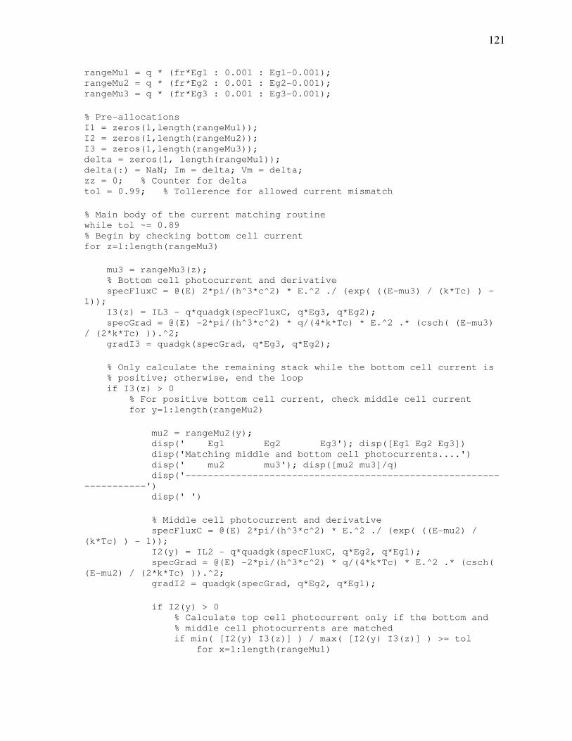
121
rangeMu1 = q * (fr*Eg1 : 0.001 : Eg1-0.001); rangeMu2 = q * (fr*Eg2 : 0.001 : Eg2-0.001); rangeMu3 = q * (fr*Eg3 : 0.001 : Eg3-0.001);
% Pre-allocations I1 = zeros(1,length(rangeMu1)); I2 = zeros(1,length(rangeMu2)); I3 = zeros(1,length(rangeMu3)); delta = zeros(1, length(rangeMu1)); delta(:) = NaN; Im = delta; Vm = delta; zz = 0; % Counter for delta tol = 0.99; % Tollerence for allowed current mismatch
% Main body of the current matching routine while tol ~= 0.89 % Begin by checking bottom cell current for z=1:length(rangeMu3)
mu3 = rangeMu3(z); % Bottom cell photocurrent and derivative specFluxC = @(E) 2*pi/(h^3*c^2) * E.^2 ./ (exp( ((E-mu3) / (k*Tc) ) -
1)); I3(z) = IL3 - q*quadgk(specFluxC, q*Eg3, q*Eg2); specGrad = @(E) -2*pi/(h^3*c^2) * q/(4*k*Tc) * E.^2 .* (csch( (E-mu3)
/ (2*k*Tc) )).^2; gradI3 = quadgk(specGrad, q*Eg3, q*Eg2);
% Only calculate the remaining stack while the bottom cell current is % positive; otherwise, end the loop if I3(z) > 0 % For positive bottom cell current, check middle cell current for y=1:length(rangeMu2)
mu2 = rangeMu2(y); disp(' Eg1 Eg2 Eg3'); disp([Eg1 Eg2 Eg3]) disp('Matching middle and bottom cell photocurrents....') disp(' mu2 mu3'); disp([mu2 mu3]/q) disp('--------------------------------------------------------
-----------') disp(' ')
% Middle cell photocurrent and derivative specFluxC = @(E) 2*pi/(h^3*c^2) * E.^2 ./ (exp( ((E-mu2) /
(k*Tc) ) - 1)); I2(y) = IL2 - q*quadgk(specFluxC, q*Eg2, q*Eg1); specGrad = @(E) -2*pi/(h^3*c^2) * q/(4*k*Tc) * E.^2 .* (csch(
(E-mu2) / (2*k*Tc) )).^2; gradI2 = quadgk(specGrad, q*Eg2, q*Eg1);
if I2(y) > 0 % Calculate top cell photocurrent only if the bottom and % middle cell photocurrents are matched if min( [I2(y) I3(z)] ) / max( [I2(y) I3(z)] ) >= tol for x=1:length(rangeMu1)

122
mu1 = rangeMu1(x); V = (mu1 + mu2 + mu3)/q; disp(' Eg1 Eg2 Eg3'); disp([Eg1 Eg2
Eg3]) disp('Matching top cell photocurrent to the
stack....') disp(' mu1 mu2 mu3'); disp([mu1 mu2
mu3]/q) disp('--------------------------------------------
-----------------------') disp(' ')
% Top cell photocurrent and derivative specFluxC = @(E) 2*pi/(h^3*c^2) * E.^2 ./ (exp(
((E-mu1) / (k*Tc) ) - 1)); I1(x) = IL1 - q*quadgk(specFluxC, q*Eg1, q*10); specGrad = @(E) -2*pi/(h^3*c^2) * q/(4*k*Tc) *
E.^2 .* (csch( (E-mu1) / (2*k*Tc) )).^2; gradI1 = quadgk(specGrad, q*Eg1, q*10);
if I1(x) > 0 % Calculate delta only if all photocurrents
are matched if min( [I1(x) I2(y)] ) / max( [I1(x) I2(y)] )
>= tol zz = zz + 1; % Store variables Im(zz) = max( [I1(x) I2(y) I3(z)] );
Vm(zz) = V; % Lagrange-maximized function delta(zz) = q*V + Im(zz) * ( 1/gradI1 +
1/gradI2 + 1/gradI3 ); end else % Return to middle cell calculation once top % cell current becomes negative x = length(rangeMu1); end end end else % Return to bottom cell calculation once middle cell % current becomes negative y = length(rangeMu2); end end else % End the loop once bottom cell current becomes negative z = length(rangeMu3); end end
% Truncate values and check delta = delta( ~isnan(delta) ); if isempty(delta) tol = tol - 0.01; % Increase tolerance

123
if tol == 0.89 % Give up calculation at this data point delta = NaN; Im = NaN; Vm = NaN; Pm = NaN; else % Reset values and try again delta = zeros(1, length(rangeMu1)); delta(:) = NaN; Im = delta; Vm = delta; zz = 0; % Counter for delta end else tol = 0.89; Im = Im( ~isnan(Im) ); Vm = Vm( ~isnan(Vm) ); Pm = Vm .* Im; end end
% Store values - [values @ minimum delta , values @ maximum efficiency] Vmax = [Vm( abs(delta) == min(abs(delta)) ) Vm(Pm == max(Pm))]; if isempty(Vmax) Vmax = [NaN NaN]; Imax = [NaN NaN]; eff = [NaN NaN]; else Imax = [Im( abs(delta) == min(abs(delta)) ) Im(Pm == max(Pm))]; eff = Vmax .* Imax / Ps; end

124
Appendix VI
Detailed Balance Model for an Intermediate Band Solar Cell
(MATLAB Code)
The following code consists of three m-files (db-ibsc.m, effFindIBSC.m, and
currentMatchIBSC.m) that together invoke the detailed balance model for the analysis of an
intermediate band solar cell as discussed in Section 2.4. The standard inputs are solar and
device temperatures, solar concentration factors, and the bandgaps separating the conduction
band from the intermediate band and separating the intermediate band from the valence band.
A range of solar concentrations and of both bandgaps may be entered. The routine loops
through each value in these ranges allowing for the generation of efficiency contours as
presented in Section 2.4. The routine is setup to allow for the analysis to use the blackbody,
AM0, AM1.5G, or AM1.5D solar spectra. Upon running the routine, the detailed balance
efficiency limits are saved in the effVal matrix for pertinent post-processing analysis.
The file db-ibsc.m is the master routine and calls upon effFindIBSC.m as part of the
routine. User-entered inputs and machine storage of pertinent data occurs in db-ibsc.m. This
routine also loops through each permutation of bandgaps and solar concentrations, each time
passing the current permutation to effFindIBSC.m. The solar spectra are automatically chosen
by db-ibsc.m
The effFindIBSC.m routine numerically solves the detailed balance model to
determine the current due to the bulk response. This file then calls upon the
currentMatchIBSC.m routine to find the current arising from the intermediate transitions.
These currents are determined over an iterative voltage sweep until a maximum power is

125
found thus giving the detailed balance efficiency. The currentMatchIBSC.m algorithm
iteratively determines the current arising from the intermediate transition subject to the
constraint of current matching discussed in Section 2.4.

126
% db-ibsc.m
% Thus routine loops effFindIBSC.m through several solar concentrations
and % finds maximum efficiency as a function of the two intermediate bandgaps
load spectrumFlux q=1.6021765e-19; h=6.626069e-34; c=299792458; k=1.38065e-23;
sigma=5.6704e-8; f=2.1646e-5;
% Tunable paramters Ts=6000; Tc=300; rangeC = [1 10 100 1000 10000 1/f]; rangeEci = 1:0.01:2; rangeEiv = 0.50:0.01:0.95;
% Solar spectral flux specFluxS = @(E) 2*pi/(h^3*c^2) * E.^2 ./ (exp(E/(k*Ts)) - 1);
% Preallocation for effiencies: Row-Eci, Col-Eiv, Dpt-Conc, 4th-Spectrum effVal = zeros(length(rangeEci), length(rangeEiv), length(rangeC), 3);
amCount=0; for w = 1:3; switch w case 1 % Blackbody spec=0; case 2 % AM0 spec=1; case 3 % AM1.5G for one sun, AM1.5D for the rest if amCount == 0 spec=2; amCount=1; else spec=3; end end
for x = 1:length(rangeC) C = rangeC(x); for y = 1:length(rangeEci) Eci = rangeEci(y); for z = 1:length(rangeEiv) Eiv = rangeEiv(z); Eg = Eci + Eiv;
effFindIBSC effVal(y,z,x,w) = eff; % Row-Eci, Col-Eiv, Dpt-C, 4th-
Spec end end
% Interim save save effFile effVal end end

127
% effFindIBSC.m % This routine steps currentMatchIBSC.m through several voltages until the
code % converges onto a maximum efficiency for the specified bandgaps.
% Fraction of the bulk bandgap ranging from 0.65 to 0.90 used to determine % the initial voltage and chemical potentials fr = .25 * ( 13/5 - log(C)/log(f) ); % Initial voltage and chemical potentials V=fr*Eg; muIV=mean([V-Eci Eiv]); muCI=V-muIV;
% Bulk short-circuit current switch spec case 0 IcvL = q*C*f * quadgk(specFluxS,q*Eg, q*22); case 1 lamCV = h*c / (Eg*q) * 1e9; % Wavelength (nm) corresponding to maxPtCV = find(lam0<=lamCV, 1, 'last'); % the enrgy gap IcvL = q*C * trapz(lam0(1:maxPtCV), AM0(1:maxPtCV)); case 2 lamCV = h*c / (Eg*q) * 1e9; % Wavelength (nm) corresponding to maxPtCV = find(lam1p5<=lamCV, 1, 'last'); % the enrgy gap IcvL = q*C * trapz(lam1p5(1:maxPtCV), AM1p5G(1:maxPtCV)); case 3 lamCV = h*c / (Eg*q) * 1e9; % Wavelength (nm) corresponding to maxPtCV = find(lam1p5<=lamCV, 1, 'last'); % the enrgy gap IcvL = q*C * trapz(lam1p5(1:maxPtCV), AM1p5D(1:maxPtCV)); end
stopSweep=0; eff=0; effOld=0; effCount=0; revDir=0; while stopSweep == 0; effCount = effCount + 1; currentMatchIBSC if isnan(eff) return end
% Determine total current and efficiency for voltage V specFluxC = @(E) 2*pi/(h^3*c^2) * E.^2 ./ (exp( (E - (q*V))/(k*Tc) ) -
1); Icv = IcvL - q * quadgk(specFluxC,q*Eg, q*10); Itotal = Icv + Ici; switch spec case 0 eff = V * Itotal / (C*f*sigma*Ts^4); case 1 eff = V * Itotal / (C*1366.1); case 2 eff = V * Itotal / (C*1000.4); case 3 eff = V * Itotal / (C*900.14); end
if eff > effOld; if revDir == 0; % Check to see which direction to sweep voltage Vold = V;

128
V = V + 0.01; else Vold = V; V = V - 0.01; end elseif eff < effOld; if effCount ~= 2; eff = effOld; V = Vold; stopSweep = 1; else % This runs only if a maximum is detected in the first run Vold = V; V = Vold - 0.01; revDir = 1; % Reverse direction of the bias sweep end else stopSweep = 1; end
disp('Solar Concentration:'); disp(C) disp('Voltage Step:'); disp(effCount) disp(' V Eff. Eci Eiv mu_ci mu_iv') disp([V eff Eci Eiv muCI muIV]) disp(' Ici'); disp(Ici) disp(' Iiv'); disp(Iiv) disp(' Icv'); disp(Icv) disp(' Itotal'); disp(Itotal)
if stopSweep == 0; effOld = eff; disp('Finding maximum efficiency....') else disp('Converged to maximum efficiency!') end disp('---------------------------------------------------------------
') disp(' ') end

129
% currentMatchIBSC.m % At a given bias and band spacing, this routine determines the % intermediate band chemical potentials and cell photocurrent.
% Intermediate band short-circuit currents switch spec case 0 IciL = q*C*f * quadgk(specFluxS,q*Eci, q*Eg); IivL = q*C*f * quadgk(specFluxS,q*Eiv, q*Eci); case 1 lamCI = h*c / (Eci*q) * 1e9; % Wavelengths (nm) corresponding to lamIV = h*c / (Eiv*q) * 1e9; % the energy gaps. maxPtCI = find(lam0<=lamCI, 1, 'last'); maxPtIV = find(lam0<=lamIV, 1, 'last'); IciL = q*C * trapz(lam0(maxPtCV:maxPtCI), AM0(maxPtCV:maxPtCI)); IivL = q*C * trapz(lam0(maxPtCI:maxPtIV), AM0(maxPtCI:maxPtIV)); case 2 lamCI = h*c / (Eci*q) * 1e9; % Wavelengths (nm) corresponding to lamIV = h*c / (Eiv*q) * 1e9; % the energy gaps. maxPtCI = find(lam1p5<=lamCI, 1, 'last'); maxPtIV = find(lam1p5<=lamIV, 1, 'last'); IciL = q*C * trapz(lam1p5(maxPtCV:maxPtCI),
AM1p5G(maxPtCV:maxPtCI)); IivL = q*C * trapz(lam1p5(maxPtCI:maxPtIV),
AM1p5G(maxPtCI:maxPtIV)); case 3 lamCI = h*c / (Eci*q) * 1e9; % Wavelengths (nm) corresponding to lamIV = h*c / (Eiv*q) * 1e9; % the energy gaps. maxPtCI = find(lam1p5<=lamCI, 1, 'last'); maxPtIV = find(lam1p5<=lamIV, 1, 'last'); IciL = q*C * trapz(lam1p5(maxPtCV:maxPtCI),
AM1p5D(maxPtCV:maxPtCI)); IivL = q*C * trapz(lam1p5(maxPtCI:maxPtIV),
AM1p5D(maxPtCI:maxPtIV)); end
% Initial solution for intermediate band photocurrents specFluxC = @(E) 2*pi/(h^3*c^2) * E.^2 ./ (exp( (E - (q*muCI))/(k*Tc) ) -
1); Ici = IciL - q*quadgk(specFluxC, q*Eci, q*Eg); specFluxC = @(E) 2*pi/(h^3*c^2) * E.^2 ./ (exp( (E - (q*muIV))/(k*Tc) ) -
1); Iiv = IivL - q*quadgk(specFluxC, q*Eiv, q*Eci);
% Current matching algorithm for the intermediate band photocurrents stp = 0.1; % Amount by which to increase the chemical potential if min([Eci-muCI Eiv-muIV]) <= 0.01 stp = stp/100; elseif min([Eci-muCI Eiv-muIV]) <= 0.1 stp = stp/10; end match=0; count=0; muCIolder=100; while match==0; count=count+1; disp('Solar Concentration:'); disp(C) disp('Voltage Step:'); disp(effCount)

130
disp('Iteration:'); disp(count)
delta = Ici - Iiv; % WARNING!!! % The delta parameter assumes both currents to be positive values. % An interlock is implemented at the end of the loop; however, it is % not 100% failsafe (especially if a negative current is realized % during the first itteration).
% This is an interlock to make sure the chemical potentials do not % exceed their respective energy gaps if max([(Eci <= muCI) (Eiv <= muIV)]) == 1 muCI = muCIold; muIV = muIVold; stp = stp/10; elseif min([Eci-muCI Eiv-muIV]) <= 0.01 stp = 0.001; muCIold = muCI; muIVold = muIV; Iciold= Ici; Iivold = Iiv; elseif min([Eci-muCI Eiv-muIV]) <= 0.1 if stp ~= 0.001 stp = 0.01; end muCIold = muCI; muIVold = muIV; Iciold= Ici; Iivold = Iiv; else % Store current values for when they must be reverted to muCIold = muCI; muIVold = muIV; Iciold= Ici; Iivold = Iiv; end
% Determine whether to step the chemical potentials up or down if delta > 0; if muCI + stp >= Eci; stp = stp/10; end disp('Increasing conduction-to-intermediate band dark
current....') muCI = muCI + stp; muIV = V - muCI; elseif delta < 0; if muIV + stp >= Eiv; stp = stp/10; end disp('Increasing intermediate-to-valence band dark current....') muIV = muIV + stp; muCI = V - muIV; else disp('Converged to a solution!') match = 1; end
if match == 0; % Check to see if there is a possible match or if a decrease in % step is necessary if muCI == muCIolder; if stp == 0.001;

131
disp('Converged to a solution!') match = 1; % Reset to previous chemical potentials; note there is no % new recalculation of the photocurrents muCI = muCIold; muIV = muIVold; % Determine and use whichever data has less error if abs(Iciold - Iivold) > abs(Iciolder - Iivolder); Ici = Iciolder; Iiv = Iivolder; muCI = muCIolder; muIV = muIVolder; end else stp = stp/10; end end end
% Recalculate the intermediate band photocurrents if match == 0; specFluxC = @(E) 2*pi/(h^3*c^2) * E.^2 ./ (exp( (E -
(q*muCI))/(k*Tc) ) - 1); Ici = IciL - q*quadgk(specFluxC, q*Eci, q*Eg); specFluxC = @(E) 2*pi/(h^3*c^2) * E.^2 ./ (exp( (E -
(q*muIV))/(k*Tc) ) - 1); Iiv = IivL - q*quadgk(specFluxC, q*Eiv, q*Eci);
if min(sign([Ici Iiv])) < 1; % Revert to previous values if either photocurrent becomes % negative muCI = muCIold; muIV = muIVold; Ici = Iciold; Iiv = Iivold; stp = stp/10; else % Store old values as older values for comparison above muCIolder = muCIold; muIVolder = muIVold; Iciolder = Iciold; Iivolder = Iivold; end end
disp(' ') disp(' V Eff. Eci Eiv mu_ci mu_iv') disp([V eff Eci Eiv muCI muIV]) disp(' Ici'); disp(Ici) disp(' Iiv'); disp(Iiv) disp('--------------------------------------------------------------') disp(' ')
if stp < 0.001 stp = 0.001; end
if count == 1000 disp('Unable to converge!') eff = NaN; return end end

132
Appendix VII
Single-Junction Solar Cell Device Model (ATLAS Code)
The following code consists of three ATLAS decks (pv00.in, pv01.in, and sr00.in)
that individually simulate the single-junction solar cell as described in Sections 3.16 and
3.17. The pv00.in and pv01.in decks both simulate the illuminated current-voltage response
of the solar cell. In the first file, the device structure is defined using an auto-meshing
technique that is simpler to define and more accurate in the numerical analysis. The latter
defines the device structure by manual meshing. This is a more complicated technique but, if
properly applied, leads to a more efficiently obtained solution. The sr00.in deck uses the
same auto-meshing technique as in pv00.in and solves for the spectral response of the device.

133
# pv00.in
go atlas
mesh auto
x.mesh loc=-200 spac=10
x.mesh loc=-50 spac=10
x.mesh loc=-45 spac=5
x.mesh loc=-10 spac=5
x.mesh loc=-9 spac=1
x.mesh loc=0 spac=1
x.mesh loc=9 spac=1
x.mesh loc=10 spac=5
x.mesh loc=45 spac=5
x.mesh loc=50 spac=10
x.mesh loc=200 spac=10
# Regions
region top thick=0.010 ny=1 material=Vacuum
region name=Contact bottom thick=0.100 ny=5 material=GaAs
acceptor=1e19
region name=Window bottom thick=0.050 ny=6 material=InGaP
acceptor=2e18 x.comp=0.52
region name=Emitter bottom thick=0.500 ny=6 material=GaAs
acceptor=1e18
region name=Intrinsic bottom thick=0.100 ny=5 material=GaAs acceptor=0
donor=0
region name=Base bottom thick=2.000 ny=20 material=GaAs donor=1e17
region name=BSF bottom thick=0.050 ny=6 material=InGaP donor=1e18
x.comp=0.52
region name=Sub bottom thick=0.100 ny=4 material=GaAs donor=1e18
# Contact Etch
region x.min=-200 x.max=-4 y.min=0 y.max=0.1 material=Vacuum
region x.min=4 x.max=200 y.min=0 y.max=0.1 material=Vacuum
# Electrodes
electrode name=Anode x.min=-4 x.max=4 y.min=-0.010 y.max=0
electrode name=Cathode bottom
# Interfaces
# Vacuum-Window
interface x.min=-200 x.max=-4 y.min=0.080 y.max=0.120 s.n=1e8
interface x.min=4 x.max=200 y.min=0.080 y.max=0.120 s.n=1e8
# Back Window
interface x.min=-200 x.max=200 y.min=0.120 y.max=0.180 s.s thermionic
tunnel
# Back BSF
interface x.min=-200 x.max=200 y.min=2.780 y.max=2.820 s.s thermionic
tunnel
# Material Properties
material taup=50e-9 taun=50e-9
# GaAs
material material=GaAs copt=7.2e-10
# InGaP
material material=InGaP affinity=4.07 index.file=../InGaP.opt

134
material name=Window mun=600 mup=40
material name=BSF mun=800 mup=40
# Contact
material material=Conductor imag.index=1000
# Models & Outputs
model fermi SRH
model material=GaAs conmob optr print
output val.band con.band opt.int u.aug u.srh u.rad
# Define AM0 spectrum
beam num=1 x.origin=0 y.origin=-0.1 angle=90 power.file=../AM0.spec
wavel.start=0.200 wavel.end=0.930 wavel.num=146
# Initial solution
solve init
solve prev
log outf=pv00.log
save outf=pv00_0.str
# Zero bias w/ photogeneration
solve b1=1
save outf=pv01_1.str
# Light IV sweep
solve b1=1 vanode=0.050 vstep=0.050 vfinal=0.800 name=anode
solve b1=1 vanode=0.805 vstep=0.005 vfinal=1.000 name=anode
solve b1=1 vanode=1.010 vstep=0.010 vfinal=1.100 name=anode
# Plot IV curve
tonyplot pv00.log -set ../iv.set
# Extracts
extract name="Voc" x.val from curve(v."anode", i."cathode") where y.val=0
extract name="Isc" y.val from curve(v."anode", i."cathode"*25*1e4*1000)
where x.val=0
extract name="Pm" max(v."anode"*i."cathode"*25*1e4*1000)

135
# pv01.in
go atlas
mesh space.mult=1
x.mesh loc=-200 spac=20
x.mesh loc=-50 spac=10
x.mesh loc=-45 spac=5
x.mesh loc=-10 spac=5
x.mesh loc=-9 spac=1
x.mesh loc=0 spac=1
x.mesh loc=9 spac=1
x.mesh loc=10 spac=5
x.mesh loc=45 spac=5
x.mesh loc=50 spac=10
x.mesh loc=200 spac=20
# Anode
y.mesh loc=-0.01 spac=0.005
# Contact
y.mesh loc=0.000 spac=0.005
y.mesh loc=0.005 spac=0.005
y.mesh loc=0.010 spac=0.010
# Window
y.mesh loc=0.050 spac=0.010
y.mesh loc=0.060 spac=0.020
# Emitter
y.mesh loc=0.560 spac=0.020
# Intrinsic Top
y.mesh loc=0.565 spac=0.005
y.mesh loc=0.575 spac=0.002
# Well Region
y.mesh loc=0.645 spac=0.002
# Intrinsic Bottom
y.mesh loc=0.660 spac=0.005
# Base
y.mesh loc=0.680 spac=0.010
y.mesh loc=0.720 spac=0.020
y.mesh loc=1.000 spac=0.200
y.mesh loc=2.600 spac=0.020
y.mesh loc=2.640 spac=0.020
y.mesh loc=2.660 spac=0.010
# BSF
y.mesh loc=2.710 spac=0.010
# Substrate
y.mesh loc=2.810 spac=0.020
# Bulk Regions
region x.min=-200 x.max=-4 y.min=-0.01 y.max=0.010
material=Vacuum
region x.min=4 x.max=200 y.min=-0.01 y.max=0.010
material=Vacuum
region name=Contact x.min=-4 x.max=4 y.min=0.000 y.max=0.010
material=GaAs acceptor=1e19

136
region name=Window x.min=-200 x.max=200 y.min=0.010 y.max=0.060
material=InGaP acceptor=2e18 x.comp=0.52
region name=Emitter x.min=-200 x.max=200 y.min=0.060 y.max=0.560
material=GaAs acceptor=1e18
region name=Intrinsic x.min=-200 x.max=200 y.min=0.560 y.max=0.660
material=GaAs acceptor=0 donor=0
region name=Base x.min=-200 x.max=200 y.min=0.660 y.max=2.660
material=GaAs donor=1e17
region name=BSF x.min=-200 x.max=200 y.min=2.660 y.max=2.710
material=InGaP donor=1e18 x.comp=0.52
region name=Sub x.min=-200 x.max=200 y.min=2.710 y.max=2.810
material=GaAs donor=1e18
# Electrodes
electrode name=Anode x.min=-4 x.max=4 y.min=-0.010 y.max=0.000
electrode name=Cathode bottom
# Interfaces
# Vacuum-Window
interface x.min=-200 x.max=-4 y.min=0.008 y.max=0.012 s.n=1e8
interface x.min=4 x.max=200 y.min=0.008 y.max=0.012 s.n=1e8
# Back Window
interface x.min=-200 x.max=200 y.min=0.058 y.max=0.062 s.s thermionic
tunnel
# Back BSF
interface x.min=-200 x.max=200 y.min=2.708 y.max=2.712 s.s thermionic
tunnel
# Material Properties
material taup=50e-9 taun=50e-9
# GaAs
material material=GaAs copt=7.2e-10
# InGaP
material material=InGaP affinity=4.07 index.file=../InGaP.opt
material name=Window mun=600 mup=40
material name=BSF mun=800 mup=40
# Contact
material material=Conductor imag.index=1000
# Models & Outputs
model fermi SRH
model material=GaAs conmob optr print
output val.band con.band opt.int u.aug u.srh u.rad
# Define AM0 spectrum
beam num=1 x.origin=0 y.origin=-0.1 angle=90 power.file=../AM0.spec
wavel.start=0.200 wavel.end=4.000 wavel.num=760
# Initial solution
solve init
solve prev
log outf=pvXX.log
#save outf=pv01_0.str
# Zero bias w/ photogeneration
solve b1=1

137
#save outf=pv01_1.str
# Light IV sweep
solve b1=1 vanode=0.050 vstep=0.050 vfinal=0.800 name=anode
solve b1=1 vanode=0.805 vstep=0.005 vfinal=1.000 name=anode
solve b1=1 vanode=1.010 vstep=0.010 vfinal=1.100 name=anode
# Plot IV curve
tonyplot pvXX.log -set ../iv.set
# Extracts
extract name="Voc" x.val from curve(v."anode", i."cathode") where y.val=0
extract name="Isc" y.val from curve(v."anode", i."cathode"*25*1e4*1000)
where x.val=0
extract name="Pm" max(v."anode"*i."cathode"*25*1e4*1000)

138
# sr00.in
go atlas
mesh auto
x.mesh loc=-200 spac=10
x.mesh loc=-50 spac=10
x.mesh loc=-45 spac=5
x.mesh loc=-10 spac=5
x.mesh loc=-9 spac=1
x.mesh loc=0 spac=1
x.mesh loc=9 spac=1
x.mesh loc=10 spac=5
x.mesh loc=45 spac=5
x.mesh loc=50 spac=10
x.mesh loc=200 spac=10
# Regions
region top thick=0.010 ny=1 material=Vacuum
region name=Contact bottom thick=0.100 ny=5 material=GaAs
acceptor=1e19
region name=Window bottom thick=0.050 ny=6 material=InGaP
acceptor=2e18 x.comp=0.52
region name=Emitter bottom thick=0.500 ny=6 material=GaAs
acceptor=1e18
region name=Intrinsic bottom thick=0.100 ny=5 material=GaAs acceptor=0
donor=0
region name=Base bottom thick=2.000 ny=20 material=GaAs donor=1e17
region name=BSF bottom thick=0.050 ny=6 material=InGaP donor=1e18
x.comp=0.52
region name=Sub bottom thick=0.100 ny=4 material=GaAs donor=1e18
# Contact Etch
region x.min=-200 x.max=-4 y.min=0 y.max=0.1 material=Vacuum
region x.min=4 x.max=200 y.min=0 y.max=0.1 material=Vacuum
# Electrodes
electrode name=Anode x.min=-4 x.max=4 y.min=-0.010 y.max=0
electrode name=Cathode bottom
# Interfaces
# Vacuum-Window
interface x.min=-200 x.max=-4 y.min=0.080 y.max=0.120 s.n=1e8
interface x.min=4 x.max=200 y.min=0.080 y.max=0.120 s.n=1e8
# Back Window
interface x.min=-200 x.max=200 y.min=0.120 y.max=0.180 s.s thermionic
# Back BSF
interface x.min=-200 x.max=200 y.min=2.780 y.max=2.820 s.s thermionic
# Material Properties
material taup=50e-9 taun=50e-9
# GaAs
material material=GaAs copt=7.2e-10
# InGaP
material material=InGaP affinity=4.07 index.file=../InGaP.opt
material name=Window mun=600 mup=40
material name=BSF mun=800 mup=40

139
# Contact
material material=Conductor imag.index=1000
# Models & Outputs
model fermi SRH
model material=GaAs conmob optr
output val.band con.band opt.int u.aug u.srh u.rad
# Initial solution
solve init
solve prev
log outf=sr00.log
# Monochromatic Beam
beam num=2 x.origin=0 y.origin=-1 angle=90
# Solve spectral response
solve b2=.1 lambda=1.000
solve b2=.1 lambda=0.975
solve b2=.1 lambda=0.950
solve b2=.1 lambda=0.925
solve b2=.1 lambda=0.900
solve b2=.1 lambda=0.875
solve b2=.1 lambda=0.850
solve b2=.1 lambda=0.825
solve b2=.1 lambda=0.800
solve b2=.1 lambda=0.775
solve b2=.1 lambda=0.750
solve b2=.1 lambda=0.725
solve b2=.1 lambda=0.700
solve b2=.1 lambda=0.675
solve b2=.1 lambda=0.650
solve b2=.1 lambda=0.625
solve b2=.1 lambda=0.600
solve b2=.1 lambda=0.575
solve b2=.1 lambda=0.550
solve b2=.1 lambda=0.525
solve b2=.1 lambda=0.500
solve b2=.1 lambda=0.475
solve b2=.1 lambda=0.450
solve b2=.1 lambda=0.425
solve b2=.1 lambda=0.400
solve b2=.1 lambda=0.375
solve b2=.1 lambda=0.350
solve b2=.1 lambda=0.325
solve b2=.1 lambda=0.300
solve b2=.1 lambda=0.275
solve b2=.1 lambda=0.250
solve b2=.1 lambda=0.225
solve b2=.1 lambda=0.200
tonyplot sr00.log -set ../qe.set

140
Appendix VIII
Dual-Junction Solar Cell Device Model (ATLAS Code)
The following code consists of two ATLAS decks (djIV.in and djSR.in) that
individually simulate the dual-junction solar cell as described in Section 3.18. The djIV.in
deck simulates the illuminated current-voltage response of the solar cell while the djSR.in
deck solves for the spectral response of the device.
141
# djIV.in
go atlas
mesh auto
x.mesh loc=-200 spac=20
x.mesh loc=-40 spac=20
x.mesh loc=-30 spac=10
x.mesh loc=-10 spac=5
x.mesh loc=-9 spac=1
x.mesh loc=0 spac=1
x.mesh loc=9 spac=1
x.mesh loc=10 spac=5
x.mesh loc=30 spac=10
x.mesh loc=40 spac=20
x.mesh loc=200 spac=20
# Regions
region top thick=0.010 ny=1 material=Vacuum
# Top Cell
region name=tContact bottom thick=0.100 ny=3 material=GaAs
acceptor=1e19
region name=tWindow bottom thick=0.030 ny=3 material=AlAs
acceptor=1e18
region name=tEmitter bottom thick=0.100 ny=3 material=InGaP
acceptor=1e18 x.comp=0.52
region name=tBase bottom thick=2.000 ny=3 material=InGaP donor=1e17
x.comp=0.52
region name=tBSF bottom thick=0.100 ny=3 material=InGaP donor=1e18
x.comp=0.52
# Tunnel
region name=td1 bottom thick=0.050 ny=4 material=InAs donor=1e19
region name=td2 bottom thick=0.050 ny=4 material=InAs
acceptor=1e19
# Middle Cell
region name=mWindow bottom thick=0.050 ny=3 material=InGaP
acceptor=2e18 x.comp=0.52
region name=mEmitter bottom thick=0.500 ny=3 material=GaAs
acceptor=1e18
region name=mIntrinsic bottom thick=0.100 ny=3 material=GaAs acceptor=0
donor=0
region name=mBase bottom thick=2.000 ny=3 material=GaAs donor=1e17
region name=mBSF bottom thick=0.050 ny=3 material=InGaP donor=1e18
x.comp=0.52
region name=mSub bottom thick=0.100 ny=3 material=GaAs donor=1e18
# Contact Etch
region x.min=-200 x.max=-4 y.min=0 y.max=0.1 material=Vacuum
region x.min=4 x.max=200 y.min=0 y.max=0.1 material=Vacuum
# Electrodes
electrode name=Anode x.min=-4 x.max=4 y.min=-0.010 y.max=0
electrode name=Cathode bottom

142
# Interfaces
# Vacuum-Window
interface x.min=-200 x.max=-4 y.min=0.090 y.max=0.110 s.n=1e8
interface x.min=4 x.max=200 y.min=0.090 y.max=0.110 s.n=1e8
# Material Properties
material taup=50e-9 taun=50e-9
# GaAs
material material=GaAs copt=7.2e-10
# InGaP
material material=InGaP affinity=4.07 index.file=../InGaP.opt mun=800
mup=40
# Contact
material material=Conductor imag.index=1000
# AlAs
material material=AlAs mun=150 mup=65
# Tunnel
material material=InAs index.file=../GaAs0ab.opt
# Models & Outputs
model fermi SRH
model material=GaAs conmob optr print
model material=InAs bbt.std
output val.band con.band opt.int u.aug u.srh u.rad
# Define AM0 spectrum
beam num=1 x.origin=0 y.origin=-0.1 angle=90 power.file=../AM0.spec
wavel.start=0.200 wavel.end=2.000 wavel.num=360
# Initial solution
solve init
save outf=pv00a_0.str
log outf=pv00a.log
# Zero bias w/ photogeneration
solve b1=1
save outf=pv00_1.str
# Light IV sweep
solve b1=1 vanode=0.10 vstep=0.10 vfinal=2.6 name=anode
#solve b1=1 vanode=1.71 vstep=0.01 vfinal=1.9 name=anode
#solve b1=1 vanode=2.00 vstep=0.10 vfinal=2.6 name=anode
# Plot IV curve
tonyplot pv00a.log -set ../iv.set
# Extracts
extract name="Voc" x.val from curve(v."anode", i."cathode") where y.val=0
extract name="Isc" y.val from curve(v."anode", i."cathode"*25*1e4*1000)
where x.val=0
extract name="Pm" max(v."anode"*i."cathode"*25*1e4*1000)

143
# djSR.in
go atlas
mesh auto
x.mesh loc=-200 spac=20
x.mesh loc=-40 spac=20
x.mesh loc=-30 spac=10
x.mesh loc=-10 spac=10
x.mesh loc=-9 spac=1
x.mesh loc=0 spac=1
x.mesh loc=9 spac=1
x.mesh loc=10 spac=10
x.mesh loc=30 spac=10
x.mesh loc=40 spac=20
x.mesh loc=200 spac=20
# Regions
region top thick=0.010 ny=1 material=Vacuum
# InGaP Cell
region name=tContact bottom thick=0.100 ny=3 material=GaAs
acceptor=1e19
region name=tWindow bottom thick=0.030 ny=3 material=AlAs
acceptor=2e18
region name=tEmmitter bottom thick=0.100 ny=3 material=InGaP
acceptor=1e18 x.comp=0.52
region name=tBase bottom thick=1.000 ny=3 material=InGaP donor=1e17
x.comp=0.52
region name=tBSF bottom thick=0.100 ny=3 material=InGaP donor=2e18
x.comp=0.52
#
region name=tSpace bottom thick=0.050 ny=1 material=Air
# GaAs Cell
region name=mWindow bottom thick=0.050 ny=3 material=InGaP
acceptor=2e18 x.comp=0.52
region name=mEmitter bottom thick=0.500 ny=3 material=GaAs
acceptor=1e18
region name=mIntrinsic bottom thick=0.100 ny=3 material=GaAs acceptor=0
donor=0
region name=mBase bottom thick=2.000 ny=3 material=GaAs donor=1e17
region name=mBSF bottom thick=0.050 ny=3 material=InGaP donor=1e18
x.comp=0.52
region name=mSub bottom thick=0.150 ny=3 material=GaAs donor=1e18
# Contact Etch
region x.min=-200 x.max=-4 y.min=0 y.max=0.1 material=Vacuum
region x.min=4 x.max=200 y.min=0 y.max=0.1 material=Vacuum
# Electrodes
electrode name=tAnode x.min=-4 x.max=4 y.min=-0.010 y.max=0
electrode name=tCathode x.min=-200 x.max=200 y.min=1.330 y.max=1.330
electrode name=mAnode x.min=-200 x.max=200 y.min=1.380 y.max=1.380
electrode name=mCathode bottom
contact name=tCathode common=mCathode

144
# Interfaces
# Vacuum-Window
interface x.min=-200 x.max=-4 y.min=0.090 y.max=0.110 s.n=1e8
interface x.min=4 x.max=200 y.min=0.090 y.max=0.110 s.n=1e8
# Material Properties
material taup=50e-9 taun=50e-9
# GaAs
material material=GaAs copt=7.2e-10
# InGaP
material material=InGaP affinity=4.07 index.file=../InGaP.opt mup=40
material name=tEmitter mun=800
material name=tBase mun=1000
material name=tBSF mun=600
material name=mWindow mun=600
material name=mBSF mun=800
# AlAs
material material=AlAs mun=500 mup=100
# Top Contact
material material=Conductor imag.index=1000
# Spacing
material material=Air index.file=../GaAs.opt
# Models & Outputs
model fermi SRH
model material=GaAs conmob optr print
output val.band con.band opt.int u.aug u.srh u.rad
# Initial solution
solve init
solve prev
log outf=srmB1.log
# Monochromatic Beam
beam num=2 x.origin=0 y.origin=-1 angle=90
# Solve spectral response
solve b2=.1 lambda=1.000
solve b2=.1 lambda=0.975
solve b2=.1 lambda=0.950
solve b2=.1 lambda=0.925
solve b2=.1 lambda=0.900
solve b2=.1 lambda=0.875
solve b2=.1 lambda=0.850
solve b2=.1 lambda=0.825
solve b2=.1 lambda=0.800
#save outf=sr00_800.str
solve b2=.1 lambda=0.775
solve b2=.1 lambda=0.750
solve b2=.1 lambda=0.725
solve b2=.1 lambda=0.700
solve b2=.1 lambda=0.675
solve b2=.1 lambda=0.650
solve b2=.1 lambda=0.625
solve b2=.1 lambda=0.600

145
solve b2=.1 lambda=0.575
solve b2=.1 lambda=0.550
#save outf=sr00_550.str
solve b2=.1 lambda=0.525
solve b2=.1 lambda=0.500
solve b2=.1 lambda=0.475
solve b2=.1 lambda=0.450
solve b2=.1 lambda=0.425
solve b2=.1 lambda=0.400
solve b2=.1 lambda=0.375
solve b2=.1 lambda=0.350
solve b2=.1 lambda=0.325
solve b2=.1 lambda=0.300
solve b2=.1 lambda=0.275
solve b2=.1 lambda=0.250
solve b2=.1 lambda=0.225
solve b2=.1 lambda=0.200

146
Appendix IX
Nanostructured Solar Cell Device Model (ATLAS Code)
The following code consists of two ATLAS decks (pvQW.in and pvEL.in) that
individually simulate the quantum mechanical effects that arise due to the inclusion of
nanostructures in a single-junction solar cell as described in Section 3.19. The pvQW.in deck
is used to explicitly analyze the quantum confined regions and to specifically determine the
properties of the eigenstates located therein. The pvEL.in deck simulates the
electroluminescence that occurs due to the nanostructured regions.

147
# pvQW.in
go atlas
mesh space.mult=1.0 auto
x.mesh loc=-2.00 spac=0.50
x.mesh loc=2.00 spac=0.50
region num=1 material=GaAs thick=1.500 sy=0.150 bottom acceptor=1e18
region num=2 material=GaAs thick=0.015 sy=0.005 bottom
region num=3 material=InAs thick=0.006 sy=0.001 bottom
region num=4 material=GaAs thick=0.010 sy=0.005 bottom
region num=5 material=InAs thick=0.006 sy=0.001 bottom
region num=6 material=GaAs thick=0.010 sy=0.005 bottom
region num=7 material=InAs thick=0.006 sy=0.001 bottom
region num=8 material=GaAs thick=0.010 sy=0.005 bottom
region num=9 material=InAs thick=0.006 sy=0.001 bottom
region num=10 material=GaAs thick=0.010 sy=0.005 bottom
region num=11 material=InAs thick=0.006 sy=0.001 bottom
region num=12 material=GaAs thick=0.015 sy=0.005 bottom
region num=13 material=GaAs thick=1.500 sy=0.150 bottom donor=1e17
# Electrodes
electrode name=anode top
electrode name=cathode bottom
# Material Properties
material taun=1e-6 taup=1e-6
# GaAs
material material=GaAs copt=7.2e-10
# InAs
material material=InAs index.file=../InAs.opt copt=1.1e-10
# Models & Outputs
models fermi srh optr
models material=GaAs conmob
models material=InAs li qwell well.nx=9 well.ny=100 well.cnbs=1
well.vnbs=5
output val.band con.band opt.int u.aug u.srh u.rad
# Define AM0 spectrum
beam num=1 x.origin=0 y.origin=-1 angle=90 power.file=../AM0.spec
wavel.start=0.200 wavel.end=4.000 wavel.num=76
# Initial solution, save equilibrium structure
solve init
solve prev
save outf=pvQW_0.str
tonyplot
# Zero bias structure w/ photogeneration
log outf=pvQW.log
solve b1=1
save outf=pvQW_1.str

148
# pvEL.in
go atlas
mesh space.mult=1
x.mesh loc=-200 spac=20
x.mesh loc=-50 spac=10
x.mesh loc=-45 spac=5
x.mesh loc=-10 spac=5
x.mesh loc=-9 spac=1
x.mesh loc=0 spac=1
x.mesh loc=9 spac=1
x.mesh loc=10 spac=5
x.mesh loc=45 spac=5
x.mesh loc=50 spac=10
x.mesh loc=200 spac=20
# Anode
y.mesh loc=-0.01 spac=0.005
# Contact
y.mesh loc=0.000 spac=0.005
y.mesh loc=0.005 spac=0.005
y.mesh loc=0.010 spac=0.010
# Window
y.mesh loc=0.050 spac=0.010
y.mesh loc=0.060 spac=0.020
# Emitter
y.mesh loc=0.560 spac=0.020
# Intrinsic Top
y.mesh loc=0.565 spac=0.005
y.mesh loc=0.575 spac=0.002
# Well Region
y.mesh loc=0.645 spac=0.002
# Intrinsic Bottom
y.mesh loc=0.660 spac=0.005
# Base
y.mesh loc=0.680 spac=0.010
y.mesh loc=0.720 spac=0.020
y.mesh loc=1.000 spac=0.200
y.mesh loc=2.600 spac=0.020
y.mesh loc=2.640 spac=0.020
y.mesh loc=2.660 spac=0.010
# BSF
y.mesh loc=2.710 spac=0.010
# Substrate
y.mesh loc=2.810 spac=0.020
# Bulk Regions
region x.min=-200 x.max=-4 y.min=-0.01 y.max=0.010
material=Vacuum
region x.min=4 x.max=200 y.min=-0.01 y.max=0.010
material=Vacuum
region name=Contact x.min=-4 x.max=4 y.min=0.000 y.max=0.010
material=GaAs acceptor=1e19

149
region name=Window x.min=-200 x.max=200 y.min=0.010 y.max=0.060
material=InGaP acceptor=2e18 x.comp=0.52
region name=Emitter x.min=-200 x.max=200 y.min=0.060 y.max=0.560
material=GaAs acceptor=1e18 LED
region name=Intrinsic1 x.min=-200 x.max=200 y.min=0.560 y.max=0.575
material=GaAs acceptor=0 donor=0 LED
region name=Intrinsic2 x.min=-200 x.max=200 y.min=0.645 y.max=0.660
material=GaAs acceptor=0 donor=0 LED
region name=Base x.min=-200 x.max=200 y.min=0.660 y.max=2.660
material=GaAs donor=1e17 LED
region name=BSF x.min=-200 x.max=200 y.min=2.660 y.max=2.710
material=InGaP donor=1e18 x.comp=0.52
region name=Sub x.min=-200 x.max=200 y.min=2.710 y.max=2.810
material=GaAs donor=1e18
# Well Regions
region name=Well1 x.min=-200 x.max=200 y.min=0.575 y.max=0.581
material=InAs LED acceptor=0 donor=0
region name=Barr1 x.min=-200 x.max=200 y.min=0.581 y.max=0.591
material=GaAs LED acceptor=0 donor=0
region name=Well2 x.min=-200 x.max=200 y.min=0.591 y.max=0.597
material=InAs LED acceptor=0 donor=0
region name=Barr2 x.min=-200 x.max=200 y.min=0.597 y.max=0.607
material=GaAs LED acceptor=0 donor=0
region name=Well3 x.min=-200 x.max=200 y.min=0.607 y.max=0.613
material=InAs LED acceptor=0 donor=0
region name=Barr3 x.min=-200 x.max=200 y.min=0.613 y.max=0.623
material=GaAs LED acceptor=0 donor=0
region name=Well4 x.min=-200 x.max=200 y.min=0.623 y.max=0.629
material=InAs LED acceptor=0 donor=0
region name=Barr4 x.min=-200 x.max=200 y.min=0.629 y.max=0.639
material=GaAs LED acceptor=0 donor=0
region name=Well5 x.min=-200 x.max=200 y.min=0.639 y.max=0.645
material=InAs LED acceptor=0 donor=0
# Electrodes
electrode name=Anode x.min=-4 x.max=4 y.min=-0.010 y.max=0.000
electrode name=Cathode bottom
# Interfaces
# Vacuum-Window
interface x.min=-200 x.max=-4 y.min=0.008 y.max=0.012 s.n=1e8
interface x.min=4 x.max=200 y.min=0.008 y.max=0.012 s.n=1e8
# Back Window
interface x.min=-200 x.max=200 y.min=0.058 y.max=0.062 s.s thermionic
tunnel
# Back BSF
interface x.min=-200 x.max=200 y.min=2.708 y.max=2.712 s.s thermionic
tunnel
# Material Properties
material taup=50e-9 taun=50e-9
# GaAs
material material=GaAs copt=7.2e-10
# InGaP

150
material material=InGaP affinity=4.07 index.file=../InGaP.opt
material name=Window mun=600 mup=40
material name=BSF mun=800 mup=40
# InAs
material material=InAs index.file=../InAs.opt copt=1.1e-10
# Contact
material material=Conductor imag.index=1000
# Models & Outputs
model fermi SRH
model material=GaAs conmob li spont print
model material=InAs li qwell well.nx=9 well.ny=100 well.cnbs=1 well.vnbs=5
spont
output val.band con.band opt.int u.aug u.srh u.rad
# Initial solution
solve init
solve prev
log outf=pv05a.log
# IV sweep
solve vanode=0.010 vstep=0.020 vfinal=0.400 name=anode
save spectrum=spec05a.log lmin=0.5 lmax=4.0 nsamp=300
tonyplot spec05.log -overlay spec05a.log

151
References
[1] Basic Research Needs for Solar Energy Utilization: Report on the Basic Energy Sciences Workshop of
Solar Energy Utilization, April 18-21, 2005, Office of Science, US Dept. of Energy, 2005.
[2] Green Paper: Towards a European Strategy for the Security of Energy Supply, European Commission,
2001.
[3] Advanced Energy Initiative, White House National Economic Council, February 2006.
[4] S.M. Hubbard et al., “Effect of Strain Compensation on Quantum Dot Enhanced GaAs Solar Cells,”
Appl. Phys. Lett., vol. 92, pp. 123512-1 – 123512-3, 2008.
[5] A. Martí, L. Cuadra, and A. Luque, “Quantum Dot Intermediate Band Solar Cell,” in Conf. Rec. 28th
IEEE Photovoltaics Spec. Conf., Anchorage, AK, 2000, pp. 940-943.
[6] R. R. King et al., “40% Efficient Metamorphic GaInP/GaInAs/Ge Multijunction Solar Cells,” Appl.
Phys. Lett., vol. 90, pp. 183516-1–183516-3, 2007.
[7] M.A. Green et al., “Solar Cell Efficiency Tables (Version 29),” Prog. Photovoltaics Res. Appl., vol. 15,
pp. 35-40, 2007.
[8] M.A. Green, Third Generation Photovoltaics: Advanced Solar Energy Conversion, Springer-Verlag,
2006.
[9] C.D. Cress, Effects of Ionizing Radiation on Nanomaterials and III-V Semiconductor Devices, PhD
Dissertation, Rochester Institute of Technology, New York, 2008.
[10] S.M. Sze and K.K. Ng, Physics of Semiconductor Devices, 3rd
Ed., John Wiley & Sons, Hoboken, NJ,
2007.
[11] A.L Fahrenbruch and R.H. Bube, Fundamentals of Solar Cells: Photovoltaic Solar Energy Conversion,
Academic Press, New York, NY 1983.
[12] D. Griffiths, Introduction to Quantum Mechanics, 2nd
Ed., Pearson Prentice Hall, Upper Saddle River,
NJ, 2005.
[13] C. Kittel, Introduction to Solid State Physics, 8th
Ed., John Wiley & Sons, 2005.
[14] L.D. Landau and E.M Lifshitz, Statistical Physics, Addison-Wesley Publishing Co., Reading, MA, 1958.
[15] W. Shockley, “The Theory of p-n Junctions in Semiconductors and p-n Junction Transistors,” Bell Sys.
Tech. J., vol. 28, pp. 435-489, 1949.
[16] Renewable Resource Data Center, National Renewable Energy Laboratory, (2008, Oct.), “Solar Spectra”
[online], Available: http://rredc.nrel.gov/solar/spectra/.
[17] L. Esaki and R. Tsu, “Superlattice and Negative Differential Conductivity in Semiconductors,” IBM J.
Res. Develop., vol. 14, pp. 61-65, 1970.
[18] W. Shockley and H.J. Queisser, “Detailed Balance Limit of Efficiency of p-n- Junction Solar Cells,” J.
Appl. Phys., vol. 32, pp. 510-519, 1961.
[19] M. Plank, “Ueber das Gesetz der Energieverteilung im Normalspectrum,“ Annalen der Physik, vol. 309,
pp. 553-563, 1901.
[20] C.T. Sah, R.N. Noyce, and W. Shockley, “Carrier Generation and Recombination in p-n Junctions and
p-n Junction Characteristics,” Proc. IRE, vol. 45, pp. 1228-1243, 1957.
[21] W. Shockley, “Electrons, Holes, and Traps,” Proc. IRE, vol. 46, pp. 973-990, 1958.
[22] P. Würfel, “The Chemical Potential of Radiation,” J. Phys. C, vol. 15, pp. 3967-3985, 1982.
[23] A. de Vos and H. Pauwels, “On the Thermodynamic Limit of Photovoltaic Energy Conversion,” Appl.
Phys, vol. 25, pp. 119-125, 1981.
[24] W. Ruppel and P. Würfel, “Upper Limit of the Conversion of Solar Energy,” IEEE Trans. Elec. Devices,
vol. ED-27, pp. 877-882, 1980.
[25] J.E. Parrott, “Self Consistent Detailed Balance Treatment of the Solar Cell,” IEE Proc., vol. 133,
pp. 314-318, 1986.
[26] L.F. Shampine, “Vectorized Adaptive Quadrature in Matlab,” J. Computational Appl. Math., vol. 211,
pp. 131-140, 2008.
[27] R.P. Raffaelle et al., “Multi-Junction Solar Cell Spectra Tuning with Quantum Dots,” in Conf. Rec. 2006
IEEE 4th World Conf. Photovoltaic Energy Conv., Waikoloa, HI, 2006, pp.162-166.
[28] A. Luque and A. Martí, “Increasing the Efficiency of Ideal Solar Cells by Photon Induced Transitions at
Intermediate Levels,” Phys. Rev. Lett., vol. 78, pp. 5014-5017, 1997.
[29] M. Wolf, “Limitations and Possibilities for Improvement of Photovoltaic Solar Energy Converters,”
Proc. IRE, vol. 48, pp. 1246-1263, 1960.

152
[30] ATLAS User’s Manual: Device Simulation Software, 06/11/08 Ed., Silvaco Data Systems, Inc., Santa
Clara, CA, 2008.
[31] J.S. Blakemore, “Approximations for Fermi-Dirac Integrals, Especially the Function F1/2(η) Used to
Describe Electron Density in a Semiconductor,” Sol. State Elec., vol. 25, pp. 1067-1076, 1982.
[32] S.A. Wong, S.P. McAlister, and Z.M. Li, “A Comparison of Some Approximations for the Fermi-Dirac
Integral of Order 1/2,” Sol. State Elec., vol. 37, pp. 61-64, 1994.
[33] W. Shockley and W.T. Read, “Statistics of the Recombination of Holes and Electrons,” Phys. Rev.,
vol. 87, pp. 835-842, 1952.
[34] R.N. Hall, “Electron-Hole Recombination in Germanium,” Phys. Rev., vol. 87, p. 387, 1952.
[35] C.T. Sah, R.N. Noyce, and W. Shockley, “Carrier Generation and Recombination in p-n Junctions and
p-n Junction Characteristics,” Proc. IRE, vol. 45, pp. 1228-1243, 1957.
[36] J. Piprek, Semiconductor Optoelectronic Devices: Introduction to Physics and Simulation, Elsevier
Science, USA, 2003.
[37] R.F. Pierret, Semiconductor Device Fundamentals, Addison-Wesley Publishing Co., USA, 1996.
[38] A.S. Grove, Physics and Technology of Semiconductor Device, John Wiley & Sons, Hoboken, NJ, 1967.
[39] L.L. Chang, “The Conduction Properties of Ge-GaAs1-xPx n-n Heterojunctions,” Sol. State Elec., vol. 8,
pp. 721-728, 1965.
[40] H.A. Bethe, “Theory of the Boundary Layer of Crystal Rectifiers,” MIT Radiat. Lab. Rep., 43-12, 1942.
[41] C.M. Wu and E.S. Yang, “Carrier Transport Across Heterojunction Interfaces,” Sol. State Elec., vol. 22,
pp. 241-248, 1979.
[42] K. Yang, J. East, and G. Haddad, “Numerical Modeling of Abrupt Heterojunctions Using a Thermionic-
Field Emission Boundary Condition,” Sol. State Elec., vol. 36, pp. 321-330, 1993.
[43] E. Hecht, Optics, 4th
Ed., Addison-Wesley Publishing Co., San Francisco, CA, 2002.
[44] O. Manasreh, Semiconductor Heterojunctions and Nanostructures, McGraw-Hill Co., USA, 2005.
[45] R.H. Yan, S.W. Corzine, L.A. Coldren, and I. Suemune, “Corrections to the Expression of Gain in
GaAs,” IEEE J. Quantum Elec., vol. 26, pp. 213-216, 1990.
[46] A. Yariv and P. Yeh, Photonics: Optical Electronics in Modern Communications, 6th
Ed., Oxford
University Press, New York, 2007.
[47] Z.M. Li, K.M. Dzurko, A. Delâge, and S.P. McAlister, “A Self-Consistent Two-Dimensional Model of
Quantum-Well Semiconductor Lasers: Optimization of a GRIN-SCH SQW Laser Structure,” IEEE J.
Quantum Elec., vol. 28, pp.792-803, 1992.
[48] I. Vurgaftman, J.R. Meyer, and L.R. Ram-Mohan, “Band Parameters for III-V Compound
Semiconductors and Their Alloys,” J. Appl. Phys., vol. 89, pp. 5815-5875, 2001.
[49] W. Nakwaski, “Effective Masses of Electrons and Heavy Holes in GaAs, InAs, AlAs, and Their Ternary
Compounds,” Physica B, vol. 210, pp. 1-25, 1995.
[50] M. Sotoodeh, A.H. Khalid, and A.A. Rezazadeh, "Empirical Low-Field Mobility Model for III-V
Compounds Applicable in Device Simulation Codes," J. Appl. Phys., vol. 87, pp. 2890-2900, 2000.
[51] C. Hilsum, "Simple Empirical Relationship Between Mobility and Carrier Concentration," Electronics
Lett., vol. 10, pp. 259-260, 1974.
[52] W.W. Tyler and H.H. Woodbury, "Scattering of Carriers from Doubly Charged Impurity Sites in
Germanium," Phys. Rev., vol. 102, pp. 647-655, 1956.
[53] D.E. Aspnes and A.A. Studna, “Dielectric Functions and Optical Parameters of Si, Ge, GaP, GaAs,
GaSb, InP, InAs, and InSb from 1.5 to 6.0 eV,” Phys. Rev. B, vol. 27, pp. 985-1009, 1983.
[54] A.B. Djurisic et al., “Modeling the Optical Constants of GaP, InP, and InAs,” J. Appl. Phys., vol. 85,
pp. 3638-3642, 1999.
[55] Measured complex refractive index of In0.5Ga0.5P courtesy of SOPRA Inc., who distributes such data to
several physics-based model developers.
[56] D.E. Aspnes, “Recombination at Semiconductor Surfaces and Interfaces,” Surf. Sci., vol. 132, pp. 406-
421, 1983.
[57] S.J. Pearton et al., “Comparison of Surface Recombination Velocities in InGaP and AlGaAs Mesa
Diodes,” J. Vac. Sci. Tech. B, vol. 12, pp.142-146, 1994.
[58] J.M. Olson et al., “Ultralow Recombination Velocity at Ga0.5In0.5P/GaAs Heterointerfaces,” Appl. Phys.
Lett., vol. 55, pp. 1208-1210, 1989.
[59] PC1D, Version 5.9, P.A. Basore and D.A. Clugston, Photovoltaics Special Research Centre, University
of New South Wales, Sydney, Australia, 2003.

153
[60] Y.P. Vrashni, “Band-to-Band Recombination in Groups IV, VI, and III-V Semiconductors (I)”, Phys.
Stat. Sol., vol. 19, pp. 459-514, 1967.
[61] L. Pavesi and M. Guzzi, “Photoluminescence of AlxGa1-xAs Alloys,” J. Appl. Phys., vol. 75, pp. 4779-
4842, 1994.
[62] C. Nozaki et al., “Growth Temperature Dependent Atomic Arrangements and Their Role on Band-Gap
of InGaAlP Alloys Grown by MOCVD,” J. Crystal Growth, vol. 93, pp. 406-411, 1988.
[63] N. El-Masry and S.M. Bedair, “Ordered-Disordered Ternary Alloys by Atomic Layer Epitaxy,” Opt.
Quantum Elec., vol. 23, pp. S909-S913, 1991.
[64] R.G. Alonso et al., “Spontaneous Ordering in GaInP2: A Polarized-Piezomodulated-Reflectivity Study,”
Phys. Rev. B, vol. 48, pp. 11833-11837, 1993.
[65] T. Saß, I. Pietzonka, and H. Schmidt, “Influence of the Domain Size on the Band Gap of Ordered
(GaIn)P,” J. Appl. Phys., vol. 85, pp. 3561-3564, 1999.
[66] S.F. Keeny et al., “Complete Transient Simulation of Flash EEPROM Devices,” in IEDM Technical
Digest, pp. 201-204, 1990.
[67] P. Michalopoulos, A Novel Approach for the Development of And Optimization of State-of-the-Art
Photovoltaic Devices Using Silvaco, MS Thesis, Naval Postgraduate School, Monterey, CA, 2002.
[68] R. Gelinas, A Novel Approach to Modeling Tunnel Junction Diodes Using Silvaco ATALS Software, MS
Thesis, Naval Postgraduate School, Monterey, CA, 2005.
[69] G.A.M. Hurkx, D.B.M. Klaassen, and M.P.G. Knuvers, “A New Recombination Model of Device
Simulation Including Tunneling,” IEEE Trans. Elec. Devices, vol. 39, pp. 331-338, 1992.
[70] G.A.M. Hurkx et al., “A New Recombination Model Describing Heavy-Doping Effects and Low
Temperature Behaviour,” in IEDM Technical Digest, pp. 307-310, 1989.
[71] S.M. Hubbard et al., “Growth and Characterization of InAs Quantum Dot Enhanced Photovoltaic
Devices,” Mater. Res. Soc. Symp. Proc., vol. 1017E, pp. DD13-11 – DD13-16, 2007.
[72] H. Kroemer and Q.G. Zhu, “On the Interface Connection Rules for Effective-Mass Wave Functions at an
Abrupt Heterojunction Between Two Semiconductors with Different Effective Mass,” J. Vac. Sci. Tech.,
vol. 21 pp. 551-553, 1982.
[73] H. Kroemer and Q.G. Zhu, “Interface Connection Rules for Effective-Mass Wave Functions at an Abrupt
Heterojunction Between Two Different Semiconductors,” Phys. Rev. B, vol. 27 pp. 3519-3527, 1983.
[74] R.A. Morrow and K.R. Brownstein, “Model Effective-Mass Hamiltonians for Abrupt Heterojunctions
and the Associated Wave-Function Matching Conditions,” Phys. Rev. B., vol. 30, pp.678-680, 1984.
[75] R.L. Kronig and W.G. Penney, “Quantum Mechanics of Electrons in Crystal Lattices,” Proc. Royal Soc.
London A, vol. 130, pp. 499-513, 1931.
[76] A. Martí, L. Cuadra, and A. Luque, “Partial Filling of a Quantum Dot Intermediate Band for Solar
Cells,” IEEE Trans. Elec. Dev. vol. 48, pp. 2394-2399, 2001.
[77] A Martí, et al., “Novel Semiconductor Solar Cell Structures: The Quantum Dot Intermediate Band Solar
Cell,” Thin Sol. Films, vol. 511-512, pp. 638-644, 2006.
[78] M.Y. Levy and C. Honsberg, “Nanostructured Absorbers for Multiple Transition Solar Cells,” IEEE
Trans. Elec. Dev., vol. 55, pp. 706-711, 2008.