MDT1010FIHR-LVDS 1280 x 800 TFT Module Specification
15
MDT1010FIHR-LVDS 1280 x 800 TFT Module Specification Version: 1 Date: 03/01/2018 Revision Electra House, 32 Southtown Road Great Yarmouth, Norfolk NR31 0DU, England Telephone +44 (0)1493 602602 Fax +44 (0)1493 665111 Email:[email protected] www.midasdisplays.com LVDS Interface Display Accessories Part Number Description Optional Variants Appearances Voltage Display Features Display Size 10.10” Resolution 1280 x 800 Orientation Landscape Appearance RGB Logic Voltage 2.5V Interface LVDS Brightness 750 cd/m 2 Touchscreen RTP Module Size 230.56 x 155.01 x 9.00mm Operating Temperature -20°C ~ +70°C Box Quantity Weight / Display Pinout --- --- 1 02/01/2018 First issue Pitch 40 Way Connector ---
-
Upload
khangminh22 -
Category
Documents
-
view
0 -
download
0
Transcript of MDT1010FIHR-LVDS 1280 x 800 TFT Module Specification
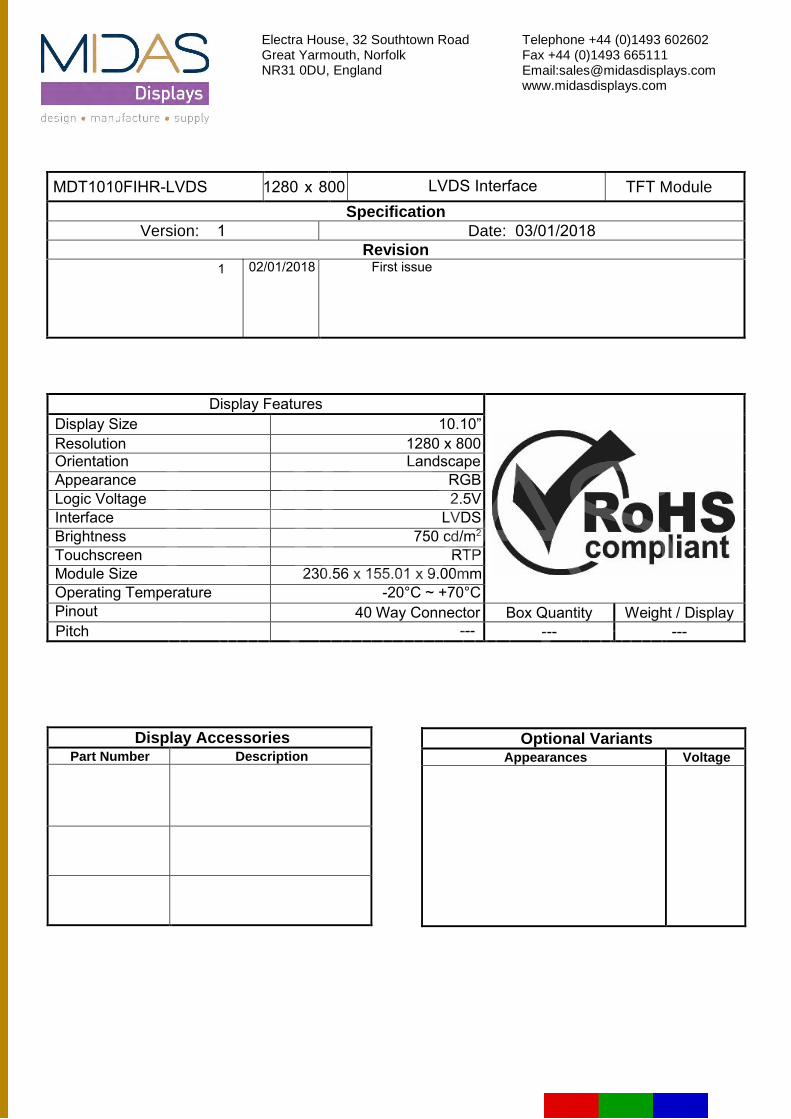
MDT1010FIHR-LVDS 1280 x 800 TFT Module Specification
Version: 1 Date: 03/01/2018 Revision
Electra House, 32 Southtown Road Great Yarmouth, Norfolk NR31 0DU, England
Telephone +44 (0)1493 602602 Fax +44 (0)1493 665111 Email:[email protected] www.midasdisplays.com
LVDS Interface
Display Accessories Part Number Description
Optional Variants Appearances Voltage
Display Features Display Size 10.10”Resolution 1280 x 800Orientation Landscape Appearance RGB Logic Voltage 2.5VInterface LVDSBrightness 750 cd/m2
Touchscreen RTPModule Size 230.56 x 155.01 x 9.00mmOperating Temperature -20°C ~ +70°C
Box Quantity Weight / Display Pinout --- ---
1 02/01/2018 First issue
Pitch40 Way Connector
---

Summary
TFT 10.1" is a TN transmissive type color active matrix TFT liquid crystal display that use amorphous silicon TFT as switching devices. This module is a composed of a TFT_LCD module. It is usually designed for industrial application and this module follows RoHs.
General Specifications
Screen Diagonal: 10.1 inch
Number of Pixels: 1280 x 3(R GB) x 800 dots
Module dimension: 230.56 x 155.01 x 9.0 mm
Active area: 216.96 (H) x 135.6(V) mm
Pixel pitch: 0.1695 × 0.1695 mm
Display Mode: Normally Black
Pixel Arrangement: R.G.B. Vertical Stripe
Backlight Type: LED,Normally White
Aspect Ratio:16:9
Electrical Interface (Logic): LVDS
With /Without TP: With RTP
Surface: Glare
*Color tone slight changed by temperature and driving voltage.

InterfaceInterface Connector A 40pin connector is used for the module electronics interface. The recommended model is F62240-H1210B manufactured by Vigorconn.
Pin No. Symbol I/O Function Remark 1 VCOM P Common Voltage 2 VDD P Power Supply 3 VDD P Power Supply 4 NC - No connection 5 NC - No connection 6 NC - No connection 7 GND P Ground 8 Rxin0- I -LVDS Differential Data Input
R0-R5,G0 9 Rxin0+ I +LVDS Differential Data Input10 GND P Ground 11 Rxin1- I -LVDS Differential Data Input
G1G5,B0,B1 12 Rxin1+ I +LVDS Differential Data Input13 GND P Ground 14 Rxin2- I -LVDS Differential Data Input B2-B5,HS,VS,
DE 15 Rxin2+ I +LVDS Differential Data Input16 GND P Ground 17 RxCLK- I -LVDS Differential Clock Input
LVDS CLK 18 RxCLK+ I +LVDS Differential Clock Input19 GND P Ground 20 Rxin3- I -LVDS Differential Data Input R6,R7,G6,G7,
B6,B7 21 Rxin3+ I +LVDS Differential Data Input22 GND P Ground 23 NC - No connection 24 NC - No connection 25 GND P Ground 26 NC - No connection 27 NC - No connection 28 NC - No connection 29 AVDD P No connection 30 GND P Ground 31 NC - No connection
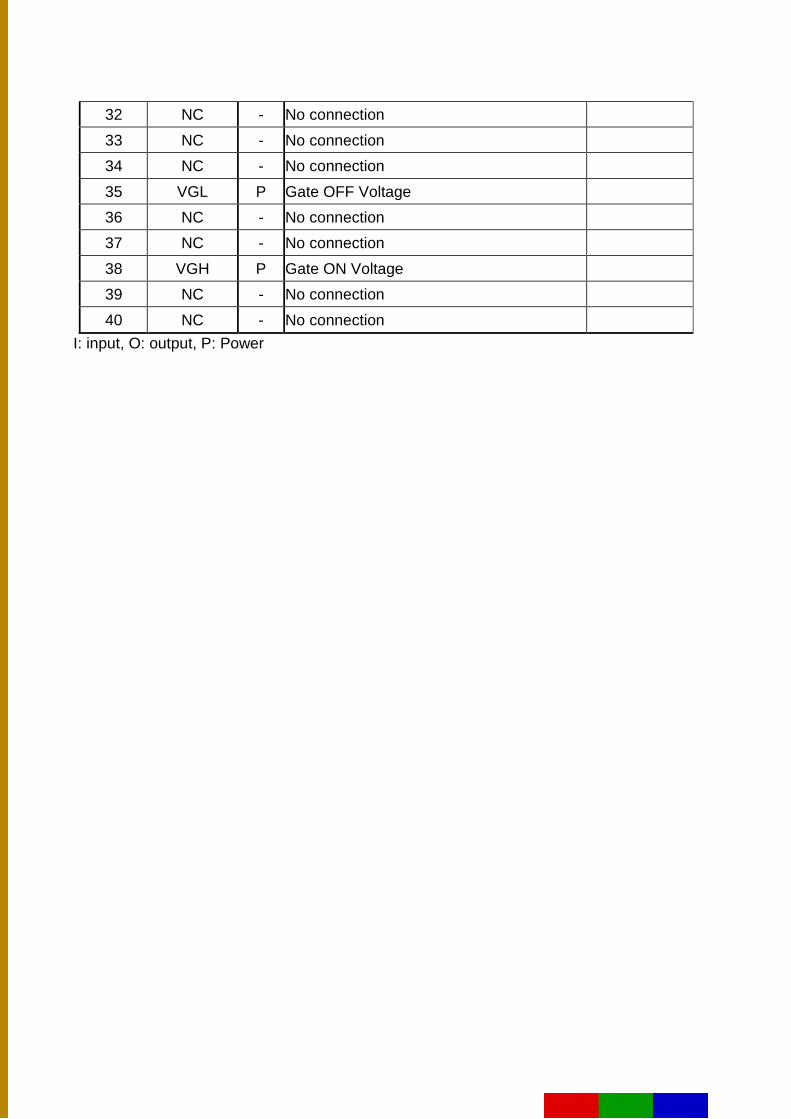
32 NC - No connection 33 NC - No connection 34 NC - No connection 35 VGL P Gate OFF Voltage 36 NC - No connection 37 NC - No connection 38 VGH P Gate ON Voltage 39 NC - No connection 40 NC - No connection
I: input, O: output, P: Power

Contour Drawing
SYMBOLPIN NO
21 XL
YD
43 XR
YU
9.00¡ Ó0.5
1280 X 3RGB X 800
8.64TP AA 217.00
8.66TFT AA 216.96
8.14TP VA 218.00
TP OUTLINE 228.34¡ Ó0.2
TFT
AA
135
.60
11.1
1
TP A
A 1
36.0
010
.91
10.4
1TP
VA
137
.00
TFT
OU
TLIN
E 15
5.01
¡Ó0.3
Black
Red
BHSR-02VS-01
The non-specified tolerance of dimension is ¡ Ó0.3 mm .
SCALE 60/1
R G B
0.0565
0.16
95
0.1695
TFT OUTLINE 230.56¡ Ó0.3
1.68
TP O
UTL
INE
147.
98¡Ó0
.2
49.7
1¡Ó0.
5
3.50
0.70P1.0*3=3.00
5.00 13.68¡ Ó0.5
Contact sideStiffener
0.30¡ Ó0.05
6.74
Lcm Connector
100.0¡ 5Ó.0
Black
Red
25.77171.00
20.0
0
Down side pitch=0.5mm
VDDVDDNCNC
23
56
4
GNDRxin0-
GND98
1011
7NC
1 VCOM
1314
12
151617
1920
18
NC
NCNC
GND
2223
2526
24
NCAVDDGND
2928
3031
27NC
21
NC3334
32
VGLNC
353637
VGH3940
38
Rxin0+
Rxin1-
GNDRxin1+
Rxin2-
GNDRxin2+
RxCLK-
GNDRxCLK+
Rxin3-
GNDRxin3+
NC
NCNC
NC
NCNC
SYMBOLPIN NO
21 LED+
LED-
The non-specified tolerance of dimension is ¡ 0Ó.3 mm .5.00
5.50 Double side adhesive
T=0.05mm
40 1

Absolute Maximum RatingsItem Symbol Min Typ Max Unit
Operating Temperature TOP -20 - +70 ℃
Storage Temperature TST -20 - +70 ℃
Note: Device is subject to be damaged permanently if stresses beyond those absolute maximum ratings listed above 1. Temp. ≦60℃, 90% RH MAX. Temp.>60℃, Absolute humidity shall be less than 90% RHat 60℃
Electrical Characteristics Typical Operation Conditions
(Note 1)
Item Symbol Values
Unit Remark Min. Typ. MAX.
Power voltage
VDD 2.3 2.5 2.7 V Note 2 AVDD 8.0 8.2 8.4 V VGH 21.7 22 22.3 V VGL -7.3 -7 -6.7 V
Input signal voltage TOP 2.7 3.0 3.3 V Note 4 Input logic high voltage TST 0.8VDD - 3.6 V
Note 3 Input logic low voltage 0 - 0.2VDD V Note 1: Be sure to apply VDD and VGL to the LCD first, and then apply VGH. Note 2: VDD setting should match the signals output voltage (refer to Note 3) of customer’s system board. Note 4: Typical VCOM is only a reference value, it must be optimized according to each LCM. Be sure to use VR.
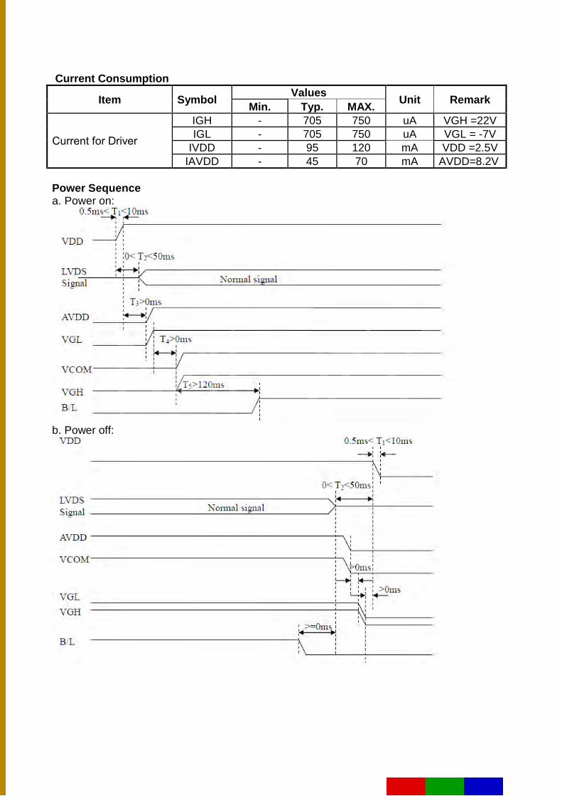
Current Consumption
Item Symbol Values Unit Remark Min. Typ. MAX.
Current for Driver
IGH - 705 750 uA VGH =22V IGL - 705 750 uA VGL = -7V
IVDD - 95 120 mA VDD =2.5V IAVDD - 45 70 mA AVDD=8.2V
Power Sequence a. Power on:
b. Power off:
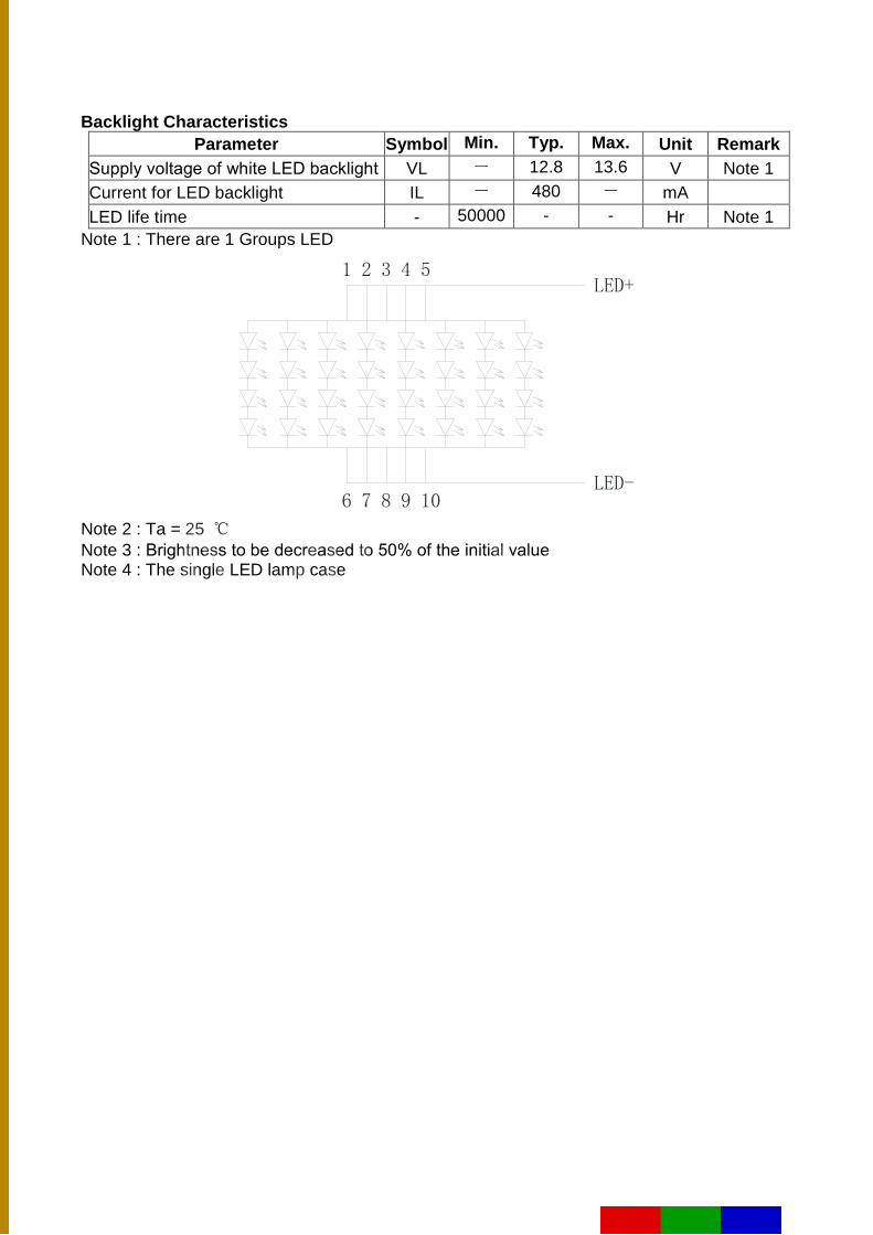
Backlight Characteristics Parameter Symbol Min. Typ. Max. Unit Remark
Supply voltage of white LED backlight VL - 12.8 13.6 V Note 1 Current for LED backlight IL - 480 - mA LED life time - 50000 - - Hr Note 1
Note 1 : There are 1 Groups LED
6 7 8 9
54321
10
LED+
LED-
Note 2 : Ta = 25 ℃ Note 3 : Brightness to be decreased to 50% of the initial value Note 4 : The single LED lamp case

LVDS Signal Timing CharacteristicsAC Electrical Characteristics
Parameter Symbol Values Unit Remark Min. Typ. MAX. LVDS Differential input high Threshold voltage RxVTH - - +100 mV RXVCM=1.2
V LVDS Differential input low Threshold voltage RxVTL -100 - - mV
LVDS Differential input common mode voltage
RxVCM 0.7 - 1.6 V
LVDS Differential voltage |VID| 200 - 600 mV

Timing Table
Parameter Symbol Value
Unit Remark Min. Typ. Max.
Clock Frequency 1/Tc 68.9 71.1 73.4 Mhz Frame rate =60Hz
Horizontal display area thd 1280 Tc
HS period time th 1410 1440 1470 Tc HS Width +Back Porch +Front Porch
tHW+ tHBP +tHFP 60 160 190 Tc
Vertical display area tvd 800 tH
VS period time tv 815 823 833 tH
VS Width +Back Porch +Front Porch
tvW+ tvBP +tvFP 15 23 33 tH
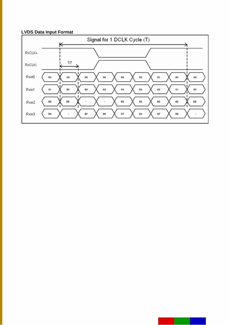
LVDS Data Input Format
Optical CharacteristicsItem Symbol Condition. Min Typ. Max. Unit Remark
Response time Tr θ=0°、Φ=0° - 10 20 .ms Note 3 Tf - 15 30 Contrast ratio CR At optimized
viewing angle 600 800 - - Note 4
Color Chromaticity White Wx θ=0°、Φ=0 0.26 0.31 0.36 - Note 2,5 Wy 0.28 0.33 0.38 -
Viewing angle (Gray Scale Inversion
Direction)
Hor. ΘR
CR≧10
75 85 -
Deg. Note 1 ΘL 75 85 -
Ver. ΦT 75 85 - ΦB 75 85 -
Brightness - - 700 750 - cd/m 2 Center of display
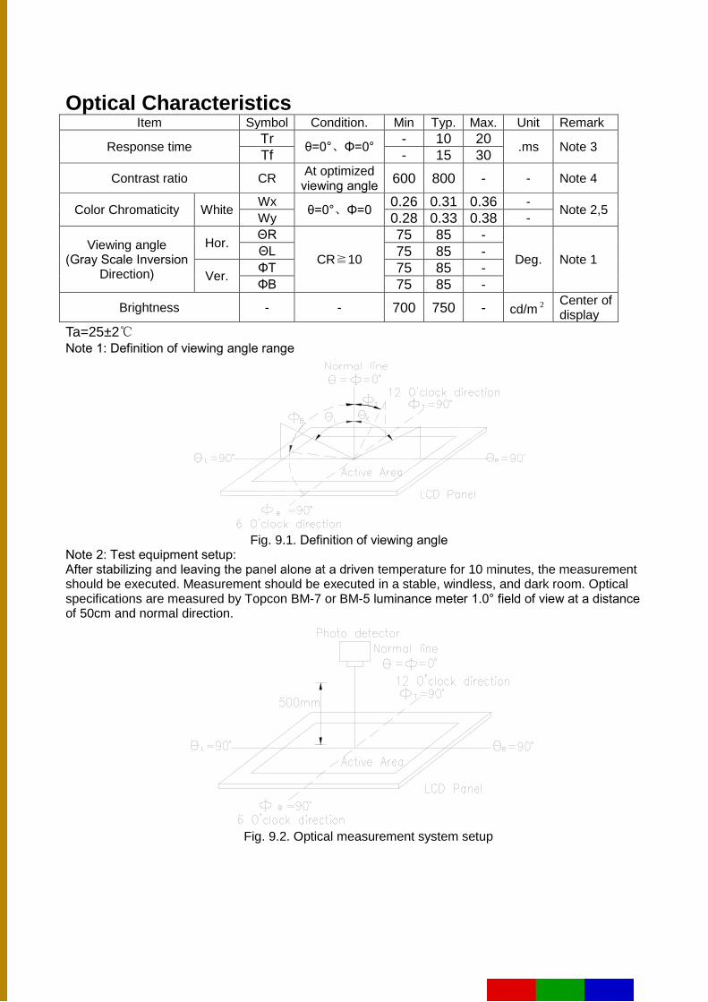
Ta=25±2℃ Note 1: Definition of viewing angle range
Fig. 9.1. Definition of viewing angle Note 2: Test equipment setup: After stabilizing and leaving the panel alone at a driven temperature for 10 minutes, the measurement should be executed. Measurement should be executed in a stable, windless, and dark room. Optical specifications are measured by Topcon BM-7 or BM-5 luminance meter 1.0° field of view at a distance of 50cm and normal direction.
Fig. 9.2. Optical measurement system setup
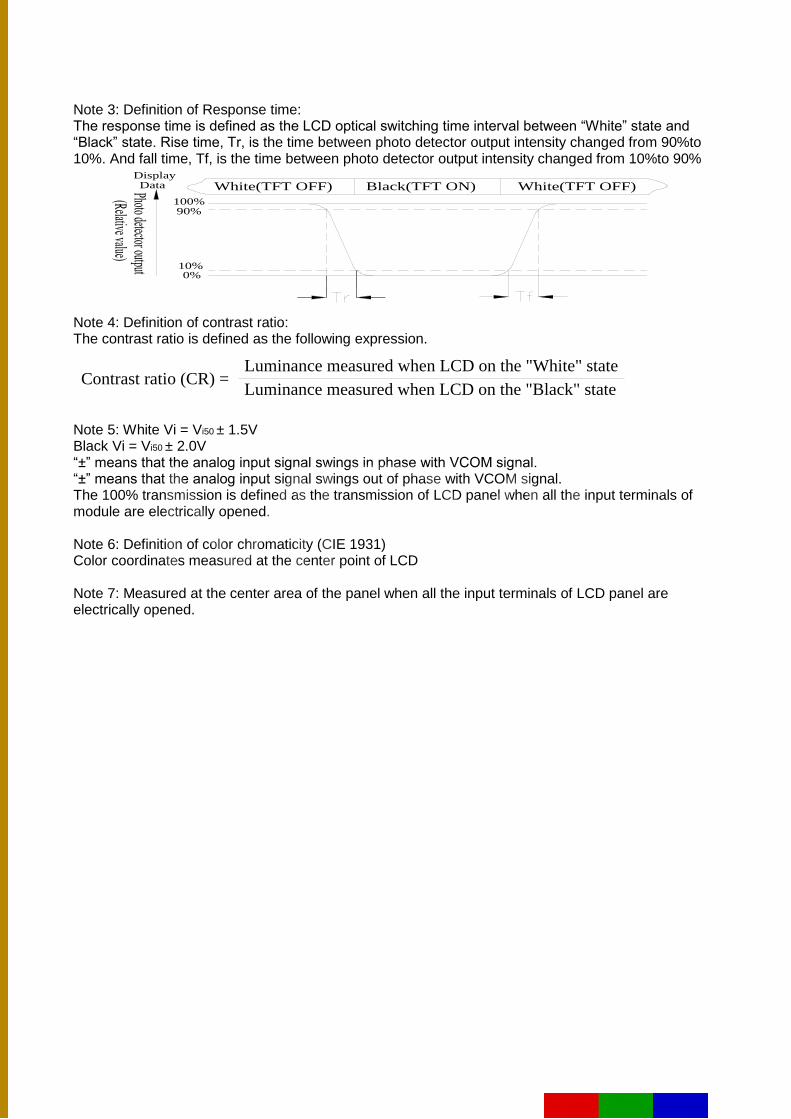
Note 3: Definition of Response time: The response time is defined as the LCD optical switching time interval between “White” state and “Black” state. Rise time, Tr, is the time between photo detector output intensity changed from 90%to 10%. And fall time, Tf, is the time between photo detector output intensity changed from 10%to 90%
Black(TFT ON) White(TFT OFF)White(TFT OFF)100%90%
10%0%
DisplayData
Note 4: Definition of contrast ratio: The contrast ratio is defined as the following expression.
Luminance measured when LCD on the "White" stateContrast ratio (CR) = Luminance measured when LCD on the "Black" state
Note 5: White Vi = Vi50 ± 1.5V Black Vi = Vi50 ± 2.0V “±” means that the analog input signal swings in phase with VCOM signal. “±” means that the analog input signal swings out of phase with VCOM signal. The 100% transmission is defined as the transmission of LCD panel when all the input terminals of module are electrically opened.
Note 6: Definition of color chromaticity (CIE 1931) Color coordinates measured at the center point of LCD
Note 7: Measured at the center area of the panel when all the input terminals of LCD panel are electrically opened.

ReliabilityContent of Reliability Test (Wide temperature, -20℃~70℃)
Note1: No dew condensation to be observed. Note2: The function test shall be conducted after 4 hours storage at the normal Temperature and humidity after remove from the test chamber. Note3: The packing have to including into the vibration testing.
Environmental Test
Test Item Content of Test Test Condition Note High Temperature storage
Endurance test applying the high storage temperature for a long time.
70℃ 200hrs
2
Low Temperature storage
Endurance test applying the low storage temperature for a long time.
-20℃200hrs
1,2
High Temperature Operation
Endurance test applying the electric stress (Voltage & Current) and the thermal stress to the element for a long time.
70℃ 200hrs
——
Low Temperature Operation
Endurance test applying the electric stress under low temperature for a long time.
-20℃200hrs
1
High Temperature/ Humidity Operation
The module should be allowed to stand at 60℃,90%RH max
60℃,90%RH 96hrs
1,2
Thermal shock resistance
The sample should be allowed stand the following 10 cycles of operation
-20℃ 25℃ 70℃
30min 5min 30min 1 cycle
-20℃/70℃10 cycles
——
Vibration test Endurance test applying the vibration during transportation and using.
Total fixed amplitude : 1.5mm Vibration Frequency : 10~55Hz One cycle 60 seconds to 3 directions of X,Y,Z for Each 15 minutes
3
Static electricity test Endurance test applying the electric stress to the terminal.
VS=±600V(contact), ±800v(air), RS=330Ω CS=150pF 10 times
——

Touch Panel Information
217.00¡ Ó0.20 (AA)
218.00¡ Ó0.20 (VA)
228.34¡ Ó0.20 (TP)
136.00¡
Ó0.20 (AA)
137.00¡
Ó0.20 (VA)
147.98¡
Ó0.20 (TP)
4.38¡ Ó0.20
3.88¡ Ó0.20
7.81¡
Ó0.20
7.31¡
Ó0.20 14.50¡ Ó0.50
50.00¡
Ó0.50
3.50¡
Ó0.30 2*1.00¡ Ó0.10
W=4*0.70¡ Ó0.05
P:1.00*3=3.00¡ Ó0.10
219.20¡ Ó0.30
227.94¡ Ó0.30
138.20¡
Ó0.30
147.58¡
Ó0.30
2.87¡
Ó0.30
5.67¡ Ó0.30
5.50¡
Ó0.30
5.00¡ Ó0.10
PIN1 PIN4
1.40¡ Ó0.15
ITO FilmT=0.188mm
0.30¡ Ó0.05
ITO GlassT=1.10mm
3M T=0.05mm
L O G I C1 2 3 4
YU
YD
XRXL
Pin No.
1
2
3
4
XL
YD
XR
YU
SYMBOL
The non-specified tolerance of dimension is 0.3mm.
Resistance Touch Panel General Specifications Item Description
Driving condition DC5V Operating force 20~100g Linearity max ≤±1.5%
Insulating resistance >20MΩ,25V(DC) Light transparence 70%
Structure type ITO Film/ITO Glass(F/G) Surface Hardness 3H typ
Pen Hitting Durability (with the silicon rubber) >1000,000 times
X resistance 450~1100Ω Y resistance 200~600Ω