MDT0200AIS-PAR 240 x 320 TFT Module Specification Version
10
MDT0200AIS-PAR 240 x 320 TFT Module Specification Version: 1 Date: 26/02/2019 Revision Electra House, 32 Southtown Road Great Yarmouth, Norfolk NR31 0DU, England Telephone +44 (0)1493 602602 Fax +44 (0)1493 665111 Email:[email protected] www.midasdisplays.com Parallel Interface Display Accessories Part Number Description Optional Variants Appearances Voltage Display Features Display Size 2.0” Resolution 240 x 320 Orientation Portrait Appearance RGB Logic Voltage 3V Interface 8/16 Bit Parallel Brightness 400 cd/m 2 Touchscreen --- Module Size 35.60 x 48.70 x 2.35mm Operating Temperature -20°C ~ +70°C Box Quantity Weight / Display Pinout --- --- 1 26/02/2019 First issue * - For full design functionality, please use this specification in conjunction with the ST77891V specification.(Provided Separately) Pitch 40 way FFC 0.5mm The MCIB-11 is an HDMI to RGB converter. Ideal for connecting a range of Midas TFT displays to a Single Board Computer such as the Raspberry Pi. MCIB-11
-
Upload
khangminh22 -
Category
Documents
-
view
2 -
download
0
Transcript of MDT0200AIS-PAR 240 x 320 TFT Module Specification Version

MDT0200AIS-PAR 240 x 320 TFT Module Specification
Version: 1 Date: 26/02/2019 Revision
Electra House, 32 Southtown Road Great Yarmouth, Norfolk NR31 0DU, England
Telephone +44 (0)1493 602602 Fax +44 (0)1493 665111 Email:[email protected] www.midasdisplays.com
Parallel Interface
Display Accessories Part Number Description
Optional Variants Appearances Voltage
Display Features
Display Size 2.0”Resolution 240 x 320Orientation PortraitAppearance RGB
Logic Voltage 3V
Interface 8/16 Bit ParallelBrightness 400 cd/m2
Touchscreen ---Module Size 35.60 x 48.70 x 2.35mmOperating Temperature -20°C ~ +70°C
Box Quantity Weight / Display Pinout
--- ---
1 26/02/2019 First issue
* - For full design functionality, please use thisspecification in conjunction with the ST77891Vspecification.(Provided Separately)
Pitch40 way FFC
0.5mm
The MCIB-11 is an HDMI to RGB converter. Ideal for connecting a range of
Midas TFT displays to a Single Board Computer such as the Raspberry Pi.
MCIB-11

General CharacteristicsITEM Specification Unit
LCD Type a-Si TFT,Transmissive,Normally black,IPS -LCD Size 2.0 inch
Resolution (W x H) 240 x (RGB) × 320 pixelLCM (W × H × D ) 35.6(W) x 48.7(H) x 2.35(D) mm
Active Area (W × H) 30.6 (W) x 40.8 (H) mmDot Pitch (W × H) 0.1275 (W) x 0.1275 (H) mmViewing Direction Free -
Color Depth 65K/262K -Pixel Arrangement RGB Vertical stripe -
Backlight Type 3LEDs, 20mA -Surface Luminance 400 cd/m2Surface Treatment Anti-glare -
Driver IC ST77891V -Interface Type MCU8/16-bit -Input Voltage 2.8 V
With/Without TP without -Weight TBD. g
Note 1: RoHS compliantNote 2: LCM weight tolerance: ± 5%.

Product drawings
MDT0200A
IS-RGB

Interface description
PIN NO. Symbol description
1 GND System Ground. (0V)
2 GND System Ground. (0V)
3 IM0IM0=0: MCU16-BIT, DB0~DB15
IM0=1: MCU8-BIT, DB8~DB15
4 FMARK Tearing Effect output signal
5 NC
6 NC
7 RESET Reset input signal
8 RS Data/Command Selection pin
9 CS Chip select signal.
10 RD read signal input
11 WR write signal input
12 VCC Power supply +2.8V
13 NC14 GND System Ground. (0V)
15~24 DB15~DB6 Data BUS
25~30 DB0~DB5 Data BUS
31 NC
32 NC
33 LEDA Backlight A Aothod input pin.
34 LEDK Backlight K Cathode input pin.
35~39 NC
40 GND System Ground. (0V)
Note: “0”connect to GND; “1”connect to IOVCC.
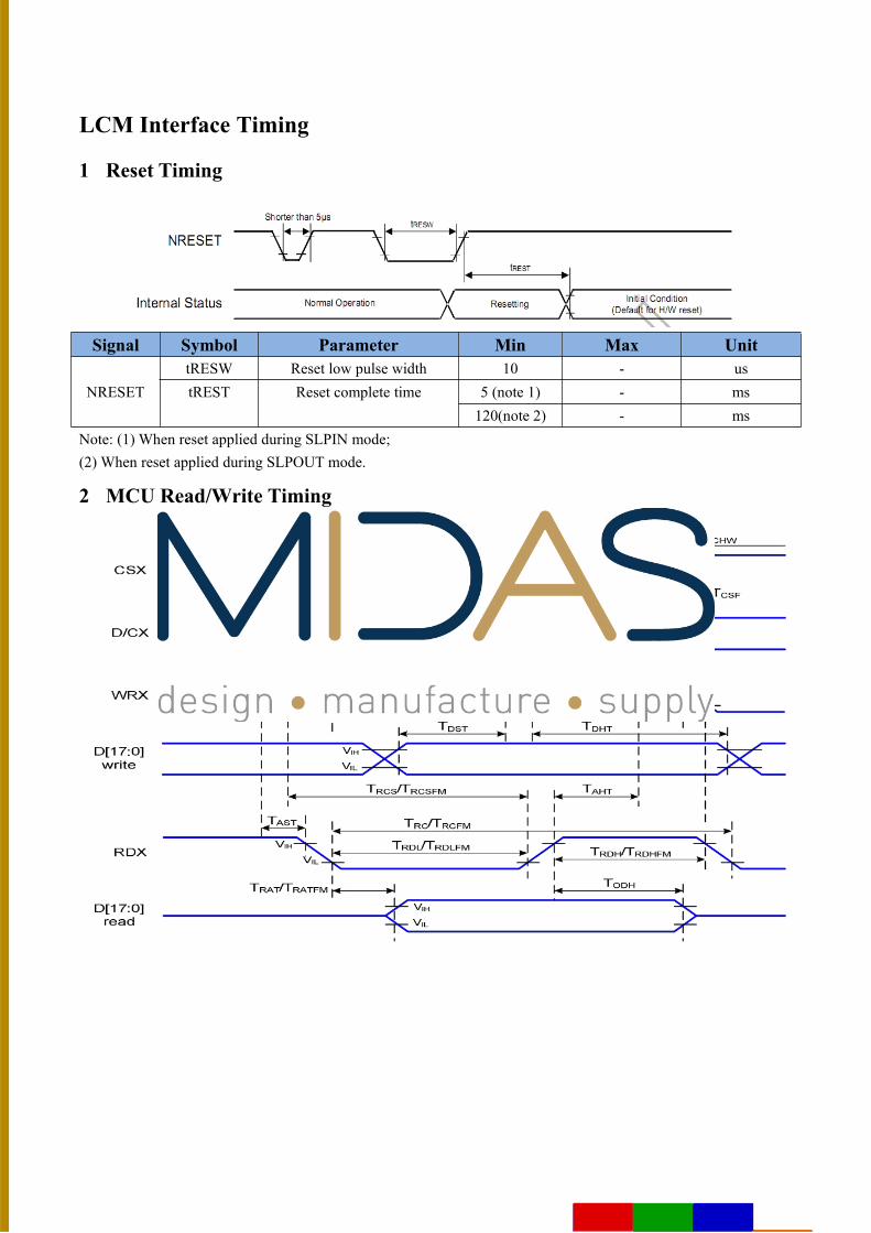
LCM Interface Timing
1 Reset Timing
Signal Symbol Parameter Min Max Unit
NRESETtRESW Reset low pulse width 10 - ustREST Reset complete time 5 (note 1) - ms
120(note 2) - msNote: (1) When reset applied during SLPIN mode;(2) When reset applied during SLPOUT mode.
2 MCU Read/Write Timing

(VSSA=0V, VDD1=1.8V, VDD3=2.8V, TA=25°C)Signal Symbol Parameter Min. Max. Unit Description
DCXtAST Address setup time 0 -
ns -tAHT Address hold time (Write/Read) 10 -
CSX
tCS Chip select setup time (Write) 15 -
ns -tRCS Chip select setup time (Read
register)45 -
tRCSFM Chip select setup time (GRAM) 355 -tCSF Chip select wait time (Write/Read) 10 -
WRXtWC Write cycle (write register) 66 -
ns -tWRH Control pulse “H” duration 15 -tWRL Control pulse “L” duration 15 -
RDX
tRC Read cycle (read register) 160 -
ns -
tRC Read cycle (GRAM) 450 -tRDH Control pulse “H” duration 90 -tRDL Control pulse “L” duration(read
register)45 -
tRDL Control pulse “L” duration(GRAM) 355 -
DB[23:0]
tDST Data setup time 10 -
ns
For maximumCL=30pF
For minimumCL=8pF
tDHT Data hold time 10 -tRAT Read access time(read register) - 40tRAT Read access time(GRAM) - 340tODH Output disable time 20 80
Note: The input signal rise time and fall time (tr, tf) is specified at 15 ns or less.Logic high and low levels are specified as 30% and 70% of VDD1 for Input signals.
Absolute Maximum RatingsPARAMETER SYMBOL MIN MAX UNIT
Supply Voltage (Analog) VCC~GND -0.3 3.3 VLogic signal voltage(I/O) IOVCC~GND -0.3 3.3 VOperating Temperature TOP -20 70 °CStorage Temperature TST -30 80 °C
Humidity RH - 90%(Max 60°C) RH

Electrical CharacteristicsPARAMETER SYMBOL MIN TYP MAX UNIT
Analog operating voltage VCC 2.5 2.8 3.3 VLogic operating voltage IOVCC 1.65 1.8 3.3 V
Input Current Icc - 6 7.5 mAInput Voltage ' H ' level VIH 0.7IOVCC - IOVCC
VInput Voltage ' L ' level VIL GND - 0.3IOVCC
Output Voltage ' H ' level VOH 0.8IOVCC - IOVCCOutput Voltage ' L ' level VOL GND - 0.2IOVCC
Backlight CharacteristicsITEM SYMBOL MIN TYP MAX UNIT
Voltage for LED backlight Vf - 9 9.3 VCurrent for LED backlight If - 15 20 mA
Power consumption Wbl - 135 186 mWUniformity Avg 80 - - %
LED Life Time - 30000 40000 - HrsNote:1.The LED life time is defined as the module brightness decrease to 50% original brightness at Ta=25°C,60%RH ±5 %.2. The life time of LED will be reduced if LED is driven by high current, high ambient temperature andhumidity conditions.3. Typical operating life time is an estimated data.4. Permanent damage to the device may occur if maximum values are exceeded or reverse voltage isloaded .Functional operation should be restricted to the conditions described under normal operatingconditions.
LCD Optical specifications
Item Symbol Condition
SpecificationUnit Remark
Min. Typ. Max.Response time (By Quick) Tr+Tf θ= 0° - 30 40 ms
Luminance L θ= 0° 350 400 - cd/m2
Contrast ratio CR θ= 0° 640 800 -
Viewing angle
Top CR≧10 - 80 -
Deg.Bottom CR≧10 - 80 -Left CR≧10 - 80 -Right CR≧10 - 80 -
Color chromaticity( CF only with ITO,
light source is Clight, CIE 1931)
Wx
θ= 0° -0.02
0.30
+0.02Wy 0.32
Note 1: Ambient temperature = 25°C.

Note 2: To be measured with a viewing cone of 2°by Topcon luminance meter BM-7.Note 3: LCD status is cell without polarizer. Transmittance of Specification is cell with polarizer.
The tolerance of Transmittance is ±10%.Note 4: Definition of response time:
The output signals of TRD-100 are measured when the input signals are changed to “White”(falling time) and from “White” to “Black” (rising time), respectively. The interval is between the10% and 90% of amplitudes. Refer to figure as below.
Note 5: Definition of contrast ratio:Contrast ratio is calculated by the following formula.
Contrast ratio (CR)=state black"" on the Brightness
state white"" on the Brightness
Note 6: Definition of viewing angle
Note 7: Optical characteristic measurement setup.
Note 8:

l LA-LA’ l / LA x 100%= 2% max., LA and LA’ are brightness at location A and A’.l LB-LB’ l / LB x 100%= 2% max., LB and LB’ are brightness at location B and B’.
RELIABILITY TESTNO. TEST ITEM TEST CONDITION INSPECTIONAFTER TEST
1High Temperature
Storage80±2°C/96 hours
Inspection after 2~4 hours storage atroom temperature and humidity. The
condensation is not accepted. Thesample shall be free from defects:
1. Air bubble in the LCD2. Seal leak3. Non-display4. Missing segments5. Glass crack
2Low Temperature
Storage-30±2°C/96 hours
3High Temperature
Operating70±2°C/96 hours
4Low Temperature
Operating-20±2°C/96 hours
5 Temperature Cycle-30±2°C ~ 25~ 80± 2°C × 10 cycles(30 min.) (5min.) (30min.)
6 Damp Proof Test 60°C ±5°C × 90%RH/96 hours
7 Vibration Test
Frequency 10Hz~55HzStroke: 1.5mm
Sweep: 10Hz~150 Hz~10Hz 2 hoursFor each direction of X, Y, Z
8 Packing Drop TestHeight: 60 cm
1 corner, concrete floor
9Electrostatic
Discharge Test
C=150pF, R=330 ΩAir: ±8KV 150pF/330Ω 30 times
Contact: ±4KV,20 times
Others1. Issues that are not defined in this document shall be discussed and agreed with both parties. (Customer andsupplier)2. Unless otherwise agreed upon in writing, the criteria shall be applied to both parties. (Customer and supplier)

Suggestions for using LCD modules
1 Handling of LCM
1. The LCD screen is made of glass. Don't give excessive external shock, or drop from a high place.2. If the LCD screen is damaged and the liquid crystal leaks out, do not lick and swallow. When the liquidis attach to your hand, skin, cloth etc, wash it off by using soap and water thoroughly and immediately.3. Don't apply excessive force on the surface of the LCM.4. If the surface is contaminated, clean it with soft cloth. If the LCM is severely contaminated, use Isopropylalcohol/Ethyl alcohol to clean. Other solvents may damage the polarizer. The following solvents is especiallyprohibited: water , ketone Aromatic solvents etc.5. Exercise care to minimize corrosion of the electrode. Corrosion of the electrodes is accelerated by waterdroplets, moisture condensation or a current flow in a high-humidity environment.6. Install the LCD Module by using the mounting holes. When mounting the LCD module make sure it is free oftwisting, warping and distortion. In particular, do not forcibly pull or bend the I/O cable or the backlight cable.7. Don’t disassemble the LCM.8. To prevent destruction of the elements by static electricity, be careful to maintain an optimum workenvironment.- Be sure to ground the body when handling the LCD modules.- Tools required for assembling, such as soldering irons, must be properly grounded.- To reduce the amount of static electricity generated, do not conduct assembling and other workunder dry conditions.- The LCD module is coated with a film to protect the display surface. Exercise care when peelingoff this protective film since static electricity may be generated.9. Do not alter, modify or change the the shape of the tab on the metal frame.10. Do not make extra holes on the printed circuit board, modify its shape or change the positions ofcomponents to be attached.11. Do not damage or modify the pattern writing on the printed circuit board.12. Absolutely do not modify the zebra rubber strip (conductive rubber) or heat seal connector13. Except for soldering the interface, do not make any alterations or modifications with a soldering iron.14. Do not drop, bend or twist LCM.
2 Storage1. Store in an ambient temperature of 5 to 45 C, and in a relative humidity of 40% to 60%. Don't exposeto sunlight or fluorescent light.2. Storage in a clean environment, free from dust, active gas, and solvent.3. Store in antistatic container.