MCP6XXX Amplifier Evaluation Board 2 User's Guide
36
© 2007 Microchip Technology Inc. DS51668A MCP6XXX Amplifier Evaluation Board 2 User’s Guide
-
Upload
khangminh22 -
Category
Documents
-
view
2 -
download
0
Transcript of MCP6XXX Amplifier Evaluation Board 2 User's Guide

© 2007 Microchip Technology Inc. DS51668A
MCP6XXX AmplifierEvaluation Board 2
User’s Guide

Note the following details of the code protection feature on Microchip devices:• Microchip products meet the specification contained in their particular Microchip Data Sheet.
• Microchip believes that its family of products is one of the most secure families of its kind on the market today, when used in the intended manner and under normal conditions.
• There are dishonest and possibly illegal methods used to breach the code protection feature. All of these methods, to our knowledge, require using the Microchip products in a manner outside the operating specifications contained in Microchip’s Data Sheets. Most likely, the person doing so is engaged in theft of intellectual property.
• Microchip is willing to work with the customer who is concerned about the integrity of their code.
• Neither Microchip nor any other semiconductor manufacturer can guarantee the security of their code. Code protection does not mean that we are guaranteeing the product as “unbreakable.”
Code protection is constantly evolving. We at Microchip are committed to continuously improving the code protection features of ourproducts. Attempts to break Microchip’s code protection feature may be a violation of the Digital Millennium Copyright Act. If such actsallow unauthorized access to your software or other copyrighted work, you may have a right to sue for relief under that Act.
Information contained in this publication regarding deviceapplications and the like is provided only for your convenienceand may be superseded by updates. It is your responsibility toensure that your application meets with your specifications.MICROCHIP MAKES NO REPRESENTATIONS ORWARRANTIES OF ANY KIND WHETHER EXPRESS ORIMPLIED, WRITTEN OR ORAL, STATUTORY OROTHERWISE, RELATED TO THE INFORMATION,INCLUDING BUT NOT LIMITED TO ITS CONDITION,QUALITY, PERFORMANCE, MERCHANTABILITY ORFITNESS FOR PURPOSE. Microchip disclaims all liabilityarising from this information and its use. Use of Microchipdevices in life support and/or safety applications is entirely atthe buyer’s risk, and the buyer agrees to defend, indemnify andhold harmless Microchip from any and all damages, claims,suits, or expenses resulting from such use. No licenses areconveyed, implicitly or otherwise, under any Microchipintellectual property rights.
DS51668A-page ii
Trademarks
The Microchip name and logo, the Microchip logo, Accuron, dsPIC, KEELOQ, KEELOQ logo, microID, MPLAB, PIC, PICmicro, PICSTART, PRO MATE, rfPIC and SmartShunt are registered trademarks of Microchip Technology Incorporated in the U.S.A. and other countries.
AmpLab, FilterLab, Linear Active Thermistor, Migratable Memory, MXDEV, MXLAB, SEEVAL, SmartSensor and The Embedded Control Solutions Company are registered trademarks of Microchip Technology Incorporated in the U.S.A.
Analog-for-the-Digital Age, Application Maestro, CodeGuard, dsPICDEM, dsPICDEM.net, dsPICworks, ECAN, ECONOMONITOR, FanSense, FlexROM, fuzzyLAB, In-Circuit Serial Programming, ICSP, ICEPIC, Mindi, MiWi, MPASM, MPLAB Certified logo, MPLIB, MPLINK, PICkit, PICDEM, PICDEM.net, PICLAB, PICtail, PowerCal, PowerInfo, PowerMate, PowerTool, REAL ICE, rfLAB, Select Mode, Smart Serial, SmartTel, Total Endurance, UNI/O, WiperLock and ZENA are trademarks of Microchip Technology Incorporated in the U.S.A. and other countries.
SQTP is a service mark of Microchip Technology Incorporated in the U.S.A.
All other trademarks mentioned herein are property of their respective companies.
© 2007, Microchip Technology Incorporated, Printed in the U.S.A., All Rights Reserved.
Printed on recycled paper.
© 2007 Microchip Technology Inc.
Microchip received ISO/TS-16949:2002 certification for its worldwide headquarters, design and wafer fabrication facilities in Chandler and Tempe, Arizona; Gresham, Oregon and design centers in California and India. The Company’s quality system processes and procedures are for its PIC® MCUs and dsPIC® DSCs, KEELOQ® code hopping devices, Serial EEPROMs, microperipherals, nonvolatile memory and analog products. In addition, Microchip’s quality system for the design and manufacture of development systems is ISO 9001:2000 certified.

MCP6XXX AMPLIFIER EVALUATIONBOARD 2 USER’S GUIDE
Table of Contents
Preface ........................................................................................................................... 1Introduction............................................................................................................ 1Document Layout .................................................................................................. 1Conventions Used in this Guide ............................................................................ 2Recommended Reading........................................................................................ 3The Microchip Web Site ........................................................................................ 3Customer Support ................................................................................................. 3Document Revision History ................................................................................... 3
Chapter 1. Product Overview ....................................................................................... 51.1 Introduction ..................................................................................................... 51.2 MCP6XXX Amplifier Evaluation Board 2 Kit Contents ................................... 51.3 Microchip’s Web-Based Mindi™ Analog Simulator Tool ................................ 61.4 MCP6XXX Amplifier Evaluation Board 2 Description ..................................... 6
Chapter 2. Installation and Operation ......................................................................... 72.1 Introduction ..................................................................................................... 72.2 Required Tools ............................................................................................... 72.3 MCP6XXX Amplifier Evaluation Board 2 Set-up ............................................ 72.4 MCP6XXX Amplifier Evaluation Board 2 Operation ..................................... 13
Appendix A. Schematic and Layouts ........................................................................ 23A.1 Introduction .................................................................................................. 23A.2 Board - Schematic ....................................................................................... 24A.3 Board - Top Silk Layer .............................................................................. 25A.4 Board - Top Metal Layer .............................................................................. 26A.5 Board - Bottom Metal Layer ......................................................................... 27
Appendix B. Bill of Materials (BOM) .......................................................................... 29B.1 MCP6XXX Amplifier Evaluation Board 2 BOM ............................................ 29
Worldwide Sales and Service .................................................................................... 32
© 2007 Microchip Technology Inc. DS51668A-page iii

MCP6XXX Amplifier Evaluation Board 2 User’s Guide
NOTES:
DS51668A-page iv © 2007 Microchip Technology Inc.

MCP6XXX AMPLIFIER EVALUATIONBOARD 2 USER’S GUIDE
Preface
INTRODUCTIONThis chapter contains general information that will be useful to know before using the MCP6XXX Amplifier Evaluation Board 2. Items discussed in this chapter include:• Document Layout• Conventions Used in this Guide• Recommended Reading• The Microchip Web Site• Customer Support• Document Revision History
DOCUMENT LAYOUTThis document describes how to use the MCP6XXX Amplifier Evaluation Board 2. The manual layout is as follows:• Chapter 1. “Product Overview” - Provides the important information about the
MCP6XXX Amplifier Evaluation Board 2.• Chapter 2. “Installation and Operation” – Covers the installation and operation
of the MCP6XXX Amplifier Evaluation Board 2. It lists the required tools, shows how to set up the board, and demonstrates how to verify the amplifier operation.
• Appendix A. “Schematic and Layouts” – Shows the schematic and board layouts for the MCP6XXX Amplifier Evaluation Board 2.
• Appendix B. “Bill of Materials (BOM)” – Lists the parts used to build the MCP6XXX Amplifier Evaluation Board 2.
NOTICE TO CUSTOMERS
All documentation becomes dated, and this manual is no exception. Microchip tools and documentation are constantly evolving to meet customer needs, so some actual dialogs and/or tool descriptions may differ from those in this document. Please refer to our web site (www.microchip.com) to obtain the latest documentation available.
Documents are identified with a “DS” number. This number is located on the bottom of each page, in front of the page number. The numbering convention for the DS number is “DSXXXXXA”, where “XXXXX” is the document number and “A” is the revision level of the document.
For the most up-to-date information on development tools, see the MPLAB® IDE on-line help. Select the Help menu, and then Topics to open a list of available on-line help files.
© 2007 Microchip Technology Inc. DS51668A-page 1

MCP6XXX Amplifier Evaluation Board 2 User’s Guide
CONVENTIONS USED IN THIS GUIDEThis manual uses the following documentation conventions:
DOCUMENTATION CONVENTIONSDescription Represents Examples
Arial font:Italic characters Referenced books MPLAB® IDE User’s Guide
Emphasized text ...is the only compiler...Initial caps A window the Output window
A dialog the Settings dialogA menu selection select Enable Programmer
Quotes A field name in a window or dialog
“Save project before build”
Underlined, italic text with right angle bracket
A menu path File>Save
Bold characters A dialog button Click OKA tab Click the Power tab
N‘Rnnnn A number in verilog format, where N is the total number of digits, R is the radix and n is a digit.
4‘b0010, 2‘hF1
Text in angle brackets < > A key on the keyboard Press <Enter>, <F1>Courier New font:Plain Courier New Sample source code #define START
Filenames autoexec.batFile paths c:\mcc18\h
Keywords _asm, _endasm, static
Command-line options -Opa+, -Opa-Bit values 0, 1
Constants 0xFF, ‘A’
Italic Courier New A variable argument file.o, where file can be any valid filename
Square brackets [ ] Optional arguments mcc18 [options] file [options]
Curly brackets and pipe character: { | }
Choice of mutually exclusive arguments; an OR selection
errorlevel {0|1}
Ellipses... Replaces repeated text var_name [, var_name...]
Represents code supplied by user
void main (void){ ...}
DS51668A-page 2 © 2007 Microchip Technology Inc.

Preface
RECOMMENDED READINGThis user's guide describes how to use MCP6XXX Amplifier Evaluation Board 2. Other useful documents are listed below. The following Microchip documents are available and recommended as supplemental reference resources.MCP6021/2/3/4 Data Sheet, “Rail-to-Rail Input/Output, 10 MHz Op Amps” (DS21685)This data sheet provides detailed information regarding the MCP602X product family.
THE MICROCHIP WEB SITEMicrochip provides online support via our web site at www.microchip.com. This web site is used as a means to make files and information easily available to customers. Accessible by using your favorite Internet browser, the web site contains the following information:• Product Support – Data sheets and errata, application notes and sample
programs, design resources, user’s guides and hardware support documents, latest software releases and archived software
• General Technical Support – Frequently Asked Questions (FAQs), technical support requests, online discussion groups, Microchip consultant program member listing
• Business of Microchip – Product selector and ordering guides, latest Microchip press releases, listing of seminars and events, listings of Microchip sales offices, distributors and factory representatives
CUSTOMER SUPPORTUsers of Microchip products can receive assistance through several channels:• Distributor or Representative• Local Sales Office• Field Application Engineer (FAE)• Technical Support• Development Systems Information LineCustomers should contact their distributor, representative or field application engineer for support. Local sales offices are also available to help customers. A listing of sales offices and locations is included in the back of this document.Technical support is available through the web site at: http://support.microchip.com
DOCUMENT REVISION HISTORY
Revision A (July 2007)• Initial Release of this Document.
© 2007 Microchip Technology Inc. DS51668A-page 3

MCP6XXX Amplifier Evaluation Board 2 User’s Guide
NOTES:
DS51668A-page 4 © 2007 Microchip Technology Inc.

MCP6XXX AMPLIFIER EVALUATIONBOARD 2 USER’S GUIDE
Chapter 1. Product Overview
1.1 INTRODUCTIONThe MCP6XXX Amplifier Evaluation Board 2 is described by the following:• Assembly # : 114-00148• Order # : MCP6XXXEV-AMP2• Name: MCP6XXX Amplifier Evaluation Board 2Items discussed in this chapter include:• Section 1.2 “MCP6XXX Amplifier Evaluation Board 2 Kit Contents”• Section 1.3 “Microchip’s Web-Based Mindi™ Analog Simulator Tool”• Section 1.4 “MCP6XXX Amplifier Evaluation Board 2 Description”
1.2 MCP6XXX AMPLIFIER EVALUATION BOARD 2 KIT CONTENTS• MCP6XXX Amplifier Evaluation Board 2 - One partially assembled board• Important Information “Read First”• Accessory Bag - Contains loose parts for populating sockets on board• Analog and Interface Products Demonstration Boards CD-ROM (DS21912)
- MCP6XXX Amplifier Evaluation Board 2 User’s Guide (DS51668)
FIGURE 1-1: MCP6XXX Amplifier Evaluation Board 2 Kit.
© 2007 Microchip Technology Inc. DS51668A-page 5

MCP6XXX Amplifier Evaluation Board 2 User’s Guide
1.3 MICROCHIP’S WEB-BASED MINDI™ ANALOG SIMULATOR TOOLThe Mindi™ Analog Simulator tool is an innovative software tool that simplifies analog circuit design. The Mindi™ Analog Simulator tool supports the following application circuits: 1) Active Filters, 2) Amplifiers, 3) Battery Chargers, and 4) DC-to-DC Converters. The Mindi™ Amplifier Designer provides full schematic diagrams of the amplifier application circuit with recommended component values and displays the responses in frequency and time domains.The Mindi™ Analog Simulator tool is a free web-based design tool available on the Microchip web site at http://www.microchip.com under “Online Simulation Tools” or by going directly to the Mindi™ web site at http://www.microchip.com/mindi.The circuit simulator within the Mindi™ Analog Simulator tool can be downloaded and installed on a personal computer (PC) for more convenient simulations. Modified circuit files can also be downloaded to the PC.
1.4 MCP6XXX AMPLIFIER EVALUATION BOARD 2 DESCRIPTIONMCP6XXX Amplifier Evaluation Board 2 is designed to support inverting/non-inverting summing amplifier circuits, however, at this time, the Mindi™ Amplifier Designer only supports the inverting summing amplifier circuits.The MCP6XXX Amplifier Evaluation Board 2 has the following features:• All amplifier resistors and capacitors are socketed• All of the component labels on board keep consistent with those on schematic
generated in the Mindi™ Amplifier Designer• Supports all Microchip single op amps
- PDIP-8 package (e.g., MCP6021) are socketed- SOIC-8 package can be accomodated; see Section 2.4.3 “Amplifier
Modifications Using 8-Pin SOIC Op Amps”• Test points for connecting lab equipment• Single supply configurationFigure 1-2 shows the block diagram of the MCP6XXX Amplifier Evaluation Board 2. Lab equipment can be attached (via test points) to measure the amplifier response.
FIGURE 1-2: MCP6XXX Amplifier Evaluation Board 2 Block Diagram.
Amplifier Circuit(Op Amp, Resistors,
Signal Outputand Test Point
Signal Inputsand
Mid-Supply Refand Power Supply
and Test Point
Test Points
Test Point
Capacitors and Jumpers)
DS51668A-page 6 © 2007 Microchip Technology Inc.

MCP6XXX AMPLIFIER EVALUATIONBOARD 2 USER’S GUIDE
Chapter 2. Installation and Operation
2.1 INTRODUCTIONThis chapter shows how to set up the MCP6XXX Amplifier Evaluation Board 2.Items discussed in this chapter include:• Required Tools• MCP6XXX Amplifier Evaluation Board 2 Set-Up• MCP6XXX Amplifier Evaluation Board 2 Operation
2.2 REQUIRED TOOLS• Lab power supply• Lab signal source (e.g., function generator)• Lab measurement equipment (e.g., oscilloscope)
2.3 MCP6XXX AMPLIFIER EVALUATION BOARD 2 SET-UPThe MCP6XXX Amplifier Evaluation Board 2 supports inverting summing amplifier and non-inverting summing amplifier. This section details the conversion of these topologies to the MCP6XXX Amplifier Evaluation Board 2. Figure 2-1 shows the circuit diagram for the board.
FIGURE 2-1: MCP6XXX Amplifier Evaluation Board 2 Circuit Diagram.
CR2
RR120 kΩ
RR220 kΩ0.1 µF UR1
U1
VDD0.1 µF
CU1
CR1
0.1 µF
A
B
DP1CP1
1.0 µF
Power Supply
D
JP2C
R10
R2
R3
R4
R5
R6
R7
R8
VIN-2
VIN-3
VIN-4
VIN-5
VIN-6
VIN-7
VIN-8
RLCLVL
R11
VDD
VREF
GND VDD
VIN-1
R9GND
R1
RISO
GND
JP1
* Test Points
**
**
**
**
*
*
*
*
*
*
© 2007 Microchip Technology Inc. DS51668A-page 7

MCP6XXX Amplifier Evaluation Board 2 User’s Guide
The power supply voltage needs to be in the allowed range for the installed op amps. Any of Microchip’s op amps that operate below 5.5V can be used. Moreover, the power supply is protected by a zener diode with nominal voltage 6.2V and bypassed by a 1.0 µF capacitor. (See Figure 2-3: “Power Supply Block.”)The mid-supply reference consists of a voltage divider and a buffer amplifier. (See Figure 2-4: “Mid-supply Reference Block.”)The resistors that are part of an amplifier are placed in pin sockets which are labeled. All of the component labels on board keep consistent with those on schematic gener-ated in the Mindi™ Amplifier Designer. The op amps are bypassed by 0.1 µF capacitors and the single op amp U1 can have either a PDIP-8 or SOIC-8 package.• PDIP-8 packages are inserted into the DIP-8 socket to the right of the U1 label.• SOIC-8 packages can be accommodated; see Section 2.4.3 “Amplifier
Modifications Using 8-Pin SOIC Op Amps”.The (surface mount) test points for power supply, ground, input signal and output signal allow lab equipment to be connected to the board. The MCP6XXX Amplifier Evaluation Board 2 top view is shown in Figure 2-2.
FIGURE 2-2: MCP6XXX Amplifier Evaluation Board 2 Top View.
DS51668A-page 8 © 2007 Microchip Technology Inc.

Installation and Operation
2.3.1 Top Level Amplifier Circuit Diagrams
2.3.1.1 POWER SUPPLY BLOCK
The power supply is protected by a zener diode and bypassed by a capacitor. Figure 2-3 shows the circuit diagram for the power supply. CP1 = 1.0 µF.
FIGURE 2-3: Power Supply Block.
2.3.1.2 MID-SUPPLY REFERENCE BLOCK
The mid-supply reference consists of a voltage divider and a buffer amplifier. Figure 2-4 shows the circuit diagram for the mid-supply reference.CR1 = CR2 = 0.1 µF, RR1 = RR2 = 20.0 kΩ.
FIGURE 2-4: Mid-supply Reference Block.
Power SupplyVS
VDD
CP1DP1
Note: DP1 is a zener diode with nominal voltage of 6.2V.
Mid-supply ReferenceVDD
VR
CR1RR1
UR1CR2 RR2
© 2007 Microchip Technology Inc. DS51668A-page 9

MCP6XXX Amplifier Evaluation Board 2 User’s Guide
2.3.1.3 OUTPUT LOAD BLOCK
The output load consists of a capacitor and two resistors. Figure 2-5 shows the circuit diagram for the output load. RISO is used to stabilize the amplifier when it drives a large capacitive load (CL). RISO is a short circuit (0Ω) when CL is small.
FIGURE 2-5: Output Load Block.
Output Load
VL
CLRL
VOUT RISO
DS51668A-page 10 © 2007 Microchip Technology Inc.

Installation and Operation
2.3.1.4 INVERTING SUMMING AMPLIFIER
• Amplifies two or more input voltages with an inverting gain. Input and output voltages are shifted by a reference voltage for single supply
• The Mindi™ Amplifier Designer gives design recommendations for circuits with up to 8 inputs; see the circuit diagram shown in Figure 2-6.- Fill the sockets with the recommended resistors and capacitors- Set JP1 and JP2 in the correct positions
(for the given example, JP1: Position A, JP2: Position C)
FIGURE 2-6: Inverting Summing Amplifier Circuit Diagram.
Figure 2-7 shows an example of the inverting summing amplifier circuit diagram sup-ported by MCP6XXX Amplifier Evaluation Board 2.
FIGURE 2-7: Inverting Summing Amplifier Example Supported by the MCP6XXX Amplifier Evaluation Board 2.
OutputLoad
Mid-supplyReference
PowerSupply
VS
VR
VL
V2
V3
VDD
R1
R2
R3
R9
R11
CU1
U1
VOUT
V1
VIN-2
VIN-3
VIN-4
VIN-5
VIN-6
VIN-7
VIN-8
VIN-1
**
**
**
**
CR2
RR120 kΩ
RR220 kΩ0.1 µF UR1
U1
0.1µF
CU1
CR1
0.1 µF
A
B
DP1
CP11.0 µF
Power Supply
D
JP2C
R10
R2
R3
R4
R5
R6
R7
R8
RLCL
R11
VDD
R9
R1
RISO
JP1
VDD
VL
VREF
GND VDD
GND
GND* Test Points
*
*
*
*
*
*
© 2007 Microchip Technology Inc. DS51668A-page 11

MCP6XXX Amplifier Evaluation Board 2 User’s Guide
2.3.1.5 NON-INVERTING SUMMING AMPLIFIER (NOT SUPPORTED)
• Amplifies two or more voltages with a non-inverting gain. Input and output voltages are shifted by a reference voltage for single supply
• It is up to the user to design this circuit to produce the target gains for up to eight inputs- Select the correct resistor and capacitor values- Set JP1 and JP2 as needed
(for the given example, JP1: Position B, JP2: Position D)
FIGURE 2-8: Non-Inverting Summing Amplifier Circuit Diagram.
Figure 2-9 shows an example of the non-inverting summing amplifier circuit diagram supported by MCP6XXX Amplifier Evaluation Board 2.
FIGURE 2-9: Non-Inverting Summing Amplifier Example Supported by the MCP6XXX Amplifier Evaluation Board 2.
OutputLoad
Mid-supplyReference
PowerSupply
VS
VDD
VL
V1
V2
V3
VOUT
VR
R1
R2
R3
R10 R11
CU1
U1
CR2
RR120 kΩ
RR220 kΩ0.1 µF UR1
U1
0.1 µF
CU1
CR1
0.1 µF
A
B
DP1 CP11.0 µF
Power Supply
D
JP2C
R10
R2
R3
R4
R5
R6
R7
R8
RLCL
R11
VDD
R9
R1
RISO
JP1
VDD
VIN-2
VIN-3
VIN-4
VIN-5
VIN-6
VIN-7
VIN-8
VL
VREF
GND VDD
VIN-1
GND
GND* Test Points
**
**
**
**
*
*
*
*
*
*
DS51668A-page 12 © 2007 Microchip Technology Inc.

Installation and Operation
2.4 MCP6XXX AMPLIFIER EVALUATION BOARD 2 OPERATIONItems discussed in this section include:• Building the Amplifier • Testing the Amplifier• Amplifier Modification: Using 8-Pin SOIC Op Amps
2.4.1 Building the AmplifierThe accessory bag that comes with this kit makes it quick and easy to evaluate the amplifier described below, which was designed in the Mindi™ Amplifier Designer. This amplifier is described as follows:• Inverting Summing Amplifier (Single Supply Configuration)• Power Supply Voltage is 5.0V• Desired Gain for VIN-1 is 1 V/V• Desired Gain for VIN-2 is 1 V/V• Desired Gain for VIN-3 is 1 V/V• Load Capacitance is 56 pF
FIGURE 2-10: Inverting Summing Amplifier Designed In the Mindi™ Amplifier Designer.
© 2007 Microchip Technology Inc. DS51668A-page 13
MCP6XXX Amplifier Evaluation Board 2 User’s Guide
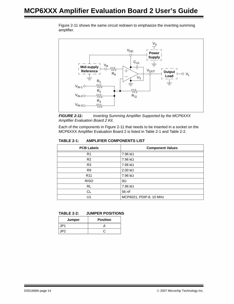
Figure 2-11 shows the same circuit redrawn to emphasize the inverting summing amplifier.
FIGURE 2-11: Inverting Summing Amplifier Supported by the MCP6XXX Amplifier Evaluation Board 2 Kit.
Each of the components in Figure 2-11 that needs to be inserted in a socket on the MCP6XXX Amplifier Evaluation Board 2 is listed in Table 2-1 and Table 2-2.
TABLE 2-1: AMPLIFIER COMPONENTS LIST
TABLE 2-2: JUMPER POSITIONS
R11
R9
CU1VR
VLVOUT Output
Load
Mid-supplyReference
VIN-1
R1
R2
R3
U1
VS
VDD PowerSupply
VIN-2
VIN-3
PCB Labels Component Values
R1 7.96 kΩR2 7.96 kΩR3 7.96 kΩR9 2.00 kΩR11 7.96 kΩ
RISO 0ΩRL 7.96 kΩCL 56 nFU1 MCP6021, PDIP-8, 10 MHz
Jumper Position
JP1 AJP2 C
DS51668A-page 14 © 2007 Microchip Technology Inc.

Installation and Operation
Figure 2-12 is the fully assembled inverting summing amplifier’s circuit diagram.
FIGURE 2-12: Fully Assembled Inverting Summing Amplifier Supported by the MCP6XXX Amplifier Evaluation Board 2.
The fully assembled MCP6XXX Amplifier Evaluation Board 2 top view is shown in Figure 2-13.
FIGURE 2-13: Picture of the Inverting Summing Amplifier Supported by the MCP6XXX Amplifier Evaluation Board 2.
CR2
RR120 kΩ
RR220 kΩ0.1 µF UR1
U1
0.1 µF
CU1
CR1
0.1 µF
A
B
DP1CP1
1.0 µF
Power Supply
D
JP2C
R10
R2
R3
R4
R5
R6
R7
R8
RLCL
R11
VDD
R9
R1
RISO
VDD
JP1
VIN-2
VIN-3
VIN-4
VIN-5
VIN-6
VIN-7
VIN-8
VL
VREF
GND VDD
VIN-1
GND
GND* Test Points
**
**
**
**
*
*
*
*
*
*
© 2007 Microchip Technology Inc. DS51668A-page 15

MCP6XXX Amplifier Evaluation Board 2 User’s Guide
2.4.2 Testing the Amplifier
2.4.2.1 CHECKING THE TEST POINTS
The (surface mount) test points for power supply, ground, input signal and output signal allow lab equipment to be connected to the board. Figure 2-14 shows the test points to check.
FIGURE 2-14: Checking the Test Points.
VDD
VL
VREF
GND
Sign
al In
puts
Test Point
GNDTest Point
GNDTest PointTest Point Test Point
Test Point
DS51668A-page 16 © 2007 Microchip Technology Inc.

Installation and Operation
2.4.2.2 TRANSIENT RESPONSES
This inverting summing amplifier was built, and its responses were measured. A MCP6021 op amp, 1% resistors, and 5% capacitors were used. Notice how close the measured and simulated data are.
2.4.2.2.1 Transient Step ResponseIn Bench Measurement:• Set VIN with a step amplitude of 1.4V and a center voltage of 2.5V. (i.e. VIN starts
0.7V below center and ends 0.7V above center) • The measured step response is shown in Figure 2-15. It is a signal with a step
amplitude of 4.2V and a center voltage of 2.5V. (i.e. VOUT starts 2.1V above center and ends 2.1V below center)
FIGURE 2-15: Measured Step Response.
Note: The center voltage of VIN is set at VREF = VDD/2 (For VDD = 5.0V,VREF = 2.5V)
VIN = 3.2V
VOUT = 0.4V
VREF = 2.5V
© 2007 Microchip Technology Inc. DS51668A-page 17

MCP6XXX Amplifier Evaluation Board 2 User’s Guide
In the Mindi™ Amplifier Designer:• Set VIN with a step amplitude of 1.4V and a center voltage of 2.5V. (i.e. VIN starts
0.7V below center and ends 0.7V above center)• The output step response is shown in Figure 2-16. It is a signal with a step
amplitude of 4.2V and a center voltage of 2.5V. (i.e. VOUT starts 2.1V above center and ends 2.1V below center)
FIGURE 2-16: Simulated Step Response.
Note: The center voltage of VIN is set at VREF = VDD/2 (For VDD = 5.0V,VREF = 2.5V)
VIN = 3.2V
VOUT = 0.4V
VREF = 2.5V
DS51668A-page 18 © 2007 Microchip Technology Inc.

Installation and Operation
2.4.2.2.2 Transient Sine Wave ResponseIn Bench Measurement:• Set VIN as a sine wave with a frequency of 100.0 Hz, a peak-to-peak voltage of
1.4V and a center voltage of 2.5V• The measured sine wave response is shown in Figure 2-17. It is a sine wave
signal with a frequency of 100.0 Hz, a peak-to-peak voltage of 4.2V and a center voltage of 2.5V
FIGURE 2-17: Measured Sine Wave Response.
Note: The center voltage of VIN is set at VREF = VDD/2 (For VDD = 5.0V,VREF = 2.5V)
VIN
VOUT
VREF
© 2007 Microchip Technology Inc. DS51668A-page 19

MCP6XXX Amplifier Evaluation Board 2 User’s Guide
In the Mindi™ Amplifier Designer:• Set VIN as a sine wave with a frequency of 100.0 Hz, a peak-to-peak voltage of
1.4V and a center voltage of 2.5V• The simulated sine wave response is shown in Figure 2-18. It is a sine wave
signal with a frequency of 100.0 Hz, a peak-to-peak voltage of 4.2V and a center voltage of 2.5V
FIGURE 2-18: Simulated Sine Wave Response.
Note: The center voltage of VIN is set at VREF = VDD/2 (For VDD = 5.0V,VREF = 2.5V)
VOUT
VIN VREF
DS51668A-page 20 © 2007 Microchip Technology Inc.

Installation and Operation
2.4.3 Amplifier Modifications Using 8-Pin SOIC Op AmpsThere are two options available to use single op amps in SOIC-8 packages (150 mil wide):• Soldering onto the MCP6XXX Amplifier Evaluation Board 2, or • Soldering it onto a separate board which is connected to the DIP-8 socket
Figure 2-19 shows a SOIC-8 op amp soldered onto the MCP6XXX Amplifier Evaluation Board 2.
FIGURE 2-19: Op Amp in SOIC-8 package soldered onto MCP6XXX Amplifier Evaluation Board 2.
Figure 2-20 shows a SOIC-8 op amp and a DIP-8 socket, soldered onto the 8-Pin SOIC/MSOP/TSSOP/DIP Evaluation Board available from Microchip Technology Inc. (order # SOIC8EV). The two interconnect strips on the bottom are Samtec part # BBS-14-T-B or equivalent and are soldered into the through holes for the DIP-8 socket. Figure 2-21 shows this board plugged into the MCP6XXX Amplifier Evaluation Board 2.
Note: The DIP-8 socket must be empty; only one op amp can be used at a time.
Solder an SOIC-8 Op Amp onto the boardThe PDIP socket (U1) must be empty.
Note: Insert the interconnect strips into the DIP-8 socket on the MCP6XXX Amplifier Evaluation Board 2. Place the SOIC8EV board on the top of the interconnect strips with the same pin orientation. Now solder the strips to the top board; this procedure ensures correct alignment of the strips. Clip the pins flush with the top surface of the SOIC8EV board, then solder the SOIC-8 op amp on the top.
© 2007 Microchip Technology Inc. DS51668A-page 21

MCP6XXX Amplifier Evaluation Board 2 User’s Guide
FIGURE 2-20: Op Amp in SOIC-8 package soldered to a separate board.
FIGURE 2-21: Connecting Adaptor Board onto MCP6XXX Amplifier Evaluation Board 2.
(Front View) (Back View)
DS51668A-page 22 © 2007 Microchip Technology Inc.

MCP6XXX AMPLIFIER EVALUATIONBOARD 2 USER’S GUIDE
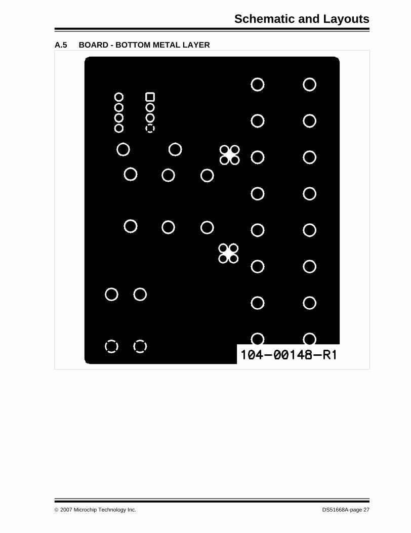
Appendix A. Schematic and Layouts
A.1 INTRODUCTIONThis appendix contains the following schematics and layouts for the MCP6XXX Ampli-fier Evaluation Board 2:• Board – Schematic• Board – Top Silk Layer• Board – Top Metal Layer• Board – Bottom Metal Layer
© 2007 Microchip Technology Inc. DS51668A-page 23
MCP6XXX Amplifier Evaluation Board 2 User’s Guide
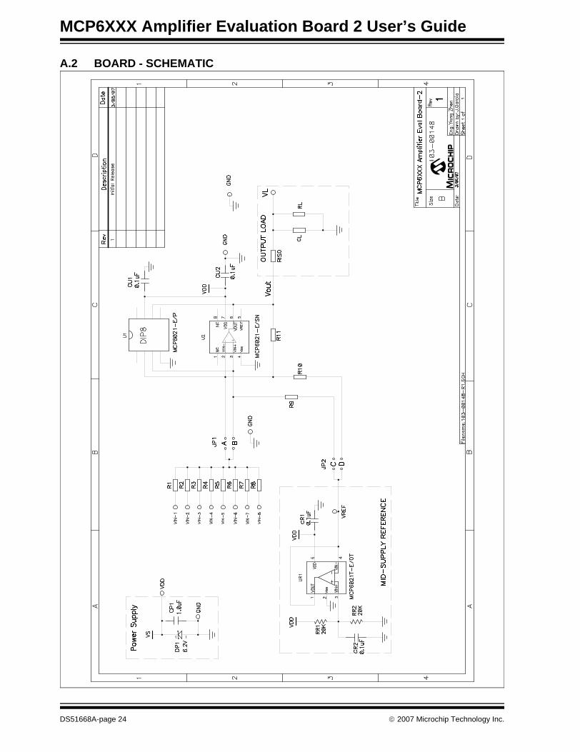
A.2 BOARD - SCHEMATIC
3 1
M
DS51668A-page 24 © 2007 Microchip Technology Inc.

Schematic and Layouts
A.3 BOARD - TOP SILK LAYER
© 2007 Microchip Technology Inc. DS51668A-page 25

MCP6XXX Amplifier Evaluation Board 2 User’s Guide
A.4 BOARD - TOP METAL LAYER
DS51668A-page 26 © 2007 Microchip Technology Inc.
Schematic and Layouts
A.5 BOARD - BOTTOM METAL LAYER
© 2007 Microchip Technology Inc. DS51668A-page 27
MCP6XXX Amplifier Evaluation Board 2 User’s Guide
NOTES:
DS51668A-page 28 © 2007 Microchip Technology Inc.
MCP6XXX AMPLIFIER EVALUATIONBOARD 2 USER’S GUIDE
Appendix B. Bill of Materials (BOM)
B.1 MCP6XXX AMPLIFIER EVALUATION BOARD 2 BOMThe Bill of Materials (BOM) in Table B-1 corresponds to Figure 2-1 and Figure 2-2. Unpopulated parts are in Table B-2.
TABLE B-1: BILL OF MATERIALS (102-00148R1) (NOTE 1)Qty Reference Description Manufacturer Part Number
1 CP1 Capacitor Ceramic 1 µF 10% 25V X5R 0805
Panasonic®- ECG ECJ-2FB1E105K
4 CR1, CR2, CU1, CU2
Capacitor Ceramic 0.1 µF 10% 25V X7R 0805
Panasonic- ECG ECJ-2VB1E104K
1 DP1 Zener Diode, 6.2V 350mW SOT-23
Fairchild Semiconductor® BZX84C6V2
4 Ea Corner Bumper clear 0.375X 15” Dome Richco Plastic Co RBS-122 J1, J2 Connector Header Breakaway
0.100 04POS STRAMP®/Tyco® Electronics 9-146258-0-02
1 PCB RoHS Compliant Bare PCB, MCP6XXX Amplifier Evaluation Board 2
— 104-00148
28 Pin Sockets Pin Recpt, 0.015/.025 dia., 0667 SER
Mill-Max® 0667-0-15-01-30-27-10-0
2 RR1, RR2 Resistor 20.0 kΩ, 1/8W, 1%, 0805 SMD
Panasonic- ECG ERJ-6ENF2002V
2 Shunts for J1, J2 Socket,Short Blks w/Tab Blk Jameco, Valuepro 2012JH-R14 Test Points PC Test Point, Compact,
Surface MountKeystone Electronics® 5016
1 UR1 MCP6021 SOT-23-5, Single Op Amp
Microchip Technology Inc MCP6021T-E/OT
1 U1 IC Socket, 8-position DIP, Tin AMP/Tyco Electronics 2-641260-1Note 1: The components listed in this Bill of Materials are representative of the PCB assembly. The released BOM
used in manufacturing uses all RoHS-compliant components.
© 2007 Microchip Technology Inc. DS51668A-page 29

MCP6XXX Amplifier Evaluation Board 2 User’s Guide
TABLE B-2: BILL OF MATERIALS – UNPOPULATED PARTS (102-00148R1)
The BOM in Table B-3 corresponds to the collection of resistors, capacitors, jumpers and MCP6021 op amps that come in the Accessory Bag which is shipped in the MCP6XXX Amplifier Evaluation Board 2 Kit. These components are placed in an separate ESD bag. They support the circuit in Section 2.4.1 “Building the Amplifier”. Customers need to provide the resistors and capacitors for more amplifier circuits.
TABLE B-3: BILL OF MATERIALS – ACCESSORY BAG PARTS (102-00148R1)
Qty Reference Description Manufacturer Part Number
1 U1 MCP6021, PDIP-8, Single Op Amp
Microchip Technology Inc MCP6021-E/P
1 U2 MCP6021, SOIC-8, Single Op Amp
Microchip Technology Inc MCP6021-E/SN
15 R1-R7, RISO, RL C1-C5, CL
Not populated when shipped to customer
— —
Note 1: The components listed in this Bill of Materials are representative of the PCB assembly. The released BOM used in manufacturing uses all RoHS-compliant components.
Qty Reference Description Manufacturer Part Number
1 Accessory Bag CAP CER 56PF 50V C0G RADIAL
Murata Electronics RPE5C1H560J2P1Z03B
1 Accessory Bag JUMPER ZERO OHM 1/8W Yageo Corporation ZOR-12-B-521 Accessory Bag RES 2.00K OHM 1/4W 1%
METAL FILMYageo Corporation MFR-25FBF-2K00
5 Accessory Bag RES 7.87K OHM 1/4W 1% METAL FILM
Yageo Corporation MFR-25FBF-7K87
1 ESD Sample Box MCP6021, Single Op Amp, PDIP-8
Microchip Technology Inc. MCP6021-E/P
Note 1: The components listed in this Bill of Materials are representative of the PCB assembly. The released BOM used in manufacturing uses all RoHS-compliant components.
DS51668A-page 30 © 2007 Microchip Technology Inc.

Bill of Materials (BOM)
NOTES:
© 2007 Microchip Technology Inc. DS51668A-page 31

DS51668A-page 32 © 2007 Microchip Technology Inc.
AMERICASCorporate Office2355 West Chandler Blvd.Chandler, AZ 85224-6199Tel: 480-792-7200 Fax: 480-792-7277Technical Support: http://support.microchip.comWeb Address: www.microchip.comAtlantaDuluth, GA Tel: 678-957-9614 Fax: 678-957-1455BostonWestborough, MA Tel: 774-760-0087 Fax: 774-760-0088ChicagoItasca, IL Tel: 630-285-0071 Fax: 630-285-0075DallasAddison, TX Tel: 972-818-7423 Fax: 972-818-2924DetroitFarmington Hills, MI Tel: 248-538-2250Fax: 248-538-2260KokomoKokomo, IN Tel: 765-864-8360Fax: 765-864-8387Los AngelesMission Viejo, CA Tel: 949-462-9523 Fax: 949-462-9608Santa ClaraSanta Clara, CA Tel: 408-961-6444Fax: 408-961-6445TorontoMississauga, Ontario, CanadaTel: 905-673-0699 Fax: 905-673-6509
ASIA/PACIFICAsia Pacific OfficeSuites 3707-14, 37th FloorTower 6, The GatewayHarbour City, KowloonHong KongTel: 852-2401-1200Fax: 852-2401-3431Australia - SydneyTel: 61-2-9868-6733Fax: 61-2-9868-6755China - BeijingTel: 86-10-8528-2100 Fax: 86-10-8528-2104China - ChengduTel: 86-28-8665-5511Fax: 86-28-8665-7889China - FuzhouTel: 86-591-8750-3506 Fax: 86-591-8750-3521China - Hong Kong SARTel: 852-2401-1200 Fax: 852-2401-3431China - QingdaoTel: 86-532-8502-7355Fax: 86-532-8502-7205China - ShanghaiTel: 86-21-5407-5533 Fax: 86-21-5407-5066China - ShenyangTel: 86-24-2334-2829Fax: 86-24-2334-2393China - ShenzhenTel: 86-755-8203-2660 Fax: 86-755-8203-1760China - ShundeTel: 86-757-2839-5507 Fax: 86-757-2839-5571China - WuhanTel: 86-27-5980-5300Fax: 86-27-5980-5118China - XianTel: 86-29-8833-7252Fax: 86-29-8833-7256
ASIA/PACIFICIndia - BangaloreTel: 91-80-4182-8400 Fax: 91-80-4182-8422India - New DelhiTel: 91-11-4160-8631Fax: 91-11-4160-8632India - PuneTel: 91-20-2566-1512Fax: 91-20-2566-1513Japan - YokohamaTel: 81-45-471- 6166 Fax: 81-45-471-6122Korea - DaeguTel: 82-53-744-4301Fax: 82-53-744-4302Korea - SeoulTel: 82-2-554-7200Fax: 82-2-558-5932 or 82-2-558-5934Malaysia - PenangTel: 60-4-646-8870Fax: 60-4-646-5086Philippines - ManilaTel: 63-2-634-9065Fax: 63-2-634-9069SingaporeTel: 65-6334-8870Fax: 65-6334-8850Taiwan - Hsin ChuTel: 886-3-572-9526Fax: 886-3-572-6459Taiwan - KaohsiungTel: 886-7-536-4818Fax: 886-7-536-4803Taiwan - TaipeiTel: 886-2-2500-6610 Fax: 886-2-2508-0102Thailand - BangkokTel: 66-2-694-1351Fax: 66-2-694-1350
EUROPEAustria - WelsTel: 43-7242-2244-39Fax: 43-7242-2244-393Denmark - CopenhagenTel: 45-4450-2828 Fax: 45-4485-2829France - ParisTel: 33-1-69-53-63-20 Fax: 33-1-69-30-90-79Germany - MunichTel: 49-89-627-144-0 Fax: 49-89-627-144-44Italy - Milan Tel: 39-0331-742611 Fax: 39-0331-466781Netherlands - DrunenTel: 31-416-690399 Fax: 31-416-690340Spain - MadridTel: 34-91-708-08-90Fax: 34-91-708-08-91UK - WokinghamTel: 44-118-921-5869Fax: 44-118-921-5820
WORLDWIDE SALES AND SERVICE
06/25/07