Aerodynamic Analysis of an AK-47 Bullet Moving at Mach 2.0 ...
Upload
khangminh22Category
view
0download
0
Publication#
17466
Rev:
G
Amendment/
0
Issue Date:
December 1998
MACH 4 CPLD Family
High Performance EE CMOS Programmable Logic
FEATURES
◆
High-performance, EE CMOS 3.3-V & 5-V CPLD families
◆
Flexible architecture for rapid logic designs
— Excellent First-Time-Fit
TM
and refit— SpeedLocking
TM
for guaranteed fixed timing— Central, input and output switch matrices for 100% routability and 100% pin-out retention
◆
High speed
— 5.0ns t
PD
Commercial and 7.5ns t
PD
Industrial— 182MHz f
CNT
◆
32 to 512 macrocells; 32 to 768 registers
◆
44 to 352 pins in PLCC, PQFP, TQFP and BGA packages
◆
Advanced capabilities for easy system integration
— 3.3-V & 5-V JEDEC-compliant operations— JTAG (IEEE 1149.1) compliant for boundary scan testing— 3.3-V & 5-V JTAG in-system programming— PCI compliant (-50/-55/-60/-65/-7/-10/-12 speed grades)— Safe for mixed supply voltage system designs— Programmable pull-up or Bus-Friendly
TM
inputs and I/Os— Hot-socketing — Programmable security bit— Individual output slew rate control
◆
Flexible architecture for a wide range of design styles
— D/T registers and latches— Synchronous or asynchronous mode— Dedicated input registers— Programmable polarity— Reset/ preset swapping
◆
Advanced EE CMOS process provides high-performance, cost-effective solutions
◆
Supported by Vantis DesignDirect
TM
software for rapid logic development
— Supports HDL design methodologies with results optimized for Vantis— Flexibility to adapt to user requirements— Software partnerships that ensure customer success
◆
Vantis and third-party hardware programming support
— VantisPRO
TM
(formerly known as MACHPRO
®
) software for in-system programmability support on PCs and automated test equipment
— Programming support on all major programmers including Data I/O, BP Microsystems, Advin, and System General
IncludesMACH 4A Family
Advance Information

2 MACH 4 Family
Notes:
1. For information on the M4-96/96 device, please refer to the M4-96/96 datasheet at www.vantis.com.
2. “M4-xxx” is for 5-V devices. “M4LV-xxx” is for 3.3-V devices.
Notes:
1. All information on MACH 4A devices is Advance Information. Please contact a Vantis sales representative for details on availability.
2. “M4A5-xxx” is for 5-V devices. “M4A3-xxx” is for 3.3-V devices.
Table 1. MACH 4 Device Features
1,2
FeatureM4-32/32
M4LV-32/32M4-64/32
M4LV-64/32M4-96/48
M4LV-96/48M4-128/64
M4LV-128/64M4-128N/64
M4LV-128N/64M4-192/96
M4LV-192/96M4-256/128
M4LV-256/128
Macrocells
32 64 96 128 128 192 256
Maximum User I/O Pins
32 32 48 64 64 96 128
t
PD
(ns)
7.5 7.5 7.5 7.5 7.5 7.5 7.5
f
CNT
(MHz)
111 111 111 111 111 111 111
t
COS
(ns)
5.5 5.5 5.5 5.5 5.5 5.5 5.5
t
SS
(ns)
5.5 5.5 5.5 5.5 5.5 5.5 5.5
Static Power (mA)
25 25 50 70 70 85 100
JTAG Compliant
Yes Yes Yes Yes No Yes Yes
PCI Compliant
Yes Yes Yes Yes Yes Yes Yes
Table 2. MACH 4A Device Features
1,2
Feature
M4A3-32/32
M4A5-32/32
M4A3-64/32
M4A5-64/32
M4A3-96/48
M4A5-96/48
M4A3-128/64
M4A5-128/64
M4A3-192/96
M4A5-192/96
M4A3-256/128
M4A5-256/128
M4A3-384
M4A3-512
Macrocells
32 64 96 128 192 256 384 512
Maximum UserI/O Pins
32 32 48 64 96 128 192 256
t
PD
(ns)
5.0 5.0 5.0 5.0 5.0 5.0 6.5 6.5
f
CNT
(MHz)
182 182 182 182 182 182 125 125
t
COS
(ns)
4.0 4.0 4.0 4.0 4.0 4.0 4.5 4.5
t
SS
(ns)
3.0 3.0 3.0 3.0 3.0 3.0 4.0 4.0
Static Power (mA)
TBD TBD TBD TBD TBD TBD TBD TBD
JTAG Compliant
Yes Yes Yes Yes Yes Yes Yes Yes
PCI Compliant
Yes Yes Yes Yes Yes Yes Yes Yes

MACH 4 Family 3
GENERAL DESCRIPTION
The MACH
®
4 family from Vantis offers an exceptionally flexible architecture and delivers a superior Complex Programmable Logic Device (CPLD) solution of easy-to-use silicon products and software tools. The overall benefits for users are a guaranteed and predictable CPLD solution, faster time-to-market, greater flexibility and lower cost. The MACH 4 devices offer densities ranging from 32 to 512 macrocells with 100% utilization and 100% pin-out retention. Both the MACH 4 and the MACH 4A families offer 5-V (M4-xxx and M4A5-xxx) and 3.3-V (M4LV-xxx and M4A3-xxx) operation.
MACH 4 products are 5-V or 3.3-V in-system programmable through the JTAG (IEEE Std. 1149.1) interface. JTAG boundary scan testing capability also allows product testability on automated test equipment for device connectivity.
All MACH 4 family members deliver First-Time Fit and easy system integration with pin-out retention after any design change and refit. With multi-tiered central switch matrices, enhanced logic arrays, intelligent logic allocators with an XOR gate and multi-clocking, the MACH 4 family has D or T-type registers and latches as well as synchronous/asynchronous logic and flexible set/reset capabilities. For both 3.3-V and 5-V operations, MACH 4 products can deliver guaranteed fixed timing as fast as 5.0 ns t
PD
and 182 MHz f
CNT
through the SpeedLocking feature when using up to 20 product terms per output (Tables 3 and 4).
Note:
1. C = Commercial, I = Industrial
Table 3. MACH 4 Speed Grades
Device
Speed Grade
1
-7 -10 -12 -14 -15 -18
M4-32/32M4LV-32/32
C C, I C, I I C I
M4-64/32M4LV-64/32
C C, I C, I I C I
M4-96/48M4LV-96/48
C C, I C, I I C I
M4-128/64M4LV-128/64
C C, I C, I I C I
M4-128N/64M4LV-128N/64
C C, I C, I I C I
M4-192/96M4LV-192/96
C C, I C, I I C I
M4-256/128M4LV-256/128
C C, I C, I I C I

4 MACH 4 Family
Notes:
1. C = Commercial, I = Industrial
2. All information on MACH 4A devices is Advance Information. Please contact a Vantis sales representative for details onavailability.
The MACH 4 family offers 13 density-I/O combinations in Thin Quad Flat Pack (TQFP), Plastic Quad Flat Pack (PQFP), Plastic Leaded Chip Carrier (PLCC), and Ball Grid Array (BGA) packages ranging from 44 to 256 pins (Tables 5 and 6). It also offers I/O safety features for mixed-voltage designs so that the 3.3-V devices can accept 5-V inputs, and 5-V devices do not overdrive 3.3-V inputs. Additional features include Bus-Friendly inputs and I/Os, a programmable power-down mode for extra power savings and individual output slew rate control for the highest speed transition or for the lowest noise transition.
Table 4. MACH 4A Speed Grades
Device
Speed Grade
1, 2
-50 -55 -60 -65 -7 -10 -12 -14
M4A3-32/32M4A5-32/32
C C C C C, I C, I C, I I
M4A3-64/32M4A5-64/32
C C C C C, I C, I C, I I
M4A3-96/48M4A5-96/48
C C C C C, I C, I C, I I
M4A3-128/64M4A5-128/64
C C C C C, I C, I C, I I
M4A3-192/96M4A5-192/96
C C C C C, I C, I C, I I
M4A3-256/128M4A5-256/128
C C C C C, I C, I C, I I
M4A3-384
C C C, I C, I I
M4A3-512
C C C, I C, I I
Table 5. MACH 4 Package and I/O Options (Number of I/Os in Table)
PackageM4-32/32
M4LV-32/32M4-64/32
M4LV-64/32M4-96/48
M4LV-96/48M4-128/64
M4LV-128/64M4-128N/64
M4LV-128N/64M4-192/96
M4LV-192/96M4-256/128
M4LV-256/128
44-pin PLCC
32 32
44-pin TQFP
32 32
48-pin TQFP
32 32
84-pin PLCC
64
100-pin TQFP
48 64
100-pin PQFP
64
144-pin TQFP
96
208-pin PQFP
128
256-pin BGA
128

MACH 4 Family 5
Note:
1. All information on MACH 4A devices is Advance Information. Please contact a Vantis sales representative for details on availability.
Vantis offers software design support for MACH devices in both the MACHXL
®
and DesignDirect development systems. The DesignDirect development system is the Vantis implementation software that includes support for all Vantis CPLD, FPGA and SPLD devices. This system is supported under Windows ’95, ’98 and NT as well as Sun Solaris and HPUX.
DesignDirect software is designed for use with design entry, simulaion and verification software from leading-edge tool vendors such as Cadence, Exemplar Logic, Mentor Graphics, Model Technology , Synopsys, Synplicity, Viewlogic and others. It accepts EDIF 2 0 0 input netlists, generates JEDEC files for Vantis PLDs and creates industry-standard EDIF, Verilog, VITAL-compliant VHDL and SDF simulation netlist for design verification.
DesignDirect software is also available in product configurations that include VHDL and Verilog synthesis from Exemplar Logic and VHDL, Verilog RTL and gate level timing simulation from Model Technology. Schematic capture and ABEL entry, as well as functional simulation, are also provided.
Table 6. MACH 4A Package and I/O Options
1
(Number of I/Os in Table)
Package
M4A3-32/32
M4A5-32/32
M4A3-64/32
M4A5-64/32
M4A3-96/48
M4A5-96/48
M4A3-128/64
M4A5-128/64
M4A3-192/96
M4A5-192/96
M4A3-256/128
M4A5-256/128
M4A3-384 M4A3-512
44-pin PLCC
32 32
44-pin TQFP
32 32
48-pin TQFP
32 32
100-pin TQFP
48 64
100-pin PQFP
64
144-pin TQFP
96
176-pin TQFP
128 128
208-pin PQFP
128 160 160
256-pin BGA
128 192 192
352-ball BGA
256

6 MACH 4 Family
FUNCTIONAL DESCRIPTION
The fundamental architecture of MACH 4 devices (Figure 1) consists of multiple optimized PAL
®
blocks interconnected by a central switch matrix. The central switch matrix allows communication between PAL blocks and routes inputs to the PAL blocks. Together, the PAL blocks and central switch matrix allow the logic designer to create large designs in a single device instead of having to use multiple devices.
The key to being able to make effective use of these devices lies in the interconnect schemes. In MACH 4 architecture, the macrocells have been decoupled from the product terms through the logic allocator, and the I/O pins have been decoupled from the macrocells due to the output switch matrix. In addition, more input routing options are provided by the input switch matrix. These resources provide the flexibility needed to fit designs efficiently.
Notes:
1. 16 for M4(LV)-32/32 and M4A(3,5)-32/32 devices.
2. Block clocks do not go to I/O cells in M4(LV)-32/32 or M4A(3,5)-32/32.
3. M4(LV)-192/96, M4(LV)-256/128, M4A(3,5)-192/96 and M4A(3,5)-256/128 have dedicated clock pins which cannot be used as inputs and do not connect to the central switch matrix.
I/OPins
Clock/InputPins
Cen
tral S
witc
h M
atrix
I/OPins
I/OPins
DedicatedInput Pins
PAL Block
PAL Block
LogicAllocatorwith XOR
Output/Buried
Macrocells
36
or34
1616
ClockGenerator
LogicArray
Out
put S
witc
h M
atrix
InputSwitchMatrix
I/O C
ells
16
16
8
Note 1
Note 2
Note 3
4
PAL Block
17466F-001
Figure 1. MACH 4 Block Diagram and PAL Block Structure

MACH 4 Family 7
The central switch matrix takes all dedicated inputs and signals from the input switch matrices and routes them as needed to the PAL blocks. Feedback signals that return to the same PAL block still must go through the central switch matrix. This mechanism ensures that PAL blocks in MACH 4 devices communicate with each other with consistent, predictable delays.
The central switch matrix makes a MACH 4 device more advanced than simply several PAL devices on a single chip. It allows the designer to think of the device not as a collection of blocks, but as a single programmable device; the software partitions the design into PAL blocks through the central switch matrix so that the designer does not have to be concerned with the internal architecture of the device.
Each PAL block consists of:
◆
Product-term array
◆
Logic allocator
◆
Macrocells◆ Output switch matrix◆ I/O cells◆ Input switch matrix◆ Clock generator
Product-Term Array
The product-term array consists of a number of product terms that form the basis of the logic being implemented. The inputs to the AND gates come from the central switch matrix (Table 7), and are provided in both true and complement forms for efficient logic implementation.
Because the number of product terms available for a given logic function is not fixed, the full sum of products is not realized in the array. The product terms drive the logic allocator, which allocates the appropriate number of product terms to generate the function.
Logic Allocator
Within the logic allocator, product terms are allocated to macrocells in “product term clusters.” The availability and distribution of product term clusters are automatically considered by the software as it fits functions within a PAL block. The size of a product term cluster has been optimized to provide high utilization of product terms, making complex functions using many product terms possible. Yet when few product terms are used, there will be a minimal number of
Table 7. PAL Block Inputs
Device Number of Inputs to PAL Block
M4(LV)-32/32 and M4A(3,5)-32/32
M4(LV)-64/32 and M4A(3,5)-64/32
M4(LV)-96/48 and M4A(3,5)-96/48
M4(LV)-128/64 and M4A(3,5)-128/64M4(LV)-128N/64
33
33
33
3333
M4(LV)-192/96 and M4A(3,5)-192/96
M4(LV)-256/128 and M4A(3,5)-256/128
34
34
M4A3-384/192
M4A3-512/256
36
36

8 MACH 4 Family
unused—or wasted—product terms left over. The product term clusters available to each macrocell within a PAL block are shown in Tables 8 and 9.
Each product term cluster is associated with a macrocell. The size of a cluster depends on the configuration of the associated macrocell. When the macrocell is used in synchronous mode(Figure 2a), the basic cluster has 4 product terms. When the associated macrocell is used in asynchronous mode (Figure 2b), the cluster has 2 product terms. Note that if the product term cluster is routed to a different macrocell, the allocator configuration is not determined by the mode of the macrocell actually being driven. The configuration is always set by the mode of the macrocell that the cluster will drive if not routed away, regardless of the actual routing.
In addition, there is an extra product term that can either join the basic cluster to give an extended cluster, or drive the second input of an exclusive-OR gate in the signal path. If included with the basic cluster, this provides for up to 20 product terms on a synchronous function that uses four extended 5-product-term clusters. A similar asynchronous function can have up to 18 product terms.
When the extra product term is used to extend the cluster, the value of the second XOR input can be programmed as a 0 or a 1, giving polarity control. The possible configurations of the logic allocator are shown in Figures 3 and 4.

MACH 4 Family 9
Table 8. Logic Allocator for MACH 4 Devices (except M4(LV)-32/32 and M4A(3,5)-32/32)
Output Macrocell Available Clusters Output Macrocell Available ClustersM0 C0, C1, C2 M8 C7, C8, C9, C10
M1 C0, C1, C2, C3 M9 C8, C9, C10, C11
M2 C1, C2, C3, C4 M10 C9, C10, C11, C12
M3 C2, C3, C4, C5 M11 C10, C11, C12, C13
M4 C3, C4, C5, C6 M12 C11, C12, C13, C14
M5 C4, C5, C6, C7 M13 C12, C13, C14, C15
M6 C5, C6, C7, C8 M14 C13, C14, C15
M7 C6, C7, C8, C9 M15 C14, C15
Table 9. Logic Allocator for M4(LV)-32/32 and M4A(3,5)-32/32
Output Macrocell Available Clusters Output Macrocell Available ClustersM0 C0, C1, C2 M8 C8, C9, C10
M1 C0, C1, C2, C3 M9 C8, C9, C10, C11
M2 C1, C2, C3, C4 M10 C9, C10, C11, C12
M3 C2, C3, C4, C5 M11 C10, C11, C12, C13
M4 C3, C4, C5, C6 M12 C11, C12, C13, C14
M5 C4, C5, C6, C7 M13 C12, C13, C14, C15
M6 C5, C6, C7 M14 C13, C14, C15
M7 C6, C7 M15 C14, C15
0 Default
0 Default
Prog. Polarity
To n
-1T
o n
-2
Fro
m n
-1
To n
+1
Fro
m n
+1
Fro
m n
+2
Basic Product Term Cluster
ExtraProduct
Term
Logic Allocator
n n
To M
acr
oce
lln
0 Default
0 Default
Prog. Polarity
To n
-1T
o n
-2
Fro
m n
-1
To n
+1
Fro
m n
+1
Fro
m n
+2
Basic Product Term Cluster
ExtraProduct
Term
Logic Allocator
n n
To M
acro
cell
n
17466F-006
Figure 2. Logic Allocator: Configuration of Cluster “n” Set by Mode of Macrocell “n”
17466F-005
a. Synchronous Mode
b. Asynchronous Mode

10 MACH 4 Family
Note that the configuration of the logic allocator has absolutely no impact on the speed of the signal. All configurations have the same delay. This means that designers do not have to decide between optimizing resources or speed; both can be optimized.
If not used in the cluster, the extra product term can act in conjunction with the basic cluster to provide XOR logic for such functions as data comparison, or it can work with the D-,T-type flip-flop to provide for J-K, and S-R register operation. In addition, if the basic cluster is routed to another macrocell, the extra product term is still available for logic. In this case, the first XOR input will be a logic 0. This circuit has the flexibility to route product terms elsewhere without giving up the use of the macrocell.
Product term clusters do not “wrap” around a PAL block. This means that the macrocells at the ends of the block have fewer product terms available.
0
17466F-007
Figure 3. Logic Allocator Configurations: Synchronous Mode
a. Basic cluster with b. Extended cluster, active high c. Extended cluster, active low
d. Basic cluster routed away;single-product-term, active high
e. Extended cluster routed away
0
17466F-008
Figure 4. Logic Allocator Configurations: Asynchronous Mode
b. Extended cluster, active high c. Extended cluster, active low
e. Extended cluster routed awayd. Basic cluster routed away;single-product-term, active high
a. Basic cluster with

MACH 4 Family 11
Macrocell
The macrocell consists of a storage element, routing resources, a clock multiplexer, and initialization control. The macrocell has two fundamental modes: synchronous and asynchronous (Figure 5). The mode chosen only effects clocking and initialization in the macrocell.
In either mode, a combinatorial path can be used. For combinatorial logic, the synchronous mode will generally be used, since it provides more product terms in the allocator.
SWAP
D/T/L QAP AR
Power-UpReset
PAL-BlockInitialization
Product Terms
From Logic Allocator
Block CLK0
Block CLK1
Block CLK2
Block CLK3
To Output and InputSwitch Matrices
Common PAL-block resource
Individual macrocell resources
From PAL-ClockGenerator
D/T/L QAP AR
Power-UpReset
IndividualInitialization
Product Term
From LogicAllocator
Block CLK0
Block CLK1
To Output and InputSwitch Matrices
Individual ClockProduct Term
From PAL-BlockClock Generator
17466F-010
Figure 5. Macrocell
17466F-009
a. Synchronous mode
b. Asynchronous mode

12 MACH 4 Family
The flip-flop can be configured as a D-type or T-type latch. J-K or S-R registers can be synthesized. The primary flip-flop configurations are shown in Figure 6, although others are possible. Flip-flop functionality is defined in Table 10. Note that a J-K latch is inadvisable as it will cause oscillation if both J and K inputs are HIGH.
D QAP AR
D QAP AR
L QAP AR
L QAP AR
GG
T QAP AR
17466F-011
Figure 6. Primary Macrocell Configurations
g. Combinatorial with programmable polarity
a. D-type with XOR b. D-type with programmable D polarity
c. Latch with XOR d. Latch with programmable D polarity
e. T-type with programmable T polarity
f. Combinatorial with XOR

MACH 4 Family 13
Note:1. Polarity of CLK/LE can be programmed
Although the macrocell shows only one input to the register, the XOR gate in the logic allocator allows the D-, T-type register to emulate J-K, and S-R behavior. In this case, the available product terms are divided between J and K (or S and R). When configured as J-K, S-R, or T-type, the extra product term must be used on the XOR gate input for flip-flop emulation. In any register type, the polarity of the inputs can be programmed.
The clock input to the flip-flop can select any of the four PAL block clocks in synchronous mode, with the additional choice of either polarity of an individual product term clock in the asynchronous mode.
The initialization circuit depends on the mode. In synchronous mode (Figure 7), asynchronous reset and preset are provided, each driven by a product term common to the entire PAL block.
Table 10. Register/Latch Operation
Configuration Input(s) CLK/LE 1 Q+
D-type Register
D=X
D=0
D=1
0,1, ↓ (↑)↑ (↓)↑ (↓)
Q
0
1
T-type Register
T=X
T=0
T=1
0, 1, ↓ (↑)↑ (↓)↑ (↓)
Q
Q
Q
D-type Latch
D=X
D=0
D=1
1(0)
0(1)
0(1)
Q
0
1
Power-UpReset
APD/T/L
ARQ
PAL-BlockInitialization
Product Terms
a. Power-up reset
Power-UpPreset
APD/L
PAL-BlockInitialization
Product Terms
ARQ
17466F-012 17466F-013
Figure 7. Synchronous Mode Initialization Configurations
b. Power-up preset

14 MACH 4 Family
A reset/preset swapping feature in each macrocell allows for reset and preset to be exchanged, providing flexibility. In asynchronous mode (Figure 8), a single individual product term is provided for initialization. It can be selected to control reset or preset.
Note that the reset/preset swapping selection feature effects power-up reset as well. The initialization functionality of the flip-flops is illustrated in Table 11. The macrocell sends its data to the output switch matrix and the input switch matrix. The output switch matrix can route this data to an output if so desired. The input switch matrix can send the signal back to the central switch matrix as feedback.
Note:1. Transparent latch is unaffected by AR, AP
Output Switch Matrix
The output switch matrix allows macrocells to be connected to any of several I/O cells within a PAL block. This provides high flexibility in determining pinout and allows design changes to occur without effecting pinout.
In MACH 4 devices (except M4(LV)-32/32 and M4A(3,5)-32/32), each PAL block has twice as many macrocells as I/O cells. The MACH 4 output switch matrix allows for half of the macrocells to drive I/O cells within a PAL block, in combinations according to Figure 9. Each I/O cell can choose from eight macrocells; each macrocell has a choice of four I/O cells. The M4(LV)-32/32 and M4A(3,5)-32/32 allow every macrocell to drive an I/O cell (Figures 12 and 13).
Table 11. Asynchronous Reset/Preset Operation
AR AP CLK/LE1 Q+
0 0 X See Table 10
0 1 X 1
1 0 X 0
1 1 X 0
Power-UpReset
APD/L/T
ARQ
IndividualReset
Product Term
a. Reset
Power-UpPreset
APD/L/T
ARQ
IndividualPreset
Product Term
b. Preset
17466F-014 17466F-015
Figure 8. Asynchronous Mode Initialization Configurations

MACH 4 Family 15
a. Macrocell drives one of 4 I/Os (except M4(LV)-32/32 and M4A(3,5)-32/32)
b. Macrocell drives one of 8 I/Os for M4(LV)-32/32 and M4A(3,5)-32/32
17466F-016
Figure 9. MACH 4 Output Switch Matrix
Macro-cell
I/OCell
I/OCell
I/OCell
I/OCell
I/OCell
MUX
Macro-cell
Macro-cell
Macro-cell
Macro-cell
Macro-cell
Macro-cell
Macro-cell
Macro-cell
Macro-cell
I/OCell
I/OCell
I/OCell
I/OCell
I/OCell
I/OCell
I/OCell
I/OCell
c. I/O can choose one of 8 macrocells

16 MACH 4 Family
Table 12. Output Switch Matrix Combinations for MACH 4 Devices (except M4(LV)-32/32 and M4A(3,5)-32/32)
Macrocell Routable to I/O Pins
M0, M1 I/O0, I/O5, I/O6, I/O7
M2, M3 I/O0, I/O1, I/O6, I/O7
M4, M5 I/O0, I/O1, I/O2, I/O7
M6, M7 I/O0, I/O1, I/O2, I/O3
M8, M9 I/O1, I/O2, I/O3, I/O4
M10, M11 I/O2, I/O3, I/O4, I/O5
M12, M13 I/O3, I/O4, I/O5, I/O6
M14, M15 I/O4, I/O5, I/O6, I/O7
I/O Pin Available Macrocells
I/O0 M0, M1, M2, M3, M4, M5, M6, M7
I/O1 M2, M3, M4, M5, M6, M7, M8, M9
I/O2 M4, M5, M6, M7, M8, M9, M10, M11
I/O3 M6, M7, M8, M9, M10, M11, M12, M13
I/O4 M8, M9, M10, M11, M12, M13, M14, M15
I/O5 M0, M1, M10, M11, M12, M13, M14, M15
I/O6 M0, M1, M2, M3, M12, M13, M14, M15
I/O7 M0, M1, M2, M3, M4, M5, M14, M15
Table 13. Output Switch Matrix Combinations for M4(LV)-32/32 and M4A(3,5)-32/32
Macrocell Routable to I/O Pins
M0, M1, M2, M3, M4, M5, M6, M7 I/O0, I/O1, I/O2, I/O3, I/O4, I/O5, I/O6, I/O7
M8, M9, M10, M11, M12, M13, M14, M15 I/O8, I/O9, I/O10, I/O11, I/O12, I/O13, I/O14, I/O15
I/O Pin Available Macrocells
I/O0, I/O1, I/O2, I/O3, I/O4, I/O5, I/O6, I/O7 M0, M1, M2, M3, M4, M5, M6, M7
I/O8, I/O9, I/O10, I/O11, I/O12, I/O13, I/O14, I/O15 M8, M9, M10, M11, M12, M13, M14, M15

MACH 4 Family 17
I/O Cell
The I/O cell (Figures 10 and 11) simply consists of a programmable output enable, a feedback path, and in all but the M4(LV)-32/32 and the M4A(3,5)-32/32 devices, a flip-flop. An individual output enable product term is provided for each I/O cell. The feedback signal drives the input switch matrix.
The MACH 4 I/O cell contains a flip-flop, which provides the capability for storing the input in a D-type register or latch. The clock can be any of the PAL block clocks. Both the direct and registered versions of the input are sent to the input switch matrix. This allows for such functions as “time-domain-multiplexed” data comparison, where the first data value is stored, and then the second data value is put on the I/O pin and compared with the previous stored value.
Note that the flip-flop used in the MACH 4 I/O cell is independent of the flip-flops in the macrocells. It powers up to a logic low.Zero-Hold-Time Input Register
The MACH 4 devices have a zero-hold-time (ZHT) fuse which controls the time delay associated with loading data into all I/O cell registers and latches. When programmed, the ZHT fuse increases the data path setup delays to input storage elements, matching equivalent delays in the clock path. When the fuse is erased, the setup time to the input storage element is minimized. This feature facilitates doing worst-case designs for which data is loaded from sources which have low (or zero) minimum output propagation delays from clock edges.
Input Switch Matrix
The input switch matrix (Figures 12 and 13) optimizes routing of inputs to the central switch matrix. Without the input switch matrix, each input and feedback signal has only one way to enter the central switch matrix. The input switch matrix provides additional ways for these signals to enter the central switch matrix.
D/L Q
Block CLK3Block CLK2Block CLK1Block CLK0
ToInput
SwitchMatrix
IndividualOutput Enable
Product Term
From OutputSwitch Matrix
17466F-017 17466F-018
Figure 10. I/O Cell for MACH 4 Devices (except M4(LV)-32/32 and M4A(3,5)-32/32)
Figure 11. I/O Cell for M4(LV)-32/32 andM4A(3,5)-32/32
ToInput
SwitchMatrix
IndividualOutput Enable
Product Term
From OutputSwitch Matrix
Power-up reset

18 MACH 4 Family
PAL Block Clock Generation
Each MACH 4 device has four clock pins that can also be used as inputs. These pins drive a clock generator in each PAL block (Figure 14). The clock generator provides four clock signals that can be used anywhere in the PAL block. These four PAL block clock signals can consist of a large number of combinations of the true and complement edges of the global clock signals. Table 14 lists the possible combinations.
Note:1. M4(LV)-32/32, M4A(3,5)-32/32, M4(LV)-64/32 and M4A(3,5)-64/32 have only two clock pins, GCLK0 and GCLK1. GCLK2 is tied
to GCLK0, and GCLK3 is tied to GCLK1.
To
Cen
tral
Sw
itch
Mat
rix
Fro
m M
acro
cell
2
From Input Cell
Dire
ct
Fro
m M
acro
cell
1
Reg
iste
red/
Latc
hed
17466F-002 17466F-003
Figure 12. MACH 4 Input Switch Matrix Figure 13. M4(LV)-32/32 and M4A(3,5)-32/32 Input Switch Matrix
Note: except M4(LV)-32/32 and M4A(3,5)-32/32
To
Cen
tral
Sw
itch
Mat
rix Fro
m M
acro
cell
Fro
m I/
O P
in
GCLK0
GCLK1
GCLK2
GCLK3
Block CLK0(GCLK0 or GCLK1)
Block CLK1(GCLK1 or GCLK0)
Block CLK2(GCLK2 or GCLK3)
Block CLK3(GCLK3 or GCLK2)
17466F-004
Figure 14. PAL Block Clock Generator 1

MACH 4 Family 19
Note:1. Values in parentheses are for the M4(LV)-32/32, M4A(3,5)-32/32, M4(LV)-64/32 and M4A(3,5)-64/32.
This feature provides high flexibility for partitioning state machines and dual-phase clocks. It also allows latches to be driven with either polarity of latch enable, and in a master-slave configuration.
Table 14. PAL Block Clock Combinations1
Block CLK0 Block CLK1 Block CLK2 Block CLK3
GCLK0
GCLK1
GCLK0
GCLK1
X
X
X
X
GCLK1
GCLK1
GCLK0
GCLK0
X
X
X
X
X
X
X
X
GCLK2 (GCLK0)
GCLK3 (GCLK1)
GCLK2 (GCLK0)
GCLK3 (GCLK1)
X
X
X
X
GCLK3 (GCLK1)
GCLK3 (GCLK1)
GCLK2 (GCLK0)
GCLK2 (GCLK0)

20 MACH 4 Family
MACH 4 TIMING MODEL
The primary focus of the MACH 4 timing model is to accurately represent the timing in a MACH 4 device, and at the same time, be easy to understand. This model accurately describes all combinatorial and registered paths through the device, making a distinction between internal feedback and external feedback. A signal uses internal feedback when it is fed back into the switch matrix or block without having to go through the output buffer. The input register specifications are also reported as internal feedback. When a signal is fed back into the switch matrix after having gone through the output buffer, it is using external feedback.
The parameter, tBUF, is defined as the time it takes to go from feedback through the output buffer to the I/O pad. If a signal goes to the internal feedback rather than to the I/O pad, the parameter designator is followed by an “i”. By adding tBUF to this internal parameter, the external parameter is derived. For example, tPD = tPDi + tBUF. A diagram representing the modularized MACH 4 timing model is shown in Figure 15. Refer to the Technical Note entitled MACH 4 Timing and High Speed Design for a more detailed discussion about the timing parameters.
SPEEDLOCKING FOR GUARANTEED FIXED TIMING
The MACH 4 architecture allows allocation of up to 20 product terms to an individual macrocell with the assistance of an XOR gate without incurring additional timing delays.
The design of the switch matrix and PAL blocks guarantee a fixed pin-to-pin delay that is independent of the logic required by the design. Other non-Vantis CPLDs incur serious timing delays as product terms expand beyond their typical 4 or 5 product term limits. Speed and SpeedLocking combine to give designs easy access to the performance required in today’s designs.
(External Feedback)
(Internal Feedback)
INPUT REG/INPUT LATCH
tSIRS tHIRStSILtHILtSIRZtHIRZtSILZtHILZ
tPDILi tICOSi tIGOSi tPDILZi
Q
tSS(T)tSA(T)tH(S/A)tS(S/A)LtH(S/A)LtSRR
tPDi tPDLi tCO(S/A)itGO(S/A)itSRi
COMB/DFF/TFF/LATCH/SR*/JK*
S/R
IN
BLK CLK
OUT
tPL
tBUF
tEAtER
tSLW
Q
CentralSwitchMatrix
*emulated
17466F-025
Figure 15. MACH 4 Timing Model

MACH 4 Family 21
JTAG BOUNDARY SCAN TESTABILITY
All MACH 4 devices, except the M4(LV)-128N/64, have JTAG boundary scan cells and are compliant to the JTAG standard, IEEE 1149.1. This allows functional testing of the circuit board on which the device is mounted through a serial scan path that can access all critical logic nodes. Internal registers are linked internally, allowing test data to be shifted in and loaded directly onto test nodes, or test node data to be captured and shifted out for verification. In addition, these devices can be linked into a board-level serial scan path for more complete board-level testing.
JTAG IN-SYSTEM PROGRAMMING
Programming devices in-system provides a number of significant benefits including: rapid prototyping, lower inventory levels, higher quality, and the ability to make in-field modifications. All MACH 4 devices provide In-System Programming (ISP) capability through their JTAG ports. This capability has been implemented in a manner that ensures that the JTAG port remains compliant to the IEEE 1149.1 standard. By using JTAG as the communication interface through which ISP is achieved, customers get the benefit of a standard, well-defined interface.
MACH 4 devices can be programmed across the commercial temperature and voltage range. Vantis provides its free PC-based VantisPRO software to facilitate in-system programming. VantisPRO takes the JEDEC file output produced by Vantis’ design implementation software, along with information about the JTAG chain, and creates a set of vectors that are used to drive the JTAG chain. VantisPRO software can use these vectors to drive a JTAG chain via the parallel port of a PC. Alternatively, VantisPRO software can output files in formats understood by common automated test equipment. This equpment can then be used to program MACH 4 devices during the testing of a circuit board. For more information about in-system programming, refer to the separate document entitled MACH ISP Manual.
PCI COMPLIANT
MACH 4(A) devices in the -50/-55/-60/-65/-7/-10/-12 speed grades are compliant with the PCI Local Bus Specification version 2.1, published by the PCI Special Interest Group (SIG). The 5-V devices are fully PCI-compliant. The 3.3-V devices are mostly compliant but do not meet the PCI condition to clamp the inputs as they rise above VCC because of their 5-V input tolerant feature.
SAFE FOR MIXED SUPPLY VOLTAGE SYSTEM DESIGNS
Both the 3.3-V and 5-V VCC MACH 4 devices are safe for mixed supply voltage system designs. The 5-V devices will not overdrive 3.3-V devices above the output voltage of 3.3 V, while they accept inputs from other 3.3-V devices. The 3.3-V device will accept inputs up to 5.5 V. Both the 5-V and 3.3-V versions have the same high-speed performance and provide easy-to-use mixed-voltage design capability.
PULL UP OR BUS-FRIENDLY INPUTS AND I/OS
All MACH 4 devices have inputs and I/Os which feature the Bus-Friendly circuitry incorporating two inverters in series which loop back to the input. This double inversion weakly holds the input at its last driven logic state. While it is good design practice to tie unused pins to a known state, the Bus-Friendly input structure pulls pins away from the input threshold voltage where noise can cause high-frequency switching. At power-up, the Bus-Friendly latches are reset to a logic level

22 MACH 4 Family
“1.” For the circuit diagram, please refer to the Input/Output Equivalent Schematics (page 393) in the General Information Section of the Vantis 1999 Data Book.
All MACH 4A devices have a programmable bit that configures all inputs and I/Os with either pull-up or Bus-Friendly characteristics. If the device is configured in pull-up mode, all inputs and I/O pins are weakly pulled up. For the circuit diagram, please refer to the Input/Output Equivalent Schematics (page 393) in the General Information Section of the Vantis 1999 Data Book.
POWER MANAGEMENT
Each individual PAL block in MACH 4 devices features a programmable low-power mode, which results in power savings of up to 50%. The signal speed paths in the low-power PAL block will be slower than those in the non-low-power PAL block. This feature allows speed critical paths to run at maximum frequency while the rest of the signal paths operate in the low-power mode.
PROGRAMMABLE SLEW RATE
Each MACH 4 device I/O has an individually programmable output slew rate control bit. Each output can be individually configured for the higher speed transition (3 V/ns) or for the lower noise transition (1 V/ns). For high-speed designs with long, unterminated traces, the slow-slew rate will introduce fewer reflections, less noise, and keep ground bounce to a minimum. For designs with short traces or well terminated lines, the fast slew rate can be used to achieve the highest speed. The slew rate is adjusted independent of power.
POWER-UP RESET/SET
All flip-flops power up to a known state for predictable system initialization. If a macrocell is configured to SET on a signal from the control generator, then that macrocell will be SET during device power-up. If a macrocell is configured to RESET on a signal from the control generator or is not configured for set/reset, then that macrocell will RESET on power-up. To guarantee initialization values, the VCC rise must be monotonic, and the clock must be inactive until the reset delay time has elapsed.
SECURITY BIT
A programmable security bit is provided on the MACH 4 devices as a deterrent to unauthorized copying of the array configuration patterns. Once programmed, this bit defeats readback of the programmed pattern by a device programmer, securing proprietary designs from competitors. Programming and verification are also defeated by the security bit. The bit can only be reset by erasing the entire device.
HOT SOCKETING
MACH 4A devices are well-suited for those applications that require hot socketing capability. Hot socketing a device requires that the device, when powered down, can tolerate active signals on the I/Os and inputs without being damaged. Additionally, it requires that the effects of the powered-down MACH devices be minimal on active signals.

MACH 4 Family 23
BLOCK DIAGRAM – M4(LV)-32/32 AND M4A(3,5)-32/32
Central Switch Matrix22
CLK
0/I0
, CLK
1/I1
I/O0–I/O7 I/O8–I/O15
I/O16–I/O23I/O24–I/O31
I/O Cells
Output SwitchMatrix
Macrocells
8
8
16
8
8
8
33
4
4 4
4
8
8
I/O Cells
Output SwitchMatrix
Macrocells
66 X 98AND Logic Array
and Logic AllocatorC
lock
Gen
erat
or
Inpu
t Sw
itch
Mat
rix
8
8
16
8
8
8
2
8
8
I/O Cells
Output SwitchMatrix
Macrocells
8
8
16
8
8
8
8
8
I/O Cells
Output SwitchMatrix
Macrocells
66 X 98AND Logic Array
and Logic Allocator
8
8
16
8
8
8
2
8
8
Inpu
t Sw
itch
Mat
rixIn
put S
witc
hM
atrix
Inpu
t Sw
itch
Mat
rix
Clo
ck G
ener
ator
OE
OE
OEOE
Block A
Block B
33
17466F-019

24 MACH 4 Family
BLOCK DIAGRAM – M4(LV)-64/32 AND M4A(3,5)-64/32
Central Switch Matrix22
CLK
0/I0
, CLK
1/I1
I/O0–I/O7 I/O8–I/O15
I/O16–I/O23I/O24–I/O31
I/O Cells
Output SwitchMatrix
Macrocells
66 X 90AND Logic Array
and Logic Allocator
Clo
ck G
ener
ator
16
16
24
16
16
8
33
4
4
2
8
8
I/O Cells
Output SwitchMatrix
Macrocells
66 X 90AND Logic Array
and Logic Allocator
Clo
ck G
ener
ator
Inpu
t Sw
itch
Mat
rix
16
16
24
16
16
8
33
4
4
2
8
8
I/O Cells
Output SwitchMatrix
Macrocells
66 X 90AND Logic Array
and Logic Allocator
16
16
24
16
16
8
33
4
4
2
8
8
I/O Cells
Output SwitchMatrix
Macrocells
66 X 90AND Logic Array
and Logic Allocator
16
16
24
16
16
8
33
4
4
2
8
8
Inpu
t Sw
itch
Mat
rixIn
put S
witc
hM
atrix
Inpu
t Sw
itch
Mat
rix
Clo
ck G
ener
ator
Clo
ck G
ener
ator
OE
OE
OE
OE
Block A
Block D
Block B
Block C 17466F-020

MACH 4 Family 25
BLOCK DIAGRAM – M4(LV)-96/48 AND M4A(3,5)-96/48
44
4
CLK0/I0, CLK1/I1, CLK2/I4, CLK3/I5
I2, I3, I6, I7
I/O0–
I/O7
I/O8–
I/O15
I/O16
–I/O
23
I/O24
–I/O
31I/O
32–I
/O39
I/O40
–I/O
47
I/O C
ells
Out
put S
witc
hM
atrix
Mac
roce
lls
66 X
90
AN
D L
ogic
Arr
ayan
d Lo
gic
Allo
cato
r
Clock Generator
16 16 24
1616
8
33
4 4
4
8
8
I/O C
ells
Out
put S
witc
hM
atrix
Mac
roce
lls
66 X
90
AN
D L
ogic
Arr
ayan
d Lo
gic
Allo
cato
r
Clock Generator
Input SwitchMatrix16 16 24
1616
8
33
4 4
4
8
8
I/O C
ells
Out
put S
witc
hM
atrix
Mac
roce
lls
66 X
90
AN
D L
ogic
Arr
ayan
d Lo
gic
Allo
cato
r
Clock Generator
Input SwitchMatrix16 16 24
1616
8
33
4 4
4
8
8
I/O C
ells
Out
put S
witc
hM
atrix
Mac
roce
lls
66 X
90
AN
D L
ogic
Arr
ayan
d Lo
gic
Allo
cato
r
161624
16 16
8
33
44
4
8
8
I/O C
ells
Out
put S
witc
hM
atrix
Mac
roce
lls
66 X
90
AN
D L
ogic
Arr
ayan
d Lo
gic
Allo
cato
r
161624
16 16 8
33
44
4
8
8
I/O C
ells
Out
put S
witc
hM
atrix
Mac
roce
lls
66 X
90
AN
D L
ogic
Arr
ayan
d Lo
gic
Allo
cato
r
161624
16 16
8
33
44
4
8
8OE
Input SwitchMatrix
Input SwitchMatrix
Input SwitchMatrix
Clock Generator
Clock Generator
Clock Generator
Input SwitchMatrix
OE
OE
OE
OE
OE
Blo
ck A
Blo
ck B
Blo
ck C
Blo
ck F
Blo
ck E
Blo
ck D
Cen
tral
Sw
itch
Mat
rix
17466F-021

26 MACH 4 Family
BLOCK DIAGRAM – M4(LV)-128N/64, M4(LV)-128/64 AND M4A(3,5)-128/64
Cen
tral
Sw
itch
Mat
rix
44
2
CLK0/I0, CLK1/I1, CLK2/I3, CLK3/I4
I2, I5
I/O0–
I/O7
I/O8–
I/O15
I/O16
–I/O
23I/O
24–I
/031
I/O32
–I/O
39I/O
40–I
/O47
I/O48
–I/O
55I/O
56–I
/O63
I/O C
ells
Out
put S
witc
hM
atrix
Mac
roce
lls
66 X
90
AN
D L
ogic
Arr
ayan
d Lo
gic
Allo
cato
r
Clock Generator
16 16 24
1616
8
33
4 4
4
8
8
I/O C
ells
Out
put S
witc
hM
atrix
Mac
roce
lls
66 X
90
AN
D L
ogic
Arr
ayan
d Lo
gic
Allo
cato
r
Clock Generator
Input SwitchMatrix16 16 24
1616
8
33
4 4
4
8
8
I/O C
ells
Out
put S
witc
hM
atrix
Mac
roce
lls
66 X
90
AN
D L
ogic
Arr
ayan
d Lo
gic
Allo
cato
r
Clock Generator
Input SwitchMatrix16 16 24
1616
8
33
4 4
4
8
8
I/O C
ells
Out
put S
witc
hM
atrix
Mac
roce
lls
66 X
90
AN
D L
ogic
Arr
ayan
d Lo
gic
Allo
cato
rClock Generator
Input SwitchMatrix16 16 24
1616
8
33
4 4
4
8
8
I/O C
ells
Out
put S
witc
hM
atrix
Mac
roce
lls
66 X
90
AN
D L
ogic
Arr
ayan
d Lo
gic
Allo
cato
r
161624
16 16
8
33
44
4
8
8
I/O C
ells
Out
put S
witc
hM
atrix
Mac
roce
lls
66 X
90
AN
D L
ogic
Arr
ayan
d Lo
gic
Allo
cato
r
161624
16 16
8
33
44
4
8
8
I/O C
ells
Out
put S
witc
hM
atrix
Mac
roce
lls
66 X
90
AN
D L
ogic
Arr
ayan
d Lo
gic
Allo
cato
r
161624
16 16
8
33
44
4
8
8
I/O C
ells
Out
put S
witc
hM
atrix
Mac
roce
lls
66 X
90
AN
D L
ogic
Arr
ayan
d Lo
gic
Allo
cato
rOE
161624
16 16
8
33
44
4
8
8
Input SwitchMatrix
Input SwitchMatrix
Input SwitchMatrix
Clock Generator
Clock Generator
Clock Generator
Input SwitchMatrix
Input SwitchMatrix
Clock Generator
OE
OE
OE
OE
OE
OE
OE
Blo
ck A
Blo
ck B
Blo
ck C
Blo
ck D
Blo
ck H
Blo
ck G
Blo
ck F
Blo
ck E
17466F-022

MACH 4 Family 27
BLOCK DIAGRAM – M4(LV)-192/96 AND M4A(3,5)-192/96
Cen
tral
Sw
itch
Mat
rix
Block BI/O8–I/O15 CLK0–CLK3
I/O32–I/O39Block E
I/O56–I/O63Block H
I/O48–I/O55Block G
I0–I15I/O40–I/O47Block F
Block AI/O0–I/O7
Block KI/O80–I/O87
Block LI/O88–I/O95
Block C I/O16–I/O23Block D I/O24–I/O31
I/O72–I/O79 Block JI/O64–I/O71 Block I
I/O Cells
Macrocells
68 X 90AND Logic Array
and Logic Allocator
Clo
ck G
ener
ator
Inpu
t Sw
itch
Mat
rix
Output SwitchMatrix
I/O Cells
Macrocells
68 X 90AND Logic Array
and Logic Allocator
Clo
ck G
ener
ator
Inpu
t Sw
itch
Mat
rix
Output SwitchMatrix
I/O Cells
Macrocells
68 X 90AND Logic Array
and Logic Allocator
Clo
ck G
ener
ator
Inpu
t Sw
itch
Mat
rix
Output SwitchMatrix
I/O Cells
Macrocells
68 X 90AND Logic Array
and Logic Allocator
Clo
ck G
ener
ator
Inpu
t Sw
itch
Mat
rix
Output SwitchMatrix
I/O Cells
Macrocells
68 X 90AND Logic Array
and Logic Allocator
Clo
ck G
ener
ator
Inpu
t Sw
itch
Mat
rix
Output SwitchMatrix
I/O Cells
Macrocells
68 X 90AND Logic Array
and Logic Allocator
Clo
ck G
ener
ator
Inpu
t Sw
itch
Mat
rix
Output SwitchMatrix
I/O Cells
Macrocells
68 X 90AND Logic Array
and Logic Allocator
Clo
ck G
ener
ator
Inpu
t Sw
itch
Mat
rix
Output SwitchMatrix
I/O Cells
Macrocells
68 X 90AND Logic Array
and Logic Allocator
Clo
ck G
ener
ator
Inpu
t Sw
itch
Mat
rix
Output SwitchMatrix
I/O Cells
Macrocells
68 X 90AND Logic Array
and Logic Allocator
Clo
ck G
ener
ator
Inpu
t Sw
itch
Mat
rix
Output SwitchMatrix
I/O Cells
Macrocells
68 X 90AND Logic Array
and Logic Allocator
Clo
ck G
ener
ator
Inpu
t Sw
itch
Mat
rix
Output SwitchMatrix
I/O Cells
Macrocells
68 X 90AND Logic Array
and Logic Allocator
Clo
ck G
ener
ator
Inpu
t Sw
itch
Mat
rix
Output SwitchMatrix
I/O Cells
Macrocells
68 X 90AND Logic Array
and Logic Allocator
Clo
ck G
ener
ator
Inpu
t Sw
itch
Mat
rix
Output SwitchMatrix
16
4 4
OE
8
16
8
4
16
24
8
16
16
34
4
4
8
24 34
4
8
8
16
16
4
4
16
16
OE
8
24 34
4
8
8
16
16
4
4
16
16O
E
8
16
8
4
16
24
8
16
16
34
34 34 34 34
34 34 34 34
4
4
OE
OE
8
16
8
4
16
24
8
16
16
4
4
8
24
4
8
8
16
16
4
4
16
16
OE
8
24
4
8
8
16
16
4
4
16
16
OE
OE
4
4
8
24
16
16
8
16 8
4
16
OE
4
4
24
16
16
8
16
16
4
8
8
OE
4
4
24
16
16
8
16
16
4
8
8
4
4
8
24
16
16
8
16 8
4
16
OE
8
16
8
4
16
24
8
16
16
4
4
OE
17466F-064

28 MACH 4 Family
BLOCK DIAGRAM – M4(LV)-256/128 AND M4A(3,5)-256/128
Cen
tral
Sw
itch
Mat
rix
Block BI/O8–I/O15 CLK0–CLK3
I/O48–I/O55Block G
I/O72–I/O79Block J
I/O64–I/O71Block I
I0–I13I/O56–I/O63Block H
Block AI/O0–I/O7
Block OI/O112–I/O119
Block PI/O120–I/O127
Block C I/O16–I/O23Block D I/O24–I/O31Block E I/O32–I/O39Block F I/O40–I/O47
I/O104–I/O111 Block NI/O96–I/O103 Block MI/O88–I/O95 Block LI/O80–I/O87 Block K
I/O Cells
Macrocells
68 X 90AND Logic Array
and Logic Allocator
Clo
ck G
ener
ator
Inpu
t Sw
itch
Mat
rix
Output SwitchMatrix
I/O Cells
Macrocells
68 X 90AND Logic Array
and Logic Allocator
Clo
ck G
ener
ator
Inpu
t Sw
itch
Mat
rix
Output SwitchMatrix
I/O Cells
Macrocells
68 X 90AND Logic Array
and Logic Allocator
Clo
ck G
ener
ator
Inpu
t Sw
itch
Mat
rix
Output SwitchMatrix
I/O Cells
Macrocells
68 X 90AND Logic Array
and Logic Allocator
Clo
ck G
ener
ator
Inpu
t Sw
itch
Mat
rix
Output SwitchMatrix
I/O Cells
Macrocells
68 X 90AND Logic Array
and Logic Allocator
Clo
ck G
ener
ator
Inpu
t Sw
itch
Mat
rix
Output SwitchMatrix
I/O Cells
Macrocells
68 X 90AND Logic Array
and Logic Allocator
Clo
ck G
ener
ator
Inpu
t Sw
itch
Mat
rix
Output SwitchMatrix
I/O Cells
Macrocells
68 X 90AND Logic Array
and Logic Allocator
Clo
ck G
ener
ator
Inpu
t Sw
itch
Mat
rix
Output SwitchMatrix
I/O Cells
Macrocells
68 X 90AND Logic Array
and Logic Allocator
Clo
ck G
ener
ator
Inpu
t Sw
itch
Mat
rix
Output SwitchMatrix
I/O Cells
Macrocells
68 X 90AND Logic Array
and Logic Allocator
Clo
ck G
ener
ator
Inpu
t Sw
itch
Mat
rix
Output SwitchMatrix
I/O Cells
Macrocells
68 X 90AND Logic Array
and Logic Allocator
Clo
ck G
ener
ator
Inpu
t Sw
itch
Mat
rix
Output SwitchMatrix
I/O Cells
Macrocells
68 X 90AND Logic Array
and Logic Allocator
Clo
ck G
ener
ator
Inpu
t Sw
itch
Mat
rix
Output SwitchMatrix
I/O Cells
Macrocells
68 X 90AND Logic Array
and Logic Allocator
Clo
ck G
ener
ator
Inpu
t Sw
itch
Mat
rix
Output SwitchMatrix
I/O Cells
Macrocells
68 X 90AND Logic Array
and Logic Allocator
Clo
ck G
ener
ator
Inpu
t Sw
itch
Mat
rix
Output SwitchMatrix
I/O Cells
Macrocells
68 X 90AND Logic Array
and Logic Allocator
Clo
ck G
ener
ator
Inpu
t Sw
itch
Mat
rix
Output SwitchMatrix
I/O Cells
Macrocells
68 X 90AND Logic Array
and Logic Allocator
Clo
ck G
ener
ator
Inpu
t Sw
itch
Mat
rix
Output SwitchMatrix
I/O Cells
Macrocells
68 X 90AND Logic Array
and Logic Allocator
Clo
ck G
ener
ator
Inpu
t Sw
itch
Mat
rix
Output SwitchMatrix
14
4 4
OE
8
16
8
4
16
24
8
16
16
34
4
4
8
24 34
4
8
8
16
16
4
4
16
16
OE
8
24 34
4
8
8
16
16
4
4
16
16O
E
OE
4
4
8
34 24
16
16
8
16 8
4
16
OE
4
4
34 24
16
16
8
16
16
4
8
8
OE
4
4
34 24
16
16
8
16
16
4
8
8
4
4
8
34 24
16
16
8
16 8
4
16
OE
8
16
8
4
16
24
8
16
16
34
4
4
OE
OE
8
16
8
4
16
24
8
16
16
34
4
4
8
24 34
4
8
8
16
16
4
4
16
16
OE
8
24 34
4
8
8
16
16
4
4
16
16
OE
OE
4
4
8
34 24
16
16
8
16 8
4
16
OE
4
4
34 24
16
16
8
16
16
4
8
8
OE
4
4
34 24
16
16
8
16
16
4
8
8
4
4
8
34 24
16
16
8
16 8
4
16
OE
8
16
8
4
16
24
8
16
16
34
4
4
OE
17466F-024

MACH 4 Family 29
BLOCK DIAGRAM – M4A-384/192
Cen
tral
Sw
itch
Mat
rix
Block BI/O8–I/O15
CLK0–CLK3Block AI/O0–I/O7
Block GXI/O176–I/O183
Block HXI/O184–I/O191
Block C I/O16–I/O23Block F I/O40–I/O47
Block D I/O24–I/O31Block E I/O32–I/O39
I/O168–I/O175 Block FXI/O144–I/O151 Block CX
I/O160–I/O167 Block EXI/O152–I/O159 Block DX
I/O Cells
Macrocells
72 X 90AND Logic Array
and Logic Allocator
Clo
ck G
ener
ator
Inpu
t Sw
itch
Mat
rix
Output SwitchMatrix
I/O Cells
Macrocells
72 X 90AND Logic Array
and Logic Allocator
Clo
ck G
ener
ator
Inpu
t Sw
itch
Mat
rix
Output SwitchMatrix
I/O Cells
Macrocells
72 X 90AND Logic Array
and Logic Allocator
Clo
ck G
ener
ator
Inpu
t Sw
itch
Mat
rix
Output SwitchMatrix
I/O Cells
Macrocells
72 X 90AND Logic Array
and Logic Allocator
Clo
ck G
ener
ator
Inpu
t Sw
itch
Mat
rix
Output SwitchMatrix
I/O Cells
Macrocells
72 X 90AND Logic Array
and Logic Allocator
Clo
ck G
ener
ator
Inpu
t Sw
itch
Mat
rix
Output SwitchMatrix
I/O Cells
Macrocells
72 X 90AND Logic Array
and Logic Allocator
Clo
ck G
ener
ator
Inpu
t Sw
itch
Mat
rix
Output SwitchMatrix
I/O Cells
Macrocells
72 X 90AND Logic Array
and Logic Allocator
Clo
ck G
ener
ator
Inpu
t Sw
itch
Mat
rix
Output SwitchMatrix
I/O Cells
Macrocells
72 X 90AND Logic Array
and Logic Allocator
Clo
ck G
ener
ator
Inpu
t Sw
itch
Mat
rix
Output SwitchMatrix
4 4
4
OE
8
16
8
4
16
24
8
16
16
36
4
4
8
24 36
4
8
8
16
16
4
4
16
16
OE
8
24 36
4
8
8
16
16
4
4
16
16
OE
OE
4
4
8
36 24
16
16
8
16 8
4
16
OE
4
4
36 24
16
16
8
16
16
4
8
8
OE
4
4
36 24
16
16
8
16
16
4
8
8
4
4
8
36 24
16
16
8
16 8
4
16
OE
8
16
8
4
16
24
8
16
16
36
4
4
OE
I/O Cells
Macrocells
72 X 90AND Logic Array
and Logic Allocator
Clo
ck G
ener
ator
Inpu
t Sw
itch
Mat
rixOutput Switch
Matrix
I/O Cells
Macrocells
72 X 90AND Logic Array
and Logic Allocator
Clo
ck G
ener
ator
Inpu
t Sw
itch
Mat
rix
Output SwitchMatrix
I/O Cells
Macrocells
72 X 90AND Logic Array
and Logic Allocator
Clo
ck G
ener
ator
Inpu
t Sw
itch
Mat
rix
Output SwitchMatrix
I/O Cells
Macrocells
72 X 90AND Logic Array
and Logic Allocator
Clo
ck G
ener
ator
Inpu
t Sw
itch
Mat
rix
Output SwitchMatrix
I/O Cells
Macrocells
72 X 90AND Logic Array
and Logic Allocator
Clo
ck G
ener
ator
Inpu
t Sw
itch
Mat
rix
Output SwitchMatrix
I/O Cells
Macrocells
72 X 90AND Logic Array
and Logic Allocator
Clo
ck G
ener
ator
Inpu
t Sw
itch
Mat
rix
Output SwitchMatrix
I/O Cells
Macrocells
72 X 90AND Logic Array
and Logic Allocator
Clo
ck G
ener
ator
Inpu
t Sw
itch
Mat
rix
Output SwitchMatrix
I/O Cells
Macrocells
72 X 90AND Logic Array
and Logic Allocator
Clo
ck G
ener
ator
Inpu
t Sw
itch
Mat
rix
Output SwitchMatrix
OE
8
16
8
4
16
24
8
16
16
36
4
4
8
24 36
4
8
8
16
16
4
4
16
16
OE
8
24 36
4
8
8
16
16
4
4
16
16
OE
OE
4
4
8
36 24
16
16
8
16 8
4
16
OE
4
4
36 24
16
16
8
16
16
4
8
8
OE
4
4
36 24
16
16
8
16
16
4
8
8
4
4
8
36 24
16
16
8
16 8
4
16
OE
8
16
8
4
16
24
8
16
16
36
4
4
OE
Block G I/O48–I/O55Block J I/O72–I/O79
Block H I/O56–I/O63Block I I/O64–I/O71
I/O136–I/O143 Block BXI/O112–I/O119 Block O
I/O128–I/O135 Block AXI/O120–I/O127 Block P
Detail A
Repeat Detail A
I/O88–I/O95Block L
I/O80–I/O87Block K
I/O196–I/O103Block M
I/O104–I/O111Block N

30 MACH 4 Family
BLOCK DIAGRAM – M4A-512/256
Cen
tral
Sw
itch
Mat
rix
Block BI/O8–I/O15
CLK0–CLK3Block AI/O0–I/O7
Block OXI/O240–I/O247
Block PXI/O248–I/O255
Block C I/O16–I/O23Block F I/O40–I/O47
Block D I/O24–I/O31Block E I/O32–I/O39
I/O232–I/O239 Block NXI/O208–I/O215 Block KX
I/O224–I/O231 Block MXI/O216–I/O223 Block LX
I/O Cells
Macrocells
72 X 90AND Logic Array
and Logic Allocator
Clo
ck G
ener
ator
Inpu
t Sw
itch
Mat
rix
Output SwitchMatrix
I/O Cells
Macrocells
72 X 90AND Logic Array
and Logic Allocator
Clo
ck G
ener
ator
Inpu
t Sw
itch
Mat
rix
Output SwitchMatrix
I/O Cells
Macrocells
72 X 90AND Logic Array
and Logic Allocator
Clo
ck G
ener
ator
Inpu
t Sw
itch
Mat
rix
Output SwitchMatrix
I/O Cells
Macrocells
72 X 90AND Logic Array
and Logic Allocator
Clo
ck G
ener
ator
Inpu
t Sw
itch
Mat
rix
Output SwitchMatrix
I/O Cells
Macrocells
72 X 90AND Logic Array
and Logic Allocator
Clo
ck G
ener
ator
Inpu
t Sw
itch
Mat
rix
Output SwitchMatrix
I/O Cells
Macrocells
72 X 90AND Logic Array
and Logic Allocator
Clo
ck G
ener
ator
Inpu
t Sw
itch
Mat
rix
Output SwitchMatrix
I/O Cells
Macrocells
72 X 90AND Logic Array
and Logic Allocator
Clo
ck G
ener
ator
Inpu
t Sw
itch
Mat
rix
Output SwitchMatrix
I/O Cells
Macrocells
72 X 90AND Logic Array
and Logic Allocator
Clo
ck G
ener
ator
Inpu
t Sw
itch
Mat
rix
Output SwitchMatrix
OE
8
16
8
4
16
24
8
16
16
36
4
4
8
24 36
4
8
8
16
16
4
4
16
16
OE
8
24 36
4
8
8
16
16
4
4
16
16
OE
OE
4
4
8
36 24
16
16
8
16 8
4
16
OE
4
4
36 24
16
16
8
16
16
4
8
8
OE
4
4
36 24
16
16
8
16
16
4
8
8
4
4
8
36 24
16
16
8
16 8
4
16
OE
8
16
8
4
16
24
8
16
16
36
4
4
OE
I/O Cells
Macrocells
72 X 90AND Logic Array
and Logic Allocator
Clo
ck G
ener
ator
Inpu
t Sw
itch
Mat
rix
Output SwitchMatrix
I/O Cells
Macrocells
72 X 90AND Logic Array
and Logic Allocator
Clo
ck G
ener
ator
Inpu
t Sw
itch
Mat
rix
Output SwitchMatrix
I/O Cells
Macrocells
72 X 90AND Logic Array
and Logic Allocator
Clo
ck G
ener
ator
Inpu
t Sw
itch
Mat
rix
Output SwitchMatrix
I/O Cells
Macrocells
72 X 90AND Logic Array
and Logic Allocator
Clo
ck G
ener
ator
Inpu
t Sw
itch
Mat
rix
Output SwitchMatrix
I/O Cells
Macrocells
72 X 90AND Logic Array
and Logic Allocator
Clo
ck G
ener
ator
Inpu
t Sw
itch
Mat
rix
Output SwitchMatrix
I/O Cells
Macrocells
72 X 90AND Logic Array
and Logic Allocator
Clo
ck G
ener
ator
Inpu
t Sw
itch
Mat
rix
Output SwitchMatrix
I/O Cells
Macrocells
72 X 90AND Logic Array
and Logic Allocator
Clo
ck G
ener
ator
Inpu
t Sw
itch
Mat
rix
Output SwitchMatrix
I/O Cells
Macrocells
72 X 90AND Logic Array
and Logic Allocator
Clo
ck G
ener
ator
Inpu
t Sw
itch
Mat
rix
Output SwitchMatrix
OE
8
16
8
4
16
24
8
16
16
36
4
4
8
24 36
4
8
8
16
16
4
4
16
16
OE
8
24 36
4
8
8
16
16
4
4
16
16
OE
OE
4
4
8
36 24
16
16
8
16 8
4
16
OE
4
4
36 24
16
16
8
16
16
4
8
8
OE
4
4
36 24
16
16
8
16
16
4
8
8
4
4
8
36 24
16
16
8
16 8
4
16
OE
8
16
8
4
16
24
8
16
16
36
4
4
OE
Block G I/O48–I/O55Block J I/O72–I/O79
Block H I/O56–I/O63Block I I/O64–I/O71
I/O200–I/O207 Block JXI/O176–I/O183 Block GX
I/O192–I/O199 Block IXI/O184–I/O191 Block HX
Block K I/O80–I/O87Block N I/O104–I/O111
Block L I/O88–I/O95Block M I/O96–I/O103
I/O168–I/O175 Block FXI/O144–I/O151 Block CX
I/O160–I/O167 Block EXI/O152–I/O159 Block DX
Detail A
Repeat Detail A
Repeat Detail A
I/O120–I/O127Block P
I/O112–I/O119Block O
I/O128–I/O135Block AX
I/O136–I/O143Block BX
4 4
4

MACH 4 Family 31
ABSOLUTE MAXIMUM RATINGS
M4 and M4A5Storage Temperature . . . . . . . . . . . . . . -65°C to +150°C
Ambient Temperature with Power Applied . . . . . . . . . . . . . . . -5°C to +100°CDevice Junction Temperature . . . . . . . . . . . . . +130°C
Supply Voltage with Respect to Ground . . . . . . . . . . . -0.5 V to +7.0 V
DC Input Voltage . . . . . . . . . . . . -0.5 V to VCC + 0.5 V
Static Discharge Voltage . . . . . . . . . . . . . . . . . 2000 V
Latchup Current (TA = -40°C to +85°C) . . . . . . . 200 mA
Stresses above those listed under Absolute MaximumRatings may cause permanent device failure. Functionality ator above these limits is not implied. Exposure to AbsoluteMaximum Ratings for extended periods may affect devicereliability.
OPERATING RANGES
Commercial (C) DevicesAmbient Temperature (TA)Operating in Free Air . . . . . . . . . . . . . . . 0°C to +70°C
Supply Voltage (VCC) with Respect to Ground . . . . . . . . . +4.75 V to +5.25 V
Industrial (I) DevicesAmbient Temperature (TA)Operating in Free Air . . . . . . . . . . . . . . -40°C to +85°C
Supply Voltage (VCC) with Respect to Ground . . . . . . . . . . +4.50 V to +5.5 V
Operating ranges define those limits between which the func-tionality of the device is guaranteed.
Notes:1. Total IOL for one PAL block should not exceed 64 mA.
2. These are absolute values with respect to device ground, and all overshoots due to system or tester noise are included.
3. I/O pin leakage is the worst case of IIL and IOZL (or IIH and IOZH).
4. Not more than one output should be shorted at a time and duration of the short-circuit should not exceed one second.VOUT = 0.5 V has been chosen to avoid test problems caused by tester ground degradation.
5-V DC CHARACTERISTICS OVER OPERATING RANGES Parameter
Symbol Parameter Description Test Conditions Min Typ Max Unit
VOH Output HIGH VoltageIOH = –3.2 mA, VCC = Min, VIN = VIH or VIL 2.4 V
IOH = 0 mA, VCC = Max, VIN = VIH or VIL 3.3 V
VOL Output LOW Voltage IOL = 24 mA, VCC = Min, VIN = VIH or VIL (Note 1) 0.5 V
VIH Input HIGH VoltageGuaranteed Input Logical HIGH Voltage for all Inputs (Note 2)
2.0 V
VIL Input LOW VoltageGuaranteed Input Logical LOW Voltage for all Inputs (Note 2)
0.8 V
IIH Input HIGH Leakage Current VIN = 5.25 V, VCC = Max (Note 3) 10 µA
IIL Input LOW Leakage Current VIN = 0 V, VCC = Max (Note 3) –10 µA
IOZH Off-State Output Leakage Current HIGH VOUT = 5.25 V, VCC = Max, VIN = VIH or VIL (Note 3) 10 µA
IOZL Off-State Output Leakage Current LOW VOUT = 0 V, VCC = Max , VIN = VIH or VIL (Note 3) –10 µA
ISC Output Short-Circuit Current VOUT = 0.5 V, VCC = Max (Note 4) –30 –160 mA

32 MACH 4 Family
ABSOLUTE MAXIMUM RATINGS
M4LV and M4A3Storage Temperature . . . . . . . . . . . . . . -65°C to +150°C
Ambient Temperature with Power Applied . . . . . . . . . . . . . . -55°C to +100°CDevice Junction Temperature . . . . . . . . . . . . . +130°C
Supply Voltage with Respect to Ground . . . . . . . . . . . -0.5 V to +4.5 V
DC Input Voltage . . . . . . . . . . . . . . . . . -0.5 V to 6.0 V
Static Discharge Voltage . . . . . . . . . . . . . . . . . 2000 V
Latchup Current (TA = -40°C to +85°C) . . . . . . . 200 mA
Stresses above those listed under Absolute MaximumRatings may cause permanent device failure. Functionality ator above these limits is not implied. Exposure to AbsoluteMaximum Ratings for extended periods may affect devicereliability.
OPERATING RANGES
Commercial (C) DevicesAmbient Temperature (TA)Operating in Free Air . . . . . . . . . . . . . . . 0°C to +70°C
Supply Voltage (VCC) with Respect to Ground . . . . . . . . . . . +3.0 V to +3.6 V
Industrial (I) DevicesAmbient Temperature (TA)Operating in Free Air . . . . . . . . . . . . . . -40°C to +85°C
Supply Voltage (VCC) with Respect to Ground . . . . . . . . . . . +3.0 V to +3.6 V
Operating ranges define those limits between which the func-tionality of the device is guaranteed.
Notes:1. Total IOL for one PAL block should not exceed 64 mA.
2. I/O pin leakage is the worst case of IIL and IOZL (or IIH and IOZH).
3. Not more than one output should be shorted at a time and duration of the short-circuit should not exceed one second.
3.3-V DC CHARACTERISTICS OVER OPERATING RANGES Parameter
Symbol Parameter Description Test Conditions Min Typ Max Unit
VOH Output HIGH VoltageVCC = Min VIN = VIH or VIL
IOH = –100 µA VCC – 0.2 V
IOH = –3.2 mA 2.4 V
VOL Output LOW VoltageVCC = Min VIN = VIH or VIL (Note 1)
IOL = 100 µA 0.2 V
IOL = 24 mA 0.5 V
VIH Input HIGH VoltageGuaranteed Input Logical HIGH Voltage for all Inputs
2.0 5.5 V
VIL Input LOW VoltageGuaranteed Input Logical LOW Voltage for all Inputs
–0.3 0.8 V
IIH Input HIGH Leakage Current VIN = 3.6 V, VCC = Max (Note 2) 5 µA
IIL Input LOW Leakage Current VIN = 0 V, VCC = Max (Note 2) –5 µA
IOZH Off-State Output Leakage Current HIGHVOUT = 3.6 V, VCC = Max VIN = VIH or VIL (Note 2)
5 µA
IOZL Off-State Output Leakage Current LOWVOUT = 0 V, VCC = Max VIN = VIH or VIL (Note 2)
–5 µA
ISC Output Short-Circuit Current VOUT = 0.5 V, VCC = Max (Note 3) –15 –160 mA

MACH 4 Family 33
MACH 4 TIMING PARAMETERS OVER OPERATING RANGES1 -7 -10 -12 -14 -15 -18
UnitMin Max Min Max Min Max Min Max Min Max Min Max
Combinatorial Delay:
tPDi Internal combinatorial propagation delay 5.5 8.0 10.0 12.0 13.0 16.0 ns
tPD Combinatorial propagation delay 7.5 10.0 12.0 14.0 15.0 18.0 ns
Registered Delays:
tSS Synchronous clock setup time, D-type register 5.5 6.0 7.0 10.0 10.0 12.0 ns
tSST Synchronous clock setup time, T-type register 6.5 7.0 8.0 11.0 11.0 13.0 ns
tSA Asynchronous clock setup time, D-type register 3.5 4.0 5.0 8.0 8.0 10.0 ns
tSAT Asynchronous clock setup time, T-type register 4.5 5.0 6.0 9.0 9.0 11.0 ns
tHS Synchronous clock hold time 0.0 0.0 0.0 0.0 0.0 0.0 ns
tHA Asynchronous clock hold time 3.5 4.0 5.0 8.0 8.0 10.0 ns
tCOSi Synchronous clock to internal output 3.5 4.5 6.0 8.0 8.0 10.0 ns
tCOS Synchronous clock to output 5.5 6.5 8.0 10.0 10.0 12.0 ns
tCOAi Asynchronous clock to internal output 7.5 10.0 12.0 16.0 16.0 18.0 ns
tCOA Asynchronous clock to output 9.5 12.0 14.0 18.0 18.0 20.0 ns
Latched Delays:
tSSL Synchronous Latch setup time 6.0 7.0 8.0 10.0 10.0 12.0 ns
tSAL Asynchronous Latch setup time 4.0 4.0 5.0 8.0 8.0 10.0 ns
tHSL Synchronous Latch hold time 0.0 0.0 0.0 0.0 0.0 0.0 ns
tHAL Asynchronous Latch hold time 4.0 4.0 5.0 8.0 8.0 10.0 ns
tPDLi Transparent latch to internal output 8.0 10.0 12.0 15.0 15.0 18.0 ns
tPDL Propagation delay through transparent latch to output 10.0 12.0 14.0 17.0 17.0 20.0 ns
tGOSi Synchronous Gate to internal output 4.0 5.5 8.0 9.0 9.0 10.0 ns
tGOS Synchronous Gate to output 6.0 7.5 10.0 11.0 11.0 12.0 ns
tGOAi Asynchronous Gate to internal output 9.0 11.0 14.0 17.0 17.0 20.0 ns
tGOA Asynchronous Gate to output 11.0 13.0 16.0 19.0 19.0 22.0 ns
Input Register Delays:
tSIRS Input register setup time 2.0 2.0 2.0 2.0 2.0 2.0 ns
tHIRS Input register hold time 3.0 3.0 3.0 4.0 4.0 4.0 ns
tICOSi Input register clock to internal feedback 3.5 4.5 6.0 6.0 6.0 6.0 ns
Input Latch Delays:
tSIL Input latch setup time 2.0 2.0 2.0 2.0 2.0 2.0 ns
tHIL Input latch hold time 3.0 3.0 3.0 4.0 4.0 4.0 ns
tIGOSi Input latch gate to internal feedback 4.0 4.0 4.0 5.0 5.0 6.0 ns
tPDILi Transparent input latch to internal feedback 2.0 2.0 2.0 2.0 2.0 2.0 ns
Input Register Delays with ZHT Option:
tSIRZ Input register setup time - ZHT 6.0 6.0 6.0 6.0 6.0 6.0 ns
tHIRZ Input register hold time - ZHT 0.0 0.0 0.0 0.0 0.0 0.0 ns

34 MACH 4 Family
Input Latch Delays with ZHT Option:
tSILZ Input latch setup time - ZHT 6.0 6.0 6.0 6.0 6.0 6.0 ns
tHILZ Input latch hold time - ZHT 0.0 0.0 0.0 0.0 0.0 0.0 ns
tPDILZi Transparent input latch to internal feedback - ZHT 6.0 6.0 6.0 6.0 6.0 6.0 ns
Output Delays:
tBUF Output buffer delay 2.0 2.0 2.0 2.0 2.0 2.0 ns
tSLW Slow slew rate delay adder 2.5 2.5 2.5 2.5 2.5 2.5 ns
tEA Output enable time 9.5 10.0 12.0 15.0 15.0 17.0 ns
tER Output disable time 9.5 10.0 12.0 15.0 15.0 17.0 ns
Power Delay:
tPL Power-down mode delay adder 2.5 2.5 2.5 2.5 2.5 2.5 ns
Reset and Preset Delays:
tSRi Asynchronous reset or preset to internal register output 10.0 12.0 14.0 18.0 18.0 20.0 ns
tSR Asynchronous reset or preset to register output 12.0 14.0 16.0 20.0 20.0 22.0 ns
tSRR Asynchronous reset and preset register recovery time 8.0 8.0 10.0 15.0 15.0 17.0 ns
tSRW Asynchronous reset or preset width 10.0 10.0 12.0 15.0 15.0 17.0 ns
Clock/LE Width:
tWLS Global clock width low 3.0 5.0 6.0 6.0 6.0 7.0 ns
tWHS Global clock width high 3.0 5.0 6.0 6.0 6.0 7.0 ns
tWLA Product term clock width low 4.0 5.0 8.0 9.0 9.0 10.0 ns
tWHA Product term clock width high 4.0 5.0 8.0 9.0 9.0 10.0 ns
tGWSGlobal gate width low (for low transparent) or high (for high transparent)
5.0 5.0 6.0 6.0 6.0 7.0 ns
tGWAProduct term gate width low (for low transparent) or high (for high transparent)
4.0 5.0 6.0 9.0 9.0 11.0 ns
tWIRL Input register clock width low 4.5 5.0 6.0 6.0 6.0 7.0 ns
tWIRH Input register clock width high 4.5 5.0 6.0 6.0 6.0 7.0 ns
tWIL Input latch gate width 5.0 5.0 6.0 6.0 6.0 7.0 ns
MACH 4 TIMING PARAMETERS OVER OPERATING RANGES1 (CONTINUED)-7 -10 -12 -14 -15 -18
UnitMin Max Min Max Min Max Min Max Min Max Min Max
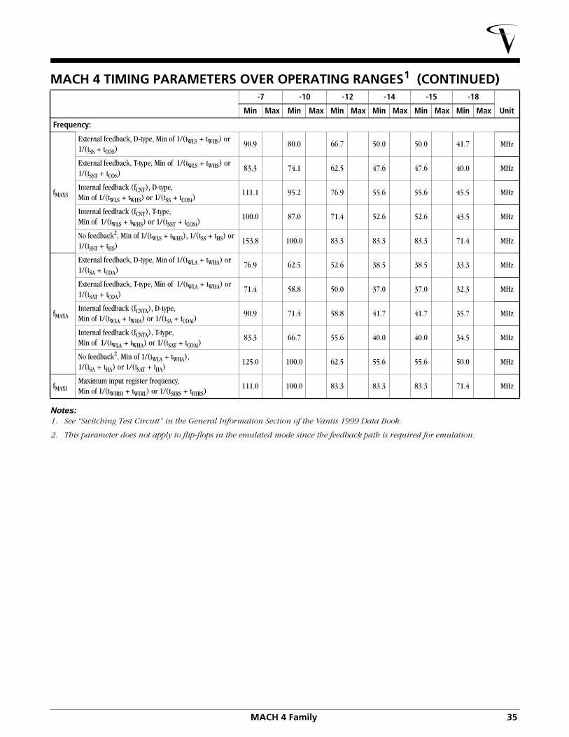
MACH 4 Family 35
Notes:1. See “Switching Test Circuit” in the General Information Section of the Vantis 1999 Data Book.
2. This parameter does not apply to flip-flops in the emulated mode since the feedback path is required for emulation.
Frequency:
fMAXS
External feedback, D-type, Min of 1/(tWLS + tWHS) or 1/(tSS + tCOS)
90.9 80.0 66.7 50.0 50.0 41.7 MHz
External feedback, T-type, Min of 1/(tWLS + tWHS) or 1/(tSST + tCOS)
83.3 74.1 62.5 47.6 47.6 40.0 MHz
Internal feedback (fCNT), D-type, Min of 1/(tWLS + tWHS) or 1/(tSS + tCOSi)
111.1 95.2 76.9 55.6 55.6 45.5 MHz
Internal feedback (fCNT), T-type, Min of 1/(tWLS + tWHS) or 1/(tSST + tCOSi)
100.0 87.0 71.4 52.6 52.6 43.5 MHz
No feedback2, Min of 1/(tWLS + tWHS), 1/(tSS + tHS) or 1/(tSST + tHS)
153.8 100.0 83.3 83.3 83.3 71.4 MHz
fMAXA
External feedback, D-type, Min of 1/(tWLA + tWHA) or 1/(tSA + tCOA)
76.9 62.5 52.6 38.5 38.5 33.3 MHz
External feedback, T-type, Min of 1/(tWLA + tWHA) or 1/(tSAT + tCOA)
71.4 58.8 50.0 37.0 37.0 32.3 MHz
Internal feedback (fCNTA), D-type, Min of 1/(tWLA + tWHA) or 1/(tSA + tCOAi)
90.9 71.4 58.8 41.7 41.7 35.7 MHz
Internal feedback (fCNTA), T-type, Min of 1/(tWLA + tWHA) or 1/(tSAT + tCOAi)
83.3 66.7 55.6 40.0 40.0 34.5 MHz
No feedback2, Min of 1/(tWLA + tWHA), 1/(tSA + tHA) or 1/(tSAT + tHA)
125.0 100.0 62.5 55.6 55.6 50.0 MHz
fMAXIMaximum input register frequency, Min of 1/(tWIRH + tWIRL) or 1/(tSIRS + tHIRS)
111.0 100.0 83.3 83.3 83.3 71.4 MHz
MACH 4 TIMING PARAMETERS OVER OPERATING RANGES1 (CONTINUED)-7 -10 -12 -14 -15 -18
UnitMin Max Min Max Min Max Min Max Min Max Min Max

36 MACH 4 Family
MACH 4A TIMING PARAMETERS OVER OPERATING RANGES1 -50 -55 -60 -65 -7 -10 -12 -14
UnitMin Max Min Max Min Max Min Max Min Max Min Max Min Max Min Max
Combinatorial Delay:
tPDiInternal combinatorial propagation delay
3.5 4.0 4.0 4.5 5.0 7.0 9.0 11.0 ns
tPDCombinatorial propagation delay
5.0 5.5 6.0 6.5 7.5 10.0 12.0 14.0 ns
Registered Delays:
tSSSynchronous clock setup time, D-type register
3.0 3.5 4.0 4.0 5.5 6.0 7.0 10.0 ns
tSSTSynchronous clock setup time, T-type register
4.0 4.0 4.5 4.5 6.5 7.0 8.0 11.0 ns
tSAAsynchronous clock setup time, D-type register
2.5 2.5 3.0 3.0 3.5 4.0 5.0 8.0 ns
tSATAsynchronous clock setup time, T-type register
3.0 3.0 3.5 3.5 4.5 5.0 6.0 9.0 ns
tHSSynchronous clock hold time
0.0 0.0 0.0 0.0 0.0 0.0 0.0 0.0 ns
tHAAsynchronous clock hold time
2.5 2.5 3.0 3.0 3.5 4.0 5.0 8.0 ns
tCOSiSynchronous clock to internal output
2.5 2.5 2.5 2.5 2.5 2.5 3.5 3.5 ns
tCOSSynchronous clock to output
4.0 4.0 4.5 4.5 5.0 5.5 6.5 6.5 ns
tCOAiAsynchronous clock to internal output
5.0 5.0 5.0 5.0 6.0 8.0 10.0 12.0 ns
tCOAAsynchronous clock to output
6.5 6.5 7.0 7.0 8.5 11.0 13.0 15.0 ns
Latched Delays:
tSSLSynchronous latch setup time
4.0 4.0 4.5 4.5 6.0 7.0 8.0 10.0 ns
tSALAsynchronous latch setup time
3.0 3.0 3.5 3.5 4.0 4.0 5.0 8.0 ns
tHSLSynchronous latch hold time
0.0 0.0 0.0 0.0 0.0 0.0 0.0 0.0 ns
tHALAsynchronous latch hold time
3.0 3.0 3.5 3.5 4.0 4.0 5.0 8.0 ns
tPDLiTransparent latch to internal output
5.5 5.5 6.0 6.0 7.5 9.0 11.0 12.0 ns
tPDLPropagation delay through transparent latch to output
7.0 7.0 8.0 8.0 10.0 12.0 14.0 15.0 ns
tGOSiSynchronous gate to internal output
3.0 3.0 3.0 3.0 3.5 4.5 7.0 8.0 ns
tGOS Synchronous gate to output 4.5 4.5 5.0 5.0 6.0 7.5 10.0 11.0 ns
tGOAiAsynchronous gate to internal output
6.0 6.0 6.0 6.0 8.5 10.0 13.0 15.0 ns
tGOAAsynchronous gate to output
7.5 7.5 8.0 8.0 11.0 13.0 16.0 18.0 ns

MACH 4 Family 37
Input Register Delays:
tSIRS Input register setup time 1.5 1.5 2.0 2.0 2.0 2.0 2.0 2.0 ns
tHIRS Input register hold time 2.5 2.5 3.0 3.0 3.0 3.0 3.0 4.0 ns
tICOSiInput register clock to internal feedback
3.0 3.0 3.0 3.0 3.5 4.5 6.0 6.0 ns
Input Latch Delays:
tSIL Input latch setup time 1.5 1.5 2.0 2.0 2.0 2.0 2.0 2.0 ns
tHIL Input latch hold time 2.5 2.5 3.0 3.0 3.0 3.0 3.0 4.0 ns
tIGOSiInput latch gate to internal feedback
3.5 3.5 4.0 4.0 4.0 4.0 4.0 5.0 ns
tPDILiTransparent input latch to internal feedback
1.5 1.5 1.5 1.5 2.0 2.0 2.0 2.0 ns
Input Register Delays with ZHT Option:
tSIRZInput register setup time - ZHT
6.0 6.0 6.0 6.0 6.0 6.0 6.0 6.0 ns
tHIRZInput register hold time - ZHT
0.0 0.0 0.0 0.0 0.0 0.0 0.0 0.0 ns
Input Latch Delays with ZHT Option:
tSILZInput latch setup time - ZHT
6.0 6.0 6.0 6.0 6.0 6.0 6.0 6.0 ns
tHILZ Input latch hold time - ZHT 0.0 0.0 0.0 0.0 0.0 0.0 0.0 0.0 ns
tPDILZiTransparent input latch to internal feedback - ZHT
6.0 6.0 6.0 6.0 6.0 6.0 6.0 6.0 ns
Output Delays:
tBUF Output buffer delay 1.5 1.5 2.0 2.0 2.5 3.0 3.0 3.0 ns
tSLW Slow slew rate delay adder 2.5 2.5 2.5 2.5 2.5 2.5 2.5 2.5 ns
tEA Output enable time 7.5 7.5 8.5 8.5 9.5 10.0 12.0 15.0 ns
tER Output disable time 7.5 7.5 8.5 8.5 9.5 10.0 12.0 15.0 ns
Power Delay:
tPLPower-down mode delay adder
2.5 2.5 2.5 2.5 2.5 2.5 2.5 2.5 ns
Reset and Preset Delays:
tSRi
Asynchronous reset or preset to internal register output
7.5 7.7 8.0 8.0 9.5 11.0 13.0 16.0 ns
tSRAsynchronous reset or preset to register output
9.0 9.2 10.0 10.0 12.0 14.0 16.0 19.0 ns
tSRR
Asynchronous reset and preset register recovery time
7.0 7.0 7.5 7.5 8.0 8.0 10.0 15.0 ns
tSRWAsynchronous reset or preset width
7.0 7.0 8.0 8.0 10.0 10.0 12.0 15.0 ns
Clock/LE Width:
tWLS Global clock width low 2.0 2.0 2.5 2.5 3.0 5.0 6.0 6.0 ns
MACH 4A TIMING PARAMETERS OVER OPERATING RANGES1 (CONTINUED)-50 -55 -60 -65 -7 -10 -12 -14
UnitMin Max Min Max Min Max Min Max Min Max Min Max Min Max Min Max

38 MACH 4 Family
tWHS Global clock width high 2.0 2.0 2.5 2.5 3.0 5.0 6.0 6.0 ns
tWLAProduct term clock width low
3.0 3.0 3.5 3.5 4.0 5.0 8.0 9.0 ns
tWHAProduct term clock width high
3.0 3.0 3.5 3.5 4.0 5.0 8.0 9.0 ns
tGWS
Global gate width low (for low transparent) or high (for high transparent)
4.0 4.0 4.5 4.5 5.0 5.0 6.0 6.0 ns
tGWA
Product term gate width low (for low transparent) or high (for high transparent)
4.0 4.0 4.5 4.5 5.0 5.0 6.0 9.0 ns
tWIRLInput register clock width low
3.0 3.0 3.5 3.5 4.0 5.0 6.0 6.0 ns
tWIRHInput register clock width high
3.0 3.0 3.5 3.5 4.0 5.0 6.0 6.0 ns
tWIL Input latch gate width 4.0 4.0 4.5 4.5 5.0 5.0 6.0 6.0 ns
MACH 4A TIMING PARAMETERS OVER OPERATING RANGES1 (CONTINUED)-50 -55 -60 -65 -7 -10 -12 -14
UnitMin Max Min Max Min Max Min Max Min Max Min Max Min Max Min Max

MACH 4 Family 39
Notes:1. See “Switching Test Circuit” in the General Information Section of the Vantis 1999 Data Book.
2. This parameter does not apply to flip-flops in the emulated mode since the feedback path is required for emulation.
Frequency:
fMAXS
External feedback, D-type, Min of 1/(tWLS + tWHS) or 1/(tSS + tCOS)
143 133 118 118 95.2 87.0 74.1 60.6 MHz
External feedback, T-type, Min of 1/(tWLS + tWHS) or 1/(tSST + tCOS)
125 125 111 111 87.0 80.0 69.0 57.1 MHz
Internal feedback (fCNT), D-type, Min of 1/(tWLS + tWHS) or 1/(tSS + tCOSi)
182 167 154 154 125 118 95.2 74.1 MHz
Internal feedback (fCNT), T-type, Min of 1/(tWLS + tWHS) or 1/(tSST + tCOSi)
154 161 143 143 111 105 87.0 69.0 MHz
No feedback2, Min of 1/(tWLS + tWHS), 1/(tSS + tHS) or 1/(tSST + tHS)
250 250 200 200 154 125 100 83.3 MHz
fMAXA
External feedback, D-type, Min of 1/(tWLA + tWHA) or 1/(tSA + tCOA)
111 111 100 100 83.3 66.7 55.6 43.5 MHz
External feedback, T-type, Min of 1/(tWLA + tWHA) or 1/(tSAT + tCOA)
105 105 95.2 95.2 76.9 62.5 52.6 41.7 MHz
Internal feedback (fCNTA), D-type, Min of 1/(tWLA + tWHA) or 1/(tSA + tCOAi)
133 133 125 125 105 83.3 66.7 50.0 MHz
Internal feedback (fCNTA), T-type, Min of 1/(tWLA + tWHA) or 1/(tSAT + tCOAi)
125 125 118 118 95.2 76.9 62.5 47.6 MHz
No feedback2, Min of 1/(tWLA + tWHA), 1/(tSA + tHA) or 1/(tSAT + tHA)
167 167 143 143 125 100 62.5 55.6 MHz
fMAXI
Maximum input register frequency, Min of 1/(tWIRH + tWIRL) or 1/(tSIRS + tHIRS)
167 167 143 143 125 100 83.3 83.3 MHz
MACH 4A TIMING PARAMETERS OVER OPERATING RANGES1 (CONTINUED)-50 -55 -60 -65 -7 -10 -12 -14
UnitMin Max Min Max Min Max Min Max Min Max Min Max Min Max Min Max

40 MACH 4 Family
CAPACITANCE 1
Note:1. These parameters are not 100% tested, but are calculated at initial characterization and at any time the design is modified where
this parameter may be affected.
ICC vs. FREQUENCY
These curves represent the typical power consumption for a particular device at system frequency. The selected “typical” pattern is a 16-bit up-down counter. This pattern fills the device and exercises every macrocell. Maximum frequency shown uses internal feedback and a D-type register. Power/Speed are optimized to obtain the highest counter frequency and the lowest power. The highest frequency (LSBs) is placed in common PAL blocks, which are set to high power. The lowest frequency signals (MSBs) are placed in a common PAL block and set to lowest power.
Parameter Symbol Parameter Description Test Conditions Typ Unit
CIN Input capacitance VIN=2.0 V 3.3 V or 5 V, 25°C, 1 MHz 6 pF
CI/O Output capacitance VOUT=2.0V 3.3 V or 5 V, 25°C, 1 MHz 8 pF
350
300
250
200
150
100
50
0
0 10 20 30 40 50 60 70 80 90 100
110
120
130
VCC = 5 V or 3.3 V, TA = 25 °C
I CC (
mA
)
Frequency (MHz) 17466G-066
M4(LV)-32/32
M4(LV)-64/32
M4(LV)-96/48
M4(LV)-128/64
M4(LV)-192/96
M4(LV)-256/128
Figure 16. ICC Curves at High Power Mode

MACH 4 Family 41
350
300
250
200
150
100
50
0
0 10 20 30 40 50 60 70 80 90 100
110
120
VCC = 5 V or 3.3 V, TA = 25 °C
M4(LV)-32/32
I CC (
mA
)
Frequency (MHz) 17466G-065
M4(LV)-64/32
M4(LV)-96/48
M4(LV)-128/64
M4(LV)-192/96
M4(LV)-256/128
Figure 17. ICC Curves at Low Power Mode

42 MACH 4 Family
CONNECTION DIAGRAM (M4(LV)-32/32, M4A(3,5)-32/32, M4(LV)-64/32 AND M4A(3,5)-64/32)
Top View44-Pin PLCC
PIN DESIGNATIONSCLK/I = Clock or Input
GND = Ground
I/O = Input/Output
VCC = Supply Voltage
TDI = Test Data In
TCK = Test Clock
TMS = Test Mode Select
TDO = Test Data Out
1 44 43 425 4 3 26 41 40
7
8
9
10
11
12
13
14
15
16
17
23 24 25 2619 20 21 2218 27 28
39
38
37
36
35
34
33
32
31
30
29
I/O5
I/O6
I/O7
TDI
CLK0/I0
GND
TCK
I/O8
I/O9
I/O10
I/O11
A2
A1
A0
B0
B1
B2
B3
D3
D2
D1
D0
C0
C1
C2
B3
B2
B1
B0
B8
B9
B10
A2
A1
A0
A8
A9
A10
A11
I/O27
I/O26
I/O25
I/O24
TDO
GND
CLK1/I1
TMS
I/O23
I/O22
I/O21
I/O12
I/O13
I/O14
I/O15
VC
C
GN
D
I/O16
I/O17
I/O18
I/O19
I/O20
B4
B5
B6
B7
C7
C6
C5
C4
C3
A12
A13
A14
A15
B15
B14
B13
B12
B11
I/O4
I/O3
I/O2
I/O1
I/O0
GN
D
VC
C
I/O31
I/O30
I/O29
I/O28
A3
A4
A5
A6
A7
D7
D6
D5
D4
A3
A4
A5
A6
A7
B7
B6
B5
B4
M4(LV)-32/32M4A(3,5)-32/32
M4(LV)-32/32M4A(3,5)-32/32
M4(LV)-64/32M4A(3,5)-64/32
M4(LV)-64/32M4A(3,5)-64/32
M4(LV)-64/32M4A(3,5)-64/32
M4(LV)-64/32M4A(3,5)-64/32
17466F-026
Macrocell (0-7)
PAL Block (A-D)
C 7

MACH 4 Family 43
CONNECTION DIAGRAM (M4(LV)-32/32, M4A(3,5)-32/32, M4(LV)-64/32 AND M4A(3,5)-64/32)
Top View 44-Pin TQFP
PIN DESIGNATIONSCLK/I = Clock or Input
GND = Ground
I/O = Input/Output
VCC = Supply Voltage
TDI = Test Data In
TCK = Test Clock
TMS = Test Mode Select
TDO = Test Data Out
I/O12
I/O13
I/O14
I/O15
VC
CG
ND
I/O16
I/O17
I/O18
I/O19
I/O20
B4
B5
B6
B7
C7
C6
C5
C4
C3
A12
A13
A14
A15
B15
B14
B13
B12
B11
I/O4
I/O3
I/O2
I/O1
I/O0
GN
DV
CC
I/O31
I/O30
I/O29
I/O28
A3
A4
A5
A6
A7
D7
D6
D5
D4
A3
A4
A5
A6
A7
B7
B6
B5
B4
I/O27I/O26I/O25I/O24TDOGNDCLK1/I1TMSI/O23I/O22I/O21
D3D2D1D0
C0C1C2
B3B2B1B0
B8B9B10
I/O5I/O6I/O7TDI
CLK0/I0GNDTCKI/O8I/O9
I/O10I/O11
A2A1A0
B0B1B2B3
A2A1A0
A8A9
A10A11
1234567891011
3332313029282726252423
44 43 42 41 40 39 38 37 36 35 34
12 13 14 15 16 17 18 19 20 21 22
M4(LV)-32/32M4A(3,5)-32/32
M4(LV)-32/32M4A(3,5)-32/32
M4(LV)-64/32M4A(3,5)-64/32
M4(LV)-64/32M4A(3,5)-64/32
M4(LV)-64/32M4A(3,5)-64/32
M4(LV)-64/32M4A(3,5)-64/32
17466F-027
Macrocell (0-7)
PAL Block (A-D)
C 7

44 MACH 4 Family
CONNECTION DIAGRAM (M4(LV)-32/32, M4A(3,5)-32/32, M4(LV)-64/32 AND M4A(3,5)-64/32)
Top View48-Pin TQFP
PIN DESIGNATIONSCLK/I = Clock or Input
GND = Ground
I/O = Input/Output
VCC = Supply Voltage
NC = No Connect
TDI = Test Data In
TCK = Test Clock
TMS = Test Mode Select
TDO = Test Data Out
I/O12
I/O13
I/O14
I/O15
VC
CN
CG
ND
I/O16
I/O17
I/O18
I/O19
I/O20
B4
B5
B6
B7
C7
C6
C5
C4
C3
A12
A13
A14
A15
B15
B14
B13
B12
B11
I/O4
I/O3
I/O2
I/O1
I/O0
GN
DN
CV
CC
I/O31
I/O30
I/O29
I/O28
A3
A4
A5
A6
A7
D7
D6
D5
D4
A3
A4
A5
A6
A7
B7
B6
B5
B4
I/O27I/O26I/O25I/O24TDOGNDNCCLK1/I1TMSI/O23I/O22I/O21
D3D2D1D0
C0C1C2
B3B2B1B0
B8B9B10
I/O5I/O6I/O7TDI
CLK0/I0NC
GNDTCKI/O8I/O9
I/O10I/O11
A2A1A0
B0B1B2B3
A2A1A0
A8A9
A10A11
123456789101112
33343536
3231302928272625
4445464748 43 42 41 40 39 38 37
13 14 15 16 17 18 19 20 21 22 23 24
M4(LV)-32/32M4A(3,5)-32/32
M4(LV)-32/32M4A(3,5)-32/32
M4(LV)-64/32M4A(3,5)-64/32
M4(LV)-64/32M4A(3,5)-64/32
M4(LV)-64/32M4A(3,5)-64/32
M4(LV)-64/32M4A(3,5)-64/32
17466F-028
Macrocell (0-7)
PAL Block (A-D)
C 7

MACH 4 Family 45
CONNECTION DIAGRAM (M4(LV)-96/48 AND M4A(3,5)-96/48)
Top View100-Pin TQFP
PIN DESIGNATIONSCLK/I = Clock or Input
GND = Ground
I = Input
I/O = Input/Output
VCC = Supply Voltage
NC = No Connect
TDI = Test Data In
TCK = Test Clock
TMS = Test Mode Select
TDO = Test Data Out
12345678910111213141516171819202122232425
NCTDINCNC
I/O6I/O7I/O8I/O9
I/O10I/O11
I0/CLK0VCC
GNDI1/CLK1
I/O12I/O13I/O14I/O15I/O16I/O17
NCNC
TMSTCKNC
A1A0B0B1B2B3
B4B5B6B7C0C1
26 27 28 29 30 31 32 33 34 35 36 37 38 39 40 41 42 43 44 45 46 47 48 49 50
GN
DN
CN
CI/O
18I/O
19I/O
20I/O
21I/O
22I/O
23 NC I2
NC
NC
GN
DV
CC I3
I/O24
I/O25
I/O26
I/O27
I/O28
I/O29 NC
NC
GN
D
C2
C3
C4
C5
C6
C7
D7
D6
D5
D4
D3
D2
100 99 98 97 96 95 94 93 92 91 90 89 88 87 86 85 84 83 82 81 80 79 78 77 76
GN
DN
CN
CI/O
5I/O
4I/O
3I/O
2I/O
1I/O
0I7 V
CC
GN
DN
CN
CI6 N
CI/O
47I/O
46I/O
45I/O
44I/O
43I/O
42N
CN
CG
ND
A2
A3
A4
A5
A6
A7
F7
F6
F5
F4
F3
F2
75747372717069686766656463626160595857565554535251
NCTDONCNCNCI/O41I/O40I/O39I/O38I/O37I/O36I5/CLK3GNDVCCI4/CLK2I/O35I/O34I/O33I/O32I/O31I/O30NCNCNCNC
F1F0E0E1E2E3
E4E5E6E7D0D1
17466F-029
Macrocell (0-7)
PAL Block (A-F)
C 7

46 MACH 4 Family
CONNECTION DIAGRAM (M4(LV)-128N/64)Top View
84-Pin PLCC
Note:Pin-compatible with the MACH131, MACH231, MACH435.
PIN DESIGNATIONSCLK/I = Clock or Input
GND = Ground
I = Input
I/O = Input/Output
VCC = Supply Voltage
123 818283846789 45 80 76777879 7512131415161718192021
232425262728293031
7372717069686766656463626160595857565554
43424140 4746454437363534 393833 48 52515049
10
22
11
3253
74I/O9
I/O10I/O11I/O12I/O13I/O14I/O15
CLK0/I0VCCGND
CLK1/I1I/O16I/O17I/O18I/O19I/O20I/O21I/O22I/O23GND
I/O8 GNDI/O55I/O54I/O53I/O52I/O51I/O50I/O49I/O48CLK3/I4
VCCCLK2/I3I/O47
G7G6G5G4G3G2G1G0
F0F1F2F3F4F5F6F7
B7B6B5B4B3B2B1B0
C0C1C2C3C4C5C6C7
I/O46I/O45I/O44I/O43I/O42I/O41
GND
I/O40
GN
D
VC
CI/O
0
I/O62
I/O63
I 5VC
C
I/O3
I/O4
I/O5
I/O6
I/O1
I/O2
I/O61
I/O57
I/O58
I/O59
I/O60
I/O56
I/O7
H0
H1
H2
H3
H4
H5
H6
H7
A7
A6
A5
A4
A3
A2
A1
A0
GN
D
GN
D
VC
CI 2
I/O34
I/O33
I/O32
VC
C
I/O29
I/O28
I/O27
I/O26
I/O31
I/O30
I/O35
I/O39
I/O38
I/O37
I/O36
GN
D
I/O25
I/O24
E0
E1
E2
E3
E4
E5
E6
E7
D7
D6
D5
D4
D3
D2
D1
D0 17466F-030
Macrocell (0-7)
PAL Block (A-H)
C 7

MACH 4 Family 47
CONNECTION DIAGRAM (M4(LV)-128/64 AND M4A(3,5)-128/64)Top View
100-Pin PQFP
Note:The numbers in parentheses reflect compatible pin numbers for 84-pin PLCC.
PIN DESIGNATIONSI/CLK = Input or Clock
GND = Ground
I = Input
I/O = Input/Output
VCC = Supply Voltage
TDI = Test Data In
TCK = Test Clock
TMS = Test Mode Select
TDO = Test Data Out
TRST = Test Reset
ENABLE = Program
I/O
7A
7A
6A
5A
4A
3A
2A
1A
0
D7
D6
D5
D4
D3
D2
D1
D0
I/O
6I/O
5I/O
4I/O
3I/O
2I/O
1I/O
0V
CC
GN
DG
ND
VC
CI/O
63
I/O
62
I/O
61
I/O
60
I/O
59
I/O
58
I/O
57
I/O
56
H0
H1
H2
H3
H4
H5
H6
H7
GNDGND
TDII5
I/O8I/O9
I/O10I/O11I/O12I/O13I/O14I/O15
IO/CLK0
GNDGND
I1/CLK1I/O16I/O17I/O18I/O19I/O20I/O21I/O22I/O23
B7B6B5B4B3B2B1B0
C0C1C2C3C4C5C6C7
TMSTCKGNDGND
282930
4 56789101112131415161718192021222324252627
123
99
98
100
31
32
33
34
35
36
37
38
39
40
41
42
43
44
45
46
47
48
49
50
97
96
95
94
93
92
91
90
89
88
87
86
85
84
82
81
83
I/O46I/O45I/O44I/O43I/O42I/O41I/O40I2ENABLEGNDGND
GNDTD0TRSTI/O55I/O54I/O53I/O52I/O51I/O50I/O49I/O48
G7G6G5G4G3G2G1G0
I4/CLK3GNDGND
I3/CLK2I/O47
F1F2F3F4F5F6F7
F0
GND
777675747372717069686766656463626160595857565554535251
807978
I/O
24
I/O
25
I/O
26
I/O
27
I/O
28
I/O
29
I/O
30
I/O
31
GN
DG
ND
I/O
32
I/O
33
I/O
34
I/O
35
I/O
36
I/O
37
I/O
38
I/O
39
E0
E1
E2
E3
E4
E5
E6
E7
(83)(12)(13)(14)(15)(16)(17)(18)(19)(20)
(23)(24)(25)(26)(27)(28)(29)(30)(31)
(33)
(34)
(35)
(36)
(37)
(38)
(39)
(40)
(45)
(46)
(47)
(48)
(49)
(50)
(51)
(52)
(62)(61)(60)(59)(58)(57)(56)(55)(54)(41)
(73)(72)(71)(70)(69)(68)(67)(66)(65)
(10) (9)
(8)
(7)
(6)
(5)
(4)
(3)
(82)
(81)
(80)
(79)
(78)
(77)
(76)
(75)
VCCVCC
VCCVCC
VC
C
VC
C
17466F-031
Macrocell (0-7)
PAL Block (A-H)
C 7

48 MACH 4 Family
CONNECTION DIAGRAM (M4(LV)-128/64 AND M4A(3,5)-128/64)
Top View100-Pin TQFP
PIN DESIGNATIONSCLK/I = Clock or Input
GND = Ground
I = Input
I/O = Input/Output
VCC = Supply Voltage
TDI = Test Data In
TCK = Test Clock
TMS = Test Mode Select
TDO = Test Data Out
TRST = Test Reset
ENABLE = Program
12345678910111213141516171819202122232425
GNDTDI
I/O8I/O9
I/O10I/O11I/O12I/O13I/O14I/O15
I0/CLK0VCCGND
I1/CLK1I/O16I/O17I/O18I/O19I/O20I/O21I/O22I/O23TMSTCKGND
B7B6B5B4B3B2B1B0
C0C1C2C3C4C5C6C7
26 27 28 29 30 31 32 33 34 35 36 37 38 39 40 41 42 43 44 45 46 47 48 49 50
GN
DG
ND
I/O24
I/O25
I/O26
I/O27
I/O28
I/O29
I/O30
I/O31 I2
VC
CG
ND
GN
DV
CC
I/O32
I/O33
I/O34
I/O35
I/O36
I/O37
I/O38
I/O39
GN
DG
ND
D7
D6
D5
D4
D3
D2
D1
D0
E0
E1
E2
E3
E4
E5
E6
E7
100 99 98 97 96 95 94 93 92 91 90 89 88 87 86 85 84 83 82 81 80 79 78 77 76
GN
DG
ND
I/O7
I/O6
I/O5
I/O4
I/O3
I/O2
I/O1
I/O0
VC
CG
ND
GN
DV
CC
I5 I/O63
I/O62
I/O61
I/O60
I/O59
I/O58
I/O57
I/O56
GN
DG
ND
A7
A6
A5
A4
A3
A2
A1
A0
H0
H1
H2
H3
H4
H5
H6
H7
75747372717069686766656463626160595857565554535251
GNDTDOTRSTI/O55I/O54I/O53I/O52I/O51I/O50I/O49I/O48I4/CLK3GNDVCCI3/CLK2I/O47I/O46I/O45I/O44I/O43I/O42I/O41I/O40ENABLEGND
G7G6G5G4G3G2G1G0
F0F1F2F3F4F5F6F7
17466F-032
Macrocell (0-7)
PAL Block (A-H)
C 7

MACH 4 Family 49
CONNECTION DIAGRAM (M4(LV)-192/96 AND M4A(3,5)-192/96)Top View
144-Pin TQFP
PIN DESIGNATIONSCLK = Clock
GND = Ground
I = Input
I/O = Input/Output
VCC = Supply Voltage
TDI = Test Data In
TCK = Test Clock
TMS = Test Mode Select
TDO = Test Data Out
123456789101112131415161718192021222324252627282930313233343536
GNDTDI
I/O16I/O17I/O18I/O19I/O20I/O21I/O22I/O23
I2I3
VCCGND
I4I/O24I/O25I/O26I/O27I/O28I/O29I/O30I/O31GNDVCC
I/O32I/O33I/O34I/O35I/O36I/O37I/O38I/O39TMSTCKGND
E7E6E5E4E3E2E1E0
F7F6F5F4F3F2F1F0
G0G1G2G3G4G5G6G7
37 38 39 40 41 42 43 44 45 46 47 48 49 50 51 52 53 54 55 56 57 58 59 60 61 62 63 64 65 66 67 68 69 70 71 72
GN
DI/O
40I/O
41I/O
42I/O
43I/O
44I/O
45I/O
46I/O
47 I5 I6 I7C
LK1
GN
DV
CC
CLK
2 I8 I9I/O
48I/O
49I/O
50I/O
51I/O
52I/O
53I/O
54I/O
55V
CC
GN
DI/O
56I/O
57I/O
58I/O
59I/O
60I/O
61I/O
62I/O
63
H0
H1
H2
H3
H4
H5
H6
H7 I7 I6 I5 I4 I3 I2 I1 I0 J7 J6 J5 J4 J3 J2 J1 J0
144
143
142
141
140
139
138
137
136
135
134
133
132
131
130
129
128
127
126
125
124
123
122
121
120
119
118
117
116
115
114
113
112
111
110
109
I/O15
I/O14
I/O13
I/O12
I/O11
I/O10
I/O9
I/O8
GN
DV
CC
I/O7
I/O6
I/O5
I/O4
I/O3
I/O2
I/O1
I/O0
I1 I0 CLK
0G
ND
VC
CC
LK3
I15
I14
I13
I/O95
I/O94
I/O93
I/O92
I/O91
I/O90
I/O89
I/O88
GN
D
D0
D1
D2
D3
D4
D5
D6
D7
C0
C1
C2
C3
C4
C5
C6
C7
B7
B6
B5
B4
B3
B2
B1
B0
108107106105104103102101100999897969594939291908988878685848382818079787776757473
GNDTDONCI/O87I/O86I/O85I/O84I/O83I/O82I/O81I/O80I12VCCGNDI11I10I/O79I/O78I/O77I/O76I/O75I/O74I/O73I/O72GNDVCCI/O71I/O70I/O69I/O68I/O67I/O66I/O65I/O64NCGND
A7A6A5A4A3A2A1A0
L0L1L2L3L4L5L6L7
K7K6K5K4K3K2K1K0
17466F-033
Macrocell (0-7)
PAL Block (A-L)
C 7

50 MACH 4 Family
CONNECTION DIAGRAM (M4(LV)-256/128 AND M4A(3,5)-256/128)
Top View208-Pin PQFP
PIN DESIGNATIONSCLK = Clock
GND = Ground
I = Input
I/O = Input/Output
VCC = Supply Voltage
TDI = Test Data In
TCK = Test Clock
TMS = Test Mode Select
TDO = Test Data Out
TRST = Test Reset
ENABLE = Program
GNDTDI
I/O16I/O17I/O18I/O19I/O20I/O21I/O22I/O23VCCGNDI/O24I/O25I/O26I/O27I/O28I/O29I/O30I/O31
I2I3
GNDVCCVCCGNDGNDVCCVCCGND
I4I/O32I/O33I/O34I/O35I/O36I/O37I/O38I/O39GNDVCC
I/O40I/O41I/O42I/O43I/O44I/O45I/O46I/O47TMSTCKGND
12345678910111213141516171819202122232425262728293031323334353637383940414243444546474849505152
C0C1C2C3C4C5C6C7
D0D1D2D3D4D5D6D7
E0E1E2E3E4E5E6E7
F0F1F2F3F4F5F6F7
GN
DI/O
15I/O
14I/O
13I/O
12I/O
11I/O
10I/O
9I/O
8G
ND
VC
CI/O
7I/O
6I/O
5I/O
4I/O
3I/O
2I/O
1I/O
0I1 I0 C
LK0
VC
CG
ND
GN
DV
CC
VC
CG
ND
GN
DV
CC
CLK
3I1
3I1
2I/O
127
I/O12
6I/O
125
I/O12
4I/O
123
I/O12
2I/O
121
I/O12
0V
CC
GN
DI/O
119
I/O11
8I/O
117
I/O11
6I/O
115
I/O11
4I/O
113
I/O11
2G
ND
208
207
206
205
204
203
202
201
200
199
198
197
196
195
194
193
192
191
190
189
188
187
186
185
184
183
182
181
180
179
178
177
176
175
174
173
172
171
170
169
168
167
166
165
164
163
162
161
160
159
158
157
B7
B6
B5
B4
B3
B2
B1
B0
A7
A6
A5
A4
A3
A2
A1
A0
P7
P6
P5
P4
P3
P2
P1
P0
O7
O6
O5
O4
O3
O2
O1
O0
GNDTDOTRSTI/O111I/O110I/O109I/O108I/O107I/O106I/O105I/O104VCCGNDI/O103I/O102I/O101I/O100I/O99I/O98I/O97I/O96I11GNDVCCVCCGNDGNDVCCVCCGNDI10I9I/O95I/O94I/O93I/O92I/O91I/O90I/O89I/O88GNDVCCI/O87I/O86I/O85I/O84I/O83I/O82I/O81I/O80ENABLEGND
156155154153152151150149148147146145144143142141140139138137136135134133132131130129128127126125124123122121120119118117116115114113112111110109108107106105
N7N6N5N4N3N2N1N0
M7M6M5M4M3M2M1M0
L7L6L5L4L3L2L1L0
K7K6K5K4K3K2K1K0
GN
DI/O
48I/O
49I/O
50I/O
51I/O
52I/O
53I/O
54I/O
55G
ND
VC
CI/O
56I/O
57I/O
58I/O
59I/O
60I/O
61I/O
62I/O
63 I5 I6C
LK1
VC
CG
ND
GN
DV
CC
VC
CG
ND
GN
DV
CC
CLK
2 I7 I8I/O
64I/O
65I/O
66I/O
67I/O
68I/O
69I/O
70I/O
71V
CC
GN
DI/O
72I/O
73I/O
74I/O
75I/O
76I/O
77I/O
78I/O
79G
ND
53 54 55 56 57 58 59 60 61 62 63 64 65 66 67 68 69 70 71 72 73 74 75 76 77 78 79 80 81 82 83 84 85 86 87 88 89 90 91 92 93 94 95 96 97 98 99 100
101
102
103
104
G0
G1
G2
G3
G4
G5
G6
G7
H0
H1
H2
H3
H4
H5
H6
H7 I0 I1 I2 I3 I4 I5 I6 I7 J0 J1 J2 J3 J4 J5 J6 J7
17466F-034
Macrocell (0-7)
PAL Block (A-P)
C 7

MACH 4 Family 51
CONNECTION DIAGRAM (M4(LV)-256/128 AND M4A(3,5)-256/128)
Bottom View256-Pin BGA
2019
1817
1615
1413
1211
109
87
65
43
21
AG
ND
N/C
GN
DI/O
108
N4
I/O10
5N
1G
ND
I/O10
0M
4I/O
96M
0G
ND
GN
DG
ND
GN
DI/O
95L7
I/O91
L3G
ND
I/O87
K7
N/C
GN
DG
ND
GN
DA
BG
ND
I/O11
3O
1N
/CI/O
109
N5
I/O10
6N
2I/O
103
M7
I/O10
2M
6I/O
98M
2N
/CI1
1N
/CN
/CI/O
93L5
I/O89
L1I/O
88L0
I/O85
K5
I/O83
K3
I/O82
K2
N/C
GN
DB
CI/O
116
O4
N/C
VC
CT
RS
TI/O
111
N7
I/O10
7N
3I/O
104
N0
I/O10
1M
5I/O
97M
1N
/CI1
0I/O
94L6
I/O90
L2I/O
86K
6I/O
84K
4I/O
80K
0E
NA
BLE
VC
CI/O
78J6
I/O74
J2C
DI/O
120
P0
I/O11
7O
5I/O
112
O0
VC
CV
CC
I/O11
0N
6V
CC
N/C
I/O99
M3
N/C
I9I/O
92L4
N/C
VC
CI/O
81K
1V
CC
VC
CI/O
79J7
I/O75
J3I/O
71 I7D
EI/O
123
P3
I/O11
9O
7I/O
114
O2
TD
IT
DO
I/O77
J5I/O
72J0
I/O68 I4
E
FG
ND
I/O12
2P
2I/O
118
O6
I/O11
5O
3I/O
76J4
I/O73
J1I/O
69 I5G
ND
F
GI1
2I/O
125
P5
I/O12
1P
1V
CC
VC
CI/O
70 I6I/O
65 I1I8
G
HG
ND
I/O12
7P
7I/O
126
P6
I/O12
4P
4I/O
67 I3I/O
66 I2I/O
64 I0G
ND
H
JN
/CN
/CN
/CI1
3I7
N/C
N/C
N/C
J
KG
ND
CLK
3N
/CN
/CN
/CN
/CC
LK2
N/C
K
LN
/CC
LK0
N/C
N/C
N/C
N/C
CLK
1G
ND
L
MN
/CN
/CN
/CI0
I6N
/CI/O
63H
7I/O
62H
6M
NG
ND
I/O0
A0
I/O2
A2
I/O3
A3
I/O60
H4
I/O61
H5
I/O59
H3
GN
DN
PI1
I/O1
A1
I/O6
A6
VC
CV
CC
I/O57
H1
I/O58
H2
I5P
RG
ND
I/O5
A5
I/O9
B1
N/C
I/O51
G3
I/O54
G6
I/O56
H0
GN
DR
TI/O
4A
4I/O
8B
0I/O
12B
4T
CK
TM
SI/O
50G
2I/O
55G
7N
/CT
UI/O
7A
7I/O
11B
3I/O
15B
7V
CC
VC
CI/O
18C
2V
CC
I/O24
D0
I/O29
D5
I2N
/CI/O
35E
3N
/CV
CC
N/C
VC
CV
CC
I/O48
G0
I/O53
G5
N/C
U
VI/O
10B
2I/O
13B
5V
CC
I/O16
C0
I/O17
C1
I/O21
C5
I/O23
C7
I/O27
D3
I/O31
D7
I3N
/CI/O
33E
1I/O
37E
5I/O
41F
1I/O
43F
3I/O
46F
6I/O
47F
7V
CC
I/O52
G4
N/C
V
WG
ND
I/O14
B6
N/C
N/C
I/O19
C3
I/O22
C6
I/O25
D1
I/O28
D4
N/C
N/C
I4N
/CI/O
34E
2I/O
38E
6I/O
39E
7I/O
42F
2I/O
45F
5N
/CI/O
49G
1G
ND
W
YG
ND
GN
DG
ND
N/C
I/O20
C4
GN
DI/O
26D
2I/O
30D
6G
ND
GN
DG
ND
GN
DI/O
32E
0I/O
36E
4G
ND
I/O40
F0
I/O44
F4
GN
DN
/CG
ND
Y
2019
1817
1615
1413
1211
109
87
65
43
21
17466F-035
CLK = ClockGND = GroundI = InputI/O = Input/OutputNC = No ConnectVCC = Supply VoltageTDI = Test Data InTCK = Test ClockTMS = Test Mode SelectTDO = Test Data OutTRST = Test ResetENABLE =Program
Pin Designations
C 7
Macrocell (0-7)
PAL Block (A-P)

52 MACH 4 Family
PRODUCT ORDERING INFORMATIONMACH 4 Devices Commercial & Industrial - 3.3V and 5VVantis programmable logic products are available with several ordering options. The order number (Valid Combination) is formed by a combina-tion of:
All MACH devices are dual-marked with both Commercial andIndustrial grades. The Industrial speed grade is slower, i.e., M4-256/128-7YC-10YI
Valid Combinations
Valid Combinations list conÞgurations planned to be supported involume for this device. Consult the local Vantis sales ofÞce to conÞrmavailability of speciÞc valid combinations and to check on newlyreleased combinations.
128
FAMILY TYPEM4- = MACH 4 Family (5-V VCC)M4LV- = MACH 4 Family Low Voltage (3.3-V VCC)
M4- 256 Y C
MACROCELL DENSITY 32 = 32 Macrocells 128N = 128 Macrocells, Non-ISP 64 = 64 Macrocells 192 = 192 Macrocells 96 = 96 Macrocells 256 = 256 Macrocells 128 = 128 Macrocells
I/Os /32 = 32 I/Os in 44-pin PLCC, 44-pin TQFP or 48-pin TQFP /48 = 48 I/Os in 100-pin TQFP /64 = 64 I/Os in 84-pin PLCC, 100-pin PQFP or 100-pin TQFP /96 = 96 I/Os in 144-pin TQFP/128 = 128 I/Os in 208-pin PQFP or 256-Pin BGA
OPERATING CONDITIONSC = Commercial (0°C to +70°C)I = Industrial (-40 ¡C to +85 ¡C)
PACKAGE TYPEA = Ball Grid Array (BGA)J = Plastic Leaded Chip Carrier
(PLCC)V = Thin Quad Flat Pack (TQFP)Y = Plastic Quad Flat Pack (PQFP)
SPEED-7 =7.5 ns tPD
-10 =10 ns tPD-12 =12 ns tPD-14 =14 ns tPD -15 =15 ns tPD-18 =18 ns tPD
-7
48 = 48-pin TQFP for M4(LV)-32/32 or M4(LV)-64/32
/
Valid CombinationsM4-32/32
-7, -10, -12, -15
JC, VC, VC48M4LV-32/32 JC, VC, VC48M4-64/32 JC, VC, VC48M4LV-64/32 JC, VC, VC48M4-96/48 VCM4LV-96/48 VCM4-128/64 YC, VCM4LV-128/64 YC, VCM4-128N/64 JCM4LV-128N/64 JCM4-192/96 VCM4LV-192/96 VCM4-256/128 YC, ACM4LV-256/128 YC, AC
Valid CombinationsM4-32/32
-10, -12, -14, -18
JI, VI, VI48M4LV-32/32 JI, VI, VI48M4-64/32 JI, VI, VI48M4LV-64/32 JI, VI, VI48M4-96/48 VIM4LV-96/48 VIM4-128/64 YI, VIM4LV-128/64 YI, VIM4-128N/64 JIM4LV-128N/64 JIM4-192/96 VIM4LV-192/96 VIM4-256/128 YI, AIM4LV-256/128 YI, AI

MACH 4 Family 53
PRODUCT ORDERING INFORMATIONMACH 4A Devices Commercial and Industrial - 3.3V and 5VVantis programmable logic products are available with several ordering options. The order number (Valid Combination) is formed by a combina-tion of:
All MACH devices are dual-marked with both Commercial andIndustrial grades. The Industrial speed grade is slower, i.e., M4A3-256/128-7YC-10YI
Valid Combinations Valid Combinations list conÞgurations planned to be supported involume for this device. Consult the local Vantis sales ofÞce to conÞrmavailability of speciÞc valid combinations and to check on newlyreleased combinations.
128
FAMILY TYPEM4A3- = MACH 4 Family Low Voltage Advanced Feature
(3.3-V VCC)M4A5- = MACH 4 Family Advanced Feature (5-V VCC)
M4A3- 256 Y C
MACROCELL DENSITY32 = 32 Macrocells 192 = 192 Macrocells
64 = 64 Macrocells 256 = 256 Macrocells 96 = 96 Macrocells 384 = 384 Macrocells
128 = 96 Macrocells 512 = 512 Macrocells
I/Os/32 = 32 I/Os in 44-pin PLCC, 44-pin TQFP or 48-pin TQFP
/48 = 48 I/Os in 100-pin TQFP /64 = 64 I/Os in 100-pin TQFP or 100-pin PQFP /96 = 96 I/Os in 144-pin TQFP/128 = 128 I/Os in 176-pin TQFP, 208-pin PQFP, or 256-pin BGA/160 = 160 I/Os in 208-pin PQFP/192 = 192 I/Os in 256-pin BGA/256 = 256 I/Os in 352-pin BGA
OPERATING CONDITIONSC = Commercial (0°C to +70°C)I = Industrial (-40 ¡C to +85 ¡C)
PACKAGE TYPEA = Ball Grid Array (BGA)J = Plastic Leaded Chip Carrier
(PLCC)V = Thin Quad Flat Pack (TQFP)Y = Plastic Quad Flat Pack (PQFP)
SPEED-50 = 5.0 ns tPD-55 = 5.5 ns tPD-60 = 6.0 ns tPD-65 = 6.5 ns tPD-7 = 7.5 ns tPD
-10 = 10 ns tPD-12 = 12 ns tPD-14 = 4 ns tPD
-7
48 = 48-pin TQFP for M4A3-32/32 or M4A3-64/32 M4A5-32/32 or M4A5-64/32
Valid CombinationsM4A3-32/32
-50, -55, -60, -65,
-7, -10, -12
JC, VC, VC48M4A5-32/32 JC, VC, VC48M4A3-64/32 JC, VC, VC48M4A5-64/32 JC, VC, VC48M4A3-96/48 VCM4A5-96/48 VCM4A3-128/64 YC, VCM4A5-128/64 YC, VCM4A3-192/96 VCM4A5-192/96 VCM4A3-256/128 YC, ACM4A5-256/128 YC, ACM4A3-384/128 VCM4A3-384/160 YCM4A3-384/192 ACM4A3-512/128 VC
Valid CombinationsM4A3-32/32
-7, -10, -12, -14
JI, VI, VI48M4A5-32/32 JI, VI, VI48M4A3-64/32 JI, VI, VI48M4A5-64/32 JI, VI, VI48M4A3-96/48 VIM4A5-96/48 VIM4A3-128/64 YI, VIM4A5-128/64 YI, VIM4A3-192/96 VIM4A5-192/96 VIM4A3-256/128 YI, AIM4A5-256/128 YI, AIM4A3-384/128 VIM4A3-384/160 YIM4A3-384/192 AIM4A3-512/128 VIM4A3-512/160 YIM4A3-512/192 AIM4A3-512/256 AI
Copyright © 2022 FDOKUMEN