
LM3697 High-efficiency three-string white LED driver
42
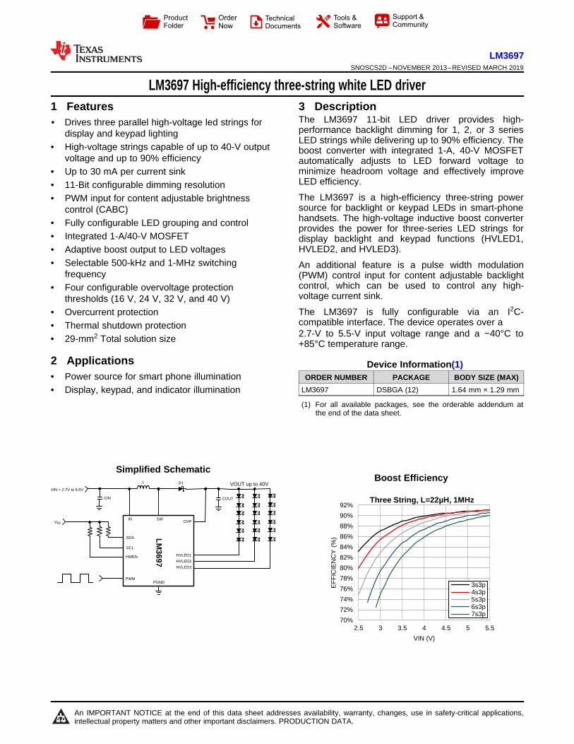
70% 72% 74% 76% 78% 80% 82% 84% 86% 88% 90% 92% 2.5 3 3.5 4 4.5 5 5.5 EFFICIENCY (%) VIN (V) Three String, L=22μH, 1MHz 3s3p 4s3p 5s3p 6s3p 7s3p C049 IN SW HVLED1 PGND HWEN SDA SCL LM3697 COUT CIN L D1 PWM OVP VIN = 2.7V to 5.5V VOUT up to 40V VIN HVLED3 HVLED2 Product Folder Order Now Technical Documents Tools & Software Support & Community An IMPORTANT NOTICE at the end of this data sheet addresses availability, warranty, changes, use in safety-critical applications, intellectual property matters and other important disclaimers. PRODUCTION DATA. LM3697 SNOSCS2D – NOVEMBER 2013 – REVISED MARCH 2019 LM3697 High-efficiency three-string white LED driver 1 1 Features 1• Drives three parallel high-voltage led strings for display and keypad lighting • High-voltage strings capable of up to 40-V output voltage and up to 90% efficiency • Up to 30 mA per current sink • 11-Bit configurable dimming resolution • PWM input for content adjustable brightness control (CABC) • Fully configurable LED grouping and control • Integrated 1-A/40-V MOSFET • Adaptive boost output to LED voltages • Selectable 500-kHz and 1-MHz switching frequency • Four configurable overvoltage protection thresholds (16 V, 24 V, 32 V, and 40 V) • Overcurrent protection • Thermal shutdown protection • 29-mm 2 Total solution size 2 Applications • Power source for smart phone illumination • Display, keypad, and indicator illumination 3 Description The LM3697 11-bit LED driver provides high- performance backlight dimming for 1, 2, or 3 series LED strings while delivering up to 90% efficiency. The boost converter with integrated 1-A, 40-V MOSFET automatically adjusts to LED forward voltage to minimize headroom voltage and effectively improve LED efficiency. The LM3697 is a high-efficiency three-string power source for backlight or keypad LEDs in smart-phone handsets. The high-voltage inductive boost converter provides the power for three-series LED strings for display backlight and keypad functions (HVLED1, HVLED2, and HVLED3). An additional feature is a pulse width modulation (PWM) control input for content adjustable backlight control, which can be used to control any high- voltage current sink. The LM3697 is fully configurable via an I 2 C- compatible interface. The device operates over a 2.7-V to 5.5-V input voltage range and a −40°C to +85°C temperature range. Device Information(1) ORDER NUMBER PACKAGE BODY SIZE (MAX) LM3697 DSBGA (12) 1.64 mm × 1.29 mm (1) For all available packages, see the orderable addendum at the end of the data sheet. space space space Simplified Schematic Boost Efficiency
-
Upload
khangminh22 -
Category
Documents
-
view
0 -
download
0
Transcript of LM3697 High-efficiency three-string white LED driver
70%
72%
74%
76%
78%
80%
82%
84%
86%
88%
90%
92%
2.5 3 3.5 4 4.5 5 5.5
EF
FIC
IEN
CY
(%
)
VIN (V)
Three String, L=22µH, 1MHz
3s3p4s3p5s3p6s3p7s3p
C049
IN SW
HVLED1
PGND
HWEN
SDA
SCL
LM
3697
COUTCIN
L D1
PWM
OVP
VIN = 2.7V to 5.5VVOUT up to 40V
VIN
HVLED3
HVLED2
Product
Folder
Order
Now
Technical
Documents
Tools &
Software
Support &Community
An IMPORTANT NOTICE at the end of this data sheet addresses availability, warranty, changes, use in safety-critical applications,intellectual property matters and other important disclaimers. PRODUCTION DATA.
LM3697SNOSCS2D –NOVEMBER 2013–REVISED MARCH 2019
LM3697 High-efficiency three-string white LED driver
1
1 Features1• Drives three parallel high-voltage led strings for
display and keypad lighting• High-voltage strings capable of up to 40-V output
voltage and up to 90% efficiency• Up to 30 mA per current sink• 11-Bit configurable dimming resolution• PWM input for content adjustable brightness
control (CABC)• Fully configurable LED grouping and control• Integrated 1-A/40-V MOSFET• Adaptive boost output to LED voltages• Selectable 500-kHz and 1-MHz switching
frequency• Four configurable overvoltage protection
thresholds (16 V, 24 V, 32 V, and 40 V)• Overcurrent protection• Thermal shutdown protection• 29-mm2 Total solution size
2 Applications• Power source for smart phone illumination• Display, keypad, and indicator illumination
3 DescriptionThe LM3697 11-bit LED driver provides high-performance backlight dimming for 1, 2, or 3 seriesLED strings while delivering up to 90% efficiency. Theboost converter with integrated 1-A, 40-V MOSFETautomatically adjusts to LED forward voltage tominimize headroom voltage and effectively improveLED efficiency.
The LM3697 is a high-efficiency three-string powersource for backlight or keypad LEDs in smart-phonehandsets. The high-voltage inductive boost converterprovides the power for three-series LED strings fordisplay backlight and keypad functions (HVLED1,HVLED2, and HVLED3).
An additional feature is a pulse width modulation(PWM) control input for content adjustable backlightcontrol, which can be used to control any high-voltage current sink.
The LM3697 is fully configurable via an I2C-compatible interface. The device operates over a2.7-V to 5.5-V input voltage range and a −40°C to+85°C temperature range.
Device Information(1)ORDER NUMBER PACKAGE BODY SIZE (MAX)
LM3697 DSBGA (12) 1.64 mm × 1.29 mm
(1) For all available packages, see the orderable addendum atthe end of the data sheet.
space
space
spaceSimplified Schematic
Boost Efficiency
2
LM3697SNOSCS2D –NOVEMBER 2013–REVISED MARCH 2019 www.ti.com
Product Folder Links: LM3697
Submit Documentation Feedback Copyright © 2013–2019, Texas Instruments Incorporated
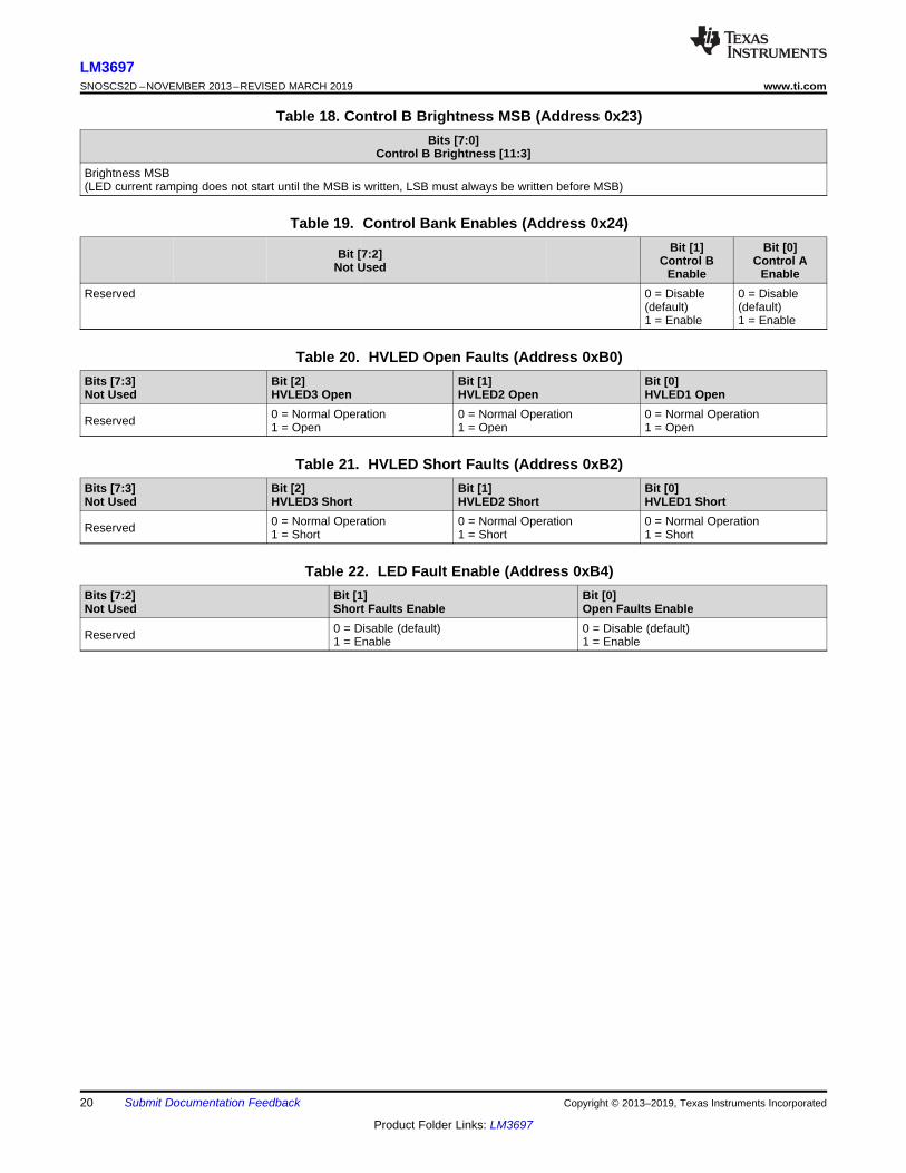
Table of Contents1 Features .................................................................. 12 Applications ........................................................... 13 Description ............................................................. 14 Revision History..................................................... 25 Pin Configuration and Functions ......................... 46 Specifications......................................................... 5
6.1 Absolute Maximum Ratings ...................................... 56.2 ESD Ratings.............................................................. 56.3 Recommended Operating Conditions....................... 56.4 Thermal Information .................................................. 56.5 Electrical Characteristics .......................................... 66.6 Timing Requirements ................................................ 76.7 Typical Characteristics .............................................. 8
7 Detailed Description .............................................. 97.1 Overview ................................................................... 97.2 Functional Block Diagram ......................................... 97.3 Feature Descriptions ............................................... 107.4 Device Functional Modes........................................ 13
7.5 Register Maps ......................................................... 178 Application and Implementation ........................ 21
8.1 Application Information............................................ 218.2 Typical Applications ................................................ 218.3 Initialization Set Up ................................................. 32
9 Power Supply Recommendations ...................... 3210 Layout................................................................... 33
10.1 Layout Guidelines ................................................. 3310.2 Layout Example .................................................... 36
11 Device and Documentation Support ................. 3711.1 Device Support...................................................... 3711.2 Related Documentation ....................................... 3711.3 Receiving Notification of Documentation Updates 3711.4 Community Resources.......................................... 3711.5 Trademarks ........................................................... 3711.6 Electrostatic Discharge Caution............................ 3711.7 Glossary ................................................................ 37
12 Mechanical, Packaging, and OrderableInformation ........................................................... 37
4 Revision HistoryNOTE: Page numbers for previous revisions may differ from page numbers in the current version.
Changes from Revision C (October 2015) to Revision D Page
• Changed Table 2 revision register POWER-ON RESET value from 0x00 to 0x01, change silicon revision value inTable 3 from 0000 to 0001 .................................................................................................................................................. 17
Changes from Revision B (April 2014) to Revision C Page
• Changed format of Device Information; add footnote and "MAX" ......................................................................................... 1• Changed Handling Ratings table to ESD Ratings table format; move storage temp to Abs Max table................................. 5• Added additional Thermal Information ................................................................................................................................... 5• Added subsection High-Speed Mode .................................................................................................................................. 16
Changes from Revision A (December 2013) to Revision B Page
• Changed to new TI datasheet standards; added Handling Ratings table; added 2 ambient temperature specs toIHVLED and one to IMATCH_HV ..................................................................................................................................................... 1
• Changed title from Pin Configurations to Terminal Functions and all references from "pins" to "terminals" ......................... 4• Changed change "terminal" back to "pin" per latest documentation standard; add "Type" column to Pin Functions
table ....................................................................................................................................................................................... 4• Changed Timing information from Elec Char table Timing Requirements ............................................................................. 7• Changed Functional Description section to Detailed Description section ............................................................................. 9• Changed Applications Information section to Application and Implementation ................................................................... 22• Changed Typical Characteristics from own section into subsection of Specifications ........................................................ 24• Added new Power Supply Recommendations section ........................................................................................................ 32• Changed Layout section to include separate Layout Example ........................................................................................... 33• Added new Device and Documentation Support section and Mechanical, Packaging and Orderable paragraph ............. 37
3
LM3697www.ti.com SNOSCS2D –NOVEMBER 2013–REVISED MARCH 2019
Product Folder Links: LM3697
Submit Documentation FeedbackCopyright © 2013–2019, Texas Instruments Incorporated
Changes from Original (November 2013) to Revision A Page
• Added graph ......................................................................................................................................................................... 11• Added Auto-Frequency Threshold Settings table................................................................................................................. 11• Added graphic....................................................................................................................................................................... 12• Added captions to graphs .................................................................................................................................................... 31

A B C D
1
2
3
Top View
D C B A
1
2
3
Bottom View
4
LM3697SNOSCS2D –NOVEMBER 2013–REVISED MARCH 2019 www.ti.com
Product Folder Links: LM3697
Submit Documentation Feedback Copyright © 2013–2019, Texas Instruments Incorporated
5 Pin Configuration and Functions
YFQ Package12-Pin DSBGA
Pin FunctionsPIN
TYPE DESCRIPTIONNUMBER NAME
A1 PWM Input PWM brightness control input for CABC operation. PWM is a high-impedance input and cannotbe left floating, if not used connect to GND.
A2 SDA I/O Serial data connection for I2C-compatible interface.
A3 HWEN Input Hardware enable input. Drive this pinl high to enable the device. Drive this pin low to force thedevice into a low power shutdown. HWEN is a high-impedance input and cannot be left floating.
B1 HVLED1 Input Input pin to high-voltage current sink 1 (40 V maximum). The boost converter regulates theminimum of HVLED1, HVLED2 and HVLED3 to VHR.
B2 SCL Input Serial clock connection for I2C-compatible interface.B3 IN Input Input voltage connection. Bypass IN to GND with a minimum 2.2-µF ceramic capacitor.
C1 HVLED2 Input Input pin to high-voltage current sink 2 (40 V maximum). The boost converter regulates theminimum of HVLED1, HVLED2 and HVLED3 to VHR.
C2 GND GND GroundC3 GND GND Ground
D1 HVLED3 Input Input pin to high-voltage current sink 3 (40 V maximum). The boost converter regulates theminimum of HVLED1, HVLED2 and HVLED3 to VHR.
D2 OVP Input Overvoltage sense input. Connect OVP to the positive terminal of the inductive boost's outputcapacitor (COUT).
D3 SW Output Drain connection for the internal NFET. Connect SW to the junction of the inductor and theSchottky diode anode.
5
LM3697www.ti.com SNOSCS2D –NOVEMBER 2013–REVISED MARCH 2019
Product Folder Links: LM3697
Submit Documentation FeedbackCopyright © 2013–2019, Texas Instruments Incorporated
(1) Stresses beyond those listed under Absolute Maximum Ratings may cause permanent damage to the device. These are stress ratingsonly, which do not imply functional operation of the device at these or any other conditions beyond those indicated under RecommendedOperating Conditions. Exposure to absolute-maximum-rated conditions for extended periods may affect device reliability.
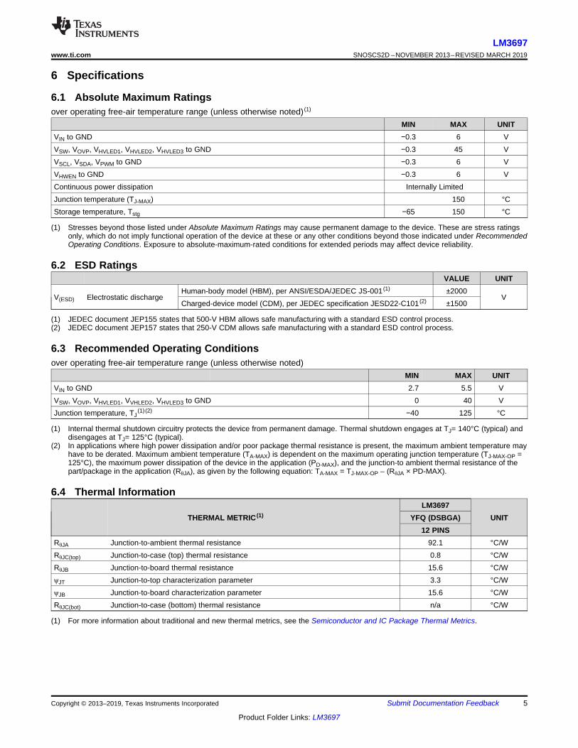
6 Specifications
6.1 Absolute Maximum Ratingsover operating free-air temperature range (unless otherwise noted) (1)
MIN MAX UNITVIN to GND −0.3 6 VVSW, VOVP, VHVLED1, VHVLED2, VHVLED3 to GND −0.3 45 VVSCL, VSDA, VPWM to GND −0.3 6 VVHWEN to GND −0.3 6 VContinuous power dissipation Internally LimitedJunction temperature (TJ-MAX) 150 °CStorage temperature, Tstg −65 150 °C
(1) JEDEC document JEP155 states that 500-V HBM allows safe manufacturing with a standard ESD control process.(2) JEDEC document JEP157 states that 250-V CDM allows safe manufacturing with a standard ESD control process.
6.2 ESD RatingsVALUE UNIT
V(ESD) Electrostatic dischargeHuman-body model (HBM), per ANSI/ESDA/JEDEC JS-001 (1) ±2000
VCharged-device model (CDM), per JEDEC specification JESD22-C101 (2) ±1500
(1) Internal thermal shutdown circuitry protects the device from permanent damage. Thermal shutdown engages at TJ= 140°C (typical) anddisengages at TJ= 125°C (typical).
(2) In applications where high power dissipation and/or poor package thermal resistance is present, the maximum ambient temperature mayhave to be derated. Maximum ambient temperature (TA-MAX) is dependent on the maximum operating junction temperature (TJ-MAX-OP =125°C), the maximum power dissipation of the device in the application (PD-MAX), and the junction-to ambient thermal resistance of thepart/package in the application (RθJA), as given by the following equation: TA-MAX = TJ-MAX-OP – (RθJA × PD-MAX).
6.3 Recommended Operating Conditionsover operating free-air temperature range (unless otherwise noted)
MIN MAX UNITVIN to GND 2.7 5.5 VVSW, VOVP, VHVLED1, VVHLED2, VHVLED3 to GND 0 40 VJunction temperature, TJ
(1) (2) −40 125 °C
(1) For more information about traditional and new thermal metrics, see the Semiconductor and IC Package Thermal Metrics.
6.4 Thermal Information
THERMAL METRIC (1)LM3697
UNITYFQ (DSBGA)12 PINS
RθJA Junction-to-ambient thermal resistance 92.1 °C/WRθJC(top) Junction-to-case (top) thermal resistance 0.8 °C/WRθJB Junction-to-board thermal resistance 15.6 °C/WψJT Junction-to-top characterization parameter 3.3 °C/WψJB Junction-to-board characterization parameter 15.6 °C/WRθJC(bot) Junction-to-case (bottom) thermal resistance n/a °C/W

6
LM3697SNOSCS2D –NOVEMBER 2013–REVISED MARCH 2019 www.ti.com
Product Folder Links: LM3697
Submit Documentation Feedback Copyright © 2013–2019, Texas Instruments Incorporated
(1) All voltages are with respect to the potential at the GND pin.(2) Minimum and Maximum limits are verified by design, test, or statistical analysis. Typical numbers are not verified, but do represent the
most likely norm. Unless otherwise specified, conditions for typical specifications are: VIN = 3.6 V and TA = 25°C.(3) LED current sink matching in the high-voltage current sinks (HVLED1 through HVLED3) is given as the maximum matching value
between any two current sinks, where the matching between any two high voltage current sinks (X and Y) is given as (IHVLEDX ( orIHVLEDY) × IAVE(X-Y))/(IAVE(X-Y)) × 100. In this test all three HVLED current sinks are assigned to Bank A.
6.5 Electrical CharacteristicsLimits apply over the full operating ambient temperature range (−40°C ≤ TA ≤ 85°C) and VIN = 3.6 V, unless otherwisespecified. (1) (2)
PARAMETER TEST CONDITIONS MIN TYP MAX UNIT
ISHDN Shutdown current2.7 V ≤ VIN ≤ 5.5 V, HWEN = GND 3
µATA = 25°C 1
ILED_MIN Minimum LED current Full-scale current = 20.2 mAExponential mapping, TA = 25°C 6 µA
TSDThermal shutdown 140
°CHysteresis 15
BOOST CONVERTER
IHVLED(1/2/3)Output current regulation(HVLED1, HVLED2, HVLED3)
Full-scale current= 20.2 mA,Exponential mapping,Brightness Code =maximum
2.7 V ≤ VIN ≤ 5.5 V 18.38 20.2 22.02 mA
Full-scale current= 20.2 mA,Exponential mapping,Brightness Code =maximumHVLED1 Bank A, HVLED2/3Bank B
TA = 25°C –3.4% ±2 % 3.2%TA = 25°C3 V ≤ VIN ≤ 4.5 V –3.6% 3.4%
TA = 25°C ±2 %
IMATCH_HVHVLED1 to HVLED2 orHVLED3 matching (3)
Exponential mapping,auto headroom off,PWM Off,HVLED1/2/3 Bank A
2.7 V ≤ VIN ≤ 5.5 VILED = 20.2 mA −2.5% 2.5%
TA = 25°CILED = 20.2 mA –2% 1.7%
2.7 V ≤ VIN ≤ 5.5 VILED = 500 µA –8.5% 8.5%
VREG_CSRegulated current sinkheadroom voltage Auto-headroom off, TA = 25°C 400 mV
VHR_MIN
Minimum current sinkheadroom voltage for HVLEDcurrent sinks
ILED = 95% of nominal, Full-scale current = 20.2 mA 275mVILED = 95% of nominal, Full-scale current =
20.2 mA , TA = 25°C 190
RDSON NMOS switch on resistance ISW = 500 mA, TA = 25°C 0.3 Ω
ICL_BOOST NMOS switch current limit880 1120
mATA = 25°C 1000
VOVP Output overvoltage protectionON ThresholdOVP select bits = 11
2.7 V ≤ VIN ≤ 5.5 V 38.75 41.1VTA = 25°C 40
Hysteresis TA = 25°C 1
ƒSW Switching frequency
Boost frequency select bit =0
2.7 V ≤ VIN ≤ 5.5 V 450 550
kHzTA = 25°C 500
Boost frequency select bit =1
2.7 V ≤ VIN ≤ 5.5 V 900 1100TA = 25°C 1000
DMAX Maximum duty cycle TA = 25°C 94%HWEN INPUTVHWEN_L Logic low 2.7 V ≤ VIN ≤ 5.5 V 0 0.4
VVHWEN_H Logic high 2.7 V ≤ VIN ≤ 5.5 V 1.2 VIN

t4
t2
t3
t5
t1
SCL
SDA_IN
SDA_OUT
7
LM3697www.ti.com SNOSCS2D –NOVEMBER 2013–REVISED MARCH 2019
Product Folder Links: LM3697
Submit Documentation FeedbackCopyright © 2013–2019, Texas Instruments Incorporated
Electrical Characteristics (continued)Limits apply over the full operating ambient temperature range (−40°C ≤ TA ≤ 85°C) and VIN = 3.6 V, unless otherwisespecified.(1)(2)
PARAMETER TEST CONDITIONS MIN TYP MAX UNITPWM INPUTVPWM_L Input logic low 2.7 V ≤ VIN ≤ 5.5 V 0 0.4
VVPWM_H Input logic high 2.7V ≤ VIN ≤ 5.5 V 1.31 VIN
tPWM Minimum PWM input pulse 2.7 V ≤ VIN ≤ 5.5 V, PWM zero detect enabled 0.75 µsI2C-COMPATIBLE VOLTAGE SPECIFICATIONS (SCL, SDA)VIL Input logic low 2.7 V ≤ VIN ≤ 5.5 V 0 0.4
VVIH Input logic high 2.7 V ≤ VIN ≤ 5.5 V 1.29 VIN
VOL Output logic low (SDA) 2.7 V ≤ VIN ≤ 5.5 V, ILOAD = 3 mA 400 mV
(1) SCL and SDA must be glitch-free in order for proper brightness control to be realized.
6.6 Timing RequirementsMIN NOM MAX UNIT
I2C-COMPATIBLE TIMING SPECIFICATIONS (SCL, SDA) (1)
t1 SCL (clock period) 2.7 V ≤ VIN ≤ 5.5 V 2.5 µst2 Data In set-up time to SCL high 2.7 V ≤ VIN ≤ 5.5 V 100 nst3 Data out stable after SCL low 2.7 V ≤ VIN ≤ 5.5 V 0 nst4 SDA low set-up time to SCL low (start) 2.7 V ≤ VIN ≤ 5.5 V 100 nst5 SDA high hold time after SCL high (stop) 2.7 V ≤ VIN ≤ 5.5 V 100 nsINTERNAL POR THRESHOLD AND HWEN TIMING SPECIFICATION
VPOR POR reset release voltage thresholdVIN ramp time = 100 µs 1.7 2.1
VVIN ramp time = 100 µs, TA =25°C 1.9
tHWEN First I2C start pulse after HWEN high
2.7 V ≤ VIN ≤ 5.5 V, PORreset complete 20
µsPOR reset complete, TA =25°C 5.0
Figure 1. I2C-Compatible Interface Timing

0
0.2
0.4
0.6
0.8
1
1.2
1.4
-50 -25 0 25 50 75 100 125
PW
M V
IH (
V)
Temperature (C)
VIN=5.5VIN=3.6VIN=2.7
C025
0
0.2
0.4
0.6
0.8
1
1.2
1.4
-50 -25 0 25 50 75 100 125
PW
M V
IL (
V)
Temperature (C)
VIN=5.5VIN=3.6VIN=2.7
C026
0
50
100
150
200
250
300
-50 -25 0 25 50 75 100 125
HE
AD
RO
OM
VO
LTA
GE
(m
V)
Temperature (C)
VIN=2.7VIN=3.6VIN=5.5
C027
0
0.5
1
1.5
2
-50 -25 0 25 50 75 100 125
PO
R T
hres
hold
(V
)
Temperature (C) C023
0.2
0.25
0.3
0.35
0.4
0.45
0.5
-50 -25 0 25 50 75 100 125
Rds
on (
Ohm
s)
Temperature (C)
VIN=2.7VIN=3.6VIN=5.5
C022
0
0.5
1
1.5
2
2.5
-50 -25 0 25 50 75 100 125
IQ S
hutd
own
(uA
)
Temperature (C)
VIN=5.5VIN=3.6VIN=2.7
C024
8
LM3697SNOSCS2D –NOVEMBER 2013–REVISED MARCH 2019 www.ti.com
Product Folder Links: LM3697
Submit Documentation Feedback Copyright © 2013–2019, Texas Instruments Incorporated
6.7 Typical Characteristics
Figure 2. RDSON vs Temperature Figure 3. IQ Shutdown vs Temperature
Figure 4. VHR_MIN vs Temperature Figure 5. POR Threshold vs Temperature
Figure 6. PWM VIH vs Temperature Figure 7. PWM VIL vs Temperature

Hardware Enable,Reference, and
Thermal Shutdown
Selectable 500-kHz/1-MHz
Switching Frequency
IN
SDA
SCL
I2C Compatible Interface
Selectable Overvoltage Protection
(16V, 24V, 32V, 40V)
LED String Open/Short Detection
1-A Current Limit
PWMInternal Low-Pass
Filter Backlight LED Control1. 5-bit Full Scale Current Select
2. 11-bit brightness adjustment
3. Linear/Exponential Dimming
4. LED Current Ramping
OVP
SW
Boost Converter
HWEN
High-Voltage Current Sinks
HVLED1
HVLED2
HVLED3
GND
9
LM3697www.ti.com SNOSCS2D –NOVEMBER 2013–REVISED MARCH 2019
Product Folder Links: LM3697
Submit Documentation FeedbackCopyright © 2013–2019, Texas Instruments Incorporated
7 Detailed Description
7.1 OverviewThe LM3697 provides the power for three high-voltage LED strings. The three high-voltage LED strings arepowered from an integrated boost converter. The device is configured over an I2C-compatible interface. TheLM3697 provides a Pulse Width Modulation (PWM) input for content adjustable brightness control.
7.1.1 PWM InputThe PWM input can be assigned to either of the high-voltage control banks. When assigned to a control bank,the programmed current in the control bank becomes a function of the duty cycle (DPWM) at the PWM input andthe control bank brightness setting. When PWM is disabled, DPWM is equal to one.
7.1.2 HWEN InputHWEN is the global hardware enable to the LM3697. HWEN must be pulled high to enable the device. HWEN isa high-impedance input so it cannot be left floating. When HWEN is pulled low the LM3697 is placed inshutdown, and all the registers are reset to their default state.
7.1.3 Thermal ShutdownThe LM3697 contains a thermal shutdown protection. In the event the die temperature reaches 140°C (typical),the boost and current sink outputs shut down until the die temperature drops to typically 125°C (typical).
7.2 Functional Block Diagram

10
LM3697SNOSCS2D –NOVEMBER 2013–REVISED MARCH 2019 www.ti.com
Product Folder Links: LM3697
Submit Documentation Feedback Copyright © 2013–2019, Texas Instruments Incorporated
7.3 Feature Descriptions
7.3.1 High-Voltage LED Control
7.3.1.1 High-Voltage Boost ConverterThe high-voltage boost converter provides power for the three high-voltage current sinks (HVLED1, HVLED2,and HVLED3). The boost circuit operates using a 4.7-µH to 22-µH inductor and a 1-µF output capacitor. Theselectable 500-kHz or 1-MHz switching frequency allows for use of small external components and provides forhigh boost-converter efficiency. HVLED1, HVLED2, and HVLED3 feature an adaptive current regulation schemewhere the feedback point (HVLED1, HVLED2, and HVLED3) regulates the LED headroom voltage VHR_MIN.When there are different voltage requirements in the high-voltage LED strings (string mismatch), the LM3697regulates the feedback point of the highest voltage string to VHR_MIN and drop the excess voltage of the lowervoltage string across the lower strings current sink.
7.3.1.2 High-Voltage Current Sinks (HVLED1, HVLED2 and HVLED3)HVLED1, HVLED2, and HVLED3 control the current in the high-voltage LED strings as configured by ControlBank A or B. Each Control Bank has 5-bit full-scale current programmability and 11-bit brightness control.Assignment of the high-voltage current sinks to control bank is done through the HVLED Current Sink OutputConfiguration register (see Table 5).
7.3.1.3 High-Voltage Current String BiasingEach high-voltage current string can be powered from the LM3697’s boost output (COUT) or from an externalsource. The feedback enable bits (HVLED Current Sink Feedback Enables register bits [2:0]) determine wherethe high-voltage current string anodes connect. When set to '1' (default) the high-voltage current sink inputs areincluded in the boost feedback loop. This allows the boost converter to adjust its output voltage in order tomaintain the LED headroom voltage VHR_MIN at the current sink input.
When powered from alternate sources the feedback enable bits must be set to '0'. This removes the particularcurrent sink from the boost feedback loop. In these configurations the application must ensure that the headroomvoltage across the high-voltage current sink is high enough to prevent the current sink from going into dropout(see the Typical Characteristics for data on the high-voltage LED current vs VHR_MIN).
Setting the HVLED Current Sink Feedback Enables register bits also determines triggering of the shorted high-voltage LED String Fault flag (see the Fault Flags/Protection Features section).
7.3.2 Boost Switching-Frequency SelectThe LM3697’s boost converter has two switching frequency settings. The switching frequency setting iscontrolled via the Boost Frequency Select bit (bit 0 in the Boost Control register). Operating at the 500-kHzswitching frequency results in better efficiency under lighter load conditions due to the decreased switchinglosses. In this mode the inductor must be between 10 µH and 22 µH. Operating at the 1-MHz switchingfrequency results in better efficiency under higher load conditions resulting in lower conduction losses in theMOSFETs and inductor. In this mode the inductor can be between 4.7 µH and 22 µH.
7.3.3 Automatic Switching Frequency ShiftThe LM3697 has an automatic frequency select mode (bit 3 in the Boost Control register) to optimize thefrequency vs load dependent losses. In Auto-Frequency mode the boost converter switching frequency ischanged based on the high-voltage LED current. The threshold (Control A/B brightness code) at which thefrequency switchover occurs is configurable via the Auto-Frequency Threshold register. The Auto-FrequencyThreshold register contains an 8-bit code which is compared to the 8 MSB's of the brightness code. When thebrightness code is greater than the Auto-Frequency Threshold value the boost converter switching frequency is 1MHz. When the brightness code is less than or equal to the Auto-Frequency Threshold register the boostconverter switching frequency is 500 kHz.
Figure 8 illustrates the LED efficiency improvement (3p5s LED configuration with a 4.7-µH inductor) when theAuto-Frequency feature is enabled. When the LED brightness is less than or equal to 0x6C, the switchingfrequency is 500 kHz, and it improves the LED efficiency by up to 6%. When the LED brightness is greater than0x6C, the switching frequency is 1 MHz, and it improves LED efficiency by up to 2.2%.

-6.0%
-5.0%
-4.0%
-3.0%
-2.0%
-1.0%
0.0%
1.0%
2.0%
3.0%
0 256
512
768
1024
1280
1536
1792
2048¨()),&,(1&<
BRIGHTNESS CODE
1Mhz Eff - 500Khz Eff, 4.7uH, Three String (Negative values when 500Khz more efficient)
C002
1Mhz LED Eff > 500Khz LED Eff
500Khz LED Eff > 1Mhz LED Eff
Auto-Frequency Threshold = 0x6C
11
LM3697www.ti.com SNOSCS2D –NOVEMBER 2013–REVISED MARCH 2019
Product Folder Links: LM3697
Submit Documentation FeedbackCopyright © 2013–2019, Texas Instruments Incorporated
Feature Descriptions (continued)
Figure 8. Auto-Frequency Boost Efficiency Improvement Illustration
Table 1 summarizes the general recommendations for Auto-Frequency Threshold setting vs Inductance valuesand LED string configurations. These are general recommendations — the optimum Auto-Frequency Thresholdsetting must be evaluated for each application.
Table 1. Auto-Frequency Threshold SettingsTHREE STRING TWO STRING
INDUCTOR AUTO-FREQUENCYTHRESHOLD
PEAK EFFICIENCYIMPROVEMENT
PEAKCONFIGURATION
AUTO-FREQUENCYTHRESHOLD
PEAK EFFICIENCYIMPROVEMENT
PEAKCONFIGURATION
4.7 µH 6C 2.2% 3p5s AC 1.1% 2p6s
10 µH 74 1.7% 3p4s B4 1.3% 2p5s
22 µH 7C 0.7% 3p3s BC 0.7% 2p4s
7.3.4 Brightness Register Current ControlThe LM3697 features Brightness Register Current Control for simple user-adjustable current control set bywriting directly to the appropriate Control Bank Brightness Registers. The current for Control Banks A and B is afunction of the full-scale LED current, the 11-bit code in the respective brightness register, and the PWM inputduty cycle (if PWM is enabled). The Control A/B brightness must always be written with LSB's first and MSB'slast.
7.3.4.1 8-Bit Control (Preferred)The preferred operating mode is to control the high-voltage LED brightness by setting the Control Bank LSBregister (3 LSB's) to zero and using only the Control Bank MSB register (8 MSB's). In this mode the LM3697controls the 3 LSB's to ramp the high-voltage LED current using all 11-bits.
7.3.4.2 11-Bit ControlIn this mode of operation, both Control Bank LSB and MSB registers must be written whenever a change inBrightness is required. The high-voltage LED current will not change until the Control Bank MSB register iswritten. If the brightness change affects only the 3 LSB's, the Control Bank MSB register (8 MSB's) must be re-written to change the high-voltage LED current.
7.3.5 PWM ControlThe LM3697's PWM input can be enabled for Control Banks A or B (see Table 14). Once enabled, the LEDcurrent becomes a function of the code in the Control Bank Brightness Configuration Register and the PWMinput-duty cycle.

To AssignedHigh Voltage Current Sinks
PWM Input LPF
Backlight Digital LED Control Block
Full-Scale Current Select
Brightness SettingExponential or Linear Mapping
Startup/Shutdown Ramp GeneratorRuntime Ramp Generator
Analog Domain
Digital Domain
DAC
Full-Scale CurrentControl
polarity
12
LM3697SNOSCS2D –NOVEMBER 2013–REVISED MARCH 2019 www.ti.com
Product Folder Links: LM3697
Submit Documentation Feedback Copyright © 2013–2019, Texas Instruments Incorporated
The PWM input accepts a logic level voltage and internally filters it to an analog control voltage. This results in alinear response of duty cycle to current, where 100% duty cycle corresponds to the programmed brightness codemultiplied by the Full-Scale Current setting.
Figure 9. PWM Input Architecture
7.3.5.1 PWM Input Frequency RangeThe usable input frequency range for the PWM input is governed on the low end by the cutoff frequency of theinternal low-pass filter (540 Hz, Q = 0.33) and on the high end by the propagation delays through the internallogic. For frequencies below 2 kHz the current ripple begins to become a larger portion of the DC LED current.Additionally, at lower PWM frequencies the boost output voltage ripple increases, causing a non-linear responsefrom the PWM duty cycle to the average LED current due to the response time of the boost. For the bestresponse of current vs. duty cycle, the PWM input frequency must be kept between 2 kHz and 100 kHz.
7.3.5.2 PWM Input PolarityThe PWM Input can be set for active low polarity, where the LED current is a function of the negative duty cycle.This is set via the PWM Configuration register (see Table 14).
7.3.5.3 PWM Zero DetectionThe LM3697 incorporates a feature to detect when the PWM input is near zero. After the near zero pulse widthhas been detected the PWM pulse must be greater than tPWM to affect the HVLED output current (see ElectricalCharacteristics ). Bit 3 in the PWM Configuration register is used to disable this feature.
7.3.6 Start-up/Shutdown RampThe high-voltage LED start-up and shutdown ramp times are independently configurable in the start-up/shutdowntransition time Register (see Table 6). There are 16 different start-up and 16 different shutdown times. The start-up times can be programmed independently from the shutdown times, but each Control bank is notindependently configurable.
The start-up ramp time is from when the Control Bank is enabled to when the LED current reaches its initial setpoint. The shutdown ramp time is from when the Control Bank is disabled to when the LED current reaches 0.
7.3.7 Run-Time RampCurrent ramping from one brightness level to the next is programmed via the Control A and B Run-Time RampTime Register (see Table 7). There are 16 different ramp-up times and 16 different ramp-down times. The ramp-up time can be programmed independently from the ramp-down time, but each Control Bank cannot beindependently programmed. For example, programming a ramp-up or ramp-down time is a global setting for allhigh-voltage LED Control Banks.
ILED = ILED_FULLSCALE x 12047 x Code x DPWM
ILED = ILED_FULLSCALE x 1255 x Code x DPWM
(44 - )ILED = ILED_FULLSCALE x 0.85
Code
5.8181818 x DPWM
+ 18
(44 - )ILED = ILED_FULLSCALE x 0.85
Code + 15.8181818 x DPWM
13
LM3697www.ti.com SNOSCS2D –NOVEMBER 2013–REVISED MARCH 2019
Product Folder Links: LM3697
Submit Documentation FeedbackCopyright © 2013–2019, Texas Instruments Incorporated
7.3.8 High-Voltage Control A and B Ramp SelectThe LM3697 provides three options for Control A and B ramp times (see Table 8). When the Run-time RampSelect bits are set to 00, the control bank uses both the Start-up/Shutdown and Run-time ramp times. When theRun-time Ramp Select bits are set to 01, the control bank uses the Start-up/Shutdown ramp times for both start-up/shutdown and run-time. When the Run-time Ramp Select bits are set to 1x the control bank uses a zero µsecrun-time ramp.
7.4 Device Functional Modes
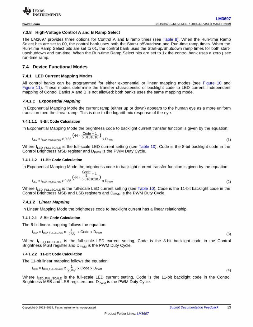
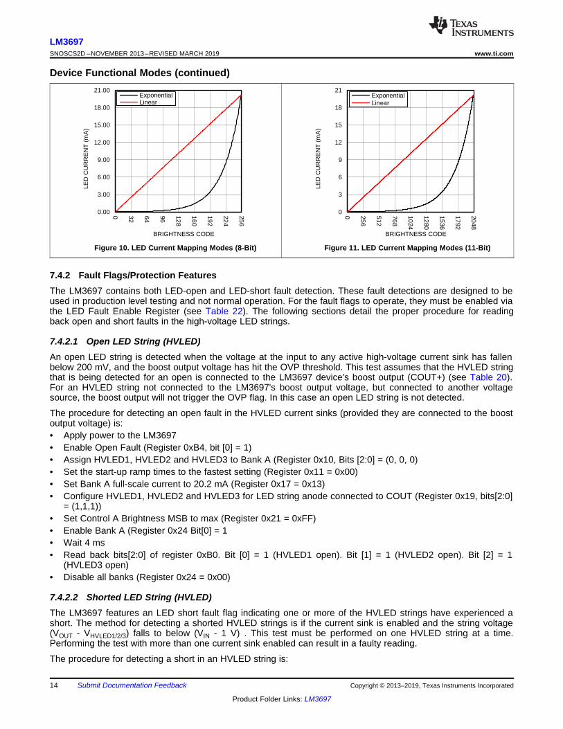
7.4.1 LED Current Mapping ModesAll control banks can be programmed for either exponential or linear mapping modes (see Figure 10 andFigure 11). These modes determine the transfer characteristic of backlight code to LED current. Independentmapping of Control Banks A and B is not allowed: both banks uses the same mapping mode.
7.4.1.1 Exponential MappingIn Exponential Mapping Mode the current ramp (either up or down) appears to the human eye as a more uniformtransition then the linear ramp. This is due to the logarithmic response of the eye.
7.4.1.1.1 8-Bit Code Calculation
In Exponential Mapping Mode the brightness code to backlight current transfer function is given by the equation:
(1)
Where ILED_FULLSCALE is the full-scale LED current setting (see Table 10), Code is the 8-bit backlight code in theControl Brightness MSB register and DPWM is the PWM Duty Cycle.
7.4.1.1.2 11-Bit Code Calculation
In Exponential Mapping Mode the brightness code to backlight current transfer function is given by the equation:
(2)
Where ILED_FULLSCALE is the full-scale LED current setting (see Table 10), Code is the 11-bit backlight code in theControl Brightness MSB and LSB registers and DPWM is the PWM Duty Cycle.
7.4.1.2 Linear MappingIn Linear Mapping Mode the brightness code to backlight current has a linear relationship.
7.4.1.2.1 8-Bit Code Calculation
The 8-bit linear mapping follows the equation:
(3)
Where ILED_FULLSCALE is the full-scale LED current setting, Code is the 8-bit backlight code in the ControlBrightness MSB register and DPWM is the PWM Duty Cycle.
7.4.1.2.2 11-Bit Code Calculation
The 11-bit linear mapping follows the equation:
(4)
Where ILED_FULLSCALE is the full-scale LED current setting, Code is the 11-bit backlight code in the ControlBrightness MSB and LSB registers and DPWM is the PWM Duty Cycle.
0.00
3.00
6.00
9.00
12.00
15.00
18.00
21.00
0 32 64 96 128
160
192
224
256
LED
CU
RR
EN
T (
mA
)
BRIGHTNESS CODE
ExponentialLinear
C001
0
3
6
9
12
15
18
21
0 256
512
768
1024
1280
1536
1792
2048
LED
CU
RR
EN
T (
mA
)
BRIGHTNESS CODE
ExponentialLinear
C001
14
LM3697SNOSCS2D –NOVEMBER 2013–REVISED MARCH 2019 www.ti.com
Product Folder Links: LM3697
Submit Documentation Feedback Copyright © 2013–2019, Texas Instruments Incorporated
Device Functional Modes (continued)
Figure 10. LED Current Mapping Modes (8-Bit) Figure 11. LED Current Mapping Modes (11-Bit)
7.4.2 Fault Flags/Protection FeaturesThe LM3697 contains both LED-open and LED-short fault detection. These fault detections are designed to beused in production level testing and not normal operation. For the fault flags to operate, they must be enabled viathe LED Fault Enable Register (see Table 22). The following sections detail the proper procedure for readingback open and short faults in the high-voltage LED strings.
7.4.2.1 Open LED String (HVLED)An open LED string is detected when the voltage at the input to any active high-voltage current sink has fallenbelow 200 mV, and the boost output voltage has hit the OVP threshold. This test assumes that the HVLED stringthat is being detected for an open is connected to the LM3697 device's boost output (COUT+) (see Table 20).For an HVLED string not connected to the LM3697's boost output voltage, but connected to another voltagesource, the boost output will not trigger the OVP flag. In this case an open LED string is not detected.
The procedure for detecting an open fault in the HVLED current sinks (provided they are connected to the boostoutput voltage) is:• Apply power to the LM3697• Enable Open Fault (Register 0xB4, bit [0] = 1)• Assign HVLED1, HVLED2 and HVLED3 to Bank A (Register 0x10, Bits [2:0] = (0, 0, 0)• Set the start-up ramp times to the fastest setting (Register 0x11 = 0x00)• Set Bank A full-scale current to 20.2 mA (Register 0x17 = 0x13)• Configure HVLED1, HVLED2 and HVLED3 for LED string anode connected to COUT (Register 0x19, bits[2:0]
= (1,1,1))• Set Control A Brightness MSB to max (Register 0x21 = 0xFF)• Enable Bank A (Register 0x24 Bit[0] = 1• Wait 4 ms• Read back bits[2:0] of register 0xB0. Bit [0] = 1 (HVLED1 open). Bit [1] = 1 (HVLED2 open). Bit [2] = 1
(HVLED3 open)• Disable all banks (Register 0x24 = 0x00)
7.4.2.2 Shorted LED String (HVLED)The LM3697 features an LED short fault flag indicating one or more of the HVLED strings have experienced ashort. The method for detecting a shorted HVLED strings is if the current sink is enabled and the string voltage(VOUT - VHVLED1/2/3) falls to below (VIN - 1 V) . This test must be performed on one HVLED string at a time.Performing the test with more than one current sink enabled can result in a faulty reading.
The procedure for detecting a short in an HVLED string is:
15
LM3697www.ti.com SNOSCS2D –NOVEMBER 2013–REVISED MARCH 2019
Product Folder Links: LM3697
Submit Documentation FeedbackCopyright © 2013–2019, Texas Instruments Incorporated
Device Functional Modes (continued)• Apply power to the LM3697• Enable Short Fault (Register 0xB4, bit [1] = 1)• Assign HVLED1 to Bank A (Register 0x10, Bits [2:0] = (1, 1, 0)• Set the startup ramp times to the fastest setting (Register 0x11 = 0x00)• Set Bank A full-scale current to 20.2 mA (Register 0x17 = 0x13)• Enable Feedback on the HVLED Current Sinks (Register 0x19, bits[2:0] = (1,1,1))• Set Control A Brightness MSB to max (Register 0x21 = 0xFF)• Enable Bank A (Register 0x24 Bit[0] = 1)• Wait 4 ms• Read back bits[0] of register 0xB2. 1 = HVLED1 short.• Disable all banks (Register 0x24 = 0x00)• Repeat the procedure for the HVLED2 and HVLED3 strings
7.4.2.3 Overvoltage Protection (Inductive Boost)The overvoltage protection threshold (OVP) on the LM3697 has 4 different configurable options (16 V, 24 V, 32V, and 40 V). The OVP protects the device and associated circuitry from high voltages in the event the high-voltage LED string becomes open. During normal operation, the LM3697 device’s inductive boost converterboosts the output up so as to maintain VHR at the active, high-voltage (COUT connected) current sink inputs.When a high-voltage LED string becomes open, the feedback mechanism is broken, and the boost converterover-boosts the output. When the output voltage reaches the OVP threshold the boost converter stops switching,thus allowing the output node to discharge. When the output discharges to VOVP minus 1 V the boost converterbegins switching again. The OVP sense is at the OVP pin, so this pin must be connected directly to the inductiveboost output capacitor’s positive terminal.
For high-voltage current sinks that have the HVLED Current Sink Feedback Enable setting such that the high-voltage current sinks anodes are not connected to COUT (feedback is disabled), the overvoltage sensemechanism is not in place to protect the input to the high-voltage current sink. In this situation the applicationmust ensure that the voltage at HVLED1, HVLED2 or HVLED3 doesn’t exceed 40 V.
The default setting for OVP is set at 16 V. For applications that require higher than 16 V at the boost output, theOVP threshold must be programmed to a higher level after power up.
7.4.2.4 Current Limit (Inductive Boost)The NMOS switch current limit for the LM3697 device’s inductive boost is set at 1 A (typical). When the currentthrough the LM3697’s NFET switch hits this overcurrent protection threshold (OCP), the device turns the NFEToff, and the inductor’s energy is discharged into the output capacitor. Switching is then resumed at the nextcycle. The current limit protection circuitry can operate continuously each switching cycle. The result is thatduring high-output power conditions the device can continuously run in current limit. Under these conditions theLM3697’s inductive boost converter stops regulating the headroom voltage across the high-voltage current sinks.This results in a drop in the LED current.
7.4.3 I2C-Compatible Interface
7.4.3.1 Start And Stop ConditionsThe LM3697 is controlled via an I2C-compatible interface. START and STOP conditions classify the beginningand the end of the I2C session. A START condition is defined as SDA transitioning from HIGH to LOW while SCLis HIGH. A STOP condition is defined as SDA transitioning from LOW to HIGH while SCL is HIGH. The I2Cmaster always generates START and STOP conditions. The I2C bus is considered busy after a START conditionand free after a STOP condition. During data transmission the I2C master can generate repeated STARTconditions. A START and a repeated START condition are equivalent function-wise. The data on SDA must bestable during the HIGH period of the clock signal (SCL). In other words, the state of SDA can only be changedwhen SCL is LOW.
SDA
Start Condition Stop Condition
SCLS P
16
LM3697SNOSCS2D –NOVEMBER 2013–REVISED MARCH 2019 www.ti.com
Product Folder Links: LM3697
Submit Documentation Feedback Copyright © 2013–2019, Texas Instruments Incorporated
Device Functional Modes (continued)
Figure 12. Start And Stop Sequences
7.4.3.2 I2C-Compatible AddressThe chip address for the LM3697 is 0110110 (36h). After the START condition, the I2C master sends the 7-bitchip address followed by an eighth read or write bit (R/W). R/W= 0 indicates a WRITE and R/W = 1 indicates aREAD. The second byte following the chip address selects the register address to which the data is written. Thethird byte contains the data for the selected register.
7.4.3.3 Transferring DataEvery byte on the SDA line must be eight bits long, with the most significant bit (MSB) transferred first. Each byteof data must be followed by an acknowledge bit (ACK). The acknowledge related clock pulse (9th clock pulse) isgenerated by the master. The master releases SDA (HIGH) during the 9th clock pulse. The LM3697 pulls downSDA during the 9th clock pulse signifying an acknowledge. An acknowledge is generated after each byte hasbeen received.
Table 2 lists the available registers within the LM3697.
7.4.3.4 High-Speed ModeThe LM3697 supports only Standard and Fast mode I2C operation. High Speed mode is not supported. If theLM3697 is connected to a I2C-bus with a HS-mode device a dummy I2C cycle is required after the HS-modecommand is complete. The dummy cycle can be a read or write to any I2C slave address.

17
LM3697www.ti.com SNOSCS2D –NOVEMBER 2013–REVISED MARCH 2019
Product Folder Links: LM3697
Submit Documentation FeedbackCopyright © 2013–2019, Texas Instruments Incorporated
(1) The PWM inputmust always be in the inactive state when setting the Control bank PWM Enable bit. The PWM configuration bits mustonly be changed when the PWM is disabled for both Control Banks.
(2) The Control Brightness MSB Register must be written for the Control Brightness LSB Register value to take effect.
7.5 Register Maps
Table 2. LM3697 Register DescriptionsNAME ADDRESS POWER-ON RESET OPERATION
Revision 0x00 0x01 DynamicSoftware Reset 0x01 0x00 DynamicHVLED Current Sink Output Configuration 0x10 0x06 StaticControl A Start-up/Shutdown Ramp Time 0x11 0x00 StaticControl B Start-up/Shutdown Ramp Time 0x12 0x00 StaticControl A/B Run time Ramp Time 0x13 0x00 StaticControl A/B Run time Ramp Configuration 0x14 0x00 StaticReserved 0x15 0x33 StaticBrightness Configuration 0x16 0x00 StaticControl A Full-Scale Current Setting 0x17 0x13 StaticControl B Full-Scale Current Setting 0x18 0x13 StaticHVLED Current Sink Feedback Enables 0x19 0x07 StaticBoost Control 0x1A 0x00 StaticAuto-Frequency Threshold 0x1B 0xCF StaticPWM Configuration 0x1C 0x0C Dynamic (1)
Control A Brightness LSB 0x20 0x00 Dynamic (2)
Control A Brightness MSB 0x21 0x00 DynamicControl B Brightness LSB 0x22 0x00 Dynamic (2)
Control B Brightness MSB 0x23 0x00 DynamicControl Bank Enables 0x24 0x00 DynamicHVLED Open Faults 0xB0 0x00 Production Test OnlyHVLED Short Faults 0xB2 0x00 Production Test OnlyLED Fault Enables 0xB4 0x00 Production Test Only
Table 3. Revision (Address 0x00)Bits [7:4]Not Used
Bits [3:0]Silicon Revision
Reserved 0001 = Rev. A2 Silicon
Table 4. Software Reset (Address 0x01)Bits [7:1]Not Used
Bit [0]Silicon Revision
Reserved 0 = Normal Operation1 = Software Reset (self-clearing)
Table 5. HVLED Current Sink Output Configuration (Address 0x10)Bits [7:3]Not Used
Bit [2]HVLED3 Configuration
Bit [1]HVLED2 Configuration
Bit [0]HVLED1 Configuration
Reserved 0 = Control A1 = Control B (default)
0 = Control A1 = Control B (default)
0 = Control A (default)1 = Control B

18
LM3697SNOSCS2D –NOVEMBER 2013–REVISED MARCH 2019 www.ti.com
Product Folder Links: LM3697
Submit Documentation Feedback Copyright © 2013–2019, Texas Instruments Incorporated
Table 6. Control A and B Start-up/Shutdown Ramp Time (Address 0x11 and 0x12)Bits [7:4]
Start-up RampBits [3:0]
Shutdown Ramp0000 = 2048 µs (default)0001 = 262 ms0010 = 524 ms0011 = 1.049 s0100 = 2.09 s0101 = 4.194 s0110 = 8.389 s0111 = 16.78 s1000 = 33.55 s1001 = 41.94 s1010 = 50.33 s1011 = 58.72 s1100 = 67.11 s1101 = 83.88 s1110 = 100.66 s1111 = 117.44 s
0000 = 2048 µs (default)0001 = 262 ms0010 = 524 ms0011 = 1.049 s0100 = 2.097 s0101 = 4.194 s0110 = 8.389 s0111 = 16.78 s1000 = 33.55 s1001 = 41.94 s1010 = 50.33 s1011 = 58.72 s1100 = 67.11 s1101 = 83.88 s1110 = 100.66 s1111 = 117.44 s
Table 7. Control A and B Run-Time Ramp Time (Address 0x13)Bits [7:4]
Transition Time Ramp UpBits [3:0]
Transition Time Ramp Down000 = 2048 µs (default)001 = 262 ms010 = 524 ms011 = 1.049 s100 = 2.097 s101 = 4.194 s110 = 8.389 s111 = 16.78 s1000 = 33.55 s1001 = 41.94 s1010 = 50.33 s1011 = 58.72 s1100 = 67.11 s1101 = 83.88 s1110 = 100.66 s1111 = 117.44 s
000 = 2048 µs (default)001 = 262 ms010 = 524 ms011 = 1.049 s100 = 2.097 s101 = 4.194 s110 = 8.389 s111 = 16.78 s1000 = 33.55 s1001 = 41.94 s1010 = 50.33 s1011 = 58.72 s1100 = 67.11 s1101 = 83.88 s1110 = 100.66 s1111 = 117.44 s
Table 8. Control A and B Run-Time Ramp Configuration (Address 0x14)Bits [7:4]Not Used
Bits [3:2]Control B Run-time Ramp Select
Bits [1:0]Control A Run-time Ramp Select
Reserved
00 = Control A/B Runtime Ramp Times(default)01 = Control B Start-up/Shutdown RampTimes1x = 0 µs Ramp Time
00 = Control A/B Runtime Ramp Times(default)01 = Control A Start-up/Shutdown RampTimes1x = 0 µs Ramp Time
Table 9. Control A and B Brightness Configuration (Address 0x16)Bits [7:4]Not Used
Bit [3]Control B Dither Disable
Bit [2]Control A Dither Disable
Bit [1]Not Used
Bit [0]Control A/B Mapping
Mode
Reserved 0 Enable (default)1 Disable
0 Enable (default)1 Disable Reserved
0 Exponential (default)1 Linear

19
LM3697www.ti.com SNOSCS2D –NOVEMBER 2013–REVISED MARCH 2019
Product Folder Links: LM3697
Submit Documentation FeedbackCopyright © 2013–2019, Texas Instruments Incorporated
Table 10. Control A and B Full-Scale Current Setting (Address 0x17 and 0x18)Bits [7:5]Not Used
Bits [4:0]Control A, B Full-Scale Current Select Bits
Reserved 00000 = 5 mA10011 = 20.2 mA (default)11111 = 29.8 mA(0.8 mA steps, FS = 5 + code * 0.8 mA)
Table 11. HVLED Current Sink Feedback Enables (Address 0x19)Bits [7:3]Not Used
Bit [2]HVLED3 Feedback Enable
Bit [1]HVLED2 Feedback Enable
Bit [0]HVLED1 Feedback Enable
Reserved
0 = LED anode is NOT CONNECTEDto COUT1 = LED anode is CONNECTED toCOUT (default)
0 = LED anode is NOT CONNECTEDto COUT1 = LED anode is CONNECTED toCOUT (default)
0 = LED anode is NOT CONNECTEDto COUT1 = LED anode is CONNECTED toCOUT (default)
Table 12. Boost Control (Address 0x1A)Bits [7:5]Not Used
Bit [4]Auto-Headroom Enable
Bit [3]Auto-Frequency Enable
Bits [2:1]Boost OVP Select
Bit [0]Boost Frequency Select
Reserved 0 = Disable (default)1 = Enable
0 = Disable (default)1 = Enable
00 = 16 V (default)01 = 24 V10 = 32 V11 = 40 V
0 = 500 kHz (default)1 = 1 MHz
Table 13. Auto-Frequency Threshold (Address 0x1B)Bits [7:0]
Auto-Frequency Threshold (default = 11001111)
Table 14. PWM Configuration (Address 0x1C)
Bits [7:4]Not Used
Bit [3]PWM Zero Detection
EnableBit [2]
PWM PolarityBit [1]
Control B PWM EnableBit [0]
Control A PWM Enable
Reserved 0 = Disable1 = Enable (default)
0 = Active Low1 = Active High (default)
0 = Disable (default)1 = Enable
0 = Disable (default)1 = Enable
Table 15. Control A Brightness LSB (Address 0x20)Bits [7:3]Not Used
Bits [2:0]Control A Brightness [2:0]
Reserved Brightness LSB
Table 16. Control A Brightness MSB (Address 0x21)Bits [7:0]
Control A Brightness [11:3]Brightness MSB(LED current ramping does not start until the MSB is written, LSB must always be written before MSB)
Table 17. Control B Brightness LSB (Address 0x22)Bits [7:3]Not Used
Bits [2:0]Control B Brightness [2:0]
Reserved Brightness LSB
20
LM3697SNOSCS2D –NOVEMBER 2013–REVISED MARCH 2019 www.ti.com
Product Folder Links: LM3697
Submit Documentation Feedback Copyright © 2013–2019, Texas Instruments Incorporated
Table 18. Control B Brightness MSB (Address 0x23)Bits [7:0]
Control B Brightness [11:3]Brightness MSB(LED current ramping does not start until the MSB is written, LSB must always be written before MSB)
Table 19. Control Bank Enables (Address 0x24)
Bit [7:2]Not Used
Bit [1]Control B
Enable
Bit [0]Control A
EnableReserved 0 = Disable
(default)1 = Enable
0 = Disable(default)1 = Enable
Table 20. HVLED Open Faults (Address 0xB0)Bits [7:3]Not Used
Bit [2]HVLED3 Open
Bit [1]HVLED2 Open
Bit [0]HVLED1 Open
Reserved 0 = Normal Operation1 = Open
0 = Normal Operation1 = Open
0 = Normal Operation1 = Open
Table 21. HVLED Short Faults (Address 0xB2)Bits [7:3]Not Used
Bit [2]HVLED3 Short
Bit [1]HVLED2 Short
Bit [0]HVLED1 Short
Reserved 0 = Normal Operation1 = Short
0 = Normal Operation1 = Short
0 = Normal Operation1 = Short
Table 22. LED Fault Enable (Address 0xB4)Bits [7:2]Not Used
Bit [1]Short Faults Enable
Bit [0]Open Faults Enable
Reserved 0 = Disable (default)1 = Enable
0 = Disable (default)1 = Enable
21
LM3697www.ti.com SNOSCS2D –NOVEMBER 2013–REVISED MARCH 2019
Product Folder Links: LM3697
Submit Documentation FeedbackCopyright © 2013–2019, Texas Instruments Incorporated
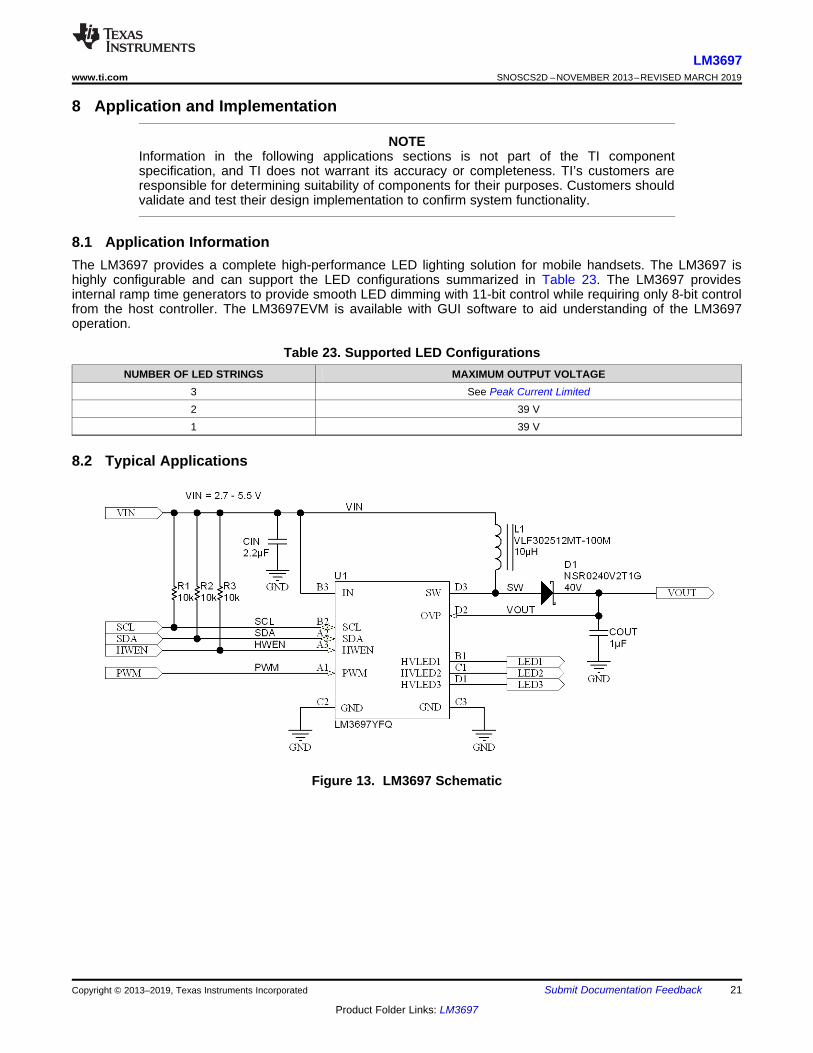
8 Application and Implementation
NOTEInformation in the following applications sections is not part of the TI componentspecification, and TI does not warrant its accuracy or completeness. TI’s customers areresponsible for determining suitability of components for their purposes. Customers shouldvalidate and test their design implementation to confirm system functionality.
8.1 Application InformationThe LM3697 provides a complete high-performance LED lighting solution for mobile handsets. The LM3697 ishighly configurable and can support the LED configurations summarized in Table 23. The LM3697 providesinternal ramp time generators to provide smooth LED dimming with 11-bit control while requiring only 8-bit controlfrom the host controller. The LM3697EVM is available with GUI software to aid understanding of the LM3697operation.
Table 23. Supported LED ConfigurationsNUMBER OF LED STRINGS MAXIMUM OUTPUT VOLTAGE
3 See Peak Current Limited2 39 V1 39 V
8.2 Typical Applications
Figure 13. LM3697 Schematic

L_PEAK26 V 60.6 mA 3 V 26 V 3 V 0.8
I 792 mA 3 V 0.8 2 1 MHz 10 H 26 Vu u
u u u u P
OUT _MAXI 20.2 mA 3 strings 60.6 mA u
OUT _MAXV 8 3.2 V + 0.4 V 26 V u
OUT _MAX OUT_MAX IN_MIN OUT _MAX IN_MINL _PEAK
IN_MIN SW OUT _MAX
V I V V V efficiencyI +
V efficiency 2 f L V
u u
uu u u
22
LM3697SNOSCS2D –NOVEMBER 2013–REVISED MARCH 2019 www.ti.com
Product Folder Links: LM3697
Submit Documentation Feedback Copyright © 2013–2019, Texas Instruments Incorporated
Typical Applications (continued)8.2.1 Design RequirementsFor 8s3p applications, use the parameters listed in Table 24.
Table 24. Design ParametersDESIGN PARAMETER EXAMPLE VALUEFull-scale current setting 0.0202 AMinimum Input Voltage 3 V
LED series/parallel configuration 8s3pLED maximum forward voltage (Vf) 3.5 V
Efficiency 80%Switching frequency 1 MHz
Inductance 10 µH
The designer needs to know the following:• Full-scale current setting• Minimum input voltage (VIN_MIN)• LED series/parallel configuration• LED maximum VF_MAX voltage• LM3697 efficiency for LED configuration (efficiency)• LM3697 boost switching frequency (fSW)• Inductor value (L)
This information guides the designer to make the appropriate inductor selection for the application.
Device boost converter output voltage (VOUT_MAX) is calculated as: number series LEDs × VF_MAX + 0.4 V.
The LM3697 boost converter maximum output current (IOUT_MAX) is calculated as follows: number parallel LEDstrings × full-scale current.
Using the design parameters from Table 24 IL_PEAK is calculated as:
(5)
For example:
(6)
(7)
(8)
This calculated value for IL_PEAK must be less than the minimum spec for the LM3697 boost current limit of 880mA. Additionally, the chosen inductor must have a saturation current rating that is greater than IL_PEAK.
8.2.2 Detailed Design Procedure
8.2.2.1 Boost Converter Maximum Output PowerThe LM3697 devices maximum output power is governed by two factors: the peak current limit (ICL = 880 mAminimum), and the maximum output voltage (VOUT). When the application causes either of these limits to bereached it is possible that the proper current regulation and matching between LED current strings will not bemet.
0.0350.0400.0450.0500.0550.0600.0650.0700.0750.0800.0850.0900.0950.100
2.72.93.13.33.53.73.94.14.34.54.74.95.15.35.5
IOU
T (
A)
VIN (V)
222426303438
C052
0.0350.0400.0450.0500.0550.0600.0650.0700.0750.0800.0850.0900.0950.100
2.72.93.13.33.53.73.94.14.34.54.74.95.15.35.5
IOU
T (
A)
VIN (V)
222426303438
C001
u 1 VIN
¹·
©§
SW u L´¶VIN u efficiency
IOUT u VOUT >
VIN u efficiencyVOUT
IPEAK = u VOUT - VIN u efficiency2 u IOUT
¹·
©§
SW u L u efficiency´¶
1 -VOUT
VIN x efficiencyx
2 x ¦SW x L
VINIPEAK = +
VIN x efficiency
IOUT x VOUT
23
LM3697www.ti.com SNOSCS2D –NOVEMBER 2013–REVISED MARCH 2019
Product Folder Links: LM3697
Submit Documentation FeedbackCopyright © 2013–2019, Texas Instruments Incorporated
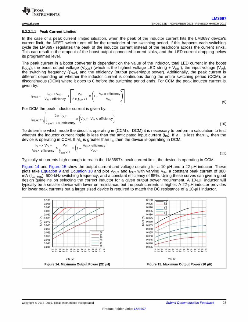
8.2.2.1.1 Peak Current Limited
In the case of a peak current limited situation, when the peak of the inductor current hits the LM3697 device'scurrent limit, the NFET switch turns off for the remainder of the switching period. If this happens each switchingcycle the LM3697 regulates the peak of the inductor current instead of the headroom across the current sinks.This can result in the dropout of the boost output connected current sinks, and the LED current dropping belowits programmed level.
The peak current in a boost converter is dependent on the value of the inductor, total LED current in the boost(IOUT), the boost output voltage (VOUT) (which is the highest voltage LED string + VHR ), the input voltage (VIN),the switching frequency (ƒSW), and the efficiency (output power/input power). Additionally, the peak current isdifferent depending on whether the inductor current is continuous during the entire switching period (CCM), ordiscontinuous (DCM) where it goes to 0 before the switching period ends. For CCM the peak inductor current isgiven by:
(9)
For DCM the peak inductor current is given by:
(10)
To determine which mode the circuit is operating in (CCM or DCM) it is necessary to perform a calculation to testwhether the inductor current ripple is less than the anticipated input current (IIN). If ΔIL is less than IIN then thedevice is operating in CCM. If ΔIL is greater than IIN then the device is operating in DCM.
(11)
Typically at currents high enough to reach the LM3697's peak current limit, the device is operating in CCM.
Figure 14 and Figure 15 show the output current and voltage derating for a 10-µH and a 22-µH inductor. Theseplots take Equation 9 and Equation 10 and plot VOUT and IOUT with varying VIN, a constant peak current of 880mA (ICL_MIN), 500-kHz switching frequency, and a constant efficiency of 85%. Using these curves can give a gooddesign guideline on selecting the correct inductor for a given output power requirement. A 10-µH inductor willtypically be a smaller device with lower on resistance, but the peak currents is higher. A 22-µH inductor providesfor lower peak currents but a larger sized device is required to match the DC resistance of a 10-µH inductor.
Figure 14. Maximum Output Power (22 µH) Figure 15. Maximum Output Power (10 µH)
24
LM3697SNOSCS2D –NOVEMBER 2013–REVISED MARCH 2019 www.ti.com
Product Folder Links: LM3697
Submit Documentation Feedback Copyright © 2013–2019, Texas Instruments Incorporated
8.2.2.1.2 Output Voltage Limited
In the case of an output voltage limited situation (VOUT = VOVP), when the boost output voltage hits the LM3697device's OVP threshold, the NFET turns off and stays off until the output voltage falls below the hysteresis level(typically 1 V below the OVP threshold). This results in the boost converter regulating the output voltage to theprogrammed OVP threshold (16 V, 24 V, 32 V, or 40 V), causing the current sinks to go into dropout. The defaultOVP threshold is set at 16 V. For LED strings higher than typically 4 series LEDs, the OVP has to beprogrammed higher after power-up, Software Reset, or HWEN reset.
8.2.2.2 Inductor SelectionThe boost circuit operates using a 4.7-µH to 22-µH inductor. The inductor selected must have a saturationcurrent greater than the peak operating current.
8.2.2.3 Output Capacitor SelectionThe LM3697's inductive boost converter requires a 1-µF (X5R or X7R) ceramic capacitor to filter the outputvoltage. The voltage rating of the capacitor depends on the selected OVP setting. For the 16 V setting a 16-Vcapacitor must be used. For the 24-V setting a 25-V capacitor must be used. For the 32-V setting, a 35-Vcapacitor must be used. For the 40-V setting a 50-V capacitor must be used. Pay careful attention to thecapacitor's tolerance and DC bias response. For proper operation the degradation in capacitance due totolerance, DC bias, and temperature, must stay above 0.4 µF. This might require placing two devices in parallelin order to maintain the required output capacitance over the device operating range, and series LEDconfiguration.
8.2.2.4 Schottky Diode SelectionThe Schottky diode must have a reverse breakdown voltage greater than the LM3697 device’s maximum outputvoltage (see Overvoltage Protection (Inductive Boost) section). Additionally, the diode must have an averagecurrent rating high enough to handle the LM3697’s maximum output current, and at the same time the diode'speak current rating must be high enough to handle the peak inductor current. Schottky diodes are required dueto their lower forward voltage drop (0.3 V to 0.5 V) and their fast recovery time.
8.2.2.5 Input Capacitor SelectionThe LM3697 device's inductive boost converter requires a 2.2-μF (X5R or X7R) ceramic capacitor to filter theinput voltage. The input capacitor filters the inductor current ripple and the internal MOSFET driver currentsduring turn on of the internal power switch.
8.2.2.6 Application Circuit Component List
COMPONENT MANUFACTURER VALUE PART NUMBER SIZE (mm) CURRENT/VOLTAGE RATING(RESISTANCE)
L TDK 10 µH VLF302512MT-100M 2.5 × 3.0 × 1.2 620 mA/0.25 ΩCOUT TDK 1.0 µF C2012X5R1H105 0805 50 VCIN TDK 2.2 µF C1005X5R1A225 0402 10 V
Diode On-Semi Schottky NSR0240V2T1G SOD-523 40 V, 250 mA
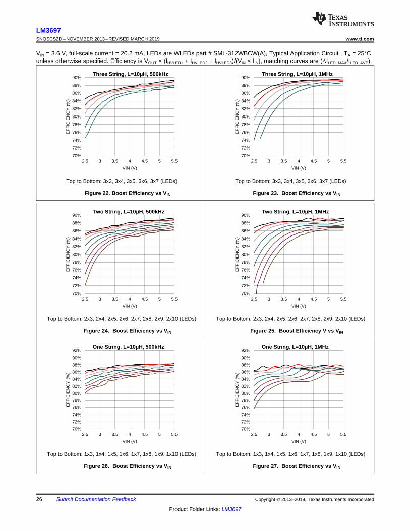
8.2.3 Application Performance PlotsVIN = 3.6 V, full-scale current = 20.2 mA, LEDs are WLEDs part # SML-312WBCW(A), Typical Application Circuit , TA = 25°Cunless otherwise specified. Efficiency is VOUT × (IHVLED1 + IHVLED2 + IHVLED3)/(VIN × IIN), matching curves are (ΔILED_MAX/ILED_AVE).

70%
72%
74%
76%
78%
80%
82%
84%
86%
88%
90%
92%
2.5 3 3.5 4 4.5 5 5.5
EF
FIC
IEN
CY
(%
)
VIN (V)
One String, L=22µH, 500kHz
C002
70%
72%
74%
76%
78%
80%
82%
84%
86%
88%
90%
92%
2.5 3 3.5 4 4.5 5 5.5
EF
FIC
IEN
CY
(%
)
VIN (V)
One String, L=22µH, 1MHz
C002
70%
72%
74%
76%
78%
80%
82%
84%
86%
88%
90%
92%
2.5 3 3.5 4 4.5 5 5.5
EF
FIC
IEN
CY
(%
)
VIN (V)
Two String, L=22µH, 500kHz
C002
70%
72%
74%
76%
78%
80%
82%
84%
86%
88%
90%
92%
2.5 3 3.5 4 4.5 5 5.5
EF
FIC
IEN
CY
(%
)
VIN (V)
Two String, L=22µH, 1MHz
C002
70%
72%
74%
76%
78%
80%
82%
84%
86%
88%
90%
92%
2.5 3 3.5 4 4.5 5 5.5
EF
FIC
IEN
CY
(%
)
VIN (V)
Three String, L=22µH, 500kHz
C002
70%
72%
74%
76%
78%
80%
82%
84%
86%
88%
90%
92%
2.5 3 3.5 4 4.5 5 5.5
EF
FIC
IEN
CY
(%
)
VIN (V)
Three String, L=22µH, 1MHz
C002
25
LM3697www.ti.com SNOSCS2D –NOVEMBER 2013–REVISED MARCH 2019
Product Folder Links: LM3697
Submit Documentation FeedbackCopyright © 2013–2019, Texas Instruments Incorporated
VIN = 3.6 V, full-scale current = 20.2 mA, LEDs are WLEDs part # SML-312WBCW(A), Typical Application Circuit , TA = 25°Cunless otherwise specified. Efficiency is VOUT × (IHVLED1 + IHVLED2 + IHVLED3)/(VIN × IIN), matching curves are (ΔILED_MAX/ILED_AVE).
Top to Bottom: 3x3, 3x4, 3x5, 3x6, 3x7 (LEDs)
Figure 16. Boost Efficiency vs VIN
Top to Bottom: 3x3, 3x4, 3x5, 3x6, 3x7 (LEDs)
Figure 17. Boost Efficiency vs VIN
Top to Bottom: 2x3, 2x4, 2x5, 2x6, 2x7, 2x8, 2x9, 2x10 (LEDs)
Figure 18. Boost Efficiency vs VIN
Top to Bottom: 2x3, 2x4, 2x5, 2x6, 2x7, 2x8, 2x9, 2x10 (LEDs)
Figure 19. Boost Efficiency vs VIN
Top to Bottom: 1x3, 1x4, 1x5, 1x6, 1x7, 1x8, 1x9, 1x10 (LEDs)
Figure 20. Boost Efficiency vs VIN
Top to Bottom: 1x3, 1x4, 1x5, 1x6, 1x7, 1x8, 1x9, 1x10 (LEDs)
Figure 21. Boost Efficiency vs VIN
70%
72%
74%
76%
78%
80%
82%
84%
86%
88%
90%
92%
2.5 3 3.5 4 4.5 5 5.5
EF
FIC
IEN
CY
(%
)
VIN (V)
One String, L=10µH, 500kHz
C002
70%
72%
74%
76%
78%
80%
82%
84%
86%
88%
90%
92%
2.5 3 3.5 4 4.5 5 5.5
EF
FIC
IEN
CY
(%
)
VIN (V)
One String, L=10µH, 1MHz
C002
70%
72%
74%
76%
78%
80%
82%
84%
86%
88%
90%
2.5 3 3.5 4 4.5 5 5.5
EF
FIC
IEN
CY
(%
)
VIN (V)
Two String, L=10µH, 500kHz
C002
70%
72%
74%
76%
78%
80%
82%
84%
86%
88%
90%
2.5 3 3.5 4 4.5 5 5.5
EF
FIC
IEN
CY
(%
)
VIN (V)
Two String, L=10µH, 1MHz
C002
70%
72%
74%
76%
78%
80%
82%
84%
86%
88%
90%
2.5 3 3.5 4 4.5 5 5.5
EF
FIC
IEN
CY
(%
)
VIN (V)
Three String, L=10µH, 500kHz
C002
70%
72%
74%
76%
78%
80%
82%
84%
86%
88%
90%
2.5 3 3.5 4 4.5 5 5.5
EF
FIC
IEN
CY
(%
)
VIN (V)
Three String, L=10µH, 1MHz
C002
26
LM3697SNOSCS2D –NOVEMBER 2013–REVISED MARCH 2019 www.ti.com
Product Folder Links: LM3697
Submit Documentation Feedback Copyright © 2013–2019, Texas Instruments Incorporated
VIN = 3.6 V, full-scale current = 20.2 mA, LEDs are WLEDs part # SML-312WBCW(A), Typical Application Circuit , TA = 25°Cunless otherwise specified. Efficiency is VOUT × (IHVLED1 + IHVLED2 + IHVLED3)/(VIN × IIN), matching curves are (ΔILED_MAX/ILED_AVE).
Top to Bottom: 3x3, 3x4, 3x5, 3x6, 3x7 (LEDs)
Figure 22. Boost Efficiency vs VIN
Top to Bottom: 3x3, 3x4, 3x5, 3x6, 3x7 (LEDs)
Figure 23. Boost Efficiency vs VIN
Top to Bottom: 2x3, 2x4, 2x5, 2x6, 2x7, 2x8, 2x9, 2x10 (LEDs)
Figure 24. Boost Efficiency vs VIN
Top to Bottom: 2x3, 2x4, 2x5, 2x6, 2x7, 2x8, 2x9, 2x10 (LEDs)
Figure 25. Boost Efficiency V vs VIN
Top to Bottom: 1x3, 1x4, 1x5, 1x6, 1x7, 1x8, 1x9, 1x10 (LEDs)
Figure 26. Boost Efficiency vs VIN
Top to Bottom: 1x3, 1x4, 1x5, 1x6, 1x7, 1x8, 1x9, 1x10 (LEDs)
Figure 27. Boost Efficiency vs VIN

70%
72%
74%
76%
78%
80%
82%
84%
86%
88%
2.5 3 3.5 4 4.5 5 5.5
EF
FIC
IEN
CY
(%
)
VIN (V)
One String, L=4.7µH, 500kHz
C002
70%
72%
74%
76%
78%
80%
82%
84%
86%
88%
2.5 3 3.5 4 4.5 5 5.5
EF
FIC
IEN
CY
(%
)
VIN (V)
One String, L=4.7µH, 1MHz
C002
70%
72%
74%
76%
78%
80%
82%
84%
86%
88%
2.5 3 3.5 4 4.5 5 5.5
EF
FIC
IEN
CY
(%
)
VIN (V)
Two String, L=4.7µH, 500kHz
C002
70%
72%
74%
76%
78%
80%
82%
84%
86%
88%
2.5 3 3.5 4 4.5 5 5.5
EF
FIC
IEN
CY
(%
)
VIN (V)
Two String, L=4.7µH, 1MHz
C002
70%
72%
74%
76%
78%
80%
82%
84%
86%
88%
90%
2.5 3 3.5 4 4.5 5 5.5
EF
FIC
IEN
CY
(%
)
VIN (V)
Three String, L=4.7µH, 500kHz
C002
70%
72%
74%
76%
78%
80%
82%
84%
86%
88%
90%
2.5 3 3.5 4 4.5 5 5.5
EF
FIC
IEN
CY
(%
)
VIN (V)
Three String, L=4.7µH, 1MHz
C002
27
LM3697www.ti.com SNOSCS2D –NOVEMBER 2013–REVISED MARCH 2019
Product Folder Links: LM3697
Submit Documentation FeedbackCopyright © 2013–2019, Texas Instruments Incorporated
VIN = 3.6 V, full-scale current = 20.2 mA, LEDs are WLEDs part # SML-312WBCW(A), Typical Application Circuit , TA = 25°Cunless otherwise specified. Efficiency is VOUT × (IHVLED1 + IHVLED2 + IHVLED3)/(VIN × IIN), matching curves are (ΔILED_MAX/ILED_AVE).
Top to Bottom: 3x3, 3x4, 3x5, 3x6, 3x7 (LEDs)
Figure 28. Boost Efficiency vs VIN
Top to Bottom: 3x3, 3x4, 3x5, 3x6, 3x7 (LEDs)
Figure 29. Boost Efficiency vs VIN
Top to Bottom: 2x3, 2x4, 2x5, 2x6, 2x7, 2x8, 2x9, 2x10 (LEDs)
Figure 30. Boost Efficiency vs VIN
Top to Bottom: 2x3, 2x4, 2x5, 2x6, 2x7, 2x8, 2x9, 2x10 (LEDs)
Figure 31. Boost Efficiency vs VIN
Top to Bottom: 1x3, 1x4, 1x5, 1x6, 1x7, 1x8, 1x9, 1x10 (LEDs)
Figure 32. Boost Efficiency vs VIN
Top to Bottom: 1x3, 1x4, 1x5, 1x6, 1x7, 1x8, 1x9, 1x10 (LEDs)
Figure 33. Boost Efficiency vs VIN
70%
72%
74%
76%
78%
80%
82%
84%
86%
88%
90%
0.00 12.00 24.00 36.00 48.00 60.00
EF
FIC
IEN
CY
(%
)
ILED (mA)
Three String, L=10µH, 500kHz
C002
70%
72%
74%
76%
78%
80%
82%
84%
86%
88%
90%
0 12 24 36 48 60
EF
FIC
IEN
CY
(%
)
ILED (mA)
Three String, L=10µH, 1MHz
C002
70%
72%
74%
76%
78%
80%
82%
84%
86%
88%
90%
0 12 24 36 48
EF
FIC
IEN
CY
(%
)
ILED (mA)
Two String, L=22µH, 500kHz
C002
70%
72%
74%
76%
78%
80%
82%
84%
86%
88%
90%
0 12 24 36 48
EF
FIC
IEN
CY
(%
)
ILED (mA)
Two String, L=22µH, 1MHz
C002
70%
72%
74%
76%
78%
80%
82%
84%
86%
88%
90%
0.00 12.00 24.00 36.00 48.00 60.00
EF
FIC
IEN
CY
(%
)
ILED (mA)
Three String, L=22µH, 500kHz
C002
70%
72%
74%
76%
78%
80%
82%
84%
86%
88%
90%
0 12 24 36 48 60
EF
FIC
IEN
CY
(%
)
ILED (mA)
Three String, L=22µH, 1MHz
C002
28
LM3697SNOSCS2D –NOVEMBER 2013–REVISED MARCH 2019 www.ti.com
Product Folder Links: LM3697
Submit Documentation Feedback Copyright © 2013–2019, Texas Instruments Incorporated
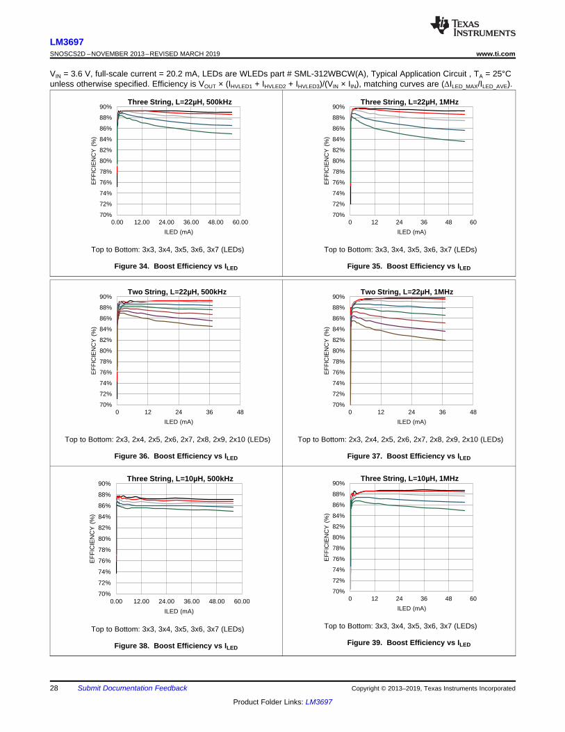
VIN = 3.6 V, full-scale current = 20.2 mA, LEDs are WLEDs part # SML-312WBCW(A), Typical Application Circuit , TA = 25°Cunless otherwise specified. Efficiency is VOUT × (IHVLED1 + IHVLED2 + IHVLED3)/(VIN × IIN), matching curves are (ΔILED_MAX/ILED_AVE).
Top to Bottom: 3x3, 3x4, 3x5, 3x6, 3x7 (LEDs)
Figure 34. Boost Efficiency vs ILED
Top to Bottom: 3x3, 3x4, 3x5, 3x6, 3x7 (LEDs)
Figure 35. Boost Efficiency vs ILED
Top to Bottom: 2x3, 2x4, 2x5, 2x6, 2x7, 2x8, 2x9, 2x10 (LEDs)
Figure 36. Boost Efficiency vs ILED
Top to Bottom: 2x3, 2x4, 2x5, 2x6, 2x7, 2x8, 2x9, 2x10 (LEDs)
Figure 37. Boost Efficiency vs ILED
Top to Bottom: 3x3, 3x4, 3x5, 3x6, 3x7 (LEDs)
Figure 38. Boost Efficiency vs ILED
Top to Bottom: 3x3, 3x4, 3x5, 3x6, 3x7 (LEDs)
Figure 39. Boost Efficiency vs ILED

70%
72%
74%
76%
78%
80%
82%
84%
86%
88%
90%
0 12 24 36 48
EF
FIC
IEN
CY
(%
)
ILED (mA)
Two String, L=4.7µH, 500kHz
C002
70%
72%
74%
76%
78%
80%
82%
84%
86%
88%
90%
0 12 24 36 48
EF
FIC
IEN
CY
(%
)
ILED (mA)
Two String, L=4.7µH, 1MHz
C002
70%
72%
74%
76%
78%
80%
82%
84%
86%
88%
90%
0 12 24 36 48 60
EF
FIC
IEN
CY
(%
)
ILED (mA)
Three String, L=4.7µH, 1MHz
C002
70%
72%
74%
76%
78%
80%
82%
84%
86%
88%
90%
0.00 12.00 24.00 36.00 48.00 60.00
EF
FIC
IEN
CY
(%
)
ILED (mA)
Three String, L=4.7µH, 500kHz
C002
70%
72%
74%
76%
78%
80%
82%
84%
86%
88%
90%
0 12 24 36 48
EF
FIC
IEN
CY
(%
)
ILED (mA)
Two String, L=10µH, 500kHz
C002
70%
72%
74%
76%
78%
80%
82%
84%
86%
88%
90%
0 12 24 36 48
EF
FIC
IEN
CY
(%
)
ILED (mA)
Two String, L=10µH, 1MHz
C002
29
LM3697www.ti.com SNOSCS2D –NOVEMBER 2013–REVISED MARCH 2019
Product Folder Links: LM3697
Submit Documentation FeedbackCopyright © 2013–2019, Texas Instruments Incorporated
VIN = 3.6 V, full-scale current = 20.2 mA, LEDs are WLEDs part # SML-312WBCW(A), Typical Application Circuit , TA = 25°Cunless otherwise specified. Efficiency is VOUT × (IHVLED1 + IHVLED2 + IHVLED3)/(VIN × IIN), matching curves are (ΔILED_MAX/ILED_AVE).
Top to Bottom: 2x3, 2x4, 2x5, 2x6, 2x7, 2x8, 2x9, 2x10 (LEDs)
Figure 40. Boost Efficiency vs ILED
Top to Bottom: 2x3, 2x4, 2x5, 2x6, 2x7, 2x8, 2x9, 2x10 (LEDs)
Figure 41. Boost Efficiency vs ILED
Top to Bottom: 3x3, 3x4, 3x5, 3x6, 3x7 (LEDs)
Figure 42. Boost Efficiency vs ILED
Top to Bottom: 3x3, 3x4, 3x5, 3x6, 3x7 (LEDs)
Figure 43. Boost Efficiency vs ILED
Top to Bottom: 2x3, 2x4, 2x5, 2x6, 2x7, 2x8, 2x9, 2x10 (LEDs)
Figure 44. Boost Efficiency vs ILED
Top to Bottom: 2x3, 2x4, 2x5, 2x6, 2x7, 2x8, 2x9, 2x10 (LEDs)
Figure 45. Boost Efficiency vs ILED
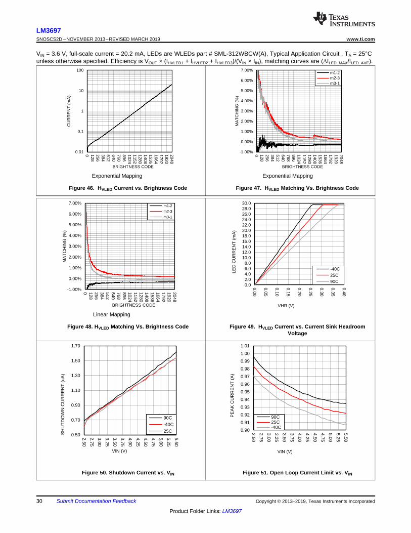
0.50
0.70
0.90
1.10
1.30
1.50
1.70
2.50
2.75
3.00
3.25
3.50
3.75
4.00
4.25
4.50
4.75
5.00
5.25
5.50
SH
UT
DO
WN
CU
RR
EN
T (
uA)
VIN (V)
90C
-40C
25C
C001
0.90
0.91
0.92
0.93
0.94
0.95
0.96
0.97
0.98
0.99
1.00
1.01
2.50
2.75
3.00
3.25
3.50
3.75
4.00
4.25
4.50
4.75
5.00
5.25
5.50
PE
AK
CU
RR
EN
T (
A)
VIN (V)
90C25C-40C
C001
-1.00%
0.00%
1.00%
2.00%
3.00%
4.00%
5.00%
6.00%
7.00%
0 128256384512640768896102411521280140815361664179219202048
MA
TC
HIN
G (
%)
BRIGHTNESS CODE
m1-2
m2-3
m3-1
C001
0.02.04.06.08.0
10.012.014.016.018.020.022.024.026.028.030.0
0.00
0.05
0.10
0.15
0.20
0.25
0.30
0.35
0.40
LED
CU
RR
EN
T (
mA
)
VHR (V)
-40C25C90C
C001
0.01
0.1
1
10
100
0 128256384512640768896102411521280140815361664179219202048
CU
RR
EN
T (
mA
)
BRIGHTNESS CODE C001
-1.00%
0.00%
1.00%
2.00%
3.00%
4.00%
5.00%
6.00%
7.00%
0 128256384512640768896102411521280140815361664179219202048
MA
TC
HIN
G (
%)
BRIGHTNESS CODE
m1-2m2-3m3-1
C001
30
LM3697SNOSCS2D –NOVEMBER 2013–REVISED MARCH 2019 www.ti.com
Product Folder Links: LM3697
Submit Documentation Feedback Copyright © 2013–2019, Texas Instruments Incorporated
VIN = 3.6 V, full-scale current = 20.2 mA, LEDs are WLEDs part # SML-312WBCW(A), Typical Application Circuit , TA = 25°Cunless otherwise specified. Efficiency is VOUT × (IHVLED1 + IHVLED2 + IHVLED3)/(VIN × IIN), matching curves are (ΔILED_MAX/ILED_AVE).
Exponential Mapping
Figure 46. HVLED Current vs. Brightness Code
Exponential Mapping
Figure 47. HVLED Matching Vs. Brightness Code
Linear Mapping
Figure 48. HVLED Matching Vs. Brightness Code Figure 49. HVLED Current vs. Current Sink HeadroomVoltage
Figure 50. Shutdown Current vs. VIN Figure 51. Open Loop Current Limit vs. VIN

0.00
5.00
10.00
15.00
20.00
25.00
0.0%
12.5%
25.0%
37.5%
50.0%
62.5%
75.0%
87.5%
100.0%
LED
CU
RR
EN
T (
mA
)
PWM DUTY CYCLE (%)
MaxTypMin
C001
0.01%
0.10%
1.00%
10.00%
100.00%
0 2000
4000
6000
8000
10000
RIP
PLE
CU
RR
EN
T (
%)
PWM FREQUENCY (Hz) C001
31
LM3697www.ti.com SNOSCS2D –NOVEMBER 2013–REVISED MARCH 2019
Product Folder Links: LM3697
Submit Documentation FeedbackCopyright © 2013–2019, Texas Instruments Incorporated
VIN = 3.6 V, full-scale current = 20.2 mA, LEDs are WLEDs part # SML-312WBCW(A), Typical Application Circuit , TA = 25°Cunless otherwise specified. Efficiency is VOUT × (IHVLED1 + IHVLED2 + IHVLED3)/(VIN × IIN), matching curves are (ΔILED_MAX/ILED_AVE).
Figure 52. Led Current Ripple vs FPWM
8s2p LED configuration
Figure 53. Start-up Response
Figure 54. Response To Step Change In PWM Input DutyCycle
Figure 55. HVLED Current Vs PWM Input Duty Cycle
Figure 56. Line Step Response

32
LM3697SNOSCS2D –NOVEMBER 2013–REVISED MARCH 2019 www.ti.com
Product Folder Links: LM3697
Submit Documentation Feedback Copyright © 2013–2019, Texas Instruments Incorporated
8.3 Initialization Set UpTable 25 illustrates the minimum number of register writes required for a two-parallel, seven-series LEDconfiguration. This example uses the default settings for ramp times (2048 µsec), mapping mode (exponential)and full-scale current (20.2 mA). In this mode of operation the LM3697 controls the brightness LSB's to rampbetween the 8-bit MSB brightness levels providing 11-bit dimming while requiring only 8-bit commands from thehost controller.
Table 25. Control Bank A, 8-Bit Control, Two-String, Seven Series LED Configuration ExampleREGISTER NAME ADDRESS DATA DESCRIPTION
HVLED Current Sink OutputConfiguration 0x10 0x04 HVLED1 & 2 assigned to Control Bank A
HVLED Current Sink FeedbackEnables 0x19 0x03 Enable feedback on HVLED1 & 2, disable feedback on HVLED3
Boost Control 0x1A 0x04 OVP = 32V, ƒsw = 500 kHzControl Bank Enables 0x24 0x01 Enable Control Bank A
Control A Brightness LSB 0x20 0x00 Control A Brightness LSB written only onceControl A Brightness MSB 0x21 User Value Control A Brightness MSB updated as required
Table 26 shows the minimum number of register writes required for a two-parallel, six-series LED configurationwith PWM Enabled. This example uses the default settings for ramp times (2048 µsec), mapping mode(exponential) and full-scale current (20.2 mA). In this mode of operation the host controller must update both thebrightness LSB and MSB registers whenever a brightness change is required.
Table 26. Control Bank A, 11-Bit Control, Two-String, Six Series LED Configuration ExampleREGISTER NAME ADDRESS DATA DESCRIPTION
HVLED Current Sink OutputConfiguration 0x10 0x04 HVLED1 & 2 assigned to Control Bank A
HVLED Current Sink FeedbackEnables 0x19 0x03 Enable feedback on HVLED1 & 2, disable feedback on HVLED3
Boost Control 0x1A 0x02 OVP = 24 V, ƒsw = 500 kHz
PWM Configuration 0x1C 0x0D PWM Zero Detect = Enabled, PWM Polarity = Active HIgh, ControlB PWM = Disabled, Control A PWM = Enabled
Control Bank Enables 0x24 0x01 Enable Control Bank A
Control A Brightness LSB 0x20 User ValueControl A Brightness LSB updated as required
(NOTE: The Brightness LSB change does not take effect until theBrightness MSB register is written.)
Control A Brightness MSB 0x21 User ValueControl A Brightness MSB updated as required
(NOTE: Anytime the Brightness LSB is changed the BrightnessMSB must be written for the Brightness LSB change to take effect.)
9 Power Supply RecommendationsThe LM3697 is designed to operate from an input supply range of 2.7 V to 5.5 V. This input supply must be wellregulated and provide the peak current required by the LED configuration and inductor selected.

SWIN
OVP
HVLED1
PWM
HWEN
GND
LM3697
2.7 V to 5.5 VUp to 40V
LD1Lp1 Lp2
Lp3
Cp1
Affected Nodedue to Capacitive Coupling
Current through Inductor
Pulsed voltage at SW
VOUT + VF Schottky
Voltage Spike (VSPIKE)
IPEAK
IAVE = IIN
Current through Schottky and
COUT
LCD Display
HVLED2
COUT
CIN
HVLED3
SCL
SDA
Parasitic Circuit Board Inductances
33
LM3697www.ti.com SNOSCS2D –NOVEMBER 2013–REVISED MARCH 2019
Product Folder Links: LM3697
Submit Documentation FeedbackCopyright © 2013–2019, Texas Instruments Incorporated
10 Layout
10.1 Layout GuidelinesThe LM3697 device's inductive boost converter sees a high switched voltage (up to VOVP) at the SW pin, and astep current (up to ICL_BOOST) through the Schottky diode and output capacitor each switching cycle. The highswitching voltage can create interference into nearby nodes due to electric field coupling (I = CdV/dt). The largestep current through the diode and the output capacitor can cause a large voltage spike at the SW pin and theOVP pin due to parasitic inductance in the step current conducting path (V = Ldi/dt). Board layout guidelines aregeared towards minimizing this electric field coupling and conducted noise. Figure 57 highlights these two noise-generating components.
Figure 57. LM3697 Inductive Boost Converter Showing Pulsed Voltage at SW (High Dv/Dt) and CurrentThrough Schottky And COUT (High Di/Dt)
The following list details the main (layout sensitive) areas of the LM3697 device’s inductive boost converter inorder of decreasing importance:1. Output Capacitor
– Schottky Cathode to COUT+– COUT− to GND
2. Schottky Diode– SW pin to Schottky Anode– Schottky Cathode to COUT+
34
LM3697SNOSCS2D –NOVEMBER 2013–REVISED MARCH 2019 www.ti.com
Product Folder Links: LM3697
Submit Documentation Feedback Copyright © 2013–2019, Texas Instruments Incorporated
Layout Guidelines (continued)3. Inductor
– SW Node PCB capacitance to other traces4. Input Capacitor
– CIN+ to IN terminal
10.1.1 Boost Output Capacitor PlacementBecause the output capacitor is in the path of the inductor current discharge path it detects a high-current stepfrom 0 to IPEAK each time the switch turns off and the Schottky diode turns on. Any inductance along this seriespath from the cathode of the diode through COUT and back into the LM3697 device's GND pin contributes tovoltage spikes (VSPIKE = LP_ × di/dt) at SW and OUT. These spikes can potentially over-voltage the SW pin, orfeed through to GND. To avoid this, COUT+ must be connected as close as possible to the cathode of theSchottky diode, and COUT− must be connected as close as possible to the LM3697 device's GND bump. Thebest placement for COUT is on the same layer as the LM3697 in order to avoid any vias that can add excessiveseries inductance.
10.1.2 Schottky Diode PlacementIn the LM3697 device’s boost circuit the Schottky diode is in the path of the inductor current discharge. As aresult the Schottky diode sees a high-current step from 0 to IPEAK each time the switch turns off and the diodeturns on. Any inductance in series with the diode causes a voltage spike (VSPIKE = LP_ × di/dt) at SW and OUT.This can potentially over-voltage the SW pin, or feed through to VOUT and through the output capacitor and intoGND. Connecting the anode of the diode as close as possible to the SW pin and the cathode of the diode asclose as possible to COUT and reduces the inductance (LP_) and minimize these voltage spikes.
10.1.3 Inductor PlacementThe node where the inductor connects to the LM3697 device’s SW pin has 2 issues. First, a large switchedvoltage (0 to VOUT + VF_SCHOTTKY) appears on this node every switching cycle. This switched voltage can becapacitively coupled into nearby nodes. Second, there is a relatively large current (input current) on the tracesconnecting the input supply to the inductor and connecting the inductor to the SW pin. Any resistance in this pathcan cause voltage drops that can negatively affect efficiency and reduce the input operating voltage range.
To reduce the capacitive coupling of the signal on SW into nearby traces, the SW pin-to-inductor connectionmust be minimized in area. This limits the PCB capacitance from SW to other traces. Additionally, high-impedance nodes that are more susceptible to electric field coupling need to be routed away from SW and notdirectly adjacent or beneath. This is especially true for traces such as SCL, SDA, HWEN, and PWM. A GNDplane placed directly below SW dramatically reduces the capacitance from SW into nearby traces.
Lastly, limit the trace resistance of the VIN-to-inductor connection and from the inductor to SW connection, byuse of short, wide traces.
10.1.4 Boost Input Capacitor PlacementFor the LM3697 device’s boost converter, the input capacitor filters the inductor current ripple and the internalMOSFET driver currents during turnon of the internal power switch. The driver current requirement can rangefrom 50 mA at 2.7 V to over 200 mA at 5.5 V with fast durations of approximately 10 ns to 20 ns. This appearsas high di/dt current pulses coming from the input capacitor each time the switch turns on. Close placement ofthe input capacitor to the IN pin and to the GND in is critical because any series inductance between IN andCIN+ or CIN− and GND can create voltage spikes that could appear on the VIN supply line and in the GNDplane.

1.
2
S2
S LkHz5002R -xxS+
LSL
RS
CIN
LM3697
-+
VIN Supply
ISUPPLY 'IL
SW
IN
LS
CIN
RS
ISUPPLY
'IL
2.
3.
1>
2SR
2SL4 xINS CL x
1RESONANTf =
2S INS CL x
xLI'|LESUPPLYRIPPI
¸¸¹
·¨¨©
§ 1
INCkHz5002 xxS
1
INCkHz5002 xxS
35
LM3697www.ti.com SNOSCS2D –NOVEMBER 2013–REVISED MARCH 2019
Product Folder Links: LM3697
Submit Documentation FeedbackCopyright © 2013–2019, Texas Instruments Incorporated
Layout Guidelines (continued)Close placement of the input bypass capacitor at the input side of the inductor is also critical. The sourceimpedance (inductance and resistance) from the input supply, along with the input capacitor of the LM3697,forms a series RLC circuit. If the output resistance from the source (RS) is low enough the circuit is underdampedand has a resonant frequency (typically the case). Depending on the size of LS the resonant frequency couldoccur below, close to, or above the switching frequency of the device. This can cause the supply current ripple tobe:1. Approximately equal to the inductor current ripple when the resonant frequency occurs well above the
LM3697 device's switching frequency;2. Greater than the inductor current ripple when the resonant frequency occurs near the switching frequency; or3. Less than the inductor current ripple when the resonant frequency occurs well below the switching frequency.
Figure 58 shows the series RLC circuit formed from the output impedance of the supply and the input capacitor.The circuit is redrawn for the AC case where the VIN supply is replaced with a short to GND, and the LM3697 +Inductor is replaced with a current source (ΔIL). Equation 1 is the criteria for an underdamped response. Equation2 is the resonant frequency. Equation 3 is the approximated supply current ripple as a function of LS, RS, andCIN.
As an example, consider a 3.6-V supply with 0.1 Ω of series resistance connected to CIN through 50 nH ofconnecting traces. This results in an underdamped input-filter circuit with a resonant frequency of 712 kHz.Because both the 1-MHz and 500-kHz switching frequency options lie close to the resonant frequency of theinput filter, the supply current ripple is probably larger than the inductor current ripple. In this case, usingequation 3, the supply current ripple can be approximated as 1.68 times the inductor current ripple (using a 500-kHz switching frequency) and 0.86 times the inductor current ripple using a 1-MHz switching frequency.Increasing the series inductance (LS) to 500 nH causes the resonant frequency to move to around 225 kHz, andthe supply current ripple to be approximately 0.25 times the inductor current ripple (500-kHz switching frequency)and 0.053 times for a 1-MHz switching frequency.
Figure 58. Input RLC Network

Input Cap Inductor
Output Cap
6.35 mm
Diode
4.57
mm
Top Layer Inner or Bottom Layer
VIA
36
LM3697SNOSCS2D –NOVEMBER 2013–REVISED MARCH 2019 www.ti.com
Product Folder Links: LM3697
Submit Documentation Feedback Copyright © 2013–2019, Texas Instruments Incorporated
10.2 Layout Example
Figure 59. LM3697 Layout Example

37
LM3697www.ti.com SNOSCS2D –NOVEMBER 2013–REVISED MARCH 2019
Product Folder Links: LM3697
Submit Documentation FeedbackCopyright © 2013–2019, Texas Instruments Incorporated
11 Device and Documentation Support
11.1 Device Support
11.1.1 Third-Party Products DisclaimerTI'S PUBLICATION OF INFORMATION REGARDING THIRD-PARTY PRODUCTS OR SERVICES DOES NOTCONSTITUTE AN ENDORSEMENT REGARDING THE SUITABILITY OF SUCH PRODUCTS OR SERVICESOR A WARRANTY, REPRESENTATION OR ENDORSEMENT OF SUCH PRODUCTS OR SERVICES, EITHERALONE OR IN COMBINATION WITH ANY TI PRODUCT OR SERVICE.
11.2 Related DocumentationFor additional information, see the following:
AN-1112 DSBGA Wafer Level Chip Scale Package
11.3 Receiving Notification of Documentation UpdatesTo receive notification of documentation updates, navigate to the device product folder on ti.com. In the upperright corner, click on Alert me to register and receive a weekly digest of any product information that haschanged. For change details, review the revision history included in any revised document.
11.4 Community ResourcesThe following links connect to TI community resources. Linked contents are provided "AS IS" by the respectivecontributors. They do not constitute TI specifications and do not necessarily reflect TI's views; see TI's Terms ofUse.
TI E2E™ Online Community TI's Engineer-to-Engineer (E2E) Community. Created to foster collaborationamong engineers. At e2e.ti.com, you can ask questions, share knowledge, explore ideas and helpsolve problems with fellow engineers.
Design Support TI's Design Support Quickly find helpful E2E forums along with design support tools andcontact information for technical support.
11.5 TrademarksE2E is a trademark of Texas Instruments.All other trademarks are the property of their respective owners.
11.6 Electrostatic Discharge CautionThis integrated circuit can be damaged by ESD. Texas Instruments recommends that all integrated circuits be handled withappropriate precautions. Failure to observe proper handling and installation procedures can cause damage.
ESD damage can range from subtle performance degradation to complete device failure. Precision integrated circuits may be moresusceptible to damage because very small parametric changes could cause the device not to meet its published specifications.
11.7 GlossarySLYZ022 — TI Glossary.
This glossary lists and explains terms, acronyms, and definitions.
12 Mechanical, Packaging, and Orderable InformationThe following pages include mechanical, packaging, and orderable information. This information is the mostcurrent data available for the designated devices. This data is subject to change without notice and revision ofthis document. For browser-based versions of this data sheet, refer to the left-hand navigation.
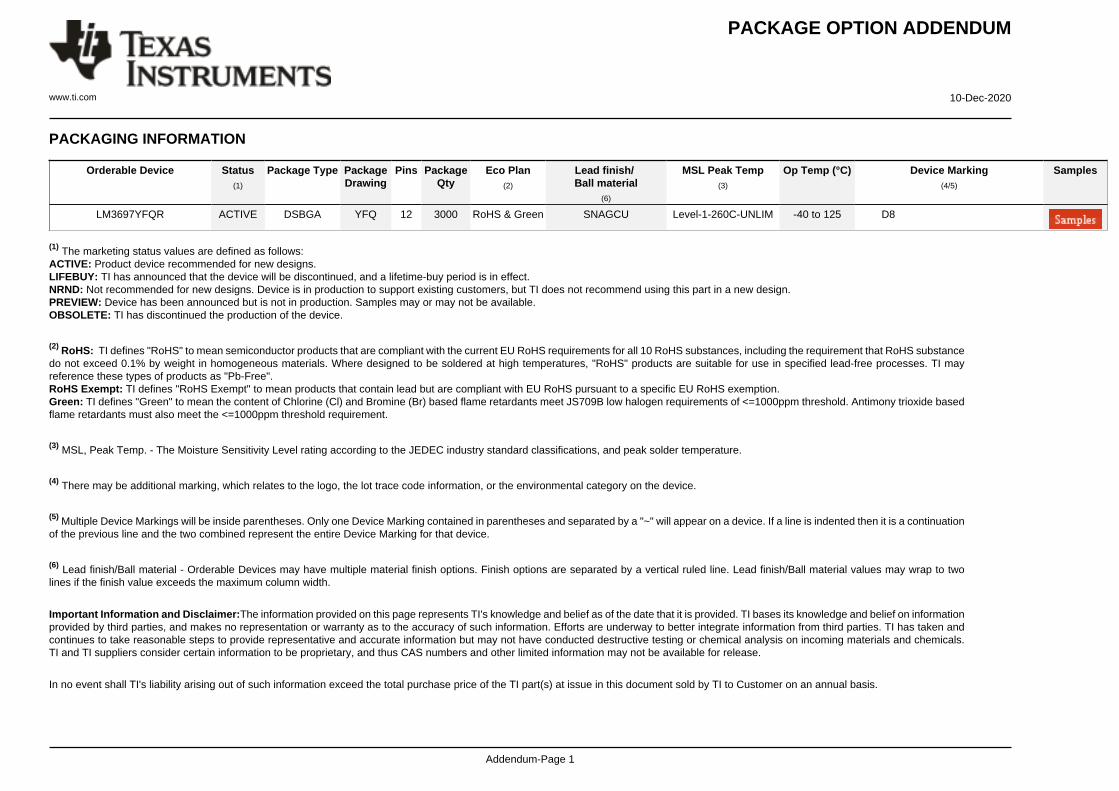
PACKAGE OPTION ADDENDUM
www.ti.com 10-Dec-2020
Addendum-Page 1
PACKAGING INFORMATION
Orderable Device Status(1)
Package Type PackageDrawing
Pins PackageQty
Eco Plan(2)
Lead finish/Ball material
(6)
MSL Peak Temp(3)
Op Temp (°C) Device Marking(4/5)
Samples
LM3697YFQR ACTIVE DSBGA YFQ 12 3000 RoHS & Green SNAGCU Level-1-260C-UNLIM -40 to 125 D8
(1) The marketing status values are defined as follows:ACTIVE: Product device recommended for new designs.LIFEBUY: TI has announced that the device will be discontinued, and a lifetime-buy period is in effect.NRND: Not recommended for new designs. Device is in production to support existing customers, but TI does not recommend using this part in a new design.PREVIEW: Device has been announced but is not in production. Samples may or may not be available.OBSOLETE: TI has discontinued the production of the device.
(2) RoHS: TI defines "RoHS" to mean semiconductor products that are compliant with the current EU RoHS requirements for all 10 RoHS substances, including the requirement that RoHS substancedo not exceed 0.1% by weight in homogeneous materials. Where designed to be soldered at high temperatures, "RoHS" products are suitable for use in specified lead-free processes. TI mayreference these types of products as "Pb-Free".RoHS Exempt: TI defines "RoHS Exempt" to mean products that contain lead but are compliant with EU RoHS pursuant to a specific EU RoHS exemption.Green: TI defines "Green" to mean the content of Chlorine (Cl) and Bromine (Br) based flame retardants meet JS709B low halogen requirements of <=1000ppm threshold. Antimony trioxide basedflame retardants must also meet the <=1000ppm threshold requirement.
(3) MSL, Peak Temp. - The Moisture Sensitivity Level rating according to the JEDEC industry standard classifications, and peak solder temperature.
(4) There may be additional marking, which relates to the logo, the lot trace code information, or the environmental category on the device.
(5) Multiple Device Markings will be inside parentheses. Only one Device Marking contained in parentheses and separated by a "~" will appear on a device. If a line is indented then it is a continuationof the previous line and the two combined represent the entire Device Marking for that device.
(6) Lead finish/Ball material - Orderable Devices may have multiple material finish options. Finish options are separated by a vertical ruled line. Lead finish/Ball material values may wrap to twolines if the finish value exceeds the maximum column width.
Important Information and Disclaimer:The information provided on this page represents TI's knowledge and belief as of the date that it is provided. TI bases its knowledge and belief on informationprovided by third parties, and makes no representation or warranty as to the accuracy of such information. Efforts are underway to better integrate information from third parties. TI has taken andcontinues to take reasonable steps to provide representative and accurate information but may not have conducted destructive testing or chemical analysis on incoming materials and chemicals.TI and TI suppliers consider certain information to be proprietary, and thus CAS numbers and other limited information may not be available for release.
In no event shall TI's liability arising out of such information exceed the total purchase price of the TI part(s) at issue in this document sold by TI to Customer on an annual basis.

TAPE AND REEL INFORMATION
*All dimensions are nominal
Device PackageType
PackageDrawing
Pins SPQ ReelDiameter
(mm)
ReelWidth
W1 (mm)
A0(mm)
B0(mm)
K0(mm)
P1(mm)
W(mm)
Pin1Quadrant
LM3697YFQR DSBGA YFQ 12 3000 178.0 8.4 1.38 1.78 0.78 4.0 8.0 Q1
LM3697YFQR DSBGA YFQ 12 3000 178.0 8.4 1.35 1.75 0.76 4.0 8.0 Q1
PACKAGE MATERIALS INFORMATION
www.ti.com 21-Oct-2021
Pack Materials-Page 1
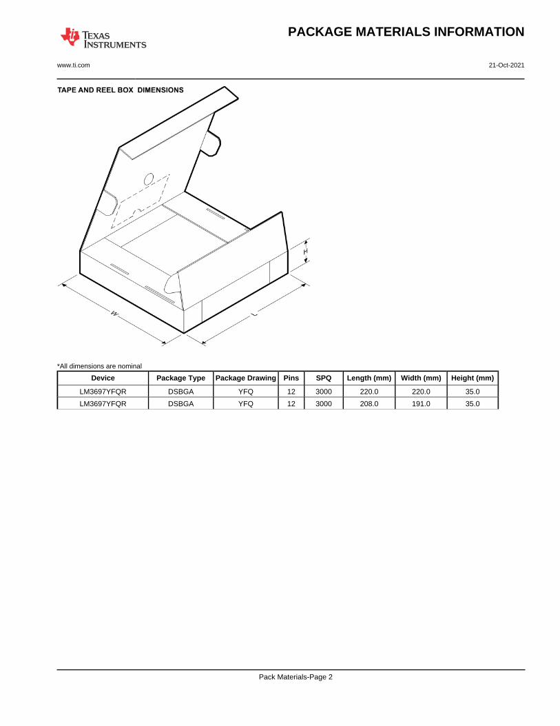
*All dimensions are nominal
Device Package Type Package Drawing Pins SPQ Length (mm) Width (mm) Height (mm)
LM3697YFQR DSBGA YFQ 12 3000 220.0 220.0 35.0
LM3697YFQR DSBGA YFQ 12 3000 208.0 191.0 35.0
PACKAGE MATERIALS INFORMATION
www.ti.com 21-Oct-2021
Pack Materials-Page 2

MECHANICAL DATA
YFQ0012xxx
www.ti.com
TMD12XXX (Rev B)
E
0.600±0.075
D
A. All linear dimensions are in millimeters. Dimensioning and tolerancing per ASME Y14.5M-1994.B. This drawing is subject to change without notice.
NOTES:
4215079/A 12/12
D: Max =
E: Max =
1.64 mm, Min =
1.29 mm, Min =
1.58 mm
1.23 mm

IMPORTANT NOTICE AND DISCLAIMERTI PROVIDES TECHNICAL AND RELIABILITY DATA (INCLUDING DATA SHEETS), DESIGN RESOURCES (INCLUDING REFERENCE DESIGNS), APPLICATION OR OTHER DESIGN ADVICE, WEB TOOLS, SAFETY INFORMATION, AND OTHER RESOURCES “AS IS” AND WITH ALL FAULTS, AND DISCLAIMS ALL WARRANTIES, EXPRESS AND IMPLIED, INCLUDING WITHOUT LIMITATION ANY IMPLIED WARRANTIES OF MERCHANTABILITY, FITNESS FOR A PARTICULAR PURPOSE OR NON-INFRINGEMENT OF THIRD PARTY INTELLECTUAL PROPERTY RIGHTS.These resources are intended for skilled developers designing with TI products. You are solely responsible for (1) selecting the appropriate TI products for your application, (2) designing, validating and testing your application, and (3) ensuring your application meets applicable standards, and any other safety, security, regulatory or other requirements.These resources are subject to change without notice. TI grants you permission to use these resources only for development of an application that uses the TI products described in the resource. Other reproduction and display of these resources is prohibited. No license is granted to any other TI intellectual property right or to any third party intellectual property right. TI disclaims responsibility for, and you will fully indemnify TI and its representatives against, any claims, damages, costs, losses, and liabilities arising out of your use of these resources.TI’s products are provided subject to TI’s Terms of Sale or other applicable terms available either on ti.com or provided in conjunction with such TI products. TI’s provision of these resources does not expand or otherwise alter TI’s applicable warranties or warranty disclaimers for TI products.TI objects to and rejects any additional or different terms you may have proposed. IMPORTANT NOTICE
Mailing Address: Texas Instruments, Post Office Box 655303, Dallas, Texas 75265Copyright © 2021, Texas Instruments Incorporated