LCD Video Processor with Built-in Decoder, MCU, OSD ...
197
1 FN7934.0 February 20, 2012 1-888-INTERSIL or 1-888-468-3774 | Copyright Intersil Americas Inc. 2012. All Rights Reserved Intersil (and design) is a trademark owned by Intersil Corporation or one of its subsidiaries. All other trademarks mentioned are the property of their respective owners. T e c h e l l w LCD Video Processor with Built-in Decoder, MCU, OSD, TCON and Analog RGB Input Support TW8825 The TW8825 incorporates many of the features required to create multi-purpose in-car LCD display system in a single package. It integrates a high quality 2D comb NTSC/PAL/SECAM video decoder, triple high speed RGB ADCs, high quality scaler, versatile OSD, and high performance MCU. Its image video processing capability includes arbitrary scaling, panoramic scaling, image mirroring, image adjustment and enhancement, Black and White Stretch, etc. On the input side, it supports a rich combination of CVBS, S-video, component video, analog RGB as well as digital YCbCr/RGB inputs. On the output side, it supports a variety of digital panel types with its built-in timing controller. The integration of additional touch screen controller, LED driver controller, PWM and MCU makes this a versatile solution for many portable applications. Applications In-car display Portable DVD and DVRs players Portable media player Analog Video Decoder NTSC (M, 4.43) and PAL (B, D, G, H, I, M, N, N combination), PAL (60), SECAM with automatic format detection Three 10-bit ADCs and analog clamping circuit. Fully programmable static gain or automatic gain control for the Y or CVBS channel Programmable white peak control for the Y or CVBS channel Software selectable analog inputs allows composite, S-video, analog YPbPr or RGB High quality adaptive 2D comb filter for both NTSC and PAL inputs PAL delay line for color phase error correction Image enhancement with 2D dynamic peaking and CTI. Digital sub-carrier PLL for accurate color decoding Digital horizontal PLL and Advanced synchronization processing for VCR playback and weak signal performance Programmable hue, brightness, saturation, contrast, sharpness High quality horizontal and vertical filtered down scaling with arbitrary scale down ratio Analog RGB Inputs Triple high speed 10-bit ADCs with clamping and programmable gain amplifier SOG and H/V sync support for YPbPr or RGB input Built-in line locked PLL with sync separator Supports input resolution up to 1080p Digital Inputs Support Supports both BT656 and 601 video formats Supports YCbCr/RGB 24-bit input Supports RGB 565 + BT 656 at the same time Supports input resolution up to 1080p TFT Panel Support Built-in programmable timing controller Supports 3, 4, 6 or 8 bits per pixel up to 16.8 million colors with built-in dithering engine Supports digital panel up to XGA resolution Supports Serial (8-bit) RGB panel Font Based On Screen Display Four window font OSD with bordering / shadow 10KB programmable font RAM and 512 display RAM 1/2/3/4 bits/pixel Supports variable width (12/16), height (2~32) SPI Flash Based On Screen Display Nine bitmap based OSD windows through SPI Supports 4/6/8 bits/pixel Supports RLE decompression for one window Supports overlapping between windows
-
Upload
khangminh22 -
Category
Documents
-
view
3 -
download
0
Transcript of LCD Video Processor with Built-in Decoder, MCU, OSD ...
1
FN7934.0
February 20, 2012
1-888-INTERSIL or 1-888-468-3774 | Copyright Intersil Americas Inc. 2012. All Rights Reserved
Intersil (and design) is a trademark owned by Intersil Corporation or one of its subsidiaries.
All other trademarks mentioned are the property of their respective owners.
T e c h e l l w
LCD Video Processor with Built-in Decoder, MCU, OSD,
TCON and Analog RGB Input Support
TW8825 The TW8825 incorporates many of the features
required to create multi-purpose in-car LCD display
system in a single package. It integrates a high quality
2D comb NTSC/PAL/SECAM video decoder, triple high
speed RGB ADCs, high quality scaler, versatile OSD, and
high performance MCU. Its image video processing
capability includes arbitrary scaling, panoramic scaling,
image mirroring, image adjustment and enhancement,
Black and White Stretch, etc. On the input side, it
supports a rich combination of CVBS, S-video,
component video, analog RGB as well as digital
YCbCr/RGB inputs. On the output side, it supports a
variety of digital panel types with its built-in timing
controller. The integration of additional touch screen
controller, LED driver controller, PWM and MCU makes
this a versatile solution for many portable applications.
Applications
In-car display
Portable DVD and DVRs players
Portable media player
Analog Video Decoder
NTSC (M, 4.43) and PAL (B, D, G, H, I, M, N, N
combination), PAL (60), SECAM with automatic format
detection
Three 10-bit ADCs and analog clamping circuit.
Fully programmable static gain or automatic gain
control for the Y or CVBS channel
Programmable white peak control for the Y or CVBS
channel
Software selectable analog inputs allows composite,
S-video, analog YPbPr or RGB
High quality adaptive 2D comb filter for both NTSC
and PAL inputs
PAL delay line for color phase error correction
Image enhancement with 2D dynamic peaking and
CTI.
Digital sub-carrier PLL for accurate color decoding
Digital horizontal PLL and Advanced synchronization
processing for VCR playback and weak signal
performance
Programmable hue, brightness, saturation, contrast,
sharpness
High quality horizontal and vertical filtered down
scaling with arbitrary scale down ratio
Analog RGB Inputs
Triple high speed 10-bit ADCs with clamping and
programmable gain amplifier
SOG and H/V sync support for YPbPr or RGB input
Built-in line locked PLL with sync separator
Supports input resolution up to 1080p
Digital Inputs Support
Supports both BT656 and 601 video formats
Supports YCbCr/RGB 24-bit input
Supports RGB 565 + BT 656 at the same time
Supports input resolution up to 1080p
TFT Panel Support
Built-in programmable timing controller
Supports 3, 4, 6 or 8 bits per pixel up to 16.8 million
colors with built-in dithering engine
Supports digital panel up to XGA resolution
Supports Serial (8-bit) RGB panel
Font Based On Screen Display
Four window font OSD with bordering / shadow
10KB programmable font RAM and 512 display RAM
1/2/3/4 bits/pixel
Supports variable width (12/16), height (2~32)
SPI Flash Based On Screen Display
Nine bitmap based OSD windows through SPI
Supports 4/6/8 bits/pixel
Supports RLE decompression for one window
Supports overlapping between windows
TW8825
2
Image Processing
High quality scaler with both up/down and panorama
/ water-glass scaling support
Built-in 2D de-interlacing function
Programmable brightness, contrast, saturation, hue
and sharpness
Programmable color transient improvement control
Supports programmable cropping of input video and
graphics
Independent RGB gain and offset controls
DTV hue adjustment
Programmable 8-bit Gamma correction for each color
Black/White Stretch
Clock Generation
Spread spectrum profile based on triangular
modulation with center spread
Programmable modulation frequency and spread
width
Timing Controller (TCON)
Supports programmable interface signals for control
Column (source) driver/Row (gate) driver
MCU
Industry standard 8052 based
Code fetch from external SPI flash memory
256B code cache
2K XDATA memory
Support power save mode with 32K internal clock
ISP (In System Programming) with internal boot ROM
Touch Screen Controller
Built-in 4-wire resistive touch screen
12–bit ADC
4 channel Auxiliary input
Miscellaneous
Supports 2-wire serial bus interface
Built-in single LED back light controller
Built-in VCOM DC voltage
Built-in VCOM AC
Built-in DC-DC converter
Up to 4 PWMs
GPIOs
1.8/3.3V operation
Power-down mode
Single 27MHz crystal
128-pin LQFP package
TW8825
3
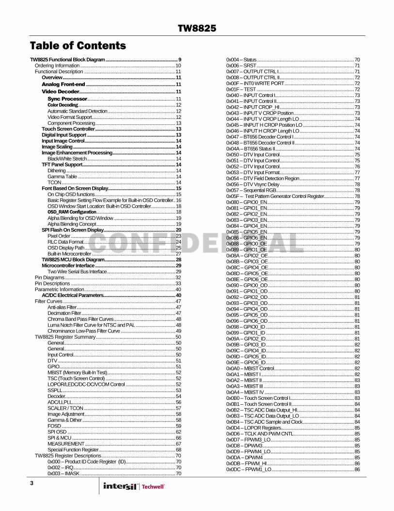
Table of Contents TW8825 Functional Block Diagram .............................................................. 9
Ordering Information ........................................................................ 10 Functional Description ..................................................................... 11
Overview ................................................................................................. 11 Analog Front-end ............................................................................. 11 Video Decoder................................................................................... 11
Sync Processor ............................................................................ 11 Color Decoding .................................................................................... 12 Automatic Standard Detection .......................................................... 12 Video Format Support ........................................................................ 12 Component Processing ..................................................................... 13
Touch Screen Controller ..................................................................... 13 Digital Input Support ............................................................................ 13 Input Image Control .............................................................................. 14 Image Scaling ........................................................................................ 14 Image Enhancement Processing ...................................................... 14
Black/White Stretch ............................................................................ 14 TFT Panel Support ................................................................................ 14
Dithering .............................................................................................. 14 Gamma Table .................................................................................... 14 TCON .................................................................................................. 14
Font Based On Screen Display .......................................................... 15 On Chip OSD functions ..................................................................... 15 Basic Register Setting Flow Example for Built-in OSD Controller.. 16 OSD Window Start Location: Built-in OSD Controller ..................... 18 OSD_RAM Configuration .................................................................... 18 Alpha Blending for OSD Window ..................................................... 19 Alpha Blending Concept .................................................................... 19
SPI Flash On Screen Display.............................................................. 20 Pixel Order .......................................................................................... 23 RLC Data Format ............................................................................... 24 OSD Display Path .............................................................................. 25 Built-in Microcontroller ........................................................................ 27
TW8825 MCU Block Diagram ............................................................. 28 Microcontroller Interface ..................................................................... 29
Two Wire Serial Bus Interface ........................................................... 29 Pin Diagrams .................................................................................... 32 Pin Descriptions ............................................................................... 33 Parametric Information..................................................................... 40
AC/DC Electrical Parameters.............................................................. 40 Filter Curves ..................................................................................... 47
Anti-alias Filter ..................................................................................... 47 Decimation Filter ................................................................................. 47 Chroma Band Pass Filter Curves ..................................................... 48 Luma Notch Filter Curve for NTSC and PAL .................................. 48 Chrominance Low-Pass Filter Curve ............................................... 49
TW8825 Register Summary ............................................................ 50 General ................................................................................................ 50 General ................................................................................................ 50 Input Control ........................................................................................ 50 DTV ..................................................................................................... 51 GPIO.................................................................................................... 51 MBIST (Memory Built-In Test)........................................................... 52 TSC (Touch Screen Control) ............................................................ 52 LOPOR/LEDC/DC-DC/VCOM Control ........................................... 52 SSPLL ................................................................................................. 53 Decoder ............................................................................................... 54 ADC/LLPLL......................................................................................... 56 SCALER / TCON ............................................................................... 57 Image Adjustment .............................................................................. 58 Gamma & Dither ................................................................................ 58 FOSD .................................................................................................. 59 SPI OSD ............................................................................................. 62 SPI & MCU ......................................................................................... 66 MEASUREMENT .............................................................................. 67 Special Function Register .................................................................. 68
TW8825 Register Descriptions ........................................................ 70 0x000 – Product ID Code Register (ID)........................................... 70 0x002 – IRQ ........................................................................................ 70 0x003 – IMASK .................................................................................. 70
0x004 – Status .................................................................................... 70 0x006 – SRST .................................................................................... 71 0x007 – OUTPUT CTRL I ................................................................. 71 0x008 – OUTPUT CTRL II ................................................................ 72 0x00F – INT0 WRITE PORT ............................................................ 72 0x01F – TEST .................................................................................... 72 0x040 – INPUT Control I.................................................................... 73 0x041 – INPUT Control II................................................................... 73 0x042 – INPUT CROP_HI ................................................................ 73 0x043 – INPUT V CROP Position .................................................... 73 0x044 – INPUT V CROP Length LO ............................................... 74 0x045 – IINPUT H CROP Position LO ............................................ 74 0x046 – INPUT H CROP Length LO ............................................... 74 0x047 – BT656 Decoder Control I .................................................... 74 0x048 – BT656 Decoder Control II ................................................... 74 0x04A – BT656 Status II .................................................................... 74 0x050 – DTV Input Control ................................................................ 75 0x051 – DTV Input Control ................................................................ 75 0x052 – DTV Input Control ................................................................ 76 0x053 – DTV Input Format ................................................................ 77 0x054 – DTV Field Detection Region ............................................... 77 0x056 – DTV Vsync Delay ................................................................ 78 0x057 – Sequential RGB ................................................................... 78 0x05F – Test Pattern Generator Control Register.......................... 78 0x080 – GPIO0_EN ........................................................................... 79 0x081 – GPIO1_EN ........................................................................... 79 0x082 – GPIO2_EN ........................................................................... 79 0x083 – GPIO3_EN ........................................................................... 79 0x084 – GPIO4_EN ........................................................................... 79 0x085 – GPIO5_EN ........................................................................... 79 0x086 – GPIO6_EN ........................................................................... 79 0x088 – GPIO0_OE .......................................................................... 79 0x089 – GPIO1_OE .......................................................................... 80 0x08A – GPIO2_OE .......................................................................... 80 0x08B – GPIO3_OE .......................................................................... 80 0x08C – GPIO4_OE .......................................................................... 80 0x08D – GPIO5_OE .......................................................................... 80 0x08E – GPIO6_OE .......................................................................... 80 0x090 – GPIO0_OD .......................................................................... 80 0x091 – GPIO1_OD .......................................................................... 80 0x092 – GPIO2_OD .......................................................................... 81 0x093 – GPIO3_OD .......................................................................... 81 0x094 – GPIO4_OD .......................................................................... 81 0x095 – GPIO5_OD .......................................................................... 81 0x096 – GPIO6_OD .......................................................................... 81 0x098 – GPIO0_ID ............................................................................ 81 0x099 – GPIO1_ID ............................................................................ 81 0x09A – GPIO2_ID ............................................................................ 81 0x09B – GPIO3_ID ............................................................................ 82 0x09C – GPIO4_ID ............................................................................ 82 0x09D – GPIO5_ID ............................................................................ 82 0x09E – GPIO6_ID ............................................................................ 82 0x0A0 – MBIST Control ..................................................................... 82 0x0A1 – MBIST I ................................................................................ 82 0x0A2 – MBIST II ............................................................................... 83 0x0A3 – MBIST III .............................................................................. 83 0x0A4 – MBIST IV ............................................................................. 83 0x0B0 – Touch Screen Control I ....................................................... 83 0x0B1 – Touch Screen Control II ...................................................... 84 0x0B2 – TSC ADC Data Output_HI ................................................. 84 0x0B3 – TSC ADC Data Output_LO ............................................... 84 0x0B4 – TSC ADC Sample and Clock ............................................ 84 0x0D4 – LOPOR Registers............................................................... 85 0x0D6 – TCLK AND PWM CNTL .................................................... 85 0x0D7 – FPWM3_LO ........................................................................ 85 0x0D8 – DPWM3 ............................................................................... 85 0x0D9 – FPWM4_LO ........................................................................ 85 0x0DA – DPWM4 .............................................................................. 85 0x0DB – FPWM_HI ........................................................................... 86 0x0DC – FPWM1_LO ....................................................................... 86
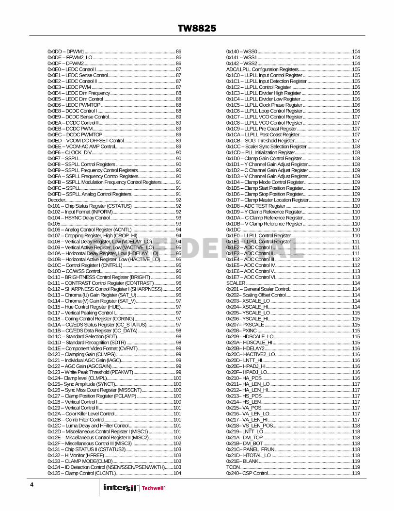
TW8825
4
0x0DD – DPWM1 .............................................................................. 86 0x0DE – FPWM2_LO ....................................................................... 86 0x0DF – DPWM2 ............................................................................... 86 0x0E0 – LEDC Control I .................................................................... 87 0x0E1 – LEDC Sense Control .......................................................... 87 0x0E2 – LEDC Control II ................................................................... 87 0x0E3 – LEDC PWM ........................................................................ 87 0x0E4 – LEDC Dim Frequency ........................................................ 88 0x0E5 – LEDC Dim Control .............................................................. 88 0x0E6 – LEDC PWMTOP ................................................................ 88 0x0E8 – DCDC Control I ................................................................... 88 0x0E9 – DCDC Sense Control ......................................................... 89 0x0EA – DCDC Control II .................................................................. 89 0x0EB – DCDC PWM ....................................................................... 89 0x0EC – DCDC PWMTOP .............................................................. 89 0x0ED – VCOM-DC OFFSET Control ............................................ 89 0x0EE – VCOM-AC AMP Control .................................................... 89 0x0F6 – CLOCK_DIV ........................................................................ 90 0x0F7 – SSPLL .................................................................................. 90 0x0F8 – SSPLL Control Registers ................................................... 90 0x0F9 – SSPLL Frequency Control Registers ................................ 90 0x0FA – SSPLL Frequency Control Registers................................ 90 0x0FB – SSPLL Modulation Frequency Control Registers............ 91 0x0FC – SSPLL ................................................................................. 91 0x0FD – SSPLL Analog Control Registers ...................................... 91 Decoder ............................................................................................... 92 0x101 – Chip Status Register (CSTATUS) ..................................... 92 0x102 – Input Format (INFORM) ...................................................... 92 0x104 – HSYNC Delay Control ........................................................ 93 0x105 ................................................................................................... 93 0x106 – Analog Control Register (ACNTL) ..................................... 94 0x107 – Cropping Register, High (CROP_HI) ................................ 94 0x108 – Vertical Delay Register, Low (VDELAY_LO) .................... 94 0x109 – Vertical Active Register, Low (VACTIVE_LO) .................. 95 0x10A – Horizontal Delay Register, Low (HDELAY_LO) .............. 95 0x10B – Horizontal Active Register, Low (HACTIVE_LO) ............. 95 0x10C – Control Register I (CNTRL1) ............................................. 95 0x10D – CC/WSS Control................................................................. 96 0x110 – BRIGHTNESS Control Register (BRIGHT) ..................... 96 0x111 – CONTRAST Control Register (CONTRAST) .................. 96 0x112 – SHARPNESS Control Register I (SHARPNESS) ........... 96 0x113 – Chroma (U) Gain Register (SAT_U) ................................. 96 0x114 – Chroma (V) Gain Register (SAT_V) .................................. 97 0x115 – Hue Control Register (HUE) ............................................... 97 0x117 – Vertical Peaking Control I .................................................... 97 0x118 – Coring Control Register (CORING) ................................... 97 0x11A – CC/EDS Status Register (CC_STATUS) ......................... 97 0x11B – CC/EDS Data Register (CC_DATA) ................................ 98 0x11C – Standard Selection (SDT) .................................................. 98 0x11D – Standard Recognition (SDTR) .......................................... 98 0x11E – Component Video Format (CVFMT) ................................ 99 0x120 – Clamping Gain (CLMPG) ................................................... 99 0x121 – Individual AGC Gain (IAGC) ............................................... 99 0x122 – AGC Gain (AGCGAIN) ....................................................... 99 0x123 – White Peak Threshold (PEAKWT) .................................... 99 0x124– Clamp level (CLMPL) ......................................................... 100 0x125– Sync Amplitude (SYNCT) .................................................. 100 0x126 – Sync Miss Count Register (MISSCNT) ........................... 100 0x127 – Clamp Position Register (PCLAMP) ............................... 100 0x128 – Vertical Control I ................................................................. 100 0x129 – Vertical Control II ................................................................ 101 0x12A – Color Killer Level Control .................................................. 101 0x12B – Comb Filter Control ........................................................... 101 0x12C – Luma Delay and HFilter Control ...................................... 101 0x12D – Miscellaneous Control Register I (MISC1) ..................... 101 0x12E – Miscellaneous Control Register II (MISC2) ..................... 102 0x12F – Miscellaneous Control III (MISC3) ................................... 102 0x131 – Chip STATUS II (CSTATUS2) ......................................... 103 0x132 – H Monitor (HFREF) ........................................................... 103 0x133 – CLAMP MODE(CLMD) .................................................... 103 0x134 – ID Detection Control (NSEN/SSEN/PSEN/WKTH) ....... 103 0x135 – Clamp Control (CLCNTL) ................................................. 104
0x140 – WSS0 ................................................................................. 104 0x141 – WSS1 ................................................................................. 104 0x142 – WSS2 ................................................................................. 104 ADC/LLPLL Configuration Registers.............................................. 105 0x1C0 – LLPLL Input Control Register .......................................... 105 0x1C1 – LLPLL Input Detection Register....................................... 105 0x1C2 – LLPLL Control Register .................................................... 106 0x1C3 – LLPLL Divider High Register ........................................... 106 0x1C4 – LLPLL Divider Low Register ............................................ 106 0x1C5 – LLPLL Clock Phase Register .......................................... 106 0x1C6 – LLPLL Loop Control Register .......................................... 106 0x1C7 – LLPLL VCO Control Register .......................................... 107 0x1C8 – LLPLL VCO Control Register .......................................... 107 0x1C9 – LLPLL Pre Coast Register ............................................... 107 0x1CA – LLPLL Post Coast Register ............................................. 107 0x1CB – SOG Threshold Register ................................................. 107 0x1CC – Scaler Sync Selection Register....................................... 108 0x1CD – PLL Initialization Register ................................................. 108 0x1D0 – Clamp Gain Control Register ........................................... 108 0x1D1 – Y Channel Gain Adjust Register...................................... 108 0x1D2 – C Channel Gain Adjust Register ..................................... 109 0x1D3 – V Channel Gain Adjust Register...................................... 109 0x1D4 – Clamp Mode Control Register ......................................... 109 0x1D5 – Clamp Start Position Register .......................................... 109 0x1D6 – Clamp Stop Position Register .......................................... 109 0x1D7 – Clamp Master Location Register ..................................... 109 0x1D8 – ADC TEST Register ......................................................... 110 0x1D9 – Y Clamp Reference Register ........................................... 110 0x1DA – C Clamp Reference Register .......................................... 110 0x1DB – V Clamp Reference Register .......................................... 110 0x1DC ............................................................................................... 110 0x1E0 – LLPLL Control Register .................................................... 110 0x1E1 – LLPLL Control Register .................................................... 111 0x1E2 – ADC Control I .................................................................... 111 0x1E3 – ADC Control II ................................................................... 111 0x1E4 – ADC Control III .................................................................. 112 0x1E5 – ADC Control IV .................................................................. 112 0x1E6 – ADC Control V ................................................................... 113 0x1E7 – ADC Control VI .................................................................. 113 SCALER ........................................................................................... 114 0x201 – General Scaler Control ...................................................... 114 0x202– Scaling Offset Control......................................................... 114 0x203– XSCALE_LO ...................................................................... 114 0x204– XSCALE_HI ........................................................................ 114 0x205– YSCALE_LO ...................................................................... 115 0x206– YSCALE_HI ........................................................................ 115 0x207– PXSCALE ........................................................................... 115 0x208– PXINC ................................................................................. 115 0x209– HDSCALE_LO ................................................................... 115 0x20A– HDSCALE_HI .................................................................... 115 0x20B– HDELAY2 ........................................................................... 116 0x20C– HACTIVE2_LO .................................................................. 116 0x20D– LNTT_HI ............................................................................. 116 0x20E– HPADJ_HI .......................................................................... 116 0x20F– HPADJ_LO ......................................................................... 116 0x210– HA_POS ............................................................................. 116 0x211– HA_LEN_LO ...................................................................... 117 0x212– HA_LEN_HI ........................................................................ 117 0x213– HS_POS ............................................................................. 117 0x214– HS_LEN .............................................................................. 117 0x215– VA_POS.............................................................................. 117 0x216– VA_LEN_LO ....................................................................... 117 0x217– VA_LEN_HI ........................................................................ 117 0x218– VS_LEN_POS.................................................................... 118 0x219– LNTT_LO ............................................................................ 118 0x21A– DM_TOP ............................................................................ 118 0x21B– DM_BOT ............................................................................ 118 0x21C– PANEL_FRUN .................................................................. 118 0x21D– HTOTAL_LO ..................................................................... 118 0x21E– BLANK ................................................................................ 119 TCON ................................................................................................ 119 0x240– CSP Control ........................................................................ 119
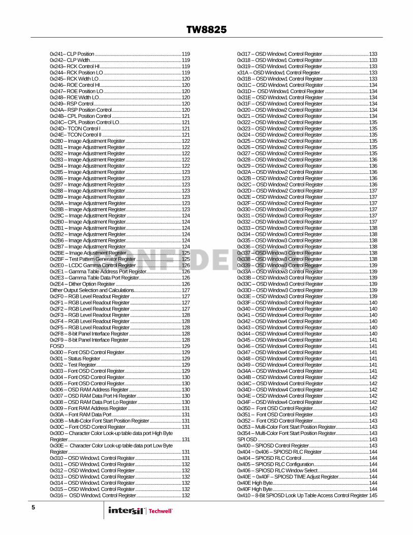
TW8825
5
0x241– CLP Position ....................................................................... 119 0x242– CLP Width ........................................................................... 119 0x243– RCK Control HI ................................................................... 119 0x244– RCK Position LO ................................................................ 119 0x245– RCK Width LO .................................................................... 120 0x246– ROE Control HI ................................................................... 120 0x247– ROE Position LO ................................................................ 120 0x248– ROE Width LO .................................................................... 120 0x249– RSP Control ........................................................................ 120 0x24A– RSP Position Control ......................................................... 120 0x24B– CPL Position Control ......................................................... 121 0x24C– CPL Position Control LO ................................................... 121 0x24D– TCON Control I .................................................................. 121 0x24E– TCON Control II ................................................................. 121 0x280 – Image Adjustment Register .............................................. 122 0x281 – Image Adjustment Register .............................................. 122 0x282 – Image Adjustment Register .............................................. 122 0x283 – Image Adjustment Register .............................................. 122 0x284 – Image Adjustment Register .............................................. 122 0x285 – Image Adjustment Register .............................................. 123 0x286 – Image Adjustment Register .............................................. 123 0x287 – Image Adjustment Register .............................................. 123 0x288 – Image Adjustment Register .............................................. 123 0x289 – Image Adjustment Register .............................................. 123 0x28A – Image Adjustment Register.............................................. 123 0x28B – Image Adjustment Register.............................................. 123 0x28C – Image Adjustment Register ............................................. 124 0x2B0 – Image Adjustment Register.............................................. 124 0x2B1 – Image Adjustment Register.............................................. 124 0x2B2 – Image Adjustment Register.............................................. 124 0x2B6 – Image Adjustment Register.............................................. 124 0x2B7 – Image Adjustment Register.............................................. 124 0x2BE – Image Adjustment Register ............................................. 125 0x2BF – Test Pattern Generator Register ..................................... 125 0x2E0 – LCDC Gamma Control Register ..................................... 126 0x2E1 – Gamma Table Address Port Register............................. 126 0x2E3 – Gamma Table Data Port Register ................................... 126 0x2E4 – Dither Option Register ...................................................... 126 Dither Output Selection and Calculations ....................................... 127 0x2F0 – RGB Level Readout Register .......................................... 127 0x2F1 – RGB Level Readout Register .......................................... 127 0x2F2 – RGB Level Readout Register .......................................... 127 0x2F3 – RGB Level Readout Register .......................................... 128 0x2F4 – RGB Level Readout Register .......................................... 128 0x2F5 – RGB Level Readout Register .......................................... 128 0x2F8 – 8-bit Panel Interface Register ........................................... 128 0x2F9 – 8-bit Panel Interface Register ........................................... 128 FOSD ................................................................................................ 129 0x300 – Font OSD Control Register............................................... 129 0x301 – Status Register .................................................................. 129 0x302 – Test Register ...................................................................... 129 0x303 – Font OSD Control Register............................................... 129 0x304 – Font OSD Control Register............................................... 130 0x305 – Font OSD Control Register............................................... 130 0x306 – OSD RAM Address Register ........................................... 130 0x307 – OSD RAM Data Port Hi Register ..................................... 130 0x308 – OSD RAM Data Port Lo Register .................................... 130 0x309 – Font RAM Address Register ............................................ 131 0x30A – Font RAM Data Port ......................................................... 131 0x30B – Multi-Color Font Start Position Register .......................... 131 0x30C – Font OSD Control Register .............................................. 131 0x30D – Character Color Look-up table data port High Byte Register ............................................................................................. 131 0x30E – Character Color Look-up table data port Low Byte Register ............................................................................................. 131 0x310 – OSD Window1 Control Register ...................................... 131 0x311 – OSD Window1 Control Register ...................................... 132 0x312 – OSD Window1 Control Register ...................................... 132 0x313 – OSD Window1 Control Register ...................................... 132 0x314 – OSD Window1 Control Register ...................................... 132 0x315 – OSD Window1 Control Register ...................................... 132 0x316 – OSD Window1 Control Register ..................................... 132
0x317 – OSD Window1 Control Register ...................................... 133 0x318 – OSD Window1 Control Register ...................................... 133 0x319 – OSD Window1 Control Register ...................................... 133 x31A – OSD Window1 Control Register ........................................ 133 0x31B – OSD Window1 Control Register ..................................... 133 0x31C – OSD Window1 Control Register ..................................... 134 0x31D – OSD Window1 Control Register .................................... 134 0x31E – OSD Window1 Control Register ..................................... 134 0x31F – OSD Window1 Control Register ...................................... 134 0x320 – OSD Window2 Control Register ...................................... 134 0x321 – OSD Window2 Control Register ...................................... 134 0x322 – OSD Window2 Control Register ...................................... 135 0x323 – OSD Window2 Control Register ...................................... 135 0x324 – OSD Window2 Control Register ...................................... 135 0x325 – OSD Window2 Control Register ...................................... 135 0x326 – OSD Window2 Control Register ...................................... 135 0x327 – OSD Window2 Control Register ...................................... 135 0x328 – OSD Window2 Control Register ...................................... 136 0x329 – OSD Window2 Control Register ...................................... 136 0x32A – OSD Window2 Control Register ..................................... 136 0x32B – OSD Window2 Control Register ..................................... 136 0x32C – OSD Window2 Control Register ..................................... 136 0x32D – OSD Window2 Control Register ..................................... 137 0x32E – OSD Window2 Control Register ..................................... 137 0x32F – OSD Window2 Control Register ...................................... 137 0x330 – OSD Window3 Control Register ...................................... 137 0x331 – OSD Window3 Control Register ...................................... 137 0x332 – OSD Window3 Control Register ...................................... 137 0x333 – OSD Window3 Control Register ...................................... 138 0x334 – OSD Window3 Control Register ...................................... 138 0x335 – OSD Window3 Control Register ...................................... 138 0x336 – OSD Window3 Control Register ...................................... 138 0x337 – OSD Window3 Control Register ...................................... 138 0x338 – OSD Window3 Control Register ...................................... 138 0x339 – OSD Window3 Control Register ...................................... 139 0x33A – OSD Window3 Control Register ..................................... 139 0x33B – OSD Window3 Control Register ..................................... 139 0x33C – OSD Window3 Control Register ..................................... 139 0x33D – OSD Window3 Control Register ..................................... 139 0x33E – OSD Window3 Control Register ..................................... 139 0x33F – OSD Window3 Control Register ...................................... 140 0x340 – OSD Window4 Control Register ...................................... 140 0x341 – OSD Window4 Control Register ...................................... 140 0x342 – OSD Window4 Control Register ...................................... 140 0x343 – OSD Window4 Control Register ...................................... 140 0x344 – OSD Window4 Control Register ...................................... 140 0x345 – OSD Window4 Control Register ...................................... 141 0x346 – OSD Window4 Control Register ...................................... 141 0x347 – OSD Window4 Control Register ...................................... 141 0x348 – OSD Window4 Control Register ...................................... 141 0x349 – OSD Window4 Control Register ...................................... 141 0x34A – OSD Window4 Control Register ..................................... 141 0x34B – OSD Window4 Control Register ..................................... 142 0x34C – OSD Window4 Control Register ..................................... 142 0x34D – OSD Window4 Control Register ..................................... 142 0x34E – OSD Window4 Control Register ..................................... 142 0x34F – OSD Window4 Control Register ...................................... 142 0x350 – Font OSD Control Register .............................................. 142 0x351 – Font OSD Control Register .............................................. 143 0x352 – Font OSD Control Register .............................................. 143 0x353 – Multi-Color Font Start Position Register ........................... 143 0x354 – Multi-Color Font Start Position Register ........................... 143 SPI OSD ........................................................................................... 143 0x400 – SPIOSD Control Register ................................................. 143 0x404 ~ 0x406 – SPIOSD RLC Register ...................................... 144 0x404 – SPIOSD RLC Control ....................................................... 144 0x405 – SPIOSD RLC Configuration ............................................. 144 0x406 – SPIOSD RLC Window Select .......................................... 144 0x40E ~ 0x40F – SPIOSD TIME Adjust Register......................... 144 0x40E High Byte ............................................................................... 144 0x40F High Byte ............................................................................... 144 0x410 – 8-Bit SPIOSD Look Up Table Access Control Register 145
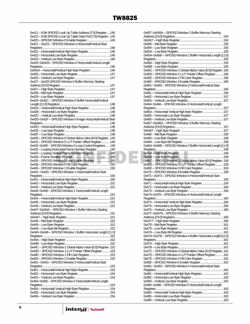
TW8825
6
0x411 – 8 Bit SPIOSD Look Up Table Address [7:0] Register .... 145 0x412 – 8 Bit SPIOSD Look Up Table Data Port [7:0] Register .. 145 0x420 – SPIOSD Window 0 Enable Register ............................... 145 0x421 ~ 0x423 – SPIOSD Window 0 Horizontal/Vertical Start Registers ........................................................................................... 146 0x421 – Horizontal/Vertical High Byte Register ............................. 146 0x422 – Horizontal Low Byte Register ........................................... 146 0x423 – Vertical Low Byte Register ................................................ 146 0x424~0x0426 – SPIOSD Window 0 Horizontal/Vertical Length Registers ........................................................................................... 146 0x0424 – Horizontal/Vertical High Byte Register ........................... 146 0x425 – Horizontal Low Byte Register ........................................... 147 0x426 – Vertical Low Byte Register ................................................ 147 0x427 – 0x429 SPIOSD Window 0 Buffer Memory Starting Address [23:0] Register ................................................................... 147 0x427 – High Byte Register ............................................................. 147 0x428 – Mid byte Register ............................................................... 147 0x429 – Low Byte Register ............................................................. 147 0x42A~0x42C – SPIOSD Window 0 Buffer Horizontal/Vertical Length [11:0] Registers .................................................................... 148 0x42A – Horizontal/Vertical High Byte Register ............................ 148 0x42B – Horizontal Low Byte Register ........................................... 148 0x42C – Vertical Low Byte Register ............................................... 148 0x42D~0x42F – SPIOSD Window 0 Image Horizontal/Vertical Start Registers ........................................................................................... 148 0x42D – Horizontal/Vertical High Byte Register ............................ 148 0x42E – Low byte Register ............................................................. 148 0x42F – Low Byte Register ............................................................. 148 0x430 – SPIOSD Window 0 Global Alpha Value [6:0] Register .. 149 0x431 – SPIOSD Window 0 LUT Pointer Offset Register ........... 149 0x432~0x435 – SPIOSD Window 0 Loop Control Registers ...... 149 0x432 – Looping Horizontal Frame Number Register .................. 149 0x433 – Looping Vertical Frame Number Register ...................... 149 0x434 – Frame Duration Register .................................................. 149 0x435 – SPIOSD Window 0 Loop Enable Register ..................... 150 0x436 – SPIOSD Window 0 Fill Color Register ............................ 150 0x440 – SPIOSD Window 1 Enable Register ............................... 150 0x441~ 0x443 – SPIOSD Window 1 Horizontal/Vertical Start Registers ........................................................................................... 150 0x441 – Horizontal/Vertical High Byte Register ............................. 150 0x442 – Horizontal Low Byte Register ........................................... 151 0x443 – Vertical Low Byte Register ................................................ 151 0x444~0x446 – SPIOSD Window 1 Horizontal/Vertical Length Registers ........................................................................................... 151 0x444 – Horizontal/Vertical High Byte Register ............................. 151 0x445 – Horizontal Low Byte Register ........................................... 151 0x446 – Vertical Low Byte Register ................................................ 151 0x447~0x044A – SPIOSD Window 1 Buffer Memory Starting Address [23:0] Registers.................................................................. 151 0x0447 – High Byte Register .......................................................... 151 0x448 – Mid Byte Register .............................................................. 152 0x449 – Low Byte Register ............................................................. 152 0x44A – Low Byte Bit Register........................................................ 152 0x44A~0x44B – SPIOSD Window 1 Buffer Horizontal Length [11:0] Registers ........................................................................................... 152 0x44A – High Byte Register ............................................................ 152 0x44B – Low Byte Register ............................................................. 152 0x44C – SPIOSD Window 1 Global Alpha Value [6:0] Register . 152 0x44D – SPIOSD Window 1 LUT Pointer Offset Register........... 153 0x44E – SPIOSD Window 1 Fill Color Register ............................ 153 0x450 – SPIOSD Window 2 Enable Register ............................... 153 0x451~ 0x453 – SPIOSD Window 2 Horizontal/Vertical Start Registers ........................................................................................... 153 0x451 – Horizontal/Vertical High Byte Register ............................. 153 0x452 – Horizontal Low Byte Register ........................................... 154 0x453 – Vertical Low Byte Register ................................................ 154 0x454~0x456 – SPIOSD Window 2 Horizontal/Vertical Length Registers ........................................................................................... 154 0x454 – Horizontal/ Vertical High Byte Register ............................ 154 0x455 – Horizontal Low Byte Register ........................................... 154 0x456 – Vertical Low Byte Register ................................................ 154
0x457~0x045A – SPIOSD Window 2 Buffer Memory Starting Address [23:0] Registers.................................................................. 154 0x0457 – High Byte Register .......................................................... 154 0x458 – Mid Byte Register .............................................................. 155 0x459 – Low Byte Register ............................................................. 155 0x45A – Low Byte Register ............................................................. 155 0x45A~0x45B – SPIOSD Window 2 Buffer Horizontal Length [11:0] Registers ........................................................................................... 155 0x45A – High Byte Register ............................................................ 155 0x45B – Low Byte Register ............................................................. 155 0x45C – SPIOSD Window 2 Global Alpha Value [6:0] Register . 155 0x45D – SPIOSD Window 2 LUT Pointer Offset Register........... 156 0x45E – SPIOSD Window 2 Fill Color Register ............................ 156 0x460 – SPIOSD Window 3 Enable Register ............................... 156 0x461~ 0x463 – SPIOSD Window 3 Horizontal/Vertical Start Registers ........................................................................................... 156 0x461 – Horizontal/Vertical High Byte Register ............................. 156 0x462 – Horizontal Low Byte Register ........................................... 157 0x463 – Vertical Low Byte Register ................................................ 157 0x464~0x466 – SPIOSD Window 3 Horizontal/Vertical Length Registers ........................................................................................... 157 0x464 – Horizontal/ Vertical High Byte Register ............................ 157 0x465 – Horizontal Low Byte Register ........................................... 157 0x466 – Vertical Low Byte Register ................................................ 157 0x467~0x046A – SPIOSD Window 3 Buffer Memory Starting Address [23:0] Registers.................................................................. 157 0x0467 – High Byte Register .......................................................... 157 0x468 – Mid Byte Register .............................................................. 158 0x469 – Low Byte Register ............................................................. 158 0x46A – Low Byte Bit Register........................................................ 158 0x46A~0x46B – SPIOSD Window 3 Buffer Horizontal Length [11:0] Registers ........................................................................................... 158 0x46A – High Byte Register ............................................................ 158 0x46B – Low Byte Register ............................................................. 158 0x46C – SPIOSD Window 3 Global Alpha Value [6:0] Register . 158 0x46D – SPIOSD Window 3 LUT Pointer Offset Register........... 159 0x46E – SPIOSD Window 3 Fill Color Register ............................ 159 0x470 – SPIOSD Window 4 Enable Register ............................... 159 0x471~ 0x473 – SPIOSD Window 4 Horizontal/Vertical Start Registers ........................................................................................... 159 0x471 – Horizontal/Vertical High Byte Register ............................. 159 0x472 – Horizontal Low Byte Register ........................................... 160 0x473 – Vertical Low Byte Register ................................................ 160 0x474~0x476 – SPIOSD Window 4 Horizontal/Vertical Length Registers ........................................................................................... 160 0x474 – Horizontal/ Vertical High Byte Register ............................ 160 0x475 – Horizontal Low Byte Register ........................................... 160 0x476 – Vertical Low Byte Register ................................................ 160 0x477~0x0479 – SPIOSD Window 4 Buffer Memory Starting Address [23:0] Registers.................................................................. 160 0x0477 – High Byte Register .......................................................... 160 0x478 – Mid Byte Register .............................................................. 161 0x479 – Low Byte Register ............................................................. 161 0x47A – Low Byte Bit Register........................................................ 161 0x47A~0x47B – SPIOSD Window 4 Buffer Horizontal Length [11:0] Registers ........................................................................................... 161 0x47A – High Byte Register ............................................................ 161 0x47B – Low Byte Register ............................................................. 161 0x47C – SPIOSD Window 4 Global Alpha Value [6:0] Register . 161 0x47D – SPIOSD Window 4 LUT Pointer Offset Register........... 162 0x47E – SPIOSD Window 4 Fill Color Register ............................ 162 0x480 – SPIOSD Window 5 Enable Register ............................... 162 0x481~ 0x483 – SPIOSD Window 5 Horizontal/Vertical Start Registers ........................................................................................... 162 0x481 – Horizontal/Vertical High Byte Register ............................. 162 0x482 – Horizontal Low Byte Register ........................................... 163 0x483 – Vertical Low Byte Register ................................................ 163 0x484~0x486 – SPIOSD Window 5 Horizontal/Vertical Length Registers ........................................................................................... 163 0x484 – Horizontal/ Vertical High Byte Register ............................ 163 0x485 – Horizontal Low Byte Register ........................................... 163 0x486 – Vertical Low Byte Register ................................................ 163
TW8825
7
0x487~0x048A – SPIOSD Window 5 Buffer Memory Starting Address [23:0] Registers.................................................................. 163 0x0487 – High Byte Register .......................................................... 163 0x488 – Mid Byte Register .............................................................. 164 0x489 – Low Byte Register ............................................................. 164 0x48A – Low Byte Bit Register........................................................ 164 0x48A~0x48B – SPIOSD Window 5 Buffer Horizontal Length [11:0] Registers ........................................................................................... 164 0x48A – High Byte Register ............................................................ 164 0x48B – Low Byte Register ............................................................. 164 0x48C – SPIOSD Window 5 Global Alpha Value [6:0] Register . 164 0x48D – SPIOSD Window 5 LUT Pointer Offset Register........... 165 0x48E – SPIOSD Window 5 Fill Color Register ............................ 165 0x490 – SPIOSD Window 6 Enable Register ............................... 165 0x491~ 0x493 – SPIOSD Window 6 Horizontal/Vertical Start Registers ........................................................................................... 165 0x491 – Horizontal/Vertical High Byte Register ............................. 165 0x492 – Horizontal Low Byte Register ........................................... 166 0x493 – Vertical Low Byte Register ................................................ 166 0x494~0x496 – SPIOSD Window 6 Horizontal/Vertical Length Registers ........................................................................................... 166 0x494 – Horizontal/ Vertical High Byte Register ............................ 166 0x495 – Horizontal Low Byte Register ........................................... 166 0x496 – Vertical Low Byte Register ................................................ 166 0x497~0x049A – SPIOSD Window 6 Buffer Memory Starting Address [23:0] Registers.................................................................. 166 0x0497 – High Byte Register .......................................................... 166 0x498 – Mid Byte Register .............................................................. 167 0x499 – Low Byte Register ............................................................. 167 0x49A – Low Byte Bit Register........................................................ 167 0x49A~0x49B – SPIOSD Window 6 Buffer Horizontal Length [11:0] Registers ........................................................................................... 167 0x49A – High Byte Register ............................................................ 167 0x49B – Low Byte Register ............................................................. 167 0x49C – SPIOSD Window 6 Global Alpha Value [6:0] Register . 167 0x49D – SPIOSD Window 6 LUT Pointer Offset Register........... 168 0x49E – SPIOSD Window 6 Fill Color Register ............................ 168 0x4A0 – SPIOSD Window 7 Enable Register .............................. 168 0x4A1~ 0x4A3 – SPIOSD Window 7 Horizontal/Vertical Start Registers ........................................................................................... 168 0x4A1 – Horizontal/Vertical High Byte Register ............................ 168 0x4A2 – Horizontal Low Byte Register ........................................... 169 0x4A3 – Vertical Low Byte Register ............................................... 169 0x4A4~0x4A6 – SPIOSD Window 7 Horizontal/Vertical Length Registers ........................................................................................... 169 0x4A4 – Horizontal/ Vertical High Byte Register ........................... 169 0x4A5 – Horizontal Low Byte Register ........................................... 169 0x4A6 – Vertical Low Byte Register ............................................... 169 0x4A7~0x04AA – SPIOSD Window 7 Buffer Memory Starting Address [23:0] Registers.................................................................. 169 0x04A7 – High Byte Register .......................................................... 169 0x4A8 – Mid Byte Register .............................................................. 170 0x4A9 – Low Byte Register ............................................................. 170 0x4AA – Low Byte Bit Register ....................................................... 170 0x4AA~0x4AB – SPIOSD Window 7 Buffer Horizontal Length [11:0] Registers ................................................................................. 170 0x4AA – High Byte Register ............................................................ 170 0x4AB – Low Byte Register ............................................................ 170 0x4AC – SPIOSD Window 7 Global Alpha Value [6:0] Register . 170 0x4AD – SPIOSD Window 7 LUT Pointer Offset Register .......... 171 0x4AE – SPIOSD Window 7 Fill Color Register ........................... 171 0x4B0 – SPIOSD Window 8 Enable Register .............................. 171 0x4B1~ 0x4B3 – SPIOSD Window 8 Horizontal/Vertical Start Registers ........................................................................................... 171 0x4B1 – Horizontal/Vertical High Byte Register ............................ 171 0x4B2 – Horizontal Low Byte Register ........................................... 172 0x4B3 – Vertical Low Byte Register ............................................... 172 0x4B4~0x4B6 – SPIOSD Window 8 Horizontal/Vertical Length Registers ........................................................................................... 172 0x4B4 – Horizontal/ Vertical High Byte Register ........................... 172 0x4B5 – Horizontal Low Byte Register ........................................... 172 0x4B6 – Vertical Low Byte Register ............................................... 172
0x4B7~0x04B9 – SPIOSD Window 8 Buffer Memory Starting Address [23:0] Registers.................................................................. 172 0x04B7 – High Byte Register .......................................................... 172 0x4B8 – Mid Byte Register .............................................................. 173 0x4B9 – Low Byte Register ............................................................. 173 0x4BA~0x4BB – SPIOSD Window 8 Buffer Horizontal Length [11:0] Registers ................................................................................. 173 0x4BA – High Byte Register ............................................................ 173 0x4BB – Low Byte Register ............................................................ 173 0x4BC – SPIOSD Window 8 Global Alpha Value [6:0] Register . 173 0x4BD – SPIOSD Window 8 LUT Pointer Offset Register .......... 173 0x4BE – SPIOSD Window 8 Fill Color Register ........................... 174 SPI & MCU ....................................................................................... 174 0x4C0 – SPI Flash Mode Control Register .................................... 174 0x4C1 -- SPI Flash Mode Control Register ................................... 174 0x4C3 – DMA Control Register ...................................................... 174 0x4C4 – Flash Busy Control Register ............................................ 174 0x4C5 – Wait Control Register........................................................ 175 0x4C6 – DMA Page Register ......................................................... 175 0x4C7 – DMA Index Register ......................................................... 175 0x4C8 – DMA Length Mid Byte Register ....................................... 175 0x4C9 – DMA Length Low Byte Register ...................................... 175 0x4CA – DMA Command Buffer1 Register .................................. 175 0x4CB – DMA Command Buffer2 Register .................................. 175 0x4CC – DMA Command Buffer3 Register .................................. 175 0x4CD – DMA Command Buffer4 Register .................................. 175 0x4CE – DMA Command Buffer5 Register .................................. 176 0x4CF ................................................................................................ 176 0x4D0 – DMA Read/Write Buffer1 Register .................................. 176 0x4D1 – DMA Read/Write Buffer2 Register .................................. 176 0x4D2 – DMA Read/Write Buffer3 Register .................................. 176 0x4D3 – DMA Read/Write Buffer4 Register .................................. 176 0x4D4 – DMA Read/Write Buffer5 Register .................................. 176 0x4D5 – DMA Read/Write Buffer6 Register .................................. 176 0x4D6 – DMA Read/Write Buffer7 Register .................................. 176 0x4D7 – DMA Read/Write Buffer8 Register .................................. 177 0x4D8 – SPI Flash Status Command Register............................. 177 0x4D9 – SPI Flash Busy Control Register ..................................... 177 0x4DA – DMA Length High Byte Register..................................... 177 0x4E0 – PCLK Control Register ..................................................... 177 0x4E1 – SPI CLK Control Register ................................................ 177 0x4E2 – Timer0 Divider High Byte Register .................................. 178 0x4E3 – Timer0 Divider Low Byte Register ................................... 178 0x4E4 – Timer1 Divider High Byte Register .................................. 178 0x4E5 – Timer1 Divider Low Byte Register ................................... 178 0x4E6 – Timer2 Divider High Byte Register .................................. 178 0x4E7 – Timer2 Divider Low Byte Register ................................... 178 0x4E8 – Timer3 Divider High Byte Register .................................. 178 0x4E9 – Timer3 Divider Low Byte Register ................................... 178 0x4EA – Timer4 Divider High Byte Register .................................. 178 0x4EB – Timer4 Divider Low Byte Register .................................. 179 Input Measurement .......................................................................... 179 0x500 ~ 0x501 Measurement Window Horizontal Start [10:0] 0x500 – High Byte Register ............................................................. 179 0x501 – Low Byte Register ............................................................. 179 0x502 ~ 0x503 Measurement Window Horizontal Length [11:0] 0x502 – High Byte Register ............................................................. 179 0x503 – Low Byte Register ............................................................. 179 0x504 ~ 0x505 Measurement Window Vertical Start [10:0] 0x504 – High Byte Register ........................................................................ 179 0x505 – Low Byte Register ............................................................. 180 0x506 ~ 0x507 Measurement Window Vertical Length [10:0] 0x506 – High Byte Register ............................................................. 180 0x507 – Low Byte Register ............................................................. 180 0x508 – Measurement Input Selection, Measurement Start Register ............................................................................................. 180 0x509 – Measurement Option, Input Change Detection Register180 0x50A – Measurement Option Register ....................................... 181 0x50B – Measurement Option Register ....................................... 181 0x510 ~ 0x513 Phase_G Registers 0x510 – Byte 3 Register ..... 181 0x511 – Byte 2 Register .................................................................. 181 0x512 – Byte 1 Register .................................................................. 181

TW8825
8
0x513 – Byte 0 Register .................................................................. 181 0x514 ~ 0x517 Phase_B Registers 0x514 – Byte 3 Register...... 182 0x515 – Byte 2 Register .................................................................. 182 0x516 – Byte 1 Register .................................................................. 182 0x517 – Byte 0 Register .................................................................. 182 0x518 ~ 0x51B Phase_R Registers 0x518 – Byte 3 Register ..... 182 0x519 – Byte 2 Register .................................................................. 182 0x51A – Byte 1 Register .................................................................. 182 0x51B – Byte 0 Register .................................................................. 182 0x51C – Minimum_G Register ....................................................... 183 0x51D – Minimum_B Register ....................................................... 183 0x51E – Minimum_R Register ........................................................ 183 0x51F – Maximum_G Register ...................................................... 183 0x520 – Maximum_B Register ....................................................... 183 0x521 – Maximum_R Register ....................................................... 183 0x522 ~ 0x523 Vertical Period Registers 0x522 – High Byte Register ............................................................................................. 183 0x523 – Low Byte Register ............................................................. 183 0x524 ~ 0x525 Horizontal Period Registers 0x524 – High Byte Register ............................................................................................. 184 0x525 – Low Byte Register ............................................................. 184 0x526 ~ 0x527 Hsync Rise to Fall Registers 0x526 – High Byte Register ............................................................................................. 184 0x527 – Low Byte Register ............................................................. 184 0x528 ~ 0x529 Hsync Rise to Horizontal Active End 0x528 – High Byte Register .................................................................................... 184 0x529 – Low Byte Register ............................................................. 184 0x52A ~ 0x52B Vsync High Width Registers 0x52A – High Byte Register ............................................................................................. 185 0x52B – Low Byte Register ............................................................. 185 0x52C ~ 0x52D Vsync Rise Position Registers 0x52C – High Byte Register ............................................................................................. 185 0x52D – Low Byte Register ............................................................. 185 0x52E ~ 0x52F Horizontal Active Starting Pixel Position I Registers 0x52E – High Byte Register ............................................................ 185 0x52F – Low Byte Register ............................................................. 185 0x530 ~ 0x531 Horizontal Active Starting Pixel Position II Registers 0x530 – High Byte Register ............................................................. 186 0x531 – Low Byte Register ............................................................. 186 0x532 ~ 0x533 Horizontal Active Ending Pixel Position I Registers 0x532 – High Byte Register ............................................................. 186 0x533 – Low Byte Register ............................................................. 186 0x534 ~ 0x535 Horizontal Active Ending Pixel Position II Register 0x534 – High Byte Register ............................................................. 186 0x535 – Low Byte Register ............................................................. 186 0x536 ~ 0x537 Vertical Active Starting Line I Registers ............... 187 0x536 – High Byte Register ............................................................. 187 0x537 – Low Byte Register ............................................................. 187 0x538 ~ 0x539 Vertical Active Starting Line II Registers 0x538 – High Byte Register ........................................................................... 187 0x539 – Low Byte Register ............................................................. 187 0x53A ~ 0x53B Vertical Active Ending Line I Registers 0x53A – High Byte Register ........................................................................... 187 0x53B – Low Byte Register ............................................................. 187 0x53C ~ 0x53D Vertical Active Ending Line II Registers 0x53C – High Byte Register ........................................................................... 188 0x53D – Low Byte Register ............................................................. 188 0x540 – Liminance Value – Minimum Register............................. 188 0x541 – Liminance Value – Maximum Register ........................... 188 0x542 – Liminance Value – Average Register .............................. 188 0x543 ~ 0x545 Vertical Period in 27 MHz Registers 0x543 – High Byte Register .................................................................................... 188 0x544 – Mid Byte Register .............................................................. 188
0x545 – Low Byte Register ............................................................. 189 MCU SFR Register .......................................................................... 189 0x9A – Code Bank Address Register ............................................ 189 0x9B – Cache Control Register ...................................................... 189 0xE2 – Chip Access Mode Control Register ................................ 189 0xFA – Interrupt7~14 Control Register .......................................... 190 0xFB – Interrupt7~14 Control Register .......................................... 190 0xFC – Interrupt7~14 Control Register ......................................... 190 0xFD – Interrupt7~14 Control Register ......................................... 190 0xFE – Interrupt7~14 Control Register .......................................... 190 0x80 – SFR Register ....................................................................... 190 0x81 – SFR Register ....................................................................... 191 0x82 – SFR Register ....................................................................... 191 0x83 – SFR Register ....................................................................... 191 0x84 – SFR Register ....................................................................... 191 0x85 – SFR Register ....................................................................... 191 0x86 – SFR Register ....................................................................... 191 0x87 – SFR Register ....................................................................... 191 0x88 – SFR Register ....................................................................... 191 0x89 – SFR Register ....................................................................... 192 0x8A – SFR Register ...................................................................... 192 0x8B – SFR Register ....................................................................... 192 0x8C – SFR Register ...................................................................... 192 0x8D – SFR Register ....................................................................... 192 0x8E – SFR Register ....................................................................... 192 0x90 – SFR Register ....................................................................... 192 0x91 – SFR Register ....................................................................... 192 0x92 – SFR Register ....................................................................... 193 0x93 – SFR Register........................................................................ 193 0x95 – SFR Register........................................................................ 193 0x98 – SFR Register........................................................................ 193 0x99 – SFR Register ....................................................................... 193 0xA0 – SFR Register ...................................................................... 193 0xA8 – SFR Register ...................................................................... 193 0xB0 – SFR Register ...................................................................... 193 0xB8 – SFR Register ...................................................................... 193 0xC0 – SFR Register ...................................................................... 194 0xC1 – SFR Register ...................................................................... 194 0xC2 – SFR Register ...................................................................... 194 0xC3 – SFR Register ...................................................................... 194 0xC4 – SFR Register ...................................................................... 194 0xC5 – SFR Register ...................................................................... 194 0xC6 – SFR Register ...................................................................... 194 0xC7 – SFR Register ...................................................................... 194 0xC8 – SFR Register ...................................................................... 194 0xC9 – SFR Register ...................................................................... 195 0xCA – SFR Register ...................................................................... 195 0xCB – SFR Register ...................................................................... 195 0xCC – SFR Register ...................................................................... 195 0xCD – SFR Register ...................................................................... 195 0xCE – SFR Register ...................................................................... 195 0xD0 – SFR Register ...................................................................... 195 0xD8 – SFR Register ...................................................................... 195 0xE0 – SFR Register ...................................................................... 195 0xE8 – SFR Register ....................................................................... 196 0xE9 – SFR Register ...................................................................... 196 0xEA – SFR Register ...................................................................... 196 0xEB – SFR Register ...................................................................... 196 0xF0 – SFR Register ...................................................................... 196 0xF8 – SFR Register ...................................................................... 196 0xF9 – SFR Register ...................................................................... 196
Life Support Policy ......................................................................... 197 Revision History ............................................................................. 197

TW8825
9
TW8825 Functional Block Diagram
2D-
Comb
Video
Decoder
Scaler/
Image
Enhance
DTV
I/F
Font OSD
Output
Formatter
TCON
2-Wire
Serial
Bus
SPI
OSD
YIN0~2
DTVCLK
DTVD[23:0]
DTVHS, VS
DTVDE
VIN0~1
TCON signals
Flat Panel Out
I2C_SDAT
I2C_SCLK
SPI
CIN0~1
LED/
VCOM
Control
Serial Data
Triple
ADCs
Input
Controller
MCU

TW8825
10
Ordering Information
PART NUMBER
PART
MARKING
PACKAGE
(PB-FREE)
PKG.
DWG. #
TW8825-LA1-CR (Note 1) TW8825 LA1-CR 128 Lead LQFP (14mmx20mm) Q128.14X20F
NOTE:
1. These Intersil Pb-free plastic packaged products employ special Pb-free material sets, molding compounds/die attach
materials, and 100% matte tin plate plus anneal (e3 termination finish, which is RoHS compliant and compatible with both
SnPb and Pb-free soldering operations). Intersil Pb-free products are MSL classified at Pb-free peak reflow temperatures that
meet or exceed the Pb-free requirements of IPC/JEDEC J STD-020.
TW8825
11
Functional Description
Overview
Intersil|Techwell’s TW8825 LCD Video processor is a highly integrated TFT panel controller. It integrates a high quality
2D comb NTSC/PAL/SECAM video decoder, scalers, timing controller, flexible font based, SPI based OSD engine and
high performance MCU. This unique level of mixed signal integration turns a TFT panel into a flexible display system. It
incorporates easy-to-operate features in a single package for multi-purpose in-car LCD display, portable DVD and DVRs
media players.
It contains all the logic required to convert analog or digital video signals in various formats to the signal formats that is
necessary to drive various kind of TFT panel types. It supports different panel resolutions depending on the scaler and
panel clock settings. It has built-in TCON for direct connecting with low cost TCON-less panel.
The integrated analog front-end contains ADCs with clamping circuits and Automatic Gain Control (AGC) circuit as well as
anti-aliasing filter to minimize external component count. The built-in video decoder employs proprietary 2D Comb filter
Y/C separation technologies to produce exceptionally high quality pictures.
The chip's internal logic synchronizes the panel frame rate to the incoming input frame rate. A high quality image-scaling
engine is used to convert the different input resolution formats to the output panel resolution. An internal de-interlacing
engine also allows interlaced video to be displayed.
On Screen Display is supported through on-chip multi-window OSD engine for maximum flexibility.
It also has built-in back light controller and panel bias voltage generator to further simplify the system design. The host
control interface supports the standard 2-wire serial bus
Analog Front-end
The analog front-end converts analog video signals to the required digital format. Each channel contains automatic
clamping circuit, AGC circuit, anti-aliasing filter and high performance ADCs to minimize the external component used.
The clamping circuit restores the signal DC level so it can be properly digitized. The analog inputs source selections are
software programmable. Different input source has different signal conditioning logics to properly convert the signal into
correct format for further processing
Video Decoder
SYNC PROCESSOR
The decoder sync processor of video input detects horizontal synchronization and vertical synchronization signals in the
composite video or in the Y signal of an S-Video signal. The processor contains a digital phase-locked-loop and decision
logic to achieve reliable sync detection in stable signal as well as in unstable signals such as those from VCR fast forward
or backward.
Horizontal Sync Processing
The horizontal synchronization processing contains a sync separator, a phase-locked-loop (PLL), and the related decision
logic.
The horizontal PLL locks onto the extracted horizontal sync in all conditions to provide jitter free image output. From
there, the PLL also provides orthogonal sampling raster for the down stream processor. It has wide lock-in range for
tracking any non-standard video signal.
Vertical Sync Processing
The vertical sync separator detects the vertical synchronization pattern in the input video signals. A detection window
controls the determination of sync. This provides more reliable synchronization. It simulates the functionality of a PLL
without the complexity of a PLL. The field status is determined at vertical synchronization time based on the vertical and
horizontal sync relationship.

TW8825
12
COLOR DECODING
Y/C Separation
The color-decoding block contains the luma / chroma separation for the composite video signal and multi-standard color
demodulation. For NTSC and PAL standard signals, the luma / chroma separation can be done either by comb filter or
notch/band-pass filter combination. For SECAM standard signals, only notch/band-pass filter is available. The default
selection for NTSC/PAL is comb filter. The characteristics of the band-pass filter can be found in the filter curve section.
In the case of comb filter, the decoder separates luma (Y) and chroma (C) of a NTSC/PAL composite video signal using a
proprietary adaptive comb algorithm. It leads to good Y/C separation with small cross luma and cross color at both
horizontal and vertical edges. Due to the line buffer used in the comb filter, there is always two lines processing delay in
the output images no matter what standard or filter option is chosen.
Color Demodulation
The color demodulation for NTSC and PAL standard is done by quadrature mixing the chroma signal to the base band
and extracting the chroma components with low-pass filter. The low-pass filter characteristic can be selected for
optimized transient color performance. For the PAL system, the PAL ID or the burst phase switching is identified to aid
the PAL color demodulation.
The SECAM color demodulation process consists of bell filtering, FM demodulator and de-emphasis filtering. The chroma
carrier frequency is identified in the process and used to control the SECAM color demodulation.
The sub-carrier signal for use in the color demodulator is generated by direct digital synthesis PLL that locks onto the
input sub-carrier reference (color burst). This arrangement allows any sub-standard of NTSC and PAL to be demodulated
easily.
Automatic Chroma Gain Control
The Automatic Chroma Gain Control (ACC) compensates for reduced amplitudes caused by transmission loss in video
signal. In the NTSC/PAL standard, the color reference signal is the burst on the back porch. This color-burst amplitude is
calculated and compared to standard amplitude. The chroma (Cx) signals are then compensated in amplitude
accordingly. The range of ACC control is –6db to +24db.
Low Color Detection and Removal
For low color amplitude signals, black and white video or very noisy signals, the color will be ―killed‖. The color killer uses
the burst amplitude measurement to switch-off the color when the measured burst amplitude falls below a programmed
threshold. The threshold has programmed hysteresis to prevent oscillation of the color killer operation. This function can
be disabled by programming a low threshold value.
AUTOMATIC STANDARD DETECTION
The video decoder has its automatic standard discrimination circuitry. The circuit uses burst-phase, burst-frequency and
frame rate to identify NTSC, PAL or SECAM color signals. The standards that can be identified are NTSC (M), NTSC (4.43),
PAL (B, D, G, H, I), PAL (M), PAL (N), PAL (60) and SECAM (M). Each standard can be included or excluded in the standard
recognition process by software control. The identified standard is indicated by the Standard Selection (SDT) register.
Automatic standard detection can be overridden by software controlled standard selection.
VIDEO FORMAT SUPPORT
The integrated video decoder supports all common video formats as shown in Table 1. It needs to be programmed
appropriately for each of the composite video input formats.
TW8825
13
TABLE 1. VIDEO INPUT FORMATS SUPPORTED
Format Lines Fields Fsc Country
NTSC-M 525 60 3.58 MHz U.S., many others
NTSC-Japan (1) 525 60 3.58 MHz Japan
PAL-B, G, N 625 50 4.43 MHz Many
PAL-D 625 50 4.43 MHz China
PAL-H 625 50 4.43 MHz Belgium
PAL-I 625 50 4.43 MHz Great Britain, others
PAL-M 525 60 3.58 MHz Brazil
PAL-CN 625 50 3.58 MHz Argentina
SECAM 625 50 4.406MHz
4.250MHz
France, Eastern Europe, Middle East, Russia
PAL-60 525 60 4.43 MHz China
NTSC (4.43) 525 60 4.43 MHz Transcoding
Notes: (1). NTSC-Japan has 0 IRE setup.
COMPONENT PROCESSING
Luminance Processing
The video decoder adjusts brightness by adding a programmable value (in register BRIGHTNESS) to the Y signal. It
adjusts the picture contrast by changing the gain (in register CONTRAST) of the Y signal.
It also provides a sharpness control function through a control register. The center frequency of the peaking filter is
selectable. A coring function is provided along with the sharpness control to reduce enhancement to the noise.
The Hue and Saturation
When decoding NTSC signals, the decoder can adjust the hue of the chroma signal. The hue is defined as a phase shift of
the subcarrier with respect to the burst. This phase shift can be programmed through a control register.
The color saturation can be adjusted by changing the gain of Cb and Cr signals for all NTSC, PAL and SECAM formats. The
Cb and Cr gain can be adjusted independently for flexibility.
Touch Screen Controller
Built-in 12-bit ADC touch screen controller in TW8825 provides accurate position reading with simplified digital operation
and can also be used to monitor up to four auxiliary inputs with touch interrupt.
Digital Input Support
In addition to analog inputs, it also has dual digital inputs mode for YCbCr/RGB data. The combination could be a RGB
565 plus BT 656 at the same time or a single 24 bit digital input mode. TW8825 supports both digital BT-656 as well as
8/16-bit 601 input. The 656 interface can work with both interlaced and progressive standard.

TW8825
14
Input Image Control
The input cropping control provides a way for programming the active display window region for the selected input video
or graphic. In the normal operation, the first active line starts with the VSYNC signal. This and vertical active length
register setting are used to determine the active vertical window. The active pixel starts HSYNC. This and the horizontal
active width register are used to determine the active horizontal window. The vertical window is programmed in line
increments. The horizontal window is programmed in one pixel increments for single pixel input mode or two pixels
increments for double pixels input mode. If data qualifier is used, then only qualified pixels will be counted in the window
size.
Image Scaling
The internal high quality image-scaling engine operates in several modes. The first is the bypass mode. No image scaling
is done in this mode. The number of active output lines per frame and the number of active output pixels per line are
identical to the input active lines and pixels, respectively. This mode is best used for displaying computer graphic at
panel's native resolution.
By default, the input active window is zoomed up to the full screen for display. This is used for non-interlaced data like PC
graphics or progressive scan video. The vertical and horizontal magnification ratio can be adjusted independently.
TW8825 has frame-sync mode which does not use frame buffer. In this mode, the zoom ratio and output clock rate
should be coordinated appropriately to avoid internal buffer overrun.
The TW8825 has a build in 2D de-interlacing mode to process interlaced video inputs. In this mode, every input field is
zoomed to the full output frame resolution. The de-interlaced fields can also be properly compensated to have fields
aligned correctly to avoid any artifacts. The offset can be programmed to provide maximum flexibility.
The horizontal scaler can be programmed to perform non-linear scaling : panorama scaling for displaying 4:3 input on a
16:9 display and water-glass scaling for displaying 16:9 input on a 4:3 display.
Image Enhancement Processing
BLACK/WHITE STRETCH
This feature is to expand dynamic range of the input image, which creates more vivid image impression.
TFT Panel Support
It supports a variety of active matrix TFT panel types and resolutions.
DITHERING
It has the dithering circuit to reduce the output dynamic range to fit the panel type. This allows LCD panels with 3, 4, 6 or
8 bits per color per pixel to display up to 16.8 million colors and LCD panels with 3 bits per color per pixel to can display
up to 2.1 million colors. It employs both spatial and frame modulation dithering. When dithering with the least significant
4-bits of input data it uses spatial modulation with 4x4 blocks of pixels. When dithering with the least significant 1 to 3
bits of input data, it uses either spatial modulation with 2x2 pixel blocks, or frame modulation.
GAMMA TABLE
It has integrated gamma table for each color output and it is fully programmable through host bus.
TCON
The integrated Timing controller supports flexible column/row driver control signals to interface with TCON-less panel
directly.

TW8825
15
Font Based On Screen Display
The TW8825 supports built-in OSD controller with programmable RAM font. The OSD display is independent of the input
active window setting or the scaling ratio.
The on-chip OSD controller is a character-based controller. The pre-defined character or graphic bit map is stored in the
font RAM. It can store up to 379 single color fonts when character is 12 pixels wide by 18 pixels high. The characters can
be displayed on the screen in four user defined window locations of any size from 1 to 512 characters. The spaces
between characters are also programmable. There is a limit of 512 characters that may be displayed on screen at one
time in all windows combined. The attributes of each window can also be set to give it a shadow effect or 3-D effect. In
addition, the characters can be expanded by a factor of 2, 3 or 4 in vertical or horizontal directions and have the blinking
effect and border/shadow effect on a character by character basis.
ON CHIP OSD FUNCTIONS
Font SRAM: Max 379 (12x18) User Programmable Single Color Font (10240x8 SRAM)
Character Register SRAM : 512 Location (9-bit Font Address + 10-bit Character Attribute, 512x19
SRAM)
Characters
Character Color: 16 colors
Character Background Color: 16 colors
Character Blinking: Enable/Disable, 1 Hz Blinking frequency
Character Border/Shadow Effect: Enable/Disable
(Multi OSD Window Display Case : Chip has a limitation) Character Space: Both H and V programmable by number of pixels
Quick Character Change in Window: Programmable Start Address and Buffer Size
Programmable OSD Color Palette Support
Re-designed OSD Font Supporting Standard Alpha-Numerical Character Set Windows
Number of Windows: 4 Independent Windows
Window Color: 16 colors
Window Zoom: 2, 3, 4 times zoom by dot number, H/V separate zooming control
Window Position: Programmable
H Direction: 1-pixel per step, V Direction: 1-Line per step
Window Size: Both H and V programmable by number of characters
Window Bordering/Shadowing Effect : 4 Independent Windows Enable/Disable Control
Window Alpha Blending Control : 4 Independent Windows Control
16 Different Color for Alpha Blending support(4-bit control)
Window 3-D Effect : 4 Independent Windows Enable/Disable Control
Window Border Color : 16 Colors
Window Border Width: programmable
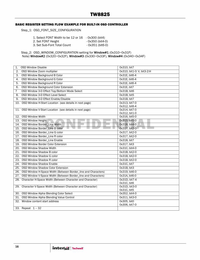
TW8825
16
BASIC REGISTER SETTING FLOW EXAMPLE FOR BUILT-IN OSD CONTROLLER
Step_1: OSD_FONT_SIZE_CONFIGURATION
1. Select FONT Width to be 12 or 16 - 0x300 (bit4)
2. Set FONT Height - 0x350 (bit4-0)
3. Set Sub-Font Total Count - 0x351 (bit6-0)
Step_2: OSD_WINDOW_CONFIGURATION setting for Window#1 (0x310~0x31F)
Note) Window#2 (0x320~0x32F), Window#3 (0x330~0x33F), Window#4 (0x340~0x34F)
1. OSD Window Disable 0x310, bit7
2. OSD Window Zoom multiplier 0x310, bit1-0: V, bit3-2:H
3. OSD Window Background B Color 0x31E, bit6-4
4. OSD Window Background G Color 0x31E, bit6-4
5. OSD Window Background R Color 0x31E, bit6-4
6. OSD Window Background Color Extension 0x31E, bit7
7 OSD Window 3-D Effect Top/Bottom Mode Select 0x31B, bit6
8. OSD Window 3-D Effect Level Select 0x31B, bit5
9. OSD Window 3-D Effect Enable/Disable 0x31B, bit7
10. OSD Window H-Start Location (see details in next page) 0x313, bit7-0
0x312, bit6-4
11. OSD Window V-Start Location (see details in next page) 0x314, bit7-0
0x312, bit1-0
12. OSD Window Width 0x316, bit5-0
13. OSD Window Height 0x315, bit5-0
14. OSD Window Border_Line Width 0x318, bit4-0
15. OSD Window Border_Line B color 0x317, bit2-0
16. OSD Window Border_Line G color 0x317, bit2-0
17. OSD Window Border_Line R color 0x317, bit2-0
18. OSD Window Border_Line Enable 0x318, bit7
19. OSD Window Border Color Extension 0x317, bit3
20. OSD Window Shadow Width 0x31C, bit4-0
21. OSD Window Shadow B color 0x31B, bit2-0
22. OSD Window Shadow G color 0x31B, bit2-0
23. OSD Window Shadow R color 0x31B, bit2-0
24. OSD Window Shadow Enable 0x31C, bit7
25. OSD Window Shadow Color Extension 0x31B, bit3
26. OSD Window H-Space Width (Between Border_line and Characters) 0x319, bit6-0
27. OSD Window V-Space Width (Between Border_line and Characters) 0x31A, bit6-0
28. Character H-Space Width (Between Character and Character) 0x31D, bit7-4
0x31C, bit6
29. Character V-Space Width (Between Character and Character) 0x31D, bit3-0
0x31C, bit5
30. OSD Window Alpha Blending Color Select 0x352, bit4-0
31. OSD Window Alpha Blending Value Control 0x311, bit3-0
32. Window content start address 0x305, bit0
0x306, bit7-0
33. Repeat 1 – 32

TW8825
17
Step_3: OSD_COLOR_ATTRIBUTE / FONT setting (OSD RAM)
1. Enable OSD RAM Access
- 0x304 (bit0 = 0)
2. Set Multi-Color Start Address
- 0x305 (bit3-1), 0x30B (bit7-0), 0x353 (bit7-0), 0x354 (bit7-0)
3. OSD RAM Address
- 0x305 (bit0), 0x306 (bit7-0)
- The first address is Step_1_32 Window content start address.
4. OSD RAM Data Port High (Font Address)
- 0x307 Data is written to above address automatically.
- 0x304 (bit5=0) select lower 256 char. (bit5=1) select upper 256 char.
5. OSD RAM Data Port Bit18 (Border Effect ), Bit17 (Blinking Effect ), Bit16 (Upper|Lower 256 char.)
- 0x304 Bit4, Bit7, and Bit5 Data are written to above address automatically.
6. OSD RAM Data Port Low (Color Attribute)
- 0x308 Data is written to above address automatically.
7. Repeat 3), 4), 5), and 6)
- The address should be increased by one each.
Step_4: COLOR LOOK-UP TABLE setting
1. Select Color Look-Up Table Write Address
- 0x30C (bit[5:0])
- BIT[5:0]: These 6 bits specify one of the 64 entries in the look-up table. Each entry is a 16-bit RGB
color by its content.
- There are 65536 colors available. For single color font, only sixteen of them are accessible by OSD
controller at a given time.
2. Color Look-Up Table control bits setting
- 0x30D (High Byte), 0x30E (Low Byte)
- The data of the Look-Up Table is accessed through 0x30D and 0x30E.
3. Repeat 1) and 2) to program each entry of the Look-Up Table.
Step_5: FONT_RAM_DATA setting (FONT RAM)
1. Enable FONT RAM Access
- 0x304 (bit0 = 1)
2. FONT RAM Address Setting - 8 bits(h00 – hFF)
- 0x309
- h00~hFF : Single Font RAM(256 Programmable Characters)
3. FONT RAM Data Port
- - 0x30A Data is written to above address automatically.
4. Repeat (4) at 27 times for one FONT RAM Data
- The internal address automatically increases by one each.
5. New FONT RAM Address Setting – 8 bits
6. Repeat 3), 4), 5)
- The FONT RAM Address should be increased by one each.
Note) as for the FONT RAM configuration and font bit mapping, see the detailed description
Step_6: End of OSD setting and Enable OSD
1. OSD On/Off Enable Control 0: ON, 1: OFF
- 0x30C (bit6 = 0)
2. OSD Window Enable
- 0x310 (bit7 = 1) Window1 Enable

TW8825
18
OSD WINDOW START LOCATION: BUILT-IN OSD CONTROLLER
Internal generated OSD DE Position delayed from H-SYNC: 0x303[7:0]
OSD window H_start location from start of internal OSD DE: 0x312[6:4], 0x313[7:0] increment by 1 pixel at a time
OSD window V_start location from start of VACT: 0x312[1:0], 0x314[7:0] increment by 1 line at a time
0
1
2
0 18
Address
The characters can be displayed on the screen in four user
defined window locations of any size from 1 to 512
characters. There is a limit of 512 characters that may be
displayed on screen at one time in all windows combined.
Example
Window #1: Address 0 – 2 (3 character)
Window #2: Address 3 – 100 (98 character)
Window #3: Address 101– 254 (154 character)
Window #4: Address 255 - 511 (257 character)
OSD_RAM CONFIGURATION
509
510
511
18 0 8 7
FONT_ADDRESS (11-bits)
Bit 18: Border/Shadow
Bit 17: Blinking
Bit 16: Up256
Bit 15 - 8: FONT Address
FONT_ATTRIBUTE (8-bits)
Bit 7: Character’s background color extension
Bit 6: Character’s background R
Bit 5: Character’s background G
Bit 4: Character’s background B
Bit 3: Character’s color extension
Bit 2: Character R
Bit 1: Character G
Bit 0: Character B
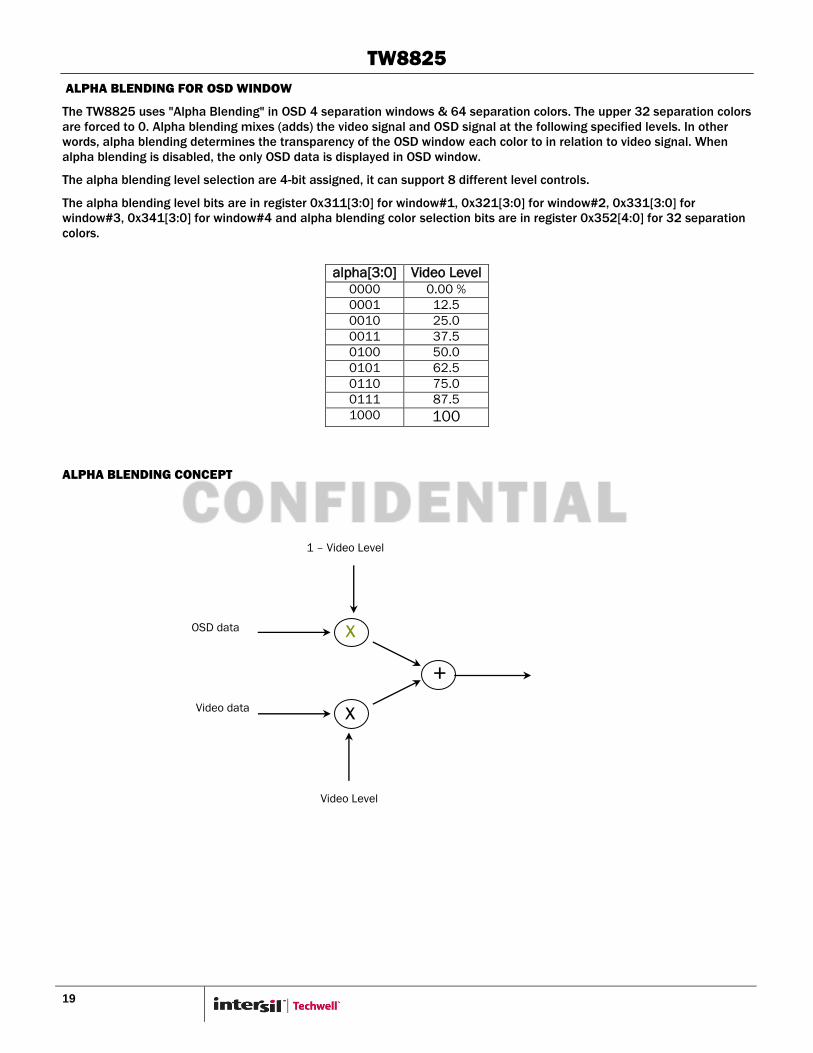
TW8825
19
ALPHA BLENDING FOR OSD WINDOW
The TW8825 uses "Alpha Blending" in OSD 4 separation windows & 64 separation colors. The upper 32 separation colors
are forced to 0. Alpha blending mixes (adds) the video signal and OSD signal at the following specified levels. In other
words, alpha blending determines the transparency of the OSD window each color to in relation to video signal. When
alpha blending is disabled, the only OSD data is displayed in OSD window.
The alpha blending level selection are 4-bit assigned, it can support 8 different level controls.
The alpha blending level bits are in register 0x311[3:0] for window#1, 0x321[3:0] for window#2, 0x331[3:0] for
window#3, 0x341[3:0] for window#4 and alpha blending color selection bits are in register 0x352[4:0] for 32 separation
colors.
alpha[3:0] Video Level 0000 0.00 %
0001 12.5
0010 25.0
0011 37.5
0100 50.0
0101 62.5
0110 75.0
0111 87.5
1000 100
ALPHA BLENDING CONCEPT
x
+
Video Level Vie
vel
OSD data
Video data
x
1 – Video Level
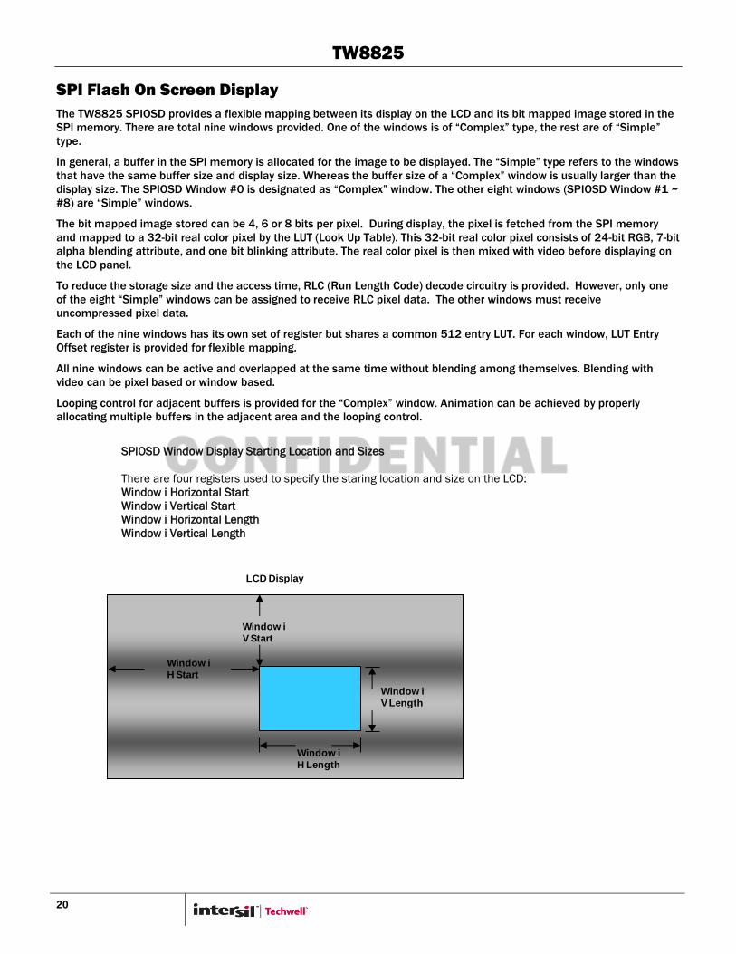
TW8825
20
SPI Flash On Screen Display
The TW8825 SPIOSD provides a flexible mapping between its display on the LCD and its bit mapped image stored in the
SPI memory. There are total nine windows provided. One of the windows is of ―Complex‖ type, the rest are of ―Simple‖
type.
In general, a buffer in the SPI memory is allocated for the image to be displayed. The ―Simple‖ type refers to the windows
that have the same buffer size and display size. Whereas the buffer size of a ―Complex‖ window is usually larger than the
display size. The SPIOSD Window #0 is designated as ―Complex‖ window. The other eight windows (SPIOSD Window #1 ~
#8) are ―Simple‖ windows.
The bit mapped image stored can be 4, 6 or 8 bits per pixel. During display, the pixel is fetched from the SPI memory
and mapped to a 32-bit real color pixel by the LUT (Look Up Table). This 32-bit real color pixel consists of 24-bit RGB, 7-bit
alpha blending attribute, and one bit blinking attribute. The real color pixel is then mixed with video before displaying on
the LCD panel.
To reduce the storage size and the access time, RLC (Run Length Code) decode circuitry is provided. However, only one
of the eight ―Simple‖ windows can be assigned to receive RLC pixel data. The other windows must receive
uncompressed pixel data.
Each of the nine windows has its own set of register but shares a common 512 entry LUT. For each window, LUT Entry
Offset register is provided for flexible mapping.
All nine windows can be active and overlapped at the same time without blending among themselves. Blending with
video can be pixel based or window based.
Looping control for adjacent buffers is provided for the ―Complex‖ window. Animation can be achieved by properly
allocating multiple buffers in the adjacent area and the looping control.
SPIOSD Window Display Starting Location and Sizes
There are four registers used to specify the staring location and size on the LCD:
Window i Horizontal Start
Window i Vertical Start
Window i Horizontal Length
Window i Vertical Length
LCD Display
Window i
V Start
Window i
H Start
Window i
V Length
Window i
H Length
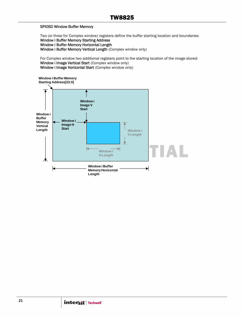
TW8825
21
SPIOSD Window Buffer Memory
Two (or three for Complex window) registers define the buffer starting location and boundaries:
Window i Buffer Memory Starting Address
Window i Buffer Memory Horizontal Length
Window i Buffer Memory Vertical Length (Complex window only)
For Complex window two additional registers point to the starting location of the image stored:
Window i Image Vertical Start (Complex window only)
Window i Image Horizontal Start (Complex window only)
Window i Buffer
Memory Horizontal
Length
Window i
Image V
Start
Window i
Image H
Start
Window i Buffer Memory
Starting Address[23:0]
Window i
H Length
Window i
V Length
Window i
Buffer
Memory
Vertical
Length

TW8825
22
SPIOSD Window Loop Control
For Complex window, three registers are used for loop control:
Window i Looping Horizontal Frame Number (Complex window only)
Window i Looping Vertical Frame Number (Complex window only)
Window i Frame Duration (Complex window only)
In the diagram below, the Looping Horizontal Frame Number register contains a value N, and the Looping
Vertical Frame Number register contains a value M. The display starts from Frame #00 and then moves
horizontally to the right and then vertically down. The display order is #00, #01, #02, … #0N, #10, #11, #12,
… #1N, …. #M0, #M1, … #MN. Each frame stays on for the time specified by Frame Duration register.
Window i Buffer
Memory Horizontal
Length
Window i Image V
Start
Window i Image H
Start
Window i Buffer
Memory Starting
Address[23:0]
Window i
Buffer
Memory
Vertical
Length
Window i Buffer
Memory Horizontal
Length
Buffer #00
Window i Buffer
Memory Horizontal
Length
Window i Image V
Start
Window i Image H
Start
Window i Buffer
Memory Horizontal
Length
Buffer #01
Window i Buffer
Memory Horizontal
Length
Window i Image V
Start
Window i Image H
Start
Window i Buffer
Memory Horizontal
Length
Buffer #0N
Window i Image V
Start
Window i Image H
Start
Window i
Buffer
Memory
Vertical
Length
Buffer #10
Window i Image V
Start
Window i Image H
Start
Window i
Buffer
Memory
Vertical
Length
Buffer #M0 Window i Image V
Start
Window i Image H
Start
Buffer #MN
Frame #00
Frame #01
Frame #10
Frame #0N
Frame #M0
Frame #MN
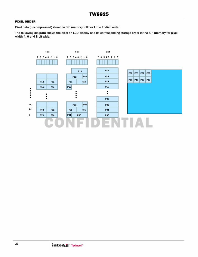
TW8825
23
PIXEL ORDER
Pixel data (uncompressed) stored in SPI memory follows Little Endian order.
The following diagram shows the pixel on LCD display and its corresponding storage order in the SPI memory for pixel
width 4, 6 and 8 bit wide.
P00 P01 P02 P03
P01
7 6 5 4 3 2 1 0
P00
P02
P03
P10 P11 P12 P13P11
P10
P12
P13
P00
P01
P01
P02
P02P03
P10
P10
P11
P11P12
P13
7 6 5 4 3 2 1 0
P00
P02
P01
P03
A
A+1
A+2
P10
P12
P11
P13
7 6 5 4 3 2 1 0
4 bit 6 bit 8 bit

TW8825
24
RLC DATA FORMAT
RLC data format is shown below:
T: Type to follow, 0 for Data, 1 for CNT
DATA: Uncompressed data
CNT: Repeat count
The width of DATA and CNT are set by RLC Control register. The valid DATA width is 4, 6, or 8. The width of CNT can be 2
up to 16.
The diagrams below show original data sequence of D0, D1, D2, D3, D4, and D5 before and after compression. In this
example the DATA width is 8 and the CNT width is 4. Data D2, D3, and D4 are the same.
Original Data:
RLC Compression result:
RLC data stored in memory:
T DATA / CNT T DATA / CNT T DATA / CNT T DATA / CNT
D0
D1
D2
D3
D4
D5
0 D0 0 D1 0 D2 21 0 D5
D00
0D0 D1
0D1 D2
1D2 2
D50
D5
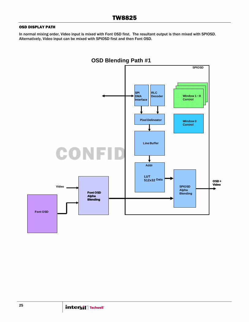
TW8825
25
OSD DISPLAY PATH
In normal mixing order, Video input is mixed with Font OSD first. The resultant output is then mixed with SPIOSD.
Alternatively, Video input can be mixed with SPIOSD first and then Font OSD.
OSD Blending Path #1
LUT 512x32
Addr
Data
Window 0
Control
Window 1 ~ 8
Control
Line Buffer
SPIOSD
Alpha
Blending
Video
Font OSD
Alpha
Blending
Font OSD
OSD +
Video
SPIOSD
Pixel Delineator
RLC
Decoder
SPI
DMA
Interface
LUT 512x32
Addr
Data
Window 0
Control
Window 1 ~ 8
Control
Line Buffer
SPIOSD
Alpha
BlendingFont OSD
Alpha
Blending
OSD +
Video
SPIOSD
Pixel Delineator
RLC
Decoder
SPI
DMA
Interface
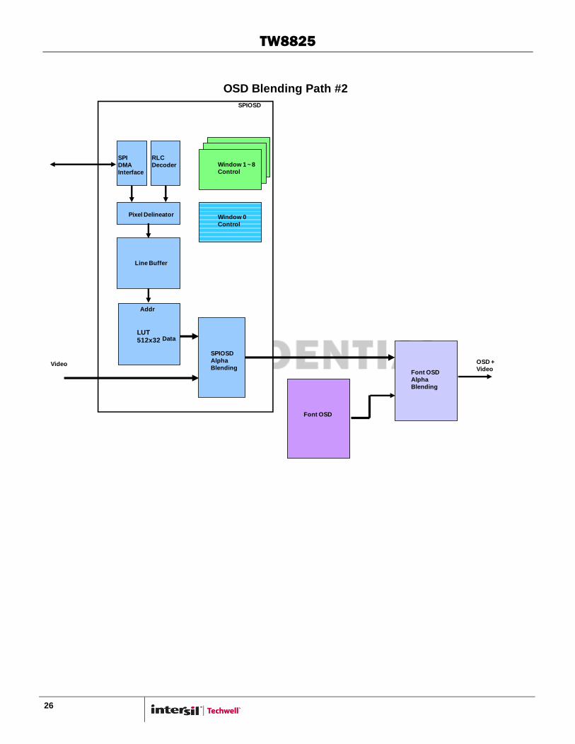
TW8825
26
OSD Blending Path #2
OSD +
VideoFont OSD
Alpha
Blending
Font OSD
Video
LUT 512x32
Addr
Data
Window 0
Control
Window 1 ~ 8
Control
Line Buffer
SPIOSD
Alpha
Blending
SPIOSD
Pixel Delineator
RLC
Decoder
SPI
DMA
Interface
TW8825
27
BUILT-IN MICROCONTROLLER
TW8825 has built-in 8052 microcontroller with program cache memory to enhance MCU performance. TW8825 MCU is
100% software compatible with industry standard 8052 with additional add-on features and faster instruction execution
time.
The main features of TW8825 MCU
Industry standard 8052 Core
Timer 0, 1 and Timer 2
Support 2 UARTs up to 115200bps
Support External Interrupt INT0~INT6
IO Port – Most of digital pins can be configured to GPIO
Power Save Mode with internal 32KHz
Watchdog
The additional add-on features for TW8825 MCU
Program fetch from external SPI Flash with Single/Dual/Quad mode
256 B Code cache and 2K XDATA memory
Additional timer 3 and timer 4 for 2 Baud Rate Generator
8 Extended Interrupt Units INT7~INT14
Support IR receiver and IRQ output
Internal ISP ROM Boot Selection
SPI DMA Read/Write XMEM
Control register for MCU Operation
SPI Flash Mode for MCU program fetch - 0x4C0 (bit2-0)
SPI Clock Control - 0x4E1 (bit5-4), - 0x4E1 (bit2-0)
MCU Cache Enable – SFR 0x9B (bit0)
MCU Timer Clock Divider Control
- 0x4E2, - 0x4E3 for Timer 0
- 0x4E4, - 0x4E5 for Timer 1
- 0x4E6, - 0x4E7 for Timer 2
- 0x4E8, - 0x4E9 for Timer 3
- 0x4EA, - 0x4EB for Timer 4
Boot Strap Sequence
TW8825 provides external boot select pin only for during device power up
SPI DMA to MCU XMEM
1.) Set SPI Flash Mode for DMA operation - 0x4C0 (bit2-0)
2.) Set SPI DMA Length - {0x4DA, 0x4C8, 0x4C9}
3.) Set SPI DMA Command - {0x4CA, 0x4CB, 0x4CC, 0x4CD, 0x4CE}
4.) Set - 0x4C3 (bit7-6 = 2‟b11) select DMA destination to MCU XMEM
5.) Set - 0x4C3 (bit5-4) DMA access mode
6.) Set - 0x4C4 (bit1) DMA read/write mode
7.) Set - 0x4C6 (bit3-0), - 0x4C7 (bit7-0) for destination start address
8.) Set - 0x4C4 (bit0 = 1) to start DMA execution
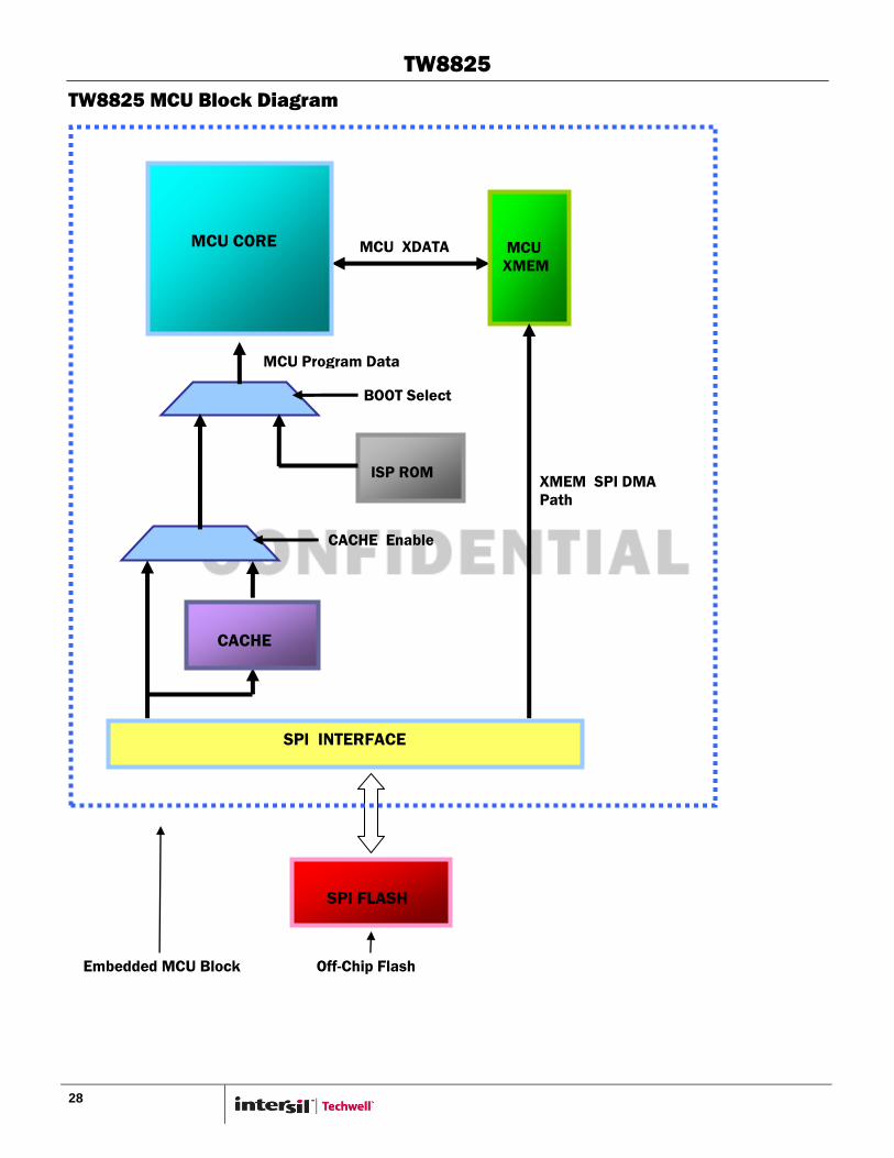
TW8825
28
TW8825 MCU Block Diagram
SPI FLASH
SPI INTERFACE
CACHE
XMEM SPI DMA
Path
MCU Program Data
MCU XDATA
BOOT Select
CACHE Enable
ISP ROM
MCU CORE
MCU
XMEM
Embedded MCU Block Off-Chip Flash

TW8825
29
Microcontroller Interface
The host interface is accessed via 2-wire serial bus interface. It always operates as a slave device.
TWO WIRE SERIAL BUS INTERFACE
MC_SDA
Start Condition Stop Condition
MC_SCLK
MC_SCLK
Device ID (1-7) R/W Index (1-8) Data (1-8)
MC_SDA
Start
Condition
Stop
Condition
Ack Ack Ack
FIGURE 1. DEFINITION OF THE SERIAL BUS INTERFACE BUS START AND STOP
FIGURE 2. ONE COMPLETE REGISTER WRITE SEQUENCE VIA THE SERIAL BUS INTERFACE

TW8825
30
The two wire serial bus interface is used to allow an external micro-controller to write control data to, and read control or
other information from the internal registers. MC_SCLK is the serial clock and MC_SDA is the data line. Both lines are
pulled high by resistors connected to VDD. Ics communicate on the bus by pulling MC_SCLK and MC_SDA low through
open drain outputs. In normal operation the master generates all clock pulses, but control of the MC_SDA line alternates
back and forth between the master and the slave. For both read and write, each byte is transferred MSB first, and the
data bit is valid whenever MC_SCLK is high.
The device is operated as a bus slave device. The 7-bit device address field is fixed and concatenated with the read/write
control bit to form the first byte transferred during a new transfer. If the read/write control bit is high the next byte will be
read from the slave device. If it is low the next byte will be a write to the slave. When a bus master (the host
microprocessor) drives MC_SDA from high to low, while MC_SCLK is high, this is defined to be a start condition (See
Figure 1). All slaves on the bus listen to determine when a start condition has been asserted.
After a start condition, all slave devices listen for their device addresses. The host then sends a byte consisting of the 7-
bit slave device ID and the R/W bit. This is shown in Figure 2. (The next byte is normally the index to the internal registers
and is a write to the device therefore the first R/W bit is normally low.)
After transmitting the device address and the R/W bit, the master must release the MC_SDA line while holding MC_SCLK
low, and wait for an acknowledgement from the slave. If the address matches the device address of a slave, the slave
will respond by driving the MC_SDA line low to acknowledge the condition. The master will then continue with the next 8-
bit transfer. If no device on the bus responds, the master transmits a stop condition and ends the cycle. Notice that a
successful transfer always includes nine clock pulses.
To write to the internal register, the master sends another 8-bit of data, it loads this to the register pointed by the internal
index register. The device will acknowledge the 8-bit data transfer and automatically increment the index in preparation
for the next data. The master can do multiple writes if they are in ascending sequential order. After each 8-bit transfer
the device will acknowledge the receipt of the 8-bits with an acknowledgement pulse. To end all transfers, the host has
to issue a stop condition.
Re-start
Condition
MC_SCLK
Device ID (1-7) R/W Index (1-8)
MC_SDA
Ack Ack
Data (1-8)
Stop
Condition Nack
Start
Condition
Device ID (1-7) R/W
Ack
FIGURE 3. ONE COMPLETE REGISTER READ SEQUENCE VIA THE SERIAL BUS INTERFACE
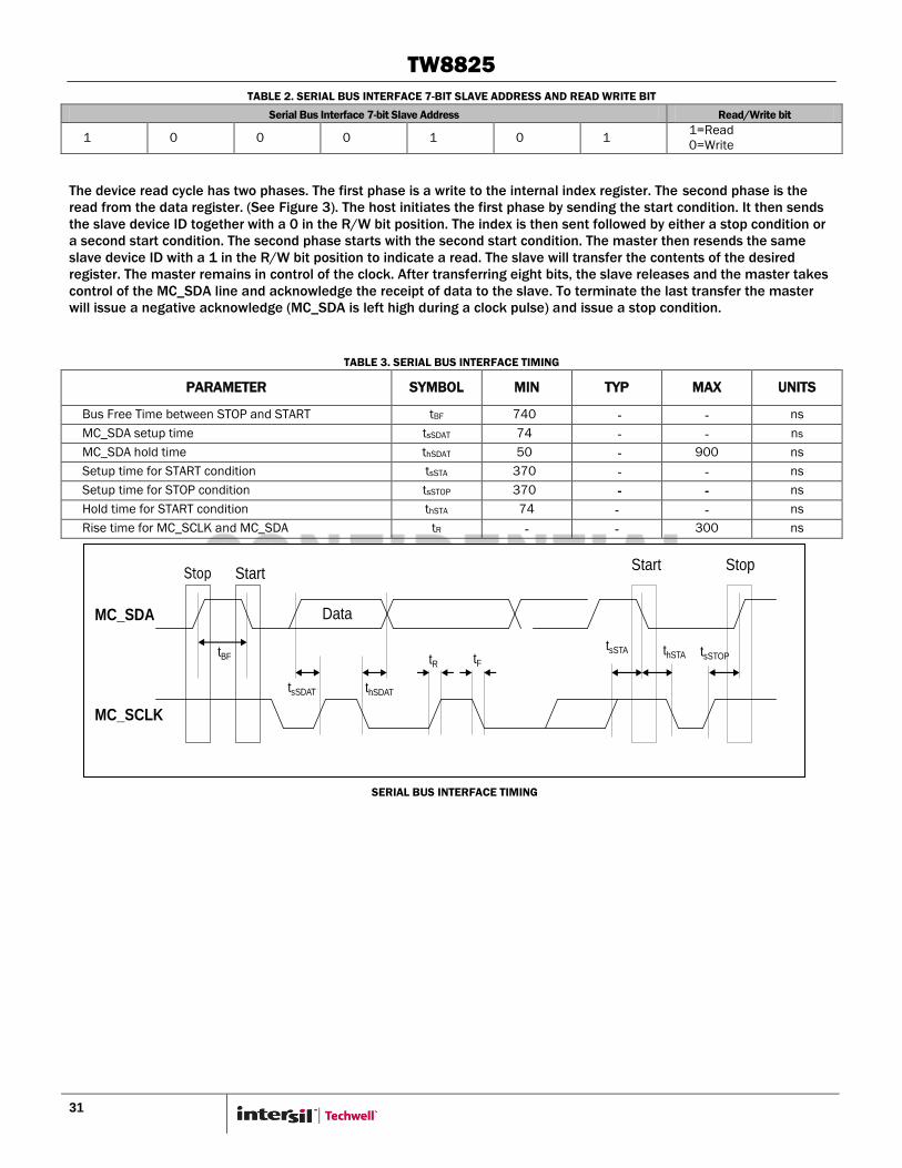
TW8825
31
TABLE 2. SERIAL BUS INTERFACE 7-BIT SLAVE ADDRESS AND READ WRITE BIT
Serial Bus Interface 7-bit Slave Address Read/Write bit
1 0 0 0 1 0 1 1=Read
0=Write
The device read cycle has two phases. The first phase is a write to the internal index register. The second phase is the
read from the data register. (See Figure 3). The host initiates the first phase by sending the start condition. It then sends
the slave device ID together with a 0 in the R/W bit position. The index is then sent followed by either a stop condition or
a second start condition. The second phase starts with the second start condition. The master then resends the same
slave device ID with a 1 in the R/W bit position to indicate a read. The slave will transfer the contents of the desired
register. The master remains in control of the clock. After transferring eight bits, the slave releases and the master takes
control of the MC_SDA line and acknowledge the receipt of data to the slave. To terminate the last transfer the master
will issue a negative acknowledge (MC_SDA is left high during a clock pulse) and issue a stop condition.
TABLE 3. SERIAL BUS INTERFACE TIMING
PARAMETER SYMBOL MIN TYP MAX UNITS
Bus Free Time between STOP and START tBF 740 - - ns
MC_SDA setup time tsSDAT 74 - - ns
MC_SDA hold time thSDAT 50 - 900 ns
Setup time for START condition tsSTA 370 - - ns
Setup time for STOP condition tsSTOP 370 - - ns
Hold time for START condition thSTA 74 - - ns
Rise time for MC_SCLK and MC_SDA tR - - 300 ns
SERIAL BUS INTERFACE TIMING
Stop StartStopStart
MC_SDA
MC_SCLK
tBFthSTA tsSTOP
tsSTA
tsSDAT
tR tF
thSDAT
Data
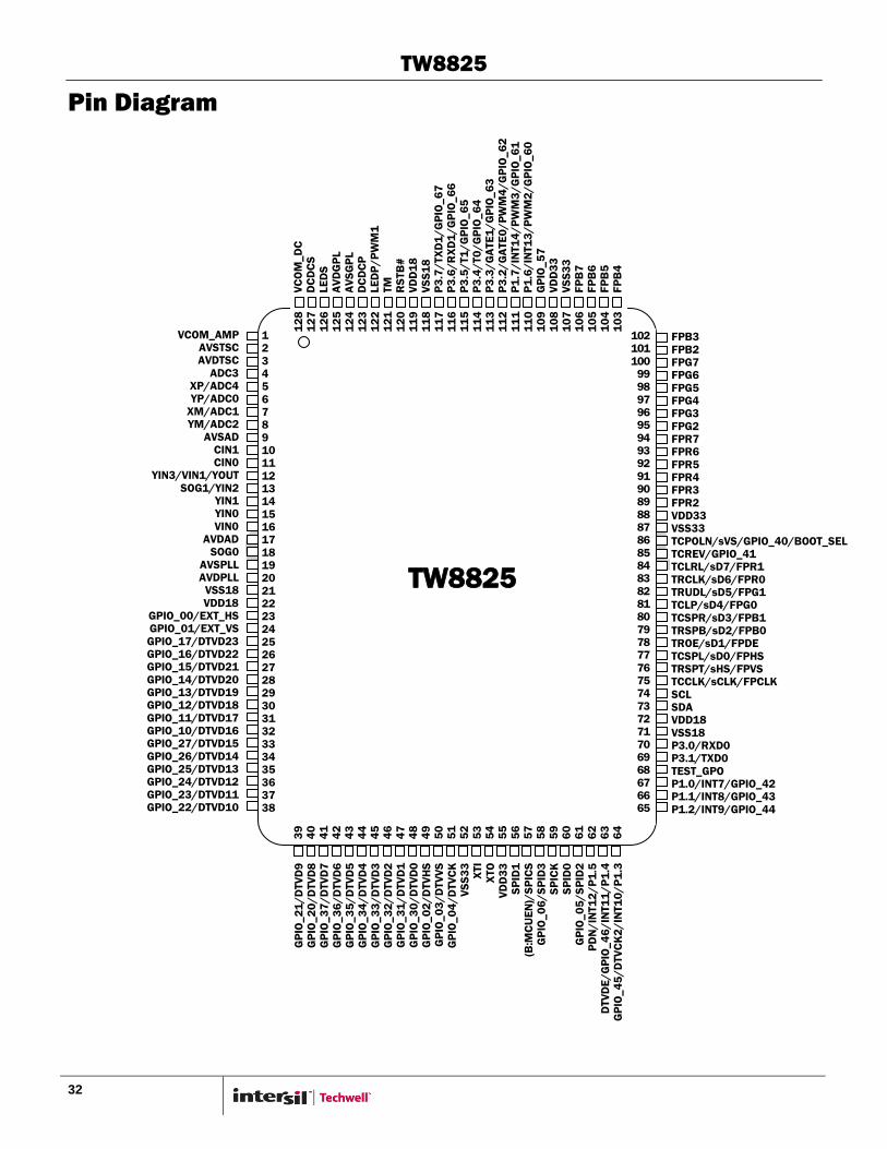
TW8825
32
Pin Diagram
VC
OM
_D
C
DC
DC
S
LE
DS
A
VD
GP
L
AV
SG
PL
DC
DC
P
LE
DP
/P
WM
1
TM
R
STB
#
VD
D1
8
VS
S1
8
P3
.7/
TX
D1
/G
PIO
_6
7
P3
.6/
RX
D1
/G
PIO
_6
6
P3
.5/
T1
/G
PIO
_6
5
P3
.4/
T0
/G
PIO
_6
4
P3
.3/
GA
TE
1/
GP
IO_
63
P
3.2
/G
ATE
0/
PW
M4
/G
PIO
_6
2
P1
.7/
INT1
4/
PW
M3
/G
PIO
_6
1
P1
.6/
INT1
3/
PW
M2
/G
PIO
_6
0
GP
IO_
57
V
DD
33
V
SS
33
F
PB
7
FP
B6
F
PB
5
FP
B4
VCOM_AMP
AVSTSC AVDTSC
ADC3 XP/ADC4 YP/ADC0
XM/ADC1 YM/ADC2
AVSAD CIN1 CIN0
YIN3/VIN1/YOUT SOG1/YIN2
YIN1 YIN0 VIN0
AVDAD SOG0
AVSPLL AVDPLL
VSS18 VDD18
GPIO_00/EXT_HS GPIO_01/EXT_VS GPIO_17/DTVD23 GPIO_16/DTVD22 GPIO_15/DTVD21 GPIO_14/DTVD20 GPIO_13/DTVD19 GPIO_12/DTVD18 GPIO_11/DTVD17 GPIO_10/DTVD16 GPIO_27/DTVD15 GPIO_26/DTVD14 GPIO_25/DTVD13 GPIO_24/DTVD12 GPIO_23/DTVD11 GPIO_22/DTVD10
G
PIO
_2
1/
DTV
D9
G
PIO
_2
0/
DTV
D8
G
PIO
_3
7/
DTV
D7
G
PIO
_3
6/
DTV
D6
G
PIO
_3
5/
DTV
D5
G
PIO
_3
4/
DTV
D4
G
PIO
_3
3/
DTV
D3
G
PIO
_3
2/
DTV
D2
G
PIO
_3
1/
DTV
D1
G
PIO
_3
0/
DTV
D0
G
PIO
_0
2/
DTV
HS
G
PIO
_0
3/
DTV
VS
G
PIO
_0
4/
DTV
CK
V
SS
33
X
TI
XTO
V
DD
33
S
PID
1
(B:M
CU
EN
)/S
PIC
S
GP
IO_
06
/S
PID
3
SP
ICK
S
PID
0
GP
IO_
05
/S
PID
2
PD
N/
INT1
2/
P1
.5
DTV
DE
/G
PIO
_4
6/
INT1
1/
P1
.4
GP
IO_
45
/D
TV
CK
2/
INT1
0/
P1
.3
39
4
0
41
4
2
43
4
4
45
4
6
47
4
8
49
5
0
51
5
2
53
5
4
55
5
6
57
5
8
59
6
0
61
6
2
63
6
4
FPB3 FPB2 FPG7 FPG6 FPG5 FPG4 FPG3 FPG2 FPR7 FPR6 FPR5 FPR4 FPR3 FPR2 VDD33 VSS33 TCPOLN/sVS/GPIO_40/BOOT_SEL TCREV/GPIO_41 TCLRL/sD7/FPR1 TRCLK/sD6/FPR0 TRUDL/sD5/FPG1 TCLP/sD4/FPG0 TCSPR/sD3/FPB1 TRSPB/sD2/FPB0 TROE/sD1/FPDE TCSPL/sD0/FPHS TRSPT/sHS/FPVS TCCLK/sCLK/FPCLK SCL SDA VDD18 VSS18 P3.0/RXD0 P3.1/TXD0 TEST_GPO P1.0/INT7/GPIO_42 P1.1/INT8/GPIO_43 P1.2/INT9/GPIO_44
TW8825
102 101 100
99 98 97 96 95 94 93 92 91 90 89 88 87 86 85 84 83 82 81 80 79 78 77 76 75 74 73 72 71 70 69 68 67 66 65
1 2 3 4 5 6 7 8 9 10 11 12 13 14 15 16 17 18 19 20 21 22 23 24 25 26 27 28 29 30 31 32 33 34 35 36 37 38
12
8
12
7
12
6
12
5
12
4
12
3
12
2
12
1
12
0
11
9
11
8
11
7
11
6
11
5
11
4
11
3
11
2
11
1
11
0
10
9
10
8
10
7
10
6
10
5
10
4
10
3

TW8825
33
Pin Descriptions This section provides a detailed description of each pin for the TW8825. The pins are arranged in functional groups
according to their associated interface.
The active state of the signal is determined by the trailing symbol at the end of the signal name. A "#" symbol indicates
that the signal is active or asserted at a low voltage level. When "#" is not present after the signal name, the signal is
active at the high voltage level.
The pin description also includes the buffer direction and type used for that pin.
PIN# I/O PIN NAME DESCRIPTION INTERNAL
CONNECTION
RECOMMENDED CONNECTION
OF UNUSED PIN
STATUS AT
HW RESET
ANALOG I/F SIGNALS AND POWER
124 P AVSGPL Genlock PLL Ground
-
- Pwr 125 P AVDGPL Genlock PLL Power +1.8V
126 AI LEDS LED Sense Open/Unconnected Hi-Z
127 AI DCDCS DCDC Sense
128 AO VCOM_DC VCOM out for DC
Open/Unconnected Hi-Z 1 AO VCOM_AMP
VCOM out for AMP.
TCON-Column Driver Inversion
2 P AVSTSC Analog TSC Ground - Pwr
3 P AVDTSC Analog TSC Power +3.3V
4 AI ADC3 Auxiliary channel 3
Open/Unconnected Hi-Z
5 AI ADC4 Auxiliary channel 4
AI XP TSC Positive X input
6 AI ADC0 Auxiliary channel 0
AI YP TSC Positive Y input
7 AI ADC1 Auxiliary channel 1
AI XM TSC Negative X input
8 AI ADC2 Auxiliary channel 2
AI YM TSC Negative Y input
9 P AVSAD Analog A/D Ground - Pwr
10 AI CIN1 Analog component C input 1
Connect to AVSAD Hi-Z
11 AI CIN0 Analog component C input 0
12
AO YOUT Analog Y output
AI YIN3 Analog composite or luma
input 2
AI VIN1 Analog component V input 0
13 AI YIN2
Analog composite or luma
input 2
AI SOG1 Sync On Green Input 1

TW8825
34
PIN# I/O PIN NAME DESCRIPTION INTERNAL
CONNECTION
RECOMMENDED CONNECTION
OF UNUSED PIN
STATUS AT
HW RESET
14 AI YIN1 Analog composite or luma
input 1
15 AI YIN0
Analog composite or luma
input 0
16 AI VIN0 Analog component V input 0
17 P AVDAD Analog A/D Power +1.8V - Pwr
18 AI SOG0 Sync On Green Input 0 Connect to AVSPLL Hi-Z
19 P AVSPLL PLL (Internal Analog) Ground
- Pwr 20 P AVDPLL
PLL (Internal Analog) Power
+1.8V
DIGITAL I/F SIGNALS
23 I EXT_HS External Hsync for RGB
Pull Down Open/Unconnected 0
I GPIO_00 General Purpose Data I/O
24 I EXT_VS External Vsync for RGB
I GPIO_01 General Purpose Data I/O
25 I DTVD23 DTV Input
I GPIO_17 General Purpose Data I/O
26 I DTVD22 DTV Input
I GPIO_16 General Purpose Data I/O
27 I DTVD21 DTV Input
I GPIO_15 General Purpose Data I/O
28 I DTVD20 DTV Input
I GPIO_14 General Purpose Data I/O
29 I DTVD19 DTV Input
I GPIO_13 General Purpose Data I/O
30 I DTVD18 DTV Input
I GPIO_12 General Purpose Data I/O
31 I DTVD17 DTV Input
I GPIO_11 General Purpose Data I/O
32 I DTVD16 DTV Input
I GPIO_10 General Purpose Data I/O
33 I DTVD15 DTV Input
I GPIO_27 General Purpose Data I/O
34 I DTVD14 DTV Input
I GPIO_26 General Purpose Data I/O
35 I DTVD13 DTV Input
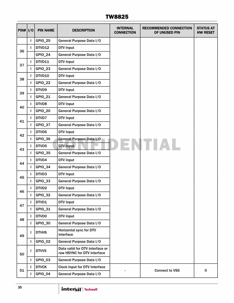
TW8825
35
PIN# I/O PIN NAME DESCRIPTION INTERNAL
CONNECTION
RECOMMENDED CONNECTION
OF UNUSED PIN
STATUS AT
HW RESET
I GPIO_25 General Purpose Data I/O
36 I DTVD12 DTV Input
GPIO_24 General Purpose Data I/O
37 I DTVD11 DTV Input
I GPIO_23 General Purpose Data I/O
38 I DTVD10 DTV Input
I GPIO_22 General Purpose Data I/O
39 I DTVD9 DTV Input
I GPIO_21 General Purpose Data I/O
40 I DTVD8 DTV Input
I GPIO_20 General Purpose Data I/O
41 I DTVD7 DTV Input
I GPIO_37 General Purpose Data I/O
42 I DTVD6 DTV Input
I GPIO_36 General Purpose Data I/O
43 I DTVD5 DTV Input
I GPIO_35 General Purpose Data I/O
44 I DTVD4 DTV Input
I GPIO_34 General Purpose Data I/O
45 I DTVD3 DTV Input
I GPIO_33 General Purpose Data I/O
46 I DTVD2 DTV Input
I GPIO_32 General Purpose Data I/O
47 I DTVD1 DTV Input
I GPIO_31 General Purpose Data I/O
48 I DTVD0 DTV Input
I GPIO_30 General Purpose Data I/O
49 I DTVHS
Horizontal sync for DTV
interface
I GPIO_02 General Purpose Data I/O
50 I DTVVS
Data valid for DTV interface or
raw HSYNC for DTV interface
I GPIO_03 General Purpose Data I/O
51 I DTVCK Clock Input for DTV Interface
- Connect to VSS 0 I GPIO_04 General Purpose Data I/O

TW8825
36
PIN# I/O PIN NAME DESCRIPTION INTERNAL
CONNECTION
RECOMMENDED CONNECTION
OF UNUSED PIN
STATUS AT
HW RESET
53 I XTI Crystal terminal or oscillator
input - - -
54 O XTO Crystal terminal
56 I/O SPID1 SPI Data 1 Pull Up Open/Unconnected 1
57
O SPICS SPI Chip Select
- Connect to VSS or VDD - I MCUEN
(Bootstrap) MCU Enable
H: Enable, L: Disable
58 I/O SPID3 SPI Data 3
Pull Up Open/Unconnected 1 I/O GPIO_06 General Purpose Data I/O
59 I/O SPICK SPI Clock Output - Connect to VSS -
60 I/O SPID0 SPI Data 0
Pull Up Open/Unconnected
1 61 I/O SPID2 SPI Data 2
I/O GPIO_05 General Purpose Data I/O
62 I/O P1.5/INT12 MCU Port / Interrupt Input
- Connect to VSS or VDD Hi-Z
I PDN Power Down Control
63
I/O P1.4/INT11 MCU Port / Interrupt Input
I/O GPIO_46 General Purpose Data I/O
I DTVDE Data valid for DTV interface or
raw HSYNC for DTV interface
64
I/O P1.3/INT10 MCU Port / Interrupt Input
I DTVCK2 Clock Input for DTV Interface
I/O GPIO_45 General Purpose Data I/O
65 I/O P1.2/INT9 MCU Port / Interrupt Input
I/O GPIO_44 General Purpose Data I/O
66 I/O P1.1/INT8 MCU Port / Interrupt Input
I/O GPIO_43 General Purpose Data I/O
67 I/O P1.0/INT7 MCU Port / Interrupt Input
I/O GPIO42 General Purpose Data I/O
68 O TEST_GPO
Multi-Purpose Test Output
For normal operation, please
remain ―High" during Reset.
Pull Up Open/Unconnected 1
69 I/O P3.1/TXD0 MCU Port / TXD0 - Connect to VSS or VDD Hi-Z
70 I/O P3.0/RXD0 MCU Port / RXD0
73 I/O SDA I2C Data - Connect to VDD Hi-Z
74 I SCL I2C Clock
75 O TCCLK TCON-Column Driver clock Pull down Open/Unconnected 0
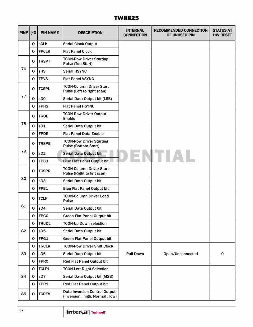
TW8825
37
PIN# I/O PIN NAME DESCRIPTION INTERNAL
CONNECTION
RECOMMENDED CONNECTION
OF UNUSED PIN
STATUS AT
HW RESET
O sCLK Serial Clock Output
O FPCLK Flat Panel Clock
76
O TRSPT TCON-Row Driver Starting
Pulse (Top Start)
O sHS Serial HSYNC
O FPVS Flat Panel VSYNC
77
O TCSPL TCON-Column Driver Start
Pulse (Left to right scan)
O sD0 Serial Data Output bit (LSB)
O FPHS Flat Panel HSYNC
78
O TROE TCON-Row Driver Output
Enable
O sD1 Serial Data Output bit
O FPDE Flat Panel Data Enable
79
O TRSPB TCON-Row Driver Starting
Pulse (Bottom Start)
O sD2 Serial Data Output bit
O FPB0 Blue Flat Panel Output bit
80
O TCSPR TCON-Column Driver Start
Pulse (Right to left scan)
O sD3 Serial Data Output bit
O FPB1 Blue Flat Panel Output bit
81
O TCLP TCON-Column Driver Load
Pulse
O sD4 Serial Data Output bit
O FPG0 Green Flat Panel Output bit
82
O TRUDL TCON-Up Down selection
O sD5 Serial Data Output bit
O FPG1 Green Flat Panel Output bit
83
O TRCLK TCON-Row Driver Shift Clock
Pull Down Open/Unconnected 0 O sD6 Serial Data Output bit
O FPR0 Red Flat Panel Output bit
84
O TCLRL TCON-Left Right Selection
O sD7 Serial Data Output bit (MSB)
O FPR1 Red Flat Panel Output bit
85 O TCREV Data Inversion Control Output
(Inversion : high, Normal : low)
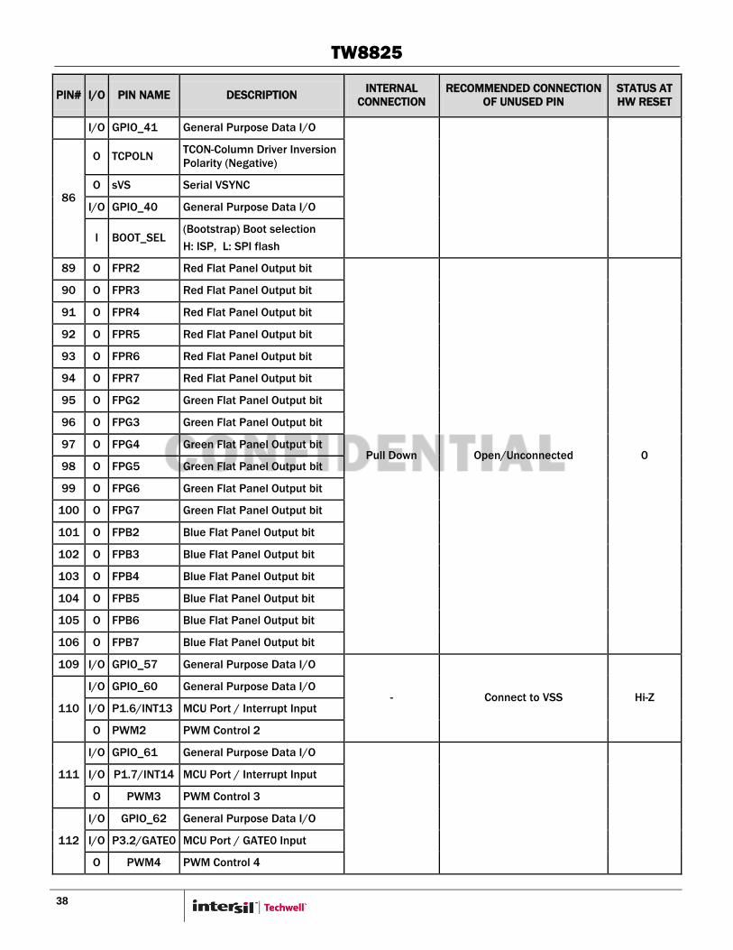
TW8825
38
PIN# I/O PIN NAME DESCRIPTION INTERNAL
CONNECTION
RECOMMENDED CONNECTION
OF UNUSED PIN
STATUS AT
HW RESET
I/O GPIO_41 General Purpose Data I/O
86
O TCPOLN TCON-Column Driver Inversion
Polarity (Negative)
O sVS Serial VSYNC
I/O GPIO_40 General Purpose Data I/O
I BOOT_SEL (Bootstrap) Boot selection
H: ISP, L: SPI flash
89 O FPR2 Red Flat Panel Output bit
Pull Down Open/Unconnected 0
90 O FPR3 Red Flat Panel Output bit
91 O FPR4 Red Flat Panel Output bit
92 O FPR5 Red Flat Panel Output bit
93 O FPR6 Red Flat Panel Output bit
94 O FPR7 Red Flat Panel Output bit
95 O FPG2 Green Flat Panel Output bit
96 O FPG3 Green Flat Panel Output bit
97 O FPG4 Green Flat Panel Output bit
98 O FPG5 Green Flat Panel Output bit
99 O FPG6 Green Flat Panel Output bit
100 O FPG7 Green Flat Panel Output bit
101 O FPB2 Blue Flat Panel Output bit
102 O FPB3 Blue Flat Panel Output bit
103 O FPB4 Blue Flat Panel Output bit
104 O FPB5 Blue Flat Panel Output bit
105 O FPB6 Blue Flat Panel Output bit
106 O FPB7 Blue Flat Panel Output bit
109 I/O GPIO_57 General Purpose Data I/O
- Connect to VSS Hi-Z 110
I/O GPIO_60 General Purpose Data I/O
I/O P1.6/INT13 MCU Port / Interrupt Input
O PWM2 PWM Control 2
111
I/O GPIO_61 General Purpose Data I/O
I/O P1.7/INT14 MCU Port / Interrupt Input
O PWM3 PWM Control 3
112
I/O GPIO_62 General Purpose Data I/O
I/O P3.2/GATE0 MCU Port / GATE0 Input
O PWM4 PWM Control 4

TW8825
39
PIN# I/O PIN NAME DESCRIPTION INTERNAL
CONNECTION
RECOMMENDED CONNECTION
OF UNUSED PIN
STATUS AT
HW RESET
113 I/O GPIO_63 General Purpose Data I/O
I/O P3.3/GATE1 MCU Port / GATE1 Input
114 I/O GPIO_64 General Purpose Data I/O
I/O P3.4/T0 MCU Port / T0
115 I/O GPIO_65 General Purpose Data I/O
I/O P3.5/T1 MCU Port / T1
116 I/O GPIO_66 General Purpose Data I/O
I/O P3.6/RXD1 MCU Port / RXD1
117 I/O GPIO_67 General Purpose Data I/O
I/O P3.7/TXD1 MCU Port / TXD1
120 I RSTB# Reset Pin Pull up Connect to VSS 1
121 I TM Test Mode Input Pull Down Connect to VDD 0
122 O LEDP LED Control Pulse Out
Pull Down Open/Unconnected - O PWM1 PWM Control 1
123 O DCDCP DCDC Pulse Out
DIGITAL POWER
55,
88,
108
P VDD33 Digital I/O Power +3.3V
- - Pwr
52,
87,
107
P VSS33 Digital I/O Ground
22,
72,
119
P VDD18 Digital Core Power +1.8V
21,
71,
118
P VSS18 Digital Core Ground
NOTE:
Pull-up Resistor 38K (min), 54K (typ), 83K (max) ohm
Pull-down Resistor 35K (min), 57K (typ), 107K (max) ohm
―-― means N/A

TW8825
40
Parametric Information
AC/DC Electrical Parameters TABLE 4. ABSOLUTE MAXIMUM RATINGS
PARAMETER SYMBOL MIN TYP MAX UNITS
VDDA18 (Measured to VSSA18) 1.8V (Note 1) VDDAM - - 1.98 V
VDDA33 (Measured to VSSA33) 3.3V (Note 1) VDDA33M - - 3.6 V
VDD18 (Measured to VSS18) 1.8V (Note 1) VDD18M - - 1.98 V
VDD33 (Measured to VSS33) 3.3V VDD33M - - 3.6 V
Voltage on any Digital Signal Pin (See the note
below)
- VSS33 – 0.5 - 5.5 V
Analog Input Voltage (Supplied by 1.8V) - VSSA18 – 0.5 - 1.98 V
Storage Temperature TS –65 - +150 °C
Junction Temperature TJ - - +125 °C
Reflow Soldering Tpeak 255 +5/-0 (10~30 seconds) °C
NOTE:
1. VDDA18: AVDAD, AVDPLL
VSSA18: AVSAD, AVSPLL
VDDA33: AVDTSC
VSSA33: AVSTSC
VDD33: VDD33
VSS33VSS33
VDD18: VDD18
VSS18: VSS18
CAUTION: Do not operate at or near the maximum ratings listed for extended periods of time. Exposure to such conditions may adversely impact product
reliability and result in failures not covered by warranty.
This device employs high-impedance CMOS devices on all signal pins. It must be handled as an ESD-sensitive device. Voltage on any signal pin that
exceeds the ranges list in Table 4 can induce destructive latch-up.
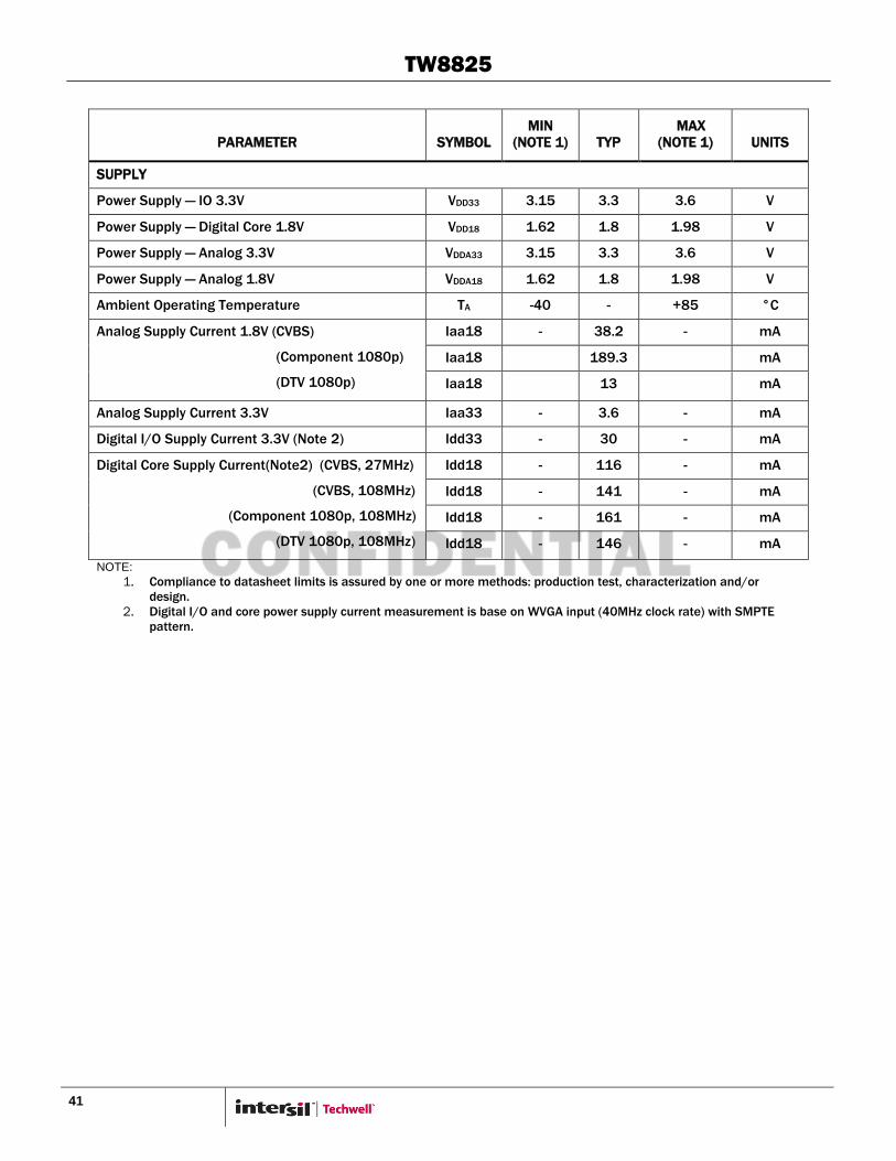
TW8825
41
PARAMETER
SYMBOL
MIN
(NOTE 1) TYP
MAX
(NOTE 1) UNITS
SUPPLY
Power Supply — IO 3.3V VDD33 3.15 3.3 3.6 V
Power Supply — Digital Core 1.8V VDD18 1.62 1.8 1.98 V
Power Supply — Analog 3.3V VDDA33 3.15 3.3 3.6 V
Power Supply — Analog 1.8V VDDA18 1.62 1.8 1.98 V
Ambient Operating Temperature TA -40 - +85 °C
Analog Supply Current 1.8V (CVBS)
(Component 1080p)
(DTV 1080p)
Iaa18 - 38.2 - mA
Iaa18 189.3 mA
Iaa18 13 mA
Analog Supply Current 3.3V Iaa33 - 3.6 - mA
Digital I/O Supply Current 3.3V (Note 2) Idd33 - 30 - mA
Digital Core Supply Current(Note2) (CVBS, 27MHz)
(CVBS, 108MHz)
(Component 1080p, 108MHz)
(DTV 1080p, 108MHz)
Idd18 - 116 - mA
Idd18 - 141 - mA
Idd18 - 161 - mA
Idd18 - 146 - mA
NOTE:
1. Compliance to datasheet limits is assured by one or more methods: production test, characterization and/or
design.
2. Digital I/O and core power supply current measurement is base on WVGA input (40MHz clock rate) with SMPTE
pattern.

TW8825
42
PARAMETER
SYMBOL
MIN
(NOTE 1) TYP
MAX
(NOTE 1) UNITS
DIGITAL INPUTS
Input High Voltage (TTL) VIH 2.0 - - V
Input Low Voltage (TTL) VIL - - 0.8 V
Input High Voltage (XTI) VIH 2.0 - VDD33 +
0.5
V
Input Low Voltage (XTI) VIL - - 0.8 V
Input High Current (VIN = V DD ) IIH - - 10 A
Input Low Current (VIN = VSS) IIL - - –10 A
Input Capacitance (f = 1 MHz, VIN = 2.4 V) CIN - 5 - pF
DIGITAL OUTPUTS
Output High Voltage (IOH = –4mA) VOH 2.4 - VDD33 V
Output Low Voltage (IOL = 4mA) VOL - 0.2 0.4 V
3-State Current IOZ - - 10 A
Output Capacitance CO - 5 - pF
NOTE:
1. Compliance to datasheet limits is assured by one or more methods: production test, characterization and/or design.

TW8825
43
PARAMETER SYMBOL
MIN
(NOTE 1) TYP
MAX
(NOTE 1) UNITS
ANALOG INPUT
Analog Pin Input Voltage Vi - 1 - Vpp
YIN0, YIN1, YIN2 and YIN3 Input Range
(AC Coupling Required)
0.5 1.0 2.0 Vpp
CIN0, CIN1 Amplitude Range (AC Coupling
Required) 0.5 1.0 2.0 Vpp
VIN0, VIN1 Amplitude Range (AC Coupling
Required) 0.5 1.0 2.0 Vpp
SOG0, SOG1 Input Range 0.02 0.3 1.8 V
LEDS Input Range - - - V
DCDCS - - - V
Analog Pin Input Capacitance CA - 7 - pF
ADCS
ADC Resolution ADCR - 9 - Bits
ADC Integral Non-linearity AINL - 1 - LSB
ADC Differential non-linearity ADNL - 1 - LSB
ADC Clock Rate fADC - 27 60 MHz
Video Bandwidth (-3db) BW - 9 - MHz
NOTE:
1. Compliance to datasheet limits is assured by one or more methods: production test, characterization and/or
design.
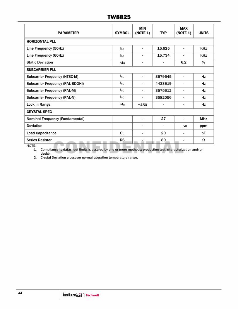
TW8825
44
PARAMETER
SYMBOL
MIN
(NOTE 1) TYP
MAX
(NOTE 1) UNITS
HORIZONTAL PLL
Line Frequency (50Hz) fLN - 15.625 - KHz
Line Frequency (60Hz) fLN - 15.734 - KHz
Static Deviation fH - - 6.2 %
SUBCARRIER PLL
Subcarrier Frequency (NTSC-M) fSC - 3579545 - Hz
Subcarrier Frequency (PAL-BDGHI) fSC - 4433619 - Hz
Subcarrier Frequency (PAL-M) fSC - 3575612 - Hz
Subcarrier Frequency (PAL-N) fSC - 3582056 - Hz
Lock In Range fH 450 - - Hz
CRYSTAL SPEC
Nominal Frequency (Fundamental) - 27 - MHz
Deviation - - 50 ppm
Load Capacitance CL - 20 - pF
Series Resistor RS - 80 - Ω
NOTE:
1. Compliance to datasheet limits is assured by one or more methods: production test, characterization and/or
design.
2. Crystal Deviation crossover normal operation temperature range.
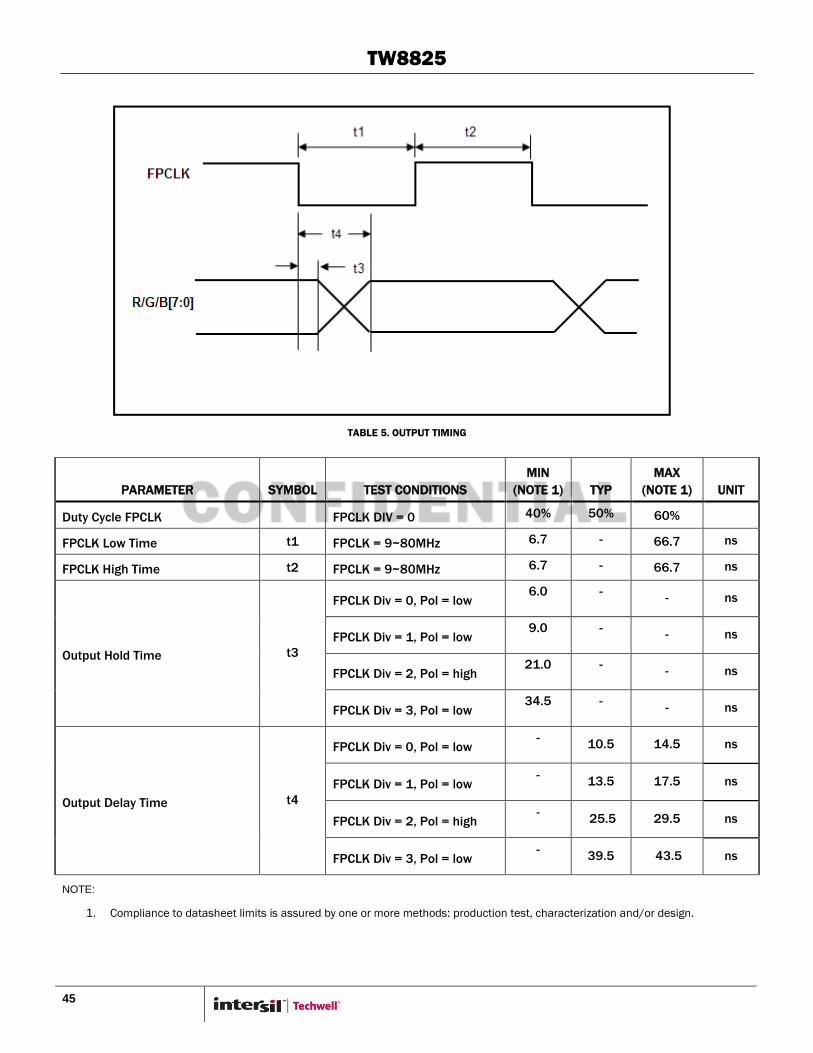
TW8825
45
TABLE 5. OUTPUT TIMING
PARAMETER
SYMBOL TEST CONDITIONS
MIN
(NOTE 1) TYP
MAX
(NOTE 1) UNIT
Duty Cycle FPCLK
FPCLK DIV = 0 40% 50% 60%
FPCLK Low Time t1 FPCLK = 9~80MHz 6.7 - 66.7 ns
FPCLK High Time t2 FPCLK = 9~80MHz 6.7 - 66.7 ns
Output Hold Time t3
FPCLK Div = 0, Pol = low 6.0 -
- ns
FPCLK Div = 1, Pol = low 9.0 -
- ns
FPCLK Div = 2, Pol = high 21.0 -
- ns
FPCLK Div = 3, Pol = low 34.5 -
- ns
Output Delay Time t4
FPCLK Div = 0, Pol = low -
10.5 14.5 ns
FPCLK Div = 1, Pol = low -
13.5 17.5 ns
FPCLK Div = 2, Pol = high -
25.5 29.5 ns
FPCLK Div = 3, Pol = low -
39.5 43.5 ns
NOTE:
1. Compliance to datasheet limits is assured by one or more methods: production test, characterization and/or design.
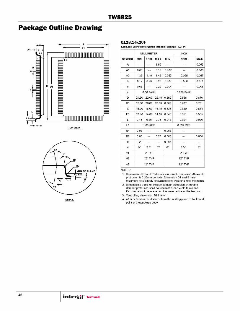
TW8825
46
Package Outline Drawing
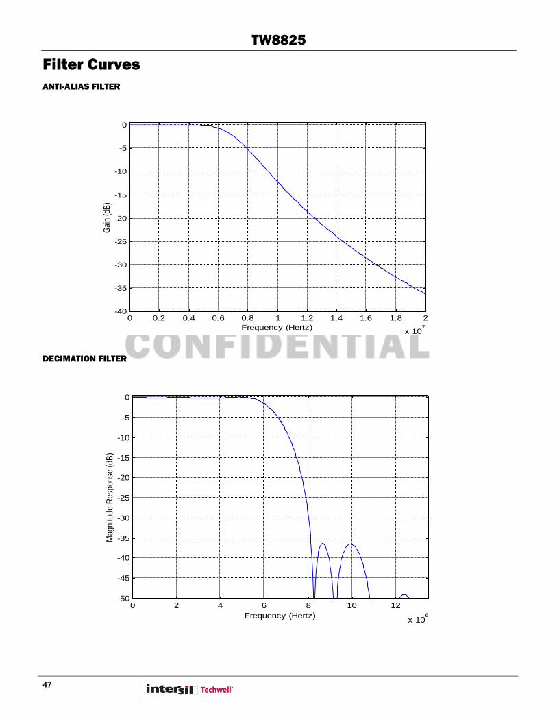
TW8825
47
Filter Curves
ANTI-ALIAS FILTER
DECIMATION FILTER
0 2 4 6 8 10 12
x 106
-50
-45
-40
-35
-30
-25
-20
-15
-10
-5
0
Frequency (Hertz)
Mag
nitu
de R
espo
nse
(dB
)
0 0.2 0.4 0.6 0.8 1 1.2 1.4 1.6 1.8 2
x 107
-40
-35
-30
-25
-20
-15
-10
-5
0
Frequency (Hertz)
Gai
n (d
B)

TW8825
48
CHROMA BAND PASS FILTER CURVES
LUMA NOTCH FILTER CURVE FOR NTSC AND PAL
0 1 2 3 4 5 6 7 8 9
x 106
-50
-45
-40
-35
-30
-25
-20
-15
-10
-5
0
Frequency (Hertz)
Mag
nitu
de R
espo
nse
(dB
)
PAL/SEAM
NTSC
0 1 2 3 4 5 6 7 8
x 106
-45
-40
-35
-30
-25
-20
-15
-10
-5
0
5
Frequency (Hertz)
Gai
n (d
B)
NTSC PAL
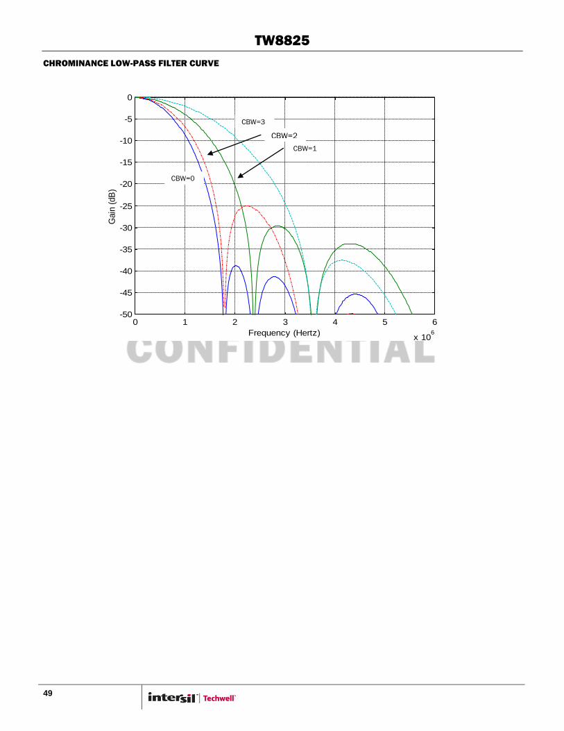
TW8825
49
CHROMINANCE LOW-PASS FILTER CURVE
Low
Med
High
0 1 2 3 4 5 6
x 106
-50
-45
-40
-35
-30
-25
-20
-15
-10
-5
0
Frequency (Hertz)
Gain
(dB
)
CBW=0
CBW=3
CBW=1
CBW=2
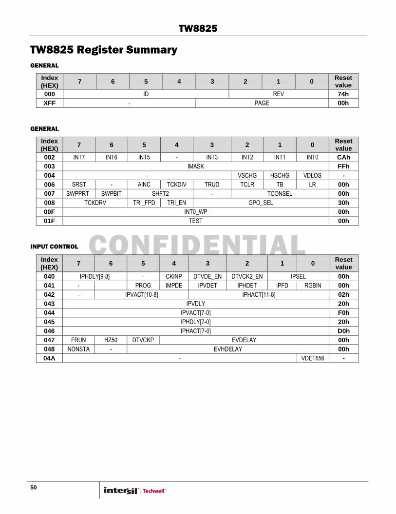
TW8825
50
TW8825 Register Summary
GENERAL
Index
(HEX) 7 6 5 4 3 2 1 0
Reset value
000 ID REV 74h
XFF - PAGE 00h
GENERAL
Index
(HEX) 7 6 5 4 3 2 1 0
Reset value
002 INT7 INT6 INT5 - INT3 INT2 INT1 INT0 CAh
003 IMASK FFh
004 - VSCHG HSCHG VDLOS -
006 SRST - AINC TCKDIV TRUD TCLR TB LR 00h
007 SWPPRT SWPBIT SHFT2 - TCONSEL 00h
008 TCKDRV TRI_FPD TRI_EN GPO_SEL 30h
00F INT0_WP 00h
01F TEST 00h
INPUT CONTROL
Index
(HEX) 7 6 5 4 3 2 1 0
Reset value
040 IPHDLY[9-8] - CKINP DTVDE_EN DTVCK2_EN IPSEL 00h
041 - PROG IMPDE IPVDET IPHDET IPFD RGBIN 00h
042 - IPVACT[10-8] IPHACT[11-8] 02h
043 IPVDLY 20h
044 IPVACT[7-0] F0h
045 IPHDLY[7-0] 20h
046 IPHACT[7-0] D0h
047 FRUN HZ50 DTVCKP EVDELAY 00h
048 NONSTA - EVHDELAY 00h
04A - VDET656 -

TW8825
51
DTV
Index
(HEX) 7 6 5 4 3 2 1 0
Reset value
050 OFDM RVODDP SLVSFLD DEONLY DE_POL HS_POL VS_POL - 00h
051 - DTV_DOD
R SELDE - DTVCK_DELAY 00h
052 - VSDL_656 UVA656 CR601 INPUT_DATA_BUS_ROUTING 00h
053 - INP_FORM 03h
054 OFD_DET_END OFD_DET_ST 00h
056 VSDELAY[7:0] 00h
057 SEQRGB_LTG SEQRGB_ORDER SEQRGB_SEL8BIT SEQRGB_POL
SEQRGB 00h
05F TPG_EN TPG_SWAP[2:0] TPG_PAT[3:0] 00h
GPIO
Index
(HEX) 7 6 5 4 3 2 1 0
Reset value
080 GPIO_EN 0[7:0] 00h
081 GPIO_EN 1[7:0] 00h
082 GPIO_EN 2[7:0] 00h
083 GPIO_EN 3[7:0] 00h
084 GPIO_EN 4[7:0] 00h
085 GPIO_EN 5[7:0] 00h
086 GPIO_EN 6[7:0] 00h
088 GPIO_OE 0[7:0] 00h
089 GPIO_OE 1[7:0] 00h
08A GPIO_OE 2[7:0] 00h
08B GPIO_OE 3[7:0] 00h
08C GPIO_OE 4[7:0] 00h
08D GPIO_OE 5[7:0] 00h
08E GPIO_OE 6[7:0] 00h
090 GPIO_OD 0[7:0] 00h
091 GPIO_OD 1[7:0] 00h
092 GPIO_OD 2[7:0] 00h
093 GPIO_OD 3[7:0] 00h
094 GPIO_OD 4[7:0] 00h
095 GPIO_OD 5[7:0] 00h
096 GPIO_OD 6[7:0] 00h
098 GPIO_ID 0[7:0] -
099 GPIO_ID 1[7:0] -
09A GPIO_ID 2[7:0] -
09B GPIO_ID 3[7:0] -
09C GPIO_ID 4[7:0] -
09D GPIO_ID 5[7:0] -
09E GPIO_ID 6[7:0] -
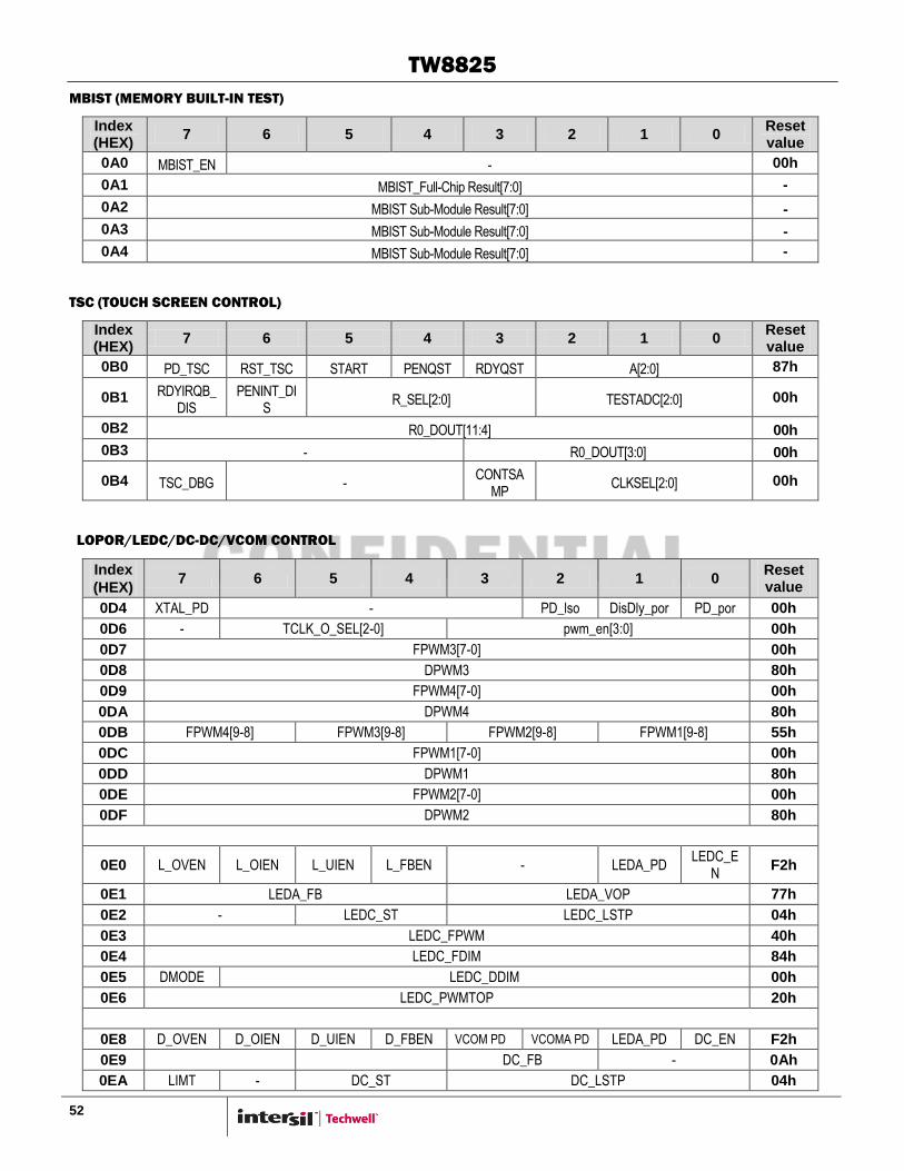
TW8825
52
MBIST (MEMORY BUILT-IN TEST)
Index (HEX)
7 6 5 4 3 2 1 0 Reset value
0A0 MBIST_EN - 00h
0A1 MBIST_Full-Chip Result[7:0] -
0A2 MBIST Sub-Module Result[7:0] -
0A3 MBIST Sub-Module Result[7:0] -
0A4 MBIST Sub-Module Result[7:0] -
TSC (TOUCH SCREEN CONTROL)
Index (HEX)
7 6 5 4 3 2 1 0 Reset value
0B0 PD_TSC RST_TSC START PENQST RDYQST A[2:0] 87h
0B1 RDYIRQB_DIS
PENINT_DIS
R_SEL[2:0] TESTADC[2:0] 00h
0B2 R0_DOUT[11:4] 00h
0B3 - R0_DOUT[3:0] 00h
0B4 TSC_DBG - CONTSA
MP CLKSEL[2:0] 00h
LOPOR/LEDC/DC-DC/VCOM CONTROL
Index
(HEX) 7 6 5 4 3 2 1 0
Reset value
0D4 XTAL_PD - PD_lso DisDly_por PD_por 00h
0D6 - TCLK_O_SEL[2-0] pwm_en[3:0] 00h
0D7 FPWM3[7-0] 00h
0D8 DPWM3 80h
0D9 FPWM4[7-0] 00h
0DA DPWM4 80h
0DB FPWM4[9-8] FPWM3[9-8] FPWM2[9-8] FPWM1[9-8] 55h
0DC FPWM1[7-0] 00h
0DD DPWM1 80h
0DE FPWM2[7-0] 00h
0DF DPWM2 80h
0E0 L_OVEN L_OIEN L_UIEN L_FBEN - LEDA_PD LEDC_E
N F2h
0E1 LEDA_FB LEDA_VOP 77h
0E2 - LEDC_ST LEDC_LSTP 04h
0E3 LEDC_FPWM 40h
0E4 LEDC_FDIM 84h
0E5 DMODE LEDC_DDIM 00h
0E6 LEDC_PWMTOP 20h
0E8 D_OVEN D_OIEN D_UIEN D_FBEN VCOM PD VCOMA PD LEDA_PD DC_EN F2h
0E9 DC_FB - 0Ah
0EA LIMT - DC_ST DC_LSTP 04h
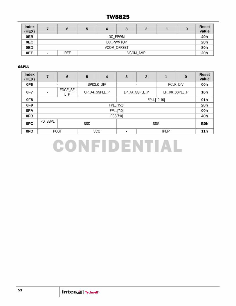
TW8825
53
Index
(HEX) 7 6 5 4 3 2 1 0
Reset value
0EB DC_FPWM 40h
0EC DC_PWMTOP 20h
0ED VCOM_OFFSET 80h
0EE - IREF VCOM_AMP 20h
SSPLL
Index
(HEX) 7 6 5 4 3 2 1 0
Reset value
0F6 - SPICLK_DIV - PCLK_DIV 00h
0F7 - EDGE_SE
L_P CP_X4_SSPLL_P LP_X4_SSPLL_P LP_X8_SSPLL_P 16h
0F8 - FPLL[19:16] 01h
0F9 FPLL[15:8] 20h
0FA FPLL[7:0] 00h
0FB FSS[7:0] 40h
0FC PD_SSPL
L SSD SSG B0h
0FD POST VCO - IPMP 11h
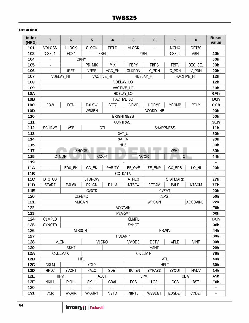
TW8825
54
DECODER
Index
(HEX) 7 6 5 4 3 2 1 0
Reset value
101 VDLOSS HLOCK SLOCK FIELD VLOCK - MONO DET50 -
102 CSEL1 FC27 IFSEL YSEL CSEL0 VSEL 40h
104 - CKHY - 00h
105 - PD_MIX MIX FBPY FBPC FBPV DEC_SEL 00h
106 - IREF VREF AGC_EN CLKPDN Y_PDN C_PDN V_PDN 00h
107 VDELAY_HI VACTIVE_HI HDELAY_HI HACTIVE_HI 12h
108 VDELAY_LO 12h
109 VACTIVE_LO 20h
10A HDELAY_LO 0Ah
10B HACTIVE_LO D0h
10C PBW DEM PALSW SET7 COMB HCOMP YCOMB PDLY CCh
10D - WSSEN CCODDLINE 00h
110 BRIGHTNESS 00h
111 CONTRAST 5Ch
112 SCURVE VSF CTI SHARPNESS 11h
113 SAT_U 80h
114 SAT_V 80h
115 HUE 00h
117 SHCOR - VSHP 80h
118 CTCOR CCOR VCOR CIF 44h
119 - -
11A - EDS_EN CC_EN PARITY FF_OVF FF_EMP CC_EDS LO_HI 00h
11B CC_DATA -
11C DTSTUS STDNOW ATREG STANDARD 27h
11D START PAL60 PALCN PALM NTSC4 SECAM PALB NTSCM 7Fh
11E - CVSTD CVFMT 00h
120 CLPEND CLPST 50h
121 NMGAIN WPGAIN AGCGAIN8 22h
122 AGCGAIN F0h
123 PEAKWT D8h
124 CLMPLD CLMPL BCh
125 SYNCTD SYNCT B8h
126 MISSCNT HSWIN 44h
127 PCLAMP 38h
128 VLCKI VLCKO VMODE DETV AFLD VINT 00h
129 BSHT VSHT 00h
12A CKILLMAX CKILLMIN 78h
12B HTL VTL 44h
12C CKLM YDLY HFLT 30h
12D HPLC EVCNT PALC SDET TBC_EN BYPASS SYOUT HADV 14h
12E HPM ACCT SPM CBW A5h
12F NKILL PKILL SKILL CBAL FCS LCS CCS BST E0h
130 - - - - - - - - -
131 VCR WKAIR WKAIR1 VSTD NINTL WSSDET EDSDET CCDET -
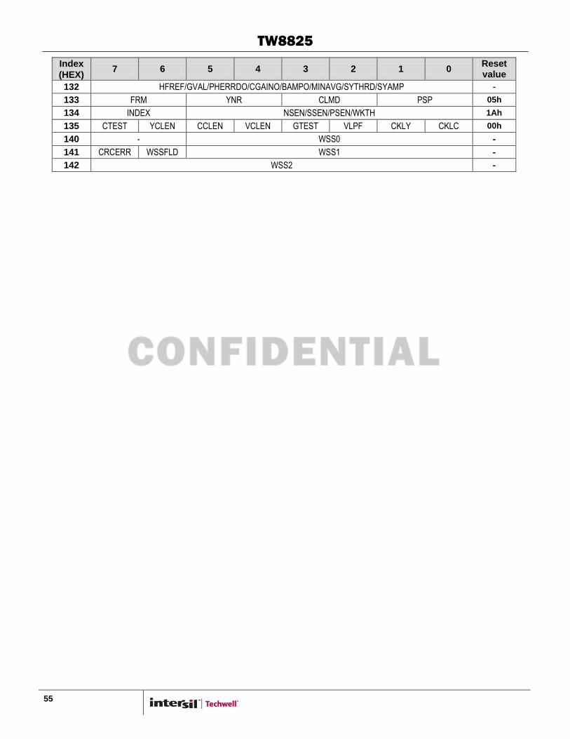
TW8825
55
Index
(HEX) 7 6 5 4 3 2 1 0
Reset value
132 HFREF/GVAL/PHERRDO/CGAINO/BAMPO/MINAVG/SYTHRD/SYAMP -
133 FRM YNR CLMD PSP 05h
134 INDEX NSEN/SSEN/PSEN/WKTH 1Ah
135 CTEST YCLEN CCLEN VCLEN GTEST VLPF CKLY CKLC 00h
140 - WSS0 -
141 CRCERR WSSFLD WSS1 -
142 WSS2 -
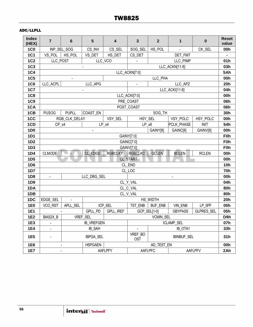
TW8825
56
ADC/LLPLL
Index
(HEX) 7 6 5 4 3 2 1 0
Reset value
1C0 INP_SEL_SOG CS_INV CS_SEL SOG_SEL HS_POL - CK_SEL 00h
1C1 VS_POL HS_POL VS_DET HS_DET CS_DET DET_FMT -
1C2 LLC_POST LLC_VCO - LLC_PIMP 01h
1C3 - LLC_ACKN[11:8] 03h
1C4 LLC_ACKN[7:0] 5Ah
1C5 - LLC_PHA 00h
1C6 LLC_ACPL LLC_APG - LLC_APZ 20h
1C7 - LLC_ACKI[11:8] 04h
1C8 LLC_ACKI[7:0] 00h
1C9 PRE_COAST 06h
1CA POST_COAST 06h
1CB PUSOG PUPLL COAST_EN SOG_TH 30h
1CC RGB_CLK_DELAY VSY_SEL HSY_SEL VSY_POLC HSY_POLC 00h
1CD CP_x4 LP_x4 LP_x8 PCLK_PHASE INIT 54h
1D0 - GAINY[8] GAINC[8] GAINV[8] 00h
1D1 GAINY[7:0] F0h
1D2 GAINC[7:0] F0h
1D3 GAINV[7:0] F0h
1D4 CLMODE - CL_EDGE RGBCLKY RGBCLKC GCLEN BCLEN RCLEN 00h
1D5 CL_START 00h
1D6 CL_END 10h
1D7 CL_LOC 70h
1D8 - LLC_DBG_SEL - 00h
1D9 CL_Y_VAL 04h
1DA CL_C_VAL 80h
1DB CL_V_VAL 80h
1DC EDGE_SEL - HS_WIDTH 20h
1E0 VCO_RST APLL_SEL ICP_SEL TST_ENB BUF_ENB VIN_ENB LP_5PF 00h
1E1 - GPLL_PD GPLL_IREF GCP_SEL[1-0] GBYPASS GLPRES_SEL 05h
1E2 BIAS2X_B VREF_SEL VCMIN_SEL D9h
1E3 - IB_VREFGEN ICLAMP_SEL 07h
1E4 - IB_SAH - IB_OTA1 33h
1E5 - IBPGA_SEL VREF_BO
OST IBINBUF_SEL 31h
1E6 - HSPGAEN AD_TEST_EN 00h
1E7 - AAFLPFY AAFLPFC AAFLPFV 2Ah
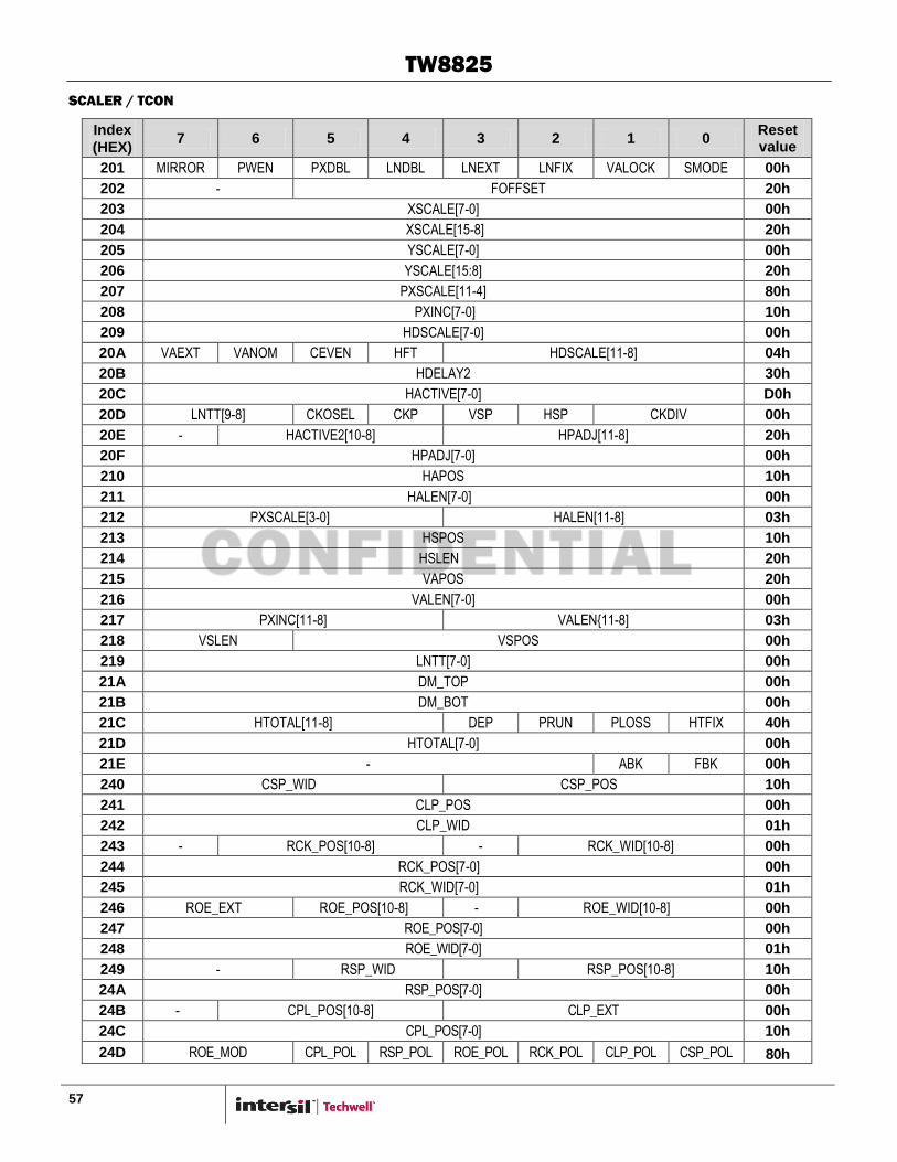
TW8825
57
SCALER / TCON
Index
(HEX) 7 6 5 4 3 2 1 0
Reset value
201 MIRROR PWEN PXDBL LNDBL LNEXT LNFIX VALOCK SMODE 00h
202 - FOFFSET 20h
203 XSCALE[7-0] 00h
204 XSCALE[15-8] 20h
205 YSCALE[7-0] 00h
206 YSCALE[15:8] 20h
207 PXSCALE[11-4] 80h
208 PXINC[7-0] 10h
209 HDSCALE[7-0] 00h
20A VAEXT VANOM CEVEN HFT HDSCALE[11-8] 04h
20B HDELAY2 30h
20C HACTIVE[7-0] D0h
20D LNTT[9-8] CKOSEL CKP VSP HSP CKDIV 00h
20E - HACTIVE2[10-8] HPADJ[11-8] 20h
20F HPADJ[7-0] 00h
210 HAPOS 10h
211 HALEN[7-0] 00h
212 PXSCALE[3-0] HALEN[11-8] 03h
213 HSPOS 10h
214 HSLEN 20h
215 VAPOS 20h
216 VALEN[7-0] 00h
217 PXINC[11-8] VALEN{11-8] 03h
218 VSLEN VSPOS 00h
219 LNTT[7-0] 00h
21A DM_TOP 00h
21B DM_BOT 00h
21C HTOTAL[11-8] DEP PRUN PLOSS HTFIX 40h
21D HTOTAL[7-0] 00h
21E - ABK FBK 00h
240 CSP_WID CSP_POS 10h
241 CLP_POS 00h
242 CLP_WID 01h
243 - RCK_POS[10-8] - RCK_WID[10-8] 00h
244 RCK_POS[7-0] 00h
245 RCK_WID[7-0] 01h
246 ROE_EXT ROE_POS[10-8] - ROE_WID[10-8] 00h
247 ROE_POS[7-0] 00h
248 ROE_WID[7-0] 01h
249 - RSP_WID RSP_POS[10-8] 10h
24A RSP_POS[7-0] 00h
24B - CPL_POS[10-8] CLP_EXT 00h
24C CPL_POS[7-0] 10h
24D ROE_MOD CPL_POL RSP_POL ROE_POL RCK_POL CLP_POL CSP_POL 80h

TW8825
58
Index
(HEX) 7 6 5 4 3 2 1 0
Reset value
24E CPL_REF CPL_SWP CPL_TGM ROE_DE CLP_REF CLP_DE CSP_DE 00h
IMAGE ADJUSTMENT
Index
(HEX) 7 6 5 4 3 2 1 0
Reset value
280 - HUE 20h
281 CONTRAST_R 80h
282 CONTRAST_G 80h
283 CONTRAST_B 80h
284 CONTRAST_Y 80h
285 CONTRAST_Cb 80h
286 CONTRAST_Cr 80h
287 BRIGHTNESS_R 80h
288 BRIGHTNESS_G 80h
289 BRIGHTNESS_B 80h
28A BRIGHTNESS_Y 80h
28B H_SHARP_COR H_SHARPNESS 30h
28C SH_FREQ - 00h
2B0 - PEDLVL WHTLVL - BW_EN 10h
2B1 BW_FMIN 40h
2B2 BW_FMAX 40h
2B6 BW_BLACK_TILT 67h
2B7 BW_WHITE_TILT 94h
2BE Y16 BT7 00h
2BF TPG_EN SWAP PAT_SEL 00h
GAMMA & DITHER
Index
(HEX) 7 6 5 4 3 2 1 0
Reset value
2E0 GAMAE_R GAMAE_
G GAMAE_B - AUTO_INC GAMMA_RGB_INDX 00h
2E1 GAMMA_RAM_STARTING_ADDR 00h
2E3 GAMMA_RAM_DATA[7:0] 00h
2E4 - DITHER_OPTION - DITHER_FORMAT 00h
2F0 RDPOS_X[7:0] 00h
2F1 RDPOS_Y[7:0] 00h
2F2 - RDPOS_Y[10:8] RDPOS_X[11:8] 00h
2F3 RDVALUE_R 00h
2F4 RDVALUE_G 00h
2F5 RDVALUE_B 00h
2F8 - RGB_OR
DR AVRG_EN
AVRG_POL
COL_ODD COL_EVEN 00h
2F9 DELTA_T
YPE REV_EN -
DMMY_EN
DMMY_POS
80h
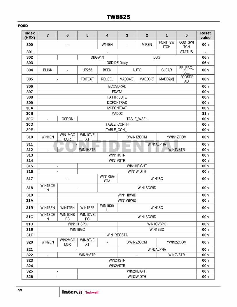
TW8825
59
FOSD
Index
(HEX) 7 6 5 4 3 2 1 0
Reset value
300 - W16EN - MIREN FONT_SW
ITCH OSD_SWI
TCH 00h
301 - STATUS -
302 DBGWIN DBG 06h
303 OSD DE Delay 06h
304 BLINK - UP256 BSEN AUTO CLEAR FR_RAC_
SEL 00h
305 - FBITEXT RD_SEL MADD4[8] MADD3[8] MADD2[8] I2COSDR
AD 00h
306 I2COSDRAD 00h
307 FDATA 00h
308 FATTRIBUTE 00h
309 I2CFONTRAD 00h
30A I2CFONTDAT 00h
30B MADD2 31h
30C - OSDON TABLE_WSEL 00h
30D TABLE_CON_H 00h
30E TABLE_CON_L 00h
310 WIN1EN WIN1MCO
LOR WIN1CVE
XT XWIN1ZOOM YWIN1ZOOM 00h
311 - WIN1ALPHA 00h
312 - WIN1HSTR - WIN1VSTR 00h
313 WIN1HSTR 00h
314 WIN1VSTR 00h
315 - WIN1HEIGHT 00h
316 - WIN1WIDTH 00h
317 - WIN1REG
STA WIN1BC 00h
318 WIN1BCE
N - WIN1BCWID 00h
319 WIN1HBWID 00h
31A WIN1VBWID 00h
31B WIN1BEN WIN1TEN WIN1EFF WIN1BSE
L WIN1SC 00h
31C WIN1SCE
N WIN1CHS
PC WIN1CVS
PC WIN1SCWID 00h
31D WIN1CHSPC WIN1CVSPC 00h
31E WIN1BGC WIN1BSC 00h
31F WIN1REGSTA 00h
320 WIN2EN WIN2MCO
LOR WIN2CVE
XT - XWIN2ZOOM YWIN2ZOOM 00h
321 - WIN2ALPHA 00h
322 - WIN2HSTR - WIN2VSTR 00h
323 WIN2HSTR 00h
324 WIN2VSTR 00h
325 - WIN2HEIGHT 00h
326 - WIN2WIDTH 00h
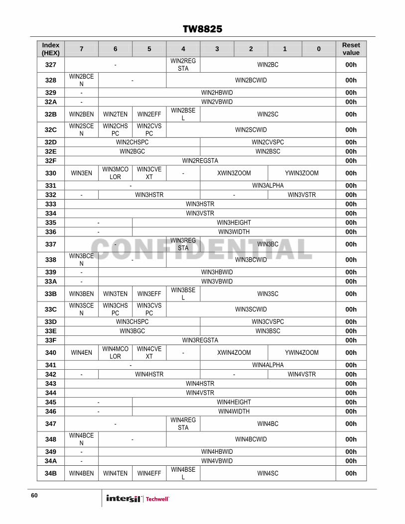
TW8825
60
Index
(HEX) 7 6 5 4 3 2 1 0
Reset value
327 - WIN2REG
STA WIN2BC 00h
328 WIN2BCE
N - WIN2BCWID 00h
329 - WIN2HBWID 00h
32A - WIN2VBWID 00h
32B WIN2BEN WIN2TEN WIN2EFF WIN2BSE
L WIN2SC 00h
32C WIN2SCE
N WIN2CHS
PC WIN2CVS
PC WIN2SCWID 00h
32D WIN2CHSPC WIN2CVSPC 00h
32E WIN2BGC WIN2BSC 00h
32F WIN2REGSTA 00h
330 WIN3EN WIN3MCO
LOR WIN3CVE
XT - XWIN3ZOOM YWIN3ZOOM 00h
331 - WIN3ALPHA 00h
332 - WIN3HSTR - WIN3VSTR 00h
333 WIN3HSTR 00h
334 WIN3VSTR 00h
335 - WIN3HEIGHT 00h
336 - WIN3WIDTH 00h
337 - WIN3REG
STA WIN3BC 00h
338 WIN3BCE
N - WIN3BCWID 00h
339 - WIN3HBWID 00h
33A - WIN3VBWID 00h
33B WIN3BEN WIN3TEN WIN3EFF WIN3BSE
L WIN3SC 00h
33C WIN3SCE
N WIN3CHS
PC WIN3CVS
PC WIN3SCWID 00h
33D WIN3CHSPC WIN3CVSPC 00h
33E WIN3BGC WIN3BSC 00h
33F WIN3REGSTA 00h
340 WIN4EN WIN4MCO
LOR WIN4CVE
XT - XWIN4ZOOM YWIN4ZOOM 00h
341 - WIN4ALPHA 00h
342 - WIN4HSTR - WIN4VSTR 00h
343 WIN4HSTR 00h
344 WIN4VSTR 00h
345 - WIN4HEIGHT 00h
346 - WIN4WIDTH 00h
347 - WIN4REG
STA WIN4BC 00h
348 WIN4BCE
N - WIN4BCWID 00h
349 - WIN4HBWID 00h
34A - WIN4VBWID 00h
34B WIN4BEN WIN4TEN WIN4EFF WIN4BSE
L WIN4SC 00h
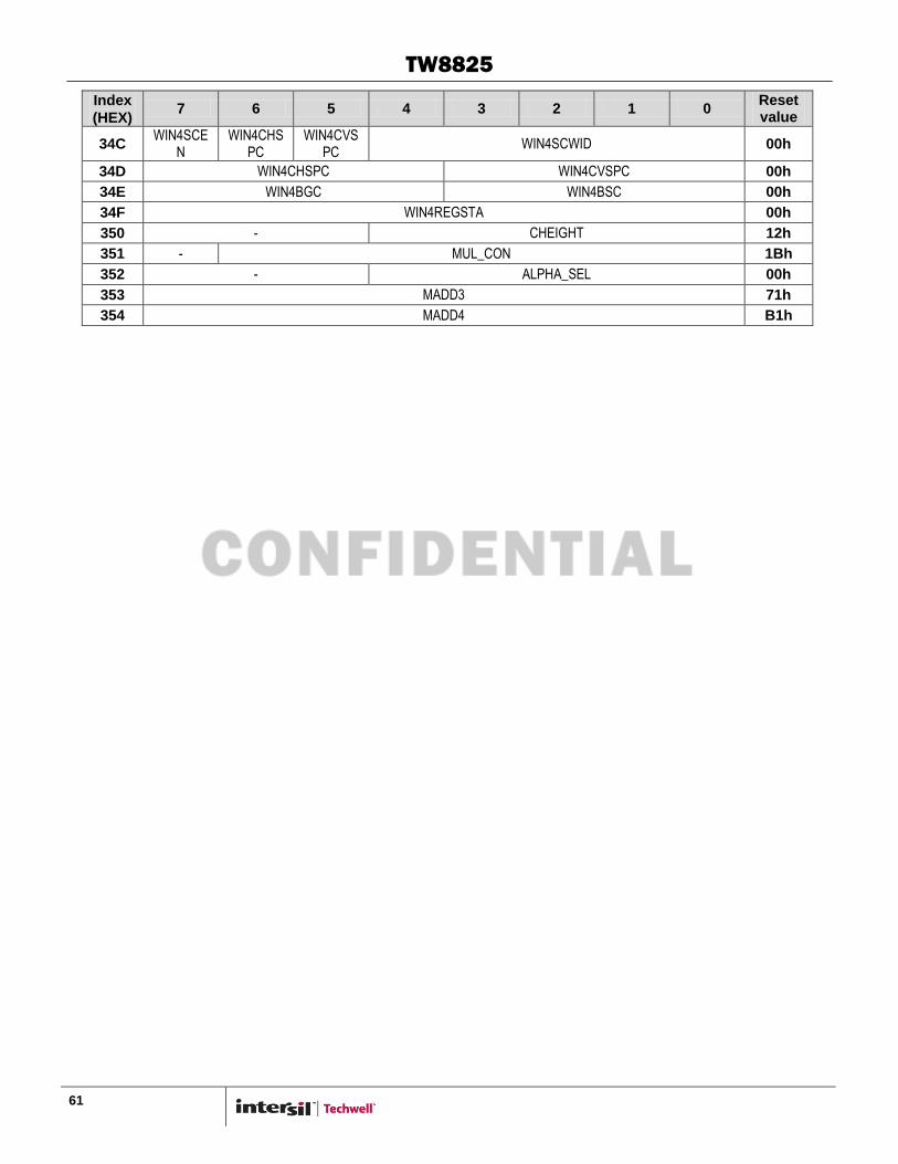
TW8825
61
Index
(HEX) 7 6 5 4 3 2 1 0
Reset value
34C WIN4SCE
N WIN4CHS
PC WIN4CVS
PC WIN4SCWID 00h
34D WIN4CHSPC WIN4CVSPC 00h
34E WIN4BGC WIN4BSC 00h
34F WIN4REGSTA 00h
350 - CHEIGHT 12h
351 - MUL_CON 1Bh
352 - ALPHA_SEL 00h
353 MADD3 71h
354 MADD4 B1h
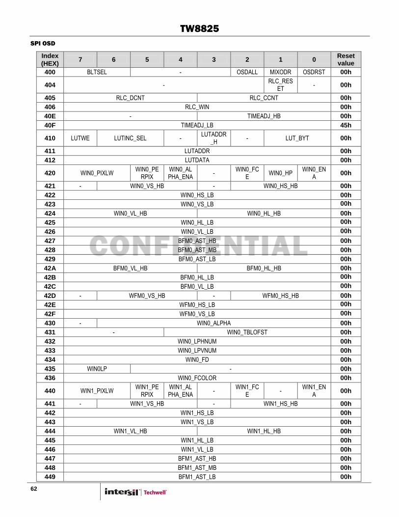
TW8825
62
SPI OSD
Index
(HEX) 7 6 5 4 3 2 1 0
Reset value
400 BLTSEL - OSDALL MIXODR OSDRST 00h
404 - RLC_RES
ET - 00h
405 RLC_DCNT RLC_CCNT 00h
406 RLC_WIN 00h
40E - TIMEADJ_HB 00h
40F TIMEADJ_LB 45h
410 LUTWE LUTINC_SEL - LUTADDR
_H - LUT_BYT 00h
411 LUTADDR 00h
412 LUTDATA 00h
420 WIN0_PIXLW WIN0_PE
RPIX WIN0_ALPHA_ENA
- WIN0_FC
E WIN0_HP
WIN0_ENA
00h
421 - WIN0_VS_HB - WIN0_HS_HB 00h
422 WIN0_HS_LB 00h
423 WIN0_VS_LB 00h
424 WIN0_VL_HB WIN0_HL_HB 00h
425 WIN0_HL_LB 00h
426 WIN0_VL_LB 00h
427 BFM0_AST_HB 00h
428 BFM0_AST_MB 00h
429 BFM0_AST_LB 00h
42A BFM0_VL_HB BFM0_HL_HB 00h
42B BFM0_HL_LB 00h
42C BFM0_VL_LB 00h
42D - WFM0_VS_HB - WFM0_HS_HB 00h
42E WFM0_HS_LB 00h
42F WFM0_VS_LB 00h
430 - WIN0_ALPHA 00h
431 - WIN0_TBLOFST 00h
432 WIN0_LPHNUM 00h
433 WIN0_LPVNUM 00h
434 WIN0_FD 00h
435 WIN0LP - 00h
436 WIN0_FCOLOR 00h
440 WIN1_PIXLW WIN1_PE
RPIX WIN1_ALPHA_ENA
- WIN1_FC
E -
WIN1_ENA
00h
441 - WIN1_VS_HB - WIN1_HS_HB 00h
442 WIN1_HS_LB 00h
443 WIN1_VS_LB 00h
444 WIN1_VL_HB WIN1_HL_HB 00h
445 WIN1_HL_LB 00h
446 WIN1_VL_LB 00h
447 BFM1_AST_HB 00h
448 BFM1_AST_MB 00h
449 BFM1_AST_LB 00h
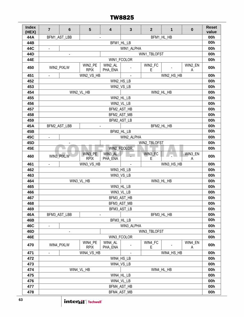
TW8825
63
Index
(HEX) 7 6 5 4 3 2 1 0
Reset value
44A BFM1_AST_LBB - BFM1_HL_HB 00h
44B BFM1_HL_LB 00h
44C - WIN1_ALPHA 00h
44D - WIN1_TBLOFST 00h
44E WIN1_FCOLOR 00h
450 WIN2_PIXLW WIN2_PE
RPIX WIN2_ALPHA_ENA
- WIN2_FC
E -
WIN2_ENA
00h
451 - WIN2_VS_HB - WIN2_HS_HB 00h
452 WIN2_HS_LB 00h
453 WIN2_VS_LB 00h
454 WIN2_VL_HB WIN2_HL_HB 00h
455 WIN2_HL_LB 00h
456 WIN2_VL_LB 00h
457 BFM2_AST_HB 00h
458 BFM2_AST_MB 00h
459 BFM2_AST_LB 00h
45A BFM2_AST_LBB - BFM2_HL_HB 00h
45B BFM2_HL_LB 00h
45C - WIN2_ALPHA 00h
45D - WIN2_TBLOFST 00h
45E WIN2_FCOLOR 00h
460 WIN3_PIXLW WIN3_PE
RPIX WIN3_ALPHA_ENA
- WIN3_FC
E -
WIN3_ENA
00h
461 - WIN3_VS_HB - WIN3_HS_HB 00h
462 WIN3_HS_LB 00h
463 WIN3_VS_LB 00h
464 WIN3_VL_HB WIN3_HL_HB 00h
465 WIN3_HL_LB 00h
466 WIN3_VL_LB 00h
467 BFM3_AST_HB 00h
468 BFM3_AST_MB 00h
469 BFM3_AST_LB 00h
46A BFM3_AST_LBB - BFM3_HL_HB 00h
46B BFM3_HL_LB 00h
46C - WIN3_ALPHA 00h
46D - WIN3_TBLOFST 00h
46E WIN3_FCOLOR 00h
470 WIN4_PIXLW WIN4_PE
RPIX WIN4_ALPHA_ENA
- WIN4_FC
E -
WIN4_ENA
00h
471 - WIN4_VS_HB - WIN4_HS_HB 00h
472 WIN4_HS_LB 00h
473 WIN4_VS_LB 00h
474 WIN4_VL_HB WIN4_HL_HB 00h
475 WIN4_HL_LB 00h
476 WIN4_VL_LB 00h
477 BFM4_AST_HB 00h
478 BFM4_AST_MB 00h

TW8825
64
Index
(HEX) 7 6 5 4 3 2 1 0
Reset value
479 BFM4_AST_LB 28h
47A BFM4_AST_LBB - BFM4_HL_HB 00h
47B BFM4_HL_LB 00h
47C - WIN4_ALPHA 00h
47D - WIN4_TBLOFST 00h
47E WIN4_FCOLOR 00h
480 WIN5_PIXLW WIN5_PE
RPIX WIN5_ALPHA_ENA
- WIN5_FC
E -
WIN5_ENA
00h
481 - WIN5_VS_HB - WIN5_HS_HB 00h
482 WIN5_HS_LB 00h
483 WIN5_VS_LB 00h
484 WIN5_VL_HB WIN5_HL_HB 00h
485 WIN5_HL_LB 00h
486 WIN5_VL_LB 00h
487 BFM5_AST_HB 00h
488 BFM5_AST_MB 00h
489 BFM5_AST_LB 00h
48A BFM5_AST_LBB - BFM5_HL_HB 00h
48B BFM5_HL_LB 00h
48C - WIN5_ALPHA 00h
48D - WIN5_TBLOFST 00h
48E WIN5_FCOLOR 00h
490 WIN6_PIXLW WIN6_PE
RPIX WIN6_ALPHA_ENA
- WIN6_FC
E -
WIN6_ENA
00h
491 - WIN6_VS_HB - WIN6_HS_HB 00h
492 WIN6_HS_LB 00h
493 WIN6_VS_LB 00h
494 WIN6_VL_HB WIN6_HL_HB 00h
495 WIN6_HL_LB 00h
496 WIN6_VL_LB 00h
497 BFM6_AST_HB 00h
498 BFM6_AST_MB 00h
499 BFM6_AST_LB 00h
49A BFM6_AST_LBB - BFM6_HL_HB 00h
49B BFM6_HL_LB 00h
49C - WIN6_ALPHA 00h
49D - WIN6_TBLOFST 00h
49E WIN6_FCOLOR 00h
4A0 WIN7_PIXLW WIN7_PE
RPIX WIN7_ALPHA_ENA
- WIN7_FC
E -
WIN7_ENA
00h
4A1 - WIN7_VS_HB - WIN7_HS_HB 00h
4A2 WIN7_HS_LB 00h
4A3 WIN7_VS_LB 00h
4A4 WIN7_VL_HB WIN7_HL_HB 00h
4A5 WIN7_HL_LB 00h
4A6 WIN7_VL_LB 00h
4A7 BFM7_AST_HB 00h
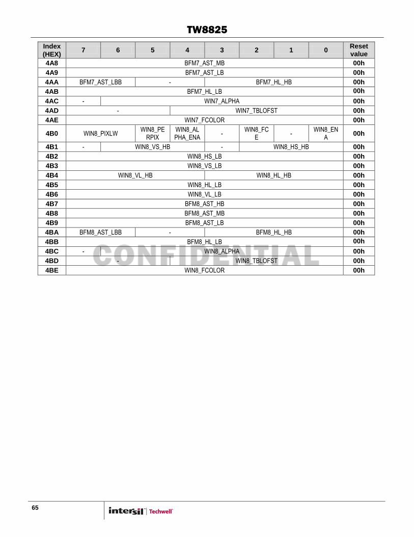
TW8825
65
Index
(HEX) 7 6 5 4 3 2 1 0
Reset value
4A8 BFM7_AST_MB 00h
4A9 BFM7_AST_LB 00h
4AA BFM7_AST_LBB - BFM7_HL_HB 00h
4AB BFM7_HL_LB 00h
4AC - WIN7_ALPHA 00h
4AD - WIN7_TBLOFST 00h
4AE WIN7_FCOLOR 00h
4B0 WIN8_PIXLW WIN8_PE
RPIX WIN8_ALPHA_ENA
- WIN8_FC
E -
WIN8_ENA
00h
4B1 - WIN8_VS_HB - WIN8_HS_HB 00h
4B2 WIN8_HS_LB 00h
4B3 WIN8_VS_LB 00h
4B4 WIN8_VL_HB WIN8_HL_HB 00h
4B5 WIN8_HL_LB 00h
4B6 WIN8_VL_LB 00h
4B7 BFM8_AST_HB 00h
4B8 BFM8_AST_MB 00h
4B9 BFM8_AST_LB 00h
4BA BFM8_AST_LBB - BFM8_HL_HB 00h
4BB BFM8_HL_LB 00h
4BC - WIN8_ALPHA 00h
4BD - WIN8_TBLOFST 00h
4BE WIN8_FCOLOR 00h
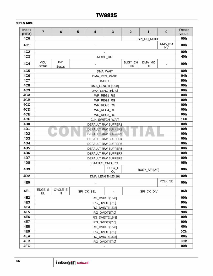
TW8825
66
SPI & MCU
Index
(HEX) 7 6 5 4 3 2 1 0
Reset value
4C0 - SPI_RD_MODE 00h
4C1 - DMA_NO
NV 00h
4C2 - 00h
4C3 MODE_RG 40h
4C4 MCU Status
ISP
Status -
BUSY_CHECK
DMA_MODE
- 00h
4C5 DMA_WAIT 80h
4C6 DMA_REG_PAGE 04h
4C7 INDEX 90h
4C8 DMA_LENGTH[15:8] 00h
4C9 DMA_LENGTH[7:0] 00h
4CA WR_REG1_RG 00h
4CB WR_REG2_RG 00h
4CC WR_REG3_RG 00h
4CD WR_REG4_RG 00h
4CE WR_REG5_RG 00h
4CF CLK_SWITCH_WAIT 1Fh
4D0 DEFAULT R/W BUFFER1 00h
4D1 DEFAULT R/W BUFFER2 00h
4D2 DEFAULT R/W BUFFER3 00h
4D3 DEFAULT R/W BUFFER4 00h
4D4 DEFAULT R/W BUFFER5 00h
4D5 DEFAULT R/W BUFFER6 00h
4D6 DEFAULT R/W BUFFER7 00h
4D7 DEFAULT R/W BUFFER8 00h
4D8 STATUS_CMD_RG 05h
4D9 - BUSY_POL
BUSY_SEL[2:0] 08h
4DA DMA_LENGTH[23:16] 00h
4E0 - PCLK_SE
L 00h
4E1 EDGE_SEL
CYCLE_EN
SPI_CK_SEL - SPI_CK_DIV 06h
4E2 RG_DVIDT0[15:8] 00h
4E3 RG_DVIDT0[7:0] 90h
4E4 RG_DVIDT1[15:8] 00h
4E5 RG_DVIDT1[7:0] 90h
4E6 RG_DVIDT2[15:8] 00h
4E7 RG_DVIDT2[7:0] 90h
4E8 RG_DVIDT3[15:8] 00h
4E9 RG_DVIDT3[7:0] 0Ch
4EA RG_DVIDT4[15:8] 00h
4EB RG_DVIDT4[7:0] 0Ch
4EC - 00h

TW8825
67
MEASUREMENT
Index (HEX)
7 6 5 4 3 2 1 0 Reset value
500 - MEA_WIN_H_ST [10:8] 00h
501 MEA_WIN_H_ST [7:0] 20h
502 - MEA_WIN_H_LEN [11:8] 01h
503 MEA_WIN_H_LEN [7:0] E0h
504 - MEA_WIN_V_ST [10:8] 00h
505 MEA_WIN_V_ST [7:0] 20h
506 - MEA_WIN_V_LEN [10:8] 00h
507 MEA_WIN_V_LEN [7:0] DAh
508 MEAS_SEL - FIELD_SEL RD_LOCK START
M 00h
509 SEL_27M NOISE_MASK [2:0] ERR_TOLER [2:0] ENDET 00h
50A EDGE_A
DJ - ENALU NOFSEL [1:0]
DE_MEA
00h
50B THRESHOLD_FOR_ACT_DET [7:0] 8Ch
510 - PHASE_R [28:24] -
511
PHASE_R [23:0] - 512
513
514 - PHASE_G [28:24] -
515
PHASE_G [23:0] - 516
517
518 - PHASE_B [28:24] -
519
PHASE_B [23:0] - 51A
51B
51C MIN_R [7:0] -
51D MIN_G [7:0] -
51E MIN_B [7:0] -
51F MAX_R [7:0] -
520 MAX_G [7:0] -
521 MAX_B [7:0] -
522 - V_PERIOD [10:8] -
523 V_PERIOD [7:0] -
524 H_PERIOD [15:0] -
525
526 - H_RISE_TO_FALL [11:8] -
527 H_RISE_TO_FALL 7:0] -
528 - H_RISE_TO_ACT_END [11:8] -
529 H_RISE_TO_ACT_END [11:0] -
52A - V_RISE_TO_FALL [10:8] -
52B V_RISE_TO_FALL [7:0] -
52C - V_RISE_TO_FALL [11:8] -
52D V_RISE_TO_FALL [7:0] -
52E - H_ACT_ST_1 [11:8] -
52F H_ACT_ST_1 [7:0] -
530 - H_ACT_ST_2 [11:8] -
531 H_ACT_ST_2 [7:0] -
532 - H_ACT_END_MIN [11:8] -
533 H_ACT_END_MIN [7:0] -
534 - H_ACT_END_MAX [11:8] -
535 H_ACT_END_MAX [7:0] -
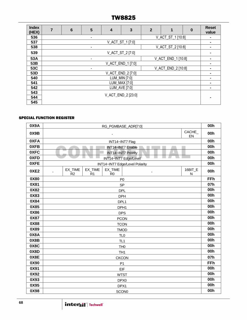
TW8825
68
Index (HEX)
7 6 5 4 3 2 1 0 Reset value
536 - V_ACT_ST_1 [10:8] -
537 V_ACT_ST_1 [7:0] -
538 - V_ACT_ST_2 [10:8] -
539 V_ACT_ST_2 [7:0] -
53A - V_ACT_END_1 [10:8] -
53B V_ACT_END_1 [7:0] -
53C - V_ACT_END_2 [10:8] -
53D V_ACT_END_2 [7:0] -
540 LUM_MIN [7:0] -
541 LUM_MAX [7:0] -
542 LUM_AVE [7:0] -
543 V_ACT_END_2 [23:0]
- 544
545
SPECIAL FUNCTION REGISTER
0X9A RG_PGMBASE_ADR[7:0] 00h
0X9B - CACHE_
EN 00h
0XFA INT14~INT7 Flag 00h
0XFB INT14~INT7 Enable 00h
0XFC INT14~INT7 Priority 00h
0XFD INT14~INT7 Edge/Level 00h
0XFE INT14~INT7 Edge/Level Polarity 00h
0XE2 - EX_TIME
R2 EX_TIME
R1 EX_TIME
R0 -
16BIT_EN
00h
0X80 P0 FFh
0X81 SP 07h
0X82 DPL 00h
0X83 DPH 00h
0X84 DPL1 00h
0X85 DPH1 00h
0X86 DPS 00h
0X87 PCON 00h
0X88 TCON 00h
0X89 TMOD 00h
0X8A TL0 00h
0X8B TL1 00h
0X8C TH0 00h
0X8D TH1 00h
0X8E CKCON 07h
0X90 P1 FFh
0X91 EIF 00h
0X92 WTST 00h
0X93 DPX0 00h
0X95 DPX1 00h
0X98 SCON0 00h
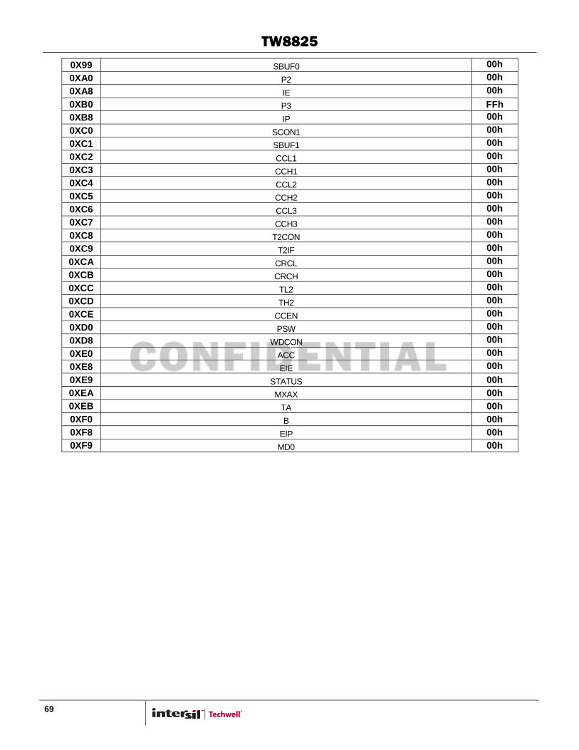
TW8825
69
0X99 SBUF0 00h
0XA0 P2 00h
0XA8 IE 00h
0XB0 P3 FFh
0XB8 IP 00h
0XC0 SCON1 00h
0XC1 SBUF1 00h
0XC2 CCL1 00h
0XC3 CCH1 00h
0XC4 CCL2 00h
0XC5 CCH2 00h
0XC6 CCL3 00h
0XC7 CCH3 00h
0XC8 T2CON 00h
0XC9 T2IF 00h
0XCA CRCL 00h
0XCB CRCH 00h
0XCC TL2 00h
0XCD TH2 00h
0XCE CCEN 00h
0XD0 PSW 00h
0XD8 WDCON 00h
0XE0 ACC 00h
0XE8 EIE 00h
0XE9 STATUS 00h
0XEA MXAX 00h
0XEB TA 00h
0XF0 B 00h
0XF8 EIP 00h
0XF9 MD0 00h
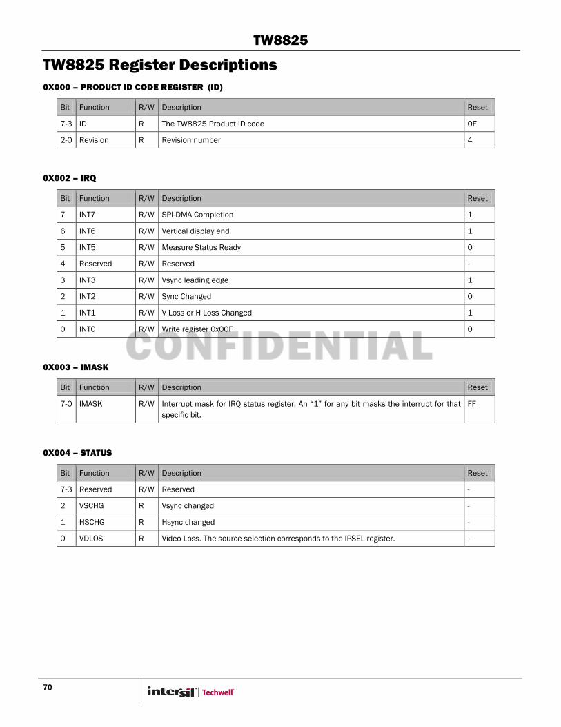
TW8825
70
TW8825 Register Descriptions
0X000 – PRODUCT ID CODE REGISTER (ID)
Bit Function R/W Description Reset
7-3 ID R The TW8825 Product ID code 0E
2-0 Revision R Revision number 4
0X002 – IRQ
Bit Function R/W Description Reset
7 INT7 R/W SPI-DMA Completion 1
6 INT6 R/W Vertical display end 1
5 INT5 R/W Measure Status Ready 0
4 Reserved R/W Reserved -
3 INT3 R/W Vsync leading edge 1
2 INT2 R/W Sync Changed 0
1 INT1 R/W V Loss or H Loss Changed 1
0 INT0 R/W Write register 0x00F 0
0X003 – IMASK
Bit Function R/W Description Reset
7-0 IMASK R/W Interrupt mask for IRQ status register. An “1” for any bit masks the interrupt for that
specific bit.
FF
0X004 – STATUS
Bit Function R/W Description Reset
7-3 Reserved R/W Reserved -
2 VSCHG R Vsync changed -
1 HSCHG R Hsync changed -
0 VDLOS R Video Loss. The source selection corresponds to the IPSEL register. -
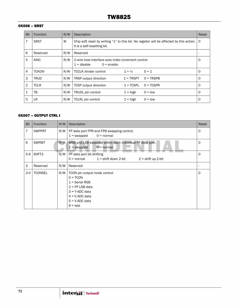
TW8825
71
0X006 – SRST
Bit Function R/W Description Reset
7 SRST W Chip soft reset by writing “1” to this bit. No register will be affected by this action.
It is a self-resetting bit.
0
6 Reserved R/W Reserved -
5 AINC R/W 2-wire host interface auto index increment control
1 = disable 0 = enable
0
4 TCKDIV R/W TCCLK divider control 1 = ½ 0 = 1 0
3 TRUD R/W TRSP output direction 1 = TRSPT 0 = TRSPB 0
2 TCLR R/W TCSP output direction 1 = TCSPL 0 = TCSPR 0
1 TB R/W TRUDL pin control 1 = high 0 = low 0
0 LR R/W TCLRL pin control 1 = high 0 = low 0
0X007 – OUTPUT CTRL I
Bit Function R/W Description Reset
7 SWPPRT R/W FP data port FPR and FPB swapping control.
1 = swapped 0 = normal
0
6 SWPBIT R/W MSB and LSB swapped within each individual FP data port.
1 = swapped 0 = normal
0
5-4 SHFT2 R/W FP data port bit shifting
0 = normal 1 = shift down 2-bit 2 = shift up 2-bit
0
3 Reserved R/W Reserved -
2-0 TCONSEL R/W TCON pin output mode control
0 = TCON
1 = Serial RGB
2 = FP LSB data
3 = Y-ADC data
4 = C-ADC data
5 = V-ADC data
6 = test
0
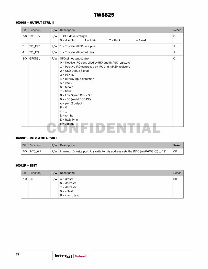
TW8825
72
0X008 – OUTPUT CTRL II
Bit Function R/W Description Reset
7-6 TCKDRV R/W TCCLK drive strength
0 = disable 1 = 4mA 2 = 8mA 3 = 12mA
0
5 TRI_FPD R/W 1 = Tristate all FP data pins. 1
4 TRI_EN R/W 1 = Tristate all output pins 1
3-0 GPOSEL R/W GPO pin output control
0 = Negtive IRQ controlled by IRQ and IMASK registers
1 = Positive IRQ controlled by IRQ and IMASK registers
2 = OSD Debug Signal
3 = PEN INT
4 = BT656 input detection
5 = vact2
6 = tcpolp
7 = field
8 = Low Speed Clock Out
9 = sDE (serial RGB DE)
A = pwm2 output
B = 0
C = 1
D = s4_hs
E = RGB Sync
F = sdbout
0
0X00F – INT0 WRITE PORT
Bit Function R/W Description Reset
7-0 INT0_WP R/W Interrupt 0 write port: Any write to this address sets the INT0 (reg0x002[0]) to “1” 00
0X01F – TEST
Bit Function R/W Description Reset
7-0 TEST R/W 4 = dtest1
6 = dactest1
7 = dactest2
9 = cctest
B = clamp test
00
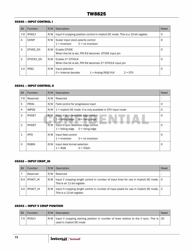
TW8825
73
0X040 – INPUT CONTROL I
Bit Function R/W Description Reset
7-6 IPHDLY R/W Input H cropping position control in implicit DE mode. This is a 10-bit register. 0
4 CKINP R/W Scaler input clock polarity control
1 = Inversion 0 = no inversion
0
3 DTVDE_EN R/W Enable DTVDE
When this bit is set, PIN 63 becomes DTVDE input pin
0
2 DTVCK2_EN R/W Enable 2nd DTVCLK
When this bit is set, PIN 64 becomes 2nd DTVCLK input pin
0
1-0 IPSEL R/W Input selection
0 = Internal decoder 1 = Analog RGB/YUV 2 = DTV
0
0X041 – INPUT CONTROL II
Bit Function R/W Description Reset
7-6 Reserved R/W Reserved -
5 PROG R/W Field control for progressive input 0
4 IMPDE R/W 1 = implicit DE mode. It is only available in DTV input mode 0
3 IPVDET R/W Input V sync detection edge control
1 = falling edge 0 = rising edge
0
2 IPHDET R/W Input H sync detection edge control
1 = falling edge 0 = rising edge
0
1 IPFD R/W Input field control
1 = inversion 0 = no inversion
0
0 RGBIN R/W Input data format selection
1 = RGB 0 = YCbCr
0
0X042 – INPUT CROP_HI
Bit Function R/W Description Reset
7 Reserved R/W Reserved -
6-4 IPVACT_HI R/W Input V cropping length control in number of input lines for use in implicit DE mode.
This is an 11-bit register.
0
3-0 IPHACT_HI R/W Input H cropping length control in number of input pixels for use in implicit DE mode.
This is a 12-bit register.
2
0X043 – INPUT V CROP POSITION
Bit Function R/W Description Reset
7-0 IPVDLY R/W Input V cropping starting position in number of lines relative to the V sync. This is
used in implicit DE mode
20
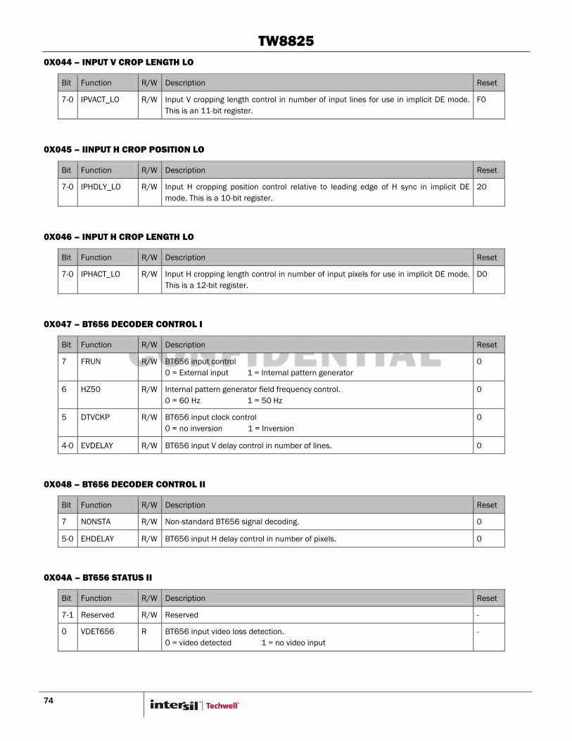
TW8825
74
0X044 – INPUT V CROP LENGTH LO
Bit Function R/W Description Reset
7-0 IPVACT_LO R/W Input V cropping length control in number of input lines for use in implicit DE mode.
This is an 11-bit register.
F0
0X045 – IINPUT H CROP POSITION LO
Bit Function R/W Description Reset
7-0 IPHDLY_LO R/W Input H cropping position control relative to leading edge of H sync in implicit DE
mode. This is a 10-bit register.
20
0X046 – INPUT H CROP LENGTH LO
Bit Function R/W Description Reset
7-0 IPHACT_LO R/W Input H cropping length control in number of input pixels for use in implicit DE mode.
This is a 12-bit register.
D0
0X047 – BT656 DECODER CONTROL I
Bit Function R/W Description Reset
7 FRUN R/W BT656 input control
0 = External input 1 = Internal pattern generator
0
6 HZ50 R/W Internal pattern generator field frequency control.
0 = 60 Hz 1 = 50 Hz
0
5 DTVCKP R/W BT656 input clock control
0 = no inversion 1 = Inversion
0
4-0 EVDELAY R/W BT656 input V delay control in number of lines. 0
0X048 – BT656 DECODER CONTROL II
Bit Function R/W Description Reset
7 NONSTA R/W Non-standard BT656 signal decoding. 0
5-0 EHDELAY R/W BT656 input H delay control in number of pixels. 0
0X04A – BT656 STATUS II
Bit Function R/W Description Reset
7-1 Reserved R/W Reserved -
0 VDET656 R BT656 input video loss detection.
0 = video detected 1 = no video input
-
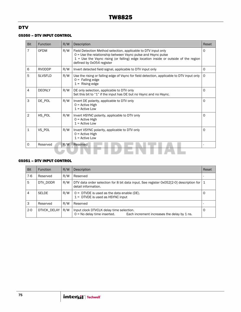
TW8825
75
DTV
0X050 – DTV INPUT CONTROL
Bit Function R/W Description Reset
7 OFDM R/W Field Detection Method selection, applicable to DTV input only
0 = Use the relationship between Vsync pulse and Hsync pulse
1 = Use the Vsync rising (or falling) edge location inside or outside of the region
defined by 0x054 register
0
6 RVODDP R/W Invert detected field signal, applicable to DTV input only 0
5 SLVSFLD R/W Use the rising or falling edge of Vsync for field detection, applicable to DTV input only
0 = Falling edge
1 = Rising edge
0
4 DEONLY R/W DE only selection, applicable to DTV only
Set this bit to “1” if the input has DE but no Vsync and no Hsync.
0
3 DE_POL R/W Invert DE polarity, applicable to DTV only
0 = Active High
1 = Active Low
0
2 HS_POL R/W Invert HSYNC polarity, applicable to DTV only
0 = Active High
1 = Active Low
0
1 VS_POL R/W Invert VSYNC polarity, applicable to DTV only
0 = Active High
1 = Active Low
0
0 Reserved R/W Reserved -
0X051 – DTV INPUT CONTROL
Bit Function R/W Description Reset
7-6 Reserved R/W Reserved -
5 DTV_DODR R/W DTV data order selection for 8 bit data input. See register 0x052[2-0] description for
detail information.
1
4 SELDE R/W 0 = DTVDE is used as the data enable (DE).
1 = DTVDE is used as HSYNC input
0
3 Reserved R/W Reserved -
2-0 DTVCK_DELAY R/W Input clock DTVCLK delay time selection.
0 = No delay time inserted. Each increment increases the delay by 1 ns.
0
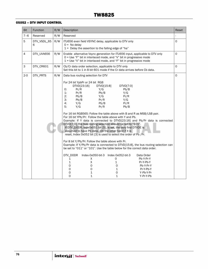
TW8825
76
0X052 – DTV INPUT CONTROL
Bit Function R/W Description Reset
7–6 Reserved R/W Reserved -
5 DTV_VSDL_65
6
R/W ITU656 even field VSYNC delay, applicable to DTV only
0 = No delay
1 = Delay the assertion to the falling edge of “ha”
0
4 DTV_UVA656 R/W Enable alternative Vsync generation for ITU656 input, applicable to DTV only
0 = Use “F” bit in interlaced mode, and “V” bit in progressive mode
1 = Use “V” bit in interlaced mode, and “F” bit in progressive mode
0
3 DTV_CR601 R/W Cb/Cr data order selection, applicable to DTV only
Set this bit to 1 in 8 bit 601 mode if the Cr data arrives before Cb data.
0
2-0 DTV_PRTS R/W Data bus routing selection for DTV
For 24 bit YpbPr or 24 bit RGB
DTVD[23:16] DTVD[15:8] DTVD[7:0]
0: Pr/R Y/G Pb/B
1: Pr/R Pb/B Y/G
2: Pb/B Y/G Pr/R
3: Pb/B Pr/R Y/G
4: Y/G Pb/B Pr/R
5: Y/G Pr/R Pb/B
For 16 bit RGB565: Follow the table above with B and R as MSB/LSB pair.
For 16 bit YPb/Pr: Follow the table above with Y and Pb.
Example: If Y data is connected to DTVD[23:16] and Pb/Pr data is connected
DTVD[7:0], the bus routing selection should be set to “101”.
If DTV_DODR, Inde0x051 bit [5], is set, the very first DTVDE is
assumed to have Pb data. On the other hand if it is
reset, Index 0x052 bit [3] is used to select the order of Pb /Pr.
For 8 bit Y/Pb/Pr: Follow the table above with Pr.
Example: If Y/Pb/Pr data is connected to DTVD[15:8], the bus routing selection can
be set to “011” or “101”. Use the table below for the correct data order.
DTV_DODR Index-0x050-bit-3 Index 0x052-bit-3 Data Order
1 X 0 Pb-Y-Pr-Y
1 X 1 Pr-Y-Pb-Y
0 0 0 Pb-Y-Pr-Y
0 0 1 Pr-Y-Pb-Y
0 1 0 Y-Pb-Y-Pr
0 1 1 Y-Pr-Y-Pb
0
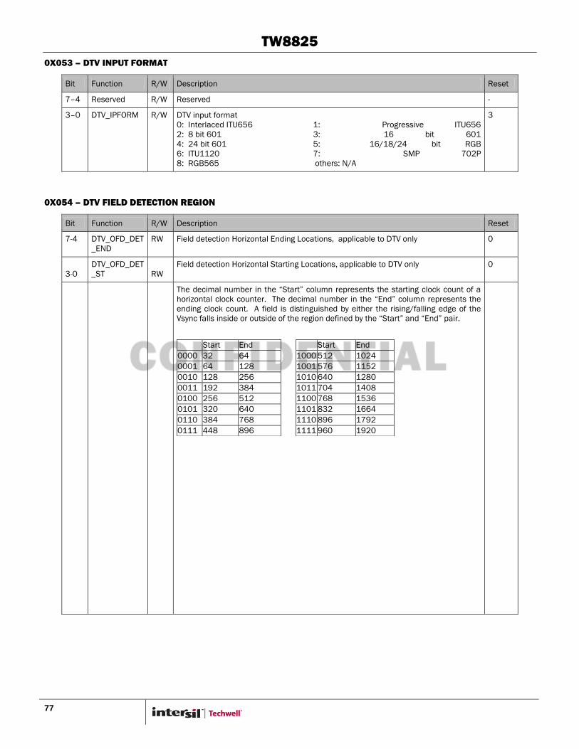
TW8825
77
0X053 – DTV INPUT FORMAT
Bit Function R/W Description Reset
7–4 Reserved R/W Reserved -
3–0 DTV_IPFORM R/W DTV input format
0: Interlaced ITU656 1: Progressive ITU656
2: 8 bit 601 3: 16 bit 601
4: 24 bit 601 5: 16/18/24 bit RGB
6: ITU1120 7: SMP 702P
8: RGB565 others: N/A
3
0X054 – DTV FIELD DETECTION REGION
Bit Function R/W Description Reset
7-4 DTV_OFD_DET
_END
RW Field detection Horizontal Ending Locations, applicable to DTV only 0
3-0
DTV_OFD_DET
_ST RW
Field detection Horizontal Starting Locations, applicable to DTV only 0
The decimal number in the “Start” column represents the starting clock count of a
horizontal clock counter. The decimal number in the “End” column represents the
ending clock count. A field is distinguished by either the rising/falling edge of the
Vsync falls inside or outside of the region defined by the “Start” and “End” pair.
Start End Start End
0000 32 64 1000 512 1024
0001 64 128 1001 576 1152
0010 128 256 1010 640 1280
0011 192 384 1011 704 1408
0100 256 512 1100 768 1536
0101 320 640 1101 832 1664
0110 384 768 1110 896 1792
0111 448 896 1111 960 1920
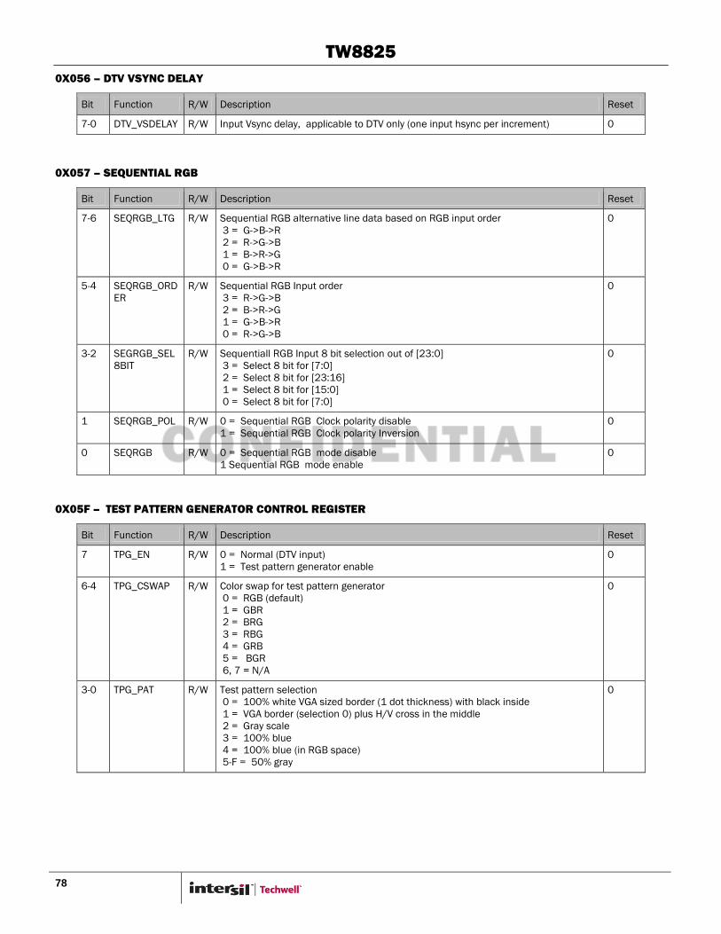
TW8825
78
0X056 – DTV VSYNC DELAY
Bit Function R/W Description Reset
7-0 DTV_VSDELAY R/W Input Vsync delay, applicable to DTV only (one input hsync per increment) 0
0X057 – SEQUENTIAL RGB
Bit Function R/W Description Reset
7-6 SEQRGB_LTG R/W Sequential RGB alternative line data based on RGB input order
3 = G->B->R
2 = R->G->B
1 = B->R->G
0 = G->B->R
0
5-4 SEQRGB_ORD
ER
R/W Sequential RGB Input order
3 = R->G->B
2 = B->R->G
1 = G->B->R
0 = R->G->B
0
3-2 SEGRGB_SEL
8BIT
R/W Sequentiall RGB Input 8 bit selection out of [23:0]
3 = Select 8 bit for [7:0]
2 = Select 8 bit for [23:16]
1 = Select 8 bit for [15:0]
0 = Select 8 bit for [7:0]
0
1 SEQRGB_POL R/W 0 = Sequential RGB Clock polarity disable
1 = Sequential RGB Clock polarity Inversion
0
0 SEQRGB R/W 0 = Sequential RGB mode disable
1 Sequential RGB mode enable
0
0X05F – TEST PATTERN GENERATOR CONTROL REGISTER
Bit Function R/W Description Reset
7 TPG_EN R/W 0 = Normal (DTV input)
1 = Test pattern generator enable
0
6-4 TPG_CSWAP R/W Color swap for test pattern generator 0 = RGB (default) 1 = GBR 2 = BRG 3 = RBG 4 = GRB 5 = BGR
6, 7 = N/A
0
3-0 TPG_PAT R/W Test pattern selection 0 = 100% white VGA sized border (1 dot thickness) with black inside 1 = VGA border (selection 0) plus H/V cross in the middle
2 = Gray scale 3 = 100% blue 4 = 100% blue (in RGB space) 5-F = 50% gray
0

TW8825
79
0X080 – GPIO0_EN
Bit Function R/W Description Reset
7-0 GPIO0_EN R/W Gpio0 enable (active high) 00
0X081 – GPIO1_EN
Bit Function R/W Description Reset
7-0 GPIO1_EN R/W Gpio1 enable (active high) 00
0X082 – GPIO2_EN
Bit Function R/W Description Reset
7-0 GPIO2_EN R/W Gpio2 enable (active high) 00
0X083 – GPIO3_EN
Bit Function R/W Description Reset
7-0 GPIO3_EN R/W Gpio3 enable (active high) 00
0X084 – GPIO4_EN
Bit Function R/W Description Reset
7-0 GPIO4_EN R/W Gpio4 enable (active high) 00
0X085 – GPIO5_EN
Bit Function R/W Description Reset
7-0 GPIO5_EN R/W Gpio5 enable (active high) 00
0X086 – GPIO6_EN
Bit Function R/W Description Reset
7-0 GPIO6_EN R/W Gpio6 enable (active high) 00
0X088 – GPIO0_OE
Bit Function R/W Description Reset
7-0 GPIO0_OE R/W Gpio0 output enable (active high) 00
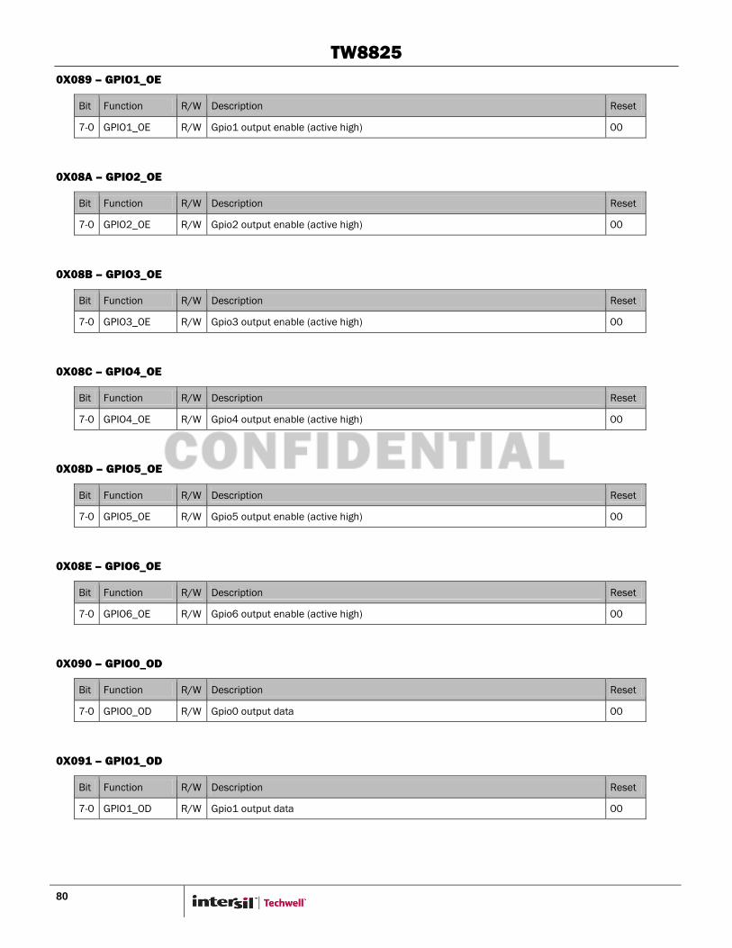
TW8825
80
0X089 – GPIO1_OE
Bit Function R/W Description Reset
7-0 GPIO1_OE R/W Gpio1 output enable (active high) 00
0X08A – GPIO2_OE
Bit Function R/W Description Reset
7-0 GPIO2_OE R/W Gpio2 output enable (active high) 00
0X08B – GPIO3_OE
Bit Function R/W Description Reset
7-0 GPIO3_OE R/W Gpio3 output enable (active high) 00
0X08C – GPIO4_OE
Bit Function R/W Description Reset
7-0 GPIO4_OE R/W Gpio4 output enable (active high) 00
0X08D – GPIO5_OE
Bit Function R/W Description Reset
7-0 GPIO5_OE R/W Gpio5 output enable (active high) 00
0X08E – GPIO6_OE
Bit Function R/W Description Reset
7-0 GPIO6_OE R/W Gpio6 output enable (active high) 00
0X090 – GPIO0_OD
Bit Function R/W Description Reset
7-0 GPIO0_OD R/W Gpio0 output data 00
0X091 – GPIO1_OD
Bit Function R/W Description Reset
7-0 GPIO1_OD R/W Gpio1 output data 00

TW8825
81
0X092 – GPIO2_OD
Bit Function R/W Description Reset
7-0 GPIO2_OD R/W Gpio2 output data 00
0X093 – GPIO3_OD
Bit Function R/W Description Reset
7-0 GPIO3_OD R/W Gpio3 output data 00
0X094 – GPIO4_OD
Bit Function R/W Description Reset
7-0 GPIO4_OD R/W Gpio4 output data 00
0X095 – GPIO5_OD
Bit Function R/W Description Reset
7-0 GPIO5_OD R/W Gpio5 output data 00
0X096 – GPIO6_OD
Bit Function R/W Description Reset
7-0 GPIO6_OD R/W Gpio6 output data 00
0X098 – GPIO0_ID
Bit Function R/W Description Reset
7-0 GPIO0_ID R Gpio0 input data -
0X099 – GPIO1_ID
Bit Function R/W Description Reset
7-0 GPIO1_ID R Gpio1 input data -
0X09A – GPIO2_ID
Bit Function R/W Description Reset
7-0 GPIO2_ID R Gpio2 input data -
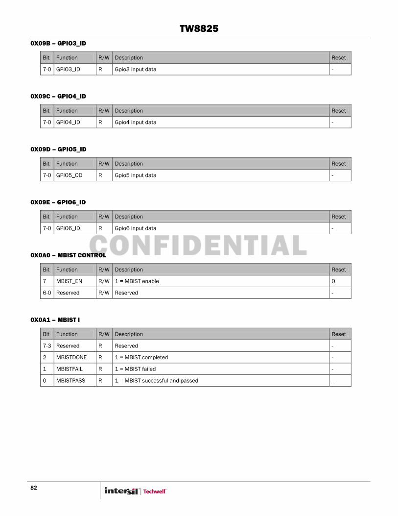
TW8825
82
0X09B – GPIO3_ID
Bit Function R/W Description Reset
7-0 GPIO3_ID R Gpio3 input data -
0X09C – GPIO4_ID
Bit Function R/W Description Reset
7-0 GPIO4_ID R Gpio4 input data -
0X09D – GPIO5_ID
Bit Function R/W Description Reset
7-0 GPIO5_OD R Gpio5 input data -
0X09E – GPIO6_ID
Bit Function R/W Description Reset
7-0 GPIO6_ID R Gpio6 input data -
0X0A0 – MBIST CONTROL
Bit Function R/W Description Reset
7 MBIST_EN R/W 1 = MBIST enable 0
6-0 Reserved R/W Reserved -
0X0A1 – MBIST I
Bit Function R/W Description Reset
7-3 Reserved R Reserved -
2 MBISTDONE R 1 = MBIST completed -
1 MBISTFAIL R 1 = MBIST failed -
0 MBISTPASS R 1 = MBIST successful and passed -
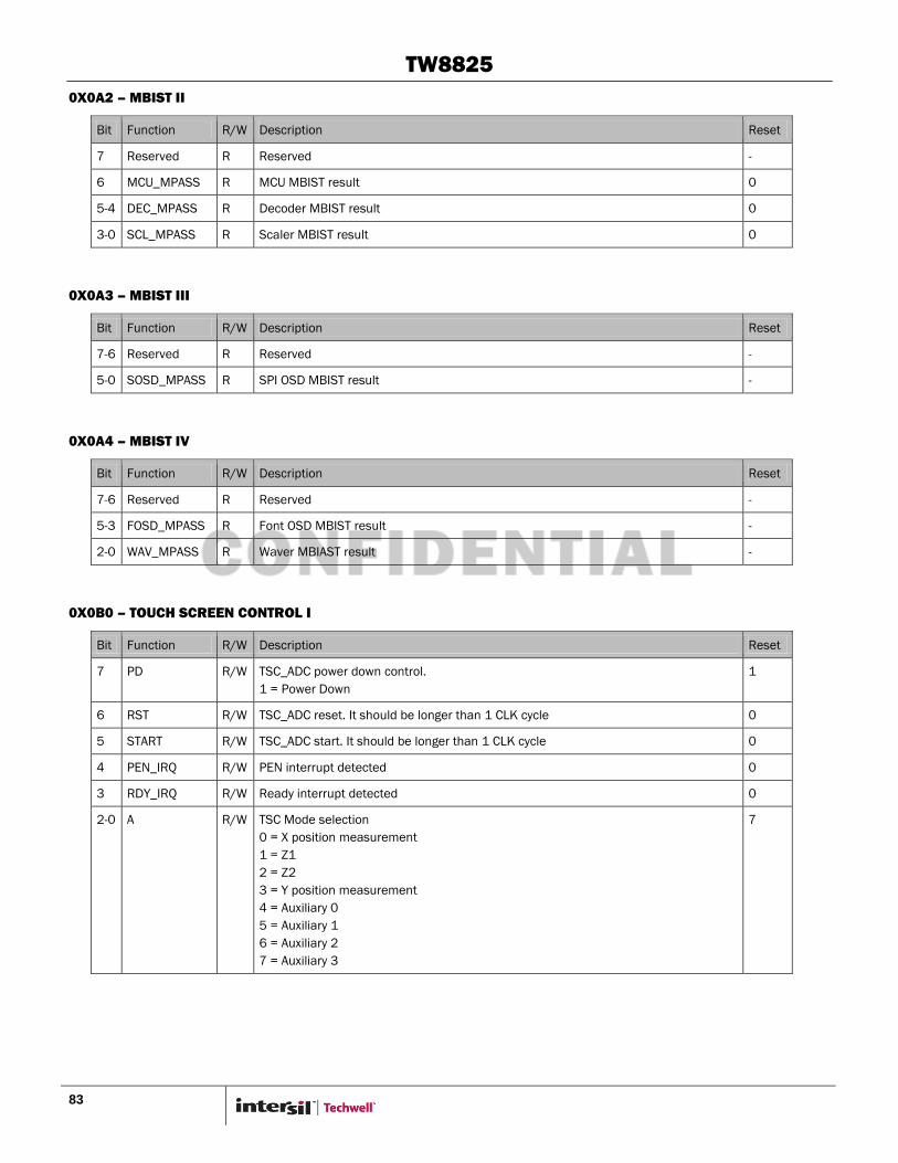
TW8825
83
0X0A2 – MBIST II
Bit Function R/W Description Reset
7 Reserved R Reserved -
6 MCU_MPASS R MCU MBIST result 0
5-4 DEC_MPASS R Decoder MBIST result 0
3-0 SCL_MPASS R Scaler MBIST result 0
0X0A3 – MBIST III
Bit Function R/W Description Reset
7-6 Reserved R Reserved -
5-0 SOSD_MPASS R SPI OSD MBIST result -
0X0A4 – MBIST IV
Bit Function R/W Description Reset
7-6 Reserved R Reserved -
5-3 FOSD_MPASS R Font OSD MBIST result -
2-0 WAV_MPASS R Waver MBIAST result -
0X0B0 – TOUCH SCREEN CONTROL I
Bit Function R/W Description Reset
7 PD R/W TSC_ADC power down control.
1 = Power Down
1
6 RST R/W TSC_ADC reset. It should be longer than 1 CLK cycle 0
5 START R/W TSC_ADC start. It should be longer than 1 CLK cycle 0
4 PEN_IRQ R/W PEN interrupt detected 0
3 RDY_IRQ R/W Ready interrupt detected 0
2-0 A R/W TSC Mode selection
0 = X position measurement
1 = Z1
2 = Z2
3 = Y position measurement
4 = Auxiliary 0
5 = Auxiliary 1
6 = Auxiliary 2
7 = Auxiliary 3
7

TW8825
84
0X0B1 – TOUCH SCREEN CONTROL II
Bit Function R/W Description Reset
7 PDYINT_DIS R/W 0 = Enable Ready interrupt
1 = Disable Ready interrupt
0
6 PENINT_DIS R/W 0 = Enable Pen interrupt
1 = Disable Pen interrupt
0
5-3 R_SEL R/W Touch sensitivity R selection
0 = 150K 1 = 130K 2 = 110K 3 = 90K
4 = 70K 5 = 50K 6 = 30K 7 = 10K
0
2-0 TEST_ADC R/W ADC test mode control
0-3 = Disabled
4 = Buffered internal comparator input
5 = vmid
6 = comp out
7 = Regen clock
0
0X0B2 – TSC ADC DATA OUTPUT_HI
Bit Function R/W Description Reset
7-0 TSc_ADOUT R TSC_ADOUT[11-4] 00
0X0B3 – TSC ADC DATA OUTPUT_LO
Bit Function R/W Description Reset
7-4 Reserved R/W Reserved -
3-0 TSc_ADOUT R TSC_ADOUT[3-0] -
0X0B4 – TSC ADC SAMPLE AND CLOCK
Bit Function R/W Description Reset
7-4 Reserved R/W Reserved -
3 CONTI_SMP R/W 0 = Sampling start by register START command
1 = Continuous sampling for TSC_ADC regardless of the START command
0
2-0 TSC_CKSEL R/W TSC_ADC clock selection
0 = Divide by 2
1 = Divide by 4
2 = Divide by 8
3 = Divide by 16
4 = Divide by 32
5 = Divide by 64
6 = Divide by 128
7 = Divide by 256
0

TW8825
85
0X0D4 – LOPOR REGISTERS
Bit Function R/W Description Reset
7 XTAL_PD R/W Crystal Power Down Control, control through PIN “MCU P2.7”. 0
6-3 Reserved R/W Reserved -
2 PL_LSO R/W LSO power down control 0
1 DIS_DLY R/W 1 = disable delay count for POR 0
0 PL_LSO R/W LSO power down control 0
0X0D6 – TCLK AND PWM CNTL
Bit Function R/W Description Reset
6-4 TCCLK_O_SEL R/W TCCLK output delay control 0
3-0 PWM_EN R/W PWM Enable. { PWM_4, PWM_3, PWM_2, PWM_1} 0
0X0D7 – FPWM3_LO
Bit Function R/W Description Reset
7-0 FPWM3[7-0] R/W PWM3 frequency control LSB. A 10-bit register.
Freq = 27MHz / 256 / FPWM3
00
0X0D8 – DPWM3
Bit Function R/W Description Reset
7-0 DPWM3 R/W PWM3 Duty cycle control. Duty = ( DPWM3 / 256 ) % 80
0X0D9 – FPWM4_LO
Bit Function R/W Description Reset
7-0 FPWM4[7-0] R/W PWM4 frequency control LSB. A 10-bit register.
Freq = 27MHz / 256 / FPWM4
00
0X0DA – DPWM4
Bit Function R/W Description Reset
7-0 DPWM4 R/W PWM4 Duty cycle control. Duty = ( DPWM4 / 256 ) % 80

TW8825
86
0X0DB – FPWM_HI
Bit Function R/W Description Reset
7-6 FPWM4[9-8] R/W PWM4 frequency control MSB. A 10-bit register. 1
5-4 FPWM3[9-8] R/W PWM3 frequency control MSB. A 10-bit register. 1
3-2 FPWM2[9-8] R/W PWM2 frequency control MSB. A 10-bit register. 1
1-0 FPWM1[9-8] R/W PWM1 frequency control MSB. A 10-bit register. 1
0X0DC – FPWM1_LO
Bit Function R/W Description Reset
7-0 FPWM1[7-0] R/W PWM1 frequency control LSB. A 10-bit register.
Freq = 27MHz / 256 / FPWM1
00
0X0DD – DPWM1
Bit Function R/W Description Reset
7-0 DPWM1 R/W PWM1 Duty cycle control. Duty = ( DPWM1 / 256 ) % 80
0X0DE – FPWM2_LO
Bit Function R/W Description Reset
7-0 FPWM2[7-0] R/W PWM2 frequency control LSB. A 10-bit register.
Freq = 27MHz / 256 / FPWM2
00
0X0DF – DPWM2
Bit Function R/W Description Reset
7-0 DPWM2 R/W PWM2 Duty cycle control. Duty = ( DPWM2 / 256 ) % 80
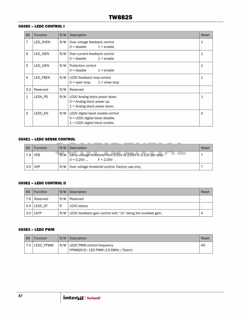
TW8825
87
0X0E0 – LEDC CONTROL I
Bit Function R/W Description Reset
7 LED_OVEN R/W Over voltage feedback control
0 = disable 1 = enable
1
6 LED_OIEN R/W Over current feedback control
0 = disable 1 = enable
1
5 LED_UIEN R/W Protection control
0 = disable 1 = enable
1
4 LED_FBEN R/W LEDC feedback loop control
0 = open loop 1 = close loop
1
3-2 Reserved R/W Reserved -
1 LEDA_PD R/W LEDC Analog block power down.
0 = Analog block power up.
1 = Analog block power down.
1
0 LEDC_EN R/W LEDC digital block enable control
0 = LEDC digital block disable.
1 = LEDC digital block enable.
0
0X0E1 – LEDC SENSE CONTROL
Bit Function R/W Description Reset
7-4 VFB R/W Lamp voltage threshold from 0.25V to 2.05V in 0.12V per step.
0 = 0.25V … F = 2.05V
7
3-0 VOP R/W Over voltage threshold control. Factory use only. 7
0X0E2 – LEDC CONTROL II
Bit Function R/W Description Reset
7-6 Reserved R/W Reserved -
5-4 LEDC_ST R LEDC status -
3-0 LSTP R/W LEDC feedback gain control with “1h” being the smallest gain. 4
0X0E3 – LEDC PWM
Bit Function R/W Description Reset
7-0 LEDC_FPWM R/W LEDC PWM control frequency
FPWM[6:0] : LED PWM (13.5MHz / Fpwm)
40
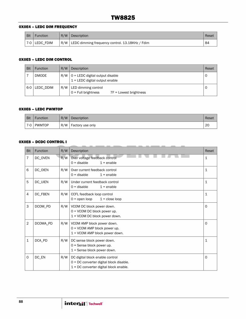
TW8825
88
0X0E4 – LEDC DIM FREQUENCY
Bit Function R/W Description Reset
7-0 LEDC_FDIM R/W LEDC dimming frequency control. 13.18KHz / Fdim 84
0X0E5 – LEDC DIM CONTROL
Bit Function R/W Description Reset
7 DMODE R/W 0 = LEDC digital output disable
1 = LEDC digital output enable
0
6-0 LEDC_DDIM R/W LED dimming control
0 = Full brightness 7F = Lowest brightness
0
0X0E6 – LEDC PWMTOP
Bit Function R/W Description Reset
7-0 PWMTOP R/W Factory use only 20
0X0E8 – DCDC CONTROL I
Bit Function R/W Description Reset
7 DC_OVEN R/W Over voltage feedback control
0 = disable 1 = enable
1
6 DC_OIEN R/W Over current feedback control
0 = disable 1 = enable
1
5 DC_UIEN R/W Under current feedback control
0 = disable 1 = enable
1
4 DC_FBEN R/W CCFL feedback loop control
0 = open loop 1 = close loop
1
3 DCOM_PD R/W VCOM DC block power down.
0 = VCOM DC block power up.
1 = VCOM DC block power down.
0
2 DCOMA_PD R/W VCOM AMP block power down.
0 = VCOM AMP block power up.
1 = VCOM AMP block power down.
0
1 DCA_PD R/W DC sense block power down.
0 = Sense block power up.
1 = Sense block power down.
1
0 DC_EN R/W DC digital block enable control
0 = DC converter digital block disable.
1 = DC converter digital block enable.
0
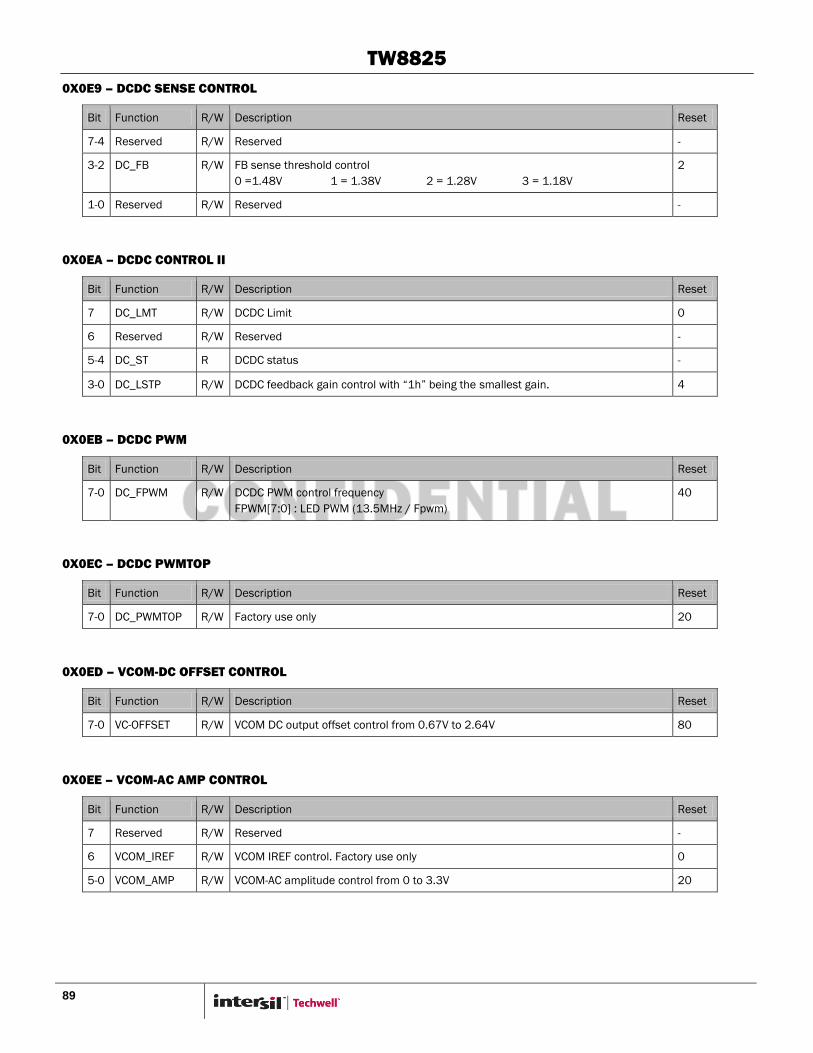
TW8825
89
0X0E9 – DCDC SENSE CONTROL
Bit Function R/W Description Reset
7-4 Reserved R/W Reserved -
3-2 DC_FB R/W FB sense threshold control
0 =1.48V 1 = 1.38V 2 = 1.28V 3 = 1.18V
2
1-0 Reserved R/W Reserved -
0X0EA – DCDC CONTROL II
Bit Function R/W Description Reset
7 DC_LMT R/W DCDC Limit 0
6 Reserved R/W Reserved -
5-4 DC_ST R DCDC status -
3-0 DC_LSTP R/W DCDC feedback gain control with “1h” being the smallest gain. 4
0X0EB – DCDC PWM
Bit Function R/W Description Reset
7-0 DC_FPWM R/W DCDC PWM control frequency
FPWM[7:0] : LED PWM (13.5MHz / Fpwm)
40
0X0EC – DCDC PWMTOP
Bit Function R/W Description Reset
7-0 DC_PWMTOP R/W Factory use only 20
0X0ED – VCOM-DC OFFSET CONTROL
Bit Function R/W Description Reset
7-0 VC-OFFSET R/W VCOM DC output offset control from 0.67V to 2.64V 80
0X0EE – VCOM-AC AMP CONTROL
Bit Function R/W Description Reset
7 Reserved R/W Reserved -
6 VCOM_IREF R/W VCOM IREF control. Factory use only 0
5-0 VCOM_AMP R/W VCOM-AC amplitude control from 0 to 3.3V 20

TW8825
90
0X0F6 – CLOCK_DIV
Bit Function R/W Description Reset
7-6 Reserved R/W Reserved -
5-4 SPICLK_DIV R/W These bits control the SPI clock divider as follow.
0 = 1 1 = ½ 2 = 1/3 3 = Reserved
0
3-2 Reserved R/W Reserved -
1-0 PCLK_DIV R/W These bits control the pclk divider as follow
0 = 1 1 = ½ 2 = ¼ 3 = 1/8
0
0X0F7 – SSPLL
Bit Function R/W Description Reset
7 Reserved R/W Reserved -
6 EDGE_SEL_P R/W Edge selection for SSPLL. Factory use only 0
5-4 SSPLL_CP_X4 R/W SSPLL_X4 CP selection. Factory use only.
1uA / 5uA / 10uA / 15uA
1
3-2 SSPLL_LP_X4 R/W SSPLL_X4 LP selection among 80K to 20K. Factory use only. 1
1-0 SSPLL_LP_X8 R/W SSPLL_X8 LP selection among 18K to 0.8K. Factory use only. 2
0X0F8 – SSPLL CONTROL REGISTERS
Bit Function R/W Description Reset
7-4 Reserved R/W Reserved -
3-0 FPLL[19-16] R/W Part of a 20-bit register that control the PLL center frequency as below.
PLL Oscillation frequency = 108MHz * FPLL / 2 ^ 17 / 2^ POST
1
0X0F9 – SSPLL FREQUENCY CONTROL REGISTERS
Bit Function R/W Description Reset
7-0 FPLL[15-8] R/W Part of a 20-bit register that control the PLL center frequency as below.
PLL Oscillation frequency = 108MHz * FPLL / 2 ^ 17 / 2^ POST
20
0X0FA – SSPLL FREQUENCY CONTROL REGISTERS
Bit Function R/W Description Reset
7-0 FPLL[7-0] R/W Part of a 20-bit register that control the PLL center frequency as below.
PLL Oscillation frequency = 108MHz * FPLL / 2 ^ 17 / 2^ POST
00
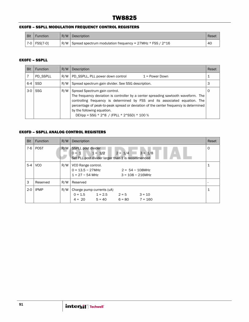
TW8825
91
0X0FB – SSPLL MODULATION FREQUENCY CONTROL REGISTERS
Bit Function R/W Description Reset
7-0 FSS[7-0] R/W Spread spectrum modulation frequency = 27MHz * FSS / 2^16 40
0X0FC – SSPLL
Bit Function R/W Description Reset
7 PD_SSPLL R/W PD_SSPLL, PLL power down control 1 = Power Down 1
6-4 SSD R/W Spread spectrum gain divider. See SSG description. 3
3-0 SSG R/W Spread Spectrum gain control.
The frequency deviation is controller by a center spreading sawtooth waveform. The
controlling frequency is determined by FSS and its associated equation. The
percentage of peak-to-peak spread or deviation of the center frequency is determined
by the following equation.
DEVpp = SSG * 2^8 / (FPLL * 2^SSD) * 100 %
0
0X0FD – SSPLL ANALOG CONTROL REGISTERS
Bit Function R/W Description Reset
7-6 POST R/W SSPLL post divider
0 = 1 1 = 1/2 2 = 1/4 3 = 1/8
Set PLL post divider larger than 1 is recommended
0
5-4 VCO R/W VCO Range control.
0 = 13.5 ~ 27MHz 2 = 54 ~ 108MHz
1 = 27 ~ 54 MHz 3 = 108 ~ 216MHz
1
3 Reserved R/W Reserved -
2-0 IPMP R/W Charge pump currents (uA)
0 = 1.5 1 = 2.5 2 = 5 3 = 10
4 = 20 5 = 40 6 = 80 7 = 160
1
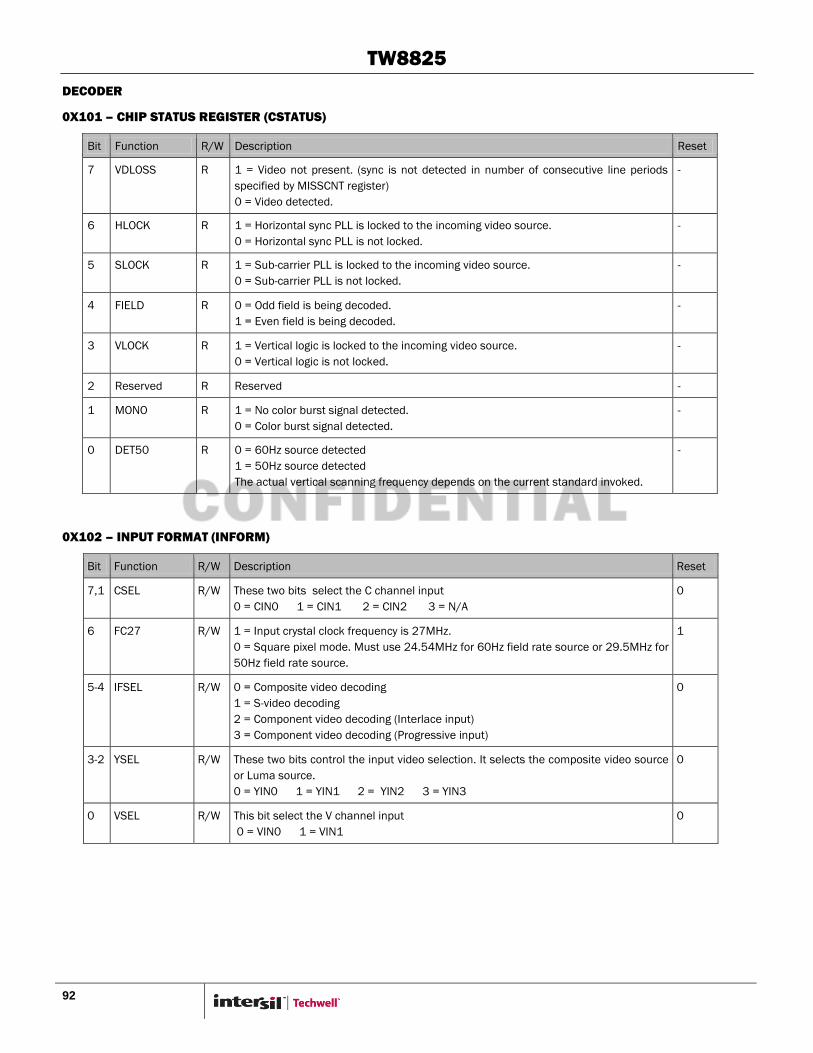
TW8825
92
DECODER
0X101 – CHIP STATUS REGISTER (CSTATUS)
Bit Function R/W Description Reset
7 VDLOSS R 1 = Video not present. (sync is not detected in number of consecutive line periods
specified by MISSCNT register)
0 = Video detected.
-
6 HLOCK R 1 = Horizontal sync PLL is locked to the incoming video source.
0 = Horizontal sync PLL is not locked.
-
5 SLOCK R 1 = Sub-carrier PLL is locked to the incoming video source.
0 = Sub-carrier PLL is not locked.
-
4 FIELD R 0 = Odd field is being decoded.
1 = Even field is being decoded.
-
3 VLOCK R 1 = Vertical logic is locked to the incoming video source.
0 = Vertical logic is not locked.
-
2 Reserved R Reserved -
1 MONO R 1 = No color burst signal detected.
0 = Color burst signal detected.
-
0 DET50 R 0 = 60Hz source detected
1 = 50Hz source detected
The actual vertical scanning frequency depends on the current standard invoked.
-
0X102 – INPUT FORMAT (INFORM)
Bit Function R/W Description Reset
7,1 CSEL R/W These two bits select the C channel input
0 = CIN0 1 = CIN1 2 = CIN2 3 = N/A
0
6 FC27 R/W 1 = Input crystal clock frequency is 27MHz.
0 = Square pixel mode. Must use 24.54MHz for 60Hz field rate source or 29.5MHz for
50Hz field rate source.
1
5-4 IFSEL R/W 0 = Composite video decoding
1 = S-video decoding
2 = Component video decoding (Interlace input)
3 = Component video decoding (Progressive input)
0
3-2 YSEL R/W These two bits control the input video selection. It selects the composite video source
or Luma source.
0 = YIN0 1 = YIN1 2 = YIN2 3 = YIN3
0
0 VSEL R/W This bit select the V channel input
0 = VIN0 1 = VIN1
0
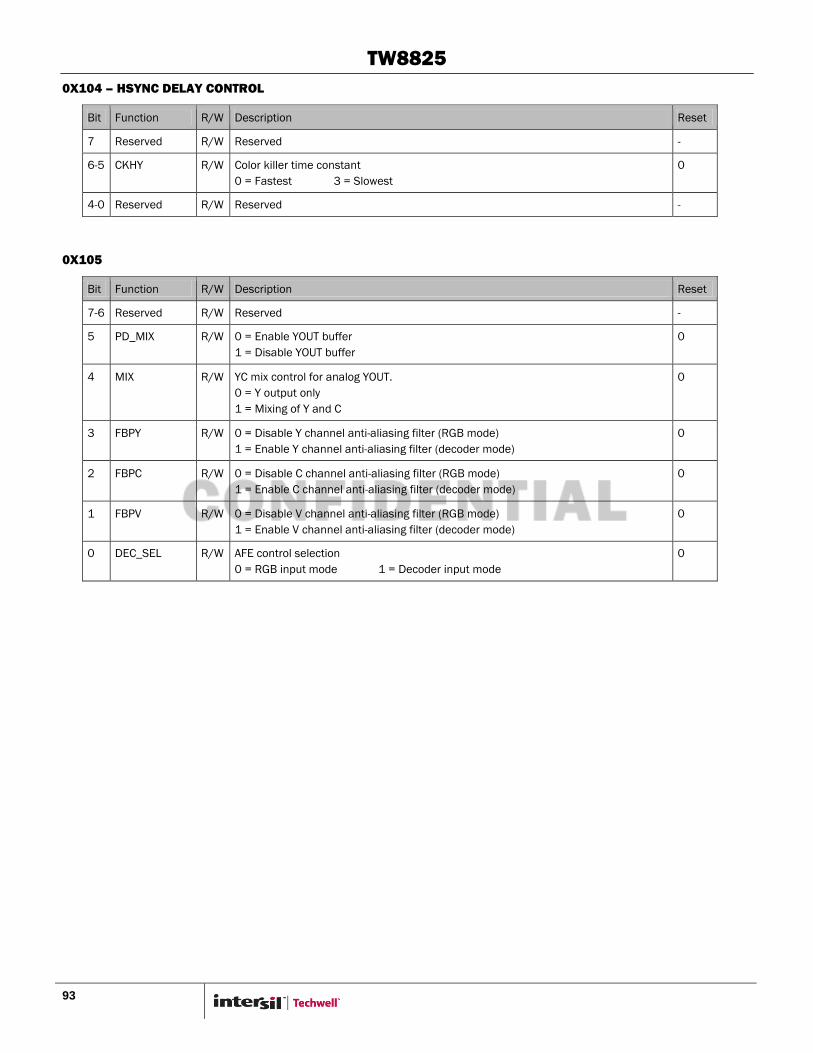
TW8825
93
0X104 – HSYNC DELAY CONTROL
Bit Function R/W Description Reset
7 Reserved R/W Reserved -
6-5 CKHY R/W Color killer time constant
0 = Fastest 3 = Slowest
0
4-0 Reserved R/W Reserved -
0X105
Bit Function R/W Description Reset
7-6 Reserved R/W Reserved -
5 PD_MIX R/W 0 = Enable YOUT buffer
1 = Disable YOUT buffer
0
4 MIX R/W YC mix control for analog YOUT.
0 = Y output only
1 = Mixing of Y and C
0
3 FBPY R/W 0 = Disable Y channel anti-aliasing filter (RGB mode)
1 = Enable Y channel anti-aliasing filter (decoder mode)
0
2 FBPC R/W 0 = Disable C channel anti-aliasing filter (RGB mode)
1 = Enable C channel anti-aliasing filter (decoder mode)
0
1 FBPV R/W 0 = Disable V channel anti-aliasing filter (RGB mode)
1 = Enable V channel anti-aliasing filter (decoder mode)
0
0 DEC_SEL R/W AFE control selection
0 = RGB input mode 1 = Decoder input mode
0
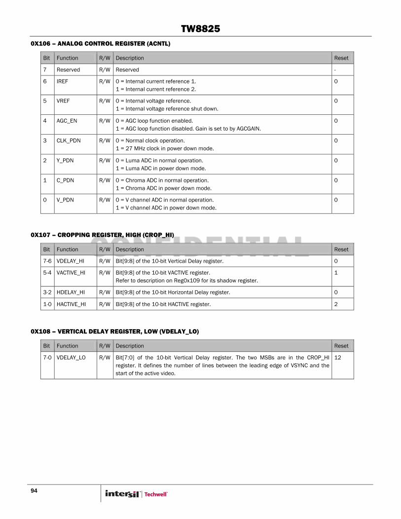
TW8825
94
0X106 – ANALOG CONTROL REGISTER (ACNTL)
Bit Function R/W Description Reset
7 Reserved R/W Reserved -
6 IREF R/W 0 = Internal current reference 1.
1 = Internal current reference 2.
0
5 VREF R/W 0 = Internal voltage reference.
1 = Internal voltage reference shut down.
0
4 AGC_EN R/W 0 = AGC loop function enabled.
1 = AGC loop function disabled. Gain is set to by AGCGAIN.
0
3 CLK_PDN R/W 0 = Normal clock operation.
1 = 27 MHz clock in power down mode.
0
2 Y_PDN R/W 0 = Luma ADC in normal operation.
1 = Luma ADC in power down mode.
0
1 C_PDN R/W 0 = Chroma ADC in normal operation.
1 = Chroma ADC in power down mode.
0
0 V_PDN R/W 0 = V channel ADC in normal operation.
1 = V channel ADC in power down mode.
0
0X107 – CROPPING REGISTER, HIGH (CROP_HI)
Bit Function R/W Description Reset
7-6 VDELAY_HI R/W Bit[9:8] of the 10-bit Vertical Delay register. 0
5-4 VACTIVE_HI R/W Bit[9:8] of the 10-bit VACTIVE register.
Refer to description on Reg0x109 for its shadow register.
1
3-2 HDELAY_HI R/W Bit[9:8] of the 10-bit Horizontal Delay register. 0
1-0 HACTIVE_HI R/W Bit[9:8] of the 10-bit HACTIVE register. 2
0X108 – VERTICAL DELAY REGISTER, LOW (VDELAY_LO)
Bit Function R/W Description Reset
7-0 VDELAY_LO R/W Bit[7:0] of the 10-bit Vertical Delay register. The two MSBs are in the CROP_HI
register. It defines the number of lines between the leading edge of VSYNC and the
start of the active video.
12

TW8825
95
0X109 – VERTICAL ACTIVE REGISTER, LOW (VACTIVE_LO)
Bit Function R/W Description Reset
7-0 VACTIVE_LO R/W Bit[7:0] of the 10-bit Vertical Active register. The two MSBs are in the CROP_HI
register. It defines the number of active video lines per frame output.
The VACTIVE register has a shadow register for use with 50Hz source when Atreg of
Reg0x11C is not set. This register can be accessed through the same index address
by first changing the format standard to any 50Hz standard.
20
0X10A – HORIZONTAL DELAY REGISTER, LOW (HDELAY_LO)
Bit Function R/W Description Reset
7-0 HDELAY_LO R/W Bit[7:0] of the 10-bit Horizontal Delay register. The two MSBs are in the CROP_HI
register. It defines the number of pixels between the leading edge of the HSYNC and
the start of the image cropping for active video.
The HDELAY_LO register has two shadow registers for use with PAL and SECAM
sources respectively. These register can be accessed using the same index address
by first changing the decoding format to the corresponding standard.
0A
0X10B – HORIZONTAL ACTIVE REGISTER, LOW (HACTIVE_LO)
Bit Function R/W Description Reset
7-0 HACTIVE_LO R/W Bit[7:0] of the 10-bit Horizontal Active register. The two MSBs are in the CROP_HI
register. It defines the number of active pixels per line output.
D0
0X10C – CONTROL REGISTER I (CNTRL1)
Bit Function R/W Description Reset
7 PBW R/W Combined with VTL[3], there are four different chroma bandwidth can be selected.
1 = Wide Chroma BPF BW
0 = Normal Chroma BPF BW
1
6 DEM R/W Color killer sensitivity
1 = Low 0 = High
1
5 PALSW R/W 1 = PAL switch sensitivity low.
0 = PAL switch sensitivity normal.
0
4 SET7 R/W 1 = The black level is 7.5 IRE above the blank level.
0 = The black level is the same as the blank level.
0
3 COMB R/W 1 = Adaptive comb filter on for NTSC/PAL
0 = Notch filter
1
2 HCOMP R/W 1 = Operation mode 1. (recommended)
0 = Operation mode 0.
1
1 YCOMB R/W This bit controls the comb operation when there is no color burst.
1 = No comb 0 = Comb.
0
0 PDLY R/W PAL delay line
1 = Disable 0 = Enable 0
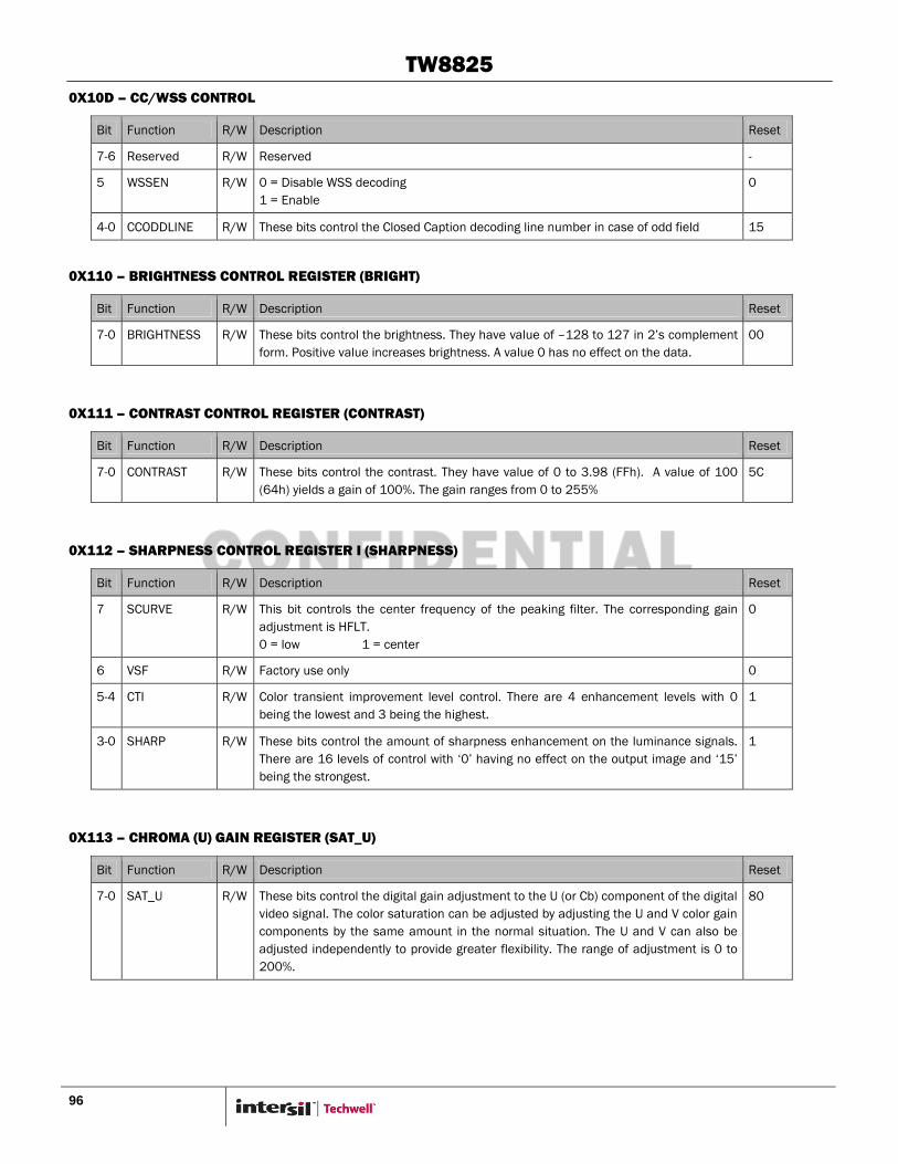
TW8825
96
0X10D – CC/WSS CONTROL
Bit Function R/W Description Reset
7-6 Reserved R/W Reserved -
5 WSSEN R/W 0 = Disable WSS decoding
1 = Enable
0
4-0 CCODDLINE R/W These bits control the Closed Caption decoding line number in case of odd field 15
0X110 – BRIGHTNESS CONTROL REGISTER (BRIGHT)
Bit Function R/W Description Reset
7-0 BRIGHTNESS R/W These bits control the brightness. They have value of –128 to 127 in 2‟s complement
form. Positive value increases brightness. A value 0 has no effect on the data.
00
0X111 – CONTRAST CONTROL REGISTER (CONTRAST)
Bit Function R/W Description Reset
7-0 CONTRAST R/W These bits control the contrast. They have value of 0 to 3.98 (FFh). A value of 100
(64h) yields a gain of 100%. The gain ranges from 0 to 255%
5C
0X112 – SHARPNESS CONTROL REGISTER I (SHARPNESS)
Bit Function R/W Description Reset
7 SCURVE R/W This bit controls the center frequency of the peaking filter. The corresponding gain
adjustment is HFLT.
0 = low 1 = center
0
6 VSF R/W Factory use only 0
5-4 CTI R/W Color transient improvement level control. There are 4 enhancement levels with 0
being the lowest and 3 being the highest.
1
3-0 SHARP R/W These bits control the amount of sharpness enhancement on the luminance signals.
There are 16 levels of control with „0‟ having no effect on the output image and „15‟
being the strongest.
1
0X113 – CHROMA (U) GAIN REGISTER (SAT_U)
Bit Function R/W Description Reset
7-0 SAT_U R/W These bits control the digital gain adjustment to the U (or Cb) component of the digital
video signal. The color saturation can be adjusted by adjusting the U and V color gain
components by the same amount in the normal situation. The U and V can also be
adjusted independently to provide greater flexibility. The range of adjustment is 0 to
200%.
80
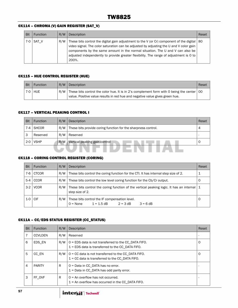
TW8825
97
0X114 – CHROMA (V) GAIN REGISTER (SAT_V)
Bit Function R/W Description Reset
7-0 SAT_V R/W These bits control the digital gain adjustment to the V (or Cr) component of the digital
video signal. The color saturation can be adjusted by adjusting the U and V color gain
components by the same amount in the normal situation. The U and V can also be
adjusted independently to provide greater flexibility. The range of adjustment is 0 to
200%.
80
0X115 – HUE CONTROL REGISTER (HUE)
Bit Function R/W Description Reset
7-0 HUE R/W These bits control the color hue. It is in 2‟s complement form with 0 being the center
value. Positive value results in red hue and negative value gives green hue.
00
0X117 – VERTICAL PEAKING CONTROL I
Bit Function R/W Description Reset
7-4 SHCOR R/W These bits provide coring function for the sharpness control. 4
3 Reserved R/W Reserved -
2-0 VSHP R/W Vertical peaking gain control 0
0X118 – CORING CONTROL REGISTER (CORING)
Bit Function R/W Description Reset
7-6 CTCOR R/W These bits control the coring function for the CTI. It has internal step size of 2. 1
5-4 CCOR R/W These bits control the low level coring function for the Cb/Cr output. 0
3-2 VCOR R/W These bits control the coring function of the vertical peaking logic. It has an internal
step size of 2.
1
1-0 CIF R/W These bits control the IF compensation level.
0 = None 1 = 1.5 dB 2 = 3 dB 3 = 6 dB
0
0X11A – CC/EDS STATUS REGISTER (CC_STATUS)
Bit Function R/W Description Reset
7 CCVLDEN R/W Reserved -
6 EDS_EN R/W 0 = EDS data is not transferred to the CC_DATA FIFO.
1 = EDS data is transferred to the CC_DATA FIFO.
0
5 CC_EN R/W 0 = CC data is not transferred to the CC_DATA FIFO.
1 = CC data is transferred to the CC_DATA FIFO.
0
4 PARITY R 0 = Data in CC_DATA has no error.
1 = Data in CC_DATA has odd parity error.
-
3 FF_OVF R 0 = An overflow has not occurred.
1 = An overflow has occurred in the CC_DATA FIFO.
-

TW8825
98
Bit Function R/W Description Reset
2 FF_EMP R 0 = CC_DATA FIFO is empty.
1 = CC_DATA FIFO has data available.
-
1 CC_EDS R 0 = Closed caption data is in CC_DATA register.
1 = Extended data service data is in CC_DATA register.
-
0 LO_HI R 0 = Low byte of the 16-bit word is in the CC_DATA register.
1 = High byte of the 16-bit word is in the CC_DATA register.
-
0X11B – CC/EDS DATA REGISTER (CC_DATA)
Bit Function R/W Description Reset
7-0 CC_DATA R These bits store the incoming closed caption or even field closed caption data. -
0X11C – STANDARD SELECTION (SDT)
Bit Function R/W Description Reset
7 DETSTUS R 0 = Idle 1 = detection in progress -
6-4 STDNOW R Current standard invoked
0 = NTSC(M) 1 = PAL (B,D,G,H,I) 2 = SECAM 3 = NTSC4.43
4 = PAL (M) 5 = PAL (CN) 6 = PAL 60 7 = N/A
-
3 ATREG R/W 1 = Disable the shadow registers.
0 = Enable VACTIVE and HDELAY shadow registers value depending on standard
0
2-0 STANDARD R/W Standard selection
0 = NTSC(M) 1 = PAL (B,D,G,H,I) 2 = SECAM 3 = NTSC4.43
4 = PAL (M) 5 = PAL (CN) 6 = PAL 60 7 = Auto detection
7
0X11D – STANDARD RECOGNITION (SDTR)
Bit Function R/W Description Reset
7 ATSTART R/W Writing 1 to this bit will manually initiate the auto format detection process. This bit is
a self-resetting bit.
0
6 PAL6_EN R/W 1 = enable recognition of PAL60.
0 = disable recognition.
1
5 PALN_EN R/W 1 = enable recognition of PAL (CN).
0 = disable recognition.
1
4 PALM_EN R/W 1 = enable recognition of PAL (M).
0 = disable recognition.
1
3 NT44_EN R/W 1 = enable recognition of NTSC 4.43.
0 = disable recognition.
1
2 SEC_EN R/W 1 = enable recognition of SECAM.
0 = disable recognition.
1
1 PALB_EN R/W 1 = enable recognition of PAL (B,D,G,H,I).
0 = disable recognition.
1

TW8825
99
Bit Function R/W Description Reset
0 NTSC_EN R/W 1 = enable recognition of NTSC (M).
0 = disable recognition.
1
0X11E – COMPONENT VIDEO FORMAT (CVFMT)
Bit Function R/W Description Reset
7 RSV R Reserved -
6-4 CVSTD R Component video input format detection.
0 = 480i 1 = 576i 2 = 480p 3 = 576p others = NA
-
3-0 CVFMT R/W Component video format selection.
0 = 480i 1 = 576i 2 = 480p 3 = 576p 8 = Auto others = N/A
0
0X120 – CLAMPING GAIN (CLMPG)
Bit Function R/W Description Reset
7-4 CLPEND R/W These 4 bits set the end time of the clamping pulse in the increment of 8 system
clocks. The clamping time is determined by this together with CLPST.
5
3-0 CLPST R/W These 4 bits set the start time of the clamping pulse in the increment of 8 system
clocks. It is referenced to PCLAMP position.
0
0X121 – INDIVIDUAL AGC GAIN (IAGC)
Bit Function R/W Description Reset
7-4 NMGAIN R/W These bits control the normal AGC loop maximum correction value. 2
3-1 WPGAIN R/W Peak AGC loop gain control. 1
0 AGCGAIN8 R/W This bit is the MSB of the 9-bit register that controls the AGC gain when AGC loop is
disabled.
0
0X122 – AGC GAIN (AGCGAIN)
Bit Function R/W Description Reset
7-0 AGCGAIN R/W These bits are the lower 8 bits of the 9-bit register that controls the AGC gain when
AGC loop is disabled.
F0
0X123 – WHITE PEAK THRESHOLD (PEAKWT)
Bit Function R/W Description Reset
7-0 PEAKWT R/W These bits control the white peak detection threshold. D8
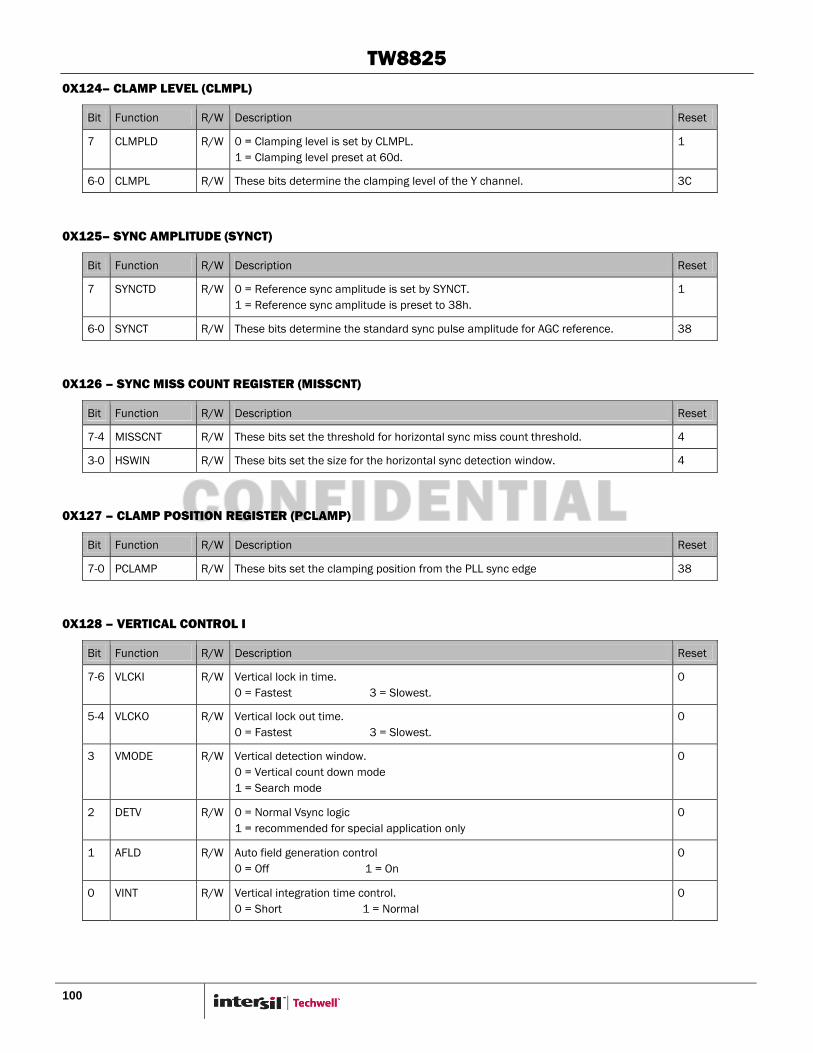
TW8825
100
0X124– CLAMP LEVEL (CLMPL)
Bit Function R/W Description Reset
7 CLMPLD R/W 0 = Clamping level is set by CLMPL.
1 = Clamping level preset at 60d.
1
6-0 CLMPL R/W These bits determine the clamping level of the Y channel. 3C
0X125– SYNC AMPLITUDE (SYNCT)
Bit Function R/W Description Reset
7 SYNCTD R/W 0 = Reference sync amplitude is set by SYNCT.
1 = Reference sync amplitude is preset to 38h.
1
6-0 SYNCT R/W These bits determine the standard sync pulse amplitude for AGC reference. 38
0X126 – SYNC MISS COUNT REGISTER (MISSCNT)
Bit Function R/W Description Reset
7-4 MISSCNT R/W These bits set the threshold for horizontal sync miss count threshold. 4
3-0 HSWIN R/W These bits set the size for the horizontal sync detection window. 4
0X127 – CLAMP POSITION REGISTER (PCLAMP)
Bit Function R/W Description Reset
7-0 PCLAMP R/W These bits set the clamping position from the PLL sync edge 38
0X128 – VERTICAL CONTROL I
Bit Function R/W Description Reset
7-6 VLCKI R/W Vertical lock in time.
0 = Fastest 3 = Slowest.
0
5-4 VLCKO R/W Vertical lock out time.
0 = Fastest 3 = Slowest.
0
3 VMODE R/W Vertical detection window.
0 = Vertical count down mode
1 = Search mode
0
2 DETV R/W 0 = Normal Vsync logic
1 = recommended for special application only
0
1 AFLD R/W Auto field generation control
0 = Off 1 = On
0
0 VINT R/W Vertical integration time control.
0 = Short 1 = Normal
0
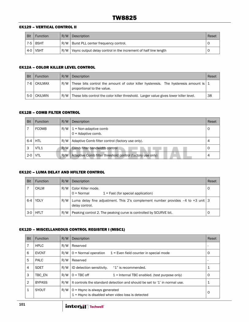
TW8825
101
0X129 – VERTICAL CONTROL II
Bit Function R/W Description Reset
7-5 BSHT R/W Burst PLL center frequency control. 0
4-0 VSHT R/W Vsync output delay control in the increment of half line length 0
0X12A – COLOR KILLER LEVEL CONTROL
Bit Function R/W Description Reset
7-6 CKILMAX R/W These bits control the amount of color killer hysteresis. The hysteresis amount is
proportional to the value.
1
5-0 CKILMIN R/W These bits control the color killer threshold. Larger value gives lower killer level. 38
0X12B – COMB FILTER CONTROL
Bit Function R/W Description Reset
7 FCOMB R/W 1 = Non-adaptive comb
0 = Adaptive comb.
0
6-4 HTL R/W Adaptive Comb filter control (factory use only). 4
3 VTL1 R/W Comb filter bandwidth control 0
2-0 VTL R/W Adaptive Comb filter threshold control (factory use only) 4
0X12C – LUMA DELAY AND HFILTER CONTROL
Bit Function R/W Description Reset
7 CKLM R/W Color Killer mode.
0 = Normal 1 = Fast (for special application)
0
6-4 YDLY R/W Luma delay fine adjustment. This 2‟s complement number provides –4 to +3 unit
delay control.
3
3-0 HFLT R/W Peaking control 2. The peaking curve is controlled by SCURVE bit. 0
0X12D – MISCELLANEOUS CONTROL REGISTER I (MISC1)
Bit Function R/W Description Reset
7 HPLC R/W Reserved -
6 EVCNT R/W 0 = Normal operation 1 = Even field counter in special mode 0
5 PALC R/W Reserved -
4 SDET R/W ID detection sensitivity. “1” is recommended. 1
3 TBC_EN R/W 0 = TBC off 1 = Internal TBC enabled. (test purpose only) 0
2 BYPASS R/W It controls the standard detection and should be set to „1‟ in normal use. 1
1 SYOUT R/W 0 = Hsync is always generated
1 = Hsync is disabled when video loss is detected 0
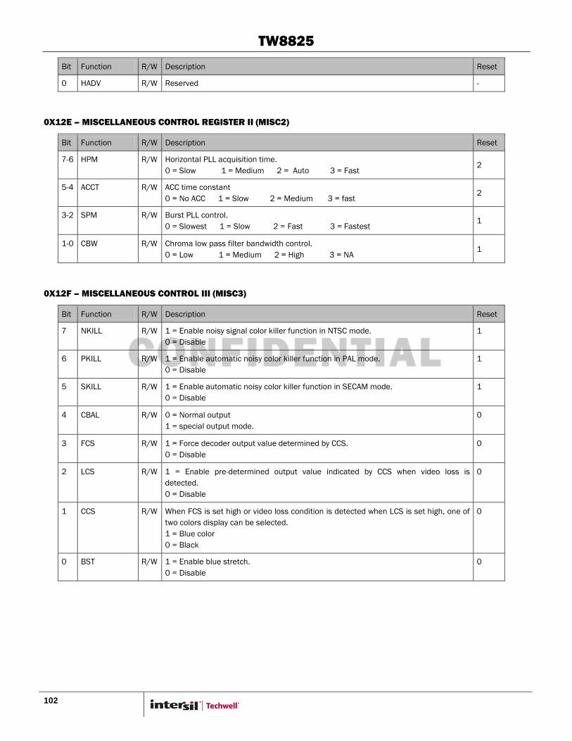
TW8825
102
Bit Function R/W Description Reset
0 HADV R/W Reserved -
0X12E – MISCELLANEOUS CONTROL REGISTER II (MISC2)
Bit Function R/W Description Reset
7-6 HPM R/W Horizontal PLL acquisition time.
0 = Slow 1 = Medium 2 = Auto 3 = Fast 2
5-4 ACCT R/W ACC time constant
0 = No ACC 1 = Slow 2 = Medium 3 = fast 2
3-2 SPM R/W Burst PLL control.
0 = Slowest 1 = Slow 2 = Fast 3 = Fastest 1
1-0 CBW R/W Chroma low pass filter bandwidth control.
0 = Low 1 = Medium 2 = High 3 = NA 1
0X12F – MISCELLANEOUS CONTROL III (MISC3)
Bit Function R/W Description Reset
7 NKILL R/W 1 = Enable noisy signal color killer function in NTSC mode.
0 = Disable
1
6 PKILL R/W 1 = Enable automatic noisy color killer function in PAL mode.
0 = Disable
1
5 SKILL R/W 1 = Enable automatic noisy color killer function in SECAM mode.
0 = Disable
1
4 CBAL R/W 0 = Normal output
1 = special output mode.
0
3 FCS R/W 1 = Force decoder output value determined by CCS.
0 = Disable
0
2 LCS R/W 1 = Enable pre-determined output value indicated by CCS when video loss is
detected.
0 = Disable
0
1 CCS R/W When FCS is set high or video loss condition is detected when LCS is set high, one of
two colors display can be selected.
1 = Blue color
0 = Black
0
0 BST R/W 1 = Enable blue stretch.
0 = Disable
0
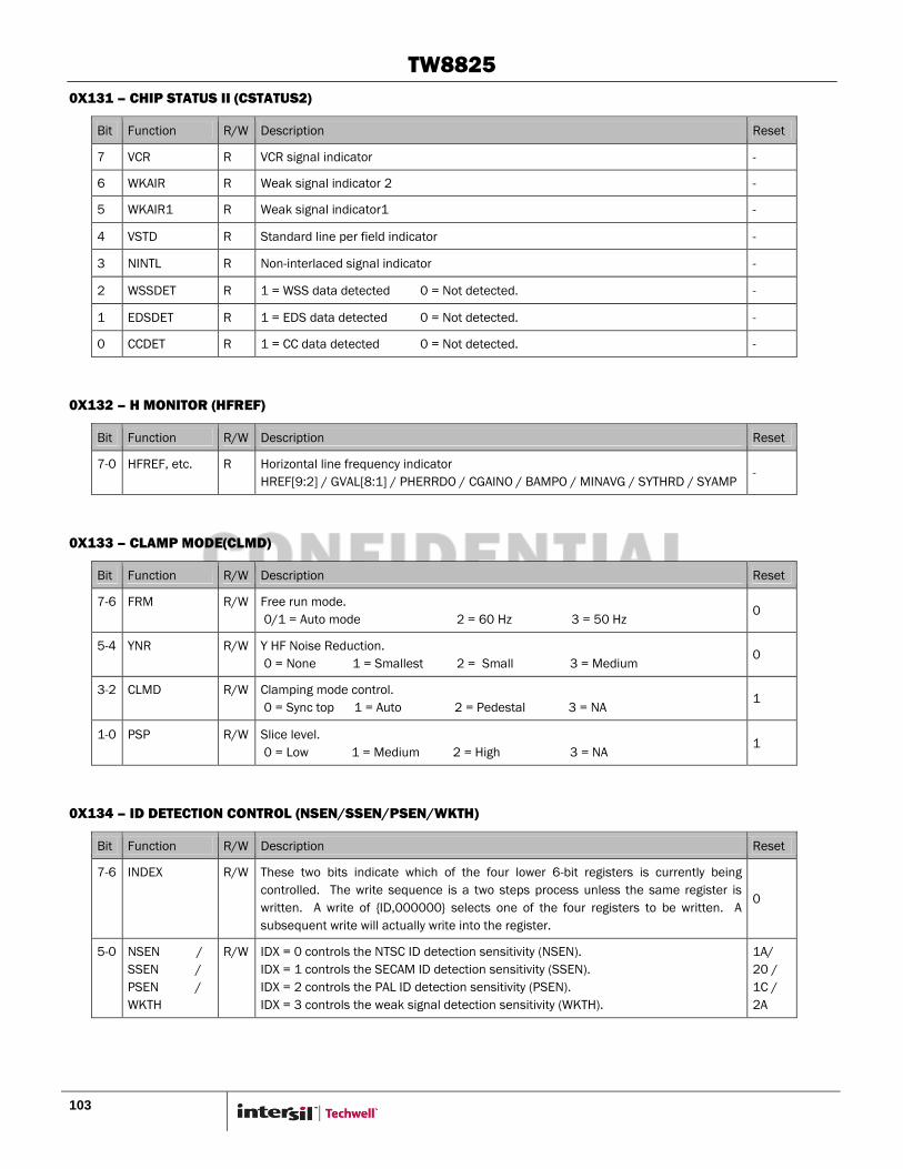
TW8825
103
0X131 – CHIP STATUS II (CSTATUS2)
Bit Function R/W Description Reset
7 VCR R VCR signal indicator -
6 WKAIR R Weak signal indicator 2 -
5 WKAIR1 R Weak signal indicator1 -
4 VSTD R Standard line per field indicator -
3 NINTL R Non-interlaced signal indicator -
2 WSSDET R 1 = WSS data detected 0 = Not detected. -
1 EDSDET R 1 = EDS data detected 0 = Not detected. -
0 CCDET R 1 = CC data detected 0 = Not detected. -
0X132 – H MONITOR (HFREF)
Bit Function R/W Description Reset
7-0 HFREF, etc. R Horizontal line frequency indicator
HREF[9:2] / GVAL[8:1] / PHERRDO / CGAINO / BAMPO / MINAVG / SYTHRD / SYAMP -
0X133 – CLAMP MODE(CLMD)
Bit Function R/W Description Reset
7-6 FRM R/W Free run mode.
0/1 = Auto mode 2 = 60 Hz 3 = 50 Hz 0
5-4 YNR R/W Y HF Noise Reduction.
0 = None 1 = Smallest 2 = Small 3 = Medium 0
3-2 CLMD R/W Clamping mode control.
0 = Sync top 1 = Auto 2 = Pedestal 3 = NA 1
1-0 PSP R/W Slice level.
0 = Low 1 = Medium 2 = High 3 = NA 1
0X134 – ID DETECTION CONTROL (NSEN/SSEN/PSEN/WKTH)
Bit Function R/W Description Reset
7-6 INDEX R/W These two bits indicate which of the four lower 6-bit registers is currently being
controlled. The write sequence is a two steps process unless the same register is
written. A write of {ID,000000} selects one of the four registers to be written. A
subsequent write will actually write into the register.
0
5-0 NSEN /
SSEN /
PSEN /
WKTH
R/W IDX = 0 controls the NTSC ID detection sensitivity (NSEN).
IDX = 1 controls the SECAM ID detection sensitivity (SSEN).
IDX = 2 controls the PAL ID detection sensitivity (PSEN).
IDX = 3 controls the weak signal detection sensitivity (WKTH).
1A/
20 /
1C /
2A

TW8825
104
0X135 – CLAMP CONTROL (CLCNTL)
Bit Function R/W Description Reset
7 CTEST R/W Clamping control for debug use. 0
6 YCLEN R/W 0 = Enable Y channel clamp
1 = Disable
0
5 CCLEN R/W 0 = Enable C channel clamp
1 = Disable
0
4 VCLEN R/W 0 = Enable V channel clamp
1 = Disable
0
3 GTEST R/W 0 = Normal operation
1 = Test
0
2 VLPF R/W Sync filter bandwidth control 0
1 CKLY R/W Clamping current control 1. 0
0 CKLC R/W Clamping current control 2. 0
0X140 – WSS0
Bit Function R/W Description Reset
7-6 Reserved R/W Reserved -
5-0 WSS0 R These are the sliced WSS data bit 19 to 14 -
0X141 – WSS1
Bit Function R/W Description Reset
7 CRCERR R This is the CRC error indicator for 525-line WSS
0 = No CRC error 1 = CRC error
-
6 WSSFLD R These bit indicates the detected WSS field information
0 = Odd 1 = Even
-
5-0 WSS1 R These bits represent the sliced WSS data bit 13 to 8. -
0X142 – WSS2
Bit Function R/W Description Reset
7-0 WSS2 R These bits represent the sliced WSS bit 7 to 0. -
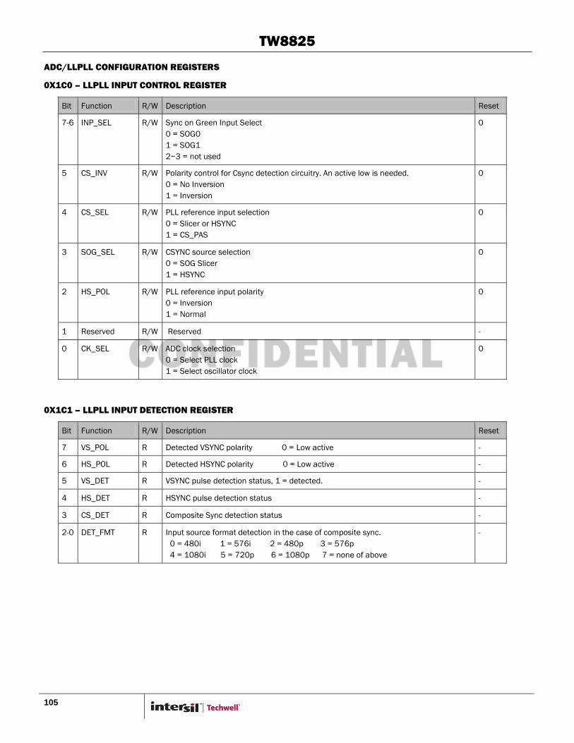
TW8825
105
ADC/LLPLL CONFIGURATION REGISTERS
0X1C0 – LLPLL INPUT CONTROL REGISTER
Bit Function R/W Description Reset
7-6 INP_SEL R/W Sync on Green Input Select
0 = SOG0
1 = SOG1
2~3 = not used
0
5 CS_INV R/W Polarity control for Csync detection circuitry. An active low is needed.
0 = No Inversion
1 = Inversion
0
4 CS_SEL R/W PLL reference input selection
0 = Slicer or HSYNC
1 = CS_PAS
0
3 SOG_SEL R/W CSYNC source selection
0 = SOG Slicer
1 = HSYNC
0
2 HS_POL R/W PLL reference input polarity
0 = Inversion
1 = Normal
0
1 Reserved R/W Reserved -
0 CK_SEL R/W ADC clock selection
0 = Select PLL clock
1 = Select oscillator clock
0
0X1C1 – LLPLL INPUT DETECTION REGISTER
Bit Function R/W Description Reset
7 VS_POL R Detected VSYNC polarity 0 = Low active -
6 HS_POL R Detected HSYNC polarity 0 = Low active -
5 VS_DET R VSYNC pulse detection status, 1 = detected. -
4 HS_DET R HSYNC pulse detection status -
3 CS_DET R Composite Sync detection status -
2-0 DET_FMT R Input source format detection in the case of composite sync.
0 = 480i 1 = 576i 2 = 480p 3 = 576p
4 = 1080i 5 = 720p 6 = 1080p 7 = none of above
-
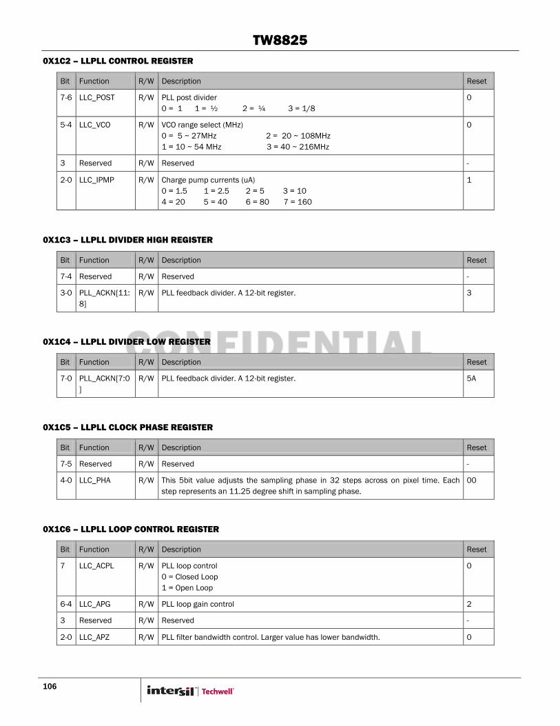
TW8825
106
0X1C2 – LLPLL CONTROL REGISTER
Bit Function R/W Description Reset
7-6 LLC_POST R/W PLL post divider
0 = 1 1 = ½ 2 = ¼ 3 = 1/8
0
5-4 LLC_VCO R/W VCO range select (MHz)
0 = 5 ~ 27MHz 2 = 20 ~ 108MHz
1 = 10 ~ 54 MHz 3 = 40 ~ 216MHz
0
3 Reserved R/W Reserved -
2-0 LLC_IPMP R/W Charge pump currents (uA)
0 = 1.5 1 = 2.5 2 = 5 3 = 10
4 = 20 5 = 40 6 = 80 7 = 160
1
0X1C3 – LLPLL DIVIDER HIGH REGISTER
Bit Function R/W Description Reset
7-4 Reserved R/W Reserved -
3-0
PLL_ACKN[11:
8]
R/W PLL feedback divider. A 12-bit register. 3
0X1C4 – LLPLL DIVIDER LOW REGISTER
Bit Function R/W Description Reset
7-0 PLL_ACKN[7:0
]
R/W PLL feedback divider. A 12-bit register. 5A
0X1C5 – LLPLL CLOCK PHASE REGISTER
Bit Function R/W Description Reset
7-5 Reserved R/W Reserved -
4-0 LLC_PHA R/W This 5bit value adjusts the sampling phase in 32 steps across on pixel time. Each
step represents an 11.25 degree shift in sampling phase.
00
0X1C6 – LLPLL LOOP CONTROL REGISTER
Bit Function R/W Description Reset
7 LLC_ACPL R/W PLL loop control
0 = Closed Loop
1 = Open Loop
0
6-4 LLC_APG R/W PLL loop gain control 2
3 Reserved R/W Reserved -
2-0 LLC_APZ R/W PLL filter bandwidth control. Larger value has lower bandwidth. 0
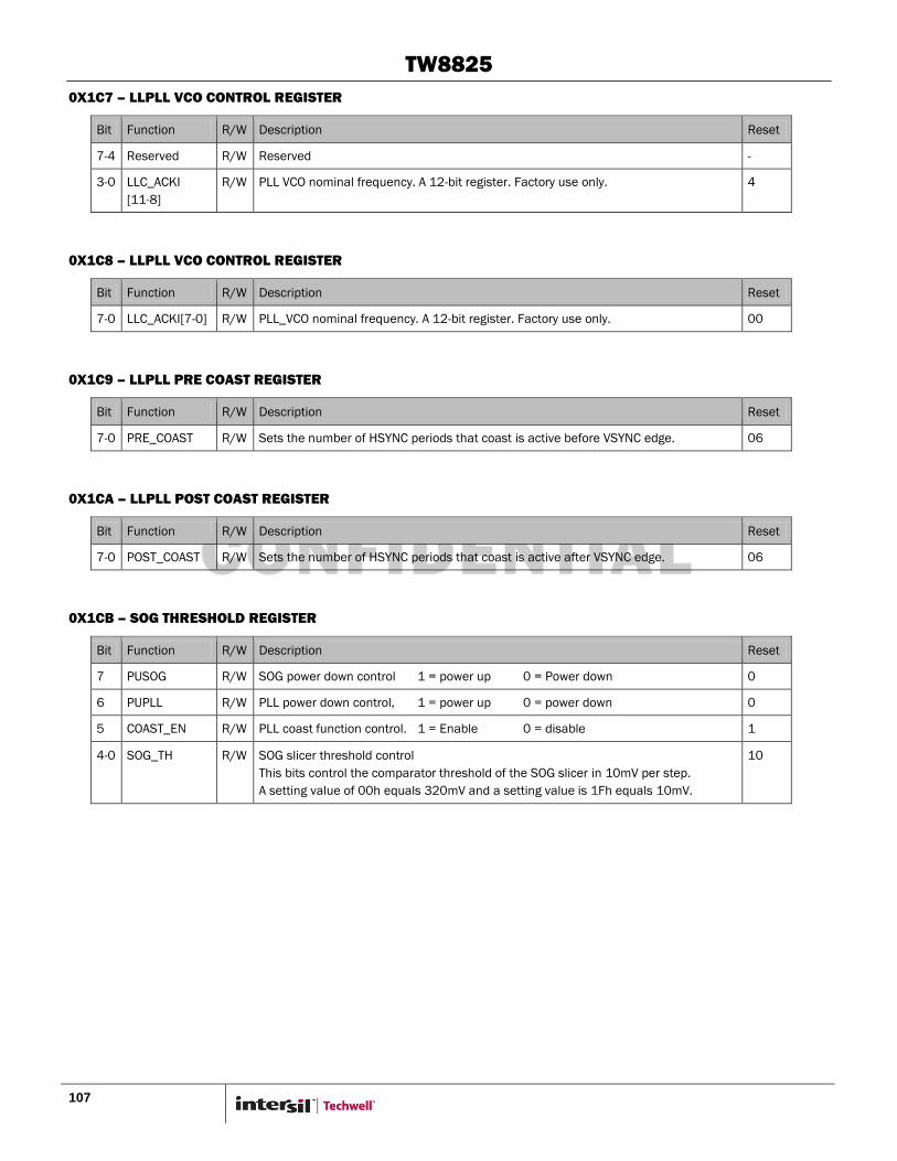
TW8825
107
0X1C7 – LLPLL VCO CONTROL REGISTER
Bit Function R/W Description Reset
7-4 Reserved R/W Reserved -
3-0 LLC_ACKI
[11-8]
R/W PLL VCO nominal frequency. A 12-bit register. Factory use only. 4
0X1C8 – LLPLL VCO CONTROL REGISTER
Bit Function R/W Description Reset
7-0 LLC_ACKI[7-0] R/W PLL_VCO nominal frequency. A 12-bit register. Factory use only. 00
0X1C9 – LLPLL PRE COAST REGISTER
Bit Function R/W Description Reset
7-0 PRE_COAST R/W Sets the number of HSYNC periods that coast is active before VSYNC edge. 06
0X1CA – LLPLL POST COAST REGISTER
Bit Function R/W Description Reset
7-0 POST_COAST R/W Sets the number of HSYNC periods that coast is active after VSYNC edge. 06
0X1CB – SOG THRESHOLD REGISTER
Bit Function R/W Description Reset
7 PUSOG R/W SOG power down control 1 = power up 0 = Power down 0
6 PUPLL R/W PLL power down control, 1 = power up 0 = power down 0
5 COAST_EN R/W PLL coast function control. 1 = Enable 0 = disable 1
4-0 SOG_TH R/W SOG slicer threshold control
This bits control the comparator threshold of the SOG slicer in 10mV per step.
A setting value of 00h equals 320mV and a setting value is 1Fh equals 10mV.
10
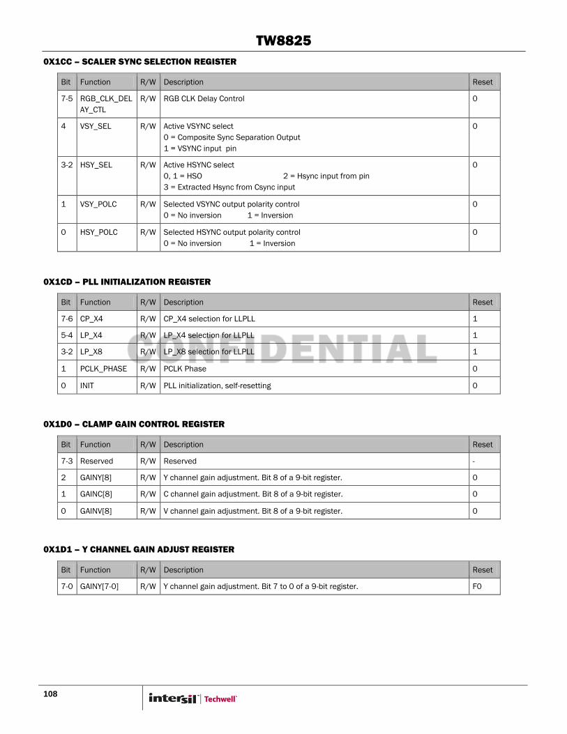
TW8825
108
0X1CC – SCALER SYNC SELECTION REGISTER
Bit Function R/W Description Reset
7-5 RGB_CLK_DEL
AY_CTL
R/W RGB CLK Delay Control 0
4 VSY_SEL R/W Active VSYNC select
0 = Composite Sync Separation Output
1 = VSYNC input pin
0
3-2 HSY_SEL R/W Active HSYNC select
0, 1 = HSO 2 = Hsync input from pin
3 = Extracted Hsync from Csync input
0
1 VSY_POLC R/W Selected VSYNC output polarity control
0 = No inversion 1 = Inversion
0
0 HSY_POLC R/W Selected HSYNC output polarity control
0 = No inversion 1 = Inversion
0
0X1CD – PLL INITIALIZATION REGISTER
Bit Function R/W Description Reset
7-6 CP_X4 R/W CP_X4 selection for LLPLL 1
5-4 LP_X4 R/W LP_X4 selection for LLPLL 1
3-2 LP_X8 R/W LP_X8 selection for LLPLL 1
1 PCLK_PHASE R/W PCLK Phase 0
0 INIT R/W PLL initialization, self-resetting 0
0X1D0 – CLAMP GAIN CONTROL REGISTER
Bit Function R/W Description Reset
7-3 Reserved R/W Reserved -
2 GAINY[8] R/W Y channel gain adjustment. Bit 8 of a 9-bit register. 0
1 GAINC[8] R/W C channel gain adjustment. Bit 8 of a 9-bit register. 0
0 GAINV[8] R/W V channel gain adjustment. Bit 8 of a 9-bit register. 0
0X1D1 – Y CHANNEL GAIN ADJUST REGISTER
Bit Function R/W Description Reset
7-0 GAINY[7-0] R/W Y channel gain adjustment. Bit 7 to 0 of a 9-bit register. F0
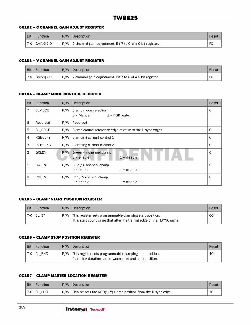
TW8825
109
0X1D2 – C CHANNEL GAIN ADJUST REGISTER
Bit Function R/W Description Reset
7-0 GAINC[7-0] R/W C channel gain adjustment. Bit 7 to 0 of a 9-bit register. F0
0X1D3 – V CHANNEL GAIN ADJUST REGISTER
Bit Function R/W Description Reset
7-0 GAINV[7-0] R/W V channel gain adjustment. Bit 7 to 0 of a 9-bit register. F0
0X1D4 – CLAMP MODE CONTROL REGISTER
Bit Function R/W Description Reset
7 CLMODE R/W Clamp mode selection
0 = Manual 1 = RGB Auto
0
6 Reserved R/W Reserved -
5 CL_EDGE R/W Clamp control reference edge relative to the H sync edges. 0
4 RGBCLKY R/W Clamping current control 1 0
3 RGBCLKC R/W Clamping current control 2 0
2 GCLEN R/W Green / Y channel clamp
0 = enable, 1 = disable
0
1 BCLEN R/W Blue / C channel clamp
0 = enable, 1 = disable
0
0 RCLEN R/W Red / V channel clamp
0 = enable, 1 = disable
0
0X1D5 – CLAMP START POSITION REGISTER
Bit Function R/W Description Reset
7-0 CL_ST R/W This register sets programmable clamping start position.
It is start count value that after the trailing edge of the HSYNC signal.
00
0X1D6 – CLAMP STOP POSITION REGISTER
Bit Function R/W Description Reset
7-0 CL_END R/W This register sets programmable clamping stop position.
Clamping duration set between start and stop position.
10
0X1D7 – CLAMP MASTER LOCATION REGISTER
Bit Function R/W Description Reset
7-0 CL_LOC R/W This bit sets the RGB(YCV) clamp position from the H sync edge. 70
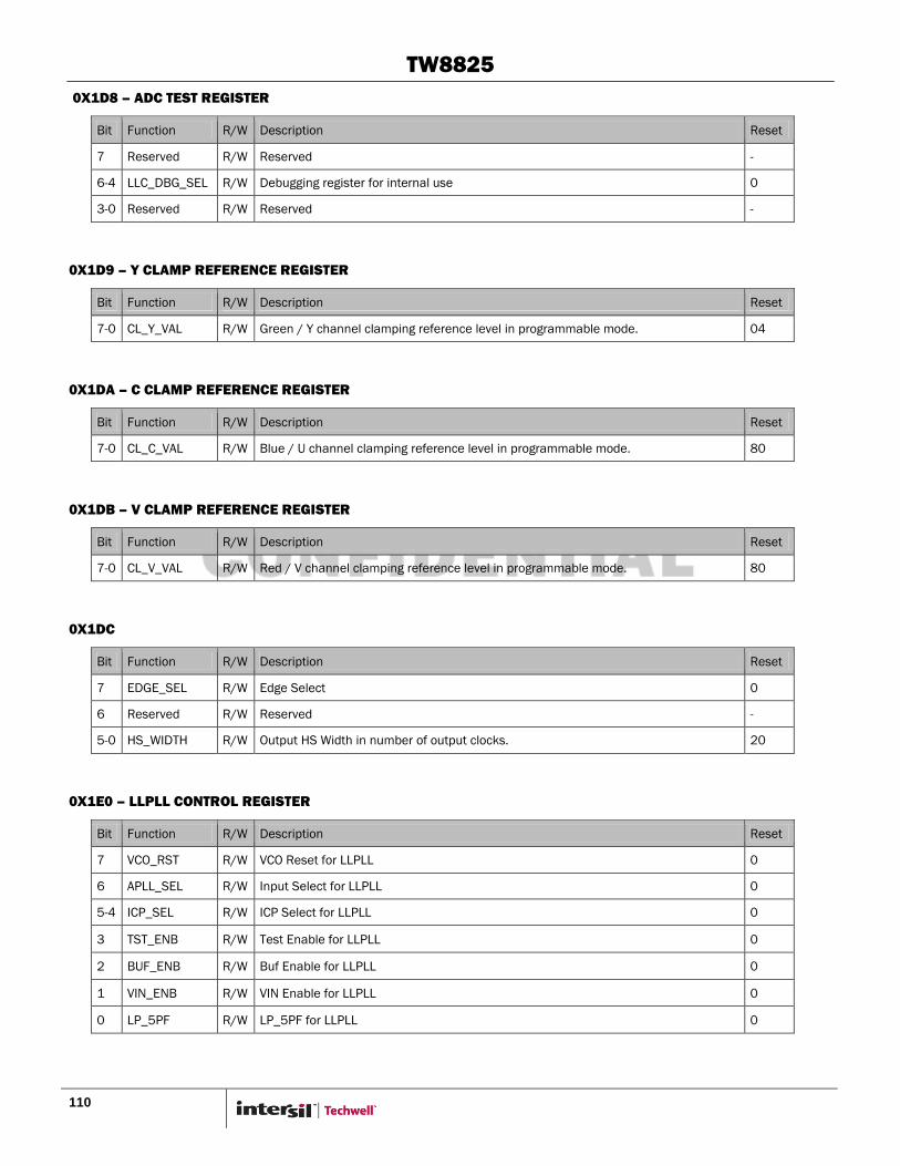
TW8825
110
0X1D8 – ADC TEST REGISTER
Bit Function R/W Description Reset
7 Reserved R/W Reserved -
6-4 LLC_DBG_SEL R/W Debugging register for internal use 0
3-0 Reserved R/W Reserved -
0X1D9 – Y CLAMP REFERENCE REGISTER
Bit Function R/W Description Reset
7-0 CL_Y_VAL R/W Green / Y channel clamping reference level in programmable mode. 04
0X1DA – C CLAMP REFERENCE REGISTER
Bit Function R/W Description Reset
7-0 CL_C_VAL R/W Blue / U channel clamping reference level in programmable mode. 80
0X1DB – V CLAMP REFERENCE REGISTER
Bit Function R/W Description Reset
7-0 CL_V_VAL R/W Red / V channel clamping reference level in programmable mode. 80
0X1DC
Bit Function R/W Description Reset
7 EDGE_SEL R/W Edge Select 0
6 Reserved R/W Reserved -
5-0 HS_WIDTH R/W Output HS Width in number of output clocks. 20
0X1E0 – LLPLL CONTROL REGISTER
Bit Function R/W Description Reset
7 VCO_RST R/W VCO Reset for LLPLL 0
6 APLL_SEL R/W Input Select for LLPLL 0
5-4 ICP_SEL R/W ICP Select for LLPLL 0
3 TST_ENB R/W Test Enable for LLPLL 0
2 BUF_ENB R/W Buf Enable for LLPLL 0
1 VIN_ENB R/W VIN Enable for LLPLL 0
0 LP_5PF R/W LP_5PF for LLPLL 0
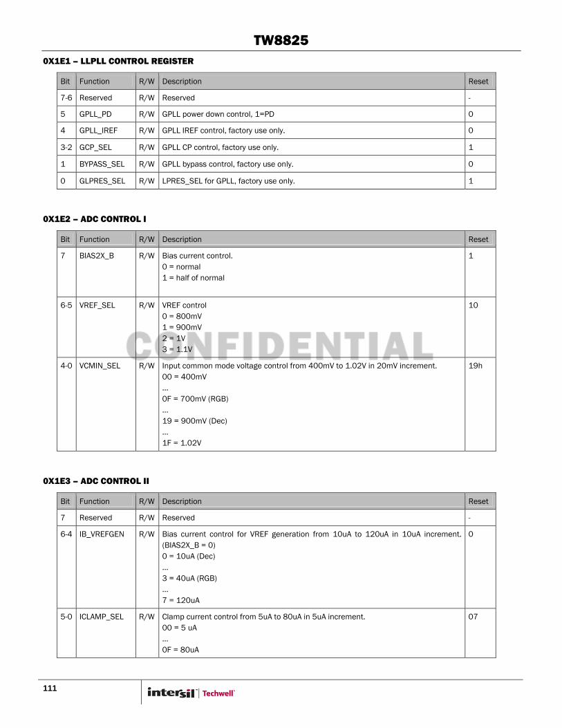
TW8825
111
0X1E1 – LLPLL CONTROL REGISTER
Bit Function R/W Description Reset
7-6 Reserved R/W Reserved -
5 GPLL_PD R/W GPLL power down control, 1=PD 0
4 GPLL_IREF R/W GPLL IREF control, factory use only. 0
3-2 GCP_SEL R/W GPLL CP control, factory use only. 1
1 BYPASS_SEL R/W GPLL bypass control, factory use only. 0
0 GLPRES_SEL R/W LPRES_SEL for GPLL, factory use only. 1
0X1E2 – ADC CONTROL I
Bit Function R/W Description Reset
7 BIAS2X_B R/W Bias current control.
0 = normal
1 = half of normal
1
6-5 VREF_SEL R/W VREF control
0 = 800mV
1 = 900mV
2 = 1V
3 = 1.1V
10
4-0 VCMIN_SEL R/W Input common mode voltage control from 400mV to 1.02V in 20mV increment.
00 = 400mV
…
0F = 700mV (RGB)
…
19 = 900mV (Dec)
…
1F = 1.02V
19h
0X1E3 – ADC CONTROL II
Bit Function R/W Description Reset
7 Reserved R/W Reserved -
6-4 IB_VREFGEN R/W Bias current control for VREF generation from 10uA to 120uA in 10uA increment.
(BIAS2X_B = 0)
0 = 10uA (Dec)
…
3 = 40uA (RGB)
…
7 = 120uA
0
5-0 ICLAMP_SEL R/W Clamp current control from 5uA to 80uA in 5uA increment.
00 = 5 uA
…
0F = 80uA
07

TW8825
112
0X1E4 – ADC CONTROL III
Bit Function R/W Description Reset
7 Reserved R/W Reserved -
6-4 IB_SAH R/W Bias current control for S/H. (BIAS2X_B = 0)
0 = 10uA
1 = 20uA
2 = 30uA
3 = 40uA (DEC)
4 = 90uA
5 = 100uA (RGB)
6 = 110uA
7 = 120uA
3
2-0 IB_OTA1 R/W OTA1 current control (BIAS2X_B = 0)
0 = 10uA
1 = 20uA
2 = 30uA
3 = 40uA (DEC)
4 = 90uA
5 = 100uA (RGB)
6 = 110uA
7 = 120uA
3
0X1E5 – ADC CONTROL IV
Bit Function R/W Description Reset
7 Reserved R/W Reserved -
6-4 IBPGA_SEL R/W OTA-PGA current control (BIAS2X_B = 0)
0 = 10uA
1 = 20uA
2 = 30uA
3 = 40uA (DEC)
4 = 90uA
5 = 100uA (RGB)
6 = 110uA
7 = 120uA
3
3 VREF_BOOST R/W 0 = normal operation (DEC)
1 = high speed operation (RGB)
0
2-0 IBINBUF R/W OTA-AFE current control (BIAS2X_B = 0)
0 = 10uA
1 = 20uA(DEC)
2 = 30uA
3 = 40uA
4 = 90uA
5 = 100uA (RGB)
6 = 110uA
7 = 120uA
1
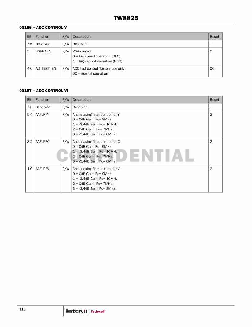
TW8825
113
0X1E6 – ADC CONTROL V
Bit Function R/W Description Reset
7-6 Reserved R/W Reserved -
5 HSPGAEN R/W PGA control
0 = low speed operation (DEC)
1 = high speed operation (RGB)
0
4-0 AD_TEST_EN R/W ADC test control (factory use only)
00 = normal operation
00
0X1E7 – ADC CONTROL VI
Bit Function R/W Description Reset
7-6 Reserved R/W Reserved -
5-4 AAFLPFY R/W Anti-aliasing filter control for Y
0 = 0dB Gain; Fc= 9MHz
1 = -3.4dB Gain; Fc= 10MHz
2 = 0dB Gain ; Fc= 7MHz
3 = -3.4dB Gain; Fc= 8MHz
2
3-2 AAFLPFC R/W Anti-aliasing filter control for C
0 = 0dB Gain; Fc= 9MHz
1 = -3.4dB Gain; Fc= 10MHz
2 = 0dB Gain ; Fc= 7MHz
3 = -3.4dB Gain; Fc= 8MHz
2
1-0 AAFLPFV R/W Anti-aliasing filter control for V
0 = 0dB Gain; Fc= 9MHz
1 = -3.4dB Gain; Fc= 10MHz
2 = 0dB Gain ; Fc= 7MHz
3 = -3.4dB Gain; Fc= 8MHz
2
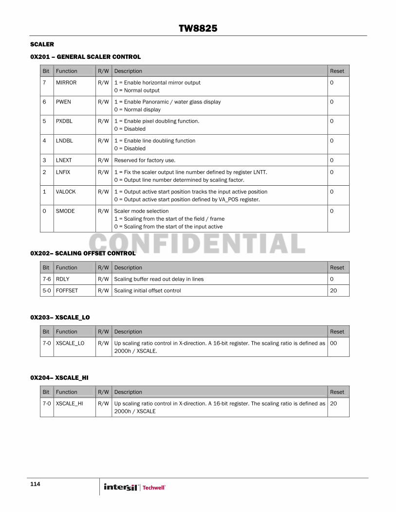
TW8825
114
SCALER
0X201 – GENERAL SCALER CONTROL
Bit Function R/W Description Reset
7 MIRROR R/W 1 = Enable horizontal mirror output
0 = Normal output
0
6 PWEN R/W 1 = Enable Panoramic / water glass display
0 = Normal display
0
5 PXDBL R/W 1 = Enable pixel doubling function.
0 = Disabled
0
4 LNDBL R/W 1 = Enable line doubling function
0 = Disabled
0
3 LNEXT R/W Reserved for factory use. 0
2 LNFIX R/W 1 = Fix the scaler output line number defined by register LNTT.
0 = Output line number determined by scaling factor.
0
1 VALOCK R/W 1 = Output active start position tracks the input active position
0 = Output active start position defined by VA_POS register.
0
0 SMODE R/W Scaler mode selection
1 = Scaling from the start of the field / frame
0 = Scaling from the start of the input active
0
0X202– SCALING OFFSET CONTROL
Bit Function R/W Description Reset
7-6 RDLY R/W Scaling buffer read out delay in lines 0
5-0 FOFFSET R/W Scaling initial offset control 20
0X203– XSCALE_LO
Bit Function R/W Description Reset
7-0 XSCALE_LO R/W Up scaling ratio control in X-direction. A 16-bit register. The scaling ratio is defined as
2000h / XSCALE.
00
0X204– XSCALE_HI
Bit Function R/W Description Reset
7-0 XSCALE_HI R/W Up scaling ratio control in X-direction. A 16-bit register. The scaling ratio is defined as
2000h / XSCALE
20
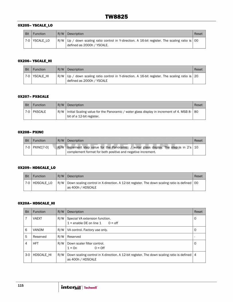
TW8825
115
0X205– YSCALE_LO
Bit Function R/W Description Reset
7-0 YSCALE_LO R/W Up / down scaling ratio control in Y-direction. A 16-bit register. The scaling ratio is
defined as 2000h / YSCALE.
00
0X206– YSCALE_HI
Bit Function R/W Description Reset
7-0 YSCALE_HI R/W Up / down scaling ratio control in Y-direction. A 16-bit register. The scaling ratio is
defined as 2000h / YSCALE
20
0X207– PXSCALE
Bit Function R/W Description Reset
7-0 PXSCALE R/W Initial Scaling value for the Panoramic / water glass display in increment of 4. MSB 8-
bit of a 12-bit register.
80
0X208– PXINC
Bit Function R/W Description Reset
7-0 PXINC[7-0] R/W Increment step value for the Panoramic / water glass display. The step is in 2‟s
complement format for both positive and negative increment.
10
0X209– HDSCALE_LO
Bit Function R/W Description Reset
7-0 HDSCALE_LO R/W Down scaling control in X-direction. A 12-bit register. The down scaling ratio is defined
as 400h / HDSCALE
00
0X20A– HDSCALE_HI
Bit Function R/W Description Reset
7 VAEXT R/W Special VA extension function.
1 = enable DE on line 1 0 = off
0
6 VANOM R/W VA control. Factory use only. 0
5 Reserved R/W Reserved -
4 HFT R/W Down scaler filter control.
1 = On 0 = Off
0
3-0 HDSCALE_HI R/W Down scaling control in X-direction. A 12-bit register. The down scaling ratio is defined
as 400h / HDSCALE
4

TW8825
116
0X20B– HDELAY2
Bit Function R/W Description Reset
7-0 HDELAY2 R/W Scaler buffer data output delay in number of pixels in relation to the H sync. 30
0X20C– HACTIVE2_LO
Bit Function R/W Description Reset
7-0 HACTIVE2 R/W Scaler data output length in number of pixels. A 11-bit register. D0
0X20D– LNTT_HI
Bit Function R/W Description Reset
7-6 LNTT_HI R/W It controls the scaler total output lines when LNFIX=1. It is used in special case. A 10-
bit register.
0
5 CKOSEL R/W Pixel clock output selection.
0 = divided clock specified by CKDIV 1 = un-divided clock
0
4 CKP R/W Pixel clock polarity control. 0 = no inversion. 0
3 VSP R/W FPVS output polarity control. 0 = no inversion. 0
2 HSP R/W FPHS output polarity control. 0 = no inversion. 0
1-0 CKDIV R/W Pixel clock output frequency division control.
0 = 1 1 = ½ 2 = 1/3 3 = ¼
0
0X20E– HPADJ_HI
Bit Function R/W Description Reset
6-4 HACTIVE2_HI R/W Scaler data output length in number of pixels. A 11-bit register. 2
3-0 HPADJ_HI R/W Blanking H period adjustment. A 12-bit 2‟s complement register. 0
0X20F– HPADJ_LO
Bit Function R/W Description Reset
7-6 HPADJ_LO R/W Blanking H period adjustment. A 12-bit 2‟s complement register 00
0X210– HA_POS
Bit Function R/W Description Reset
7-0 HA_POS R/W Output DE position control relative to the internal reference in number of output clock 10
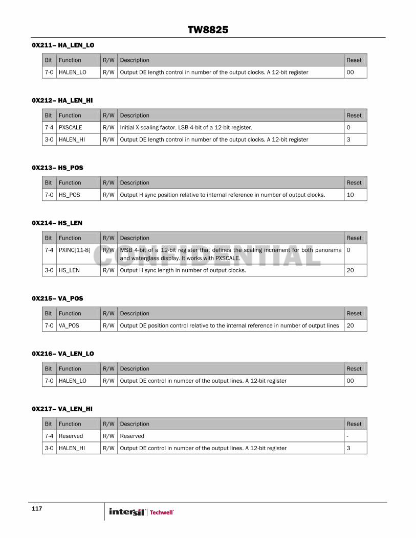
TW8825
117
0X211– HA_LEN_LO
Bit Function R/W Description Reset
7-0 HALEN_LO R/W Output DE length control in number of the output clocks. A 12-bit register 00
0X212– HA_LEN_HI
Bit Function R/W Description Reset
7-4 PXSCALE R/W Initial X scaling factor. LSB 4-bit of a 12-bit register. 0
3-0 HALEN_HI R/W Output DE length control in number of the output clocks. A 12-bit register 3
0X213– HS_POS
Bit Function R/W Description Reset
7-0 HS_POS R/W Output H sync position relative to internal reference in number of output clocks. 10
0X214– HS_LEN
Bit Function R/W Description Reset
7-4 PXINC[11-8] R/W MSB 4-bit of a 12-bit register that defines the scaling increment for both panorama
and waterglass display. It works with PXSCALE.
0
3-0 HS_LEN R/W Output H sync length in number of output clocks. 20
0X215– VA_POS
Bit Function R/W Description Reset
7-0 VA_POS R/W Output DE position control relative to the internal reference in number of output lines 20
0X216– VA_LEN_LO
Bit Function R/W Description Reset
7-0 HALEN_LO R/W Output DE control in number of the output lines. A 12-bit register 00
0X217– VA_LEN_HI
Bit Function R/W Description Reset
7-4 Reserved R/W Reserved -
3-0 HALEN_HI R/W Output DE control in number of the output lines. A 12-bit register 3

TW8825
118
0X218– VS_LEN_POS
Bit Function R/W Description Reset
1-0 VS_LEN R/W Output V sync length in number of output lines. 0
5-0 VS_POS R/W Output V sync position relative to internal reference in number of output lines. 0
0X219– LNTT_LO
Bit Function R/W Description Reset
7-0 LNTT_LO R/W It controls the scaler total output lines when LNFIX=1. It is used in special case. A 10-
bit register.
00
0X21A– DM_TOP
Bit Function R/W Description Reset
7-0 DM_TOP R/W These bits control the number of data masked lines (black lines) from the top of DE 00
0X21B– DM_BOT
Bit Function R/W Description Reset
7-0 DM_BOT R/W These bits control the number of data masked lines from the end of DE. 00
0X21C– PANEL_FRUN
Bit Function R/W Description Reset
7-4 HTOTAL_HI R/W MSB of a 12-bit register. It controls the panel free run H length. 4
3 DEP R/W DE polarity control.
1 = inversion 0 = no inversion.
0
2 PRUN R/W Panel free run control.
1 = free run with HTOTAL and LNTT 0 = disabled
0
1 PLOSS R/W Panel free run on the condition of input loss.
1 = enabled. 0 = disabled
0
0 HTFIX R/W Panel output line length control.
1 = fixed by HTOTAL 0 = auto adjusted.
0
0X21D– HTOTAL_LO
Bit Function R/W Description Reset
7-0 HTOTAL_LO R/W LSB of a 12-bit register. It controls the panel free run H length. 00
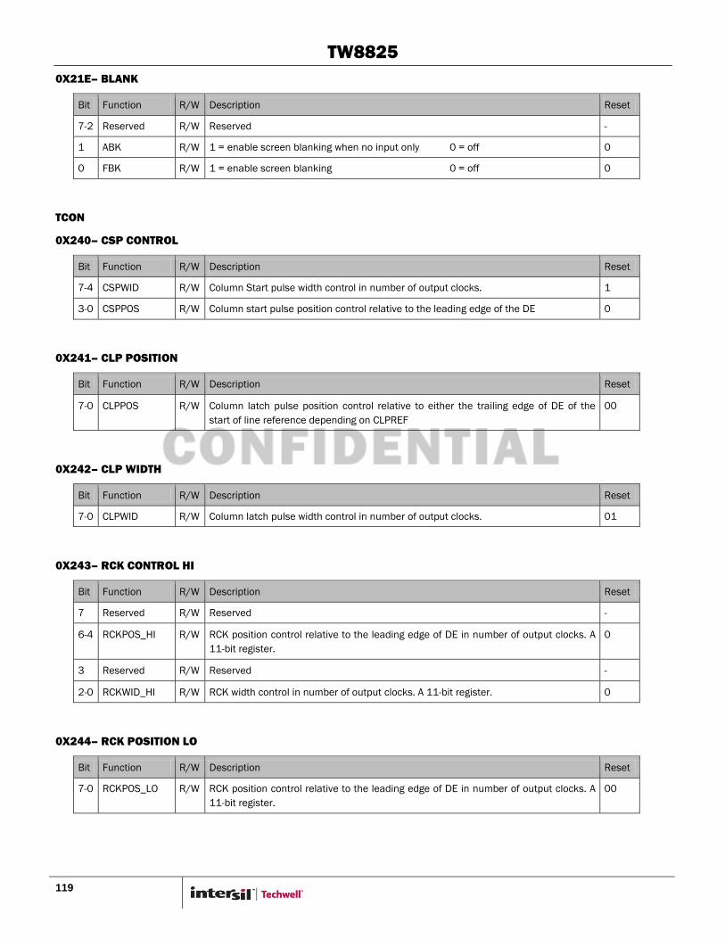
TW8825
119
0X21E– BLANK
Bit Function R/W Description Reset
7-2 Reserved R/W Reserved -
1 ABK R/W 1 = enable screen blanking when no input only 0 = off 0
0 FBK R/W 1 = enable screen blanking 0 = off 0
TCON
0X240– CSP CONTROL
Bit Function R/W Description Reset
7-4 CSPWID R/W Column Start pulse width control in number of output clocks. 1
3-0 CSPPOS R/W Column start pulse position control relative to the leading edge of the DE 0
0X241– CLP POSITION
Bit Function R/W Description Reset
7-0 CLPPOS R/W Column latch pulse position control relative to either the trailing edge of DE of the
start of line reference depending on CLPREF
00
0X242– CLP WIDTH
Bit Function R/W Description Reset
7-0 CLPWID R/W Column latch pulse width control in number of output clocks. 01
0X243– RCK CONTROL HI
Bit Function R/W Description Reset
7 Reserved R/W Reserved -
6-4 RCKPOS_HI R/W RCK position control relative to the leading edge of DE in number of output clocks. A
11-bit register.
0
3 Reserved R/W Reserved -
2-0 RCKWID_HI R/W RCK width control in number of output clocks. A 11-bit register. 0
0X244– RCK POSITION LO
Bit Function R/W Description Reset
7-0 RCKPOS_LO R/W RCK position control relative to the leading edge of DE in number of output clocks. A
11-bit register.
00

TW8825
120
0X245– RCK WIDTH LO
Bit Function R/W Description Reset
7-0 RCKWID_LO R/W RCK width control in number of output clocks. A 11-bit register. 01
0X246– ROE CONTROL HI
Bit Function R/W Description Reset
7-6 ROE_EXT R/W Row driver enable pulse extension control. 0
5-4 ROEPOS_HI R/W ROE position control relative to the leading edge of DE in number of output clocks. A
10-bit register.
0
3 Reserved R/W Reserved -
2-0 ROEWID_HI R/W ROE width control in number of output clocks. A 11-bit register. 0
0X247– ROE POSITION LO
Bit Function R/W Description Reset
7-0 ROEPOS_LO R/W ROE position control relative to the leading edge of DE in number of output clocks. A
10-bit register.
00
0X248– ROE WIDTH LO
Bit Function R/W Description Reset
7-0 ROEWID_LO R/W ROE width control in number of output clocks. A 11-bit register. 01
0X249– RSP CONTROL
Bit Function R/W Description Reset
7-6 Reserved R/W Reserved -
5-4 RSPWID R/W Row Start pulse width control in number of output lines. 1
3 Reserved R/W Reserved -
2-0 RSPPOS_HI R/W Row start pulse position control relative to the first output DE line. An 11-bit register
in 2‟s complement form.
0
0X24A– RSP POSITION CONTROL
Bit Function R/W Description Reset
7-0 RSP_POS_LO R/W Row start pulse position control relative to the first output DE line. An 11-bit register
in 2‟s complement format.
00
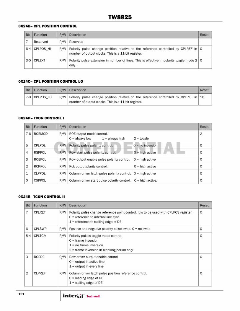
TW8825
121
0X24B– CPL POSITION CONTROL
Bit Function R/W Description Reset
7 Reserved R/W Reserved -
6-4 CPLPOS_HI R/W Polarity pulse change position relative to the reference controlled by CPLREF in
number of output clocks. This is a 11-bit register.
0
3-0 CPLEXT R/W Polarity pulse extension in number of lines. This is effective in polarity toggle mode 2
only.
0
0X24C– CPL POSITION CONTROL LO
Bit Function R/W Description Reset
7-0 CPLPOS_LO R/W Polarity pulse change position relative to the reference controlled by CPLREF in
number of output clocks. This is a 11-bit register.
10
0X24D– TCON CONTROL I
Bit Function R/W Description Reset
7-6 ROEMOD R/W ROE output mode control.
0 = always low 1 = always high 2 = toggle
2
5 CPLPOL R/W Polarity pulse polarity control. 0 = no inversion 0
4 RSPPOL R/W Row start pulse polarity control. 0 = high active 0
3 ROEPOL R/W Row output enable pulse polarity control. 0 = high active 0
2 RCKPOL R/W Rck output plarity control. 0 = high active 0
1 CLPPOL R/W Column driver latch pulse polarity control. 0 = high active 0
0 CSPPOL R/W Column driver start pulse polarity control. 0 = high active. 0
0X24E– TCON CONTROL II
Bit Function R/W Description Reset
7 CPLREF R/W Polarity pulse change reference point control. It is to be used with CPLPOS register.
0 = reference to internal line sync
1 = reference to trailing edge of DE
0
6 CPLSWP R/W Positive and negative polarity pulse swap. 0 = no swap 0
5-4 CPLTGM R/W Polarity pulses toggle mode control.
0 = frame inversion
1 = no frame inversion
2 = frame inversion in blanking period only
0
3 ROEDE R/W Row driver output enable control
0 = output in active line
1 = output in every line
0
2 CLPREF R/W Column driver latch pulse position reference control.
0 = leading edge of DE
1 = trailing edge of DE
0
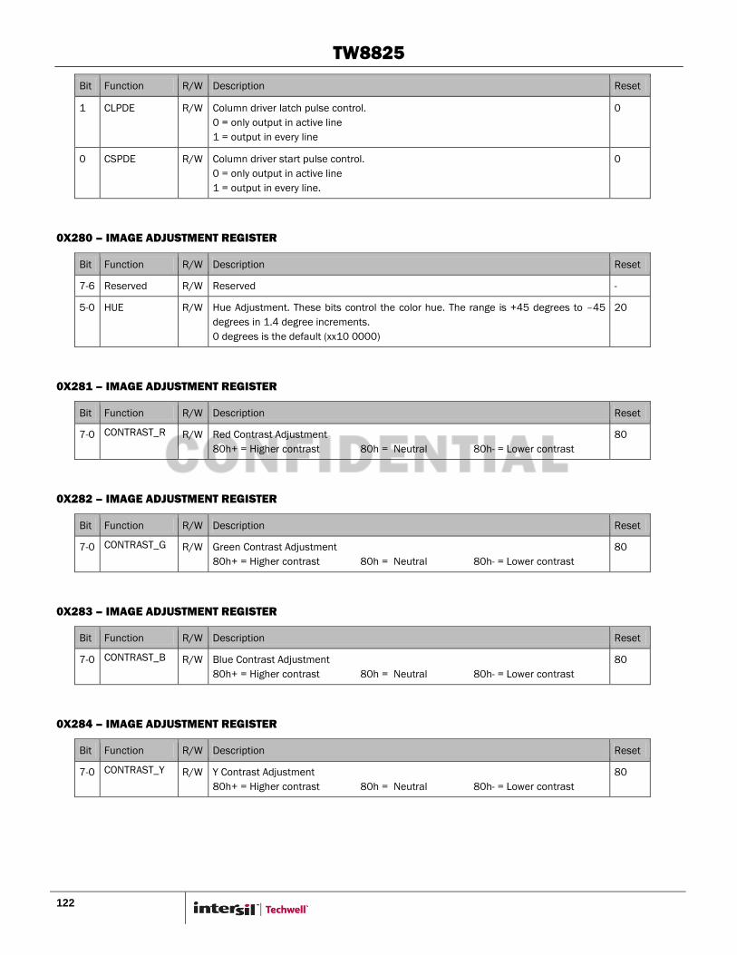
TW8825
122
Bit Function R/W Description Reset
1 CLPDE R/W Column driver latch pulse control.
0 = only output in active line
1 = output in every line
0
0 CSPDE R/W Column driver start pulse control.
0 = only output in active line
1 = output in every line.
0
0X280 – IMAGE ADJUSTMENT REGISTER
Bit Function R/W Description Reset
7-6 Reserved R/W Reserved -
5-0 HUE R/W Hue Adjustment. These bits control the color hue. The range is +45 degrees to –45
degrees in 1.4 degree increments.
0 degrees is the default (xx10 0000)
20
0X281 – IMAGE ADJUSTMENT REGISTER
Bit Function R/W Description Reset
7-0 CONTRAST_R R/W Red Contrast Adjustment
80h+ = Higher contrast 80h = Neutral 80h- = Lower contrast
80
0X282 – IMAGE ADJUSTMENT REGISTER
Bit Function R/W Description Reset
7-0 CONTRAST_G R/W Green Contrast Adjustment
80h+ = Higher contrast 80h = Neutral 80h- = Lower contrast
80
0X283 – IMAGE ADJUSTMENT REGISTER
Bit Function R/W Description Reset
7-0 CONTRAST_B R/W Blue Contrast Adjustment
80h+ = Higher contrast 80h = Neutral 80h- = Lower contrast
80
0X284 – IMAGE ADJUSTMENT REGISTER
Bit Function R/W Description Reset
7-0 CONTRAST_Y R/W Y Contrast Adjustment
80h+ = Higher contrast 80h = Neutral 80h- = Lower contrast
80

TW8825
123
0X285 – IMAGE ADJUSTMENT REGISTER
Bit Function R/W Description Reset
7-0 CONTRAST_Cb R/W Cb Contrast Adjustment
80h+ = Higher contrast 80h = Neutral 80h- = Lower contrast
80
0X286 – IMAGE ADJUSTMENT REGISTER
Bit Function R/W Description Reset
7-0 CONTRAST_Cr R/W Cr Contrast Adjustment
80h+ = Higher contrast 80h = Neutral 80h- = Lower contrast
80
0X287 – IMAGE ADJUSTMENT REGISTER
Bit Function R/W Description Reset
7-0 BRIGHTNESS_
R
R/W Red Brightness Adjustment
80h+ = Higher brightness 80h = Neutral 80h- = Lower brightness
80
0X288 – IMAGE ADJUSTMENT REGISTER
Bit Function R/W Description Reset
7-0 BRIGHTNESS_
G
R/W Green Brightness Adjustment
80h+ = Higher brightness 80h = Neutral 80h- = Lower brightness
80
0X289 – IMAGE ADJUSTMENT REGISTER
Bit Function R/W Description Reset
7-0 BRIGHTNESS_
B
R/W Blue Brightness Adjustment
80h+ = Higher brightness 80h = Neutral 80h- = Lower brightness
80
0X28A – IMAGE ADJUSTMENT REGISTER
Bit Function R/W Description Reset
7-0 BRIGHTNESS_
Y
R/W Y Brightness Adjustment
80h+ = Higher brightness 80h = Neutral 80h- = Lower brightness
80
0X28B – IMAGE ADJUSTMENT REGISTER
Bit Function R/W Description Reset
7-4 H_SHARP_
COR
R/W Coring function for sharpness control 3
3-0 H_SHARPNES
S
R/W Sharpness Adjustment 0

TW8825
124
0X28C – IMAGE ADJUSTMENT REGISTER
Bit Function R/W Description Reset
7 H_SHARP_
FREQ
R/W Sharpness frequency select
0 = Low freq 1 = High freq
0
6-0 Reserved R/W Reserved -
0X2B0 – IMAGE ADJUSTMENT REGISTER
Bit Function R/W Description Reset
7-6 Reserved R/W Reserved -
5 PEDLVL R/W Black level selection. 0 = 0 1 = 16d 0
4 WHTLVL R/W White level selection. 0 = 235d 1 = 255d 1
3-1 Reserved R/W Reserved -
0 BW_EN R/W 0 = BW stretch disable 1 = BW stretch enable 0
0X2B1 – IMAGE ADJUSTMENT REGISTER
Bit Function R/W Description Reset
7-0 BW_BSLOPE R/W Black side slope. 00h : x1, 40h : x2, 80h : x3, C0h : x4, Should not be more than D0h 40
0X2B2 – IMAGE ADJUSTMENT REGISTER
Bit Function R/W Description Reset
7-0 BW_WSLOPE R/W White side slope. 00h : x1, 40h : x2, 80h : x3, C0h : x4, Should not be more than D0h 40
0X2B6 – IMAGE ADJUSTMENT REGISTER
Bit Function R/W Description Reset
7-0 BW_BLACK_TI
LT
R/W Tilt point for black stretch 67
0X2B7 – IMAGE ADJUSTMENT REGISTER
Bit Function R/W Description Reset
7-0 BW_WHITE_TIL
T
R/W Tilt point for white stretch 94
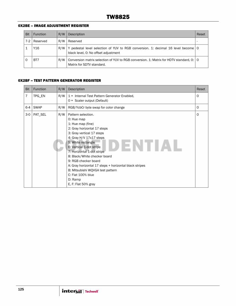
TW8825
125
0X2BE – IMAGE ADJUSTMENT REGISTER
Bit Function R/W Description Reset
7-2 Reserved R/W Reserved -
1 Y16 R/W Y pedestal level selection of YUV to RGB conversion. 1: decimal 16 level become
black level, 0: No offset adjustment
0
0 BT7 R/W Conversion matrix selection of YUV to RGB conversion. 1: Matrix for HDTV standard, 0:
Matrix for SDTV standard.
0
0X2BF – TEST PATTERN GENERATOR REGISTER
Bit Function R/W Description Reset
7 TPG_EN R/W 1 = Internal Test Pattern Generator Enabled,
0 = Scaler output (Default)
0
6-4 SWAP R/W RGB/YcbCr byte swap for color change 0
3-0 PAT_SEL R/W Pattern selection.
0: Hue map
1: Hue map (fine)
2: Gray horizontal 17 steps
3: Gray vertical 17 steps
4: Gray H/V 17x17 steps
5: White rectangle
6: Vertical 1-dot stripe
7: Horizontal 1-dot stripe
8: Black/White checker board
9: RGB checker board
A: Gray horizontal 17 steps + horizontal black stripes
B: Mitsubishi WQVGA test pattern
C: Flat 100% blue
D: Ramp
E, F: Flat 50% gray
0

TW8825
126
0X2E0 – LCDC GAMMA CONTROL REGISTER
Bit Function R/W Description Reset
7 GAMAE_R R/W Enable Red gamma correction. 0
6 GAMAE_G R/W Enable Green gamma correction. 0
5 GAMAE_B R/W Enable Blue gamma correction. 0
4 Reserved R/W Reserved -
3-2 AUTO_INC R/W Enable Gamma table address auto increment for reading/writing Gamma data port.
0 = Disable 1 = Read Only 2 = Write Only 3 = Read/Write
0
1-0 GAMMA_RGB_
INDX
R/W Gamma tables access selection:
Index address 0x2F1 to 0x2F2 are used for gamma table accesses. There are 3 sets
of gamma table, one table for one color, sharing the same address port and data
port. These 2 bits identifies which table is accessed.
0 = RGB Gamma table 1 = Red Gamma table
2 = Green Gamma table 3 = Blue Gamma table
0
0X2E1 – GAMMA TABLE ADDRESS PORT REGISTER
Bit Function R/W Description Reset
7-0 GAMMA_RAM-
STARTING_AD
DR
R/W Gamma table address port. 00
0X2E3 – GAMMA TABLE DATA PORT REGISTER
Bit Function R/W Description Reset
7-0 GAMMA_RAM_
DATA[7:0]
R/W Gamma table data port (lower bits) 00
0X2E4 – DITHER OPTION REGISTER
Bit Function R/W Description Reset
7 Reserved R/W Reserved -
7-0 DITHER_OPTIO
N
R/W Dither Option Code "010" is recommended for 6:6:6 output 0
3 Reserved R/W Reserved -
2-0 DITHER_FORM
AT
R/W Dither Output Format Selection "001" is recommended for 6:6:6 output 0
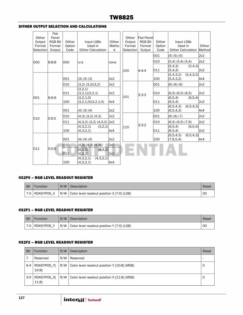
TW8825
127
DITHER OUTPUT SELECTION AND CALCULATIONS
Dither
Output
Format
Selection
Flat
Panel
RGB Bit
Format
Output
Dither
Option
Code
Input LSBs
Used in
Dither Calculation
Dither
Metho
d
Dither
Output
Format
Selection
Flat Panel
RGB Bit
Format
Output
Dither
Option
Code
Input LSBs
Used in
Dither Calculation
Dither
Method
000 8:8:8 000 n/a none
100
4:4:4
001 (5) (5) (5) 2x2
010 (5,4) (5,4) (5,4) 2x2
011
(5,4,3) (5,4,3)
(5,4,3) 2x2
001
6:6:6
001 (3) (3) (3) 2x2
100
(5,4,3,2) (5,4,3,2)
(5,4,3,2) 4x4
010 (3,2) (3,2)(3,2) 2x2
101 3:3:3
001 (6) (6) (6) 2x2
011
(3,2,1)
(3,2,1)(3,2,1) 2x2
010 (6,5) (6,5) (6,5) 2x2
100
(3,2,1,0)
(3,2,1,0)(3,2,1,0) 4x4
011
(6,5,4) (6,5,4)
(6,5,4) 2x2
010 5:6:5
001 (4) (3) (4) 2x2
100
(6,5,4,3) (6,5,4,3)
(6,5,4,3) 4x4
010 (4,3) (3,2) (4,3) 2x2
110 3:3:2
001 (6) (6) (7) 2x2
011 (4,3,2) (3,2) (4,3,2) 2x2 010 (6,5) (6,5) (7,6) 2x2
100
(4,3,2,1) (3,2,1)
(4,3,2,1) 4x4
011
(6,5,4) (6,5,4)
(6,5,4) 2x2
011 5:5:5
001 (4) (4) (4) 2x2
100
(6,5,4,3) (6,5,4,3)
(7,6,5,4) 4x4
010 (4,3) (4,3) (4,3) 2x2
011
(4,3,2) (4,3,2)
(4,3,2) 2x2
100
(4,3,2,1) (4,3,2,1)
(4,3,2,1) 4x4
0X2F0 – RGB LEVEL READOUT REGISTER
Bit Function R/W Description Reset
7-0 RDKEYPOS_X R/W Color level readout position X [7:0] (LSB) 00
0X2F1 – RGB LEVEL READOUT REGISTER
Bit Function R/W Description Reset
7-0 RDKEYPOS_Y R/W Color level readout position Y [7:0] (LSB) 00
0X2F2 – RGB LEVEL READOUT REGISTER
Bit Function R/W Description Reset
7 Reserved R/W Reserved -
6-4 RDKEYPOS_Y[
10:8]
R/W Color level readout position Y [10:8] (MSB) 0
3-0 RDKEYPOS_X[
11:8]
R/W Color level readout position X [11:8] (MSB) 0
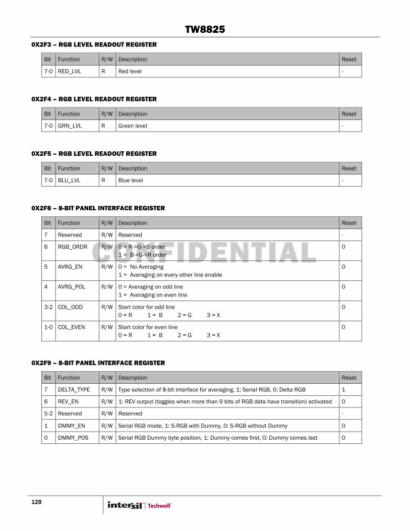
TW8825
128
0X2F3 – RGB LEVEL READOUT REGISTER
Bit Function R/W Description Reset
7-0 RED_LVL R Red level -
0X2F4 – RGB LEVEL READOUT REGISTER
Bit Function R/W Description Reset
7-0 GRN_LVL R Green level -
0X2F5 – RGB LEVEL READOUT REGISTER
Bit Function R/W Description Reset
7-0 BLU_LVL R Blue level -
0X2F8 – 8-BIT PANEL INTERFACE REGISTER
Bit Function R/W Description Reset
7 Reserved R/W Reserved -
6 RGB_ORDR R/W 0 = R->G->B order
1 = B->G->R order
0
5 AVRG_EN R/W 0 = No Averaging
1 = Averaging on every other line enable
0
4 AVRG_POL R/W 0 = Averaging on odd line
1 = Averaging on even line
0
3-2 COL_ODD R/W Start color for odd line
0 = R 1 = B 2 = G 3 = X
0
1-0 COL_EVEN R/W Start color for even line
0 = R 1 = B 2 = G 3 = X
0
0X2F9 – 8-BIT PANEL INTERFACE REGISTER
Bit Function R/W Description Reset
7 DELTA_TYPE R/W Type selection of 8-bit interface for averaging, 1: Serial RGB, 0: Delta RGB 1
6 REV_EN R/W 1: REV output (toggles when more than 9 bits of RGB data have transition) activated 0
5-2 Reserved R/W Reserved -
1 DMMY_EN R/W Serial RGB mode, 1: S-RGB with Dummy, 0: S-RGB without Dummy 0
0 DMMY_POS R/W Serial RGB Dummy byte position, 1: Dummy comes first, 0: Dummy comes last 0
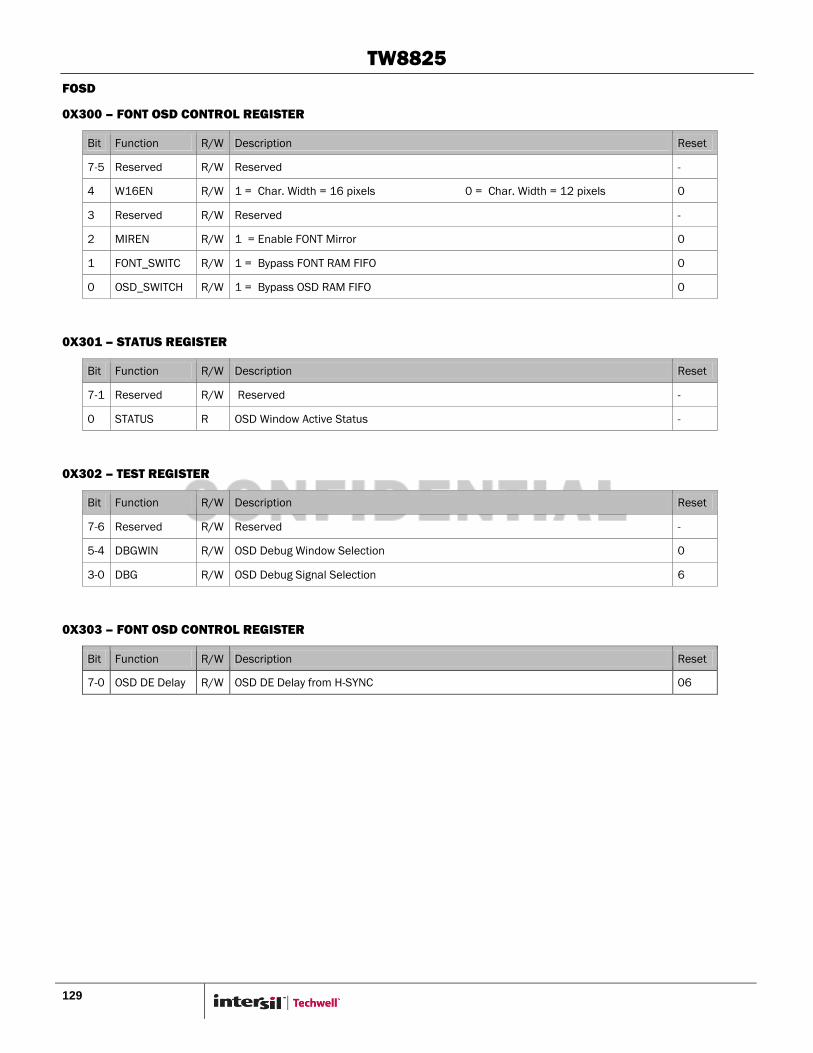
TW8825
129
FOSD
0X300 – FONT OSD CONTROL REGISTER
Bit Function R/W Description Reset
7-5 Reserved R/W Reserved -
4 W16EN R/W 1 = Char. Width = 16 pixels 0 = Char. Width = 12 pixels 0
3 Reserved R/W Reserved -
2 MIREN R/W 1 = Enable FONT Mirror 0
1 FONT_SWITC R/W 1 = Bypass FONT RAM FIFO 0
0 OSD_SWITCH R/W 1 = Bypass OSD RAM FIFO 0
0X301 – STATUS REGISTER
Bit Function R/W Description Reset
7-1 Reserved R/W Reserved -
0 STATUS R OSD Window Active Status -
0X302 – TEST REGISTER
Bit Function R/W Description Reset
7-6 Reserved R/W Reserved -
5-4 DBGWIN R/W OSD Debug Window Selection 0
3-0 DBG R/W OSD Debug Signal Selection 6
0X303 – FONT OSD CONTROL REGISTER
Bit Function R/W Description Reset
7-0 OSD DE Delay R/W OSD DE Delay from H-SYNC 06

TW8825
130
0X304 – FONT OSD CONTROL REGISTER
Bit Function R/W Description Reset
7 BLINK R/W 1 = Character Blinking effect enable 0
6 Reserved R/W Reserved -
5 UP256 R/W 1 = Upper 256 Char. 0 = Lower 256 Char. 0
4 BSEN R/W 1 = Character Bordering/Shadowing effect enable. 0
3-2 AUTO R/W OSD RAM Auto Increase of Write Address Mode Selection.
0 = Normal mode
1 = Font Data or Attribute Address auto mode
3 = Font Data auto mode(Previous Attribute data automatic write)
0
1 CLEAR R/W OSD RAM Auto Clear Mode 0
0 FR_RAC_SEL R/W Font/OSD RAM Serial Bus Access
0 = OSD RAM 1 = Font RAM access
0
0X305 – FONT OSD CONTROL REGISTER
Bit Function R/W Description Reset
7-6 Reserved R/W Reserved -
5 FBITEXT R/W 1 = Enable character horizontal extension. 0
4 RD_SEL R/W Register 097h, 098h Read mode selection.
0 = Normal display 1 = QVGA display
0
3 MADD4[8] R/W Programmable SRAM address start position High 1-bit for 4-bit Multi-Color fonts. 0
2 MADD3[8] R/W Programmable SRAM address start position High 1-bit for 3-bit Multi-Color fonts. 0
1 MADD2[8] R/W Programmable SRAM address start position High 1-bit for 2-bit Multi-Color fonts. 0
0 I2COSDRAD[8] R/W OSD RAM Address High 1-bit (total 9 bits). 0
0X306 – OSD RAM ADDRESS REGISTER
Bit Function R/W Description Reset
7-0 I2COSDRAD R/W OSD RAM Address Low 8-bit (word address for single byte access). 00
0X307 – OSD RAM DATA PORT HI REGISTER
Bit Function R/W Description Reset
7-0 FDATA R/W OSD RAM Data Port Hi (Font Data). 00
0X308 – OSD RAM DATA PORT LO REGISTER
Bit Function R/W Description Reset
7-0 FATTRIBUTE R/W OSD RAM Data Port Lo (Font Attribute). 00
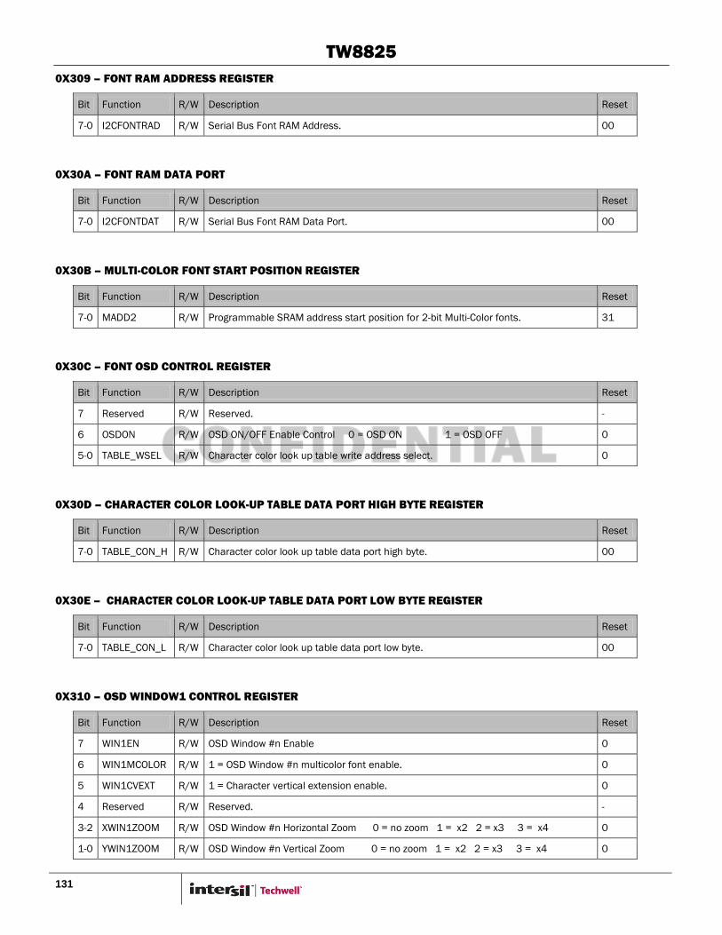
TW8825
131
0X309 – FONT RAM ADDRESS REGISTER
Bit Function R/W Description Reset
7-0 I2CFONTRAD R/W Serial Bus Font RAM Address. 00
0X30A – FONT RAM DATA PORT
Bit Function R/W Description Reset
7-0 I2CFONTDAT R/W Serial Bus Font RAM Data Port. 00
0X30B – MULTI-COLOR FONT START POSITION REGISTER
Bit Function R/W Description Reset
7-0 MADD2 R/W Programmable SRAM address start position for 2-bit Multi-Color fonts. 31
0X30C – FONT OSD CONTROL REGISTER
Bit Function R/W Description Reset
7 Reserved R/W Reserved. -
6 OSDON R/W OSD ON/OFF Enable Control 0 = OSD ON 1 = OSD OFF 0
5-0 TABLE_WSEL R/W Character color look up table write address select. 0
0X30D – CHARACTER COLOR LOOK-UP TABLE DATA PORT HIGH BYTE REGISTER
Bit Function R/W Description Reset
7-0 TABLE_CON_H R/W Character color look up table data port high byte. 00
0X30E – CHARACTER COLOR LOOK-UP TABLE DATA PORT LOW BYTE REGISTER
Bit Function R/W Description Reset
7-0 TABLE_CON_L R/W Character color look up table data port low byte. 00
0X310 – OSD WINDOW1 CONTROL REGISTER
Bit Function R/W Description Reset
7 WIN1EN R/W OSD Window #n Enable 0
6 WIN1MCOLOR R/W 1 = OSD Window #n multicolor font enable. 0
5 WIN1CVEXT R/W 1 = Character vertical extension enable. 0
4 Reserved R/W Reserved. -
3-2 XWIN1ZOOM R/W OSD Window #n Horizontal Zoom 0 = no zoom 1 = x2 2 = x3 3 = x4 0
1-0 YWIN1ZOOM R/W OSD Window #n Vertical Zoom 0 = no zoom 1 = x2 2 = x3 3 = x4 0

TW8825
132
0X311 – OSD WINDOW1 CONTROL REGISTER
Bit Function R/W Description Reset
7-4 Reserved R/W Reserved. -
3-0 WIN1ALPHA R/W OSD Window #n alpha blending amount. 0
0X312 – OSD WINDOW1 CONTROL REGISTER
Bit Function R/W Description Reset
7 Reserved R/W Reserved. -
6-4 WIN1HSTR R/W OSD Window #n H-Start Location High 3 bits (total 11 bits). 0
3-2 Reserved R/W Reserved. -
1-0 WIN1VSTR R/W OSD Window #n V-Start Location High 2 bits (total 10 bits). 0
0X313 – OSD WINDOW1 CONTROL REGISTER
Bit Function R/W Description Reset
7-0 WIN1HSTR R/W OSD Window #n H-Start Location Low 8-bit (1 pixels per step). 00
0X314 – OSD WINDOW1 CONTROL REGISTER
Bit Function R/W Description Reset
7-0 WIN1VSTR R/W OSD Window #n V-Start Location Low 8-bit (1 scan lines per step). 00
0X315 – OSD WINDOW1 CONTROL REGISTER
Bit Function R/W Description Reset
7-6 Reserved R/W Reserved. -
5-0 WIN1HEIGHT R/W OSD Window #n V-Height (1 Character height per step). 00
0X316 – OSD WINDOW1 CONTROL REGISTER
Bit Function R/W Description Reset
7-6 Reserved R/W Reserved. -
5-0 WIN1WIDTH R/W OSD Window #n H-Width (1 Character width per step). 00
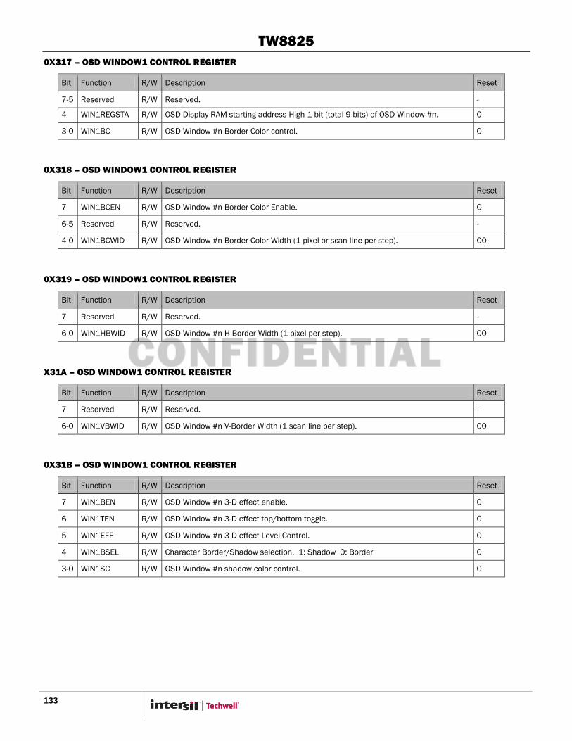
TW8825
133
0X317 – OSD WINDOW1 CONTROL REGISTER
Bit Function R/W Description Reset
7-5 Reserved R/W Reserved. -
4 WIN1REGSTA R/W OSD Display RAM starting address High 1-bit (total 9 bits) of OSD Window #n. 0
3-0 WIN1BC R/W OSD Window #n Border Color control. 0
0X318 – OSD WINDOW1 CONTROL REGISTER
Bit Function R/W Description Reset
7 WIN1BCEN R/W OSD Window #n Border Color Enable. 0
6-5 Reserved R/W Reserved. -
4-0 WIN1BCWID R/W OSD Window #n Border Color Width (1 pixel or scan line per step). 00
0X319 – OSD WINDOW1 CONTROL REGISTER
Bit Function R/W Description Reset
7 Reserved R/W Reserved. -
6-0 WIN1HBWID R/W OSD Window #n H-Border Width (1 pixel per step). 00
X31A – OSD WINDOW1 CONTROL REGISTER
Bit Function R/W Description Reset
7 Reserved R/W Reserved. -
6-0 WIN1VBWID R/W OSD Window #n V-Border Width (1 scan line per step). 00
0X31B – OSD WINDOW1 CONTROL REGISTER
Bit Function R/W Description Reset
7 WIN1BEN R/W OSD Window #n 3-D effect enable. 0
6 WIN1TEN R/W OSD Window #n 3-D effect top/bottom toggle. 0
5 WIN1EFF R/W OSD Window #n 3-D effect Level Control. 0
4 WIN1BSEL R/W Character Border/Shadow selection. 1: Shadow 0: Border 0
3-0 WIN1SC R/W OSD Window #n shadow color control. 0
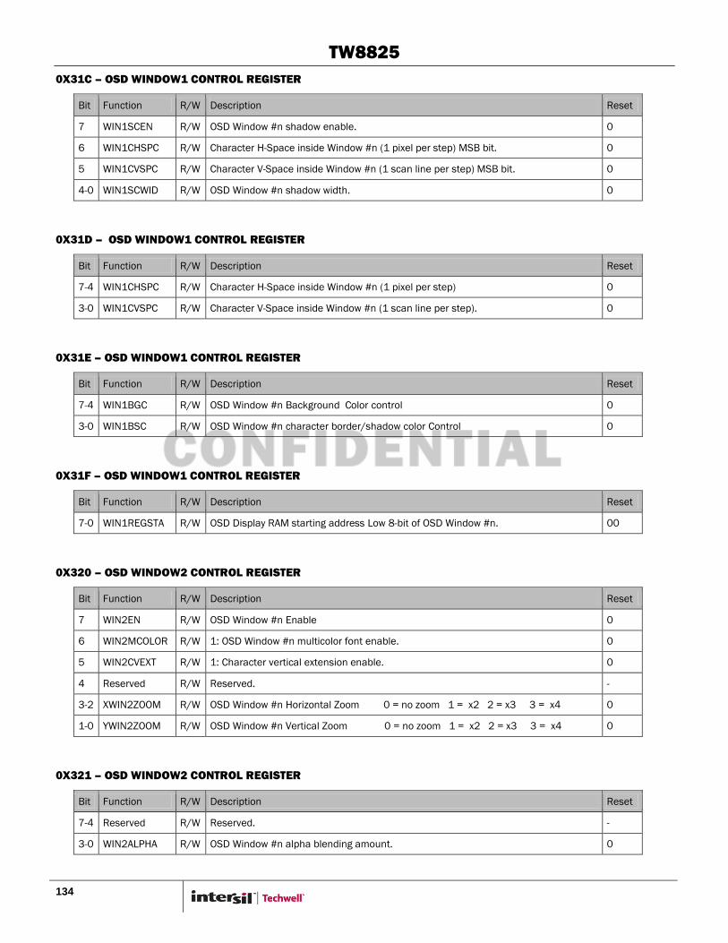
TW8825
134
0X31C – OSD WINDOW1 CONTROL REGISTER
Bit Function R/W Description Reset
7 WIN1SCEN R/W OSD Window #n shadow enable. 0
6 WIN1CHSPC R/W Character H-Space inside Window #n (1 pixel per step) MSB bit. 0
5 WIN1CVSPC R/W Character V-Space inside Window #n (1 scan line per step) MSB bit. 0
4-0 WIN1SCWID R/W OSD Window #n shadow width. 0
0X31D – OSD WINDOW1 CONTROL REGISTER
Bit Function R/W Description Reset
7-4 WIN1CHSPC R/W Character H-Space inside Window #n (1 pixel per step) 0
3-0 WIN1CVSPC R/W Character V-Space inside Window #n (1 scan line per step). 0
0X31E – OSD WINDOW1 CONTROL REGISTER
Bit Function R/W Description Reset
7-4 WIN1BGC R/W OSD Window #n Background Color control 0
3-0 WIN1BSC R/W OSD Window #n character border/shadow color Control 0
0X31F – OSD WINDOW1 CONTROL REGISTER
Bit Function R/W Description Reset
7-0 WIN1REGSTA R/W OSD Display RAM starting address Low 8-bit of OSD Window #n. 00
0X320 – OSD WINDOW2 CONTROL REGISTER
Bit Function R/W Description Reset
7 WIN2EN R/W OSD Window #n Enable 0
6 WIN2MCOLOR R/W 1: OSD Window #n multicolor font enable. 0
5 WIN2CVEXT R/W 1: Character vertical extension enable. 0
4 Reserved R/W Reserved. -
3-2 XWIN2ZOOM R/W OSD Window #n Horizontal Zoom 0 = no zoom 1 = x2 2 = x3 3 = x4 0
1-0 YWIN2ZOOM R/W OSD Window #n Vertical Zoom 0 = no zoom 1 = x2 2 = x3 3 = x4 0
0X321 – OSD WINDOW2 CONTROL REGISTER
Bit Function R/W Description Reset
7-4 Reserved R/W Reserved. -
3-0 WIN2ALPHA R/W OSD Window #n alpha blending amount. 0
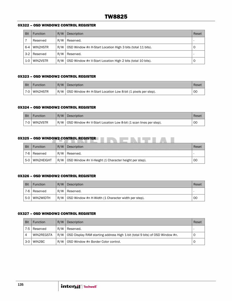
TW8825
135
0X322 – OSD WINDOW2 CONTROL REGISTER
Bit Function R/W Description Reset
7 Reserved R/W Reserved. -
6-4 WIN2HSTR R/W OSD Window #n H-Start Location High 3 bits (total 11 bits). 0
3-2 Reserved R/W Reserved. -
1-0 WIN2VSTR R/W OSD Window #n V-Start Location High 2 bits (total 10 bits). 0
0X323 – OSD WINDOW2 CONTROL REGISTER
Bit Function R/W Description Reset
7-0 WIN2HSTR R/W OSD Window #n H-Start Location Low 8-bit (1 pixels per step). 00
0X324 – OSD WINDOW2 CONTROL REGISTER
Bit Function R/W Description Reset
7-0 WIN2VSTR R/W OSD Window #n V-Start Location Low 8-bit (1 scan lines per step). 00
0X325 – OSD WINDOW2 CONTROL REGISTER
Bit Function R/W Description Reset
7-6 Reserved R/W Reserved. -
5-0 WIN2HEIGHT R/W OSD Window #n V-Height (1 Character height per step). 00
0X326 – OSD WINDOW2 CONTROL REGISTER
Bit Function R/W Description Reset
7-6 Reserved R/W Reserved. -
5-0 WIN2WIDTH R/W OSD Window #n H-Width (1 Character width per step). 00
0X327 – OSD WINDOW2 CONTROL REGISTER
Bit Function R/W Description Reset
7-5 Reserved R/W Reserved. -
4 WIN2REGSTA R/W OSD Display RAM starting address High 1-bit (total 9 bits) of OSD Window #n. 0
3-0 WIN2BC R/W OSD Window #n Border Color control. 0
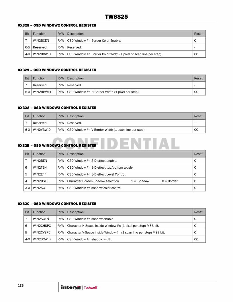
TW8825
136
0X328 – OSD WINDOW2 CONTROL REGISTER
Bit Function R/W Description Reset
7 WIN2BCEN R/W OSD Window #n Border Color Enable. 0
6-5 Reserved R/W Reserved. -
4-0 WIN2BCWID R/W OSD Window #n Border Color Width (1 pixel or scan line per step). 00
0X329 – OSD WINDOW2 CONTROL REGISTER
Bit Function R/W Description Reset
7 Reserved R/W Reserved. -
6-0 WIN2HBWID R/W OSD Window #n H-Border Width (1 pixel per step). 00
0X32A – OSD WINDOW2 CONTROL REGISTER
Bit Function R/W Description Reset
7 Reserved R/W Reserved. -
6-0 WIN2VBWID R/W OSD Window #n V-Border Width (1 scan line per step). 00
0X32B – OSD WINDOW2 CONTROL REGISTER
Bit Function R/W Description Reset
7 WIN2BEN R/W OSD Window #n 3-D effect enable. 0
6 WIN2TEN R/W OSD Window #n 3-D effect top/bottom toggle. 0
5 WIN2EFF R/W OSD Window #n 3-D effect Level Control. 0
4 WIN2BSEL R/W Character Border/Shadow selection 1 = Shadow 0 = Border 0
3-0 WIN2SC R/W OSD Window #n shadow color control. 0
0X32C – OSD WINDOW2 CONTROL REGISTER
Bit Function R/W Description Reset
7 WIN2SCEN R/W OSD Window #n shadow enable. 0
6 WIN2CHSPC R/W Character H-Space inside Window #n (1 pixel per step) MSB bit. 0
5 WIN2CVSPC R/W Character V-Space inside Window #n (1 scan line per step) MSB bit. 0
4-0 WIN2SCWID R/W OSD Window #n shadow width. 00

TW8825
137
0X32D – OSD WINDOW2 CONTROL REGISTER
Bit Function R/W Description Reset
7-4 WIN2CHSPC R/W Character H-Space inside Window #n (1 pixel per step) 0
3-0 WIN2CVSPC R/W Character V-Space inside Window #n (1 scan line per step). 0
0X32E – OSD WINDOW2 CONTROL REGISTER
Bit Function R/W Description Reset
7-4 WIN2BGC R/W OSD Window #n Background Color control 0
3-0 WIN2BSC R/W OSD Window #n character border/shadow color Control 0
0X32F – OSD WINDOW2 CONTROL REGISTER
Bit Function R/W Description Reset
7-0 WIN2REGSTA R/W OSD Display RAM starting address Low 8-bit of OSD Window #n. 00
0X330 – OSD WINDOW3 CONTROL REGISTER
Bit Function R/W Description Reset
7 WIN3EN R/W OSD Window #n Enable 0
6 WIN3MCOLOR R/W 1 = OSD Window #n multicolor font enable. 0
5 WIN3CVEXT R/W 1 = Character vertical extension enable. 0
4 Reserved R/W Reserved. -
3-2 XWIN3ZOOM R/W OSD Window #n Horizontal Zoom 0 = no zoom 1 = x2 2 = x3 3 = x4 0
1-0 YWIN3ZOOM R/W OSD Window #n Vertical Zoom 0 = no zoom 1 = x2 2 = x3 3 = x4 0
0X331 – OSD WINDOW3 CONTROL REGISTER
Bit Function R/W Description Reset
7-4 Reserved R/W Reserved. -
3-0 WIN3ALPHA R/W OSD Window #n alpha blending amount. 0
0X332 – OSD WINDOW3 CONTROL REGISTER
Bit Function R/W Description Reset
7 Reserved R/W Reserved. -
6-4 WIN3HSTR R/W OSD Window #n H-Start Location High 3 bits (total 11 bits). 0
3-2 Reserved R/W Reserved. -
1-0 WIN3VSTR R/W OSD Window #n V-Start Location High 2 bits (total 10 bits). 0
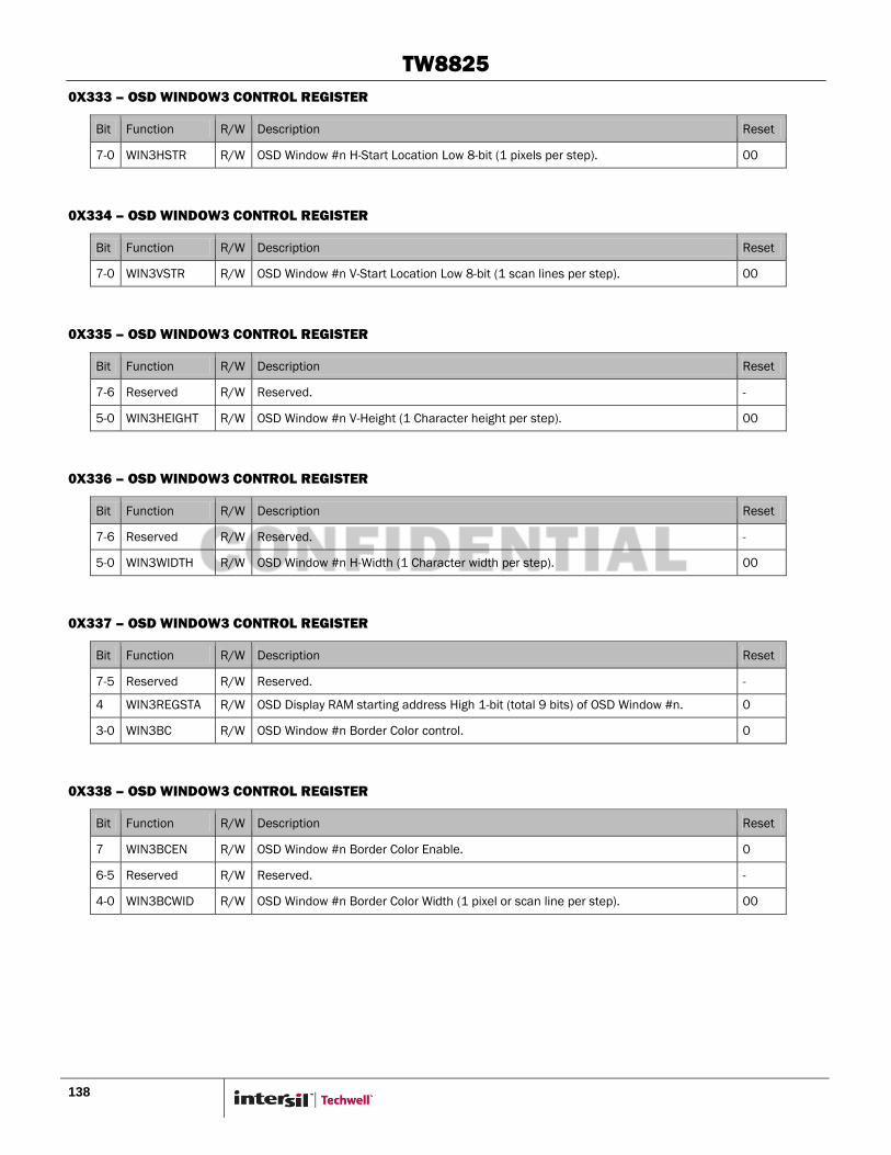
TW8825
138
0X333 – OSD WINDOW3 CONTROL REGISTER
Bit Function R/W Description Reset
7-0 WIN3HSTR R/W OSD Window #n H-Start Location Low 8-bit (1 pixels per step). 00
0X334 – OSD WINDOW3 CONTROL REGISTER
Bit Function R/W Description Reset
7-0 WIN3VSTR R/W OSD Window #n V-Start Location Low 8-bit (1 scan lines per step). 00
0X335 – OSD WINDOW3 CONTROL REGISTER
Bit Function R/W Description Reset
7-6 Reserved R/W Reserved. -
5-0 WIN3HEIGHT R/W OSD Window #n V-Height (1 Character height per step). 00
0X336 – OSD WINDOW3 CONTROL REGISTER
Bit Function R/W Description Reset
7-6 Reserved R/W Reserved. -
5-0 WIN3WIDTH R/W OSD Window #n H-Width (1 Character width per step). 00
0X337 – OSD WINDOW3 CONTROL REGISTER
Bit Function R/W Description Reset
7-5 Reserved R/W Reserved. -
4 WIN3REGSTA R/W OSD Display RAM starting address High 1-bit (total 9 bits) of OSD Window #n. 0
3-0 WIN3BC R/W OSD Window #n Border Color control. 0
0X338 – OSD WINDOW3 CONTROL REGISTER
Bit Function R/W Description Reset
7 WIN3BCEN R/W OSD Window #n Border Color Enable. 0
6-5 Reserved R/W Reserved. -
4-0 WIN3BCWID R/W OSD Window #n Border Color Width (1 pixel or scan line per step). 00
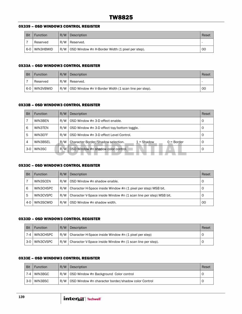
TW8825
139
0X339 – OSD WINDOW3 CONTROL REGISTER
Bit Function R/W Description Reset
7 Reserved R/W Reserved. -
6-0 WIN3HBWID R/W OSD Window #n H-Border Width (1 pixel per step). 00
0X33A – OSD WINDOW3 CONTROL REGISTER
Bit Function R/W Description Reset
7 Reserved R/W Reserved. -
6-0 WIN3VBWID R/W OSD Window #n V-Border Width (1 scan line per step). 00
0X33B – OSD WINDOW3 CONTROL REGISTER
Bit Function R/W Description Reset
7 WIN3BEN R/W OSD Window #n 3-D effect enable. 0
6 WIN3TEN R/W OSD Window #n 3-D effect top/bottom toggle. 0
5 WIN3EFF R/W OSD Window #n 3-D effect Level Control. 0
4 WIN3BSEL R/W Character Border/Shadow selection. 1 = Shadow 0 = Border 0
3-0 WIN3SC R/W OSD Window #n shadow color control. 0
0X33C – OSD WINDOW3 CONTROL REGISTER
Bit Function R/W Description Reset
7 WIN3SCEN R/W OSD Window #n shadow enable. 0
6 WIN3CHSPC R/W Character H-Space inside Window #n (1 pixel per step) MSB bit. 0
5 WIN3CVSPC R/W Character V-Space inside Window #n (1 scan line per step) MSB bit. 0
4-0 WIN3SCWID R/W OSD Window #n shadow width. 00
0X33D – OSD WINDOW3 CONTROL REGISTER
Bit Function R/W Description Reset
7-4 WIN3CHSPC R/W Character H-Space inside Window #n (1 pixel per step) 0
3-0 WIN3CVSPC R/W Character V-Space inside Window #n (1 scan line per step). 0
0X33E – OSD WINDOW3 CONTROL REGISTER
Bit Function R/W Description Reset
7-4 WIN3BGC R/W OSD Window #n Background Color control 0
3-0 WIN3BSC R/W OSD Window #n character border/shadow color Control 0
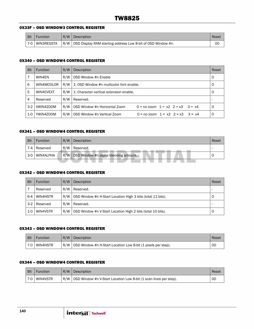
TW8825
140
0X33F – OSD WINDOW3 CONTROL REGISTER
Bit Function R/W Description Reset
7-0 WIN3REGSTA R/W OSD Display RAM starting address Low 8-bit of OSD Window #n. 00
0X340 – OSD WINDOW4 CONTROL REGISTER
Bit Function R/W Description Reset
7 WIN4EN R/W OSD Window #n Enable 0
6 WIN4MCOLOR R/W 1: OSD Window #n multicolor font enable. 0
5 WIN4CVEXT R/W 1: Character vertical extension enable. 0
4 Reserved R/W Reserved. -
3-2 XWIN4ZOOM R/W OSD Window #n Horizontal Zoom 0 = no zoom 1 = x2 2 = x3 3 = x4 0
1-0 YWIN4ZOOM R/W OSD Window #n Vertical Zoom 0 = no zoom 1 = x2 2 = x3 3 = x4 0
0X341 – OSD WINDOW4 CONTROL REGISTER
Bit Function R/W Description Reset
7-4 Reserved R/W Reserved. -
3-0 WIN4ALPHA R/W OSD Window #n alpha blending amount. 0
0X342 – OSD WINDOW4 CONTROL REGISTER
Bit Function R/W Description Reset
7 Reserved R/W Reserved. -
6-4 WIN4HSTR R/W OSD Window #n H-Start Location High 3 bits (total 11 bits). 0
3-2 Reserved R/W Reserved. -
1-0 WIN4VSTR R/W OSD Window #n V-Start Location High 2 bits (total 10 bits). 0
0X343 – OSD WINDOW4 CONTROL REGISTER
Bit Function R/W Description Reset
7-0 WIN4HSTR R/W OSD Window #n H-Start Location Low 8-bit (1 pixels per step). 00
0X344 – OSD WINDOW4 CONTROL REGISTER
Bit Function R/W Description Reset
7-0 WIN4VSTR R/W OSD Window #n V-Start Location Low 8-bit (1 scan lines per step). 00
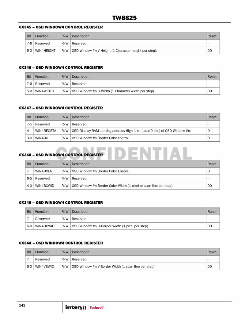
TW8825
141
0X345 – OSD WINDOW4 CONTROL REGISTER
Bit Function R/W Description Reset
7-6 Reserved R/W Reserved. -
5-0 WIN4HEIGHT R/W OSD Window #n V-Height (1 Character height per step). 00
0X346 – OSD WINDOW4 CONTROL REGISTER
Bit Function R/W Description Reset
7-6 Reserved R/W Reserved. -
5-0 WIN4WIDTH R/W OSD Window #n H-Width (1 Character width per step). 00
0X347 – OSD WINDOW4 CONTROL REGISTER
Bit Function R/W Description Reset
7-5 Reserved R/W Reserved. -
4 WIN4REGSTA R/W OSD Display RAM starting address High 1-bit (total 9 bits) of OSD Window #n. 0
3-0 WIN4BC R/W OSD Window #n Border Color control. 0
0X348 – OSD WINDOW4 CONTROL REGISTER
Bit Function R/W Description Reset
7 WIN4BCEN R/W OSD Window #n Border Color Enable. 0
6-5 Reserved R/W Reserved. -
4-0 WIN4BCWID R/W OSD Window #n Border Color Width (1 pixel or scan line per step). 00
0X349 – OSD WINDOW4 CONTROL REGISTER
Bit Function R/W Description Reset
7 Reserved R/W Reserved. -
6-0 WIN4HBWID R/W OSD Window #n H-Border Width (1 pixel per step). 00
0X34A – OSD WINDOW4 CONTROL REGISTER
Bit Function R/W Description Reset
7 Reserved R/W Reserved. -
6-0 WIN4VBWID R/W OSD Window #n V-Border Width (1 scan line per step). 00
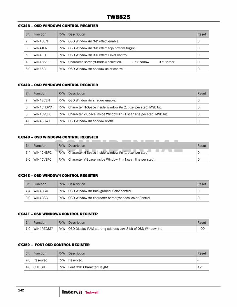
TW8825
142
0X34B – OSD WINDOW4 CONTROL REGISTER
Bit Function R/W Description Reset
7 WIN4BEN R/W OSD Window #n 3-D effect enable. 0
6 WIN4TEN R/W OSD Window #n 3-D effect top/bottom toggle. 0
5 WIN4EFF R/W OSD Window #n 3-D effect Level Control. 0
4 WIN4BSEL R/W Character Border/Shadow selection. 1 = Shadow 0 = Border 0
3-0 WIN4SC R/W OSD Window #n shadow color control. 0
0X34C – OSD WINDOW4 CONTROL REGISTER
Bit Function R/W Description Reset
7 WIN4SCEN R/W OSD Window #n shadow enable. 0
6 WIN4CHSPC R/W Character H-Space inside Window #n (1 pixel per step) MSB bit. 0
5 WIN4CVSPC R/W Character V-Space inside Window #n (1 scan line per step) MSB bit. 0
4-0 WIN4SCWID R/W OSD Window #n shadow width. 0
0X34D – OSD WINDOW4 CONTROL REGISTER
Bit Function R/W Description Reset
7-4 WIN4CHSPC R/W Character H-Space inside Window #n (1 pixel per step) 0
3-0 WIN4CVSPC R/W Character V-Space inside Window #n (1 scan line per step). 0
0X34E – OSD WINDOW4 CONTROL REGISTER
Bit Function R/W Description Reset
7-4 WIN4BGC R/W OSD Window #n Background Color control 0
3-0 WIN4BSC R/W OSD Window #n character border/shadow color Control 0
0X34F – OSD WINDOW4 CONTROL REGISTER
Bit Function R/W Description Reset
7-0 WIN4REGSTA R/W OSD Display RAM starting address Low 8-bit of OSD Window #n. 00
0X350 – FONT OSD CONTROL REGISTER
Bit Function R/W Description Reset
7-5 Reserved R/W Reserved. -
4-0 CHEIGHT R/W Font OSD Character Height 12
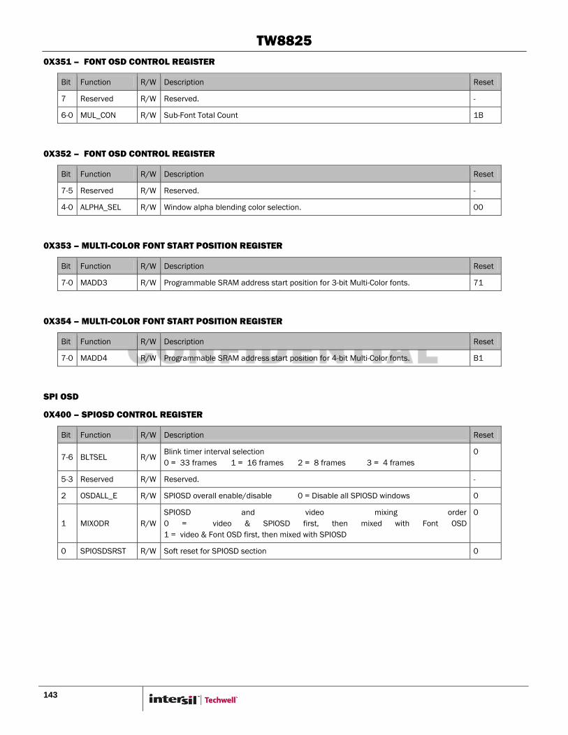
TW8825
143
0X351 – FONT OSD CONTROL REGISTER
Bit Function R/W Description Reset
7 Reserved R/W Reserved. -
6-0 MUL_CON R/W Sub-Font Total Count 1B
0X352 – FONT OSD CONTROL REGISTER
Bit Function R/W Description Reset
7-5 Reserved R/W Reserved. -
4-0 ALPHA_SEL R/W Window alpha blending color selection. 00
0X353 – MULTI-COLOR FONT START POSITION REGISTER
Bit Function R/W Description Reset
7-0 MADD3 R/W Programmable SRAM address start position for 3-bit Multi-Color fonts. 71
0X354 – MULTI-COLOR FONT START POSITION REGISTER
Bit Function R/W Description Reset
7-0 MADD4 R/W Programmable SRAM address start position for 4-bit Multi-Color fonts. B1
SPI OSD
0X400 – SPIOSD CONTROL REGISTER
Bit Function R/W Description Reset
7-6 BLTSEL R/W Blink timer interval selection
0 = 33 frames 1 = 16 frames 2 = 8 frames 3 = 4 frames
0
5-3 Reserved R/W Reserved. -
2 OSDALL_E R/W SPIOSD overall enable/disable 0 = Disable all SPIOSD windows 0
1 MIXODR R/W
SPIOSD and video mixing order
0 = video & SPIOSD first, then mixed with Font OSD
1 = video & Font OSD first, then mixed with SPIOSD
0
0 SPIOSDSRST R/W Soft reset for SPIOSD section 0
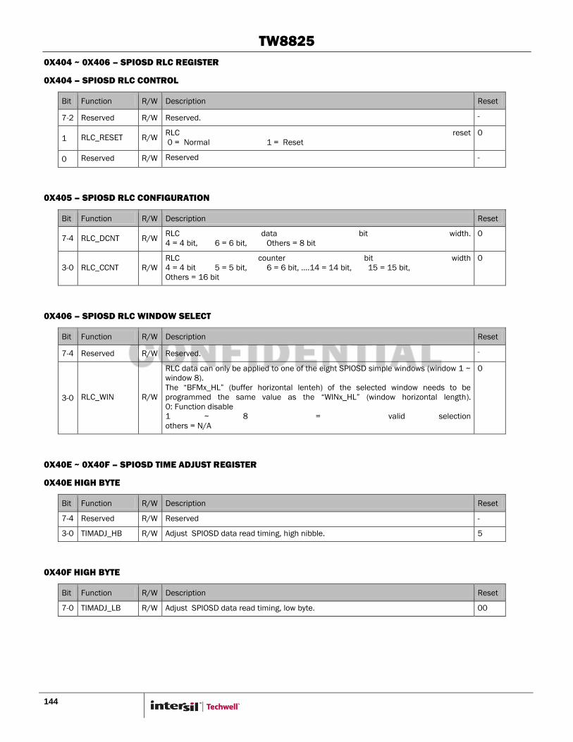
TW8825
144
0X404 ~ 0X406 – SPIOSD RLC REGISTER
0X404 – SPIOSD RLC CONTROL
Bit Function R/W Description Reset
7-2 Reserved R/W Reserved. -
1 RLC_RESET R/W RLC reset
0 = Normal 1 = Reset
0
0 Reserved R/W Reserved -
0X405 – SPIOSD RLC CONFIGURATION
Bit Function R/W Description Reset
7-4 RLC_DCNT R/W RLC data bit width.
4 = 4 bit, 6 = 6 bit, Others = 8 bit
0
3-0 RLC_CCNT R/W
RLC counter bit width
4 = 4 bit 5 = 5 bit, 6 = 6 bit, ….14 = 14 bit, 15 = 15 bit,
Others = 16 bit
0
0X406 – SPIOSD RLC WINDOW SELECT
Bit Function R/W Description Reset
7-4 Reserved R/W Reserved. -
3-0 RLC_WIN R/W
RLC data can only be applied to one of the eight SPIOSD simple windows (window 1 ~
window 8).
The “BFMx_HL” (buffer horizontal lenteh) of the selected window needs to be
programmed the same value as the “WINx_HL” (window horizontal length).
0: Function disable
1 ~ 8 = valid selection
others = N/A
0
0X40E ~ 0X40F – SPIOSD TIME ADJUST REGISTER
0X40E HIGH BYTE
Bit Function R/W Description Reset
7-4 Reserved R/W Reserved -
3-0 TIMADJ_HB R/W Adjust SPIOSD data read timing, high nibble. 5
0X40F HIGH BYTE
Bit Function R/W Description Reset
7-0 TIMADJ_LB R/W Adjust SPIOSD data read timing, low byte. 00

TW8825
145
0X410 – 8-BIT SPIOSD LOOK UP TABLE ACCESS CONTROL REGISTER
Bit Function R/W Description Reset
7 LUTWE R/W This bit enable look up table write access for MCU or DMA
1 = Enable Look up table write access
0
6-5 LUTINC_SEL R/W
LUT pointer increment selection:
0 = No increment
1 = Byte pointer increments by 1 after each LUT data port write ; when it reaches
“11”, the byte pointer wraps around and the address pointer increments by 1
2 = Address pointer increments by 1 after each LUT data port write; when it reaches
“FF”, the address pointer wraps around and the byte pointer increments by 1
Note: For DMA write access, there are only two valid selection, “01” or “10”.
0
4 Reserved R/W Reserved -
3 LUTADDR_H R/W MSB of the address pointer to one of the 512 entries of the LUT (see 0x411
description).
-
2 Reserved R/W Reserved -
1-0 LUTBYT R/W
Byte pointer for the LUT access. Read reflects the current byte pointer value.
If DMA is used to read from SPI Flash and write to LUT, the initial byte pointer is
specified by 0x4C6[1:0] (with 0x410[6:5] =10), or 0x4C7[1:0] (with 0x 410[6:5]
=01).
0
0X411 – 8 BIT SPIOSD LOOK UP TABLE ADDRESS [7:0] REGISTER
Bit Function R/W Description Reset
7-0 LUTADDR R/W
Address pointer (lower 8 bits) to one of the 512 entries of the LUT. Read reflects the
current address pointer value.
If DMA is used to read from SPI Flash and write to LUT, the initial address is specified
by 0x4C6[0]#0x4C7[7:0] (with 0x410[6:5 ]=10), or 0x4C6[2:w
:0]#0x4C7[7:2] (with 0x 410[6:5]=01).
00
0X412 – 8 BIT SPIOSD LOOK UP TABLE DATA PORT [7:0] REGISTER
Bit Function R/W Description Reset
7-0 LUTDATA R/W
Write data to the look up table pointed by the Address and Byte pointers
Read returns the data pointed by the Address and Byte pointers. Two reads are
required to get the correct data. Read does not advance either the Address pointer or
Byte pointer. This register is not used for DMA write LUT.
00
0X420 – SPIOSD WINDOW 0 ENABLE REGISTER
Bit Function R/W Description Reset
7-6 WIN0_PIXLW R/W Window 0 pixel width.
0 = 4 bits 1 = 6 bits others = 8 bits
0
5 WIN0_PERPIX R/W SPIOSD window 0 alpha blending selection
0 = Global window 0 alpha 1 = Per pixel alpha
0
4 WIN0_ALPHA_
ENA
R/W SPIOSD window 0 alpha blending enable 0

TW8825
146
Bit Function R/W Description Reset
3 Reserved R/W Reserved -
2 WIN0_FCE R/W SPIOSD window 0 fill color enable 0
1 WIN0_HP R/W SPIOSD window 0 priority 1 = Highest 0 = Lowest 0
0 WIN0_ENA R/W SPIOSD window 0 = Enable 0
0X421 ~ 0X423 – SPIOSD WINDOW 0 HORIZONTAL/VERTICAL START REGISTERS
0X421 – HORIZONTAL/VERTICAL HIGH BYTE REGISTER
Bit Function R/W Description Reset
7 Reserved R/W Reserved -
6-4 WIN0_VS_HB R/W SPIOSD window 0 Vertical start (offset from the LCD display top first line)
High byte
0
3 Reserved R/W Reserved -
2-0 WIN0_HS_HB R/W SPIOSD window 0 horizontal start (offset from the LCD display first left pixel)
High byte
0
0X422 – HORIZONTAL LOW BYTE REGISTER
Bit Function R/W Description Reset
7-0 WIN0_HS_LB R/W SPIOSD window 0 horizontal start (offset from the LCD display first left pixel)
Low byte
00
0X423 – VERTICAL LOW BYTE REGISTER
Bit Function R/W Description Reset
7-0 WIN0_VS_LB R/W SPIOSD window 0 Vertical start (offset from the LCD display top first line)
Low byte
00
0X424~0X0426 – SPIOSD WINDOW 0 HORIZONTAL/VERTICAL LENGTH REGISTERS
0X0424 – HORIZONTAL/VERTICAL HIGH BYTE REGISTER
Bit Function R/W Description Reset
7-4 WIN0_VL_HB R/W SPIOSD window 0 vertical Length High byte
(one line per increment, minimum is 1, maximum is 2048)
0
3-0 WIN0_HL_HB R/W SPIOSD window 0 horizontal Length High byte
(one pixel per increment, minimum is 1, maximum is 2048)
0
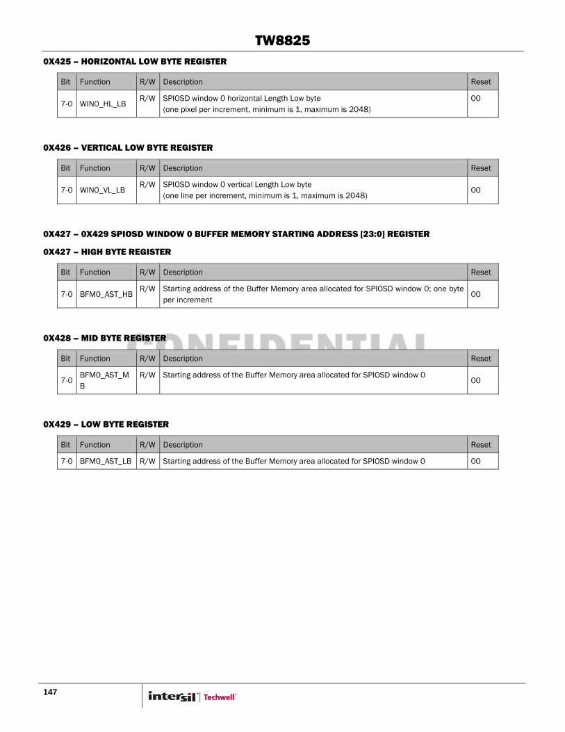
TW8825
147
0X425 – HORIZONTAL LOW BYTE REGISTER
Bit Function R/W Description Reset
7-0 WIN0_HL_LB R/W SPIOSD window 0 horizontal Length Low byte
(one pixel per increment, minimum is 1, maximum is 2048)
00
0X426 – VERTICAL LOW BYTE REGISTER
Bit Function R/W Description Reset
7-0 WIN0_VL_LB R/W SPIOSD window 0 vertical Length Low byte
(one line per increment, minimum is 1, maximum is 2048) 00
0X427 – 0X429 SPIOSD WINDOW 0 BUFFER MEMORY STARTING ADDRESS [23:0] REGISTER
0X427 – HIGH BYTE REGISTER
Bit Function R/W Description Reset
7-0 BFM0_AST_HB R/W Starting address of the Buffer Memory area allocated for SPIOSD window 0; one byte
per increment 00
0X428 – MID BYTE REGISTER
Bit Function R/W Description Reset
7-0 BFM0_AST_M
B
R/W Starting address of the Buffer Memory area allocated for SPIOSD window 0 00
0X429 – LOW BYTE REGISTER
Bit Function R/W Description Reset
7-0 BFM0_AST_LB R/W Starting address of the Buffer Memory area allocated for SPIOSD window 0 00
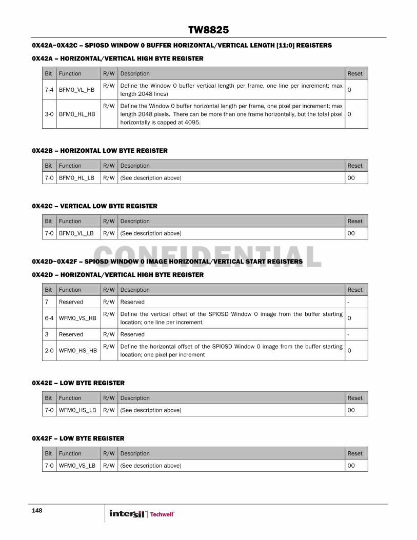
TW8825
148
0X42A~0X42C – SPIOSD WINDOW 0 BUFFER HORIZONTAL/VERTICAL LENGTH [11:0] REGISTERS
0X42A – HORIZONTAL/VERTICAL HIGH BYTE REGISTER
Bit Function R/W Description Reset
7-4 BFM0_VL_HB R/W Define the Window 0 buffer vertical length per frame, one line per increment; max
length 2048 lines) 0
3-0 BFM0_HL_HB
R/W Define the Window 0 buffer horizontal length per frame, one pixel per increment; max
length 2048 pixels. There can be more than one frame horizontally, but the total pixel
horizontally is capped at 4095.
0
0X42B – HORIZONTAL LOW BYTE REGISTER
Bit Function R/W Description Reset
7-0 BFM0_HL_LB R/W (See description above) 00
0X42C – VERTICAL LOW BYTE REGISTER
Bit Function R/W Description Reset
7-0 BFM0_VL_LB R/W (See description above) 00
0X42D~0X42F – SPIOSD WINDOW 0 IMAGE HORIZONTAL/VERTICAL START REGISTERS
0X42D – HORIZONTAL/VERTICAL HIGH BYTE REGISTER
Bit Function R/W Description Reset
7 Reserved R/W Reserved -
6-4 WFM0_VS_HB R/W Define the vertical offset of the SPIOSD Window 0 image from the buffer starting
location; one line per increment 0
3 Reserved R/W Reserved -
2-0 WFM0_HS_HB R/W Define the horizontal offset of the SPIOSD Window 0 image from the buffer starting
location; one pixel per increment 0
0X42E – LOW BYTE REGISTER
Bit Function R/W Description Reset
7-0 WFM0_HS_LB R/W (See description above) 00
0X42F – LOW BYTE REGISTER
Bit Function R/W Description Reset
7-0 WFM0_VS_LB R/W (See description above) 00
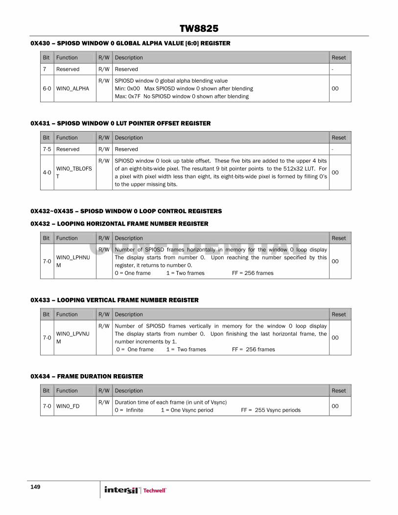
TW8825
149
0X430 – SPIOSD WINDOW 0 GLOBAL ALPHA VALUE [6:0] REGISTER
Bit Function R/W Description Reset
7 Reserved R/W Reserved -
6-0 WIN0_ALPHA
R/W SPIOSD window 0 global alpha blending value
Min: 0x00 Max SPIOSD window 0 shown after blending
Max: 0x7F No SPIOSD window 0 shown after blending
00
0X431 – SPIOSD WINDOW 0 LUT POINTER OFFSET REGISTER
Bit Function R/W Description Reset
7-5 Reserved R/W Reserved -
4-0 WIN0_TBLOFS
T
R/W SPIOSD window 0 look up table offset. These five bits are added to the upper 4 bits
of an eight-bits-wide pixel. The resultant 9 bit pointer points to the 512x32 LUT. For
a pixel with pixel width less than eight, its eight-bits-wide pixel is formed by filling 0‟s
to the upper missing bits.
00
0X432~0X435 – SPIOSD WINDOW 0 LOOP CONTROL REGISTERS
0X432 – LOOPING HORIZONTAL FRAME NUMBER REGISTER
Bit Function R/W Description Reset
7-0 WIN0_LPHNU
M
R/W Number of SPIOSD frames horizontally in memory for the window 0 loop display
The display starts from number 0. Upon reaching the number specified by this
register, it returns to number 0.
0 = One frame 1 = Two frames FF = 256 frames
00
0X433 – LOOPING VERTICAL FRAME NUMBER REGISTER
Bit Function R/W Description Reset
7-0 WIN0_LPVNU
M
R/W Number of SPIOSD frames vertically in memory for the window 0 loop display
The display starts from number 0. Upon finishing the last horizontal frame, the
number increments by 1.
0 = One frame 1 = Two frames FF = 256 frames
00
0X434 – FRAME DURATION REGISTER
Bit Function R/W Description Reset
7-0 WIN0_FD R/W Duration time of each frame (in unit of Vsync)
0 = Infinite 1 = One Vsync period FF = 255 Vsync periods 00
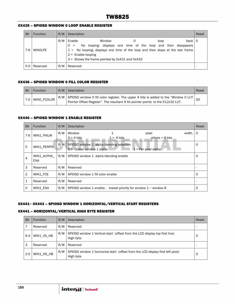
TW8825
150
0X435 – SPIOSD WINDOW 0 LOOP ENABLE REGISTER
Bit Function R/W Description Reset
7-6 WIN0LPE
R/W Enable Window 0 loop back
0 = No looping; displays one time of the loop and then disappears
1 = No looping; displays one time of the loop and then stays at the last frame
2 = Enable looping
3 = Shows the frame pointed by 0x431 and 0x432
0
5-0 Reserved R/W Reserved -
0X436 – SPIOSD WINDOW 0 FILL COLOR REGISTER
Bit Function R/W Description Reset
7-0 WIN0_FCOLOR R/W SPIOSD window 0 fill color register. The upper 4 bits is added to the “Window 0 LUT
Pointer Offset Register”. The resultant 9 bit pointer points to the 512x32 LUT. 00
0X440 – SPIOSD WINDOW 1 ENABLE REGISTER
Bit Function R/W Description Reset
7-6 WIN1_PIXLW R/W Window 1 pixel width.
0 = 4 bits 1 = 6 bits others = 8 bits
0
5 WIN1_PERPIX R/W SPIOSD window 1 alpha blending selection
0 = Global window 1 alpha 1 = Per pixel alpha
0
4 WIN1_ALPHA_
ENA
R/W SPIOSD window 1 alpha blending enable 0
3 Reserved R/W Reserved -
2 WIN1_FCE R/W SPIOSD window 1 fill color enable 0
1 Reserved R/W Reserved -
0 WIN1_ENA R/W SPIOSD window 1 enable; lowest priority for window 1 ~ window 8 0
0X441~ 0X443 – SPIOSD WINDOW 1 HORIZONTAL/VERTICAL START REGISTERS
0X441 – HORIZONTAL/VERTICAL HIGH BYTE REGISTER
Bit Function R/W Description Reset
7 Reserved R/W Reserved -
6-4 WIN1_VS_HB R/W SPIOSD window 1 Vertical start (offset from the LCD display top first line)
High byte 0
3 Reserved R/W Reserved -
2-0 WIN1_HS_HB R/W SPIOSD window 1 horizontal start (offset from the LCD display first left pixel)
High byte 0

TW8825
151
0X442 – HORIZONTAL LOW BYTE REGISTER
Bit Function R/W Description Reset
7-0 WIN1_HS_LB R/W SPIOSD window 1 horizontal start (offset from the LCD display first left pixel)
Low byte 00
0X443 – VERTICAL LOW BYTE REGISTER
Bit Function R/W Description Reset
7-0 WIN1_VS_LB R/W SPIOSD window 1 Vertical start (offset from the LCD display top first line)
Low byte 00
0X444~0X446 – SPIOSD WINDOW 1 HORIZONTAL/VERTICAL LENGTH REGISTERS
0X444 – HORIZONTAL/VERTICAL HIGH BYTE REGISTER
Bit Function R/W Description Reset
7-4 WIN1_VL_HB R/W SPIOSD window 1 vertical Length High byte
(one line per increment, minimum is 1, maximum is 2048) 0
3-0 WIN1_HL_HB R/W SPIOSD window 1 horizontal Length High byte
(one pixel per increment, minimum is 1, maximum is 2048) 0
0X445 – HORIZONTAL LOW BYTE REGISTER
Bit Function R/W Description Reset
7-0 WIN1_HL_LB R/W SPIOSD window 1 horizontal Length Low byte
(one pixel per increment, minimum is 1, maximum is 2048) 00
0X446 – VERTICAL LOW BYTE REGISTER
Bit Function R/W Description Reset
7-0 WIN1_VL_LB R/W SPIOSD window 1 vertical Length Low byte
(one line per increment, minimum is 1, maximum is 2048) 00
0X447~0X044A – SPIOSD WINDOW 1 BUFFER MEMORY STARTING ADDRESS [23:0] REGISTERS
0X0447 – HIGH BYTE REGISTER
Bit Function R/W Description Reset
7-0 BFM1_AST_HB R/W Starting address of the Buffer Memory area allocated for SPIOSD window 1; one byte
per increment 00

TW8825
152
0X448 – MID BYTE REGISTER
Bit Function R/W Description Reset
7-0 BFM1_AST_M
B
R/W Starting address of the Buffer Memory area allocated for SPIOSD window 1 00
0X449 – LOW BYTE REGISTER
Bit Function R/W Description Reset
7-0 BFM1_AST_LB R/W Starting address of the Buffer Memory area allocated for SPIOSD window 1 00
0X44A – LOW BYTE BIT REGISTER
Bit Function R/W Description Reset
7-6 BFM1_AST_LB
B
R/W Starting bit address of the Buffer Memory area allocated for SPIOSD window 1.
specifies one of the four even bit addresses in a byte 0
0X44A~0X44B – SPIOSD WINDOW 1 BUFFER HORIZONTAL LENGTH [11:0] REGISTERS
0X44A – HIGH BYTE REGISTER
Bit Function R/W Description Reset
5-4 Reserved R/W Reserved -
3-0 BFM1_HL_HB
R/W Define the Window 1 buffer horizontal length per frame, one pixel per increment; max
length 2048 pixels. There can be more than one frame horizontally, but the total pixel
horizontally is capped at 4095.
0
0X44B – LOW BYTE REGISTER
Bit Function R/W Description Reset
7-0 BFM1_HL_LB R/W (See description above) 00
0X44C – SPIOSD WINDOW 1 GLOBAL ALPHA VALUE [6:0] REGISTER
Bit Function R/W Description Reset
7 Reserved R/W Reserved -
6-0 WIN1_ALPHA
R/W SPIOSD window 1 global alpha blending value
Min: 0x00 Max SPIOSD window 1 shown after blending
Max: 0x7F No SPIOSD window 1 shown after blending
00

TW8825
153
0X44D – SPIOSD WINDOW 1 LUT POINTER OFFSET REGISTER
Bit Function R/W Description Reset
7-5 Reserved R/W Reserved -
4-0 WIN1_TBLOFS
T
R/W SPIOSD window 1 look up table offset. These five bits are added to the upper 4 bits
of an eight-bits-wide pixel. The resultant 9 bit pointer points to the 512x32 LUT. For
a pixel with pixel width less than eight, its eight-bits-wide pixel is formed by filling 0‟s
to the upper missing bits.
00
0X44E – SPIOSD WINDOW 1 FILL COLOR REGISTER
Bit Function R/W Description Reset
7-0 WIN1_FCOLOR R/W SPIOSD window 1 fill color register. The upper 4 bits is added to the “Window 1 LUT
Pointer Offset Register”. The resultant 9 bit pointer points to the 512x32 LUT. 00
0X450 – SPIOSD WINDOW 2 ENABLE REGISTER
Bit Function R/W Description Reset
7-6 WIN2_PIXLW R/W Window 2 pixel width.
0 = 4 bits 1 = 6 bits others = 8 bits
0
5 WIN2_PERPIX R/W SPIOSD window 2 alpha blending selection
0 = Global window 2 alpha 1 = Per pixel alpha
0
4 WIN2_ALPHA_
ENA
R/W SPIOSD window 2 alpha blending enable 0
3 Reserved R/W Reserved -
2 WIN2_FCE R/W SPIOSD window 2 fill color enable 0
1 Reserved R/W Reserved -
0 WIN2_ENA R/W SPIOSD window 2 enable 0
0X451~ 0X453 – SPIOSD WINDOW 2 HORIZONTAL/VERTICAL START REGISTERS
0X451 – HORIZONTAL/VERTICAL HIGH BYTE REGISTER
Bit Function R/W Description Reset
7 Reserved R/W Reserved -
6-4 WIN2_VS_HB R/W SPIOSD window 2 Vertical start (offset from the LCD display top first line)
High byte 0
3 Reserved R/W Reserved -
2-0 WIN2_HS_HB R/W SPIOSD window 2 horizontal start (offset from the LCD display first left pixel)
High byte 0

TW8825
154
0X452 – HORIZONTAL LOW BYTE REGISTER
Bit Function R/W Description Reset
7-0 WIN2_HS_LB R/W SPIOSD window 2 horizontal start (offset from the LCD display first left pixel)
Low byte 00
0X453 – VERTICAL LOW BYTE REGISTER
Bit Function R/W Description Reset
7-0 WIN2_VS_LB R/W SPIOSD window 2 Vertical start (offset from the LCD display top first line)
Low byte 00
0X454~0X456 – SPIOSD WINDOW 2 HORIZONTAL/VERTICAL LENGTH REGISTERS
0X454 – HORIZONTAL/ VERTICAL HIGH BYTE REGISTER
Bit Function R/W Description Reset
7-4 WIN2_VL_HB R/W SPIOSD window 2 vertical Length High byte
(one line per increment, minimum is 1, maximum is 2048) 0
3-0 WIN2_HL_HB R/W SPIOSD window 2 horizontal Length High byte
(one pixel per increment, minimum is 1, maximum is 2048) 0
0X455 – HORIZONTAL LOW BYTE REGISTER
Bit Function R/W Description Reset
7-0 WIN2_HL_LB R/W SPIOSD window 2 horizontal Length Low byte
(one pixel per increment, minimum is 1, maximum is 2048) 00
0X456 – VERTICAL LOW BYTE REGISTER
Bit Function R/W Description Reset
7-0 WIN2_VL_LB R/W SPIOSD window 2 vertical Length Low byte
(one line per increment, minimum is 1, maximum is 2048) 00
0X457~0X045A – SPIOSD WINDOW 2 BUFFER MEMORY STARTING ADDRESS [23:0] REGISTERS
0X0457 – HIGH BYTE REGISTER
Bit Function R/W Description Reset
7-0 BFM2_AST_HB R/W Starting address of the Buffer Memory area allocated for SPIOSD window 2; one byte
per increment 00

TW8825
155
0X458 – MID BYTE REGISTER
Bit Function R/W Description Reset
7-0 BFM2_AST_M
B
R/W Starting address of the Buffer Memory area allocated for SPIOSD window 2 00
0X459 – LOW BYTE REGISTER
Bit Function R/W Description Reset
7-0 BFM2_AST_LB R/W Starting address of the Buffer Memory area allocated for SPIOSD window 2 00
0X45A – LOW BYTE REGISTER
Bit Function R/W Description Reset
7-6 BFM2_AST_LB
B
R/W Starting bit address of the Buffer Memory area allocated for SPIOSD window 2.
specifies one of the four even bit addresses in a byte 0
0X45A~0X45B – SPIOSD WINDOW 2 BUFFER HORIZONTAL LENGTH [11:0] REGISTERS
0X45A – HIGH BYTE REGISTER
Bit Function R/W Description Reset
5-4 Reserved R/W Reserved -
3-0 BFM2_HL_HB
R/W Define the Window 2 buffer horizontal length per frame, one pixel per increment; max
length 2048 pixels. There can be more than one frame horizontally, but the total pixel
horizontally is capped at 4095.
0
0X45B – LOW BYTE REGISTER
Bit Function R/W Description Reset
7-0 BFM2_HL_LB R/W (See description above) 00
0X45C – SPIOSD WINDOW 2 GLOBAL ALPHA VALUE [6:0] REGISTER
Bit Function R/W Description Reset
7 Reserved R/W Reserved -
6-0 WIN2_ALPHA
R/W SPIOSD window 2 global alpha blending value
Min: 0x00 Max SPIOSD window 2 shown after blending
Max: 0x7F No SPIOSD window 2 shown after blending
00

TW8825
156
0X45D – SPIOSD WINDOW 2 LUT POINTER OFFSET REGISTER
Bit Function R/W Description Reset
7-5 Reserved R/W Reserved -
4-0 WIN2_TBLOFS
T
R/W SPIOSD window 2 look up table offset. These five bits are added to the upper 4 bits
of an eight-bits-wide pixel. The resultant 9 bit pointer points to the 512x32 LUT. For
a pixel with pixel width less than eight, its eight-bits-wide pixel is formed by filling 0‟s
to the upper missing bits.
0
0X45E – SPIOSD WINDOW 2 FILL COLOR REGISTER
Bit Function R/W Description Reset
7-0 WIN2_FCOLOR R/W SPIOSD window 2 fill color register. The upper 4 bits is added to the “Window 2 LUT
Pointer Offset Register”. The resultant 9 bit pointer points to the 512x32 LUT. 00
0X460 – SPIOSD WINDOW 3 ENABLE REGISTER
Bit Function R/W Description Reset
7-6 WIN3_PIXLW R/W Window 3 pixel width.
0 = 4 bits 1 = 6 bits others = 8 bits
0
5 WIN3_PERPIX R/W SPIOSD window 3 alpha blending selection
0 = Global window 3 alpha 1 = Per pixel alpha
0
4 WIN3_ALPHA_
ENA
R/W SPIOSD window 3 alpha blending enable 0
3 Reserved R/W Reserved -
2 WIN3_FCE R/W SPIOSD window 3 fill color enable 0
1 Reserved R/W Reserved -
0 WIN3_ENA R/W SPIOSD window 3 enable 0
0X461~ 0X463 – SPIOSD WINDOW 3 HORIZONTAL/VERTICAL START REGISTERS
0X461 – HORIZONTAL/VERTICAL HIGH BYTE REGISTER
Bit Function R/W Description Reset
7 Reserved R/W Reserved -
6-4 WIN3_VS_HB R/W SPIOSD window 3 Vertical start (offset from the LCD display top first line)
High byte 0
3 Reserved R/W Reserved -
2-0 WIN3_HS_HB R/W SPIOSD window 3 horizontal start (offset from the LCD display first left pixel)
High byte 0

TW8825
157
0X462 – HORIZONTAL LOW BYTE REGISTER
Bit Function R/W Description Reset
7-0 WIN3_HS_LB R/W SPIOSD window 3 horizontal start (offset from the LCD display first left pixel)
Low byte 00
0X463 – VERTICAL LOW BYTE REGISTER
Bit Function R/W Description Reset
7-0 WIN3_VS_LB R/W SPIOSD window 3 Vertical start (offset from the LCD display top first line)
Low byte 00
0X464~0X466 – SPIOSD WINDOW 3 HORIZONTAL/VERTICAL LENGTH REGISTERS
0X464 – HORIZONTAL/ VERTICAL HIGH BYTE REGISTER
Bit Function R/W Description Reset
7-4 WIN3_VL_HB R/W SPIOSD window 3 vertical Length High byte
(one line per increment, minimum is 1, maximum is 2048) 0
3-0 WIN3_HL_HB R/W SPIOSD window 3 horizontal Length High byte
(one pixel per increment, minimum is 1, maximum is 2048) 0
0X465 – HORIZONTAL LOW BYTE REGISTER
Bit Function R/W Description Reset
7-0 WIN3_HL_LB R/W SPIOSD window 2 horizontal Length Low byte
(one pixel per increment, minimum is 1, maximum is 2048) 00
0X466 – VERTICAL LOW BYTE REGISTER
Bit Function R/W Description Reset
7-0 WIN3_VL_LB R/W SPIOSD window 3 vertical Length Low byte
(one line per increment, minimum is 1, maximum is 2048) 00
0X467~0X046A – SPIOSD WINDOW 3 BUFFER MEMORY STARTING ADDRESS [23:0] REGISTERS
0X0467 – HIGH BYTE REGISTER
Bit Function R/W Description Reset
7-0 BFM3_AST_HB R/W Starting address of the Buffer Memory area allocated for SPIOSD window 3; one byte
per increment 00

TW8825
158
0X468 – MID BYTE REGISTER
Bit Function R/W Description Reset
7-0 BFM3_AST_M
B
R/W Starting address of the Buffer Memory area allocated for SPIOSD window 3 00
0X469 – LOW BYTE REGISTER
Bit Function R/W Description Reset
7-0 BFM3_AST_LB R/W Starting address of the Buffer Memory area allocated for SPIOSD window 3 00
0X46A – LOW BYTE BIT REGISTER
Bit Function R/W Description Reset
7-6 BFM3_AST_LB
B
R/W Starting bit address of the Buffer Memory area allocated for SPIOSD window 3.
specifies one of the four even bit addresses in a byte 00
0X46A~0X46B – SPIOSD WINDOW 3 BUFFER HORIZONTAL LENGTH [11:0] REGISTERS
0X46A – HIGH BYTE REGISTER
Bit Function R/W Description Reset
5-4 Reserved R/W Reserved -
3-0 BFM3_HL_HB
R/W Define the Window 3 buffer horizontal length per frame, one pixel per increment; max
length 2048 pixels. There can be more than one frame horizontally, but the total pixel
horizontally is capped at 4095.
0
0X46B – LOW BYTE REGISTER
Bit Function R/W Description Reset
7-0 BFM3_HL_LB R/W (See description above) 00
0X46C – SPIOSD WINDOW 3 GLOBAL ALPHA VALUE [6:0] REGISTER
Bit Function R/W Description Reset
7 Reserved R/W Reserved -
6-0 WIN3_ALPHA
R/W SPIOSD window 3 global alpha blending value
Min: 0x00 Max SPIOSD window 3 shown after blending
Max: 0x7F No SPIOSD window 3 shown after blending
0

TW8825
159
0X46D – SPIOSD WINDOW 3 LUT POINTER OFFSET REGISTER
Bit Function R/W Description Reset
7-5 Reserved R/W Reserved -
4-0 WIN3_TBLOFS
T
R/W SPIOSD window 3 look up table offset. These five bits are added to the upper 4 bits
of an eight-bits-wide pixel. The resultant 9 bit pointer points to the 512x32 LUT. For a
pixel with pixel width less than eight, its eight-bits-wide pixel is formed by filling 0‟s to
the upper missing bits.
00
0X46E – SPIOSD WINDOW 3 FILL COLOR REGISTER
Bit Function R/W Description Reset
7-0 WIN3_FCOLOR R/W SPIOSD window 3 fill color register. The upper 4 bits is added to the “Window 3 LUT
Pointer Offset Register”. The resultant 9 bit pointer points to the 512x32 LUT. 00
0X470 – SPIOSD WINDOW 4 ENABLE REGISTER
Bit Function R/W Description Reset
7-6 WIN4_PIXLW R/W Window 4 pixel width.
0 = 4 bits 1 = 6 bits others = 8 bits
0
5 WIN4_PERPIX R/W SPIOSD window 4 alpha blending selection
0 = Global window 4 alpha 1 = Per pixel alpha
0
4 WIN4_ALPHA_
ENA
R/W SPIOSD window 4 alpha blending enable 0
3 Reserved R/W Reserved -
2 WIN4_FCE R/W SPIOSD window 4 fill color enable 0
1 Reserved R/W Reserved -
0 WIN4_ENA R/W SPIOSD window 4 enable 0
0X471~ 0X473 – SPIOSD WINDOW 4 HORIZONTAL/VERTICAL START REGISTERS
0X471 – HORIZONTAL/VERTICAL HIGH BYTE REGISTER
Bit Function R/W Description Reset
7 Reserved R/W Reserved -
6-4 WIN4_VS_HB R/W SPIOSD window 4 Vertical start (offset from the LCD display top first line)
High byte 0
3 Reserved R/W Reserved -
2-0 WIN4_HS_HB R/W SPIOSD window 4 horizontal start (offset from the LCD display first left pixel)
High byte 0
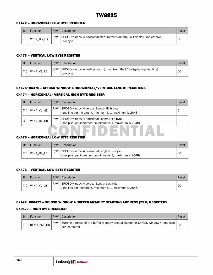
TW8825
160
0X472 – HORIZONTAL LOW BYTE REGISTER
Bit Function R/W Description Reset
7-0 WIN4_HS_LB R/W SPIOSD window 4 horizontal start (offset from the LCD display first left pixel)
Low byte 00
0X473 – VERTICAL LOW BYTE REGISTER
Bit Function R/W Description Reset
7-0 WIN4_VS_LB R/W SPIOSD window 4 Vertical start (offset from the LCD display top first line)
Low byte 00
0X474~0X476 – SPIOSD WINDOW 4 HORIZONTAL/VERTICAL LENGTH REGISTERS
0X474 – HORIZONTAL/ VERTICAL HIGH BYTE REGISTER
Bit Function R/W Description Reset
7-4 WIN4_VL_HB R/W SPIOSD window 4 vertical Length High byte
(one line per increment, minimum is 1, maximum is 2048) 0
3-0 WIN4_HL_HB R/W SPIOSD window 4 horizontal Length High byte
(one pixel per increment, minimum is 1, maximum is 2048) 0
0X475 – HORIZONTAL LOW BYTE REGISTER
Bit Function R/W Description Reset
7-0 WIN4_HL_LB R/W SPIOSD window 4 horizontal Length Low byte
(one pixel per increment, minimum is 1, maximum is 2048) 00
0X476 – VERTICAL LOW BYTE REGISTER
Bit Function R/W Description Reset
7-0 WIN4_VL_LB R/W SPIOSD window 4 vertical Length Low byte
(one line per increment, minimum is 1, maximum is 2048) 00
0X477~0X0479 – SPIOSD WINDOW 4 BUFFER MEMORY STARTING ADDRESS [23:0] REGISTERS
0X0477 – HIGH BYTE REGISTER
Bit Function R/W Description Reset
7-0 BFM4_AST_HB R/W Starting address of the Buffer Memory area allocated for SPIOSD window 4; one byte
per increment 28

TW8825
161
0X478 – MID BYTE REGISTER
Bit Function R/W Description Reset
7-0 BFM4_AST_M
B
R/W Starting address of the Buffer Memory area allocated for SPIOSD window 4 00
0X479 – LOW BYTE REGISTER
Bit Function R/W Description Reset
7-0 BFM4_AST_LB R/W Starting address of the Buffer Memory area allocated for SPIOSD window 4 00
0X47A – LOW BYTE BIT REGISTER
Bit Function R/W Description Reset
7-6 BFM4_AST_LB
B
R/W Starting bit address of the Buffer Memory area allocated for SPIOSD window 4.
specifies one of the four even bit addresses in a byte 00
0X47A~0X47B – SPIOSD WINDOW 4 BUFFER HORIZONTAL LENGTH [11:0] REGISTERS
0X47A – HIGH BYTE REGISTER
Bit Function R/W Description Reset
5-4 Reserved R/W Reserved -
3-0 BFM4_HL_HB
R/W Define the Window 4 buffer horizontal length per frame, one pixel per increment; max
length 2048 pixels. There can be more than one frame horizontally, but the total pixel
horizontally is capped at 4095.
0
0X47B – LOW BYTE REGISTER
Bit Function R/W Description Reset
7-0 BFM4_HL_LB R/W (See description above) 00
0X47C – SPIOSD WINDOW 4 GLOBAL ALPHA VALUE [6:0] REGISTER
Bit Function R/W Description Reset
7 Reserved R/W Reserved -
6-0 WIN4_ALPHA
R/W SPIOSD window 4 global alpha blending value
Min: 0x00 Max SPIOSD window 4 shown after blending
Max: 0x7F No SPIOSD window 4 shown after blending
00

TW8825
162
0X47D – SPIOSD WINDOW 4 LUT POINTER OFFSET REGISTER
Bit Function R/W Description Reset
7-5 Reserved R/W Reserved -
4-0 WIN4_TBLOFS
T
R/W SPIOSD window 4 look up table offset. These five bits are added to the upper 4 bits
of an eight-bits-wide pixel. The resultant 9 bit pointer points to the 512x32 LUT. For a
pixel with pixel width less than eight, its eight-bits-wide pixel is formed by filling 0‟s to
the upper missing bits.
00
0X47E – SPIOSD WINDOW 4 FILL COLOR REGISTER
Bit Function R/W Description Reset
7-0 WIN4_FCOLOR R/W SPIOSD window 4 fill color register. The upper 4 bits is added to the “Window 4 LUT
Pointer Offset Register”. The resultant 9 bit pointer points to the 512x32 LUT. 00
0X480 – SPIOSD WINDOW 5 ENABLE REGISTER
Bit Function R/W Description Reset
7-6 WIN5_PIXLW R/W Window 5 pixel width.
0 = 4 bits 1 = 6 bits others = 8 bits
0
5 WIN5_PERPIX R/W SPIOSD window 5 alpha blending selection
0 = Global window 5 alpha 1 = Per pixel alpha
0
4 WIN5_ALPHA_
ENA
R/W SPIOSD window 5 alpha blending enable 0
3 Reserved R/W Reserved -
2 WIN5_FCE R/W SPIOSD window 5 fill color enable 0
1 Reserved R/W Reserved -
0 WIN5_ENA R/W SPIOSD window 5 enable 0
0X481~ 0X483 – SPIOSD WINDOW 5 HORIZONTAL/VERTICAL START REGISTERS
0X481 – HORIZONTAL/VERTICAL HIGH BYTE REGISTER
Bit Function R/W Description Reset
7 Reserved R/W Reserved -
6-4 WIN5_VS_HB R/W SPIOSD window 5 Vertical start (offset from the LCD display top first line)
High byte 0
3 Reserved R/W Reserved -
2-0 WIN5_HS_HB R/W SPIOSD window 5 horizontal start (offset from the LCD display first left pixel)
High byte 0

TW8825
163
0X482 – HORIZONTAL LOW BYTE REGISTER
Bit Function R/W Description Reset
7-0 WIN5_HS_LB R/W SPIOSD window 5 horizontal start (offset from the LCD display first left pixel)
Low byte 00
0X483 – VERTICAL LOW BYTE REGISTER
Bit Function R/W Description Reset
7-0 WIN5_VS_LB R/W SPIOSD window 5 Vertical start (offset from the LCD display top first line)
Low byte 00
0X484~0X486 – SPIOSD WINDOW 5 HORIZONTAL/VERTICAL LENGTH REGISTERS
0X484 – HORIZONTAL/ VERTICAL HIGH BYTE REGISTER
Bit Function R/W Description Reset
7-4 WIN5_VL_HB R/W SPIOSD window 5 vertical Length High byte
(one line per increment, minimum is 1, maximum is 2048) 0
3-0 WIN5_HL_HB R/W SPIOSD window 5 horizontal Length High byte
(one pixel per increment, minimum is 1, maximum is 2048) 0
0X485 – HORIZONTAL LOW BYTE REGISTER
Bit Function R/W Description Reset
7-0 WIN5_HL_LB R/W SPIOSD window 5 horizontal Length Low byte
(one pixel per increment, minimum is 1, maximum is 2048) 00
0X486 – VERTICAL LOW BYTE REGISTER
Bit Function R/W Description Reset
7-0 WIN5_VL_LB R/W SPIOSD window 5 vertical Length Low byte
(one line per increment, minimum is 1, maximum is 2048) 00
0X487~0X048A – SPIOSD WINDOW 5 BUFFER MEMORY STARTING ADDRESS [23:0] REGISTERS
0X0487 – HIGH BYTE REGISTER
Bit Function R/W Description Reset
7-0 BFM5_AST_HB R/W Starting address of the Buffer Memory area allocated for SPIOSD window 5; one byte
per increment 00
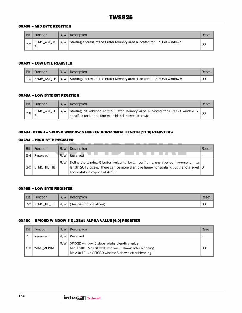
TW8825
164
0X488 – MID BYTE REGISTER
Bit Function R/W Description Reset
7-0 BFM5_AST_M
B
R/W Starting address of the Buffer Memory area allocated for SPIOSD window 5 00
0X489 – LOW BYTE REGISTER
Bit Function R/W Description Reset
7-0 BFM5_AST_LB R/W Starting address of the Buffer Memory area allocated for SPIOSD window 5 00
0X48A – LOW BYTE BIT REGISTER
Bit Function R/W Description Reset
7-6 BFM5_AST_LB
B
R/W Starting bit address of the Buffer Memory area allocated for SPIOSD window 5.
specifies one of the four even bit addresses in a byte 00
0X48A~0X48B – SPIOSD WINDOW 5 BUFFER HORIZONTAL LENGTH [11:0] REGISTERS
0X48A – HIGH BYTE REGISTER
Bit Function R/W Description Reset
5-4 Reserved R/W Reserved -
3-0 BFM5_HL_HB
R/W Define the Window 5 buffer horizontal length per frame, one pixel per increment; max
length 2048 pixels. There can be more than one frame horizontally, but the total pixel
horizontally is capped at 4095.
0
0X48B – LOW BYTE REGISTER
Bit Function R/W Description Reset
7-0 BFM5_HL_LB R/W (See description above) 00
0X48C – SPIOSD WINDOW 5 GLOBAL ALPHA VALUE [6:0] REGISTER
Bit Function R/W Description Reset
7 Reserved R/W Reserved -
6-0 WIN5_ALPHA
R/W SPIOSD window 5 global alpha blending value
Min: 0x00 Max SPIOSD window 5 shown after blending
Max: 0x7F No SPIOSD window 5 shown after blending
00
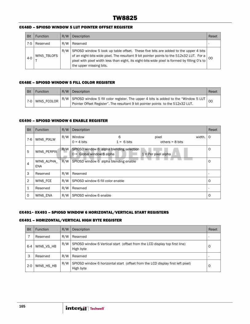
TW8825
165
0X48D – SPIOSD WINDOW 5 LUT POINTER OFFSET REGISTER
Bit Function R/W Description Reset
7-5 Reserved R/W Reserved -
4-0 WIN5_TBLOFS
T
R/W SPIOSD window 5 look up table offset. These five bits are added to the upper 4 bits
of an eight-bits-wide pixel. The resultant 9 bit pointer points to the 512x32 LUT. For a
pixel with pixel width less than eight, its eight-bits-wide pixel is formed by filling 0‟s to
the upper missing bits.
00
0X48E – SPIOSD WINDOW 5 FILL COLOR REGISTER
Bit Function R/W Description Reset
7-0 WIN5_FCOLOR R/W SPIOSD window 5 fill color register. The upper 4 bits is added to the “Window 5 LUT
Pointer Offset Register”. The resultant 9 bit pointer points to the 512x32 LUT. 00
0X490 – SPIOSD WINDOW 6 ENABLE REGISTER
Bit Function R/W Description Reset
7-6 WIN6_PIXLW R/W Window 6 pixel width.
0 = 4 bits 1 = 6 bits others = 8 bits
0
5 WIN6_PERPIX R/W SPIOSD window 6 alpha blending selection
0 = Global window 6 alpha 1 = Per pixel alpha
0
4 WIN6_ALPHA_
ENA
R/W SPIOSD window 6 alpha blending enable 0
3 Reserved R/W Reserved -
2 WIN6_FCE R/W SPIOSD window 6 fill color enable 0
1 Reserved R/W Reserved -
0 WIN6_ENA R/W SPIOSD window 6 enable 0
0X491~ 0X493 – SPIOSD WINDOW 6 HORIZONTAL/VERTICAL START REGISTERS
0X491 – HORIZONTAL/VERTICAL HIGH BYTE REGISTER
Bit Function R/W Description Reset
7 Reserved R/W Reserved -
6-4 WIN6_VS_HB R/W SPIOSD window 6 Vertical start (offset from the LCD display top first line)
High byte 0
3 Reserved R/W Reserved -
2-0 WIN6_HS_HB R/W SPIOSD window 6 horizontal start (offset from the LCD display first left pixel)
High byte 0

TW8825
166
0X492 – HORIZONTAL LOW BYTE REGISTER
Bit Function R/W Description Reset
7-0 WIN6_HS_LB R/W SPIOSD window 6 horizontal start (offset from the LCD display first left pixel)
Low byte 00
0X493 – VERTICAL LOW BYTE REGISTER
Bit Function R/W Description Reset
7-0 WIN6_VS_LB R/W SPIOSD window 6 Vertical start (offset from the LCD display top first line)
Low byte 00
0X494~0X496 – SPIOSD WINDOW 6 HORIZONTAL/VERTICAL LENGTH REGISTERS
0X494 – HORIZONTAL/ VERTICAL HIGH BYTE REGISTER
Bit Function R/W Description Reset
7-4 WIN6_VL_HB R/W SPIOSD window 6 vertical Length High byte
(one line per increment, minimum is 1, maximum is 2048) 0
3-0 WIN6_HL_HB R/W SPIOSD window 6 horizontal Length High byte
(one pixel per increment, minimum is 1, maximum is 2048) 0
0X495 – HORIZONTAL LOW BYTE REGISTER
Bit Function R/W Description Reset
7-0 WIN6_HL_LB R/W SPIOSD window 6 horizontal Length Low byte
(one pixel per increment, minimum is 1, maximum is 2048) 00
0X496 – VERTICAL LOW BYTE REGISTER
Bit Function R/W Description Reset
7-0 WIN6_VL_LB R/W SPIOSD window 6 vertical Length Low byte
(one line per increment, minimum is 1, maximum is 2048) 00
0X497~0X049A – SPIOSD WINDOW 6 BUFFER MEMORY STARTING ADDRESS [23:0] REGISTERS
0X0497 – HIGH BYTE REGISTER
Bit Function R/W Description Reset
7-0 BFM6_AST_HB R/W Starting address of the Buffer Memory area allocated for SPIOSD window 6; one byte
per increment 00

TW8825
167
0X498 – MID BYTE REGISTER
Bit Function R/W Description Reset
7-0 BFM6_AST_M
B
R/W Starting address of the Buffer Memory area allocated for SPIOSD window 6 00
0X499 – LOW BYTE REGISTER
Bit Function R/W Description Reset
7-0 BFM6_AST_LB R/W Starting address of the Buffer Memory area allocated for SPIOSD window 6 00
0X49A – LOW BYTE BIT REGISTER
Bit Function R/W Description Reset
7-6 BFM6_AST_LB
B
R/W Starting bit address of the Buffer Memory area allocated for SPIOSD window 6.
specifies one of the four even bit addresses in a byte 0
0X49A~0X49B – SPIOSD WINDOW 6 BUFFER HORIZONTAL LENGTH [11:0] REGISTERS
0X49A – HIGH BYTE REGISTER
Bit Function R/W Description Reset
5-4 Reserved R/W Reserved -
3-0 BFM6_HL_HB
R/W Define the Window 6 buffer horizontal length per frame, one pixel per increment; max
length 2048 pixels. There can be more than one frame horizontally, but the total pixel
horizontally is capped at 4095.
0
0X49B – LOW BYTE REGISTER
Bit Function R/W Description Reset
7-0 BFM6_HL_LB R/W (See description above) 0
0X49C – SPIOSD WINDOW 6 GLOBAL ALPHA VALUE [6:0] REGISTER
Bit Function R/W Description Reset
7 Reserved R/W Reserved -
6-0 WIN6_ALPHA
R/W SPIOSD window 6 global alpha blending value
Min: 0x00 Max SPIOSD window 6 shown after blending
Max: 0x7F No SPIOSD window 6 shown after blending
0

TW8825
168
0X49D – SPIOSD WINDOW 6 LUT POINTER OFFSET REGISTER
Bit Function R/W Description Reset
7-5 Reserved R/W Reserved -
4-0 WIN6_TBLOFS
T
R/W SPIOSD window 6 look up table offset. These five bits are added to the upper 4 bits
of an eight-bits-wide pixel. The resultant 9 bit pointer points to the 512x32 LUT. For a
pixel with pixel width less than eight, its eight-bits-wide pixel is formed by filling 0‟s to
the upper missing bits.
00
0X49E – SPIOSD WINDOW 6 FILL COLOR REGISTER
Bit Function R/W Description Reset
7-0 WIN6_FCOLOR R/W SPIOSD window 6 fill color register. The upper 4 bits is added to the “Window 6 LUT
Pointer Offset Register”. The resultant 9 bit pointer points to the 512x32 LUT. 00
0X4A0 – SPIOSD WINDOW 7 ENABLE REGISTER
Bit Function R/W Description Reset
7-6 WIN7_PIXLW R/W Window 7 pixel width.
0 = 4 bits 1 = 6 bits others = 8 bits
0
5 WIN7_PERPIX R/W SPIOSD window 7 alpha blending selection
0 = Global window 7 alpha 1 = Per pixel alpha
0
4 WIN7_ALPHA_
ENA
R/W SPIOSD window 7 alpha blending enable 0
3 Reserved R/W Reserved -
2 WIN7_FCE R/W SPIOSD window 7 fill color enable 0
1 Reserved R/W Reserved -
0 WIN7_ENA R/W SPIOSD window 7 ( enable 0
0X4A1~ 0X4A3 – SPIOSD WINDOW 7 HORIZONTAL/VERTICAL START REGISTERS
0X4A1 – HORIZONTAL/VERTICAL HIGH BYTE REGISTER
Bit Function R/W Description Reset
7 Reserved R/W Reserved -
6-4 WIN7_VS_HB R/W SPIOSD window 7 Vertical start (offset from the LCD display top first line)
High byte 0
3 Reserved R/W Reserved -
2-0 WIN7_HS_HB R/W SPIOSD window 7 horizontal start (offset from the LCD display first left pixel)
High byte 0

TW8825
169
0X4A2 – HORIZONTAL LOW BYTE REGISTER
Bit Function R/W Description Reset
7-0 WIN7_HS_LB R/W SPIOSD window 7 horizontal start (offset from the LCD display first left pixel)
Low byte 00
0X4A3 – VERTICAL LOW BYTE REGISTER
Bit Function R/W Description Reset
7-0 WIN7_VS_LB R/W SPIOSD window 7 Vertical start (offset from the LCD display top first line)
Low byte 00
0X4A4~0X4A6 – SPIOSD WINDOW 7 HORIZONTAL/VERTICAL LENGTH REGISTERS
0X4A4 – HORIZONTAL/ VERTICAL HIGH BYTE REGISTER
Bit Function R/W Description Reset
7-4 WIN7_VL_HB R/W SPIOSD window 7 vertical Length High byte
(one line per increment, minimum is 1, maximum is 2048) 0
3-0 WIN7_HL_HB R/W SPIOSD window 7 horizontal Length High byte
(one pixel per increment, minimum is 1, maximum is 2048) 0
0X4A5 – HORIZONTAL LOW BYTE REGISTER
Bit Function R/W Description Reset
7-0 WIN7_HL_LB R/W SPIOSD window 7 horizontal Length Low byte
(one pixel per increment, minimum is 1, maximum is 2048) 00
0X4A6 – VERTICAL LOW BYTE REGISTER
Bit Function R/W Description Reset
7-0 WIN7_VL_LB R/W SPIOSD window 7 vertical Length Low byte
(one line per increment, minimum is 1, maximum is 2048) 00
0X4A7~0X04AA – SPIOSD WINDOW 7 BUFFER MEMORY STARTING ADDRESS [23:0] REGISTERS
0X04A7 – HIGH BYTE REGISTER
Bit Function R/W Description Reset
7-0 BFM7_AST_HB R/W Starting address of the Buffer Memory area allocated for SPIOSD window 7; one byte
per increment 00

TW8825
170
0X4A8 – MID BYTE REGISTER
Bit Function R/W Description Reset
7-0 BFM7_AST_M
B
R/W Starting address of the Buffer Memory area allocated for SPIOSD window 7 00
0X4A9 – LOW BYTE REGISTER
Bit Function R/W Description Reset
7-0 BFM7_AST_LB R/W Starting address of the Buffer Memory area allocated for SPIOSD window 7 00
0X4AA – LOW BYTE BIT REGISTER
Bit Function R/W Description Reset
7-6 BFM7_AST_LB
B
R/W Starting bit address of the Buffer Memory area allocated for SPIOSD window 7.
specifies one of the four even bit addresses in a byte 0
0X4AA~0X4AB – SPIOSD WINDOW 7 BUFFER HORIZONTAL LENGTH [11:0] REGISTERS
0X4AA – HIGH BYTE REGISTER
Bit Function R/W Description Reset
5-4 Reserved R/W Reserved -
3-0 BFM7_HL_HB
R/W Define the Window 7 buffer horizontal length per frame, one pixel per increment; max
length 2048 pixels. There can be more than one frame horizontally, but the total pixel
horizontally is capped at 4095.
0
0X4AB – LOW BYTE REGISTER
Bit Function R/W Description Reset
7-0 BFM7_HL_LB R/W (See description above) 00
0X4AC – SPIOSD WINDOW 7 GLOBAL ALPHA VALUE [6:0] REGISTER
Bit Function R/W Description Reset
7 Reserved R/W Reserved -
6-0 WIN7_ALPHA
R/W SPIOSD window 7 global alpha blending value
Min: 0x00 Max SPIOSD window 7 shown after blending
Max: 0x7F No SPIOSD window 7 shown after blending
00

TW8825
171
0X4AD – SPIOSD WINDOW 7 LUT POINTER OFFSET REGISTER
Bit Function R/W Description Reset
7-5 Reserved R/W Reserved -
4-0 WIN7_TBLOFS
T
R/W SPIOSD window 7 look up table offset. These five bits are added to the upper 4 bits
of an eight-bits-wide pixel. The resultant 9 bit pointer points to the 512x32 LUT. For a
pixel with pixel width less than eight, its eight-bits-wide pixel is formed by filling 0‟s to
the upper missing bits.
00
0X4AE – SPIOSD WINDOW 7 FILL COLOR REGISTER
Bit Function R/W Description Reset
7-0 WIN7_FCOLOR R/W SPIOSD window 7 fill color register. The upper 4 bits is added to the “Window 7 LUT
Pointer Offset Register”. The resultant 9 bit pointer points to the 512x32 LUT. 00
0X4B0 – SPIOSD WINDOW 8 ENABLE REGISTER
Bit Function R/W Description Reset
7-6 WIN8_PIXLW R/W Window 8 pixel width.
0 = 4 bits 1 = 6 bits others = 8 bits
0
5 WIN8_PERPIX R/W SPIOSD window 8 alpha blending selection
0 = Global window 1 alpha 1 = Per pixel alpha
0
4 WIN8_ALPHA_
ENA
R/W SPIOSD window 8 alpha blending enable 0
3 Reserved R/W Reserved -
2 WIN8_FCE R/W SPIOSD window 8 fill color enable 0
1 Reserved R/W Reserved -
0 WIN8_ENA R/W SPIOSD window 8 enable 0
0X4B1~ 0X4B3 – SPIOSD WINDOW 8 HORIZONTAL/VERTICAL START REGISTERS
0X4B1 – HORIZONTAL/VERTICAL HIGH BYTE REGISTER
Bit Function R/W Description Reset
7 Reserved R/W Reserved -
6-4 WIN8_VS_HB R/W SPIOSD window 8 Vertical start (offset from the LCD display top first line)
High byte 0
3 Reserved R/W Reserved -
2-0 WIN8_HS_HB R/W SPIOSD window 8 horizontal start (offset from the LCD display first left pixel)
High byte 0
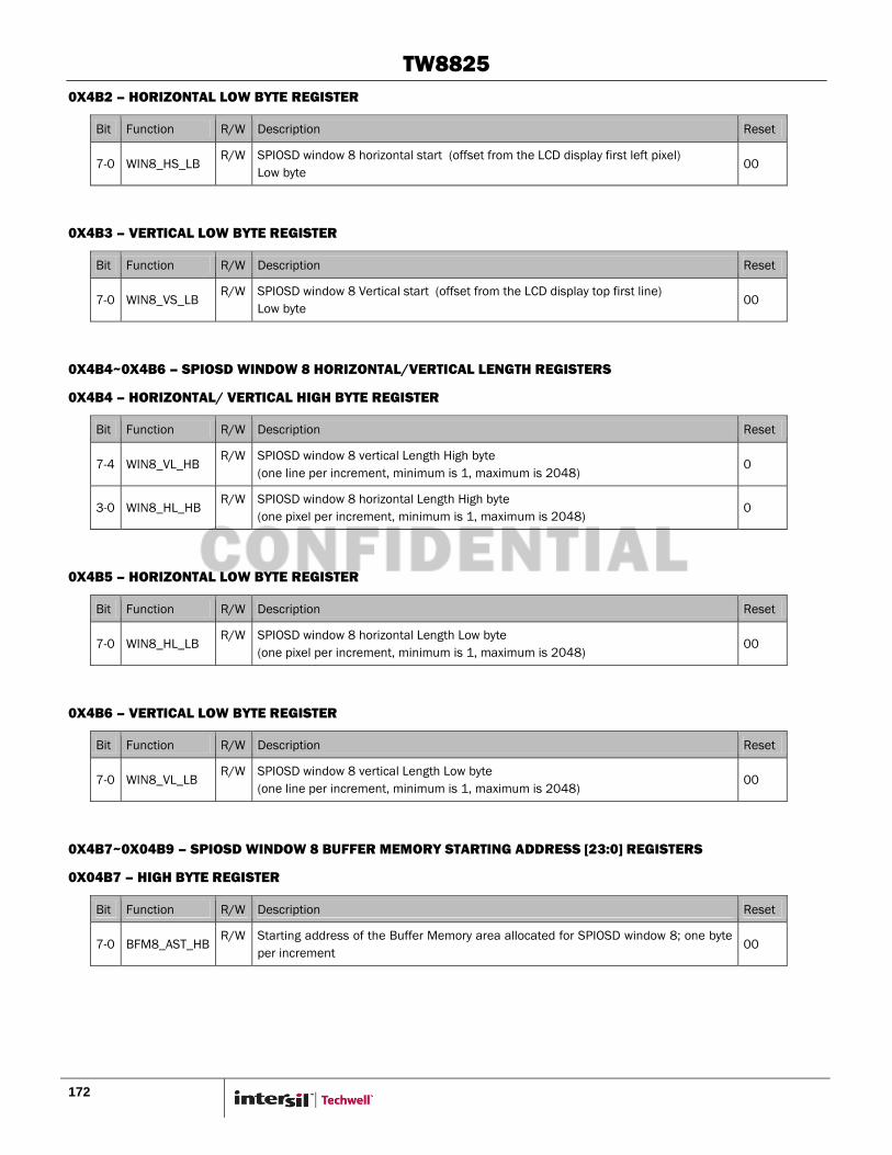
TW8825
172
0X4B2 – HORIZONTAL LOW BYTE REGISTER
Bit Function R/W Description Reset
7-0 WIN8_HS_LB R/W SPIOSD window 8 horizontal start (offset from the LCD display first left pixel)
Low byte 00
0X4B3 – VERTICAL LOW BYTE REGISTER
Bit Function R/W Description Reset
7-0 WIN8_VS_LB R/W SPIOSD window 8 Vertical start (offset from the LCD display top first line)
Low byte 00
0X4B4~0X4B6 – SPIOSD WINDOW 8 HORIZONTAL/VERTICAL LENGTH REGISTERS
0X4B4 – HORIZONTAL/ VERTICAL HIGH BYTE REGISTER
Bit Function R/W Description Reset
7-4 WIN8_VL_HB R/W SPIOSD window 8 vertical Length High byte
(one line per increment, minimum is 1, maximum is 2048) 0
3-0 WIN8_HL_HB R/W SPIOSD window 8 horizontal Length High byte
(one pixel per increment, minimum is 1, maximum is 2048) 0
0X4B5 – HORIZONTAL LOW BYTE REGISTER
Bit Function R/W Description Reset
7-0 WIN8_HL_LB R/W SPIOSD window 8 horizontal Length Low byte
(one pixel per increment, minimum is 1, maximum is 2048) 00
0X4B6 – VERTICAL LOW BYTE REGISTER
Bit Function R/W Description Reset
7-0 WIN8_VL_LB R/W SPIOSD window 8 vertical Length Low byte
(one line per increment, minimum is 1, maximum is 2048) 00
0X4B7~0X04B9 – SPIOSD WINDOW 8 BUFFER MEMORY STARTING ADDRESS [23:0] REGISTERS
0X04B7 – HIGH BYTE REGISTER
Bit Function R/W Description Reset
7-0 BFM8_AST_HB R/W Starting address of the Buffer Memory area allocated for SPIOSD window 8; one byte
per increment 00
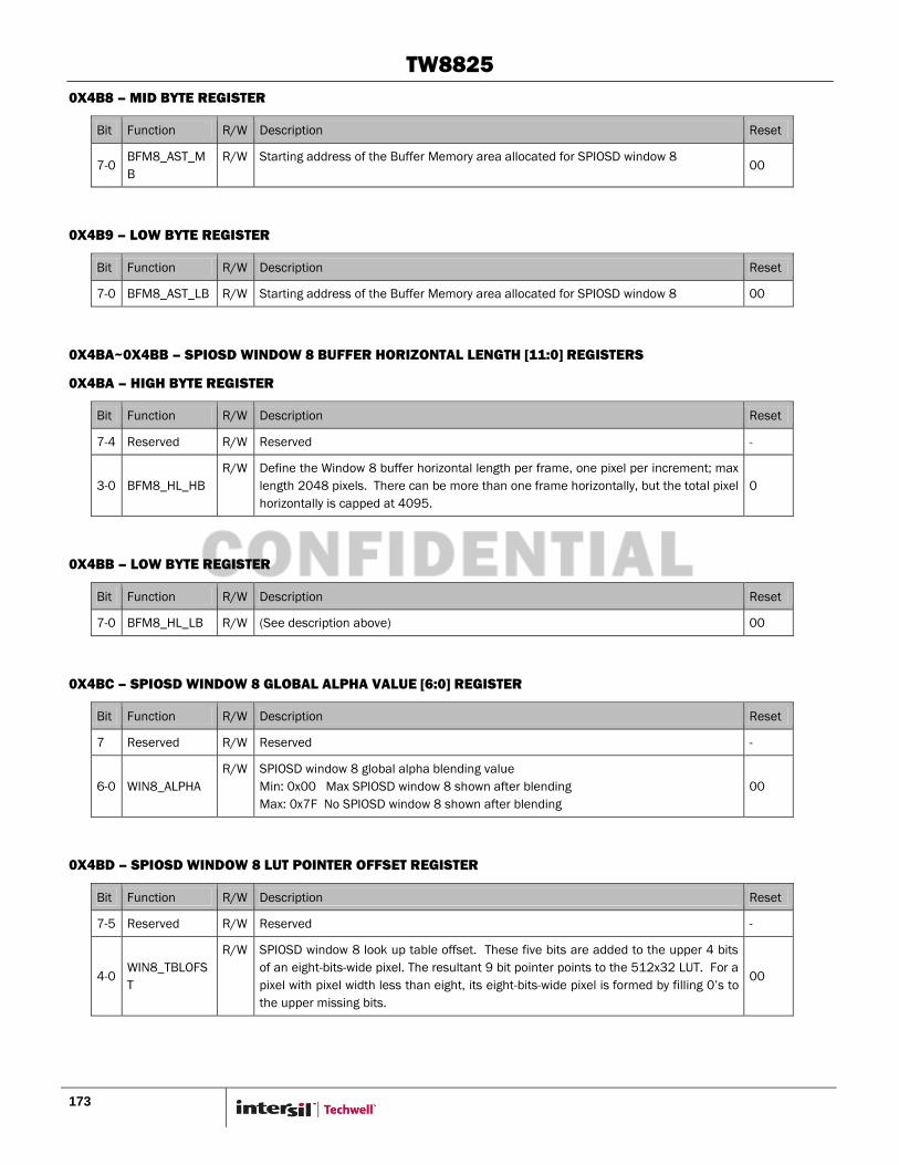
TW8825
173
0X4B8 – MID BYTE REGISTER
Bit Function R/W Description Reset
7-0 BFM8_AST_M
B
R/W Starting address of the Buffer Memory area allocated for SPIOSD window 8 00
0X4B9 – LOW BYTE REGISTER
Bit Function R/W Description Reset
7-0 BFM8_AST_LB R/W Starting address of the Buffer Memory area allocated for SPIOSD window 8 00
0X4BA~0X4BB – SPIOSD WINDOW 8 BUFFER HORIZONTAL LENGTH [11:0] REGISTERS
0X4BA – HIGH BYTE REGISTER
Bit Function R/W Description Reset
7-4 Reserved R/W Reserved -
3-0 BFM8_HL_HB
R/W Define the Window 8 buffer horizontal length per frame, one pixel per increment; max
length 2048 pixels. There can be more than one frame horizontally, but the total pixel
horizontally is capped at 4095.
0
0X4BB – LOW BYTE REGISTER
Bit Function R/W Description Reset
7-0 BFM8_HL_LB R/W (See description above) 00
0X4BC – SPIOSD WINDOW 8 GLOBAL ALPHA VALUE [6:0] REGISTER
Bit Function R/W Description Reset
7 Reserved R/W Reserved -
6-0 WIN8_ALPHA
R/W SPIOSD window 8 global alpha blending value
Min: 0x00 Max SPIOSD window 8 shown after blending
Max: 0x7F No SPIOSD window 8 shown after blending
00
0X4BD – SPIOSD WINDOW 8 LUT POINTER OFFSET REGISTER
Bit Function R/W Description Reset
7-5 Reserved R/W Reserved -
4-0 WIN8_TBLOFS
T
R/W SPIOSD window 8 look up table offset. These five bits are added to the upper 4 bits
of an eight-bits-wide pixel. The resultant 9 bit pointer points to the 512x32 LUT. For a
pixel with pixel width less than eight, its eight-bits-wide pixel is formed by filling 0‟s to
the upper missing bits.
00

TW8825
174
0X4BE – SPIOSD WINDOW 8 FILL COLOR REGISTER
Bit Function R/W Description Reset
7-0 WIN8_FCOLOR R/W SPIOSD window 8 fill color register. The upper 4 bits is added to the “Window 8 LUT
Pointer Offset Register”. The resultant 9 bit pointer points to the 512x32 LUT. 00
SPI & MCU
0X4C0 – SPI FLASH MODE CONTROL REGISTER
Bit Function R/W Description Reset
7-3 Reserved R/W Reserved -
2-0 SPI_RD_MODE R/W SPI Flash Read Mode
0 = slow 1 = fast 2 = dual 3 = quad
4 = dual-io 5 = quad-io 6 = d-quad 7 = N/A
0
0X4C1 -- SPI FLASH MODE CONTROL REGISTER
Bit Function R/W Description Reset
7-1 Reserved R/W Reserved -
0 DMA_NONV R/W Start mode
0 = Immediately 1 = At vertical blank
0
0X4C3 – DMA CONTROL REGISTER
Bit Function R/W Description Reset
7-6 REG_MEM R/W DMA Read/Write destination
0 = Font RAM 1 = Chip Register
2 = SPIOSD LUT 3 = MCU XMEM
1
5-4 DMA_REG_MOD
E
R/W Read/Write access mode
0 = Increase 1 = Decrease
2 = Fix 3 = Reserved
0
3-0 WR_CNT_NUM R/W Command write byte count 0
0X4C4 – FLASH BUSY CONTROL REGISTER
Bit Function R/W Description Reset
7 MCUEN R MCU Status 0=Disabled 1=Enabled -
6 ISPEN R ISP Status 0=Disabled 1=Enabled -
5-3 Reserved R/W Reserved -
2 BUSY_CHECK R/W Busy check
0 = No busy check
1 = Busy check after command. Wait until busy is cleared
0
1 WR_MODE R/W SPI DMA/CMD Mode
0 = Read, 1 = Write
0
0 DMA_STR R/W Start command execution. Self cleared.
Write „1‟ = Start Write „0‟ = Stop
Read „1‟ = Busy Read „0‟ = Ready
0
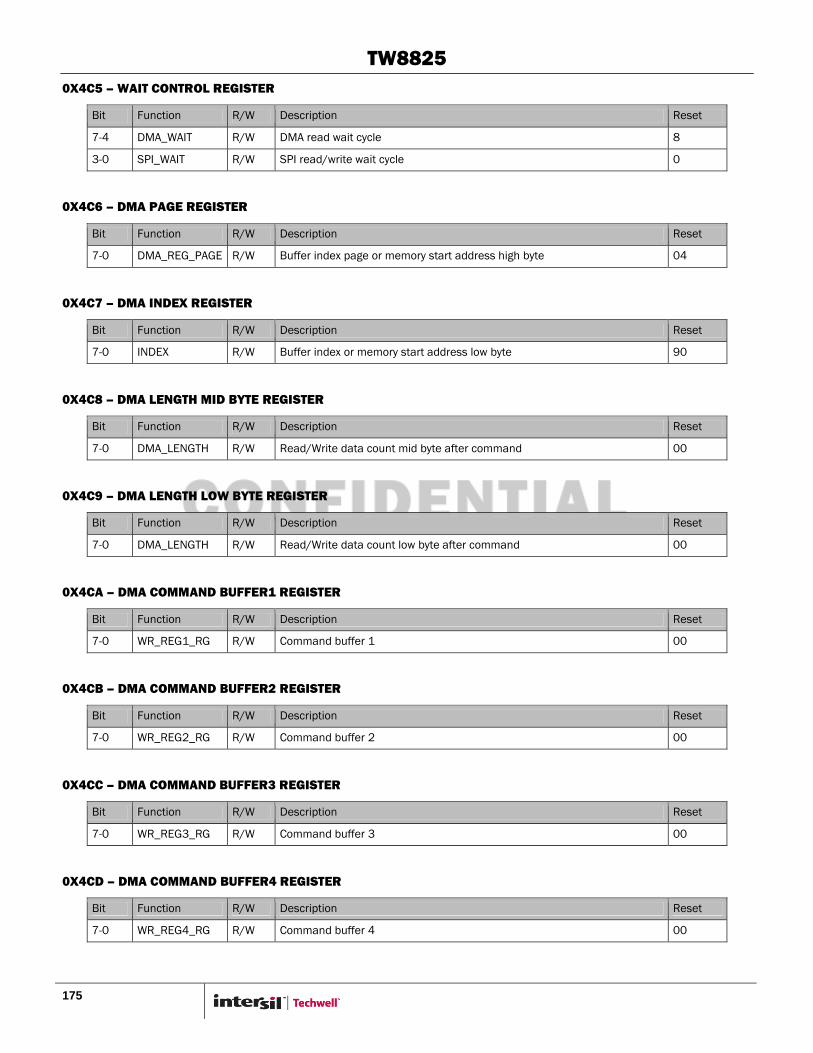
TW8825
175
0X4C5 – WAIT CONTROL REGISTER
Bit Function R/W Description Reset
7-4 DMA_WAIT R/W DMA read wait cycle 8
3-0 SPI_WAIT R/W SPI read/write wait cycle 0
0X4C6 – DMA PAGE REGISTER
Bit Function R/W Description Reset
7-0 DMA_REG_PAGE R/W Buffer index page or memory start address high byte 04
0X4C7 – DMA INDEX REGISTER
Bit Function R/W Description Reset
7-0 INDEX R/W Buffer index or memory start address low byte 90
0X4C8 – DMA LENGTH MID BYTE REGISTER
Bit Function R/W Description Reset
7-0 DMA_LENGTH R/W Read/Write data count mid byte after command 00
0X4C9 – DMA LENGTH LOW BYTE REGISTER
Bit Function R/W Description Reset
7-0 DMA_LENGTH R/W Read/Write data count low byte after command 00
0X4CA – DMA COMMAND BUFFER1 REGISTER
Bit Function R/W Description Reset
7-0 WR_REG1_RG R/W Command buffer 1 00
0X4CB – DMA COMMAND BUFFER2 REGISTER
Bit Function R/W Description Reset
7-0 WR_REG2_RG R/W Command buffer 2 00
0X4CC – DMA COMMAND BUFFER3 REGISTER
Bit Function R/W Description Reset
7-0 WR_REG3_RG R/W Command buffer 3 00
0X4CD – DMA COMMAND BUFFER4 REGISTER
Bit Function R/W Description Reset
7-0 WR_REG4_RG R/W Command buffer 4 00
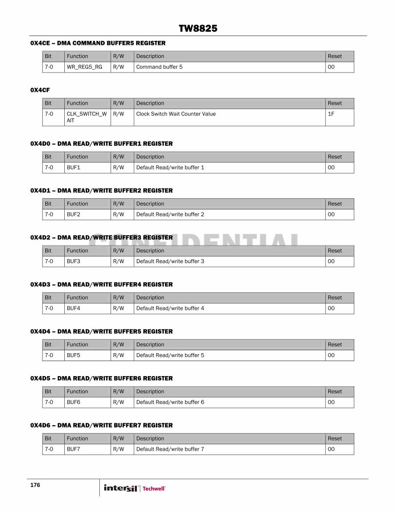
TW8825
176
0X4CE – DMA COMMAND BUFFER5 REGISTER
Bit Function R/W Description Reset
7-0 WR_REG5_RG R/W Command buffer 5 00
0X4CF
Bit Function R/W Description Reset
7-0 CLK_SWITCH_W
AIT
R/W Clock Switch Wait Counter Value 1F
0X4D0 – DMA READ/WRITE BUFFER1 REGISTER
Bit Function R/W Description Reset
7-0 BUF1 R/W Default Read/write buffer 1 00
0X4D1 – DMA READ/WRITE BUFFER2 REGISTER
Bit Function R/W Description Reset
7-0 BUF2 R/W Default Read/write buffer 2 00
0X4D2 – DMA READ/WRITE BUFFER3 REGISTER
Bit Function R/W Description Reset
7-0 BUF3 R/W Default Read/write buffer 3 00
0X4D3 – DMA READ/WRITE BUFFER4 REGISTER
Bit Function R/W Description Reset
7-0 BUF4 R/W Default Read/write buffer 4 00
0X4D4 – DMA READ/WRITE BUFFER5 REGISTER
Bit Function R/W Description Reset
7-0 BUF5 R/W Default Read/write buffer 5 00
0X4D5 – DMA READ/WRITE BUFFER6 REGISTER
Bit Function R/W Description Reset
7-0 BUF6 R/W Default Read/write buffer 6 00
0X4D6 – DMA READ/WRITE BUFFER7 REGISTER
Bit Function R/W Description Reset
7-0 BUF7 R/W Default Read/write buffer 7 00
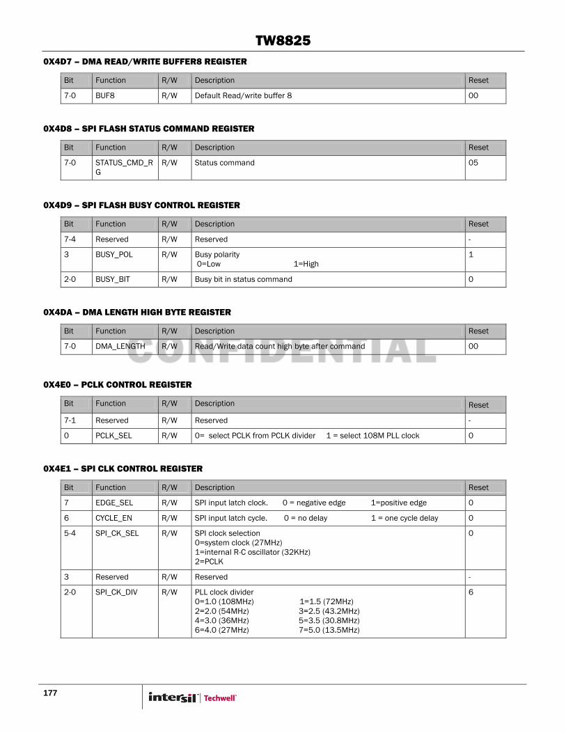
TW8825
177
0X4D7 – DMA READ/WRITE BUFFER8 REGISTER
Bit Function R/W Description Reset
7-0 BUF8 R/W Default Read/write buffer 8 00
0X4D8 – SPI FLASH STATUS COMMAND REGISTER
Bit Function R/W Description Reset
7-0 STATUS_CMD_R
G
R/W Status command 05
0X4D9 – SPI FLASH BUSY CONTROL REGISTER
Bit Function R/W Description Reset
7-4 Reserved R/W Reserved -
3 BUSY_POL R/W Busy polarity
0=Low 1=High
1
2-0 BUSY_BIT R/W Busy bit in status command 0
0X4DA – DMA LENGTH HIGH BYTE REGISTER
Bit Function R/W Description Reset
7-0 DMA_LENGTH R/W Read/Write data count high byte after command 00
0X4E0 – PCLK CONTROL REGISTER
Bit Function R/W Description Reset
7-1 Reserved R/W Reserved -
0 PCLK_SEL R/W 0= select PCLK from PCLK divider 1 = select 108M PLL clock 0
0X4E1 – SPI CLK CONTROL REGISTER
Bit Function R/W Description Reset
7 EDGE_SEL R/W SPI input latch clock. 0 = negative edge 1=positive edge 0
6 CYCLE_EN R/W SPI input latch cycle. 0 = no delay 1 = one cycle delay 0
5-4 SPI_CK_SEL R/W SPI clock selection
0=system clock (27MHz)
1=internal R-C oscillator (32KHz)
2=PCLK
0
3 Reserved R/W Reserved -
2-0 SPI_CK_DIV R/W PLL clock divider
0=1.0 (108MHz) 1=1.5 (72MHz)
2=2.0 (54MHz) 3=2.5 (43.2MHz)
4=3.0 (36MHz) 5=3.5 (30.8MHz)
6=4.0 (27MHz) 7=5.0 (13.5MHz)
6
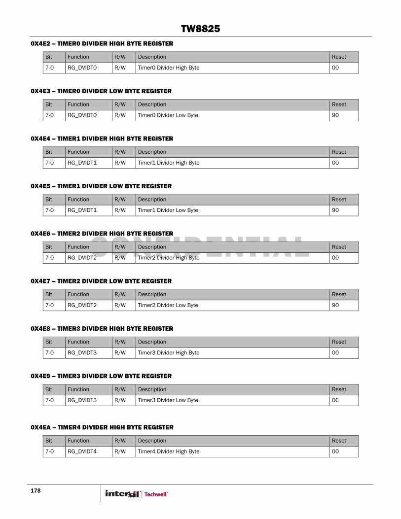
TW8825
178
0X4E2 – TIMER0 DIVIDER HIGH BYTE REGISTER
Bit Function R/W Description Reset
7-0 RG_DVIDT0 R/W Timer0 Divider High Byte 00
0X4E3 – TIMER0 DIVIDER LOW BYTE REGISTER
Bit Function R/W Description Reset
7-0 RG_DVIDT0 R/W Timer0 Divider Low Byte 90
0X4E4 – TIMER1 DIVIDER HIGH BYTE REGISTER
Bit Function R/W Description Reset
7-0 RG_DVIDT1 R/W Timer1 Divider High Byte 00
0X4E5 – TIMER1 DIVIDER LOW BYTE REGISTER
Bit Function R/W Description Reset
7-0 RG_DVIDT1 R/W Timer1 Divider Low Byte 90
0X4E6 – TIMER2 DIVIDER HIGH BYTE REGISTER
Bit Function R/W Description Reset
7-0 RG_DVIDT2 R/W Timer2 Divider High Byte 00
0X4E7 – TIMER2 DIVIDER LOW BYTE REGISTER
Bit Function R/W Description Reset
7-0 RG_DVIDT2 R/W Timer2 Divider Low Byte 90
0X4E8 – TIMER3 DIVIDER HIGH BYTE REGISTER
Bit Function R/W Description Reset
7-0 RG_DVIDT3 R/W Timer3 Divider High Byte 00
0X4E9 – TIMER3 DIVIDER LOW BYTE REGISTER
Bit Function R/W Description Reset
7-0 RG_DVIDT3 R/W Timer3 Divider Low Byte 0C
0X4EA – TIMER4 DIVIDER HIGH BYTE REGISTER
Bit Function R/W Description Reset
7-0 RG_DVIDT4 R/W Timer4 Divider High Byte 00
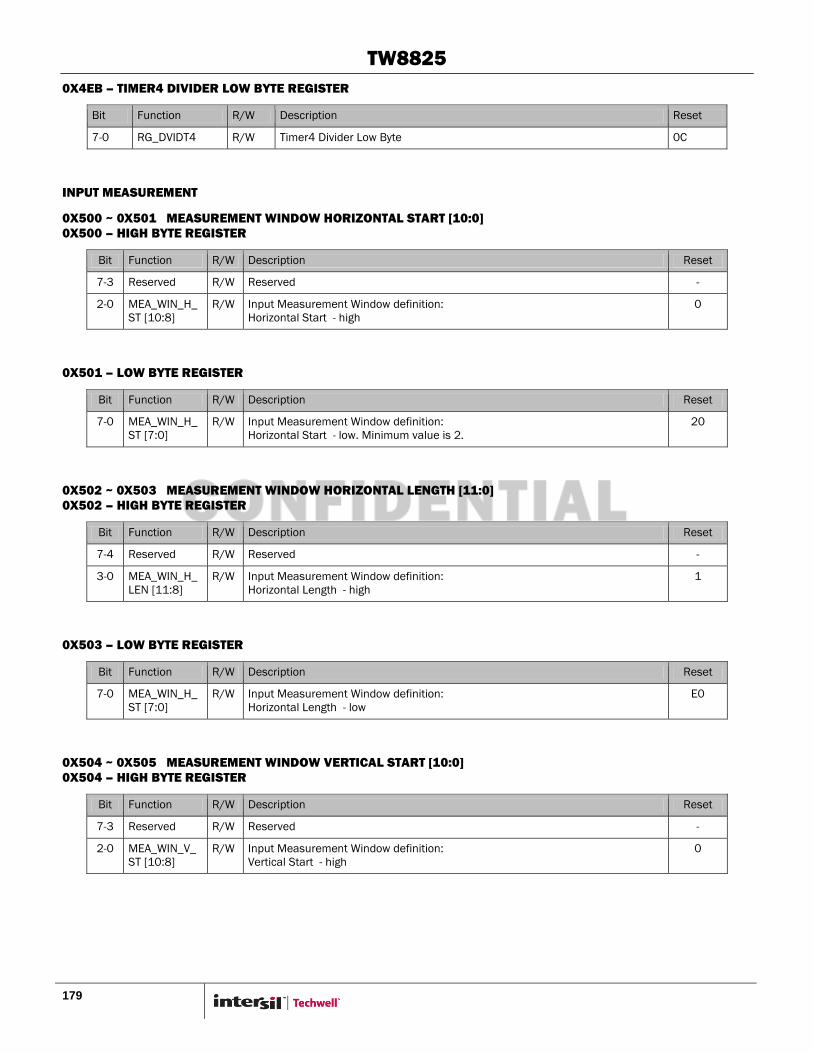
TW8825
179
0X4EB – TIMER4 DIVIDER LOW BYTE REGISTER
Bit Function R/W Description Reset
7-0 RG_DVIDT4 R/W Timer4 Divider Low Byte 0C
INPUT MEASUREMENT
0X500 ~ 0X501 MEASUREMENT WINDOW HORIZONTAL START [10:0]
0X500 – HIGH BYTE REGISTER
Bit Function R/W Description Reset
7-3 Reserved R/W Reserved -
2-0 MEA_WIN_H_
ST [10:8]
R/W Input Measurement Window definition:
Horizontal Start - high
0
0X501 – LOW BYTE REGISTER
Bit Function R/W Description Reset
7-0 MEA_WIN_H_
ST [7:0]
R/W Input Measurement Window definition:
Horizontal Start - low. Minimum value is 2.
20
0X502 ~ 0X503 MEASUREMENT WINDOW HORIZONTAL LENGTH [11:0]
0X502 – HIGH BYTE REGISTER
Bit Function R/W Description Reset
7-4 Reserved R/W Reserved -
3-0 MEA_WIN_H_
LEN [11:8]
R/W Input Measurement Window definition:
Horizontal Length - high
1
0X503 – LOW BYTE REGISTER
Bit Function R/W Description Reset
7-0 MEA_WIN_H_
ST [7:0]
R/W Input Measurement Window definition:
Horizontal Length - low
E0
0X504 ~ 0X505 MEASUREMENT WINDOW VERTICAL START [10:0]
0X504 – HIGH BYTE REGISTER
Bit Function R/W Description Reset
7-3 Reserved R/W Reserved -
2-0 MEA_WIN_V_
ST [10:8]
R/W Input Measurement Window definition:
Vertical Start - high
0
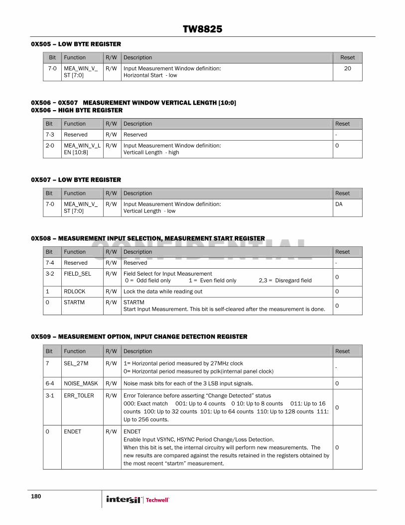
TW8825
180
0X505 – LOW BYTE REGISTER
Bit Function R/W Description Reset
7-0 MEA_WIN_V_
ST [7:0]
R/W Input Measurement Window definition:
Horizontal Start - low
20
0X506 ~ 0X507 MEASUREMENT WINDOW VERTICAL LENGTH [10:0]
0X506 – HIGH BYTE REGISTER
Bit Function R/W Description Reset
7-3 Reserved R/W Reserved -
2-0 MEA_WIN_V_L
EN [10:8]
R/W Input Measurement Window definition:
Verticall Length - high
0
0X507 – LOW BYTE REGISTER
Bit Function R/W Description Reset
7-0 MEA_WIN_V_
ST [7:0]
R/W Input Measurement Window definition:
Vertical Length - low
DA
0X508 – MEASUREMENT INPUT SELECTION, MEASUREMENT START REGISTER
Bit Function R/W Description Reset
7-4 Reserved R/W Reserved -
3-2 FIELD_SEL R/W Field Select for Input Measurement
0 = Odd field only 1 = Even field only 2,3 = Disregard field 0
1 RDLOCK R/W Lock the data while reading out 0
0 STARTM R/W STARTM
Start Input Measurement. This bit is self-cleared after the measurement is done. 0
0X509 – MEASUREMENT OPTION, INPUT CHANGE DETECTION REGISTER
Bit Function R/W Description Reset
7 SEL_27M R/W 1= Horizontal period measured by 27MHz clock
0= Horizontal period measured by pclk(internal panel clock) -
6-4 NOISE_MASK R/W Noise mask bits for each of the 3 LSB input signals. 0
3-1 ERR_TOLER R/W Error Tolerance before asserting “Change Detected” status
000: Exact match 001: Up to 4 counts 0 10: Up to 8 counts 011: Up to 16
counts 100: Up to 32 counts 101: Up to 64 counts 110: Up to 128 counts 111:
Up to 256 counts.
0
0 ENDET R/W ENDET
Enable Input VSYNC, HSYNC Period Change/Loss Detection.
When this bit is set, the internal circuitry will perform new measurements. The
new results are compared against the results retained in the registers obtained by
the most recent “startm” measurement.
0
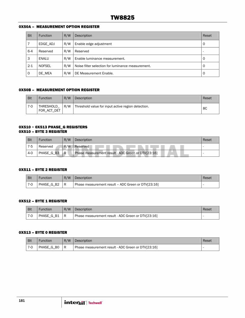
TW8825
181
0X50A – MEASUREMENT OPTION REGISTER
Bit Function R/W Description Reset
7 EDGE_ADJ R/W Enable edge adjustment 0
6-4 Reserved R/W Reserved -
3 ENALU R/W Enable luminance measurement. 0
2-1 NOFSEL R/W Noise filter selection for luminance measurement. 0
0 DE_MEA R/W DE Measurement Enable. 0
0X50B – MEASUREMENT OPTION REGISTER
Bit Function R/W Description Reset
7-0 THRESHOLD_
FOR_ACT_DET
R/W Threshold value for input active region detection. 8C
0X510 ~ 0X513 PHASE_G REGISTERS
0X510 – BYTE 3 REGISTER
Bit Function R/W Description Reset
7-5 Reserved R/W Reserved -
4-0 PHASE_G_B3 R Phase measurement result - ADC Green or DTV[23:16] -
0X511 – BYTE 2 REGISTER
Bit Function R/W Description Reset
7-0 PHASE_G_B2 R Phase measurement result – ADC Green or DTV[23:16] -
0X512 – BYTE 1 REGISTER
Bit Function R/W Description Reset
7-0 PHASE_G_B1 R Phase measurement result - ADC Green or DTV[23:16] -
0X513 – BYTE 0 REGISTER
Bit Function R/W Description Reset
7-0 PHASE_G_B0 R Phase measurement result - ADC Green or DTV[23:16] -
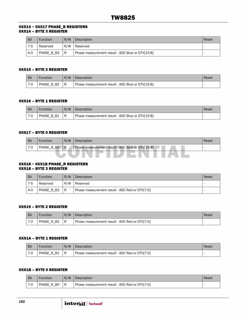
TW8825
182
0X514 ~ 0X517 PHASE_B REGISTERS
0X514 – BYTE 3 REGISTER
Bit Function R/W Description Reset
7-5 Reserved R/W Reserved -
4-0 PHASE_B_B3 R Phase measurement result - ADC Blue or DTV[15:8] -
0X515 – BYTE 2 REGISTER
Bit Function R/W Description Reset
7-0 PHASE_B_B2 R Phase measurement result - ADC Blue or DTV[15:8] -
0X516 – BYTE 1 REGISTER
Bit Function R/W Description Reset
7-0 PHASE_B_B1 R Phase measurement result - ADC Blue or DTV[15:8] -
0X517 – BYTE 0 REGISTER
Bit Function R/W Description Reset
7-0 PHASE_B_B0 R Phase measurement result - ADC Blue or DTV[15:8] -
0X518 ~ 0X51B PHASE_R REGISTERS
0X518 – BYTE 3 REGISTER
Bit Function R/W Description Reset
7-5 Reserved R/W Reserved -
4-0 PHASE_R_B3 R Phase measurement result - ADC Red or DTV[7:0] -
0X519 – BYTE 2 REGISTER
Bit Function R/W Description Reset
7-0 PHASE_R_B2 R Phase measurement result - ADC Red or DTV[7:0] -
0X51A – BYTE 1 REGISTER
Bit Function R/W Description Reset
7-0 PHASE_R_B1 R Phase measurement result - ADC Red or DTV[7:0] -
0X51B – BYTE 0 REGISTER
Bit Function R/W Description Reset
7-0 PHASE_R_B0 R Phase measurement result - ADC Red or DTV[7:0] -
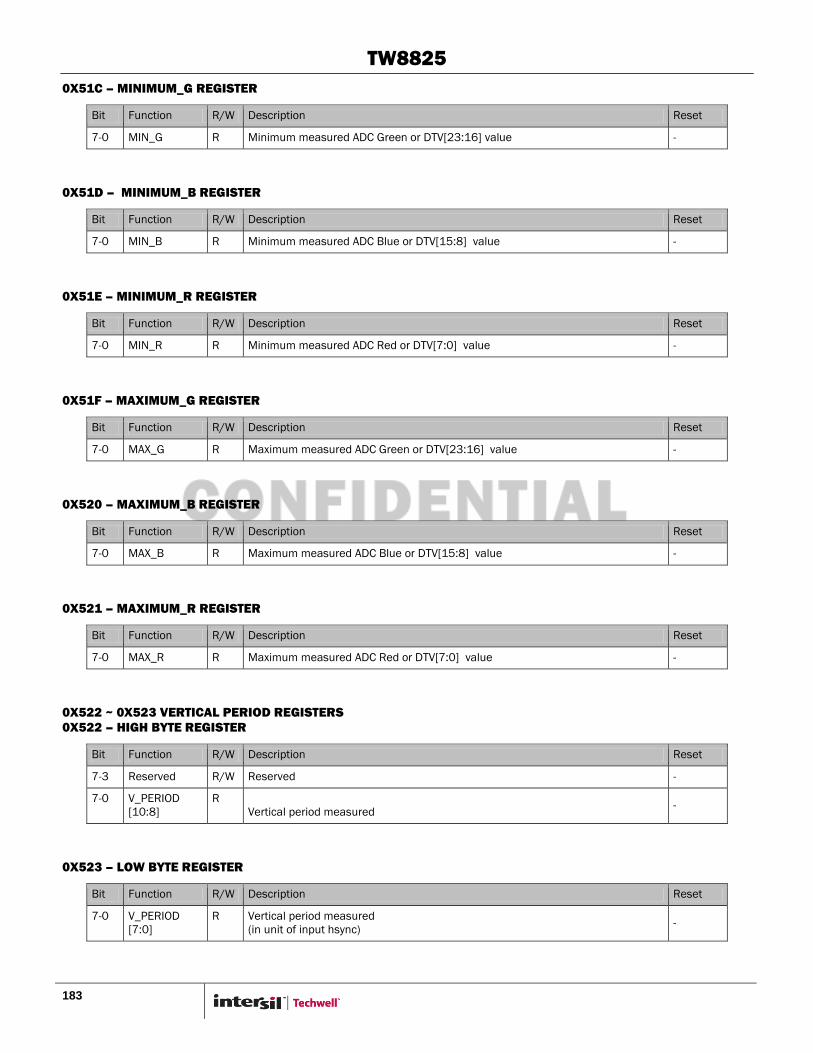
TW8825
183
0X51C – MINIMUM_G REGISTER
Bit Function R/W Description Reset
7-0 MIN_G R Minimum measured ADC Green or DTV[23:16] value -
0X51D – MINIMUM_B REGISTER
Bit Function R/W Description Reset
7-0 MIN_B R Minimum measured ADC Blue or DTV[15:8] value -
0X51E – MINIMUM_R REGISTER
Bit Function R/W Description Reset
7-0 MIN_R R Minimum measured ADC Red or DTV[7:0] value -
0X51F – MAXIMUM_G REGISTER
Bit Function R/W Description Reset
7-0 MAX_G R Maximum measured ADC Green or DTV[23:16] value -
0X520 – MAXIMUM_B REGISTER
Bit Function R/W Description Reset
7-0 MAX_B R Maximum measured ADC Blue or DTV[15:8] value -
0X521 – MAXIMUM_R REGISTER
Bit Function R/W Description Reset
7-0 MAX_R R Maximum measured ADC Red or DTV[7:0] value -
0X522 ~ 0X523 VERTICAL PERIOD REGISTERS
0X522 – HIGH BYTE REGISTER
Bit Function R/W Description Reset
7-3 Reserved R/W Reserved -
7-0 V_PERIOD
[10:8]
R
Vertical period measured -
0X523 – LOW BYTE REGISTER
Bit Function R/W Description Reset
7-0 V_PERIOD
[7:0]
R Vertical period measured
(in unit of input hsync) -
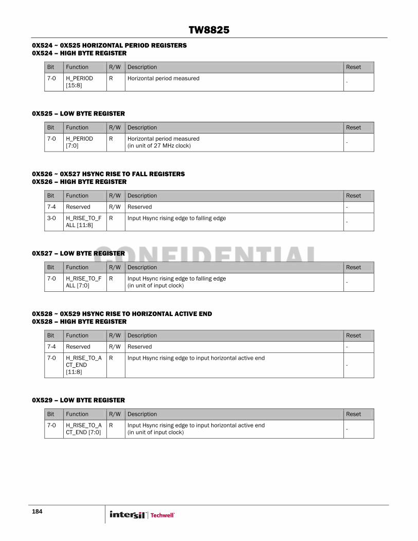
TW8825
184
0X524 ~ 0X525 HORIZONTAL PERIOD REGISTERS
0X524 – HIGH BYTE REGISTER
Bit Function R/W Description Reset
7-0 H_PERIOD
[15:8]
R Horizontal period measured -
0X525 – LOW BYTE REGISTER
Bit Function R/W Description Reset
7-0 H_PERIOD
[7:0]
R Horizontal period measured
(in unit of 27 MHz clock) -
0X526 ~ 0X527 HSYNC RISE TO FALL REGISTERS
0X526 – HIGH BYTE REGISTER
Bit Function R/W Description Reset
7-4 Reserved R/W Reserved -
3-0 H_RISE_TO_F
ALL [11:8]
R Input Hsync rising edge to falling edge -
0X527 – LOW BYTE REGISTER
Bit Function R/W Description Reset
7-0 H_RISE_TO_F
ALL [7:0]
R Input Hsync rising edge to falling edge
(in unit of input clock) -
0X528 ~ 0X529 HSYNC RISE TO HORIZONTAL ACTIVE END
0X528 – HIGH BYTE REGISTER
Bit Function R/W Description Reset
7-4 Reserved R/W Reserved -
7-0 H_RISE_TO_A
CT_END
[11:8]
R Input Hsync rising edge to input horizontal active end
-
0X529 – LOW BYTE REGISTER
Bit Function R/W Description Reset
7-0 H_RISE_TO_A
CT_END [7:0]
R Input Hsync rising edge to input horizontal active end
(in unit of input clock) -

TW8825
185
0X52A ~ 0X52B VSYNC HIGH WIDTH REGISTERS
0X52A – HIGH BYTE REGISTER
Bit Function R/W Description Reset
7-3 Reserved R/W Reserved -
2-0 V_PULSEW
[10:8]
R Input Vsync (logic) high width -
0X52B – LOW BYTE REGISTER
Bit Function R/W Description Reset
7-0 V_PULSEW
[7:0]
R Input Vsync (logic) high width
(in unit of input hsync) -
0X52C ~ 0X52D VSYNC RISE POSITION REGISTERS
0X52C – HIGH BYTE REGISTER
Bit Function R/W Description Reset
7-4 Reserved R/W Reserved -
3-0 V_RISE_PCNT[
11:8]
R Input Vsync rising edge position in one input hsync period -
0X52D – LOW BYTE REGISTER
Bit Function R/W Description Reset
7-0 V_RISE_PCNT[
7:0]
R Input Vsync rising edge position in one input hsync period
(in unit of input clock) -
0X52E ~ 0X52F HORIZONTAL ACTIVE STARTING PIXEL POSITION I REGISTERS
0X52E – HIGH BYTE REGISTER
Bit Function R/W Description Reset
7-4 Reserved R/W Reserved -
3-0 H_ACT_ST_MI
N[11:8]
R Horizontal active region starting position -
0X52F – LOW BYTE REGISTER
Bit Function R/W Description Reset
7-0 H_ACT_ST_MI
N[7:0]
R Horizontal active region starting position
(in unit of input clock) -

TW8825
186
0X530 ~ 0X531 HORIZONTAL ACTIVE STARTING PIXEL POSITION II REGISTERS
0X530 – HIGH BYTE REGISTER
Bit Function R/W Description Reset
7-4 Reserved R/W Resereved -
3-0 H_ACT_ST_MA
X [11:8]
R Horizontal active region starting position -
0X531 – LOW BYTE REGISTER
Bit Function R/W Description Reset
7-0 H_ACT_ST_MA
X [7:0]
R Horizontal active region starting position
(in unit of input clock) -
0X532 ~ 0X533 HORIZONTAL ACTIVE ENDING PIXEL POSITION I REGISTERS
0X532 – HIGH BYTE REGISTER
Bit Function R/W Description Reset
7-4 Reserved R/W Reserved -
3-0 H_ACT_END_
MIN [11:8]
R Horizontal active region ending position -
0X533 – LOW BYTE REGISTER
Bit Function R/W Description Reset
7-0 H_ACT_END_
MIN [7:0]
R Horizontal active region ending position
(in unit of input clock) -
0X534 ~ 0X535 HORIZONTAL ACTIVE ENDING PIXEL POSITION II REGISTER
0X534 – HIGH BYTE REGISTER
Bit Function R/W Description Reset
7-4 Reserved R/W Reserved -
3-0 H_ACT_END_
MAX [11:8]
R Horizontal active region ending position -
0X535 – LOW BYTE REGISTER
Bit Function R/W Description Reset
7-0 H_ACT_END_
MAX [7:0]
R Horizontal active region ending position
(in unit of input clock) -
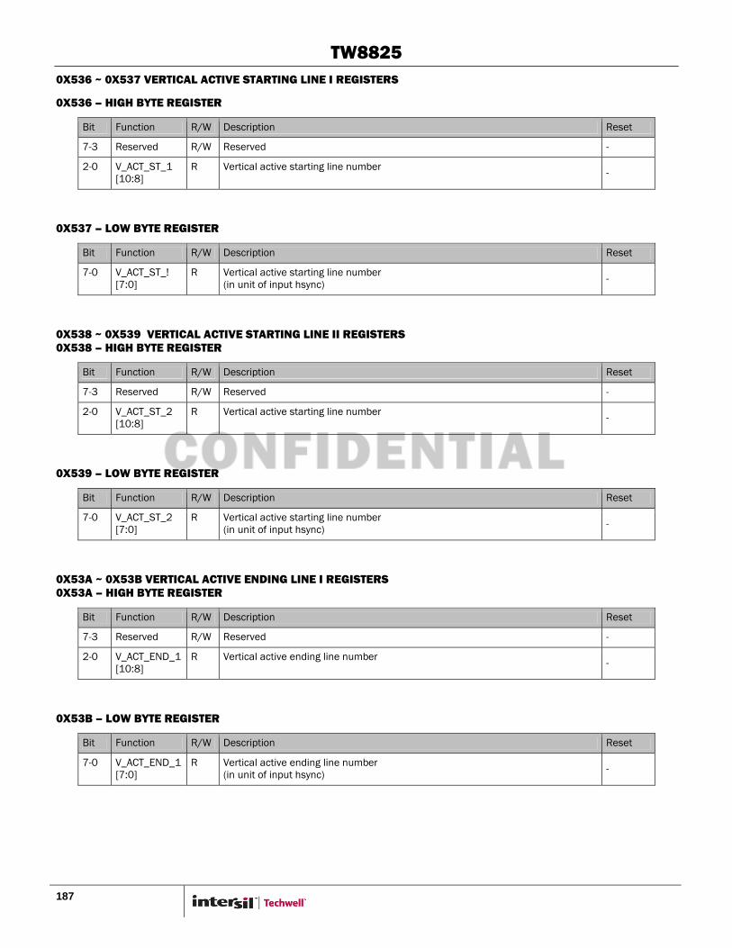
TW8825
187
0X536 ~ 0X537 VERTICAL ACTIVE STARTING LINE I REGISTERS
0X536 – HIGH BYTE REGISTER
Bit Function R/W Description Reset
7-3 Reserved R/W Reserved -
2-0 V_ACT_ST_1
[10:8]
R Vertical active starting line number -
0X537 – LOW BYTE REGISTER
Bit Function R/W Description Reset
7-0 V_ACT_ST_!
[7:0]
R Vertical active starting line number
(in unit of input hsync) -
0X538 ~ 0X539 VERTICAL ACTIVE STARTING LINE II REGISTERS
0X538 – HIGH BYTE REGISTER
Bit Function R/W Description Reset
7-3 Reserved R/W Reserved -
2-0 V_ACT_ST_2
[10:8]
R Vertical active starting line number -
0X539 – LOW BYTE REGISTER
Bit Function R/W Description Reset
7-0 V_ACT_ST_2
[7:0]
R Vertical active starting line number
(in unit of input hsync) -
0X53A ~ 0X53B VERTICAL ACTIVE ENDING LINE I REGISTERS
0X53A – HIGH BYTE REGISTER
Bit Function R/W Description Reset
7-3 Reserved R/W Reserved -
2-0 V_ACT_END_1
[10:8]
R Vertical active ending line number -
0X53B – LOW BYTE REGISTER
Bit Function R/W Description Reset
7-0 V_ACT_END_1
[7:0]
R Vertical active ending line number
(in unit of input hsync) -

TW8825
188
0X53C ~ 0X53D VERTICAL ACTIVE ENDING LINE II REGISTERS
0X53C – HIGH BYTE REGISTER
Bit Function R/W Description Reset
7-3 Reserved R/W Reserved -
2-0 V_ACT_END_2
[10:8]
R Vertical active ending line number -
0X53D – LOW BYTE REGISTER
Bit Function R/W Description Reset
7-0 V_ACT_END_2
[7:0]
R Vertical active ending line number
(in unit of input hsync) -
0X540 – LIMINANCE VALUE – MINIMUM REGISTER
Bit Function R/W Description Reset
7-0 LUM_MIN R Minimum measured luminance value -
0X541 – LIMINANCE VALUE – MAXIMUM REGISTER
Bit Function R/W Description Reset
7-0 LUM_MAX R Maximum measured luminance value -
0X542 – LIMINANCE VALUE – AVERAGE REGISTER
Bit Function R/W Description Reset
7-0 LUM_AVE R Average measured luminance value -
0X543 ~ 0X545 VERTICAL PERIOD IN 27 MHZ REGISTERS
0X543 – HIGH BYTE REGISTER
Bit Function R/W Description Reset
7-0 V_PERIOD_27
MH [23:16]
R Vertical period measured using 27 MHz clock -
0X544 – MID BYTE REGISTER
Bit Function R/W Description Reset
7-0 V_PERIOD_27
MH [15:8]
R Vertical period measured using 27 MHz clock -

TW8825
189
0X545 – LOW BYTE REGISTER
Bit Function R/W Description Reset
7-0 V_PERIOD_27
MH [7:0]
R Vertical period measured using 27 MHz clock -
MCU SFR REGISTER
0X9A – CODE BANK ADDRESS REGISTER
Bit Function R/W Description Reset
7-0 RG_PGMBASE R/W Code Bank Address 0
0X9B – CACHE CONTROL REGISTER
Bit Function R/W Description Reset
7-1 Reserved R/W Reserved -
0 CACHE_EN R/W 1 = Enable Cache 0 = Disable Cache 0
0XE2 – CHIP ACCESS MODE CONTROL REGISTER
Bit Function R/W Description Reset
7 Reserved R/W Reserved -
6 EX_TIMER2 R/W 1 = Timer2 Clock from External PIN 0 = Timer2 Clock from Internal
Divider
0
5 EX_TIMER1 R/W 1 = Timer1 Clock from External PIN 0 = Timer1 Clock from Internal
Divider
0
4 EX_TIMER0 R/W 1 = Timer0 Clock from External PIN 0 = Timer0 Clock from Internal
Divider
0
3-1 Reserved R/W Reserved -
0 16BIT_EN R/W 1 = Enable 16 BIT Index Mode 0 = 8 BIT Index Mode 0
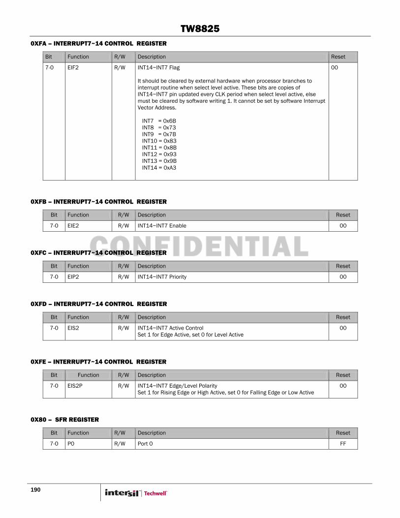
TW8825
190
0XFA – INTERRUPT7~14 CONTROL REGISTER
Bit Function R/W Description Reset
7-0 EIF2 R/W INT14~INT7 Flag
It should be cleared by external hardware when processor branches to
interrupt routine when select level active. These bits are copies of
INT14~INT7 pin updated every CLK period when select level active, else
must be cleared by software writing 1. It cannot be set by software Interrupt
Vector Address.
INT7 = 0x6B
INT8 = 0x73
INT9 = 0x7B
INT10 = 0x83
INT11 = 0x8B
INT12 = 0x93
INT13 = 0x9B
INT14 = 0xA3
00
0XFB – INTERRUPT7~14 CONTROL REGISTER
Bit Function R/W Description Reset
7-0 EIE2 R/W INT14~INT7 Enable 00
0XFC – INTERRUPT7~14 CONTROL REGISTER
Bit Function R/W Description Reset
7-0 EIP2 R/W INT14~INT7 Priority 00
0XFD – INTERRUPT7~14 CONTROL REGISTER
Bit Function R/W Description Reset
7-0 EIS2 R/W INT14~INT7 Active Control
Set 1 for Edge Active, set 0 for Level Active
00
0XFE – INTERRUPT7~14 CONTROL REGISTER
Bit Function R/W Description Reset
7-0 EIS2P R/W INT14~INT7 Edge/Level Polarity
Set 1 for Rising Edge or High Active, set 0 for Falling Edge or Low Active
00
0X80 – SFR REGISTER
Bit Function R/W Description Reset
7-0 P0 R/W Port 0 FF
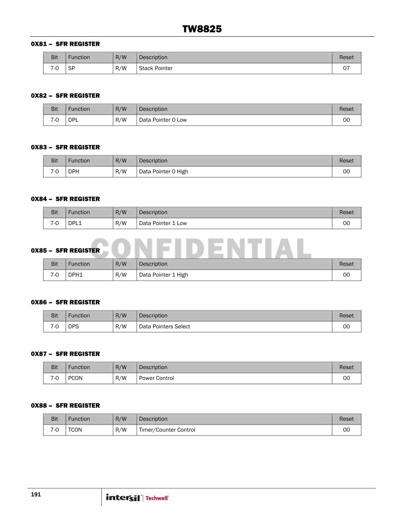
TW8825
191
0X81 – SFR REGISTER
Bit Function R/W Description Reset
7-0 SP R/W Stack Pointer 07
0X82 – SFR REGISTER
Bit Function R/W Description Reset
7-0 DPL R/W Data Pointer 0 Low 00
0X83 – SFR REGISTER
Bit Function R/W Description Reset
7-0 DPH R/W Data Pointer 0 High 00
0X84 – SFR REGISTER
Bit Function R/W Description Reset
7-0 DPL1 R/W Data Pointer 1 Low 00
0X85 – SFR REGISTER
Bit Function R/W Description Reset
7-0 DPH1 R/W Data Pointer 1 High 00
0X86 – SFR REGISTER
Bit Function R/W Description Reset
7-0 DPS R/W Data Pointers Select 00
0X87 – SFR REGISTER
Bit Function R/W Description Reset
7-0 PCON R/W Power Control 00
0X88 – SFR REGISTER
Bit Function R/W Description Reset
7-0 TCON R/W Timer/Counter Control 00

TW8825
192
0X89 – SFR REGISTER
Bit Function R/W Description Reset
7-0 TMOD R/W Timer Mode Control 00
0X8A – SFR REGISTER
Bit Function R/W Description Reset
7-0 TL0 R/W Timer 0, low byte 00
0X8B – SFR REGISTER
Bit Function R/W Description Reset
7-0 TL1 R/W Timer 1, low byte 00
0X8C – SFR REGISTER
Bit Function R/W Description Reset
7-0 TH0 R/W Timer 1, high byte 00
0X8D – SFR REGISTER
Bit Function R/W Description Reset
7-0 TH1 R/W Timer 1, high byte 00
0X8E – SFR REGISTER
Bit Function R/W Description Reset
7-0 CKCON R/W Clock control 07
0X90 – SFR REGISTER
Bit Function R/W Description Reset
7-0 P1 R/W Port 1 FF
0X91 – SFR REGISTER
Bit Function R/W Description Reset
7-0 EIF R/W Extended interrupt Flags 00

TW8825
193
0X92 – SFR REGISTER
Bit Function R/W Description Reset
7-0 WTST R/W Program Memory Wait-States 07
0X93 – SFR REGISTER
Bit Function R/W Description Reset
7-0 DPX0 R/W Data Page Pointer 0 00
0X95 – SFR REGISTER
Bit Function R/W Description Reset
7-0 DPX1 R/W Data Page Pointer 1 00
0X98 – SFR REGISTER
Bit Function R/W Description Reset
7-0 SCON0 R/W UART0 Control 00
0X99 – SFR REGISTER
Bit Function R/W Description Reset
7-0 SBUF0 R/W UART0 Buffer 00
0XA0 – SFR REGISTER
Bit Function R/W Description Reset
7-0 P2 R/W Port 2 00
0XA8 – SFR REGISTER
Bit Function R/W Description Reset
7-0 IE R/W Interrupt Enable 00
0XB0 – SFR REGISTER
Bit Function R/W Description Reset
7-0 P3 R/W Port 3 FF
0XB8 – SFR REGISTER
Bit Function R/W Description Reset
7-0 IP R/W Interrupt Priority 00

TW8825
194
0XC0 – SFR REGISTER
Bit Function R/W Description Reset
7-0 SCON1 R/W UART1 Control 00
0XC1 – SFR REGISTER
Bit Function R/W Description Reset
7-0 SBUF1 R/W UART1 Buffer 00
0XC2 – SFR REGISTER
Bit Function R/W Description Reset
7-0 CCL1 R/W Timer2cc compare/capture 1 low byte 00
0XC3 – SFR REGISTER
Bit Function R/W Description Reset
7-0 CCH1 R/W Timer2cc compare/capture 1 high byte 00
0XC4 – SFR REGISTER
Bit Function R/W Description Reset
7-0 CCL2 R/W Timer2cc compare/capture 2 low byte 00
0XC5 – SFR REGISTER
Bit Function R/W Description Reset
7-0 CCH2 R/W Timer2cc compare/capture 2 high byte 00
0XC6 – SFR REGISTER
Bit Function R/W Description Reset
7-0 CCL3 R/W Timer2cc compare/capture 3 low byte 00
0XC7 – SFR REGISTER
Bit Function R/W Description Reset
7-0 CCH3 R/W Timer2cc compare/capture 3 high byte 00
0XC8 – SFR REGISTER
Bit Function R/W Description Reset
7-0 T2CON R/W Timer2cc control 00
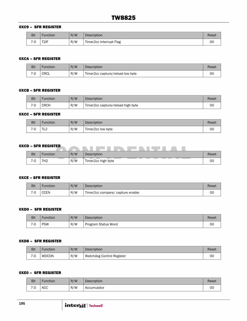
TW8825
195
0XC9 – SFR REGISTER
Bit Function R/W Description Reset
7-0 T2IF R/W Timer2cc Interrupt Flag 00
0XCA – SFR REGISTER
Bit Function R/W Description Reset
7-0 CRCL R/W Timer2cc capture/reload low byte 00
0XCB – SFR REGISTER
Bit Function R/W Description Reset
7-0 CRCH R/W Timer2cc capture/reload high byte 00
0XCC – SFR REGISTER
Bit Function R/W Description Reset
7-0 TL2 R/W Timer2cc low byte 00
0XCD – SFR REGISTER
Bit Function R/W Description Reset
7-0 TH2 R/W Timer2cc high byte 00
0XCE – SFR REGISTER
Bit Function R/W Description Reset
7-0 CCEN R/W Timer2cc compare/ capture enable 00
0XD0 – SFR REGISTER
Bit Function R/W Description Reset
7-0 PSW R/W Program Status Word 00
0XD8 – SFR REGISTER
Bit Function R/W Description Reset
7-0 WDCON R/W Watchdog Control Register 00
0XE0 – SFR REGISTER
Bit Function R/W Description Reset
7-0 ACC R/W Accumulator 00
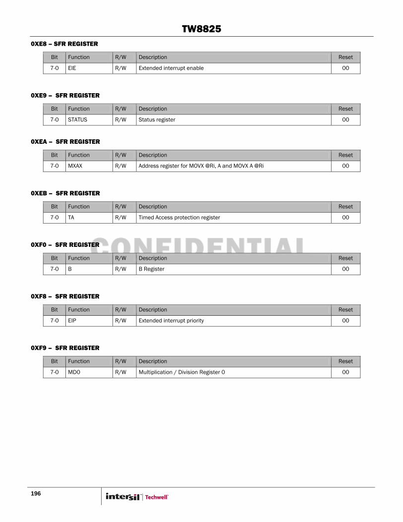
TW8825
196
0XE8 – SFR REGISTER
Bit Function R/W Description Reset
7-0 EIE R/W Extended interrupt enable 00
0XE9 – SFR REGISTER
Bit Function R/W Description Reset
7-0 STATUS R/W Status register 00
0XEA – SFR REGISTER
Bit Function R/W Description Reset
7-0 MXAX R/W Address register for MOVX @Ri, A and MOVX A @Ri 00
0XEB – SFR REGISTER
Bit Function R/W Description Reset
7-0 TA R/W Timed Access protection register 00
0XF0 – SFR REGISTER
Bit Function R/W Description Reset
7-0 B R/W B Register 00
0XF8 – SFR REGISTER
Bit Function R/W Description Reset
7-0 EIP R/W Extended interrupt priority 00
0XF9 – SFR REGISTER
Bit Function R/W Description Reset
7-0 MD0 R/W Multiplication / Division Register 0 00

TW8825
All Intersil U.S. products are manufactured, assembled and tested utilizing ISO9000 quality systems.
Intersil Corporation‟s quality certifications can be viewed at www.intersil.com/design/quality. Intersil products are sold by description only. Intersil Corporation reserves the right to make changes in circuit design, software and/or specifications at any time without notice. Accordingly, the reader is
cautioned to verify that data sheets are current before placing orders. Information furnished by Intersil is believed to be accurate and reliable. However, no responsibility is assumed by Intersil or its
subsidiaries for its use; nor for any infringements of patents or other rights of third parties which may result from its use. No license is granted by implication or otherwise under any patent or patent
rights of Intersil or its subsidiaries.
For information regarding Intersil Corporation and its products, see www.intersil.com
Life Support Policy These products are not authorized for use as critical components in life support devices or systems.
Revision History
DATE REVISION CHANGE
February 20, 2012 FN7934.0 Initial release.