Lateral deformation of silicon crystal surface structure induced by low fluence ion beam irradiation
7
e-Journal of Surface Science and Nanotechnology 14 February 2015 e-J. Surf. Sci. Nanotech. Vol. 13 (2015) 35-41 Regular Paper Lateral Deformation of a Silicon Crystal Surface Structure Induced by Low-Fluence Ion-Beam Irradiation Xiaowei Guo Department of Intelligent Mechanical Engineering, Kochi University of Technology, Tosayamada, Kami-city, Kochi 782-8502, Japan Sadao Momota ∗ School of Environmental Science and Engineering, Kochi University of Technology, Tosayamada, Kami-city, Kochi 782-8502, Japan Noriko Nitta Center for Nanotechnology, Research Institute, Kochi University of Technology, Tosayamada, Kami-city, Kochi 782-8502, Japan Kazuki Maeda Department of Intelligent Mechanical Engineering, Kochi University of Technology, Tosayamada, Kami-city, Kochi 782-8502, Japan (Received 20 December 2014; Accepted 26 January 2015; Published 14 February 2015) The increasing importance of the volume expansion effect on crystalline materials induced by ion-beam irradiation has drawn much attention because of its applications. For example, the expansion effect is used as a good probe to investigate any crystalline-amorphous (c-a) phase change and/or damage. Because the expansion rate and its depth profile can be controlled by means of the irradiation parameters, such as fluence and energy, the deformation of structures on the micro-/nano-meter scale is expected. The fluence needed to achieve deformation is relatively low, and it is expected that irradiation-induced damage is reduced compared with that induced by conventional ion-beam fabrication. Therefore, this expansion effect is a potential method to improve the ion-beam technology employed to fabricate complicated 3-dimensional structures requested in actively developing industrial fields, such as MEMS/NEMS. [DOI: 10.1380/ejssnt.2014.35] Keywords: Ion implantation; Order-disorder phase transition; Radiation damage; Nano structure processing; Silicon; Lateral deformation I. INTRODUCTION In recent studies, the expansion effect has been ob- served in various crystals [1, 4-9], and the controllability along the vertical direction, a swelling height, was con- firmed [10]. In contrast, no remarkable deformation of a crystalline silicon (c-Si) nano-structure along the lat- eral direction has been observed. Upon irradiating an ion beam on an amorphous silicon (a-Si) micro-structure, an irreversible deformation along the lateral direction has been observed [11, 12]. However, a high fluence, which is required for an irreversible deformation, would lead to the prolongation of the processing time compared with a de- formation arising from the expansion effect. Furthermore, more studies are necessary to understand the expansion effect. The deformation of a micro/nano-meter scale structure of c-Si along the lateral direction, which is induced by Kr-beam irradiation, was investigated. As the first step of the investigations, the present study focuses on the contributions of the fluence and the structure size. And the lateral deformation effect is discussed based on the crystalline-amorphous (c-a) phase change obtained from Raman spectroscopy and TEM observations. Further- more, the present results will lead to a further understand- ing of the ion-beam induced expansion effect in crystalline materials. * Corresponding author: [email protected] II. EXPERIMENTAL A. Preparation of initial nanostructures Czochralski-grown (Cz-Si) p-type Si ⟨100⟩ samples, whose size and thickness is 1.5 × 1.5 cm 2 and 0.5 mm, were used in the present studies. In order to clean and remove any oxidized layer of the sample surface, all of the samples were sequentially washed in acetone, ultra-pure water, 18% buffered hydrofluoric acid (BHF) and ultra- pure water. An initial pattern of stripe structure was fabricated on the cleaned c-Si surface by using a 30 keV Ga + FIB (QUANTA 3D 200i dual-beam system, FEI). An SEM image and a schematic picture of the cross section of the stripe structure are shown in Fig. 1. The length, L, and the height, H, of the stripe, which are defined in Fig. 1, are 10 µm and ∼ 500 nm, respectively. Stripe structures, which consist a pile with four different widths of about 200, 300, 400 nm and 500 nm, were prepared. The formation of a damaged layer on the surface of a nano-structure, introduced by the FIB process, was re- ported in Ref. [13]. In order to remove this layer, pro- cessed samples were etched with 18% BHF for 12 minutes under an ultrasonic condition at room temperature. In or- der to relax any possible residual damage, such as point defects, we annealed samples in an argon ambient envi- ronment at atmospheric pressure by desktop lamp heat- ing (MILA-3000, ULAVC). The condition of the annealing process was the same as that described in Ref. [14]. ISSN 1348-0391 c ⃝ 2015 The Surface Science Society of Japan (http://www.sssj.org/ejssnt) 35
-
Upload
kochi-tech -
Category
Documents
-
view
3 -
download
0
Transcript of Lateral deformation of silicon crystal surface structure induced by low fluence ion beam irradiation

e-Journal of Surface Science and Nanotechnology 14 February 2015
e-J. Surf. Sci. Nanotech. Vol. 13 (2015) 35-41 Regular Paper
Lateral Deformation of a Silicon Crystal Surface Structure Induced byLow-Fluence Ion-Beam Irradiation
Xiaowei GuoDepartment of Intelligent Mechanical Engineering,
Kochi University of Technology, Tosayamada, Kami-city, Kochi 782-8502, Japan
Sadao Momota∗
School of Environmental Science and Engineering,Kochi University of Technology, Tosayamada, Kami-city, Kochi 782-8502, Japan
Noriko NittaCenter for Nanotechnology, Research Institute, Kochi University of Technology,
Tosayamada, Kami-city, Kochi 782-8502, Japan
Kazuki MaedaDepartment of Intelligent Mechanical Engineering,
Kochi University of Technology, Tosayamada, Kami-city, Kochi 782-8502, Japan(Received 20 December 2014; Accepted 26 January 2015; Published 14 February 2015)
The increasing importance of the volume expansion effect on crystalline materials induced by ion-beam irradiationhas drawn much attention because of its applications. For example, the expansion effect is used as a good probeto investigate any crystalline-amorphous (c-a) phase change and/or damage. Because the expansion rate and itsdepth profile can be controlled by means of the irradiation parameters, such as fluence and energy, the deformationof structures on the micro-/nano-meter scale is expected. The fluence needed to achieve deformation is relativelylow, and it is expected that irradiation-induced damage is reduced compared with that induced by conventionalion-beam fabrication. Therefore, this expansion effect is a potential method to improve the ion-beam technologyemployed to fabricate complicated 3-dimensional structures requested in actively developing industrial fields, suchas MEMS/NEMS. [DOI: 10.1380/ejssnt.2014.35]
Keywords: Ion implantation; Order-disorder phase transition; Radiation damage; Nano structure processing; Silicon; Lateraldeformation
I. INTRODUCTION
In recent studies, the expansion effect has been ob-served in various crystals [1, 4-9], and the controllabilityalong the vertical direction, a swelling height, was con-firmed [10]. In contrast, no remarkable deformation ofa crystalline silicon (c-Si) nano-structure along the lat-eral direction has been observed. Upon irradiating anion beam on an amorphous silicon (a-Si) micro-structure,an irreversible deformation along the lateral direction hasbeen observed [11, 12]. However, a high fluence, which isrequired for an irreversible deformation, would lead to theprolongation of the processing time compared with a de-formation arising from the expansion effect. Furthermore,more studies are necessary to understand the expansioneffect.The deformation of a micro/nano-meter scale structure
of c-Si along the lateral direction, which is induced byKr-beam irradiation, was investigated. As the first stepof the investigations, the present study focuses on thecontributions of the fluence and the structure size. Andthe lateral deformation effect is discussed based on thecrystalline-amorphous (c-a) phase change obtained fromRaman spectroscopy and TEM observations. Further-more, the present results will lead to a further understand-ing of the ion-beam induced expansion effect in crystallinematerials.
∗ Corresponding author: [email protected]
II. EXPERIMENTAL
A. Preparation of initial nanostructures
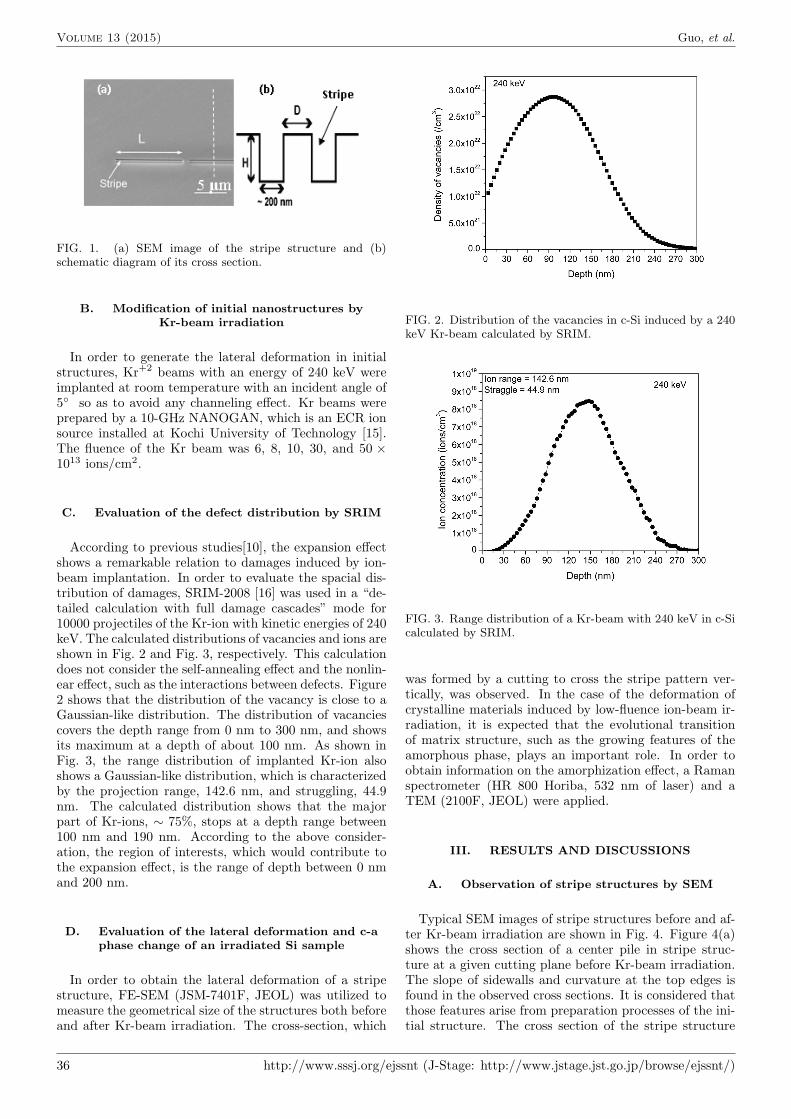
Czochralski-grown (Cz-Si) p-type Si ⟨100⟩ samples,whose size and thickness is 1.5 × 1.5 cm2 and 0.5 mm,were used in the present studies. In order to clean andremove any oxidized layer of the sample surface, all of thesamples were sequentially washed in acetone, ultra-purewater, 18% buffered hydrofluoric acid (BHF) and ultra-pure water. An initial pattern of stripe structure wasfabricated on the cleaned c-Si surface by using a 30 keVGa+ FIB (QUANTA 3D 200i dual-beam system, FEI). AnSEM image and a schematic picture of the cross sectionof the stripe structure are shown in Fig. 1. The length,L, and the height, H, of the stripe, which are defined inFig. 1, are 10 µm and ∼ 500 nm, respectively. Stripestructures, which consist a pile with four different widthsof about 200, 300, 400 nm and 500 nm, were prepared.The formation of a damaged layer on the surface of anano-structure, introduced by the FIB process, was re-ported in Ref. [13]. In order to remove this layer, pro-cessed samples were etched with 18% BHF for 12 minutesunder an ultrasonic condition at room temperature. In or-der to relax any possible residual damage, such as pointdefects, we annealed samples in an argon ambient envi-ronment at atmospheric pressure by desktop lamp heat-ing (MILA-3000, ULAVC). The condition of the annealingprocess was the same as that described in Ref. [14].
ISSN 1348-0391 c⃝ 2015 The Surface Science Society of Japan (http://www.sssj.org/ejssnt) 35
Volume 13 (2015) Guo, et al.
FIG. 1. (a) SEM image of the stripe structure and (b)schematic diagram of its cross section.
B. Modification of initial nanostructures byKr-beam irradiation
In order to generate the lateral deformation in initialstructures, Kr+2 beams with an energy of 240 keV wereimplanted at room temperature with an incident angle of5◦ so as to avoid any channeling effect. Kr beams wereprepared by a 10-GHz NANOGAN, which is an ECR ionsource installed at Kochi University of Technology [15].The fluence of the Kr beam was 6, 8, 10, 30, and 50 ×1013 ions/cm2.
C. Evaluation of the defect distribution by SRIM
According to previous studies[10], the expansion effectshows a remarkable relation to damages induced by ion-beam implantation. In order to evaluate the spacial dis-tribution of damages, SRIM-2008 [16] was used in a “de-tailed calculation with full damage cascades” mode for10000 projectiles of the Kr-ion with kinetic energies of 240keV. The calculated distributions of vacancies and ions areshown in Fig. 2 and Fig. 3, respectively. This calculationdoes not consider the self-annealing effect and the nonlin-ear effect, such as the interactions between defects. Figure2 shows that the distribution of the vacancy is close to aGaussian-like distribution. The distribution of vacanciescovers the depth range from 0 nm to 300 nm, and showsits maximum at a depth of about 100 nm. As shown inFig. 3, the range distribution of implanted Kr-ion alsoshows a Gaussian-like distribution, which is characterizedby the projection range, 142.6 nm, and struggling, 44.9nm. The calculated distribution shows that the majorpart of Kr-ions, ∼ 75%, stops at a depth range between100 nm and 190 nm. According to the above consider-ation, the region of interests, which would contribute tothe expansion effect, is the range of depth between 0 nmand 200 nm.
D. Evaluation of the lateral deformation and c-aphase change of an irradiated Si sample
In order to obtain the lateral deformation of a stripestructure, FE-SEM (JSM-7401F, JEOL) was utilized tomeasure the geometrical size of the structures both beforeand after Kr-beam irradiation. The cross-section, which
FIG. 2. Distribution of the vacancies in c-Si induced by a 240keV Kr-beam calculated by SRIM.
FIG. 3. Range distribution of a Kr-beam with 240 keV in c-Sicalculated by SRIM.
was formed by a cutting to cross the stripe pattern ver-tically, was observed. In the case of the deformation ofcrystalline materials induced by low-fluence ion-beam ir-radiation, it is expected that the evolutional transitionof matrix structure, such as the growing features of theamorphous phase, plays an important role. In order toobtain information on the amorphization effect, a Ramanspectrometer (HR 800 Horiba, 532 nm of laser) and aTEM (2100F, JEOL) were applied.
III. RESULTS AND DISCUSSIONS
A. Observation of stripe structures by SEM
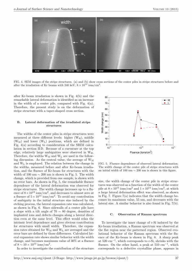
Typical SEM images of stripe structures before and af-ter Kr-beam irradiation are shown in Fig. 4. Figure 4(a)shows the cross section of a center pile in stripe struc-ture at a given cutting plane before Kr-beam irradiation.The slope of sidewalls and curvature at the top edges isfound in the observed cross sections. It is considered thatthose features arise from preparation processes of the ini-tial structure. The cross section of the stripe structure
36 http://www.sssj.org/ejssnt (J-Stage: http://www.jstage.jst.go.jp/browse/ejssnt/)
e-Journal of Surface Science and Nanotechnology Volume 13 (2015)
W
H
W
M
W
L
FIG. 4. SEM images of the stripe structures. (a) and (b) show cross sections of the center piles in stripe structures before andafter the irradiation of Kr beams with 240 keV, 8× 10¹³ ions/cm2.
after Kr-beam irradiation is shown in Fig. 4(b) and theremarkable lateral deformation is identified as an increasein the width of a center pile, compared with Fig. 4(a).Therefore, the present study is on the deformation ofstripe structure with a taper-shaped cross section.
B. Lateral deformation of the irradiated stripestructures
The widths of the center piles in stripe structures weremeasured at three different levels: higher (WH), middle(WM) and lower (WL) positions, which are defined inFig. 4(a) according to consideration of the SRIM calcu-lation in section IID. Because of a curvature at the topedge, relatively large ambiguities were observed in WH.Therefore, the widths WM and WL are used in the follow-ing discussion. As the central value, the average of WM
and WL is employed. The relation between the change inthe widths, measured before and after Kr-beam irradia-tion, and the fluence of Kr-beam for structures with thewidth of 100 nm ∼ 200 nm is shown in Fig. 5. The widthchange, which is provided from one sample, is shown withno error bars. As shown in Fig. 5, the remarkable fluencedependence of the lateral deformation was observed forstripe structures. The width change increases up to a flu-ence of 8×10¹³ ions/cm2, and decreases to almost zero ata fluence of 5× 10¹⁴ ions/cm2. To avoid any contributionof ambiguity in the initial structure size induced by theetching process, the lateral expansion rate was calculated,as shown in Fig. 6. Since sidewalls of a center pile havea slope with a tilt angle of 70 ∼ 80 degree, densities ofimplanted ions and defects changes along a lateral direc-tion even at the same level. This effect would relax theintrinsic level dependence and gives obvious contributionfor structures with small width. Therefore, the expan-sion rates obtained for WM and WL are averaged and theerror bars are defined by those differences. Calculated lat-eral expansion rate shows similar behavior with the widthchange, and becomes maximum value of 30% at a fluenceof 8 ∼ 10× 1013 ions/cm2.In order to investigate the contribution of the structure
FIG. 5. Fluence dependence of observed lateral deformation.The width change of the center pile of stripe structures withan initial width of 100 nm ∼ 200 nm is shown in this figure.
size, the width change of the center pile in stripe struc-tures was observed as a function of the width of the centerpile at 8× 10¹³ ions/cm2 and 1×10¹⁴ ions/cm2, at whicha large lateral deformation effect was observed, as shownin Fig. 7. Figure 7(a) indicates that the width change be-comes its maximum value, 55 nm, and decreases with thelateral size. A similar behavior is also found in Fig. 7(b).
C. Observation of Raman spectrum
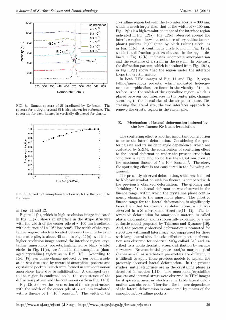
To investigate the inner change of c-Si induced by theKr-beam irradiation, a Raman spectrum was observed atthe flat region near the patterned region. Observed evo-lutional behavior of the Raman spectrum with the flu-ence of the Kr-beam is shown in Fig. 8. A sharp peakat 520 cm−1, which corresponds to c-Si, shrinks with thefluence. On the other hand, a peak at 510 cm−1, whichcorresponds to a defective crystalline phase, appears in
http://www.sssj.org/ejssnt (J-Stage: http://www.jstage.jst.go.jp/browse/ejssnt/) 37

Volume 13 (2015) Guo, et al.
FIG. 6. Fluence dependence of the lateral expansion rate ofstripe structures with a width of a central pile of 100 nm ∼200 nm.
the spectrum for higher fluence. Also the broad peakplaced at 480 cm−1, which corresponds to a-Si, grows withthe fluence, and becomes the dominant component in thespectrum for a fluence larger than 3× 10¹⁴ ions/cm2.The crystalline volume fraction of a-Si sample deduced
from the Raman spectrum, ϕc, was introduced in [17] as
ϕc = (I520 + I510)/(I520 + I510 + I480), (1)
where Ii is the area under the Gaussian distribution,whose center is located at i. As a semi-quantitative index,the amorphization faction, ϕa, is defined using ϕc as
ϕa = I480/(I520 + I510 + I480). (2)
In Fig. 9, the amorphization fraction, calculated fromthe deconvoluted spectra obtained from three-peak fittingof the observed Raman spectrum, is shown as a functionof fluence of the Kr-beam. The figure indicates that the c-a phase change proceeds continuously in the fluence rangebetween 6×10¹³ ions/cm2 and 5×10¹⁴ ions/cm2. Consid-ering Fig. 5, the range of the Kr-beam fluence, at whichthe lateral deformation effect shows remarkable fluencedependence, corresponds to the transitional range fromthe crystal phase to amorphous phase. The lateral defor-mation achieves the maximum at an amorphous fractionof about 85%. Also at higher fluence, the lateral defor-mation relaxes and returns to zero at an amorphous frac-tion of about 100%. As a result, Raman spectroscopyindicates that the amorphization process of c-Si has anobvious relation with the lateral deformation of the c-Sinano-structure.
D. Observation by TEM
Figure 10 shows cross-sectional TEM images of thestripe structure irradiated by a Kr beam with three differ-ent fluences. In this figure, an amorphous layer is clearlyrecognized in the top and sidewalls of the stripe structure,and is separated from the crystalline region by an inter-face. The thickness of the amorphous layer grows withthe Kr-beam fluence and reaches to 270 nm at the top
FIG. 7. Structure size dependence of the lateral deformation.(a) and (b) show the observed results with a fluence of 8×10¹³
and 1× 10¹⁴ ions/cm2, respectively.
of the center pile and 249 nm at the flat region for a flu-ence of 5× 10¹⁴ ions/cm2. This result indicates that thedepth region of interest, 0 - 200 nm, mentioned in IID,is completely amorphized for higher fluence. The grow-ing nature of the amorphous layer is consistent with theincrease in the amorphous fraction, which was obtainedfrom the Raman spectra. The figure also shows the differ-ences in the thickness of the amorphous layer at the rightand left sidewalls of the stripe structure. The tilt angle ofKr-beam irradiation from the normal of Si-surface wouldcause the asymmetric feature. In section III C, observedRaman spectra indicated the importance of the c-a phasechange in order to understand the lateral deformation ef-fect on nano-structure. In the case of heavy-ion irradia-tion at low temperature, the c-a phase change proceedsthrough the overlap of the isolated damaged region in-duced by ion-beam irradiation, and shows a heterogeneousnature. Therefore, the amorphization induced by Kr-ionirradiation at room temperature is expected to be het-erogeneous. Also, observed lateral deformation indicatesstructure size dependence, as described in section III B.To investigate the heterogeneous features in and aroundthe amorphous region and contributions of the lateral size,high-resolution TEM images of center piles were observedfor two structures with different lateral sizes, and shown
38 http://www.sssj.org/ejssnt (J-Stage: http://www.jstage.jst.go.jp/browse/ejssnt/)
e-Journal of Surface Science and Nanotechnology Volume 13 (2015)
FIG. 8. Raman spectra of Si irradiated by Kr beam. Thespectra for a virgin crystal Si is also shown for reference. Thespectrum for each fluence is vertically displaced for clarity.
FIG. 9. Growth of amorphous fraction with the fluence of theKr beam.
in Figs. 11 and 12.Figure 11(b), which is high-resolution image indicated
in Fig. 11(a), shows an interface in the stripe structurewith the width of the center pile of ∼ 100 nm irradiatedwith a fluence of 1×10¹⁴ ions/cm2. The width of the crys-talline region, which is located between two interfaces inthe center pile, is about 40 nm. In Fig. 11(c), which is ahigher resolution image around the interface region, crys-talline (amorphous) pockets, highlighted by black (white)circles in Fig. 11(c), are found in the amorphous (dam-aged crystalline) region as in Ref. [18]. According toRef. [18], c-a phase change induced by ion beam irradi-ation was discussed by means of amorphous pockets andcrystalline pockets, which were formed in semi-continuousamorphous layer due to solidification. A damaged crys-talline region is confirmed to be the coexistence of thediffraction pattern and the continuous circle in Fig. 11(d).Fig. 12(a) shows the cross section of the stripe structure
with the width of the center pile of ∼ 450 nm irradiatedwith a fluence of 1 × 10¹⁴ ions/cm2. The width of the
crystalline region between the two interfaces is ∼ 300 nm,which is much larger than that of the width of ∼ 100 nm.Fig. 12(b) is a high-resolution image of the interface regionindicated in Fig. 12(a). Fig. 12(c), observed around theinterface region, shows an existence of crystalline (amor-phous) pockets, highlighted by black (white) circle, asin Fig. 11(c). A continuous circle found in Fig. 12(e),which is a diffraction pattern obtained in the region de-fined in Fig. 12(b), indicates incomplete amorphizationand the existence of a strain in the system. In contrast,the diffraction pattern, which is obtained from Fig. 12(d),in Fig. 12(f) shows that the region under the interfacekeeps the crystal nature.
In both TEM images of Fig. 11 and Fig. 12, crys-talline/amorphous pockets, which indicated heteroge-neous amorphization, are found in the vicinity of the in-terface. And the width of the crystalline region, which isplaced between two interfaces in the center pile, changesaccording to the lateral size of the stripe structure. De-creasing the lateral size, the two interfaces approach toremove the crystal region in the center pile.
E. Mechanism of lateral deformation induced bythe low-fluence Kr-beam irradiation
The sputtering effect is another important contributionto cause the lateral deformation. Considering the sput-tering rate and its incident angle dependence, which areevaluated by SRIM, the contribution of sputtering effectto the lateral deformation under the present irradiationcondition is calculated to be less than 0.64 nm even atthe maximum fluence of 5 × 10¹⁴ ions/cm2. Therefore,the sputtering effect is not considered in the following ar-gument.
The presently observed deformation, which was inducedby Kr-beam irradiation with low fluence, is compared withthe previously observed deformation. The growing andshrinking of the lateral deformation was observed in thefluence range, within which the crystalline phase contin-uously changes to the amorphous phase. The effectivefluence range for the lateral deformation, is significantlylower than that for irreversible deformation, which wasobserved in a-Si micro/nano-structure[11, 12]. The ir-reversible deformation for amorphous material is calledplastic deformation, and is successfully explained by a vis-coelastic model proposed by Trinkaus and Ryaznov [19].And, the presently observed deformation is promoted forstructures with small lateral size, and suppressed for thosewith large lateral size. The size effect on plastic deforma-tion was observed for spherical SiO2 colloid [20] and as-cribed to a nonhydrostatic stress distribution by surfacecurvature. Because initial phases and/or morphologicalshapes as well as irradiation parameters are different, itis difficult to apply those previous models to explain thepresently observed lateral deformation. In the presentstudies, initial structures are in the crystalline phase asdescribed in section IIID. The amorphous/crystallinepockets and internal stress were observed in TEM imagesfor stripe structures, in which a remarkable lateral defor-mation was observed. Therefore, the fluence dependenceof the lateral deformation is considered by means of theamorphous/crystalline pockets.
http://www.sssj.org/ejssnt (J-Stage: http://www.jstage.jst.go.jp/browse/ejssnt/) 39

Volume 13 (2015) Guo, et al.
FIG. 10. Cross-sectional TEM images of Stripe structures irradiated by a Kr beam with fluences of (a) 8 × 10¹³, (b) 1 × 10¹⁴
and (c) 5× 10¹⁴ ions/cm2.
FIG. 11. TEM images of stripe structures with the widthof the center pile of ∼ 100 nm, irradiated with a fluence of1×1014 ions/cm2; (a) cross-sectional image; (b), (c) are imagesof higher resolution. The rectangles in (a) and (b) indicate theobserved regions for higher resolution. Amorphous pocketsand crystalline pockets are highlighted by white circles andblack circles, respectively. (d) Fourier transform of (c).
The cascade localization induced bias (CLIB) model,proposed by Yoshiie et al. [21] to explain the behaviorsof defects in the lattice system, indicates that defects in-duced in the Si lattice by Kr-beam irradiation would beabsorbed by boundaries between amorphous/crystallinepockets and their surroundings. This absorption stimu-lates the growth of amorphous pockets and shrinkage ofthe crystalline pockets. Also, when amorphous pocketsgrow to overlap with others, amorphous pockets combineand contributions of boundaries to absorb defects are sup-presses. Based on this idea, the fluence dependence can bequalitatively understood as follows. In the case of lowerfluence, amorphous pockets are produced and grow to pro-mote a heterogeneous nature with the fluence of Kr beam.
FIG. 12. TEM images of stripe structure with the width ofthe center pile of ∼ 450 nm, irradiated with a fluence of 1 ×10¹⁴ ions/cm2; (a) cross sectional image of the center pile; (b),(c), (d) are images in higher resolution; (e) and (f) are Fouriertransform of (c) and (d), respectively.
Then the internal stress, which promotes the expansioneffect, increases. On the other hand, in the case of higherfluence, amorphous pockets start combining with otherswith increasing the fluence of Kr beam. Then the internalstress decreases.
Considering observed TEM images, the following naivemodel is a possible candidate to explain the contributionof lateral size to the lateral deformation. In the case ofa smaller lateral size, the crystalline region between twointerfaces in the center pile reduces, and the major partof the center pile is occupied by the amorphous region.Therefore, contributions of stress induced by the hetero-geneous nature would become obvious in the whole regionbetween the interfaces in the left and right sidewall, andpromote an expansion along the lateral direction. In con-trast, in the case of the larger lateral size, the contribu-
40 http://www.sssj.org/ejssnt (J-Stage: http://www.jstage.jst.go.jp/browse/ejssnt/)

e-Journal of Surface Science and Nanotechnology Volume 13 (2015)
tion of the crystalline region, which tends to keep its form,becomes prior. Therefore, the lateral deformation effectwould be suppressed by the crystalline region comparedwith structures of smaller lateral size.
IV. CONCLUSIONS
In conclusions, a deformation of taper-shaped Si struc-tures along the lateral direction has been successfullyachieved firstly by irradiating Kr beam of 240 keV. Theobserved results have shown that the lateral deformationdepends on the lateral size of stripe structure as well asthe fluence of Kr beam. The typical fluence of a 240keV Kr-beam employed to provide lateral deformation isabout 1×10¹⁴ ions/cm2. This fluence is much lower thanthe typical fluence of ion beams, which is needed to pro-vide plastic deformation in amorphous materials. Theamorphous/crystalline pockets, which were observed with
stress in the lattice structure, can provide a consistentqualitative explanation for observed lateral deformationand its fluence dependence. The suppression effect onthe lateral deformation, which would be originated fromcrystalline region between two interfaces in the center pile,provides a possible explanation for the structure size de-pendence. However, further investigations are needed toconfirm the reliability of this idea. In addition, the con-tributions of irradiation energy and ion species will beperformed in next studies.
ACKNOWLEDGMENTS
We thank Professor Taniwaki for providing valuablesuggestions. We are indebted to all colleagues ofMOMOTA-lab for helping to perform experiments involv-ing ion beam irradiation.
[1] Y. H. Li, Y. Q. Wang, J. A. Valdez, M. Tang, and K. E.Sickafus, Nucl. Instrum. Methods Phys. Res. B 274, 182(2012).
[2] C. Trautmann, M. Boccanfuso, A. Benyagoub, S.Klaumunzer, K. Schwartz, and M. Toulemonde, Nucl. In-strum. Methods Phys. Res. B 191, 144 (2002).
[3] C. Ascheron, A. Schindler, R. Flagmeyer, and G. Otto,Nucl. Instrum. Methods Phys. Res. B 36, 163 (1989).
[4] R. Nipoti, E. Albertazzi, M. Bianconi, R. Lotti, G. Lulli,M. Cervera, and A. Carnera, Appl. Phys. Lett. 70, 3425(1997).
[5] J. S. Custer, M. O. Thompson, D. C. Jacobson, J. M.Poate, S. Roorda, W. C. Sinke, and F. Spaepen, Appl.Phys. Lett. 64, 437 (1994).
[6] J. Costantini, C. Trautmann, L. Thome, J. Jagielski, andF. Beuneu, J. Appl. Phys. 101, 073501 (2007).
[7] M. Gauneau, R. Chaplain, A. Rupert, Y. Toudic, R. Cal-lec, and E. Andre, J. Appl. Phys. 73, 2501 (1993).
[8] T. Fa, L. Li, S. Yao, M. Wu, and S. Zhou, Chin. Phys. B20, 056101 (2011).
[9] P. Giri, V. Raineri, G. Franzo, and E. Rimini, Phys. Rev.B 65, 012110 (2001).
[10] S. Momota, J. Zhang, T. Toyonaga, H, Terauchi, K.Maeda, J. Taniguchi, H. Takashi, M. Furuta, and T.Kawaharamura, J. Nanosci. Nanotechnol. 12, 552 (2012).
[11] T. van Dillen, M. J. A. de Dood, J. J. Penninkhof, A.Polman, S. Roorda, and A. M. Vredenberg, Appl. Phys.Lett. 84, 3591 (2004).
[12] M.-O. Ruault, F. Fortuna, H. Bernas, M. C. Ridgway, andJ. S. Williams, Appl. Phys. Lett. 81, 2617 (2002).
[13] J. Yu, J. Liu, J. Zhang, and J. Wu, Mater. Lett. 60, 206(2006).
[14] J. Zhang, Mechanism and application of morphologicalchanges of Si crystal material induced by ion-beam (KochiUniversity of Technology, Kami-city, 2012).
[15] S. Momota, Y. Nojiri, M. Saihara, A. Sakamoto, H. Ham-agawa, and K. Hamaguchi, Rev. Sci. Instrum. 75, 1497(2004).
[16] James F. Ziegler, and J. P. Biersack, The Stopping andRange of Ions in Matter (Springer US, New York, 1985).
[17] C. Droz, E. Vallat-Sauvain, J. Bailat, L. Feitknecht, J.Meier, and A. Shah, Sol. Energ. Mat. Sol. Cells 81, 61(2004).
[18] L. Romano, K. S. Jones, K. Sekar, and W. A. Krull, J.Vac. Sci. Technol. B 27, 597 (2009).
[19] H. Trinkaus and A. Ryazanov, Phys. Rev. Lett. 74, 5072(1995).
[20] T. van Dillen, E. van der Giessen, P. Onck, and A. Pol-man, Phys. Rev. B 74, 132103 (2006).
[21] T. Yoshiie, Y. Satoh, S. Kojima, and M. Kiritani, J. Nucl.Mater. 179-181, Part 2, 954 (1991).
http://www.sssj.org/ejssnt (J-Stage: http://www.jstage.jst.go.jp/browse/ejssnt/) 41