
Laser Data Transfer - Department of Electrical and Computer ...
96
i Laser Data Transfer Senior Design Documentation Department of Electrical Engineering & Computer Science University of Central Florida Fall 2015-Senior Design I Group #32 Derek Clark Photonic Science and Engineering Joshua Jordan Photonic Science and Engineering Kenneth Figueiredo Computer Engineering Table of Contents
-
Upload
khangminh22 -
Category
Documents
-
view
0 -
download
0
Transcript of Laser Data Transfer - Department of Electrical and Computer ...

i
Laser Data Transfer Senior Design Documentation
Department of Electrical Engineering & Computer Science University of Central Florida Fall 2015-Senior Design I
Group #32
Derek Clark Photonic Science and Engineering Joshua Jordan Photonic Science and Engineering
Kenneth Figueiredo Computer Engineering
Table of Contents

ii
1 Executive Summary…………………………………………………………Page2
2 Project Description………………………………………………………….Page 3
2.1 Motivation and Goals…………………………………………………. Page 3
2.2 Milestones………………………………………………………….….. Page 5
2.3 Requirements and Specifications…………………………………… Page 5
2.4 Impact of Design Constraints……………………………………….. Page 7
3 Communication Technologies……………………………………………. Page 7
3.1 Guided Transmission……………………………………………... Page 8
3.2 Unguided Transmission…………………………………………….Page 8
4. Optical receiver subsystems………………………………………………Page 8
4.1 Photodetectors………………………………………………………… Page 9
4.2 Noise……………………………………..……………………………. Page 19
4.3 Amplification……………………………………………………………Page 21
4.4 Filtering …………………………………………….…………………..Page 25
4.4 Receiver Design……………………………………………………….Page 26
5 Transmitter………………………………………………………………… Page 28
5.1 Laser Types……………………………………………………………Page 28
5.2 Analog vs Digital Communication……………………………………Page 32
5.3 Laser Modulation Types……………………………………………. Page 33
5.4 Laser Safety Standards…………………………………………… Page 39
5.5 Transmitter Design………………………………………………… Page 42
6 Power Electronics……………………………………………………… Page 45
6.1 AC Power………………………………………………………… Page 45
6.2 DC Power………………………………………………………… Page 45
6.3 Rectifiers………………………………………………………… Page 46
6.4 Inverters…………………………………………………………… Page 48
6.5 AC to AC Converters………………………………………………. Page 48
6.6 DC to DC Converters……………………………………………… Page 48
6.7 USB to Serial Adapter……………………………………………… Page 48

iii
7 Microcontroller and Peripherals…………………………………… Page 50
7.1 Suitable Microcontrollers for proof of concept………………. Page 51
7.2 Components of the custom prototype boards…………………… Page 52
7.3 Transmitter side of Microcontroller Board……………………… Page 55
7.4 Receiver Microcontroller……………………………………… Page 58
8 Circuits………………………………………………………………… Page 62
8.1 Analog Circuit……………………………………………… Page 62
8.2 Laser Driver Circuit…………………………………………… Page 65
8.3 Photodiode Circuit……………………………………………… Page 75
9.0 Prototype Testing………………………………………………… Page 81
9.1 Testing Environment……………………………………… Page 82
9.2 Transmitter Testing…………………………………………… Page 82
9.3 Transmitter Subsystem Testing…………………………… Page 83
9.4 Photodiode Testing……………………………………………… Page 83
9.5 Microcontroller and Peripheral Testing……………………… Page 84
10 Administrative Content………………………………………… Page 87
10.1 Budget……………………………………………………… Page 87
12 Conclusion………………………………………………………… Page 89
Appendix A: Permissions…………………………………………… Page 91
Appendix B: Datasheets……………………………………………
Appendix C: Works Cited…………………………………………… Page 91
Appendix D: Full Code……………………………………………

1
1.0 Executive Summary
Since the dawn of the digital age the demand to move large amounts of
information as fast as possible has been unquestionable. The group has decided
to continue the advancement in the movement of information by creating the LDT
project. The group feels that their efforts and expertise in their respective degree
fields can contribute greatly to this initiative. We envision a product that can
surpass present consumer demand for moving, or transmitting large magnitudes
of information at comparable speeds to current industry technology. The process
of transmitting this information begins with a computer. A digital signal containing
all the desired information will be sent to a transmitter box by means of a USB to
serial converter. The transmitter will obtain its power directly from the USB to
serial connection. The digital signal will then travel to a microcontroller circuit with
a laser diode driver integrated into it. This laser diode driver will then condition, or
modulate the digital signal to extremely high frequencies. This signal will then exit
the microcontroller circuit and enter the laser. The laser will convert the incoming
electrical signal to an optical signal, amplify the signal and transmit it through
space to a phototransceiver that will collect the incoming signal. The high and
low values of the collected signal will be processed and sent to an optical to
electrical converter. Once the signal is electrically converted it can be sent
through a second microcontroller circuit and be routed through a second serial to
USB converter to a computer. The final result is information that has been
successfully sent from one computer to another without any physical interaction.
Maximizing the amount of correctly transferred information as fast as possible will
be the top priority of the LDT project. Other features such as portability, security,
and energy efficiency will also be incorporated at no expense to the defined top
priority. The LDT project also boasts small safety features. The transmitter will
contain a visible LED light to signify the laser is on. The receiver will also contain
a series of lights that will identify the amount of power that is being collected.
This will serve as a means of establishing a strong and secure link between the
transmitter and receiver. Both the transmitter and receiver will also stand on
adjustable legs. This will allow both components to be fully adjustable. With these
features in mind the group feels that the LDT project will be a serious competitor
in the wireless communications industry; an industry that has been dominated by
Wi-Fi for far too long. The group feels that the rugged design of both the
transmitter and receiver, along with the portability of both, will offer the consumer
with a unique and simple solution to transferring data from anywhere. To
succeed in constructing the LDT project each group member will research and
apply their respective knowledge toward designing a desirable product. This
product will be comprised in a cost efficient way and will utilize effective coding
techniques to ensure a quality product is produced. This product will also strictly
adhere to ABET standards and constraints. Upon completion of the design phase
the group will go through an extensive testing phase that will guarantee that all

2
hardware and software components are functioning as designed. The final
product, after all consideration, will be a revolutionizing product that will change
the marketplace forever.
2.0 Project Description
2.1 Project Motivation and Goals
The motivation behind the idea of creating a channel of communication through
the air between transmitter and receiver began with current projects in production
such as Light Fidelity, or Li-Fi. Li-Wi is a relatively new field in which lasers in the
visible spectrum will carry information at great speeds. The idea of Li-Fi is to get
past the limitation of Radio frequency bandwidths that services like Wi-Fi are
restricted to. The designers of the LDT project further found inspiration by
imagining a fiber optic communications link without the fiber. The designers of
LDT believed this to not only be possible but that a system can be designed that
can achieve data transfer speeds comparable to current Wi-Fi technology. The
Laser Data Transfer project was born.
There is an increasing need for the fastest transfer rates possible. A fiber optic
cable can provide users with the fastest data transfer speeds technology has to
offer. Some circumstances, however enlist wireless technology to transmit data.
Currently Wi-Fi technology leads the industry for wireless data transfer. Wi-Fi has
an inherent limitation of only being able to broadcast in a certain radio frequency
range. This radio frequency bandwidth limits the amount of data that can be sent
wirelessly. This is a direct effect of the radio frequencies only being able to be so
efficient, spectrally. This spectral efficiency creates a finite number of radio
frequencies, and they are all almost be utilized. The LDT project is designed to
utilize frequencies far beyond the radio frequency, thereby bypassing the radio
frequency limitations. Typical Wi-Fi networks operate on 2.4 GHz - 5.6 GHz
frequencies, whereas the LDT project will operate on THz frequencies.
The LDT project is unique from Li-Fi because the LDT project will be a
connection using direct line of sight to transfer data from transmitter to receiver.
The laser beam will have a conical shape to allow for an angle of accepted data
transmission. Figure 2.1-1 is a diagram of a transmitter and a signals potential
path, in red. The receiver would be able to move within that signal path to receive
the data being transferred.

3
Figure 2.1-1
The goal of the LDT project is to continue the growth of the digital era by getting
past the limitations that current technology has. With the continued advance in
technology data communication demands have never been greater. Fiber optic
communication projects like Google Fiber wire are being load tested and
employed nationwide to offer users affordable data speeds of up to 1Gbps
download speeds. The limiting factor of the entire data transmission process will
soon be Wi-Fi. If this product were to replace Wi-Fi it would be a profitable and
marketable in all areas of wireless communication. The LDT project can be used
to stream high bandwidth services such as Netflix in high definition, Cloud
backup and recovery, virtual desktops, Office 365, video calling and even more.
Another goal the designers of the LDT project have is to design a system that
offers its users secure transfer of data. The integration of technology in daily life
has brought up security concerns. We now share credit card information, pay
bills online, browse and purchase goods online, and even file taxes online. It is
no wonder how people get their identities and other personal information stolen
from them. The LDT project hopes to minimize these risks by having a directional
link to a transmitter. From a security perspective this link is superior to Wi-Fi,
where anyone within a radial range from a Wi-Fi transmitter can gain access to
all of the devices connected to it. The LDT project is also more easily confined to
either indoor or outdoor functionality. This property of the LDT project stems from
the fundamental characteristics of optical frequencies. Frequencies in the optical,
near and mid infrared spectrum cannot travel through solid objects, such as
walls, metal and the ground. Imagine a data transmission system that is portable,
secure, and can achieve data lighting fast data speeds. This system can either
be relocated according to the user’s needs, or multiple transmitters can be
employed similar to security camera systems that can detect users on network to
offer directional internet on demand. This detection system can be more energy
efficient as it can be turned on and off as required.
The last goal of the LDT project is to promote health to humanity. The average
United States citizen is subjected to Radio frequency radiation almost 24 hours a
day. A concern is growing that too much exposure to these radio frequencies is
unhealthy. The implementation of the LDT project would eliminate the strongest
Transmitter Receiver

4
intensity radio frequencies that reside in family homes, replacing them with
optical frequencies that the human body has been exposed to since the
beginning of time. The LDT project is guaranteed to be healthier for all humanity.
All of these goals will be met when this product is finished, creating a marketable
product and will be instantly employable worldwide.
2.2 Milestones
As this project will span at least five months from beginning to end, it will prove worthwhile to set some milestones to ensure we are on track for our completion date.
Milestone 1: Complete initial design document Milestone 2: Obtain and acquire parts for prototype build Milestone 3: Setup prototype circuits to connect to transmitter and
receiver. Milestone 4: Build of the program for transmitter and receiver functions on
the prototype. Milestone 5: All tests pass on the prototype board Milestone 6: Acquire custom PCB Milestone 7: Setup circuits to connect transmitter and receiver to the PCB Milestone 8: Build of the program for transmitter and receiver functions on
the custom PCB Milestone 9: All tests pass on the custom PCB board Milestone 10: Complete final document
These tasks will be roughly completed around the time shown in the following chart labeled Figure 2.2-1.
Figure 2.2-1
As this is an estimation of our project lifecycle, the times needed for each step may not be guaranteed this chart will be updated accordingly with the final design document. 2.3 Requirement and Specifications
2.3.1.1 Physical Specifications

5
The following is a list of physical specifications. These specifications will be strict
guidelines in the design of the LDT project. The primary physical specifications
are:
Fast Data Transfer – The primary goal for the LDT project is to achieve a
bit rate of over 1Mbps download speeds from transmitter to receiver.
Lightweight – Both the transmitter and receiver will not exceed 5 pounds.
This will preserve mobility.
Durable – Transmitter and Receiver housings will withstand everyday
wear and tear from movement. The housings will withstand a force of 20
pounds from any given side.
Affordable – The project will not exceed an overall budget of $500.00. This
includes mistakes and any equipment needed to fabricate the project.
Long Lifetime – Once fabricated the LDT project will be designed to last
over 3 years of use.
Low Maintenance – Upon completion of the project the user will only be
required to remove dust from the units via pressurized air at least once
every 6 months.
Caution Light – The transmitter house must contain 1 LED that lights up
signifying when the laser is on.
Intensity Lights – Alignment can be an issue with laser systems. It is
required to display 3 LED lights on the receiver visible to a user at the
transmitter box. Each light will be associated with low, medium and high.
2.3.1.2 Laser Specifications
In order to meet the specifications listed in the previous section there are certain
specifications that that transmitting laser must meet. Therefore, the transmitting
laser must:
Wavelength – The laser must operate at 1.55µm. This is one of the safest
and most useful wavelengths to use.
Cost – In order to stay within budget the laser must be absolutely no more
than $150.00
Drive Current – The laser must have a drive, or operating, current at
between 20mA-70mA. Maintaining low operating currents will allow the
laser to be interchangeable with various breadboards for prototyping.
Short Rise and Fall Times – The LDT project places a strict limit on the
rise and fall times of a signal pulse to within picoseconds
Variable Drive Current – Along with a specific operating current, the
current must be able to swing at least 30mA to allow for the laser to
properly amplify the signal.

6
2.3.1.3 Power Specifications
To ensure that the project meets all its specifications the following specifications
have been placed on the power system:
Low Voltage – DC voltage entering both the transmitter and receiver units
will not exceed 12V.
Stable Voltage – Voltage throughout the entire system must not fluctuate
more than 0.5V after turn on.
Size – DC to DC regulators will be limited to 100mm x 100mm.
Low Cost – The cost to power the transmitter and receiver combined must
not exceed $70.00.
2.3.2 Software Requirements
To achieve the specifications and goals listed in the above sections, there are
certain specifications that the software must adhere to and perform up to in order
for the entire LDT to function properly. The software needs to be:
User Friendly – need to ensure that the software is not overly difficult to
use as it will be presented.
Efficient – need to ensure that the software does not have any extraneous
loops or irrelevant subroutines that could potentially cause a slowdown of
the entire project.
Structured – need to ensure that the software is well structured and
organized as this will streamline the process for debugging and testing.
Precise – need to ensure that the software is precise, as it will be
controlling the MCU to output current, so we do not cause any damage to
the prototype board or the PCB.
Documented – need to ensure that the software is properly commented,
as this will ensure proper understanding of thought processes of coding
decisions between the group.
Functional – need to ensure that the model pipeline for both the
transmitter and receiver sides are functional, as the project will fail if either
side cannot perform their duties.
2.3.3 Constraints
Transportable – The transmitter and receiver units will be easily
disassembled for transport. Both the receiver and transmitter will be
stackable.

7
Connectivity – The system will be easily transferrable from computer to
computer. This allows a broader range of customers.
Easy Setup – The LDT project must breakdown into as few parts as
necessary to facilitate an easy setup. Simple instructions will be located
on each unit to guide users through the set up process.
Powered by a 120VAC standard wall outlet.
Receiver Unit $113.45
Total $378.43
This grand total for the LDT project meets the specification that was placed in
effect. An excess in our budget will serve the project in case of accidents or
repairs.
3.0 Data Communication Technologies
As our project will be transmitting data over laser as the medium, it will be useful
to look into other data communication technologies as many share similarities to
our medium. There are two categories of transmission medium that will be
discussed in this section, which are guided transmission, and its counterpart,
unguided transmission. Our laser guided transmission will need to have a
comparable speed to at least some of these other medium bit rates.
3.1. Guided Transmission
A guided transmission is a link of networks via a physical connection such as fiber optics, or a copper wire connection such as through telephone lines or coaxial cables. This type of connection requires heavy and massive infrastructure to be able to use in a large scale model. These connections however usually end up being paired up and using previously existing communication lines such as television cable lines or telephone lines.
Dial-up and DSL: Dial-up and Digital Subscriber line (DSL) are physical connections that use wired telephone service lines to transmit data to internet connections. Dial-up, now an outdated, slow technology was originally one of the most widely used ways to connect to the internet. It was very slow with max bit rates were averaging around 56Kbps. DSL was similar in this respect as it also ran over copper telephone lines. DSL technology is still being expanded upon to this day with a max speed reached in a controlled condition of 10Gbps, however typical speeds range from 256Kbps to 100Mbps.
Coaxial: Cable internet access uses the existing cable television infrastructure to allow for high bit rates to be reached with coaxial cables as the medium. These

8
cables usually allow for bitrates up to 400 Mbps. One of the key disadvantages of this physical medium though is that populations of users share available bandwidth. Same neighborhoods with cable internet may share this bandwidth which will slow down the connection for everyone.
Fiber Optic: Fiber optic cables are a physical link between networks which are currently on the rise as it is one of the fastest physical links currently available. It has such a high bit rate, that currently electrical cables have reached their physical limitations at 10 Gbps. The current record bitrate is currently set at 1.05 Petabits/s by NEC corp. and Corning Inc.
3.2. Unguided Transmission
An unguided transmission is a link of networks via electromagnetic, usually omnidirectional, waves. These connections have gained massive traction due in part to the rise of smartphones and mobile communications. The infrastructure needed is usually much cheaper than setting up a physical link. These connections in relation to data communication include Wi-Fi and Bluetooth.
Wi-Fi: Wi-Fi is a local area wireless computer networking technology based on the IEEE 802.11 standard. Wi-Fi is the most widely used wireless communication within local area networks as it has a fairly large range, decent wall penetration and is very affordable to setup. Currently the 802.11ad protocol has a max bit rate of 6.75 Gbps.
Bluetooth: Bluetooth is device-to-device standard for exchanging data over
short distances. It was originally based upon the IEEE 802.15.1 standard but no
longer supports the standard. Its current max bit rate is 25Mbps.
4. Optical Receiver Subsystems
The four main parts of an optical receiver subsystem include a photodetector, an amplifier, a filter, and a signal processor. Figure 4.0-1 is a block diagram for the optical subsystem.
Figure 4.0-1Block Diagram of Optical Subsystem

9
4.1. Photodetectors
A photodetector is a semiconductor device that electrically detects optical signals and can convert the optical signal into an electrical signal. Depending on the operating wavelength, the ideal photodetector should have high sensitivity, high speed response, low voltage, minimum noise, and be small in size. For a photodetector to work it must be able to generate carriers from incident light, transport carriers by current gain, and have current interaction with an external circuit for output signal. The output is an electrical signal that has various specifications such as signal power, impedance level and bandwidth. A typical photodetector consists of a photodiode and an electrical circuit.
4.1.1. Photoelectric Effect
First discovered in 1887 by Heinrich Hertz and later explained in 1905 by Albert Einstein, the photoelectric effect is a method used to detect forms of light. As light is incident on a specific material, electrons are emitted and energy is released. This phenomenon is applied to construct the photodetector resulting in the conversion of light energy into electrical energy. The energy and number of emitted electrons can be measured as intensity and frequency of light.
Any discrete emitted electron energy is independent of incident light intensity and increases linearly with a frequency above a specific threshold frequency. Additionally, the number of electrons emitted per second increases linearly with incident light intensity and is independent of frequency. Furthermore, there are three different methods of converting light energy into electrical energy which are known as the photoconductive, photovoltaic, and photoemissive effects. Figure 4.1-1 is a visual representation of the photoelectric effect.
Figure 4.1-1: As incident light, photons, hit the surface of a material an electron will be ejected.
4.1.1.1. Photoconductive

10
The photoconductive effect results in the increase of electrical conductivity of a device when exposed to a light source, in other words the current flows through the device much easier when exposed to light. As light is incident on a device, such as a semiconductor, the incident photons liberate discrete electrons resulting in an increase in electron-hole pairs. However, when the light is no longer incident, the device becomes idle. Taking advantage of the photoconductive effect results in various applications such as the photoresistor, used in street lights, and photocopying.
4.1.1.2. Photovoltaic
The photovoltaic effect uses solar cells, a semiconductor device, to convert light into an electrical current or voltage. The photon-electron interaction is similar to what takes place with the photoconductive effect except the semiconductor device used in the solar cell has a different chemical structure. The materials in the solar cell create a chemical imbalance that accelerates the electrons resulting in a voltage. The photovoltaic effect is used for solar panels and photodiodes.
4.1.1.3. Photoemissive
Considered the oldest method of converting light into electrical energy, photoemission uses photoemissive cells. These cells are sealed a glass vacuum tube with a metal plate inside. As light hits the metal it causes electrons to move resulting in an active current through the circuit.
4.1.2. Photoconductor
A photoconductor is a resistor, where the resistance is a function of the incident light intensity. The device consists of a semiconductor with Ohmic contacts connected to the opposite ends and has an increase in conductivity when light hits the surface, where most of the photons will be absorbed and is shown in figure 4.1-2. This receiver is used to measure quantum efficiency or gain, response time, and sensitivity. Photoconductors are cheap due to their simplicity, toughness, and gain profile making them a relatively cheap photodetector.

11
Figure 4.1-2: A schematic of a photoconductor has Ohmic contacts sandwiched
between a piece of semiconductor material. 4.1.3. Quantum Efficiency
Quantum efficiency is defined as the number of electron-hole pairs generated per incident photon and varies by both the semiconductor material property and the
devices physical structure: Quantum efficiency is represented by 𝜂 = (𝐼𝑝
𝑞) ∗
(𝑃𝑂𝑝𝑡
ℎ𝜈)
−1
, where 𝐼𝑝 is the photocurrent, 𝑞 is the electron charge, and 𝑃𝑂𝑝𝑡is the
incident optical power and ℎ𝜈 is the photon energy. Figure 4.1.3-1 represents the quantum efficiency of various photodetectors.
4.1.4. Responsivity
Responsivity is the ratio of photocurrent to input optical power in units of Ampere per Watt and is represented by ℛ = 𝐼𝑝/𝑃𝑜𝑝𝑡, where 𝐼𝑝 is the photocurrent
produced and 𝑃𝑜𝑝𝑡 is the input optical power. There are four components when
photon energy is incident on a photodiode reflection from the front surface, transmission through the detector without absorption, absorption by ionizing collisions, and other absorption mechanisms. Figure 4.1.4-1 represents the responsivity vs wavelength for two common photodiode materials.

12
Figure 4.1.4-1 (Above): This graph represents the quantum efficiency versus wavelength for various materials used as photodetectors.
Figure 4.1.4-2 This graph represents the spectral responsivity of Silicon and InGaAs materials. The graph details responsivity vs wavelength.
4.1.5. PN Photodiode

13
A PN photodiode is an n-type material bonded with a p-type material and is basically a PN junction under reverse bias and the device configuration is shown in Figure 4.1.5-1. A PN photodiode is a PN junction with an optical window and is a device whose conductivity is sensitive to the intensity of incident light. Due to a small depletion layer the PN photodiode has two major flaws which include having a minimal absorption at long wavelengths and a small junction capacitance. The intensity of the incident light is a measurement of the current that flows into the photodiode. Silicon is the most common used material as a photodiode and has a wavelength less than 1μm. These photodetectors are fabricated to be small as to minimize junction capacitance.
Figure 4.1.5-1: The device configuration for a high-speed PN photodiode.
4.1.6. PIN photodiode
A PIN photodiode is similar to a PN photodiode but has a lightly doped intrinsic layer between the p- and n-type regions of the semiconductor and figure 4.1.6-1 shows the device configuration. The added intrinsic layer in the PIN photodiode increases the depletion layer resulting in a smaller junction capacitance and a greater absorption at longer wavelengths. By adding the intrinsic layer and adjusting the doping levels in each region the design of the semiconductor will optimize the quantum efficiency and frequency response.

14
Figure 4.1.6-1: The device configuration for a high-speed PIN photodiode.
4.1.7. Metal-Semiconductor Photodiode
Used as a high-efficient photodetector, the metal-semiconductor photodiode requires a very thin layer of metal, ~10 nm, and an antireflective coating. The combination of a thin metal and an antireflective coating can avoid absorption and reflection of incident light and is shown in Figure 4.1.7-1. Depending on the photon energies and by adjusting the voltage, this photodiode can operate in three different modes. One mode is used to study the hot-electron transport in metal thin films by determining the Schottky-barrier height.
Accordingly, the second mode results in similar characteristics of a PIN photodiode and lastly can be used as an avalanche photodiode. Material selection is a major factor, an ideal metal and antireflective coating will result in maximizing the absorption at the semiconductor air interface. A metal-semiconductor photodiode has an absorption coefficient that is compatible with both visible and ultraviolet light.

15
Figure 4.1.7-1: The device configuration of a high-speed metal-semiconductor photodiode.
4.1.8. Avalanche Photodiode (APD)
Operating at high reverse bias voltages will lead to internal current gain due to avalanche multiplication and is shown in figure 4.1.8-1. This diode works fast resulting in high gains and is very sensitive to bias voltage and temperature. With that, the current gain-bandwidth can be as high as 100 GHz, responding to microwave frequency modulated light. This diode has similar quantum efficiency and responsivity to non-avalanche photodiodes.
Two important properties that occur with the avalanche photodiode include noise and avalanche gain. Avalanche gain, the impact of ionization, allows for very large currents to be generated and multiplies single current, background current, and dark current. However, the avalanche gain must be uniform over the whole surface where light is incident upon the device. Applications used are for high frequency.

16
Figure 4.1.8-1: The device configuration of a guard-ring photodiode structure.
4.1.9. Phototransistor
The phototransistor is used to enhance the optical absorption. This device is often compared to the avalanche photodiode and doesn’t require high voltages nor creates high noise. Gain occurs at low frequencies and a BJT circuit can be used for a phototransistor. However, the fabrication of this device is much more complicated than that of the photodiode resulting in reduced performance with the high-frequency and is shown in figure 4.1.9-1. This is a bipolar phototransistor and has a large base-collector junction used for collecting light resulting in a high current-transfer ratio.
Figure 4.1.9-1: The device configuration of a bipolar phototransistor.
4.1.10. Heterojunction Photodiode

17
The junction of this photodiode is made between two semiconductors. Taking advantage of the unique junction, materials can be combined to optimize the quantum efficiency and responsivity at different wavelengths.
4.1.11 Photodiode Product comparison
Before choosing a photodiode there are a few parameters to consider. It is known that responsivity affects noise equivalent power, therefore it is only appropriate to choose a photodiode that is within the wavelength range of the laser diode being measured. The laser diode will be emitting at a wavelength of 1.55μm, therefore a photodiode with responsivity within the range of 1. 55μm is desired and an infrared photodiode will be required. InGaAs photodiodes have the responsivity within this wavelength making them the preferred photodiode.
Additionally, the active area of the photodiode is important to consider as it affects the noise equivalent power. A small active area is desired because the square root of the active area is proportional to the generated noise. Furthermore, a smaller active area will not reduce the gain bandwidth as a large active area will. A smaller frequency response is also desired as this will lead to an acceptable level of noise equivalent power.
Optical power damage threshold is an important parameter that will help determine the photodiode to use as we do not want to destroy the photodiode. The laser diode used will produce a maximum output power of 5 mW; therefore the optical power damage threshold must be greater than 5 mW.
Thorlabs has several InGaAs photodiodes available and will be reviewed. Table 4.1.11-1 is a table of the top three photodiode found.
InGaAs Photodiode
FGA01 FDGA05 FGA01FC
Price ($US) $56.70 $134.00 $144.00
Key Feature High Speed, High Responsivity, and Low Capacitance
High speed and low capacitance, ball lens
High speed and low capacitance, direct fiber couple
Responsivity 1.003 A/W 0.95 A/W 1.003 A/W
Active area Ø 0.12mm Ø 0.5mm Ø 0.12mm
Rise Time (5V) 300 ps 2.5 ns 300 ps
Bandwidth 1.167 GHz 0.14 GHz 1.167 GHz
Peak Wavelength 1550 nm 1550 nm 1550 nm
Max Dark Current (5V)
2.0 nA 30 nA 2.0 nA
Capacitance (5V) 2.0 pF 10 pF 2.0 pF

18
Max Reverse Bias Voltage
20 V 20 V 20 V
Max Reverse Current
2 mA - 2 mA
Operating Temperature
-40 to 75 °C -40 to 85 °C -40 to 75 °C
Optical Power Damage threshold
18 mW - 18 mW
NEP 4.5x10⁻¹⁵
W/√Hz 0.8x10⁻¹⁴
W/√Hz 4.5x10⁻¹⁵
W/√Hz
Package TO-46 TO-46 TO-46, FC/PC Bulkhead
4.1.11-1: Specification of three InGaAs photodiodes manufactured from Thorlabs.
After review the top three options Thorlabs has to offer it is clear that FDGA05 can be eliminated as it has the largest active area and largest frequency response of the three, additionally the optical power damage threshold was not specified.
The packaging system used by all three photodiodes is the same with the exception to FGA01FC, which has an additional bulkhead. However, we will eliminate the FGA01FC as a direct fiber couple package is not required for this project. The FGA01 InGaAs photodiode will be use as it as it fits the required specification to properly operate with the laser diode, and it also the cheapest.
The FGA01 uses a TO-46 package size which is shown in figure 4.1.11-1 and has three pins along with a ball lens that has a 1.5 mm diameter.

19
Figure 4.1.11-1: This is the TO-46 package size schematic of the FGA01 InGaAs photodiode manufactured by Thorlabs.
4.2. Noise
Noise is an undesired randomly alternating voltage or current that is associated with the desired signal in the receiver. By adding noise to the signal causes a particular amount of uncertainty about the exact value of the signal current or

20
voltage. When the signal is greater than the noise, the uncertainty resulting from the noise can be small and irrelevant. Additionally, when the noise is greater than the signal, the signal may be impossible to obtain.
Furthermore, noise can be characterized as the average noise current and the average squared noise current. Each and every active device component in the receiver produces some noise, including the photodiode. By understanding the noise produced by the circuit in the receiver, the receiver sensitivity can be determined.
4.2.1. Optical Receiver Noise
Optical noise can be described by photon noise, photoelectron noise, and gain noise that are associated with random fluctuations.
4.2.1.1. Photon Noise
Photon noise is the most fundamental source of noise associated with the random arrival of photons at the photodetector, and is measured by the amount of individual incident photons over a time interval. While under a fixed optical power the resulting photon flux is uncertain however the value of the mean photon flux fluctuates randomly. When incident light is monochromatic and coherent the number of photons adheres to the Poisson probability distribution. Additionally, the arrival of one photon is dependent in energy, direction, and magnitude of the arrival of another photon.
4.2.1.2. Photoelectron Noise
An incident photon on the surface of a photodetector has a quantum efficiency value that will, free a photoelectron or create a photoelectron-hole pair that does not recombine, with the same quantum efficiency value or fail to do so. Furthermore, due to this random carrier generation process, photoelectron noise serves as an optical noise. Additionally, there is no additive relationship between photon noise and photoelectron noise.
4.2.1.3. Gain Noise
Gain noise typically occurs with the avalanche photodiode. As carrier-multiplication takes place, an amplification process will result in internal gain. Each incident photon on the surface of the photodetector will appear as a random quantity of carriers and also have an average quantity of carriers. However, both quantities will be accompanied with uncertainty based on the amplification mechanism.
4.2.2. Receiver Circuit Noise
This noise results from the electronic components, transistor or resistor, of the optical receiver circuit.
4.2.2.1. Shot Noise

21
Most electronic devices produce shot noise. Shot noise is the random emission of electrons from the cathode of a thermionic diode resulting in an average current value I accompanied with fluctuations. These fluctuations are due to the random emission times and individual electron charge quantity. The shot noise is represented by noise current and is added to the average current. For a photodiode, the average current is proportional to the intensity of the incident light and would have two current sources, one a signal current and the other a shot noise current.
4.2.2. Thermal noise
Thermal noise is only produced by resistive components due to the relation with black body radiation. The intensity of electron motion in a resistor is proportional to temperature and produces measurable varying voltages or currents.
4.2.3. Total Noise
The magnitude from all noise sources which are represented by the mean-squared value of either a noise current or voltage. Under the circumstances of multiple independent noise sources in a circuit, the mean-squared noise current or voltage must be add from all independent sources.
4.2.4. Signal-to-noise Ratio
Signal-to-noise ratio is the most important parameter for analyzing communication system. Known as the ratio of signal power to total noise power and is usually expressed in decibels (dB).
4.3 Amplification
Amplification is used to increase the amplitude of an electrical signal while keeping the remaining parameters with the original waveform. Amplifiers are able to perform various functions and are commonly used in electric circuits. There are various types of amplifiers based on the type of signal that is being amplified.
4.3.1 Preamplifier
To begin amplification, the preamplifier is the first component in the process. Although amplifier is incorporated within the name, the preamplifier does not perform any amplification and is the interface between the photodetector and amplification process. The purpose of a preamplifier is to extract the electrical signal from the photodetector without reducing the signal-to-noise ratio. With that being said, the preamplifier circuit is designed to match the characteristics of the photodetector.
Photodiodes are known to produce large output pulses resulting in fewer restrictions on the preamplifier. Additionally, the photodiode output can be used with a wideband amplifier that contains low input impedance generating short and fast pulses; these output pulses can be analyzed for timing and counting. A preamplifier has two key requirements; Maximize the signal-to-noise ratio by terminating the capacitance, and providing high impedance for the photodiode

22
and low output impedance for the amplifier. The three basic preamplifiers that can be used are: The current-sensitive preamplifier, parasitic-capacitance preamplifier, and the charge-sensitive preamplifier.
4.3.1.1 Current-Sensitive Preamplifier
A current-sensitive preamplifier converts the incoming current into an output voltage. This is done by adding a 50Ω coaxial cable to the output of the photodetector resulting in a voltage pulse. When the rise time of the photodetector is much larger than the photodetector rise time the amplitude of
the resulting output voltage pulse will be 𝑉𝑂 = 50𝐼𝑖𝑛𝐴, where A is the voltage gain and 𝐼𝑖𝑛 is the amplitude of the current pulse. Additionally, a fast discriminator can be applied to record and analyze the output pulse timing and counting. The type of photodetectors this preamplifier is typically applied are the photomultiplier tube and microchannel plate and is shown in figure 4.3.1.1-1.
The preamplifier noise will cause jittering in the pulse time as it crosses the timing discriminator threshold. To reduce the noise in the preamplifier, the rise time of the preamplifier should be slower than the rise time of the photodetector. When the preamplifier rise time is faster than the detector rise time the resulting bandwidth adds to the noise. Additionally when choosing a current-sensitive preamplifier, the rise time of the preamp should be similar to the rise time of the output detector pulse since the best option. A typical current-sensitive preamplifier should have a preamplifier rise time that is a factor of 2 of the photodetector rise time.
Figure 4.3.1.1-1: Schematic of a current-sensitive preamplifier.
4.3.1.2 Parasitic-Capacitance Preamplifier
The parasitic-capacitance preamplifier is for pulse-amplitude measurements or energy spectroscopy. Accompanied with high input impedance, the resulting current pulse from the photodetector merges on the combined parasitic capacitance at the detector output and preamplifier input. As this preamplifier’s gain is sensitive to small changes in the parasitic capacitance it is typically not

23
used with semiconductor photodetectors but is used with photomultiplier tubes (PMT) and electron multipliers.
Accordingly, the combined capacitors result in a voltage pulse signal with amplitude similar to the total charge in the detector pulse and the rise time has the same length as the current pulse of the detector. A resistor is connected in parallel to the parasitic capacitance resulting in an exponential decay of the pulse. Additionally, a high impedance amplifier is place as a buffer to create low impedance for the output and is shown in figure 4.3.1.3-1.
Figure 4.3.1.3-1: Schematic of a parasitic-capacitance preamplifier.
4.3.1.3 Charge-Sensitive Preamplifier
Typically used for energy spectroscopy, the charge-sensitive preamplifier uses a signal from a semiconductor photodetector as a charged quantity and is delivered as a short current pulse. The charge quantity and time of an event are the parameters measured by the charge-sensitive preamplifier. Unlike the parasitic-capacitance preamplifier, this preamplifiers gain is not sensitive to the photodetectors capacitance and a schematic is shown in figure 4.3.1.3-1.
Additionally the output voltage can be calculated by V0 =QD
Cf, and the decay time
constant by τf = RfCf, where QD is the charge release of the detector, Cf is the feedback capacitor, Rf and is the feedback resistor.
The feedback resistor and the input capacitor are noise sources. Increasing the value of the feedback resistor will reduce noise but increase the decay time constant. Additionally, reducing the value of the feedback capacitor will keep the decay time constant but will affect the linearity of the preamplifier. The charge
release of the detector can be calculated by QD = E e∗106
ε, where E is the energy
in MeV, e is the charge of an electron, 106 is the conversion from MeV to eV, and
ε is the required energy to produce an electron-hole pair in the detector.

24
Furthermore, the output voltage can be expressed as V0 =E e∗106
εCf and gain can be
express as V0
E=
e∗106
εCf.
The noise in the charge-sensitive preamplifier can be measure by the full width at half maximum (FWHM) of the energy by a test pulse sent into the preamplifier
input and is expressed as FWHM = 2.35E
VpVrms, where Vp is the pulse amplitude,
E is the energy, and Vrms is the root mean square voltage.
Figure 4.3.1.3-1: Schematic of a charge-sensitive preamplifier.
4.3.2. Amplifiers
Following the preamplifier is the main amplifier that processes and increases the amplitude of the input signal waveform without changing the other input signal parameters. An amplifier is typically described by the type of signal that is needed to be increased. Additionally, an amplifier typical has several parameters and includes gain, frequency response, and bandwidth, input impedance, output impedance, phase shift, and feedback.
Gain in an amplifier is simply the measurement of the amplification and is described as the ration of an output signal over the input signal. However, the gain is not the same at all frequencies resulting in a specific frequency response for each amplifier. Frequency response is a band of frequencies that amplifies the electrical signal within the band and excludes frequencies outside the band and an example is shown in Figure 4.3.2-1. Additionally, bandwidth is an important parameter that can be obtained from a frequency response curve. The bandwidth is the area between the lower cutoff frequency and upper cutoff frequency, and is useful gain for the amplifier.

25
Figure 4.3.2-1: Generic Frequency response curve and the resulting bandwidth. Where 𝑓𝑜, 𝑓𝑐1, and 𝑓𝑐2 are the center frequency, lower cutoff frequency, and upper
cutoff frequency respectively. 𝐴𝑝(𝑚𝑖𝑑) is the gain for either power, voltage, or a
current.
Input impedance is the same as resistance when there is no frequency and impedance is the opposite of an AC current flow. However when frequency is applied input impedance and resistance are not the same. Additionally, the input impedance is the effective impedance between the input terminals of an amplifier and is influenced by applied signal frequency, amplified gain, and feedback. The output impedance depends on the components connected to the amplifier output. An example is when a voltage signal falls this is because a current is drawn from the output terminals.
Phase shift, expressed in degrees, is a delay or advanced in the output signal with respect to the input signal. When electric components such as resistors, inductors, and capacitors are added to an amplifier circuit, typically this will result in a phase shift of one quarter output peak phase shift. Additionally, phase shift changes with frequency. Feedback occurs when the output signal goes back into the input and there are two types of feedbacks; positive feedback and negative feedback. Positive feedback increases the gain in the amplifier, where negative feedback reduces the gain in the amplifier.
4.4. Filtering
Filters are named after the frequencies they affect. Some common filters are passive, active, and digital filters. Passive filters only require the use of three electronic components; a resistor, an inductor, and a capacitor. Additionally, passive filters do not require an external power supply. However, active filters use a combination of passive and active components resulting in the need of an outside power source. Active filters are often accompanied with an active filter and the frequency is limited by the bandwidth. Digital filters are used to convert signals from analog to digital or vice versa.

26
For this senior design we will be using a bacic RC filter with a resistor and a capacitor. We will start off with a 1kΩ resistor and a 0.1μF capacitor.
4.5 Receiver Design
Figure 4.5-1 is what the receiver casing will look like. All the components will fit inside of the casing. The white circle in the front is where the incoming laser beam will enter and hit the photodiode. The circle in the back is where the power source wire will enter to supply the device with power, as well as the USB to serial adapter.
Figure 4.5-1: Drawing of the receiver and receiver component housing.
On the inside of the casing will contain the circuit boards for both the photodiode and the power systems for the photodiode and is shown in figure 4.5-2 and figure 4.5-3 is the complete and final design of the receiver housing with the receiver.

27
Figure 4.5-2: Photodiode circuit and the power circuit that is connected to both the computer and wall outlet.

28
Figure 4.5-3: Final set up for the design of the receiver housing.
5.0 Transmitter
Transferring data by means of a laser calls for the use of a transmitter. In electronics a transmitter is an electrical device that generates and amplifies a carrier wave, modulates a signal derived from a source, and radiates the resulting signal to a receiver. In this project the transmitter will consist of a laser that will send a modulated signal to a receiver, printed circuit board (PCB) that will house the microcontroller and an voltage regulator circuit to power the transmitter. Before designing the PCB and voltage regulator circuit it is first necessary to determine what laser will be sending the signal. In order to do this some research was required. The following sections all explore important constraints when choosing which laser to use.
5.1 Laser Types
Before deciding on a type of laser to buy it is important to declare important requirements and specifications the laser must fulfil:
The laser must emit light at 1.3 to 1.55µm. This wavelength range is both relatively safe and efficient. See the laser wavelength operations section as well as the laser frequencies section for a detailed explanation of the corresponding material.
Laser tunability is not needed as wavelength division multiplexing will not be incorporated in this project. Standard bandwidths are then acceptable for this application.
Avoiding optical feedback, or bandwidth dispersion, is crucial to how well the sensor can detect amplitudes.
Power efficiency is not a large factor. The project will be drawing power from a serial connection from a computer.
Let’s consider the different methods of producing a laser.
5.1.1 Semiconductor Lasers:
Semiconductors have revolutionized the laser industry. By controlling the flow of electrons to emit light, semiconductor lasers have become a cheap and compact-size laser. Semiconductor lasers also A semiconductor laser can now be optimized to fit desirable attributes. The following sections are different types of semiconductor diode lasers:
5.1.1.1 Fabry-Perot Diode Lasers
One of the most common types of semiconductor laser, the Fabry-Perot diode laser will function, but is not optimized. This laser type can be compared to an LED pumping in a resonator cavity. Due to the construction of the diode laser setup it produces a wider spectral width than other alternative lasers. In order for an optical sensor to receive the data correctly the beam must be of a coherent nature, which Fabry-Perot diode lasers typically are not.

29
5.1.1.2 Heterostructure Diode Lasers
A heterostructure diode laser consists of multiple heterojunctions. A heterojunction comprises of two different lattice matched crystalline semiconductor materials containing different bandgap energy levels that, when matched together, produce electron movement and light is then emitted.
5.1.1.3 Quantum Diode Lasers
There are three types of quantum diode lasers:
1. Quantum well lasers 2. Quantum line lasers 3. Quantum dot lasers
Quantum diode lasers are atomic in nature, yet exhibit the same desired quality that semiconductors. Quantum diode lasers specialize in short wavelengths and were designed to have more control over the absorbance and emission wavelengths. This is accomplished by altering the energy levels, through quantization. Overall, this laser type is not the most efficient for our applications. A laser that has maximum intensity is desired more than a broad range of wavelengths to choose from. Quantum diode lasers are more expensive than more traditional semiconductor diode lasers.
5.1.1.4 Distributed Feedback Diode Lasers
Distributed feedback diode lasers are optical fiber lasers that utilize a diffraction grating to select and filter a particular wavelength to be emitted. Having a lower bandwidth is desirable to eliminate wavelength dispersion. By eliminating wavelength dispersion the distributed feedback laser can send more precise pulses at different intensity values. The more intensity levels that can be produced the higher order number systems can be used. This is exactly what desired for this project is. Optical fiber lasers, in general are small packages that are easy to incorporate into a circuit. Distributed feedback diode lasers are a strong candidate for this project requirements and specifications.
5.1.1.5 Vertical Cavity Surface Emitting Laser (VCSEL)
VCSEL’s incorporate distributed Bragg reflector mirrors and quantum wells to achieve lasing capabilities. For this project VCSELs are appealing. VCSELs are more compatible with fiber coupling, and easy for manufactures to fabricate so cost will be reduced. Lower power is the only disadvantage to this type of laser.
5.1.2 Gas Lasers
One of the most widely used laser types; a gas laser utilizes different types of gasses as gain material. When a current is applied through this gain material, electrons are excited to higher energy states then, upon returning back to its lower energy state emits light in a coherent manner. Gas lasers are effective but are very large, when compared with other laser types, such as semiconductor lasers. Gas lasers also require a lot of energy to operate and are typically not

30
cheap. Gas lasers do not have the ability to control intensity values and pulsing for data transfer easily. Therefore, gas lasers are not a viable option for this project.
5.1.3 Chemical Lasers
Chemical lasers utilize the energy from chemical reactions to produce very high continuous wave output intensity values. To achieve similar power levels other laser types need to be pulsed. This laser type is, however, typically a tool used in industry for cutting, or used in research. Chemical lasers cannot be pulsed easily and intensity values cannot be altered. This laser is not appropriate for data transfer.
5.1.4 Solid-State Lasers
Solid-State lasers have many military applications as a laser that produces high output powers. As mentioned with other laser types size is again an issue as well as the amount of energy required to operate the laser. The laser also cannot be simply controlled by a driver circuit to be pulsed which makes it an unlikely candidate for out project.
5.1.5 Laser Packaging
For the purposes of this project as well as time constraints stand-alone semiconductor laser are not going to be a viable option. This limits the project to package laser systems. There are many different types of packaging options when dealing with lasers. In Telecom laser applications there are three major types of packing options: Butterfly, Boxed TOSA MSA, and TO-Can TOSA. Butterfly is the standard format for optical Telecom transmissions. A butterfly package typically contains 14 pins and a Thermo Electric Cooler (TEC). This method of regulating the temperature is required to ensure a more stable power output and minimizing the beam divergence of the outgoing laser beam. Butterfly packaging is typically used for bit rates up to 10Gbit/s. A boxed TOSA MSA is a standard used with bit rates up to 100Gbit/s. This type of packaging was designed to be a miniature version of the butterfly packaging. This left less room for the TEC. Smaller TECs were designed which causes the price of this packaging to be higher than the more universal butterfly package.. The last packaging option is TO-Can TOSA. This package option is a compromise between the butterfly and boxed TOSA MSA configurations. It is a cheap and compact package that is projected to be the new standard. Any of these three packaging types can be used in this project.
5.1.6 Product Comparison
We have successfully narrowed down the possible laser types to quantum well lasers, VCSEL, and Distributed Feedback Diode lasers. Table 5.1.6-1, split up by laser type and structure, is a list of different lasers currently on the market.

31
Table 5.1.6-1 Laser Comparison
Wavelengt
h Range
(nm)
Operatin
g
Voltage
(V)
Threshol
d
Current
(mA)
Outpu
t
Power
CW
(mW)
Puls
e
Widt
h
(ns)
Price
$
Diode Only Quantum Well Laser
Panasonic
LNCT28PF01W
W
656-665 2.4 50 100 30 15.62
Panasonic
LNCT22PK01W
W
777-791 2.5 45 200 100 15.62
Diode Only Vertical Cavity Surface Emitting Laser
TT
Electronics
OPV300
860 2.2 3 1.5 .2 14.65
TT
Electronics
OPV314AT
860 2.2 3 .6 .210 20.50
Pigtail Package Quantum Well Laser
US-Lasers
MM850-0 840-860 2.4 20 5 - 76.0
Renesas
NX7338BF-AA 1310 2.5 20 10 4 266.0
Renesas
NX7538BF-AA 1550 2.5 45 10 4
285.9
5
14 Pin Butterfly Package Quantum Well Laser
Mitsubishi FU-
68SDF-
V802MxxB
1550 1.8 10 6 .150 148.5
0
After analysis of many lasers that can be purchased in the market this project will be utilizing a quantum well laser to transmit its data to the receiver. This laser type is more expense than other types but, it allows for higher maximum

32
intensities and they are packaged in pigtail configurations. This allows the laser to be easily integrated into our project design. This project places emphasis on the pulse width that a laser can be modulated to, as well as the cost. Stand-alone laser diodes are cheaper and have more desirable specifications, such as pulse width, but entire configurations have a photoresistor and can more easily be incorporated to a design. The photoresistor serves to regulate the output power of the laser beam, which is important when choosing the appropriate receiver photoresistor.
5.2 Analog vs Digital Communication
In an age where digital communication is dominating over analog some applications still require analog signals for broadcasting a signal. Services such as television, telephones, and radio still utilize this archaic communication type. Our group is going to design an electronic device that is required to have the ability to transmit videos and audio clips, as well as other forms of data. It is important to consider both types of communication with an unbiased opinion. Highlights, or advantages and disadvantages, of both methods of communication are summarized in Table 5.2-1.
Table 5.2-1: Analog vs. Digital Communications
Digital Communication Analog Communication
Signal that transmits a
square waveform at
discrete time intervals.
Signal that transmits
information in a
continuous sinusoidal
waveform
Can be implemented in
Computing and data
transfer easier
Easier to transmit audio or
video signals
Hardware records bits of
data at discrete clock
intervals
Hardware records entire
signal
Less susceptible to noise
interference
Greatly affected by outside
noise interference
The project seeks to transmit data. In analog communication there is much more noise. This translates to loss of bits of data. For the purposes of this project digital communication is the most efficient method of data transfer. Loss of bits still occurs, but there are coding methods of ensuring minimal losses occur.

33
5.3 Laser Modulation Types
In order for a specific signal to be transmitted and received it needs to undergo
modulation. Modulation is a way a transmitted signal is manipulated in order for a
receiver to distinguish between different bits of information. All the methods to
modulating a laser can be grouped into two categories:
1. Internal/Direct Modulation- the manipulation of a laser signals amplitude
by varying either the supplied voltage or current to the laser.
2. External Modulation- the manipulation of a laser signals phase, or
amplitude, by integrating an electro-optic device that splits the incoming
laser signal into two beams that are fashioned to constructively and
destructively interfere.
3. Wave Division Multiplexing- the manipulation of a laser signals
frequencies by diving a laser signal into multiple frequencies with finite
bandwidths assigned with bit information.
5.3.1 Internal/Direct Modulation
Direct modulation is the earliest form of modulation in analog communications.
Almost every packaged laser system can be directly modulated by just altering
the voltage or current. All three types of modulation mentioned in the modulation
section utilize amplitude modulation to modulate the laser power intensity. When
dealing with data rates of 2.5Gbit/s to 10Gbit/s direct modulation can be used to
transmit data. When designing a system using direct modulation three different
types of modulation can be used.
1. Small Signal Modulation – Small sinusoidal variations in the supplied
current. Can support speeds of between 1Gbit/s to around 20Gbit/s, but
due to the continuous nature of the analog signal it is an unreliable signal
for data transfer.
2. Large Signal Modulation – Relatively large square pulse that causes the
laser to dip below and above its lasing threshold. This leads to a very slow
Turn-on delay time. Typical lasing turn on time is 10ns, which is not small
enough to support Gbit/s frequencies.
3. Pulse Code Modulation – Is a square pulse that is configured to modulate
just above lasing threshold. This eliminates the turn-on delay of the laser
and achieves a stable signal that has a bit rate in the desired Gbit/s
regime.
Pulse code modulation is the preferred direct modulation method for laser data
transfer. It is a simple and fundamental modulation method. Pulse code
modulation is easy to analyze an laser pigtail packaging is designed to be
modulated directly.

34
5.3.2 External Modulation
External modulation utilizes the constructive/destructive interference of laser
beams to modulate the intensity, or polarization, of the laser beam. To achieve a
bit rate beyond small signal modulation an external modulator, or electro-optic
modulator may be configured. This special type of modulation exploits phase
modulation by sending an incident laser beam through a waveguide that splits
the beam up into two beams of equal intensity. Then one waveguide will shift the
phase of the second beam 90 degrees, which when the beams combine again
they cancel and produce a zero. Ones will be produced with no phase shift. Even
though this modulation type produces some of the fastest bit rates it is not
feasible to use in this project. Incorporating an external modulator would require
a great deal of space and optical precision. Packaged laser systems available
can be made to phase modulate, but traditionally this modulation type is more
difficult to incorporate to integrated systems without the system becoming large.
Due to our size constraint we cannot use this method. Due to time constraints
and limited overall system packaging this modulation type is not efficient.
5.3.3 Wave Division Multiplexing
Wave division multiplexing is a method where the variation in frequency can be
picked up by a sensing device. If a broad spectrum laser beam source was
chosen for the project then the beam could be transmitted through a grating that
only allows certain frequencies of light to pass an discrete time intervals. This
shift can then be picked up as a change in wavelength and be associated with a
digital value for signal transmission. Wave division multiplexing is an important
and effective discovery in communication that allows a single signal to have
many bits of information. The limit of the system is how narrow the bandwidth
can be transmitted and received. The cost to include this method of data transfer
is far too high and due to time restrictions this effective communication tool
cannot be used in this project.
5.3.4 Modulation Method to be Employed
After analyzing the three most common methods of laser modulation the group
determined that direct modulation will be the most suitable means to transmit a
signal. We decided on this largely due to the simplicity of direct modulation in
digital communications. The laser chosen for the project has already been
designed to be directly modulated, which will allow the group to focus efforts on
other important components to the project. Direct modulation will also be more
cost efficient as no additional components will need to be incorporated to the
design. The next step in the design process is to consider the different keying
methods to direct modulation.

35
5.3.5 Keying Methods for Direct Modulation
Amplitude modulation had been decided to be the primary form of modulation for
the laser. There are many different amplitude modulation methods, two of which
are: Amplitude Shift Keying (ASK) and On-Off Keying (OOK). Amplitude shift
keying is a type of amplitude modulation that assigns bit values to discrete
amplitude levels. When the analog signal is at its maximum intensity the receiver
will register a one. Conversely, when the signal is at a low intensity, designated
by the receiver to read, a zero will be registered. More bits can be added to this
keying type by assigning signal intensity values to numbers, creating quantization
levels. The limit to this is the amount of signal noise the laser transmits and
detector introduces to the signal upon receiving the signal. On-Off Keying is
similar to Amplitude shift keying expect registered value of zero occurs when
there is an absence of signal, or when only a noise level is detected. This leads
to a greater number of quantization levels, but On-Off keying fundamentally
causes the laser to fall below threshold. If the laser falls below threshold then
lasing ceases to occur. To transmit the signal again the laser would require
additional time to achieve lasing, which is not desirable for the purposes of this
project. Figure 5.3.5-1 compares a digital binary data signal to the ASK, OOK,
and FSK keying methods:
Figure 5.3.5-1 courtesy of Lou Freszel

36
This project will be incorporating amplitude shift keying as the means to transmit
data, through air, using a laser. The group will be upholding the product
specification of having the capability of transmitting up to 8 bits of data at once.
This will increase the amount of data that can be sent at a time. The limiting
factor to the quantization level, or number of bits, that can be sent is the amount
of noise a system has. The following topic offers insight to understanding signal
noise.
5.3.6 Signal Noise
Noise in Digital communications is an important property to mitigate. Figure
5.3.6-1 is a reading of a transmitted signal in an optical fiber communication
system, taken by an oscilloscope. The input square waveform of ones and zeros
is modulated, transmitted using a laser at 1550nm through a 2km fiber optic
cable received by a photodetector and demodulated to form the purple signal.
The output purple signal contains a noise level.
Figure 5.3.6-1
5.3.6.1 How Noise is introduced to an Optical System
In order to prevent noise we must understand where it comes from. Noise in an
optical system comes from the photodetector, electronics design, and shot noise
of the incoming light itself. Usually thermal noise from electronic design is the
dominant noise. Keeping the electronics as cool as possible will be a priority.
Prototype testing will provide the group with the potential feedback required to
adjust the design accordingly. If thermal noise is an issue preventions such as
adding a fan to the rear of the transmitter housing, heat sinks to help pull heat off
vital components. The transmitter housing can also be constructed out of
aluminum to help dissipate heat. All options will be considered when designing
the most efficient transmitter.
5.3.6.2 Methods of Mitigating Noise
Noise in an analog signal can only be prevented so much. There are components
that can be added to reduce noise, or allow for the signal bit values to be

37
readable by the photodetector. Some common components in a telecom
communication system are:
1. Amplifier-takes in a received signal and increases the entire waveform at
every location and then transmits the enlarged signal. This is somewhat
effective when being able to discern between quantization levels but
eventually noise levels within the signal will be greater than some of the
lower bits, causing a loss of data.
2. Repeaters-takes in a noisy signal just before it becomes unreadable and
resends a new signal copied from the original signal. This requires an
entirely new transmitter, which is more components and will exceed the
project budget.
These options are attractive but costly. In order to remain within budget this
project will not contain repeaters or amplifiers.
5.3.7 Analyzing Bit Error Rate
The objective of transmitting any form of data is to preserve the bits being
transmitted in such a way that the receiver can detect exactly what that data was
that was sent. Hard work in involved in order to preserve these bits but naturally
some bits will not be read correctly. This misrepresentation of bits can be
quantized into a number called the bit error rate (BER). Understanding how the
BER can help in designing an efficient data transfer system. The following
describes what BER is and how to use it.
5.3.7.1 Bit Error Rate
In an ideal data communication system the user would like to see zero bits
dropped but it is inevitable, especially when air is used as a medium of travel,
that some bits will be lost. These bits can be summarized into a BER. The BER is
a measure of the number of incorrectly transmitted bits per unit time. Incorrectly
transmitted bits can occur from a process that alters the sending signal to
something undesired. Some of the most common reasons that causes a BER is
noise, interference, distortion, and bit synchronization errors. Mitigating these
reasons will be key to an proficient telecommunication system. The group will be
utilizing eye diagrams to analyze potential signal deficiencies. The subsequent
topic describes eye diagrams.
5.3.7.2 Eye Diagrams
One of the most effective tools in analyzing signals for noise, interference, and
other forms of signal disruptions is eye diagrams. An eye diagram overlaps
multiple bit strings on top of one another to form a graph that looks similar to
DNA. Figure 5.3.7.2-1 is a digital signal that would be detected by a photdetector.
To create an eye diagram from the signal first split up the signal into equal strings
according to bits sent. The minimum number of bits it takes to create an eye

38
diagram is 3 bits. The signal in Figure 5.3.7.2-1 contains 24 bits so the signal
was split into four 6 bit strings.
Figure 5.3.7.2-1
Then overlap the four strings using the same coordinate system. Figure 5.3.7.2-2
is a graph of the four 6 bit strings overlapping each other. When enough strings
are overlapping each other the eye diagram is created. The center of the
diagram is the ‘Eye’.
Figure 5.3.7.2-2
Eye diagrams contain a myriad of information on signal integrity such as rise and
fall times of signal pulses, jitter, distortion and signal to noise. Figure 5.3.7.2-3 is
data extracted from an oscilloscope reading of a digital communication system
using a 1550nm laser.
0
0.2
0.4
0.6
0.8
1
1.2
1 2 3 4 5 6 7 8 9 10 11 12 13 14 15 16 17 18 19 20 21 22 23 24
Series2
Series 3
Series 4
0
1
1 2 3 4 5 6
Series1
Series2
Series3
Series4
Series 1
Eye of the
Diagram

39
Figure 5.3.7.2-3
Upon analysis of the eye diagram some deduction can be made. The peak to
peak distortions on both the high and low bit levels keep the eye from being
open. With no clear separation between high and low bits potential error can
occur. Jitter is low, and due to the intersection of the jitter points being above
than the center line means that the fall time is slower than the rise time. All these
deductions can allow the user to focus on the limiting factors of the signal to
minimize the BER. The following topic will explain laser safety standards and why
they are important.
5.4 Laser Safety Standards
Safety is a big concern when choosing the type of laser that will be implemented to any design. Frequencies in the visible spectrum can be more dangerous to the human eye. This is due to the human eye having characteristics that focuses visible light between 300 to 650nm directly into the retina, causing more damage with lower power outputs. Therefore, this project will be utilizing frequencies beyond 1µm. These frequencies are absorbed by the eyes cornea and lens, allowing for greater output powers. Frequencies beyond 1µm can still be dangerous to the eye and skin so for the applications of this project we will limit the power to 5mW. Figures 5.4-1, 5.4-2, and 5.4-3 all show the consequences of receiving a direct laser beam to the eye:
-4
-3
-2
-1
0
1
2
3
4 Series1
Series2
Series3
Series4
Series5
Series6
Series7
Series8
Series9
Series10
Series11
Series12
Series13
Series14
Distortion
Jitter
Signal to NoiseRise Time
Fall Time

40
Figure 5.4-1
Figure 5.4-2
Figure 5.4-3
When comparing Figure 5.4-1 and Figure 5.4-3 above Mid-range IR is safer than optical wavelengths. With enough power even Mid-range IR can be damaging to the iris and cornea. Damage done to the eye in this manor is called ‘flash burning’. In order to avoid this damage we will adhere to laser safety standards in place by the Center for Devices and Radiological Health. This standard can be understood in the following section. 5.4.1 Laser Classes
The Center for Devices and Radiological Health (CDRH) was tasked with determining a class system for the performance safety for all lasers within the United States. The result is a regulation known as the Federal Laser Product Performance Standard (FLPPS) and can be found by searching the address 21CFR sub-chapter parts 1040.10 and 1040.11. This regulation divides all lasers
Figure 5.3-1, to the right, is the
standard human eye when introduced
to optical frequencies (350nm-700nm).
The eye focuses these frequencies to a
focal point directly onto the retina. At
the focal point the intensity of the
incoming light is at its maximum.
Figure5.3-2, to the right, is the
standard human eye when introduced
to near IR radiation (700nm-1400nm).
The eye focuses these frequencies
close to, but not directly onto the
retina.
Figure 5.3-3, to the right, is the
standard eye when introduced to Mid-
range IR (1400nm-10000nm). Mid-
range frequencies are absorbed by the
Iris and Cornea. No focal point is
present within the eye laser intensities
before damage is done.

41
into five classes: Class 1, 2, 3a, 3b, and 4. This Standard is more commonly referred to as ANSI-Z136.1 and is generally regarded as the industry standard. Table 5.4.1-1 describes each laser classification:
Table 5.4.1-1 ANSI-Z136.1 Laser Classifications
Class 1
Any laser or laser system containing a laser that
cannot emit laser radiation at levels that are known to
cause eye or skin injury during normal operation.
This does not apply to service periods requiring
access to Class 1 enclosures containing higher class
lasers.
Class 2
Visible lasers considered incapable of emitting laser
radiation at levels that are known to cause skin or
eye injury within the time period of the human eye
aversion response (0.25 seconds).
Class 3a
Lasers similar to Class 2 with the exception that
collecting optics cannot be used to directly view the
beam
Class 3b
Medium powered lasers (visible or invisible regions)
that present a potential eye hazard for intrabeam
(direct) or specular (mirror-like) conditions. Class 3b
lasers do not present a diffuse (scatter) hazard or
significant skin hazard except for higher powered 3b
lasers operating at certain wavelength regions.
Class 4
High powered lasers (visible or invisible) considered
to present potential acute hazard to the eye and skin
for both direct (intrabeam) and scatter (diffused)
conditions. Also have potential hazard considerations
for fire (ignition) and byproduct emissions from target
or process materials.
This class standard is what our group will use to determine the appropriate laser. For this project we will be designing a Class 2 laser system. Class 2 laser systems will offer the highest intensity value, while keeping the project safe for demonstration.
5.4.2 Laser Wavelength Operations
In telecom applications coherent laser light traditionally travels through fiber optic cables with glass cores. When studying different wavelengths that pass through the fiber cable wavelength bands that had lower loss characteristics was discovered. Below is an illustration of loss in fiber optic cables:

42
Figure 1: Pending approval courtesy of Understanding Data Communications,
6th Edition by Gilbert Held.
This project is using air as a medium instead of glass. The important null points of the graph disappear and the overall loss increases from dB/km to dB/m. The longer wavelengths, such as IR lasers, will then be more suitable for transmitting data through the air. IR lasers can penetrate through atmospheric conditions better than visible light.
5.5 Transmitter Design
In order to meet product specifications it was decided that a 3 dimensional model
of the transmitter and transmitter housing was to be constructed. The transmitter
model is pictured in Figures 5.5-1, 5.5-2 and 5.5-3 and was designed using a free
open source drafting program called FreeCAD. This model gives the group an
idea of what the final product will look like. Figure 5.5-1 show a front view of the
transmitter. The laser will be attached perpendicular to the front face of the
transmitter housing at location a. This will simplify aligning the laser with the
receiving photodiode. Under the transmitter housing will be four adjustable feet
on each corner of the housing. They will be constructed from nuts, fastened to
the bottom face of the transmitter housing, and bolts. Rubber will be glued to the
bottom of the bolt heads to avoid the alignment complications of slipping and
sliding of the transmitter. The bolts can then vary each edge of the transmitter,
which will aid in the aligning process. The entire transmitter housing will be
constructed out of a fully transparent Plexiglas. In order to avoid overheating of
the circuitry and laser packaging within the transmitter housing the left, right, rear
and bottom faces of the transmitter housing will have machined louvers cut into
them. Louvers on the top face would be ideal, due to the lighter density hot air
rising over the heavy density cool air, but gravity would cause more detrimental
materials to fall inside such as water. The left, right and rear face louvers will be
vertical and the bottom face louvers will run down the width of the transmitter
housing. The vertical louvers around the transmitter housing will allow hot air to

43
escape and the bottom louvers will allow cool air to enter the housing. These
louvers will aid in heat dissipation, keeping all circuitry and laser packaging from
overheating. The top of the transmitter housing will also be placed on hinges.
This will allow the group to access the interior components for any reason.
Figure 5.5-1
Figure 5.5-2 is a 3 dimensional model of the back of the transmitter housing. The
power cable, labeled b, will allow input power from a 120V AC wall outlet. This
power will enter directly into the AC to DC converter circuit board that will also
regulate the DC voltage to the required input voltage of the PCB microcontroller.
The voltage will then be divided to each component according to their required
input voltages. The input data from the computer will enter the transmitter
housing, labeled c, and connect directly to the PCB microcontroller. This data will
be the input signal that is transmitted to the receiver. There will be a manual
power switch on the rear of the transmitter housing at position d in Figure 5.5-2.
The power switch will control the voltage regulator circuit and, therefore, the PCB
and laser.
a
12 in
6 in
4 in

44
Figure 5.5-2
Figure 5.5-3 is a look inside of the transmitter housing. The PCB microcontroller,
labeled e, will be located on the left side of the picture and the voltage regulator
circuit, labeled f, will be toward the rear of the tranmitter housing. The transmitter
house will keep the PCB and voltage regulator circuit as far away as possible to
mitigate any thermal exchange from each of the respective crcuits. Location g, in
Figure 5.5-3, is where the laser packaging will reside. The fiber will be coiled up
in a circular loop and fastened down with ties to aviod any damage to the laser
package. It is also important to note that the group will be utalizing the PON
connector on the terminating end of the flylead of the butterfly package to
establish a perpindicular joining to the front of the transmitter housing. A female
end to the PON connector will be attached to label a of Figure 5.5-1. This will
allow the group of remove the laser when desired.
b
c
d

45
Figure 5.5-3
6.0 Power Electronics
Power electronics uses a combination of different electronic components to control and convert the input electric power into a processed power output. These power systems use two types of current flow, either DC (Direct Current) or AC (Alternating Current). Additionally, there are several categories of power electric converters, only four will be discussed and are the Rectifier, Inverter, and Voltage Regulator and DC Chopper.
6.1 AC Power
Alternating Current (AC) is an electric current, can also be measured as a voltage level, which can flow in the forward and backward direction. This form of electricity is typically transported by powerlines to residential areas as a sine waveform and is a time varying quantity. The major advantage AC has over DC is the ability for AC to be increased or decreased voltage with the assistance of a transformer resulting in higher voltage transmission through powerlines. High voltages also lead to an increase in insulation which leads to hazardous safety handling.
6.2 DC Power
Discovered by Thomas Edison, Direct Current (DC) power is known as the first form of electrical power transmission. DC is an electric current which flows in one direction and can be used to charge or supply power; examples include batteries
e f
g

46
and solar cells. Although AC is the preferred transmission of a current, DC is typically used for long distance such as undersea cables. Additionally, the voltage or current across a DC source can change as long as the flow does not.
6.3 Rectifiers (AC to DC)
A rectifier is an electrical device that converts AC to DC. Additionally, there are many different types of rectifying devices but semiconductor diodes and thyristors are commonly used. The semiconductor diode is known as an uncontrolled rectifier, and the thyristors is known as controlled rectifiers both reflect their dc output. Rectification can be accomplished by using a half wave or a full wave rectifying circuit. Additionally, the common types of rectifiers include: Single-Phase half wave, full wave, and bridge rectifiers and three-phase full wave and bridge rectifiers.
6.3.1 AC to DC Rectifier for Transmitter Circuit
The rectifier is where the entire transmitter assembly will be getting its power from. The designers of the LDT project have decided to use currently available AC to DC adapters to power both the transmitter and receiver. These adapters will be responsible for rectifying 120VAC to a useable 9V DC source at 1A. The adapter will then be connected directly to the microcontroller. The following section discusses different connectors this project can utilize.
6.3.2 AC to DC Rectifier Connector Options
At first the design team of the LDT project considered connecting the AC to DC rectifier directly to the microcontroller input VCC and Ground pins. This would achieve sending power to the transmitter circuit, but can make the prototype testing of the transmitter circuit difficult. To make the LDT project more robust and mobile the designers have decided to use a pin connector. This will also make power adapters interchangeable in case the AC to DC rectifier breaks. If troubleshooting is required being able to interchange AC to DC rectifier wall adapters will be beneficial as well. There are a variety of connecters for low power output. Table 6.3.2-1 displays a few of the most popular connector types on the market:
Table 6.3.2-1 Common AC to DC Rectifier Connector Types
DIN Plug Deutsche Industry Norm Standard not a popular connector for power supply.
3-Pin and 4 Pin DC Plug Limit is up to 20V at 7.5A. This
connecter is also known as a power connector.
Concentric Barrel Plug or Coaxial Power Connector
Wide range of voltage and current capabilities.

47
Common adapters use the coaxial power connectors. These can be found charging notebooks, powering Wi-Fi routers and other various low voltage applications. Table 6.3.2-2 is a list of five different size coaxial power connectors, and their capabilities:
Table 6.3.2-2 Coaxial Power Connector Sizes
EIAJ-01 0-3.15V
EIAJ-02 3.15-6.3V
EIAJ-03 6.3-10.5V
EIAJ-04 10.5-13.5V
EIAJ-05 13.5-18V
Based off the research the LDT project can utilize the EIAJ-01 coaxial power connecter. This connecter size will provide the both the transmitter and receiver with up to 10.5V, which is more than the designed circuits require to be powered. The following section will research different AC to DC rectifier adapters currently available on the market. One will then be chosen to be used for both the transmitter and receiver circuits. 6.3.3 Product Comparison AC to DC Rectifier Adapter
After determining the plug type the group researched universal AC to DC adapters that had, or was compatible with the EIAJ-03 plug. Table 6.3.3-1 is a product comparison of three universal AC to DC adapters from different vendors:
Table 6.3.3-1 Product Comparison Universal AC to DC Adapters
Supply Current
Seller Supply Voltage
Number of
Adapters
Cost
Original Power
Powerline
1300mA Walmart 3-12V 7 Plugs $11.65
Velleman PSSMV1USA
1500mA Max
Amazon 3-12V 8 Plugs $14.99
Enercell 1000mA Radioshack 3-12V 0 Plugs $19.99
Radioshack has always been known for quality electronics. The Enercell would be a more dependable choice for the project, but the adapter lacks the different connecter choices. The Velleman adapter found on amazon is more suitable than the Enercell adapter. The Velleman has multiple adapters to choose from, including the desired adapter, but the product would have to be shipped. The

48
group can avoid shipping cost by purchasing the Original Power Powerline at Walmart. If the adapter is not available in the store it can be shipped at walmarts expense, and it contains 7 different connecters including the desired connecter. Therefore, the designers will incorporate the Original Power Powerline AC to DC adapter to power the transmitter and receiver box. 6.4 Inverters (DC to AC)
An inverter is the opposite of the rectifier, and converts DC to AC. However the input DC voltage or current can come from a rectifier, this is known as a dc link converter. The resulting output AC frequency is adjustable by varying the inverter device frequency. Additionally, the two dominant output wave forms are the square and sine wave. The square wave form is simple and useful, and the sine waveform is superimposed. Inverters are the first process in an AC system and there is three different types, the voltage source, current source, and resonant inverter.
6.5 AC to AC converters
An AC to AC converter changes the input ac signal into a different ac voltage, frequency, phase, or shape depending on what is desired. Typically a these converters are more efficient than a dc link but often involves a greater amount of semiconductor switching devices. There are three types of AC to AC converts and include the AC voltage regulator, direct frequency converter, and DC link converter. However the ac voltage regulator is the simplest and changes the ac voltage without affecting the frequency.
The ac voltage regulators are either a single phase or a three phase, and typically for higher power loads the three phase voltage regulator is used. However if frequency is to be changed the direct frequency converter is used and converts an input ac frequency signal to a different frequency. The most common direct frequency converters are cycloconverters and matrix frequency converters, and benefit from not containing energy storage within the circuit. DC link converters have many application uses as they can convert a wide range of power, however at large power levels the performance will be affected.
6.6. DC to DC converters
The DC to DC converters changes the magnitude of the input dc signal and is considered linear and switching converters. A linear converter typically deals with low power for analog, audio, and interface circuits. The more commonly used switching converter takes the input dc signal and chops it up then averages the current as a percentage. DC to DC converters are categorized as either DC voltage regulator, step down chopper, step up chopper, and universal chopper. 6.7 USB to Serial Converter For the power source of this senior design project, a USB to serial converter will be utilized. However for optimal transmission the USB to serial converter must

49
have several requirements: Processing chip, serial driver chip, output power, static protection, and TX and RX activity.
6.7.1 Processing Chip
The processing chip required should be either FTDI or Silabs as they are known to be very reliable. Typically for FTDI processing chip the FT IC series is used and is known as USB slave converters. However, Silicon Labs offers free samples and will be using a Silabs processing chip. Below is figure 6.7.1-1 of 32-bit USB capable microcontrollers offered by Silabs. Silicon labs processing chips are preferred because they are used with a large quantity of devices and equipment. Additionally they are stable and compatible with Windows, Mac, and even Linux.
Silabs Happy Gecko Leopard Gecko Giant Gecko Wonder Gecko
Core ARM Cortex MO+ ARM Cortex M3 Arm Cortex M3 Arm Cortex M4
Speed (MHz) 25 48 48 48
Flash (kB) 32-64 64-256 512-1024 64-256
Ram (kB) 8 32 128 32
Digital I/O 35 93 93 93
UART 1 2/4 2/4 2/4
USART/SPI 2 3 3 3
I2C 1 2 2 2
Timers (16 bit) 3 4 4 4
Figure 6.7.1-1: A list of 32-bit USB microcontroller from Silicon Labs.
As this senior design project is aiming for speed, we will be aim to use a Giant Gecko microcontroller as the processing chip for the USB to serial converter.
6.7.2 Serial Driver Chip
There are three preferred serial driver chips, or simply USB Bridge, that are very reliable and are compatible with Silabs processing chips, and are made by ZyWyn, now Asix, Maxim Integrated, or National Instruments. This device will be the communication and power signal interface between the device and USB to serial converter. Although the availability status for Asix is under production they have the desired qualities.
6.7.3 Output Power
The output power will need enough power to ensure a strong communication signal. No less than 5V DC power should be used.
6.7.4 Static Protection
Although electricity surges are rare, it is always a good idea to be prepared. With that being said, at least 600 W static protection should be utilized to avoid any issues.
6.7.5 TX and RX LED activity

50
To ensue transmission is present LED tx and rx activity will be used. This will also help troubleshoot any issues that occur between transmissions.
6.7.6 Market USB serial adapters
Additionally, there are already serial adapters already integrated and ready to use. We
will be using one of these for the project prototype and below is a Figure 6.7.6-1 of the
product comparison of these adapters.
USB Serial Adapter
XS882 XS8801 XS880 UMC-104 MWE820B
Price ($US) $27.50 $34.95 $37.95 $59.95 $69.00
Description Mini PRO Professional Ultimate 4 Port Industrial
Chipset FTDI FT232RL
FTDI FT232RL
FTDI FT232RL
FTDI FT232BL
Silicon Labs CP2102
Operating System
Windows, Mac, Linux, Android
Windows, Mac, Linux, Android
Windows, Mac, Linux, Android
Windows, Mac, Linux, Android
Windows, Mac, Linux,
Ports available
1 1 1 4 1
TX/RX LED Yes Yes Yes Yes Yes
USB 1.1/2.0/3.0 1.1/2.0/3.0 1.1/2.0/3.0 1.1/2.0/3.0 1.1/2.0/3.0
ESD Protection
3 kV−+ 3 kV−
+ 3 kV−+ 3 kV−
+ 3 kV−+
Output Power
5.7 V (DC) 5.7 V (DC) 5.7 V (DC) 8.6 V (DC) 8.9 V (DC)
Figure 6.7.6-1: USB Serial Adapter RS232 chart comparison.
7.0 Microcontroller and Peripherals Since the project will be broken up into phases of testing, design, re-design, it is important to note how these different testing phases will affect the peripherals on both the transmitter and receiver side of the project. Initially we will be using a premade, single microcontroller board, as this will allow us to test our proof of concept. This initial test will also offer guidance as to what components we will need to use when we reach the point of designing our own microcontroller board.

51
Figure 7.0-1
The diagram above shows the planned project progression as it pertains to the microcontroller and peripherals to be used in this project. These stages will be referenced throughout this section.
7.1 Suitable Microcontrollers for Proof of Concept
Using a premade, single microcontroller board will allow us to ensure that we can achieve our desired end goal. Due to our constraint of having our data transmitter reach speeds in the megabits per second range, we want to use a board that may have more that we will finally need as it will give us a good baseline of how fast of a microcontroller we will eventually need. With that in mind, we have narrowed the vast amount of microcontrollers, down to three possible options that are within our budget and can be easily replaced if they were to suffer from a catastrophic failure in the prototyping stage.
Arduino Mega: The Arduino Mega is an 8-bit microcontroller board with a various amount of relevant features which could be utilized for this project. First and foremost, it has 54 digital I/O pins, 16 analog inputs and 4

52
UARTs. The I/O pins are rated up to 20 mA each and it uses an ATmega2560 microcontroller with a clock speed of 16MHz.
Raspberry Pi 2: The Raspberry Pi 2 is a microcontroller board with a very powerful 900 MHz quad-core CPU. The Model B has 40 general purpose I/O pins, rated up to 3.3 volts. It also supports one UART via the pin connector.
TI – MSP-EXP430G2: The Launchpad based on the MSP430 is a low cost limited functionality board, which could be used for some early testing. The board has a 16Mhz microcontroller, 16KB of flash memory, a comparator, and 1 UART.
Table 7.1-1 Comparison of relevant features for proof of concept microcontroller boards
Clock Speed
(AVG) Digital output
pins DC current
per Pin Cost
Arduino Mega 16 MHz Yes 20 mA $13.49
Raspberry Pi 2 (Model B)
900 MHz Yes 16 mA $34.99
TI – MSP-EXP430G2
16 MHz Yes N/A $9.99
7.1.1 Proof of concept phase board choice For our proof of concept stage, we plan to use an Arduino Mega. This board is a good starting point as it will be able to power our laser at low voltages and has a fast enough average clock speed that it will not act as a ceiling to limit the speed of our data transfer. Since we will need two premade boards, one for the transmitter side and the receiver side, it will be simpler and more efficient to have both boards be the same. The hardware on the Arduino Mega also will be the most similar to what we plan to use eventually for our custom microcontroller board.
7.2 Components of the custom prototype boards
The two required custom made single-microcontroller boards, one for the transmitter side and one for the receiver side, will be near identical in their design. The only major difference between the two boards will be the inclusion of a driver circuit on the transmitter side, while the receiver side will have a signal processor to analysis what the photodetector is receiving from the transmitter. The components that will be present on both boards are the microcontroller, USB to Serial Converter, and the notification LED. The only difference in parts for the two boards is that the microcontroller board on the transmitter side will include a driver circuit while the receiver side will feature a photodiode with some signal processing components to attempt to clear the signal of some noise.

53
7.2.1 Shared components of the custom boards Microcontroller: Based on our proof of concept board selection, we decided on a microcontroller that is similar enough to the Arduino Mega, in which we could expect to find similar results. The Microchip dsPIC30F3013-20I/SO
Figure 7.2.1-1
microcontroller has features similar enough to our proof of concept that we feel we could replicate or obtain similar results with. Its key features are a 16-bit architecture, a CPU speed of 20MIPS, 24KB memory, 2KB of RAM and 2 UARTs. It also features a C compiler, which allow us to port most of our proof of concept code into the new board without having to alter much of the code except for some minor syntactic changes. Other features of this controller that will assist us in this project are its I/O max currents of 25mA, which will be just enough to run the laser at its minimum potential and its 16-bit & 32-bit timer modules. If needed the board also has an Analog-to-Digital Converter which can be useful if we would want to experiment with sending analog signals over laser instead of digital signals. This microcontroller is also cost effective and is readily available if extras or replacements are needed in the case of damage or catastrophic failure. Below is a breakdown of the features included in the Microchip dsPIC30F3013-20I/SO microcontroller.

54
Table 7.2.1-2: Microchip dsPIC30F3013-20I/SO
Architecture 16-bit I/O Pins 20
CPU Speed 20 MIPS Analog Peripherals 1 Analog-to-Digital Flash Memory 24 KB
Operating Voltage Range 2.5V to 5.5V
RAM 2 KB Programming Language C
Connections 2 UART | 1SPI | 1 I2C
USB to Serial Converter: The purpose of this component is to allow for passage of data between the PC and microcontroller. Without this piece, there is no viable way to pass data to the microcontroller
Figure 7.2.1-3
as it’s only input is a UART. We will be using a premade breakout board for this made by Pololu. This board is a USB to serial adapter for the Silicon Labs CP2104 USB-to-UART bridge. Using this board will streamline our prototyping stage as we will not need to construct a board for connecting and passing data from our PC to our microcontroller.
The board itself is budget friendly, and will be easy to sit on our custom board. This board will handle communication from the PC to the microcontroller as well as powering the microcontroller itself.

55
The board will be powered via the VBUS pin which supplies five volts from the USB port on the PC. The five volts will be enough to supply power to the microcontroller and LED to allow them to function. The only other pins that will be used on this breakout board are the RX and TX pins which are used for UART transmission and receiving. The pins will be directly connected to the RX and TX pins on the microcontroller which should serve as the link to be able to load programs and gather data from the Microchip microcontroller.
Figure 7.2.1-4
Notification LED: This component, which will be present on both sides (transmitter and receiver) will act as a safety and debugging tool for us to use. On the transmitter side, the LED will light up when the laser is transmitting, which will alert us that the laser is actually functioning and to inform us that the laser is on, as the laser cannot be seen with the naked eye. This allows us to take an extra safety step to ensure the safety of everyone involved to prevent eye damage. On the receiver side, the LED will act as a notification for us to actually view that the laser is being successfully received by the photodetector. 7.3 Transmitter side Microcontroller board The microcontroller on the transmitter side of the project will have all the parts mentioned in the previous section (7.2.1 Shared components of the custom boards) and the driver circuit, which was discussed and is the planned schematic

56
for the custom single-microcontroller board which we plan to use in the prototyping phase on the transmitter side of the project.
7.3.1 Code structure The microcontroller on the transmitter side of our device will act as our modulator, as we can pulse our signal through a microcontroller with a simple on-off through one of the many output ports found on a microcontroller. This pulsing will result in a time modulation as the receiver will be able to receive a binary on/off signal if it knows how much time to wait in between each binary string. The software will follow an object oriented style approach and have three main stages: input, encode, and transmit
Figure 7.3-1
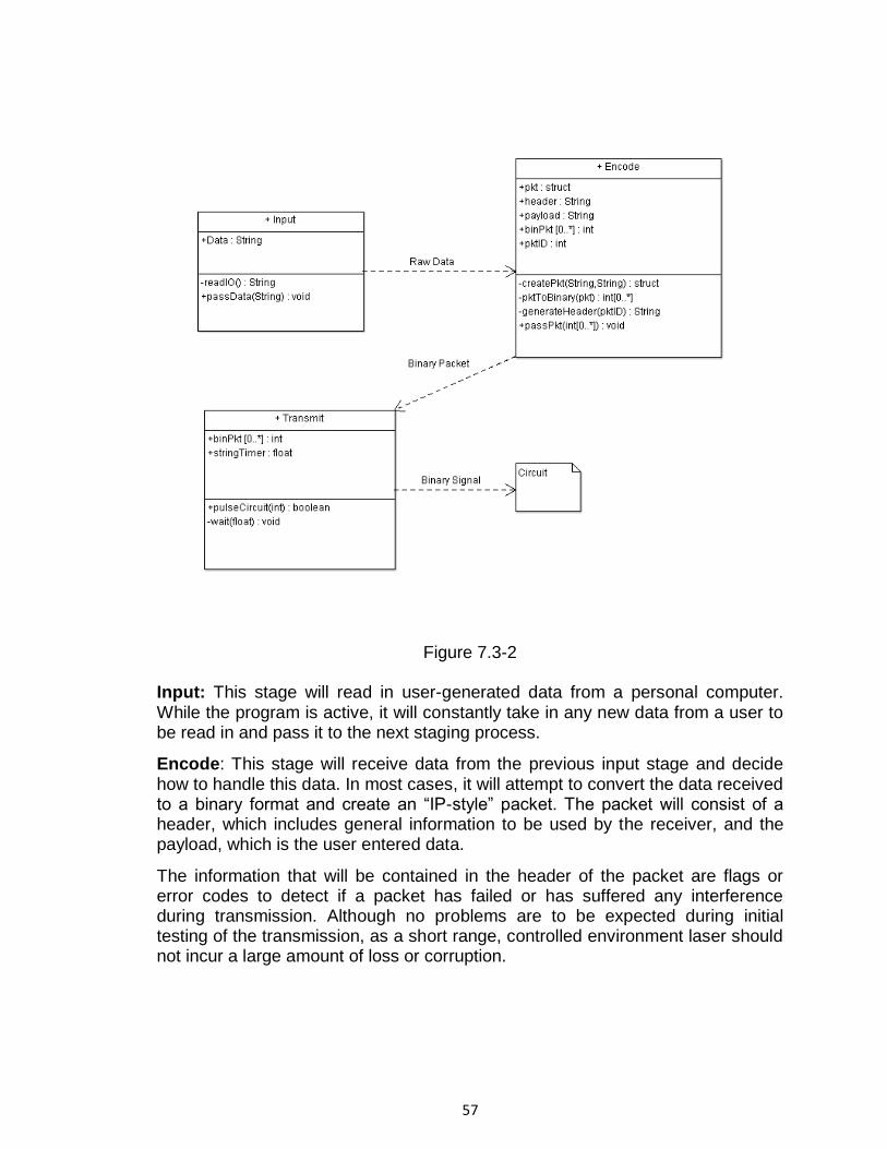
57
Figure 7.3-2
Input: This stage will read in user-generated data from a personal computer. While the program is active, it will constantly take in any new data from a user to be read in and pass it to the next staging process.
Encode: This stage will receive data from the previous input stage and decide how to handle this data. In most cases, it will attempt to convert the data received to a binary format and create an “IP-style” packet. The packet will consist of a header, which includes general information to be used by the receiver, and the payload, which is the user entered data.
The information that will be contained in the header of the packet are flags or error codes to detect if a packet has failed or has suffered any interference during transmission. Although no problems are to be expected during initial testing of the transmission, as a short range, controlled environment laser should not incur a large amount of loss or corruption.

58
Figure 7.3-3 Convection currents causing interference with a bidirectional laser communication system.
This addition will also allow us to scale up the project and increase the distance to where packet loss will eventually become a common issue that will need to be handled. This packet loss can be caused by various environmental factors and these tests will be done in Florida, where the sun and heat will be one of our biggest environmental factors. If we do not take this into account, we can face the possibility of a large amount of data being lost, as the environment can cause an issue similar to that shown in the figure above. Transmit: This stage will receive the packet, which is just a binary string, from the Encode stage. It will take that received packet and pulse one of the output ports on the microcontroller. This port will be connected to our transmit circuit which consists of the laser, driver circuit, etc. The port will pulse a current either on or off, with which the circuit will decide how to pulse the laser.
7.3.2 Connection to Driver Circuit
The driver circuit will be attached directly onto the custom board with a signal pin being attached to it. A possible issue with this setup that will have to be dealt with

59
is the possibility of needing more current than the microcontroller can output, which will put the microcontroller at risk of being destroyed. This may have to be resolved by adding a separate current source to the driver or having multiple pins output current to the driver synonymously, which may not be possible due to timing issues.
7.4 Receiver Microcontroller
The microcontroller on the receiver side of the project will have all the parts mentioned in one of the previous sections (7.2.1 Shared components of the custom boards) and the photodiode circuit, which is discussed in detail in section 4.1. Below is the planned schematic for the custom single-microcontroller board which we plan to use in the prototyping phase on the receiver side of the project. The design of this board are nearly identical to that of the transmitter side.
Figure 7.4-1

60
7.4.1 Code structure
The microcontroller on the receiver side of our device will act as our demodulator, as it will be able to differentiate the pulses sent by the transmitter by the software running on the microcontroller. Since the incoming data will be time modulated, we can set a delay of the software to tell packets apart from each other. The code structure of the receiver software will also follow an object oriented approach, in which it will be sectioned out into four main stages: input, decode, decipher, and output.
Figure 7.4.1-1
Input: This stage will be the most active stage during the receiver’s runtime. It will be constantly running and waiting for the transmitter to send a signal. Once that signal is received, the input stage will read in the full string and pass it to the decode stage.
Decode: This stage will receive the signal data or packet from the previous stage and deconstruct it into one continuous string to be deciphered in the next stage. The most difficult challenge in this stage will be to successfully reconstruct the signal, especially in the vent of loss or interference. If the signal cannot be properly decoded, it will not be able to be deciphered and result in an error.
Decipher: This stage will take in the decoded binary string and attempt to deconstruct the header and payload portions of the packet. If the stage is successful in deconstructing the header and payload, the payload and packet identifier will be passed on to the next stage to be output. The header is used to

61
ensure the current frame of the receiver matches that of the packet sent by the transmitter. If the frames do not match, the receiver will assume that the previous packet has been lost, and will report an error. This lost packet will also have to be dropped as the channels currently in the project are not planned to be bidirectional.
Output: This stage will receive the converted payload and packet identifier, which will have been passed as an ASCII String to be printed out to the user. This will be achieved via a serial connection from a personal computer to the receiver end microcontroller to exchange data.
7.4.2 Connection to Sensor Circuit
The microcontroller will be at the end of the Sensor Circuit to read in the data from its digital I/O pins. Since the microcontroller and receiver circuit must be in always on, it will require a steady supply of power that can constantly maintain the system. If the power drops below an acceptable range, there is a high probability of a packet being lost. This will be taken into account when designing the power system for the project.
7.4.3 Handling lost or corrupted packets
There are currently no plans to expand this project to have a bidirectional channel, loss and corruption cannot be dealt with by traditional networking means, where the receiver would simply request for the packet to be resent. The only currently available option to us is to simply detect when an error occurs and report it to the terminal. These erroneous packets have to be dealt with each in their own way and will be discussed separately in this section.
Packet loss: To deal with packet loss, we will have to delve into the header information which will be included in the packet upon creation. During the packet’s creation, there will be header information added. This information will include a Sequence number, size of the payload, and a timestamp. The sequence number or SEQ will act as a packet’s identifier, and conventionally the SEQ number will increase by the size of the payload. This can be seen in the diagram below.

62
Figure 7.4.3-1
As you can see in the above diagram, when the receiver obtains the first packet, it knows the first packet’s SEQ number and the size of that packet. The next packet the receiver will be expecting should have a SEQ of the previous SEQ plus the size of the previous packet, or in this case 24. In this scenario, the packet with SEQ 24 is lost, so when the next packet is sent with the SEQ of 40, the receiver will know that the packet with SEQ 24 never arrived and is assumed lost. It will then report this error to the terminal to let the user know that the packet was lost in transmission. Packet corruption: As with packet loss, there is no efficient way to deal with packet corruption so the most we can do in this situation is report the error when it is obtained. A packet can be corrupted from a numerous amount of reasons, from signal interference, power fluctuations, environmental factors, and etc., so aside from removing as many sources of interference as possible it is difficult to account for all errors. A scenario of a packet corruption can be seen in the diagram below.

63
Figure 7.4.3-2
Packet corruption can potentially be very difficult to account for as there is a slim possibility that the header remains unaffected, but the payload is corrupted. This may be alleviated by the implementing a checksum of some sort where the checksum is calculated and cross checked with a checksum of the packet on the receiver end of the network. Hopefully, packet corruption should be a fairly rare issue to occur as using a laser over short distances in a controlled environment should reduce any outside influences on the laser and signal itself.
8.0 Circuits
An electronic circuit is a network of electronic components connected by wires that have an electric current flowing. There is an infinite amount of combinations for these electronic components that have an array of operations. Circuits can be made different ways, but modern techniques are used to write on printed circuit boards (PCB) and solder flip chips onto these PCBs. Integrated circuits are another way to create a circuit board, this method uses microelectronic techniques on a substrate that contains various semiconductors. However, breadboards are commonly used for testing new designs. Additionally there are three types of electronic circuits; an analog circuit, a digital circuit, and a mixed-signal circuit.
8.1 Analog Circuit
Analog circuits have continuous and variable signals, and can carry information by current, voltage, or frequency. These circuits use a combination of fundamental electronic components, that are analog, and each component has a

64
specific symbol used as a visual representation. Figure 8.1-1 shows some common analog circuit symbols. Additionally, Figure 8.1-2 shows most of the common power supply symbols. Although these circuits are difficult to design the benefit of using an analog circuit is that no information will be lost since the output is also analog. Additionally, amplifiers and filters are the considered the most important application of an analog circuit.
Figure 8.1-1: Starting from the left, the first symbol is called the earth ground and is used as a zero potential reference and for electrical shock protection. Following is the chassis ground, also a zero potential reference but is connected to the chassis of the circuit board. The third symbol is a resistor and is used to reduce current flow. The fourth symbol is a capacitor and is used to store electric charge and acts as a short circuit with AC and an open circuit with DC. The fifth symbol is an inductor that represents a coil and generates a magnetic field. The sixth is a photodiode and allows current to flow when it is exposed to light. Finally, the last component is an operational amplifier and amplifies the input signal.
Figure 8.1-2: Starting from the left, the first power supply symbol is a voltage source that generates a constant voltage. The next symbol is a current source and generates a constant current, following with an AC voltage source. The fourth symbol is a battery and also generates a constant voltage. The fifth symbol is a controlled voltage source and generates a voltage as a function voltage or current of other circuit elements. The last symbol is a controlled current source and generates current as a function of voltage or current of other circuit elements.
8.1.1 Analog Circuit Schematics
A circuit schematic is a graphical representation, similar to a blue print of a building, of an electrical circuit. The use of a circuit schematic is necessary for analyzing and building the circuit. Each circuit schematic uses electrical symbols that represent the electrical components on a circuit and an example of an analog circuit schematic is shown below as figure 8.1.1-1.

65
Figure 8.1.1-1: Basic non-inverting amplifier.
8.2 Laser Driver
Upon choosing the appropriate laser for the project, the next component in the
process is a way to modulate the laser. The easiest method discussed in the
laser modulation section was pulse code modulation, also broadly known as
direct modulation. Modulating the current being sent to the Mitsubishi FU-68SDF-
V802MxxB laser is the most effective solution to driving the laser. This is
because the Mitsubishi FU-68SDF-V802MxxB laser package was designed for
be current driven. Figure 8.2-1 is a Light vs Current diagram, or LI Diagram, that
characterizes the laser operation. The laser receives an input current (green) and
transmits a signal (red) of greater amplitude to the receiver. The frequency of
both the input and output currents remain the same throughout this process,
which means the group is restricted to only manipulating the lasers input current
source to achieve high speed data rates. One of the most common and effective
methods to manipulating the input current source to the laser is with a current
driver. In order to meet product specifications the group researched different
laser diode drivers currently on the market and determined the most compatible
driver to achieve the highest possible data rates. The following section is a
comparison of the top three laser drivers on the market.

66
Figure 8.2-1
8.2.1 Product Comparison
To get an idea of the capabilities of laser diode drivers the group researched
three different drivers. Table 8.2.1-1 is a comparison between these three
drivers.
Table 8.2.1-1 Laser Diode Diver Comparison
Supply
Voltage
(V)
Min
Bias
Current
(mA)
Packaging
Configuratio
n
Data
Rates
(Gbps)
Pulse
Width
(ps)
Price
$
Texas
Instrument
s
ONET1101L
3.3 5 QFN
Package 2-11.3 60
Sampl
e
Mindspeed
M02067 3.3 4 Tray up to 2.1 <150 8.50
Philips
TZA3047A 3.3 5 BCG
.030-
1.25 300 10
The chosen laser diode drivers are all RoHS compliant. Driver components are
constructed out of hazardous materials. In order to limit the amount of hazardous
materials the driver is assembled out of restrictions are placed on these
0
2
4
6
8
10
12
14
16
18
Threshold Current

67
components and others. Table 8.2.1-2 is a list of hazardous materials and there
limitations.
Table 8.2.1-2 Hazardous Material Restrictions to Meet RoHS Standards
Lead (Pb) < 1000 ppm
Mercury (Hg) < 100 ppm
Cadmium (Cd) < 100 ppm
Hexavalent Chromium: (Cr VI) < 1000 ppm
Polybrominated Biphenyls (PBB) < 1000 ppm
Polybrominated Diphenyl Ethers
(PBDE)
< 1000 ppm
Bis(2-Ethylhexyl) phthalate (DEHP) < 1000 ppm
Benzyl butyl phthalate (BBP) < 1000 ppm
Dibutyl phthalate (DBP) < 1000 ppm
Diisobutyl phthalate (DIBP) < 1000 ppm
It’s not only important to maintain RoHS compliance for environmental reasons,
but also because the RoHS compliant components are easily accessible to the
consumer in the United States. Upon reviewing the laser diode drivers above the
Texas Instruments model ONET1101L driver would suit the project best. The
driver is capable of pulse widths at 60ps (30ps rise time and 30ps fall time),
which is around 67 times faster than the Mitsubishi FU-68SDF-V802MxxB laser
can be pulsed to. The limiting factor is then the laser. The chosen laser diode
driver also meets ESD (Electrostatic discharge) standards. Electrostatic
discharge control is an important standard to upkeep. According to the
ANSI/ESD S5.3.1-2009 standard this device maintains ground contact, uses
static dissipative materials to replace insulators and uses air ionization to
neutralize charge on device packages. Some of these methods of control aid to
prevent the component from receiving or sending out electrostatic discharge.
MSL (Moisture sensitivity level) standards are also met. There are 7 levels to
MSL that corresponds to the amount of time a component can be set on a shelve
before being heated up, or baked: MSL 1-Unlimited time, MSL 2-1 year, MSL2A-
2 weeks, MSL 3-168 hours, MSL 4-72 hours, MSL 5-48 hours, MSL 5A-24 hours,

68
and MSL 6-Mandatory bake before use. The laser diode driver chosen is a MSL
2 level and, therefore, meets the standard according to IPC-M-109. The laser
driver is also capable of between 2-11.3 Gbps. This bit-rate range meets the
specifications of the project, highlighted in the design specification section of this
document. The following section describes some capabilities that will be useful
when designing the project.
8.2.2 Texas Instruments ONET1101L Attributes
The ONET1101L laser driver is an integrated circuit with multiple specifications
this project can utilize. Table 8.8.2-1 is a comparison between the decided laser
for the project and the laser driver circuit to verify that the two components will be
compatible with each other. From this table it is apparent that both components
can operate simultaneously to provide the project with a modulated laser signal.
Table 8.2.2-1 Component matching: Laser with Laser Driver
Mitsubishi FU-
68SDF-V802MxxB
Texas
Instruments
ONET1101L
Matched
Supply/Operating
Voltage 1.3-1.8V 3.3V
Supply/Operating
Current 40-65mA 66-85mA
Pulse Width 150ps 70ps
Voltage
Regulating
Photodiode
Supply/Forward
Current
2mA 3.080mA
Input/Output
Impedance 25Ω 25Ω
The Texas Instruments ONET1101L is also configured in a QFN packaging
scheme, making integration onto the PCB microcontroller seamless. The next
section describes the QFN package and why it is beneficial to PCB designs.
8.2.3 QFN Packaging
QFN stands for Quad Flat No-Lead, and has quickly became an industry
standard when designing PCBs. Figure 8.2.3-1 was taken using a program called

69
Eagle and is a picture of the pin layout of the laser driver being incorporated into
the laser data transmission project.
Figure 8.2.3-1
This packaging type is advantageous to the consumer because the contacts are
directly under the package chip so the leads are not exposed. The QFN package
also sits flush with the PCB board. This will mitigate any damage that can be
done to the chip by means of transporting or moving the PCB. The package is
very small. Texas Instruments ONET1101L laser driver dimensions are 4mm x
4mm x 1mm. This small profile demands less overall PCB area allowing for either
a smaller PCB board or other component space. The next section will introduce
the laser driver design.
8.3 AC to DC Converter Characteristics
A AC to DC converter is a key essential to transmitting a viable modulated signal
to the photodetector. The AC to DC converter converts a digital input signal from
an input device, such as a computer, to an analog signal that will modulate
current driving the laser beam. The three main jobs a digital to analog convert is
responsible for performing is
1. Sampling Amplitude- the digital to analog converter creates a continuous,
or analog, current signal equal to a numeric value read from a computer
file. The more accurately the converter can perform this task the higher
quantization level the laser system can transmit.
2. Sample Timing- the digital to analog converter must also establish the
analog current signal with a stable timing that can be detectable by the
laser. If an analog current signal had timing faster than the laser could
modulate then data would be lost.

70
3. Filling in errors- there is a certain error that occurs throughout the digital to
analog converting process. This “quantization error” can be mitigated
through the use of a clock signal that synchronizes the entire system to
check the laser signal at discrete times.
There are several methods to designing a AC to DC converter. Some of the more
popular methods are as follows:
1. Pulse width modulation is a form of modulation where data is represented
by the ratio of the time to the total time, or duty cycle. Pulse width
modulation is one of the easiest methods to control a digitally encoded
analog signal.
2. Oversampling or interpolating- interpolating is a digital circuit that accepts
a low rate data signal, adds zeros at a high rate, and then applies a digital
filter algorithm and outputs an analog signal at a high rate. A primary
circuit lta-sigma digital to analog converter.
3. Binary-weighted-contains electrical components for each bit and a
summing point. Binary weighted digital to analog converters produce very
fast analog signals, but are not precise. The cost to produce an efficient
binary-weighted digital to analog is too high. This component will not be
practical when maintaining a budget.
4. R-2R ladder- is similar to the binary weighted digital to analog converter
except it uses cascaded repeating resistor values. This method increases
precision, but decreases the speed in which the analog signal can
modulate the laser.
5. Cyclic or successive approximation- this digital to analog converter allows
each digital input to be processed in each cycle.
6. Thermometer-coded- contains an equal resistor or current source
segments. This is one of the most efficient digital to analog converters but
the converter is expensive and cannot be incorporated in this project.
Upon researching of the process of AC to DC converters it will not be beneficial
to this project for signal transfer. Analog signals typically can be modulated at
higher rates. As the modulation rate of an analog signal increases the signal
noise increases. TO compensate for the increased noise complex filter circuits
would have to be incorporated that can eliminate frequencies that cause noise.
These filters sacrifice amplitude to perform this task. Losing any amplitude is not
ideal for the purposes of this project. Instead if the laser was pumped with a
square digital current source it can transmit much higher amplitudes. Rise and
fall times of the laser and receiver become the limiting factor. The components
we have chosen for this project have rise and fall times in the picosecond range
which will yield Gbps data transmissions. The next section will discuss the design
of the laser diode driver component. The following section will utilize the AC to
DC characteristics to design an AC to DC power converter.
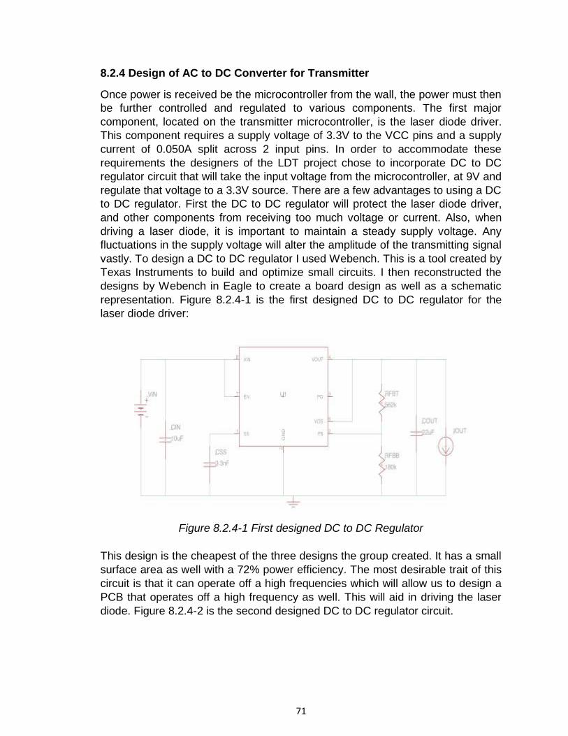
71
8.2.4 Design of AC to DC Converter for Transmitter
Once power is received be the microcontroller from the wall, the power must then
be further controlled and regulated to various components. The first major
component, located on the transmitter microcontroller, is the laser diode driver.
This component requires a supply voltage of 3.3V to the VCC pins and a supply
current of 0.050A split across 2 input pins. In order to accommodate these
requirements the designers of the LDT project chose to incorporate DC to DC
regulator circuit that will take the input voltage from the microcontroller, at 9V and
regulate that voltage to a 3.3V source. There are a few advantages to using a DC
to DC regulator. First the DC to DC regulator will protect the laser diode driver,
and other components from receiving too much voltage or current. Also, when
driving a laser diode, it is important to maintain a steady supply voltage. Any
fluctuations in the supply voltage will alter the amplitude of the transmitting signal
vastly. To design a DC to DC regulator I used Webench. This is a tool created by
Texas Instruments to build and optimize small circuits. I then reconstructed the
designs by Webench in Eagle to create a board design as well as a schematic
representation. Figure 8.2.4-1 is the first designed DC to DC regulator for the
laser diode driver:
Figure 8.2.4-1 First designed DC to DC Regulator
This design is the cheapest of the three designs the group created. It has a small
surface area as well with a 72% power efficiency. The most desirable trait of this
circuit is that it can operate off a high frequencies which will allow us to design a
PCB that operates off a high frequency as well. This will aid in driving the laser
diode. Figure 8.2.4-2 is the second designed DC to DC regulator circuit.

72
Figure 8.2.4-2 Second designed DC to DC Regulator
This second design is similar to the first in almost every way except it is slightly
more expensive. For this reason the second circuit will not be used in the design.
Figure 8.2.4-3 is the third and last designed DC to DC regulator circuit.
Figure 8.2.4-3 Third designed DC to DC Regulator
The last design is a simple in construction, which makes it more desirable. It is
the most expensive, though the cost difference between the three circuits are
negligible. The most undesirable trait of this circuit is the operating frequency is
low. This is a good circuit to prototype with because the Audunio Due operates
on lower pin frequencies of 64kHz, but for PCB design the group will hav eto use
a higher operating frequency. Table 8.2.4-4 is a product comparsion of the three
designed circuits and their attributes.
Table 8.2.4-4 Product Comparison DC to DC regulator Circuit Design
Components
Bill of
Materials
Cost
Efficiency Frequency Temperature

73
TPS62122 7 $0.68 72% 874kHz 35°C
TPS62120 8 $0.69 72% 874kHz 35°C
TPS563200 7 $0.89 84% 78kHz 31°C
Upon analysis of the three different circuit designs it would be most beneficial to
use the first circuit, or TSP62122 as seen in Figure 8.2.1-1. This circuit contains
the most desirable characteristics such as high operating frequency, meets the
standard 9V at 1A input to 3.3V output at 50mA regulation, and is cheap.
Efficiency is not a big concern we will be using the wall as our power source and
not a battery.
8.2.5 Design Laser Diode Driver
The laser diode driver is a key component in transmitting a useable data signal
so the design of the driver is extremely important. Figure 8.2.5-1 is a schematic
representation of initial design of the laser diode driver. The schematic, designed
using a program called EagleCAD allows the design team to get a better
understanding of the driver and begin simulating possible circuit behaviors.

74
Figure 8.2.5-1
Table 8.2.5-2 identifies and offers a brief description of the pins on the driver.
The driver will be powered by connecting the VCC pins together in parallel, as
each pin will be supplied with 3.3V of power. The transmitting laser, marked D1
in the schematic, will be on pin 13. The driver will function by first accepting a
digital square waveform from a computer through the SCK clock and SDA data
ports gets modulated and is output through the MOD+ and MOD- pins. MOD+
will bias the transmitting laser diode at high values for the input data signal and
MOD- will bias the laser diode at low values. An internal photodiode included in
the laser packaging will be connected to pin PD. The scans the laser diode to
regulate the output power of the laser. This is necessary to ensure a stable
transmission signal. This laser diode driver design will be integrated into the PCB
microcontroller design. Please see the microcontroller design section for details.
Table 8.2.5-2 Laser Diode Driver Pin Identification
Port Number Port Identity Description

75
1 FLT Fault Detection Flag
2 GND Ground
3 DIN+ Not in use
4 DIN- Not in use
5 GND Ground
6 RZTC Not in use
7 MONB Not in use
8 MONP Not in use
9 COMP Not in use
10 VCC 3.3V Power Supply
11 GND Ground
12 BIAS Not in use
13 VCC 3.3V Power Supply
14 MOD+ Output Current (high)
15 MOD+ Output Current (high)
16 MOD- Output Current (low)
17 MOD- Output Current (low)
18 VCC 3.3V Power Supply
19 PD Internal Photodiode
20 GND Ground
21 VCC 3.3V power supply
22 DIS Disables bias and
modulation current at
high state
23 SCK Serial Clock
24 SDA Serial Data Input
8.3 Photodetector Circuit

76
As discussed in chapter 4, a photodetector is a semiconductor device that electrically detects optical signals and converts the optical signal into an electrical signal. The photodetector semiconductor device applies the photovoltaic effect which converts the incident light into an electrical voltage or current. Incident light on a photodetector from a laser diode can either be visible or invisible, infrared, to the naked eye and this property will help choose the correct photodiode for a given circuit. Chapter 4 also discussed the basic processes of various photodetectors that can be used; in the chapter those semiconductor photodetectors will be applied into circuits with additional electrical components to analyze and transfer data.
8.3.1 Photodiode Circuit Design
The voltage in a photodiode circuit is in reverse-bias and when no light is incident on the photodiode only a reverse-saturation current is present. A photocurrent is the result of incident light on the diode and is in the reverse-bias direction. The photocurrent can be calculated by 𝐼𝑝ℎ = 𝜂𝑒𝛷𝐴, where η is the quantum efficiency,
𝑒 is the electronic charge, Φ is the photon flux (#/𝑐𝑚2𝑠) and A is the area of the junction. There is a linear relationship between photon flux and photocurrent, a basic photodiode circuit design is represented in figure 8.3.1-1. Two ways commonly used to operate a photodiode are the photovoltaic mode and photoconductive mode; although both the designs are similar their properties are not.
Figure 8.3.1-1: A basic photodiode circuit, the diode is reverse biased. This circuit transforms the photocurrent produced by the photodiode into an output
voltage. 𝑉𝑂 < (𝑉𝐷 + 𝑉𝑃𝑆) Where 𝑉𝑂 is the output voltage, 𝑉𝐷 is the diode voltage, and 𝑉𝑃𝑆 is the power source voltage.

77
8.3.2. Photoconductive Mode
As discussed in chapter 4, the photoconductive mode, a type of photoelectric effect, converts light into an electrical current resulting in an increase in the electrical conductivity of a device when exposed to light. For applications that use the photoconductive mode, a reverse bias must be applied resulting in greater response speed, linearity of the device, and lower capacitance. Additionally, the photoconductive mode is used when speed is the key parameter being analyzed.
When a reverse-bias is applied to the photodiode a current leakage becomes
present and is known as dark current 𝐼𝐷𝑎𝑟𝑘. Additionally, when incident light is blocked, the resulting output voltage becomes 𝑉𝑂 = 𝐼𝐷𝑎𝑟𝑘 ∗ 𝑅. Key properties of using this circuit under reverse-bias are: High-speed response, and wide output. However, with the simple circuit in figure 8.3.2-1 high sensitivity and speed cannot be achieved at the same time.
As the voltage produced by the photodiode increases the output current no longer remains proportional to the light intensity. By applying an op-amp to the circuit in figure 8.3.1-1, a constant reverse-bias voltage will be obtained for all incident light intensities and a schematic is shown in figure 8.3.1.2.1-1. Additionally, the op-amp will convert the photocurrent into an amplified voltage but due to the resulting capacitance in the photodiode, oscillations can occur in the op-amp. To compensate for the oscillations, a feedback capacitor is connected in series with the resistor as shown in figure 8.3.2-2.
Figure 8.3.2-1: Schematic of a simple photodiode utilizing the photoconductive mode, this circuit is also known as a transimpedance amplifier.

78
Figure 8.3.2-2: Schematic of a transimpedance amplifier with a feedback capacitor.
InGaAs photodiodes, which operate in the near infrared range, are commonly used because to their wide range of applications and will be discussed as a potential photodiode for this design. Understanding the electrical characteristics is important to designing any circuit. The photovoltaic mode is used for precision measurements.
Shunt Resistance, Rsh, is used to calculate the noise in the current in photovoltaic mode and is determined by the slope of the current-voltage curve of the photodiode. Low shunt resistance will result in power loss as the photocurrent will have an alternate current path to flow. Additionally, an ideal photodiode has infinite resistance; therefore the greatest achievable shunt resistance is preferred.
Series resistance, Rs, is used to determine the linearity of the photodiode under photovoltaic mode. Typically this resistance is irrelevant due to its low value; however a value is observe and is commonly caused by current movement and
metal contact in the semiconductor. This can be calculated by Rs =(Ws−𝑊d)𝜌
𝐴∗ Rc,
where W𝑠 is the substrate thickness, 𝑊d is the depletion region width, A is the junction area, and ρ is the substrate resistivity, and RC is the contact resistance.
Junction Capacitance, CJ, is used to determine the speed of the response of the photodiode. The junction capacitance is the same expression for a parallel plate capacitor; however the depletion layer width is considered the spacing between the two plates and is dependent upon the reverse bias voltage and is shown in

79
figure 8.3.2-3. The following equation is used to calculate the junction
capacitance of a photodiode: CJ=ϵϵ0A
𝑊𝑑, where Wd is the depletion depth, Wd =
√2ϵSiϵ0𝜌𝜇(VA + Vbi), ϵ is the dielectric constant of the semiconductor material, ϵ0
is the permittivity of free space, 𝜇 is the mobility of electrons at room
temperature, 𝜌 is the resistivity of semiconductor material, VA is the applied voltage and Vbi is the built-in voltage. Figure 8.3.2-4 is a schematic of this circuit with the components discussed.
Figure 8.3.2-3: The figure shows the dependence of capacitance on the reverse bias voltage of a photodiode under the photoconductive mode.
Rise time (tr), and fall time (tf), are times for a signal to rise from 10% to 90% and fall from 90% to 10% of the final value. Commonly expressed as frequency
response (t3dB) and is approximately tr≅0.35
f3db and is inversely proportional to
bandwidth (f3db).

80
Figure 8.3.2-4: An ideal photodiode circuit in parallel with a current source. The junction diode is parallel to the shunt resistance that is connected in series with
the series resistance. RL is the load resistance.
8.3.2.1 Photovoltaic Mode
The photovoltaic mode, a type of photoelectric effect, converts light into an electrical current or voltage by using a type of solar cell. When applied to a circuit, as shown in figure 8.3.2.1-1, the photovoltaic mode operates under zero bias voltage resulting in no current and a voltage build up. This mode is typically used for low frequency and low light applications. With no voltage across the photodiode there will be no dark current, to be discussed in the photoconductive mode section, resulting in lower noise and a linear output.

81
Figure 8.3.2.1-1: Schematic of a simple photodiode utilizing the photovoltaic mode.
8.3.3 Thorlabs InGaAs photodiode circuit
After selecting the correct photodiode the first circuit to be tested will be the recommended circuit provided by Thorlabs and a schematic of this circuit is shown in figure 8.3.3-1.
Figure 8.3.3-1: Thorlabs recommended circuit for the FGA01 InGaAS photodiode.
9.0 Prototype Testing

82
Once the project is designed it needs to be tested before major component such
as the PCB can be fabricated. Fabrication and testing are dependent on each
other and will occur simultaneously therefore our project will be striving to reach
our milestones on time. This section focuses on both hardware and software
testing. Testing these will ensure a project that meets all specifications
requirements, determines functionality, and maintains quality the entire project.
This section will test each subsection of the project to confirm that each piece of
the design is functioning as intended.
9.1 Testing Environment
For the purposes of this project there will be three different types of testing
environments. The three types of testing environments are in a laboratory setting,
inside common areas and outdoors. Most of the laboratory prototype testing will
be conducted in the College of Optic and Photonics undergraduate lab. To test
circuitry and other electronic components we may utilize the senior design lab in
the College of Electrical Engineering and Computer Science Engineering 2
building. The group will prototype major components together but it will be the
responsibility of the individual group member to ensure their smaller subsystems
are properly tested. Outside testing will be conducted upon completion of the
transmitter to collect data on how the signal will transmit in outside conditions.
9.2 Transmitter Testing
How the signal will transmit through the air is a vital component to maximize
efficiency. In order to begin testing on the transmitter the group will first construct
the housing using Figures 5.6-1, 5.6-2 and 5.6-3 as guidelines. The two major
functions required of the transmitter housing for initial prototype testing is having
the adjustable feet and a secure location for the laser to be mounted. The laser
can then be adjusted according to the needs of the test. The required
components for testing will be the laser, the prototype microcontroller, a
measuring device, an oscilloscope with input and output connectors and a power
meter that reads up to 6mW of power at 1550nm. The power meter and
oscilloscope will be supplied courtesy of the College of Optics and Photonics.
Simple tests will be conducted to ensure the laser functions properly, and to
pulse the laser beam all at varying distances. We will record the results and
repeat this process in all three environments. This data will establish a baseline
and give the group an idea of the capabilities of the laser system. The group can
then design a PCB microcontroller based off the results of the results from
testing. The next stage to testing is when the receiver is designed and tested for
functionality. The same testing will be conducted in order to draw comparisons
between each batch of data results. Once the PCB microcontroller and voltage
regulator have been tested for functionality they will be incorporated into the
transmitter housing. A third prototype testing date will be required in which the
group attempts to recreate the results from the first two tests by using the same

83
clock speed, supply voltage and vary the current in the same matter. The final
prototype testing will occur to maximize the bit rate of the system. and voltage
regulator have been tested for functionality they will be incorporated into the
transmitter housing. A third prototype testing date will be required in which the
group attempts to recreate the results from the first two tests by using the same
clock speed, supply voltage and vary the current in the same matter. The final
prototype testing will occur to maximize the bit rate of the system.
9.3 Transmitter Subsystem Testing
There are two subsystem components to the transmitter, which are the voltage
regulator circuit and the PCB microcontroller. The designed voltage regulator will
be tested by simply observing the input and output waveforms at varying input
DC voltages. The regulator will regulate voltage to the laser so the group will be
looking for a maximum output voltage of 1.8V to meet the operating voltage of
the laser described on the datasheet. Once tested the regulator circuit will be
integrated to the transmitter design.
9.4 Photodiode Testing
For the testing we will first start of by using the Thorlabs recommended circuit
and from there move on to other circuits. The reason for using the recommended
circuit is to verify that the photodiode is working correctly and to avoid any
damage to the photodiode and surrounding circuitry. Three measurements that
will be conducted to verify this will be the responsivity, dark current, and
capacitance curves. The results that will be recorded will not be exactly the same
as the results obtained by Thorlabs. Figure 9.4-1 is the responsivity observed by
Thorlabs, figure 9.4-2 is the Dark Current, and figure 9.4-3 is the capacitance
curve.
Figure 9.4-1: Responsivity observed by Thorlabs from 800nm-1700nm.
0
0.2
0.4
0.6
0.8
1
1.2
800 900 1000 1100 1200 1300 1400 1500 1600 1700
Res
po
nsi
vity
(A
/W)
Wavelength (nm)
FGA01 Responsivity

84
Figure 9.4-2: Dark current observed by Thorlabs.
Figure 9.4-3: Capacitance observed by Thorlabs.
After we run the experiment a comparison will take place between Thorlabs data
and our data. If we see similarities we will proceed to carry out more experiments
to ensure that data transfer will occur.
9.5 Microcontroller and Peripheral testing
Each testing cycle for ensuring the microcontroller is functioning properly will include three stages of testing. The first stage will test to ensure that the data being transferred from the PC to the microcontroller is being encoded properly to
0
0.1
0.2
0.3
0.4
0.5
0.6
0.01 0.1 1 10
Dar
k C
urr
ent
(nA
)
Reverse Bias (V)
FGA01 Dark Current
0
1
2
3
4
5
6
0 2 4 6 8 10 12 14 16 18 20
Cap
acit
ance
(p
F)
Reverse Bias (V)
FGA01 Capacitance

85
be sent. The second stage is to ensure that the coming incoming data is being decoded properly with as little errors as possible. The third stage is a stress test to see how fast the entire circuit and project will be able to transmit and receive a large amount of data. This test will also measure bit-rate test of how fast we are actually able to transmit. This stage breakdown can be seen in the following diagram.
Figure
9.5-1
First Stage: The first stage of testing will use the following guidelines and will be considered failing if any of these steps execute erroneously or fail to execute.
1. Port transmitter programs to their respective boards. 2. Ensure after the program is running that the microcontroller can receive
commands via a terminal from the PC and execute said commands. 3. Use a debugging mode of the program to ensure that the entered data is
converted properly through the staging pipeline for the transmitter (Input -> Encode -> Transmit)
4. Ensure that LED is in an on state after the final stage of the program being run.
Following these guidelines during the custom PCB implementation and the proof of concept section should allow us to debug and see if there is an error where it

86
is occurring and what the root cause of it could be on the transmitter’s end of the project. If an error occurs in step one, the error is most likely in the connection between the PC and microcontroller. If an error occurs in step two, there is a probable issue with the UART connection. If an error occurs in step three, there is a probable error with the software. If an error occurs in step four there is a probable error within the connection to the driver circuit and laser.
Second Stage: The second stage of testing will use the following guidelines and will be considered failing if any of these steps execute erroneously or fail to execute.
1. Port receiver programs to their respective boards. 2. Ensure that LED is in an on state after the data has been sent from the
transmitter side, this indicates that data has been received. 3. Use a debugging mode of the program to ensure that the entered data is
converted properly through the staging pipeline for the receiver (Input -> Decode -> Decipher -> Output)
a. If a received packet is lost, the receiver will only know after the next packet arrives successfully. In this case, the program will output an error message to the user about the packet being lost.
b. If a received packet is corrupted, the receiver will output an error with an appropriate message.
4. Ensure the data received is displayed correctly in a terminal on a PC on the receiver end of the project.
Following these guidelines during the custom PCB implementation and the proof of concept section should allow us to debug and see if there is an error where it is occurring and what the root cause of it could be on the receiver’s end of the project. If an error occurs in step one, the error is most likely in the connection between the PC and microcontroller. If an error occurs in step two, there is a probable issue with the photodiode or the connection between the transmitter and receiver. If an error occurs in step three, there is a very probable error with the software. If an error occurs in step four there is a probable error within the UART connection from the PC to the microcontroller.
Third Stage: The third stage will be tested repeatedly with an increase of load to test how the circuit will perform under a heavy load and how fast the bit rate will be under these loads. If we are at this stage in testing, then the previous stages can be assumed to have been successful. Our goal for this stage is to reach a speed of approximately 1 Mbps.
Initial aim for bit-rate: 1Kbps
1. Load one-byte file into microcontroller. If transmission is successful, check bit-rate. If the bit-rate matches aim, move to next step. If the transmission is lost or corrupted, resend.
2. Load 512-byte file into microcontroller in fragments. If transmission is successful, check bit-rate. If the bit-rate matches aim, move to next step. If the transmission is lost or corrupted, resend.

87
3. Load one-kilobyte file into microcontroller in fragments. If transmission is successful, check bit-rate. If the bit-rate matches aim, increase bit-rate aim to 16 Kbps, then move to next step. If the transmission is lost or corrupted, resend.
4. Load 512 Kb file into microcontroller in fragments. If transmission is successful, check bit-rate. If the bit-rate matches aim, increase bit-rate aim to 256 Kbps, then move to next step. If the transmission is lost or corrupted, resend.
5. Load 1 Mb file into the microcontroller in fragments. If transmission is successful, check bit-rate. If the bit-rate matches aim, the test is a success. If the transmission is lost or corrupted, resend.
Following these guidelines during the custom PCB implementation and the proof of concept section should allow us to test and debug to see if we are correctly implementing everything in the circuit and if our selected parts for the initial design are effective enough to achieve our goal. If any of these sections fail, we will have to redesign our custom PCB implementation or change our proof of concept board. A failure in this stage during the custom PCB implementation will be very costly with both hardware parts and time as we would have to reorder new better parts.
10.0 Administrative Content
10.1 Budget
MCU, PCB, Components – The budget as it pertains to these parts of the
project should be fairly inexpensive compared to other components needed in
the project. A lenient estimate for the max to be spent on these components is
one hundred dollars. Table 10.3-1 is the breakdown:
Figure 10.3-1: Budget for MCU, PCB, & other components
Part Quantity Cost per item
Arduino Mega 2 $13.99
MCU dsPIC30F3013-20I/SO 2 $3.83
Pololu USB to Serial Converter 2 $5.95
LED (Pack of 80) 1 $3.64
PCB Estimate 2 $15.00
TOTAL: $81.18
Transmitter Unit Components – Besides the microcontroller there are a variety
of components that need to be itemized and accounted for. Table 10.3-2 is a list

88
of the different components required in the transmitter unit, omitting the
microcontroller:
Table 10.3-2 Budget for the Transmitter Unit
Part Quantity Cost
Laser Diode 1 $148.50
Current Driver 1 Free from TI
Capacitators for Current Driver Circuit 10 Free from UCF
Resistors for Current Driver Circuit 5 Free from UCF
Inductors 4 Free from UCF
Strip board for transmitter DC to DC regulator 2 $11.80 from Amazon
Lexan Sheet for Transmitter Housing 12” X12” 1 $11.85 from Amazon
AC to DC Adapter for Transmitter 1 $11.65 from Walmart
Adjustable feet for Transmitter 4 Free Donated
Total $183.80
Receiver Unit Components – Omitting the microcontroller, Table 10.3-3 lists the
components within the receiver unit along with the cost of each item.
Table 10.3-3 Budget for the Receiver Unit
Part Quantity Cost
Photodiode 1 $56.70
AC to DC Adapter 1 $11.65
Capacitators 8 Free from UCF
Resistors 10 Free from UCF
Inductors 3 Free from UCF
Strip board for transmitter DC to DC regulator 2 $11.80 from Amazon
Lexan Sheet for Transmitter Housing 12” X12” 1 $11.85 from Amazon
AC to DC Adapter for Transmitter 1 $11.65 from Walmart
Adjustable feet for Receiver 4 Free Donated
Wires NA Free from UCF

89
Breadboard for Testing 1 $9.80 from Ebay
Total $113.45
Overall Budget – After tabulating every component required for the LDT project
the overall budget is calculated in Table 10.3-4.
Table 10.3-4 Overall Budget
Part Cost
Microcontrollers $81.18
Transmitter Unit $183.80
Receiver Unit $113.45
Total $378.43
This grand total for the LDT project meets the specification that was placed in
effect. An excess in our budget will serve the project in case of accidents or
repairs.
Conclusion
To conclude our paper, we believe we have sufficiently covered all possible
aspects of this project from start to finish. The project itself proved to be a great
deal more challenging than the group initially conceived, however through our
combined efforts and collective experience we were able to complete our goals
and milestones in a timely fashion. Our Laser Diode Transfer device has
progressed our individual knowledge in each of our prospective fields as the
project pushed us to travel into “unfamiliar waters”.
This project was initially conceived out of the idea of wanting to have a very fast,
secure medium of transport, which could be setup relatively quickly and easily.
Out of this thought, we eventually landed on using laser as the medium for this
transportation, as it did not restrict us in any conceivable way to what we wanted
to end up with.
From there we began to research into different types of lasers, photodetectors,
MCUs, and anything which we thought could even remotely be relevant to aiding
us in completing our task at hand. Admittedly, we may have been a tad
overzealous when it came to the scope of this project, however we know all of
the components in our project forwards and back. Each part was chosen
carefully after the extensive and rigorous testing was performed on our
prototype/proof of concept model. Once we had all of our parts selected, we
designed our necessary circuitry in a schematic using Eagle Cad software. This

90
schematic would eventually be transformed into our custom made printed circuit
board made especially for this project. This board would also be ordered
alongside protective casings for our transmitter and receiver sides of the project.
These casings would serve to protect our components from outside exposure, as
well as keeping our laser and photodetector seated to prevent us from ruining our
set directionality. It also had an added bonus of giving our entire project move of
a professional look, rather than having exposed wires and circuitry out for our
presentation.
Once our research was complete, we began to collect all of the necessary
components that would be needed for our project. Our biggest challenge here
was remaining in our budget. As per our testing procedures, all parts were
selected with the requirements needed for our laser and photodetector. At this
stage, the project was nearing about forty percent completion and there was
nothing to do but wait for all of our components to arrive. Eventually the day
came where we could finally start our building and assembling of the project after
months of planning and preparation.
After everything was assembled and prepared in our testing environment, we
began our rigorous rounds of testing. We tested our same build repeatedly until
we were either satisfied with the results or we scrapped a part and went back to
the drawing board. This reinforced our understanding of testing procedures that
everyday professional engineers endure to ensure that the product that they are
developing will be up to their requirements, code, and safety, which we will
undoubtedly experience when we join the workforce. This testing cycle went on
for weeks on end until we finally reached our milestone of having our LDT
achieve our desired bit rate of 1Mbps. Once our goal for the project was
complete, we continued to press our experiment to see how fast we could
actually get to. As a personal group goal we hope to reach speeds comparable to
common bitrates found for residential internet access, as it would provide another
method of data transfer which could possibly be used by a consumer.
All in all, this project gave us all a small experience of what is to come within the
engineering field in terms of how a major project is researched, designed, and
eventually created from the ground up. This project also demonstrated to us how
the mixing of different engineering fields allows for a group’s collective
knowledge to come together and create something that may have seemed
daunting or near impossible alone.
Appendix A: Permissions

91
Appendix C: Workcited
"All About Circuits - Electrical Engineering & Electronics Community." All About
Circuits - Electrical Engineering & Electronics Community. N.p., n.d. Web. 10
Dec. 2015.
"Features." Unmounted Photodiodes. N.p., n.d. Web. 10 Dec. 2015.
Jones, William B. Introduction to Optical Fiber Communication Systems. N.p.: n.p., n.d.
Print.
Neamen, Donald A. Microelectronics: Circuit Analysis and Design. New York:
McGraw-Hill, 2010. Print.

92
Nilsson, James William., and Susan A. Riedel. Electric Circuits. Boston: Prentice Hall,
2011. Print.
Sze, S. M., and M. K. Lee. Semiconductor Devices, Physics and Technology. Hoboken,
NJ: Wiley, 2012. Print.
Diffen. (n.d.). Retrieved 11 01, 2015, from Analog vs Digital:
http://www.diffen.com/difference/Analog_vs_Digital
HyperPhysics. (n.d.). Retrieved 11 15, 2015, from Gas Lasers: http://hyperphysics.phy-
astr.gsu.edu/hbase/optmod/lasgas.html
Laser Focus World. (1995, 07 01). Retrieved 11 05, 2015, from The three phases of
lasers:
http://www.laserfocusworld.com/articles/print/volume-31/issue-7/world-news/the-three-
phases-of-lasers-solid-state-gas-and-liquid.html
M. C. Lin, M. E. (n.d.). Annual Reviews. Retrieved 10 30, 2015, from Physical Chemistry:
http://www.annualreviews.org/doi/abs/10.1146/annurev.pc.34.100183.003013?journalCo
de=physche
m
Paschotta, D. R. (n.d.). RP Photonics Encyclopedia. Retrieved 11 15, 2015, from Laser
Diodes :

93
https://www.rp-photonics.com/laser_diodes.html
Peucheret, C. (2009, 11 22). Direct and External Modulation of Light. Retrieved from
http://www.cpeu.dk/data/uploads/teaching/34129_e2009_cpeu_dml_eml.pdf
RH Photonics. (n.d.). Retrieved 10 15, 2015, from Wavelength Division Multiplexing:
https://www.rp-
photonics.com/wavelength_division_multiplexing.html
Torry Hills Technologies, LLC. (n.d.). Retrieved 10 15, 2015, from Understanding of
Lasers, Laser Diodes,
Laser Diode packaging and its relationship to Tungsten Copper:
http://www.torreyhillstech.com/Documents/Laser_package_white_paper.pdf
Tanenbaum, A. (2003). Computer networks (4th ed.). Upper Saddle River, N.J.: Prentice
Hall PTR.
Zou, C. (2015, August 24). CNT 4704: Computer Communication Networks. Retrieved
November 1, 2015,
from http://www.cs.ucf.edu/~czou/CNT4704-15/notes.html