KV-1499XF_SERVICE MANUAL - Index of
46
MODEL COMMANDER DEST. CHASSIS NO. KV-1499XF RM-952 ME SCC-U16X-A MODEL COMMANDER DEST. CHASSIS NO. CHASSIS TRINITRON ® COLOR TV SERVICE MANUAL BG-3S Self Diagnosis Supported model
-
Upload
khangminh22 -
Category
Documents
-
view
2 -
download
0
Transcript of KV-1499XF_SERVICE MANUAL - Index of

MODEL COMMANDER DEST. CHASSIS NO.
KV-1499XF RM-952 ME SCC-U16X-A
MODEL COMMANDER DEST. CHASSIS NO.
CHASSIS
TRINITRON ® COLOR TV
SERVICE MANUAL BG-3S
Self DiagnosisSupported model

– 2 –
KV-1499XFRM-952
SPECIFICATIONS
Note
Power requirements 110-240 V AC, 50/60 Hz
Power consumption (W) Indicated on the rear of the TV
Television system B/G
Color system PAL, PAL 60, SECAM, NTSC4.43, NTSC3.58 (AV IN)
Channel coverage VHF: E2 to E12 / UHF: E21 to E69 / CATV: S01 to S03, S1 to S41
˘ (Antenna) 75-ohm external terminal
Audio output 3W + 3W
Number of terminal
D (Video) Input: 2 Output: 1 Phono jacks; 1 VP-P, 75 ohms
≥ (Audio) Input: 2 Output: 1 Phono jacks; 500 mVrms
@ (Earphone) Output: 1 Minijack
Picture tube 14 inch
Tube size (cm) 37 Measured diagonally
Screen size (cm) 34 Measured diagonally
Dimension (w/h/d, mm) 466 × 341 × 416
Mass (kg) 13
Design and specifications are subject to change without notice.
SAFETY-RELATED COMPONENT WARNING!!
COMPONENTS IDENTIFIED BY SHADING AND MARK ! ONTHE SCHEMATIC DIAGRAMS, EXPLODED VIEWS AND IN THEPARTS LIST ARE CRITICAL TO SAFE OPERATION. REPLACETHESE COMPONENTS WITH SONY PARTS WHOSE PARTNUMBERS APPEAR AS SHOWN IN THIS MANUAL OR INSUPPLEMENTS PUBLISHED BY SONY.
CAUTION
SHORT CIRCUIT THE ANODE OF THE PICTURE TUBE ANDTHE ANODE CAP TO THE METAL CHASSIS, CRT SHIELD,OR CARBON PAINTED ON THE CRT, AFTER REMOVING THEANODE.
Ø

– 3 –
KV-1499XFRM-952
TABLE OF CONTENTS
Section Title Page
SELF DIAGNOSIS FUNCTION ................................ 4
1. GENERAL ........................................................................ 8
2. DISASSEMBLY2-1. Rear Cover Removal ................................................ 182-2. Chassis Assy Removal ............................................. 182-3. F Bracket Removal .................................................. 182-4. Service Position ....................................................... 182-5. Replacement of Parts ............................................... 19
2-5-1. Replacement of Control Button .......................192-5-2. Replacement of Light Guide ............................19
2-6. Terminal Bracket Removal ...................................... 192-7. Degauss Coil Removal ............................................. 192-8. Picture Tube Removal .............................................. 20
3. SET-UP ADJUSTMENTS3-1. Beam Landing .......................................................... 213-2. Convergence ............................................................. 223-3. Focus Adjustment .................................................... 243-4. G2 (Screen) and White Balance Adjustments ......... 24
4. CIRCUIT ADJUSTMENT4-1. Adjustments with Commander ................................ 254-2. Adjustment Method ................................................. 264-3. Picture Quality Adjustments .................................... 314-4. A Board Adjustment After IC003 (Memory)
Replacement............................................................. 314-5. Picture Distortion Adjustment ................................. 32
Section Title Page
5. DIAGRAMS5-1. Block Diagram ......................................................... 355-2. Frame Schematic Diagram ...................................... 385-3 Circuit Boards Location .......................................... 405-4. Schematic Diagrams and Printed Wiring Boards ... 41
(1) Schematic Diagram of A (1/2) Board ...................... 43(2) Schematic Diagram of A (2/2) Board ...................... 47(3) Schematic Diagrams of C3 and F Boards ............... 54
5-5. Semiconductors ........................................................ 59
6. EXPLODED VIEW6-1. Chassis ..................................................................... 62
7. ELECTRICAL PARTS LIST ...................................... 64

– 4 –
KV-1499XFRM-952
The units in this manual contain a self-diagnostic function. If an error occurs, the STANDBY/TIMER lamp will automaticallybegin to flash.The number of times the lamp flashes translates to a probable source of the problem. A definition of the STANDBY/TIMERlamp flash indicators is listed in the instruction manual for the user’s knowledge and reference. If an error symptom cannotbe reproduced, the remote commander can be used to review the failure occurrence data stored in memory to reveal pastproblems and how often these problems occur.
1. DIAGNOSTIC TEST INDICATORSWhen an errors occurs, the STANDBY/TIMER lamp will flash a set number of times to indicate the possible cause of theproblem. If there is more than one error, the lamp will identify the first of the problem areas.
Result for all of the following diagnostic items are displayed on screen. No error has occured if the screen displays a “0”.
DiagnosticItem
Description
• Power does notturn on
• +B overcurrent(OCP) orovervoltage(OVP)
• Vertical deflectionstopped
• Horizontaldeflectionoverdrive
• White balancefailure (noPICTURE)
• Micro reset
No. of timesSTANDBY/TIMER
lamp flashes
Does not light
2 times
5 times
—
Self-diagnosticdisplay/Diagnostic
result
—
002:000 or002:001~255003:001~255004:001~255
at the same time
005:000 or005:001~225
101:00 or101:001~225
ProbableCause
Location
• Power cord is not pluggedin.
• Fuse is burned out F4601(F)
• H.OUT Q511 is shorted. (Aboard)
• -13V is not supplied. (Aboard)
• IC 503 faulty (A board)• IC 301 faulty ( A board)
• G2 is improperly adjusted.(Note 2)
• CRT problem.• IC301 is faulty. (A board)• No connection A board to
C3 board.
• Discharge CRT (C3 Board)• Static discharge• External noise
DetectedSymptoms
• Power does not come on.• No power is supplied to the
TV.• AC power supply is faulty.
• Power does not come on.• Load on power line is
shorted.• Has entered standby state
after horizontal raster.• Vertical deflection pulse is
stopped.• Power line is shorted or
power supply is stopped.
• No raster is generated.• CRT cathode current
detection reference pulseoutput is small.
• Power is shut down shortly,after this return back tonormal.
• Detect Micro latch up.
Note 1: If a + B overcurrent is detected, stoppage of the vertical deflection is detected simultaneously.The symptom that is diagnosed first by the microcontroller is displayed on the screen.
Note 2: Refer to screen (G2) Adjustment in section 3-4 of this manual.
SELF DIAGNOSTIC FUNCTION
– 5 –
KV-1499XFRM-952
2. DISPLAY OF STANDBY/TIMER LIGHT FLASH COUNT
Diagnostic Item Flash Count*+B overcurrent/overvoltage 2 timesVertical deflection stopped
White balance failure 5 times
* One flash count is not used for self-diagnostic.
3. STOPPING THE STANDBY/TIMER FLASHTurn off the power switch on the TV main unit or unplug the power cord from the outlet to stop the STANDBY/TIMER lampfrom flashing.
Lamp ON 0.3 sec.Lamp OFF 3 sec.Lamp OFF 0.3 sec.
2 times
5 times
STANDBY/SLEEP lamp
– 6 –
KV-1499XFRM-952
4. SELF-DIAGNOSTIC SCREEN DISPLAYFor errors with symptoms such as “power sometimes shuts off” or “screen sometimes goes out” that cannot be confirmed, itis possible to bring up past occurances of failure for confirmation on the screen:
[To Bring Up Screen Test]In standby mode, press buttons on the remote commander sequentially in rapid succession as shown below:
[Screen display] / channel [5] / Sound volume [-] / Power ON
˘Note that this differs from entering the service mode (mode volume [+]).
Self-Diagnosis screen display
002 : 000003 : 000004 : 000005 : 001
Numeral "0" means that no fault has been detected.
Numeral "1" means a fault has been detected.
101 : 000
SELF DIAGNOSTIC
5. HANDLING OF SELF-DIAGNOSTIC SCREEN DISPLAYSince the diagnostic results displayed on the screen are not automatically cleared, always check the self-diagnostic screenduring repairs. When you have completed the repairs, clear the result display to “0”.
Unless the result display is cleared to “0”, the self-diagnostic function will not be able to detect subsequent faults aftercompletion of the repairs.
[Clearing the result display]To clear the result display to “0”, press buttons on the remote commander sequentially as shown below when the diagnosticscreen is being displayed.
Channel [8] / 0
[Quitting Self-diagnostic screen]To quit the entire self-diagnostic screen, turn off the power switch on the remote commander or the main unit.

– 7 –
KV-1499XFRM-952
6. SELF-DIAGNOSTIC CIRCUIT
[+B overcurrent ªOCPº] Occurs when an overcurrent on the +B(135) line is detected by Q604. If Q604 go to ONand the voltage to pin 18 of IC301 should go down when V.SYNC is more than sevenverticals in a period, the unit will automatically turn off.
[Vertical deflection stopped] Occurs when an absence of the vertical deflection pulse is detected by Q509 and IC001shut down the power supply.
[Vertical deflection overcurrent] Occurs when an overcurrent on V drive line is detected by Q507. Power supply will beshut down when detect this by IC001.
[White balance failure] If the RGB levels* do not balance or become low level within 5 seconds, this error will bedetected by IC301. TV will stay on, but there will be no picture.
* (Refers to the RGB levels of the AKB detection Ref pulse that detects IK.)
IC301Y/CHROMA JUNGLE
FROMCRT
FROM[+B] Q604 C3
[V] Q509/507
IC001SYSTEM
IC003MEMORY
B-DAT
IO-SDAT
IK-IN
MP/PROTECT
IO-8DAT
O-LED
SDA
54521
18 51
4635

– 8 –
KV-1499X
FR
M-952
2
WARNING• Dangerously high voltages are present inside the TV.
• Operate the TV only between 110 – 240 V AC.
To prevent fire or shock hazard, do not exposethe TV to rain or moisture.
Do not operate the TV if any liquid or solid objectfalls into it. Have it checked immediately byqualified personnel only.
Do not open the cabinet and the rear cover of theTV. Refer servicing to qualified personnel.
Do not install the TV in hot, humid or excessivelydusty places.
Do not install the TV in a confined space, suchas a bookcase or built-in cabinet.Do not block the ventilation openings of the TV.
Do not pull the power cord to disconnect the TV.Pull it out by the plug.
Disconnect the power cord during lightningstorms or if you are not going to use the TV forseveral days.
Install the TV in a stable position. Do not allowchildren to climb onto it.
Do not plug in too many appliances to the samepower socket. Do not damage the power cord.
Clean the TV with a dry and soft cloth.Do not use benzine, thinner, or any other chemicalsto clean the TV. Do not scratch the picture tube.
4 Using Your New TV
Getting Started
Step 1
Connect the antennaIf you wish to connect a VCR, see the “Connecting a VCR” diagram below.
Using Your New TV
IEC connector(not supplied)
To video andaudio outputs
VCR
(yellow) (black)
Antenna cable (not supplied)
To … 1(video input)
Audio/Video cable(not supplied)
: Signal flow
To antennaoutput
Antenna cable(not supplied)
Rear of TV
Rear of TV
Connecting a VCRTo watch the video, press … (see page 11).
Note• You are advised to use an outdoor antenna for better reception.
Rod antenna and cable(supplied)
oror
To ˘(antenna)
: Signal flow
VIDEO
VIDEO IN
VIDEO OUT
AUDIO
1
SECTION 1
GENERAL
The operating instructions mentioned here are partial abstracts from the Operating Instruction Manual. The page numbers of the Operating Instruction Manual remain as in the manual.

– 9 –
KV-1499X
FR
M-952
5Using Your New TV
Usin
g Yo
ur N
ew TV
11
VHF LOW B/G
1
2
Notes• If you connect a stereo VCR, connect the yellow plug to (the yellow
jack) and the white plug to (the black jack).• If you connect a VCR to the ˘ (antenna) terminal, preset the signal
output from the VCR to the program number 0 on the TV.• When no signal is input to the connected video equipment, the TV screen
becomes blue.
Front of TV
Step 2
Note• Do not use old batteries nor use different types of batteries together.
Step 3Preset the channels automatically
Tips• If you want to exit automatic channel presetting, press SELECT twice.• If your TV has preset an unwanted channel or cannot preset a particular
channel, then preset your TV manually (see page 8).
Now You Are Ready. . .
To watch your TV, see page 11.
CAUTIONDo not connect the power cord until you have completed making all otherconnections; otherwise a minimum leakage current might flow through the antennaand other terminals to ground.
Insert the batteriesinto the remote
6 Using Your New TV
1
Connecting optional componentsYou can connect optional video components, such as a VCR, multi disc player,camcorder or video game.
To watch the picture of the connected equipment, press … (see page 11).
Connecting a camcorder/video game equipmentusing the … (video input) jacks
Note• You can also connect video equipment to the … 1 (video input) jacks at
the rear of your TV.
Connecting video equipment using the Ú(monitor output) jacks
Note• When connecting a stereo VCR, connect the yellow plug to (the yellow
jack) and the white plug to (the black jack).
Front of TV
Camcorder
Video gameequipment
To video andaudio outputs
(yellow) (black)
Rear of TVToantennaoutput
To video andaudio inputs
VCR
: Signal flow
: Signal flow
To… 2(video input)
To Ú(monitoroutput)
or
Audio/Video cable (not supplied)
Antenna cable (not supplied)
Audio/Video cable(not supplied)
2

– 10 –
KV-1499X
FR
M-952
8 Using Your New TV
Presetting channels (continued)
1 Press SELECT until“MANUAL PROGRAM”appears.
2 Press + or –.
3 Press PROGR +/– or thenumber buttons until thedesired program numberappears.
4 Press + or – until thedesired channel pictureappears.
5 Press SELECT.
1
Presetting channels manually
1 2 3
4 5 6
7 8
0-/--
9
PROGR
or
MANUAL PROGRAM
SELECT
VHF LOW B/G
SELECT
7Using Your New TV
Usin
g Yo
ur N
ew TV
Presettingchannels
You can preset up to 100 TV channels innumerical sequence from programnumber 1 using the remote and thebuttons on your TV as well.
Presetting channels automatically
1 Press U to turn on the TV.
2 Press AUTO PROGR.
To preset channels automatically from a specified programnumber(1) Press SELECT until “AUTO PROGRAM” appears.
(2) Press + or –.The on-screen display will start flashing.
(3) Press PROGR +/– or the number buttons until the desired program numberappears.
(4) Press + or –.
u
Number buttons
SELECT
. +/–
PROGR +/–
+ or –PIC MODE
b
TV
1 2 3
4 6
7 8 9
÷ 0
5
JUMP
SOUND MODE
FAVORITE
PROGRÁ
VHF LOW B/G
AUTOPROGR
continued
– 11 –
KV-1499X
FR
M-952
9Using Your New TV
Usin
g Yo
ur N
ew TV
AUTO PAL SECAM NTSC 3.58 NTSC 4.43
COL SYS : AUTO
To change the color system settingIf the color is abnormal when receiving programs through the˘ (antenna) terminal or the … (video input) jack
(1) Press SELECT until “COL SYS” appears.
(2) Press + or – to select the appropriate color system until the color is optimal.
Tip• Normally set “COL SYS” to “AUTO”.
Skipping program numbers
1 Press PROGR +/– or the number buttons until the unused or unwantedprogram number appears.
2 Press SELECT until “MANUAL PROGRAM” appears.
3 Press + or –.
4 Press PIC MODE.
5 Press SELECT.
To preset the skipped program number againPreset the channel automatically or manually.
Tip• You can also use SELECT and ¸ +/– on the TV to preset channels and
skip program numbers.
To use the fine tuning (FINE) functionThe fine tuning (FINE) function may help to reduce the following problems: doubleimages and lines moving across the TV screen.
You can use the fine tuning function as below:(1) Select the program number you want to adjust.(2) Press SELECT until “MANUAL PROGRAM” appears on the screen.(3) Press + or – on the remote control once.(4) Press to display “FINE” on the screen.(5) Press + or – continuously until the above problems are minimized.
The + or – icon on the screen flashes while tuning.(6) Press SELECT to return to normal screen.
10 Using Your New TV
TV
1 2 3
4 6
7 8 9
÷ 0
5
JUMP
SOUND MODE
FAVORITE
PROGR
SELECT p
PIC MODE p
Á
Watching the TV
This section explains functions usedwhile watching the TV. Most operationscan be done using the remote.
1 Press U to turn on the TV.
When the TV is in thestandby mode (the uindicator on the TV is litred), press u on the remoteor PROGR +/– on the TV.
2 Press PROGR +/– or thenumber buttons to selectthe TV program.
For double digit numbers,press ÷, then the number(e.g., for 25, press ÷, then2 and 5).
3 Press . +/– to adjust thevolume.
¤
u…;
Number buttons
SELECT
. +/–PROGR +/–
+ or –
JUMP
1 2 3
4 5 6
7 8
0-/--
9
PROGR
or

– 12 –
KV-1499X
FR
M-952
12 Using Your New TV
Setting the Wake Up timer
1 Press until thedesired period of timeappears.
2 Select the TV program or video mode you want to display when you wakeup.
3 Press u or set the Sleep timer if you want the TV to turn off automatically.
The indicator on the TV lights up orange.
To cancel the Wake Up timerPress until “WAKE UP TIMER: OFF” appears or turn off theTV’s main power.
Notes• The Wake Up timer starts immediately after the on-screen display
disappears.• If no buttons or controls are pressed for more than two hours after the
TV is turned on using the Wake Up timer, the TV automatically goes intothe standby mode. To continue watching the TV, press any button orcontrol on the TV or the remote.
Setting the Sleep timer
Press until thedesired period of timeappears.
To cancel the Sleep timerPress until “SLEEP TIMER: OFF” appears or turn the TV off.
WAKE UP TIMER:10M
WAKE UP TIMER:OFF WAKE UP TIMER:12H00M
After 10 minutes
No Wake Up timer After 12 hours
SLEEP TIMER:30M SLEEP TIMER:60M
SLEEP TIMER:OFF SLEEP TIMER:90M
After 30 minutes
No Sleep Timer
After 60 minutes
After 90 minutes
Watching the TV (continued)
11Using Your New TV
Usin
g Yo
ur N
ew TV
LANGUAGE / :
LANGUAGE / : ENGLISH
SELECT
To
Turn off temporarily
Turn off completely
Mute the sound
Watch the video input(VCR, camcorder, etc.)
Jump back to the previous channel
Display the on-screen information*
Adjust the volume of each TVprogram automatically
Do this
Press u. The u indicator on the TV lights up red.
Press U on the TV.
Press ¤.
Press … to select “VIDEO 1” or “VIDEO 2”.To return to the TV program, press ;.
Press JUMP.
Press .
Press SELECT repeatedly until “INTELLIGENT VOL”appears, then press + or – to select “ON”.
To cancel, select “OFF”.
* The picture, sound, and either the program number or video mode aredisplayed. The on-screen display for the picture and sound informationdisappears after about 3 seconds.
Changing the on-screen display language
1 Press SELECT until“LANGUAGE / :ENGLISH”appears on thescreen.
2 Press + or – to select“ “.
Tip• You can also use SELECT and . +/– on the TV to select the on-screen
display language.
Additional tasks
continued

– 13 –
KV-1499X
FR
M-952
13Advanced Operations
≥ DYNAMIC ≥ DRAMA ≥ SOFTSOUNDMODE
STANDARDDYNAMIC SOFTPIC MODE
TV
SOUND MODE
FAVORITE
PROGRÁ
Advanced Operations
SOUND MODE
Customizing thepicture and sound
You can customize the picture andsound by selecting the picture andsound modes or by adjusting itssettings.
Selecting the picture and sound modes
To select the picture modePress PIC MODErepeatedly until you getthe desired picture mode.
Select To
DYNAMIC receive high contrast pictures.
STANDARD receive normal contrast pictures.
SOFT receive mild pictures.
To select the sound modePress SOUND MODErepeatedly until you getthe desired sound mode.
Select To
DYNAMIC listen to dynamic and clear sound that emphasizes the low andhigh sound.
DRAMA listen to sound that emphasizes vocals and background music.
SOFT receive soft sound.
PIC MODE
SELECT+ or –
Ad
van
ced
Op
era
tion
s
continued
14 Advanced Operations
PICTURE COLOR BRIGHT HUE*
TREBLE BASS SHARP
SELECT
PICTURE 60
Adjusting the picture and sound settings
1 Press SELECT until thedesired setting appears.
Each time you pressSELECT, the setting itemwill change as follows:
2 Press + or – to adjust theitem.
3 To adjust other items, repeat steps 1 to 2.
* “HUE” can be adjusted for NTSC system only.
Notes• When you select a picture or sound mode, the adjusted settings will be
reset according to the selected mode.• You can also use SELECT and ¸ +/– on the TV to adjust the sound and
picture settings.
Customizing the picture and sound (continued)

– 14 –
KV-1499X
FR
M-952
15Advanced Operations
Blocking thechannels(CHILD LOCK)
You can prevent a child from watchingcertain programs by using the buttonson the remote control.
1 Select the TV program you want to lock.
2 Press SELECT until “CHILDLOCK” appears on thescreen.
3 Press + or – to select“ON”.
The symbol appears onthe screen.
To unlock the channel,press + or – to select“OFF”. The symboldisappears from the screen.
Note• If you preset a locked channel, that particular channel will be unlocked
automatically.
CHILD LOCK: ON
1
CHILD LOCK: OFF
SELECT
TV
1 2 3
4 6
7 8 9
÷ 0
5
JUMP
SOUND MODE
FAVORITE
PROGRÁ
SELECT
+ or –
16 Additional Information
Additional Information
Self-diagnosis function
Your TV is equipped with a self-diagnosis function. If there is aproblem with your TV, the u indicator flashes red. The number oftimes the u indicator flashes indicates the possible causes.
1 Check that the u indicator flashes red a number of times between 3-secondintervals.
2 Count the number of times the u indicator flashes.
3 Press U (main power) to turn off your TV.
4 Inform your nearest Sony service center about the number of times theu indicator flashes.Be sure to note the model name and serial number located on the rear ofyour TV.
Front of TV
u indicator

– 15 –
KV-1499X
FR
M-952
17Additional Information
Snowy picture
Noisy sound
Distorted picture
Noisy sound
Good picture
Noisy sound
(not used for this model)
No picture
No sound
Troubleshooting
If you find any problem while viewing your TV, please check the following guide. Ifany problem persists, contact your Sony dealer .
Possible causeSymptom Solutions
continued
Ad
ditio
nal In
form
atio
n
• Check the antenna cable and connectionon the TV, VCR and on the wall. (page 4)
• Press SELECT until “MANUALPROGRAM” appears on the screen thenpreset the channel again. (page 8)
• Check the antenna type (VHF/UHF).Contact a Sony dealer for advice.
• Adjust the antenna direction. Contact aSony dealer for advice.
• Try using a booster.
• Turn off or disconnect the booster if it isin use.
• If the sound of all the channels arenoisy, check the TV system (TV SYS)setting (page 8), then press AUTOPROGR to preset the channels again(page 7).
• If the sound of some channels are noisy,select the channel, then select theappropriate TV system (TV SYS).(page 8)
• Check the power cord, antenna and theVCR connections.
• Press u (power).
• Press U (main power) on the TV to turnoff the TV for about five seconds, thenturn it on again.
• Connection is loose or thecable is damaged.
• Channel presetting isinappropriate orincomplete.
• The antenna type isinappropriate.
• The antenna direction isinappropriate.
• Signal transmission is low.
• Broadcast signals are toostrong.
• The TV systen setting orchannel presetting isinappropriate orincomplete.
• The power cord, antennaor VCR is not connected.
• The TV is not turned on.
18 Additional Information
Troubleshooting (continued)
Possible causeSymptom Solutions
• Press ¸ + to increase the volume level.
• Press ¤ to cancel the muting.
• Do not use a hair dryer or otherequipment near the TV.
• Adjust the antenna direction forminimum interference. Contact a Sonydealer for advice.
• Use a highly directional antenna.• Use the fine tuning (FINE) function.
(page 9)
• Adjust the antenna direction. Contact aSony dealer for advice.
• Turn off or disconnect the booster if it isin use.
• Press SELECT until “COLOR” appearson the screen, then press + or – to adjustthe color level. (page 14)
• Press SELECT until “COL SYS ” appearson the screen, then check the colorsystem setting (usually set this to“AUTO”). (page 9).
• Adjust the antenna direction. Contact aSony dealer for advice.
• Keep external speakers or otherelectrical equipment away from the TV.Do not move the TV while the TV isturned on. Press U (main power) onthe TV to turn off the TV for about fiveminutes, then turn it on again.
Good picture
No sound
Dotted lines or stripes
Double images or
“ghosts”
No color
Abnormal color patches
• The volume level is too low.
• The sound is muted.
• There is local interferencefrom cars, neon signs, hairdryers, power generators,etc.
• Broadcast signals arereflected by nearbymountains or buildings.
• The antenna direction isinapproprite.
• Use of a booster isinappropriate.
• The color level setting istoo low.
• The color system setting isinappropriate.
• The antenna direction isinapproriate.
• The magnetic disturbancefrom external speakers orother equipment, or thedirection of the earth’smagnetic field may affectthe TV.

– 16 –
KV-1499X
FR
M-952
19Additional Information
• Use the fine tuning (FINE) function.(page 9)
• Contact your nearest Sony servicecenter. (page 16)
––
—
Possible causeSymptom Solutions
• There is interference fromexternal sources, e.g.,heavy machineries, nearbybroadcast station.
• Your TV may need service.
• Changes in roomtemperature sometimesmake the TV cabinetexpand or contract,making a noise. This doesnot indicate a malfunction.
• The TV’s demagnetizingfunction is working. Thisdoes not indicate amalfunction.
Lines moving across the
TV screen
The u indicator on your
TV flashes red a number
of times between
3-second intervals.
TV cabinet creaks.
A “boom” sound is heard
when the TV is turned on.
20 Additional Information
Identifying parts and controls
Refer to the pages indicated in parentheses ( ) for details.
Front panel
2
1 U (main power) button (10)
2 PROGR +/– (program) buttons (10)
3¸ +/– (volume) buttons (10)
4… (TV/video) button (11)
5 AUTO PROGR (program) button (5)
6 SELECT button (9)
7 (earphone) jackØ

– 17 –
KV-1499X
FR
M-952
21Additional Information
TV
1 2 3
4 6
7 8 9
÷ 0
5
JUMP
SOUND MODE
FAVORITE
PROGR
SELECT p
PIC MODE p
Á
Remote Control
!§
TV
1 2 3
4 6
7 8 9
÷ 0
5
JUMP
SOUND MODE
FAVORITE
PROGR
SELECT p
PIC MODE p
Á
Button function
For general TV operations
For Teletext operations
1 u (power) button (10)2 ; (TV) button (11)3 Number buttons (10)4 JUMP button (11)5 PROGR +/– buttons (10)6 SELECT button (8)7 PIC MODE button (13)8 + or – buttons (7)9 (display) button (11)!º ¤ (muting) button (11)!¡… (video) button (11)!™. +/– (volume) buttons (10)!£ A/B button
(not used for this model)!¢ Timer setting buttons (12)
(wake up timer)(sleep timer)
!∞ FAVORITE button(not used for this model)
!§ SOUND MODE button (13)!¶ Teletext operation buttons
(not used for this model) (text) (enlarge) (reveal) (hold) (index) (text clear)
p (FASTEXT: red, green, yellow, blue)
Names/symbols of buttons on theremote are indicated in differentcolors to represent the availablefunctions.
Label color
White
Green
1
2
3
4
5
6
7
8
!¶
9
!º
!¡
!™
!£
!¢
!∞

– 18 –
KV-1499X
FR
M-952
SECTION 2
DISASSEMBLY
2-2. CHASSIS ASSY REMOVAL
Chassis assy
Lever
Lever
2-1. REAR COVER REMOVAL
1 Eight screws (+BVTP 4 × 16)
3 Two screws (+BVTP 4 × 16)
2 Rear cover
2-3. F BRACKET REMOVAL
3 One screw (+BVTP 3 × 12)
4 One screw (+BVTP 4 × 16)
1 Three connectors
2 F board
Lever
2-4. SERVICE POSITION
(Note: Remove F Bracket first.)

– 19 –
KV-1499X
FR
M-952
2-6. TERMINAL BRACKET REMOVAL
A board
Terminal board bracket
2-7. DEGAUSS COIL REMOVAL
2 Demagnetization coil
1 Tension spring
Picture tube
3 DGC holder
3 DGC holder
2-5. REPLACEMENT OF PARTSFor replacement of the Multi Button, unscrew it, and exchange with the new part.
2-5-1. REPLACEMENT OF MULTI BUTTON
Multi button
Two screws(+BVTP 3 × 12)
2-5-2. REPLACEMENT OF LIGHT GUIDEFor replacement of the Light Guide, unscrew it and exchange with the new part.
Light guide

– 20 –
KV-1499X
FR
M-952
2-8. PICTURE TUBE REMOVAL •REMOVAL OF ANODE-CAP
NOTE : After removing the anode, short circuit the anode of the picture tube andthe anode cap to the metal chassis, CRT shield or carbon paint on theCRT.
•REMOVING PROCEDURES
1 Do not damage the surface of anode-caps with sharp shaped objects.2 Do not press the rubber too hard so as not to damage the inside of anode-cap.
A metal fitting called the shatter-hook terminal is built into the rubber.3 Do not turn the foot of rubber over too hard.
The shatter-hook terminal will stick out or damage the rubber.
• HOW TO HANDLE AN ANODE-CAP
3 When one side of the rubber cap is separated from the anode button, the anode-capcan be removed by turning up the rubber cap and pulling it up in the direction of thearrow c.
2 Using a thumb pull up the rubber cap firmly in the direction indicated by the arrow b.
1 Turn up one side of the rubber cap in the direction indicated by the arrow a.
a
a
b
b
c
Anode button
2 A board
4 C3 board
5 Deflection yoke
Cushion
6 Four screws (Tapping screws)
1 Anode cap
3 F board

– 21 –
KV-1499XFRM-952
• The following adjustments should be made when a complete
realignment is required or a new picture tube is installed.
• These adjustments should be performed with rated power
supply voltage unless otherwise noted.
Controls and switches should be set as follows unless otherwise noted:
PICTURE control ........................................................... normal
BRIGHTNESS control ................................................... normal
Perform the adjustments in the following order :
1. Beam Landing
2. Convergence
3. Focus
4. White Balance
Note : Test Equipment Required.
1. Color-bar/Pattern Generator
2. Degausser
3. Oscilloscope
SECTION 3
SET-UP ADJUSTMENTS
................................................................................................................................................................................................................................
Fig. 3-3
normal
Purity control
Fig. 3-1
RedBlue
Green
Preparation :
• In order to reduce the influence of geomagnetism on the set's
picture tube, face it east or west.
• Switch on the set's power and degauss with the degausser.
3-1. BEAM LANDING1. Input a white signal with the pattern generator.
Contrast
Brightness
2. Set the pattern generator raster signal to a green raster.
3. Move the deflection yoke to the rear and adjust with the purity
control so that the green is at the center and the blue and the red
take up equally sized areas on each side.
(See Figures 3-1 through 3-3.)
4. Move the deflection yoke forward and adjust so that the entire
screen is green. (See Figure 3-1.)
5. Switch the raster signal to blue, then to red and verify the
condition.
6. When the position of the deflection yoke has been decided,
fasten the deflection yoke with the screws and DY spacers.
7. If the beam does not land correctly in all the corners, use a
magnet to adjust it.
(See Figure 3-4.)
Fig. 3-2
Fig. 3-4
Deflection yoke positioningcorrects these areas.
Purity control correctsthis area.
Disk magnets or rotatabledisk magnets correctthese areas (a-d).
b
c
a
d
b a
c d

– 22 –
KV-1499XFRM-952
3-2. CONVERGENCEPreparation :
• Before starting this adjustment, adjust the focus, horizontal size
and vertical size.
• Minimize the brightness setting.
• Provide dot pattern.
(1) Horizontal and Vertical Static Convergence
(Moving vertically), adjust the V.STAT magnet so that the red, green
and blue dots are on top of each other at the center of the screen.
R G B
G
R
B
Center dot
C3 board
RV 702
V.STAT MagnetH. STAT VR
4 BMC (Hexapole) Magnet.
If the red, green and blue dots are not balanced or aligned, then
use the BMC magnet to adjust in the manner described below.
1 V. STAT
2 H. STAT VR
BMC (Hexapole)
V.STAT
Purity
V.STAT
BMCPurity
R G B R G B R G B
R BR GG GB
R B
RR
RR
GG
GG
BB
BB
a
a
a
b
b
b b
R
R
GG
B
B
a
a
b
b
b
3

– 23 –
KV-1499XFRM-952
(3) Screen-corner Convergence
b a
c d
a-d : screen-corner misconvergence
a
d
c
b
a to d : Permalloy assembly
Fix a Permalloy assycorresponding to themisconverged areas
(2) Dynamic Convergence Adjustment
Preparation:
• Before starting this adjustment, adjust the horizontal static
convergence and the vertical static convergence
RB
TLVYCH
BR
on DY
YCH TLV
– 24 –
KV-1499XFRM-952
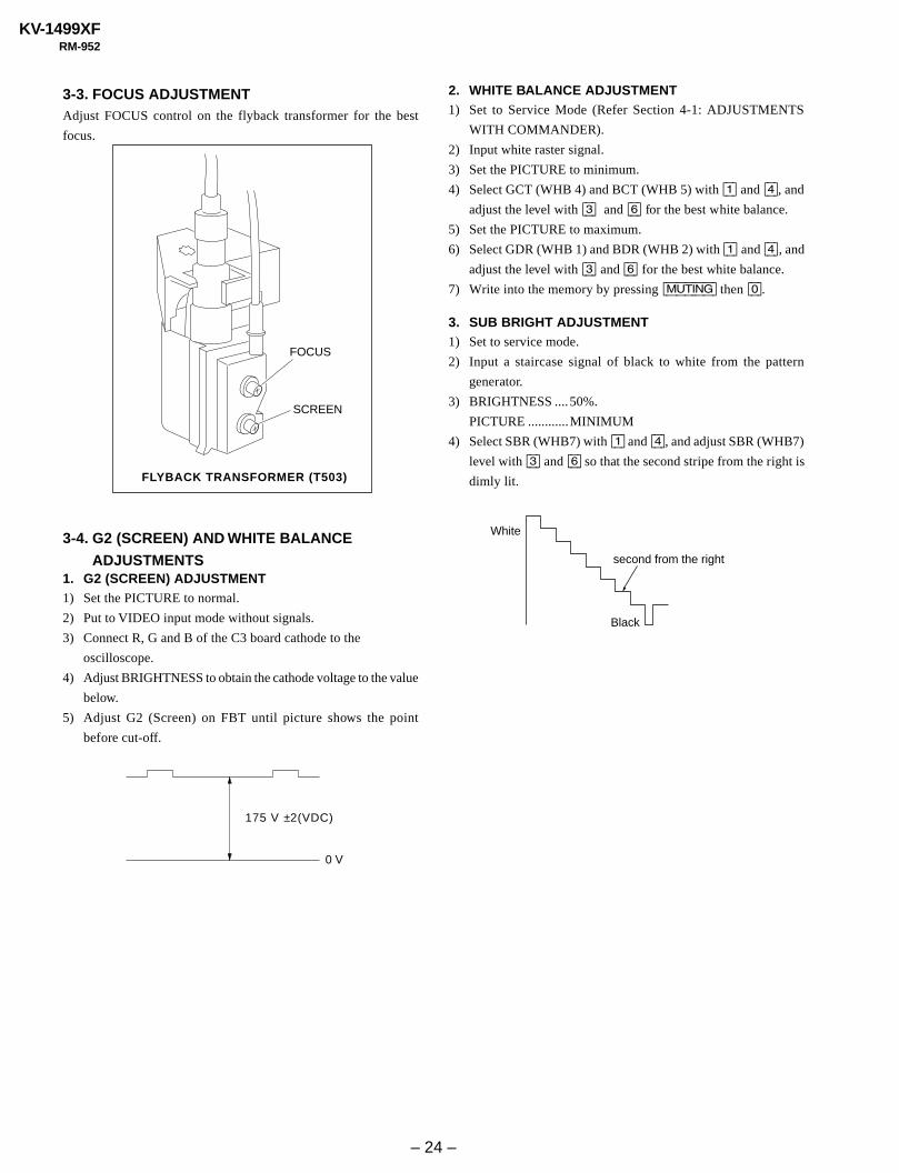
3-3. FOCUS ADJUSTMENTAdjust FOCUS control on the flyback transformer for the best
focus.
FLYBACK TRANSFORMER (T503)
2. WHITE BALANCE ADJUSTMENT1) Set to Service Mode (Refer Section 4-1: ADJUSTMENTS
WITH COMMANDER).
2) Input white raster signal.
3) Set the PICTURE to minimum.
4) Select GCT (WHB 4) and BCT (WHB 5) with [1] and [4], and
adjust the level with [3] and [6] for the best white balance.
5) Set the PICTURE to maximum.
6) Select GDR (WHB 1) and BDR (WHB 2) with [1] and [4], and
adjust the level with [3] and [6] for the best white balance.
7) Write into the memory by pressing [MUTING] then [0].
3. SUB BRIGHT ADJUSTMENT1) Set to service mode.
2) Input a staircase signal of black to white from the pattern
generator.
3) BRIGHTNESS ....50%.
PICTURE ............MINIMUM
4) Select SBR (WHB7) with [1] and [4], and adjust SBR (WHB7)
level with [3] and [6] so that the second stripe from the right is
dimly lit.
White
second from the right
Black
0 V
175 V ±2(VDC)
FOCUS
SCREEN
3-4. G2 (SCREEN) AND WHITE BALANCE
ADJUSTMENTS1. G2 (SCREEN) ADJUSTMENT1) Set the PICTURE to normal.
2) Put to VIDEO input mode without signals.
3) Connect R, G and B of the C3 board cathode to the
oscilloscope.
4) Adjust BRIGHTNESS to obtain the cathode voltage to the value
below.
5) Adjust G2 (Screen) on FBT until picture shows the point
before cut-off.

– 25 –
KV-1499XFRM-952SECTION 4
CIRCUIT ADJUSTMENTS
With the unit on standby
↓[DISPLAY]
↓5
↓VOL (+)
↓[POWER]
This operation sequence puts the unit into service mode.
4-1. ADJUSTMENTS WITH COMMANDERService adjustments are made with the RM-952 that comes with
this unit.
a. ENTERING SERVICE MODE
1, 4 Select the adjustment item.↓
3, 6 Raise/lower the data value.↓
[MUTING] Writes.↓
- Executes the writing.
7, - All the data becomes the values in memory.
8, - All user control goes to the standard state.
5, - Service data initialization (Be sure not to use
usually.)
2, - Write 50Hz adjustment data to 60Hz, or vice
versa.
PAL, SECAM : 50
NTSC : 60
00 HPS 1C SERVICE
Data Mode
Item Name
Item No
Software version
Suffix No(OEM Code)
Total Power-On time (hours)
p
Marking of virgin NVM
GEO
1.0C 59 7F 000A0601S
Device Name
50 TV
1 2 3
4 6
7 8 9
÷ 0
5
JUMP
SOUND MODE
FAVORITE
PROGRÁ
RM-952
b. METHOD OF CANCELLATION FROM SERVICEMODE
Set the standby condition (Press [POWER] button on the commander),
then press [POWER] button again, hereupon it becomes TV mode.
c. METHOD OF WRITE INTO MEMORY1) Set to Service Mode.
2) Press [1] (UP) and [4] (DOWN), select an item of adjustment.
3) Press [MUTING] button and it will indicate WRITE on the screen.
4) Press [0] button to write into memory.
d. MEMORY WRITE CONFIRMATION METHOD
1) After adjustment, pull out the plug from AC outlet, and then
plug into AC outlet again.
2) Turn the power switch ON and set to Service Mode.
3) Call the adjusted items again to confirm adjustments were made.
The screen display is :

– 26 –
KV-1499XFRM-952
4-2. ADJUSTMENT METHODItem Number 00 of device GEO
This explanation uses H-Position as an example.
1. Select “GEO 00 HPS” with the 1 and 4 buttons.
2. Raise/lower the data with the 3 and 6 buttons.
3. Select the optimum state. (The standard is 1F for PAL reception.)
4. Write with the [MUTING] button. (The display changes to
WRITE.)
5. Execute the writing with the - button. (The WRITE
display will be changed to red color while excuting, and back
to SERVICE.)
Use the same method for all Items. Use 1 and 4 to select the
adjustment item, use 3 and 6 to adjust, write with [MUTING],
then execute the write with -.
Note : 1. In [WRITE], the data for all items are written into memory
together.
2. For adjustment items that have different standard data
between 50Hz or 60Hz, be sure to use the respective
input signal after adjustment.
1F SERVICE 50HPS
Adjusted with [3] and [6] buttons.
GREEN
Written with [MUTING]
Write executed with [0]
GEO 00
7F 0 000A59615S 1.0C
1F SERVICE 50HPS REDThe WRITE displaythen the display returns to a greenSERVICE.
GEO 00
7F 0 000A59615S 1.0C
1F WRITE 50HPS GREENGEO 00
7F 0 000A59615S 1.0C

– 27 –
KV-1499X
FR
M-952
Adjustment Item Table
Device Functionality Note Data Range Function Note for Register Slava RAM AddressName No Name Different Data No. (bit) Address (bit)
GEO 0 HPS 7 3F H Position 50/60HZ 12 (7-2) CXA2130S(88H) 82 (7-2)1 HSZ 1F 3F H Size 50/60HZ 11 (7-2) 81 (7-2)2 PAP 1F 3F Pin Amp 50/60HZ 13 (7-2) 83 (7-2)3 TLT 7 0F Trapezium 50/60HZ 15 (7-4) 85 (7-4)4 VPS 1F 3F V Position 50/60HZ 0F (7-2) 7F (7-2)5 VSZ 1F 3F V Size 50/60HZ 0E (7-2) 7E (7-2)6 SCO 7 0F S Correction 50/60HZ 10 (7-4) 80 (7-4)7 VLN 7 0F V Linearity 50/60HZ 10 (3-0) 80 (3-0)8 BOW 7 0F AFC Bow 50/60HZ 16 (7-4) 86 (7-4)9 AGL 7 0F AFC-Angle 50/60HZ 16 (3-0) 86 (3-0)
0A UPN 1F 3F Upper Pin 50/60HZ 14 (7-2) 84 (7-2)0B VOK 2F 3F Lower Pin 50/60HZ 18 (7-2) 88 (7-2)0C HBL 1 1 H Blanking on/off 18 (1) 67 (1)0D LBL 0F 0F Left H Blanking 50/60HZ 17 (7-4) 87 (7-4)0E RBL 00 0F Right H Blanking 50/60HZ 17 (3-0) 87 (3-0)
WHB 0 RDR 25 3F R Drive DYNAMIC/others 09 (7-2) CXA2130S(88H) 8F (7-2)1 GDR 1F 3F G Drive DYNAMIC/others 0A (7-2) 90 (7-2)2 BDR 1F 3F B Drive DYNAMIC/others 0B (7-2) 91 (7-2)3 RCT 7 0F R Cutoff SECAM/others 07 (3-0) 93 (3-0)4 GCT 7 0F G Cutoff SECAM/others 08 (7-4) 94 (7-4)5 BCT 7 0F B Cutoff SECAM/others 08 (3-0) 94 (3-0)6 BMN 15 1F Brightness Minimum Data 977 SBR 28 3F Sub Brightness Control 98
SAJ 0 PMX 37 3F Picture Maximum Data CXA2130S(88H) 961 SHU 8 0F Sub Hue Control TV/Video 992 SSH 3 0F Sub Sharpness Control TV/Video 9A3 SCL 1F 3F Sub Color Control NTSC/others 9B
VP 0 EHT 07 0F EHT Comp 50/60HZ 15 (3-0) CXA2130S(88H) 85 (3-0)1 GMA 2 03 Gamma Correction Refer NVM Map A4 0B (1-0) 1A3 (1-0)2 YDL 6 0F Y Delay PAL/SECAM/NTSC 0C (3-0) 8C (3-0)3 SST 1 03 SECAM ID Start Position 1B (1-0) 6A (1-0)4 SSP 1 03 SECAM ID Stop Position 1B (3-2) 6A (3-2)5 SLV 2 03 SECAM ID Level 1C (1-0) 6B (1-0)6 SBF 22 3F SECAM BELL fO 1C (7-2) 6B (7-2)7 DYC 1 1 Dynamic Color on/off 0A (1) 59 (1)8 ABL 1 1 ABL Mode Switching STANDARD ALWAYS 0 09 (1) 58 (1)9 VTH 1 1 ABL Detection Vth Switching 09 (0) 58 (0)10 SFO 1 1 FO Switching for Sharpness NTSC/others 05 (1) 198 (1)11 DCX 1 1 DC Trans. Ratio Switching 06 (1) 55 (1)12 SHT 1 1 Pre-/Overshoot ratio Switch NTSC/others 06 (0) 199 (0)

– 28 –
KV-1499X
FR
M-952
Adjustment Item Table
Device Functionality Note Data Range Function Note for Register Slava RAM AddressName No Name Different Data No. (bit) Address (bit)
VP 13 HDW 0 1 H Drive Pulse Width Switch 00 (6) 4F (6)14 AFC 1 03 AFC Gain Control TV/Video/Text 0F (1-0) 8D (1-0)15 HOS 7 0F H Oscillation 0C (7-4) 5B (7-4)16 HSS 0 1 Slice Level of H Sync Sep. 0D (1) 5C (1)17 VSS 0 1 Slice Level of V Sync Sep. 0D (0) 5C (0)18 HMS 1 1 Macro Vision C/m off/on 50/60Hz 0E (0) 7E (0)19 YUV 1 1 YUV Switch Control 01 (0) 50 (0)20 CDV 2 3 CD mode for Video Video only 0D (5-4) 1A1 (5-4)21 RON 1 1 R ON not memorized 01 (3) 50 (3)22 GON 1 1 G ON not memorized 01 (2) 50 (2)23 BON 1 1 B ON not memorized 01 (1) 50 (1)24 PON 1 1 P ON not memorized 00 (7) 4F (7)25 BLK 0 1 BLK Off 12 (0) 61 (0)26 VMC 0 1 VM Off 13 (0) 62 (0)
AP 0 INF 05 3F Input Attenuation When surround off 00 (5-0) TDA7429 19F (5-0)1 INS 0A 3F Input Attenuation When surround on 1A0 (5-0)2 PH1 03 3 Phase 1 Register Selection 02 76 (1-0)3 PH2 0 3 Phase 2 Register Selection 76 (3-2)4 PH3 0 3 Phase 3 Register Selection 76 (5-4)5 PH4 0 3 Phase 4 Register Selection 76 (7-6)6 BCS 2 3 Bass Center Shift #4 (3-0) 1A8 (1-0)7 TCS 2 3 Treble Center Shift #5 (3-0) 1A9 (1-0)8 TRF 2 3 RF Treble Offset #5 (3-0) 1A9 (5-4)
MSP 0 WST 15 FF W/G Stereo Threshold MSP3415D(84H) 157 (7-0)1 WBT EC FF W/G Bilingual Threshold 158 (7-0)2 WLL 5 FF W/G Monaural Threshold 159 (7-0)3 WAC 1 0F W/G Agreement Count 15A (3-0)4 WDL 30 FF W/G Search Delay 15B (7-0)5 NDL 20 FF NICAM Search Delay 15C (7-0)6 SDL 10 FF Stereo status Read Delay 15D (7-0)7 AGC 1 1 AGC Switch Auto/Constant BB (7) 108 (7)8 REL 28 3F AGC Gain at Constant Mode BB (6-1) 108 (6-1)9 CRM 0 1 Carrier muting on/off BB (9) 107 (1)10 ACO 1 1 Audio Clock out on/off 83 (5) 10C (5)11 FP 1B 7F FM Prescale for non-M system 0E (7-0) 16C (6-0)12 FPM 32 7F FM Prescale for M system 0E (7-0) 16D (6-0)13 FH 36 7F FM Prescale for HDEV 0E (7-0) 16E (6-0)14 FHM 65 7F FM Prescale for HDEV and M 0E (7-0) 16F (6-0)15 WGP 2A 7F W/G Prescale 0E (7-0) 170 (6-0)16 NIP 6D 7F NICAM Prescale 10 (7-0) 138 (6-0)17 ERR 50 FF Auto FM switch Threshold 21 (10-3) 166 (7-0)18 VOL 6D FF Loud Speaker gain 7000h to 7ffoh 0000 (15-4) 1A7 (7-0)

– 29 –
KV-1499X
FR
M-952
Adjustment Item Table
Device Functionality Note Data Range Function Note for Register Slava RAM AddressName No Name Different Data No. (bit) Address (bit)
TXT 0 TXH 1 3 Teletext Horizontal Position (58H) 18D (1-0)1 TXV 0 3 Teletext Vertical Position 18D (6-4)
OPM 0 OSH 0A 3F OSD H Position Option-Misc AC (7-2)1 COM 0 03 Comb Selection A5 (7-6)2 APC 1 1 APC Switch A4 (5)3 TSY 0 03 TV Sys at Auto TV Sys A4 (4-3)4 MUT 0 1 No Signal Mute A4 (0)5 AFM 1 1 Auto FM switch A4 (1)6 RFB 0 3 C-BPF Control A5 (5-4)7 TV0 0 7 Tilt to V-Angle offset A5 (2-0)8 DBL 0 1 Disable Blueback Function A4 (2)
OPB 0 OP1 FF FF Optional Bits 1 (see below) Option-Bits 451 OP2 03 FF Optional Bits 2 (see below) 462 OP3 0 FF Optional Bits 3 (see below) 47
NOTE• shaded items are fixed data.• Standard data listed on the Adjustment Item Table are reference values, therefore it may be different for each model and for each mode.• Note for Different Data Those are the standard data values written on the microprocessor. Therefore, the data values of the modes and stored respectively in the
memory.In case of a device replacement, adjustment by rewriting the data value is necessary for some items.

– 30 –
KV-1499XFRM-952
Item
KV-1499XF
M
0
D/K
0
I
0
B/G
1
2nd. Lang
1
SECAM
1
XTAL 3.58
1
XTAL 4.43
1
ITEM INFORMATION.No. OPB0 OP1
No. OPB1 OP2
No. OPB2 OP3
Color SW
0
11 KEY
0
AV Mono
1
US ST
0
Auto TV sys
0
Auto PIC
1
2199 Cune
0
Pic Rot
0
AV InputItem
KV-1499XF 01
DVD Input
0
Dis Fav.
0
Thai Bil
0
HDEV
0
NICAM
0
TOP
0
Item
KV-1499XF
– 31 –
KV-1499XFRM-952
SUB HUE ADJUSTMENT
1. Select Video 1.
2. Input a NTSC color-bar, video into Video 1.
3. Set the following condition:
PICTURE 100%, BRIGHTNESS 50%, COLOR 50%
4. Connect an oscilloscope to pin 1 (B OUT) of CN305, A board.
5. Select SAJ 1 ‘SHU’ with 1 and 4 of the commander by set-
ting to Service Mode and adjust to VB1=VB2=VB3=VB4 with
3 and 6.
4-3. PICTURE QUALITY ADJUSTMENTS
SUB COLOR ADJUSTMENT
1. Input a PAL color-bar.
2. Set to the following condition:
PICTURE 100%, BRIGHTNESS 50%, COLOR 50%
3. Connect an oscilloscope to pin 1 (B OUT) of CN305, A board.
4. Set to Service Mode and select SAJ 3 ‘SCL’ with 1 and 4 of
the commander then adjust to VB2=VB3=VB4 with 3 and
6.
5. Press [MUTING] → - of the commander to write the data.
6. Adjust SAJ 3 ‘SCL’ as step 2 to 5 when receiving NTSC color-
bar.
VB1 VB2 VB3 VB4
VB2 = VB3 = VB4
6. Press [MUTING] → - of the commander to write the data.
VB1 VB2 VB3 VB4
VB1 = VB2 = VB3 = VB4
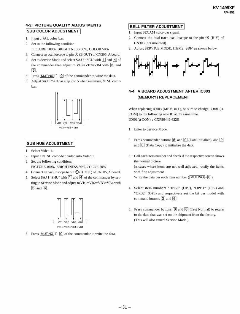
BELL FILTER ADJUSTMENT1. Input SECAM color-bar signal.
2. Connect the dual-trace oscilloscope to the pin 9 (R-Y) of
CN303 (not mounted).
3. Adjust SERVICE MODE, ITEMS ‘SBF’ as shown below.
4-4. A BOARD ADJUSTMENT AFTER IC003
(MEMORY) REPLACEMENT
When replacing IC003 (MEMORY), be sure to change IC001 (µ-
COM) to the following new IC at the same time.
IC001(µ-CON) : CXP86449-622S
1. Enter to Service Mode.
2. Press commander buttons 5 and - (Data Initialize), and 2
and - (Data Copy) to initialize the data.
3. Call each item number and check if the respective screen shows
the normal picture.
In cases where items are not well adjusted, rectify the items
with fine adjustment.
Write the data per each item number ([MUTING]+-).
4. Select item numbers “OPB0” (OP1), “OPB1” (OP2) and
“OPB2” (OP3) and respectively set the bit per model with
command buttons 3 and 6.
5. Press commander buttons 8 and - (Test Normal) to return
to the data that was set on the shipment from the factory.
(This will also cancel Service Mode.)

– 32 –
KV-1499XFRM-952
4-5. PICTURE DISTORTION ADJUSTMENTItem Number 00 – 0B
GEO 0 HSH (H POSITION)
GEO 1 HSZ (H SIZE)
GEO 2 PAP (PIN AMP)
GEO 5 VSZ (V SIZE)
GEO 7 VLN (V LINEARITY)
GEO 4 VSH (V POSITION)
GEO 6 SCR (VERTICAL S-Correction)
GEO 8 VBOW (AFC.BOW)
GEO 9 AGL (AFC.ANGLE)
GEO 3 TILT (TRAPEZIUM)
GEO 0A UCP (UPPER CORNER PIN)
GEO 0B LCP (LOWER CORNER PIN)

– 33 –
KV-1499XFRM-952
MEMO
– 34 –
KV-1499XFRM-952
MEMO

SECTION 5
DIAGRAM5-1. BLOCK DIAGRAM
– 36 – – 37 –– 35 –
YC JUNGLEIC301CXA2130S<slave:88H>
MONITOROUT
TV V in
TV L in
TV R in
Mon out
TV V in
V1 V in
43
6
12V1 V in
V1 L in
V2 V in V2 V in4
V2 L in
V out 2
L out 2
JACK BLOCKJ401 4P
J902 2P
VIDEO IN 1
VIDEO IN 2(FRONT)
AUDIOPROSESSORIC203
TDA7429S<slave: 80H>
AUDIO OUTIC201TA8248K
RED OUT
GREEN OUT
BLUE OUT
STV5112Q704-712
C3
SP ASSY
R outCRT SOCKET
G out CRTA34LRG70X
DYY14RSA-S
B out
R out
V o
ut
U o
ut
Y o
ut
V in
U in
Y in
G out
B out
22
23
24
21
19
18
11
13
14
IK in
H. DRIVE
H. PULSE
E/W
VD+
VD-
H-OUTQ5112SC4927
V-OUTIC503TDA8172
HDTT501
H-DRIVEQ5062SD774-34
PIN-CONTIC502NJM2903M
PIN-OUTQ505IRF614
PMCL509
HLCL510
FBTT503NX-1748
+B
Audio Front Vcc
+9V11V
7V+5V
5V REG & RESETIC002 MM1319AF
9V REC IC603
5V REC IC604
STB TRANST604
SRTT603
AdditionalColor Matrix
SYSTEMUcomIC001CXP86449
RECEIVERSBX1981-51IC901
SIRCS
R G B BLK
I2L MEMORYIC003ST24C08FB6
32 31 30 37 39 40 28 29 30 31
F
STB SW TRQ605 2SK2845
POWER ICIC601STR-F6654 LINE FILTER
T601
LINE FILTER
T4601T4602
THPTHP600
AC CORDDGC
MAIN. TUVIFTU101BTF-LG411(I)<slave: C0H>
KV-1499XFRM-952
KV-1499XFRM-952
KV-1499XFRM-952

– 41 –
KV-1499XFRM-952
5-4. SCHEMATIC DIAGRAMS AND PRINTED WIRING BOARDS
Note:• All capacitors are in µF unless otherwise noted.• All electrolytic capacitors are rated at 50V unless otherwise noted.• All resistors are in ohms.
kΩ = 1000Ω, MΩ = 1000kΩ• Indication of resistance which does not have rating electrical power is as follows
Pitch: 5 mmRating electrical power 1/4W (CHIP: 1/10W)
• : nonflammable resistor.• ¢ : internal component.• : panel designation or adjustment for repair.• All variable and adjustable resistors have characteristic curve B unless otherwise
noted.• Readings are taken with a color-bar signal input.
no mark : PAL( ) : SECAM[ ] : NTSC 3.58« » : NTSC 4.43
• Readings are taken with a 10 MΩ digital multimeter.• Voltage are dc with respect to ground unless otherwise noted.• Voltage variations may be noted due to normal production tolerances.• All voltages are in V.• : Cannot be measured.• Circled numbers are waveform references.• : B + bus.• : B – bus.• : signal path.
Reference informationRESISTOR : RN METAL FILM
: RC SOLID: FPRD NONFLAMMABLE CARBON: FUSE NONFLAMMABLE FUSIBLE: RS NONFLAMMABLE METAL OXIDE: RB NONFLAMMABLE CEMENT: RW NONFLAMMABLE WIREWOUND: * ADJUSTMENT RESISTOR
COIL : LF-8L MICRO INDUCTORCAPACITOR : TA TANTALUM
: PS STYROL: PP POLYPROPYLENE: PT MYLAR: MPS METALIZED POLYESTER: MPP METALIZED POLYPROPYLENE: ALB BIPOLAR: ALT HIGH TEMPERATURE: ALR HIGH RIPPLE
Note: The component identif ied by shading andmark !!!!! are critical for safety. Replace onlywith part number specified.
*

– 42 –
KV-1499XFRM-952
5
8
2
6
2
2
3
8
8
8
INT
0IN
T1
INT
2
TE
XT
XE
XT
AL
XT
AL
RS
TM
PV
DD
VS
S
RMC
AN0~AN5 6 PA0~PA7
PO
RT
AP
OR
T B
PO
RT
CP
OR
T D
PO
RT
EP
OR
T F
PO
RT
G
PB0~PB7
PC0~PC5
PC6~PC7
PD0~PD7
PE0~PE1
PE2~PE3
PE4~PE6
PF0~PF7
PG3~PG6*, PG7
S1SO
SCK
SD
A0
SD
A1
SC
L0
SC
L1
PW
M
AD
J
PW
M0~
PW
M7
(PW
M0~
PW
M5)
I2C BUSINTERFACE UNIT
8-BIT PWM 8CH (6CH)
14BIT PWM 1CH
ON SCREENDISPLAY
8-BIT TIMER/COUNTER 0
SERIAL INTERFACEUNIT
REMOCON FIFO
A/D CONVERTER6CH
SPC700 CPU CORE
ROM12K/16K/24K/32K
40K/48K/60K BYTES
PRESCALER/TIME-BASE TIMER
WATCHDOG TMER
32kHZTIMER/COUNTER
RAM352/704/1536 BYTES
CLOCK GENERATOR/SYSTEM CONTROL
INT
ER
RU
PT
CO
NT
RO
LLE
R
8-BIT TIMER 1
HSYNC COUNTER 1
HSYNC COUNTER 0
8 (6)
EC
XLCEXLC
RGBI
YSYM
HSYNCVSYNC
HS0
HS1
TO
2
2
2
A BOARD IC001 CXP86449-622S

5-5. SEMICONDUCTORS
TRANSISTOR IC
– 60 –
UN2111UN2211UN2213UN22162SA1162-G2SC2712-YG2SD2114K
2SC2785-HFE
2SA1091-O
2SD2144S-UVW
2SC2611
E
B
C
E C B
LETTER SIDE
E
LETTER SIDE
C B
EC B
1 TOP VIEW
Dual In-line PackagePin 6~98
Single In -line PackagePin 6~98
1 TOP VIEW
KV-1499XFRM-952
KV-1499XFRM-952
D1NS4D1N20RRD20ES-B2RD30ESB2RD6.8ES-B1RD9.1ES-L21SS119-25
DTZ-TT11-15BMA111-TXRD10S-BRD5.1SB-T2RD9.1S-BUDZS-TE17-6.8B1SS355TE-17
5P6M
DA204K
– 59 –
CATHODE
ANODE
CATHODE
ANODE
DIODE
AK04V0AU-01Z-V1EL1ZGP08DRD33EB3TRGP02-17EL-6433
D4SB60L
ERC04-06SEERC06-15SRN4ZRU4AM-T331DQ06-FC5
ERA22-08
ON3171-R
CATHODE
ANODE
CATHODE
ANODE
21
34
1
43
CATHODE
ANODE
CATHODE
ANODEGATE
3
1
2
1
3
2
LED
CATHODE
ANODE(GRN) ANODE
(GRN)
E C B
2SC4927-01
2SD774-34
IRF614
2SK2845-LB102
D1G1
S1NC
S2G2 D2
E C B
GSD
E
BC
CXA2130S (64PIN)CXP86469-614S (64PIN)ST24C08FB6 (8PIN)TDA7429S (42PIN)
MM1319AFBE (7PIN)NJM2903M (8PIN)
NJM78M09FATA7805S
SBX1981-51
SE-135N

– 62 – – 63 –– 61 –
KV-1499XFRM-952
KV-1499XFRM-952
KV-1499XFRM-952
39
40 26
52 14
27
1 13
MARKING SIDE VIEW
TDA8172
STR-F6654
RU-1P
TA8223K
1
15
Zig-zag In -line PackagePin 6~99
MARKING SIDE VIEW
1
SECTION 6
EXPLODED VIEW
NOTE:• Items with no part number and no des-
cription are not stocked because theyare seldom required for routine service.
• The construction parts of an assembledpart are indicated with a collationnumber in the remark column.
6-1. CHASSIS[ : BVTP3 × 12 7-685-648-79
• Items marked " * " are not stocked sincethey are seldom required for routineservice. Some delay should beanticipated when ordering these items.
The components identif ied byshading and mark ! are criticalfor safety.Replace only with part numberspecified.
731
2
437
36
6
12
14
10
22
35
16
17
31
19
27
24
32
23
38
20
21
3
11
18
[513
8
7
1
9
34
15
9
8
29
33 23
25
30
2826
REF. NO. PART NO. DESCRIPTION REMARK
1 X-4036-825-1 BEZNET ASSY 2-62 4-047-464-01 CATCHER, PUSH3 4-067-190-01 BUTTON, POWER4 4-036-405-11 SPRING, COMPRESSION5 4-067-196-01 BUTTON, MULTI
6 * 4-067-197-01 GUIDE, LIGHT7 1-504-305-11 SPEAKER (5X12 CM)8 4-054-981-01 SCREW, STEP TAPPING9 4-365-808-01 SCREW (5), TAPPING10 4-046-600-11 SPACER, DY
11 * 3-704-372-11 HOLDER, HV CABLE12 ! 8-735-570-05 PICTURE TUBE (A34LRG70X)13 8-451-401-11 DEFLECTION YOKE (Y14RSA-S)14 * A-1331-968-A C3 BOARD, MOUNTED15 4-369-318-61 SRING, TENSION
16 ! 1-419-185-11 COIL, DEGAUSSING17 * 4-067-189-01 PWB(L), GUIDE18 * 4-067-187-01 PWB(R), GUIDE19 8-598-447-00 TUNER, FSS BTF-LG41120 ! 1-453-313-11 TRANSFORMER ASSY, FLYBACK (NX-1912//M3A4)
21 * A-1298-962-A A BOARD, COMPLETE22 4-057-714-01 PIECE ASSY, TLH CORRECTION23 ! 4-022-115-12 HOLDER, AC CORD24 ! 1-574-062-61 CORD, POWER (WITH CONNECTOR) 2.5A/250V25 1-452-032-00 MAGNET,DISC
26 4-051-736-41 PIECE A(90), CONV, CORRECT27 4-067-167-21 BRACKET, TERMINAL28 1-452-094-00 CIRCULAR DISC MAGNET B29 * A-1241-355-A F BOARD, MOUNTED30 4-070-853-01 DOOR, CONTROL
31 * 4-379-189-11 CUSHION, SPEAKER32 ! 4-070-947-01 COVER, REAR33 4-069-978-01 CUSHION, DGC34 4-069-652-02 CUSHION (HS BAND)35 4-069-972-01 CLIP, DGC
36 * 4-070-854-01 PANEL (L)37 * 4-070-855-01 PANEL (R)38 4-070-202-01 HOLDER, FBT

KV-1499XFRM-952
KV-1499XFRM-952
KV-1499XFRM-952
– 65 – – 66 –– 64 –
REF. NO. PART NO. DESCRIPTION REMARK
* A-1298-962-A A BOARD, COMPLETE*********************
* 4-055-304-01 HOLDER, LED4-382-854-11 SCREW (M3X10), P, SW (+)7-685-648-79 SCREW +BVTP 3X12 TYPE2 IT-3
<CAPACITOR>
C004 1-163-001-11 CERAMIC CHIP 220PF 10% 50VC005 1-163-001-11 CERAMIC CHIP 220PF 10% 50VC006 1-164-004-11 CERAMIC CHIP 0.1MF 10% 25VC007 1-126-933-11 ELECT 100MF 20% 16VC008 1-163-251-11 CERAMIC CHIP 100PF 5% 50V
C010 1-163-251-11 CERAMIC CHIP 100PF 5% 50VC012 1-163-251-11 CERAMIC CHIP 100PF 5% 50VC013 1-163-021-91 CERAMIC CHIP 0.01MF 10% 50VC014 1-126-967-11 ELECT 47MF 20% 50VC015 1-163-009-11 CERAMIC CHIP 0.001MF 10% 50V
C016 1-163-113-00 CERAMIC CHIP 68PF 5% 50VC017 1-163-113-00 CERAMIC CHIP 68PF 5% 50VC019 1-104-665-11 ELECT 100MF 20% 25VC022 1-163-227-11 CERAMIC CHIP 10PF 0.5PF 50VC023 1-163-227-11 CERAMIC CHIP 10PF 0.5PF 50V
C024 1-163-227-11 CERAMIC CHIP 10PF 0.5PF 50VC026 1-164-004-11 CERAMIC CHIP 0.1MF 10% 25VC027 1-164-004-11 CERAMIC CHIP 0.1MF 10% 25VC028 1-163-037-11 CERAMIC CHIP 0.022MF 10% 50VC030 1-126-965-11 ELECT 22MF 20% 50V
C031 1-164-004-11 CERAMIC CHIP 0.1MF 10% 25VC032 1-107-823-11 CERAMIC CHIP 0.47MF 10% 16VC034 1-163-031-11 CERAMIC CHIP 0.01MF 50VC041 1-163-251-11 CERAMIC CHIP 100PF 5% 50VC042 1-163-251-11 CERAMIC CHIP 100PF 5% 50V
C043 1-163-251-11 CERAMIC CHIP 100PF 5% 50VC044 1-163-251-11 CERAMIC CHIP 100PF 5% 50VC047 1-163-251-11 CERAMIC CHIP 100PF 5% 50VC048 1-163-251-11 CERAMIC CHIP 100PF 5% 50VC050 1-163-251-11 CERAMIC CHIP 100PF 5% 50V
C051 1-163-251-11 CERAMIC CHIP 100PF 5% 50VC053 1-163-251-11 CERAMIC CHIP 100PF 5% 50VC054 1-163-251-11 CERAMIC CHIP 100PF 5% 50VC055 1-163-251-11 CERAMIC CHIP 100PF 5% 50VC103 1-164-004-11 CERAMIC CHIP 0.1MF 10% 25V
C104 1-126-933-11 ELECT 100MF 20% 16VC107 1-163-005-11 CERAMIC CHIP 470PF 10% 50VC108 1-126-933-11 ELECT 100MF 20% 16VC109 1-163-005-11 CERAMIC CHIP 470PF 10% 50VC110 1-163-005-11 CERAMIC CHIP 470PF 10% 50V
REF. NO. PART NO. DESCRIPTION REMARK
C111 1-163-005-11 CERAMIC CHIP 470PF 10% 50VC112 1-126-933-11 ELECT 100MF 20% 16VC113 1-126-967-11 ELECT 47MF 20% 50VC114 1-126-967-11 ELECT 47MF 20% 50VC202 1-163-020-00 CERAMIC CHIP 0.0082MF 10% 50V
C203 1-163-020-00 CERAMIC CHIP 0.0082MF 10% 50VC204 1-136-153-00 FILM 0.01MF 5% 50VC205 1-163-021-91 CERAMIC CHIP 0.01MF 10% 50VC206 1-163-021-91 CERAMIC CHIP 0.01MF 10% 50VC207 1-136-153-00 FILM 0.01MF 5% 50V
C208 1-126-965-11 ELECT 22MF 20% 50VC209 1-126-965-11 ELECT 22MF 20% 50VC210 1-126-933-11 ELECT 100MF 20% 16VC211 1-126-941-11 ELECT 470MF 20% 25VC212 1-126-933-11 ELECT 100MF 20% 16V
C213 1-126-933-11 ELECT 100MF 20% 16VC214 1-126-942-61 ELECT 1000MF 20% 25VC215 1-126-942-61 ELECT 1000MF 20% 25VC216 1-163-021-91 CERAMIC CHIP 0.01MF 10% 50VC217 1-126-964-11 ELECT 10MF 20% 50V
C218 1-136-167-00 FILM 0.15MF 5% 50VC219 1-136-167-00 FILM 0.15MF 5% 50VC220 1-126-942-61 ELECT 1000MF 20% 25VC221 1-126-964-11 ELECT 10MF 20% 50VC223 1-126-965-11 ELECT 22MF 20% 50V
C224 1-163-133-00 CERAMIC CHIP 470PF 5% 50VC226 1-109-982-11 CERAMIC CHIP 1MF 10% 10VC227 1-163-037-11 CERAMIC CHIP 0.022MF 10% 50VC228 1-163-024-00 CERAMIC CHIP 0.018MF 10% 50VC229 1-163-018-00 CERAMIC CHIP 0.0056MF 10% 50V
C230 1-163-024-00 CERAMIC CHIP 0.018MF 10% 50VC231 1-163-018-00 CERAMIC CHIP 0.0056MF 10% 50VC232 1-163-037-11 CERAMIC CHIP 0.022MF 10% 50VC233 1-164-004-11 CERAMIC CHIP 0.1MF 10% 25VC234 1-164-004-11 CERAMIC CHIP 0.1MF 10% 25V
C235 1-164-004-11 CERAMIC CHIP 0.1MF 10% 25VC236 1-164-004-11 CERAMIC CHIP 0.1MF 10% 25VC238 1-164-505-11 CERAMIC CHIP 2.2MF 16VC240 1-164-505-11 CERAMIC CHIP 2.2MF 16VC241 1-164-346-11 CERAMIC CHIP 1MF 16V
C242 1-164-505-11 CERAMIC CHIP 2.2MF 16VC243 1-216-295-91 SHORT 0C244 1-164-700-11 CERAMIC CHIP 0.68MF 16VC245 1-164-346-11 CERAMIC CHIP 1MF 16VC246 1-163-018-00 CERAMIC CHIP 0.0056MF 10% 50V
C248 1-163-010-11 CERAMIC CHIP 0.0012MF 10% 50VC249 1-164-004-11 CERAMIC CHIP 0.1MF 10% 25V
SECTION 7
ELECTRICAL PARTS LIST
NOTE:
The components identified by shadingand mark ! are critical for safety.Replace only with part number specified.
When indicating parts by referencenumber, please include the board name.
• All resistors are in ohms• F : nonflammable
CAPACITORS• MF : µF, PF : µµF
COILS• MMH : mH, UH : µH
• Items marked " ∗ " are not stocked since theyare seldom required for routine service.Some delay should be anticipated when or-dering these items.
• All variable and adjustable resistors havecharacteristic curve B, unless otherwisenoted.
AREF. NO. PART NO. DESCRIPTION REMARK
The components identified by shadingand mark ! are critical for safety.Replace only with part number specified.
REF. NO. PART NO. DESCRIPTION REMARK
C251 1-163-017-00 CERAMIC CHIP 0.0047MF 10% 50VC252 1-164-346-11 CERAMIC CHIP 1MF 16VC253 1-163-037-11 CERAMIC CHIP 0.022MF 10% 50V
C254 1-126-965-11 ELECT 22MF 20% 50VC255 1-163-037-11 CERAMIC CHIP 0.022MF 10% 50VC256 1-164-004-11 CERAMIC CHIP 0.1MF 10% 25VC259 1-126-933-11 ELECT 100MF 20% 16VC264 1-164-505-11 CERAMIC CHIP 2.2MF 16V
C265 1-164-505-11 CERAMIC CHIP 2.2MF 16VC301 1-126-935-11 ELECT 470MF 20% 16VC302 1-163-005-11 CERAMIC CHIP 470PF 10% 50VC303 1-126-964-11 ELECT 10MF 20% 50VC304 1-126-967-11 ELECT 47MF 20% 50V
C305 1-164-004-11 CERAMIC CHIP 0.1MF 10% 25VC306 1-163-233-11 CERAMIC CHIP 18PF 5% 50VC307 1-163-233-11 CERAMIC CHIP 18PF 5% 50VC308 1-163-259-91 CERAMIC CHIP 220PF 5% 50VC309 1-126-957-11 ELECT 0.22MF 20% 50V
C310 1-126-963-11 ELECT 4.7MF 20% 50VC311 1-126-962-11 ELECT 3.3MF 20% 50VC312 1-164-346-11 CERAMIC CHIP 1MF 16VC313 1-164-346-11 CERAMIC CHIP 1MF 16VC315 1-164-004-11 CERAMIC CHIP 0.1MF 10% 25V
C316 1-126-967-11 ELECT 47MF 20% 50VC317 1-164-004-11 CERAMIC CHIP 0.1MF 10% 25VC318 1-163-031-11 CERAMIC CHIP 0.01MF 50VC319 1-163-031-11 CERAMIC CHIP 0.01MF 50VC320 1-163-031-11 CERAMIC CHIP 0.01MF 50V
C322 1-163-005-11 CERAMIC CHIP 470PF 10% 50VC324 1-163-017-00 CERAMIC CHIP 0.0047MF 10% 50VC325 1-126-960-11 ELECT 1MF 20% 50VC327 1-126-965-11 ELECT 22MF 20% 50VC328 1-164-004-11 CERAMIC CHIP 0.1MF 10% 25V
C330 1-164-004-11 CERAMIC CHIP 0.1MF 10% 25VC331 1-247-807-31 CARBON 100 5% 1/4WC332 1-126-963-11 ELECT 4.7MF 20% 50VC335 1-164-004-11 CERAMIC CHIP 0.1MF 10% 25VC336 1-164-004-11 CERAMIC CHIP 0.1MF 10% 25V
C337 1-126-961-11 ELECT 2.2MF 20% 50VC338 1-163-017-00 CERAMIC CHIP 0.0047MF 10% 50VC341 1-115-340-11 CERAMIC CHIP 0.22MF 10% 25VC342 1-163-259-91 CERAMIC CHIP 220PF 5% 50VC402 1-164-346-11 CERAMIC CHIP 1MF 16V
C404 1-163-005-11 CERAMIC CHIP 470PF 10% 50VC405 1-126-935-11 ELECT 470MF 20% 16VC407 1-164-346-11 CERAMIC CHIP 1MF 16VC408 1-163-133-00 CERAMIC CHIP 470PF 5% 50VC409 1-126-963-11 ELECT 4.7MF 20% 50V
C502 1-163-275-11 CERAMIC CHIP 0.001MF 5% 50VC506 1-107-638-11 ELECT 33MF 20% 160VC507 1-161-830-00 CERAMIC 0.0047MF 500VC510 1-102-112-00 CERAMIC 330PF 10% 50VC512 1-163-989-11 CERAMIC CHIP 0.033MF 10% 25V
C513 1-163-263-11 CERAMIC CHIP 330PF 5% 50VC514 1-106-383-00 MYLAR 0.047MF 10% 200VC517 1-164-182-11 CERAMIC CHIP 0.0033MF 10% 50VC518 1-104-665-11 ELECT 100MF 20% 10VC519 1-102-212-00 CERAMIC 820PF 10% 500V
C521 1-126-934-11 ELECT 220MF 20% 16VC522 1-126-933-11 ELECT 100MF 20% 16VC523 1-102-002-00 CERAMIC 680PF 10% 500VC524 1-126-967-11 ELECT 47MF 20% 50VC526 1-130-495-00 MYLAR 0.1MF 5% 50V
C527 1-102-820-00 CERAMIC 330PF 5% 50VC528 1-162-116-00 CERAMIC 680PF 10% 2KVC530 1-137-372-11 FILM 0.022MF 5% 50VC531 1-126-961-11 ELECT 2.2MF 20% 50VC532 1-126-941-11 ELECT 470MF 20% 25V
C533 1-126-941-11 ELECT 470MF 20% 25VC536 1-136-165-00 FILM 0.1MF 5% 50VC537 1-126-969-11 ELECT 220MF 20% 50VC538 1-104-492-11 FILM 0.0056MF 3% 2KVC539 1-129-746-91 FILM 0.039MF 5% 400V
C540 1-136-171-00 FILM 0.33MF 5% 50VC546 1-165-319-11 CERAMIC CHIP 0.1MF 50VC549 1-163-017-00 CERAMIC CHIP 0.0047MF 10% 50VC550 1-106-220-00 MYLAR 0.1MF 10% 100VC551 1-126-960-11 ELECT 1MF 20% 50V
C552 1-162-116-00 CERAMIC 680PF 10% 2KVC553 1-162-116-00 CERAMIC 680PF 10% 2KVC554 1-137-417-11 MYLAR 0.0047MF 10% 200VC556 1-126-941-11 ELECT 470MF 20% 25VC557 1-126-941-11 ELECT 470MF 20% 25V
C558 1-123-024-21 ELECT 33MF 160VC560 1-102-228-00 CERAMIC 470PF 10% 500VC561 1-136-557-11 FILM 0.0033MF 5% 630VC562 1-102-228-00 CERAMIC 470PF 10% 500VC564 1-163-038-91 CERAMIC CHIP 0.1MF 25V
C565 1-107-655-11 ELECT 47MF 20% 250VC566 1-102-244-00 CERAMIC 220PF 10% 500VC567 1-115-521-11 FILM 0.82MF 5% 250VC568 1-102-228-00 CERAMIC 470PF 10% 500VC570 1-115-520-11 FILM 0.68MF 5% 250V
C573 1-137-350-11 MYLAR 0.015MF 10% 100VC574 1-107-636-11 ELECT 10MF 20% 160VC576 1-130-495-00 MYLAR 0.1MF 5% 50VC577 1-106-395-00 MYLAR 0.15MF 10% 200VC582 1-164-004-11 CERAMIC CHIP 0.1MF 10% 25V
C586 1-216-295-91 SHORT 0C600 ! 1-104-705-51 FILM 0.1MF 20% 250VC602 ! 1-104-705-51 FILM 0.1MF 20% 250VC604 1-163-009-11 CERAMIC CHIP 0.001MF 10% 50VC605 ! 1-127-942-51 CERAMIC 330PF 10% 250V
C606 ! 1-127-942-51 CERAMIC 330PF 10% 250VC607 1-161-830-00 CERAMIC 0.0047MF 99% 500VC608 1-161-830-00 CERAMIC 0.0047MF 99% 500VC609 1-126-968-11 ELECT 100MF 20% 50VC610 1-126-964-11 ELECT 10MF 20% 50V
C611 1-161-830-00 CERAMIC 0.0047MF 99% 500VC612 1-161-830-00 CERAMIC 0.0047MF 99% 500VC613 1-117-752-11 ELECT(BLOCK) 330MF 20% 450VC614 1-126-964-11 ELECT 10MF 20% 50VC616 1-130-202-00 FILM 0.022MF 10% 400V
C617 1-107-792-11 CERAMIC 100PF 5% 1KVC618 1-125-893-11 FILM 680PF 3% 1.5KVC619 ! 1-119-886-51 CERAMIC 470PF 10% 250V
AREF. NO. PART NO. DESCRIPTION REMARK REF. NO. PART NO. DESCRIPTION REMARK
The components identified by shadingand mark ! are critical for safety.Replace only with part number specified.
C620 1-163-133-00 CERAMIC CHIP 470PF 5% 50VC621 1-102-114-00 CERAMIC 470PF 10% 50V
C622 1-102-074-00 CERAMIC 0.001MF 10% 50VC623 1-104-665-11 ELECT 100MF 20% 25VC624 1-104-331-11 CERAMIC 0.0022MF 10% 1KVC627 1-102-002-00 CERAMIC 680PF 10% 500VC628 1-126-942-61 ELECT 1000MF 20% 25V
C629 1-126-964-11 ELECT 10MF 20% 50VC630 1-123-024-21 ELECT 33MF 160VC633 1-104-999-11 MYLAR 0.1MF 10% 200VC634 1-126-933-11 ELECT 100MF 20% 16VC635 1-104-665-11 ELECT 100MF 20% 10V
C636 1-104-760-11 CERAMIC CHIP 0.047MF 10% 50VC639 1-164-004-11 CERAMIC CHIP 0.1MF 10% 25VC640 1-164-004-11 CERAMIC CHIP 0.1MF 10% 25VC641 1-102-002-00 CERAMIC 680PF 10% 500VC642 1-126-943-11 ELECT 2200MF 20% 25V
C643 1-104-665-11 ELECT 100MF 20% 10VC644 1-104-331-11 CERAMIC 0.0022MF 10% 1KVC645 1-137-605-11 FILM 0.01MF 10% 250VC646 1-107-679-91 ELECT 10MF 20% 450VC647 1-163-275-11 CERAMIC CHIP 0.001MF 5% 50V
C649 1-126-940-11 ELECT 330MF 20% 25VC650 1-163-275-11 CERAMIC CHIP 0.001MF 5% 50VC651 1-163-133-00 CERAMIC CHIP 470PF 5% 50VC652 1-126-965-11 ELECT 22MF 20% 50VC653 1-104-664-11 ELECT 47MF 20% 25V
C657 1-101-821-00 CERAMIC 0.0022MF 500VC658 1-164-004-11 CERAMIC CHIP 0.1MF 10% 25VC901 1-136-153-00 FILM 0.01MF 5% 50VC902 1-136-153-00 FILM 0.01MF 5% 50VC905 1-126-963-11 ELECT 4.7MF 20% 50V
C906 1-164-346-11 CERAMIC CHIP 1MF 16VC907 1-163-133-00 CERAMIC CHIP 470PF 5% 50VC910 1-126-967-11 ELECT 47MF 20% 50VC911 1-126-967-11 ELECT 47MF 20% 50VC912 1-164-004-11 CERAMIC CHIP 0.1MF 10% 25V
C913 1-126-933-11 ELECT 100MF 20% 16VC914 1-163-133-00 CERAMIC CHIP 470PF 5% 50V
<CONNECTOR>
CN104 1-695-915-11 TAB (CONTACT)CN202 * 1-785-608-11 PIN, CONNECTOR 4PCN203 * 1-564-506-11 PLUG, CONNECTOR 3PCN204 * 1-564-506-11 PLUG, CONNECTOR 3PCN305 * 1-564-509-11 PLUG, CONNECTOR 6P
CN505 1-508-765-00 PIN, CONNECTOR (5MM PITCH) 3PCN506 4-352-844-01 PIN, LEAD, COATINGCN507 * 1-564-507-11 PLUG, CONNECTOR 4PCN601 * 1-580-843-11 PIN, CONNECTOR (POWER)CN602 * 1-508-786-00 PIN, CONNECTOR (5MM PITCH) 2P
CN604 * 1-573-963-11 PIN, CONNECTOR (PC BOARD) 3PCN609 * 1-508-784-21 PIN, CONNECTOR (5MM PITCH) 1PCN901 * 1-564-507-11 PLUG, CONNECTOR 4P
<DIODE>
D001 8-719-988-61 DIODE 1SS355TE-17D005 8-719-988-61 DIODE 1SS355TE-17D006 8-719-988-61 DIODE 1SS355TE-17D203 8-719-914-42 DIODE DA204KD300 1-216-295-91 SHORT 0
D301 8-719-988-61 DIODE 1SS355TE-17D306 8-719-988-61 DIODE 1SS355TE-17D307 8-719-988-61 DIODE 1SS355TE-17D308 8-719-988-61 DIODE 1SS355TE-17D309 8-719-159-10 DIODE RD5.1SB-T2
D311 8-719-988-61 DIODE 1SS355TE-17D312 8-719-988-61 DIODE 1SS355TE-17D313 8-719-988-61 DIODE 1SS355TE-17D314 8-719-988-61 DIODE 1SS355TE-17D315 8-719-988-61 DIODE 1SS355TE-17
D316 8-719-069-57 DIODE UDZS-TE17-6.8BD402 8-719-158-35 DIODE RD9.1SBD403 8-719-158-35 DIODE RD9.1SBD405 8-719-158-35 DIODE RD9.1SBD406 8-719-158-35 DIODE RD9.1SB
D504 8-719-302-43 DIODE EL1ZD505 8-719-988-61 DIODE 1SS355TE-17D506 8-719-911-19 DIODE 1SS119-25D507 8-719-988-61 DIODE 1SS355TE-17D508 8-719-988-61 DIODE 1SS355TE-17
D509 1-216-073-00 RES,CHIP 10K 5% 1/10WD510 8-719-988-61 DIODE 1SS355TE-17D511 8-719-988-61 DIODE 1SS355TE-17D512 8-719-988-61 DIODE 1SS355TE-17D513 8-719-908-03 DIODE GP08D
D517 8-719-945-80 DIODE ERC06-15SD518 8-719-979-85 DIODE EGP20GD521 8-719-302-43 DIODE EL1ZD522 8-719-302-43 DIODE EL1ZD523 8-719-302-43 DIODE EL1Z
D527 8-719-908-03 DIODE GP08DD528 8-719-908-03 DIODE GP08DD531 8-719-988-61 DIODE 1SS355TE-17D532 8-719-988-61 DIODE 1SS355TE-17D534 1-216-295-91 SHORT 0
D602 8-719-911-19 DIODE 1SS119-25D603 8-719-150-92 DIODE RD33EB3TD604 8-719-028-72 DIODE RGP02-17EL-6433D605 8-719-510-53 DIODE D4SB60LD606 8-719-108-18 THYRISTOR 5P6M
D607 8-719-404-50 DIODE MA111-TXD608 8-719-110-53 DIODE RD20ESB2D609 8-719-311-31 DIODE RU-1PD610 8-719-043-76 DIODE AK04V0D611 8-719-046-74 DIODE AU-01Z-V1
D613 8-719-046-74 DIODE AU-01Z-V1D614 8-719-046-74 DIODE AU-01Z-V1D615 8-719-312-10 DIODE RU4AM-T3D618 8-719-067-18 DIODE RN4ZD620 8-719-110-72 DIODE RD30ESB2
A

– 67 –
REF. NO. PART NO. DESCRIPTION REMARK
The components identified by shadingand mark ! are critical for safety.Replace only with part number specified.
REF. NO. PART NO. DESCRIPTION REMARK
KV-1499XFRM-952
D623 8-719-978-65 DIODE DTZ-TT11-15BD624 8-719-404-50 DIODE MA111-TXD625 8-719-158-39 DIODE RD10SBD627 8-719-073-84 DIODE 31DQ06-FC5D628 8-719-911-19 DIODE 1SS119-25
D631 8-719-068-00 DIODE ERC04-06SED632 8-719-068-00 DIODE ERC04-06SED633 8-719-948-45 DIODE ERA22-08D634 8-719-404-50 DIODE MA111-TXD635 8-719-404-50 DIODE MA111-TX
D636 8-719-510-02 DIODE D1NS4D637 8-719-109-96 DIODE RD6.8ESB1D638 8-719-510-48 DIODE D1N20RD901 8-719-158-35 DIODE RD9.1SBD902 8-719-158-35 DIODE RD9.1SB
D904 8-719-158-35 DIODE RD9.1SBD905 8-719-158-35 DIODE RD9.1SBD906 8-719-045-19 DIODE SPB-26MVWF
<CONNECTOR>
DY1 * 1-580-798-11 CONNECTOR PIN (DY) 6P
<FERRITE BEAD>
FB103 1-410-397-21 FERRITE 1.1UHFB501 1-410-397-21 FERRITE 1.1UHFB502 1-410-397-21 FERRITE 1.1UHFB600 1-410-397-21 FERRITE 1.1UHFB601 1-410-397-21 FERRITE 1.1UH
FB602 1-410-397-21 FERRITE 1.1UHFB603 1-410-397-21 FERRITE 1.1UHFB604 1-410-397-21 FERRITE 1.1UHFB607 1-410-397-21 FERRITE 1.1UHFB608 1-412-911-31 FERRITE 0UH
FB611 1-410-397-21 FERRITE 1.1UHFB613 1-410-397-21 FERRITE 1.1UHFB615 1-410-397-21 FERRITE 1.1UH
<IC>
IC001 8-752-906-20 IC CXP86449-622SIC002 8-759-371-21 IC MM1319AFBEIC003 8-759-370-34 IC ST24C08FB6IC201 8-759-339-60 IC TA8248KIC203 8-759-553-40 IC TDA7429S
IC301 8-752-088-39 IC CXA2130SIC502 8-759-700-07 IC NJM2903MIC503 8-759-980-58 IC TDA8172IC601 8-749-013-75 IC STR-F6654IC602 8-749-920-61 IC SE-135N
IC603 8-759-701-59 IC NJM78M09FAIC604 8-759-231-53 IC TA7805SIC901 8-742-014-11 HYB IC SBX1981-51
<JACK>
J401 1-779-849-11 JACK BLOCK, PIN 4PJ901 1-770-786-21 JACKJ902 1-779-205-11 JACK, PIN 2P
<CHIP CONDUCTOR>
JR002 1-216-295-91 SHORT 0JR003 1-216-295-91 SHORT 0JR004 1-216-295-91 SHORT 0JR005 1-216-295-91 SHORT 0JR006 1-216-295-91 SHORT 0
JR007 1-216-295-91 SHORT 0JR008 1-216-295-91 SHORT 0JR009 1-216-295-91 SHORT 0JR010 1-216-295-91 SHORT 0JR011 1-216-295-91 SHORT 0
JR012 1-216-295-91 SHORT 0JR013 1-216-295-91 SHORT 0JR014 1-216-295-91 SHORT 0JR015 1-216-295-91 SHORT 0JR016 1-216-295-91 SHORT 0
JR018 1-216-295-91 SHORT 0JR019 1-216-295-91 SHORT 0JR102 1-216-295-91 SHORT 0JR109 1-216-295-91 SHORT 0JR202 1-216-295-91 SHORT 0
JR301 1-216-295-91 SHORT 0JR303 1-216-295-91 SHORT 0JR404 1-216-295-91 SHORT 0JR405 1-216-295-91 SHORT 0JR500 1-216-295-91 SHORT 0
JR501 1-216-295-91 SHORT 0JR600 1-216-295-91 SHORT 0
<COIL>
L002 1-414-856-11 INDUCTOR 10UHL003 1-414-180-11 INDUCTOR 3.3UHL005 1-414-233-22 INDUCTOR CHIP 0UHL101 1-414-856-11 INDUCTOR 10UHL102 1-414-856-11 INDUCTOR 10UH
L103 1-414-856-11 INDUCTOR 10UHL104 1-414-856-11 INDUCTOR 10UHL105 1-414-856-11 INDUCTOR 10UHL204 1-414-856-11 INDUCTOR 10UHL301 1-414-189-31 INDUCTOR 100UH
L302 1-414-185-41 INDUCTOR 22UHL501 1-412-525-31 INDUCTOR 10UHL502 1-422-613-11 COIL, AIR COREL503 1-412-525-31 INDUCTOR 10UHL504 1-412-525-31 INDUCTOR 10UH
L505 1-412-525-31 INDUCTOR 10UHL506 1-412-525-31 INDUCTOR 10UHL507 1-459-111-00 INDUCTOR 10MMHL508 1-412-525-31 INDUCTOR 10UHL509 1-459-390-00 INDUCTOR 390UH
A

– 68 –
REF. NO. PART NO. DESCRIPTION REMARK REF. NO. PART NO. DESCRIPTION REMARK
The components identified by shadingand mark ! are critical for safety.Replace only with part number specified.
KV-1499XFRM-952
L510 1-416-972-11 COIL, HORIZONTAL LINEARITYL512 1-412-549-31 INDUCTOR 1MMHL513 1-412-549-31 INDUCTOR 1MMHL515 1-459-104-00 COIL, WITH COREL518 1-408-611-31 INDUCTOR 47UH
L601 1-412-527-11 INDUCTOR 15UHL901 1-408-603-31 INDUCTOR 10UHL902 1-408-603-31 INDUCTOR 10UHL905 1-414-856-11 INDUCTOR 10UH
<PHOTO COUPLER>
PH600! 8-749-924-35 PHOTO COUPLER ON3171-R
<IC LINK>
PS200 1-532-675-21 LINK, IC 1.5A/150V
<TRANSISTOR>
Q002 8-729-230-49 TRANSISTOR 2SC2712-YGQ003 8-729-424-08 TRANSISTOR UN2111Q004 8-729-421-22 TRANSISTOR UN2211Q101 8-729-230-49 TRANSISTOR 2SC2712-YGQ201 8-729-424-67 TRANSISTOR UN2216
Q202 8-729-424-67 TRANSISTOR UN2216Q203 8-729-421-19 TRANSISTOR UN2213Q204 8-729-216-22 TRANSISTOR 2SA1162-GQ205 8-729-421-19 TRANSISTOR UN2213Q206 8-729-421-19 TRANSISTOR UN2213
Q207 8-729-421-19 TRANSISTOR UN2213Q301 8-729-216-22 TRANSISTOR 2SA1162-GQ302 8-729-230-49 TRANSISTOR 2SC2712-YGQ303 8-729-216-22 TRANSISTOR 2SA1162-GQ305 8-729-216-22 TRANSISTOR 2SA1162-G
Q306 8-729-216-22 TRANSISTOR 2SA1162-GQ307 8-729-230-49 TRANSISTOR 2SC2712-YGQ308 8-729-216-22 TRANSISTOR 2SA1162-GQ312 8-729-216-22 TRANSISTOR 2SA1162-GQ313 8-729-230-49 TRANSISTOR 2SC2712-YG
Q315 8-729-421-19 TRANSISTOR UN2213Q401 8-729-424-67 TRANSISTOR UN2216Q404 8-729-216-22 TRANSISTOR 2SA1162-GQ503 8-729-230-49 TRANSISTOR 2SC2712-YGQ505 8-729-931-45 TRANSISTOR IRF614
Q506 8-729-140-96 TRANSISTOR 2SD774-34Q507 8-729-216-22 TRANSISTOR 2SA1162-GQ509 8-729-230-49 TRANSISTOR 2SC2712-YGQ511 8-729-016-32 TRANSISTOR 2SC4927-01Q601 8-729-023-22 TRANSISTOR 2SD2114K
Q602 8-729-230-49 TRANSISTOR 2SC2712-YGQ603 8-729-424-08 TRANSISTOR UN2111Q604 8-729-200-17 TRANSISTOR 2SA1091-OQ605 8-729-044-30 TRANSISTOR 2SK2845-LB102Q606 8-729-230-49 TRANSISTOR 2SC2712-YG
Q607 8-729-922-37 TRANSISTOR 2SD2144S-UVWQ608 8-729-230-49 TRANSISTOR 2SC2712-YGQ901 8-729-421-19 TRANSISTOR UN2213Q902 8-729-421-19 TRANSISTOR UN2213
<RESISTOR>
R001 1-414-233-22 INDUCTOR CHIP 0UHR002 1-216-025-91 RES,CHIP 100 5% 1/10WR003 1-216-073-00 RES,CHIP 10K 5% 1/10WR004 1-216-025-91 RES,CHIP 100 5% 1/10WR005 1-216-025-91 RES,CHIP 100 5% 1/10W
R007 1-216-295-91 SHORT 0R008 1-216-065-91 RES,CHIP 4.7K 5% 1/10WR010 1-216-065-91 RES,CHIP 4.7K 5% 1/10WR011 1-216-065-91 RES,CHIP 4.7K 5% 1/10WR012 1-216-065-91 RES,CHIP 4.7K 5% 1/10W
R013 1-216-065-91 RES,CHIP 4.7K 5% 1/10WR014 1-216-025-91 RES,CHIP 100 5% 1/10WR015 1-216-025-91 RES,CHIP 100 5% 1/10WR016 1-216-025-91 RES,CHIP 100 5% 1/10WR017 1-216-049-91 RES,CHIP 1K 5% 1/10W
R018 1-216-033-00 RES,CHIP 220 5% 1/10WR019 1-216-073-00 RES,CHIP 10K 5% 1/10WR021 1-216-073-00 RES,CHIP 10K 5% 1/10WR022 1-216-033-00 RES,CHIP 220 5% 1/10WR024 1-216-057-00 RES,CHIP 2.2K 5% 1/10W
R025 1-216-057-00 RES,CHIP 2.2K 5% 1/10WR026 1-216-057-00 RES,CHIP 2.2K 5% 1/10WR027 1-216-073-00 RES,CHIP 10K 5% 1/10WR029 1-216-049-91 RES,CHIP 1K 5% 1/10WR031 1-216-049-91 RES,CHIP 1K 5% 1/10W
R035 1-216-025-91 RES,CHIP 100 5% 1/10WR036 1-216-025-91 RES,CHIP 100 5% 1/10WR037 1-216-025-91 RES,CHIP 100 5% 1/10WR040 1-216-025-91 RES,CHIP 100 5% 1/10WR041 1-216-025-91 RES,CHIP 100 5% 1/10W
R042 1-216-295-91 SHORT 0R043 1-216-049-91 RES,CHIP 1K 5% 1/10WR044 1-216-025-91 RES,CHIP 100 5% 1/10WR045 1-414-233-22 INDUCTOR CHIP 0UHR046 1-216-049-91 RES,CHIP 1K 5% 1/10W
R047 1-414-233-22 INDUCTOR CHIP 0UHR048 1-216-073-00 RES,CHIP 10K 5% 1/10WR050 1-216-073-00 RES,CHIP 10K 5% 1/10WR053 1-216-049-91 RES,CHIP 1K 5% 1/10WR055 1-216-073-00 RES,CHIP 10K 5% 1/10W
R056 1-216-073-00 RES,CHIP 10K 5% 1/10WR061 1-216-033-00 RES,CHIP 220 5% 1/10WR062 1-216-041-00 RES,CHIP 470 5% 1/10WR063 1-216-037-00 RES,CHIP 330 5% 1/10WR064 1-216-037-00 RES,CHIP 330 5% 1/10W
R065 1-216-037-00 RES,CHIP 330 5% 1/10WR066 1-216-049-91 RES,CHIP 1K 5% 1/10WR105 1-216-295-91 SHORT 0R109 1-216-041-00 RES,CHIP 470 5% 1/10WR111 1-216-025-91 RES,CHIP 100 5% 1/10W
R112 1-216-025-91 RES,CHIP 100 5% 1/10WR113 1-216-047-91 RES,CHIP 820 5% 1/10WR202 1-216-053-00 RES,CHIP 1.5K 5% 1/10WR203 1-216-057-00 RES,CHIP 2.2K 5% 1/10WR204 1-216-073-00 RES,CHIP 10K 5% 1/10W
A

– 69 –
REF. NO. PART NO. DESCRIPTION REMARK
The components identified by shadingand mark ! are critical for safety.Replace only with part number specified.
REF. NO. PART NO. DESCRIPTION REMARK
KV-1499XFRM-952
R350 1-216-061-00 RES,CHIP 3.3K 5% 1/10WR351 1-216-053-00 RES,CHIP 1.5K 5% 1/10W
R354 1-216-057-00 RES,CHIP 2.2K 5% 1/10WR355 1-216-057-00 RES,CHIP 2.2K 5% 1/10WR356 1-216-057-00 RES,CHIP 2.2K 5% 1/10WR357 1-216-079-00 RES,CHIP 18K 5% 1/10WR358 1-216-049-91 RES,CHIP 1K 5% 1/10W
R359 1-216-033-00 RES,CHIP 220 5% 1/10WR360 1-216-033-00 RES,CHIP 220 5% 1/10WR361 1-216-073-00 RES,CHIP 10K 5% 1/10WR362 1-216-075-00 RES,CHIP 12K 5% 1/10WR363 1-216-079-00 RES,CHIP 18K 5% 1/10W
R364 1-216-295-91 SHORT 0R365 1-216-033-00 RES,CHIP 220 5% 1/10WR366 1-216-073-00 RES,CHIP 10K 5% 1/10WR367 1-216-073-00 RES,CHIP 10K 5% 1/10WR370 1-216-033-00 RES,CHIP 220 5% 1/10W
R376 1-216-081-00 RES,CHIP 22K 5% 1/10WR377 1-216-121-91 RES,CHIP 1M 5% 1/10WR378 1-216-031-00 RES,CHIP 180 5% 1/10WR404 1-216-073-00 RES,CHIP 10K 5% 1/10WR405 1-216-049-91 RES,CHIP 1K 5% 1/10W
R406 1-216-073-00 RES,CHIP 10K 5% 1/10WR408 1-216-049-91 RES,CHIP 1K 5% 1/10WR411 1-216-113-00 RES,CHIP 470K 5% 1/10WR412 1-216-041-00 RES,CHIP 470 5% 1/10WR413 1-216-021-00 RES,CHIP 68 5% 1/10W
R414 1-216-113-00 RES,CHIP 470K 5% 1/10WR417 1-216-077-00 RES,CHIP 15K 5% 1/10WR418 1-216-113-00 RES,CHIP 470K 5% 1/10WR419 1-216-022-00 RES,CHIP 75 5% 1/10WR426 1-216-033-00 RES,CHIP 220 5% 1/10W
R505 1-216-101-00 RES,CHIP 150K 5% 1/10WR506 1-216-085-00 RES,CHIP 33K 5% 1/10WR507 1-249-389-11 CARBON 4.7 5% 1/4W FR508 1-215-910-00 METAL OXIDE 68 5% 3W FR509 1-215-911-11 METAL OXIDE 100 5% 3W F
R510 1-215-886-11 METAL OXIDE 100 5% 2W FR511 1-215-911-11 METAL OXIDE 100 5% 3W FR516 1-216-081-00 RES,CHIP 22K 5% 1/10WR518 1-247-807-31 CARBON 100 5% 1/4WR520 1-215-445-00 METAL 10K 1% 1/4W
R522 1-216-675-91 METAL CHIP 10K 0.50% 1/10WR523 1-249-411-11 CARBON 330 5% 1/4WR525 1-218-776-11 METAL CHIP 1M 0.50% 1/10WR526 1-208-798-11 RES,CHIP 4.7K 0.50% 1/10WR527 1-216-001-00 RES,CHIP 10 5% 1/10W
R528 1-216-683-11 METAL CHIP 22K 0.50% 1/10WR529 1-216-635-11 METAL CHIP 220 0.50% 1/10WR531 1-247-843-11 CARBON 3.3K 5% 1/4WR533 1-249-417-11 CARBON 1K 5% 1/4WR534 1-216-361-00 METAL OXIDE 0.22 5% 2W F
R535 1-216-067-00 RES,CHIP 5.6K 5% 1/10WR536 1-216-067-00 RES,CHIP 5.6K 5% 1/10WR537 1-216-687-11 METAL CHIP 33K 0.50% 1/10WR540 1-216-065-91 RES,CHIP 4.7K 5% 1/10WR541 1-216-065-91 RES,CHIP 4.7K 5% 1/10W
R205 1-216-073-00 RES,CHIP 10K 5% 1/10WR206 1-216-057-00 RES,CHIP 2.2K 5% 1/10WR207 1-216-053-00 RES,CHIP 1.5K 5% 1/10WR208 1-216-073-00 RES,CHIP 10K 5% 1/10WR209 1-216-073-00 RES,CHIP 10K 5% 1/10W
R211 1-216-029-00 RES,CHIP 150 5% 1/10WR212 1-216-029-00 RES,CHIP 150 5% 1/10WR213 1-216-073-00 RES,CHIP 10K 5% 1/10WR214 1-216-073-00 RES,CHIP 10K 5% 1/10WR215 1-216-059-00 RES,CHIP 2.7K 5% 1/10W
R216 1-216-059-00 RES,CHIP 2.7K 5% 1/10WR217 1-216-067-00 RES,CHIP 5.6K 5% 1/10WR218 1-216-067-00 RES,CHIP 5.6K 5% 1/10WR219 1-216-025-91 RES,CHIP 100 5% 1/10WR220 1-216-025-91 RES,CHIP 100 5% 1/10W
R221 1-216-295-91 SHORT 0R225 1-216-033-00 RES,CHIP 220 5% 1/10WR226 1-216-033-00 RES,CHIP 220 5% 1/10WR227 1-216-033-00 RES,CHIP 220 5% 1/10WR228 1-249-389-11 CARBON 4.7 5% 1/4W
R229 1-216-073-00 RES,CHIP 10K 5% 1/10WR230 1-216-069-00 RES,CHIP 6.8K 5% 1/10WR231 1-216-295-91 SHORT 0R234 1-249-389-11 CARBON 4.7 5% 1/4WR235 1-216-069-00 RES,CHIP 6.8K 5% 1/10W
R236 1-216-069-00 RES,CHIP 6.8K 5% 1/10WR237 1-216-308-00 RES,CHIP 4.7 5% 1/10WR301 1-216-073-00 RES,CHIP 10K 5% 1/10WR302 1-216-295-91 SHORT 0R303 1-216-049-91 RES,CHIP 1K 5% 1/10W
R304 1-216-073-00 RES,CHIP 10K 5% 1/10WR305 1-216-051-00 RES,CHIP 1.2K 5% 1/10WR306 1-216-073-00 RES,CHIP 10K 5% 1/10WR308 1-216-025-91 RES,CHIP 100 5% 1/10WR309 1-216-025-91 RES,CHIP 100 5% 1/10W
R310 1-216-025-91 RES,CHIP 100 5% 1/10WR311 1-216-017-91 RES,CHIP 47 5% 1/10WR312 1-216-041-00 RES,CHIP 470 5% 1/10WR313 1-216-053-00 RES,CHIP 1.5K 5% 1/10WR314 1-216-045-00 RES,CHIP 680 5% 1/10W
R316 1-216-053-00 RES,CHIP 1.5K 5% 1/10WR317 1-216-077-00 RES,CHIP 15K 5% 1/10WR318 1-216-051-00 RES,CHIP 1.2K 5% 1/10WR319 1-216-025-91 RES,CHIP 100 5% 1/10WR320 1-216-065-91 RES,CHIP 4.7K 5% 1/10W
R321 1-216-073-00 RES,CHIP 10K 5% 1/10WR322 1-216-033-00 RES,CHIP 220 5% 1/10WR326 1-216-295-91 SHORT 0R331 1-216-295-91 SHORT 0R332 1-216-033-00 RES,CHIP 220 5% 1/10W
R333 1-216-073-00 RES,CHIP 10K 5% 1/10WR334 1-216-129-00 RES,CHIP 2.2M 5% 1/10WR335 1-216-045-00 RES,CHIP 680 5% 1/10WR338 1-216-033-00 RES,CHIP 220 5% 1/10WR340 1-216-025-91 RES,CHIP 100 5% 1/10W
R345 1-216-081-00 RES,CHIP 22K 5% 1/10WR348 1-216-675-91 METAL CHIP 10K 0.50% 1/10WR349 1-216-073-00 RES,CHIP 10K 5% 1/10W
A

– 70 –
REF. NO. PART NO. DESCRIPTION REMARK REF. NO. PART NO. DESCRIPTION REMARK
The components identified by shadingand mark ! are critical for safety.Replace only with part number specified.
KV-1499XFRM-952
R542 1-216-295-91 SHORT 0R543 1-249-426-11 CARBON 5.6K 5% 1/4W FR544 1-215-918-00 METAL OXIDE 1.5K 5% 3W FR545 1-216-077-00 RES,CHIP 15K 5% 1/10WR546 1-216-077-00 RES,CHIP 15K 5% 1/10W
R547 1-216-085-00 RES,CHIP 33K 5% 1/10WR549 1-215-465-00 METAL 68K 1% 1/4WR550 1-216-097-91 RES,CHIP 100K 5% 1/10WR551 1-249-421-11 CARBON 2.2K 5% 1/4WR552 1-216-057-00 RES,CHIP 2.2K 5% 1/10W
R553 1-215-465-00 METAL 68K 1% 1/4WR554 1-215-445-00 METAL 10K 1% 1/4WR556 1-215-437-00 METAL 4.7K 1% 1/4WR557 1-216-345-11 METAL OXIDE 0.47 5% 1W FR558 1-249-421-11 CARBON 2.2K 5% 1/4W
R559 1-249-429-11 CARBON 10K 5% 1/4WR560 1-216-073-00 RES,CHIP 10K 5% 1/10WR562 1-249-401-11 CARBON 47 5% 1/4WR565 1-216-073-00 RES,CHIP 10K 5% 1/10WR567 1-216-105-91 RES,CHIP 220K 5% 1/10W
R568 1-249-383-11 CARBON 1.5 5% 1/4W FR570 1-216-069-00 RES,CHIP 6.8K 5% 1/10WR571 1-215-437-00 METAL 4.7K 1% 1/4WR573 1-216-089-91 RES,CHIP 47K 5% 1/10WR577 1-215-913-11 METAL OXIDE 220 5% 3W F
R578 1-216-369-00 METAL OXIDE 1 5% 2W FR579 1-216-097-91 RES,CHIP 100K 5% 1/10WR580 1-216-699-11 METAL CHIP 100K 0.50% 1/10WR581 1-208-794-11 RES,CHIP 3.3K 0.50% 1/10WR585 1-249-391-11 CARBON 6.8 5% 1/4W F
R588 1-215-888-00 METAL OXIDE 220 5% 2W FR589 1-215-888-00 METAL OXIDE 220 5% 2W FR590 1-215-465-00 METAL 68K 1% 1/4WR591 1-260-288-11 CARBON 0.47 5% 1/2W FR593 1-260-288-11 CARBON 0.47 5% 1/2W F
R594 1-260-288-11 CARBON 0.47 5% 1/2W FR596 1-215-920-11 METAL OXIDE 3.3K 5% 3W FR597 1-247-750-11 CARBON 680 5% 1/2W FR598 1-249-438-11 CARBON 56K 5% 1/4WR599 1-249-389-11 CARBON 4.7 5% 1/4W
R600 1-249-438-11 CARBON 56K 5% 1/4WR601 1-249-418-11 CARBON 1.2K 5% 1/4W FR602 1-249-389-11 CARBON 4.7 5% 1/4W FR603 1-215-485-00 METAL 470K 1% 1/4WR604 1-216-097-91 RES,CHIP 100K 5% 1/10W
R607 1-249-425-11 CARBON 4.7K 5% 1/4WR608 1-240-205-91 CARBON 22M 5% 1/2WR609 1-216-057-00 RES,CHIP 2.2K 5% 1/10WR610 1-216-073-00 RES,CHIP 10K 5% 1/10WR611 1-216-089-91 RES,CHIP 47K 5% 1/10W
R612 1-216-045-00 RES,CHIP 680 5% 1/10WR614 1-216-041-00 RES,CHIP 470 5% 1/10WR615 1-216-353-00 METAL OXIDE 2.2 5% 1W FR616 1-260-302-51 CARBON 6.8 5% 1/2W FR617 1-247-791-91 CARBON 22 5% 1/4W
R619 1-260-128-11 CARBON 270K 5% 1/2WR620 1-215-915-11 METAL OXIDE 470 5% 3W FR622 1-216-400-11 METAL OXIDE 8.2 5% 3W F
R623 1-216-095-00 RES,CHIP 82K 5% 1/10WR624 1-216-089-91 RES,CHIP 47K 5% 1/10W
R626 1-216-049-91 RES,CHIP 1K 5% 1/10WR627 1-240-251-11 CMT,MELF 6.8 5% 10WR629 1-247-747-11 CARBON 470 5% 1/2W FR630 1-249-429-11 CARBON 10K 5% 1/4W FR631 1-216-089-91 RES,CHIP 47K 5% 1/10W
R632 1-202-933-61 FUSIBLE 0.1 10% 1/2W FR634 ! 1-218-265-91 METAL 8.2M 5% 1WR635 1-216-492-11 METAL OXIDE 82K 5% 3W FR636 1-215-924-00 METAL OXIDE 15K 5% 3W FR637 1-216-492-11 METAL OXIDE 82K 5% 3W F
R639 1-216-363-00 METAL OXIDE 0.33 5% 2W FR640 1-249-415-11 CARBON 680 5% 1/4WR641 1-216-362-11 METAL OXIDE 0.27 5% 2W FR642 1-249-419-11 CARBON 1.5K 5% 1/4WR643 1-247-843-11 CARBON 3.3K 5% 1/4W
R644 1-249-419-11 CARBON 1.5K 5% 1/4WR646 1-215-924-00 METAL OXIDE 15K 5% 3W FR647 1-249-401-11 CARBON 47 5% 1/4WR648 1-216-057-00 RES,CHIP 2.2K 5% 1/10WR649 1-249-417-11 CARBON 1K 5% 1/4W
R650 1-215-882-00 METAL OXIDE 22 5% 2W FR652 1-215-900-11 METAL OXIDE 22K 5% 2W FR653 1-215-873-00 METAL OXIDE 4.7K 5% 1W FR657 1-260-127-11 CARBON 220K 5% 1/2WR659 1-216-049-91 RES,CHIP 1K 5% 1/10W
R660 1-216-073-00 RES,CHIP 10K 5% 1/10WR661 1-215-873-00 METAL OXIDE 4.7K 5% 1W FR680 1-216-308-00 RES,CHIP 4.7 5% 1/10WR901 1-249-411-11 CARBON 330 5% 1/4WR902 1-249-411-11 CARBON 330 5% 1/4W
R903 1-216-022-00 RES,CHIP 75 5% 1/10WR904 1-216-033-00 RES,CHIP 220 5% 1/10WR905 1-216-113-00 RES,CHIP 470K 5% 1/10WR906 1-216-077-00 RES,CHIP 15K 5% 1/10WR909 1-216-065-91 RES,CHIP 4.7K 5% 1/10W
R910 1-216-065-91 RES,CHIP 4.7K 5% 1/10WR911 1-216-067-00 RES,CHIP 5.6K 5% 1/10WR912 1-216-041-00 RES,CHIP 470 5% 1/10WR913 1-216-049-91 RES,CHIP 1K 5% 1/10WR914 1-216-055-00 RES,CHIP 1.8K 5% 1/10W
R915 1-216-061-00 RES,CHIP 3.3K 5% 1/10WR916 1-216-017-91 RES,CHIP 47 5% 1/10WR917 1-216-041-00 RES,CHIP 470 5% 1/10WR918 1-216-041-00 RES,CHIP 470 5% 1/10W
<RELAY>
RY601! 1-755-266-11 RELAY, AC POWER
<SWITCH>
S502 1-572-707-11 SWITCH, LEVERS600 ! 1-571-433-31 SWITCH, PUSH (AC POWER)S901 1-692-431-21 SWITCH, TACTILES902 1-692-431-21 SWITCH, TACTILES903 1-692-431-21 SWITCH, TACTILE
A

– 71 –
REF. NO. PART NO. DESCRIPTION REMARK
The components identified by shadingand mark ! are critical for safety.Replace only with part number specified.
REF. NO. PART NO. DESCRIPTION REMARK
KV-1499XFRM-952
S904 1-692-431-21 SWITCH, TACTILES905 1-692-431-21 SWITCH, TACTILES906 1-692-431-21 SWITCH, TACTILES907 1-692-431-21 SWITCH, TACTILE
<TRANSFORMER>
T501 1-437-195-11 TRANSFORMER, HORIZONTAL DRIVET503 ! 1-453-313-11 TRANSFORMER ASSY FLYBACK (NX-1912//
M3A4)T601 1-424-682-11 TRANSFORMER, LINE FILTERT603 ! 1-433-512-31 TRANSFORMER, CONVERTER (SRT)T604 ! 1-431-852-11 TRANSFORMER, CONVERTER (SRT)
<THERMISTOR>
THP600 1-810-961-11 THERMISTOR, POSITIVE
<TUNER>
TU101 8-598-447-00 TUNER, FSS BTF-LG411
<CRYSTAL>
X001 1-579-125-11 VIBRATOR, CERAMICX301 1-781-134-21 VIBRATOR, CRYSTALX302 1-781-132-21 VIBRATOR, CRYSTAL
****************************************************************************
* A-1331-968-A C3 BOARD, MOUNTED*********************
4-382-854-11 SCREW (M3X10), P, SW (+)
<CAPACITOR>
C701 1-162-114-00 CERAMIC 0.0047MF 2KVC702 1-102-074-00 CERAMIC 0.001MF 10% 50VC703 1-107-651-11 ELECT 4.7MF 20% 250VC704 1-130-202-00 FILM 0.022MF 5% 400VC708 1-102-114-00 CERAMIC 470PF 10% 50V
C709 1-102-114-00 CERAMIC 470PF 10% 50VC710 1-102-114-00 CERAMIC 470PF 10% 50VC712 1-102-115-00 CERAMIC 560PF 10% 50VC713 1-102-115-00 CERAMIC 560PF 10% 50VC714 1-102-116-00 CERAMIC 680PF 10% 50V
C716 1-126-933-11 ELECT 100MF 20% 16VC717 1-102-106-00 CERAMIC 100PF 10% 50VC736 1-102-114-00 CERAMIC 470PF 10% 50VC737 1-102-114-00 CERAMIC 470PF 10% 50VC746 1-102-114-00 CERAMIC 470PF 10% 50V
<CONNECTOR>
CN701 1-508-765-00 PIN, CONNECTOR (5MM PITCH) 3PCN702 1-695-915-11 TAB (CONTACT)CN703 * 1-564-509-11 PLUG, CONNECTOR 6PCN704 1-695-915-11 TAB (CONTACT)
<DIODE>
D701 8-719-911-19 DIODE 1SS119-25D702 8-719-911-19 DIODE 1SS119-25D703 8-719-911-19 DIODE 1SS119-25D707 8-719-911-19 DIODE 1SS119-25D708 8-719-911-19 DIODE 1SS119-25
D709 8-719-911-19 DIODE 1SS119-25D710 8-719-911-19 DIODE 1SS119-25D711 8-719-911-19 DIODE 1SS119-25D712 8-719-911-19 DIODE 1SS119-25D716 8-719-911-19 DIODE 1SS119-25
D717 8-719-121-26 DIODE RD9.1ESL2
<JACK>
J701 ! 1-540-071-22 SOCKET, CRT
<COIL>
L701 1-410-667-31 INDUCTOR 22UH
<TRANSISTOR>
Q704 8-729-326-11 TRANSISTOR 2SC2611Q705 8-729-326-11 TRANSISTOR 2SC2611Q706 8-729-326-11 TRANSISTOR 2SC2611Q707 8-729-200-17 TRANSISTOR 2SA1091-OQ708 8-729-200-17 TRANSISTOR 2SA1091-O
Q709 8-729-200-17 TRANSISTOR 2SA1091-OQ710 8-729-119-78 TRANSISTOR 2SC2785-HFEQ711 8-729-119-78 TRANSISTOR 2SC2785-HFEQ712 8-729-119-78 TRANSISTOR 2SC2785-HFE
<RESISTOR>
R703 1-249-496-11 CARBON 100K 5% 1/2WR705 1-216-353-00 METAL OXIDE 2.2 5% 1W FR710 1-216-486-00 METAL OXIDE 8.2K 5% 3W FR711 1-260-101-11 CARBON 1.5K 5% 1/2WR712 1-216-486-00 METAL OXIDE 8.2K 5% 3W F
R713 1-260-101-11 CARBON 1.5K 5% 1/2WR714 1-216-486-00 METAL OXIDE 8.2K 5% 3W FR715 1-260-101-11 CARBON 1.5K 5% 1/2WR719 1-215-471-00 METAL 120K 1% 1/4WR720 1-247-704-11 CARBON 220 5% 1/4W F
R721 1-215-473-00 METAL 150K 1% 1/4WR722 1-247-704-11 CARBON 220 5% 1/4W FR723 1-215-479-00 METAL 270K 1% 1/4WR724 1-247-704-11 CARBON 220 5% 1/4W FR725 1-249-424-11 CARBON 3.9K 5% 1/4W
C3A

– 72 –
REF. NO. PART NO. DESCRIPTION REMARK REF. NO. PART NO. DESCRIPTION REMARK
The components identified by shadingand mark ! are critical for safety.Replace only with part number specified.
KV-1499XFRM-952
Sony CorporationSONY TV Industries (M) Sdn. Bhd.
TV Business of General Area
English99EG70180-1
Printed in Malaysia 1999. 59-965-746-01
R726 1-249-424-11 CARBON 3.9K 5% 1/4WR727 1-249-424-11 CARBON 3.9K 5% 1/4WR728 1-249-408-11 CARBON 180 5% 1/4WR729 1-249-408-11 CARBON 180 5% 1/4WR730 1-249-408-11 CARBON 180 5% 1/4W
R731 1-247-791-91 CARBON 22 5% 1/4WR732 1-247-791-91 CARBON 22 5% 1/4WR733 1-247-791-91 CARBON 22 5% 1/4WR734 1-247-739-11 CARBON 100 5% 1/2WR738 1-247-807-31 CARBON 100 5% 1/4W
R739 1-247-807-31 CARBON 100 5% 1/4WR740 1-247-807-31 CARBON 100 5% 1/4W
<VARIABLE RESISTOR>
RV702 1-241-656-21 RES, ADJ, METAL FILM 110M
****************************************************************************
* A-1241-355-A F BOARD, MOUNTED********************
1-533-223-11 CLIP, FUSE* 4-374-846-01 COVER, CAPACITOR, CAP TYPE
<CAPACITOR>
C654 ! 1-117-703-51 CERAMIC 0.0047MF 99% 250VC4602! 1-104-708-51 FILM 0.47MF 20% 250V
<CONNECTOR>
CN4601* 1-580-843-11 PIN, CONNECTOR (POWER)CN4602* 1-580-843-11 PIN, CONNECTOR (POWER)CN4603 1-695-915-11 TAB (CONTACT)
<FUSE>
F4601! 1-532-237-11 FUSE, TIME-LAG (BET) 3.15A/250V
<RESISTOR>
R4601! 1-202-719-91 SOLID 1M 10% 1/2W
<TRANSFORMER>
T4601 1-424-682-11 TRANSFORMER, LINE FILTERT4602 1-424-682-11 TRANSFORMER, LINE FILTER
<VARISTOR>
VDR461 1-801-073-31 VARISTOR TNR14V471K660
****************************************************************************MISCELLANEOUS*****************
1-417-151-21 MATCHING TRANSFORMER, ANTENNA1-419-185-11 COIL, DEGAUSSING1-452-032-00 MAGNET,DISC1-452-094-00 CIRCULAR DISC MAGNET B1-501-372-81 ANTENNA, TELESCOPIC
1-504-305-11 SPEAKER (5X12CM)1-569-008-21 ADAPTOR, CONVERSION 2P! 1-574-062-61 CORD, POWER (WITH CONNECTOR) 2.5A/250V
8-451-401-11 DEFLECTION YOKE (Y14RSA-S)! 8-735-570-05 PICTURE TUBE (A34LRG70X)
****************************************************************************
ACCESSORIES AND PACKING MATERIALS***************************************
1-417-151-21 MATCHING TRANSFORMER, ANTENNA1-501-372-81 ANTENNA, TELESCOPIC1-569-008-21 ADAPTOR, CONVERSION 2P3-865-870-13 MANUAL, INSTRUCTION
* 4-070-175-01 INDIVIDUAL CARTON
* 4-070-176-01 CUSHION (UPPER)(ASSY)* 4-070-177-01 CUSHION (LOWER)(ASSY)* 4-392-859-01 BAG, PROTECTION
****************************************************************************
REMOTE COMMANDER**********************
1-418-163-11 REMOTE COMMANDER (RM-952)9-939-697-01 BATTERY COVER, REMOTE COMMANDER
F C3