KEKB B-Factory Design Report - CERN Document Server
335
KEK Report 95-7 August 1995 A KEK--95-7 JP9603334 KEKB B-Factory Design Report June, 1995 NATIONAL LABORATORY FOR HIGH ENERGY PHYSICS o 1 U 1 %
-
Upload
khangminh22 -
Category
Documents
-
view
0 -
download
0
Transcript of KEKB B-Factory Design Report - CERN Document Server

KEK Report 95-7August 1995A
KEK--95-7
JP9603334
KEKB B-Factory
Design Report
June, 1995
NATIONAL LABORATORY FORHIGH ENERGY PHYSICS
o 1 U 1 %

© National Laboratory for High Energy Physics, 1995
KEK Reports are available from:
Technical Information & LibraryNational Laboratory for High Energy Physics1-1 Oho, Tsukuba-shiIbaraki-ken, 305JAPAN
Phone:Telex:
Fax:Cable:E-mail:
0298-64-51363652-534
(0)3652-5340298-64-4604
KEK OHO
(Domestic)(International)
[email protected] (Internet Address)

KEKB B-Factory
Design Report
June, 1995
National Laboratory for High Energy PhysicsTsukuba, Ibaraki 305
Japan

Table of Contents
Overview1 Introduction2 Basic design3 Hardware systems4 Schedule
1 Physics requirements1.1 Energy asymmetry1.2 Luminosity1.3 Energy range1.4 Beam energy spread1.5 Beam background
2 Machine Parameters2.1 Luminosity, tune shift, and beam intensity2.2 Crossing angle2.3 Bunch length2.4 Bunch spacing2.5 Emittance2.6 Momentum spread and synchrotron tune2.7 Other issues
3 Beam-Beam Interactions3.1 Introduction3.2 Simulation of beam collision3.3 Simulation with linear lattice functions3.4 Simulation with the lattice which includes nonlinearity
and errors3.5 Quasi strong-strong simulation3.6 Bunch tails excited by beam-beam interactions3.7 Tail, luminosity and longitudinal tilt3.8 Summary3.9 Comments on parasitic crossing effects
4 RF Parameters4.1 Introduction4.2 Requirements4.3 Cavity-related instabilities4.4 RF parameters
112610
1-11-11-21-31-41-4
2-12-12-22-52-62-72-72-8
3-13-13-23-3
3-103-133-153-173-193-21
4-14-14-24-34-7

4.5 Summary 4-13
5 Impedance and Collective Effects 5-15.1 Impedance 5-15.2 Single-bunch collective effects 5-115.3 Coupled-bunch instabilities 5-125.4 Beam blow-up due to transient ion trapping in the electron ring 5-175.5 Instabilities due to beam-photoelectron interactions 5-23
6 Lattice Design 6-16.1 Dynamic aperture 6-16.2 Development of beam optics design 6-36.3 Optics design of the interaction region 6-136.4 Optics design of other straight sections 6-166.5 Requirements on the magnet quality 6-176.6 Effects of machine errors and tuning procedures 6-186.7 Conclusions 6-22
7 Interaction Region 7-17.1 Beam-line layout 7-17.2 Detector boundary conditions 7-47.3 Beam line aperture considerations 7-97.4 Superconducting magnets for IR 7-107.5 Special quadrupole magnets for IR 7-197.6 Installation and magnet support for IR 7-267.7 Beam background 7-28
8 RF System 8-18.1 Normal conducting cavity 8-18.2 Superconducting cavity 8-328.3 Low-level RF issues 8-438.4 Crab cavity 8-52
9 Magnet System 9-19.1 Magnets in the arc and straight sections 9-19.2 Magnet power supplies and cabling 9-159.3 Installation and alignment 9-18
10 Vacuum System 10-110.1 LER Vacuum system 10-110.2 HER Vacuum system 10-11

11 Beam Instrumentation 11-111.1 Beam position monitor 11-111.2 Optical monitor 11-911.3 Laser wire monitor 11-1911.4 Bunch feedback system 11-23
12 Injection 12-112.1 Linac " 12-112.2 Average Luminosity . 12-2412.3 Beam transport 12-27
13 Accelerator Control System 13-113.1 System requirements 13-113.2 System architecture 13-5

Overview
1 Introduction
KEKB is an asymmetric electron-positron collider at 8x3.5 GeV, which aims to provide
electron-positron collisions at a center-of-mass energy of 10.58 GeV. Its mission is to
support high energy physics research programs on CP-violation and other topcis in
B-meson decays. Its luminosity goal is 1034cm~2s~1. With approval by the Japanese
government as a five-year project, the construction of KEKB formally began in April
of 1994. The two rings of KEKB (the low-energy ring LER for positrons at 3.5 GeV,
and the high-energy ring HER for electrons at 8 GeV) will be built in the existing
TRISTAN tunnel, which has a circumference of 3 km. Maximum use will be made of
the infrastructure of TRISTAN. Taking advantage of the large tunnel width, the two
rings of KEKB will be built side by side. Since vertical bending of the beam trajectory
tends to increase the vertical beam emittance, its use is minimized.
Figure 1 illustrates the layout of the two rings. KEKB has only one interaction
point (IP) in the Tsukuba experimental hall, where the electron and positron beams
collide at a finite angle of ±11 mrad. The BELLE detector will be installed in this
interaction region. The straight section at Fuji will be used for injecting beams from
the linac, and also for installing RF cavities of the LER. The RF cavities of the HER
will be installed in the straight sections of Nikko and Oho. These straight sections are
also reserved for wigglers for the LER. They will reduce the longitudinal damping time
of the LER from 43 ms to 23 ms, i.e. the same damping time as the HER. In order
to make the circumference of the two rings precisely equal, a cross-over will be built
at the Fuji area. The HER and LER are located at the outer and inner sides inside
the tunnel in the Tsukuba-Oho-Fuji part. The relative positions of the two rings are
reversed in the Fuji-Nikko-Tsukuba part of the tunnel.
To facilitate full-energy injection into the KEKB rings, and thus to eliminate the
need for accelerating high-current beams in the rings, the existing 2.5 GeV electron linac
will be upgraded to 8 GeV. The upgrade program includes the following modifications
to the injector configuration: combine the main linac with the positron production
1

TSUKUBA
(TRISTAN I Accumulation Ring)
1
OHO
Figure 1: Configuration of the KEKB accelerator system.
linac, increase the number of accelerating structures, replace the klystrons with higher-
power types, and compress the RF pulse power by using a SLED scheme. With this
upgrade the energy of electrons impinging on the positron production target will be
increased from 250 MeV to 4 GeV. This will increase the available positron intensity
by 16. With this improvement the injection time of positrons to the LER from zero to
the full current is expected to be 900 s.
A new bypass tunnel, which is 130 m long, will be excavated for building transport
lines between the linac and KEKB. This new beam transport functionally separates
the TRISTAN accumulation ring (AR) from KEKB. This will be an advantage to both
KEKB and AR programs, since the upgrade work of either accelerator can be carried
out without significantly affecting the other. The tunnel will be built in JFY 1996 and
1997.
2 Basic Design
A Beam Parameters
Table 1 summarizes the main parameters of KEKB. The HER and LER have the same
circumference, beam emittance, and beta-function values at IP (/?*). The large current,
small /?*, and finite-angle crossing of beams are salient features of KEKB.

Table 1: Main Parameters of KEKB
Ring
Energy
Circumference
Luminosity
Crossing angle
Tune shifts
Beta function at IP
Beam current
Natural bunch length
Energy spread
Bunch spacing
Particles/bunch
Emittance
Synchrotron tune
Betatron tune
Momentum
compaction factor
Energy loss/turn
RF voltage
RF frequency
Harmonic number
Longitudinal
damping time
Total beam power
Radiation power
HOM power
Bending radius
Length of bending
magnet
ECC9X
Zx/ty/3*//3*
I
<yz
<ys
%
Nex/ey
Vs
VxIVy
ap
Uo
vcIRF
hre
Pb
PSR
PROM
P
LER HER
3.5 8.0
3016.26
lxlO34
±110.039/0.052
0.33/0.01
2.6 1.1
0.4
7.1xlO-4 6.7xlO-4
0.59
3.3xl010 1.4xlO10
1.8xl0-8/3.6xl0-10
0.01 ~ 0.02
45.52/45.08 47.52/43.08
lxlO"4 ~ 2xlO~4
0.81f/1.5tt 3.55 ~ 10 10 ~ 20
508.887
5120
43f/23ft 23
2.7f/4.5ft 4.02.1f/4.0tt 3.8
0.57 0.15
16.3 104.5
0.915 5.86
GeV
m
cm"^" 1
mrad
m
Acm
m
m
MeV
MVMHz
ms
MW
MW
MWm
m
f: without wigglers, ff: with wigglers

B Noninterleaved Chromaticity Correction and 2.5?r Lattice
For efficient operation it is highly desirable to be able to inject beams into KEKB
without having to modify the lattice optics from the collision time. This calls for
a design which maximizes the dynamic aperture. A large dynamic aperture is also
preferred for increasing the beam lifetime. For this goal, a noninterleaved sextupole
chromaticity correction scheme has been adopted for the arc sections. In this scheme
sextupole magnets are paired into a large number of families. Two sextupole magnets
in each pair are placed ir apart in both the horizontal and vertical phases. No other
sextupole magnets are installed within a pair. This arrangement cancels out geometric
aberrations of the sextupole magnets through a "—/" transformation between each
member of the sextupole pair.
One unit cell of the arc lattice has a phase advance of 2.57T. It includes two pairs of
sextupole magnets, SF and SD. With the introduction of an extra 7r/2 phase advance on
the 2TT structure, chromatic kicks by the lattice magnet components are very efficiently
corrected, and it significantly improves the dynamic aperture.
The lattice design includes a mechanism that makes it possible to change the mo-
mentum compaction in the range from -lxlO"4 to 4xlO~4. By adding two quadrupole
magnets in a cell the emittance is also made tunable from 50% to 200% of the nominal
value. The flexibility for choosing such critical parameters will be a strong asset for
optimizing the operating condition of KEKB.
In addition, a local chromaticity correction scheme will be implemented for the
LER in order to correct the large vertical chromaticity that is produced by the final
focus quadrupole magnets near the IP. A few dipole magnets will be introduced in
the IR straight section to create a dispersion at each side of the IP. A —/ sextupole
magnet pair will be arranged in this area for each side of the IP to correct the vertical
chromaticity. In the HER, since the chromaticity correction by sextupole magnets in
the arc sections can guarantee sufficient large apertures, this local correction scheme
will not be applied.
C Finite-Angle Crossing of Beams
A finite-angle crossing scheme of ±11 mrad has been adopted for the IP of KEKB. With
this scheme, parasitic collisions will not be a concern, even when every bucket is filled
by bunches. Since the need for separation bend magnets is eliminated, it allows a much
less complex design of synchrotron light masks and a round vertex vacuum chamber
at the IP. This choice is expected to improve the optimization of vertex detection and
particle tracking devices of the experimental facility.

Superconducting final-focus quadrupole magnets will be used at KEKB for better
flexibility of tuning. The use of a finite crossing angle scheme has created room for
implementing superconducting compensation solenoid magnets. One superconducting
solenoid and one final-focus quadrupole are contained in a single cryostat. The com-
pensation solenoids help reduce the coupling effects due to the detector solenoid, and
consequently, improve the dynamic aperture and emittance coupling.
Computer simulation work has found that the finite-angle crossing somewhat re-
duces usable areas in the vx-vy plane. This effect comes from synchro-betatron reso-
nances. However, if the synchrotron tune (vs) is kept smaller than 0.02, a fair amount of
area in the ux-uy plane will be still free from reduction of luminosity due to resonances.
D Impedance Budget and Beam Instabilities
The total inductive impedance and loss factor in the LER are estimated to be 0.014 Q
and 42.2 V/pC. They correspond to a HOM power of 570 kW. Since the HER has
more RF cavities than the LER does, its total loss factor is larger, 60 V/pC. The total
HOM power in the HER will be 150 kW.
According to calculations, neither bunch lengthening nor the transverse mode-
coupling instability will impose a significant limitation on the stored bunch current.
The design current has a factor of two margin for the threshold of the microwave in-
stability. With the design intensity, the magnitude of bunch lengthening will be 20%.
Although a large vacuum chamber (diameter = 94 mm) is to be used in the LER, the
growth time of the transverse coupled-bunch instability due to resistive wall of vacuum
ducts is estimated to be 5 ms. This instability must be cured by a fast feedback system.
Recent studies indicate that two other types of transverse coupled bunch instabili-
ties may be encountered at KEKB. One is caused by ions that are temporarily trapped
around the electron beam orbit in the HER. The ions excite a vertical betatron oscilla-
tion with a typical growth time of 1 ms. It will be accompanied by a vertical emittance
growth. Although this phenomenon has been neither fully understood nor observed
in any storage ring, we should prepare tactical plans for the worst case. A simulation
shows that instability oscillations of successive bunches have a similar phase, and hence
it can be controlled by using a narrow-band feedback system. It is considered that this
instability can be damped by an adequate use of the feedback system
Another is related to photoelectrons coming off synchrotron radiation onto the in-
ner wall of the vacuum chamber. This phenomenon is expected to appear in positron
storage rings, e.g. the LER. A simulation shows that the photoelectrons excite a cou-
pled bunch oscillation with a growth time shorter than the damping time. While the
photoelectrons have been recently suspected of exciting coupled bunch instabilities in

CESR and the KEK Photon Factory, the proposed conjecture is still controversial.
Since the phase difference of the instability oscillations of the bunches is again pre-
dicted to be small, we will be able to suppress the photoelectron instability with a
powerful narrow-band feedback system.
3 Hardware Systems
A RF System
The RF cavity for KEKB should have a structure that damps higher-order modes
(HOMs) in the cavity. The growth time of coupled-bunch instabilities excited by HOMs
must be comparable to or longer than the damping time. The cavity should have a
sufficient amount of stored energy, so that the detuning frequency due to beam loading
is brought below revolution frequency of the ring. Otherwise, a strong coupled-bunch
instability will be excited by the fundamental mode of the cavity. For KEKB, two
types of accelerating cavities are currently under development: a normal conducting
cavity, called ARES, and a single-cell superconducting cavity.
B ARES
Extensive R&D work is under way for ARES (accelerator resonantly coupled with
energy storage). It has been shown that the amount of the detuning frequency of the
accelerator cell can be dramatically decreased by attaching a low-loss energy storage
cell with a large volume. For practical applications at KEKB a 3-cell structure has been
proposed, where an accelerating and an energy storage cells are joined via a coupling
cell. The system uses a ?r/2 mode, which excites an almost pure TM010 mode in
the accelerating cell and an almost pure TE015(013) mode in the energy storage cell.
In this configuration the field excitation in the coupling cell is negligibly small. Two
parasitic modes (0 and IT modes) excite a field in the coupling cell. However, they can
be damped relatively easily by using a coupler attached to the coupling cell.
In order to suppress HOMs in the accelerating cavity, a choke-mode structure is
adopted. While the fundamental mode is confined within the accelerating volume by
the choke, HOMs are extracted and absorbed by SiC absorbers. The first prototype of
the choke-mode cavity has been successfully tested up to a wall loss power of 110 kW,
which corresponds to a gap voltage of 0.73 MV.

C Superconducting RF Cavity
A superconducting cavity has a large stored energy because of its high field gradient.
Consequently, it is less sensitive to beam-loading than standard normal-conducting
cavities. The superconducting cavity for KEKB is a single-cell cavity with two large-
aperture beam pipes attached to the cell. HOMs propagate toward the beam pipes,
because their frequencies are above the cut-off frequencies of the pipes. The iris between
the cell and the larger beam pipe prevents the fundamental mode from propagating
toward the beam pipe. HOMs are absorbed by ferrite absorbers.
A full-size niobium model has been built and tested in a vertical cryostat. The
maximum accelerating field of 14.4 MV/m with a Q value of 109 have been obtained.
Another prototype cavity is under construction for beam tests at the TRISTAN AR.
HOM dampers are made by using the hot isostatic pressing (HIP) method. There,
ferrite powder is sintered and bonded on the vacuum pipe surface under a high tem-
perature and high pressure environment. Two HOM damper modules built this way
have been successfully tested at 508 MHz. The outgassing rate was found to be suffi-
ciently low. No damages to the ferrite was observed. A beam test of these dampers is
in preparation.
D Crab Cavity
In a case where some unexpected problems are encountered with finite-angle collisions
at the interaction point (IP), a crab crossing scheme will be introduced. The beam line
design around the IP includes adequate spaces for crab cavities, which can effectively
restore the head-on collision condition with a finite orbit crossing angle.
The TM110 mode field of 1.4 MV at 508.9 MHz will be used to create time-
dependent horizontal rotational kicks to beam bunches. Designs of the crab cavity
shape and a coaxial beam pipe together with a notch filter have been developed. The
required TM110 mode is trapped within the cavity, while other modes that are not
required are extracted from the cavity module.
A one-third niobium model has been built for measuring the RF characteristics.
The kick voltage required for KEKB has been achieved with a sufficiently high Q-
value. Full scule niobium crab cavities for KEKB will be built within three years.
E Vacuum System
Copper will be used as the material for vacuum ducts for its low photo-desorption
coefficient, high thermal conductivity, and capability of shielding X-ray. The maximum

heat load due to synchrotron light will be 14.8 kW/m for the LER, and 5.8 kW/m for
the HER.
The LER duct has a circular cross section with an inner diameter of 94 mm for
reducing resistive wall instabilities. With this large duct size and dipole magnets having
a short length, the use of a non-distributed pumping system is allowed for the LER.
NEG cartridges will be used as the main pumps for the LER.
In the HER, since the resistive wall instabilities are not strong, a duct with a
race-track shape will be used. This will minimize the gap size of the dipole magnets.
However, because of the long dipole magnets to be used at the HER, a distributed
pumping system with NEG strips will be used there.
F Magnets and Power Supplies
The specifications for magnets and power supplies have been nearly finalized. They are
based on an optimization of the lattice design, and studies of the sensitivities of the ring
performance with respect to various construction errors. Experience with TRISTAN
indicates that those specifications will be satisfied by using a conventional technique.
A large number of magnets from the TRISTAN Main Ring will be recycled for the
HER and LER, in as much as they do not compromise the performance of KEKB.
The HER will re-use magnets from TRISTAN, except for some quadrupole magnets
and defocusing sextupole magnets. For the LER new dipole and quadrupole magnets
will be fabricated. This is because the LER requires quadrupole magnets with a larger
bore aperture size, and short dipole magnets for obtaining a short damping time.
Some of the large power supplies from TRISTAN will be also used for cost-saving. A
main issue in constructing the power supply system is that a large number of medium
and small-size power supplies with good stability need to be prepared for sextupole
magnets and steering correction magnets. R&D work is under way for building new
power supplies to meet the specifications, while minimizing the manufacturing cost.
G Beam Instrumentation
The performance of the KEKB optics will be sensitive to various magnet errors and to
the beam orbit at coupling elements, such as sextupole magnets. In order to recover
the ideal optics by correcting these errors, beam-based error measurement techniques
will be used. The beam position monitor (BPM) system at KEKB will be built to
provide beam orbit data for these purposes. The BPM read-out at KEKB is based on
a "slow system" in the sense that the beam positions averaged over many turns will be
extracted. This allows the beam position data to be obtained with good stability and
8
precision. The minimum read-out time is approximately 1 second. The signal detection
is done with a narrow-band filter circuit together with a synchronous detector. The
same detection system has been working at TRISTAN.
Synchrotron light monitors are being prepared for observing the beam profile and
for measuring the bunch length. Weak dipole magnets will be installed as the light
source. For further precise profile measurement we plan to use another system with
lasers, which is now under study.
Feedback systems are being developed to damp the coupled-bunch oscillations of
the beam. Since the number of bunches is large (~ 5000), and the bunch spacing is
short (2 ns), the signal processing part of the system is a technological challenge. A
2-tap FIR digital filter system is being developed as the kernel of the signal processing
unit. Since this filter requires only subtraction operations in the arithmetic unit (no
multiplication operations are necessary), the circuit can be built with memory chips
and simple CMOS logic ICs, without relying on digital signal processing (DSP) chips.
This signal processing scheme is used for both the longitudinal and transverse feedback
systems. Prototype units have been completed for transverse and longitudinal pick-ups
that can detect bunch oscillations for the 500 MHz bunch frequency. Feedback kickers
are also being developed.
H Control System
Efforts will be made to maximally utilize the existing software toolbox, libraries and
the framework for efficient development of a reliable control system for KEKB.
The lowest level hardware control will be done by either CAM AC, GPIB or VME.
The software to control such devices and to handle low level data manipulation will be
built with the EPICS toolbox system, which has been developed by a collaboration of
several high energy physics laboratories. The data acquisition and the control signal
transmission are to be handled by I/O processors that operate in the framework of the
EPICS system.
Fast network loops with FDDI or ethernet, wherever appropriate, will be imple-
mented to provide a sufficient bandwidth for the data traffic. The man-machine in-
terface layer will be built on the X-windows system which will be running on Unix
workstations. A sophisticated accelerator model code will be integrated with the con-
trol system for improved efficiency in understanding the machine behavior.
4 ScheduleA three-month long beam experiment is planned for 1996 at AR. The existing RF
cavities will be temporarily removed from the ring, and an ARES cavity and a single-
cell superconducting cavity for KEKB will be installed for testing. The goal is to store a
500 mA electron beam at 2.5 GeV in a multi bunch mode. Transverse and longitudinal
feedback systems will also be installed and tested.
The main components of the LER, such as the magnets and vacuum elements,
will be fabricated in JFY 1995 and 1996, whereas those for HER will be fabricated
in JFY 1996 and 1997. Operation of the TRISTAN Main Ring will be discontinued
near the end of 1995. Its components will be dismantled, starting January, 1996. By
the end of 1996 the TRISTAN tunnel will be ready for installing the magnets. The
commissioning of KEKB is scheduled to begin within JFY 1998.
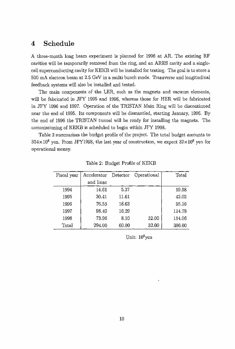
Table 2 summarizes the budget profile of the project. The total budget amounts to
354 xlO8 yen. From JFY1998, the last year of construction, we expect 32xlO8 yen for
operational money.
Table 2: Budget Profile of KEKB
Fiscal year
1994
1995
1996
1997
1998
Total
Accelerator
and linac
14.61
30.41
76.53
98.49
73.96
294.00
Detector
5.37
11.61
18.63
16.29
8.10
60.00
Operational
32.00
32.00
Total
19.98
42.02
95.16
114.78
114.06
386.00
Unit: 108yen
10

Chapter 1
Physics Requirements
1.1 Energy Asymmetry
The required energy asymmetry at KEKB is derived from considerations on the physics
program. The major part of the research topic is a study on CP violation in decays of
neutral B mesons, where decay modes such as B —> J/ipKs need to be reconstructed.
The magnitude of CP violation is expected to be 0(10%) according to the Standard
Model. For this study, B mesons with finite momenta have to be produced so that
the time evolution of their decay pattern can be measured. The B mesons produced
in decays of T(4s) at rest do not suit this purpose, because in this condition the B
mesons will have only a small fixed momentum of 300 MeV in the laboratory frame.
An e+e~ collider with an asymmetric energy collision is required to produce T(4s)s
which are moving along the beam axis in the laboratory frame.
The energy asymmetry is characterized by the motion of the center of mass of the
BB system in the laboratory frame. Its Lorentz boost parameter is written as
K F,^ ^ ± . (1.1)
Here, the E- and E+ are the energies of the electron and positron beams, respectively.
The y/s is the center-of-mass energy, which can be written as v/ s = ^/AE^E+. It is
equal to the rest mass of T(4s), 10.58 GeV.
With a larger energy asymmetry, time evolution measurements can be done with
better accuracy. However, the effective acceptance of the detector with a fixed geometry
will be reduced. The optimum value of the asymmetry must be found by taking into
account these two factors. Figure 1.1 shows the total integrated luminosity that is
required to observe CP violation as a 3 standard deviation signal as a function of f3~f.
It is seen that the asymmetry values between /?7=0.4 and 0.8 result in a similar
sensitivity for this measurement.
1-1

Required Integrated Luminosity
X)_4
Figure 1.1: Required integrated luminosity for observing CP violation, as a function
of energy asymmetry
On the other hand, it should be pointed out that there are a number of other physics
topics involving B meson decays, where studies of the decay time evolution are not
required. For these processes, a smaller asymmetry is preferred for a larger acceptance
and for a better event reconstruction efficiency [1].
Combining these considerations, the energy asymmetry has been chosen as /?7=0.42,
which is obtained by
E. = 8.00 GeV (1.2)
E+ = 3.50 GeV (1.3)
1.2 Luminosity
For measuring the CP violation in the decay B —> J/ipKs, the required integrated
luminosity is estimated to be between 30 and 100 fb"1. The uncertainty of this estimate
arises from quoted errors in the experimental data and their theoretical interpretations.
Other channels to measure CP violation have been also studied. It is estimated that
at least 100 fb"1 of the integrated luminosity is necessary to measure other important
parameters in the Standard Model.
1-2

The CLEO-II experiment at CESR is presently collecting data with a world-record
high luminosity of a few xlO32 cm~2s~1. They are expected to collect 20 fb"1 by
the time KEKB starts data taking. Studies on a variety of rare decay modes of B
mesons will have been conducted by then. A desire to go beyond the statistical sensi-
tivity available at CLEO-II adds another reason why KEKB should collect more than
100 fb"1.
Prom these considerations, it is concluded that the target luminosity for the first
few years of the experiment should be 100 fb"1. To achieve this in a timely manner,
the target peak luminosity for KEKB should be l.OxlO34 cm~2s~1.
1.3 Energy Range
Three T resonances are known to exist below the BB threshold, while the first res-
onance above the BB threshold is T(4s) at 10.58 GeV. The T(4s) decays almost
exclusively into BB (either Bu or Bd), and it is at this resonance that the bulk of data
should be collected at KEKB.
However, some data need to be collected at different center-of-mass energies for the
following reasons.
• An energy scan is required to find the peak of T(4s). This is to ensure that the
data taking is conducted at the most efficient energy. Since the mass and width
of T(4s) is well known from measurements by CLEO, it also serves the purpose of
cross-calibration of the machine configuration at KEKB. The width of the energy
scan can be as small as 30 MeV, and the number of the data points will be at
most 10.
• Off-resonance data have to be collected to understand qq continuum events. This
is important for some data analyses where the continuum background has to be
statistically subtracted. An integrated luminosity of more than 10% of the on-
resonance data will be required for this purpose. The energy of the off-resonance
run should be 10.50 GeV, where the cross section of the BB pair-production is
negligibly small. At KEKB this determines the lowest center of mass energy for
the required run.
• It has been pointed out that studies of Bs should provide additional information
on 6-quark decays. For this purpose it is necessary to go to T(5s) (10.87 GeV) to
produce Bs mesons. However, its production rate is expected to be O(^) of the
Bu,d production rate at T(4s). The present perspective is that the measurement
of Bs will be done only after a significant amount of data is collected for Bu^ at
1-3

T(4s). At KEKB this specifies the highest center of mass energy for the required
run.
It is concluded that the energy coverage by KEKB should be between 10.4 and
11.0 GeV, which includes a small margin on the higher and lower
E+ = 10.4 ~ 11.0 GeV (1.4)
Throughout these runs, the energy asymmetry should be kept at /?7=0.42.
1.4 Beam Energy Spread
In the experiment at KEKB, rare decays of B mesons need to be reconstructed, where
the combinatorial background from continuum events can be significant. In many of
those decay modes, a reduction of this background is equivalent to an increase of the
effective luminosity from the viewpoint of statistical significance.
It has been shown by simulation studies that the signal-to-noise ratio S/N of the
B decay reconstruction is approximately inversely proportional to the beam energy
spread [2], By applying an adequate Lorentz boost according to the beam energy,
the measured momentum vectors of B meson decay products can be brought into the
rest frame of T(4). The momentum of the B in this frame will have a fixed value of
300 MeV. This can be used as a powerful constraint for finding B. The effectiveness
of this technique depends on the magnitude of the energy spread of the accelerator.
For example, in the reconstruction of Bd decays into 7r+7r~, the signal-to-noise ratio
is expected to be approximately 1:1 with a beam energy spread of 7.8xlO~4. It will be
worsened to 1:2, if the energy spread increases by a factor of two. This is equivalent
to a factor of 1.7 reduction of the luminosity.
The energy spread should, therefore, be chosen to be the smallest possible that is
allowed by machine design considerations.
1.5 Beam background
As the previous sections have shown, high luminosity is required to study the CP
violation and rare decays. Naturally, the KEKB machine must store an extremely
high beam current. Also, a beam pipe with a small radius needs to be used at the
interaction point (IP) for precise vertex measurements. Therefore, the reduction of
beam background is a critical issue. It is essential to design the machine, especially
the interaction region (IR), so as to reduce the beam background.
1-4

If bend magnets are used near the collision point to separate two beams, the syn-
chrotron radiation emitted by particles passing through these magnets have to be
handled with utmost care. This condition can be significantly relaxed if no separation
bend magnets are useu, because synchrotron radiation from other magnets will have a
significantly reduced critical energy.
However, it will still be necessary to have movable masks in the straight section to
absorb photons that are emitted by the beams when they go through the magnets far
from the interaction point. Also, the location and size of the magnets near the IP have
to be designed while taking into account the synchrotron radiation background. The
aperture of beam pipe vacuum chambers needs to be allocated with sufficient margins to
allow the synchrotron radiation to pass, as well as the beam during injection conditions.
The particle background due to beam-gas scattering is potentially more harmful
than the synchrotron radiation in KEKB. The vacuum pressure in the IP straight
section must be kept at less than 10~9 torr. This is required for reducing the rate of
off-momentum particles directed toward the beam pipe to an acceptable level.
A set of movable masks in the arc or non-IR straight sections needs to be imple-
mented, in order to clip the beam tail, because the long beam tail might hit the IR
masks and cause severe background.
The beam background during the injection time is another important issue, con-
sidering radiation damage to the silicon vertex detector, the Csl calorimeter, and their
electronics circuit. These issues have to be considered in the design of the injection
scheme and the shielding of detector components.
1-5

Bibliography
[1] The BELLE Collaboration, KEK Report 94-2.
[2] "Progress Report on Physics and Detector at KEK Asymmetric B Factory", B Physics
Task Force, May 1992, KEK Report 92-3.
1-6

Chapter 2
Machine Parameters
2.1 Luminosity, tune shift, beam intensity
KEKB is a double-ring asymmetric e+e~ collider at 3.5 GeVx8 GeV. Its target peak
luminosity is £ = 1034 cm"2s~1. To determine basic machine parameters, we begin
with the most fundamental equations for the luminosity and vertical beam-beam tune
shift:
= 7 ^ R$ ( 0 P£ £ P O") (2-2)7 ^
fc [a* + a;) a;Here, AT1)2 is the number of particles per bunch, and / is the bunch collision frequency.
The suffix k = 1,2 specifies each beam in the low energy ring (LER) and high energy
ring (HER). The 6X is the half crossing angle at the interaction point (IP). The functions
Re and R$y represent reduction factors for the luminosity and the vertical tune shift,
which arise from the crossing angle and the hour-glass effect. Since there is no obvious
reason for choosing unequal beam parameters, except for the number of particles per
bunch, we simply set £y, f3*y, eXiy, and az to be equal for the two beams. This implies
that iVi7i = A 272.
The possibility of a round-beam collision has been excluded. With a round beam
with small /?* in two planes, so far no consistent design solutions have been found with
an acceptable dynamic aperture and with a feasible two beam separation at the IP.
We thus combine Equations 2.1 and 2.2, and by assuming equal beam-parameters and
flat beams (a* 3> o"*),
2ere(3*y
2-1

where Ik = N^ef is the current for each beam, with k = 1,2. It should be pointed out
that if the relation (5* > a: holds (i.e. if the hour-glass effect is small), the ratio of the
reduction factors above becomes close to a unity,
%r « 1 • (2-4)K
This means that Equation 2.3 can be rewritten in a form that is nearly independent of
the choice of the crossing angle. Thus, to a good approximation,
C « ^f . (2.5)
Equations 2.3, 2.4 and 2.5 state that while the lunr nosity may be reduced due to
the crossing angle, the beam-beam interaction is also reduced by approximately the
same ratio. Therefore, if the dynamics of the beam-beam interaction with the crossing
angle allows the same value of £y as for the head-on collision, there is no loss of the
luminosity for a fixed total beam current. Figure 2.1 shows the calculated reduction
factors and the ratio Rc/R$y as functions of the half crossing angle 9X. Note that the
reduction factors above simply involve geometric effects due to the crossing angle and
the hour-glass effect. No effects due to the dynamics of the beam-beam interactions
are included.
In the design of KEKB, we assume £y « 0.05 and ft* = 1 cm. Then, the beam
intensities required for C = 1034 cm~2s~1 are / = 2.6 A for the LER and / = 1.1 A
for the HER. Exactly how much luminosity will be actually available at KEKB can be
answered only after operating the machine and after examining where the performance
limitations come from. Re-optimization of operating parameters will naturally follow
studies during operation. An important issue concerning the design of KEKB at this
stage is to allocate some flexibility in the parameter space, so that such changes in the
future can be easily accommodated. Details of some of the specific issues are discussed
in subsequent chapters.
2.2 Crossing angle
Near the IP a rapid two beam separation is necessary in order to maintain optimized
focusing of the LER and the HER beams without significantly increasing the chro-
maticity. Suppression of emerging parasitic crossing effects also calls for a good beam
separation, except the designated IP.
Several beam separation schemes based on horizontal bend magnets, a finite beam
crossing angle, and their mixed combinations have been examined for KEKB. For
2-2

10.8
0.6
0.4
0.2nu
(
1
0.8
0.6
0.4
0.2
o
_ j ^ . | . , , , | . . . , | . . . . | . . .i_
:- ^ ^ ^ ^ ^
'— -^
' i i , i i , i i , i i , , i i i i i i i i i i i~
3 0.01 0.02 0.03 0.04 0.05e x
R^x_ii 11 1 i i i i 11 i i 11 i i 111 i i i j _
L \v _E
L \ . J
" i i i i 1 i • i i 1 i i i i 1 i i i i 1 i i i i ~
0 0.01 0.02 0.03 0.04 0.05ex
I0.8
0.6
0.4
0.2n
^~
^~
^~
'—
~ i r i i
0 0
1
0.98
0.96
0.94
0.92
0 9\/ • z*
(
n /TRT /J' ' ' '
'—
"till
) o
1 ' '\
1 1 ,
.01
i ' •
111
.01
i
\
0.02
, , | i
I l l l
0.02
^ ^
i t
0.
ex
1 '
i t i
0.
ex
i ' '
i , ,03
1 ' '
1 i i
03
• • 1 • • - i _
—_
—_
—_
, , 1 , , , , :
0.04 0.05
• i 1 i i i i .
_ — _
—m
—_
—_
, , 1 , , , , :
0.04 0.05
Figure 2.1: Reduction factors of the luminosity and tune shifts as functions of the half
crossing angle 6X. Other parameters are KEKB's. The ratio Rc/R^y is always close to
unity.
2-3

example, it has been found that to allow more than a 2 0 ^ beam separation at the first
parasitic crossing point, it will be very difficult to accommodate a bunch spacing st,
below 3 m if a small or zero crossing angle at the IP (0x < 3 mrad) is to be maintained.
The reasons include:
• The separation bend magnets will have to be strong (> 0.6 T) compared to the
standard bend magnets in the arc sections, leading to significant problems in
handling synchrotron radiation in the vicinity of the IP.
o There is a severe limitation of geometrical space available for separation bends
very close to the IP (i.e. a distance comparable to a half of the bunch spacing).
However, the situation can change significantly when a larger beam crossing angle is
allowed. A brief summary of the hardware and beam-dynamics issues involved in the
beam separation of varying crossing angle choices is given in Table 2.1.
Crossing angle Hardware Beam dynamics
Rapid beam separation is
critical for staying away
from parasitic crossing
effects
Synchro-betatron resonance
OK?
Comfortable for parasitic
crossing effects with
S(, & 0.6 m.
Synchro-betatron resonances
OK? Need to be checked.
Increased need for Crab-
crossing.
0 mrad
2 mrad
5 mrad
8 mrad
10 mrad
20 mrad
Very compact separation bend
magnets (such as permanent
magnets) are necessary.
Superconducting separation bend
is feasible with a reasonable field
strength (< 0.7 T).
Separation bend magnets are no
longer necessary.
Use of common quadrupole magnet
for two opposing beams per side
becomes painful.
Table 2.1: Possible choices of the crossing angle, and their implications to the hardware
design and beam dynamics.
2-4
The big advantage of a moderately large crossing angle of 6X > 10 mrad is that
although it eliminates the need for separation bend magnets, it allows final focusing
with superconducting quadrupole magnets with reasonable inner aperture sizes. It also
offers a flexible configuration that permits a wide range of combinations of the bunch
intensity vs. bunch spacing for varying center-of-mass energies. The scheme allows
us to safely stay away from potential problems due to parasitic crossing effects. The
critical energy of synchrotron radiation that passes through the IP is also significantly
reduced by not using separation bend magnets.
It has been estimated that with a crossing angle of ~ 3 mrad or less, the maxi-
mum achievable luminosity, with its inevitably large bunch spacing (~ 3 m), is roughly
3 x 1033 cm~2s~1. Therefore, assuming that full-bunch operation with s& = 0.6 m is
eventually possible from RF and multi-bunch stability viewpoints, a scheme with a
crossing angle of ~ 10 mrad brings big advantages, if the beam-beam parameter can
be maintained at ^ > 0.015. Thus, the critical question is how the beam dynamics
behavior will be with finite crossing angles. To investigate this issue, we have con-
ducted extensive simulation studies on the beam-beam interaction with finite crossing
angles. The results, as detailed in later chapters, demonstrate an absence of serious
degradations at many operating points.
Prom these considerations and from practical evaluations of the accelerator layout
near the IP, we have chosen the half-crossing angle 9X to be 11 mrad. As a fall-back
position, the use of a crab-crossing scheme with superconducting cavities is also being
considered. It will serve as a cure to reduce the remaining luminosity degradation, or
to extend the acceptable combinations of operating parameters. It should be noted
that a crossing angle 11 mrad is close to the minimum that allows us to eliminate the
IP separation bend magnets. It is also nearly the maximum crossing angle that allows
final focusing of both beams at the IP with common quadrupole magnets. If separate
quadrupole magnets are to be used for the two beams, hardware design constraints will
force us to use a crossing angle larger than 40 mrad. In that case, the field strength
of the crab cavities will have to be increased four-fold, and their reliable operation can
be problematic. Up to now the 11 mrad value for the half crossing angle is the most
preferred one.
2.3 Bunch length
A shorter bunch length is preferred for reduced intrinsic synchrotron-betatron coupling
in the beam-beam interaction. It is also preferred for reduced hour-glass and reduced
crossing-angle effects. The lower limit of the bunch length is given by the single-bunch
2-5

longitudinal instability, Touschek lifetime, and the required accelerating voltage. We
have chosen the bunch length to be az > 4 mm, which is close to the minimum possible
value. Here, the bunch-lengthening due to a potential-well distortion needs to be taken
into account. The target value of 4 mm includes this bunch-lengthening effect of 20%
in the LER. As detailed in subsequent chapters, the lattice design of KEKB will allow
us to tune the momentum compaction over a wide range, so that the actual bunch
length can be optimized by looking at the beam behavior.
2.4 Bunch spacing
The bunch spacing is the next parameter to be determined. First, the accelerating
RF frequency should be ~ 508 MHz, because the RF resources at TRISTAN, which
will be reused at KEKB, are based on this frequency. Therefore, the allowed bunch
spacing will be an integer multiple of ~ 0.59 m. Since the total beam current has been
determined to be 2.6 A for the LER and 1.1 A for the HER, the number of particles
per bunch is proportional to the bunch spacing. The hardest limit on the number of
particles per bunch comes from the longitudinal single-bunch threshold for the LER.
At KEKB, the threshold bunch intensity is about 2.5 times the bunch intensity for the
minimum bunch spacing of si, = 0.6 m. Therefore, either s& = 0.6 m or S(, = 1.2 m is a
possible choice.
Second, we examine the relation between the required bunch intensity and emit-
tance. The vertical beam-beam tune shift given by Equation 2.2 can be rewritten
as
0* 1l^fJ^ &X
where K = ey/ex is the ratio of the horizontal and vertical emittance. We thus obtain
the relation
ex a JL= . (2.7)
Consequently, if the emittance ratio K and (3* are kept constant, the required horizontal
emittance is proportional to the bunch spacing, because N oc s;,. Another reason for
increasing the emittance, besides Equation 2.7, is the need for maintaining a sufficiently
long Touschek beam lifetime for an increased bunch intensity when the bunch spacing
is increased.
However, design considerations concerning the interaction region limit the practical
maximum beam emittance. This is because when the beam emittance is increased for
a fixed j3* at IP, the angular divergence there is also increased, resulting in an increased
2-6

synchrotron radiation background to the detector. Although a smaller emittance cou-
pling ratio may allow a larger emittance without increasing the angular divergence, it
will be problematic to rely on delicate operating conditions of this sort.
In conclusion, at KEKB we have chosen s<,=0.6 m as the standard value. Conse-
quently, the number of particles per bunch with Sb = 0.6 m is set as N = 3.3 x 10¹⁰ for
the LER and JV = 1.4 x 10¹⁰ for the HER.
2.5 Emittance
When the bunch spacing is chosen, and once the (5X and K are given, the horizontal
emittance is determined by Equation 2.7. As stated earlier, although a smaller /3* is
preferred for a larger K, there is a limit given by the angular divergence limit at IP.
The horizontal beam-beam tune shift, which can be written as
also speaks for reduced horizontal emittance. The horizontal tune shift does not have
to be equal to the vertical value. However, it should not be significantly larger than
0.05, which corresponds to ex = 1.4 x 10~8 m. We have chosen the horizontal emittance
so that the luminosity given by the strong-weak beam-beam simulation is maximized
in the allowable range. The results are /?* = 33 cm, K = 2.4%, and ex = 1.8 x 10~8.
With this choice, the bunch diagonal angle at the IP cr*/crc will be 19 mrad, nearly
equal to the total beam crossing angle. The reduction ratios, luminosity, and tune
shifts are summarized in Table 2.2.
The lattice design (discussed in detail in Chapter 6) will incorporate quadrupole
magnet "knobs" so that it can vary the horizontal emittance in the range of 1.0 x 10~8 <
ex < 3.6 x 10~8 m. This is to manage possible changes of the bunch spacing, angular
divergence, beam intensity, and emittance ratio under actual operating conditions. For
instance, full-current operation with s& = 1.2 m instead of 0.6 m will be possible by
using this measure.
2.6 Momentum spread and synchrotron tune
The momentum spread of the beam is set to be ~ 0.07%, which is close to the upper
limit value from a high energy physics experiment viewpoint, which prefers a small
energy spread. From accelerator design considerations, it is hard to reduce the energy
spread much below 0.07% without decreasing the radiation damping rate.
2-7

The last issue among the choice of basic parameters is the synchrotron tune vs,
and the momentum compaction factor ap. Since the bunch length and the momentum
spread as have been determined, vs and ap are not independent. They are related as
oz = C-^as , (2.9)
where us = 2-KVS/TQ is the synchrotron frequency. Generally speaking, a large us
induces pronounced synchro-betatron resonances, due to lattice nonlinearity effects and
beam-beam interactions. It also causes an anomalous emittance growth at synchro-
betatron resonance lines. A small value of us < 0.02 is necessary to have a sufficiently
large tune space as the possible operational parameter space.
On the other hand, a small us decreases the threshold for single-bunch instabilities.
Also, higher-order momentum compaction can be more harmful with a small ap for
synchrotron motions with large amplitudes.
Our choice is us = 0.015 for both the LER and the HER. However, the lattice design
of KEKB will incorporate another set of quadrupole strength "knobs," so that it can
vary the momentum compaction in the range — 1 x 10"'1 < ap < 4 x 10"'1, without
affecting the horizontal beam emittance.
2.7 Other Issues
The particles in the LER have been chosen to be positrons, so as to reduce the effects
of the ion trapping phenomenon of residual gas molecules in the vacuum chamber. In
the HER (i.e. electron ring), 100-500 of RF buckets need to be left vacant in order to
avoid ion trapping. Even if ions are not trapped, transient ions created by the bunch
train may interact with the trailing bunches, and a beam break-up phenomenon may
result, as has been observed in linear accelerators. Studies of these phenomena are in
progress.
The radiation damping time of the LER is longer than that of the HER's by a factor
of 2, if the sole source of radiation is bending due to dipole magnets in the lattice. A
room will be allocated in straight sections of the LER to implement damping wiggler
magnets, if it is found necessary to change the LER damping time.
The machine parameters are listed in Table 2.2.
2-8

Beam Energy
Luminosity
Luminosity Reduction Factor
Half crossing angle
Tune shifts
Tune shift reductions
Beta functions
Beam current
Bunch spacing
Particles/bunch
Number of bunches/ring
Emittance
Bunch length
Momentum spread
Synchrotron tuneMomentum compaction factor
Betatron tunes
Circumference
Damping time
EC
Re
ex
R$xlR$y
i
Sb
NNB
ex/ey
Vz
Vs
aP
VxIVy
cTE
LER HER
3.5 8.0
1.0 x 1034
0.845
11
0.039/0.052
0.737/0.885
0.33/0.01
2.6 1.10.59
3.3 x 10¹⁰ 1.4 x 10¹⁰
5000
1.8 x 10-73.6 x 10-10
4
7.1 x 10~4 6.7 x 10~4
0.01~0.02
1 x 10~4 ~ 2 x 10⁻⁴
45.52/46.08 47.52/43.08
3016.26
44.9 22.5
GeV
cm-2s"1
mrad
m
Am
mmm
m
ms
Table 2.2: Machine Parameters of KEKB.
2-9

Chapter 3
Beam-Beam Interactions
3.1 Introduction
As Chapter 2 has shown, a beam separation scheme with a relatively large crossing
angle ( 2 x 1 1 mrad) has been chosen for KEKB. The expected benefits are as follows:
1. It makes it possible to accommodate a wide range of combinations of the bunch
intensity vs. bunch spacing (minimum 0.6 m).
2. It makes it possible to use superconducting final focusing quadrupole magnets,
and the system can provide collisions at EQM = 10-4 ~ 11.0 GeV without modi-
fying the hardware layout of the beam line.
3. The absence of separation bend magnets leads to a significant reduction of syn-
chrotron radiation near the interaction point.
4. Compensation solenoid magnets can be implemented near the interaction point.
5. An extremely large beam separation is provided, even at the first parasitic colli-
sion point.
How this scheme is realistically adequate at KEKB depends on whether the behavior of
the beams should be stable and satisfactory under finite angle crossing. The purpose
of this chapter is to document the results of studies that have been carried out for
KEKB in an effort to answer this question.
3-1

Laboratory Frame
Electron Positron
Boosted (Head-on) Frame
SlicingElectron Positron
Figure 3.1: Lorentz transformation from the laboratory frame to the "head-on" frame,
which is used for applying synchro-beam mapping to calculate beam-beam interactions
with finite crossing angles.
3.2 Simulation of a Beam Collision with Finite
Crossing Angles
A new modelling algorithm has been developed to simulate beam-beam collisions under
finite crossing angles. In the algorithm, as indicated in Figure 3.1, the bunches that are
colliding at the crossing angle are first Lorentz-transformed into a frame in which their
momentum vectors are parallel. In this "head-on" frame a symplectic synchro-beam
mapping is applied, and the beam-beam forces and their effects on the bunches are
calculated. When the mapping is finished, the two bunches are Lorentz-transformed
back to the laboratory frame, where the beam tracking code takes over the rest of the
simulation.
This beam-beam code incorporates all known effects, including: (a) the energy loss
due to the fact that a particle traverses the transverse electric fields at an angle, (b)
energy loss due to longitudinal electric fields, and (c) effects due to the variation of P
along the bunch length during a collision (hourglass effect).
Full descriptions of this code and its preliminary results are given in [1] and the
references therein. To date, this is the only code known to us to be fully sympiectic
in the 6-dimensional phase space with the hourglass and crossing angle effects taken
into account. The symplecticity in the 3-dimensional sense, and correct treatment
of Lorentz-covariance and bunch slicing there are considered to be important in our
application. This is because the planned total crossing angle (22 mrad) is comparable
to the geometric angle of bunches at the IP of KEKB, i.e. crx/crz = 19 mrad.
3-2

3.3 Beam-Beam Simulation with Linear LatticeFunctions
A series of beam-beam simulations has been conducted based on a simplified lattice
model, where the beam transfer through the ring is represented by a one-turn ma-
trix and a diffusion matrix [5]. Although the interaction between the beam-beam and
non-linear lattice effects cannot be studied using this method, it allows us to quickly
compare the luminosity performance in various beam parameter and tune conditions.
This simulation is also necessary to compare the luminosity between linear and non-
linear lattices.
In this simulation the beam-beam effect is calculated according to the prescriptions
given in the previous section. A weak-strong formalism is used. Typically the strong
bunch is longitudinally sliced in 5 slices, and the weak bunch is represented by 50 super-
particles. The effects of radiation damping and diffusion are included in the calculation.
Its details are given in [1], Parameters such as the initial beam emittance, coupling,
bunch intensity, /?*, orbit errors at the IP and the machine tunes are specified as
initial conditions. Then, the beam-beam collision and revolutions through the ring are
simulated for up to 10 radiation damping times. The resultant beam size is examined.
The strong beam is given a specified Gaussian distribution. The weak beam has a
distribution function given as the sum of 6-functions, which represent the ensemble of
particles. The expected luminosity is calculated as a convolution of the distribution
functions of the two beams.
The initial beam parameters in the simulation are specified in such a way that
they would give the design luminosity value of 1 x 1034 cm2s~1 or somewhat higher
values, with collisions of 5120 bunches per ring in the absence of aberrations and beam
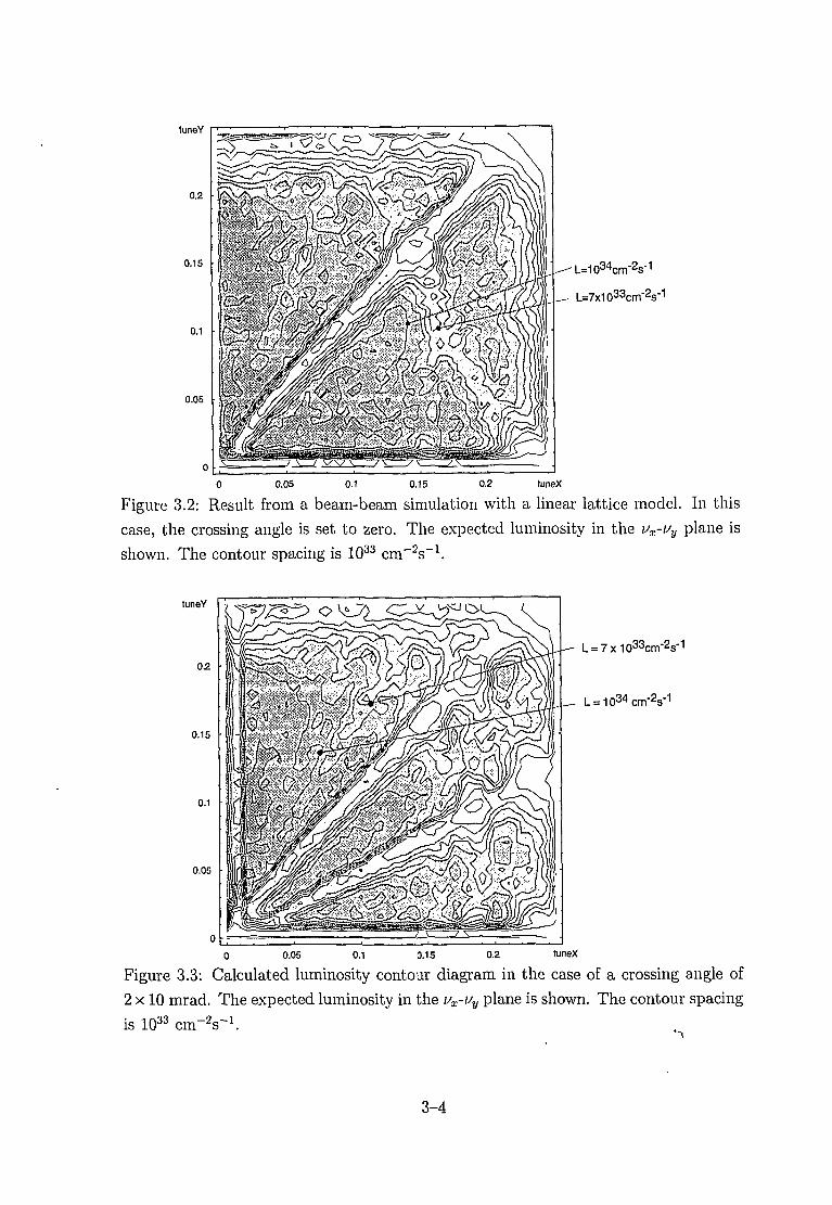
blow-up. Figure 3.2 shows an example of the results from this simulation. In this case,
the crossing angle at the IP is set to zero. The synchrotron tune us is assumed to be
0.017. The figure shows a contour diagram of the expected luminosity as a function of
the transverse tune (vx and vy) in the range 0 < vx, vy < 0.25. The contour spacing is
1033 cm~2s~1. Pronounced luminosity reduction due to the coupling resonance is seen.
Also, traces of vy = 2vx, Aux + 2vy = 1 and the synchro-betatron resonance vs = 2vy
are seen.
Figure 3.3 shows a similar luminosity contour plot in the vx-uy plane, but for the
case with a crossing angle of 2 x 10 mrad. The beam intensity was changed from that
of Figure 3.2 in order to adjust the geometric luminosity, while keeping the other pa-
rameters unchanged. An additional luminosity reduction due to the synchro-betatron
resonance line us = 2vx is evident. Also, resonance lines such as vx = 2vy, 3vx = 5uy,
3-3
tuneY
0.15
0.05
L=1034crrT2s-1
L=7x1033cm"2s"1
0 0.05 0.1 0.15 0.2 tuneX
Figure 3.2: Result from a beam-beam simulation with a linear lattice model. In this
case, the crossing angle is set to zero. The expected luminosity in the vx-vy plane is
shown. The contour spacing is 1033 c m ' V 1 .
tuneY
0.15
0.1
0.05
0 •
= 7x1033cm"2s-1
L = 1034cm-2s"1
0 O.05 0.1 0.15 0.2 tuneX
Figure 3.3: Calculated luminosity contour diagram in the case of a crossing angle of
2 x 10 mrad. The expected luminosity in the vx-vy plane is shown. The contour spacing
is 1033
3-4

tuneY0.05 0.1 0.15 0.2 0.25 0.3
tuneY0.05 0.1 0.15 0.2 0.25 0.3
Figure 3.4: Two slices from the luminosity contour plot for the zero crossing angle
case. The expected luminosity as a function of vy is shown for ux = 0.1 and 0.11.Lum/10^34
tuneX -> 0.1
tuneY0.05 0.1 0.15 0.2 0.25 0.3
tuneY0.05 0.1 0.15 0.2 0.25 0.3
Figure 3.5: Two slices from the luminosity contour plot for a crossing angle of 2 x 10
mrad. The expected luminosity as a function of uy is shown for ux = 0.1 and 0.11.
3-5

3vx = vy, and 4uy — Ava = 1 are causing a luminosity reduction. Those resonances did
not cause a luminosity reduction in the case of the zero crossing angle. However, a
sizeable amount of areas in the ux-vy plane appear to be intact.
Figure 3.4 shows two slices of the contour plot in Figure 3.2. The expected lumi-
nosity as a function of vy is shown for vx = 0.1 and 0.11. Likewise, Figure 3.5 shows
two slices of Figure 3.3 for a comparison.
Some notable observations are summarized as follows:
1. Introducing a finite crossing angle at the IP certainly causes a reduction of us-
able vx-vy combinations, because of synchro-betatron and other resonances. The
effects are larger for a larger synchrotron tune i>s, particularly when vs > 0.03
holds.
2. However, when vs is kept small i.e. below 0.02, a fair amount of regions in the
Vx-Vy plane is still free from synchro-betatron resonances, and thus they appear to
be usable. Such regions exist as well-connected zones, rather than many isolated
islands. Some of the acceptable vx-vy regions are compatible with the conditions
preferred in dynamic aperture considerations.
3. For the beam intensity of a few x 1010 per bunch or below, no intensity-dependent
beam blow-up is predicted with finite crossing angles, as far as this simulation
using the simplified lattice model is concerned.
4. When the synchrotron tune (us) is small, and when a resonance-free condition
of vx-vy is chosen, the expected luminosity there is roughly consistent with naive
expectations based on the geometric and linear effects, as discussed in Chapter
2.
5. The luminosity calculated with an ideal linear lattice, in some cases, can become
larger than a naive expectation, which only considers geometric factors. This
is because of effects of the dynamic beta [3] and dynamic emittance [4]. As
an example, Figure 3.6 shows correction factors for the 0 and e calculated for
0<uy< 0.1.
The results from this study have been reviewed in conjunction with investigations on
the tune-dependence of the dynamic aperture and other aspects of the KEKB design.
It has been found that beam dynamics considerations in the lattice design favor a
horizontal tune {ux) slightly above the half integer resonance. From studies on the
engineering design required for magnets in the interaction region, a crossing angle of
2 x 1 1 mrad has been chosen. Figures 3.7 and 3.8 show the calculated luminosity tune
3-6

52o
act
o
u
mam
ical
Q
1.4
1.2
1
0.8
0.6
0.4
0.2
C
^ Emittance" " - • —
Emittance x Beta
,..- Beta
/
) 0.02 0.04 0.06 0.08
Tune (modulo 1/2)
0.1
Figure 3.6: Dynamic beta and dynamic emittance effects: the dotted line indicates (3,
dashed line is e and the solid line is /?e. The horizontal axis is the tune (modulo 1/2).
All of these are normalized by their nominal values.
tuneY
0.15
0.05
0.0
0.55 0.6 0.65 0.7 tuneX
Figure 3.7: Result from a beam-beam simulation with simplified particle tracking. In
this case, the crossing angle is set to 2 x 10 mrad. The expected luminosity in the vx-vv
plane is shown. The contour spacing is 1033 cm~2s~1.
3-7

tuneY0.05 0 . 1 0.15 0.2 0.25 0.3
tuneY0.05 0.1 0.15 0.2 0.25 0.3
Figure 3.8: Two slices from the luminosity contour plot of for the region 0.5 < vx < 0.75
and 0 < vy < 0.25 as shown in Figure 3.7. Expected luminosity as function of uy is
shown for ux = 0.52 and 0.53.
diagram for 0.5 < vx < 0.75 and 0 < vy < 0.25. The final working parameters for
the detailed design work have been determined as Table 3.1. The effective beam-beam
parameter for this set of parameters is £XiV = (0.04,0.05), which takes account of the
dynamical reduction factors, as discussed in Chapter 1. Figure 3.9 shows the luminosity
tune diagram, which gives a magnified view of the vicinity of the working parameter
set.
Surveys have also been made on how the luminosity is affected by the bunch length.
Let us call the bunch length of the weak beam af and that of the strong beam asz.
Figure 3.10 shows the expected luminosity as a function of o™ and ai. The plot on
the right side shows the expected luminosity (solid line) when the condition a™ =
af is imposed. The broken line in the plot shows the luminosity expected from a
consideration of only the geometry. It is seen that a shorter bunch gives a higher
luminosity. It is also seen that there is no reasons for choosing different bunch lengths
for the two beams; each bunch should have the bunch length as short as possible. From
a consideration of the necessary RF voltages, it was decided to use 4 mm for the bunch
length.
3-8

Px at the IP
fo at the IPexev
{Vx, Vy, Ua)
Bunch population
Total number of bunches
0.33
0.01
1.8 x 10"8
3.6 x 10"10
0.004
(0.52,0.08,0.017)
1.4 x 10¹⁰
3.2 x 10¹⁰
5120 max.
m
mm
mm
electrons
positrons
per ring
/ bunch
/ bunch
Table 3.1: Working parameter set for the half crossing angle 9X of 11 mrad, determined
from considerations on beam-beam effects, dynamic apertures and others.
Vy
0.14
0.12
0.1
0.08
0.06
= 1034cm-2s-1
7x1033cm-2s'1
0.5 0.52 0.54 0.56 0.58 Vx
Figure 3.9: Luminosity contour diagram near the operating point.
3-9

%
g 0.51
Beam-Beam Simulation
Geometrical ~ - ^ T r ^ ^ ^Luminosity ~ ^ "
0.002 0.002 0.004 0.006 0.008 0.01Bunch Length (m)
Figure 3.10: Left: Expected luminosity as a function of the bunch length (in m) of the
strong bunch (asz) and the weak bunch (a™). Right: The same figure for the case with
rf = at.
3.4 Simulations with the Lattice Which Includes
Nonlinearity and Errors
The beam-beam simulation algorithm based on the weak-strong model has been in-
corporated in the computer code SAD at KEK (SAD stands for "Strategic Accelerator
Design" code). This facilitates a tool to study the effects of finite crossing angles at
the IP, combined with the nonlinearity of the lattice and its possible errors.
3.4.1 With Quadrupole Rotation Errors Only
To create finite vertical emittance in the tracking procedure, it is necessary to assume
some x-y coupling sources in the ring. As a simplified case, we first examine a nonlinear
lattice where rotation errors of the quadrupole (Q) magnets are considered to be the
sole source of coupling. We rotate all of the Q magnets randomly, according to
rotation angle = / x f3,
where f$ is the Gaussian random variable around zero with a unit standard deviation.
The distribution is cut off at 3 standard deviations. For each series of errors, we adjust
/ so that the ay equals the assumed vertical beam size at the IP. (Without errors, the
vertical beam size vanishes.) A typical value of / is 5 x 10~4 rad.
Calculations of the beam-beam collision and particle tracking, now with SAD, have
been conducted for up to 90,000 turns. Then, the expected luminosity is calculated.
Parallel to these calculations, with the given rotation errors of the Q magnets, the
single-turn beam transfer matrix with radiation damping and the single-turn diffusion
3-10

matrix of the ring are extracted[5]. These matrices are used in a beam-beam simulation
with the linear ring-lattice as discussed in the previous section. The difference between
the luminosity values obtained in these two methods is considered to give some infor-
mation about the effects of nonlinearity in the lattice including sextupole magnets and
skew fields.
Without Solenoid Field Compensation With Full Solenoid Field Compensation
0 . 6 0 . 8 1 1 . 2 1 . 4 1 . 6 1 . 8
Luminosity (1034cm'2s"1) with linearized lattice
0 . 6 0 . 8 1 1 . 2 1 . 4 1 . 6 1 . 8
Luminosity (1034cm"2s"1) with linearized lattice
Figure 3.11: Expected luminosity in the weak-strong model calculations of beam-beam
interactions, which are combined with tracking through the ring. The two diagrams
show the cases where the detector solenoid field is compensated in situ at the IP
(right) and without (direct) solenoid field compensations (left); the solenoid field is
compensated by skew quadrupole magnets sitting at other locations.
Furthermore, to investigate the effects of the presence of a solenoid field from the
experimental facility at the IP, those calculations have been repeated for two versions
of the lattice design. In the first case, no explicit solenoid field compensation is made
at the IP, and all of the coupling corrections are made with skew quadrupole magnets
distributed in the interaction region. In the lattice case, the field compensation is
achieved with counter-acting solenoid magnets.
Figure 3.11 shows the results of this study. For each data point in the scatter dia-
gram, the horizontal coordinate gives the expected luminosity from calculations based
on the linear lattice matrix. The vertical coordinate gives the luminosity expected
from full SAD tracking. The diagram on the left shows the result with a lattice design
which assumes no solenoid field compensation at the IP. The diagram on the right is
from a lattice design with full solenoid field compensation.
3-11

The expected luminosity has been found in the range of (0.938±0.185) x 1034cm 2s 1,
depending on the random number seed that is used to create rotation errors of quadrupole
magnets. Figure 3.11 indicates that compensation of the detector solenoid field by
counter-acting solenoid magnets is favored over coupling corrections with skew quadrupole
magnets. The field compensation scheme at the interaction point is designed to use
compensation solenoid magnets.
3.4.2 With Realistic Lattice Errors
Simulations with SAD have been repeated with a more advanced model of lattice
errors. Here, finite alignment and excitation errors of the bend (B), quadrupole (Q)
and sextupole (S) magnets are simultaneously considered, together with offset errors
of the beam position monitors (BPMs). The typical magnitudes of the assumed errors,
which we consider realistic, are summarized as follows:
type of elementhorizontal shift (urn)
vertical shift (/im)
x-y rotation (mrad)
strength error
BPM75
75
0
0
B0
100
0.1
IO-'1
Q100
100
0.1
lO"3
s100
100
0.1
io-3
Steering correctors0
0
0.1
0
xf,
Gaussian errors (f3) are produced according to the rms values given in the table
above. For each series of generated errors, orbit and tune corrections are made in the
tracking code as if it were in an actual operation. Then, the scale of the assumed
errors is re-normalized so that the expected vertical spot size ay agrees with the design
value. We call this normalization factor / . With those renormalized errors in the
machine, the orbit and tune corrections are, once again, performed. The expected
luminosity is evaluated by using the beam-beam code, plus the tracking with SAD.
Different random seeds used for generating lattice errors result in different values of
/ (error normalization factor) and different expected luminosity values. Some of the
obtained results are:
luminosity/lO^cnrV1 = { 0.9 / = 0.8
3-12
This result indicates that the lattice nonlinearity and possible machine errors do
not lead to fatal degradations of the estimated luminosity.
3.5 Quasi Strong-Strong Simulation
The results presented so far are based on a strong-weak model, where typically the HER
beam (electron) is assumed to be strong, and the LER beam (positron) to be weak.
To address the issues which may be overlooked in this treatment, a quasi strong-strong
formalism has been developed. In this scheme, once every 500 turns of revolution
the average electron and positron bunch sizes are "registered." During the next 500
turns, weak-strong model calculations are performed, while this "registered" electron
(positron) bunch size is used as the "strong bunch size" for calculating the development
of the positron (electron) bunch size. Then the "strong bunch sizes" are updated again,
and the simulation continues.
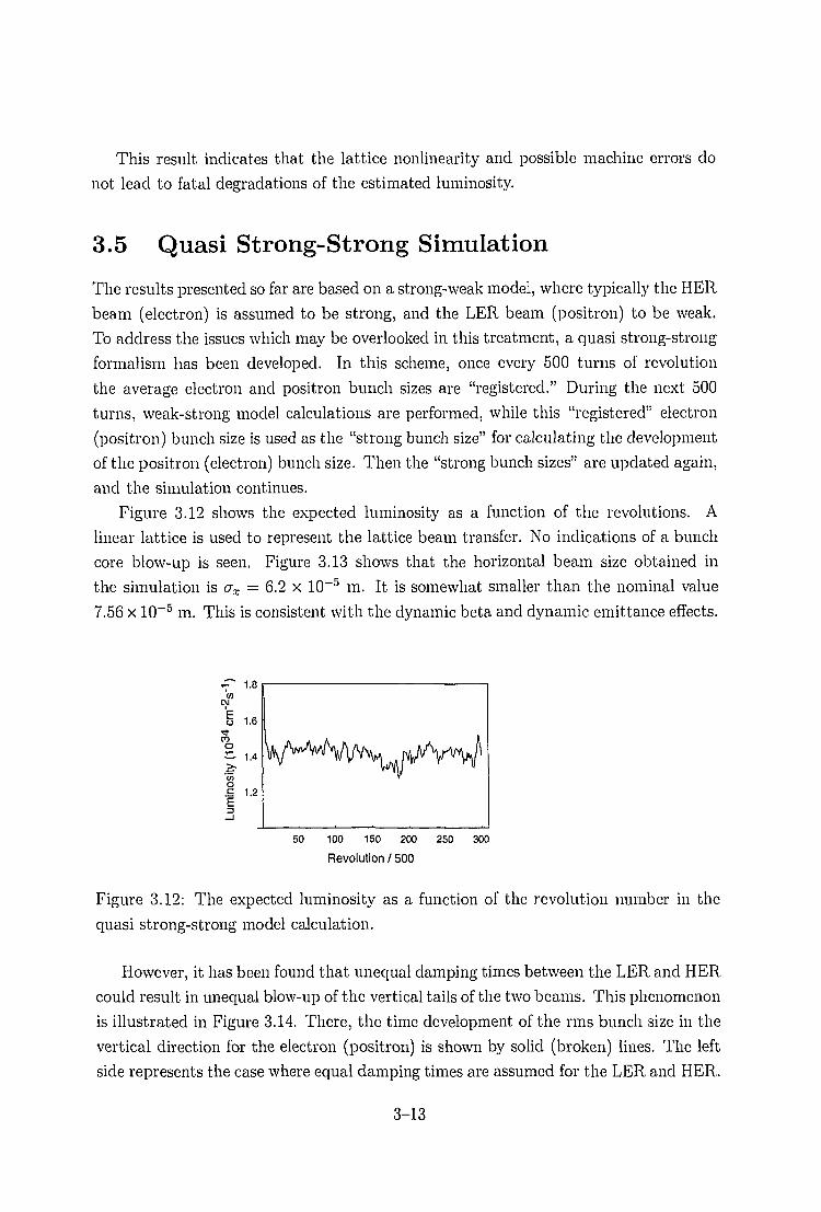
Figure 3.12 shows the expected luminosity as a function of the revolutions. A
linear lattice is used to represent the lattice beam transfer. No indications of a bunch
core blow-up is seen. Figure 3.13 shows that the horizontal beam size obtained in
the simulation is ax = 6.2 x 10~5 m. It is somewhat smaller than the nominal value
7.56 x 10~5 m. This is consistent with the dynamic beta and dynamic emittance effects.
'inCM
u
1
Lum
inos
it
l.B
1.6
1.4
1.2
50
v*vy
100 150 200 250 300
Revolution / 500
Figure 3.12: The expected luminosity as a function of the revolution number in the
quasi strong-strong model calculation.
However, it has been found that unequal damping times between the LER and HER
could result in unequal blow-up of the vertical tails of the two beams. This phenomenon
is illustrated in Figure 3.14. There, the time development of the rms bunch size in the
vertical direction for the electron (positron) is shown by solid (broken) lines. The left
side represents the case where equal damping times are assumed for the LER and HER.
3-13

CO
oD.COCO
Io
0.00008
0.00007
0.00006
0.00005
0.00004
Positrons
50 100 150 200 250
Revolution / 500
300
Figure 3.13: Behavior of ax as a function of the revolution number. The solid line
shows the electron bunch size. The broken line shows the positron bunch size.
Equal Damping Time Unequal Damping Time
0 50 100 150 200 250 300
Revolution / 500
E 3.0
aCO 2 . 5
o
!
I
(B) Positrons
Electrons
0 50 100 150 200 250 300
Revolution / 500
Figure 3.14: Behavior of oy as a function of the revolution number. The design value
is ay = 1.66 x 10~6 m. The solid lines show the HER beam size and the broken lines
show the LER beam size. The figure on the left (A) is for the case when both beams
have equal damping times. Figure on the right (B) shows the case where the LER has
a damping time longer by factor 2.
3-14

The right side of Figure 3.14 shows the case with unequal damping times between the
LER and HER (TLER = 2THER)- A factor 1.5 blow-up of the positron rms size is seen.
Note that the spot sizes plotted here are based on the rms of particle distributions. On
the other hand, calculations of the luminosity based on the convolution of the particle
distributions show no significant difference for the two cases: i.e. with and without
equal damping times. This signature is consistent with a growth of the vertical tail.
Thus, it appears desirable to maintain similar damping times for the LER and HER.
This can be accomplished by using damping wigglers in the LER; it will be part of the
lattice design goals.
3.6 Bunch Tails Excited by Beam-Beam Interac-tions
The presence of non-Gaussian bunch tails causes an extra synchrotron radiation (SR)
background to the detector facility, which is harmful to its data collection and data
analysis. The fractional bunch tail population should be kept less than 10~5 for >
10ax and 10~5 for > 30<7y, according to design considerations on SR masks near the
interaction point.
The development of bunch tails due to beam-beam interactions has been studied
with a long-term strong-weak calculation with a linear lattice model. Typically the
simulation is done by tracking 50 super particles over 108 turns of revolution. This
means 1000 seconds for 50 particles, and 14 hours for a single particle in the actual
machine.
Figure 3.15 shows the calculated particle distribution as a function of the action
variable Iy in the vertical coordinate,
/(vv)2 + pl/(vPv)2}- (3-1)
The particle distribution function p(Iy) is normalized to unity. In Figure 3.15 the
vertical axis indicates log1Q{p(Iy)). The core part is identical with the nominal Gaussian
distribution. Non-gaussian tails in the particle distribution are seen. In this case the
function p(Iy) can be fitted with a sum of
p{Iv) <, e~Iv + 5.2 x 10⁻³e-a 1 5^ + 3 x KrV 0 - 0 4 7 ' . (3.2)
We define the normalized vertical amplitude Ay as
3-15
T3
COQ_
O
100 120 140 160
L: Normalized action variable in y
10 15 20 25 30
Figure 3.15: (A) Tail distribution for an ideal linear lattice as a function of the normal-
ized nominal action Iy. (B) The same distribution in the {Ix,Iy) space. The contour
lines are drawn for each factor step of 10.
3-16

of
O>.O
-2
-4
- 6
- 8
-10
-12
\
0 5
A y :
10 15
Normalized Particle
\ X20 25 3
Amplitude
Figure 3.16: Probability of a particle having the amplitude larger than Ay.
Then the probability of finding a particle whose amplitude exceeds Ay is calculated as
R[Ay] = T p(Iv)AydAy.JAy
Figure 3.16 shows Iog10(i?[i4j/]) as a function of Ay, based on the calculations shown in
Figure 3.15.
It can be seen that the probability that a particle has a vertical amplitude larger
than 30ay, where ay is the design bunch size, is approximately 10~12. Since the bunch
population is on the order of 1010, no particle is likely to have such a large vertical am-
plitude. Tails in the horizontal direction have been also studied. It has been found that
the development of horizontal bunch tails is much slower than in the vertical direction.
The limit imposed by requirements on the small synchrotron radiation background to
the detector facility is satisfied without problems. Preparations are under way to eval-
uate bunch tails by using tracking calculations which include non-linear effects of the
lattice and possible machine errors.
3.7 Tail, Luminosity and Longitudinal Tilt
The dependence of the tail behaviors on the tunes have been studied. To characterize
the size of bunch tails the largest amplitude (ax,ay) among 50 super-particles during
several damping times is picked up. The part (A) and (B) of Figure 3.17 show lu-
minosity contour plots for the region 0.5 < vx < 1.0 and 0 < uy < 0.5 along with
the maximum particle amplitude in the vertical direction. They show that luminosity
reduction is frequently associated with a growth of vertical tails, but not necessarily
so all the time.
3-17

(A)
0.1
0.5 0.6 0.7 0.8 0.9Vv
0.1
0.5 0.6 0.7 0.8 0.9Vv
(B)
0.5 0.6 0.7 0.8 0.9Vv
Figure 3.17: (A) Luminosity contour diagram in the ux-uv plane. The contour lines are
drawn for luminosity values of 1034 and 0.5 x 1034 cm~2s~1. (B) Contour diagram of
the maximum vertical amplitude of bunch particles. Contour lines are drawn for 30a0y,
20ooy and 10cr0y, where &oy is the nominal vertcal beam size. (C) The longitudinal tilt
angle (j)xz is shown. The contour lines are drawn for 1, 0.8, 0.6, 0.4,and 0.2 mrad.
3-18

The angle of the beam envelope relative to the longitudinal coordinate has been also
calculated at the same time. The crossing angle in the collision introduces a coupling
between the transverse and longitudinal coordinates. Consequently, the principal axes
of the bunch may tilt not only transversely, but also longitudinally. We calculate the
longitudinal tilt angle in the head-on frame as
Here, (xz) represents the long term (three damping times) average of xz. Similar
definitions hold for (xz) and (xx). To be more precise, evaluation should be made with
a strong-strong model simulation. However, the weak-strong results can indicate how
serious the effect is.
Part (C) of Figure 3.17 shows a contour diagram of the calculated <j}xy. The longi-
tudinal tilt angle increases as ux approaches the integral value from below. It exceeds
1 mrad for vx > 0.75.
3.8 Summary of Beam-Beam Simulations with Fi-nite Crossing Angles
The estimated values of the luminosity in the simulations presented so far are summa-
rized in Table 3.2. The assumed beam parameters are set as in Table 3.1.
Method
1
2
3
4
5
Luminosity (xlO34)
1.16
1.24
0.938±0.185
0.9 to 1.34
1.4
Legend
Geometrical
Ideal linear lattice
Nonlinear lattice
Nonlinear lattice with
realistic errors and corrections
Quasi strong-strong (equal damping)
Table 3.2: Comparison of the expected luminosity values evaluated by various simula-
tions.
Brief descriptions of individual cases in Table 3.2 are given bellow:
1. Expected luminosity with the 2 x 11 mrad crossing angle, where only the geo-
metric effects are considered. Dynamical effects, such as the dynamic beta and
dynamic emittance, are not considered.
3-19

2. Weak-strong beam-beam simulation, combined with a linear, error-free lattice.
3. Weak-strong beam-beam simulation, combined with a nonlinear lattice. Rotation
errors of the Q magnets are used to create the finite luminosity coupling. The
variations are due to the difference in the seed used to generate the rotation
errors. Full compensation of the detector solenoid field is assumed.
4. Weak-strong beam-beam simulation, combined with the nonlinear lattice model.
Excitation and alignment errors of bend, quadrupole and sextupole magnets are
considered. Orbit and coupling corrections are performed in the tracking code,
mimicking the actual operation.
5. Quasi strong-strong simulation with a linear, error-free lattice. Equal damping
times for the HER and LER are assumed.
It is seen that within the simulation studies conducted so far, the luminosity in the
design goal can be achieved with a finite angle crossing of 2 x 11 mrad at the interaction
point. Unfortunately, this performance cannot be fully experimentally tested until
operating the real-life KEKB machine. As a back-up safety measure, the use of crab
crossing scheme to combine with the finite angle collision is being considered. The
status of its R&D efforts is presented in Chapter 8. Meanwhile, more elaborate studies
of beam-beam effects will be continued:
• In a tail simulation, nonlinear effects in the lattice should be included in the
calculation.
• In a weak-strong simulation with a nonlinear lattice, error correction schemes
from the beam-beam point of view will be examined.
• The strong-strong simulation will be updated so that it can evaluate the beam
envelopes in each turn, using a Gaussian approximation to calculate the beam-
beam forces.
• A more ambitious strong-strong simulation which does not rely on the Gaussian
approximation to calculate the beam-beam force is being developed.
One example of storage rings which implemented a finite crossing angle in the past is
DORIS at DESY. It has been known that difficulties were encountered in its operation.
According to a report [2]:
"Although the width of these satellite resonances (due to synchro-betatron reso-
nances) is very small (< 0.001) as compared to the distance between the resonances,
3-20

they limit the luminosity of the storage ring DORIS. The reasons are the decoupling
transmitter and the rf-quadrupole, which are needed to suppress instabilities. The de-
coupling transmitter gives to different bunches different synchrotron frequencies, with
a spread of AQS = ±0.006. The rf-quadrupole produces a spread in betatron frequen-
cies of AQ/3 = ±0.005. At the present operating point between 6.24 and 6.15, there
are always some bunches on a resonance."
"The theoretical and experimental investigations have shown that the satellite reso-
nances are weaker for Qp-values closer to an integer. We therefore expect that shifting
the operating point into a region near 6.1 will permit higher currents and thus increase
the luminosity."
Attention has been paid in the KEKB design so that those conditions which could
lead to serious operational difficulties will be avoided. For instance, a fairly low syn-
chrotron tune (0.01 < vs < 0.02) will be used. The coupled-bunch instabilities will
be addressed by careful design of the RF cavities, feedback systems and an optimized
choice of operating parameters, and by not introducing a tune spread.
3.9 Comments on Parasitic Crossing Effects
When the half crossing angle is small (~ a few mrad or less), the issue of parasitic cross-
ing is quite difficult to study theoretically. This is because both the focussing effects
and shifts of bunch centroid need to be considered in a multi-bunch, multi-crossing
condition in a 3-dimensional way. Studies have been carried out with simulation cal-
culations for a bunch spacing as small as 0.6 m:
1. A strong-strong model simulation based on the Rigid Gaussian Model has been
conducted. Closed orbit effects due to parasitic collisions have been analyzed. It
was observed that the closed orbits of individual bunches will differ from each
other for a smaller (a few mrad or less) crossing angle. In extreme cases, a closed
orbit may not exist at all. Chaotic behaviors of clusters of bunches can result,
having orbit deviations exceeding 10ax.
2. A 2-dimensional weak-strong model simulation to analyze the beam size during
injection and collision conditions has been performed. It was found that for small
crossing angles, the injected beam can rapidly blow up, exceeding the dynamic
aperture limit, and may never become damped to acceptable sizes.
However, it should be pointed out that the validity of the results for small crossing
angles (< a few mrad) with a small bunch spacing (< 1 m) are limited by the approxi-
3-21

mation which is used in the simulation. With the present-day capabilities of computing
facilities, it appears to be very difficult to obtain reliable results in a realistic compu-
tation time. Thus, for a crossing angle < 2 x 2.5 mrad, exact statements cannot be
made, except that the acceptable bunch spacing is likely to be limited to roughly 3 m
or larger.
Fortunately, the choice of a 11 x 2 mrad crossing allows us to evaluate the effects
of parasitic collisions with an approximation that is based on the simplified Gaussian
model with adequate accuracies. This is because the beam separation at the first and
subsequent parasitic crossing points will be large (> 6 mm), and the forces between
opposing bunches in parasitic crossing will be quite weak. No fatal effects have been
observed for a half crossing angle near 10 mrad in weak-strong or strong-strong simu-
lations. We consider that it is safe to conclude that the effects of parasitic collisions at
KEKB with a crossing angle of 2 x 11 mrad are negligible.
3-22

Bibliography
[1] For a treatment of the beam-beam interaction, see K. Hirata, H. Moshammer and
F. Ruggiero, Particle Accelerators 40, 205 (1993); K. Hirata, Phys. Rev. Lett., 74
2228(1995); N. Toge and K. Hirata, Study on Beam-Beam Interactions for KEKB,
KEK Preprint 94-160 (1994).
[2] A. Piwinski, IEEE Trans, on Nucl. Sci. 24 1408 (1977).
[3] B. Richter, Proc. Int. Sym. Electron and Positron Storage Rings, Saclay, 1966.
[4] K. Hirata and F. Ruggiero, Particle Accelerators 28, 137 (1990). (Proceedings of
XIV Int. Conf. on High Energy Accel. 1989 Tsukuba.)
[5] K. Ohmi, K. Hirata and K. Oide, Phys. Rev. E49751(1994).
3-23

Chapter 4
RF Parameters
4.1 Introduction
This chapter discusses the requirements for the KEKB RF system, coupled-bunch
instabilities caused by RF cavities and our solutions, and a consistent set of RF design
parameters. Detailed descriptions of the cavities and other RF hardware components
are given in chapter 8.
Coupled-bunch instabilities arising from the higher-order modes (HOM's) of cavities
must be sufficiently suppressed. Since the stored current at KEKB is much higher than
that at any existing storage rings, the Q-values of HOM's must be sufficiently lowered,
typically much below 100 for dangerous modes, by effectively extracting the field energy
out of the cavity. A number of HOM-damped cavity structures have been proposed
and studied around the world.
In addition, the accelerating mode itself can give rise to a longitudinal coupled-
bunch instability in a large electron/positron storage ring with an extremely high
beam current, such as KEKB or other high-luminosity factory machines. If we use
conventional normal-conducting damped cavities in KEKB, several modes of coupled-
bunch instabilities can be excited. The growth rate will be extremely high due to the
high impedance of the accelerating mode.
In order to solve this problem, a new normal-conducting RF structure, referred to
as an accelerator resonantly coupled with an energy storage (ARES) [1], was proposed.
It employs an energy storage cavity operating in a high-Q mode. Another candidate
is a superconducting cavity (SCC), which is fairly immune against this instability.
Extensive R&D work is in progress at KEK on both the ARES and the superconducting
cavity.
The design parameters of the RF system have been determined by taking the follow-
ings into consideration: required accelerating voltage and beam power, growth rates of
4-1

the coupled-bunch instabilities, RF properties of the proposed cavities, and the power
handling capability of high power components.
4.2 Requirements
4.2.1 RF Voltage
The total RF voltage is determined by requirements to provide: (1) a short bunch
length (<72 = 4 mm) and (2) the desired synchrotron tune. The required RF voltage
(Vc) is given by
(4.1
where c is the velocity of light, C the ring circumference, ap the momentum compaction
factor, E the beam energy, ae the relative energy spread, az the rms bunch length, UJRF
the RF angular frequency and (j)s the synchronous phase. In general, a short bunch
length requires a high accelerating voltage. The synchrotron tune (vs) is given by
"• -
It is seen from Equations (4.1) and (4.2) that when ue and az are given, V^sin^ and
ap are proportional to vs. Since a£ is given by the bending radius, Vc and ap are
determined uniquely by giving a~ and vs.
From beam dynamics considerations the synchrotron tune should be variable in
order to find the best operation point, while avoiding synchrotron-betatron coupling
resonances. It is considered that the synchrotron tune should be variable from 0.01 to
0.02, while keeping the bunch length constant. For this purpose both the momentum
compaction factor and the total RF voltage need to be able to be varied in proportion
to each other. Thus the RF voltage should be variable over a range of 4.9~9.4 MV
(LER) and 8.7-16.2 MV (HER), respectively.
4.2.2 Beam Power
The radiation power loss of the beam at bending magnets is 2.1 MW for the LER and
3.8 MW for the HER. An additional beam power loss is caused by wake potentials due
to the ring impedance (HOM loss) and by radiation at wiggler magnets. The total ring
impedance is estimated to give a loss factor of about 42 V/pC in the LER and 60 V/pC
in the HER, which causes a HOM loss of about 0.57 MW and 0.14 MW, respectively.
Wiggler magnets may be optionally installed in the LER in the future for reducing the
4-2
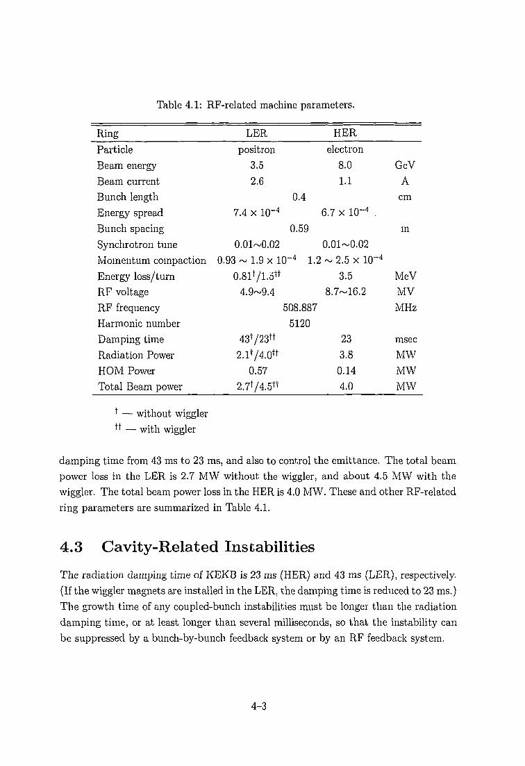
Table 4.1: RF-related machine parameters.
Ring
Particle
Beam energy
Beam current
Bunch length
Energy spread
Bunch spacing
Synchrotron tune
Momentum compaction
Energy loss/turn
RF voltage
RF frequency
Harmonic number
Damping time
Radiation Power
HOM Power
Total Beam power
LER
positron
3.5
2.6
7.4 x 10"4
0.01~0.02
0.93 ~ 1.9 x 1(
0.8lVl.5tf
4.9~9.4i
43723**2.lt/4.0tt
0.572.7t/4.5tt
0.4
0.59
r 4 1.2
508.887
5120
HER
electron
8.0
1.1
6.7 x 10~4 ..
0.01~0.02
~ 2.5 x 10~4
3.58.7~16.2
23
3.80.14
4.0
GeV
Acm
m
MeV
MV
MHz
msec
MWMW
MW
* — without wiggler
tt — with wiggler
damping time from 43 ms to 23 ms, and also to control the emittance. The total beam
power loss in the LER is 2.7 MW without the wiggler, and about 4.5 MW with the
wiggler. The total beam power loss in the HER is 4.0 MW. These and other RF-related
ring parameters are summarized in Table 4.1.
4.3 Cavity-Related Instabilities
The radiation damping time of KEKB is 23 ms (HER) and 43 ms (LER), respectively.
(If the wiggler magnets are installed in the LER, the damping time is reduced to 23 ms.)
The growth time of any coupled-bunch instabilities must be longer than the radiation
damping time, or at least longer than several milliseconds, so that the instability can
be suppressed by a bunch-by-bunch feedback system or by an RF feedback system.
4-3
4.3.1 Coupled-Bunch Instability due to the Accelerating Mode
In storage rings, the cavity tuning is usually set to minimize the input power to the
cavity. The resonant frequency is detuned toward the lower side to compensate for the
reactive component of the beam loading. Without this detuning, a large amount of RF
power is reflected from the cavity. The amount of detuning frequency for an optimum
operation is given by
Jsin& Rs Pj, t o n <f>aA / = —2VT Q~o X fRF = " i ^ T 1 ( 4 3 )
where / is the beam current, 4>s the synchronous phase, Vc the voltage per cavity, Rs
the shunt impedance, Qo the Q-value, fnp the RF frequency, Pj> the beam power and
U the stored energy.
If a high beam current is stored in a large storage ring, the detuning frequency can be
comparable to, or even exceed the revolution frequency (frev)- The coupling impedance
of the accelerating mode at the upper synchrotron sidebands of the revolution harmonic
frequencies / becomes significantly high. Here the / is given by / = frev(h + m +
us), where h is the harmonic number and m = — 1,— 2, If we use conventional
normal-conducting cavities in KEKB, the detuning frequency would be several times
the revolution frequency. It will excite several modes of the coupled-bunch instability
with a growth time on the order of 100 /.isec, which is much faster than the radiation
damping time.
In order to reduce the growth rate of this instability, the detuning frequency should
be decreased. As seen in Equation 4.3, a direct solution is to increase the stored energy
compared to the beam power. In other words, we need to decrease R/Q, while keeping
a high shunt impedance and Vc.
By employing an energy storage cavity operating in a high-Q mode that is coupled
to an accelerating cavity,the stored energy is increased and the growth rate is lowered.
This was first pointed out by T. Shintake [2]. In order to put this idea into practical
use, Y. Yamazaki and T. Kageyama devised the ARES scheme [1]. A schematic view of
ARES is shown in Figure 4.1. The accelerating cavity couples with the energy storage
cavity through a coupling cavity in between. With the additional coupling cavity,
ARES has advantages in the stability of the accelerating mode and in the clamping of
parasitic modes associated with the accelerating mode. A more detailed description of
ARES is given in chapter 8.
The use of a superconducting cavity (SCC) is another possible solution, since its
R/Q value is usually lower than that of conventional normal-conducting cavities, and
it can be operated at a higher accelerating voltage. The R&D work is in progress at
KEK on both the ARES normal-conducting cavity and the superconducting cavity.
4-4

Accelerating Cavity
Coupling Cavity
Storage Cavity
Figure 4.1: Schematic view of the ARES normal-conducting cavity system.
The growth time is quantitatively discussed in the next section in connection with the
RF parameters.
Another approach to avoid this instability is to introduce an RF cavity feedback
system. This feedback reduces the coupling impedance at the upper synchrotron side-
bands of the revolution harmonic frequencies. Along with the development of the
cavities, we are developing an RF feedback system with parallel comb filters. It will
be applied for providing additional damping, when necessary.
4.3.2 Coupled-Bunch Instability due to HOM's of the RFCavities
Detailed descriptions on the HOM properties of ARES and SCC are given in chapter 8.
This section summarizes the estimated growth time.
Naturally, the accelerating cavity itself that is employed in the ARES scheme must
be a HOM-damped structure. The HOM-damping method applied to the accelerating
cavity of ARES is to employ a coaxial wave guide which is equipped with a notch
filter [3], [4] (see, section 8.1). The R/Q and Q values of the HOM's in the accelerating
cavity of ARES was calculated using a computer code MAFIA. The number of cavities
is estimated in the next section (20 cavities for the LER and 36 for the HER). The
growth time of the fastest growing mode in the LER (HER) is then about 60 msec
(150 msec) in the longitudinal case ana ? :sec (80 msec) in the transverse case.
In the ARES, since the accelerating ca/ity is connected to the storage cavity via
the coupling cavity, we must be careful concerning the following facts.
4-5

• The coupling impedance can be different if the HOM of the accelerating cavity
is coupled to other cavities. The impedance of the whole ARES system needs to
be accurately estimated.
• Since ARES is a three-cell cavity, the system has 0, ?r/2 and ir modes which
couple to the accelerating mode. The n/2 mode is the operating mode. The 0
and 7T modes are parasitic modes; their frequencies are close to the operating
RF. The parasitic modes (0 and TV) can be damped by a damper attached to
the coupling cavity, and the growth time of the coupled bunch instability due to
these modes is expected to be longer than 10 msec.
In the case of superconducting cavity, the HOM's are extracted through beam pipes
with a large diameter, and are absorbed by ferrite material attached toe the beam pipes.
The R/Q values of HOM's have been calculated using a computer code URMEL. The
frequency and the Q value of each HOM have been measured with a full-size model
cavity made of copper. According to the result shown in section 8.2, when 10 SC
cavities are used in the HER, the growth time of the fastest growing mode is about
420 msec for longitudinal and 110 msec for transverse instabilities. They are much
slower than the damping time.
4.3.3 Static Robinson Limit
The static Robinson limit gives a maximum stored current of
_ 2Vcsin<j>s 1lmax ~ sin2(d> - aL) f Q * Q L ' l '
where (f>s is the synchronous phase, ai the tuning-offset angle, and Qi the loaded-Q
value. It should be pointed out that if superconducting cavities are operated with the
optimum input coupling to the design beam current (Id) and with the optimum tuning
(QL = 0) to compensate for the reactive component of beam loading, the stability
condition becomes marginal at the design current. This is because ilie input coupling
is much larger than unity in the case of SCC and the loaded-Q is represented by
Here, Pf,, Pc, (3, and QQ are the beam power, cavity wall loss, input coupling, and
intrinsic Q-value, respectively. It is seen that la in Equation (4.5) is equal to Imax
in Equation (4.4) when CLL, = 0. In order to avoid an instability, an artificial offset
from the optimum tuning should be introduced at the expense of extra RF power. For
4-6

this purpose, 10~20 degrees of the tuning offset (ai) will be sufficient, which requires
3~13% extra input power. This will be taken into account in the RF parameters
discussed in the next section.
4.4 RF Parameters
The RF operation parameters have been optimized by taking the following into account:
• The required RF voltage should be provided. (It should be variable to change vs
from 0.01 to 0.02)
• The expected beam power should be supplied.
• The growth time of the instability due to the accelerating mode should be longer
than the damping time.
• It should also meet the full wiggler option in the LER.
• The high power system should be stably operated.
It should be noted that in KEKB the beam power is rather high, while the required
RF voltage is relatively low. In ordinary storage rings where the beam loading is
moderate, the number of cavities is determined by the total RF voltage. On the
other hand, in a storage ring where the beam power is significantly large, the number
of cavities is determined by the cavity input power, which may be limited by the
performance of the input couplers, high power source or others. In the latter case, since
the cavities are operated with a lower field gradient, and hence with a larger detuning
frequency, the growth rate of the coupled-bunch instability due to the accelerating
mode is increased. This is in contrast with the growth rate of the coupled-bunch
instability due to HOM's, which is simply proportional to the number of cavities. In
the following, we quantify the feasibility for both cases of ARES and SCC, operated
in the LER and HER, with the full design beam current and the full wiggler option in
the LER. The cavity performance, power handling capability, and the growth rate of
the instability are taken into account. The RF properties of the accelerating mode of
these cavities are listed in Table 4.2.
4.4.1 ARES Normal-conducting Cavity
The maximum cavity voltage is expected to be 0.5~0.6 MV/cavity, which corresponds
to a permissible wall loss of 150 kW. (This wall loss is distributed to the accelerating
4-7

Table 4.2: Accelerating mode of the cavities.
ARES SCC
R/Q 12.8 93 Q/cavity
<2o 1-33 x 105 > 1 x 10°
cavity and the storage cavity of ARES.) The maximum input power to the cavity
depends on the technology available for the input coupler. The input couplers for the
APS normal-conducting cavities in TRISTAN have been successfully operated up to
200 kW. The R&D work is in progress to develop an input coupler that can handle
a much higher power. In addition, since we will feed the power through the storage
cavity, two input couplers can be installed for each ARES system. This scheme doubles
the power transfer capability.
Figure 4.2 shows the input power, wall loss, and reflection power in each cavity of the
HER as a function of the RF voltage. The input coupling was set to give the optimum
coupling at 13.2 MV (^=0.016). The maximum required RF voltage of 16.2 MV can
be provided by 36 ARES cavities with an input power of 233 kW. The growth time
of the coupled-bunch instability due to the accelerating mode is much longer than the
damping time. Thus the required range of the RF voltage from 8.7 MV to 16.2 MV
can be covered with these cavities without changing the input coupling or the number
of cavities. The parameters at 8.7 MV and 16.2 MV are listed in Table 4.3.
In the LER, the input coupling and the number of cavities should be optimized
depending on the total RF voltage. As an example, the parameters optimized at 4.9 MV
(i/a=0.01) and 9.4 MV (ys=0.02) are listed in Table 4.3. The maximum required RF
voltage of 9.4 MV can be provided with 20 ARES cavities, with the input RF power
to each ARES being 355 kW. If the operating voltage is 4.9 MV, we need to decrease
the number of cavities; otherwise the growth time becomes faster than the damping
time. In this low voltage case 10~12 ARES cavities will be operated, each of which is
powered by one klystron. The growth time will be longer than 30 msec in either case.
Thus, the required voltage range can be covered by optimizing the input coupling and
the number of cavities.
4.4.2 Superconducting Cavity
An accelerating gradient of 10 MV/m can be easily achieved in a bench test with the
present technology for 508 MHz superconducting cavities at KEK. The design gap
voltage of the KEKB cavity is set to 1.5 MV/cavity, which corresponds to a gradient
4-8

Table 4.3: RF Operation Parameters for the ARES Cavity.
Beam energy
Beam current
Beam power
RF voltage
Synchrotron tune
# of Cavities
R/Q
Qo
QL
Input P
Voltage
Input power
Wall loss
Detuning freq.
Growth time*
# of Klystrons
Klystron power**
GeV
AMW
MV
Q/c&v.
xlO4
MV/cav.
kW/cav.
kW/cav.
kHz
msec
kW
LER
3
2
4
4.9
0.01
10
12
1.33
2.6
4.19
0.49
591
141
16.2
49iottt
640
5
6
5
9.4
0.02
20
.8x 105
3.6
2.73
0.47
355
130
17.7
30
10
760
HER
8.0
1.1
4.0
8.7 16.2
0.01 0.02
36
12.8
1.33 x 10⁵
3.9
2.41
0.24 0.45
157 233
34 119
13.5 7.8
100 180
18
340 500
Wiggler magnets are included in the LER.
t — Coupled-bunch instability due to the accelerating mode.
^ — 7% loss at the wave guide, circulator, magic tee etc. is taken into account.
m — In this case one klystron feeds one cavity.
4-9
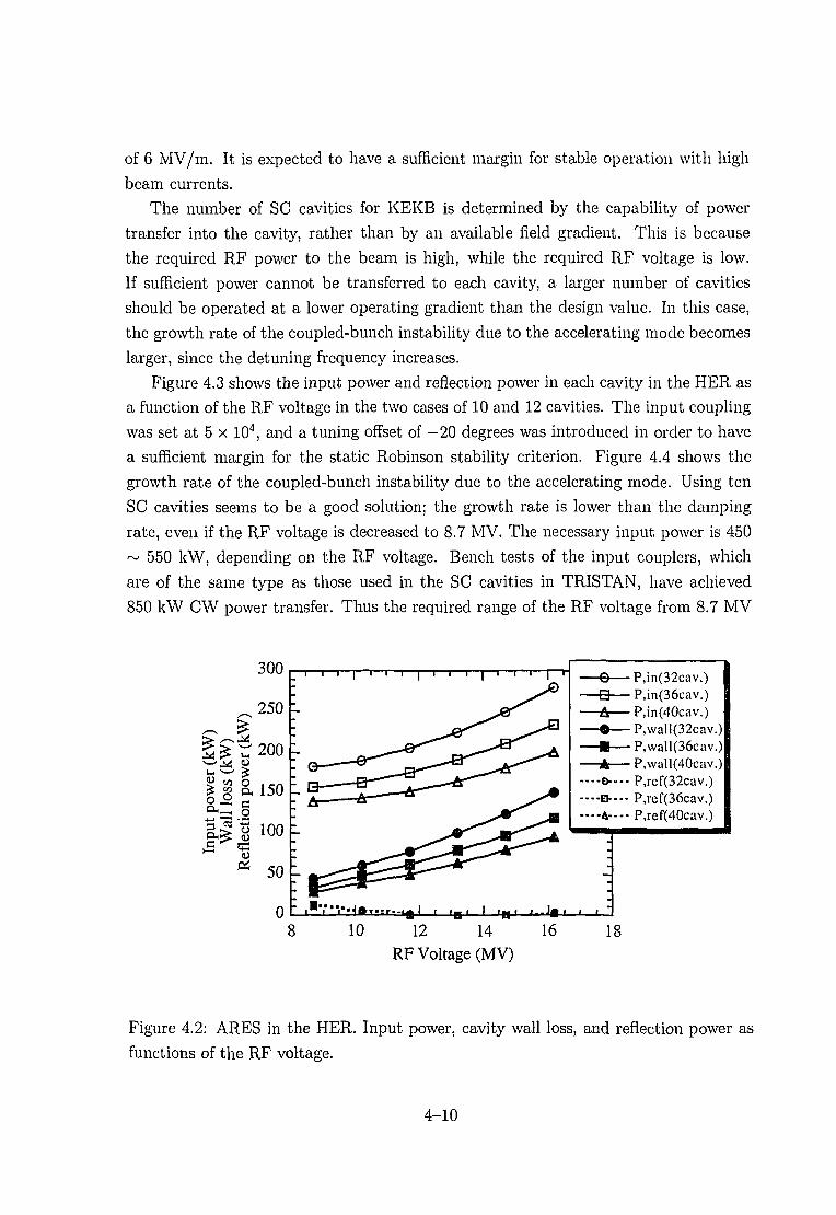
of 6 MV/m. It is expected to have a sufficient margin for stable operation with high
beam currents.
The number of SC cavities for KEKB is determined by the capability of power
transfer into the cavity, rather than by an available field gradient. This is because
the required RF power to the beam is high, while the required RF voltage is low.
If sufficient power cannot be transferred to each cavity, a larger number of cavities
should be operated at a lower operating gradient than the design value. In this case,
the growth rate of the coupled-bunch instability due to the accelerating mode becomes
larger, since the detuning frequency increases.
Figure 4.3 shows the input power and reflection power in each cavity in the HER as
a function of the RF voltage in the two cases of 10 and 12 cavities. The input coupling
was set at 5 x 10⁴, and a tuning offset of —20 degrees was introduced in order to have
a sufficient margin for the static Robinson stability criterion. Figure 4.4 shows the
growth rate of the coupled-bunch instability due to the accelerating mode. Using ten
SC cavities seems to be a good solution; the growth rate is lower than the damping
rate, even if the RF voltage is decreased to 8.7 MV. The necessary input power is 450
~ 550 kW, depending on the RF voltage. Bench tests of the input couplers, which
are of the same type as those used in the SC cavities in TRISTAN, have achieved
850 kW CW power transfer. Thus the required range of the RF voltage from 8.7 MV
300
I j a 150
U ! 100
Pi 50
P,in(32cav.)P,in(36cav.)P,in(40cav.)P,wall(32cav.)P,wall(36cav.)P,\vall(40cav.)P,rcf(32cav.)P,ref(36cav.)P,ref(40cav.)
. ' ' . ' " . • n t f i f - a l . , - . 1 , - , , • • • ) • • , , •
10 12 14RF Voltage (MV)
16 18
Figure 4.2: ARES in the HER. Input power, cavity wall loss, and reflection power as
functions of the RF voltage.
4-10

$
600
500
u 400
SH 300
1 200
^ 100
0
QL=5xlC/*
offset=-20deg
•P,in(10SCC)•P,in(12SCC)
— O — P,ref(10SCC)—e—P,ref(12SCC)
• i i i i i i I I I I I I
8 10 12 14 16 18
RF Voltage (MV)
Figure 4.3: SCC in the HER. Input power and reflection power as functions of the RFvoltage.
to 16.2 MV can be covered with these cavities.
In the LER, since the beam loading is very heavy and the required RF voltage
is low, the detuning frequency is significantly large, even with the SC cavities. An
example of the operation parameters is shown in Table 4.4. Even when an input power
of 500 kW is fed into the cavity, and even without the wiggler, the growth time is faster
than the damping time. If the wiggler magnets are installed, the detuning frequency
will exceed the revolution frequency, and the growth time will become on the order of
0.1 msec. If we insist on applying SC cavities in the LER, the impedance seen by the
beam must be reduced by 40 dB, for example, by the RF feedback system. This totally
defeats the major advantage of SC cavities over the conventional normal-conducting
cavities. Thus, the SC cavities are not presently being considered for the LER.
4.4.3 High Power System
As seen from Table 4.3 and Figure 4.3, the klystron output power required in a normal
operation is less than 800 kW. However, some margin is needed for the case when
one RF unit is down because of a trip or other reason. Thus the maximum power
requirement is set to be about 900 kW in the LER with the full wiggler option.
The existing high power systems will be re-used at KEKB, including: the klystrons,
power supply systems and cooling systems for the klystrons, and wave guide compo-
4-11

o
i2O
100
80
0
• i i | i i
10 SC cavities12 SC cavities
offset=-20deg
10 12 14 16
RF Voltage (MV)18
Figure 4.4: SCC in the HER. Growth rate of the instability arising from the accelerating
mode.
Table 4.4: RF operation parameters for the superconducting cavity.
Beam energy
Beam current
Synchrotron tune
Total RF voltage
Beam power
Number of cavities
R/QUnloaded Q
Gap voltage
Coupler power
External Q
Growth time
LER
3.5
2.6
0.01 ~ 0.02
4.9 ~ 9.4
(no wiggler) (with wigglers)
2.7 4.5
6 10
93l x l O 9
0.8 ~ 1.6 0.5 ~ 0.9
450
1.6 x 10" 6 x 10³
~ 6 x 10⁴ ~ 2 x 10⁴
1.2 ~ 14 0.3 ~ 0.5
HER
8.0
1.1
0.01 - 0.02
8.7 ~ 16.2
4.0
10
93
1 x 10⁹
0.9 ~ 1.6
500 ~ 400
5 x 10"
23~54
GeV
AMV
MV
MW
n
MV/cell
kW/coupler
msec
4-12

nents, such as the magic tees and circulators. The long-term operation of TRISTAN
has proven the reliability and stability of our high power system. Furthermore, some
R&D efforts will be made to improve the performance.
4.5 Summary
We have studied the RF operating parameters by taking into account the requirements
for the RF system, the power handling capability of the cavities and the high power
systems, and the growth rate of the coupled-bunch instabilities. A consistent set of RF
parameters which satisfies these requirements has been obtained for ARES for both
the LER and HER, and for SCC in the HER. Using SCC in the LER will require a
very sophisticated RF feedback system.
The growth time of any coupled-bunch instabilities caused by the cavities (arising
from the accelerating mode and the higher order modes) is expected to be longer than
the radiation damping time, or at least, longer than several milliseconds. Even if the
growth time of some modes might be faster than the radiation damping time, it is
expected to be cured by a bunch-by-bunch feedback system or the RF cavity feedback
system.
4-13

Bibliography
[1] Y. Yamazaki and T. Kageyama, Particle Accelerators 44 107 (1994).
[2] T. Shintake, Particle Accelerators 44 131 (1994).
[3] K. Akai, J. Kirchgessner, D. Moffat, H. Padamsee, J. Sears, T. Stowe and M. Tigner,
Proc. B Factories SLAC-400 181 Apr. 6-10 SLAC (1992), and Proc. 15th Int. Conf.
on High Energy Accel. 757 (1992).
[4] T. Shintake, Jpn. J. Appl. Phys., 31 L1567 (1992).
4-14

Chapter 5
Impedance and Beam Instabilities
This chapter focuses on the beam instabilities due to single-beam collective effects,
impedance contributions from various beamline elements, ion trapping, and other issues
in KEKB. We also discuss the power deposition generated by a beam in the form of
the higher order mode (HOM) losses by interacting with its surroundings.
The dominant issues at KEKB in terms of beam instabilities are the very high
beam current (2.6 A in the LER and 1.1 A in the HER) to achieve the high luminosity
goal of 1034cm~2s~1, and a short bunch length (a~ =4 mm) to avoid degradation of
the luminosity by the hour-glass effect and a finite angle crossing. However, since
the charges are distributed over many (up to 5120) bunches, the bunch current is not
unusually high. As a consequence, single-bunch effects are expected to be relatively
moderate; they are well below the stability limits with comfortable margins. The main
concern, in turn, is coupled-bunch instabilities dua to high-Q resonant structures such
as RF cavities and the transverse resistive-wall instability at very low frequency (lower
than the revolution frequency). The short bunch can pick up impedance at a very high
frequency (/ ~ 20 GHz), which can lead to an enormous heat deposition by the HOM.
The <_ ^posited power is likely to be localized at places where wake fields can be trapped
by small discontinuities in the beam chamber such as BPMs, or in regions partitioned
by two objects inserted inside the beam chamber, such as masks at the interaction
region (IR). This heating problem requires serious efforts to (i) reduce the impedance
of various beam components or (ii) eliminate structures in the vacuum system which
can trap higher order modes.
Other classes of issues include multi-bunch instabilities that may be caused by
the effects of ionized gas molecules and photo-electrons in the ring. Some theoretical
investigations have been made. They are also discussed in this chapter.
5-1

5.1 Impedance
In this section, we summarize our estimate of impedance contributions from various
beamline components. Most of them are small discontinuities in the vacuum chamber
wall which produce inductive impedance. Their wake potentials are almost a derivative
of the delta-function, and therefore, their loss factors are mostly negligible. Among the
impedance-generating elements in the rings, the largest contributors are RF cavities,
the resistive wall, the IR chamber (including two recombination chambers at both
ends), bellows (because of their large numbers), and their protection masks in the arc
sections. The impedance of normal-conducting ARES and superconducting cavities
will be described in detail in Chapter 8. We only show their loss factors at a bunch'
length az of 4 mm for later use in the loss factor budget.
5.1.1 ARES RF cavities
When the ARES system is implemented at KEKB, the number of ARES cavities re-
quired is 20 for the LER and 40 for the HER. These numbers have been derived to
compensate for the synchrotron radiation and HOM power losses, as well as to satisfy
the requirement for the short bunch length. Using the program ABCI [1], we have es-
timated that the main body of the ARES cavity produces a loss factor of 0.529 V/pC
for a bunch length of 4 mm. If this cavity is connected to the beam chamber (diame-
ter=100 mm) at both ends with 100 mm long tapers,1 the additional loss factor will be
0.363 V/pC [2]. In total, the loss factor of one cell of the ARES cavity is 0.892 V/pC.
5.1.2 Resistive-Wall
The material of the KEKB beam chamber was chosen to be copper because of its
low photon-induced gas desorption coefficient, its high thermal conductivity, and its
large photon absorption coefficient. Its high electrical conductivity also helps to reduce
the resistive-wall impedance. Nevertheless, this is still the dominant source of trans-
verse impedance for the coupled-bunch instability. The total transverse resistive-wall
impedance of the circular pipe with an inner radius b is given by
Znw(w) = Z0(sgn(u) - i)~, (5.1)
1 There is a possibility of not using tapers (the vacuum chamber with a diameter of 145 mm may
run all the way through the straight section). The quote loss factor quoted will then represent the
worst-case scenario.
5-2

where Zo (= 377ft) is the characteristic impedance of the vacuum, 8 the skin depth,
R the average radius of the ring, and sgn(w) the sign of u. For the LER vacuum
chamber (b = 50 mm), Eq. (5.1) gives the resistive-wall impedance of 0.3 Mfi/m at the
revolution frequency 100 kHz, while the impedance decreases to 2 kfl/m at the cutoff
frequency 2.3 GHz of the chamber. The HER vacuum chamber, which has a racetrack
cross section shape, may be approximated by a circular one with a radius of 25 mm.
5.1.3 Masks at Arc
Each bellows has a mask (5 mm high) located at its front side so that it is shielded
from the synchrotron radiation from a nearby bending magnet. There are about 1000
bellows (one bellows on both sides of each quadrupole magnet. There will be no mask
for the BPMs). The cross section of the mask in the medium plane is shown in Fig. 5.1.
0.10
O.OB
0.06
0.04
0.02
0.00
-
-
-
-
i • • • • i . . . ( . i . . | . . . |
/
i . . . . i . . . . I . . . . i . . . . i . . i
•
-
_
_
0.1 0.3 0.3Z-axis (m)
0.4 0.5
Figure 5.1: Mask at arc
For accurate calculations of the wake potentials and loss factors, a 3-D program
called MASK30 has been developed to solve the Maxwell equations directly in the time
domain. Using this code, we have found that the total longitudinal impedance of 1000
masks is
I m [ ^ ] = 2.8 x 10~3 fi, (5.2)Tb
where n expresses the frequency u divided by the revolution frequency u0> n = U/UJQ.
The total loss factor is
kL = 4.6 V/pC, (5.3)
5-3

which corresponds to a total HOM power of 62 kW in the LER.
5.1.4 Pumping Slots
The current design of the pumping slots adopts a so-called "hidden holes" structure,
which is similar to those of HERA and PEP-II. A slot has a rectangular shape with
rounded edges, which is long in the beam-axis direction (100 mm long, 4 mm wide).
The slot is patched on the pumping chamber side by a rectangular grid. They help
to prevent microwave power generated somewhere else from penetrating through the
slots to the pumping chamber, and then depositing the energy in the NEG pumps.
Analytic formulae exist for calculating impedance and loss factor of such a narrow slot
with length I and width w by Kurennoy and Chin[3]. The formula for the inductive
impedance can be written at low frequency (until the wavelength becomes comparable
to the slot width) as
Im[Z(u)} « -0.1334 Zo- • - ^ , (5.4)
where c is the speed of light. The thickness correction to the above formula was studied
by Gluckstern[4]. It tends to reduce the impedance by 44% compared with that for
the zero-thickness case. The total impedance of the pumping slots at arc (there are 10
slots per port and there are 1800 ports in total) with a thickness correction is
^ ^ = 1.1 x 10"3 a (5.5)n
The total loss factor was calculated to be
kh = 0.37 V/pC. (5.6)
There will be additional contributions from pumping slots in the straight section.
Among them, only those at the wiggler section have been designed. A rough estimate
shows that they will increase the above values for the impedance and the loss factor
by about 10%.
5.1.5 BPMs
The annular gap (or groove) in a BPM between the button electrode and the supporting
beam chamber can be approximated by a regular octagon. The impedance of a BPM
can thus be calculated with the same formula for a narrow slot, by considering it as a
combination of eight narrow slots (two transverse, two longitudinal, and four tilted) [5].
If we neglect small contributions from the longitudinal slots, and consider four tilted
5-4

slots as two transverse ones, the impedance of the BPM becomes equivalent to that of
the four transverse slots. For a transverse slot, equation (5.4) is replaced by
Im[Z(u;)] & ~ZQ-
where
In : ^ +w 2w 3
is the longitudinal magnetic polarizability. The other parameters are: a, the radius of
the annular gap; w , the width of the gap; and t, the thickness of the chamber wall.
In our case, they are numerically, a = 6.5 mm, w = 1 mm, and t = 1 mm. For 400
four-button BPMs, the total inductive impedance is
I m P ^ ] = 1.3 x 10~4 a (5.9)n
The total loss factor of the BPMs has been computed using the T3 code of MAFIA,
and found to be
fcL = 0.79 V/pC. (5.10)
There is a theory [6] which predicts that small holes or slots in the beam chamber
can create localized trapped modes in their vicinity. These trapped modes can give rise
to sharply peaked behavior of the impedance slightly below the cutoff frequencies of
the corresponding propagating modes in the beam chamber. These narrow resonances
may drive coupled-bunch instabilities. We have estimated the shunt impedance and
the Q-value of such a trapped mode created by the gap in the BPM at the first cutoff
frequency of the LER chamber (2.3 GHz) according to Kurennoy-Stupakov's formulae.
In this calculation, we assumed that the radiated fields through the gap in the outer
space (=inside the BPM) will propagate away freely, and will not resonate in the BPM.
Our BPMs have been designed to satisfy this condition. The resulting shunt impedance
is
fl=1.56xlO-6 fi (5.11)
per one button of the BPM. The Q-value is 0.7 x 10⁵, and the resonant frequency
is only by 1.8 Hz below the cutoff frequency. Thus, this mode is likely to propagate
away quickly by coupling with the TM mode of the beam chamber. Besides, the shunt
impedance given by (5.11) is completely negligible compared with those of HOMs in
the cavity.
5-5

5.1.6 Mask at IP
There are four masks (two large and two small) on both sides of the beryllium chamber
at the interaction point (IP) to shield it from direct synchrotron radiation. Figure 5.2
shows their geometry.
aIx
20
10
0
- 1 0
- 2 0
. • | • • • • | •
E Vy
—
-
A
- , 1 , , , , 1 ,
' ' ' 1 ' ' ' ' 1 ' ' ' ' 1 ' -
v ;
—
X —IP
—
A :, , , 1 . , . , 1 , , , , 1 . -
-0 .1 -0.05 0.05 0.1Z-axis (m)
Figure 5.2: Mask at the IP.
The loss factor due to these masks has been calculated using the code MASK30,
and was found to be
kL = 0.08 V/pC. (5.12)
This value is about one-fourth that obtained by ABCI using the axially symmetrical
model. The ratio of the two loss factors agrees with the ratio of the opening angle of
the IP mask from the beam axis (about 90 degrees) to that of an entire circle. It is
seen that a rough estimate of the loss factor can be obtained by multiplying the result
for an axially-symmetric model by a factor that corresponds to the solid angle covered
by the asymmetric model of interest.
Not all of the power generated at the IP will be deposited there. This depends
on the Q-values of modes excited between the masks. The beam chamber at the IP
has a cutoff frequency at 6.36 GHz, and the tips of the taller masks create another
cutoff frequency at 8.20 GHz. It was estimated using the MASK30 code that if the
wake fields between these two frequencies are trapped, the deposited power by two (an
electron and a positron) bunches at the IP will be
P = 0.0084 V/pC x (2.6 + 1.1) A x (5.23 + 2.22) nC = 240 W,
5-6
(5.13)

which is 20% more than the design tolerance of 200 W for a beryllium chamber. How-
ever, a careful examination using an axially symmetric model for the IP masks showed
that the actual Q-values of the modes between 6.36 - 8.20 GHz are at most 70, which
is much smaller than Q ~ 1.4 x 10⁴ based on the finite conductivity of the beryllium
chamber. This is because the radius of the beam chamber remains the same inside
and outside of the IP region separated by the masks, and therefore, the modes can
escape to the outside region by making a bridge over the masks. Consequently, less
than 0.5%(= 70/(1.4 x 104)) of the HOM power created at the IP is deposited there
(P< 1.2W). Even if these modes are resonant with the bunch spacing causing a build-
up of wake fields, the maximum enhancement factor for a mode on the resonance is
only4Oc
Dmax = - * - ~ 3.5, (5.14)
where um is a typical mode frequency and st, is the bunch spacing. Therefore, the
maximum power deposition is D m a xP < 4.2W. The actual 3-D masks at the IP have a
more open structure than the axially symmetric model, and thus the power deposition
might be even smaller.
A more serious problem may be a dissipation of the HOM power generated at other
parts of the IR chamber, which propagates to the IP region. As will be seen in the
next two subsections, a HOM power of about 26 kW will be created in the entire IR
region. If the same factor (0.5%) found above can be used as the efficiency for the
power deposition at the IP, we can estimate that a power of about 130 W will be
deposited at the IP out of 26 kW.
5.1.7 IR Chamber
The vacuum chamber inside the experimental facility makes two large shallow tapers.
Its layout is sketched in Fig. 5.3. Its impedance has been calculated using ABCI and
was found to be mostly inductive,
^ ^ = 1.0 x 10⁻³ a (5.15)n
The loss factor without any contribution from the IP masks is
kL = 0.29 V/pC, (5.16)
which corresponds to a HOM power loss of 4 kW. This power deposition as well as the
power generated at the recombination chambers must be taken care of by e.g., putting
an absorber in the chambers.
5-7

100
M
a
X
- 5 0 —
-100
Z-axis (m)
Figure 5.3: Layout of the IR chamber.
5.1.8 Y-shaped recombination chambers
The LER and HER chambers are combined to make a single chamber on both sides
of the IP (about 3 m away). The impedance and loss factors of two recombination
chambers were modeled as axially symmetric structures, and the results by ABCI were
then averaged in proportion to the azimuthal filling factors. It is found to give a large
loss factor, almost equivalent to that of two ARES cavities,
kL = 1.6 V/pC, (5.17)
which corresponds to a HOM power loss of 22 kW due to the low energy beam.
5.1.9 Bellows
As explained in the subsection for the masks at arc, there are about 1000 shielded
bellows in both rings (one bellows on both sides of every quadrupole). We have adopted
the so-called sliding-finger structure for bellows. Their layout in the LER is sketched
in Fig. 5.4. The bellows in the HER have a similar structure. These bellows produce
predominantly inductive impedance. Their impedance has been calculated using ABCI.
The imaginary part of the total impedance and the total loss factor for 1000 bellows
in the LER ring areZ-^-} = 4.23 x 10~3 n (5.18)
5-8

0.05 h
0.04 h
0.03 h
0.02 h
0.01 h
0.00
Z-axis (m)
Figure 5.4: Bellows in the LER.
and
kL = 2.5 V/pC. (5.19)
They are lm[Z/n] = 0.8 x 10~2 J2 and fcL = 5.0 V/pC in the HER.
Additional impedance is generated by the slits between the sliding fingers of the
bellows. Using the same formula for a narrow slot, we found that their contributions
are negligible.
5.1.10 Summary of Impedance Section
The inductive impedance and the loss factors of the individual elements in the LER are
tabulated in Table 1.1. The total longitudinal wake potential for the LER is plotted
in Fig. 5.5. The total HOM power deposition in the LER (corresponding to the loss
factor of 32.1 V/pC) is P=440 kW. Without tapers for the ARES cavities, it is reduced
to 330 kW. In the HER, the total inductive impedance would be comparable to that of
the LER. The total loss factor in the HER is larger than that of the LER by 18 V/pC
(10.6 V/pC without tapers) due to additional 20 RF cavities, leading to 50 V/pC (36.3
V/pC without tapers). The corresponding total HOM power deposition is 120 kW (90
kW without tapers). These numbers should be used in designing RF parameters.
5-9
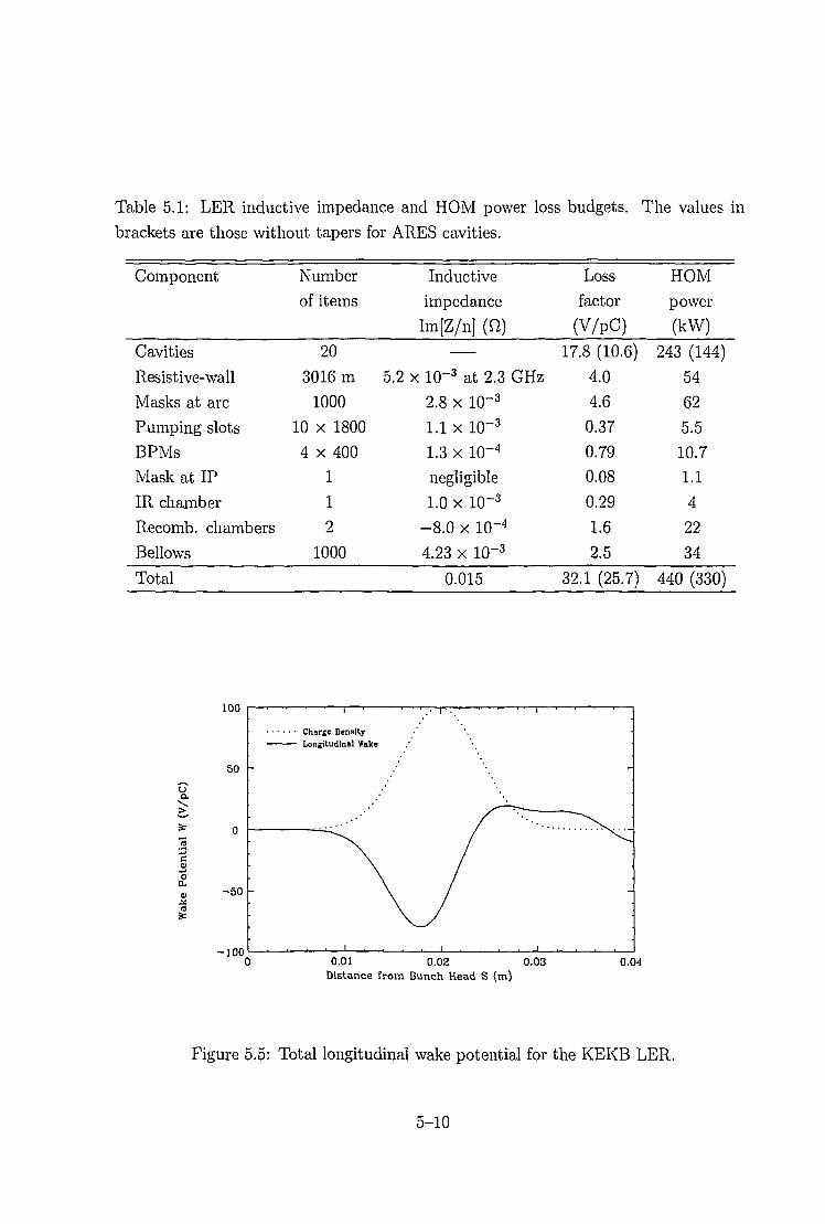
Table 5.1: LER inductive impedance and HOM power loss budgets. The values in
brackets are those without tapers for ARES cavities.
Component
Cavities
Resistive-wall
Masks at arc
Pumping slots
BPMs
Mask at IP
IR chamber
Recomb. chambers
Bellows
Total
Number
of items
20
3016 m
1000
10 x 1800
4 x 400
1
1
2
1000
Inductiveimpedance
Im[Z/n] (fi)
5.2 x lO-3 at 2.3 GHz
2.8 x lO-3
1.1 x lO-3
1.3 x 10"4
negligible
1.0 x lO-3
-8.0 x 10"4
4.23 x lO-3
0.015
Lossfactor
(V/pC)
17.8 (10.6)
4.0
4.6
0.37
0.79
0.08
0.29
1.6
2.5
32.1 (25.7)
HOM
power
(kW)
243 (144)
54
62
5.5
10.71.1
4
22
34
440 (330)
100
uo.
Io
a
-50 -
-1000.01 0.02 0.03
Distance from Bunch Head S (m)0.04
Figure 5.5: Total longitudinal wake potential for the KEKB LER.
5-10

5.2 Single-Bunch Collective Effects
In this section, we review our predictions of the singe-bunch collective effects, namely,
the bunch lengthening and transverse mode-coupling instability. As mentioned earlier,
these instabilities are expected to impose no fundamental limitation on the stored
current, since the bunch current is relatively low compared to that of other large
electron rings. However, the requirement of a short bunch (az = 4 mm) demands that
careful attention be paid to any possible causes for deviation from the nominal value.
The transient ion problem and coupled-bunch instabilities due to photo-electrons will
be discussed separately in sections 5.4 and 5.5, respectively.
5.2.1 Bunch Lengthening
There are two mechanisms to alter the bunch length from the nominal value. One is the
potential-well distortion of the stationary bunch distribution due to the longitudinal
wake potential. The deformed bunch distribution can be calculated by solving the
Haissinski equation. The bunch can be either lengthened or shortened depending on
the type of wake potential. Another mechanism is the microwave instability which has
a clear threshold current for the onset of the instability.
Oide and Yokoya have developed a theory which includes both the potential-well
distortion effect and the microwave instability [7]. A program is now available to
compute the bunch length according to their theory. Figure 5.6 shows the calculated
bunch length in the LER as a function of the number of particles in a bunch, Np.
, , , , I , . _ • _ . , I . , , , ! , , , ,
5 10 15
Particles/bunch (1010)
20
Figure 5.6: Bunch length and energy spread in the LER.
5-11

As can be seen, there is a constant bunch lengthening due to the potential-well
distortion; and the microwave instability takes off at Np = 1.5 x 10u , which is about
four times larger than the proposed number of particles per bunch. At the design
intensity, the bunch is lengthened by only 10%.
5.2.2 Transverse Mode-Coupling Instability
The transverse mode-coupling instability is known to be responsible for limiting the
single-bunch current in large electron rings, such as PEP [8] and LEP. This instability
takes place when two head-tail modes (m= 0 and m= —1 modes in most cases) share
the same coherent frequencies. In the short bunch regime where the KEKB will be
operated, the coherent frequency of the m= —1 mode keeps almost constant as a
function of the bunch current, while that of the m— 0 mode keeps descending until
it meets the m= —1 mode. Using the estimated transverse wake potential and the
averaged beta function of 10 m, we found that the coherent tune shift of the m=0
dipole mode is only ~ —0.0002 at the design bunch current. This value is much
smaller than the design value of the synchrotron tune (~ 0.017). Thus, the transverse
mode-coupling instability will not impose a serious threat to the performance of KEKB.
5.3 Coupled-Bunch Instabilities
As mentioned earlier, the coupled-bunch instabilities due to high-Q structures, such
as RF cavities and the resistive-wall beam pipes, are the main concerns in the KEKB
rings because of the unusually large beam current. We have adopted the so-called
damped-cavity-structure to sufficiently lower the Q-values of higher-order parasitic
modes, typically less than 100. The calculation results of the longitudinal growth time
due to the RF cavities will be given in detail in the RF section. Here, we focus on the
transverse coupled-bunch instability due to the resistive-wall impedance and coupled-
bunch instabilities (both transverse and longitudinal) that are excited by the crabbing
mode of the crab cavity.
5.3.1 Transverse Resistive-Wall Instability
The growth rate of the instability in terms of the rigid particle model is given by
W{UV41,V0)1 (5.20)p-_oo
5-12

where(5.21)
Here, /?j. is the averaged beta function over the ring, Re[ZtfH'] the real part of the
resistive-wall impedance, h the beam current, E^ the beam energy, vp the betatron
tune, \x the mode number of the coupled-bunch oscillation and M the number of
bunches in the beam. In the above formula, it is assumed that the RF buckets are
uniformly filled with equal numbers of particles (we ignore the effects of the gap in the
bunch filling, which may be necessary to suppress ion trapping).
In Figures 5.7 and 5.8, the growth time of the most unstable mode in the LER
and HER, respectively, are shown as a function of the betatron tune. In the current
design of the LER (HER), the horizontal and vertical tunes are 45.52 (46.52) and 45.08
(46.08), respectively. The most unstable mode (5074 mode) in the LER has growth
times of 5.9 and 8.1 msec at these tunes, respectively. On the other hand, the most
unstable mode in the HER is the 5073 mode, which has growth times of 4.0 and 5.6
msec at the horizontal and vertical tunes, respectively. Conversely, plots of the growth
time as a function of the coupled-bunch mode number at the tunes 45.52 and 46.52 for
the LER and the HER are given in Figures 5.9 and 5.10, respectively.
One possible cure for this instability is a bunch-by-bunch feedback system. The
growth rates obtained above are, however, close to the limit of the design capability of
our feedback system. Fortunately, since the coherent frequencies of the unstable modes
<D 6• H&H
oM 9
"tr\
4 5 . 2 4 5 . 4 4 5 . 6
T u n e
45 .8 46
Figure 5.7: Growth time of the resistive-wall instability as a function of betatron tunein the LER.
5-13

- 5u(Uw „
js 40)
3 3EH
I2\
\
46 46.2 46.4 46.6
Tune
46.8 47
Figure 5.8: Growth time of the resistive-wall instability as a function of the betatron
tune in the HER.
1 8
<Dw£14
5 100
o 8
6\
5070 5071 5072 5073
Mode Number
5074
Figure 5.9: Growth time of the resistive-wall instability as a function of the mode
number at the betatron tune of 45.52 in the LER.
5-14

7712n
1°g
EH
\
5068 5069 5070 5071
Mode Number
5072 5073
Figure 5.10: Growth time of the resistive-wall instability as a function of the mode
number at the betatron tune of 46.52 in the HER.
stay in a narrow frequency range at low frequency, these modes may be stabilized by a
narrow-band mode feedback system rather than a wide-band bunch-by-bunch feedback
system. If the bunch-by-bunch feedback system can perform at a damping time of 10
msec, the mode feedback system must cover only one unstable mode for the LER and
three modes for the HER, as seen from Figures 5.9 and 5.10. Then, a combination
of two feedback systems is expected to provide a damping time of 1 msec for the
fastest-growing modes.
5.3.2 Coupled-Bunch Instability by the Crabbing Mode
In this section we deal with only the instability due to the impedance of the crabbing
mode. The instability due to the HOMs can be treated in a similar manner to those
in accelerating cavities. The transverse coupling-impedance of a deflecting crabbing
mode is expressed as
Z,{u) = ^u>
Qi(5.22)
where uiT is t h e resonant frequency of t h e crabbing mode , R± is t h e t ransverse shun t
impedance , QQ is t h e unloaded Q-value and Qi is the loaded Q-value. T h e most
characteristic feature of the crabbing mode is that it operates at the same frequency as
5-15
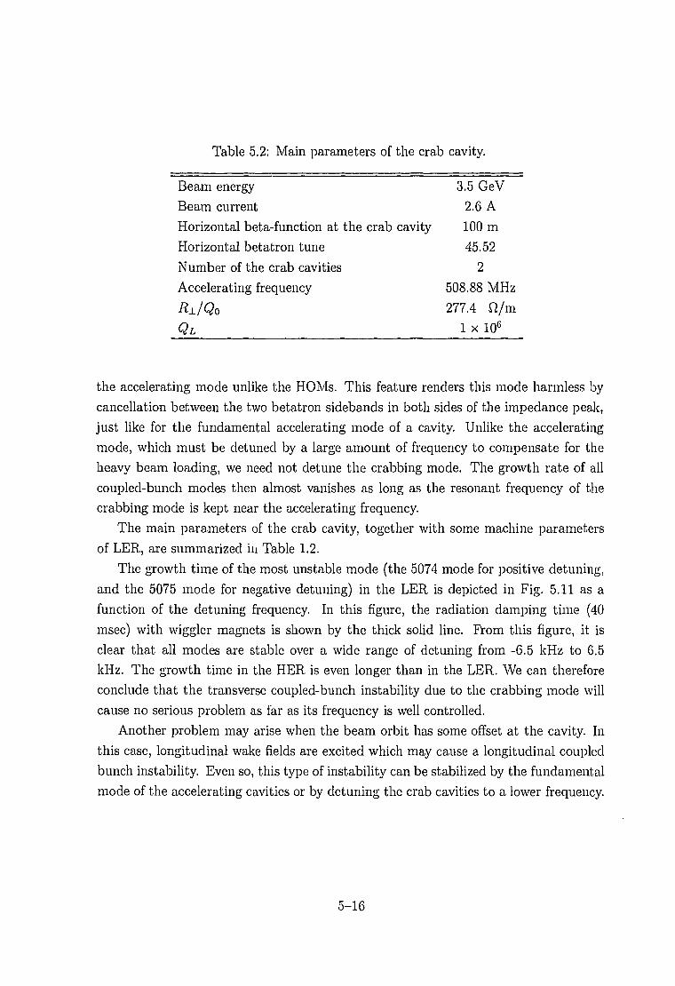
Table 5.2: Main parameters of the crab cavity.
Beam energy
Beam current
Horizontal beta-function at the crab cavity
Horizontal betatron tune
Number of the crab cavities
Accelerating frequency
R±/QoQL
3.5 GeV
2.6 A
100 m
45.52
2
508.88 MHz
277.4 n /m
1 x 10⁶
the accelerating mode unlike the HOMs. This feature renders this mode harmless by
cancellation between the two betatron sidebands in both sides of the impedance peak,
just like for the fundamental accelerating mode of a cavity. Unlike the accelerating
mode, which must be detuned by a large amount of frequency to compensate for the
heavy beam loading, we need not detune the crabbing mode. The growth rate of all
coupled-bunch modes then almost vanishes as long as the resonant frequency of the
crabbing mode is kept near the accelerating frequency.
The main parameters of the crab cavity, together with some machine parameters
of LER, are summarized in Table 1.2.
The growth time of the most unstable mode (the 5074 mode for positive detuning,
and the 5075 mode for negative detuning) in the LER is depicted in Fig. 5.11 as a
function of the detuning frequency. In this figure, the radiation damping time (40
msec) with wiggler magnets is shown by the thick solid line. From this figure, it is
clear that all modes are stable over a wide range of detuning from -6.5 kHz to 6.5
kHz. The growth time in the HER is even longer than in the LER. We can therefore
conclude that the transverse coupled-bunch instability due to the crabbing mode will
cause no serious problem as far as its frequency is well controlled.
Another problem may arise when the beam orbit has some offset at the cavity. In
this case, longitudinal wake fields are excited which may cause a longitudinal coupled
bunch instability. Even so, this type of instability can be stabilized by the fundamental
mode of the accelerating cavities or by detuning the crab cavities to a lower frequency.
5-16

140
O120w6,100
I 80£ 60
o 4020
/
/
/
/
\
\
\
\
\\
-10 -5 0 5
Detuning Frequency [kHz]
10
Figure 5.11: Growth time of the coupled bunch instability due to the crabbing modein the LER versus the detuning frequency.
5.3.3 Summary of Collective Effects Sections
We have seen that neither bunch lengthening nor the transverse mode-coupling insta-
bility will impose a significant limitation on the stored bunch current. The luminosity
performance of KEKB is rather affected by the couple-bunch instabilities due to the RF
cavities (longitudinally) and the resistive-wall instability (transversely). Our carefully
designed damped-cavity-structure helps to reduce the longitudinal growth to a man-
ageable level. Even the most unstable mode has a growth time (60 msec) longer than
the radiation damping time of 20 msec in the LER with wiggler magnets. Transversely,
however, the growth time of the resistive-wall instability (~ 5 msec) is far shorter than
the radiation damping time of 40 msec. The design of the fast feedback system that
can deal with the remaining growth is one of the most challenging problems for KEKB.
5.4 Beam Blow-up due to Transient Ion Trapping
in the Electron Ring
In any circular machines, the beam produces ions via ionization of residual gas molecules
as well as through other processes. At an electron ring which stores many bunches,
these positive ions are attracted towards the beam. After several turns the ions are
concentrated near the beam orbit, where they can disturb the beam motion. This
phenomenon, called ion trapping, has been studied for many years. One possible cure
for this problem is a partial fill, i.e., to create a contiguous group of empty RF buckets
5-17

that are unoccupied by the beam, and to let the ions drift away during this gap.
It has been recently pointed out that a somewhat different process can also degrade
the beam. This effect may be called transient ion trapping. With high intensity and
low emittance beams, even if the ions eventually disappear in the bunch gap, they may
cause a serious effect before disappearing through the following mechanism. While
each bunch ionizes the residual gas, if a bunch is displaced from the design orbit, the
ions left in space will also be displaced. Such ions execute off-centered oscillations
in subsequent electron bunches, and act as an amplifier for electron oscillation. The
purpose of this section is to present a theoretical study of this effect.
Since the vertical emittance is much smaller than the horizontal one, the effect is
more serious in the vertical plane. We assume that n& electron bunches are followed by
a gap which is long enough to sweep out the ions. This bunch pattern of n& bunches
plus a gap may be repeated several times over the ring. The first bunch of each train
travels in a fresh residual gas without ions.
This phenomenon is characterized by two important parameters, © and K. First,
the phase advance of the ion oscillation between the arrival time interval of two adjacent
electron bunches is_ / 2zNmrPL
Here,
z,A the electrovalence and the mass number of the ion,L distance between bunches,N number of electrons per bunch,Hj = (o^e + cr^i)1/2 (j = x, y), where <jj<e and crJ;i are the r.m.s. beam size of electrons
and ions,7n,Mjv the mass of an electron and a nucleon,
re classical electron radius.
The size of the ion cloud is equal to the electron beam size when it is created. It
settles down to ~ l/ \ /2 of the electron size after a few oscillations due to non-linear
smearing. In the case of the KEKB electron ring (HER), 0 for CO+ ions, for example,
is about 0.12 radian, which means that the CO+ ions execute one cycle of oscillation
during the passage of about 50 (= 2n/Q) electron bunches.
The ion cloud focuses the electron beam. The number of ions is proportional to the
electron bunch index n (counted from the first bunch in each train). Therefore, the
tune shift is proportional to n, and is given by
5-18

where
R the average radius of the ring,(3y average beta function,7 electron beam energy in units of rest mass,
7ij number of ions created by one electron bunch per unit length, given by Nng(Ti, ng
being the number density of the residual gas and O{ the ionization cross section.
In the case of CO+, n* will be about 100/m.
If the oscillation amplitudes of electrons and ions are small compared with cryte,
the buildup of the oscillation may be approximately described by linear theory. Let us
denote the center-of-mass position of the n-th electron bunch after travelling a distance
s by yn{s). Then, the mode which is unstable against ion perturbation is given by
yn(s) * aoe«en-ks\
where k is the betatron wave number. The conjugate mode el(-@n-ks) is damped.
The amplitude blowup factor of the unstable mode is approximately given, in the
linear regime, by
G =an(s)
a0
where
1 + i exp Ur + {aoQn)2 - ao6n] (r » 1),
T = KQsn2 =MN 7
rPzN^2
£TE.'z *-"!/.sn
2
for F 3> 1. The factor a0 « 0.077 approximately takes into account the non-linear
smearing of the ion center-of-mass motion. (The center-of-mass of ions oscillates ap-
proximately as exp(—ao6)cos6.) The blowup is essentially described by the factor
F. Since the ionization cross section o\ is roughly proportional to Z (sum of the
atomic numbers of the constituents of the molecule), the ion-species dependence of F
is a Zz3/2/y/A. Therefore, heavier ions contribute more to the instability than lighter
ones, if the partial pressure is the same.
The amplitude blowup factor G for the HER is plotted in Figure 5.12 as a function
of the number of turns nt for various values of the number of electron bunches rib. The
residual gas is assumed to be CO with a pressure of 10~9 Torr. The e-folding time of
the amplitude is about 70 turns for n;,=500 (a n^2), although the growth with respect
to nt is not exponential.
In practice, the ion phase advance 0 can have a spread for a number of reasons.
This can lead to a damping effect. For example, since 0 depends on the electron beam
5-19

, § ' <§"" <§>' J 1 " <§>'f T Jt f fi
uu
50
10
5
1
c 0 c"° c"0 <
• • ' / ' / I / ' •
11/• l///
~ / / f / / • • • ' ' ' • ' ' '• I/// /• III///
«5 <JO ^ O
• - , , • ' ^ ' | • • • • •
/ / // / ' " ;
/
500
nb = 200.
150.
nb = 100.
50.
1000 1500 2000
Figure 5.12: Amplitude blowup factor G for CO+ of 10~9 Torr.
T3S
>
0.15
0.10
0.05
0.00
/ V
\ /
I \I \
_J I I I [_
' \
I I I
0 20 40 60 S (m)
^~ T - T - C\J c \ l c \ i PJ CO CO COQ U . Q Q U-LLLJ Q U. Q
O O £0 w a Ocno a m o m O
CM CMCM CM CV1 T - T-
UJLLU. Q Q U. Q
awo oco m a o
Figure 5.13: The Qx and 0^, phase advance of ion (CO+) oscillations between the
arrival of consecutive beam bunches in the HER arc.
5-20

size, it varies over the ring. In the periodic part of the arc sections of the HER, 0
modulates between 0.10 to 0.14 radian in the case of CO+ ions, as shown in Figure 5.13.
Another reason for the spread in 0 comes from the existence of various ion species.
However, since the dependence of 0 on A is weak (~ 1/yfA), the spread due to this is
much smaller than the lattice effect. For example, a mixture of O2, N2, CO, CO2, etc,
cannot cause a more efficient spread than the lattice effect. It should be also noted
that the contribution of H2 is very small because of the small ionization cross section.
The nonlinear smearing expressed by the factor c*0 causes a similar effect. The
value c*o ~ 0.077 has already been taken into account in Figure 5.12. It corresponds
to a ~30% full spread of 0 . Therefore, we cannot expect drastic damping due to the
0 spread.
Linear theory is valid only for small amplitude oscillations. It does not predict
emittance growth, either. In order to take into account those effects that are ignored
in linear theory, a computer simulation is being conducted. Some preliminary results
are summarized here. The essential points in the simulation code are listed as follows:
1. The electron beam is represented by 105 macro-particles per bunch. The model
ring consists only of periodic cells which are extracted in the HER arc.
2. Ions are also represented by macro-particles. Instead of a continuous distribution
over the ring, they are placed at some selected points (ionization points) in the
ring. It was confirmed that only a few ionization points in the ring are enough
if the points are carefully selected so as to properly represent the spread of 0 .
Eventually, only two points were selected for long-time calculations. The number
of macro ions is at most 105 per ionization point. The longitudinal drift of ions
is negligible.
3. The initial position of ions when they are created is that of the parent electron.
The transverse velocity is generated according to the Maxwell distribution with a
temperature of 300 K (this does not cause a sizable effect). Each electron bunch
creates approximately 2xlO4 macro ions per point. When the number of macro
ions exceeds 105 at one ionization point due to the passage of many bunches, some
of them are randomly selected and thrown away. The subsequent ionization rate
is accordingly reduced. (Although one could generate a small number of macro
ions so that the final number does not exceed the limit, this is not statistically
good, because the ions created by early electron bunches are more important.)
4. The interaction of an electron bunch and an ion cloud is calculated by solving
the 2-dimensional (horizontal and vertical) Poison equation on a 2-D grid (64x64
to 64x256, equal space). The mesh size is typically 0.15 standard deviations in
5-21

each plane. The grid for electrons and that for ions are not identical. However,
because of the structure of the code, the aspect ratio (vertical to horizontal) has
to be the same. The interaction between ions is negligible.
5. The ions are assumed to disappear after interacting with n;, electron bunches
before the electrons come in the next turn, so that the first electron bunch always
travels in non-ionized residual gas.
6. Standard runs are performed with 512 electron bunches over 1000 turns.
The results of simulations up to now can be summarized as follows:
1. As long as the center-of-mass amplitude is small (^ 0.5 standard deviations),
linear theory can describe the phenomena reasonably well.
2. The center-of-mass amplitude saturates at about lay.
3. In order to study the effects of the bunch gaps, the electron bunch structures,
like 256+[25]+256, 256+[50]+256, 128+[25]+128+[25]+128+[25]+128, etc (the
number in [ ] is the number of missing bunches), have been simulated and com-
pared with 512 continuous bunches. It turned out that the effect of up to 50
missing bunches does not considerably improve the situation.
4. The growth rate with 256 bunches (followed by long enough gap) is much smaller
than that with 512 bunches as the linear theory predicts. However, the repetition
of 256 bunches plus a gap of much more than 50 missing bunches will not be
acceptable because of the luminosity reduction.
5. The emittance growth is about 30%.
Thus, in order to damp the growth with 512 successive bunches, a feedback system
as fast as 50 to 100 turns (0.5 to 1 msec) is needed, if the gas pressure is 10~9 Torr.
The fastest bunch mode will be about 50 bunches per cycle.
Remaining issues for future studies include:
1. It is desired to find out how many missing bunches are enough for terminating the
chain of interaction. However, in order to try a longer bunch-gap, the simulation
code has to be modified, because the ions after the gap extend to a large vertical
dimension, whereas the newly created ions are concentrated on the axis. This
ion distribution cannot be accurately expressed by an equally-spaced mesh.
2. It must be confirmed whether the emittance growth can be cured by the feedback
system of the center-of-mass motion. (This is a question technically very hard to
answer. The present calculation is done with a parallel processor with 64 cpu's.
5-22
Interactions during tens of revolutions are simultaneously computed so that it is
logically impossible to faithfully simulate a feedback system.)
5.5 Instabilities due to Beam-Photoelectron In-
teractions>
Photoeletrons are produced by synchrotron radiation (SR) photons, when they hit
the inner wall of the beam pipe. In the LER where the positrons are stored, those
photoelectrons would migrate towards the beam path, where they can create a sizeable
electric field. Although such individual electrons are not trapped around the beam,
they form a flowing gas of electrons. Under certain conditions these photoelectrons
can act as a media for transmitting perturbative forces from a particle bunch onto
subsequent bunches. Thus, a coupled-bunch instability can emerge [9].
At the 2.5 GeV Photon Factory (PF) ring of KEK, when it is operated to store
positrons, a coupled-bunch instability which may be consistent with this mechanism has
been observed. At the PF with a stored current of 350 mA ( ~ 4 x 10° particles/bunch),
the growth rate of the instability is much higher than the damping rate. The problem
in the LER may be even more serious, since its stored current will be larger by a factor
of 7.
This section presents a theoretical study of instabilities in the positron ring due to
interactions between the beam and photelectrons, and discusses on a possible cure.
5.5.1 Synchrotron radiation and photoelectron
The number of photons emitted by a positron (or an electron) during one full revolution
is given by[10]5?r
N, = - ^ 0 7 , (5.23)
where a and 7 are the fine structure constant and the Lorentz factor, respectively. In
the LER with 7 = 6850, the number of photons emitted by a positron in one revolution
is
iV7 = 453 . (5.24)
We next estimate the production of photoelectrons by SR photons. We assume that
the photoelectron production rate (quantum efficiency) is 0.02 for the copper chamber
and that the energy of photoelectrons follows a Gaussian distribution with an r.m.s.
value of 5 ± 15 eV[ll]. Then the number of photoelectrons will be
Ne = 9.1/particle , iVe,bunch = Ne x N = 3 x 10n/b>unch (5.25)
5-23
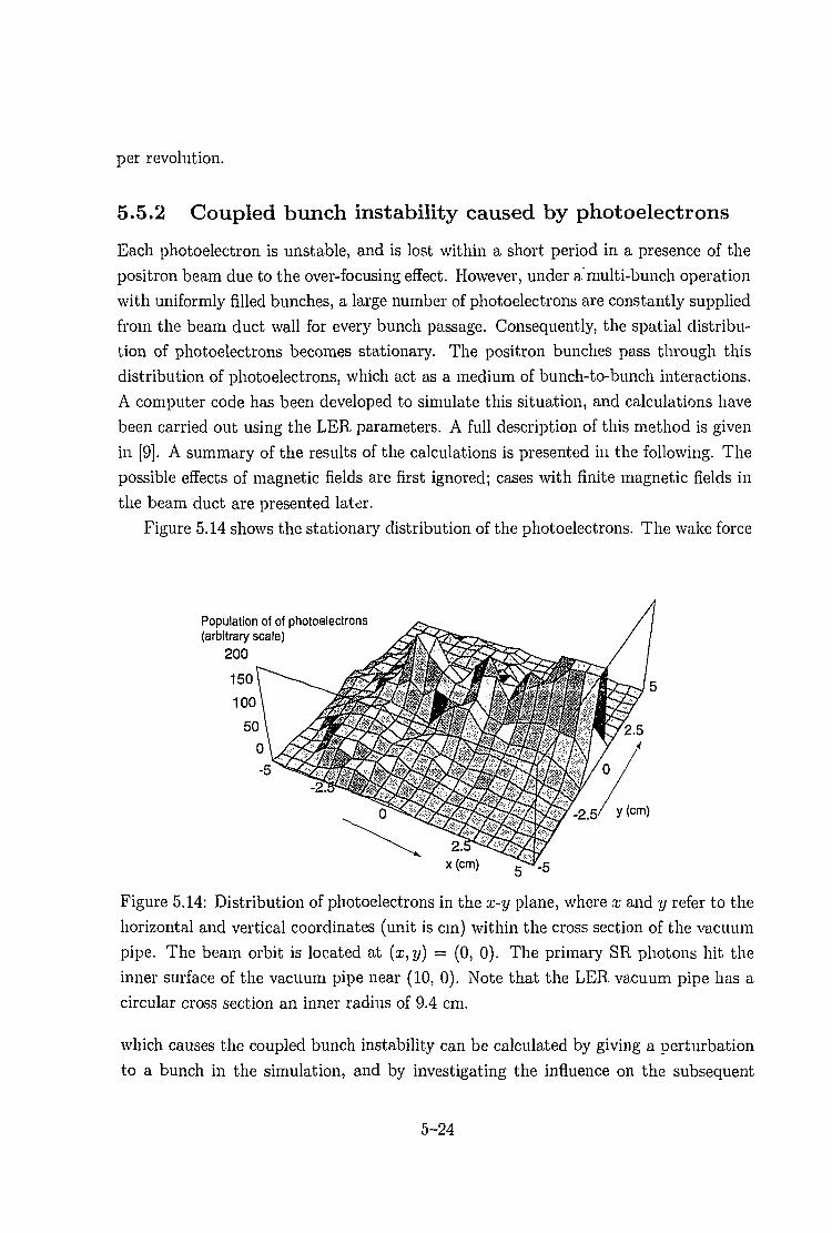
per revolution.
5.5.2 Coupled bunch instability caused by photoelectrons
Each photoelectron is unstable, and is lost within a short period in a presence of the
positron beam due to the over-focusing effect. However, under a. multi-bunch operation
with uniformly filled bunches, a large number of photoelectrons are constantly supplied
from the beam duct wall for every bunch passage. Consequently, the spatial distribu-
tion of photoelectrons becomes stationary. The positron bunches pass through this
distribution of photoelectrons, which act as a medium of bunch-to-bunch interactions.
A computer code has been developed to simulate this situation, and calculations have
been carried out using the LER parameters. A full description of this method is given
in [9]. A summary of the results of the calculations is presented in the following. The
possible effects of magnetic fields are first ignored; cases with finite magnetic fields in
the beam duct are presented later.
Figure 5.14 shows the stationary distribution of the photoelectrons. The wake force
Population of of photoelectrons(arbitrary scale)
200
-2.5/ y<cm)
Figure 5.14: Distribution of photoelectrons in the x-y plane, where x and y refer to the
horizontal and vertical coordinates (unit is cm) within the cross section of the vacuum
pipe. The beam orbit is located at {x,y) = (0, 0). The primary SR photons hit the
inner surface of the vacuum pipe near (10, 0). Note that the LER vacuum pipe has a
circular cross section an inner radius of 9.4 cm.
which causes the coupled bunch instability can be calculated by giving a perturbation
to a bunch in the simulation, and by investigating the influence on the subsequent
5-24

InE
¥V
500000
400000
300000
200000
100000
0
-100000
+
o
oo
mmm t +%Wtittitt* f, (5 SU
Wake from+ 1.0 mm initial bunch displacement
o 0.5 mm initial bunch displacement
1 1 I 1
100 120 140 160
Bunch
180 200
Figure 5.15: Vertical wake force. The strength of the wakes created by an initial bunch
displacement of 0.5 mm (diamond and ) and 1.0 mm (cross hair) are shown. It indicates
that the wake strength is roughly proportional to the displacement of the initial bunch.
bunches. We treat the vertical instability first. Figure 5.15 shows the wake force. The
wake forces are calculated in the cases of displacements of 0.5 mm and 1 mm. The
linearity of the wake force can be seen. The growth rate of a coupled-bunch instability
due to a wake force is generally given by
nrT >1 no
uy Nb ^ dy h
where the mode is defined by
and
(5.26)
(5.27)
(5.28)
By using the wake force found in Figure 5.15 for dv in Equation 5.26, the growth rate
of the instability can be estimated. The result is shown in Figure 5.16. The maximum
growth rate is found to be about 2500 s"1. This is much higher than the damping rate
of the LER, which is 12.8 s"1. Although the head-tail damping effect will reduce the
instabilities, its damping rate (~ 200 s""1) will not be sufficient to cure this instability.
The horizontal wake force is shown in Figure 5.17 for bunch displacements of 0.5 mm
and 1 mm. The feature of the horizontal wake force is very different from that of the
vertical wake force. The linearity of the wake is broken after the passage of a dozen or
so bunches. The wake force remains non-zero even after a hundred bunches. Therefore,
5-25

CD
13
CD
1000 2000 3000Mode number
4000 5000
Figure 5.16: Growth rate of the vertical instability plotted against the mode number.
the conventional treatment to obtain the growth rate is not applicable. (If we use this
wake force in Equation 5.26, a maximum growth rate of 1700 s"1 is obtained). To
evaluate the horizontal growth rate correctly, tracking calculations of the beam motion
passing through the electron distribution will be necessary.
150000
100000
50000
0
-50000
-100000
Y
_l_
- X© ©
<©
+
1
+
© © <
-+ + f
Wake from+ 1.0 mm initial bunch
© 0.5 mm initial bunch
-tt-
t $+ + + 4© ^ c
" t . <- ><s», 4 M -
-P+
i
*- ° %
1
displacement
displacement
+
* © A- dP
+ +"
100 120 140 160Bunch
180 200
Figure 5.17: Horizontal wake force. The strength of the wakes created by an initial
bunch displacement of 0.5 mm (diamond) and 1.0 mm (cross hair) are shown.
5.5.3 Possible cures
A possible cure for this instability is to apply magnetic fields, and to restrict the motion
of photoelectrons (blocking magnetic field). For example, an electron with an energy
5-26

of 10 eV has a Larmor radius of 1.1 cm in magnetic fields of 10 G. Thus the electrons
will not propagate towards the beam. The wake force is expected to be smaller in this
condition.
If the photoelectrons tend to reach the beam by drifting along a horizontal path, we
can consider using a solenoid or a vertical dipole fields as the blocking magnetic field.
Figure 5.18 shows the wake force when the solenoid field is applied in the vacuum duct
with a strength of Bz = 1 G and 20 G. It is seen that with B~ = 20 G the wake force
A
1•ay
A
-<dv
(m/s
300000
200000
100000
0
-100000
-200000
-300000
300000
200000
100000
0
-100000
-200000
-300000
(A)Bz=1G
-
-
100 120
(B) Bz=20G
-
-
1 1
100 120
*''«•'.' --Vv'''''''.' .. . S:;'"':''-V-, •••<:.••'•
1 1 1
140 160 180 20
Bunch
v.:.,, .;:. „.,.0,.,.,:.,..v, .•....;,..,..,.../.v;.v,,,,,..,.,;.,...
I I I
140 160 180 2C
Bunch
Figure 5.18: Wake force when applying solenoid fields.
becomes small. In this condition the growth rate is estimated to be less than 200 s"1.
Figure 5.19 show? the wake force when a vertical dipole field is applied in the
vacuum duct. It is seen that the wake force becomes small for By = 20 G.
We next consider the case where a horizontal magnetic field is applied. Here,
the electron motions are bounded on the horizontal plane. Thus, the photoelectrons
5-27

300000
200000
A 100000
I °•a
Y -100000
-200000
-300000
300000
200000
-
~»v.;:.
1
(A)By=1G
'-•..*. v;'
1 t
100 120 140 160
Bunch
180 200
100 120 140 160 180 200
Bunch
Figure 5.19: Wake force when applying vertical fields.
A
f
600000
400000
200000
0
.onnnnn
- c Bx=20G
-
i * , i - •'•'•
i i i i i
100 120 140 160 180
Bunch
200
Figure 5.20: Wake force when applying horizontal fields.
5-28

produced by primary SR photons are freely allowed to reach the beam path area.
Figure 5.20 shows that the wake field is stronger, as expected. The strength of the
wake force shows that the wake force becomes 2.5 times larger due to the magnetic
fields. By the way, we can find the ".yclotron period, 18 ns, in the wake force.
Although the dominant source of photoelectrons may be concentrated on the area
to be hit by primary SR photons, the effects of reflection and scattering of SR photons
need to be taken into consideration. Therefore, even if the direction of the magnetic
field is arranged to be vertical, electrons produced by the reflected photons may become
important. This has to be noted in applications to the real KEKB condition. Therefore,
the use of the solenoid fields may be a better solution. By using solenoid coils of
alternating field signs, the coupling effect on the beam is considered to be minimized.
5.5.4 Conclusions
The effects of interactions between the positron beam and photoelectrons have been
evaluated for the LER. The growth rate is estimated to be 2500 s"1. By applying
solenoid or vertical magnetic fields of 20 G, the growth rate will be reduced by one
order, which can be cured by the bunch-to-bunch feedback system.
5-29

Bibliography
[1] Y. H. Chin, User's Guide for ABCI Version 8.8, CERN SL/94-02 (AP) and LBL-35258
(1994).
[2] T. Akasaka, private communications.
[3] S. Kurennoy and Y. H. Chin, KEK Preprint 94-193 (1995). To be submitted to Par t .
Accelerators.
[4] R. L. Gluckstern, Phys. Rev. A 46, 1106 (1992).
[5] S. S. Kurennoy, Part. Accelerators 39, 1 (1992).
[6] G. V. Stupakov and S. S. Kurennoy, Phys. Rev. E 49, 794 (1994).
[7] K. Oide and K. Yokoya, KEK Preprint 90-10 (1990).
[8] M. S. Zisman et. a l , Study of Collective Effects for the PEP Low-Emittance Optics,
LBL-25582 and SSRL ACD Note-59 (1988).
[9] K. Ohmi, KEK Preprint 94-198.
[10] M. Sands, The Physics of Electron Storage Rings, SLAC-121(1970).
[11] K. Kanazawa, private comunications.
5-30
Chapter 6
Lattice Design
This chapter discusses the lattice design of KEKB in detail. Specific requirements to
consider are the following:
1. Realize the beam parameters listed in Table 2.2.
2. Ensure a sufficiently large dynamic aperture for a high injection efficiency and a
long beam lifetime, particularly the Touschek lifetime in the LER.
3. Maintain a wide range of tunability for the beam parameters, especially for the
horizontal emittance.
4. Allow a reasonable amount of tolerance for machine errors.
Because of the small /3* (~ 1 cm) at the interaction point (IP), a large amount of
chromaticity is produced, and it has to be corrected without sacrificing the dynamic
aperture. Discussions on the dynamic aperture and the sources that cause its reduction
are given in section 6.1. The development of the ring lattice design is presented in
section 6.2. Designs of the straight section beam optics are given in sections 6.3 and
6.4. Sections 6.5 and 6.6 examine the required magnet field qualities and tolerances.
6.1 Dynamic Aperture
For efficient beam injection at KEKB it is considered that the lattice design should
allow a momentum aperture of at least ±0.5% and a transverse aperture of > 1.2 x
10~5 m. For maintaining a sufficiently long beam lifetime ( ~ 10 hours or better in the
absence of machine errors), an even larger aperture is strongly favored.
A major cause for the reduction of the transverse dynamic aperture is the nonlin-
earity of sextupole magnets which are introduced to correct the chromaticity in the
6-1

ring. To solve this problem, it is considered best to use a pair of identical sextupole
magnets that are connected with a — I transformer in both the horizontal and vertical
planes. This allows to cancel transverse nonlinearity of the sextupole magnets to the
third order in the Hamiltonianfl]. Then, residual terms come to limit the dynamic
aperture. In the case of KEKB, the vertical dynamic aperture is limited by: (1) the
kinematic term of the drift space around the IP, and (2) the fringe field of the final
qu&drupole magnets at the edge, facing the IP[2].
A source of momentum aperture limitation is the modulation of linear betatron
oscillations due to the synchrotron motion. If the beta functions at cavities have
dependencies on the momentum, a change of I:he momentum by the cavity RF field
produces a mismatch between the beam and the betatron phase space ellipse. This
excites synchrotron-betatron resonances at 2vx^-k.ynvs = N, and an exponential growth
of transverse betatron amplitudes results. The momentum aperture is significantly
degraded near these resonances. Resonances of smaller orders are more harmful. To
avoid this problem a small synchrotron tune is required, such that those resonance
conditions are not met [2]. The chromaticity in the x-y coupling terms is another
source that limits the momentum aperture, since the compensation of the detector
solenoid at the IP is not perfect, as described below.
As mentioned in the previous chapter, a small momentum compaction factor is
needed to reduce the synchrotron tune, while keeping the bunch length and the mo-
mentum spread constant. When the linear momentum compaction is made small, the
effects of higher-order momentum compaction becomes non-negligible. For example,
the second order term produces an imbalance of the dynamic aperture for the positive
and negative sides of the momentum deviation of a particle. This is due to eccen-
tric motions of particles in the longitudinal phase space induced by the second-order
momentum compaction.
Yet one more source of aperture limitation is the chromo-geometric aberration
caused by a breakdown of the — I transformer for off-momentum particles. This aberra-
tion becomes serious in the sextupole pairs for the local chromaticity correction scheme
in the LER, which is discussed in Section 6.2.5. This problem arises, because the prod-
uct of the sextupole strength and the vertical beta function at the sextupole magnets
becomes much larger than in the arcs.
For a given lattice layout, the excitations of sextupole magnets are determined by
evaluating the off-momentum optics directly, i.e. not by using perturbative methods.
The solution of the sextupole excitations is calculated so as to simultaneously minimize
the deviations of the betatron tune vZyV and Twiss parameters fj^y and a££ for a few
points in the RF section. The momentum bandwidth considered is 1.5% for the HER
6-2
and 2 ~ 3% for the LER. The number of fitting points of the momentum bandwidth
is typically 20. All of the sextupole pairs are treated independently. (The results of
the chromaticity correction are shown in Figures 6.5 and 6.6.) Optimization can be
improved by matching for finite betatron amplitudes or by a nonlinear optimization of
the dynamic aperture itself.
The dynamic aperture is estimated by tracking particles in six-dimensional phase
space (x, pXj y,py, z, 8) using SAD. Hers, the variable z is defined as z = —vt, where t is
the delay from the nominal particle. SAD is a fully symplectic tracking code, developed
at KEK. It incorporates all known terms, such as linear and nonlinear fringe fields, thick
lens multipole fields, kinematic terms, overlap of the solenoid field and other magnets,
etc. In this study, the initial conditions are given as pxo = pyo = z0 = 0 and yo = axo,
where a is a constant. The dynamic aperture is expressed by the initial values of the
action 2JXiy0 and the momentum deviation So of the particles which survived 1000
turns without damping due to synchrotron radiation. Although this period, which
corresponds to 1000 turns, is only 1/8 of the transverse damping time of the LER,
the results of 1000-turn tracking are almost equal to, or slightly smaller than, those of
8000-turn with radiation damping. Therefore, 1000-turn tracking is considered to be
a sufficiently accurate estimation of the dynamic aperture.
The dynamic aperture is evaluated in two ways:
1. With the initial condition y0 = XQ/Z. This is to check the acceptance for hori-
zontal beam injection.
2. With the initial condition yo = £o/\/50- This is for estimating the Touschek
lifetime at collision with an emittance ratio of 2%. The Touschek lifetime is
evaluated while assuming that the dynamic aperture in the Jx-Jz plane is given
by 0 < (JX/J™K) + (Jz/J™x) < 1. See Figures 6.8 and 6.10 for illustrations of
this approximation.
6.2 Development of Beam Optics Design
We have so far studied five types of optics design, as listed in Table 6.1. These optics
have different combinations of cell structures and chromaticity correction schemes. All
of the optics have been designed to give the required values of the horizontal emittance
and the momentum spread. We have compared the performance of these optics in light
of the following requirements:
1. To give a small synchrotron tune, and
6-3

2. To have a sufficiently large dynamic aperture for beam injection and for the
Touschek lifetime.
The results are summarized in Table 6.1 and Figure 6.1. In the following subsections
these designs are reviewed one by one. Since the second criterion above is especially
challenging for the LER, we will discuss mainly issues concerning the LER.
Injection Touschek us
Interleaved TT/3 FODO Cell bad bad bad
Noninterleaved TT/2 FODO Cell good fair bad
Noninterleaved IT Cell excellent fair good
Noninterleaved 2.5?r Cell excellent good excellent
Noninterleaved 2.57T Cell excellent excellent excellent
-fLocal Chromaticity Correction
Table 6.1: Comparison of the performances of the cell structures and chromaticity
correction schemes for the LER.Dynamic Aperture of LER
4 10-5
3 10-5 h
2 10-5 L?
1 10-5 h
0 100
V I \\<' ' I ' I ' ' ^ 'I. FODONI FODO
NI rc-ccll low-a
NI 2.5it-cell
NI 2.5 it-cell !c
1Ap/p (%)
Figure 6.1: Dynamic aperture of the LER with five types of beam optics.
6-4

6.2.1 Interleaved ?r/3 FODO Cell
We have tried a conventional chromaticity correction scheme with interleaved sextupole
magnets in TT/3 FODO cells, where each quadrupole magnet is associated with a sex-
tupole magnet. Sextupole magnets that are separated by the n phase difference are
paired so as to cancel the lowest order of the transverse nonlinearity. We have tried
chromaticity corrections with 6, 12, and 24 sextupole families. In all cases, the dynamic
aperture remained too small, and did not satisfy the requirement. This interleaved sex-
tupole scheme has been abandoned.
6.2.2 Noninterleaved n/2 FODO Cell
An arc lattice based on TT/2 FODO cells with a chromaticity correction scheme with
noninterleaved sextupole magnets has been considered. As the first step, the bend
radius p is determined based on the requirement for the momentum spread. In elec-
tron storage rings with a constant bending radius and smooth focusing, the horizontal
emittance ex and the momentum compaction factor ap are given by
(6.1)
= -£ (Vx)hend * - ^ 5 - . (6.2)
Here, RA is the average radius of the arc, vx the total horizontal tune of the arc, rjx
the horizontal dispersion, and H = fix {rfx + axrjx//3x)2 + vl/Px- The symbol (f)bend
represents the average of a quantity / in bend magnets.
According to Equations 6.1 and 6.2, once p is fixed, ex and ap are uniquely de-
termined by the total tune ux. Thus, if the arc is built with FODO cells to give
ex = 1.8 x 10~8m, the momentum compaction factor becomes too big. This, in turn,
means that us > 0.06, and produces serious difficulties in finding adequate operating
points in the tune space. The anomalous emittance due to chromaticity can also be-
come very large when us is high [3]. In addition, the accelerating voltage becomes
excessively high, if the short bunch length required in the design is to be achieved.
Because of these difficulties, this scheme has been rejected.
6.2.3 Noninterleaved TT Cell
To obtain small momentum compaction ap, we must reduce (?7z)6end, while keeping
{H)bend constant. This can be done by combining two TT/2 FODO cells, v.here four
bend magnets are merged into two, as shown in Figure 6.2. In this scheme, in addition
6-5

x
x
Figure 6.2: Structure of the vr cell for the HER (above) and the LER (below).
6-6

to the total tune ux, the position of the bend magnets can also be taken as a free
parameter for achieving the desired ap and ex simultaneously. An acceptable solution
was found, for the LER. In the HER, since the bend magnets are longer than those in
the LER, the variable range of ap is narrower. The possible minimum ap in the HER
is somewhat larger than the required value.
From a chromaticity correction view point, the arc lattice built with TT cells has a
disadvantage in that the high peaks of r]x appear only in the phase steps of Nir. This
means that if we place sextupole pairs (SF's) for horizontal corrections only near the
r]x peaks, corrections at the (N + l/2)ir phases become difficult. Even if we add SF's
at small r)x points, it is still less effective for (N + l/2)7r phases than in the FODO
case. As a result, the longitudinal dynamic aperture of the LER is unsatisfactory for
the Touschek lifetime.
6.2.4 Noninterleaved 2.5?r Cell
The 2.5TT cell is created by combining five ?r/2 FODO cells and by merging ten bending
magnets into four. In this cell structure, the bend magnets are arranged to form
two dispersion bumps, so that we can keep small 7]x at the dipole magnets, similar
to the 7r cell case. By adjusting the positions of the bend magnets and T]X there, we
can achieve the required emittance and momentum compaction factor at the same
time for both rings. This flexibility of the 2.5ir cell results in another merit for the
HER: the existing bending magnets become re-usable in the HER arc, satisfying the
requirements of the optics. Successive SF (SD) pairs in the 2.57T cell structure have a
relative phase of 3ir/2. Thus, chromatic kicks at the Nir and (N+l/2)ir phases in both
the horizontal and vertical planes can be corrected efficiently. The dynamic aperture of
the 2.57T cell is significantly improved over previous schemes, and it satisfies all of the
beam dynamics requirements. As shown in Figure 6.5, some higher-order chromaticity
still remains, because the sextupole magnets are not sufficiently close to the main
chromaticity sources in the interaction region. For this, further improvements can be
achieved by a "localized chromaticity correction" in the interaction region, which is
discussed in Section 6.2.5.
6.2.5 Noninterleaved 2.5?r Cell with Local Chromaticity Cor-rection
The local chromaticity correction refers to a scheme in which the large chromaticity
produced by the final quadrupole magnets is corrected within the interaction region. Its
advantage is that the creation of higher-order chromaticity can be avoided, by placing
6-7

6 F
1—1
QOf
Cz.<3f
Q Qcocy
N-.CV}
CCOO1
COQ
o-COCz.O"
COQcy
Cd fc.Cz. Q Q fc. QC C31
Q fc.cy cy
QQcoo- C3"
co CO W .—i CVi C\J ^Hb . Q bi b.fc. QQo1 o- o- coo- o-co Q
Figure 6.3: Structure of the 2.57T cell for the HER (above) and the LER (below).
6-8

6.0 10"5
4.0 10"5
2.0 10-5
0.0 10°-2.0
I ' ' ' '
1^99900560
I I I I -4- —
-1.0 0.0 1.0Ap/p (%)
2.0
Figure 6.4: Dynamic aperture of the HER with the 2.57T cell.
-1 0 1Ap/p(%)
Figure 6.5: Chromaticity correction with the 2.57T cell for the LER.
0Ap/p(%)
Figure 6.6: Chromaticity correction with the 2.57T cell and the local chromaticity cor-
rection for the LER.
6-9

sextupole magnets optically close to the final quadrupole magnets.
Pairs of vertical correction sextupole magnets are connected by the "pseudo —/"
transformer, which is discussed in Section 6.2.6. Such sextupole pairs are placed in
phase with the final quadrupole magnets near the IP. For those sextupole magnets,
dispersive regions with large (3y/0x ratios are created by adding bend magnets in the
straight section. It is practically difficult to install two sextupole pairs for correcting
both the horizontal and vertical planes in the IP straight section. Fortunately, the
sources of the horizontal chromaticity are not so strongly localized as the vertical
(i.e. a sizable amount of horizontal chromaticity comes from the arc and elsewhere,
besides the final focusing section). Thus, we will place only one sextupole pair for the
vertical correction in the straight section in each side of the IP. The last sextupole pairs
(the pans closest to the IP) at the end of the arc are used for the horizontal correction.
The design of the local chromaticity correction optics was done by minimizing the
momentum dependence of optical parameters in a bandwidth of 2 ~ 3%. The optimum
drift space length, and excitations of the quadrupole and sextupole magnets have been
found. The local correction has significantly improved the chromaticity correction, as
shown in Figure 6.6. Also, it has drastically improved the dynamic aperture in the
region of large momentum deviations, resulting in a factor 1.5~2 improvement of the
Touschek lifetime over the optics without a local correction.
A local chromaticity correction scheme is considered for the LER to maximize the
available dynamic aperture. Since the dynamic aperture requirement on the HER is
less demanding, a local chromaticity correction will not be to implemented in HER.
6.2.6 Tunability of Beam Emittance and Momentum Com-paction Factor with the Noninterleaved 2.5TT Cell
It has been found that the 2.5TT cell structure has a nice tunability feature, which
allows us to adjust the beam emittance and momentum compaction. It is illustrated
as follows. A noninterleaved sextupole pair in a 2.5TT cell is connected with the transfer
matrix,
(6.3)
Even if m-n and 77143 are non-zero, nonlinear kicks by sextupole magnets are basically
canceled within a pair. We have confirmed that this pseudo — / transformer brings
about a large dynamic aperture, comparable to a perfect —/. Then, by allowing m2\ ^
6-10
( - 1
77121
0
^ 0
0- 1
0
0
00
- 1
771/11
0
00
- 1
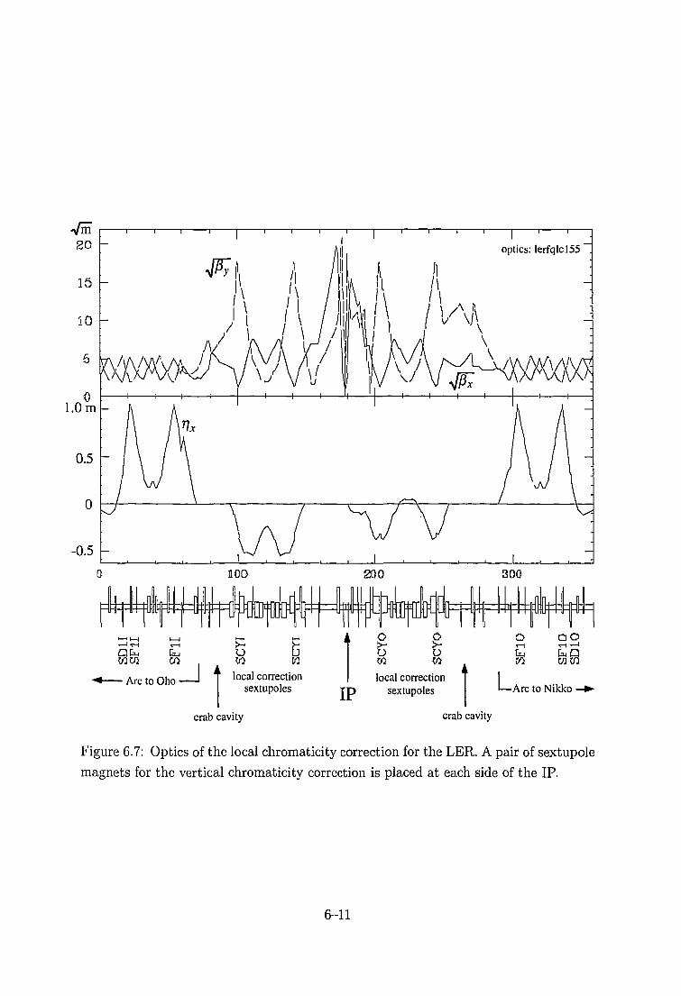
COW
— Arc to Oho _J 1local correctionsextupoles IP
local correctionsextupoles
wen
LArc to Nikko
crab cavity crab cavity
Figure 6.7: Optics of the local chromaticity correction for the LER. A pair of sextupole
magnets for the vertical chromaticity correction is placed at each side of the IP.
6-11

XCO
-,*CN
i i 1 1 1 1 i
' . . . 1 . . .
1 '
/%
• . 1 . . • 1
lve > 76000 sec
T. = 61000 sec (£z
. . I . . . 1 .
Optics: Ierfqlcl55local correction+crab space -
1000 turns, J / J x = 2% -
ex = 1.80 10-8 m
= 3.2 mm^y/ex = 2%) ~
XT+ > 105 sec ~
/ :
1 1 1 1 1 f 1 1 ^ 1 •
2500
2000
1500
1000
500 -
00 200 400 600 800 1000 1200 1400
2Jz/ez
Figure 6.8: Dynamic aperture and Touschek lifetime of the LER with a local chro-
maticity correction.
6-12

0 and 7/143 =fi 0, two new free parameters become available for tuning. The "knobs"
corresponding to these parameters may be the excitations of two families of quadrupole
magnets (QF2 and QD2) outside the sextupole pairs. This allows us to tune ap without
breaking down the pseudo — / transformation.
In the present design, the momentum compaction can be changed over the range
of - 1 x 1CT4 < ap < 4 x 10~4 by changing the strength of QF2's and QD2's by a few
percent. During this time, ex is kept nearly constant. In practice, it is rather difficult to
change ex over a wide range by only adjusting the two families of quadrupole magnets.
A cure to this restriction is to introduce a new family of quadrupole magnets QE2
inside the SF pair. By adjusting r]x at bend magnets, using five free parameters (QF2,
QF3, QD2, QD3, and QE2), we can obtain the required tunability, 1.0 x 10~8m <
£.T < 3.6 x 10~8m, while keeping ap constant and maintaining the pseudo —/ condition
between the SF's. In summary, a solution exists to tune ex and av independently by
adding QE2's.
6.3 Optics Design of the Interaction Region
6.3.1 Compensation of the Detector Solenoid Field
One of the important issues in designing the optics around the IP is compensation
of the x-y coupling effects generated by the detector solenoid field. Due to the finite
crossing angle at the IP, the design beam orbits are not parallel to the detector solenoid
axis. Thus, dispersion is also generated by the solenoid. Corrections have to be made
for four coupling elements of the transfer matrix between the IP and the arc, as well
as the dispersion near the IP.
A possible solution to this is to add four or more skew quadrupole magnets and
several bend magnets at each side of the IP. This correction, however, is perfect only
for on-momentum particles. The chromaticity of the x-y coupling remains uncorrected,
and can significantly increase the "anomalous emittance" at
vx±uy± mus = N
2vx,y±mvs = N (6.4)
The use of skew quadrupole corrections reduces the dynamic aperture, as shown in
Figure 6.10.
The best way to compensate for the x-y coupling effects of the detector solenoid is
to use counter solenoids, so that the integrated field, / Bzds, becomes zero within the
drift space around the IP. This compensation works perfectly for particles with any
momentum. This is the solution that has been adopted in the design of KEKB.
6-13

H H ) N ra rt n <N «M N-Hpq ft p, O H hh Rs<y c o" a* o" no? »<n
i—i—i—i——i—i—i—i——i—i—i—i——i
-O.B b
J=o=k=I*=icu w «-H co ? ] F3 CT
TK&1C3T O-Kl O" O-
Figure 6.9: Examples of emittance control in the LER: ex = 1.0 x 10~8m (above) and
3.6 x 10"8m (below).
6-14

3000
2500
2000
% 1500
1000 *
500 -
0
1 . . 1 1 I . 1 1
- TT,ave = 43000
• 1 \ xT. = 35000
: . . . i . . . r>
1 ' 1sec
seco^z
/ T T + -
i i i 1 i i i _
Optics: lcrfqlc90local correction
1000 turns, J / J x = 2% JRzL=1.5Tm
= 3.2 mm^y/ex = 2%) ;
57000 sec ;
-
0 200 400 6002JZ/£Z
800 1000
CO
3000
2500
2000
* 1500•j
-i
1000
500
0
L
I
L
• i •
\
X1 1 •
TT,ave
TT- =
/
/
1 1 1 1
= 22000 sec
19000 sec <j
1 i i i | i i i _
Optics: Ierfqlc93local correction
1000 turns, J / J x = 2% J
z = 3.2 mm^y/ex = 2%) ;
= 26000 sec 1
I . . i 1 . i i "
0 200 400 6002Jz/ez
800 1000
Figure 6.10: Dynamic aperture of the LER with an integrated solenoid field of 1.5 Tm
(above) and 4.5 Tm (below).
6-15
6.3.2 Crab Cavities
An optional use of a crab crossing scheme is currently being studied. To minimize the
required number of crab cavities, the transverse kicks given by the cavities should have
a maximum effect on the bunch orientation at the IP. This means that the horizontal
phase distance of the crab cavities from the IP should be (jV + l/2)?r. From the lattice
design view point, it is possible to reserve such a dispersion-free drift space in the
straight section near the arc.
The dynamic aperture has also been checked with the crab cavities. It has been
shown that the dynamic aperture is quite insensitive to the crab cavities, even with a
large amount of errors in the amplitudes and phases of the crab-mode RF kicks.
6.4 Optics Design of Other Straight Sections
This area of the design is still in progress. The following issues will be discussed in a
future version of the design report.
• Dispersion suppressors:
• Symmetry points of arcs:
• Optics with wigglers: As discussed in Chapter 2, the parameter sets for the HER
and the LER are almost identical. However, if the radiation loss is assumed to
come only from bend magnets in the arcs, the radiation damping time of the LER
is longer than that of the HER by a factor of 2. To halve the LER damping time,
without increasing the momentum spread, preparation is under way to install
optional damping wigglers for a total length of 96 m in Oho and Nikko. These
wigglers can be also used to control the LER beam emittance. We can obtain
the required tunability of the horizontal emittance by the wigglers.
• Adjustment of the path length: Changes of the path length due to the wigglers
can be adjusted by special sections called "chicanes". Each section is built with
four bending magnets, which are placed in a way similar to that of a unit of wig-
glers. The LER has four 12 m-long chicanes, which provide a sufficient tunability
of the path length. These chicanes can also be used to equalize the circumference
of the LER to that of the HER. Figure 6.11 shows the optics design of the LER
in the vicinity of the chicane structure. The chicane bend magnets are labelled
BC1 and BC2 in Figure 6.11.
• Injection point:
6-16

4
6
4
2
0
1.00
0.75
0.50
0.25
0.00
•
A'\\ /\/
A/\
A
\V /
A' )\7
A/\\
\\
\/\I\\
\
/
/
A/ /
V\
V/ \A AA
VV
I
A/ \/ \
Vii
i
A/V
-_-
150
CQ CQ CQ CQ
Figure 6.11: Optics design of the LER in the vicinity of the chicane structure for ring
length adjustments. The chicane bend magnets are labelled as BCl and BC2.
• Translation chicane:
6.5 Requirements on the Magnet Quality
The tolerances on the systematic multipole errors of the bend magnets and quadrupole
magnets in the arcs have been estimated. The criteria is based on a 2% reduction of
the dynamic aperture integrated in both the momentum and transverse phase spaces.
The results ere listed in Table 6.2. In the table Kn is defined as
K - (6.5)Bp dxn
It is known that requirements similar to those listed in Table 6.2 have been met by
existing magnets that are used for the TRISTAN main ring.
6-17

Dipole Magnets
K2/Ko
KA/K0
Quadrupole Magnets
1.0m"2
17000m-4
22000m-4
1.3 x 10¹³m-8
A S / B at 50 mm radius
0.12%0.45%
0.12%
0.45%
Table 6.2: Tolerances of systematic multipole errors.
6.6 Effects of Machine Errors and Tuning Proce-dures
The performance of the noninterleaved scheme lattice may be sensitive to machine
construction errors, which break down the cancellation of sextupole aberrations in the
—/ transformation. This section considers the effects of the construction and setup
errors in the ring lattice, and their tolerances for the acceptable operation of KEKB.
The criteria used in this analysis are the emittance ratio, the dynamic aperture, and the
miss-crossing at the IP. The errors considered include: the misalignment of magnets,
BPM offset and field ripple.
Concerning magnet misalignment, we consider the combined effect of temperature-
dependent drift, movement of the tunnel, vibration of the magnets and others. No
attempts are being made to resolve individual errors, or to quote their tolerances
separately. This is because there is no sufficient information available for fixing their
relative contributions at this stage.
In this section the tolerances are not discussed in the form of the maximum allowable
errors, which may be considered to be the common definition. Rather, we assume
certain combinations of initial lattice errors, and simulate how the emittance ratio
and dynamic aperture can be improved by applying a series of beam-based tuning
procedures. This study has been performed by using a sophisticated beam simulation
code SAD, which has been developed at KEK. In this study an analysis was made on
what magnitude of combined errors are still acceptable, such that the target emittance
ratio and the dynamic aperture, etc. can be achieved by realistic beam-based tuning.
This approach clarifies the significance of each tuning process and its role. It also helps
to create guidelines for the development of beam-based techniques of error analyses.
The errors used in the simulation are given in Table 6.3. The assumptions used in
6-18

Element
Quadrupole Magnets
QC Quads2)
Sextupole Magnets
Bend Dipole Magnets
Steering Corrector Magnets
Ax(mm) Ay(mm) A0(mrad
0
0
0
15
01
15
0.
0.
0.
0
0
15
01
15
.1
.1
0.2
0.1
0.2
0.1
0.2
)1
1
2
2
Ak/k
x 10~3
x 10~4
x 10"3
x 10-3
BPMs3) 0.075 0.075
values are for one standard deviation (a).2) Two quads near IP(QCS and Q C l ) .3) Assume Beam-based measurement of BPM offset.
Table 6.3: Errors used in t h e simulation1)
t h e s imula t ion are summar ized as follows:
1. Only the LER has been considered. The situation at HER is expected to be
similar, since its arc lattice structure is basically identical to that of the LER.
2. Errors of the quadrupole magnets close to the interaction point (QCS and QCl)
are intentionally assumed to be very small compared to those in the arc section.
This is done in order to magnify the effects of the errors in the arc section. We
will consider the effects of QCS and QCl separately in the near future.
3. Every sextupole magnet has a mover which can transversely move the magnet
with a maximum stroke of ±3 mm in both the horizontal and vertical directions.
4. The offset errors of the BPMs relative to the magnetic center of the quadrupole
and sextupole magnets are assumed to be measurable with an accuracy of 75 yum.
This is considered to be achievable, for example, by using the /^-modulation
method [4, 5].
5. The strength errors of the quadrupole magnets are assumed to be measurable
with an accuracy of 0.1%. The measurement may be directly performed prior to
installation, or by using beam orbit bumps across each magnet.
6. The errors are assumed to obey Gaussian distributions with a cut-off at 3 stan-
dard deviations (3cr). Their magnitudes are given in Table 6.3.
6-19

6.6.1 Emittance ratio and Dynamic aperture
Simulations with 20 different random seeds (events) have been conducted. Figure 6.12
shows the machine performance at various stages of beam tuning. The graphs show
the emittance ratio plotted against j3y (m) at the interaction point, and the estimated
dynamic aperture (nx = \/2Jx/eXo vs. dp/p). The operation point was set to be
(i/x)'/2/)=(46.52, 46.08), which is preferred from the viewpoint of beam-beam effects
(see Chapter 3).
In the tracking calculation, the initial vertical amplitude was set to be one third
that of the horizontal. In the plots for the emittance ratio, the black dots represent
results from individual "events" that correspond to different random seeds for errors.
The straight broken line indicates the design emittance ratio of 2%. In the dynamic
aperture plots, the thick lines indicate the expected dynamic aperture in the error-free
lattice, while the thin lines show the results from simulations with random lattice errors.
The injected beam is expected to occupy the area indicated by the thick rectangle.
Plots (al) and (a2) are for only orbit corrections, while (bl) and (b2) are for
sextupole adjustments by movers, in addition to orbit corrections.
It can be seen that for the "orbit correction only" case, the emittance ratio is huge,
and the dynamic aperture (DA) is degraded compared to the "error-free" case (thick
line). Although the DA has sufficient space to accept the injected beam, it is desirable
to have much more margins for safety, especially for large momenta, because it limits
the Touschek lifetime.
In order to improve the emittance coupling, sextupole magnets are vertically moved,
simulating movers, such that the orbit passes through their center within 75 [.an. The
emittance ratio is dramatically improved, as shown in (bl). The corresponding DA
also shows a small improvement for the transverse direction.
The scatter of (3*, in (al) and (bl) is fairly large (~ ±25%). This is a reflection of
strength errors of the quadrupole magnets that are included in the simulation. It has
been found that DA is strongly correlated with /3*. Thus although those "events" with
smaller (3* give a larger luminosity, they are also responsible in part for the deteriorated
DA in (b2).
In the next simulation step optics matching was performed, assuming that the
strength errors of the quadrupole magnets are known with an accuracy of 0.1%. This
has the effect of making the expected /3* of each "event" closer to the design value.
As shown in (cl), the spread of f3* is much reduced. However, as shown in (c2), DA
becomes much worse for large momenta. This is because the strengths of the sextupole
magnets are no longer optimum for the re-matched optics.
As the final step, by optimizing the sextupole magnets we could recover the DA
6-20

0.002 0.004 0.006 0.008 0.01
Pv*0.012
0.002 0.004 0.006 0.008 0.01 0.012
Py* (m)
0.002 0.004 0.006
Py* (m)0.008
dp/p (%)
0dp/p (%)
0 1dp/p (%)
50
40
30
' 20
10
0
(d2)
»i_L-2 -1
/
n 1 2dp/p (%)
Figure 6.12: Simulated machine performance at various stages of beam tuning. The
graphs show the emittance ratio plotted against j3y (m) at the interaction point, and
the estimated dynamic aperture (nx = (2Jx/ea;o)~1/'2 vs. dp/p). Plots (al) and (a2)
are for only orbit corrections, while (bl) and (b2) are for sextupole adjustments by
movers, in addition to the orbit corrections. Plots (cl) and (c2) show the case with
optics re-matching. Plots (dl) and (d2) show the results with chromaticity correction
for re-matched optics. For detailed descriptions see the text.
6-21

close to the ideal, as shown in (dl) and (d2). (There was one exception for which we
could not find the optimum setting of the sextupole magnets).
It can be seen that tuning with sextupole mover is very effective to optimize the
emittance coupling, because it is orthogonal to the DA: it does not affect the dynamic
aperture.
6.6.2 Field Ripples
If the excitation strengths of the magnets change at frequencies for which the or-
bit feedback system cannot apply corrections effectively, then noticeable performance
degradation may result. To evaluate this issue, the tolerances on the field jitter of the
magnets have been calculated.
The criteria for calculating the jitter tolerances are that: (1) changes in the field do
not induce either emittance growth or a deterioration of DA by more than 10%, and
(2) shifts of the beam orbit at the IP do not exceed 0.1a*
The calculated tolerances of the field jitter are summarized in Table 6.4. The
tolerances on the sextupole jitters are smaller than those for the quadrupole magnets.
The QCS quadrupole magnets for the final focusing are assumed to be connected in
series to a common power supply. The third column in the table gives the effect of
jitter on the emittrnce or DA. The symbols Ax* and Ay* are the horizontal and vertical
orbit deviations at the IP. The ratio AA/A0 is the relative change in the area of the
dynamic aperture, i.e., the sum of nx for each dp/p point.
It should be noted that the tolerances quoted in the table are for the field, and that
the numbers are not to be considered directly for the magnet power supply. To estimate
the tolerances on the ripples of the magnet power-supplies, the effects of eddy currents
in the vacuum chamber have to be taken into consideration. Generally, the power-
supply ripple tolerances are much more relaxed than the values shown in Table 6.4.
For example, the tolerances of the 50 Hz component of the power supply ripples are
10 times greater than those given in Table 6.4
6.7 Conclusions
Detailed studies on the lattice for the arc sections of KEKB have been performed. The
present working design is based on a 2.5TT cell structure. It offers an excellent dynamic
aperture, and tunability of momentum compaction and beam emittance. The use
of a local chromaticity correction scheme near the IP appears to be very promising.
The requirements on the magnet field quality and errors of alignment and magnet
6-22

Element
Bend Dipole Magnets
Quadrupole Magnets
QCS Quads
Sextupole Magnets
Steering Corrector Magnets
relative
l x
1 X
1 X
l x
jitter (a)
10"5
io-4
10~5
10"5
what limits
(a* = 80(im)
AA/Ao = - 3 ± 14%ey/eyo = 10%
AA/Ao = -10%
Ay* = 0.1/zm
Table 6.4: Tolerances of field jitter. Symbols Ax* and Ay* denote the horizontal and
vertical orbit deviations at the IP, while the AA/Ao is the relative change of the area
of the dynamic aperture plot, i.e., the sum of nx for each dp/p point.
excitations have been studied.
6-23

Bibliography
[1] K.L. Brown, IEEE Trans. Nucl. Sci. NS-26, 3490 (1979); K.L. Brown and
R. Servranckx, in Physics of High Energy Particle Accelerators, Proc. the
Third Annual U.S. Summer School in High Energy Particle Accelerators, AIP
Conf. Proc. No. 127 (1983).
[2] K. Oide and H. Koiso, Phys. Rev. E47, 2010 (1993).
[3] K. Oide and H. Koiso, Phys. Rev. E49, 4474 (1994).
[4] R. Schmidt, Misalignments from K-modulation, Proceedings of The Third Work-
shop on LEP Performance, Chamonix, January, 1993, 139-145
[5] M. Kikuchi, K. Egawa, H. Fukuma and M. Tejima Beam-Based Alignment of
Sextupoles with Modulation Method, to be published
6-24

Chapter 7
Interaction Region
7.1 Beam Line Layout
The design beam parameters of KEKB and their rationale have been discussed in
Chapter 1. Some pertinent parameters are repeated in Table 7.1 for convenience.
A schematic layout of the beam line near the interaction point (IP) is shown in Fig-
ure 7.1. The figure shows the following magnets: S-R, QCS-R, QC1ER, S-L, QCS-L
and QC1EL. The final vertical focusing of two beams is provided by a pair of super-
conducting quadrupole magnets, QCS-R and QCS-L. The superconducting solenoid
magnets, S-R and S-L, are for compensating solenoid fields created by the detector fa-
cility. The QCS and S magnets on each side of the interaction point (IP) are contained
in a common cryostat enclosure.
The vertical focusing field strength of QCS is tuned to the positron energy (3.5
GeV). Extra vertical focusing for the electron (8.0 GeV) is provided by a pair of normal
conducting quadrupole magnets QC1E-L and QC1E-R. The beam separation and the
geometry of QC1E magnets are designed such that only the electrons would see non-zero
gradient fields when passing through them. To minimize the growth of chromaticity
from this region, the QC1E magnets are placed close to the QCS magnets, in as much
as the hardware design constraints allow.
The positrons enter the IP through QCS-R and leave the IP through QCS-L. The
electrons proceed in the opposite direction. Since the two beams collide at the IP at
a finite crossing angle of 2 x 11 mrad, inevitably one beam or the other must go off
axis within the QCS. To minimize the flux of synchrotron radiation through the IP,
the incoming positron beam orbit is set on the axis of QCS-R. Likewise, the incoming
electron beam is set on the axis of QCS-L.
A sufficiently large beam separation is created at QC1E-L, so that a full quadrupole
7-1

Energy
Crossing angle
Luminosity
Tune shifts (fs/€i/)Beta function (/?*//?*)
Beam current
Bunch length
Energy spread
Bunch spacing
Particles/bunch
Emittance (ex/ey)
Synchrotron tune
Betatron tune (ux/uy)
LER HER
3.5 8.0
±111 x 1034
0.039/0.052
0.33/0.01
2.6 1.1
4
7.1 x 10"4 6.7 x 10"4
0.59
3.3 x 10¹⁰ 1.4 x 10¹⁰
1.8 x 10⁻⁸/3.6 x 10-10
0.01~0.02 0.01~0.02
45.52/45.08 47.52/43.08
GeV
mrad
cm'V1
m
Amm
m
m
Table 7.1: Beam parameters related to the IR issues.
QC1ERSeptum Quad
Positron Positron: off axisof QCS-L
Detector solenoid axis
Total crossingangle = 22 mrad
Electron:off axis ofQCS-R
S-RCollisionpoint -•
Electron
Positron
QC1ELFull Quad E i e c t r o n : , t l , , .„
off axis of the solenoid,on axis of QC1-L
QCS-L axis has~ 35 mm offsetrelative to the detector
Positron:on axis of the solenoid,on axis of QCS-R
Figure 7.1: Schematic plan view layout of the magnets and the beam line near the
interaction point. The superconducting solenoid S-R and the final focusing quad QCS-
R are contained in a single cryostat. Similarly, S-L and QCS-L are contained in another
cryostat.
7-2
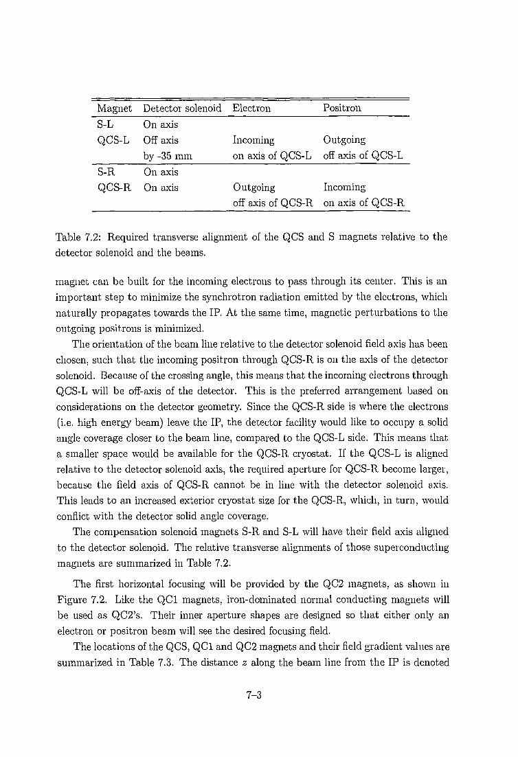
Magnet
S-LQCS-L
S-RQCS-R
Detector solenoid
On axis
Off axis
by -35 mm
On axis
On axis
Electron
Incoming
on axis of
Outgoing
off axis of
QCS-L
QCS-R
Positron
Outgoing
off axis of
Incoming
on axis of
QCS-L
QCS-R
Table 7.2: Required transverse alignment of the QCS and S magnets relative to the
detector solenoid and the beams.
magnet can be built for the incoming electrons to pass through its center. This is an
important step to minimize the synchrotron radiation emitted by the electrons, which
naturally propagates towards the IP. At the same time, magnetic perturbations to the
outgoing positrons is minimized.
The orientation of the beam line relative to the detector solenoid field axis has been
chosen, such that the incoming positron through QCS-R is on the axis of the detector
solenoid. Because of the crossing angle, this means that the incoming electrons through
QCS-L will be off-axis of the detector. This is the preferred arrangement based on
considerations on the detector geometry. Since the QCS-R side is where the electrons
(i.e. high energy beam) leave the IP, the detector facility would like to occupy a solid
angle coverage closer to the beam line, compared to the QCS-L side. This means that
a smaller space would be available for the QCS-R cryostat. If the QCS-L is aligned
relative to the detector solenoid axis, the required aperture for QCS-R become larger,
because the field axis of QCS-R cannot be in line with the detector solenoid axis.
This leads to an increased exterior cryostat size for the QCS-R, which, in turn, would
conflict with the detector solid angle coverage.
The compensation solenoid magnets S-R and S-L will have their field axis aligned
to the detector solenoid. The relative transverse alignments of those superconducting
magnets are summarized in Table 7.2.
The first horizontal focusing will be provided by the QC2 magnets, as shown in
Figure 7.2. Like the QC1 magnets, iron-dominated normal conducting magnets will
be used as QC2's. Their inner aperture shapes are designed so that either only an
electron or positron beam will see the desired focusing field.
The locations of the QCS, QCl and QC2 magnets and their field gradient values are
summarized in Table 7.3. The distance z along the beam line from the IP is denoted
7-3

with positive values in the "right" direction, where the electron leaves the IP. The
"left" direction, where the electron enters the IP, is denoted by negative values of z.
IR Hall wall Detectur structureboundaries
IR Hall wall
10
(Vertical scale: Expanded by x5)
20 m
Figure 7.2: A schematic diagram of the beam line beyond QC1 magnets.
Magnet
QC2E-L
QC2P-L
QCIE-L
QCS-L
QCS-R
QC1E-R
QC2P-R
QC2E-R
Zmin (m)
-8.0
-5.0
-3.6
-1.85
1.685
4.0
5.4
7.2
Zmax(rn)
-7.2
-4.4
-3.0
-1.35
2.185
4.6
6.4
7.8
Field gradient (T/m)
5.78
6.42
-14.6
-16
-16
-14.47
3.9
9.7
Purpose
Horiz. focusing e~
Horiz. focusing e+
Vert, focusing e~
Vert, focusing e"e+
Vert, focusing e~e+
Vert, focusing e~
Horiz. focusing e+
Horiz. focusing e~
Table 7.3: Positions relative to the IP and field gradients of the QCS, QCl and QC2
magnets.
Several orbit correction dipole magnets will also be installed in the beam line. A
few horizontal and vertical bend magnets are required to match the orbit to the rest
of the straight section. As discussed in Chapter 2, local chromaticity corrections are
7-4

applied to the LER in the straight section that includes the IR. A schematic beam line
layout of the IR, including a part of the chromaticity correction sections, is shown in
Figure 7.3. Soft bend magnets will be used as the last dipole magnets for the incoming
beam to see before reaching the IP. This is so that the critical energy of synchrotron
radiation off these magnets will be sufficiently low, and that it would not cause harmful
background to the detector facility.
Crab cavities
Detector
I^fof-M—HHHElectron
Vertical scale: expanded by x10
Crab cavities
Positron
Inilinnliniiiinln Mln nln Mill ntitnil ml
0 50m
Figure 7.3: Schematic layout of the HER and LER beam lines in the straight section
which includes the IR. Part of the LER local chromaticity corrections are shown.
Although the bulk of the x-y coupling effects due to the detector solenoid are
cancelled by compensation solenoids S-L and S-R, the remaining coupling terms need
to be corrected in the rest of the IR beam line. For this purpose, the support frames for
QCl, QC2, QC3 and several other magnets allow us to introduce a variable amount
of small rolls (< 2°) for introducing skew components to the magnetic field. The
roll angles will be remotely controlled using a magnet mover mechanism. Engineering
development of these magnet support will begin soon.
7.2 Detector Boundary Conditions
7.2.1 Geometric Conditions
The detector facility for high energy physics experiments at KEKB has approximately
an axially symmetric geometry around the beam line. Physics requirements call for
a good solid angle coverage for detecting decay product particles from e+e~ -* BB
interactions. Figure 7.4 shows a schematic side view of the proposed detector facility.
Table 7.4 summarizes the solid angle coverage requested by proponents of the de-
tector facility. In the table, the polar angle is measured from the forward extreme, i.e.
7-5

- 6 - 5 -d - 3 - 2 - 1 0 2 6 l rn
Figure 7.4: Schematic side view of the proposed detector facility, together with the
accelerator cryostat for superconducting compensation solenoid and QCS magnets.
A pair of normal conducting quadrupole magnets and QCIEL and QCIER are also
shown. Details of the detector configuration may vary in the final design.
7-6

Detector Polar angle range
Barrel KL catcher and \x detector 45° - 113°
Forward KL catcher and \x detector 25° - 45°
Backward KL catcher and \i detector 113° - 155°
Barrel Calorimeter 32.5° - 130°
Forward Calorimeter 11.5° - 32.5°
Backward Calorimeter 130° - 160°
Barrel TOF/TSC 32.5° - 130°
Barrel Particle ID device 32.5° - 130°
Forward Particle ID device 12.5° - 32.5°
Central Drift Chamber 17° - 150°
Silicon Vertex Detector 17° - 150°
Table 7.4: Polar angle coverage requested by the experimental detector facility.
the direction where the positrons enter the interaction point (IP).
The interaction point relative to the detector center is shifted towards the left by
470 mm. This is for increasing the solid angle coverage in the forward direction, while
taking into account the Lorentz boost of the final state particles in the asymmetric
collision.
The detector geometry that has a direct bearing on the accelerator design is that of
the central drift chamber (CDC). In the latest design the CDC has an inner radius of
280 mm. Thus, the accelerator components must fit within a cone-shaped space with
an opening angle of 17 degrees forward and 30 degrees backward, clipped by the CDC
inner radius, minus the cable space for detector elements. The CDC occupies the Z
space between —970 mm and +1660 mm, as measured from the IP.
Just at the IP, a high precision particle tracking device based on silicon micro strips
will be installed. Its design calls for a small vacuum chamber around the IP with an
inner radius of 20 mm for —80 < Z < +80 mm. The particle trajectories during the
injection period and synchrotron radiation during the run must not be intercepted by
this aperture.
7.2.2 Magnetic Conditions
The nominal solenoid field created by the detector magnet for charged particle tracking
is 1.5 T. The field is extended in an effective volume length of ~ ±2.5 m. If the
solenoid field of the detector is not cancelled in situ on the beam line, its coupling
7-7

effects must be corrected by using a set of skew quadrupole magnets, whose strength
is approximately KSQ « 0.05. However, corrections with skew quad magnets are exact
only for on-energy particles. The remaining chromatic coupling term will result in an
increased vertical emittance. Also, the use of skew quadrupole magnets will create
extra chromaticity, which need to be compensated in chromaticity correction sections
in the arcs and elsewhere. This tends to reduce the available dynamic aperture, and
consequently, the expected beam lifetime. Furthermore, there is an indication from
simulations on beam-beam effects, that the luminosity will tend to be reduced if the
solenoid field compensation is not sufficient.
Beam dynamics calculations have been conducted to evaluate these effects. Cases
with various sophistication of solenoid field compensation schemes have been examined.
It has been found that if the integral of the axial field Bz is cancelled to zero on the
average, the reduction of the dynamic aperture and its effects on the beam lifetime are
negligible. In that condition, the accelerator performance is comparable to the case
where the detector solenoid field is completely absent. The effects of fringe fields of the
solenoid and quadrupole magnets are taken into account. As an example of incomplete
field compensation, in the case with a left-over field of / Bzdz = 1.5 T m, it has been
found that up to a 30% reduction of the beam lifetime will result, because of the reduced
dynamic aperture. Thus, the goal of field compensation for the accelerator within the
detector volume should be to bring the net value J Bzdz to zero. The superconducting
compensation solenoid magnets S-L and S-R will be implemented to achieve this.
Magnetic fields from S-L, S-R, QCS-L and QCS-R will leak into the detector volume,
and distorts its solenoid tracking field. Their effects in physics analyses were a potential
problem. Simulation work by the detector group has shown that the effects of the leak
field due to S-L and S-R magnets are, in fact, manageable. Relatively straightforward
tuning of the track analysis software can recover the full momentum resolution of
charged particles. It has been also found that perturbations due to leak fields from QCS
magnets are sufficiently isolated from the interaction point. In addition, the quadrupole
field component quickly attenuates as a function of r, the radial distance from the
beam line. Thus, the leak quad field is also manageable from the physics analysis view
point. Therefore, no additional compensation magnets will be implemented to shield
the detector volume from S and QCS accelerator magnets.
Since QCS-L is not in line with the detector axis, the field that is produced by
QCS-L may couple with the detector iron in such a way as to create an axially non-
symmetric field on the accelerator beam line. The magnitude of such multipole fields
has been evaluated, and its effect on the beam dynamics examined. It has been found
that their adverse effects are negligible. Consequently, no special measures will be
7-8

taken to shield QCS from the detector iron structure, either. However, it is felt that
in any case it is desirable to introduce some correction devices for multiple pole field
errors. A feasibility study of such devices is now being prepared.
Turning to outside the QCS region, the QC1E-L and QC1E-R magnets will be
located near the outer edge of the detector structure. If the magnetic field from the
detector solenoid is large there, the presence of QC1E iron can significantly distort
the magnetic field near their entrance. Unless care is taken, this will lead to sizeable
multipole field errors to be felt by the beams.
The magnitude of the detector leak field depends on the details of the relative geom-
etry of the detector and the accelerator. There is a desire on the part of experimental
physicists to increase the thickness of the end yoke for better muon detection coverage.
This would tend to increase the leak field from the detector, unless care is taken to
reduce the magnetic saturation within the detector structure. Or, both the accelerator
and detector designers agree that increasing the inner aperture size of the detector end
cap (currently set to be 1000 mm diameter) would relax the space problem for cabling,
installation and maintenance. However, it would quickly increase the detector leak
field.
In one version of the structure design, the detector leak field near QC1E could be
reduced to Bz < 20 G and Br < 20 G, which is considered to be acceptable from a beam
dynamics viewpoint. Efforts are still on-going to optimize the structure configuration
so that the detector coverage is maximized while the leak field is minimized. Prepa-
rations for high-precision 3-dimensional field calculations in this area are in progress.
A possible use of weak compensation solenoid magnets or end-shimming is also being
considered near QCl magnets. However, the priority is on efforts to first reduce the
strength of the detector leak field.
7.3 Beam Line Aperture Considerations
The aperture of the vacuum chambers in the QCS and S magnets have been determined,
so that neither the beam during injection time nor the synchrotron radiation (SR)
during the data acquisition time should directly hit the inner surface of the vacuum
pipes.
The beam envelope considered in the injection system design is 1.2 x 10~5 m for
x and 1.2 x 10~6 m for y. To include a safety margin, in the design of IR the beam
envelope emittance of 2 x 10~5 m for x and 2 x 10~6 m for y is assumed. Parallel to
these, the trajectories of SR photons from 10cr particles during the collision time have
been calculated. The beam stay clear values have been determined from the maximum
7-9

of the injection time beam envelope and the run-time SR flux trajectory. This beam
stay clear, plus 13 mm for the work space for the vacuum chambers is specified as the
required inner aperture of the cryostats for QCS and S magnets.
The beam stay clear for QC1 and QC2 magnets has been determined by considering
only the injection condition. The assumed beam envelope is 1.4 x 10~5 m for x and
2 x 10~6 m for y.
The vacuum chamber that connects the beam line between those magnets must fully
contain the specified beam-stay clear. Since the (3 function values are rapidly changing
in this area, the beam stay clear also varies along the beam line. The design of the
vacuum chamber in the IR has to accommodate this situation. Also, attention must be
paid to possible trapping of higher order mode (HOM) RF fields in this area. Although
efforts are being made to reach an optimum solution, some amount of HOM trapping,
and heating due to it, will be inevitable. To rectify this situation, the possibility of
implementing some antenna structures to remove the HOM power from this section is
being contemplated.
7.4 Superconducting Magnets for IR
7.4.1 Introduction
Four superconducting magnets will be used in the interaction region: solenoid field
compensation magnets (S-L and S-R), and final focusing quadrupole magnets (QCS-L
and QCS-R). Each pair of S + QCS magnets in the left and right side is contained
in a single stainless steel vessel. It provides a sturdy structure which tightly holds
the coil windings and prevents their motions during cooling down and excitation. The
vessels (cryostat) are designed to withstand forces due to the magnetic field of the
coils, themselves, and their interactions with the detector solenoid field. They have
to be installed completely inside the detector facility. Figure 7.4 shows the layout of
the interaction region with the superconducting magnets, surrounded by the detector
elements. This section presents the engineering design work that has been done for the
superconducting magnets.
7.4.2 Compensation solenoids
The two field compensation solenoids have magnetic fields opposite to the detector
solenoid. Figures 7.5(A) and 7.5(B) show cross section views of the right and left
solenoids in their horizontal cryostats. In both cases, the solenoid coil has an inner
7-10

Central field
Coil current density
CoilInner diameter
Outer diameter
Length
Max. field of the conductor
Stored energy
Magnetic pressure in radial direction
S-R5.4
300
190
220
650
5.4
225
9.2
S-L
4.4
258
190
220
470
4.5
115
6.4
TA/mm2
mm
mm
mm
TkJ
MN/m2
Table 7.5: Main parameters for the solenoid magnets.
diameter of 190 mm, and a thickness of 15 mm. Between the inner helium vessel and
the coil, some space is allocated for accommodating a few kinds of correction coils. The
main parameters of these solenoids are listed in Table 7.5. The final specifications of
the conductor wire and the operating current will be decided in the near future, while
tacking into account the magnetic, coupling with the detector solenoid and the heat
load to the cooling system.
A computer code OPERA-2D has been used to calculate the magnetic field from
the combination of those solenoid magnets, the detector solenoid, and its field return
yoke structure. Figure 7.6 shows the expected axial magnetic field Bz along the beam
axis. With this configuration, the integral of Bz along the accelerator beam line is
brought to zero.
The field distortions in the detector's tracking volume, which is caused by the
leak field from these solenoids, have been evaluated. Figure 7.7 shows the contour
lines of the field distortions relative to the nominal 1.5 T solenoid field. The number
attached to each contour line indicates the field deviation expressed in the unit of
percent. Except for the regions close to the compensation solenoids, the field deviation
in the volume for charged particle tracking by the experimental facility is less than 5%.
According to simulations studies carried out by the detector group, this is considered
to be acceptable.
When the solenoid magnets are excited in the detector field, axial magnetic forces
which act on the solenoid coils appear. The peak field values on the conductor will
be shifted from the values in Table 7.5. These effects have also been evaluated using
OPERA-2D. The estimated magnetic forces are listed in Table 7.6. The axial body
7-11

150-H
(A) S-R
IOCH
50 H
100 1501
200(mm>
50
(B) S-L
1501
200(mm>
Figure 7.5: Cross section views of the S-R solenoid (A) and the S-L solenoid (B).
7-12

4
3
3- 2
gb 1
0
-1
j
II
1
11
j
i
7\ i
1 r i|
-400 -300 -200 -100 0 100^ 200 300 400Distance from the detector Center (cm)
-0.002 -
1" -0.004
N -0.006CD
-0.008 f
-0.01300 320 340 360 380 400
Distance from the detector center (cm)
Figure 7.6: Distribution of the axial magnetic field Bz along the axis of the experimental
facility.
7-13
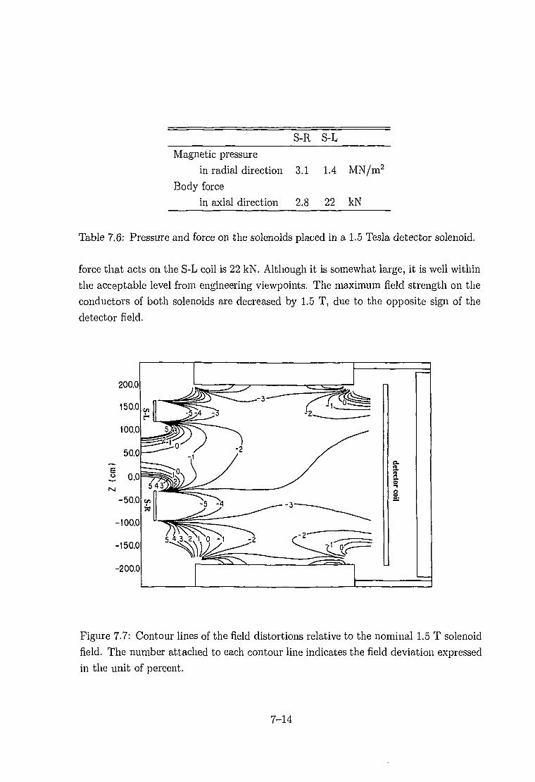
S-R S-L
Magnetic pressure
in radial direction 3.1 1.4 MN/m2
Body force
in axial direction 2.8 22 kN
Table 7.6: Pressure and force on the solenoids placed in a 1.5 Tesla detector solenoid.
force that acts on the S-L coil is 22 kN. Although it is somewhat large, it is well within
the acceptable level from engineering viewpoints. The maximum field strength on the
conductors of both solenoids are decreased by 1.5 T, due to the opposite sign of the
detector field.
Figure 7.7: Contour lines of the field distortions relative to the nominal 1.5 T solenoid
field. The number attached to each contour line indicates the field deviation expressed
in the unit of percent.
7-14

Field gradient
Current
Coil
Inner diameter
Outer diameter
Overall length of the coil
Collars
Material
Radial thickness
Integrated field uniformity (at r = 40 mm)
B6L/B2LB10L/B2L
Effective magnetic length
Max. field on the conductor
Stored energy
Magnetic force per unit length in a coil octant
Fx (horizontal)
Fy (vertical)
18.8
2224
260
295.4
780
710
SUS316LN
27
< 1 x 10~4
< 1 x 10~4
490
420
3.1
157
125
-290
T/m
A
mm
mm
mm (for QCS-L)
mm (for QCS-R)
mm
mm (for QCS-L)
mm (for QCS-R)
T
kJ
kN/m
kN/m
Table 7.7: Parameters of the superconducting quadrupole magnet. The overall length
of the coils does not include the coil end spacer and magnet end plates.
7.4.3 Quadrupole magnets
The final quadrupole magnets are iron-free, superconducting magnets. They provide
a maximum field gradient of 18.8 T/m for an effective field length of 0.5 m in a usable
aperture diameter of 80 mm. Extensive experience from the development, fabrica-
tion and operation of the TRISTAN superconducting mini-beta insertion magnets is
reflected in the design work.
The basic design of QCS is similar to that of the TRISTAN magnets. It is based
on a set of cos 29 winding layers clamped by stainless steel collars. The required warm
bore aperture specifications of QCS-R and QCS-L are approximately the same. This
allows us to use an identical coil structure for both sides, QCS-L and QCS-R. However,
the dimensions of the cryostats will be different, as discussed in a previous section. The
main parameters of the quadrupole magnet are listed in Table 7.7.
7-15

Cable dimensions
width
thickness
Number of SC strands
Number of Cu strands
Cu / SC ratio of SC strand
Strand diameter
Filament diameter
RRR of stabilizing copper
Cable twist pitch
Critical current in cable (at 4.2 K)
8.35 ± 0.05
0.925 ± 0.02
16
16
2.0
0.510 ± 0.005
< 6
180 ± 20
70 ± 5
more than 2900
more than 4200
mm
mm
mm
/j,m
mm
A at 5T
A at 3T
Table 7.8: Parameters of the superconducting cable.
Figure 7.8(A) shows a cross section of the QCS-R magnet in a horizontal cryostat.
The inner diameter of the warm bore is 178 mm, and the outer diameter of the vacuum
vessel is 480 mm. Starting with the innermost part, the main components of the magnet
are: a warm bore, inner radiation shield, inner wall of the helium vessel, correction
coils, main coil, stainless steel collar, outer wall of the helium vessel, outer radiation
shield and vacuum vessel.
The main coil is made of two layers of superconducting windings. The cos 29 current
distribution is approximated by using a copper wedge in the first layer. To keep the
higher multipole fields within the tolerances, a computer code based on an analytical
formula of field harmonics has been used to determine the two-dimensional cross section
of the coil winding. The resultant shape has 115 turns in total, combining the first and
second layers in each of the four quadrants. The operating current was chosen to be
relatively small. This allows us to reduce the heat load on the cooling system.
The superconducting cable will be of the NbTi/Cu Rutherford type, which is com-
monly used in many accelerator magnets. Since the operating current is relatively low,
it is planned to use a cable in which copper strands and NbTi/Cu strands are mixed for
ease of the winding process. The main parameters of the cable are listed in Table 7.8.
Effects of various fabrication errors of the coils have been investigated. A basic
eight-fold symmetry in the coil geometry is assumed. Table 7.9 summarizes the results
of this study. The quoted numbers are for a 0.1 mm variation of the parameters listed.
7-16

250 H
200
(A) QCS-R
50 100 150 200
(B) QCS-L
50 J 0119.61 115.51
Figure 7.8: Cross section views of the QCS-R (A) and QCS-L (B) magnets.
7-17

Parameters changed
Radius of inner coil
Radius of outer coil
Radius of inner No.l coil
Radius of inner No.2 coil
Pole angle of inner coil
Pole angle of outer coil
Wedge of inner coil
b2 (mT/m)
-11.0
-32.6
-9.41
-4.73
-4.96
-19.0
-4.22
b6 10-4
-0.14
-0.10
-0.18
-0.07
-0.11
-0.17
-0.20
b10 10~4
-0.00
-0.00
-0.00
-0.00
-0.00
-0.00
-0.00
Table 7.9: The values show the effect of a 0.1 mm shift of the given parameter on the
quadrupole field strength and higher harmonics at r = 40mm.
The harmonics are calculated at a reference radius of 40 mm.
Since the quadrupole magnets considered here are rather short compared to other
typical accelerator superconducting magnets, the effects of the end parts are not neg-
ligible. Three-dimensional field calculations are in progress to investigate the field
distribution, and to optimize the shape of the coil end.
Figure 7.8 shows a cross section of the QCS-L magnet in the horizontal cryostat.
In this case, the quadrupole axis has to be shifted horizontally by 35.1 mm from the
detector axis. Therefore, the cryostat has a rather complex structure, as shown in
the figure. However, the engineering work for fabricating this magnet is considered
to be quite possible. In this eccentric configuration, higher order multipole fields and
the asymmetric electromagnetic forces can arise, due to the image current in the end
yoke of the detector. An estimate of this effect has been made by treating the issue
as a 2-dimensional problem. Beam dynamics calculations based on this estimate have
found that the higher multipole fields are well within an acceptable level in terms of
dynamic apertures. The strength of the attractive force between the end yoke and the
quadrupole magnet is about 2.3 kN, which is within a manageable range.
7.4.4 Cryostat and cooling system
As mentioned earlier, two cryostats will be built and installed on each side of the
interaction point. A preliminary design of these cryostats has been conducted, while
taking into account the many practical constraints near the interaction point. They
include: the desire for a small outer diameter, a narrow thermal insulation space,
sufficient mechanical strength to sustain the forces acting on the magnets, a small
heat load, and others. The longitudinal cross sections of these cryostats, including the
7-18

Gryostat (including connection box) 35 W x2
Current leads
for QCS-R and QCS-L 11 £/h
for S-R and S-L 7 i/h
for six kinds of correction coils 9.5 £/h
Transfer line ~ 35 m 56 W
(including 2 connection boxes)
Subcooler 6.6 W
Total 97.6 W +27.5 l/h
Table 7.10: Estimated heat load and the required amount of liquid helium for the QCS
cryogenic system.
coils, the radiation shield, and the helium vessel, are shown in Figures 7.9(A) and (B).
Detailed designs of the support rods and piping are in progress. The heat load of a
pair of cryostats is estimated to be less than 35 W.
The estimated head load of each cryogenic component is listed in Table 7.10. Al-
lowing for a minimum safety margin of 2.1, the required capacity of the common
refrigerator is 203 W + 27.5 £/h. The cooling system that has been used for the Tris-
tan mini-beta insertion quadrupole magnets since 1991 has a capacity of that level. It
will, therefore, be recycled and reused. The basic components of the system (helium
compressor, cold box, sub-cooler, and control computer) will be reused. Figure 7.10
shows a simplified flow diagram of this system. The system will use single phase liquid
helium of 4.5 K and 0.16 MPa.
7.5 Special Quadrupole Magnets for IR
Near the interaction point, six iron-dominated quadrupole magnets of special type are
required: QC2E-L, QC1E-L, QC1E-R and QC2E-R for HER, and QC2P-R and QC2P-
L for LER. The specifications for these quadrupole magnets are listed in Tables 7.11
and 7.12.
The purpose of these magnets is to apply optimized focusing and defocusing fields
on electrons and positrons, independent of each other. Figure 7.11 shows the areas
occupied by beams of electrons and positrons and their center positions at the edges of
QC1E-L and QC2P-R. The ellipses indicate the beam areas which correspond to the
beam envelope during the injection time, plus the vacuum chamber thickness 5 mm.
7-19

720 ,
(A) QCS-R Cryostat
1980
CoilHelium vesselShield (80K)
(B) QCS-L Cryostat
a
1827
in _<\i
780
1487747
627
517
-2 t ^
520
682
Figure 7.9: Longitudinal cross section views of the right-side cryostat (A) that contains
S-R and QCS-R, and the left-side cryostat (B) that contains S-L and QCS-L. The
dimensions are given in mm.
7-20
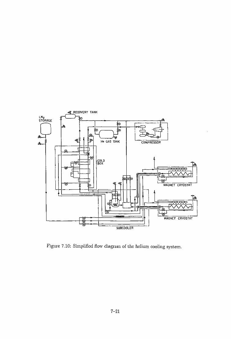
LN2STORAGE
RECOVERY TANK
<*.
E/—vrHe GAS TANK
SUBCOOLER
Figure 7.10: Simplified flow diagram of the helium cooling system.
7-21

y(mm) QC1E-L
x(mm)
PositronElectron
QC2P-R
-380 -250 V -200 -15O7 /100 x(mm)
Electron
Figure 7.11: Beam positions and beam envelopes during the injection time at the edges
of QC1E-L and QC2P-R.
Entrance aperture(e )
Exit aperture(e~)
Entrance aperture(e+)
Exit aperture(e+)
Beam separation
Beam separation
Max. field gradient
Pole length
horizontal (mm)
vertical(mm)
horizontal(mm)
vertical(mm)
horizontal (mm)
vertical(mm)
horizontal(mm)
vertical(mm)
entrance(mm)
exit (mm)
(T/m)
(m)
QC1E-L
37.66
33.62
29.04
32.99
43.85
22.8
34.96
23.77
130.14
100.42
15.4
0.6
QC2E-L
114.7
18.5
106.7
20.4
50.9
33.9
53.1
30.8
339.0
302.0
6.1
1.0
QC1E-R
38.47
39.85
47.27
40.43
48.1
24.5
56.95
23.51
112.2
132.2
12.6
0.6
QC2E-R
99.5
30.4
105.2
29.8
61.5
29.2
66.2
26.7
254.8
283.0
10.2
0.6
Table 7.11: Specification of the IR quads for HER.
7-22

Entrance aperture(e )
Exit aperture(e~)
Entrance aperture(e+)
Exit Apertuve(e+)
Beam separation
Beam separation
Max.. field gradient
Pole length
horizontal(mm)
vertical(mm)
horizontal(mm)
vertical(mm)
horizontal (mm)
vertical(mm)
horizontal(mm)
vertical(mm)
entrance (mm)
exit (mm)
(T/m)
(m)
QC2P-L
52.99
30.69
64.51
28.48
55.7
21.52
59.37
22.19
170.0
200.0
7.3
0.6
QC2P-R
63.3
37.4
83.4
33.5
68.8
22.2
72.4
23.4
172.2
218.2
4.1
1.0
Table 7.12: Specifications of the IR quads for LER.
The beam emittance envelope of ex = 1.4 x 10~5m and ey = 1.4 x 10~6m is assumed for
the beam during the injection time. The beam line has been designed to create a suffi-
cient beam separation within those magnets, so that magnets with realistic engineering
design can be built. Five of these magnets will be built as full quadrupole magnets.
They have to have non-standard shapes in which a field free space is embedded for the
beam of the other ring. Due to the limited beam separation, one of them, QC1E-R,
will have to be a half quadrupole magnet.
Although a large region with good field quality must be created, in the region for
the other beam ("spectator beam") the field strength must be minimized. This has to
be achieved while the beam separation is only marginal. For example, the free space
thickness for QC1E-L an.' QC2P-R is merely 30 ~ 40 mm. Consequently, the thickness
of the conductor in between must be minimized. The conductor shape resembles that of
a septum magnet. Therefore, QClE-L and QC2P-R will have very high current density
in the conductors. The field distribution in those magnets have been calculated using
the computer code Poisson. The cross section shapes of QC2E-L, QC2P-R, QClE-L
and QC1E-R have been determined, as shown in Figure 7.12.
The magnet that has the highest current density in the coil is QClE-L; the overall
current density of its "septum conductor" is about 56 A/mm2. Although not trivial,
it is considered to be possible to cool the conductor by minimizing the length of the
cooling circuit. It is considered relatively easy to build QC2E-R and QC2P-L, because
7-23

_200—4. 26i_754—125-4—125-J—135—
QC1E-L
i QC1E-RI
-400- .. .
~f8| J
1
1QC2P-R
QC2E-L
Figure 7.12: Cross section shapes of some of the special IR quadrupole magnets.
7-24

1600
1560
1560
1540
QC1E-L
642
641
640
639
638
•
' 1 |
• Fl
i . . . i
aid Gtad onl (Gaus
. . . .
r •
s/onH
. . .
•
•
. . . . . . . . .
0 0 5 1 1.5 2 2.5 3 3.5
i(cm)
QC2E-L
„»•••••'
Raid Grad
i , , .
• • • • • • •
enl (Gauss/
• i
j n ) |
•• ;
. L
1300
1290
1280
1270
1260
1250
• •
QC1E.R (aux p.8.=700A)
j • Field gradient (Gauss/cm) |
. . .
434
I 432
! 43°
1 428
426
QC2P-R
Field Groldlonl (Gausi'cm)
0 1 2 3 4 5 6 7
• (cm)
Figure 7.13: Calculated distributions of the field gradient of the IP quads.
the free space between two beam areas is much larger. Since the field distribution
near the pole edge is also affected by the position of the conductor, it is important
to mechanically firmly fix the "septum conductor" against its thermal expansion and
magnetic forces.
As for the half quad (QC1E-R), the field distribution near the iron septum is de-
termined by a delicate relation between the magnetic resistance of the flux circuits. To
make corrections for possible errors, trim coils will be attached to the iron septum.
The calculated field gradient distributions of QC2E-L, QC2P-R, QCIE-L and QC1E-
R are shown in Figure 7.13. If a further reduction of the field gradient near the aperture
boundary is proved necessary, this can be done, to some extent, by adding end-shims.
Because of the lack of 90-degree rotation symmetry, this magnet geometry is prone
to produce sextupole and octapole fields due to errors. If these multipole components
are found to be larger than the tolerance, a magnet geometry with a 90-degree rota-
tion symmetry may have to be implemented. Investigations of these possibilities will
be made in the near future, before freezing the final design of these magnets. The
parameters of four of six IR special quads are listed in Table 7.13.
7-25

Aperture radius (mm)
Pole length(m)
Max. field gradient (T/m)
Current(AT)Current density of
the septum conductor(A/mm2)
Field in the area for
counter-circulating beam
(with magnetic shield) (Gauss)
QC1E-L
38
0.6
15.6
9000
56
0 ~ - l
QC1E-R
70
0.6
12.7
27000
6.8
0 ~ - 2
QC2E-L
80
1.06.4
16500
4.6
2 ~ -0.6
QC2P-R
45
1.0
4.3
3500
22
0 ~ - l
Table 7.13: Parameters of QClE-L, QC1E-R, QC2E-L and QC2P-R.
7.6 Installation and Magnet Support for IR
The magnets which will be placed in the Tsukuba experimental hall (IR hall) are
superconducting magnets in the QCS solenoids, QC1E, QC2E and QC2P magnets.
The support structure of the QCS cryostat is illustrated in Figure 7.14. The QCS
cryostats are supported from a movable stage. This movable stage serves as a common
support base for other accelerator magnets (QC1 and QC2 for both the LER and HER)
located in the IR hall.
The movable stage can move along the beam line by approximately 4 m. The QCS
magnets can be pulled out and pushed in with this motion. The alignment position and
angle of the QCS cryostats can be adjusted by a mechanism installed on the support
base. The relative positions between the cryostat and the endcap calorimeters are
monitored by four units of a position measurement device called "holo-gauge." These
gauges have been tested to be operational in a high magnetic field up to 1 T with
radiation dose up to 10 krad.
In order to prevent vibration of the QCS head during an earthquake, movement
of the cryostat body is limited by four support bars which are stretched radially from
the support rails of the endcap calorimeter. When the QCS cryostat or the endcap
calorimeter needs to be moved, the support bars are mechanically moved, and its
connection to the cryostat is loosened. This allows the cryostats to slip off the support
bars. When the cryostat is to be stationed in the operational location, the cryostat
body is latched to the support bars.
To align the left and right QCS magnets, hair cross targets are installed on the
7-26
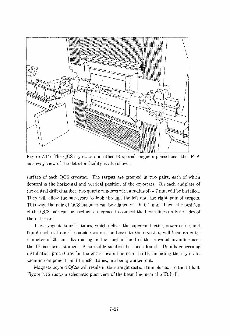
Figure 7.14: The QCS cryostats and other IR special magnets placed near the IP. A
cut-away view of the detector facility is also shown.
surface of each QCS cryostat. The targets are grouped in two pairs, each of which
determine the horizontal and vertical position of the cryostats. On each endplate of
the central drift chamber, two quartz windows with a radius of ~ 7 mm will be installed.
They will allow the surveyors to look through the left and the right pair of targets.
This way, the pair of QCS magnets can be aligned within 0.1 mm. Then, the position
of the QCS pair can be used as a reference to connect the beam lines on both sides of
the detector.
The cryogenic transfer tubes, which deliver the superconducting power cables and
liquid coolant from the outside connection boxes to the cryostat, will have an outer
diameter of 26 cm. Its routing in the neighborhood of the crowded beamline near
the IP has been studied. A workable solution has been found. Details concerning
installation procedures for the entire beam line near the IP, including the cryostats,
vacuum components and transfer tubes, are being worked out.
Magnets beyond QC2s will reside in the straight section tunnels next to the IR, hall.
Figure 7.15 shows a schematic plan view of the beam line near the IR, hall.
7-27

Tunnel area to be occupiedby the cable rack andcooling water piping
Positron Concrete Wallfor the tunnel
BelleDetector
Electron
Electron
| Tsukuba ExperimentalHall !
Positron
10m
Figure 7.15: Schematic plan view of the beam line near the IR hall. The LER, and
HER. beams collide at the interaction point within the detector facility, called "Belle."
The concrete walls for the tunnels are included. The beam line components are not
allowed to extend into the tunnel area that will be occupied by the cable rack and
cooling water piping. The allowed boundary is indicated by broken lines.
7.7 Beam Background
7.7.1 General
Since a finite crossing angle scheme is adopted, and separation bend magnets will no
longer be used, the conditions to consider the background issues have become much
more relaxed than the past case which is described was the detector reference design
in 1994 [1] [2]. Still, much detailed simulation work is required before freezing the
final design of the masking system. This section briefly outlines the strategies used for
handling synchrotron radiation (SR.) and the particle background near the IP.
A high precision c^arr^d particle tracking device with silicon micro-strips will be
installed, surrounding the IP. The requirement on the momentum resolution of the
tracking system calls for using a cylindrical beam pipe with an inner diameter of
40 mm for —80 < z < +80 mm. This beam pipe will be made of a double-wall
beryllium structure for efficient cooling with a minimum amount, of material. At, the
edge of this beryllium central vacuum pipe, Mask-A will be implemented so that the
Be pipe is shielded from back-scattered photons. The arrangement of the beryllium
pipe and Mask-A are illustrated in Figure 7.16. Mask-A and vacuum chambers outside
will be made of copper.
7-28

Beam Pipe and Mask100
-100
I
t I \ I 1 I
Mask-B Cryostai
- l 0 1
Length (m)
Figure 7.16: Arrangement of the central beam pipe at the IP and horizontal masks
7.7.2 Synchrotron radiation
The SR from bunch particles going through QCS and QCl are required not to directly
hit the Be pipe and Mask-A. The geometry of the magnet layout in the IR and their
excitations have been chosen so that this requirement is satisfied. Calculations have
shown that if the fractional particle population beyond 10ax and 30cry is kept below
10~°, the SR background should have no significant harmful effects for data acquisition
and analysis. Simulations of bunch tail development indicate that this condition will
be met.
Some of the photons from upstream magnets QC2 and QC3 can hit Mask-A. Since
those photons will have a critical energy below 2 keV, they can be easily absorbed by
heavy metal. The masks and the inner surface of vacuum chambers will be gold-plated
for this purpose. Photons from far upstream magnets away from the IP should be
intercepted by movable masks installed just upstream of QC3. The design of these
movable masks will soon be started.
7-29

7.7.3 Particle background
The particle background is, again, expected to be less severe than in the case of the
past reference design. In the presence of separation bend magnets, the low-momentum
charged particles could be easily swept into the detector. This is no longer the case with
the finite-angle crossing scheme. However, the particle background can be potentially
more serious than the SR background.
Calculations by the computer code Decay Turtle have been done. It has been
found that the rate of spent particles from the two beams to directly hit the beam pipe
between the two cryostats is 130 kHz, when the vacuum pressure is 10~9 torr. (This
rate is a factor of three smaller than that for the past reference design.)
According to the simulation, the vacuum pressure outside QC2 is more important
than that inside the detector, where the pumping speed is limited by the beam pipe
aperture. The best efforts will be made to implement efficient pumping systems near
QC2 magnets. The design goal for the vacuum level in the region outside QC2 is
1CT10 torr.
Mask-B (shown in Figure 7.16) will be installed outside of the beam pipe to reduce
the particle background. Movable masks should be installed in the arcs and the non-IR
straight sections to clip the beam tails. They will help reduce the radiation level at the
detector facility during the injection time. Detailed design work of these mask systems
will start soon.
7-30

Bibliography
[1] The BELLE Collaboration, KEK Report 94-2, 1995. p. 58.
[2] BELLE Collaboration, Technical Design Report, KEK Report 95-1, 1995.
7-31

Chapter 8
RF System
In this chapter we describe the RF hardware components for KEKB. RF stations will
be located in three straight sections, called Oho, Fuji, and Nikko (see, Figure 8.1). It
has been recommended from simulations regarding the ring dynamic aperture that the
RF cavities for the LER should be located at the Fuji straight section which is opposite
to the Tsukuba interaction region. The RF stations for the HER will be located in the
Oho and Nikko straight sections.
A block diagram of each RF unit for the ARES cavities is shown in Figure 8.2.
A 508 MHz 1MW CW klystron will feed the power to two ARES normal-conducting
cavities or one superconducting cavity. Best efforts will be made to use the existing
infrastructures and facilities in the TRISTAN accelerator to minimize the construction
cost. In particular, the existing klystrons, together with the power supply systems
and the cooling systems for the klystrons, wave guide components, magic tees and
circulators will be re-used in KEKB. In addition, a 6kW large refrigerator system,
which has been operated for the superconducting cavities in TRISTAN, can be re-
used.
Extensive R&D work is in progress on both the ARES and the superconducting
cavity. Coupled-bunch instabilities arising irom the accelerating mode and the higher
order modes are expected to be sufficiently suppressed, as discussed in chapter 4.
In the following, detailed descriptions of the ARES and the superconducting cavity
are given in section 8.1 and section 8.2, respectively. Section 8.3 treats the issues
related to the RF low level system, including the effect of a bunch gap and the R&D
work of an RF cavity feedback system. Section 8.4 discusses a crab cavity for the crab
crossing, which will be implemented as a fall •'. •: ~k solution to the problems encountered
with the finite angle crossing scheme.
8-1

TSUKUBA
OHO
Figure 8.1: Schematic plan view layout of KEKB.
station start upphase phase
Mystronpower supply - | (another ARES) | -
L J
I"i ^
Figure 8.2: Block diagram of one RF unit with the ARES cavities.
8-2

8.1 Normal Conducting Cavity
8.1.1 ARES scheme
The accelerator resonantly coupled with an energy storage (ARES) [1] is expected to
break through the difficulties concerning the coupled-bunch instabilities arising from
the accelerating mode. As shown in Figure 8.3, it has an energy storage cavity coupled
with an accelerating cavity via a coupling cavity. As discussed in chapter 4, owing to
a large stored energy in the storage cavity, the detuning frequency is reduced and the
instability is sufficiently suppressed.
The reason why the coupling cavity is implemented is explained in the following.
The original scheme of employing an energy storage cavity was proposed by T. Shin-
take [2], where no coupling cavity is used. However, this scheme has a couple of
problems. The first one is an instability arising from a parasitic mode which exists
near the accelerating mode. When the accelerating cavity is coupled with the energy
storage cavity, the accelerating mode splits into two eigenmodes. One is called the 0
Figure 8.3: Schematic view of ARES.
8-3

mode, and the other the n mode, according to the phase difference between the two
cavities. For example, the 0 mode becomes the parasitic mode when the IT mode is
employed for beam acceleration. The coupling impedance of the parasitic mode has the
same order of magnitude as that of the accelerating mode. Therefore, the growth rate
of the instability will be as large as that due to the accelerating mode of a conventional
single-cell cavity. The second problem is that the field amplitude and phase of the ?r
mode is unstable against heavy beam loading.
By employing a coupling cavity in the ARES, these difficulties in using an energy
storage cavity can be successfully solved. Since the ARES has three resonators, the
accelerating mode splits into three eigenmodes: the 0 mode, the TT/2 mode, and the
7T mode. The ARES scheme has the following advantages over the former coupled-
cavity system where an accelerating cavity is directly coupled with a storage cavity.
First, the operating mode of the ARES is the n/2 mode, which has excellent field
stability against the heavy beam loading. Second, the ratio of the stored energy in the
storage cavity relative to that in the accelerating cavity can be adjusted by changing
the relative strength of the coupling factor between the storage and coupling cavities
vs. that between the accelerating and coupling cavities. Third, the ?r/2 mode has
almost no field excitation in the coupling cavity. Therefore, the two parasitic modes
(the 0 and ir modes) can be selectively damped by installing a coupler in the coupling
cavity, while the ir/2 mode is not affected. Finally, the 0 and n modes are located
nearly symmetrically with respect to the ?r/2 mode. Therefore, the contributions of
the impedance of the damped parasitic modes to the instability are expected to be
counter-balanced to some extent.
The basic design of the ARES was carried out on the basis of a three-dimensional
analysis of the RF properties [3] by using the computer code MAFIA.
Storage Cavity
As the storage cavity, we chose a cylindrical cavity operating in the TE015 mode, which
is the same mode employed in the SLED [4]. For an RF frequency of 509 MHz, the
dimensions of the storage cavity are about 1100 mm in diameter and about 2000 mm
in axial length. Assuming the standard value of copper conductivity, the Q value of
the TE015 mode is estimated to be 2.6 x 10⁵, which is sufficiently high to store a large
amount of the field energy with a low wall power dissipation.
Since the storage cavity has many parasitic modes in the vicinity of the TE015
mode, the perturbation of opening a slot to the coupling cavity easily mixes parasitic
modes into the TE015 mode. Mixing with a low-Q mode would deteriorate the high
Q value of the operating mode. Therefore, careful fine tuning of the cavity dimensions
8-4

coupling hole groove
Figure 8.4: Schematic view of the storage cavity.
is required to prevent parasitic mode mixing.
Figure 8.4 shows a schematic drawing of the storage cavity with a coupling slot
arranged to keep the mirror symmetry with respect to the mid-plane between the two
end plates. The circumferences of both end plates are grooved in order to remove the
degeneracy of the TE015 and TM115 modes. This method was first applied in the
SLED cavities [4]. A groove depth of 80 mm gives a sufficient mode separation of
16 MHz.
According to a precise study [3] concerning the perturbative effect of the coupling
slot, the TE015 mode should be kept away from the TEmnp(p=odd) and TMmnp(ra >
0, p=odd) modes to minimize the parasitic mode mixing. Figure 8.5 shows a mode
diagram of a cylindrical cavity without grooves at the end plates. The ratio of the radius
to the axial length was carefully chosen to obtain the best location of the TE015 mode
among the harmful parasitic modes. The frequency shift of each harmful parasitic
mode due to the groove must also be taken into account. For example, the frequency
of the TM213 mode, which is close to the TE015 mode in the mode diagram, is actually
lowered by 10 MHz due to the grooves.
Basic RF Design of the ARES
In the RF design of the ARES, we started with the most simple case, where a cylindrical
accelerating cavity is coupled with the storage cavity via a cylindrical coupling cavity.
Figure 8.6 shows a schematic view of the structure. The ratio of the axial length of
the coupling cavity to that of the accelerating cavity was chosen to be just half.
8-5

a<
N
zfauia:u.
3
5LUa:
340 ^ " /
320
300
200
260
0.2
310
320
0.25 0.3RADIUS/LENGTH
0.35
0.3RADIUS/LENGTH
Figure 8.5: Mode diagram in a pillbox cavity, (upper) all TE and TM modes, and
(lower) TEmnp (p=odd) and TMmnp (m > 0, p=odd) modes.
8-6

Iterative optimization of the structure is performed [3] using MAFIA until the
following requirements are satisfied:
1. Each cavity should be tuned to the same frequency of 508 MHz under the TT/2-
mode boundary condition. This assures that almost no field is excited in the
coupling cavity for the operating mode.
2. The stored energy in the storage cavity should be larger than that in the accel-
erating cavity by factor 10. This reduces the detuning frequency under beam
loading by an order of magnitude.
3. The 0 and IT modes should be nearly symmetrically located with respect to the
TT/2 mode. This assures counter-balancing the contributions of the 0- and 7r-mode
impedance to the coupled-bunch instability.
Each cavity frequency was tuned by changing its radius. The ratio of stored energies
was adjusted by changing the ratio of the coupling factor ks between the storage and
coupling cavities to A;a between the accelerating and coupling cavities.
The optimized dimensions of the ARES are listed in Table 8.1. The RF properties of
the operating mode are listed in Table 8.2, together with those of the parasitic modes.
Figure 8.7 shows the electromagnetic fields of the ir/2 mode. As can be seen from
the field pattern, the mixing of parasitic modes into the TE015 mode is successfully
suppressed, and almost no field is excited in the coupling cavity. Most of the field
energy is stored in the storage cavity in the form of the low-loss TE015 mode. The
R/Q value of the total ARES system is reduced by an order of magnitude compared to
that of a conventional single-cell copper cavity. This means that the required detuning
frequency is also reduced by the same magnitude. On the other hand, the Q value
of the system is increased by factor 5, compared to a copper cavity. Therefore, the
shunt impedance of the ARES is kept at a reasonable level. According to the operating
RF parameters discussed in chapter 4, the growth time of the instability due to the
accelerating mode is longer than 30 ms (LER) and than 100 ms (HER), which is
sufficiently long compared with the radiation damping time.
Figure 8.8 shows the field patterns of the parasitic modes in the vicinity of the
operating mode, including the 0 mode at 501.7 MHz and the IT mode at 512.8 MHz.
Since the coupling cavity is excited for all parasitic modes, these can be damped by
extracting the field energy through a coupler attached to the coupling cavity. The
growth time of the instability due to the damped parasitic modes has been calculated [3]
using the R/Q values in Table 8.2. Figure 8.9 shows the fastest growth time as a
function of the loaded Q value. If the loaded Q values of the parasitic modes are
8-7

Table 8.1: Dimensions of the optimized shape.
cavitiesradius (mm)
length (mm)
coupling holes
location
length (mm)
width (mm)
distance (mm)
accelerating
224.0
260.0
between a-
130.0
180.0
0.0
coupling
213.5
130.0
and c-
storage535.2
1989.4
between s- and c-
200.0
130.0
0.0
rs
Is
Figure 8.6: Schematic view of the three-cavity system.
8-8
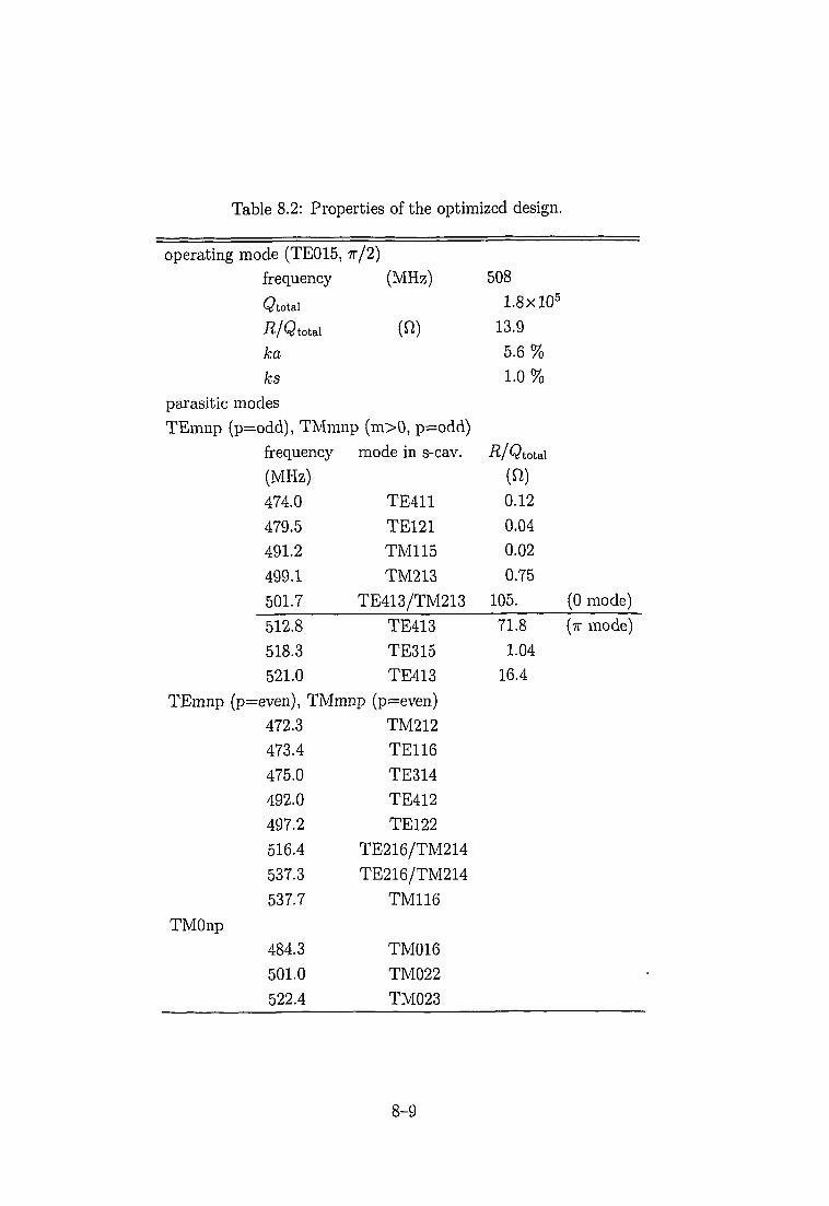
Table 8.2: Properties of the optimized design.
operating mode (TE015, TT/2)frequency
<5total
H/Qtotal
ka
ks
parasitic modes
(MHz)
(ft)
TEmnp (p=odd), TMmnp (m>0, p=odd)
frequency
(MHz)
474.0
479.5491.2
499.1
501.7
512.8
518.3
521.0
mode in s-cav.
TE411
TE121
TM115
TM213
TE413/TM213
TE413
TE315
TE413
TEmnp (p=even), TMmnp (p=even)
472.3
473.4
475.0
492.0
497.2
516.4
537.3
537.7
TMOnp484.3
501.0
522.4
TM212
TE116TE314
TE412
TE122
TE216/TM214
TE216/TM214
TM116
TM016
TM022
TM023
508
1.8xlO5
13.9
5.6%
1.0%
•ft/Qtotal
(n)0.12
0.04
0.02
0.75
105. (0 mode)
71.8 (TT mode)
1.04
16.4
8-9

Figure 8.7: Field pattern of the 7f/2 mode calculated with the MAFIA code. The
electric field (left) and the magnetic field (right) patterns are shown.
8-10

I I < I
I I I i I • t ' < I 1 1 ' •
499.1 MHz
. . , i 1 I T I M i l l 1 1 t T 1 1 1
501.7 MHz
512.8 MHz
518.3 MHz
521.0 MHz
525.2 MHz
Figure 8.8: Field patterns of the parasitic modes, with frequencies close to the operatingmode.
8-11

Coupled-Bunch Instability caused by parasitic modes
1 000
oCD(0
E0)
E
so
<5
1 00
1 0
1
•
:::::fc:::i:::?::S::j::
• : : : ;i • i i •
f . . . . ; . . „ > . . . - . . { . .
••••.-: j . . . . s — . : . . . | ~
: : : : :
^ } . . . . ; . . . . • , . - . ; . .
; : ; : :
i i i i i i
\ {
1 • <
i
i
Srowth ti
< i....;....
ne (msqc
:::::
i !
: ;: :
! !
*••••••'•;....;...
)..
1 0 1 00
Loaded Q
1 0 0 0
Figure 8.9: Fastest growth time of the coupled bunch instability caused by the parasitic
modes plotted against the damped Q value.
reduced below 100, the instability growth time becomes longer than 10 ms, where the
beam instability can be controlled by a feedback system.
Results of Cold Model Test
Two aluminum 1/5 scale cold models have been fabricated to confirm the design de-
scribed above. They are equipped with two tuners for each of the accelerating, cou-
pling and storage cavities. The resonant frequencies of the three cavities are adjusted
by these tuners to coincide with each other. There is no damping structure on the
coupling cavity of the first model. The measured Q value of the TT/2 mode is 3.3 x 10⁴,
which corresponds to 1.40 x 10⁵ for a full scale copper cavity. The effect of the surface
finish on the Q value has been estimated by measuring the Q value of a pillbox cavity
of the same material, same surface finish and same inner shape as the accelerating
cavity of the cold model ("reference pillbox"). Taking this effect into account, the
measured Q value of the n/2 mode is 0.85 times that calculated by MAFIA. The shift
of the resonant frequency of the ?r/2 mode was measured by placing a small metallic
8-12

Table 8.3: Measured parameters of the 0 and IT modes.
/ [MHz] Q R/Q [n\
0 mode
7T mode
503.4
514.9
110
150
10372
bead in the accelerating cavity to simulate the effect of detuning. The ratio of this
frequency shift to the shift obtained by the same measurement for the reference pillbox
was 0.069. This agrees well with the expected value 0.065. This means that R/Q of the
accelerating mode is reduced by a factor of about 1/14, clearly showing that detuning
of the ARES TT/2 mode is greatly reduced.
The second cold model has two coaxial lines at the center of the end plates of
the coupling cavity. The coupling cavity can be damped by connecting loads to these
coaxial lines. The cavity surface around the inner conductor of a coaxial line protrudes
into the cavity like a nose cone for concentrating the electric field and to stabilize the
mode. The transmission between a beam port and an end plate of the storage cavity
is shown in Figure 8.10: (a) the coupling cavity is not damped and (b) is damped.
The measured Q, R/Q and frequency are listed in Table 8.3. Using the parameters in
Table 8.3, the growth time of the longitudinal coupled bunch instability was calculated
to be 17 ms for 20 ARESs in LER. We have also calculated the response of the growth
(a) (b)
l c 3 ICG leg
a
3
1
R :
V
IF
17.3 zR
1aaiNG FG
1jin
A
:TCR
11
\ 1
1i,
I/A
yw1II
1
NN
\
1
]•
11
* 7?:?3BC
MRR
ptain
<ER I.33^72 qH z
n
i !
\
V
CENTER 2.5-13EC33DS
e
Figure 8.10: Transmission between beam ports: (a) coupling cavity is not damped and
(b) is damped.
8-13

time to the skewness of the passband, which is defined as
\f* ~ /olIt has been found that the growth time decreases from 35 ms to 10 ms as the skewness
increases from 0 to ~ 10%.
Mechanical Design
The accelerating and coupling cavities are made of oxygen-free copper (OFC) to handle
large power dissipation on the cavity wall. The water-cooling channels are milled out
at the outer surface of the cavity. They are covered by copper plates by means of
electron beam welding. Their configuration is carefully designed so that cooling water
does not leak into the cavity if there should be an imperfection of brazing or welding at
any connecting part. In the case of the storage cavity, the experience of the KEK APS
cavities is fully utilized, since the wall loss density is not very high. Steel is used for the
structural material, because it is of higher strength and is less expensive than copper.
Copper is electroplated on its inner surface. The side cylinder is separated to form
three parts at the nodes of the axial component of the magnetic field farthest from the
center. This allows us to electroplate the structure in a moderately-sized vessel. Two
end plates and three side cylinders are welded together. Welding deformation offers
good electrical contact.
The accelerating and coupling cavities are joined by brazing. The coupling cavity is
then bolted to the storage cavity. The two parts of ARES are transported from factory
and installed at their position in the tunnel separately, where they are eventually bolted
together. These procedures would be difficult if ARES is not detachable.
8.1.2 HOM-Damped Cavity
The HOM-damped accelerating cavity of the ARES is shown in Figure 8.11. The cavity
has a HOM-damping coaxial waveguide which is equipped with a notch filter. Monopole
and dipole HOM's excited in the cavity are coupled with the TEM and TEH waves
of the coaxial waveguide, respectively. On the other hand, the notch filter blocks the
TEM wave coupled with the accelerating mode, while passing other waves of HOM's.
RF waves passing through the filter are absorbed by microwave absorbers inserted
from the waveguide end. This damping scheme was originally proposed independently
for a crab cavity for B-factories [5] and for a damped structure for linear colliders (a
radial line is used instead of the coaxial wave guide) [6]. As the absorbers, sixteen
bullet-shape sintered SiC will be used.
8-14

Notch Filter
Figure 8.11: Schematic drawing of the KEKB HOM-damped cavity.
The cavity that is loaded with a coaxial waveguide is axially symmetric. This design
has the following advantages:
• No concentration of wall currents of the accelerating mode assures good perfor-
mance under high power operation.
• The main cavity parts can be precisely machined by using a turning lathe.
• Precise electromagnetic and thermal-structural analyses are possible by using
only two-dimensional codes.
The first prototype to verify the performance in high power operation is under construc-
tion. A verification for high-current beam handling at the TRISTAN accumulation ring
is scheduled in 1996.
Design
The gap dimensions of the notch filter and the coaxial waveguide have been carefully
determined so as to avoid multipactoring discharges at the accelerating frequency. The
S parameters of the notch filter have been calculated using the computer code HFSS
(High Frequency Structure Simulator) [7]. Figure 8.12 shows the frequency responses
8-15

1 _
0.8 -
0.6 -
0.4 -
0.2 -
• • • • 1 ' • * * * '
/
>
7/Woi cuto
:utoff i
• • - ^
\ -
i i
0.5 1 1.5
frequency /GHz
Figure 8.12: Frequency response of S21 of the notch filter.
of 5*21 (transmission) for TEM waves. The first stop frequency for TEM waves can
be precisely tuned to the accelerating frequency 508.9 MHz by lathe-machining of the
bump at the bottom of the filter structure. The TEM second stop frequency is raised
to 1.67 GHz from 1.39 GHz by deforming the outer volume of the filter. The first and
second stop frequencies for TEl l waves are 0.53 GHz and 1.68 GHz, respectively. Near
the TEM and TEl l second stop frequencies, some HOM's may be trapped within the
cavity. To avoid this problem, the beam bore diameter was increased to 145 mm. This
lowers the TMOl and TEl l cutoff frequencies as indicated by the arrows in Figure 8.12.
R F Propert ies of the Accelerating Mode
The filter position along the waveguide affects the HOM-damping properties as well as
the shunt impedance of the accelerating mode.
First, we examine the RF properties of the accelerating mode. Let us define the
filter position along the waveguide by /, which is the distance between surfaces A and
F, as shown in Figure 8.11. Let us also represent the stored energy and power dissi-
pation in the cavity (the left side of surface A) by Ua and Pa, and those in the notch
filter by Uf and Pj. Figure 8.13 shows the ratio Pj/Pa as a function of I, together
with the response of the shunt impedance. They have been calculated using the pro-
gram SUPERFISH. The notch filter functions as a quarter-wavelength resonator at
the accelerating frequency. When the total electrical length from the waveguide aper-
8-16

6.5
6 -
a 5-5
DC5 -
4.5 -
• — • —
• 4\
\\
'. J
R /MOhi
>
• *
J
n
\
Pf/Pa ;
* :
//
0.1
- 0.095
~ 0.09
0.085
- 0.08
60 80 100 120 140 160
I/mm
0.075
Figure 8.13: Ratio Pj/Pa and the shunt impedance are plotted as a function of /.
Table 8.4: RF parameters of the accelerating mode.
/ = 508.6 MHz Ve = 0.6 MV Pc = 70 KWW
R/Q = 150Q Q = 3.3 x 10⁴'*) R = 5.0 Mf2
(*) a degradation of ~ 5% due to copper surface imperfections is taken into account.
ture (surface A) to the top end of the filter (surface T) is close to a half wavelength
(/ = 110 mm in Figure 8.13), the electrically-short boundary at surface T is mapped
onto surface A, and the ratio Uj/Ua{also,Pf/Pa) becomes minimum. However, this
is not a necessary condition in designing the choke mode cavity. For optimizing the
efficiency of beam acceleration, a shorter coaxial waveguide between A and F is desir-
able. Figure 8.13 shows that the shunt impedance increases as I becomes smaller. The
waveguide length I was determined to be 120 mm. This gives better HOM damping
properties at little sacrifice of the shunt impedance of the accelerating mode. Table 8.4
is a set of cavity parameters for the case when I = 120 mm.
HOM Damping Properties
The distance / also changes the HOM damping properties of the choke mode cavity
8-17

Table 8.5: Ring parameters used in to calculate the growth time of the coupled bunch
instability in Figure 8.14(b).
Parameters
Beam Energy
Beam Current
RF Frequency
Number of Bunches
Momentum Compaction
Synchrotron Frequency
Number of Cavities
3.5
2.6
508.9
5120
1.5 x 10"4
1.7
20
GeV
AMHz
kHz
(a) (b)
80
70
60!•*—I
£50uI 40
s60
30
20
10
09 10 11
/[cm]12 13 14
Figure 8.14: (a) Qext and (b) growth time of the coupled bunch instability as a function
of the length between the cavity and notch filter /.
through Qext. Figure 8.14(a) shows the values of Qext as a function of I. The time
domain method with MAFIA [8] was used in the calculation. For TMOll and TM110
modes, the time domain method was not applicable for larger I because of unwanted
excitation of nearby modes in the calculation. The value of I around 12 cm provides a
small Qext for the modes other than TM020. The TM020 mode needs not be damped
like the TMOll mode, since R/Q of the TM020 mode is much smaller than that of the
TMOll mode.
We also calculated the growth time of a coupled bunch instability as a function of I
8-18

Table 8.6: HOM impedance of the accelerating cavity of the ARES.
monopole
/(MHz)76.2
190
662.6
731.7
821.8
925.2
1331.9
1389.5
dipole
/(MHz)275.4
67.0.0766.2
826.7
905.8
986.8
1067.5
R/Q(V)17.4
4.5
2.8
11.0
7.9
3.83.2
3.1
R/Q (fi/m)
50.7
16.6
167
113
109
210
68.1
QL
71.5
24.5
25.4
35.7
22.7
16.6
28.7
27.8
QL
63.4
37.1
50.9
30.4
20.5
23.2
10.4
(R/Q) x QL (ft)1243
10972.2
394
180
62.4
90.7
86.4
(R/Q) x QL (kQ/rn)
3.21
0.62
8.51
3.43
2.23
4.85
0.70
by using the formulae of Sacherer [9]. The modes which are trapped in the notch filter
or coaxial line have to be taken into account. The eigenmodes were calculated with the
MAFIA 2D eigenmode solver. As an approximation, the absorbers were modelled by
an axially symmetric structure. The permittivity was assumed to be 7, which is about
half the measured value of some sample blocks of SiC [10]. This is to compensate for
the packing factor of the bullet-shaped SiC. The Q value and shunt impedance have
been calculated in the MAFIA postprocessor assuming that tan 6 of the absorber was
0.3. Then, the calculated frequencies, impedance and Q values were substituted in the
formulae of Sacherer with the ring parameters shown in Table 8.5. The results are
plotted in Figure 8.14(b). It shows that / = 12 ~ 13cm is a good choice for /. This
is consistent with the time domain Qext calculation. The growth time will be then
~ 70 ms for the longitudinal instability and ~ 30 ms for the transverse. The R/Q and
Q values with this design are summarized in Table 8.6. However, we must be careful
8-19

about this value, because the Q calculation in the MAFIA postprocessor is based on
the eigenmode that assumes no loss in the absorber.
Mechanical Design
The cavity parts, whose inner surfaces must withstand the heat due to wall currents of
the accelerating mode, are made of oxygen-free copper (OFC). The coaxial waveguide
parts are made of stainless steel to reinforce the entire cavity structure. Vacuum furnace
brazing and electron-beam welding techniques are employed to assemble the parts. For
I ho prototype cavity at 70-kW wall dissipation, thermal and thermal-stress analyses
have been carried out using the finite element analysis program ANSYS. Figure 8.15
shows the temperature contour over the model based on the thermal analysis. The
boundary conditions are as follows: on the surfaces of the cooling-water channels, the
temperature is fixed at 30 °C. The outside surfaces of the cavity are thermally insulated
to the air.
In Figure 8.15, there are two points with the maximum temperature rise: one is at
the tip of the right nosecone; the other around the corner of the waveguide aperture.
A maximum temperature rise less than 30 °C is acceptable. Therefore, the prototype
cavity will be capable of stable continuous operation at the design value of the wall
dissipation.
DEC 5, 19930 :45 :48
NODAL SOLUTIONSTEP=1SUB =1TIME=1TEMPTEPC=.224144SMN =303. 345SMX =327.122
303.345305.987308.629311.271313.913316.555319.197321.838324.48327.122
L_J
Figure 8.15: Temperature contour over the model resulting from the thermal analysis.
8-20
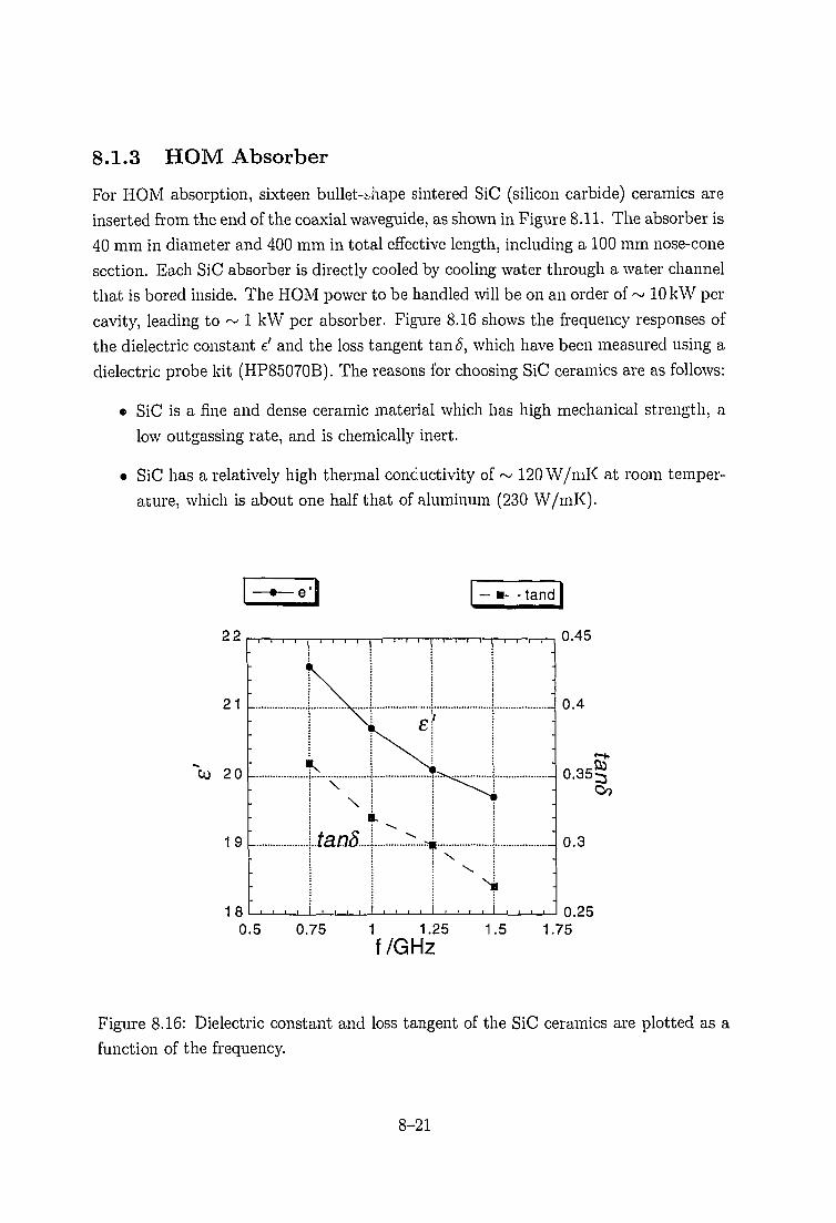
8.1.3 HOM Absorber
For HOM absorption, sixteen bullet-i-hape sintered SiC (silicon carbide) ceramics are
inserted from the end of the coaxial waveguide, as shown in Figure 8.11. The absorber is
40 mm in diameter and 400 mm in total effective length, including a 100 mm nose-cone
section. Each SiC absorber is directly cooled by cooling water through a water channel
that is bored inside. The HOM power to be handled will be on an order of ~ 10 kW per
cavity, leading to ~ 1 kW per absorber. Figure 8.16 shows the frequency responses of
the dielectric constant e' and the loss tangent tan 8, which have been measured using a
dielectric probe kit (HP85070B). The reasons for choosing SiC ceramics are as follows:
• SiC is a fine and dense ceramic material which has high mechanical strength, a
low outgassing rate, and is chemically inert.
• SiC has a relatively high thermal conductivity of ~ 120 W/mK at room temper-
ature, which is about one half that of aluminum (230 W/mK).
- •- -tand
22
21
CO 2 0
19
^ ' ' ' I ' ' ' ' \ ' ' " ^0.45
0.4
0.35§Oo
0.3
1 8 I M M I U M I i I i • i i I 0.25
0.5 0.75 1 1.25 1.5 1.75
f/GHz
Figure 8.16: Dielectric constant and loss tangent of the SiC ceramics are plotted as a
function of the frequency.
8-21

• At the 2.5-GeV electron linac of KEK, nearly two hundred SiC absorbers (diam-
eter = 24 mm, length = 300 mm) have been used for the S-band waveguide loads
without any trouble for about ten years. A prototype of the S-band SiC absorber
has been tested up to a peak power of 10 MW with a pulse width of 3.5 isec at
50Hz, corresponding to an average power of 1.75 kW [11].
Among these reasons, the third one encouraged us most to use SiC ceramics. A proto-
type of the SiC absorber for the KEKB cavity was fabricated to verify its performance
in a vacuum environment. Figure 8.17 shows the layout of the high power test. The
prototype absorber was inserted from the end of an L-band rectangular waveguide
(WR650), where the standing-wave ratio VSWR was measured to be ~ 1.1. A metal
O-ring was used for the vacuum seal between the SiC ceramics and the SUS flange.
The vacuum pressure was about 10~9 ~ 10~8 Torr. The high power test was carried
out using a pulsed klystron (/ = 1296 MHz) up to a peak power of 105 kW with a
pulse width 538 fisec at 50 Hz, which corresponds to a average power of ~2.8 kW.
The prototype SiC absorber functioned normally without any vacuum, thermal, or
discharge problems. The outgass rate of the SiC ceramics was also measured using a
cylindrical sample (diameter = 50 mm, height = 50 mm). After baking for 24 hours
at 150°C, the outgass rate at room temperature was 3 x 10~12 Torr-//s-cm2.
RF POWERFROM KLYSTRON
VIEWINGPORT
PILLBOX TYPERF WINDOW
WR650 WAVEGUIDE
SiC ABSORBER
MASSFILTER
METALO-RING COOLING
WATER
$40 mm
VIEWINGPORT
400 mm
Figure 8.17: Layout of the high power test.
8-22

METAL O-RING SEAL
SUS FLANGE
Figure 8.18: Prototype of the SiC absorber using a metal O-ring for vacuum sealing.
SiC ABSORBER
BRAZING JOINT
SUS FLANGE
Figure 8.19: Next prototype of the SiC absorber using a brazing joint. The SiC ceramicsis directly brazed to the copper sleeve.
For the second prototype cavity, we are planning to braze a thin copper sleeve to
an SiC ceramic absorber for vacuum tightness. Figures 8.18 and 8.19 show an SiC
absorber structure that uses a metal O-ring seal and another that uses a brazing joint,
respectively. For both structures, a series of heat-cycle tests will be carried out, which
simulates the baking processes, in order to study the reliability of the vacuum tightness
during long term operation.
8-23

8.1.4 Input Coupler
Requirements
The most important parameters for the coupler are the transmitted RF power and its
frequency. At the present stage the cavity for KEKB requires ~ 400 kW (CW) RF
power at 508.9 MHz. In order to maintain stable operation at ~ 400 kW, the coupler
is required to be able to transmit the RF power that is much larger than ~ 400 kW.
We have thus set the target value of the transmitted RF power to be ~ 800 kW (CW)
that is twice the required power.
The requirements for the mechanical structures are as follows:
1. The RF power is fed from a klystron through the WR1500 rectangular waveguide.
2. The coupler couples with the cavity by a loop (magnetic) coupling.
3. The size of the coupler port of the cavity is designed for the WX77D coaxial
waveguide.
4. The ceramic window must be shielded from the beam and the cavity surface. This
is to reduce direct irradiation by the x-rays and charged particles produced by
collisions between the beam, field-emitted electrons, sputtered ions and residual
gases and to avoid the adsorption of Cu evaporated from the cavity wall.
5. The coupler matches the APS cavity in TRISTAN, because the coupler of the
APS will be used for the first beam test of the cavity.
The coupler has several transitions. Every transition is designed so that the its
VSWR is less than 1.05 and that of the coupler assembled with the transitions is less
than 1.1 at 509 MHz.
Design Status
The design of the input coupler is based on the structure of the output coupler of the
UHF klystron for TRISTAN. The first design for the RF structure was completed by
using the computer simulation code HFSS. The mechanical design is in progress. The
RF properties of the coupler will be measured by a low-power model so as to confirm
the simulated results. A high-power test for the coupler is planned for the summer os
1995 with an RF power up to 800 kW (CW).
8-24

Choice of Window Structure
Many problems with the coupler are related to multipactoring on the window. Several
experiments and analyses of the ceramic window in couplers suggest the following [12,
13]: the uniformity of the electric field distribution around the window is very important
for preventing the local heating of the ceramic induced by multipactor; the multipactor
induced by an electric field that is perpendicular to the window causes the damage
on the surface, while the multipactor induced by the parallel field causes no serious
problem.
Two types of ceramic windows are in use for the coupler at KEK. One is a
cylindrical-type ceramic window that has been used in the APS cavity. It was tested
at up to 300 kW (CW) RF-power [14]. The other is a disk-type ceramic window that
has been adopted for the UHF (508 MHz) klystron. It transmits 1.2 MW (CW) RF-
power [12]. Since our target value for the transmitted RF-power is 1MW (CW), we
chose the disk-type ceramic as the window for the coupler.
The disk-type ceramic window is contained in a coaxial waveguide. The waveg-
uide near the window has an impedance matching section, because the permittivity of
ceramic is about nine.
One of the typical matching sections is a choke-type structure. The output coupler
of the klystron and the input coupler of the superconducting cavity (SCC) of the
TRISTAN have the choke structure. (Recently a high-power test of the SCC coupler
was successfully performed up to an RF power of 800 kW (CW) [15].)
An over- and under-cutting (OUC) is another structure for the matching section.
This structure is in use for the couplers of the high-power models of the RFQ [16] linac
and DTL [17, 18] for the Japanese Hadron Project (JHP). For the RFQ the coupler
transmits an RF pulse that is 300 kW peak, with 300 isec duration at 50 Hz. The
transmitted RF pulse for the DTL coupler is 150 kW peak, with GOO sec duration at
50 Hz.
Two types of couplers with choke or OUC structures will be made for the high-power
test.
Design
The coupler consists of three transition sections:
1. The door-knob transition between the WX152D coaxial wave guide and the
WR1500 rectangular wave guide;
2. The disk-type ceramic window in the WX152D waveguide;
8-25
3. The transformer between the coaxial wave guide of the WX77D and that of the
WX152D.
The door-knob transition with a capacitive iris has a wider band width. A schematic
view of the transition is shown in Figure 8.20. The calculated VSWR is shown in
Figure 8.21.
The choke and OUC structures of the window are shown in Figures 8.22 and 8.23.
Both figures include the transition from the WX152D coaxial waveguide to the WX77D
coaxial waveguide. The waveguide has bumps for window shields. The VSWRs of the
transitions with the window are plotted in Figure 8.24. Figure 8.25 shows the radial
dependence of the electric field strength at a location 1 mm away from the window
surface. The value of the ordinate is normalized to the field strength on the surface of
the inner cylinder of the WX152D coaxial waveguide. This plot shows: (1) that the
uniformity of the field strength of the OUC structure is better than that of the choke-
type structure; (2) that the electric field strength of the choke-type structure is about
70% of the OUC structure near the inner triple junction of the window. Figures 8.26
and 8.27 show the electric field lines when the maximum electric field is at the center
of the ceramic. These show that the direction of the electric field is almost parallel to
the window for the OUC structure, while for the choke structure the lines concentrate
in the tip of the choke.
The window is 5/8A away from the detuned short plane (DSP). The DSP of the
coupler is located about 55 mm inside the cavity wall.
8-26

Teflon support
WR1500
Door-knob
Figure 8.20: Schematic view of the door-knob transition.
CO
1.5
1.4
1.3
1.2
1.1
1.0
\\
i
• HFSS simulation)
V /480 490 500 510 520 530
MHzfrequency
Figure 8.21: Calculated VSWR of the door-knob transition.
8-27

WX77D
WX152D
Ceramic window
Figure 8.22: Choke structure of the ceramic window with the transition between thecoaxial waveguides.
WX77D
WXJ52D
Ceramic window
Figure 8.23: Over- and under-cut (OUC) structure of the ceramic window with thetransition between the coaxial waveguides.
8-28

HFSS simulation data
crW
1.2
1.1
1.0
G
•
I I I I|
— • — with the OUC structure 1- - e - - w i t h the choke structur^
-
__———--o—__•
440 460 480 500 520 540 560
frequency M H z
Figure 8.24: Calculated VSWR of the choke and OUC structures with the transition
between the coaxial waveguides.
2.0
1.5
1.0
0.5
/El on the caramic window
o.o
1 1/ 11 11 11 \1 11 11 \
1 11 1
\
N
Choke struGturelOUC structure |
x"
0 20 40 60 80 100
Radius mm
Figure 8.25: Asolute strength of the electric field. (Simulation) The abscissa is the
radial direction of the window. See the text for the unit of the ordinate. The solid line
is the OUC structure data and the dotted one is the data of the choke structure.
8-29

Outer cylinder of WX152D
Inner cylinder of WX152D
Figure 8.26: Line of the electric force for the choke structure. (Simulation)
Outer cylinder of WX152D
Inner cylinder of WX152D
Figure 8.27: Line of the electric force for the OUC structure. (Simulation)
8-30

8.1.5 Summary
The ARES structure, where an accelerating cavity is resonantly coupled with a low-loss
energy storage cavity, is expected to be a breakthrough for high-current, low-emittance
beam accelerators such as KEKB. The results of 1/5-scale ARES model cavities are
very encouraging. The fabrication of a full-scale storage cavity model, operating in the
TE013 mode, is under way.
In parallel with the development of the ARES structure, the first prototype of the
accelerating cavity, which will be employed as a part of the ARES scheme, is currently
being fabricated in order to verify its performance in high power operation. The cavity
has a coaxial waveguide with a notch filter to block the TEM wave of the accelerating
frequency while passing other waves of HOM's to the load.
As the HOM load, sixteen bullet-shape sintered SiC absorbers will be used. SiC is
a fine and dense material with high mechanical strength and relatively high thermal
conductivity. It has been experimentally shown that a single SiC absorber can handle
an average RF power of 2 kW, and that the outgass rate is as low as those of such
metals as copper and stainless steel.
The RF window is another key issue. Two types of coaxial RF windows that can
transmit CW RF power of 500 kW have been designed. Cold models of both types
are currently being fabricated, and a series of high-power tests are scheduled for the
summer of 1995.
8-31

8.2 Superconducting Cavity
8.2.1 Introduction
At KEK the superconducting (SC) RF system for the TRISTAN Main Ring has been
successfully operated since 1988. On the basis of extensive experience in its construc-
tion and operation, the application of SC cavities to KEKB have been studied.
An advantage of the SC system is that a relatively small number of cavities can
provide the required RF voltage without greatly increasing the impedance of the system
for higher order modes (HOMs). This is because of the high accelerating field in the
SC cavities. Due to recent technologies the field gradient of SC cavities can exceed 5
MV/m in large-scale applications. It is higher than typical normal conducting cavities
by a factor of 3 ~ 5. In addition, because of the high values of the unloaded Q, the
SC cavities do not require a very high R/Q. Consequently, a HOM damping system
with SC cavities will be less complicated than normal-conducting cavity systems.
Another advantage of the SC cavity system is that it is fairly immune against the
coupled-bunch instability arising from the accelerating mode. As discussed in chapter 4,
a consistent set of operating parameters was obtained for the HER, while the growth
time is still fast in the LER. In addition, a large refrigerator that has been used for
the TRISTAN SC cavities in the Nikko straight section can be re-used in KEKB. From
these points, in the HER the SC cavity is considered to be a good candidate for the
accelerating cavities.
8.2.2 R&D Status
A preliminary design of the cavity cell structure has been completed. An aluminum
model and two niobium test cavities have been built. The HOM characteristics of the
aluminum test cavity have been measured using ferrite absorbers that are attached to
the beam pipe. Sufficient HOM damping has been observed. In vertical cold tests of
the Nb cavities, a gap voltage of 3 MV has been achieved. A bench test of TRISTAN-
style input couplers has shown that they can transmit a traveling wave RF power of
850 kW. A prototype module including these components (Figure 8.28) is currently
being prepared for a beam test at the TRISTAN Accumulation Ring. The test is
scheduled for 1996. The goal is to store a total current of 0.5 A.
Cavity Shape
A single-cell cavity design has been chosen, so as to reduce the number of HOMs as
well as to minimize the coupler power. The concept of HOM damping is based on the
8-32

B-FACTORY
SUPERCONDUCTING
CAVITY
GATE VALVE
INPUT COUPLER
Figure 8.28: A cryomodule for a SC damped cavity for beam testing at the TRISTANAccumulation Ring.
single-mode cavity idea, proposed by T.Weiland in 1983 [19]. All HOMs of a cavity
are extracted out through large beam holes towards the beam pipes. They are damped
by ferrite absorbers attached on the inner surface of the beam pipes. This scheme is
favored for the SC cavities. Even if the large beam holes reduce the R/Q somewhat,
the high impedance of the accelerating mode can be maintained, because of the high
Q value of the SC cavities.
The spherical cell shape of the cavity with large beam holes was optimized by using
computer codes, URMEL and SUPERFISH [20]. The diameter of the hole (220mm)
was chosen to maintain the desired coupling of the lowest monopole modes of TMOll
and TM020. Furthermore, a large cylindrical beam pipe (LBP) of 300 mm diameter
is connected on one side to obtain a sufficient coupling of the lowest dipole modes,
TE111 and TM110. This cylindrical geometry allows easy fabrication and surface
treatment in contrast to a grooved beam pipe [21]. The external Q of each HOM was
estimated using the tuning curve method by J. Slater [22]. The cavity parameters of
the accelerating mode are summarized in Table 8.7. The design of the cavity shape is
8-33

Table 8.7: Cavity parameters of the accelerating mode (by SUPERFISH).
frequency
gap length
dia. of iris
dia. ofLBP
R/Q
loss factor
•E^surfacepeak/ ^cu
•Hsurfacepeak/ ^a
508 MHz
243 mm
220 mm
300 mm
93 Ohm/cavity
0.074 V/pC
1.84
40.3 Gauss/(MV/m)R is denned by V2/P.
Figure 8.29: Optimized cell shape and ferrite absorbers.
shown in Figure 8.29.
HOM Damping
IB-004 ferrite has been chosen as the HOM absorber, because of its superior RF prop-
erties around 1 GHz. The damping characteristics of the absorbers strongly depend
on geometrical parameters: the distance from a cell, the length and the thickness of
ferrite, and the taper angle between absorbers and a beam duct. These parameters are
optimized by using the computer code SEAFISH, which can calculate the Q value of
monopole modes for the cavity, including the effects of resistive materials.
An aluminum model cavity was built to confirm the damping characteristics. The
8-34
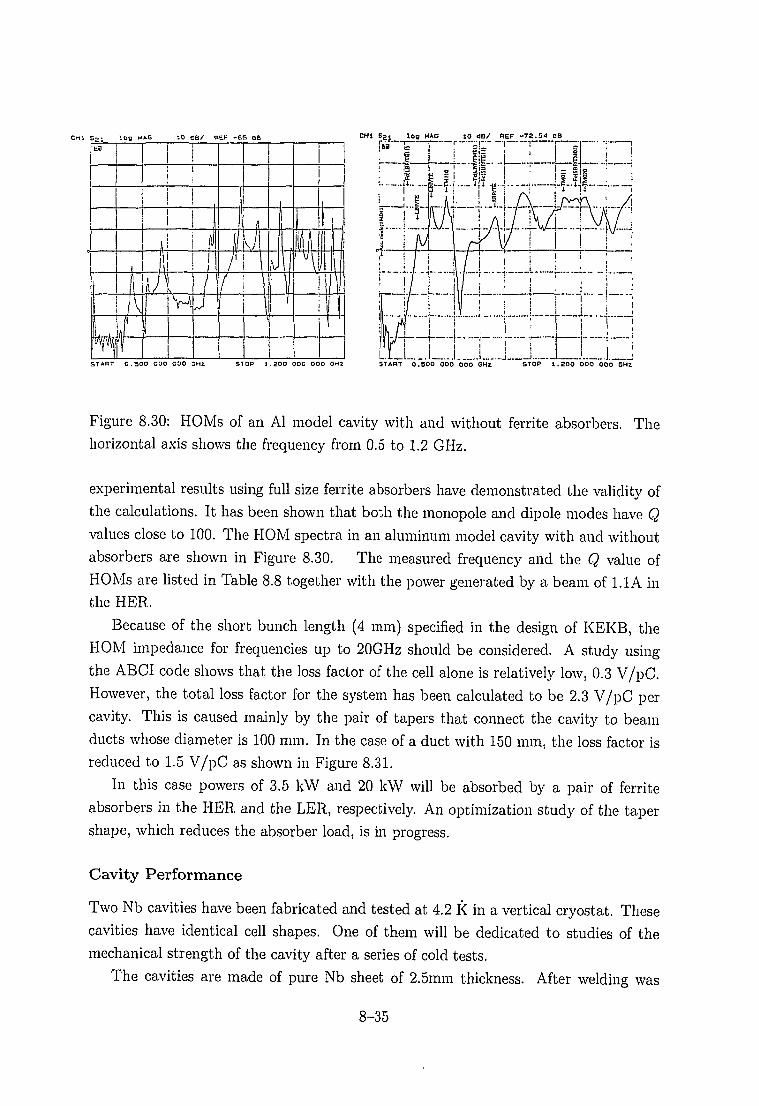
CHI E 2 ; log M«.G 10 CB/
1
,'!
Vif
L—fj-
i
!ii
i
!
i
•AV4
/IJ
/I
j!Mi/'/
11
Mi 1
\
1
...CHI S21 loo MAG 10 dB/ BEF -72.S4 OB
START C.500 030 OOO GHZ STOP 1.200 OOC 000 GH2 START 0.500 000 000 GHl" ~ STOP J. 200 000 000 GHZ
Figure 8.30: HOMs of an Al model cavity with and without ferrite absorbers. Thehorizontal axis shows the frequency from 0.5 to 1.2 GHz.
experimental results using full size ferrite absorbers have demonstrated the validity of
the calculations. It has been shown that both the monopole and dipole modes have Q
values close to 100. The H0M spectra in an aluminum model cavity with and without
absorbers are shown in Figure 8.30. The measured frequency and the Q value of
HOMs are listed in Table 8.8 together with the power generated by a beam of 1.1 A in
the HER.
Because of the short bunch length (4 mm) specified in the design of KEKB, the
H0M impedance for frequencies up to 20GHz should be considered. A study using
the ABCI code shows that the loss factor of the cell alone is relatively low, 0.3 V/pC.
However, the total loss factor for the system has been calculated to be 2.3 V/pC per
cavity. This is caused mainly by the pair of tapers that connect the cavity to beam
ducts whose diameter is 100 mm. In the case of a duct with 150 mm, the loss factor is
reduced to 1.5 V/pC as shown in Figure 8.31.
In this case powers of 3.5 kW and 20 kW will be absorbed by a pair of ferrite
absorbers in the HER and the LER, respectively. An optimization study of the taper
shape, which reduces the absorber load, is in progress.
Cavity Performance
Two Nb cavities have been fabricated and tested at 4.2 K in a vertical cryostat. These
cavities have identical cell shapes. One of them will be dedicated to studies of the
mechanical strength of the cavity after a series of cold tests.
The cavities are made of pure Nb sheet of 2.5mm thickness. After welding was
8-35
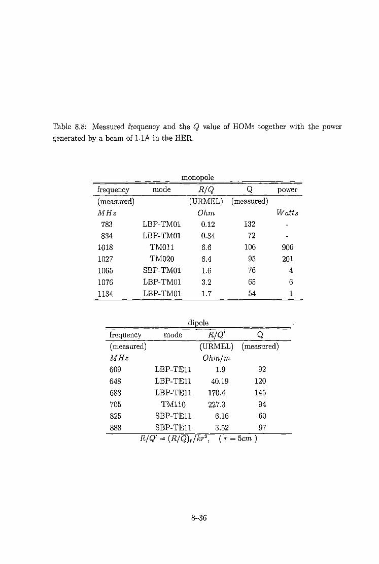
Table 8.8: Measured frequency and the Q value of HOMs together with the power
generated by a beam of 1.1 A in the HER.
monopole
frequency
(meavSiired)
MHz783
834
1018
1027
1065
1076
1134
mode R/Q Q(URMEL) (measured)
LBP-TM01
LBP-TM01
TM011
TM020
SBP-TM01
LBP-TM01
LBP-TM01
Ohm
0.12
0.34
6.6
6.4
1.6
3.2
1.7
dipole
frequency mode
(measured)
MHz
609
648
688
705
825
888
LBP-TE11
LBP-TE11
LBP-TE11
TM110
SBP-TE11
SBP-TE11
RIQ'
132
72
106
95
76
65
54
Q
power
Watts-
-
900
2014
6
1
(URMEL) (measured)
Ohm, I'm
1.9
40.19
170.4
227.3
6.16
3.52
92
120
145
94
60
97
RIQ' = {R/Q)r/kr2, ( r = 5cm )
8-36

o 5 b
Q.
>4 f-
oo£ 2
0
3 -
- * ' •: o
..V. ....
-
i t r
>
, , ,
. i , , , . I . , , I , , ,• •: :i i
o with 100dia.
X with 150dia.
0c
X
, , ,
i
0X
. , ,
"0X
, , , 1 , ,
-
-
-
-
-
, , , •
0 4 6 8 10bunch length (mm)
1 2 1 4
Figure 8.31: Loss factor of a cavity with a beam duct of 100mm/150mm in diameter
(calculated by ABCI).
completed, the cavities were treated in the same procedure as that for TRISTAN SC
cavities: electropolishing (EP) of 90/ m, annealing (700°C) and the final EP of 15/ m
followed by thorough rinsing with pure and ultra pure water. The results of cold
tests are shown in Figure 8.32. A similar performance of Q and the accelerating field
(•Eacc) could be obtained for both cavities, where maximum Eacc of 12.4 MV/m and
14.4 MV/m were obtained.
The field gradient is limited by electron emission, which is observed by a tem-
perature and X-ray mapping system based on carbon resistors and PIN diodes (Fig-
ure 8.33). It has been observed that electron emission is increased for gradients exceed-
ing 7 MV/m, if the cavity surface is exposed to air. To reduce the electron emission
and to improve the stability of the RF-processed surface, ozonized ultra pure water
rinsing is under study [23].
HOM Absorber
The priority of our efforts concerning ferrite absorbers has been to establish the fabri-
cation procedure. Three bonding methods have been investigated to fix IB-004 ferrite
onto the surfaces of copper beam pipes: ultrasonic soldering, vacuum brazing and HIP
(Hot Isostatic Press) method. Among these methods, HIP has proven to be the most
8-37

1010
aoT3CD
COC>C13
10°
:::::::::::::::::::::::::::::::::::::::::::::::i::::::::::::::::::::::::::::::::::::::::::::::::
SggX)<xxxxxxx-x
o CAVITY-Ix CAVITY-II
;
i i t i i t i i i 1 i r i i i i i i i
T^X^K
:::::::::::::::::: ::::::::::::::::::::::
0 5 10Eacc (MV/m)
15
Figure 8.32: Q vs Eacc at vertical cold tests of the superconducting Nb cavities.
promising. There, the powder of IB-004 is packed in an iron vessel together with a
copper cylinder. After pumping the vessel to a vacuum, it is heated to 900°C in a fur-
nace under a pressure of 1000 bar. In this vacuum environment the ferrite is sintered
in a cylindrical form which is firmly attached to the inner surface of the copper [24].
To study its RF power capacity, small scale models of a HlP'ed ferrite cylinder
have been fabricated. They are 15 cm long and 10 cm in diameter. A traveling RF
power of 5 kW at 2.45 GHz has been applied. An RF absorption of 3.4 kW, which
corresponds to 25 W/cm2 at the front edge, caused the temperature to rise to 200° C.
No cracking has occurred. The effective area of the power absorption was determined
by the temperature distribution, and the average power density on the ferrite was
calculated to be 14W/cm2. An RF power test of full size models is currently being
prepared.
Figure 8.34 shows a ferrite absorber for the LBP side. The out-gas rate of a full size
model has been measured to be 2 x 10~7 Torrl/sec at room temperature, after baking
at 150 ~ 250°C. Pre-baking of the ferrite powder is under examination to reduce the
outgas rate. The measurement of a loss factor of a ferrite wall has been conducted
using the synthetic pulse method. Analytic calculations and preliminary experiments
using full size models predict the loss factor of 0.3 V/pC per absorber for a bunch
length of 4 mm. It will cause an additional loss of 1.4 kW for the HER and 8 kW for
the LER.
8-38

Figure 8.33: A niobium cavity module with a mapping system using 25 carbon resistersand 19 PIN photo diodes.
8-39
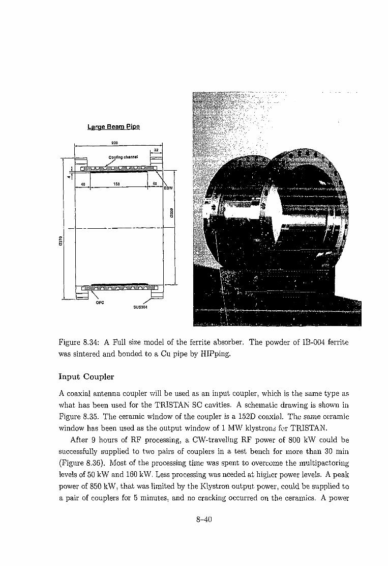
Large Beam Pipe
230
32
Cooling channel
EBW
OFCSUS304
Figure 8.34: A Full size model of the ferrite absorber. The powder of IB-004 ferrite
was sintered and bonded to a Cu pipe by HIPping.
Input Coupler
A coaxial antenna coupler will be used as an input coupler, which is the same type as
what has been used for the TRISTAN SC cavities. A schematic drawing is shown in
Figure 8.35. The ceramic window of the coupler is a 152D coaxial. The same ceramic
window has been used as the output window of 1 MW klystrond for TRISTAN.
After 9 hours of RF processing, a CW-traveling RF power of 800 kW could be
successfully supplied to two pairs of couplers in a test bench for more than 30 min
(Figure 8.36). Most of the processing time was spent to overcome the multipactoring
levels of 50 kW and 160 kW. Less processing was needed at higher power levels. A peak
power of 850 kW, that was limited by the Klystron output power, could be supplied to
a pair of couplers for 5 minutes, and no cracking occurred on the ceramics. A power
8-40

test with reflecting RF will be made after completing these traveling wave tests.
An analysis of cooling or heating has just started. The heating of the inner copper
conductor is estimated to be 360 W for an RF power of 500 kW. The temperature rise
is kept to within 10 degrees by cooling water. On the other hand, the loss of the outer
conductor, which is made of copper plated stainless steel, is 160 W/m on the room
temperature side and 30 W/m on the 4.2K side. This power will introduce a heat loss
of about 50 W to liquid He. Optimization of He gas cooling for the outer conductor
has to be done.
Figure 8.35: Coaxial input coupler for SC cavities.
8.2.3 Summary
The development of main components for an SC damped cavity for KEKB is in
progress. A spherical single-cell cavity with large beam pipes has demonstrated sat-
isfactory damping of HOMs using IB-004 ferrite absorbers fixed onto the beam pipes.
The gap voltage of 3 MV has been obtained with Nb cavities in vertical cold tests.
Tests of reduced model absorbers have been successfully conducted with RF powers of
25 W/cm2 in peak and 14 W/cm2 in average. No cracking of the absorbers has been
observed. Coaxial input couplers that are the same as those for the TRISTAN cavities
could transfer the traveling wave of 850 kW at a test bed.
The RF parameters of the HER can be realized with the recent superconducting RF
technology, where 10 ~ 12 single cell cavities will be used to maintain a beam of 1.1 A.
The field gradient of each cavity is 4 ~ 6.5 MV/m, and 400 ~ 500 kW couplers with
the Qext of 5 x 10⁴ will be required. Induced HOMs of 6 kW should be absorbed by a
8-41

Figure 8.36: High power test bed for input couplers; a travelling RF power of 850kW
was supplied to a pair of couplers.
pair of ferrite absorbers. This corresponds to an absorber power density of 3 W/cm2.
The main components, such as Nb cavities, HOM absorbers and input couplers, have
been extensively tested. The experimental results demonstrate the feasibility of SC
cavities for the HER. On the other hand, the application to the LER will involve many
difficulties caused by the heavy beam loading under a low RF voltage. High power
couplers with a low external Q and the absorption of a HOM power of 34 kW will be
required.
A prototype module which includes these components and a frequency tuner is
under construction for a beam test of 0.5 A in the TRISTAN Accumulation Ring. The
test is scheduled for 1996.
8-42

8.3 Low Level RF Issues
8.3.1 Phase and Tuner Control
The low level RF system consists of RF signal generators, a reference line system which
distributes the RF signal to all RF stations, and a low level RF control system for each
RF unit. The low level system for each RF unit has feedback loops to control the
cavity field, the klystron output and the cavity tuners. Phase detection is conducted
at an intermediate frequency of 1 MHz.
The cavity phase should be controlled with an accuracy of less than 1 degree. This
requirement is considerably tighter than that at ordinary storage rings due to the
following reasons. In a double ring collider with a small (3* at the colliding point, a
phase error of one ring relative to the other gives rise to a displacement of the colliding
point from the minimum {3*. This results in a luminosity reduction. Another reason is
that a phase error in one cavity causes extra input power and reflection power to that
cavity due to the heavy beam loading. For example, if the phase of one superconducting
cavity is different from the others by 1 degree, an extra power of 30~40 kW is fed to
that cavity in order to keep the cavity voltage constant.
We will improve the accuracy of the existing RF reference system and phase control
modules that have been used for TRISTAN. In addition, we will use a computer-
aided real-time phase correction scheme, where the input power, reflection power, and
cavity voltage of every cavity are monitored, and the phase error of each cavity is
then calculated and corrected. This correction scheme takes advantage of the high
beam-induced voltage.
In order to reduce fast ripples of the klystron power supply and phase changes of the
klystron, which is on the order of ten degrees, we need a control loop for the klystron
output which acts as an inner loop within the cavity voltage loop.
As seen in Figure 8.2, the ARES requires two tuner control loops: one is for the
accelerating cavity; the other for the storage cavity. The accelerating cavity tuner is
controlled according to its phase with respect to the input phase, which is the usual
method used to compensate for the reactive component of beam loading. The storage
cavity tuner is controlled not by its own phase, but by the phase of the coupling cavity;
otherwise, the phase tolerance would be extremely severe.
8.3.2 Bunch gap transient
Ion-trap ping is one of the problems which arises from a high electron beam current.
In storage rings, some part of residual gas molecules is ionized due to collisions with
8-43

stored beams. The ions can be trapped around the beam orbit by the potential well
of the electron beam. The trapped ions can: (1) shorten the beam lifetime due to the
collisions, (2) give rise to a two-beam instability, and (3) affect the betatron tune.
In order to cure the ion trapping problem, several methods have been proposed.
Among them, introducing a bunch gap is the most attractive solution for KEKB. In
this scheme, beams are partially filled in the ring with one or more gaps, instead of
being filled uniformly. The ions escape from the beam orbit to the duct wall when
they encounter the bunch gap. Other methods are less attractive. For example, a
method using clearing electrodes increases the ring impedance, or gives rise to local
heat problems. Thus, a 5~10% bunch gap will be introduced in HER.
The bunch gap, however, modulates the accelerating field and the synchronous
phase of each bunch, resulting in unequally-spaced bunches. A bunch phase modulation
of ± 2.4 degrees corresponds to a longitudinal displacement of ± 1 uz (=4 mm) in
KEKB. Furthermore, since a finite crossing angle of 2 x l l mrad will be adopted, this
modulation gives rise to a transverse displacement of 77 fim at the collision point,
which is close to 1/3 of a*. Both effects reduce the luminosity.
The bunch phase modulation has been calculated for the cases of the ARES and
SCC [25]. The results are summarized in Table 8.9. Because of the large stored energy,
the phase modulation is much smaller than that of conventional normal-conducting
damped cavities, which would give a modulation of typically 20~30 degrees at KEKB.
The displacement of the collision point can be further reduced by introducing a corre-
sponding gap in the positron ring (LER), which makes a similar gap transient response
in LER to that in HER. Figure 8.37 shows the relative bunch phase with and without
the compensation gap. By controlling the bunch charge at the compensation gap in a
range from 50 to 60% of that of other bunches, the bunch phase modulation is kept
below 0.5 degrees (=0.2cr2), which is acceptable.
8-44

O
o
Table 8.9: Bunch phase modulation due to a bunch gap.
Cavity
in HER
ARES
sec
Gap length
(%)
10
5
10
5
Bunch phase modulation
(degree)
with compensation gap?
No Yes
2.7 ~ 0.3
1.3 ~ 0.1
4.9 ~ 0.5
2.4 ~ 0.3
4 I 1 1 1 r
- 2
- 4
NO COMPENSATION GAP
r ' ' I
WITH A COMPENSATION GAP
10 20 30TIME (MICRO SEC)
Figure 8.37: Bunch phase modulation due to a bunch gap and the effect of a compen-
sation gap. The ARES cavities were assumed. The relative gap length is set to be
10%. The bunch current in the compensation gap is set 50, 55, and 60% of that of
other bunches.
8-45

8.3.3 RF Cavity Feedback
Background
By using the ARES or the SCC the two particular beam-loading effects can be re-
duced: namely, the excitation of longitudinal coupled-bunch instabilities by the de-
tuned accelerating mode, and the presence of bunch-phase modulation due to gaps in
the bunch-train. Along with the development of those cavities, we are developing an
RF cavity feedback system. The purpose of the feedback development is to reduce the
beam-loading effects to the extent that the HOM-damped accelerating cavity of the
ARES itself, without the energy storage cavity, can be used as the KEKB accelerating
structure. It is obvious that, in the case where the ARES or the SCC are employed,
the feedback can be used as an auxiliary means to reduce the beam-loading effects.
Here, we discuss the RF cavity feedback to be used for damping the instabilities that
will arise, if the beam is accelerated solely by the HOM-damped accelerating cavities of
the ARES. Figure 8.38 shows the calculated growth rates of the longitudinal coupled-
bunch instabilities due to the accelerating mode of the cavities in the LER (Figure 8.38-
a) and in the HER (Figure 8.38-b). The parameters used in the calculations are listed
in Table 8.10. For simplicity, we refer to the mode m = M — n as the mode m = —n.
Here, M is the number of bunches, and m ranges from 0 to M — 1. The expected
damping rate by the longitudinal bunch-by-bunch feedback system is also shown in the
figure, together with the longitudinal radiation damping rate. As shown in Figure 8.38,
the growth rates in the LER are higher than those in the HER, mainly due to its higher
Table 8.10: Parameters used in the instability calculations
Type of cavity
Total cavity voltage
Number of cells
Cavity voltage/cell
Shunt impedance/cell
Unloaded Q
R/QMaximum frequency detuning
Synchrotron frequency
Energy loss/turn
vcNc
K/cell
Rs
Qo
Af
/ .Uo
LER HER
accelerating cavity of ARES
8.6
20
0.43
-232
1.7
0.87
15.7
32
0.49
5.3
35000
147
-82
1.6
4.8
MV
MV/cell
MSI
nkHz
kHz
MV
8-46

1 1.5
Beam Current [A]
(a)
2.5
1 0 -
5
2io2
a
IO1
1 t 1 1
woxlJttiK
Bubch-
Radial
: :::/:::" / . . . .
/
/ 'b\/Bunch Fee7. rr:/.on Damping R
>>•y\.
\ X.i /
":::..'.\"sr' '"•••. . / ^
y ^ •
dback Darnmn
jjte^^j
• X
^. . . . ^ ^ r .
g^te
: ... J>^.
if=-i
: " " ^
Tf^2
lf^-4
^ ^
^ ^
(b)
0.2 0.4 0.6Beam Current [A]
0.8
Figure 8.38: Calculated growth rates of longitudinal coupled-bunch instabilities caused
by the accelerating mode of the cavities in the LER(a) and in the HER (b). The type
of cavity used in the calculations is the accelerating cavity of the ARES, that is. the
HOM-damped normal conducting cavity not equipped with the storage cavity.
8-47

beam current. The RF cavity feedback must reduce the growth rates, at least, down to
a level which can be damped by the bunch-by-bunch feedback system. This means that
the damping rate by the cavity feedback must be higher than 35 dB in the LER and
higher than 23 dB in the HER. The number of modes to be damped are six (m = — 1 to
—6) in the LER and three (ra = — 1 to —3) in the HER. Since the revolution frequency
of the bunches is about 100 kHz, the frequency range to be covered by the cavity
feedback is more than 600 kHz in the LER and more than 300 kHz in the HER.
Principle of the System
In an RF cavity feedback, a part of the cavity voltage is picked up, filtered and vecto-
rially added to the RF drive with an appropriate amplitude and phase so as to reduce
the beam-induced cavity voltage. In this way, the magnitude of the effective cavity
impedance seen by the beam is reduced. In the case of KEKB, however, an unavoidable
large group delay in the feedback loop limits the bandwidth of the system to less than
100 kHz. Cables and waveguides cause a constant group delay of about 1 [is, while the
klystron causes a frequency-dependent group delay of about 0.6 fxs at maximum. To
circumvent this problem, we are developing a feedback system with a large loop-gain
only in the vicinity of the frequencies n/rev + /s. They are the upper synchrotron side-
bands of the revolution harmonics, and are responsible for driving the coupled-bunch
oscillations. This feedback is realized by using a comb-filter comprising of an array
of resonators. Each resonator is tuned to a particular frequency of n/ rev + /s, and its
phase is shifted properly to compensate for the phase differences among the sideband
frequencies. The comb-filter can also compensate for the frequency-dependent ampli-
tude response of the feedback loop by adjusting the attenuation of the resonators. The
array of resonators is, from here on, referred to as the parallel comb-filter. A block
diagram of the RF cavity feedback system is shown in Figure 8.39.
R&D Status
We have carried out a preliminary experiment of the parallel comb-filter feedback
through the RF cavity. Figure 8.40 shows the experimental setup, which includes a
parallel comb-filter, a 2-cell damped cavity of the Palmer type and a klystron. Since
the cavity used was a cold model, only a small portion of the klystron output power
was extracted with a 55dB directional coupler, to be fed into the cavity. The parallel
comb-filter consists of five individual LC resonators arranged at 100 kHz intervals, and
each resonator has a 2 kHz 3dB-bandwidth. A network analyzer was used to measure
the amplitude and phase of the cavity voltage over the frequency range from 508 MHz
8-48

Accel. SignalAmp. Cavity
f F.B. Signal
Ampl. and Phase Adj.Pickup
UpConv.
ParallelComb-Filter
DownConv.
ftf
i rPhase Shifter — Attenuator |—j Resonator
Phase Shifter Attenuator Resonator — ' '
Figure 8.39: Block diagram of the RF cavity feedback system using a parallel comb-
filter.
8-49

Network Analyzer
RFAmp. Att.
UpConv.
ParailelComb-Filter
DownConv. Att.
LocalOsc.
DriverAmp. K 1y s t r o n 2-Cell Damped Cavity
Figure 8.40: Block diagram of the experimental RF cavity feedback loop, which includes
a parallel comb-filter, a low-power damped cavity and a klystron.
to 509 MHz. The bandwidth and the center frequency of the cavity were 236 kHz and
508.5 MHz, respectively.
The results of the measurement are shown in Figure 8.41; the top figure shows
the magnitude and the real part of the effective cavity impedance, with or without
feedback, as a function of the normalized frequency (/ — /rf)//revi and the bottom
figure shows the phase of the cavity. With the feedback, the real part of the impedance
was reduced by 17 dB to 25 dB, at five sideband frequencies. The measured values
are in good agreement with estimations obtained by using the measured parameters of
loop the components. The maximum gain of the feedback loop is limited by the top-to-
bottom amplitude ratio of the filter, because the loop gain must be less than 0 dB at
the bottom where the filter becomes 180° out of phase. The increase in the impedance
between the revolution harmonics in Figure 8.41 is the result of a positive feedback due
to an improper phase relationship in this region. An estimate shows that to reduce
the real part of the cavity impedance by more than 35 dB, the 3dB-bandwidth of the
resonator needs to be smaller than 1 kHz.
A new comb-filter with ten parallel resonators is currently being built. The center
frequency of the resonator can be adjusted continuously and the bandwidth in a step-
8-50

-30 rr
150
100
1 50
0
-50
-100
-150
- 8 - 7 - 6 - 5 - 4 - 3 - 2 - 1 0 1Frequency (f - frf)/frev
...
-• ' .
Loopdeslay = 1.1
1 5 l l c . . .•ID US •
i \
Vi\V
r—ji
• — .
-7 -6 -5 -4 -3 -2Frequency (f - frf)/frev
-1
Figure 8.41: The results of the RF cavity feedback experiment. The top figure shows
the magnitude and real part of the effective cavity impedance, with or without feedback,
as a function of the normalized frequency (/ — /rf)//rev; the bottom figure shows the
phase of the cavity.
wise manner. The new comb-filter will be tested soon. The main purpose of the test
is to improve the loop gain by more than lOdB. The RF cavity feedback system will
be tested using a beam of the TRISTAN Main Ring (scheduled in May 1995).
8-51

8.4 Crab Cavity
8.4.1 Introduction
A large number of buckets in each ring (the HER and LER) must be filled with beams
to obtain the design luminosity of 1034 /cm2sec. Consequently KEKB has to operate
with a short bunch spacing of minimum 60 cm. It is necessary, therefore, to separate
both beams quickly near the interaction point (IP) to avoid parasitic collisions. It is
also necessary to minimize synchrotron radiation generated near the IP, particularly
just upstream of the crossing point. In order to meet these requirements, the interaction
region (IR) design of KEKB is based on beam crossing with a finite angle of ±11 mrad.
One consequence of employing a finite crossing angle is a luminosity reduction due
to geometrical effects. Another important effect of a finite crossing angle is the possi-
bility to excite synchrotron-betatron resonances. The crab crossing scheme [26], [27] is
considered to solve these problems. Figure 8.42 shows the crab crossing scheme, where
bunches are tilted by a time-dependent transverse kick in an RF deflector (crab cavity)
located before the IP in each ring. After the bunches collide head-on, this bunch tilt
is kicked back to the original orientation in another deflector after the IP.
Figure 8.42: crab crossing scheme.
The R&D work on the crab cavity was carried out in 1991 and 1992 in collaboration
with Cornell university, where superconducting crab cavities operating in the TMllO
mode were designed for CESR-B at Cornell. In order to damp the parasitic modes,
a new damping scheme that employs a coaxial beam pipe and a notch filter was pro-
posed [5]. The damping scheme was verified by measurements of model cavities made
of copper and aluminum. The high field performance was tested with a one-third scale
niobium cavity in liquid helium. A cold measurement showed that the design values of
8-52

the necessary kick voltage and Q-value were achieved.
At KEK we started an R&D effort for the crab cavity aimed at making full-scale
niobium cavities for KEKB in three years. We decided to adopt the same design of
the crab cavity as that designed for CESR-B, although a slight modification' is needed,
since the frequency of KEKB is 508.9 MHz, which is slightly higher than that of CESR-
B (500 MHz). In this section we describe the design and measurement results of the
crab cavity that has been developed under the KEK-Cornell collaboration [5], [28]. At
the end of this section our R&D plan for the crab cavity at KEK is presented.
8.4.2 Design Concept
Deflecting Mode
The required transverse deflecting voltage (Vj.) is determined by the desired crossing
angle at the IP and the operating frequency of the crab cavity:
URF\
(8.!)
where /?*, Pcrab, E, 0x and OJRF are the beta-function at the IP, the beta-function at the
crab cavity, the beam energy, the half crossing angle and the RF frequency of the crab
cavity, respectively. Table 8.11 summarizes the basic parameters for the crab cavities
in the LER and the HER of KEKB. The required deflecting voltage is 1.4 MV in each
ring.
One possible method to realize the crab crossing scheme is to use RF cavities
operating in a transverse deflecting mode. The best choice for this would be the
TM110 mode, which has a high transverse shunt impedance. Since superconducting
Table 8.11: Parameters for the Crab Cavity in KEKB.
Ring LER HER
Beam energy 3.5 8.0 GeV
RF frequency 508.887 MHz
Crossing angle ±11 mrad
P* 0.33 0.33 m
Pcrab 20 100 mRequired kick 1.41 1.44 MV
8-53

cavities can be operated in a high field gradient, a single-cell superconducting cavity
would be sufficient to provide the necessary transverse kick voltage.
Damping Scheme for Parasitic Modes
Coupled-bunch instabilities caused by the crab cavities must be sufficiently suppressed,
as well as those caused by the accelerating cavities of KEKB. The Q-values of dangerous
parasitic modes should be sufficiently lowered, typically to the order of 100. In the case
of superconducting accelerating cavities, the accelerating mode is the lowest frequency
mode, and all parasitic modes have higher frequencies. As a damping scheme for
higher order modes, the superconducting accelerating cavity for KEKB employs large-
diameter beam pipes, through which the field energy of those modes can be extracted
and absorbed by microwave absorbers attached to the beam pipe.
In the case of a crab cavity, however, since the operating mode (TM110) used for
the crabbing is not the lowest frequency mode, there are some modes with lower, or
about the same, frequencies. Four unwanted parasitic modes remain trapped in the
cavity region with high Q-values, even if a beam pipe with a large diameter is attached.
Those are the TM010 monopole mode, two polarizations of the TE111 dipole mode
and an unwanted polarization of the TM110 mode. In order to overcome this problem,
a coaxial beam pipe and a notch filter are employed in the crab cavity. A schematic
view of this damping scheme is shown in Figure 8.43. With this scheme, not only the
higher order parasitic modes, but also the lower frequency parasitic modes, can be
damped, as will be discussed in the following.
In a coaxial transmission line, although there is no cut-off frequency for TEM mode
waves, there is a cut-off frequency for the dipole modes. By attaching a coaxial beam
Absorbingmaterial Notch filter
Absorbingmaterial
Coaxial beam pipeCooling forinner conductor
Figure 8.43: A schematic view of the crab cavity.
8-54
pipe to the crab cavity, every monopole resonant mode in the cavity can couple to the
coaxial beam pipe as a TEM mode wave, and then propagate. In addition, every dipole
resonant mode in the cavity can couple to the coaxial beam pipe as a dipole mode wave;
it will propagate if its frequency is higher than the cut-off value. By designing a cell
shape such that /(TM110)< /(cut off)< /(TE111), all monopole and dipole modes,
except the TMllO mode, in the cavity can be extracted out of the cavity via the coaxial
beam pipe.
However, one unwanted polarization of the TMllO mode is still trapped, in the
cavity. Since this mode has a high transverse shunt impedance, it must be cured. Two
possible measures for cure have been considered:
• Use of a slightly polarized cell, and tuning this mode at a safe frequency. If we
control the frequency of this mode at a damping side of transverse coupled-bunch
instability, we can avoid the instability driven by this mode. For this method
we designed a round cell shape cavity using cylindrical symmetric calculations.
A slight polarization will be introduced to separate the unwanted polarization
mode from the operating mode.
• Extremely polarized cell ("Squashed" crab cavity). By making the cross section
of the cavity cell an ellipse or race-track shape with a large eccentricity, we can
increase the frequency of the unwanted TMllO mode to be above the cut-off
of the dipole mode wave in the coaxial beam pipe. An analytical calculation
of a rectangular cavity has shown that when the ratio of the longer to shorter
dimension in the cross section is 2:1, the unwanted TMllO mode goes up to
700 MHz, while the operating mode is kept at 500 MHz. We designed such an
extremely polarized cell cavity.
In the following we describe both designs of the round cell and the squashed cell.
8.4.3 Design Optimization
Coaxial beam pipe
Since we will operate the crabbing mode TMllO, at 509 MHz, the cut-off frequency
of the dipole mode in the coaxial beam pipe should be higher than that frequency. In
order to have a sufficient attenuation for the crabbing mode, it is desirable to make
the cut-off frequency high enough. On the other hand, the cut-off frequency should be
lower than the lowest parasitic dipole mode (TE111 in this case). The dimensions of
the coaxial beam pipe were chosen so that: (1) it has a cut-off frequency of 600 MHz,
which gives an attenuation of 60 dB/m for the crabbing mode, and (2) it has a sufficient
8-55

thickness of the inner conductor to allow a cooling system in it. We have chosen the
radius of the inner surface of the outer pipe to be 94 mm and the outer and inner radii
of the inner conductor to be 65 mm and 45 mm, respectively.
Round cell design
Computer studies involving a cylindrical symmetry have been carried out in order to
optimize the cell shape. The variables in the optimization were the cell length, the iris
radius, the equator radius and the slope of the wall. Several points taken into account
in designing the cell shape were:
• The frequencies of all dipole parasitic modes should be higher than the cut-off
frequency of the dipole mode in the coaxial beam pipe.
• The ratio of the kick voltage to the surface peak field should be high.
• The R/Q values of the parasitic modes (especially for the most dangerous TM010
mode) should be low.
© The external Q for parasitic modes having high R/Q should be low (typically
less than on the order of 100).
C\J
Figure 8.44: Cell shape of the round crab cavity.
The kick voltage, surface field, frequency and the R/Q value were calculated by
using URMEL. The external Q-values were calculated with URMEL by changing the
short position of the beam pipe by using Slater's formula [22]. The external Q-values for
monopole modes were also calculated using SEAFISH by assuming a ferrite absorber
8-56

Table 8.12: RF properties of the round cell crab cavity.
Crabbing Mode
Frequency
R*/QKick voltage
Loss factor
Parasitic modes
(TM110)
500
51.2
(MV)
(V/pC)
mode frequency
(MHz)
(Monopole modes)
TM010
TM020
TM011
TM030
TM021
(Dipole modes)TE111
TM120
TE112
TE121
342
731
914
1107
~1200
720
898
1048
~1100
(MHz)ft/cell
2.0
0.58
R/Q(fi/cell)
135
26
21
1
4
6
6
1
at Egp=21.7 MV/m,
Qext
coax
108
40
38
141
<100
18
160
~1000
Qext
hollow
-
-
-
165
<100
-
37
186
<100
Hsp=750 Oe
Qloaded
total
108
40
38
76
<100
18
30
~161
<100
R/Q = {V{roy/uU)l{kro)2m, where m=0 (monopole) and m=l (dipole).
Esp and Hsp is the surface peak electric and magnetic field, respectively.
8-57

attached to the beam pipe. The loss factor was calculated using TBCI. Figure S.44 and
Table 8.12 show the cell shape and RF properties of the final design. The Q-values of
dangerous (high R/Q) monopole and dipole parasitic modes are damped to less than
100 with the coaxial beam pipe.
Squashed cell design
The design of the extremely polarized cell (squashed cell) was carried out by using
MAFIA. In addition to the considerations taken in the round cell design, the frequency
of the unwanted polarization of the TM110 mode was increased up to 700 MHz so
that it propagates in the coaxial beam pipe. Figure 8.45 and Table 8.13 show the cell
shape and RF properties of the final design. The Q-values of dangerous (high R/Q)
monopole and dipole parasitic modes are damped to less than 100 with the coaxial
beam pipe, similarly as for the round cell case.
Cross Section
Rs
1
i R s
Figure 8.45: Cell shape of the squashed crab cavity. In the left side figure, the upper
part shows the cross section in the horizontal plane, while the lower part shows that
in the vertical plane.
Notch filter
Since the crabbing mode is a dipole mode and its frequency is below the cut-off of
the coaxial beam pipe, the crabbing mode attenuates in the coaxial beam pipe. With
our design, the crabbing mode is sufficiently attenuated and the power dissipation
8-58
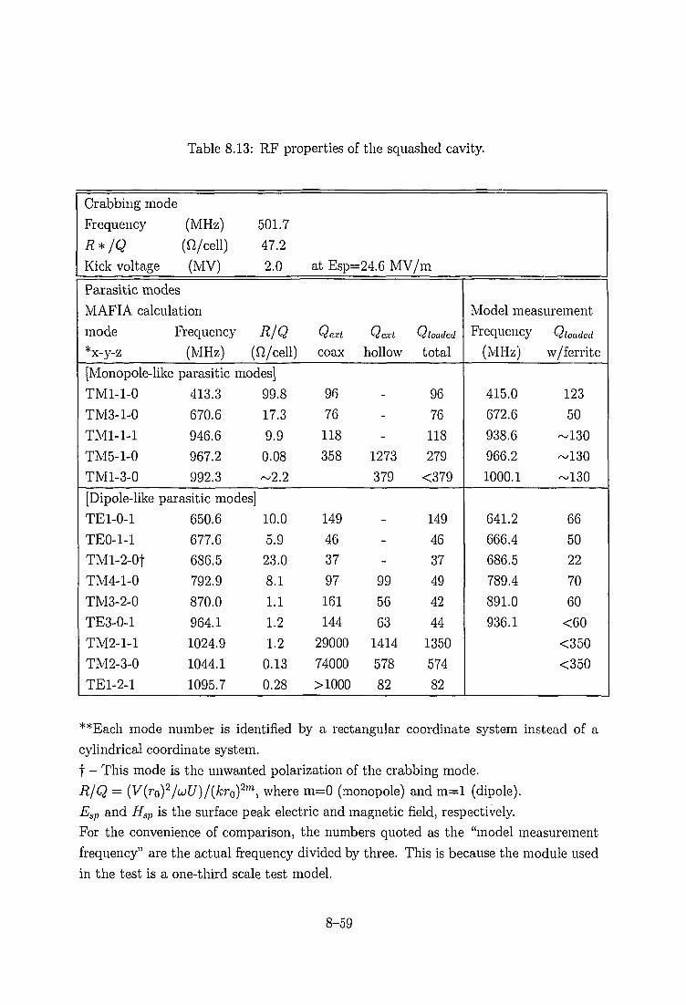
Table 8.13: RF properties of the squashed cavity.
Crabbing mode
Frequency
R*/QKick voltage
Parasitic modes
(MHz)
(ft/cell)(MV)
MAFIA calculation
mode Frequency
*x-y-z
[Monopole-like j
TMl-1-0
TM3-1-0
TM1-1-1TM5-1-0
TM1-3-0
(MHz)
501.7
47.2
2.0
R/Q(fi/cell)
parasitic modes]
413.3
670.6
946.6967.2
992.3
99.8
17.3
9.9
0.08
~2.2
[Dipole-like parasitic modes]
TE1-0-1
TE0-1-1
TMl-2-OfTM4-1-0
TM3-2-0
TE3-0-1
TM2-1-1
TM2-3-0
TE1-2-1
650.6
677.6
686.5
792.9
870.0
964.1
1024.9
1044.1
1095.7
10.0
5.9
23.0
8.1
1.1
1.2
1.2
0.13
0.28
at Esp=24.6 MV/m
Qextcoax
96
76
118
358
149
46
37
97
161
144
29000
74000
>1000
Qext
hollow
-
-
-
1273
379
-
-
-
99
56
63
1414
578
82
^Jloaded
total
96
76
118
279
<379
149
46
37
49
42
44
1350
574
82
Model measurement
Frequency
(MHz)
415.0
672.6
938.6
966.2
1000.1
641.2
666.4
686.5
789.4
891.0
936.1
Wloaded
w/ferrite
123
50
~130
-130
~130
66
5022
70
60
<60
<350
<350
**Each mode number is identified by a rectangular coordinate system instead of a
cylindrical coordinate system.
t - This mode is the unwanted polarization of the crabbing mode.
R/Q = (V(ro)2/W)/(*To)2m, where m=0 (rnonopole) and m=l (dipole).
Esp and Hsp is the surface peak electric and magnetic field, respectively.
For the convenience of comparison, the numbers quoted as the "model measurement
frequency" are the actual frequency divided by three. This is because the module used
in the test is a one-third scale test model.
8-59

m•a
Ia.•D
I
-1 0
-20
-30
-40
-50
-60
-70
A
O URMEL calculationA Equivalent circuit
A A
470 480 490 500 510
frequency (MHz)
520 530
Figure 8.46: Frequency characteristics of the notch filter.
caused by this mode in the ferrite absorber at the end of the coaxial beam pipe is
less than 1 kW. In a real cavity, however, some asymmetry due to machining errors
or a misalignment of the coaxial beam pipe can transfer a part of the field energy of
the crabbing mode into a TEM mode wave in the coaxial beam pipe. This TEM wave
propagates down the coaxial beam pipe without attenuation, resulting in an increase of
the dissipation power at the ferrite absorber. In order to avoid this, we have attached
a notch filter which rejects the TEM-coupled crabbing mode back to the cavity.
Figure 8.46 shows the transmission property of the notch filter calculated using
URMEL, together with the results of an analytical calculation of an equivalent circuit.
If the resonant frequency of the filter is tuned within ±0.5 MHz, a rejection rate higher
than 50 dB is obtained. Even if the external Q for the crabbing mode might be reduced
to 105 for a machining error or misalignment, this rejection of 50 dB assures an external
Q of 1010, which is sufficiently high.
The resonant frequency of the filter can be tuned by changing the filter iris. Accord-
ing to SUPERFISH calculations, the rate of the frequency shift is 1.8~3.6 MHz/mm.
In addition to the stopband at 500 MHz, the notch filter has a higher order TEM
stopband at 1.45 GHz. Since there are several parasitic modes near this frequency, the
hollow beam pipe opposite to the coaxial beam pipe has been opened wide enough so
that the monopole modes above 1.3 GHz and the dipole modes above 1 GHz escape
from the hollow beam pipe.
8-60

8.4.4 Model Measurements
In order to examine new ideas concerning the parasitic mode damping, we have built a
one-third scale (L-band) round copper cavity and a one-third scale squashed aluminum
cavity, with a coaxial beam pipe and ferrite absorbers. In addition, a high field perfor-
mance test was made in liquid helium with a one-third scale round cell niobium cavity
equipped with a coaxial beam pipe and a notch filter made of niobium.
Coaxial Beam Pipe Measurement
First, we measured the effect of the coaxial beam pipe on the damping property of the
TM010 monopole mode, and on the Q-value of the crabbinf mode. Figure 8.47 shows
the loaded Q-value of the TM010 mode as a function of the penetration length of the
inner conductor of the coaxial beam pipe into the cavity cell. The Q-value is damped
below 100 with moderate penetration. The result agrees with a SEAFISH calculation
within a factor of two.
100000
10000
o•o<D73COO
1000
100 -
10
, -A A — * - - - . *
1 o-
-e-loadedQ
-•-loaded Q-SEAFISH
tf frequency (MHz)
- * - frequency (MHz)-SEAFISH
N
\\
A .\ v
N *
\ *
\ *
\ \ ' •
1100
• 1090
CD
1080 "§CD3
• 1070
• 1060
1050
-80 -60 -40 -20 0 20
penetration of the inner conductor (mm)
Figure 8.47: Damping of the TM010 mode in the crab cavity with a coaxial beam pipe.
Figure 8.48 shows how a misalignment of the inner conductor relative to the outer
conductor affects the crabbing mode. When the inner conductor is aligned within
1 mm, the loaded Q-value with and without the coaxial beam pipe are nearly the
same. Since the intrinsic Q of this copper cavity is 23000, this means that the external
Q of the coaxial beam pipe, when thus-aligned, is at least on the order of 105. As
mentioned earlier, the notch filter assures an additional 50 dB reduction, which makes
8-61

24000
22000
20000
om 18000
-e-Q (TM110-H) displace=H
-• -Q (TM110-H) displaced
O
16000
14000
12000
800
600
4 0 0
2 0 0
0
uen
o
orrfl)13
(QCD
-J~IN
-200
-400
-1 0 5 0 5
displacement (mm)
10
Figure 8.48: Effect of misalignment of the coaxial beam pipe on the crabbing mode.
the external Q-value above 1010. Different sensitivities of the Q-values with respect to
the horizontal and vertical displacements are considered to be due to the fact that the
electric field at the tip of the coaxial beam pipe is polarized horizontally. Since this is
a result of the one-third scale model, the alignment tolerance for the full-scale cavity
is expected to be about 3 mm, which can be easily achieved.
Squashed Cavity Model Measurement
The resonant frequency and the damping properties have been measured with the one-
third scale squashed crab cavity. Figure 8.49 shows the frequency spectrum with and
without the coaxial beam pipe and ferrite absorbers. The measured frequency of each
mode and the Q-values with the ferrite absorbers are listed in Table 8.13 together
with the results of MAFIA calculations. As expected from the MAFIA calculation,
all the dangerous monopole and dipole modes are damped to less than on the order
of 100, including the unwanted polarization of the crabbing mode. A high Q-value is
maintained for the crabbing mode. The external Q-value of the crabbing mode via the
coaxial beam pipe was estimated from the measured loaded Q-value with and without
the coaxial beam pipe. It has been estimated to be at least on the order of 105, which
is the same result as in the case of a round-cell cavity.
8-62

CHI »J1 Icifl MAC 10 dB/ WSF -BQ
CHI START l.ona ana aoa CH> sTor 4. oca aaa oa'j en.
CHI «Z| log MAC 10 4B/ KV -50 dB
u
i
Ol
c
•sH
u
A /
km l i Ff
\'\
1J r
A
CHI *TART 1.000 000 000 CH* STOP 4.000 000 000 CHa
Figure 8.49: Frequency spectrum of a squashed crab cavity: (upper) without a coaxial
beam pipe and (lower) with a coaxial beam pipe and a ferrite absorber.
8-63

High Field Performance
The kick voltage required for crabbing is 1.4 MV which corresponds to a surface peak
field of 15 MV/m. According to the present technology of superconducting accelerating
cavities at around 500 MHz, a surface peak field of 20 MV/m can be easily achieved,
which corresponds to an accelerating gradient of about 10 MV/m . For the crab cavity,
it is still crucial to confirm high field performances, because it has several new features,
such as the coaxial beam pipe and the notch filter on the beam pipe, which might cause
some limitation to the field due to multipactoring or other causes.
Figure 8.50 shows the one-third scale niobium cavity mounted on a test stand.
Measurements of the TMllO mode at 1.5 GHz were made when the system was cooled
down to 1.5 K in liquid helium. At a surface peak field of 1 MV/m a multipactor-
ing was encountered, which is considered to have occurred at the coaxial beam pipe.
The multipactoring was processed away after an hour of RF processing. Figure 8.51
shows the Q-value versus the surface peak field. The maximum surface peak field was
25 MV/m, where we experienced field emission. The kick voltage required for KEKB
has been achieved with a sufficiently high Q-value. Thus, the feasibility of the crab
cavity has been realistically demonstrated.
Figure 8.50: One-third scale Niobium round-cell crab cavity mounted on a test stand.
8-64

1)3
10 15
E, peak (MV/m)
20 25
Figure 8.51: Surface peak field vs Q-value measured in liquid helium.
8.4.5 R&D Schedule
In the R&D program of the crab cavity at KEK, we are planning to fabricate full-scale
superconducting cavities in three years. For the base line design of the crab cavity, we
have adopted a squashed cell shape cavity scheme, which was designed and extensively
studied at Cornell for CESR-B under the KEK-Cornell collaboration. The R&D work
on the crab cavities at KEK will take advantage of the fabrication and measurement
techniques of niobium superconducting cavities that have been established through
constructing the TRISTAN SCRF system.
Figure 8.52 shows the R&D schedule of the crab cavity for KEKB. At the first stage
of the R&D program, a test stand with a vertical cryostat and an RF measurement
system for a one-third scale model will be completed by the end of JFY1994. The one-
third scale round cell shape Nb cavity that has been designed, fabricated and tested at
Cornell for CESR-B will be tested again at KEK. Three one-third scale squashed cell
shape model cavities will be designed and built to establish the fabrication technique
for a non-axially symmetric structure by the end of FY1995. At the final stage of the
R&D, two full-scale squashed cell shape prototype cavities, equipped with coaxial beam
pipe and notch filter, will be designed and fabricated. After an RF test in a vertical
cryostat, one of these cavities will be installed in a horizontal cryostat. The prototype
cavity in a horizontal cryostat will be cooled down by a helium refrigerator, and a high
power RF test will be conducted to confirm the performances that are required for
KEKB.
8-65

CRAB - CAVITY R&D SCHEDULE
1/3 Scale Model
Nb-Cavity
Cryostat (Vert.)
RF System
Cornell Cavity
Cu-Model
Full Scale Model
Nb-Cavity
Cryostat (Vert.)Cryostat (Hori.)
RF SystemCu-Model
FY 1994
Design & Construction
I *1
| I
| 1
IDesign
HE
FY 1995
Cool Down &RF Test
i #3 Ir-
• , j , ' s |
Cool Down &RF Test
I& Construction
FY 1996
Cool Down &RF Test
I #2 11 v,%<?;w]
I I
1 1
1 1
Design & Construction
I
FY 1997
I
Figure 8.52: R&D schedule of the crab cavity at KEK.
8-66

Bibliography
[1] Y. Yamazaki and T. Kageyama, Particle Accelerators 44 107 (1994).
[2] T. Shintake, Particle Accelerators 44 131 (1994).
[3] K. Akai and Y. Yamazaki, Particle Accelerators 46 197 (1994).
[4] Z. D. Farkas et al, Proc. 9th Int. Conf. on High Energy Accel. , SLAC 576 (1974).
[5] K. Akai, J. Kirchgessner, D. Moffat, H. Padamsee, J. Sears, T. Stowe and M. Tigner,
Proc. B Factories SLAC-400 181 Apr. 6-10 SLAC (1992), and Proc. 15th Int. Conf.
on High Energy Accel 757 (1992).
[6] T. Shintake, Jpn. J. Appl. Phys., 31 L1567 (1992).
[7] HP Part No. 85180A., HP Corp.
[8] N. Akasaka, T. Kageyama and Y. Yamazaki, Proc. 4th European Part. Accel. Conf. ,
2137 (1994).
[9] F. J. Sacherer, IEEE Trans. Nucl. Sci. NS-20 825 (1973).
[10] T. Kageyama, N. Akasaka, Y. Takeuchi and Y. Yamazaki, Proc. 4th European Part.
Accel. Conf. , 2098 (1994).
[11] H. Matsumoto et al., Proc. 9th Linear Accelerator Meeting in Japan, Kyoto, pp. 124-126
(1984).
[12] S. Isagawa, et al., Proc. IEEE Part. Accel. Conf. , Washington, D.C., 1934 (1987).
[13] S. Yamaguti, et al., IEEE Trans. Nucl. Sci. , 39, No. 2, 278 (1992).
[14] M. Akemoto, KEK preprint 91-45 (1991).
[15] S. Mitsunobu, private communication.
[16] A. Ueno, et al., KEK preprint 94-117 (1994).
[17] F. Naito, et al, KEK preprint 90-99 (1990).
8-67

[IS] F. Naito, et al, KEK preprint 94-115 (1994).
[19] T. Weiland, DESY report 83-073, (1983).
[20] T. Takahashi et ah, Proc. 9th Symposium on Accelerator Science and Technology, KEK,
327 (1993).
[21] T. Kageyama, Proc. 15th Linear Accelerator Meeting in Japan, (1990).
[22] J. C. Slater, Microwave Electronics, Van Nostrand (1950).
[23] K. Asano et a/., submitted to the 1995 Part. Accel. Conf.
[24] T. Tajima et al., Proc. 6th Workshop on RF Superconductivity, CEBAF, 962 (1993).
[25] K. Altai and E. Ezura, Proc. 4th European Part. Accel. Conf. , 1141 (1994).
[26] R. B. Palmer, SLAC-PUB 4707 (1988).
[27] K. Oide and K. Yokoya, Phy. Rev. A40 315 (1989).
[28] K. Akai, J. Kirchgessner, D. Moffat, H. Padamsee, J. Sears and M. Tigner, Proc. IEEE
Part. Accel. Conf. (1993).
8-68

Chapter 9
Magnet System
This chapter discusses the parameters and the design of the magnets to use at KEKB.
Plans on the magnet power supply systems, magnet installation procedure and align-
ment strategies are also presented. Special magnets required near the beam collision
point are discussed in a separate chapter on the Interaction Region.
9.1 Magnets in the Arc and Straight Sections
Tables 9.1 and 9.2 tabulates the magnets that are required for KEKB. The tolerances on
the multipole field errors for the dipole and quadrupole magnets have been determined
from studies on the expected dynamic aperture and emittance coupling. Table 9.3
summarizes the required field qualities. It has been found that these requirements are
well met by existing magnets in the TRISTAN Main Ring (hereafter abbreviated as
"TR"). Table 9.4 shows the field quality achieved by TR magnets for reference.
Prom considerations on the cost and schedule, a decision has been made to make
maximum use of magnets from the existing TR. However, it is still necessary to fabricate
new magnets to fill the requirements for KEKB. When new magnets are built, they
will be all made of lamination (the TR magnets to be re-used are also all lamination-
type). Steering correction magnets will be also built with lamination, since very fine
and rapid beam control is required at KEKB. The core material will be 0.5 mm-thick
silicon steel, with inorganic insulation layers on both sides. The specifications for the
lamination include: induction B50 > 1.6 T and coercive force H^ < 70 A/m with
AB50/B50 < ±1 % and AH^/H^5 < ±5 %.
Compared to the TR magnets, the LER magnets generally will have a wider gap,
larger bore and shorter length. The HER magnets have similar dimensions as TR.
9-1
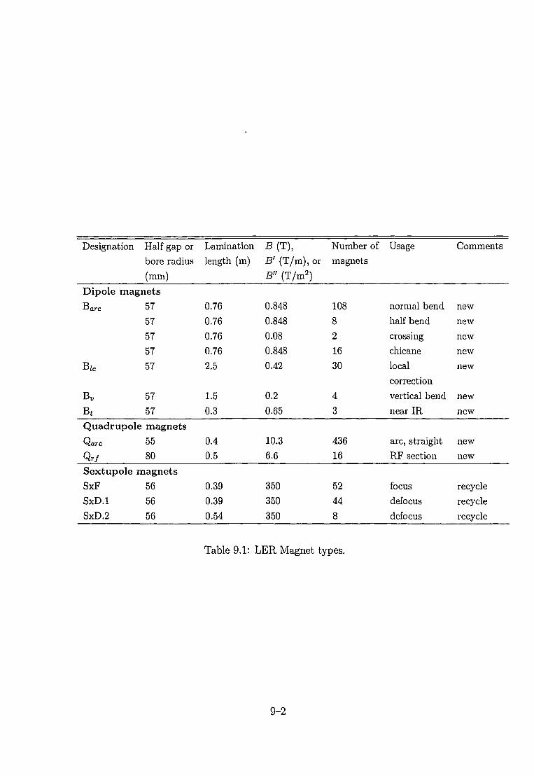
Designation Half gap or
bore radius
(mm)
Dipole magnets
•Bare
B,c
Bu
Bt
57
57
57
57
57
57
57
Quadrupole magnets
Ware
Qr/
55
80
Sextupole magnetsSxF
SxD.l
SxD.2
56
56
56
Lamination
length (m)
0.76
0.76
0.76
0.76
2.5
1.5
0.3
0.4
0.5
0.39
0.39
0.54
23 (T),
23' (T/m), or
23" (T/m2)
0.848
0.848
0.08
0.848
0.42
0.2
0.65
10.3
6.6
350
350
350
Number of
magnets
108
8
2
16
30
4
3
436
16
52
44
8
Usage
normal bend
half bend
crossing
chicane
local
correction
vertical bend
near IR
arc, straight
RF section
focus
defocus
defocus
Comments
new
new
new
new
new
new
new
new
new
recycle
recycle
recycle
Table 9.1: LER Magnet types.
9-2

Designation Half gap or Lamination B (T),
bore radius length (m) B' (T/m), or
(mm) B" (T/m2)
Number of Usage
magnets
Comments
Dipole magnets&CLTC 03
35
5.804
5.804
0.3 112
2
normal bend
crossing
recycle
recycle
QuadrupoleWare
QrfQA
QB
magnets50
80
50
50
0.6
1.00.762
0.95
10.9
6.6
8.5
8.5
144
32
184
92
arc, straight
RF section
arc, straight
arc, straight
new
new
recycle
recycle
SextupoleSxF
SxD
magnets56
56
0.54
0.80
350
350
52
52
focus
defocus
recycle
new
Table 9.2: HER Magnet types.
Tolerance at 50 mm radius
Dipole magnets
Quadrupole magnets
B3/B1 < 0.12
B6/Bi < 0.45
B6/B2 < 0.12
B10/B2 < 0.14
Table 9.3: Tolerances of systematic multipole errors
9-3
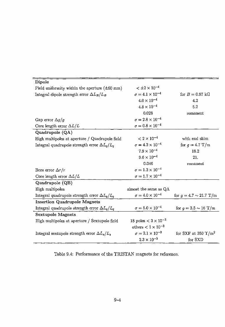
DipoleField uniformity within the aperture (±60 mm)Integral dipole strength error ALB/LB
Gap error Ag/gCore length error AL/L
Quadrupole (QA)High multipoles at aperture / Quadrupole fieldIntegral quadrupole strength error ALq/Lq
Bore error Ar/rCore length error AL/LQuadrupole (QB)High multipolesIntegral quadrupole strength error ALq/Lq
Insertion Quadrupole MagnetsIntegral quadrupole strength error ALq/Lq
Sextupole MagnetsHigh multipoles at aperture / Sextupole field
Integral sextupole strength error AL3/LS
< ±2 x 10~"cr = 4.1 x 10""
4.0 x 10""4.8 x 10""
0.028a = 2.8 x 10~"a = 0.8 x 10~"
< 2 x 10""a = 4.2 x 10-"
7.9 x 10-"9.6 x 10""
0.046a = 1.2 x 10~"a = 1.7 x 10-"
almost the same as QAa = 4.0 x 10~"
o- = 5.0 x 10""
18 poles < 3 x 10~3
others < 1 x 10"3
a = 2.1 x 10~3
2.3 x 10~3
for B = 0.97 kG4.2
5.2
remanent
with end shimfor g = 4.7 T/m
18.221.
remanent
for g = 4.7 ~ 21.7 T/m
for g = 3.5 ~ 16 T/m
for SXF at 350 T/m2
for SXD
Table 9.4: Performance of the TRISTAN magnets for reference.
9-4

Shorter magnets are known to have inferior field qualities, because of increased end-
field effects. In addition, the accuracy of 2-dimensional calculations will be less reliable
for shorter magnets. However, we believe that the field qualities similar to the TR
magnets would be possible with a careful design and fabrication process control.
The physical designs have been made for the main dipole and quadrupole mag-
nets, the sextupole and vertical steering magnets used for the LER and HER. The
2-dimensional magnetic field code POISSON and the 3-dimensional code 0PERA-3d
have been used for field calculations. The full engineering design of the KEKB magnet
system will be completed as soon as the final beam optics design is finalized.
9.1.1 LER
Table 9.1 summarizes the magnets that are required for the LER. Four types of dipole
bend magnets are needed in the LER: Barc, B/c, Bv and Bj. The LER also requires
two types of quadrupole magnets (Qarc and Qr/), and two types of sextupole mag-
nets (SXFTH and SxDTa). All of them except the sextupole magnets will be newly
fabricated. The LER sextupole magnets will be recycled from the TR.
Dipole Magnets
The LER requires 171 dipole magnets in total. They include 134 Barc, from which 108
Ba r c will be used for normal bends, 8 for half bends, 2 for beam crossing (the LER-
HER cross-over) and 16 for the chicane structure. From the special dipole magnets, 30
B/c will be used for local chromaticity correction, 4 B^ for vertical bends and 3 Bt for
special use near the IR section located near the Tsukuba experimental hall.
The mechanical and electric parameters of Ba rc are listed in Table 9.5. The lami-
nation core length in the table does not include the side plates and electrodes. Thus
the physical magnet sizes will be larger. A cross section view of the preliminary design
of a LER dipole magnet (Barc) is shown in Figure 9.1. The final designs of the special
dipole magnets have not been fixed yet. We will proceed with physical designs of these
magnets as soon as their final parameters are finalized.
Quadrupole Magnets
There are 452 quadrupoles in the LER. The 436 Qarc will be used for the arc and
the straight sections, except for the beam line that includes RF cavities. For the RF
sections, 16 Qry which have larger aperture will be used. The mechanical and electric
parameters of Qarc and Q r / are listed in Tables 9.6 and 9.7. Figure 9.2 shows a cross
section view of the preliminary design of a LER quadrupole magnet (Qarc)-
9-5

Figure 9.1: A cross section view of the preliminary design of a LER dipole magnet
(Bare)-
650
Figure 9.2: A cross section view of the preliminary design of a LER quadrupole magnet
(Qarc).
9-6

Figure 9.3: A cross section view of the preliminary design of a LER sextupole magnet.
Sextupole Magnets
The mechanical and electric parameters of the sextupoles are listed in Table 9.9. The
LER will require 104 sextupoles, which consist of 56 SxF's and 48 SxD's. The present
plan is to re-use the TR sextupoles, SXFTR and SxDrn• For each of SxFT^ and SxDTfi
from TRISTAN, 96 units out of 120 are expected to be negligibly radio-active and thus
adequate for re-use. The 96 SXFT^'S will be recycled to provide all of the 56 SxF's and
40 SxD's. The remaining 8 SxD's will come from SXDTRS.
Radiation damages on the TR magnets will be closely inspected in the summer of
1995. Exactly which part (iron core and the coils) of the TR magnets should be reused
will be decided based on the results of this inspection.
Figure 9.3 shows a cross section view of the preliminary design of a LER sextupole
magnet. The HER sextupole magnets will have a similar cross section shape.
Steering Correction Magnets
The parameters of the vertical steering magnets are given in Table 9.10. The LER
will require 450 vertical steering magnets, which will be located adjacent to each
quadrupoles. The maximum kick angle of 1 mrad is assumed for the vertical steer-
ing magnets. Almost same number of horizontal steering magnets would be necessary
9-7
in the future.
Wiggler Magnets
The wiggler magnets will be used for the LER to control the radiation damping time.
The field strength of the wiggler is the same as the arc dipole magnets. The total
length of wigglers will be 96 m. This is close to the total length of the arc dipoles.
Detailed design of the wiggler magnet is being worked out.
9.1.2 HER
Table 9.2 summarizes the magnets that are required for the HER. There will be one
type of bending magnet called Barc, 4 types of quadrupoles Qarc, Q r/ , QA and QB, and
2 types of sextupoles SxF and SxD. The Qarc, Q r/ and SxD will be newly fabricated,
while the others will be recycled from TR. Details of the recycle plan will be determined
after the inspections on the TR magnets planned in the summer of 1995.
Dipole Magnets
The HER needs 114 Barc's, in which 112 Ba rc will be used for the arc and 2 for beam
crossing. The TR bending magnets will be recycled for these dipole magnets. The
mechanical and electric parameters of Barc are listed in Table 9.5.
Quadrupole Magnets
The HER requires 452 quadrupole magnets in total. The 144 Qarc and 32 Q r/ will be
newly fabricated. The 184 QA and 92 QB will be recycled from TR for the arc and
straight sections except the beam line that includes the RF cavities. The Qr/'s, which
have 80 mm bore radius, will be used for the RF sections. The mechanical and electric
parameters of these quadrupole magnets are listed in Tables 9.6, 9.7 and 9.8.
Sextupole Magnets
There will be 104 sextupoles in HER; 52 SxF's and 52 SxD's. At present, the SxF's
will use the SxDrn's recycled from TR, while 52 SxD's with 0.8 m length will be newly
fabricated. The mechanical and electric parameters of the sextupoles are listed in
Table 9.9.
9-8
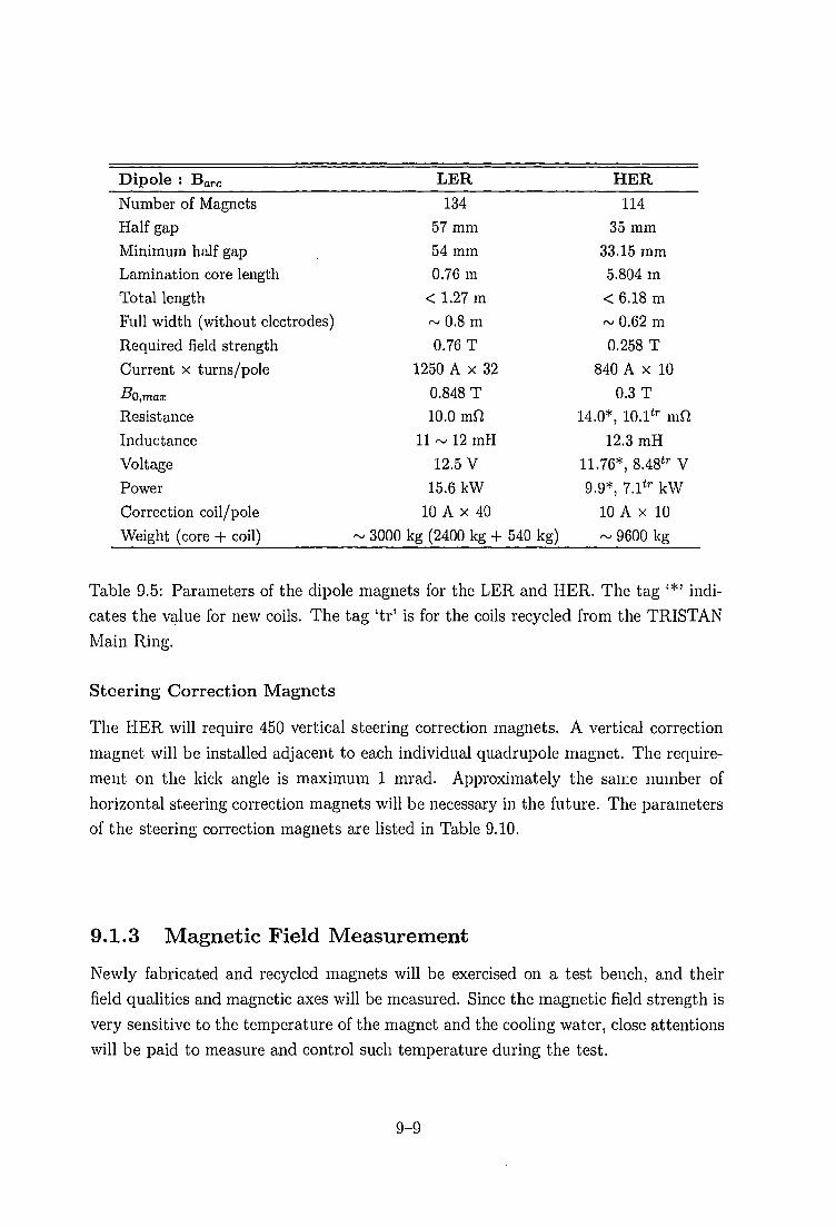
Dipole : Barc
Number of MagnetsHalf gapMinimum half gapLamination core lengthTotal lengthFull width (without electrodes)Required field strengthCurrent x turns/pole
•t'O.mox
ResistanceInductanceVoltagePowerCorrection coil/poleWeight (core + coil)
LER134
57 mm54 mm0.76 m
< 1.27 m~0.8m0.76 T
1250 A x 320.848 T10.0 mfi
11 ~ 12 mH12.5 V
15.6 kW10 A x 40
~ 3000 kg (2400 kg + 540 kg)
HER114
35 mm33.15 mm5.804 m< 6.18 m~ 0.62 m0.258 T
840 A x 100.3 T
14.0*, 10.1tr mfi12.3 mH
11.76*, 8.48tr V9.9*, 7.1ir kW
10 A x 10~ 9600 kg
Table 9.5: Parameters of the dipole magnets for the LER and HER. The tag '*' indi-
cates the value for new coils. The tag 'tr' is for the coils recycled from the TRISTAN
Main Ring.
Steering Correction Magnets
The HER will require 450 vertical steering correction magnets. A vertical correction
magnet will be installed adjacent to each individual quadrupole magnet. The require-
ment on the kick angle is maximum 1 mrad. Approximately the same number of
horizontal steering correction magnets will be necessary in the future. The parameters
of the steering correction magnets are listed in Table 9.10.
9.1.3 Magnetic Field Measurement
Newly fabricated and recycled magnets will be exercised on a test bench, and their
field qualities and magnetic axes will be measured. Since the magnetic field strength is
very sensitive to the temperature of the magnet and the cooling water, close attentions
will be paid to measure and control such temperature during the test.
9-9

Quadrupole ; Qare LER HERNumber of Magnets 436 144Bore radius 55 mm 50 mmLamination core length 0.4 m 0.6 mTotal length < 0.63 m < 0.83 mHalf width (without electrodes) ~ 0.35 m ~ 0.35 mRequired field strength 8.5 T/m 11 T/mCurrent x turns/pole 500 A x 25 500 A x 22B'Qtmax 10.3 T/m 10.9 T/mResistivity 25.1 mQ 32.2 mfiInductance ~ 22 mH ~ 30 raHVoltage 12.6 V 16.1 VPower 6.28 kW 8.04 kWCorrection coil/pole 10 A x 12 10 A x 12Weight (core + coil) ~ 1230 kg (1100 kg + 130 kg) ~ 1750 kg (1550 kg + 160 kg)
Table 9.6: Parameters of the arc quadrupole magnets for the LER and HER.
Quadrupole : Q r / LER HER32
80 mm1.0 m
< 1.25 m~ 0.40 m6.0 T/m
500 A x 346.6 T/m86 mft
~49 mH43 V
21.5 kW10 A x 17
Weight (core + coil) ~ 1700 kg (1480 kg + 200 kg) ~ 3150 kg (2820 kg + 300 kg)
Table 9.7: Parameters of the quadrupole magnets in the RF sections for the LER and
HER.
9-10
Number of MagnetsBore radiusLamination core lengthTotal lengthHalf width (without electrodes)Required field strengthCurrent x turns/pole73/•D0,max
ResistivityInductanceVoltagePowerCorrection coil/pole
1680 mm0.5 m
< 0.75 m~ 0.40 m5.1 T/m
500 A x 346.6 T/m52 mfi
~27mH26 V
12.9 kW10 A x 17

Quadrupole : QA, QB
Number of Magnets
Bore radius
Lamination core length
Total length
Half width (without electrodes)
Required field strength
Current x turns/pole
•"O.maz
Resistivity
Inductance
Voltage
Power
Correction coil/pole
Weight (core + coil)
HER: QA
(recycled from TR)
184
50 mm
0.762 m
< 1.0 m
0.42 m
T/m
500 A x 17
8.5 T/m
13.0 mfi
15.5 mH
6.5 V
3.25 kW
10 A x 10
~ 4500 kg
HER: QB
(recycled from TR)
92
50 mm
0.95 m
< 1.2 m
0.42 m
T/m
500 A x 17
8.5 T/m
15.2 mft
19 mH
7.6 V
3.8 kW
10 A x 10
~ 5600 kg
Table 9.8: Parameters of the QA and QB quadrupole magnets for the HER. Calcula-
tions have been made with an assumption that these magnets are recycled from the
TRISTAN main ring.
9-11

Sextupole
Number of Magnets
Bore radius
Lamination core length
Total length
Half width (without electrodes)
Required field strength
Current x turns/pole
B'otmax measuredResistivity
Inductance
Voltage
Power
Correction coil/pole
Weight (core + coil)
Number of Magnets
Bore radius
Lamination core length
Total length
Half width (without electrodes)
Required field strength
Current x turns/pole
- d'max measuredResistivity
Inductance
Voltage
Power
Correction coil/pole
Weight (core + coil)
LER
Sx: 0.39 m long(recycled from SXFJTJ)
96
56 mm
0.39 m
< 0.51 m
~ 0.36 m
350 T/m2
425 A x 21
350 T/m2
32.8 mfi
15.5 mH
13.9 V
5.9 kW
830 kg (720 + 110)
Sx: 0.54 m long(recycled from SXDTR)
8
56 mm
0.54 m
< 0.66 m
~ 0.36 m
350 T/m2
425 A x 21
350 T/m2
40.9 mft
19 mH
17.4 V
7.4 kW
1100 kg (960 + 140)
HER
SxF: 0.54 m long
(recycled from SXDy/^)
52
56 mm
0.54 m
< 0.66 m
~ 0.36 m
350 T/m2
425 A x 21
350 T/m2
40.9 mQ
19 mH
17.4 V
7.4 kW
1100 kg (960 + 140)
SxD: 0.8 m long(new)
52
56 mm
0.8 m
< 0.92 m
~ 0.36 m
350 T/m2
425 A x 21
350 T/rn2
56.6 mQ
28 mH
24.1V
10.2 kW
1590 kg (1390 + 200)
Table 9.9: Parameters of the sextupole magnets for the LER and HER.
9-12

Steering: STVNumber of MagnetsBore radiusLamination core lengthTotal lengthRequired kick angleCurrent x turns/poleSteering: STHNumber of MagnetsBore radiusLamination core lengthTotal lengthRequired kick angleCurrent x turns/pole
LER
45080 mm0.2 m
< 0.3 m1 mrad
5 A x 760
45080 mm0.2 m
<0.3 m1 mrad
5 A x 760
5
5
HER
45080 mm0.2 m
< 0.35 m1 mradA x 1700
45080 mm0.2 m
< 0.35 m1 mradA x 1700
Table 9.10: Parameters of the steering correction magnets for the LER and HER.
Dipole Magnets
A long flip coil and a small flip coil will be used for measurements of dipole magnets.
The integral dipole field is obtained by measuring the voltage induced on the long flip
coil which rotates in the magnetic field. The small flip coil is used for field mapping.
This small flip coil system is mounted on 3-axes mover, and it measures the magnetic
field in the fiducial volume point by point.
The absolute values of the integral and the center field strength will be also mea-
sured by using some devices. These measurement systems will be developed soon.
Quadrupole and Sextupole Magnets
The magnetic field of quadrupole and sextupole magnets of KEKB will be measured by
harmonic coil (rotating coil) systems. Each harmonic coil system consists of one long
coil and three short coils located at the center and both ends. The long coil measures
the integral field strength directly and its quality. The center field is measured by the
middle short coil. The two short coils at both ends are used to assess the end effects
and to locate the magnetic axis to the measuring system.
Before conducting field measurements, the magnet should be pre-aligned to the
measuring bench. A laser beam is used as the reference axis. A 3-axes magnet mover
9-13
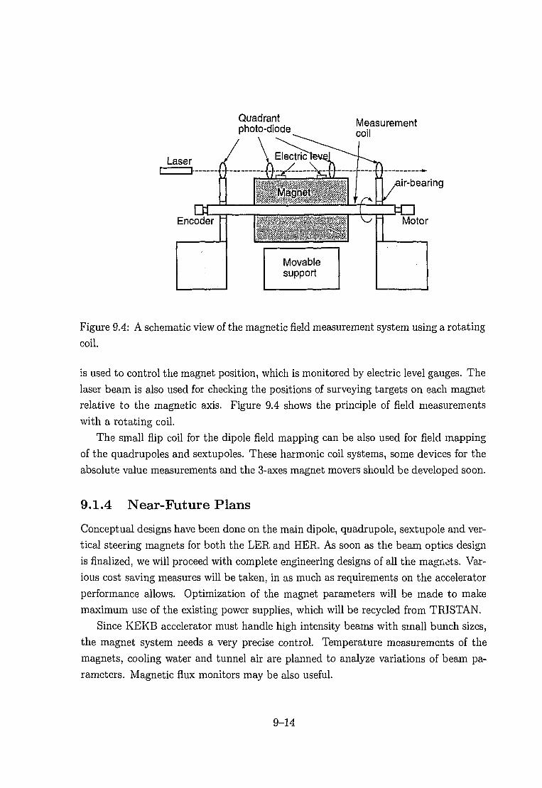
Quadrantphoto-diode
Measurementcoil
ir-bearing
Figure 9.4: A schematic view of the magnetic field measurement system using a rotating
coil.
is used to control the magnet position, which is monitored by electric level gauges. The
laser beam is also used for checking the positions of surveying targets on each magnet
relative to the magnetic axis. Figure 9.4 shows the principle of field measurements
with a rotating coil.
The small flip coil for the dipole field mapping can be also used for field mapping
of the quadrupoles and sextupoles. These harmonic coil systems, some devices for the
absolute value measurements and the 3-axes magnet movers should be developed soon.
9.1.4 Near-Future Plans
Conceptual designs have been done on the main dipole, quadrupole, sextupole and ver-
tical steering magnets for both the LER and HER. As soon as the beam optics design
is finalized, we will proceed with complete engineering designs of all the magnets. Var-
ious cost saving measures will be taken, in as much as requirements on the accelerator
performance allows. Optimization of the magnet parameters will be made to make
maximum use of the existing power supplies, which will be recycled from TRISTAN.
Since KEKB accelerator must handle high intensity beams with small bunch sizes,
the magnet system needs a very precise control. Temperature measurements of the
magnets, cooling water and tunnel air are planned to analyze variations of beam pa-
rameters. Magnetic flux monitors may be also useful.
9-14

9.2 Magnet Power Supplies and Cabling
9.2.1 Magnet Power Supply
The magnet power supply units required at KEKB are listed in Table 9.11. The total
number of large power supplies for the dipole, quadrupole and sextupole magnets is
382. Prom the existing TRISTAN facility about 80 units will be recycled for operating
the dipole and quadrupole magnets at KEKB. Thus the remaining 300 units, which
include most of the sextupole magnet power supplies, need to be newly installed.
The output voltage and the current from the power supplies have been determined
by considering the impedance of power feeding cables with adequate margins for the
output voltage. The designs of the power supply units assume that a substantial
fraction of dipole, quadrupole and sextupole magnets will be recycled from TRISTAN,
as stated earlier. It should be noted that the specifications for the HER magnet power
supplies are subject to change, if the coils are rewound for those TRISTAN magnets.
The maximum output current of the majority of large power supplies is set to be
500 A for two reasons: (1) the cost of power feeding cables, which are very long, can
be reduced by using relatively thin cables, and (2) the room that is available on the
cable ladders in the tunnel is limited, such that not much thick cables can be used.
With this system design choice, both the DC output voltage and the current of large
power supplies are smaller than the case with TRISTAN.
For the power supplies that are recycled from TRISTAN, the DCCT (DC Current
Transformer) heads will be replaced by new units, which have an optimized range for
current measurements at KEKB. If it is found necessary for improved power factor and
better regulation, three-phase AC transformers will be applied to the input of some of
the power supplies.
Table 9.12 shows a list of stability requirements and limits on the ripple content for
magnet power supplies at KEKB.
The requirements on the steering correction magnets at KEKB are much more strin-
gent than the case with TRISTAN. Adequate power supplies for the steering correction
magnets will be newly developed and will be fabricated.
9.2.2 Installation
Along the TRISTAN tunnel there exist 8 power supply stations: 4 big and 4 small.
Most of the TRISTAN magnet power supplies that are housed in the 4 big supply
stations will be re-used for KEKB with some improvements, as discussed earlier.
9-15

Ring Magnet
type
LER Dipole
Wiggler
Quadrupole
Sextupole
Steering
HER Dipole
Quadrupole
Sextupole
Steering
Voltage
(V)1400
120
70
30
700
600
400
90
60
40
30
40
1400
40
20
900
500
400
300
100
60
30
20
60
40
Current
(A)1250
1250
1250
1250
1250
1250
500
500
500
500
500
500
500
425
425
840
840
840
840
500
500
500
500
500
500
500
500
500
425
425
Number of
units
1
2
2
2
15
8
4
1
2
5
21
26
59
2
52
2
886
1
4
3
9
1
3
4
3
10
12
46
29
1
24
28
886
Total
30
120
54
886
17
109
52
886
Table 9.11: The list of magnet power supplies required at KEKB.
9-16

Magnet type Stability Ripple contentDipole 1 x 1(T4 / 8 h 5 x 10~5
Quadrupole 1 x 1CT4 / 8 h 1 x 1(T5
Sextupole 5 x 10~4 / 1 h 5 x 10~4
Steering correction 5 x 10~4 / 8 h 5 x 10"5
Table 9.12: Stability requirements and limits on the ripple content for magnet powersupplies at KEKB
The four small power supply stations will house the power supplies as follows: 12
units for quadrupole, 26 for sextupole and 443 for steering correction magnets.
In addition, a part of Oho, Fuji, and Nikko experimental halls, and the Tsukuba
RF power station will be used for remaining dipole, wiggler and quadrupole magnet
power supplies. A multi-stage structure will be built in each of these halls to make
maximum use of available areas.
9.2.3 Cooling Water
The large power supplies in the existing 4 big power supply stations are all cooled by
pure water. The consumption of pure water has been about 750 £/min for each power
station in the TRISTAN MR operation. The requirement will be reduced to roughly
a half for KEKB.
In a new power supply station in the Oho experimental hall, 14 large power supplies
(a few hundred KW each) need to be installed. Those power supplies will be water-
cooled, considering the limited air conditioning capacity of the station.
All other power supplies that are newly built will be air-cooled for improved han-
dling in the maintenance work.
9.2.4 Electric Power
The maximum total electric power of the magnet power supplies is 19 MW. Considering
the power factor, the capacity of the input power line will somewhat exceed 20 MVA.
However, during actual accelerator operation the total electric power is estimated to
be less than 15 MW. Overall, it is not considered necessary to increase the power of
the input power line.
9-17

9.2.5 Wiring of DC Power Feed Cables
Approximately 500 km of 2-core cables in total is required for the steering correction
magnets in the entire KEKB. The total length of the cables for quadrupole magnets
will be roughly 100 km. Thus the cabling cost can be quite large. As discussed earlier,
the maximum DC current of most of large power supplies is kept below 500 A to
alleviate this situation. Still the weight of cable bundles can exceed 300 kg/m in the
most crowded areas.
9.2.6 Power Supply Controls
All power supplies will be controlled by distributed VME computers. Since KEKB has
a large number of steering correction magnets, the cost of their control interface is a
non-trivial problem. To address this issue, a specialized interface will be developed,
where control set points are serially sent to the power supply units.
9.2.7 R & D for Magnet Power Supplies
Two prototype power supply units will be built in JFY 1995. One is a relatively low-
power magnet power supply with a power of 20 kW. A switch-mode power supply
will be developed for reducing the physical size of the unit, while increasing the power
factor. The other is a power supply for steering correction magnets. The techniques
required for satisfying the tight tolerance and stability specifications will be studied.
9.2.8 Schedule
The bulk of magnet power supply units will be built in 1997 and 1998. The wiring
of the DC power cables and the installation of the control system will be carried out
before installing the power supply units. The work is coordinated with the rest of the
accelerator construction schedule.
9.3 Installation and alignment
About 300 primary network reference points will be installed on the floor inside the
ring tunnel. The interval of the reference points is roughly 10 m. The work will be
done by using a laser tracker system. The overall precision for those primary network
points is expected to be about 2 mm.
9-18

After all the old TRISTAN accelerator elements are brought out of the tunnel and
the floor is cleared, reference points will be marked on the floor by referring to those
primary network points.
Two points will be marked for each dipole magnet in arc sections, one at the position
of the upstream edge and another at the downstream edge. By connecting those points
the lines will be created on which other individual magnets should be installed. The
positions to install all these magnets can be easily obtained by measuring the distance
along those connection lines. In straight sections, reference points will be marked on
the floor every 10 m in distance.
Magnets for the straight sections can be brought in from both experimental halls
and from carry-in entrances in the arc sections. The magnets for the arc sections are
brought into the tunnel from carry-in entrances by using magnet carriers.
Magnets are aligned by using a laser tracker and reflector targets. According to the
vendor catalog, the precision for the position measurement is 1 ppm for the distance
and 10 ppm for the angle. The precision of the angle measurement is improved to
5 ppm by averaging the data taken at the same position. The data can be collected
at the rate of 500 Hz. The relative precision of alignment in the distance of 50 m is
expected to be about 0.1 mm.
In the straight sections, magnets are also aligned by using the laser tracker. The
location along the beam line is measured by a mekometer, a polarization modulated
laser interferometer. With this technique, the expected precision for the distance is
0.2 mm in the distance of 200 m.
9.3.1 Layout for arc and straight sections
Both the LER and HER rings consist of four arc sections and four straight sections.
Each arc quadrant consists of 7 regular cells, each of which includes 5 dipole magnets
Portions of the plan view of the arc sections are shown in Figure 9.5. In the part
(A) the LER is placed outside and the HER, and in the part (B) the LER is outside
the HER.
The two rings of the LER and HER cross each other in the north (Tsukuba) and
the south (Fuji) straight sections. The electron and the positron beams collide in the
Tsukuba experimental hall and cross each other in the Fuji region.
The RF cavities for the low energy ring are located in the Fuji region, and those for
the high energy ring in the Nikko and the Oho region. Wiggler magnets are placed in
the Nikko and the Oho region to adjust the beam dumping times. A schematic layout
view of the Nikko straight section is shown in Figure 9.6
9-19
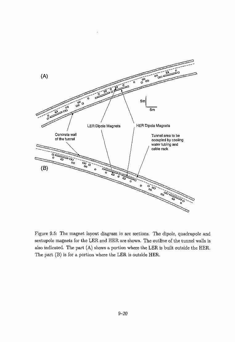
(A)
Concrete wallof the tunnel
Tunnel area to beoccupied by coolingwater tubing andcable rack
(B)
Figure 9.5: The magnet layout diagram in arc sections. The dipole, quadrupole and
sextupole magnets for the LER and HER are shown. The outline of the tunnel walls is
also indicated. The part (A) shows a portion where the LER is built outside the HER.
The part (B) is for a portion where the LER is outside HER.
9-20

LER Electron beam
Concrete wallfor the tunnel
LER Wiggler magnets
\ \
n i< r\
HER Electron beam NikkoHall
0 10 50i n1 1 1 1 1 1 1 1 1 1 1 1 1 1 1 1 1 1 1 1 1 1 1 1 1 1 1 1 1 1 1 ; 1 1 1 1 1 1 1 1 1 1 1 1 1 1 1 > 1 1 1
1 •>. I I L U LX ' ~
HER ARES RF Cavities" \ 2-cell unit
Beam pipe
Figure 9.6: Layout of the Nikko straight section which includes RF acceleration cavities
for the HER and wiggler magnets for the LER.
9-21

Chapter 10
Vacuum System
10.1 LER Vacuum System
This section discusses the vacuum system design for the LER regular arc sections,
which occupy 2200 m out of the 3000 m circumference. The remaining parts of the
LER are four 200 m long straight sections. One straight section is dedicated to beam
collision and the interaction region for physics experiments. The others are reserved
for beam injection, RF cavities and wiggler magnets.
10.1.1 LER System Considerations
Copper has been chosen as the vacuum duct material for its ability to withstand a
high peak heat load, and to shield radiation from the beam. The beam duct has a
circular cross section with an outer diameter of 106 mm. The wall thickness is 6 mm,
which is sufficient for radiation shielding, while being appropriate for fabrication. The
expected radiation dose outside vacuum duct is well bellow 1 x 10⁸ rad/year. The
grade of copper is ASM C10100 (oxygen-free electronic copper) for vacuum surface,
and C10200 (oxygen-free copper) elsewhere. Vacuum flanges are made of stainless
steel AISI304. The magnetic permeability of stainless steel must be less than 1.2 so as
not to magnetically disturb the beam.
The LER stores a positron beam having an energy of 3.5 GeV at a maximum
current of 2.6 A. The bending radius of a dipole magnet is 16.31 m. The total power of
synchrotron radiation will be 2117.1 kW, and its critical energy 5.84 keV. As an option,
there is a plan to add wiggler magnets to the LER, so that its radiation damping time
will equal that of the HER. When this is done, the total radiation power will be
increased to 3817.2 kW (i.e. the same as HER).
The cooling capacity of the refrigerators for the TRISTAN vacuum chamber has
10-1

been 4464 kW. This capacity must be increased to 3817.2 x 2 = 7634.4 kW. A total
water flow rate of 1600 £/min is available for each quadrant of two rings, whose com-
bined length is 1500 m. To ensure a 15 ^/min flow of water which is required based on
thermal calculations, one loop of peripheral circulation must cover about 10 m of the
vacuum duct.
With a bending angle of 3.214° per dipole magnet, the linear heat load on the
chamber wall is estimated to be between 27.6 W m"1 and 14.8 kW m"1. Due to this
horizontally localized heat, the temperature of the beam duct rises locally to 120° C.
Consequently, a high local strain of -0.15% appears along the z direction. Applying
a 0.15% strain over 108 cycles does not cause cracking on a half or quarter tempered
OFC [1]. However, localized heating will lead to an annealing of the material, which can
reduce the local mechanical strength. Annealed OFC can still withstand 104 cycles of a
0.5% deformation at 150° C [2]. However, it is preferred to keep the local temperature
below 140° C at KEKB.
The gas desorption induced by synchrotron radiation, and its implications to the
expected vacuum pressure, have been analyzed. The desorption rate is proportional
to the number of incident photons. The linear photon density (N) averaged over the
entire LER arc (2200 m) is 3.3 x 10¹⁸ photons s^m"1 for the LER. While the desorption
coefficient 77 (molecules per photon) is dependent on the surface finish, roughly it is
decreased with the accumulated photon dose. An average pressure P (Torr) is given
by
P = K^-nN/Sd = 0.1r?/Sd, (10.1)
where K is a unit conversion coefficient (= 3.3 x 10¹⁹ molecules Torr"1^1"1) and Sd is
the distributed pumping speed in units of £ s^m""1.
The pressure-level goal to achieve at KEKB in the presence of the beam is 1 x
10~9 Torr. Our vacuum system has been designed such that this is achieved when 77
reaches 10~6. At storage rings an assumption is often made that 77 = 10~5. However,
this requires an enormous pumping speed, which will be impractical at KEKB. An
rj value of 10~6 is considered to be realistic after a reasonable running time and the
resultant beam dose (~ 1000 Ah) at KEKB. The required pumping speed under this
condition is 100 is^nr1.
Small bunch sizes and the high current of KEKB place additional requirements on
the vacuum system design. The size of any steps of the vacuum duct (i.e. discontinuity
of the inner surface shape) may not exceed 0.5 mm. Pumping slots must be backed up
by a grid, so that the penetration of wake fields, which causes a heat-up of the pumping
elements, is reduced. Bellows and flange connections should be protected from direct
synchrotron radiation hits. This will be accomplished by using suitably shaped, masks
10-2

in the vacuum duct. However, the height of a mask must be lower than 5 mm. In this
regard, a large bend angle in the LER creates a challenging condition for the bellows
immediately downstream of the dipole magnets.
10.1.2 LER Vacuum System Components
Our design does not adopt an ante-chamber scheme. In the LER the synchrotron
radiation is simply distributed on the duct wall. In this configuration it is preferred to
distribute pumping slots along the beam duct.
An issue here is how to cope with possible beam-induced radiation onto the vacuum
pumps. Unfortunately no reliable estimation is available concerning the magnitude
of the radiation that propagates through pumping slots. Consequently, the vacuum
system design must be prepared for an unexpectedly high power penetration. This will
be done by making it possible to install a second grid between the slots and pumping
elements.
All of the pumping elements are, therefore, attached to the vacuum duct via a
flange connection to a pumping port. With the relatively large vacuum conductance
of the beam duct (98 &""1), it has been shown that a distributed pumping speed of
100 fs^m" 1 should be possible by installing pumps having a capacity of 100 £s~l every
1 m. In practice, because of the presence of magnets, such a uniform distribution of the
vacuum pumps cannot always be realized. This causes about a 20% reduction of the
distributed pumping speed. Figure 10.1 shows the basic arrangement of the vacuum
duct in a regular cell. A calculation of the distributed pumping speed for a part of the
regular cell is shown in Figure 10.2.
In the current design three types of beam ducts will be fabricated for the LER.
The first is the "B chamber" which is used with dipole bend magnets. It has a cooling
channel and a mask, as well as pumping ports. The second is the "Q chamber" which is
used for quadrupole magnets. It includes a beam position monitor and a mask, but no
pumping port. The cooling channels are welded on both sides. The third is a straight
"S chamber" which has a cooling channel, a mask and pumping ports. Examples of
those chambers are shown in Figures 10.3, 10.4 and 10.5.
A typical cross section of a LER vacuum duct is shown in Figure 10.6. Two water
channels are electron-beam welded to the outside of the S chamber in a symmetric, way.
One of the beam-based alignment techniques of magnets planned at KEKB will utilize
an active modulation of the excitation of the quadrupole and sextupole magnets. The
symmetric arrangement of water channels causes a eddy current to be induced with
a good left-right symmetry. This symmetry helps analyze the data without having to
make corrections for asymmetric systematic effects.
10-3

£0
I • I I I • I • I • 1 • I • I • I • I10m
td1
fo
CD
O
on
P
CD
cm
oCD
• " •
4 10
Qend
Bend
SO, ,
- Beam Position Monitors(BPMs)
Vacuum Pumps
f«(«»,*,#«*&=
Positron
Standard Cell of LER
Steering CorrectionDipole Magnets

150
I"8d> 1 0 0Q.
w
'a.Eif 50CD
Ul
LER Effective Pumping Speed' ' ' '
10 15
x[m]
Figure 10.2: Expected pressure profile along the beam direction in the LER.
150
b-3150
150-
-2439.7-
Mask 379.29—SR peak
-99 4.85 1- 994.85-Pump port
300
-915- -267.5
b-4
o;
Figure 10.3: An example of the "B chamber" for the LER.
10-5

-200O
q-sx2
h
BPM
Figure 10.4: An example of the "Q chamber" for the LER.
41
Mask
-2674.7-
-^20
—T15Q-—737.35-
oo
-900-
PumF
-—737.35—1150
port
Figure 10.5: An example of the "S chamber" for the LER.
10-6
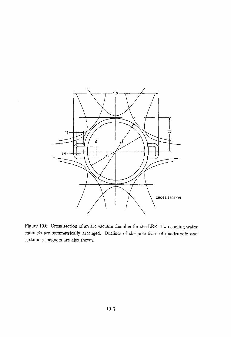
CROSS SECTION
Figure 10.6: Cross section of an arc vacuum chamber for the LER. Two cooling waterchannels are symmetrically arranged. Outlines of the pole faces of quadrupole andsextupole magnets are also shown.
10-7

s"\\ n
c-c c
ICF203
Figure 10.7: Structure of the LER pumping port and slots.
Figure 10.7 shows the structure of a pumping port and slots. The vacuum con-
ductance of the slots of the port has been designed to be greater than 200 is'1. By
using a 200 is'1 NEG or a 200 is'1 ion pump, a pumping speed of 100 is'1 per port
is expected to be achieved.
While the primary pumps comprise of NEG cartridges, secondary pumping is pro-
vided by ion pumps, which are installed every 10 m. Those ion pumps are required
for operating the NEGs. They are also expected to bring the pressure down to about
10 ~7 Torr during the initial pump down before the first activation of the NEGs.
An oxide layer on the duct inner surface contains a large amount of carbon com-
positions, which are released as CO and CO2 in desorption. To avoid the necessity of
frequent conditioning of the NEG during commissioning, it is necessary to remove this
first oxide layer and to produce a new oxide layer that is free of carbon. This treat-
ment will be done using a commercially available chemical cleaner containing H2O2
and H2SO4, or by applying a standard acid etch with H2SO4, HNO3, HC1, and water.
The effect of each cleaning is shown in Figure 10.8.
The bellows and flanges must be protected from direct exposure to synchrotron
light. For this purpose a mask structure is embedded at one end of each vacuum
duct unit. A schematic design diagram of a mask is shown in Figure 10.11. A mask
10-8

10°
£ 1 o"1 -
o
o8
Q.o
o
Q.
10"!
Untreated OFC H2......... ( ^ J .
i i
w I
\
4
3
101 101 1019 10Z0 1021 102 2
Photon dose [photons/m]
Figure 10.8: Measured photo desorption rate of hydrogen, water, carbon mono oxide
and carbon di-oxide as function of accumulated photon doze. In this case, the copper
material is not treated by chemical cleaner nor by acid etching.
Chemical polishing
1 ( ) 22
Photon Dose [photons/m]
Figure 10.9: Measured photo desorption rate from a copper sample which has beencleaned by chemical cleaner.
10-9

Acid etch
10°
co
J. 10'1
O
I 10-£
s 10-
o
I 10''
;« -*""""
j:
;
rrr*n.
. . .
:
M
H2
CH4
c ° 2
1011 0 2 0 1 0 2 1
Photon dose [photon/m]
Figure 10.10: Measured photo desorption rate from a copper sample which has been
processed by standard acid etching.
receives a larger amount of heat than the surrounding wall. The most stringent case is
a 1.41 kW heat load for a 12 cm mask. The maximum temperature will reach about
130° C. This level of temperature rise is not considered to be problematic.
Button electrodes of the beam position monitor (BPM) unit are blazed on a copper
block. The locations of the BPMs in a regular cell are shown in Figure 10.1. The
design of the BPM blocks is discussed in chapter 11. The heat load due to synchrotron
radiation depends on the location of individual BPMs. The heat deformation of the
BPM units has been estimated. About one hundred BPMs will have their pickup feed-
through assemblies shifted by 10 to 20 /an. However, if the shift of four electrodes in a
BPM unit occurs in a symmetric way, the net effect does not cause an apparent shift
of measured beam position. It only causes a very small change of the BPM sensitivity.
Bellows of two different designs (Type A and Type B) are being considered for the
LER, as shown in Figures 10.12 (Type-A) and 10.13 (Type-B). In a Type-A bellows
a tube seal is used as the RF contact. The seal follows the possible deformation of
the bellows unit. A Type-B bellows has a finger contact. The loss factor of the Type-
B bellows is expected to be smaller than that of Type-A. However, since a Type-B
bellows has long slot gaps between the fingers, field penetration through those gaps is
a potential problem. It appears to be difficult to plug those gaps while maintaining
good mechanical flexibility. A possible design solution is to adopt a Type-B bellows,
10-10
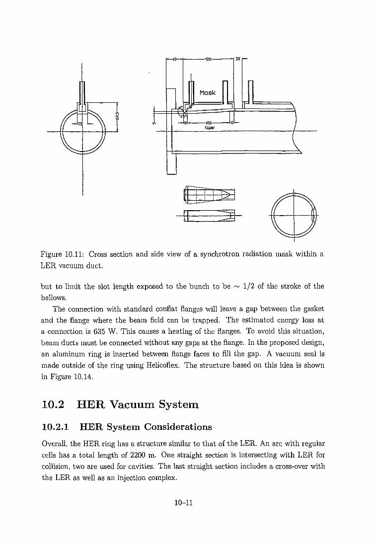
jg ;
".5 ••*
Figure 10.11: Cross section and side view of a synchrotron radiation mask within a
LER vacuum duct.
but to limit the slot length exposed to the bunch to be ~ 1/2 of the stroke of the
bellows.
The connection with standard conflat flanges will leave a gap between the gasket
and the flange where the beam field can be trapped. The estimated energy loss at
a connection is 635 W. This causes a heating of the flanges. To avoid this situation,
beam ducts must be connected without any gaps at the flange. In the proposed design,
an aluminum ring is inserted between flange faces to fill the gap. A vacuum seal is
made outside of the ring using Helicoflex. The structure based on this idea is shown
in Figure 10.14.
10.2 HER Vacuum System
10.2.1 HER System Considerations
Overall, the HER ring has a structure similar to that of the LER. An arc with regular
cells has a total length of 2200 m. One straight section is intersecting with LER for
collision, two are used for cavities. The last straight section includes a cross-over with
the LER as well as an injection complex.
10-11

-160-
ON
it
tube seal
Lznmm
Figure 10.12: Schematic drawing of a Type-A LER bellows
('O)U) (')(£)(£) (£) ill) (£)
Figure 10.13: A schematic drawing of a Type-B LER bellows.
10-12

Helicoflex
SUS304
Al ring Ra=0.8
HV>65
(22)
Figure 10.14: Vacuum sealing using Helicoflex.
As shown in Figure 10.15, the cross section of the HER beam duct has a racetrack
shape with a 58 mm half width and r = 31 mm (outer curvature) with a thickness of
6 mm. The vacuum duct will be made of copper.
The HER stores the electron beam of E = 8 GeV at a maximum current of / =
1.1 A. The orbit bend radius in a dipole magnet is 104.46 m. The total power of
synchrotron radiation is 3817.2 kW with a critical energy of 10.9 keV. Synchrotron
radiation will hit the wall of the beam duct within a dipole magnet. The maximum
linear heat load on the chamber wall in the arc is 5.8 kW m"1. This heat load allows
the use of an aluminum alloy.
The linear photon density in the HER averaged over the arc (2200 m) is expected
to be 3.2 x 10¹⁸ photons s^m"1 . This situation is quite similar to that of the LER.
Consequently, the distributed pumping speed in the HER is also 100 I s"1 m"1.
Since the beam current is lower than the LER, expected wake field problems at
HER are not so serious as in the LER. A beam duct is pumped through side slots
(backed up with grid) and NEG strips are used as the distributed pump.
10-13
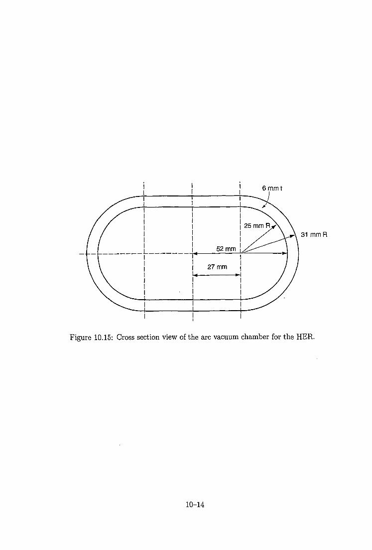
6mmt
31 mm R
Figure 10.15: Cross section view of the arc vacuum chamber for the HER.
10-14

Bibliography
[1] Private communication with Hitachi Works, Co. Ltd.
[2] Private communication with Hitachi Cable, Co. Ltd.
10-15

Chapter 11
Beam Instrumentation
11.1 Beam Position Monitor (BPM)
The purpose of the Beam Position Monitor (BPM) system is to measure the beam orbit
in the accelerator. The BPM data will be used for correcting closed orbit distortions
(COD), and to optimize the operation of the rings. At KEKB the data are also used
for analyzing the alignment and strength errors of magnetic components in the rings.
The latter purpose requires a BPM system with good stability and high precision.
This cannot be easily realized with a "fast" system where the beam positions are
measured every turn. Therefore, the system adopted at KEKB is a "slow" system,
where measurements are performed for the beam positions averaged over many turns.
A similar system has been used at TRISTAN for several years, and its operation has
been well proven.
An electrostatic pickup unit at KEKB consists of four disk electrodes. A pickup
unit will be installed near every quadrupole magnet in the two rings. There will be
about 450 BPMs to be installed in each ring; in total there will be 900 pickup units
for the entire KEKB. Since a multi-bunch, high-current beam will be stored at KEKB
(LER 2.6 A, HER 1.1 A) special attention must be paid to the design of the pickups,
transmission lines, switches and front-end electronics. This section outlines the BPM
system design for KEKB.
11.1.1 Pickup unit
The important design considerations of the BPM pickup electrodes are as follows:
• Reduce the pickup beam power by using electrodes with a small cross section
(diameter 12 mm).
11-1

Alumina 95%
CuproNickel
TE11 mode damper
Beam direction
— — » Z
Figure 11.1: BPM electrode for KERB
• Transfer the beam power safely through feed-throughs with sufficient mechanical
strength and power capacity.
• Suppress the higher-order mode resonances in the electrode assembly.
• Minimize the mechanical deformation of the unit in order to improve the mea-
surement precision.
• Unit assembly with reliable brazing processes.
• Precise and mechanically robust installation of the pickup units on the quadrupole
magnets.
Figure 11.1 shows a preliminary design of the pickup unit. To realize sufficient
mechanical strength and to withstand the expected transmission power, an iV-type
feed-through with a modified center conductor having a larger diameter, together with
a spring contact, will be used.
The BPM block is made from a solid piece of copper. Four feed-throughs with
electrodes are brazed onto the block, as shown in Figure 11.2. Two stainless steel
frames are brazed to the block, and they prevent a deformation of the unit. The
completed BPM assembly is supported firmly and precisely at the end of a quadrupole
magnet, as shown in Figure 11.3. The flat surface of the frame also serves as a reference
plane for the purpose of an electrical mapping calibration of the BPM.
11-2

120 120
Figure 11.2: BPM blocks for the HER(left) and the LER(right).
All BPMs will be tested at a calibration bench where the electrical center of each
BPM will be identified within 20 /im using a movable antenna. During installation,
the BPM positions relative to the quadrupole magnets will be measured within several
tens of a fjxn, and the data will be used to correct the measured beam position data.
The frequency response of the BPM electrode impedance has been calculated using
a coaxial model. The result is shown in Figure 11.4. Since the 1 GHz component
of the signal (i.e. 2nd harmonic of the RF frequency) will be used for beam position
measurement, it is not necessary to be very concerned about the VSWR. over a wide
frequency range.
However, to avoid the growth of coupled bunch instabilities and heating problems of
the ceramic seal, close attention must be paid to the resonance impedance of the BPM
electrode and the feed-through structure. Design optimization to minimize harmful
resonances is in progress. One of the most harmful resonances against beam stability
is the TE110 mode, which is expected in the 7.3 ~ 7.9 GHz frequency range. Our
calculations indicate that the coupling impedance of the TE110 mode may be suffi-
ciently low, so that the beam instability due to this mode may not be a concern. If this
actually becomes a problem, the cross section shapes of the feed-through and the rod
electrode may be made non-axially-symmetric to suppress the TEl l mode within the
structure. As for the other resonances which may be trapped inside the feed-through
structure, it is planned to optimize the size of the ceramic seal, thereby shifting the
11-3

Figure 11.3: Support of the BPM block.
11-4

T—i—i—i—i—i—i—i—i—I—i—i—i—i—|—i—E—i—i—i—i—i—i—i—i—i—i—i—r
0 2.5 5 7.5 . 10 12.5frequency [GHz]
Figure 11.4: Frequency response of the BPM electrode impedance, which has been
calculated using a coaxial model.
resonance frequency off the RF harmonics.
11.1.2 Signal processing method
The following performance requirements have been given to the BPM read-out system
design:
• The position resolution should be better than lOfxm.
• The COD measurement must be completed within a short time of ~ 1 second.
• The system must function for a beam current range of 10 mA ~ 2.6 A.
In order to satisfy these requirements, we have adopted basically the same signal
processing method as of the TRISTAN Main Ring BPM read-out system. Four beam
signals from each pickup unit are detected with a common detection circuit, which
measures a higher harmonic of the revolution frequency. With narrow band signal
processing and by using a common detector we can reduce the measurement errors.
The expected position resolution and the measurable range of the beam signal have
been estimated. The calculation assumed that the geometrical sensitivity coefficient
K of typically 26 mm, and it includes the effects of the thermal noise of the detection
11-5

—•— Df=10Hz(HER)—a -Df=100Hz(HER)- • - -Df=1KHz(HER)
10 100beam current(mA)
1000
Figure 11.5: Expected position resolution determined by the thermal noise.
circuit, including the signal cable. Figure 11.5 shows the expected position resolution as
function of the beam current for a varying frequency band-width (A/). The resolution
improves in proportion to the beam current, and to the inverse of the square root
of the band width. This is because the thermal noise power is proportional to the
band width. From this study, the bandwidth was chosen to be A / = 100 Hz, so
that the resolution, including the thermal noises, would be better than 10 /zm at the
beam current of 10 mA. In the case of the single bunch operation, the bandwidth must
be significantly decreased, because the transient signal amplitude limits the dynamic
range, and it becomes difficult to keep the noise figure small. Optimization for the
single bunch measurement is now under consideration.
11.1.3 Layout of the BPM system
A schematic layout of the signal processing system is shown in Figure 11.6. These cir-
cuit units are distributed in 20 local control buildings around the ring. The beam signal
from the four pickup electrodes for each BPM are transmitted through independent
coaxial cables. A 2 m long radiation-resistant cable, such as a PEEK (poly-ether-
ether-keton) insulation cable, will be used between the pickup electrode and the signal
transmission cable to overcome possible damage due to radiation. At the input of a
detection circuit the signals are selected by RF switches.
The effects of the cable impedance variation during a period of several days have
been evaluated for signal cables of the TRISTAN BPMs. It has been found that the
equivalent shift of the measured beam position due to such effects is less than 10 jj,m.
At KEKB the BPM measurements are expected to be conducted much more fre-
11-6

FDDI
45 BPMsVXI
FDDI
Ethernet
Controller
SW.DET.ADC
SW.DET.ADC
SW.DET.ADC
SW.DET.ADC
SW.DET.ADC
VXIController
SW.DET.ADC
SW.DET.ADC
SW.DET.ADC
SW.DET.ADC
SW.DET.ADC
VXIController J
SW.DET.ADC
SW.DET.ADC
SW.DET.ADC
SW.DET.ADC
SW.DET.ADC
Figure 11.6: Beam position monitor system.
11-7

RF switch
BPM ProgramableAttenuator BPF
0-75dB step 5dB Circurator
fc=50MHz
BW=1MHz
1.0178GHZ
lc=10.7MHz
BW=200KHz
lc=455KHz
BW=30KHz
1st Mixer
I1st
L.O.
- |LPF[—
_|HFF [_,-MA
X
\1st > v ^IF a m p / "
2nd Mixer
^ 11
2nd
L.O.
-j LPF | —
•JHPF [-,
-vU1
2ncNvIF amp/—
3rd Mixer
I3rd
L.O.
-|LPF |—
-JHPF L
-vUr
SrdN.IF amp/—
L/
Synchronous
Detector— ADC -VXI
Figure 11.7: Block diagram of the front-end signal processor.
quently than at TRISTAN. For reliability reasons, the use of mechanical switches was
abandoned at an early stage of the design studies. Two types of RF switches are cur-
rently under consideration: a PIN diode switch and a mercury switch. In our on/off
test of 5 x 10⁶ ~ 1.4 x 10⁷ switching, the measured fluctuation of the insertion loss was
less than 1 x 10~4 for both types of switches. This contact fluctuation translates into
a measurement error of < 10 ^m.
The signal detection circuit consists of a triple-stage super-heterodyne circuit with
a synchronous detector. Its concept is similar to that of TRISTAN. Figure 11.7 shows
a block diagram of the front-end electronics. In order to measure beams with any
multi-bunch configurations, a pickup frequency of 1.016GHz has been chosen. This
corresponds to twice the accelerating RF frequency, and the 10240'th harmonic of the
revolution frequency (99.9 KHz). To obtain good linearity in a wide signal dynamic
range, a synchronous detector is employed to convert the intermediate frequency (IF)
signal to the DC signal. The band width for signal detection is determined by the low
pass filter in the final stage. The output of the detection circuit is converted to digital
data by an A/D converter (ADC). The present plan is to use a 20-bit "A/S" type
ADC with a step-response time of ~ 120 msec to meet the resolution requirement.
The digital data will be sent to a VXI (VME-bus Extensions for Instrumentation)
mainframe in each local control room, where they are transformed into beam position
data. Each VXI station will be linked to a workstation through a local area network.
11-8

The shortest possible measurement time is determined by the sum of the switching
time of the RF switch (~ 4 x 2 ms), the response time of the front-end processor
(~ 4 x 15 ms) and the conversion time of the A/D converter (~ 4 x 120 ms).
In the present design, each front-end signal processor has an individual A/D con-
verter to minimize the conversion time and the data acquisition time. If each BPM
signal is managed by an individual front-end processor including an ADC, a shorter
data acquisition time of ~ 0.6 s is expected, thus satisfying the ultimate performance
requirement described earlier. In the early stage of operation, signals from the BPMs
will be multiplexed to a common circuit to reduce the system cost. For example, if
5 BPMs share a common circuit, the measuring time will be ~ 3 s. However, since
the signals from all BPM electrodes are delivered through separate cables, the signal
processing time will be shortened by incrementally adding circuits in the electronics
house.
11.2 Optical Monitor
The beam profile monitor based on an imaging of the synchrotron radiation will give a
visible beam profile, which will greatly improve the efficiency of the commissioning of
KEKB. By digitizing the image data, transverse beam sizes can be obtained, and with
knowledge of the lattice parameters, various beam parameters, such as the beam emit-
tance and horizontal-vertical coupling, can be deduced. The dependence of the beam
size measured with this device on the beam current gives some information concerning
collective effects. Furthermore, by using a streak camera or a photon counting system,
the longitudinal profile of the beam bunch can be observed. This section presents the
basic design of the optical beam profile measurement system at KEKB.
11.2.1 Choice of the Synchrotron Light Source Point
While several choices of the synchrotron light sources are possible, the heat load due to
the radiation onto the light extraction mirrors needs to be considered. This is because
of the high current operation expected at KEKB. Our design choice is to relax the
heat load on the mirror by using a dedicated weak bending magnet as the light source
in a zero-dispersion section for both the LER and HER. This offers synchrotron light
of manageable power with simple spatial and energy distributions for handling. The
parameters of the light source magnets (preliminary) are listed in Table 11.1.
With these parameters the theoretical angular distribution and energy spectrum
of the synchrotron light at wavelengths of 480 nm, 550 nm and 634 nm are shown in
11-9
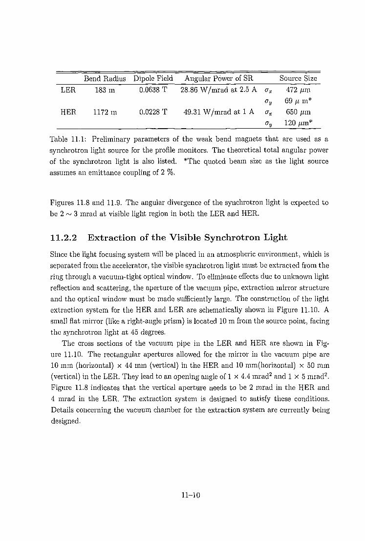
28.86 W/mrad at 2
49.31 W/mrad at
.5 A
1 A
ox
Oy
Ox
Oy
47269^650
120
: m*fim
fim*
Bend Radius Dipole Field Angular Power of SR Source Size
LER 183 m 0.0638 T
HER 1172 m 0.0228 T
Table 11.1: Preliminary parameters of the weak bend magnets that are used as a
synchrotron light source for the profile monitors. The theoretical total angular power
of the synchrotron light is also listed. *The quoted beam size as the light source
assumes an emittance coupling of 2 %.
Figures 11.8 and 11.9. The angular divergence of the synchrotron light is expected to
be 2 ~ 3 mrad at visible light region in both the LER and HER.
11.2.2 Extraction of the Visible Synchrotron Light
Since the light focusing system will be placed in an atmospheric environment, which is
separated from the accelerator, the visible synchrotron light must be extracted from the
ring through a vacuum-tight optical window. To eliminate effects due to unknown light
reflection and scattering, the aperture of the vacuum pipe, extraction mirror structure
and the optical window must be made sufficiently large. The construction of the light
extraction system for the HER and LER are schematically shown in Figure 11.10. A
small flat mirror (like a right-angle prism) is located 10 m from the source point, facing
the synchrotron light at 45 degrees.
The cross sections of the vacuum pipe in the LER and HER are shown in Fig-
ure 11.10. The rectangular apertures allowed for the mirror in the vacuum pipe are
10 mm (horizontal) x 44 mm (vertical) in the HER and 10 mm(horizontal) x 50 mm
(vertical) in the LER. They lead to an opening angle of 1 x 4.4 mrad2 and 1 x 5 mrad2.
Figure 11.8 indicates that the vertical aperture needs to be 2 mrad in the HER and
4 mrad in the LER. The extraction system is designed to satisfy these conditions.
Details concerning the vacuum chamber for the extraction system are currently being
designed.
11-10

~~ 1.40E+10n
E 1.20E+10
| 1.00E+10
?; 8.00E+09d
^ 6.00E+09
2 4.00E+09
2.00E+09
O.OOE+00
1.80E+10
1.60E+10
1.40E+10
ra 1.20E+10
1.00E+10
8.00E+09
» 6.00E+09o1 4.00E+09a
2.00E+09
0.00E+00-1.5 -1.0 -0.5 0.0 0.5 1.0 1.5
Vertical observation angle(mrad)
-2.000 -1.000 0.000 1.000 2.000
Vertical observation angle(mrad)
(A) HER (B) LER
Figure 11.8: Theoretical angular distribution of the synchrotron light in the HER (A)
and the LER (B).
m
•a2
o
JO
>co'o
a.
1.00E+16 -»
1.00E+15-I
1.00E+14
1.00E+13-
1.00E+12
1.00E+11 -
1.00E+10
1.00E+09-
1.00E+08
\
0.10 1.00 10.00 100.00
Photon energy(KeV)
(A) HER
1.00E+16-
1.00E+15-
£ 1.00E+14-S
d
"g 1.00E+13-S
|
S: 1.00E+120)
c 1.00E+11 -oo
1- 1.00E+10-
1.00E+09-:
1.00E+08'
0.10"T 1—TTTTTT
1.00 10.00 100.00
Photon energy(KeV)
(B)LER
Figure 11.9: Theoretical energy distribution of the synchrotron light in the HER (A)
and the LER (B).
11-11

Effective area of the mimbr
JO f t
Effective area of the mirr6r
\
(A) HER
Extraction mirror
(B) LER
Figure 11.10: Configuration of the extraction system for visible synchrotron light.
11-12
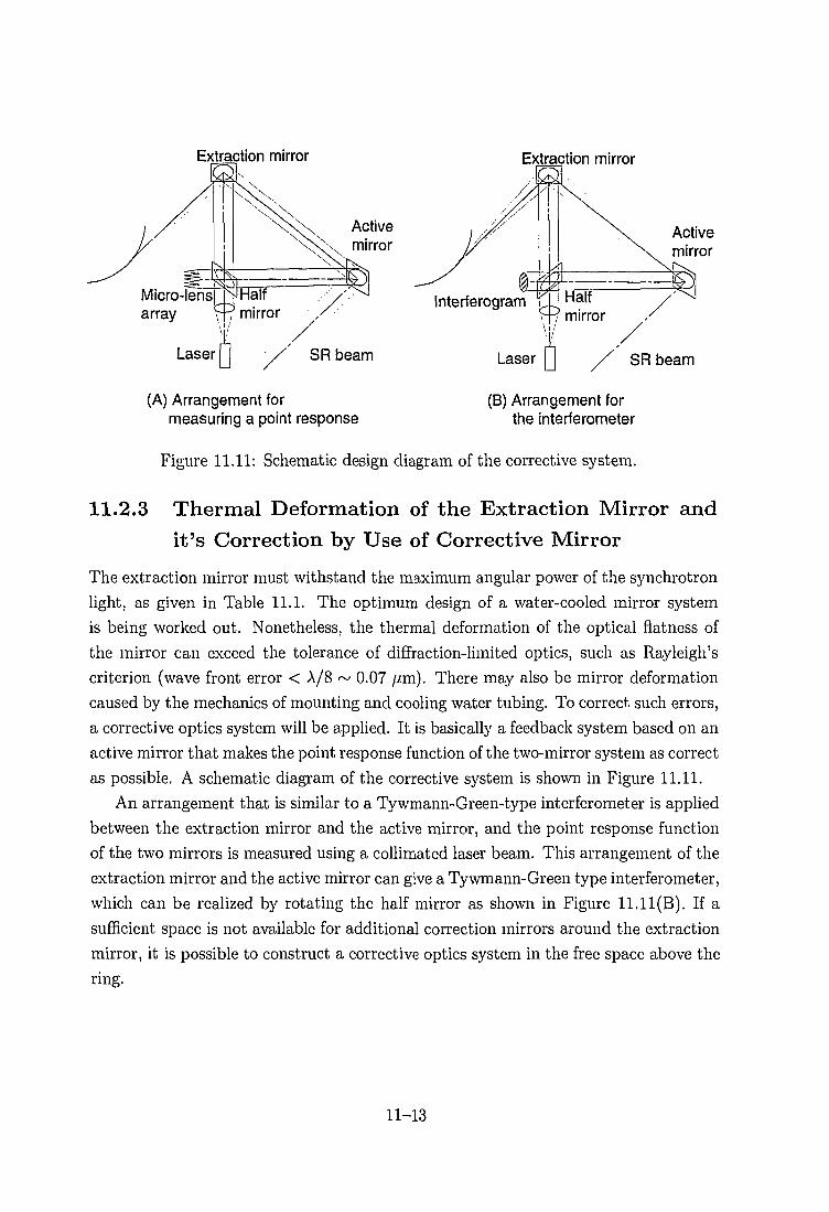
Extraction mirror Extraction mirror
Activemirror
Laser
(A) Arrangement formeasuring a point response
SR beam
(B) Arrangement forthe interferometer
Figure 11.11: Schematic design diagram of the corrective system.
11.2.3 Thermal Deformation of the Extraction Mirror and
it's Correction by Use of Corrective Mirror
The extraction mirror must withstand the maximum angular power of the synchrotron
light, as given in Table 11.1. The optimum design of a water-cooled mirror system
is being worked out. Nonetheless, the thermal deformation of the optical flatness of
the mirror can exceed the tolerance of diffraction-limited optics, such as Rayleigh's
criterion (wave front error < A/8 ~ 0.07 fim). There may also be mirror deformation
caused by the mechanics of mounting and cooling water tubing. To correct, such errors,
a corrective optics system will be applied. It is basically a feedback system based on an
active mirror that makes the point response function of the two-mirror system as correct
as possible. A schematic diagram of the corrective system is shown in Figure 11.11.
An arrangement that is similar to a Tywmann-Green-type interferometer is applied
between the extraction mirror and the active mirror, and the point response function
of the two mirrors is measured using a collimated laser beam. This arrangement of the
extraction mirror and the active mirror can give a Tywmann-Green type interferometer,
which can be realized by rotating the half mirror as shown in Figure l l . l l (B) . If a
sufficient space is not available for additional correction mirrors around the extraction
mirror, it is possible to construct a corrective optics system in the free space above the
ring.
11-13

15m 30m
(\
Object Lens Relay Lenses
Figure 11.12: Schematic diagram of the focusing system.
11.2.4 Focusing System
The optical image of the beam must be delivered to the measurement room above
the accelerator tunnel, so that sophisticated measurements can be made with streak
cameras and photon counting there. The basic design of the focusing system consists of
an objective system and a relay system which minimizes the loss of optical information
along this long path. The distance between the source point and objective system will
be about 15 m. The distance between the objective system and a measurement room
at ground level is about 30 m.
Figure 11.12 shows a design diagram of the focusing system which consists of three
sets of doublets made of normal optical glass. The first doublet makes up the objective
system, and latter two the relay system. The design of the entire system is optimized
for a wavelength of 480 nm, The design modulation transfer function (MTF) of the
total system and the diffraction-limited MTF (MDMTF) are shown in Figure 11.13.
The expected longitudinal aberration is shown in Figure 11.14. By comparing the
MTF and the MDMTF, it can be seen that this system is almost aberration-free
(diffraction limited) for paraxial use (clear aperture is 0.05 degrees), but is usable only
for monochromatic rays. By introducing other kinds of glass, such as ED (extraordinary
dispersion) glass, more correction of the aberration will be possible. Since the total
magnification of the above mentioned system is set to be 0.0714, the estimated image
sizes of the beam on the focusing plane are 33.7 //m (h) x 4.93 jtiin (v) in the LER
and 46.4 fj,m (h) x 8.57 fim (v) in the HER. Since this image is too small for direct
observation by a CCD camera, it is necessary to apply a final magnification system,
such as an eye-piece, in the telescope.
11-14

IS BMW DGG
I
_J
•O
.00 76.65 153.31SPRTIAL FREQUENCY IN CYCLES PER MILLIMETER
; DIFFfMCTION LIMIT
u.o
u.o
-JDDO
76.65SPBTIflL FREQUENCY IN CYCLES PER MILLIMETER
153.31
Figure 11.13: Design MTF (A) and MDMTF (B) of the total system.
(A) (B)
O.BBBOMILLIMETERS
0.0020 -0.0200 0.0000MILLIMETERS
Figure 11.14: Expected longitudinal aberration of the object lens (A) and the total
system (B).
11-15

11.2.5 Correction of the Optical Pass Difference by Win-dows and Filters
Since the components of the focusing system, such as the optical windows and the
filters, have the refractive index greater than 1, an optical pass difference (OPD) will
appear. It we denote the refractive index and thickness of material i as n* and i, the
OPD relative to the vacuum optical pass is given by
OPD = (rii - l ) x t . (11.1)
For example, a 20 mm thick optical window made of the typical crown glass creates
an OPD of 9.8 mm. If an OPD exists in the image field (after lens), its effect on the
magnification is often non-negligible. Consequently, to measure the magnification of
a real system, an OPD correction will be required. This correction is important for
measuring the absolute beam size.
If we have a material with an unknown refractive index, such as a band-pass filter
for monochromatization, it is necessary to measure its OPD in advance. It should be
noted that special care is required when applying a variable number of neutral-density
filters to regulate the image intensity. If the filters are located in a non-collimated
section of the focusing system, the OPD effect will cause a shift of the focal plane.
Also, an OPD by means of a longitudinal aberration (color or spheric aberration)
causes a time difference, resulting in a traveling time difference among different optical
paths. Therefore, the longitudinal aberration should be corrected for time-sensitive
measurements, such as studies of the bunch length.
11.2.6 Transverse Diffraction Effects
The finite aperture of the entrance pupil of the focusing system produces diffraction.
With the Fresnel approximation of the diffraction theory and the paraxial lens transfer
function, a pupil with a lens produces a Franhofer diffraction on the image plane. The
wave front error in these approximation is treated by means of the wave front aberra-
tion. With a well optimized focusing system (i.e. diffraction limited), the diffraction
pattern is dominated by Franhofer diffraction (paraxial theory). Then a diffraction
pattern is given by the Fourier transformation of a generalized pupil function of the
focusing system.
The amplitude transmittance of the generalized pupil function is modified by the
vertical angular intensity distribution, as shown in Figure 11.8. To create a simple gen-
eralized pupil function, an apodization for the entrance pupil of the focusing system
11-16

(A) HER (B) LER
(im
96|im 96|im
Figure 11.15: Point Spread Function (PSF) of the focusing system. The side length of
the 3-dimensional density plots is 96 fj,m.
is required. The apodization filter must have an anti-amplitude transmittance corre-
sponding to the vertical angular intensity distribution of the synchrotron light beam.
This apodization filter will create a flat intensity distribution on the entrance pupil,
and the entrance pupil will give a maximum cut-off spatial frequency. The entrance
pupil will be the maximum rectangular slit, which has an apodization filter that corre-
sponds to the intensity distribution of the extracted synchrotron light. As mentioned
in section 11.2.2, it will be 10 mm in the horizontal direction and 40 mm in the vertical
direction at 10 m for the LER, and 10 mm in horizontal and 20 mm in vertical for the
HER apart from the source point.
The entrance pupil of the focusing system will be located 15 m from the source
point, so the dimensions of slit will be multiplied by a factor of 1.5. The results of a
calculation of a point spread function (PSF, i.e. a diffraction pattern) for the system
are shown in Figure 11.15.
The rms width of the central peaks of the PSF are 5.36 /iin vertical and 13.1 /im
horizontal for the LER and 7.32 [xm vertical and 13.1 / m horizontal for the HER. The
image of the beam is given by a convolution of the PSF and the geometrical image.
Noting the expected beam size in Table 11.1, it is important to apply a correction of
the PSF in the beam size observation. The point response of the real focusing system
will be measured for the PSF correction.
11.2.7 Longitudinal Diffraction and the Field Depth Effect
The field depth of the diffraction limited focusing system is dominated by longitudi-
nal diffraction along the optical axis. Figure 11.16 shows the calculated longitudinal
diffraction pattern of the first doublet lens. The rms of the central peaks are 0.87 mm
in the LER and 2.18 mm in the HER. The corresponding field depths on the object
11-17

1.0000
0.9000
0.8000
0.7000
0.6000
0.5000
0.4000
0.3000
0.2000
0.1000
0.0000
/
/
J
(\\\\\
\\\\\\\\
-10.00 -6.67 -3.33 0.00 3,33 6.67 10.00
Forcal Depth (mm)
(A) HER
1.0000
0.9000
0.8000
0.7000
0.6000
0.5000
0.4000
0.3000
0.2000
0.1000
0.0000 - n --10.00 -6.67 -3.33 0.00 3.33 6.67 10.00
Focal Depth (mm)
(B) LER
Figure 11.16: Longitudinal diffraction pattern of the focusing system.
point (on the beam) are 171 mm in the LER, and 428 mm in the HER. The effects of
the longitudinal aberration, as discussed in section 11.2.3, is sufficiently small for this
length. The system also appears to be diffraction-limited in the longitudinal direction.
The curvature effect in the horizontal beam size of the beam trajectory due to this field
depths will be 14.3 ^m in the LER and 81.6 ^m in the HER. This effect in the HER is
not negligible. Since the curvature effect is mostly proportional to the bending radius,
it is better to adopt a smaller bending radius in the HER. The observed horizontal
beam sizes including this effect are expected to be 427 (im in the LER and 655 /xm in
the HER.
11.2.8 Alignment of the system
The total path length of the focusing system will be about 40 m ~ 50 m. To maintain
good optical alignment of the entire system, an independent alignment for the lenses
needs to be established first. Then, the axis of synchrotron light after the corrective
system must align with the optical axis of the focusing system. The alignment of these
two axes can be established with a two- or three-mirror system which corrects angular
and transverse alignments. It is also very important to suppress fluctuation of air flow,
and to eliminate dust in the optical pass. Therefore, an optical pass will be surrounded
by a structure which has some irises to eliminate unwanted reflections or scattering.
The entire arrangement of the total system, which includes the optical lab hut, is yet
to be determined.
11-18

LER HER
Original 472 /an 69 /xm 650 /xm 120 /xm
With Aberration 472 /xm 69 /xm 650 /xm 120 /xm
With transverse diffraction 506 /xm 102 /xm 675 /xm 158 /xm
With longitudinal diffraction 471 /xm 69 /xm 655 /xm 120 /xm
Total 507 /xm 102 /xm 680 /xm 158 /xm
Table 11.2: Expected values of the observed beam sizes which include contributions
from effects of aberrations and diffraction.
11.2.9 Summary
1. An extraction mirror system having a corrective optical system has been prelim-
inary designed.
2. A diffraction-limited focusing system having an object-lens and relay-lens system
has been designed.
3. A Fourier analysis of the focusing system is done in both the transverse and the
meridional (longitudinal) planes. The expected observed beam sizes are summa-
rized in Table 11.2. Since the diffraction effects are not negligible for a beam size
measurement, it will be necessary to measure the point response of the system
and to correct it.
4. The total length of optical pass will be 40 ~ 50 m. An independent alignment
will be required for both the focusing system and mirrors.
11.3 Laser Wire Monitor
In addition to the beam profile monitor based on imaged synchrotron light, the use
of so-called laser wires is under consideration for better resolution with an ability to
measure individual bunches.
The principle of the measurement is illustrated in Figure 11.17. A narrow laser beam
("laser wire") meets a beam bunch perpendicularly, creating a number of Compton-
scattered photons. The population of scattered photons is proportional to the overlap
area of the laser wire and the particle beam. Therefore, by scanning the laser light
11-19

laser forvertical sizemeasurement
laser forhorizontal sizemeasurem ent
particlebeamorbit
gamma raysSi detector
sweeping magnet
gate signal
Figure 11.17: Concept of the beam size measurement using laser wires. A lens and
laser monitors are necessary for the vertical size measurement as well, although they
are not shown in the figure.
horizontally or vertically, and by measuring the flux of Compton-scattered photons, a
one-dimensional particle distribution of the bunch is obtained.
The discussions in this section assume that the laser wire is placed at the end of a
straight section. However, since the laser wire technique can offer a very high resolution,
it may be also used at the collision point. The practical application depends on the
availability of adequate space for the measurement ports.
The accuracy of the measurement is determined by the waist size (focused spot size)
of the laser beam. As an example, we consider the vertical bunch-size measurement,
which requires a better resolution than the horizontal one. In this case, the depth
of the focus of the laser beam should be longer than the horizontal bunch size. The
Rayleigh length LR gives a measure for which a laser beam keeps its transverse size
nearly constant,
LR = 4Kal/\L, (11.2)
where a^ is the rms spot size at the waist of the laser and A , is the laser wavelength.
We note here that in the field of laser technology w = 2aL is conventionally used when
giving the size of a light spot.
11-20

vertical distributionof the beam particles
urn100
vertical distributionof the laser intensity -1 oo
horizontal distributionof the beam particles
2a envelopeof the laser beam
Figure 11.18: Design example of the laser-wire dimensions at a typical vertical beam-
size measurement. The assumed beam sizes are 30/tm vertically and 500 /im horizon-
tally. Laser wavelength A is 355nm and the minimum rms spot size is 5.3/im.
As stated earlier, we based our laser optics design on the following requirement:
LR = 2aex) (11.3)
where aex is the horizontal size of the particle beam. The laser spot size then becomes
OL = [AL<W(2TT)]1/2. (11.4)
The typical particle bunch size in the horizontal direction is around 500 //m, except
for the interaction region. The 355 nm third harmonic YAG gives ai = 5.3 /im.
The minimum vertical beam size is approximately 30 fj,m. The measured value of the
vertical bunch size by the laser wire will be (302 + 5.32)1/2 = 30.4/xm. Figure 11.18
shows an example of the laser profile at the vertical beam-size measurement, together
with the beam particle distributions.
The statistical resolution of the measurement depends on the counting rate (Ny) of
the Compton photons,
(N1)=acLc, (11.5)
where ac is the cross section of the Compton scattering and Lc is the luminosity of the
Compton scattering. The cross section is given by
ac = 2e)) + ^: (11.6)o — o x - • --/} • Q — o > - • "^ I /-, , ne\2':
>- J. r Zt ^E \i- "T" At)
where re denotes the classical electron radius and e = 7/ifn/(mec2) w ^ n t n e
frequency u0 and Lorentz factor of the electron beam 7. This equation gives <rc =594 mb
for the 3.5GeV LER and 527 mb for the 8 GeV HER.
11-21

The Compton luminosity is given by
1] = 0.5 x 10⁹XL[nm}I[mA}W[J}fL[seC-1}mmm2}fr[sec-1], (11.7)
where Ax, is the laser wavelength, I the bunch current, W the laser pulse energy, fL the
laser pulse rate, and fr the revolution frequency. The E is maximum when the laser
beam passes the center of the particle beam. This maximum S is given by
S = K + o%,)W[(ol + o\x) cos2(«5/2) + (al + a\z) sin2(<5/2)]1/2, (11.8)
where 8 = ir/2 denotes the crossing angle, oeXiey<ez denotes electron beam sizes and
&Lx,Ly,Lz denotes laser beam sizes of the respective directions. If we assume the follow-
ing pertinent parameters:
XL = 355nm,
/ = 0.1mA, / r = 100kHz,
aex = 500/rni, aey = 50/im, aez = 5mm,
0LX = crLy = aL = 5/im, aLz = 30mm,
S = 1.42mm2 is obtained. Here, the beam current assumed in the LER and HER
are 0.5 mA and 0.2 mA, respectively. By approximating ac =500 mb, we have
Lfsec^mb-1] = leSW^/^sec- 1 ] and (A^sec"1]) = 82.7VF[mJ]/L[sec-1]. A commercially-
available 20 mJ, 100 Hz, 100 ps laser gives 165 kHz 7 radiations at the maximum.
The maximum energy of the scattered photons is
_ (472
which gives 389MeV to the LER and 1.77GeV to the HER. The bremsstrahlung pro-
duces noise radiation in this energy range. The bremsstrahlung counting rate caused by
the interaction between the particle beams and the residual gas has been estimated to
be ~ 50MHz. This estimate is based on the following assumptions: the mean atomic
number of the gas is 5, length of the straight section is 100 m, the gas pressure is
10~8 Torr, the particle beam current is 2.5 mA and the threshold energy of the gamma
radiation detection is 20 MeV.
The photon detector consists of a tungsten converter, which converts gamma ra-
diations to electron-positron pairs, a sweeping magnet to select electrons in a specific
energy range and a Si detector, as shown in Figure 11.17. The Analog-Digital converter
is controlled by a gate circuit to improve the S/N ratio. Gating of 10 ns width that
is synchronized to the 100 Hz laser beam will reduce the bremsstrahlung noise rate to
50 Hz. The S/N ratio will be improved to 165kHz/50Hz=3300. The fluctuation of the
11-22

laser output power contributes another statistical error. Using a 20 mJ, 100 Hz, 100 ps
laser, the beam size measurement will be obtained with a statistical error better than
1% within a few minutes.
A pair of ports are required for each of the vertical and horizontal beam size mea-
surements: one port to introduce the laser beam into the beam duct, and the other
to monitor the laser beam transmitted through the duct. These ports may influence
the impedance of the beam duct, depending on the size. The size requirement for the
measurement is given by
1 ^ <»•"»where w = 2ap is twice the r.m.s. size of the laser beam at the lens with focal length
/ . This / is nearly equal to the distance between the lens and the particle beam.
The 4/3 correction factor is for aberration and diffraction caused by a single lens.
Assuming / = 100mm, o^ = 5^m and A , = 355nm, we obtain w = 2ap = 1.50mm or
ap = 0.75mm.
The port size, under the assumption that the particle beam passes through the
center of the beam duct, should be determined by the root of the squared sum of the
particle beam size ae = aex or aey and the laser beam size at the port ap, i.e. (of +
&p)1/2- The result is 0.901 mm for the horizontal size measurement and 0.751 mm for
the vertical size measurement. If we want to cover 6a at the port, the diameters of
the ports for the horizontal and vertical size measurement are 5.4 mm and 4.5 mm,
respectively. The port with 10mm diameter is large enough in each case, even if we
take account of the variation in the particle beam position. A laser beam expander is
commercially available for obtaining a w = 1.50mm beam at the final focusing lens.
Design of the laser optics, the timing control and the Compton detectors are being
worked out. They are essentially the same as what has been developed for particle-
beam polarization measurements at the TRISTAN Main Ring[l].
11.4 Bunch Feedback System
11.4.1 Design Considerations
Required damping time Studies on the acceleration cavities indicate that the
growth times of multi-bunch instabilities at KEKB will be on the order of a few ms
to 10 ms. The transverse instabilities will generally be stronger than the longitudinal
ones. From these considerations, the goal of the bunch feedback system has been set
to achieve a damping time of one ms for the transverse and 10 ms for the longitudinal
planes.
11-23

Feedback systems There are roughly two categories of feedback systems that can
be applied at KEKB: the bunch-by-bunch and the mode-by-mode feedback systems.
The bunch-by-bunch feedback systems are designed to deal with any combined
oscillations of multi-bunches with or without correlations. For this purpose, such feed-
back systems should be wide-banded, and must cover up to at least one half of the
bunch frequency. At KEKB this frequency is 255 MHz. The mode-by-mode feedback
systems are designed for specific coupled-oscillation modes, and their bandwidth does
not have to be as wide as the bunch-by-bunch feedback systems. However, a number
of identical feedback systems (at least as many as the number of dangerous modes)
need to be prepared for stable operation of the storage rings.
At KEKB both technologies will be implemented. For instabilities due to the resis-
tive wall, as well as those due to the fundamental mode of the accelerating cavities, we
will use the mode-by-mode feedback method [2]. This is because for these two cases,
the frequencies of the instabilities are predictable and can be known in advance. For
those instabilities due to the higher order modes (HOM) of the accelerating cavities, our
choice is to use the bunch-by-bunch feedback method. This is because their frequencies
and the number of dangerous modes cannot be reliably predicted at this stage. Another
reason to prepare bunch-by-bunch feedback systems is that they can deal with tran-
sient oscillations of a bunch during the injection process. The mode-by-mode feedback
method could be less effective in this case.
Digital signal process The key technique in signal processing for the feedback
system is to store information of bunch orbit deviations (transverse or longitudinal)
for at least one full revolution period of the ring. At KEKB this is achieved by a pure-
hardware digital filter system, which can work in a very high-frequency environment.
The reasons for using the digital delay technique are as follows:
1. The digital system is more flexible than an analog delay with optical fiber cables
and other devices.
2. The DC offset can be relatively easily eliminated with simple digital filters. We
note here that the elimination of the DC offset for an individual bunch is essential
for saving power to send to the kicker. This is because, in the longitudinal case,
the synchronous phases of individual bunches can vary because of the large beam
loading on the cavities introduced by the bunch gap.
3. It is easier to adjust the gain, phase and other parameters with digital systems.
This helps the rapid start-up of the system as well as allowing efficient mainte-
nance.
11-24

11.4.2 Pickup part
The feedback systems at KEKB consist of three parts: the pickup part, the signal
processing part, and the kicker part. Figure 11.19 shows a system block diagram. The
design of each of the three parts is described in the following.
pickup part signal processing part kicker part
kickers
liming clock generator \— RF signal1 - 2 - 1—IT1 [50B MH;T
i = « 1E 1
i 1Q
Block Diagram of the Bunch Feedback System
- KEKB •
Figure 11.19: Block diagram of the feedback system.
Longitudinal
The longitudinal position (timing) of a bunch is converted into the phase difference
between the pickup signal and a timing-reference signal as shown in Figure 11.20.
The timing-reference signal is generated by multiplying the frequency of the RF signal
for accelerating cavities. Hereafter, we call the frequency of the reference signal the
"detection frequency." It is chosen to be 4 times the RF frequency, ~2 GHz [3]. The
pickup signal is created by combining 3 pulses from 3 longitudinally aligned pickup
electrodes with a power combiner. The timing differences of these pulses should be
adjusted so that the combined signal contains the detection frequency component.
Since the output of this circuit is proportional to the bunch current, the feedback
gain will be proportional to the bunch current. However, this gain variation is not
considered to be a major problem, since the growth rates of the instabilities are also
proportional to the bunch current.
Transverse
The transverse position of a bunch is detected by the AM/PM method [4]. Figure 11.21
shows a block diagram of the circuit. Similar to the longitudinal signal pickup tech-
11-25

electrodesmcombinei
DBM
RF slgna(509 MHz) ^ Ireq. multiplie
(x4)phaseshifter
1
low pass filter(1GHz)
to ADC
phase shiftcontrol
'KEKB
Figure 11.20: Front-end circuit for longitudinal pickup.
nique, the transverse beam signal is created by combining 3 pulses from three pairs of
pickup electrodes. It produces the detection frequency component without any extra
band-pass filter (BPF) in the front-end stage. By eliminating the BPF, unwanted over-
laps of the ringing to the neighboring bunch are avoided, and the phase shift associated
with the filter can be reduced.
The detection frequency used in the AM/PM circuit is chosen to be 2 GHz. This is
so that the signals can terminate within the time interval that corresponds to a bunch
spacing, i.e. 2 ns.
ntlow pass (liter
-KEKB-
Figure 11.21: Front end circuit for transverse position detection.
11-26

11.4.3 Signal Processing
Two-tap filter in the signal processing
The jobs [5] of the signal processing part are: (1) create a signal delay (or phase shift),
and (2) eliminate the DC offset.
These jobs are done by a simple 2-tap finite impulse response (FIR) filter. In
general, the relation between the inputs (CCJ) and the output (y) of an FIR filter is
expressed by
3=1
where the a,'s are called the filter coefficients. The 2-tap filters are the simplest ones
among these FIR filters, and they will be employed in the KEKB feedback systems.
The output of the filter is a very simple function of the inputs, which can be written
as:
y = a(xk-Xj). (11.12)
Note that the two coefficients have the same magnitude, but with opposite signs.
This ensures that the gain of the filter is 0 in the limit of the frequency near zero.
This also means that the calculations required during the operation of the digital
filter involves only subtraction operations and, no multiplications. Consequently, the
required hardware of the filter calculation is greatly simplified.
There is a large difference in the tap positioning in the longitudinal and the trans-
verse cases. For the longitudinal case, since the tune (synchrotron tune) is much smaller
than 1, sampling points of the oscillation are relatively dense. In this case peak-gain
filters can be applied, in which the positions of two taps should be separated by half of
the full period of the oscillation. For efficient feedback purposes the phase shift should
be 90 degrees [6]. As shown in Figure 11.22, this is achieved by choosing the taps at
the 1/4 (90 degrees) and 3/4 period (270 degrees) positions relative to the timing of
applying correction kicks to the beam.
Figure 11.23 gives an example of the frequency characteristics of the peak gain filter.
The synchrotron tune is assumed to be 0.015, i.e. one period being about 67 turns.
The taps are positioned at the 16-th and 49-th turns. The gain of the filter has peaks
at a tune of 0.015 and at its multiples. The phase shift is 90 degrees at a tune of 0.015
and at its odd multiples.
For transverse systems, the tap positioning is more complex. The betatron tune
is larger than 1 and its fractional part can vary between 0 and 1. The algorithm of
the tap positioning is to find the configuration that maximizes the feedback gain for a
11-27

tap 1 tap2
o
tap#
present data
Figure 11.22: Tap positioning for the peak gain mode filter. The distance of two taps
is half of one period and tap 1 is positioned at the 1/4 period before the present time
to obtain a 90 degree shift.
1.2
O.B
c 0.6 -ro
ID
0.4
0.2
/
\
\
. '<
\
\v\\1
/
\
/
,
\
\
\
\
1
!•, (
J
\\\
>
\\\1/ \
\•/ w
V
\, •
180
120
60 •§.u
zro 5"
- -60
-120
0 0.015 0.03 0.045 0.06 0.075
Tune
-1800.09 0.105 0.12
Figure 11.23: Fi equency Characteristic of the FIR filter for longitudinal signal process-
ing. The taps are positioned at 16 and 49. The solid and dashed lines show the gain
and phase shift of the filter, respectively
11-28

given betatron tune. The feedback gain, x, is expressed by
X = g&infilter-sm(is + 8u), (11.13)
where u is the betatron tune and 8v is the phase advance from the monitor to the
kicker. A simple computer program has been written to tabulate suitable tap positions
for each tune. This program calculates the gain for all possible combinations of the tap
positions. Figure 11.24 shows the result of a calculation for the case bv = 90 degrees
with a maximum tap position of 8. Figure 11.24 indicates that for any tune we can
find suitable tap positioning. We plan to prepare a few additional signal pickups which
correspond to various 5u values, and will select one of them for a given betatron tune.
This technique allows us to find a suitable tap positioning more easily with restricted
positions of the taps.
10
6 .
co5
Ia.
2 -
0 -
urn * •
M i
:< ;• :
f
j
i
' \
L11144*J
* \
i
!!
j
1
i
0.1 0.2 0.3
Fractional part of tune0.4
.. 0.8
0.6
- 0.4
:- 0.2
0.5
Figure 11.24: Tap positioning of the 2 tap filter for the transverse feedback. The
feedback gain corresponding to the tap position is also shown. Note that tap position
0 means that the data of the last turn are used, but not the data of the present turn.
Signal processor
The heart of the signal processing part, which executes the filter calculation, is the
digital filter complex. It consists of memory units and simple arithmetic units. Since
the digital filter complex is a relatively low-speed device, in order to feed/extract data
to/from it, two auxiliary devices will be implemented, i.e. fast demultiplexers (FD-
MUX) and fast multiplexers (FMUX). In addition, the signal processing part must be
11-29

equipped with an analog-to-digital converter (ADC) and a digital-to-analog converter
(DAC) as the interface with external elements. Figure 11.25 shows a block diagram
of the system. The same design concept applies to both the longitudinal and the
transverse systems.
TI33O3>OO
4
•—•
4
4bitFDMUX
4bitFDMUX
4x16./
4x16
mpl
exIte
r co
gita
l fi
•o
4x16
r
4x16
4bitFMUX
4bitFMUX
oa
Figure 11.25: Block diagram of the signal processing part. The main part is a digital
filter complex, which stores the data and executes the filter calculation. Two fast
demultiplexers degrade the signal rate from 509 MHz to 1/16 that value. The processed
data is again multiplexed to 509 MHz by a couple of the multiplexers.
Digital filter complex Figure 11.26 shows a block diagram of the digital filter
complex. The complex consists of 16 identical units, each of which treats the data of
320 bunches (5120/16 = 320). The memory in one unit is aligned in two series. Each
series is used for one of two taps. The capacity of one memory series is 32 kbytes, and
it can store the data for 100 turns for each bunch. There is one arithmetic logic unit
(ALU) in one unit which executes the subtraction of data from two series of memories.
The digital filter complex will be assembled with wired logic or a custom IC. It will be
capable of processing all of the data within one revolution period of the KEKB rings.
For practical use it must be made possible to rearrange the tap positioning easily and
quickly when the working point is changed. This flexibility is particularly important
for the transverse feedback systems. For this purpose, this circuit is equipped with tap
pointers which can be modified with a relatively slow logic circuit.
A digital gain adjuster is implemented at the back-end of the digital filter com-
11-30

o
>ao
turn 0 turn(-1) turn (-100) X16
=j — i 31; I ;
32kby1es x 2 ALU
-Digital Filter Complex
OD>O
Figure 11.26: Block Diagram of the digital filter complex.
plex. This adjuster allows us to easily control the loop gain. In addition, it realizes a
saturated feedback loop (i.e. the bang-bang damping).
Demultiplexers and multiplexers Since the bunch frequency is 509 MHz at KEKB,
the rate of the signal output from the ADC can be up to 509 MHz. The digital filter
complex can not work at such high frequencies. To overcome this difficulty, a high
speed demultiplexer will be used to drop the signal rate by a factor of 1/16 (about
32 MHz). Since this demultiplexer needs to handle the original 509 MHz signal, it will
be built with custom GaAs gate-array chips. Each chip has 136 connector pins and
is packed in a 28 mmx28 mm package. For demultiplexing 8-bit data, two chips are
used, where each chip treats 4-bit data. The multiplexer will be built using the same
technique. Figure 11.25 shows the connection of these chips as well as the digital filter
complex.
ADC and DAC Flash ADC technologies have seen a remarkable progress in recent
years. Several vendors have released 8-bit ADC's with a digitization speed of 500 Mega
samples/second. Such devices can be used in the front end of the signal processing
system. DAC's with similar speed and accuracies are less difficult to design than
ADC's, and are also available.
11-31

11.4.4 Power Amplifiers and Kickers
Longitudinal
Kicker design The kicker for the bunch feedback system must support wide-band
operation while maintaining a reasonable shunt impedance. At KEKB the band-width
of the kicker required for the bunch by bunch feedback is 255 MHz. This is not a trivial
requirement. Although a resonator structure similar to an accelerating cavity can be
a good longitudinal kicker from the view point of the shut impedance, its frequency
band width is too narrow for this purpose. While a structure which guides the TEM
wave offers adequate wide-band characteristics, the shut impedance is sacrificed there.
The R & D for KEKB has been centered on a wide-band device based on TEM wave-
guides (so-called the drift tube type). Figure 11.27 schematically shows the structure
of the TEM wave guide [7] for the longitudinal case. A combination of the beam pipe
and the inner electrodes creates a co-axial structure of the characteristic impedance
of 25ft. An RF power fed by power amplifiers propagates as a TEM wave along the
structure. The RF to the kicker is created by modulating a sinusoidal carrier signal
with the feedback signal. The frequency of the carrier is chosen to be 1016 MHz,
which is twice the bunch frequency. Between adjacent inner electrodes, delay lines are
inserted to shift the phase of this RF power by 180 degrees in the carrier frequency.
This phase shift creates a longitudinal electric field between the neighboring electrodes.
Since the RF power propagates in the direction opposite to the bunch in the kicker
structure, the number of electrodes (N) in a kicker is limited by the condition that it
must give an individual kick to each bunch. With the carrier frequency of 1016 MHz
the largest number of electrodes, Nmax, is given by
AT n rf frequency . ,.Nmax = 2 X — i y—. 11.14
bunch frequency
Thus, for KEKB, the largest number of the electrodes is 2. The longitudinal length of
a unit kicker is approximately 20 cm. The shunt impedance of the kicker is given by
Zs = 4N2ZC) (11.15)
where Zc is the characteristic impedance of the co-axial structure. Then, the expected
shunt impedance for Zc = 25Q and N = 2 is
Zs = 400ft. (11.16)
Amplifier power and the number of the kickers One unit of the kicker has two
input connectors. Each connector receives RF signals from a 500 W power amplifier.
11-32

beampipe
inner electrodes
TEM wavembunch
u mdelay line (n)
Figure 11.27: Principle of the longitudinal kicker
Thus the total power per kicker is 1000 W. The maximum kick voltage available from
this kicker unit is
it = ^2ZsPmax = y/2 • 400 • 1000 ^ 900(v). (11.17)
The number of required kicker-units in the case of the LER is evaluated as follows [8].
The required kick voltage per turn, Vturru is given by
(11.18)
where g is the available damping rate, TQ the revolution period and AE/e an energy
deviation. If the required exponential damping rate is 100s"1 (damping time=10 ms)
up to the energy deviation of 0.1%, the required kick per turn is
= 2 • 100 • 1 x 10~5 • 3.5 x 10⁹ • 0.001 = 7000(v/°"s). (11.19)
Therefore, 8~9 kicker units will be required. The total length of the kickers will be
about 1.8 m.
11-33
Transverse
The strip-line kickers For the transverse kickers we use standard strip-lines. The
shunt impedance, Z±, of the transverse kicker is given by
Z^2Z.Li^), (11.20)
where,
a : radius of the strip-line (distance of the strip-line from the pipe center),
Zc : characteristic impedance of the strip-line,
k : the wave number of the rf power,
g±. '• a geometrical factor (usually close to 1),
I : length of the strip-line of the kicker.
From this expression, it is seen that the shunt impedance at the lower frequency limit
is proportional to the square of strip-line length. Therefore, for the lower frequency
the longer one is preferable. However, at a higher frequency, the sine factor in Equa-
tion 11.20, contributes with an opposite sign. Two kinds of the strip-line kickers
will be prepared: a broad-band type, and a relatively narrow-band one with higher
shunt impedance at lower frequencies. The wide-band type is 30 cm long and its shunt
impedance at around 125 MHz is about 6 kQ, assuming a=3cm, Zc=50 Q, g±=Q.9. The
narrow-band type, which will suppress instabilities due to the resistive wall impedance
and some HOM instabilities which have very low mode numbers, is 3 m long. The
shunt impedance at the low-frequency limit is 200kfL
Estimation of the required power A formula corresponding to (11.18) for the
transverse case is
Vturn = 2gTQ{E/e)Xmaxl\JPmPk, (H-21)
where E/e is the energy of the beam in electron-Volts, (3m<k the beta function at the
monitor and the kicker, and xmax the maximum amplitude of the oscillation. Assuming
the beta function at the kicker is 10 m and the maximum beam orbit amplitude is 1 mm,
the voltage required to bring the damping time to 4 ms is obtained as
Vturn = 2 • 250 • 1 x 10~5 • 3.5 x 10⁹ • 0.001/10 = 1750(v/°"s). (11.22)
Using the shunt impedance of 6 kf2 of the wide-bad type, the required power is ap-
proximately 250 W. To fulfill this requirement, two 200 W-amplifiers will be prepared.
They must cover a frequency range from 20 MHz to 250 MHz.
For the narrow-band type, the required voltage for obtaining a damping time of 1 ms
is 7 kV. The required power will be 120 W. For this purpose two 120 W amplifiers need
to be prepared. They must cover a frequency range from 10kHz to 20MHz.
11-34

Bibliography
[1] K. Nakajima et a/., Phys. Rev. Lett. 66, 1697(1991); TRISTAN Polarization Study
Group, Proc. 10th Int. Symp. High Energy Spin Physics, 1992, Nagoya, (University
Academy Press, Inc., Tokyo, 1993) p.919.
[2] The instability due to the fundamental mode of the accelerating cavities can be fatal
without any damping techniques. The RF cavities are very carefully designed so as to
decrease the growth rate of this instability. Nonetheless, there is some possibility left
that the growth time is shorter than the radiation damping time.
[3] The detection frequency must be lower than the cut-off frequency of the beam pipe.
Typically, the radius of the beam pipe at KEKB is about 50 mm, or a somewhat smaller.
The cut-off frequency in this case is 1.7 GHz. We will prepare a special beam pipe with
the radius of 35 mm for the oscillation pickup.
[4] The principle and characteristics of the AM/PM method is explained in detail in the
paper by R.E. Shafer. (AIP Conference Proceedings 212).
[5] One may think that noise reduction must be one of the tasks of the signal processing part.
However, according to our beam studies the noise is very low and its is not necessary.
[6] Strictly speaking, this 90 degrees should be the sum of the phase shift of the filter and
the synchrotron phase advance within one revolution. Because the synchrotron tune is
very small compared with 1, one turn delay is very small.
[7] This structure of the longitudinal kicker was originally proposed in the PEP-II Design
Report.
[8] A rough estimation shows that the growth rate of the coupled bunch instabilities is
proportional to the factor, R = IbeamJEbeam x (# of cavities). The ratio of this factor
for LER and HER, fl(LER)/Jl(HER), is about 3. Then the instabilities will be stronger
in LER.
11-35
Chapter 12
Injection
12.1 Linac
12.1.1 Overview
To allow for the smooth operation of KEKB, a major upgrade program is under way
for the 2.5 GeV injector linac, which was formerly used to inject beams to the Tristan
accelerator complex and the Photon Factory (PF) ring. Two main goals of the upgrade
are:
• Increase the energies of electrons and positrons to 8 GeV and 3.5 GeV, so that
they can be injected into HER and LER of KEKB at full energies.
• Increase the bunch intensities of positrons by a factor of ~ 20 Tor efficient fills.
Tables 12.1(1) through (4) compare the parameters of the injector before and after the
upgrade. The upgrade program includes tasks in the following three areas:
1. Successive replacement of the RF power sources by higher-power klystrons with
RF pulse compressors.
2. Small extension of the linac total length.
3. Relocation of the positron production target, so that positrons are produced by
incident electrons of 3.7 GeV instead of the former 0.25 GeV.
The pre-upgrade linac consists of six sectors called P, 1, 2, 3, 4 and 5. A regular
sector consists of eight accelerator units, which include four 2-m accelerator sections.
The accelerator sections in each unit are driven by one klystron. In the upgrade, two
sectors will be added to the linac, and they will be renamed A, B, C, 1, 2, 3, 4 and 5,
as shown in Figure 12.1.
12-1

Sectors A, B and C are those to be newly built. Sector A will have a pre-injector,
which will produce intense single bunches. It will include double sub-harmonic bunchers
(SHB's), followed by three accelerator units. Sectors B and C are regular accelerating
sectors. Sector 2 will be rebuilt so as to incluae a positron generator by moving Sector
P to this location. In Sectors 1, 3, 4 and 5, the component layout will not be changed,
or changed only slightly.
The pulse energy of the pulse modulators will be increased by a factor of two. This
will be achieved by increasing the total capacitance of PFN while maintaining the same
charging voltage. All of the 30-MW klystrons will be replaced by 50-MW types. RF
pulse-compressors will be installed at the klystron output with a small modification to
the waveguide system and improvements to the vacuum system.
The number of accelerator units is to be increased from 46 to 57. The average energy
gain of one unit will be 160 MeV. The full linac energy without beam loading will reach
about 9 GeV. An extra energy gain of over 8 GeV(13%) will be used to compensate
for any gain loss due to defective units, energy-spread adjustment, or energy tuning.
In the pre-upgrade linac the positrons were produced with primary electrons of 0.25
GeV. The positron production yield has been measured to be N+/(N~E~) = 1.8 %
GeV"1. The expected positron charge after the upgrade is 0.67 nC for a primary
electron pulse of 0 nC at 3.7 GeV.
12-2

B' ^' C D ' (§'c-t- l-tO fD
CD
O
oB
, _ , CD
to toCO CJ1
oCD
3%
8
Sector P (positron generator)
PositronGun Radiator I
- Move the P4, P5 units
Move the P6 unit
CO
oo
OCD

[INJECTION BEAM]energy (e~)
pulse lengthbunch width (az)particle (charge)/pulse (e~)
pulse repetitionemittance (e~)
energy width (e"~)
[MAIN ACCELERATOR]Accelerator sectiontype of structurefrequencydisk aperture diameterlength (with vacuum flanges)filling time
energy gain (no-load)total numberAccelerator unit*2
length (regular unit)number (total)(before e+ radiator)(stand-by and energy-tuning)energy gain (with RF compressor)
(without RF compressor)
energy multiplication
PRESENT KEKB
2.5 8.02.5 3.5
<2 single bunch~5 ~5
2 x 10⁹(0.32) 8 x 10⁹(1.28)2 x 10⁸(0.032) 4 x 10⁹(0.64)
25 504 x 10"8 6.4 x 10~8
8 x 10"7 8.8 x 10"7
0.2 0.1250.22 0.25
T.W., |7r-mode, semi-C.G.2856
24.85~ (75 urn step)20400.5
7.4162 230
9.646 573 26
~3+l 4+2160
62.5 90(@20 MW) (@40 MW)
1.8
GeVGeV
nsps
(nC)(nC)
mm
0}/
07
MHzmmmm
yUS
MeV/MW1/2
m
MV/unit
MV/unit
Table 12.1(1): Changes in the major parameters of the linac from the present to KEKB.
12-4

[PRE-INJECTOR]Guntypecathodehigh-voltage/widthgrid-voltage/widthnormalized emittancelst-subharmonic bunchertype of structurefrequencyfield-strength2nd-subharmonic bunchertype of structurefrequencyfield-strengthlst-prebunchertype of structurefrequencycell numberdisk-aperture diameterphase velocityshunt impedance2nd-prebunchertype of structurefrequencycell numberdisk-aperture diameterphase velocityshunt impedanceBunchertype of structurefrequencycell numberdisk-aperture diameterphase velocityshunt impedanceOutput beamenergyenergy spread (<7JS/E)
normalized emittance
PRESENT KEKB
triodeBl-cathode (EIMACY796)
200 kV/l/is200 V/4 ns~ 5 x 10~6
re-entrant cavity119.000 114.2
4 4
re-entrant cavity571.27
4
T.W, §7T, C.I.2856
735.740.7c16.0
T.W., §7T, C.I.2856
536.890.7c15.0
T.W., §7r, C.G.285635
35.0~19.30.7c~lc
15.0
50 500.6 0.6
~ 5 x 10~5
m
MHzMV/m
MHzMV/m
MHz
mm
MO/m
MHz
mm
Mfi/m
MHz
mm
Mfi/m
MeV%m
Table 12.1(2): Changes in the major parameters of the linac from the present to KEKB.
12-5

[POSITRON PRODUCTION]Radiatormaterialthickness (radiation length)diameterPrimary electronenergyparticle (charge)/pulseemittance (la)energy with (CTJS/E)
Positron production rateafter the solenoid (100 MeV)at the 30° -transport (250 MeV)final (2.5 GeV)Focusing systemtypepulsed solenoid (strength x length)D.C. solenoid (strengthxlength)normalized acceptance
PRESENT KEKB
Ta8 (2Xo) 16(4X0)
8 8
0.25 3.71 x 10n(16) 6 x 10¹⁰(10)
0.45
6.5%4.2%1.8% >1.8%
QWT2.3Tx45 mm 2.3Tx45 mm
0.4Tx8 m6 x 10~3
mmmm
GeV(nC)
m%
e+e"GeV
m
Table 12.1(3): Changes in the linac major parameters from the present to KEKB.
12-6

[RF SOURCE]ModulatorPFN charging voltagePFN total capacitanceenergy stored in PFNpulse repetition ratePFN impedancepulse widthpulse output voltagepulse output powerPulse transformerstep-up ratio2nd. voltage x widthcore biasKlystronbeam voltagebeam currentrf power peakrf power averagerf pulse widthPulse compressionmultiplication factorEnergy gain/unit
[BEAM TRANSPORT]solenoids (injection)solenoids (e+ generator)quadrupole tripletsdoubletssingletsbetatron wavelength
[BEAM MONITORS]wall current monitorprofile monitor (Ceramic)beam position monitorwire scannercore monitor
PRESENT KEKB
450.3 0.6300 600
506.4 4.73.5 5.6
22.580 107
1:12 1:13.50.95 1.7none necessary
270 304295 35233 463.3 9.32 4
none SLED1 ~2
65 ~160
kV/iFJ
ppsftUskV
MW
Vs
kVA
MWkWUS
MeV
Table 12.1(4): Changes in the major parameters of the linac from the present to KEKB.
12-7

12.1.2 RF Power Sources
The pulse modulators will be upgraded as indicated in Table 12.1(4). Ten new modu-
lators will be added, while the existing units will be upgraded by replacing the IVRs,
charging choke transformers, PPNs and thyratrons. To produce 4 /j,s pulses, two arrays
of 20-section PFNs are used for each modulator. A schematic drawing of a modulator
unit is shown in Fig. 12.2.
PFN(Z=4.7fi ,Cioiai=O.S88/iF)1.3 H L1_ L2_ L3, L2i
CiT C2f C3J" C19j~ C20["
• L2 J ^ - LgQ,
" 3T C1$T C2(T
22.5KV4750A5,5 jis
48KVA2.2KV
200/130-270V 1.3A
IVR CONTROLLER de-Q'ing TRIGGERTRIGGERSIGNAL
Figure 12.2: Modulator for the KEKB injector linac.
1 ^oduce the required 50 MW output power, an upgrade program of PV3030
klystron (30 MW type) is under way. The new klystron is called PV3030A3. Some of
the specific features are:
1. The dimensions of the RF interaction region (cavity) are kept the same as those
of PV3030, and hence, the same as SLAC XK-5 tubes.
2. The cathode diameter is increased from 80 mm to 85 mm, and the average pulse-
current density from the cathode has been reduced.
3. A larger ceramic-seal is employed on the gun, in order to improve the high voltage
capability.
12-8

4. The dimensions of the new klystron are similar to those of the original 30 MW
type. This allows focusing magnets of previous types to be used with only minor
modifications.
5. The distance between the anode and the 1st cavity was increased by 4 cm for
stable microwave operations.
6. The space between the collector and its outer spool is increased, and a thicker
X-ray shielding is inserted.
A test of PV3030A3 at a beam voltage of 310 kV has produced an output power of
51.5 MW with an efficiency of 44%.
In addition, a totally new 50 MW type klystron is under development. Figure 12.3
shows a comparison of cut-away views of the old and new tubes with an optimum
magnetic field. Table 12.2 gives a comparison of the existing klystron and the new
tubes.
Beam voltageBeam currentBeam powerBeam pulse widthRepetition rateRF output power peakRF output power av.RF pulse widthEfficiencyPerveanceOverall lengthNumber of cavityRF window
UnitkVAMW/iS
ppsMWkW/IS
%
M/v3/mm
existing(PV3030)270295803.550333.3242
2 2.11317
5single
PV3030A3285(310)319(362)91(112)5.55040(50)8.04442.113175single
50MW3153701175.55050104442.1<14005single
Table 12.2: Parameters of the high power klystrons
12-9

100012001400
160
600800
200400
• 5 ? -e
sod
••so
•J3
:s:i
sor v
tion
pos
uo
cat
1/
/
/ ' £/ / o
/ / to
1
//
/ ,
/ •
%
u
cCN
i1
nu"2CO
i
—xv \
u
• T
Figure 12.3: Comparison of a cut-away view of the old and new tubes with an optimum
magnetic field.
The pulse transformers are being upgraded to provide a step-up ratio of 1 : 13.5
instead of the former 1 : 12. This is done by changing the winding ratio of the primary
and secondary coils. To continue using the existing cores, which are rather large, a
core-reset bias current to the primary windings will be applied. The insulation of
the transformer will be improved to withstand a high voltage of over 310 kV during
operation.
The existing pulse-transformer oil tanks will be reused. However, extension adapter
tanks (10 cm high) will be added for mounting new klystrons with long gun insula-
tors. All other parts, such as the feeder sockets, cooling pipes, klystron socket, heater
transformer, and wave-form monitors, will be reused without modifications.
12-10

12.1.3 RF Pulse Compressor
The design of a SLED-type RF compressor has been developed to meet the specifica-
tions for KEKB. Table 12.3 summarizes its parameters. Five units have been fabricated
so far. During an initial testing the RF power up to 48 MW was fed, and the energy
gain was measured with and without the SLED to be 179 MeV and 97 MeV, respec-
tively. The amplification of the accelerating energy was found to be > 1.85, as shown
iv Figure 12.4. The theoretically expected energy gain is 1.96 (see Figures 12.5(a)-(d)).
A new RF-drive system is also being tested (Fig. 12.6).
Resonant modeQ (theoretical)Q (measured)Coupling (type)
tunerdetuner (type)
(separation)gain-shift
TE015105000100000two-hole, side-wall6.4< 2kHz/step (manual)solenoid-drive, needle (</>2mm, stroke 168mm)>20MHz0.1%/5kHz(0.1°C)
Table 12.3: SLED specifications for the KEKB linac
i
110
; - • ;
r. . . .
50Oj) i1
•H++
'1.
I'D • ';'J| —
.
i
—
++++ +H+
, > *
10(
:H4+ n 11V111
* j
SLED Off SLED on
Figure 12.4: RF-pulse waveforms observed at an output port of the SLED.
12-11

2.4
| 2.2
•J2.0
I 1.8SiI 1.6
2-—£••- —
Our SLED
— —
O0=150000 :
QO=100000 •
00=70000 :
i :——.
2.01
% 2.00
o. 1.99
6 1.98
I1.97
1 2 3 4 5 6 7 8 9RF Pulse Width (us)
5 6 7Coupling Coefficient P
Figure 12.5(a): Energy multiplication factor as a function of the RF pulse width and
the Q-value of the cavity.
Figure 12.5(b): Energy multiplication factor as a function of the coupling coefficient 0.
Cavity Temperature Variation f C)•0.5 0 0.5
1.00
0.99
0.98
0.97
0.96
0.95
/
! i..: zts7] 1 1
7 \ \i ii i
I 11 ! 1
\ iH i
2.00
1.20
VOO
. 1\ l\!
j \
; V 7
// !
!-40 -20 0 20 40
Cavity Frequency Error (kHz)•60 -40 -20 0 20 40
Cavity Frequency Error (kHz)
Figure 12.5(c): Relative energy multiplication factor as a function of the frequencyerror and temperature variation.
Figure 12.5(d): VSWR as a function of the frequency difference of the SLED cavities.
Main Drive System CW2856MH2 ALCAmp
MainOscillator - Multiplier
SHB Amp
Amplitude & PhaseModulatoi
Sub'Booster Electronic ElectronicA m p Attenuator Phase Shifter A m p
; 60 kW Klystron
Upstream
50 MW Klystron
Downstream
I I I I I IKlystron
Modulator
Figure 12.6: New rf drive system for the KEKB injector linac.
12-12

14Klystron
O15
RF window
-O16
10
5
«--^ RF waveguides
(KLYSTRON GALLERY)(LINAC TUNNEL)
•)•) Accelerator guides 12
g
4
8
3
7
2,
A 1
...T
I eU—Vacuur
• ©• ®
present
case (1)O case (2)
Figure 12.7: Schematic diagram of the vacuum network in an accelerator unit.
12.1.4 Vacuum Improvement for High-power Operation
To stably operate the linac under a very high-field strength (20 MeV/m) condition in
the linac, the rf-conditioning may take a long time period. Also, electrical breakdown
phenomena at the accelerator guides and the rf window are a concern.
The breakdown phenomena depend not only on the strength of the electric (acceler •
ating) and magnetic (focusing) fields, but also on the surface and bulk conditions of the
materials. Such surface conditions as contamination and adsorbed water molecules are
generally correlated to the vacuum pressure. Therefore, the breakdown phenomena
are often related to the vacuum quality in the system. For instance, klystron win-
dow breakdown is scarcely initiated from the inside of a klystron, where the pressure
is lower than 1 x 10~6 Pa; window breakdown usually occurs on the waveguide side,
where the pressure is typically ~ 10~5 Pa. It is thus expected that a pressure reduction
is one of the possible measures for suppressing various breakdown problems. A new
method, which uses characteristic matrices of the vacuum network geometry, has been
developed, and is used to analyze the pressure profile of the system.
We have investigated the changes of the pressure profile when some new pumps are
added to the present system. Figures 12.7 shows the layout of the vacuum system.
Two configurations have been tested initially: (1) A pump is added at node 13, and
(2) three pumps are added at nodes 13, 15 and 16. Figure 12.8 shows the resultant
pressure distribution.
Other configurations were then examined for a further reduction of the pressure
(Figure 12.9). The configuration for case (3) is slightly different from that of case
(2). A 500 £/s pump is moved from the klystron gallery to the neighborhood of the
accelerator guides in the tunnel; the length of the penetrating vacuum duct is shortened
from 6 m to 1 m. In case (4), eleven pumps having an effective pumping speed of 10
£/s are mounted at every node. The pressures at both ends of the accelerator guide
are noticeably reduced in these configurations, as shown in Figure 12.10. Among these
12-11
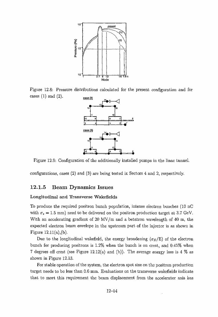
10'
10-
10'
present
1 27 8 12Node
16 1314
Figure 12.8: Pressure distributions calculated for the present configuration and for
cases (1) and (2).
• ^ 1
|l1 12
10 9
5 4
case
15'
16
B 7
3 2
| 13X <
10 9
<I16
8 ^ 7
6
Figure 12.9: Configuration of the additionally installed pumps in the linac tunnel,
configurations, cases (2) and (3) are being tested in Sectors 4 and 2, respectively.
12.1.5 Beam Dynamics Issues
Longitudinal and Transverse Wakefields
To produce the required positron bunch population, intense electron bunches (10 nC
with az = 1.5 mm) need to be delivered on the positron production target at 3.7 GeV.
With an accelerating gradient of 20 MV/m and a betatron wavelength of 40 m, the
expected electron beam envelope in the upstream part of the injector is as shown in
Figure 12.11 (a), (b).
Due to the longitudinal wakefield, the energy broadening (cr^/E) of the electron
bunch for producing positrons is 1.2% when the bunch is on crest, and 0.45% when
7 degrees off crest (see Figure 12.12(a) and (b)). The average energy loss is 4 % as
shown in Figure 12.13.
For stable operation of the system, the electron spot size on the positron production
target needs to be less than 0.6 mm. Evaluations on the transverse wakefields indicate
that to meet this requirement the beam displacement from the accelerator axis has
12-14

10"
10"
a.
//
J
1
j \
present
( 4 ) _ \
1 1'27 8 12 16 134Node
Figure 12.10: Pressure distributions calculated for cases (3) and (4).
1-,ttUt (Vt>tlftl)|wM)
r*,\U*n Pn4-itllHlirj<l
_ _ ^
^s~^~ — —
^—V-.
BUitnrt f ix* 1M*#.| Turn (ra|
Figure 12.11(a): Calculated electron beam envelopes from the pre-injector (right side)to the 180° arc (left side).
Figure 12.11(b): Calculated electron beam envelopes after the 180° arc (left side) and
positron beam envelopes after the positron production target (center).
12-15
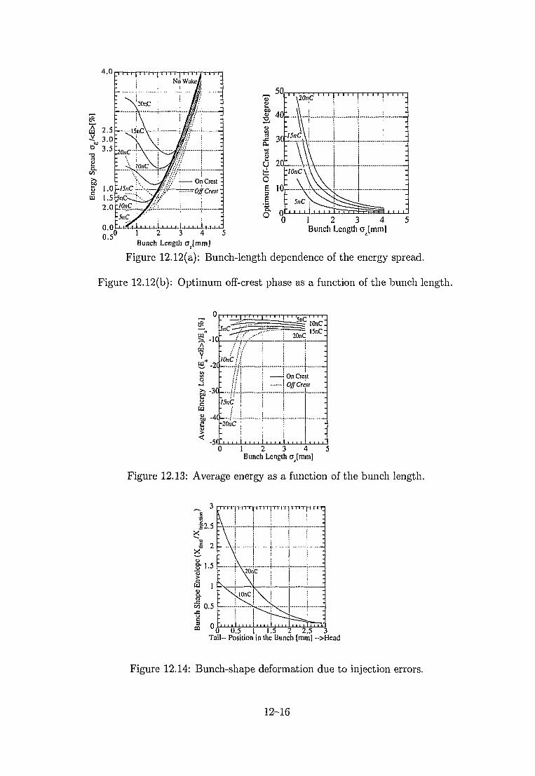
4.0
ifi 2.5 -15nC\-
3.5
$ 1.0w 1.5
2.0
0.00.5U
•20nC
-15nC ^:5n6
On Crest -
~OJf Crest;
i i , , I i i i , I , i i , i . , i ,1 2 3 4Bunch Length o. [mm]
1 2 3 4 5Bunch Length a [mm]
Figure 12.12(a): Bunch-length dependence of the energy spread.
Figure 12.12(b): Optimum off-crest phase as a function of the bunch length.
J/iC-
i
-5(t
15nC
- 4 ( - ;•••20nC
5nClOnCl
On Crest
OffCresi
_L0 1 2 3 4 5
Bunch Length ajmm]
Figure 12.13: Average energy as a function of the bunch length.
3 rrr
0 0.5 1 1.5 2 2.5 3Tail- Position in the Bunch [mm] -->Head
Figure 12.14: Bunch-shape deformation due to injection errors.
12-16

Figure 12.15: Beam position monitor (BPM) to be used in the KEKB injector linac.
to be kept below 0.5 mm. Good accelerator alignment and the beam position control
must achieve and maintain this requirement.
Beam Position Measurement
From the discussion above, the accuracy of beam-position monitors (BPMs) is required
to be ±0.1mm. Conventional strip-line monitors have been developed to be used at
each quadrupole magnet. An electrode length of 130 mm has been tentatively chosen
for testing, as shown in Figure 12.15.
The read-out electronics consists of the front-end, the detector and an external
ADC, as shown in Figure 12.16. At the front-end the signal from an electrode is
stretched in time by a band-pass filter (BPF), and is then amplified. At the detector
the signal is split into the RF mixer port and the limiting amplifiers (L/A) to generate
a local oscillator (LO). The peak value of the low-pass filtered intermediate-frequency
(IF) signal is proportional to the beam-charge density and the beam position. The
signal is captured by the sample-and-hold, and is digitized for computer processing
where the horizontal and vertical displacements of the beam are calculated.
The required dynamic range of the signal processing circuit is 60 dB. Out of this,
35 dB is for the beam intensity measurement, and the remaining ±12 dB is for position
measurements. This dynamic range covers the signal levels expected during regular
operation, as well as during the commissioning period. A linearity better than 2% needs
to be maintained. The measurements of test circuits indicate that those specifications
can be met.
12-17
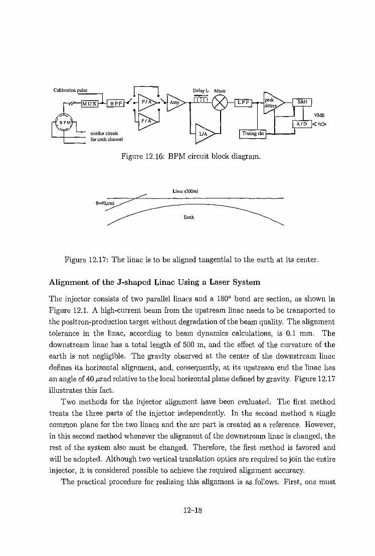
Calibration pulse Delay L Mi:Mixer
Figure 12.16: BPM circuit block diagram.
Linac (500m)
Earth
Figure 12.17: The linac is to be aligned tangential to the earth at its center.
Alignment of the J-shaped Linac Using a Laser System
The injector consists of two parallel linacs and a 180° bend arc section, as shown in
Figure 12.1. A high-current beam from the upstream linac needs to be transported to
the positron-production target without degradation of the beam quality. The alignment
tolerance in the linac, according to beam dynamics calculations, is 0.1 mm. The
downstream linac has a total length of 500 m, and the effect of the curvature of the
earth is not negligible. The gravity observed at the center of the downstream linac
defines its horizontal alignment, and, consequently, at its upstream end the linac has
an angle of 40 /irad relative to the local horizontal plane defined by gravity. Figure 12.17
illustrates this fact.
Two methods for the injector alignment have been evaluated. The first method
treats the three parts of the injector independently. In the second method a single
common plane for the two linacs and the arc part is created as a reference. However,
in this second method whenever the alignment of the downstream linac is changed, the
rest of the system also must be changed. Therefore, the first method is favored and
will be adopted. Although two vertical translation optics are required to join the entire
injector, it is considered possible to achieve the required alignment accuracy.
The practical procedure for realizing this alignment is as follows. First, one must
12-18

Laser
Positron Production Target
Linac Plane
J-Part Planc(Horizontal)
Figure 12.18: Alignment of two long linacs to be built parallel to each other.
establish a reference plane determined by the downstream linac by using the existing
alignment system. A diffraction-limited laser beam defines the precise alignment axis
along the entire downstream linac. Quadruple-type photo detectors placed on two ends
of each support frame of the accelerator can detect vertical and horizontal position
deviations with an accuracy better than 0.1 mm. All of the accelerator components
are put on the support frames with a mechanical precision within 0.1 mm.
We then transfer two points of the downstream linac to the corresponding points
of the upstream linac, as shown in Figure 12.18. This is done by using a laser beam,
while using the usual levels for the direction perpendicular to the beam line. Based
on these two points in the upstream linac as a reference, the laser alignment system
is used in the same way as that of the downstream linac. Thus, one realizes the same
plane for the two linacs with the same alignment precision.
Finally, the arc part is aligned in the horizontal plane by using levels. Because of
the way that the "horizontal" alignment is defined for the upstream and downstream
linacs, the plane of the arc part is inclined to that of the linac plane by 40 /trad.
After an initial alignment is carried out, continuous monitoring of the alignment
status will be carried out by two sets of level-comparing systems for the upstream and
downstream linacs. Clinometers will be installed at key locations, including the arc
part.
12.1.6 Beam Control
Linac Operation Mode Regarding Electron and Positron Injection
Several schemes are being studied concerning the acceleration of electrons and positrons.
12-19

e+ radiator (Ta 4X0)
4.5 GeV e-;tf~10% passing 8.0 GeV e"
"T ^"T 3.5 GeV e+
e~ energy adjustmente+ energy adjustment
Figure 12.19: Simultaneous acceleration scheme of the electron and positron beams.
In the most straightforward scheme, the operating conditions for the electrons and
positrons are completely switched, and they are separately injected to HER and LER.
This scheme provides optimized lattice focusing for the accelerated particles. However,
many parameters, such as the RF timing and phases, need to be re-adjusted for both
the upstream and downstream linacs.
In another scheme both the electron and positron beams are simultaneously ac-
celerated and injected into the rings, as shown in Figure 12.19. The electrons are
accelerated to 4.5 GeV by the first part of the injector. They then hit the positron
production target. The emerging positrons are accelerated to 3.5 GeV. The target is
built so as to have a small aperture which allows 10% of the electrons to pass through.
Those electrons are accelerated in the downstream part up to 8 GeV. The electron and
positron energies are adjusted at the end of the first and second parts, respectively.
In downstream part of the injector, the acceleration phases of the electrons and
positrons should be 180° apart. This can be achieved by two methods. The first case
is schematically shown in Figure 12.20: emerging positrons are first focused during
their deceleration phase, but soon come to be accelerated because of phase-slippage.
Figures 12.21(a) and 12.21(b) show a simulation of the capture rate and the longitu-
dinal phase space of these positrons. Calculations indicate that 80% of the produced
positrons can be accelerated; however, the energy spread will be larger than in the case
with an optimum phase configuration.
In the second case (shown in Figure 12.22) positrons are first focused in their
acceleration phase, then their phase is shifted by 180° by separating them with a
chicane. In the interval between the positron production target and the chicane, the
electrons are slightly decelerated. However, its effect is negligible since the electron
energy is larger than the positron energy there by a factor > 50.
If the two beam are co-accelerated, naturally the early part of the beam transport
beam line needs to simultaneously deliver two beams of different energies. Studies
are being prepared, regarding these issues as well as the bunching process during the
12-20

e+ radiator
e~ACC phase I e -ACC phase
e+ energy
\ phase slippage
Figure 12.20: Acceleration phase adjustment of the electron/positron beams (Op.l),
using phase slipping of the positrons in deceleration phase.
oaI - 5
N
Longitudinal. . • • • 1 •
• . . . . 1 .
Phase space (ACC phase Case)
( n(e+)/n(e-) = 3.5 %')J
_ . 1 i . 1 i i • ... 1 , , , , :
00 OS
Energy (MeV)
ao
s -6alN
Longitudinal Phase space (DCC phase Case)• • ' ' I ' ' ' ' I ' ' ' ' I ' ' ' '
( n ( e + ) / n ( o - ) = 2 . 6 % )
• • • • ' • • • , I
Energy (MeV)
Figure 12.21(a): Longitudinal phase-space of the accepted positron beam (positron-
acceleration phase).
Figure 12.21(b): Longitudinal phase-space of the accepted positron beam (positron-
deceleration phase at first).
12-21

e+ radiator
e~ACC phase ^ | e+ACC phase^ e~ACc Phase
chicanee+ s (-100 MeV) delay 180' (52.5 mm)
Figure 12.22: Acceleration phase adjustment of the electron/positron beams (Op.2),
using a chicane to make phase-delay of positrons.
phase-slippage.
Feedback to the Linac Beam Parameter
The beam energy in the injector is monitored at two locations: one in the arc section
and the other after the linac.
In the arc section the nominal beam energy is 1.6 GcV. The energy fluctuation
is detected with BPMs having a resolution of 0.03%. The beam energy there will
be controlled by adjusting the phase of the last two klystrons of the upstream linac.
Details of the correction algorithm are being considered.
At the end of the linac, electron and positron beams will be separated and trans-
ported independently. At the beam switch yard, the energies of both the electron and
positron beams will be controlled in the same manner as in the arc section.
12.1.7 Schedule
The schedule for the upgrade is shown in Table 12.4. An important constraint is that
injection to the PF ring has to be maintained during the upgrade project. Invasive
work has to be done during the annual shutdown period each year. The upgrade of
the present linac (from sector 1 to 5 ) and the construction of new sections (A, B, C
and the arc section) will be conducted independently before June, 1998. After each
portion is sufficiently tested, it will be connected during the summer shutdown of 1998.
Commissioning of the 8 GeV linac will start in November, 1998.
12-22

Construction Schedule
Operation
Shutdown
1 ~- 5 sector
A B C sector
Building (Gun)
Building (ARC)
1994
4 5 6 7 8 9 10 11 12 1 2 3
Upgrad ; upgra k
1995
4 5 6 7 8 9 10 11 12 1 2 3
upgrad : u Jgradc
construction
1996
4 5 6 7 8 9 10 11 12 1 2 3
upgrad
construction
1997
4 5 6 7 8 9 10 11 12 1 2 3
upgrade
construction
1998
4 5 6 7 8 9 10 II 12 1 2 .1
Joint
Table 12.4: The schedule of the injector upgrade program.
12-23

12.2 Average Luminosity
12.2.1 Beam Lifetime
In this section we evaluate the beam lifetime, which will be useful for simulating the
optimum operation and the beam fill patterns of KEKB. The dominant sources of
particle loss, which is responsible for the finite beam lifetime at KEKB, are the following
three: the beam-beam bremsstrahlung in the beam collision, the beam-gas scattering
and the Touschek effect.
The beam lifetime due to beam collisions depends on the energy acceptance AE/E
of the ring. However, the dependence on AE/E is relatively small for AE/E >0.5%.
For example, if the energy acceptance is increased from 1% to 2%, the lifetime varies
from 8.8 hours to 10.7 in the LER, and from 20.9 hours to 25.3 in the HER. Since an
optics study has shown the feasibility of an energy acceptance which exceeds 1% in
both rings, it is reasonable to take the lifetime at the 1% acceptance.
The lifetime due to beam-gas scattering depends on the vacuum pressure, and again
weakly on the energy acceptance. Assuming a design value pressure of 1 x 10~9 Torr
and a 1% energy acceptance, the lifetime would be 45 hours in both rings.
The Touschek effect plays an important role in causing a beam loss in the LER.
In this case, the lifetime depends strongly on the energy acceptance, as well as on the
transverse acceptance. The expected acceptance of LER leads a Touschek lifetime of
more than 15 hours. At this moment the LER lattice has not been completely finalized,
and complete calculations of the expected acceptance, which include effects of machine
errors, are not yet available. Consequently, the estimated Touschek lifetime should be
considered to be a variable parameter for simulating the operation. It is noted that
this effect does not contribute to the lifetime of the HER. Table 12.5 summarizes the
beam lifetime estimation.
Table 12.5: Beam lifetime estimation for KEKB
LER
HER
Beam-Beam
20.9
8.8
Beam-Gas
45
45
Touschek
5
10
15-
Total
3.7 h
5.9 h
7.3 h
7.4 h
12-24

12.2.2 Operation Pattern
First, we estimate the initial fill time for KEKB. In what follows, the calculations are
made based on the assumption that the positron and electron charges from the linac
are 0.64 nC/pulse and 1.28 nC/pulse at 50 Hz, and that the injection efficiency to the
KEKB rings is 50%. Then, for full-bunch operation the required injection time for the
LER and HER will be 0.5 hours and 0.1 hours, respectively.
It should be noted that the beam intensity in the rings does not necessarily decay
as an exponential function of time. Under stationary operation, the stored current will
not decay very much before the next topping. Therefore, we use a simple model where
the intensity decays exponentially with the estimated lifetime. Then the luminosity
itself decays exponentially with a lifetime, T[,, given by
_L - i. 1
where T\ and r2 are the lifetime for the LER and HER. With the refilling time TF, and
the experiment time TE, the average luminosity would be
where CQ is the peak luminosity. The beam loss during the refill time has been ne-
glected. The refill time is a sum of the injection time for the positrons and electrons,
and the time that is needed for switching the operation mode between the injection
and the physics run.
Figure 12.23 shows the average luminosity for three cases with the varying Tou-
schek lifetime in LER. A mode switch time of 2 minutes is assumed. With a 10-hour
Touschek lifetime, the average luminosity and the injection time would be as shown
in Figure 12.24. Taking account of the number of bunches (5120) and the repetition
rate of 50 Hz of the linac, we can see that at least 1.7 minutes are required to refill
each bunch. The injection time will be a multiple of the minimum refilling time. We
define the optimum operation pattern to be what gives an average luminosity to be
> 75% of the peak luminosity. In Figure 12.24, such an optimum operation pattern
would consist of a 40-minute physics data acquisition time and a 7-minute refill time,
including both electrons and positrons. Each positron bunch would be recharged with
two shots from the linac. Under this condition the operation pattern would look like
the time chart in Figure 12.25.
12-25

-0 0 . 8 0IDN
•H
0 0.75
ra 0.70 +0a•H
&ft)n
I
0 . 6 5 - •
0 . 6 0
LER Touschek Lifetime
20 40 60 80
Experiment Time ( m i n . )
• • 1100
Figure 12.23: Average luminosity for different LER Touschek lifetimes.
5 0.80 T T 10
Typical Operation Condition
20 40 60 80
Experiment Time (min.)
100
Figure 12.24: Average luminosity and injection times for the case of a 10-hour LER
Touschek lifetime. The vertical line indicates a typical operation condition.
12-26
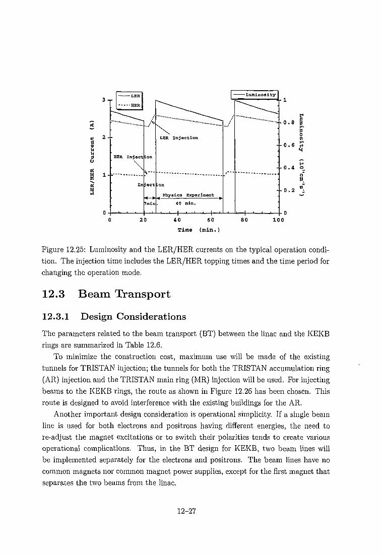
3 -r
2 - -30uuu
a* • • "
HER InjoctLon
lect
7min
LER Injection
Physics Experiment
40 min.
• I • ' ' I •20 40 60
Time ( m i n . )
•» - 0 . 8
- - 0 . 6
in
- - 0 . 4
- - 0 . 2
80 100
Figure 12.25: Luminosity and the LER/HER currents on the typical operation condi-
tion. The injection time includes the LER/HER topping times and the time period for
changing the operation mode.
12.3 Beam Transport
12.3.1 Design Considerations
The parameters related to the beam transport (BT) between the linac and the KEKB
rings are summarized in Table 12.6.
To minimize the construction cost, maximum use will be made of the existing
tunnels for TRISTAN injection; the tunnels for both the TRISTAN accumulation ring
(AR) injection and the TRISTAN main ring (MR) injection will be used. For injecting
beams to the KEKB rings, the route as shown in Figure 12.26 has been chosen. This
route is designed to avoid interference with the existing buildings for the AR.
Another important design consideration is operational simplicity. If a single beam
line is used for both electrons and positrons having different energies, the need to
re-adjust the magnet excitations or to switch their polarities tends to create various
operational complications. Thus, in the BT design for KEKB, two beam lines will
be implemented separately for the electrons and positrons. The beam lines have no
common magnets nor common magnet power supplies, except for the first magnet that
separates the two beams from the linac.
12-27
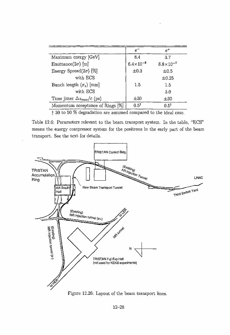
Maximum energy [GeV]
Emittance(2cr) [m]
Energy Spread(2c") [%]
with ECS
Bunch length [az) [mm]
with ECS
Time jitter Azmax/c (ps)
Momentum acceptance of Rings [%]
e
8.4
6.4xlO'8
±0.3
1.5
±300.5*
e+
3.7
8.8xlO"7
±0.5±0.25
1.5
3.0
±300.5t
f 30 to 50 % degradation are assumed compared to the ideal case.
Table 12.6: Parameters relevant to the beam transport system. In the table, "ECS"
means the energy compressor system for the positrons in the early part of the beam
transport. See the text for details.
TRISTANAccumulationRing LINAC
New Beam Transport Tunnel
TRISTAN Fuji Exp.Hall(not used for KEKB experiments)
Figure 12.26: Layout of the beam transport lines.
12-28
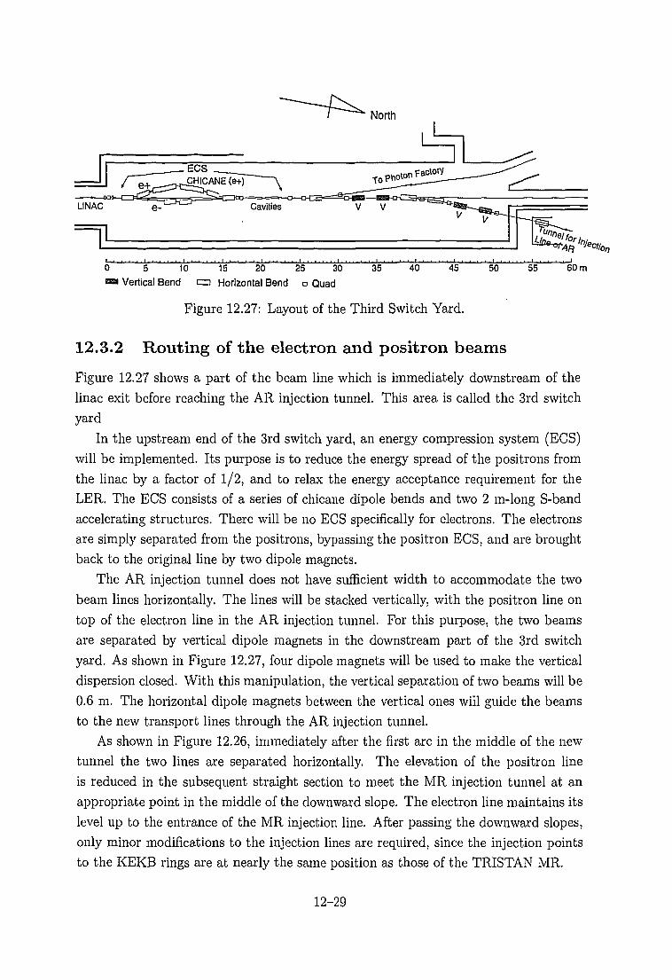
5 10
Vertical Bend
15 20 25 30
Horizontal Bend a Quad
35 40 45 50 55 60 m
Figure 12.27: Layout of the Third Switch Yard.
12.3.2 Routing of the electron and positron beams
Figure 12.27 shows a part of the beam line which is immediately downstream of the
linac exit before reaching the AR injection tunnel. This area is called the 3rd switch
yard
In the upstream end of the 3rd switch yard, an energy compression system (ECS)
will be implemented. Its purpose is to reduce the energy spread of the positrons from
the linac by a factor of 1/2, and to relax the energy acceptance requirement for the
LER. The ECS consists of a series of chicane dipole bends and two 2 m-long S-band
accelerating structures. There will be no ECS specifically for electrons. The electrons
are simply separated from the positrons, bypassing the positron ECS, and are brought
back to the original line by two dipole magnets.
The AR injection tunnel does not have sufficient width to accommodate the two
beam lines horizontally. The lines will be stacked vertically, with the positron line on
top of the electron line in the AR injection tunnel. For this purpose, the two beams
are separated by vertical dipole magnets in the downstream part of the 3rd switch
yard. As shown in Figure 12.27, four dipole magnets will be used to make the vertical
dispersion closed. With this manipulation, the vertical separation of two beams will be
0.6 m. The horizontal dipole magnets between the vertical ones will guide the beams
to the new transport lines through the AR injection tunnel.
As shown in Figure 12.26, immediately after the first arc in the middle of the new
tunnel the two lines are separated horizontally. The elevation of the positron line
is reduced in the subsequent straight section to meet the MR injection tunnel at an
appropriate point in the middle of the downward slope. The electron line maintains its
level up to the entrance of the MR injection line. After passing the downward slopes,
only minor modifications to the injection lines are required, since the injection points
to the KEKB rings are at nearly the same position as those of the TRISTAN MR.
12-29

Acceptanceellipse
33 mm
Figure 12.28: Acceptance of the LER and incoming beam. The large circle indicates the
acceptance ellipse in the longitudinal plane of the LER. The rotated ellipse with a solid
line represents the incoming positron beam with ECS, while the ellipses with broken
lines indicate incoming beams with a timing jitter. The outermost ellipse corresponds
to the maximum allowable jitter. R56 is assumed to be 4 m.
12.3.3 Constraints to R56 and the tolerance of timing jitter
The ECS may not be operational in the initial KEKB operation. In that case, the
positron beam will have a large energy spread (at = 0.25% without ECS). While the
original bunch length expected from the linac is 1.5 mm, a bunch lengthening effect
through the atR^ term needs to be considered. Here, the R56 refers to the (5, 6)
component of the transfer matrix, i.e. the path length dependence on the momentum.
For example, if the R^Q term of the BT exceeds 5 m, the bunch length will be larger than
12.5 mm. The beam with a large bunch length induces a large quadrupole synchrotron
oscillation after injection. Similarly, any timing jitter of the injected beam also induces
(dipole) synchrotron oscillations. Figure 12.28 illustrates the acceptance ellipse for
injection and possible patterns of a mismatch.
The largest amplitude of the induced bunch oscillation immediately after injection
thus depends on R56. Figure 12.29(a) shows the largest amplitude of energy oscillation
as a function of R56. Figure 12.29(b) shows the timing jitter tolerances as a function of
R56, which was defined as the largest longitudinal position shift that makes the beam
ellipse cross with the acceptance boundary.
It is seen that the timing jitter tolerance is zero for the case of positrons without
ECS. For positrons with ECS, a jitter tolerance of 30 ps (9 mm) demands that R§6 be
12-30

1.0
0.9 ^ Ap/p(%) s*- w/o ECS
(b)25
-5
Az (mm) e + w/o ECSto(mra) e + w/ECSAz (mm) e~ w/oECS
10
Figure 12.29: (a) Largest amplitude of energy oscillation as a function of R56. The
dash-dot line shows a momentum acceptance of 0.5%. (b) the timing jitter tolerances
as a function of R56. The broken line shows a tolerance of 9 mm (30 ps).
less than 7.5 m. For electrons, R56 should be less than 6 m. The optics design of BT
has been made such that the value of R56 will be 4 m.
It should be noted that R56 can be written as
#56 = ®'< (12.1)
where 0 is the total bending angle and 77 is the average dispersion in the dipole magnets.
From this it is found that f\ needs to be smaller than 1.2 m for the positron line to
satisfy R56 = 4 m.
Since the BT arc is occupied by strong dipole magnets of 1.5 T, there is no room
to make the dispersion below 1.2 m for each arc. Consequently, another approach to
suppress the R56 has been taken for this BT design: the optics around the three arcs in
the new BT tunnel are arranged such that the arcs in the upstream generate negative
dispersion at the downstream arcs so that Rs6 of the downstream arcs is decreased.
In the current design the electron line will require 54 dipole and 62 quadrupole
magnets; the positron line will require 57 dipole and 64 quadrupole magnets. Some of
the magnets, particularly the magnets in the downward slopes, may be recycled from
the TRISTAN injection beam line.
12-31

Chapter 13
Accelerator Control System
13.1 System Requirements
The KEKB accelerator complex has more than 50,000 control points along the 3 km
circumference of the two rings, the LER and HER. Some control data must be updated
at a high rate up to 100 Hz. A fast and powerful control system is required to implement
sophisticated tuning procedures and feedback loops for the stable operation of KEKB.
In addition, such a control system has to be readied in a timely fashion, i.e. it has to
be operational at the first commissioning time of KEKB, which is expected to begin
near the end of 1998. The schedule for the control system development is summarized
in Table 13.1.
13.1.1 Functional Requirements
The functional requirements for the KEKB accelerator control system can be catego-
rized into three groups as follows. Some of the important issues are itemized below:
1. Hardware Control:
(a) It should be that the graphical user interface (GUI) to read/set/monitor
the status of a hardware device can be constructed without resorting to
complicated programming.
(b) It should be that the data logging can be configured without complicated
programming.
(c) The low level access to individual hardware components should be supported
for developing and debugging the hardware interface. The interface of this
low level access should be user-friendly and flexible.
13-1

FY1995 April Decision to use EPICS.
Start development of software tools.
Start user education on EPICS.
July Complete First stage of Relational Database
Design.
December Complete Steering Power supply/ BPM inter-
face design.
FY1996 Develop Application programs for AR/KEKB.
December System test of new TRISTAN AR control
system.
FY1997 July New TRISTAN-AR control system
commissioning
New TRISTAN/KEKB beam transport line
control system
December Starts installation of KEKB accelerator con-trol system equipment.
_ _ _ _ _
December Commissioning of KEKB.
Table 13.1: Schedule of the KEKB accelerator control system development.
13-2

(d) A powerful yet easy-to-handle development system should be provided for
the device driver level software.
(e) Stand-alone operation of the hardware subsystem should be allowed, without
depending on other part of the accelerator.
2. Accelerator Operation:
Application programs required for this category include: automated machine
operation software, monitors of the machine performance, feedback loops to op-
timize the machine performance, alarm notification system and others.
(a) The user interface of these programs should be operator-friendly.
(b) Operator interfaces should have a quick response; typically less than a few
seconds.
(c) An alarm notification system should be included.
(d) All key operations should be recorded for later inspection.
(e) Powerful yet easy-to-handle development system for the development of ap-
plication programs with GUI.
3. Accelerator Development:
Accelerator development refers to activities where various machine errors are
identified and fixed, new tuning techniques are attempted, better operating con-
ditions are searched for, or unresolved accelerator physics issues are investigated,
and so on. Its guiding principles may be summarized as:
(a) All data that can possibly be collected should be collected.
(b) All collected data should be saved for later analyses.
(c) All operations should be recorded for later inspection.
The requirements on the data analysis tools are:
(d) Stored data can be easily retrieved.
(e) The data can be easily analyzed.
(f) The data analysis tools should be able to handle both data from the accel-
erators and the results from computer simulation in a similar way.
(g) The development system for application programs should be programmer-
friendly.
13-3

In a particle accelerator for high energy physics, hardware modifications and up-
grades to the machine configuration are common events in its life cycle. The following
features should be incorporated so that the control system will be able to keep pace
with the changes of the accelerator.
1. All machine parameters and data of individual machine components should be
saved in a database. This is so that changes in the accelerators are automatically
reflected in the control system.
2. Incremental upgrades and the replacement of components of the control system
should be allowed.
3. Integration of control sub-systems within the accelerator control system should
be done in a easy and seamless way.
13.1.2 Design Guideline
With the requirements stated above, the design considerations for the KEKB accel-
erator control system are summarized as follows. The keywords of the guidelines are
"Openness", "Standard" and "Scalability":
1. For future maintenance and upgrades, the control system should have a layered
structure. The layers described here refer to such concepts as: the device interface
layer, the equipment control layer and the presentation layer. The interface
protocol between these layers should be a well-defined one based on international
standards. This layered structure will allow us to modify components in one layer
without affecting other layers.
2. As the interface between the control system and the equipment, international
standards such as CAMAC, VME, VXI and GP-IB should be used where their
performance is found adequate.
3. To maintain good responsiveness of the control system, a high-speed network
should be used to connect the computers. The network architecture should be
chosen from well established, standard technologies.
4. To reduce the man-power requirement and efforts to build the control system, in-
ternational collaboration and/or commercially available products should be taken
advantage of.
5. At times, adopting object-oriented techniques or data abstraction for hiding the
details of the hardware helps in the development of application programs
13-4

Operator Interface Operator Interface Global Data Storage
DistributedHardwareControler
DistributedHardwareControler
DistributedHardwareControler
§?'iceInlerface
2
'iceInlerface
as.
M M
fi-lmerface
2g_re"
s>'ice
Serface
2acn
•Hi
?'iceInlerface
a
PresentationLayer
High SpeedNetwork
EquipmentControlLayer
DeviceInterfaceLayer
Figure 13.1: Schematic view of the KEKB accelerator control system.
13.2 System Architecture
The KEKB accelerator control system will be built based on the EPICS[2] toolbox.
The control system is divided into three layers:
• Presentation layer,
• Equipment control layer, and
• Device interface layer,
as shown in Figure 13.1. The network system which connects the first two layers is
another key component of the control system. In EPICS terminology, a computer in
the presentation layer is called an OPI (Operator Interface) and one in the equipment
control layer is called an IOC (Input/Output Controller).
13.2.1 Device Interface Layer
The device interface layer, which sits at the lowest level of the three, sends and receives
signals from or to individual hardware equipment. This layer communicates such sig-
nals and data with computers in the equipment control layer. A schematic view of the
device interface layer is shown in Figure 13.2.
KEK has a large inventory of CAMAC modules from the TRISTAN control system.
The CAMAC crates and modules inside them are used as a device interface layer of
the KEKB control system. The CAMAC crates are connected by CAMAC serial high-
ways or CAMAC branch highways, depending on specific requirements. An equipment
13-5

High Speed Backbone Network (FDDI)
t
Ethernet
\
FDDI <-> EthernetBridge
Terminal _Server
Sn
IOC
CA
MA
C Serial
Driver
""
CAMAC Create &Modules
I
I
GP
-IB
—
1
r™r
1
| V
ME
Bus
extender
VME subrack &Modules
i
Figure 13.2: Schematic of the device interface layer
control computer in the VME sub-rack controls the serial/branch CAMAC highway
driver in the same VME sub-rack .
The standard CAMAC modules used in TRISTAN are supported by the KEKB
accelerator control group, i.e. the control group takes the responsibility for maintaining
proper functionality of these modules. It is considered that standard CAMAC modules
can cover most of the needs for the device interface modules.
However, CAMAC is not the only field bus that is used in the device interface layer
for KEKB. Drivers of other field bus architecture, such as GP-IB, can be placed in a
VME sub-rack . Another example of the field bus used in the KEKB accelerator control
system is a multi-drop serial line, with which about 1600 power supplies for steering
correction magnets are controlled. A device interface using a multi-drop serial line for
magnet power supplies is now being studied in collaboration with the magnet group
and the beam transport group for KEKB. The high-speed BPM electronics system will
be implemented on VXI. The VXI is yet another example of the field bus to be used
at KEKB. In this case, it will be natural to control these modules directly from IOC
through the VME/VXI bus .
13.2.2 Equipment Control Layer
The equipment control layer consists of computers that functionally control the equip-
ment in each hardware group, e.g. magnet, RF systems, beam monitor and others. The
13-6

LaboratoryNetwork CATV
X-TERMINAL X-TERMINAL X-TERMINAL
_tGATEWAY
±_DISPLAY
Network (or X-termlnals
CONSOLE
1CONSOLE
1Database
High Speed Network
1Simulation
1Logging ALARM
Presentation Layer
Equipment Control Layer
ICAMAC| [CAMAC|Device Interface Layer
Figure 13.3: KEKB Accelerator Control System Architecture
equipment control computer, IOC, is a VME board-computer. The current version of
EPICS system supports VxWorks as the real-time operating system for IOC.
One of the core elements in EPICS is the distributed runtime database, which re-
sides in IOC. A database record (also called a process variable) in the runtime database
corresponds to each channel in the device interface layer. Those records include all the
device-specific information, such as hardware address, calibration table, upper/lower
limits of action variables, and others.
Software components to support CAM AC are already included in EPICS. To sim-
plify the use of standard CAMAC modules for KEKB, device support routines for these
standard CAMAC modules will be developed.
Although EPICS supports a rich collection of VME modules, some modules that
are introduced for KEKB may not be readily supported by EPICS at the moment. For
these modules, it is necessary to develop a set of software, device driver, device support
and record support. This task will be carried out by personnel from the control group
and the hardware group which uses such modules.
13.2.3 Network
The equipment control layer and the presentation layer are connected through a high-
speed network, such as FDDI. To separate the network traffic between these layers
13-7
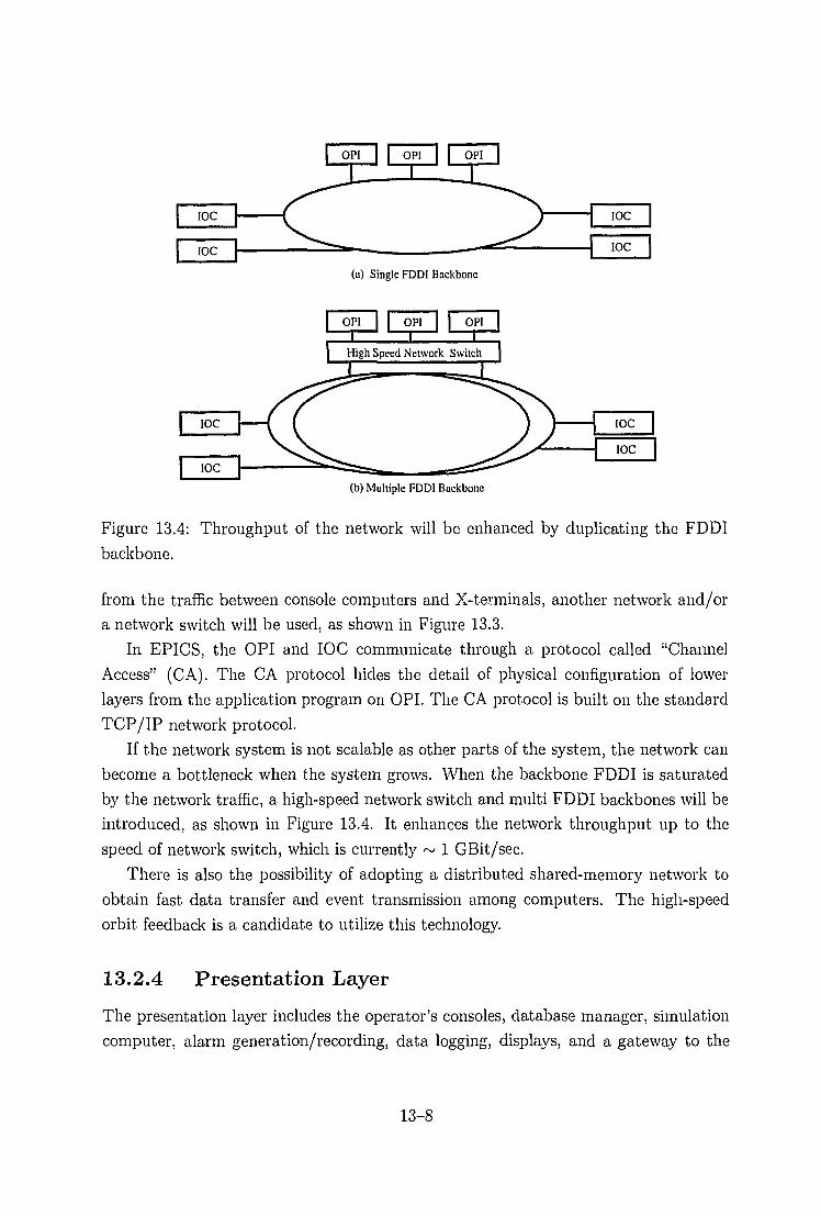
(a) Single FDDI Backbone
I High Speed Network Switch
(b) Multiple FDDI Backbone
Figure 13.4: Throughput of the network will be enhanced by duplicating the FDDI
backbone.
from the traffic between console computers and X-te.vminals, another network and/or
a network switch will be used, as shown in Figure 13.3.
In EPICS, the OPI and IOC communicate through a protocol called "Channel
Access" (CA). The CA protocol hides the detail of physical configuration of lower
layers from the application program on OPI. The CA protocol is built on the standard
TCP/IP network protocol.
If the network system is not scalable as other parts of the system, the network can
become a bottleneck when the system grows. When the backbone FDDI is saturated
by the network traffic, a high-speed network switch and multi FDDI backbones will be
introduced, as shown in Figure 13.4. It enhances the network throughput up to the
speed of network switch, which is currently ~ 1 GBit/sec.
There is also the possibility of adopting a distributed shared-memory network to
obtain fast data transfer and event transmission among computers. The high-speed
orbit feedback is a candidate to utilize this technology.
13.2.4 Presentation Layer
The presentation layer includes the operator's consoles, database manager, simulation
computer, alarm generation/recording, data logging, displays, and a gateway to the
13-8

KEK local-area network. Workstations and/or CPU servers running UNIX1 operating
systems are used in this layer. The X-window system is used as the graphical user
interface standard.
The software environment used in this layer is very important for the whole system.
The fundamental functions that have to be supported from the beginning of the instal-
lation include: the controls of each hardware equipment and graphical displays of the
hardware status and various monitor values from the accelerator. Programmer-friendly
interfaces must be provided for the accelerator physicists to develop application pro-
grams painlessly. It is also important to have very efficient data retrieval tools and
analysis tools. The use of EPICS solves some of these problems as discussed later.
Operator's console
X-terminals with multiple displays will be used as operator consoles. The X-terminals
are connected to the UNIX machines in the presentation layer. By using the tools in
EPICS, personnel who are not from the control group will be able to create graphical
operator interfaces without difficulties. Tcl/Tk and other languages which support CA
access can also be used to develop application programs.
Database manager
The database manager keeps all information concerning the KEKB accelerator com-
plex, such as machine parameters, equipment specifications, component locations,
and others. Logged data, archived data and configuration data should also be ac-
cessible from a database system with the same interface. Commercially available
DBMS (Database Management System) will be used as a framework of the database
manager. Two commercial relational database management software, ORACLE2 and
SYBASE3, are currently being evaluated. Recent progress in OODB(Object Orientt^
Database) technology should be also taken into account for the choice of DBMS.
Each runtime database record in EPICS has a unique name in the system. This
unique name may not be easy enough to decipher for application programmers. The
database manager also works as a channel name server. An application program can
send a query on channel names and get a list of the channel names from the database
manager.
'UNIX is a trademark of Unix Lab.2ORACLE is a registered trademark of ORACLE Corporation.3SYBASE is a registered trademark of SYBASEJnc.
13-9
Simulation computer
The simulation computer is used for accelerator physics calculations for such purposes
as orbit correction and optical matching optimization. Computer code SAD[4] has been
heavily used in the design work of KEKB, and will be used as a modeling/simulation
program in the KEKB control system as well.
The ultimate goal of the development of SAD is to build a virtual accelerator on
a digital computer. The KEKB control system will be built such that the SAD users
should be able to control this virtual accelerator through the same operator interface
that is used for the real accelerator, like a "flight simulator." To realize this idea, an
interface program between SAD and a portable CA server will be developed, which will
run on UNIX workstations. The CA clients can access the virtual accelerator through
this CA server using an ordinary CA protocol.
The concept of a virtual accelerator is also useful in the development of application
programs. Application programmers can test their software without risking operation
of the real machine. It is even possible to develop an application program without a
real machine.
System Alarm/Data logging
Equipment failures are monitored by each IOC and are reported to the alarm computer
for broadcasting and recording purposes. The alarm computer notifies such conditions
to the operator with various methods including: alarm sound, flashing or pop-up dis-
play, automatic pocket-beeper calls, and so on. The data logging computer collects
and saves data from IOCs for later analyses.
System status broadcast and the local network gateway
The display computer broadcasts and displays data and information throughout the
KEK site through the CATV network and other media. There is also a gateway com-
puter which connects the KEKB control computer network with the KEK laboratory
network. Through the KEK lab network, users who are away from the control room
can monitor the status of each device and the status of KEKB overall. Privileged
users are allowed to control their equipment from their office. To avoid a network jam
caused by access through the laboratory network, a proxy channel access (CA) server
will be used on the gateway computer. It will intercept and bundle CA requests from
the laboratory network.
13-10

13.2.5 Timing system
Magnet synchronization
Since the magnet setting in the KEKB rings needs to be changed without loosing the
beam, the control system has to change the strength of the magnets step by step in a
synchronized way. For this operation, a timing system will be used to send a "heart
beat" to the entire system. A dedicated signal line will be used to send a timing signal.
A module in a device interface layer receives this signal and triggers an action.
Synchronized data acquisition
The beam orbit in the beam transport line are measured by using one-pass beam
position monitors (BPMs). The KEKB control system needs to be able to associate
this data with data from the injector linac BPMs or from the beam loss monitors and
others within KEKB. This is important for studying and optimizing the beam injection
setup.
When orbit distortions are intentionally introduced at KEKB for studying magnet
misalignment and other effects, the BPM data need to be tagged appropriately such
that sensible analyses are made possible.
13-11
Bibliography
[1] W-D. Klotz et al., "Experience with a Standard Model '91 based Control System
at the ESRF", ICALEPCS '93, Berlin(FRG), 1993.
[2] L.R. Dalesio, et al., "EPICS Architecture", ICALEPCS 91, KEK Proceedings 92-
15, (1992) pp.278-282., Dalesio, L., et al. "The Experimental Physics and Industrial
Control System Architecture," ICALEPCS, Berlin,Germany, Oct. 18-22, 1993.
[3] "Vsystem" is a product of Vista Control Systems Inc., Los Alamos, NM.
[4] SAD is the accelerator design tool program developed at KEK.
[5] Shin-ichi Kurokawa, et al., "The TRISTAN Control System", Nucl. Instr. and
Meth., A247, (1986) pp. 29-36.
[6] Shin-ichi Kurokawa, " Status of TRISTAN-II Project", Proceedings of the 1993
Particle Accelerator Conf, pp. 2004-2006, S-I Kurokawa, "KEKB status and Plans",
1995 Particle Accelerator Conference, Dallas, Texas.
13-12