
KC's Problems
471
KC's Problems and Solutions for Microelectronic Circuits FOURTH EDITION Kenneth C. Smith
-
Upload
khangminh22 -
Category
Documents
-
view
1 -
download
0
Transcript of KC's Problems

KC's Problemsand Solutionsfor Microelectronic Circuits FOURTH EDITION
Kenneth C. Smith

KC's Problemsand Solutionsfor Microelectronic Circuits FOURTH EDITION
Kenneth C. Smith

KC's Problemsand SolutionsforMicroelectronic Circuits FOURTH EDITION
Sedra/ Smith
KennethC. SmithUniversity of TorontoHongKong University ofScience and Technology
New York OxfordOXFORD UNIVERSITY PRESS1998

Oxford University Press
Oxford New YorkAthens Auckland Bangkok Bogota Bombay Buenos AiresCalcutta Cape Town Dar es Salaam Delhi Florence Hong KongIstanbul Karachi KualaLumpur Madras Madrid MelbourneMexico City Nairobi Paris Singapore Taipei Tokyo Toronto Warsaw
and associated companies inBerlin Ibadan
Copyright © 1998, 1992 by Oxford University Press, Inc.
Published by Oxford University Press, Inc.,198MadisonAvenue, New York, New York, 10016http://www.oup-usa.org1-800-334-4249
Oxford is a registered trademark of Oxford University Press
All rights reserved. No part of this publication may be reproduced,stored ina retrieval system, or transmitted, inany form or by any means,electronic, mechanical, photocopying, recording, or otherwise,without the prior permissionof Oxford University Press.
ISBN 0-19-511771-9
98765432
Printed in the United States of Americaon acid-free paper
Cover Illustration: The chip shown is the ADXL-50 surface-micromachined accelerometer. For the first time,sensor and signal conditioning are combined on a single monolithic chip. In its earliest application, it was a keyfactor inthe improved reliability and reduced cost of modern automotive airbag systems. Photo reprinted withpermission ofAnalog Devices, Inc.

. v II ÿ ÿÿ
y,
&
I I I I
CUJhFYEM. iCHAPTE1 2• Co " 3CHAFIBS. 4CtlASriaE 5chapter e
GMAFTKR 2« • '
CHAFIEft •
chaftS ncEWim.. isCIIAFIBC 14
' to £3fifii.f ÿ: Jtsles' tf > i « '' > 'IMsoIjss
BjsoSar Jciaetioe. T«wi«$i»rs {RJ-TCj14oM«t21£cs,fVftf5ssstois (FBI's).Blflktssitlsl swscl Mitlltsfef® AfffplifisfsFf'i>c|oeacf llesjKstsefsclfesick{>stf;«2 Stages i.Fsoior < ; '« -Aml&g fetep'ateil Clrawls
' FStes a»• Tsisial AmplifiersSigaal GaoamSoss' §i:t«l WsoofeiwCltfiamg ClrcBiis' C- SO/pOSl AgrCCUS?!A t - swd -n/ < IligitisI .,.f»
: f-fOt
,-iSlr
fatr«o!sct»a te Mortrvsiesÿ " ; ' - i'
ItKOiCr
Itifitiku: Rmmiiou Traasfetora (IJJTs)£'fc£:l*Ei2eoi' 'I'i'aaaisinivt l-Flvl's)
PiFFreafisI astl MtsMtecsgu kmpHtmrfyvqsmicy Mmmmmsi'sstifcaok
Oaiffst Stagas mid Power Am0iRm%Aaalag Is-ifegrasesI Circuits¥wem t TtmrA AflipFfesoi, > C • » , • r. sinA i ,>• CircuitsMt>8 lAgreal CiretriCIMpelar aiicl AJsae£«NBl£ei«s<G>g;r lisgFa! Circaifs
' 1- - 'jLc Jl:
V ' , I |1{ . IIStaatlarcl Catapoaeat Yal&es-

PREFACE
IOVERVIEW
• THE MANUAL FORMAT
This manual, "KC's Problems and Solutions", is a collection of problems and solutions with compiled answers,designed to accompany the Text "Microelectronics Circuits", fourth edition, by Sedra and Smith, OxfordUniversity Press, 1997.
The goal of this Manual, captured in its former subtitle "Trial and Success", is to motivate and assist inthe dynamic process of active learning.
The mechanism provided here includes three parts: I: Problems, II: Solutions, III: Answers.Specifically:
Part I: Problems, consists of a collection of problems keyed to the Text in a variety of ways:Most obviously, the problems are grouped according to the Sections of the Text. Possibly lessapparent is their relationship both to segments of the Text and to the end-of-chapter problems con¬tained there, about which more will be said shortly. As well, the problems are coded to indicate Com¬plexity (C), Length (L), and Design content (D), with an appended asterisk notation to indicate theintensity of the associated attribute.
Part II: Solutions provides solutions which are relatively detailed. While the presentation isusually in a somewhat compressed format, attention has been given to revealing intermediate analyticaland computational steps. As well, additional comments on the interpretation of the Text, and thedirection for additional work are relatively common.
Part III: Answers allows readers to conveniently evaluate their success at problem solvingwithout the inevitable hints that skimming the actual solution might provide.
• AN APOLOGY TO THE USER - THE LIKELYHOOD OF ERRORS
In a Manual such as this, intended as an aid to the student in a process of active learning, the issue oferrors is a very critical one. Obviously, errors embodied in the problem solutions presented here can be verydisconcerting to anyone who is less than secure in his or her knowledge of the subject matter. Thus the reduc¬tion of errors has been, and will continue to be, a high priority. It is in the latter sense that your indulgenceand help are sought in the conjoined processes of error detection and error recovery. Certainly Iwill be mostgrateful for your help in reporting them!
In this process of error compensation, it is possibly useful to identify the types of errors you will inevit¬ably find. In order of increasing subtlety and criticality, they are:
Typographical errors:There are many types of possible typographical errors which can be broadly characterized asomission, exchange, and replacement, either in word, number, symbol, phrase or sentence con¬structs. While unnecessarily confusing, they usually have the virtue of being easily detectableand correctable in context. To assist the detection process at its lowest level, solutions arerelatively detailed with lots of intermediate calculations, relatively consistent variable naming,and relatively complete use of units for numerical results. Unfortunately, however, you may

Preface -2
possibly find missing solution lines, as well.
Arithmetic Errors:These occur between steps in a computation as a result of calculator misuse or transcriptionerror in the original work. They are distinguished from typographical errors by the fact thatthey propagate. They can be detected only by carefully checking and reproducing thepreceeding substitutional and computational steps. Often the integrity of the following solu¬tion structure remains, but not always. One of the generic methods Iuse to help ensure struc¬tural integrity is an overall test for physical plausibility, or reasonableness, though this is oftennot documented. However, an explicit demonstration of the attempt to reveal such errors is inthe use of frequent Check comments which typically employ a recent result in a somewhat-global verification process. Incidentally, this is a good approach for you to use in your solu¬tions, as well!
Conceptual Errors:These are of two kinds, either local or global. The former occur usually as a result of misin¬terpretation of a symbol, or of the scope of a question. Occasionally you may find a piece ofa question that was not answered at all, or answered in a less than complete fashion. Theonly virtue of this sin is that it is normally detectable. On a far more serious scale will be theoccasional occurrence of totally wrong solution methods. These are quite insidious andconfusing to a novice, since they can easily be mistaken to be a valid alternative approach.While these are relatively unlikely, they are almost certainly present.
For all of these errors, please accept my apologies. While Ihave utilized many approaches to minimiz¬ing them, the limitations of available time and resources have produced the result you see before you. All thatremains to be said, again, is that Ibeg your indulgence, and look forward to your help in improving the situa¬tion!
• SOLUTION-PRESENTATION FORMATAs you will note, the solution format in Part II:Solutions in this Manual is often less-than-ideal, being
basically a run-on string of what would ideally be separated lines. This choice was made in view of the needto reduce the overall size of the Manual while making the solution relatively complete, with lots of intermedi¬ate steps. Obviously fewer steps in a more structured format would be more readable, and certainly more beau¬tiful, but probably less informative! To help in interpreting the string format, a somewhat-variable attempt at
the use of bridging language, sentence structure, and punctuation has been made. For instructive variety, somesolutions are presented more elegantly, including more explicit language, both with respect to physical arrange¬ment and description, as well as mathematical structure.
IIADVICE TO THE STUDENT
• COPING WITH ERRORS
As noted earlier, Iregret that you are likely to find errors in the solutions presented here. My regret con¬cerns the fact that Iam distressingly aware that an error of mine can be difficult to separate from a conceptualdifficulty you may have. The only positive thing Ican say is that learning to cope with imperfection is "goodfor the soul". Certainly a lot has been written about the positive effects of moderate stress on mental (and phy¬sical) development. Ask any reformed couch potato!

Preface —3
But what can you do? Certainly compare notes with your colleagues! Revel in the possibility that thisManual is an ideal candidate for leisure-time conversation, after a hard day in class or study hall! More seri¬ously, it is certain that a minor degree of cross-checking with others can certainly avoid wasted time. Then,and even on your own, if your solution and mine differ, certainly be prepared for a quick check of obviousthings - typos, arithmetic, etc. If you do not find the source of the discrepancy quickly, go on to another one,as a way to test yourself. If you have trouble there as well, suspect your own need for more reading andreview of the Text. Otherwise a bit more work on checking the solutions is appropriate. Bear in mind, that itis regrettable, but true, that there are errors in these Solutions. Feel good about yourself infinding them! Feelsadness (and compassion) for my failure to do so! In any case, report them (through our WWW page). Wewill be grateful!
• THE ROLE OF CIRCUIT-RELATED SKETCHING INELECTRONICS-PROBLEM SOLUTION
The merits of sketching in the solution of problems in Electronics cannot be overemphasized! Properlyorganized, sketching constitutes a highly-efficient information-transmission mechanism, a language in whichrelatively complex issues in electronics design and analysis can be presented and communicated. As well, par¬ticularly for those broadly conversant with its idioms and dialects, circuit-related sketching can provide thebasis for an enriching aesthetic experience, manifesting a kind of "poetry", or "music for the eyes", so to speak.This idea is a very important element in the graphic presentation style seen in the Text "Microelectronics Cir¬cuits", where a lot of use is made of schematic-circuit and waveform sketches. As well, the role of sketchingin laboratory work is made quite explicit in the associated Laboratory Manual "Laboratory Explorations".
Regrettably, here in this Manual, "Trial and Success", it has not been possible to properly present any¬thing like a complete view of the potential of sketching as language. There are two reasons, one economic, andone paedogogical.
The paedogogical issue appears first in problem presentations, in the use of circuit sketches in Part I:Problems. Thus, there, you see some problems posed almost exclusively in tenns of circuit sketches. Tobetter appreciate circuit sketches as language, pause for a moment to reflect on how to present problems likethese, without a sketch! For large electronic assemblages, this can be a very daunting problem: For example,for those of you familiar with SPICE as a Circuit Simulator, contrast the sterility of the SPICE input file - theconnection-specification list used in basic simulators (for example in Appendix D of the Text) - with theaesthetic elements of the circuit sketch it attempts to describe. It is for this reason that schematic-circuit inputto circuit simulators is becoming more common, as you can see, for example, in the Electronic Workbenchmaterial, by Interactive Technologies, Inc., provided with the Text.
It is for exactly this reason that the graphical user interface provided in "Electronic Workbench" isrecommended for practical work associated with the Text, particularly as a replacement for (or adjunct to) a"hands-on" laboratory.
On the other hand, to communicate situational detail using spoken and written language is also important!Certainly as a student of Electronics, or of engineering in general, you must be able to handle problemspresented in spoken-language style. However one of the best ways of dealing with such a word problempresented to you, isfirst to prepare a sketch of the situation described. Incidentally, for a person proficient inthe process of circuit sketching, such a sketch would normally be created incrementally as the text descriptionis scanned, then augmented and checked later, as the text is reread.
In spite of all this, economic issue associated with the creation of well-formed drawings in a publishedwork such as this is a very real one. Regrettably, because of the relatively-high cost of production and presen¬tation, there are far fewer sketch-based problems provided to you in this Manual than good paedogogy wouldsuggest. In particular, as well, there is a lot of reference to existing figures in the Text. Notice, however, thatthis is a good example of an important engineering principle, that reuse of a costly resource is a logical part of
a good engineering solution to any (engineering) problem!

Preface —4
More critically, in terms of illustrating the best style for you to emulate, Imust emphasize that there arefar too few sketches used in the Solutions part of this Manual. The ones seen usually arise in response to adirect request for a sketch. While this is paedogogically wrong, it is economically necessary. More concretely,in your work in Electronics, normally without these constraints, the very best and most-effective style Iwouldrecommend is to always try a sketch. "When in doubt, sketch", would not be too strong a recommendation tofollow. Notice that in the Text, an aspect of this idea is embedded in the recurring idea of "working on thediagram" that appears there, for example on pages 248 (numerically) and 267 (analytically). As is illustratedoccasionally in the Solutions to follow, it is generally a very good idea to notate circuit sketches with smallcalculations or notations, whose role it is to present, memorably, in context, circuit-specific data. For example,a convenient way to notate event timing on digital or pseudo-digital circuits is illustrated on page 364 here inthe Solutions. In a very broad sense, in general, but certainly in the solution of the relatively intricate prob¬lems which appear in this Manual, first try to capture the specified situation as a sketch. Then, at or near theappropriate node of the circuit, possibly connected by a pointer line or other reference notation, do the calcula¬tions that you can do easily, such as those, for example, relative to bias-point analysis, signal limits, etc. Usethese (possibly approximate) results, then, to guide your more elegant and formal solution, and, as well, to pro¬vide a rough check on the plausibility of your final results.
• SOLVING A PROBLEM - SOME GENERAL ADVICE
Read the Problem carefully to see if you understand the general idea it attempts to present. As noted ear¬lier, try to present the situation described in a labelled sketch. The preparation of this sketch may be somewhatiterative — first a rough idea with some labels (to be left in place on your page), then a refined version added,with complete labelling. Note the idea of progression without erasure. As a general rule, don't eliminate ear¬lier work, either by erasure or abandonment, for it represents the path of your progress, the history of the pro¬cess of your "learning to learn", the shoulders on which your final solution stands, the available evidence of thelogical process you can use when reviewing your work, and so on. Perhaps, later, you may want to make yoursolution more beautiful for final presentation, but this is often not necessary in the engineering workplace,except for very formal reports required by top management. Notice also that in the phrase "to be left in place",Ihave attempted to suggest avoiding the scraps of paper, the legendary "back of the envelope", and so on,which are relatively inappropriate in a modern responsible decision-path-traceable engineering-design process.It is for these reasons that working engineers often use a bound "Engineering Workbook" to record their pro¬gress.
• In general, it is often a good idea to redraw the circuit presented in the original problem specification (orphotocopy it with segmentation and enlargement, if complex), and then do your work while looking at it,and working on it, if that is convenient.
• Prepare an informal summary table of the symbolic and numeric values of specified variables and of thevalues which you must find in your calculations. It is often useful to organize the solution to your prob¬lem by first preparing a tabular format in which you might wish to present the results. Certainly fromthe point of view of real engineering problem solving, this is a very credible and effective way to bothorganize your thinking and to prepare for the ultimate presentation of your work to the "boss". Bear inmind, of course, that while all of this is a good idea (else Iwould not have written about it!), it is oftendifficult to do, and may be overkill in a simple situation. Whether you use the idea, or not, depends on
your particular situation, in the same sense as does the use of refined sketches. If it helps, do it!Notice, in general, that most of life's problems arc amenable to more than one solution style!
• As a generalization of the detailed comments above, always attempt to make the specifications of anyproblem you face, whether here, now, or later in real life, as explicit as you can. That is what thesketches and tables arc all about! Set yourself up, as much as you can, for a multisensory input, for thepossibility that a rapid review of the situation through, say, a quick glance at a circuit diagram can crys-talize the issue before you, thereby avoiding the forgotten fact, the potential omission, the unnecessaryrework, etc.

Preface -5
IIIGENERAL INFORMATION
• RELATIONSHIP OF THE PROBLEMS HERE TO THE EXERCISESAND PROBLEMS INTHE TEXT
The problems in this Manual are intentionally coupled in a variety of ways to the Exercises and Prob¬lems in the Text:
• First, you will see that a fraction of the Problems are direct variations of those in the Text. By andlarge, these can be seen to represent several situations: One is of the acknowledged existence of a set ofrelatively basic, classic problems that bear repeating. Another is where problem variety in some subjectis somehow limited. Another is a concern for representing, by example, a general approach to creatingnumerically-different problems in an area where that is often not straightforward. Another is to provide,in conjunction with the Exercises or Problems in the Text, an opportunity to see the bigger picture asinfluenced by a particular set of circuit-design parameters, and thereby experience the issue of designvariants, by viewing a few sample points in a related "design space".
• Second, a fraction of the Problems presented are coupled more subtley to those in the Text by beingexpansions, extensions, or decompositions of them. By expansion,Iimply the more detailed examinationof an interesting aspect of the Text problem. By extension, Iimply the posing of questions whichenlarge the domain of analysis, of design, or of application. By decomposition, Irefer to the reuse ofselected parts of a Text problem, often over a wider domain of device parameters, loads, frequencies, etc.The enlarged dimensionality implied by the words expansion and extension is indicative of the fact thatthe Problems presented are often relatively complex. The arguments, in support of the intended com¬plexity, are many: that real life is complex, that complexity may reinforce in-depth and long-chain think¬ing, that complexity by added parts implies choice, and, Anally, that the existence of Solutions as aids,all are intended to justify and support a complex situation that could otherwise be quite difficult.
• AIDS TO SIMULATION
You may notice that a large number of the circuit schematics used in this Manual have been preparedusing software associated with "Electronics Workbench" by Interactive Image Technologies, Ltd. A majorbenefit of this approach is the availability of these circuits in a form-compatible with simulation using Electron¬ics Workbench. In the near future, we proposed to make such material selectively available through our WWWsite {sedrasmith.org} and in a CD-ROM.
• SOME FACTS OF INTERESTThis Manual contains 753 Problems, of which 202 involve direct design practice.

Preface -6
ACKNOWLEDGEMENTS
Iwould like to express my particular appreciation to some of those who made this work possible:
• To Laura Fujino, the love of my life, Iam indebted for countless hours of discussion on theprocesses of problem creation and presentation, as well as for the final camera-ready production,both of this and the first edition.
• To Raymundo Tang Tang, who has prepared a majority of the circuit schematics you will see, bothin the Problems and in the Solutions using Electronics Workbench.
• To Franky Leung, who has solved all of our continuing computer problems, both hardware andsoftware.
• To the Computer Systems Research Institute at the University of Toronto, whose facilities and ser¬vices were used so intensively in preparing the first edition of this work.
• To the Department of Electrical and Electronic Engineering at the Hong Kong University of Sci¬ence and Technology, where this second edition was prepared.
•To these and others more peripherally involved, Iam most grateful.
But, for the errors and omissions, you will doubtless find here, Ialone am responsible. For them, Imustagain apologize, and thank you in advance for your tolerance and forebearance in enduring and reporting them.
Kenneth Carless Smith, PhD, LFIEEE, PEng
Department of Electrical and Computer EngineeringUniversity of Toronto10 King's College Rd.Toronto, Ontario, M5S 1A4Canada
FAX: 416 971 2286
Email: [email protected]
August 1997

PARTI
PROBLEMS
pages 1to 131
CHARACTERIZATION CODE
C Complex
D Design
L Long
Where suffixes * and ** indicateindicate more and much more
of the preceeding attribute.


Chapter 1
INTRODUCTION TO ELECTRONICS
SECTION 1.1: SIGNALSL
1.1 For the following circuits, identify the signal-source form, whether Thevenin or Norton, and provide, inan organized two-column table, sketches of both standard forms. Where appropriate, reduce the circuit toits single-source, single-impedance form. Be careful with the polarities of voltage and current generators.
Q1-1a
R1 R2-VSA/-Wv-
vs(t)
Q1-1c
2
s/yVs(t)
C
Q1-1b
Q1-1d
2—•
v/yVstt)
Q1-1e
w
vOJVS(t)
Q1-1h
SECTION 1.2: FREQUENCY SPECTRUM OF SIGNALS1.2 For the following signals whose frequency is expressed either in radians per second or Hertz, find the
corresponding value in the alternate form. Provide your answers in a neat five-column format, a linelabel at the left, Hz next left, rad/s at middle right, and 2 blank columns at the far right.
(a) 60Hz, (b) 754 rad/s, (c) 2513.3 rad/s, (d) 1010 kHz, (e) 97.30 MHz, (f) 1 Hz, (g) 377 rad/s, (h) 1rad/s, (i) 1 GHz, (j) 400 GHz.
- 1 -

PROBLEMS: Chapter #1-2
L
1.3 For each part of the previous question find the period of the signal. Express it in seconds in two ways,using 3 significant digits:
a) with one left of the decimal point and with an appropriate power of 10, and
b) using the standard names for subdivisions (seconds(s), milliseconds(ms), microseconds(ps),nanoseconds (ns), picoseconds (ps), femptoseconds (fs)).
Create your answer in two ways:
i) directly from the specifications given in the previous question,
ii) the easiest way, using data from your table.
Use the 2 far-right columns in the answer table of PI.2 above for your answer (first using powers of 10,then names).
1.4 An oscillator, operating in an instrument at 10.7 MHz, is said to be stable within 3 parts-per-million per-degree-Celsius variation in temperature. What change of period would you expect from the moment it isfirst turned on in a room at 25°C, until it finally reaches its internal operating temperature at 50°C?
1.5 Three individuals, when asked to characterize different sine-wave signals presented to them, state:
a) 0.20 V peak-to-peak at 1000 Hz,
b) 2.12 V rms, with a 20jisec period,
c) 1.0 V peak amplitude, and a frequency of 12.57 rad/s.
Find the amplitude and frequency ratios which characterize the 3 signals using a) as the reference.
1.6 What fraction of the energy in a square wave of frequency / and 10 V amplitude is contained in harmon¬ics above 9/ ? at and above 3/ ?
1.7 An ideal low-pass filter with cutoff frequency / passes all signal energy below /, and rejects all signalenergy above. Find the cutoff frequency of a low-pass filter such that square waves at 1 khz and 2 kHz,with amplitudes of 1.1V and 1.2V respectively, provide nearly the same output-power levels.
SECTION 1.3: ANALOG AND DIGITAL SIGNALS1.8 A square wave at frequency / can be considered to be the result of sampling a sine wave of frequency /
twice per cycle (at a uniform rate of 2/), and extending the measured value until the next sample. Forthis interpretation, characterize the result of sampling a IV rms sine wave:
a) exactly at its peaks,
b) at 90° from a negative-going zero crossing,
c) at 45° from a positive-going zero crossing.
What waveform results for case a) if the sampling frequency isi) doubled, ii) halved?
1.9 A designer wants to represent all decimal numbers from 0 to 33. How many bits are needed? What arethe binary representations for 0, 7, 15, 31 and 33? What is the largest value that can be represented?
C
1.10 A second designer involved in creating a low-cost version of the application situation introduced in P1.9above, realizes that only the even numbers from 0 to 30 must be represented. How many bits are
needed? What are the binary representations she can use for 0, 8, 14, 28? What is the largest value thatcan be represented in this low-cost version?
-2-

PROBLEMS: Chapter #1-3
1.11 Consider the 8-bit digital-signal representation shown in Figure 1.8 of the Text. If the most-significantbit (MSB) is sent first (at time 0), what value D is represented if a) all bits are positive, b) all but theMSB is positive; and the MSB has a negative weight (that is, b„ is negative, while b\ through blt arcpositive). In each case, what is the value represented if the MSB is reversed (thus becoming logic 0)?
1.12 Reconsider the situation presented in PI.11 above, but with the MSB (b0) appearing last in time. Whatis the value of D, the number represented? What value D is represented if a) all bits are positive, b) theMSB (alone) has a negative weight, c) the MSB is considered to be a sign bit with zero weight, 1 beingthe negative sign. What values are represented in each of these three interpretations, if the MSB isreversed (that is, to take on the logic value 1)?
1.13 For a 5-bit digital representation, what are the largest and smallest numbers that can be represented?What decimal value D corresponds to the 5-bit number 01101 written in conventional form. In a moderninstrumentation system using a 3V supply, the digit voltages are 0V and 3V for logic 0 and logic 1respectively. For an associated 5-bit DAC circuit, the most-significant digit (alone) produces an output of2/1= 1.5V. To what output voltage does the number 01101 correspond? What is the highest availablevoltage-output value? What is the smallest non-zero output value? What available output is closest to1.00V? To what digital input to the DAC does this correspond?
SECTION 1.4: AMPLIFIERS1.14 Measurements made on a set of amplifiers, labelled a) through e), provide the attributes tabulated below.
Calculate those missing elements needed to characterize each. Each amplifier uses ± 10V supplies withno dc ground connection. Signal connections are with respect to ground, however. Signals are assumedto be sine waves whose peak values are given. Amplifier a) has been completely characterized by way ofexample.
Supply Input Output 4, Ap Eff.
# /+ /_ P w <1 Rin Pin lO Ploud Pout ratio dB ratio dB ratio dB %
mA mA raW mV Pa k£2 (Iw V mA mW V/mV mA/|lA mW/pw
a 3 3 60 1 i i .<XK>5 2 20 0.1 20 2 66 20 86 4xl04 76 33
b 1 20 .01 1 1
c 103 0.1 10 10 10
d 2(X) .01 10 40 0.2
c 10 0.5 10 0.1 20
1.15 An amplifier operating from ± 10V supplies has a linear transfer characteristic passing through (0, 0), butwith output saturation at +7V and -9V. If the amplifier gain is 50 V/V, what is the largest sine-wave
- 3 -

PROBLEMS: Chapter #1-4
input having no dc component, that can be applied without clipping?
1.16 For the situation described in PI.15 above, it is desired to have the largest possible undipped output, anda dc component can be tolerated. What is the rms value of the largest possible sine wave at the outputand at the input? What is the dc output component? To what dc value must the input be biassed?
1.17 An amplifier having a transfer characteristic
D0 = 8 - 4 (U/ - l)2
with
1 £ D/ < t)o + 1 . D0 ÿ 0
is to operate with a dc output voltage of 4V. For an output signal of <1 volt peak amplitude at the inputfrequency to, what % second-harmonic distortion results? (HINT: Sec Problem 1.15 on page 30 in theText)
1.18 Repeat Example 1.2 on page 17 of the Text, for the situation in which
Do = 5 - 10"10 e40"'for x>i > 0 and v0 £ D/ with the output biassed at VG =+S2 volts. Find V), L+, L-, the peak magni¬tude Vi of the output sine wave allowed, and the voltage gain Au at the bias point.
SECTION 1.5: CIRCUIT MODELS FOR AMPLIFIERS1.19 A voltage amplifier connected to a particular source vs has a no-load voltage gain of 100 V/V and a gain
of 70 V/V with a 1 k£2 load. What is its output resistance? What is its gain with a 500 £2 load?
1.20 A voltage amplifier, when connected to a 10 k£2 source, has an overall gain (o„A>.f) of 1667 V/V. Whena second identical amplifier is connected in parallel to the same source, the corresponding gain for each isfound to be 909 V/V. Estimate the input resistance of the amplifiers.
1.21 A voltage amplifier has an open-circuit voltage gain of A„„, an input resistance /?, , and an output resis¬tance R0. Find the condition under which a cascade of n of these amplifiers has the same open-circuitgain as a single amplifier.
D
1.22 A design is required of a voltage amplifier to operate between a 1 M£2 source and a 100 £2 load. Youhave two amplifiers, each with a gain 10 V/V, but with the input and output resistances of A ! being 1M£2 and 10 k£2, respectively, and of A2 being 10 k£2 and 100 £2, respectively. There are two possibleways to connect the two amplifiers between the source and load. Which is best? What is the highestoverall gain? Contrast this with the gain using only one amplifier at a time? If a good fairy granted youone wish — to double (or halve) any one property of either amplifier — is there a best choice to be made?Why?
1.23 A voltage amplifier with a basic gain of 80 dB, has an output resistance of 10 k£2. What is the voltagegain which results for loads of 1 M£2, 10 k£2, 10£2? What is its equivalent transconductance whenoperating into a zero-ohm load?
DL*
1.24 This problem is intended to provide you with a basis for insight into Problem 1.21 on page 51 in theText.
- 4 -

PROBLEMS: Chapter #1-5
(a) Evaluate the gain v„/vs for each of the amplifier stages described there interposed individuallybetween the stated source and load.
(b) From the process and results of (a), identify where the least loss occurs, whether at the source orload, for each amplifier. Use these observations to make 3 lists of amplifiers (in which amplifiersare put in descending order of merit), as input-stage coupler, output-stage coupler, and as providerof gain.
(c) Now consider a design with a pair of amplifiers, picking, as input, an amplifier high on list 1 andreasonable on list 3, and, as output, one high on list 2 and reasonable on list 3.
(d) What is the highest gain you can get from two stages?
(e) Reconsider the process outlined above, in an attempt to see if you could reach the same conclusionby simply thinking about it, rather than by making explicit lists.
DL*
1.25 You are required to design a two-stage current amplifier to operate between a current source having a 10kfl internal resistance and a load of 10 k£2. Three types of amplifier stage are available:(1) A low-input-resistance type, with Rt = 10 £2, R„ = 10 kfi and Ais = 100A/A
(2) A high-gain type, with Rj = 10 k£2, R„ = 1 k£2 and Ais = 1000A/A
(3) A high-output resistance type, with /?; = 10 kQ, R„ = 100 kQ and Ais = 100A/A.
How many two-stage amplifier combinations are there? Rank them by available gain.
D
1.26 Reconsider Problem
amplifiers) which is
.25 above. Rank the 3 amplifiers on the basis of a figure of merit (for current
Ais X R„--- . Select the two amplifiers of lowest rank, and use only those types tore¬
design a two-stage current amplifier of highest-possible gain between a 10 kfi source and 10 k£2 load.What is the highest available gain?
D
1.27 Reconsider the three amplifiers introduced in Problem 1.25 above as transconductance amplifiers. Restatethe specifications of each as a transconductance amplifier. Identify a figure of merit for a transconduc¬tance amplifier like that suggested in Problem 1.26 above for a current amplifier. Use this to rank thethree as transconductance amplifiers.
1.28 Using the results of Example 1.4 (on page 25 of the Text) for a BJT, characterize its use with Egrounded, B as input and C as output, both as a current amplifier and as a transconductance amplifier.Use rn = 5 k£2 and (3 = 200. What are Ais and Gm respectively?
1.29 For the BJT circuit shown in Figure El.14 on page 28 of the Text, find expressions for the voltage gainVj/Vfr and the resistance seen by resistor Re connected between the emitter and ground. (Hint: to find thelatter, use a test voltage as in Examplel.4 in the Text)
1.30 For the BJT circuit shown in Figure El.14 on page 28 of the Text, find expressions for the voltage gain
Vt/vb ,and the resistance seen by RL.
1.31 Use the results of Exercise 1.14 on page 28 of the Text and those from P1.29 above, to find an expres¬sion for the voltage gain when a source v,,whose source resistance is Rs, is connected to the base.What is the value of Rs for which VgA>s is half the value of ve/vh found in PI.29 above.
- 5 -

PROBLEMS: Chapter #1-6
SECTION 1.6: FREQUENCY RESPONSE OF AMPLIFIERS1.32 In passing through a particular amplifier, an input sine wave of 2 mV peak-to-peak amplitude at 1 kHz
emerges with the same wave shape, an amplitude increased to 2V peak, and evidence that is has beendelayed by 0.2 ms. For the amplifier transmission, what is the magnitude? What is the phase?
1.33 A direct-coupled (dc) amplifier (one whose response extends down to zero frequency) has an upper 3 dBfrequency of 100 kHz. What is its bandwidth? When coupled to a signal source using a capacitor, itsfrequency response is found to deteriorate at low frequencies, the response being reduced by 3 dB at 20kHz. What is the overall bandwidth of this arrangement?
1.34 Consider the circuits of Fig. 1.22 (on page 31 of the Text). In a particular system application, a new out¬put Vou, = Vj - V„ is created in each case. What is the type of the corresponding output Vou, for circuita)? circuit b)?
1.35 An amplifier, considered to have a high-frequency response which can be characterized as STC, is meas¬ured at 3 frequencies, 1kHz, 10 kHz and 20 kHz, at which the gain magnitude is found to be 11x lO3, 8x 10³, and 4 x 10³V/V, respectively. Estimate the 3 dB frequency and the frequency at which the gaincan be expected to drop to 1. At what frequency does a phase lag of 60° or so appear?
CDL
1.36 Consider one stage of the amplifier cascade in Fig. P1.37 (on page 54) of the Text. At what frequency isits response 3 dB down from the midband value? For 2 stages in cascade, what docs the 3 dB frequencybecome? For a modified 2-stage cascade in which one of the resistors is decreased to kR (k<l), find aprocess to calculate what the frequency becomes. For what value of k does fjjg of the modified 2-stage
0.95 „cascade have a value
2nRC
1.37 A voltage amplifier has the transfer function
T(f) =1000
1+j105
1 +10j f
On a Bode magnitude plot, sketch asymtotes representing each of the terms shown. Then sketch theoverall (sum) response. What do each of the three terms contribute (in dB) at / = 1, 10, 100, 104, 10sand 106 Hz. What is the overall response at the same frequencies? What is the 3 dB bandwidth of theamplifier? Over what frequency range is the phase 0 ± 6°?
1.38 A voltage amplifier has the transfer function
101JfT(f) =
[if + io5) JL10
+ i
Note that this is not in the most useful standard form. Without converting it explicitly, what are theupper and lower 3 dB frequencies and what is the midband gain (i.e. the gain between the upper andlower cutoffs)? Now reduce T(f) to standard form, and consider the same questions: Do you have apreference for one form over the other?
D
1.39 Consider the transconductance amplifier in Table 1.1 (on page 24) of the Text driving a load capacitanceof C - lOpF and driven by a 10 kQ source, Rs. Find expressions for the gain at low frequencies andthe associated upper 3 dB frequency. For one particular amplifying device, namely a BJT, both /?,• and
-6-

PROBLEMS: Chapter #1-7
R„ are inversely proportional to bias current /, while G„, is directly proportion to it. Typically,
Ri =ÿj~, R„ = and Gm = 40/
Design the circuit bias current so that the resulting upper 3 dB frequency is 1 MHz or more. What is themidband gain AM that results? Using the expressions you have derived, find the product of gain andbandwidth. What is interesting about it? Use this result to state the gain of an amplifier whose bias isadjusted for a 3 dB frequency of 10 MHz. What current is needed?
DC
1.40 Consider the circuit of Figure 1.25 of the Text in which the output is augmented in two ways: capacitorC2 couples Rl to another load resistor /?2, and C, (a small capacitance) is shunted by a relatively largecapacitor C\. Here, Rs = 20k£2, Rj = lOOkil, R„ = 20012, RL = lk£2, R2= lk!2 and p = 100V/V.What is the nominal gain at midband frequencies, where the effects of C\ and C2 are ignored, that is, Cjis considered to be very small, and C2 is considered to be very large? Find values for C, and C2 so thatthe amplifier has a relatively narrow midband region extending from 20kHz to 80kHz. What gain resultsat 40kHz? Over what frequency range is the gain within ldB of the midband value. Here, the 3dBbandwidth is designed to be 80 - 20 = 60kHz. What is the ldB bandwidth? (Hint: Follow the generalappraoch implied in Equation 1.24 on page 34 of the Text and in Exercise 1.17 on page 38 there.
1.41 Find the transfer function of the circuit shown: Sketch its magnitude and phase.
SECTION 1.7: THE DIGITAL LOGIC INVERTERD
1.42 An amplifier, operating from a 5V supply limits 1.5V from the upper supply rail (at 5V) and 0.5V fromthe lower rail (at 0V). It has a relatively constant gain of -10V/V in the transition region which is cen¬tered at "0/ = 2.5V. Using the three-segment-transfer-characteristic inverter model of Fig. 1.29 of theText, find V0l< Voh> Vil> Vih> NMl, NMh. How wide is the transition region? If the transition regionis doubled in width due to a manufacturing error, what do the noise margins become? By what factor dothey change? If you, as a designer had a choice of relocating the center the transition region, what valuewould you chose in order to equalize the impact of lower gain on noise margins?
1.43 For a particular logic inverter modelled by the circuit of Fig.1.31c) of the Text, VDD = 5V, R = lk£2,
Ron - 50£2, V0ffSel - 50mV. Find V0h and VOL. What static power is dissipated for input high? Forinput low? If the switch also has a 5k£2 leakage, what does Vqh become? What is the average staticpower loss of this "leaky inverter" for 50% duty cycle?
1.44 For a logic inverter whose operation is modelled by the complementary-switch circuits of Fig.1.32 of theText, Vdd ~ 5V and R„„ = 50£2. Find VOL, Vow, and the average static power dissipation of the
-7-

PROBLEMS: Chapter #1-8
inverter. If each switch has a 5kO leakage, what do V0l, Voh and the average power become?
D
1.45 Consider the switched-current logic represented in Fig.1.33 of the Text. For Iee — 4mA, what values ofRci and Ret are required to achieve a IV logic swing? For Vcc - OV, what values of Vol and Vqhresult? To achieve equal noise margins, at what value of \)/ should the switch be made to operate?(Note that the switch is usually modelled to have V/l = Vm-) If Vee — 5V, what is the average staticpower dissipation in the circuit? Provided operation is otherwise OK, does switch resistance affect thetotal power dissipation of the gate?
1.46 Reconsider the situation described in Pi.44 above in which the logic gate, loaded by a lOpF capacitor,operates at 100MHz. What is the dynamic power dissipation which results? Estimate the transitiontimes and propagation delay for this inverter following the definition in Fig.1.35 of the Text and assum¬ing that the switches operate instantaneously at O/ = Vdq/1.
1.47 Reconsider the situation presented in PI.44 above for VDD reduced from 5V to 3V, with the switches stilloperating at VDD/1.
1.48 A current-mode-logic gate modelled by the circuit in Fig.1.33 of the Text, uses Iee - 4mA, VCc = OV,Vee = 5V and Rc\ = Rci — 250£2. The logic load connected to each output can be modelled by a 3 pFcapacitor. Sketch and label the output waveforms that result for a sequence of 2 switch reversals. Esti¬mate values for Vql, Voh, hui> 'rwz.. {plhi {phl for each output, assuming switch operation to occurinstantaneously at its operating threshold. For this gate operating at 200 MHz with 50% duty cycle, whatare the static, dynamic and total power consumptions?
- 8 -

Chapter 2
OPERATIONAL AMPLIFIERS
SECTION 2.1: THE OP AMP TERMINALS2.1 What is the number of op amps that can be accomodated in an 8-pin IC package? In a 14-pin package?
How many unused pins are there in each case?
SECTION 2.2: THE IDEAL OP AMP2.2 An otherwise-ideal op amp, known to have a gain of 104 V/V, is measured in a circuit to have an output
voltage of -3 V. While it would be difficult to measure, what would you expect the voltage from thenegative input pin to the positive one to be? If the voltage at the positive pin is known to be +100 mV,what is the voltage you would expect at the negative one?
2.3 For the amplifier described in P2.2 above, connected in the circuit shown in Fig. P2.2 (on page 110 ofthe Text), what voltage i)/ would be required at the input to produce o0 = 3.5 V?
SECTION 2.3: ANALYSIS OF CIRCUITS CONTAINING IDEAL OP AMPS -THE INVERTING CONFIGURATION
2.4 An inverting op-amp circuit with the topology of Fig. 2.4 on page 65 of the Text, has R|=4.7 k£2 andR2 = 47 kil What closed-loop gain would you expect? In the laboratory, a student accidentallyexchanges these two resistors. What gain would you expect him to find?
2.5 The circuit shown in Fig. P2.8 c), (on page 111 of the Text) using an op amp with a gain of 104 V/V, isfound to have an output voltage of +10 V. What is the voltage required at the inverting input terminal ofthe op amp for this to occur? What is the current through the grounded 10 kill resistor? What is the pre¬cise input voltage, U/, you would expect? (Hint: First, consider this question assuming that the gain(104) is very very high. Then, refine your answer with a calculation in which a very small error correc¬tion is made).
D
2.6 Design an op-amp circuit with a gain of -2 V/V, using three 100 k£2 resistors. How many solutions arethere? What is the input resistance of each?
D
2.7 Design an inverting op-amp circuit with a gain whose magnitude is 10 V/V using one 220 k£2 resistorand another resistor no greater than 1 M£2.
CD
2.8 Design an amplifier with a gain of -20 V/V, an input resistance of 100 k£2, and no resistor greater than 1MQ. (Hint: you need more than 2 resistors! But not 4!)
2.9 An inverting op-amp circuit is designed to use one 10 k£2 and one 100 kS2 resistor. What are the two
possible closed-loop gains you would expect with an ideal op amp? What gains do you get with an opamp whose open-loop gain is only 100 V/V?
2.10 An inverting op-amp circuit designed for a nominal gain of -100V/V uses a very high-frequencyamplifier whose open-loop gain is relatively low. What must the amplifier gain be if the closed-loop gainis to lie within 10% of the nominal value? Within 1% of nominal?
- 9 -

PROBLEMS: Chapter #2-2
2.11 For the inverting amplifier shown in Fig. 2.6 in the Text, find the input resistance /?,• of the feedback cir¬cuit connected to the rightmost end of R| (namely the amplifier with gain -A and feedback resistor R2).[Hint: Follow the general approach used in the analysis leading to Equation 2.1 with /?,• being the ratio ofthe voltage at the negative input terminal and the current in R2.] The mechanism, that causes Rt to bequite small is called the Miller Effect. Use R, with Ri and A to calculate G. Compare the result withEquation 2.1.
2.12 A relatively ideal op amp with open-loop gain A is connected in a circuit with its positive input groundedand an unmarked resistor Rf connected between its output and negative-input terminals. A 10)1A testcurrent is injected into the negative-input connection, where a voltage of 10.1 mV is measured. Acorresponding measurement at the output shows o0 to be -978 mV. Estimate the value of the equivalentinput resistance at the negative-input node, the amplifier open-loop gain A, and the actual value of thefeedback resistor Rf. What is likely to be the nominal value of Rfl What is its corresponding toler¬ance? For what value of resistor joining a source Mr to the negative input terminal isVoA>s = - 10.00V/V.
D
2.13
D
Design an amplifier with a gain of +200 V/V and an input resistance of 100 kfi using 2 op amps andresistors no larger than 1M£2. Share the gain as much as is convenient between the two amplifiers.
2.14 Reconsider P2.13 above if Rin must be 2 M£2. Use a minimum number of resistors.
CD
2.15 Design the circuit of Fig. 2.8 on page 69 of the Text to have an input resistance of 1 MO and a gain of-22 V/V using resistors no larger than 1 MO. If resistors no smaller than 100 kO are available, what doyou do?
2.16 Consider the circuit of Fig 2.8 of the Text with the grounded end of R3 connected to input u2, and t>iconnected to R\. Use the approach in Example 2.2 (on page 69 of the Text) and supeiposition, to find anexpression for v0 in terms of \)2 alone, and of t)j and x>2 together.
SECTION 2.4: OTHER APPLICATIONS OF THE INVERTING CONFIGURATIONL
2.17 Find the transfer function of the following circuit:
What is the condition for which the out¬
put is independent of frequency? SketchBode magnitude plots (in rad/s) for 3cases:
a) C2 = 0.1C, = 0.1|iF,
R2 = 10/?|= 100k£2;
b) R2 is raised to 1M£2;
c) R2 is lowered to lOkfi.
2.18 A Miller integrator for which the time constant is 1 ms is driven by a positive step of 1 volt amplitude.What does the output do? At what rate? If the initial output voltage is 10 V, how long does it take forthe output to reach 0 V?
- 10-

PROBLEMS: Chapter #2-3
2.19 A Miller integrator with a time constant of 10 ms is driven by a 60 Hz sine wave of 0.1 V peak ampli¬tude. Describe the resulting output waveform, in amplitude and phase. Is the output leading or laggingthe input?
C
2.20 Consider a differentiator circuit such as that shown in Fig. 2.14 a), on page 79 of the Text, having a 5 mstime constant. For what rate of change of input signal is the output +1 V? An input signal begins to risefrom zero volts at / = 0 at the rate of 1V/ms, reaches a value of 20 V, then falls at the same rate to zerovolts. Sketch and label the resulting output waveform over an interval of 50 ms.
L
2.21 The differentiator circuit of Fig 2.14 a) of the Text is augmented by a resistor r = 100 £2 in series withC = 1.0 JJ.F. Resistor /? = 10 kfl. Sketch and label the output if the input is:a) a positive pulse of 0.1 V amplitude and 10 ps duration,
b) a negative pulse of 50 mV amplitude and 0.1 s duration.
2.22 Design a circuit with 3 inputs to provide an output u0 = - (Uj + 2 u2 + 3 1)3) using 10 kfi as the smal¬lest resistor.
D
2.23 Design a circuit to combine 3 inputs to form u0 = + 2 u2 - 3 u3. Use only inverting amplifiers, with10 kft as the smallest resistor. There is more than one way! Find one which minimizes the total resis¬tance used.
2.24 For the following circuit, find an expression for the output v0 in terms of U| and u2, assuming an idealop amp.
v1 10 kQ
v2 5 kQ
•-VvV
0.1 |iF
Hh-
_Tvo
SECTION 2.5: THE NONINVERTING CONFIGURATION2.25 A non-inverting op-amp circuit with the topology of Fig 2.16, on page 82 of the Text, has R 1 = 4.7 kfi
and R2 = 47 k£L What closed-loop gain would you expect? In the laboratory, a student accidentallyexchanges these two resistors. What gain would you expect her to find?
D
2.26 Design a non-inverting amplifier with a gain of 1.5 V/V using three 1 k£2 resistors. Sketch two solu¬tions.
CDL
2.27 Use the circuit idea shown in Fig P2.44 (on page 116 of the Text) to design a circuit whose output isu0 = D| + 2i)2 - 3w3, with 10 kfl as the smallest resistor used. There are several possible ways! Findone.
- 11 -

PROBLEMS: Chapter #2-4
DL*
2.28 Use the general result outlined in P2.44 on page 116 of the Text for the arrangement shown there in FigP2.44 to create a circuit to provide an output D0 = 10 (Di-d2). (Hint: Use an additional positive input.)Have you seen this circuit before? What is it called? You may find the latter questions more straightfor¬ward after you have read the next Section of the Text.
D
2.29 A designer, needing to provide a unity-gain buffer, considers the use of the circuit topology shown inFig. 2.19 on page 84 of the Text. However, the amplifier he has available has an open-loop gain of only10. What closed-loop gain would the simple circuit produce? His boss suggests that he consider the cir¬cuit of Fig 2.16 on page 82 as a solution. As well, she requests that the smallest resistor used be 10 kO.What design would result?
SECTION 2.6: EXAMPLES OF OP-AMP CIRCUITSCD
2.30 A designer wishes to use a simple modification of the circuit of Fig 2.20 on page 86 of the Text toimplement a centre-zero voltmeter whose scale ends are ±1 volt. The meter movement provided is a 0 to1 mA unit with a resistance of 50 £2. Her boss suggests that a solution is possible using a single addi¬tional resistor and one of the ±10 V supplies from which the op amp is powered. What is the value ofthe additional resistor? To what supply is it connected? To what circuit node is the additional resistorconnected? What is the required value of R ?
CD
2.31 An analog-circuit designer requires a +5 V power source from which to run a small amount of digitallogic requiring 20 mA at +5 V. The analog system uses ±15 V supplies which are quite well-regulated(that is stable over time and temperature and reasonably independent of load). Suggest a simple op-ampcircuit, using a resistor network operating at 0.5 mA, to do the job. If the op amp requires a bias currentof 2 mA from its supplies at no load, what is its total power dissipation when fully loaded at the max¬imum current required by the logic?
2.32 For a particular difference amplifier using the topology of Fig 2.21 on page 86 of the Text,Do
Ri — R4 = 100 k£2 and R\ =R3 = 10 k£L What is the gain, G =-,you would expect? (Be care-Dl-V)2
ful of what is asked!).
D
2.33 The difference amplifier described in P2.32 above is connected to two sources, \)s 1 and O52. each havingDo
a 10 k£2 internal resistance. What is the gain-which results? What must you do to achieve aDsi-dS2
source-to-output gain of magnitude 10. As well, the source resistance of Uy2 is found to be only 8 k£2.What else must you do to achieve true difference action?
L
2.34 Reconsider the difference amplifier analyzed in Example 2.6 on page 86 of the Text, using Fig 2.21 andFig 2.22, under the condition that resistor R4 is connected to a 3rd input, 03. Find the expression
/J2 R4corresponding to Equation 2.13 for Do. Simplify it for the case in which —— = —— .
R 1 "3
- 12-

PROBLEMS: Chapter #2-5
L
2.35 Consider the circuit shown here which employs an ideal op amp.
What is the value of u0 for
a) Dj = v2 = 5 V,
b) = -u2 = 0 V,
c) v, =+3 V, v2 = -2 V?
Do your analysis from first principles.Afterward, consider using the answer toP2.34 above.
D
2.36 Using the circuit of Fig 2.25 on page 90 of the Text, design an instrumentation amplifier with a differ¬ence gain of 100 V/V shared equally between the input and output stages. Employ 10 kO as the smallestresistor. For your design, what voltages appear on the outputs of A i and A2 for = 5.0 V and x>2 = 4.9V?
2.37Show that the input resistance of the circuit shown is
R\Y Rin = -1?3—,assuming the op amp to be ideal. (Hint: Use
R2a test voltage Ux at node X and find the current it must sup¬ply.) To appreciate the significance of a negative resistance,connect it in series with a resistor R4 to a signal source
at node W. Sketch the circuit. Find expressions for the input resistance Rj seen by the signal source atW, and for the voltage ratios UxA>w and What do these become for 7? 1 = 7?2 and a) 7?4 = 2/?3, b)7?4 =s 7?3, c) 7?4 = 7?3*2? For what value of R4 is the voltage gain UyA>iy equal to +10V/V?
2.38For the circuit shown with input D/, find the Nortonequivalent circuit at node X. Assume the op amp to be ideal.(Hint: Proceed as at the beginning of above.) What currentwill flow in an impedance Z connected to node X ? Find thecorresponding expression for the transmission from W to Xin general, and when Z is a capacitor C, in terms of complexfrequency s. Note that the latter circuit is actually a nonin-verting integrator. What is its integrator time constant?What is its unity-gain frequency?
2.39 A differential amplifier has a composite input signal consisting of 2 sine-wave components at differentfrequencies (60Hz and 1kHz) at each of its inputs: Both have a common component of 8 volts peak at
60Hz. At 1kHz, each has a component of lmV amplitude, but of 180° relative phase. The output con¬sists of a 0.6V peak component at 60Hz and a 60mV peak component at 1kHz. Find the difference-modegain, and the common-mode gain. Using the definition of the Common-Mode-Rejection Ratio (CMRR)provided in Problem 2.60 on page 118 of the Text, calculate the CMRR in dB.
v1
v2•—
R1100 kQ
R3100 kQ—w.—
R2100 kQ-Wr-
vo—«
R4b + 15V300 kQ T—VA-1
R4a150 kQ
| vw
- 13-

PROBLEMS: Chapter #2-6
2.40 A differential amplifier is characterized by the first equation in Problem 2.60 on page 118 of the Textwhere CMRR is also defined. It is found to have a difference-mode gain of 200V/V and a CMRR oflOOdB. For what amplitude of input common-mode signal is the unwanted output signal only 1% of thedesired difference-mode output of 2Vpp?
SECTION 2.7: EFFECT OF FINITE OPEN-LOOP GAIN AND BANDWIDTH ONCIRCUIT PERFORMANCE
2.41 An internally-compensated op amp has f, of 10 MHz and a dc gain of 106 V/V. What is the 3 dB fre¬quency of its open-loop gain? If this amplifier is to be operated at 100 kHz, what open-loop gain isavailable?
2.42 The op amp in P2.41 above is to be used in a closed-loop amplifier having a gain of 20 dB. Whatcorresponding break frequencies would you observe in the inverting and non-inverting versions? Forwhat frequencies is the phase shift of the corresponding amplifier less than 6 degrees?
2.43 The op amp described in P2.41 above is to be used in a system for which low-frequency operation shouldextend (within 3 dB) to 10 kHz. What is the maximum closed-loop gain available from a singleamplifier? From 2 identical amplifiers used in cascade? (See the result for 2 amplifiers in cascadedeveloped in Problem 2.73 on page 119 of the Text).
2.44 A measurement of the closed-loop gain of an amplifier shows it to be -25 V/V at 120 kHz and -100V/V at 5 kHz. Estimate the closed-loop gain at low frequencies and the corresponding 3 dB frequency.What is f, for the op amp used? (Be careful!)
2.45 An amplifier intended for very-high-frequency operation, yet characterized by a single-pole rolloff, has /,= 100 MHz and A0 = 20 V/V. For a design in which the actual (rather than the nominal) closed-loopgain is -10 V/V, what 3 dB frequency results?
SECTION 2.8: LARGE-SIGNAL OPERATION OF OP AMPS2.46 An op-amp circuit operating from ±10 V supplies has L+ and L- of +8 V and -8.5 V respectively, and a
closed-loop gain of -10 V/V. What is the peak-to-peak value of the largest possible input sine wavehaving zero average, for which the output is not distorted?
2.47 An op amp has a slew rate of 10 V/psec. What is the highest frequency at which it can reproduce a 6-Vpeak-to-peak triangle wave at its output?
2.48 Find an expression for the amplitude of the sine wave for which the small-signal and large-signal (SR-limited) bandwidths are the same. When the small-signal bandwidth is 0.5 MHz and the slew rate is 2V/psec, what is the amplitude for which equal bandwidths result?
SECTION 2.9: DC IMPERFECTIONSD
2.49 For an amplifier operating with ±4 V saturation limits at a closed-loop gain of -100 V/V, what inputoffset voltage is required to assure less than 1% reduction in output swing capability due to offset?
D
2.50 An inverting amplifier with gain of -100 V/V and an input resistance of 100 k£2, uses an op amp with 1mV offset, a bias current of 30 nA and an offset current of 3 nA. What output offset results with a) a
basic uncompensated design b) a bias-current-compensated design? In the latter case, what compensating
- 14-

PROBLEMS: Chapter #2-7
resistor do you use? Which offset source dominates in each case? What is the net output offset if thedominant source is halved?
D
2.51 If the amplifier in P2.50 above is capacitor-coupled at the input, what output offset results in the basicand compensated designs? What compensation resistor should be used?
CD
2.52 Design a direct-coupled inverting op amp with a gain of -100 V/V, the highest possible input resistance,and an output offset 20.5 V, using an op amp with 2 mV offset, and bias currents of 1 pA equal towithin ±10%. What is /?;„ of your design?
A basic integrator circuit such as that shown in Fig.2.11 on page 74 of the Text, operates from ±12Vsupplies. The op amp saturates at ±10V, has an input offset voltage of ±2mV, a bias current of lOOnA(directed into the input terminals), and an offset current of ±10nA. For R = 10k£2 and C = 0.1p.F, aninput voltage of zero, and an initial charge of 0V on the capacitor, what is the minimum time it will takefor the output to saturate, if imperfections lead to a) positive limiting, b) negative limiting. Consider thecircuit shown as a means for improving operation.
L2.53
LD
2.54
Vl R
+ 12V
1 -t12V
Assuming /?/, »Ra, what value of Ru should be used? Whatdo you expect the times to saturation to become now? If thebias current doubles, while the offset current remains thesame, what (if anything) happens? For the offset voltage andbias current assumed to be stable at their most extreme valueswhich cause positive saturation at the output, and with R/, =10ML1, to what voltage should the wiper on Rc be adjusted inorder to reduce the rate of output-voltage change to essen¬tially zero?
A non-inverting amplifier using resistors of lOkQ and 1MD to achieve a high gain is found to have anoutput offset voltage of +1.8V with input grounded. When a 10k£2 resistor is used in series with thepositive input (and grounded), the output offset reduces to +0.6V. Estimate the nominal gain of theamplifier, and the input-bias current. What can you say about the input offset voltage and offset current?If the value of all 3 resistors is reduced by a factor of 10, the output offset reduces to 0.4V. What doyou estimate the input offset voltage to be? Now, if the 10 ki2 resistor connected to the amplifier's nega¬tive input terminal is capacitor-coupled to ground, what does the output offset voltage become? Whatmust you now do to compensate? What does the output offset voltage now become?
- 15 -

PROBLEMS: Chapter #2-8
NOTES
- 16-

Chapter 3
DIODES
SECTION 3.1: THE IDEAL DIODE3.1 For the following circuits employing ideal diodes, find the labelled currents, I, and voltages, V, measured
with respect to ground.
+ 5V
1kQ
Va
:la
(a)
+ 5V
1kQ
Vb
ib
5V
(b)
|C
10V
(C)
+ 5V
1kQVc Yd
—•:1kQ
* Id
(d)
+ 5V
ieVe-•
:ikQ
- 5V1 1
(0
+ 6V
3.2 For the following logic gates using ideal diodes:
i) If = VE = 5 V, and VB = Vc = VD = 0 V, what is the value of VY produced?
ii) If logic '1' = 5 V and logic '0' = 0 V, identify the logic function performed.
iii) If logic '1' = 0 V and logic '0' = 5 V, identify the logic function performed.
-M-B—M-
B—N-
Y D- —M-
i, i"— (a)
R
ÿ(b)
+ 5V
-K-J-r i— (c)
+ 5V
+ 6V
Y
i(d)
A•HCE—H-c•—«-
Y
J-, ,— («)
- 17

PROBLEMS: Chapter 3-2
3.3
B
+ 6V
D1
Hf-D2
H4-
D3
©100 pA
04
D5
+ 5V
©100 nA
Q 06
—M-D 07—W-
©5V
For the conditions stated in P3.2 ii) above, (ind an expressionfor the logic function Y=f (A ,B, C,D,E) of the circuitshown. In particular, for the input logic values stated, what isthe logic output value?
50 pA
3.4In the battery-charger circuit shown, the sinewave input vs is12 V rms, while the battery voltage varies from 12 V to 14 Vfrom the discharged to fully-charged states. R$ - 10 12 is thecharging-source resistance, D is an ideal diode andRc = 50 Q, is a current-controlling resistor established by thedesigner. Sketch and label the diode-current waveform for
Vb = 12 V. What are its peak and average values? What dothe peak and average diode currents become when VB reaches14 V?
3.5 Find the currents / j, /2, 13, 14 in each of the diodes D1, D2, D3, D4 of the circuit shown. What V0results? The diodes are assumed to be ideal.
+ 8V + 8V
- 18 -

PROBLEMS: Chapter 3-3
SECTION 3.2: TERMINAL CHARACTERISTICS OF JUNCTION DIODES3.6 A very small discrete silicon diode (a "100 pA diode") is found to conduct 100 pA at 0.700 V and 1 mA
at 0.815 V. Find the values of n and /$ which correspond.
3.7 A diode for which n = 1 conducts 0.1 mA at 0.7 V. Find its voltage drop at 1 mA. For what current isits voltage drop equal to 0.815 V?
3.8 A 10-A silicon diode for which n = 2 is known to have a forward voltage drop of 0.700 V at 10 A.What is the junction voltage at which it conducts 10 mA? 10 pA?
3.9 A particular "1 mA diode", which at 25" C conducts 1 mA at 0.7 V, is operated at 95° C in a circuitwhich provides it a constant 100 pA current. What does its junction voltage become if n = 2?
3.10 For the diode described in P3.9 above, the leakage current at 25° C is 1 nA. What does it become at 95°C? at 100° C?
SECTION 3.3: PHYSICAL OPERATION OF DIODESNOTE: For a summary of important relationships and values of particular parameters or physical con¬stants not stated explicitly in the following problems, please consult Table 3.1 on page 156 of the Text.
3.11 At a particular temperature, the fraction of ionized atoms in a piece of silicon is 10"". If the material isdoped to a level of 1 in 10m with acceptor atoms, what is the net concentration of holes and electrons inthe resulting material?
3.12 Using Equations 3.6 and supporting data following it, find the intrinsic carrier density «,• at 200K, 300Kand 400K, that is in the ± 100 °C range at and around room temperature. What is the % increase in con¬centration for the 100 °C rise above room temperature? At 127 °C, what fraction of the silicon atoms areionized?
3.13 Find the resistivity of a) intrinsic silicon and b) n-type silicon with ND = 10[6/cm3. Use«,• = 1.5 x I0l0/cm3 with p„ = 1350cm*/Vs and \ip = 480cmVV,, for intrinsic silicon, and mobility reduc¬tion to 80% for the doped material. To what values will the resistivity change in each case for a 100 °Crise in temperature of the material?
3.14 For a pn junction in which the n region is doped at ten times the concentration of the p region, in whatregion is the depletion region largest? By what factor?
3.15 For a junction in which the built-in voltage is 0.7V, what are the doping-concentrations in the tworegions if: a) they are equal, b) they are in the ratio 10 to 1. [Hint: Use Eq.3.18 in the Text.] For eachcase, what is the width of the depletion region and the distance it extends each side of the junction? Fora junction that is 30 pm by 50 pm in size, what is the magnitude of the uncovered charge on each side?
3.16 For a particular reverse-biased pn junction, the terminal current is 10 nA. If the drift current at theoperating temperature is 15 nA, what must the voltage-dependent diffusion current be at this particularreverse voltage?
CL*
3.17 Find an expression for the charge qj formed on either side of the junction in terms of the applied reversevoltage VR, as represented in Fig. 3.14 of the Text. Calculate the value of qj which applies to the
- 19-

PROBLEMS: Chapter 3-4
junctions described in P3.15 above, for V* = OV, 10V and 11V. Use the latter pair of values to estimatethe junction capacitance. Calculate this more directly at VR = 10.5V, using Equations 3.25 and 3.26 onpages 148 and 149 of the Text. If the junction is not abrupt, but has a grading coefficient m = 1/3, whatare the expected capacitances alt VR = 10.5 V? At VR = 100V?
3.18 At a particular operating point of a reverse-biased pit junction, a change of 1 volt produces a transientcurrent increase corresponding to a net charge flow of 0.1 pC. What is the corresponding depletion capa¬citance of the junction at this operating voltage?
3.19 For a particular junction for which m=1.6, a capacitance C; of 1.8 pF is measured for a reverse junctionvoltage of 2 V, and 0.2 pF for a voltage of 10 V. What arc the corresponding values of Vo ,Cjo and CjatO V?
3.20 A particular pn junction for which the breakdown voltage is 120 V, can dissipate 50 mW while maintain¬ing its junction temperature at a value low enough to avoid permanent junction damage. What continu¬ous reverse current flow appears likely to cause permanent failure? If reverse current flows only 10% ofthe time at the peaks of a cyclic applied voltage, what peak current can be tolerated?
3.21 In a diode intended for high-speed switching, the excess-minority-carrier lifetime for holes is 1 ns. Usingthe value of hole mobility in doped silicon from Ex. 3.12 on page 143 of the Text, and the Einstein rela¬tion (in Eq. 3.12 on page 141), find an estimate of the diffusion length in the forward-conducting diode.For this diffusion length, at what distance from the depletion-region edge will the excess hole densityreach 10% of its value there?
3.22 For a 3|iwt x 5\lm junction, with NA = 10l7/c/n3 and ND = 1016/cm3, in which minority-carrier lifetimesare xp — 1 ns and T„ = 2 ns, hole and electron mobilities are 400 and 1100 cmWs,respectively, find Is.
3.23 Using Eq. 3.6 of the Text, evaluate the temperature dependence of Is (as defined in Eq. 3.34 there) in%/'C at room temperature (say 300K).
3.24 For the diode in P3.22 above, conducting a 1 mA current, what fractions of the current are carried byholes and by electrons? Estimate both the hole and electron minority stored charges. What is the meantransit time Tr of the diode? What is the associated small-signal diffusion capacitance?
3.25 For a junction conducting 1 mA at 700 mV, for which « = 2 and a diffusion capacitance of IpF is asso¬ciated, what is the value of xr which applies? For a junction 10 X larger what would iT be? In the ori¬ginal junction, what is the total stored charge at 1mA? At 10 mA?
3.26 Use the relationships given for charge Q in Eq. 3.38 on page 154 of the Text and thereafter, to calculatethe diffusion capacitance of a junction characterized by n,D, i in the diode equation.
SECTION 3.4: ANALYSIS OF DIODE CIRCUITS
3.27 A diode described by the exponential characteristic of Fig. 3.20 on page 159 of the Text is connected to asource whose Thevenin-equivalent voltage is VT and resistance is Rr- {Note that VV is a Thevcnin vol¬tage, not a thermal voltage!} Draw load lines and find operating points (VD, ID) for:
(a) VT = 1V, Rr = 100 £2,
(b) VT = 0.9 V, Rt a 100 £2,
-20-

PROBLEMS: Chapter 3-5
(c) Vj — 0.9 V, Rt = 90 £2.
Note that the graphical process, while tedious for a single analysis, can be quite effective if a variety ofrelated or similar situations are to be evaluated.
3.28 Determine the diode current ID and voltage VD for the circuit in Fig. 3.18 on page 157 of the Text, withVdd = 1.0 V and R = 100 £2. Consider the diode to be much like the one sketched in Fig. 3.20, havinga current of 1 mA at a voltage of 0.7 V, exhibiting a voltage change of 0.1 V per decade of currentchange. Use an iterative solution of the diode logarithmic voltage-current relationship.
3.29 Repeat problem P3.28 above utilizing a pieccwisc-linear diode model whose parameters are VDO = 0.65V and rD = 20 £2.
3.30 Repeat problem P3.29 above utilizing a lower-resistance piecewise-iinear model whose parameters areKdo = 0.70 V and rD = 10 £2. What do Id and VD become if a simple 0.75 V battery model (for whichrD = 0 £2) is used?
L
3.31 In the context of the sequence of problems P3.28, 3.29 and 3.30 preceding, note that the degree of ade¬quacy of a simple model depends on the choice of its parameters in the particular context. To illustratethis dependence, consider the circuit Figure 3.18 of the Text, with VDd reduced to 0.8 V while R remainsat 100 £2. Find the operating point (VD, Id) for:
(a) a diode characterized by Fig. 3.20 on page 159 of the Text, by plotting the load line,
(b) a piecewise-iinear diode for which Vdo — 0.65 V and rD = 20 £2,
(c) a piecewise-iinear diode for which VDo = 0-70 V and rD = 10 £2,
(d) a constant-voltage model with VD = 0.75 V.
D
3.32 A series string of 5 diodes is connected through a resistor R to a 10 V supply. For diodes having 0.7 Vdrop at 1 mA and a 0.1 V/dccade characteristic, find R required to establish a total diode-string voltageof 4.0 V.
3.33 In problem P3.32 above, if R is reduced to 500 £2, what does the voltage across the string of 5 diodesbecome?
3.34 A 1-mA diode having a 0.1 V/decade characteristic operates from a constant-current supply withVD = 0.8 V. If it is shunted by two more identical diodes, what does the voltage drop become?
SECTION 3.5: THE SMALL-SIGNAL MODEL AND ITS APPLICATIOND
3.35 A junction diode for which n=2 operates in a particular circuit with a current that varies over the range0.1 mA to 10 mA. What is the diode incremental resistance at the extreme values of current? If youwere asked to state an "average"resistance, which would be "best" - an arithmetic mean (rj + rtfl, or a
geometric mean (ri ri)Al Calculate both, as well as the resistances at 5.05 mA and at 1 mA (the meancurrents of each kind). What do you conclude?
3.36 A diode for which n = 2 operates in a circuit for which the current is essentially a constant value of 2mA. Find the corresponding diode incremental resistance. A second identical diode is used to shunt thefirst. What does the current in each diode become? What is the incremental resistance of each? What istheir parallel combination? What can you conclude about the relation of diode incremented resistance to
-21 -

PROBLEMS: Chapter 3-6
junction size?
3.37In the circuit shown, Vy is a sine wave of amplitudeV and Cc is a large capacitor which blocks direct-current, and allows all of Ito flow in D. ForRs = 1k£l and vj 2 10 mV, find Vo/Vy for I= 10,1, 0.1 and 0.01 mA. Use n = 2.
D
3.38
vs Rl
vo
In the circuit shown, vy is a small signal having arelatively low source resistance. I\ = /2 = / is vari¬able. All diodes are identical, with n =2. Forv>o = vs = 0V, how does the current Isplit amongthe diodes? In general, as the output voltage varies,what is the relationship amongst the diode currents?Find an expression for the Thevenin-equivalentsource resistance seen by RL as a function of IforOy around zero volts. For RL = 10 k£2, find vÿ/Vyfor / = 1 mA and 1 jiA. For which current is theinput signal size most critical?
What is the peak signal for which reasonably linear operation is possible at / = lpA ? Note that this cir¬cuit, when compared to that in P3.37 above, gives you a preview of a general principal that you will seemuch more of in your Text. It is that an increased use of semiconductors (such as in the diodes and thecurrent sources, here) reduces the need for other (often much larger) components (such as the capacitor
3.39 For the design described in problem P3.32 above, of a 4.0 V regulator using five diodes and a 600 f2resistor with a 10 V supply, the supply voltage is found to vary by ±10%. What output-voltage variationresults? Use n = 2. If, separately, a load of 2 mA is applied to the output, what drop in output voltagewould you expect? For both low input voltage and maximum load, what is the lowest output voltage youwould find? Express the resulting changes in output voltage (for supply variation alone, load variationalone, and both together) both in absolute terms and as % changes.
3.40 For a particular pn junction, the following measurements are taken:
Cj = 0.8 pF at vr = 1V reverse bias,
Cj = 0.2 pF at vr = 5 V reverse bias,
Cj =0.1pF at vr = 10 V reverse bias,
Ct = Cj + Cj = 10 pF at x>f = 0.70 V where if = 1 mA,
rj = 50 ft at if = 1mA.
Find Cj0, V0, m,n, iT. What is CT = C, + Q at if = 10 mA?
Cc in P3.37).
CL*
-22-

PROBLEMS: Chapter 3-7
3.41 For a diode 10 times the junction area of that in P3.40 above, find rd, Cd, Cj, CT at if = 5 mA forwardbias and Cj at 10 V reverse bias.
SECTION 3.6: OPERATION INTHE REVERSE BREAKDOWN REGION-ZENER DIODES
3.42 A 6.8 V Zener diode specified at 5 mA to have Vz = 6.8 V and rz = 20 £2 with fa = 0.2 mA, isoperated in a regulator circuit using a 200 £2 resistor and a 9 V supply. Estimate the knee voltage of theZener. For no load, what is the lowest supply voltage for which the Zener remains in breakdown opera¬tion? For the nominal supply voltage, what is the maximum load current for which the Zener remains inbreakdown operation? For half this load current, what is the lowest supply voltage for breakdown opera¬tion?
3.43 For the situation described in P3.42 above, what are the line regulation and load regulation (as defined inEquations 3.60 and 3.61 in the Text).
D
3.44 For the situation described in P3.42 above, a modified design is required for the situation in which thesupply variation is ±3%, the Zener-diode nominal voltage variation is ±3%, and the load variation isfrom 2 to 10 mA. Find the value of R for which the minimum Zener current is > 2 fa. For this situa¬tion, what are the limits on the output voltage produced? Assume rz = 20 £2 and fa = 0.2 mA for allavailable zeners.
D
3.45 A designer needing a well-regulated 15 V supply in an application where a poorly-regulated 24 V sourceis available, considers the use of a shunt regulator string consisting of a series string of two 6.8 V Zenersand two junction diodes. Available Zener diodes are specified to have Vz = 6.8V at 20 mA withrz = 5 £2. Available junction diodes are 10-mA types modelled at 10 mA by a 0.7 V drop and a 2.5 £2series resistance. Design a suitable regulator for desired operation with a 15 mA nominal load. Whatdoes the output of your design become if the supply is 10% high, the series resistor is 5% low, and theload is accidentally removed? What is the power dissipated in each 6.8 V Zener under the worst combi¬nation of these conditions?
SECTION 3.7: RECTIFIER CIRCUITS3.46 A half-wave rectifier using diodes for which VD = 0.7 V, is supplied by an 8 V rms sine wave at 60 Hz.
What is the peak value of the output voltage for very light loads? For what fraction of a cycle does thediode conduct (first approximately, and then more exactly)? What is the average value of the output vol¬tage? What is the peak-inverse voltage across the diode? Now, if the diode resistance is 10 £2, thesource resistance is 50 £2, and the load resistance is 1 k£2, what do the peak and average output voltagesbecome? [Hint: The average value of half-sine wave of peak amplitude VP is VPA.]
3.47 In a half-wave rectifier employing an 8 V rms sine-wave supply and driving a 1 k£2 load, a 6.8 V Zenerdiode connected with its cathode at the output is accidentally substituted for the rectifier diode. Using6.8 V and 0.7 V drops for diode conduction in the two directions, sketch the output voltage. What aver¬age value of the output voltage results? [Hint: The average value of a half-sinewave of peak amplitude
VP is VPA.}
C
3.48 In a full-wave rectifier, using a centre-tapped transformer winding with full-output voltage of 16 V rms,
and having a 1 k£2 load, 6.8 V Zener diodes are accidentally installed in place of high-breakdown diodes,but with the same cathode polarities. Sketch and label the output voltage waveform in the event that thetotal-winding equivalent resistance is 100 £2. What peak diode currents flow?
-23-

PROBLEMS: Chapter 3-8
3.49 A transformer secondary winding whose output is a 12 V rms sinusoid at 60 Hz is used to drive a bridgerectifier whose diodes' conduction can be modelled as 0.7 V voltage drops. The load is a 1 k£2 resistor.Sketch the load waveform. What is its peak value? Over what time interval is it zero? What is its aver¬age value? What is the PIV for each diode? [Hint: The average value of a full-wave rectified sinewavcof peak amplitude V/> is 2VPAi.]
3.50 A half-wave rectifier employing a 12-V-rms 60-Hz sine-wave source and no dc load is filtered using apolarized electrolytic capacitor having a small leakage current. For diodes assumed to have a 0.7 V dropindependent of current, characterize the resulting output. What is the PIV required of the diode?
D
3.51 To the circuit in P3.50 above, a load which can be modelled as a 1 mA constant current is connected. Ifan output ripple of 0.4 V pp results, what is the value of the filter capacitor used? For half this ripple,and double the load current, what capacitor is necessary? In each case, what average current flows dur¬ing the diode's conduction interval?
D
3.52 For both situations described in P3.51 above, but with full-wave rectification, what capacitor values arenecessary? What average diode currents flow? What diode PIV is required?
D
3.53 A design is required of a full-wave rectifier with capacitor filter to supply 12 volts dc to a 100 £2 load.A ripple voltage of less than or equal 0.4 V pp is necessary. Diodes are assumed to conduct with 0.7 Vdrop. Characterize the required 60 Hz transformer secondary, the capacitor and the diodes. For thediodes, provide the required PIV and the peak-current ratings.
C*L*
3.54 Consider a full-wave bridge rectifier operating at 60 Hz from a single transformer-secondary windinghaving a 1.0 £2 equivalent internal resistance and 20 V pp open-circuit output. The load consists of a1000 pF capacitor and 200 £2 resistor in parallel. Consider the diodes to have a constant 0.7 V drop dur¬ing conduction. [Hint: To characterize this situation, first consider the ideal case of a zero-impedancesource, finding the usual parameters, including the average diode current during conduction.] Assumingthe diode current to be a triangular pulse, limited by some combination of the sinewave slope and thecharging-circuit time constant, find the corresponding average voltage drop in the transformer resistance.
SECTION 3.8: LIMITING AND CLAMPING CIRCUITS
For the passive symmetric hard limiter shown, find the upperand lower limiting levels (including a 0.7 V diode drop), thegain K, and the upper and lower input threshold levels.What is the input current required from an input which istwice the upper threshold value?
ÿ D2 <10 HQ
- 2.3V ~±r
3.55
+ 2.3V
vl 10 kQ•-Wv-
D1vo
CD*
3.56 Convert the circuit in P3.55 above to a soft limiter with K = % after limiting begins, by adding two addi¬tional components. Add two more components (and additional power supplies) for hard limiting at ±5.0
V. Using the new supplies and two more components, create an equivalent circuit having the same hard-
- 24 -

PROBLEMS: Chapter 3-9
and soft-limiting characteristics, but only two power supplies.) [Hint: Your final circuit should employsix resistors, four diodes, and two power supplies!]
D
3.57 Design a passive symmetric high-gain pseudo-hard-limiting circuit using four diodes for ±1.4 V limits.Use only a connection to ground (that is, use no supplies). This limiter is to be used to create anapproximation of a square wave from a sine-wave input. For what peak-to-peak amplitude of the sinewave is the rise and fall time of the pseudo-square wave <5% of the wave period. What resistor isrequired for a peak diode current of about 10mA?
3.58 A simple clamped-capacitor circuit such as that shown in Fig. 3.56 of the Text, utilizing a capacitor Cand grounded-cathode diode, has a square-wave input with upper and lower levels at 100 V and 10 Vrespectively. Describe the resulting output for a very high-resistance load to ground and a 0.5 V diodedrop at very low currents. What happens as the load resistance R reduces? Describe the outputwaveform when RC = 2T where T is the period of the input square wave.
3.59 A voltage doubler, consisting of a clamped capacitor and a half-wave rectifier, operates at 20 kHz usingtwo 0.1 pF capacitors. For a sine-wave input signal of 100 V peak, what output voltage would youexpect at no load? For a peak-to-peak ripple voltage of 5% of the peak voltage, what average output vol¬tage would you expect? What is the load current for which this situation applies?
CI
3.60 Consider the detailed operation of an unloaded half-wave doubler circuit with positive output using equalcapacitors C and driven by a 100 V pp square wave. In particular, follow the cycle-by-cycle operationimmediately upon turn-on, with the output voltage initially equal to zero and the input low. What is theoutput voltage after the first half cycle (after the input has risen by 100 V and fallen again)? After thefirst cycle (just after the input rises again)? After the first two cycles? After four cycles? After eightcycles? Sketch the output voltage against time as measured by the number of cycles.
3.61 Continue to think about the operation of the half-wave doubler as suggested in P3.60 above. In particu¬lar, if the load is a current which discharges a capacitor of value C by 5% in Vi cycle, find the steady-state average output voltage as a function of V0> the peak-to-peak input (V0 = 100 V here). (Hint: Notea) that the total effective capacitance is 2C for half the cycle and b) that two equal capacitors whenjoined, share their charge difference equally).
SECTION 3.9: SPECIAL DIODE TYPES
3.62 A particular silicon Schottky-barrier power rectifier conducts 0.1 A at 0.30 V, and 1 A at 0.37 V. Evalu¬ate n and Ig for this diode assuming that the diode equation applies. At 20 A, the rectifier diode has avoltage drop of 0.8 V. Estimate its series resistance.
3.63 A small-signal silicon Schottky diode conducts 10 mA at 0.42 V with n = 1.5. If it has a series resis¬tance of 1012, what is its voltage drop at 1 mA and at 50 mA?
3.64 A small GaAs SBD has n = 1.1 and Is = 10"I5A. Find the forward voltage drop at 0.1 mA and at 10mA.
3.65 A Zetex silicon ion-implanted hyperabrupt-junction varactor, for which the grading coefficient is m =0.9 and V0 = 2.2V, has a capacitance of 33 pF at a reverse bias of 2 V. Find its capacitance at 0 V, 1 Vand 10 V. What is the value of Cj0?
- 25 -

PROBLEMS: Chapter 3-10
3.66
CD
3.67
A particular photodiode capable of operating over a range of wavelengths from 350 nm to 1100 nm, hasa peak sensitivity of 0.7 pA/mW/cm2 at 750 mm, and a dark current of 1.5 nA at 20 V reverse bias.Incidentally, intended for high-speed applications, it has a junction capacitance of 12 pF and currentresponse time of 4 ns. For each 10°C rise in temperature, the dark current doubles, and the photocurrentincreases by about 3.5%. For illumination in bright sunlight with intensity estimated at 1000 W/m2, whatphotocurrent flows in a suitably-reverse-biased diode at 25°C? At 125°C? What is the dark current ineach case? Note the relative insensitivity of photocurrent to temperature.
Consider the operation of the photodiode introduced in P3.66 above, in a circuit in which the cathode isconnected to a +10-V supply and the anode to ground through a 100 k£2 resistor. The photodiode isilluminated either directly by a light beam at 10 mW/cra2 or indirectly by reflected light at 0.5 mW/cm2.What are the two output-signal levels available? Modify the circuit using a ±5 V supply, a second diode,a single resistor, and a fixed-intensity light source of your choice, in order to produce a ±1V outputsignal.
3.68
D
3.70
CD
3.71
Light-•> it o
The photodiode introduced in P3.66 above, can beused for detecting relatively high-speed light pulsesusing the circuit shown, in which the op amp gainand bandwidth are large. If D is an ordinary diode(in a light-sealed package), what value of v0 wouldresult? If D is a photodiode (or even a conventionaldiode whose junction is exposed to light), what hap¬pens? For the diode described in P3.66 aboveexposed to light of intensity of 20 mW/cm2, whatdoes the output become?
CL*
3.69 A silicon solar panel intended to operate with a 12 V automobile battery, consists of a large number oflarge-area diodes, or cells,in series. Its commercial specifications, an optimistic combination of average,expected, uncoordinated-limiting-case and optimized behaviours, include the following: In bright sunlight(at 1000 W/m2) the panel has an open-circuit voltage at 24 V, and a short-circuit output current of 110mA. The panel generates a maximum load power at 17.5 V (where at higher voltages the forward con¬duction loss reduces available load current significantly). Nominal operation (in the battery environment)is at 14.5 V with nominal 100 mA output current. At what power level is the panel normally operating?If each diode has a forward-conduction voltage of 0.67 V at around 10 mA, how many series diodes areused in the panel? Estimate the value of n for these diodes and the corresponding current lost to diodeforward conduction at the normal operating voltage of 14.5 V.
A GaAs LED producing red light at 635 nm operates at 10 mA with a junction voltage of 1.9 V. Whatis the corresponding input-power level? This diode has a 60 mW power rating. If the junction is charac¬terized by n = 1.2, what current and voltage correspond to operation at half the maximum rated powerlevel? The LED is to be driven by a logic gate for which V0L, = 0.5 V, using a series resistor connectedto a + 5 V supply. What resistors are needed for operation in the low- and high-current modes suggestedabove?
A particular opto-isolator, the Siemens IL 300-X016, available in a wide-body 8-pin dual-in-line package,includes three optically-coupled diodes - one emitter diode and two detector diodes - with physicalseparation between diodes capable of withstanding 7500 V. The two detectors are closely matched to
allow feedback from one of them to the emitter driver circuit to ensure a linear relationship between theinput current and the output current from the second isolated detector diode. For the AlGaAs emitter
- 26 -

PROBLEMS: Chapter 3-11
LED, the operating point is typically at 1.25 V and 7 mA. For the detector, the corresponding open-circuit voltage is about 500 mV, and the short-circuit current is about 70 (lA. Overall, the current-transfer gain is specified to be within the range from 0.6% to 1.6%. For what mode of operation are thedetector diodes specified? For an emitter current of 5 mA, what is the range of short-circuit diodecurrents you would expect? Sketch an isolating driver and receiver system using two op amps and asmall number of resistors, operating from two isolated sets of ± 5 V supplies.
-27-

PROBLEMS: Chapter 3-12
NOTES
-28-

Chapter 4
BIPOLAR JUNCTION TRANSISTORS (BJTs)
SECTION 4.1: PHYSICAL STRUCTURE AND MODES OF OPERATION
4.1 Various transistors, either npn or pnp are measured with the following voltages on their terminalslabelled E,B, C. Identify the likely transistor type and its operating mode:
# E B C Type Mode
1 2.1 2.8 4.92 1.0 1.2 10.03 2.1 2.4 -1.14 2.2 1.4 1.95 1.8 1.4 -8.96 0.6 1.4 0.9
4.2 The BJT transistor, whose simplified structure is shown Fig. 4.2 of the Text, has two junctions, each ofwhich can be either forward-biased or reverse-biased. How many different modes of operation are possi¬ble? What is missing from Table 4.1? It is called the inverse or inverted or reverse mode of whichsomething is said on pages 234 and 308 of the Text. This mode is relatively rarely used directly, exceptin one form of BJT digital logic (called TTL), but can occur in the dynamic operation of other more-conventional circuits.
SECTION 4.2: OPERATION OF THE NPN TRANSISTOR IN THE ACTIVE MODE4.3 A particular npn transistor operating at about 25°C conducts a collector current of 2.0 mA at a base-
emitter voltage of 0.70 V. For an IC process in which n = 1, what is the value of the saturation current
Is1. For this device, NA = 10l8/cm3 where p„ = 1100 cm2/Vs . Find the value of Dn which applies, andestimate the emitter-base junction area AE in terms of the effective base width W. What docs it becomefor W = 2pm? [Hint: Use Equations 4.4 and 3.12 with /i, = 1.5 X 10'%m3, q = 1.6 x 10⁻¹⁹C.]
4.4 For a transistor which is 100 times larger in emitter-base junction area than that described in P4.3 above,find the value of Is, the current at VBE = 0.70 V, and the voltage at 1.0 mA, which apply. What do Isand Vbe (at 1 mA) become if the temperature is raised by 100°C? [Hint: Use Equations 4.3, 4.4 and3.6.]
4.5 A particular npn transistor has an emitter area of 20flm x 20pm . The doping concentrations are:
No = 1019/cm3 in the emitter, NA = 1017/cm3 in the base, and ND = 10l5/cm3 in the collector. Thetransistor operates at T = 300K, where n, = 1.5 X 10lo/cm3. For electrons diffusing in the base: Ln19pm and Dn =21.3cm2/s. For holes diffusing in the emitter, Lp - 0.6 pm and Dp = \.lcm2/s andq = 1.60 x 10~19 C. For base widths W = 1pm and 0.1pm, and vBE = 700 mV, calculate np0, np (0), /„,?s» 'c> P> a- [Hint: Use Equations 4.1, 4.2, 4.3, 4.4, 4.12, 3.30.]
4.6 Using the information provided in P4.2 in the Text, find the value of base width VP for which p is a)
1000, b) 2000.
- 29 -

PROBLEMS: Chapter 4-2
4.7 A particular BJT for which n = 1 has a base-emitter voltage of 0.650V at t'c = lOpA. What value of Isapplies? By what factor must the base-emitter junction area be increased to provide a 0.500 V drop atlOpA? For what current does this large junction have a base-emitter voltage of 0.650 V? 0.700 V?
4.8 A particular npn BJT operates in the active mode with ic = 10 mA, iB = 75pA, and VBE = 0.69 V.With a view to providing values for all the parameters in the large-signal T models presented in Fig. 4.5of the Text, find the corresponding diode scale currents, as well as a and p.
4.9 Measurements made on the emitter and collector currents of a particular BJT show values of 0.753 mAand 0.749 mA. Assuming these results to be accurate to within ±1 in the third decimal place, find therange of a and P which may apply.
4.10 For the transistor and situation described in P4.3 above, find the stored base charge at ic = 2 mA. If thecommon-emitter current gain p is found to be 120, and assuming recombination to be the dominantsource of base current, estimate the minority-carrier lifetime t/,.
4.11 A particular npn BJT operates with the base-emitter junction forward-biased, with the base-to-emitter vol¬tage being 700 mV. For active-mode operation, in what range must the collector-to-base and collector-to-emitter voltages lie? When the transistor is appropriately biased in the active mode, the collectorcurrent is found to be 10 mA. What is the corresponding value of Is for this transistor if n is assumedto be 1? Under the same conditions, the base current is found to be 100 pA. What is the value of P forthis transistor? If measured, what would the emitter current be found to be?
4.12 For the devices and situations described in the following table, provide the missing entries. Line a) isgiven completely by way of example.
Device Ic h Ie a P# mA mA mAa 10 0.1 10.1 0.99 100b 1 50c 2 0.98d 0.01 0.995e 110 10
f 0.001 1000
Note that transistors like device f) are constructed with very thin bases in order to achieve high p, butsuffer accordingly from reduced breakdown-voltage ratings.
4.13 Of the first-order large-signal equivalent-circuit models of an npn BJT shown in Fig. 4.5 of the Text, con¬sider the two which employ a and p explicitly. Draw these side-by-side to emphasize current flowdirectly from collector to emitter with base current entering from the left (the final shape can be called a
"tilted T", or, in the spirit of livestock branding in the far west of North America, a "Lazy T" or, simply,a T (model)). Label all currents and ube 'n each case. What two labels can be applied to each of thetwo controlled current sources?
4.14 A particular BJT operates in its usual current range with x>BE = 0.7 V, and ic = 1 mA. What would beits x>be at 'c = 0.1 pA for n - 1? Repeat for n = 2.
- 30-

PROBLEMS: Chapter 4-3
4.15 For a "1 mA transistor", that is, one for which ic = 1 mA for x>BE = 700 mA, the collector-base reversecurrent, ICbo, is 0.1 nA at 25°C. Device P is nominally 100. For a transistor operating with its baseopen-circuited (in which case Icbo constitutes the only source of base current), what collector currentflows, at 25*C? At 95"C?
4.16 For a particular BJT fabricated in the style shown in Fig. 4.6 of the Text, the collector-base junction is100 times larger in area than the emitter-base junction. If, for this device, normal P = 150, what wouldyou expect it to become if the roles of emitter and collector are reversed? That is, estimate Pÿ .
SECTION 4.3: THE PNP TRANSISTOR4.17
IB (?)
For the accompanying equivalent circuit of a pnptransistor (drawn to emphasize the direction ofcurrent flow), a = 0.975. For an external currentextracted from the base, IB = 10 pA, what collectorand emitter currents would you expect? If for thisdevice, x>eb = 0.70 V at Ic = 1 mA, what value ofmeb would you expect? (Assume that n=l)
4.18 For a particular pnp transistor for which DB has a scale current of 10"'3 A ,and DE has a scale current of10"" A, calculate P and ic for x>BE = 0.643 V, for n = 1.
SECTION 4.4: CIRCUIT SYMBOLS AND CONVENTIONS4.19
+ Vcc
The operation of the BJT in this circuit can be shown to be con¬veniently independent of device parameters. Of course, it requires thecomplexity of the current sink 7. However, this will be shown later(in Sections 4.10 and 6.4 of the Text) to be relatively simply con¬structed in an integrated-circuit environment. Specifically, for opera¬tion of this circuit, consider various different devices for which vBevaries from 0.6 to 0.8 V at 1mA with p variation from 10 to 300.
(a) For 7 = 1 mA, what is the range of values expected for emittercurrent iE, emitter voltage VE and collector current /c?
(b) For VCc = 10 V, Rc =5 k£2, what is the correspondingexpected range of values of Vc? Does variation of VE fromdevice to device make any difference?
(c) To ensure operation in the active mode, Mcb ÿ 0. What is thelargest value of Rc which maintains active-mode operation?
4.20 Reconsider the situation described in P4.19 above, modified to include an additional (signal) current
source iE connected to the emitter. For our purposes here, iE can be considered to be a sine-wavecurrent with peak amplitude of 0.1 mA, that is 1/10 of the emitter-bias current 7 = 1 mA. For this situa¬tion, express the collector current ic in terms of 7, iE and a. What is the largest value of ic for a) veryhigh P, b) P=10? Under these conditions, what is the largest value you can use for Rc to ensure active-mode operation? [Recall that VCc = +10 V.] For this value of Rc, what is the peak-to-peak value of thesignal voltage \)c at the collector that is produced for a) very high P and b) P = 10?
- 31 -

PROBLEMS: Chapter 4-4
4.21 Reconsider the situation described in P4.19 above in which Iis implemented using a resistor RE and anegative voltage supply. With a -10 V supply what value of RE ensures IE = 1 mA for a transistor forwhich Vbe - 0.7 V. For RE, select a "pseudo-standard value", one specified to two significant digits,chosen to produce a current on the high side of your calculated value. Now, for VBE varying from 0.6 Vto 0.8 V, (i from 10 to oo, and RE by ±1%, what is the largest available collector current? Now chose Rcas large as possible while ensuring active-mode operation. For Rc, select a pseudo-standard value (asspecified above) on the low side. What is the lowest possible value of oc for your chosen Rc varyingby ±1%?
SECTION 4.5: GRAPHICAL REPRESENTATION OF TRANSISTORCHARACTERISTICS
4.22 A BJT which conducts ic = 10 mA at VBE = 0.7 V and 25°C is operated with VBE fixed at 0.62 V.What is the collector current at 0°C, 25°C and 50'C? Assume n-1.
4.23 A BJT operating at a fixed VBE is found to have ic = 2.1 mA at Vce = 2 V, and ic =2.19 mA at Vce -9 V. What is its output resistance r0 at this current level? What value of corresponds? What wouldits output resistances be at 0.1 mA and 10 mA (approximately)?
4.24 A BJT for which = 200 V operates at Vce = 5 V at a current of 100 pA. What would its currentbecome (provided breakdown does not occur) if VCE is raised to 50 V?
SECTION 4.6: ANALYSIS OF TRANSISTOR CIRCUITS AT DC
L
4.25 For the following circuits, find node voltages, VE, Vc, and branch currents IE,Ic, h- UseVBE = I VEB | = 0.7 V and p = 50.
+ 2V
3.3 kQ3.3 kQ 3.3 kQ
4.7 kQ 4.7 kQ 4.7 kQ
3.3 kQ 3.3 kQ 3.3 kQ
— >4.7 kQ 4.7 kQ 4.7 kQ
- 32-

PROBLEMS: Chapter 4-5
D
4.26 For the circuits shown in P4.25 a), b) above, find emitter and collector resistors (to replace the presentones) such that 1ÿ = 0.5 mA and Vÿc = 0 for a = 1.
4.27 For the following circuits in which |VBE | = 0.7 V and p = 10, find the collector, emitter and basecurrents and voltages.
+ 10V + 10V
•100KQ >2kQ
+ 10V+ 10V + 10V
' 100 kQ >2kQ
• 100 kQ > 2 kQ
ÿ(a) (b)
10 kQ
ÿ(c)
+ 10V
•100 kQ
• 100 kQ >2 kQ
10V 10V
4.28 For the following circuits in which |VBE | = 0.7 V and P = 20, find the collector, base and emitter vol¬tages and currents.
+ 10V + 10V + 10V
10 kQ 10 kQ
1MQ100 kQ
10 kQ10 kQ 10 kQ
10V 10V10V
ÿ(c)
- 33 -

PROBLEMS: Chapter 4-6
4.29 + 10V + 10V
R1100 kQ 3.3 kQ
10 kQ
3.3 kQ
For the circuit shown, find the voltages at the base,emitter and collector for P = oo, 100 and 10.Assume VBE = 0.7 V.
4.30 For the circuit of P4.29 above, for what value of P does the emitter current reduce to 80% of that forP — oo?
4.31
+ 9V + 9V
>20 kQ >2kQ
i10 kQ >1kQ
For the circuit shown, find IE and VCE for VBE = 0.7V anda) p = oo
b) P = 100c) p = 10
4.32 For the following circuits, find the currents IE and the voltages VEE- Use P = 50 and VBE = 0.7 V.
+ 10V
' 10 kQ
' 100 kQ
(h *Vt/20(iA
(>)
+ 10V
1 10 kQ
; 100 kQ:-G> 660 kQ
10V =- (b)
+ 10V
100 kQ
33 kQ
10 kQ
=* (c)
+ 10V
' 10 kQ
ÿ 100 kQ
•68 kQ >1kQ
(d)
- 34-

PROBLEMS: Chapter 4-7
4.33 +15V
200kn 1okn > 1kn
Vo
OOkfl s
For the circuit shown, find the labelled node voltageswhen p is a) oo, b) 100.
SECTION 4.7: THE TRANSISTOR AS AN AMPLIFIER4.34 What values of transconductance apply to BJTs biased at 1 |iA, 100 |iA, 1 mA, and 100 mA?
4.35 For the current levels listed in P4.34 above, what equivalent small-signal input resistances model opera¬tion as seen at the emitter? At the base, for P = 100?
D
4.36 In the design of a particular amplifier, a young engineer considers the use of bias currents lE, from 0.1 to
10 mA. Unfortunately, the application requires that the dc voltage across the load resistor be held con¬stant to provide correct biassing of a connected amplifier stage. Find the range of gains she can expectfrom this gain stage.
4.37 A particular amplifier utilizes a BJT biased at IE = 100 pA and having P = 150 to drive a load of 10 k£2.For the emitter grounded for signals, what is the input resistance at the base, and the voltage gain frombase to collector?
4.38
100 kQ—wv
v/VVS
What is the voltage gain U„A),- of the amplifier shown? Note thatcapacitor C grounds the base of the amplifier for ac signals. Notethat the gain is essentially independent of P (although the dc voltageVQ is not). What is the input resistance "seen" by the source t)v.
What does the gain become if the source resistance is 75 £2.
SECTION 4.8: SMALL-SIGNAL EQUIVALENT-CIRCUIT MODELS
4.39 A BJT having a particular P and bias current, has a resistor rE added in series with the emitter. Use theT model shown in Fig. 4.27 a) of the Text to create a simplified hybrid-7t model for the overall amplifier(including rE). For this model find g„,', r,/ in terms of rE, gm and rK of the basic BJT. What is the
- 35 -

PROBLEMS: Chapter 4-8
equivalent input resistance (rn') and transconductance (gm') of the modified amplifier, for P = 100, Iq- 1mA and r# = 3re ?
L
4.40 An appropriate choice of one of the BJT models of Figs. 4.26 and 4.27 of the Text, often makes the solu¬tion of a particular problem somewhat easier. To illustrate, find the gain v„A>s foreach of the circuits below using the model(s) suggested as nÿ,„, lip, TK„ ,Ta, corresponding to Fig. 4.26
a) 4.26 b), 4.27 a), 4.27 b) respectively. In each case, assume (for simplicity) that Ig = 1 mA,rt - 25 £2, rK = 2.5 kO, p = 100, a = 0.99 and gm = 40 mA/V. (Note that biassing is generally notshown in detail).
ngm
Use Tgm(or To)
Use n»(or ngm)VO
Use ngm(or n»)
Use To(or Tgm)
Vo
4.41
+ 10V
Rcvo-e
In the circuit shown, I= 1 mA, Rc = 7.5 k£2 anda = 0.99. What is the voltage gain u„A)s? What isthe largest sine-wave output for which the transistorremains in the active region? What is the peak valueof the corresponding input?
-36-

PROBLEMS: Chapter 4-9
4.42 For reasonably-linear operation of a transistor amplifier, it is customary to limit the base-emitter voltageswing to ±10 mV around the operating point. For a transistor for which n=l, to what fraction of theemitter bias current does this voltage range correspond? For the circuit shown in P4.41 above, find thevalue of Rc which provides the largest-possible reasonably-linear output while operation remains in thelinear region.
4.43+ Vcc
Vblas <Q2
An amplifier employs the components shown,together with others that maintain'ci = 'C2 = 100 pA and VQ ~ Vcc/1. What is thegain MgAij for = 200 V?
vo
vi r•-£>
c4.44
+ Vcc Find the equivalent resistance of the circuit shown, as a two-terminaldevice, (i.e., find r = x/i) in terms of (i, rc ,Ru R2. Assume that thetransistor remains biassed at current /. What does r become when:a) R2 = 0, Ri= oo
b) R i = oo, R2 — rnc)R, =R2 = r„?
4.45
ls->
+ Vcc
©'Rf
<vo
—ÿ
Use the hybrid-Ji model with gm and r„ to find thevoltage gain, Av = oyb,, and the input resistance,R, = v)y4t ,of this circuit, assumed biassed at ic ~ Iÿ
What do these parameters reduce to when Rf = r„.(Hint: Use the fact that the signal at the base mustbe relatively small).
-Vblas
-37-

PROBLEMS: Chapter 4-10
4.46Find the equivalent hybrid-rt model of the followingcircuit (called a Darlington connection) expressingoverall values r„' and gm' in terms of rni, gmU rn2and gm2- Now, realizing that the total collectorcurrent will flow predominantly in Q\ and, accord¬ingly, that the parameters of Q2 will differ fromthose of Q| by a factor of approximately pi (for
Pi »0), find a corresponding approximate model.
SECTION 4.9: GRAPHICAL ANALYSIS
4.47 Sketch the ic - x>EC characteristics for a pnp transistor having P = 200 and VA = 100 V. Sketch thecharacteristic curves for iB = 1, 2, 5, 8, 10 |i.A. Assume for this sketch that iE = P<b at x>EC — 0. Sketchthe load line for VEc - 10 V and R - 5 k£2. Operation is defined by a dc bias current of IB = 5pA.Identify the operating point, and estimate its coordinates. For a triangular signal of 3 pA peak superim¬posed on IB, find the corresponding signal component of iE and vEc- For operation in the active region,defined for convenience as vEE S 0, estimate the maximum peak of an output triangle wave and thecorresponding peak signal current. Sketch the output which corresponds to a superimposed base-currenttriangle wave of 10 flA peak amplitude. Assume for this purpose that vEC can reduce to zero. For whatfraction of a cycle is its output clipped?
4.48 Consider the one-supply bias scheme in Fig. 4.39 of the Text. For RB = RE> above what value of P is IEconstant to within 1%?
4.49 Using the rule (VBB = VCB = Vct/3) and RB = P??£ AO, provide a design for the circuit of Fig. 4.39 inthe Text, in which VEc — 12 V and IE = 100 mA. For the BJT, p = 50 and VBE = 0.7V. FindRe, R!,R2, Rc to the nearest single significant digit. What values of lE and VCE does your design pro¬vide?
4.50 For the bias arrangement shown in Fig. 4.40 in the Text, using ±5 V supplies, a design is required forwhich IE is fixed to within 5% and a ±1V signal output range is available, for P > 20 and RE = 1kfi.
4.51 A design is required of the feedback-bias scheme shown in Fig. 4.41 in the Text which will maintainVCB > 0.5 V for P < 200, Vcc = 5 V and Rc = 3.6 k£2, with VBE = 0.7 V. For P > 50, what is the rangeof lE and VCB you achieve?
D
4.52 In the situation described in P4.51 above, a designer, faced with the possibility of P being uncontrollablyhigh, choses to shunt the base-emitter junction with resistor Rp. What is its value for $eq <, 200? Find
Rb to meet the other specifications. What ranges of lE and VCB result for P £ 50?
D
4.53 Repeat P4.52 above for pe? <, 100.
4.54 For a BJT operating with the constant-current-source bias shown in Fig. 4.42a) in the Text, the manufac¬turer specifies P to lie in a range from 40 to 200. The bias-current source operates at 1 mA for voltagesat its upper end in the range ±5V. For VBE = 0.70V, what is the largest value of RB that can be
SECTION 4.10: BIASING THE BJT FOR DISCRETE-CIRCUIT DESIGN
D
D
D
D
- 38 -

PROBLEMS: Chapter 4-11
tolerated? For this value of RB, what is the range of dc voltages to be found at the base? For RB = 100rn at the lowest value of P, what range of base voltages results?
4.55 A current source using the current-mirror circuit shown in Fig. 4.42b) of the Text operates from ±5V sup¬plies. Select a value of R for / = 1 mA. Over what range of voltages V, does the current remainessentially constant? Use VBE = 0.7 V and assume that linear operation is possible until VBC reaches theedge of conduction at 0.5 V.
SECTION 4.11: BASIC SINGLE-STAGE BJT AMPLIFIER CONFIGURATIONS4.56 For the circuit in Fig. 4.43 in the Text, Rs = 0.5 k£2, Rc = 0.5 k£2, / = 10 mA Vcc = VEE = 10 V. For
the BJT, p = 100 and VA = 100 V. Find the corresponding values of VB, VE, Ic and Vc. Findgm, re, rK and r„ which correspond.
4.57 Consider the common-emitter amplifier, whose bias design was analyzed in P4.56 above. Find the valuesof RitR„,Av, Aj. What does A„ become if the collector is coupled appropriately to a 500 CI load?Compare your results with those in Ex. 4.31 (page 285 of the Text). What conclusions can you reachrelated to resistance-scaled (or current-scaled) designs?
CD
4.58In an attempt to reduce the number of components ina space-critical design, a designer employs the circuitshown, which incorporates the source resistance Rsand load resistor RL as part of the bias design. Inthis particular situation, RE = 10 kfl, Rs = 100 k£2,P ÿ 90 and VA = 100 V. Design for the highest pos¬sible gain and an output-signal swing of 1Vpp underall bias conditions. What are the extreme values ofVE, Vc and Ic which your design produces? Whatis the range of voltage gains M„A)S you expect?What is the range of voltages x>b, and u, whichcorrespond to ±1V output signals?
4.59 A common-emitter amplifier operating between a 10 k£2 source and a 10 k£l capacitor-coupled load, with±10 V supplies, employs RE = Rc = 10 k£2. For VA = 200 V and P ranging from 50 to 150, what rangeof voltage gains v,/os results?
4.60 An alternative to the CE amplifier described in P4.59 above is considered in which a 100 CI part of RE isleft unbypassed. What range of voltage gains results?
+ 9V
-RL
Rs~vw-
s
vo—•
CEII
so 4>RE
9V
- 39 -

PROBLEMS: Chapter 4-12
4.61 + 10V ÿ 10V
• RL•10 kQ
Rb2->
' RLÿ 10 kQ
Rs10 kQ Rb1->-«—
>yvvs
LQ1
vo—•
©
Q2ooHh
Vh2For p = 150, find -—,Rh2,-,Rbi,
1mA
10V
Wi W
1
©
• 10 kQ
°o
J1 mA
- 10V
Vb2 ÿObi
D
4.62 Provide a design using the basic circuit in Fig. P4.84 on page 344 of the Text in which RE (shown as125 £2) is chosen so /?,„ is 10 kQ for P = 50. what is its voltage gain from vs, for the load reduced(from 10 kQ) to 1 kQ?
4.63 A common-base amplifier, biased at an emitter current of 3 mA, employs an unbypassed base resistorRg = 2 kQ, with Rc = 3 kQ, RE = 3 kQ and RE = 1 kQ. For p > 150, what range of input resistancesresult? What range of voltage gains result from a 100 Q source? What does the input resistance and gainbecome if RB = 0 Q? Note how much simplier the design now becomes!
D
4.64
ÿ 9V
ÿ 10 kQ
10 kQ
<
For the circuit shown, evaluate VE, VB , VE and lEfor p = 100. Show capacitor-coupled connections toa 0 Q source, a 10 kQ load, and ground to achievevoltage gains of:a) = + 1V/Vb) - 1V/V (Hint: Use an extra resistor)c) - K, where K is larged) + K, where K is large
10 kQ C
110 kQ
4.65 For each of the designs created in P4.64 above, calculate the exact gains assuming P = 100, VA = oo.
4.66 An emitter follower biassed at 0.1 mA employs a 100 kQ base resistor and a 50 kQ emitter resistor. TheBJT has P = 50 and VA = 100 V. When driven by a capacitor-coupled 20 kQ source and driving a 2 kQ
capacitor-coupled load, what is the voltage gain which results?
-40-

PROBLEMS: Chapter 4-13
CL
4.67
+ 6V
1.5 kQ1MQWv
RIn->
vÿVVS 68 kQ1kQ
The circuit shown is a combination of a fol¬lower and common-emitter amplifier (It iscalled a CC - CE cascade.), which has theadvantage of a simple biassing structure andrelatively high input resistance. Forp = 100 and VA = 100 V, find u,/us andRin for the circuit a) as shown, and b) withR removed. [Hint: To calculate /?,„ , realizethat the 1M£2 resistor Rf has an importanteffect since at its right-hand-side, the vol¬tage is v,/os times that at its left; Thus fora test-voltage input \)x at the left, the inputcurrent is ix = x>x(l-x>„A)syRf . This is anexample of the Miller-Effect idea introducedearlier in P2.ll in this book.
SECTION 4.12: THE TRANSISTOR AS A SWITCH-CUTOFF AND SATURATION
4.68 In the circuit shown in Fig. P4.97 in the Text, the transistor operates with VCE - 0-2 V, VBE = 0.7 V, andforced p of three. What must the value of RB be? For pforced < P<2, what is the largest value RB canhave?
4.69+ 5V
vl*-
1kQ
1kQ
vx
Q1
+ 5V
•1 kQ
vo—•
Q2
For the circuit shown, characterize the mode ofoperation of each transistor and the voltages 1)* andDo for u, equal to:a) 0 Vb) +5 VAssume that VCE sat = 0.2 V, VBE = 0.7 V. At whatvalue of forced P do Q\ and Q2 operate, whensaturated?
- 41 -

PROBLEMS: Chapter 4-14
4.70 In the following circuits, p = 100, VBE = 0.7 V, and VCE sut = 0.2 V. Find VE, VB, Vc and the value ofP at which each BJT operates. At what value of / does each transistor just leave saturation?
+ 5V + 10V
• 10 KQ <10 kO
C (•)
<Pl ImA
+ 5V
©100 pA
(b)
(i) 'VVl mA
SECTION 4.13: A GENERAL LARGE-SIGNAL MODEL FOR THE BJT:THE EBERS-MOLL (EM) MODEL
4.71 A particular large npn BJT is known to have a base-emitter diode whose scale curent is 2 X 10-I3A, anda base-collector junction which is 40 times larger. Current gain P/r is measured to be 150. For thistransistor, what are the values of I$E, Isc> <*r> and Pr?
4.72 The transistor in P4.71 above is operated as a diode. If operation is in the forward active mode, what isthe resulting diode drop at a diode current of 100 mA?
4.73 In an application of the transistor in P4.72 above, the base connection is changed, being wired to theemitter rather than to the collector. Since the base and emitter voltages are the same, the base-emitterjunction is cut off. What happens to the direction of current flow? What is the mode of operationcalled? What is the voltage drop between emitter and collector for a 100 mA current flow?
4.74 A particular BJT for which P/? is 200 is known to have CBJ 50 times larger than EBJ. What is its valueof P/? ? This transistor is to be operated as a saturated switch with 7fl = 1 mA and Ic = 0. What valueof Vqe results if the transistor is used in the normal saturation mode?
4.75 Consider the possibility that a BJT operating with collector open, and a somewhat-variable base current,
can be used as a very-low-voltage regulator. What value of Pf„rCeJ applies? For base currents varyingfrom 1 to 4 mA, a junction-area ratio of 10 to 1, and pf ranging from 70 to 280, what range ofcollector-to-emitter voltages result? Note that for a range of transistors, this voltage is relatively constant,
even for varying base currents!
- 42-

PROBLEMS: Chapter 4-15
4.76
m 'VV1 mA
< R21kQ
R11kQ
vo
A particular BJT for which p/r = 100, whenoperated as suggested in P4.75 above, with open col¬lector and 1 mA base current, has a collector-to-emitter voltage of 100 mV. What is the output vol¬tage, Do, of the circuit shown? For I= 1 mA andR\ = R2= 500S2, what does Do become? What isthe equivalent Rce of the device itself?
4.77 Considering Table 4.4 on page 307 of the Text, prepare a table for the same transistor but with emitterand collector roles interchanged. What is the limiting value for forced P? Find table entries at 90%,50%, 20%, 10% and 1% of this value, as well as for Pforced = 0.
4.78 Prepare a table of saturation voltages versus pforce(i for an npn transistor for which aF = 0.995 and thecollector-junction area is 5 times that of the emitter. What is the limiting value of forced P? Tabulate
VCem for Pforced values as suggested in P4.77 above. For IB = 10 mA and Ic = 1 mA, what voltageexists between collector and emitter with the transistor operated in the normal mode? inverted mode?
4.79 For a grounded-emitter pnp transistor for which pf = 200 and = 2, operated in a circuit for whichh = 1mA and pforced - 10:
a) Calculate and label all currents in the branches of the EM model (with diodes reversed fromFig.4.55b).
b) For Is = 10"14 A, find the voltages across the two junctions and VEC .c) Verify VECÿ using Equation 4.114.
4.81 A particular version of the logic inverter circuit of Fig. 4.60 of the Text (called Resistor-TransistorLogic), popular in the early days of integrated circuits, used Vcc = 3V, RB = 450£2 and Rc = 640Q.For a transistor for which VBE = 0.70 V in saturation with conduction beginning at about 0.5 V, and
Vce = 0.3 V, with P = 30, find Vow, V0L, V,H and V!L and the noise margins for 2 cases of fanout to
similar circuits: a) 10, b) 1. What is the voltage gain in each case for Do = 0.7 V?
4.80+ 0.1V Use the transport model to find the current flowing
from 0.1 V to ground in the circuit shown using atransistor for which pF = 50, Pÿ = 0.1, and VBE =0.70 V for ic = 10 mA in normal active mode.
SECTION 4.14: THE BASIC LOGIC INVERTER
-43-

PROBLEMS: Chapter 4-16
CL
4.82 Reconsider P4.81 above for fanout of 1, using a transistor for which X)BE = 0.70 V for ic = 1 mA,n — 1, P/r = 30, and the collector junction is 5 times the size of the emitter. Using a detailed analysis,find V0H, Vol, Vih, Vil, NMh,NMl, the overall voltage gain, and the small-signal gain at Mo = 0.7 V.
SECTION 4.15: COMPLETE STATIC CHARACTERISTICS, INTERNALCAPACITANCES, AND SECOND-ORDER EFFECTS
4.83 For a particular transistor, for which V/ = 200 V, p = 120, operating in the grounded-base configuration,the collector current is found to increase by 50 nA from its former value of 0.1 mA when the collectorvoltage is raised by 10 V. Estimate r„ and /y (Hint: Use the results of P4.119 in the Text)
4.84 A particular transistor for which BVcbo = 50 V, BVebo - 7 V, BVCE0 = 30 V is used in the followingcircuits: In each case, find VQ ÿ Note that X represents (the shears causing) an open circuit.
+ Vcc
©100 jiAVoa
+ Vcc
H;Open clrc.
©
=" (a) =- (b)
+ Vcc
100 |iA
Vob
Open circ.
r< ©100 pA
Voc—•(c)
4.85 A particular BJT with grounded emitter and a constant base current of 0.1 mA, is found to have VCE sa,
of 0.2 V at Ic = 3 mA and Vce sat of 0.1 V at /c = 1 mA. What are the corresponding values of Rce sat
and VCE „ff ?
4.86 A BJT operating at a constant collector-to-emitter voltage of 10V is found to have Ic = 1.20 mA withIB - 11 pA. When IB is increased to 12 (lA, Ic becomes 1.29 mA. What are the values of hFE and hfefor this transistor in this situation? Estimate V& .
4.87
©1
+ 5V
ImA
Vo-•
1820 Q
For VCe off = 50 mV and Rce sat = 50 Q. for atransistor operating at a base current of 1 mA in thecircuit shown, what output voltage results? If thebase drive were quadrupled, what would you expect
Vo to become?
4.88 Consider the relationships shown in Fig. 4.68 of the Text between p, Ic and temperature T. Estimate anaverage value for the temperature coefficient of P in %/"C for Ic = 1pA and 1mA.
-44-

PROBLEMS: Chapter 4-17
4.89 Consider the npn transistor whose detailed physical parameters are as specified in P4.2 of the Text, whenoperating at Ic = 1 mA. For W = 1 pm and 5 pm, calculate: the stored base charge, the forward basetransit time and the emitter diffusion capacitance.
4.90 For the BJT specified in P4.2 of the Text having a base width of 1 pm, calculate Cje and using Equa¬tions 4.123 and 4.124 with Equations 3.26 and 3.18. Use a grading coefficient of 0.4 for the CBJ, whichis 10 times the area of the EBJ and reverse biased by 2.0 V. Note that the permittivity of silicon isES = 1.04 x 10~12 F/cm. Using the result for the emitter diffusion capacitance at 1 mA found in P4.89above, calculate CK and fT.
4.91 A particular BJT for which fx is 10 GHz at Ic = 10 mA, has fx reduce to 7 GHz at Ic = 1 mA. Esti¬mate values for + Cje, and Cje at 10 mA and at 10 pA. What is fT at 10 pA?
4.92 A need arises to adapt the BJT described in Exercise 4.44 of the Text to a new application in whichoperation is desired at Ic = 4 mA, but with the base-emitter voltage unchanged. A decision is made touse the same process but to double the perimeter of the square base area. What do the values of if,Cjeo. Cÿo. ÿ0e. mcBJ, Qe» Cje, CK, and fx become for operation at 4 mA? What fx results at Ic =1 mA?
4.93 The 500 MHz transistor in Exercise 4.45 of the Text is being considered for operation at ic = lOpA andeven ic = 1 pA. What unity gain frequencies would likely apply? If it is possible to reduce each of thesides of the square base used in this device structure by a factor of 10, what values of fT would youexpect at 10 pA and 1 pA?
- 45 -

PROBLEMS: Chapter 4-18
NOTES
-46-

Chapter 5
FIELD-EFFECT TRANSISTORS (FETs)
SECTION 5.1: STRUCTURE AND PHYSICAL OPERATION OF THEENHANCEMENT- TYPE MOSFET
5.1 An n-channel enhancement MOS transistor for which V, = 1.5 V is operated with a source voltage of 0V. For what range of values of vGS is a channel induced? For \)GS = 3.0 V, for what range of values ofVos is the channel pinched off at the drain end? For what range of values of vD does the drain currentsaturate? For what range of values of i)G does the transistor operate in the triode mode?
5.2 Complete the following table for devices (a) through (g)
# Channel vG ModeType V V V V (region)
a n 1 0 3 2.1b n 2 -2 2 -0.1c P -2 0 -1 -3d P -1 2 0 -1e 2 -3 0 saturatedf -2 3 0 -1g -2 3 -3 cutoff
SECTION 5.2: CURRENT-VOLTAGE CHARACTERISTICS OF THEENHANCEMENT MOSFET
5.3 The n-channcl enhancement MOSFET characteristics shown in Fig. 5.11b of the Text represent the rela¬tionship between /e. and for a range of devices for which k =k'{W/L) = 0.5 mAJV1with V, asa parameter. For a particular device for which V, = 1 V, use the data in the following table to locate thepoint (or points) of operation and, thereby, the missing attribute. [Hint: It may help to mark and labelthe points on Fig. 5.11b in the Text, or, preferably, a photocopy of it.
Reference ÿ°GS VdS 'DV V mA
a 4 4b 4 2.25c 4 2.25
d 3 3e 3 2f 3 1
g 5 4h 5 3
-47-

PROBLEMS: Chapter #5-2
L
5.4 The characteristic curves in Fig. 5.11b of the Text are even more useful than you have perhaps realized.On a photocopy or other facsimile of the curves, relabel the axes and x>GS values to correspond to the fol¬lowing situations:a) k\W/L) = 0.50mA/V2, V, = 1 V
b) k'(W/L) = 0.50mA/V2, V, = 0.5 V
c) k'(W/L) = 0.25 ixA/V2, V, = 1 V
d) k\W/L) = 1.00 mA/V2, V, = 1 V
*e) k\W/L) = 2.0 inA/V2, with the five oGS lines labelled from (and including) the lower axis as 1.0,1.5, 2.0, 2.5 and 3.0 volts. [Hint: The iD axis remains unchanged.]
**f) k (W/L) = 0.50 mA/V2 with the five X)Cs lines labelled from (and including) the lower axis as 0.5,1.0, 1.5, 2.0, 2.5 volts.
5.5 An n-channel enhancement MOSFET having \i„C„x = 20 JiA/V2, W/L = 10, and V, = + 1 V isoperated with x>s = 0 V and vG = 3 V. For what range of voltages, x>D , on the drain is operation in thetriode region? What current flows for x>pS =2 V? 1 V? 0.5 V? What is the value of rDS for vDS rela¬tively small? At what value of x>ds does rDS increase beyond its very low-voltage value by 1%? 10%?
DL
5.6 An n-channel enhancement MOSFET having \l„C„x - 20 jiA/V2, W = 20pm, L = 2pm, and V, = +1 Vis to be used for small signals as a linear resistor in the range 1 k£2 to 1MO. What is the correspondingrange of values of \)Gs required? What are the corresponding ranges of operating current (iD) and vol¬tage (x>ds ) for which the resistance provided is within 10% of its desired value?
5.7 Using Equations 5.5 and 5.6 of the Text, find a relationship for \>DS for which iD is 100%, 99%, 90%and 50% of its saturated value. For a device for which k W/L = 0.50 mA/V2 and V, = 2 V, find thevalues of for vGS = V, + | V, | = 2 IV, I .
5.8 For a particular MOSFET operating in saturation at ip = 2.10 mA and \>ps = 3.0 V, the drain current isfound to increase to 2.20 mA when \>Ds is raised by 5 V. Find the corresponding output resistance andestimates for the channel-length-modulation factor k, and the equivalent Early voltage .
5.9 A p-channel MOSFET for which V, =-2 V has a channel width of 100 pm and length of 3 pm. If it isfabricated in a process for which p„C„x = 20 pA/V2 and X = -0.01 V-1, estimate the drain current forsaturation operation with ÿoGiS = vDS =-5 V. [Hint: Note p„ above, not p;,;Use p„ = 2.5 pp]
5.10 A p-channel MOSFET for which the nominal threshold is - 1 V (when x>sb = 0) operates in a circuit forwhich operation is such that the source voltage takes on any value between 0 V and +5 V. In a processfor which y = 0.6 Vv' and <|)f = 0.3 V, what is the threshold voltage which applies at 5 V? at 0 V? [Hint:Note that the substrate must be connected to a voltage which prevents the substrate-to-channel junctionfrom becoming forward-biassed; here, + 5 V would be the normal choice.]
-48-

PROBLEMS: Chapter #5-3
5.11 For the following circuits employing enhancement MOSFETS, for which | V, | = 2 V and p.,, Cax = 20pA/V2, W = 20pm,and L = 2pm,find the labelled voltages and currents.
©+5V
©+5V
0.4mA
©+5V +2V
© t_jA +5V
£*—ÿ• Vd
(ÿ) 0.9mA
SECTION 5.3: THE DEPLETION-TYPE MOSFET5.12 A depletion-type n-channel MOSFET for which pnC„x — 20pA/V2, W = 200pm, L = 2pm and V, = -4
V is operated under a variety of conditions as stated partially in the following table: Complete the tableby providing the missing entries:
# Vs Vgs Ud OperationV V V V V Mode mA
a 0 -4 5b 0 -2 3 saturationc 0 0 5d 0 0 2e 0 +1 5 25f 0 +2 5 triodeg 0 +2 0
h 0 +2 0 triode
-49-

PROBLEMS: Chapter #5ÿ1
5.13 For the following circuits employing depletion MOSFETS, for which |V,M-n Cox = 20|i4/K2 and W/L = 10, find the labelled voltages and currents.
= 2 V and
+5V
©+5V
©Vb
y) 0.4mA
© f5V(t) 0.9mA
—5V
® +5aV +aV
XJ WL
Vd
i)1.8mA
+5V
1XL
©
-• Ve
4mA
5.14
t) 1=1OOllA
A depletion-type PMOS transistor operates in the cir¬cuit shown with \)p = 4.8 V when \)G = 5V, and= 4.95 V when UG =0 V. Find its IDSS and V, .
-50-

PROBLEMS: Chapter #5-5
SECTION 5.4: MOSFET CIRCUITS AT DCD
5.15 For a circuit whose topology is as shown in Fig. 5.24 of the Text, employing an n-channel enhancementtransistor for which V, = 1 V, (x„ Cox = 20 \xA/V2 and W =40 L, and with RD = 7.5 k£2 and ±5 V sup¬plies, Vp is measured to be +2 V. What is the current /p? What source voltage would you expect?What is the value of R$ used? Assume X = 0.
5.16 A circuit using the topology shown in Fig. 5.24 of the Text with RD =Rs = 7.5 k£2 is found to have Vp= +2 V. If V, is known to be 1 V, what value of K = V2k'{W/L) applies? For K of half this value,what Vp results? By what factor has it changed to compensate for a 50% change in K?
5.17
D
5.18
Design the circuit of Fig. 5.25 of the Text, to obtain /p = 0.4 mA with the transistor specified in P.5.15above.
For a transistor for which V, = 1 V and k\W/L) = 1 mAA/2 used inthe circuit shown, find the value of Rs for which VD = +2 V. SpecifyRs to 1 significant digit. For this value of Rs, what would a moreprecise measurement of VD show it to be?
150kQ
5.19 In the following circuit, the transistor employed has nominal values of K = V2k (W/L) and | V, | of 0.5mAA'2 and 1 V respectively.
What voltage would you expect at VD ? If the voltage actually meas¬ured at Vp is 90% of that expected, what % change from the valuespecified for in V, alone or of K alone would account for the result?+5V
10MQ
-t
+5V
IkQ
10MQ ÿ 4kQ
- 51 -

PROBLEMS: Chapter #5—6
5.20 In the circuit shown, the depletion PMOS has \ip Cox = 8|iA/V2, VP = 500 pm, L = 2|im and V, = 2 V.What is its value of loss?
What are the voltages at the source and drain? What is the lowestvalue of Vÿy for which the device remains in the saturated mode?VU-15V
5.21
4MQ
In this circuit, the depletion PMOS has V, = 2 V,\ipCox = 8|Wy2, and W/L = 250. What is thecorresponding value of ÿAS?
5.22
+ 5V + SV
R1 R2
In this circuit, the enhancement NMOS havep„C()X = 20\iAA/2, V, = IV, L = 2\im andW = 30|X»i. Find Ri so the current iD\ is 150 (J.A.If R\=R2, what voltage results at the drain of M2.Suggest a connection for a third transistor whichwill potentially double the current in R2. What valuemust R2 now be to make vDsi - ÿ>ds i?
SECTION 5.5: THE MOSFET AS AN AMPLIFIER5.23 Consider the generalized amplifier circuit of Fig. 5.31 of the Text, in which is installed a transistor with
V, = 2V, and k\W/L) = 2mA/V1. For VDD = 12V, RD = 0.5k£2 and VGS = 5V, what iD and vDresult? For vgs = ± 0.5V peak, what is the total variation in drain current? [Hint: Perform 2 more biascalculations for this result.] What is the peak-to-peak value of Vj.
5.24 For the situation described in P5.23 above, what is the largest load resistance for which operation remainsin the saturation mode for Voo — 12 V and vgs = ±0.5 V. For the load resistance increased to 1 k£2,what is the ratio of the peak voltages of the output signal produced by a ±0.5 V input signal?
5.25 For the situation described in P5.23 above. Use Eq. 5.38 of the Text to find g„, . What is the voltagegain you expect (using Eq. 5.40). Using this result, with a ±0.5 V input, what output signal should
- 52-

PROBLEMS: Chapter #5-7
result? Using Eq. 5.35, what peak output signal voltages would you expect? [Hint: Use the last term inEq. 5.35 extended which represents a dc output shift.] Compare generally with the results of P5.23above.
D
5.26 A p-channel MOSFET, for which \ip Cox = 10 pA/V2, W = 300 pm, and L = 3 pm is operated at ID = 4mA. What is the corresponding value of gm. For what value of RL is the gain of a simple amplifierequal to -10 V/V? For what peak input signal value is operation reasonably linear. [Hint: use Eq. 5.36with Eq. 5.32.]
5.27 A MOS device operating at a dc bias current of 1 mA with a 10 k£2 load has a gain of -9.091 V/V forsmall signals. When the current is reduced to V* mA, the gain reduces to -4.808 V/V. What values ofK - ]/lk'(W/L) and VA apparently prevail? At ID = 1 mA, as a sine wave input signal is raised inamplitude, the output signal peaks are found to change by 10% from their expected value for input peaksof ±0.5 V. What is the value of (x>Gs - F,) which apparently applies?
5.28
5.29
10MT1
10kfl
For the transistor shown, k\W/L) = 2 rnA/V2, V, = 1V, and VA = 50 V. Find VD, ID, gm, r„, v,/*),- andRi for RL = R. For I= 1 mA, what are Rj,1vtyfor Rl = Rg7 r„?, Rj?. Note that the latter gain isthe one to be used for each stage in a cascade of nidentical stages.
For the transistor shown, gm = 1 mA/V and r„ = 100kQ. Find . What does the gain become for R$= 0? for Rs = 3.76 kO?.
-15V
5.30 An NMOS source follower operates with a constant bias current ls for which g,„ = 0.725 mA/V and
r„ = 47kfl. Ignoring the body effect, use the T model to find the output resistance of the follower.What is the no-load voltage gain G0? For what range of load resistances is the follower gain greater than0.95? 0.90?
5.31 Consider the impact of body effect on the situation described in P5.30 above. Generally speaking, there
are two effects of substrate bias on V,: The first is the average change in V, from V,0 as the average
value of % changes. The second is the instantaneous signal-induced change in V, due to the changingchannel-to-substrate voltage and modelled by %. For this situation (where Is is fixed), does the first
- 53 -

PROBLEMS: Chapter #5-8
effect matter? [Hint: Consider what controls gm .] For % = 0-2, find a better estimate of the followeroutput resistance. What is the follower no-load gain? For what load resistor is the follower gain greaterthan 50%?
SECTION 5.6: BIASING INMOS AMPLIFIER CIRCUITS5.32 A particular n-channel enhancement MOS device for which V, = 2 V and k'(W/L) = 1.0 mA/V2 is to be
biassed using the circuit of Fig. 5.39a of the Text with a 9 V supply. For RGl = RG2 = 10MQ andRs = Rd = 10 find Ip and VDS. For what peak amplitude of output signal will operation remain inthe saturation region? What are all the corresponding values when a device with V, = 1 V is substitutedin the same circuit?
CD
5.33 A design of a bias circuit using the scheme shown in Fig. 5.39a is required for a family of MOSFETs,for which V, ranges from 1 to 2 V and K = V2k'(W/L ) ranges from 0.3 to 0.5 mA/V2. The design shouldprovide the largest possible gain using a drain current limited to the range 0.5 to 1 mA. For the situationin which the largest resistor available is 10 M£2, what are the values of RGi, RG2, Rs and RD to be usedwith a 9 V supply? Arrange that the largest output signal for which operation in saturation is assured, is0.5V peak.
5.34 A particular n-channel enhancement MOS device for which V, = 2 V and k\W/L) = 1.0 mA/V2 is to bebiased using the circuit of Fig. 5.39d of the Text with Rc = 10 MO, RD = 20 kO and VDD = 9V. FindId and Vps- For what peak amplitude of the output signal will operation remain in the saturation region?What are the corresponding values when a device with V, = 1 V is substituted?
5.35 The circuit and situation described in P5.34 above, is modified by a second resistor, RG2 = 10 MOshunted from gate to source. Repeat the computations requested there.
D
5.36 Using the circuit of Fig. 5.39d of the Text, prepare a design for the situation described in P5.33 above,but with a 5 V supply.
D
5.37 Reconsider the situation presented in P5.36 above using the topology of Fig. 5.39d of the Text, but witha resistor RG2 added from gate to source to increase the output swing by a factor of 1.5, all other condi¬tions being the same.
D
5.38 For a depletion MOS device for which Vp = -4 V and Ipss = 32 mA, design a bias circuit of the typeshown in Fig. 5.39a of the Text for a drain current of 8 mA, using a 9 V supply, and the largest possiblevalue of Rd that allows for a drain-signal swing of ±2 V. Find values for Rs, Rp, Rgu Rgi using 10M£2 as the largest available resistor value.
D
5.39 A basic current mirror circuit resembling that in Fig. 5.40 of the Text, operates with two transistors forwhich V, = IV, H„C0X = 20pA/V2, and W = 4 pm and L = 2 pm, from a 5 V supply, with vGS =2.5V. What is the output current flowing into Q-p. What value of R is to be used? For what range ofvoltages on Q2 does it operate in saturation? For what value of output voltage does the output current
reduce by a factor of 2?
D
5.40 Using transistors for which V, — 1 V, ÿ = 10 V/pm of channel length, and kn = 20 pA/V2, design a
mirror circuit, using a reference current of 25|XA, to produce a nominal output current of lOOpA with an
output resistance of lMfl Arrange that the output transistor remains in saturation mode for voltages to
within 0.5 V of the negative supply. What values of L, W| and W2 should be used? At what output
-54-

PROBLEMS: Chapter #5—9
voltage (measured from the negative supply) will the output be exactly lOOpA? What does the outputcurrent become for an output that is 5V above the negative supply?
CD
5.41 Sketch the topology of a multiple-output current-steering circuit using a lOpA reference current source, toproduce current sinks of 5pA, 40pA and lOOpA, and sources of 20pA and 40pA. Use transistors all ofthe same length and having a minium width of 2pm. How many individual transistors are needed?What is the total width of all the NMOS? of all the PMOS?
SECTION 5.7: BASIC CONFIGURATIONS OF SINGLE-STAGEIC MOS AMPLIFIERS
5.42 For each of the circuits of Fig. 5.44 of the Text operating from a ±5V supply with transistors for whichV, = IV and operation is at VGS = 2V using current/sources/sinks whose minimum operating voltage is0.5V, find the nominal operating voltage or voltage range for each of the input and output terminals.
5.43 A CMOS amplifier using the topology of Fig. 5.45 of the Text employs devices for all of whichk — k (W/L) = 20pA/V2 and = 100 V. What is the small-signal voltage gain which results forIref = 25 pA, and for 0.25 pA?
5.44 A CMOS amplifier using the topology of Fig. 5.45 of the Text is fabricated using a process for which 0.5PnCox - \ipC0X = 20 pA/V2, |V, | = 1 V, |VA | = 50 V, and L - 10 pm, to have W„ = Wp = 100pm. Iref >s created using a diode-connected NMOS device half the width of Q\. For the amplifierbiased to have Vqsi = VDS| using a 5 V supply, find the total supply current, the dc output voltage V0,the voltage gain o„A>, ,and the output votlage signal range for which all devices operate in saturation.
5.45 Consider the CMOS common-gate configuration shown in Fig. 5.47 of the Text, using transistors forwhich |V, | = IV, p„C„, = 2ppCox = 20pA/V2, | | = 50 V, L = 10 pm and Wn = Wp = 100pm, Iref = 50 pA. For the input signal source having an average voltage of 0 V, what must VDIAS be?For % found to be 0.2, what are the values of the voltage gain and the input resistance at thesource Rj,which result?
C
5.46 Consider the common-drain circuit shown in Fig. 5.48 of the Text, using transistors for which p„Cox =20 pA/V2, V, = 1 V, VA = 50 V, L = 10pm, W = 100 pm, x= 0-2. Iref = 50 pA, andVdd = Vss = 5 V. What are the limits on t)/ and x>o for saturation-mode operation? Find the no-loadvoltage gain u„A),, and the output resistance R„. For what value of load resistor is the gain reduced by afactor of 2?
5.47 A source follower employing a constant-current bias supply is measured to have an output resistance of952 ohms. When its bias current is quadrupled, its output resistance reduces to 455 ohms. Find valuesfor gm and r„ in the original situation. If this bias current was 1 mA at first, what is VA for this transis¬tor? At 1mA bias, for what range of loads is the follower gain > 0.900 V/V?
DL
5.48 Two p-channel transistors, one enhancement and one depletion, are operated as 2-terminal devices. Foreach, how many connections are there in which current can flow between the two terminals? (Be care¬ful!) In total, how many configurations allow the device to operate in saturation? Sketch them and iden¬tify for each the minimum terminal voltage at which current flows in the saturation mode.
-55-

PROBLEMS: Chapter #5-10
5.49 For the following circuits, for which k'(W/L) = 2 mAJV2 and | V, | =2 V, find the labelled currentsand voltages.
a)+5V
b) +5V
+ 11
HVI
I f *SVd) A *5V
HQh HQ"O)
H-• Va
ÿl H
+5V
-« V«
I HVs
ÿi5.50 A particular amplifier employs two enhancement p-channel transistors for which V, = -1 V. For the
driver, kD = kD(W/L) = 180pA/V2. For the load, kL = ki(W/L) = 20pA/V2. The power supply is +5 V.Ignoring the body effect, when this amplifier is operated in its linear range, what is the gain, Vt„A)< ?What is the value of U/ for which d0 = VDD/21 What arc the upper and lower values of output voltage,and corresponding input voltage, for which Equation 5.81 applies?
5.51 For an NMOS enhancement-load transistor for which V,„ = 0.9V, 2 = 0.6V, y = 0.5Vÿ1,k {WA,) = 20|aA/V2, connected to a +5 V supply, what is the upper limit of the output-voltage range?[Hint: Use Eq. 5.30 on page 374 of the Text]. What are the values of V,, and gm for outputs near theupper limit, and near 0 V? [Hint: Use Eq. 5.51 on page 399 of the Text.]
5.52 For the load situation described in P5.51 above, employing a driver for which k'nD(W/L) = 180 pA/V2,what voltage gain results for Vq = 2.5 V?
5.53 An NMOS amplifier employs a driver for which V, = 1 V and kD = 180|iA/V1 with a depletion load forwhich V, = -2 V and kÿiW/L) = 45pA/V2. For both devices Va = 50 V. The power supply is +5 V andX = 0.2. Find the gain for V0 around 2.5 V. What is the range of outputs for which this gain valueapplies?
SECTION 5.8: THE CMOS DIGITAL LOGIC INVERTER5.54 A CMOS logic inverter such as that in Fig. 5.55 of the Text employs matched transistors in a 0.5pm pro¬
cess in which pnCox = lOOpAIV\W/L)n = (2pm/lpm), | VA \ = 40 V and |V, \ = 0.8 V, with a3.3 V supply. Find values for V0n, V0l> V///, V/r., NMH, NML and Vth = VM (where % =Uo), [Hint:
-56-

PROBLEMS: Chapter #5-11
Use Equations 5.93 to 5.96.]. What is the current Ipeak which flows from the supply whenU/ = t>o = = V,h = Vdd/2? At what input voltages is the current half that value? one-tenth thatvalue? What are the output resistances of this gate in the high and low output states? Estimate the out¬put voltage levels for load-current levels equal to lpeak .
5.55 For the CMOS inverter described in P5.54 above, loaded by a capacitance of 50fF, estimate the averagepropagation delay tP = (tPLH + tPHLyi. For operation at the frequency l/(4tP), estimate the averagepower dissipation for transition times which are a) ideal (that is, zero), and b) equal to 2tP . [Hint: For thelatter case, consider the triangular current pulses conducted through the two devices.] Estimate thedelay-power product on the latter basis. How does the result compare with CVqD suggested on page 435of the Text. What is the reason for the difference?
SECTION 5.9: THE MOSFET AS AN ANALOG SWITCHD
5.56 A MOSFET switch is to be used to ground an internal node of a network whose open-circuit voltageranges from 1.1 to 3.3 V and source resistance is 21 k£2. The available FET control voltage availableswitches between 0 and 5 V. For the technology used, V, = 1 V, |i„Cox = 20 |iA/V2 and L = 10 pm.What switch width is required to guarantee that the node can be brought to within 10 mV of ground?
5.57 A CMOS transmission gate uses devices for which Wp = 2W„ =100L, IF,1 = 2 V andFnQx - 20 |iA/V2. For control signals of ±5 V and a load of 5 kO to ground, what is the fraction of theac input signal lost in the switch, for an input vt = u, + V/, for Vt = -5 V, 0 V or +5 V?
SECTION 5.10: THE MOSFET INTERNAL CAPACITANCES ANDHIGH-FREQUENCY MODEL
L
5.58 The gate-to-channel capacitance of a MOS transistor is often used as an explicit capacitor in MOS cir¬cuits, in which case the gate and source are joined to form the second electrode. Use the data providedin Table 5.1 on page 364 of the Text to calculate the dimensions of a square capacitor of 1 pF for therange of technologies cited, where oxide thickness ranges from 20 nm to 100 nm. In a 0.8 pm feature-size technology, in which the minimum-size NMOS digital device has L = 1.2pm and W = 2.4pm, to
how many such transistors do these capacitor areas correspond?
5.59 For the 1.2 pm technology whose parameters are provided in Ex. 5.41 on page 444 of the Text, calculatevalues of Cnv, Cgs, Gg(i, CsB, Cdh, for transistors operating in saturation at | VSB | = |VDB | = 2 V forwhich: a) L = 2.4 pm, W = 100 pm; b) L — 24 pm, W = 10 pm. [Hint: Recall in calculating Cshand Cjh that the values at Ct/,0 and Cjbo provided are approximately proportional to source and drainareas, respectively and correspondingly to device widths.]
5.60 For each of the transistors in P5.59 above, operating at lD = 100 pA with k„ = 100 p/V2, calculate fT-What does fT become in each case if the operating current is reduced to lOpA?
5.61 For the transistor evaluated in Ex. 5.42 and Ex. 5.41 on pages 447 and 444, respectively, of the Text,what is the gate input impedance of the NMOS device with output shorted when operating at fp. Whatdoes the input impedance become at /r/10 if the FET operates there with a voltage gain of -2 V/V?
-57-

PROBLEMS: Chapter #5-12
SECTION 5.11: THE JUNCTION FIELD-EFFECT TRANSISTOR (JFET)D
5.62 An n-channel JFET with lDSS = 10 mA and Vp =- 2 V operates with gate and source grounded anddrain connected to a positive voltage V+. What current flows when V+= + 4 V? +2 V? +1 V? Atwhat value of V+ does iD become half its saturation value?
D
5.63 An n-channcl JFET for which loss — 10 mA and VP = - 2 V operates with source grounded and drainat +1 V . For what value of gate voltage is the drain current 5 mA? 1mA?
5.64 An n-channel JFET for which loss = 10 mA and VP - - 2 V operates as a switch with small vDS.What is the series switch resistance for vGS = 0 V? -IV? - 2V?
5.65 An n-channel JFET for which IDss = 10 mA, and VP = - 2 V operates at vDS = 2 V with iD = 5mA, and at x>os = 7 V with iG = 5.1 mA. If vG$ is the same in each case, what is its value? Whatvalues of r„,A, and corespond?
5.66 For the following JFET circuits, using devices for which loss - 4 mA and | Vp | = 2 V, find thelabelled voltages and currents.
L
®5V +5V
© (ÿ) 1mA ©
- 58 -

PROBLEMS: Chapter #5-13
5.67
1MO
-5V
Vo
For the FETs shown, IDSS = 4 mA, V,, = - 2 V.What values of ID and VQ result? What do theybecome if both resistors are accidentally replaced byones of value 2 kft?
5.68ÿ +5V For the FET in the circuit shown, VP = - 2 V,
Idss - 10 mA, VA = 100 V. For / = 10 mA, whatare ID, VD, r„, gm, and u„A), and R, for RL = oo ?for Rl = r„7
v 1
T -5V
SECTION 5.12: GALLIUM ARSENIDE (GaAS) DEVICES - THE MESFET
5.69 A GaAs MESFET for which P = 10~*A/V2 for each \lm of gate width, X = 0.2 V~l and V, = -1.0 V, andhaving a width of 100 [Un, is operated at VGS = 0 ± 0.2 V, with of about 3 V. Find the range ofgm ,r„ and the highest available voltage gain you can expect for such operation.
5.70 The transistor described in P5.69 above is operated with a 3 V supply and a 100 ft load. What values ofDas result for the inputs stated? What is the corresponding "voltage gain" for a ± 0.2 V input signal?
5.71 The amplifier in Example 5.11 and Fig. 5.73 on page 457 of the Text is modified by increasing the widthof Qi to equal that of Q\. For the output' stabilized at 5 V by some external means, what values of <D1,
VGisi, gm i, and small-signal voltage gain result?
5.72 For the situation described in P5.71 above, the output is stabilized at +3 V. What is the value of VG51required? What are gm i and the gain V),/o, ?
- 59 -

PROBLEMS: Chapter #5—14
NOTES
- 60-

Chapter 6
DIFFERENTIAL AND MULTISTAGE AMPLIFIERS
SECTION 6.1: THE BJT DIFFERENTIAL PAIR6.1 For the BJT differential-pair configuration, find the differential signal (Vj = Ubi-ÿbi) sufficient to cause
a) ici= 99%I
b) ici = 95% /
c) ici - 9.0 iciL
6.2 For situations related to those shown in Fig. 6.2 of the Text, some measurements are taken as tabulatedbelow: For all cases, Vcc = + 10 V, Rc = 4 k£l, and 1=2mA. For the BJTs, assume P is high, kfiE =0.7 V, Vce sat = 0.2 V, all essentially independent of the detail of junction-current magnitude. Find themissing values.
Case Dei VB2 VE1,2 1>C2V V V V V
a 0 -0.7 6b 2 2 6c 1 1.3d -2 0.3 10e 1 2.8 3f -4 -4 8g 0 +3.3h 1 3.5
L
6.3 For an npn BJT differential pair using a +10 V supply and collector resistors of 4 k£2, partial measure¬ments provide results as follows. Find the missing entries, assuming a = 1 and n = 1.
Case / Ufl2 Ve 1>C1 ÿ"C2
mA V V V V Va 0.2 0.00 -.700 9.60
b 0.2 0.01 0.00c 0.2 0.00 0.05d 0.2 0.00 -.675e 0.2 -1.00 9.90
f 2.0 -1.00 -1.00
g 2.0 0.01 0.00
h 2.0 0.00 0.05i 2.0 1.00 3.00
-61 -

PROBLEMS: Chapter #6-2
SECTION 6.2: SMALL-SIGNAL OPERATION OF THE BJTDIFFERENTIAL AMPLIFIER
C
6.4 Explore the nature of the small-signal assumption made following Eq. 6.11 on page 493 of the Text, inthe creation of Eq. 6.12, by including one additional term of the exponential series (ex=l+x+x2/Z) in thecreation of a higher-order alternative. What is the error made in using Eq. 6.12 for Vj/2 < 10 mV7 Forwhat value of Vj is the error made by the linear approximation equal to 10%, 5%, 1%?
6.5 A particular differential amplifier resembling that in Fig. 6.5 of the Text, usesI= 200 pA , Rc = lOkQand Vcc - +3 V. What is the differential gain achieved for outputs taken differentially? If taken fromone or the other collectors separately? What is the upper limit of common-mode input voltage, for whichoperation maintains vCE ÿ -0.4 V?
D
6.6 A differential amplifier resembling that in Fig. 6.5 of the Text, employs collector resistors of 100 k£2 anda bias source of 200 pA. What is its differential voltage gain for outputs taken differentially? What isits differential input resistance? Transistor p > 150. Emitter resistors are added to double the input resis¬tance. What are their values? What docs the differential voltage gain become?
6.7 A differential amplifier employing 10 kf2 collector resistors, and for which the emitter bias current is 400pA, uses BJTs for which n = 1 and P = 200. It is driven differentially by signal sources whose outputresistances are 10 k£2. The emitter-current source has an output resistance of 0.5 MQ. For outputs takenboth differentially and single-endedly, find the differential input resistance, the differential-mode gainfrom the source, the common-mode input resistance, the common-mode gain, and the CMRR as a ratioand in dB.
6.8 For the situation described in P6.7 above, the collector resistors are mismatched. For outputs taken dif¬ferentially, find the common-mode gain and CMRR (as a ratio and in dB) for load resistors specified tobe ±1%, and to be ±10%.
C
6.9 For the situation described in P6.7 above, the source resistors are mismatched by 10% and device betasvary by ±10% from their nominal value. For outputs taken differentially, find the nominal differentialgain, the worst-case common-mode gain, and the corresponding CMRR in dB. Hint: Note that the half-circuit idea does not work directly here; rather current division in a Y-shaped resistor network must beconsidered.
6.10 For the situation described in P6.9 and P6.7 above, fixed emitter resistors, each of value RE = 9re (wherere is the incremental emitter resistance) are added. What do Aj, Acm and CMRR become for the outputtaken differentially from matched collector resistors?
SECTION 6.3: OTHER NON-IDEAL CHARACTERISTICS OF THEDIFFERENTIAL AMPLIFIER
6.11 A BJT differential amplifier operating at a total bias current of 200 pA employs collector resistors thathave a ±5% tolerance. What is the worst-case input offset voltage you would expect? If emitter resistorsare added, with RE = 9re what input-offset voltage results?
6.12 If in P6.ll above, the added emitter resistors each have a ±5% tolerance, what might the most extreme
input offset become? What might be a more realistic estimate of its expected value [Hint: Use the ideaof uncorrelated variations presented in Eq. 6.55 on page 506 of the Test.] If the collector resistors arenow trimmed to have exactly equal values, what does the input offset become?
-62-

PROBLEMS: Chapter #6-3
6.13 Four uncorrected sources of input offset to which a differential amplifier is subject, produce essentiallyequal individual contributions of 2 mV. Estimate the total offset resulting. If closer examination revealsthat the offsets are 0.5, 1, 2, and 4 mV individually, what overall offset might be expected?
6.14 For a BJT differential pair biased at current /, both a (3 mismatch of 10% and a source-resistancemismatch of 10% are present. For nominal values of/, p, and Rs of 100 pA, 100, and 100 k£2, respec¬tively, what worst-case input-voltage offset is possible?
6.15 An npn BJT differential amplifier for which the bias current is 300 pA employs a 15 V supply and 60k£2resistors. For peak signals of 10 mV across the junctions of each input transistor and VCEsat limited to0.4 V with Vbe = 0.7 V, what is the most positive usable common-mode input signal?
SECTION 6.4: BIASING INBJT INTEGRATED CIRCUITS6.16 A diode-connected transistor is operated at a bias current of 100 pA. What is the resistance between its
two terminals? If two such transistors are connected, a) in parallel, b) in series, to the same biassingsource, what do the resistances across the combinations become?
6.17 For what value of P would a simple current mirror have a gain error of 1%? 0.1%?
DL*
6.18 A simple mirror operating at a current of 1 mA is augmented by resistors in series with each emitteracross which the nominal voltage drop is 1/10 VBE. For transistors for which VBE = 0.700 V at 10 mAand n = 1, what resistors would be used (specify to 1 significant digit only). Now one of these resistorsis to be laser-trimmed to raise its value to compensate for a nominal value of P equal to 90. Whichresistor must be adjusted? What is its required value? What is the current error at 0.5 mA and at 2 mAwith nominal P? At each of the 3 currents with P = 70?
6.19 A simple current mirror operating at 100 pA employs devices for which P = 150 and VA = 150 V. Forwhat value of output voltage do the two imperfections cancel? Over what output-voltage range is the net
error less than 1%?
D
6.20 In the design of a simple current mirror for a particular application, there is a concern for the effect oftemperature change on the output current. Chose a value of R and VCE to provide a nominal current of100 pA at 25°C, at which VBE = 0.700V, and for which the change at 75°C limited to 5% (Use a junc¬tion temperature coefficient of -2 mV/'C).
D
6.21 Given several identical npn transistors and a reference current of 1 mA, sketch the circuit of a multiple-output mirror whose nominal current values are 0.5 mA, 1 mA, and 2 mA. How many transistors do youneed? If you also are provided with some matched pnp transistors, is it possible to save transistors?Sketch an alternative circuit topology assuming only one end of 1BEE is available. How many transistorsdo you need? What is the number needed if both ends of IBEF are available (as in Fig. 6.18 of the Text).
6.22 Repeat the analysis of the circuit of Fig. 6.16 of the Text, by starting with iBi = iB2 = i- What does thecurrent gain become with two outputs using two identical transistors Qy, and Qy, with separate collec¬tors?
CDL
6.23 For the compensated circuit of Fig. 6.19 of the Text, repeat the analysis leading to Eq. 6.67, but maintainall 3 p values separately. For 3 transistors having current gains of p and P(1 ±k), select an optimalplacement of each in the circuit. Is there a particular value of k for which your design is particularly
- 63 -

PROBLEMS: Chapter #6-4
good?
DC
6.24 For the Wilson Mirror in Fig. 6.20 of the Text, follow through the process with separate betas as sug¬gested in P6.23 above for the base-current-compensated mirror.
6.25 Design a two-output Widlar current source using a 100 pA reference to provide outputs of both 1 pA and10 pA using 1mA transistors for which VBE = 0.700V at 1mA with n = 1.
SECTION 6.5: THE BJT DIFFERENTIAL AMPLIFIER WITH ACTIVE LOAD6.26 The amplifier shown in Fig. 6.25 of the Text uses a bias source of 100 pA with devices for which VA =
150 V and P = 75. What is its overall transconductance, its open-circuit voltage gain, its output resis¬tance, and its differential input resistance? What does the voltage gain become when feeding a loadequal to the input resistance?
6.27 The differential amplifier in Fig. 6.25 of the Text, using a 100 pA bias source, is augmented with 500 £2resistors in the emitters of each of Q\ through <24- For P = 75 and VA = 150 V, what is the overall tran¬sconductance, the output resistance, and the open-circuit voltage gain. (Hint: Note that the common con¬nection between emitter resistors is virtual ground for differential inputs).
D
6.28
vo
For the circuit shown, with P = 75, VA = 75 V and/=100 pA, find the overall gm, the output resistanceand the open-circuit gain. Incorporate the fact that
>>= 10Pr„.
Vr.l
- 64 -

PROBLEMS: Chapter #6-5
SECTION 6.6: MOS DIFFERENTIAL AMPLIFIERS
6.29 Consider Fig. 6.30 in the Text, where the slope of the curves represents gm . For what values of ———Vgs~Vidoes gm of each device deviate from its value at vid = 0 by 10%? 5%? 1%? [Hint: Consider Eq.6.101.]
6.30 A PMOS differential amplifier utilizing a bias current of / = 25 pA uses devices for which V, = 1 V, W= 120 pm, L = 6 pm, \ipCox=10 pA/V2 and VA = 50 V. Find VGs, gm and the maximum possible vol¬tage gain using current-source loads which are a) ideal, b) have VA = 50 V.
6.31 For the amplifier in P6.30 above, the current-source loads are unbalanced, one being 10% higher and theother 10% lower than the nominal value of III. What input offset voltage is required to compensate?
6.32 Reconsider Ex. 6.16 on page 533 of the Text, for the situation in which the RD and W/L tolerances are±1%, and the V, tolerance is ±0.6 mV. Find the separate offsets corresponding. What is the worst-casetotal offset? What is a likely value for the offset, assuming the offset sources are independent? [Hint:Use a root-sum-of-squares estimate.]
6.33 Consider the cascode mirror circuit of Fig. 6.32b of the Text, for the situation in which Vt = 1 V,k (W/L) = 200 pA/V2, IREF = 100 [iA, and = 20 V, for all transistors. Include the effect of X inyour bias calculations. What is VGSll What is I0 for VD3 = VD4? For VD3 = 12V? What is the outputresistance?
6.34 Repeat P6.33 above for the (simple) Wilson mirror of Fig. 6.32c.
D
6.35 Consider the cascode mirror as described in P6.33 above, augmented by another transistor Q5 having gateand source connections common with those of Q3 and providing a second output, 102ÿ What values of 70|and /02 result? (Be careful!) What is the output resistance of the outputs, when joined? When operatedindependently? What change can be made to provide two high-resistance outputs of IREFI2 each? Com¬pare the total width of the transistors used in the two cases with that of the original single-output mirror.
6.36 For the CMOS amplifier of Fig. 6.34 in the Text, all transistors have IVÿI = 20 V, IP,I = 1 V, andA: (W/L) = 200 pA/P2. For I= 200 p.A, find the voltage gain. For what external load docs the gainreduce by a factor of 2?
SECTION 6.7: BiCMOS AMPLIFIERS6.37 For / = 10 pA, find gm, r„ and the voltage gain of the CE and CS amplifiers shown in Figs. 6.35a, b.
For the BJT, PA = 100 V, P = 100. For the MOSFET, VA = 20 V, p„C„, = 20 pA/V2, L = 2 pm andW =20 pm.
6.38 For the BiCMOS cascode shown in Fig. 6.35c of the Text, using the parameters provided in P6.37 above,find the overall voltage gain u,/u,, for I= 10 pA.
6.39 For the BiCMOS cascode shown in Fig. 6.35d of Text, using the parameters provided in P6.37 above,find the voltage gain u„A)( , for / = 100 pA.
6.40 Consider the BiCMOS double-cascode mirror in Fig. 6.37 of the Text using devices described in P6.37above, and operating at 10 pA. What does the output resistance become if Q3 and Q6 arc not used?
- 65 -

PROBLEMS: Chapter #6-6
Recall that rÿ=10 Pr0. What does the output resistance become if Q6 and Q3 are retained, but Qs> Q2are eliminated?
SECTION 6.8: GaAs AMPLIFIERS6.41
a)
02 10pmb)
02 30pm
lookn
For the following GaAs circuits,using devices characterized by thenormalized data given in Table 5.2(see page 456 of the Text) withwidth in |im as noted near each,find labelled values of / and V.
c)
+5V A A +5V
>2ka ÿ 2ka
10pm Ic2ÿ <
Elookn
10pm
d> _ÿ
4+5VOpm(
T
~*"IH |ld
lookn
-0.8Qi 20pm
1 Vd
•r
0)
A +5VlOpmT
—*• |Qz 11,
+0.2V
Ve
Qi 20pm
6.42 Repeat Ex. 6.24 on page 544 of the Text for the cascode current source, for conditions as stated, exceptthat Wi=5 |xm.
L
6.43 The circuit of Fig. 6.40 of the Text is extended to a double cascode by adding a transistor Q3 of width20 |im whose gate is connected to Vbias 2> with a change of Vss to 6 V, and VB/AS to Vbias 1 = —5.3 V.For this design provide the data requested in Exercise 6.24 on page 544 of the Text.
D
6.44 Consider the circuit of Fig. 6.41. Using the data from Table 5.2 (on page 456 of the Text), selectappropriate values for FET channel and diode widths for operation at / = 5 mA, with VDD=5 V and
VbVa ~ 2 V. For this design, calculate a = from Eq. 6.132 on page 546 of the Text, and R„ from both
Eq. 6.133 and Eq. 6.134.
-66-

PROBLEMS: Chapter #6-7
CDL
6.45 Using Table 5.2 values, design a composite MESFET for nominal operation with Iosseq = 0.5 mA, x>ds -3 V and t>ayi = 0.7 V. What are W|and W2 required? Using basic relationships for device currents andvoltages, what does loss become when Mas is increased to 6 V? Using formal small-signal analysis,what is R„eq nominally? How well does this account for the change in IDSS already found?
D
6.46 Use two of the composite devices created in P6.45 above to implement the amplifier in Fig. 6.43c. ForVdd = 6 V, what nominal value of bias Vt is required for V0 ~ VDD/11 Using the results of P6.45above, what is the output resistance of the amplifier? What is the overall gain?
CDL
6.47 For the gain-enhanced MESFET differential amplifier in Fig. 6.45 of the Text, prepare a design for opera¬tion of as many as possible of the devices at a nominal iD of 0.5 mA and Og.s = -0.5 V. What currentsources are needed for -oCm around 0 V and VDD = 5 V? What is V0? What is the resulting gainW/b,?
SECTION 6.9: MULTISTAGE AMPLIFIERS6.48 For the multistage amplifier of Fig. 6.46 of the Text, evaluate the input resistance, output resistance and
overall gain for the situations in which:
a) (3 = 00
b) p = 50
DL
6.49 Consider the amplifier in Fig. 6.46 of the Text,, with the third and fourth stages modified to operate at ahigher current to allow more output-drive capability. For i'c7 and ic% increased by a factor of 2 and 4respectively, what resistor values must be changed? What do A3, A 4, A and Ro become for P = 100?For what load does the gain reduce to 0.8 of the value calculated? For this load, what output signalswing is possible?
D
6.50 Consider the multistage amplifier in Fig. 6.46 of the Text with the supplies reduced to ± 10 V: Find thevalues of all resistors to accommodate the charge in supply while maintaining v0 = 0 V, Ic3 = 0.5 mA,/C7 = 1 mA, /C8 = 5 mA, 3 V across the collector resistors of Q\, Q2, and 2 V across the collectorresistor of Q$. Use IVÿI= 0.7 V and p = 50. Now, find the overall gain using the method describedon page 557 of the Text. [Hint: First find critical input resistances, namely /?, |, /fo. R»3» Ri4> then evalu¬ate the local current-transmission factors.] What happens to this method when P = 00? (Essentially,when p - 00, each amplifier stage becomes exclusively voltage-controlled, and the usual voltage-factormethod must be used.)
-67-

PROBLEMS: Chapter #6-8
NOTES
-68-

Chapter 7
FREQUENCY RESPONSE
SECTION 7,1: S-DOMAIN ANALYSIS: POLES, ZEROS, AND BODE PLOTS7.1 Find the transfer function T(s) = V0 (syvt (s) of the circuit shown: Is this an STC circuit? If so, of
what type? For IOC] = C2 = 0.5(xF and /?, = 10k£2, find the location of the polc(s) and zero(s) andsketch Bode plots for the magnitude and phaseresponses.
Ri
VICi
VO
Cz
L*
7.2 For the transfer function:
7.(y)
____________________108 (.v) (.5 + 10)
(s + 1)(s + 100) (s + 105) (s + 106)
find
a) The
b) The
c) The
d) The
e) The
s .a
Sketch Bode plots for gain and phase. Note that you have been asked to prepare Bode plots at the veryend. Is this appropriate? At what stage in your overall answer would the Bode sketches have been easi¬est? most useful?
7.3 For the situation presented in P7.2 above, use exact analysis to calculate the amplitude and phase of T(s )at 100 rad/s and 2 x 10⁵ rad/s.
SECTION 7.2: THE AMPLIFIER TRANSFER FUNCTION7.4 For an amplifier whose overall response is characterized as in P7.2 above, find (expressions for)
Am, Fl(s), Fh(s),A/.(j), Ah(s).
7.5 From a dominant-pole point of view, find approximate transfer functions for FL(s), FH(s) and A (s) foran amplifier characterized by the complete transfer function in P7.2 above.
7.6 For the transfer function in P7.2 above, find a value for the lower 3-dB frequency a) from a dominant-pole viewpoint, b) using the root-squares approach, and c) exactly.
- 69 -

PROBLEMS: Chapter #7-2
7.7
C
7.8
CL*
7.9
Proceed as in P7.6 above, but for the upper 3-dB frequency.
An amplifier having the transfer function described in P7.2 above, is augmented by circuitry whichcauses the addition of a zero and pole at 105 and 2 x 10⁶ rad/s respectively. What is the new transferfunction? Estimate the new upper 3-dB frequency. Calculate it exactly. Note that the technique demon¬strated is called pole-zero cancellation.
For the circuit shown, find the upper 3-dB frequency using the method of open-circuit time constants,and exactly, for the conditions that:
Ri
•-'Vv-VI
R2-V-
Ci
a) R{ = R2 = 10 k£2,
C, = C2 = 100 pF.vo b) Ri = 10 kO, R2 = 100 k£2,
C2 Ci= 100 pF, C2 = 10 pF.
c) As in b), but with Ct = 10 pF.
7.10 For the circuit shown, find the lower 3-dB frequency using the method of short-circuit time constants,for the conditions that:
Ci C2. 1 1VI '1 ' ' 1 1
VO b)
Ri >R2
a) /?i =/?2= 10k£2
C, = C2 = 1 pF
Ri = lOkQ, R2 = 100k£2
C, = 1 pF, C2 = 0.1 pF
c) As in b) but with Ci=0.1 pF
SECTION 7.3: LOW-FREQUENCY RESPONSE OF THECOMMON-SOURCE AND COMMON-EMITTER AMPLIFIERS
7.11
D
7.12
CDL
7.13
A MOSFET amplifier using the topology of Fig. 7.10 fo the Text, employing R = 100k£2, RG2 = 10 MQ.,Rgi= 22Mf2, Rs = RD = 10 kJ3, RL = 20 k£2, CGi= 0.01 pF, Cc2 = 0.1 pF and Q = 1 pF, operateswith gm = 2 mA/V. Find the midband gain, and 3 poles and a zero at low frequencies.
For the situation described above in P7.ll above, it is desired to have a single dominant pole at 10 Hz orless, and two coincident ones at about 1 Hz. What values of coupling and bypass capacitors should beused which minimize the total capacitance? Specify the capacitors to 1 significant digit. What poles andzero actually result?
The circuit and situation described in P7.ll above is modified by the addition of a resistor rs in serieswith Cj. Find expressions for the associated zero and pole, and the gain which correspond to Equations7.37, 7.38 and 7.42, respectively. For gain reduced from its maximum value by a factor of 2 using Vs,what do the new pole and zero associated with Cj become?
-70-

PROBLEMS: Chapter #7-3
7.14 For a particular BJT CE amplifier using the circuit of Fig. 7.13 of the Text, Rs = 10 k£2, II R2 = 40k£2, Re = 8.2 k£2, Rc = 9.1 k£2, RE = 10 k£2, and Vcc = 5 V. Under these conditions, Ie is 0.15mA, at which p = 150 and r„ = 500 k£2. Coupling capacitors of value Cci = Cq2 = 1 (J.F and abypass capacitor CE = 10 pF are used. Calculate the three associated pole and zero frequencies, andestimate the gain and lower 3dB frequency.
D
7.15 For the situation described in P7.14 above, find suitable values for Cc1, Cc2 and CE so that the dominantlow-frequency pole is at 20 Hz, another pole is at 2 Hz, and the third pole and zero coincide.
7.16 For the situation described in P7.14 above, an additional resistor of 350 £2 is included in series with CE.Calculate the midband gain and the associated pole and zero frequencies and estimate the lower 3dB fre¬quency.
SECTION 7.4: HIGH-FREQUENCY RESPONSE OF THE COMMON-SOURCE ANDCOMMON-EMITTER AMPLIFERS
L
7.17 Find values of the FET unity-gain frequency fT (for operation in the grounded-source (CS) configuration)for:
a) A JFET for which loss - 4 mA, Vp = -2V, Cgs = 2 pF and Cgd = 0.2 pF, operating at 1 mA.b) A MOSFET with gate-to-channel capacitance of 0.15 pF, overlap capacitance of 20 fF, gate-to-
substrate capacitance of 0.1 pF, having V, = 1 V, and k'(W/L) = 200 pA/V2, operating at 200 pA.
c) A GaAs MESFET for which g„, = 10 mA/V at relatively high bias currents with Cgs = 0.15 pF andCgd = 15 fF.
[Hint: See the development associated with Eq. 5.115 on page 446 of the Text.]
7.18 An n-channel enhancement MOSFET, for which Cox - 1.0 fF/\im2, p„ = 0.05mWs,L = 3 p/n, VP = 27 pm, and V, = 0.5 V, operates with Vqs — t>rw = 2.5 V, and the source grounded.The gate overlap is about 0.3 pm. Estimate Cgs, Cgd and the unity-gain frequency fT whichcorresponds.
7.19 A particular FET transistor is to be operated in one of two grounded-source topologies for which the gainfrom gate to drain is either -1 or -100 V/V. Its Cgs = 200 fF, Cdb = 100 fF, Cgd = 20 fF. Find theequivalent capacitances to ground at the gate and at the drain of each circuit.
D
7.20 A particular FET operates in a common-source circuit environment in which gm = 1 mA/V, r„ = 50 k£2,Cgs = 1pF, Cgd = 0.5 pF, Rs = 100 k£2, Rin = 1MCl, Rp = 10 kf2 and Re = 30 k£2. Find the equivalentinput capacitance at the gate, output capacitance at the drain, two poles, and an estimate of the upper 3-dB frequency. What is the highest frequency to which fH can be raised by lowering Rs? What is thevalue of R„ which reduces fn to 90% of that frequency?
7.21 For the situation described in P7.20 above, find exact values of the associated poles and zero, and an esti¬mate of fn~ [Hint: Use the results associated with Eq.7.61 of the Text.] To what do all these frequen¬cies change if the signal-source resistance Rs is reduced to 1 k£2?
C
7.22 A high-performance n-channel MOS device for which V, = 1 V and fx = 1 GHz [See Eq. 5.115 of theText.] operates at 1 mA and VG5 = 2 V in a common-source amplifier stage for which the gain is -3V/V. If Cgd is known to be £ 0.2Cst = Cdb,what is the equivalent input capacitance? If driven from asimilar amplifier whose output impedance is approximately (3'gm) II 4Cdb , what 3-dB frequency would
-71 -

PROBLEMS: Chapter #7-4
you estimate? Consider this situation in the context of that described in P7.50 of the Text.D
7.23 A MOS amplifier resembling that in Fig. P7.50 of the Text uses a resistor Rf connected from the drain tothe gate of Qi for biasing. If the stage gain is 3, and the output resistance of the source is 10 k£2, whatis the minimum value of Rj to ensure at most a 5% loss in signal at the input?
7.24 For a particular BJT transistor, for which = 0.5 pF, operating at 2 mA, with p = 200 and /p = 12.7MHz, find the corresponding values of unity-gain frequency fT and CK. [Hint: See Eq. 4.131 on page321 of the Text.] If the bias current is increased to 10 mA, what values of /p and C„ apply? For theusual situation described, for what range of currents is fT maintained at the value estimated, as definedby the situation in which Cn > CM?
7.25 For a particular BJT CE amplifier using the circuit of Fig. 7.13 of the Text, Rs = 10 k£2, II R2 = 40kft, Re = 8.2 k£2, Rc = 9.1 k£2, RL = 10 k£2, and VCc = 5 V. Under these conditions, lE is 0.15mA, at which P = 150, r0 = 500 k£2, rx = 50 £2, fE = 1 GHz and = 0.3 pF. Estimate the mid-band gain and the upper 3-dB cutoff frequency assuming large bypass and coupling capacitors.
7.26 For the situation described in P7.25 above, with all coupling and bypass capacitors appropriately large, anadditional resistor R = 350 £2 is included in series with CE. What new values of midband gain andupper 3 dB frequency result?
7.27 An amplifier having a gain of -50 V/V and dominant poles at 50 Hz and 50 MHz is supplied by a nega¬tive pulse of 50 mV amplitude and 50 jas duration. Completely characterize the output pulse produced.[Hint: Consult Appendix F, pages F-14 to F-17 of the Text.]
SECTION 7.5: THE COMMON-BASE, COMMON-GATE ANDCASCODE CONFIGURATIONS
7.28 For a particular BJT common-base amplifier using the topology of Fig. 7.21 of the Text, Rs - 100 £2, Rc= 9.1 k£2, with an external load RE = 10 k£2. The bias current is / = 0.2 mA, at which P = 150, r„ =400 k£2, rx =50 CI, fT = 1 GHz and CM = 0.3 pF. Estimate the midband gain and the upper 3-dB fre¬quency.
7.29 For a particular BJT cascode amplifier using the circuit of Fig. 7.33 of the Text, Rs = 10 k£2, Rc = 9.1k£2 and an external load RE = 10 k£2 is connected. The bias current / is 0.15 mA, at which P = 150,r„ = 500 k£2, rx = 50 £2, fT = 1 GHz and = 0.3 pF. Estimate the midband gain and the upper 3-dB frequency.
SECTION 7.6: FREQUENCY RESPONSE OF THE EMITTER ANDSOURCE FOLLOWERS
7.30 For a particular BJT emitter-follower circuit resembling that in Fig. 7.25 of the Text, Rs = 10 k£2, RE =8.2 k£2 and RE = 10 k£2 is coupled through a capacitor CE = 1|iF. Under these conditions IE = 0.15mA, at which P = 150, r„ = 500 k£2, rx = 50£2, fT = 1 GHz and = 0.3 pF. Estimate the midbandgain and the upper and lower 3-dB frequencies.
7.31 For a particular FET source-follower circuit operating at a 1 mA bias current, Rs = 1 M£2, RE = 10 k£2,gm = 1mA/V, Cgs = Cgj = 1 pF. Estimate the midband gain and upper 3dB frequency resulting.
-72-

PROBLEMS: Chapter #7-5
SECTION 7.7: THE COMMON-COLLECTOR COMMON-EMITTER CASCADECL
7.32
vs u
Vo
For the circuit shown, Rs = 100 k£2, RL =lOkO, Rc = 9.1 kQ, RE = 10 k£2,/ = 160 pA, R = 70 k£2, Ccl = 1 pF,CE = 10 |iF. Under these conditions, P =150, VA = 100 V, r, = 50 O, /r = 1 GHzand = 0.3 pF. Estimate the midbandgain and the upper and lower 3-dB frequen¬cies. Use VEE = 0.7 V. Note that for low-current operation, fT may reduce, since6- n min ~ Cÿ.
L*
7.33 Repeat P7.32 above for the situation in which a) R =14 k£2, b) oo.
SECTION 7.8: FREQUENCY RESPONSE OF THE DIFFERENTIAL AMPLIFIER7.34 A BJT differential amplifier operates with a 300 |lA emitter-current source and collector resistors of 4
k£2. For differential input from a source having a total resistance of 10 k£2, and output to a 10 k£2 loadconnected differentially, what are values of the gain m„A)s and the upper 3-dB frequency? For the BJTsused, p = 150,fj = 1 GHz and Cÿ = 0.3 pF.
7.35 The situation described in P7.34 above, is modified so that one BJT base is grounded, with the other con¬nected to a 10 k£2 source. Both collector resistors remain, but the 10 k£2 load is capacitively-coupled toonly one of them. There are two possible topologies. Find the midband gain and upper cutoff frequencyfor each.
7.36 The situation described in P7.35 is further modified so that the 10 kf2 load is connected to the collectorresistor of the grounded-base BJT, while the collector of the other BJT is connected directly to the sup¬ply. What midband gain and upper cutoff frequency result?
7.37 The situation described in P7.34 above is modified by the addition of resistors equal in value to re con¬nected in series with the emitter of each of the BJTs of the differential pair. What midband gain and cut¬
off frequency result?
7.38 For the situation described in P7.34 above, the emitter-current source uses a single transistor for which
Cn = 0.3 pF and VA = 200 V. Wiring at the common-emitter connection accounts for an additional 0.5pF. For a common-mode input signal of 5 V peak, what is the corresponding peak voltage on the endsof the load resistor at low frequencies? At what frequency does it reach IV peak? At what frequency ofthe common-mode signal, do the input transistors saturate, for Vcc - 10V?
- 73 -

PROBLEMS: Chapter #7-6
D
7.39 A wideband amplifier using the topology shown in Fig. 7.34 of the Text, employs a 300 (lA emitter-current source, a source resistance of 10 k£2, and an equivalent collector resistance of 2.7 kX2. For theBJTs used, P = 150, fT = 1 GHz and = 0.3 pF. What midband gain and high cutoff frequencyresult? [Ignore the effect of bias imbalance due to the asymmetric drive.]
D
7.40 For the situation described in P7.39 above, emitter resistors are used to double the input resistancepresented to the 10 k£i source. Find the modified midband gain and cutoff frequency.
7.41 In the CD-CG amplifier shown in Fig. 7.35 of the Text, the MOS devices each operate with gm =ImA/V, Cgs = 200 fF, Q/, = 100 fF, and Cgj = 20 fF. The drain resistor is 5 k£2. Find the value of
fx which characterizes these transistors. Find the midband gain and upper 3dB frequency.
7.42 In the common-base differential circuit shown in Fig. 7.36a) of the Text, assume all transistors are rela¬tively well-matched with specifications as in P7.39 above, namely P = 150, fT = 1 GHz and = 0.3pF. Feedback biasing assures that each transistor operates at 150 pA emitter current. The collector loadresistors are 2.7 k£L The source resistances are each 10 k£2. Find the midband gain and upper 3dB fre¬quency.
7.43 Repeat P7.42 above, for the situation in which the pnp transistors, while matched to each other, haveP = 50, fT = 300 MHz and = 1 pF.
- 74-

Chapter 8
FEEDBACK
SECTION 8.1: THE GENERAL FEEDBACK STRUCTURE8.1 A feedback amplifier having the structure shown in Fig. 8.1 of the Text, is found to have x„ = 3.0 V and
xf = 0.99 V when a signal of xs = 1.00 V is applied. What value of xt results? What must the values ofA and P be? What is the open-loop gain? What is the amount of feedback? What is the closed-loopgain? If by accident the connection to the P network were removed, what value would the load voltagetend toward? Is that value likely to be measured? What would happen instead?
8.2 For the circuit in Fig. E8.1 on page 670 of the Text, with A = 102 V/V, find RÿR\ for a closed-loop vol¬tage gain of 8 V/V. What is the corresponding value of P? What is the amount of feedback in decibels?For V, = 0.125 V, find V„, Vj and V,-. If A increases by 100%, what is the % change in Af ?
SECTION 8.2: SOME PROPERTIES OF NEGATIVE FEEDBACK8.3 An amplifier for which design was done with A = 103 and P = 10~2 is manufactured using an amplifier
with half the intended gain. What is the desensitivity factor? What is the sensitivity of closed-loop to
open-loop gain dAf/AfdA/A
in dB? What closed-loop gain results?
8.4 An amplifier for which the loop gain is designed to be 89 V/V is suspected to be deteriorating over anextended period of operation at high temperature. The closed-loop gain is found to be 98 V/V ratherthan the value of 99 V/V measured shortly after original installation. On the assumption that the changehas occurred in the active components within the basic amplifier itself, what % deterioration would youexpect to find in the open-loop gain if it were possible to measure it directly?
8.5 An amplifier whose open-loop response is characterized by a dc gain of 104 V/V and a 3-dB rolloff at
104 Hz, is connected in a feedback loop for which the overall low-frequency gain is 102 V/V. What isthe 3 dB rolloff with feedback? What are the values of the Gain-Bandwidth product of the basicamplifier and of the feedback arrangement?
8.6 If in P8.5 above, a manufacturing error reduces the upper 3-dB cutoff to 2 x 10³ Hz, what does theclosed-loop upper cutoff become? Is this consistent with the sensitivity idea? To appreciate this situa¬tion better, find the new gain at 104 Hz using a relatively basic calculation. How does the desensitivityfactor manifest itself?
8.7 Performance of a basic power amplifier having a signal-to-noise ratio of -3 dB (at the output) is to beimproved, using a low-noise preamplifier and feedback, by 40 dB. What is the gain of the preamplifierrequired? What does the S/N ratio at the output become?
8.8 An amplifier exhibiting a non-linear transfer characteristic with a gain > 103V/V for v0 ÿ 0.1V, a gain >102V/V for 0.1V < u0 < IV, but which hard-limits at u0 = 1 V, is connected in a feedback loop with (3
= 0.01 V/V. Characterize the transfer characteristic of the closed-loop circuit by finding values of
closed-loop gain for the 3 regions of operation, and the values of input and output voltage which boundthem.
-75 -

PROBLEMS: Chapter #8-2
SECTION 8.3: THE FOUR BASIC FEEDBACK TOPOLOGIES8.9 Characterize each of the following amplifiers by feedback type. As well, for each, find P in terms of the
labelled components. In all cases, assume that the op amp is ideal.
a)
is&) eRs rR2
> b>ÿ
ÿ Rl is0ÿRsR2
i
8.10 For each of the circuits below, identify the feedback type and find an expression for p. Assume for thepresent purposes that gm for each FET is very high.
-76-

PROBLEMS: Chapter #8-3
8.11 A series-series feedback circuit representable by Fig. 8.4c in the Text, and which uses an ideal transcon-ductance power amplifier, operates with Vs = 1 V, Vf = 0.1 V and /„ = 2 A. What values of A and Pcorrespond (with correct units noted)?
8.12 A series-shunt feedback amplifier, has an A circuit for which A = 100 V/V, /?,• = 10 k£2 and R„ = 10 £2,and a P circuit with P = 0.1 V/V, R\ = 2 k£2 and R2 = 18 k£2. When operating from a zero-impedancesource and with no load, what is the overall gain and input and output resistances that result with feed¬back? If this feedback amplifier is connected between a 0.1 V rms source whose resistance is 10 k£2 anda load of 100 £2, what does the output voltage become?
8.13 A feedback amplifier connected in the series-shunt topology employs an amplifier having a gain of 900V/V, an input resistance of 20 k£2, and an output resistance of 1 k£2, with a feedback network employingtwo resistors of 10 k£2 and 190 k£2 at its output and input respectively. The amplifier operates between a10 k£2 source and a 1 k£2 load. Find A, p,R\\, R2i and Aj as well as the overall gain and input andoutput resistances seen by the source and load respectively.
SECTION 8.4: THE SERIES-SHUNT FEEDBACK AMPLIFIER
CL
8.14
+5V
For the circuit shown, the transis¬tors have BJT P = hfe = 120. Findv,/as, Rin and Rout . For whatvalues of R$ and RL (consideredseparately) does tv4)f drop to /ithe value just found. (Hint: becareful!)
Rs
Eika
iooka
ioknRl
-iooka
-77 -

PROBLEMS: Chapter #8-4
L
8.15 +5V
t) 200uA200pA
In the circuit shown, all transistorshave V, = 1 V,K = /ik'{W/L ) = lOOpA/V2, =20 V. Find, , Rin,Rnul .What does the overall gain becomewith a 1 kO load? Estimate theoffset voltage. [Hint: Consider theeffects of r0i, r02, rm and rÿ,.]
L*
8.16
(?) 1OOpA
e rl=ioknÿJ 200|iA
In the circuit shown, all transistorshave V, = 1 V, K = Vik\W/L) =0.1 mAIV2, VA = 20 V. Finduyo, and Roul using a feedbackapproach. Formulate the process intwo slightly different ways involv¬ing interpretations of whether Q2 ispart of A or part of p. What hap¬pens if Q2 and Q2 are increased bya factor of 10 in width, and Iisincreased to 1.1 mA?
8.17
?) 1OOpA+5V
JQ, oTILi
p-"
03
Considering Q2 and Q4 to be thefeedback network, find
A , 11, R22, Aj and Use thedevice specifications provided inP8.16 above.
Rout
-• Vo
JSto
-78 -

PROBLEMS: Chapter #8-5
SECTION 8.5: THE SERIES-SERIES FEEDBACK AMPLIFIER8.18 A feedback amplifier connected in the series-series topology uses a basic amplifier having a gain of 900
V/V, an input resistance of 20 kfi and an output resistance of 1 k£2, with a feedback network for which P= 50 V/A, /? 11 = 10 kf2 and R22 = 200£2. The amplifier operates between a 10 k£2 source and a 1 k£2load. FindA, Af as well as the resistance Rin and R„u, seen by the source and the load. [Hint: Note thespecification of A is as a voltage amplifier: You must transform it suitably!]
8.19 Reconsider the situation described in Example 8.2 and Fig. 8.17 on pages 692 through 696 of the Text,modified to place RL - 600 Q between the emitter of 23 and the connection to RE2 and RF. The outputcurrent is that measured in RE. Find A, p, Af and the input and output resistances seen by the sourceand load respectively.
8.21 A shunt-shunt feedback circuit uses a basic amplifier whose voltage gain is 900 V/V, input resistance is20 k£2, and output resistance is 1 k£2, with a feedback network consisting solely of a 100 kfi resistor.The amplifier operates between a 10 kft source and 1 kfi load. What is the transresistance of the basicamplifier? What are RiU R22, A ,Af and the input and output resistances presented to the source andload? What does the gain become if the load resistance is halved? What change in Rs (nominally 10k£2) is needed to compensate?
8.20
J) 200pA
For the circuit shown,
hfe = hFE = 100, VA = 200V.
Find P, Ru, R22, A, Af, and theresistances Rin and R,mt .
SECTION 8.6: THE SHUNT-SHUNT AND SHUNT-SERIES FEEDBACKAMPLIFIERS
CDL
-79-

PROBLEMS: Chapter #8-6
L*
8.22The circuit shown combines two feedbackloops: One, involving Ri, Rj and /?3operates at dc, but because of C3, not athigh frequencies. The other, involvingR3 and R5 operates at high frequencies,but because of C2, not at low frequen¬cies. At low frequencies, the feedback isintended to establish the dc voltage at Aat a value which is nearly the voltageVBe 1, and thereby the entire bias-currentsituation at nodes B and C. What is thefeedback type? At high frequencies theobject is to create an output current i„.What is the feedback type? For the latterfeedback loop, find P (with its charac¬teristic resistances
ÿ11. ÿ22). A, Af' = i,/os, Ri„, Rout •
Assume hFF = «>, and hfe — 100.
8.23 For the shunt-shunt loop described in P8.22 above, which operates at low frequencies, what is p, thecorresponding /?n and R22, and Af ? What is the corresponding resistance seen by C3? What is theupper cutoff frequency for a 100 pF capacitor? What would you have judged it to be before consideringthe feedback situation?
C
8.24 Again consider the circuit in P8.22 above: As noted in P8.23 above, capacitor C3 must be very large (andtherefore costly). What occurs at high frequencies if it is removed? What are p, Rn, /?22, A and
Af = i,/os corresponding?
8.25 Using the results of P8.23, and those of P8.24 above with C3 removed, find Cj and C2 for poles at 1 Hzand 10Hz respectively.
CDL
8.26 For the circuit of P8.10d above, with / such that gm = 2 mA/V, r„ = 10 k£2, Rs = 100 k£2, and r = 1kfi, find i„A>s for a reasonable range of choices of RF. What is the source resistance associated with i„?What constrains the values of RL that can be used?
CDL
8.27 Reconsider the situation in P8.23 above with respect to C3. Consider the effect of moving C3 to some
tap on R\\ That is, split R\ into two parts R ,R\B where R 1 = R\a + R\h- For what ratio of R\a/R 1 isthe resistance seen at the tap, a maximum? What is the input resistance seen at the tap at this settingwhen the low-frequency feedback loop is closed? By what factor can the capacitor C3 be reduced to
maintain the same pole frequency as found in P8.23?
+5V
Rout2.7kQ
10kn
Rln00
vs
00
5kD
-80-

PROBLEMS: Chapter #8-7
SECTION 8.7: DETERMINING THE LOOP GAINC#
8.28 A particular feedback loop intended for relatively high-frequency operation, when opened and terminated,returns a signal of 1.27 V rms when a signal of 20 mV rms at 1kHz is injected, and 3.1 V rms when a 2mV rms signal at 10 Hz is injected. What are the loop gains at the two frequencies? Assuming a singlecapacitor is associated with low-frequency bias stabilization of a direct-coupled amplifier, what do youimagine to be happening? Estimate the lower 3-dB point associated with the loop-gain response. Whatwould you estimate the lower 3-dB response of the closed loop to be? If a third measurement indicatesthe loop gain to be only about twice as great at 1 Hz as at 10 Hz, estimate a lower bound for the open-loop gain of the basic amplifier. What might the closed-loop gain at 1 kHz be? If the capacitor whichstabilizes the bias loop has been identified to be 1 pF, what is the equivalent (open-loop) resistance at thenode to which it is attached? (Hint: see P8.29 following).
DL
8.29 A useful circuit, which is also a possible model of the situation alluded to in P8.28 above, is shownhere. For an ideal amplifier with A = 1550 V/V andR\ = 2 k£2, R2 = 47 k£2, find the loop gain at high
A frequencies and at very low frequencies. For what*!_ value of C does the loop gain have a zero at 2.45—*vo Hz? What is the associated pole of the loop gain?
What is the corresponding 3-dB frequency of the
ÿclosed-loop gain? If the capacitor used must be 10
ÿ jiF, what values of Ri and R2 are needed to keep thes same frequency response?
_AA-
8.30 A non-inverting op-amp circuit for which the two resistors in the P network arc 100 £2 and 10 k£2 ismeasured for loop gain by disconnecting the larger resistor from the output, injecting a 10 mV signal andmeasuring the returned signal to be 1.2 V. What is the loop gain found? What is the basic op-ampopen-loop gain?
C
8.31 For a particular situation involving a non-inverting series-shunt feedback amplifier in which a complexunlabelled feedback network is used, measurements at a particular frequency show both the loop gainmagnitudes and the closed-loop gain to be 10. Estimate the (gain) of the basic amplifier and P at thisfrequency.
8.32 For the circuit shown in P8.15 above, evaluate the loop gain for the conditions stated with a) no load,and b) a load of 1 k£2. Using the fact that p = 1, what closed-loop gain results in each case? Checkyour results with those obtained in P8.15 using the direct method.
SECTION 8.8: THE STABILITY PROBLEM8.33 An amplifier with a midband gain of 103 and dominant pole at 103 rad/s has two other poles coincident at
105 rad/s. At what frequency does its total phase shift become 180"? At that frequency, what is its gainmagnitude? When incorporated in a feedback loop for which the feedback factor is independent of fre¬quency, for what range of P is the resulting amplifier stable?
-81 -

PROBLEMS: Chapter #8-8
8.34 For the situation described in P8.33 above, sketch Nyquist plots for the loop gain |A P |,for three valuesof p: equal to the critical value, and 20 dB more and less than that.
C
8.35 Through a manufacturing error, an op amp whose dc gain is 106 V/V and dominant pole is at 103 rad/s,acquires a second non-dominant pole at 108 rad/s. When used with a frequency-independent feedbacknetwork, what total phase shift can result when |/ip |= 1 for p < 1. Can oscillation occur? Unfor¬tunately, in a particular application, a stray capacitance of up to 5 pF to ground is associated with theoutput of the feedback network. For nominal P = 0.5, what is the maximum tolerable equivalent outputresistance of the P network for which oscillation will not begin?
SECTION 8.9: EFFECT OF FEEDBACK ON THE AMPLIFIER POLES8.36 A dc amplifier having a single-pole response with pole frequency at 5 x 10³ Hz and unity-gain frequency
of 20 MHz is operated in a loop whose feedback factor is 0.125, independent of frequency. Find thelow-frequency gain, the 3-dB frequency and the unity-gain frequency of the closed-loop amplilier. Bywhat factor did the pole shift?
D
8.37 Using the dc amplifier described in P8.36, above, a design is required of a closed-loop amplifier whose 3dB frequency is at least 1 MHz. What is the corresponding amount of feedback required? The loopgain? The feedback factor? What low-frequency gain results?
8.38 A two-stage dc amplifier having a low-frequency gain of 104 K, one pole at 105 Hz and a second pole at106/AT, where K is a factor depending on the choice of a resistor in one of the stages. For a particularfeedback application using a frequency-independent feedback factor, coincident closed-loop poles at5 x 105 Hz are acceptable. What value of K can be used? What is the dc open loop gain of theamplifier? the frequency of its second pole? the value of P for which the poles are coincident? and thecorresponding low-frequency closed-loop gain?
DL
8.39 A two-pole amplifier with dc gain of 103 and poles at 106 Hz and 2 X 10⁷ Hz is available to a designerinterested in exploring bandwidth extension using feedback. For a maximally flat design, what pole fre¬quencies result? What is the corresponding value of Q1 of a>„? of the 3-dB frequency? What valuesof P and closed loop gain are achieved with this design?
CL
8.40 Consider the amplifier of P8.33 above in a feedback loop with frequency-independant p. Find theclosed-loop poles as a function of p. Sketch a root-locus diagram. At what frequency and for what p isthe complex-pole-pair Q = 0.707? What is the corresponding phase margin?
SECTION 8.10: STABILITY USING BODE PLOTS8.41 Use equation 8.48 on page 726 of the Text to explore response peaking as a function of phase margin:
For what phase margin is there no peak? For what margin is the peaking factor equal to 2? to 10?
8.42 A particular amplifier with a dc gain of 104 has one pole at 106 Hz and two coincident poles at 108 Hz.Provide a sketch of the Bode magnitude and phase plots. Use them to estimate the following: What isthe value of frequency-independent P for which the margins are zero? For what value of P is the phasemargin 78°? 45°? What are the corresponding closed loop gains? What is the phase margin for
P = 3 x 10"2?L
8.43 For the situation described in P8.42 above, express the amplifier transfer function in a form correspond¬ing to Eq. 8.50 on page 727 of the Text. Then use the approach exemplified in Eq. 8.51 to find more
-82-

PROBLEMS: Chapter #8-9
precise values for the results requested in P8.42 above.
DL*
8.44 For the parameterized amplifier design described in P8.38 above, and frequency-independent feedback,use the rate-of-closure rule to design an amplifier with 20 dB of feedback at low frequencies and thegreatest available bandwidth. What is the available bandwidth? For a closed-loop gain of 10, what is thebandwidth? For each design, what are the corresponding values of K, dc gain, and the second-pole fre¬quency?
SECTION 8.11: FREQUENCY COMPENSATIOND
8.45 For the amplifier described in P8.42 above, consideration is being given to various frequency-compensation ideas. In the case of an added dominant pole, what must its location be for a closed-loopgain of 10? of 1? What arc the corresponding closcd-loop cutoff frequencies?
D
8.46 Continue the compensation evaluation begun in P8.45 above, by considering the possibility of loweringthe existing dominant pole. To what frequency must it be lowered for a closed-loop gain of 10? of 1?What closed-loop cutoff frequencies correspond? (Hint: Concerning the double pole, find the frequencyat which each pole contributes 22.5° as the frequency to use in the design to give a net margin of 45° orso.)
DL**
8.47 For a particular amplifier in which one pole is at 105 Hz and two at 107 Hz, one approach to compensa¬tion involves lowering the dominant pole to 104 Hz. It is realized that two of the poles are controlled byone amplifier stage, for which input and output capacitances and resistances are Ci=Cz = C,
R\ = 100 R2 = 1 MLt, and the gain is -gm R2 = - 100, and across which a Miller capacitor can beinstalled. What is the required value of Cfl What is the overall effect on the other poles? What is theresulting cutoff frequency? In view of the pole shift, by how much can the dominant pole be raised to
maintain the same margins? What new value of Cj is needed? What poles result? What is the resultingcutoff? For comparison, what was the original frequency at which the phase margin was 45°?
-83 -
PROBLEMS: Chapter #8-10
NOTES
-84-
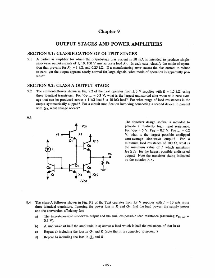
Chapter 9
OUTPUT STAGES AND POWER AMPLIFIERS
SECTION 9.1: CLASSIFICATION OF OUTPUT STAGES9.1 A particular amplifier for which the output-stage bias current is 50 mA is intended to produce single-
sine-wave output signals of 1, 10, 100 V rms across a load RL. In each case, classify the mode of opera¬tion that prevails for RE = 1 k£2, and 0.25 k£2. If a manufacturing error causes the bias current to reduceto zero, yet the output appears nearly normal for large signals, what mode of operation is apparently pos¬sible?
SECTION 9.2: CLASS A OUTPUT STAGE9.2 The emitter-follower shown in Fig. 9.2 of the Text operates from ±3 V supplies with R = 1.5 kfl, using
three identical transistors. For VCE sal = 0.3 V, what is the largest undistorted sine wave with zero aver¬age that can be produced across a 1 kO load? a 10 k£2 load? For what range of load resistances is theoutput symmetrically clipped? For a circuit modification involving connecting a second device in parallelwith Q2, what change occurs?
9.3The follower design shown is intended toprovide a relatively high input resistance.For Vqc = 5 V, VEB = 0.7 V, VCE sat = 0.2V, what is the largest possible undippedzero-average sine-wave output? For aminimum load resistance of 100 Q, what isthe minimum value of / which maintainsIE2 ÿ for the largest possible undistortedoutput? Note the transistor sizing indicatedby the notation x n.
Voc
X10
vo
Qa
X10
-Vcc
9.4 The class-A follower shown in Fig. 9.2 of the Text operates from ±9 V supplies with / = 10 mA usingthree identical transistors. Ignoring the power loss in R and Q3, find the load power, the supply powerand the conversion efficiency for:
a) The largest-possible sine-wave output and the smallest-possible load resistance (assuming VCE sut =0.3 V).
b) A sine wave of half the amplitude in a) across a load which is half the resistance of that in a)
c) Repeat a) including the loss in Q3 and R (note that it is connected to ground!)
d) Repeat b) including the loss in Qj and R.
- 85 -

PROBLEMS: Chapter #9-2
9.5
VI 0'+9V
vo
d rÿ -9V
For the FET follower shown, V, = -2 V, IDSs = 10mA. For \)0 = 0 V, what value of t>; is measured?For = 1 k£2, what are the most positive and mostnegative outputs for which both transistors remain insaturation? What are the corresponding inputs?What are the corresponding values of load power,supply power, and conversion efficiency? What isthe largest possible relatively undistorted output sinewave, and the corresponding conversion efficiency?
SECTION 9.3: CLASS B OUTPUT STAGEC
9.6 For the circuit shown, sketch the transfer characteristics for RE = oo and = 10 k£2. For both
nd+10V
VI
vo
LncfTT-10V
devices, |V, |= 1 V and K = Vik\W/L) = 1 mA/V2.What is the amplitude of the maximum possible out¬put sine wave for which £?i> Q2 remain in satura¬tion? What are values for the corresponding inputvoltage equivalent gain, supply power, load power,and conversion efficiency?
9.7 Consider the circuit of Fig. 9.9 of the Text, in which the supplies for A„ and the output stage are ±3 V,and A0 is a CMOS amplifier with rail-to-rail (i.e. ±3 V) outputs, having a transconductance of 10 mA/V.For Rl = 100£2, | VBE |= 0.7 V, (3 = 50, find the input voltages required for outputs of +10 mV, +100mV and 1 V.
9.8 Consider a particular automotive application of the circuit of Fig. 9.10 of the Text, for which RL = 16 £2and 2Vcc = 12 V nominally, and the base input is biassed at Vqc- What is the power level of the largestpossible undistorted output signal? What is the corresponding supply power? What is the power dissipa¬tion in the two transistors? What is the corresponding efficiency? What are the values of output power,supply power, total device dissipation, and efficiency for output sine-wave signals of 4-V peak ampli¬tudes. For the signal level maintained at the maximum undistorted level found above, but with the sup¬ply raised to 14.5 V, what do the total device dissipation and efficiency become?
SECTION 9.4: CLASS AB OUTPUT STAGE9.9 A BJT class-AB output stage using the structure shown in Fig. 9.11 of the Text employs transistors for
which Vbe = 0.690 V at 10 mA and n = 1. For a small-signal output resistance at light loads of <5 £2,what quiescent current is needed? What value of VBb should be used? For a 50 £2 load and peak outputvoltage of 5 V, what is the peak input voltage required? What large-signal gain results? For RE = 50 £2,what is the corresponding small-signal gain?
- 86-

PROBLEMS: Chapter #9-3
D
9.10 Design the quiescent current of a class-AB MOS output stage so that the incremental voltage gain for V/near zero volts, is in excess of 0.99 V/V, for loads larger than 100 £2. The MOS devices have | V, |= 1V and K = Vik\W/L) = 200 mA/V2. What value of VBB is required?
SECTION 9.5: BIASING THE CLASS AB CIRCUITD
9.11 For the situation described in P9.9 above, in which the output transistors have P > 30, design a 2-junctionbiassing scheme, such as that shown in Fig. 9.14 of the Text, with devices having one-fourth the junctionarea of those at the output. What is the maximum output current available into a short circuit? For a 50£2 load, what is the value of the peak output signal for which the current in the bias junctions reduces to1/10 of the no-load value?
DL
9.12 For the situation described in P9.9 above, in which the output transistors have P £ 30, design a VBE mul¬tiplier, such as that shown in Fig. 9.15 of the Text, with a device for which the junction area and P arethe same as those of the output transistors. For a 1-volt positive output across a 50 £2 load, arrange thatthe bias network current reduces to no less than 20% of its normal value, and that the current in thebiassing transistor is no less than half of that. What is the incremental gain for your design with the peakpositive output described, and P = 30?
9.13 For the VBE multiplier embodied in Fig. 9.15 of the Text and operating at total current /, find an expres¬sion for the incremental resistance between its terminals in terms of /, R(, VBE and P, and a multiplica¬tion factor k = 1 + R/R], k > 1. For k = 2, / = 1 mA, and P > 50, what is the available value of incre¬mental resistance when Ri = rKl
SECTION 9.6: POWER BJTs9.14 The base-emitter junction voltage of a heat-sink-mounted power BJT, measured at a particular test current
immediatedly following the application of power, is found to be 630 mV at what is assumed to be Tj =30*. Subsequently, it is found to display a junction voltage of 500 mV when operated for some time atten times the initial test current and with a larger supply voltage at a power level of 45W. Estimate thenew junction temperature. If the ambient temperature remains at 30°C, what is the thermal resistance ofthis device? To maintain operation with a junction temperature of 180°, at the same collector voltage,what collector current would be needed? What voltage drop across the base-to-emitter junction wouldyou expect under these conditions? Use a junction TC of -2 mV/°C.
D
9.15 A power transistor, for which the maximum safe junction temperature is believed to be 150°, has a ther¬mal resistance junction-to-case of <1.1°C/W. What is the maximum power it can dissipate for a casetemperature <55°C? For half that power level, to what temperature can the case be allowed to rise? Foran ambient temperature of 30°C, what is the thermal resistance of the heat sink needed in each of thesesituations? For a modular heat sink design for which the rating is 3°C/W for each cm of length, howlong a heat sink is needed in each case? If all the thermal resistance measurements cited can be in errorby as much as 20%, to what length must the large heat sink be increased to guarantee safe operation?
9.16 A BJT for which Tj max = 150°, and QJC = 2°C/W, operates with an electrically-isolating bond to a heatsink for which the resistances are ©cs = 0.5°C/W, and 0ÿ = 1°C/W for each cm of heat-sink length,respectively. For a 10 cm heat sink, what is the maximum power this device can dissipate for ambienttemperatures less than 40°C? What is the effect of doubling the heat-sink length? What do you con¬clude?
- 87 -

PROBLEMS: Chapter #9-4
9.17 A power BJT operating at a high current density at /g = 5 A is found to have a base current of 0.2 A anda base-input resistance of 0.72 CI. Estimate a value for the base spreading resistance. Estimate a valuefor the base-input resistance at IE = 3 A.
9.18 A version of the circuit in Fig. 9.24 of the Text, uses equal current sources, /, in place of R\ and RyWhat must their value be for the following situation: the maximum load current is 100 mA, $„pn > 100,ppM„ > 80; the minimum current in Q\ and 02 must be no less than the maximum base currents of Q3 or
04, nor smaller than 1.5 mA. For the situation in which Q3 and 04 have junction areas 5 times those of01 and 02 and conduct 50 mA at 0.7 V, (with n = 1 for all), find R3 = R4 so that the quiescent outputcurrent is equal to Icalculated above. For what value of RL is the small-signal gain >0.90 for outputvoltages a) near zero volts b) near +10 volts, c) near -10 volts.
9.19 For the output stage using compound devices as shown in Fig. 9.27 of the Text, the output npns are 100mA devices while the other transistors arc 1mA devices. For the npns, p > 100, and for the pnp, p > 20.Find the voltage needed across the VBE multiplier for a standing current, Iq, of 10 mA in the output,when a) the circuit is as shown, b) the base-emitter junctions of 02 and 04 are shunted to provide 1 mAcurrents in each of 0| and Qy For each situation described, with calculated voltages applied betweenthe bases of Q\ and <2 3, estimate the total effect of all transistors having a P which is ten times theirminimum specified value.
9.20 For the circuit of Fig. 9.28 of the Text, in which transistors conduct 1 mA at 0.7 V, with n - 1 and P S100, and Ibias - 1 mA, find RE\ = RE2 so that the outgoing short-circuit current is limited to 25 mA.What is the current available without 05?
SECTION 9.7: VARIATIONS ON THE CLASS AB CONFIGURATIOND
D
D
9.21
1MQ
For the circuit shown, with P ranging from50 to 150, VA = 100 V, and = 10 Pr„,find the limits of the ranges of values of
&m eg < ÿ»A)i iRin and R0ul •
- 88 -

PROBLEMS: Chapter #9-5
D
Consider Ihe circuit shown as a simple candidate for use in athermal-shut-down mechanism. The transistor has VBE of 0.7V at 100 p.A, (1 = 100 and a TC of -2 mV/°C at 25'C.Design the circuit so that at 125"C the current in R i and Q2are each 100 ftA. What is the current in Q2 at 25°C? Forwhat supply voltage (nominally 10 V) would the current at25°C be double the value found? For operation at 100°C, atwhat value of supply voltage does the current in Q2 become50 pA?
SECTION 9.8: IC POWER AMPLIFIERSD
9.23 Consider the circuit of Fig. 9.30 in the Text. For operation with a supply voltage of 25 V, it is desired toreduce the input bias current to 0.5 pA while maintaining nearly the original gain. Find new values forall the important resistors that must be changed. As a result of your change, what happens to the steadycurrents in (2 12 and 29? Assume P„/)n = 100, fipnp = 20, | VBE | = 0.7V.
9.24 For the circuit shown in Fig. 9.30 in the Text, operating from a 27 V supply with all transistors (but Q2and Q9) of the same junction size, and VA = 100 V, and with P„pn = 100 and P/)n;, = 20, estimate thegain A (as shown in Fig. 9.31) with no external load, and the corresponding 3 dB rolloff. Note that thecurrent level in Q9 is about 10 times that in 2n-
D
9.25 For the circuit of Fig. 9.33 of the Text, find the value of R3 for which a load current of 50 mA is sharedequally by Q3 and Q5. By what factor does the current in Q3 increase for a total output current of 1A?Q5 and (56 both have an emitter-base voltage of 1.0 V at 1A, while 23 and Q4 are 10 mA units, and 2i.Q2 are 1mA units. All show a 0.1 V/decade junction-voltage variation. Use P = 30 for 2s. Q6 a"d 100for the other devices. What values of R$ and RB ensure a quiescent current of 2mA in 23 and 24?
D
9.26 Design the bridge amplifier shown in Fig. 9.34 of the Text, to provide the largest possible output sinewave from an input sine of 0.1 V peak. The input resistance should be 10 k£2 or more, with the largestavailable resistor limited to 10 Mf2. The op amps saturate at (at most) 2 V from the supply rails. Use±12 V supplies.
D
9.27 Modify the connections shown in Fig. 9.34 of the Text to create a bridge amplifier with infinite inputresistance. Choose values to provide a 20-V peak output from a 1-volt peak input signal.
SECTION 9.9: MOS POWER TRANSISTORS9.28 A power MOSFET for which |X„ C„x = 30pA/F2 has W = 105p»<. L — 5pm. For electrons in silicon,
USai = 5xl04 m/s and p„ = 5x10~2m2/Vj. For V, = 2 V, find the value of vGS for which velocity satura¬
tion begins. What is the corresponding current? What are the currents at twice and half this value?Find gm at all three values of current.
9.29 For the class-AB amplifier shown in Fig. 9.38 of the Text, operating in the non-saturated-velocity region,K = Vik'{W/L) = 200 mA/V2, | V, | = 2 V, | VBE | = 0.7V, P is high, and the quiescent currents
lp = lN = I2 = /3 = 5 mA. Find the required voltage Vi4 between the bases of 2i a"d 24- What is thevalue of resistor R1 If the TC of V, (at low currents) is -3 mV/°C and of VBE is -2 mV/°C, what
- 89 -
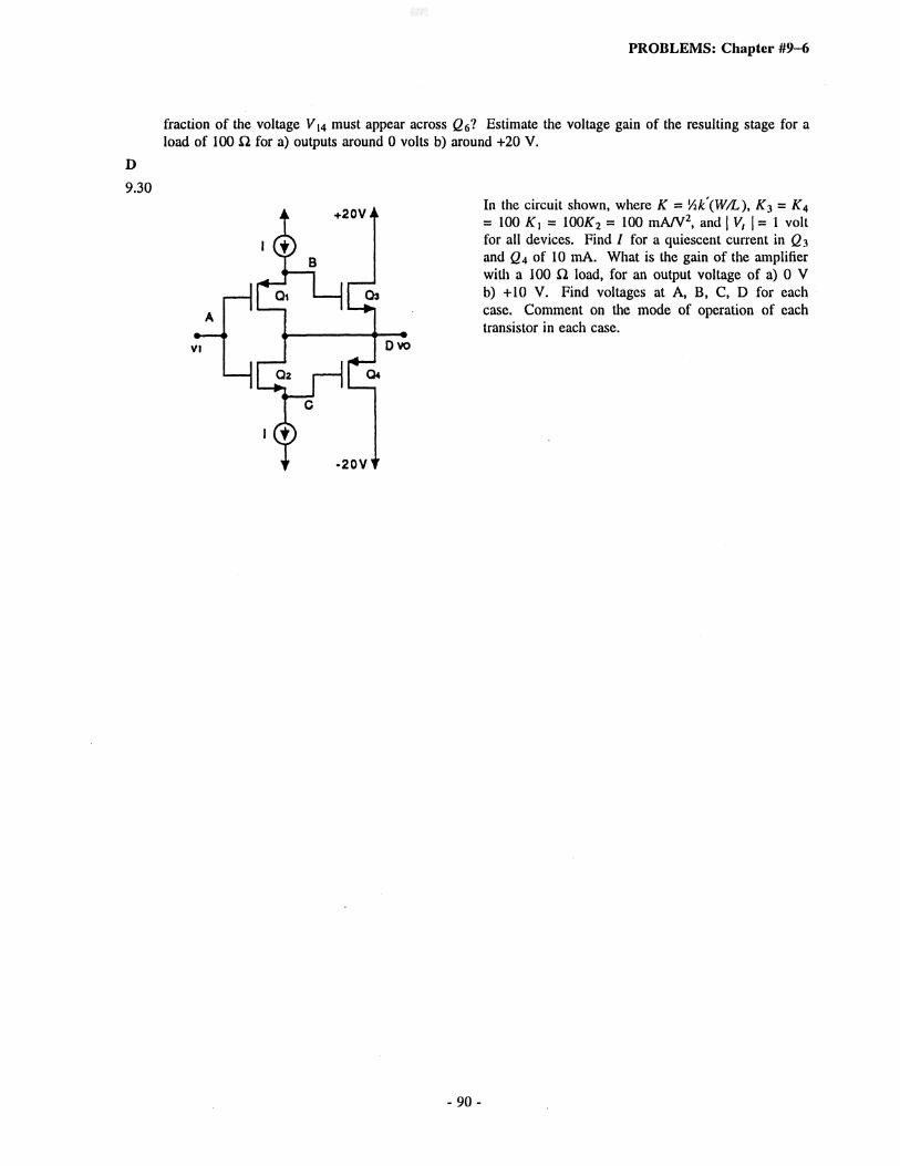
PROBLEMS: Chapter #9-6
D
9.30
fraction of the voltage V 14 must appear across Q61 Estimate the voltage gain of the resulting stage for aload of 100 ft for a) outputs around 0 volts b) around +20 V.
In the circuit shown, where K = '/ik\W/L), K3 = AT4
= 100 Ki = lOO/sTz = 100 mA/V2, and |V, |= 1 voltfor all devices. FindIfor a quiescent current in Q3and Q4 of 10 mA. What is the gain of the amplifierwith a 100 Q load, for an output voltage of a) 0 Vb) +10 V. Find voltages at A, B, C, D for eachcase. Comment on the mode of operation of eachtransistor in each case.
VI
H
HDvo
Qz
- 90-

Chapter 10
ANALOG INTEGRATED CIRCUITS
SECTION 10.1: THE 741 OP-AMP CIRCUITD
10.1 In the 741 op-amp circuit of Fig. 10.1 of the Text, transistors Qn and <2 12 with R5 establish IREF forthe rest of the circuit. For ±15 V supplies and | VBE\ = 0.7, what value of IREF results? What is IREFfor ±5 V supplies? To what value must R5 be changed to restore IREF to its high-supply value?Specify it to 2 significant digits.
D
10.2 For the situation described in P10.1 above, consider the operation of the Widlar current source involv¬ing 610 and Q\i with /f4. For both devices having Is = 10~I4A and n=l, calculate the Widlar outputcurrent for ±15 V and ±5 V supplies. Choose a new value for R4 which reestablishes the ±15 Vcurrent level in (2 10 f°r the ±5 V situation.
CD*
10.3 A designer, attempting to reduce the number of high-value resistors in the 741 design shown in Fig.10.1 of the Text, notes the possibility that R9 can be replaced by another transistor (225 and a smallresistor R 12. Suggest two possible connections and corresponding resistor values to establish a suitablecurrent. Which is best? Why?
C
10.4 Reflect upon the ability of the extended input stage of the 741 Op Amp of Fig. 10.1 (consisting ofQu 0.2, Q3 and Q4, with Qs, Q6, Qa, Qg, j2 10) to withstand the application of voltages outside thenormal operating range. For this purpose, approximate the breakdown voltages as follows: 7 Vbetween the npn base and emitter, and 50 V for both pnp junctions and the npn base-to-collector junc¬tion. Specifically, consider a) In+ and In- connected in all possible ways to the ±15 V rails, b) In+and In- having voltages somewhat outside the supply range. What are the limitations you see?
SECTION 10.2: DC ANALYSIS OF THE 74110.5 For the Widlar current source in Fig. 10.2, find the effect on Equation 10.1 of making the base-emitter
junction of Q 10 k times that of Q\\. For IREF = 730 pA, 7?4 = 50000, k = 0.5, what does IC\qbecome? For what value of R4 does it become 19 pA again?
10.6 For Ic10 = 19 pA, and the inputs to the bases of <2 1 and <22 both at zero, what voltage on the bases of(23 and Q4 results?
10.7 For the mirror circuit consisting of Q$, Qa, Q7, and assuming all devices conduct approximately thesame current with R 1 =Rj = lk£2 and R3 = 50k£2, find the ratio Icfflcs 1" terms of p, assumed equalfor all devices. What is its value for P = 200?
10.8 For the mirror consisting of £>5, Qe, Qi, find the ratios leases for R 1 and R2 shorted separately.Assume P is high, and operation is at ICs + ?C6 = 19pA.
10.9 For the extreme situations described in P10.8 above, what are the corresponding input-offset voltages(between the bases of Qu Q2) which result? Note in general that offsets originating anywhere in theinput stage can be compensated by varying R 1 and R2.
- 91 -

PROBLEMS: Chapter #10-2
D
10.10 Consider the second stage of the 741 op amp shown in Fig. 10.1 of the Text modiiied slightly by con¬necting the lower end of R9 to the emitter of QX1. What should its value be to maintain the current inQ|6 at its present value? What must (the new) R9 be to reduce its current to 4 times that in the baseof Q 17> for which P = 200 is assumed?
D
10.11 For the output-stage-biasing scheme of the 741 op amp shown in Fig. 10.1 of the Text, what value ofR10 would be needed to increase the quiescent current in Q X4, Q20 by 50%? First assume
R6 — Ry = 0. Then consider R6 = R7 = 27£2.
SECTION 10.3: SMALL-SIGNAL ANALYSIS OF THE 741 INPUT STAGE10.12 For a particular application, it is desired to raise the input resistance of a 741-like input stage to 3.6
MO for P„ > 180. If a change of input-stage bias current is to be used for this purpose, to what valuemust the current be changed? What is the corresponding value of Gm 1 which results?
10.13 Reconsider the output resistances of Q4 and £?6 as calculated in association with Fig. 10.8a, b of theText. What is the value of R2 for which Roe = R04 = 10.5MQ? What is the corresponding value ofR01? Contrast the open-circuit voltage gains for the original and /ÿ-modified versions of the inputstage.
10.14 In an input-stage design for which the new value of R 1 and R2, as established for R2 in PI0.13 above,is used, the actual resistors installed are different from each other by 2%. Calculate the correspondinginput-offset voltage which results. Contrast that with the result for the original design as calculated inExample 10.1 on page 825 of the Text.
D
10.15 Use the result of Exercise 10.9 on page 826 of the Text to evaluate the required degree of matchbetween Rj and Rj to ensure that the CMRR without feedback (that is the ratio of GmX to Gmcm) is£80 dB.
D
10.16 In the calculation of Ro performed in Exercise 10.10 on page 827 of the Text, its value is seen to bedominated by that of R09. Augment Qg and Q9 with additional resistors which will raise R09 to beequal to R0io- What resistors are needed? What value of Rq results? For this situation, find a newvalue for Gmcm as requested in Exercise 10.11 on page 827 of the Text, and CMRR as requested inExercise 10.12, there.
SECTION 10.4: SMALL-SIGNAL ANALYSIS OF THE 741 SECOND STAGE10.17 Find the input resistance of the 741 second stage in the event that R9 is replaced by a transistor Q25
and 1 kQ resistor R9, all connected suitably to the emitter of (27.
D
10.18 A designer wishes to capitalize on the change suggested in PI0.17 above by lowering Rg to a valuewhich causes Rj2 to return to the value of about 4 MO. What value of Rg is appropriate? What valueof Gm2 results? What does Ron become? What is the new value of R02? What is the new value ofthe no-load voltage gain of stage 2? Contrast this with the original value (having the same input resis¬tance).
SECTION 10.5: ANALYSIS OF THE 741 OUTPUT STAGE10.19 Assuming the existence of some degenerative process which causes the P of C23 to reduce, what is the
value for which R,-3 reduces to 4 times the value of R02? What does the second-stage gain become
-92-

PROBLEMS: Chapter #10-3
with RL=2kQ. and the conditions assumed just following Equation 10.22 on page 832 of the Text?What does the corresponding output resistance become?
L
10.20 Evaluate the sensitivity of the output-current-limiting scheme involving R§ to the p of <2i4 and <2 15-In particular, calculate the output current levels at which the excess current available from Q 134 (180pA) is absorbed by (25. for the cases in which transistor P is 400, 200 or 100. Recall that/sis = 10"14A.
SECTION 10.6: GAIN AND FREQUENCY RESPONSE OF THE 74110.21 For the situation described in P10.18 above, calculate the overall gain which results when the amplifier
is loaded with Rc = 2 k£2. Find the frequency of the dominant pole associated with Cc = 30 pF.Find the unity-gain frequency f,. Provide a corresponding Bode plot for this situation. What do younotice about f, in this and the original cases?
D
10.22 Consider the possibility of a 741-like amplifier in which Cc is available for the customization of fre¬quency response for high-gain applications. What values of Cc would be necessary to maintain phasemargins of 45" and of 60" for closed-loop gains of 1000 and of 104. In each of the four cases, whatupper 3 dB frequencies are possible?
10.23 For the two modified versions of the 741 amplifier alluded to in P10.22 above, for which the phasemargin is 45", calculate the corresponding values of slew rate SR and full-power bandwidth fm, foroutputs of ±10 V.
10.24 Reconsider the amplifier shown in Fig. P10.44 on page 880 of the Text, modified to have the biascurrents reduced by a factor of 2, to 50 pA and 500 pA respectively, and the junction sizes of Q6 andQ-j made 2 times that of Q$. Assume p = 120 and VA = 200 V for all devices. What is theclassification of the output stage type? What is its standing current? What is the gain with a load of10k£T? Calculate the capacitor C required for an open-loop 3dB frequency of 1kHz?
SECTION 10.7: CMOS OP AMPSL*
10.25 Consider a CMOS amplifier which uses the topology of Fig. 10.23 of the Text, but with somewhat dif¬ferent device sizing than that in Example 10.2 on page 842 of the Text. In particular, all devices haveL = 10pm, the p devices have W = 200pm, and the n devices are such that
W6 = 2W4 = 2W3 = 200pm. Generally, VA = 25 V, VDD = VSs = 5 V, and Iref = 25pA. For all dev¬ices, evaluate Id,|Fosl » 8m > and r„,with VA ignored in the bias calculations. Present these results intabular form. Also find A 1, A 2, the dc open-loop gain, the input common-mode range, and the outputvoltage range. Use p„ Cox = 20pA/V2 = 2p/( Cox, and |V, |= IV.
L
10.26 Repeat Example 10.2 on page 842 of the Text for Iref — 12pA.
D
10.27 A young designer having forgotten the issue revealed in Eq.10.46 on page 844 of the Text, uses(W/L)6 = (W/L)4 = 5010 in a design otherwise the same as considered in Example 10.2. What new
value of Vas6 is required? Recalculate the value of A2 and the overall gain which result. What is theinput offset voltage produced?
D
10.28 For the modified amplifier described in P10.25 above, find the value of Cc that will result in /, = 1
MHz. Find the value of R that places the transfer-function zero at infinity. Find the frequency of the
-93-

PROBLEMS: Chapter #10-4
second pole under the condition that the total capacitance at the output (C2) is 10 pF. Find the excessphase it introduces at to = (0,. For a 10 pF load, what value of Cc is required to reduce the excessphase shift to 6* at a modified f, frequency (//). What is the maximum available slew rate for thetwo cases of excess phase?
10.29 In the CMOS bias circuit in Fig. 10.25 of the Text, all transistors have the same W/L ratio, W/L = 2,except for (2 12 which is m times larger. For all devices operating at a bias current of 5 pA in a pro¬cess in which \lnCox = 2.5p/( C„x = 20 pAIV1, with VA very large, find RB, g,„ |2, and gm9, for 111
selected to be a) 2, and b) 5. Note that the circuit incorporates a positive feedback loop involving allthe transistors and RB. Breaking the loop at the gate of <29, evaluate the loop gain in terms of m.Are there any restrictions on the value of m which can be used? What factors determine a goodchoice for the value of m? Assume, for simplicity, that operation is at a fixed bas current IB.
SECTION 10.8: ALTERNATIVE CONFIGURATIONS FOR CMOS ANDBICMOS OP AMPS
D
10.30 Consider the mirror used for differential-to-single-ended signal conversion in the cascode first-stageconfiguration in Fig. 10.26 of the Text. In this context, consider the relative merit of configuring63. Q3C' Q4. Qac as a simple cascode mirror, or as a Wilson mirror. Assuming all transistors identi¬cal and characterized by I V, I, K, Fes. and r„, find the (effect of the) output resistance of each (as seenat the drain of Qac)- Also, find the minimum voltage between VB/AS 2 and -Vss to ensure that alltransistors operate in saturation.
10.31 Repeat Exercise 10.29 on page 852 of the Text for the current 21 reduced to 10 pA, but all other con¬ditions the same. What values of R„ and A 1 result?
D
10.32 A designer inspired by the additional gain provided by the cascode connection as exemplified in Fig.10.26 of the Text, contemplates the use of a 3-layer cascode using Qscc< Qacc and VBiAB 3 withQ3 cc and Qa cc in a simple cascode connection. Find an expression for the output resistance R„now available. For conditions corresponding directly to those in Ex. 10.29 on page 852 of the Text,find the new values of R„ and A 1. Assuming the values of VB/As 2 and VB!AS 3 to be optimized, what isthe total voltage required for saturation operation, as measured from the gates of Q 1, Q3 to the supply,-Fss?
D
10.33 For the circuit in Fig. 10.27 of the Text, and conditions as stated in Exercise 10.30, on page 853, butwith 21 = lB — lOpA, find values of VB/AS 1, VmAS 2, VBiAS 3 so that Q6 and Q-j operate at the edge ofsaturation. As well, find the output resistance and overall gain in the event that \VA I= 25 V for alldevices.
10.34 A folded cascode such as that shown in Fig. 10.27 of the Text, operates with a bias current of 10 pAflowing in each of the devices Qh Q2, Qic> Q2C and Qic< Qac all having the same value ofK = Vik'{W/L) and VA = 25 V. For a load capacitance, CL, of 10 pF, a unity-gain frequency of 1MHz is found. What is the value of gm for the critical devices? What is the low-frequency voltagegain of the amplifier? What is the dominant-pole frequency? The slew rate?
10.35 Repeat Problem P10.59 on page 882 of the Text for the situation in which IB = 800pA and (W/L)l 2 =600/10, with p,,C„x = lOpA/V2, and CL = 2 pF. What output-pole frequency /, results? For all BJTsof the same size, what is the minimum value of unity-gain frequency of the BJT which ensures thatthe parasitic pole is at least a factor of 10 higher than the overall /,.
-94-

PROBLEMS: Chapter #10-5
SECTION 10.9: DATA CONVERTERS -AN INTRODUCTION10.36 A sample-and-hold circuit operating at a 100 kHz rate uses a sampling switch which closes for a 10-
nsec interval during each cycle. What is the frequency, / , of the highest-frequency square-wave inputsingal for which the output of the S/H provides an adequate representation? Sketch the output of theS/H for input square waves having a frequency /, 0.5/, 1.1/ and 2/. Note in this context thatShannon's sampling theorem states that sampling must be performed at a frequency at least twice thatof the highest frequency component to be represented. For a sampling capacitor of 100 pF, what is themaximum value of total source and switch resistance that will normally provide samples which areaccurate to within 1%? (Hint: think again of the square-wave situation).
D
10.37 A signal, to be sampled and converted to digital format, has a dynamic range of ±5 V. If it is impor¬tant to resolve signals and signal changes as small as 0.1 V, what is the number of binary digits (bits)required in the converter? What is the greatest possible resolution that a 10-bit converter would pro¬vide?
SECTION 10.10: D/A CONVERTER CIRCUITS10.38 For the DAC circuit shown in Fig. 10.32 of the Text, using resistors no smaller than 1 k£2, what is the
largest resistor required to implement an 8-bit converter? (Be careful!). What is the largest value ofswitch resistance for which the associated error is at most ±A LSB? Assuming that resistors areadjusted to compensate for the average value of switch resistance, what variability in switch resistanceis acceptable if the corresponding error is limited to ±A LSB? If the two sources of error identifiedare switch-resistance variation and resistor tolerance, and each is allowed to contribute equally to theoverall error, what switch-resistance variation and resistor tolerance are needed for the 8-bit converterdescribed?
10.39 For an R-2R ladder of 8 bits using a 10 V reference, what is the value of R which ensures that thetotal reference-supply current is 1 mA? What switch resistance would cause an error of A LSB if leftuncompensated? If compensated by an appropriate change in the 2R resistor, what value of switchresistance, when doubled, produces an error < A LSB?
10.40 A D/A circuit modelled after that shown in Fig. 10.34 of the Text operates with lref - 1 mA and R =0.5 k£2. If device EB Junction area can be maintained only to within 1%, while other components andparameters are ideal, what is the greatest number of bits possible for which the corresponding error is± LSB?
SECTION 10.11: A/I) CONVERTER CIRCUITSD
10.41 Sketch the design of a 2-bit flash converter for signals in the range ±1 V using uncompensated opamps as comparators. How many comparators do you need? What reference voltages would you use?Assuming op amps whose output limiting levels are precisely ±10 V, sketch a converter circuit using 2op amps, one of which detects the polarity of the input, and, thereby, controls the reference voltage forthe second. For the analog input connected to positive input terminals of each op amp, find, for theboth the 3-op-amp and 2-op-amp designs, the output codes corresponding to inputs of +0.75 V, +0.25V, -0.25 V and -0.75 V. Let +10 V correspond to logic '1', and -10 V correspond to logic '0' inboth cases.
- 95 -

PROBLEMS: Chapter #10-6
10.42 The following circuit, whose operation is related to that of the charge-redistribution converter, can beused as a comparator component in a flash converter. With X indicating an NMOS switch operated bynon-overlapping positive pulses d>4 or ,describe x>0 : a) during , b) following <S>A , before ,c) during 4>fl, d) following <bB, for i) VA > VREF, ii) VA < VREf ÿ Assume that the op amp saturates at
±10 V.
Vo
-96-

Chapter 11
FILTERS AND TUNED AMPLIFIERS
SECTION 11.1: FILTER TRANSMISSION, TYPES, AND SPECIFICATIONL
11.1 The transfer function of a first-order high-pass filter (such as that realized by an RC circuit) can be
expressed as T(s) = - — — , where CD„ is the 3 dB frequency of the filter. Provide a table of values of
IjTI , O, G and A at 0) = 2(0o, (0„, (0,/2, co,/5, a),/10, co/lOO, co/lOOO.
11.2 A high-pass filter has an equiripple magnitude response and specifications resembling those in Fig. 11.3of the Text, but with the passband and stopband exchanged on the frequency axis. Provide a sketchcorresponding to this situation. If Amax = 1 dB and Ami,, = 50 dB, find ITI at to = °o, co = co,, and0) = (0,
11.3 A high-pass filter is required to pass all signals within its passband extending from 4 kHz to °°, with atransmission variation of at most ±5%. The transmission in the stopband, which extends below 3.2 kHz,should not exceed 0.05% of the maximum passband transmission. Find corresponding values of i4max,A lnin, and the selectivity factor.
11.4 A high-pass filter is specified to have Amax = 0.5 dB and Amin = 20 dB. It is found that itsspecifications can be just met with a single-time-constant RC circuit with a time constant x of 10~3 sand a high-frequency transmission of unity. What are the values of to,,, to.v and the selectivity factorwhich correspond? In a modified design for which Amin, Amax and ayfi), are the same, but fp = 103Hz, what value of x is required? What is the 3-dB frequency of the STC network? What is the result¬ing attenuation at 100 Hz?
SECTION 11.2: THE FILTER TRANSFER FUNCTION11.5 A third-order high-pass filter has transmission zeros at to = 0 and to = 0.1 rad/s. Its natural modes are at
s = — 1 and s = -0.5 ±0.8. The high-frequency gain is unity. Find T(s).
11.6 Find the order N and the form T(s) of a bandpass filter having transmission zeros as follows: one atto = 0, one at to = 1 x 10³ rad/s, one at 2 X 10³ rad/s, one at 6 x 10³ rad/s, one at 12 x 103 rad/s andone <it oo, If this filter has a monotonically decreasing passband transmission with a peak at the center
frequency of 4 x 10³ rad/s. and equiripple response in the stop bands, sketch the shape of its ITI .
SECTION 11.3: BUTTERWORTH AND CHEBYSHEV FILTERS11.7 Determine the order N of the Butterworth filter for which Amax = 0.5 dB, Anlin > 40 dB, and the selec¬
tivity ratio 03,/cOp = 1.6. What is the actual value of minimum stopband attenuation realized? If A min isto be exactly 40 dB, to what value can Amax be reduced? For Amax raised by 0.1 dB, what change inA mi,, results for the same filter order?
D
11.8 Design a Butterworth filter having the following low-pass specifications: /,, = 20 kHz, Amax = 1 dB, f„= 30 kHz and Amin = 20 dB. Find N, the natural modes, and T(s). What attenuation is provided at 25kHz? 40 kHz?
- 97 -

PROBLEMS: Chapter #11-2
11.9 Contrast the attenuation provided by a 3rd-order low-pass Chebyshev filter at to, = 2co,, to that providedby a Butterworth filter of the same order. For both, i4max = 1 dB. Sketch in of both filters on thesame axes.
11.10 Repeat PI1.7 above for a Chebyshev filter.
L
11.11 For P11.7 and PI1.10 above, with a>p = 103 rad/s, and a dc gain of 1, find the required natural modes.
SECTION 11.4: FIRST-ORDER AND SECOND-ORDER FILTER FUNCTIONS11.12 Consider the op-amp circuit of Fig. 11.13a) on page 902 of the Text driven so as to have a infinite input
resistance, a dc voltage gain of 11, and a 3 dB frequency of 10 kHz using 10 k£2 as the lowest resistorvalue. What is the frequency of the associated zero? What is the gain at high frequencies? For thepole and zero separated by a factor of 100, what must its dc gain become?
D
11.13
DL
Use a combination of the table entries in Fig. 11.13 on page 902 of the Text to design a first-orderbandpass filter using a single op amp with 3 dB frequencies at 100 and 1000 Hz. Arrange for a mid-band gain of -1V/V and midband input resistance around 10 k£2. Available capacitors can be specifiedonly to one significant digit.
11.14 Find the transfer function T(s) of the circuit shown: Use it to create a spectrum-shaping network, hav¬ing a midband gain of -10 V/V, with gain at high and low frequencies of -1 V/V. The 3-dB limits ofmidband gain should be at 100 and 1000 Hz. The midband input resistance should be around 10 k£2.Available capacitors can be specified to only one significant digit. Sketch and label a pole-zero plot forthis design.
Vi
•-AA-Rla
Ciÿil-
AA-Rlb
C2
AA-R2a
AA-R2b
X
vo-•
DL
11.15 Use the circuit in PI1.14 above, and any insight you may have derived about it, to design a spectrum-shaping network, for which the gain between (3-dB points at) 100 Hz and 1000 Hz is -1 V/V, but thegain at high and low frequencies is -10 V/V. Arrange that the lowest resistance presented to the inputsource is around 10 k£2, with the same capacitor-availability restriction as stated in PI1.14 above. Pro¬vide a labelled pole-zero plot.
11.16 For the op-amp phase-shifter circuit derived from that shown in Fig. 11.14 of the Text by the exchangeof R and C, find the transfer function T(s) and the corresponding pole and zero. What phase shiftresults at co„ = VCR ? For an input frequency of 104 Hz, and C = 1.59 nF, what values of R are
required for phase-shift magnitudes of 6°, 12°, 30°, 60°, 90°, 120°, 150°, 168°, and 174°?
-98-

PROBLEMS: Chapter #11-3
11.17 Use the information in Fig. 11.16c) on page 907 of the Text, to obtain the transfer function of asecond-order bandpass filter with (0„ = 103 rad/s, a maximum gain of 1, and a 3-dB bandwidth of 200rad/s. What are the frequencies at the stopband edge as characterized by A = 20 dB?
L
11.18 Using the information provided in Fig. 11.16b) on page 907 of the Text, find the transfer function for 2second-order high-pass filters for which A,™* = 3-dB, (0/( = 1 rad/s, and the maximum gain is 1. Forone version, the maximum gain occurs at very high frequencies; for the other, the maximum is at rela¬tively low frequencies. Each has the maximum possible Q. For each, what is the lower 3 dB fre¬quency, and Amjn at w* = A rad/s?
DL
11.19 Use the result of Exercise 11.15 on page 905 of the Text to find the transfer function of a notch filterthat is required to eliminate 60 Hz power-supply hum in an instrumentation system. To accommodatesome variability in the power-supply frequency component values, design the filter to provide 20 dB ormore attenuation over a band of 1 Hz total width, nominally centred at 60 Hz. The high-frequencytransmission is to be unity. What is the 3-dB bandwidth of the notch? At what frequencies is the notchtransmission down by 1 dB? by 1%?
SECTION 11.5: THE SECOND-ORDER LCR RESONATORD
11.20 Using the data in Fig. 11.16c and Equation 11.29 on pages 907 and 905, respectively, of the Text,design the LCR resonator of Fig. 11.17b) (on page 910 of the Text) for operation at 1 MHz with a 20kHz bandwidth, for R = 10 k£2. What is the rms output when driven by a 1 MHz 1 mA-rms current?
D
11.21 The user of an FM radio receiver, discovering that reception is bad due to overload from a nearbybroadcast transmitter radiating at 99.9 MHz, considers the use of a "wave trap" employing the notch cir¬cuit of Fig. 11.18c) on page 912 of the Text. The input resistance of his receiver is 75£2. Design thetrap's LC components so that the loss presented to stations 2 MHz from the interfering one is only 3dB. If the initial adjustment and stability of the trap components is such that the trap can be off-tunedby as much as 100 kHz, what attenuation would you expect of the offending station's signal?
D
11.22 Using the circuit of Fig. 11.18c) on page 912 of the Text, design an RLC high-pass filter having a max¬imally flat response with a 3-dB frequency of 100 kHz, to operate as part of a circuit for which theloading resistance is 10 k£2. If coil Q of 50 is available, find suitable values of L and C.
SECTION 11.6: SECOND-ORDER ACTIVE FILTERS BASED ONINDUCTOR REPLACEMENT
D
11.23 Design the inductance-simulator circuit of Fig. 11.20 of the Text to realize inductances of 10 H and 0.1H for operation around 1 kHz. Choose a majority of resistors of value 10 k£2 and a capacitor whoseimpedance is about 10 k£2 at the operating frequency. Available capacitors can be specified to only onesignificant digit.
DL
11.24 Use the designs prepared in PI1.23 above to create a circuit which, when connected to a source havingan output resistance of 20 kfi, provides a bandpass function at 1 kHz. with a) the highest possible Q,b) the least-possible capacitor spread c) equal-valued capacitors (specified to 1 significant digit) and a
change of a single resistor but whose value is not less than lk£2. What are the Q values which result ineach case?
-99-

PROBLEMS: Chapter #11-4
D
11.25 Design a fifth-order Butterworth LP filter having a 3-dB bandwidth of 104 Hz, and a dc gain of 10. Usea cascade of the circuits shown in Figs. 11.22a) and 11.13a) of the Text. Assume that capacitors of anyrequired two-digit value are available as composed of 2 paralleled parts, each specified to 1 significantdigit. Use as many resistors of 33 kQ as possible. [Your boss has a surplus of these, since all the otheremployees seem to prefer to use 10 k£2 in their designs! As well, she likes the colour code!]
CD
11.26 Rework the transfer function of the BP filter given in Table 11.1 on page 922 of the Text, to employequal capacitors C with two resistors chosen to control Q and co0 as conveniently as possible, with allthe other resistors of some fixed value. For Q ranging from 0.5 to 50, and capacitors specifiable usingsingle digits 1, 2, 3 or 5, what is the range of values, specified by the ratio of maximum to minimumvalue, required for the resistors selected to tune Q and to„ .
SECTION 11.7: SECOND-ORDER ACTIVE FILTERS BASED ON THETWO-INTEGRATOR-LOOP TOPOLOGY
CDL
11.27 Design the KHN circuit of Fig. 11.24a) of the Text to realize a bandpass filter with center frequency of10 kHz and 3 dB bandwidth of 500 Hz. Use 1 nF capacitors. Arrange that the input resistance is 100k£2, that 100 k£2 resistors predominate, and that no resistor larger than 1 M£2 is used. [Hint: In general,you may have to replace Ej by a T network.] Sketch the complete circuit and specify all components.What center-frequency gain results?
D
11.28 Use the KHN circuit with an output summing amplifier, to design a low-pass notch filter with /„ = 5kHz, fn - 7.5 kHz, Q = 10 and a dc gain magnitude of 3. Where possible, use the values found inExercise 11.22 on page 929 of the Text.
D
11.29 Consider the bandpass filter described in PI1.27 above, implemented using the Tow - Thomas biquad.Maintain the same center-frequency gain. Find suitable capacitor and resistor values, (assuming novalue restriction).
SECTION 11.8: SINGLE-AMPLIFIER BIQUADRATIC ACTIVE FILTERSDL
11.30 Design the circuit of Fig. 11.29 of the Text to realize a pair of poles for which (0„ = 10s rad/s andQ = lW2. Use the largest possible values of resistance, but with 1 M£2 as the largest available (pre¬cisely specifiable) value. Precision capacitors available are specified to one significant digit, either 1, 2or 5.
D
11.31 Design the Bridged-T-based circuit of Fig. 11.30 of the Text, to realize a bandpass filter with center fre¬quency of 10 kHz, center-frequency gain magnitude of 1, and 3-dB bandwidth of 500 Hz. Use 1 nFcapacitors. What is its input resistance at very-low and very-high frequencies?
CL
11.32 For the bandpass circuit of Fig. 11.30 of the Text, find an expression for the input impedance as a func¬tion of component values and a, and then as a function of center-frequency gain, co„ and Q . What isthe value of input impedance at very low frequencies, very high frequencies, and at the center fre¬quency?
- 100-

PROBLEMS: Chapter #11-5
DL
11.33 Design a 7th-order Butterworth low-pass filter with a 3-dB bandwidth of 5 kHz and a dc gain of unity,using the cascade connection of 3 Sallen-and-Key biquads [Fig. 11.34c)], and a first-order section [Fig.11.13a)]. Use a 3.3 nF value for all capacitors.
SECTION 11.9: SENSITIVITY11.34 In a particular implementation of the feedback loop of Fig. 11.34a) of the Text, for which the values of
co„ and Q are given by Equations 11.77 and 11.78 respectively, each of the capacitors C3 and C4 iscreated using the parallel combination of 2 others. In particular, C3 = C3a + C3B where C3B = k3 C3aand C4 = C4a + C41, where C41, = A:4 C4„ for 0 <1 k3, ÿ4 < 1. Find the passive sensitivities of a)„ andQ relative to C3a, C3b, C4a, C4j, in terms of k3, A:4, and when k3 = k4 = 1.
L
11.35 The feedback loop of Fig. 11.34 of the Text, for which co„ and Q arc described by Equations 11.77 and11.78 there, operates over a range of temperatures for which the resistors, nominally equal, have a resis¬tance which is not exact and, as well, a function of temperature, T. Thus R\ = kt R and R2 = k2 Rwhere k1, k2 - 1± k, k «1, and R = R„ (I + a(T„-T)). Find the sensitivities of io„ and Q to bothk and T. Note that although this is a special situation in which the resistors vary equally around a fixedmean value, the results can be usefully combined with the average resistor sensitivity of -1/2, asneeded.
SECTION 11.10: SWITCHED-CAPACITOR FILTERS11.36 For a dc voltage of 1V applied to the input of the circuit of Fig. 11.35b) of the Text in which the capa¬
citance C1 is 0.1 pF, what charge is transferred for each cycle of a 1 MHz clock. What is the averagecurrent drawn from the input source? What is the equivalent resistance seen by the input source? For a2 pF feedback capacitance, what change in output would you expect for each cycle of the input clock?In what direction? For an amplifier saturating at ±10 V, how many cycles does it take for the amplifieroutput to go from one limit to the other? What is the average slope of the output? What does the slopebecome for an input of —0. 1 V?
D
11.37 Design the circuit of Fig. 11.37b) of the Text to realize, at the second integrator output, a Butterworth(maximally-flat) low-pass function with f 3dB = 10s Hz, and unity dc gain. Use a clock frequency of
fc = VTC = 1 MHz with = CS = 2 pF. Find values for C3, C4, C5, C6 (Note that for a 2nd-ordermaximally-flat response, Q = l/» 2 and w3dB = co„). Characterize the output of the first integrator:What is its centre frequency? Its 3-dB bandwidth? Its associated maximum gain?
SECTION 11.11: TUNED AMPLIFIERS11.38 A signal source with internal resistance Rs = 10k£2 is connected to the input of a common-emitter BJT
amplifier having an emitter resistor RE. From base to ground, a tuned circuit having L = l\iH and C =200 pF is connected. The transistor is biased at 1 mA, with P = 200, CK = 10 pF and = 1 pF. Thetransistor has a load resistance of 5 k£2. Find co„, Q, the 3-dB bandwidth and the center-frequency gainwhich result for: a) RE = rc, b) RE = 9re. (Hint: Use a Miller calculation for the effect of both andC„).
L
11.39 Repeat PI1.72 on page 971 of the Text for the situation as described, except that the base is connectedto a coil tap located at a fraction k from the grounded end ( the one to which the emitter is connected.).Find co„, Q, the bandwidth and overall center-frequency gain for: a) k = 0.5 and b) k =0.1. Contrastthese results with those found in PI1.38 above.
- 101 -

PROBLEMS: Chapter #11-6
D
11.40 A coil having an inductance of 2 {xH and intended for operation at 10 MHz, has a Q specified to be200. What is its equivalent series resistance, its equivalent parallel resistance, the value of the resonat¬ing capacitor, and the parallel resistance, which, when added, provides a bandwidth of 200 kHz?
D
11.41 A particular LC single-tuned amplifier has a center frequency of 1 MHz and a 3-dB bandwidth of 100kHz. What is the corresponding Q ? How many such amplifiers synchronously-tuned would result in abandwidth reduced to 50 kHz? For the basic amplifier, what is the 30-dB bandwidth and skirt selec¬tivity? What do these become for the synchronously-tuned cascade with a 50 kHz bandwidth?
D
11.42 A two-stage 4th-ordcr stagger-tuned Butterworth design is required with center frequency of 10.7 MHzand an overall bandwidth, B = 250 kHz. Using 3 \xH inductors, find C and R for each of the twostages. What is the relative peak gain of each of the two stages?
- 102-

Chapter 12
SIGNAL GENERATORS AND WAVEFORM - SHAPING CIRCUITS
SECTION 12.1: BASIC PRINCIPLES OF SINUSOIDAL OSCILLATORS12.1 Consider a sinusoidal oscillator consisting of a non-inverting transconductance amplifier and an RLC
tank circuit. The amplifier is characterized by transconductance Gm, input resistance Rin, and outputresistance R„. The tank circuit employs a tapped inductor L for which the turns ratio is n (see Fig.11.42 on page 951 of the Text), and whose total series resistance is Rls, with a capacitor C whose(small) loss is represented by a parallel resistance Rcp. For the amplifier input connected across thesmall part of the coil, and the amplifier output connected so as to drive it all, find an expression for theconditions for oscillation, the oscillation frequency, and the required relationship amongst parameters.
CD
12.2 For the situation described in P12.1 above, sketch the corresponding circuit topology. Prepare a secondsketch to show what must be done if the available transconductance is of an inverting kind. What arethe new conditions for oscillation?
12.3 For a situation related to that described in PI2.1 above, the connections between the coil and transcon-ductor are exchanged, such that its output drives the tap, while its input is connected across the entirecoil. What are the conditions which prevail at the threshold of oscillation?
12.4 For a particular oscillator application, the limiting-amplifier topology shown in Fig. 12.3 of the Text isbeing considered. The requirement is a design with a maximum gain of 5 which reduces to 0.5 at ±2.5V, and has an input resistance of 10 kO. The op amp to be used has an open-loop gain of 1000V/V ormore. Supply voltages of ±10 V are available. Assume a diode drop of 0.6 V at the levels of conduc¬tion implied. Find appropriate component values. If the op amp, assumed to have a single-pole rolloff,has an f, of 1MHz, what is the maximum frequency of operation for which an amplifier phase shift of2* can be tolerated.
12.5 Reconsider the circuit of Fig. P12.8b) on page 1032 of the Text with R2 = 10 k£2, R\ = 7.5 k£2 and aresistor R2 - 10 kQ connected in series with Z\ and Z2. Sketch the resulting transfer characteristicunder the conditions that Vz = 6.8 V, Vf = 0.7 V and IZK is 100 pA. Show what happens if, for abetter zener, 1ZK reduces to 10 pA.
SECTION 12.2: OP-AMP-RC OSCILLATOR CIRCUITSDL
12.6 Design a basic Wien-Bridge oscillator circuit, using the topology of Fig. 12.4 augmented by a gain-control mechanism consisting of two paralleled anode-to-cathode-connected diodes and a series resistorequal to R2. The diodes are 1 mA units for which n = 2, and the voltage drop at 1 mA is 0.7 V.Select component values for an output voltage of 2 V peak-to-peak at 10 kHz using 10 nF capacitors.Assume the op amp to have A„ andf, high enough to be ignored.
C*
12.7 A designer, wishing to use the idea described in PI2.6 above at a higher frequency, is concerned withamplifier phase shift. She considers an otherwise-suitable amplifier for which /, = 1MHz. What is thehighest nominal frequency of operation for which the actual frequency of oscillation is different by 10%,because of amplifier phase shift. What must the amplifier closed-loop gain be for operation in thismode?
- 103 -

PROBLEMS: Chapter #12-2
A designer, wishing to employ the phaseshift inherent in acompensated op amp, operated in a closed loop in the vicin¬ity of its 3dB frequency, considers the circuit shown: For anop amp having a relatively large open-loop gain and high-order poles remote from f,, find expressions for the loopgain and potential conditions for oscillation. For what valueof R2 is the frequency of oscillation 4/RC! Now for excessphase shift at f,, what occurs? How could you use this ideato evaluate f,,and phase margins under various conditions?
the Text is modified by removing the rightmost resistor Rand connecting the lower node of the rightmost capacitor C to the op-amp negative input. Find anexpression for the loop gain, the frequency of possible oscillation and the conditions for which it occurs.What is the sensitivity of the frequency of oscillation, and of the critical value of Rf to a deviation ofvalue of any one of the resistors R.
12.10 Another possible variant of the phase-shift oscillator of Fig. P12.18 of the Text can be considered inwhich the right-most RC circuit is removed, and a capacitor C is shunted across Rf. Find an expres¬sion for the corresponding loop gain, and the frequency and gain conditions for possible oscillation.
CD
12.11 A phase-shift oscillator is considered which resembles that of Fig. 12.7 of the Text, but uses a positive-gain amplifier. What is the minimum number of RC sections required? What is the corresponding fre¬quency of oscillation and critical value of gain, K?
C*
12.12 For the circuit of Fig. 12.8 of the Text, consider the effect of adding an additional RC section. Whatare the conditions of oscillation? For the modified and original circuits, find the effect on frequency andcritical gain of a simultaneous change in value of all its resistors R . [Hint: Economize your effort byusing the technique described in Exercise 12.5 on page 963 of the Text. Correspondingly, note the solu¬tion of Exercise 12.5 which emerges in your work.]
C*D
12.13 Design the active-filter tuned oscillator shown in Fig. 12.11 of the Text for operation at 10 kHz using10 nF capacitors, and diodes for which the voltage drop is a 0.7 V at 1mA. Establish Q to reduce the3rd-harmonic distortion to less than 1%. What is the output voltage which results?
SECTION 12.3: LC AND CRYSTAL OSCILLATORSC*L**
12.14 For the Colpitts oscilator shown in Fig. P12.21b) on page 1034 of the Text, in which both FETs arematched with IDss = 4 mA, Vp = -2 V and VA = 100 V, the load resistor is 10 k£2, and the inductorhas an inductance L = 10 p.H with a Q of 100 at the operating frequency of 1 MHz. Find the values of
C\ and C2 to ensure oscillation at 1 MHz. With C2 set 5% lower than the value calculated, and thegate-to-source diode of Q\ characterized as having a 0.7 V drop at 1 mA and n - 1, find the output sig¬nal amplitude, assuming the supply voltages to Q\ and Q2 are high enough. For supplies of ±3 V,
CL
12.8
Ri A Rz
The circuit of Fig. P12.18 on page 1033
- 104-

PROBLEMS: Chapter #12-3
estimate the amplitude of the output signal. (Hint: Use the incremental slope of the characteristic in theupper end of the triode region for a value of vDS slightly less than IP,,I .
C*DL*
12.15 A particular quartz crystal is measured to have a series resonance at 2.015 MHz, a parallel resonance at2.018 MHz, a parallel plate capacitance of 4pF, and a Q of 50 x 103. Find corresponding values ofL, Cs, and r. When used in the circuit of Fig. 12.16 of the Text, C2 = 10 pF, and C\ can be as low as1 pF. For device sizing and VDD such that gmn = gmp = 1 mA/V and VA is large, with Rf = 1 M£2,choose values of C| and R\, for which the loop gain can be assumed to be >1. (Hint: Consider theCMOS amplifier as an op amp with finite gain loaded by /? i II /fy , with gain established by a networkconsisting of Miller-multiplied Rf reflected back through the C/C2 capacitor ratio, driven by R Usingthis idea, find a maximum value for R 1).
SECTION 12.4: BISTABLE MULTIVIBRATORSCDL**
12.16 For the CMOS circuit shown, in which all transistors are matched with K = Yik'(W/L) = 1 mA/V2, andIV,I = 1 V,
VA = 30 V, design a version whose output voltagerange extends beyond +4.9V and +0.1V for inputsin the range 0 to 5V, with Vtl = 2.0V, and VTfj =3.0V. What is the consequence on the input thres-
q holds of K and V, varying by ±20%? For amplifierÿ » • capacitance characterized as 10 pF at each inverter
input and 1 pF at each inverter output, estimate theoutput rise and fall times. For an input rising andfalling at a rate of 1 V/psec, estimate delay timefrom the time the source begins to change untilregeneration begins.
DL
12.17 In the circuit shown, using a high-gain op amp,and
+15V
Ds
the output signal is ±13 V or so with ± 15V supplies,
diode drops are 0.7 V for reasonable currents.Design Ri,R2, and R3 so that each diode, whenconducting, has a current in the range 1 to 4 mA,with as low a current level as possible preferred.What are the input thresholds VTL, Vth for this cir¬cuit?
- 105 -

PROBLEMS: Chapter #12-4
12.18 In the circuit shown, all transistors have IV,I = IV and, with K = '/ik\W/L), Kx = K2 = K2 = K4= 2KS = 2K6 = 100llA/V2.
Sketch and label the transfer characteristic of theQ3 - Q4 inverter. Now sketch and label thetransfer characteristic 1)„ versusand V/t?
+5V+5V
Qavo
Q*02
Oc
SECTION 12.5: GENERATION OF SQUARE AND TRIANGULAR WAVEFORMSUSING ASTABLE MULTIVIBRATORS
DL
12.19With high-gain op amps for which x>„ of±13 V is guaranteed, design the circuitshown, using a 6.8V zener diode, to pro¬vide a triangle-wave output at \)3 of ±1 Vamplitude at 10 kHz, using a 1000 pFcapacitor. Arrange a current of at least 1.0mA in the zener diode and approximatelyequal current flow in R2 and R. For thisdesign, find both the average and extreme
slopes of the output triangle wave. If it isimportant to reduce the slope variation bya factor of 2, show a simple circuitmodification involving the addition of 2resistors and suitable changes in values,which does the job.
- 106-

PROBLEMS: Chapter #12-5
CD
12.20 Use the topology of Fig. 12.25 of the Text, implemented using the output-voltage-regulator schemeshown in P12.19 above, to provide square and triangular waves at 10 kHz, each of ±1 V peak ampli¬tude, the square wave being obtained from an appropriate voltage divider using a 1 mA current. Noticethat the required bistable is of the non-inverting type. What must its upper and lower thresholds be?Sketch the complete circuit, and select values consistent with specifications provided in P12.19 above.
SECTION 12.6: GENERATION OF A STANDARDIZED PULSE-THE MONOSTABLE MULTIVIBRATOR
12.21 The circuit shown uses an op amp for which the limiting output voltages are ±10 VFor this design, R2 R2 = lOOkQ,/?, =R5 = R4= 10kQ, C, = 10 nF, C2 = 1000 pF.What are the resting voltages at A, B, C, D1What is the minimum amplitude of a positive step(V) at the input that will trigger the circuit? Sketchwaveforms at all nodes for the case in which V is a5 V step. What is the length of the output pulseproduced? What is the purpose of Rfl For V, arate-limited rising input of 5 V, what is the slowestrate of rise to ensure triggering? How soon afterthe output falls can the circuit be retriggered withthe expectation of an output pulse of the usualduration?
12.22 For the circuit shown, Q\ through Q+ have IV,I = 1 V and equal values of K = Zik (W/L ).Correspondingly, their active (amplifying) region isaround VDD/2 = 2.5 V. Normally A is held at 0 Vby R2, B is high at 5 V and C is low at 0V. Wheninput V/ is applied, D rises and A rises with it,lowering B and causing C to rise, replacing o,through D2. For R\ = R2 = 10 kO, C\ = 10 nF,sketch the waveforms at all nodes following the riseof D,-. What is the expected maximum duration of•o, ? What happens if it stays high longer? In thisevent, the circuit operates open-loop for the fall of•0o (and does not regenerate upon turnoff). If u,- istoo long and the gain of each stage is 40 V/V, whatoutput fall time results?
- 107 -

PROBLEMS: Chapter #12-6
SECTION 12.7: INTEGRATED-CIRCUIT TIMERS12.23 With reference to Fig. 12.28 in the Text, showing the 555 timer operating as a monostable multivibrator
with R = 10 k£2 and C = 10 nF, what is the length of output pulse produced by a negative triggerpulse? What is the maximum length of input pulse which might logically be used? What happens tothe flip-flop if the input is longer than this? It is usual in the case of such conflict that the flip flop isarranged to be so-called "set-dominant", such that t>„ (that is, Q) remains high (with Q low) while S ishigh (held by V trigger being low).
12.24 With reference to the situation described in PI2.23 above, and for normal operation with a 5 V supply,what is the % change in output pulse length for each 100 mV increase in the saturation voltage of Q\1
D
12.25 For the astable connection of the 555 timer depicted in Fig. 12.29 of the Text, using C = 10 nF andRa — Kb - 10 k£2, what is the frequency of the output at u„? What is the duly cycle? What do thesebecome if Rb is reduced to 1 k£2? What change must be made to Ra to return to the same frequency?What combination of resistors will provide an output at 10 kHz with a duty cycle of 10%?
SECTION 12.8: NONLINEAR WAVEFORM-SHAPING CIRCUITSDL*
12.26 Design a sine-wave shaper using a series resistance R and two shunting diodes connected to ground,one with anode grounded, and the other with cathode grounded. The input is a triangle wave whoseamplitude is such that its zero-crossing slope equals that of the desired output sincwave. The diodes arecharacterized as conducting 1 mA at 0.700 volts, with n = 2. Find the triangle-wave peak voltage, anda suitable value for R. Then find the angles 0 (0 = 90° at the wave peak) where the output of the cir¬cuit is 0.7, 0.65, 0.6, 0.55, 0.5, 0.4, 0.3, 0.2, 0.1 and 0 V. Use these angles to find the values of theprototype sine wave (i.e., x>0 = 0.7 sin 0) and the corresponding errors. Present your results in tabularform.
DL*
12.27 Use the results obtained in Exercise 12.22 on page 1017 of the Text, for the square-law shaper shown inFig. E12.22 there, using ideal diodes, as the basis of a design with real diodes. First consider pseudo-1-mA diodes modelled by an ideal diode, a 600 mV offset and a 100 £2 resistor. Chose new values forR|,R2, Rj and associated voltages V2 and F3. Second, using these values of V2 and F3, create arevised design using diodes for which the drop is 0.7 V at 1 mA with n = 2. In each case, in approxi¬mating i= O.lo2, arrange that the approximation is perfect at 2, 4, and 8 volts, and calculate the error at
3, 5, 7 and 10 volts.
CD
12.28 Using the idea embodied in Fig. P12.44 on pages 1037 and 1038 of the Text and similar componentvalues, prepare a design of a circuit for which the output is x>„ = Dj for x>\, X)2, v>3 > 0. Check cir¬cuit performance at various combinations of input voltages, say, 0.5, 1, 2, 3 volts. Assume that alldiodes are identical with 700 mV drop at 1 mA with n = 2.
SECTION 12.9: PRECISION RECTIFIER CIRCUITSD
12.29 Combine the circuits of Fig. 12.33 and Fig. 12.34 of the Text into a single one connected both to a
common source u(- and a common load R„ as in PI2.30 below. Sketch the composite circuit and itscomposite transfer characteristic. Since its output is always positive, yet proportioned to the size of the
input, what is such a circuit called?
- 108 -

PROBLEMS: Chapter #12—7
D
12.30 Note that the circuit created in answer to P12.29 above is not symmetric, in the sense that one amplifieris allowed to saturate. Add an additional resistor R3 and diode D4 to correct for this, using the ideaembodied in the use of D2 in the more complete sub-circuit. How should the value of R3 be chosen inrelation to R1, R2, and R0?
D
12.31 A designer wishes to create an expanded-scale ac voltmeter in which voltages in the range 100V rms to140 V rms are displayed. Note that for voltages < 100 V rms, the meter reads 100 V at the left end ofthe moving-coil-meter scale. Use a combination of the circuit in Fig. 12.35 of the Text, the idea embo¬died in Fig. E12.28 on page 1021 there, and a 1-mA 50-Q meter connected in series with R4 = 10 k£2of the filter. Within the circuit itself, design for signals whose largest value in the normal operatingrange is ±10 V. Chose R1 to absorb the very large input voltage involved. Note that ±15 V suppliesare available.
Consider the operation of the circuit shown: Whatis the output voltage for U/ = +5 V, 0 V, -5 V.What is the input resistance of the circuit? Whatmight the circuit be called? Notice the relationshipto the bridge amplifier in Fig. P9.52 on pages 808and 809 of the Text.
E
vo
iokn
12.33Consider the transfer characteristic of the circuitshown. Sketch and label it for Rt = lk£2, R2= 100kI2, R3 = 100 k£2, with r% = rp = 0, but Vz = 6.8V, VD = 0.7 V.
- 109 -

PROBLEMS: Chapter #12-8
DL12.34
For the circuit shown using ideal op amps,what output results for the application of a100 mV peak sine wave of frequency / atthe input? What happens to the outputwhen the input signal is removed? Add acomponent which will return the output95% of the way to zero in a time 10//.What happens if the average value of theinput drifts around by a volt or so at a rate
//100 Hz? Add a component to correct
for drift at the stated rate or less. Providea labelled sketch of the output with thesetwo components added.
- 110-

Chapter 13
MOS DIGITAL CIRCUITS
NOTE CONCERNING STANDARD DEVICE SPECIFICATIONS: In some of the problems to follow, wewill consider the design of a 3.3 V CMOS inverter in a generic 0.8 pm process in which: V,n = - V,p = 0.6V, p„Cox = 100 pA/V2, \ipCox = 40 pA/V2, and the minimum size digital device has W/L = 1.2 pm/0.8 pm= 1.5. For capacitance calculations, use Cox = 1.8 fF/pm2, gate-drain overlap capacitance as 0.5 fF/pm of
gate width, and drain-to-body capacitance as Cjb = 2.5 fF/pm of gate width. For gain calculations, use|Vyi | = 20 V for all 0.8 pm channels. For body-effect calculations, IV,ol = 0.6V, y= 0.5 VVl, 2<S>j = 0.6 V.
SECTION 13.1: DIGITAL CIRCUIT DESIGN: AN OVERVIEW13.1 The voltage-transfer characteristic (VTC) of a particular logic inverter is observed to have the following
salient features:
a) The upper output voltage level is 3.3 V.
b) The lower output voltage level is 0 V.
c) The slope of the characteristic is -1V/V for inputs of 1.8 V and 1.2 V.
d) The maximum slope is about - 40 V/V occuring where the input and output voltages eachequal 1.5 V.
Sketch and label the transfer characteristics. Find values for V0l> Vow, Vil< V/W, Vlh, VM, NML, NMH.
13.2 Five inverters of the type described in P13.1 above are connected in a ring (each driving the next; eachwith a fanout of 1). Convince yourself that this circuit will oscillate by sketching waveforms at eachsuccessive gate input. Though your sketch can be quite rough, make sure it includes identifiable propa¬gation delays. The circuit is called a ring oscillator. How many transitions does each inverter make inone cycle of the overall oscillation? How many gate-propagation delays tPLH are there in one cycle?How many tPm? How many transitions in total? If the ring of 5 oscillates at 100 MHz, what is theaverage propagation delay, tP ? If the asymmetry of the inverter makes tPUI 20% greater than tPHL , esti¬mate each value.
13.3 During oscillation at 100 MHz, the ring-of-five described in P13.2 above is found to use 300 pA fromthe 3.3 V supply. When the loop is opened, and the input to the string grounded, the supply current isessentially zero. What is the dynamic power PD of each inverter (whose fanout is 1)? What is thecapacitance associated with each? What is the delay-power product DP for this logic?
13.4 A particular two-input NOR logic gate has tPm = 30 ns and tPHL = 10 ns. Five such gates, each withone input low, are connected in a ring. What is the frequency of the oscillation which results? Twoadditional NOR gates, A and B, are connected to the ring, gate A to the outputs of gates 1 and 3, andgate B to the outputs of gates 1 and 4. Sketch the resulting waveforms at the NOR-gate outputs, payingattention to their relative timing.
SECTION 13.2: DESIGN AND PERFORMANCE ANALYSIS OF THECMOS INVERTER
13.5 For the generic process described in the introductory NOTE, above, what is the W/L ratio for thePMOS device in a matched minimum-size inverter (for which the output drive currents are equal). Forthis design, what are the values of V(/,, V/i, V///, NM/j, NMÿI [Hint: Use Equations 5.93, 5.94, 5.95,5.96 and 13.8 in the Text.]
- Ill-

PROBLEMS: Chapter #13-2
13.6 For a general CMOS inverter characterized by V,„ , Vlp, kn and kp, and VDD where k = k'(W/L), derivethe expression for VM = V,h given in Equation 13.8 in die Text. As an extra challenge, you might con¬sider deriving corresponding expressions for V/«, VIL, NMH and NML. If you try this, you can testyour results for the special case of a matched inverter as expressed in Equations 5.93, 5.94, 5.95 and5.96 in the Text.
13.7 For the the general CMOS inverter alluded to in P.13.6 above, for which Early voltages are Vÿn ,find an expression for the slope of the transfer characteristic at VM. For the general minimum-sizematched inverter (as described in the introductory NOTE above), what is the voltage gain for a linearamplifier biased at Do = U/ = Vm-
13.8 Consider a CMOS inverter for which |i„Cox = 2\ipC„x = 20|OjW2, (W/L)n = 8pm/2|im, {W/L)p -16|Xm/2|lm, V,n = -V,p = 1 V, and VDD = 5 V. What are the resistances from the output node to thesupply rails for inputs high (+5 V) and low (0 V).
13.9 For the inverter described in P13.8 above, with standard inputs of 0 V or Vdd< find the maximumcurrents that can be sourced or absorbed with the output joined to ground or VDD , respectively. Whatdo these currents become for an output voltage of VDd/21 for an output voltage of 0.1 VDd from eitherVDD or 0V?
13.10 A CMOS inverter for which the device thresholds and k factors are matched, with | V, | nominally 1 V,operates from a nominal supply voltage of 5 V. For possible variation of both V, (of both devices) and
Vdd by ±25%, what ranges of V/L, Vm, Vol< Voh result? [Hint: Use Equations 5.93 and 5.94 in theText.] What ranges of NMh and NMl result between various pairs of these inverters?
13.11 Consider the propagation delay associated with the generic minimum-size matched inverter described inthe introductory NOTE above, in the context of the description of the associated capacitances identifiedin Fig. 13.6 of the Text. In particular, evaluate the total load capacitance C seen by the test inverterusing Equation 13.12. Assume the wiring capacitance Cw to be about equivalent to the n-channcl gatecapacitance. Now, estimate tpm, tpui and tp from Equations 13.18 and 13.19.
13.12 In the computation for propagation delay leading to Equation 13.17 of the Text, both saturation andtriode operation of the driving transistor are considered. What propagation delay would result ifsaturation-mode current was available for the entire half-signal transition? Put your result in the stan¬dard form represented by Equation 13.18. For the standard minimum-size matched inverter for whichtp/iL = tpLH — b» what are the 3 available estimates? Which is easiest to calculate from first principles?(But see the effect of decreased IV,I in P13.13 below.)
13.13 Repeat the analysis leading to Equation 13.18 of the Text, for the situation in which V, = 0.1 VDD. Forthe approximation in which the initial saturation current is presumed to continue at the level provided byEquation 13.14, what relationship results? Finally, substitute for this value of Vt in Equation 5.101 to
find the presumably most accurate result. What do you prefer for rapid analysis?
13.14 The CMOS inverter specified in P13.8 above, and having a 0.5 pF load, is switched at a rate of 20 MHzby an input wave whose rise and fall times are each 14 of the wave period. What is the peak current
due to gate self-conduction? Assuming the gate self-current to be triangular in pulse form, flowing forinput voltages t>/ = IV,I to u, = Vdd ~ IP/' » find the average supply current due both to self-conduction and capacitor charging. What is the gate power dissipation for this situation? What is itwith the load capacitor removed?
- 112-

PROBLEMS: Chapter #13—3
13.15 For the inverter specified in P13.8 above, loaded with a 0.5 pF capacitor, estimate tPHL and tPUj usingEquations 13.18 and 13.19 of the Text. What is the oscillation frequency of a five-stage oscillator?What is the corresponding delay-power product?
13.16 A CMOS inverter for which kn = kp = k = 20 \iA/V2 and IF,I= 0.8 V, is considered for operation inan electronic-watch environment with VDD = 1.3 V.
(a) For what range of input voltages does Qn conduct? Qp conduct? What happens for D/ = VDD/11(b) What range of output voltages is possible? What values of VOH and V0l can be identified?
(c) What are the values of ViP and Vm which apply? What currents flow in the transistors for vol¬tages between and V/Hl
(d) Sketch the transfer characteristic, under the assumption that the input is a triangle wave extendingfrom V0l to Vow. and that the output is loaded with a very small capacitor to ground.
(e) For the inverter loaded by a 1 pF capacitor, and input driven by an ideal square wave, sketch theoutput waveform. Estimate the times taken for the output to rise and fall by the amount V, fol¬lowing a change in state of the input? Estimate the propagation delay, as defined as the timetaken for the output to move to the switching threshold of a succeeding gate, following the cross¬ing of its own threshold.
(f) Estimate the frequency of oscillation of a ring of 5 such gates, once an oscillation is initiated.Note that this oscillator is not ordinarily self-starting, but must be "kick-started" by an externalsignal. Otherwise, the ring has a stable state with all voltages in a range around VDD/2 (in factfrom 0.5V to 0.8V).
13.17 Consider an inverter for which FnCox = 2]Xp Cox = 20pA/V2, {W/L)n =(W/L)p = 4\un/l\x.m, Vw = -V,p = 1 V, and VDD = 5 V. What values of V0H, V0L, V,L, ViH and Vthapply? For the latter threshold voltage used in defining propagation delay, find tPLH and tPHL with thegate loaded by a 0.5 pF capacitor.
SECTION 13.3: CMOS LOGIC-GATE CIRCUITSD
13.18 For the Boolean function Y = A (B + C), synthesize the PDN and PUN networks for a CMOS imple¬mentation using the direct method. Now, use the PDN to obtain a PUN design. Is it identical, or are thedetails of some transistor connections different? Did you have other choices? Now, perform the com¬plementary process, obtaining the PDN from the PUN. Note in your designs that some transistors areconnected directly to a power supply while others are more remote. Correspondingly, several differentarrangements are usually possible. How many different PDN are there? How many PUN? How manydifferent gate topologies exist? We will see in other contexts that the position of inputs can effect gatedynamic performance, and that, correspondingly, gate performance can be optimized depending on thestatistics on input activity.
D
13.19 As noted in Fig. 13.15 of the Text, the PUN and the PDN there, each synthesized directly, are not dualnetworks. Sketch the PDN which is dual to the PUN shown, and the PUN which is dual to the PDNshown. How many possible XOR circuits of this general kind are possible using these four networks?How many are there if the proximity of an input to a power-supply connection is of importance?
D
13.20 Design a minimum-size 4-input CMOS NOR gate for ideal performance similar to that of theminimum-size matched inverter suggested in the introductory NOTE. What is its area? Compare thatwith the area of the basic inverter.
- 113 -

PROBLEMS: Chapter #13—4
D13.21 Repeat P13.20 above for a 4-input CMOS NAND.
D13.22 Repeat 13.20 for the circuit whose topology was considered in P13.18 above.D
13.23 For the 2-input NOR circuit of Fig. 13.12 of the Text, in which |i„ =2(1,,, kn = k'n{W/L)n =k,Vln = -V,p = 1 V, and VDD = 5 V, find the value of kp such that the threshold for a single input activeis 2.50 V. What is the corresponding threshold for both inputs tied together?
D
13.24 Create a CMOS implementation of the logic function Y =AB +ACD both directly and in factoredform (ie Y =A (B + CD). Size all devices for worst-case speed performance equivalent to that of theminimum-size matched inverter described in the introductory NOTE above. What is the total devicewidth needed in each case? Clearly, Boolean factoring and minimization are important elements in digi¬tal logic-circuit design!
D
13.25 In a so-called buffered-logic family for which minimum overall size and input capacitance is important,a minimum-size input stage is buffered by two additional larger inverters. For example, a buffered-inverter input stage is matched, using the smallest possible n-channel device of unit area with a p-channel device of twice its width. In the 2nd and 3rd stages, all corresponding devices are each 3xwider. What is the total area of the buffered inverter? What is the total area of a buffered 4-input NORwhose first stage is made basic-inverter-compatible? What is the input capacitance relative to theinverter? A second design is considered with the same stage-size ratio (ie 3 x) but using minimum-sizematched input inverters and an intermediate-stage NAND. What is its total area? What is the relativeinput-capacitance presented?
SECTION 13.4: PSEUDO-NMOS LOGIC CIRCUITSD
13.26 Using the parameters introduced in the NOTE preceding Section 13.1, design a pseudo-NMOS inverterto operate with a 3.3 V supply using a minimum-size NMOS device and a PMOS of minimum areachosen to provide equal positive and negative current drive to a load capacitor at = VDD/l. Whatvalue of r is needed? What are V0h> Vol< Vih> Vil> and VM for this design? What do you think of thedesign?
D
13.27 A designer, wanting to reproduce the dynamic behaviour of a complementary matched CMOS inverter,considers a pseudo-NMOS inverter using a minimum-size NMOS with a PMOS that provides the samemaximum load-driving current as is available from a complementary gate. What is the problem withthis idea? What value of V0L and VM result? Use VDD = 3 V.
13.28 As noted on page 1072 of the Text, pseudo-NMOS is a ratioed logic for whichr = knAp = k 'n (W/L )n/kp(W/L )p has a value from 4 to 10. Using a technology in which \in = 2.0 |i,,and the minimum gate length and width arc each 1unit, consider two types of designs for each of theextreme values of r:
a) With the minimum-size NMOS and Wp = 1 unit, find Lp and the combined areas of the n-channel and p-channel devices.
b) With the minimum-size PMOS, and L„ = 1 unit, find Wn and the combined areas of the n-channel and p-channel devices.
By what factor does the output-current drive improve in design b) over that in a)? Now consider anintermediate design c) in which the extreme dimensions of devices are reduced by "sharing" the ratio
- 114 -

PROBLEMS: Chapter #13-5
between the two devices, making each more "square" and reducing the total device area. Find such adesign for which as many dimensions as possible are of miniumum value. What is the total arearequired? By what factor does the output-current drive exceed that in a)?
C*L
13.29 Use Equations 13.41 and 13.42 to find the value of r for which the noise margins of a pseudo-NMOSinverter are equal. What values of V0„, V0L, Vm, V,Lt VM, NMH, NML correspond, when VDD = 3.3V and V, = 0.6 V? For the NMOS specified as the minimum-size device in the NOTE preceeding Sec¬tion 13.1 above, what is
13.30 For V0i °f a pseudo-NMOS gate expressed as a fraction a of V, = V,n = - Vlp, find r. For Vdd -3.3 V and V, = 0.6 V, what is the value of r for which a = 0.5?
13.31 For a pseudo-NMOS inverter for which VDD = 3.3 V and IF,I= 0.6 V, find r for: a) VM = VDD/l\ b)
Vol ~ vi> c) V0L = 0.1 V; d) VOL = 0.01 V; e) VlL = 2V, . For case a), find V0L\ For cases c), d),find VlL.
L
13.32 For a pseudo-NMOS inverter, use Equations 13.43 and 13.44 and the fact that r = k„Ap to find expres¬sions for tPHL and tPU, in terms of a) kp , b) k„. Further, find the ratio tPLH/tPHL . For tPLH = tPHL = tP ,what value of r is needed? For this value, what are VM,V0L and the noise margins? By what factor istp/iL longer than that of a matched CMOS inverter using the same devices, supply voltage, and capaci-tive loading. Is such a design useful? Recall that the major advantage of pseudo-NMOS occurs withcomplex logic functions where a large saving in gate area can be achieved by eliminating the PUN. Insome such circumstances a high-threshold complementary load inverter may be used to accommodatethe high VOL level of a design like this one.
L
13.33 An 8-input pseudo-NMOS NOR gate operating at 3.3 V uses the standard minimum-size NMOS devicesdescribed in the introductory NOTE preceding Section 1.1. It is to be loaded with an inverter of similardesign. For r = 4 and r = 10, evaluate tPLH and tPHL for a single input active and for two inputsoperating together.
13.34 Compare the total device areas of pseudo-NMOS and matched complementary CMOS implementationsof an 8-input NOR. Use all minimum-size NMOS, with k'n = 2.5kp, and r = 2.
SECTION 13.5: PASS-TRANSISTOR LOGIC CIRCUITSL
13.35 For the standard minimum-size NMOS transistor (specified in the introductory NOTE) used as a passtransistor in a 3.3-V system, find VOL and Von assuming both the logic and gate inputs to be full-swingsignals, 0 to 3.3 V. For a second pass gate driven by this one, what does Vqh become? For this valueof Pow> what current will flow in a connected minimum-size matched complementary CMOS inverter?What will the inverter output voltage be? For a single pass gate driving the basic inverter, with asecond passgate connected to ground at the inverter input, estimate the total capacitance there, and then
tPLH and tPHL . as the logic input to the pass transistor rises and falls.
13.36 Consider the pass-gate situation described in P13.35 above agumented by the circuit of Fig. 13.28 of theText, using a PMOS of minimum width with (W/L)p = 0.1. Using the notation of that figure, at whatvalue of x)0i rising from 0 V does Qp begin to conduct? What is the effect on tPUI? What is the gen¬eral effect on the upper end of the rising transition? What does Voh become? As measured at Uoi. esti¬mate what tpup becomes.
- 115 -

PROBLEMS: Chapter #13—6
13.37 Consider the operation of a single CMOS transmission gate in a pass-transistor logic configuration con-
D*
13.38
D*
13.39
D*
13.40
CD
13.41 Following the idea suggested in Exercise 13.9b) in conjunction with Fig. 13.32 of the Text, sketch thecircuit of a CPL XOR-XNOR of 3 variables A, B, C. It is known that A is the most active signalchanging twice as often as B and four times as often as C. The dynamic response of your design canbe improved using this fact. How?
SECTION 13.6: DYNAMIC LOGIC CIRCUITS13.42 A dynamic logic 3-input NAND gate uses 5 minimum-size devices with Vpp = 3.3 V as specified in
the introductory NOTE at the beginning of the problems of this Chapter. Assuming that it is reasonableto consider all stray capacitance to be represented by C = 100 fF at the gate output, find tpw and tpppin response to with inputs A, B, C assumed high. What does tPHL become for a corresponding 3-input NOR?
13.43 For a 3-input dynamic-logic NAND implemented with 5 minimum-size standard devices (as specified inthe NOTE early in this Chapter), estimate the capacitances at each of the circuit nodes. If all of theseare accumulated at the output node, what does the equivalent capacitance become? If this circuit drivesthe equivalent of two minimum-size matched inverters, what does the output load capacitance become?What does the equivalent output load capacitance become? Now, consider the inputs as labelled A ,B,
nected to a standard matched inverter and a single NMOS grounding switch (as additional capacitance).At the inverter input, what do VOL and VOH become? Estimate the capacitance at the inverter inputnode. Estimate tPU! and tPUL . Assume all the pass transistors have (W/L) = 1.245.8 to the inverterinput.
Following the pattern suggested in Fig. 13.30 of the Text, sketch a PTL version of a 4-to-l multiplexorwith automatic decoding of two control bits (Ci and C2). Label inputs X(, X2, X3, X4 and output Y.[Hint: Consider 2 inputs at a time.]
Consider the Exclusive-OR function PTL implementation for two variables shown in Fig. 13.31 of theText. Extend the Boolean expression to a third input variable C. [Hint: A with B produce X and Xwith C produces P.] Sketch the corresponding PTL realization.
The circuit shown illustrates the existence of yet other possibilities for the design of flexible logic func¬tions using CMOS devices:
It combines aspects of transmission-gate logic andconventional CMOS logic, with neither in its com¬plete form. In usual applications, the signal C actsas a clock, being normally held high while X, Yand Z change. Finally, C falls while X, Y, C arestable. For signals having 0 V and 5 V levels andusing the positive logic convention (where logic '1'is high), prepare a truth table for F. Express F asa function of C, X, Y, Z. In an application inwhich variable X is available, but X is not, suggesta means to provide the required function withoutadding a (complete) additional inverter.
For dynamic operation of the original circuit equivalent to that of a basic symmetric inverter with(W/L)n = \0\im/5\\m, chose appropriate device widths on the assumption that all device lengths are5|im.
- 116-

PROBLEMS: Chapter #13-7
C, from the top, with <I> as the clock signal, and the nodes labelled 1, 2, 3, 4 from the top, with 1 as theoutput node. Now with 4> recently gone high at time t0 with C, B high and A low, first C goes low at/ 1, then A goes high at t2. Prepare a table which records the voltages at all nodes at times fo+> *i+, andt2+, the + sign indicating a time just after the change. Pay particular attention to the entries for nodes 1and 2 at t2+. They show the impact of charge sharing.
13.44 Consider the impact of charge leakage in defining the functional threshold of a dynamic n-input NORgate. Inititally, all inputs are low, and <I> has just gone high for a short evaluation period tE. Estimatethe voltage at an input which will cause the output capacitor voltage to fall by an amount V, in te.Assume that all transistors arc minimum size as specified in the introductory NOTE using a 3.3 V sup¬ply, and that the equivalent output capacitor is (50 + lOn) fF. For n = 5, and tE = 10 ns, find thethreshold for a single input, and for all n inputs acting together. Note that the latter situation can occurreadily due to noise at the grounded source of the evaluation transistor. Note as well that subthresholdconduction can make the effective noise threshold even lower.
13.45 Consider the simple dynamic inverter siring shown in Fig. 13.35 of the Text operating from 3.3 V withstandard minimum-size transistors (as specified in the introductory NOTE) and CL = 50 fF (arbitrarily).Estimate how long Y ( remains above V,„ with A high following the rise of In this interval, what isthe average current in Q21 What voltage change would you expect on Q.2?
13.46 For the Domino CMOS logic scheme shown in Fig. 13.37 of the Text using minimum size devices, esti¬mate the capacitances at nodes Xt and Y\ and the low-to-high propagation delay from A to Y\. Includethe effect of the low threshold voltage of the simple inverter. How long must <I> be high to evaluate astring of 10 such logic gates. In practice, for worst-case device tolerances, wiring capacitances, etc, amuch longer time would be needed. One approach is to control the evaluation interval pseudo-asynchronously by detecting the propagation delay of a model Domino chain.
SECTION 13.7: LATCHES AND FLIP FLOPS13.47 Consider two standard minimum-size matched CMOS static inverters in a positive-feedback loop. For
each latch, find VIL, V)w, VM and the voltage gain at x>/ =v0 = VM. For the pair, what is the max¬imum loop gain?
13.48 Two CMOS inverters operating from a 5 V supply with V/E and Vm of 2.40 V and 2.90 V, respectivelyfor which corresponding outputs are 4.7 V and 0.4 V, are connected as a latch. Approximating thecorresponding transfer characteristic of each gate by a straight line between threshold points, sketch thelatch open-loop transfer characteristic. At what points are the open-loop input and output voltagesequal? What is the loop gain at each?
13.49 Consider the CMOS SR flipflop implimcntation shown in Fig. 13.40 of the Text using only standardminimum-size devices with VDD = 3.3 V. What is VM for the regenerating inverters, say at node Q.For R high, what voltage is required at to lower Q from 3.3 V to Vm ?
13.50 Sketch the circuit of a NAND SR flip-flop using CMOS, and prepare a truth table whose entries are interms of stable output voltages available with a 3 V supply, and devices for which IV,I < 3/2 V.
13.51 For the SR flipflop shown in Fig. 13.40 of the Text, implimented with minimum-size devices of thestandard kind (as specified in the introductory NOTE), estimate the total capacitance of the Q and Qnodes, each with a matched inverter load. Find the propagation delay from <t> rising (with R high) to Qfalling, and then to Q rising.
- 117-

PROBLEMS: Chapter #13-8
D
13.52 Consider the design of the clocked SR flipflop shown in Fig. 13.42 of the Text driven by the equivalentof matched CMOS inverters of non-minimum size. Assume that all NMOS, Q\, Qj. Qs, (26 are ofminimum size and Qi and Q4 wide enough to make VM = VDo/2 for each internal inverter. Use thestandard process described in the introductory NOTE at the beginning of this Chapter. Note, for exam¬ple, with Q initially high and Q low, that Q6 will be able to provide more current than Qs, due pri¬marily to the source follower configuration of Q5 and its body effect as the driven node rises.Correspondingly, we will concentrate on the process of pulling Q low via Q6. Now, assume for ease ofcalculation, that during the gating process, Q4 will conduct the full saturation current for loGiSI - ÿdd.and that the current flowing through (26 will cause S to rise, say to V, as a worst case. Find the widthÿ6 of (26 to allow Q to be brought to VDD/l where regeneration is assured. What minimum width WDof the driver at the S input is required?
DL*
13.53 Design a D flipflop resembling that in Fig. 13.44 of the Text whose PMOS and NMOS are all ofminimum-size. Assume that the D input is driven by a minimum-size matched CMOS inverter and thatthe internal switches are simple NMOS. To what level V,h must the input of the internal inverter bebrought to assume full switching at Q ? Assume each of the internal nodes has an equivalent capaci¬tance of 50 fF. Calculate the propagation delay from the rise of <J> until the change of Q for D high,and then low. How long must <t> be high to ensure correct data flow? Is there any restriction on howlong O must be high? Note that the clock phases are said to be "non-overlapping", meaning that d> andd> must not be simultaneously high. Does overlap matter at the falling edge of d>? Why? Does over¬lap matter at the falling edge of d>? Why? What is your view of a highest possible frequency for O ifthe non-overlap interval must be at least 5% of the longest clock phase.
L*
13.54 Reconsider P13.53 above for the situation in which each switch is a full CMOS transmission gate usingminimun-size PMOS and NMOS. Estimate the input propogation delays, the minimum phase durations,and the maximum clock frequency. What advantages do the added PMOS bring to speed and topower-supply current reduction?
13.55 Consider the master-slave D flipflop in Fig. 13.45 of the Text, using full CMOS transmission gates andinternal inverters. How many transistors are needed? If every device is minimum size, what is the totaldevice width needed? If the current-driving capabilities of the NMOS and PMOS are matched, whattotal width is needed? What is the perecentage cost increase of matching? Suggest locations wherematching and/or even larger devices would provide an advantage, with reasons for your choice,emphasizing reliability, speed, output capability, etc.
13.56The logic circuit shown is driven by a square wave
of period 20t where t is the propagation delay ofeach inverter/gate. Sketch a timing chart with rela¬tive timing of d>, <P|, <>2 carefully shown. Whatare the non-overlap periods for d>(, 02? Sketch theeffect of eliminating, successively, the invertersfeeding Oj, d>2, both 4>i and 4>2. What do thenon-overlap intervals become in each case? Toincrease the gap between <t» j falling and 02 rising,which inverter string should be increased (the topor the bottom one)? By how many inverters shouldthe string be increased to approximately double thegap?
- 118 -

PROBLEMS: Chapter #13-9
13.57 Sketch a CMOS implementation of the circuit using PI3.56 above, using minimum-size unmatchedcomplementary CMOS everywhere except for the outputs which should provide 10 times the normalmatched inverter output. What total device width is needed?
SECTION 13.8: MULTIVIBRATOR CIRCUITS13.58 Consider the monostable circuit of Fig. 13.47 of the Text, implemented with devices from an SSI
CMOS package operating at VDD = 5 V with devices for which V,h = VDD/Z, tP = 15 ns, Ron = 200£2 and the protection diodes begin to conduct at 0.5 V and are fully conducting at 0.7 V. Using a 20 pFcapacitor, find R required for a positive 200 ns pulse at o02. What is the minimum length of the posi¬tive input triggering pulse? What happens if the input pulse is positive for lpsec? If the large-signalvoltage gain of G2 is about 20 V/V, what is the fall time of 1)02 for a long input pulse? What is themaximum length of input pulse for optimal behaviour? What would you estimate the output pulse tran¬sition times to be [Hint: tT is in the range of tP/l to 3 tP .]
13.59 For the monostable circuit of Fig. 13.47 of the Text, whose waveforms arc given in Fig. 13.50 and anexpression for T given in Exercise 13.15 (on page 1110), let VDD = 5 V, V„, = 0.6 Vdd> R = 22k£2, C= 1500 pF, and R„n = 180£2. Find the values of T, AV|, and AV2. By how much does Oqi change dur¬ing the interval 7? What are the peak sink and source currents of G\! Use x>o = 0.7 V.
D
13.60 In a particular CMOS implementation of Fig. 13.47 of the Text, G2 is a simple inverter and G\ a NOR,both of which use all minimum-sized devices for which (W/L) = 2. For this process, IV,i =1 V,(i„Cox = 2jlpC„x = 20pA/V2, and VDD = 5 V. The function of R is implemented using a simple current
mirror employing two minimum-sized p-channel devices and a grounded-source diode-connectedminimum-width n-channel device of 10 times the minimum length. Find the value of C for a 10 psoutput pulse, accounting for the non-zero value of Vol °f G| and the actual value of Vlh of G2.
CL
13.61 The circuit shown is a One-Shot intended for operation using the standard technology introduced in theintroductory NOTE of this Chapter, with VDD = 3.3V. All NMOS have minimum L and lOxminimum width. Q6 is minimum size. Q4 is matched in current to Q3. <25 has minimum width but10X minimum length.
+ VDD + VDD + VDD
For C = 10 pF, estimate the output pulse length. Estimate the parasitic capacitances at the output andinternal node (for which C is a short-circuit), and then the propagation and transition times for each ofthe gates. What is the minimum-length trigger pulse? What is the maximum trigger pulse which stillallows regnerative turnoff. Between pulse inputs, what is the required power-supply current? What isthe supply current immediately after triggering? What is the voltage across C during the period
- 119 -

PROBLEMS: Chapter #13-10
between inputs? How long does it take C to recover to zero volts following the end of a pulse at theoutput (or after a long input)? [Hint: Q$ operates for a time with drain and source functions inter¬changed.]
13.62 For the astable multivibrator modified as suggested in P13.77 on page 1154 of the Text, provide adesign for operation at 1MHz, using a 100 pF capacitor, VpD = 5 V, and V,i, = 0.44 VDD. What valuesof resistors would you use?
D
13.63 Describe the operation of the circuit shown. It is implemented with a 3.3 V supply using the standard¬ized technology introduced earlier in the introducotry NOTE. Q\, Qi is a regular minimum-sizematched CMOS inverter. Qj, 04 is matched but 10 times wider than minimum. Q$ has minimumwidth and a length which is lOOx the minimum. Capacitor C = 10 pF. For inverter thresholds atVDD/1, how long does the output stay positive? How long negative? Suggest a way to arrange for a50% duty cycle.
+ VDD + VDD
13.64 (For other ring-oscillator problems, see also P13.2 and P13.3 above.)
A ring of 5 inverters is constructed with the basic matched CMOS inverter described in the NOTE atthe beginning of this Chapter. Operation in this technology is at 3.3 V. Estimate the equivalent loadcapacitance, the propagation delay and oscillation frequency. What would you expect the frequency to
become if: a) an additional inverter loads each stage, b) the supply is reduced to 2.0 V?
- 120-

PROBLEMS: Chapter #13-11
SECTION 13.9: SEMICONDUCTOR MEMORIES: TYPES AND ARCHITECTURES13.65 For various Random-Access Memories listed, complete the missing Table entries.
Address Bits Structures
# Block Row Col Total Blocks Rows Columns Words Bits/Word Bits/Block Total Bits
a 10 7 22 32 1024 128 4M 1 4Mb 0 8 256 16Mc 11 25 16 256Md 4 10 24 16M 16Me 3 12 11 1
f 1024 4 8M 64M
13.66 A 1 M-bit memory chip is organized as 4 square blocks, each of which uses simple NOR decoders forrow and column selection. How many inputs would each decoder need? For a bit address consisting(from its left) of block-number bits, row bits, and column bits, what are the column-address digits of bit102,476 on the chip?
SECTION 13.10: RANDOM-ACCESS MEMORY (RAM) CELLS13.67 Consider an SRAM cell of the type shown in Fig. 13.55 of the Text using the standard 3.3 V, 0.8 pm
technology described in the NOTE at the beginng of this Chapter's problems. For each of the inverters,use a minimum-sized matched design. For the access transistors, use NMOS of 3x the minimum width.What is the total area of the gates of all the devices in the cell? Assuming that the connection overheadin the cell causes the cell area to be twice as large as the gate area, what would the dimensions of asquare cell be, approximately? For the Read operation, let us examine the situation in which the wordline is activated to select a cell for which vB = vB = VD[/1 initially. For this situation, evaluate theavailable current to charge/discharge the bit line, assuming that vQ and Vq do not change, but includingthe body effect for one of the gating devices. Now consider the bit-line capacitance, assuming 128 cellson the line and capacitance about the same as a 1 pm gate stripe 128 cells long. Using this value andthe current data, how long will it take to establish a differential voltage of about 0.2 V between the bitlines?
13.68 For the situation described in PI3.67 above, consider the Write operation in which the bit lines havecomplementary values, either 0 or Vdd as the word line is raised from 0 to Vdd- For this analysis, con¬sider the cell to consist of 2 separated inverters with fixed inputs, either 0 or VDD , and to be concrete,
with Q high and Q low. The write operation will be successful if either input is moved beyond theregeneration point at V,h = VDD/2. The excess driving current at x>q = VDD/1 or x>g = VDD/1 will be ameasure of operating speed. For Vg = Vg = VD[/Z, evaluate the direction and magnitude of the net
current flow in the access transistors with the bit line, B, low and bit line, B , high. Is switching possi¬ble? Now estimate the total capacitance at Q (or Q). For the successful case (or cases), evaluate theexcess drive current initially (at VDD/1), and on average. Use the average current(s) to estimate the timefor regeneration to begin.
- 121 -

PROBLEMS: Chapter #13-12
D*L
13.69A proposed CMOS static RAM uses cells such as that shown in Fig. 13.55 of the Text, having a cellsupply voltage of 5V and word-line selection voltages of 0 at rest, 5 V for reading, and 5 V for writing.Digit-line voltages are precharged to 2.5 V for reading, and 0 and 5 V for writing. The cell itself usesminimum-size devices for which (W/L) = 2pm/3(i;» and IV,I = IV with|i.„Cox = 2.5(1,, Cox - 25|lA/V2. What is the threshold voltage at the drain of Q|or Q2 at which the cellwill change state? What currents supplied to or from the cell, move the cell output voltage half wayfrom its stable state to the threshold? What must the width of (2s ( and Q6 ) be to ensure that readout isnondestructive? What currents can be supplied during the writing process by such a device? Is thedesign viable? Why or why not?
13.70 Consider the one-transistor dynamic RAM cell in Fig. 13.58 of the Text, using a minimum-size NMOStransistor in the standard 0.8 |im technology with a storage capacitor of 40 fF. The cell pitch (bit-to-bitspacing) in the bit-line direction is 2.5 |im. A l-(im-wide bit line is used to couple the 256 cells in acolumn. Bit-line capacitance per unit area is about the same as gate capacitance. Sense amplifiers anddrivers add another 70 fF to the bit-line capacitance. What is the total bit-line capacitance? For max¬imum cell signals t)cs of (Vpp — V,) and 0 V, subject to a possible charge deterioration due to leakagein one direction or the other of 20% of full signal, and bit-line pre-charge to (VDp/l - V,), what bit-linesignals will result? [Hint: Recall that V, is subject to body effect.]
13.71 For the situation described in PI3.70 above, where the voltage (Vpp - V,) on each 40 fF cell capacitorcan deteriorate by as much as 20% in the 10-ms interval between guaranteed refresh cycles, estimate thecorresponding leakage resistance.
13.72 In a particular dynamic-RAM technology, cell leakage currents can be reduced to 10 fA (1 fempto-ampere = 10~l5/l). What is the minimum allowable capacitor for a 4 ms refresh interval with a recover¬able cell-voltage loss of 1.5 V?
13.73 For a particular DRAM having 1024 rows and 1024 columns in each of 16 blocks, with a read-writecycle time of 30 ns and a refresh cycle of 10 ms, what fraction of the available cycles is spent onrefresh if one word in each block is refreshed in parallel in one cycle. How many sense amplifiers doessuch a design require? If all blocks share a single set of 1024 sense amplifiers, what does the refreshoverhead become?
SECTION 13.11: SENSE AMPLIFIERS AND ADDRESS DECODERSD
13.74 Consider the bit-line-voltage equalization process involving transistor Qÿ in Fig. 13.60 of the Text.Assume bit-line capacitances of 1 pF. Using a minimum-size NMOS in the standard technology intro¬duced in the introductory NOTE of this Chapter, how long must <t>P be activated to reduce the voltagedifference on the bit lines to 1% of its regular value? [Hint: Recall that the bit-line average voltage isto be VDD/1, that Q1 is subject to body effect, and that VDD = 3.3 V.] If precharge must be completein 1 ns, how wide must £?7 (and the cooperating path through Qs and Q9) be made?
D
13.75 Consider the regenerative process occuring in the sense amplifier in Fig. 13.60 of the Text, immediatelyfollowing the rise of the <bs signal. Each of the constituent inverters in the sense amp is matched, butwith (W/L)n to be determined. The sense-line capacitances are each 2 pF. Size the sense-amplifierinverter to achieve a time constant of 2 ns. Estimate the time for the sense line to rise from 0.5 Vpp to
0.9 Vpp initiated by a 50 mV signal, and for the line to fall from 0.5 VDD to 0.1 Vpp initiated by a 25mV signal.
- 122 -

PROBLEMS: Chapter #13-13
13.76 A particular 1 Mb DRAM uses a square cell array with 4-bit readout. How large a word-line (row)decoder is needed? How large a bit-line (column) decoder is needed? For a 1024-row decoder, howmany address bits are used? Using the design in Fig. 13.63 of the Text, how many decoder-arrayNMOS are needed? How many dynamic-load PMOS? How many input address-bit inverters areneeded?
D
13.77 For a tree column decoder such as that shown in Fig. 13.65 of the Text, how many input layers areneeded for 256 lines? 1024 lines? How many transistors are used in each case? If each transistor isthe minimum-size standard NMOS (as specified in the introductory NOTE) , what series resistance isacquired with each switch? For a 1-pF bit line directly connected, what is the greatest number of layersthat can be used while ensuring that a logic zero settles to Voo/10 = 0.33 V within 7 ns. What can youdo to improve this situation?
13.78 For the NOR address decoder, part of which is shown in Fig. 13.63 on page 1132 of the Text, draw row13, indicating the connection of its transistors to the first 4 address lines. How many transistors, includ¬ing the load, are connected to each row line of a 256 K-bit square array?
SECTION 13.12: READ-ONLY MEMORY (ROM)
13.79 A CMOS ROM of the general type shown in Fig. 13.66 of the Text uses a gated load structure in whichthe PMOS loads are turned on only at evaluation time. Minimum-size standard 0.8 |im NMOS (see theintroductory NOTE) are used in the array. Connections to each cell require 30% overhead in each dev¬ice dimension. Approximately, what would the typical cell dimensions be? If the array has a 15%overall overhead for decode, sensing buffering and connection, how many bits of ROM can be installedin a chip 1mm2 in area. If the ROM is configured for a 32-bit-word output, how many words(expressed as a power of 2) can be accommodated in a chip of about this size?
D
13.80 Design a bit pattern to be stored in a (14 x 5) ROM which provides the results of division of one two-
bit number, X, by another, Y. The 4-bit word address is to be (jc !,x0, y i,yo). The output is to be(f .<7i. <7o> n> ro) where F is the 1-bit overflow (divide-by-0) flag. Q is the 2-bit quotient, and R isthe 2-bit remainder. Give a circuit implementation resembling that in Fig. 13.66, but in which aninstalled transistor represents a logic 1 internally. (Hint: While this saves ROM transistors, it requiresadditional inverters). Excluding the input decoder, how many transistors do you need in the heart of theROM? How many are used in inverters? How many transistors would be required in total, withoutusing the extra inverters? How many transistors would be required for the 4-bit input decoder using thecircuit of Fig. 13.63?
13.81 Sketch the decoder and array parts of a 16-word 8-bit MOS ROM combining Fig. 13.63 with Fig. 13.66of the Text, as modified in P13.79 above. For simplicity, represent the NMOS devices by circles at theintersection of access and output lines, and the required inverters by triangle symbols; but show thePMOS explicitly. Provide a sketch of the relative timing of the precharge and access signals.
D
13.82 A ROM used to record the presence or absence of unusual properties of diverse materials in an
inventory-control system. A designer has a choice of representing this data as either high or low signalsat the output of a transistor array such as that shown in Fig. 13.66 of the Text. What choice of datarepresentation is best if
a) Transistors exist at array nodes and must be selectively "removed" to allow the digit line to gohigh.
- 123 -

PROBLEMS: Chapter #13-14
b) Transistors must be created and connected at array nodes as needed to lower the digit line.
c) Fuses must be blown to disconnect an npn emitter from a digit line to allow it to remain low.
d) High-voltage programming pulses must be applied to raise the threshold of a floating-gatetransistor allowing the bit line to be always high.
[Hint: In each case, identify the relative cost of the production or programming technique for representing alogic zero or logic one. Obviously, it will be best ot chose a logic representation which is cheapest for thestatistics of the data being represented, which in this case has mostly zeros with only a few ones.]
- 124 -

Chapter 14
BIPOLAR AND ADVANCED - TECHNOLOGY DIGITAL CIRCUITS
SECTION 14.1: DYNAMIC OPERATION OF THE BJT SWITCHL
14.1 A particular BJT inverter of the type shown in Fig. 14.1a) of the Text, uses Vcc = 5 V, Rc = 2 k£2,and Rb = 10 k£2, with a 0 to 4.3 V input signal. For the transistor, pp = 100, pR = 0.25, VBE = 700mV at Ic = 1 mA, rx = 50 Q and n = 1. Find aF, aR, ISE, he, h, VBEsal, VCEsat, Icsai, hsm,pforced- [Hint: Use Equations 4.100, 4.102, 4.109, 4.110, 4.113, 4.114.]
14.2 Consider the dynamic operation of the circuit described in P14.1 above in response to a 0 to 4.3 V inputpulse. For the BJT, fy = 1 GHz, Cje = Cjc = = 0.5 pF and T, = 1.5 ns. Estimate tj, tr, ts,
tf , t0ff and the time the base voltage remains at essentially 0.7 V following the fall of the input. [Hint:Think a lot about the details of Fig. 14.1.]
14.3 A BJT for which the storage time constant is 20 ns, and P = 200, is operated in a circuit for whichlc Sai = 10 mA and the base turn-on current, IB2, is 1 mA. Calculate the storage delay under the condi¬tions that the base turn-off current, IBU is a) 0 mA, b) 1 mA, c) 10 mA.
D
In the following circuit, ts is measured for variousvalues of C: For C = 0, ts - 80 ns; for C = 8 pF,ts = 30 ns. Estimate values of t, and P if VBE =0.7 V and Vce sat = 0.2V. What value of C wouldyou chose to reduce ts to zero? For p twice thepresent value, what would ts be with the capacitoryou have chosen? What would it have been with C= 0?
SECTION 14.2: EARLY FORMS OF BJT DIGITAL CIRCUITS14.5 With reference to Fig. 14.4 on page 1164 and P14.5 on page 1232 of the Text, provide a better estimate
for Vil, as that voltage V/ for which the gain is -1 V/V, for a gate with a single fanout, assumed to
consist of 450£2 connected to the low-impedance base of a saturated transistor. [Note that a fanout ofzero is not normal in logic applications, and 2 or more lowers the gain, implying a need for higher VIL].Assume that X>BE = 0.700 V at iE = 1 mA and that P = 50. [Hint: Proceed by finding the required rnand the corresponding currents and voltages.] For two inputs operating simultaneously (for examplejoined), what does VIL become?
14.6 For the RTL NAND logic gate shown in Fig. P14.7 on page 1232 of the Text, evaluate VIH for each ofthe inputs under the condition that for V/h, Pfarced - P and Pf = 50, P/? =0.1 with VBE = 0.700 V at
iE = 1mA. [Hint: Since a« is quite small, VBE in saturation can be calculated approximately using theexternal emitter current.]
14.4
5V
500Q
vo
0.2V
- 125 -

PROBLEMS: Chapter #14-2
DL
14.7 Your boss is considering the possibility of raising the input threshold of the DTL circuit of Fig. 14.6.She asks you to help, by calculating, some important parameters, for operation with input B high andinput A controlling:
a) The base current in Q required to lower the output to VDdI2. Use p = 30.
b) The input threshold voltage Vlh (at A ) corresponding. All junctions have a 0.7 V drop at 1 mA.
c) The maximum base current available to Q when A is high.
d) The input current flowing from D! when A is at 0 V.
Now, she suggests that you add a diode and change a resistor so that V,h is raised by about 0.7V, while the maximum base drive remains the same. What change do you make? What is theinput current needed now when = 0? What is the fanout available with this redesign, forwhich $f„rccd - P/2 is maintained?
D
14.8 Following the general direction suggested by the two-input NAND DTL gate in Fig. 14.6 of the Text,sketch a circuit using only a single transistor, but many diodes, to provide the functionY =ABC +D + EF using voltage and resistor values the same as those in Fig. 14.6. What is the basecurrent which results when D alone is high? When all inputs are high?
SECTION 14.3: TRANSISTOR-TRANSISTOR LOGIC (TTL OR T2L)
D
14.9 Modify the design of the /C-form DTL gate in Fig. 14.7 to double the turnoff current of Q3. Using theresults of Ex. 14.4 on page 1168 of the Text, what does the turnon base current of (23 become? What isthe absolutely greatest fanout N that ensures that Q3 is barely saturated? What does Vol become for %that value of fanout? Use pfi = P/r/100, P/? = 50.
14.10 For the modification and current levels suggested in P14.9 above, and is = 10 ns, what does the storagedelay become for N = 0? for N equal to /* of the maximum fanout? Recalculate these values in theevent that p is doubled (from 50 to 100), but with the N values kept the same.
14.11 Consider the output stage of a DTL gate, consisting of a transistor with p/r = 50, operating at forced Pof 10, with a load resistor of 2 kQ connected to a +5 V supply. Assume Vcesm = 0.2 V, what is theminimum value of external load resistance connected to +5 V, that still ensures saturation? For a resis¬tor of twice that value, calculate the 10% to 90% rise and fall times of the output with a 10 pF loadcapacitor.
D*L
14.12 Consider the circuit of Fig. 14.9 of the Text as the basis of a very-low-voltage BJT logic structure. ForVbe = 0.7 V nominally, but 0.6 V at turnon, and VCe = 0.2 V in saturation, with P/r = 40 and p« =0.1, prepare a design meeting the following specifications: a) the total collector current that can be sus¬tained by Q3 with fiforced = Pf/2 is > 20 mA, b) resistors of a single value, R, are used, c) VCc = V ischosen as small as possible, d) NMH > 1.5 NML with fanout N = 10 for which Pforced ÿ 20. For whatvalue of N does £>3 reach the edge of saturation with U/ high?
D
14.13 Extend the structure of the logic gate of Fig. 14.9 of the Text to provide a logic gate to perform the fol¬lowing function: Y = A B + C D while maintaining the same input thresholds. Use 6 transistors and3 resistors in total.
- 126 -

PROBLEMS: Chapter #14—3
14.14 A manufacturing-process deviation in the production of T2L gates using the circuit of Fig. 14.19 of theText, reduces current gain such that Pf = 9 and (3« = 0.05. For input high, estimate all node voltagesand branch currents, for VBE = 0.7 V, and a load of lkft connected to the 5 V supply. What is the larg¬est possible fanout (excluding the lkft load), for which saturation of (23 is still possible?
14.15 Repeat the analysis suggested in P14.14 above, with input low (at 0.3 V) and a resistor of 1 kft con¬nected from the output to ground.
L*
14.16 For the situation described in P14.14 above, and with input and output joined by a 200ft resistor, esti¬mate all the node voltages and branch currents. Calculate VCE sat for Q l relatively precisely using anegative value for P/orcej.
L*
14.17 Modify your response to P14.16 above for the situations in which a) a load resistor of 200ft is con¬nected from the output to: a) ground, b) +5 V.
SECTION 14.4: CHARACTERISTICS OF STANDARD TTL14.18 Using a similar analysis style to that found following Eq. 14.6 on page 1180 of the Text, find the value
of R2 which raises point C of Fig. 14.23b) to 3.0 V. What does the slope of the BC segment become?If R2 is to be kept at lkft by a desire to maintain the turnoff current level that R2 provides, whatchange in R\ would be needed to raise C to 3.0 V? What change in turnon current to (23 does this pro¬duce (in absolute value and as a percentage)? What is the effect on gate storage delay? And so yousee, once again, the nature of compromise in real design!
14.19 Using the data provided in the answers to Exercise 14.11 on page 1182 of the Text, find the noise mar¬gins that apply at the interface between two sets of T2L logic gates, one operating at -55°C and theother at 125°C. Note that there are two pairs of margins depending on the relative temperatures of thedriving and driven gates.
14.20 For the circuit of Fig. 14.26 of the Text extended to as have 4 OR inputs, what is the maximum basecurrent provided to Q3? In a particular circuit with values shown, and no load, with 3 of the 4 ORinputs already low, the storage delay is 10 ns. What delay would you expect when all 4 inputs arebrought low simultaneously?
14.21 For the tristate gate shown in Fig. E14.16 on page 1187 of the Text, find the voltage at the tristate inputat which the collector current in Q6 just reaches 1 mA. For all junctions, the voltage drop is 0.700 V at1 mA, Pf = 50 and Pÿ = 0.1.
14.22 For the tristate gate shown in Fig. E14.16 of the Text, estimate the possible current flow in the base ofQ3 if the connection from the tristate input is low, but the corresponding link to Q 1 is broken. Use Pf= 50, VEE = 0.7 and VEE ,wt = 0.2 V.
SECTION 14.5: TTL FAMILIES WITH IMPROVED PERFORMANCE14.23 A Schottky npn transistor consists of 2 elements: a BJT for which lE = 1 mA at VBE = 0.75 V with n
= 1 and P = 50, and a Schottky diode for which 7 = 1 mA at 0.5 V with n = 1. For the emittergrounded, find the base and collector voltages and transistor base and diode currents, for input and loadcurrents, respectively, of
a) 1 mA, 0 mA,
- 127 -

PROBLEMS: Chapter #14-4
b) 1 mA, 1 niA,
c) 1 mA, 10 mA,
d) 10 mA, 10 mA,
e) 10 mA, 1 mA.
L
14.24 Consider the Schottky TIL circuit of Fig. 14.28 in the Text, with both inputs A and B high. For dev¬ices as specified in P14.23 above, find the voltages at the base and collector of Q3, Q\ and Q6.Assume that the circuit has a fanout of two similar gates.
D
14.25 Consider the active-pulldown circuit shown in Fig. 14.28 of the Text. Find the value of R5 for whichhalf the emitter current from Qi flows in the base input of Q3, but only 1 mA is required to cause theSBD in J23 to conduct.
C
14.26 Consider the output stage of the Schottky 1'IL gate shown in Fig. 14.28 of the Text. For both inputshigh and a current Iflowing into the output, find the incremental output resistance for a) I= 1 mA, b)/ = 10 mA. Use the device data provided in P14.23 above.
L
14.27 For the low-power Schottky TTL gate of Fig. 14.31, find the current that flows in the power supply witha) inputs both high, or b) inputs both low, both for the output i) open-circuited or ii) short-circuited toground. What is the power dissipated in the gate under all 4 conditions? For a propagation delay of 10ns average, what is the delay-power product for operation with a 10 pF load at 30 MHz?
SECTION 14.6: EMITTER-COUPLED LOGIC (ECL)L
14.28 Reconsider P14.38 on page 1235 of the Text, for the situation in which Vn and V/H are based oncurrents ranging from 0.951 to 0.051.
14.29 Consider Fig. P14.38 on page 1235 of the Text, for the situation in which VBE = 0.75 at current 1=4mA. Find R so that V,h = -1.32 V. What are the values of V0n and V0l that result? Find V/// andV11 for a current split in QR and the input transistor in the ratio of 1000 to 1. What are the correspond¬ing noise margins?
D
14.30 Modify the circuit of Fig. P14.38 on page 1235 of the Text to create an ECL-to-T2L converter by con¬necting the upper supply connections (now grounded) to +5 V, and adding a number of 0.75 V diodesin series with the emitters of Q% and Q3 (to lower the output voltage). Maintain the input threshold at
-1.32 V by a suitable choice of R/l (still connected to ground) with 7=4 mA, and corresponding VBE= 0.75V. Select the resistors (called R 1) connected to the bases of Q\ and Q2, and the number ofdiodes, N, to meet T2L worst-case output specifications, namely V0L = 0.5V and V0n = 2.7 V, whilekeeping R 1 as small as possible.
- 128 -

PROBLEMS: Chapter #14-5
14.31
D1
VI
R2
D3
D2
Consider the circuit shown as a T2L-to-ECL con¬verter: Use values of Iand R as specified and cal¬culated in PI4.29 above. Arrange that the currentfrom the T2L gate is 8 mA when its output is at theminimum specified high value of output, ie V0n =2.7 V. What is the T2L output current at Vol - 0-5V? What are V0L and VOH of the converter cir¬cuit? Use 0.75 V for all junctions, when operatedat 4 mA.
' ®
14.32 For the circuit of Fig. 14.37 of the Text, a manufacturing error reduces the junction size of Q2 by a fac¬tor of 2 and its p to 30. What is the corresponding effect on NMH?
14.33 For the circuit of Fig. 14.35 of the Text, calculate the small-signal voltage gain from input to OR outputfor x>i biased at VR .
14.34 Estimate the propagation delays expected to the OR output of the ECL gate of Fig. 14.35 of the Text,loaded with a single fanout for which CEQ - 3 pF. Assume that the capacitance at the output of anunloaded gate is 2 pF, and that for the transistors, fT = 5 GHz and Cp = 0.1 pF. What do the delaysbecome for a fanout of 10?
14.35 For signals whose rise and fall times are 1.2 ns, what length of unterminated gate-to-gate interconnectcan be used if a ratio of rise time to return time of 6-to-l is required. Assume that the signal pro¬pagates at 2/3 the speed of light (which is 0.3 mm/ps or 300 |im/ps).
14.36 Consider a version of the ECL gate in Fig. 14.33 of the Text, in which resistors RE, R2. R3 are replacedby current sources. What values would you use in each case? One other resistor must be changed.Which one? To what value? Using the techniques in Example 14.2 on page 1208 of the Text, evaluatethe temperature-related changes associated with V0h< Vol and VR for this new circuit. Are there anyother changes you would suggest?
SECTION 14.7: BICMOS DIGITAL CIRCUITS14.37 For the circuit of Fig. 14.44e) of the Text using VUD = 5V, with kp = Zikn = k, IF,I = IV, and with
Ri = R2 = rSDP at small IFiD/,I and IFJC/)I = VDD, find Vth, VOII and Vol with a) no load, b) a 5 kOload to 2.5 V. Assume P = 100, VBE = 0.7 V, and k = 400pA/V2.
14.38 The circuit of Fig. 14.44d) of the Text has the apparent advantage over the circuits of Figs. 14.44c) andd) of using no resistors, which generally occupy far greater area than a MOS device. However the R-
D
D
- 129 -

»1 Jt 1 1 » -ÿ
I ÿi-'To rPROBLEMS: Chapter #14—6
ÿiual full-swing outputs. Show how the circuit|nal CMOS inverter connected between inputcilied in PI4.37 above, what are the averageV of output swing?
: specifications are given in the introductoryre to be augmented by BJT output devices.'. 14.44d) of the Text, using predominantly5n transistors for which VBE = 0.7 V at fullp = 50. For the resulting circuit, estimateV/i and V/// . For a load capacitor of 10 pF,at arc the available currents at u0 = Vdd/11id by the output circuit. If the circuit is aug-i, what do Voh and Vol become on a short->r a full-swing signal to be established [to,
L3 V circuit shown, MOS devices are thein P14.39 above, with IV,I = 0.6 V,
2.5|xpCox = 100pA/V2, with (W/L), =
f0.8 pm, (W/L)2 = (W/Lh = 2.5(W/L)i, andFind Vol , ÿo//> #/.//> aI1(l 1piil for a 10What supply current flows if D0 = VDD/11
e Text, provide a circuit sketch of a 2-inputr having the same W/L ratio, what arc ther, what is the threshold voltage for the others operate in saturation? Assume \ln/mup =
IRCUITSn Example 14.3 of the Text, for the condi-5FET width to 5|im. Find Voh< Vol, Vil,
ge supply current, the average static power
lilent load, the dynamic power loss at 2GHz,
ransfer characteristic is shown in Fig. 14.52
I.V,H, NHl, and NMt/ to some of the vari-pm, Ws = WL = 20pm, WPD = 10pm, P3 V, Vjs = 2 V. In particular, conisder

PROBLEMS: Chapter #14-7
(separate) changes, as follows: a) all VlD to -0.8 V, b) all VtD to - 1.0 V, C) Wi = 2WPD to 5 |xm.
Note that the latter design choice will also make propagation delays quite asymmetric.
D
14.45 Using the FET-sizing ideas associated with the FL design of Fig. 14.51 of the Text, provide a directly-corresponding design for the SDFL NOR in Fig. 14.53b) of the Text. Using the results for the FLdesign, find Vol, Voh, Vil< Vih and noise margins for your SDFL gate. Note that the design requested,for which the device-size ratios correspond directly to those used for Fig. 14.51, will have a problemwith fanout. What can be done to increase the fanout from 1 to 4?
- 131 -

PART II
SOLUTIONS
pages 133 to 425

Chapter 1
INTRODUCTION TO ELECTRONICS
SECTION 1.1: SIGNALS1.1 Results: (See "Rough Work/Notes" at the end).
''V)vs=isR
THEVENIN
R 1-VA-•
S1-1a
NORTON
JK)vs(t)
S1-1b
(T)is= C(dvs/dt)
t )vs Cs
R1 R2 1-WV-VA--
)vs(t) rWls=vs/(R1+R2) < R1+R2
S1-1c
R-'wv-
C
'\Jvs=lsR/(1+RCs)
S1-1d;=isR T" C
2—•
- 133 -

SOLUTIONS: Chapter #1-2
1.1 (continued)THEVENIN
C1+C2 ,
HI--(Jyvs C1/(C1+C2)
S1-1e
vw-#
4Jvs/(1+RC2s)
NORTON
'>)(C1+C2)dvs/dt C1+C2
©is=vs(1+RC2s)/R >R 4=C2
S1-1f
R2-VW-
KJisR2
'V//VS
fo)vs/(1+RCs)
©is(t) ÿ R2
©vs/R (T)| >R
S1-1h
Rough Work/Notes:
a) Simply recall that the Thevenin generator is the open-circuit voltage, while the Norton generator is the
short-circuit current:
b) The Norton equivalent is presented in the time-domain by the derivative, and in the complex frequencydomain using Laplace-transform notation.
d) Converting only the resistive part to the Thevenin form or Norton form avoids the use of complex fre¬
quency notation.
- 134 -

SOLUTIONS: Chapter #1-3
SECTION 1.2: Frequency Spectrum of Signals1.2 Results: In general, co = 2nf, 2n rad/s = 1 Hz = 6.283 rad/s, and 1 rad/s = 0.159 Hz. Note that the
rightmost columns arc the results from PI.3.
Line Label Frequency (Hz) Frequency (rad/s) Period (s) Period
a 60 377 1.67 x 10~2 16.7 ms
b 120.0 754 8.33 x 10~3 8.33 ms
c 400.0 2513.3 2.50 x 10~3 2.50 ms
d 1.01 x 10⁶ 6.346 x 10⁶ 9.90 x 10~7 990 ns, 0.99 |is
e 97.3 x 10⁶ 611.4 x 10⁶ 1.03 x 10"8 10.3 ns
f 1 6.28 1.00 1.00 s
g 60.0 377 1.67 x 10~2 16.7 ms
h 0.159 1 6.29 6.29 s
i 109 6.28 x 10⁹ 1.00 x 10~9 1.00 ns
j 4 x 10" 25.1 x 10" 2.50 x 10~12 2.50 ps
1.3 Results: These are tabulated in the two rightmost columns of the table above.
Examples:1 i
a) For 60 Hz, period = — = 0.0166 seconds = 1.66 x 10 s = 16.6 or 16.7 ms.
g) For 377 rad/s, corresponding,to = .00265 sec/rad, period = 2n rad = 2tc X .00265 = 0.01665 s
= 16.7 ms.
j) For 400 GHz, period = 1/(400 x 109) = .0025 x 10"9 = 2.50 x 10"12 = 2.50 ps.
Conclusion: Clearly, dealing with frequency is easier, either directly from the specification in Hz, orfrom the tabulated calculation derived from rad/s.
- 135 -

SOLUTIONS: Chapter #1-4
1.4 AT = 50 - 25 = 25C".
Period of a 10.7 MHz wave = 1/(10.7 x 106) = 93.46 ns.
Total variation in the period would be 93.46 x 10~9 x 3 x 10~6 x 25 = 7.009 x 10"12 = 7.01 ps.
1.5 a) 0.2 V peak-to-peak = 0.1 V peak a 0.\Al = 0.0707 Vrms.
1000 Hz s 2tt x 103 rad/s = 6.28 x 10³ rad/s, with a period of 1/1000 = 1 ms. Since this is thereference: Amplitude Ratio is 1 times; Frequency Ratio is 1 times.
b) 2.12 Vrms, 20jxsec period.
Vh 2.12Amplitude ratio,
Frequency ratio,
V„ .0707
fh 1
= 29.98, or about 30 times.
1x10"
fa Period ratio Th 20xl0~6c) 1.0 V peak amplitude, 12.57 rad/s frequency.
Vr 1.00
50 times.
Amplitude ratio,
Frequency ratio,
0.1
12.57
10 times.
fc_ =_
fa 2n x 103 = 2xl0"3 =1000
= 1/500 times.
1.6 The Fourier series for a square wave of frequency / and 10 V peak amplitude is (from Eq. 1.2 of theText):
v(t) = 4(10)4t (sin 2kft + 1/3 sin 3(2nft) + l/5sin 5(2nft) + I/7sin 7(2nft) + L41sin 9(2nft )
+ 1/11 sin 11 (2nft) + ...).
IfxiEnergy per unit time in a voltage wave u(f) of duration X, across a unit load = — J u (t)dt.
In one cycle of the square wave (period T = Vf), associated energies are proportional to:
a) For the square wave: (102) T = 1007" Ws."12
40b) For the fundamental (first harmonic):
third harmonic:
fifth harmonic:
seventh harmonic:
40 1n
T = T/2,
12
403 K
12
405 n
T/2,
2
\_7
40K
ninth harmonic:
For the first 9 harmonics:
= 1.184 X
2 '
1 409 7C
T/2,
T/2,
T/2.
40n
4071
T2
11111 + 9
+ 25 + 49 + 8T
= 95.95 T Ws.
- 136 -

SOLUTIONS: Chapter #1-5
c) Above the ninth harmonic, total energy is proportional to 100 7 - 95.95 7 = 4.05 7, correspond-4.057
ing to1007
graphic view of this)
X 100 = 4.05% of the total. (See page 200 following Chapter 3, Solutions, for a
d) At and above the 3rd harmonic, the total energy is proportional to 1007
401007 - (—)
407t
7/2.
.40,2 7
Of the total, this is: Jt
100 7x 100 = 100-
40K
_1_2 = 18.9%.
4V1.7 For a square wave of amplitude V, o = — (sin (0/ + 1/3 sin 3(0/ + 1/5 sin 5(0/ + • • • ).
Assume the pass band includes both fundamentals, i.e., / > 2 kHz, and totally excludes energy outsidethe band. For cutoff at / = 4 kHz, power levels for unit loads are:
(l2 + ()2] = 1.96 x 1.111= 2.18 W, andPi=4x1.1
7t
P2=4x1.2
n H-2.33 W, where P2 -Pi = 0.15 W.
For cutoff at / = 5+, between 5 and 6 kHz,
Pi = 1.96 (l2+ l/32+ 1/52 = 2.26 W,
P2 = 2.33 W, where P2-P, = 0.07 W.
For cutoff at / = 8 kHz,
(1/3)2 + (1/5) + (1/7) = 1.96 (1.172) = 2.29 W,»i = 1.96 (l +
P2 = 2.33 (l + (1/3)2j = 2.33 (1.11) = 2.59 W, where P2-Px= 0.29 W.
See that the closest one can get to equal power is for filtering at a frequency between 5 kHz and 6 kHz,
where the difference is 0.07 W, or x 100, or 3% of the average energy level.(2.26 + 2.33)2
SECTION 1.3: ANALOG AND DIGITAL SIGNALS1.8
1 Vrms corresponds to "ÿ2 V or 1.414 V peak.
a) For sampling at the peaks, the square wave ampli¬tude would be 1.414 V peak or 2.818 Vpp.
b) 90* from a negative-going zero crossing is at a nega¬tive peak. The next sample is at the positive peak.The result is the same as a).
- 137 -

SOLUTIONS: Chapter #1-6
c) 45" from a positive-going zero crossing, the amplitude is sin 45° = 1.00 V. The result would be a
For sampling at 2(2/) = 4 / Hz, the result is asequence of positive and negative pulses of ampli¬tude ÿ2 V, width l/4f, spaced l/4f apart.
For sampling at 14(2/) = / Hz, the result is a dclevel of V~2 V = 1.414 V.
1.9 Five bits correspond to 25 = 32 values. Six bits are needed with values ranging from 000000 = 0|0 to111111 = 63|o where the subscript 10 indicats a radix 10 number, and the least-signilicant digit is at theright. Thus 63 is the largest value. Generally, for particular cases: b5, b4, b3, b2, b\, b0 representb02° + b]22r + + b525. Thus, 0,0 = 0000002; 7,0 s 0001112, 1510 s 0011112; 31,0 = 0111112; and33,o = 100001.
1.10 The even numbers from 0 to 30 are: 0, 2, 4, 6, 8, 10, 12, 14, 16, 18, 20, 22, 24, 26, 28, 30, a total of 16values in all. Thus, one could use only 4 bits (for 16 values) with a rccoding. For particular values:0 ÿ 0000; 8 ÿ (4) ÿ 0100; 14 s (7) = 0111; 28 = (14) = 1110. The biggest value is 1111s (15) ÿ
30.
1.11
<— Most to Least Significant —>Time 0 1 2 3 4 5 6 7Bit# 7 6 5 4 3 2 1 0Value 128 64 32 16 8 4 2 1
In order of presentation (MSB first, at time 0, at the left), the digits have weight magnitude 128, 64, 32,16, 8, 4, 2, 1. The 8-digit binary number in Fig. 1.8 is 101110100: a) For all bits positive, its value is128 + 32 + 16 + 4 = 180. b) For MSB negative, its value is - 128 + 32 + 16 + 4 =-76.
For the MSB digit reversed (becoming 0, at the left), the value is a) 52, b) 52.
1.12 In order ofpresentation (MSB last, at time 7, at the right), the digits have weights 1, 2, 4, 8, 16, 32, 64,128. The number in Fig. 1.8 in time order is 10110100 with value, a) All digits positive:1+ 4 + 8 + 32 = 45. b) MSB negative: same, 45. c) MSB as a sign (1 negative): same, 45.
For the MSB digit reversed (becoming 1, at the right), the digits are 10110101 with values as follows: a)All digits positive: 45 + 128 = 173. b) MSB negative: 45 = 128 = - 83. c) MSB a sign:45 x ( - 1) = - 45.
1.13 For a 5 bit representation, the largest number is 11111of value 25 = 1= 32 - 1= 31, and the smallest is00000 = 0. In conventional form (MSB, at the left),
square wave of amplitude IV and frequency / .For case a) and sampling at other frequencies:
I
- 138 -

SOLUTIONS: Chapter #1-7
01101 = 0(16) + 1(8) + 1(4) + 0(2) + 1(1) = 13. For a system where 10000 = 3/2 V, 00001 =(3/2)/16, and 01101 = 13 X (3/2)/16 = 1.219 V. The highest available output is 11111 = 31/(3/32)= 2.906 V. The smallest (non-zero) output is 1(3/32) = 0.09375 V. Check: 31(0.09375) =
2.906 V, OK. For closest to 1.000 V: See 1.000/0.9875 = 10.67, for which the nearest integer is 11and the nearest representation is 11(3/32) = 1.03125. This corresponds to 1110 = 010112.
SECTION 1.4: AMPLIFIERS1.14 For each amplifier in turn, beginning with b):
b) No dc connection to ground implies that /+ = /— = 1mA:
P = 2 (1 mA x 10 V) = 20 mW.
"i -20x10~3
__.OlxlO3
/; = = = 2000uA = 2 x 10 uA = 2 mA.Rin .OlxlO3 ÿ r
„ 20 2xl03Pin =~ÿX nW = 2°FW.
i0=ÿ-= 1/1 = 1mA.Rl
1 1Pout
ÿ
ÿ2 x ÿ2 x 10 ~
_120x10
A„ =--—r- = 50 V/V = .05 V/mV = 34 dB.u on.,-i n-j
A, = — = —1XI° 3, = 0.5 A/A = 0.5x10"3 mA/pA = -6 dB.
i; 2x10 xlO
A =I'««<_ _ 0.5 x 10- _25 w/w
_Q25 mW/„w
_10 , 25
_M dB j 34-6 _
dfip Pin 20 x 10~6 ÿ 6 2
Eff = — =0,5 X 10I= 0.025 = 2.5%.
P 20 x 10"3
- 139 -

SOLUTIONS: Chapter #1-8
Supply Input Output 4, Ap Eff.
n l+mA
/_
mA
PmW mV
hHA
RinkiQ
Pin|lw V
l0mA
P-load Pout
mW
ratio
V/mV
dB ratio
mA/(lA
dB ratio
mW/|iW
dB %
a 3 3 60 1 1 1 0.0005 2 20 0.1 20 2 66 20 86 40x103 76 33
b 1 1 20 20 2xl03 0.01 20 ÿ 1 1 0.5 0.05 34 0.5x10⁻³ -6 0.025 14 2.5
c 0.05 0.05 I 100 103 0.1 50 2 10 0.2 10 0.02 26 0.01 20 0.2 23 10
d 10 10 200 14.1 1.41
xlO30.01 10 2.R2 28.2 0.1 40 0.2 46 0.02 26 4 36 20
e 3.1
xlO"33.1
xlO-30.063 SO 5 10 0.125 0.5 0.05 10 0.013 0.01 20 0.01 20 0.1 20 20
c) Pou, = 0.1 mW, Eff = 10% = -j- X 100.
P = 10 Pout = 10 (0.1) = 1mW.P 1 x 10~3
/ = = 0.05 mA.2(10) 2(10)
i),- = j, /?,„ = 103 X 10"6 x 0.1 x 103 = 0.1 V = 100 mV.
p.n = ijEx 10-3 x 10ÿ-210 6
= 5 x 10~5 W = 50 |XW.
p\)„ = —jj)x 10— _ ÿ yrms = 2 V peak.F ° 1(W2 X 10"32
r3
Rfoad —/t» =
10 x 10~32 2000
100 X 10'3 100
= 20012 = 0.2 k!2.
= 20V/V = .02 V/mV = 26 dB.
A,- = — =10 X 10 * = 10 A/A = .01 lnA/pA = 20 dB.
ii 103 x 10-6
= '°X 107 = 200 WAV = 0.2 mW/)tW ÿ 10 log 200 = 23 dB.
d) / =
p50 x 10"6
P 200= 10 mA.
V+ + V_ 2(10)
X>i = (Pin Rin)v' = (10 x 10~6 x .01 x 103)'/' = 10"2 V = 10 mV rms = 14.1mV peak.
- 140 -

SOLUTIONS: Chapter #1-9
ii =W 14.1 x 10~3 _
A , A1 --— - ÿ .... ÿ ÿ - 1 ill mA - 1 >11 V 1fWl .Rin .01 X 103
-r- - 1.41 mA = 1.41 x 10³uA.V r
=Av Vi = 0.2 x 103 x 14.1 x 10"3 = 2.82 Vÿu2
2.82 ,
'" = ÿT = "or= 28-2mA-
A„ = 0.2 x 10³ ÿ 201og|0(200) = 46 dB.I 90 9 y 1A-3
At = — =- ,--r = 20 A/A = 0.02 mAAtA = 26 dB.h 1.41 x 103 x 10~6 P
ap = -jr- =40 X 10_ÿ = 4 X 10³ WAV = 4 inW/nW s 36 dB.
'in 10x10
£//=%- = ÿ- x 100 = 20%.JJ P 200
e) i„ = -f- = ——— = 0.05 mA peak.Rl 10 x 103 V
Pout = Voio = (O.VT;2) x (.05 x 10"3/T2) = 0.0125 raW.
Pin = =0125 X 1(j 3
= 0.125)0.W.Ap 0.1 x 10³
Ap = 0.1 x 103 = lOlogio(lOO) = 20 dB.
•u< = (RinPin?' = (10 x 103 x .125 X 10"6)/' = (1.25 x 10-Y" = .0354 V = 35.4 mV rms = 35.4 x 1.414 =50 mV peak.
•u. 50mV „ ,
Rin 10 x 1030.5
~
50 X 10"3 "
io .05 x 10~3ii 5 x 10"6Po .0125 x 10
Eff 20*100= 0.0625 mW.
/ = - P+ - = °°ÿ2(10)'Q3
= 3125ÿA = 0-003125 mA = 3.1 x 10'3 mA.
1.15 Largest undistorted positive output signal is 7V peak.
Largest undistorted output sine wave can be 7 volt peak.70
Corresponding input = = 140 mV peak.
Largest sine wave input (having no dc component) is 140 mV peak.
1.16 For the largest possible undipped output, center the output between +7 V and -9 V. The correspondingsine wave has a peak voltage of (7 --9)/2 = 8 V and an rms of 2 = 5.66 V, with an offset of +7 -8= -1V.
Required dc input offset = —1/50 = —20 mV.
Required ac input signal = 850 = +160 mV peak, or 113 mV rms.
- 141 -

SOLUTIONS: Chapter #1-10
1.17 For Va =4 V, V0 = 8 - 4 (V,- l)2 = 4, -4 = -4 (V, - l)2, (V/ - l)2 = 1, V, - 1 = ±1, and V, = 0or 2 V, with 0 V forbidden.
Now, for a sine wave input \>,- = V; cosoo/ correctly biassed, x>, = 2 + V, cos cot, where,
v0 = 8 - 4 (2 + V,- cos cot - l)2 = 8-4(1 + V/Cosco/)2 = 8-4(1 + 2V,cos(»/+V,2cos2(0/)= 8 - 4 (1 + 2Vj cos cor + V2 (1 + cos 2(0/ >2)
= 4 - 8Vf cos co/ - 2V,-2 - 2V,-2 cos 2co/
= 4 - 2V(2 - 8V,- cos (0/ - 2V,-2 cos 2co/.
Now, for an output signal (at the input frequency co) < 1 V peak, 8V,- £ 1, V, < 0.125 V.0( 195
Now, % 2nd harmonic distortion = x 100 = X 100 = J-x 100 = 3.125%.8V,- 8(.125)
1.18 X)0 = 5 - 10"10 e40"' for v, > OV, dÿd,.
x>o is largest when U/ = 0, at which point \>0 = L+= 5 - 10"10 c40(0>= 5 V.
For bias at Vp = 52, 52 = 5 — 10~'° e40 V', for which
eWV' = 2.5 x 10¹⁰, and V, = — 2'5,* 10'°= 0.598 V.
404(h),
V0Now for L-: v0 = V/ = 5 - 10 10 e
In (5 — D/)10'° in f5_
0 6M010Solve Iteratively: \), =-—-, with \>,0 = 0.6V. Thus U/| = —-- ÿ-= 0.612V, and40 40
In (5 - 0.612) 10'° e r\>i2 =-—-= 0.613 V. See convergence: L-= 0.613 V.
Peak sine-wave allowed is limited by L- to 2.5 - 0.613 = 1.89 V (peak).
Gain, =d v0d "0/
Vo = 2.5 =d U/
5 - 10"'° c40u,
v, = 0.598 = -10"'° (40) e40 u,
i.e., = -10~'° (40 e40(a598)] = -97.8 V/V.
V, = 0.598.
SECTION 1.5: CIRCUIT MODELS FOR AMPLIFIERSRl
__Rl + Rn R„ A,
1.19 /l\)t — >4\)o ÿ
and R„ = RL
R[ + Rn R(fn Thus „ = 1+ -7T-Rl + R, Rl Rl lvL
-1 = IkA\>l
For a 50012 load, gain = 100 x
10070
500
-1
500 + 429
= 0.429 k!2. Use R„ ~ 430 ohms.
= 53.8 V/V.
1.20
vs 10 kQ vl•——AAAr—
Rl, u
Rl, u+
vol—•
vo2
Originally, x>„ = 1667 \)s =
Ri
R,M-Vr
whence |l
Ri + m
= 1667 V/V ---(1).Ri + 10
Now, with a second amplifier connected,Rj/2
(D/(2)->
= 909V/V --- (2).
Ri + 10 1667 Ri + 20
Rj/2 + 10
Ri
Rj/2
Rj/2 + 10
909 Ri + 10 '
- 142 -

SOLUTIONS: Chapter #1-11
Thus, 1667 /?, + 16670 = 909/?, + 18180, and /?, =1818° 'ÿfj0 = 1.99 kO = 2.0 kO.
1667 - 909
1.21
vs•—
Rov| Avo, Ro
vo Ri
JO(open)
Gain of an internal clement in the cascade =R• R
Thus, p ' X Ay,„ = 1, or Auo = 1+ ~R, + Ro Ki
Particular Cases:See, for R0 = 0, Av„ = 1;
for R(j /?, , A = 2,
for/?,- =oo, Avn = 1;
forA„0 = 11, R„ = 10/?,.
RiRj + R„ xAvo. For the condition stated, this must be 1.
1.22
vs 1MQ 1M, A1, 10k 10k,A2, 0.1k
-fTA1=10 "£a2=10 100 Q
vs 1MQ 10k' A*. °-1k 1M, A1, 10kfv
Jzl jdvo—•
ÿTA2=10 "ÿFA1=10 ? 100 Q
(b)
Gain (A iA j) =
where:
Gain (A2 A 1) = ÿ
100 in 10*x 10 x100 + 100
100100 + 104
x 10 x
lOifc + 10*
106
,A 1A/ 1A2X 10 X 777-777 = 101M + 1M 23
100 + 106x 10 x 104
104 + 106= 102
101
= 12.5 V/V, the best,
x(l) = 0.01 V/V.
„ . „ 10 x 100 wGain {A |) =-r X106
--r ~ . = 10 J- X = 0.05V/V.100 + 104 106 + 106 101 2
Gain (A 2) = 10 x 100 x 10'10
100 + 100 104 + 1061 12 101
= 0.5V/V.
- 143-

SOLUTIONS: Chapter #1-12
Gain (wire) = 1 x 100 I= 0.0001 V/V.
100 + 106 104Note how important source-to-load matching can be: Only one of 4 possible one-or-two-amplifier combi¬nations does any good; and one two-amplifier arrangement is worse than cither one-amplifier arrange¬ment!
Choices:double gain, double input resistance, halve output resistance.
In general, a change in an input or output resistance by a particular factor provides less than that factor ofimprovement, due to the comparison process inherent in a voltage divider. Thus change of gain has thegreatest affect for a given factor. Next choice would be output resistance (reduction by 2) since thisimplies reduced power loss in many applications.
1.23 80 dB m 108MO = 104 V/V:
For lMft load, A„ = 104—
For 10 kft load, A„ = 104
For 10 ft load, A„ = 104 -
For a 0 ft load, i„ =
106104 + 106
104104 + 104
10 1104 + 10 1001
x>s x 104
= 0.99 x 10⁴ V/V.
0.5 x 10⁴ V/V.
104 = 9.99 V/V.
10'4= u,, for which gm = — = 1A/V.
1.24 Individual Amplifiers:
Amp Ri ÿ vo R„1 106 10 104
2 104 100 103
3 104 1 20
With a 0.5 x 106ft source and a 100 ft load:
a)Vv
u„
106' 0.5 x 10⁶ + 106
104z ~
0.5 X 10⁶ + 104104
3 - 0.5 X 10⁶ + 104
x 10 x 102 1X 10 X Arr = 0.066 V/V.
102+ 104 1.5 101
x 100 x ,1Q2 ,= Ar x 100 x Ar = °-178 v/v-102+103 51 11
102 1 , 10x 1 x-T = — x 1x — = 0.016 V/V.
20 + 102 51 12
- 144-

SOLUTIONS: Chapter #1-13
b) One-Stage designs:
Loss
Amp Input OutputLeastLoss
1 low high source
2 med med load
3 med low load
Ranking (best first): As Input Coupler: 1, 2/3, 3/2; As Output Coupler: 3, 2, 1; As Provider ofGain: 2, 1,3.
c) Two-Stage Designs:
Input: clearly A) is #1 on list 1, and reasonable on list 3;
Output: clearly A3 is #1 on list 2, but worst on list 3;
But, A 2 is #2 on list 2, but #1 on list 3.
Conclude: Try (Aj A2) and (A| A3).
d) Highest Gain for a Two-Stage Design:
For (A 1 A 2):
Gain =106
106 + 0.5 x 106x 10 x 104
104 + 104x 100 x 100—9-r = "TT X 10 x -i- x 100 x -J-
102+103 1.5 2 11
= 30.3 V/V.
For (A, A 3):
Gain =106 x 10 x 104
106 + 0.5 x 10⁶ 104 + 104
Certainly (Aj A2) seems best with an overall gain of 30.3 V/V
100 1 1 , 10x 1 x ———— = —— x 10 x — x 1 x —100 + 20 1.5 2 12
= 2.78 V/V
e) Reconsidering:
Certainly, maximizing the gain is a good idea, since coupling is never perfect, (i.e. there is alwaysa loss). Of the highest gain choices, pick the highest input resistance for the input stage and thelowest output resistance for the output stage, i.e., A 1 and A 2 respectively.chose (A) A2).
Try also:
For (A2 A3):
Gain104 x 100 x 104
104 + 0.5 x 10⁶ .......104 + 103= 1.49 V/V.
Now if two amps of the same kind can be used:
For (A 2 A 2):
104 104
x 1 x 100 1 in_ 10 , 10,00* -xlx-
Gain = — , .0.5 x 106 + 104
= 16.2 V/V.
100x 100 x —ÿ—7 x 100 x . = 4- x 100 x x 100 * tt103 + 104 102+ 103 51 11 11
- 145 -

SOLUTIONS: Chapter #1-14
Note in retrospect, that the only way to possibly better the value of 30.3 V/V is to use (/I i A i),(A 2 A 2), (A 2 A 1). See that the loss at the output is too great in the (A ] A |) and (A2A 1) cases.
1.25
Amp Ri Ro# n A/A
1 10 100 104
2 104 1000 103
3 104 100 105
With 10 k£2 source, and 10 k£2 load:
a) There are 9 possible amplifier pairs:
Gain 1, 1 =
Gain 1,2 =
Gain 1,3 =
Gain 2, 1 =
10410+ 104
1000
104™
104X 100 X--r X 100 X ---r
10 + 104 104 + 104
X 100 x4Sr x 100 = 4901 A/A-1001 1001 2104
10 + 104
1000
x 100 x104 10|3
. . x 100 x 7 .104 + 104 103 + 104
„ x 100 x -j- x 1000 x — = 4541 A/A.1001 2 11104
10 + 104
1000
x 100 x 104104 + 104
x 100 x105
105 + 104
x 100 x — x 100 x = 4541 A/A.1001 2 11104
104 + 104x 103 x 10|3
10 + 103x 100 x 104
104 + 104
= 4- x 103 x X 100 x- = 24752 A/A2 101 2104
Gain 2, 2 = — T x 103 x104 + 104
103 in1 103x 103 x
103 + 104 103 + 104
= i- x 103 x x 103 x ÿ— = 4132 A/A.2 11 11
Gain 2, 3 =104
104 + 104x 103 X
103 105x 10 x103 + 104 10s + 104
= x 103 x — x 102 x = 4132. A/A.2 11 11
Gain 3, 1 =104
104 + 104x 100 x 105
10 + 10sx 100 x 104
104 + 104
= 4- x 100 x 1 x 100 x = 2500 A/A.2 21r\4 ia5 1n3
Gain 3, 2 = —r x 100 x—ÿ—r x 103 x j104 + 104 105 + 104 103 + 104
- 146-

SOLUTIONS: Chapter #1-15
= 4- x 100 x 4?- x 103 x -J- = 4132 A/A.2 11 11
Gain 3, 3 =104
104 + 104x 100 x 105
104 + 105x 102 x 105
104 + 105
= ± x 100 x x 102 x = 4132 A/A.2 11 11
Summary:
Gain Combination
24752 (2,1)4901 0.1)4541 (1.2). (1.3)4132 (2,2), (2,3), (3,2), (3,3)2500 (3,1)
Note the relative superiority of (1,1) is due essentially to the /?,• of amplilier 1 being 10£2.
1.26 Figure of merit: AisRÿRi
Amp Ri Ais RoAis X R„
RiRank
1 10 102 104 103 1
2 104 103 103 102 3
3 104 102 10s 103 2
Lowest ranked are A 2, Ay.
Consider: Gi,2< ÿ2,3< G12, G33 with values (from P1.25 above) of 4132, 4132, 4132, 4132, respectively.Thus the highest available gain with the lowest-ranked amplifiers is 4132 A/A.
1.27
Amp Ri Sm Ro Fig. of Merit (1)
SmRoRi =A iLs R(i
Rank(1)
Fig. of Merit (2)gmR„Rj2=AiSR„Ri
Rank(2)
1 10 102 10 104 10° 2 10' 3
2 104 103 10"' 103 106 2 1010 2
3 104 102 10"2 10s 107 1 10" 1
Now, gn =h) i(> A /v
Vi~
Ri ii~
Ri
- 147-

SOLUTIONS: Chapter #1-16
For A |,gm = = 10 A/V.
ia3For A 2, Sm=~ÿ = 10-' A/V.
For A 2, gm = = 10~2 A/V.A-
Figure of merit (FM) for a transconductancc amplifier is gmR0Ri ÿ But gmR„Rj = x R„ x RjRi
= A|SR0. Use as FM1. However, high Rt is obviously very important for the gm generator. ConsiderAisR„Ri = gmR„R|2, as FM2.
1.28 Aix = -f-'h
R>=ÿib
Rn =Mr
«(=o — P-
Ohev =0 — ,, / '"*•vb/rK
i_o = oo ,as described.
Gm = but ic = p ib, and ih = —obe rB
P ib P obe/rn p\Jm — — ————— .
"Ohe "Obe
Numerically:
Ais = P = 200 mA/mA, and G„, = — = ——ÿ-yrji 5 X 10
= 40 mA/V.
1.29 For the gain v,A>b :
From Fig. El.14, see ib = ix , ob = d,, and ie = ib + ic = ib(l + P) = (P + 1)ix, Thusoe = itRt = (p + l)Reix, and ox = ix(rK) + oe = ix(rK + (P + l)/?e). Correspondingly,oAh = = f(P + l)ReixY[(rn + (P + 1)Re)ix], or o<A>h = (p + l)RA(rK + (P + 1)R.], orv/ob = HI+ rÿ(P + 1)R,]] = HI+ r/Re) = R/(re +RAFor the resistance Rj„ seen at the emitter: apply a test voltage vx at E, with the base input grounded,and Re removed. See ib = -Oj/rn: ic = pib = - Thus total current from \)x isix = "oAk — PvAn - "OjcfP + lYrn. Thus Rin -v/ix = 1/[(P + 1Yrpi] = /"HP + 1) = rt. Thus theresistance seen by Rt is Ri„ = r/(p+ 1) = re
1.30 For the gain oA>b'- See (from P1.29 above) that ib = (upsilonb - oeyrK, that t)e = (P + 1)ibRe, and thatupilonc = rKib + (P + 1)ibRe = ib(rn + (P + 1)/?,). Thus Vc/ob - - PRiAr*+ (P + 1)/?«], or dividingby (P + 1), \>A>b - ~ [P/f/XP + OW/HP + 1) + Re] = - aR|/(rc + Re). For the resistance seen by Rb,note that the output at C is a current source p,y, whose current is independent of \>c. Thus the outputresistance seen by RL is infinite.
1.31 From Exercise 1.14, Rin = rK + (P + l)Re at the base. Now with a resistor Rs connected from a sourceos to the base, oh = [RbARs + Rin)]ox, or oh =u,[r„+ (P + l)/?eHÿs + rK + (P + 1)RJ. NowOeA), = fivA)y,]|/ivA)v], where from P1.29 above, o/Oh = (P + l)RAfit + (P + Thus
= [(r„ + (P + l)R«HRs + r„+ (p + 1)R,)] x [(p + l)RHr„ + (P + l)Re]].
This reduces to half the value without Rs when the leftmost factor becomes Vi, that is whenRs = [r*+ (P + 1)RJ.
- 148 -

SOLUTIONS: Chapter #1-17
This is a very logical result which can be seen directly, since when Rs = Rin,half the input signal is lostin the resulting voltage divider.
SECTION 1.6: FREQUENCY RESPONSE OF AMPLIFIERS
1.32t)„ 7(2V) 1
= — = = 2000 V/V. At 1 kHz, the period is -fr = 1 ms.\>i 2mV v 103
0.2Delay of 0.2 ms corresponds to —j— x 360 = 72°. Thus, the corresponding phase shift is 72°, lagging.
1.33 The 3 dB bandwidth = 100 kHz - 0 kHz = 100 kHz. For capacitor coupling, the bandwidth is 100 kHz- 20 kHz = 80 kHz.
1.34 See for circuit a) that \>„ul = u, — \)„ is the voltage across R, fed by C, i.e. a high-pass output.Correspondingly, for circuit b), xtoul = v>,- — o„ is the voltage across C, a low-pass output. In fact, thecircuits are really the same, with both output types available: high-pass across R, and low-pass across C.
1.35
11x108x1C
Nÿ4x10°10 20 kHz
See immediately, that as frequency goes from 10 kHz to 20kHz, gain drops by a factor of 2 from 8 X 10³ to 4 x 10³V/V. Conclude that 10 kHz and 20 kHz are on the - 20dB/decade rolloff, such that
Af =/, = 20 x 103 x 4 x 103 = 80 x 106Hz. Thus /,, theunity-gain frequency, is 80 MHz. Now, since at 1 kHz, thegain is only 11/8 larger than at 10 x the frequency, one canconclude that the midband gain is likely to be 11 x 103 V/V.
or> x if)6Thus the 3 dB frequency is fH =-r- = 7.27 kHz. At
11x 103i f/r.. por tan i1 ///«• 1 Mh =frequency /, the phase shift is tan
60°, f/fH = tan 60° = 1.73.
Thus, / = 1.73 (7.27 kHz) = 12.6 kHz is the frequencywhere the phase lag is 60°.
1.36 For each stage of the amplifier, the 3 dB frequency is at tow = 1/RC rad/s. For 2 stages, the outputreaches lW~2 of midband amplitude at the frequency where each stage contributes (l/2)'/\ that is when
12
• Zi 2
— i ,or 1+to
= 2Vl =2 toH[l2+ (oyto//)2 f
(o = (Oh (1.4142 - if = 0.644 a>w.Thus, for 2 stages, the 3 dB frequency becomes 0.644/(RC) rad/s.
Now, for a modified cascade, where one stage has (0W = 1/RC and the other has (%i = 1AJcRC) = (%/fc,the response will be:
K KT(s) — (1+j a>toH) (1+j ku/(>)H)
1+j (4 + 1)to
(0H
The response is 3 dB down when 1-k(Ql
(Oh(4+1)
to
toH
k to2(Oh
= 2,
or, 1- 2k to2(Oh
+ k2 to' to"4 +(*+1>'
2(Oh (Oh= 2, or k2-ÿr+(k2+ 1)
W
(Oh (Oh1=0,
- 149-

SOLUTIONS: Chapter #1-18
whence0) (k2 + 1) ± ( (ft2 + l)2 + 4k2f _ -{k2 + 1) ± ( k4 + 6k2 + 1)'/'
Ik2 2k2
Thus a) = (On-k2 - 1 ± (k4 + 6k2 + if'
2k2 ---(1).
Check:
See (0 = cow = <o«
k
- 2± V~8= (0„ ( - 1 ±ÿ2
2
__j_
2 2/fc21 1.5 1— +-~~ +-~T4 k2 4k4
for- 1 - 1 ± (1 + 6 + 1)*
2= (0//(0.414)y' = 0.644(0// : OK.
To find AT for which W/W/, = 0.95 from (1), solve by Trial and Success:1 I
Now, for the convenience of smaller k, from (J): co = CO//
in general.
For k = 0.1: a) = (0W ( - 0.5 ± 50 ± (.25 + 150 + 2500)'/' J = (0„ [ - 50.5 ± 51.48 |54 = 0.99(0,/.
For k = 0.2: (0 = (ow ( - 0.5 - 12.5 ± (.25 + 37.5 + 156.25)* ) = 0.964cow.
For k = 0.25: a) = (0„ ( - 0.5 - 8 ± (.25 + 24 + 64)'/l )* = 0.946(0,/.
Thus, the required value of k is about 0.25.
1.37
I-1—I10 102 1o3 10
/Av -
© /©1000
© ®
Overall, 1000 ÿ 201og 10J = 60 dB, At . = 1:
1
1+/ —i-
105
= -j- a 0 dB, and1+ ji
At / = 10:
1. 10
10s1+j »•» ,nj
= 1=0dB, and
= — = -20 dB, totalling 60 + 0 - 20 = 40 dB.
1 +10j io
s -3 dB, totalling 60 + 0 - 3 = 57 dB.
- 150-

SOLUTIONS: Chapter #1-19
At / = 100: 1000 x1+j
100105
1+10
yioo
= 1000 x 1x 1s 60 + 0 + 0 = 60 dB.
At / = 104: 1000 x
At / = 10s: 1000 x
At / = 106: 1000 X
= 1000 x 1 x 1= 60 + 0 + 0 = 60 dB.
= 1000 X 1/2 x 1 s 60 - 3 + 0 = 57 dB.
= 1000 x x 1 s 60 - 20 + 0 = 40 dB.
See, 3 dB bandwidth = 105 Hz - 10 Hz = 10s Hz.
Now, phase is 6* at a frequency which is a factor of 10 on the midband side of fL and fH.1Q5
Thus, theregion for which phase extends from +6° through 0 to -6° is from 10 (10 Hz) to —77;—, or
from 100 Hz to 104 Hz.10
1.38
a) We see in general that: Aÿ =10"if
(if + 105) (ÿ#• + 1)
See at very high frequencies, that A(f) —>101f _ _10ÿ
/ x//10 /
See at very low frequencies, A (f ) 107/ - inÿ
(105) (1)*=I° /'
See at midband frequencies, A (J) =
4r: = 1, or/ = 10 Hz, to / = 10s Hz.10 >J
107/105 (fAO)
= 103, where the midband extends from
Check:
See, at / = 10 Hz,A(f) =101j 10
(j 10+ 105)(ÿ- + 1)-, and A(f)
108 103WT5 = Tf
See, at / = 105Hz,A(/) 107 j 10s 1012
105 io5o+i) (io4),and A(f)
v 105 + 105) 0' 75- + D
103Ti
Thus the midband gain is verified to be 103V/V.
- 151 -

SOLUTIONS: Chapter #1-20
b) Now, Au ='°7 if 107/105
(if + io5) (jf/io+ i) 4-+i10s1 1
10 + jf
103
1 + if105
1 + "TJf
From this form, we see that the critical frequencies occur when:
_10103 /
= 1 -+/ = 105 Hz, and ~= 1 -4 / = 10 Hz,
10-,3such that between these frequencies, A = — . ÿ N(1 +ye,)(l -ye2)
Note that the latter approach is more straightforward.
and = 103 V/V.
1.39
10 KQ
ÿGmvl < Ro
vo—•C
10 pF
At low frequencies, A „=Ri
1d.v Rs + Ri
Now Ri = 2.54, R„ = 2007, Gm = 40 /. For „ „ „2k Ra C
I= 106 X 2 7C x 200 X 10"" = 0.0126 A = 12.6 mA.
x Gm R0 = Am. The upper 3 dB frequency, (0H = KRo C).
> 106, i.e.1
2 n 2007 x 10 x 10~122: 106,
Now, Am = Gm R„ _ R' _ = 40 x 12.6 X X25/12-6
Rs + Ri 12.6 2.5/l2.6+10= 40 x 200 x 0.198ÿ0.198 + 10) = 155.3 V/V.
Gain-BandwidthRi
(iGB) =„ D 1 Gm Ri
R,+RiX "X R„ C C
XRs + Rj C
40/ (2.57)
R.i "f2.5
100C
100See that for large /, GB = , independent of 1\
Rs C
Now, Gain x 2n x 107 =100100
=_
C Rs 10 x 10"12 x 104 = 109, whence Gain = 1092ji x 107 = 15.9 V/V.
See directly (but approximately), that the previous design has a gain of 155 and a bandwidth of 1 MHz.Thus this design, with a bandwidth 10 X greater, should have a gain 10 X less. Required current/ = 107 x 2n x 200 x 10_" = 126 mA.
- 152-

SOLUTIONS: Chapter #1-21
1.40 The circuit described is as shown,
Rsvs 20 KQ
•-vw-
In this circuit, C, is small and included within C\ (or ignored). The resistance seen by C j isRC 1 = R.\ 'I Ri = 20k£1 II 1001:£2 = 1001:£2 = 1001:£2ÿ5 + 1) = 16.671:£2. The resistance seen by C2 isRci — (200£2 II 11:£2 + lk£2) = (ll:£2/(5 + 1) + 11:£2) = 1167£2. For a low cutoff frequency at 20 kHz,2n(20)103 = l/(/?c2ÿ2)» where C2 = l/[2rc(20)103(l 167)] = 6.8 nF. For a high cutoff frequency at 80kHz, 2tc(80)103 = V[Rc\C\), whence C, = 1/[2tc(80)103(16.67 x 103) = 119 pF. The midband gain {for
whose calcultion Ct = 0 and C2 = °°} is v„A)s = jqqÿ20 X ÿ X lllV+ÿ02= x ÿOOÿOO =
59.5 v/v.
Now for the transfer function (in terms of p = s/2n, a complex Hertz value, and (using Table 1.2 on page
32 of the Text): VW- fl+pÿ+20) " (, tÿ„2<ypy ICHect For 0,
= 0; For p =°°, d„A>,(p) = 0; OK.}
Now at midband (40 kHz), P -jf =j40, and59 5 59 5 '
UfAxO/) =(1 + ;4(V80)(1 + 20/40)
=(1+y0.5)(l -70.5) ' N°W 3t 40 kHZ
li>„A)vl =-ÿ-= 47.6 V/V and/ (1)ÿ(40))= - tan"'0.5 - tan~'( - 0.50) = 0°.(1 +0.52)(1 +0.5yi
For the 1dB bandwidth where: -1 dB —>20log \0K = — 1; K = logfo(-1/20) = 0.89125 = 0.891.
1Now .1+///8040.708 kHz.
Likewise1
= 0.891, when 1+ /2/802 = (1/0.891)2 = 1.259, and / = (0.259)ÿ80 = 0.509(80) =
= 0.891, when 1 + 202//2 = 1.259 and / = 200.259* = 39.304 kHz.1-720/
Thus the 1 dB bandwidth is 40.708 — 39.304 = 1.404 kHz.
- 153 -

SOLUTIONS: Chapter #1-22
1.41
+vl• '
va *4
0>«
ÿ
011 ÿR
vb
»--> R =
u„ =R
x X>i.R +
Cs
Csvh =-7- \), .
R +1
Us
Cs
Vn =D„ -Vh.
R__LCs RCs - 1
R + J_ RCs + 1Cs
u„At low frequencies ,--» -1; Magnitude =1,0 = ±180°.
"0.v
y>0At high frequencies : —---> —— = 1; Magnitude = 1, <t> = 0°.
Dv RC
At CD =1 u„ /-I aT2
= -r— :— = 4-r. with magnitude —7-— = 1, and <h = -45° -45° = -90°.RC x>s j + 1 V 2
N4
OdB
0°.-12°.
-90°.
-100*
CD
1/10RC1/RC 10/RC(0
- 154-

SOLUTIONS: Chapter #1-23
SECTION 1.7: THE DIGITAL LOGIC INVERTER1.42
C.O 5.5V
3-
0.5Y-
2-35V 2.65V2..5oV
From the description (and diagram), Vot = 0 + 0.5 = 0.5 V; V0n = 5 - 1.5 = 3.5 V. The transition-region gain is essentially constant at [- 10 V/V]. The transition-region width= (Yoh ~ VolY\ gain I =(3.5-0.5/10= 0.3 V. The transition region is centred at VM = 2.5 V.
Correspondingly, V/W = 2.5 + 0.32 = 2.65 V, and VtL = 2.5 - 0.3/2 = 2.35 V. TliusNMl = V0H - Vm = 3.5 - 2.65 = 0.85 V and NML = V,L - VOL = 2.35 - 0.50 = 1.85 V. If the transi¬tion region doubles to 0.6 V, the margins change by 0.62 = 0.30V to NMy = 0.85 - 0.30 = 0.55 V,andNMi = 1.85 - 0.30 = 1.55 V. To equalize the noise margins for lower gains, the transition centre mustbe moved by (1.55 - 0.55)2 = 0.50 V (lower) to VM = 2.5 - 0.5 = 2.0 V.
1.43 See with the switch open (as in Fig. 1.31(b), Von = VDD = 5 V. With switch closed (as in Fig. 1.31(c),
VOL = 0.050 + [50450 + 1000)](5.000 - 0.50) = 0.050 + 0.0476(4.95) = 0.286 V.
For input high, Ps> = 5[4.952050] = 23.6 mW.
For input low, PSj = 5(0) = 0 mW.
For a 5 k£2 "leak" and assuming that the lower end of the switch is essentially grounded,Von = 5(5-(l + 5)) = 4.17 V, and the static power is essentially Pss = V2/R = 52/[1+ 5) = 4.17 mW.
Now for 50% duty cycle, average dissipation is P5ÿ = 0.5(23.6) + 0.5(4.17) = 13.9 mW.
1.44 For ideal switches, Vott = VDD = 5.0 V, and V0i = 0 V. Since there are no static current paths, staticpower is P$ = 0 mW. For each switch with a leakage resistance of 5 kI2, VOL = 5V(505050) = 49.5mV and Vqh = 5 - 0.50 = 4.95 V. In each state, the static power loss is 52/5050 = 4.95 mW. Thus,the average power loss is 4.95 mW.
1.45 For a 1 V logic swing, RC\ = Rc\ = R = 1VAmA = 250 £2. For a 0 V upper supply, V0h = 0*0 V and
Vol = 0 - 1V = - 1.0 V. For equal noise margins, the switch should operate at (0 + 1)2 = 0.5V.. For
Vie — 5 V, and Iee = 4 mA, the power loss is constant at P$ = 5V(4inA) = 20 mW. Since the circuitswitches currents, gate operation is unaffected by reasonable switch resistances (<Rc). Switch resistancechanges only the voltage at the switch common point. No, the power dissipated (assuming no load capa¬citances) is unaffected by switching.
- 155 -

SOLUTIONS: Chapter #1-24
1.46 For Vdd = 5 V, R„„ = 50 12 (and ignoring leakage) with a 10 pF capacitor and operation at 100 MHz,dynamic power is PD =fCV$D = 100 x 106 x 10 x 10"12 x 52 = 25 mW. Transition times aregoverned by X = R„nC = 50 x 10 Xl0~12 = 0.5 ns. For the transition times e'"05 = 0.1 fort — — 0.51n0.1 = 1.15 ns. Thus the 10% to 90% rise and fall times are essentially 1.15 ns (ignoring thevery small time for the initial 10% swing). The output reaches VDD/2 when t - - 0.51n0.5 = 0.35 ns.Thus the propagation delay is 0.35 ns.
1.47 Here, the supply is 3V, switches operate at 1.5 V, Rnn = 50 ft, and Rieuk = 5 kft. For no leakage,Vol = 0 V and V0„ = 3.0 V. For leakage, V0L = 3(505050) = 29.7 mV = 0.03 V andVon = 3F — 30mV = 2.97 V. For no leakage, the static power is 0 mW. For leakage, the static poweris 3ÿ5050 = 1.78 mW.
1.48
LeftSwitch
RiqWtowitch
Vot
V0*
The time constant for each transition is x = RcC = 250 x 3 x 1012 = 0.75 ns. See V0n = 0 V andVol = 0 -4mA (250ft) = - 1 V. Now tTLH - hnL - - xlnO.l = 2.3x = 2.3(0.75) = 1.73 ns, andtpLH — tpHL - — xln0.5 = 0.69x = 0.69(0.75) = 0.52 ns. For 200 MHz operation (independent of dutycycle) the dynamic power at each output is Ppi -fC(AV)2 = 200 x 106 x 3 x 10"12 x 12= 0.6 mW.For 2 outputs, the dynamic dissipation at 200 MHz (independent of duty cycle) 2(0.6) = 1.2 mW. Thestatic dissipation is 4mA (5V) = 20 mW. The total power dissipation is 21.2 mW. Note that if thepower-supply voltage is reduced, the dominance of static power also reduces, to give 13.2 mW total for a3V supply.
OKIOFF
OMOFF
OV
-IV
OV
-IV
•
r r ncv_r QCO T/2 T 3T/Z IT 5V* 3T
- 156-

Chapter 2
OPERATIONAL AMPLIFIERS
SECTION 2.1: OP AMP TERMINALS2.1 Each op amp has pins for
input : 2- uniqueoutput: 1- uniquepower : 2- sharable
Thus an 8-pin package can accommodate: 2 op amps, using 2(3) + 2 = 8 pins, with none unused
Thus a 14-pin package can accommodate: 4 op amps, using 4(3) + 2 = 14 pins, with none unused.
SECTION 2.2: THE IDEAL OP AMP2.2 Voltage between input pins, v = \)+ - u_ = -3V7104 or -300 |TV.
In particular, from the negative to the positive input, one would expect -300|xV or -0.3 mV.
If the positive pin is at +100 mV, the negative would be at 100 — 0.3 = 100.3 mV.
2.3 For \>0 = 3.5 V: o+ = 3.5 V/104 = 0.35 mV, across 1 k£2.
0.35 x IP"31 X 103required \)/ = o+ + \>im = 0.35 X 10 3 + 106 = 0.35035 V = 0.35 V.
10-* 1o?Check: Overall gain is —r-t x 104 = —r X 104 = 10 V/V.6 103 + 106 106
0.35 V at the input produces 3.5 V at the output.
SECTION 2.3: ANALYSIS OF CIRCUITS CONTAINING IDEAL OP AMPS- THE INVERTING CONFIGURATION
2.4
R1 R2.7 kQ
•-vw-
For the desired connection:
vl 4.7 kQ 47 kQ _ R2ÿ
47 _ _1Q y/y47
For R|and R% exchanged:
\>o Ri 4 7— =--i=-Zif- = -0.1V/V.Vi Ri 47
r-ÿX1vo
—•
- 157-

SOLUTIONS: Chapter #2-2
2.5
Vl 10 KQ V 100 kQ
10 kQ
|——wv-
r1vo
For an ideal op amp: to obtain u0 = +10 V, D_ = 0V, and the current in the grounded lOkQ resistor is
zero. Thus, t»/ = - , lOkQ = -1V.lOOkQ
For gain = 104: For u0 = +10 V, t)_ =- lOÿO4 = -10"3 V.
Whence current in 100 kQ is (10 --10~3yi05 = 10"4 A, to the D_ node;
current in grounded 10 kQ is 10~3/l04 = 10"7 A, to the t)_ node;
current in input 10 kQ is (10~4 + 10"7) A = 10-4 A, to the input.
v, =- 10~3 -104 (lO-4 + 10"7) = -10"3 - 1 - 10"3 = - (1 + 2 x 10⁻³) = -1.002 V.
2.6 Want Gain of -2 V/V with three 100 kQ resistors:
There are 2 solutions:vl RI -> 100 kQ 100 kQ 100 kQ• -m—< --aaa.-17r.
vl Riÿ 100 kQ 100 kQ•-WV
100 kQ
For (a),
For (b),
WVo_W
200kQ
lOOkQ
lOOkQ
100km
= -2 V/V, and Rin = 100 kQ.
=- 2 V/V, and Rin =lOOkQ
= SO k£2.
2.7 There are 2 potential solutions:
a) R i= 220 kQ, and R2 = 10(220kQ) = 2.2 MQ > 1 MQ; no good.220IcO.
b) R2 = 220 kQ, and R, = ÿ = 22 kQ « 1 MQ; OK.
R1 R2vl 22 kQ 220 kQ•-Wv-< Wv-
N vo
JT1+ / ~
- 158 -

SOLUTIONS: Chapter #2-3
2.8 For an inverting op amp, with Rin = 100 k£2, use Ri = 100 k£2.
(a) For a direct design of gain = -20 V/V, R2 = 20(1?,) = 2 MO; not allowed directly, butR2= 1MO+ 1MO in series is OK. If very large resistors are to be avoided completely, and even1MO is too large, consider a network for R2:
There are many possible designs, butonly three which use 3 1000 resistorsto meet the specifications, all havingR|= 100 kO.
(b) Make R,= R2 =R3 = 100 kO:
R1vl 100 kQ Va R2 Vb R4ÿ—wv-
r
Wrvo—•
*2Vb =- — Vi =-Vj
Ri
and v„ = t)/,
v„ =-u,
1 +R*
1+
R2 II R3
R450k
= -20o,.
R41+ = 20 —> /?4 = (20-1) 50 = 950 kO, but this may be too large for some applications.
(c) Make R i= R2 = R4 = 100 k£2:D„ - Vh Vb Vh -Va
See Vb - -Vi and, summing currents at %, —--= —— + —--,where va - 0.R4 R3 «2
Thus = VbK4
V/V.
_L _L JLr3 r2 r4
, and tlius — = — R4v,1 1 1
/?3 R2 R4=-20
100 . i . i on d 100 l°° tKln . i ,—— + 1+ 1= 20, or jff 3 = = —— = 5.55 k£2, a very good solution!a3 20—2 1o
(d) Make R,= R3 = R4 = 100k£2:
See Thevenin equivalent at Vb (to the right) is a source vyi with source resistance R3 II R4 = 50k£2. Now, gain to equivalent source Cu«/2) must be 10 V/V:
R2= 10 R 1 - 50 = 10(100) - 50 = 950 k£2, which, again may be too large.
2.9 Two possible gains:
a) With an ideal op amp:
Gains are = -10 V/V, and = -0.1V/V.
b) With an amplifier with gain of A =100 V/V, and G =-R7/R1
l+d+RÿO/A'
Gains are G =- 100ÿ10 -10
and G = —
1+ (1+ 100W100 1+ 11/100
1M00 -0.1
= -9.009 V/V,
= -0.0989 V/V.1+ (i + lMOoyioo 1+ 1.1/100
See that the error in the high-gain case = 10%, where G/A ~ 1/10, and = 1% in the low-gain case, whereG/A = 1/1000 (We will see why in Chapter 8).
- 159-

SOLUTIONS: Chapter #2-4
—R'/R | R2 1on2.10 From Equation 2.1: G = -—,, n ' . For -f- = 100 -> IGI =
l+ (l+/?*R,>a /?| 1+ 101/A'
Now, IGI "2: 0.9 (100) whent
2: 0.9 (100), or 1+ 101/A < ~= 1.11 or 101/A £ 0.11.
Whence A > = 909 V/V.
Now, IGI "2> 0.99 (100) when 101/4 < — - 1 = 0.01010.v 0.99
Whence A 2> yjjyy = 104 V/V.
Check: G =- -j =-100= 99.0001.
1+ (1 + 100)404 1 + 101404
2.11 For a small test voltage x> applied at the negative op-amp input terminal (where /?2 returns), the op ampoutput voltage \)o = — Av . The current flowing into R2 is i= (o — — AvYR 2. The input resistanceRi = x/i = \y[D(l + A )4?2] Ri — +A ). Now, for an input resistor R j, and input voltage v>/, the vol¬tage at the op amp negative input is x> = V/RjA.Ri + Ri) and Do = -Av. Thus, combining,
-ARj -ARAl+A) -AR2 _ RzK,Rj + R| Ry(l +A) + Ri /?2 + /?i +7?|A 1+ (1 + R2/Ri)4k
expected.
2.12
vo=-978mV
Since the op amp is conventionally ideal with zero input current, 10 ftA flows in Rf. Thus
Rf = (10.1 - - 978)10~Xl0 x 10-6) = 98.8 k£2. Rf is likely to be a nominal 100 k£2 resistor, with atolerance of 98.8 - 100) 100- 98.8/100 x 100 = - 1.2%. [Even more likely, this is a ±5% resistor nearthe middle of its value distribution.] The open-loop gain A = —97840.1 = — 96.8 V/V. The inputresistance at the negative input node is /?, = lO.ltnVAOpA = 1010 £2. Check: Using the result in P2.llabove R, = RfA1-A ) = 98.841- - 96.8) = 1.01 k£2, as above. OK. For input resistor
R, Vq/os = - + /?,)] x 96.8. Now, x>qA3S = - 10.00 for Rs + Ri = 96.8/?,/10.00 = 9.68A,,Rs = 8.68Ri = 8.68(1.01) = 8.77 kQ.
Check: From Eq. 2.1, C = ,+(1~**'i)at| =i+ {l'*9iMJ7y96.S " ~ 10'00n''"rCql,i"id-
- 160-

SOLUTIONS: Chapter #2-5
Note how much smaller Rs is than the nominal value of lOOÿQÿOV/V = lOjfcQ!
2.13
R1Vl 100 kQ R2 R3 R4 VO
_•—vw—t-WV— —WH-•
_d
Since Rin = lOOkQ, R, = lOOkQ.
For equal gain/stage,
G|, G2 =± ÿ200 = -14.14V/V,
and R2 = 14.14 (lOOkQ) = 1.414MQ,which is too large.
Use R2 = 1MQ, for which G\ = -106/105 = -10 V/V.
G2 =20010 = -20V/V.
Use R4 = 1MQ, Rj= R/-G2= 106/20 = 50 kQ.
Thus, use R| = 100 kQ, R2 = 1MQ, R3 = 50 kQ, R4 = 1MQ.
2.14 Now for the circuit above, with Rin = 2MQ, make R \ = Ria + Rih, each 1MQ, since larger resistors arenot available, and R2 = 1 MQ. Correspondingly, G\ = -1/2 V/V, and G2 must be +200ÿ-1/2) = -400V/V. Use R4 = 1MQ, and R3 = 106/400 = 2.5 kQ.
In summary, use R| = 1MQ in series with 1MQ, R2 = 1MQ, R3 = 2.5 kQ, R4 = 1MQ.
2.15
vlR1
1MQ Va R2 Vb R4 vo-AAA-•-AAA.—-•
X1
Since Rin = 1 MQ, use R\ - IMQ =R2 =R4.From page 70_ R2V,
~R\
Df the Text,R4 R4
1+«7+«7 - (i)
Thus -22 = ,+ T + K and
R3 = W0 MQ = 50 kQ. If resistors £ 100 kQ onlyare available, one could make R3 = R}a II R3h, each
of 100 kQ. Alternatively, chose R3 = 100 kQ and select a suitable value for R4:1
22 =1
R4 ÿ4
T~ + oT ,and R4 (1 + 10) = 22 -1= 21kQ.
Unfortunately, R4 = 21/11 = 1.909 MQ is too large! One can see that there are in fact no other choicesthan using two resistors in parallel for R3, or in series for R2 or R4.
Rewriting (1) above:
u,
VoV/
R2 + R4 +R2 R4
R%
«2 Ra R2R4R1 Ri R1 R3
which, for R ( = 1 MQ, becomes
,and for R3 = 0.1 MQ, then 22 = R2 +R4 + 10 R2 R4.
Now, if cither R2 or R4 are 1MQ, say R2= 1MQ, then 22 = 1 + R4 + 10R4, and R4 = 21/11> 1MQ.
Obviously, using two resistors in series for R4 is possible also, but not as nice from a practical point ofview, since a new circuit node (for connection of the two resistors) must be found. Thus, the first solu¬tion (where R3 = R3a II R3b) is the preferred one:
- 161 -

SOLUTIONS: Chapter #2-6
In summary, use R| = R2 = R4 = 1 MO, and R3 = 100 kO II 100 kO.
2.16
vi R1
JT
v2
a R2AAAr-
>R3
b R4-Wv-
>V0
—•
For tj1 = 0: For A = 00, and the feedback working,x>a = 0. Since it = i2, then x>h = 0. Now, for W/, =0. h- '4> and =- (R44I3) For w2 = 0:
/? 4 #41+ —— + —— , as derived in
Ri R3Example 2.2 on page 69 of the Text. Using superpo¬sition:
R2
Wo = -W|*2Ri
Wo =-R.
R4 R41+ ÿ+r7
r4W, - W,
SECTION 2.4: OTHER APPLICATIONS OF THE INVERTING CONFIGURATION2.17
1 Rÿ/C2s R2w„{s) Z2(s)
R2 IIC2s
w,(s) Z,(s)Ri II
Thusw0(s)
Wj(s)RiR.
1C|j
1+R|C|S
R2+VC2s
R/C|t
/? i+l/C|5
1 + R2 C2s/?
1+R2C2s
1+ /? 1C* |jr
4B
40-
which is independent of frequency if R|C| = R2C2.
(a) For C2 = 0.1 Ci = O.lftF, and R2 = 10 Riv„
See — =- 10W/
1 + 104 x 10~6 .v
1+ 105 x 10"7 s
- 10V/V, independent of frequency.
105Q:
= -101 + 10"2j
1+ 10"2j
(b) For R2 raised to 1M£2:
Seew„
w(-
106104
1+ 10~2s1+ io-'j = -100
1 +sÿ00
1 +s40
(c) For R2 lowered to 10 kQ:
Seew»w, = -1
1 +s4001+S4000
1 f '2.18 Using w0 = Vc — — J wi(t)dt, see:La W
For W/ = +1 V, the output Vq = Vc
20-
© -
I*)
rlTt
-26-vo »o*\ 10*
p \
40-
20-
O
r\t\\
-20-
clE40-
20-
0
A—\ r—rio\y«>* te
[b)
ÿvi
-20-
(O
IA1
\ 10 10'•vi
--—r- f ' ldt = Vc - 103 1.1x 10"3 Jo
- 162-

SOLUTIONS: Chapter #2-7
That is, the output is a negative-going ramp with slope of 1V/ms or 1000 V/s, proceeding fromVc = 10 V downward, reaching zero in 10 ms.
Directly: Following the 1 V step, the input current is charging C, causing o0 to fall at a rate
VI 1 1 _inJ,--------- - 10RC — — = 10 V/s, moving 10 V in —r- = 10 ms
10 103
2.19 Assuming Vc = 0 V, o0 = j V/ dt = J 0.1 sin 2k 60 t =—,nJt -3 0.1-1CR
-12rc 60
X cosCR J 10 x 10-
2n 60 t = 26.5 X 10~3 cos 2n 60 t = 26.5 x 10~3sin(2rc60/ + 90°) = -26.5 X 10~3sin(27t60f - 90°)
indicating that the output is a sine wave of 26.5 mV peak, leading the input by 90°, or, alternatively, isan inverted sine wave, lagging by 90°. Note that the latter idea, that of a lagging inverted output is themost consistent with the STC low-pass view of the Miller integrator.
2.20
20V t2
VI 0V
ti ta
+5V__
VO0V
ÿ5Vti t2 ta
I I IO 20ms 40ms
dvi ,dvix>o=-CR —7— =-5 x 10"3
dt = 1 V.dt
dVi— = - 200 V/s. That is, for an output of +1V,dt
the input must fall at a rate of 200 V/s.
See / 1 = 0,20-0
/ 2 =-r = 20 ms,1/1tr31/10"
t3 = 20x10"3 - 20—r — 40 ms.
-VI0-3For the rise, = -5 ms X 1V/ms = -5 V.
For the fall, t)0 =- 5 ms x -1V/ms = +5 V.
2.21
(a)
vl 100 Q 1
•— -([ÿ
10 kQ
(«) o ®Vl' 0.1V
VO
•10VT-100ns
Immediately, upon the input rise, v0 =- lOifeft1000 = —10 V. Time constant: x = 10012 X 1 X 10~6 =
10 x 10"610 s = 100 |is. In 10 |is: the output rises (almost linearly) to -10 +
1UU X luas the input falls, the output rises by 10 V to +1 V.
x 10 = -9 V. Then,
- 163 -

SOLUTIONS: Chapter #2-8
(b)
vl © ®50mv
100mS
vo
5V T-0.1ms
_kÿ2Lof
At the falling edge of the input (time /j ) the output rises by 50 mV x 10kQ/100Q = 5 V, then begins tofall with a time constant, t = RC = 100 x 10~6 = lOÿs = 0.1 ms. By the rising edge of the input(100/0.1 = 1000 time constants later), the output has reached 0 V.
2.22
R1v1 30 kQ
Rf30 kQv2 15 kQ
R3v3 10 kQ
Want, i)0 =- (Dj + 2d2 + 3d3)
3= -3
But, DO -- Rf
d2 1>3+ — +yi 1
D|_J.
Rl r2 R)
Thus, make R3 = 10 kQ, Rf = 30 kQ,
R, = 30 kQ, and R2 = = 15 kQ.
2.23 Want \>q = D] + 2d2 - 3d3.See that there are several decompositions:
2d2 + 3u3 j ,-(Dj + 2\)2) + 31)3
a) DO
b) Do
c) Do
-b(o, + 2d2 - 3d3) ,with corresponding circuits:
R1v1 10 kQ
•-Wv—R2
10 kQ
R5v2 10 kQ
•-WV—
R620 kQ
_D
R330 kQ
—Wv-
R730 kQ
R8v3 10 kQ
(a)
R430 kQ
VO
- 164-

SOLUTIONS: Chapter #2-9
2.23 (continued)R1 R2
v1 20 kQ 20 kQ
• ÿ -AAAr
R5v2 10 kQ# Wv—
J?
-(b)
R6 R7v3 10 kQ 15 kQ
JJ3(c)
R330 kQ
-VvV-
R8v3 10 kQ
R430 kQ
JT1vo—•
R1v1 20 kQ
v2 10 kQ
10 kQw»
R2 R3 R420 kQ 10 kQ 10 kQAMr-f-VlAi— -Wv-
JJVO
For each circuit, there are many variants of which some are:
Version r2 Rs «4 Rs Re «7 *8 ZR # Amp.
a\ 10 10 30 30 10 20 30 10 150 3
a2 10 10 30 30 10 10 15 10 125 3
as 10 10 10 10 10 20 10 10| 1 10| 1 10 110 3
b\ 20 20 30 30 10 10 120 2
b2 20 10 15 30 10 10 95 2
b3 10 10 15 30 10| 1 10 10 95 2
c 1 20 20 10 10 10 10 15 10 105 3
Conclusion:
Note that b) is obviously the simplest, using the fewest op amps, derivable directly from c) which is the
brute-force approach. Note that a) is clearly not a good choice, using an extra op amp to separate
(unnecessarily) the D( and u2 inversions. Conclude b2 is best, with the fewest op amps, the fewest resis¬
tors, the lowest total resistance, and on input resistance ÿ10 kfl.
- 165 -
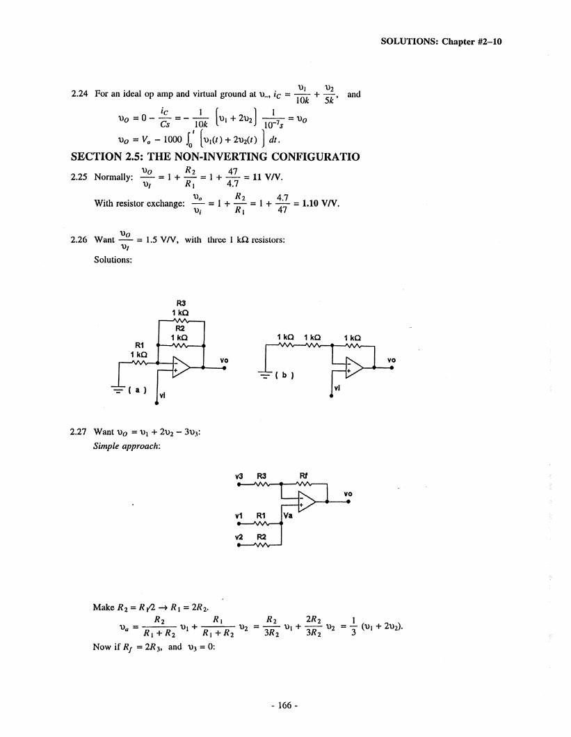
SOLUTIONS: Chapter #2-10
D| U22.24 For an ideal op amp and virtual ground at v>_, ic = , and
'c 1 f= 0 - — =- —— hti + 2t)21
10_7jt = o0Cs 10/fc
t>0 = - 1000 JQ' (o,(r) + 2v2(t) ) dt.
SECTION 2.5: THE NON-INVERTING CONFIGURATIOVo R2 47
2.25 Normally: — =1+ — = 1 + — = 11V/V.J v, /?, 4.7
With resistor exchange: — = 1 + = 1 + = 1.10 V/V.Ri 47
vo2.26 Want -=1.5 V/V, with three 1 k£l resistors:
•0/Solutions:
R11kQ
R31kQ
R21kQ
="( a )vl
vo—•
1kQ 1kQ 1kQ
="( b )
VO
2.27 Want -00=1)!+ 2\)2 - 3d3:Simple approach:
Make R2 — R/2 —> R 1 = 1R2.
R2 R 1 Ri 2R2 1»ÿ - + + +
Now if Rj = 2/?3, and o2 = 0:
- 166 -

SOLUTIONS: Chapter #2-11
Vo = 1 +2R,
Ri(Ui + 2i>2) = (\)| + 2u2).
In general, u0 = D| + 2v>2 - 2u3. Unfortunately, neat and simple, but not quite right! We see the needfor more gain for u3.Second approach: (The idea is to reduce the gain given to (v>i + 2t)2) ). Let Rf = 3R2, such that for t>3alone, v0 = -3l)3. But, now, x>(/oa = 4. Introduce an additional input u4 = 0V connected to v>u by R4.Now by superposition,
RtR|A4
1>a =R2\\R4 R \ II I?4
D, +R|+ R2 II R2 + R|II R4X>2 =
R2R4
ÿ 4 ÿ 1+ÿ?4-•u, +-—-\)2,
/?,+2"4
R2+R4r2+
R,RI'MRi+#4
or
R=
2 "4
Ri R2 + R|R4 + R2 R4d, +
/?41 /?2 + /?2/?4 + f?i I?4
ÿ2-
Now, if it is required (for \)3 = 0), that i)i + 2o2 = t>„, need R\=2R2, for which
= -l~E- + 2x)2>-Rl R\7ÿ +ÿ + 1
i iNow for the desired output, v0 = 4o(, , and —-= —, for which —- =4- 2-1= 1, or
R i 4 RaIT+ 2+ 1r4
R4 — R j =2R2. Thus use R2= 10 kQ —> R i = R4 = 20 k£2, and use R2 = 10 kQ —» Rf = 3R3 = 30kQ.
2.28
v2 R2 Rf vH1 RN1 Rf
vo
vp1 RP1 Va
vp2 RP2
vo
Va R3
Want u0 = 10 (l)| - t)2). Try the circuit in 1) using R j, R2, R/: For i)2 alone,
Do = —10122 = — Rf/R2 t)2. Rf = 1OR 2
For R2 = 10 kQ -> Rf = 100 kQ, for which u0 = - 10 v2
Now for Ui alone, (R2 = oo), d0 = 11 + Rs/R2 I Di = (1 + 10) \>j = llDj
- 167 -

SOLUTIONS: Chapter #2-12
and, together, D0 = 1lx>, — 10u2We see that there is too much of Uj:It needs to be attenuated:
Introduce an additional resistor /?3 from uu to ground:
R* 10= 7ÿT/?7 U, = TTU|
Now for /?, = 10kf2 , /?/(10 + /?3) = 1011, and 11 R3 = 100 + 10/?3,
whence /?3 = lOOkO, with the result that x>0 = 11 *>i X lOll - 10 \)2 = 10(\)| - d2), as required.
In summary. /?, — R2 = 10 kO, Rf = R3 = 100 k£2.
This configuration, with Rj/R2 = RyR |, is referred to as a difference amplifier.
Alternatively: From the equations supplied in P2.44 on page 1116 of the Text:
u0 =RfR.AM
Wm + 1 +RfRni
VpIRpi R.P2
RPi+ Vp2
Rpi II Rpi
RP2
We want v0 = 10 (x>i — v2). Now, for vN\ = \)2, seeRf
Now for \)/>i = \)|, see 1 +rfRni
Rp| II Rp2
Rp|
Rni
= 10= 11
= 10, and for RNi = 10 kQ, RF = 100 kf2.
Rp2
Rpl + Rp2, and for /?/.,= 10 k£2, RP2
= 100 ki2. Clearly, if \>P2 = 0, then u0 = 10(\Ji - 1)2).
2.29
(a) For the circuit of Fig. 2.19, using the result in Equation 2.11 on page 83 of the Text,1+1?'/R | 1
G = ÿ
V/V.1 + (1 + R/RiYA
. Now with /? 2 = 0, /? |= oo, /l =10 V/V, sec G =1 + (1/10)
= 0.909
(b) Now for the circuit of Fig. 2.16, with /?,, R2 finite, G =1 + R/Ri
Now for G = 1.00,1+(1+/?2«,/10
1 + RÿRi = 1+(1+/?2ÿ|/10= 1 +0.1 +0.1 Rÿu and 0.9/?ÿ?, = 0.1, /?/??,= 0.1/0.9, andR\=9R2. Thus, /?2 = 10 kf2 ,1?| = 90 kii. Thus
Gain (nominal) = 1 + 10/90 =1.11 V/V.1.111 1.111
Gain (actual) =1 + 1.11/10 1.111
= 1.00 V/V, as required.
SECTION 2.6: EXAMPLES OF OP-AMP CIRCUITS2.30
R Imsoa
Ri
-10V
>t CxtmA
For U/ =0,X)K = 0, and the meter is required to readmid-scale. That is, IM = 0.5mA. Thus Ri = (0--10)/0.5mA = 20kQ with the — 10V supply. Now, forfull-scale reading with V/ = +IV ,IM must be 1mA.U//7? + (U/ --10/7?| = 1mA, and 1//? + (1 +10)//?, = 1, whence VR = 1- 11/20 = 9/10 = 0.45,and R = 1/0.45 = 2.22kQ. Check: for v, = -1 V:
-I --10 1 9 1 _.c _.clM =-----— = -rr- -
___= 0.45 - 0.45
R\= 0 V: OK.
R 20 2.22
- 168 -

SOLUTIONS: Chapter #2-13
2.31+ 16V
Di> ÿ 6V
R11kQ
/?, = +5V/0.5mA = 10 kO; R2 = (15 - 5)/0.5mA =20 kQ. Op amp standby dissipation is 2(15V) x2mA = 60 mW. Op amp dissipation when loaded is20 mA (15 - 5) = 200 mW. Total op amp dissipa¬tion is 200 + 60 = 260 mW.
Note also: That the bias network dissipation is 15 x0.5 mA = 7.5 mW, and the load power consumptionis 5 x 20 mA = 100 mW.
Thus the total supply power is 60 + 200 + 7.5 + 100= 367.5 mW.
2.32 From Equation 2.13 (or directly by superposition):
*4R2=- ITV| +
«i R3 + R4
R2 1 ÿ2ÿ 1U2 = -«7U' + TTÿ7ÿ
100 1 + tocioHence "On =--v.- +-v? — —0 10 ' 1 + KK100
10010
1), +100 + 1000100+10
\)2 = 10 (1)2 -Ui).
gain A =D0
1), -1)2= -10 V/V: (Note the sign!)
2.33 For this situation, gainDo
Dj|- D.,2
vs1•—
Rs1 R110 kQ 10 kQ
-JWV—vw-
vs2Rs2 R3
10 kQ 10kQ—-w\—ww-
R2100 kQ
10010+10
= -5 V/V.
R4100 kQ—-wW*-|
vo—•
To recover the gain, two possibilities exist:
a) Remove R{ and R2 and connect sourcesdirectly.
b) Make R2 = R4 — 200kQ.
The latter is probably best for secondaryreasons. For example, it reduces (by a fac¬tor of 2), the effect of minor variations inRs1 and Rs2.
For the case in which RS2 is 8 k£2, there are twobasic approaches: a) "Pad out" /?3, i.e., add anadditional 2kQ resistor in series with RS2 and R3,
or, b) change R4 to 180kQ to compensate. (Mak-R2 R4
tngR 1eq R3eq
)
R2 /?42.34 Using superposition, i)0 consists of 3 parts. Thus i)0 =- 1)1 —— + i)2 ————
K\ K3 +K4
d3R,
Rj + R4 1+*7R! .,or D0 =- th — + 1)2«i
l+R2R.
1Rl
+ R4
+ i)3
R21+r71+
R4R3
1 +*2*1
- 169-

SOLUTIONS: Chapter #2-14
Ri R4Now, — = —, and
K i K3
r2V0 = -\), — + \)2
Ri
R21+ -rr-
1 +RiR7
1 +Ri
+ V31+
Ri/?.
R2 ÿ2 (ÿ1+ÿ2)- +\)2— (/?i+/?2)+ÿ3.
whence Do = — Co2 -Ui) + \)3. Note that the operation is the same, but with the output establishedKi
by U3 for (t)2 -Ui) = 0. This is an interesting and important result!
2.35 Check first that it is a balanced difference amplifier for \>| and V>2: see that R4i, II R4a = 300k£2II 1501:£2 = 300/3 = 100 k£2 = R2, (OK).
100 100 11150(a) For Ui = v2 = 5 V: See (by superposition), t)ÿ = 5 + 15 + 0, or100 + 100 " 300 + 100 II 150
1)4 = 5 (1/2) + 15 (60360) = 2.5 + 154S = 2.5 + 2.5 = 5V. Now, since vA = 5V, and u, = 5V,current in R 1 = 0, and \>0 = 5V.
(b) For v>! = \)2 = 0V, x>A = 15100 II 150
300 + 100 II 150 = 1560360
15= 2.5V, and \)0 = 2.5 (2) = 5V.
(c) For "Uj = 3V, x>2 = -2V, see x>A = -2
t>i -t)B
+ 15
Vo — % — /?!
= -1 + 2.5 = 1.5V. Thus \)B = 1.5V, and
x R2 = vB -D| + x>B =2 (1.5) -3 = 0V.
Alternatively, to use the extended result from P2.34 above, realize that R4B with R4a and the con¬
nected supplies have a Thevenin equivalent of U3 =ÿ
x 15 = 5V, and 150k II 300k =
100k£2. Thus, since R\ = R2 = R3 = R4, \>0 = u2 - t>i + v3. Therefore the output is the conven¬tional difference plus the extra (reference) input. Thus (a) o0 = 5V, (b) v0 = 5V, (c)Vq = -2 -3 +5 = 0V.
2.36 For an overall gain of 100 V/V, with 10 V/V from the input stage, and 10 V/V from the output stage, seethat 1 + 2RÿR\ - 10, and R/R3 - 10. For R\ = 10k£2, R2 = (10 - 1) R\l2 = 45k£2, and for R3 - 10k£2,
R4 = 100k£2. Now, for \), = 5.0V, m2 = 4.9V, \)01 = 5.0 +5 ÿQ~ÿ9 (45k£2) = 5.45 V, and
x>02 - 4.9 - 5f~ÿ'9 (45k£2) = 4.45 V. Check: \)0l - x>02 = 5.45 - 4.45 = 1.00V = 10 (0.1), as
expected!10k£2
2.37 See that Vy = (1 + RÿR\)x>x and that the current into X is ix = (i>x - VyYR3.
vxThus Rin = \>XAX =
[X)X ~ (I + RJROVxYR3, or Rin = /?y(l - 1-R-/R 1) = - R[RyR2» as required.
See, from the diagram that /?, = R4 + Rin = R4 - R|RyR2.R>,
Also, using a voltage-divider ratio, -=D|y R4 + /<„
— R \RyR2, or vxA)w =
1
and Djv4)h? = (1 + Rj/R i)(\>xAi\y)1 + Rj/R 1
1- (/?yR,)(Rÿ3)
R4 -RxRJR2 ' " ~A' "" 1 - {RJR\){RJRti '
. For R\=R2, these become: /?,• = R4 -R3,
- 170-

SOLUTIONS: Chapter #2-15
— 1/(1 — R4/R3) and Dj'Ajiv — 2ÿ1 — Rj/Rÿ)
a) For R4 — 2/?3, /?,• = 1R3 — /? 3 = R3, = 1/fl — 2) = — 1V/Y and ÿOjvÿiy = — 2.W/V.
b) For /?4 = /?3, /fj = /?4 — /? 3 = 012 v>x/biv — 1/(1 — R4R3) — 00, and \)yZ\iy/ — <x>, also.
c) For Ra =R/2, Ri= - R4- = -R;A x>ÿw = V(l -RJRJ = 1/fl - 1/2) = 2 V/V, and oK\)w = 4V/V.
For \)rA)w = 10 V/V, 10 = 2ÿ(1 -Rÿ). Thus (1-RJR3) = 210 = 0.2, and
R/R4 = 0.8, whence RA = O.8R3.
2.38 Use the results from P2.37 above: Input resistance at X to the right is (-/?), and to the left is R.Overall, at X, the resistance is R II (-/?) =~— = 00! Now the short circuit current at X to
R — Rground, with V/ applied is V/ZR (from W) and 0 from Y for a total of iyR. Thus the Norton equivalentat X is a current source In = t)/R with a shunt resistance Rn - <». For an impedance Z connected at X,the current flowing will be Ojdl and the voltage will be V/ZZR . In general, the transmission x>xZ\)w =Z/R and vY/ow — 2Z/R. For a capacitor for which Z = V(Cs ), %A>w = 1ZsCR . For this non-invertingintegrator, the time constant is RC. The unity-gain frequency is co„ = 1/(RC)
2.39 The common-mode input (at 60Hz) is 8 V peak, and the output is 0.6 V peak. The difference-modeinput (at 1 kHz) is 1+1 =2 mV peak, and the output is 60 rnV peak. Thus, the common-mode gain =0.6V/8V = 0.075 V/V, and difference-mode gain = 60mV/2mV = 30 V/V. Thus the CMRR = 30/.075 =400 s 201ogio 400 = 52 dB.
2.40 CMRR = lO100"20 = 10s. For a difference-mode output of 2 Vpp, the required common-mode signal out¬
put = 1/100 x 2 = 20 mVpp. Thus = 10s, and vicm = — x 20 x 10"3 = 10 Vpp.ZA)tli V / Ulcj)i ZUU
SECTION 2.7: EFFECT OF FINITE OPEN-LOOPS GAIN AND BANDWIDTHON CIRCUIT PERFORMANCE
2.41 At and above the cutoff frequency ,A x / =/, = 107. Thus /3ÿ =f/A„ = 107/106 = 10Hz. At /= 100 kHz, the available gain, A =f/f = 107/105 = 100V/V.
2.42 Closed-loop gain of 20 dB corresponds to a gain ratio of 102tK2° = 10 V/V. In general,f,m -fA1+ R-/R\Y For a gain of -10 V/V, R/Rt = 10, and f3dB = 107/(1 + 10) = 0.909 MHz. For again of +10 V/V, 1+ R/R, = 10, R/R{ = 9, and f3dB = 107/(1 + 9) = 1.00 MHz. The phase shift atthe 3 dB frequency is 45°, and 6° at 1/10 the 3 dB frequency. Thus 6° shift is reached at 90.9 kHz forthe inverting amplifier, and at 100 kHz for the non-inverting, and is less than 6° for all lower frequencies.
2.43 Amplifiers have A0 = 106 V/V and /, = 107 Hz: For maximum bandwidth, use the noninvcrting formwith gain (1 + R-/R\). For a single amplifier, with / 3,//) = 10 kHz: 104 = 107/(1 + R-/R ()• Thus1 + R-/R\ = 107/I04 = 103, and the available gain is 103 V/V. For 2 amplifiers in cascade, each with a3dB frequency at / j, f 3dB = (f2 - l)*4 f \ = 0.64f4/ ] . Noyv, for / 3,tB = 10kHz, f\ = 10kHz/.644 =
R715.54 kHz, with corresponding gain per stage of I+K,
10715.54 x 103 = 643.6 V/V, and, for two
stages in cascade, a gain of (643.6)2 = 4.14 x 10s V/V.
2.44 Gain with feedback at low frequencies is likely to be: -R-/R 1 = -100 V/V. Assume |A 0 1»100: Now,120
for a 3dB frequency fB < 120 kHz, 100 = 120(25), and fL = (25) = 30 kHz. For the closed-
loop amplifier, the unity-gain frequency (where Rÿi= 1) is 120(25) kHz = 3 MHz. But the unity-gain
- 171 -

SOLUTIONS: Chapter #2-16
frequency of the ncgalivc-gain amplifier is
and for the op amp itself, /, = 6 MHz.(1 +fRjRxy which is 4" Ior ÿ7 = '• Thus fA = 3 MHz-
2.45 /, = 100 MHz, A„ = 20 V/V: Now, for
/? i 201+
Ri= 10+4- +2
Now, forD,
1 Ri 1 R22 /?,' 2 /?!
-R-/Ri
*>/
-211+ (2220) = 10 V/V, OK. Correspondingly, /vfl =
l+ (l+/?ÿ,/A„R2Ri
100 x 106
= 10.5, and
f,
l+RfRt 1+ 21
= -10 V/V,
= 21. Check:
= 4.55 MHz.
SECTION 2.8: LARGE-SIGNAL OPERATION OF OP AMPS2.46 The largest possible peak output with zero average is 8 V. The corresponding input has a pcak-to-pcak
value of 2(8)/10 = 1.6 V.
2.47 A 6-V pp triangle wave at /Hz moves 6 V in 1/2 x 1// seconds with a slope of 6/(1/2/) = 12/V/s.Now, if this just matches the slew rate: 12/V/s = 10V/p.s, and/ = 10/12 X 106 Hz = 0.833 MHz.
2.48 The slew-rate-limited bandwidth of an amplifier with a sinewave peak output V„ is fR =
fR =fb, when V„ = SR42 n fb). Now, for SR = 2 V/fts, andV„ = 2 x 10⁶A2 n X 0.5 x 106) = 0.64 V peak.
SR„ ,, . Now2kV„
fb = 0.5 x 10⁶,
SECTION 2.9: DC IMPERFECTIONS2.49 Nominal 4V peak swing is reduced by less than 4V/100 = 40mV. Since gain = -100 V/V, RfR\ = 100
40and the gain for the offset voltage is 1+ R-/R\ = 101. Thus, the required offset < = 0.40 mV.
2.50 Af = -100; Rin = 100 kfl= /?,-+ = 10 Mil
a) For no compensation: x>0 = (1+ 100) (lmV + 30 X 10-9 X 100k II 10M) = 101 (1 mV + 3 mV) = 404mV = 0.40 V.
b) For compensation, using R} = Rt II R2 ~ 100 kfl, only the offset current and offset voltage apply. Thusu0 = (101) (lmV + 3 X 10~9 x 100 k) = 131.3 mV = 0.13 V. For case (a), bias current dominates; Forcase (b), offset voltage dominates. For each dominant effect halved, the output offset becomes: (a) 101(1 + 3/2) = 0.25 V; (b) 101 (1/2 + 0.3) = 0.08 V.
2.51
vl 100 kQ 10 MQ
•-1|-----vo
J71
Note that the offset gain = 1V/V:
(a) For no compensation, X)q = 1 X Iffi-3
30 x 10"9 x 10 X 106 = 301 mV = 0.3 V.
(b) For compensation with /? 3 = 10 M£2 from thenegative input to ground, Do = 1 mV +3 X 10~9 x 10 x 106 = 31 mV = 0.03 V. Thus, use10 Mil to compensate.
- 172-

SOLUTIONS: Chapter #2-17
2.52
vi R 100R
RJt 100R= R
For no offset compensation,
= 101 [2xl0"3+(R II (100 R)) 1.1 x 10"6] <0.5V. Thus 2 x 10~3 + 1.1 x 10⁻⁶/? < 4.95 x 10⁻³,
j „ 2.95 x 10"3and R = ——-— = 2.68 ki2.
For1.1 X lO""6compensation, with
1R?, = R,
\)0 = 101 [2x10~3 + R(2 x 10"6)] < 0.5V.2 95 x in-3
Thus R = ---r- = 14.75 kO, (use 15 kf2).0.2 x 10~6 7
For this design, Rin ~ 14.75kO = 15 k£2.
2.53
a) Positive limiting is caused by current flowing out of the capacitor at the op amp negative-input node.Contributions include: bias current of 100 nA, offset current (worst case polarity) of 10 nA, current fromthe input resistor when the offset voltage is + 2mV is hnVAQkkl = 200nA . Total current is100 + 10 + 200 = 310/iA . The ouput voltage will reach positive saturation inT = CV/l = 0.1 x 10~6(10/(310 x 10-9) = 3.22s.
b) For negative limiting, current must flow into the input end of the capacitor. Maximum current from inputresistor (with offset - 2mV) is 200 nA. Maximum offset current is 10 nA. Minimum bias current is -100 nA (flowing into the top amp). Thus the total current is 200 + 10 - 100 = llOnA for which nega¬tive saturation occurs in T = 0.1 x lO-ÿ10/110 x 10~9 = 9.09s.
For Compensation: Make Ra - R\ = 10kf2, in which case the bias current flows through R i (and Ra) toproduce voltages at each input which are equal and cancel. Adjusting Rc with Rh provides an additional± 2mV on the positive op-amp input to cancel the voltage offset, which though unknown may be rela¬tively stable (certainly if the temperature is fixed). Even the offset current can be compensated on theshort term. Typically a factor of lOx improvement is possible (at least) with saturation time increased toperhaps one minute. Because Ra ~ R j, doubling the bias current does not matter much. (Again cancella¬tion is usually good to within a 10% difference error.)
For compensated positive saturation, the choice of Ra = 101:£2 compensates bias current, while the
current from Rb compensates for the offset voltage. Here, vc = x Vc = 2mV or10*12+10mL2
1/1001Vc = 2/1000 and Vc ~ 2V. Note that the offset current flowing in 10 k£2 produces a voltage of10 x 10"9 X 10 X 103 = 0.1 mV. For this included, Vc = (2.0 + 0.1)1001/1000 = 2.1V
2.54 The nominal closed-loop gain is G = 1 + R/Ri = 1 + lO/lO4 = 101 V/V. The bias current flowing in
101:12(11 10Mil) is responsible for an offset of = H-88 mV. Thus the bias current is
11 88 x icr3—:-r— = 1.19liA. The input offset voltage is 0.6/101 = 5.94 mV. Note that a fraction of the 5.94lOxlO3
mV voltage offset is due to the offset current flow in 10 kfl. Now, with all resistors reduced by a factor
of 10, the change in input offset voltage is = 1-98 mV, due to the difference between I„ffse,flowing in 10 kf2 and in 1 k£2. That is, I„ff(l0k - Ik) = 1.98. Ioffset — 1.98*9kCl = 0.22 [lA . Now theoriginal offset voltage 5.94 mV at the input includes the Vos + I„ffse, X 101:12, orVos = 5.94mV - 220 x 10~9 x 104 = 3.74 mV.
To summarize, for the basic amplifier, Vos = 3.74 mV, = 1.19 pA, = 0.22 pA.
Now if the 10 kt2 resistor at the negative input is capacitor-coupled, the offset voltage is multiplied onlyby 1, but the bias and offset currents flow in 1 MI2. If they add, the output offset becomes1M£2(1.19 + 0.22) X 10"6 = 1.41V!. Two possible compensations arc possible:
- 173 -

SOLUTIONS: Chapter #2-18
a) If the resistances R \ and R2 are reduced by a factor of 10, the output offset reduces to 0.14V.
b) If a resistor Ri= 1MCl is connected from the positive op-amp input terminal to the actual input,which is grounded, bias currents are compensated, and the output offset becomes1M£2(0.22 X 10"6) = 0.22V.
c) If both techniques are used (ie using a 1 k£2 resistor and two 100 k£2 resistors), the offset due tooffset current reduces to about 22 mV. With the voltage offset remaining, about 22 + 3.74 = 25.7mV would be found at the output.
- 174-

Chapter 3
DIODES
SECTION 3.1: THE IDEAL DIODE
3.1 Diodes are ideal: Thus the forward voltage drop is OV and reverse current is 0 mA:
(a) Diode is polarized to conduct by the +5V and OV connections: Thus Va = OV, and la = (5-0)/IkO= 5mA.
(b) As in (a), but the most negative supply is -5V. Thus Vb = -5+0 = -5V, and Ib = (+5 - 0 -(-5))/lkfl = 10mA.
(c) Diodes both conduct: Thus Vc = -10 + 0 + 0 = -10V, and Ic = (0 -0 -0 -(-10))/lk£2 = 10mA.
(d) Both diodes are polarized to conduct. Thus Vd = +5 -0 = 5V, and Id = (+5 -0-0-0)/lkil= 5mA.
(e) Upper diode is polarized to conduct, but lower to cut off. Thus current le = 0mA, and Ve = 5V —0V = 5V (with the upper diode conducting the meter current).
(f) Upper diode polarized to cut off, and lower to conduct. Thus current, If = 0mA, and Vf = —5V -0- 0 = -5V (with the lower diode conducting the meter current (assumed very small) through lkfl).
3.2 (a)
(b)
(c)
(d)
i) V& = +5V; upper diode conducts; Vy = +5V.
ii) The output is high if either input is high. For high (+5V) defined as logic '1', the output is1, if A = 1 or B = 1; ie, Y = A + B. Thus, the function is logic OR (in positive logic).
iii) For high (+5V) defined as logic '0', the output is high (logic '0') if either A or B is high(logic '0'). That is Y = A + B, or Y=Y=A+B=A • B =AB (for simplicity). Thusthe function is a logic AND in negative logic. The AND idea can be verified by noting thatthe output is low (logic '1') only if A and B are both low.
i) , Vc and VD are all 0V. Vy follows the highest input. Thus Vy = 0V.
ii) Y = A + B + C, an OR (in positive logic).
iii) Y = A • B' C =ABC,an AND (in negative logic).
i) See that the output follows the lower of A or £ (just as the output followed the upper of Aor B in (a)). That is, = Ve = 5V -> Vy = 5V.
ii) From above, Y =A + B, ie Y = Y=A+ B=A • B =AB That is, the function is ANDor, directly, Y = A • B = AB (since both inputs must be high for the output to be high).
iii) Directly, from logic first principles, or in analogy to the circuit in (a), Y = A + B (in nega¬tive logic). That is, the function is an OR.
i) = 5V, VB = 0V —> VY = 0V.
ii) AND (positive logic).
- 175 -

SOLUTIONS: Chapter #3-2
iii) OR (negative logic).
(e)
i) VA = VE = 5V, Vc = OV -> Vy = OV.
ii) AND; Y =A •£ • C =A£C.
iii) OR ; K = A +E + C.
3.3 Use positive logic, that is, '1' = 5V, '0' = OV.
For D5 open, P -A • E =AE.
For Z>6 open, Q = B • C = BC.Now, note that the current available from node P or Q (100(1A) exceeds that drawn from node Y: Thusif P or Q goes high, Y is also pulled high. Thus Y = P + Q + D and, Y = AE + BC +D (in positivelogic).Now, for VA = VE = 5V; VB = Vc = VD = OV; that is A = E = T and B = C = D = *0', for which Y= l*l+0*0+ 0 =1. Thus the output is logic '1', or 5V (for ideal diodes)
3.4 12V rms = 12(1.414) = 16.97V peak
For a 12V battery and an ideal diode, the peak diode current is (16.97 -12)/(10 + 50) = 82.8mA
The diode begins to conduct (and ceases to conduct) when 16.97 sincot = 12V .or sinco/ = 12/16.97 =0.707 or cot = tc/4 s 45".
1 r3w*Average value of iD = ——2k V4(16.97 sin 0 - 12) dQ)/60 = .
3W4VS
16.97V
io
3tt/4 - it/4-0.2 \ = (.0635 - .0500)
2n>
82.8mA0
0mA —45° 135°
>> Olt
A = 13.5mA. Now for VB = 14V:Peak current = (16.97 - 14)/60 =0.0495A or 49.5mA. Conductionbegins when 16.97 sincof = 14, orsincol = 14/16.97 = 0.825, or tot =55.6°.
180*—55.6*
Average current =P- (-.565 -.565) - 0.2332n
= 0.0507 - 0.0445 = 0.0062A or 6.2mA.2n
- 176-

SOLUTIONS: Chapter #3-3
Consider the conducting state ofeach of the diodes: Assume D\conducts; thus its cathode is at OV.Correspondingly, the current in theIkO resistor, IlK = (0--8)/lk =8mA. Assume D2 conducts; thusits cathode is at OV, and I2K = (8 —0)/2k = 4mA.
Now, since IlK > I2K, then D\ andD2 both conduct as assumed.Now, noting that succeeding resis¬tors are progressively larger,assume that both D3 and D4 alsoconduct, and that their anode andcathode voltages
are all zero volts. Thus, /4ÿ = (0 — 8)/4k = 2mA, and IiK = (8 - 0)/8k = 1mA.
Thus, overall: ID4 = ISK = 1mA; ID3 = /4/f - /D4 = 2 - 1 = 1mA; ID2 = I2K - ID3 = 4 - 1 = 3mA;foi =Iik ~ Idi= 8 - 3 = 5mA; Thus diodes are all conducting, and V„ - OV.
SECTION 3.2: TERMINAL CHARACTERISTICS OF JUNCTION DIODES
3.6 Given: V, = 0.700V @ /, = 100ÿA, and V2 = 0.815V @ I2= 1mA.
Now iD = Is eÿ7 —» \)p = nVT In i[/Is = nVT In iD - nVT In Is.Vd l— t)D2 = "Vy (111 io/lDl)-
Here, 0.700 - 0.815 = n VT In 0.1/1 = 0.025n (- 2.3026).
n = 0.115/(.025(2.303)) = 1.997 or 2.00.
Now Is = iD e'V,/"Vr = 100 X 10"6 e"70(K2(25,) = 10"4 e"14 = 8.32 x 10"17A.
3.7 i= 1$ e r, and - v2 = nVT In i/i2 ---(1).
Thus, \)t = u2 + nVT In i/i2= 700 + 1(25) In 1/0.1 = 700 + 25 In 10 = 757.6mV, or 0.758V.
Now from (1), i\ = i2 e "V7 = 0.1 e<815 - 7°°yiC25) _9.95mA.
WnV3.8 ( = Is e 7 —> v = nVT In iAs, or x> = v„ + nVr In iA„.
At 10mA, u = 700 + 2(25) In (10 x 10-3/10) = 355mV, or 0.355V.
At lOp-A, u = 700 + 2(25) In (10 x lOÿ/lO) = 9.2mV.
3.9 At lOOjiA and 25"C, v = t)„ + nVT In iA„ = 700 + 2(25) In 0.1/1 = 585mV.
At 100}iA and 95"C, o = 585 + 2.0 (25 - 95) = 445mV, or 0.445V.
3.10 The leakage doubles for each 10"C rise in temperature.
Now at 95°C, it is 2(95 ~ 25)40 = 27 = 128 times its value at 25°C, or 128nA, or 0.128(xA.
Now at 100°C, it is 2(l00~ 25)40 = 275 = 181 times its 25°C value, or 181nA.
- 177-
3.5
+ 8V + 8V

SOLUTIONS: Chapter #3-4
Note that it is 2(10° 95)10 = 2a5, or 1.41 times as large as at 95°C, ie 1.41 x 128 = 181nA, as alreadynoted.
SECTION 3.3: PHYSICAL OPERATION OF DIODES
3.11 Acceptor concentration is NA = 10"™. Thus the hole concentration is pp0 ~ 10~m, while the electron con¬centration is npQ = 10~", n »m. More precisely, in 10" atoms, one is ionized at a particular tempera¬ture to produce one hole and one electron. As well, the number of acceptor - produced holes is10" X 10"™. Thus the total number of holes is 1 + 10" x 10"™ in 10" atoms, where
1 + 10" x 10~™Ppo = =10-", while np0 = 10"" directly.
3.12 From Eq. 3.6, n2 = BTÿe E"*rt where for silicon, B = 5.4 x 1031, Eq = 1.12eV, k - 8.62 X 10"5.
At 200 K, ni2 = 5.4 X 1031 x 200V1-12*8-62 * ,<r' * 200) = 2.639 x 10¹⁰,and n, = 1.62 x 10⁵ carriers/ cm3.At 300 K. n? = 5.4 x 1031 x 3003e-l.12/(8.62 x 10"5 x 300) = 2.2616 x 10²⁰,and rij = 1.50xbold {10 sup 10}carriers/bold {cm sup 3}..IPAtA00K ,n sub i sup 2 "=" 5.4 "times" 10sup 31 "times" 400 sup 3 e {-1.12/(8.62 "times" 10 sup -5 "times" 400)} "=" 2.706 "times" 10 sup25,.//,andn sub i"=" 5.20 X 10¹² carriers/ cm3.
5 2 x 10¹² — 1 5 x 10¹⁰For the 100 °C rise above room temperature, the increase is —-'-n;-x = 3.46 x 10⁴%!F 1.5 x 10'°
5 2 x 10'2At this temperature (127 °C), the fraction of ionized atoms is —- ~ '0~10, or one in every 10
(US) billion! Note that the reference on page 139 of the Text is to British billion.
3.13 From Eq. 3.10C, resistivity is p = \Z[q(p\ip + np.„)]12cm.
(a) For intrinsic silicon at room temperature: n =p = «, = 1.5 x 10l0/cm3.Thus p = H1.6 x 10",9(1.5 x 10'°)(1350 + 480)] or p = 2.28 x 10⁵I2cm
(b) For n-type silicon with ND = 10l6/cm3: nno = 1016, and pn„ = n2/ND = (1.5 x 10¹⁰)ÿ1016, or
pn0 = 2.25 x 10⁴.Thus (including mobility reduction):
p = 141.6 x 10"'9(2.25 x 104 x 0.8 x 480 + 1016 x 0.8 x 1350)] or p = 1.73 12cm.
As noted in the solution to P3.12 above, for a 100 °C rise n, will increase by a factor of 3.46 X 10⁴.Thus for the intrinsic material p will decrease to 2.28 x 10⁵/3.46 x 104 = 6.59£2cm, while for the dopedmaterial, it will stay the same, at 1.73f2cm
3.14 The depletion region will be larger in the lighter-doped p region. In fact, it will be 10 x larger therethan in the n region.
3.15 Eq. 3.18 in the Text states that the built-in voltage is V0 = VTln[NAN[/iij2], where tij = 1.5 X 10l0/cm3for intrinsic silicon at room temperature. Here 700 = 251n[/V)iA/041.5 x 1010)2].
Thus NaNd = (1.5 x 10lo)2e7(Xm = 3.254 x 1032/cm6---(1)
(a) For Equal Doping:
NaNd =N2 = 3.254 x 1032, whence N = 1.804 x 10l6/cm3 = 1.80 x 10²²/m3.From Eq. 3.20 in the Text, Wdep = xn + xp = 2x = [(2c/qHVND + VNA)V0]'A ---(2)
where (from Table 3.1 on page 157 of the Text), q = 1.60 x 10~I9C, ande, = 1le„ = 11(8.85 x 10~")F/cm = 9.74 x 10~nF/cm = 9.74 x 10~uF/cm.
- 178 -

SOLUTIONS: Chapter #3-5
Thus Wdep = [2(9.74 x 1CTI3H1.60 X 1(TI9)(2/1.804 x 10,6)0.7],/4 = 3.07 x 10~6cm = 0.307pm.The distance depletion extends into each region is W/2 = 154 nm. From the preamble to Eq. 3.21,the uncovered charge on each side is
qj = qNDxn = 1.6 x 10~19 x 1.80 x 1032 x 154 x 10~9 x 30 x 10"6 x 50 x 10-6 = 0.665 pC.(b) For 10-to-l doping:
From (1), NaNd = 3.254 x 1032/cm6, and
for ND = 10Na, say, see 10N% = 3.254 x 1032, where NA = 5.70 x 10'Vcm3 = 5.70 x 10²¹/m3, andND = 5.70 X 10¹⁶/cm3 = 5.70 x 10²²/m3.From (2), Wdep = [2(9.74 x 10~I3X1.60 X 10-'9)(M;5.70 x 10,6)(1 + 10)0.7f'4.046 x 10"5c/n =0.405pm.
Now Wdep =xn +xp =xp{Na/Nd + 1) =*,,(0.1 + 1).
Thus xp = 0.405/l.l — 0.368pm
xn — XpAQ = 0.037pm.
The charges uncovered on each side arc equal, and of value
qj = qNDx„A = 1.6 x 10~19 x 5.70 x 1022 x 0.368 x 10"7 x 30 x 10-6 x 50 x 10"6 = 0.504 pC
3.16 Is — Id = / —ÿ> 15 - Id = 10 and lo - 15 - 10 - 5. Thus the diffusion current is Io = 5nA.
3.17 Combining Eq. 3.21 and Eq. 3.22, see
qj =qnand
na +ndÿAWdep =
qNAND
Ha + Hp
2e,y
ql l
na +nd
<y0 + Vr ) f .whence
qj = a nand2esq (V0 + Vr)1 na + nd
For the (30 X 50)pm2 junctions in P3.15 above, for which V0 = 0.7F:
a) Na =Nd = 1.80 x 10²²/m3.b) Na = 5.70 X 10²i/w3, ND = 5.70 x 10²²//n3.
(a) For Na = Nd:qj = 30 X 50 x 10-i2[2 x 9.74 X 10" x 1.6 x ~'9 x (1.80 x 1022/2)(0.7 + VR)t = 7.94 x 10-'3[0.7 + VR]'AFor VR = 0.0F, qj = 7.94 x 10-,3(0.7),/i = 6.65 x 10-'3C or 0.665 pC, as in P3.15.
For VR = 10V, qj = 7.94 x 10"13(0.7 + IO)'"4 = 2.597 pC.
For VR = 11V, qj = 7.94 X 10~l3(0.7 + 11)'/' = 2.716 pC.
From AQ = CAV, the junction capacitance is C = AQ/AV = (2.716 - 2.597X11 - 10) = 119 fF.
Now, from Eq. 3.26,
Cjo -A
' •
e.t<7 nandÿ
12 [Na +Nd Vo ---(1)
Thus, Cjo = 30 x 50 x 10_12[9.74 x.10"11 x (1.6 x 10~19/2)(1.6 x 10_l9/2)(1.80 x lOÿ/iyOJf' = 0.475/F.At 10.5 V, Cj = Cjd[1+ VrW0Y' = 0.47541 + 10.50.7]'/l = 0.475ÿ4 = 0.119pF = 119 fF same as foundabove.
Now for a graded junction with m = 1/3:
At VR = 10.5V, Cj = 0.47M1 + lO.SOJ)173 = 189 fF.
- 179 -

SOLUTIONS: Chapter #3-6
At VR = 100V, Cj = 0.47541 + 10OO.7)w = 90.6 fF(b) For Na = No/10 = 5.70 x 10²l//n3
qj = A [2zsqNAN[ANA + ND)(V0 + VR)]'A = 30 X 50 X 10~12[2(9.74 X ir")(1.6 X 10~19) X
5.70 x 1021 x 10/11Jÿ(0.7 + VRf = 6.028 x 10-|3(0.7 + VRf.For VR = 0,qj=6.028 x 10-'3(0.7)'/' = 0.5043 pC.
For VR = 10F: qj = 6.028 x 10~13(0.7 + 10)'/" = 1.9718 pC.
For VR = 11V, qj = 6.028 x 10"13(0.7 = ll)'7' = 2.0619 pC.
xr •. aÿ./a„ 2.0619 - 1.9718Now, the junction capacitance is C = AQ/AV =-j-= 90.1 fF.
Now, from Eq. 3.26 ((1) above),
Cjo = 30 x 50 x 10"l2[9.74 x 10"" x (1.6 x 10"l9/2)(5.7 x 102I)(1M1)(M).7)]71 = 0.360/jF.
and Cj = CJrAl + Vr/V0]v'.At VR = 10.5F, Cj = 0.360/(l + 10.5D.7)'7' = 0.3604 = 0.090 = 90 fF, very much like the earlier esti¬mate. Now for a graded junction with m - 1/3.
At VR = 10.5F, Cj = 0.36041 + 10.541.7) = 0.360416) = 143 fF.
At VR = 100F, Cj = 0.36041 + 1000.7) = 68.7 fF
3.18 Q = CV —> C = ~Ty— = O.lpF. That is, the depletion capacitance is O.lpF.
3.19 From Eq. 3.27, Cj = Cy0(1 + FR/F0rm.For VR = 2F, 1.8 = C;o(l + Wo)"16.For VR = 10F, 0.2 = C,0(1 + lOVo)"1'6-Divide these to get 9 = [(1 + 2Y0K1 + lOYo)]"1'6Thus 1+ 2Y0)41 = lOV0) = 9-171'6 = 0.253, and 1 + 2/F0 = 0.253 = 2.5W0, and
0.5W0 = 1- 0.253 = 0.747, whence F0 = 0.530.747 = 0.709V.
Now, 0.2 = Cj0(1+ 100.706)1-6 = 0.2(15.1)' 6 = Thus Cj0 = 15.4 pF.
For VR = OF, Cj = 15.4(1 + 00.71)-'-6 = 15.4 pF, as expected, the same as Cyo, by definition.
3.20 PD = VB IR. Tims, IR = =50 * = 0.42mA.
For breakdown only 10% of the time, a peak current of 0.42/0.1 = 4.2mA can be tolerated.
3.21 From Exercise 3.12, in doped silicon, pp = 400cmWs.From Eq. 3.12, DP = Fÿp,, = 25 x 10-3 x 400 = I0cm2/s.From Eq. 3.30, the diffusion length, Lp = VDPiP where %P = 1/ii.
Thus LP = 10(1)10-9 = 10~4cm = 10~6m = 1pm. For the diffusion profile, the excess hole concentra¬tion is pn(x)=p„{0)e~x/L where a 10% level is reached when e~x/L =0.1 or x/L = 2.3.
Thus the conentration reaches 10% at 2.3L = 2.3pm from the depletion-region edge.
3.22 From Eq. 3.34, ls =AqiijDp Dn
LpN/j LnNawhere from Table 3.1 on page 156 q = 1.6 x 10_19C, «, = 1.5 x 10lo/cm3.
- 180-

SOLUTIONS: Chapter #3-7
Now, from Eq. 3.12, Dn/\ln = r/; = VT and from Eq. 3.30, L = XT
whence D/L = jiVr/(p.VrT)'/' = (|iVrA)/'.Thus Dp/Lp = (400(25 x lOÿ/lO"9)7' = 105cm/Vj = 103m/VsDn/L„ = (1100(25 x 10-X2 x 10"9))'/'1.17 x 10scniAIs = 1.17 x 10ht/Vs.ThusIs = 3 x 10"6 x 5 x 10"6 x 1.6 x 10"19 x (1.5 x 10'° x 106)2[ lOÿlO16 x 106) + 1.17 x 10³/(1017 x 106)]= 5.4 x 10²[10-19 + 1.17 x 10~20] = 6.03 x 10"nA
3.23 From Eq. 3.34,
Is =AqtijD„ Dn
LpND L„NAwhere n2 = BT}e EÿkT
t and
5=5.4x 1031, Eg = 1.12eF, k = 8.62 x lO~5eV/K.We see that the temperature dependence originates in the n2 term. Evaluate this at two temperatures andfind the coefficient:
At 300 K, n? = 5.4 x 1031(300)3e " l l2<8'62 x l0"5(300)) = 1,458(1039)ÿ-43-3= 1.458(10)391.551 x 10"'9 = 2.2616 x 10²°.
At 303K, n,2 = 5.4 x 1031(303)3e_l l248-62x l0 ÿ303» = 1.502(10)392.382 x 10"19 = 3.5782 x 10²⁰.
Thus the temperature coefficient is x 100 = 19.4v (2.2616)(303 - 300)>°C
3.24 From the solution to P3.22 above, in which (from Eq. 3.33),
I=Aqn2 Dn
LPNDDn
LnNAV/V
e - 1
the ratio of the hole to electron components lp/In = 10 19/1.17 X 10 20 = 8.55
Of the total, I= lp + /„ ,In 1
= 89.5% (holes), and In/I =1
= 10.5% (electrons).Ip/IIp+In l+/„4 "" Ip-I„ 1=I/In
For a total current of 1 mA flowing in the junction, Ip = 895|jA flows as hole current and /„ = 105pA ,as electron current.
Now, in general, the stored charge is Q = T/ for each current component.
For holes, Qp = ipIp = 1x 10~9 x 895 x 10*6 = 0.895 pC.
For electrons, Qn = T„/„ =2x 10"9 x 105 x 10-6 = 0.210 pC.
Total stored charge is Q = 0.895 + 0.210 = 1.105pC, and the mean transit timetT = Q/I = 1.105 x 10~12/1 x 10"3 = 1.1ns.
Here, from Eq. 3.39, Q = (tTA/T)l = TTl/VT = 1.1 x 10"9 x 1x 10"3(25 x 10"3), or Q = 4 pF
3.25 From Eq. 3.39, generalized, Q = (%T/nVT)I. Thus xr = nVpCj/I. For this junction,xT = 2(25 x 10-3)1 x 10-,2/l x 10"3 = 50 ps.
For a junction lOx larger, XT is the same, namely 50 ps, simply because it relates stored charge to currentlevel at an essentially-constant junction-voltage. For a larger junction, the current density changes, butthe total charge does not.
Total stored charge at 1 mA is Q = xTI = 50 x 10~12 x 1 x 10~3 = 50 fC.
For 10 mA, (2io = 10(50) = 500/C = 0.5 pC.
- 181 -

SOLUTIONS: Chapter #3-8
3.26 From Eq. 3.38, q = Xji and i= l$eÿ"Vr) Thus q — xxIseÿ"Vr.
Now, Q = dq/dv> = xTIsA,nVT)eÿ"Vr.Thus Cd = xtKiiVt), as Eq. 3.39 indicates (/ being substituted for i and n added for generality).
SECTION 3.4: ANALYSIS OF DIODE CIRCUITS
3.27
RT-Wv-
--1
1-VT ID
10 (.75) = 2.5 mA.
For the Load Lines:
(a) Vy = IV,Rt = 10012, 1T = 1/100 = 10mA.
(b) Vr = 0.9V, Rt = 10012, lT = 0.9/100 = 9mA.
(c) Vy = 0.9V, Rt = 900, lT = 0.9/90 = 10mA.
From the Graph:
(a) VD = 0.75V, ID = 2.5mA.
Check: ID = 10- Vo/0.1 = 10 -10Vo = 10 -(b) VD = 0.73V, lD = 1.7mA.
Check: lD = 9 - Vy/0.1 = 9 - lOVy, or /e = 9 - 10 (.73) = 1.7 mA. "
(c) VD = 0.74V, ID = 1.8mA
Check: = 10 - Vo/.09 = 10- 11.11 VD = 10 - 11.11 (.74) = 1.77 mA.
3.28 Though the diode is "like the one sketched in Fig. 3.20", use its analytical description to provide a com¬parison with the results in P3.27a) above.
For the diode: x> = 0.7 + 0.1log</l.For the circuit: i, VDD = 1.00V = (100f2) i+ 0.7V + 0.1 log il1,
or i= 0.3V/0.1k - (0.1/0.1) log i,or i= 3 - log /, in mA.
Solve iteratively: Initially with 1 = 1:
1 = 1—ÿ1=3 — log 1=3 — 0 = 3mA,
i=3 —» / = 3 — log 3 = 3 - .48 = 2.52mA,
The exponentialv characteristic
t'/,(V|
Straight line A
Straight line D
Slope - —-
- 182-

SOLUTIONS: Chapter #3-9
i= 2.52 —» i= 3 - log 2.52 = 2.60mA, whence
i= 2.60 —> / X 30 — log2.60 = 2.59mA ,whence
ID = 2.59mA, and V0 = 0.7 + 0.1 log 2.59 = 0.741V.
3.29 For the diode, 1) — Vp„ + rDi Here, VDD = 1.00 = (1000) i+ 0.65V + (200) i,
or for i in mA, ID = i= = 2.92mA, and VD = 0.65 + 2.92 (.02) = 0.708V.
3.30 For VDO = 0.70V, and rD = 100, 1.00 = 0.1/ + 0.70 + 0.01/, and
Id = ' = oT:o0oT = "577" = 2'73mA' with V° = 0J0 + 273 (a01) = °-727V-
For VD0 = 0.75V and rD = 00, ID = i= q ÿ= 2.50mA, with = 0.750V.
For Vr = 0.8V and RT = 1000, /r = 0.8/100 =8mA. From the Figure, see VD = 0.7V, ID = 1mA.Check: ID = 8 - Vo/0.1 = 8 - 10VD =8-10 (0.7)= 1 mA.
h =Q |+ Q Q2 = 1-25mA' and vd = 0.65 + 0.22
(1.25) = 0.675V.O X —- O 70
b =Q1 + 0 01
= 0.91mA, and VD = 0.70 + 0.01
(0.91) = 0.701V.
Id =0 8 ~ 1°'75 = 0.50mA, and VD = 0.750V.
1/XI
Check: Overall, using the logarithmic model, the supply voltage is V = 0.1(/o) + 0.7 + 0.11og(/o/l)which for ID = 1mA ,d = 0.1(1) + 0.7 + 0.11og(l) = 0.1 + 0.7 + 0 = 0.8, as proviced, OK.
3.32 Drop across each diode = 4.0/5 = 0.8V. Thus 0.8V = 0.7V + 0.1 log (IpAinA ), or log ID = (0.8 -0.7)/0.1 = 1, whence Ip — 1o'°8 = 101 = 10, or ID = 10mA (as can be seen directly). Now R = (10 —4.0)/10mA = 0.6kO, or 6000.
3.33 For R = 5000 used in P3.32 above, with each diode having a drop of D volts:
See, i= i0~55X> = 20 - 10u, also u = 0.7 + 0.1 log ill.
Solve iteratively:
u = 0.8V -> / = 20 - 8 = 12, u = 0.7 + 0.1 log 12 = 0.7 + 0.1079 = 0.8079V;
\) = 0.8079V -> / = 20 - 8.079 = 11.92, t> = 0.7 + 0.1 log 11.92 = 0.7 + 0.1076 = 0.8076V;
•u = 0.8076V -» / = 20 - 8.076 = 11.92 mA, x> = 0.7 + 0.1 log 11.92 = 0.7 + 0.1076 = 0.8076V.
Thus the diode-string voltage becomes 5(0.8076) = 4.038V, or 4.04V.
(a)
Straight line B
Slope - — (b)'/»
_ The exponentialcharacteristic
Straight line A
ÿ (c)
(d)
6ÿ0.8 1.0 ,V|
- 183 -

SOLUTIONS: Chapter #3-10
3.34 After shunting, three identical diodes in parallel share the current equally.Original current is i= (1) io'0-8-0-7ÿ' = 10mA (as can be seen directly).Final current in each diode = 10/3 = 3.33mA. Final voltage drop = 0.7 + 0.1 log 3.33/1 = 0.752V.
SECTION 3.5: THE SMALL-SIGNAL MODEL AND ITS APPLICATION
3.35 In general, r = nVT/lD. At 0.1mA, r = = 50012. At 10mA, r = 4!r~r = 512.0.1mA 10mA
Now the "average" resistance would more likely be considered at (0.1 x 10)'7' = 1mA,than at (0.1 + 10>2= 5.05mA. Thus the geometric mean is likely to be most relevant, and therefore "best". But, let uscheck:
See (r\ + r2)/l = (500 + 5)/2 = 252.512, and (ri r2)v' = ÿ500 x 5 = 5012. Now, at 1mA,2(25) 2(25)
r = ——— = 5012, and at 5.05mA, r = ———- = 9.912. Note the correspondence of the value at 1mA1mA 5.05mA
with the geometric mean, as expected. Note that the arithmetic-mean results appear to be less easilyinterpreted.
nVT 2(25mV)3.36 At 2mA: r — —— = —-—-— = 25 12. With a second identical diode shunting the first, the current is
ID 2mA 6
2(25)shared equally: 1mA in each. At 1mA: r = = 50 12, and for two in parallel, req = 501150 = 25
£2. This demonstrates that diode incremental resistance is independent of diode junction size.
nV7* I)# f3.37 For small 1)j, use the small-signal slope resistance, r. In general, r = —— andI 1)5 r + R$
For / = 10mA: r = = 5£2; V(/os = 5+5100Q = 0.00498V/V = 0.005V/V.
For I= 1mA: r = = 50£2;5Q ÿ000 = 0-0476V/V = 0.05V/V.
For / = 0.1mA : r = = 500£2; = 0.333V/V = 0.33V/V.0.1 500+ 1000
For I= 0.01mA :r = = 5000Q; ÿ5°°°
___= 0.833V/V = 0.83V/V.
.01 5000 + 1000
3.38 For d0 = % = 0, see that I\ and /2 both split equally between D\,D2 and Z23, D4 respectively. Thusall diode currents are equal.
In general, for 1)5 * 0 (say +8), the currents in £>1, D2 redistribute with their sum = I\. Extra current in£>2 needed to drive Ri high implies that there is less current in D4 than in the balanced case, the extrapart of /2 flowing in £>3. In general, current needed by RL for 1)0 * 0 is provided half by that in D2increasing and half by that in D4 decreasing, with corresponding changes in D\ and £)3, such that loadcurrent originates ultimately in vs, as Kirchoff's current law would require.
For small 1)5 (around zero volts), with all diode currents equal to ill,
Rt - jrf 1 (f3 + r4] =
•
50 50 50 50[ri + r2\ 1/1+ m II
1/1 + l/l200 200
= _K)0I I I
For I= 10mA, RT = = 100, and with RL = 10k£2, 1j(/o5 = , *°* = 0.999V/V.10mA 10 + 10a:
For / = l|iA, Rt = -ÿ7ÿ = 100k£2, and VoA>s = , '°f in, = 0.0909V/V.lpA 100k + 10k
- 184-

SOLUTIONS: Chapter #3-11
Concerning Linearity: Signal size (for RL = lOkO) is of little concern at 1mA, since the load current islikely to be a small part of /. But, at low /, the load current may cause the diode current to vary over awide range. Operation is linear for diode-voltage variation of ±10mV or so: Note that the correspondingcurrent variation is Ai,where 10 = 2(25) In or In = .20, or AiA - 1.2, corresponding to
i i 50a variation of about 20%. Now for a positive output signal, iD2 can increase by 20% of its normalcurrent III, while iD4 decreases by the same amount, the output current being the sum of the two
changes. Thus for RL = lOkO and I= lpA, X>0 is limited to 2 x 0.20lpA
X 10k£2 = 2mV peak, in
which case % is restricted to2mV.0909
= 22mV peak.
An Alternative View: The largest (positive) output occurs when the drop in D2 increases by lOmV, andthat in D\ decreases by lOmV. Thus, at the limit, —v0 = 2(10) = 20mV. But for lpA and a 10k£2load, x>qA)s = 0.09, or u0 = 0.09 x>s . Thus, the limit is at 1)5 - .09 % = 20mV, or % = 22mV.
3.39 For the regulator, ID =10-4 nVr 2(251
= 10mA. For each of 5 diodes, r = —— =ÿ = 512; Resistance of
the total diode string = 5(5) = 2512. For ±10% supply variation, expect an output variation of
± x (0.1 x 10) = ± 40mV, equivalent to ± x 100 = ±1%. For a 2mA load increase,25 + 600 4V
the diode current reduces from 10mA to 8mA (by a small amount) and the output drops by 5(5£2) (2mA)
= 50mV, or X 100 = —1.25%. For both effects, assuming approximately linear operation, the com¬
bined drop would be [-40mV -50mV] = -90mV or -2.25%. The lowest output voltage would be 4.00- .09 = 3.91V.
From First Principles: (for a O.lV/decade current change (which is not n - 2 precisely!)), Vs = 90% of
10 = 9V. For diode current iand voltage o, seeÿ.5° = ' + 2, whence i= 13 - 8.33 \> ---(1),0.6
and x> = 0.7 + 0.1 log i/l---(2). Thus D = 0.7 + 0.1 log (13 - 8.33 \>).
Iterate: with X) = 0.8 - .09/5 = .782 initially. Thus u= 0.7 + 0.1 log (13 - 8.33 (.782)) = 0.7812V, andv = 0.7 + 0.1 log (13 - 8.33 (.7812)) = 0.78123V.
Thus the output drop is 5 (0.8000 — .78123) = 93.9mV.
3.40 rj = nVT/Iÿ —» n = (50£2 x XmAyiSmV = 2. Also Cj = -70(1+ VVVo)"
-. Thus, at VR - , 0.75 =
-jo
(1 + W0T ---(1). Thus, at 5V, 0.2 =0---(3). Now (l)/(2) -> 0.75/0.2 =
mV„ + ID
0.2/0.1 =v0+ 10
Vo + 5
1 +W01+ W0
---(2). Thus, at -10V, 0.1 =-jo
= 2.0---(5).
Explore trial solutions of (4), (5).
0 + 5For V0 = 0 V:
and
For V0 = 1.0:
and
0+1
0+100 + 5
1+ 51+ 11 + 101+5
Vp + 5
Vo + 1
(1+ lOVo)"
= 3.75 ---(4), and (2)/(3)
= 3.75 -+ m = 0.82,
= 2.0 -> m = 1 ,A = 0.18.
= 3.75 -+ m = 1.21,
= 2.0 -+ to = 1.15 ,A = 0.06.
- 185-

SOLUTIONS: Chapter #3-12
For V0 = 2.0:
and
2 + 52+12+102 + 5
See result is nearer F0 = 1 —» Try:
0.5 + 5
= 3.75 —> m - 1.56,
= 2.0 -» m = 1.27 ,A = 0.29.
F„ = 0.5:
and
0.5+10.5 + 100.5 + 5
= 3.75 = 3.666™ -+ m = 1.02,t
= 2.0 = 1.909m -> m = 1.07 ,A = 0.05.
See between 0.5 and 1.0 -+ Try:
0.7 + 5F0 = 0.7:
and
0.7+ 1
0.7 + 100.7 + 5
= 3.75 = 3.353m -+ m = 1.095,I
= 2.00= 1.877m -> m = 1.10 ,A = 0.005 = 0.
Overall, conclude that n = 2, m = 1.10, F0 = 0.7V, and Cj0 = 0.75 (1 + 1/0.7)'-' = 1.99 pF.
Now, at F0 = OV, C.(0) =- ,, = 1.99 pF.1 (1- 00.7)
Forforward conduction: As noted on page 155 of the Text, Eq. 3.27 does not properly represent Cj forforward conduction. [For example, check here, where if the diode is forwarded biased at VD = F0, andthat Vr = - Fo and Cj becomes infinite!] Rather, for forward conduction, one uses from experienceCj = 2Cyo = 2(2) = 4pF, here.
Now, at 1 mA, as CT = Cj + Q = lOpF, then Q = 10-4 = 6pF.
Generally, Q = (xT/nVT)ID- Thus XT = nVTCdAD = 2(25 X 10"3) x 6 x lO~i2A X 10"3 = 300 X 10"12 =300 ps.
Correspondingly, at 10mA, CT ~ 10(6) + 4 = 64pF.
3.41 For a diode lOx the area of that in P3.40, but otherwise using the same technology, both n and XT willbe the same, 2 and 300 ps, respectively. Thus, at Ip = 5mA , r = nVjAp = 2(25)5 = 10 £2, andCj - (1t/hVt)Id = [300 x l0~n/(2 X 25 x 10-3)] x 5 x 10"3 = 30pF. [Aside: This could be seen moredirectly, since Cd must be 5x larger at 5 mA then at 1 mA. Correspondingly, Cd = 5 X 6 = 30pF.Since the junction is lOx larger, so must be Cj. Thus, Cj = 10 X 4pF = 40 pF.
Thus at 5 mA, CT = Cj + Q = 40 + 30 = 70 pF.
For 10V reverse bias, Cj will be lOx that value given in P3.40 (which was 0.1 pF). Thus, here,C;(10)= 10(0.1)= lpF
SECTION 3.6: OPERATION INTHE REVERSE BREAKDOWN REGION-ZENER DIODES
3.42 Knee voltage = 6.8V - 201000
(5 - 0.2) = 6.70V. For no load, breakdown is sustained for supply vol-
9-67tages down to about 6.7V. For a 9V supply, and bare breakdown, the load can increase to ÿ
______
0.2
= 11.5 -0.2 = 11.3mA. For11.3
200£2
= 5.65mA load, the lowest supply voltage for regulation is V, whereV -6.1
0.2k - 5.65 = 0.2, from which V = 6.7 + 0.2 (5.85) = 7.87V. Thus the lowest supply for regulation
- 186-

SOLUTIONS: Chapter #3-13
with half-maximum load = 7.9V.
3.43 Line regulation (Eq. 3.60) is20
R + r, 200 + 20 = 0.0909V/V = 90.9mV/V.
Load regulation (Eq. 3.61) is - (rz II R) = - (20 II 200) = -18.212 or, -18.2mV/mA.
3.44 Worst case: Vs low, IL high, Vz high, where9(.95) - 6.8 (1.03)
R= 10mA + 2 (0.2)mA, whence
* < 9 (*S)- 68 (1.03)m
8.55 -7.004= 0 148kÿ Usc 150£1
10 + 0.4 10.4
The lowest output occurs for 10mA load, Vz low, Vs low, where Iz ~
8.55 - 6.596
_ 9 (.95) - 6.81 (.97)0.148
-10.0 =
0.148-10.0 = 3.20mA, for which Vz ~ 6.8 (.97) - (5 - 3.2) 20£2 = 6.596 - .036 = 6.56V.
More precisely: lz =8 5ÿ 14|j'56 - 10 = 3.45mA, for which Vz ~ 6.8 (.97) - (5 - 3.45) 20 = 6.596 -
.031 = 6.565V = 6.57V.
The highest output occurs for 2mA load, Vz high, Vs high, where Iz ~ ÿ (1-03) _0» x 4o
9 45 - 7 0042 =
0 148~ 2 = 14-52mA' for which Vz = 68 (L03) + (14'52 - 5> 20 = 7.004 + .1904 =
7.194V = 7.19V.
More precisely, lz = 9-4ÿ0194 = 15.24mA, for which Vz = 6.8 (1.03) + (15.24 - 5.0) 20 = 7.004 +0.205 = 7.209, or 7.21V.
0.148
3.45
R-VwV-
— VDD
j 24 V1* 6.8V Zener
at
vo—•
£V = 2 (6.8) + 2 (0.7) = 15V, but since Vz is specified at 20mA andVD at 10mA, use an lz in between, where 2 (20 - lz) (5£2) = 2 (/z -10) (2.512), or 2 (20 - Iz) = lz - 10, 40 - 2lz = lz - 10, 3/z = 50,and lz = 16.7mA. For a nominal load of 15mA, and nominal 24V
24 - 15supply, R = — — — — = 0.284kf2. Use a 27012 resistor, as a stan¬
dard value. For supply 10% high, resistor 5% low, and no load,
/z * = 102'9 " 3'899,,z- AISO Vz = 15V + </z "
16.67) (2 (5) + 2 (2.5)) x 10~3 = 15 + .0157Z - 0.250 = 14.75 + .015/z, whence /z = 102.9 - 3.899 (14.75 + 0.015 lz) = 102.9 - 57.51 -.0585 /z, and Iz = = 42.88mA, for which Vz = 14.75 + .015
(42.88) = I5.39V. For each zener at 42.88mA, Vz = 6.8V + (42.88 -20) (.005) = 6.911V, and PD = 6.911 x 42.88 = 296mW.
SECTION 3.7: RECTIFIER CIRCUITS
3.46 The peak output is 8ÿ~2 - 0.7V = 11.31 - 0.70 = 10.6V: The diode conducts for about Vi cycle, butmore precisely, between the pqints where 11.31 sin 0 = 0.7, or sin 0 = 0.0619, for which 0 =
180 — 2 55}3.55° and 180 - 3.55°, that is, for -—7ÿ—- = 0.48 or, 48% of a cycle. Ignoring the diode
360drop, the average output = 8ÿ 24c = 3.60V. With a constant 0.7V drop for 0.48 of a cycle, the averageoutput is 3.6 - 0.48 (0.7) = 3.26V. Alternatively, and perhaps better, including the diode, the peak vol¬tage is 10.6 V, and assuming the waveform to be approximately a half-sine, the average output is10.64t= 3.37 V The peak inverse voltage across the diode is approximately the peak input = 8ÿ~2 =
- 187 -

SOLUTIONS: Chapter #3-14
\k11.3V. For Rs = SOD.. rD = 100 and a load of lk0, D0 = (Dc - 0.7) —0 y s ' (1 + .01 + .05)kor u0 ~ 0.94 \)$ - 0.66. Correspondingly, at the peak, the peak output is 0.94 (11.3)Overall, the average output is 0.94 (3.26) = 3.06V.
for a half cycle,
- 0.66 = 9.97V.
3.47 Peak inputs are ± 8ÿ2 = ± 11.31V. Peak outputs are 11.31 - 0.70 = 10.61 V, and -11.31 + 6.80 =-4.51V.
For conventional forward conduction: (As noted inP3.46), conduction is from 3.6° to 176.4°, or about48% of the cycle, For reverse conduction: currentflows for the parts of the cycle between which 11.31
ft 8sin 0 = 6.8V, or sin 0 =
] j= 0.601, for which
0 = 36.96° or 37°, and 180° - 37° = 143°, that isfor (143 — 37)/360 = 29.4% of a cycle. Assumingthat the rectified half-waves are sinusoidal-like, forthe conduction period, the forward current average isabout (10.6Mt)(48ÿ0) = 3.24V, and the reversecurrent average is about(4.5 lA)(29.4/50) = 0.844V. Overall, the averagevalue of the output is 3.24 - 0.84 = 2.40V.
3.48 Full-winding peak transformer output voltage = 16ÿ2 = 22.62V.
V1 (open-circuited)
3.75-0.7 - 3.05V
3.75V
1kfl
6.8+0.7 - 7.5V
11.31Vvo with Di only
0.7V
vo withD1, D2 as zeners
6.8V
For full-winding voltages > (6.8 + 0.7) = 7.5V, D\ conducts in the forward direction (0.7V), while D2breaks down (6.8V). At the peak, the shorted-diode current flow is (22.62 - 7.5>1OO0 = 151.2mA withD0 = 22.62<2 - 0.7 - (10002) x 151.2mA = (11.31 - 0.7 - 7.56V) = 3.05V, (or, see this as 7.5/2 -0.7
= 3.05V}. But current also (lows in Rlÿrl ~ = 3mA from an equivalent source of II pp- =
250, to produce an additional drop of 3mA x 250 = 0.075V. Correspondingly, v0 ~ 3.05 -.075 =2.975V.
Thus, the peak value of the output is 2.975V, relatively constant while the sum of the open-circuit wind¬ing voltages exceeds 7.5V. The peak diode current flow is 151.2mA + 3mA/2 = 152.7mA.
- 188 -

SOLUTIONS: Chapter #3—15
3.49
16.97V 16.97-1.4 = 15.57V
Vo
Transformer Peak Voltage = 12ÿ2 = 16.97V. LoadPeak Voltage = 16.97 - 2 (0.7) = 15.57V. Now,16.97 sin 0 = 0.7 + 0.7 = 1.4, for which sin 0 =
jg'gy = 0.0825, and 0 = 4.73°. That is the output
is zero for 4(4.73°) = 18.92° per cycle or18 92 1„ x — = 0.876msec. Thus, the average out-360 60
put <= — 16.97 - 1.4 = 10.80 - 1.4 = 9.40V. Peakjt
Inverse Voltage for each diode is 16.97 — 0.7 =16.3V.
3.50 For a 12V sinusoid, the peak is 12ÿ~2 = 16.97V. Capacitor charges to the peak voltage less one diodedrop (due to the flow of small capacitor leakage currents), that is, to 16.97 - 0.7 = 16.27V. Thus theoutput is a dc voltage of 16.27V. The PIV required of the diode is 16.27 + 16.97 = 33.2V.
3.51 For a constant current of 1mA flowing for one cycle, the voltage drop is V = ÿ = 0.4V = * mÿ,
ic c
1 x 10whence C = — — — — = 41.7(iF. For Zi the ripple and 2x the load, need 4x the capacitance or 4(41.7) =
167|xF. For 0.4V ripple with 16.97V peak input, diode conduction occurs for inputs from16.97 - 0.4 = 16.57V to 16.97V, or for an angle from sin-1 (16.57/16.97) to 90°, that is, from 77.54° to
90°, or 12.5°. Thus for 12.5/360 = 0.0347 of a cycle, diode current flows to replace charge lost throughthe 1mA load. The average diode current during conduction is 1/0.0347 = 28.8mA. For 0.2V ripple, theinterval is from sin-1 16.77/16.97 = 81.2° to 90°, or 8.8°, corresponding to 8.8/360 = 0.0244 of a cycle.Thus, the average diode current for a 2mA load is 1/.0244 x 2 = 81.8mA!
3.52 For full-wave rectification, the discharge interval is essentially halved. Using the results of P3.51 above,for the same ripple, half the capacitance is needed, namely 41.7/2 = 2O.9(0,F for 1mA and 0.4V ripple,and 167/2 = 83.4(iF, for 2mA and 0.2V ripple. Also diodes conduct twice per cycle. Thus the diodeaverage conduction currents are Zi of the originals, ie 28.8/2 = 14.4mA, and 81.8/2 = 40.9mA, respec¬tively. In each case, diode PIV = 16.27 + 16.97 = 33.24V.
3.53 12V applied to a 10012 load implies a 120mA load current. Now CV = IT.
Thus C = (120 x 10~3 x Zi x 1/60/0.4 = 2500|jF. Assume negligible transformer resistance: Thus thepeak sine wave required is 12 + 0.4/2 + 0.7 = 12.9V and the transformers RMS voltage = 12.SW2 =9.12V per side. Thus the transformer should have an 18.24V rms centre-tapped secondary.
For diodes: PIV = 12 + 0.2 + 9.12 ÿ2. = 25.1V. Diode current flows from sin-1 (12.9 - 0.4)/12.9 =75.69° to 90°, or (90 — 75.69)/360 = 0.0397 of a cycle. Average diode current for each diode =120/0.0397 x Zi = 1.509A, with the peak current being about twice as high, ie (1.509 - 0.12) 2 = 2.78A!!
- 189 -

SOLUTIONS: Chapter #3-16
3.54
VOC, the transformeropen-circuit voltage
VOC - 2VD - RS IL VRpeaK
Ideal Case: Peak output = 20 — 0.7 — 0.7 =18.6V, for which the peak output current =18.6/200 = 93mA. Ripple voltage isv - ir/r - 93 x IP"3 x 1/60 x 1/2
1000 x 10"60.77SV.
Diode conduction is from sin-1 ((20 -.775)/20) = 74.0* to 90', ie 16° or 16/360 =0.0444 of a cycle, with an average diodecurrent = 93/0.0444 x 14 =. 1.047A, and anaverage DC output = 18.6 — 0.775/2 =18,2V.
With Source Resistance, Rs, the peak diode current is limited, and the output voltage will drop. As theoutput voltage drops, the recharging interval will increase, and the ripple will decrease, both because atlower voltages the load current is smaller, and also because during the charging intervals), the load issupported directly through the diodes.
Now, the average output decreases to 18.2x where x <* 1.0, and the ripple to 0.78*. Thus the peak diodecurrent (near the sine-wave peak and where (say) the ripple is halfway) is + 0.78(jc/2)/Rs = (18.6 —ll.&x)/Rs. Now, assume the current to be triangular in form, flowing for a fraCtiony of a cycle, twiceper cycle. Thus average charge delivered from the supply (through two diodes) in one cycle must be that
18 6 — 17 8r 18 1xrequired by the load in the whole cycle, that is, 2(14) (y)
Rs 200 ---(1)
18 2x — 0 78jc/2Now for y: Diodes begin to conduct at sin-1 —:——r-= sin"1 (0.958*) and cease conduction
r lo.o... . 18.2* + 0.78*/290 -s,° —m— 180-sin"1 (0.999jc),(following the input peak) at 90°+
180 - sin"' 0.958y - sin"1 0.999ywhere y =-—----(2)
Now. for Rs = 1.012, (1) -» 2('/i)y <l8 6~ 17 ta> = and * = 1l.Ov (18.6 - 17.8*)---(3)
Iterate: Try * = 0.95 initially:
(2) -4 y = (180 - sin"' .958(.95) - sin"' .999 (.95))360 = (180 - 65.5 - 71.6>360 = 0.119, and
(3) -4 * = 11.0 (.119) (18.6 - 17.8 (.95)) = 2.21.
Try * = 1.0:
(2) -4 y = (180 - sin"1 .958 - sin"' .999)4360 = (180 - 73.3 - 87.4)360 = 0.0536,
(3) -4 * = 11.0 (.0536) (18.6 - 17.8) = 0.472.
Try * = 0.97:
y = (180 - sin"1 (.958 X 0.97) sin"1 (.999) (.97))/360 = (180 - 68.3 - 75.7)/360 = 0.100,
* = 11 (.100) (18.6 - 17.8 (.97) = 1.47.
Try * = 0.99:
y = (180 - sin"1 (.958) (.99) -sin"' (.999 X .99))/360 = (180 - 71.5 - 81.5)/360 = 0.075,
* = 11 (.075) (18.6 - 17.8 (.99)) = 0.807.
- 190 -

SOLUTIONS: Chapter #3-18
3.56
(a)
vl 10 kQ—Wv—
+ 2.3V
*• R1
vo
• R2
- 2.3V
• 10 kQ
~=~ (a)
For x>o > 3.0 V, current begins to flow in /? j.
10 II /?,Thus K
10 Rx= V* =
\0RX
and
= 10 +
10 II Ri + 10', 40 R{ = 100 + 10 R{
10 + R i 10 + R|
+ 10 R\, 20 R\ = 100, whence R i = 5k£2.
For symmetrical operation, R2 = 5kO also, note,further that for symmetrical operatiop, R ) and R2 canbe combined, as shown.
(b) vl 10 kQ
•-VW-
+ 2.3V
2.3V
> R• 5 kQ
vo—•
• 10 kQ
(b)
Hard limiting at +5V can be provided using twoadditional diodes: D2, from u0 to +4.3V with anodeat v0, and D4, from D0 to -4.3V with cathode at
Do-
(c)
+ 4.3V
vl 10 kQ•-wv-
D3
D4
4.3V
D1
vo
02 > R2b '
B
"X
• R2a
• 10 kQ
=" (c)
R iii
Ria + Rx 4.3 = 2.3 V and R
lbHere,
5kf2.ÿ In ÿ lb R la
Thus —--— = 5 ,or —--—R\a + R\b R\a + R\b
la R lb =
lb
Substitute the last into the first to get:
2.3, or R u, =5 ÿ3) = 9.35ki2,
R
. 5 (4.3) _R lb
and R\„5
9.35
2.3(R ia + 9.35) = 0.535 Rla + 5
1 535= ÿgain, a resistor can be
saved by replacing Rlh and R2/, by a single resistorequal to their sum (18.7k£2) between nodes A and Bwith no ground connection.
- 192 -

SOLUTIONS: Chapter #3-17
Try x = 0.98:
y = (180 - sin"1 (.958) (.98) -sin-1 (.999 X .98))/360 = (180 - 69.86 - 78.24)/360 = 0.0886,jc = 11 (.0886) (18.6 - 17.8 (.98) = 1.13.
Try x = 0.983:
y = (180 - sin"1 (.958 x .983) -sin-1 (.999) (.983))/360 = (180 - 70.34 - 79.12)/360 = 0.0848,
x = U (.0848) (18.6 - 17.8 (.983)) = 1.028.
Try jc = 0.984:
y = [l80- sin-1 (.958 x .984) - sin"' (.999 x .984) ]/360 = (180 - 70.50 - 79.43)/360 = 0.0835,
jc = 11 (.0835) (18.6 - 17.8 (.984)) = 0.996.
Try jc = 0.986:
y = [l80- sin"1 (.958 X .986) -sin"1 (.999 x .984) ]/360 = (180 -70.84 - 79.43)/360 = 0.0826,
jc = 11 (.0826) (18.6 - 17.8 (.986)) = 0.953.
Try jc = 0.985:
y = [l80- sin"1 (.958 x .985) -sin"1 (.999 x .985) ]/360 = (180 - 70.07 - 79.74)/360 = 0.0821,
jc = 11 (.0821) (18.6 - 17.8 (.985)) = 0.964.
Use jc = 0.985.
One can conclude that:a) The iterative process is not a very good one, but the result is probably OK.
b) The output voltage decreases to 18.2jc = 18.2 (.985) = 17.9V, a drop of about 18.2 - 17.9 =0.3V, or 0.3/18.2 X 100 = 1.6%, in the transformer resistance of 1 ohm, implying an"equivalent" current of 300 mA.
SECTION 3.8: LIMITING AND CLAMPING CIRCUITS3.55 The upper limiting level is 2.3 + 0.7 = 3.0V. The corresponding input threshold level is 3.0 + (3.0/10k)
X 10k = 6.0V. The corresponding lower values are -3.0V and -6.0V respectively. The gain K (forlinear operation) is 10k/(10k + 10k) = 0.5V/V. At twice the upper threshold, Vin = 2 (6.0) = 12V, andthe current is (12 - 3)/10k = 0.9mA.
- 191 -

SOLUTIONS: Chapter #3-19
3.57
vl R vo—•-M—M--M—K-
Consider an input \)f- = A sin tor . Now, A sin 0 =1.4V, where ©<360 = 5/100. See that 0 = 18° and
A = - - = 4.53V peak, or 9.1Vpp.
4 53 - 1 4The peak diode current =---= 10mA. Use
. . n 4.53-1.4a resistor, R --—-= 31312.
3.58
0.7V posaibly < 0.5V
T.C.-RC
-(100-10-0.5)ÿ - 89.5V
For light load, the output is a square wave of periodT going from +0.5V to +0.5 -(100 - 10) = -89.5V.As the load resistance reduces, the negative side ofthe waveform is no longer flat at -89.5V, but ratherrises toward ground. As well, upon the positivetransition, the diode current increases initially, with0.7V or so positive output at first. For RC = 27, inone half cycle, where t = 7/2, the output falls to
-7V2
e 2T = e~m = 0.779 of its original value. Thus,assuming the diode to have a constant 0.7V dropwhen conducting, the waveform initially rises to
0.7V, then drops to 0.7 (.779) = 0.55V, then falls to
-90 + .55 = -89.5V, then droops (up) to -89.5(0.779) = -69.7V, then rises to 0.7 V, and so on. Inpractice, the diode conducts at voltages lower than0.7 V. Thus the upper level is not simply anexponential, but will fall more rapidly, to slightlyless than 0.55V.
3.59
, 0.1pF 02VI it vo-N—r—
: 0.1pF
For a lOOV-peak sine wave and no load, the outputwould be 2(100) -0.7 - 0.7 = 198.6V for a 0.7Vdiode drop. For a pp ripple of 5% of peak, ripplevoltage is (5/100) (198.6) = 9.93V, and the averageoutput voltage = 198.6 - 9.93/2 = 193.6V. The
.... . , 0.1 x KT®x 9.93corresponding load current is / =
= 19.86mA.1/(20 x 103)
- 193 -

SOLUTIONS: Chapter #3-20
100V-
3.60 Assume ideal diodes having a drop of 0V. Initially, the input capacitor C, is charged, with 0V on itsinternal end and input low, while the output capacitor C2 is discharged. As the input rises by 100V,charge is dumped through the connecting diode £>2 from Ct into C2. Since the capacitors are equal andthe input voltage change is 100V, the output rises to 50V.
When the input falls, C, is recharged through thegrounded diode D\, while the connecting diode D2
vo opens, leaving C2 charged at 50V. Now, when theinput rises again, diode D2 does not conduct untilthe input rises by 50V. For the remaining 50Vchange of input, charge is shared equally by C\ andC2, while the voltage on C2 rises J?y 25V to 75V.When the input falls, C\ is recharged. Correspond¬ingly, after 2 cycles, the output becomes 50 + 25 +25— = 87.5V. After four cycles, the output is 50 +
25 + = 96.9V. After eight cycles
25 25the output is 50 + 25 + —- + —— +2 4
75V
50V
12 3 4 # of Cycles25
1 +1 12 + 4 + _1_
16 = 99.8V.
3.61 Ultimately, an equilibrium is established with the output reaching V, at the beginning of a cycle, V2 half
way, and V3 at the end. Here, V2 = V, (1 - ) = 0.975V, since two capacitors C supply the load.
Also V3 = V2 (1 — 5400) = 0.95V2 = 0.95 (.975) V\ = 0.92625 V|. But at the start of the next cycle,with V, = (V0 + V3yZ, hence V, = (V0 + .92625 V,y2 = Vo/2 + .4631V,.
V| =2(1-04631)
=2(5369)
= a931U°' ÿ = °-9263V\ = 0.863V0, and the average output =(V, + V3y2 ='(0.931 V0 + 0.863 V0)/2 = 0.897V0.Here, including an approximation of the effect of diode drops, the average output would be about 0.897(100 - 1.4) = 88.4V, with ripple = V, - V3 = (.931 - .863) 100 = 6.70Vpp, the output ranging from 88.4+ 6.70/2 = 91.8V, to 88.4 - 6.70/2 = 85.0V.
SECTION 3.9: SPECIAL DIODE TYPES\VnV
3.62 For a junction diode, i= I$e T, and \) = nVf\n{i/Is)-
Thus, 300 = n(25)lnl00ÿy, or 12 = nlnlOO - nln/s ---(1)
Also, 370 = n(25)ln100075, or 14.8 = /ilnlOOO - /iln/s ---(2)
(2) - (1) = 2.8 = n(ln 1000 - InlOO),
whence, n = 2.8ÿ6.908 - 4.605), or n = 1.216
NOW, ls = ie'ÿr = le -370(..216 x 25) = g.jg x 1Q-6ACheck: i= 5.18 x i0-VOoa2i6x25) _
0.1 A, OK.
At 20 A, \) = nVM'/Is) = 1.216(25)ln[20/(5.18 x 10"6)] = 461 mV.
Thus the ohmic drop is R(20A ) = (800 — 461)10-3, whence R = 339 x 10"3/20 = 16.95 mil.
Check: 20 A and 17 mO -> GA r>R = 20 x 17/1000 = 0.34 V. Thus the series resistance of this powerdiode is 17 x 10_312 or 17 mii.
- 194 -

SOLUTIONS: Chapter #3-21
xrtiV3.63 For a junction diode, i= Ise r, and v =nVT\n(i/Is).
For the specified diode having a 10Q scries resistance, = lOi + 1.5(25)ln(//7s)
At 10 mA, 420 = 10(10) + 37.51n(10tfs), ln(107s) = (420 - 100)67.5 = 8.533, 107s = e8-533 = 5081,whence Is = 106081 = 1.97 X 10"3mA.At 1 mA, vD = 10(1) + 37.51n(l/(1.97 x 10"3)) = 334 mV.
At 50 mA, vD = 10(50) + 37.51n(5M.97 x 10"3) = 880 mV.
x/ny3.64 i=IRe ': Taking base e logarithms, u = nVT\n(i/Is)
At 0.1 mA, D = l.l(25)ln[0.1 x 10--Vl0~15] = 696 mV.
At 10 mA, V = l.l(25)ln[10 X lO-'VlO"15] = 823 mV.
3.65 For a varactor (or variable-capacitance diode) (from Eq. 3.27), Cj = Cy0( 1 + Vr/VqY'" .Here, 33 = Cy0(l + 26.2)-0-9, Cj0 = 33(1 + 22.2)0-9 = 59.1 pF.
Thus, at 0 V, C = 59.1 pF
At 1 V, C = 59.1(1 + 1/2.2)"09 = 23.6 pF
At 10 V, C = 59.1(1 + 102.2)-0,9 = 7.1 pF
3.66 In sunlight, lOOOW/m2 = 1000 x lOÿW/cm2 = 100mW/cm2At 25°C, the diode photocurrent is IR = 100 X 0.7 = 70 (lA.
At 125 °C, IR = 70 x 10-6(1.035)(125-2WO = 70 x 10"6(l.O35)10 = 98.7 pA
At 25 °C, the dark current is 1.5 nA
At 125 *C, the dark current is 1.5 x 2(125_
25>1° = 1536 nA = 1.54 pA.
3.67 In direct light, ID = 20 x 0.7 X 10-6 + 1.5 X 10~9 = 14.0pA
In reflected light, IR = 0.5 x 0.7 x 10-6 + 1.5 x 10'9 = 0.35 pA
For direct light: "Oq = 14 X 10-6 X 10s = 1.40 V.
For reflected light: u0 =0.35 x 10-6 x 105= 0.35 V
In the modified circuit shown, D2 is biased by light passing through a filter to adjust its intensity to abouthalf the direct light beam applied to D|.In operation I\ is either 14 pA or 0.35 pA, and l2 is adjusted (by varying the light bias) to balance thetwo output current magnitudes.
+ 10V + 5V(
- 195 -

SOLUTIONS: Chapter #3-22
For direct light: I= 1\d ~ h-For reflected light: —I = 12 — I\r ÿ
Now, the magnitudes should be equal, that is 1 I\d -hI= Ih- I\r I.Thus I\d — I2 — ÿ Iir)
Take the positive sign: 2/2 =Iid +hr = 14 + 0.35, and I2 = 7.17 pA.
Check: For /, = U\iA ,1= 14 -7.17 = 6.83pA . For /, = 0.35pA ,/ = 7.17 - .35 = 6.82\iA . OK
For a ± 05 V signal, R = 1/6.83 X 10'6 = 146 k£L
Note that in this balanced circuit, if the diodes are matched, dark currents cancel and operation isindependent of the operating temperature of the diodes (as long as they are at the same temperature).
3.68 See that for a usual op amp, the diode is connected across virtual ground and = 0 V. Thus, if thediode is not exposed to light, the current through it is zero. Note that this is the case with an ordinarydiode in a sealed package, where U0 = 0 V. When light falls on the junction of D,photo-carriers areproduced with the photocurrent polarity (which allows photocurrent to flow from cathode to anode).When an illuminated diode is short-circuited (as is D in Fig. Q3.68); current is extracted from the exter¬nal circuit. For the connection shown, v»0 rises. For light at 20 mW/cm2, and the diode rated at 0.7pA/inW/c/n2, the photo current is 0.7 x 10~6 X 20 = 14 p.A. For light applied to the circuit, = 5k£2 X 14 pA = 5 x 103 X 14 X 10"6 = 70 mV. For no light applied, u0 = 0 V (if usual small offsetsare ignored).
3.69
A B (a) A V B (b)•--14-• r*-14-
j
As noted in P3.68 above, an illuminated photodiode attempts to conduct photo-current (as seen exter¬nally) flowing from cathode to anode. Such a current is shown in Fig. 3.69a) as i. In Fig S3.69b), thesituation is redrawn with the external circuit indicated by the dashed lines, where current labels in b) fol¬low from a): Here i'i is /, i2 is i|, 13 is i2 is i\.We conclude that a photodiode can generate current, which flows out of its anode, just like a photo-operated battery with the anode positive. Certainly, this happens if the external circuit is a short-circuit(This was illustrated in P3.68 above.) But as the resistance in the external circuit rises, the voltage acrossthe diode increases until the internal junction begins to conduct increasingly. Thus an open-circuited sili¬con photodiode when illuminated has an open-circuit voltage equal to a diode drop (of 0.7 V or so forsilicon). Thus, tt behaves like a 0.7 V battery. When an external load is connected, the terminal voltagedrops until at (say) 0.5 V, 99% or more of the photo current flows in the external load, and only 1% isinternally short-circuited by the (slightly) forward-biased junction.
For die specific solar panel:vo Output power level is* p = IV = 100 x 10"3 x 14.5 = 1.45 W.
Panel power level is P = /V = 110 x 14.5 =TBattery~ 12V 1.59 W.0 Open-circuit power level is_ p =iv = 110 x 10"3x24= 2.64 W— (c)
Iÿ D1
Solar Panel (D1..Dn)
tDn
- 196-

SOLUTIONS: Chapter #3-23
For an open circuit, the photo-current of 110 mA or so flows in the series-connected forward-biased junc¬tion to create the open-circuit voltage of 24 V. Since each cell has a forward voltage of 0.67 at 110 mAor so, the number of series cells is approximately 24/0.67 = 36 cells.
Maximum power calculations: Maximizev P = ILV = (/ - i)v ---(1)
©'wvr
(t>where i= Ise T ---(2)
Maximize P = (/ - Ise 7b.
=" (d)
Now = / - Iseÿ' - x>ls/VTeÿT =I-Is(1+ (\A/T)eÿMaximum power occurs when dPAv = 0, or / = (1 + \A?T)Ise T = t'(l + \yVT), or / = i+ ix/VT, orb = (/- iyiVT ---(3), or v = (IA - l)Vr ---(4).
Now, Pmax = (/ - i)ViVT---(5)
Combining (2) and (4), PmM occurs at current i= /?e(M ~ = 0.367/.veM ---(6)
For the specific case, x> = 670 mV, and i= 110 mA, with the initial assumption of n =1:
From Eq.(2), 110 x 10"3 = /se6701(25), and Is = 110 x 10"3e "67(K!5 = 2.525 x 10~I3A = 2.525 x 10~wmAGenerally, i= /se(M " l), and taking In, lni/75 = IA - 1, or IA = lni + 1«- ln/,s - - - (7), or
lnt + 1- ln/jÿ
For the specific case, i= -, or / =lni +23.1 ---(9)
lni + 1 - ln2.525 x 10~10 'Solve Eq.(9) interatively for / = 110 mA:
Try i= 10 mA: / = 110t2.30 + 23.1) = 4.33 mA
Try i= 4.5 mA: i= 11011.504 + 23.1) = 4.47 mA
Try i= 4.47 mA: i= 11011.497 + 23.1) = 4.472 mA
Thus, maximum power occurs for an internal diode current i= 4.47 mA or 4.47/1 10 = 4% of fullshort-circuit current.
At maximum load power, each diode voltage is (from Eq.(4)):
v = (IA - )VT = (1104.47 - 1)25 x 10~3 = 590 mV.
For a stack of such diodes (with n = 1) with open-circuit voltage of 24 V, the maximum-power voltagewould be 590/670(24) = 21.1 V.
This is clearly much higher than the 17.5 volts specified. Probably n > 1, although the detail of thespecifications, whether nominal or best/worst case, may also be suspect.
Now ifn = 2 is assumed,
from Eq.(2), 110 X 10"3 = /se6702(25), and Is = 110 X 10"3e - 67(350 = 1.67 X 10~7A = 1.67 X 10ÿmA .I I
From (8), / =--r-, or i=lni + 1- ln(1.67 x 10"4)
Solve Eq.(10) iteratively for / =110 mA:110
lni + 9.70 ---(10).
Try i= 10 mA: i=
Try i= 9 mA: i=
In10 + 9.70110
ln9.2 + 9.70
= 9.16 mA
= 9.24 mA
- 197 -

SOLUTIONS: Chapter #3-24
Try i= 9.2 mA: i=110
= 9.23 mAln9 + 9.70
Thus, mnv im power occurs for i= 9.23 mA, or 9.23/110 = 8.4% of full current, for which (fromEq.(4) c> xl) the diode voltage is (IA = 1)nVT = (1109.23 - 1)(2 x 25 x 10~3) = 546 mV
For the ! tack of diodes, this maps to 546-670 x 24 = 19.5 V
Clearly, more likely to be 2 than 1!
For the operation at 14.5 V, each diode drop is 14.5-24 x 670 = 405 mV, andi= Iseÿ(Vl) = .67 x lO-V0*50 = 0.55 mA.
Thus the current loss at 14.5 is about 0.6 mA, which is quite small!
3.70 Input power is P = ft) = 10 X 10-3 X 1.9 = 19 mW
Now, i= IseWnV\ and 10 = [seÿ-2ÿ\ or Is = 10e,9(xy,2(23) = 3.12 x 10~21mA .At a power level of 60/2 = 30 mW, assume the current increases by 50% to 15 mA.
Thus for i= 15mA, u = nV,ln(i/7s) = 1.2(25)ln[15/3.12 x 10"27] = 1.2(25)(63.74) = 1.912 V,
for which it) = 15(1.912) = 28.7 mW, a bit small.
Now, try / = 301.912 = 15.69 mA, for which t) = 1.2(25)ln[15.69-3.12 x 10~27] = 1.914 V, andit) = 15.69 x 1.914 = 30.03 mW.
Thus a current of 15.7 mA produces an output of 1.91V for a dissipation of half rated power, 30 mW.
For 10 mA operation: R = (5 — 0.5)(10 x 10~3) = 45012
For 15.7 mA operation: R = (5 - 0.5)(15.7 x 10~3) = 28712
From Appendix H, standard 1% resistor values to be used would be 453 12 and 287 12.
3.71 The detector is specified to have an open-circuit voltage of 500 mV and a short-cirucit current of 70nA.From the discussion in P3.68 above, this specification relates to operating in the low-voltage or solar-cellmode.
For an emitter current of 5 mA, the output short-circuit currents can range from 5 x 10~3 X G.6ÿ100 =30flA to 5 X 10"3 X 1.6T00 = 80pA
In this circuit, the isolated ± 5V supplies are labelled (1) and (2) (for primary and secondary). Op ampsA | and A2 operate in the inverting mode. Resistor R |( = 100/:12) where R i establishes the operatingcurrent for Ddi (and DD2) at 50 (i.A. Initially it causes the output of A ! to rise driving DE through R5,
limits the maximum current in DE to 30 or 40 mA. As the current rises in DE, so does the current inDd (and Dp). The current in DD\ rises until it equals that in R\ (50 (J.A). R2~ R 1 ( = 1001:12) ensures
- 198 -

SOLUTIONS: Chapter #3-25
that Dp2 operates at the same current. Diode mismatch can be compensated by minor control of R2.Resistor R3 (with R4) establishes the overall voltage gain to a value Rt/R4 (here of lOOk/lOk = 10V/V). Resistor R4 isolates the input and controls the range of current variation in Dp|, Dp2 to ±0.1/VIOk = ± 10 pA for ± 0.1 V signals. Notice that the current transfer gain is completely compen¬sated by establishing the current in Dp1 (via R\) and allowing the current in DE to seek an appropriatevalue (limited only by R$ on those rare occasions on turn-on, or when the loop is broken accidentally.
- 199-

SOLUTIONS: Chapter #3-26
-200-

Chapter 4
Bipolar Junction Transistors (BJTs)
SECTION 4.1: PHYSICAL STRUCTURE AND MODES OF OPERATION
# Type Mode
1 npn active2 npn cutoff3 PnP cutoff4 pnp saturated5 pnp cutoff*6 npn saturated
ÿCutoff, but nearly active.
4.2 Two junctions, each in two states of conduction, imply 2x2=4 modes of operation.Table 4.1 lacks the case: EBJ Reverse Biased, CBJ Forward biased.
SECTION 4.2: OPERATION OF THE NPN TRANSISTOR INTHE ACTIVE MODE
4.3 Generally, ic -he0"ÿ'. Here, 2.0 x 10~3 = Ise1(m5 and Is = 2 x 10"3e~70025 = 1.38 x 10~,SA. Now,from Eq.4.4 Is -AEqDnnÿA,NA W) and from Eq. 3.12, Dn/\in -D,/\xp = VT. Thus,D„ = Vr|i„ = 25 x 10"3 x 1100 = 27.5 cm2/s.Now (from Eq.4.4) Ag = NA WI,/(qDnnf2), and calculation in cm,Ae = 1018 x W x 1.38 X 10_l5/(1.6 X 10"19 x 27.5 x (1.5 X 1010)2) = 1.39Wc/n2(with IV in cm) = 1.39 x 10⁴W|i.m (with W in \xm).
For W = 2\im = 2 X 10_4cm,Ae = 1.39(2 x 10"4) = 2.78 x 10"4cm2 = 2.78 x 10"4 x 108 = 2.78 x lOfyn2, being, for example,167 X 167pm2.
4.4 For a transistor whose EBJ is 100X larger, Is is lOOx larger, namely ls = 100 x 1.38 x 10~'5A orIs = 1.38 x 10"13A.For vBE = 0.70V, ic = 100(2) = 200 mA.
For ic = 1mA, 1.0 x 10"3 = 1.38 x l0-|3eÿ and VBE = 25mVln(l x 10"V(1.38 x 10¹³) = 568 mV.
For Is = AEqDnn?ANAW) and n? = BT3e~E,/KT, with B = 5.4 x 1031 and EG = l.UeV,k = 8.62 X l0~seV/K.Thus Is =AEqDnBT3e~E,/kT/NA W = constant X T3e~E,/kT = K* X 7ÿ-1.12ÿ.62x10ÿ _ ÿÿ-iÿoxiovr
At 300K, Is = /sf*3003e~130*l0'/300 =K*4.09 X 10"12.
- 201 -

SOLUTIONS: Chapter #4-2
At 400K, Is = K*4oo3c-I",0xlC),/'400 = K*4.9l xl0~7.Thus at 400K, Is increases by 1.20 x 10⁵ times! to Is = 1.2 x 105 x 1.38 x 10~I3A = 1.656 x 10~8A, forwhich vBE = 25 x 10"3ln[l x 10_V(1.656 x 10"8)] = 275 mV
4.5 Now, in the base, npQ = n2/NA , and at 25°C, np0 = (1.5x 10lo)2/l()'7 = 225(Kcm3, and (from Eq.4.1)n,,(0) = np0e°"ÿT = 2250e7(XV25 = 3.25 x 10l5/cm3. Now (from Eq.4.2), /„ = AEqDn( - np(0y\V), andusing cm,/„ = - 20 x 10~4 x 20 x 10"4 x 1.6 x 10~19 x 21.3 x 3.25 x 10I5/1V = - 4.43 x 10r8/lV.For W = lpm = 1 x 10~4cm, /„ = - 4.43 X lOÿ/lO'4 = 4.43 x 10"4A, or - 0.443 mA.
For W = 0.1pm, /„ = - 4.43mA.
Now (from Eq.4.4), Is = AEqD„n2/{NAW), and with all dimensions in cm,
Is = 20 x 10*4 x 20 x 10"4 x 1.6 x 10"19 x 21.3 x (1.5 x 10lo)Vl017VK = 3.067 x 10~20AV.For W = 1pm = 1 x 10~4cm, Is = 3.07 x 10"16A.
For W = 0.1pm, Is = 3.07 x 10"15A.Check: Now, for vBE = 700 mV, ic = Isev,'/v'r.For W = lpm, t'c = 3.07 x 10-,6e70025 = 0.444 mA. For W = 0.1pm, ic = 4.44mA, both (asexpected), the same as /„ (within a factor a).
Now, for the base current (from Eq.4.12), p = 1/ Dn Na W+ ]/2_
W2 , where,t/, = L2/Dn, by adap¬
tation of Eq.3.30. Here, the base minority-carrier lifetime (using calculations in cm) isXb = L2/Dn = (19 x 10_4)2/21.3 = 169.5 ns.
Thus,f
W2P = 1/
1.7 1017 IVX -— —r +
21.3 1019 0.6 2(21.3 x 108 x 169.5 x 10"9) 141.33 x 10~31V + W2(1.385 x 10"3)].
Now, for W = lpm: P = 141.33(1) + 12(1.385)]10~3 = 368, for which a PP+l
0.997,
and for W = 0.1pm: p = 141.33(0.1) 4- 0.12(1.39)]lO-3 = 6807, for which a = 0.9999.
Note that for IV = 0.1pm, p is very very high. Such a transistor would be very difficult to make in prac¬tice, and would have low breakdown voltages. (See P4.6, next).
4.6 Generally, from Eq. 4.12, P = 1/NaNd
/> ' 'A Wx — x — +1 IV2
Lp 2 D„X/,, where %b — Ln2/Dn . From P4.2 in the
Text, Nd = 1019/cm3, NA = 10'Vc/n3, Ln = 19 pm, D„ = 21.3cm2/s ,Lp = 0.6 pm, Dp — \.lcm2/s .Thus Tb = (19 x 10~6)2/21.3 x (10-2)2 = 16.95 x 10"8 = 169.5nj.
_. „ 1.7 1017 IV IV2Thus P = V — - x —— x —— +-5-5- ,or
21.3 1019 0.6 2(21.3 x 10⁸)(169.5 X 10"9) .
P = 141.33 x 10⁻³W + 1.385 x 10"3W2] = 141.33W + 1.391V2]10-3Now, for P = 1000:
1.39W2 + 1.33W = 1 = 0 or
-1.33 ± V1.332 _4(1.39)( — 1)
IV =2(1.39)
- 1.33 ± 2.712(1.39)
0.469 pm
For P= 2000: 1.39W2 + 1.33V - 0.5 = 0 or
ÿ — 1.33 ± ÿ1.33ÿ — 4(1.39)( - 0.5) _ 1.33 ±2.13 _ÿ
2.(1.39) 2(1.39)
- 202 -

SOLUTIONS: Chapter #4-3
4.7 i'c = Ise*"ÿ', whence Is = ice~ v"ÿr
= 10 X 10"6e "65025 = 5.11 x 10~17AFor a 0.500 V drop at 10 pA, Is = 10 x IQiÿe ~5CXy25 = 2.06 X 10~14Junction size increase is 2.06 x 10-I<H5.11 x 10-17) = 403 times.
, (500 - 650) ÿTJ.Check: e - --—-- = 403, OK.
At 0.65 V, this large junction has a current of 2.06 X IQ~14e65025 = 4.03 mA.At 0.70 V, the current is 2.06 X 10~14e70025 = 29.8 mA.Check: 4.03e(700 - 65W25 = 29.8, OK.
4.8 %c = Ise",/Vr, and Is = ice"
Here, Is = 10 x 10"3e ~ 69025 = 1.03 x 10"14 A.Also p = icAB = 10 x 10"-V75 x 10"6 = 133.3 and
a=TrfT = "iii= °-"3' whence
Is/a= 1.039 x 10",4A and Is/f> = 7.73 x 10"17A.
4.9 Here, ig = 0.753 ± 0.001 mA and i'c = 0.749 ± 0.001.
Thus iB — iE — i'c = 0.004 ± 0.002, a current ranging from 0.002 to 0.006.ÿ D . r 0.749 + 0.001 . 0.749-0.001 " 3Thus P varies from-——-= 375 to -——-= 124.7, for which a = .K , = 0.9973
0.002 0.006 p + 1to 0.9920
Directly: a ranges from 0.750/0.752 = 0.9973 to 0.748/0.754 = 0.9920.
Clearly, measurement of the currents which are nearly equal leads to a lot of error in P, although a isrelatively insensitive (except that casual measurement of ig and i'c can easily suggest that a is negative!
4.10 From P4.3, ic = 2.0 mA, VBE = 0.7 V, n = 1, = 10l8/cm3, p„ = 1100cm2/Vs, Is = 1.38 X 10~I5A,Dn - 27.5 cm/s. AE = 1.39 W cm (for W in cm) W = 2pm = 2 x 10_4cm
The Minority stored charge in the base (with calculations in cm) is (from Eq.4.9)AgWqni2 yt/Vr
Un 2Nan-4\2/1 £ v c v in'0\21.39 x (2 x HTT(1.6 x I0~iy)(1.5 x 10'Y ,nl2 «
_or Q„ =---' ---—e l.446 X 10IZ = 1.46 pC
W22(1018)
For equation 4.12, assuming recombination to be dominant, 3=1/
u- u .u ,-r .• Pÿ2 120 x (2 x 10"4)2 _for which, the lifetime xB = 1.ÿ =- - = 87.3 ns" 2Dn 2(27.5)
2Dn%b
4.11 For (ensured) active-mode operation of an npn transistor v>cu ÿ 0V and x>Cg = x>CB + X>BE > 700 mV. Inthe active mode, ic -heÿ (for n = 1); 10 X 10"3 = Ise10025-, or 1$ - 10 X 10-3e-28 = 6.91 X 10""I5A.Also, in the active mode, p = ~r~ = = -77- = 100, and ig - ic + 'a = 10mA + 0.1mA = 10.1
ifl lOOpA 0.1mA.
- 203 -

SOLUTIONS: Chapter #4-4
4.12 For the tabulated devices,
(b) = ~§- = -ÿT = 20ÿ /£ = /c + /c = 1 + -02 = 1.02 mA; a = ~= = 0.980.P OU 117 1.02
(c) Ic = aIE = 0.98(2) = 1.96mA; IB = lE - Ic = 2 - 1.96 = .04wiA = 40nA; p = = 49.Iq 0.04
ot 0 995(d) 7C = plB = -—IB = - _ÿy995 x 0.01 = 1.99 mA; IE = lc + IB = 1.99 + .01= 2.00 mA;
P = -ÿ- =~°"5
= 199.H 1- a 1- .995
(c) /c = a/£ = -J-r/£ = 1ÿTxllO= 100 mA; /B = ÿ = i_ 10 mA;
a = —ÿ = -122- = 0.909.IE HO
(d) Ic = p IB = 1000 x 0.001 = 1mA; IE = Ic + IB = 1 + 0.001 = 1.001mA; a =l° 1
lE 1.0010.999.
Device Ic Ib h a P# mA mA mAa 10 0.1 10.1 0.99 100b 1 0.02 1.02 0.98 50c 1.96 0.04 2 0.98 49d 1.99 0.01 2.00 0.995 199e 100 10 110 0.909 10
f 1 0.001 1.001 0.999 1000
4.13
nlE= piB ÿ> aiE= piE
The controlled sources can be labelled a iE or P iB where a i£ = P iB
4.14 Generally, ic = IsFor n = 1, at 1mA, 10~3 = Is e7cm5 ---(1), and at O.lptA, 10"7 = Is ---(2). Now,dividing, 10~Vl0~7 = e(700-u>ÿ5 = 104. Taking logarithms, 700 -o = 25 In 104 = 230. Thus, \) = 700 -230 = 470mV, or 0.47V.
For n = 2, see v = 700 - 2(25) In 104 = 700 - 2(230) = 240mV, or 0.24V.
204 -

SOLUTIONS: Chapter #4-5
4.15 Generally, for the base open, ic = P is = 100 JCuo ÿ
At 25*C, ICBO = O.lnA, and ic = 100 (0.1 x 10"9) A = lOnA.95 - 25
At 95°C, Icbo = 0.1 X 10-9 x 2 10 = 10"10 x 2yA ,whence ic = 100 x 10"'° x 27 = 1.28|xA.
aF 1504.16 aF/aK = 100, the relative junction area. Thus aR = yy =
ÿ ÿ ÿ/100 = 0.00993, and
P* = ——— =0 00993
= 0.0092 s 0.01.WR l-aR 1 - 0.00993
SECTION 4.3: THE PNP TRANSISTORa 0 975
4.17 For a = 0.975, p = ={_ 975 = 39. For I„ = 10pA, Ic = 39 (10)pA = 3.90(iA = 0.390mA,
and IE = 390 + 39 = 429|J.A = 0.429mA. Generally, x>bei = ÿbe\ + nVT In ictfcv Thus at ic =0.390mA, vbe = 700 + 25 In = 676mV.
1.00
4.18 For Db,Is/P= 10~I3A, and for DE,Is/a= 10-1IA. Thus, lÿ/l/oc = 10-2, or a/fi = 10"2. Correspond¬
ingly, + = 10-2, or p + 1 = 100, and p = 99.
Now, t'c = Is e64V25(l) = 99 x 10~13 c25'7 = 1.46A! Note that this is a large transistor, a 14.5-Amperedevice (where 10"" e1(m5 = 14.5A).
SECTION 4.4: CIRCUIT SYMBOLS AND CONVENTIONS
4.19
(a) Here, iE =I= 1mA, independent of vBe or P> V? ranges from -0.6V to -0.8V; ic = a iE ranges
fr°m -~y(l) = 0.909mA to ÿ- (1) = 0.997mA.
(b) Vc = Vcc ~ Kc Ic.ranges from 10-5 (.909) = 5.45V to 10 - 5 (.997) = 5.02V.
No, \E variation has no effect on Ic or Vc-
(c) For Vcb ÿ 0, at the largest value of ic,Rc ic - Vcc - 0 = 10V, whence Rc ÿ = 10.03kG
(use 10ki2).
104.20 Here, ic = a (I+ ic)- Now, for high p, a = 1 and ic = 1 + 0.1 = 1.1mA. For p = 10, a ••
0.909, and ic = (1.1) (.909) = 1mA. For high p, the largest allowed Rc is limited to be Rc = ° =
9.90kQ, and oc = l(O.lmA) (9.09kfl) = 0.909V peak or 1.82 Vpp. For p = 10, vc = 0.909 (0.1mA)(9.09kf2) = 0.826V peak, or 1.65Vpp.
4.21 For VE = 0.7V, use RE = (0 -0.7 -710/1= 9.3kfl. ÿNow the largest ic occurs for small RE, small-0.6 --10
and large p. That is, ic , x 1 = 1.021mA. For active-mode operation,9.3 (1- .01)
I. Now for R,
10 - (9.7) (1.01) (1.021) = -2.8mV. Note that operation is still in the active mode, since VE =-0.70V.
Rc < '°Q2° = 9.79kO. Use 9.7k£2. Now for Rc varying by 1%, the lowest possible value of V>c =
- 205 -

SOLUTIONS: Chapter #4-6
SECTION 4.5: GRAPHICAL REPRESENTATION OF TRANSISTORCHARACTERISTICS
4.22 Generally, TC ~ -2.0mV/°C. Now, for 10mA, at 25"C, VBE = 700mV. Thus, for 10mA, at 0°C, VBE =700 + (0 - 25) (-2.0) = 750mV. For 10mA, at 50°C, VBE = 700 + (50 - 25) (-2.0) = 650mV. For VBEconstant at 620mV, at 25°C, i= 10e(62(K700)<25 = 0.407mA; at 0°C, i= 10 eÿ20"750*25 = 0.055mA; at50'C, i= 10 e (62°-650>ÿ5 = 3.012mA, a nearly 55 to 1 range!!
4.23 Here, A ic = 2.19 - 2.10 = 0.09mA, for A VCE = 9 - 2 = 7V. Thus r„ = 4ÿ = = 77.8k£2, at anA i .09
average current of ( 2.19 + 2.10/2 ) = 2.145mA. Thus VA = 77.8 x 2.145 = 167V. Correspondingly, at
0.1mA, r„ = -j~y- = 1.67M12 ÿ 1.7MO, and at 10mA, r„ =~= 16.7kO ÿ 17 kO.
4.24 At IOOliA, r„ = = 2MO. For an increase in VrE from 5 to 50V, the increase in current is0.1m/l
**ÿ.4 = 22.5tlA. Thus at 50V, the current becomes 100 + 22.5 = 122.5uA.2M
SECTION 4.6: ANALYSIS OF TRANSISTOR CIRCUITS AT DC
4.25 In general, assume the active mode initially, with a conducting emitter-base junction, then verify that the
collector-base junction is not conducting. Since p = 50, a= = 0.98.
(a) VB = -4V; VE = -4 +0.7 = -3.3V; lE = ° 3= 1mA; lc = 0.98(1) = 0.98mA;
lB - - 19.6pA; Vc = -10 + 4.7 (0.98) = -5.39V. See this is OK; operation is in the active
mode.
(b) VB = -6V; VE = -6 + 0.7 = -5.3V; 1E = °~3~5 3= 1.606mA; Ic = 1.606 (.98) = 1.574mA;
1 57IB = ~jq- = 31.4pA; VE = -10 + 4.7 (1.574) = —2.60V. Since VE is well above VB , the transistor
is saturated.
In practice, in saturation x>Ec ~ 0.2V. Thus, Vc = VE -0.2 = -5.3 -0.2 = -5.5V, and
Ic =~5'5
= 0.957mA, with IB=IE-IC = 1.606 -.957 = 0.648mA.*T. /
9
__t a n qq
(c) VB = -2V; VE= -2 + 0.7 = -1.3V; lE = g3 = 1mA; Ic = 0.98mA; IB = = 19.6|iA;
Vc = -8 + 4.7 (0.98) = -3.39V. See OK, active!(d) VB = 0V; VE = 0V. Thus the transistor is cutoff.
Vc = -10V, and IB = Ic = IE = 0mA.
(e) VB = —4V; VE = -4 - 0.7 = -4.7V; IE =~10
= 1.128mA; /c = 1.128 (0.98) = 1.105mA;
lB =sÿ
~ 22.1pA; Vc = 0 - 1.105 (3.3) = -3.67V. Since Vc > VB, operation is in the active
mode, as assumed.
(f) VB = -6V; VE = -6 -0.7 = -6.7V; IE = = 0.702mA; lc = 0.702 (0.98) = 0.688mA;
h = = 13.8jxA; Vc = 0 - 0.688 (3.3) = -2.27V. Since VC>VB, this is active-mode opera¬
tion, as assumed.
-206-

SOLUTIONS: Chapter #4-7
4.26
(a) VB = -4V; VE = -4 + 0.7 = -3.3V; lE =°~~3'3V
= 0.5mA; Thus, RE = = 6-6kn- Now,Re 0.5
Ic = 0.5 X 1= 0.5mA; Vc = -10 + Rc (0.5) = VB - VBC = -4 -0 = -4V; Thus, (-4 +10) = 12kO.
(b) VB = -6V; VE = -6 + 0.7 = -5.3V; /£ = °~ ~5'3= 0.5mA; Thus, RE = = 10.6kQ. Now,
/<£ 0.5
Vc = -10 + Rc (0.5) = VB - VBC = -6 - 0 = -6V. Thus = yj (-6 + 10) = 8k£2.
4.27 Assume active mode, with forward conduction of the base-emitter junction.
(a) VE = 0V; VB = 0 + 0.7 = 0.7V; lB = = 93(iA; Ic = 93|iA x 10 = 0.930mA; lE = 930 +93 = 1023(1A = 1.023mA; Vc = 10- 2k (0.93) = 8.14V.
(b) VE = +10V; VB = +10 - 0.7 = 9.3V; lB = = 93(iA; Ic = 93 (10) = 0.930mA; lE = 11 (93)
= 1.023mA; Vc = 0.93 (2) = 1.86V.
(c) VE = 0V; VB = 0.7V; IB = ~ = 93)lA - 70(iA = 23(iA; /c = (23(iA) 10 =0.230mA; IE = 11 (23) = 0.253mA; Vc = 10-2 (0.23) = 9.54V.
(d) See that VE = 0V, and that if the transistor conducts with VB = -0.7V, that the current in the upper100k£2 will exceed that in the lower, providing no net base current. Thus the transistor is cut off,
with v, = +io-(10--10) =«v. rc =-iov, „,d /. - ic - = OmA.
4.28
(a) Assume active mode, and consider the base-to-emitter circuit: Thus 0 - 10k£2 (IB) -0.7 -10k£2 (IE) = -10V. But IE =(|3+ \)1B =2Ub. Thus 10 IB + 10 (21 IB) = 9.3V, whence
IB =~= 42.27(xA. Thus, VB = 0 - 42.27 (10k) = -0.423V; VE = -0.423 - 0.7 = -1.123V; IE= 21 (42.27) = 0.888mA; Ic = 20 (42.27) = 0.845mA; and Vc = +10 - 10k (0.845) = 1.55V.
(b) As before: 1B = = 32.26)lA; VB = 0 - 100k (32.26) = -3.23V; VE = -3.23 -0.7100k + 21(10k)
= -3.93V; IE = 21 (32.26) = 0.677mA; Ic = 20 (32.26) = 0.645mA; Vc = +10 - 10k (0.645) =3.55V.
<*> ''" 1«+7mL - 110 +47.6X =°"4mA; " 10k£i (°174mA) = a26V; V' =90 0 MAmA
8.26 - 0.70 = 7.56V; /c = =pr (0.174) = 0.166mA; lB = = 8.29 (lA; Vc = -10 + 0.166
(10) = -8.34V.
4.29 For VBE = 0.7V, the current in the base-emitter shunting resistor is 0.7V/10kI2 = 70|XA. This flows inthe resistor to 10V, creating an equivalent base source of VBB = 10- lOOkfl (70(lA) = 3.0V, with RBB =lOOkO. Now, for the base-emitter loop and base current IB, 3V - (lOOkil) lB - 0.7V - (P + 1) (3.3kH)
iB = 0. Thus, IB =3 3 (p + l) + 100'
For p = oo: IB = 0|iA; VB = 3V; VE = 3 - 0.7 = 2.3V; lE = = 0.697mA; Vc = 10 - 3.3 (0.697)
= 10 - 2.3 = 7.7V.
For p = 100: lB = 33(1qÿ+ 1qo = vb = 3-0 - 5.35 x 10"6 (10s) = 2.465V; VE = 2.465 -
-207-

SOLUTIONS: Chapter #4-8
0.7 = 1.765V; lc = 100 (5.35) = 0.535mA; Vc = 10 - 3.3 (.535) = 8.23V.
For P = 10; lB =3 3 (ÿ}3+ 1QQ
= 16.87ÿA; VB = 3.0 - (16.87) (0.1) = 1.313V; VE = 1.313 - 0.7 =
0.613V; Vc = 10 - 3.3 x 10³ (16.87 X 10~6) (10) = 9.44V.
4.30 From the solution of P4.29, VBB = 3V, RBB = lOOkO.2 3V
For p = oo; VE = 3 - 0.7 = 2.3V, with IE = "7 = 0.697mA.J•j/C au
For f generally, /, >»+ i) =3.3 + 10(y|P + 1) '
2 3 100 2 3 "T"U8'3.3 3- .imP+1) - °'8 <0'697) = '5576' "33 + J+T = OJSK " 4125' <* + '> =
0.8248, P + 1 = 100/.8248 = 120, whence P = 120.
10A-4.31 Here, VBB = (9V) = 3V; RBB = 10k II 20k = 6.66K2.
2 3V(a) For p = oo; VB = 3V; VE = 3 - 0.7 = 2.3V; IE = = 2.3mA; Vc = 9 - 2 (2.3) = 4.4V.
Vex = VC-VE = 4.4 -2.3 = 2.1V.
(b) For p = 100: IE =3 ~ °;L, = 2.156mA; VE = 2.156 (lk) = 2.156V;
Ik + 6.6301Vc = 9 - 2k (2.156) x 100T01 = 4.731V; VCE = 4.731 - 2.156 = +2.575V. , -
(c) For p = 10: IE = , 23 , = 1.432mA; VE = 1.432V; Vc = 9 - 2 (1.432) 10/11 = 6.396V;Ik 4- 6.(yl 1
VCE = 6.396 - 1.432 = 4.964V.
4.32
(a) Let lc - i- From the supply to ground: 10 = 10k(/ + //p + /) + 100k(/ + i>P) + 0.7, or10 / + 10 i/50 + 100 *750 = 9.3 - 10/ - 100/. Thus 12.2/ = 9.3 - 110/ ---(1), or
/ =93 ~ (°2) , or / = = 0.582mA = /c, for which VCE = 10-10 (.02 + (0.582))
1Z.Z IZ.Z J"
= 3.86V.
(b) For Vfl = 0.7V, l5m -ÿ ÿ
= -0191mA. From the previous result (1) in (a):
.=
9 3 ~ "2 2'°191) = °-590mA = 7c. and VCE = 10-10 (.0191 + (.590)) = 3.79V.
(c) For V„ = 0.7 1334 = = .0212mA. Thus, Ic =9 3 ~ 1/° ( °212)
= 0.571mA, andjjK lZ.Z
VCE = 10-10 (.0212 + Ji- (0.571)) = 3.96V.
(d) Let the base voltage be x> and base current be /. Thus, \> = 0.7 + (P + 1) / (lk) = 0.7 + 51 / —--(1); = o + 100k (o/68k + /) = V + 1.47 o + 100 / = 2.47 v + 100 / ---(2); Also
-oc = 10 — 10it ((p + 1) / + o/68k) = 10 - 510 / - 0.147 D ---(3). Now (3) with (2) -» 2.47u + 100 / = 10 - 510 / - 0.147 t), or 2.617u + 610 / = 10 ---(4). Then (4) with (1) —»2.617 (0.7 + 51 /) + 610 / = 10, or 1.832 + 133.5 i + 610 / = 10. Thus,. _ 10- 1-832 _ JU8_ _
0UmA) whence u = 0.7 + 51 (.011) = 1.261V, and Ic = p i = 50133.5 + 610 743.5
(.011) = 0.55mA, VE = lk (p + 1) i= 1 (51) (.011) = 0.561V, Vc = 10 - 10k (51(.011) + -ÿ-)68k
= 10- 5.61 - .185 = 4.205V. Thus, VCE = 4.205 - .561 = 3.69V
- 208 -

SOLUTIONS: Chapter #4-9
4.33
+15V 15-0.7V +15V +14.3V
1 10 kQ<1k{101J = <10kQ?i01k = >R
For |3 = oo: VA = 100'°0200 (15) = 5V; VB = 5 - 0.7 = 4.3V; Vc = 15 - (4.3) = 10.7V; VD =
10.7 + 0.7 = 11.4V; VE = (15 1M) lk = 3.6V.
IkFor P = 100: At node A : VM = 5V, and Rÿ = 100kl2 II 200kl2 = 66.7kl2;
h= ioaffÿiol = -4034mA; Vb = lk (4034) = 4-03V; and = 4-03 + °-7 = 4-73V-
At node C: V = 15 —jq +ÿioi (®-7) = 14.94; R = 10k II 101k = 9.10kl2. Now, from the collector at
node C, / = 0.4034 x -jjjy- = 0.399mA. Thus, Vc = 14.94 -0.399 (9.10) = 11.31V, and VD = 11.37 +0.7 = 12.07V._ ,, .15 — 12.07 100,Thus, VE = 0 + lk (---x ——) = 2.90V.
Ik 101
SECTION 4.7; THE TRANSISTOR AS AN AMPLIFIER
Ic 10~®4.34 Generally, gm = ——:For lflA, gm =--r = 40 x 10-6 = 40pA/V; and for lOOpA, gm = 4mA/V;
Vt 25 X 10for 1mA, gm = 40mA/V; for 100mA, gm = 4A/V.
Vp 0C Vp (x 1 Vt Vp R4.35 At the emitter, rt = —— = —-— =-= —. At the base, rK = —— = —— = -t— = (P + 1)re . For
'B 'c gm gm h 'c4> gm
p = 100, a = 0.99. Now, for lc = l|iA, re = —— . = 24.75kl2 ÿ 25kl2, rK =- r = 2.5M12;H ÿ40 x 10"6 40 x 10"6
for lOOpA, re ~ 25012, rn = 25kl2; for 1mA, re = 2512, rK - 2.5kl2; for 100mA, re = 0.2512, rn = 25012.
ot IE lE4.36 Gain = -gm RL, where gm = —— ~ ——. The voltage across RL = Ic RL = a IE RL is a constant, K.
Vf VfK ah K K
Thus Re = ——,for which the | gain | = —— x —— = ——,a constant! Thus the gain is constant.ex 7/r Vf cc i£ Vt
There is no gain variation possible. The bias current does not matter, if the load resistor is varied thisway!
4.37 The input resistance at the emitter, re = —— = ——qr = 25012. The input resistance at the base,Vp_ _ 25 x IP'3IE 100 x 10"
= (p -t- l)re = 151 (250) = 37.75kl2. The voltage gain, base-to-collector, isait >50xi0m 39.73V/v_
re 151 250
- 209 -

SOLUTIONS: Chapter #4-10
4.38 The collector load is the lOOkQ resistor from collector to (grounded) base. Now, IE = 1mA,100k£l _
_4QQQy/y -phe resistance "seen" by25mV a Rr
and re = 4ÿr- = 2512. Thus the gain ----1/nAMi
the source % is re = 2512. Now, for Rs = 7512, — =Ms
14 = -1000V/V.
251225 v>„ Mi l>0— = 14, and — = — x — = -4000 x
25 + 75 I)., U, o,-
SECTION 4.8: SMALL-SIGNAL EQUIVALENT-CIRCUIT MODELS
4.39
4>+ +v
gmV = gm' Vbe'
Vbe'
*' re
ÿ E
.i;r*'
Vta'- 17<i>ÿgm' Vbe'
See t) =
Mh,r„ =
ibre +rE
1- 8m rc
re + rE
ÿ = Mb//
Mbe > 2nd gm Mbe — 8m M = 8m
Mhere + i'e
-8m Mbe = Vre + rE
r, + rE
8m
Mhe'- Thus, gm' = gm
1= V
re + rE-. Now,
re + rE' 8m re + i'e
re + rE1-a = (P + 1) (re + rE). Now, for Ic - 1mA, re = 2512, and rE = 3re = 7512,
r/ = (P + 1) (re + rE) = 101 (25 + 75) = 10.1k 12, and gm' =a
10(H01
25 + 75
grn i'e (o/rcye
I'e + I'E re + rE re + rE
- 9.9 x 10_3A/A = 9.9mA/V.
4.40
(a)
4>+
V#
gmV ÿ al
V ÿ Te » 25
h' Vo
r
See directly (with either Tgm or Ta) thatIk12
m„ =25 + lJk!2
X v.,,whence
— = 0.976V/V.
-210-

SOLUTIONS: Chapter #4-11
(b)
+Vs
RSlOkn
rn < V2.5kO
For ngm ' see
Vo
4>'"n + Rs
2.5
gmV a p)
RL1kO
= ~gm V =-
whence —— = —- _Vs 2.5 + 10
-8V/V. For hn, see U„ = ~(i(i) RL%
(Vv) X i'm Rl,
x 40 x 1 =
= "PV,
Rs + rnVRl
Ri, whence
100(1)= -8V/V.
(c) As in (b), with Rs = 0,
P 100(1) _Rs + rn 0 + 2.5
tyi _ 8m '*71 RLV*
~ra + RS
-40V/V.
+ rn (10 + 2.5)
= -i'„. = -40 X 1 = -40V/V, or
(d)
al m gmv
Vj_Vv
or
a Rlre + rE
0.99(1*)'
25 + 100= —7.92V/V,
= ~8m Rl xre + rE
40 x 2525 + 100
= -8V/V,
with the former (using Ta) being more direct
(e) iokn
2.5kn
/2.5kn
25mV
SeeV),
x 1 x
= X
2.5*22.52 + 10
Rb II rK
Rb 1 1 rn + Rs= -4.44V/V.
= - 40
4.41 Since IE = 1mA, re - = 250, and — = = -0.99 = -297V/V. For a signal1mA vs re 25
voltage of 0V, VQ - 10 - 7.5 (.99) (1) = 2.575V. For guaranteed active operation, \>CE ÿ 0V. Thus thelargest allowed sinusoid has a peak value of 2.575 V -0V = 2.575V at the output, and 2.575/297 =8.67mV peak at the input.
4.42 Now, i=Is eÿ7 in general. Thus ~r~ = e(1>l x>ÿ7, and for i2 = /mA initially, i,= Iel<y2S = 1.49/mA,'2
(or i\ = le~l(y15 = 0.670/mA). That is, the current increases by 49%, or reduces by 33%, for ±10mVvariation around the operating point. For linear operation over a ±10mV input range, a current of 1.49/
- 211 -

SOLUTIONS: Chapter #4-12
must be tolerated. For X)Co ÿ 0, with / = 1mA, —— = 1.49 / = 1.49mA, and Rc ÿ ——— <Rc 1.49mA
6.7kf2.
4.43 For ic = 100pA, re = = 25012, and r„ = y-
— -_ÿ-£L _ 2 x 10⁶ » 2 x 10⁶ _ÿooov/y
V)f re 250
2001/lOOpA
= 2 x 10⁶£2. Thus, the gain
4.44 For u across the two-terminal device, the voltage across the base-emitter junction isR| II r„
v* = ——-— x v.* RiWrK + R2
For this situation, the total current, i=
8m rnR\
= o
1+
R2 +rnR\
R\ + rK
= \)
fli II + R2
R1+/*it+Pÿ i
+ 8m = X>1_ 8m (R i H rK)
Ri II rK +R2 A, II rK + R2
R \Ri+rkRi+rrR i
_ x> R\ R2 + rn (Ri + R2)Thus, resistance r = — =--—rz-—-
i rK +Ri{(3+1)
(a) For R2 = 0, R\ = °o, r = ÿ
(b) For R \ = °o, R2 = rK, r =
R i RiP+l
0 + r„
+ re (R i+ ÿ2)
f it
+/?!)•
ÿ2 + rn (1 + Rj/Rj) __ _ _iyR, + (p+l) "
0 + (P + l)" p+l
rK + fit (1 + 0) .= 2re.
= r..
(c) For /?) = 7?2 = r«, r
0 + p + 1
'*+ At 0 + 1) 3r,
— + P+ 1P + 2
= 3 re.
4.45
am Vn
For V/, = d-v , small compared to x>„ , the gain is
A „ = — = -gm (rQ II Rf), and the input current
l>/ (1 -~8m (r„ H R/))h = — + u.v —
whence Rin =
Rf•0,
f, 1— +I'll
Rf
1rK RfA\ + gm (r„ II Rf))
=r,1+ gm (ro I' Rf)
gm roNow for Rf = r„, the gain is Av = -gm (r„ II r„) =---—,
r„r
and Rin = rK 1 + 8m >,A~ rn II
2
8m~ 2re, that is, very small.
- 212 -

SOLUTIONS: Chapter #4-13
4.46
VJi2 Y gm2 Vji2
gml Vnl Y„'v
Note that the emitter current of Q2 is the base current of Q\, and therefore re 2 = rnl andrK2 = (Pi + 1) r,t j. Correspondingly, Mn j = u*2 = and gm2 = gmrtPi+1)- By considering the inputbase current, see: rK' = rn2 + (p, + 1) ] = (Pi + 1) r„ i + (P, + 1) rK j = 2 (pi + 1) r„By considering the output collector current, see: gm' D = gml Dre i + gm2 u„ 2 = gm l t/2 +(gml tÿHP. + 1)
= (gml vV) [1+ KPi + 1) ] = gml v2. Thus g„,' = gmÿ2.
SECTION 4.9: GRAPfflCAL ANALYSIS
4.47
With p = 200 and VA = 100V, for iB = 1, 2,5, 8 and lOpA, ic = p iB = 200, 400, 1000,1600 and 2000pA, and r„ = VaAc = 500k£2,250kf2, lOOkO, 62.5kf2 and 50kf2, with thecurrent at 10V greater than that at 0V, by10/r„ = 20, 40, 100, 160 and 200pA (ie by10% (= (10V/100V) X 100)). For VCC =10V and RE = 5k12, the intercept isic = My5kCl = 2mA.
For the operating point (Q), iB = 5p.A,Vec ~ 5V from the graph, and ic ~ (5(200)) (1 + 5/100) s 1050pA, with vEC =10 - 5kO (1.05mA) = 4.75V. For a ±3pApeak input wave, operation varies from Q toA to B to Q above. At A: iB = 2pA, vEC= 8V from the graph, with ic ~ 2 (200) (1 +8/100)|iA = 432|iA = 0.432mA, for whichuec = 10 - 5kf2 (.432) = 7.84V, and ic = 2(200) (1 + 7.84/100) = 0.431mA. At B: iB= 8pA, X)Ec = 2V from the graph, with ic ~8 (200) (1 + 2/100)pA = 1.632mA, and vEC= 10 -5 (1.632) = 1.84V.
Thus the output wave has a positive peak of 4.75 - 1.84 = 2.91V, at an output current of 1.632 - 1.050= 0.582mA, {Check: RL' = 2.91/0.582 = 5k£2}, and a negative peak of 7.84 - 4.75 = 3.09V, with a
current of 1.050 - 0.432 = 0.618mA, {Check: RL' = 3.09/.618 = 5k«}.
5kQ load Una
VEC
- 213 -

SOLUTIONS: Chapter #4-14
Note that the positive and negative peaks are different, indicating that a (small) signal distortion results.
BasaCurrant
-10 + 5 « +15pA
>7
- 10pA
\ /-SpAOpA
—10 + 5 ÿ -5pA10V
VEC
For a ±10p.A peak input wave: See from the graphthat for base signals of more than +5|iA, iB > lOpAand the transistor saturates, and that for signals lessthan -5pA, iB < OpA, and the transistor cuts off.For this situation, the output is clipped for 50% ofthe cycle.
SECTION 4.10: BIASING THE BJT FOR DISCRETE-CIRCUIT DESIGN
Rb4.48 From Fig. 4.39b), in general, IE = (VBB - VBEy
Rb
Re+-P+l„ „ , VBB -VBE . _
. For p = oo, IE --—-= /. ForRe
Ie = -99 /,P+l
] RbRe, or P + 1= 100 —. For RE = RB, P + 1 = 100 or p = 99. That is, for
100 reP > 99, IE is within 1% of its maximum value.
Alternatively, one could interpret the situation to mean ±1% of a nominal value, where the largest occurs11 12
for P = oo, and the nominal for p = 99, where ——- = -777-, and the minimum where
for which P = —ÿ— -1 = 49.P+ 1 100 P+l 100'
10 Vnn — nc
4.49 See that VBB = — = 4V. Generally, IE =-—-. Here, 100mA =3 Kb
4-0.7
Re +3 3
ÿToo7, 50 11+5TX1o
p+l50 Re
R" + jr*ioThus
= 0.03005k£2. Practically speaking, use RE = 30 12, with RB = Vjh10
50(30)/10 = 150£2. NowR2 12--— x 12 = VBB = —,whence 3R2 = R\ + R2. or R\ = 2R2. Now, since
A |+ A 2 3R\ R2 2R2{Ri) 2 3(150)
Ri II R2 = 150 = ' = 150, or 4 /?2 = 150, or R2 = ÿ4ÿ- = 225£2, and Rt = 2R2 =A 1 + A 2 3A 2 3 L
45012. For a conservative design, use smaller values, such as R2 = 20012 and R\ = 2(200) = 400£2.
Now, for lE = 100mA, Ic = -77- (100) = 98mA, and RE Ic - ÿ = 4V. Thus Rc = \ =51 3 98mA
0.0408k£2, for which use Rc = 40 12. Now, for the design overall: RE = 30 £2, Rc = 40 £2, R2 = 200
Q, Ri = 400 £2, where RB = 200 II 400 = 2°"ÿ°0) = 133.3£2, and200
4-0.7Thus, IE — 30 + 133.331
= 4.995 - 0.7 = 4.30V.
600
= 101.2mA, VCE = 12 -0.1012
'BB x 12 = 4V.
5051
400 + 200
40-0.1012 (30) = 4.995V, and VCB
4.50 Assume 1E varies 5% over the entire range of p, from 20 to 00. Assume that for ±1V output, the basesignal is very small. Further, assume that VB~ 0V, and that operation is for Dcb - 0- Now, for a -IV
5V - 1V -0 7 --5output signal and P = 00, —7777— = /c = IE = 4mA. Since VE = -0.7V, RE = — -= 1.075k£2.lit£2
In practice one would use RE = 1.00k£2, in which case VE S 5 — 1A:(1)5-0.7
1= 0.7V, and the
collector goes to -0.3V with a
0 - -5 - 0.7
1.075 +Rb
20+ 1
-, whence RB - 21
V signal peajc. For RE = 1.075k£2, 1E = 0.95 (1mA) =4.3.95
- 1.075 = 72.5k£2. In practice use a smaller (standard)
-214-

SOLUTIONS: Chapter #4-15
value, say 68k£2.
4.51 For VCB = 0.5V, and p = 200: lE =5 ~ÿ~ °'5 = 1.056mA, and lB =
1 056mA= 5.25{tA. Thus,
0 5VRb = = 95.2kO. {In practice one would use a lOOkft resistor.} Now, for P = 50, 5 - 3.6 IE -
95.2ÿ—0.7 = 0, or IE = —-— = 0.787mA. That is, with RB = 95.2k£2, IE varies from
36+ÿr1.056mA to 0.787mA and, VCB from 0.5V to 95.2 (0ÿ87) = 1.47V.
Alternatively, with Rg = 100k£l: For P = 200: IE = —-—ÿ = 1.049mA, and VCB = 100ÿ
=3.6 + 201
2010.522V. For p = 50: IE =
5 "°'7= 0.773mA, and VCB = 100 (°_ÿ3) = 1.516V.
o s~ '\J\J Ji1
"sT
lE VbE IE4.52 For this situation, the "base" current is IB = ——- + —— = —--. Now for p = 00 ,and pM = 200,P + 1 «p pe? + 1
=0-7 (201)
Now> for y = Q 5V> p = 2(K)) Vcc = 5V ÿ = 3 6ka ;=5 ~ °'5 "0/7
=Ie 3..6kLl
1.056mA. Thus, Ra-~rÿ7ÿ" ~ 133.2kfl. In practice, use a (smaller) standard value, 130k£2, or1.056
0 7120k& as it is more commonly available. With Rp = 120kI2, IB =\20k
= anÿ f°r P = 00 a"d
VCB = 0.5V, Rb = g '** = 85.8k£2. In practice, use a larger standard value, say RB = 91k£2, for
which VCB = 91k (5.83pA) = 0.530V, and IE =5 ~ °'336~ 0-70
= 1.047mA. Now for p = 50, base
current flows in RB to produce a voltage drop which combines with a constant voltage drop of Vp =
0.53V i„ R.due to Rt. Thus. ,E = '0™mA'""" = 5 "X6
(0.700) -0.7 = 1.78V. That is, for /?p = 120k£2, RB = 91kd, and P > 50, IE varies from 0.700mA to1.047mA, while VBc varies from 1.78V to 0.530V.
4.53 For Pÿ = 100, and using the solution for P4.52, /?p = ~ 66.95kQ. Use 68kf2 as very close
(though larger). Now IB = = 10.3|xA, whence RB = = 48.5kf2. Use 47k£2 as close (though00A: 10.3
smaller). For these choices and for P = 00, VCB = —7ÿ- X 47 = 0.484V, and IE = —— —0.700 _68 3.6
1.06mA. Now for p = 50, lE =5 ~ 0 484 "" 0,7
= 0.844mA, and VCB = 5 - 3.6 (.844) -0.7 = 1.26V.3.6+-
4.54 In Fig. 4.42a) of the Text, / = 1 mA. For P in the range 40 to 200, base current ranges from1/41 = 24.4pA to 1/201 = 4.98|xA . The lowest the emitter can operate is at -5 V. The lowest the base isallowed to go is - 5 + 0.7 = - 4.3 V. Thus the largest acceptable RB = 4.324.4 X 10"6 = 176 k£2.For Rb = 176 kfi, the base will range from - 176 x 103 x 24.4 x 10"6 = - 4.29 V to- 176 X 103 x 4.98 x 10"6 = - 0.876 V.
Now, at low p, r„= (P + 1)re = (p + l)Vr/7 = 41(25 x 10'M x 10"3 = 102512.
Thus consider Rb = 100(1025) ~ 100 kfl, in practice.
-215-

SOLUTIONS: Chapter #4-16
The base voltage now ranges from - 100 X 103 X 24.4 x 10 6 = - 2.44 V to- 100 X 103 X 4.98 X 10~6 = - 0.50 V.
As you will see in subsequent Sections, the 100r„ design allows 99% or so of the signal currents appliedto the base lead to enter the transistor. From the signal point of view, this is a very efficient design.
4.55 For VBE = 0-7 V, the drop across R is (5 - - 5 - 0.7) = 9.3 V. For / = 1 mA, use R = 9.34mA =9.3 k£2. From a practical point of view (See Appendix H of the Text) a resistor of 9.31 k£2 is availableon the 1% scale. If a lower cost resistor were needed, 9.1 k£2 ± 5% unit would be acceptable. The out¬put current Iremains essentially constant provided Q2 does not break down or saturate, from + 5 V ormore to - 4.8 V or so (if VCEm = 0.7 - 0.5 = 0.2 V)
SECTION 4.11: BASIC SINGLE-STORE BJT AMPLIFIERCONFIGURATIONS
4.56 As is customary, ignore VA in the bias calculation: Directly, IE = 10.0mA . Thus, lE = (100401)10 =9.90 mA and Ic = 10.0{101) = 0.099mA. Thus VB = 0 -0.5(0.099) = - 0.049 V, andVE = -0.049 - 0.700 = - 0.749 V. Now Vc = Vcc -Rck = 10.0 - 0.5(9.90) = 5.05 V.
For this bias situation: gm = /(VVy = 9.9025 = 0.396A/V = 396 mA/V, re = VT/IE = 2540 = 2.50 £2,r„(p + 1)re = 101(2.50) = 252 £2, r„ = VA/IC = 100(9.90 x 10"3) = 10.1k£2.
4.57 Using the result of P4.56 above: /?, =rK= 252 £2, R„ = Rc II r„ =0,5k II 10.1ÿ = 476£2,At) = -DoA)5 = - p(flc II r„}{Rs + r„)= - fiRAR* + Ri) = - 100(476X500+ 252) = - 6.3. V/V,A, = iAb = - PV(rc +RC) = - 100(10.UX10.U + 0.5k) = - 95.3 A/A.
For A \) with a 500 £2 load there are two approaches: a) the direct, and b) the Thevenin:
(a) A\> = - P(/?c Hr„ II RlWs +rn)= - 100(0.5 II 10.1 II 0.5X0.5 + 0.252) = - 100(244452) = -32.4 V/V.
(b) The amplifier as a Thevenin equivalent voltage gain, At =A v0 = - 63.3V7V with a Theveninequivalent source resistance R„ = 476£2. Thus with load,Am = A moRARl +Ro) = -63.3(500X500 + 476) = - 32.4 V/v.
When comparing with the results of Exercise 4.31 in the Text, we see that with resistor/current scalingthat the voltage and current gains are essentially constant, this is reasonable, since we are dealing with alinearized circuit model. Here, even the nonlinearity associated with bias design is eliminated by the useof the constant-emittcr-current bias design. In general, for such designs, parameters scale by the samefactor, and gains are constant.
4.58 The need for highest-possible gain for a fixed load implies a large bias current: Thus, for P = °°, VB = 09 - 1
and for ±1V swing, and Uc S 0, VE = 0 + 1 = IV and IE = IE = — 0.8mA, whence0_07--9Re = nQ--= 10.38k£2.
U.o
Now, if we use Re = 10k£2 (as a standard value), we see that me falls to 0.7V (for p = «.) with vCB =-0.3V, which is often acceptable for linear operation. Otherwise, use RE = llk£2.
For Re = 10k£2: With p =«: VE = -0.7V, Vc = +0.7V, Ic =9 ,7
= 0.83mA; re = = 30.1£2;
100V lOJk il 120Jfe At xiv . , „ „ 1rK = <*>, r„ = = 120.5k£2, —• =--—-= -307V/V, and for ±1V output, Mh = t)., = —= 3.26mV.
wuk t'90-v° -icoÿuiot) x ,00k - 01'-L52V' ,c = lr = 9 -25mV 100V
10k (.740) = 1.60V, re = = 33.8mA, = 91 (33.8) = 3.074k£2, r„ = = 135mA, =
-216-

SOLUTIONS: Chapter #4-17
90 (10& II 135&) fAI, t. , 3.07 90 (10A: il 135ife)---rrrÿ = -64.1V/V. {Alternatively, — =--x — --- =3.074/t + lOifc 3 10 + 3.07 91 33.8
-64.0V/V}. Now for ±1V output, o, = J = 15.6mV, and (15.6) = 3.66mV.VI* 1 1U I 3*(iI
4.59 Approximately, since the resistor through which base current flows is R$ ~ Rq, Ie 's essentially fixed at
= 0.930mA for reasonable p. Thus, re = = 26.912, and r„ = = 215k£2. Now,10A 0.93/n/t 0.93
e R en c, ,nr n\ inun i 1.37A II 10A 50 10A II 215A „for P = 50, = 51 (26.9) = 1.372kl2, and--- ÿ ÿ + ÿ
x -xÿ = -0.177 x
0.98 x 355 = -37.5V/V. Now for, p = 150, rK = 151 (26.9) = 4.062ki2, andÿ =
_ -1ÿ1110 x 150 x 10AH|15A = 355 =-
x>s 4.06 1110+ 10 151 26.9
4.60 From P4.59 above, IE ~ 0.93mA, re = 26.9, and r„ = 215k£2. For p = 50, rih = 51 (26.9 + 100) =
6.47k£2, and — =- ÿj7 " 10 x x \°k 11 2l5k= -0.282 x 0.98 x 75.3 = -20.8V/V. For p
o.v 6.47 1110+ 10 51 100 + 26.9 K
= 150; rih = 151 (26.9 + 100) = 19.2kO, and =-19 ÿiflO + 10
X '98 X 153 = ~293V/V- We
see that the design using unbypassed resistor in the emitter is relatively insensitive to p variation.
4.61 For each transistor, IE = 1mA, re = 2512, and rK = 151 (25) = 3.78k£2. Thus —— = —7ÿ7- J* ÿ\>hi 151 25
= -199V/V. Now, Rh2 = 3.78kO, and — =- -jrr" 10A: " 3,78t= -109V/V. Now Rhi = 3.78kI2, and
Oft 1 151 25
— =-3J*k, = 0.274V/V. Thus — = .274 (-109) (-199) = 5934V/V.
o, 10k + 3.78/fe vs
4.62 Rj = (P + 1) (re + Re) = 10kl2, re = = 12512, P = 50. Thus 10kf2 = 51 (125 + RE), whence
104 ,oc -,n .u n • P 11 50 (10k II life)RE = — -125 = 710. Thus the voltage gam o>.5 = - — =-—— =
-2.27Vrv.
4.63 IE = 3mA, re = = 8.3312. Tlius /?, = RE3mARb
rr + P+l= 3k II 8.33+
2k151 = 3k "I r
21.58 = 21.412 for p = 150, and 8.3£2 for P = oo. Now, the gain from a 10012 source is:a (Rl II Rc) . . „ „ 150 (1*113*) c nvA>s =
R +R— "i general. For P = 150, vf/os = —1QQ + 214
= 6.14V/V. For p = co,
Ik II 3ko,A»t = -* s 100 + 8.3\),/os = 6.92 V/V.
= 6.92VIV. For RB = 0, the results for P = 00 apply, that is r, = 8.312 and
4.64 For a base current i and VEB = 0.7V, using KVL: 9 — 10££2 (101 i+ ) -0-7, whence
-10*12 (i+_
io*12 (101 i+ -ÿr-) = 0, or 9 - 1010 i- 0.7 - 0.7 -10 i- 0.7 - 1010 i-10A:12 10A:12
0.7 = 0, 9 - 4 (0.7) = 2030 i,and / = 3.054fiA. Thus Ic = 50 (3.054) = 0.153mA, VE = 9 - 10kQ. (101
(3.054 X 10"3) + ÿ-) = 9 - 3.084 - 0.7 = 5.216V, VB = 5.216 -0.7 = 4.516V, Vc = 10kf2 (101 (3.0541yjfC
x 10"3) + = 3.784V. Check: VB - Vc = 4.516 - 3.784 = 0.732 = 0.7 + 10kf2 (3.054pA)m aslyjK a/i
- 217 -

SOLUTIONS: Chapter #4-18
required.For all designs, all couplings arc via capacitors:
(a) Source coupled to B;Load to E\ (Ground to C)
(b) Source to B; 10k£2 coupled from E to ground (or (better) 10/3kQ from E); Load to C.(c) Source to B;Ground to E, Load to C.
(d) Source to E;Ground to B,Load to C.
4.65 For all designs, Iq = 0.153mA, re =25
.153 = 163.412;
(a) Since u€ = U/,, the shunt 10k£2 can be ignored, and A„ =10k II 10k
(b)
+ Vcc
[10 kQ
Re10 kQ
ÿ—wv
Vb
rvJVs
Rf10 kQ
L—AAAr—
Vo
XVc
-ib
i'10 kQ <10 kQ
0.163 + 10k II 10k= 0.968V/V.
For -= -1V/V, and o, = u, the voltageVb
across Rf is 2u. ThusRu„ = Rl II Rc II Rf/2 = 10k II 10k II 5k =2.5ki2, and the gain =
R- aLeq 100
Rx 2.5k
Eeq 101 10k II 10k
-0.5V/V. For Re = lOGkG, Gain = -2.5
100101
10k II10k
s -1V/V. *
(c) For K large, the signal across Rj is essentially only due to the output voltage. Thus Ruq =
RL\\Rc\\Rf = = 3.33kQ, and the gain = = -20.4V/V.
(d) Base is grounded, and the gain = +20.4V/V.
4.66
20 kQÿ
Vb
XJVs
+ Vcc + Vcc
0.1mA
1 100 kQ ><60 kQ
P = 50; VA = 100V. Now for Ic = 0.1mA,100l/ ujor„ = .. . = 1MO,
re -
0.125mV0.1mA
= 1.919kk2,
250Q, RUq = 2k II 50k II 1M
GainVn 1.919kvh 250 + 1.919
= 0.885V/V, Rinb
= 101 (.25 + 1.919) = 219ki2, Gain
100 II 219100 II 219 + 20
0.775 x 0.885 = 0.685V/V.
= 0.775. Thus gain
Vb
D.v•»«Uv
- 218 -

SOLUTIONS: Chapter #4-19
4.67 Iterate: VB2 = 0.7V, VBl = 1.4V, IBi > X -±~68k 101
5 - 15 2 33/c2 = —rrÿ = 2.33mA, IB2 = = 23.1nA, /fll =1.5 101
= 0.102pA. Thus, VC2~ 1.4 + 0.1 = 1.5V,
0.7
+ 0.7 + 0.33 x 10"6 x 1x 10w = 1.73V. Thus, IC2 =
68/k1.73
+ 23.1 /101 = 0.33|xA. Thus, VC2 = 0.7
(a)1.5 = 2.18mA
(b)
See with R = 68kf2 included, IE2 ~ 2.20mA, IEl = 32|iA. Now, re2 = 25/1.20 = 11.4£2, rKl = 101
(11.4) = 114812, rei = 25/032 = 78112, rni = 781 (101) = 78.9k£2. Thus, — =- — L5k " ikub 101 11.4
= -52.1V/V, — = nno]A4S, " 608„ = 0.591V/V, and — = -52.1 X 0.591 = -30.8V/V, witht).5 0.781 + 1.148 II 68
Rin = (1.148k II 68k + 0.78k) 101 = 193kf2.
Now with R = 68kI2 removed, the base current in Q\ reduces slightly, and the collector of Q2lowers by 0.1V or so, with IEi increasing by 0.07mA. Thus IE2 = 2.3mA, IEl~ 23(iA, with
10.912, rn2~ 1.098kf2, reX~ 25/023 = 108712, and rnl ~vh i098 V),.
= -54.5V/V, — = , ' , = 0.503, and
re2 ~
-="52-1x4h4uft 10.9 uv 1.098 + 1.08727.4V/V, with Rin = (1.098 + 1.087) 101 = 221kQ.
1MQ.
110kf2. Now,
= -54.5 x 0.503 =
Thus resistance seen by Ms for (a) is1 - -30.8
193k£2 = 31.4 II 193 = 27kf2.
SECTION 4.12: THE TRANSISTOR AS A SWITCH -CUTOFF AND SATURATION
4.68 Ic = ÿ = 4.8mA, and IB = - :r—ÿ = But = 3. Thus 4.8 = 3 (4.3)/RB, whence1x12 Rb Rb Ib
5-0.2
Rb = = 2.69kI2= 2.7k£2. Now, $forced = -p = = Rb4.84.3
<, (V2, and
rb <ÿ X = 0.448 pkf2.Rb
4.69
(a) U/ = 0V —> Qi cutoff, and Q2 saturated;
(b) x>i = 5V -j> Qi saturated, at
$forced ~lg
~5-0.2
l/tS2/
5-0.7l/tf2
d Q2 cutoff.4.84.3
= 1.12.
- 219 -

SOLUTIONS: Chapter #4-20
4.70 (a) Assume the transistor is saturated. Working on the diagram:
+ 6V + 10V + 4.3V + 9.8V
10 kQ > 10 kQ
(4.3+9.8)/2 = 7.0SV
• 10 kQ > 10 kQ
0>.mA
10k//10k6 kQ
CD, ImA
VE = 7.05 - 5kQ(lmA) = 2.05V, VB = 2.05 + 0.7 = 2.75V, Vc = 2.05 + 0.2 = 2.25V,10-225 5-275 0 775
Ic =- — = .775mA, IB = — — = .225mA, and (if0rcej — oog = 3.44. For the edgelOJfc
of saturation at t) = VE,
lOJfc5 — 0.7 — t)
10A:
.225
100 =10 ~ °:2 ~ V , for which 430 - 100 u = 9.8 - D,
99\) = 420.2, and o = 4.244V, withI=
10k101 (9.8 - 4.24)100 10ifc
= 0.561mA (at the edge of saturation).
(b) For saturation: Vc = 5V, VE = 5 - 0.2 = 4.8V, VB = 4.8 + 0.7 = 5.5V, Ic = 1- 0.1 = 0.9mA, and
pf = -jjy = 9. For barely linear operation, / = IE = (P + 1) IB = 101 (0.1mA) = 10.1mA.
SECTION 4.13: A GENERAL LARGE-SIGNAL MODEL FOR THE BJT:THE EBERS-MOLL (EM) MODEL
4.71 For p/r = 150, ttE = 150C151 = 0.9934. Now, we are given Ise = 2 x 10"13ASince die BCJ is 40 times larger than the EBJ, Isc - 40I$E = 40(2 x 10~'3) = 8 x 10~I2A, and
00248= 0.0254.aR = (l/40)oc/r = 0.9934/40 = 0.0248. Finally, p* =
1- aR 1- 0.0248
4.72 For the forward active mode, iE = 100 mA. From Eq. 4.10, and for diode connection,
iE = IsEie3"ÿ* ~ 1), since vBC = 0.
Thus, VBE = Vyin[iE/ISE] = 25 x 10"3ln[100 x 10ÿ/(2 x 10"13)] = 673 mV.
4.73 With this connection, operation is in the reverse active mode, with collector current flow in the forwardBCJ direction, making iE in Fig. 4.55 of the Text negative. Now, in Eq. 4.107, IE = - 100 mA,\>BE = 0, the first term is zero, and the - 1 is negligible due to the large value of vBC: Thus- 100m4 = where ISc = 40/SE = 40(2 x 10~13A). Thus
t)£C = W»c = 25 x 10-3ln(100 x 10"3K40 x 2 x 10"13) = 581 mV.
4 74 a'-pr7T=lr= °"5' °0199' and °-om
For normal saturated operation, with lB - 1 mA, lE = 0, $forced = .
-220-

SOLUTIONS: Chapter #4-21
VCE_ = vyin[(l + (Pforced + 1>P*H1- P/»rc«fpF)] = 25 x 10-3ln[(l + (0 + 1)0.0203/(1- 0)]
= 25 x 10-3ln50.25 = 97.9 mV.
4.75 For the collector open, and IB finite, (3forced = 0. From Eq. 4.114, VCe sat = Vy In
1
• + (Pforced + iyP/{
For Pforced — 0, Vce sal ~ 1 + P/?
1- PforcedÿF
Now, for p/r = 70 to 280, and, correspondingly,
Pf + 1 70 280aF = -= — to •— = 0.9859 to 0.9964, with aR = — = 0.0986 to 0.0996, and
P/r 71 281 10
P/? -
1 +
l-a«1
0.111
'°986to . , or 0.109 to 0.111, Thus, VCE sat = 251n
1-.0986 1-.0996
, or 58.0mV to 57.7mV.
1 +-1
0.109to 25 In
4.76 For open-collector operation, $j„rCed = 0, and VCE sat = VT In
1In 1+ P*
1 + P/t. For VCE sat = 100 mV,
= 4, 1 + ~— = 54.6, and ps = 0.0187. Now, for the circuit shown, assume Vce25 p«
ÿ ™ • 100 mV „ . „ „ -50 x 10 6 _ _ . ..to be 100 mV. Thus tc = ——-— =-50p.A. Thus Pforceti = Pt --~r~ = -0.05. Now,
Ik + Ik J 1 1 x 10⁻³ "
w , 1+ (P/+Iyp* 1 +(1 -.05/0187 51.8 ÿ= Vrl" l-Mfr - 251n1 -(-,05/100 = 251n To555 = 98,67 mV- Thus
t)0 = = 49.3mV.2
Now for R\ - R2 = 500L1, ic ~ - lOOpA, and P/ = -0.1, and Vce sat = 251n—j q jyjoQ
=
251n = 97.33 mV, with = ~~ = 48.7mV.
c a. „ AK (49.3 - 48.7)JmV)See Rce sa, - ÿ (]00_
50) ÿ)
4.77 For Table 4.4, p£ = 50, and pfi = 0.1. For the required table, p£ = 0.1, p£ = 50,
Pforced - current — em'tter _3 < a _
qj The voltage from emitter lead to collector leadJ current in base lead ( t \
i+ (B, + iypK J l+ (pr + lyso I(from Eq. 4.114), is VEC sa, = VT In j- -j' or VeCu" = 25 ln j—l
_ p//0 1— J ~
25 ln L°2_+10°p/P/ • Now, for P/ = 0.1, VC£ sal = For p, = 0.09, VCE M, = 25 ln
= 58.1 mV. For P/ = 0.05, VCE sa, = 25 ln 1-02+ÿ(-05) = ,7 8 mV For ÿ = 0 02> yC£ Mf =
25 in iÿ±Jf®.= 6.9 mV. For p, = 0.01, FC£"j( - 25 In_
3.4 mV. For P/ =
0.001. = 25 ln = 0.75 mV. For p, = 0, VC£ = 25 ln ÿ~T = °-5° mV'
In summary:
-221 -

SOLUTIONS: Chapter #4-22
Pforced 0.1 0.09 0.05 0.02 0.01 0.001 0.000
VEC sat (mV) oo 58.1 17.8 6.1 3.1 0.75 0.50
4.78 Here, aF = 0.995 implies pE =ÿ = 199> and aR ~ ~jj~ ~ °-199 ~ °*2 P« =
1 ÿgg ~
0.25. The limiting value ÿ of forced P is, 199. For $forced *= Py < 199,5 + 4py
Vce sai = 25 In1+ (Py + 1)0.25
1- Py/199 = 25 In1- .005py
Now for Py = 199, 180, 100, 40, 20, 2, 0: For Py = 199: VCE sat = °°- For Py = 180:
VCE sa, = 25 In = 223 mV. For py = 100: VCE M = 25 In = 168 mV. For Py
= 40: VCE sal = 25 In5 + 4(40)
= 133 mV. For Py = 20: FCE M, = 25 In = 114 mV.1- 40199
For py = 2: VCE sat = 25 In = 64 mV. For py = 0: VCE sat = 25 In = 40 mV.
These results are summarized in the table:
Pforced 199 180 100 40 20 2 0
VscsatimV) 223 168 133 114 64 40
Now, for Ig = 10 mA, Ic = 1 :nA, Py = -yyy = 0.1. In normal mode: VEE = 25 In
42.2mV. In inverted mode: VEC sat = 25 In
5 + 4(0.1)
i_AL199
1+ (0.1+iyi991- 0.1/0.25
1.0055 ..= 25In ——— = 12.9mV.
0.6
4.79
12.9mAon ioc
Here, aF =Pf
ar =2+1
pE + 1
= 0.667.
200201 = 0.995, and
a) See iDE - 0.667 iDC = 10 +1 = 11 --(1), and0.995 ('d£ - iDc = 10.0— (2). From (1), 0.995 iDE- 0.663 iDC = 10.945 - - (3). (2) - (3) -> -0.337iDC = -0.945, and iDc = 2.804mA. >From (1), iDE= 0.667 (2.804) + 11 = 12.87mA. Check in (2):0.995 (12.87) -2.804 = 10.00, with aR iDC = 1.87mA, and (XF iDE = 12.8 mA.
x/v,b) Now, i= Is e T -+ \) = VF In i/Is- Thus x>EB = 25 In
12.87 X 10"310"ÿ14 = 697mV.
-222-

SOLUTIONS: Chapter #4-23
Now for the collector: Isc = 10 14 x = 1.49 x 10 14 A. Thus, x>CB = 25 In2 804 x 10ÿ _
649mV and VEC ml = 697 - 649 = 48mV.
«) From 4-' 14: -25 "ÿS- 25 iir - 45-6mV'nearly the same as in b).
4.80 For vBE = 700 mA at ic = 10 mA, with n = 1
Is = ice'ÿ
= 10 x 10_3e ~ 1(m5 = 6.91 x 10"lsA .From Eq. 4.116: iB = -jr-e*ÿ +
PR PR
From Eq. 4.117: iT = -he*""'.Here, \>BC = \)BE - 0.10 = o - 100, in mV, and iB = 100 pA.
From Eq. 4.116:
100 x 10'6 = 6.91 x 10_l5[(l/50)eÿ5 + (l/0.1)e(u" looy25 = 6.91 x 10-,5(eÿ5)(lx50 + 10e"4)= 6.91 X 10-l5(0.185)eu'25.
Thus v = 251n[(100 x 10"V(6.91 x 10"15 x 0.185)], or o = 627.1 mV.
Check: 691 x 10~15[l/<pe627 I/25 + l/0.1e527 1/15] = 10.82pA + 99.1pA = lOOpA ,as expected.Now, from Eq. 4.117,
iT = 6.91 X I0"15(e627 1/25 - e511v25 = 6.91 x 10-,5(1010)(7.83 - 0.14) = 531pA flowing from the 100 mVsupply to ground. Also, from the base, (see Check above), 99.1 pA flows into the 100 mV supply.
The net current from the 100 mV supply to ground is 531 - 99 = 432pA
SECTION 4.14: THE BASIC LOGIC INVERTER
4.81 Model the fanout as a single 0.7 V diode in scries with R = RB/n where n is the fanout.
(a) For a fanout of 10, R = 45040 = 45£2:
Von = Vcc ~ (RcARc + R)(Vcc ~ VBE) = 3.0 - (6404640 + 45))(3.0 - 0.7) = 0.85V,
Vol = VCEm = 0.3 V; V,L = VBE = 0.5 V, roughly.
V,„ = VBE + Rb(Vdd - VceJM) = 0.70 + 450(3 - 0.3/(640 x 30) = 0.70 + 0.0632 = 0.763 V
NMn = VOH - V,H = 0.851 - 0.763 = 0.088 V, and NML = V,L - V0L = 0.5 - 0.3 = 0.2 V.For t>0 = 1.0 V, ic = (3.0 - 1.0)454 - (0.7 - 0.7/45 = 3.125 mA, for which re ~ 253.125 = 8 £2, andthe gain is G = - [640 II (45040)](3031)(1/8) = - 5.09 V/V
(b) For a fanout of 1, /? = 450 Q.:
Voh = 3.0 - (6404640 + 450/3.0 - 0.7) = 1.65 V,
VOL = 0.3 V, V,„ = 0.763 V, V,L = 0.5 V,
NM„ = Voh ~ V,H = 1.65 - 0.76 = 0.89 V, and NML = VIL - VOL = 0.5 - 0.3 = 0.2 VGain G ~ - [640 II 450]303 1(1/8) = - 32 V/V.
4.82 For saturation, ic = (VCc ~ 0.3/540 = 4.22 mA.
Now, ic = IseV"/nVr, and VBE = vBEO + Vrln(»A„, = 0.70 + 251n(4.224) = 736 mV.
Thus Vqh = Vcc ~ (VDD - VDE)RC/(RC + RB) = 3.0 - (3.0 - .736/6404640 + 450) = 1.67 V.
-223 -

SOLUTIONS: Chapter #4-24
Now, for Vol, = (3031)5 = 0.1935,
and p* = aR/(l - a*) = 0.19353 - 0.1935 = 0.24.
Collector current with output low (say 0.3 V) is iE — (VDD - VceÿYRc — (3-0 - 0.3)540 = 4.22 mA.Now, the base drive iB depends on the fanout of the previous gate being largest for a fanout of 1:iB = (Vcc ~ VbeKRc + Rb), or iB = (3 - 0.7X640 + 450) = 2.11 mA.
For these conditions, using Eq. 4.114, where (5<forCed = 'cÿb = (4.223.11= 2.0, VOE = Vcb= yrln[(l + (p/orced + l)PfiXl - h«rceA>F)] = 25In[(l + (2.0 + 1)0.24X1-250)] = 66.8 mV
Now, for Vil, operation is where the transistor barely turns on, and the gain is - 1 V/V. For such anarrangement, G ~ - $RC/(RB + rn).
Thus PRcARb + rn) = 1 or RB + rK = pKc or rK = p/?c -RB = 30(640) - 450 = 18750.
Now, r„= (p + l)re = (p + l)VTAE, or iE = (p + l)VT/rK = 31(25 x 10"3)18750 = 41pA, for whichiB - 1.4 |iA, and x>/ - VBE at 41 (lA.
Now, iE = Isc and \)BEl — vBEl + VVlnigÿEi-
Thus at 41 pA, x>BE = 700 + 251n[41/1000] = 620 mV.
Thus VIL = \>BE + iBRB = 0.620 + 41 x 10"6 X 450 = 0.638 V.
Now, for Vih, operation is where the transistor is turned on, but past the edge of saturation and the gainis - 1 VfV. This gain results as the base collector junction conducts, shunting RE • Though it is quitepossible to calculate the detail using the Ebers-Moll model, the process is quite tedious. A good worst-case approximation occurs when the incremented resistances of base-emitter and base-collector diodes areabout equal, when the base current splits equally between them, while that in the base-emitter is enoughto sustain i'c in saturation. For this situation, iE ~ (3.0 - 0.3)540 = 4.2 mA and for saturationiB = 4.250 = 0.141 mA.
Now at ic = 4.2 mA, x>BE = 700 + 25/«4.2/1 = 736 mV and V,H = 0.736 + 450(2)(0.41 X 10"3) =1.105 V. A more usual estimate might ignore the base-collector current split (and a factor of 2) and sim¬ply use V,H ~ 0.736 + 450(0.41 x 10"3) = 0.921 V.
The larger value gives a more conservative view of noise margins:
Now NMh = V0H - V,H = 1.67 - 1.105 = 0.57 V, and NML = V,L - V0L = 0.638 - 0.067 = 0.57 V.
Now, the large-signal voltage gain is
G = (Vow "VolWil ~ Vw ) = - (1-67 - 0.067X1.105 - 0.638) or G = - 3.43 V/V.
Note that this is low because of the choice of a conservative value for V/W. For the other valueG = (1.67 - 0.067)0.921 - 0.638) = - 5.63 V/V.
Now at v»o = 0.7 V, and assuming no effect of fanout load, iE{3.0 - 0.7)540 = 3.59 mA for which
re = 255.59 = 6.96 £2 and rK = 31(6.96) = 215.9. Thus, the small-signal gain= - PRcARb +rn)= - 30(640X450 + 216) = - 28.8 V/V.
SECTION 4.15: COMPLETE STATIC CHARACTERISTICS, INTERNALCAPACITANCES, AND SECOND-ORDER EFFECTS
4\)c4.83 For a grounded-base amplifier, the output resistance r„B is approximately II pr0. Here, r„b = :— =
A ic
-ÿ-5- = 200 x 106£2, with r„=ÿ-=- = 2M£2. Thus — = — + or50 x 10-9 Ic 0.1 x 10'3 r„i, r„ p r„
1 1 1 • r • 1 1 1 240 - 200-r = — +-r- That is, for ru in Mil, — = ——- - —— = .ÿ , or200 x 106 /> 120 x 2 x 106 200 240 200 (240)
rM = (240) = 1200MQ = 1.2GQ
- 224 -

SOLUTIONS: Chapter #4-25
4.84 VQa = BVcbs ~ BVcbo = 50V; Voh = BVCE0 = 30V; V0c = BVebo = 7V.
4.85 Rce sal -A V,CE 0.2-0.1 0.1VA Ic 3 - 1 2mA
~ Gcncrally' ÿCE" ~ ÿCE "ff + ÿCE 5"' " Thus at
= 2mA, VCE sal = M±H= Vc£ off + Q 05(2)) and off = ±-.05(2) = .15 - .10 = 0.05V.
Otherwise, we could use values at one of the 1mA or 3mA points, to obtain the same result since thesame line is involved in all 3 cases.
4.86 At 1.20mA, hFE — 1,20mA= 109, and hfe =
A/c (1.29 - 1.20)mA .09= 90. If one
IB 11mA ' fe Mb (12-11)mA .001assigns the increase in dc P to the effect of collector voltage on the base width, then at the particular
value of vCE = 10V, lc = hfe lB +
101.20
12.r„
, with r„ = ——. Thus 1.20 = 90 (11 x 10"3) +lc
- - - (1), and also 1.29 = 90 (12 X 10"3) + 101.29 ---(2). From (1),
V/i = (L20). = 57.1V, and from (2), VA =-1£(L29)-_
Thys_
(1.20 — .99) no _ on cni v m-3 n1.29 - 90 (12) X 10"
4.87 Assuming saturation, with lB = / = 1mA, and VCE sat = 0.05 + /c(0.05), we see v„ = 5 - VCE mt, and5 - (0.05 + Ic (0.05))
Ic =---nori --- 1.0. That is, 0.82 lc - 5 -.82 - 0.05 -.05 /c, Ic = 4.75mA, and VCE sa,0.82
= .05 + 4.75 (0.05) = 0.287V, with = 5 - .287V = 4.71V.
Now for I= 4(1) = 4mA, Ic — 5 - (.05 + Ic (-05))
0.824mA, 0.82 Ic = 5 -.05 -.05 Ic -3.28, Ic =
1.67.87
= 1.92mA, and VCE sa, = .05 + 1.92(.05) = 0.146V, with v0 = 5 -.146 = 4.85V.
4.88 From the graph in Fig. 4.68: At IpA: p is 200 at 125 °C, 120 at 25 °C, and 70 at - 55 °C.
Thus an average TC is (200 - 70K125 - -55)= 1.38/'C,
or 1.38/120 x 100 or 1.15%/°C.
At ImA: p is 105 at 125 °C, 190 at 25 °C, 320 at - 55 °C. Thus the average TC is(320 - 105H180) = 1.19/°C or 1.1SF190 x 100 = 0.63%/°C.
4.89 From Eq. 4.120, the stored base charge is Qn = Wlic/(2Dn ) = xFicFor W = 1pm, = (10"6)2 X 1 x 10_3/(21.3 x (10~2)2) = 4.69 X 10"13C.Tlie forward base transit time XF = W2/(2Dn) = Q„/ic = 4.69 x 10_l3/(l x 10"3) = 4.69 x 10¹⁰j = 0.47ns.
is (from Eq. 4.121)The small-signal emitter diffusion capacitance1 x 10-3
Cde = xFgm = tFIC/VT = 0.47 x lO"9 xÿ x io_3 = 1.88 pF.
For IV = 5pm: Qn = 25(4.69 x 10,3C) = 1.17 x 10-nC, xF = 25(0.47) = 11.8 ns,
Cde =25(1.88pF)= 47 pF.
It is apparent that thick (wide) base regions can lead to slower operation!
4.90 From Eq. 3.26, Cj„ = A
where (from Eq. 3.18, V0 = Vrln
es9 NaNd (i(
2 )X(Na +Nd)X V0)
NaNd".2
- 225 -
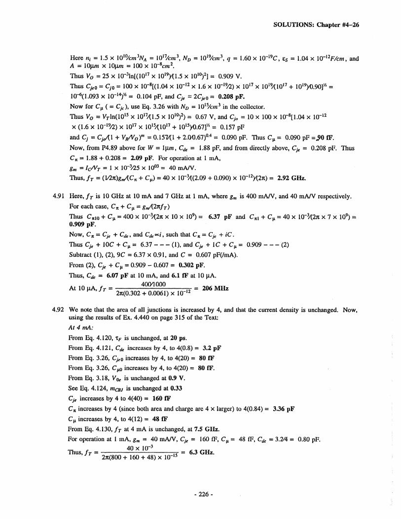
SOLUTIONS: Chapter #4-26
Here tij = 1.5 x 10l0/cmiNA = 10l7/cm3, ND = 10l9/cm3, q = 1.60 X 10⁻¹⁹C, ts — 1-04 X 10~12F/cm, andA = lOjxm x 10pm = 100 x 10~8cm2.Thus V0 = 25 X 10_3ln[(1017 x 10,9K1.5 x 1010)2] = 0.909 V.
Thus Cje0 = Cj0 = 100 x 10_8t(l.04 x 10"12 X 1.6 x 10"l9/2) X 1017 x 10l9/(1017 + lO'ÿ.OOf1=10~6(1.093 x lO-14)" = 0.104 pF, and Cje = 2CJe0 = 0.208 pF.Now for ( = Cjc), use Eq. 3.26 with ND = 10ls/cm3 in the collector.
Thus V0 = Vrln(10ls x 10l7/C1.5 X 1010)2) = 0.67 V, and Cjo = 10 x 100 X 10"8[1.04 x 10"12X (1.6 X 10",9/2) x 10'7 x 10l5/(1017 + 10l5>0.67]/' = 0.157 pF
and Cj = CjA1+ VR/V0)'" = 0.157/(1 + 2.00.67)04 = 0.090 pF. Thus = 0.090 pF =ÿ0 fF.Now, from P4.89 above for W = l|i»i, = 1.88 pF, and from directly above, CJe = 0.208 pF. Thus
CK = 1.88 + 0.208 = 2.09 pF. For operation at 1 mA,
gm = lcWT = 1 x 10"3/25 x 10°3 = 40 mfiJV.
Thus, fT = (]/2n)g„/(CK + CV) = 40 X 10"X(2.09 + 0.090) X 10~l2K27i) = 2.92 GHz.
4.91 Here,fT is 10 GHz at 10 mA and 7 GHz at 1mA, where gm is 400 mA/V, and 40 mA/V respectively.
For each case, Cre + =gmA2itfx)
Thus CKio + Cn = 400 x lO'ÿnx 10 x 109) = 6.37 pF and CKl + = 40 x \Qr\2n x 7 x 109) =0.909 pF.
Now, Cn = Cje + Cje> and Cje°<i, such that CK = Cje + iC.Thus Cj, + 10C + = 6.37 ---(1), and Cje + 1C + = 0.909 ---(2)
Subtract (1), (2), 9C = 6.37 X 0.91, and C = 0.607 pF(/mA).
From (2), Cje + CM = 0.909 - 0.607 = 0.302 pF.
Thus, = 6.07 pF at 10 mA, and 6.1 fF at 10 pA.40CKI000
2n(0.302 + 0.0061) x 10"At 10 pA,fx = — _|2 = 206 MHz
4.92 We note that the area of all junctions is increased by 4, and that the current density is unchanged. Now,using the results of Ex. 4.440 on page 315 of the Text:
At 4 mA:
From Eq. 4.120, xF is unchanged, at 20 ps.
From Eq. 4.121, Cje increases by 4, to 4(0.8) = 3.2 pF
From Eq. 3.26, Cjeo increases by 4, to 4(20) = 80 fFFrom Eq. 3.26, Cÿo increases by 4, to 4(20) = 80 fF.
From Eq. 3.18, V0c is unchanged at 0.9 V.
See Eq. 4.124, mcaj is unchanged at 0.33
Cje increases by 4 to 4(40) = 160 fF
C,iincreases by 4 (since both area and charge are 4 x larger) to 4(0.84) = 3.36 pF
increases by 4, to 4(12) = 48 fF
From Eq. 4.130, fx at 4 mA is unchanged, at 7.5 GHz.
For operation at 1 mA, gm = 40 mA/V, Cje = 160 fF, = 48 fF, Qt = 3.2/4 = 0.80 pF.
TU 40 X 10"3 ,„ YYThus, fx —-rr = 6.3 GHz.2ji(800 + 160 + 48) x 10~15
-226-

SOLUTIONS: Chapter #4-27
4.93 For this transistor, = 2 pF and CK = 10.7 pF at 1 mA. If we assume that Cje -0ÿ=2 pF, ThenCJe = 10.7 - 2 = 8.7 pF at 1 mA, and 8.7/100 = 87 fF at 1 mA/100 = 10 pA, and 8.7 pF at 1 pA.. .n . , 40 x 10~Vl00At 10 pA, fx ~-pp = 15.6 MHz.
271(2.0 + 2.0 + .087) x 10~12
At 1pA, fT = n_mn
™ÿ . 77112 = 159 MHz
40 x lO'VlOOO2tc(2.0 + 2.0 + 0.009) x 10"
{Note that if Cje is assumed to be 0, rather than equal to Cÿ, fT values are 30.2 MHz and 3.17 MHz}.
The proposed change would reduce the capacitance Cÿ (and Cje) by a factor of 100 since the junctionareas are reduced by that factor. Continue to use Cjc = 8.7 pF at 1 mA for lack of a better choice.
Now at ic = 10 pA,40 x 10~3/100
fT ~-pp = 501 MHz.271(2100 + 2100 + 8.7/100) x 10~12
Now at 1 ic = lpA ,40 x 10~3/l000
fx =-pp = 131MHzJ271(2100 + 2400 + 8.7/1000) x 10"12
- 227-

SOLUTIONS: Chapter #4-28
NOTES
- 228 -

Chapter 5
FIELD-EFFECT TRANSISTORS (FETs)
SECTION 5.1: STRUCTURE AND PHYSICAL OPERATION OF THEENHANCEMENT-TYPE MOSFET
5.1 In general, a channel is induced for x>Gs ÿ t>s + V, = 0 + 1.5V. Hence Uqs 2: 1.5V, here.
In general, the drain end of the channel is pinched off for uCD £ V, = 1.5V. Now for vGS = 3.0V andVs = 0, X)G = 3.0V, and the drain is pinched off for uD > 3.0 -1.5 = 1.5V. Hence uDS £ 1.5V, here.
In general, saturation occurs for a given x>Gs, when vDS £ vGS - V,, or \)DS > 3.0V -1.5V = 1.5V, forwhich x>D 2: 1.5V, here (which is, of course, when the drain end of the channel is pinched off).
Ingeneral, triode operation occurs for uDS < x>Gs - V,, for which Up ÿ 1.5V, here.
(a) \)ds = x>d — \>s =2.1 — 0 = 2.1V; x>G$ — x>G — x>s — 3 — 0 — 3V; x>Gs — V, = 3 — 1 — 2.0V ÿ \>ps
-» saturated mode.
(b) Vds = v»o —\)s — —0.1 --2 = 1.9V; x>Gs = x>G — x>s — 2 --2 = 4V; Dcs — V, = 4 — 2 = 2.0 ÿ
vDS —» triode mode.
(c) x>sd = Vs - \>d = 0 --3 = 3V; vSg = Vs ~ % = 0 —1 = IV <|V, |= 2V -» cutoff mode.
(d) \>sd =Vs - \)p = 2 --1 = 3V; - i>g = 2 - 0 = 2V; + V, = 2-1= IV < msd -»saturated mode.
(e) V, = 2V —> n channel; vGs =0 --3 = 3V; Since saturated, X)ps ÿ Dcs -V, = 3- 2= IV;
vD = VpS + vs > I- 3 = -2V.
(f) V, = —2V -» p channel; vSp = t)j - vD = 3 —1= 4V; \)JG = Vs - x>G = 3 -0 = 3V; vSG + V, =3 -2 = IV < Ojo —» saturated mode.
(g) V, = -2V -> p channel; t)s = 3V, t)0 = -3V; - vG < -V, = + 2V for cutoff;
-t»G £ 2 -% = 2 -3 = -IV, and uG ÿ IV.
SECTION 5.2: CURRENT-VOLTAGE CHRACTERISTICS OF THEENHANCEMENT MOSFET
5.3 Id(mA)Vds s l*OJ ~ Vi
Triode ÿ Icregion * /
vcs ~ VrSaturation region
Since V, = IV, the uGsare relabelled as shown.See iDa = 2.25 mA, \)GSb =4 V, Ddsc — > 3 V, ij),) = 1mA, iDe = 5 mA, iDf =0.75 mA, \>QSg = 5 V,t>DSH = 2 V.

SOLUTIONS: Chapter #5-2
5.4ijj (mA)
(0 (a) (c)I 8 2 4
CaHW(e)vDs ÿ vcs - V,
Triode
0-5 H i j
2 as i
Mi¬tel
VDS s l'CS *~ KrSaturation region->
l'cs ™ V'/ + 4 5 q.5 3 2..5
vos - V, + 3 ,Lj 3.5 2.5 -2.
- veJ = v, + 2 3 2.5 '2 \.s
O O o>— o
". l'CJ -V.+ 1 2. 1.5 l.s I1 2 3.4 5 6 7 il»(V)£ I 0-5 I " 0-S
• 8 \9* 3 4 Vta*r,(cutoff)
(SXt)
The axes labels are indicated by (a), (b), etc, at the top right and left, and at the right bottom.
5.5 Vs = 0V, VG = 3V. Now, for saturation VDS S VGS - V,. and for V5 = 0, VD £ 3 - 1 = 2V. Thus thedevice is in triode operation for VD < 2V.
In general, in triode mode, = &(VV/L)[(uG,s - V,) vDS - 2d]).
For vDS = 2V, iD = 20 X 1(T6 X 10 [(3 - 1) 2 - 22/l] = 200 ( (2) (2) -22/2) = 200 ( 4 - 2) = 400)lA.
Check, in saturation, iD = 1/2(20)(10) (vGg - V,)2 = 100 (3 - l)2 = 400(xA.
For vDS = IV, iD = 200 [(2) 1- \2/l] = 300|xA.
For x>ds = 0.5V, iD = 200 ((2) 0.5 - 0.52/2) = 175pA.
For x>DS very small, iD = k'(W/L) (vGS - V,) VDS, whence
vDs 1 1rDS ~
iD k'(W/L) (vGS - V,) 200 (3 - 1) = 2.5kQ.
Now, rDS increases by 1% when D5y2 = ((vcs - V,) %) -777, for which vDS =2 (3 - 1)
Now rDS increases by 10% when
1001
1000.04V.
= 1.101
or((Vas — V,) \>os — t)oy2) (Dg5 — V, )x>ds
(vGS - V.) - vDS/2 = 0.909 ((vGS ~ V)), for which, vDS =2 (1- 0.909) (vGS - V,) = 2 (0.091) (3 - 1)
= 0.36V.
5.6 For triode operation at low vDs> 1d =k (W/L) ((vGS - V,) vDS), whence
rDS - Vds 1 10"20(202) (t)GS - 1)
, or rDS5000Q
t)Gs - 1'iD k'(W/L) ((vGS - V,))5kCI .
whence vGs =-+ 1.rDS
For rDS = lktt: vGS = y + 1= 6V, and for rDS = 1MI2: uGS = + 1 = 1.005V.I lu /Ca6
- 230-

SOLUTIONS: Chapter #5-3
For x>DS near OV, and less than a 10% increase in rDS, (x>cs - 1) - \)DS/2 > -yy( vGS ~ 1). or
Uds ÿ 2 (\)OT - 1) (0.0909).
For rDS = lkft , x>Gs = 6V, and \>ds ÿ 2 (6 - 1) (.0909) = 0.909V, at whichiD = k'(W/L) [(oGJ - V,)uOJ - vÿs/1] = 200 ((6 - 1) 0.909 -(0.0909)2/2) = 200 (4.545) - .413) =826|iA.
For rDS = 1MQ, VGS = 1.005V, and \)DS < 2 (1.005 - 1.00) (.0909) = 0.91 raV, at which iD = 200t(1.005 - 1) (0.91 x 10~3) - (.91 x 10"3)2/2] = 200 [ (5 x 0.91 x 10"6) - 0.912 x 10"6/2] = 100 (9.1 x10⁻⁶ - .83 x 10~6) = 827 x 10~6|iA = 0.83nA! or, easier, iD = ~ 0.91 nA, as a quick approx¬
imation.
5.7 For saturation, iDj = V2k'{W/L) (vGS - V,)2, and for triodc operation,
For ipÿ = 1.00iDxs: <d( = k (W/L) [(oGS — V,) \>os — VEmÿL
k\W/L) [(Uos - V,) vDS - Doy2] = k'2(W/L) (x>as - V,)2, or vGs - 2 (%) (\)GiS - V,) + (uG.? - V,)2 =0,
2 (Mas - V,) ± V 22 (mGs ~ V,)2 - 4 (uGS - V,)2whence \)DS =---,
or Vim = (Vgs — V,)[l ± ÿ1 - 1] = (uspilonGS - V,)
For iD, = 0.99 iDs :2 (Ugs — V,) Vps — Vps — 0,99 (y>Gs — V,)2, or Vps — 2 (vDS) (vGs — V,) + 0.99 (oG.s — V,)2 = 0,
1± V 1- (,99)2 Jwhence vDS = (vGS - V,)
applies). Thus dds = 0.859 (uGs - V,).
1 ± V 1 - ,92
(vGS - V,) (1 ± 0.141), (where the negative value
For iD, = 0.90 iDs : vDS = (yGS - V, )
For io, = 0.50 iGs 'ÿ Dds — (Vm ~ V, ) 1±Vj
. Thus uDS = 0.564 (uGS - V,).
. Thus t>os — 0.134 (oGs — Vt).
Now, for oGS = 2 V, and V, = 2V, X>DS = 2V, 1.72V, 1.13V, and 0.264V, for 100%, 99%, 90%, and 50%of saturation value, respectively.
5.8 Here, r„ = —- = 50k"; Va = r° = 50kfl
0.0093V-'.
2.1 + 2.2= 107.5V; and X, = -)-
'A
5.9 Now Kp = yPp Cox -p Assuming p.,, = j p„, Kp = y x y x 20 x -p- - 166.7pAIV2.
For vGS = vDS = -5V, iD = K (oG5 - V,)2 (l+X vDS) = 166.7 (-5 - -2)2 (1 - ,01(-5)) = 166.7 (32)(1.05) = 1.575mA.
5.10 For the substrate Vn of the PMOS connected to +5V. while the source voltage is varied:IV,I = IV,ol + Y N2 <bf + VSB - V 2 Of] = + 1 + 0.6 [V 0.6 + VSB - -fo.6). For Vs = +5V, VSB =
0V, and IV,I = IV, or V, = -1 V. For Vs = 0V, VSB = 5 - 0 = 5V, and IV,I =1+0.6[V 0.6 + 5 - ÿ0ÿ6] = 1.955V, or V, = -1.96 V.
5.11 In each of the circuits, consider the saturation transconductance factor isK = V2\an Cox(W/L) = 1/2 X 20 X 10"6(202) = 100|WV2= OAmAA/2. Accordingly: (a) vGS =% =5V; saturated operation, for which iD = K (\)GS - V,)2 = 0.1 (5 - 2)2 = 0.9mA. Thus Ia = 0.9mA.
- 231 -

SOLUTIONS: Chapter #5-4
(b) v>,sG = x>sd ', saturated operation, for which 0.4 = 0.1 (x>SG --2)2, or x>SG + 2 =± V~4 = ± 2. ThusVsc = 0. which is not possible, or -4V. Thus Vb = +4V.
(c) V'g.s = 0; cutoff, for which Ic = OmA.
(d) 0G,S = \), X>DG = 3V; saturated operation, for which iD = 0.9 = 0.1 (v - 2)2, or v - 2 = "ÿ9 = 3, or v= 5V. Thus Vj = vG -vGS = 2-5 = -3V.
Section 5.3: THE DEPLETION- TYPE MOSFET5.12 For all conditions, the saturatin transconductance factor is
K = V2\inCox(W/L) = 1/2 x 20 x 10-6 X 2002 = 1000 x 10~6 = 1/nA/V2; V, = —4V (for an n-channcldepletion mode).
(a) t)Ciy = -4 -0 = -4Y. cutoff. iD = OmA, and vDS = 5 - 0 = 5V.
(b) "0(7 = t)C5 + o.s = -2 + 0 = —2V, and Oy = o? +% = 0 + 3 = 3V. This implies saturation forwhich iD = (x>cs - V, )2 = 1 ( -2 —4)2 = 4mA.
(c) x>as -vG-vs = 0-0 - 0V, and vDS = vD - vs = 5 - 0 = 5V,
for which vDG = 5 - 0 = 5V > "1 V, I". This implies saturation operation, for which iD = 1 (0 --4)2 = 16mA.
(d) vG = x>gs + x>s = 0 + Q = OV, and = vs + vDS = 0 + 2 = 2V, for which VDG = 2 - 0 < IV,I .This implies triode operation, for which iD = K [2 (v>GS - V,) %- v%s] - 1 (2 (0--4) 2 - 22)= 12mA.
(e) Vs = vG - vGS = 0 - 1 = -IV, and vD = vs + vDS = -IV + 5V = 4V, for which vDG = vD - vG= 4V — 0 = IV,I . This implies operation at the edge of saturation, for which i'd = 1 (1 — -4)2 =25mA.
(0 VGS =vG-X)s = 2- 0 = 2V, and vDS =vD-vs = 5- 0 = 5V, for which vDG = vD - vG = 5 -2 = 3V < IV,I . This implies triode operation, for which, iD = K [2 (vGS - V,) Uns - = 1[2 (2 - -4) 5 - 52] = 60 - 25 = 35mA.
(i) = vgs + Vs = 2 + 0 = 2V, and vDS = vD - vs = 0- 0 = 0V. See that operation is in thetriode mode, but with ip = OmA.
(h) = vSG + vG = - 2 + 0 = -2V, and \)DJ = vD - vs = 0--2 = 2V. See that vDG =vD -v,
= 0 — 0 = 0<|V, | —> triode operation, for which iD = K r2 (vGS - V,) %- x>bs= 1 [2 (2 -- 4) 2 -22 ] = 24 - 4 = 20mA.
5.13 Depletion MOS: For simplicity, use K=V2\lnCox (W/L ) = 1/2(20 X 10 6)(10) = 100 X 10 6 = 0.1/nA/V2,IV,I = 2V.
(a) Saturation with Dcs = 0, for which la = in = K (dgÿ - V, )2 = 0.1 (0 - - 2)2 = 0.4mA.
(b) Saturation, for which 0.4 = 0.1 (X3GS - - 2)2, and vGS + 2 =±ÿ~4 = ±2V, whence vGS = -4V or0V. Clearly, 4V is not possible. Thus Vh = 0 - 0 = 0V.
(c) Saturation, for which 0.9 = 0.1 (vGS - - 2)2, and x>GS + 2 = ± ÿ~9 = ±3, for which x>GS = -5 or+1V —> Clearly —5V is not possible. Thus \)Gs = +1V, and Vc = 0 + IV = +1V.
1 18(d) Devices are connected symmetrically: Ij= — I= = 0.9mA. Also see saturated operation,
for which 0.9 = 0.1 (Ucs —2)2. Thus mgs = +1V (as in (c)), and Vj = +1V.
(e) Iÿere, Vps - VGs ÿ Thus = 0 < IV,I implies triode operation, for which iD = 0.4mA = 0.1
or 4 = 2 viGs + 4 Ugj — vGs, vGs + 4 vGs —4 = 0, whenceI2 Cues —2) vGS - vGs
- 4 ± V 42 _4f-4)i - 4 + 4 V~2 r—L±—Z.—2LJLLL - -L±-Z—± = -2 ± 2 V 2. But it must be positive. Thus = -2 +VgS ~
2 22<~2 = 0.828V, and Ve = 5 - .828 = 4.172V.
- 232 -

SOLUTIONS: Chapter #5-5
5.14 For convenience, let K = 1/21'(W/L). Operation is triode mode in both cases: ThusiD =K |2 (uG5 - V,) v>SD - Vsd , V, being negative for a p-channel depletion device, when X>SG isused.
For vD = 4.8V, v)yD = 5.0 - 4.8 = +0.2V, \>G = 5.0V, vGS = 5.0 - 5.0 = 0.0V;
0.1 = K \l (0 - V,) (+0.2) -0.22 ], or 0.1 = K [-0.4V, - 0.04 ] - - - (1).
For vD = 4.95, vSd = 5.0 - 4.95 = +.05V, vG = 0V, x>SG = 5 - 0 = +5V;
0.1 = K [2 (+5 - V,) (+.05) -.052 ], or 0.1 = K [+0.5 + 0.1V, - .0025 ],or 0.1= K [o.4975 + 0.1V, ] - - (2).
-0.4V, - 0.04Now (l)/(2) -+ 1 =
+0 4975 -,. Q1yÿ or "°-4 Vt ~ 04 = + 0.4975 + 0.1V,, or -0.5V, = +0.5375,
whence V, = -1.075V. Thus with \)Gy as defined, the depletion threshold is 1,075V.
From (1). 0.1 = AT [ -0.4V, -.04], K = ÿÿÿ04 = ÿ4ÿ = "ow. 4, =
K (Mas ~ V,)2 = bss (1 - -p-)2 = "P" (Vgs - V,)2. Thus IDSS = K V,2 = 0.256 x (1.075)2 =
0.296mA.
SECTION 5.4: MOSFET CIRCUITS AT DC
5.15 K = Kn =1\in Cox ~ = |(20) x 40 = 0.4mA/V2. Thus lD =Vd° ~ V°
= = 0.4mA. In2 L 2 Rd 7.5x£2
saturation, iD = K (vGs - V,)2, or 0.4 = 0.4 (vGS - l)2. Thus vGs -1 = 1. or uGS = 2V.n 1 117 A D
~ Vss _2 --5 3V innx>s = vG - vGS = 0 - 2 = -2V, and Rs =---= ——— = — = 7.5kl2.Ij) U.4 U.4
5.16 Now, ID =Vpp ~ V° - 1z2l- o.4mA, and Vy = -5 + 7.5(0.4) = -2V. Thus VGS = 2V, whence 0.4
Rd ) 7.5
= K (2 - l)2, and K = 0.4mA/V2.
Now for K = -p- = 0.2mA/V, in the source circuit: ÿ — = i0 = 0.2 (-Vy - l)2, or
Vy + 5 = 1.5 (Vy + l)2 = 1.5 Vs2 + 3Vy + 1, or 1.5V/ + 2Vy -4 = 0, whence
—2 ± V 22 - 4(-4) (1.5) -2 ± V 4 + 24 -2 ± 5.29 „ 11X „ „Vy =-
2 5—1=---=---= -2.43 or +1.10 (too small). Thus Vy =
2 43 — 2 00-2.43V, and VD = +2.43V, with a corresponding change of —— '— = 21.5%.
5.17 For Fig. 5.25, VDD = 10V, VD5 = VGy, and operation is in saturation. Thus VD = VD0 - ID R, or VG =10 - OAR. Also ID =K (VGy - V,)2, where K = V2\in Cox x W/L = Zi x 20 x 40 = 0.4mA/V2, and
10 — 9VGy = VD. Thus 0.4 = 0.4 (VD - l)2, or VD -1= 1, or VD = 2V. Thus R =
Q4 = 20kl2.
5.18 For VD = 2V, ID = = 20)tA.
Also ID = V2k\W/L) (vGS - V,)2 = 0.5 x 10"3 (\)Gy - l)2 = 20 x 10~6, or vGS - 1 = (40 x 10"3)'/' = 0.2,
whence uGy = 1.2V. Now, since VG = 5V, Vy = 5 -1.2 = 3.8V, see Rs = *?'** = 190kl2. Thus, to20pA
one significant digit, /?y = 200kl2.
- 233 -

SOLUTIONS: Chapter #5-6
Now, ID = 500 (VGS - l)2 and ID =5
or5 QÿC,y = 500 (uGS - l)2, or 5 - vGS = 100 x>GS
- 200 \)GS + 100, or 100 vj; - 199ÿ + 95 = 0,' or v&s - 1.99 VGS + 0.95 = 0, whence1.99±V 1.992- 4(.95) 1.99 ± V .1601 1.99 ±.4 , ÿ ,
vGs =-2-— =-
2-=-
2-= U95V' or < l- Thus' Vs = 5 -U95V
Q OQC= 3.805V, ID = = 19.025pA, and VD = 5 - .15 x 19.025 = 2.15V.
5,19 Vc = loJTlOM X 5V = 2,5V- N°W f0r Ucs = iD =5" U~2'5 = '• and = K {Vgs ~ V,) =
0.5 (\) - l)2, 0.5 (t) - l)2 = (u - l)2 = 5 - 2 \), D2 - 2t) + 1 = 5 - 2\), t>2 = 4,n> = 2V. Thus
Vs = VG + vGS = 2.5 + 2.0 = 4.5V, and iD =5 ~ 4-5
= 0.5mA, VD = 0 + 4k (0.5mA) = 2V.iK
90We actually find (2V) = 1.8V, in which case iD is reduced to 90% or 0.45mA.
For K = 1/2k(W/L) = 0.5mA/V2 and V, varying, 5 -lkfl (0.45mA) —uG.y = 2.5V, whence vgs = 5-0.45 -2.5 = 2.05V. Now, 0.45 = 0.5 (2.05 - V,)2, or V, - 2.05 = ± (0.90)* = +.949, whence V, = 2.05± .949 = 1.101V. That is, V, could have raised by 10.1%.
2 ,, 0.45For V, = IV and K varying, again vGS = 2.05V, but now, 0.45mA = AT (2.05 - l)2, or K =ÿ
0.408mA/V2. Thus K could have dropped byÿ = 18.4%.
Note that the effect of V, is essentially direct, a 10% change in current resulting from a 10% change inV,. However, the change in current is only about 10/18.4 or about 54% of that in K, due to negativefeedback included in the circuit. (See Chapter 8.)
5.20 For the Depletion Device, K = l/2\lpC„x(W/L) = 1/2(8 X 10-6)(50(V2) = 0.1m/l/V2 and x>Gs = 0.
Thus iD = Ipss = K{\)GS - V,)2 = lmA/F2(0 - 2)2 = 4mA. Thus V5 = 15 - lkfl (4mA) = 11V = VG,and VD = 0 + 2k12 (4mA) = 8V, whence x>SD = 11-8 = 3V>V,. Thus the device operates in saturatedmode.
Triode operation begins for uJD = V, = 2V, in which case VSs = 8 + 2 + 4 = 14V, with operation beingsaturated for Vss > 14V.
5.21 Here K = V2\ipCnx{W/L) = l/2(8)(250) = ImA/V2. See VG = jjj x 5 = 4V. Now vSG = 5 - lkfl
(iD) -4 = 1- iD, or iD = 1 - uSG = 1+ t)GS. Assuming saturation, iD = K {\>GS - V,)2 = 1 (uGS - 2)2,or 1+ t»Gis = (vGs — 2)2 = v2f — 4t)<7c + 4, or vG$ — 5x>Gs + 3 =
5 ±ÿ 52 - 4131 5 ± 3 610, whence uGJ =
J — = 2, or x>GS = 0.697V (or 4.305V (too large)). Now
Vs = VG - vGS = 4 - 0.697 = 3.30V, and VD = 0 +5~3-30 x 1 = 1.70V. Thus VDS = 1.70 - 3.30 =
-1.60V, and VGD = 4 -1.70 = 2.30V > V,. Thus, operation is in saturation.
5.22 For operation at ip = 150|xA in saturation, ip = (1/2)(X„ Cox (W/L)(x>Gs - V,)2or 150 X 10"6 = 0.5(20 x 10"6)(3ÿ2)(X)GS - l)2, or t)GJ - 1= 1*, whence \>GS 2 V.
Now Rt = ÿ ÿ = 20kQ. lfR2= R, = 20kQ, then vD2 = + 2 V (also).5-2150 x 10"
If M3 is joined to M2 with corresponding elements connected, then the current in R2 will tend to double.If R2 is reduced to 10 k£l, v>DS2 = Vpsi = 2 V.
- 234-

SOLUTIONS: Chapter #5-8
90 91 — 24 04 i—VA = 9616_ 9 091= 127V. From (1): 9.091 = 2 <K (1011127), whence K =
= 0.240mA/V2. Check: At 0.25mA, gain = 2 <244 10 II
-+ OK.
1271/4
9.091 1(10 II 127)
= 2 <06 x X 5®l = 4.804 V/V10 + 508
For an output distortion of 10%, as stated, from Eq 5.35, K u2t
ÿgs - 5 (0.5) = 2.5V.10 u„
(VGS -V,)--= 5o,
102K (Vas - V,) x>„, or
5.28 Generally. K = V2k'{W/L) = 2/2= 1niA/V1. lD = ZmA, I=K (x>GS - V,)2 = 1 (VD - l)2.
VD = (< + 1)V, gm = 2K (vGS - Vt) = 2 (V0 - 1) = 2 <1mA/V, r„ = Vÿ/7 = 504 kO, whence — =Rg 104
-fa II Rg II r0 = -gm Rl = -2R<~1 V/V, and /?, = ---= , r-1 -gam 1+ 2RV IRl=Rg: d>(- = -2 <* (/?c II /?c II r„) = -2 X (104 II 104 1| 50) = -100V/V, /?, ~
104
kO. For I= 1mA and
104, " = 99kO.1+ 100
For Rl = r„: \)>,- = -2 (104 II 50 1| 50) = -50V/V, /?, = = 196kO. For RL = /?,: Vb, =104-2 (104 II 50 II Ri) ~ -2 (50 II /?,), /?, = 1+ 2 (50 II Ri)
,or
/?, 1+ 2(50)/?,
50 + /?,= 104, Rj +
100 Rj
Ri +50104, Rÿ + 50 Rt + 100 Ri2 = 104 Ri + 50 x 104,
101/?,2 - 9950 Ri - 50 x 104 = 0, /?,-2 - 98.5 /?, - 4950 = 0, whence /?, =98-5 ± V 9852 4 ( 495°) _
98.5 ± 171.8= 135kO, and o/o,- = -2 (50 II 135) = -73.0V/V.
5.29 Note that while the lower end of r„ is not actually grounded, the signal there is small. Assume it to be„ „ 11rt . Rc H Rl II r„ 10 II 10 II 100 -4.76 „zero. For Rs = lk£2, gain -=--—--— ---—---= —-— = -2.38V/V. For Rs =
Vi 1/gm+Rs 1A + I 2v„ -4 76 -4 76
Oft, gain y- = — = -4.76V/V. For Rs = 3.76kG, gain -y- = = -1V/V.
5.30 For the T-model, the equivalent resistor in the source is r, = Vgm = \A).725mA/V = 1.38 kfli. The out¬put resistance of the follower (with body effect ignored) is Rou, = r„ II rs = 47 II 1.38 = 1.34kf2.
47Thus, the no-load gain is Go = j 33 + 47
= V/V.
For load RL, the gain is G = (Rl/[Rl + Roul)) x G0 for which GRL + GRout = G0RL, andRl = GR„„AG0 -G).
For G = 0.95 V/V, RL = 0.99(1.34X0.971 = 0.95) = 63kG.
For G = 0.90 V/V, RL = 0.90(1.34X0.971 - 0.90) = 17.0kO.
5.31 For the situation in which Is is fixed, the gm of the transistor is independent of V, : This follows fromthe fact that: iD = ]/2k'(W/L)(vcs - V,)2, gm = Oi/yOucs, or
gm = V2(2)k'(W/L)(vGS = V,) = k\W/L){2iDA\W/L)f. Thus gm = (2k'(W/L)iD)y\ depending only on
'o - is-Now, for x = 0.2, gni/, = 0.2 (0.725) = 0.145 mA/V. Thus the additional load on the source isVgmb = IX).145 = 6.90 kQ.
- 235 -

SOLUTIONS: Chapter #5-7
SECTION 5.5: THE MOSFET AS AN AMPLIFIER5.23 Here iD = V2k'(W/L)(vGS - V,)2 = 0.5(2 x 10"3)(5 - I)2= 9 mA, and
md = VDD - iDRD = 12- 0.5 x 10³(9 x 10~3) = 7.5 V.
For \)GS = 5 + 0.5 = 5.5 V, iD = 1(5.5 - 2)2 = 12.25 mA, and for vGS = 5 - 0.5 = 4.5 V,
iD = 1(4.5 - )2 = 6.25 mA.
That is, current reduces by 9 — 6.25 = 2.75 mA, or increases by 12.25 — 9 = 3.25 mA.
Total variation in drain current is 2.75 + 3.25 = 6.0 mA.
Thus Vj = idRp = 6.0mA x 0.5kCl = 3.0 V. [Note that the gain is - 2/(2 x 0.5) = - 3.0 V/V.]
5.24 Here, from P5.23 above, K = V2k'(W/L) = 1/2(2) = 1niA/V2.For v>s-v = ± 0.5V, and VGS = 5 V, the largest value of x>GS is 5 + 0.5 = 5.5 V for which iD = 12.25mA. For saturation, the smallest value of vDS is x>GS - V, = 5.5 - 2 = 3.5 V. Thus the largest value ofRp that can be used is Rp = (12 — 35/12.25 = 694£2.
Now, for a 1 kfl load resistor, and dgs = 5.5 V, operation is in the triode mode where
iD = K(2(vgs - V,)\)DS -vis), and iD = (VDD -DDSyRL. Now with vDS =v, for simplicity,(12 -uyi = 1(2(5.5 - 2)u - u2), or 12 - U = 7u - u2, or u2 - 8\> + 12 = 0.
Thus v = (- - 8 ±ÿ82 - 4(12)>2 = (8 ± ÿ64 - 482 = (8 ± 4>2 = 2 V. Thus = 2 V.
Now for zero signal, X)Gs = 5 V, ip = 9 mA, and x>DS — 12 - S/l = 3 V, with operation just at the edgeof saturation. Correspondingly, the negative output swing for a + 0.5 V input is 3-— 2" = IV.
For a — 0.5 V signal, •oGs = 4.5 V, ip = 6.25 mA and uÿy = 12 - 6.25(1) = 5.75 V, with output swingfor — 0.5 V input being 5.75 — 3 = 2.75 V. Thus the ratio of peak voltage outputs is 2.75 to 1 or 2.75V/V.
5.25 K = V2k'(W/L) = ImA/V2, V, = 2V, VDD = 12V, RL = 0.5kO, x>Gs = 5V ± 0.5V. ThusiD = K (\)GS - V,)2 = 1 (5 -2)2 = 9mA, and x>D = VDD - RD iD - 12 - 0.5(9) = 7.5V. See, from Eq.5.44, that gm =2ÿ~K <~ID =2<~lf9 = 6mA/V. From Eq 5.43, g,„ = 2K (Vcs - V,) = 2(1)(5 - 2) =6mA/V, in correspondence. From Eq 5.40, = -g„, Rp = -6mA/V (0.5k£2) = -3.0V/V. For a±0.5V input, expect a ±0.5(-3.0) = +1.5V output signal. From Eq 5.35,ip = /if [(Vcs - V,)2 + 2K (Vas - V,) + /ft)2]. Thus for vgs = ±0.5V, iu = 1 (5 - 2)2 + 2 (1) (5 -2) 0.5 + (1) 0.52 = 9 + 3 + 0.25 = 12.25mA, for which VD = 12 - 0.5 (12.25) = +5.875V, and iD = 1 (5
- 2)2 + 2 (1) (5 - 2) (-0.5) + (1) (-015)2 = 9 - 3 + 0.25 = 6.25mA, for which Dp = 12 - 0.5 (6.25) =8.875V. This is to be contrasted with 7.5 — 1.5 = 6.0V, and 7.5 + 1.5 = 9.0V, as calculated from alinearized model.
5.26 Kp = jHp Cox jr = j- (10) (300/3) = 500pA/V2. g„, =2<~K<~ID from Eq 5.4 or
gm = 2 "ÿ0.500 M= 2 ÿ2 = 2.83mA/V. Generally, gain = -gm RL = -10V/V implies that
Rl = = 3.53kf2. Operation is reasonably linear for x>gs « 2 (VGS - V,), but Ip =gm 2.83 - -
K (Vr* - V,)2 -> (VGS - V,) = ilp/K . Thus, linear for x>gs <<2 (VGS -V,) = 2 Hlp/K , that is Dgs << 2 wOJ = 2 ÿ8 = 5.66V. For 1% nonlinearity, vgs= 0.06V peak. For 10% nonlincarity us.v~ 0.6Vpeak.
5.27 Gain = -gm (RL II r„), where gm = 2 V/f Ip, and /-„ = . Now, at 1mA, 9.091 = 2 ÿK(l)'i?
10k II Va_1 ---(1), and at 0.25mA, 4.808 = 2 ÿK/A
1ovA
10/: ||1/4 ---(2). Thus (l)/(2)
9.091 10 + VA 141/4+10
10+ 4 VA4.808 10 VA (4) 2 VA + 10
J &
. whence 9.091VA + 90.91 = 9.616V), + 24.040, and

SOLUTIONS: Chapter #5-9
Now the follower output resistance is 1.34/:£2 II 6.90k£2 = 1.12 k£2 amd the no-load gain is6.90 II 47 0 814V/V
" 1.38 + 6.901147For a gain of 50%, 0.5 = 0.814 x RlARl + 112) or 0.50/?,. + 0.56 = 0.814RL, or 0.314/?,, = 0.56 orRl = 1.78 k£2
SECTION 5.6: BIASING INMOS AMPLIFIER CIRCUITS5.32
+9V
10MQ
10MQ
10kQ
10k£2
For this device, V, = 2V, K = V2k (W/L) = 0.5mA/V2. Assumesaturation: For V, = 2V, VG = 1/2 (9) = 4.5V, 7 = K(x>GS - V,f =0-5 (t)Gs - 2)2 ---(1), and x>GS = 4.5 - 10 7 ---(2). Sub¬stitute (2) in (1) —> 2 / = (4.5 - 10 / - 2)2 = (2.5 - 10 7)2 = 6.25 -507 + 100 I2, or 100 I2- 52 / + 6.25 = 0,
, 52 ± V 522 - 4 (100) (6.25) . ,whence I=-ÿ (100)— — = 0.189mA, (or too large a
value). % = 10k (0.189) = 1.89V, \)GS = 4.5 -1.89 = 2.61V, vD =9 - (10K£2) (0.189mA) = 9 -1.89 = 7.11V, and vDS = 7.11 -1.89 =5.22V -» OK, saturation. Operation remains in saturation untilvGD k V, = 2V, ie, for vGS = 2.61V, and vDS k 2.61 - 2 = 0.61V.Thus the peak negative-going output signal allowed is 7.11 -(1.89 +0.61) = 4.61V. But note that the largest positive-going output sig¬nal (for cutoff) is 1.89V.
Now, For V, = IV, / = 0.5 (vGS - if,and x>GS = 4.5 - 107. 27 =(4.5 -10 7 -l)2 = (3.5 - 107)2 = 12.25 - 707 + 10072, and 10072 -727 + 12.25 = 0.
Thus 7 =72 ± 722 JL(1°°) (12-25)
= 0.276mA. \>s = 10 (.276) = 2.76V, vGS = 4.5 - 2.76 =200
1.74V, Vp = 9 - 2.76 = 6.24V, Vps - 6.24 - 2.76 = 3.48V. Now, saturation prevails while vGs £ 1.0V.Thus the maximum negative swing is 6.24 - 4.5 + 1 = 2.74V. The largest positive-going output signal(for cutoff) is 9 - 6.24 = 2.76V.
5.33
j.O\/
4.166 - 3.291.75
The design is required to endure the following variations: V, from 1to 2V, K from 0.3 to 0.5mA/V2, and ID from 0.5 to 1mA: Largestcurrent occurs when V, smallest (IV) and K largest (0.5mA/V2).Thus 1 = 0.5 (\>gs " l)2. or vGS -±ÿ2 + 1 = 2.414V ---(1).Smallest current when V, largest (2V) and K smallest (0.3mA/V2).Thus 0.5 = 0.3 (Ogs - 2)2, and vGS =€67 + 2 = 1.29 + 2 =
VGG - 2.4143.29V ---(2). From (1), „-= 1mA, where 7? =RS.
From (2),Vco ~ 3.29
R
R
= 0.5mA. See VGG - 2.414 = 7?, and 2 VGG -6.58 = 7?. Subtracting, -VGG + 4.166 = 0 —» VGG = 4.166V. For
VGG = 4.166V, 7?gi = 10M £2, 7?G2 = 4.166ÿ9 "jÿ166 ) = 8.6M£2
(Use 8.2 M£2), and Rs = R = 4.166 - 2.414 = 1.75k£2 (Use 1.8 k£2).
= 0.507mA. Now for /„ = 1mA, V, = IV, and a 0.5V signal, x>p > VGG - V,.Check:l./*>
That is, i)D > 4.166 - 1.0 = 3.166, and 7?„ =9 ~ (3j66 + °-5) - 5.33k£2. (Use 5.1k£2).
1mA
-236-

SOLUTIONS: Chapter #5-10
5.34
+9V For V, = 2V, and k'(W/L) = 1.0mA/V2, iD = Vlk{W/L) (vGS - V,)2,
= l/2(l)(t>GS = 2)2 =0.5(t)GS -2)2, and iD =9 ~ÿ . Thus.— , 20«i2
10MQ 20kn 9 -DCS = 20 (0.5) (uGS - 2)2, 9 - Ugs = 10 vG.s - 40 VGS + 40,
10 - 39 oGS + 31 = 0, whence ÿ =39 ± V 392 4 (10) (31)
9 - 2 79= 2.79V. vDS = 2.79V, and ID = —ÿ— = 0.311mA. For nega¬
tive peak outputs of up to 2Vp, operation remains in saturation. For
V, = IV, iD = 0.5 (t)G5 - l)2, and iD2 ----ÿ • 9~"GS20
9 — vGs = 10 (uG5 — l)2 = 10 "0Gs — 20 \>Gs + 10, and 10 vGs — 19 dGj + 1= 0, whence mGs =19 ±V 192 — 4 (10) (1) 19 ±17.9 , , 9-1.85 „ A-27Io)-=-20
-= 1>845V- Thus VDS = 1.85V, ID =-—-= 0.358mA, with a
IV peak signal allowed.
5.35 For RG2 = 10MI2 from gate to source, Vps = 2 x>GS . For V, = 2V, iD = l/2(1.0)(\)GS - 2)2 and
'0 =-2q-• Thus 9 — 2 vGs = 10 (y>Gs — 2)2 = 10 uG5 — 40 x>Gs + 40, and 10 dGj — 38 vGs + 31
„ . 38 ± ÿ 3S2 — 4 (10) <31) 38 ±14.28= "to™ --2(10) --20— = 2'61V'
9 - 5 22Thus x>DS = 5.22V, and 1D = ——ÿ— = 0.189mA. For negative peak outputs, 5.22 -2.61 + 2 = 4.61V
is allowed for operation in saturation.
For V, = IV, iD = 0.5 (vGS - l)2 and iD = • Thus 9 - 2 t)GS = 10 (vGS - l)2 =
in 2 on m Jin 2 10 1 n u 18 182 - 40 18 ±16.8510 dG5 — 20 uGs + 10, and 10 x>Gs — 18 x>Gs + 1=0,whence \>G$ --—-=-—-=
9 - 3 481.74V. Thus "Ops = 3.48V and ID = ——— = 0.276mA, with 3.48 -1.74 + 2 = 3.74V negative output
peaks allowed, while saturated operation prevails.
5.36+5V
iomh
Here, V, varies from 1 to 2V, K = 1/2k(W/L) varies from 0.3 to0.5mA/V2, ID varies from 0.5 to 1mA. The largest current (1mA)occurs for the smallest V, (IV), and largest K (0.5mA/V2). Thus
5 — 2 4141= 0.5 (t)GS - l)2. uGJ = 2.414V, and R > , , > 2.59kfl.
1mAThe smallest current (0.5mA) occurs for the largest V, (2V) and smal¬lest K (0.3mA/V2). Thus 0.5 = 0.3 (v>GS - 2)2. x>GS = "*L67 + 2 =
5 - 3 29 2 59 + 3 423.29V, and R < < 3.42kfl. Use R = ÿ = 3.0kft.
Because of feedback, the effect of variation is reduced.
The circuit automatically allows a negative signal = V, > IV but the gain is smaller than in P 5.33, sinceR here (3.0kI2) is less than RD there (5.2kQ). Raising R to (say) 3.3kH would be allowed here, andwould improve the gain by 10%.
5.37 In P5.36 above, the minimum negative-going signal is IV. Here it should be 1.5V. That is, we want
x>os - vGs + 0.5V for the case in which V, = IV.
- 237 -

SOLUTIONS: Chapter #5-11
For smallest V, (and also the largest current), from the results inP5.36, \)CS = 2.414V, and vDS = 2.414 + 0.5 = 2.914, with
5-2914 inR > ÿ = 2.09k£2. If we use RG2 = 10MO, RGl =(0.5) = 2.07MQ. Use RGi = 2.0MO. Now for V, = 2V (and also thesmallest current), from the solution for P5.36 we see, vGS = 3.29V,
3 29 5 — 3 95and vDS = x 2.0 + 3.29 = 3.95V. Thus R < Q 5
< 2.1k12.
Notice that a solution barely exists, using R = 2.1kQ, essentially as aconsequence of a demand for large signal swings with a limited sup¬ply voltage.
Here, Vp = -4V, IDSS = 32mA. For /c = 8mA, 8 = 32 (1 - )2."p
Thus (1- )2 = 1/4, - = ± 1/2 -1= -1.5 or -0.5, and VGSvp vp= 0.5Vp = -2V. Now for a negative swing of 2V to the edge ofsaturation, x>D > vG + | V, | . Now for the largest possible value ofRG, \)g will be lowest and \>G lowest. The lowest possible x>G is 0V,with Rgi= oo and RG2 = 10M£2, in which case Rs = 2V/8mA =0.25kf2, and VG ÿ 0 + 4 = 4V for lowest swing or-4 + 2 = 6V for nosignal, with RD £ 9-6/8 = 0.375kf2. Note that for a 2V positive out¬put swing, VG rises to 6 + 2V = 8V, and the transistor is not yet cutoff. OK. Note that this design with no biassing supply is relativelysensitive to device variability, all as a result of wanting a large signalswing with a small supply.
5.39 Here, iD = Vl\LnCnx(W/L){x>GS - V,)2 = 1/2 X 20 x 10"6(42)(2.5 - l)2= 45pA .Thus, assuming the Early effect to be negligible, Q2 operates at 45 pA. For a 5 V supplyR = (5 - 2.5)445 X 10"6) = 55.6 k£2.
Transistor Q2 remains in saturation for i)0 > (vGS - V,) = 2.5 - 1 = 1.5 V or > 1.5V.
In triode mode, «0 = \i„Cox(W/L)[(\)Gs - V, )x>Ds - 1)0/2]. Now for iD reduced to half, for vDS =x>,452 = 20(42)[(2.5 - 1)\) - d2/2], or 0.5625 = 1.5o- \>2/l, or o2 - 3u + 1.125 = 0, whence
u = (- - 3 ±ÿ32- 4(1.125)YZ = (3 ± 2.121)2 = 0.439 V.
Thus the current reduces to 1/2 normal for Vps — = 0.439 V.
Check: iD = 20 x 2[(2.5 - 1)(.439) - .4392/2] = 22.5 pA.
5.40 For a 1Mil output resistance at 100 pA output, VA = 106 x 100 x 10"6 = 100 V. This requires that theoutput transistor have a channel length L = lOOV/lOV/pm = 10pm. Use this for both transistors. Forthe edge of saturation at x>0 = 0.5 V, uGs = 0-5 + V, = 1.5 V. Now for Qt, 25 = 20(W/10)(1.5 - l)2,or IV, = 25 X 10410(0.5)2) = 100pm.
Correspondingly, IV2 = (10025)W, = 4(100) = 400pm. The output current will be exactly 100 pA whenQ, and Q2 operate identically, with x>DS = vGS = 1.5 V and v0 is 1.5 V above the negative supply. Foroperation at 0)0 = 5 V above the negative supply,
i0 = 100 x 10"6 + (5 - 1.5yi06 = 103.5pA.
RGI
5.38
+9V
RGI
RG2
- 238 -

SOLUTIONS: Chapter #5-12
S5-41(a)
Topology A: This design is relatively straightforward, except that it p-channel devices operating at twicethe current density of the n-channei. Widths are as indicated: 8 transistors arc needed. The total widthof the NMOS is XW„ = 4 +2+ 16 + 40 +4= 66pm. The PMOS width is TWp + 2 + 4 + 8 = 14p.m.If the same current density is used in the PMOS, the total PMOS width would be double, namely 2(14)= 28pm. Notice, incidentally, that neither of these designs, nor the others to follow, compensate for the
Pn/py, ratio r. For such compnesation, multiply all the PMOS widths by r.
Topology B: If both ends of Iref( - 10pA) are available:
+ VDD + VDD + VDD
x16
ix16 x40
VSSVSS - VSSVSS
This is a design for equal current densities in the PMOS and NMOS transistors: #T = 7, ZW„ = 62pm, XWp = 28 pm.
-239-

SOLUTIONS: Chapter #5-13
Topology C: The attempt here is to create the 5 (lA output separately without making all the othertransistors twice as large.
+ VDD +VDD +VDD + VDD
S5-41(c)
This uses 9 transistors but it is smaller: = 36 (J.ni and ZW,, = 16 (Im.
SECTION 5.7: BASIC CONFIGURATIONS OF SINGLE-STAGE "
IC MOS AMPLIFIERS5.42 For Fig. 5.44a):
Input: Operates at vGs = 2 V.
Output: Source saturates at 5 - 0.5 = 4.5 V; amplifier saturates at t)GS — V, = 2 - 1 = IV.
Overall: Input: 2 V. Output: 1V to 4.5 V.
For Fig. 5.44b):
Input: Operates at - 2 V.
Output: Operates from + 4.5 V to - 1V where the drain falls V, below the gate.
Overall: Input - 2 V . Output: — 1V to + 4.5 V.
For Fig. 5.44c):
Input: Saturation at O/ = 5 + 1= 6 V.
Output: Sink saturates at - 5 + 0.5 = - 4.5 V. Driver saturates at 5 + V, - VGS = 4 V.
Input: For output at - 4.5 V, input is limited to - 4.5 + 2.0 = - 2.5 V.
Overall: Input: — 2.5 V to + 6 V; Output: - 4.5 V to 4 V.
\VA I V jn 1)0015.43 Eq 5.101 indicates Av =--1-. Let I= IREF. For / = 25(iA: Av =--,-= -63.2V/V..-» Iref _ ÿ 25
For I= 2.5(iA: Au =--1)° (1°Q)= - 200V/V. For I= 0.25p.A: A„ =--*,° (100)
= -632VA'.ÿ2.5 Vo.25
5.44 For the diode-connected NMOS (call it Q4) of half the width of Q\, its width is also half that of Q$.Thus, Q4, Qi have the same k , and the same V,. Thus x>sg 3 = ÿ>sc2 = 5/2 = 2.5V.
Iref = 1 - (1/2) x 20 X (2.5 - l)2 = 112.5|xA, with a total supply current = 2 (112.5) = 225|iA.
For fit. i = 112.5 = (1/2) X 40 x 100/10 (l)GS - l)2 = 200(bGJ - l)2. Thus x>0 = vGS = 1 +
- 240-

SOLUTIONS: Chapter #5-16
5.48 (continued)
rl' S
'ik
loss
J IVtl
o >|V, |saturatedo <|V, j triodet) < 0 triode
t> > |V, |saturatedu < j V, j triodeÿo < 0 triode
5.49 Assuming no back-bias effect:
(a) Devices identical, V, = 5/2 = 2.5V, i= K (\>cs - V,)2 = 1 (2.5 - 2)2 = 0.25mA. Thus /, =0.25mA.
(b) Lower transistors operate as one with K = 2mA/V2. Here for V2 = t),
i= 1 (5 - \) -2)2 = 2 (o —2)2, (3 - o)2 = 2 (\> - 2)2, 3 - x> = ± <2 (v -2) = ± 1.414 o ± 2.828.Thus, 3 - t) = 1.414 o -2.828, or 3 - D = -1.414 v + 2.828. Correspondingly -2.414 x> = -5.828,o = 2.414V, for which i= 2 (2.414-2)2 = 0.343mA. Thus V2'= 2.414V, I2= 0.343mA.
(c) /3 operates at Ipss if the upper transistor is in saturation, in which case,i= K (VGS - V,)2 = 1 ( - -2)2 = 4mA = /3. Also i= K (uGS - V,)2, or 4 = 1 (uos - 2)2,vGs -2 =± 2, whence \)GS = 4V (which is too high to allow the upper transistor to saturate).
Thus, the upper is in triode mode, the lower in saturation. For o = V3,/ = K (2 (0 - -2) (5 - \>) - (5 - = K (m- 212. 20 - 4 \) - 25 + 10 \) - o2 = \)2 -Av + 4,
(d)
(e)
2o2 - lOo + 9 = 0, o =+10 ± y 102 - 4(2) (9) 10 ± 5.29
= 3.82V (or an impossibly low2(2) 4
value), for which / = 1 (3.82 - 2) = 3.31mA. Thus /3 = 3.31mA and V3 = 3.82V.
From Symmetry, V4 = 2.5V, and 14 - 1 (2.5 - 2)2 = 0.25mA.
From Symmetry, V5 = 5/2 = 2.5V, and /5 = 1 (2 (2.5 - -2) (2.5) -2.52) = 5 (4.5) - 2.52 =16.25mA.
5.50
•—1- dH
+5V
ÿi
Here V, = -IV, KD = 90pA/V2, and KL = 10|iA/V2. Ignoring thebody effect, and assuming both in saturation,:' =K (Dr.-? — V, )2. Forthe driver, gmD = 2Kn (t)ÿ -V,) = 2KD V i/KD - 2 V KD i. Forthe load, g„,L = 2 y KL i. Ignoring r„, (and back-bias effects), gain
1 2 V K.j) i 1- i-Vo/ = -gmD ----J . =-<KdKl -ÿ0= -3V/V.
gml 2iKl IFor u0 = V00/2, / = /ft (-2.5 --l)2 = 10 (1.52) = 22.5pA. Now,for Qd, 22ÿ5_jf_ 90 (-(5 - v,) - -l)2 = 90 (v, -4)2, or
V/ - 4 =± 22.S90 = ± 0.5, O/ = 3.5 or 4.5 (not possible). Thus V/= 3.5V for v0 = VddI2. Equation 5.78 applies while devices are bothin saturation: ie for v0 down to IV) I , or vG = IV, where V/ = +4V(at cutoff), and v0 up to Do + 1 = V/.
- 243 -

SOLUTIONS: Chapter #5-17
For Qd- i= 90 (5 - u, - l)2. For QL: i = 10 (uc - l)2. Thus 90 (4 - v,)2 = 10 (o0 - l)2, or 3 (4 -D/) = DG — 1, or oG = 13 — 3\>/. Check: For D/ = +4, oG = 13 — 3(4) = IV as found before. Now forD, =u0+l, Do = 13 - 3(d0 + 1) = 10 - 3d0. 4d0 = 10V, d0 = 2.5V, for which d; = 2.5 + 1 = 3.5V.Check:For D/ varying from 4 V to 3.5 V, d0, varies from 1 V to 2.5 V, respectively. That is a 1.5 Vchange results from a - 0.5 V change, consistent with a gain of - 3 V/V.
5.51
Eq 5.25: V, = V,„ + y [ V 2<t>f + VSB - V 20/ ]. Eq 5.84:V+5V X = .J _ .-r—'Eq 5.83: gmh =%gm. The upper output voltage limit is
2 v 2<Py + VjaVnn - V, = 5 - V, at which = 5 - V,. Thus V, = 0.9 + 0.5(V 0.6 + 5 - V, -ÿ06), or V, = 0.513 + 0.5 V 5.6- V,.Iterate: Try V_= 2V, V, = 0.513 + 0.5 ÿ6 - 2 = 0.513 + .949 = 1.46, V, =0.513 + 0.5 - 1.46 = 1.53V, V, = 0.513 + 0.5 ÿ5ÿ6 - 1.53 = 1.52V.
Thus the upper output voltage is 5 - 1.52 = 3.48V, at which V, = 1.52V, and % = yA, 2 V 24>y + VjB) =0.5/(2 0.6 + 1.52) = 0.172, and g„ = 0, since iD is zero at the upper limit. At oG = 0V, VJfi = 0and V, = 0.9V. Thus i= K (dgs - V,)2 = 10 (5 -0 - 0.9)2 = 6.168mA, for which gm = 2K (oGS - V,)= 2 (10) (5 -0 -0.9) = 82pA/V, and % =yA. 2 V 2 Oy + Vfo) = 0.5/(2 V 0.6 + 0) = 0.323.
5.52 From P5.51: At V0 = 2.5V, VSB = 2.5V, V, = V,„ + y (V 20r + VSB -V2d>/) = 0.9 + 0.5 (ÿ 0.6 + 2.5- "H).6) = 1.39V. Now, gmL = 2K (dgs - V,) = 2 (10) (5 - 2.5 - 1.39) = 22.2|iA/Vt i= K (dgs - V,)2= 10 (5.0 - 2.5 - 1.39)2 = 12.3pA, % = —,-1-- = — -= 0.142. Thus, gmh =vgmL =
2 V 24>y + V™ 2 ÿ 0.6 + 2.5 *.142 X 22.2pA/V = 3.15pA/V. Also = 2 AT <I/K = 2<Ki =2 ÿ90 x 12.3 = 66.54pA/V Now theoverall voltage gain = -gmD (Vgm/ II Vgmh) = - 66.54 ((1/22.2) II (1/3.15)) = - 66.54pA/V (45.0k II317k) =- 2.62VTV, rather than - ÿ 9O10 = -3V/V that the basic calculation would indicate.
5.53 Assuming V, includes the back-bias effect, iL -K (dC5 - V,)2 = 22.5 (0 - 2.0)2 = 90|iA,gmL = 2K (dGj "V.) = 2 (22.5X2) = 90pA/V, gmB = % gmL = 0.2 (90) = 18pA/V, r„ = VaAl = 50/90pA= 556k£2, gmD = 2 VAT iL = 2 ÿ90x90 = 180|iA/V. Thus, gain (around Vo = 2.5V), is -g„,(r„ II r„ II l/gmB) = - 180|iA/V (556k/2 II l/18pA/V) = -0.180 (278k II 55.6k) = -8.34V/V.
This again applies reasonably well until the load enters triode operation at DG = Vdd -1 V, I= 5 - 2 =3.0V, or until the driver enters the triode region at oG = D. Now for the lower level, it = 90(iA, that is90 = 90 (dGj - l)2 -> dGs = 2V. Now for dGs = 2V, triode operation begins at vDS = uGS - V, = 2 - 1= IV. In actual fact, as dg falls from the middle, that is from 2.5V to IV, input must rise by (2.5 — 1)/8.34 = 0.2V. Thus, the output range is from 3.0V to about 1.2V.
SECTION 5.8: THE CMOS DIGITAL INVERTER5.54 For the NMOS, Kn = l/2\i.„Cax(W/L) = 1/2(100)(24) = 100pA/V2. Since the inverter is matched,
Kp = 100pA/V2 also. With a 3.3 V supply, VOH = 3.3 V and VOL = 0 V.
Now V,H = (l/8)(5VDd - 2V,) = [5(3.3) - 2(0.8)}ÿ = 1.86 V, and V,L = 3.3 - 1.86 = 1.44 V.
Thus NMh = V0H - Vm = 3.3 - 1.86 = 1.44 V, and NML = V,L - V0L = 1.44 - = 1.44 V.
Now, by symmetry, Vlh = Vw = VDD/2 = 3.2/2 = 1.65 V.Peak current from the supply is iD = 100 x 10"6(3.2k2 - 0.8)2 = 72.25 pA.
Current is half the peak at dgj = D when one of the transistors is in triode operation, and one is insaturation, where 72.254 = 100(d- 0.8)2 or u= 0.8 + 0.362* = 1.40 V.
Thus by symmetry, half-current operation occurs at D/ = 1.40 V and 3.3 - 1.4 = 1.90 V.
- 244-

SOLUTIONS: Chapter #5-18
Current is one-tenth the peak value where v = 0.8 + ((72.2540)400)'/' = 1.07 V.Thus 1/10 peak current occurs at U/ = 1.07 V and 3.3 - 1.07 = 2.23 V.For output resistances at the output limits:For triode mode operation, ip = k'(W/L)[(x>GS - V,)\)DS - x>p/Z\.
For small x>DS, iD = k'{W/L)(x>GS - V,)\)pS, and
rDs = W(W/L)(x>gs -V,)= 1/(100(2)(3.3 - 0.8)) = 2 X 10³O.Thus the output resistances in each extreme state are 2 kil.For output currents of peak value = 72.25pA and triode operation with full input signals:72.25 = 200((3.3 - 0.8)x>DS - \>Ay4], or u£y4- 2.5x)DS + 0.36125 = 0, or x>t,s - 5mds +£.7225 = 0
and VDS=(- - 5 ± ÿ52 - 4(0.7225))4 = (5 ± 4.70)4 = 0.15 V.Thus, the peak current of 72.25 pA flows at v0 = 0.15 V and 3.15 V
5.55 From Eq. 5.102, tPHL = tPW = , L6C-=16 x 50x lO"15
=„
=kn(W/L)n VDD 100 X 10"6(24)3.3
and the average propagation delay is tP = (tPLp + tPHLyi = 0.121 ns.
Alternatively: For saturation mode operation initially, iDi = (1/2)100(24)(3.3 - 0.8)2 = 0.6125 mA, andat the mid point: iD2 = 100(24)[(3.3 - 0.8)(3.34) - (3.34)2/2] = 200(4.125 - 1.36) = 553 pA.
Thus the average current is (553 + 612.5)4 = 583 pA. 50 x 10~15 x 3.34 ,__9 „ ,and t„ ~--7-= 0.142 x 10 'j= 0.142 ns.p
583 x 10"6For operation a) with an ideal (0-ns) input, dissipation is entirely dynamic, Pj =fCVpD, or
Pd = — =50 X 10— = 1.125 mW at a frequency of K4(121xl0"12)) = 2.07 GHz.
4tp 4(0.121 X 10~9)b) with transition times of 2tp, an additional power is lost due to dcvice-to-devicc current whose peakvalue is 72.25 pA (from P5.54 above). Average power loss per transition is the product of the half thepeak current and the supply voltage for the duration of the active part of two transitions, while both dev¬ices conduct as the input goes from 0.8 V to 3.3 - 0.8 = 2.5 V. Thus the average power loss in twotransitions/cycle is (72.254) x 3.3 X 2((2.5 - 0.8)2 X tp/33y4t/> = 61.4 pW. Thus the total power loss is1.125 + 0.061 = 1.186= 1.19 mW.
See that for this logic, at this supply voltage, at this frequency, that the dominant loss is due to loadcapacitance charging, (ie fCVpp). The delay-power product is, DP = 0.121 x 10~9 x 1.19 x 10"3 = 0.14pj. For the approximation on page 435 of the Text, DP = CVpD = 50 x 10-l5(3.3)2= 0.54 pj. Notethat this is essentially 4x the earlier value, simply because in the Text, / is assumed to be VtP.f = (2t„)~x would have been a better choice.
SECTION 5.9: THE MOSFET AS AN ANALOG SWITCH5.56 Now, for lOmV to ground with a 3.3V, 2.lkll source, iD = (3.30 - 0.01)/ 2.1k& = 3.29V/21kO =
0.157mA. Now in the triode region, iD = AT 12 (x>Gs - V,) Vps - *>ds J ~ AT (2 (x>Gs - V,) \>ps)< or
0.157 x 10"3 = 1/2 x 20 x 10"6 x W/10 x 2 (5 - 1) (10 x 10"3), or 0.157 = 10 x 10~6 x 2 (4)W. ThusW = 0.157/80 x 10"6 = 1963pm, which is quite a large device! Now, if 0.10V were acceptable:
(.30 -.10X21 ,n6 ,nnW = --~—L-x 10 = 190pm.800
ÿ
5.57 Af„ = 1/2 (20 x 10"6) (50L/L) = 500pA/V2. Assuming pp = l/2p„ with Wp = 2Wn,then Kp = Kn = 500pA/V. Now, for operation in the triode mode,
-245-

SOLUTIONS: Chapter #5-19
i'd - /i { 2(t)Cj - V,) x>DS - v£s ) ~2K (\)qs - V,) vDs, and ros - "Odsÿd = M2K (\>GS - V,)). Now,
for V/ = —5V with VGn = +5V and VGp = —5V, only the n-channel device conducts withres — l/(2(500 X 10~6) (5 — 5 -2)) = 1250. Now, with 5kI2 load, ac loss in the switch is 125/(125 +5000) = .0244 or 2.4%. Now, for V) = +5V, with Kp = Kn, the result is the same and the loss is 2.4%in the switch. Now, for V/ = 0V, with VGn = +5V, VGp = -5V, both switches conduct (equally), withrDS = 1/(2 (500 X lO"6) (5 - 0 - 2)) = 333.312 each. Thus the total switch resistance is 333.3/2 = 167£2,and the ac switch loss is 167/(167 + 5000) = 0.0323, or 3.2%.
SECTION 5.10: THE MOSFET INTERNAL CAPACITANCES ANDHIGH-FREQUENCY MODEL
5.58 Gate oxide capacitance ranges from 1.75 fF/pm2 for 20 nm oxide to 0.35 fF/pm2 for 100 nm oxide. Fora 1 pF capacitance of area W2 in the thin-oxide technology, 1x 10~12 = W2 x 1.75 x 10~15 and IV =23.9pm.
For the thick oxide, W = [(1x 10"12K0.35 x lO"15)]* = 53.5pm.
For the minimum-size MOS, the area is IV x L = 2.4 x 1.2 = 2.88 pm2.Over the range of oxide thicknesses, from 23.922.88 = 198 transistors, to 53.522.88 = 994 transis¬tors would be required.
5.59 Here, Lov = 0.15 pm, Csb0 = Cjbo = 40 fF for a 10 pm wide device, V0 = 0-8 V. From Table 5.1 onpage 364 of the Text, for tox = 20 nm, Cox = 1.75 fF/pm2.
a) For (W/L) = - (100 pm/2.4 pm), and Lov = 0.15 pm
Cov = WLov Cox = 100 X 10"6 X 0.15 X 10"6 X 1.75 x 10"15/10-12 = 26.25 fF
Basic CgS = 2/i(WL)Cox = 22 X 100 X 10"6 x 2.4 X 10"6 X 1.75 x 10-15/10-12 = 280 fF, in saturation.
Including overalap, Qgs = Cgs + Cov = 306 fF. Basic Cgj ~ O.OfF, in saturation.
Including overlap, Cgd = Cgd + Cov = 26 fF.
Now assuming the source and drain areas are proportional to the device width, thenCsb0 = Cj/,0 = (4(K10)100 = 400 fF and since \VDB\ = IVÿl = 2 V, from Eq. 5.11,
Csb = Cdb -40041 + 2.00.8)14 = 214 fF. {This can be seen directly from Ex. 5.41, since IVSBI = \VDB\is also 2 V there.}
b) For (W/L) = (10/24):
C„v = 10 x 10"6 x 0.15 x 10'6 x 1.75 x lO-'VlO"12 = 2.62 fF.
C'gs = 22 X 10 x 10"6 x 24 x 10"6 X 1.75 X 10~l5/l0-12 = 280 fF
Cgs - C„v + Cgs = 282.6 fF, and CgJ = Cov + C'gd = 2.6 fF, and Cdb = 214 x 10200 = 21.4 fF, andCsh = 21.4 fF.
5.60 For the wide transistor at 100 pA:
From Eq. 5.44, gm = (2k'n(W/L)IDf = (2 X 100 X 10~6(1002.4)100 x lO"6)'"4 = 912pA/V.
and Cgs = 306 fF and Cgd = 26 fF.
Thus fT = g„A2n(Cgs + Cgd)) = 912 x W~%2k x (306 + 26) x 10~15) = 437 MHz.
For the longer transistor at 100 pA:
gm = (2 x 100 x 10_6(1024)100 x lO"6)ÿ = 91.3pA/V .and Cgs = 283 fF, and Cgd = 2.6 fF.
Thus fT = 91.3 x 10~6/{2rc(283 + 2.6) x 10~15 = 50.9 MHz.
-246-

SOLUTIONS: Chapter #5-20
Now at 10 (XA, a reduction by a factor of 10, gm will reduce by "ÿ10 = 3.16, and so will fT to 138 MHzand 29.9 MHz for the two transistors.
5.61 From Exercises 5.41, 5.42, CRI = 30.6 fF, Cgj = 2.6 fF and fj= 1.38 GHz. For drain and sourcegrounded, the input capacitance is C - 30.6 + 2.6 = 33.2 fF, whose impedance at fT isZ = lA.2nfTC) = 1/(2nx 1.38 x 109 x 33.2 x 10~15) = 3.47 k£2.
Now for a voltage gain of - 2 V/V, the input capacitance becomes Cin = 30.6 + 2.6(1 - -2) = 38.4 pF.
At /7-/IO, Zin = 1/(2jc x (1.3840) x 38.4) = 30.03 kQ.
SECTION 5.11: THE JUNCTION FIELD-EFFECT TRANSISTOR (JFET)X)qs Q
5.62 For V+ = 4V, operation is in saturation, and ip = lass (1—7}—)2 = 10 (1--—) = 10mA.Vp —A
For V+ = 2V, operation is at the edge of saturation and iD = 10mA, also.
For V+ = IV, operation is in triode mode, and iD — DSÿ £2 (mgs — Vp) x>DS — (Mas)2 j, or
[1Vp
2 (0 - -2) 1- l2 J = -j- ( 4 - 1) = 7.5mA.
For t'o = —-— = 5mA = —— \2 (2) Mas ~ vas 1. 2 = 4 Mas ~ ÿds< "°ds ~ 4 ÿ>ds +2 = 0, andÿ — - -
4[2 (2) Mas ~ Vas ].
— —4 + V42 _4f2t 4 ±2ÿ2 r-
mds =- -2ÿ- = * = 2 ±ÿ2 = 3.414 or 0.586V. Clearly V+ = 0.586V.
Check: iD = -y- [2 (2)(.586) - .5862 ]= 5mA.
loss r 15.63 For triode-mode operation: i0 = — [2 (mgs - Vp) Mas ~ Vds J-Now, for iD = 5mA, 5 = [2 (mgs + 2) 1- l2 j, whence 2 = 2 (mgs + 2) -1 = 2 mgs +4-1.
4Thus mgs = = -0.5V.
Check: iD = -j- [2 (-0.5 - -2) 1 -1 ] = 2.5 [2 (1.5) -1] = 5mA.
Now, for ia = 1mA, 1= [2 (mGs + 2) 1- l2 J, or 0.4 = 2 mgs +4-1, whence MGS =0.4-3
2 = -1.3V.
5.64 For triode operation: iD = [2 (oGS - Vp) mDs - i>ds ]•vp„ „ . 2lass ... , "°as 1 VpFor small mds, »o = —rpr ~ vp) vds, and rDS = -t— = -z:-= y-7~-rrr-
Vp 'd 2wss 2'dss (y>GS - Vp)Vp2
(Vas-Vp)
22Now for IDss = 10mA, Vp = -2V: For mgs = 0V, rDS = „ .n n-rr = 10012. For mgs = -IV, rDS
22 2= 2 x 10 (-1—2) = 200"- Forÿ = _2V' rDS =
2 x 10 (-2—2)="• (0f COUrSe' Since at =
-2V, the switch is cut off!)
-247-

SOLUTIONS: Chapter #5-21
5.65 For mds = 2V, and Vp = -2V, the JFET is just at the edge of saturation, for which
vgsiD = K (mgs -V,?=ÿL (»GS
_Vp )2 = [Dss j _
"p
1 + =ÿ = -707- Thus Ugs = 2 (0,707 -1) = "°-586V-2
or 5 = 10 1 --2
and
Check: ip = 10 1 - -.586-2
= 5.00mA.
0.1For mgs = -0.586V, x>DS = 7V, 5.10 = 5.00 (1 + A. (7 - 2)), or 0.10 = 25A., whence A. = = 0.004V'1.1 1 250V
Thus VA = -f = —±— = 250V, and r„ (at 5mA) = = 50k£2.X 0.004 5mA
2
More painstakingly: In saturation, iD = IDSS2
1VGS-2
1 -
(1 + X 2), and at x>DS = 7V, 5.1 = 10
ÿgs
1-
(1 + Xmds). Thus, at mds = 2V, 5 = 102
(1 + A, 7).
Divide: Thus -ÿr- = ? +ÿ = 1.02, or 1 + IX = 1.02 + 2.04A,, whence A, = ——— = 0.00403V '.5 1+ 7.X 7 — 2.04
2
Thus 5 = 10 1- VGS-2
(1 + 2 (.00403)), or 1-Vqs
2~ w 12(1.00806) = 0.7043, whence uG,s
= -2 (.2957) = 0.591V, for which V„ =
(10 (.7043)2 (.00403))"1 = 50.02kD.
1.00403
= 248V, and r„ = Idss (1UGS )2X
5.66 Now, iD = j in trie2 (\)GS - V,,) (dD5) - Vds J in Viode mode, or iD = IDSS 1- in saturation.
(a) For p-channel; mgs = 0; vGD = 5V —» saturation. Thus lu =Idss — 4mA.2
(b) For n-channel; mdg = 5V —> saturation. Thus iD = IDSS
VGS
1-ÿ°GS
, or 1 = 4 1-ÿG5
-2,or
1--y = ± Vi, whence \)GiS = 2 (± 14 -1) = -1 or -3 (cutoff). Thus Vh = \)G -mgs =0--1 =
IV.4
(c) For n-channel; iD < IDSS —> triode. Thus 1 = (2 (0 --2) \)Dj -%), or \)GS - 4 + 1=0,
4±V 42 = 4(1)whence Mps = = 0.268V, or very large. Thus Vc = +0.268V.
(d) The p-channel device is operating with the gate somewhat forward-biassed in the triode mode.
Thus iD = (vCs ~ Vp) mds - vbs), or 1= ÿ (2 (Vd - 2) (Vd) -{Vdf) = 2V} - 4Vd - Vd\Vn --*t-
or Vd - 4Vd -1=0, whence Vj =16-4<-l)
=4 ± 4.472
= ÿ
5.67 For the lower device, assumed to be in saturation, iD = loss12
Thus, ip = 4
Id
1- ~lD~ÿT
i
2
ÿÿG.V, and Mas = -i0 (Ik1.1) =-i0.
+ 5 ± V 52 - 4(4)=
+5 ±3 _2 2
= (2 - ('d)2, 4 - 4 i0 + i'd = iD, ip - 5iD + 4 = 0, whence
or 4mA (not acceptable). ID = 1mA and dGs = —IV. Now, the
- 248 -

SOLUTIONS: Chapter #5-22
upper circuit is the same. Thus, the since the gate is at OV, source is at +1V and V0 = OV.Now, if both resistors are raised to 2kX2, ID(reduces, but it is the same in both cases, and V„ = OV is
j-2ip
retained. Here vGS = -2iD, and ip = 4-2
4ip - 9ip +4 = 0, and ip =9 ± V 81 - 4(4)(4) 9 ±4.123
-1.22V, but V0 remains at OV.2(4)
= (2 - 2iD)2 = 4 - 8i0 + 4t"o, for which
= 0.61mA. Now for /D = 0.61mA, vGs =
5.68 Current in the 1M£2 network can be ignored. Thus ID =/ = 10mA. Now, ID = IDSS2
10 = 10 1-
1- vGs , or
ÿ ucs = OV (as could be seen directly). Since vGS = 0, vG - 0,
«. 0--5 .. Va 50V 2 IDSS1
vGs _ 2 (10)(1-0)
= lOmA/V. For /?/, = <*>, u„A),- = -g,„ r„ = -10 x 10-3 (5 x 10³) = -50V/V. For Rl = r„, X)„A)j =-£m (r„ II Ri) = -10 x y = -25V/V. Now /?,• = 1M12 II (1M12/(1 - gain)) in general, or /?, = 1 II 1/(1
—50) = 19.2kf2, or 1 orI 1/(1—25) = 37k£2, in the two cases.
SECTION 5.12: GALLIUM-ARSENIDE (GaAs) DEVICES - THE MESFET5.69 Here, from Eq 5.108 and 5.109, gm = 2 P (VGS - V,) (1 + A, VDS), r„ ~ (VGS - V,)2), and the
highest available gain is p. = gm r„.
For x>GS = +0.2V, gm = 2 (10"4) X 100 (0.2 - -1.0) (1 + 0.2(3)) = 200 x 10"4 x 1.2 (1.6) = 38.4mA/V,r0 ~ l/(.2 x 100 x 10"4 (.2 -- 1.0)2) = 34712, and p = 38.4 x 10"3 X 347 = 13.3V/V.
For X>GS = -0.2V, gm = 2 (10"4) X 100 (-0.2 - -1.0) (1 + 0.2(3)) = 20 X 10"3 X 0.8 X 1.6 = 25.6mA/V,r„ = 1/(20 X 10-4 (.8)2) = 78112, and p = 25.6 x 10"3 x 781 «20.0V/V,
For \>GS = OV, gm = 2 (10"4) X 100 (0 - -1) (1.6) = 20 X 10~3 (1) (1.6) = 32.0mA/V, r„ = 1/(20 X 10"4(1.0)2) = 50012, and p = 32.00 x 500 = 16.0V/V.
5.70
+3V4 Vdd
P = 100 x 10~4A/V2 = 10mA/V2 for a 100pm device. FromEq 5.107, iD = P ('Ogj-V/)2 (1 + tops) assuming operation isin saturation, and % = VDD - iD RL, iD = (VDD - 1)dsWl-For \)GS = +0.2V, (3 - Day>0.1 = 10 (0.2 - -l)2(1+0.2 Vps)> or 3 - vDS = 1 (1.2)2 (l+0.2uD5) =1.44 + 0.288 D/jj, and 1.288 \)ds = 3 —• 1.44 = 1.56, x>ds =1.56/1.288 = 1.211V. Now this exceeds (0.2 - - 1.0) =1.2V, OK. For uGS = -0.2V, (3 - \)05}0.1 = 10 (-0.2 - -l)2(1 + 0.2 tioy), or 3 — "Ops ~ 0.64 (1 + 0.2 x>ps) — 0.64 +0.m\)DS, 1.128t)os = 2.36, vDS = 2.36/1.128 = 2.092V.
For vGs = OV, 3 — Dus = 1 (l)2 (1 + 0.2uoy) = 1+ 0.2uay, 1-2x)ps = 2, and Vp$ = 1.67V.
Voltage gains: For x>GS = 0.2V to -0.2V, "gain" = (1.211 - 2.092)/(0.2 - -0.2) = -2.2V/V. For VGS =0.0V to -0.2V, gain = (1.67 - 2.092)/(0 --0.2) = -2.13V/V.
VGS
.+VDS
5.71 Now, Pi = p2 = 10mA/V2. Assume that the dc output is stabilized at half the supply voltage. That is,Uasi = Vpsi = 5V. Now, ID2 = P2 (Vgs2 ~ V,)2 (1+ A, x>DS2) = 10 (0 - l)2 (1 + 0.1 x 5) = 15mA, andIpi = ID2 = 15mA, with vGSi = OV as well. Thus = 2 (10) (0 — 1) (1 + 0.1 X 5) = 30mA/V, r0i =1/(0.1 (10) (0 -- l)2) = lka r02 = 1/(0.1 (10) (0 -- l)2) = lkft,A„ = -30 (lkO II IkO) = -15V/V.
-249 -

SOLUTIONS: Chapter #5-23
5.72 For V0 = +3V, vDS2 = 10 - 3 = 7V, ID1= 10 (0 - l)2 (1 + 0.1 (7)) = 17mA = IDi. Now for fij: 17 =10 (t)Gsi ~ - I)2 (1 + 0.1(3)), or (oC5i + l)2 = 17/(10 (1 + .3)) = 1.308, \)cs, = ± 1.144 - 1 = -2.144(cutoff) or +.144V. Now gml = 2 x (10) (.144 - - 1) (1 + 0.1(3)) = 29.7mA/V, r01 = 1/(0.1 (10)(1.144)2) = 0.764kQ, r02 = 1/(0.1 (10) (0 - - l)2) = lkQ. Thus, the gain: =- gm r01 II r02 = -29.7 (lkQII 0.764kO) = -12.9V/V.
- 250 -

Chapter 6
DIFFERENTIAL AND MULTISTAGE AMPLIFIERS
SECTION 6.1: THE BJT DIFFERENTIAL PAIR
6.1 Eq.6.7, 6.8. iEi rj _v w m > '£2 = zjj - \> w = v7v~'1+ Wr l+e 1+ e
"ÿT 1+ eÿT
(a) iC2 = a iE2~ iE2 - 0.99/, when-* „ = 0.99, or ev/Vr = 1/0.99 -1= 0.0101, or vd = VT In1+ 6
T
.0101 = -4.595Vr = - 115mV. That is, i)fli must be lower than X)B2 by 115mV.
(b) ic\ =ol iEi~ iE|= 0.95/, when- = 0.95, or eVj/V'
= 1/0.95 -1 = 0.05263, or -o<//Vr =1+ e T
-2.94, or v>d = 2.94 VT = 73.6mV. That is, vBl must be higher than x>B2 by 73.6mV.
(c) For ici = 9.0 i'c2 with iE\ + ic2 = 1,1-ic2 = 9j'c2. or ic2 - //10 = 0.1/, for which iE\ = 0.9/.
Therefore,-I—zr = 0.9/, e~v/Vr = 1/0.9 -1 = 0.1111, -vd/VT = -2.197, or vd = 54.9mV.1 + e
That is, X>Bi must be higher than vB2 by 54.9 mV.
Case *>fli %2 1>CI ~°C2V V V V V
a 0 0 -0.7 6 6b 2 2 1.3 6 6c 2.0 1 1.3 2 10d -2 1.0 0.3 10 2e 1 3.5 2.8 10 3
f -4 -4 -4.7 4 8
g 4.0 0 +3.3 3.5 10h 1 3.5 2.8 10 3
(a) t)j| = 0V, X)E\2 = —0.7V —> VB2 = — 0.7 + 0.7 — 0V (or lower), — 6V —> "ÿrc2 ~ 10 — 6 = 4V,and i'c2 = 4V/4k£2 = 1.0mA. Therefore i'ci = 2.0 - 1.0 = 1.0mA, and t>ci = 10- 4(1) = 6V. Forequal current split, \)B\ = vB2 = 0V.
(b) Vji = x>B2 — 2.0 \) —> X)gi2 = 2.0 — 0.7 — 1.3V. Now t)ct = 6V —> id= (10—6)/4 = 1mA, and ic2= 2.0 - 1.0 = 1.0mA, and oC2 = 10- 4(1) = 6V.
(c) x>EI2 = 1.3V. Thus one of Ogj, mB2 = 1.3 + 0.7 = 2.0V. Therefore, \>B\ - 2.0V. Now, since X>B2 =1.0V, ici = 2.0mA, and Dei = 10-4(2) = 2V. Also i'c2 = 0mA, so x>c2 - 10V.
(d) i)£i2 = 0.3V. Thus one of vBi, \>B2 = 0.3 + 0.7 = 1.0V. Therefore vB2 = 1.0V, Q2 conducts 2mAand X)C2 = 10-2(4) = 2V, with X)a = 10V.
(e) x>E\2 = 2.8V. Thus one of oB1, x>B2 must be 2.8 + 0.7 = 3.5V. Therefore vB2 = 3.5V and iE2 —2mA. Thus \>C2 = 10 - 2(4) = 2V, possibly. Therefore Q2 is saturated with uC2 = 2.8 + 0.2 =3.0V, with extra current flowing in the base of Q2. But Q\ is cut off and \)ci = +10V.
(f) X>B 1 — vB2 — —4.0 V —+ \>£|2 = —4.0 — 0.7 — —4.7V, vE2 = 8V —> iE2 = (10—8)/4k£2 = 0.5mA.Thus ic1 = 2.0 - 0.5 = 1.5mA, and uc, = 10 - 1.5(4) = 4V.
- 251 -

SOLUTIONS: Chapter #6-2
(g) Uei2 = 3.3V. Thus one of t)B), vB2 is at 3.3 + 0.7 = 4.0V. Thus vBi = 4.0V, with Q\ conducting,Qi cut off, 0C2 = 10V. For iC\ = 2mA, dCi = 10 - 2(4) = 2V. But x>Ei = 3.3V. Thus Q ( issaturated with t)Ci = 3.3 + 0.2 = 3.5V.
(h) "0Ei,2 = 3.5 - 0.7 = 2.8V with Q\ cut off and Q2 conducting. Thus t)Ci = +10V, and v»C2 possiblyas low as 10- 2(4) = 2V. But vE2 = 2.8V. Thus uC2 = 2.8 + 0.2 = 3.0V.
Case / ÿUfll Vb2 % Vci VC2mA V V V V V
a 0.2 0.00 0.00 -0.700 9.60 9.60b 0.2 0.01 0.00 -0.695 9.52 9.68c 0.2 0.00 0.05 -0.664 9.90 9.30d 0.2 0.037 0.00 -9.675 9.35 9.85e 0.2 -1.00 -1.05 -1.714 9.30 9.90f 2.0 -1.00 -1.00 -1.758 6.00 6.00g 2.0 0.01 0.00 -0.752 5.21 6.79h 2.0 0.00 0.05 -0.722 9.05 2.95i 2.0 1.00 0.951 0.228 3.00 9.00
(a) x>c2 - 9.60V —» iC2 = (10.0 - 9.6)/4k = 0.1mA, that is iE2 = / - 0.1 = 0.2 -- 0.1' = 0.1mA —» Dei= 9.60V. Since i'ci = 'C2> vbi = u«2 = 0.00V. Note that for iE = 0.1mA, vBE = 0.700V.
(b) vd=vBl- vB2 = .01 - .00 = lOmV. Thus iE2 =} +
=i+ÿ492 = Oÿ3"1ÿ and '«> =
0.200 - .0803 = 0.1197mA, v>B£1 = 0.700 + 25 In (0.1197/0.100) = 0.7045V. Thus x>E = 0.010-.7045 = -0.695V, t)Ci = 10 -4(.l 197) = 9.52V, and \)C2 = 10- 4(.0803) = 9.68V.
(c) urf = t>B| - x>B2 = -0.05V, iE2 -- = 0.176mA, iE\ = 0.200 - 0.176 = 0.024mA, t)Ci =1 +
10 - 4(.024) = 9.90V, uC2 = 10 - 4(.176) = 9.30V, x>BE2 = 0.700 + 25 In (0.176/0.1) = .714V.Thus vE = vB2 - vBE2 = .050 - .714 = -0.664V.
(d) Assuming x>B\ > 0 and iE2 < 0.1mA, iE2 = 0.1 ei675-700)ÿ5 = 0.0368mA, iE1 = 0.200 — 0.0368 =0.1632mA, uBE, = 700 + 25 In (0.1632/0.100) = 712.2mV. Thus uB1 = 712.2 - 675 = + 0.037V,and t)c, = 10 - 4(.1632) = 9.35V, vC2 = 10-4(.0368) = 9.85V.
(e) ic2 = (10 - 9.90)/4 = 0.025mA. Thus iCi = .200 -.025 = 0.175mA, and uCi = 10-4 (.175) =9.30V See from (c) that x>BE 2 = 0.664V, and vBE 1 = 0.664V + .050V, and since uBi = -1.00V,
x>B2 = -1.00 -0.050 = -1.05V, and % =-1.05 - 0.664 = -1.714V.
(f) Inputs equal: current splits equally and j'ci = i'c2 = 2.0/2 = 1.0mA, Dei = 10- 4(1) = 6.00V, uC2 =10 - 4(1) = 6.00V. Thus uBE = 700 + 25 In (1.00/0.1) = 757.6mV, and % = -1.00 -.758 =-1.758V.
/ 20 20(g) vd = dBi - db2 = lOmV. Thus iE2 =
ÿ ÿ t ÿÿ1035 = 2ÿ92 = °-803mA' and 'ei =
2.00 - .803 = 1.197mA, X)BE 2 = 700 + 25 In (0.803/0.100) = 752mV, % = 0 - .752 = -0.752V,DC| = 10-4 (1.197) = 5.21V, X>c2 = 10-4(0.803) = 6.79V.
20(h) vd = vB, - vB2 = 0 - .05 = -0.05V = -50mV. Now iE2 =
ÿ + e-so25 = 1762mA, and vBE 2 =700 + 25 In (1.762/0.1) = 772mV, that is vE = vB2 - vBE 2 = 50 - 772 = - 722mV = -0.722V.Now (El = 2.0 - 1.762 = 0.238mA, and vct = 10 - 4 (.238) = 9.05V, and VC2 = 10-4 (1.762) =2.95V.
-252-

SOLUTIONS: Chapter #6-3
(i) t>o = 3.00V -+ iCi = (10 - 3)/4 = 1.75mA. Thus iC2 = 2.00 - 1.75 = 0.25mA, VC2 =10-4 (.25)= 9.00V, vBE , = 700 + 25 In (1.75/0.1) = 771.6mV, vBE 2 = 700 + 25 In (0.25/0.1) = 722.9mV.Thus x>E = 1.00 - .772 = 0.228V, and x>B2 = .228 + .723 = 0.951V.
SECTION 6.2: SMALL-SIGNAL OPERATION OF THE BJTDIFFERENTIAL AMPLIFIER
, \>j/l VraIe 4 1
6.4 Using e* = l+x+x2/2 in Eq. 6.11: 'ci =
vd u] . vd/ 1+
a /2
a /2
a /
2 VT 8 VT
vd
+ 1 — 2 VT
1+xx2Vd
1+
2 VTVd _
2 VT+
8 Vr2
8 Vr2vj
1 -
-+ -«L2 2Vt
Vd_2
1 -
Vd8 Vr21
Vd qI8 Vr 2
ÿXX2Vd8 V/
Vd
r + e= a / 1+
1+Vd
2 VT 8 Vj/ 1+
Vd2 Vr
8»Vr
ÿ2
8 Vr2
16 Vr3 64 Vr4vd
21 Vd •1
2 VT 4 2 Vr J
16 Vr3 64 Vr4
Now for vd/2 = lOmV, i 1- 1 vd2
1 vd "1—*10
21 10
2 VT 4 2Vr 25 .4 25
1-0.08 - 0.016 = 0.904. {Rather than 1.000 for a linear system.}
That is, we see that the higher-order approximation implies a reduction in output current by about 10%from that derived from the linear one.
Alternatively (and directly) at vd/2 = lOmV: j'ci =a / 2 e 1075
g 1025 + c-1075«I2
2 (1.492)
1.380
aI2
of which the signal part is 0.380 —r—. whereas from Equation 6.12:2 2
i+Vr
aI2
qI= 1.400 -- of which the signal part is 0.400
ÿ
1.492 + 0.670
'ci
qIThus the
linear approximation produces a result which is high by (0.400 -0.380)/0.380 = 0.053, or about 5%.
Forÿspecified errors, using the result (1) above, but only the term in \)d, we see that the error is about
vd-/VT = e. Now for e = 10%, y-/Vr = (2 (0.1))'/* = 0.447, and x>d!2 = 0.447 (25) = llmV.
2For 5%, vd/2 = (2 (.05))'/l (25) = 7.9mV. For 1%, vd!2 = (2 (.01))" (25) = 3.5mV.
»,/2Vr
Check with the original (Eq. 6.11): iEi=q / 2 e
\>./i vr -x>.a vTe ' T + e ' r. For vd/2 = 3.5mV,
'ci =q/ 2e3.575
e3.575 + C-3.S75q / , whereas, from Eq. 6.12: i'ci ==
q/ 2(1.150) _2 1.150+ .869 ~ '
— (1+ vd/2 VT) = ~9l+ 3.5/25) = (1.140). Thus the error is (0.140 - 0.139)/0.139 a 0.7%.
6.5 For a differential input of 0V, iCi = iC2 =112 = lOOpA, and y>C) = 3-0.1 (10) = 2V = x>c2. For IE =
lOOpA, re = = 25012. For differential output, —— =a = 40V/V. For out-ÿ ' e IE 0.1mA vd 250 + 250
puts individually, the gain magnitude is 20V/V. For vCB = -0.4V and very small signals, v>ci = VC2 =2V, and t)fii = vB2 = 2.0 —0.4 = 2.4V. That is, the upper limit of the input range is +2.4V.
- 253 -

SOLUTIONS: Chapter #6-4
6.6 For I= 200pA, re = 25mV/100(xA = 25012. For differential output, gain is a Rl lOOJfcQ
re 0.25kQ.400V/V. Differential input resistance is (p + 1) (re + re) = 151 (0.25 + 0.25) = 75.5k£2. To double theinput resistance, add 0.25kf2 resistors in series with each emitter, at which point the gain (for differentialoutput) is (100k+100k)/(250+250+250+250) = 200V/V.
6.7
VI1
iokn ioknVol Vo2
iokniokn
(J r) 400pA
For each transistor, IE = 200jiA and re =25mV/0.2mA = 12512. Thus the differential inputresistance is 2 (201) (0.125k£2) = 50.25k£2.
0i
For differential output: Differential gain frombases = 200/201 (10k/0.125k) = 79.6V/V. Differen¬tial gain from input sources = 50.25/(10+10+50.25) x79.6 = 56.94V/V. Common-mode gain = 0V/V.CMRR = 56.9/0 = <», as ratio and in dB. Common-mode input resistance = (P + 1) (R) = 201 (0.5M£2)= 100MI2.
For single-ended output:... 200 10k£2\A<is 1= 50.25 56.94
201 0.125 + 0.125 70.25 22"wv- ÿ - -w '-OOW5V/V'CMRR = 28.5/0.00995 = - 9.95 mV/V. 2864V/Vÿ 69.1dB.
6.8 From P6.7 above, for outputs taken differentially, Aj = 56.9V/V. For Acm : For matched loads, it is10k£2/lM£2- 10k£2/lMI2 = 0V/V. For ± 1% loads, it is 10k(1.01)/lM- 10k(0.99)/lM= 0.02(10k)/lM= 2 x 10"5V/V ÿ -94dB, for which CMRR = 56.9/(2 x 10"5) = 2.85 x 10⁶V/V ÿ 129dB. For ± 10%loads, correspondingly, Acm = 2 x 10~4V/V ÿ -74dB, and CMRR = 2.85 x 10⁵V/V ÿ 109dB
iokn
V2
0.5MQ
P - (200)(0.S) P - (200)(1.1)
Note that the collector resistors are ideal (that is bothare exactly 10k£2).
For DC Bias: Assume that junction voltages arcadequately modelled by rel, re2~ 25mV/200pA =0.125k£2 nominally. Now for / in (2i and 0.400 - /
in Q2, 10 (1.1) 2oo79j- + °'125 f = °'125 (0-4 " ,-)
+ 10 (-9) onl • Now multiplying by 100: 6.11ZUU (1.JJ
/ + 12.5/ = 5 - 12.5/ + 1.636 - 4.09/, 35.2/ =6.636, / = 0.1885. That is iE\ = 188.5|xA, and iE2 =2U.511A.
- 254 -

SOLUTIONS: Chapter #6-5
For signals: Now rei = 25mV/l88.5|iA = 132.60, re2 = 25/211.5 = 118.20, rK , = ((200) (.9) +1) 132.6= 24.0kO, rn2- (200 (1.1) +1) 118.2 = 26.1k£2. Now for common-mode input, base currents split, with26.1/(24.0 + 26.1) = 0.52 of the input change in the base of Q\ (and 0.48 in the base of Q2).Correspondingly, for a total base current i, ici = Pi 9>i = (200) (0.9) (0.52)/ = 93.6/, and ic2 = p2 ih2 =(200) (1.1) (.48)/ = 105.6/. Thus ici/ici = 105.6/93.6 = 1.128. Note that the dc current ratio is211.5/188.5 = 1.122, essentially the same. From either point of view, there will be about a 12% total
mismatch in the two output voltages. Acm ~ ÿ (SQQkQ,)X = x lOÿV/V. Since_ lOfcfl 4- 10IcCl _
79>7V/V CMRR_ —79'7
= 66.4 x 10³V/V ÿ 96.4dB." .133 + .118 12 X 10
6.10 For Ibias = 400(xA, Iei = Iei = 200pA nominally, and re = 25mV/0.2mA = 125£2, Re = 9 (125) =1.125k£2, and Re + re = 1.25k£2. Using the dc analysis from P6.9 above with iE\ =/, see that 10(1.1/ )/(200(.9)) + 1.25/ = 1.25(0.4 -/) + 10(0.9) (0.4 - /)/(200(l.l)). Multiplying by 100, 6.11/ + 125/= 50 - 125/ + 1.64 - 4.09/, or 260.2/ = 51.64, and / = 0.1985. That is, iE\ = 198.5pA and iE2 =
201.5uA, with = 1015. Thus there is about a 1.5% mismatch, such that Acm ~ xiEi 198.5 1m£2
79 71.5/100 = 1.5 X lOÿV/V with Ad = 79.9V/V, the same as before, and CMRR =- ,= 53.3 x 10⁴
1.5 x 10"4& 114.5dB. Note that there is a nearly 20dB improvement due to the balancing effect of the emitterresistors.
SECTION 6.3: OTHER NON-IDEAL CHARACTERISTICS OF THEDIFFIERENTIAL AMPLIFIER
6.11 For Ibias = 200(iA, reX = re2 = 25mV/0.1mA = 250£2. For the Basic Amplifier, differential gain =Rc "i" Rc— = 4 Rc~VIW. Now ±5% variation in Rc produces an output offset of 0.1mA (1.05/?c
0.25k£2 + 0.25k£2- 0.95Rc) = 0.1 (0.1)/?c = 0.01/?c- Corresponding input offset (to reduce output to zero) is
•01 RcVos - Volgain = ——— = 2.5mV, or from equation 6.49: IV05I = Vj-
4 RcA Rc
= 25mV (2 (5/100))Rc
Rc= 2.5mV. For emitter resistors Re = 9re: Here, the differential gain = n <,)——ÿ = 0.4RC. Now
0.25 (1+9).01Rc
to compensate an output offset of 0.01/?c> we nee(l Vos = = 25mV.0.4Rc
6.12 From P6.ll above, to compensate for ±5% Rc variation, one needs a 2.5mV input offset with no emitterresistors. This involves an increase in one of the collector currents to 105pA and decrease in the other to95|iA. Now with Re = 9 re = 9 (250) = 2250£2 nominally, but actually ranging from 0.95(2250) =2.1375k£2, to 1.05(2250) = 2.3625kO, equivalent offset can reach .105(2.3625) -.095(2.1375) = .2481 -.2031 = 45mV. Total maximum offset is approximately 2.5 + 45 = 47.5mV.
For uncorrelated variation: For nominal Re (from P6.ll above), acquire 25mV due to Rc variation.For nominal Rc and varying Re, to achieve lOOfiA in each transistor, we need an offset of 0.1(2.3625) -0.1(2.1375) = 22.5mV. (See the worst case is again 22.5 + 25 = 47.5mV, as an alternative approach).For no correlation, Vos = (22.52 + 252)y' = 33.6mV. For collector resistors trimmed: Collectorcurrents will be both 100|xA and, as above, Vos = 22.5mV.
6.13 For equal 2mV offsets: Vos = (22 + 22 + 22 + 22)'/l = (16)'7' = 4mV.
For unequal offsets: Vos = (0.52 + I2+ 22 +42)* = (.25 + 1 + 4 + 16)y' = (21.25)* = 4.61mV.
6.14 For the offset totally compensated, the collector currents in both transistors will be 100/2 = 50pA.Assume pi is 5% high and p2 is 5% low, while Rsi is 5% low and Rg2 is 5% high. Thus the total offset
- 255-

SOLUTIONS: Chapter #6-6
is Ib\ Rs\ -hiRs2 -50 x IP"6 x 100 x 103
100
,50/(105 + 1) ? 100 (.95) - 50 /(95 +1.05.95
1.06 .96
1) x 100 (1.05) or
= 50 x 10"3 (.896 - 1.094) = -50 x 10~3 (.198) = -9.9mV.
Thus the offset can be as large as 9.9mV.
6.15 For each transistor, re = 25mV/150pA = 0.1667kft. For \>Bc = lQmV, t»c = 60kO/.1667kO X lOmV =3.6V. Thus, the lowest collector voltage is 15V - 150pA x 60k£2 -3.6V, or 15 - 9 - 3.6 = 2.4V. Forbare saturation, the base voltage can exceed this by 0.7 - 0.4 = 0.3V. Thus, the highest usablecommon-mode input is 2.4 + 0.3 = 2.7V.
SECTION 6.4: BIASING INBJT INTEGRATED CIRCUITS6.16 As seen from the emitter, IE = 100|iA and re = 25mV/100pA = 250 fl. Thus the resistance between the
terminals is 25012.
For two in parallel, the current divides (say equally) with each re = 25mV/50|iA = 50012. The parallelresistance is then 50012150012 = 25012, as before. One can see this directly since the junctions are bigger,but the current is the same.
For two in series, the current in each is the same; the resistance of each is the same, and the total resis¬tance is 250 + 250 = 50012.
6.17 From Eq.6.63,
For 0.1% error,Iref
_!_ For 1% error,
1.998
= 0.99, 1 = 0.99 + 1.98/p, p = 1.98/0.01 = 198.
1+ 2$= 0.999, p =
1- 0.999 = 1998.
1mA
6.18 At 1mA, VBE =700 + 25 In (ImA/lOmA) = 642.4mV.Required r = (642.4mV)(0.1)/lmA = 64.212. Use r = 60 12. For P= 90, IR = 1mA and I0 = 1mA, IB2 = 1/90, IEl = (1- 1/90) = 0.9889,and /ci = 0.9778 mA, lE2 = 91/90(1) = 1.0111, and IC2 = 1.0000mA.VBEt = 700 + 25 In (0.9778/10) = 641.9mV, VBE2 = 700 + 25 In(1/10) = 642.4mV, VrX = 60 (.9889) = 59.3mV, Vr2 = 60 (1.0111) =60.67mV, VBEX + VrX = 641.9 + 59.3 = 701.2mV,Vbe2 + Vf2 = 642.4 + 60.67 = 703.1 mV. Thus rx must be increased
to 7°3;*~ 641-9= 61.8912. For P = 90, I= 0.5mA: lB2 ~ 0.5/90,
0.9889and IE|= 0.5 - 0.5/90 = 0.5 (0.9889) = 0.4944mA, and Icx = 90/91(.494) = 0.489mA, and VBE\ + VrX = 700 + 25 In (0.489/10) + 0.4944(61.89) = 624.55 + 60.67 = 655.1 mV.
655.1 - 625.160 = 0.500Assume la~ 0.5mA —> VBE2 = 700 + 25 In (0.5/10) = 625.lmV. Thus IE2 ~
mA, and /C2 = 90/91 (0.500) = 0.4945mA. Gain = .4945/.5000 = 0.990A/A.
For P = 90, IR = 2.0mA: IB2= 2/90, IEX = 2 — 2/90 = 2 (0.9889) = 1.9778mA, and Icx = 90/91(1.9778) = 1.9561mA, and VBEX + VrX = 700 + 25 In (1.9561/10) + 1.9778 (61.89) = 781.6 mV. Assume
IC2 ~ 2mA -+ VBE2 = 700 + 25 In (2/10) = 659.8mV, lE2 =781-6 659 8
= 2.030mA, IC2 = 90/91
(2.03) = 2.008mA. Gain = 2.009/2.00 = 1.004A/A.
For p = 70, 0.5mA: lB2 = 0.5/70, IEX = 0.5 - 0.5/70 = 0.5 (0.9857) = 0.4929mA, Icx = 70/71 (0.4929)
= 0.4859mA, VBEX + VrX = 700 + 25 In (0.4859/10) + 0.4929 (61.89) = 654.9 mV. Assume lC2 ~ 0.5mA
-+ VBE2 = 700 + 25 In (0.5/10) = 625.lmV, IE2 =
0.4897 mA, gain = 0.4897/0.5000 = 0.979A/A.
654.9-625.160 = 0.4967 mA, IC2 = 70/71 (0.4967) =
- 256 -

SOLUTIONS: Chapter #6-7
And at 1.0mA; IB2~ 1.0/70, IEl ~ 1.0 - 1.0/70 = 1.0 (0.9857) = 0.9857mA, /c, = 70/71 (0.9857) =0.9718mA, VBEl + Vri = 700 + 25 In (0.9718/10) + 0.9857 (61.89) = 702.7 mV. Assume
702 7 -642 4IC2 = 1.0 -+ VBe2 = 700 + 25 In (1/10) = 642.43mV. Thus IE2 = ' = 1.005mA, /C2 =
6070/71 (1.005) = 0.991, gain = .991/1.00 = 0.991A/A.
And at 2.0mA: IB2 ~ 2.0/70, lE\ = 2.0 (0.9857) = 1.9714mA, 1C\ = 1.9714 (70/71) = 1.944, VBEX + Vrl= 700 + 25 In (1.944/10) + 1.9714 (61.89) = 781.1. Assume IC2 = 2.0mA -+ VBE2 = 700 + 25 In (2/10)
= 659.8mV. Thus IE1=7811 ~ 659 8
= 2.021mA, IC2 = 70/71 (2.022) = 1.993mA, gain = 1.993/2.0 =60
0.996A/A.
619 T~ =1+ 2f' Io = 100Mj4
1+ 1/150 = 98-684ÿA- Thus l0 is low by 100 - 98.684 = 1.316)lA, for
which rQ = 150V/100(xA = 1.5MS2. To compensate,ÿ ÿ x 'jO6 = X ÿ~6' or = (1-ÿ1ÿ) =
1.974V. For a net error of <1%, output current must range from 99pA to 101|iA.
At 99|i.A, r„ contributes 99 — 98.684 = 0.316|J.A, for which Vou, = .316 x 1.5 = 0.474V.
At 101(xA, r„ contributes 101- 98.684 = 2.316|ta, for which V,mt = 2.316 x 1.5 = 3.474V.
6.20 For a change from 25°C to 75°C, VBE drops by (75 - 25)2 = lOOmV. For lOOmV to be a 5% change,the drop in R must be 100mV/.05 = 2V. That is, Vcc = 2.7V, and R = 2/100pA = 20k£2.
6.21
(a)
1mA 1mA|0.5mA 2mA
Need 9 BJTs.
- 257-
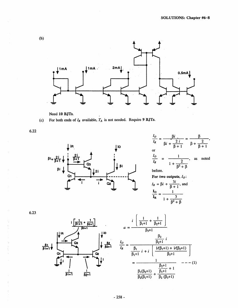
SOLUTIONS: Chapter #6-8
(b)
0.5mA
Need 10 BJTs.(c) For both ends of Ir available, T& is not needed. Require 9 BJTs.
6.22
p'+t&tI EI
Io_Ir
or
[o_Ir
PLp« +
2 i
P + l
1
P + p + l
as noted1+ P2+P
before.
For two outputs, I0ÿ
3iIr = P' +
Io=_
ÿ"1+
P+l1
, and
P2 + P
6.23
JJin /a jio
Iq
h
1
Pi+1 P2+IP3+I
P2P2+I
P.Pi+1
1 + 1Kp,+l)+ KPz+l)
P3+1
P2+1Pl(p2+D
+Pl+1 ---(1)
+ 1
P2(Pl+D P2 (P.3+1)
- 258 -

SOLUTIONS: Chapter #6-9
For the optimal location: See a) Q3 provides a second-order effect, and any P would be OK. b) ForQi with lower P, icl is fixed and iEt will increase, causing VBEl to increase, and Io to increase, c) ForQl with higher P, l0 is larger for a fixed VBE. Conclude that one should make pi = (1 - k) P,P2 = (l+k)p, p3 = p.Substitute in (1)
I_o_Ir P +kP+1
(l-k)p(p+ kp+ I) P-kp+1(l+k)p (P-kp+1) (p + JkP)(P+l)
(1 -k)(P + kP + 1) p + kp + 1 +P-&P+ 1(1+ k) (p -kp + 1) p (k + 1) (p + 1) (P - itp + 1)
12(8+1)(l-k)(P+ kP+l) _
(1 +k) (P -kp + 1) p (* + 1) (p + 1) (p -*p + 1)
_!
___(p + tp)(p-tp+ 1)
(1 -k)(P + kp+l) _2_(1+k) (p-kp+ 1) p (1 +*)(p-Jfcp+ 1)
= P2 -kp2 + p + kP2 - k2 p2 + k Pp2 + Jtp2 + p - itp2 - k2 P2 - k P + 2
(P-*P)(P +*P+ l)+ 2
p2 + p + kp - k2p22r2 'P2 + P - *P + 2 -Jfczp
This becomes one, if kp = 2 -kP, or kp = 1, or k = 1/piNote that for k = 1/p, pi = (1 - 1/P)P = p - 1, and p2 = (1 + 1/p = P + 1, with P3 = p.
6.24
—L_P3+1 LP2+IJ
j J
P2+1 Pl+1
a =
, c =
ii+ 1P2 •*" 2
P2 + 1
p' 1
Pi + 1 Pi + 1 p2 + 1
1
P2+ 1
_ 1
P2+I Pi+1
+ 1 1 =P2 + 2
P2 + 1
1
P3+IP2+2P2+I P.i (P2+2)
JR 1 P2+2 . P2P3+1 P2+l P2+I
___P2 P3 + 2p3
P2+2 + p2 (P3+I) P2 P3 + 2p2 + 21
2 (P2 - P3 + 1)1+ P2 P3 + 2P3
For optimal placement of transistors: See (a) that Q\, being diode-connected, Pi does not matter, (b) thatfor Q2 with low beta, iC2 being fixed, iE2 increases, VBE increases, and iE1 increases, (c) that for p3 high,
I0 increases. Thus, use pi = P, P2 = (1-k) P, P3 = (1 + k) p. Correspondingly, ='R
- 259 -

SOLUTIONS: Chapter #6-10
P2 P3 + _ (1 + k) (1 -k) p2 + 2 (1+ fe) p p2 - k2P2 + 2frp + 2p .P2 p3 + 2P2 + 2
~(1+ lc) (1-k) p2 + 2 (1-k) P + 2 p2 -k2 P2 - 2/fcp + 2p + 2 ' 'S 1S Umty
if 2&P = —2£p + 2, or &P = !4,or k =Zp
6.25 Assume very large P: For the lOOpA reference: VBE = 700 + 25 In (0.1/1) = 642.4mV. For the lpAoutput: VBE = 700 + 25 In (10-3/l) =527.3mV. For the lOpA output: VBE = 700 + 25 In (10~2/1) =
/642 4 — 527 31 x 10"3584.9mV. Thus, for lpA output, RE = K
_6 = H5k£L For lOpA output,
(642.4 - 584.9) 10-3E 10"5
SECTION 6.5: THE BJT DIFFERENTIAL AMPLIFIER WITH ACTIVE LOAD6.26 Each transistor conducts 50pA, for which r„ = 150/50pA = 3M£2, and re - 25mV/50|iA = 50012, Gm =
2/(500+500) = 2mA/V, = ~5QQ ÿ 5QQ
(3M12II3M12) = -2 x 10"3 x j x 106 = -3000V/V.
R„ = 3MS1W3M£2 = 1.5M12, Rin = (75 + 1) (500 + 500) = 76k£2. For a 76kl2 load,A„ = -2 x lO"3 (1.5A/12H76&12) = -144.7V/V.
6.27 For each of the transistors, with an emitter resistor RE = re, the output resistance increases to R„ = r„(1 + gm Re') ~ 3 X 10⁶ (1 + 500/(500)) = 6M12. Thus, the output resistance is approximately6M12 11 6M12 = 3M12. The overall transconductance is 2/(500+500+500+500) =,ImA/V. The open-circuit voltage gain is
- ImA/V X 3M12 = -3000V/V.
6.28 / = lOOpA —> Collector current for all transistors is 50|xA, for which r„ = 75V/50pA = 1.5M12, and re =25mV/50pA = 50012, and r„ = (75 + 1) (0.50) = 38kl2. For the cascode transistors,Ro = r„ (1+g„, rK) = r„ (p + 1) = 1.5 X 10⁶ (76) = 114M12. Also r„ = 10 (75) (1.5 X 10⁶) = 1125M12.Thus the output resistance (in Mil) is 114 1 1 114 1 1 1125 1 1 1125 = 114/2 1 1 1125/2 = 51.8M12.Overall, gm = Gm ~ 2/(500+500) = 2mA/V, A„ = -2mA/V x 51.8M12 = 103.5 x 10³V/V.
SECTION 6.6: MOS DIFFERENTIAL AMPLIFIERS
6.29 Here, gm = ——ÿfor each transistor ---(1), with a maximum at
Vcs ~ "t
ipi = iD2 = 1/1=K (VGS - V,)2 ---(2), where K = Vlk = V2kn(W/L), and VGS - V, = EL2
and gm ÿÿ 2IA.K), or gm max = 2K (VGS - V,), (from (1) with (2)). In general,
(Kl/Z)
iD = K (Vgs - V,)2, and gm = 2K (vGS -V,) = 2K (VCs ± -J" ~ F/)- For a 10% gm drop,
2K(Vgs±ÿ--V,) = 0.9 (2K) (VGS - V,), when VGS±~~Vt = 0.9 VCs - 0.9V,, or
0.1 (Vgs - V,) = ± ÿ-, orVu „ = ± 0.2. For 5%: „
ÿl7 = ± 2(.05) = ± 0.1. For 1%:
2 VGs - v, Vgs - vi
.. .. = ± 2(.01) = ±0.02.VGS
_"T
6.30 iD = V2kp(W/L)(vas - V,)2 = K(x>GS - V,)2, where K = '/: \lpCox{W/L) = '/2 x 10 X 120/6 = 100pA/V2.For equal current division, 25/2 = 100 (Vgs - l)2. Vgs - 1 = ± (l/8),/4, and vCs = 1.354V. Thus VGS =
1.35V. Now, gm = IK (Vgs - V,) = 2 (100) (1.354 - 1) = 70.8pA/V, and r„ = -- = = 4M12./£) LJ/L
-260-

SOLUTIONS: Chapter #6-11
2 (4 x 10⁶)Maximum gain will occur for outputs taken differentially: (a) For ideal loads: A,, =-----=
6 62 (1/70.8 x 10"6)
283.2V/V, (b) For loads with VA = 50V: AX)=2 (4 x 10 II4 x 10 > = 283.2/2 = 141.6V/V.
2 (1/70.8 X 10"6)
6.31 With balanced loads, ip = = 100(dCiS - V,)2, with i)cs = 1.354V (from P6.30 above). Now for iD
= 0.9 (25/2) = 100 (X)Gs - l)2, uGs =(~f + 1 = 1.3354V. For iD = 1.1 (25/2) = 100 (vGS - l)2,
ÿ°cs = (~3~)/l + 1= 1.371V. Thus the input offset = 1.371- 1.335 = 36mV.O
6.32 From Exercise 6.15, k'n = \inCox = 20pA/V2, (W/L) = (12015) = 20, and V2k'n(W/L) = 200pA/V2, withVGs 1.25V, g„, = 100|iA/V, and V, = IV. For an RD mismatch of ± 1%,
f<w =- V, A Rp
Rn1.25 - 1
100= ±1.25mV. For a (W/L) mismatch of ±1%, Vos =
Vgs - V, A(W/L) _ 1.25 - 1 _j_.. = ±1.25mV. For V, tolerance of ±0.6mV, V0s = ±0.6mV.(W/L) 2 100
Thus the worst-case offset is 1.25 + 1.25 + 0.6 = 3.1mV. The likely offset =V 1.252 + 1.252 + 0.62 =1.87mV.
6.33 Here, I0 ~ Iref = 100pA, and K = V2k'(W/L) = 1ÿ(200) = 100\iA/V2.Roughly: iD = K (vGS - V,)2, 100 = 100 (vGS - l)2 -> vGS = 2V. Now, for Qu Q4> x>DS = 2V and
\)ps 2(1+ ——) = 1 + — = 1.1. This could be ignored, but let us include it in a more basic calculation:
More precisely: For Q\, Q4, Vp$ = vGs = and 100 = 100 (u - l)2 (1+1/20), or 1 =(i)2 -2 t) 4- 1) (1 + .05u). Thus i)2 - 2 i) + 1 + .05i)3 - O.li)2 + .05u = 1 or .05 i)3 + 0.9 D2 - 1.95 1) =0, or .05 u2 + 0.9 i) - 1.95 = 0, i) = (-0.9 ±ÿ 0.92 + 4(1.95) (.05))/(2(.05)) = (-.9 ± 1.095)/0.1 =1.954V. Thus VGSi = 1.954V. Now for V0 = V03 = VD4, see IQ = 100|iA, from symmetry arguments.
Va 90For each device, r„ ~ ~P~ = —~r = 200k£2, and gm = 2K (vGS - V,) ~ 2 (100 X 10'6) (2 - 1) =
//> 100|i/\200(xA/V. For the whole mirror, (from Eq. 6.116) R„ul ~ r„3 ro2 = 200 x 10"6 x 200 x 103 X 200 X
103 = 8 X 10⁶£2 = 8MQ. Thus, for V0 = 12V, with the standard output being at 2 + 2 = 4V, the extracurrent = (12 - 4)/8M12 = 8/8 = l(iA. Thus lo - 101p.A for V0 = +12V.
6.34 Assume lo - Iref - 100pA. From results of P6.33 above, VGs ~ 2.0V. Thus VD1 = 2.0 + 2.0 = 4V.
Correspondingly, for Q\, with x>Gs = X> ~ 2.0V and Vps ~ 2V, lOOpA = 100pA/V2 (u — l)2 (1 + -ÿ-), 1
= (d2-2d + 1) (1 + 0.1d) = i)2 — 2o + 1 + O.li)3 — 0.2d2 + O.lt). or + O.li)3 + 0.8u2 - 1.9i) = 0,
O.li)2 + .81) - 1.9 = 0, i) = ~° 8 ± 2(|)4(1ÿ (= L916V- Thus> uC5i = 1-916V = 1.92V. Now
for Q2, ip = 100 (1.916 - l)2 (1 + = 91.9pA. Now, for Q3 with VG ~ 2 (1.92) = 3.84V, 10 =
91.9jlA. From P6.91 of the Text, R„ ~ (gm r„)r„ - 8M£2 using the results of P6.33 above. Thus forV0 = 12V, l0 = 91.9 + (12 - 3.84)/8 = 92.9pA,
-261 -

SOLUTIONS: Chapter #6-12
Generally speaking, see that currents in Q3 and Q5 will bethe same, provided the output voltages are the same. Further,the current in each will slightly exceed 100/2 pA since thevoltage at node X will rise slightly due to doubling of theequivalent K of Q3, Q5. Since the current in each of Q3, Q5is only slightly more than half what it was, each output resis¬tance will be twice as large. In particular, with outputsjoined, the output resistance will be only slightly smaller thanbefore: Now to check these ideas: iD2 ~ lOOpA= (100 + 100) (\>GJ - l)2. Thus \)CS = 14 = 1.707V,rather than 2.0V previously. Thus node X will rise about0.3V, and iD3 will increase by 0.3/200kf2 = 1.5)0,A. Thecurrent in Q3, Qs will be about 5O.Sp,A, for which gm = 2K(Ugs - V,) = 2 (100 x 10~6) (1.707 - 1) = 141)oA/V. Nowfor outputs joined, r035 = 20/(100 + 1.5) = 197kQ.
Consider r02 in two parts of 400kf2 each, with R03 = R05 = 197k x 400k x 141pA/V = 11.1MH.Together, R035 = 11.1/2 = 5.6MI2. When outputs operate independently, the output resistance decreases alot since node X is grounded via l/gm of the other output. From Eq. 6.116 (full version)/?03 = r03 + VgmS + gm3 r03 l/gm5 ~ 2 r03 = 800kQ. An improved circuit would split both Q3 and Q2into two parts, with each pair of half-size transistors driven from the gate of Q4, Qt respectively. Thetotal device width needed would be same as in the original design, that is 4W fqr each original transistorof width W. The version with only Q3 duplicated uses a total width of 5W and has poorer performance!
6.36 For IB = 200p.A, ID for each transistor = lOOpA, r„ = VA/ID = 20/ lOOpA = 200kf2,
iD = V2k'(W/L) (VGS - V,)2, 100 x 10"6 = 1/x 200 x 10'6 (vGS - l)2 -) VGS = 2V,
gm = k\W/L)(vGS - V,) = (200) (2 - 1) = 200pA/V. Gain A„ =- 2= -20V/V. Gain
reduces by a factor of two for a load of 100kf2.
SECTION 6.7: BiCMOS AMPLIFIERS6.37
10 x in-6(a) Here, ic = lOpA, g„, = ÿ = 400pA/V, r„ = lOOV/lOpA = 10MI2, /?, = \Vgm = 100/400 x
10~6 = 250k£2, Av = -400 x 10"6 x 10 x 106 = -4000V/V.
b) For iD = lOpA = 'A X 20 X 20/2 (vGS - V,)2 = 100 (vGS - V,)2. Thus vGS - V, = (1CH00)'/' =0.316, gm = k\W/L) (vGS - V,) = (200 X 10"6) 0.316 = 63.2pA/V, r„ = 20/1OpA = 2MG, /?, = 00,
= -63.2 X 10~6 x 2 x 106 = —126.4V/V, that is much, much less!
P2 1006.38 For / = lOpA, gm2 = 400pA/V, rn2 =-= .= 250ka, r02 = 10M£2, gml = 63.2pA/V, r0i =
gm2 400 X 102MI2. From Eq. 6.116, Rnut ~ gm2 r02 (r01 II rn2) = 400 x 10"6 x 10 x 106 x (2 x 106 II 0.25 X 10⁶) =
888 X 106ft. Thus — =-63.2 x 10~6 x x .888 X 109 = -55.6 X 10³V/V.ÿu, 101
6.39 For I= lOOpA, see by scaling from P6.38 above, gm2 = 4mA/V, rn2 = 25kf2, r02 = 1MS2, r0i = 200kf2,and \)G5i-V, = (100/100)* = 1. Thus gml = 2 (100 x 10~6) 1 = 200pA/V,
Rout ~ 4 xlO"3 x 106 x (200 X 103 II 25 x 103) = 88.8 x 10⁶, = -200 x 10"6 x 100/101 x 88.8 x106 = -17.6 x 10³V/V.
6.35
10,; II ' " "
OS
- 262 -

SOLUTIONS: Chapter #6-13
6.40 From P6.37 at lOpA: For the BJTs, gm = 400pA/V, rK = 250kO, r„ = 10MO, rÿ = 10 (100)107 = 10 x109£2. For the MOS, gm = 63.2pA/V, r„ = 2MO.
For the circuit as shown, R„u, = 2 X 106 x 63.2 X 10~6 X (10 X 106 X 400 X 10"6 X 250 X 103) II (10 X109) = 126.4 x (4000 x 250 x 103) II 1010 = 126.4 x .909 x 109 = 115 x 109O. With Q3, Q6 not used,Rom ~ 10'° II (107 x 400 x 10~5 x (.25 x 106) II (10 x 106) = (10 II .976) 109 = 0.889 x 10⁹O. WithQs, Qi eliminated, Rou, = 2 x 106 x 63.2 x 10"6 x (10 x 106 II 10 x 109) = 1.264 x 10⁹O.
SECTION 6.8: GaAs AMPLIFIERS6.41 For a 1pm long, 1pm wide GaAs device, V, = -1.0V, p| = 100pA/V2, X = 0.1V-1, VA = 10V,
Is = 10-|5A, n = 1.1.
(a) Symmetry would indicate that Va = 5/2 = 2.5V, P = Pio = 10 (100) = ImA/V2,id = P (uGj - V,f (1+ A, dds) = 1 x 10"3 ( 0 - -l)2 (1+0.1 (2.5)). Thus /„ = 1.25mA.
(b) Assume operation is in saturation. Lower transistor (Qi) operates with Mas - 0. Upper one (Q2)is 1.5 X larger: Thus 1.5 (t)cs2--l)2 = (0 --l)2, or x>gs2 ~ (1/1.5Y' ~ 1= —0.18V. Thus, io\ =20 x 100 x 10~6 (0 — l)2 (1 + 0.1 (5 — .18)) = 2.964mA. See that the drain of Q2 is at about 5 -lkll (2.96) = 2.04V, while the gate is at OV. See that operation is indeed in saturation. Check:2.964 = 30 x 100 x 10"6 (oOT -- l)2 (1 + 0.1 (2.96 - - 0.18)) (Dc,y + l)2 = 0.752, dcj = 0.867 -1= - 0.132V OK. Vh = -0.13V, and Ih ~ 2.95mA.
(c) See 2, operates at vGS = 0 with Vci = OV. Icl = 20 x 100 X 10"6 (0 - - l)2 (1 + 0.1(5)) =3.0mA. Then /53 = lS2 = 3.0/2 = 1.5mA = Ic2, and VC2 = 5 - 2(1.5) = 2V. Thus, 1.5 = 10 (100 x10-6) (-Oas -- l)2 (1 + 0.1(2)), or (\)CJ + l)2 = 1.5/(1(1.2)) = 1.25, x>Gs = 1.12 - 1 = 0.12V. ThusVcl ~ -0.12V. Check: lc2 = 1 (0.12 + l)2 (1 + 0.1(2)) = 1.505mA.
(d) See that Q 1 is near cutoff, though it is larger. Assume Vd is near +5V, say at 5V, in which case
iD\ = 2 x 100 x 10~6 (- 0.8 - - l)2) (1 + .1 (5 - 0)) = 0.12mA. Now
iD2 = P I 2 (t)Gs ~ V,) x>DS - \)o5 J (1 + X vDS). Let vDS = t), which is small, such that the X
term can be ignored. Thus 0.12 x 10-3 = 10 x 100 x 10~6 [2 (0 --1) V — u2], or 0.12 = (2d -o2), D2 - 2 D + 0.12 = 0, and D =
~~2± 4 -4 (.12) _0062V Thus = 5
_062 = 4.94V
and Id = 0.12mA.
(e) See that Q\ is turned on with Ve near OV. For Q2, iD = 10 x 100 X 10"6 (0--l)2 (1 +0.1 (5)) =1.5mA. For Q2, iD = 20 x 100 x 10"6 (0.2 - - l)2 (1+0.1 (0)) = 2.88mA. Thus, Q2 is in triodemode with x>DS = D, assumed small and ignored. Correspondingly. 1.5mA = 2.0mA [2 (0.2--1)
D -D2], and D2 - 2.4d + .75 = 0, D =2,4- 2ÿ ~ 4('?5)
= 0.37V. Thus Ve = 0.37V, and le =
1.5mA.
6.42 Here, Pi = 100 x 10"6 x 5 = 0.5mA/V2:(a) iDl = 0.5 (0 - - l)2 (1 + 0.1 (1)) = 0.55mA, for vDSi =| V,| . For V0 = -3V, VS5 = -5V, Vs2 =
—4V, iD2 = 0.55 x 10"3 = 20 (100) x 10"6 (dgs - - l)2 (1 - 0.1 (- 3 - - 4)). Thus (dot + U2 =0.25, dgj = ± .5 - 1 = -0.5V.Vbias = -4 - 0.5 = -4.5V.
(b) Lowest VG = -4V + j V, \ = -3V.
(c) For V0 = -3V, r„ of Q2 does not matter, the current being established by Q 1 at a value I0 =0.55mA.
(d) F,»m Eq. 5.122: ÿ '0.1 X 0.5(0 -1)' * 20kft
r =-l--r = 20kQ. From Eq 5.121: gm = 2p (vGS - V,) (\ + X x>DS). Thus0.1 X 2.0 (—0.5 —1)
gm2 = 2 (2) (-0.5 - -1) (1 + 0.1 (1) ) = 2.2mA/V. Thus R„ut = gm2 ro2 roi = 2.2 x 10"3 X 20 X
- 263 -

SOLUTIONS: Chapter #6-14
103 x 20 x 103 = 880kO.
(e) Now for the output raised from -3V to +1V, ie by 4V, AI=4V
880 x 10j= 4.5|jA.
6.43
VBIm2
10 J .VO
—»{|q3
-5.3V02
nT -€V T
Add Q3 with IV3 = 20pm, P3 = 2mA/V2, p2 = 2mA/V2, P, =ImA/V2, V, = -IV, A. = 0.1V-',
(a) Use the results of Ex. 6.24. Since Q2, Q3 are the same size,V/«v,.v i = -5.3V permits vDSI = IV. Thus Vbias 2 = V/)(us , + 1.0 =-4.3V. Check: Now, for uDJi = IV, i = ImA/V2 (0 --l)2(1 + 0.1(1)) = 1.1mA. Now for Q2, 1.1mA =2mA/V2(x>gs l)2 (1 + 0.1(1)), or 1 = 2 (t)cs + l)2, andVcs = VvT -1 = .707 - 1= -0.3V. OK.
(b) Now, Q3 remains in saturation for vDS S vGS - V, or vDS >-0.3 --1 = 0.7V. Thus, the output can be as low as -4.3 + 1.0= -3.3V.
(c) Now as Q3 is operating just as Q2, VQ can go as low as -4.3 +0.3 + 1 = -3.0V, at which point l0 = 1.1mA.
(d) r01 =1
= lOkfi, r02 =1, - .uz - -r- = 10.2kf2 = r03, gm2 = 2 (2)
0.1 x 1 x (0 —l)2 0.1 x2x(-0.3--l)2(-0.3 + 1) = 2.8mA/V = gm3. Thus, R02 = gm2 r02 r0i = 2.8 x 10.2 x 10.0 = 285.6k£2, andÿ03 — Sm3 ÿ03 ÿ02 = 2.8 x 10.2 X 283.6 = 8.16MO
4(e) For a 4V change in output voltage, AI= = 0.49pA.
6.44 See Qi and Q3 have the same width. Thus for VDD = 5V and VA = 2V, uDj3 — uosi = {5—2)12 = 1.5V,and VE = VB = 5 - 1.5 = 3.5V. See 5 X 10~3 = IV x 100 X 10~6 (0 - -l)2 (1 + 0.1 (1.5)). ThusIV, = iv3 = 43.5p.rn, and IV2 = 43.5/2 = 21.7pm. Note that the diodes are sized to give 0.75V drop each
1for //2 = 2.5mA.
1roi =
Now, r„ =P (vas " V,)2 < gm -2P - V») (1+ A, vDS). Thus
= 2.3k£2 = r03, and r02 =1
= 4.61kQ. Also gmi = 2 (4.35)0.1 (4.35) (0 + l)2 'UJ'
0.1 (2.17) (0 + l)2(0 + 1) (1 + 0.1 (1.5)) = 10mA/V = g„(3, and gm2 = 2 (2.17) (0 + 1) (1 + 0.1 (5 - 2)) = 5.64mA/V.
t)/,Now, from Eq. 6.132: a = — =
10 x 2.30 x 5.64 x 4.61 2.305.64 x 4.61 + 1 + 2.30
2 3010 x 2.30 + + 1
2.30
23.1525
= 0.926V/V. From
Eq. 6.133: R„ =
= 26.5kfl.
-r—— = , 2 3OOA = 31.1kQ. From Eq. 6.134: R„ = r0i {gm3) ~= 2.3 X 10 X M1- a 1- .926 2 2
- 264 -

SOLUTIONS: Chapter #6-15
0-4J 'DSSeq
-- >
ÿ ÿ ÿ j"j~Cg
Ql
Thus t)C52 = -0.7V, with X)DS2 = 3 - 0.7 = 2.3V, 0.5 = W, (0.1) (0 -l)2 x (1 + 0.1 (0.7)), or W{ = jL- = 4.67p.m. Also 0.5 =
W2 (0.1) (-0.7 - -l)2 (1 + 0.1 (2.3)), or W2 =MX x
= 45.2pm. For x>DS = 6V, the current loss will increase, withi>dsi = 3> increasing as well. Thus i = 0.467 (0 --1)2 (1 + 0.1 *0),and i = 4.52 (-v + l)2 (1 + 0.1 (6 - v)), (1 + O.lv) = 9.68 (V2 - 2v +1) (1.6 - O.lv), 1 + O.lv = 15.5 v2 - 31v + 15.5 - .968 V3 + 1.94 V2- .968 v, 0.968v3 - 17.34v2 + 32.07v - 14.5 = 0, v»- 18v2 + 33.13v - 14.98 = 0.
Solve this cubic iteratively: D =18\>2 -+ 14.98 - v3
33.13= 0.543v2 + 0.452 - 0.030V3. Now, for v = 0.7: v
= .543 (.7)2 + .452 - .03 (.7)3 = 0.266 + 0.452 - .01 = 0.708; for v = 0.71: v = 0.543 (0.71)2 + 0.452 -0.030 (0.71)3 = 0.274 + 0.452 - 0.011 = 0.715. See that the process does not converge: Thus reformu¬late it: v2 =
v3 + 33.13v - 14.9818
,-o = (0.056\)3 + 1.84v - 0.832)1/1. Now, for v = 0.7: v = (0.056 (.73)
+ 1.84 (.7) - 0.832)" = (0.0192 + 1.288 - 0.832)" = (0.4752)" = 0.689. See that now it will diverge forlower values: Also for v = 0.8: v = (0.056 (.83) + 1.84 (.8) - 0.832)" = (0.027 + 1.472 - 0.832)" =0.818. Again we see that it also diverges, but that a solution lies between 0.7 and 0.8, but nearer to 0.7.Now, for V = 0.75: v = (0.056 (0.75)3 + 1.84 (0.75) -0.832)" = (0.024 + 1.38 -0.832)" = 0.756; for V =0.74: V = (0.056 (0.74)3 + 1.84 (0.74) -0.832)" = 0.743; and for v = 0.73: v = (0.022 + 1.343 -0.832)"= 0.7302. /
Now conclude v = x>ds\ = 0.73V, for which Q\, iD = 0.467 (l2) (1 + .1 (0.73)) = 0.501mA, and for Q2,iD = 4.52 (-.73 -- l)2 (1 + 0.1 (6 - 0.73)) = 4.52 (0.0729) (1.527) = 0.503mA. This calculation is verysensitive due to squared term. Use iD = 0.502mA.
8m = 2 p (Vcs - V,) (1+ X X>DS )•Small-Signal analysis:
Kut = rQ2 gm2 r0h for
r„ =ÿ P (uG5 - V,)1'
which r02 =1
r0i =1
0.1 (45.2 x 0.1 x 10"3) (-0.7 - -1)
Here
24.6kn,
= 21.4kft, gm2 = 2 (4.52 x 10"3) (-0.7 - -1) (1 + 0.1 (3 - 0.7)) =0.1 (.467 X 10-3) (0 + l)2
3.34mA/V. Thus R„ul = 24.6 X 103 x 21.4 x 103 x 3.34 x 10-3 = 1.76MQ. Now, the expected currentincrease as vDS rises from 3V to 6V is (6-3)/(1.76 x 106) = 1.7pA. The earlier estimate of change from0.500mA to 0.502mA by 2pA is quite consistent. The small-signal scheme is certainly more straightfor¬ward!
6.46 From the results of P6.45 above, for VDD = 6V and V0 ~ 6/2 = 3V, the upper composite would conduct0.5mA, while the lower one would be biased at V/ = 0V to correspond. For each composite, the outputresistance is 1.76M£2. For the amplifier, the output resistance is 1.76/2 = .88MQ, and the gain is-gm Rout- Here, gm = gm i = 20, (vGS, -V,) = 2(0.467 X 10"3)(0--1) = 0.934mA/V, and the gain is- 0.934 x 10'3 X -0.88 x 106 = -822V/V.
6.47 Though it is not required explicitly by the specification, make all devices the same size. For Vcm ~ 0V,
VDD = 5V, and Qi and Qj matched, the voltages across each will be the same, and
V/M, = X)DS3 =5 ~ °~ 0 5 = 2.25V. Thus 0.5 x 10"3 = W, (0.1 x 10"3) (-0.5 - - l)2 (1 + 0.1 (2.25)),
0.5 11or W|= —— X-r X ———
0.1 (0.5) 1.225= 16.3pm = W2 — Wj. Use / = 1.0mA: Now for 0.5mA in Q\, the
-265 -

SOLUTIONS: Chapter #6-16
voltage at the sources of Q, and Q2 is 0.5V, and that at the source of Q3 is 0.5 + 2.25 = 2.75V, with2.75 - 0.5 = 2.25V at its gate. Thus vDs2 ~ 2.25 - 0.5 = 1.75V. .Now, 0.5 x 10~3 = 16.3 (0.1 x
Vi0.5 1 - 1 = 0.5109 - 1 = -0.489V10"3) («cs - -l)2 (1 + 0.1 (1.75)). Thus Man =±l63
ÿ
{ 175(rather than 0.500V). Thus, there would be an llmV offset to maintain VQ at 0.5 + 1.75 = 2.25V. Notethat since the drain voltages of Q\ and Q2 are different, as required by g.3 operating at vGSi & 0, whileQ | and Q2 are matched and share a source connection, there must be an input offset voltage. Otherwise,for gate inputs connected, and the drain supply exactly half that of the source bias supply, the output willrise until Q3 enters the triode mode and vGS2 = 0. For the offset acceptable, and nominal operation withiD ~ 0.5mA and vDS = 2.25V, and 3)G5 = -0.5V, gm = 2p (vGS - V,) (1 + A, x>DS) = 2 (0.1 x 16.3 x
r>-3\ / r> i- " .mm 'lO-3) (-0.5 - -1) (1 + 0.1 (2.25)) = 2.00mA/V. r„
* P (Ugs - V,)21
0.1 (1.63 x 10"3) (-0.5 + l)2
~gm I r01
= 24.5ka Now from Eq. 6.139 of the Text:3)„
3),
- 2.00 x 24.5 49
gm 1 '*01 + 1 gm3 ÿ03 2 x 24.5 + 1 - 2 x 24.52 x 24.5 + 1 2 x 24.5 + 1
5050
4950
= -49 (50) =
gm2 r02 + 1 gm3 r03 + 1 .2450V/V.
Alternatively, for W\ = W2, but W2 smaller, so vDS\ = vDS2 = 2.0V, and VGS3 = 0V with 33GJi = vGS2 =-0.5V, all operating at 0.5mA nominally. Find: 0.5 x 10-3 = Wi (0.1 x 10⁻³) (-0.5 + l)2 (1 + 0.1 (2.0)),
0.5 1 11 2=oTx
0.1 (5 - 2)), or W3 =
ImA/V, r03 =
,X — = 16.7p.m. Now for Wy 0.5 x 10-3 = W3 (0.1 x 10~3 (0 + l)2 (1 +(0.5) 1.2 3 v ; v
of x "k * TT = 3'85ÿm' Now gm3 = 2 (0,1) (3,85) (0 ~ -1) (1 + 0,1 (3)) =l — = 25.97k£2, and gm, = gm2 = 2 (1.67) (-0.5 - - 1) (1 + 0.1) (2)) =
0.1 (0.1) (3.85) (l2)2.004mA/V, with r0i = '02 =
2.00 (24.0)2.00 (24.0) + 12.00 (24.0) + 1
1 (26)
---r- = 23.95kf2. Thus the gain is ——0.1 (1.67) (-0.5+ l)2 5
3),48
= -1296V/V.4949
26271 (26 + 1)
SECTION 6.10: MULTISTAGE AMPLIFIERS
6.48 DC bias for VBE = 0.7V, P = °°, and ±15V supplies, 1E9 = ÿ 7= 0.5mA. Thus lc3 = 0.5mA,
28.6Ke = 100£1, Iqg = 2.0mA, Iqa ~ Ics = 1.0mA —> re = 25£2. Vbi ~ 15 — 3(1) =
12V, V£7 = 12 + 0.7 = 12.7V, lE1=15 ~ 12 7
= 1mA -+ = 25a VBi = -15 + 1 (15.7) = 0.7V, V0IGi — lc2 — 0.25mA
12 + 0.
0-152.3
= ov, IES =3k
= 5mA -> re = 5Q.
AC for p = oo: Rin = <*>, Roul3k
_ . 20* + 20k3kQ. II 5Q - 5a Gam = -rrr- X
3k x 15.7*100 + 100 25 + 25 2.3* + .025*
3* + .005*= 200 x 60 x 6.75 x .998 = 80.9 x 10³V/V.
AC for p = 50: Rin = 51 (100 + 100) = 10.2kQ, Rout = 3kQ. II 5 +15.7*51
= 3kQ II ,313kQ = 28312
For gain: Second-stage Rj2 = 51 (25 + 25) = 2.55kf2, third-stage Ri2 = 51 (2.3 + .015) = 117.6kQ,, , _ „ ..... ,. 40*112.55* 50 3*11117.6* 50fourth-stage Ri4 = 3k (51) = 153kQ. Thus the gam =-—-X — x
ÿ 2x — x
15-7* II 153* 50 3* _ 2397 50 Z925 50 J434 50 _S_ }
2.325* 51 3.005* ~ 0.2 51 .05 51 2.325 51 3.005
- 266-

SOLUTIONS: Chapter #6-17
6.49 To raise icy from 1mA to 2mA, and ia from 5mA to 20mA, reduce R4 to 2.3kQ/2 = 1.15k£2, R5 to15.7/2 = 7.85k£2, R6 to 3/4 = 0.75k£2. Now Ri4 = 101 (25/20 + 750) = 75.85kQ,
, _ /?5H/?,4 7.85* II 75.85* „ _ *6 750 xr
"'- - =- 12.5 + 1150 = -612™' A< - ÿ7T«7 = -25— '0Msy/y Now'
50A =A, A2 A3 A4 = 22.4 x (-59.2) X (-6.12) x 0.998 = 8099V/V, and R„ = R6 II (reS + Rrfp + 1)) =
Rl750 II (1.25 + 7850/101) = 750 II 78.97 = 71.411 For load RL, loss isR + ?14 = 0.8. Thus RL =
0.8Rl + 57.12, 0.2RL = 57.12, Rb = 28612. For a 28612 load, the upper swing is limited by Qy saturat¬ing. Assume 0V between the emitter and collector of Qy, and look down from the collector of Qy. Seean equivalent load resistance at the emitter of Qg of 28612 11 75012 = 20712 connected to a supply of(.286/(.286+.75)) (-15) = -4.14V. At its base, see a resistor of 101 (207) = 20.9kl2 to a supply of -4.14+ 0.7 = -3.44V. The equivalent circuit is as shown:
I+15 Looking down from the collector of Qy, see 20.9 II 7.85 = 5.71kl2to -3.44 + (20.9/(20.9+7.85)) (-15+3.44) = -11.84V.
Thus, VA =+15t 5ÿ71 (15 ~ ~ 1184) = 10-47V (for which
Q$ does not saturate). The maximum positive output is 10.47 - 0.7= +9.77V. For negative output, with g8 cutoff, the output is
7.85kQ i- «j"ÿ-9kQ (286/(286+750)) (-15) = -4.14V. Thus with a 28612 load, the out-
-3.44 put can swing from 9.8V to -4.1V..,s;>20.S
•-3/
6.50 For the resistor values:
The reference resistor, Rq = (0 - - 10-0.7)0.5 = 18.6 k!2; R6 = (0 - - 10)5 = 2 k!2;R$ — ( + 0.7--10)1= 10.7 k!2; = R2 = 3<0.S2) = 12 k!2; R} = 7A2/2.) = 2 k!2;R4 = (2 — 0.7yi = 1.3 k!2.
For the emitter resistances:
For Qi, Q\, re \ = re2 = 25 mV/0.25 mA = 100 12. For Q4, Qs, re4 = re5 = 25 mV/1 mA = 25 12.For Qy, rel = 25 mV/1 mA = 25 12. For Qs, rei = 25 mV/5 mA = 5 12.
For the input resistances:
r„= (P+ l)r, =51re, in general; rK\ = r„2 = 5.1*12; rn4 = rre5 = r„7 = 51(25) = 1.275 k!2;rn8 = 51(5) = 0.255 k!2.Now Rn = Rid = rK1 + r„2 = 2(5.1) 10.2 k!2; Ri2 = rn4 + rn5 = 2(1.275) = 2.55 k!2;
Rn = rnl+ (P + l)(R4) = 1.275 + 51(1.3) = 67.575 k!2; Ri4 = rnS + (P + l)/?6 = 0.255 + 51(2) =102.26 k!2.As noted on page 557 of the Text; d„A>«/ = (RÿRiiXhAi) = (240.2)(teÿt,) = 0.196/eg4( ,where ie84f = ie/ib% x ib/icl x ic/ibl X lbyic5 X ic/ih5 x ib/ic2 x jc24(.
Here, ie/ib% = p + 1= 51; ih/icl = R&RS + Ri4) = 10.7/1:10.7 + 102.26) = 0.0947; ic-/ibl = p = 50;
k/ics = RARy + Rid = 2/(2 + 67.6) = 0.0287; ic/ib5 = p = 50;
. . Rj+R2
___12+ 12 _ non. . . _
R_ „
lbAc2 (Rl+R2) + Rn 12+12+ 2.55 ' ÿ
Thus overall, \y„A>id = 0.196 x 51 x 0.0947 x 50 X 0.0287 x 50 x 0.904 x 50 = 3070 V/V.
Clearly this method fails if p = 00, although it is generally OK for large (but finite) p, in which case thecurrent-divider factors become smaller and smaller as P rises.
-267-

SOLUTIONS: Chapter #6-18
NOTES
-268 -

Chapter 7
FREQUENCY RESPONSE
SECTION 7.1: S-DOMAIN ANALYSIS: POLES, ZEROS, AND BODE PLOTSV(> (.S ) Zshunt
7.1 Using the voltage-divider rule:
1 ,, „ R/C\s R\
T(s) =
C|j 11*.= R|+ 1/C1
V:(s)
T(s) =V„(s)
-•shunt +Here
VC2s1+R\C\S Vi(j) 1/C2ÿ + /? /(I +
1+ R) C| s„ „ or T(s) = -—-——-—-—. That is, we see a single-time-
1+Ri C2s/{\ +Ri C, s) w 1+R|(C,+ C2)s 6
constant response with a time constant x = Ri (C| + C2), where the resistor R i "sees" C j + C2,the parallel capacitance of Cj and C2 when the source is shorted.
Type of STC:
a) See that the circuit passes dc directly via R i, with the signal reduced at high frequencies.Thus it is a low-pass (LP) STC circuit.
b) See for s = 0, V0(syVi(s) = 1, and for j = <*., V„(sYVi(s) = C/(C, + C2) < 1.Now, for R, = 104n, C, = (0.5/10)|iF, andC2 = 0.5|xF. There is a pole at- ox, = 1/(7?|(C, + C2)) = M;104(0.05+0.5)10 ) = 182rad/s, and a zero at 0)z = K/?iCi) =K104(0.05)10"6) = 2000 rad/s. From
the Figure, or directly, see T(co)
1+y (O Ri C\
10 100 ik iok
IT(<d)I>ÿ co rad/s 1 +y'co Ri (C| + C2)
1+ (co R\ Ci
. Now,|T(co) |
4>(co)
1+ (co /?i (Ci + C2))2
C,
Thus,
IT"(0)1
= 1 =0dB,\T(oo)\ 1=
0.5ÿ0
C, + C21/10 0.1 1
0.540 + 0.5 1/10+1 0.1 + 1 11d>(co) = tan-1 co R, C|-tan"' co R\ (Ci + C2).<h(0) = 0-0 = 0*, 0>(oo) = 90 - 90 = 0*.
*i C,d>(cop) = tan"'-
ÿ -20.8dB.
= tan0.540
0.540 + 0.5
4> (coz) = tan-1 1- tan"'
R{ (C, + C2)
- tan"1 1 = tan-1 1/11 - tan"1 1= 5.19* - 45* = -39.8*.
*i (C, + C2)
- tan 1 1
R, C,= tan"1 1- tan"1 11= 45* - 84.8° = -39.8*.
For com = (co„ coz)'/' = (182 x 2000)* = 603 rad/s, (com) = tan-1 - tan"1 = 16.8* -"p wz
73.2* = -56.4*.
-269-

SOLUTIONS: Chapter #7-2
7.2
(a) ro--10'4ÿ + 10>(s + 1) (s + 100) (s + 105) (s + 106)_10'4 (10) (j) (1 + j/tO)
(100) (105) (106) (1 + s) (1+ s/100) (1+ s/105) (1+ sAO6)
or T(s) =_102 s (1+ j/IO)_
OT S(1+ j ) (1 + j/100) (1 + s/105) (1+ j/106) '
(b) As s -+ 0, |T(0) |= (11)°(1)°()1)1()1) = ov/v, and <D(0) = tan"11/0 + tan"'(yi - 4tan-'M =90'.
/ \2 i
As s —> oo, |T(oo) |=-- = —J = OV/V, <h(oo) = 2 tan-' (oo) — 4 tan~'(oo) = —2 tan-1 (oo)(oo) oo
= -180°.
(c) Poles at s = -1, -100, -10s, -106 rad/s. Zeros at s = 0, -10, oo, oo rad/s.
(d) As the frequency rises, the zeros increase the gain while the poles reduce it. We see thatthe gain increases from 0 to the first pole at 1 rad/s, then begins to rise again at 10 rad/suntil 100 rad/s where it flattens, beginning to fall again at 105 rad/s, and more at 106 rad/s.Thus, we see that the gain is greatest from 100 rad/s to 105 rad/s. Thus at (0 = 103 rad/s,
|rao3)|3 2_ 10 (10 ) (10 )= 1030 (1q3)
_90 tan-l102 _ tan-l103 _ tan-l 10
_ tan-l 10-2_ t -1 10-3103 (10) (1) (1)
= 90 + 90 - 90 - 84 - 0 - 0 = 6°. Also at (0 = 104 rad/s, IT(104) I=10 00 ) (10 )
104 (102) (1.1) (1)= 0.9x10 ,and
<D (104) = 90 + tan-'lO3 - tan"'l04 - tan"' 102 - tan"1 10"' - tan"' 10-2= 90 + 90 - 90 -90 - 0 - 0 = 0*. Thus the greatest gain is 103V/V, and the correspondingphase is 0', occuring from about 103 to 104 rad/s.
(e) Gain at 103 rad/s,
T (co = 103) =_(102)(103)(1 + (lOVlO)2 )'/l_
_ 102 (103) (lO"*) _ 102+ 3 +2-3-1 _ l03V/Vs60dB.103 (10) (1) (1)
,5 ÿ _10'(1q5> (lp4>
a+ (lo-M)2)14 (l + (10V100)2)14 (i + (io3/io5)2)'/i (i + (ioMo6)2)14) )
= in2+ 3 +2-3-1 _in2v/v = £n<in
At 10 rad/s, T (to 10)1Q5 (1Q3) (1 + (ioMoW (1 + (lOVlO6)2)*. 10* (lQ5) (104) ,0,707x|0,.57dB,
10s (103) (1.414) (1)It certainly would have been better to prepare the Bode plots earlier, certainly by the end of part(a). It is actually possible to sketch the pole and zero locations immediately, and to sketch theshape of the magnitude plot. However the absolute magnitude requires a calculation like theconversion done in part (a) (see P7.4 following). Probably easiest after (c), most useful before (d),and usefully possible before (b).
(See the Bode Plot on the following page.)
- 270-

SOLUTIONS: Chapter #7-3
7.2 (Continued)
,0 10V> 3 ,<4
<P 45
6
0) rad/s
0) rad/s
7.3 From P7.2 above, T(s) =102 J (1+5/10)
(1+ 5) (1+ j/100) (1 + 5/105) (1+ 5/106) '
102 102 (1+ (10M0)Y-For co = 100 rad/s, |T (to) |-----
(1+ 1002)" (1+ (KXKIOO)2/' (1+ (lOOtOY)" (1+ (lOOÿOY)
= 0.707 x 10²+ 2 + 1 ~ 2 = 0.707 x 10³ a 57dB. <i> (to) = 90 + tan-1 10- tan"
,5\2y/. 1<>"\2\/i102 x 102 x 101102 (2'a) (1) (1)
100 - tan"1 1- tan"' 10"3 - tan-1 10"4 = 90 + 84.3 - 89.4 - 45 - 0.1 - 0 = 39.8*.For to = 2 x 10⁵ rad/s,
I T(co) | = •
102 x 2 x 105 (1 + (2 x 10s.2.y,
10 ''(1 + (2 x 10⁵)Y (1 + (
100 106——— ,*2)!/i (i + (ÿr-)2)'7' (i + (ÿrÿ)2)'7'
102 x 2 x 10s (2 x 10⁴) 4x10"2 x 10⁵ (2 x 10³) (1 + 4)'/i (1+ 0.22)* 4 ( V 5) ( V 1.04) X 108
= 0.4385 X 10³ a 52.8dB.
O (to) = 90 + tan"1 (2 X 10⁴) - tan"1 (2 x 10s) - tan-1 (2 x 10³) - tan-1 (2) - tan"1 (0.2) = 90 +90 - 90 -90 - 63.4 - 11.3 = -74.7*.
- 271 -

SOLUTIONS: Chapter #7-4
SECTION 7.2: THE AMPLIFIER TRANSFER FUNCTION
7.4 From P7.2, T(s ) = -108 J 0 + 10)- _
-s (s + 10)-(s + 1) (s + 100) (s + 10s) (s + 106) (s + 1) (s + 100)
1 108 s (i + 10) .„3 1—hr~,-f——- x 10 xxS w, , & \ lo5 x 106 (s + 1) (j + 100) J 5
(I + 1F)<1+ WThus, A„ = 10', Fl(s) = '('+ ,F„(s) =-1-
(s + 1) (s + 100) „+»)(,+ •)10s 106
A ,N 103 s (s + 10) A f \ 103AL(s) = , , ' , ' .Ah(s) =
(s + 1) (s + 100) „ _s_10s M 10'
7.5 From P7.4, FL(s) = - =-5_, FH(s) =1 1
(. + 1)C» + I00) s+1001+
ÿ
105 „ 10® 105with the dominant-pole responses indicated by =. Thus A(s) = 103 s
(s + 100) (1 + -ÿr)10s
7.6 For the low-frequency response of the transfer function given in P7.2, there are 2 low-frequencypoles, at 1 rad/s and 100 rad/s, and zeros at 0 and 10 rad/s.
For the 3dB frequency:
(a) Dominant Pole: CO/, ~ 100 rad/s.
(b) Root Squares: CO/. = (1002 + l2 - 2 (102) f = 102 (1 + 10"4 - 2 x 10 2)'/j = 99 rad/s.
. , „ (co2 + 102) (co2) _ 1X3C y* (co2 + l2) (co2 + 1002) 2
2co4 + 2(10)2 co2 = co4 + 1002 co2 + co2 + 1002,co4 - CO2 (9801) - 10000 = 0, co2 = [ - -9801 ± V 98012 - 4(-10000))>2 = [9801 ± 9803]/2,that is co2 = 9802, or CO/, = 99.00 rad/s. Note above in (1) that the zero at zero frequencymust be included in the calculation. Why?
7.7 For the upper 3dB frequency of the transfer function in P7.2, two poles, at 105 and 106 rad/s.
For the 3dB cutoff:
(a) Dominant pole: cow = 105 rad/s.
' ' 10s(1 + 1/100)" '
(b) Root squares: WH = l/V —ÿ-7 + — = V —U- (1 + —~r)y'H v (10s)2 (106)2 10s 102CD// = 0.995 X 10s rad/s.
(c) Exactly: F,,(s) =-ÿ-7-, T2 (co) =-ÿ-7-7- = 1/2,' (1 + a/10 ) (1 + J/106) (1 + (ci/10 ) ) (1 + (0/106)2)1 + CD2 (1/1010 + 1/1012) + cd4/1022 = 2, CD4 + CO2 (1012 + 10'°) - 1022 = 0,
cd4 + 101 x 10'° co2 -1022 = 0,_, -101 x 1010 + ÿ1012 x 1020 + 4 x 10²²CO2 =---,
or
2 -101 x 1010 ± 102.96 x 10¹⁰ ,nl0 , „nnn ,„5 .,cd2 =---= 0.9805 X 10 and (oH = 0.990 x 10 rad/s.
- 272 -

SOLUTIONS: Chapter #7-5
7.8 Old T (s) =
Modified
j (j + 10)x 103 x 1
(s + 1) (s + 100) " " (1+ j/105) (1 + s/106) '
,y (s + 10)
____.. 1
T(s) = x 103 x (1 + s/105)(s + 1) (s + 100) (1+ s/105) (1 + sAO6) (1 + sA2 x 106)) '
Note the pole-zero cancellation with the result that T(s)103 s (s + 10)
(s + 1) (s + 100) (1 + sÿO6) (1 + si2 x 106))106 (1 + 1/4)-* = 0.894 x 10⁶ rad/s.
,and (oH = lW (1/(1 x 105))2 + (1/(2 x 106))2 =
Exactly,1
(1+ (oylO6)2) (1 + (o>{2 x 10⁶))2
to4 + 2 x 10¹² in2 - 2 (1024) = 0,
= 1/2, 1 +
<o2 =
or J_. or1012 + 4 2 (1024) = 2,
-2 x 10¹² ± ÿ 4 x 1024 - 4 (-2 x 1024)
10'2( 2 + 3.46) _Q ?3 x 10,2 Thus = Q g56 x 1q6 rad/s
2
7.9
(1) Using open-circuit time constants: For C\,Req=R\, and Ti - R\ C\. ForC2, Ret/ = R\ + ÿ2i ancl = C2 (ÿ1+ ÿ2)-
(a) For Rl = R2=\0kCl, Ci=C2 = lOOpF, t, = 104 x 100 X 10"12 = 10-6s,
x2 = 100 x 10"'2 (104+ 104) = 2 x I0~6s, coH = —-— = --- ~-r-2 X, + x2 1 x 10"6 + 2 x 10~6= 1/3 x 10-6 = 333 x 103 rad/s, or = 0.333 x 10⁶rad/s. Alternatively, the sum of
squares approach yields (% = 1/(12 + 22)* x 106 = 0.447 xl06rad/s.(b) For R] = lOkO, R2 = lOOkO, C, = lOOpF, C2 = 10pF, X, = 104 x 100 x
10-'2= 10_6s, x2 = 10 x 10-12 (10 x 104 + 1 x 10⁴) = 10 x 10~8 (11) = 1.1 x 10⁻⁶s,
CO// = -J-- = 0.476 X 10⁶ rad/s. Alternatively, the sum of squares(1 + 1.1) 10~6
approach yields c% = 1/(12 + l.l2)* x 106 = 0.673 x 10⁶ rad/s.
(c) R, = lOkQ, R2 = 100k£2, C, = C2 = lOpF, x, = 104 x 10 x 10"12 = 0.1 X 10~6s,x2 = 10 x 10~12 x (10s + 104) = 10 x 10"12 x 104 (11) = 1.1 x lOÿs, c% = 1/((0.1 +1.1) 10~6) = 0.833 x 10⁶ rad/s. Alternatively, using the sum of squares, (% =1/fO.l2 + l.l2)* x 106 = 0.905 x 10⁶ rad/s.
Vo +vo C2 S R2
Ri Jc Rz
vt •—AA -AA- -« vo
jc =vo (R2 C2 S + 1) C1 S
iRl = VO KR2 C2 S + 1) C1 S + C2 S]
vi =vo [R1 R2 C1 C2 S 2+ R1 C1 S + R1 C2 S + R2 C2 S + 1]
- 273 -

SOLUTIONS: Chapter #7-6
(2) Exactly: T(s)=V" 1Vj s2 R|R2 C\ C2 + s (R 1 C| + R 1 C2 + R2 ÿ*2) "t* 1
T(j(o) = -— -——--—J——--- „ ÿ. Now, response is 3dB
j co (Rx C| +R\ C2 +Ri C2) + (1 — to R\ R2C\ C2)down when (O2 (Rx C\ + R\ C2 + /? 2 C2)2 + (1 — co2 R\ R2 C\ C2)2 = 2. Now, for particu¬lar cases:
(a) /?, = R2 = 10k£2, C, = C2 = lOOpF. Now, co2 (3 x 104 x 10"10)2 + (1- co2 x 104 x104 x 10"'° x lO"10)2 -2 = 0, 9 x 10"12 co2 + (1 - co2 10"12)2 - 2 = 0, 9 co2 10"12 + 1-
2 co2 10"12 + co4 1Q-24- 2 = 0, co4 + co2 (7 x 10¹²) -1024 = 0, co2 =-7 x 10¹² ± 10l2ÿ72--4 .n,2 (~7 ± 7.28) A1, 1a12 , _ . inS---= iol2-i----= 0.14 x 10 , and cow =0.3J4 x lO6rad/s.
(b) Rx = lOkO, R2 = lOOkQ, C, = lOOpF, C2 = lOpF. Now, co2 (lO4 x lO"10 +104 x 10"" + 10s x lO"11)2 + (1 - co2 x 104 x 10s x lO"10 x 10"11)2 - 2 = 0, orco2 (10"6 + 10"7 + 10"6)2 + (1 - co2 10"12)2 - 2 = 0, or co2 (2.1 x 10"6)2 +(1- 10~12 co2)2 -2 = 0, 4.41 x 10"12 co2 + 1 - 2 x 10"'2 co2 + co4 10"24 -2 = 0,
CO4 10"24 + 2.41 x 1Q—12 co2 — 1 = 0, co4 + 2.41 x 10¹² co2 - 1024 = 0,CO2 = 1012 (-2.41± V 2.412 --4yi= 1012 (-2.41± 3.132>2 = 0.309 X 10¹².Thus (On = 0.601 x 10⁶ rad/s.
(c) Rx = lOkfl, R2 = lOOkO, C, = lOpF, C2 = lOpF. Now, co2 (104 x10"" + 104 x 10"" + 10s x 10-")2 + (1 - co2 x 104 x 105 x 10"" x 10"")2 -2 = 0.Thus co2 (1.2 x 10"6)2 + (1- co2 (0.1) 10"12)2 - 2 = 0, 1.44 x 10"12 co2 + 1 - 2co2 (0.1) 10"12 + co4 (0.01) IP"24 - 2 = 0, co4 + 1.24 x 10+14 - 10+26 = 0,_CO2 = (-1.24 X 10¹⁴ ± V 1.242 X 1028 - 4 ( -1026)>2 = 1014 (-1.24 ±ÿ 1.242 + ,04>2 =0.00801 x 1014 = 0.801 x 10¹². Thus c% = 0.895 x 10⁶ rad/s.
7.10 Using short-circuit time constants: For C(, Req = R\ II R2, and xx = Cx Rx R2/( Rx + R2).
For C2, Req = R2, and x2 = C2 R2.(a) For Rx=R2 = 10kf2, C, = C2 = lpF, x, = 1 X 10~6 X 10⁴/2 = 0.5 x 10"2s, and
tOi = 1/0.5 X 10-2 = 200 rad/s; x2 = 10"6 x 104 = 10"2s, and co2 = 100 rad/s. Thus CO/, = 100+ 200 = 300 rad/s. Using the sum of squares idea, CO/, = (1002 + 2002)'/l = 224 rad/s.
(b) For R1 = lOkft, R2 = lOOkft, C, = lpF, C2 = 0.1pF, x, = 10"6 X 101:12 II 1001:12 = 0.909 X10_2s, x2 = 10s x 10"7 = 10"2s. Thus CO/, = (1/0.909 + 1/1) x 1/10"2 = 210 rad/s. Alterna¬tively, CO/, = ((1/909)2 + (1A)2/1 x 100 = 147 rad/s.
(c) For R, = 10k£2, R2 = 100k£2, C, = C2 = 0.1pF, x, = 10~7 x .909 x 10+4 = 0.909 x 10"3s,x2 = 10"7 X 10s = 10"2s. Thus CO/, = K0.909 x 10~3) + 1/10"2 = 1100 + 100 = 1200 rad/s.Alternatively, CO/, = (1/9092 + 1/102)'7' x 1000 = 1054 rad/s.
SECTION 7.3: LOW-FREQUENCY RESPONSE OF THE COMMON-SOURCEAND COMMON-EMITTER AMPLIFIERS
—/?(j| II R(j27.11 For Midband Gain: all capacitors are ac short circuits. Thus, Au = —--——— x
R + "CI 'I "02
«- * ""ÿ>-'ÿ0mT10«T22M * 2 * 10"3 (2« » 1 = "HI* 10"S * "67* 103 *- 13.14 V/V.
For CC\: Rc1 = lOOkO + 6.875M£2 = 6.975 X 10⁶fl, andfpx = K2rc x 6.975 X 106 x 0.01 x 10~6) = 2.28Hz. For Cc2: RC2 = 10kl2 + 20ki2 = 30kf2, andfp2 = K2tt x 30 x 103 x 0.1 x 10"6) = 53.1Hz.
-274-

SOLUTIONS: Chapter #7-7
For Cs: R's = Rs II Vgm = lOJfcQ II (l/(2 x 10~3)) = 0.5/:111OA: = 4760, andfPs = H2K x .476 x 103 x 1 x 10"6) = 334.3Hz(with fa = V[2n x 10 x 103 x 1x 10"6) =15.9Hz.
7.12 Use the largest capacitor at the source, where the resistance level is least. Now,Cs = lA2n x .476 x 103 xlO) = 33.4|iF. Use Cs = 30pF. Now, Cc, = V{2k x 6.975 x 106 x 1)= 0.0236pF. Use CC\ = 0.02jxF. Now, CC2 = V(2n x 30 x 103 x 1) = 5.3(xF. Use Cc2 = 5pF.Actual critical frequencies are: fpS = J/(2jt X .476 x 103 x 30 X 10~6) = 11.1Hz, fpl = 1/(271 x6.975 x 106 x 0.02 x 10"6) = 1.14Hz, fp2 = V(2n x 30 x 103 x 5 x 10-6) = 1.06Hz, /rf = 1/ (2nx 10 x 103 x 30 x 10"6) = 0.53Hz.
7.13 Modify Equations 7.35 through 7.36 for the addition of r$ in series with C$ :
MO-MO- -nr-T5T - ». V. <«) t-TVT- Here, 1Vgm +ZS om g gm + Ys- " Zs Rs V(s Cs + rs)
1J-
s Cs _ s (Rs + + 1 ...Rs 1 + srsCs Rs (s Cs rs + 1) " "S 'd (s)
s Cs (Rs + rs) + 1
v ( . Rs (s Cs rs + 1) _ _s Cs (Rs + rs) + 1_s s Cs (Rs + rs) + 1 8m g s Cs (g„, Rs rs + Rs + rs) + Rs gm + 1
8m + Rs (s Cs rs + 1)(Rs + r?)
= V, (*)g R r ÿ n ÿ rgm Ks rs + Rs + rs
Cs (Rs '.v )x--—--. See that there is a zero at o)2 = V(CS (Rs + rs)), and a pole_1+Rs gm_Cs (gm Rs rs + Rs + rs)
at to„ =--[—, where the resistor associated with Cs at the pole fre-"p
CsRs + rs (1+ gm Rs)
1+ gm Rs.. .. „ Rs/gm Rs rs (1 + gm Rs) + Rs
quency is rs + Vgm II Rs = rs + = rs + =- -, asVgm + Rs I+ gm Rs I+ gm Rs
1 8mnoted. Now the equivalent transconductance is —-—-— = --- =Vgm + Rs II rs gm Rs rs
1+Rs + rs
gm (Rs + rs)t
,-, as noted.gm Rs rs + Rs + rsNow for the situation in P7.ll, with gm = 2mA/V, Rs = 10k£2, the gain is reduced by a factor of
Rs + rs , gm Rs rs „two, when ---——-- = 1/2, or 1+ ——-= 2, or gm Rs rs = Rs + rs, or
gm Rs rs +RS + rs Rs + rsRs 10 x 103 10 x 103 „
rs =---— =-5-5-=-—-= 52612. For the new pole:gm Rs ~ 1 2 x 10~3 X 10 x 103 - 1 19 y
RP=rs + (Vgm) II Rs = 526 + (1/(2 x 10"3)) II (10 x 103) = 526 + 476 = lOOOfl Thisshould have been obvious since the gain was to have been reduced by a factor of 2, and 1lgm =50012. Thus fpS = V(2n x 1000 x 1x 10"6) = 159Hz, and
fjS = 142.11 x 1 x 10"6 (10/:£2 + 0.526/fc£2)) = 15.1Hz.
- 275 -

SOLUTIONS: Chapter #7-8
SECTION 7.4: HIGH-FREQUENCY RESPONSE OF THE COMMON-SOURCEAND COMMON-EMITTER AMPLIFERS
7,14 r< = a2,5/ 'ÿ-3 = 166.7a rn = 166.7 x 151 = 25.17k*2, AM =- 251711400.15 xlO"-1 , " 25.17 1140+ 10
9.1 II 10 II 500 15.45 4.93 xlO3 £ ,nne-166?7— =- 25ÿ5 X166/7
= "a6°7 X 25 6 = ~17"95 = "18V/V'
For Ccl: Rct = 10**2 + 40*0 II 25.2**2 = 10*0+ 15.5*0 = 25.5*0,
fp j =- ÿ = 6.24Hz.p271 x 25.5 x 103 x 1 x 10'6
For CC2: RC2 = (9.111500*0 + 10*0) = 18.94kO,
/-2 =--zr = 8.4Hz.' 27t x 18.94 x 103 x 1 x 10"6
For CE: Rce — .,n 50 + 40*1110*167 +-151
- II 8.2* = 220.3 II 8.2* = 2140,
fPE =---r = 74.4Hz, fzE =---r = 1.94Hz.p27t x 214 x 10 X HT6 271 x 8.2 x 103 x 10 x 10~6
Overall: fL = ( 6.242 + 8.42 + 74.42 - 2 (1.94)2 = (39+71+5535-7.5)'/' = 75.1Hz.
7.15 Use data from P7.14 above, where for Cci, Rci = 25.5kO; for Cc2, Rci = 18.9kO; for CE, RCE =0.214kO. Now, for fpE = 20Hz, CE =--—j- = 37.2(xF, for which
(.214 x 10 ) x 20
fzE =-r-r = 0.521Hz. Now, for /_ i = 0.521Hz,J 2ti x 8.2 x 103 x 37.2 x 10"6 Jpl
Cc, =--= 12.0JJ.F. Now, for fp2 = 2Hz, Cc2 =---5-=271 x 25.5 X 103 X 0.521 Jp
Inx 18.9 x 103 x 24.2(iF.
Alternatively, for fn2 = 0.521Hz, Cc2 =--—r-= 16.2uF, and for /„ 1 = 2Hz,p2tc x 18.9 x 103 x .521 Jpi
Cc1 =-ÿ-= 3.12pF. This arrangement is better, since it makes the pole - zero27t x 25.5 x 10" x 2
cancellation independent of (3, although it takes a larger total capacitance.
7.16 Here, as in P7.14 above, rc = (25 x 10-3X0.15 x 10~3) = 166.7 12.
Now, rE = 350 £2, and the resistance looking into the base, (call it r'n) isrK = 151(166.7 + 350) = 78.0**2.
-78.0 1140 150 (9.1 II 10 II 500) x 103 -26.4 150 4.72 x 10³NOW A" -78.0 II 40 + 10 "W x-166.7 + 350-°"xT"liT" 516.7 °
- 6.58 V/V.
For Cci: Rci = 10**2 + 40**2 II 78**2 = 10**2 + 26.4**2 = 36.4**2,
and f,,i = 1/(2tc x 36.4 x 103 x 1 x 10~6) = 4.37 Hz
For Cc2: RC2 = 9.1 II 500**2 + 10**2 = 8.94**2 + 10**2= 18.9**2
and fp2 = K27t x 18.9 x 103 x 1 x 10~6) = 8.42 Hz
For CE: RCE = 350 + [167 + (40**2 1110**2X51] II 8.2**2
= 350 + [167 + 53] II 8.2**2 = 350 + 214 = 564*2
and fpE = K2tc x 564 x 10 x 10~6) = 28.2 Hz
with fx = 1X271(8.2 X 10³ + 350)10 x 10"6) = 1.86 Hz
- 276-

SOLUTIONS: Chapter #7-9
For fL : fL = [4.372 + 8.422 + 28.22 - 2(1.86)2]14 = [19.1+ 70.9 + 795.2 -6.9f = 29.6 Hz
7.17 From Eq. 5.115,fT=gm/[2n (Cgx + Cs</) ].
(a) id =/dss(1-~)2--- (1).yp
1 = 4 (1- ~-)2 -> 1 +~=(i)" = 1/2. Thus -y- = -1/2, V,JS = -1. Now
Sm = -~rr- (1- ~TT~) = ÿ(1/2) = 2n,A/V. Thus fr - -2* 10"'=-Vp Vp —2 T
2it(2 + 0.2)x 10~12144.7MHz.
(b) iD = V2k\w/L)(»GS - v,)2, 200 = 100 (uG5 - l)2 (vGS - 1) = ÿ2,= k\W/L){MGS - V,) = (200 X 10"6) <~2 = 283J1.A/V, Cs.s = 0.15 x 10"12 + 20 X 10"15 +
0.1 x 10"12 = 0.27pF, and Cgd = 20 x 10"I3F = 0.02pF. Thus283 x 10~6
fr =-—rr- = 155.3MHz.2k (0.27 + 0.02) x 10"12
/t 2- 10xl0~3(c) fr --rr = 9.65GHz.
2tc (0.15 + 0.015) x 10"12
7.18 For convenience, K = V2\i Cox (W/L) = VI (.05 x 1012) x 1x 10"'5 x 27/3 = .225 x 10~3A/V2 =225[iA/V2; gm = 2K (vGS - V,) - 2 (225 x KT6) (2.5 - 0.5) = 900pA/V; Cgd = Ld W Cox =.3 x 27 x 1x 10"'5 = 8.1fF. Cgs = 23 WL Cox + Ld W Cox = 2/3 x 27 X 3 x 1 x 10"15 + 8.1 x
grn
___900 x 1Q-6
2K (Cgs + Cgd)~
2k (62.1 + 8.1) x 10"10"15 = 54 + 8.1 = 62.1fF. Thus fT = „ „ ,=- -pr = 2.04GHz.
"— \ . . o .. </y-15
7.19 C, = Cgs + Cgd (1 - gain) = 200 + 20 (1 - - 1) = 240fF, for gain of -1V/V, or = 200 + 20 (1 -- 100) = 2220fF, for gain of -100V/V. Cd = Cdh + Cgd (1 -1/gain) = 100 + 20 (1 - - 1/1) =1401F, for gain of -1V/V, or = 100 + 20 (1-- 1/100) = 120.2fF, for gain of -100V/V.
7.20 Gain, gate to source, is —g,„ (r„ II RD II /?/,) = -1x 10"3 (50 II 10 II 30) x 103 = -6.52V/V. Cg =lpF + 0.5pF (1--6.52) = 4.76pF, Cd = 0.5 (1-- 1/6.52) = 0.577pF.
Input pole: fpg = l/(2tt (4.76 X 10"12) x (1001:12 II 1A/12)) = 0.368MHz.
Output pole: fpd = V2.K x 0.577 X 10⁻¹² (50 II 10 II 30) X 103) = 42.3MHz.
Upper 3dB frequency fH\ =fpg = 0.37MHz. For Rs reduced to zero, the output pole dominates,and fn2 = fpd = 42.3MHz. Now for /W3 = 0.9 (42.3) = 38MHz, with Rx non-zero and for
fPg'=fg- Now J_ + JL// fp<i
11 1 1 1= (0.000693 -38.0' fg2 42.32 38.02 ' fg
0.000559)'/". Thus fg = 86.4MHz.
Now fg = \A2k (4.76 X lQ~i2)Rs), whence Rs = lA2n (4.76 x 10"12) (86.35 x 10⁶)) =38712
7.21 Using the results of P7.20 and Equations 7.63 and 7.64,
tO/»i = 1/ £ Cgs + Cgd (1 + g,„ Rt)+ Cgd (Rl'/Rs) J Rs1 1
[ 1.0 + 0.5 (1+ 6.52) + 0.5 (6.52/90.9)] 90.9 x 103 x 10"12 [4.76 + .036] X 90.9 x 10~9= 2M rad/s, or
x n1/fmnÿg" ÿgd + Sin ) + Cgd (FG/R )
fpX = 0.365MHz. (0;)2 = -rr-7:—£-7-cs* Lgd Rl4.796 x 10 2 , .„n . ÿyiAA/iu t=-p:-n-r = 1.47Grad/s, or /„2 = 234MHz. f, - -—-—1x 10"12 x 0.5 x 10"'2 x 6.52 x 103 p 2k Cgd
-277 -

SOLUTIONS: Chapter #7-10
1 x 10~3(2k (0 5 x 10~12)) = 318MHz' for which f»~fpI = 0.365MHz. Now, for Rs = lk!2, fz =
318MHz, /„ |= K2w (4-76 + 0.5 X (6.52/1)) 10"12 X 103) = 19.8MHz, f„2(A 76 + 3 261 X 10"'*--K '~ Z -r- = 392MHz, for which fH ~ 19.8MHz.
2k (1x 0.5 x 10"24 x 6.52 x 103) J
7.22 Generally, iD =K (vGS - V,)2 I= K (2 - l)2 = K; gm = 2K (oGS - V,) = 2 (1) (2 - 1) =o A A/ TU r 8m
v in9 2 X 10"3 „ 2 X 10~32mA/V. Thus fT = ———-—— -> 10* = -——-——. Thus C„ + C„rf =-5- =2k (Cgs + Cg(/) 2jc (Cg!l + Cgd) gs gd2% (109)
0.318pF. Now, if Cgd = 0.2 Cgs = Cdh, then 1.2 Cgs = 0.318pF, Cg, = 0.265pF, Cgd = Cdh =0.053pF. Thus C,„ = 0.265 + 0.053 (1 --3) = 0.477pF. For input source, resistance,3/gm =3/(2 X 10"3) = 1.5kl2, and capacitance = 4 (0.053pF) = 0.212pF,
fn ~ —————. ,—rrr" = 500MHz. Problem P7.50 of the Text provides the topol-2n (0.212 x 10⁻¹²) (1.5 x 10"3) K
ogy for which this high performance is possible.
Rr Rr Rr Ri„ Rr/A7'23 = KTmS * a'5 = ÿTHo'
Rf/A = 0.95 Rf/A + 9.5, (R/A)(l - 0.95) = 9.5, whence Rf = 4(9.5)/0.05 = 760kl2! See that Rfmust be very high, even in such a low-impedance circuit!
7.24 /p = K2K (C„+ Cÿ) rj. For lc = 2mA, gm = 2mA/25mV = 80mA/V, rK = |Vgm = 200/80 =2.5kl2. Now, 12.7 x 106 = V{2n (C„ + 0.5) x 10"'2 x 2.5 x 103).
C« = 5.01 -0.5 = 4.51pF, and fT = P„ cop = 200 (12.7 X 10⁶) = 2.54GHz. For Ic = 10mA, gm= 10/2 x 80 = 400mA/V, rK = 2/10 x 2.5 = 0.5kl2, CK = 10/2 x 4.51 = 22.55pF, /p = 1/(2k
(22.55 + 0.5) X 10"12 x 0.5 X 103) = 13.8MHz. For C„ = C„ = 0.5pF, 4"51ÿF = Thus2mA
05x2Ic — —rr.— = 0.222mA. That is,/r is maintained at 2.5GHz for currents > 0.22mA or so.c 4.51 J
24 x 10-3 25 17 II 407"25 " 166-™' = 1667 X 151 = 2517k"' ÿ =-
25.17 .»40+ 10 *91 500
=" x = -0.607 X 25.6 = -17.95 = -18V/V. Now, C„ + CM =' 150 x 1 '
gm 151 166.7 _0 948pF Cjt
_ o 94g _q 30_ o 648pF
2k fr 2k x 109Input Pole: CT = 0.648 + 0.3 (1 - -25.6) = 8.63pF, Rr = 25.17*12 II 40*12 1110*12 + 50 =6.12kl2,
/„, --X-rz-r = 3.00MHz.p 2k x 8.63 x 10_12x 6.12 x 103Output Pole: CT = 0.3pF, RT = 9.1*12 II 10*12 II 500*12 = 4.93kl2,
f„2 =-ÿ-r = 108MHz.Jp 2k x 0.3 x 10"12 x 4.93 x 103The upper 3dB frequency is fu = 3.0MHz.
7.26 For R - 350 in series with Q, using data from P7.25 above, the total equivalent emitter resis¬tance becomes 166.7 + 350 II 8.2* = (0.167+0.336) k!2 = 0.503kl2, and at the base,
Rin = 40*12 II (151 (0.503kl2)) = 40 II 75.95 = 26.2kl2. Thus Au = -lQ
x(9.1 II 10 II 500)*12
=_ 26,2 x 4.72 _ _q ?24 x 9 38
_ÿ.79V/\.
0.503*12 32.4 0.503
- 278 -

SOLUTIONS: Chapter #7-11
Now, from P7.25: CK - 0.65pF, Cp = 0.3pF.Input Pole: Cr = 0.65 (1 - (0.336/0.503)) + 0.3 (1 - -9.38) = 0.216 + 3.114 = 3.33pF,
Rt = 26.2k£2 II 10k£2 = 7.24k£2, fpl =-ÿ-r = 6.60MHz.Jp 2rt x 3.33 X 10"12 x 7.24 x 103Output Pole: As before, fpi = 108MHz. Thus fpi dominates, and fn~ 6.6MHz.
7.27 The output pulse is positive with amplitude = 50 (50 x 10~3) = 2.5V and duration of 50|is. Its
transition times are2.2 2.2
2n fH 2jc x 50 x 106= 2it X 50 X 50 X 10"6 = 0.0157, or 1.6%.
= 7ns. Its sag (or droop) =A V
= 271A tp
SECTION 7.5: THE COMMON-BASE, COMMON-GATE ANDCASCODE CONFIGURATIONS
7.28 re = 25/0.2 = 12512, fT =aZr. a/r,
~*C*~ 2ti fT-Cu =
150 1151 125
271 x 1 x 109
= 0.96pF. Am = ax
2k (Ck + Cp)re II Re
ÿRc II Rl II r„
= ÿ.125 II 8.2
re II Re + Rs " re ------- .125 II 8.2 + .1
= C"3) 4ÿ7 x -TTF = 20.65V/V = 20.7V/V. fpl =
-0.3 = 1.26 -.3
9.1 II 1011 400<-
.125
.2231 .1251
= 3GHz. fpl =
2rt Cn (r, II Re H Rs)_127t Cp (Rc IIRl II r„)271 (.96 X 10"'2) (.125 II 8.2 II .100) x 103
-r,-r- = 112.6MHz. Thus fH ~ 113MHz, with AM = 20.7V/V.2„ (0.3 x 10"'2) (4.71 x 10³)
7.29 IE = 0.15mA, re = 25/0.15 = 167£2. Thus C„ =
0.3 = 0.65pF.
a/re2k fT
~Cp =
150 1151 167
271 X 109 - 0.3 = 0.946 -
At the input: CT = C« + CM (1 --1) = 0.65 + 0.3 (2) = 1.25pF,
Rt = 15mII 10mII (151(167)) = 15 II 10 II 25.2 = 4.85k£2,
/„, =-J-r,- = 26.3MHz.Jp 271 (4.85 X 10³) (1.25 x 10"12)At the emitter of Q2: CT - C„ + CM (1-- 1/1) = 0.63 + 2 (0.3) = 1.25pF, Rr = 16712,
fpl ~2k (167) (1.25 x 10~12) = 953MHz.
At the collector: Cp ~ Cp = 0.3pF, Rp = 9.1A:£2 II 10k£2 = 4.76k£2,
1fp3
2n x 4.76 x 103 x 0.3 x 10~1225.6MHz.
Midband gain Am =-
= 111MHz. Thus fH ~
15k II (151 x 167)
1 1 1+ — +
26.3
15 II 25.215 II 25.2 + 10
150151
15k II (151 x 167) + 10k
9.1 II 100.167
9.4019.40
150151
1501514.760.167
1112
2
9532
9.1kQ II 10k£20.167k£2
= -13.6V/V.
-279-

SOLUTIONS: Chapter #7-12
SECTION 7.6: FREQUENCY RESPONSE OF THE EMITTER ANDSOURCE FOLLOWERS
Vt 25mV 150 1730 re = ir= o~i5ÿ4 = 167"- 8m = ifr x ik = 5-95mA/v- = 151 (l67> = 25-2k"> c* =
i5ox£_L'—- - 0.3 = 0.947 -.3 = 0.65pF.
2n x 109 v
8.2 1110w
151 (0.167 + 8.2 1110) 4.5 . 151 (4.667)eC M 8.2 11 10 + 0.167
X151 (0.167 + 8.2 11 10)+ 10
"
4.667X
151 (4.667) + 10~
0.963V/V.
ForfH: CT = Cp + Cn (1 - (4.5/4.667)) = 0.3 + 0.65 (1 - 0.964) = 0.323pF,
Rt = 10*0 II (151 (0.167 + 8.2 II 10)*12) = 10 *12 II 705*0 = 9.86kO,
fH~fP\ =-r-r> = 50.0MHz.p2n x 9.86 x 103 x 0.323 x 10~12
For fL: CCi = l|lF, RCi = 10*0+ 8.2*0 II (.167 + ) = 10*0+ 8.2*0 II .233*0 =
10.23kO, fL =-ÿ-r- = 15.6Hz.2n x 1 x 10~6 x 10.23 x 10
7.3' r. = Vgm - lkn,Am .(10'fi" a - »-*»v/v.
For fH: CT = 1 + --p—— = 1.09pF, RT = lOOkO, fH =- --- =1+ 1x10 F2n x 105 x 1.09 x 10"'
1.46MHz.
SECTION 7.7: THE COMMON-COLLECTOR-COMMON-EMITTERCASCADE
vT7.32 Since VBE ~ 0.70V, IR ~ 0.70/70k0 = 10)tA. Thus IE2 ~ 160 - 10 = 150ÿA, re2 =
150|JA1670, gm2 = X = 5.95mA/V, rn2 = 151 (167) = 25.2kO, IB2 = = lÿlA. Now IEl
= 1+ 10 = 1ljxA, re i = = 2.27kO, = 151 (2.27) = 343kO.11[In
5 95 y In-3For Q2: Cn =
3*D-0.3 = 0.65pF. For Q,: Cn = 0.3pF. For AM-. Rin2 =
2K X 10100„ . 9.1 II 10 150 18.5 (18.5 + 2.27) 151
70*n » 25.2k Cl = 18.5kfl. A„ = X ÿ X X
- x ,993 x x m.Ziifl..24.4V/V.0.167 20.77 3136+ 100
For ///: At the base of Q2: Cr = 0.65 + 0.3 (1 + 4.76 x 5.95) = 9.45pF, Rt =70*12 II 25.2*12 II (2.27*£2 + -ÿÿ-) = 70 II 25.2 II 2.93 = 18.5 II 2.93 = 2.53kl2, fpX =
1= 6.66MHz.
2n x 2.53 x 103 x 9.45 x 10_l2
At the collector of Q2. f„2 =-i-pr = 111MHz.J p27t x 4.76 x 103 x 0.3 x 10"12
At the base of Q CT = 0.3 + 0.3 (1 - (18.5/18.5 + 2.27)) = 0.333pF, RT = 100*12 II (151
(2.27 + 18.5)) = KXM2 II 3.1M12 = 96.9kl2, fp3 =-\-w = 4.93MHz.p27t x 96.9 x 103 x .333 x 10~12
-v,
fu ~1 1 1
+-T +4.932 6.662 1112 = 3.96MHz.
- 280-

SOLUTIONS: Chapter #7-13
ForfL: For CC\ Rci = 10k + 9.1k = 19.1kft,/„ = ---- ' --j= 8.33Hz.
For CE: RCE.167 l» 70. +7°* "ÿl0°™» -a167 II 70 ÿ 0.019 = I860,
fP2=---r = 85.6Hz, and f, = 0Hz.Jp 1% x 186 x 10 x 10"6 Jz
fL - (8.332 + 85.6Y' = 86Hz.
7.33 a) For R = 14kO: IR = -ÿ2- - 50ha, IE2 = 160 - 50 = llOpA, re2 = = 227ft, gm2 =
iff x 2I7 = 4-38mA/v> r«2 = 34-3k£2- /fl2 = "131" = 0/73, /£1 = 0-73 + 50 = 50•7,AA, r" =
= 493ft, gml = x = 2.01mA/V, r*= 151 (0.493) = 74.5kft.
„ _ „ 4.38 x 10"3 .F"2': C" " 2n x 10'"°'3 = a40pF'
2 01For G,: C„= „ -0.3 -» Use 0.30pF.
2n X109 K
For AM: Rin2 = 14kft II 34.3kft = 9.94kft, AM = x 0.993 x *(9.94 + 0.493) 151
ÿ4.76 ,, 9.94 1570.4 .
'
(10.4) 151+ 100 0.227 ' 10.4 1670.4 ~
For fH: At the base of Q2: CT = 0.40 + 0.3 (1 + 4.76 x 4.38) = 6.95pF, RT =1DO
14 II 34.3 ||(0.493 + -Jjp) = 14 II 34.3 II 1.16 = 9.94 II 1.16 = 0.963kft,
/„, =-1=-pr = 23.8MHz. Also/.,2 = 111MHz.p 27t x 0.963 x 103 x 6.95 x 10"12 'At the base of Q\:
CT ~ 0.3 + 0.3 (1 — 9 9/+9q493) = 0.314pF, RT = 100 11(151 (0.493 + 9.94)) =
lOOkft II 1.58A*ft = 94.0kft, fp3 =-ÿ-pr = 5.39MHz.J pj Itt wO/inv inJuAH/t vy in-12
Thus fu =1 1
5.39 23.8
271 x 94.0 x 103 x 0.314 x 10-'21-/.
= 5.26 x 10⁶Hz.
(.4931: + -jÿ-) II 14kFor fL: fpX = 8.33Hz. Now, For CE: RCE = .221k II 14 +--= 0.234kft,
/„2 =---r = 68.0Hz. Thus fL = (682 + 8.332)14 = 68.5Hz.p 271 x 234 X 10 x 10"6b) For R = IR = 0, lE2 = 160pA, re2 = = 0.156kft, gm2 = -||y- X = 6.37mA/V,
rn2 = 151 (0.156) = 23.6kft, IB2 = -Jg. = li07pA, IEl = 1.07pA, rtl = = 23.4kft,
fi 17 y Ifr3r„, = 151 (23.4) = 3.5Mft. For Q2: C„2 = ——ÿ-0.3X10"'2 = 0.714pF. For Qt: CKi =
2n x 10~*0.3pF.„ . „ . -4.76 nnn. 23.6 (23.6 + 23.4) 151For AM: Ffn2- r„2 = 23.6kft, A„ = — X 0.993 X X
= Zili x o 993 x 23J_ 7097= y/V
0.156 47.0 7197
-281 -

SOLUTIONS: Chapter #7-14
For fH: At the base of Q2: CT = 0.714 + 0.3 (1 + 6.37 x 4.76) = lO.lpF, RT = 23.6 II (23.4 +100/151) = 11.92kI2,/pi = l/(2n x 11.92 x 103 x 10.1 X 10"12) = 1.32MHz,fp2 = 111MHz.
At the base of Qx: CT = 0.3 + 0.3 (1-23 ÿ+\3 4
) = 0.449pF, RT = lOOkft II (151 (23.6 +23.4)) = 99kI2, fp3 = l/(27t x 99 x 103 x 0.449 x 10"'2) = 3.58MHz. Thus
For fL: /p, = 8.33Hz. Now For CE: RCE = 0.156 +(23 4 + (100/151))
= 0.315kQ, fp2 = 1/(2tc
x 315 x 10 x 10-6) = 50.5Hz. Thus fL = (50.52 + 8.332)'71 = 51.2Hz.
Summary (also using P7.32)
K(kf2) Am(V/V) /z(Hz) /h(MHz)14 -18.7 68.5 5.2670 -24.4 86.0 3.96oo -15.0 51.2 1.24
See that R is important in improving gain and bandwidth. The worst idea is to use R = oo.
Perhaps a good design would be at R = ÿ 14 x 70 = 31kI2. (You can check this for interest).
SECTION 7.8: FREQUENCY RESPONSE OF THE DIFFERENTIALAMPLIFIER
7.34 For each, IE = 300/2 = 150pA, re = 166.712, gm = 150/151 X 1/166.7 = 5.96mA/V, rn = 166.7 x
151= 25.2k£2, CK =5 %* 10Q - 0.3 x 10"12 = 0.65pF.
271 X 109
•{f ((4 + 4)110)
2 (0.1667)X
.0+ 2(25.2)= F°r B>'7'96)'For Gain:
/tf =1 1
2tc (-y II 25.2) X 103(0.65 + 0.3 (1 + 5.96 x 4 II (y)x 10"12 2n (4-172> 4-92 x 10 9
7.75MHz.
7.35 As in P7.34: re = 166.712, gm = 5.96mAAÿ, r„= 25.2kI2, CK = 0.65pF, Cp = 0.3pF.
For R• connected to the collector of the input transistor: Gain = —150 (4J* x151 2(0.1667)
2 (0.1667) 151
________150 (2.86) x 503
= 12y/y2 (0.1667) 151+ 10 151 0.333 60.3
Gain from base to collector of the input transistor = - 150 2.86= -8.53V/V, (from which base
151 0.333there is a Miller-multiplied Cp, and a voltage divider with two C„ in series). Thus, CT = 0.65/2 +0.3 (1- -8.53) = 3.18pF. RT = 10k12 II (2 (0.1667) 151 = 10k12 II 50.3k£2 = 8.34kI2, fH ~ 1/(2tcx 8.34 x 103 X 3.18 X 10"12) = 6MHz.
For Rl connected to the collector of the grounded-base amplifier: Gain = +7.12V/V. Gain frombase to collector of the input transistor is - (150/151) (4)/0.333 = -11.92V/V. At the input baseCr = 0.65/2 + 0.3 (1- -11.92) = 4.20pF, RT = 8.34kI2, fH - 1/(2tc X 8.34 xlO3 x 4.2 x 10"12) =4.54MHz.
7.36 Parameters as in P7.35: Gain = +7.12V/V, Cr = 0.65/2 + 0.3 = 0.625pF, Rj = 8.34k£2, fp\ -l/(27t x 8.34 X 103 x 0.625 X 10~12) = 30.5MHz. Now check the output pole, where CT = 0.3pF,
- 282-

SOLUTIONS: Chapter #7-15
Rt = 4k II 10k = 2.857kft, fp2 = 1/(271 x 2.857 x 103 X 0.3 x 10-'2) = 186MHz. Thus,fH ~ HVS0.5 + 1/186) = 26.2
7.37 From P7.36, rt = 166.712, gm = 5.96mA/V, rK = 25.2kft, C„ = 0.65pF, C„ = 0.3pF. With re[(4 + 4) llr 10]
added in each emitter lead, and load taken differentially, AM - -4 (0 16671-X
4 (25.2) _ 4.44 x 0.993 100.810 + 4(25.2) 4(0.1667) 110.8
1 4 44 x 0 993At each input, gain from base to collector of Q ÿ = — x ' = -6.68V/V, that is CT -2 2(0.1667)0.65/2 + 0.3 (1- -6.68) = 2.63pF, RT = (10/2) II (2(25.2)) = 4.55kft,
and fH = 1/(2jix 4.55 X 103 X 2.63 X 10"12) = 13.3MHz.
7.38 For the current source, r„ = 200V/300pA = 667kft, Cr = 0.3 + 0.5 = 0.8pF. Thus Voul =A ,n3 1504 x 10J x —— ,,„
1ÿ1 AlO- x 5V = 14.9 mV. For IV peak on the load ends, x 5V = IV -> Zc =2 x 667 x 103 2 Zc
10k£2, and / = 1/(271(0.8) X 10"12 X 10 X 103) = 20MHz.
For saturation: Quiescent collector voltage = Vcc ~ //2 (4k) = 10 -0.15 X 4 = 9.4V. For 5Vpeak on the bases, saturation begins for a collector voltage of 5.0V, for which the peak load signalis 9.4 — 5V = 4.4V. This occurs at a frequency of (4.4/1) X 20 = 88MHz.
7.39 Here, IE = 150pA , re = 25 X 10i4150 x 10"6) = 166.7ft,
(15(yi51)x(M66.7)_03 =271 x 109
=(15(yi51)2.7 x 10³ 2x 166.7x 151 _ 2.68 x 10³ 503
=M 2(166.7)X
2x 166.7 x 151 + 10 x 103 333.3 60.3
For fH: CT= 0.651+ 0.3 = 0.625pF,
Rt = [(2 x 166.7)151] II (10 x 103) = (50.3 II 10)103 = 8.34Jtft.
Now,fH = K2tc x 8.34 x 103 x 0.625 x 10"12) = 30.5 MHz.
Note that the gain-bandwidth product GB =6.71x 30.5 x 106 = 204.6MHz
7.40 IE = 150pA, re = (25 X 10_3y(150 X 10"6) = 166.7ft, Add rE = re = 166.7ft to double the input
2 7 x 10³ xXT 150151x W66.7 , ' 151
resistance. Now, CK = -ÿ x 1q9--0.3pF = 0.65pF, AM = -4 (166 ?)- x
4 x 166.7 x 151 2.68 x 10³ 100.7Jkft _= J.ooV/V.
4 x 166.7 x 151 + 10 x 103 667 110.7kft
For fH: CT = 0.65/4 + 0.3 = 0.4625pF, RT = (4 (166.7) (151)) II 10k = 100.7k II 10k = 9.10kft,
fH = 1/(271X 9.10 x 103 x 0.4625 X 10"12) = 37.8MHz.
Note here that GB = 3.66 X 37.8 = 138.3 MHz. Notice that this is considerably smaller than GBin P7.39 above. Why? (Hint: Although one might expect feedback through rE would allow gainand bandwidth to be exchanged (see Section 2.7 of the Text), we note here that Cp, which dom¬inates, is outside of the feedback loop.].
7.41 From Eq. 5.115, fT = gmÿ27i(Cs.v + Cgd)) = 1 x 10"3/(27t(200 + 20)10~15) = 723 MHz.
- 283 -

SOLUTIONS: Chapter #7-16
The midband gain AM = + RpAYgm + Vgm) = + 5 x 10³/(2(1 x 10 3) ') = 2.5 V/V.
At the input: CT = Cgs/1+ Cgj = 2002 + 20 = 120/F, and RT = 10 kJTi, for which,
fPin = K2jix 104 x 120 x 10"15) = 132.6MHzAt the output: Cp = Cji, + Cj„ = 100 + 20 = 120fF, and Rp = 5 kQ, for whichfpom = K27C x 5 X 103 x 120 x 10-'s) = 265 MHz.
Overall, fUB = (132.6"2 + 265"V = 118.6 MHz.
7.42 For all transistors, re = VT/IE = 25 x 10-3/(150 x 10"6) = 166.612, or 0.16kG, and
gm = P** = (PP + 1Yre = ct/re = (150251)166.7 = 5.96mA/V. Since fT =g„/(2n(CK + Cÿ)),CK + C„ = 5.96 x 10~3/(2rt x 109) = 0.949pF, and Cn = 0.949 - 0.3 = 0.649pF.
For the gain:
Now, for differential signals, consider half-circuits: Input resistance at the base is(P + 1)(re + re) = 151(2)(0.16)103 = 50.3kG.
ÿÿ
*50.3 (150251)2.7 x 10³ noo. „Thus, the gain —— = U„A)V =->— X --=—---— = 0.834 x 8.05 = 6.71 V/V.
x>/2 10 + 50.3 2(0.166 x 10³)For the cutofffrequency:
At the input, Cp - C/2 + C,, =0.6492 + 0.3 = 0.625pF,and Rp = 10&£2 II 50.3kG= 8.34kG.
Thus, fPin = K2re x 8.34 x 103 x 0.625 x 10"12) = 30.5MHz.At the output: Cp = Cp = 0.3pF, and Rp = 2.1kG.
Thus, fPou, = H2nx 2.7 x 103 x 0.3 x 10"12) = m.5MHz.Overall, f3dB - (30.5"2 + 196.5"2)-" = 30.61MHz
7.43 Comparing this with the solution of P7.42 above, the emitter resistances remain at 0.16 k£2, butgm = °ÿre reduces gmp to (5051)0.16 = 5MmA/V (while gmn stays at 5.96 niA/V.
For this reason and the change infp of the pnp,
(CK + Cf)p = 5.88 x 10"X2n: x 0.3 x 10⁹) = 3A2pF.
Thus Cnp = 3.12 - 1= 2.12pF.
For the gain: = 5°'3. x (5(y5P2J x '°3= 0.834 x 0.794 = 6.63 V/V.
10 + 50.3 2(0.16 X 10³)For the cutofffrequency:
At the input: CT = (0.649 •• 2.12) + 0.3 = K1/0.649 + 12.12) + 0.3 = 0.191pF {where " •• " indi¬cates a series connection}, and Rp - 10&12 II 50.3kG = H.34kG,
whence fPin = 1/{2jc(3.34)103 x 0.797 x 10~12) = 23.9MHz.
At the output: Cp = Cp= 1pF, and Rp = 2.1kG.
Thus, fPout = \A2n x 2.7 x 103 x 1x 10"12) = 5&.9MHzOverall, f3JB = (23.9"2 + 5ÿ.9'YA = 22.1 MHz.
Notice, in comparsion with the results of P7.42, that the details of the specifications of the pnp arequite important!
-284-

Chapter 8
FEEDBACK
SECTION 8.1: THE GENERAL FEEDBACK STRUCTURE8.1 From Fig. 8.1, see x, = xs -xf = 1.00 - 0.99 = 0.01V. Thus A =x)/xi = 3.00/.01 = 300V/V. Thus
P -Xf/x„ - 0.99/3.0 = 0.33V/V. The open-loop gain is A = 300V/V. The amount of feedback is (1 +A p) = 1 + 300 (.33) = 100. The closed-loop gain is Af =x„/xl! =A/(l +A p), where, directly, Af -3.0/1.00 = 3.0V/V, and, indirectly, is 300/(1 + 300 (.33)) = 300/100 = 3.0V/V. For 'the p networkdisconnected, 1),- = vs, and t)„ tends toward A D, = 300 (1.0) = 300V. This value would not be meas¬ured, since much before it is reached, the output would typically limit (or saturate).
8.2 See from Af = AA.1 +A P), that 8 = 102/(1 + 102 p), or 1+ 102 P = 102/8, whence P = (102/8 - 1)/102 =0.115. Now P = /?iA/?i +Rz) = 0.115, or (Rl+R2YR, = 1/0.115 = 8.696 = 1 + RJRX. Thus Rÿ/Rx =8.696 - 1= 7.696. Amount of feedback is 1+ A p =A/Af = 102/8 = 12.5V/V. a 201og]0 12.5 = 22dB.For V, = 0.125V, V„ =Af Vs = 8 (.125) = IV, Vf = p V„ = 1 x .115 = 0.115V, V, = V„/A = 1/102 =0.01V, or V) = Vs - Vf = 0.125 - 0.115 = 0.01V, as expected. For A increasing by 100%, A becomes2(102) = 200, and Af =A/(l + A p) becomes 200/(1 + 200 (0.115)) = 8.33, rather than the former valueof 8. That is, Af increases by (8.33 - 8)/8 x 100 = 4.12%.
SECTION 8.2: SOME PROPERTIES OF NEGATIVE FEEDBACK8.3 For the original design, Af =A/(1+A p) = 103/(1 + 103 x 10~2) = 90.9. For the fabricated design, Af =
0.5 x 10³/(1 + 0.5 X 103 X 10"2) = 83.3 results. Now, the desensitivity factor, 1+ A p, as designed, was1 + 103 x 10"2 = 11, and, as fabricated, is 1 + 0.5 (103) (10~2) = 6. Thus for (small) changes around theoriginal design, one would expect the original 50% reduction in A to result in a 50/11 = 4.5% reductionin Af. Using the changed desensitivity factor, a 50/6 = 8.33% change would be expected. Now, concep-
3 At/A, J itually (for small changes), the sensitivity, 2 = --—— = — = .091 a -20.8dB.d A/A 1+A p 11
dAf/Af A A/Af (90.9 - 83.3)90.9 7.690.9 „ _Actually, _ = = -r--z-r- = = 0.167 a 16.7% The resulting3 3 A/A A A/A (103 - 0.5 (103)yi03 5001000 6
manufactured closed-loop gain is (as calculated above) 83.3.
8.4 We know that A p = 89, and Af =A/(l +A p). Thus, ideally, 99 = A/(l + 89), for which A = 99 (90) =8910, and p = 89/8910. After a time, Af = 98 = A/(l + A (89/8910)), or A = 98 + 98 (A ) (89)/8910 =98 + .9789A. A = 98/(1 -0.9789) = 4645, lower by more than a factor of 2. Check:
4645Af = -— ™ = 98.000. Thus gain A has reduced by (8910 - 4645)/8910 X 100 = 47.9%.
1 4* 4645 (oSvoyiO)
8.5 For the closed loop, 1+ A p =A/Af = 104/102 = 100, and P = (100 - 1)/104 = 99 x 10"4. Thus theclosed-loop 3dB frequency is (104) 100 = 10 6Hz. For the basic amplifier, GB - 104 X 104 = 108Hz.For the feedback arrangement, GB = 100 x 106 = 108Hz, the same! (as expected!)
8.6 For /mb of A reduced to 2 x 10³Hz, the 3dB closed-loop frequency reduces to 2 X 103 x 102 = 2 x10sHz. On the surface, it appears that the desensitivity idea is not working, since the percentage changeof the open-loop and closed-loop 3dB frequencies are the same. For the original amplifier at 104Hz, theopen-loop gain is down by 3dB, to 104/1.414 = 0.707 x 10⁴, a percentage reduction of about 30%.Correspondingly, the percentage reduction in closed-loop gain = 30/1 + A P = 30/100 = 0.3%, from 100to 100 (1 - .3/100) = 99.7. For the manufactured amplifier, for which /3jB = 2 x 10³Hz, the gain at
-285-

SOLUTIONS: Chapter #8-2
10 Hz is Am =104 104
= 0.196 x 10⁴. Now
Af —(l2+ (f/fn)2 t (1 + (104/(2 x 103))2)'7' (1 + 25)'a
0.196 x 104= 96.06. This corresponds to a drop of about 4% in gain1 1 + A (P) 1 + .196 X 104 (99 x 10"4)
for a change of / (from 104Hz to 2 X 10³Hz) of 80% in frequency, an improvement of about 20times. Note that at 104Hz, (1 + A P) is 26, correspondingly. Thus the desensitivity factor is still at work,maintaining the gain for frequencies above the cutoff.
8.7 With a low-noise preamplifier of gain A2, S/N = (V/V„) A2. For an improvement of 40dB, A2 = lO40ÿ0= 100V/V. New S/N = -3dB + 40dB = 37dB.
8.8
slope ÿ 91V/V
(20mV, 1V)
0V/V
50V/V
.1mV, 0.1V)
I I I II I I I I
For < 0.1V, and A = 103V/V, Af =103
1 + 103 (.01)= 90.9V/V. Now for v„ = 0.1V, o.v = 0.1/90.9 a
102l.lmV, and u,- = 0.1/103 = O.lmV. For 0.1 < t)„ < 1.0, and A = 102V/V, Af =--= 50V/V.
' 1+ 102 (.01)Now for u„ = 1.0V, t)5 = 1.0/50 = 20mV, and t>(- = 1.0/103 = lmV. For x», > lmV, \)„ limits at IV, andA = 0, for which As = 0, as well.
SECTION 8.3: THE FOUR BASIC FEEDBACK TOPOLOGIES8.9 For the circuits shown, the feedback type is:
If V„/R2 iShunt-Shunt: [3 = —— =--—— =- —— .
R2If _ I„ r/R2 _ r
/o l0 R2
(a) r ÿ ÿ R2
(b) Shunt-SeriesK: Now, assuming R2»r,P =
(c) Series-Shunt: P =RiVf __ R 1 _
V„ R{ + R2 V„ R! + R2vy
(d) Series-Series: Now, assuming (Rt + R2) »r, p = —— ~R h r rR,
For (b), assuming R2~ r,Ij =
o R \ + R2
- r
Rj + R2
r + R9
- 286 -

SOLUTIONS: Chapter #8-3
For (d), assuming (Rl+R2)-r, Vr = (r ||(/?, + R2)) I„ = * +_ÿo x I<" andr +ai+a2
Ri
o _ Vf _ Rj + R2 r _ Rjÿ
r(Rj + R2)ÿ
A,
___f R|
/0 I„ R\ + R2 r + R\ + R2 A, r + Ri + R2
8.10 Assuming gm is very high, the basic gain A is high, and rs — Vgm ~ 0.
(a) Series-Series: V/ = r i„,and P = x>fA„ - r.
(b) Shunt-Shunt: if = -tvft/r, and P = ifA)„ — -1/Rp.
(c) Series-Shunt: X>f =v„, and P =VfA)„ = 1.
(d) Series-Series: V)/ = i„ r,and P =vfA0 = r.
8.11 Here, V, = V„ - Vf = IV - 0.1V = 0.9V. Thus A = 1,/Vj = 2A/0.9V = 2.22A/V = 2.22S, and p = VfA„= 0.1V/2A = .05V/A = .050 = 50ml2.
SECTION 8.4: THE SERIES-SHUNT FEEDBACK AMPLIFIER8.12 For the p network, P = 2/(2 + 18) = 0.1, as suggested. Also, 7?n = 2kl2|| 18kCl = 1.8kl2, and R22 =
2kl2 + 18k£2 = 20kl2. For the A circuit, there are losses at the input and output. For a zero impedancesource and no load: Thus
Ria Rl I' Rll 10 00 II 20A = Ria+R:+Ru*A"XRL* R22 :Rm =
10 + 0 fl.8 * 10° * ~ II 20 + .01= 84JV/V
Now for A = 84.7V/V, p = 0.1V/V, A P = 84.7 X 0.1 = 8.47, and 1+ A p = 9.47. Thus A} =A/(l + A P)= 100/9.47 = 10.6V/V.
Now, Ri = Rs + Ria +/?,,= 0 + 10kO + l.8k!2 = 11.8kO, and R„ = RL II Roa \\R22 = 00 II 1012 II 20kl2= 10O. Thus with feedback, Ri{ = Rj (1+AP) = 11.8 (9.47) = 11.2kl2, and, Ro{ = RA1+Ap) =
11210/9.47 = 1.0612. For a 0.1V rms, lOkCl source and 10012 load, x>out =0.1 X
ÿX 10.6 x
100/(100 + 1/.06) = 0.963V rms.
8.13 For the feedback network-, p = 10/(1290 + 10) = 0.05V/V, Rn = 10kl2 II 190kl2 = 9.5kl2, and Rz2 =10kl2 + 190kl2 = 200kl2.
Fur fc A circuit: * =ÿ + + K„
» xRJ = 10 +10+9.5 " 900 X
} lÿ t = 227V/V. Ri=Ria+Rs+Ru = 20 + 10 + 9.5 = 39.5kl2
R0 = Roa II Rl II R22 = 1 II 1 II 200 = 0.499kl2.
Overall, Af = tA„ , = -—J",7 „g = = 18.4V/V, Rtl= Rt (1 +A P) = 39.5 x 12.35 =1 1+ P A 1+ 227 X .05 12.35
488kl2, Rof = R,A\ +A P) = 0.499/12.35 = 40.412. Resistance seen by the source is R,{- Rs = 488 -0 0404 x 1
10 = 478kl2. Resistance seen by the load is R„f II (-Ri) = 40.412 II (-1A12) = ÿ = 0.0421kl2
= 42.112. Overall gain, V„/Vs =Af = 18.4V/V.
8.14 For the P circuit (between nodes F and B): P = 100kl2/(lM12 + 100kl2) = 0.0909, /?u = 100kl2 II 1M12= 90.9kl2, R22 = 100kl2 + 1M12 = 1.1M12.
For the A circuit (between nodes A, B to F): For Q\, Q2, lE = IOOjxA. Thus re = 25/0.1 = 25012, rK =250 (120 + 1) = 30.25kl2. Thus Riti = 2 (30.25) = 60.5kl2. For Q5, assuming V„ ~ OV, lE - 2mA, andre - 25/2 = 12.512, with rK = 12.5 (121) = 1.51kl2. Input resistance to the right at node C is Ric - (120)
- 287 -

SOLUTIONS: Chapter #8-4
[12.5 + lk£2 + 10k£2 II 1.1M£2] = 1.32M£2. Now ignoring device r„, the gain from S to F, is
A =60.5 J20 1.32 X 10⁶ 10k£2 II 1.1M£2 _
u,v/v100 + 90.9 + 60.5 121 250 + 250 10k£2 II 1.1M£2 + lJfc£2 + 12.5£2
°r " 1143V/V'
with Ri = (100 + 90.9 + 60.5)k£2 = 251.4k£2, and R„ = 10k£2 II 1.1M£2 II (RQ5 + lk£2). Now, since r„ ofthe devices has been ignored, the resistance driving node C is infinite, and thus the output resistance atthe emitter of Q$ is also infinite (however strange that may be!). {Note that if VA = 200V,
r02 = roi -- = 2M£2, and roc = 1M£2, and R0s ~ 106/121 = 8.3k£2, which with lk£2, willlOOflO-6) y
reduce Ra by about a factor of 2, not a large effect}. Ignoring the latter effect, R„ = 10k£2 1 1 1.1M£2 =9.91k£2. Now, A = 1143V/V, p = 0.0909, Ap = 103.9 and 1 + A p = 104.9. Thus, — = , Aa n =
"\)5 1 4- A p1143
= 10.9V/V. Now, Ri(= Ri (1 + A P) = (251.4k£2) (103.9) = 26.1M£2, and Rin = Rl( -Rs = 26.1
- .1= 26M£2. Now, R„f = R„/(1 + Ap) = 9.91k£2/103.9 = 95.4Q, and Rout = R„f II (~RL) = 95.4 II (-10k£2) = 96.3£2. For source resistance and load resistance considered separately in the reduction ofx>„A>s to 'A, the required Rs = 26M£2 and the required RG = 96.312. Clearly in practice, reduction of gainthrough loading will predominate.
8.15 Assume = 0 and that current splits equally between Q\,QA. Now for Qi> 22> <24. 'o =(200pA)/2 = 100(1A = K (x>GS - V,)2. Thus, \>GS - 1= (100/100)* = 1, x>GS = 2V, gmi = 2K {mgs - V,)= 2 (100 X 10"6) (2 - 1) = 200pA/V, r0i = VA/ID = 20/100 x 10~6 = 200k£2.
For Qs, iD = 200pA, (vGS - 1) = (200/100)* = 1.414, t)OT = 2.414V, gm5 = 2 (100 x 10"6) (1.414) =282|iA/V, r„s = 20V/200pA = 100k£2. For the P circuit, P = 1.0, R\\ = 0£2, R22 = °°. For the A circuit,
Ri -Rs + Ria +R\\ = 1M£2+ oo + 0 = oo, R„ = r„5 II — = 105 II--— = 100k£2 II 3.55k£2 =' gm5 282 x 10-*336kfl a - 2 11 r<"> x ÿ_ =
2 (IQQkDAL)=_100m
__193V/y Thus
Vgm\ + VgmA ros+l/gms 2 (1/200 X 10"6) 100k£2+ 3.55*£2
Ap = 19.3 X 1 = 19.3, and 1 + AP = 20.3. Thus Af =A
= 19.3/20.3 = 0.951V/V = D.A,.1 *f* A p
Rof = RoAl +A P) = 3.36/20.3 = 16612, that is R„u, = 16612. Now Rl(= oo (20.3) = oo, that is Rin = <*>£2.Now for lk£2 load, the overall gain, tvb, = 1/:£2/(166 + lk£2) X .951 = 0.816V/V.
Concerning offset: For V„ - OV, FG5 = 2.41V, VG2 = 5 - 2 = 3V, Vjj = Vs2 = 0 - 2 = -2V, that is
oimmc in <•<>,= = 25ÿ. in = = IOhA, in r»j = = I2.95ÿA, in2 41
__2
r04 = 'onni r> ' = 22|iA. Thus, assuming an ideal mirror, the net current offset at the gate of Q5 is 252Q0&12
- 10 + 12.95 - 22 = 5.95pA. Input offset to compensate is Vos = I0/gm. Here
G„, =---= —- — = -J— =gml = 200pA/V. Thus Vos = 5.95|xA/200pA/V = 29.8mV.rs\ + rs2 i/gmi + Vgm2 VgmX
8.16 See that 100|xA in the drain of Q\ forces ipi = lOOpA. Since / = 200(iA, thus iD2 = 200 - 100 =100|iA. Since iD1 = iG2. for \)s = 0, then x>0 = 0, and iKi = 0. Thus i03 = lOOpA also. Now lOOjiA =lOOpA (y>Gs - l)2, whence vGs = 2V. Also gm = 2K (t)Gj - V,) = 200pA/V, rs = Vgm = 5k£2, and r„ =20/100pA = 200k£2.
For Q2 seen as part ofA, the feedback is a wire for which P = 1, R\i = 0£2, and R22 = <*>£2. Now, the Acircuit consists, at the input, of i)v connected via 1M£2 to the gate of Q\ and the gate of Q2 grounded(through /? 11 = 0£2). At the output, RL only is connected to t>„. Thus
A =200ÿQ
x 10*n 11 200kil= 38.1V/V, Ri = 00, and R„ = rQ3 II RL = 200k£2 II 10k£2 = 9.52k£2.
5ÿ£2 + 5k£2 5k£2Thus AP = 38.1 X 1 = 38.1, and 1 + Ap = 39.1, and Af = { +
= 0.974V/V,
Rif = Ri (1+A p) = 00, Rnf = RJil +A p) = 9.52/39.1 = 243£2, that is Rout = 243 II ( -10k£2) = 249£2,and m„A)s = 0.974V/V.
- 288 -

SOLUTIONS: Chapter #8-5
Nowfor Qi seen as part of p, the feedback is a resistor rs2 = 5kl2, for which P = 1, and /?n = 5kl2, andR\2 = oo£2. Now the A circuit, at the input, includes R\\ = 5kl2 to ground from the source of Qt, andotherwise is as before. Thus A = 38.1V/V, and P = 1, as before, with the same results.Nowfor Q2 and Q3, both 10 x wider with I= 1.1mA: iDX = 100|XA as before, while iD2 = ip3 = 1mA.But K2, K3 are each ImA/V, and vGSt = vGS2 = vCs3 as before, but gm2 = gm3 = 10 (200|iA/V) =2mA/V, rs = Vgm = 0.5kl2 and r03 = 20/lmA = 20kl2. Now using the first idea (ie Q2 part of A),
A = ÿoTnÿt-o x mÿ"2°kh = 484.8V/V,Ap = 484.8, Ap + 1 = 485.8, R0 = 10kl2 II 20kl2 =5x12 + 0.5k£2 0.5x12
6.66kl2. Thus — = A, = , Atn = 4ÿ- = 0.998V/V, Rof = 6.66kl2/484.8 = 13.7512, Roul =•uv J 1+A P 485.8 1
13.75 II ( -10kl2) = 13.812. See a great improvement in performance as a unity-gain buffej:.
8.17 Following the idea in P8.16 above, see t)„ = 0V and iD\ = i04 = iD2 = iD3 = 100|i.A, for whichgm 1 = gm2 - 8m3 = 8m4 = 200|J.A, rs = 5k£2, and r„ = 200kf2 for each. Here, consider the A circuit toconsist of J2i with source grounded through /?11( and Q2 loaded by R22 and RL. Correspondingly, the Pcircuit consists of Q2 and Q4 with r,2 = rt4 = 5kf2, where P = 5/(5 + 5) = 'A, RiX = 5kf2 II 5kI2 = 2.5kI2,
C.n on .n.n tl ÿ ' 200kil 10A:i2 II 10ArC2 II 200A:£2 ÿn„nr kTR22 — 5k£2 + 5kfl = lOkQ. Thus, A = —————— X-——-= 26.0V/V. Now, R„5«i2 + 2.5a:12 5k12
= 10kl2 II 10kl2 II 200kl2 = 4.88kl2, A p = 26.0 X 'A = 13.0, A p + 1 = 14.0, Af =A/(A P + 1) = 26/14 =1.857V/V, Rof = 4.88kl2/14 = 0.349kl2, Rom = 0.349 II ( -10kl2) = 36212.
SECTION 8.5: THE SERIES-SERIES FEEDBACK AMPLIFIER8.18 For the A circuit: At the input, R$, /?,«, and 7?u are in series such that /?,ÿ = 10kl2 + 20kl2 + 10kl2 =
40kl2. At the output, Roa, Ri, and R22 are in series such that R0 = lk!2 + lk!2 + 0.2kl2 = 2.2kl2.
Now A= — = — X — = 4?"X = 204.5mA/V. Now p = 50V/A = 0.05V/mA, and A P =Uj Ri R0 40 2.2kkl
y p
204.5 X .05 = 10.23, and Ap + 1 = 11.2, A{ = 204.5/11.2 = 18.3mA/V. Ru = 40kl2 x 11.2 = 448kl2,Rin = R,{ -Rs = 448 - 10 = 438kl2, R„f = 2.2kl2 X 11.2 = 24.64kl2, Rout = Rnf -RL = 24.64 - 1=23.6kl2.
8.19 Using the results of Example 8.2 as much as possible: As before p = Vf'/I„' = 11.912 ,with /„' now inthe emitter of Qy A - I„'/Vi' - 20.51/.99 = 20.7A/V, with /„' corrected for being in the emitter of £>3.Ri = 13.65kl2, R„ = R22 + RL + R03. Here R22 = RE2 II (RF + REl) = 100 II (640 + 100) = 88.1Q. RL= 60012, and R03 = re3 + Rc2/(P + 1) = 6.25 + 5kl2/101 = 55.812. Thus R„ = 88.1 + 600 + 55.8 = 74412.Now A = 20.7A/V, p = 11.912, A P = 20.7 X 11.9 = 246.3, A P + 1 = 247.3, Af =A/(l+A p) = 20.7/247.3= 83.7mA/V. Thus Ri( = 13.65 x 247.5 = 3.38M12 = Rin (since Rs = 0), Rof = (744) (247.3) = 184kl2,and R„ul = 184kl2- 0.6kl2 = 183kl2, as seen by RE.
8.20 For Q\, Q2, Q3, Q4, iE ~ (200|J,A)/2 = 100p.A for balanced operation. Thus re = 25mV/0.1mA =25012, rn= 101 (250) = 25.25kl2, and r„ = 200V/0.1mA = 2M12.
For Qs, iE - 1mA. Thus re = 2512, rn = 101 (25) = 2.525kl2 and r„ = 200V/lmA = 200kl2. Now,consider the 10kl2 at the base of Q2 (included to compensate for the dc drop in Rs) to be part of the Acircuit. Thus the P circuit consists only of the 1012 resistor, and P = x>fA0 = 1012, for which /?n = 1012and R22 = 1012.
For the A circuit: For the input series connection, /?, = 10kl2 + 2(25.25kl2) + 10kl2 + 1012 = 70.5kl2,and for the output series connection, R„ = /?22+ Ri + (re + (1/(P + 1)) (>*04 II J"02)) II A"05 = 10 + 103 +(25 .ÿ)»(200 X ,0» = 10-5ka No
2 W (2M£i 11 2Mn 11 (101 (likn+ 10Q + 25£2) ) )1
x2 (250)
X(11:12 + 1012 + 2512)
- 289 -

SOLUTIONS: Chapter #8-6
= 0.716 X 376.2 x .966 x 10-3 = 0.260A/V = 260mA/V.
A p = .260A/V x 10V/A = 2.60, A p + 1 = 3.60, Af = = -Ag- = = .0722A/V or 72.2mA/V,Kj |j 3*60
/?o/ = /?„ (1+AP) = 10.5k£2 x 3.6 = 37.8kO, whence = /?()/ -ÿ = 37.8 - 1 = 36.8kO. NowRi{ = /?, (1 +A P) = 70.5 (3.6) = 254kO, whence Rin = /?if - = 254 - 10 = 244k£2.
SECTION 8.6: THE SHUNT-SHUNT AND SHUNT-SERIES FEEDBACKAMPLIFIER
D„ A„t);8.21 For the basic amplifier: R,„ = -r- = ——— =A„ Rj = 900V/V x 20k£2 = 18M£2. For the purposes of
Ij D|/iv| ÿ
shunt-shunt analysis, convert the input into a current source Is = Vj/lOkO with a shunt Rs = lOkO.
For the p circuit: P = -4- =- -7- =----7 = -10_5A/V, Ru = 100k£2, and R2i- 100k£2.P V„ Rf 100 xlO3For the A circuit: The input network consists of lOkO II 100k£2 II 20kf2 = 6.25k£2. The gain is Rm =18MI2 (for input current flowing into the 20kf2 input resistor). The output network consists of a scriesresistor of Roa = lkf2 and a shunt load of /? 22 " Rl = 100k£2 II lk£2. Now
V„' 10# II 100# 1G ,n6 1# II 100# .... 9.09 10 tn6
a°T10* II loot H- 20*x 18 x10' * it + mi loot
V/A °- W720 x 18 xltf xO 99
, * = -2.80 X 10⁶V/A = —2800V/mA = -2.8V/pA, A p = - 2.8 X 10⁶ x -10-5 = 28, 1 + A P = 29,1 + 0.99
ÿ
Af = =~A
=~2-8 * 10
= -96.6V/mA. For A , /?, = 6.25k£2, /?if = 6.25kO/29 = 216£2, Rinij 1 "t- u 29
= 216 II (-10kQ) = 22112, R„ = lkft II 100k£2 II lkQ = 498£2, R„f = 498/29 = 17.1612, Rou, = 17.16 II(-lk£2) = 17.5£2.
Now, for a load of lk/2 = 50012, the gain reduces to 500/(500 + 17.5) X (-96.6V/mA) = -93.3V/mA.To compensate at the input, seen as a fixed current source, we require that the source resistance increasefrom 10k£2 in order that more of the available input current enters the amplifier. For a source Is, Rs and
RsRin = 22112, we want the same output voltage for the original and new loads. That is, ——-— Is x
221 + Rs933 = x %<3, or Rs = (221 + /?s) (1-013). or Rs = 221/(- 013) = -17k£2. Thus it is not
221 -t~ l(Ja£2possible for normal input circuits to compensate if Is is fixed. Alternatively, if the input voltage is fixedat Vs = Is (10k£2), then we may lower Rs (from lOkQ) so that the output is the same for the original and
«— -* * If• STiff * "<"*> x if- ÿ
96 6 -, 221 + 10k£2 = (221 + Rs) 1.035, whence Rs = 10.221/1.035 -221 = 9.65ki2.221 + 10#
8.22 At low frequencies, with the Ri, R2, R3 loop viewed as defining the voltage at node A, operation is as avoltage regulator, with the reference voltage being Vbe\- Here, R\ acts as a resistive-wire connection tothe input with a voltage comparison being made across the base-emitter of £?i- Thus the feedback is ofthe series-shunt variety. As a result of it, V& ~ 0.7V, lB2 = 0.7/700 = 1mA = IE2, VB = 0.7 + 1(1) =1.7V, Vc = 1.7 + 0.7 = 2.4V, IC\ ~ (5-2.4)/2.7k£2 = 1mA, with rel = re2 = 25mV/lmA = 25i2, and
= rn2 ~ 2.5k£2.
At high frequencies, feedback is of the shunt-series variety, with I„ as output and Is = V/Rs as input.I' ~~R$ 1For this, the P network consists of R-x and /?5 with P = ---— =-= —0.166A/A,/„' Rÿ + Rs 1+5
Ru = R5 + R3 = 6kQ, R22 = R5 II R3 = (5 X l)/(5 + 1) = 0.833kf2.
The A circuit consists at the input, of Rs II /?n II rn1 = 10kf21| 6k£2 II 2.5ki2 at the base of Qt fed by /,-and /„' emerging from the emitter of Q2 and connected to R22 to ground. The output resistance associ¬ated with /„' is R02 = re2 + R/(P + 1) = 25 + 2.7k£2/101 = 51.712. Now, using a current-divider
-290-

SOLUTIONS: Chapter #8-7
, • >_ < • Daÿ0 10 II 6 2.7
approach with device p, A = =———————ÿ x 100 x ———, „
___——— x I0l =vv H /,' 10 l/l 6 + 2.5 2.7 + lOl (.025 + .833)-3.75/6.25 x 100 X 2.7/89.4 x lOl = -183A/A. That is, A p = -183 X (- 0.166) = 30.5, l+ A P = 31.5,
/ _ioi IIA/ =~ = 5.81A/A. Now A/ = -f- = — = 5.81/104 = 0.581mA/V. Now
Is 31.5 V$ /j RsRi = R3 II /?,, II rKl = 10kl2 II 6kl2 II 2.5kl2 = 1.5kl2. Thus, R,{ = 1.5kl2/31.5 = 47.612, Rin = 47.6 II(-10kl2) ~ 5012. Also R„ = R22 + R02 = 833.3 + 51.7 = 88512, and R„f = 885 (31.5) = 27.9kl2. This isthe resistance seen (for example) by a low-resistance load inserted between node B and the emitter ofQ2. Since V& is assumed large and r02 -°°. then Rou, is also infinite (independent of the feedbackdetail). But, even if rÿ2 were very low, Rou, would still be extremely high (see Eq. 6.78 on page 519 ofthe Text), since R„f is quite high.
8.23 For the dc loop, a series-shunt configuration, P = -1.0 (via R 1) with i?n = 10kl2, and R22 = °°12. For A ,
Ri = rKl = 2.5kl2, R„=R3+ re2 + or R„ = (70012)11(1*12 + 2512 + = 700 II 1051.7 =
42012, and the output of the A circuit consists of a 70012 load. Thus A =—jjjy- x
2.7*12 II (101 (2512 + 1.7*12)) 700 .. ..... „. ,0.,, A . A-—2512-x ~ij25 = ~43-4V/V- TIlus' A P = 433, A P + 1= 44-4, Af = T+T3 =-43 4 420— = -0.977V/V. At node A, R„ = 42012, Rof = —— = 9.4612. Thus the resistance seen by C3 is44.4 1 44.4
9.4612! For a IOO11F capacitor, fn =-—r = 168Hz. Note that before your exposurep2„ x 9.46 x 100 x 10"6
to the effects of feedback, you may have considered the resistance seen by R3 to be (roughly)
700 II 1*12 II 10*12 = 0.4kl2, with /„ =-1-r = 3.98Hz!2jc x 0.4 x l-3 x 100 x 10~6
8.24 When C5 is removed, we end up with a complex feedback network, consisting of R3, R2, R\, R$ in ashunt-series feedback loop. Refer to P8.22 above for the basic calculations. For p, l„' sees two paths to
I/, one through R$ ami one through R3. The resistance in the R3 path is lk!2 + 0.7kl2 II 10kl2 =1.654 5 .. 0.7
1.654kl2. // =-// 5 + 1.654 5+ 1.654 10 + 0.7, or If/I0'= p = -(.2486 + .0492) =
-0.298A/A and /?,, = ((/?5 + R3) II R1) + R2 = (5 + 1) II 10 + .7 = 4.45kl2, R22 = 1.654kl2 II 5kl2
= 1.24kl2. Using current ratios directly, A = -p- =- ÿ. X 100 X/j 1U II 4.4j 4" Z.J
2,7x 101 = - -Irr X 100 x x 101 = -115.4A/A. Now, AP = -115.4 x
2.7 + 101 (.025 + 1.24) 5.58 130.4
(-.298) = 34.4, A p + 1 = 35.4, Af = ÿ = 3.35, A/ = = 0.335mA/V.
8.25 Using results from P8.23: For C\, Ri„o ~ (r„i II R\) (Ap + 1) = (2.5*12 II 10*12) X 43.4 = 86.8kl2,
Rsource ~ Rs H R5 = 10k II 5k = 3.33kl2. Now, for 1Hz cutoff, C| = ---——7—————7 =sm ce 4 3 2ic x 1 x (3.3 + 86.8) x 1031.77p.F. For C2, RT~R5 + Rs H R,nD = 5k + 10k II 86.8k = 14kl2. For 10Hz cutoff,
C =-!-ÿ = 1.14JJ.F.2n xlO (14 x 103)
-291 -

SOLUTIONS: Chapter #8-8
8.26 For Fig. Q8.10 d) in P8.10 above, with gm - 2mA/V, r„ = 10k£2, Rs = lOOkO, r - lk£2, for RL = R £0, find Io/Vs and Roul (facing RL). This is a series-series feedback circuit, with the output current moni¬tored by r and a corresponding voltage fed to the source of the transistor. Thus P = Vj'A„'= (/„' ryi,,'= r = lk£2, for which Ru = r = lk£2, and R22-r = lk£2. The A circuit is as shown, where:
V<t[RS
-A*-
A =V gm V,' r„
2mA/V x (10/11 + Rl)
1—A*—Rn=r
5. R22=r
V;' V,# r.+fli+rwhere /? = Rl in kf2 and /?, = oo.
For /?/, = 0, A = 2 -jy = 1.82mA/V. For /?L = 10k£2,
ro A = 2 TTTTo = °-95mA/v- For = 100kfl' A = 2 TTTToo= 0.09mA/V. Generally, p = -j— = r = lkf2, Thus AP = 1.82 x
*o
= 1.82 to 0.95 to 0.09 for Ri from 0 to 10k£2 to 100k£2 respec¬tively, and 1 + AP = 2.82, to 1.95, to 1.09 correspondingly, with
io' | Ar = Jo_ =_
Vg 2.821-82
= ,645mA/V for RL = 0, or = ,487mA/V
iRL for Ri = lOkQ, or0.091.09
1.95
= ,082mA/V for RL = 100k£2.
1011+Rl
See the gain is 3dB down from the 0-ohm value, when-———-— = -j— (.645) = .456. This is of
the form 2jc = .456 + .456 (2a:). Tlius10
1+.456
11+/?/,
= 0.419, for which /?/, =10
-11 =11+Rl 2(1 -.456) *"......** .41912.85k£2. It is a further 3dB down (ie 6dB altogether) at RL = 31k£2. For the output resistance of A,see that since the transistor gate and source are joined through the (floating) signal source, the MOS out-
20 R + 31put resistance is just r„. Thus R„ =RL + r + r„ - 11 + R. Now 1+AP=1+ 1(—-—) = —-—,
11+a 11 4- aD . Q1
and R„f - R„ (1+AP) = (11+/?) (ÿ ÿ
) = (/? + 31)kO. Now the resistance seen by /?t is
/?„„, =R„f -/?=/? + 31-/? = 31kft (!). The limit on the value of /?/, used depends on the degree towhich transconductance constancy is required, and on the size of output voltage that can be toleratedwhile maintaining linear operation. Certainly for loads from 0kf2 to 12.9k£2, the transconductance variesonly by 3dB, and by another 3dB for RL up to 31k£2.
8.27 Note the solution of P8.23. See that Ri= lOkft = R ia + Rib with a tap at x . Let R lu = R. Now at the/?4
tap, without feedback, the resistance is R„x ~ (Rla + rK i) II (Rlh + R2 II (/?3 + re2 + or Rox =
(/? + 2.5) II (10 — /? + 0.7 II (1 + 0.05)) = (/? + 2.5) II (10.42 - /?) =B+ 1_ (2.5 + /?) (10.42-/?)
12.92Now,
= 0, when (2.5 + /?) (-1) + (10.42 -/?) !=0, 1042 + 2.5 -2R = 0, or R = 12.92/2 = 6.5kO, for9 /?««dRu- L Rio nee D (2.5 + 6.5) (10.4 - 6.5) mo, r, ,D £1 in -#uwhich = 0.65, Rox = ---= 2.72k£2, and R„f = ÿ +
= 61.312, with2.72
the low-frequency loop closed. For this situation, for lOOpF, fH =1
= 26Hz.2jix 61.3 X 100 x 10-6
For fff = 168Hz, as in P8.23, C3 = lOOpF x 26/168 = 15.5pF, or 15.5% of the (lOOpF) capacitorneeded with R 1 untapped.
-292-

SOLUTIONS: Chapter #8-9
SECTION 8.7: DETERMINING THE LOOP GAIN
8.28 At 1kHz, AB = —1-27 ,= 63.5V/V. At 10Hz, Ap = — r = 1550V/V. Assume the amplifier toK 20 x 10~3 2 x 10"3 F
be direct-coupled, and that the feedback network employs a single capacitor to ground which limits theloop gain at higher frequencies by maintaining p lower there. Further, assume that the loop-gain fre¬quency response around 1kHz is relatively flat, and (separately) that at 10Hz, it falls as frequency rises.Since a single-pole response is postulated, it must fall (proportional to 1//) at 20dB/decade, from1550V/V at 10Hz to reach 63.5V/V at 10 x 1550/63.5 = 244Hz. Thus the corner (3dB) frequency for thefeedback network seems to be at 244Hz. Now, as frequency is lowered below 244Hz, P increases andA P increases, reaching 1550 at 10Hz and only 2 x 1550 = 3100V/V at 1Hz. Thus there must be an asso¬ciated pole of P at about 10Hz/2 = 5Hz with the loop gain at dc being about 3100V/V.„Since the loopgain A P is 3100 at dc, and 63.5 at 1kHz, while P is frequency-dependent, it is likely that at 1kHz, P is atmost 63.5/3100 = 0.0205, and it may even be less if feedback is not unity at dc. Now assuming the
worst case, that is that A is at least 3100: Then at 1kHz, Ar = -—-~rrr = , g = 48V/V. For the' 1+ A p 1+ 63.5
closed loop, the lower 3dB frequency is a 3dB frequency of the P network, occuring in particular where
P is 3dB high, at which the closed-loop gain is essentially 3dB down (for A P »1). For a closed-loop
pole at 244Hz with C = luF, Rea =---r = 650Q.1 q 2n x 244 x 1 x 10"6
R 98.29 At high frequencies, p = -—L— = — = 0.0408V/V, and AP = 0.0408 (1550) = 63.3V/V. At
R|+R2 2 + 47very low frequencies, P = 1V/V, and A P = 1 (1550) = 1550V/V. Now p has a zero when the magnitude
of the reactance of C equals the resistance of Rt, for C =-z-— = 32.5pF. The associ-2rc x 2 x 103 x 2.45
ated pole is at f„ =---=--7 - 0.100Hz. See at high frequencies,P Jp 2n (/?, + R2) C 2n (49k£2) x 32.5 x 10"6 64
that the gain will be- .-= 24.1V/V, and at low frequencies is essentially 1.00V/V. See1+ 1550 (.0408)
that flis the frequency at which P begins to rise, ie at the frequency at which P has a zero, ie at 2.45Hz,A 1
ie f1= 2.45Hz. Generally speaking, Af = ÿ +/ÿp ~ p"- Thus a pole of the closed-loop response will
occur at a zero of p. For the capacitor reduced from 32.5pF to lOpF, resistors must be raised by 32.5/10
= 3.25 times, to R\ = 2 (3.25) = 6.5k£2 (use 6.8k£2), and R2 = 47 (3.25) = 152.8k£2 (use 150k£2).
8.30 Loop gain = 1.2V/10mV = 120V/V. From the p network, p = , ÿ = 0.0099. Thus A =100£2 + lOkiz
120/.0099 = 1.21X 10⁴V/V, is the basic op-amp gain.
A8.31 IAp (f)1= 10, [4f (/)(=10. Now Af = |+ÿ p ÿ Assume that at a particular frequency there is no phase
shift in A , but that Q = a + jb, and Af = x +jy. Thus x +j y = --—ÿ-—-r =- . . /
' 1+A (a +j b) a + VA +j b
- a + ~j b . Thus x = — a + ÿ—j • y ~-~2—it- Now x2 +y2 ~ lo2> and(a + VA )2 + b2 (a + l/A) + b2
2 (q + VA )2 + b2A2 (a2 + b2) = 102. Combining:
(a + VA) + b _1Q0
_a2 (a2 + b2), whence
((a + 1/4) + b )
a2 + b2 ~-z—z—-j-, (say).\ +A (a2 + b )
A2 (a2 + b2)2 + (a2 + b2) - 1 = 0, a2 + b2 =A
< orZn
A2 (a2 + b2) = l±ÿ2+4~- Thus1 ± 2! +4A 2
= 100, -1±ÿ 1+ 4A2 = 200, 1 + 4A2 =
(201)2, 4A2 = 40400, A2 = 10100, A = 100.5. Now A2 (a2 + b2) = 102, a2 + b2 =ÿ10
Thus(100.5)
- 293 -

SOLUTIONS: Chapter #8-10
1(31 = (a2 + b2)y' = 10/100.5 = .0995. Correspondingly, at this frequency, A = 100.5V/V and ipi =0.0995.
An alternative approach is simply to ignore the possibility of phase shifts in either L or Af: Directly,A (3= 10 and Af = 10. Thus, Af =A/(l + A P) = A/f 1 + 10) = 10, whence A = 110, andP =A|yA = 10T10= 0.091.
8.32 In the circuit of Fig. Q8.15 in P8.15 above, open the loop at the gate of Q4 and inject a signal x>. Now,for Q i, Q2, 23. 24. 'd = 100(1A, that is iD = K (x>cs - V,)2, or 100 = 100 (vGS - l)2, whence x>GS =2V, for which gm = 2K (vGS - V,) = 2 (100) (1) = 200(1A/V, r = Vgm = 5k£2 and r„ = 20/100(tA =200kf2. Also for 2s. 200 = 100 (vGS - V,)2, and (x>GS -V,) =<2= 1.414V, whence gm = 2 (100) 1.44= 282(iA/V, rv = Ugm = 3.546kfi, and r„ = 20/200(iA = lOOkfl. Now, for no load,
vn 2 (200k II 200k) 100*= 20 x 0.966 = 19.3V/V. Since p = 1, Af =a Q =
__L. -H 2 (5k) " 100k + 3.55k ÿ ""J 1+Ap
= .— = 0.951V/V, the same as originally found. Now, for lkQ load, A p = — ** 200/:)1 + 19.3 H 2 (5k)
1001:1111: 0.99 A , .u o . „ 4.36ÿ1 ,......TT7T = 20 x ————— = 4.36V/V, and with P = 1, Af = --——ÿ = 0.813V/V, where1001: II Ik + 3.551: 0.99 + 3.55 1 1 + 4.36
the earlier calculation yields Af = 0.816V/V.
SECTION 8.8: THE STABILITY PROBLEM8.33 At frequency CO, = tan-1 oVlO3 + 2 tan-1 coTO5 = 180°. Now at to = 105rad/s: <& = tan-1100+2 tan~'l =
89.4 + 2 (45) = 179.4°. Thus the phase shift is 180° at (slightly above) 105 rad/s.
|A (10 ) |=103 10J
10
ioVio3 l+ ( ioVio5 )2 i+ ( io5/io5 )' 102 (V 2) 0? 2)
= 5V/V.
Now for P < 1/5, AP < 1/5 X 5 = 1, when 4> = 180 °, with no margins. For a 20dB gain margin, P =1/10 x 1/50 = 0.02 or less. For P = 0.02, AP = 1, when A = 50. Now 20 logi0 50 = 34dB. Since themidband gain is 60dB, the gain drop is 60 - 34 = 26dB, implying a 3dB frequency of 26/20 or 1.3decades above 103rad/s, that is at 103 x 1013 = 2 x 10⁴rad/s.
Check: At 2 x 10⁴rad/s, 103 103'2 V, 2
1 +2 x 10⁴
1 +2 x 10⁴
103 10s(20.02) (1.04)
= 48, for
which O = tan_120 + 2 tan-1 0.2 = 87.14 + 2 (11.3) = 110°, for a phase margin of 70°.
8.34 P=0.02Not to Scale:
C0»105
(-10.0)
(-1.0)
(-O.1.0)
A (0-2x10
(10 P.0) for (0-0ÿ
Re
- 294 -

SOLUTIONS: Chapter #8-11
From P8.33: A = 103, co;, i = 103rad/s, (Op2 = 0)ÿ3 = 105rad/s, Pcritical - 0.2. Now A P (co)
=-=-ÿ ÿ .-r-. Now from the solution of P8.33: Know at 105rad/s,
(1+/aylO ) (1+y'aylO5) (1 +./0/tO5)|/tp|= 5p,<I> (Ap) = 180°, and at 103rad/s, |Ap| = 0.7 X 10³ p, <I> (A p) = 45°, and at 2 X 10⁴rad/s, |A P| = 48p, 4>(A P) = 110°. The plot is for P = 0.2, 2, and 0.02. Note that for 3 poles, the maximum shift is 270°.
8.35 For p = 1.0, |A p| =1 at 0) = 103 x 106 = 109rad/s, at which the total phase shift is tan-1 (109/103) + tan-1(109/108) = 90° + 84.3° = 174.3°. Thus, oscillation does not occur, although there is only 5.7° phasemargin. Now for P = 0.5, A = 2, when A P = 1, whence A =
1o6= 2, for to just above 108rad/s. At 108rad/s,
1
A a
A =
38,
+ ( aylO3)3106
103 (1+ 1y10s
2 x 10⁵ (1+ l2f
= 7.07.
+ ( a/108 ]'At 3 x 10srad/s, A =
106
= 2.24. At 2.1 X 10 rad/s, A =
3 x 10⁵ (1 + 32f106
10 rad/s, O = 90° + tan2.1 x 108
2.1 x 10³ (1 +2.V)
~ 1. At 2 x 10⁸rad/s,
= 2.05. Now at 2.1 x2\/,
= 25.5°
if tan-1
Now withÿ2.1 x 10⁸
10890° + 64.5° = 154.5°, for which the phase margin is 180° - 154.5°
(0„
an input capacitance, the p network provides a 3rd pole at <ap . Oscillation can begin
= 25.5°, or2-1 * 108
= 0.477, or (Op = 2\ X„l°8 = 4.4 X 10⁸rad/s. Now for C =0.477
14.4 x 108 x 5 x 10
= 45412. Thus for the P network consisting of two
equal resistors R, R/2 < 454, or R < 91012. To ensure stability, even smaller resistors would be needed,say 10012.
SECTION 8.9: EFFECT OF FEEDBACK ON AMPLIFIER POLES
8.36 The low-frequency amplifier gain, A = =2ÿ X ÿ = 4 X 10³V/V. With feedback, Ar = -—ÿ
=H v 6 f„ 5 x 10³ ' 1+A P- = 7.98V/V. fuB =/„(l +AP) = 5 x 103 x 501 = 2.5MHz. The unity-1+ 4 x 103 x 0.125 501 J 3dB JpK v>
gain frequency = 2.5 X 7.98 = 19.95MHz, or 20MHz. Thus the pole is shifted by the amount of thefeedback factor, that is by about 500 times.
8.37 From P8.36 above, for A = 4000V/V and fp = 5kHz. To achieve fpf = 10 Hz, the amount of feedback,106
1+A P =-r- = 200. Correspondingly, the loop gain is A P = 199, and the feedback factor, p =4000
5 x 103199/4000 = 0.04975. Use P = 0.05, for which the low-frequency gain is Af = YÿjTÿoo x 0 519.9V/V.
8.38 A(j) =104A"
For loop closure with a feedback factor P, the poles are: s = -1/2(1 + s/105) (1+s/iltf/K))
(cd,, 1 + (Dp2) ± 1/2 [(co,,i + (Bpz)2 -4 (1 +A„P) ©pi o)p2]ÿ See that the poles are coincident at 5 x 10⁵when 5 x 10s = 1/2 (10s + 106/K), 10 = 1 + 10IK, or 10/AT = 9, K = 10/9 = 1.11. The poles are coin¬cident when ((opl + (Dp2)2 -4 (1 + AP) (Op, (Op2 = 0, or (10s + 106/K)2 = 4 (1 + AP) 10s x 106/X, or
1+A P = = TÿT = 2-778- Thus A P = L778' and P = 1-778 x 10"4- 1111115 the4 (1(YK) 4 (9) 4 (9)
dc open-loop gain of the amplifier is 10 K = 1.11x 10⁴V/V, with poles of 10sHz and 9 x 10sHz. The
Low-frequency closed-loop gain is Af = -—\ ÿ= 4 x 10³V/V.
1+ P A 2.778
- 295 -

SOLUTIONS: Chapter #8-12
8.39 Note that for convenience of notation we will use co as the variable which denotes frequency in Hz!For a maximally-flat design, Q = 0.707, where from Eq. 8.38 in the Text,
((1 +Ap) (On i (On2)ÿQ =-——— -----(1) and (0,,, + (Op2 = co/2, with poles at - 1/2 (to„i + (0„2) ± 1/2
((Opi + (0/;2) ' '(((Op! + (Op2)2 - 4 (Op 1 (Op2(1 +An$)f'. That is, poles are at
Wpl — Wp2 ± 1/2 (((Opi + (Op2)2
(1-4 Q2)f, or(°/'' ÿC°/'2 (1±j (4 Q2 - l)'/l). or
lp6 + 2P x 1q6x (1 ±j (4 (.707)2 -if') = 10.5 x
106 (1 ± j) Hz (as seen directly from Fig. 8.32 in the Text, and the text following), andw„ = Q (CO/,, + (Op2) = .707 (21 X 106) = 14.85 x 10⁶Hz = 14.85MHz (that is ÿ2 x 10.5MHz). Nowfrom the characteristic equation (Eq. 8.37 of the Text), s2 + s ((Opi + (Op2) + (1 +A0p) (Op,i (Op2 = 0, and(1) above, s2 + s ((Op! + (Op2) + Q2 ((0pi + (Op2)2 is the denominator of the transfer characteristic, whichfor s =ji0, is ( - (o2 + jo) (21 x 106) + (21 x 106)2/2). Now at the 3 dB frequency (coc): [((Oc (21 x106)) + ((21 x 106)2/2 - (O2)]2 = 1/2. Normalizing to 21 x 106Hz, (oc2 + (1/2 - (D2)2 = 1/2, or (O2 + 1/4 +(- (O2) + (0* = 1/2. Thus (0* = 1/4, (O2 = 1/2, (Oc = 0.707 (normalized), and, in general, (Oc = 0.707 x 21.. ,«6 ,.U .• .. S XT r . , ON
(G («<V > + (0.707 (21 X 1(fitfx 10 = 14.85MHz (that is, to„). Now, from (1), (1 + A., p) =-----= —-7-(oplwp2 (1 x 10⁶) (20 x 106)
=2 joÿ = 441' A°ÿ = 431' ÿ = 43-1/1(}3 = °-0431, and AS =
\ +Ap = 1°3/44-1 =22.7V/V.
iq38.40 A„ = 103, (0„i = 103rad/s, (0„2 = Wnj = 105rad/s, and A (s) =-5-7-7.p p p
(1 +5/103) (1 +5/IO5)2_10ÿ_
ÿ , (1 +ÿ03)(1+J/105)2
___10ÿ_
US fi_pJOÿ_ (1 + s/103) (1 + j/105)2 + p 103 '
+(1 + j/103) (1 + sAO5)2
Denominator is (1 + .s/103) (1 + 2s/105 + s2/1010) + p 103 = 1 + 2sAO5 + s2/1010 + sAO3 + 2.s2/108 +j3/1013 + P 103 = (P 103 + 1) + j (2/105 + 1/103) + s2 (lÿO10 + 2/108) + iVlO13. Normalize to ÿ/105, thatis 103 P + 1 + s (102) + s2 (201) + 100 j3. Now divide by 100 and set equal to 0: s3 + 2.01 s2 +1.02.S + 10 P + .01 = 0 ---(1), which is in the form (s + a) (s + b — jc) (s + b +j c) = 0 =(s +a) (s2 + sb + jsc + bs + b2 + jbc - jcs - jbc + c2) = (s + a) (s2 + 2 sb + b2 + c2) = (j3 +2s2 b +sb2 + sc2 + as2 + 2abs + ab2 + ac2) = s3 + s2 (a +2b) + s (b2 + c2 + 2ab) + a (b2 + c2)--— (2). Now, sec a + 2b = 2.01, or a = 2.01 -2b --- (3), b2 + c2 + 2ab = 1.02 ---(4),ab2 + ac2 = 10P + .01 = jc ---(5). Now, (4) + (3) -4 b2 + c2 + 2b (2.01 - 2b) = 1.02, b2 + c2 +4.02Z> - Ab2 = 1.02, c2 + 4.02b - 3b2 = 1.02---(6).
Special Cases: (i) Two poles are coincident when c = 0
(3) -» a = 2.01 - 2b ---(7),
(4) -4 b2 + 2ab = 1.02---(8),
(5) -4 ab2 =x ---(9).
(9) -4 (8) b2 + 2xÿ = 1.02 -4 b3 + 2x = 1.02b ---(10)
(9) -4 (8) x/a +2ab = 1.02, x + 2a2b = 1.02a
(9) -4 (7) b2 (2.01 - 2b) = x, 2.01b2 -2b3 = x b3 = 2.01/2 b2-xl2 ---(11)
(10) + (11) -4 2.01/2 b2 - x/2 + 2x = 1.02b, 2.01b2 - 2.04Z> + 3jc = 0
b = 2.04 ±ÿ2-042 ~ 4 (+3*)2.01 _
Q 50? ± V .258 - 1.49. The two are identical when 0.258 = 1.49.x =2 (2.10)
1.49 (10P + 0.01), or p = °1731~ 0 01= 0.0163, at which b = 0.507 and a = 2.01 - 2 (.507) = 0.996.
-296-

SOLUTIONS: Chapter #8-13
Denormalizing, the poles are at about -1x 10⁵, -0.5 X 10⁵, and -0.5 x 10⁵ rad/s.(ii) Now the ju) axis is reached when b = 0, for which:
(3) —» a - 2.01, and(4) -+ c2 = 1.02, c = 1.01,
2.05 - .0110
where from (5), x = 1Op + .01 = ac2 = 2.01 x 1.02, whence (3 =poles are approximately at -2 x 10⁵ rad/s and ±j 10s rad/s.
(iii) Now, Q = 0.707 for the complex pole pair implies that b = c, (4)2ab2 = jc, (6) -> b2 + 4.02b - 3b2 = 1.02, 2b2 - 4.02b + 1.02 = 0,
4.02 ± 'V 4.022 - 4(2) (1.02) 4.02 ± 2.83
= 0.204. In this case, the
2b 2 + 2ab = 1.02, (5)
b = = 1.71 or 0.298. Now, from (3), for a = 2.01 - 2b2 (2) 4
positive, b = 0.298 for which a = 2.01 - 2 (0.298) = 1.41, and x - ab2 + ac2 = lab2 = 2 (1.41) (0.298)2
= 0.250. Thus x = 10p + 0.01 = 0.250, and p = = 0.024. Accounting for the initial normaliza¬
tion, the pole locations for Q = 0.707 are at — 1.41x 10s rad/s, and at (-0.298 ±j 0.298) x 10s rad/s.
Nowfor Q = 0.707, for which p = 0.024, using the normalized frequency, w = ayl05rad/s, see
103 103T(w) =
(1+jl00w)(l +jw )2 + 24103
(1+jlOOw) (1 -w2 + 2jw) + 24103
1-w2 + 2jw +j lOOw -j 100w3 - 200w2 + 24 25 - 201w2 +j (102w - 100w3) - - - (12).
Thus |T |=
1.
103((25 - 20lw2)2 + (102w - 100wJ)z)3\2x'/i Now at the closed-loop unity-gain frequency, |T \ =
Thus (squaring), 106 = (25 - 201w2)2 + (102w - 100w3)2 = 625 - 10050w2 + 40401w4 + 10404w2 -20400w4 + lOOOOw6, whence w6 + 2w4 + 0.035w2 - 100.06 = 0. Solve w6 + 2w4 - 100 = 0 by trial.For w = 2, 26 + 2 X 24 - 100 = 64 + 32 - 100 = -4. For w = 2.02, (2.02)6 + 2 X (2.02)4 - 100 = 67.9
+ 33.3 -100 = 1.2. Use w = 2 as an approximate solution. Now for w = 2, from (12), d>(w) = -tan-1102(2)- 100(2')
=, 204 - 800
=, 5% _
ÿ p.„Q225 — 201(22) 25 - 804 779 .
with Q = 0.707, occurring at about 2 x 10s rad/s, is about 180- 37.4 or 143°.
At(s) 10J(1+S/103 K1+S/105 f +103 p
(-.3+.31)10(for p- 024)
(for p-0.204)
20-0.5x10®(for p-0.16)
20-10®(for p-0)
-103(for p-0)
-1.42x10®(tor P-.024)
-2x10®(for p-0.204)
(for p-0.204)
-297 -

SOLUTIONS: Chapter #8-14
SECTION 8.10: STABILITY USING BODE PLOTS1/B e~,@
8.41 From Eq.8.48: At the unity-loop-gain frequency, Af (J(a) =ÿ ÿ _.Q , and \ Aj (y'ro)|=
1/p1 1+ e -ye
((1+ cos 0)2 + sin2 Q)y' (1+ cos2 0+ 2cos 0+ sin2 0)14
(2 (1+ cos 0))
lAr I- i/p= 1.307/p.
1 1+ cos 0-j sin 01-ÿ
„ . Now as noted on page 726 of the Text, for a margin of 45*, © = 180-45 = 135*, and
(2 (1 + cos 135*))'/"There is no peak when (2 (1 + cos x ))Y' = 1, or 1 + cos x = 'A, cos x = - 'A, x = 120°, and phase margin= 180 - 120 = 60°, (and, of course, greater). For a peakingfactor of 2: 2 = 1/(2 + 2 cos ©)'/l, or 2 + 2cos 0 = 0.25, cos 0 = -1.75/2 = -0.875, or 0= 151°, for which the margin is 29*. For a peakingfactorof 10: 2 + 2 cos 0= 1/100; cos 0 = -1.99/2 = -0.995, 0 = 174.3°, for which the margin is 5.7*.
8.42-20dB/decoda
78* $ margin
45* « margin
0* <J> margin
See that margins at 108Hz, are likely to be zero for 1/p s 40dB, or 1/p = lO4®20 = 100, or p = 0.01.Moreover, the phase margin is about 78* at 107Hz, where Pi contributes 90* and Pi ,P3 each 6* to thetotal shift. The corresponding 1/p = 60dB, or P = 0.001. The phase margin is 45° at 3 x 10⁷Hz, for
which 1/p 2 50dB, and p = l/lO5020 = 0.0032. For p = .001, A, = , At a =-ÿ-r =K K ; 1+Ap 1 + 10 x 10~3909V/V. For P = .0032, Af = 104/(1 + 104(.0032» = 306.5V/V. For P = 3 x 10⁻², 1/p = 100/3 = 33.3,where 20 log 33.3 = 30.5dB = 30dB. See from the ligure that / = 108 (10 X 10/60) = 1.67 X 10⁸Hz, andthe phase margin = - 1/6 (90) = -15*.
8.43 For the situation in P8.42, A =104 , for which d> = — tan"1 SAO6 — 2 tan"
(1+ / fAO6) (1+j fAO8)2 'f/108. For 0 = -180*, check / = 108. See d> = -tan"1 108/106 - 2 tan"1 108/108 = -89.43 -2(45) =179.4°.
For / = 1.1 X 10⁸ O =- tan"1 110 -2 tan"1 1.1 = -89.5 -2 (47.7) = 185*.
-298 -

SOLUTIONS: Chapter #8-15
For/ = 1.01 x 10⁸, 0= -lan"1 101 -2 tan"1 1.01 = -89.4 -2 (45.29) = 180°.
Thus margins are zero at / = 1.01x 10⁸Hz.ÿ3 y 1(]7 a y |n7
Now, at / = 3 x 10⁷, $ = -tan-1-7--2 tan-1-7— - -88.1 - 2 (16.7) = 121.5 for a margin of10 108
180- 121.5 = 58.5* (rather than 45°).
For / = 4 X 10⁷Hz, 0 = -tan-1 40-2 tan-1 .4 = -88.6 - 2(21.8) = -132.2°, for a margin of 180°-132.2° = 47.8°.
For / = 4.2 x 10⁷Hz, 0 = -tan-1 42 -2 tan-1 .42 = 88.6 -2(22.8) = 134.2°, for a margin of 180° -134.2°= 45.8°.
Thus margins are 45° at f ~ 4.3 x 10⁷Hz.10? 107
Now at / = 107, the phase margin is 180 -tan-1 -ÿg- - 2 tan-1 = 180 - 84.3 - 11.4 = 84.3° (not
78° as suggested). For / = 1.2 x 10⁷, the phase margin is 180 - 85.2 - 13.7 = 81.1°. For / = 1.4 x10⁷, the phase margin is 180- 85.9 - 15.9 = 78.2°. Thus the margin is 78° at/ = 1.4 X 10⁷ Hz.
1n4 1n4Now, at / = 1.4 X 10⁷Hz, \A I=--7- = T77T7Trxxr = 698V/V. Thus p can be 1/698J 11 (1+ 142)" (1+.142) 14.04(1.02) H
= 0.00143 (where the 0 margin = 78°).
104_=_104
(1+ 43Y" (1+ ,432)~
(43.01) (1.185)= 0.0051 (where the phase margin is 45°).
Now at / = 4.3 x 10⁷Hz, \A 1= —---5- = = 196.2V/V. Thus p = 1/196.2J /* . 4i2\/j /1 , ai2\ sai r\i\ f\ 1qc\ r
8.44 The available amplilier has a gain of 104K with poles at 10sHz and 106/K Hz.
(A) For 20dB of feedback, IO2020 = 1+ A p. Thus 1+ 104/C (P) =10, P = 9 X 10~*/K. From the rate-of-closure rule, the 1/p and A lines
1o5should intersect at 106/K Hz, where A ~ 104AT X —g— = 103 K2, and
where /lp = 1, or p= 1X '2°?. Now p =
1 X 1°"ÿ= 9XJ°4. forK K *+ÿ
K - * X ÿ= 1.11, for which the bandwidth is 106/AT = 0.9MHz,
9 x 10⁻⁴A
and the low-frequency gain is As = \ +aQ~
-'P* =i°ÿ)=900V/v.1+ io4a: (9 x io-4/ÿ) 10
The second pole is at 106//f = 106/1.11 = 0.9MHz. Now from Eq. 8.36, the closed-loop poles are at -1/2 (G)pI + ©p2) ± V (CO,,, + co/)2)2 - 4(1 +A„ P) (Op |Oip2.
Here A0 = 0.9 x 10⁴V/V, P = 1 x 10⁻³V/V, (of,i = 105Hz, tof,7 = 9 x 10sHz. Tlius the closed-loop poles
are at_ (1 + 9) X 10s ± -ÿ(0 +9) x 105)2 _
(1+ 09 x 104 x 1x 10-3) (105) (9 X 10⁵), or - 5 X 10s± [(5 x 10⁵)2 - 10 x 9 x 1010]'7', or - 5 x 10⁵ ± 105 (25 - 90)'7', or - 10s (- 5 ± 8.06;).
(B, Now, for »«* -i+pw-r.p- = 0.1 - Krtr.
Now, using the rate-of-closure rule, the intersection of the 1/p and A lines will be at IQ6/K Hz, where A
= 104A- x -i?— = 103 K2. Now, at 106/K Hz, A P = 1. Thus 103 K2 (0.1 - 10~*/K) = 1, 100 K2 - 0.110f>/K
K - 1 = 0, for which K ~ 0.10. That is, K = 0.10, dc gain = 10V/V, p = 0.1 — lOÿ/O.l = .099, A =104/sT = 103, and bandwidth = 106/0.1 = 10MHz. The second pole is at 106IK = 106/0.1 = 10MHz.
-299 -

SOLUTIONS: Chapter #8-16
SECTION 8.11: FREQUENCY COMPENSATION8.45 A = 104, fp \ = 106Hz, fp2 =fpi = 108Hz. For an added dominant pole at fp0, the second pole would be
at 106Hz. Now for Af = 10 (and A very high), (3 = 1/Af = 0.1. Thus 1/(3 = 20dB, while A = 80dB.Thus the dominant pole must drop the response by 80 - 20 = 60dB, using three decades.fpo =/,./103 = 106/103 = 103Hz. Similarly for A} = 1, fp0 = 102Hz. In both cases the closed-loop 3dB
frequency would be 106 Hz. s.p
8.46 For the existing pole lowered, from fpl = 106Hz to fp/, consider the effective second pole at / wheretan-1 //10s = 22.5", or / = 0.414 x 10⁸Hz. Now for a gain of 10, must lower fpl by a factor of 1000below 0.414 x 10⁸Hz to fp{ = 4.14 x 10⁴Hz. Now for a gain of one, similarly need fp{ = 4.14 X10³Hz. In each case, / 2dB ~ 40MHz.
8.47 Now /„ = =2n X C X l06 ' a"d " 2ÿ7*7 = i.xCxlO1' 'frCq""Cy 10° 'imeS
Th" iS'2* Cx 10' = 10S' "C * 2n X 10s X 10s = '•59"F
Now, for Miller compensation, ——-—---, ory Jpl 2k (C\ R{ + C2 Ri+ Cf (gm R\ R2 + R\ + R2))1
|q4 A
10 x 10"12 x 106 + 10 x 10"12 x 104 + 6.28 Cf (100 x 106 + 106 + 104) '
104 =-<-=-l--j-, or 10"' + 10"3 + 6.87 Cf (1012) =1. Thus Cf =---pr10"5 + 10-7 + 6.8 Cf (1.01 x 10⁸) ; 1 6.87 x 10¹²(1 - 0.1 - 0.001), or Cf = 0.146pF. Check (From Eq.8.58): Cf ~ --ÿ-=
gm R2R \ fpi1
= 0.159pF.271 x 102 x 106 x 104
/=_grn Cf_ __1OOl04 X .146 x 1Q-'2_°W *p2 ~
2k (C, C2 + Cf (C, + C2))~
2k ((1.59 X 10'12)2 + 0.146 X 10"12 (2) (1.59 x 10~12))
=-—-k = 77.6MHz, and /d3 remains at 10MHz, with /„. reduced to 104Hz, or1.59 X 10"9 + 0.292 x 10"9 p Jp
10kHz. Thus the closed-loop cutoff frequency raises to 10MHz. Note that the pole split lowered thedominant pole by a factor of 10 and raised the upper pole by a factor of 8 or so. Had the upper poleremained double at 10MHz, and assuming a double pole behaves as a single pole at a frequency forwhich each contributes 4572, that is at 107 tan"1 (22.5°) = .414 x 107Hz, the cutoff would have been at
4.1MHz. Thus pole splitting allows the same phase shift at 10MHz as formerly at 4.14MHz. Thus itseems that the dominant pole could be raised by the factor 10/4.14 = 2.4, to 2.4 X 10⁴Hz for roughly thesame margins. For this situation,
/„/ =--————,and Cf =-ÿ -t = 0.066pF, for which2tc gm R2 Cf R\ J 2k x 100 x 2.4 x 10 x 10
fP2 =grn Cf looao4 x 0.066 x 10"12
C, C2 + Cf (C, + C2) 2tc (1.59 x 10"12) (1.59 x 10"12) + 1.59 x 2 x 10"12 (0.066 x 10"12)0.066 _
39 gjyjjjz Thus the poles are at 24kHz, 10MHz and 39.8MHz. Again,1.59 x 10"9 + 0.066 x 10"9
the closed-loop cutoff frequency will be at about 10MHz, whereas the original frequency for which thephase margin is 45° would have been about 4.1MHz.
- 300-

Chapter 9
OUTPUT STAGES AND POWER AMPLIFIERS
SECTION 9.1: CLASSIFICATION OF OUTPUT STAGES9.1 Peak voltages applied are: 1.414V, 14.14V, and 141.4V. Peak load currents for a lk£2 load are: 1.4mA,
14mA, 141mA. With a 50mA bias current, corresponding operating modes are A, A, AB, respectively.For a load of 0.25ki2, the peak load currents are 5.7mA, 57mA, and 566mA, with operation in modes A,AB, AB respectively. For an nearly-normal large output at zero bias current, class B operation isapparently possible.
SECTION 9.2: CLASS A OUTPUT STAGE0 —3 - 0.79.2 /max--i~5££2-= F°r a lkH load, this will support a negative output peak of -1.53V,
and for 10k£2, a peak of -15.3V. In the latter case, saturation will occur earlier at -3 + 0.3 = -2.7V.For positive inputs, the positive peak is 3.0 - 0.3 = 2.7V, independent of load. Thus for a lk£2 load, thelargest sine wave is 1.53V peak, and for a 10ki2 load, it is 2.7V peak. For a negative output at -2.7Vwith / = 1.53mA, R > 2.7V/1.53mA = 1.76kf2. For a second device connected in parallel with Q2, Idoubles to 3.06mA, and load resistances down to 1.76/2 = 0.88ki2 can be accommodated with a -2.7Vpeak signal.
9.3 The output signal is voltage-limited by the saturation of Q 1 to t)„ = VGc ~ 0.2 - 0.7 = VGG - 0.9 = 5 -0.9 = 4.1V peak, or current-limited to v0 = 10 //?£. Thus for large enough /, the largest possible zero-average undipped output is 4.1V peak. For /£2 £ /£|, there is 101-I- 91 available to the load. For a4.1V peak, 9 / > 4.1/10012, / > 4.56mA. Thus the minimum / required is 4.56mA.
9.4 (a) The largest-possible sine-wave output is 9 - 0.3 = 8.7V peak. The smallest-possible load resistanceis 8.7V/10mA = 87011
/o 7/m2Load power = q gÿQ = 43.5mW. Supply power = 2 (9) x 10 = 180mW. Conversion efficiency =
43.5/180 x 100 = 24.2%.(A 3v/2)2
(b) For a signal of 8.7/2 = 4.35V across a load of 870/2 = 43512, the load power = —Q435— =
21.75mW. Supply power = 2 (9) (10) = 180mW. Conversion Efficiency = 21.75/180 X 100 = 12.1%.
(c) The loss in (23 and R is 9 V x 10mA = 90mW, the supply power = 2 (9) 10 + 9 (10) = 270mW.For (a), efficiency = 43.5/270 x 100 = 16.1%.
(d) For (b), efficiency = 21.75/270 x 100 = 8.06%.
9.5 For matched FETs, no load, and v0 = 0,I02 = fass = 10mA = lD1 and uGSi = 0V. Thus U/ = 0V. Foroperation in saturation, vDG >| |= 2V. Thus the negative limit of v0 is -9 + 2 = -7V, for which IL
Upc= 7V/lkl2 = 7mA, and /OI = 10 -7 = 3mA. Generally, iD = IDss (1- -T7-)2.vp3 = 10 (1- 1+ = (-ÿr)ÿ = -548, x>Gs = 2 (.548 - 1) = -0.905V. Thus the corresponding
"~Z Z IU
input is -7 -.90 = -7.9V. For positive outputs, the input limit for saturation is 1)/ = 9 - 2 = 7V, forwhich Do = t).
10 + 7HT = 10 (1 ~ "ÿ5r">2 = 10 (1 + 3 5 " W2)2> or 10 + t) = 10 (4.5 - t>/2)2 = 202.5 - 45\) +
~ri « 46 ±ÿ 462 - 4(2.5) (192.5) 46 ±13.8 ,2.5'U2. Thus, 2.5vr - 46\) + 192.5 = 0, v> --„ n -- =---= 6.43V = X)0 ÿ
2d \jL»D) D
- 301 -

SOLUTIONS: Chapter #9-2
Check: iDi = 10 (1- —— -)2 = 16.5mA. Compare with 6.43/lk£2 + 10 = 16.4. OK.*"4r
C6 43)2Nowfor a fixed (dc) output signal of = 6.43V: Load power = v '
ÿ = 41.3mW. Supply power =9 (10 + 6.43) + 9 (10) = 147.9 + 90 = 238mW. Efficiency = 41.3/238 X 100 = 17.4%.Nowfor a dc output of x>0 = -7.0V. Load power = 72/lkO = 49mW. Supply power = 9 (10 - 7) + 9(10) = 27 + 90 = 117mW. Efficiency = 49/117 x 100 = 41.9%
Largest-possible relatively-undistorted sine wave output is 6.43V peak, for which Load power =(6 42/W)— — = 20.7mW. Supply power = 9(10 + 6.434c + 10) = 198.5mW, where 6.43/ n is the average
value of the 6.43V half-sine current pulse. Efficiency = 20.7/198.5 x 100 = 10.4%.
SECTION 9.3: CLASS B OUTPUT STAGE9.6 For Rl =oo; iD = 0 and x>GS = V, as V/ varies. For |D, |£ IV, va = 0. For 1 S |o, | ÿ 11V,
IVol=\V/\~l-For |v, |£ 1IV, 1 1)0 |= 10V. For RL = 10k&: ForDo = IV, i'o = 1/104 = lOOpA = 1 (y>o$ — l)2, Das= ± (l/lO)" + 1 = 1.32V, D, = 2.32V. For u0 = 9V,
4* n«. ». iD = 9/104 = 1 x 10"3 {mgs - l)2, dcs = ± (.9)* + 1= !-95V. v, = 10.95V = 11V. For v0 = 10V, iD =10/104 = 1mA = 1 [2 (Ocs — 1) \>ds~d/mL Say x>ps= 0.1. Thus 1 = 2 (mgs - 1) (0.1), vGS =1/(2(0.1)) + 1= 6V,x>i = 16V. For Vo - 9.5V, t'o = 1mA = 1mA (2
(vGS - 1) 0.5 - 0.52), vGs — 1 = 1 + .25, vGS =2.25V, D, = 2.25 + 9.5 = 11.75. For Qh Q2 insaturation, the largest possible sinewave output is 9Vpeak or 18Vpp. The corresponding input voltage is20Vpp for no load, and 22Vpp for 10k£2 load.Equivalent gain is 18/20 = 0.9V/V, or 18/22 =0.82V/V respectively. Supply power is OmW for noload, and 10 (9 2)/10k = 6.36mW. for lOkft load.
(<W 2)2Load power is OmW, or ÿ = 4.05mV respec-
1U/CaZ
tively. Efficiency is «> (for no load), or 4.05/6.36 x100 = 63.7% for a 10k£2 load.
9.7 For v0 = +10mV, Dÿ = 0.710V, iL - 10 x 10~3/100 = 0.1mA, ibase = 0.1/50 = 2pA, for which the2il4 2 X 10"6
amplifier input voltage is D,„ = ÿ . =-r = 0.2mV. Thus D/ = 10 + 0.2 = +10.2mV.F v * m 10mA/V 10 X 10-310-3 20 x 10~®
For \)0 = +100mV, Mbase = 0.800V, iL = 100- 10"3/100 = 1mA, ibaK = = 20llA, Min = ÿ jÿ_3= 2mV. Thus D/ = +102mV.
200 x 10"6For D0 = +1V, vbase = 1.7V, iL = 1/100 = 10mA, ibase = 10/50 = 200pA, Min = " = 20mV.
Thus V/ = +1.02V.
9.8 Assuming DGe sat = 0V, the largest possible undistorted output is 6V peak or 6ÿ2 = 4.24V rms.Corresponding output power = (6/ÿ)2/16 = 1.125W. Current from the supply is a half sinewave of 6/16= 0.375A peak, whose average value is 0.375/rc = 0.119A. That is supply power = 12 (0.119) = 1.43W.Efficiency = 1.125/1.43 x 100 = 78.7%. Power loss in both transistors is 1.43 -1.125 = 0.305W. Power
in.»i
MJ. II
.. !>••>
See page 308 forexpanded version.
Ml.-HI
- 302-

SOLUTIONS: Chapter #9-3
loss in each transistor is the same = 0.305/2 = 0.153W.
For 4V peak output: Output power = (4W2)2/16 = 0.5W. Supply power = (12 X 4/16 x 1/n) = 0.95W.Total device dissipation = 0.95 -0.5 = 0.45W. Efficiency = 0.5/.95 X 100 = 52.6%.
For a +14.5V Supply, and 6V peak output: Output power = 1.125W. Supply power = 14.5 (.119) =1.73W. Device dissipation = 1.73 -1.125 = 0.60W. Efficiency = 1.125/1.73 x 100 = 65%.
SECTION 9.4: CLASS AB OUTPUT STAGE9.9 For rout < 512, reN \ \reP - 512 = re/2. Thus re = 1012, and IE = 25mV/1012 = 2.5mA, the quiescent
current, for which VBBI2 = 690 + 25 In (2.5/10) = 655mV, and VBB = 2 (655) = I.31V. For 5V peakoutput and 5012 load, lE - 5/50 = 100mA, vBE = 690 + 25 In 100/10 = 748mV. Thus x>E = 5.00 + .748- .655 = 5.09V. Large-signal gain = 5.00/5.09 = 0.982V/V. For small changes around 0V and a 5012load, gain = 50/(5 + 50) = 0.91V/V. For small changes around +5V, and a 5012 load, re = 25mV/100mA= 0.2512, gain = 50/(50 + .25) = 0.995V/V.
9.10 For each device, biased at current 1,1= 200 (uGs - l)2. and gm = 2 (200) (\)cs - 1) mA/V with rs =1lgm. For a 10012 load, gain =
100= 0.99, 100 = 99 + .495rt, rs = 1/.49512, or l/rt = .495 A/V
100 1 11 fy/2*
= 495mA/V. Thus 2 (200) (X)GS -1) = 495, uGj - 1= 495/400 = 1.237, \)GS = 2.237V, VBB = 2 (2.237)= 4.48V.
SECTION 9.5: BIASING THE CLASS AB CIRCUIT9.11 For each junction, Vj = 0.675V, to maintain an output quiescent current of 2.5mA for which 1B = 2.5/31
= 81(xA. Correspondingly, the quiescent current of the biassing junctions is 2.5/4 = 625|xA. ThusI=625 + 81 = 706pA. Now for a short-circuit output, the maximum available current = 706pA (30 + 1) =21.9mA. For junction bias reduced to 0.1 (625|xA) , available base current = 706 -0.1 (625) = 643.5|J,A,for which iE = 31 (643.5) = 19.9mA, and v0 = 50 x 19.9 = 1.00V across 5012. Thus the peak output for5012 is 1.00V.
9.12 Iq = 2.5mA for which vBE = 675mV and iB = 81pA. For a IV positive output across 5012, iE = 1V/50= 20mA, for which iB = 20/31 = 645|xA. Now for a normal bias network current /, (/ - 645)// x 100 =20, / - 645 = 0.2/, 0.8/ = 645,I= 806|xA. Thus the resistor-network current level = 1/2 (20%) 806 =80.6pA. Here VBB = 2 (0.675) = 1.35V, and /?, + R2 = 1.35/80.6|xA = 16.75k£2. Now the normalcurrent in the bias transistor is 806 - 80.6 - 81 = 644nA, for which VBE\ = 690 + 25 In (0.644/10) =621mV, and IBi = 644/30 = 21.5pA. That is /?, = 621/80.6 - 21.5 = 10.5kl2. Use lOkQ, for which lR1= 621/10 + 21.5 = 83.6(J.A, R2 = 1.350 - 0.621/83.6 = 8.7kl2. In practice, use 8.2kl2 with a variable (orfixed) series resistor. Now for u0 = IV, iEn = 20mA, iBn = 645(iA, and iE\ = 806 - 645 - 80.6 =80.4pA. That is, rei = 25mV/80.4(xA = 31112, rKi =
input u. current i is8 + ° ,%Mk
X 1+ 31
1 (311) = 9.64kl2, and for the multiplier with10
10 + 9.64v (16.78) ..
= —jjj-. ot r, - tV, .16.78/13.6 = 1.23kl2. Now, at the peak output of IV, reN = 25mV/20mA = 1.2512, and rKN = 31
(1.250) = 38.75£i. Gnin at the peak = X = 0.976 X 0.564 =
0.55V/V.
For signals around 0V, with a 5012 load, R0 = 512 as before, but iEi rises to 644pA for which rel =25/.644 = 38.812, and req reduces to about 38.8/311 or 0.12 of the previous, or 0.12 (1.23kl2) or about
150Q. Thus the gain = X (a,(fÿ'|50 - 0.91 X 0.92.0.84VAt.
9.13 From the sequel to Eq. 9.33 of the Text, neglecting f) for the bias situation, k = 1 + R2!R 1 =(/?|+ R2YR\- Now, for a junction voltage x>BE, the emitter current of the multiplying transistor = / -
k Vrf Vt Vf-,where IE =I- VBE/R\. Thus re = — = -— ÿ Now for a small incremental voltageR\+R2 Ie i-vbe/R\
- 303 -

SOLUTIONS: Chapter #9-4
u applied across the multiplier, a current iB flows in the Rh R2 network, where iB =ÿ
R2 + Ri II rK(/?, + r„)t) ........ „ . . . A) II r% p i—--——--, and ir in the transistor collector is ic =-x«x — — x —Rlrn+ R2(Rl+rn) R2 +Rl\\rn p + 1 re
Rj rK _ Mi v
Ri rK + R2 (R i+ rK) * rn~
R, rK + R2 (/?, + r„)
Thus i= iB + i'c =P R\ + R\ + rK
R\ fx + "2 («i + rn)
R\ rK + R2 (R\ + rn)
(p+1)Ri + rn(P+l)r, Ri+Ri /?2 + (P+ l)r, R2 re (R, + R2) + R, Rÿp + 1) .-(P+W.-MP+IK-=- -• «>"ÿ » = W -V.M and
k =(R\ + R2yR\. Now, k = 1 + RyR i, or R-/R\ = k - 1, or R2 = (k - 1) R\, and $|+ R2 = k R{.rt (k R,) + R,2 (k - 1KP + D
Thus, req =---, with re = VTAJ - VBE/R i).Ki + re
Now for k = 2, / = 1mA, P > 50, Ri = rK = (P + l)/-e, re = -—ÿ O, with Rx in ohms, req =
{1 — /UIKa J .102 + 51 1-—- f = 2.94 r,, where
52 Jre = Y _ 70ÿ51~y , 25 = re - 700/51 -> re = 25 + 700/51 = 38.70,
req = 38.7 (2.94) = 11412.
SECTION 9.6: POWER BJTs9.14 At 30°C, the junction drop at current Iis 630mV. At 10 times that current the drop would be 630 + 25
In (10///) = 687.6mV. Now at T'C, the junction drop is 500mV. The new temperature, T = 30°C +(687.6 ÿ50Q)mV _
j23.g°c. For a total dissipation of 45W, the thermal resistance, junction-to-ambient
is (123.8 — 30)/45 = 2.08°C/W. For a junction temperature of 180C°, total dissipation could be (180 —30)/2.08 = 72.1W, and the new current would be 72.1/45 X 10/ = 16/, that is 16 times the original test
current. At 30°C, at this current, VBE = 630 + 25 In 16 = 699.3mV, or 700mV. At 180°C, VBE = 699.3- 2 (180 - 30) = 399.3mV, or 400mV.
9.15 Pmax ÿ (150 - 55)/l.rC/W = 86.4W. For 86.4/2 = 43.2W, the junction-to-case rise is 1.1 (43.2) =47.5*C, and for Tj = 150, Tc = 150 - 47.5 = 102.5°C. For TA = 30°, the thermal resistance of the heatsink required is (55 — 30)/86.4 = 0.289°C/W in the first case, and (102.5 — 30)/43.2 = 1.68°C/W in thesecond. For a heat-sink length L, the rating is 3/L °C/W. In the first case 3/L = 0.289 and L = 3/.289 =10.4cm. In the second case 3/L = 1.68, and L = 3/1.68 = 1.79cm. Now for a potential error of 20% inall thermal measurements, but with 86.4W applied, TE should be 150 - 86.4W (1.1°C/W) (1.2) = 35.95*,for which the thermal resistance of the sink must be (35.95 — 30)/86.4 = 0.0689°C/W, for which L = 3(l+0.2)/0.0689 = 52.3cm. Note the dramatic impact of measurement error on the adequacy of a design!
9.16 For a device dissipating W watts: 40° + 1/10 x W + 0.5W + 2W = 150°, IV (0.1 + 0.5 + 2) = 110°, W
= 110/2.6 = 42.3Watts. For a heat sink twice as long, W = - * ——— = 43.1W. We now concludeZiD "f" 1/2U
that the heat sink is already quite large, the major problem lying in the transistor itself, with its dominat¬ing thermal resistance. For an infinite heat sink, the maximum rating would only be 44W!
9.17 For IE = 5A, IB = 0.2A, P = (5 — 0.2)/0.2 = 24, and re = 25mV/5A = 5mi2. Thus rK = (24 + 1) 5 X
10-3 = 125 x 10-3 = 0.125 12. For Rih = .7212, rx = .72 - .125 = 0.59512. At IE = 3A, re = 25/3 = 8.3m!2, rK = 25 X 8.3 = 208.3 m!2 = 0.20812. Thus, Rih = .595 + .208 = 0.8012.
- 304 -

SOLUTIONS: Chapter #9-5
SECTION 9.7: VARIATIONS ON THE CLASS AB CONFIGURATION9.18 For //, max = 100 mA and a standing current /, the maximum base current occurring in the pnp transistor,
is (100 + i)/81. Thus IE2 > (100 + 0/81, or > 1.5mA. Thus, use / = 2 (100 + 0/81 = 2.47 + .025/ --- (1), or / = (100 + i)/81 + 1.5 = 2.73 + .0123/ ---(2). Now for the quiescent state, / = lE3 = 1Ea =h\ = hi= /• Now, for (1) above / = 2.47 + .025/, or / = 2.47/(1 - .025) = 2.53mA, for which IE2 =(100 + 2.53)/81 < 1.5, and thus use (2), for which I= 2.73 + .0123 (/), for which / = 2.73/(1 - .0123) =2.76mA. Now, since the output transistors are 5 times larger than the bias transistors, VR3 = VR4 - 25 In5 = 40.2mV at a current I= 2.76mA. That is, R3 = R4 = 40.2mV/2.76mA = 14.612; Use 15£2. Now foroutputs near zero volts, IE3 = IE4 = 2.8mA, and re = 25mV/2.8mA = 912. Thus, Rout = (9 + 15)/2 =
Rl12£2. For a gain of 0.90 (dominated by the output coupling) —-— = 0.90, where RE = 12/(1- .90)
Re + 12= 12012. Near ±10V, where the situations are essentially the same for a particular Re, one transistor is
likely to be cut off and lE = 10/RE. Thus rc = = 2-5Rl Q with Rl in k£2, and Rou, = (2.5RE +
Rl1
15) £2. Thus,---r = 0.90, or RL = 0.90RL + 0.00225 RL + 0.0135. Thus RL =Rl + (2.5Rl + 15) x 10"3
0.0135/(1 - 0.90225) = 138£2. Thus for loads in excess of 140£2, the gain of the output stage can exceed0.90, for outputs of ±10V.
9.19 For a standing current of 10.0mA in the output:
(a) lE2 = IE4 - 10mA, and IE\ = 10/100 = 0.1mA, and IE3 = 10/100 = 0.1mA. That is VBB = 700 +25 In (10/100) + 700 + 25 In (0.1/1) + 700 + 25 In (0.1/1) = 2100 -57.6 - 57.6 - 57.6 = (2100 -172.8)mV s 1.93V. Now, for all P increased by 10 and VBB = 1.93V, all currents will increase to
maintain the voltage. The current, say 10k mA, will be such that the currents in Q2, Q\, £23 willchange to 10k, 10k/(1000) = .01k, and 10k/(100 x 10) = 0.01k respectively. Now - 172.8/25 = (In10k/100 + In 0.01k/l + In 0.01k) = -6.91. Try k = 10: In 1 + In .1 + In .1= -2.3 - 2.3 = -4.60.Try k = 3: In 0.3 + In .03 + In .03 = -1.20 - 3.51 - 3.51 = -8.22. Try k = 5: In 0.5 + In 0.05 +In 0.05 = -0.693 - 2.995 - 2.995 = -6.68. Thus, the standing current increases by more than 5times!.
(b) Iea ~Iei~ 10 - 1 = 9mA, IE\ = /£3 = 1mA. Thus, VBB = 700 + 25 In (9/100) + 2 (700) = 2.04V.Now for all p increased by 10, the output current increases slightly, but the base-shunt current,
established by resistors and a VBE which changes only slightly, stay essentially the same. Thus fora factor-of-10 change in IB2, from 0.1mA to .01mA, lE\ changes from 1.00 to .91 mA for the sameoutput current. Thus it is likely that the standing current changes by a few tens of %. A greatimprovement!
9.20 For I0 = 25mA = IEl, IBl = 25/100 = .25mA. Thus /C5 = 1- .25 = .75mA,
vBE j = 700 + 25 In (0.75/1) = 693mV. Thus REi ~ 693mV/25mA = 27.70. Use 27Q. Without Qs,the peak load current could be 1mA x 100 = 100mA.
259.21 For both devices having P = 50, IE2 = 10mA, IB2 = 1E\ = 10/50 = .2mA, re2 = p5o)(10)
= r*2
= 51 (2.45£2) = 125 £2, rel = 25/.2 = 125£2, r„, = 51 (125) = 6.375k£2. For \)2 at the base of Q2, ih2 =\)2/127.5 = ie 1 and ic2 = P t)/r„2 = 50 d2/127.5. Now voltage Ui at the base of Q\ = t)2+ iei re\, or
ic 1 + ic2Dj = D2 + D2/I25 x 125 = 2 \>2, snd ic\ = 50/51 ie\ = 50/51 x 1)2/125. Thus, gm eq = ~ —50 V2 50 v251 '"C 125 - -zjk) ("51+ "- 203-9mA/v- For r-'= iwm'10-2ka = 10
(50) 10.2 = 5.1M£2, r„\ ~ 100/.2 = 500k£2, = 250M£2. Now, for a rise in output of t), with the input
short-circuited,the total current is approximately / = (W1M£2) + (uÿSOMfl) + (t)/(0.5M£2 I! 5.1M£2) 50
- 305 -

SOLUTIONS: Chapter #9-6
+ (v/10.2kft). Thus IIR0UI = 1 + .004 + 109.8 + 98.0 = 208.8pA/V, and Rout = 4.79km. Thus the gain= -gm t„ R„u, = - 202 X 10"3 X 4.79 x 103 = -977V/V, and Rin ~ (1MQ/(1 + 977)) II (51 (2
(125))) = 1.022km II 12.75km = 0.946km.
For both devices having P = 150, lB2 = IE\ = 10/150 = 0.066mA. Thus rn2 = reX = 25/.066 = 375m, r„i150 t)2 150 t)2
151 375 + 375 150 1= 151 (375) = 56.6km. Thus gm eq =
3 /3= (1+ -±~) = 206.6mA/V, that is,
U2 + D2 2(375) 151almost the same as with P = 50.
For j22, ra2 = 15q°°— = 10.07km, = 10 (150) (10.07) = 15.1MO, rm = 100/.066 = 1.501Mil
Rou, = 1ML1II co || || 10.07km = 1MHII 10km II 100km II 10.07km = 4.75km.
Now the gain = -206.6 x 10-3 X 4.75km = -981V/V, and Rin ~ 1M£2/[(1 + 981) II (151 (2 (375)))] =1.018kfll II 113.3km = 1.01km. Overall, for p = 50 to 150, gm ranges from 204mA/V to 207mA/V, thegain ranges from -977V/V to 981V/V, Rin ranges from 946m to 1010m, Rou, ranges from 4.75km to4.79km. That is, there is very little effect.
9.22 At 125°C, and 100pA, VBE =700 - 2 (125 - 25) = 500mV . Thus Rx = 1Q,ÿ ~ °/5 = 95km, and iB =100(lA
100liA/100 = luA. Thus iB2 = 100 - 1 = 99ftA, and R2 = .500/99ttA = 5.05km. Now, at 25°C (with-700 + 504.7
<C2 low) and iB2 ~ 0, vB = J Ql- n X 10 = 504.7mV. Now i2 = 100 X 10"6 e 25 =0.0405|lA. For doubling, that is t2 = 0.0810(xA, vB = 504.7 + 25 In 2 = 522mV. Thus the supply vol-
50 x 10-6tage = (0.522/5.05) (5.05 + 95.0) = 10.34V. At iC2 = 50pA, VBE = 700 + 25 In
1QQ )< 1Q-6 = 682.7mV.
Now at 100°, VBE = 682.7 - (100 - 25)2 = 532.7mV, for which the supply voltage =(0.533/5.05)(100.05) = 10.56V.
SECTION 9.8: IC POWER AMPLIFIERS
9.23 For the circuit shown in Fig. 9.30, IRX ~ = 0.458mA. Thus Ibias = ~
1.15pA. To reduce this to 0.5|xA, raise R\ to (1.15/0.5) X 50 = 115km with 57.5km in each half. Nowfor the same gain and to maintain the same assumptions for the gain calculation, raise R2 and R3 by thesame factor [(= 1.15/0.5 = 2.3)] to 2.3km and 57.5km respectively. Because of the change, the current in2jo, fin an(l fi12 aH reduce by a factor of 2.3, that in Q9 reduces, but not by as large a factor due to
/?6, Ri•
9.24 For the calculation of A, include QX2, fin, Qi> fis, fi9, as driven by the output resistance of fi6 and Q4.With a 27V supply, bias current = (27 - 3(0.7))/50 = 0.5mA. Thus Ica = lc6 - /cio = lew = /ci2 =0,5mA, Ic9 = 10 Icu - 5mA. Now reX2 = 25mV/0.5mA = 50m, roX2 = 100V/0.5mA = 200km = r„xx.Now Qs operates as a follower with P = 100 X 20 = 2000, while Q2 operates as a follower with P = 100,where at the output the only load is r„7 II r„9 ~ r„7 12 where rnl = 100V/5mA = 20km. Thus the net loadon the collector of £12 is roX2 II roXX II ((101) (20km/2)) = 200km II 200km II 1M£2 = 90.9km. The gainfrom the base of QX2 to the collector of Qx2 is about —90.9km/50m = —1818V/V. Follower gain for noload is nearly 1V/V. Thus the overall gain A is - 1818V/V. Equivalent input capacitance is Cr = 10 x10~12 (1 + 1818) = 1.82 X 10"SF. Corresponding input resistance is RT = ro6 II ro4, where at 0.5mA, r„
= 100V/0.5 = 200km. Thus, the cutoff frequency = -———— ,* ——5- = 87.5Hz.2k (200 x 10/2) (1.82 x 10 8)
- 306 -

SOLUTIONS: Chapter #9-7
9.25 For equal sharing, each conducts 50/2 = 25mA. For VEB3 = 0.70V, R3 = 700mV/25mA = 2812. Notethat a specification of 1.0V at 1A is given for Q3. However a lot of this VEB is likely due to resistiveeffects in the base. Thus we use 0.7V as above. (Note, that we get a higher result for R3 if we use theO.lV/decade idea, in which case VEB5 = 1.00-0.1 log 25/1000 = 0.84V). Now at /„„, = 1A, VBE =1.00V, and /R3 = 1.00/28 = 35.7mA. As well, IB5 = 1A/30 = 33.3mA. Thus /c3 = 35.7 + 33.3 = 69mA.For a load change from 50mA to 1A, a factor of 20, the current in Q3 varies from 25mA to 69mA, a fac¬tor of 2.76. For Q |, Q2 operating at 1mA,|VBE\ = 0.700V. For Q3, Q4 operating at 2mA, |VBE\ = 700 +0.1 log (2/10) = 0.630V. Thus RS = R6 = (0.700 -0.630)/2mA = 3512.
9.26 For ±12V supplies and 2V saturation, outputs of ±10V are available. Thus a 20V peak signal is possible.Input provided is 0.1V peak. Required input resistance = 10kI2. Thus, R3 = lOkQ, and R4 = 10V/0.1VX 10k£2 = 1MI2. For the highest possible input resistance, use R4 - 10MI2 and R3 = 100kf2 for a100ki2 input resistance. For the positive side, 10/0.1 = 1 + R2/R\, or R2 = 99/?j . Use R2 = R4= 1M£2and R\ = 1MQ/99 = 101k£2, a 100k£2 and lkf2 in scries, as a quick solution.
9.27 There are several choices:
(a) One is to drive A\ as shown, but with R3 connected to the output of AI( with R4 = R3 and 1 +R2/Ri= 20/2 = 10, R2 = 9RU or /?, = R2/9. Use R|= 10kf2, R2 = 90kI2, R4 = R3 = lOOkO.
(b) Modify (a) above to merge R3 and Ri into R|3 = 10ki2, with R2 = 90kI2, and R4 - 100k£2 usingonly 3 resistors in all.
SECTION 9.9: MOS POWER TRANSISTORS9.28 K = 1/2 Cox W/L = 1/2 x 30 X 10"6 x 10s/5 = 0.3A/V2. At low \)GS, ip = K (vas - V,)2 =
on y 100.3 (vGS - V,)2. At high mgs, i„ = 1/2 Cox W Um (vGS - V,) = 1/2 x J. ' _2 x 10s x 10"6 x 5 x
J x lu104 (vGS - V,) = 1.5 X (X)GS - V,). These currents are equal when 0.3 (vGS - V,)2 = 1.5 X (\)C5 - V,),or \)GS - V, = 5, or \)GS = 5 + 2 = 7V. For x>GS = 7V, iD = K (vGS - V,f = 0.3 (7 - 2)2 = 7.5A, forwhich gm =2 (0.3) (7 - 2) = 3A/V. For vGS = 3.5V, iD = 0.3 (3.5 - 2)2 = 675mA or .675A, for whichSm = 2 (0.3) (3.5 - 2) = 0.9A/V. For x>GS = 14V, iD = 1.5 (14 - 2) = 18A, for which gm =1.5(Ogs ~ V,) = 1.5(14- 2) = 18 A/V. Note that from the velocity-saturated relationship at 7V, the gmwould be 1.5A/V (rather than 3A/V). In practice, the transition between modes begins to occur at lowervalues of uGs and gm.
9.29 For 5mA bias: iD = 5 = K (\)GS - V,)2 = 200 (\>GS - 2)2, vGS = (5/200)'/' + 2 = 2.158V. Thus Vl4 = 4(0.7) + 2 (2.158) = 7.12V, R = 2(2.158)/5mA = 863£2. Total FET TC = 2 (-3) = -6mWC. Total BJTTC = 4 (-2) = -8mV"C. Total TC = -14mV/"C. Thus 6/14 = 0.429 of Vl4 must appear across Q6.For outputs around zero: gm = 2K (x>Gs — V,) = 2 (200 (2.158 — 2)) = 63.2mA/V. Thus, R„ul of fol¬lower = (1/gm) II (/gm) = (l/63.2)/2 = 7.912. The gain for 10012 load = 100/(7.9 + 100) = 0.927V/V.
For outputs around +20V: lL ~ 20/.100 = 200mA, whence 200 = 200 (x>GS - 2)2, uGS = (200/200)'/l + 2= 3V, and gm = 2 (200) (3 - 2) = 400mA/V. Thus Rou, = (l/400)/2 = 1.25. The incremented gain =100/(1.25 + 100) = 0.988V/V. Alternatively, note that the input must be 20 + 3 - 2.158 = 20.84V at thepeak. The corresponding overall gain = 20/20.84 = 0.960V/V.
9.30 See that Q3, Q4 are 100 times larger than Q\, Q2. Thus for 10mA in Q3, Q4 require I= 10/100 =0.1mA in Q\, Q2. For IQ = 5mA, 5 = 100 (vGS - l)2. Thus vGS = (5/100)'7- + 1 = 1.224V, gm = 2
(100) (1.224 - 1) = 44.8mA/V, Rout = 1!gm II Vgm = For vo = 0V, the gain with
100£2 load is 100/(100 + 11.2) = 0.899V/V, with VD = 0V, VB = 1.22V, Vc = -1.22V, VA = 0V. Seethat DGpi = VGD2 = 0 and all transistors operate in saturation mode. For V0 = +10V, with 100Q load,
iD3 = 10/0.1 = 100mA, that is 100 = 100 (\)GS - l)2, x>as = 1 + 1 = 2V. Thus VD = +10V, and VB =
- 307-

SOLUTIONS: Chapter #9-8
+12V. Now Q|continues to conduct 0.1mA with VGS = 1.224V, that is = 12- 1.224 = 10.78V. ForQi, Vq - 10V, VG = 10.78V, and operation is in triode mode with vGD - 0.78V, where, 0.1 = 1 (2(Ugs — 1) (v>ds) — vis). Now, since vGG = t>G5 — ÿ>ds = 0.78, and vGs = 0.78 + x>ds< 1 = 20 ((.78 +vDS -1) vDS - 10 vis) = - 4.4 vDS + 20 vis - 10 ÿds, or 10
44 ± V4 42 _4(_n (101
vis ~ 4.4 vDS - 1 = 0. Thus vDS = -win? = °-605V> and vas = .78 + .605 = 1.38V.L (IU)
Correspondingly, Vc = +10 - 0.605 = 9.40V. Thus Q\, Q3 operate in saturation, Q4 cuts off, and Q\ isin triode mode. Overall, the gain is V[/VA = 10/10.78 = 0.928V/V. Incrementally, for Q3, gm = 2 (100)(2 - 1) = 200mA/V, and Rou, = 1!gm = 1/200 = 512. Thus the gain vdA>a = 100/(100 + 5) = 0.952V/V.
9.6 (contined)
VO(tÿ. 10)
RL * lOkCl
(-1. 0)(2.32. 1)10
(1. 0)
(-11,-10)
- 308 -

Chapter 10
ANALOG INTEGRATED CIRCUITS
SECTION 10.1: THE 741 OP-AMP CIRCUIT10.1 For ±15V supplies, IRef - [+15 --15 — 0.7 — 0.7]/39kO = 0.733mA, or 733pA. For ±5V supplies,
Iref — [+5 —5 - 1.4]/39k£2 = 0.2205mA. For ±5V supplies and IRef - -73mA, R$ = (10 - 1.4)/0.733= 11.73kQ. One could use 12kQ as a standard value.
10.2 For ±15V supplies, IREF = 733pA. Thus \>BEU = n VT In (Ms) = 25 In (.733 x lOÿ/lO"4) = 625.5mV.Now Dbeio = "o = 625.5 + 25 In (i1.733), with i in mA, where iR4 = -25 In i1.73 - 5000i, or i= -.005In i/0.73.
Iterate: For i= 0.1 (mA), i = -.005 In 0.1/.73 = .01mA. For i= .01 (mA), i= -.005 In .01/.73 =.0215mA. For i = .015 (mA), i = .005 In .015/.73 = .0195mA. For i = .018 (mA), i = .005 In.018/.73 = .0185mA. Thus i- 18.3|xA.
For ±5V supplies, IREF = .2205mA, x>BEU = 25 In ((.2205/10-14) x 10"3) = 595.4mV, and vBEio = 595.4x 25 In i/,2205, where //?) = -25 In i1.2205 = 50001, or i= -.005 In H.2205.
Iterate: For i= .01mA, i= .005 In .01/.2205 = .0155mA. For i= .015mA, i= .0133mA. For i=.014mA, i= .0138mA. Thus i~ 13.9(iA (reduced from 18.3pA).
For i= 18.3pA as before, x>BB\o = 625.5 + 25 In (.0183/.733) = 533.2mV, (or, vBeio = 595.4 + 25 In
(.0183/.2205) = 533.2mV) and, for ±5V supplies, \)BEn = 595.4mV. Thus R4 =(595'4 "f3ÿ2)mK =
3.40kfl
10.3 Replace Ra by a transistor Q25 whose collector is connected to the emitter of Qi6, emitter to a resistorR12 connected to -VEe< and base to either the base of Qn or the emitter of £>?. From page 820 of theText, note that the voltage VB\i ~ 618mV + 550(iA (100Q) = 618 + 55 = 673mV, and IR9 =673mV/50k£2 = 13.5|lA. Now at 13.5pA, VBE2s = 25 In (13.5pA/10~14A ) = 525.6mV. For the con-
ÿ . , , „ ... 730 xlO"6 ÿ „ (625.3 - 525.6)mVnection to the base of gn. Vbew = 25 In-ÿ— = 625.3mV. Thus R\2=- -=
7.4k£2. For the connection to the emitter of Q-j, VE1 = VBE6 + R2 (IE6) and, (from page 706), VE1 =
517 + 9.5 x 10"6 x 1 x 103 = 517 + 9.5 = 526.5mV, for which Rl2' =(525-6 ~52ÿ-5),nV - 0. Xo
13.5pAavoid an unusual load on Qy, it would be best to include a resistor R i2 = lk£2 say (= Rj, R2), in whichcase the current extracted from Q7 is about 9.5|iA. The latter has the advantage of using a smallerresistor and, as well provides a (small) signal component of a reinforcing polarity from the collector of
Qs via 07-
10.4 For inputs limited to the supply range, the worst case is for one of In+ and /„— connected to +15V (say/„+) and the other (say /„-) to -15V, in which situation the collector junction of Q2 has 15 - 0.7 —15= 29.3V reversed across it. OK. Also the EBJ of Q2 and Q4 are reversed in series, with a combinedrating of 7 + 50 = 57 > 30. OK.
Nowfor inputs outside the supply range: For /„+ or /„- positive, the base-collector diode of Q2 (say)conducts, reversing the EBJ of Qg, Q9. The greatest allowed voltage is 7 + 2 (0.7) = 8.4V above thepositive supply.
For /„+ or /„- negative, the most-negative input stresses the CB junction of Q2 (say) to 50V when Vin= 30 — 0.7 — 50 = —20.7V below the negative supply.
- 309 -

SOLUTIONS: Chapter #10-2
SECTION 10.2: DC ANALYSIS OF THE 741
10.5 From the preamble to Eq. 10.1 on page 816 of the Text, VBE\\ ~ Vbew = /cio ÿ4. or VT InREF - VT
/c 10 IreFIn -—— = lc io °r Vx In —--= Icio 84---(1). For Irep — 730pA, R4 = 500012, and k =
* 's _fc 10
0.5, 25 x IO"3 In °'5(73,0 X 10 }= /cio x 5000. Now, for /C10 = iin pA, In 365// = .2/, or / = 5 In
'cio365//. Use a process of trial and success: i= lOpA —» / = 5 In 365/10 = 17.98, / = 15pA —> / = 5 In365/15 = 15.95, / = 15.5pA i= 5 In 365/15.5 = 15.8, / = 15.7pA —> / = 5 In 365/15.7 = 15.7.Thus, /cio = 15.7pA.
Normally for k - 1, 25 In 730// = 5/, or / = 5 In 730//, / = 19 -» / = 5 In 730/19 = 18.24, / = 18.5 —»/ = 5 In 730/18.5 = 18.4. Thus for Irep = 730.00pA, /cio = 18.45pA (or so). Thus for k = 0.5, from/iN „ 25 x 10~3 , 0.5(730) Anttn TT(1). R4 =--r In — ÿ - 4.04kl2. Use 4k£2.
18.45 x 10"* 18.45
10.6 For (2i through Q4, Is = 10"I4A, n = 1, and lc = 19/2 = 9.5pA. Thus VBE = VT In Ms = 25 In9 5 x 10"6'
14— = 516.8V. Accordingly, the voltage on the bases of Q3, Q4 is -2 (516.8) = -1.034V.
10.7 Use the fact that VBEB - 517mV and IE6 ~ IE5 = 9.5pA. Correspondingly, VE2 = 0.517 + 9.5 x 10"6 x 1X 103 = 0.5265V, IE1= (/C6 + lcsVP + .5265/50ktt = Ic«2p + 11.3pA, and 1B1= Ic<Aty2) + H-3/p, /C3= les + hi= Ice + hi= Ice + IcA2P2) + 11.3/p, whence ICÿC6 = 1+ W2) + ~ 1 + 142p2)
P tC6
+ i- (11.3/9.5) = 1+ 1/2P2 + 1.19/p. Thus ICÿC3 = 1/(1+ K2p2) + 1.19/p). For p = 200,
Icflci=1 1.19
1+-=- +2 (200) 200'rl
= 1/(1 + (.0025 + 1.19)/200) = 0.994.
10.8 For high P, ignore the base current of £>7. For Ics - /, Ice =19-1, for Iin pA. Now, VBE5 = 25 InMs = 25 In 1014 /, and VBE6 = 25 In (19 -1) 1014.ForRi shorted: 25 X 10"3 In (1014 /) = 25 X 10"3 In ((19 - /)1014) + 1x 10³ (19 - I),whence / = 19-25 In (//(19 - /)) with / in pA. Try / = 10 —» / = 19 - 25 In (10/(19 - 10)) = 16.37. Try / = 12-> / = 19 - 25 In 12/7 = 5.52, try / = 11 -W = 19 - 25 In 11/8 = 11.04. Thus /C5 = ll.OpA, forwhich /c6= 19- 11.0 = 8.OpA, and /C6//cs = 8/11 = 0.727.
For R2 shorted: VBES + /?,/ = VBE6, 25 In (I/Is) + /?,/ = 25 In ((19 - I)/Is), R\I =25 In ((19 -/)//), / = 25 In ((19 - /)//), for Iin pA. Try / = 8pA -> / = 25 In (19 - 8)/8 = 7.96. Thus /C5 =8.0pA, for which /c6 = 19 - 8 = ll.OpA, and Ice/lcs = 11/8 = 1.375.
8 x 1O-® 11x10-ÿ10.9 For 8pA in Qlt and llpA in Q2, VBEi = 25 In --— = 512.5mV, VBE2 = 25 In --—jj- =
1 X 10 1 X iU520.5mV. Now the offset (due to the npn + pnp devices) = 2 (520.5 - 512.5) = 16mV, the negativeinput being higher with R2 shorted. The offset is -16mV for R\ shorted.
618 x 10-310.10 At present, VBEi7 = 618mV, and IEl6 ~ 16.2pA. Thus, the revised Rg' = —--g = 38.1kfL Now,
16.2 x 10618x10""
for /en = 550pA, IBll= 550/200 = 2.75pA, for lR9 = 4 (2.75) = 1lpA, Rg" = " = 56kfl.11 X 10
231 x 10"610.11 For the current in (2i4> 220. increased to 1.5 (154) = 231pA, VBE = 25 In —— 14 = 569.1mV, and
3 X 10
- 310-

SOLUTIONS: Chapter #10-3
VR6 = 27 x 231 x 1CT6 = 6.23mV. For R6 = R-,= 012, VBB = 2 (569.1) = 1138.2mV. For R6 = R1=27, VBB = 2 (6.23 + 569.1) = 1150.7mV. Now VBB = VBEls + VBEi9, and with high P, VBB = 25 In(180X 10"6- VfiElgÿlo) . „c , (VbE18ÿ10)
r x, m • ..a i/ oc . (180~-ltr"- -kF1*—' or for yBE18ÿ10 in pA, = 25 In-ÿ-, (Vbeisÿio)
,1n+ 25 In ——s----(1).
Now for R6 = R1= 012, VBB = 1138mV, VBEu = v,Rw =R. From (I). 10"'6 In"' 1138/25 = (180 -\XR) x (xyR) = 5876, or (x/R f - 180 (xyR) + 5876 = 0, ÿ =
"H80± 1802 - 4(5876) _ 180- 94.3R 2 2
1OO 9 y ino
= 42.8pA. Thus /£I8 = 180 - 42.8 = 138.2mA, VBEls = 25 In ÿ_,4 = 583.7mV. Thus /?10 =
583.7/42.8 = 13.6k£2. Check: VBEI9 = 25 In 42.8 X 108 = 554.4mV, and VBB = 583.7 + 554.4 =1138.1mV, as required.Now for R6 = R2 = 2712, VBB = 1151mV, VBEls = u, /? l0 = R. From (1) 10~16 In"' 1151/25 = (180 -xyR) x (x>/R) = 9766.
1on. . , 1) 180 ±ÿ1802- 4(9786) 180±/81Thus (x/RY - 180 (xyR) + 9766 = 0, and — =------ =--1—.a 2 2
See the result is imaginary, that is it is not possible to provide the desired operation by varying R\o.To check this fact, note that the largest real value of xyR = 180/2 = 90mA, at which VBE = 25 In (90 x10+8) = 573mV, for which VBB max = 2 (573) = 1146mV < 1151mV required.
SECTION 10.3: SMALL-SIGNAL ANALYSIS OF THE 741 INPUT STAGE3 6 x 10⁶
10.12 From Eq. 10.4 of the Text, Ri(i = 4 (Pw + 1) re, whence re = A' —— = 4.97k£2, for which lE =
4 (180 + 1)25 x 10 oc-r = 5.03mA, reduced from the present value of 9.5mA. For this change, Gmi, = —— =4.97 XlO3 em. 2r(180481———— = O.lmA/V.2(4.97)
10.13 Generally, R0 = ra [1+ g„, (RE II r„)]. Here, re - 2.63kf2, and rK = (P + 1)re = 201 (2.63) = 528.6kf2,
with r„ = 5.26MI2, where g,„ = — =- -t- = 0.378mA/V. Thus, /?06 = 10-5 X 106 = 5.266 re 201 (2.63) x 103x 106 [1 + .378 x 10~3 (R2 II 528.6k12)].
R2 II 529k12 = (4%5- - 1)---r = 0.99640.378 x 10"3) = 2.635kf2, and5.26 .378 xlO"3
R2 = 2.635ll(-529)k£2 = 2.65k£2. Thus R0i = RogÿRqa = 10.5/2 = 5.25MI2. For Gml = l/5.26mA/V,
and for the new situation, A„| = \ X 10-3 X 5.25 X 106 = 1000V/V. For the old, /?06 = 5.26 x 1065.26
[1 + .378 X 10"3 (lk£2 II 528k£2)] = 7.25MI2, and R0l = Roe II R<h = 10.5 II 7.25 = 4.29M£2, for which
Avi = -5— x 103 x 4.29 X 106 = 815V/V.5.26
A R (J/Gm\)10.14 Use Rx = R2 = 2.65k£2 = R. From Example 10.1, Fos = --—--,with NR = .02 (2.65) = 5312,
R + A R + re25 xlO"3 ÿ 53 x 5.26 x 103 x 9.5 x 10ÿ
a"d r- = iJxlo1' = "3ka ™here ÿ U5.2T"™ =(2.65 + .053 + 2.63) X 1013
= 0.497mV. This is .497/.3 = 1.67 of the original, or 67% larger, although the resistors are only (1 -2.65/2), or 33% larger.
10.15 From Ex. 10.9 of the Text, Gmcm = x -r———,where P„ = 50, re5 = 25mV/9.5MA = 2.63k£2, and2«o R + re5
- 311 -

SOLUTIONS: Chapter #10-4
R„ = Ro9 II RoW = 2.43M12 (From Ex. 10.10), and /?, = R = lk!2. For CMRR = 80dB, Gm/Gmcm =104, or Gmcm = 10"4 Gml, where Gml = (l/5.26)mA/V, or Gmcm = ÿ . mA/V,
1 50 x A R ' ' X
5.26 x 10⁴ 2 (2.43 x 10⁶) (1 + 2.63) x 103 '3 63 x 103 x 2 (2 43 x 1061
A R = —;-5 26 x 106 x 50
-= corrcsPonÿ'ng tolerance is 67/1000 x 100 = 6.7% or
±3.4%.
10.16 Add resistors of value RE in series with the emitters of both Qs and Q9. Now, for the p-channel dev¬ices, VA = 50V, P = 50, (rather than 125Vand 200 for 2io)- Now, since /Cio = /c9 = Ars = 19fiA, re =Vt 25mV
~h =19M (51x50)
= L29k"' r" = (P + 1} = 51 (L29) = 65'8kU 8m = °/r' = (50/51)/L29 =
0.760mA/V, r„ = VA/Ic ~ (50/(19) x 10-6) = 2.63M12. From Equation 10.7, want R0 = r„ (1 +, Re (65.8) (.760)
gm (Re I' rK)) to be 31.1M12. Thus 31.1 = 2.63 (1 + .760 x 10"3 (RE II 65.8 x 10³)), TRe + 65.8 x 103
= 31.1/2.63 - 1 = 10.83. Thus 50 RE = 10.83 RE + 712.6, and RE = 712.6/(50 - 10.83) = 18.2kl2.Thus use resistors RE = 18.2kl2. In this case, Rm = R0l0 = 31.1M12, and R0 = 31.1/2 = 15.6M12. Now
Pp A R , n Cr\ A R
2Rowl,crc = 50' "T
50 02 x 10~39.5pA, and re ~ 25mV/9.5|lA = 2.63kl2. Tlius Gmcm --—-- -Gmcm = ——-» where pp = 50, —— = .02, whence A R = .02 (lk!2) = 0.02kl2. Now /C5 =
2 (15.6 X 10⁶) (1 + 2.63) x 10"3Gm I
0.0088pA/V. Now Gm\ = l/5.26mA/V as noted below Eq. 10.6 in the Text. Thus CMRR = ——mem
K5.26 x 10 ) _2L6 x 103 _
86-7dB_0.0088 x 10"
SECTION 10.4: SMALL-SIGNAL ANALYSIS OF THE 741 SECOND STAGE10.17 The situation is one in which the base of Q25 is joined to the emitter of Q7, with lk!2 connecting the
emitter of Q25 to -VEE, and the collector of (225 connected to the emitter of Ql6 joined to the base of
<2 17- Here, the collector current of Q25 is the same as that in Q6, namely 9.5(iA, for which r025 = VA/Ic= 125/(9.5 x 10"6) = 13.2M12. Now lew = 730|iA, IB\\ = 730/200 = 3.65pA. Thus the emitter current
of Ci6 = 9.5 + 3.65 = 13.15[iA, for which rei6 = 25mV/13.15jxA = 1,90kl2. Also rel = 25mV/730|xA -34.212. From Eq. 10.12, Ri2 = (P + 1) [r<16 + ro25 II t(P + D (G17 + ÿs)]] = 201 [(1.90 x 10³ + (13.2 X
106) II (201 (34.2 + 100))], or Ri2 = 201 (1.9 x 10³ + 27.0 x 10³) = 5.81M12, (rather than the 4.0M12found previously).
10.18 For Rn= (P + 1) [r„6+ r„25 II ((P + 1) (rell + /?«))], or Ri2 = 4 x 106 = 201 [1.90 x 10³ + 13.2 x10⁶ II ((201 (34.2) + /?8))], 19.9 x 103 = 1.90 x 10³ + 6.87 x 10³ + 201 Rit Rs =
R9 " ÿ(17a-
(19.9 - 1.9 -6.87) x 103 „ VI „ *c 17 /?9 II /?,7 + rcl64-—--= 55.412. Now G„2 = —— =-—--, where flil7 = (P17 + 1)201 v,2 r«l7 ± "8
(re i7 + Rg). Here, rel6 = 1.90kl2 (from the solution to P.10.17 above). Thus, /?,• i7 = 201 (34.2 + 55.4)200 x 18.01
= 18.01kl2, and Gm2 = -18.01 + 1.90 _QQjÿyy
_jo.OmA/V. This is to be compared tom 34.2 + 55.4
6.5mA/V found previously. Now Rnl = R„\w II Rn 17. where R„ns = r„ |3fl = 90.9kl2, and R„ |7 = r„|7
(1 + gmn (Rs 'I r*n))< where r„17 = J xTo~ÿ = suc'1 l'iat = -227 x 105 (1 + 200/201
x (1/34.2) (55.4 II (201 (34.2))) = 00.59M12. Thus Rol = 90.9kl2 II 590kl2 = 78.8kl2, and the open-circuit voltage gain is —Gm2 /?n2 = —10.0 x 10-3 x 78.8 x 103 = —788V/V, compared to —526.5V/Vfound previously). Thus the change of bias network produces a gain increase of (788/526.5 - 1) = 0.50,
-312-

SOLUTIONS: Chapter #10-5
or 50%!
SECTION 10.5: ANALYSIS OF THE 741 OUTPUT STAGE10.19 For the basic design, Ro2 = 81kft. Now, for RL = 2kft, Ri3 = pÿ (74kft) = 4(81kft) for which, P23 =
R 3(81/74) (4) = 4.38. Now the second-stage gain is A2 = -Gm2 Ro2 —— —,where (from the bottom
of page 716 of the Text) Gm2 = 6.5mA/V, and R„2 = 81kft.
Thus A2 = -6.5 x 10"3 x 81 x 103 x-4(81xl03)
4 (81 x 103) + 81 x 103
Ri3 +Rol
= -6.5 x 81 x 4/5 = -421V/V
R.o 2
(as contrasted with -515V/V available with high P23). Now R0- P23 + 1 + re23+ re20 + R7, where
P20 + 1(using the data on page 833 of the Text), Rol - 81kft, p23 = 50, re23 = 139ft, p20 = 50, re20 = 512, R2 =27ft.
+ 139
+ 5 + 27 = 65.9ft.Ro = 51
10.20 Assume the base current of Q4 to be i. Thus the collector current in gis is 180 - i and the basecurrent of <2 is is (180 - <)(P- Thus ÿthe load current is (P + 1) i + 180 - i = pi + 180, while the
180- 1current in R6 is (P + 1) i- = (P + 1) i, for which VBe 15 = /?6 (P + 1) with Ic15 = 180 -
1. Thus 27 (P + 1) ix 10"6 = 25 x 10"3 In(180 -i) (IP"6)
10i-3
,-14,with iin pA.
For P = 400, i in pA: 10"6 X 27 (401) i= 25 x 10"3 (In (180 - i) + In 10"), or 10.83 X 10"3 i= 25 x10"3 (In (180 - /) + 18.42), i= 2.31 In (180 - i) + 42.6.
Try 1 = 100, i= 2.31 In (100) + 42.6 = 52.2pA;
Try i= 52, i= 2.31 In (127.8) + 42.6 = 53.8pA;
Try i= 53.8, i= 2.31 In (126.2) + 42.6 = 53.8pA, for which IL = 400 (53.8) + 180 = 21.7mA.
Note that for low P, below about 100, the output will be P-limited:For p = 200: 10"6 X 27 (201) i= 25 x 10-3 (In (180 - i) + In 108), i= 4.60 In (180 - i) + 87.74.
Try i= 50, i= 4.6 In (130) + 87.7 = 110;
Try i= 110, i= 4.6 In (70) + 87.7 = 107.2;
Try i= 107.2, i= 4.6 In (72.8) + 87.7 = 107.4, for which lL = 200 (107.4) + 180 = 21.6mA.
For P = 100: 10-6 (27) (101) / = 25 x 10"3 (In (180 - i) + In 108), i= 9.17 In (180 - 1) + 168.9
Try i= 150, i= 9.17 In (30) + 168.9 = 200;
Try i= 175, i= 9.17 In (5) + 168.9 = 183.6;
Try / = 179, i= 9.17 In (1) + 168.9 = 168.9;
Try 1 = 178, i= 9.17 In (2) + 168.9 = 175.2;
Try 1 = 177, i= 9.17 In (3) + 168.9 = 178.9;
Try 1 = 177.5, i= 9.17 In (2.5) + 168.9 = 177.3, for which lL = 100 (177.3) + 180 = 17.9mA.
- 313 -

SOLUTIONS: Chapter #10-6
SECTION 10.6: GAIN AND FREQUENCY RESPONSE OF THE 74110.21
lAldB120
Using the results of the solution of P10.18 above,the overall gain is A„ - -Gml (Rol \\ Ri2) X
(~Gm2 Roi) ft p . p * assuming that Ri3Rl + R0is very large, where Gm\ = l/5.26mA/V, Roi =6.7MO, Rn = 4.0MQ, Gm2 = lO.OmA/V, Ro2 =78.8kQ, p. = 1.0, Rl = 2kO, R„ = 39 + 27 = 66£2
(from page 833 of the Text). Thus A„ = + _ \ xm 5.26
10~3 (6.7 x 10⁶ II 4 x 10⁶) (10.0 X 10"3 X 78.8 x9 y in3
103) X 1 X —=—ÿ-= 362.6 X 10³ ÿ 111.2dB.2 x 103 x 66
For the pole associated with Cc, at the base
1 1010016 104 105 10®
of Q i6> Q = Cc (1- gain) = 30 x 10"12 (1 - -Gm2 Ro2) = 30 x 10"12 (1 + 10 x 10"3 x 78.8 x 103) =23 X 10"9F, Ri = Rol II R„2 = 6.7MI2 II 4.0M£2 = 2.5 X 10⁶£2. Thus fp =
1p 2ji x 23 x 10"9 x 2.5 x 106
= 2.77Hz, for which f, = 363 x 103 x 2.77 = 1.00MHz. Note that f, is the same, since the increasedgain is in the Miller compensation stage!
10.22 Using the gain result on page 832 of the Text, see that for customized compensation with capacitor Cc,
C, = Cc (1 - - gain) = Cc (1 + 515) = 516Cc, where fp = J. „ , or 516 Cc =1
12n Cj Ri 2nfp Ri
2n fp (2.5 x 10⁶),whence Cc = 1.23 x 10"'7/„.
(a) 45° phase margin occurs when the first pole contributes 90° and the second 45°, where f -f 2 tan
45° = f2, at the frequency of the second pole, say at f, = 1MHz. Nowfor At = 103, for whichir\6
P = 10~3, the first pole should be at fp = jq6ÿq3 = lÿHz, for which Cc = 1.23 x 10⁻¹°/103 =
0.123pF. The corresponding 3dB frequency is at 103 (1 + Ap) = 103 (1 + 243 x 103 X 10"3) =J a6
244kHz. Now for At = 104, for which P = 10 , the first pole should be at /„ = —;—j =J l Jp 106/104104Hz, for which Cc = 0.0123pF. The corresponding 3dB frequency is at 104 (1 + 243 x 103 x10"4) = 253kHz.
(b) 60° phase margin occurs when the first pole contributes 90° and the second 30°, where f =f2 tan
30° = 0.58 f2,otf = 0.58 f, = 580kHz. Now for Af = 103, for which P = 10~3, the first pole
should be at/„ =58 * = 0.58kHz, for which Cc = 1.23 x 10"lo/.58 x 103 = 0.212pF, andJp 10ÿ10
fidB = 0-58 X 103 (244) = 142kHz. Nowfor Af = 104, for which P = 10 , the first pole shouldco v 10®
be at fp = " = 5.8kHz, for which Cc = 0.0212pF, and f3dB = 5.8kHz (25.3) = 146kHz.
2 (9 51 X 10"610.23 SR = 21/Cc, where I= 9.5pA or Cc = 0.123pF and .0123pF, for which SR =
123 x 10"12 ~
154V/|isec. and 1540V/|isec. respectively. Now, from Eq. 2.33 on page 100 of the Text, the full-power
bandwidth is fu= ÿÿ = 2.45MHz, and 24.5MHz respectively.2k V,O max 2k x 10
-314-

SOLUTIONS: Chapter #10-7
10.24 The output stage is a Class AB type. Its standing current is defined by the current in Qs, being /C5 =500pA, and the fact that Q6 is four times larger than Qs, being /C6 = 5 X 500pA = 2.5mA.For the gain: /, = /2 = /3 = /4 = 50pA/2 = 25pA, rel = re2 = 25mV/25pA = lkQ, r02 = r04 = 200V/25X 10-6 = 8MO. I5 = 500pA, re5 = 25 x 10"3/500 x 10"6 = 5012, rn5 = 121 (50) = 6.05kO, r05 =200V/500|iA = 400kO. /6 = 1.0mA, re6 = 25mV/1.0mA = 2512, rn6 = 121 (25) = 3.025kI2, rM =200V/1.0mA = 200kf2. For output-stage operation, assume the gain to be controlled primarily throughthe Qs, Qi connection. Now with /7 = 1.0mA, re7 = 2512, r<>6 = 200kI2, and with a lOkO load, RL' =lOkLl II 200k Q. II 2001:12 = 9.90k£2. At the base of Qlt Rin = 121 (9.09kO) = 1.1MO, and the load onQs - r*05 'I Rin - 400kf2 II 1.1MI2 = 283kO. Thus, the gain from the base of Qs Qb to the output
293 x 103 9 09 x 103=-—- x ——-- = -5860V/V. Now at the base of Qs, the resistance is RT =50 10 + 9.09 xl03r04 II r02 II rn5 II rn6 = 8 x 10⁶ II 8 x 10⁶ II 6.05k£2 II 3.025kO = 2.017kO. Thus the gain of stage 1 =2C2 017 x 1031
1kQ= 2.02V/V. Correspondingly, the overall gain = 2.02 x 5860 = 11.8 x 10³V/V. At the
base of Q5, RT = 2.017kO, CT = C(1 - -5860) = 5861C. Since f„ = --l--, Cr = 5861C =271 Rf Cj
-r-whence C = 13.5pF.2n x 2.017 x 103 x 1 x 103
SECTION 10.7: CMOS OP AMPS10.25 For Q8, Qs, Qi, ID = 25pA, K = 1/2 (10 X 10~6) (200/10), = 100pA/V2, r0 = VA/ID = 25V/25pA =
1MO. 25 = 100 (x>GS - I)2, or vGS = (25/100)" + 1 = 1.504V, gm = 2K (uG5 - V,) = 2 (100) (0.50) =lOOpA/V.
For Qh Q2, lD = 25/2pA = 12.5pA. K = 100pA/V2, r0 = 25/12.5pA = 2MO. 12.5 = 100(x>gs - l)2, or X)GS = (12.5/100)" + 1 = 1.354V/V, gm = 2 (100) (.354) = 70.8pA/V.
For Qs, Q4, Id = 12.5pA, K = 1/2 (20 x 100/10) = 100pA/V2, r0 = 25/12.5pA = 2MO, 12.5 = 100(Vgs ~ I)2, or vGS = 1.354V, and gm = 70.8pA/V.
For Q6, ID = 25pA, K = 1/2 (20 X 10"6) X 200/10 = 200mA/V2, r0 = 25V/25pA = 1M12, 25 = 200(Vcs ~ l)2, or vGS = (25/200)l/! + 1 = 1.354V, gm = 2 (200) (.354) = 141.6pA/V.
Qi Qi Qs Qa Qs Q6 Qi Qs
b (M-A) 12.5 12.5 12.5 12.5 25 25 25 25
IVG5I(V) 1.35 1.35 1.35 1.35 1.50 1.35 1.50 1.50
8m (BAA/) 70.8 70.8 70.8 70.8 100 141.6 100 100
r„ (MO) 2 2 2 2 1 1 1 1
„ „ . , r„4 II ro2 2 x 10⁶/2 106 (lO"6) 70.8 tFor Gains: A i = —-—— =--r- =---= 35.4V/V. For no load,A 2 =Vgm\+Vgm2 2 (1/70.8 x 10"6) 2
8m6 (ro6 'I roi) = 141.6 x 10-6 x 1 x 106/2 = 70.8V/V. Overall, the open-loop gain = A\ A2 = 35.4(70.8) = 2506V/V.
For the Input Common-Mode Range: Input High: VC5 = 5 - 1.5 + 1 = 4.5V, VGsi = 1.35. Thus, V; £
4.5 - 1.35 = +3.15V. Input Low: VD3 = -5 + 1.35 = -3.65V, VCD1 = -IV, V, S -3.65 - 1= -4.65V
- 315 -

SOLUTIONS: Chapter #10-8
For the Output Comnwn-Mode Range: For triode operation of the output devices, the output range is±5V. For saturated-mode operation, F„ < 5 -1.5 + 1= 4.5V, V0 £ -5 + 1.35 -1= -4.65V.
10.26 For Ikef = 12p,A: Reduce all currents in the Table on page 842 of the Text, by the factor 12/25 = 0.48.
Qi Qi Qi Qa Qs Q6 Qi Qs
ID (FA) 6 6 6 6 12 12 12 12
IVGSI (V) 1.28 1.28 1.35 1.35 1.4 1.35 1.4 1.4
gm (FA/V) 42.5 42.5 34.6 34.6 60 69.2 60 60
r„ (MO) 4.2 4.2 4.2 4.2 2.1 2.1 2.1 2.1
For Qs, Qs, Q7, K = 1/2 (10 x 10-6) (150/10) = 75|iA/V2, ID = 12pA = 75pA/V2 (t)GS - l)2, vGS =(12/75)" + 1= 1.4V, gm= 2 (75) (1.4 - 1) = 60pA/V, r„ = 25/12 = 2.08MO.
For Qi, Q2, K = 1/2 (10 X 10"6) (120/8) = 75pA/V2, ID = 12/2 = 6pA = 75 (uGJ - l)2, vGS = (6/75)"+ 1= 1.283V, gm =2 (75) (.283) = 42.5|iA/V, r„ = 25/6 = 4.17MQ.
For Qa, K = 1/2 (20 X 10-6) (50/10) = 50pA/V2, ID = 6pA = 50 (t)GS - l)2, vGS = (6/50)" + 1 =1.346V, gm = 2 (50) (VGS - 1) = 2 (50) (.346) = 34.6pA/V. r„ = 25/6 = 4.17M12.
For Q6, K = 1/2 (20 x 10-6) (100/10) = 100|lA/V2, ID = 12|J.A = 100 (\>GS - l)2, vGS = (12/100)" + 1= 1.346V,gm= 2 (100) (.346) = 69.2pA/V, r0 = 25/12 = 2.08MK2.
Now A , = -gml (r02 II rM) = -42.5 X 10⁻⁶ (4.2 II 4.2) X 106 = -89.25V/V, and A2 = -gm6 (ÿ llr07 =-69.2 X 10⁻⁶ (2.1/2) X 106 = -72.7V/V. Thus A0 = A ,A2 = (89.25) (72.7) = 6488V/V. Also v, CM max
= Vdd ~ IVGS5I + IV,I- IVGSII = 5 - 1.4 + 1- 1.28 = 3.32V, -0/ CM min = -VS5 + IVGJ3I - IV„ = - 5 +1.35 - 1= -4.65V, \)0 max = VDD ~ KW + IV,I= 5 - 1.4 + 1 = 4.60V, o0 rain = -Vss + \vGS6\ - IV,I =-5 + 1.35 - 1 = -4.65V.
10.27 For fie, (W/L)6 = 50/10, K = 1/2 (20) 50/10 = 50pA/V2, ID = 25 = 50 (\>GS - l)2, vGS = (1/2)2 + 1 =1.707V, gm = 2 (50) (.707) = 70.7pA/V, r„ = 25/25 = lMft. A2 = -70.7 (1/2) = -35.4V/V, A\ =-62.5V/V (from Example 10.2), A0 = A, A2 = -62.5 (-35.4) = 2212V/V. Now for I6 = h = 25pA,
vGs6 = 1.707V. But \)Gis4 = 1.50V. Thus, the input offset = — = 3.3mV.A i 62.5
10.28 From the solution of P10.26 above, and the development following Eq. 10.50 in the Text, R\ = ra2 II r„4
= 4.2/2 = 2.1M12, R2 = ro7 II ro6 = 2.1/2 = 1.05MI2, Gml = gml = 42.5pA/V, Gm2 = gm2 = 69.2|iA/V,1 Q 1 49 C y 10"ÿ
/. = — x ——,Cc = = 6.76pF. For a zero at «,R = 1/Gra2 = 1lgm2 = 1/69.2 x 10"6 =•" 2k Cc 2n x 106Got2
14.5kQ. For C2, the lOpF output capacitance, and C2 > > Cj, the second pole is at f2 ~ -—— =2K C2
fio 9 v 1rr6 ,-:-rr = 1.10MHz. Excess phase at 1MHz is tan- (1/1.1) = 42.3*. For 6° excess phase at2k x 10 x lp-12
6
«m- A- = 6". or// = 1.1 X .1051 = 0.U6MH*, for which Cc =ÿ ÿ =
58.3pF is required. Slew rate, SR = 21/CG where 2/ = 12|J.A. For the case, of 42.3* excess phase, SR10 v irr® 17 x 10-6--— = 1.78V/|is. For 6* excess phase, SR =-pr = 0.206V/|Xs.
6.76 X 10⁻¹² 58.3 x 10⁻¹²
-316-

SOLUTIONS: Chapter #10-9
10.29 For IB = 5 |xA, and using the rearranged form of Eq. 10.58 on page 849 of the Text:
Rb = [2<2 X 20 X 10"6 X 2m x 5 X lO"6)'7'] x {(2m/lf - 1] = (l/m'7')(l X 105)(m71- 1) = 1x 105 X (1- Vmv').Now gm 12 = (2|i„ Cox{W/L)x2IbY\ = (2 x 20 x 10"6 x 2m x 5 x 10~6)'7' = 20 x 10and with the currents in 212 and Q9 equal, with (X„ = 2.5 \ip,
Sm9 =SmizKMh.XW/L),# = 20 X 10-6m'7,(2.5m)ÿ = 12.65 X lOÿA/V.
(a) Form = 2, RB = 1 x 10⁵(1 - (1/if) = 29.3 k£2,
and gm|2 = 20 x 10"6ÿ2 = 28.3|iA/V, and gm9 = 12.7 X 10"6 = 12.7|lA/V.(b) For m = 5, RB = 1 X 10⁵(1 - (i/5)'7") = 55.3 kO, and gml2 = 20 X lO"6ÿ = 44.7|iAW, and
8m9 = 12.7p.AV.For the loop gain: (Note that the cascode transistors Qi0 and (211 provide unity current gain.} Assumea fixed bias current IB and inject voltage t> at the gate of Q9 and measure the return as vÿg.Thus <9 = gm90, and og-vl3 = i9(l/g„,u) = i/8mi3- i12 = "ÿgsiAÿSmii + Rb)< and
Vg.v8 = 'l/gm8 - (Vgm8)Cl/(l/gml2 + Rb))(Vgm n)(gm9v)-
Thus the loop gain is L = vGSg\) = (8m</8ms)i8mi/8mi2 +Now, gm8 = gm9, gm 13 = gmi2(l/m)'7', and RB = (2/gm - 1).
Thus gmi3RB = 2(1 - Vm\ and L = V{\A,VmA + 2 -2An*) - 2 - 1/m'7'.Overall, L= 2 - 1/fon171.Now for m = 2, L = 1.29 V/V, and for m = 5, L — 1.55 V/V.
Note that the loop gain is less than 1 for small in where 2 - 1/m1/4 = 1, 1/m'7' = 1, or m = 1.
See that as m gets larger, RB gets larger, a marginal disadvantage, but that as m approaches 1, RBapproaches 0, implying lack of control and sensitivity to minor variations in device parameters. Clearlym must be large enough (for example) to exceed the uncertainty in mirror gain due to the effect, forexample, of .
SECTION 10.8: ALTERNATIVE CONFIGURATIONSFOR CMOS AND BICMOS OP AMPS
10.30 For the Wilson mirror (Fig. 10.26) in the Text, VBIAS2 ~ IV,I \c + VGS 3C + Vast = -Vss, orVB/As2 = -VjS + V, -2 VGS. Thus the minimum voltage between VBiAS2 and Vss is 2VGs - V,. Nowfrom Eq. 10.62, R„ = gm4C r„4C r„3 = gm r$ = k'(W/L) (VGS - V,) r2. Now for the cascode mirror(Fig. 6.32b)), the bias situation is essentially the same, with -V, + VGB 3c + Vgs 3 between VB/As2 and-Vss , ie 2VCs - V,. As well, R„ is the same: R„ = gm4 c ro4 c r„4 = gm r§, as before. Thus asmeasured by the output resistance and output-voltage overhead, the cascode and (modified) Wilson arcthe same. However, if Q3G were eliminated, VB/AS2 could be reduced to 2VGS - 2V, above Vss, but theinput offset voltage would be effected, as well.
10.31 For 21 = 10|iA, lD = 5|lA, Kn = V2\inCnx(W/L)n = 1/2 x 20 x 60/8 = 75 = K, Kp = 1/2 x 10 x 120/8= 75 = K, r„ = 25/5|iA = 5.0M£2, 5 x 10"6 = 75 X 10"6 (uGS - l)2, vGS = 1+ (5/75)7' = 1.258V, gm =2K (\)GS -V,) = 2 (75) (.258) = 38.7pA/V. Now R„ = 1/2 (gm r2) = 1/2 (38.7 X 10~6 x 5 x 106 x 5 x106) = 484MH, and A ,= gm R„ = 38.7 x 10~6 x 484 x 106 = 18.7 x 10³V/V.
10.32 For the double cascode, Ro4 cc ~ (gm4 cc ro4 cc) R„4C ~ gm4 cc ro4 cc gm4C r„4c ro3, Rolc ~(Sm2C ro2c) ro2- Now R„ = R„2G II R„4 cc- For conditions as in Ex. 10.28, 21 = 25pA,I= 12.5|lA, Kn= K„ = 1/2 (20) (60/8) = 75pA/V2, 12.5 = 75 (oGS - l)2, oGS = (12.5/75)'7' + 1 = 1.408V, gm = 2 (75 x10"ÿ) .408 = 61.2pA/V, r„ = 25/12.5 x 10"6 = 2MQ, Ro4cc = 8m r? = (61.2 x 10"6)2 x (2 x 106)3 =29.96GI2, Ro2C = gm r„2 = 61.2 X 106 X (2 x 106)2 = 2451VK2, R„ = (0.245 II 30)GQ. = 243MG, Cm, =gm = 61.2 X 10'6A/V. Thus A, = 61.2 x 10ÿ x 243 x 106 = 14.9 X 10³V/V. Total voltage from input
- 317 -

SOLUTIONS: Chapter #10-10
to supply is -1+ 1.41 + 1.41 + 1.41 = 3.23V.
10.33 Here, 2/ = IB = 10|xA, IV,I = IV, and K = V2k\W/L) in general.
For (26, Qf. h= lOjiA, K6 = 1/2 X 20 X 8/8 = 10pA/V2, 10 = 10 (t)GS - l)2, or vGS = 2V. ThusVbias's = 2 + -5 = -3V.
For Qic, Qic• he = 10 - 10/2 = 5pA, Kxc = 1/2 x 20 x 60/8 = 75pA/V, 5 = 75 (uGS - l)2, vGS =(5/75)'/l + 1 = 1.258V, also g„, = 2 (75) (.258) = 38.7pA/V. Thus, VBMJ2 = -3 - 1+ 1.258V = -2.74V.Use -2.75V.
For Qs: h= 10pA, K5 = 1/2 x 20 x 150/10 = 150pA/V2, 10 = 150 (vGS - l)2, vGS = (1/15)* + 1 =1.258V, Vmsx = +5 - 1.26 = 3.74V. Use 3.75V.
For Qi, Q2: h = 5pA, K{ = 1/2 x 10 x 120/8 = 75pA/V2, 5 = 75 (\>GJ - l)2, dgj = (5/75)" + 1 =1.258V, gml = 2 (75) (uGS - 1) = 2 (75) (.258) = 38.7nA/V.For Q4C: I4C = 5pA, K4C = 1/2 X 10 x 120/8 = 75pA/V2, 5 = 75 (vGS - l)2, oGS = 1.258, gm = 2(75) .258 = 38.7pA/V.
Output resistance: rol = ro2 = 25/5pA = 5MO, ro6 - rol = 25/10pA = 2.5MO, r„lc = ro2C = ro4C =r„s = 25/5 = 5MO. Thus, Ro4C = gm4C ro4c ro3 = 38.7 x 10"6 x 5 x 106 x 5 x 106 = 967MO, andFoic = gmic r„2C rol II r„2 = 38.7 x 10~6 x 5 x 106 X (2.5 x 106 II 5 x 10⁶) = 322MO. Correspond¬ingly, R0 = 967 "I I" 322 = 242MO. Gain A0 = gmi R„ = 38.7 x 10-6 x 242 x 106 = 9.36 x 10³V/V.
10.34 For all (Qi, (22. Qic. G20 63c. Q4c)> /o. K, Va> an£l ro = 25/10 = 2.5M£2 are the same. From Eq.KmI
10.69, /, = *ÿ
, or 1 = 2k CL /, = 2k x 10 x 10 "12 x 106 = 62.8pA/V. Now ID1= 10 + 10 =2k CL20pA, and rnl = 25/20 = 1.25MQ. Thus Ro4c = r„2 = 62.8 x 10-6 x (2.5 x 106)2 = 393MG, RoJC =62.8 x 10"* x 2.5 x 106 x (1.25 x 106 II 2.5 x 10⁵) = 131MQ. Correspondingly, R0 = 131MI2 II 393MI2= 393/4 = 98.25MG. Also, A0 = gml R„ = 62.8 x 10"6 x 98.25 x 106 = 6170V/V. The dominant-polefrequency, fD = ——J—— =-ÿ-r = 162Hz Now SR = =2n CL R„ 2k x 10 x 10~12 x 98.25 x 106 CL2 x 10 x 10"6
10.35 Here, IB = 21 = 800pA, 1D\ = 1D2 = 400pA. Assume p„ C„x = 2p;) C„x = 20pA/V2, V,l = IV, VA =25V and K = V2\imCnx(W/L). Thus K\ =K2 = 1/2 X 10 x 600/10 = 300pA/V2, 400 = 300 (x>GS - l)2,dG5 = (4/3)ÿ + 1 = 2.155V, gmi = 2 (300) (2.155 - 1) = 693pA/V, and the output pole is at /, =
Snt 1 693 x 10"6——— =-7T = 55.15MHz. For the parasitic pole located at the folding node, IF\r ~2k Cl 2k x 2 x 10 e . «ic
400 x JO"6400pA and gm\c = —[q-5- = ÿow at ÿc emitter of Qtc, the total capacitance is C„1G +
Cu6 = CK+ C„, with the corresponding pole at/,lc = , and Cn + C„ = X, 10 . For2k (Ck + 2k /,ic
this parasitic pole to be 10 x higher than the output pole ftiC = 10 x 55.2 = 550MHz, a BJT unity-gainfrequency which is relatively easy to achieve.
SECTION 10.9: DATA CONVERTERS - AN INTRODUCTION10.36 For a 100kHz sampling frequency, the highest frequency signal component that can be sampled "ade¬
quately", as noted by Shannon, is at / = 100kHz/2 = 50kHz. This means that for a square wave at50kHz, the fundamental would be adequately represented, but the waveshape-specific harmonics wouldnot. Note that for sampling at frequency fs =/ , that for an input signal at / , output is at / , for inputat 0.5/, output is at//2, at 2//2, output is dc, and at 1.1/12, output is at 1.1//2 for 9 or so cycles witha break and corresponding phase reversal occurring at a rate of (1.1 - 1.0)/2 = 0.1/12. The figure illus¬trates input and output waves at various frequencies /, with sampling at /., = 100kHz. For sampling in
- 318 -

SOLUTIONS: Chapter #10-11
a 10ns interval, with source resistance R and capacitor C, 1- e~,/RC = 0.99, or e~l/KC = 0.01, -t/RC =10 x 10~9 10 X 10~9-4.6, RC =-—-,R = ————— „ = 21.712. Thus the switch resistance should not exceed4.6 4.6 x 100 x 10"12
21.712.
Input and Output waves at various (rsquenciss fi withsampling at fs«100kHz
vl at 50kHz
v« at 25kHz_\ft I II I I
vo _J Lv. at lOOkHzJ-jJ-ÿqj-y-ÿJ
f» I I I I I I
vo
.vl at
f* I I I I I I I I | I I(at 100kHz)
vo _n_rn_rLn_r" Note that the, top and bottom(Note that I waves are the same (either high orthe scale has .. . . low) at the time of the mark Ion fs. Note the phase shiftc anfl# ' (and ambiguity) at
every tenth cyclefor fi- 1.1ft/2
10.37 See that the required resolution is 0.1V in 2(5) = 10V or 1 in 100. Thus 2" > 100. Now, 27 = 128 >100. Thus need 7 bits. For a 10-bit converter, 210 = 1024, and the resolution would be 10V/1024 =9.77mV.
SECTION 10.10: D/A CONVERTER CIRCUITS10.38 Notice that there are two interpretations for this question depending on whether Rf = R/2 is included in
the specification. If not, for R = lk!2 and n = 8, 2n~lR=2*~lR =21R = 128kl2. But if R/2 is lk!2,the largest resistor required is 2 (128) = 256kl2. The LSB current is V/(21R) = 7.81VpA. Correspond¬ingly, the allowed error is 1/2 (7.81V) = 3.91V |iA (or 1.95V |iA for the second view of R). Here, the
V V VMSB current is V/R nominally, or —-——, for a switch resistance AR. Now — —--—ÿ <
a +An R R + A RV
or -J- - „ „ < -J—, 1- w Ra n = -V, n R, n = 1- 2~8, R=R+AR-2~*R2 (27) R ' R R + A R 28 R ' R + A R
_g 28 ' R + A R
-2-8 AR AR = 2~SR + 2"8A R. Thus, =[
2 = 2"8. Now, for an MSB resistor of lk£2, A R
< I-8 103 = 3.9112, or for an MSB resistor of 2kfl, A R < 7.8112. Now for both resistor error andswitch resistance each contributing a half, switch resistances less than 3.91/2 = 1.95 12, (or 7.81/2 =
-319-

SOLUTIONS: Chapter #10-12
3.91 12) areraccepn ÿ • 100
allowed is18
able. Also, for a perfect Rf (say it is trimmed to the correct value), resistor tolerance
/2 = 0.39%. For Rj also variable, allowed resistor-tolerance = 0.39/2 ~ 0.2%.
10.39 The resistance of an R - 2R ladder as seen from the supply is 2R II 2R = R. For a 10V reference, and1mA, R = lOV/lmA = 10kl2. See that the current in the LSB switch is - , = —— that in the MSB
2"~l 128
switch. Thus1
2R1
2R +AR1
2R1
12812, 1 - 1 1 1
1+ AR/2R 256 ' 1 + AR/2R= 1 - 1
256
||.or ' ÿ MAR= ||= 1 ÿ Jj. rhat is M= <}> „ 78.40.
Now if 2R is reduced by 78.412 to compensate, doubling of the nominal switch resistance of 7812 to15612 would again produce an 1/2 LSB error.
10.40 For device junction area 1% in error, in both Qref and Q\, the output current error may be as much as
Iref For n bits, the LSB current = >ref Now,1 x j, when 2" = = 50, for
2""' ' ' 100 2"-1which n < 5 bits. If the absolute value of the output current is not critical, 6 bits is available,
SECTION 10.11: A/D CONVERTER CIRCUITS10.41The requirement is for ±1V signals s 2V range, with 2 bits. Now, the range is divided into 22 = 4 parts,
each of 1/2 volt. Thus, use 3 comparators, with references at -1/2V, 0V, +1/2V, as shown, first in aparallel connection, or alternatively, as 2 in cascade. Output codes for the two circuits are shown in theTable.
V, B| B0 H2 //, Ho
+0.75 1 1 1 1 1
+0.25 1 0 0 1 1
-0.25 0 1 0 0 1
-0.75 0 0 0 0 0
b)
VI »
a)
VI »
+1/2V
-1/2V
±10V
19k£2
±0.5V
- 320 -

SOLUTIONS: Chapter #10-13
10.42 (a) During <tA , Vx = VA , V0 = Vy = 0V.
(b) Following <I>A ,before d>B,Vx = VA ,Vy = 0, V0 = 0V, held by Vy (and by stray feedback capaci¬tance across the switch connecting output to input).
— Vrizf(c) During 4>fl, Vx - Vref< Vy = 0 +---, VQ saturates at ±10V with the sign reversed from
that at node Y.VA - VREF
(d) Following d>B, V* = VREF, VY =---, VQ stays saturated.
Specifically, for
i) VA > Vref, (a) V0 = 0, (b) VQ = 0, (c) VG = -10V, (d) VG = -10V.
ii) VA < Vref, (a) VG = 0, (b) VG = 0, (c) VG = +10V, (d) VG = +10V.
Thus the circuit operates as a comparator of VA against VREF.
- 321 -

SOLUTIONS: Chapter #10-14
NOTES
- 322-

Chapter 11
FILTERS AND TUNED AMPLIFIERS
SECTION 11.1: FILTER TRANSMISSION, TYPES, AND SPECIFICATION1U r(s) = 7T5T T<Ja) " lrl= lryM)l = *= 90 " ,a" 0 - 20
log in dB, A = -20 log in dB.
For co = oo, in = 1, 4> = 90 - 90 = 0', G = 20 log(l) = OdB, A = OdB.2co„ 2 i 2co„
For co = 2co„, III =-=-ÿ = -V = 0.894, <D = 90 - tan —- = 26.6*, G = 20((2co„)2 + co2)" (5)" co„
log(.894) = -0.969dB, A =- G = 0.969dB.
For co = C0o , in = — = 4- = 0.707, = 90 - tan-1 — = 45*. G = -3dB, A = 3dB.(co2 + co2)" V2 cofl
CO in $ G Arad/s v/v o dB dB
oo l 0 0 0
2co0 0.894 26.6 -0.969 +0.969
«>„ 0.707 45 -3 +3
a></2 0.447 63.4 -6.99 6.99
(oy5 0.196 78.7 -14.2 14.2
coyio 0.0995 84.3 -20 20
coyioo 0.010 89.4 -40 40
coyiooo 0.001 89.94 -60 60
For co = oo, IT! = 0 dB,
co = co>p, in= -1dB,
co = tov , ID = -50 dB.
cos (OP
11.2
OdB fTXi
Amu a ld8
3TAmin s 50dB
/ \7 V -ÿ (0
- 323 -

SOLUTIONS: Chapter #11-2
11.3 Here, ±5% transmission variation s 0.95 ± 0.05. Thus Amax = I201og(0.9)l = 0.915 dB. Now,
Amin = I201og0.05l = 26 dB. The selectivity factor (high pass) = —— = = 4/3.2 = 1.25.Js
11.4 See T(s)= ——TIT =--—t, for a high-pass filter with co„ = 103rad/s. Now, I7Ycd)I =s + 1/c s + 10
(cÿaow F" - 05 dB- lrl - 'tr0'MO = a944- «-ÿ = »-944' <»! -0.891 (co2 + 106), co2 = 8.195 x 10⁶, or cop = 2.86 X 10³ rad/s. For = 20 dB, 171 = 0.1. Thus
— = 0.1, 100 co2 = to2 + 106, 99co2 = 106, co2 = 10.1 x 10³, co, = 100.5 rad/s. The selec-(co2 + (103) ). , f . ,U- u \ 2 86 X !°3 -.ortivity factor (high-pass) =
ÿ ÿ— = 28.5.
Now, for a modified filter for which fp = 103 Hz, wp = 2 nfp = 6.283 x 10³ rad/s. Formerly, for the6 283 x 103
same shape and 0)o = 103 rad/s, co„ = 2.86 x 10³ rad/s. Thus the revised co„ is co„ = —-r- Xp2.86 x 103
103 = 2.197 x 10³ rad/s, for which X = 1/(2.197 x 103) = 0.455 x 10"3s, and f3JB = /„ = — =, 2 n2 197 x 103 f 100' = 0.35 kHz. At 100Hz, \T(f)\ = ,J ,,. =-, ,,. = .275 s 20 10 .275 = -
2 itv (fo+f) (350 + 100 )
10
11.2 dB. Thus, A ,oo = 11.2 dB.
SECTION 11.2: THE FILTER TRANSFER FUNCTION
115 7fs1=_J2 (s --0.1)_ __s2(s +0.1)_ _
W (s - -1) (s - (-0.5 -j0.8)) (s - (-0.5 +;0.8)) (j + 1) (s + 0.5 +j0.8) (s + 0.5 -j0.8)_ s (s + 0.1)
___s (s + 0.1)_
(s + 1) (j2 + 0.5s -;0.8s + 0.5s + 0.25 -j0.4 + j0.8s + 0.4; + 0.64)~
(s + 1) (s2 + s + 0.89) '
or T(s) = —r-s +0.1s- (jlat |y|_
j as ss3 + 2s2 + 1.89s + 0.89
11.6 Following the preamble to Equation 11.9:
_ a9 s (s2 + 1 x 10⁶) (s2 + 4 x 10⁶) (s2 + 36 x 106) (s2 + 144 x 106)ÿ
s10 + b9 s9 + hg s8 +---+ b0where the filter order is N = 10. From Fig. 11.4:
1x10³ 2 x 10³ ( 6 x 10³ 12 x10. V4 x 103
- 324 -

SOLUTIONS: Chapter #11-3
SECTION 11.3: BUTTERWORTH AND CHEBYSHEV FILTERS11.7 For a Butterworth filter of order N, E = (10Ama/10 - if' = (10oyi° -1f' = 0.349. Now. at the edge of
the stopband A (coj = - 20 log (1 + e2 (to/toP)WTV' = 10 log (1 + e2 (w/(ap)2N), or 40 = 10 log (1 +.3492 (1.6)2"), 1 + .1218 (1.6)2" = 104, (1.6)2" = 8.21 x 10⁴. Try N = 10, or 2N = 20, whence (1.6)20= 1.209 x 10⁴ rather than 8.21 x 10⁴. Try N = 12, 2N = 24, (1.6)24 = 7.92 X 10⁴. Try N = 13, 2N =26, (1.6)26 = 20.28 X 10⁴. That is, 13th order will clearly do the job. For N = 13, A(cqv) = -20 log (1+ £2 (cq/ooP)2N)~V' = -20 log (1 + .3492 (1.6)2b)~y' = -20 log (1 + .1218 X 20.28 X 104)-/l = 43.93 dB.Now, for Amin = 40 dB exactly, with N = 13, Amin = 10 log (1 + e2 (cq/CDp)2*), or 40 = 10 log (1 + e2(1.6)26), 1 + e2 (1.6)26 = 104, e = (104/(1.6)26)'/i = 102/(1.6)13 = 0.222. Now .222 = (10A ~/U) -if,10 = .0493 + 1 = 1.0493, A max = 10 log 1.0493 = 0.209 dB. Alternatively, if A max is raised from0.5 dB to 0.6 dB, e = (1006™-if = .385, and Amin = 10 log (1 + e2 (G)/cOp)w) = 10 log (1 + ,3852)(1.6)25) = 44.8 dB. Now, we can check whether the filter order could be reduced for Amin = 40 dB.See that 40 = 10 log (1 + ,3852 (1.6)w), or 1.62" = 6.75 x 10⁴. Taking logs, 2N = log (6.75 x 10⁴)/log1.6 = 4.829/.204 = 23.6. Thus, J2th order would suffice!
11.8 Now, the (low-pass) selectivity ratio is f/fp = 30/20 = 1.5, A mnx = 1 dB, £ = (101710 -if = 0.5088, andA (/-.,) = 10 log (1 + E2 (J/f,,)2N) or 20 = 10 log (1 + (.509)2 (1.5)w), 1 + .259 (1.5)2" = 100, (1.5)2"= 991.259 = 382.3. Try N = 6, 2N = 12, (1.5)12 = 129.7. Try N = 7, 2N = 14, (1.5)14 = 292. Try N =8, 2N = 16, (1.5)16 = 657. Thus use 8th order, N = 8. The poles all have the same frequency (D„ = 2n
fp (1/fe)1*1, or w„ = (2tc) 20 x 103 (—ÿ—-)I/8 = 136.7 krad/s. The first pole (or natural mode) p\ is,5Uoo
given by p\ = (0o (-cos (90 — 11.25) + ysin (90 — 11.25)) = (0„ (-.1951 + j'0.9808). Combining p\
with its conjugate p% yields the factor (s + 3:0.3902(0ÿ + (0„). Likewise p2 = co„ (- cos (90 - ÿ ) +2(8)
j sin (90 - 33.75)) = (0„ (-0.5556 + j 0.8315) with factor (s2 + s 1.1111C0„ + co2) and p3 = (D„ (- cos(33.75) + j sin (33.75) ) = co0 (- .8315 + j 0.5556) with factor (s2 + s 1.663 a>„ + co2), and p4 = co„(-cos (11.25) + j sin (11.25)) = co„ (-0.9808 + j 0.1951) with factor (s2 + s 1.9616 co„ + co2). Thus
co08XCs) -----—--
(s2 + 0.3902 co„s + to2) (s2 + 1.111 co„ s + co2) (s2 + 1.663 co„ s + co2) (s2 + 1.962 co0 s + co2)
Generally, \T\ = (1 + E2 (a/U3p)2N)-'A. Now with fp = 20kHz, N = 8, £ = .5088. At 25kHz, |T \ = (1 +(.5088)2 (25/20)l6)-14 = (1 + .2589 x 35.53)"14 = 0.313 = 20 log .313 = -10.1 dB, or A = lO.ldB at
25kHz. At 40kHz, 171 = (1 + .2589 X (40/20)l6r'/' = 00768 s 20 log .00268 = -42.3 dB. Thus A =42.3dB at 40kHz.
11.9
2ri/j
Here, at cqv = 2co,, , cq/a>p = 2, N = 3. For Butter-worth and Chebyshev, E = (10ÿ ""ÿ°-lf = (101710-if' = 0.509. For Butterworth, A(cov) = 10 log [1
+ £2 (co/co-)w] = 10 log [1 + .5092 (2)6] - 12.45dB. For Chebyshev, A (co,5) = 10 log [1 + £2 cosh2(N cosh"1 cq/cOp)] = 10 log [1 + .5092 cosh2 (3cosh"'2)] = io log [1 + .259 cosh2 (3 (1.317))] = 10log [1 + .259 cosh2 3.951] = 10 log [1 + .259(26.0)2] = 22.5 dB.
- 325 -

SOLUTIONS: Chapter #11-5
At very high frequencies, C is a short circuit, and follows D,, such that = +1V/V.
RiFrom First Principles'. Vÿ/V, = 1 +
1Cs
Ri +Ri Ri+ R\ + R |R2 Cs
R|+ R|R2 Cs
R i
.V +
1R i
Ri + R2R, R1 «2
/?. +h.Cs
R2 + 1/Cs_1_Ri
_1_C
1s + 1/7?2 C
1
. Thus the zero is more pre-
= 110kHz. Note that
/? 2 Cs + 1 Jcisely at fz - YnC (RX\\R2)
~2 nx 159.2 x 10-12 (104 II 10s)
AL fP =A„ fz, ie 11 (10kHz) = 1 (110kHz). Now for AH = 1V/V, f/fp = 100, AL = AH f/fp =100WV, for which R , = lOkO, and R2 = R , (100-1) = 990kl2.
11.13 The Bandpass requirement suggests the combination of Fig. 11.13a and 11.13b as shown, with1 , „ 1
—J |—AA-VI 11 Ri
C2
Hh
r1R2 vo
CiRx = -, and C2 R2 =2 7t(100) 2 71 (1000)The midband gain is -Rffl.\ = 1V/V, with R\ ~Rin ~ lOkO. Now, if use R\ = R2= 10k£2, C\ -
' = 0.159|iF. Chose C\ = O.lpF,2 71 (100) (104)
and C2— O.OlfxF.1
Now Ri,-= 15.9kl2. For gain =
2 7t x 0.1 X 10 x 100-1V/V, R2 = 15.9kii, as well, with an input resis¬tance at midband of about 15.9kQ.
Rla + R2b
11.14 T(s) = - C2 s
Rla + R 1h C 1 5
Rla +
Rla +
R2b
c2 s (Ry, + VC2 s) Rla +R2b
1+ R2/, C2 s
R Ih
C| s (Rib + 1/Ct s) Rla +R
or1h
1 + Rib C\ S
1+ R\b C| S Ry, + R2b + /? 2ÿi Rib C2Sÿ
Rib C 1ÿ
Rla R2h C2ÿ
I+ Rib C2 s Ria + R\b + Ria Rib C\ s Rib C2 R ia Rib C1
X •
s +
s +
1
(Rla \\Rlb)C21
(Ki.||*i*)C,
1
s +
s +
and -, with poles at
Rib C,1
ÿ2b C2
1
s +1
(R2a II R2b) C2
s +1
(RIa II Rib) C,
s + R lb
S +1
Rib C2
, with zeros at
and1 -, and with a high-frequency
Rib Ci (Ria \\R2b)C2' ......r Rib C2 " (Ria II Rib) Cigain of Rja/Ria, a low-frequency gain of (Ry, + Rib)!(R\a +R\b), a mid-band gain of(Ria + Ru)lRu or R2a/(Ria + Rib)< depending on the relative locations of the poles and zeros. For a
midband gain of -10V/V, gains at low and high frequencies of -1V/V, and 3dB points at 100Hz and1000 Hz, the corresponding Bode plot is as shown:
- 327 -

SOLUTIONS: Chapter #11-4
11.10 Required that A niax = 0.5dB, Amj„ > 40 dB, (p/(Dp = 1.6 for a Chebyshev filter.
From Equation 11.21: e = V 1{yt™**o _j_ V 10OS/1° -1 = V 1.122-1 = V .122 = 0.3493. From Equa¬
tion 11.22, at the stopband edge, where CD = (pt, A (co.v) = lOlog [1 + e2 cosh2 (N cosh-1 cp/(Dp)] =lOlog [1 + .34932 cosh2 (N cosh-1 1.6)] = lOlog [1 + oll22 cosh2 (1.04697/V). Now for N = 10, A =10 log [1 + 0.122 cosh2 (1.047 x 10)] = 75.8dB, much greater than required. For N = 6, A =10 log [1+ .122 cosh2 (1.047 x 6)] = 39.4dB < Amin. For N = 7, A = 10 log [1 + .122 cosh 2 (1.047 x 7)] =48.5dB > Amin. Thus, use N = 7, for which Amin = 48.5dB. Now for N = 7 and Aÿn = 40dB, 40 = 10log [1 + £2 cosh2 (7 cosh-1 1.6)]. Thus 1 + e2 cosh2 (7.329) = 104, or e2 = (104 - l)/0.5802 x 106 =0.01723, or £ = 0.1312, for which Amax = 10 log (1 + E2) = 0.074dB is possible. Check: Amj„ = 10 log[1 + E2 cosh2 (N cosh-1 CD/to,,)] = 10 log [1 + .01723 cosh2 (7 cosh-1 1.6)] = 40dB; OK. Now for A max
raised to 0.074 + 0.1 = 0.174dB, E = (lO4™*10 -if = 0.202, and A,ÿ = 10 log-[l + 0.2022 cosh2(7.329)] = 43.8dB, an increase of nearly 4dB of stopband attenuation in return for a O.ldB increase inpassband ripple!!
11.11
= 103
Consider the question to refer to the initial specification in PI1.7 and PI1.10 above, for which Amax =0.5dB and Amjn ÿ 40dB, with (o/(ap = 1.6. Here co;, = 103rad/s, for which cp, = 1.6 X 10³rad/s, and,the dc gain is 1.
Now for the Butterworth filter, N = 13, with £ = 0.349, the poles are on a circle with radius (D„ = C0p(1/e)1/W = 103 (1/0.349)1713 = 1.084 x 10³rad/s, at an angular separation of tt/N = 13.85*, at angles (fromthe negative real axis) of 0°, ±13.85°, ±27.69*, ±41.54°, ±55.38°, ±69.23°, ±83.08°. Now pj = to„ (- cos83.08° + j sin 83.08°) = 1.084 x 10³ ( - 0.1205 + j 0.9927) = 103 (- 0.131 + j 1.076). Correspond¬ingly,p\,P13 = 103 (- 0.131 ±j 1.076) rad/s; p2, P\i- (~ c°s 69.23° ±j sin 69.23°) = 1.084 x 10³(- .3546 ± j 0.9350) = 103 (- 0.384 ±j 1.013) rad/s; p3,pu = («„ (- cos 55.38° ±j sin 55.38°) = 103(- 0.616 ±j 0.892) rad/s; p4, p\0 = (0„ (- cos 41.54° ± j sin 41.54°) = 103 (- 0.811 ± j 0.719) rad/s;p5, p9 = (D„ (- cos 27.69° ±j sin 27.69°) = 103 (- 0.960 ±j 0.504) rad/s; p6, p8 = co„ (- cos 13.85° ±j sin 13.85°) = 103 (- 1.052 ±j 0.259) rad/s; p7 = 1.08 x 10³ rad/s.
Nowfor the Chebyshev filter, N = 7, with £ = 0.349, and C0p = 103 rad/s, the poles are (for k = 1 to 7):
pk = (Op i-sin
-sin2/t—1
(90°)
2k-lN
sinh
sinhN
sinh 1 Ffe +j cos2k-l
Ncosh _1_
Nsinh 1 l/t
j sinh-1 (l/0.349 ) +j cos2k—I
(90°) cosh sinh (1/0.349 ]
= 103 [-0.2563sin ((2it-l) (12.86°)) + 1.032; cos ((2Jfe—1) (12.86°)) ].Now, pi,Pl = 103 [- 0.057 ± j 1.006] rad/s; p2, p6 = 103 [" 0.160 ± j 0.807] rad/s; p3, ps = 103 [-0.231 ±j 0.448] rad/s; p4 = 103 [- 0.256] rad/s.
SECTION 11.4: FIRST-ORDER AND SECOND-ORDER FILTER FUNCTIONS
11.12
vi
-AA-R2
vo
For infinite input resistance, the circuit must bedriven as shown. Use R\ = 10kS2. The dc gain is1 + = 11 V/V. Thus R/Ri = 10, and R2 =10 R\ = 100kf2. For a 3dB frequency of 10kHz,
CR2 = l/C0o, or C =--r = 159.2pF.2 2 Ji x 10 x 10Thus, the zero frequency is approximately at
f =_i_ 1
Jz 2n C R\100kHz.
2 7t x 159.2 x 10-12 x 104
- 326 -

SOLUTIONS: Chapter #11-6
10kHz
Now, at low frequencies, „2<l +ÿ = 1; at high
frequencies,Rla
Ri
R\a+R= 1; at midband,
lb(Rla + Rib)
10Hz 100Hz"- 1000Hz
For the zero at 10Hz,l
2 n Rtb Ci= 10, C, =
Id R la10. Thus Ria + Rib = R ia + R\b = 10 R \a = 10Ria, and Rib =9R\a, Ry, = 9/?ÿ, R\a = Ria. andR\h - Rib• For Rin = lOkO at midband, R\„ ~lOkO and R\h ~ 90k£2.
1 1= 0.177|iF.
O X X o10.
100
10
10'
j2nf
2no-ÿ
2 it /? |5 x 10 2xcx 10x90 x 103Use C| = 0.2|iF, for which R\b = " 1
1
2 it C( X 10
= 79.58kQ = /?y,, and R\a - Ry, =2 it x 0.2 x 10"6 x 10
79.58/9 = 8.84kO. Now for pole the at 1kHz:
1
1
= 103, C2 =-,2 it X 103 x 79.58 x 103
check the second pole, to be at fp2 =
2 it C2 R2b= 0.002pF. Now,
12 it (Ria II Rib)Ci
Here Ria II Rlh = (8.84 II 79.58)kf2 = 7.956k£2, and fpl =-ÿ5-r = 100Hz, with /„> at 1kHz.2 it (7.956 x 103) x 0.2 x 10"6 Jp
Correspondingly, fzi = 10Hz and fz2 = 10kHz. The pole-zero plot is as shown:
11.15 The required response is as shown in the Bode plot below:
IAI .20dB
OdB
iL
\ I f
10XN o >Hz 1kHz 1(JkHz
Ria + R2hFor the circuit in PI1.14 to have a gain of -10V/V at dc, —-—— = 10---(1). For a gain of
R\a + Rlb
-10V/V at high frequencies, 'laR la
= 10 - - - (2). Now for a lower gain at midband, C2 must provide
a zero at 100Hz, and C\ a zero at 1kHz, with Ry, shorted there (while Ci is still (relatively) open).Rla
Thus in the midband, the gain is —--— =1---(3).R la + Rib
The pole associated with C2 must be at 100Hz/10 = 10Hz. The pole associated with C\ must be at(1kHz) X 10 = 10kHz. Now, Rin > lOkQ, Rla > lOkCL For Ru = lOkfi, Ry, = 10 (10) = lOOkflFrom (3), Ry, = R,„ + Rib, or Rib = Ry, - R\a = lOOkfi - 10k£2 = 90kf2. From (1), Ry, + Ry, = 10Rla + 10 Rib, or Ry, = 10 (10) + 10 (90) - 100 = 100 + 900 - 100 = 900kf2. That is (tentatively),
Ria = 10kn, Rib = 90kn, Ria - 100k£2, Ry, = 900k£2. For a zero at 1kHz, — —— = 1kHz, or
C, =1
' 12 it x 103 x 90 x 10
or InF, to maintain /?,„ > 10kI2. Conclude: R a, =
2 it Rib CtY = .00177(iF. Now, for a one-significant-digit capacitor, use Ct = .OOlftF,
1
2 it x 103 x .001 x 10-6 = 159kQ, Rÿ = (10/90)
- 328 -

SOLUTIONS: Chapter #11-7
159 = 17.7k£2, Ru = 10 (17.7) = 177kQ, Rv, = 10 (159) = 1.591MO.
-104v
-100Pi Pi
j
v
1 j2nf
*2"" A
103 -A10
2no
Now for a zero at 100Hz associated with C2, use C2 =_1
___1_
=2 rc x 102 (R2a II Rib)
~2 nx 102 (0.177 II 1.591) 106
.999 x 10"8 = lOnF. Check: The pole from C2 is
—— —-— =-3-7- = 10Hz, and2 Jt C2 Rn, 2 Jtx 10 x 10-9x 1.591x 106the pole from C| is l/[2 71 Ct (/? |„ II R tb )] =
142 nx .001 x 10-6 x (17.7 II 159) x 103] = 0.0099 x 106 =10kHz. Overall, there are zeroes at 100Hz„1kHz, and polesat 10Hz, 10kHz, for which the pole-zero plot is shown.
11.16 For Fig. 11.14 modified:
R1 vb R2_V—+-V-
4>
-90"
-180°
1/CR-ÿI
R vo= 0 ÿ v' = vh + vh - x>i = 2\)b - vi, and T(s ) = —
R + VCs t>;2R - R - VCs RCs - 1 , s - 1/RC, or T(s) =
2R - 1 =
R + VCs RCs + 1' "" ~v"' s + 1/RCco„ = 1IRC, phase shift is +tan 1 (-1) -tan~'(l) = -90°.
Now, for /„ = 104, C s 1.59 x 10⁻⁹F, and l<bl = 90°, R =
R + VCs
. See a pole at -1/RC and a zero at 1/RC. Now at
1
For <1> in general, 4> = tan 1 a>„
VRC - tan-1 CO„
VRC
2 % x 1.59 x 10-9 x 104
= -2 tan-' (co„ RC), or R -1
= 104£2 = lOkfl.
1
2 ji X 104 x 1.59 x 10-9
2Jt f0 C
ÿ tan (- - 90/2) = 104(1) =tan(-0/2). Now, at/0 = 104Hz, for 4> = -90°, R =
104£2.For ld>l = 6°, R = 104 tan(6/2) = 5240; for 12°, R = 104 tan(12/2) = 105Id; for 30°, R = 104tan(30/2) = 2.68k£2; for 60°, R = 104 tan(60/2) = 5.77k£2; for 90°, R = 104 tan(90/2) = 10k£2; for 120°,R = 104 tan(120/2) = 17.3k£2; for 150°, R = 104 tan(150/2) = 37.3kH; for 168°, R = 104 tan(168/2) =95.1kfl; for 174°, R = 104 tan(174/2) = 190.8k£2.
11.17 For co„ = 103rad/s, and 3dB bandwidth is of m„/Q = 200 rad/s, see Q = 103/200 = 5. Now peak gain isa\ Q
= 1. Thus, a 1 = ox/2 = 10/5 = 200, and T(s) =co„
Q ] S 200s
*2 +5 CO„
T(j<a) =200 j co
200 /co + 10 - co'1 A
,2 * At Amin = -20dB,200 co
Q + C0„s2 + 200s + 106
. At a),
(200 co2 + (106 - co2)2)'7' 10,20002 co2 = 200 co2
+ 1012 - 2 x 10⁶ co2 + co4, or co4 + co2 (- 4 X 10⁶ - 2 x 10⁶ + 200) + lO12 = 0, or co4 - 6 x 10⁶ co2 +1012 = 0,
- 329-

SOLUTIONS: Chapter #11-8
- +6 x 10⁶ ± V (6 x 10⁶)2 - 4 x 10'2 _ 6 x 10⁶ ± 5.657 x 10⁶ _or (O =- -=---= .1716 x 10", and 5.829 X 10⁶,where CO = 414 rad/s and 2.414 k rad/s. Check: 0.414 x 2.414 = 0.999 krad/s = 103 rad/s, as expected.
11.18m,
OdB
peakr_iAmin
7£081/2
COP1
T-?Amax=3dB
COrad/s
peak
Amax=3dB
COrad/s
a)
The response characteristics described above are as follows: For both designs, we require A max = 3dBat (Dp = 1rad/s, with maximum gain = 1V/V, and Aÿ,, to be measured at cqv = 0.5 rad/s.
From Fig. 11.16b) for the response shown first, arrange that the peak amplitude is such that a2 = 1, that
is thata2 Q
2\'/i ~ a2' Q =11
(1- 1/4 QT 4 Q2,4 Q4 = 4 Q2 - 1, 4 Q4 -4 Q2 + 1= 0,
+4 ± V lfi_
4 (41 1 a2 sQ2 =-——-— = 1/2, and Q = ~i— = 0.707. Now, T(s) = —5-r in general,* 2 (4) V2 s2 + s 0vQ +(°o2For a2 = 1, Q = 0.707, (0 = <op = 1 for ITI = -3dB ÿ 0.707. Thus T(j 1) =- -
and1
O'lr +7'1 (0,/707 + (oj
,,-rr = .707, or (0„ + 2co2 +1—2 to2 = 2, or (0„ = 1, and co„ = 1. Thus T(s) =((to2 - 1)2 + 2(o2r
,with Q = 0.707, and co„ = = 1rad/s. Now, for A,™,, = - \T(j 'A)\ ,T (j/2) =-1 -1
s2 + 1.414 s + 1(j/2.)2
'j/2)2 + 1.414 (j/2) + 1 4 [ (-1/4)+ 1+.707./] 2.828./ + 3
-\-TT7- = -20 log 0.2425 = 12.3dB.((2.828) + 3 )
Q
Amin = - 20 log
(b) From the second response, see a2 = 0.707, and at the peak, /* ~—— = 1, or (0.707 Q)2 = 1
, * 1- K4 Q )
4(221 = 1-
4 Qr, Q2 = 2
— 2 ± ÿ 22 -4 (0.5) 2±ÿ2i-y, 2 (24 = 4 (22 - 1, Q4 ~ 2 Q2 + 0.5 = 0, Q =
2 (2 ,1.707 for Q > 1. Now, in general, T(s) =
02 J
and for (2 = 1.707, a2 = 0.707, co = (Dp = 1 for 171 = 0.707. T(j 1) =
s2 +s co„/Q + (O2 '.707 (jl)2
__.707
(co0 - 1) + .5858j (0o. Now, 0.707 =
0.707(/I)2 +7'1 o),/!.707 + (0o
2 _[((o)2 - l)2 + .5858 <)]2 2 v/, .or <-2 to2 + 1 + .343 to2 = 1
C0g = 1.657 to2, co2 = 1.657, co0 = 1.287 rad/s. Thus T(s) =.707 s2
.707 s2s2 + s 1.287/1.707 + (1.287)j,
or T(s) =
s2 + 0.754s + 1.657 '-.707 (1/4)
with co„ = 1.287 rad/s, and (a3dB = 1 rad/s. Now T(j/2) =-.707 -1
r, and Amin = -20 log1
-1/4 + .754 j/2 + 1.657 5.628 + 1.508/ 7.960 + 2.133/ """ " (7.962 + 2.1332)'/j= -20 log (.1213) = 18.3dB, an improvement of 6dB over the arrangement in (a).
- 330-

SOLUTIONS: Chapter #11-9
11.19 Use the description in Fig. 11.16d for the notch. Here f„ = 60Hz, and to„ = 2 n(60) = 377.0 rad/s.s2 + 3772Now T(s) =--. Now, assuming the required 1Hz band to be centered, arrange that
s2 +s 2ZL + ill1le attenuation is 20dB at_Q'380.1)2 + 3772_
(/380.1)2 +)380.1 (377/(2) + 3772
60 +_ J_10*
or
10,or (l + (61Wj2)2
60
.61.06,
1/? = 60.5Hz, or-2347
-2347 + 143298y/(2
61.06 ÿ 61.06
380. rad/s.1
Thus,
1- 61.06jQ
= 102, (ÿiÿL)2 - 99, - 9.95, q - _6.136. Now the 3cjb
bandwidth is = ——-Q 6.14
For the 3dBfrequencies:
Q= 9.78Hz.
Q'to)2 + 37720(o)2 +;(o|ÿ-+ 3772
= 0.707,
9.95
3772 -w'
1+
_1_jo) 61.4
' 2 '
61.4© 13772-©2 .707
= 0.707, l2 + ..,1V"" , = = 2,
3772 - to2
- - (1). Now, 3772 - to2 = ± 61.1co, ©2 ± 61.1co - 3772 = 0, to =
3772 - a)2 +j co 61.4
61.1 ©
= 0.707,
, ,= (2 - If = ± 1-377 - ©2
±61.1 61.12 --4± 61.1 ± 756.5 . , .. 756.5-61.1 „ ,756.5 + 61.1—, of which the relevant solutions are---= 347.7 rad/s, and —2 '.............2
......' 2408.8 rad/s, or 55.3Hz and 65.06Hz, for a 3dB bandwidth of 65.1 — 55.3 = 9.8Hz. (As noted.)
Qm)2 + 3772For the ldBfrequencies: 20 log x = -1 -» jc = .891V/V, and
= 0.891,
0'©)2 +/© + 37726.14
_ 10-wo
3772 - ©23772 - ©2 + 61.4 ;©
= .891,1
, 61.4© .1 + —-rJ= .891, l2 +
' 2 '
61.4© 13772-©2 .89!
3772 - ©2= 1.2596,
61.4© = ± (3772 - m2) (.2596)* = ± (3772 - ©2) .5096, ©2 ± 120.5©- 3772 = 0,
± 120.5 ± ÿ 120.52 + 4 (377)2© =120.5 + 763.6
± 120.5 ± 763.62 2
= 442rad/s or 70.35Hz, and736-6 ~ 120-5
= 308.1 rad/s or 49.0Hz.
for which relevant solutions are
For the 1% frequencies (from (1) above) 61.1©3772 - ©2 —)2
.99- 1 = ± .142, or ©2 ± 428.8© -
-__2 n ± 428.8 ± V 428.82 + 4 (3772) ± 428.8 ± 754.3 . .. .377 = 0, © =---1-- =---, of which appropriate solutions are
591.6 rad/s or 94.1Hz, and 162.8 rad/s or 25.9Hz.
- 331 -

SOLUTIONS: Chapter #11-10
SECTION 11.5: THE SECOND-ORDER LCR RESONATOR
11.20 Equation 11.29 indicates that: 0)1,0)2 = ©„ 1+ 4Q21
2Qo)„
Now BW = —— = 2 71 (20 X 10 ), whence Q =106
Now Q
Accordingly, L =
Q0)„ CR, and C
1
Q 5020 x 103 = 50.
0)„ R 2 Ji x 106 X 104796pF.
1= 264|iH.
© 2 C (2 7t x 106)2 x 796 x 10"12For a 1mA rms input at the 1MHz resonant frequency, v„ = 104 x1(T3 = 10V rms.
11.21 Here, O)2 = -ÿ = (2 71 x 99.9 x 106)2 = (6.2769 x 10⁸)2 = 3.940 x 10¹⁷, L =-l---LC C x 3.94 x 10¹⁷
f» „ ,n .. ÿ 99.9 X 10⁶. Now
the response is 3dB down at 99.9 -2 = 97.9MHz. Thus = 2 (2 x 10⁶), Q =Q 4 x 10'14:"
= 24.98.
Now Q = o)„ CR, C =1
Q©„ R
w = 0.0048|xH.
_ÿ98_2 7t x 99.9 x 106 X 75
= 530.6pF, and L =
530.6 X 10"12 x 3.94 x 101For off-tuning by 100kHz, ©1 = 2 7t (99.9 x 10⁶ + 0.1 x 10⁶) = 200 71 X 106 = 6.2822 x 10⁸rad/s. From
1r+ 0)*Eq. 11.40 for the notch (with a2 = 1), T(s) = ,
s2 + siWo/Q) + O)21+1
s coy«2-, and T(a>i) =
jr + ffl„
16t |
j6.2832 X 10B (6.2769 x 10g>24.98{
j 1.579x 10+
-(6.2832 X 10⁸)2 + (6.2769 X 10⁸)2 .07913 X 10161-j 19.95
Now, |7- (00,) | =
(lz + 19.95"72\'A = .050. Thus the attenuation expected would be -20 log (.05) = 26dB.
11.22 For a maximally flat response, Q = W2 = 0.707. Now, for the high-pass filter, T(s) =a2 s
s2 + s (©yg) + ©2100kHz:
_-(10s)2
where a2 = 1, and T(jwi) =-0)z
-or + 1.414;© ©„ + ©„. For a 3dB frequency of
= *2 x 10'° = ( (f2- 1010)2 + (1.414 X 10⁵)2/2 f, or 2 X-(105)2 + 1.414; 10s /„ +f2
1020 =/ 4 - 2 x 10¹⁰f2 + 1020 + 2 x 10¹⁰f2, or / 4 = (2 - 1) 1020 = 1020, or f„ = 10sHz (as could beseen directly). Now, LC = V[2 nx 10s)2 = 2.533 X 10~12. For an ideal coil, Q = ©„ CR, and C =
0.707 _ .. . 1 1,4 v o w v in5 ~ w,m L ~ ,„2 v r ~ o w v 1n5\2 v 1n< v ,n-l2104 X 2 71 X 10
coil available, Q =
= 22.5mH. ow for the
©„ L©;xC (2 7t x 10T X 112.5 x 10"
,or r =ÿ 71 x m X ÿ— = 28312 (in series with L). The equivalent
parallel resistance is R„ - — •V pCO0 C
ignore it.
5050
2 7t x 10s x 112.5 x 10"'2 = 707kf2. Since R„ »R, one can
SECTION 11.6: SECOND-ORDER ACTIVE FILTERS BASED ONINDUCTOR REPLACEMENT
11.23 For the Inductance-Simulator of Fig. 11.20, L = C4 R\ Rj RÿR2. Use R\ = R$ = R2 = 10kf2, and R$ =10k£2 to accommodate the lack of capacitor choice. Now for L = 10H and R$ = lOkfl, C4 =
aL X 1°-= .L = — —j = 10 x 10"8 = 0.1)tF, and for L = 0.1H, C4 = -ÿ x 0.1 =104 x 104 x R5 104 R5 104 x 104 10
- 332-

SOLUTIONS: Chapter #11-11
InF.
Alternatively, for a fixed C, where -— = lOkQ, C4 =-ÿ-7 = ,0159uF. Use O.OluF =2nfC 2rcxl04xl03 ÿ ÿ
lOnF. Now select R\ = R3 = R2 = lOkQ in which case L = C4 R\ R3 R/R2 = 104 C4 R$. For L =10H, R5 = —y— = —7——-r = lOOkO. For L = 0.1H, R5 = —7-—--r = lkQ.
104 C4 104 x .01x 10"6 5 104 x .01 X 10"6
11.24 From the solution to PI1.23 above, for L = 10H, Rt = R2 = R2 = 104O, R5 = 105O, C4 = 10~8F, andfor L = 0.1H, Rt = R2 = R3 = 104O, R5 = 103f2, C4 = 10"8F. For /„ = 1kHz, co„ = 2 nx 103 = 6.28 x
103 rad/s. Using R$ = 20k£2, with o)„ = (1/LC)'7', or C = —ÿ-7, and Q = co0 C/?. For L = 10H, C =L 0)4
1= .00254pF, and Q = co„ CR = 6.28 x 103 X .00254 X 10"6 X 20 X 103 = 0.319.
10 X (6.28 x 103)2For L = 0.1H, C =-'-yj = .254|iF, and Q = to„ CR = 6.28 X 103 X 0.254 X 10~6 x 20
0.1 x (6.28 x 10")X 103 = 31.9.
(a) Use Rl=R2 = R3= 104£2, Rs = 103£2, C4 = lOnF, and C = 254nF, to obtain a Q of 31.9.
(b) Use /?i = R2 = R3 = 104£2, R5 = 105f2, C4 = lOnF, and C = 2.54nF, to obtain a Q of 0.32.
(c) For a design with equal-valued capacitors: For the simulated inductor L = C4 R\ R3 R/R2, andfor /?! = R3 = R2 = lOkUt, L = 104 C4 /?5. Now with C = C4, the resonant frequency is co„ =(—1—f = 2 n X 103rad/s.L C4
TU ÿ2 D 1 .0 1 10"4 2 533 X 10~12Thus (C4 #5 x 10⁴)/! =-7, and ÿ5 =-7-7 x —7- =-=-, or C4 =
2 k x 103 (2 ji x 103)2 C} C}2 533 X 10-'2 1
(_:-_-y/»# Now, as g = co„ CR, to raise Q, keep C4 relatively large. Now, if R5 is limited to
12 12103a, C4 = (
2 533 x 10—)'/• = ,0503|xF. (Use ,05pF). Now for C4 = .05|iF, R5 =2,533 X ÿ , =103 (.05 x 10"6)2
1.013k£2. In which case, Q = 0)„ C4 R = 2k x 103 x .05 x 10"6 X 20 X 103 = 6.28. It is apparent thatif a smaller value of R$ were allowed, C\ = C could be higher, and Q would be raised. For example,
9 v 1ry~with C4 = C = O.lftF, /?5 = J, . = 25312, and Q = 2 w x 103 x .1 x 10"6 x 20 X 103 = 12.6.
(0.1 X 10-*)6
11.25 For a 5th-order Butterworth with 3dB bandwidth of 104Hz, e = 1, and (Op = 2 ji x 104rad/s, with a pole
radius co„ = (np {W)w = 2itx 104rad/s. Now poles are at 90° - K= 82°, and 82° - ÿ = 46°, and
®Aq 1 ÿ 10°. Thus the first complex pole pair has a Q such that cos 82° =-= ——,or O = „F v v co„ 2Q * 2 cos 82°
3.593. For the second complex pole pair, Q = ——ÿ= 0.7198. For the 5th pole, Q = 0.5. Use a
2 cos 46cascode of two circuits of the form shown in Fig. 11.22a with one of the form shown in Fig. 11.13a onthe right. For a straightforward design, seven op amps would be needed. To achieve a low-frequencygain of 10, arrange a) a gain of 1 in one second-order section using a wire, b) a gain of 5 in the othersecond-order section using 2 series 33k£2 in the feedback path and 2 parallel 33k£2 to ground, c) a gainof 2 in the first-order section with one 33k£2 in the feedback and 2 parallel 33k£2 at the input.
Now for the first-order section (Fig. 11.13a), for which co„ =--—7 and O = 0.5, R 1 =2 n 104
133k£2 II 33k£2, R2 = 33k£2, C =-ÿ-7 = 482.2pF. Use C = 400pF II 80pF.
2 7t x 104 x 33 x 103 F r v
Now for one first second-order section (Fig. 11.22a), for which (0o =--—7 and Q = 3.593, use C4 =2 re 104
C6 = C = 400pF II 80pF, and /?, = R2 = R3 = R5 = 33kI2, with R6 = QR = 3.593 (33) = 118.6kfl.
- 333 -

SOLUTIONS: Chapter #11-12
Use 120k£2.
Now for the other second-order section (Fig. 11.22a), for which 0)„ =--—r and Q = .7198, use C42 7t 104
= C6 = C = 400pF II 80pF, and R, = R2 = R3 = R5 = 33kf2, with R6 = QR = .7198 (33) = 23.75k£2.Use 24k£L
11.26 From Table 11.1 for the BP filter, T(s) =-sÿ(> ÿ6 -Now, ÿ—, co22 , J ,_21_ ® C6ÿ6
C6R6 CÿCÿR\R3R3R2 . Use C4 = C6 = C, with R6 to control Q (and co„), and Rt = R2 » R3 = R,with
C4 Cg /?i R3 /?51 1 ... r6R5 to control co0. Thus ft)2 = —5-,co0 =-, ---(1), and Q = (0o C R6 = -,
c2rr5 cV rr5 Vrr5- (2). For capacitors using single digits 1, 2, 3, 5, the largest range of C to be accommodated by Rs inestablishing co„ is 2/1 = 2. Since from (1), R5 = — —,the compensating range of R$ will be 22 =
. C R4. Now from (2), /?6 = v /? R$ Q, and for Q varying from 0.5 to 50 (that is by a factor of 100), and/?5 by a factor of 4, R$ must vary by a factor of "ÿ4 (100) = 200.
SECTION 11.7: SECOND-ORDER ACTIVE FILTERS BASED ON THETWO-INTEGRATOR-LOOP TOPOLOGY
®o ,11.27 From Fig. 11.16c) for a BP filter, see that the 3dB bandwidth is Here, co„ = 2 it x 10 ,and — =
1o4 100 1 ÿ500 x 27t, or Q = = 20. Now for Fig. 11.24a, CR = —, = 2Q - 1, and -f- = 1.
500 5 co„ «2 «i
For C = InF, R = ---3- = 15.92kQ. From Eq.11.59, TbAs) = -=—~K ÿ *-r.2 it x 104 x 1 x 10"9 M p s2 + s ((M2) + (0o2
Thus at (0„,ÿ •/ (D"- = _KQ Now> from Eq nM k = 2- (1/(2). Thus
Vt -w2 +j(o„ (coyg) + co2Vhp-= -Q (2 — 1/(2) = -2(2 + 1= -2 (20) + 1 = -39V/V. Now using Miller's theorem at resonance
V;(R2 + R3) R2 + R3 R2 + R3 R2 4" R3
(<o„), RI(t = Y • = , 00 = Anÿ Now- An = 100ka by specification. Thus R2 +
I—gain 1--39 40 40
R3 = 4MQ. Also = 2(2 X 1 = 39 as well, and R3 = 39 R2. Thus R2 + 39 R2 = 4M£2, whence R2R2
= lOOkQ and R3 = 3.9MQ, unfortunately too large. To reduce R3, replace the original R2 R3 circuit bya network.
R2In the original situation, Vx = V) —--— (V, - Vb„)
R2 + R3
= Vf I1—-— — (1—39) r = Vj I1 — (40) f = 0. Thus the positive input node of theI R2 + R3 J l 4M« J
leftmost amplifier is a virtual ground (as might have been obvious already). Thus use the network asshown:
- 334 -

SOLUTIONS: Chapter #11-13
VI 100 kQ
100 kQ—WV
100 kQ
> 15.9 kQ
100 kQ 100 kQ—Wv
15.9 kQ
2.7 kQ
Note that since Vx = 0, the vol¬
tage Va = -Vh1
Rx II 100
100 + R. II 100
, 100 + Rx II 100 = 3938 Rx (100)
<R* " 100)- -iotnr = 100'
38 Rx = 100 + Rx, 37 Rx = 100,Rx = 100/37 = 2.7kft. Use R2 =R3a = R3B = Ri = Rf = lOOkl).
The center-frequency gain is-39V/V.
11.28 From Ex. 11.22, for f„ = 5kHz, /„ = 8kHz, Q = 5, dc gain = 3V/V, and C = InF, one used R =31.83kQ, R\ — Rf = R2 — lOkO, R3 — 90kO, Rfi — 25.6kO, Rf — 42.7kS2, RB — 00, Rÿ — lOkO. Here,
f„ = 5kHz, /„ = 7.5kHz, Q = 10, and dc gain = 3V/V. From Eq. 11.67, = (—)2 = (ÿ-)2 =Rl ©„ 5
— K R /R co ~~K R2.25. For RL = 10kl2, R„ = 22.5kf2, RB = «>. From Eq. 11.66, dc gain = - F 1 " F
Here K = 2 - HQ, with Q = 10. Thus K = 2- 1/10 = 1.9, and RF =
Use C = InF, R =1
3RlK
3 x 10m1.9
*l
= 15.79k£2.
-5-5- = 31.83kQ. Use Rt - Rr - R2 = lOkfl, and R3 = R2 (2Q -2 it X 5 X 10J X 10
-. Here,
1) = 10 (2 (10) - 1) = 190kfl.
11.29 Required to design a bandpass filter with /„ = 10kHz, f 3BB = 0.5kHz, /?,„ = lOOkQ using C = InF,with a center-frequency gain of -39V/V. Thus, for the Tow-Thomas circuit of Fig. 11.26, chose the
ORnegative bandpass version, for which Ci = 0, R2 = R3 = o°, and R 1 =---
center-frequency gam
from Fig. 11.16c, f 3dB = whence Q = /" = = 20. Thus R\ = but the input resis-Q J 3JB 0.5 39
39tance = Ri > lOOkfl Thus R = — R 1 = 195kf2. Use R = 200kQ for a slightly higher value of Rin =
(200) = 102.6kO. Now a)„ = and C =-r-ÿ-x = 769pF. As well, use r1 39 RC 2 nx 104 x 20 x 103= lOOkQ, and QR = 4MO.
SECTION 11.8: SINGLE-AMPLIFIER BIQUADRATIC ACTIVE FILTERS11.30 Eq. 11.73 and 11.74 indicate that co„ = (C1 C2 R3 R4) v' and
l-iI (C C R R )*Q = ( ——2 3 4
(1/C, + 1/C2) f . Try R3 = R4 = 1M£2 and C{ = C2 = C. Now for co„ =
105 rad/s, C =1 . = lOpF, Q = 10s x 106 [l/lO-11 + 1/10-"]-' = 10" x [2 X lO11]"1 = 1/2 (as
105 x 106 v
expected). Now since the required Q is 0.707, C must be raised to allow resistor values which are dif¬ferent, yet no larger than 1M12. Thus we could try C = 20pF and proceed to find R3 R4, then each
1014separately, as follows: See R3 R4 = (Ct C2 to2)-1 = (20 x 10~12 x 105)"2 = (20 x 10~7)"2 = ——— =
5 1 5ÿ
0.25 X 10¹². Now for Q = lW~2, <2 = * (--—pr), or R3 = x 10" = .707M12, forR3 20 x 10 u ÿ 2
- 335 -

SOLUTIONS: Chapter #11-14
25 x 1012which R4 = —— = .354MQ. Thus, C, = C2 = 20pF, R3 = .707MK2 and R4 = R3/2 = .354MO
.707 x 106is a possible solution. Check: co„ = (20 x 10~12 x 20 x 10"'2 X .707 x 106 x 0.354 x 106 )_/' = 10s.But this is possibly not the solution with the largest possible resistors!Alternatively, try C\ = lOpF, C2 = 20pF, for which R3 R4 = (10 X 10"12 x 20 X 10"12 x 10s X 105)-1 =
0.5 x 10"12, and for Q, <2 =R3
i5\-l 1 120 x 10"12 10 x 10~12
, or R3 =10i-5
TT x 10" (1.5) =
0 5 x 10121.061MI2, for which R4 = —:--r = .471MO. But this solution is not directly acceptable since R3
1.061 x 10⁶is too large (although a series combination would clearly suffice). For example, one could use C, =lOpF, C2 = 20pF, R3 = 1IVK2 + 62k£2 in series, R4 = 470kI2.
Alternatively, tryrC| = lOpF, C2 = 50pF, fof which R3 R4 = (10 x 50 X 10"24 x 1010) = 0.2 X 10¹², and1rr5
, or R3 = -4t— (1.2 X 10") = 0.849MO, for which R4 =R3
0.2 x 10¹²
|5\—1 1 150 x 10"12 10 x 10" 12 IT
= 0.236M£2. Could use C, = lOpF, C2 = 50pF, R3 = .849MI2, R4 = .236M£2. Of the.849 x 106three solutions, the lirst, with equal capacitors, is the most straightforward.
10411.31 Now, for (0„ = 2 nx 104rad/s, Q = — ,= 20. Use C\ = C2 = InF = 10-yF. From (0„ = (C1 C2
5 x 10zR3 R4y'A, R3 R4 =
_______\____
q j = 2.533 x 10⁸. From Q = co0 R3 [1/C, + 1/C2]-', R3 =(2 re x 104 x 10"9)2
9 9 y 108. (-ÿ=-5-) = 6.366 X 105 = 6370, and R4 = . = 39812.104 x 2 re 10"9 6.366 x 10s
20Check:
Q =(C, c2 r3 R4)
R3(1/C, + 1/C2)
(10~9 x 1Q-9 x 6.37 x 10s x 398)'/'6.36 x 10s
l-i(1/10-9 + 1/10-")i"9\ 159.2 x 10"7 2x
6.36 x 10s 10"= 19.97:
OK. Now, for the center frequency gain: For VA (at the common node A of C,, C2, R/a and1 Vo
Rf(l-a)), with the voltage at the amplifier's negative input being zero volts, see VA = 0--———- =sC3 R3
V„ +--———. Writing a node equation at node A yields: —— + s C,s C2 A3 A3
Vi -VA V„ C, (1-a) V„
R/a~ °* °r "ÿ7 + S Cl V° + V" C2R3
+s C2 R3R4
+s C2 R3 R4
- a/R4
s C2 R3a V„
VAR/1-a)
~ ViR/a' °r
Vj
11 c,S Cl+ R3
+ R3C3+ ~s C2 r3 r4
- sa
C1 R4
5 + s (1 1
) +1
-, for which the center-frequency gain is
C1R3 C2 R3 C1 C2 R3 R4a
C, R4
1 1 — a R3 C2r4 (C, + C2)Ci r3 c2 R3
R4 (C, + C2) 398 (10-9 + 10"9) , in_3 „-=-i-5-— = 1.25 X 10 \ Now,R3 C2 637 x 103 (10-9) a
398
Here, 1 =
R4
a R3 C2whence a =
R4 (C, + C2) '398- ,= 318.4kf2, and
1.25 x 10"3 1-a
1- 1.25 x 10"3— = 398.512. As a result, at very high frequencies (where the capacitors arc short cir-
- 336-

SOLUTIONS: Chapter #11-15
cuits), Rjn ~ 318kO, and at very low frequencies (where the capacitors are open), Rin = 318kO +398Q = 318kf2, as well.
-sa
11.32 From the derivation in PI1.31 above: —— = T (s) ='i
C|R4
s2 + s1 1
+C, R3 C2 R3 C[ C2R3 R4R4 fl4— (1), where the voltage at the join-point A of C\, C2, —,and —--, is VA .Note that the currenta (1 — a)
in R3 establishes the voltage across C2, since their join-point is virtual-ground point with no current
loss. Thus VA =
impedance is Z,- (s) = —— =
- V„ . Vj - VA——-. Now the input current is /, = ——-—s C2 R3v ' R/a
V, '
S C2 R3
R/aR/a
, and the input
!+ _ZM.-. Thus Yi(s) = VZi{s)
s C2 R3
1-c<AClC2R3R4)
2 Ss +
r31 1
C, +c2
1
r4Thus Zj(s)=— x
a
2 sS + Ri
c1C2R3ÿ4
1 1
C, +c2
s2 + s1 1
+R-jPi RiCi1-a
Cic2R 3R4
2 s »+
1 1
' +*3 C1 c2 C\C2R3Ra
1c,c2r3r4
2 S 1 . 1 1-as +
R3 C, c2 C,C2R3R4
Now (from Equations 11.73, 11.74), (0o = \/(CiC2R3R/!/'< Q =(c,c2R3R4r
R3i i
C, +c2
©o
or l/Q =©„/?3
. Thus Zj(s) =a
S + —- S + CD„
©o-. Now, at very low fre-
s + s (—) + (l-a)a)„
R4 -, as can be seen quite directly with capacitors- R4 ©»quencies, as s —> 0, Z, = — X-7 - ,,M a (l-a)co02 a (1-a)
R R Ropen, noting that — +-= —-—-. Now, at very high frequencies, as s —> °°, Z, = R/a, withv a 1-a a (1-a)
- 337 -

SOLUTIONS: Chapter #11-16
capacitors shorted. Now at the center frequency, s = -jco0 , Z,-
*4 j wfrQ R4
R4
a
.a j coyQ -am
az Q2 a g
a1
1-jaQ
2 • 2•'"q" + co°
9 9
~G" + (1_a)
*4 0+7 «2) .. , , « , . *4---. , , which, for a g large, is -a (1+ a2 g2) ~ & a
,of relatively low magnitude, and with a 90° (inductor-like) phase.
11.33 For this Butterworth, N = 7, Amax = 3dB, Ajc = OdB. Here fp = 5kHz, and 0)p = 2ji(5") = 105n rad/s,and e = (lo4™ÿ0 -if' = (lo™-1
Thus for each filter stage, co,, = C0p
\A = 0.998. (It should1/7 ÿctuallyÿbe 1.000. Why? Why is it not?).
,or tD„ = 105ji 1.998 = 3.14 X 10⁵ rad/s. The 7 poles
ov2<2are located at 0°, ± 180/7 = ±25.7 ,±51.4°, and ±77.14 . For each pole pair, cos 0 =-= 1/2g,
whence g = 0.5/cos 0 = 0.5/cos 0 = 0.5, 0.5/cos 25.7 = .555, 0.5/cos 51.4 = 0.801, and 0.5/cos 77.14 =2.25 respectively. From Ex. 11.28, see that for the Sallen and Key circuit of Fig. 11.34(c), that the dc
gain is 1, and from Eq.11.77 and Eq. 11.78 that (0„ = (R \R2C3C4) V2, and 1/g =1
1 _1_*1 *2
(o„C4
. Use C = 3.3nF for C\, C2 for all sections.
Now for the first-order section, co„ = 1IRC, and R =1 1
0.965k£2.
For the lowest-Q Sallen and Key Section, HQ = 1/.555 =
HRi + NR2 =
a\C 3.14 x 10s x 3.3 x 10"9
1
= 96512 or
3.14 x 10s x 3.3 x 10~9_1_ J_ ,or
' X -rrr = .001868---(1). Also co„ = {R\R2C2)~VI implies that R\ R2 =1
.555 965C2 r, 9652
tni
= R} = 9652, or Rx = Thus in (1) +1
coiC
R2
1X At- Therefore R\ + 9652 R2 -
965= 0---(2),
.555
or for R2 in kilohm, R2 + .9312 R2 -1.739 = 0, R2 =
9652 R2 .555 " 965
-.9312 ± ÿ .93122 + 4(1.739) .9312 ± 2.797
= 0.933kQ, for which R1 =965.933
= 0.998k£2.
.965Nowfor the second Sallen and Key (by analogy from (2) ), R2 + .9652 R2- gni = 0, R2 + .9312 R2
_i205
_0 =
—.9312 ±ÿ .93I22+ 4(1.205)= „.-----.. . „ '.9652I.727kf2, for which Ri= .727
= 1.281k£2.
Now for the third Sallen and Key, Ri + .9652 R2 - = 0, Ri + .9312 R2 - .429 = 0, R2 =ÿ—-931 + 4(.429) _
Q for which R\ = = 2.68kf2, with all capacitors of 3.3nF.348
value.
SECTION 11.9: SENSITIVITY
11.34 From Eq. 11.77 and 11.78, co„ = (C3 C4 R, R2)~A, and Q =
ÿ ,, „ .. „_VJ
ÿ7
(C3 C4 R, R2)a i i
C4 R2'd co0 C3 co„
-l
Now for co0, see = -«/, (C4 K, RJ* and 5C; = x — = -ÿ x
- 338 -

SOLUTIONS: Chapter #11-17
Cj_= - 1/2. Now C3 = C3a + C3b and C3/, = /:3 C3a, nominally. However, note that C3a and C3(,
3 C3 co 3 G)„ C3aare independent from a sensitivity point of view. Thus — = 1. Now Sc" = ÿr—;— x
d co„ d C3 C3ax -r—:— X3 C3_ CO
Sc° - ~ ~
3 C3a1 C3h
OX,
C3rtX 1 X
12 C3
ÿ3 C.3«C0„
3C3a_1_ C3a
ÿ
2 C3C3a
3 C3a C0„-11
2 (1 + k3) C3u 2(1+ k3), and
2 (1 + k3) C3a 2(1+ k3)~~k3 to. Correspondingly, Sc" = - 1
2 C3k4 . When k3 = k4 = 1, all these sensitivities become -1/4.
2(1+ k4), and Sc"
2(1+ £4)
Now for Q, see3(23 C3
-1/2, where Sg = —
(C3 C4 /? 1 R2f 1 1
C4 /?!+
/?2
-1-1/2
c3= - 1/2 -Q-. Thus Sgt =
-, and Sg = — *32(1+ k3) 2(1+ A:3)
Q. Thus = 1/2, and S# = „ „ 1 , N, Sg = n
*4 ,C4 *ÿ 2 (1 + A:4) " 2(1+ k4)
,both being -1/4 for A3 = 1. Sec also3 Q3 C4
, both being 1/4 for k4 = 1.
11.35 From Equations 11.77 and 11.78, (On = (C3 C4 /?| /?2)~'/l. a°3
2 =
co„2 «i
(C3 C4RxR2f
,and Sfl " =
C4CO 3 co„
1 1/?,
+R2
l-iNow for cd„, see
3 to,,
3 R, = -1/2 (C3 C4 R2y'/' x /?fM = -
-r—— X -3 Ri C0„
lDn R | 0)
-x-=- 1/2. Likewise sR " = - 1/2 as well.2R\ 0)o
Now for a fixed temperature, Ru R2 = (\ ± k)R with
Thus S?" = Sr" S*' + Sr™ 5*:1 = -1/2 (+ * +(- k)) = 0.
3 /? 1, /? 2
3 £± /? , and S*'* *' = ±1? X — - ± k.
R
Now for small A, /?j = 7?2 = /?o (1 -+« (T„ - T)), whence3 R 1
Tt = — a R„ and Sp ' =3 R
aR„ Xa T
3 T * R\R, „co R.
= 2
(1 + a (T„ - T))-a T- 1/2 x
1 + a (T„ ~T)
l+a(T„-T)
, which around T = T„ , is a T0.
= St-1. Thus iSy " = Sr " x Sp' + Srÿ x Sp'
Now for Q, see Q =
C4C3
__12 R\ R 1 + R2
1
C4C3 R 1 R2V2
R\ RiR\ + R2
£±c3
+ (-1) xRi
(R\ RiTRi + R2
£±c3
Thus
1'/.
3 Q__
3 /?,(/?ÿ R2fR\ + R2R\+R2 R'{' (Ri+R2)2
ÿ a x 2ÿrk>ÿ Now for = R" lir-"ÿ and*'sg- = °- Bu'
„ilhs# = 432x4 =_
2/? • 2R Qfor /?„ /?2 = (1 ± A:)/? with & «I, = Q x
ÿ (2/?)
k/2. Likewise ÿ ® = 4rÿ"< w'lh 5ÿ = +/:/2.a a 1 2a j
Now, Sg = Sgt Sk' + Sgÿ Sk \ where here, R\, R2 = (1 ± k)R, and —ÿ 2= ± R, with Sk''R' = ± R
x|=iL Thus Sg = -k/2(k) + k/2 (-k) = - k2. Also Sg = Sg Sp ' + S# Sr", where /?=/?„ (1 +d R R ' 2
a (To-T), and ÿ2= - (1 ± £) /?„ a, with = - (1 ± k) R„ a xd 1
(1 ±k)R0 (1+ a (T„ - T)
- 339 -

SOLUTIONS: Chapter #11-18
a 7Thus S$ = -k/2
l+a(T„-T)-a T
1+a(T„-T) + k/2-a T
I+ a (T„ - T)= 0.
SECTION 11.10: SWITCHED-CAPACITOR FILTERS11.36 For <&! high, Ct is discharged to zero (that is, virtual ground ( VG) via the second switch. Then, for <£,
high, the first switch closes, charging C\ to IV, for a total charge transfer of Q = CV = 0.1 X 10-/l x 1= O.lpC. For 1MHz operation, the corresponding average current is / = 0.1 x 10~12 x 106 = O.luA.
V IVEquivalent input resistance is — = ÿ = 10MQ. For a 2pF feedback capacitance, O.lpC charge
O'
tXl x 10"'2produces an output change of V = — = —ÿ— _12 = 0.05V. Thus the output change per cycle would
be 50mV. For \), = +1V, C\ charges positive when 0| occurs. When d>2 occurs, VG tends to go posi¬tive, forcing the output negative to compensate. Thus the output changes in the negative direction. For
20Vsaturation at ±10V, the maximum output change is 20 volts, requiring-- = 400 cycles. The aver-
50mV20
age slope is —20V in 400 (is, or — = —.05V/(is, or -50V/ms, or -50,000V/s. For a -0.1V input,
the output slope becomes +5V/ms or 5000V/s.
11.37 Require f3JB = /„ = 105Hz, Q = lAl = 0.707, and A„ = 1V/V for fc = l/Tc = 106Hz, C, = C2 =2pF.
Now co0 = — A/ C*Thus V C3 C4 = oo0 Tc V C2 C, = 2 it x 105 x 10"6 x 2 x lO"12 = 1.257
TcT T C4
X 10"12. Now for —7- C2 = ~~ Cu with C\ - C2, then C3 = C4 = 1.257pF. Now Q = —*. ThusC3 C4 ÿ5
c, = —i=1-257 x 10 12
= 1.777pF. Check: C5 = to„ Tc C/Q = 2 7t X 10s x 10"6 X 2 x 10'12 xQ .707 r
1.414 = 1.7772 x 10"12, as before. Now A„ of the low-pass function is R/R6 = C6/C5. Thus C6 = 1 X
C5 = 1.777pF. In summary, C, = C2 = 2.000pF, C3 = C4 = 1.257pF, C5 = C6 = 1.777pF. The outputof the first integrator is the bandpass output. Its center frequency is f„ = 10sHz. Its 3dB bandwidth
is — = —ÿ— = 1.41 x 10⁵Hz. Its maximum gain (from Eq. 11.100) is —- =1-777
= 1V/V.Q 0.707 L5 1.///
SECTION 11.11: TUNED AMPLIFIERS
11.38 For IE = 1mA, re = = 25£l. For RE = re = 2512: Rin = (p + 1) (re + fl£) = 201 (25 + 25) =1niA
—Rl —5 x 1010.05kl2. Gain from base to collector, Abc =-— = —— = -100V/V. Gain from base to
re + Re 25 + 25D r\c
emitter, Abe =--— =-= 0.5V/V. Equivalent input capacitance Ceg = 10 (1 - 0.5) + 1 (1re "i" Re 25 + 25
- (-100)) = 5 + 101 = 106pF. The total tuning capacitance is C = 200 + 106 = 306pF. Now co„ =1HLC = (1 x 10"6 x 306 x \0~n)-Vl = 57.17 x 10⁶rad/s. s 9.1MHz.
1 1 57.17 x 10⁶B = -=-—-ÿ-r— = 652krad/s. Q = —— =-=- = 87.7.
CR 306 x 10~12 (10.05 x 10³ II 10 x 103) B 652 x 103Center-Frequency Gain A = )q 05
x = ~50.1V/V.5 x 103 9 (251
For RE — 9 re: Rm = 201 (10) (25) = 50.25kl2, Ahc = - — (2g)= -20V/V, Abe = = 0.9V/V,
C = 200 + 10 (1 - 0.9) + 1 (1--20) = 200 + 1 + 21 = 222pF, R = 10k£2 II 50.25kl2 = 8.34kl2, co„
= (1 x 10-6 x 222 x lO-'V = 67.1 x 10⁶rad/s, B =222 x ÿ-.2 x g 34 x 1Q3 = 540 x K>3rad/s, Q =
— = 124, A = — — x (-20) = -16.7V/V.0.54 50.25 + 10 v '
- 340-

SOLUTIONS: Chapter #11-19
11.39 Here, lE = 1mA. Thus re = 2512 and rK = 201 (25) = 5.025kl2. Gain from base to collector =-5000/25 = -200V/V, C„, = lOpF + lpF (1 - -200) = 21lpF,For direct connection (as in PI1.72 of the Text): C = 200 + 211 = 411pF, R - 10kl2 II 5.025kl2 =3.34kl2, to„ = {LCT'a = (1 x 10"6 x 411 x lO"12)"" = 49.3 x 10⁶rad/s, B = (CRT1 = (411 x 10"12 x
3.34 x 10T' = 0.728 x 10f,rad/s, Q =B
49.30.728 = 67.7, A =
5.0255.025 + 10.0
x (-200) = -66.9V/V.
5 025 x 1O3For a tapped coil with k = 0.5: Rin = 5.025kl2 is transformed to —-j— = 20.1kl2, C,„ = 211pF
is transformed to 211 x 0.52 = 52.8pF, C = 200 + 52.8 = 252.8pF, R = 10kl2 II 20.1kl2 = 6.68kl2, co„= (1 X 10-6 x 252.8 x lO-'V1 = 62.9 x 10⁶rad/s, B = (252.8 x 10~12 x 6.68 x 103)"' = 0.592 x10⁶rad/s, Q =
62.80.592
= 106, A =20.1
10 + 20.1x 0.5 x (-200) = -66.8V/V.
5 025 x 103For a tapped coil with k =0.1: Rr = —-j-= 502ki2, CT = 211 x 10"'2 X (0.1)2 = 2.1 lpF, C =200 + 2.1 = 202.lpF, R = 10kl2 II 502kf2 = 9.8kf2, co„ = (1 x 10"6 x 202.1 x 10~{2yv' = 70.3 x10⁶rad/s, B = (202.1 x 10~12 x 9.80 x 103)"' = 0.505 x 10⁶rad/s, Q =0.1 x (-200) = -19.6V/V.
Comparison:
70.30.505 = 139.2, A =
50210 + 502
Mrad/s.Q A
V/V
Basic Circuit 49.3 68 -66.9
Re = re 57.2 88 -50.1
Re =9 re 67.1 124 -16.7
k =0.5 62.9 106 -66.8
k = 0.1 70.3 139 -19.6
Thus the tapped coil gives the best results in general.
11.40 For the coil, Q„ = Here, at 10MHz, (0„ L = 2 it X 107 X 2 X 10"6 = 125.712. For Q„rs (00 L
IOC -j
= 200, rs = = 0.6312, and Rp = 200 (125.7) = 25.1kl2. For resonance at 10MHz, (0„ = {LC)~V\
or C = —i— =-=-4-r- = 126.7pF. Bandwidth B = —— -, for which R -(02 L (2 nx 107)2 x 2 x 10"6 2nCR
* 6.28lk!2. The resistor to be added is 6.281 II (-25.1)kl2 =2 nx 200 x 103 x 126.7 x 10'126.281 X 25.1 _
8>38k!Qi25.1 - 6.28
- 341 -

SOLUTIONS: Chapter #11-20
(D„ /„ 10611.41 For a single LC circuit, Q = —- = —— = —j - 10. For synchronous tuning of N stages, from Eq." J b 10
11.110, fB = -1. Here, 50 x 103 = -iy V 2™ -1, or 1 = 2 V 2W -1, 2m -1 = (-i)2 =
0.25, 2W = 1.25, 1/N log 2 = log 1.25, N = ,ÿ = 3.1. Thus, use 3 stages: Check:ÿ _ log 1.25 .0969
fB = ILV 2W-1 = 10s V 1.2599 -1= 10s ÿ .2599 = .51 x 105Hz. OK.
For the 30dB bandwidth, (from problem 11.77 on page 972 of the Text, part b)), for synchronous tun-\T(j co„)l
ing: IT (jto)l =[1+4 (2ÿ-1) (6 f/fh)2]N/1
I TFor 1stage: N = 1, [1 + 4 (2 - 1) (bf/fh)2]Yl = = 10+302° = 31.6, or 1 + 4 (8f/fh)2 = 1000,
bf/fh = (1Q°Q ~ 1 )'/ÿ _
15.8. Thus the skirl selectivity is -f" = = 2 (15.8) = 31.6, and the 30dB4 " fI)
bandwidth is 31.6 (100kHz) = 3.16MHz. For the synchronously-tuned cascade, with Af = 3, [1 + 4 (21/3Zi
9.995 - 12.94. Thus- 1) (Sf/fhfY1= 31.6, 1 + 4 (.2600) (8f/fh)2 = 9.995, that is Sf/fh =
4
the skirt selectivity factor is 2 (2.94) = 5.88, and the 30dB bandwidth is 5.88 (50kHz) = 0.294MHz.
11.42 Using Equations 11.115 and 11.116 of the Text: /0| =f„ + = 10.7 + = 10.735MHz, /02
= f'-JT2= WJ = 10-665MHz- = = ,0707MHz, Qi = (h =ÿ~2 x 10.7 „ X, T. 1 ÿ 1- = 151.3. Now /„ = -1-, and Ct = —- , =
0.1 J 2n <LC (2 7t foi) L
-X-—-z-r = 73.27pF, and C2 =-—«-=-r = 74.23pF.(2itx 10.735 x 105)2 x 3 x 10"6 (2itx 10.665 x 106)2 x 3 x 10~6
Now R = 2 nf„ L Q, and R\ = 2 n x 10.735 x 106 x 3 x 10~6 X 151.3 = 30.616k£2, R2 = 2 n X
10.665 x 106 x 3 X 10-6 x 151.3 = 30.416k£2. Since the voltage gain at resonance is proportional to R
(see Ex. 11.37), the relative peak gain of each of the two is —- = ÿ = 1.007./v 2 JU.416
- 342-

Chapter 12
SIGNAL GENERATORS AND WAVEFORM - SHAPING CIRCUITS
SECTION 12.1: BASIC PRINCIPLES OF SINUSOIDAL OSCILLATORSIO12.1 Look ahead to the diagram in the solution to P12.2 following only if you need to! Convert all resistive
elements to equivalent values across the tank inductor L. Now, Q =
w,
co„ L RipThus Rip =
,2ÿ2
Rls
Ris R
is the equivalent resistor across L due to inductor-wire resistance. Now the amplifier input
resistance reflected through the turns ratio is R( = n2 Rin. Thus the total load on the tank is R =R„ 11 R,p 11 Rcp 11 Ri = R„ II 0)j Ll/Rk II Rcp II n2 Rin. Loop gain (from the active end of the coil and
Gm R Gm Jback) is G,„ R/n. Oscillation will occur when this is unity, that is when-= 1, or -= — =
n n RRis 1 1 . r+ 2 2 + — + 2 D
, at a frequency co0 =R„ coi L Rcn n2- Rin1
£L '
with oscillation occuring for
n 1n n R|SCG""k+~iT+ R,cp n R:in
Gmn
1 2 1 ,1-7-. Now co„ = ——, and —=—-Vz.C LC' 0)2 L2
LCl}
RnRis C l l
R.cp n2 Ritor for
12.2
(a) Showing the inductor's parasitic resistancein its parallel form, the topology shownresults for a non-inverting amplifier. Threeclassical circuit forms result depending onwhich of A, B, C is grounded in a practi¬cal implementation. Grounding A pro¬duces the design that is usually drawnfrom the description given.
(b) For an inverting transconductance element,the topology shown results, again withthree classical variations depending onwhere ground is connected. The one withC grounded, in which the device acts as afollower, is quite common in practice.
- 343 -

SOLUTIONS: Chapter #12-2
Gmv Rep ]Rip RO
(c) This may be redrawn to resemble (a) moreclosely to illustrate that the change ofamplifier sign is compensated simply byshifting the tap from one end of the auto-transformer to the other. For thenegative-gain version, the loop-gain magni¬tude (as measured across L) is exactly asbefore, with the same conditions for oscil¬lation. Note that the amplifier inversion isaccounted for by the coil-tap-connectionreversal.
12.3Here, at resonance, the load on the tran-
sconductor is R = R„ IIn
(,Rcp II Rip llflfo), and the voltage across thetap is Gm R, with the loop gain equal to
For oscillation to occur,1 1 1
n Gm R.
n Gm R — 1, or Gm —
Ro R,
Gm =*4 Rit
nn Rfl Rq) R|P Ri
n R
, or Gmi =
n_in
n
with
above, Gm \ - R,cp R,ip
oscillation at a frequency co0 = (LC)7'.Recall that for the connection in P.12.1
_n_ n n
Rol
n Rin '
Note that for a particular coil and capacitor, the relative value of the required Gm for each topologydepends on the relative size of R„ and Rin of the amplifier. For Rin = R„, the same Gm is required for
1 1a given n. Thus, for example, for R„ = Rin = Rcp = Rip = R, Gml = Gm2 = Gm = — +(3/t + 1/n), or Gm R = 3n + 1/n.
R n R R
12.4 For an input resistance of lOkft, Ri= 10kQ, and Rj = 5 (/?i) = 50k£2. Negative clamping occurs with
D\ conducting with 0.6V drop, the negative op-amp input at 0 volts, and at -0.6V correspondingly.Thus at the edge of D\ conduction, Vr2 =10 --0.6 = 10.6V, and = -0.6 --2.5 = 1.9V.
106 Rf I' RiCorrespondingly, R2 = —j— R3 = 5.58 R3. For a limiting gain of 0.5, —-—- = 0.5, or 50k \\R3 =
1.9 ÿRi0.5 (10k) = 5kH. Thus, R3 = 50k II R3 II (-50k) = 5k II (-50k) = ÿÿ = 5.56kfl, and
R2 = 5.58 (5.56) = 31.0kQ. Overall, use R, = lOkO, R, = 50kO, R3 = 5.6kO, and R2 = 31.0k£2.10
Now, for the amplifier, A = 1000, f, = 106Hz, and thus f3dB = 1QQQ= 103Hz. For a gain of 5, P =
1/5, A P = 1/5 x 1000 = 200, and f3JB ~ 200kHz. Alternatively, from page 80 of the Text, f3JB =106/(1 + Rf/Ri) = 106/(1 + 50/10) = 167kHz. For a 3dB frequency of 167kHz, 2° phase shift occurs at
tan"1 = 2°, or/ = 167 tan 2* = 5.83kHz.167
- 344 -

SOLUTIONS: Chapter #12-3
12.5 For low input voltages, the gain is -hRi
107.5 = -1.33V/V. For the zeners conducting, the gain is
R2 II R3
Rt10 II 10
7.5Vz
7.5 = -0.67V/V. Assume that the zener can be characterized by a linear
resistor of value R2 = -— for voltages below the knee.hK
(8.7, 7.8)
(M.7.8)1.32V/V(0.6,0.7)
l.l*V/V
•J1WV
(-0-7-7.8)
Here, =6.8
6.8= 68kf2, and /?z2 =
10|Moutput
IOOjxA
= 680kQ. For the poorer zener, for
voltages beyond 0.7V (with"07corresponding inputs of -= 0.53V),
Rz1 — 68kO,Rz 'I (R3 +Rzi)
1.33and the gain is -
10 II (10 + 68)7.5
= - 1.32V/V. For out-
1.18V/V. For the better zener it is -10 II (10 + 680)
7.5puts greater than 6.8 + 0.7 = 7.5V, thegain is -0.67V/V as calculated earlier. Forthe better zener, the corresponding input is
7 5about T2r = 5.68V, and for the poorer
1.32zener, it is about
7.51.18 = 6.36V.
SECTION 12.2: OP-AMP-RC OSCILLATORS1 ÿ „ 1
12.6 Now, (0„ = For C = lOnF, R =1
= 1.59kQ. For oscillation,CR'
.......2 nf„C 2 it x 104 x 10 x 10"9R2 ÿ 2 R\. For 2V peak-to-peak output, peak output is IV. At the threshold of oscillation the voltageat the positive op amp input must be 2/3V. Thus the voltage across the regulating diode plus its seriesresistor (R2) must be 2/3V, as must be the voltage across R2, with 1/3V across Ri- Thus the current in
1/3 2/3+ lD. Now ID = /, eV,/1Vr where VD +ID R2 = 2/3V. Now, VD = 0.70 + 0.05 In/?,=/ =
R 1 Rz1
IDn mV, and 0.700 + .05 In ID + ID R2 = 0.667, or lD — ~~~ (-.05 In ID - .033)---(1). Also ID =Rz
0|33 _ 0|67 ---(2)> with > 2 Ri---(3) with (1)( try Jd_ o linA> whence R2 = (-
A 1 A 2 0.1
.05 In 0.1 - .0333) = .818kf2. Try ID = 10pA: /?2 = (~ -05 In .01 - .0333) = 19.7kf2. Try ID =
20|xA: R2— (— .05 In .02 - .0333) = 8.11k£L Use R2 = 8.2kQ. From (2), .01 =,3333 6666
or Rt =
.02.3333
.010 + .0813
Ri 8.2
3.65kO. Use 3.6kf2. Check: from (3), R2 = 8.2 > 2 /?, = 2 (3.65) = 7.3 OK.
Check: From (2), ID =.3333 .6666
= .0926 - .0813 = .0113mA. Now the drop across the diode3.6 8.2
plus the extra R2 is 0.0113 (8.2) + .05 In .0113 + 0.70 = .0927 - .2241 + 0.70 = .569V. Current in the569
feedback R2 = ' . = .0693mA. Voltage across R 1 = (.0693 + .0113) (3.6) = 0.200V, and the outputo»2t
voltage is .290 + .569 = .859V. Too low! Now, reduce R\ slightly to R\ = 3.3k£2. From (2), Id =.3333 .6666 _
jqjq_
Q823 = .0187mA. Now the drop across the diode plus the extra R2 is .01873.3 8.2
(8.2) + .05 In .0187 + 0.70 = .1534 - .199 + 0.70 = .654V. Current in the feedback R2 =.6548.2
.0800mA. Voltage across R\ = (.0800 + .0187) (3.6) = .355V. Thus the output voltage is .355 + .654
- 345 -

SOLUTIONS: Chapter #12-4
= 1.01V. Use C = lOnF, R = 1.59kO, R, = 3.3kO, R2 = 8.2kO.
1+ RjT?,12.7 From Eq. 12.11 of the Text, using an ideal amplifier, L(jto) = ---———————,where oscilla-
3 +y(co CR - l/(co CR))tion occurs when - 0, and ILI = 1 at co„ = From Eq. 2.20 of the Text, for an amplifier with
V, 1+R*fl|co, = 2 rerad/s and Aa »(1 + R-/R i), —— (/co) =-:-• For oscillation at co = 0.9 coa =vi i+—m—oy{l +R-/R00.9ICR with this amplifier:
1+ RVR\L (j 0.9 co0) =-
1 j 0.9 co„
1+ Rÿ/R\
2.27 / (0„ .1899 co„3 — y (.2ii) + —„ ;D ° +co, (1+ Rj/Ri) co, (1 +RÿRi)
Oscillation will occur when 0.211 = 2.27co0/(co, (1+ R-/R i)), or (0„ = co, (1 + R2/R\) (.09295). Now1+ Rj/Ri
for a nominal frequency co0, oscillation will occur at 0.9 co„, when-——-= 1, or 1 +3 +
• 1899 COp
co, (1+ RÿRy)R2/Ri = 3 + .1899 (.09295) = 3.018, or R2/R| = 2.018, or R2 = 2.018 R,. Thus for/, = 1MHz, the fre¬quency of oscillation will be 0.9 x 10⁶ (3.018) (.09295) = 0.252 x 10⁶Hz, with nominal frequency, f„ =
-— = 0.280MHz. Thus, for operation at 0.252MHz, and 1 + R2IR\ = 1 +--—- =2 re RC 0.9 Rin ..... , , ,, . . 3.018 3.023.018, the closed-loop op-amp gain must be-t— = -———ttt, a value which seems
j .25 x 106 1+ 0.755 j1x 106/3.018
quite reasonable.
12.8 From Eq. 2.20 of the Text, for an op amp with A„ large and a unity-gain frequency co,, the gain of the1 + R*/R i
non-inverting topology is: G(co) =-;-, and of the network is:i+—J——
co, (1+ R2/R{)
R 1 1+ RrfRiT(co) =--— =---. Overall, L(co) -
R + j(oC1 + y co RC
( 1+ co, (1+R/Ri))( 1+ jcoRC
)
1+ RijdRi
1 + —is*---i_ +-!-co,(1 +R2«i) coRC RC co, (1+ RyR,)
Oscillation will occur when the net phase shift is 0*, when - (°n = — orco, (1+ R-/R,) co RC
co =co, (1 + R2*Rl)
RC
1+ R27?i, provided the gain is at least one, that is---> 1, or1+ RC co, (1+ R'/Rj)
RyR, = Rr,ÿ n + R_
ÿ, or (RÿR,)2 + (R/R,) - 1/(RCCO,) = 0. Now for co = 4/RC =
'/j ÿ
,co, (1 + RÿR) = 16/(RC), and R2/Ri =1 1
RC RC (167(C) 16
- 346-

SOLUTIONS: Chapter #12-5
R2 = Ri/16 = .0625 Ru for — = .RC
1 W/ ®/ ,/
More generally, for — = —, to = — (1 +/ÿi) . with (1 + R2/R0 = 1 + 1/(a (1 + R2/R ,)),nC a v a
or x = 1+ 1/(ojc), ax2 - ax -1= 0, x2 -x - \/a = 0,
r , —1±V l_ 4(— l/a) \ 1 ± V4/a + 1 „ , „for which x ----,or 1 + R2IR\ ----. Now, for example: For a = 1, 1 +I— ÿ z
R2/Ri =1 +2 5
= 1.618, R2 = .618 R\ and co = to, (1.618)* = 1.27to,. For a = 2, 1 + R2IR, =1± 2+ 1
= 1.366, /?2 = .366 /?, and to = co, (-ÿV'= .826®,. For a = 4, 1 + /?2?fl, =1
Z Z --JL—
= 1.2707, R2 = .2707 R, and © = (0, ( L2J°7 )'/l = 0.564®,. For a = 16, 1 + R2IR{ =1± 2'-25 =
1.059, /?2 = .059 Ru and ® = to, = 0.257®,.16
Generalizing, we see that for frequencies significantly lower than co, for an amplifier with idealizedsingle-pole rolloff, oscillation is possible for R2 nearly zero, at a frequency which is the geometric meanof 0), and 1/RC. For excess phase shift due to additional poles near and above ®,, more compensatingphase shift will be required from the RC network, implying operation at a frequency lower than in thesimple case. Note that this type of oscillator, operating at co„ with a network for which 0) = 1/RC,allows an estimate of to,, and associated excess phase, if R2 is adjusted to the maximum value forwhich oscillation is sustained. For 1/RC «®„, the oscillation frequency co„ can become a sensitivefunction of various things, such as construction, but not of excess phase. For 1/RC very near C0„ , thefrequency of oscillation is quite sensitive to excess phase. By varying R, find ®„ in the range two tofour times 1/RC in order to evaluate co, . ®„ < 1/RC is an indication of excess phase, where operationalso requires a higher value of R2.
12.9 From the right, label the components C\, R\, C2, R2, C3, ft 3, with joining nodes Nj, N2, A/ 3 respec¬tively. Assume a virtual ground at the op-amp input into which a current flows from C\. At N\, c'ci =1, D] — i/C\s. At N2, t)2 = i'ci ÿ1 + = ' (fti + 1/C\s ), ici — /C2s) = \>2 C2s = i (R\C2s +CyC1). At N3, O3 = ('ci "t ici) ft2 "t ÿ2 = i(1+ R\C2s + C/C|) R2 + i(R\ + l/C\s) = i (R\R2C2s+ R2C2/C1 + R2 + R 1 + 1/C|i), ic3 = "02C$s = i (R\R2C2C2s2 + R2C2C$s/C1 + R2C$s + R\Cÿs
+C/Cu At x, x>x = (j'ci + 'c2 + 'o) ft3 + *>3 = i (1 + R,C2s + C/C1 + R\R2C2C-},s2 + R2C2C-$s/C\+ R2Cjs + R\C$s + CyC1) /? 3 + i (R\R2C2s + R2C2IC\ + R2 + R \ + 1/C\s) — i (R\ + R2 + R$ +R3C/C1 + R$CyC1 + R2C-/C\ + s (R\R2C2 + R1R3C3 + R2RiC3 + R\R2C2 + R2R2C2C/C1) +/?,/?2/?3C2C3 s2 + 1/Ci s. Now the loop gain L = -i ft/A)*. Thus, for C\ = C2 = C3 = C, L(s) =-ft//[ft, + 2J?j + 3 ft 3 + sC (ft,ft2 + 2 R2Rÿ + 2 ft,ft3) + ft,ft2 ftjCV + l/(Gs)]> and L(s) =-RfCs/[l + (R,+ 2 R2 + 3 R3) Cs + (RjR2 + 2 R2R3 + 2 R,R3) C2s2 + R,R2 R3C3s3]. Now substitut¬ing s = ju) and multiplying top and bottom by j, L(ja)) = +RfC(o/[j - (R 1 + 2R2 + 3ft3) Ceo - (R\R2
+ 2ft2ft3 + 2R\Rj) C2(02 j + R\R2 /?3C3co3]. For oscillation, the phase angle = zero, that is 1= (ftift2
+ 2 R2R3 + 2 R1R3) C2 to2, where the frequency of oscillation is co„ =-1-!-, which for R< = R2 = = R is co„ = —ÿ-j—, withC V R, R2 +2 R2 R3 + 2 R, R3 CR ÿ5
Rf C <o0 , ,I
_________"____________________
— 1 D — / D .1. ID .. ID \ j_ D T> T> n2ÿ2 _-3—r = 1, or Rr — (R\ + 2R2 + 3/?3) + R\R2R$C (0„ =
(Ri + 2R2 + 3/?3) C (0„ + R[ R2 R3 C CD3 1
(R 1 + 2R2 + 3Rj) + (R[R27?3) (R\R2 + 2R2R2 + 2R\R$) ', which for Ri — R2 — R$ = R is Rf —6 R +RI5 = 6.2R.
Nowfor sensitivities (with R 1 ~ R2~ R2 ~ R):
d(0„ 1dR , " 2
1
C («, R +2R2 + 2Ri Rf23 R 3 1
(3R) = (o„ co„2 " 3« Ri + 2R2 2 0 3Ri + 2R'
da>„ 3 1 jd(0„ 4 1 xt
d(0« Ri 3u; jr;-2 wNowi"'»- =
ÿ 347 -

SOLUTIONS: Chapter #12-6
1 R| 3x -—, which, for /?, = /?, is - = -0.3. Similarly SR ' = -0.5. Alsod Rr
= 1 +3/? ,+ 2/? co„ ................ .....2(5) ™----------'~
3/?,R2R3 (/?i/?2 + 2/?2/?3 + 2RiR3)~l + (-1) RiR2R3 (R \R2 + 2/?2/?3 + 2/?,/?3)~2 (/f2 + 2/?3), which for R2
= /?3 = /?, isdR>/
dRi(3/?, + 2/?)"' - 3RtR (3/?, +
91? 2 + 12/?, R +6R2
= 1+ R2 (/?,/? + 2/?2 + 2/?,/?)-1 - /?i/?2 (/?, R +2R2 + 2/?, /?)-2 ( 3 /?) = 1 + R
9R2 + AR2 + 12/?, R + 3R /?, + 2/?2 - 3/?, /?2/?r2 =
1.08 X
(3/?, +2/?)2R
, and for /?, = R, is 27/25 = 1.08. Thus, SRr =
(3R 1 + 2R)2r. d Rf R1
= 0.174. Also with /?, = R3~ R,9 Rr
dRix /?/• for = R' is
= 2 + Rz (/? /?2 + 2R /?2„+ 2/?2)"1 -/?2 /?26.2R ' J ' dR2(/? /?2 + 2R R2 + 2R2)-2 (3/?) = 2 + R (3/?2 + 2/?)"1 -3/? /?2 (3/?2 + 2/?)"2, which for R2 = /?, is 2 +/? (5/?)"' -3/?2 (5/?)"2 = 2 + 1/5 - 3/25 = 2.08. Thus 5$ is 2.08 x = 0.335. Similarly, is
3.08/6.2 = 0.497.
12.10
R3Xi_
/va¬ns Ra
-AA-N2
=±=C3 XI
R:-V-
C2
C1
_A/_Rf
Here, /? ,= R2 = R3 = R, and C, = C2 = C3 = C.For a current i in /?,, at node N2, \)2 = i/?, = //?,'C2 = WCl/CV) = i/?Cs\ At node /V3, ir2 = /«, +ic2 — i (1+ RCs), 1)3 = 1)2 + /?2 (//j2) = '/? + /? (i)(1 + /?Cs) = i (2/? + /?2 Cs), i'C3 = U3C2 s = i(2/? Cs + R2C2 s2). At node x ,1ÿ3 = iR2 + iC3 - i(1 +RCs) + i (2RCs + R2C2s2) - i (1 + 3RCs +R2C2s2), X>x = x>3 + /?3 iR3 = i (2/? + R2Cs) + /?/(1 + 3/?Cs + R2C2s2) = //? (3 + 4/?Cs + R2C2s2).Now, / flows in /?f ||C,. Thus the op-amp output
Rf (1/Cs)voltage = = -1
Rf + 1/Cs-Rr 1
Loop gain L(s)ÿ Rf Cs + 1 " R (3 + 4RCs + R2C2s2) '
Now L(s) = - (Rf/R) [3 + 4R Cs + R2C2s2 + 3 Rf Cs + 4R RfC2s2 + R2RfC3s3]~l = - (RfR) [3 + s(4 RC + 3RfC) + s2 (R2 C2 + 4R RfC2) + R2 Rf C3 s3]-1. Substituting s = jm0 and requiring the ima¬ginary part to be zero, and L(to„) = 1, see (4RC + 3/?/ C) co„ = R2RfC3io3 — - (1), and 1= -(Rf/R)
(3 - R2C2(Q2 4R RfC1w,f)~' ---(2). From (1), co0 =,2ÿ-1 1RC
4R + 3 Rf~W From (2), Rf = R
C2 + 4R RfC2) (a2 - 3) = R (R2C2 + AR RfC2) ( * *1*! ) - 3/? = (4R + 3Rf) (-£- + 4) -RfC R Rf._
O . o J J
+ 16R + 11/?, = 0, AR2 + 16R Rf + 11/?/ = 0,
/?. Note that Rf/R is always negative,
((/?
AR2 AR23R. Thus R{ = + 3R + 16R + 12Rf - 3/?,
Rf
whence Rf =-16 ± ÿ 162 — 4 (4) (11)
2(11)R =
Rf-16 ± 8.94
22implying that oscillation is not possible. Why?
12.11 For each section, a maximum of 90* phaseshift is possible. Now with a positive-gain amplifier, the net¬work must shift by 360°. Thus, realistically, for operation on a phase slope of more than 360/90 = 4%,five sections are needed. Label the sections 1 to 5 from right to left with the RC join nodes called N\through /V5 respectively. Now for D, =\) = \)(1), ic1 = 1x7? = x/R (1), x>2 = ic/Cs + x>i =xÿRCs +u=u (W?Cs + 1), i'c2 = x>/R + ici = (yRCs +x>yR + \/R =\yR [VRCs +2], t)3 =ic/Cs + 1>2 = t) [(\XRCs + 2YRCs + VRCs + 1] = x> (VR2C2s2 + 3/RCs + 1),
- 348 -

SOLUTIONS: Chapter #12-7
ic3 = V/R + iC2 = v KVR2C2s2 + 34?Cs + 1)4? + (1/RCs + 2)4?] = \>4? [L4?2C2s2 + 44?Cs + 3 ],
U,= ic/Cs + \>3 = v [(]/R2C2s2 + 44?Cs + 3YRCs + VR2C2s2 + 34? Cs + 1] = v (VR3C3s3 +yR2C2s2 + 64? Cs + 1),
iC4 = U*4? + iC3 = x/R (1/R3C3 s3 + 54?2C2s2 + (/RCs + 1 + VR2C2 s2 + 44?Cs + 3) = x/R (VR3C3s3+ (ZR2C2s2 + 107? Cs + 4),
1)5 = ic/Cs + u» = u (VR4C4s4 + (/R3C3s3 + 104?2C2j2 + 44?Cr + VR3C3s3 + 54?2CV + (/RCs + 1]= 1> (VR4C4s4 + 1/R3C3s3 + 154?2C2j2 + 104?Cs + 1),
ics =v/R + ic4 = t>4? (VR4C4s4 + l/R3C3s3 + 15K2C2s2 + 104?Cs + 1 + VR3C3s3 + (/R2C2s2 +104?Cs + 4) = t>4? (VR4C4s4 + 84?3C3s3 + 1VR2C2s2 + 204?Cs + 5),
i)(; = ic/Cs + \)5 = -o (l/7?5C5s5 + 84?4C4j4 + 2VR3C3s3 + 204?2C2s2 + (/RCs + 1/4?4CV + l/R3C3s3+ 154?2C2j2 + 10RCs + 1) = V (VR5C5s5 + 94?4CV + 284?3C3j3 + 35W2C2s2 + 154?Cr + 1).
Now L(s) = = K (14?5C5s5 + 94?4CV + 284?3C-V + 354?2C2s2 + 154?Gr + 1)_I. Now subsli-
tuting s = j co, the condition for zero phase angle is 1/7?5 C5 to5 - 284?3 C3 co3 + 154? Coo = 0, or
1/7?4 C4 to4 - 284?2 C2 to2 + 15 = 0. Now 1/7?2 C2 002 = - ~28 ± ÿ 2jf ~ 4 (>5)=
28 ± 26 91 _2 2
27.45 or .545. Now at 00 = 1/7?C, the phase contribution of each section is 45°, and the total phase isabout 225*. Thus operation must be at 00 < 1/7?C. Thus choose the 27.45 solution, where 1/7?2 C2 002 =
27.45, or co0 = X -1—-- = . For this condition, |L I = K (94?4 C4 oo4 -0 RC V2X45 RC354?2 C2 to2+ I)"1. Now for |L |= 1, K = 9/(.191)4 - 35/(.191)2 + 1 = 6762.5 - 959.4 + 1 =5804V/V.
12.12 The modified amplifier has 4 sections, with all 4 capacitors of value C, and all 3 resistors of value /?.The feedback resistor is /?/. Perhaps from the results of Exercise 12.5, we could reason that L =
co2 C2 R Rf———-———————, (incorrectly!), but we must check: Label tlie network nodes, from the op-5 +j (4cd C7? - l/co C7?) v } ' v
amp negative input toward the left, N0, N\, /V2, 7V3, 7V4. Note that N* = x. Now for a current i flowinginto node 7V0 from C|, = OV, ici = i, V 1 = ic/Cs = i/Cs, ic2 = U/R + i'ci = i(VRCs + 1) o2 =ic/Cs + v>i — i (1/7? Cs + 1)/Cs + i/Cs, ia — m/R + icz = ' [14?2C2i2 + 2/RCs + 1/7?Cs + 1] =/ [VR2C2s2 + yRCs + 1], \)3 = ic/Cs + \)2 = i (VR2C2s2 + 2/RCs + 1)/Cs + i (VRCs + 2)1Cs =i (1/R2C2 s2 + A/RCs + 3)/Cs. Note that this corresponds to the result of Exercise 12.5. Now, ic4 =x>/R + iC3 = i [VR3C3s3 + 44?2C2s2 + 2/RCs + 14?2C2s2 + 34?Cs + 1] = i [l/7?3C3s3 + 54?2CV +64?Cs + 1], \)4 = ic/Cs + x>3 = (i/Cs) [1ÿ?3C3j3 + 54?2C252 + 64?Cs + 1 + 14?2C2j2 + 44?Cs + 3] =(i/Cs) [1/7?3C3j3 + (ZR2C2s2 + 107?Cs + 4]. Now, = 1)4, and D„ = -Rf i. Thus L(s) = vr/ox =-RfCs [1ÿ?3C3j3 + (/R2C2s2 + 104?Cj + 4]
—R C=-, ,,-, ,,-r-. Now for s = /to, the phase of L(jto) = 0 when 64?2C2co3 =Hl3C s4 -vCR2C2«3 + lO-RCs2 + 4/s
4/co, or co =3 12 RC
1 224 ~ C'___
where ILI must be 1 (or more). For 1 =-, , .-r-, RrRC 1/7?3C co - 104?C co2 1
= -1/7?3 C4 co4 + 10 / 7? C2 to2 = 10 (2/3) 7? - 1 (2/3)2 7? = (6.666 - .444) 7? = 6.22R.
Note that the result for u3 above allows the solution of the 3-capacitor circuit in Exercise 12.5 of theu„ -Rri -Rfs2RC2
Text, namely L(s) = — =-,,,-= -7—7--— , and L(j(o) =' w\)3 (i/Cs) [VR C s + 44?Cj + 3] l/7?Cs + 4 + 37?Cr
co27?C27?/---—,as stated there.4 +j (3co7?C - 1/co RC)
1 R612.13 For the filter with C4 = C6 = C and 7?, = 7?2 = 7?3 = 7?s = 7?, /„ = ,with Q = —, from Eq.
L 7t La j\
11.53 and 11.54 on page 917 of the Text. Now for f„ = 10kHz with C = lOnF, 7? =
- 349-

SOLUTIONS: Chapter #12-8
—-—J-5-—r = 1.59kQ. While the solution to satisfy the distortion specification is quite2 n x 10 x 10~v x 104 M
complex, we can simplify the process by assuming that the signal at \>2 is a square wave of 0.7V peakamplitude, for which the fundamental is
ÿ= 0.89V and the 3rd harmonic is 1/3 (0.89) = 0.297V,
(from page 4 of the Text). For this situation, since the gain from t)2 to u, is 2 times, the peak output at
Ui will be 2 (0.89V) peak = 1.78V peak. Now the 3rd harmonic component at \)2 will be less than 1/3
= 33.3 =of the fundamental there (since the wave at u2 is not very square. Thus a rejection of
20 log 33.30 = 30dB will be enough. Now for the second-order bandpass filter, T(s) =(oVQ).v—j-2 w'th Sa'n of 1 at co„. Now for gain of 1/33.3 at 3 to„ T(j(a) =
(cuyQ) to_ — ___________________________that jp
-co2 +;co (co„/Q) + co2 co (w(/Q) +j (co2 - co2) '
j2 + (co,/(2) j + co2(to/Q)y'co
T(3co0) =(co„/e) 3co„
whence 100!Q = ((3/Q)2 + (9 - 1)2/, or(3cd„ coye)2 + (9co2 - co2)2/'in4 — 9 10—9
9/Q2 + 64, 2 = 64> Q2 =64
= 156. Thus, Q = 12.5, for which R6 = 12.5 R = 12.5 (1.59)ÿ
1 78 — 0 7= 19.9ki2. Use R|= "
A = 1.1M2.1niA
SECTION 12.3: LC AND CRYSTAL OSCILLATORS12.14 For the FETs, operation is at Iass = 4mA, with gm -2 Iqssÿ I I = 2 (4)/2 = 4 mA/V. For each FET,
Ye 100Vr„ = —— = ——— = 25k£2. For L = 10p.H and Q = 100 at 1MHz, the equivalent parallel resistance is
I 4ftiARp = (2 7i x 106 x 10 X 10~6) x 100 = 6.28k£2. Now at resonance, Rp loads the tank consisting of Land C| with C2 in series. Now the voltage across C\, ie from the follower output to ground, is
C2of that across Rp. Since the power supplied to Rp comes via the capacitors, the current must
C\ + C2be correspondingly increased.
Thus the corresponding load on Rp isC2
C, + C
load on Qi is = 25kI2 II 25kQ
2
6.28C2
C| + c2
x Rp =
6.28C2
c, + c22)
c, + c2
, and the voltage gain of the amplifier is
x 6.28. Thus the total
Rl
II 10k£2, or Rl = 5.56
RlRl + k&n Rl + 1/4
V/V. Now,
looking back from the C\C2 node to the gate of Q\, the Thevenin gain equivalent is a gain ofRl 5.56,, ... „. = 0.957V/V, with a resistance of — II RL = (5'5ÿ = .239kfl. Now
Rl + 1/gm 5.56 + .25 gm 0.25 + 5.56when loaded by the Rp L C\ C2 network, the gain to the gate end of C2 becomes
c22
6.28Ci + C2x---. Now for oscillation, this must be unity, that is
(0.959) x
6.28C2
c, + c2T"
Ci + c2
0.957 (6.28)1
1+ C/C2
+ 0.239
= 6.28
C2
1i+ cyc2 + .239.
XT , 1 TU .TO 2 iCn, oo„ n 6.01 ± ÿ 6.012 - 4 (6.28) (.239)Now let x =-— — . Thus 6.28 x - 6.01 x + .239 = 0, x =-. —--=
1+ C/C2 2 (6.28)6.01 ±5.49 _
915 of Q414 (unlikely) Therefore1
= .915, 1 + C/C2 = 1.0929, C/C2 =2 (6.28) 1+ C/C2
- 350 -

SOLUTIONS: Chapter #12-9
0.0929, or C/C, = 10.76.
Alternatively, ignoring the effect of R„ and using Eq. 12.21, C/C, = gm R = 4 x (25 II
22.22c, + c2
£5 II 10) =
x Rn =22.22. Now fy, reflected through the capacitor network becomes2
6.28 = 5.75k£2, and R = 25 II 25 II 10 II 5.75 = 2.82kf2, and C/C, = gm R = 4
C/C1+ 22.22
(2.82) = 11.28. Now R„ reflected becomes1+ C/C|
which R = 5.55 II 5.30 = 2.71kO, and C/C, = 4 (2.71) = 10.84.
Alternatively, from Eq. 12.21, C/C, = g„, R, and here R = 5.56 ||6.28
11.281+ 11.28
C2
2
c, + c2
6.28 = 5.30k£l, for
. Now let C/C,
= jc . Thus x = 4 x 5.56
' 21
6.28X
1+JC
4 x 5.56 x 6.28 x (•1 +x
y-. Thus 5.56 jc + 6.28 jc
5.56 + 6.28 (1+JC
y
(X -)2 = 139.7 (-ÿ—)2, or jc = ( * x2 (139.7 -6.28jc) A r , .--) -——-. As a means for solution, try jc = 10: jc
1+ jc 5.56 J
JM)2 (139.71L34< Try ,= 10>6:
-
106)2 (139.7 - 6.28 (10.6))=ÿ Try ÿ =11 5.56 11.6 5.56
ia8: * = (*TTT>2 (139'7 "A? (1° 8))= 10.83. Thus C2 = 10.83 C,. and, from Eq. 12.20, (0„ =
1lit ,/ 5.50c, c2
L (———~")C, + C2
c, c2C, + C2 CO2 L C| + 10.83 C,
C, (10.83 C,) 11.83, or C, = x 110.83 (2 nx 106)2 x 10 x la
= 2.767nF, and C2 = 10.83 (2.767nF) = 29.97nF.______1 (2.5 x 10~9x 10 x 10-V5 _ ,
Check: for C = 2.5nF, / = -— (LC) " = -----— = 1.006MHz.2 71 2 71
For loop-gain > 1: With C2 set 5% lower than calculated, the loop gain will be
C, + 10.83 C, (.95)
10.83C (.95)= 1097 = U'°r 10% ,arger-
For diode limiting: There are several views of the limiting mechanism: One is to find the gateconducting-diode resistance, Miller-multiplied by the follower action which reduces the existing load at
Ci + C2C2
the gate (Rp) by 10%. This value is about 10 Rp. Now rg at IG is about25mVIg
. Since the loaded fol-
= (1 + 1/10.83)-' = 0.915. Thus, 10 (6.28) =lower gain is originally = ,+ÿ25 x 10~3
and Iq = , ' (11.76) = 4.68pA. Now for IG = 4.68|xA, VG = 0.7 + 2510 (6.28)
25 x 10"3 1
IG (J3- .915)
Inÿ— = 0.57V. Now for x>GS raised by 0.57V, iD = 4 (1 - )2 = 6.60mA, of which 4mA
1is absorbed by the current source.
Now for a load resistance of 5.56 II (6.28 II 6.28) (
1-2
-2
-y = 5.5611
5.56 II 5.711
1 +1
12'
5.711 + C/C2c, + c2
= 5.56 II (5.71 (.831)) = 5.56 ||4.745 = 2.56kft, the peak
(10.84) (0.95)output swing is 2.56k£2 (6.60 - 4) = 6.66V. A second, simpler, view of finding the peak output is sim¬
ply to use X)GS < 0.7V, say 0.6V, and proceed, as above, to find iG = 4 (1 - = 6.76mA, and a
peak output of (2.56) (6.76 - 4) = 7.1V, or, using a much simpler view of the load as 5.56 II 6.28 =2.95k£2, find a peak = 2.95 (6.76 - 4) = 8.1V.
- 351 -

SOLUTIONS: Chapter #12-10
For triode-region limiting: For VGG = 0, V, = +3V, and X>GS ~ 0, triode-modc operation for Q x beginsfor vgd = IVpl = 2V, that is for vGI = 3 - 2 = IV. Now for \)Gi = IV for a 2.56KO load, id = 1/2.56
= 0.39mA, iD = 4 + .39 = 4.39mA, and 4.39 = 4 (1 - -)2, \)Gji = 2 - 1) = 0.2V, for
which Vps i = 3 - 1 = 2V, and VGG |= 3 - 1 — 0.2 = 1.8V. Triode-mode operation begins for Q2, forVdg2 ~ Vds2 = 2V, that is for V_ = — 3V, when O51 = vG2 = *>„ = -IV. Now it is apparent that theworst case occurs for Q\, although that for Q2 is easier to calculate. For simplicity, use the \)GiS = 0
>ain from 1.1 to Lthe triode-region resistance must reduce theC> \2
characteristic. Now to reduce the loop
equivalent load resistance from 5.56 (6.28)(- -)2 = 5.56 II (6.28 (.831)) = 5.56 II 5.22 =C| + C22.69kf2 to 2.69/1.1 = 2.45kfl to reduce the loop gain to 1. Now RT II 2.69 = 2.45, or RT~= 2.45 II —2.69= 27.5kQ. Thus, the triode slope resistance must be about 27.5k£2. Now, iD = K (2 (vGS - VT)
,2 \ rv... 1
____ v \/2 — j " " "33Gs - 33DS
Vds ~ Vps). which for IDSS = K V/, and VT - - Vp is iD = IDSS (2 (1
for vGS ~ 0, iD
V -Vyp Yp
.ÿds .2. » T-i-y-Y). NOW-j . r r -x P
"ÿDS ÿDS 1 V Id 2 o V*DS4 (2 — (-ÿ-)2). Now, -=r-~~ = 4 (1 - 4 Vds), and RT = = (4 - 2
2 2 4 d iDUDi)~'k£2. [Aside: Note that RT = 0 at % = 4/2 = 2 = IV),I , since VA is assumed infinite.] Now1/(4 - 2 vDS) = 27.5kf2, for 1 = 110 - 55 vDs, or vDS = (110 - l)/(55) = 1.98V. Accordingly, for x>DS= 1.98V with 3V supplies, a peak signal output of about 3 - 2 = IV would result.
12.15 (os = (L Cey* = 2 n (2.015) x 106 = 12.661 x 10⁶ rad/s (1). co„ =LCS C„Cs + CP
= 2 71
(2.018) X 106 = 12.679 X 10⁶ rad/s ---(2). Q = co„ L/r - 50 x 103. Now co„ = co5. Thus r =1266x 106 1 C, + C„ 1 1 1iz.00 x tu x L = 253 2 L---prom L = —j x
ÿ ' = — (— + —), where C„-~L Cs C„ r*L r r50 x 103
= 4 x 10'12F. Thus L = (12.679 x 10⁶)-2
ÿp-) or i/cv = cjo/ Li. rrom (*;, l, =1
C0,t
1 14 x 10~12 C,
co»---(4). Now, from (1), L -1
<0;
(-ÿ-) or 1/C, =0)/L. From (4), L = 1.555 X 10~3 + (|ÿ)2L,L - 1-555 * '°3
= 253.2 (.523) = 132.512, with Cs =
2.0181
= 0.523H, and r.00297
= 0.0119pF. Note, as suggested,cos2 L (12.661 x 10⁶)2 (.523)
that the topology of Fig. 12.16 is the same as that in Fig. 12.13, in which oscillation is possible with thecrystal acting as an inductor. In both cases the amplifier input voltage across C2 is C/C2 times thatacross Cj. Now, for an amplifier with input resistance Rin and input voltage V2 (across Rin and C2),the voltage across C1 is V\ = C/C2 V2, where, for no power loss, V2/R must be the same in each case.
y2 y2 rQ /q \2 y2Thus ~= „ --, whence Req = (C/C2)2 Rm > 1/100 Rin, for C2 = lOpF and C, >
Ri, R„ RryPS
lpF. Now, the equivalent load on the amplifier is RL = {R\+ Req) II R} and its gain is - (gm/j + gnm )
Rl = -2 Rlÿ For this gain, Rin =Rr 1000m
1- -2Rl 1+ 2Rl, and Rl = /?,+
10001+ 2Rl
x (C/C2)2 1000--->(4). Now, the loop gain, L = 2 RG
1,2 (R 1 +1000
1+2RlC1 ,
X ("7T-) ) I' 1000
C/C2, must exceed 1 for oscillation. Thus for 2 RL C/C2 =
C2= 1---(5). Now, to solve (4) and (5), try appropri¬
ate values of C/C1 as a measure of the required gain. First, for C2 = lOpF )tnd C1 = lpF, C/C\ =1000 1 ,
(*<+ , . no X—2)10/1 = 10. From (4) and (5), or directly, 2
1, or Rl = 5k£2, whence from (4), 5 = Rx +
\+2Rl1000
10z1000
1 , 2Rl* ° '• "ir
101000, or /? 1 + -jy = 5, R\ = 5 -
100 (1+2 (5))
0.9 = 4.1k£2. Use 3.9kf2. Second, for larger Cx, say 2pF, C/C2 = 1/5 and 2RL x 1/5 = 1, or RL =
2.5kf2, whence 2.5 = Rx + — — — ,or R, = 2.5 - 40/6 = -4.17k£2. This implies that for R, =
- 352 -

SOLUTIONS: Chapter #12-11
0, a critical value of C/C2 exists: Ignoring Rf, from (4), RL = 10ÿ- x (-ÿ-)2, and from (5) 2RL1 + 2Ri C2C| _1 r> _ I o , ... .. c2 1000 ,CK, C2 2000— = 1, or Rl = = —— Substituting, —— =--— x (—-)2, — = — — x
2 2C/C2 2C, 2C, 1+2_£l C2 C, 1+ C/C,
C C Cÿi
( c7)2' c7 + ( c7)2 =(C/CO2 ' 0r ("§7)4 + ("§7)3 = 200°- Thus' CÿC1 < (200°)1/4 = 6.69. Try
C/C, = (2000 - (C/COY4. For C/C, = 6, C/C, = (2000 - 6Y4 = 6.5. For C/C, = 6.5, C/C, =(2000 - 6.53)w = 6.44. For C/C, = 6.3, C/C, = (2000 - 6.33)l/4 = 6.46. Thus C/C, = 6.4 for whichCi = = 1.56pF is an estimate of the critical value for which R, = OkQ. Otherwise the largestvalue of R, occurs for the smallest value of C,, that is for C, = lpF, and is R, ~ 4.1k£l
SECTION 12.4: BISTABLE MULTIVIBRATORS12.16 As specified, there is at most a 0.1V drop in the output device(s) with a voltage of 4.9 - 0 = 5.0 - 0.1 =
4.9V across the series connection of R, and R2. For corresponding operation in triode mode, iD = N (2
(Vgs ~ V,) VDS -nig], or 4;9 = 1 [2 (5 - 1) 0.1 - 0.12] = 0.8 - .01 = 0.79, R, + R2 = =K, + K2 0.796.20k£2 (or more). Now assuming that the threshold of the symmetric input inverter is at 2.5V, VTL and
49-25 05VTH each lie 0.5V beyond the threshold. To establish this 0.5V offset, ' —— = — , for example.
R2 R1
Thus, — = |4= 4.8, or R2 = 4.8 R,. Now R, + R2 = (1 + 4.8) R, = 6.20, for which R, = =R 1 0.5 5.8
1.07kQ, and R2 = 4.8 (1.07) = 5.13kf2. In practice, 5% resistors of higher values such as 2.7kQ and13k£2 would do the job, although 1% values of 5.11k£2 and 24.9kO would be better. In general,higher-valued resistors would save power, ensure a full output swing, and improve output transitiontimes, while lower-valued ones would tend to reduce regeneration time.
Now for device variation, the highest value of Vlh of the input device occurs for Kp - 20% high, K„20% low, Vm 20% high, and V,p 20% low. Now at Vlh, Kn (V„, - V,nf = Kp (5 - V„, - V,,)2, or 0.8
(Vn, ~ 1-2)2 = 1.2 (5 - V„, - 0.8)2, or V„, - 1.2 = (-ÿ|)2 (4.2 - V,h) = 9.45 - 2.25 V(/l. Thus, 3.25 V,„
V,n - 3.28 3 28 - 0 1= 10.65, or V,h = 3.28V. With V„, = 3.28V and input at Vm, -= D
, or VlH =R1 R2
(3.27) + 3.28 = 3.96V. Likewise V,L = (4.9 - 3.28) + 3.28 = 2.94V. Now for the> i J.1J
reversed set of extremes, by symmetry, V,h = 2.5 - (3.28 - 2.5) = 1.72V, for which Vm = 5 - 2.94 =2.06V, and V/i = 5 - 3.96 = 1.04V. Notice that for the two extreme versions that the two thresholdsets do not overlap, although both lie within the power-supply range (0 to 5V).
Concerning the rise andfall times, a complete calculation is somewhat complex, involving estimates ofthe transition times of the internal node, the Vil to Vm range of the second inverter and its gain, as wellas switching of the output inverter. Alternatively, a quick estimate of output rise and fall times isdefined by the current available from each output transistor as K (5 - l)2 = 16AT = 16mA. Thus t,,
(4 5 — 0 5) x 1 x 10-12between 0.5 and 4.5V, for a lpF load, exceeds —-—-5-= 0.25ns. A closer estimateF 16 x 10"3could be found by including the effect of current reduction due to triode operation over a large part ofthe switching range. As an approximation, the current for x>Ds = 0.5V is iD = 1 (2 (5 - 1) 0.5 - 0.52) =3.75mA. Thus a better estimate of the average current would be
ÿ= 9-875mA, and of the
. ... .. 4.5 - 0.5 x Ix 10"12 „transition time as-5-= 0.40ns.
9.9 x 10'3The delay requested includes a lot of factors, the most important of which are first the time for the firstinverter to reach its threshold, and then for the second to do so. The former is dominated by the input
- 353 -

SOLUTIONS: Chapter #12-12
itself which to rise (for example) from OV to VtH = 3V, by 3V, takes (3V/lV/ps) = 3ps!! Now the out¬put of the first inverter changes at a rate defined by the input-signal rate and by its load capacitance.Likely the former dominates. Now, due to R\, R2 the signal at the gate of the first inverter pair is
R2 5.13rx+ ~ 107 + 5 13 = 'nPut- Now the gain of the first inverter at the middle of the
switching region is gm r„ whereÿat the middle iD = K (vGS - V,)2 = 1 (2.5 - l)2 = 2.25mA, gm = 2(2.5 - 1) = 3mA/V, and r„ = -A- = ~~ = 13.3kO. Thus, the gain is g„, r„ = 3 X 13.3 = 40V/V.
l[) Z.Zj
Thus the rate of change of the output of the first inverter is limited to lV/ps x .83 x 40 = 33.2V/|Xs,before regeneration. Thus the output of the first inverter will move from 0 or 5V to 2.5V in somewhat
2 5Vmore than ' — = 75.3ns. After regeneration, the remainder of the transition will-be faster, with
33.2K4Uthe output current driving the llpF load. Shortly after the transition begins as the circuit regenerates,the available current will be at least the 2.25mA middle bias current, for which the remaining transition
11 x 10~12 (2.5 — 0.5)time will be about T =-:—=—:— = 10ns. Now the final (isolated) conclusion about
2.25 X 10"3regeneration that can be easily made, is to estimate the time it takes for the input of the first inverter tocross the remaining half of its active region as driven through R2 by the output changing by all (or partof) the output range. Now as implied earlier, the input active region is approximated by 5V/40 =.125V, and half is about 62mV. Now for a 5V change in output, the current change in R2 is about5V/5.13k£2 = 0.97mA, most of which supplies the lOpF input capacitance. For the input to move
10 x 10-'2 x 62 x 1062mV, takes about-—— -= 0.64ns. Thus, regeneration, once it begins as the output
of the second gate begins to move, can be very fast.
12.17 Now for v>0 (at node B) high, 04 = 1.4V. For IDl = 1mA, -—7:—— — = 1, whence -K2 "1 "2
-L£ = 1---(i). Now for D0 low, VA = VD4 + VD3 - VD2 - 0.7V, and for O02 = 1mA,ÿ ——
R 1 R2
+ ~~ = 1, or + ~~ = 1---(2). Now, adding (2) + (2) + (1) -+ + 0 = 3, R2 =Al t<2 R\ A 2 A2
ÿ ÿ ÿ ÿ- ~T~ - 13k£2, and —— - = 1, and R\ = -— = -13kO. Now, the negative
3 3 13 a 1 1 — .892value of/?., not available without active components, implies that the specifications are too tight. For
13 7 07example, allow the current in Iq2 to increase, say to 2mA, for which change (2) becomes ' + —— =
R2 R\11 6 27 4 39
2. Now combining the old (1) with the new (2) -» ' " ' = 5, R2 - — - 7.8kf2, and R 1 =R2 R2 5
—14 —14-:-=-:-= 2.87ki2. Note that while this is a solution, that the latter formulation indi-1-11.&7.8 1-1.487
cates the possibility of a solution for which R\-oo, where the term in the denominator reaches zero.Examining the circuit with R1 removed, one sees this possibility directly. Thus, for R \ = 00, either13.0- 1.4 _
j for w|,jc}1_
1l.6kf2, or — - —— = 1, for which R2 = 13.7kfl. Now, to ensureRi R2
that the associated current exceeds 1mA, the smaller value (or one even smaller) should be chosen. For
convenience, make Rt=oo and R2 = 10k£2, for which ID\ = * 14= 1.16mA, and lD2 -
13 + 07- = 1.37mA. Now for D2 conducting, the current in D3 and D4 must exceed 1mA. Thus R3 =15 -0.7 0.7 _
5 741ÿ Use R3 = 5.6k12. Now, the maximum current in D4 isÿ
+ 1.16 =1 + 1.37 ......J 5.6
3.6mA (< 4mA, as required). Finally, note that the input thresholds are defined by the possible voltagesat node A ,namely Vth = +1.4V and VTL = +0.7V. For inputs lower than 0.7V, the output is high, and
XtA = 1.4V. Now, as U/ rises and just exceeds 1.4V, x>o falls, and \)A falls to 0.7V. For "0/ > 1.4V, Do= -13V. Now as t)/ falls, at t)/ = 0.7V, the output reverses again, and v0 goes to +13V.
- 354 -

SOLUTIONS: Chapter #12-13
12.18vo
5V-
0V-
2.125
4.625
voA
5V--
0.375
VQ ov-2.675
3.27V i
2.51.17V 3.83V
VI
For the Q2, Q4 inverter, since K3 = K4 and IV,I arc equal, Vlh = VDDI2 = 5V. As noted on page 934of the Text, the transfer characteristic slope exceeds 1 in magnitude for *0/ between 5/8 VDD - V,/4, and3/8 VDD + V,/4, or VDDI2 ± (VDO/8 - V,/4) = 2.5 ± (.625 - .25) = 2.5 ± .375 = 2.875V and 2.125V, forwhich D0 is (VDD/8 - V,/4), and VDD - (VDD/8 - V,/4), or .375V and 4.625V respectively. While arelatively complete transfer characteristic is provided for interest, the value V,/, = 2.5V is the mostessential feature. We will use this to estimate the overall characteristic Dc/Oj. Essentially, for the vol¬tage at the internal node (/I), Dÿ < 2.5V, D0 is high, which for Dÿ > 2.5, d0 is low, in both of whichcases, positive feedback via Q5, Q6 forces node A away from 2.5V in the direction to which it tends.Correspondingly, the thresholds at the input are the voltages D/ for which the voltage Dÿ is 2.5V withW = V/£, when Q6 conducts (for D0 high (5V)), and D/ = V/h when Q5 conducts (for dg low (0V)).For V//, = D, <i = i2 + *6 for all devices in saturation, K\ (5 - D - l)2 = K2 (d - l)2 + K6 (5 - l)2.Now Kt=K2 = 2 K6. Thus 2 (4 - d)2 = 2 (D - l)2 + 42, 32 - 16 D + 2 D2 = 2 D2 - 4 D + 2 + 16 D
(-16 + 4) = 16 + 2 - 32 = -14, and D = 14/12 = 1.167V. Thus VIL = 1.167V and, symmetrically, Vw= 5 -1.167 = 3.83V. Check: 2 (4 -1.167)2 = 2 (1.167 - l)2 + 1 (5 - l)2, 16.052 = 0.056 + 16 —> OK.
SECTION 12.5: GENERATION OF SQUARE AND TRIANGULAR WAVEFORMSUSING ASTABLE MULTIVIBRATOR
12.19 Here, for a 6.8V zener, the voltage values at d02 are ± (6.8 + 2 (0.7)) = ± 8.2V. Now the D03 outputamplifier is a unity-gain follower. Thus the voltage at the RC common node is a triangle (approxi¬mately) of ± IV peak amplitude. Now for the notation on pages 1003, 1004 of the Text, L+ = 8.2V, (3
1 and P (8.2V) = IV, whence p = 0.12195, and = 0.12195 (/?, + R2) and = .1389 R2.Ri+R2
Now, from Eq. 12.31, with L+ = -L~, T\ = - rc In
1+ .12195= .245RC. Thus R =
2.50 X 10"6
= 0.204M£2. Use R = 200k£2, for which RC1-.12195 ' .245 x 1000 x 10"12
= 200us, R2 = 200k£2, Rt = 0.1389 (200) = 27.8kQ, or, better, R2 = 240kQ and Rt = 33.3kQ, for8 2 13 — 82
which use 33kf2. For Rj, the current exceeds (1mA + 2 (2qq/ÿq
ÿ ~ ÿ-OSmA. Thus R3 - —ÿ =
4.4kl2. Use 3.9kf2. Now, using the notation on page 1004 of the Text, D~ = L+ - (L+ -PL- )e~'A,
or D" = 8.2 - (8.2 - l)e~,/RC, in general. Now ~=-7.2 (-ÿ)e~l/RC = -ÿ1e~,/RC.dt RC
)e
7.2V50
RCThus at / = 0,
. = 0.036V/|is, and at t = 50 (is, slope is .036 e 200 = .036 (.779) = 0.028V/|is.I 9a
0.036 + .028
slope is200 X 10 "s
Thus the average slope is0 + .028 _ qq32v/jxs, and the slope change is .036 — .028 = 0.008V/(Xs.
For the slope change reduced by half, reduce the voltage swing across C, so that 0.036 e~5(yRC = 0.036- .008/2 = 0.032, or e~5(yRC = .8888, 50IRC = - In .889 = 0.1178. Thus RC = 50/.1178 = 424/ps, for
424 x 10"6which R =
1000 x 101-12 = 424k£l. Now for this design, at / = 0, D" = D = L+- L+ - PL-) = pL" =
- 355 -

SOLUTIONS: Chapter #12-15
12.21 (continued)
VI SV
4.17V-f
-0.83V
-1.67V-1.67V
?l«10ps!
-10V
, Tt»CÿR«q-C2{RSII{Rl+R2))"(100x10*)10 «10pt
I+0.83V,-0.83V
2.88+(10/110)(10+10)-4.70V
-1.67V+(100/110)5-2.88V+1.67-1.82—0.15V
10V
ClR3»10x10"x10S »1m«
-9.3V
T3»R4Cl«104x10 x10*ÿ0.1m#
Since x>A is limited to -0.7V, and x>B can be made lower, the output remains at -10V in a stable state,10/?5
~
In this state, for this design: Vq =
-10 (10+ 10)
120
R5 + /?! + /? 2--10 (10)— = -0.833V, VB =
l0(Rs +Rri10+10+100 B /? 5 + /? |+ /?2
= -1.67V, VA = -0.7V, VD = -10V. To trigger the circuit, v>ÿ must rise to -0.7 or
by (1.67 — 0.7) = 0.97V, and t)c to u where t>100
= 0.97, or x> = +0.97 (1.1) = 1.067V, that is10 + 100
from -0.833 to +0.233V. Thus the positive step at t)/ required is D/ = 1.07V. From waveform ,seethat the pulse ends when 10 - (10 - -0.7) e~'Ams = 1.67V, or 10.7 e1/10 3 = 8.33, e~'A0'3 = 0.778, or t =-10"3 In .778 = 0.25ms. Thus the pulse length produced is 0.25ms. For a rate-limited input: i =C
and i (R5 II (/?, + R2)) = 1.07V. Thus 1000 x 10-9— v ,n4 'dV
dt1.07
, x 104 II (11 x 104)= 1.07, and ,at dt
. . = 117.6V/s = 118V/s. For recovery: See that for a positive input pulse0.91 x 104 x 1000 x 10"9
shorter than the output pulse, that the longest recovery time constant, controlled by RA is t3 = /?4 C| =0.1ms, where x>A = -9.3 + (9.3 + l.61)e~'A0\ and recovery is complete when = 0.7 = -9.3 +(10.97)e-iao- ,or e -t/10"4 _ 10
10.97, or t = 10"4 (.093) = 9.3)is.
Thus it appears that relriggering could occur 10|is or so after the output falls (assuming zero recoverytime for the amplifier). In practice, recovery of the amplifier itself (from limiting) might require some¬what more time.
- 357 -

SOLUTIONS: Chapter #12-14
- 8.2(1, while at 50ps, \T = +8.2p. Thus 8.2P = 8.2 - (8.2 + 8.2P)e"50/424, p = 1- (1 + p) (.8888), P =1 - .8888 - .888P, P = .1112/1.8888 = 0.0589, and the peak voltages of the improved triangle wave areat ± 8.2p = 8.2 (.0589) = ± 0.483V. Now to achieve a ± IV output, two resistors must be added to the
Rz 1output amplifier to produce a gain of 1 + ÿ = —— = 2.07, or R2 = 1.07 Ri . To arrange such
a i .483values, one could make R{ — 10k£2 and Rz, as lOkQ in series with 68012.
12.20 The required circuit is as shown:
VoT
R8VoS
RA
For a 6.8V zener and 0.7V diodes, the voltage at £ is ± (6.8 + 2 (0.7)) = ± 8.2V. For 1mA drain, RA +
RB = -ÿ2- = 8.2kl2. For ±1V square waves, —— x 8.2 = 1, that is RA = lk!2 and RB = 7.2k£2.1mA R,i + Rb
8 2For ±1V triangle waves, the thresholds at node B must be ±1V. Now, for R i = 10kl2, Rz = —j— R\ =
82k£2. Now for C = lOOOpF, to charge to IV in - 50ps, the current in R must be / =
1000 x 10"12 x 1 n 8.2V - 0V ....„ .. ,, . • d ÿ
i a r d---= 20uA. Thus R =--— = 410kl2. Now the current in /?3 is 1mA for RA50X10 M
13-82and Rb, 1mA for the zener, 0.1mA for Rc, and 20pA for R . Thus £3 = --;-7-—— = 1.589kl2.
1+ I+ 1 + .02Use R3 = 1.5kl2. Note how easy this circuit is to design! This is because it has a desirable direct rela¬tionship between particular components and specific functions!
SECTION 12.6: GENERATION OF A STANDARDIZED PULSE -THE MONOSTABLE MULTIVIBRATOR
12.21 See that for B more positive than A, vD = +10V and VA rises very slowly until 1)4 > V>fl, at whichR 1 + £5
point oD goes to -10V, vB falls to -10 x —---—,and A goes slowly to -0.7V.K\ + /c5 + Rz
- 356 -

SOLUTIONS: Chapter #12-16
12.22
X2-C1(Rl+R2)-0.2ma
2.5Jÿxi«C1R2«10x10 x10* -0.1ms
Vl -™j Li4.3-2.5-1.8V
0V
T2-C1{R1+R2)-0.2ms
-t/R, C,
where e"
Now, Vyi = 2.5V
or t = 10"4 In 1.72 = 54.2|is. Thus the pulse is 54.2ps long. Normally, V; would
For node A ,assuming the Dlt D2 resistances to be zero, = 0 - (0 - 4.3V)e0-t/10-" _ 2ÿ
4.3be very much shorter than that, a few tens or hundreds of ns, at most, the delay through the two invert¬ers. For very long pulses at the input, the loop is held open, and the output fall time is an amplifiedversion of that at node A . For gain of 40 x 40 = 1600V/V, and 5V output swing, the input active
region is about 5/1600 = 3 x 1 x 10~3V. Now, = 4.3c >/K' C' = 4.3e~'A0ÿ, and ÿA- = e~'A0ÿ.
9x)1
At t = 54.2(is, e~'A0 =A
= — x = 2.5 x 10⁴V/s. Thus the output fall time4.3 dt 10"4 4.3 10"4
3.1 x 10"3V~-j- = 124ns.
2.5 X 10⁴
SECTION 12.7: INTEGRATED-CIRCUIT TIMERS12.23 From Eq. 12.39, T = CR In 3 = 1.1 x 10 X 10"9 X 104 = 0.11ms. The input pulse must be shorter than
0.11ms by an amount which guarantees the relationship for component variation. For longer inputs,both comparator outputs are high, and the flip-flop is set and reset at the same time.
12.24 Extending Equation 12.38 for the case in which the capacitor voltage is not quite zero, but rather x>, x)c
= Vcc -(Fee -v) e~,/RC = 5 - (5 - x>)e~t/RC. Now for x>c = 2/3 Vcc = 10/3V, 10/3 = 5 - (5 -—t/RC —t/RC _ —3.333 + 5 _ 1.666
A n/1 , 5 — u A ÿ f 9/u)e~
1(3 - 0.6u)
5 - \)
For w small,3x>
5-x)* 1
0.6RC
RC ÿ TT77- = RC In (3 - 0.6x>), and = -0.6 RC1.666 oXJ
= -0.2 RC. Now for T = 1.1 RC, for a 0.1V change in X),
the change in T is -0.2 RC (0.1), or - 0.2RC (0.1)1.1JK7
x 100 = -1.8%.
- 358 -

SOLUTIONS: Chapter #12-17
12.25 From Eq. 12.41 on page 1013 of the Text, TH = 0.69 C (RA + RB) = 0.69 X 10 X 10"9 (2 X 10⁴) =1ÿ8
138|is, and TL = 0.69 C RB = 0.69 x 10 X 10"9 (104) = = 69ps. Thus the period is T = 138 + 69138
= 207ps, and the frequency 1/207 x 10"6 = 4.83kHz, with duty cycle x 100 = 66.7%. For RA -lOkfl and RB = lkfl, TH = 0.69 C (RA + RB) = 0.69 x 10~8 (10 + 1) x 103 = 75.9|is, and TL = 0.69 C
(Rb) = 0.69 x 10"8 (103) = 6.9(is, for which the frequency is ÿ = 12.1kHz, and duty cycle is
75.9/(75.9 + 6.9) X 100 = 91.7%. For the same frequency, T = 207 X 10~6 = 6.9 x 10"6 + .69 X 10"8900 x irr6
(Ra + 1) 103, Ra = , -1= 28k£2. For 10kHz, T = lOOus, 100 x 10"6 = .69 C (RA + 2RB),0.69 x 10"5
100 x 10~6Ra + 2 Ra =-=- = 1.45 X 104 = 14.5k£2. There is no combination of resistors which will pro-
.69 x 10"8 F
duce 10% duty cycle. Use 90% duty cycle and an inverter!
SECTION 12.8: NONLINEAR WAVEFORMPING CIRCUITS12.26 For a sine-wave of peak output u, ie u sin cor, the zero-crossing |slope) is uco volts per second. Thus
the triangle wave reaches t)to X 774, or D (2rt/) x (1/4/) = 27tu/4 = rru/2 = 1.57 t), at the peak.Though the choice is arbitrary, let us assume a sine wave peak of 0.7V, with 1D peak = 1mA, such thatthe triangle input peak = 0.7 X 1.57 = 1.10V, with the drop across R being (.57) (.7) = .400V. Thus R= 0.400/lmA = 40012. Now, in general, o, = 1.10 (0/90), or 0 = 81.8 t),-, over the range 0* to 90°.
Also X) = 700 + 50 In i/1, and i= For v0 = 0.7V, © = 90°, u, = 1.10V,I= 11ÿ0,7 =1mA. For v„ = 0.65V, i = 1 e*650"700*50 = 0.368mA, u, = .65 + .368 (.4) = 0.79, 0 = 81.8 (.797) =65.2°, and 0.7 sin 65.2° = 0.635V. For "o„ = 0.60V, i= eÿ60ÿ700*50 = ,135mA, v>(- = .60 + .135 (.4) =0.654, 0 = 81.8 (.654) = 53.5°, 0.7 sin 49.5° = .563V. For \)a = 0.55V, i= eÿo-TOoxso _
Q50 mA> v.= 0.55 + .05 (.4) = 0.57V, 0 = 81.8 (.57) = 46.6°, 0.7 sin 46.6° = 0.509V. For \)0 = 0.50V, i =e(500-700)50 _
-018mA) = 0.50 + .018 (.4) = .507, 0 = 81.8 (.507) = 41.5°, 0.7 sin 41.5° = .464V.For = 0.45V, i= c(«o-700)50 _
0Q7 v,_
Q 45 + 0Q7 (4) = 453) ©_
81 8 (453)_
37 QJ sin41.5° = .422V. For = 0.40V, i= eÿ700*50 = .0025, u, = 0.40 + .0025 (.4) = .401, 0 = 81.8 (.401)= 32.8°, 0.7 sin 32.8° = .379V. For v>„ = 0.35V, i= e"5a-7ooy5o _
0009, \), = .35 + .0009 (.4) = .350,0 = 81.8 (.350) = 28.6°, 0.7 sin 28.6° = .335V. For = 0.3V = \>, , 0 = 81.8 (.3) = 24.5°, 0.7 sin24.5 = .291V. For !>„ = 0.2V = vh 0 = 81.8 (.2) = 16.3°, 0.7 sin 16.3° = .197V. For = 0.1V = D(,0= 81.8 (.1) = 8.18°, 0.7 sin 8.18° = .099V. For x>„ = 0V = v,,0 = 0, OV. In summary:
0° 90 65.2 53.5 46.6 41.5 32.8 24.5 16.3 8.2 0
u„,V 0.7 0.65 0.60 0.55 0.50 0.40 0.30 0.2 0.1 0
0.7 sin0V 0.7 0.635 0.563 0.509 0.464 0.379 0.291 0.197 0.099 0
e, mV 0 15 37 41 36 21 9 3 1 0
e% 0 2.4 6.6 8.1 7.8 6.4 3.1 1.5 1 0
- 359 -

SOLUTIONS: Chapter #12-18
Note that the output wave is generally "fatter" than the sine wave.
12.27 Here, i= O.lt)2, with a match at u = 2, 4, and 8V, using 0, 3, and 7V supplies. For u = 2V, i-0.4mA, Ri = 2/0.4mA = 5k£2 as before. Now chose V2 = 3 - 0.6 = 2.4V, and V3 = 7 - 0.6 = 6.4V.
For \) = 4V, i= 4/5 + 4~°'6"<2,4 = 0.1(4)2 = 1.6mA. Thus, n
1n , = 1.6 - .8 = .8mA, R2 =Rj + 0.1 R2 + 0.1
-V -0.1 = 1.15k£2.0.8
For \) = 8V, i=j + t j8" 3p t + 8-°+6-16-4 = 0.1(8)2 = 6.4mA. Thus 1 / (R3 + 0.1) = 6.4 - 1.6
-4 = 0.8mA, R3 = 1/ 0.8 - 0.1 = 1.15kO.J
Nowfor the errors: At 3V, i= — = 0.6mA, rather than 0.1 (32) = 0.9mA, with an error = - 0.3mA.
At 5V, i= -j + ÿ ÿ ÿ = 1 + 1.6 = 2.6mA, rather than 0.1 (5)2 = 2.5mA, for an error of +0.1mA.
Thus at 7V, the error is -0.3mA, and at 10V, it is 0mA, just as in Ex. 12.22.
Nowfor 1mA diodes with n - 2, with V2 = 2.4V, V3 = 6.4V. Now at D = 2, / = 0.4mA and R|= 5kf2as before. Now at v = 4V, i= 1.6mA, with loi= 1.6 — 0.8 = 0.8mA. For 0.8mA, u02 = 700 + 50 In
= 689mV. Thus R2 =4 "2-4 ~ 689
= 1.139kfl. Now at u = 8V, i= 6.4mA. Here /«, = -§- =1 0.8 5
o _94 — 07 8 —9 4 — 77ÿ
1.6mA, and IR2 ~im = 4-30mA- ÿdi = 700 + 50 In 4.3/1 = 773mV, 1D2 = -—\ =
4.24mA (OK), Thus, ID3 = 6.4 -1.6 -4.24 = 0.56mA, uD3 = 700 + 50 In .56 = 671mV. Thus R3 =8 "6 4 ~ 671
= 1.659kO..56
Nowfor the errors: At 3V, i= 3/5 + j'd2, = 3 - 2.4 - IR2 = 0.6 - lR2. Try iD = .05mA, x>D = 700+ 50 In .05 = 550mV, \)R2 = .05 X 1.139 = .057V, and V© + vR2 = .607V (rather than .600V) (OK).Thus i= .6 + .05 = .65mA, rather than 0.9mA, for an error of -0.25mA. At 5V, the required i is 0.1
5 5 - 2.4 - VD2 5-24-07 19(5) = 2.5mA, and the actual i= -j +- -= 1 +- -= 1+ yyyy = 1 + 1.67 =
2.67mA. Now for D2, and Ip2 = 1.67mA, Vp2 = 700 + 50 In 1.67 = 726mV, iD2 = ——2'4ÿÿ =
1.64mA. Overall, i= 1 + 1.64 = 2.64mA with an error of +0.14mA. At 7V, required / = (0.1) (7)2 =7 7 - 2.4 - VD2 7 - 6.4 - VDS
4.9mA, and the actual i = — + -——--+-—-, which for vD2 ~ .75V, t02 =5 1.139 1.659
ni"o°'75 = 3-38mA- Now = 700 + 50 In 3.38 = 761mV, iD2 =7 ~ 2,4 76
= 3.37mA.
Now ipi = ——,ÿ'4 = 0. Thus i = 1.4 + 3.37 = 4.77mA, with an error of - 0.13mA. At 10V,1.659
- 360-

SOLUTIONS: Chapter #12-19
required i = (0.1) 102 = 10mA. Actual i =10 10- 2.4 - VD2 10- 6.4 - VD3
1.139Now iD2 =
_____1.659
10 -2.4 - .78 _5 99mA for wh.chÿ= 70Q + 5Q ln 5 99
_79V> fo2
_ 10 ~ ~ -79= 5.99mA.
1.139Now iD3 —10- 6.4 - .73
1.139= 1.74mA, for which i)02 = 700 + 50 ln 1.74 = .73V, i/>2 =
1.6590.28mA.
10 - 6.4 - 0.721.659
= 1.73mA. Thus i= 2.00 + 5.99 + 1.73 = 9.72 with an error of
D/ —u /nV12.28 For each of the top two circuits to which D| and v2 are applied as in Fig. 12.44, iD = —- = Is e " r
R*>/
where Do = -Do, Do = -nVT ln , for D/ > 0. For the lower circuit to which we apply -o3: Do =
+nVf ln
nVT ln
d3R Is
R Is
Thus D0 =- nVT (lnd3 D| Oi -R
Ti7-lnJT~ln-RT)(ÿ) = ÿln
R Is D| t)2
ÿ1 ÿ2
D3X
1R Is
D, D2
»VrNow iD4 = Is e
. Thus to obtain x>o =
nVTD| D2
-Inp| ÿ2
R Is d3
Dj X \)2
(R Is)2
d3
= IsPi P2
R Is D3
R Is
, and Do = -
, add one unity-gain inverter at the input of theR Is d3 d3 " d3
lower logarithmic circuit (for d3), and a second unity-gain inverter at the output of the antilog circuit.
Now, as a check, for a 1mA diode with n = 2, lk£2 inputs, and voltages of 0.5, 1, 2, 3V applied: at1mA, d = 0.700V; at 0.5mA, D = 700 + 50 ln 0.5 = 665.3mV, at 2.0mA, D = 700 + 50 ln 2 =734.6mV; at 3.0mA, o = 700 + 50 ln 3 = 754.9mV. Test
°'5 * °'5: See dd = -1/1 (- .6653 - .6653
+ .7549) = .5757V. Now d4 =
2 e (-700+575.7V30 _0832mA, Do = .0832 = 1/12 as required. Test
754,9 + 665.3) = 844.5. Now i4 = e<"7<XH"844-5>50 = 17.993, D0 = 17.993V = 18 as required, provided1 x 1
of course the supply voltages are high enough! Test —-—: see directly OK, with x>0 - 1.
1x1 —1See dd = -j- (-754.9 -
SECTION 12.9: PRECISION RECTIFIER CIRCUITS12.29 This is called an absolute-value circuit.
bottom part, top part
ÿ vl
vO
AA_
R
- 361 -

SOLUTIONS: Chapter #12-20
12.30R3»R
Note that while 7?2 is a constant load on the output,since its leftmost end is always at ground, the non-output end of R3 is connected to the ac input. ThusR3 »R2 for least effect, and usually R2> R forrelative efficiency. For equivalent offset currenteffects, Rj= R\ li V?2 = R® with R »R0.
vO
R2 = RRi = R
12.31
+15V
B 10kn
198k£l
R«
10kQ X
Here, lOOVrms = 141.4V peak, 140Vrms = 198.0V peak. Design for +10V at node B for 140Vrmsinput. Now 7?5 supplies a current which cancels the effect of U/ as t>/ goes negative, until it reaches
R-i 15V100V rms. Thus
ÿ —> 7?5 = 0.1061 R\. Chose R \ so the change of input from 141.4V peak
' 198 - 1414to 198V peak produces an extra 1mA. Thus ---= 1mA, or 7? 1 = 56.6k£2 - use 56k£2 in
"1series with 620Q. For \>B = 10V full scale with 1mA, R2 = lOkQ. Also R5 = 0.1061 X 56.6k£2 =6.00kQ - use two 12k£2 resistors inparaUel.
10) 5 = +10V, vA = +112.32 For t>/ = +5V: = +10V, and since vB = +5V, = 0V, t>£ = (1 + -jjj,u - - -r
x>d = -0.7V. For D/ = 0V: D0 = 0V, and since VB = 0V, Uc = 0V, = 0V. For V/ = -5V:20
+10V, and since vB = -5V, uc = 0V, vE =- (-5) = +10V, \>A = -5.7V, vD = +10.7V. Th
resistance is (ideally) infinite. The circuit could be called a full-wave doubter rectifier.
- 362-

SOLUTIONS: Chapter #12-21
12.33
(ISOmV. 1UV)
(14mV. 1.41V)
B IDM 04 It)
A (Ban M 101)
20 40 10 10100120140100 »' ÿ»
Note that the gain is generally VqA)/ = 1 + R-/R i,
for /?2//e i v, < (+0.7 +0.7) = 1.4V, 1 +(/?2 II /?3)//? 1 for ((/?2 H ÿ3)ÿ i) t)/ between 1.4Vand 1.4 + 6.8 = 8.2V when the zener conducts, and1 + {R2 II /?3 II QYRi = 1V/V beyond. In region A ,
Ri 1 t>ofor 0 < O/ < 1.4 —- = 1.4 -j— = 14mV,
R2 ,+ r7 =14
1001001
U/= 1
= 101V/V, and Vq reaches 101 x
= 1.414V. In region B, for 14mV < V/ <1000
14mV + 6.8V x
(R2 II
1
R1 +
100 11100100 II 100
1
= ISOmV,i>o
V/= 1 +
= SIVA', and v0
reaches -————- 51 + 1.414 = 8.35V. In region1000 6
*>oC, for 150mV < V/ < 00,-= 1V/V. Due to the
v/bridge connection, saturation is symmetric for posi¬tive and negative inputs.
12.34 The circuit is a dc restorer and rectifier, using the lower and upper amplifiers, respectively, to create
ideal diodes. For a lOOmV peak sine wave at the input, the voltage at the intermediate node (B) is alOOmV sine with lower peaks at 0V and upper peaks at 200mV. Correspondingly, the output t)„ wouldbe a dc level of 200mV, which would remain if the input is lowered or was removed. To return theoutput to zero from a peak-to-peak input o, one could use a resistor R 1 to ground at the output, or(better) to a negative supply connected to the output. For a ground connection, and a return to 0V in10//, the time constant RC is such that IIf < R\ C < 10//. For 95% recovery, one must wait 3 time
constants (since e~3 = .05). Thus, 3 R\ C = 10//, and R\ =10
3/ C3.3
fC'For input average drift at a
low rate, the drift signal is coupled via the input C to node B where the resistance is infinite. Thus theaverage voltage at B would rise, and the output at C would rise to represent the maximum peak-to-peakvalue of the combined signal at / and //100. To correct this, add a resistor R2 from node B to ground(or to a negative supply). Now, from a filtering point of view, we want a high-pass filter with a pole at
/„, for which / is clearly in the passband and //100 is rejected as much as possible. Now the transfer
function from U/ to \>B is T(s) = ,and T(j(ti) = —/ÿQ)— _ '1+R Cs 1 +jw RCwhence 17*1 =
1+
1+1
= 0.95. Now, at 0)„, 17*1 = 1+1
(RCa>„y= 1.108,
1RCco„
RCco
= (1.108 - if' = 0.33,
(RCw)3
or co0 = — = 2 n/, where R2 =KC
T {-?—) I=1001
2 k fC114
.48
fC'fNow at —r—, for T(s) =
1 1
1+2nf
1
100
14
1+1
1+2nf3s
133.3
RCs
ÿ 20 log .03 = -30.5dB. This
3(2tc//100)
implies that a "volt or so" of drift will be reduced to "1/30 volts or so", or to around 30mV, stillsignificant, but about as good as can be done.
- 363 -
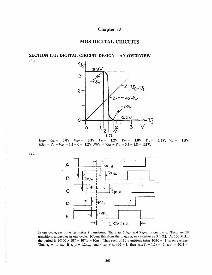
Chapter 13
MOS DIGITAL CIRCUITS
SECTION 13.1: DIGITAL CIRCUIT DESIGN-AN OVERVIEW13.1
-MOW
o.ov
Here V0L = 0.0V, V0H = 3.3V, V„ = 1.2V, Vm = 1.8V, Vth =NMl = Vn - V0L = 1.2 - 0 = 1.2V, NMh = V0H - V,H = 3.3 - 1.8 = 1.5V.
1.5V, VM = 1.5V.
13.2
A
B
C
D
-iI
u ÿ'
UPL\A [
>mL -J•fPUlI
"jjvuv.
<-
tpu.H
H 1 CYCLE h-In one cycle, each inverter makes 2 transitions. There are 5 tPUi and 5 tPHL in one cycle. There are 10transitions altogether in one cycle. [Count this from the diagram, or calculate as 5 x 2.]. At 100 MHz,the period is 1/ÿ100 x 106) = 10"8s = 10/ts. Thus each of 10 transitions takes 1040= 1 ns on average.Thus tP = 1 ns. If tpm = 1.2tPm and (tPm + tPmyi — 1, then //>///,(1+ 1.2) = 2, tPm = 7/1.2 =
- 365 -

SOLUTIONS: Chapter #12-22
12.34 (continued)
Vo
200mV
1/f
- AÿV\
Front end of a tin* wava
TC-3.3/1Long-term-drittanvalopa of a fawtana of mtllivolta
tnon-datum
- 364-

SOLUTIONS: Chapter #13-3
Check:
Finally, NML = V,L - VOL = 1.3875 — 0 = 1.3875V, and NM„ = V0H - V,„ = 3.3 - 1.9125 =1.3875V
13.6 For Vlh: Both transistors operate in saturation, sharing the same current i, with V/ = v0 = V,/,Thus i = V2kp(VDD - V„, - IV,pl )2, and i= V2kn(V,h - V,„)2.Equating and taking square roots: Vdd - Vlh - IV,pl = <KAp{Vth - V,„).
Thus V,h = [VDD - IV,pl + Vk,/kpVtn] / [1 + Viq/kp], as provided in Eq. 13.8.
13.7 From part of the solution to P.36.6 above, for V where
VM = [Vdd ~ W,p\ + ÿkn/kpVm]/[1+ ÿlkn/k,,l wherei= Vlkp(VDD -VM- IV,p I )2, and i= 1/lkn(VM - V,„)2.Generally, gm = di/dv, where for v - VM:gmp = kP (VDd ~ VM - IV,p I) = kpÿ2,/kp = Alikp, and gmn = kn (VM - V,„ ) = ÿ2ikn.Also rop = VAp/i, and r„n = VAn/i.
Gain = - (gmn + gmp)(ron II rnp) =ÿpfk~+ Vl~][ JAp An x Vi]vAp + Ml!
= <2A(<kÿ + <k~p){VAp VAn Y(VAp + VAn )
= - vavdd -vm- \vtp\m<KAP + mApVAny[vAp + vAn)i
Thus the transfer slope at VM is 2(Vk/kp + l)(VApVAn)t(VAp + VAn)(VDD - VM - IV,pl )]Now, for Vln = IV,p I= 0.6, IVAI = 20V, kn = kp = (1.20.8)(100) = 150 pA/V2,
the gain is - 2(<l + 1)20 x 20<40 x (3.3 - 1.65 - 0.6)) = = - 38.1 V/V.
Check: From first principles, numerically: VM = 1.65, i= 1/2(150 x 10"6)(1.65 - 0.6)2 = 82.7(Vl ,r„ = 20452.7 x 10~6 = 0.242MQ., gm = 1/2(2)150 x 10ÿ1.65 - 0.6) = 1575p/W. and the
«ain = -gmr„ = - 1575 x 10"6 x 0.242 x 106 = 38.1 V/V, OK.
13.8 See kn = (20) x 8/2 = 80pA/V2, kp = (10) x 16/2 = 80pA/V2. From Eq. 13.6 and 13.7 of the Text {ordirectly from the triode relation, that is, iD = k ((vGS - V, )\)DS - vfcs ~ k (uGs ~ V,)x)Ds> for small
vDS}, see rDS = vDSAD =k v>)-
For inPut hi8h' =80 x lO"6 (5 - 1)
= 3,125k£1 For
input low, rDc =--= 3.125k Cl, the same, since the inverter is matched.F 80 xlO (5 - 1)
13.9 Maximum currents are the same for both the p -channel and n-channel devices.
For the output connected to an opposing supply, Imax - k/2 (vGS — V,)2 = 40 x 10~6 (5 - l)2 = 640|iA.
For the output at Vddÿ2,I— k (Cues ~ V,)Vds - uds42) = 80 x 10"6 ((5 - 1) 2.5 — 2.5/2) = 40 x 10 6
(0 - 6.25/2) = 550pA.
For the output 0.1Vdd from the limit, I= 80 x 10"6 ((5 — 1) 0.5 — 0.52/2) = 80 X 10~6 (2 — 0.25/2) =150 pA.
13.10 For all the inverters, V0L = 0V, VOH = Vdd > as VDD varies from 3.75 to 6.25V, and asV,„ = V,p = V,varies from 0.75 to 1.25V, with k„ = kp. From Eq. 5.94: V/p = 1/8 (3 Vdd + 2 V,). From Eq. 5.93:
VIH = 1/8 (5 Vdd - 2V,), or V,„ = VDd ~ V„, generally (for symmetry). Now for V/L to be largest,
VDD = 6.25 and V, = 1.25, whence V,L = 1/8 (3 (6.25) + 2 (1.25) = 2.66V, for which Vm = 6.25 - 2.66
= 3.59V. For V,L smallest, VDD = 3.75 and V, = 0.75, VIL = 1/8 (3 (3.75) + 2 (0.75)) = 1.59V, for
- 367 -

SOLUTIONS: Chapter #13-2
0.909 ns and tPLH = 1.2(0.909) = 1.091ns.
13.3 See that the static dissipation is zero. Thus the dynamic power/inverter isPD = (300 X 10-6 X 3.3V5 = 990 X 10~6/5 = 198pW.Now PD -fCV2, and C = PdA/V2) = 198 x lOÿlOO x 106 x 3.32) = 0.182 pF.For this logic, tP = (K100 x 106))10 = Ins and DP = 1x 10"9 x 198 x 10"6 = 0.198 pj
13.4 For the gates, tp = (30 + 10)/2 = 20ns. Total delay through 5 gates for 2 transitions each is T = 5 x 2X 20 = 200ns. Frequency of oscillation = 1IT - l/200ns = 5MHz.
0110ns 0 90ns 01 / I-VI
V2i30ns
, © _o__®-E-hjÿlOns 1_©
V3
V4
VS
.© ©L
© ®
1GL
©"L
©is 0 ©aÿ
©©AO
©r
© / © ©I-i—i-
30+10+30-70ns 30+10+30«70ns
10+30+10+30+10+30+10s130ns
Note that [3-©lor matched gates.
SECTION 13.2: DESIGN AND PERFORMANCE ANALYSIS OF THECMOS INVERTER
13.5 Since pn/p.;, = 10040 = 2.5, then from Eq. 13.10, for a matched device{W/L)p =2.5(W/L)n = 2.5(1.2p/»/0.8pm) = (3.0 (|inv0.8|im).
Since the generic process uses a supply of VDD = 3.3V, VOL = 0V and VOH = 3.3V.
From Eq. 13.8, with V,„ = IV(/)I = 0.6V and k„ = kp for matching.
VDD-\V,P\ + VM~V,„ 3.3-0.6 + ÿ(0.6) _=-TTluk--TTTi--3-ÿ - 1,65V-
IT*A.|j,/ l\.p 1 ' 1
[Of course, this result could have been written down directly.]
From Eq. 5.94, V,L = (3Vco + 2V,y8 = (3(3.3) + 2(0.6)>8 = 1.3875V.
From Eq. 5.93, Vm = (5VPD - 2V,V8 = [5(3.3) - 2(0.6)ÿ8 = 1.9125V.
From Eq. 5.95, NM„ = (3VDD + 2V,y8 = (3(3.3) + 2(0.6)>S = 1.3875V.
From Eq. 5.96, NML = (3V0D + 2V,y8 = 1.3875V.
-366-

SOLUTIONS: Chapter #13-4
which V,H - 3.75 - 1.59 = 2.16V. Now VOL is always OV, and V0H ranges from 3.75V to 6.25V, V,Lfrom 1.59V to 2.66V, VlH from 2.16V to 3.59V. See that the noise margins between gates (with dif¬ferent supplies and different V,) vary widely: Consider NM„ = VOH - V,H. Highest is 6.25 - 2.16 =4.09V. Lowest is 3.75 - 3.59 = 0.16V (See that this is very bad). Consider NM, = V„ - VmHighest is 2.66 - 0 = 2.66V. Lowest is 1.59 - 0 = 1.59V.
13.11 From Eq. 13.12, for an inverter with a fanout of 1,C = 2CgdI + 2Cgd2 + Cdbx + Cdb2 + Cg2 + Ci4 + Cw.For the matched inverter, (W/L)n = (1.20.8), and (W/L)p = (10040X1.20.8) = (3.00.8).Thus, Cgdi = 0.5 x 1.2 = 0.6/F, Cgd2 = 0.5 x 3.0 = 1.5/F, Cdbx = 2.5 X 1.2 = 3.0/F,Cdb2 = 2.5 x 3.0 = 7.5fF, Cg3 = 1.8 x 0.8 X 1.2 = 17.3/F, C„4 = 1.8 x 0.8 X 3.0 = 4.32/FCw = Cg3 = 1.73fF.Thus C — 2(0.6 + 1.5) + 3.0 + 7.5 + 1.73 + 4.32 + 1.73 = 22.5 fF. Since the inverter is matched-" ™-
13.12 For the assumption of constant current. From Eq. 13.14, in saturation,iDN(0) = V2K{W/L)n(VDD - V,)\From Eq. 13.17, tpm = CVpc/lAosiO).
Now for V, = 0.2VDD, iDS(0) = Vlk'n(W/L)n(\ - 0.2)2V%D = kÿW/L)nV$D{0.32).
ÿ CVDD4
1.6CThus tpm = n/i , ,,2 or fpHL =
2(kn)(W/L)„ V)jd(0.32) kn(W/L)nVDD
2CAlternatively, from Eq. 5.101, tpm =
kn(W/L)n(VDD - V,)V' Wdd~4V,
+ F21n-Vdd ~ V, VDD
For this case, in which Vdd - 3.3V and V, = 0.6V,
2CIpHL
inn v Irv-6,100 X HTX1.20.8)(3.3 - 0.6)
2C
06 3(3.3) -4(0.6)3.3 - 0.6 3.3
X [0.22 + 0.41] = 3111 Cs.100 X 10ÿ(1.5)2.7
Now, ignoring the fact that here V, = 0.60.3VOD = 0.182VDD, (rather than 0.2 Vdd)-1.7C
100 X 10ÿ(1ÿ0.8X3.3)1.6C
100 X 10ÿ1.20.8X3.2)Assuming the estimte from Eq. 5.101 to be the most accurate, it is interesting to see that of the simpleapproximations, the one found here, is best. It is certainly, the easiest to obtain from first principles.
From Eq. 13.18, tPHL =
______= 3434 C s.
J I
From the constant-current calculation above, tpm = _6 . ow„ = 3232 C s.
13.13 For simplicity, use k = k'n{W/L)„, and substitute V, = 0.1VDd ÿ
From Eq. 13.14, iD(N)iD(0) = V2k{VDD - Vcf = (0.405) ---(1)
From Eq. 1315, iD(AV)iD(M) = k[(VDD - V,)VD[A ~ (VW2)2/2] = kV$D(0.SV2 - 1/8) = £FD20(0.325)
Thus, iD(av) = kV$D(0.405 + 0.325X2 = *Vj&>(0.365)1 17C
From Eq. 13.18, tPHL = CVDD/240.3651Vo2o) = tzt-.kvdd
Now for the current in (1) sustained for the half transition,
- 368-

SOLUTIONS: Chapter #13-5
tpHL = CVDD/2/(0A05kVoD) =kVDD
h'HL =2C
Hvdd - V.)
V,
2CkVDD(0.9)
0.11 -0.1
Vdd - v,
+ l/21n
+ l/21n
3-4(0.1)1
From Eq. 5.101 on page 434 of the Text,
3VDD - 4V,
2C-(0.111 + 0.478) =
1.31CkVDD(0.9) v~.....' kVDD
Obviously, the sustained saturation result is reasonably good and certainly simple to obtain from firstprinciples. Notice, as well, the impact of change of V, from 0.2 Vqj to 0.1 Vpp, being a change in thecoefficient from 1.6 to 1.2 in the simplest constant-current formula.
13.14 From P13.8 above, kn = k,, = 80pA/V, IF,I= IV, VDD = 5V. For Vin = VDD/2 = 2.5V, Ipeuk = iD =80/2 (2.5 - l)2 = 90 it A. Assume (for the present purposes) that rise and fall times arc measured
from 0% to 100%. As the input goes from IV to4V, the current flow is triangular, with a peak valueof 90pA. Over an interval of 3/5 x 774, the aver¬age current is 90/2 = 45pA. This happens twiceper cycle. Thus the average current per cycle from
2 (35) x 774x45= 13ÿA<T/4
T/4
V T/4
T/4
/self conduction is
The average current due to capacitance load isCVDD f = 0.5 x 10-'2 x 5 x 20 x 106 = 50 pA.Total average current = 50 + 13.5 = 63.5 |iA. Withload, PD - 63.5 x 10"6 x 5 = 317.5 pW. Withoutload, PD = 13.5 x 5 = 67.5 pW.
13.15 From Eqs.13.18 and 13.19, tPHL1.7C
kn(W/L)n VDD, and tpui - 1.7C
kp(W/L)pVDDHere, k'n = 2k'p = 20pA/V, and (W/L)n = V2(W/L)p = 8pm/2p/n.
For V/jo = 5V, IV,I = 0.2VDD = IV, and tPHL = tPLH = tP. -1.7 x 0.5 x 10~12
2.12 ns.20 X 10-* (8/2)(5)
For a 5-stage ring oscillator, / = [10(2.12)]"' = 47.2 MHz. Ignoring the transition-time peak-currentflow per gate, PD =/ CV$D = 47.2 x 106 x 0.5 x 10"12 (52) = 590pW.
The Delay-Power product DP = 2.12 x 10"9 x 590 X 10"6 = 1.25 X 10"12/ = 1.25pJ.
13.16 Here, VDD = 1.3V, IV,I = 0.8V, (a) Qn conducts for x>, from 0.8 to 1.3V, and Qp conducts for v,from 0 to (1.3 - 0.8), or 0 to 0.5V. For x>, = 1.3/2 = 0.65V, neither transistor conducts and iD = 0,(b) Output voltages range from 0 to 1.3V. Von = 1*3V; V0l - 0.0V, (c) V/L = 0.8V, and V,// = 1.3 —0.8 = 0.5V. [Note that V,L > V,H !] Between V,{, and V///, no current flows.
0.8 1.3
I.JV
vl 0V
1.3V 0.5VCO<
vO 0V [r0.39ps
- 369 -

SOLUTIONS: Chapter #13-6
(d) (Note in considering the transfer characteristic, that the small capacitor at the output holds the out¬put while neither transistor conducts, (e) iD = 1/Ik (1.3 - 0.8)2 = 1/2 x 20 x 10~6 (0.5)2 = 2.5pA peak.For \)q at 0.8V, iD = k [(uG5 - V,) vDS - dAv2] = 20 x 10"6 [(1.3 - 0.8) 0.8 - 0.82/2] = 1.6pA. Aver¬
age current is —1—ÿ—— = 2.05pA, and the time for a 0.8V change (from 0 V to 0.8 V) is —— =1 x 10~'2 X 0 8-—t" = 0.39 p s. Conclude that propagation delay is more than 0.39ps. Now, for the out-
2.05 x 10"6put moving from 0.8V to 1.3V, the average current available is (1.6+0)/2 = 0.8pA.
13 — 08Thus, the time to reach 1.3V from 0.8V is about 1 x 10"'2 x —:-ÿ = 0.625ps, and the total transi-
0.8 x 10"6tion time is about (0.39 + 0.625) = 1.02py . Considering the driven stage with input at 0.8V, the avail¬able output current is Op.A. At an input of 1.3V, the available output current is 2.5pA. Thus, the aver-
0 + 2.5 , „c . , .. .. ,. 1.0 x 10~12 x 0.8age current =---= 1,25pA, and the propagation delay =- — = 0.64 ps.
(f) Frequency of oscillation of 5 gates is (at most) =---t- = 156kHz.10 (0.64 x 10"6)
13.17 Here, kn = (20) x 18/2 = 180pA/V2, kp = (20/2) x 4/2 = 20pA/V2: IV,I= IV, VDD = 5V. See V0H =5V Vol = 0V. For V,h = d, D/ = Do = D, both devices are in saturation, and 90 (D - l)2 = 10 (5 - D -l)2. Taking the square root, 3(d — 1) = 4 — D, 3d - 3 = 4 — D, 4d = 7. Thus, V,h = D = 1.75V. ForVil= U, Qp in triode, Qn in saturation, 90 (o - l)2 = 10 (2 (5 — t) — 1) (5 — uG) — (5 — v0)2),9 (\> — l)2 = 2 (4 — v) (5 - v0) - (5 - v0)2 ---(1). Now, taking derivatives, 18 (x>— 1) = 2(4 — v)
d Dq —9 Do 9 Do( - -T-ÿ-) + 2 (5 - Do) (-1) - 2 (5 - Do) —r——. Now, with = -1->18d-18=18-2d
d D d D d D- 10 + 2 Do - 10 + 2 D0, 20 D = 4 D0 + 6, d = .2 d0 +0.3 ---(2). Substitute (2) in (l) ->9 (.2d0 + 0.3 -l)2 = 2 (4 - ,2d0 - 0.3) (5 - D0) - (5 - D0)2, 9 (,2d0 - 0.7)2 = 2 (3.7 - .2d0 - 0.3)(5 -Do) - (5 - D0)2, 0.36 Do + 4.41 - 2.52 D0 = 37 - 9.4 d0 + .4 d3-25 + 10 Do - D3, 0.96 DI- 3.12 D0 - 7.59 = 0. Thus D0 =ÿ
3-12 ÿ V 3122 +ÿ4 (.96) (7.59ÿ _4.87V, and VtL = D = .2 (4.87 + 0.3) = 1.275V. For V,H = D, Qn in triode, Qp in saturation,
10 (5 -D - l)2 = 90 (2 (D - 1) (Do) —Do), (4 - D)2 = 18 (D - 1) (Do) — 9 Do ---(1). -jp- 2 (4
9 Do 9 Do 9 Do- D) (-1) = 18 (D - 1) + 18 Do - 18 Do -r-. For —— = -1 —> 2 D — 8 = 18 — 18 D + 18
' 9d 9d 9dDo + 18 Do, 20 D = 36 Do + 26, D = 1.8 D„ + 1.3 ---(2). Now, substituting (2) in (1), (4 - 1.8 D0- 1.3)2 = 18 (1.8 D0 + 1.3 - 1) D0 - 9 d£, (2.7 - 1.8 D0)2 = 18 (1.8 D0 + .3) D0 - 9 Do, 7.29 - 4.86
d0 + 3.24 Do = 32.4 Do + 5.4 d0 - 9 Do, Do (20.16) + d0 (10.26) - 7.29 = 0, Do + .509 D0 - .362
= 0, Do =~'509 ± 5092 + 4 ( 362)
= 0.400V, and D = 1.8 (.4) + 1.3 = 2.02V. Thus VlH = 2.02V.
For tp : For D0 = 5V, /„ = 90 (5 - l)2 = 1.44mA. For D0 = 0V, 1p = 10 (5 - l)2 = .160mA. For D0= 1.75V, /„ = 90 (2 (5 - 1) (1.75) - 1.752) = 0.984mA, and Ip = 10 (2 (5 - 1) (5 - 1.75) - (5 - 1.75)2)
CV 0 5 x 10-12 x f5 - 1 751= 10 (26 - 10.6) = 0.154mA. For discharging, tPHL = — = lp-3 ÿ 44 + 934ÿ2
= 2,89ns' For
. . 0.5 X 10'12 (1.75) rcharging,.rLH = = 5.57»s.
SECTION 13.3: CMOS LOGIC-GATE CIRCUITS13.18 Y =A(B + C). The corresponding pull-Down network (PDN) is shown asD|.
Y =A(B + C) =A + B + C =A + B C. The corresponding pull-Up network (PUN) is shown as
Usbu 1.
- 370 -

SOLUTIONS: Chapter #13-7
Now, the PUN dual to Di is U2-
J*_h
.jp
+ VDD + VDD
*~~lj' ÿ
=" ( D1 ) (U1)
See that U2 is similar to t/|, but not identical, D and C being interchanged with respect to the connec¬tion nearest to the power rail.
£>2 is a PDN obtained from U
+ VDD
t!
Y
yj|(U2)
J-i=" (D2)
See that D2 and D\ are not identical, the transistor A (the one with input A) being near ground in D2,but near the output in D\. For this logic function, there arc 2 PUN and 2 PDN which can form2x2=4 different gate topologies in all.
13.19 In Fig. 13.15, the PDN shown is to be called Di and the PUN is to be called Uj. Here, PDN D2 is dualto U1.
r1 r•£btfcJ
ÿtij
!_E
iJ5 -£JS -£iÿÿ=ÿ (D2) =" (D3)
- 371 -

SOLUTIONS: Chapter #13-8
Z)3 is D2 redrawn more symmetrically. U2 is the PUN dual to Dh drawn directly. U3 is U2 redrawn.
+ VDD + VDD + VDD + VDD
-A I B | A I B 1-p -p1_
ÿ•~|J *~~fJ1_1
•A
Hi1d nd *nd -B
Y ÿ(U2)
~1<U3)
Using U\,D\ and U3, D3, there are 4 possible XOR circuits that can be constructed. When the relativeplacement of the inputs with respect to the supplies is considered, there are two versions of each of theperfectly square networks (like U3, £>3) depending on proximity to the supply of each of the two serieslayers (of paralleled transistors). Thus for each of these U and D networks there are 2 variations.However for networks U\ and D2, in which the two series nodes are not joined (but, correspondingly,not for D3 or U3), there are 4 variations:
AB AD CB CDC D C B A D A B
with respect to proximity to a supply.
Now, for all networks like Uh D\, there are 42 = 16 possible arrangements, but for half of these (thatis, 8), there are twice as many combinations each (the diagonal exchanges in each group of 4 above).Thus the number of combinations is 8 <t> 8(3) m 34
13.20ÿ VDD
Jn.reTj
J _ _ JaJ1bJ1cJ1dJ!
Refer to the transistors by their variable names PA ,Na, etc. Now Na,Nb,Nc, Nd are all of unit size,the same as N in the unit inverter, where(W/L)n = (1.20.8). Now for matching, PA, PB, Pc<Pd are all 4x larger than P in the inverter, whichin turn is 2.5x the size of N,4(W/L)p = 4(3.00.8) = (120.8).
Total area of the NOR is 4[(1.2)0.8 + (12)0.8]
= 4(11)(0.8)(1.2) = 44(0.8 X 1.2) = 42.24pm2.This is 44 X the area of a single NMOS. The areaof an inverter is (1+ 2.5)(0.8 x 1.2) = 3.36pm2.Thus the NOR is 42.240.36 = 440.5 = 12.6 xlarger than a single inverter.
13.21 For a 4-input NAND gate, the N devices are in series and the P devices are in parallel. For mobilitymatching, each P device is the same size as P in the inverter, namely (W/L)p = 2.5(1.20.8) = (3.00.8).
For current-drive matching, each N of the NAND is 4 x larger than N in the inverter
= 4(1.20.8) = (4.80.8).
- 372-

SOLUTIONS: Chapter #13-9
NAND gate area = 4[(4(1) + 2.5)(0.8 x 1.2)] = 4(6.5)(0.8)1.2 = 26(0.96) = 24.96p.rn2.This is 26x the area of one NMOS, and 266.5 = 7.43X the area of the basic matched inverter, and24.96/42.24 + 59% of the area of a NOR?
13.22+ VDD + VDD
nJ *~daaijI
Consider one of the circuits resulting from the solution of P13.18above for Y =A(B + C). For a matched inverter, the transistors areP, N where (W/L)p = 2.5(W/L)n = 2.5(1.2/0.8). Thus, we can sayP = 2.5N, referring to width or area (for all devices all of the samelength). Here, Pa -P and PB = Pc -2A. AlsoNa =NB =Nc = 2N.Total area
= P(1+ 2 + 2) +N(2+ 2 + 2) = 2.5N(5) +N(6) = 18.5N =18.5(1.2 X 0.8) = 17.8 |im2, or 18.5x the area of the basic NMOS,and 18.56.5 = 5.28x the area of a basic matched inverter.
13.23 Consider Fig. 13.12 of the Text, with input A low and input B active at \)/ = 2.5V. All devices sharea current Iwith the upper PMOS which operates in triode mode with its drain voltage = V\. Thus, forone input active: I= k/2(2.5 - l)2 = k,/2 (V, - 2.5 - l)2 and I= kp [(5 - 1) (5 - V,) - (5 - V,)2/2].Thus, (V, - 3.5)2 = 8 (5 - V,) - (5 - V<9. V? - IV, + 12.25 = 40 - 8 V, - 25 + 10 V,
-9 V, - 2.75 = 0. and v,,-* ±"9'- 4 (-2.75K2) 9±,0.l5V?, 2 V,2
2x2 = 4.787V,
whence kp =k (1.5 )
= 1.36k.(4.787 - 3.5)2
Now, for two inputs active: V,h = u.(series) transistors is i= 2k/l (o - l)2
- V 02/2]. From the first pair, v> - 1 =
Since the two NMOS operate in parallel, the current in the upperV - l)2, and also,i = kt
1.362
rk„ /6(V,k„ '2k
x (V, -v - 1) =
q(5 - t> - 1) (5 - V0 - (5
x (Vi- o - 1) = 0.82
V, - 0.82 V -0.82. Thus 1.82 v = 0.82 V, + 0.18, v = 0.4505 V, + 0.2195, or V, = 2.22 V - 0.220.
From the second pair: (V, - u- l)2 = (4 - u) (10 - 2 V,) - (5 - V,)2, (2.22 u- .220 - "U - l)2 = (4- V) (10 - 4.44 v + .44) - (5 - 2.22 o + .22)2, or (1.22 o - 1.22)2 = (4 - o) (10.44 -4.44 \>) - (5.22 -2.22 u)2, or 1.488 t)2 - 2.977 u + 1.488 = 41.76 - 17.76 u - 10.44 t) + 4.44 \)2 - 27.25 + 23.18 \) -4.93 o2, 1.98 i)2 + 2.043 o - 13.02 = 0, u2 + 1.032 o - 6.575 = 0, t) =[-1.032 ± V 1.0322- 4 (-6.575)]6 = 2.10V. Thus, the threshold is 2.10V, for which V, = 2.22 (2.10) -.220 = 4.44V.
Note that a simpler approach results from realizing that with both inputs active, the upper transistorsbehave as a single PMOS with twice the usual length, for which (kp )eq =k/2= 1.36k/2 = 0.68& whilethe lower pair operate with a combined (kn )eq = 2k.
Thus I= ((2ky2)(u - l)2 = (0.68L<2)(5 - t) - l)2, or (v - l)2 = (0.34)(4 - u)2,a) - 1= 0.583(4 -V) = 2.33 - 0.583\>, or 1.583o= 3.33, and V = 3.334.583 = 2.10V, as
orbefore.
- 373 -

SOLUTIONS: Chapter #13-10
13.24 For Y =AB +ACD, obtain the PDN directly and the PUN as its dual:
S_lgLij !_Eji_£i i-6
=ÿ(01)
Y
DJ;
CJ5 tijt-h
ÿ4" (D2)
+ VDD + VDD + VDD
h| t!B
—pi —i;h t-iY (U1)
Hi+ VDD + VDD + VDD
J nj *-iJ"1
1 Y (U2)-•-•
For Y =AB +ACD: W„ = [3(3) + 2(2)31.213(1.2) = 15.6pm, and Wp = [5(2)](2.5)1.2 = 30pm.
The total width is WT = 15.6 + 30 = 45.6pm.
For Y=A(B+ CD): W„[3(3) + 1(32)]1.2 = 10.5(1.2) = 12.6pm, andWpfl + 3(2)]2.5(1.2) = 17.5(1.2) = 21pm. The total width is WT = 12.6+ 21 = 33.6pm, a reduction
of45.6 - 33.6
45.6X 100 = 26.3%!
13.25 For a Buffered Inverter: Total n-width isl + 3 + 9 = 13 units, while the total p-width is 2 + 2 (3) + 2(9) = 26 units. Thus the total width (and area) is 39 units. For a Buffered 4-Input NOR: The inputgate uses 4 n-channel devices of unit width, and 4 p-channel devices whose width is 4(2) units [sincethe input stage is "basic-inverter compatible"]. Thus, the total width (and area) of the input stage is 4(1) + 4 (4)(2) = 36 units, and of the two buffer stages is 39 - 3 = 36. Thus, the total area of the buf¬fered NOR is 36 + 36 = 72 units. Input capacitance is proportional to the area of the p and n devicesconnected to each input. For the buffered inverter, it is 1+ 2 = 3 units. For the buffered 4-input NOR,it is 1 + 4 (2) = 9 units, that is, 3 times greater. For input inverters and an intermediate NAND, thetotal area of the input inverters = 4x(l +2)= 12. For the NAND, each n-channel device is 3 X 4 =12 units wide, and each p-channel device is 3 x 2 = 6 units wide. Total area of the NAND is 4 (6 +12) = 72. Total area of the output inverter is 9 (1 + 2) = 27 units. Overall area of the equivalent NORis 12 + 72 + 27 = 111 units. For the equivalent NOR, the input capacitance is 3 units, equal to that ofan inverter and 1/3 that of the direct buffered NOR. It is interesting to note that an equivalent unbuf¬fered NOR has an input capacitance of 9(3) = 324 units, 108x more than that of the inverter-inputequivalent NOR!!
SECTION 13.4: PSEUDO-NMOS LOGIC CIRCUITS13.26 Use a 3.3V supply with (W/L)„ = (1.20.8), (W/L)p = (3.00.8), k'n = 2.5kp = 100pA/V2, and
0.6V. To meet the capacitor current-drive specification, iDn = liDp at Up = 3.3ÿ2 = 1.65V.IV,I=
-374-

SOLUTIONS: Chapter #13-11
Now, iDn =k'n(W/L)n [(3.3 - 0.6)1.65 - 1.652/2] = 100(1.5)[1.65(2.7 - 1.65-2)] = 464|M , andipp — 464 = 2 X 40(W/L);, [(3.3 - 0.6)1.65 - 1.652/2] = 40(W/L)p(3.09). Now, noting that the terms [ ]are both the same ( = 3.09), see that (W/L),, = 100(W/L)„/(2 x 40) = 1.25(W/L)„.
Here, kn = 100(1.241.8) = 150|M/V2 and kp = 40(1.25)(1.20.8) = 75|M/V2.Thus r = kn/kp = 15075 = 2.
Vdd - V. 3 3-06VOH = 3.3 V. From Eq. 13.36, Vw = V, + -- = 0.6 + , U°
= 2.16V.Vr + 1 "V2 + 1
From Eq. 13.38, V,H = V, + 2ÿ3r (VOD - V,) = 0.6 + 2ÿ6(2.7) = 2.80V.VDO - V, 2 7From Eq. 13.35, V,L = V, = -- = 0.6 + -A— = 1.70V.Mr + 1) ÿ2(3)
From Eq. 13.39, V0L = (VOD - V,)[[l -ÿl-Vr ] = (2.7)[1- ÿ1- 17] = 0.79V.Note that Vor. is very high, exceeding the threshold of the NMOS transistor of a succeeding inverter,whose current would reach iDL = V2 * 150 X 10~6(0.791- 0.6)2 = 2.75(iA .Thus, this circuit might be appropriate for high-speed operation but leads to a supply current somewhatin excess of the usual 50% of the total PMOS current. Otherwise,NMl = V,L - Vol = 1.70 - 0.80 = 0.9V, and NMH = V0„ - V,H = 3.3 - 2.80 = 0.5V whichare not large, but relatively balanced.
13.27 To meet this specification, the PMOS in the pseudo-NMOS gate must be identical to that in a matchedminimum-size CMOS inverter. In this case, the most that a minimum-size NMOS driver could do islower x>o to VdcV2! Correspondingly, V0L would be = 37 = 1.5V. VM = o, would be very high:
Here, iD„ = k[(3 — 0.6)(3 - o) - (3 - u)ÿ2], and iDn = k/2[o - 0.6]2. For equality,(o - 0.6r = 2(2.4)(3 - -u) - (3 - V)2, or o2 - 1.2u + 0.36 = 14.4 - 4.8o - 9 + 6t) -d2. or2o2 -2.4o -5.04 = 0, whence u= [--2.4 ± ÿ2.42 - 4( - 5.04)(2)]4 = (2.4 + 6.79y4 = 2.30V
13.28
(a) For minimum-size NMOS: For r = 4, kp = knM. or k'p(W/L )p = k'n(W/L)„/4, or(k'/l)(W/L)p = k'n(W/L)nA whence, (W/L)p = (W/L)„/2.Since the width is a minimum of 1 unit, Lp must be raised to 2 units.
Thus NMOS is 1 x 1and PMOS is 1x 2 and the total area is 1x1+2x1= 3units2.For r = 10, Lp = 107= 5 units, and the total area is 1x1+ 5x1= 6units2.
(b) For minimum-size PMOS (1 x 1units)
For r = 4, Wn = 47 = 2 units, whence the total area is (1x2+1x1) = 3units2.For r = 10, W„ = 107 = 5 units, whence the total area is (1 X 1 + 5 X 1) = 6units2.For design style (b), the output current drive (as measured by the PMOS current) is larger thanthat in (a) by a factor r/2 although the areas are the same!
(c) In (a) and (b), arrange that the devices are (1 x 1) and (r/2 x 1) in size. Here, we try a designstyle where the devices are each (1 X ÿ/>7) and fÿr/7 x 1) in size.
For r = 4, the PMOS would have Wp = 1 unit and Lp = 1.414 units, with Wn = 1.414 unitsand L„ = 1 unit.
The total area is 2(1.414 X 1) = 2.83 units { = 2ÿ2 = 2ÿ47 = 2ÿ7/2}, in general.
For r = 10„ Wp = 1 unit, Lp = ÿ107 = 2.236 units; W„ = 2.236 units, L„ = 1unit.
The total area is 2(2.236 X 1) = 4.47units2 ( = 2ÿ5 = 2ÿ107 = 2<r/2), in general.
In general, the total area is 2ÿr/2 =ÿ2r ,as contrasted with (1 + r/2) for styles (a), (b).
- 375 -

SOLUTIONS: Chapter #13-12
The output drive, proportional to the PMOS W/L ratio, is W/v2 = ÿ2/r in (c), while its is propor¬tional to l/(r/2) = 2/r in style (a).
Thus style (c) produces a "ÿr/2 improvement in current and a ~ÿ2r/{l + r/l) reduction in area.In summary:
Ratio Current Arear a c ratio % a c ratio%4 0.5 0.707 141% 3.0 2.83 94%10 0.2 0.447 224% 6.0 4.47 75%
1*r( + 1)
13.29 For VDD = 3.3V and V, = OV:
From Eq. 13.41: NML = 0.6 - 2.7 - ÿ1 - Vr -From Eq. 13.42: NMH = 2.7(1 - lW3r ).
From equality, evaluate by a process of "trial and success":
For r = 1: NML = 0.6 - 2.7
---(1)
-Vi - l/i - -J—ÿ1(2)
For r = 2: NML = 06. - 2.7
NMh = 2.7(1 - 2ÿ3x2) =0.495.
For r a 3: NML = 0.6 - 2.7
= 2.7(1 - 2ÿ3(3)) = 0.900.
For r = 2.9: VM*. = 0.6 - 2.7
/VM„ = 2.7(1 - 2ÿ3(2.)) = 0.8692.
-ÿ1-1/2- -J—V2(3)
_Vl _ V3___L_V3(4).
= 0.6 - 2.7(1 - 0 - 0.707) negative, unworkable.
= 0.910;
= 0.884;
1-ÿ1- 1/2.9- -i—J-ÿ2.9(3.9)0.8882;
For r = 2.95: = 0.6 - 2.7
NMh = 2.7(1 - 2ÿ3(2.95)) = 0.8848
For r = 2.97: = 0.6 - 2.7
1_ Vi - 1/2.95 - ÿ2.95(3.95)
-Vl - 1/2.97 - -i-J-*2.97(3.97)
= 0.8860;
= 0.8853;
= 2.7(1 - 2ÿ3(2.97)) = 0.8909
For r = 2.955: = 0.6 - 2.7 1-Vl - 1/2.955 - -1-ÿ2.955(3.955) = 0.8859;
= 2.7(1 - 2ÿ3(2.955)) = 0.8863.
Conclude that the noise margins are equal at r = 2.954, where = 0.886V.
Now, for r = 2.954: V0H = 3.3V.
From Eq. 13.39: VOL = (Voz> - V,)[l - ÿ1 - 1/r ] = 2.7(1 - ÿ1 - 1/2.954) = 0.504V.
From Eq. 13.38: Vm = V, + 2{VDD - V,Yÿ3r =0.6 + 2(2.7)ÿ3(2.954) = 2.414V.
From Eq. 13.35: V,L = V, + (VDD - V,)Wr(r + 1) = 0.6 + 2.7/ÿ2.954(3.954) = 1.390V.
From Eq. 13.36: VM = V, + (VDD - V,)Wr + 1= 0.6 + 2.7W3.954 = 1.958V.
- 376-

SOLUTIONS: Chapter #13-13
From Eq. 13.40: Islm = V2kp(VDD - V,)2 = l/2(100(1.20.8yi.954)(2.7)2 = 185|J.A and NMH =0.886V, NMl = 0.886V.
13.30 From Eq. 13.39: VOL = (VDD - V,)[l - ÿ1 - Vr = aV,, or 1-ÿ1 - Vr = aV/(VDD - V,).
VDD - (1 + a)V,
Vdd - V,= []
,- Vdd ~ V, - aV,Thus, Vl-l/r = 1-aV,AVDd ~ V,) = —---rr-1- =
Vdd ~ V,
„ , t/ „2 Jt/ , ri2(Voo-Vtf-lVoD-d+aOV,]2
Now, 1- Vr = [r,and Vr - 1 - [1 =-s-,or(VDD-V,)2
„ VSd- 2VDD V, + V,2 - V$D + 2VDD V,(l + a) - (1 + a)2V,2 2 x VDD V2[l - (1+ a)2]Vr =-Thus, in general, r =
(Vdd ~V,f (Vdd ~ V,)2(Vdd-V,)2
aV,[2VDD - (a+ 2)V(]
„ „ , (3.3 -0.6)2 20.25 20.25For Vdd- 3.3 and V, = 0.6: r - „(06)[2(33).(g+ -,)Q6) "
Now. tor a= 0.5. 4.76.
Check: From Eq. 13.39: V0L = (VDD - V;)[l - ÿ1 - Vr ] = 2.7[1 - ÿ1 - 1/4.76] = 0.300 = V,/2, OK.
13.31
(a) Need VM = V, + (VDD - Vÿr + 1= VDD/1: Thus 0.6 + 2.7//r + 1 = 1.65, and
V7TT = J"? = 2.57, whence r = 5.61.1.65 - 0.6
(b) Need VOL = (VDD - V,)[l -Vl _ ]/r ] = V,: Thus 2.7[1 - ÿ1 - Vr ] = 0.6, andVl - Vr = 1-0.222 = 0.777, and Vr = 1- 0.7772 = 0.395, whence r = 2.53.
(c) Need Vot = (VDD - V,)[l - Vi- ]/r ] = 0.1V: Thus, 2.7[1 -Vl - Vr ] = 0.1, andVl - Vr = 1- .0370 = 0.963, and Vr = 1- 0.9632 = 0.0727, whence r = 13.75.
(d) Need V0L = 0.01V: Thus 2.7[I - ÿ1 - Vr = 0.01, and ÿ1 - Vr = 1 - 3.7 x 10"3 = 0.9963, andVr = 1- 0.99632 = 7.39 X 10"3, whence r = 135.2.
(e) Need V,L = V, + (VDD - V,y/r(r + 1) = 2V,: Thus, 2.7//r(r + 1) = 0.6, and ÿr(r + 1) = 4.5,and r2 + r = 20.25, whence r = ( - 1± "*/ 1- 4( - 20.25)V2 = ( - ± 9.06V2 = 4.02. For case a),r = 5.61, and VOL = (VDD - V,)[l -Vl - l/r ] = 2.7[1 - ÿ1 - 1/5.61] = 0.252V.
For case c), r = 13.75, and V,L = V, + (VDD - V,ylr(r + 1) = 0.6 + 2.7//13.75(14.75) =0.789V
For case d), r = 135.2, V,L = 0.6 + 2.7//135.2(136.2) = 0.62V
1.7C13.32 From Eq. 13.43, tPW =
kp VDD17C
From Eq. 13.44, ,rHL =ÿ(|
_ ,whore r =kAr.1 7C 1 7Cÿ " kÿW' an<1
Als0' " k„(l -l£wm-"nd - kp(r -Im>VdcNow, see tpm/tpm, =
1.7Ckp Vod
\nckAr - 0.96)Vdd
= (r - 0.46).
- 377 -

SOLUTIONS: Chapter #13-14
For tpiM = tpHL 0-46 = 1and r = 1.46
Correspondingly,
VDD - V,From Eq. 13.36, VM = V, -- = 0.6 +2.7/0+146 = 2.05V,
*r + 1 _ _From Eq. 13.39, V0L = (VDD - V,)[l - ÿ1 - Vr ] = 2.7[1 -ÿ1 - 1/1.46 = 1.18V.
From Eq. 13.41,
NMl = V, - (VDD - V,) 1 — V 1_
i/r_ —1-v(r + 1)
= 0.6 - 2.7 1 -ÿ1- 1/1.46 —j-ÿ-*1.46(2.46)
= - 0.089V.
From Eq.13.42, A/M„ = (Vco - V,)[l - 1ÿ3r ] = 2.7[1 -2ÿ3(1.46)] = 0.120 VNote that with these (small, negative) noise margins, this circuit would not normally be used in a stringof similar circuits, but rather as a special solution to a particular problem:
16C 1 6CFor a matched inverter, t„ = -:-= —7-—,where we assume that C is dominated by exter-
' k„(W/L)nVDD knVDDnal load (as it is not otherwise the same as C for the pseudo-NMOS.
11CFor the balancedpseudo-NMOS, t„ = — Ignoring the 1.6/1.7 coefficient difference see that the
\kn/f ) *DDpseudo-NMOS has a delay of 1.46 of the CMOS, being therefore about 50% greater.
13.33 For all NMOS devices, (W/L)n = 1.20.8, k'n = 100pA/V2, Vln = 0.6V. For the PMOS, \Vlp\ = 0.6V,kp = 40pA/V2. Generally, kp = kn/r, and (W/L)p40 = (W/L)n 1004*.
Thus (W/L)p = (l.W.S)(l0(y40yr = 3.754*. Now, for r = , (W/L)p = 3.754 = 0.9375. Thus, forWp = 1.2\im, Lp = 1.20.9375 = 1.28|iw.
Now, for r = 10, (W/L)p = 3.7540 = 0.375. Thus, for Wp = 1.2pm, Lp = 1.2/375 = 3.2pm.
Concerning Capacitances: Follow the development on page 1053 of the Text:
Assume Cw = 0. For each NMOS: Cgd = 0.5(1.2) = 0.6/F, Cdh =2.5(1.2) = 3.0/F,Cg =1.81.2x0.8 = 1.73fF. For the PMOS with r=4 or r = 10, assuming 1.2 pm width, andincreased length: Cgd = 0.5(1.2) = 0.6fF, Cdp = 2.5(1.2) = 3.0fF.Thus for the 8-input NOR with one input active, and an inverter load,C| = 2(0.6) + 7(0.6) + 8(3.0) + 0.6 + 3.0 + 1.73 + 0 = 10(0.6) + 9(3.)) + 1.73 = 34.73fF.For 2 inputs active, Ci= 2(0.6) + 2(0.6) + 6(0.6) + 8(3.0) + 0.6 + 3.0 + 1.73 = 34.73 + 0.6 = 35.33fF.
For a single input active: tpm = \.lC/[kn(i - 0.464*)VDO], and
tew = \.lC/[kpVDD] = l.lCA{kn/r)VDD].
For r = 4: tPLH = 1.7(34.37 X 10-'5)t(150 x 10i4)3.3]= 0.477 x 10"9jr = 477 ps, and
tPHL = 1.7(34.73 X 10~15)1150(1 - 0.464)3.3] = 135 ps.
For r = 10: tPLH = 104(477) = 1.19 ns, and tPHL = 135(1-0.464H1 - .4640) = 125 ps.
For 2 inputs active, kn is effectively doubled as is r in the calculation for tPHL . For tPLH, the kp and rused are the same. Why?
For r = 4: tpw = 477 X 35.3234.73 = 485 ps, and
tpHL = 1.7(35.33 X 10"15)1150 X 2(1 - 0.46-8)3.3] = 64.5 ps .For r = 10: tpm = 1.19 x 35.33-34.73 = 1.21ns, and
tPHL = 1.7(35.33 x 10-,5H150 x 2(1 - 0.46<20)3.3] = 62 ps.
- 378 -

SOLUTIONS: Chapter #13-15
13.34 Assume all NMOS have unit length and width. For the matched complementary 8-input NOR, there are8 unit-size NMOS and 8 PMOS which are each 8 X 2.5 = 20 times larger, due to the fact that there are8 in series and that kp = k',/2.5. Thus the area of the CMOS 8-input NOR is8(1 x 1+ 20 x 1) = 8(21) = l6Sunits2. For the pseudo-NMOS with r = 2, all NMOS are unit-size andthe PMOS is (k'ÿkpYr = 2.5Q. = 1.25 x wider. Thus the area of the pseudo-NMOS 8-input NOR is8(1 x 1) + (1.25 x 1) = 9.25units2. The complementary CMOS is 16841.25 = 18.2 X larger!Correspondingly, the pseudo-NMOS gate is only 9.25468 x 100 = 5.5% of the size of the CMOSgate!
SECTION 13.5: PASS-TRANSISTOR LOGIC CIRCUITS13.35 For this situation, Vql = 0.0V, but Vqh = 3.3 — V,, where V, is increased by the body effect. From
Eq. 5.30, and the data in the introductory NOTE:
V, = V,0 + d(SvSB + 2<t>f - <2®f) = 0.6 + 0.5(VV0h + 0.6 - ÿ06),or V, = 0.6 + 0.5V3.3 - V, + 0.6 - 0.5ÿ0~6 or V, = .2127 + 0.5ÿ3.9 - V,, or
V3.9 - V, = 2(V, - .2127) = (2V, - 0.4254). Squaring, 3.9 - V, = 4V,2 - 1.702V, + 0.181, or4V,2 - 0.702V, - 3.72 = 0,
whence V, = (--0.702 ± %7022 - 4(4)( - 3.72)/2(4) = (0.702 ± 7.747/8 = 1.06V
Thus Von = 3.3 - 1.06 = 2.24V.
Assuming that the specification "driven" means that the two gates are joined drain to source (not drainto gate), they behave as a single transistor with twice the length, but with the same V,. Thus for no dcload on the gate, Voh — 2.24V, as before. However, dynamically, they are different: For a matchedinverter using the standard devices for which IV,I = 0.6V, kn = 2.5kp = 100pA/V2, and(W/L)n = (1.241.8), kn = kp = 100(1.241.8) = 150pA/V2.For a 2.24V input, the current in the connected inverter, io = 1/2(150)(3.3 - 2.24 - 0.6)2 = 15.87pA
For the NMOS with V0 = D, 15.47 = 1501(2 24 - 0.61o - d2/21. and 3.28u - u2 = 0.2063, orv2 - 3.28u + .2063 = 0, whence u = ( - - 3.28 ± ÿ3.282 - 4(.2063)/2 = (3.28 ± 3.152X2 = 0.064V.
For the capacitance at the inverter input including the input pass gate: and a grounded pass gate.
Cgn = 1.2 x 0.8 X 1.8 X 10~15 = 1.728 fF, Cgp = 2.5 x 1.2 X 0.8 x 1.8 x 10"15 = 4.32 fF,
C.*b — Qfc = 2.5 x 10-15 X 1.2 = 3.0 fF. Now, assuming Cw = 0. Thus,C = 1.728 + 4.32 + 3.0 + 3.0 + 0 = 12.04 fF.
For propagation times: Consider the gate of the pass transistor to be always at + 3.3V.
At vs = 3.3/2 = 1.65V, V, = 0.6 + y[ÿVSB + 2<D/ - ÿ2<6/ ] = 0.6 + 0.5ÿ1.65 + 0.6 - 0.5ÿ06 =0.962V
For tPLH (V; = 3.3V): iD(L) = 1/2(150)(3.3 - 0.6)2 = 547pA , and
io(M) = 1/2(150)(3.3 - 1.65 - 0.962)2 = 35.5pA , for which iD(.av) = (547 = 35.5/2 = 291pA .Correspondingly, tPLH = (12.04 x 10~15 x 1.65H291 x 10"6) = 68.3 ps.
For tpnL (Vt — 0V). Assuming the output starts from 3.3V! i„(/7) = 1/2(150)(3.3 - 0.6)2 = 541\iA (asbefore), and iD(M) = 150[(3.3 - 0.6)1.65 - 1.652/2] = 463pA, for whichiD(av) = (547 + 463>2 = 505pA .Thus tpHL = 12.04 x 10""15 x (3.3 - 1.65X505 x IO"6) = 39.3 ps
For an imperfect initial signal (2.24V rather than 3.5V).
tPHL = 12.04 x 10"l5(3.3 - 2.24/505 x 10~6 = 4 25.3 ps.
13.36 For (W/L)p =0.1, with Wp = 1.2pm, Lp = 1.241.1 = 12pm. Now, QR begins to conduct when V0zreaches 3.3 - 0.6 = 2.7V. For u0i = u. For the inverter, iDn = 1/2(150)(\) - 0.6)2 = 15(v - 0.6)2,iDp = 150[(3.3 - u)0.6 - 0.62/2] = 90(3.3 - u) - 27.
- 379 -

SOLUTIONS: Chapter #13—16
Now iDn = iDp -> 75(u - 0.6)2 = 90(3.3 - v) - 27, 75\)2 - 90o + 0.36 = 297 - 90o - 27,75u = 297 — 27 — 0.36 = 269.6, D2 = 269.625 = 3.595, whence u = 1.896V. Thus QR begins to con¬duct with Uoi = 1.896 V.As Qr begins to conduct it assists in the LH transition pulling oOI to Vom = 3.3V, and reducing tPWby speeding up the upper end of the transition.Now for tPHL at D0i with QR: Initially, im{H) = 1/2(150)(3.3 - 0.6)2 = 547pA • TheniDi(M) = 150[(3.3 - 0.6X1.65 - 1.652/2)] = 463pA .Also, at \)0 1 = VDD/1 = VM , t)0i = Vm/l = 1.65V eventually and the minimum size QR conducts(tw(Af) = 1/2(1502.5)(3.3 - 1.65 - 0.6)2 = 33.1pA but before \)02 responds (and is still at 0V),iDR (jc) = 1/2(1502.5X3.3 - 0.6)2 = 218.7pA .Thus there are two choices represented: First, there is the case in which turnoff is regenerative, and QRhelps, correspondingly, the average capacitor current is((547 - 0) + (463 - 33))2 = 489pA .Now for C = 12 fF, from P13.35 above, tPHL = 12 X 10~15 x (3.3 - 1.65X489 x 10-6 = 40.5ps .In the second case, regeneration is assumed to be delayed and QR conduction reduces the current avail¬able to the capacitor, namely, igÿ)= 1502.5[(3.3 - 0.6X1.65) - 1.652/2] = 4632.5 = 185pA .If this is assumed to flow all the time (it is actually smaller for high o0|) then the average capacitorcurrent is [(547 - 185) + (463 - 185)X2 = 320pA, for which tPHL = 12 x 10"15 x 1.6S320 x 10"6 =56.25 ps.
13.37 For this situation, the pass transistors, the grounding switch and the inverter NMOS are all minimumsize (1.2pm x 0.8pm), while the inverter PMOS is 2.5 x wider.
Using the data for the standard devices (in the introductory NOTE above),
Cdh = Csb = 2.5 x 1.2 = 3.0fF, Cg = 1.8 x 1.2 X 10.8 = 1.73/F, Cgs = 0.5 x 1.2 = 0.6fF, while Cwis assumed to be zero.
At the Inverter input:
Thus C = 3(3.0) + (1 + 2.5X1.73) + 3(0.6) + (1 + 2.5)(0.6) = 9.0 + 6.06 + 1.8 = 2.1 = 18.9 fF. Also
Vol = 0.0V and VOH - 3.3V. For propagation calculations, the gate signals of the pass device areassumed to keep the devices on while the input (to the drain source connection) rises and falls.
For tPLH: At 0V, iDn (L) = 1/2(150)(3.3 - 0.6)2 = 547pA , and
iDp(L) = 1.2(1502.5)(3.3 - 0.6)2 = 219pA .At 1.65V, V, = y,0 + 3(Vvsa + 2<&/ - ÿ2<h/ ) = 0.6 + 0.5(ÿ1.65 + 0.6 -ÿ06) = 0.96V.
Thus iDn(M) = 1/2(150)(3.3 - 1.65 - 0.96)2 = 35.7pA .iDp(M) = 1502.5[(3.3 - 0.6)1.65 - 1.652/2] = 185pA .Thus the current available to charge the output is ic(Av) = (547 + 219 + 35.7 + 185)2 = 493pA .Correspondingly, tPLH = 18.9 X 10"15 x 1.65493 x 10"6 = 62.3 ps. For tPHL: Roles interchange: p-channel currents are 1/2.5 those available from the n-channel.
ic(Av) = (547/2.5 + 219(2.5) + 35.7/2.5 + 185(2.5))2 = (219 + 547 + 14.3 + 463)2 = 622pA .Thus tPHL = 18.9 x 10~5 x 1.654533 x 10"6 = 50.1 ps.
- 380 -

SOLUTIONS: Chapter #13-17
13.38
C1
C2
-C1X=(-A)B + A(-B)
X2
-C2
X3
-C1
X4C2
13.39
B C
-A
•B
-C
- 381 -
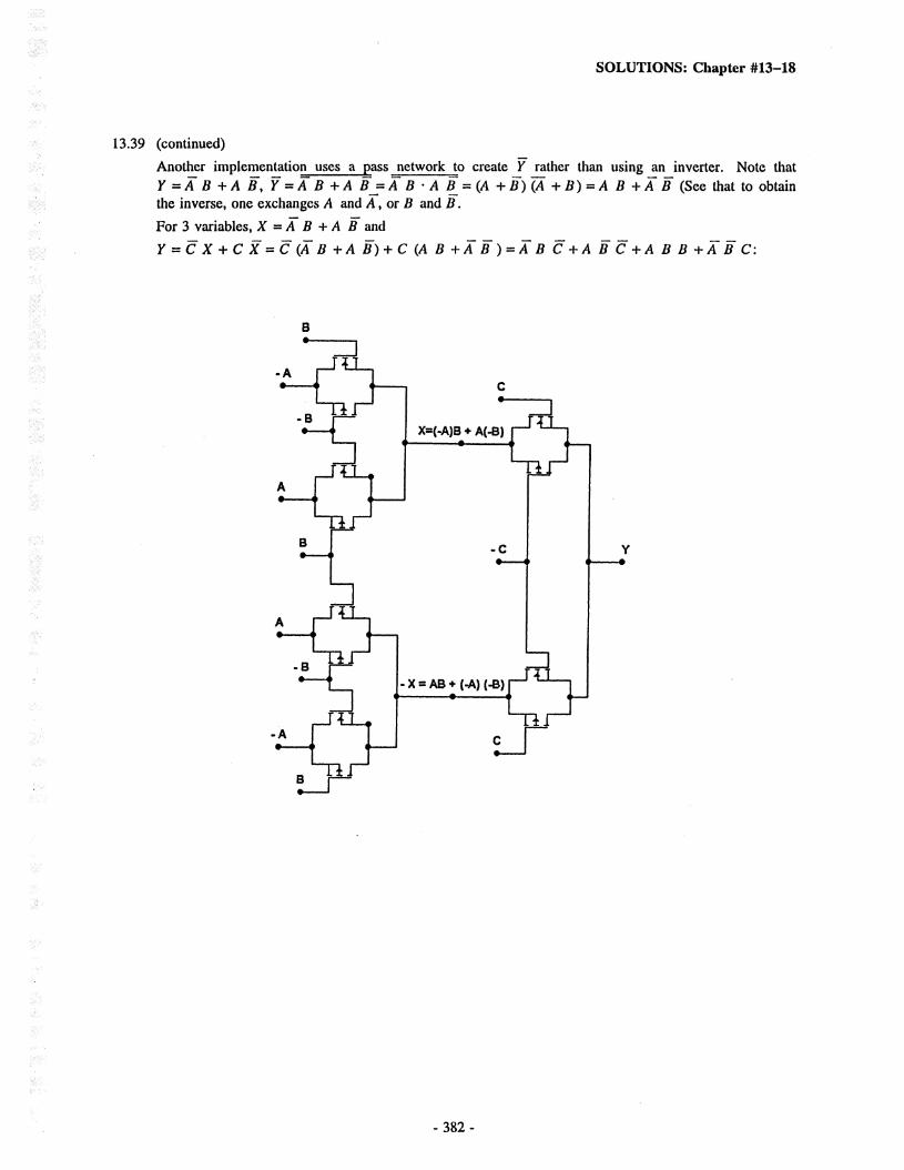
SOLUTIONS: Chapter #13-18
13.39 (continued)
Another implementation uses a pass network to create Y rather than using an inverter. Note thatY = A B + A B, Y = A B + A Bj= A B - A B_ = (A +B)jA +B) =A B +A B (See that to obtainthe inverse, one exchanges A and A ,or B and B.For 3 variables, X =A B + A B and
Y = CX + CX=C (A B+A B) + C (A B +A B ) =A B C +A B C +A B B + A B C:
B
-A
-BX=(-A)B + A(-B)
-C
•B
- X = AB + (-A) (-B)
-A
- 382 -

SOLUTIONS: Chapter #13—19
13.40
c X Y z F
0 0 0 0 00 0 0 1 00 0 1 0 00 0 1 1 00 1 0 0 00 1 0 1 00 1 1 0 10 1 1 1 01 0 0 0 01 0 0 1 01 0 1 0 01 0 1 1 01 1 0 0 01 1 0 1 01 1 1 0 01 1 1 1 0
X Y Z Cÿ ÿ 1 1
-zXirm_TLÿFHC
j_ov
See that F goes high when X is high, Y is low, Z is low, as C goes low. Thatjs, F = C X Y Z. IfX_ is available, but X is not, and Y is available, replace X (as shown) by Y, and Y (as shown) by X. IfX is available, but X is not and Y is not, use an additional p-channel MOSFET at the left connected tothe supply and X. For the basic symmetric inverter (W/L)t, - 20/5. Thus (W/L)4 = 10/5, (W/L)t 2j =10/5 x 2 x 3 = 60/5, to account for hole mobility and the fact that there are 3 transistors in series. Inmany applications in which the load is an inverting input, and the goal is circuit simplicity, all devicescan be of minimum size.
13.41
-C C -A A. JK\1
<
ÿ B1 >-t
mX
<-•—< i
T~Z~'
ÿ® rrf u........J "t_
! nf-X
< —rr
- 383 -

SOLUTIONS: Chapter #13-20
SecX =B C + B C and X = B C + B C
See Y =X A +X A and Y =X A + X A
whence, Y = A (B C +B C ) + A (B C + B C ) = A B C + A B C + A B C + A B C
and Y = A (B C + B C ) + A (B C + B C )=ABC+AB C +A B C +A B C
See that for the XOR, the output is 1 for all cases of an odd number of inputs, that is (1 or 3).
See that for the XNOR, the output is 1 for all cases of an even number of inputs, that is (0 or 2).
Concerning dynamic operation, there are several principles to observe:
(1) Most active input should be closest to the output.
(2) Most active input should drive the least capacitance.(3) Most active input should activate the least capacitance charging activity.
(4) Source-drain paths are fastest (since there arc no thresholds to overcome).
(5) Mutual conflict between principles will exist.
For this situation, placement of input A follows rule (1), rule (2), and rule (3), but is in conflict withrule (4). Placement of inputs B and C follows rules (4) and (1), but is in conflict with rules (2), (3).
SECTION 13.6: DYNAMIC LOGIC CIRCUITS13.42 For these devices, k„ = 2.5kp = 150pA/V2, IV,I= 0.6 V. In general, use the techniques suggested in
Excercises 13.10 and 13.11. Note in particular that the usual definition of tPUt (to 50%) is not particu¬larly relevant, since it is important for a dynamic gate that the output be at V0H before evaluation takesplace.
For tPm: Use a 0% to 90% rise-lime estimate.
For v0 low, iDp(L) = 1/2(1502.5)(3.3 - 0.6)2 = 21.87pA .For v0 high, iDp(H) = (1502.5)[(3.3 - 0.6)(0.1 X 3.3) - (0.1 x 3.3)2/2] = 50.2pA .Thus, iDp(Av) = (218.7 + 50.2>2 = 134pA ,whence tPUi ~ 100 x 10"15(0.9 X 3.3X134 X 10~6) =2*22 ns.
For tpHL • Consider 4 NMOS in series and tPLu measured from v0 = 3.3V to = 1.65V:
For v0 high. 'Dn(H) = V2(15(V4)(3.3 - 0.6)2 = 136.7|M.For u0 middle, iDn(M) = (15CK4)[(3.3 - 0.6)1.65 - 1.652/2] = 115.7|M.Thus, iD„(Av) = (136.7 + 115.T/2 = 126jM, whence tPHL = 100 x 10~15 x 1.65<126 X 10~6) = 1.31 ns.
For a 3-input NOR;tPLH is about the same, namely tPLH = 2.2ns . However tPHL is reduced by a factorof 2, since only 2 transistors are in series during evaluation. Thus tPHi = 1.31/2 = 0.65 ns.
13.43 For standard minimum-size devices, kn = 150|i/\/V2, IV,1 = 0.6V, (W/L) = (1.24).8),
C0x = 1.8/7viUM2, Cgll = Cgs - Q.5fF/\am, and Cdb = Csb = 2.5fF/\im .For a 3-input NAND, the equivalent capacitance includes 5 drains, 3 sources, 3 gates and 2 overlaps:
Ceq = 5(2.5 x 1.2) + 3(2.5 x 1.2) + 3(1.2 x 0.8 x 1.8) + 2(0.5 X 1.2)
= 5(3) + 3(3) + 3(1.73) + 2(0.6) = 15 + 9 + 5.2 + 1.2 = 30.4 fF.
For 2 inverters, CL = 2[1.2 X 0.8 x 1.8 x (1 = 2.5)] = 7(1.73) = 12.1/F. Thus COL = 30.4 + 12.1 =42.5 fF.
Initially at QA is cut off, node 1 is precharged to 3.3V, and nodes 2, 3, 4, are pulled to 0V throughtransistors driven by <S>, C, B. Now at /1+, C goes low, isolating node 3 (at OV). Now at t2+, A goeshigh, joining nodes 2, 3 to the output node 1.
- 384 -

SOLUTIONS: Chapter #13-21
Capacitance of each of the nodes 2 and 3 is
C = 2(2.5 x 1.2) = 1(1.2 x 0.8 x 1.8) = 2(3) = 1(1.73) = 6 + 1.73 = 7.73fF.Capacitance of both nodes 2.3 together = 2(7.73) = 15.5fF.
Time Node 1 Node 2 Node 3 Node 4 d> A B C
'o_ _ _ _
L L H H3.3(F) 0 0 0 H L H H
'i+ 3.3(F) 0(F) 0(F) 0 H L H L*2+ 1.83(F) 1.83(F) 1.83(F) 0 H H H L
Note: Here, (F) indicates a floating voltage stored on the node capacitance.
Notice that the capacitance of node 1, when isolated by A low, isCdbp + Cdbn + 2(Cov) + 2{Csp + Cgn) = 2.5 x 1.2 + 2.5 x 1.2 + 2(0.5 x 1.2) + 2(3.5)(1.73)
= 3.0 + 3.0 + 1.2 + 12.1 = 19.3fF.Now at *2+. nodes 1, 2, 3 are joined with a common voltage D. Charge is conserved.
Thus Q = CV, and 19.3(3.3) + (15.5)0 = u(19.3 + 15.5) = 34.8o.
Thus u= (19.334.8)3.3 = 1.83V.
Note the dramatic loss in voltage! In practice addtional wiring capacitance Cw at the output node wouldhelp.
13.44 For CfF to discharge V, volts in tE ns, the leakage is iE = CV/tE = (50 + 10m)(0.6)4£ pA .For a single device for which V,n — 0.6V and kn = 150pA/V2, with an input voltage u
(50 + 10«)(0.6//e = 1503(1) - 0.6)2, whence t> = 0.6+(0.4 + 0.08nKtE>ÿ.For n = 5, and tE = 10/is, the voltage needed at one input is Ui where
\>i = 0.6 + ([0.4 + (0.08)syi0)'/' = 0.6 + 0.283 = 0.883V
For all 5 inputs acting together, t>5 = 0.6 + (l/SÿOÿSS) = 0.727V
13.45 For these transistors, (W/L ) = (1.23.8), kn = 2.5kp = 150pA/V2.From Qu iD(H) = F2(150)(3.3 - 0.6)2 = 547 pA.
Time taken for V, to fall from 3.3V to 0.6V is / = 50 x 10"l5(3.3 - 0.6X547 x 10"6) = 247 ps.
Now, for the leakage in Qj\
'02(3.3) = 1/2(150)(3.3 - 0.6)2 = 547p4 ,and iD2(0.6) = OpA ,such that i'D2(Au) = (547 + 0) = 273pA.
Thus, the change of voltage on CE2 is Ao2 = 273 x 10-6 x 247 x 10_12/(50 X 10~15) = 1.35V! Clearly,this circuit has a problem! It is this problem which motivated the invention of Domino CMOS.
13.46 The inverter uses (W/L) = 1.23.8 for both devices.
At node Xu CXi = 2Cdb + 2Cov = 2Cg = 2 X 2.5 x 1.2 + 2 x 0.5 x 1.2 + 2 X 1.8 X 1.2 X 0.8
= 2(3) + 2(0.6) + 2(1.73) = 6.0 + 1.2 + 3.46 = 10.66/F.Now for the simple inverter, VM = u is reached when
i= l/2(150)(u - 0.62) = 1/2(1503.5)(3.3 - v - 0.6)2, or 2.7 - x> = ÿL5(\) - 0.6), or
2.7 - X) = 1.58-u = 0.949 or 2.58\> = 3.65, or \) = 1.41V.
Now for A rising to 3.3V, Q\ and Qei are in series, and the current in Q, varies fromiDn(H) = 1/2(1503)(3.3 - 0.6)2 = 273pA to iDn(M) = 1503[(3.3 - 0.6)1.41 - 1.412/2] = 211pA, as X,
- 385 -

SOLUTIONS: Chapter #13-22
falls, where the average is iDn(Av) = (273 + 2liyi = 242|xA.
Thus the time taken for Xj to fall to VM = 1.41V is
t = 10.66 X 10"15 X (3.3 - 1.41H242 x 10"6) = 83.2/w.For the inverter loaded by Q2, the output capacitance is
Cyi = 2Cdb + 2(2C0V) + Cg = 2(3) + 4(0.6) + 1(1.73) = 6 + 2.4 + 1.73 = 10.13/F.For the p device in the simple inverter, at X\ = 0V, iDp(L) = 1/2(150<2.5)(3.3 - 0.6)2 = 219(XA , andiDp(M) = (150*2.5)[(3.3 - 0.6)1.65 - 1.652/2] = 80pA, with iDp(Av) = (219 + 80ÿ2 = 150pA, for whichtp = 10.13 x 10-|5(1.65>150 x 10"6 = 111/w.Thus tpin from Xi to Y\ is approximately (83.2 + 111) = 194 ps.
For 10 such gates in cascade, <I> must be high for at least 10(194) = 1.94 ns
SECTION 13.7: LATCHES AND FLIP FLOPS13.47 For this technology, IV,I= 0.0V, kn = kp = 150|iA/V2, VA = 20V, and VDD = 3.3V.
From Eq. 5.94, V,L = 1/8(3VDD + 2V,) = (3(3.3) + 2(0.6))8 = 1.3875V.
From Eq. 5.93, V,H = V8(fVDD - 2V,) = (5(3.3) - 2(0.6))8 = 1.9125V.
and VM = VDD/1 = 3.2/1= 1.65V.
Now at Vm, ion - 150/2(1.65 -0.6)2 = 82.7|xA ,for which gm = 150 X 10ÿ(1.65 - 0.6) = 157pA/V, andr„ = VaAd = 2082.7|M = lAlkQ..
Thus, for each inverter, the voltage gain at \)/ = VM is- (gn +gmXro il r„) = - gmr„ = - 157 X 10"6 X 242 X 103 = -38.0 V/V.
Thus the maximum loop gain is 38.02 = 1444 V/V.
13.48
(2.4,4.7)
(2.667,4.7)
(A,2.9)VOaVl
(2.9.0.4)
12/34
(2.609,0.4)
For the input coordinates corresponding to the2.9V and 2.4V output levels (ie nodes A, B):
4 7-29Va = 2-4 + x (2'9 ~ 2'4) =
2.4 + (0.5) = 2.609V.
4 7-24= 2A + "7ÿ—7T7 x (2-9 ~ 2-4) =4.7 - 0.4
2.32.4 + (0.5) = 2.667V.
There are 3 points for which input and output are at
equal levels: Two of these are at (0V, 0V) and(5V, 5V) where the loop gain is 0, and the other (inthe middle, more or less) is where, va =2.609 + 2.667 « sa\t .u . • <"» £.*---= 2.64V = V/, that is at (2.64,
2.64). For each inverter, the gain there exceeds47-04 43—A—— = - = -8.6V/V. Thus the overall2.4 - 2.9 0.5loop gain exceeds 8.62 or 74 V/V at the (middle)unstable point, and is 0 V/V at the other two pointsof equality, which are stable.
- 386-

SOLUTIONS: Chapter #13-23
13.49 For transistors for which IF,I = 0.6V and (W/L)„ = (W/L)p ,and k'n = 2.5k'p = 150|xA/F2, VM = i)
is found from l/2(150)(i) - 0.6)2 = 1/2(1502.5)(3.3 - 1) - 0.6)2, or JL5(x> - 0.6) = 2.7 - i), or1.581) - .949 = 2.7 - i>, 2.58i) = 3.649, or i) = 1.414F. Thus V,h = VM = 1.41V
Now to lower Q with R high to Mq = VM requires that the current in Qg and Q7 equal that in Q4.Now i= iD4 = (1502.5)t(3.3 - 0.6)1.65 - 1.652/2] = 185(M.Now for Q7, i>ds = 1) and 185 = 150[(3.3 - 0.6)o -dÿL or 1.23 = 2.7o + v2/2, or
d2 - 5.4d + 2.46 = 0, whence o = [--5.4 ± (5.42 - 4(2.46))'/,>2 = (5.4 ± 4.395>2 = 0.302F.
Now the voltage needed on d> to lower Og to VM is o<t, = i) where 185 = 1502(1) - 0.6 - 0.302)2, orD-0.902 = (2.46)17' = 1.571. Thus D = 1.571+ 0.902 = 2.47V, relatively high, but workable in a 3.3Vsystem.
T7 T6
S R Q Q
0 00 33 03 3
3 33 00 3
0/3 3/0
Note that IF,I < 3/2V is necessary in order to ensure that at least one transistor conducts for all inputvoltages in the range 0 to 3V.
13.51 The flip flop inverters use minimum-size devices, but the load inverters are matched. For the flip flopinverters:
C = 3Cdb + 3Cov + 2Cg + 2(1 + 2.5)C„ = 3(2.5 x 1.2) + 3(0.5 X 1.2) + 9(1.2 X 0.8 x 1.8)
= 3(3) + 3(0.6) = 9(1.73) = 9 = 1.8 + 15.6 = 26.4 fF
Note from the solution of P13.49 above, that for the internal inverters, VM - 1.41V. We will use thisrather than VD[/2 for the tp calculations.
Now with d> high (at 3.3V) the current in Q7, Qg is that created by a double-length device:
iDg(H) = 1/2(1502)(3.3 - 0.6)2 = 273pX .As Q falls, the competing current in Q4 is initially zero, increasing to
iD4(M) = 1/2(1502.5)(3.3 - 0.6)2 = 219|M as Q falls. Thus the average discharging current is
[(273 — 0) + (273 - 219)}2 = 164pA and tPUL at Q is 26.4 x 10~15(3.3 - 1.41X164 X 10~6 = 304ps
For the second internal inverter, one can estimate its propagation time roughly on the basis of the max¬imum available p-channel current, just calculated as 2\9\lA .
- 387 -

SOLUTIONS: Chapter #13-24
Thus tp to Q is 26.4 x KT15(1.41)419 x 10~6 = llOps.
Thus the propagation delay from <I> rising with R high is approximately 304 ps to Q falling and304 + 170 = 474 ps to Q rising.
13.52 For the internal inverters, VM = VDD/1. Correspondingly, k„ = kp = 150pA/V2, and Wp = 2.5W„.For gating, the maximum current from Q4 is iD4 = 1/2(150)(3.3 - 0.6)2 = 547pA. Now for Q6, whosesource may be as high as V, = 0.6Vm conducting this with uG = 1.65V:
547 = 100 x (WV0.8)[(3.3 - 0.6 - 0.6)(1.65 - 0.6) - (1.65 - 0.6)2/2],
W6 = (547/100)0.84.65, whence W6 = 2.65pm.
Now, for the bit-line driver, whose width is WD , as a worst case operating at vDS < 0.6V with547 = 100(VFo/0.8)[(3.3 - 0.6)0.6 - 0.62/2],whence WD = (547/100)(0.84.44 = 3.04pm.
Check the current from a transistor representing the series connection of Q6, QD, whose width is 3 pmand length is 2(0.8) = 1.6pm: iD = 1/2(100(3.04.6)(3.3 - 0.6)2 = 683p/l,
which exceeds 547 due to effectively enlarging Q6 from 2.65 to 3.04pm (OK)
13.53 For the internal inverters, using devices of minimum size, kn = 2.5kp = 150pA/V2, and IV,I= 0.6:
Thus Vlh = \), where i = 1/2(150)(V) - 0.6)2 = 1/2(1504.5)(3.3 - o -0.6)2, ÿ25(-o - 0.6) = 2.7 -u,1.58f) - 0.949 = 2.7 -u, 2.58u = 3.649, whence Vth = d = 1.414V.
For D high: The threshold of the input pass NMOS at the switching point (1.414V) will be
V, = V,0 +7(VvSfl +24>/ - = 0.6 + 0.5(ÿ1.414 + 0.6 -Vol= 0.922V.
Now, iD,(M) = 1/2(150)(3.3 - 1.414 - 0.922)'7' = 69.7pÿ ,and iD,{L) = l/2(50)(3.3 - 0.6)2 = 547pA , forwhich iDi(Av) = (69.7 + 547)4 = 308pÿ ,and tPLH = tPun = 50 x 10-15(1.414)408 x 10"6 = 230ps.
For Q falling, Ion ~ V2(150)(3.3 - 0.6)2 = 547p4 ,and
tpHLJ ~ 50 X 10"15(3.3 - 1.414)547 X 10"6 = 172ps.
For Q rising to regeneration, iDD ~ 1/2(1504.5)(3.3 — 0.6)2 = 547.2.5 = 219p4 , and
tpLHi = 50 x 10~15 x 1.414419 x 10"6 = 323ps.
Thus for <& rising with D held high until Q rises, tPj = 230 + 172 + 323 = 725 ps.
For D low: iDi = 1/2(150)(3.3 - 0.6)2 = 547pA ,and tPHL\ = 50(3.3 - 1.414)547 x 10'6 = 172ns.Using the earlier inverter calculations, tPP> = 172 + 323 + 172 = 667 ps.
To ensure correct data flow, 4> must be high for the longer of tPu or tPJ , namely 725 ps.
For 5% overlap and equal phases, the maximum clock frequency will be---pr = 657y H F 2(1.05)725 x 10"'2MHz.
Since O ensures the latched state, it is normally relatively long, but can be as short as one wants orneeds. There is generally no restriction. Overlap at the falling edge of 4> does not matter in generalprovided D is stable. Moreover if D changes while <F is high, there is trouble in any case, since this isa different mode of operation than we consider here. Overlap at the falling edge of O is a bit more of a
problem, since during overlap a short-circuit develops from Q to D which will load the source and willinduce reduced logic levels at Q. It is not generally obviousjwithout detailed calculations) whether thenew state will be established at the rise of 3> or at the fall of <b. It depends • • • !
Aside. Notice that this circuit can be interestingly improved by replacing the feedback NMOS by a
PMOS and driving its gate with the same signal as that of the input gate. There are several advantages:
(1) Only a single clock signal is used.
- 388 -

SOLUTIONS: Chapter #13-25
(2) Non-overlapping is not an issue.(3) The weak upper level at the first inverter input is restored by the PMOS feedback circuit.Note, however, that the input inverter low level is brought down to zero, but not held there by thePMOS. In practice, it is likely to stay low. Discuss these points and do some appropriate analysis.
13.54 Compared with the situation in P13.53 above, there are several differences:(1) The upper voltage level at the input to the first inverter will be a regular 3.3V value.
(2) The leakage current in the first inverter will be reduced essentially to zero.
(3) The delay in the input switch will be reduced due to the current-drive contribution of the PMOS.(4) <t> and O will be used in both the input and feedback switches.(5) Clock overlap will be more complex, but OK at the falling edge of <&. The situation is trickier at
the falling edge of <I>.
From P13.53, we know that the minimum-size inverter, for which (W/L)n = (W/L)p,has VM = 1.414V.For D high, the PMOS current for output low is iDp(L) = 1/2(15Q2.5)(3.3 - 0.6)2 = 219}iA .For output at the middle (1.414V), the current is essentially the same,
iDp(M) = (1502.5)[(3.3 - 0.6)(3.3 = 1.414) - (3.3 - 1.414)2/2] = 199|Jv4 .For output low, the NMOS current is iow(L) = 1/2(150)(3.3 - 0.6)2 = 5Al\iAFor output at the middle (where Vm ~ 1.0V), j'0„(A/) = 1/2(150)(3.3 - 1.414 - 1.0)2 = 59\iA .Thus the average current //)„(/4v) = (219 + 199 + 547 + 59)2 = 512|iA andtPU1l = 50 X 10"15 X 1.414*522 X 10"6 = 135ps.
For D low, iDn(H) = 1/2(150)(3.3 - 0.6)2 = 547pA ,idp(H) = 1/2(1502.5)(3.3 - 0.6)2 = 547/2.5 = 219}iA ,«o„(M) = 150[(3.3 - 0.6)1.414 - 1.4142/2] = 423pA.
Now assuming = 1.1V with back bias at t) = 1.414V,
ioP(M) = 1/2(1502.5)(1.414 - l.l)2= 3\iA.Thus i(Av) = (547 + 219 + 423 = 3)2 = 596\xA ,and tPHLi= 50 x 10"IS(3.3 - 1.414)596 x 10'6 = 158ps.
For the inverters:
For tpiM, iDp(L) = 1/2(1502.5)(3.3 - 0.6)2 = 219\lA. Assuming this current is nearly constant, tpun =50(1.414)/219 - 323 ps.
for tpHL, iDn(H) = 1/2(150)(3.3 - 0.6)2 = 547pA and
tpHLi = 50 x (3.3 - 1.414)547 = \12ps .For loop delay
For D high: tp - 135 = 172 + 313 = 630 ps
For D low: tp = 158 + 323 + 172 = 653 ps
[Note that doubling the size of the PMOS in the inverters would reduce these delays by 100 ps or so(Check this yourself, but be careful to correct, everywhere(l), for the new value of Vm which this pro¬duces.)]
It is apparent that the minimum phase duration should be about 650 ps as it affects the input gate. If $
and d> are used and implimented (with an inverter) the clock period would be 1.3 ns.
For this situation, the maximum clock frequency would be 1/1.3 = 769 MHz. If 2 inverters are used to
produce <E>i, <&i, $2. ÿ2» the length of <t> can be much much reduced (if that is useful). However, inmost systems the holding time of the flip flop would be as long or longer than the gating time.
- 389 -

SOLUTIONS: Chapter #13-26
See that the added PMOS increase the speed slightly, the reliability a lot, and the power efficiency a lot,the latter by reducing the static leakage current to near zero.
13.55 The circuit of Fig. 13.45 in the Text needs 16 transistors for full complementary operation. For all dev¬ices of minimum size with W = 1.2pm a total of 16W = 19.2pm is needed. If devices are matched forkn = kp (while k'n = 2.5k'p), the total width needed is 1.2(8 + 8(2.5)) = 33.6pm. Matching increases thecost by 33.6 - 19.219.2 X 100 = 75%.
Suggestions:
(1) Matching of the D-input gate is important for speed and noise reduction.
(2) Matching of Gi centers VM and balances the noise margins.
(3) Making the <3>i gate NMOS alone and the Q2 gate PMOS alone reduces the leakage current prob¬lem while maintaining low cost.
(4) There is little need to match the feedback switch.
(5) Matching the slave input switch is of some important for speed and to reduce leakage, althoughapproach (3) would suffice at much lower cost.
(6) Matching the inverters would reduce the latching time.
(7) Matching G4 and making it large would improve output symmetry and drive capability.
(8) Making the input switch large and matched and the feedback switch very small (and one device)would be useful.
13.56
It!PUT <t> _f
Note from the figure that the non-overlap periods (between and d>2) are:
3t, 3t for both <F| and <t>2 paired-inverter delays installed, 3t, It for no delay, It,3t for no <b2 delay,and It,It for no delays installed
To increase the gap between <1>| falling and <t>2 rising, increase the number of inverters in the 02inverter string (the one on top). The gap is originally 3 units. To increase it to 5 units, add 2 inverters;To 7 units, add 4 inverters. Generally speaking, the reason for at least 2 added inverters, is that gate-to-gate variability makes the actual length of the nominal It non-overlaps relatively uncertain.
- 390 -

SOLUTIONS: Chapter #13-27
13.57
+ VDD
ÿ VDD
rC
3Jflÿ'LiIf
+ VDD
3r
uf?
+ VDD + VDD
\} n3MX25
to uÿ10
+ VDD + VDD
rsJ rrL3—u3-
b Lfcj™
All transistors are minimum-size except those marked specifically (by xk).
Total device width required is 2 + 2[4 + 2 + 25 + 10] = 84 units or 84(1.2pm) = 100.8pm
SECTION 13.8: MULTIVIBRATOR CIRCUITS13.58 From the Equation just preceding Exercise 13.15,
R VddT = C(R + Ron)InR + Ron VDD ~ VrA
whence 200 x 10~9 = 20 x 10~,2(/? + 200)ln
2R
RR + 200 5 - 5<2
,and for R in kft,
10 = (R + 0.2)lnR + 0.2
Now, for R assumed to be very large (R »0.2k£2), R = 101n2 = 100.693 = 14.43kft
Noting that In2R
R +0.2In
2(14.43)
14.43 + 0.2= 0.6794, we see that (R + 0.2) should be changed to
14.63 x 0.6794O.6931 = 14.34kft and R to 14.14 kft.
[Note that, now, ln[2(14.1444.34)] = 6.791, unchanged essentially.] Thus, use R = 14.14 kft.
To ensure correct operation, the triggering input pulse must be long enough to allow the positive feed¬back path through Gt and G2 to close before the input goes away. Thus t>; must be positive for at least2(15)= 30 ns.
If the input pulse is longer than the output pulse, it inhibits the regenerative action which normallyoccurs at the pulse end, by keeping u01 low when \)/2 reaches of G2- At this point, the current inR is 2.544.1 x 103 = 177.3pA and the rate of rise of t)/2 is 177.3 x lOÿ/lO x 1012 = 8.86 x 10⁶V/s.If G2 has a I gain I of 20 V/V and an output swing of 5 V, its input transition region is 520 = 0.25Vwide. This region is crossed by D/i in 0.25ÿ8.86 x 10⁶) = 2.82 x 10"8s or 28.2ns. Thus the fall time
- 391 -

SOLUTIONS: Chapter #13-28
of X)02 would be 28.2 ns, that is, somewhat long. Thus, to sustain an ideal 200 ns output, the inputpulse should be no longer than 215 ns. Transition times for SSI CMOS gates are likely to be aboutequal to the propagation delay, and about 15 ns here.
13.59 Here, T = C (R + Ron) InR Vdd
R + Ron VdD ~ Vth, or T = 1500 X 10~12 (22 + 0.18) X 103 In
2222 + 0.18 5 -0.6 (5)
RAV, = VDD R + R„
= 5
= 1.5 x 10"6 (22.18) In
22
22 1= 30.2|is. Now,
22 + 0.18
22.18 0.4
= 4.96V, AV2 = VDD + VDi ~ Vlh = 5 + 0.7 - 0.6 (5) = 2.7V.
During the interval T, Vi2 changes by V„, - (VDD - AV|) = 0.6 (5) - (5 - 4.96) = 2.96V. The current2.96V 2 96
changes by ' , and v0i changes by 0.18 x ÿ = 0.024V. The peak sink current for Gj, occur-22kCl 22
ing as o01 falls at the beginning of the timing interval, is it =AV, 4.96
= 0.225mA. The peakR 22kQ
source current occurs at the end of the timing interval, where D\ conducts, and \)01 (at the interior endof Ron) changes from 0 to +5V, while the gate of G2 changes from Vth = 3V to VDD + VD1 = 5.7V, for
5 - (5.7 - 3) _which, i2 =
0.18*n= 12.8mA.
13.60
+5VIn the mirror, for Q j, Q2, K = V2k = 1/2 x 10 X 2 = 10JJ.A/V2, andfor Q3, K = 1/2 x 20 x 2 x 1/10 = luA/V2. For node voltage v>, 10(5 — o — l)2 = 1 (u — l)2, o - 1 = Vio (4 - o), m - 1 = -3.16 v +12.65, 7.16 t) = 13.65, \> = 1.906V, and / = 1 (1.906 - l)2 =0.822pA. For G| loaded by /, at the beginning of the timing inter¬val, the output voltage is o, where: / = 0.822 = 1/2 x 20 x 2 [2 (5 —1) t) - \>2] = 20 [8 o - 1)2], and u2-8t) + .0411 = 0, and__
8 ± V 82 - 4 (.0411) . _ „ ,. .V =-—----, whence o0i = 5mV. For the Inverter
Threshold: at V,h = o, o0 = O/ = \), with Kr = Kn/Kp = 1/2, 1= Kp(5 - o - l)2 = Kn (o - l)2, (4 - v) = <2 (v - 1),4 - u = 1.414U- 1.414, or 2.414o = 5.414, whence Vth = u =2.24V.
(2.24 - 0.005) x CNow, the time for \)/2 to rise to V(/l from u0i is — 6— = 10 x 10
0.822 X 10⁸ 22 * 1(r'2
= 3.67pF.0.24
s, and C =
13.61 The maximum current supplied by Q6 is iD6 = 1/2(1002.5)(1.24).8)[3.3 - 0.6]2 = 218.7pA .The maximum current in Q$ is L54L6 = 1/10 of this. Correspondingly, iosiL) = 21.87(iA .At t)/2 = Vco/2 = 1.65V, iD5(M) = (10(V2.5)(1.2/8.0)[(3.3 - 0.6)1.65 - 1.652/2] = 18.5pA.
Note that VDD/2 is the threshold of the Q3, Q4 inverter since the devices are matched. The low outputof Gj, namely o051 = o is such that
218.7 x 10-6 = 100 x 100_6(120.8)[(3.3 - 0.6)t) - d2/2]0.2916 = 5.4t> - o2 or
V2 - 5.4u + 0.2916 = 0, and o = [--5.4 ± (5.42 - 4(l)0.2916)'/l>2 = (5.4 ± 5.291>2 = 54.5mV, or 60mV is ip5 if included).
Now for the circuit at rest, with input low, vD6 = 3.3V, vD5 = 3.3V, \)02 = 0V. For "0/ rising to 3.3V,•Oog falls to 60 mV (or so), and VD5 falls to the same value.
- 392 -

SOLUTIONS: Chapter #13-29
Now the average current flow into C is (21.9 + 18.5)2 = 20.2pA ,and the time for uC4 to reachV,h m VDL/1= 1.65 is T = 10 x 10",2(1.65 - 0.060)20.2 x 10"6 = 0.795)15 = 795ns.Thus the negative output pulse is about T = 795 ns long.For capacitances: At the internal node:
C, = 2(Cdhn) + 2Cjbp + 2Cmn + 2Covp + Cg4 + Cg5 = 2(12 x 2.5) + 2(1.2 x 2.5) + 2(12 x 0.5)
+ 2(1.2 x 0.5) + (1+ 2.5)(10 x 1.2 x 0.8 x 1.8) = 60 + 6 + 12 + 1.2 + 60.5, or C, = 140/F.At the output:
Co = Cjbn + Cjbp + Cf/vn CnVp + Cgn = 12 X 2.5 + 2.5(12) X 2.5 + 12 X 0.5 + 2.5(12) X 0.5+ 12 X 0.8 X 1.8 = 30 + 75 + 6 + 15 + 17.3 or C„ = 143/F.For transition andpropagation time: At the output of G\.W) = 1/2(150 X 10)(3.3 - 0.6)2 = 5.467mA ; tT„u = 140 x 10"15 x 3.35.467 x 10"3 = 84.5 ps;
tpHL\ is half this, namely 42.2 ps. [For more on tTLH and tPU1, see the later discussion on timing-capacitor recovery.]
At the output ofG2: iD3(M) ~ 150 x 10[(3.3 - 0.6)(1.65 - 1.652/2)] = 4.63mA .Thus tpm2 = tptMi ~ 143 x 10-15 x 1.654.63 X 10"3 = 51.0 ps, and tp may be about 3x larger, at 150ps. {Aside: Why is the factor 3 reasonable? [Hint: Consider the current as constant until VDD/2, thenreducing to zero as the transition is completed.]}
The minimum-length trigger pulse is tmj„ = tPIIL { + tpLH2 = 42.2 + 51.0 = 92 ps.
The maximum length of the trigger pulse that allows regeneration is tmax = T + tpmi ~ 795 ns.
Between pulse inputs, the power-supply current is 0 pA. Immediately after triggering, the current is(218.7 + 21.87))UJ = 241(iA.
During the period between inputs, the voltage across the timing capacitor C is 0V.
For the Recovery Time: At the pulse end, x>06 rises from near 0V to 3.3V, and VD3 rises from 3.3-2 to
nearly 3.32 + 3.3 = 1.5(3.3) = 4.95V. Meanwhile, Qs> operating with drain and source interchanged,conducts a drain current of ip5, nearly ip5 = (1502.5)40[(4.95 — 0.6)(4.95 — 3.3) — (4.95 — 3.3)ÿ2], or
'05 = 17.9fiA .This current causes a small drop in i)06 below 3.3V by an amount
V) = 17.9 X 10~6/(1502.5(3.3 - 0.6)) = 0.1V, or so.
During recovery, the average recovery current is about 17.92 or 9|xA. Recovery takes about10 x 10"12 x 1.65-9 x 10"6, or about 1.83ps, quite long!
Very fast recovery can be arranged using a circuit addition which clamps Vp$ to + 3.3V when both U02and U; are low. Such a circuit, which can produce any desired recovery time, is shown.
+ VDD
vo2
-393 -

SOLUTIONS: Chapter #13-30
13.62 From P13.77 in the Text, T = CR InVdd ~ Vlh
value 10 R or more. Thus, KT6 = 100 X 10~12 R In
2VDD - V,i, VDD + VlhxV*
10- 2.2 5 + 2.2x5-2.2
(or more).2.2
= 104 In
, for an added gate resistor of
, R = 104 In2(5) - 0.44(5) 5 + 0.44(5)
5 - 0.44(5)
7.8 7.22.8
X2.2
0.44(5)
= 22kO, with the gate resistor used being 220kO,
13.63 In the circuit, Qs tends to keep Q\, Q2 in the active region (near V,h ): For example, if D/ > Vlh, u0 islower, and Q5 will conduct to tend to equalize them. As well, if D/ < V,h , \)0 is higher. In no case canboth D/ and Do be low enough to turn off Q5. Now if Q i, Q2 's active, so also is Q3, Q4. Two invert¬ers in a loop makes a bistable. A bistable with a time-dependent loop is an astable.
Now, when d02 goes high, D/ goes high, and o0I goes low to establish one astable state. While d02 ishigh, Q5 operates (as a follower) to charge C and pull x>n low. When Dn reaches Vlh, DO0i rises to V,hof Q3, Q4 and v02 falls, regenerating with Qt, Q2. With D01 high, Qs conducts current to C causingD/ 1 to rise, eventually to reach V,H for a new cycle to begin.
The voltage change on v»oi and \}02 is 0 to 3.3V and on t)/i> from Vth = 1.65V to V,h + VDD = 4.95V toV,h - VDD = - 1.65V.
For V01 high, 0ÿ5 = 3.3V, U/| varies from - 1.65V to 1.65V, and \>sd varies from 4.95V to 1.65Vfor which ips ~ (1502.5/100(3.3 - 0.6)2 = 4.37pA ,reducing to
(1502.5yi00[(3.3 - 0.6)1.65 - 1.652/] = 1.85pA, for an average value of (4.37 + 1.85)2 = 3.1|iA.
For x>0i low, drain and source roles interchange, and U/i varies from 4.95 to 1.65, \)JC1 varies from4.95V to 1.65V, and vSdi varies from 4.95V to 1.65V, for which iD5 varies from
'D5 ~ (1502.5yi00(4.95 - 0.6)2 = 11.35pA to (1502.5yi00(1.65 - 0.6)2 = 0.66(iA for an average valueof (0.66 + 11.35)2 = 6.0pA.
Thus the waveform is asymmetric, with x>02 low for about twice as long as it is high; that is
thigh = 10 x 10"12(4.95 - 1.65)43.0 x 10"6 = 5.5ps
tlow = 10 x 10"12(4.95 - 1.65)2.1 x 10~6 = 10.6(is
To achieve a 50% duty cycle, (that is, equal high and low times), there are several approaches:
(1) To maintain symmetry, add an NMOS Qf, with gate connected to 3.3V, and drain and source con¬nected to Do1 and D/i (just like Qs). Unfortunately its length should be 250x regular to achievesymmetry in this case as specified.
(2) Another approach is to vary V,/, of G\, by one of several means: For example, by increasing thesize of Q 1 to lower Vlh. One might also add a fixed bias current to node D0i to change both V,hand the Dci output levels.
(3) Yet another approach is to use 2 capacitors with switches to allow the two parts of the cycle to beadjusted separately. One approach is shown. Unfortunately, there is some interaction between thetwo parts of the circuit (Explore this!). Qp and Qn can be minimum size, but matched.
vl1+ VDD
- 394 -

SOLUTIONS: Chapter #13-31
13.64 For each matched inverter, F,/, = Vdq/2 = 1.65F and io = 1/2(100)(1.24).8)(3.3 — 0.6)2 = 547pA .Also Ceq — Cdim 4" Cdbp 4" Covn + C0Vp + Cg„ + Cgp- Now, since Wp — 2.5Wn ,Ceq = (1+ 2.5)(1.2 X 2.5) + (1 x 2.5X1.2 X 0.5) + (1 + 2.5X1.2 X 0.8 X 1.8)
= 3.5 x [3.0 + 0.6 + 1.73] = 3.5(5.33) = 18.7 fF, whence tP ~ 18.7 x 10"l5(1.65>547 X 10"6 = 56.4ps.
The oscillation frequency is / = 1/10tp = 1/(10(56.4) x 10~12) = 1.77 GHz. For changes:
(a) For an extra inverter load on each stage Ceq increases by 3.5(1.73) = 6.06fF, or6.06ÿ18.7 x 100 = 32.4%. Thus the new frequency will lower from /, — 1.11GHz to
f2 = 1.77/(1.324) = 1.34 GHz.
(b) If, separately, the supply is reduced to 2.0V, iD becomes z'D = 1/2(150)(2- 0.6)2 = 105pA, areduction to 105/547 = 0.192 of the previous. Thus = 1.77(0.192) = 340 MHz.
SECTION 13.9: SEMICONDUCTOR MEMORIES: TYPES AND ARCHITECTURES13.65
Address Bits Structure
# Block Row Col Total Blocks Rows Columns Words Bits/Word Bits/Block Total Bits
a 5 10 7 22 32 1024 128 4M 1 128K 4Mb 0 8 8 16 1 256 256 64K 16 1M 1M
c 4 11 10 25 16 2048 1024 32M 8 16M 256M
d 4 10 10 24 16 1024 1024 16M 16 16M 256M
e 3 12 11 26 8 4096 2048 64M 1 8M 64M
f 3 11 10 24 8 2048 1024 16M 4 8M 64M
13.66 Each decoder handles 1M/4 = 256K bits in an array of size ÿ 256K , or 512 by 512. Now 512 = 29.Thus each decoder uses 9 bits, such that the required address is 2 + 9 + 9 = 20 bits where 220 = (IK)2 =1M. For the address being two array-bits, nine row-bits, and nine column-bits, the address 102476 is inthe zeroth quadrant. Working from the top (bit 19), the bits are found, by successive trial subtractions,as follows: Thus 102476 - 216 = 102476 - 65536 = 36940, 36940 - 215 = 36940 - 32768 = 4172,4172 - 212 = 4172 - 4096 = 76, 76 - 26 = 76 - 64 = 12, 12 - 23 = 12 - 8 = 4, 4 - 22 = 0.
Thus the total address is: 0001 10010000 0 1001 10 0, where 4 + 8 + 64 +4096 + 32768 + 65536 = 102476, OK. Thus, the corresponding column address (the rightmost 9 bits)is: 00100110 0 s 76,0.
SECTION 13.10: RANDOM-ACCESS MEMORY (RAM) CELLS13.67 Total area of all the devices in the cell is
(1.2 x 0.8)[2(1) + 2(2.5) + 2(3)] = (0.96)[2 + 5 + 6] = 13(0.96) = 12.48pm2. Expected area of thewired cell = 2(12.48) = 24.96fun2. The side length of a square cell = ÿ24.96 = 5.0pm.
For the connection to the 0V side of the cell: The available current is:
iD = 3(150)[(3.3 - 0.6)(1.65 - 1.652/2) = 1.389 mA directed to pulling down the bit line.
For the connection to the 3.3V side of the cell:
V, = Vl0 + Y0/V.H, + 2<t>f - <2.Of = 0.6 + 0.5((1.65 + 0.6)" - (0.6)") = 0.96F.
and iD = 3(150)(1.65 - 0.96 - 0.6)2 = 3.6 pA, directed to pulling up the bit line.
-395 -

SOLUTIONS: Chapter #13-32
Bit-line capacitance for the 5|Xm x 5pm cell is C = Cox x Area Xn = 1.8 X 10"15 X 1 X 5 X 128 =1.152 pF.
Clearly, the majority of the action will be to pull down one of the bit-lines, the other going up onlyinfinitesimally. However, including its effect, the differential current is 1.389 + 0.004 = 1.393niA .For a 0.2V change, t = 1.152 x 10"12 x 0.2-1.393 x 10"3 = 165 ps.
13.68 For the standard minimum-size matched inverter, the current required to hold its output at VDI/1 ineither direction is i= 150[(3.3 - 0.6)1.65 - 1.65ÿ2] = 463pA . Current from the gate NMOS whose
source is grounded is iG = 3(150)[(3.3 - 0.6)1.65 - 1.652/2] = 3(0.463) = 1.388mA .Here the net current for capacitor drive is ic = (3 - 1)0.463 = 2(0.463) = 0.926 mA pulled from thecell.
Now, for the connection to the 3.3V input side, and the cell voltage pulled to 1.65V: V, for the gatetransistor is V, = Vl0 + y((VSB + 0.6)'/" - (0.6)7') = 0.6 + 0.5(1.65 + 0.6)'7' - 0.6'7' = 0.963V, for whichiD = 3(150)[3.3 - 1.65 - 0.96 - 0.6]2 = 3.64 pA! Very low!
Thus lifting the low side up is not possible! However switching is still possible, with a one-sided driveforcing the high side of the cell (ie Q ) toward 0V.
For the cell output capacitance:
Ceq = ÿdbn 4* Cdbp 4" ÿdbg 4" Covn "J" COVp + COVg + Csp + Cgn = (1 + 2.5 + 3) x 1.2 x 2.5 + (1 + 2.5 + 3)x 1.2 x0.5 + (1 + 2.5X1.2 X 0.8 x 1.8), or
Ceq = 6.5 x 3.0 + 6.5(0.6) + 3.5(1.73) = 6.5(3.6) + 3.5(1.73) = 29.5fF.Returning to the current drive, the excess drive current at VDD/1 is 0.926 mA. But at VDD, the cell out¬put is 0 mA, while the gate drive is iG = 3(150)(3.3 - 0.6)2 = 3.28/nA . Thus the average switchingdrive is ic(Av)(3.28 + 0.926)2 = 2.10 mA.
Time for regeneration to begin is treg = 29.5 x 10~15 x 1.6S3.28 x 10~3 = 14.8 ps
13.69 For each inverter, V,h = v is the voltage at which u0 = o, = u. Now Kn = V2kn = 1/2 x 25 (2/3) =8.33 pA/V2, Kp = 1/2 x 10 x 2/3 = 3.33pA/V2. For both devices in pinchoff, 8.33 (u — l)2 = 3.33 (5 —v - l)2, v - 1 = (4 - v) (0.632), v - 1 = 2.53 - 0.632 t), 1.632 t) = 3.53, and u = 2.16V. For inputcurrent iand u0 = 2.16/2 = 1.08V, with the n-channel device in triode mode with vGS = 5V, i= 8.33(2 (5 - 1) (1.08) -1.082) = 8.33 (8
channel device, i = 3.33 [2(5-1)
r (1.08 - 15-2.16
08 )). Thus tlÿe current to the cell = 62.3 p A. For the p-5-2.16
] = 3.33 (8(1.42)—1.42 ) = 31.1pA. Thus,
the current from the cell = 31.1 pA. Now, for reading, the digit line is assumed held at VDD/2 = 2.5Vby its large capacitance, with a noise margin of half the threshold. Assume Qs and Q6 are n-channelFETs and that the p-channel output connection is the most sensitive. Thus, arrange the size of Qs (orQ6) so that the current is 31.1pA (or less), with \)Ss = 2.5V, vD5 = 3.58V, and uG5 = 5V. Thus, 31.1 =K (2 (5 - 2.5 - 1) (3.58 - 2.5) - (3.58 - 2.5)2) = K (2 (1.5) (1.08) -1.082) = 2.074K, K = 31.1/2.074
= 15.00pA/V2. Since K = 1/2 (25) x IV/3 = 15, W = VV5 =3 X ÿ X 2
= 3.6 p. m. For writing, the
worst case is likely to be raising the output against the n-channel device. Here uC5 = +5V, i)D5 = +5V
and vS5 > 2.16V, while \)Gi = +5V, d01 > 2.16, u5| = 0V. Correspondingly, is = (1/2 x 25 x ~y~) (5
- 2.16 - l)2 = 27.6 p. A, I", = (1/2 x 25 x j) [2 (5 - 1) (2.16) -2.162] = 105.1p A. Thus writing can¬
not occur by Qs overpowering Q\. However, the other digit line at 0V may succeed. For this case, £>4and Q6 compete, where i6 ~ (1/2 x 25 x 3.6/3) (5 - l)2 = 240 p A, while j4 = (3.33) (5 - l)2 = 53.35 pA. Thus t6 clearly exceeds »4, and the design is viable. Therefore writing will occur, with a major rolefor one of inputs in pulling down, and a secondary role for the other input in pulling up.
- 396 -

SOLUTIONS: Chapter #13-33
13.70 For the bit-line capacitance:
Bit-line length = 256 x 2.5Jim = 640)1m = 0.64mm.Bit -line capacitance = 640 x 1x 1.8 = 1.152pF.
Total bit-line capacitance = 1.152 + 0.070 = 1.222 pF
For the stored signals:
For Q with the gate at 3.3V, the cell voltage is 3.3 - V, where V, = V,0 = J((VSB + 0.6)* - (0.6)*) TryV, = 1.1V, whence VSB = 2.2V. V, = 0.6 + 0.5((2.2 + 0.6)* - 0.6*) = 1.049
For V, = 1.05, VSB = 2.25, V, = 0.6 + 0.5((2.25 + 0.6)* - 0.6*) = 1.06.Use V, = 1.06V in which case the cell voltages are 0V and 3.3 - 1.06 = 2.24V.Thus the total stored voltage is 2.24 - 0 = 2.24V of which 20% is 0.448 V. Thus the stored signalscould be a high as 0.45V or as low as 2.25 - 0.45 = 1.79V.Now for the bit lines charged nominally to (VDD/2 - V,) = (3.32 - 0.6) = 1.05V,
40the positive signal (from Eq. 13.58) is
ÿ + 1222~0"79 - 1-05) = 23.5 mV,
40and the negative signal is —————(1.05 - 0.45) = 19.0 mV.
4U "I" 12*2*2*
13.71 Where the body effect raises V, to about IV, the initial stored cell voltage is 3.3 - 1.0 = 2.3V. Thus a20% change is 0.2(2.3) = 0.46V. For this to occur in 10 ms across a 40 fF capacitor, the leakagecurrent must be li= 40 x 10"15 x 0.46<10 x 10~3 = 1.84/?A .For an average voltage of 2.3 - 0.462 = 2.07V, the equivalent leakage resistance must be
9 07RL =- = 1.125 x 1012 = 1.1212
1.84 X 10"'2
10 x 10"15 X 4 x 10~3 „_ig_13.72 Here, Q = CV = IT. Thus, C = —— 15 —— = 26.7 X 10~18 m 0.027fF.
13.73 Refresh is done 1 row (or word) at a time, in each block. Thus a total refresh takes 1024 cycles. In 10ms, there are 10 x 10~3/30 x 10"9 = 3.33 x 10s read/write cycles. Thus of the available cycles,10242.33 x 10s ss 3.07 X 10~3, or 1 in 325, or 0.3% are spent on refresh. Such a design needs 1024sense amps in each block, or 16 X 1024 = 16.384 altogether. If only 1024 amplifiers must be used, theoverhead increases to 16 x 0.307 or 4.9%, corresponding to 1 in 20.4 cycles!
SECTION 13.11: SENSE AMPLIFIERS AND ADDRESS DECODERS13.74 For the body effect on Qn, V, = V,0 + j((VSB + 0.6)* - 0.6*) = 0.6 + 0.5((1.65 - 0.6)* - 0.6*) = 0.96V
Assume the difference is quite small, and that Qi operates in the triode mode with resistance r where
Vr = 150(3.3 - 1.65 - 0.96) = 103.5pA/V, or r = 9.66kQ..
With respect to this resistor, the 1 pF line capacitances are in series, corresponding to an equivalentcapacitance of 0.5 pF. Thus the time constant is 0.5 X 10-12 x 9.66 x 103 = 4.83ms .The voltage across r is v = Ave ~'/4-83. Now i/Av = 1/100, when t = - 4.831n1/100 = 22.2 ns.
To reduce this to 1ns, Q-j must be 22.2 times wider, that is VV7 = 22.2 X 1.2 = 26.6|Xm
13.75 The regeneration time constant is C/Gm where C is the line capacitance and Gm = (gmp +gm„) for eachinverter. Here, for a matched minimal inverter, at V,„ = VDD/Z = 1.65V, = 1/2(150)(1.65 - 0.6)*and gm = 2(1/2)(150)(1.65 - 0.6) = 157.5|JA/V, with Gm = 2(157.5) = 315pA/V.
- 397-

SOLUTIONS: Chapter #13-34
Now for an inverter nx minimum size needed to achieve a 2 ns time constant,2 X lO"9 = 2 x 10"12/n(315 x 1(T6), and n = 2 x 10~l2/t;315 X 10"6 x 2 x 10"9), or n = 3.17.
Now, generally u= VDD/1-Aoe " ,and t = 21n— Vdd/2
At)
Time to rise from 0.5 VDD to 0.9 VDD for by 50 mV input is t = 21n
6.55 ns.
Time to fall from 0.5 VDD to 0.1 VDD initiated by 25 mV is t = 21n
(0.9 - 0.5)3.3
50 x 10"3
(0.5 - 0.1)3.3
25 x 10'3 = 7.93 ns
13.76 For a so-called 1 Mb memory, the number of cells is 220 = 1,048,576. For a square array of 1024 x1024, there are 1024 rows (words) requiring a decoder with 10 input bits and 1024 output lines. Sincebits are grouped in 4-bit packs for readout, only 10- 2 = 8 bits of column addressing are needed. Thecolumn decoder would have 8 input bits and 10244 = 256 output lines.
For a 1024 bit row decoder, needing n bits, 2" = 1024, and log1024 = nlog2. Thusn = Iogl0244og2 = 10 bits.
For a 10-bit 1024 line output decoder as in Fig. 13.63 of the Text, there are 1024 output lines and 10pairs of input lines with 1 NMOS/pair/row. Thus there are 1024 x 10 = 10,240 decoder NMOS, with1024 dynamic PMOS and 10 address inverters.
13.77 Now a 256-line decoder rquires n = log2564og2 = 8bits of input. Thus a corresponding tree decoderhas 8 input layers. Since 210 = 1024, there are 10 layers in a 1024-line tree decoder. For n bits input,the number of tree transistors isN=2+ 4 + 8+ ••• +2". Now, see that N = V2{N + 2" + ') - 1,2N =N + 2" + '2, and N = 2" + 1 - 2.
Now for 256 lines, it = 8 and N =29 -2 = 512 - 2= 510 transistors. For 1024 lines, n = 10 andN = 2" - 2 = 2048 - 2 = 2046 transistors.
For a standard minimum-size NMOS at low Vps, the series resistance is r, where1/r = 150 x lOÿJ- 0.6) and r = 1ÿ150 x 10"6 x 2.7) = 2.469 kft
Thus a resistance of almost 2.5 left is associated with each switch. For n layers, the associated timeconstant is n(2.469) x 103 X 1x 10~12 = 2.47 ns.
For the line to fall from VDD to VDD/\0 in 7 ns, 0.1 = \e~1/1Aln — 1/1Aln =ln0.1 = -2.302, andn = 7(2.47 x 2.3) = 1.23.
Thus only one layer is possible! Clearly this is quite unsatisfactory! To resolve this problem, two pos¬sible solutions exist:
(a) Increase the width of all NMOS by a factor m, allowing n to become 1.23 m.
(b) Buffer the decoder output with a buffer consisting of 2 cascaded inverters.
For situation (b), a single NMOS provides a current of about iD = 150(3.30 - 0.6)2 = 1.09mA. Thiswill discharge 1pF from 3.3 to 0.33 in t = 1x 10"'2 x (0.9 x 3.3yi.09 x 10-3 = 2.1ns .Thus the buffer could use 3 minimum-size NMOS (2 for the inverter, and one output transistor). For nlayers, this buffered solution would increase the number of minimum-size transistors to3(2") + 2" + 1 - 2 = 5 x 2" - 2 for a total device width of (5 x 22 - 2)Wn For the direct solution (a)with wide transistors, and the approximation that a minimum-size device can serve only a single layer,we need for n layers, (2 X 2" - 2) transistors of width n,for a total width of (2 X 2" - 2)n.For example, for 10 layers and n = 10: (a) gives 10(222 - 2) = 20.5 x 10³W„, while (b) gives5 x 210 - 2 = (5.2 X 10³)W„. Obviously a buffered solution is attactive, economic, and potentially fas¬ter!
- 398 -

SOLUTIONS: Chapter #13-35
A3 A3 A2 A2 Al Al AO AO
Here, 13jo = (1101)2- Thus the decoding pattern is as shown. For a 256K-bit square array, there arctwo 512-line decoders, each with a 9-bit input requiring 9 + 1= 10 transistors per row.
SECTION 13.12: READ-ONLY MEMORY (ROM)13.79 Basic NMOS are 1.2pm X 0.8pm. With 30% overhead in each dimension, the cell size may be
1.2 X 1.3 = 1.56pm by 0.8 X 1.3 = 1.04pm. Perhaps a 1.6 pm x 1pm cell design is possible. For achip 1mm2 in area, 85% can be used for the array whose area would be 0.85 x 10"6m2. The number ofcells that can be accommodated is 0.85 x 10~ÿ(1.56 X 10~6 x 1.04 x 10"6) = 5.24 x 10s. Thus it seemsthat the ROM could accommodate 219 cells where 219 = 5.243 x 10⁵. For 32-bit words, where 32 = 25,the ROM capacity is 219"5 = 214 = 16,384, or 16K words.
13.80 For the computation of X/Y as F + Q + R ,where "1" in the 5 output columns represents the locationof a ROM transistor:
X\ *0 y i yo / 1 tfi <7o r\ >0
0 0 0 0 1 0 0 0 00 0 0 I 0 0 0 0 00 0 1 0 0 0 0 0 00 0 1 1 0 0 0 0 10 1 0 0 1 0 0 0 00 1 0 1 0 0 1 0 00 1 1 0 0 0 0 0 10 1 1 1 0 0 0 1 11 0 0 0 1 0 0 1 01 0 0 1 0 1 0 0 01 0 1 0 0 0 1 0 01 0 1 1 0 0 0 1 01 1 0 0 1 0 0 1 11 1 0 1 0 1 1 0 01 1 1 0 0 0 1 0 11 1 1 1 0 0 1 0 0
Now, count the ones in the output columns of the table (the rightmost 5 columns). See that for the 5column outputs, there are 20 transistors in the array itself, plus 5 loads, plus 5 inverters of 2 transistorseach. Thus the design needs 20 + 5 = 25 transistors in the array, and 5(2) = 10 for the inverters fora total of 25 + 10 = 35. Without the inverters (and using transistors to represent logic zero), thedesign would use 5 (16) -20 +5 = 65 transistors total. For the 4-bit decoder, one needs 4+1 transistorsper row (including the load), for 16 rows = 80 transistors in total.
- 399 -

SOLUTIONS: Chapter #13-36
13.81
WO
W1
W2*—
WJ
W4m—
W5•—
W6
w/
wo
W9
W10
W11
W12
W13
W14
W15
PR):CHARGE
*
EVALUATE 0
*ÿ VDO
A31
A2 A1
07
< J-
00 05
4 >-
-O
B4 03 02 01
jSSTL
STL
STL
_ra
STL
JTT
jm
STL
_tei
STL
STL
_m
_ra_
00
AO
(a)
«
w
1
1—1—A
w
- 400 -

SOLUTIONS: Chapter #13-37
Here, £ is a global signal input to the ROM array which can be grounded (or earthed), or driven by asingle (large) NMOS by signal F for evaluation control. In the latter case, the design is totally dynamicand nonOratioed.
There are at least two possible timing modes, depending on the use of line B (and signal F):
Case a): Precharge is done early by lowering C, D. (They can be connected together.} Evaluation doesnot occur until F is raised, lowering the common line E and allowing some bits B to fall. This design isunratioed.
Case b): F is always high (or E is grounded). C precharges the address decoder. A allows only oneword line to be high. D falls to raise the bit-line B of only the selected word. The design is ratioed.
13.82To reduce the initial cost of programming the ROM:
(a) Use a high value for a '1' so that few transistors need be "removed".
(b) Use a low value for a '1' so that few transistors must be used.
(c) Use a low value for '1' so that few fuses need to be blown.
(d) Use a high threshold value for '1' so that little threshold-raising is needed.
But there are other costs, for example in:
(ii) Creating the basic ROM IC which is cheaply programmable.
(iii) Providing the operating power.
For example, in the case of operating power, such power can increase if larger currents flow in one signalconvention than in another. For this reason, one might choose for the 4 cases above:
Key ÿ ÿ = causes ÿ a
(i)
(a) a low '1\(b) alow'l',
(c) either choice,
(d) a low threshold for '1'.
-401 -

SOLUTIONS: Chapter #13-38
NOTES
-402-

Chapter 14
BIPOLAR DIGITAL CIRCUITS
SECTION 14.1: THE BJT AS A DIGITAL CIRCUIT ELEMENT14.1 Generally, a = (HP + 1). Thus aF = 100/101 = 0.990, aR = 0.25/1.25 = 0.200.
From Eq. 4.100, iDE = ISE(e - 1).
Here, 1/0.99 = ISEe1(m(-25) or ISE = e ~2M" = 6.98 x 10~13A.From Eq. 4.102, aFISE = aRISC = Is. Thus Is = 0.99 x 6.98 x 10~13 = 6.91 X 10"I3A,and Isc = h/v-R = 6.91 x 10"l3/0.2 = 3.46 x 10-'2A.For saturation, IBsa, ~ (4.3 -OjyiOkQ. = 0.36 mA,
and, assuming VCEw, ~ 0.2 V, ICsai ~ (5.0 - 0.2y{2kQ. - 2.4 mA.
From Eq. 4.113 simplifed, iB ~ hÿFÿ"ÿ' or 0.36 x 10-3 = 6.91 x 10~13/100<? v,l/25t and
x>BE = 251n(0.36 x 10"3 x 10015.91 x 10'13, or vBEsul = 616.9 mV.now, a better version of IBmt is 4.3 - 0.617)10&fl = 0.368 mA forVsEsa, = 251n(0.368 X 10~3 x 10015.91 X 10"13) = 617.5 mV.
1+ (ftforced + 'VP/?
which
From Eq. 4.114 VCEsa, = F,ln-
ThuS VCEsal = 25
1_
&force<F$F-, where Pj„reced ~ 2.4D.368 = 6.52.
1+ (6.52 + 1)0.25= 251n
31.080.935
= 87.6 mV.1- 6.52100
Now iCsat = (5 - 0.0876)2/:Q = 2.46 mA, and fif(,rcej = 2.460.368 = 6.68,
1 + (6.68 + 1)0.25whence Vcesm - 251n
1-6.68100251n[31.720.933] = 88.2 mV
14.2 For turnon:
For the turnon delay: The total capacitance at the base, C = Cje + = 0.5 + 0.5 = 1.0 pF, mustcharge from 0 to 0.7 V through RB = 10 k£2, with U/ = 4.3 V and VB between 0 and 0.7 V, providing
4.3 - (0.7 + 0)2 Aan average current IB3 =-ioifc£2— — = m
Thus, using CV = IT, td = 1 x 10"12 x 0.7/(0.395 x 10"3) = 1.77 ns.
{Aside: Note that from Exercise 14.1, considering the early part of the exponential:
td = (Rb + rx){Cje + Cÿ)ln[(y2 - VlyV1-0.7)] = (104 + 0)(0.5 + 0.5)-,2101n[(4.3 - 0K4.3 - 0.7)] =1.777 ns, which is nearly the same.}
For the turnon rise time: The base current charges the active base capacitances. The equivalent resis¬tance is Rb II rK as rK falls from 00 to the value just before saturation. Use the value that applies whenVc = 2.5 V, where Ic = (5 - 2.5)2 = 1.25 mA, IB = 7c/p = 125 pA, and
rK = Vj/IB = 25 x 10"Vl2.5 x 10"6 = 2 kil. Thus, at the base,
Req = 10ikS2 II 2kQ. = \0kW6 = 1.67kQ.
Likewise, use C„ at 2.5 mA, where gm = tyrK = 1002 x 103 = 50 mA/V.n CQ w IQ-3
Now, from Eq. 4.130, Ceq =Cn+ Cÿ or C„ + C,, = 3ÿ(1ÿ = 7.96 pF.
Ignoring the Miller effect, the base time constant becomes
-403 -
SOLUTIONS: Chapter#14-2
X = ReqCeq = Req(Cn + Cÿ) = 1.67 x 103 x 7.96 x 10"'2 = 13.3 ns.
If the Miller effect is included, with an average gain equal that at u0 = 2.5 V and ic = 1.25 mA, thecorresponding gain is - gm/?z. = - 50 x 10~3(2 x 10³) = - 100 V/V,
for which Ceq = Cn + + 100(0ÿ) = 7.96 + 100(0.5) = 57.96 pF, and the base time constant isX = ReqC'eq = 1.67 x 10³(57.96 X 10"12 = 96.8ns.
Now ic = - e ~'A)» and tr is the time it takes from essentially zero to when ic = 0.9 (/w,)= 0.9(2.5) = 2.25 mA, where 1B1= (4.3 - 0.7)40 = 300 pA.
Thus at 90% of the current rise, 2.25 x 10~3 = 100(360 x 10"6)(1 - e ',A), or
-e~',A = (2.25 x 10"3)/(3 x 10~2) - 1= - 0.325, - t/z = - 1.124, whence tr = 1.124x.Here, tr = 1.124(13.3) = 14.9 ns, or with the Miller effect, tr = 1.124(96.8) = 109 ns.
Of these, the first applies to the collector current if the load is shorted. For the RTL inverter, as shown,tr = 109 ns is a better estimate.
Now, overall, t„n = tj + t/1= 1.77 + 109*2 = 56.3 ns, or for a shorted load, ton = 1.77 + 14.92 = 9.2ns.
For turnoff: For the turnoff delay: From Eq. 14.3,/n2 — I(\,,rAj ,
ts = Is-IT—rÿ-where ÿc.tur = (5 - 0.1)2 x 103 = 2.45 mA.>B I+ 'CsafV
Here, IB1= (4.3 - 0.7)40 x 103 = 360 pA, and IBi = 0.7/10 x 103 = 70 pA, 0 = 100, and x5 = 1.5ns.
Thus, ts = 1.5 x 10⁻⁹(0.360 - 2.45400K0.07 + 2.45400) = 1.5 x 10⁻⁹(0.3355X0.0945) = 5.325 ns.
For the (turnoff) fall time: (i) Using the Miller-Effect approach introduced earlier for the rise time, andthe corresponding average resistance and capacitance data: Req = 1.671:£2, and Ceq = 57.96pF, forwhich x' = 96.8ns, tf is calculated for the current level falling from /Cm, to 0.1 ICsu,,
where ic = Icmte ~ 'A> 0. lICxai - Ic.uue '*• and tj = -xln0.1= - 96.81n0.1 = 223ns , a very longtime. Note, just as in the case of tr above, an estimate of tf for the collector shorted is much smaller,
tf = 13.3(2.3) = 30.6 ns.
Alternatively: (ii) One might consider using Req = RB = 10 k£2, with a) Ceq = Cje + = 1 pF, forwhich X = 10 ns, and tf = - 101n(0.1) = 23ns. or b) Ceq = Cn + = 7.96 pF, for which the timeconstant is 7.96pF x 101:£2 = 79.6 ns, and tf = 79.6(2.3) = 183/w .A better approximation could be obtained by using the first approach for (say) the initial half of thecurrent fall, and the basic second approach for the final part. In that event, the current fall time wouldbe tf = [ - 96.81n(0.5) - 101n(0.2)] = 96.8(0.693) + 10(1.61) = 67.1 + 16.1 = 83.2ns.
Yet another estimate can be made by considering RB as a source of current drawn from the base lead,with most current flowing in Cÿ, as Vc rises while ic falls. Time for to charge to 5 V is
tf = 0.5 x 10-12 x 51(0.7 - 0)/(10 x 103)] = 35.7ns.
While no firm conclusion can be reached simply, tf is likely to be quite large, perhaps in the vicinity of100 ns. This situation is very appropriate for SPICE simulation!
Now t„ff = tj + tf/1= 5.3 + tf/1. For the load shorted, this becomes t„Sf = 5.3 + 30.62 = 20.6 ns.Otherwise, tf dominates. For the worst-case Miller-Effect calculation, /„// = 5.3 + 2232 = 117 ns.
Finally, the base will stay essentially in the conduction region until conduction ceases. From theMiller-Effect viewpoint, this is for most (but not all) of tf , up to 223 ns. Certainly for no Miller Effect,the base voltage will hold up until the excess stored charge is removed, namely, for the period ts = 5.3ns.
143 Here' = T- No"' 'ÿ "20 * 10"'0 + So = 20
1 - .05.05
= 20(19)
- 404 -

SOLUTIONS: Chapter#14-3
380ns. For lBi = 1 mA: ts = 20ÿ
= I8.1ns; and for /B1 = 10 mA: ts = 20+ÿ =
1.89ns.
14.4 Here, for vBE = 0.7 V, Oc£ra« = 0-2 V, lB2 =3
= 4.3 mA, IBl =ÿ
= 0.5 mA, and5 02
Icsm = qÿ = 9.6 mA. Now, the original stored base charge = xs (4.3 --ÿ-).9 6Without a Capacitor: charge removed = 80 ns (0.5 + -—) mA = 80 (0.5 + 9.6$) pC.
With a Capacitor: charge removed by capacitor = CV = 8 pF X (5 - 0.2) V = 38.4 pC. Subsequentcharge removed = 30 (0.5 + 9.6/(3). For a charge balance, 80(0.5 + 9.6/(3) -38.4 = 30 (0.5 + 9.6$).Thus 50(0.5 + 9.6/(3) = 38.4, 0.5 + 9.6$ = 38.4/50 = 0.768, 9.6$ = 0.268, and (3 = 9.6/0.268 = 35.8.
Also xs (4.3 - 9.6$) = 80(0.5 + 9.6$). Thus, x,v = 80 ÿ + = 15-2 ns. Now, ts = 0 when the4.3 - 0.268
charge provided via C just cancels the internal charge: Thus CV = xs (IB2
15.2
/,C sat), or
C =5-0.2
(4-3 - (4-032) = 12.77pF or 12.8pF.35.8 4.8
Now for C = 12.8 pF, and (3 = 2 (35.8) = 71.6, ts =
15.2(4.166)- 12.8 (4.8) „ „=-i i = 2.97, or 3ns.
.634
15.2 (4.3 - jÿ) - 12.8 (5.0 - 0.2)
0.5 +9.6
71.6
9 615.2 (4.3 - -)
Now for C = 0, ts =71.6' 15.2(4.166)
Check: ts
0.5 +
152 (4"3 " 357>
9.671.6
.634= 99.9ns! (compared with 80 ns originally).
0.5 +9.635.8
= 79.8 ns.
SECTION 14.2 EARLY FORMS OF BJT CIRCUITS14.5
-0.7V
iV
R
450
R = 450 II 640 = 264 12, V = 0.7 += 1.65 V.
For gain = -/: Gain =-
4501090
(3 - 0.7)
Ml -50(264)
Rs + rK 450 + rK-1, 450 + r,i= 13200, and rn = 12750. Thus re =12750 _ , , 25mV n . . e
3oTT = 250 and /£ =250a
= al mA> for
which \)BE = 700 + V, In -y- = 642 mV. Thus
VIL = 0.642 + X 0.45 = 0.643V (rather than
0.60V, as assumed).
Now for two inputs, at a gain of —1, equivalent rKis the same; total current is the same; current in
each transistor is half; and X)BE = 700 + V, In0335
1
- 405 -

SOLUTIONS: Chapter#14-4
14.6= 625 mV. Thus V,L = 0.625V.
If for input A, py =26
HF ÿC2— = 25, or = 25, then IC\ = 261 hi
hi= 2J lei- For simplicity, let 7C1 = /C2, and VCEsalnc l
1 + (P/ +25 ln —r»i— = 25 ln
1 - P//Pf(261/0.5) = 156mV
3-0.31 „„„ A=640
= m
= 25 ln1 + (25+1>0.1
1 -2S50Thus VY = 0.156 + 0.156 = 0.313 V,
h% = "XT (4-20) = 4.37 mA, and lEX ~ A2 (4.20) = 4.542625 .........C1 v 25 '
mA. Thus v>BEX = 700 + 25 ln 4.54/1 = 738 mV, and vBE2= 700 + 25 ln 4.37/1 = 737 mV. Now, V,„x = 0.738 + 0.45X 4.54/25 = 0.820V, V,H2 = 0.737 + 0.156 + 0.45 x 4.37/25= 0.972V.
14.7
(a)
(b)
(c)
4V - 2V n, . , 0.5 k'c "~lkcT "06 ">*ÿ'» = 15" = 16-7ÿ-
VBE = 700 + 25 ln 0.517/1 = 0.684V, 1R1=2 + .684
= 0.537 mA, IDiA = 0.537 + .017 = 0.554
Thus Vx = 0.684 + 2 (.685) = 2.054 V,mA, VD3,4 = 700 + 25 ln .554/1 = 0.685V.
7*1 =4 ~ jj'°54 = 0.973 mA, 1DX = 0.973 - 0.554 = 0.419 mA, and VDX = 700 + 25 ln 0.419/1 =
0.678V. Thus Vlh = VX-VDX = 2.054 - 0.678 = 1.376V.
For diode drops as calculated, Vx = 2.054V, and IRX = 0.973 mA. For A high, ID3A = 0.973mA,V/)3,4 = 700 + 25 ln 0.973/1 = 699mV, and IB ~ 0.973 - 0.537 = 0.436 mA, for which Q is
saturated with /c = 4-0= 1 mA, and IE ~ 1.44 mA, with VB ~ 700 + 25 ln 1.44/1 = 0.709V.
(d) L =
Thus the corrected value of Vx = 0.709 + 2 (.699) = 2.107 V, for which IRX =
mA, and IB ~ 0.946 - 0.537 = 0.409mA.4-0.7
4-2.107= 0.946
= 1.65 mA, for which vD = 700 + 25 ln 1.65/1 = 713mV, and /,„ =4 - 0.713
1.64mA.
(e) Add another diode in series with D3, D4, which (for the same base drive) has a 0.678 V drop.Thus V,h is raised by 0.678 V, provided that the current levels remain the same. Now, for same
maximum base drive, Vx = 0.709 + 3 (0.699) = 2.806V, and R 1 =4 -ÿ77— = 1.26kO. Now,
for V4 = 0V, /,„ =4 - .724
4-0.7
Iin =1.26
1.26
= 2.60mA.
0.946= 2.62 mA, for which VD = 700 + 25 ln 2.62/1 = 724mV, and
For fanout, lB max = 0.436 mA, and with PforceJ = (V2 = 30ÿ = 15, Ic sat - 15 (0.436) = 6.54mA. Thus the maximum load current = 6.54 - (4-0)/4 = 5.54 mA. Thus the maximum fanout =5.54/2.60 = 2.13, or 2, conservatively. For a fanout = 3, Prorce(i =
0.436Pforced < P. as required.
= 20.2. Thus
-406 -

SOLUTIONS: Chapter#14-5
14.8
A —K}
B —40c *—40
D •-(O
For VBE = VD ~ 0.7V, and with VD (alone) high,4 - 3(0.7) 2 + 0.7
= 0.95 - 0.54 =2 50.41mA. For all inputs high, IB = 3(.95) -.54 =2.31mA.
SECTION 14.3: TRANSISTOR-TRANSISTOR LOGIC14.9 Reduce RB to 5/2 = 2.5 k£2. From Exercise 14.4, the turn-on base current was 1.6 mA. Now, it is 1.6
- 0.7/5 = 1.46mA. Now, for p = 50, Ic max = 1.46(50) = 73 mA. The load current = 73 - 5/2 = 70.570 5
mA. Thus, for /,„ = 1.1 mA, the maximum fanout is = 64.1, ie N = 64. Now for N = 64/4 =
16, Ic = 16(1.1) + 2.5 = 20.1 mA, and $forccd = 20.1/1.46 = 13.8. Now, for pf = 50, P* = 50/100 =nc „ l+(P/+iyP*
„C1 1 +(13.8+1)0.5 ne, „ „0.5, Vecsui = 25 In —--—--= 25 In — — = 95.6mV = V0L .1 - P//Pf 1- 13.8/50
0 7V /fl2~AyP14.10 Generally, lB2 = 1.46 mA, lBX = = 0.28 mA, Ic ~ 5/2 = 2.5 mA, and ts = xs2.5kQ. hi+ /c'P
1.46 —For P = 50 and, Ic = 2.5 mA, becomes ts = 10
.28 +
2.550 10(1.41) ...
= 42.7ns.2.5 .3350
1.46-For N = 16, Ic = 5/2 + 16(1.1) = 20.1 mA, and ts = 10
20.150
0.28 +20.150
= 15.5ns.
1.46-For p = 100, and N = 0, ts = 10-
2.5100
.28 +2.5100
= 47.0ns.
1.46-ForN = 16, ts = 10
20.1100
0.28 +20.1100
= 26.2ns.
- 407 -

SOLUTIONS: Chapter#14-6
14.11 For a load of 2 k£2, lc =5-0.2
2k = 2.4 mA. For fifl)rced = 10. h = 2.4/10 = 0.24 mA. Thus, the max¬
imum collector current available = 50 X 0.24 = 12 mA. Thus, the additional load current allowed = 125-0 2- 2.5 = 9.5 mA. Thus, the minimum external load = RL =
ÿ = 505Q. Now, consider a load of
2(505 £2) = 1.01 k£2, for which the total equivalent collector resistance = 2k II 1.01 k = 0.67 k£2.—t/R C
For the rise time: Here = 5.0 - (5-0.2)e 1 . Now the time for 10% = time for 0.2 V = 0 ns.Now, for the time for 90%: 0.9(4.8) + 0.2 = 5.0 - 4.8 C, 4.32 + 0.2 = 5.0 - 4.8 e"'ÿ C,t =-RL C In 5~4052 = -0.67 X 103 x 10 x 10~12 X (-2.30) = 15.4ns. Thus the rise time = 15.4ns.
4.8Thus2 +
For the fall time: Here the output starts at 5.0 V and heads toward 5-12 mA(0.67k) = -3.04 V. T
u0 = -3.04 +(5+3.04)e ,/R' . Now, the fall time is complete when -3.04 + 8.04e ° - 0.0.1(4.8), or / = -6.7 ns x In 3.72/8.04 = 5.16ns. Because of the load, the rise and fall times havebecome more equal than they are with very light loads. Note that if an external load of 505 £2 is used,
tr and tf become equal. Why?
14.12 Here, (a) For Ic = 20 mA and = 40/2 = 20, IB = 20/20 = 1 mA, (b) Rc = R, (c) Supply = V issmall, (d) Vol ~ 0.2 V. Now, VtL = 0.6 -0.2 = 0.4V, and assuming Qi conducting in inverted satura¬tion, Vm = 0.7 + 0.2 = 0.9 V. Now,for loading:
For u0 high: For reverse-current flow in each input transistor and fanout N, the total outward-directedload is A(/B3)(V For N = 10, ILH = 10(1)(0.1) = 1 mA. Thus VOH = V -R(l).
V -0 7 - 0 2For V)0 low (=0.2V): The current required by each input is -—-—. For N = 10,
R
h= 10(V~° 9
) £ (3/ h = 20. Thus, V <5 2R + 0.9 ---(1). Now, NML = V,L - VOL = 0.4 - 0.2 =R
0.2V, and NM„ Z 1.5 NML = 1.5(0.2) = 0.3V. Now, since Vm = 0.9V, VOH Z 0.9 + 0.3 ÿ 1.2V. But,
Voh = V - /?(1) 2: 1.2V. Thus V 2: 1.2 + R ---(2). Now from (a), for IB 2: 1 mA, and for
saturated with Q| op
V - 0.7 - 0.7(23 =
R
aerating in reverse mode with = 0.1, the current in the base of
(1 + 0.1) > 1mA. Thus V - 1.4 ÿ R!1.1, or V > 1.4 + 0.91/? ---(3). Now,
overall, there are three conditions: (1) V <x 2R + 0.9, (2) V > 1.2 + R, and (3) V > 1.4 + 0.91 R.See that the minimum V occurs for theintersection of conditions (1) and (3),where 1.4 + 0.91 R = 2R + 0.9, or 1.09/?= 0.5, whence R = 0.459k£2, and V = 0.9+ 2(0.459) = 1.817V. Use (conservatively)V = 2.0V, and (from (1)) 2R > 2 -0.9,R > 0.55 k£2, and (from (3)) 0.91/? ÿ 2.0-1.4 = 0.6, or R < 0.66K. Use R = 600£2.Here, it is apparent that the higher thevoltage chosen (and the resistor chosen),the greater is the range of adequate opera¬tion.
V-1.4+0.81R
1.2+R
V.0.9+2R
2.0V - -
useable region
0.5V --l I I I
Thus for V = 2.5V, R > 2.5 -0.9= 0.8
0.2 0.4 0.6 0.8 1.0 1.2 1.4 1.6 1.8 2.0k£2, and R < 2-5 —— = 1.21 k£2. Thus
0.91use 1.0k£2.
For V = ,2.0, R = 0.(i k£2: For V/ high,2-0.7-0.7
?C3 — 400.6
= 40 mA. For V/
- 408 -

SOLUTIONS: Chapter#14-7
2-0 2-0 7low, ÿ 7 = 1.83mA. Thus, for the edge of saturation, N <, 40/1.83 = 21.8, say 21. For V0.6
= 2.5, R = 1.0 kfl: For x>/ high, Ic3 ÿ 40
1.6 mA. Thus N £ 44/1.6 = 27.5, say 27.
2.5-0.7-0.71
44 mA. For U/ low, /,„ =2.5-0.2-0.7
1
14.13
14.14 For input high, assuming VBE = 0.70 V and VCE sat = 0.2 V, see VB3 = 0.7V, /ÿ = 0.7 mA, VC2 =c_n q 1
0.9V, Ici= —-7—ÿ = 2.56mA, VB2 = 1.4V, VBi = 2.1V, IBl = = 0.725mA, IEX = 0.725(.05) =
1.6 436 (lA. Thus IE2 = 0.725 + 2.56 + .036 = 3.33mA, and /B3 = 3.33 -.70 = 2.63mA.
Check Saturation: For Q2, (3/ =725+ 036
= ~ 9, = .05. Thus
= 25 In 'ÿ"ÿy05 .0.124 V.1-P//Pf
For (23. VC3= 0.2V, /C3 =5-0.2
1- 3.369
= 4.8 mA, py = 4.8/2.63 = 1.83. Thus VCE sc
25 In1 +, = 107mV. Now for input low, /,„ = —— = 1.025mA. Thus the max-
1 — 1.83ÿ9 4e , ,, 2.63 x 9 „
lmum fanout A =ÿ
=23.1, say 23.
14.15 For input low at 0.3 V, VEl = 0.3V, VB1 = 0.3 + 0.7 = 1.0V, VC\ ~ 0.3 + 0.2 = 0.5V. Now assuming
Vou, ~ 3V, = 3 mA, IBa~-~ = 0.3mA. Thus VB4 = 5 - 1.6(0.3) = 4.5V, V£4 = 3.8V, V„ul =
3.1V. Thus Ioul = 3.1mA, /B4 = 0.31mA, and VB4 = 5 - 1.6(0.31) = 4.5V, with
VC4 = 5 - .13 x 3.1 x = 4.64V.
14.16 Here, VB3 = 0.7V, VB2 = 1.4V, VBl = 2.1V, VEi ~ 1.4V, IEl ~5 - 2.1
= 0.725mA, V0~ 1.4 -5 - 2.66
0.725(.200) = 1.26V = VCj, V£4 = 1.26 + 0.7 = 1.96V, VB4 = 1.96 + 0.7 = 2.66V, IiM =1.6
1.46mA. Now Q2 and 24 will both conduct at approximately the same levels (except for /2oo)- Thus
- 409-

SOLUTIONS: Chapter#14-8
h*=hi=h and (1.46 mA - /) y- - = /, 1.62 - 1.11/ - 0.7 = /, 2.11 / = 0.92. Thus / = lB3= IB* = 0.44mA, and IC3 = 9(0.44) = 3.92mA. Also IEi= .44 + 0.7 = 1.14mA, lB1= = 0.114mA.Thus IEi = 0.725 — .114 = 0.61mA, with V0 ~ 1.4 - 0.2(.61) = 1.29V = VC3. Thus /£4 = 3.92 - .61 =3.31mA, IB4 = 3.31/9+1 = 0.33mA, VB4 = 1.29 + 0.7 + 0.7 = 2.69V, IiM = 5~2;69 = 1.44mA, /c2 =
101.44 - .33 = 1.11mA, IE2 = — (1.11) = 1.23mA, IB3 = 1.23 - 0.7 = 0.53mA, /C3 = 9(.53) = 4.77mA,
lE4 = 4.77 - .61 = 4.16mA, IB4 = = 0.416mA, IC2 = 1.44 - .416 = 1.024mA, IE2 = (10/9) (1.024)
= 1.14mA, IB3 = 1.14 - 0.7 = 0.44mA, IC3 = 9(.44) = 3.96mA, IB2 = 1.14/(9+1) = 0.114mA, IEX = .725- .114 = 0.61mA, IE4 = 3.96 - .61 = 3.35mA, IB4 = 3.35/(9+1) = 0.335mA, IC2 = 1.444 - .335 =1.11mA, IE2 - 1.233mA, IB3 = 1.233 - 0.7 = 0.533mA, IE3 = 9(.533) = 4.80mA. Conclude
hi~4 80 * 3-96
= 4.4mA, IB3 = 4.4/9 = 0.49mA, IE3 = 0.49 + 4.4 = 4.9mA, IE2 = 0.49 +0.7 = 1.19mA, IEi= 0.61mA, and V0 = 1.29V.
For VCEsall: IEl ~ 0.61mA, /„, ~ 0.725mA, Icl ~ -0.114mA. Thus (3/ = -0.114/0.725 = -0.157,«, 1+ (P/ + 1)0* , 1+ .8434X5 „„ „
whence Vcs m = 25ln ,.ÿ = 25 In ,+ = 72mV.
14.17 From the solution of P14.15, for no load, V0 = VC3 = 1.29 V, lE\ = /200 = 0.61 mA, VB4 = 2.69 V,IXM= 1.44 mA, IC3 ~ 4.4 mA, with (3/r = 9, VBE = 0.7V, and + 1 = 10. Now iterate:
129(a) With Re = 20011 to ground, IL = ÿ = 6.45 mA. Assume IE3 reduces, say to 2 mA. Thus IE4
= 6.45 + 2 = 8.5 mA, IB4 = 8.5/10 '= 0.85mA. Thus IC2 = IlM- IB4 ~ 1.44 - 0.85 = 0.59 mA,IE2 = 10/9(0.59) = 0.66 mA,Ilk ~ 0.7 mA. Thus IB3 ~ 0mA. Thus Ic3 ~ 0. Thus IE4 ~ IE = 6.5mA, IB4 = 6.5/10 = .65mA---(1), IC2 = 1.44 - .65 = 0.79 mA, IE2 = 10/9(0.79) = 0.88 mA,IB3 = 0.88 - 0.7 = 0.18 mA, IC3 = 9(0.18) = 1.62 mA, IE4 = 1L + /C3 -/200 = 6.5 + 1.62 - 0.61= 7.51 mA, IB4 = 7.51/10 = .75mA, /c2 = 1.44 -.75 = 0.69mA, IE2 = 10/9(.69) = 0.766mA, IB3 =0.766 - 0.70 = .066mA, IC3 = 9(.066) = 0.6mA, IE4 = 6.5 + 0.6 - 0.61 = 6.5mA, 1B4 = 6.5/10 =.65mA, Ic2 = 1.44 - .65 = .79mA, lE2 = 10/9 (.79) = .88mA, and IB3 = .88 - .7 = .18, etc.
See that we begin a cycle initiated in (1) above, presumed to converge {with a more detailedanalysis (eg exponential junctions and consideration of the effect of IB2 on IE\, V0, etc)} on the
intermediate value. Thus IE3 = ÿ = 1.1mA, 1E4 = 6.5 + 1.1 -.6 = 7.0mA, lB4 = 7.0/10
= 0.7mA, 1C2 = 1.44 -.7 = 0.74mA, 1E2 = (10/9)(.74) = 0.82mA, IB3 = 0.82 -0.7 = 0.12mA, IC3= 0.12 x 9 = 1.08 = 1.1mA, as conjectured, where V0 = VE3 = 1.29V, and lE = 6.5mA.
5-1 29(b) With Rl = 20012 to +5V: For V0 ~ 1.29V, IC3 =h+ h\ = ÿ + 0.61 = 19.2 mA. Likely
Q4 is nearly cutoff —> IB4 ~ 0mA. Thus lei= I\m = 1-44 mA, IE2 = (10/9) (1.44) = 1.6mA, IB3= 1.6 - 0.7 = 0.9mA, IE3 = 9(0.9) = 8.mA (too small). Conclude that as V0 goes up, IE reduces,
IE1 reduces, IB2 increases, possibly Q2 saturates.
r. ÿ . . , , _ 5-0.7-0.2 A r_ 5 -0.7-0.7 -.7 AFor Q2 saturated: IC2~- -= 2.56 mA, IBl~---= 0.725mA,
IE2 < 2.56 + .73 = 3.29mA, 1B3 ÿ 3.29 - 0.7 = 2.59mA, IC3 £ 9(2.59) = 23.3 mA. Conclude that5-14
Q2 is not saturated, but IE\ is small, V0 ~ 1.4V, for which IC3 ~ —ÿqq = 18mA, IB3 = 18/9 =
2mA, IE2 = 2 + .7 = 2.7mA, lC2 ~ 9/10 x 2.7 = 2.43mA, VC2 = 5 - 2.43(1.6) = 1.11V, not quitesaturated, as assumed. Thus IB2 - 2.7/10 = 0.27mA, lE\ = .725 - .27 = 0.46mA, and V0 = 0.7 +0.7 + 0.7 - 0.7 - 0.46(0.2) = 1.3V, with Q4 cut off.
-410-

SOLUTIONS: Chapter#14-9
SECTION 14.4: CHARACTERISTICS OF STANDARD TTL
14.18 For u0(C) = 3.0 V, \>C2(C) = 3 + 0.65 + 0.65 = 4.3 V. Now at C, VBE3 = 0.6V and IE1~ /C2 =
Thus Vc2 = 5 - 1.60.6Ri
0.6Rn '
= 4.3V. Thus R2 = 1ÿ6) = 1.37kft. For this change, x>,(C) = 1.2V,
v>o(C) = 3.0V, U/(B) = 0.5V, = 3.7V. Thus gross slope BC =- 3.7 - 3.01.2 - 0.5
0.70.7 = -1V/V.
For Incremental gain: IE2 varies from 0 to 0.6/1.37 = 0.44mA, and lE2av = 0.22 mA. Thus re2 ~1 ftk
251.22 = 114ft, and gain = - 0.98 X = -1.06 V/V. For R2 = lkft and u0(C) = 3.0V,.114a + 1.3 Ik
t>C2 = 5 -R{ (0.6/1) = 4.3V, and R{ =~= 1.17kft.0.6
For turnon of Qy. Previously: IB3 = lB2 + Ici— Iri— 5 - 0.7 - 0.7 - 0.7 5 - 0.7 - 0.2 0.7
.725 + 2.563 - 0.7 = 2.59 mA. Now: IB3 = .725 +4.11.17
1.6 1-0.7 = 3.53 mA. Thus the increase = 3.53 -
2.59 = 0.94mA = 36%. Now the Storage Delay will increase even more, by a factor due to thejg ÿ ÿ _ 0 2
IB2- difference. For example, with (V = 50, and lE = 10, the increase is by ——— = 1.39,/•Jy u.z
or by39%!
14.19 Use coordinates of points C, D:
Temp. Vol V/i V0n V,H-55°C 0.1 1.52 2.16 1.72
125°C 0.1 0.80 3.46 1.0
For Source at -55*C, load at 125°C:
NMl = V/i.(125) - Vol(-55) = 0.80 -0.1= 0.7V,
NM„ = Vow(-55) - VIH(,125) = 2.16 - 1.0 = 1.16V.
For Source at 125'C, load at -55°C:
NMl = V/t(-55) - V0i.(125) = 1.52 -0.1 = 1.42V,
NMt, = Voh(\25) - V/h(-55) = 3.46 - 1.72 = 1.74V.
For comparison, for the nominal circuit with source and load both at 25°C:
NMl = 1.2-0.1= 1.1V,
NMh = 2.7 - 1.4 = 1.3V.
14.20 The maximum base current IB3 = 45-2.1 5 - 0.7 - 0.2 0.7
1.6= 2.9 + 2.56 - 0.7 = 4.76mA.
IB2 — /(VP IB2For three inputs low, lB3 = .725 + 2.56 - 0.7 = 2.585 mA. Now ts = xs -—, , a = -—, for Ic =
0mA. Thus the delay for four inputs dropping together is ts = 10 X4.762.585
iB1 + /<yP /a 1
= 17.8ns.
14.21 For Ic6 - 1 mA, the voltage drop in 4kft = 4V. Thus VC6 = 5 - 4 = 1 V. Now 102 ~ 1 mA, VE6 ~
0.7V. Thus Q6 >s barely saturated (if at all). Assume linear —> IB(, = = 0.02 mA. Thus IE(, =
1.02 mA. Thus x>B6 ~ 2102
(25)ln ip+ 700
50
= 1.401V. Check VCE sat for (3/ = 49 (say): VCe sat =
-411 -

SOLUTIONS: Chapter#14-10
(1 + (49+1VO 11 5—2 1251n-1_
4cÿq-= 253 mV. Thus Q6 operates linearly, and IB5~ — = 0.725 mA, /C5 =
-0.02 mA, IE2 = 0.705 mA, for which p, = - = -.028 -4 VCE sat = 251n °t = 59./ 1+ .02800mV, and v, = 1.401 -.059 = 1.34V.
5 - 3(0 7114.22 IB|=--—:— = 0.725 mA. Via £>7, Vq2 = 0-7 + 0.2 = 0.9V. Now, from the symmetry of Q2, D2
and 4kl2, with Q2, VBE3 and 4kO, it is likely that /C2 ~ = 1-28 mA. Thus lB3 ~ 0.7252 2(1.ok)
+ 1.28 - 0.7 = 1.31mA. That is, Q3 is distinctly turned on. Thus we see the need for the connectionfrom the tristate input to Q 1!
SECTION 14.5: TTL FAMILIES WITH IMPROVED PERFORMANCE14.23
/,„ = 1 mA, 4=0 mA. Thus lE = 1mA, IB = - = ~= 19.6 |xA, ID = 1li p+1 51IL mA - 19.6pA = 0.98mA. Thus VB = 750 + 25 In 1/1 = 750 mV = 0.750V,
and Vc = 750 - (500 + 25 In .98/1) = 0.25V.
Ii„ = 1 mA, 4 = 1 mA. Thus 4 = 2mA, IB = 0.04mA, 4 = 0.96mA. Thus
VB = 750 + 25 In 2 = 767 mV = 0.767V, Vc = 767 - (500 + 25 In =0.266V.
(c) Ii„ = 1mA, 4 = 10 mA. Thus IE = 11mA, IB = 11/51 = 0.216mA, 4 = 1 — .216 = 0.784mA.Thus VB = 750 + 25 In 11/1 = 0.810V, Vc = 810 - (500 + 25 In .784) = 0.316V.
(d) Ijn = 10 mA, 4 = 10 mA. Thus 4 = 20mA, lB = 20/51 = 0.392mA, 4 = 10 - .392 = 9.61mA.Thus VB = 750 + 25 In 20 = 0.825V, Vc = 825 - (500 + 25 In 9.61) = 0.268V.
(e) I = 10 mA, 4 = 1 mA. Thus 4 = 11mA, 4 = 11/51 = 0.216mA, 4 = 10 - .46 = 9.78mA.Thus VB = 750 + 25 In 11 = 0.810V, Vc = 810- (500 + 25 In 9.78) = 0.256V.
14.24 For the transistor: 4 = 1 mA at VBE = 0.75 V, with n — 1, and P = 50. For the SBD, 4=1mAat V0 = 0.5 V, with n = 1.
Consider the problem in three parts: First, use a constant-voltage junction approximation to find theapproximate voltage values. Second, estimate device currents. Third, refine the junction voltages basedon the current levels found.
(a) Voltages for VBE = 0.75V, and VD = 0.5V: Now, for inputs A and B both high, Q\ is cutoff,Q2, Q3, Q6 all conduct and Q4, Qs are cutoff. See VB3 = 0.75 V, VC3 = 0.75 - 0.5 = 0.25 V,VB2 = 0.75 + 0.75 = 1.5 V, VC2 = 0.75 + 0.25 = 1.00 V, VCi = VB2 = 1.5 V,
VBI = 1.5 + 0.5 = 2.00 V. For Q6, VB6 = 0.75 V, VC7 > (0.75 - 0.5) = 0.25 V.
(b) Device Current Estimates:
4 = (5 -2)2.8 = 1.07mA = IDl,4, = (5 ->0.9 = 4.44mA = lC2Now, IB2 = 42"P = 4.4450 = 0.09mA . Thus 42 =4i -hi- 1.07 - .09 — 0.98mA , and41 =4i +h -4-44 + 1.07 = 5.51mA
Now the load on the output is from resistor R of 2 similar gates, with input at 0.25 V, VBEl =0.75 and 4 = 2(5 - 0.75 - 0.25>2.8 = 2.86 mA.
Thus 43 = 2.86mA ,lBi = 2.8650 = 0.06mA .Now 43 is relatively large depending on the fraction of current from Q2 that is conducted awayby f26- However its value does not matter, since its voltage-drop variation is absorbed by Vc3changing slightly, leaving VB3 as is.
-412-

SOLUTIONS: Chapter#14-ll
Now for the BJT, VBE = 0.75 V for IE ~ lc - 1 mA.\yV
Since i= lBe r, \>t - o2 = FrlnO"1ÿ2)1 and t)2 = D| + Vj-lnfiÿi) ---(1)
and, as well, i2 = i|C<u' ---(2)
Thus for IC3 = 2.86 mA, VB3 = 750 + 251n(2.864) = 776.3mV.Now for VB6= 776 mV, from (2), ICB = le(776 ~ 15QYl5 = 2.83mA , for whichIB6 — 2.8360 = 0.057mA ,and
VR1 = 500 X 50 X 10-6 = 0.0285 V.
Thus VB6 is lower than expected; but not 776.3 - 28.5 = 748 mV.Iterate: To start, for VBE6 = 750 mV, /C6 = 1 mA and IB6 = 20p.A, for whichVR2 = 500 X 20 X 10"6 = 10 mV, and VB3 = 750 + 10 = 760mV.For VBB6 = 760/nV, I= lcÿ50"750ÿ3 _
1.49 mA, and VR2 = 500 X 1.49 X 10i60= 14.9 mV,and VBi = 760 + = 775 mV.
For VBE6 = 761 mV, / = le(761-750*") = 1.82 mA, and VR2 = 500 x 1.82 X 10"3/50 = 1.55 mV,and VB3 = 761 + 15.5 = 776.5 mV more or less as needed.
Conclude that VB6 = 761 mV with VB3 = 776 mV, lBB = 36pA , and /C6 = 1.82mA
For this condition VR3 = 250 X 1.82 X 10"3 = 0.455 V, and VC6 = 776 - 455 s 321 mV, imply¬ing that DB is not conducting.
Now the current supplied by Q2 is IE2 - IR\ + IR - 5.51mA and that needed by IB3, is 0.09 mA.
Thus the excess current is 5.51 - 1.82 - .09 - .04 = 3.56 mA. This current will flow in D3.For Eq. (1), the voltage drop in D3 will be v> = 500 + 251n3.56/l = 532 mV.
Thus Vc3 = 776 - 532 = 244 mV.
Now, returning to Q2 and Q 1, IE2 - 4.44 mA and VBE2 = 750 + 251n4.44 = 787 mV.
Now /D2 = 0.98 mA and VD \ = 500 + 251n0.98 = 499mV, in which case,
VB2 = VB3 + VBE2 = 776 + 787 = 1563 mV, and VC2 = VB3 + VBE2 - VD2 = 776 + 787 - 499 =1064 mV.
Thus Vci = 1064 111V. Now /Di = 1.07 mA, and Vol = 500 + 251n1.07 = 502mV. ThusVBi = 1064 + 502 = 1566 mV.
14.25 Using some of the results from the solution of P14.24 above, the emitter current of Q2 is IE\ — 5.51mA. For half this current flowing in QB, IE6 = 5.51/2 = 2.75 mA, and 1B3 = 2.75 mA. For 1 mArequired to operate Q3, and P = 50, then Ic3 = 50 mA and VB3 - 750 + 251n50<l = 848mV.
For /c6 = 5061 x 2.75 = 2.70 mA
VBE6 = 750 + 251n2.70 = 775mP. Thus IB6 = (848 - 775>0.5 = 146 jiA, flowing in R2 = 500 ft.
But the base current needed to support lEB = 2.75 mA is 2.7561 = 54 (J.A. Thus D6 conducts acurrent of 146-54 - 92 pA for which VD = 500 + 251n0.092 = 440 mV. Thus7?5 = (848 -440X2.750-0.146)= 157ft.
For larger values of R3 (like the 250 ft in the current design, more current would enter the base of Q3.Further, as the load on Y and Q3 is reduced, and less current is actually needed by the base of Q3, VB3will lower, and the current in Q6 will also diminish, with extra current (ie > 1/2) flowing into the baselead of Q3, but then via D3 and the collector junction to ground. Of course, the minimum emittercurrent in Q3 is the fraction of lE2 that does not flow in when the output is open-circuited, and itscollector current is nearly as large as its base current. It is interesting to calculate R2 for equal currentsin Q6 and the base of Q3, while R6 is 250 ft.
-413-

SOLUTIONS: Chapter#14-12
14.26 To establish the base drive for 03, assume that the conducting transistors, 03, Q2 and 06 have VBE -0.75 V and Vgc — 0.5 V, and that for Q\, VBE = 0.5 V while the EB junction is cutoff.Correspondingly, VB3 = 0.75 V, VD2 = 0.75 + 0.75 = 1.5 V, VBl = 1.5 + 0.5 = 2.0 V, andVC2= 1.5-0.5= IV.
Thus IR = (5 - 2>2.8*ft = 1.07 mA, IRX = (5 - 1)0.9 = 4.44 mA, IR5 = (0.75 - 0.25)0.25 = 2.0 mA,whence 1E2 = 1-07 + 4.44 = 5.51 mA and IB3 = 5.51 - 2.0 = 3.51 mA, neglecting IB6.(a) Now for load current / = 1 mA, IE3 = 3.51 + 1.0 = 4.51mA , the internal base current of
03 =43 = 4.51/51 = 88.4pA ,and the SBD current in Q3 = Id3 = 3.51 - .0884 = 3.42mA .For these currents: rd = nVT/ID = 253.42 = 7.3ft
rK3 = 25 x 10"3/t;88.4 x 10"6) = 283ft. and gm3 = p/r„3 = 50383 = 177 mA/V.
Assuming that the base source of 03 can be represented as R6, the equivalent circuit is as shown.Here \) is a test voltage and i the response current.
Now for Rh assumed to be large enough to
•gore, 1 =gmvK = gm —-—urK + rd
and the output resistance. X) rn+ rd rK + rd
r = x/i =
vpl 7.3 QWv
283 QA f r — Xyi =-<V yP' = 177 VP' VVV + rd) gmrn p
or r = re + ryp = (283 + 7.3)30 = 5.812.
Note that this is essentiallyre = /y(P + 1) = 28331 = 5.5ft.
Now to include RB: reB = nVy/IE6 ~ nVE/IR3 = 252 = 12.5 ft. Thus,
Rb ~ R II R\ II (R5 + re6) = 2.8 II 0.9 II [(250 = 12.5)10"3] = 2.8 II 0.9 II 0.263 = 0.195kft = 195ft.
Clearly, this may be too small to be ignored.
,,, 283 11195 115.4 ...e .NOW' ' = = "7V
7.3 + 283 II 195= "7" X
7.3 -.115.4 " '6" " mA and
r = xyi = 1/166 x 10"3 = 6.02ft.
Thus, in fact, Rb does not have much effect, since rd is so small.
(b) Now for a load current / + 10 mA, IE3 - 3.51 + 10 = 13.51, and 43 = 13.51/51 = 265 pA,/03 = 3.51 - .265= 3.24 mA, with rd = 253.24 = 7.7ft, r# = 250.265 = 94.3ft,gm3 = P/r„3 = 5094.3 = 530 mA/V.
Thus, ignoring Rb, r = (rn + rdy$ = (94.3 + 7.7)50 = 2.04ft.
Note that this is small due to shunt-shunt negative feedback provided by the SBD.
14.27 Use VBE = 0.75 and VD = 0.5V.
.• r 5 -.75 -.75 n,nc. K , 5 - 0.75 - 0.75 + 0.5 „ r A ÿ(a) Input is high: Iÿk --rr-= 0.175 mA, /8t =---= 0.5 mA. Thus20 o
Icc = 0.175 + 0.5 = 0.675mA, for output open or shorted to ground.
(b) Input is low; at V, = 0.75 - 0.5 = 0.25V. I20k =5 ~ °ÿQ" °'25
= .2125 mA. Output shorted:
04 and 05 conducting with drop of 0.75 + 0.75 - 0.5 = IV. Thus Isc = = 33.3mA. Thus
lcc = 0.213mA for output open, or Iqc = 33.5mA for output grounded.
Now, Power Loss is 5 X .675 = 3.37 mW for inputs high, and 5 x .213 = 1.07mW for inputs low, out¬
put open, or 5 x 33.5 = 167.5mW for inputs low, output grounded. The average dc power loss with no
load =ÿ ÿ ÿ ÿ
= 2.22 mW. Dynamic power with a 10 pF load at 30 MHz = fCV1= 30 x 106 x
- 414 -

SOLUTIONS: Chapter#14-13
10 x 10~12 x (5 - 1.4 - 0.3)2 = 3.27mW. Thus total power = 3.27 + 2.22 = 5.49 mW. Now, DP pro¬duct = 5.49 x 10"3 x 10 x 10"9 = 54.9 pj.
SECTION 14.6: EMITTER-COUPLED LOGIC (ECL)14.28 (a) Von = 0 -0.75 = -0.75V. V0L = 0 -RI -0.75 = - (RI + 0.75)V.
(b) V,h A = -IR/2 -0.75 = -(RP2 + 0.75)V, for which VBE = 750 + 25 In /// = 750 + 25 In -y- =682.7mV.
(c) For i= 0.95/: VBE = 750 + 25 In 0.95 = 750 -1.3 = 748.7mV.(d) For i= 0.05/: VBE = 750 + 25 In .05 = 750 - 74.9 = 675.1mV, and AVBE = 748.7 - 675.1 =
73.6mV.
(e) Thus VIL = —RI12 - 0.750 - .0736 = - (RI/2 + 0.824)V, and VIH = -Rl/1- 0.750 + .0736 = -(RI/2 + 0.676)V.
(0 NMf, = Voll - V,„ =- 0.750 + RI/2 + 0.676 = (RI/2 -0.074)V, and NML = V,L - VOL = -RI/2- .824 + RI + .750 = (RI/2 -0.074)V.
(g) Transition region = 2 A VBE - 2(73.6) = 147.2 mV. Thus V/H - V/L = 147 mV. Now RI/2-.074 = .147V -»/?/ = 2(.147 + .074) = 0.442V = IR.
(h) Now for IR = 0.442V, V0H = -0.750V, V0L = -1.192V, V,„ = -0.897V, V,L = -1.045V, VR =(-.897 - 1.045)/2 = -0.971V.
14.29 Here, VBE = 0.75 @ 4 mA, and Vth = -R/2 -0.75 = -1.32V. Thus R =X32~-15 _
0.285 = 28512.
Also, VOH = 0 - 0.75 = -0.750V, and VOL = -0.750 - 0.285(4) = -1.89V. For a 1000-to-l currentsplit, A VBE = 25 In 103 = 173 mV. Thus V,L = -1.32 -.173 = -1.493V, and V,H = -1.32 + .173 =-1.147V. Thus NMl = V,L - V0L = -1.493 + 1.89 V = 0.397V, and NMH = V0H - V,H = -0.750 +1.147 V = 0.397V.
14.30Here, / = 4 mA, Vlh = -(/«/2 + 0.75) = -1.32 V.
Thus R =1-32 ~ 75
= 28512. For N diodes, V0H= 5 - 0.75 -N(0.75) 2 2.7 V ---(1), and VOL =5 - 0.75 -N(0.75) -R{ I<, 0.5 ---(2).
_2 7 + 5 -o 75From (1), N <
ÿ = 2.07. Use two
diodes with VOH = 5 - 3(0.75) = 2.75V. From (2),5 - 2 25 - 50
5 - 3(0.75) - /?,(4) < 0.5, /?i > -—ÿ—— =
0.5625 k!2. Use R ( = 57012, for which, V0L = 5 -2.25 - .570(4) = 0.47V.
+5V
02
vo
4mA =4mA
-1.32V R=28512
-415-

SOLUTIONS: Chapter#14-14
14.31Use 1=4 mA, and R = 28512. See with t)/ high, D3 operates at 8 mA with VD =750 + 25 In 8/4 = 0.767V, while D\ and D2 operate at 4 mA. Thus
9 70 — Iffl— 7S/?2= --"g-'— = 14812. For T2L output low enough, Iflows in R and
diodes cut off: VBase = -4(.285) = -1.14V. For V0L (of T2L) = 0.5V, voltageacross two diodes (D3, D2) and R2 is 1.14 + 0.5 = 1.64 V. Thus
Ir2 ~ ———-777— = ~ 0.95mA, for which VBase is higher. For 0.75 V.14o
diodes, \) = -1.14 + — J(0.5 + 1.14 - 2(0.75)) = -1.04 V = V0L ÿ This is
14o •+ÿ Zo5not ideal, but fairly good, and certainly OK. Now for V0 ttl > Voh ttl. Dl con¬ducts excess current, causing the base of Q2 to rise above ground, and Voh of theconverter to rise above -0.75 V. In summary, for the converter, Vow = -0.75V, orslightly more positive, and V0L = -1.04V to -1.14V.
14.32 For this smaller transistor, VBE = 0.75 at IE = 0.5 mA, with (3 = 30, and VOH lowers.9—0 90
Iterate: Normally V0H = -0.88V. Try V0H = -0.90V. Thus /50 = —ÿ— = 22 mA. Thus VBE =
750 + 25 In -|j = 0.845V, IB = |j- = 0.710 mA, and VB = 0.710 x 245 = 0.174V. Thus V0H = 02-1 20
-.174 -.845 = -1.02V, for which /50 = = 20 mA, and VBE = 750 + 25 In = .842V, and VB =20— x .245 = 0.158V. Thus Voh - -0-158 -0.842 = -1.000 V, as conjectured. Now
NMh = Voh ~ Vih = -1.000 -(-1.205) = 0.205V.
14.33 Assume x>BE = 0.75 at 1 mA, n = 1, and (3 = 100. For D/ = Uri, Ie splits equally between QA andQr. Using \)BE ~ 0.75 V, 1E = ( - 1.32 - 0.75 - - 5.2>779 = 4.02 mA.
Thus Iea = Ier - 2.01 mA, and reA = reR = 2S2.01 = 12.412.
Iteratefor the current in Q2:Now, the voltage at the base of Q2 is approximately vB2 = — 245(2.01) = — 0.492 V.
Assuming VBE = 0.75 V, vE2 = - .492 - .75 = - 1.242 and iE2 ~ ( - 1.242 - - 2)50 = 15.2mA .For iE = 15.2 mA, vBE = 750 = 251n(15.2/l) = 818 mV and iB = 15.2401= 0.15 mA.
Thus vE2 = 0 - 245(2.01 + 0.15) - 0.818 = - 1.35V, for which iE2 = (2 - 1.35)50 = 130 mA, and forwhich vBE2 = 750 — 251nl3.0 = 814 mV, and iB2 = 13.0401= 0.129 mA in which case
•o£, -0-245(2.01 +0.129) -.814= -0.524 -.814= - 1.34 V.
Thus, t£| = 13.0 mA and re2 = 2543 = 1.92 £2
Now the load reflected to the base of Q2 is ((1+ l)(rf2 + 50) = 101(1.92 + 50) = 5.24 k£2.
Thus the voltage gain from U/ to v0r is + (245 II 5240)42(12.4)) = 23424.8 = 9.44 V/V.
14.34 For tPHL, operation is likely dominated by Rp and the load capacitance as Q2 cuts off. For this situa¬tion, T = RtCe = 50(3 + 2) x 10"12 = 250ps and the propagation delay to 50% of the signal swing istpHt ~ 2501n0.5 = 173 ps.
For tpm, the situation is more complex, since Q2 conducts. At the low end, the current is(Voi --2)50 = ( - 1.77 + 2)50 = 4.6 mA.
At the middle ( = Vr), the current is (V« - — 2)50 = ( — 1.32 + 2)50 = 13.6 mA.
0.5V
2850
-1.14V
- 416 -

SOLUTIONS: Chapter#14-15
Use an averge current = (13.6 + 4.6)6 = 49. ImA for which gm ~ 9.1 x 10~V(25 x 10~3) = 364 mA/V.
Now fT = 2n(/+ c )and + ~ Sm/ÿ2ÿrÿ for which
C„ + = 364 X IOtÿjix 5 x 10⁹) = 11.6 pF, and CK = 11.6- 0.1 = 11.5 pF.
As well, for P = 100, rK = p'gm = 100664 X 10~3 = 275 CI.
The equivalent circuit is as shown:
Now follow the general approach to follower frequency response to Section 7.6 of the Text, workingwith a basic-equivalent circuit and using the Miller approach to handling rn and Cn, with the followertransformation to handle rT and CL. Here the follower voltage gain isG = rEA.Vgm + rE) =gmrEÿi + gmrE).
The follower current gain is (P + 1). The Miller multiplier for the base-to-emitter circuit is
Here, 1+ gmrE = 1+ 364 x 10"3 x 50 = 19.2 and P + 1= 101. Thus, in the base, we sec a resistance
Req = 245 11(275 x 19.2) II (50 x 101) = 245 II 5280 II 5050 = 224Q,
and a capacitance Ceq = 0.1 + 0.1 + 11.569.2 + (2 + 3)601 = 0.85pF.
for which the time constant is 224 X 0.85 x 10~'2 = 190ps and tpui = — 1901n(0.5) = 132 ps.
Thus tP = (132 + 173)6 = 152 ps.
For a fanout of 10, CE = 360 = 30 pF. For tPHE, the load capacitance enters the calculation directly.Thus tPHL = 17330 + 2X3 + 2) = 1.11 ns.
For tPUi, an additional capacitance of 9(3)601 = 0.267 pF is added to 0.85 pF to make 1.12 pF forwhich tpw - 132 x 1/624X85 = 174 ps.
Thus tP = (174 + 1110)6 = 642 ps
14.35 Here, the signal velocity = 2/3 x 0.3 = 0.2 mm/ps. For a rise time of 1.2 ns, and rise/return ratio of 6,wire length = 1/2 x 1.2/6 = 0.1ns, or lOOps. A line whose end-to-end delay is 100 ps is 0.2 x 100 = 20mm long. Thus the longest allowed interconnect is 2 cm!
14.36 Here, IRE = (5.2 - 1.32 - 0.75/779 = 4.02 mA
1RJ = (5.2 - 1.32)6100 = 0.656 mA
IR2 = (5.2 - 1.32 + 0.75 - 2(0.75)/4.98 = 0.653 mA.
Use values of about 4, 0.66 and 0.66 mA to replace RE, R2, R$.
Now, since 1E is constant, there is no need to make REi and RE2 different. Rc1 should be raised to 245CI since the current in RCI and RE2 is always 4 mA at its maximum. (Note that it was higher in Qa,dformerly because of RE.)
(1- G = 1-gmrE)i1+ gmrE) = —-.1+ gmÿE
-417-

SOLUTIONS: Chapter#14-16
As well, since IR2 is constant, D\ and D2 can be removed and replaced by a direct connection.
For the temperature effects:Since the bias currents are assumed to be temperature-indpendent, most changes are due directly to thebase-emitter variation, 5 = - 2 mV/"C.
Following Example 14.3: Directly AVR = — 8 = 2mV /°C.
For Vol,only the Q2 variation is observed, through a voltage divider comprising re2 and RT.Thus AVol = - 5(/M/,2 + Rt)•Now from page 1202, IE2 = (- 0.98 - 0.79 - - 2)60 = 4.6 mA, for which re2 = 254.6 = 5.43 £2.
Thus AVol = ~ 5(50{50 + 5.43) = - 0.908 = 1.8 mV fC.For Von,Ie2 = 22.4 mA, re2 — 25*22.4 = 1.1 £2
and AVoh = - 550150 + 1.1) = - 0.985 = 2 mV/'C.
Variation of the midpoint is l/2(AVot + AVoh) = 5( - 0.90 + 0.98)2 = - 0.945 s 1.9 mV/*C
Other changes:
• Of course, D\ and D2 are eliminated.
• Ra and RB could be replaced by current sources of about (5.2 - 1.32V50& = 80 |iA. This maysave space, although Ra and RB can be made with very imprecise processes that may be physi¬cally more compact than regular resistor designs (eg. using very narrow devices, or FETs).
• Constant currents could be supplied to replace some aspects of Rt. One might consider a currentfor which (re +Rc/P) = 50 £2 for which re = 5— 2.45400 = 47.5 £2 and lE = 2547.5 = 0.53mA. Larger currents are a problem; certainly 22 mA is too power consuming; perhaps 4 mAcurrent would be a compromise..RE
12SECTION 14.7: BiCMOS DIGITAL CIRCUITS
14.37 For Qp in triode-mode operation:
iD - kp((vSG - V,) vSG - v}(/2)< and for small \>DS, iD - kP (\)sc - V,) vSG, which for \)SGp = VDD =
5 V, results in rSDp = ' .. = -±- = = r = H2 x 400 x KT6) = 1.25A:£2.1Dp kP (5-1) 4kP 2kn
For no load: VOH = 5.0V. VOL - 0.0V. For V,h: with R2 small, so that Q2 does not conduct, Vlh isreached with Qp, Qn both in pinchoff and sharing the same current, ie iD = V2kp(5 - Vlh - l)2 =V2kn(Vlh - l)2, or k,/2(4 - V,„)2 = kn (V„, - l)2, 4 - V,h = <2 (V„, - 1), 2.414 V,h = 5.414, whence
V'h =2 414
= f°r which iD = kn/2 (2.24 - l)2 = 0.77 k„. Now, the drop across
R2 = r = -jj— = 1.25Jt£2 is x 0.77k„ = 0.39 V, and Q2 does not turn on, as desired.
For a 5 k£2 load to 2.5 V: Assume, initially, that V0h = 5 - 0.7 = 4.3V, and VOL = 0.7V, for which2 5-07
lL = = 0*36mA, directed either in or out.
For Voh >n detail: Q\ conducts: x>SDp = 0 is assumed small. Now, iDp = kp ((5-0- 1) t> - o2/2)4DO 1) 1
= Jt„/2(4 v) = x 10~6 x 4t) = 800 x 10~6 o, and rDSp = -— = —-——j- = 1.25 k£2. Now R1 =2 1On 800 X 10
OiÿO
1.25 k£2, as well. Now for v0 = +4.3 V and VB \ ~ 5V, IL = 360 |iA, IBi ~ ÿ = 3.6|xA, and
iDp ~ÿBE"
+ IBp ~ .ÿ3. + 3.6jxA = 0.564 mA. Now it is apparent that (23 will not conduct, butR J 1>25n)
rather that Q i and Ri in series will support the load, in which case VQh ~
"+ 5 + 1.25 + 1.25(5 - 2-5) - 4-17V- wi,h v" *ÿr1'a42V-
-418-

SOLUTIONS: Chapter#14-17
For V0i *n detail: Assume Q2 does not conduct, but that V0L is sustained by rDSN and R2 in series.
Now for small x>osn< rdsn ~ y = 0-625 k!2. Thus VOL = 2.5 - 2.5 = 0.68V,
with VBE2 ~1.25
5 + 1.25 + 0.625
x 0.68 = 0.45 V. Now with this centred load, V,h will be that voltage for1.25 + 0.625
which the output voltage is centred, that is where gi and Q2 conduct equally. Thus Vlh will be essen¬tially as before, ~ 2.24V.
14.38 See that QPX and Qm below, form an output inverter connected in parallel with the main BiCMOSinverter.
+ VDD
+ VDD+ VDD
For the devices specified in P14.37,kn =2kp =400pA/V2, IV,I = IV, and VDD =5V. Use such devices for QPX and QNX .For QpX operating in the Iriode region,'o = kp[(t)jc ~ Vr )Vsd — VszV2]
For very small x>SD, iD = kp (uCJ - V, )x>SD andrso - - vsdAd = K&pCuas ~ V))
Here rSDP = V[200 x 10'6(5 - 1)] = 1.25 kfl
Check: For VSD = 0.7V,iD = 200 X 10_6[(5 - 1)0.7 - 0.7z/2] = 511 pA
req =0.7/511 x 10"6 = 1.37k£2, which is not toomuch larger!
For QnX operating in the triode region (with
kn = 2kp), rDSN = 1.2S2 = 0.625 kfl.
Thus the output resistances are 1.25 fcft with outputhigh, and 62512 with output low.
vi»-
+ 3.3V
lÿQP
14.39 From the introductory NOTE to Chapter 13, the corresponding minimum-size matched CMOS inverterhas Vm = - V<;, = 0.6 V, p„ Cox = 100 (iA/V2, ppCm = 40pA/V with (W/L)n = 1.2pm/0.8p/« and(W/L)p = 3.0pm/0.8pm. For this design, kn = kp = 100 X 10-6 X 1.20.8 = 150pA/V2. The body-effectparameters are y = 0.5Vÿ', and 2<t>f = 0.6 V.
As implied in the specifications, all NMOS areminimum size and the PMOS 2.5 x wider. Allhave k = 150pA/V2. For the BJTs, VBE = 0.5 at
the edge of conduction and 0.7 in conduction, withp = 50. The supply is 3.3 V.
For V0ii, V0l'- For very short-term signals V0/,and V0i are 3.3 - 0.7 = 2.6 V and 0.7 V respec¬tively. On a somewhat longer term, as the BJTscontinue to conduct small currents, V0h — + 2.8Vand Vql = 0.5 V.
Note that as the input rises and as Qw begins to
conduct, its source raises to 0.7V, for whichVln = Vsutt 0 + ylVVs-B + 2<D/ - V2<bf (from Eq.5.30).
KQR11QN
QFaÿ]
+ 3.3V
Cqi
vo—•
CQ2
- 419 -

SOLUTIONS: Chapter#14-18
Here Vln = 0.6 + 0.5ÿ0.7 + 0.6 -ÿ06] = 0.78V. Earlier, for the source at 0.5V,Vln = 0.6 = 0.5[V0.5 + 0.6 -ÿ06 = 0.74V.
For ViH and v,l-
V/t will occur approximately at the point when VB2 reaches 0.5V, as QN conducts in competition withQB2. First assume that VB\ does not change much in this interval.
At VB2 = 0.5V,
iDR2 = k[(vGS - VT)vDS -uBy2] = 150 x 10"6[(3.3 - 0.6)0.5 - 0.52/2] = 184pA.For V,L = d, 184 = 1502(u- 0.5 - 0.78)2, D - 1.28 = f2(184450)]/l = 1.57, D = 2.85V, clearly veryhigh.
Now V,h for the QP, QRl matched inverter is 3.32 = 1.65 V where vB = 1.65 andiDR2 = 150 x 10"6t(1.65 - 0.6)0.5 - 2/2] = 60 pA.
For V,L = d,
60 = 1502(v - 0.5 - 0.98)2 or D - 1.28 = (120250)14 = 0.89 D = 2.17 V > 1.65 V.
Thus it is apparent that Vn is too high, being controlled by the matched inverter.
Now modify the design to increase the width of Q„ to comparator. Use a 4x minimum device. Thus,repeating the last calculation but with V, = 0.74V: 60 = 4(150)2(1) - 0.74 - 0.5)2, orD - 1.24 = (120t4(150)))/l = 0.45, whence d = 1.69V.Though this may be acceptable, try 6x minimum
60 = 6(150)2(1) - 1.24)2, or i) - 1.24 = = -365, whence i) = 1.61V6250
Thus VtL ~ 1.61V, with Q„ with 6x minimum width.
For V/u:
As estimate is when the output of the matched inverter reaches a level at which Qi and QB2 begin toturn on . Since at the time i)0 = 0.5V to 0.7V, VBl is at least 1.0V.
For the matched inverter with input o
1/2150(3.3 - i) - 0.6)2 = 150[(d-0.6)1 - l2/2], or (2.7 - i))2 = 2(i) - 0.6) - 1, or7.29 - 5.4i) + i)2 = 2d - 1.2- 2, or d2 - 7.4d + 10.49 = 0, or
D = (--7.4 ± V7.42 - 4(10.40)2 = (7.4 ± 3.58)2 = 0.6, and V0H = 1.91V
Forpropagation delays:
For the output rising from near zero, the peak current from QP is nearlyiO/>/2)l/2(150)(3.3 - 0.6)2 = 547fiA (actually it will be slightly lower because the drain voltage must behigh enough to cause Q to conduct, puring QP somewhat into the triode region). Correspondingly thepeak output current from Q\ will be (50 + l)(547|iA ) = 27.9 mA.
For Do at 1.65V and Dg| = 1.65 + 0.7 = 2.35, \>sdp — 3-3 - 2.35 = 0.95V, in which case,iDp(M) = 150[(3.3 - 0.6)(0.95) - 0.952/2] = 318pA .Corresponding, the available output current from (2i is 51(318) = 16.2 mA.
Thus the average current causing the output to rise is (16.2 + 27.9)2 = 22.05mA and tPLH (from Do =0.5V to 1.65V) is tPLHX = 10 X 10~12(1.65 - 0.5)22.05 x 10~3 = 0.52 ns.
For the output fallingfrom 2.7V, the peak current from Q„ is
iDn(H) = 1/2(6)150[3.3 - 0.7 - 0.78]2 = 1490pA.Correspondingly, the current drain into Q2 is 51(1490) = 76.0 mA.
For Do = 1.65V, iDN(M) = 6(150)[(3.3 - 0.7 - 0.78)(1.65 - 0.7) - (1.65 - 0.7f/2] = 1.154mA .Correspondingly, the current drawn from the load by Q2 is 51(1.154) = 58.9 mA.
-420-

SOLUTIONS: Chapter#14-19
Thus the average available current is (76.0 + 58.9/2 = 61.5mA ,and tPHL (from u0 = 2.8V to 1.65V) is
tpHL\ = 10 x 10~'2(2.8 - 1.65)457.5 x 10~3 = 0.170 ns.
Thus tp = (0.170 + 0.52/2 = 0.345 ns
Augmented Circuit:
For a minimum-size matched inverter connected in parallel with this circuit, input to input, and outputto output, the long-term values of VOH and V0l become - 3.3V and 0.0V respectively. On the shortterm, values of 2.6V and 0.7V would be expected.
For full-swing output; the BJTs bring the output to within 0.7V of the supplies, and the matchedinverter drives it to the full swing. At the very end of the range over which the BJT operates, (Msd) °fQP is zero and the drive current is zero. Thus for the last half of the rising edge, the average current is(0 + 16.2/2 = 8.1 mA and the rise from 1.65 to (3.3 - 0.7) = 2.6, (by 0.95 V) takes about
hun= 10 x 10~12(0.95/8.1 x 10~3 = 1.17 ns. Finally, the current from the inverter at 0.7V from the3.3 V supply is 150[(3.3 — 0.6)(0.7) — 0.7ÿ2] = 247|iA, and at 0.2V from the supply is150[(3.3 - 0.6)0.2 - 0.22/2] = 78pA .Thus the average current is (247 + 78/2 = 163\iA . Time taken is
tTLH3 = 10 x 10'12(0.7 - 0.2yi63 x 10'6 = 123 ns.
Now, the first part of the transition from 0.5 V to 1.65 V, tput i is calculated above as tPLfJ = 0.52ns .Thus, tpuf = tfujj + tpuj2 + t'jui \ = 0.52 + 1.17 + 123 — 125 ns.
Correspondingly, the fall time is dominated by the final half-volt change. Thus tTHL ~ 125 ns, as well.
14.40 For short-duration signals, V0h = 3.3 - 0.7 = 2.6V. For longer signals V0H = 3.3V. For all signalsV0L = 0V.
For tPLH:
For mq = 0, iDi(L) = 1/2(1002.5)(2.5)(3.3 - 0.6)2(1.20.8) = 547pA.1 652
For x>0 = 1.65V, iD2(M) = 150[(3.3 - 0.6)(1.65) - = 469pA .Thus ioiiAV) = (547 + 469y2 = 508pA , and the average current available to the load capacitor is51(508) = 25.9mA.
Thus tPLH = 10 x 10-l2(1.65/25.9 X 10'3 = 0.64 ns.
F°r hue 'ÿ
For M0 = 3.3V or 2.6V, iD4(N) = 1/2(100)(1.24).8)(|})(3.3 - 0.6)2 = 1/2(150)(50)(2.72) = 27.3mA .For u0 = 1.65, iD4(M) = 150(50)[(3.3 - 0.6)(1.65) - 1.652/2] = 23.1mA .Now, iD4{AV) = (27.3 + 23.1/2 = 25.2mA ,and for a fall from 3.3V,
tpHL = 10 x 10_12(3.3 - 1.65/25.2 x 10"3 = 0.65 ns.
Thus we see that the propagation delays are well-matched through the use of a very large MOS device.
For the supply current at = VDD/1, current / in Q4 in iBi = (/ - i'd3/51. 'oi= 7/50, and
i-D2 = 7/50 + (/ — <03/51.But iD3 = <D2. Thus <02 = 7/50 + I/tl - <oz5I, iD2(52/51) =I(gpÿgj , whence
<02 = -~-ÿ-7 = 0.0391, <D1 = 1/50 = 0.0201 and iDfiD{ = 0.0390.020 = 1.94, and iD2 = 1.94<0,.jU X j/
Assuming Qi and Qi are in saturation, and v»/ = o, where
<D2 = 1/2(150)(3.3 -u- 0.6)2 = 1.94<d1 = 1.94(l/2)(150)(u - 0.6)2.
Thus, 1.94(2.7 - m)2 = (m - 0.6)2, ÿ/L94(2.7 - d) = ± (\) - 0.6), and 3.76 - 1.39o = ± (t) - 0.6).
- 421 -

SOLUTIONS: Chapter#14-20
For the + choice:Now 2.39t) = 4.36 (the other choice leading to a non-physical result).
Thus t) = 4.362.39 = 1.82V.
Now for v, = 1.82V, iD4 = 1/2(150)(50)(1.82- 0.6)2 = 5.6 mA.Thus the supply current is 5.6 mA
14.41 A two-input BiCMOS NOR is as shown:
+ 5Vi <
A
For (W/L)n = (W/L)p in the prototype inverter, here (W/L)PA = (W/L)PB = 2(W/L)P and(W/L)na = (W/L)nb = (W/L)n. Since the inverter prototype uses equal-sized devices and = 2\ip, inthe NOR circuit, the NMOS have kn =k, and the PMOS, kp = 2k/2 =k.
Chose A low for simplicity (keeping QPA in tje triode mode).
At V,i, , VB = Vy = V,i, = 1) and the voltage across QPA is X)a . The current in all 3 devices QPA , QPB adQnb, is the same, i. Assume the voltage drops across R\ and R2 are each 0.7V, raising the lower endof Qnb 1 hut otherwise having no effect.
For Qpa, i=k[(5- l)\)a - vfa] ---(1).
For Qpb, i= k/l(5 - 0 - x>„ - l)2---(2).
For Qnb ,i= kA(u-0.7 - l)2---(3).
From (2), (3), (o - 1.7) = (4 - x> - x>a), whence \)a = 5.7 - 2x> ---(4).
{Check: t) ÿ 5.7/2 = 2.85 (seems OK)}
Substitute (4) in (1), and use (3) for i:
i= k/2(x> - 1.7)2 = it [4(5.7 - 2o) - (5.7 - 2t>)2/2],t)2 - 3.4\) = 2.89 =45.6 - 16o - 32.49 = 22.8o - 4u2,5t)2 - 10.2\) - 9.81 = 0ÿ_whence 0 = ( + 10.2 ±ÿ10.j2- 4(5)( - 9.81ÿ25) = (10.2 + 17.3>10 = 2.75V
and from (4), x>a = 5.7 - 2(2.75) = 0.20V.
One (reasonable approach to designing this circuit, now, would be to first establish the value for k (pos¬sibly using minimum-size NMOS, as the original inverter specification implied), then finding i, thenselecting Rj -R2 to remove a suitable fraction (say 10 to 20%) from each transistor base. You mighttry this for interest!!
-422-

SOLUTIONS: Chapter#14-21
SECTION 14.8: GALLIUM ARSENIDE DIGITAL CIRCUITS14.42 For the load MESFET reduced in width from 6|im to 5(xm: VDD = 1.5V, V<D = -IV, V<£ = 0.2V, p =
10~4A/V2 per p.m, X = 0.1V"1. For the input device, W = 50fim and P/ = 5mA/V2. For the load dev¬ice, W = 5jim and pt = 0.5mA/V2. V0H = 0.7V.
For Vol = m: 5 x 10"3 [2 (0.7 - 0.2) m - o2] (1 + 0.1 o) = 0.5 x 10~3 [0 - 1 (-1)]2 (1 + 0.1 (1.5 - v),10 (2 (0.5) o -M2) (1 + 0.1 m) = (1) (1 + 0.15 - 0.1 v), or (10 o - m2) (1 + 0.1 m) = 1.15 -0.1 o,10 o - lo2 + 1 t)2 - 0.1 M3 = 1.15 - 0.1 o, 0.1 X)3 - 10.1 m + 1.15 = 0, and m3 - 101 M + 11.5 = 0.For D small, m ~ 11.5/101 = 0.114V. Thus V0L - 0.114V.
For V,L =d: 5x 10"3 ("0 - 0.2)2 (1 + 0.1 (0.7)) = 0.5 x 10"3 [2 (1) (1.5 - 0.7) - (1.5 - 0.7)2] (1 + 0.1(1.5 - 0.7)), or 10 (M - 0.212 fl + .071 = 1 T2 (0.8) - ,82] [1.08], d2-.4v + .04 = .0969, d2-.4v-.0569 = 0, D =
"-4± • 4* - 4 (- .0569) _ .4 ±ÿ226 = 0 511> or _0.H3V. Conclude V,L =0.51V.
For V,H = m: Q/ in triode, QL in saturation, 5 x 10~3 [2 (m - 0.2) v0 -Vq] [1+ 0.1 u0] = 0.5 x 10⁻³
(0--l)2 (1 + 0.1 (1.5 - x>o ))• Now, neglecting terms in 0.1 o0, 2 (o - 0.2) v0 - v%) = 0.1 (1 +i d d Vo d Vn
.15), Mo -2 o \)0 + 0.4 + .115 = 0---(1). Now taking -r--> 2m0 --2 m —--2mo. . o'Od'Od'Od MP d M0
+ 0.4 —— + .115 = 0, which for —— =- 1, becomes -2 o0 + 2m - 2m0 -.4 + .115 = 0, 2m = 4u0d M d M+ 0.285, \) = 2m0 + 0.1425 ---(2).
Substituting (2) in (1) -> Mq - 2o0 (2m0 + 0.1425) + 0.4 m0 + 0.115 = 0, Mq - 4 m}> -
= 0, - 3 Mb - .115 M0 + .115 = 0, mI + .0383 M0 - .0383 = 0, =--0383 ± ÿ -03832 ~ 4 (-.0383)
="-O383ÿ- -3933 _
0 1?7V) whence VlH =v = 2 (.177) + .1425 = 0.497V. Now NMH = V0H - VIH= 0.700 -.497 = 0.203V, and NML = V,L - V0L = 0.510 - .114 = 0.396V.
14.43 From P13.45: p, = 5mA/V2; pL = 0.5mA/V2.Output High-. IDD = 0.5mA/V2 [2 (0 - - 1) (1.5 - 0.7) - (1.5 - 0.7)2] [1 + 0.1 (1.5 - 0.7)] = 0.5 [2(0.8) - 0.82] [1 + .08] = 0.5184mA.
Output Low: (Vql = 0.114V) QL in saturation, IDD = 0.5 x 10⁻³ (0 - - I)2 (1 + 0.1 (1.5 - .114) =0.5693mA. Thus average current =
'ÿÿ4 ÿ -3ÿ3 _o.544mA. Average static power + 1.5 (.574) =
0.816mW.
Voh + Vol ,, .. , „_ . 0.7 + .11For tpHL- Need to calculate the time to fall from V0h to---,that is, from 0.7 toÿ
0.407V. For // at = 0.7, (2/ Is in saturation (with = 0.7V), // = 5 x 10⁻³ (0.7 - 0.2)2 (1 +0.1(0.7)) = 1.38mA. For // at M0 = 0.407, Qi is nearly in saturation (with Mqs = 0.7V), // = 5 x 10~3(0.70 - 0.2)2 (1 + 0.1 (0.41)) = 1.30mA. Also iL at M0 = 0.7V is 0.518mA, and iL at M0 = -114V is
0.569mA, and (probably) iL = .518 + = 0.544mA, at m0 = 0.407. The discharge current =1.38 - .518 + 1.30 - .544 n onn . , CV 30 x 10"15 x (0.70 - .407) in.---= 0.809mA, and t„HL = —--1-5-- = 10.9ps.
2 ' I .809 X 10-3For tpHL: At Mo = .114V, iL = ,569mA. At m0 = 0.407V, iL ~ 0.544mA. Thus the charging current =.544 + .569 f\ ecf a , . 30 x 10"15 (.407 - .114)---= 0.556mA, and t„w =---5-- = 15.8ps. Thus, overall, t„ =2 pLH
.556 x 10~3 * p
15.8 + 10.9 ,---= 13.4ps.
Dynamic Power at 2GHz: PD = 30 X 10"15 X (0.70 - .114) (2 x 10⁹) = 35.2|XW. Total power =35.2|fW + 816flW = 851p.W. Delay-power product DP = 851 X 10"6 x 13.4 X 10"12 = O.OllpJ.
-423-

SOLUTIONS: Chapter#14-22
14.44 For the nominal design, (Jy = 10"4 x 20 = 2mAN1, = 2mAN1, $PD = 10~4 x 10 = ImA/V2, VtD =-0.9V, X = 0V-1, VDD = 3V, Vss = 2V, VD = 0.7V. From Fig. 13.54 of the Text, for the nominaldesign, VOH = 0.7V, V0L = -1.27V, VlL = -0.26V, V,H = -0.16V, NM„ = 0.86V, NML = IV.
(a) For V,D = -0.8V, V0H = 0.7V.
For VIL, is ~ iL - ipo, i,,D = 1 (0--0.8)2 = ,64mA, iL = 2 (0 --0.8)2 = 1.28mA, is = 1.28 —0.64 = 0.64 mA. Thus, 0.64 = 2 (v> --0.8)2, v + 0.8 = V .64ÿ2 = .566, d = .566 - 0.8 =-0.234V. Thus, V,L = -0.234V.
For Vol, ipD = -64mA, iL = 1.28mA, is = 1.28 - 0.64 = 0.64mA. But = 0.7V with Qs intriode mode, with vDss = uo, °-64 = 2 [2 (0.7 — 0.8) (d0) - Mq], 032 = 3o0 - x>b, \>o ~ 3t>o+ 0.32 = 0,
-3 + ÿ 32 - 4 ( 321Vo = -
2= °-111V- Thus' V°L = 0-lH "°-7 ~0-7 = _1-29V-
For V/n = u: As above, but with input u (rather than 0.7V), see 0.64 = 2 [2 (u --0.8)
- Dq], 0.32 = 2 (d + 0.8) X)0 - \>o, or x>% - 2 (u + 0.8) t>0 + 0.32 = 0 ---(1). --» 2d \)
d D0 d V0 d V0v0 -3--2 (\) + 0.8) —r--2u0 = 0. Now, for —-= 1, - 2v0 + 2 (o + 0.8) - 2v0 = 0,
do do do2o = 4o0 - 1.6, o = 2o0 - 0.8 ---(2).
Substituting (2) in (1), v& - 2 (2v$) + .32 = 0, 3o£ = .32, o0 = (.32/3)* = 0.327V, o = 2 (.327)- 0.8 = - 0.146V. Thus, V,,{ = -.146V. Now NM„ = VOH ~ V,H = 0.7 - -.146 = 0.85V, NML= V,L - Vol = - -234 - -1.29V = 1.06V.
(b) For all V,D = -1.0V, V0H = 0.7V.
For Vil- 1pd = 1 (0--1.0)2 = 1mA, iL = 2 (0--1.0)2 = 2mA, is = 2 - 1= 1mA. Now 1=2 (v-- 1.0)2, o = <1/2 - 1 = - 0.293V, and V,L = -0.293V.
For Vol =v0 - 1.4: 1.0 = 2 f2 (0.7 - - 1) (o0) - o£], 0.5 = 3.4 o0 - x>b, x>l - 3.4 o0 + 0.5
= 0, and o0 = - ~3-4 ± 3 ~ 4 (°-5)= 0.308V, V0L = 0.308 - 1.4 = -1.09V.
For VIH = o, 1= 2 [2 (o - -1) o0 - o£], 0.5 = (2o + 2) o0 - oÿ, Oo - 2 (o + 1) o0 + 0.5 = 0d d On d o0 do0---(1), 3-->2o0 -3--2 (o + 1) -3--2 (o0) = 0. Now, for -3-= -1, -2o0 +
do do do do2o + 2 - 2o0 = 0, 2o = 4o0 - 2, o = 2o0 - 1---(2).
Substituting (2) in (1), Oo - 2 (2o0) o0 + 0.5 = 0, o0 = (0.5/3)* = .408V, o = 2 (.408) - 1 = -.184V, V,„ = -0.184V. Now, NM„ = 0.7 - - .184 = 0.88V, and NML = - .293 - -1.09 =0.80V.
(c) For WL = 2WPD = 5pm, = 10~4 x 20 = 2mAN2, pt = 10"4 x 5 = 0.5mA/V2, P,,0 = 10"4 x 5/2= ,25mA/V2, V,D = -0.9V, X = OV"1, VDD = 3V, = 2V. See V0H = 0.7V.
For Vil = o: iPD = 0.25 (0 - - .9)2 = .2025mA, iL = 0.5 (0 - - .9)2 = ,4056mA, is = .405 -909S
.2025 = ,2025mA. Now 0.2025 = 2 (o - -0.9)2, o = ~ 0.9 = -.582V, VIL = -0.582V.
For Vol = v0 '- »o ~ 3.2u0 + .10125 = 0, v0 =32 ±-
ÿ ~ 4 C10125)= 0.032V, V0L =
.032 - 1.4 = -1.37V.
For V,H = v, 0.2025 = 2 [2 (o - -0.9) v0 - v$, - 2 (u + 0.9) v0 + .10125 = 0 ---(1).d 3\)(i d V0 d V0—--> 2v0 -x--2 (o + 0.9) -3--2v0 = 0. Now for —— = -1 -> -2v0 + 2v + 1.8
dv dv dv dv-2v0 = 0, v = 2v0 - 0.9 ---(2).
Substituting (2) in (1), v$ - 2 (2v0) v0 + .10125 = 0, o0 = ( '°j25f = 0.184V, D = 2 (.184 -0.9) = -.532V, Vm = -0.532V. Now, NM,{ = V0// - V,H = 0.7 - -.532 = 1.23V, and NML =
- 424-

SOLUTIONS: Chapter#14-23
V,L - V0L = --582 - -1.37 = 0.79V.
13.45 Use V,D = -0.9V for all devices, and use W$ = WL = 20fun, and WPD = 10|im for easy equivalence tothe FL design. However, actually, since Qpd is the load presented by each gate, and since the loadingof the Qpd drain is very light (the gate of Qs), then Qpd can be made much smaller. For a fanout of 4,reduce the width of Qpd to 2.5 (im or less. Ps = Pl = 20 x 10"4 = 2mA/V2, pPD = 10 x 10"4 =ImA/V2, VD = 0.7V. For the FL gate, V0„ = 0.7V, V,L = -0.26V, V,H = -0.16V, V0L = -1.27V. Atthe gate of Qs of the connected circuit, v0 - 0.7V, V0h = 0.7 + 0.7 + 0.7 = 2.1V, with a fanout of 1!Vol = -1-27 + 2 (0.7) = 0.13V, or lower with a fanout >1. V/l - -0.26V + 1.4V = 1.14V, Vm =-.16V + 1.4V = 1.24V. Thus, NMH = 2.10 - 1.24 = 0.86V, NML = 1.14 - .13 = 1.01V. For a designin which WPD is reduced to 2.5(xm, these results are an approximation for a fanout of 4. For a fanoutof 1, V0l increases, as do V/n and VIL slightly.
- 425 -

PART III
ANSWERS
pages 427 to 458

Chapter 1
INTRODUCTION TO ELECTRONICS
1.1 See pages 132 and 134 for sketches.
1.2 377 rad/s, 120 Hz, 400 Hz, 6.35 x 10⁶ rad/s, 611 x 106 rad/s, 6.28 rad/s, 60 Hz, 0.159 Hz, 62.8 X 10⁹rad/s, 25.1 X 10" rad/s.
1.3 1.67 x 10~2s, 16.7 ms; 8.33 X 10~3s, 8.33 ms; 2.50 X 10~3s, 2.50 ms; 9.90 X 10~7s, 990 ns; 1.03 X 10~8s,10.3 ns; 1.00 s, 1.00 s; 1.67 X 10_2s 1.67 ms; 6.29 s, 6.29 s; 1.00 x 10"9s, 1.00 ns; 2.50 X 10⁻¹²s, 2.50ps. '
1.4 7.01 ps.
1.5 a) 1 times, 1 times; b) 30 times, 50 times; c) 10 times, 1/500 times.
1.6 4.05%; 1.89%. See page 200 for square-wave recompositions.
1.7 Between 5 kHz and 6 kHz.
1.8 a) 2.82 Vpp square wave; b) 2.82 Vpp square wave; c) 2 Vpp square wave; d) sequence of positive andnegative pulses of amplitude 1.41 V, width 1/4 f, spaced 1/4 f apart; dc level of 1.41 V.
1.9 6 bits; 000000, 000111, 001111, 011111, 100001; 63.
1.10 4 bits; 0000, 0100, 0111, 1110; 30.
1.11 a) 180, 52; b) - 76, 52.
1.12 a) 45, 173; b) 45, - 83; c) 45, - 45.
1.13 11112 = 31io, 00002 = 010; 13; 1.219 V; 2.906 V; 0.09375 V; 1.03125; 010112.1.14 b) 1 mA, 20 mW, 2 x 10³pA, 20 pW, 1 mA, 0.5 mW, 0.05 V/mV, 34 dB, 0.5 x 10⁻³ mA/pA, -6 dB,
0.025 mW/pW, 14 dB, 2.5%; c) 0.05 mA, 0.05 mA, 1 mW, 100 mV, 50 pW, 2 V, 0.2 kfl, 0.02 V/mV,26 dB, 0.01 mA/pA, 20 dB, 0.2 mW/pW, 23 dB; d) 10 mA, 10 mA, 14.1 mV, 1.41 x 10³ pA, 2.82 V,28.2 mA, 0.1 k£2, 46 dB, 0.02 mA/pA, 26 dB, 4 mW/pW, 36 dB, 20%; e) 3.1 x 10"3 mA, 3.1 x 10"3mA, 0.01 V/mV, 20 dB, 0.01 mA/pA, 20 dB, 20 dB.
1.15 140 mVp.
1.16 5.66 Vrms, -1V, - 20 mV.
1.17 3.125%.
1.18 0.598 V, 5 V, 0.613 V, 1.89 Vp, -97.8 V/V.
1.19 430 Q, 53.8 V/V.
1.20 2.0 ka.
1.21 Avo = l+Rg/Ri-
1.22 A,A 2, 12.5 V/V, 0.05 V/V, 0.5 V/V, double the gain.
1.23 0.99 x 10⁴ V/V, 0.5 x 10⁴ V/V, 9.99 V/V, 1A/V.
1.24 a) 0.066 V/V, 0.178 V/V, 0.016 V/V; b) 1, 2 or 3, 3 or 2; 3, 2, 1; 2, 1, 3; c) A,A2> A,A3; d) 30.3 V/Vfor A \A 2.
1.25 9 amplifier pairs: (2,1): 24752 V/V; (1,1): 4901 V/V; (1,2), (1,3): 4541 V/V; (2,2), (2,3), (3,2), (3,3):4132 V/V; (3,1): 2500 V/V.
1.26 A |,A3, A2; 4132 A/A.
1.27 10 A/V, 10_1 A/V, 10"2 A/V; FM2 = gmR„R?\ A3, A2, A ,.1.28 200 mA/mA, 40 mA/V.
-427-

ANSWERS -2
1.29 = l/d + M(P + Dÿl= rAre + Re), Rin = MP + D = rt.1.30 VcA)b = - aRAre + Re), where re = r/(P + 1); Roul =1.31 Vu, = [(rn+ (P + 1)ReWs + rK + (p + l)Re)] X [(p + DM/k + (P + l)re)]; + (p + l)Re.
1.32 2000 VA', 72 * lagging.
1.33 100 kHz, 80 kHz.
1.34 high-pass output, low-pass output.
1.35 7.27 kHz, 80 MHz, 12.6 kHz.
1.36 1/(RC) rad/s, 0.0644/(RC) rad/s, k = 0.25.
1.37 60 dB, 0 dB, -20 dB, 40 dB; 60 dB, 0 dB, -3 dB, 57 dB; 60 dB, 0 dB, 0 dB, 60 dB; 60 dB, 0 dB, 0 dB,60 dB; 60 dB, -3 dB, 0 dB, 57 dB; 60 dB, -20 dB, 0 dB, 40 dB; 105 Hz; from 100 Hz to 104 Hz.
1.38 10 Hz, 105 Hz, 103 V/V;The standard form is more straightforward.
1.39 Av = RiARs + Ri] x GmR«, = 1/(R«C); 155 V/V; GB = lOOÿC) for large I, independent of I; 15.9V/V, 126 mA.
1.40 59.5 V/V; 119 pf, 6.8 nF; 47.6 V/V; 39.304 kHz to 40.708 kHz; 1.404 kHz.
1.41 [/?Cj-1] / [RCs + 1].
1.42 0.5 V, 3.5 V, 2.35 V, 2.65 V, 0.85 V, 1.85 V; 0.3 V; 0.55 V, 1.55 V; 2.0 V.
1.43 5.0 V, 0.286 V, 23.6 mW, 0 mW, 4.17 V, 13.9 mW.
1.44 0.0 V, 5.0 V, 0 mW; 49.5 mV, 4.95 V, 4.95 mW.
1.45 250 12, 250 12; 0.0 V, - 1.0 V; 0.5 V; 20 mW; No.
1.46 25 mW; 1.15 ns, 1.15 ns; 0.35 ns.
1.47 0.0 V, 3.0 V, 0 mW; 29.7 mV, 2.97 V, 1.78 mW.
1.48 - 1V, 0 V, 1.73 ns, 1.73 ns, 0.52, ns, 0.52 ns, 20 mW, 1.2 mW, 21.2 mW.
- 428 -

ANSWERS -3
Chapter 2
OPERATIONAL AMPLIFIERS
2.1 2 op amps, no pins unused; 4 op amps, no pins unused.2.2 - 300 pV, 100.3 mV.
2.3 0.35 V.
2.4 - 10 V/V, - 0.1 V/V.
2.5 - 1V, 10~7A (from ground), - 1.002 V.
2.6 2 solutions: a) 100 kQ; b) 50 kQ.
2.7 R,= 22 kQ.
2.8 Use Ri= 100 kQ with R2 - 2 MQ, using two 1 MQ resistors in series. Other options are discussed.2.9 a) - 10 V/V, -0.1 V/V; b) - 9.009 V/V, - 0.0989 V/V.
2.10 909 V/V, 104 V/V.
2.11 R, = flzfl +A ); G = AR/iR ,+ /?,).
2.12 1.010 kQ, - 96.8 V/V, 98.8 kQ, 100 kQ, - 1.2%, 8.77 kQ.
2.13 /?,= lOOkQ, R2= 1MQ, R3= 50kQ, R4 = 1MQ.
2.14 R|= 1MQ in series with 1MQ, R2 = 1MQ, R} = 2.5kQ, R4 = 1MQ.
2.15 R, = R2 = R4 = 1MQ, /?3 = 100&QII100&Q.
2.16 Do = ~(R4/ Do = —(R2/ 4- R4//?2 + ÿ4/Rj)D| - (/?4/ R2)X)2.
2.17 )/d,(j) =—(fi2/ /? i)(l + /?iCii)/(l + R2C2s), independent of frequency if /?jC| = R2C2: a) - 10V/V, independent of frequency; b) - 100 (1 + s / 100) / (1 + s / 10); c) - 1(1 + s / 100) / (1 + s / 1000).
2.18 Negative-going ramp of slope 1000 V/s, falling from 10 V to 0 V in 10 ms.
2.19 An inverted sine-wave of 26.5 mV peak lagging by 90°.2.20 Input falls at a rate of 200 V/s; for the rise, v0 = - 5 V; for the fall, Vo = +5 V.
2.21 See pages 163 and 164: a) - 10 V, 0.1 ms, +1 V; b) 5 V, 0.1 ms, 0 V.
2.22 Use R 1 = 30kQ, R2 = 15kQ, = 10 kQ, Rf = 30kQ.
2.23 See pages 164 and 165: two op amps with R \ = 20kQ, R2 - lOkQ, R3 = 15kQ, R4 = 30kQ, /?5 =lOkQ, R8 = lOkQ, with a total resistance of 95kQ.
2.24 d0 = Vo-1000J0 [d,0)+2d2(O ~]dt.2.25 11 V/V, 1.10 V/V.
2.26 See page 166.
2.27 Rt = R4= 20kQ, R2 = R3 lOkQ, Rf = 30kQ.
2.28 R 1 -R2= lOkQ, R} = Rf = 100 kQ. This configuration, with Rf/R2 = R/Ri, is called a differenceamplifier.
2.29 G = 0.909 V/V; /?, = 90kQ, R2 = 10kQ.
2.30 20kQ to the - 10 V supply from the op amp negative input, with R = 2.22kQ.
2.31 See page 169: /? t = lOkQ, R2 = 20kQ; total power = 367.5 mW.
2.32 Gain = - 10 V/V.
2.33 Gain = - 5 V/V; Remove R\ and R2 and connect sources directly, or make R2 = R4 = 200kQ; Add anadditional 2kQ resistor in series with R$2 and R3, or change R4 to 180kQ.
- 429 -

ANSWERS -4
2.34 Mo = —U|(/?2/K|)+'V)2(l+/?2ÿi)/(l+Ry/R4)+Mi(l+R'/R j)/ (l+Rÿj); x>o — (R-/R i)("ÿ2—"ÿi) + t>3-2.35 a) 5 V, b) 5 V, c) 0 V; a) 5 V, b) 5 v. c) 0 V.
2.36 For R|= 10k£2, R3 = 45k£2, and for R3 = lOkQ, /?4 = lOOkO; t>0| = 5.4 V, x>02 - 4.5 V.
2.37 /?,• = /?4 — R\R3/Ri, ttyAJtv — 1/(1— (RyR \)(Rj/R3)), Dy/bÿ = (1+ Rÿ/R t)/ (1 + (R/Ri)/ (R/R3))\
a) R3, - 1V/V, - 2 V/V; b) 0 £2, 00, 00 ;c) -Ry2, 2 VAÿ, 4 V/V.
2.38 = Mj/R, = 00j ('2 = Mj/R\ Z/R , 1/sCR; RC, 1/RC.
2.39 30 VAf, 0.075 VAf; CMRR = 400 VA', or 52 dB.
2.40 lOVpp.
2.41 10 Hz, 100 VAf.
2.42 0.909 MHz, 1.00 MHz, 90.9 kHz, 100 kHz.
2.43 103 V/V for a single amplifier; 4.14xl05 V/V for two stages in cascade.
2.44 - 100 V/V, 30 kHz, 6 MHz.
2.45 4.55 MHz.
2.46 1.6 V.
2.47 0.83 MHz.
2.48 V„ = SR/(2nfh), 0.64 Vpeak.
2.49 0.40 mV.
2.50 0.40 V; Use R3 = 100 k£2 for which \)0 = 0.13 V; For case a), bias current dominates; For case b),offset voltage dominates. For each effect halved, the output offset becomes 0.25 V and 0.08 V respec¬tively.
2.51 a) 0.3 V; b) 0.03 V, with 10 Mil to compensate.
2.52 R = 15 k£2, Rin = 15 kft.
2.53 a) 3.22 s, b) 9.09 s; 10 kO, longer by perhaps lOx, nothing happens; 2.1 V.
2.54 101 V/V, 1.19 pA; Vos — 3-7 mV, Ios = 0.22 pA; 1.41 V; Reduce resistors to 1 kil and 100 kil, anduse 10 k£2 in series with the positive input; 22 mV.
- 430-

ANSWERS -5
Chapter 3
DIODES
3.1
3.2
3.3
3.4
3.5
3.6
3.7
3.8
3.9
3.10
3.11
3.12
3.13
3.14
3.15
a) 0 V, 5 mA; b) - 5 V, 10 mA; c) - 10 V, 10 mA; d) 5 V, 5 mA; e)5V,0mA;f)-5 V,0 mA.
a) 5 V, logic OR (in positive logic), logic AND (in negative logic); b) 0 V, OR (in positive logic), AND(in negative logic); c) 5 V, AND (in positive logic), OR (in negative logic); d) 0 V, AND (in positivelogic), OR (in negative logic); e) 0 V, AND (in positive logic), OR (in negative logic).
Y =AE + BC + D in positive logic, 5 V.
82.8 mA, 13.5 mA, 49.5 mA, 6.2 mA.
5 mA, 3 mA, 1 mA, 1 mA, 0 V.
n = 2.00, Is = 8.32xl0"l7A .0.758 V, 9.95 mA.
0.355 V, 9.2 mV.
0.445 V.
128 nA, 181 nA.
PPo = 10"m, npo = 10"".
1.6 x 10⁵carriers/cm2 at 200 °C, 1.5 X 10¹⁰carriers/cm3 at 300 °C, 5.2 x carriers/cm2 at 400 "C;(3.5 x 10⁴)%; 1 in 1010.a) 2.3 x 10⁵£2 cm and 6.59 £2 cm; b) 1.73 £2 cm and 1.73 £2 cm.
Larger in the lighter-doped p region, by ten times.
a) 0.307 pm, 154 nm, 154 nm; 0.665 pC, 0.665 pC; b) 0.405 pm, 0.368 pm, 0.037 pm; 0.504 pC, 0.504pC.
5 nA.3.16
3.17 qj = A„ nand2tsq—,—. (V0 + Vg) ;a) 0.67 pC at 0 V, 2.60 pC at 10 V, 2.72 pC at 11 V; 119 fF,
Na +Nd119 fF; 1.89 fF at 10.5 V, 90.6 fF at 100 V; b) 0.50 pC at 0 V, 1.97 pC at 10 V, 1.97 at 11 V; 90.1 IF,
90.0 fF; 143 fF at 10.5 V, 68.7 fF at 100 V.
3.18 0.1 pF.
3.19 Vo = 0.71 V, Cjo = 15.4 pF, Cj = 15.4 pF.
3.20 0.42 mA, 4.2 mA.
3.21 1pm, 2.3 pm.
3.22 Is = 6.0 x 10"I7A .3.23 + 19.4% / *C.
3.24 holes: 85.%, 0.895 pC; electrons: 10.5%, 0.210 pC; 1.1 ns, 4 pF.
3.25 50 ps; same; 50 fC, 0.5 pC.
3.26 Q = xl /(nVT).
3.27 a) 0.75 V, 2.5 mA; b) 0.73 V, 1.7 mA; c) 0.74 V, 1.8 mA.
3.28 0.741 V, 2.59 mA.
3.29 0.708 V, 2.92 mA.
3.30 0.723 V, 2.73 mA; 0.750 V, 2.5 mA.
-431 -

ANSWERS -6
3.31 a) 0.7 V, 1 mA; b) 0.675 V, 1.25 mA; c) 0.701 V. 0.91 mA; d) 0.750 V, 0.50 mA.
3.32 60012
3.33 4.04 V.
3.34 0.752 V.
3.35 At 0.1 mA, r = 50012; At 10 mA, r = 512; The geometric mean is likely to be best; (/*| + rÿ/1=252.512, (rir2)'/l = 5012; At 5.05 mA, r = 9.912. At 1 mA, r = 5012. The arithmetic mean is clearlynot very relevant!
3.36 2512; 1 mA in each; 50 12; 25 12; This demonstrates that diode incremental resistance is independent ofdiode junction size.
3.37 0.005 V/V, 0.05 V/V, 0.33 V/V, 0.83 V/V.
3.38 Currents split equally; Thus all diode currents are equal; RT = 100/1; At 10 mA, VqA)s = . 0.999 V/V;At 1 pA, Do/Os = 0.0909 V/V; Linearity is critical for small currents; Us is limited to 22 mVpcak for/ = 1 pA.
3.39 ± 40 mV, or ± 1%;- 50 mV, or - 1.25%; Combined as - 90 mV, or - 2.25%; 3.91 V.
3.40 Cjo = 1.99 pF, V0 = 0.70 V, m = 1.10, n = 2.0, Tr = 300 ps, CT = 64 pF.
3.41 10 12, 30 pF, 40 pF, 70 pF, 1 pF.
3.42 6.70 V, 6.7 V, 11.3 mA, 7.9 V.
3.43 90.9 mV/V, - 18.2 mV/mA.
3.44 150n, 6.57 V, 7.19 V.
3.45 27012, 15.39 V, 296 mW.
3.46 10.6 V; Conduction for one-half cycle, or more precisely, 48% of a cycle; 3.60 V, 11.3 V; 9.97 V,
3.06 V.
3.47 See page 188: 2.40 V.
3.48 See page 188: 152.7 mA.
3.49 See page 189: 15.57 V, 0.876 ms, 9.40 V, 16.3 V.
3.50 16.3 V dc output; 33.2 V PIV.
3.51 41.7 pF, 167 pF, 28.8 mA, 81.8 mA.
3.52 20.9 pF, 83.4 pF, 14.4 mA, 40.9 mA, 33.2 V.
3.53 Use an 18.2 V rms centre-tapped secondary, 2500 pF, 25.1 V, 2.78 A.
3.54 »d(Av) = , 1.05A, vQ = 18.2 V; With a source resistance, the output drops by 0.3 V or 1.6% to 17.9 Von average.
3.55 +3.0 V for 6.0 V input; - 3.0 V for - 6.0 V input; K = 0.5 V/V; 0.9 mA.
3.56 See page 192.
3.57 9.1 Vpp, 31312.
3.58 For light load, the output is a square wave of period T going from + 0.5 V to - 89.5 V; As R reduces,the negative side rises toward ground. For RC = 2T, the waveform rises initially to 0.7 V, then drops to
0.55 V, then falls to - 89.5 V, then reduces to - 69.7 V, then rises to 0.7 V to begin a new cycle.
3.59 198.6 V, 193.6 V, 19.9 mA.
3.60 See page 194: 50 V, 75 V, 87.5 V, 96.9 V, 99.8 V.
3.61 88.4 V using 0.7 V diodes.
3.62 n = 1.216, 5.18 x 10⁻⁶A, 17 m!2.
3.63 334 mV, 880 mV.
- 432 -

ANSWERS -7
3.64 696 mV, 823 mV.
3.65 59.1 pF, 23.6 pF, 7.1 pF, 59.1 pF.
3.66 70 pA, 98.7 pA; 1.5 nA, 1.54 pA.
3.67 1.40 V, 0.35 V; See page 195.
3.68 0 V; Do rises' 70 mV.
3.69 1.59 W; 36 series diodes (cells); n ~ 2; 0.6 mA.
3.70 19 mW; 15.7 mA. 1.91 V; 453 Q, 287 Q.
3.71 Solar-cell mode; 30 pA to 80 pA; See page 198.
- 433 -

ANSWERS -8
Chapter 4
BIPOLAR JUNCTION TRANSISTORS (BJTs)
4.1 (1) npn, active; (2) npn, cutoff; (3) pnp, cutoff; (4) pnp, saturated; (5) pnp, cutoff; (6) npn, saturated.
4.2 4 modes; EBJ Reverse, CBJ Forward.
4.3 27.5cm2/S, 1.39 x 10⁴Wpm2 (for W is pm); 2.78 x 10⁴pm2.4.4 1.38 x l(TnA , 200 mA, 578 mV, 1.66 x 10"8A ,275 mV.
4.5 np0 = 2250/cm*, np(0) = 3.25 x lO'Vcm3; For W = 1 pm: /„ = - 0.443 mA, Is = 3.07 x 10_I6A,iE = 0.44 mA, (3 = 368, a = 0.997; For W = 0.1pm : /„ = - 4.43 mA, Is = 3.07 x 10"I6A , iE = 4.44mA, p = 6807, a = 0.9999.
4.6 0.469 pm, 0.288 pm.
4.7 5.11 x 10~17A ,403x, 4.03 mA, 29.8 mA.
4.8 ls = 1.03 x 10-'4A , Is / a = 1.04 x 10'14A , Is /p = 7.73 x 10"nA ; a = 0.993, P = 133.3.
4.9 p from 125 to 375; a from 0.9920 to 09973.
4.10 1.46 pC, 87.3 ns.
4.11 0 V, \>ce— 700 mV; Is = 6.91xl0"15 A, p = 100, iE = 10.1 mA.
4.12 b) 20 pA, 1.02 mA, 0.980; c) 1.96 mA, 40 pA, 49; d) 1.99 mA, 2.00 mA, 199; e) 100 mA, 10 mA,0.909; f) 1 mA, 1.001 mA, 0.999 mA.
4.13 See page 204: aiE or Pic .4.14 0.47 V, 0.24 V.
4.15 10 nA, 1.28 pA.
4.16 0.01.
4.17 0.390 mA, 0.429 mA, 676 mV.
4.18 99, 1.46 A.
4.19 a) IE at 1 mA; VE from - 0.6 V to - 0.8 V; lc from 0.909 mA to 0.997 mA; b) Vc from 5.45 V to 5.02V; VE has no effect on Ic or Fc; c) Rc = 10 kfl
4.20 i'c = a(/+««) =1.1 mA for high beta, and 1 mA for p = 10; 9.90 kfl, 1.82 Vpp; 1.65 Vpp.
4.21 9.3 k£t, 1.021 mA, 9.7 kf2, - 2.8 mV.
4.22 0.055 mA, 0.407 mA, 3.012 mA.
4.23 77.8 kfl, 167 V; 1.7 MQ; 17 K£2.
4.24 122.5 pA.
4.25 a) - 3.3 V, - 5.39 V, 1 mA, 0.98 mA, 19.6 pA; b) - 5.3 V, - 5.5 V, 1.606 mA, 0.957 mA, 0.648 mA;C)
_1.3 v, - 3.39 V, 1 mA, 0.98 mA, 19.6 pA; d) 0 V, - 10 V, 0 mA; e) - 4.7 V, - 3.67 V, 1.128 mA,
1.105 mA, 22.1 pA; f) - 6.7 V, - 2.7 V, 0.702 mA, 0.688 mA, 13.8 pA.
4.26 a) 6.6 kfl, 12 kil; b) 10.6 kQ, 8 k£2.
4.27 a) 0.930 mA, 1.023 mA, 93 pA, 8.14 V, 0 V, 0.7 V; b) 0.930 mA, 1.023 mA, 93 pA, 1.86 V, 10 V, 9.3V; c) 0.230 mA, 0.253 mA, 23 pA, 9.54 V, 0 V, 0.7 V; d) 0 mA, 0 mA, 0 pA, - 10 V, 0 V, 0 V.
4.28 a) 1.55 V, - 0.423 V, - 1.123 V, 0.845 mA, 42.27 pA, 0.888 mA; b) 3.55 V, - 3.23 V, - 3.93 V, 0.645mA, 32.26 pA, 0.677 mA; c) - 8.34 V, - 7.56 V, 8.26 V, 0.166 mA, 8.29 pA, 0.174 mA.
4.29 3 V, 2.3 V, 7.7 V; 2.465 V, 1.765 V, 8.23 V; 1.313 V, 0.613 V, 9.44 V.
4.30 120.
- 434 -

ANSWERS -9
4.31 a) 2.3 mA, 2.1 V; b) 2.156 mA, 2.575 V; c) 1.432 mA, 4.964 V.
4.32 a) 0.582 mA, 3.86 V; b) 0.590 mA, 3.79 V; c) 0.571 mA, 3.96 V; d) 0.55 mA, 3.69 V.
4.33 5 V, 4.3 V, 10.7 V, 11.4 V, 3.6 V; 4.73 V, 4.03 V, 11.31 V, 12.07 V, 2.90 V.4.34 40 pA/V, 4 mA/V, 40 mA/V, 4 A/V.
4.35 25 kft, 2.5 Mft; 250 ft, 25 kft; 25 ft, 2.5 kft; 0.25 ft, 250 ft.
4.36 Gain = K/Vr, a constant.
4.37 37.8 kft, - 39.7 V/V.
4.38 - 4000 V/V, - 1000 V/V.
4.39 g'm = gmre / (re+rE), r'K = (P+l)(/-,,+r£), 9.9 mA/V, 10.1 kft.
4.40 a) 0.976 V/V; b) - 8 V/V; c) - 40 V/V; d) - 7.92 V/V; e) - 4.44 V/V.
4.41 - 297 V/V, 2.575 Vp, 8.67 mVp.
4.42 Increases by 49%, or reduces by 33%; 6.7 kft.
4.43 -4000 V/V.
4.44 r = [/?,/MP+l)+/V(n+K2)]/ (',+*,): a) re; b) 2re; c) 3rre/(p+2) = 3re.4.45 Gain = -gm(r„\\Rf), Rj = rK\\(RfA_l+gm(r„\\Rf)))- Gain = -gmr,/2, R, = rK\\(2/gm) ~ 2re.4.46 See page 213: r'n = 2(P,+l)r„i> g'm = gm/2.
4.47 See page 213: iB = 5 pA, 'c = 1050 pA, vEC = 4.75 V; 2.9 V, 0.582 mA; 3.09 V, 0.618 tnA; clippingfor 50% of the cycle.
4.48 49.
4.49 30 ft, 400 ft, 200 ft, 40 ft; 101.2 mA, 4.995 V.
4.50 Re = 1.00 kft, Rb = 68 kft.
4.51 For Rb = 95.2 kft, IE varies from 1.056 mA to 0.787 mA, and VCB from 0.5 V to 1.47 V. For RB =100 kft, IE varies from 1.049 mA to 0.773 mA, and VCB from 0.522 V to 1.516 V.
4.52 /?p = 120 kft, Rb — 91 kft; IE varies from 1.047 mA to 0.700 mA and VBE varies from 0.530 V to1.78 V.
4.53 = 68 kft, Rb = 47 kft; 0.484 V, 1.06 mA; 1.26 V, 0.844 mA.
4.54 176 kft;- 4.29 Vto - 0.876 V; - 2.44 V to - 0.50 V.
4.55 9.3 kft; from + 5 V to - 4.8 V, or so.
4.56 - 0.84 V, - 1.54 V, 8.4 mA, +1.6 V, 336 mA/V, 2.95 ft, 298 ft, 11.9 kft; Note constant voltages,inversely-scaled currents, and directly-scaled parameters.
4.57 289 ft, - 336 mA/V, 0.922 kft, - 310 V/V, - 97.1 A/A, 36.2 V/V, 46.7 A/A; Note that for resistance-scaled designs, parameters scale correspondingly and gains are constant.
4.58 Use Re = 10 kft: For P = oo, - 0.7 V, +0.7 V, 0.83 mA, - 307 V/V, 3.26 mV; For p = 90, - 1.52 V,1.60 V, 0.74 mA, - 64.1 V/V, 3.66 mV, with vs = 15.6 mV.
4.59 - 37.5 V/V to - 79.0 V/V.
4.60 - 20.8 V/V to - 29.3 V/V.
4.61 - 199 V/V, 3.78 kft,- 109 V/V, 3.78 kft, 0.274 V/V, 5934 V/V.
4.62 71 ft, - 4.55 V/V.
4.63 21.4 ft to 8.3 ft; 6.14 V/V to 6.92 V/V.
4.64 5.216 V, 4.516 V, 3.784 V, 0.153 mA; a) Source coupled to B, load to E, ground to C; b) Source to B,10 kft from E to ground or 10/3 kft from E, with load to C; c) Source to B, ground to E, load to C; d)
- 435 -

ANSWERS -10
Source to E, ground to B, load to C.4.65 a) 0.968 V/V; b) - 0.5 V/V or - 1.0 V/V for an added 10/3 k£l resistor; c) - 20.4 V/V; d) 20.4 V/V.
4.66 0.685 V/V.
4.67 a) - 30.8 V/V, 193 k£2; b) - 27.4 V/V, 221 kfl; c) 27 HI
4.68 2.7 k£2, RB<, 0.448P kft.
4.69 a) Q i cut off and Q2 saturated; b) Q\ saturated and Q2 cut off, with pforCed - 1-12.
4.70 a) 2.05 V, 2.75 V, 2.25 V, 3.44, 0.561 mA; b) 4.8 V, 5.5 V, 5.0 V, 9, 10.1 mA.
4.71 2 X 10_,3A ,8 x 10"I2A ;0.9934, 0.0248; 0.0254.
4.72 673 mV.4.73 Flow in the forward BCJ direction with (text) ic negative (as defined); Reverse Active mode; 581 mV.
4.74 0.0203, 97.9 mV.
4.75 pforced = 0, 58.0 mV to 57.7 mV.
4.76 49.3 mV, 48.7 mV, 12 fl.
4.77 P/W = 0.1; VECsat (mV): oo, 58.1, 17.8, 6.1, 3.1, 0.75, 0.50.
4.78 199; Vecsm (mV): <», 223, 168, 133, 114, 64, 40; In normal mode, 42.2 mV; In inverted mode, 12.9 mV.
4.79 a) ioc — 2.80 mA, ide = 12.87 mA; b) 697 mV, 649 mV, 48 mV; c) 45.6 mV.
4.80 432 pA.
4.81 a) 0.85 V, 0.3 V, 0.76 V, 0.5 V; 0.088 V, 0.20 V; - 5.09 V/V; b) 1.65 V, 0.3 V, 0.76 V, 0.5 V; 0.89 V,0.20 V; - 32 V/V.
4.82 1.67 V, 66.8 mV, 1.10 V, 0.64 V, 0.57 V, 0.57 V; - 3.43 V/V, - 28.8 V/V.
4.83 2 Mfl, 1.2 GfL
4.84 a) 50 V; b) 30 V; c) 7 V.
4.85 50 12, 0.05 V.
4.86 109,90,60 V.
4.87 4.71 V, 4.85 V.
4.88 1.15 % / *C, 0.63 %°C.
4.89 4.69 x 10-|3C, 0.47 ns, 1.88 pF; 1.17 x 10-"C, 11.8 ns, 47 pF.
4.90 0.208 pF, 90 fF; 2.09 pF, 2.92 GHz.
4.91 0.302 pF; 6.07 pF, 6.1 fF; 206 MHz.
4.92 20 ps, 80 fF, 80 fF, 0.9 V, 0.33, 3.2 pF, 160 fF, 3.36 pF, 48 fF, 7.5 GHz; 6.3 GHz.
4.93 15.6 MHz, 1.59 MHz; 501 MHz, 131 MHz.
-436-

ANSWERS -11
Chapter 5
FIELD-EFFECT TRANSISTORS (FETs)
5.1 t)Cj2: 5 V, vDS> 1.5 V, vD> 1.5 V, vD£ 1.5 V.
5.2 a) Saturated mode; b) Triode mode; c) Cut-off mode; d) Saturated mode; e) N-channel, x>Dk - 2 V; 0 P-channel, saturated mode; g) P-channel, 1V.
5.3 9 mA, 8 V, 8 V, 4 mA, 4 mA, 3 mA, 10 V, 4 V.
5.4 See page 230.
5.5 VD<, 2 V, 400 pA, 300 pA, 175 pA, 2.5 kf2, 0.04 V, 0.36 V.
5.6 6 V to 1.005 V, 826 pA, 0.909 V, 0.43 nA, 0.45 mV.5.7 Vgs-V,, 0.859 (vGS-Vt), 0.564 (vGS-V,), 0.134 (vGS-V,y, 2 V, 1.72 V, 1.13 V, 0.26 V.
5.8 50 kf2, 0.0093 V~\ 107.5 V.
5.9 1.575 mA.
5.10 - 2 V, -2.96 V.
5.11 a) 0.9 mA; b) 4 V; c) 0 mA; d) - 3 V.
5.12 a) — 4 V, 5 V, Cutoff, 0 mA; b) — 2 V, 3 V, Saturation, 4 mA; c) 0 V, 5 V, Saturation, 16 mA; d) 0 V, 2V, Triode, 12 mA; e) - 1 V, 4 V, Edge of saturation, 25 mA; 0 2 V, 3 V, Triode, 35 mA; g) 2 V, 0 V,Triode, 0 mA; h) — 2 V, 2 V, Triode, 20 mA.
5.13 a) 0.4 mA; b) 0 V; c) 1 V; d) 0.9 mA, +1 V; e) 4.172 V.
5.14 0.296 mA, - 1.075 V.
5.15 0.4 mA, - 2 V, 7.5 kf2.
5.16 0.4 mA/V2, 2.43 V, 21.5%.
5.17 20 kfl.
5.18 200 kfl, 2.15 V.
5.19 2 V, V, raised by 10.1%, K lowered by 18.4%.
5.20 4 mA, 11 V, 8 V, > 14 V.
5.21 - 1.60 V.
5.22 20 kf2; M3 II M2; 10 kfl.
5.23 9 mA, 7.5 V; 6.0 mA, 3.0 V.
5.24 0.076 kfl, 3.12 to 1.
5.25 9 mA, 7.5 V, 6 mA/V, 6 mA/V, - 3.0 V/V, ± 1.5 V, + 5.875 V and 8.875 V, versus 6.0 V and 9.0 V.
5.26 2.83 mA/V, 3.53 kfl;Linear for \>gs« 5.66 V, for 1%, 0.06 V peak, or for 10%, 0.6 V peak.
5.27 0.240 mA/V2, 127 V, 2.5 V.
5.28 (I+lf V, ImA, 2ÿ7 mA/V, 50/1 kQ, - 2R<I V/V, 104/(l+2R<7) ki2; - 100 V/V, 99 kfl; - 50 V/V,196 kli;- 73.0 V/V, 135 kfl.
5.29 - 2.38 V/V, - 4.76 V/V, - 1 V/V.
5.30 1.34 kfl; 0.971 V/V; > 63 kfl, > 17 kfl.
-437-

ANSWERS -12
5.31 No; 1.12 k£2; 0.814 V/V; > 1.78 k!2.
5.32 0.189 mA, 5.22 V. 4.61 V, 1.89 V for cutoff. 0.276 mA, 3.48 V, 2.74 V, 2.76 V for cutoff.
5.33 10 M£2, 8.6 M12, 1.75 k£2, 5.33 k!2.
5.34 0.311 mA, 2.79 V, 2 Vp; 0.358 mA, 1.85 V, 1 Vp.
5.35 0.189 mA, 5.22 V, 4.61 V, 0.276 mA, 3.48 V, 3.74 V.
5.36 See page 237: 3.0 k!2.
5.37 10 M£2, 2 Mil, 2.1 k!2.
5.38 0.25 k!2, 0.375 k£2, e» 12, 10 M12.
5.39 45 pA, 55.6 k£2; > 1.5 V; 0.439 V.
5.40 10 pm, 100 pm, 400 pm; 1.5 V above the negative supply; 103.5 pA.
5.41 See pages 239 and 240; Topology A: 8, 66 pm, 14 pm or 28 pm; Topology B: 7, 62 pm, 14 pm or 28pm; Topology C: 9, 36 pm, 16 pm.
5.42 a) 2 V, 1V to + 4.5 V; b) - 2 V, - 1V to 4.5 V; c) - 2.5 V to 6 V, - 4.5 V to 4 V.
5.43 - 63.2 V/V, - 632 V/V.
5.44 225 pA, 1.75 V, - 66.7 V/V; 3.5 V, 0.75 V.
5.45 1.707 V, 85.2 V/V, 11.8 k!2.
5.46 D0 from 4.29 V to - 4.29 V, with O/ from + 8.41 V to - 3.12 V; 0.832 V/V, 5.88 k£2; 5.88 k!2.
5.47 1.002 mA/V, 20.62 k£2, 20.6 V, > 8.57 k£2.
5.48 See page 242. There are 2 enhancement and 4 depletion configurations, with 6 in total, for which current(lows. Of these, four allow saturation operation.
5.49 a) 2.5 V, 0.25 mA; b) 2.414 V, 0.343 mA; c) 3.82 V, 3.31 mA; d) 2.5 V, 0.25 mA; e) 2.5 V, 16.25 mA.
5.50 - 3 V/V, 3.5 V, 1 V, for V, = 4 V, and 2.5 V for D; = 3.5 V.
5.51 3.48 V, for V, = 1.25 V, and % = 0.172 and gm = 0 pA/V; 0 V at V, = 0.9 V, and % = 0.323 andgm = 82 pA/V.
5.52 -2.62 V/V.
5.53 - 8.34 V/V; The output range is from 3.0 V to about 1.2 V.
5.54 3.3 V, 0.0 V, 1.86 V, 1.44 V, 1.44 V, 1.44 V, 1.65 V; 72.25 pA; 1.40 V, 1.90 V; 1.07 V, 2.23 V; 2 k!2,2 k!2; 0.15 V, 3.15 V.
5.55 121 ps or 142 ps; a) 1.125 mW, b) 1.19 mW; 0.17 pJ; The match is poor since / is defined on a dif¬ferent basis!
5.56 1963 pm.
5.57 2.4%, 3.2%, 2.4%.
5.58 23.9 pm, 53.5 pm; 198 T, 994 T.
5.59 a) 26.25 fF, 306 fF, 26 fF, 214 fF, 214 fF; b) 2.62 fF, 282.6 (F, 2.6 fF, 21.4 fF, 21.4 fF.
5.60 a) 437 MHz and 138 MHz; b) 50.9 MHz and 29.9 MHz; for 100 pA and 10 pA, respectively.
5.61 3.47 k!2, capacitive; 30.0 k!2, capacitive.
5.62 10 mA, 10 mA, 7.5 mA, 0.586 V.
5.63 - 0.5 V, - 1.3 V.
5.64 100 £2, 200 £2, oo£2.
5.65 - 0.586 V, 15 k£2, 0.004 V~l, 250 V; or, alternatively 50.02 k£2, 0.00403 V~\ 248 V.
5.66 a) 4 mA; b) 1V; c) 0.268 V; d) - 0.236 V.
- 438 -

ANSWERS -13
5.67 1 mA, 0 V; 0.61 mA, 0 V.
5.68 10 mA, 5 V, 5 k£2, - 50 V/V, 19.2 k£2, - 25 V/V, 37 k£2.
5.69 38.4 mA/V to 25.6 mA/V, 347 £2 to 781 £2, 13.3 V/V to 20.0 V/V.
5.70 1.21 V to 2.09 V, - 2.2 V/V.
5.71 15 mA, 0 V, 30 mA/V, - 15 V/V.
5.72 0.144 V, 29.7 mA/V, - 12.9 V/V.
- 439 -

ANSWERS -14
Chapter 6
DIFFERENTIAL AND MULTISTAGE AMPLIFIERS
6.1 a) 115 mV; b) 73.6 mV; c) 54.9 mV.
6.2 a) 0 V, 6 V; b) 1.3 V, 6 V; c) 2.0 V, 2.0 V, 10 V; d) 1 V, 2 V; c) 3.5 V, 10 V; 0 - 4.7 V, 4 V; g) 4.0V, 3.5 V, 10 V; h) 2.8 V, 10 V, 3 V.
6.3 a) 0.0 V, 9.6 V; b) - 0.695 V, 9.52 V, 9.68 V; c) - 0.664 V. 9.90 V, 9.30 V; d) 0.037 V, 9.35 V, 9.85V; e) - 1.05 V. - 1.714 V, 9.30 V; f) - 1.758 V, 6.00 V, 6.00 V; g) - 0.752 V, 5.21 V, 6.79 V; h) -0.722 V, 9.05 V, 2.95 V; i) 0.951 V, 0.228 V, 9.00 V.
6.4 icl = aI/2+aI/(2VT)(uy2)[(l-(1/2)(\V(2Vt ))2-( l/4)(uy(2VT )2))], 10% (or 5%); 11 mV, 7.9 mV, 3.5 mV.
6.5 40 WV, 20 V/V, 2.4 V.
6.6 400 V/V, 75.5 kil, 200 V/V.
6.7 50.25 kil; 56.94 V/V, 100 Mil, 0 V/V, »V/V, « dB; 28.5 V/V, - 0.00995 V/V, 2864 V/V, 69.1 dB.
6.8 2x10~5 V/V, - 94 dB, 2.85xl06 V/V, 129 dB; 2xl0~4 V/V, - 74 dB, 2.85x10s V/V, 109 dB.
6.9 79.7 V/V, 12X10"4 V/V, 66.4xl03 V/V, 96.4 dB.
6.10 79.9 V/V, 1.5X10"4 V/V, 114.5 dB.
6.11 2.5 mV, 25 mV.
6.12 47.5 mV, 33.6 mV, 22.5 mV.
6.13 4 mV, 4.61 mV.
6.14 9.9 mV.
6.15 2.7 V.
6.16 250 £2, 250 il,500 £2.
6.17 198, 1998.
6.18 60 £2, 58.15 £2; 0.990 A/A, 1.005 A/A; 0.982 A/A, 0.991 A/A, 0.996 A/A.
6.19 1.974 V, 0.474 V to 3.474 V.
6.20 20k£2, 2.7 V.
6.21 a) See pages 257 and 258: 9 BJTs; b) See page 215: 10 BJTs; c) 9 BJTs.
6.22 I(/1r = Kl+3/(p2+p)).6.23 I(/Ir = K(Pÿ2)(P2+iKPi+iMP+WPi+i)+iKP2(p3+i))); Pi = d-*)P. P2 = (i+*)P, P3 = P;
IqAr = (P2+P+A:Pÿ2P2KP2+P-ÿp-/:2p2+2 = 1, for k = 1/p.
6.24 IqAr = Kl+2(p2—P3+IKP2P3+2P3)); Use p, = p, p2 = (1-*)P, p3 = (1+A)P;1o/Ir = (p2Hk2p2+2*p+2pKP2-A:2p2-2/:p+2P+2) = 1 for k = l/(2p).
6.25 For 1 jaA, Re = 115 kil; For 10 (lA, RE = 5.75 kil.
6.26 2 mA/V, - 3000 V/V, 1.5 Mil, 76 kil, - 144.7 V/V.
6.27 1 mA/V, 3 Mi2, - 3000 V/V.
6.28 2 mA/V, 51.8 Mi2, 103.5X10³ V/V.
6.29 ± 0.2 V/V, ± 0.1 V/V, ± 0.02 V/V, for 10%, 5%, 1% drop, respectively.
6.30 1.35 V, 70.8 nA/V, 283.2 V/V, 141.6 V/V.
6.31 36 mV.
6.32 ± 1.25 mV, ± 1.25 mV, ± 0.6 mV; ± 3.1 mV, ± 1.87 mV.
- 440 -

ANSWERS -15
6.33 1.95 V, 100 pA, 101 pA, 8 MQ.
6.34 1.92 V, 91.9 pA, 92.9 pA, 8 Mil.6.35 I0\ = /02 - 50.8 pA, 5.6 kfl, 800 k£2; To improve, split both Q3 and Q2 into two parts, requiring a total
device width of 4 W as in the original case, rather than 5 W as required by the initial modification.
6.36 - 20 V/V, 100 kQ.
6.37 a) 400 pA/V, 250 kO, 10 Mil, - 4000 V/V; b) 63.2 pA/V, <*> £2, 2 M£2, - 126.4 V/V.
6.38 - 55.6x10s V/V.
6.39 - 17.6X10³ V/V.
6.40 Normally, Rou, = 115xl09£2; 0.889xl090 with no Q3, Q6\ 1.264xl09£2 with no Q$, Q2.6.41 a) 1.25 mA, 2.5 V; b) 2.95 mA, - 0.13 V; c) 3.0 mA, 1.5 mA, - 0.12 V, 2 V; d) 0.12 mA, 4.94 V; c)
1.5 mA, 0.37 V.
6.42 a) - 4.5 V; b) - 3 V; c) 0.55 mA; d) 880 kf2; e) 4.5 pA.
6.43 a) - 4.3 V; b) - 3.3 V; c) 1.1 mA; d) 8.16 M12; e) 0.49 pA.
6.44 W, = 1V3 = 43.5 pm, W2= 21.7 pm; Diode drop is 0.75 V at 2.5 mA; 0.926 V/V; 31.1 kO or 26.5 k£2.
6.45 W, = 4.67 pm, IV2 = 45.2 pm; Use i'd = 0.502 mA; 1.76 Mil; 2 pA change is consistent.
6.46 0 V, 0.88 M£2, - 822 V/V.
6.47 IV, = W2 = IV3 = 16.3 pm; Use I= 1.0 mA; Needs an 11 mV offset to keep v0 at 2.25 V; 2450 V/V;Alternatively, with IV, = IV2 = 16.7 pm and W3 = 3.85 pm, andI= 1.0 mA, the gain is - 1296 V/V.
6.48 a) 00 Q, 5 £2, 80.9xl03 V/V; b) 10.2 k£2, 283 £1, 4040 V/V.
6.49 Reduce R4 to 1.15 k£2, R5 to 7.85 kO, R6 to 0.75 k£2, for which A3 = - 6.12 V/V, A4 = 0.998 V/V,A = 8099 V/V, with R0 = 71.4 £1; With RL = 286 £1, swing is from 9.8 V to - 4.1 V.
6.50 R0 = 18.6 kQ, /?, = 12 kfi, R2 = 12 k£1, R3 = 2 k£2, R4 = 1.3 kQ, R5 = 10.7 k£1, R6= 2 k£2;
Rn = 10.2 kO, Rj2 = 2.55 k£2, Ri3 = 67.6 kf2, Ri4 = 102.3 k£2; 3070.
- 441 -

ANSWERS -16
Chapter 7
FREQUENCY RESPONSE
7.1 T(s) = (l+ft|Cy}tl+/?1(Ci+C2).y); a) Yes, low pass; b) See page 225: Pole at 182 rad/s, 0 at 2000rad/s.
7.2 a) T(s) = (102* (1+j/l0)y((1+i)(1+sA00)(1+j/105)(1+s/l06)); b) 0 V/V, 90°; 0 V/V, - 180°; c) Poles ats = - 1, - 100, —105, -106 rad/s; Zeros at s = 0, - 10, <», oo rad/s; d) Gain is 103 V/V and phase 0"from about 103 to 104 rad/s; e) 60 dB, 57 dB; Better to prepare plots earlier, certainly by the end of parta), easiest after c), most useful before d).
7.3 57 dB, 39.8°; 52.8 dB, - 74.7°.
7.4 Am = 103, Fl(s) = 5(5+10>t(j+l)(5+100)), F„(s)= l/((l+5/105)(l+5/106)),Al(s) - 1035 (5+10H(.r+!)(*+100)), Ah(s) = 103/t(l+5/105)(l+j/106)).
7.5 Fl(s) = j/fj+100), FH(s) = Hl+5/105), A (s) = 10V(j+100)(1+5/105)).7.6 a) 100 rad/s; b) 99 rad/s; c) 99.00 rad/s.
7.7 a) 10s rad/s; b) 0.995x10s rads/s; c) 0.990x10s rad/s.
7.8 T(s ) = 103j(5+1OHO+1)0+100)(1+sA06)(1+s/2x106)); 0.894xl06 rad/s, 0.856xl06 rad/s.
7.9 a) 0.333x10⁶ rad/s, 0.447x10s rad/s, 0.374x10s rads/s; b) 0.476x10s rad/s, 0.673x10s rad/s, 0.601x10srad/s; c) 0.833x10s rad/s, 0.905x10s rad/s, 0.895x10s rad/s.
7.10 a) 300 rad/s, 224 rad/s; b) 210 rad/s, 147 rad/s; c) 1200 rad/s, 1054 rad/s.
7.11 - 13.14 V/V, 2.28 Hz, 53.1 Hz, 334.3 Hz; 15.9 Hz.
7.12 Cs = 30 (IF, Cc = 0.02 (iF, CC2 = 5 yF; 11.1 Hz, 1.14 Hz, 1.08 Hz; 0.53 Hz.
7.13 (Dz = 1/(CS(RS+/-S)), (0r = lA.Cs(Rs+rs(l+gmRs)y(.l+gmRs))'< The equivalent transconductance isgrn (Rs+rs)igmKsrs+Rs+rs); rs = 526 = 159 Hz,/„ = 15.1 Hz.
7.14 6.24 Hz, 8.4 Hz, 74.4 Hz, 1.94 Hz; - 18 V/V; 75.1 Hz.
7.15 CE = 37.2 (iF, Ca = 12.0 (IF, Ca = 4.2 (iF; Alternatively, Ca = 16.2 |iF, CC\ = 3.12 (iF.
7.16 - 6.58 V/V; 4.37 Hz, 8.42 Hz, 28.2 Hz, 1.86 Hz; 29.6 Hz.
7.17 a) 144.7 MHz; b) 155.3 MHz; c) 9.65 GHz.
7.18 62.1 IF, 8.1 fF, 2.04 GHz.
7.19 240 fF, 2220 IF, 140 fF, 120.2 fF.
7.20 4.76 pF, 0.577 pF, 0.368 MHz, 42.3 MHz, 0.37 MHz, 42.3 MHz, 387 G.
7.21 0.365 MHz, 234 MHz, 318 MHz, fH = 0.365 MHz; 19.8 MHz, 392 MHz,fH = 19.8 MHz.
7.22 0.477 pF, 500 MHz.
7.23 760 kG.
7.24 2.54 GHz, 4.51 pF, 13.8 MHz, 22.6 pF; Ic>0.22 mA.
7.25 - 18 V/V, 3.0 MHz.
7.26 - 6.79 V/V, 6.6 MHz.
7.27 A positive pulse of 2.5 V amplitude, of 50 (is duration, with transitions of 7 ns, and sag of 1.6%.
7.28 20.7 V/V, 113 MHz.
7.29 - 13.6 V/V, 25.6 MHz.
7.30 0.963 V/V, 50.0 MHz, 15.6 Hz.
-442-

ANSWERS -17
7.31 0.909 V/V, 1.46 MHz.
7.32 - 24.4 V/V, 3.96 MHz, 86 Hz.
7.33 a) - 18.7 V/V, 5.26xl06 Hz, 68.5 Hz; b) - 15.0 V/V, 1.24 MHz, 51.2 Hz.
7.34 11.05 V/V, 7.75 MHz.
7.35 For Ri connected to the collector of the input transistor: - 7.12 V/V, 6 MHz; For Ri connected to thecollector of the grounded-base amplifier: + 7.12 V/V, 4.54 MHz.
7.36 7.12 V/V, 29.3 MHz.
7.37 6.02 V/V, 13.3 MHz.
7.38 14.9 mV, 20 MHz, 88 MHz.
7.39 6.71 V/V, 30.5 MHz.
7.40 (rE = 16712); 3.66 V/V, 37.8 MHz.
7.41 723 MHz; 2.5 V/V, 119 MHz.
7.42 6.71 V/V, 30.61 MHz.
7.43 6.63 V/V, 22.1 MHz.
- 443 -

ANSWERS -18
Chapter 8
FEEDBACK
8.1 0.01 V, 300 V/V, 0.33 V/V, 300 V/V, 3.0 V/V, 300 V; The output limits.
8.2 7.696, 0.115, 22 dB, 1 V, 0.115 V, 0.01 V, 4.12%.
8.3 As designed, 11; as fabricated, 6; 16.7%, 83.3.
8.4 47.9%.
8.5 106 Hz, 108 Hz, 108 Hz.
8.6 2x10s Hz, 0.707xl04 V/V;The desensitivity factor maintains the gain for frequencies above cutoff.
8.7 100 V/V, 37 dB.
8.8 90.9 V/V, 1.1 mV, 0.1 V, 50 V/V, 20 mV, 1.0 V, 0 V/V.
8.9 a) Shunt-Shunt, - 1/ R2; b) Shunt-Series, - r/R2 or - r/(+R2)\ c) Series-Shunt, R /(R+R2)\ d) Series-Series, rR/(Ri+R2) or rR tÿr+R \+R2).
8.10 a) Series-Series, r; b) Shunt-Shunt, - 1 / RF\ c) Series-Shunt, 1; d) Series-Series, r.
8.11 2.22 S, 50 ma8.12 10.6 V/V, 11.2 kfl, 1.06 12, 0.963 Vrms.
8.13 227 V/V, 0.05 V/V, 9.5 k!2, 200 k!2, 18.4 V/V, 478 k!2, 47.1 12, 18.4 V/V.
8.14 10.9 V/V, 26 M12, 96.3 12, 26 M12, 96.3 12.
8.15 0.951 V/V, oo 12, 166 12, 0.816 V/V, 29.8 mV,
8.16 0.974 V/V, 249 12, 0.998 V/V, 13.8 12.
8.17 26.0 V/V, 2.5 k!2, 10 k!2, 1.856 V/V, 362 12.
8.18 204.5 mA/V, 18.3 mA/V, 438 k!2, 23.6 k!2.
8.19 20.7 A/V, 11.9 12, 83.7 mA/V, 3.38 M12, 183 k!2.
8.20 10 12, 10 12, 10 12, 260 mA/V, 72.2 mA/V, 244 k!2, 36.8 k!2.
8.21 18 M12, - 10"5 A/V, 100 k!2, 100 k!2, - 2.8 V/pA, - 96.6 V/mA, 221 12, 17.5 a - 93.3 V/mA, 9.65k!2.
8.22 Series-shunt at low frequencies; Shunt-series at high frequencies; — 0.167 A/A, 6 k!2, 0.83 k!2, — 183A/A, 0.58 mA/V, 50 12, oo 12.
8.23 - 1.0, 10 kl2, oo 12, — 0.98 V/V, 168 Hz, 3.98 Hz.
8.24 - 0.298 A/A, 4.45 k!2, 1.24 k!2, - 115.4 A/A, 0.335 mA/V.
8.25 1.77 pF, 1.14 pF.
8.26 2 x (1011 + Ri) mA/V, 12.9 k!2, 31 k!2; For loads from 0 k!2 to 12.9 k!2, the transconductance variesby only 3 dB, and by another 3 dB for RL up to 31 k!2.
8.27 0.65, 61.3 a 26 Hz; 15.5 pF, 15.5%.
8.28 See page 293: 63.5 V/V, 1550 V/V, 5 Hz, 244 Hz, 3100 V/V, 48 V/V, 650 a8.29 1550 V/V, 63.3 V/V, 32.5 pF, 0.10 Hz, 2.45 Hz, 6.8 k!2, 150 k!2.
8.30 120 V/V, 1.21X10⁴ V/V.
8.31 100.5 V/V, 0.0995 V/V.
8.32 a) 19.3 V/V, 0.951 V/V; b) 4.36 V/V, 0.813 V/V.
8.33 105 rad/s, 5 V/V, p = 0.02 or less.
- 444 -

ANSWERS -19
8.34 See page 294.
8.35 174.3 *, Oscillation does not occur; 454 ft.
8.36 7.98 V/V, 2.5 MHz, 20 MHz; The pole is shifted by the amount of the feedback factor, namely 500x.
8.37 200, 199, 0.05, 19.9 V/V.
8.38 1.11, l.llxlO4 V/V, with poles at 10s Hz and 9x10s Hz, 1.78X10"4, 4xl03 V/V.
8.39 10.5xl06(l±/) Hz, 0.707, 14.9 MHz, 14.9 MHz, 0.043 V/V, 22.7 V/V.
8.40 See page 297: p = 0.024; poles at - 1.41x10s rad/s and at (- 0.298 ±j 0.298) xlO5 rad/s, 143°.
8.41 60°, 29°, 5.7°.
8.42 0.01, 0.001, 0.0032, 909 V/V, 306.5 V/V, - 15 °.
8.43 -tan"'//l06-2tan"'//l08;Margins are zero at / = 1.01x10s Hz; Margins are 45° at / = 4.3x7 Hz, with again of 196.2 V/V and P = 0.0051; Margins are 78 ° at / = 1.4xl07 Hz with a gain of 698 V/V and
P= 0.00143.
8.44 K = 1.11, 900 V/V, 0.9 MHz, 0.9 MHz; K = 0.10, 10 V/V, 10 MHz, 10 MHz.
8.45 103 Hz, 102 Hz; 106 Hz, 106 Hz.
8.46 4.14X10⁴ Hz, 4.14X10³ Hz; 41 MHz, 41 MHz.
8.47 1.59 pF, 0.146 pF, 77.6 MHz, 10 MHz, 10 MHz; Factor of 2.4, 0.066 pF; Poles are at 24 kHz, 10 MHz,39.8 MHz; 10 MHz, 4.1 MHz.
-445 -

ANSWERS -20
Chapter 9
OUTPUT STAGES AND POWER AMPLIFIERS
9.1 For a 1 k!2 load, peak load currents are 1.4 mA, 14 mA, 141 mA, with operation in modes A, A, AB,respectively; For a 0.25 k!2 load, peak load currents are 5.7 mA, 57 mA, 566 mA, with operation inmodes A, AB, AB, respectively; Class B operation is possible, for large signals and low bias currents.
9.2 1.53 Vp, 2.7 Vp, £ 1.76 k!2, > 0.88 k!2.
9.3 4.1 Vp, 4.56 mA.
9.4 a) 43.5 mW, 180 mW, 24.2%; b) 21.8 mW, 180 mW, 12.1%; c) 43.5 mA, 270 mW, 16.1%; d) 21.75mW, 270 mW, 8.06%.
9.5 0 V, - 7 V for - 7.9 V input; 6.43 V for +7 V input; For v0 = 6.43 V: 41.3 mW, 238 mW, 17.4%; Forx>o — - 7.0 V: 49 mW, 117 mW, 41.9%; For largest sine wave output of 6.43 Vp: 20.7 mW, 198.5 mW,10.4%.
9.6 1)0 is 9 Vp or 18 Vpp, with input of 20 Vpp for no load and 22 Vpp for a 10 k!2 load. Gain is 0.9 V/Vor 0.82 V/V. Supply power is 0 mW or 6.36 mW. Load power is 0 mW or 4.05 mW. Efficiency is100% or 63.7%.
9.7 +10.2 mV, +102 mV, +1.02 V.
9.8 For 6 Vp or 4.2 Vrms; 1.125 W, 1.43 W, 78.7%, 0.305 W. For 4 Vp: 0.5 W, 0.95 W, 52.6%, 0.45 W.For a +14.5 V supply and 6 Vp: 1.125 W, 1.73 W, 65%, 0.6 W.
9.9 2.5 mA, 1.35 V, 5.07 V, 0.982 V/V, 0.910 V/V, 0.995 V/V.
9.10 4.48 V.
9.11 21.9 mA, 1.00 V.
9.12 /?, = 10 k!2, R2 = 8.7 k!2; At the peak, 0.55 V/V; At 0 V, 0.84 V/V.
9.13 req =(rARi+R2)+R .K/CP+DWi+r.) = (r,(M,)+J??(*-lXP+l)X*i+r.). 114 12.
9.14 123.8 *C, 2.08 "C/W, 161mA, 400 mV.
9.15 86.4 W, 102.5 "C, 0.29 °C/W, 1.68 °C/W, 10.4 cm, 1.79 cm, 52.3 cm.
9.16 42.3 W, 43.1 W; The problem lies in the transistor itself with its dominating thermal resistance.
9.17 0.595 12,0.8012.
9.18 2.76 mA, 15 12, 140 12.
9.19 a) 1.93 V; Current increases by more than 5 times; b) 2.04 V; Current increases by a few tens of %.
9.20 27 12, 100 mA.
9.21 For P from 50 to 150, g„, ranges from 204 mA/V to 207 mA/V, gain ranges from - 977 V/V to 981V/V, Rn ranges from 946 12 to 1010 12, ranges from 4.75 k!2 to 4.79 k!2; Rhat is, there is littleeffect.
9.22 95 k!2, 1 ftA, 5.05 k!2, 0.0405 jiA, 10.34 V, 10.56 V.
9.23 Raise Rt to 115 k!2 with 57.5 k!2 in each half. Raise R2 and R3 to 2.3 k!2 and 57.5 k!2, respectively./ j 2 reduces by 2.3 times while I9 reduces by less than 2.3 times.
9.24 - 1818 V/V, 87.5 Hz.
9.25 28 12, Factor of 2.76, R5 = R6 = 35 12.
9.26 Use R4 = 10 M12, R3 = 100 k!2, R2 = 1 M12, Ri = 101 k!2, for an input resistance of 100 k!2.
9.27 a) Drive A |as shown, but with R3 connected to the output of A 1: R\ = 10 k!2, R2 = 90 k!2, R3 = R4 =100 k!2; b) Merge R3 and R 1 into Rl3 = 10 k!2 with R2 = 90 k!2, R4 = 100 k!2, using 3 resistorsoverall.
- 446 -

ANSWERS -21
9.28 7 V. 7.5 A. 6.0675 A. 18 A. 0.9 A/V, 3 A/V, 1.5 A/V.
9.29 7.12 V, 863 £2; 0.429 of Vl4 must appear across Q& a) 0.927 V/V; b) 0.988 V/V; On average, the gain is0.960 V/V.
9.30 0.1 mA; a) 0.899 V/V, 0 V, 1.22 V, - 1.22 V, 0 V; b) 0.952 V/V, 10.78 V, 12 V, 9.40 V, 10 V;
On average, the gain is 0.928 V/V.
- 447 -

ANSWERS -22
Chapter 10
ANALOG INTEGRATED CIRCUITS
10.1 0.733 mA, 0.2205 mA, 12 kQ.
10.2 18.3 pA, 13.9 pA, 3.40 kQ.
10.3 Use a transistor £>25 whose collector is connected to the emitter £>16, emitter to a resistor R 12 con¬nected to - VEE, and base to either the base of £>u or the emitter of Qf, 7.4 kQ, 1 kQ; The latter isbest.
10.4 a) OK; b) From 8.4 V above the positive supply to - 20.7 V below the negative supply.
10.5 refÿc10) = Ic\oR*\ fcio = 15.7 pA, 4 kQ.
10.6 - 1.034 V.
10.7 Ic</Ici = H1+H2P2)+1.194}), 0.994.
10.8 For R i shorted, 0.727 A/A; for /?2 shorted, 1.375 A/A.
10.9 ± 16 mV.
10.10 38.1 kQ, 56 kQ.
10.11 For /?6 = /?7 = 0 0, /?io= 13.46 kO; For /?6 = /?7 = 27 Q, a design is not possible.
10.12 5.03 pA, 0.1 mA/V.
10.13 2.65 kQ, 5.25 MQ; Now 1000 V/V versus 815 V/V then.
10.14 0.497 mV, 67% larger.
10.15 ± 3.4%.
10.16 Add resistors RE in series with the emitters of both £>8 and £>g, 18.2 kQ, 15.6 MQ, 0.0088 pA/V, 86.7dB.
10.17 5.81 MQ versus 4.0 MQ previously.
10.18 55.4 Q, 10.0 mA/V, 0.59 Mil, 78.8 kQ, - 788 V/V versus - 526.5 V/V previously, a gain increase of50%.
10.19 4.38, - 421 V/V, 330 Q.
10.20 21.7 mA, 21.6 mA, 17.9 mA.
10.21 111.2 dB, 2.77 Hz, 1.00 MHz, the same as before.
10.22 a) For 45°: 0.123 pF, 244 kHz; 0.0123 pF, 253 kHz; b) For 60°: 0.212 pF. 142 kHz; 0.0212 pF, 146kHz.
10.23 154 V/ps, 1540 V/ps; 2.45 MHz, 24.5 MHz.
10.24 Class AB, 2.5 mA, 11.8xl03 V/V, 13.5 pF.
10.25 For Q\ through Qs: Id are 12.5, 12.5, 12.5, 12.5, 25, 25, 25, 25 pA; | 1 are 1.35, 1.35, 1.35, 1.35,1.50, 1.35, 1.50, 1.50 V; gm are 70.8, 70.8, 70.8, 70.8, 100, 141.6, 100, 100 pA/V; r„ are 2, 2, 2, 2, 1,1, 1, 1 MQ; 35.4 V/V, 70.8 V/V, 2506 V/V; from 3.15 V to - 4.64 V on the input; from 4.5 V to -4.65 V on the output.
10.26 For £>i through £2s: Id are 6, 6, 6, 6, 12, 12, 12, 12 pA; |VgJ| are 1.28, 1.28, 1.35, 1.35, 1.40, 1.35,1.40, 1.40 V; gm are 42.5, 42.5, 34.6, 34.6, 60, 69.2, 60, 60 pA/V; r„ are 4.2, 4.2, 4.2, 4.2, 2.1, 2.12.1, 2.1 MQ; - 89.3 V/V, - 72.7 V/V, 6488 V/V, from 3.32 V to - 6.5 V on the input; from 4.60 V to
- 4.65 V on the output.
10.27 1.707 V, 2212 V/V, 3.3 mV.
- 448 -

ANSWERS -23
10.28 6.76 pF, 14.5 k!2, 1.10 MHz, 42.3", 58.3 pF, 0.116 MHz; 1.78 V/ps, 0.206 V/ps.
10.29 a) 29.3 k!2, 28.3 pA/V, 12.7 pA/V; b) 55.3 k!2, 44.7 pA/V, 12.7 pA/V; L = (2 - 1/m'7'); m > 1, toovercome component variations, but small enough to minimize RB «* (1- 1/m'7').
10.30 Minimum voltage is 2VqS-V,, R0 = gm /"„2; Thus, as measured by the output resistance and output-voltage overhead, the cascode and (modified) Wilson are the same.
10.31 484 M12, 18.7xl03 V/V.
10.32 R0 — (gm4cc t*04cc gm4C r04C roi) 11 (gmic roic r0i), 243 M£2, 14.4xl03 V/V, 3.23 V.
10.33 3.75 V, - 2.75 V, - 3 V, 242 M£2, 9.36xl03 V/V.
10.34 62.8 pA/V, 6170 V/V, 162 Hz, 2 V/ps.
10.35 55.15 MHz, 550 MHz.
10.36 See page 319: 50 kHz, 21.7 12.
10.37 7 bits, 9.77 mV.
10.38 128 k£2 or 256 k!2, 3.91 12 or 7.81 12, 1.95 12 or 3.91 12, 0.2%.
10.39 10 k!2, 78.4 12, 78 12 to 156 12.
10.40 5 bits.
10.41 See page 320: Use 3 comparators with references at - Vi V, 0 V, +'/i V.
10.42 a) 0 V; b) 0 V; c) Saturated at ± 10 V; d) Stays saturated; Specifically, for i) VA>VREF, Va = 0 V, 0V, - 10 V, - 10 V, for a), b), c), d), respectively; for ii) VA<VREF> V0 = 0 V, 0 V, +10 V, +10 V fora), b), c), d), respectively.
-449 -

ANSWERS -24
Chapter 11
FILTERS AND TUNED AMPLIFIERS
11.1 See Table, page 323.
11.2 0 dB, - 1 dB, - 50 dB.
11.3 0.915 dB, 26 dB, 1.25.
11.4 2.86xl03 rad/s, 100.5 rad/s, 28.5; 0.455x10⁻³ s, 0.35 kHz, 11.2 dB.11.5 T(s) = (s3+0.1j2Kj3+2j2+l.89s+0.89)
11.6 See page 324.
11.7 For N = 13, 43.9 dB, 0.21 dB, 44.8 dB; twelfth order would suffice.
11.8 Use N = 8, (B„ = 136.7 krad/s; poles at oo„ (-0.1951±/0.9808), co„(-0.5556±/'0.8315),
(D„ (-0.8315±;0.5556), co0 (-0.9808±y0.1951);T(s) = cojHCr 2+0.3902(o„s+o>o)(j2+l.111a>„s+a>2)(s2+l,663co„j+a)2)(j2+1,962co„s+a>2)],10.1 dB, 42.3 dB.
11.9 For Butterworth, 12.45 dB; For 4 Chebyshev, 22.5 dB.11.10 N = 7, 48.5 dB, 0.074 dB, 43.8 dB.
11.11 For Butterworth, N = 13, co„ = 1.084x10³ rad/s; Poles at 103(—0.131±y 1.076) rad/s,103(0.384±7 1.013) rad/s, 103(-0.616±/0.892) rad/s, 103(-0.811±/0.719) rad/s, 103(-0.969±/0.505)rad/s, 103(-1.052±j0.259) rad/s, 1.08xl03 rad/s; For Chebyshev N = 7, co;, = 103 rad/s; Poles at103(-0.057±/ 1.006) rad/s, 103(-0.160±/0.807) rad/s, 103(-0.231±/0.448) rad/s, 103(-0.256) rad/s.
11.12 10 kl2, 100 k£2, 159.2 pF, 100 kHz, 1 V/V; More precisely: fz = 100 kHz, 100 V/V, with R{ = 10kft and R2 = 990 kQ.
11.13 0.1 ftF, 0.01 pF, 15.9 kil, 15.9 k£2, with input resistance of 15.9 k12.11.14 T(s) = (R2./R la)((s+KRuCiMs+WibC2)))(s+HR2,, \\Rv,C2))\s+V{Ru ||/?,fcC,)); C, = 0.2 pF
with Rib = R21, = 79.58 kO and Ria = Rju = 8.84 kil, C2 = 0.002 pF, for poles at 100 Hz and 1kHz, and zeros at 10 Hz and 10 kHz.
11.15 C, = 0.001 pF, Ria = 17.7 kll, Rih = 159 kll, 7?ÿ = 177 kll, R2h = 1.591 Mil, C2 = 10 nF,with zeros at 100 Hz and 1 kHz, and poles at 10 Hz and 10 kHz.
11.16 T(s) = (s~]/RC)is+VRC), - 90 *; 524 Q, 1051 SI, 2.68 kil, 5.77 kll, 10 kll, 17.3 k£2, 37.3 k£2, 95.1kQ, 190.8 kll.
11.17 T(s) = 200j/(j2+200j+106), 414 rad/s, and 2414 rad/s.
11.18 a) T(s) = j2/(j2+1.414j+1), with Q = 0.707 and co„ = 0)3dh = 1 rad/s; A niin = 12.3 dB; b) Q =1.707 with co„ = 1.287; T(s) = 0.707j2/(j2+0.754i+1.657) where (oÿ = 1 rad/s and 18.3dB, a 6 dB improvement.
11.19 T(s) = (j2+3772X$2+s 111/Q+3772), with Q = 6.136 and a 3 dB bandwidth of 9.78 Hz; 3dB frequen¬cies at 55.3 Hz and 65.1 Hz; 1 dB frequencies at 49.0 Hz and 70.4 Hz; 1% frequencies at 25.9 Hz and94.1 Hz.
11.20 796 pF, 264 pH, 10 Vrms.
11.21 530.6 pF, 0.0048 pH, 26 dB.
11.22 112.5 pF, 22.5 mH, rseries = 283 SI, Rpara„e, = 707 kSl.
11.23 Ri -R2 = R3 = R5 = 10 k£2, C4 = 0.1 pF for L = 10 H and 1 nF for L = 0.1 H; R{ = R2 = R3 =10 kO, C4 = 10 nF, R5 = 100 kH or 1kfl.
-450-

ANSWERS -25
11.24 a) R, =/?2 = /?3= 104£2, R3 = 103£2, C4 = 10 nF, C = 254 nF, for Q= 31.9; b)Ri = R2 = Rj= 104£1, R5 = 10s£2, C4 = 10 nF, C = 254 nF, for Q = 0.32; c) Rt=R2 = R3 = 104£2,C4 = C = 0.05 |xF, /?5 = 1.013 kH, for Q = 6.28; with C4 = C = 0.1 llF and R5 = 253 £2, Q =12.6.
11.25 For the first-order section: co„ = l/(27tl04), Q = 0.5, R{= 33 k£2 II 33 k£2, R2 = 33 k£2, C = 400 pFII 80 pF; For one second-order section: 0)„ = l/f2jtl04), Q = 3.953, C4 = C6 = C = 400 pF II 80 pF,Ri-R2 — R3 = R5- 33 k£2, R6 = 120 k£2; For the other second-order section: (0„ = ]/(27Cl04), Q =0.7198, C4 = C6 = C = 400 pF II 80 pF,R{ = R2 = R3 = R5 = 33 k£2, R6 = 24 k£2.
11.26 Use C4 = C6 = C, with /?5 to control Q (and co„), and Rl = R2 = R3 =R, with Rs to control a>„;(0„ = l/(CRY'R3 ), Q - RÿRR5)'a\ R6 must vary by a factor of 200.
11.27 Rx = 2.7 k£2, R,= R2 = R3a = R3b = Rf = 100 k£2, - 39 V/V.
11.28 RL = 10 k£2, Rh = 22.5 k£2, /?fl = oo £2, = 15.79 k£2, C = 1 nF, R = 31.83 k£2,Rl = R2 = Rf = I0k£2, /?3 = 190 k£2.
11.29 /?, = 102.6 k£2, R2 =R3 = oo £1, r = 100 k£2, R = 200 k£2, QR = 4 Mil, C, = 0, C = 769 pF,R2 — R3 = °° £2.
11.30 C( = C2 = 20 pF, R3 = 0.707 M£2, /?4 = 0.354 M£2; Alternatively, use C| = 10 pF, C2 = 20 pF,/?3 = 1 M£2 and 62 k£2 in series, /?4 = 470 k£2; Alternatively, use C\ = 10 pF, C2 = 50 pF, R3 =0.849 M£2, /?4 = 0.236 M£2; Of the 3 solutions, the first with equal 20 pF capacitors is the moststraightforward.
11.31 R3 = 637 £2, /?4 = 398 £2, R/a= 318 k£2, Rÿl—a) = 398.5 £2; Rin = 318 k£2 at both low and highfrequencies.
11.32 Z, = (R/a)(s2+s(l/R3Cl+VR3C2)+iiClC2R3R4)y{s2+s(l/R3Cl+l/R3C2)+(l-aY(CiC2R?lR4))= (R/a)(s2+(0os/Q+(0„y[s2+(j30s/Q+(l-a)a)ÿ); Z-, -R&a(l-<x)), as s approaches 0; Z/ =R/a as s
approaches <»; at the centre frequency, Z, = R4(l+jaQ)ia.(l+a2Q2)).11.33 C = 3.3 nF; For the first-order section, R = 0.965 k£2; For the lowest-Q Sallen and Key section,
R\ — 0.998 k£2, R2 — 0.933 k£2; For the second Sallen and Key section, R \ = 1.281 k£2, R2 = 0.727k£2; For the third Sallen and Key section, R1 = 2.68 k£2, R2- 0.348 k£2.
11.34 Scl =-142(1+1:3)), Sc"» = -kyi2(l+k3)), = -l/(2(1+-Jt4)), = -k/(2(l+kA)); All become - 14;
SSl =-142(1+1:3), S$l = -kA2(l+k3)y, Both become - 14; Sg[ = I42(l+A4)), Sgn = k/(2(l+kA));
Both become 14.
11.35 S?" = 0, St " =aT0 around T = T0; Sg = -k2, Sf = 0.
11.36 0.1 pC, 0.1 |iA, 10 M£2, 50 mV in the negative direction, 400 cycles, - 50,000 V/s, 5,000 V/s.
11.37 C| = C2 = 2.000 pF, C3 = C4 = 1.257 pF, Cj = Cb = 1.777 pF, bandpass output, 10s Hz, 1.41x10sHz, 1 V/V.
11.38 a) 57.2X10⁶ rad/s, 87.7, 652 krad/s, - 51.1 V/V; b) 67.1xl06 rad/s, 124, 540 krad/s, - 16.7 V/V.
11.39 a) 62.9xl06 rad/s, 106, 592 krad/s, - 66.8 V/V; b) 70.3x10s rad/s, 139.2, 505 krad/s, - 19.6 V/V; Thusthe tapped coil gives the best results in general; sec page 341 for a comparison.
11.40 0.63 £2, 25.1 k£2, 126.7 pF, 8.38 k£2.
11.41 10; Use three stages: For one stage, bandwidth is 3.16 MHz and selectivity is 31.6; For the cascade,bandwidth is 0.294 MHz and selectivity is 5.88.
11.42 C, = 73.27 pF, C2 = 74.23 pF, R, = 30.616 k£2, R2 = 30.416 k£2; Relative gain is 1.007.
-451 -

ANSWERS -26
, Rÿ/Ri = V{RC(0,(l+RÿR\)), R2 = 0.0625/? j ; Excess phase shift implies
Chapter 12
SIGNAL GENERATORS AND WAVEFORM-SHAPING CIRCUITS
12.1 (Oo = l/{LC)y\ Gm = n/R„+nRCg/L+n/Rcp+V{nRin ).
12.2 See pages 343 and 344: Note that amplifier polarity change can be accounted for by coil-tapped con¬nection reversal.
12.3 Gm = 1/(«/?„) + n/Rcp + n/Rtp + n/Rm).
12.4 Ri = 10 ki2, R2 - 31.0 k£2, R3 = 5.6 ki2, Rf = 50 kf2, 5.83 kHz.12.5 For zeners which are normal {or better}, gain: for uo=0 is {- 1.33 V/V} (- 1.33 V/V), For X)0> 0.7 V
is — 1.18 V/V {- 1.32 V/V}, For v<j> 7.5 V is — 0.67 V/V {— 0.67 V/V}, with the input threshold at6.36 V {5.68 V}.
12.6 C = 10 nF, R = 1.59 k£2, /?, = 3.3 k£2, R2 = 8.2 k£2.
12.7 0.280 MHz; The closed-loop op-amp gain must be 3.02/(1 + 0.755j).
12.8 L(to) = (l+RÿRiYl l+j(i>i(al(l+Rÿl))-j/{wRC)+biRC(x)t(l+RYRJ)],r L ii/. J
co = IojÿI+RÿÿRC)operation at a frequency ower than in the simple case; see page 347.
12.9 L(s) = -Rf Cs/ [l+(/?i+2R2+3R})Cs+(R iR2+2R2R3+2R iR3)C2s2+R iR2R3C3s3];co„ = HC(R{R2+2R2R3+2R iR3f), which for R\ = R2 = R3 = R is to„ = l/(CR<5) with Rf = 6.26/? ;
SrX = - 0.3, Sr; = -0.5,5*; = 0.174,5*; = 0.335,5*; = 0.497.
12.10 L(s) = -{Rf/R ) [3+s{ARC+3Rf C)+s2(R2C2+4RRf C2)+R2Rf12.11 Five sections needed, to„ = 0.191/(RC), |L| = 5804 V/V.
12.12 L(s) = -Rfc\\A,R2C:ssA)+(A.R2C2s2)+Uy(RCs2)+<Vs ] ', co = 1.224/(RC), Rf = 6.22 R.
12.13 R = 1.59 kO, C = 10 nF, Q = 12.5, 1.78 Vpeak, /?, = 1.1 k£2, R6= 19.9 k£2.
12.14 C/C1 = 10.83, C\ = 2.767 nF, C2 = 29.97 nF; For high supply voltages, the peak voltage can beestimated as 6.66 V, 7.1 V or 8.1 V; For 3 volt supplies a peak signal of about 1 V results.
12.15 0.523 H, 0.0119 pF, 1325 12; C/C, = 6.4 for which C, = 1.56 pF with /?, = 0, or C, = 1 pF withR1 = 4.1 k!2.
12.16 R\ = 1.07 k!2, R2 = 5.13 k!2; VtL ranges from 1.04 V to 2.94 V, and V/H ranges from 2.06 V to 3.96V; Estimates of some critical delay times include 0.4 ns, 0.64 ns, 10 ns, 75.3 ns, 3 ps, (see pages 353and 354 ).
12.17 R 1 = 2.87 k£2 with R2 = 7.8 k£2, or /?( = 00 12 with R2- 10 k!2 and R3 = 5.6 k!2; VTi = + 0.7 V,VTH = + 1.4 V.
12.18 See page 355: V,H = 3.83 V, V,L = 1.17 V.
12.19 R = 200 k!2, /?| = 33 k!2, R2 = 240 k!2, R3 = 3.9 k!2; The slope is 0.036 V/ps at t = 0, 0.028V/ps at t = 50 ps, and 0.032 V/ps on average, R = 424 k!2; Use R|= 10 k!2 and R2 as 10 k!2 inseries with 680 12.
12.20 Ra = 1 k!2, Rg = 7.2 k!2, wih thresholds of ± 1 V; R\ = 10 k!2, R2 = 82 k!2; C = 1000 pF, R =410 k!2, R3 — 1.5 k!2.
12.21 - 0.7 V, - 1.67 V, - 0.833 V, - 10 V, 1.07 V step, 0.25 ms pulse, > 118 V/s; /?4 controls recovery;Retriggering is possible 10 ps (plus the amplifier recovery time) after output falls.
12.22 54.2 ps; For very long input pulses, the loop is open, and the output fall time is an amplified versionof that at node A ;124 ns.
-452-

ANSWERS -27
12.23 T = 0.11 ms; Input less than 0.11 ms; For longer inputs, set and reset are applied together.
12.24 - 1.8%.
12.25 4.83 kHz, 66.7%; 12.1 kHz, 91.7%; 14.5 k£2; There is no combination of resistors which will produce10% duty cycle: Use 90% duty cycle and an inverter!
12.26 400 fl; See the Table on page 359: The maximum error is about 8% at about 45°.
12.27 Progressively: Rx = 5 kQ, V2 = 2.4 V, V3 = 6.4 V, R2 = 1.15 kO, R3 = 1.15 kO; Errors: - 0.3 mAat 3 V, + 0.1 mA at 5 V, - 0.3 mA at 7 V, 0 mA at 10 V; With 1 mA diodes: V2 = 2.4 V, V3 = 6.4V, Rx = 5 k£2, R2 = 1.139 k£2, R3 = 1.659 kft; Errors: - 0.25 mA at 3 V, + 0.14 mA at 5 V, - 0.13mA at 7 V, - 0.28 mA at 10 V.
12.28 Requires 7 amplifiers and 4 diodes in total, with extra inverters from input 03 to the lower amplifier,and on the output.
12.29 This is an absolute-value circuit.
12.30 See page 362: R3 = R 1 1| R2 = R/2. with R»R0-12.31 See page 361: R \ is 56 k£2 in series with 620 fl, R2 = 10 k£l, R$ is to 12 k£2 resistors in parallel.
12.32 + 10 V, 0 V, + 10V; Input resistance is infinite; The circuit is called a full-wave doubler rectifier.
12.33 Up to O/ = 14 mV, OpA)/ = 101 V/V, with v0 reading 1.414 V; From ty = 14 mV to ty = 150mV, WoA)/ =51V/V, with x>o reading 8.35 V; Above ty = 150 mV, \>oA>( = 1 V/V.
12.34 The output is a dc level of 200 mV which remains when the input is lowered; R\- 3.3 / (fC) toground at the output; Output rises to represent the maximum peak-to-peak value of the combined sig¬nal at//100; add R2 = 0.48 / (fC) from node B to ground.
- 453 -

ANSWERS -28
Chapter 13
MOS DIGITAL CIRCUITS
13.1 See page 365; 0.0 V, 3.3 V, 1.2 V, 1.8 V; 1.5 V, 1.5 V; 1.2 V, 1.5 V.
13.2 See page 365; 2, 5, 5, 10; 1 ns; 1.091 ns, 0.909 ns.
13.3 See page 366; 198 pW, 0.182 pF, 0.198 pJ.
13.4 5 MHz; See page 366.
13.5 (3.0 pm/0.8 pm); 1.65 V, 1.3875 V, 1.9125, 1.3875, 1.3875.
13.6 vlh = [VDD - \v,p\ + <KApv,n} / [l+ Vm~].13.7 Slope is: 2 VAp VAn(VDD - VM - \Vtp\ )(<k/k~n + \)/(VAp + VAn); - 38.1 V/V.
13.8 3.125 kO, 3.125 kft.
13.9 Both 640 pA; both 550 pA; both 150 pA.
13.10 Vn from 1.59 V to 2.66 V, VIH from 2.16 V to 3.59 V, V0L always 0 V, V0h from 3.75 V to 6.25 V;NMh from 4.09 V to 0.16 V, NHL from 2.66 V to 1.59 V.
13.11 22.5 fF; 77.3 ps, 77.3 ps, 77.3 ps.
13.12 tpin = 1.6C/ (kn(W/L)n VDD)\ From constant current, tPHL = 3232 C s; From Eq. 5.101, tPHL =
3111 C s; From Eq. 13.18, tPHL = 3434 C s; The constant-current approach, here, is the simplest.
13.13 tPHL = 1.37C /(£„'(W/L)n VDD)-, From constant current, tPHL = 1.23C /{k'n(W/L)„ VDD)\ From Eq.5.101, 1.31C/tATn(Mÿ)nVco); The constant current approach is good for rapid analysis.
13.14 90 pA, 13.5 pA, 50 pA, 63.5 pA total, 317.5 pW, 67.5 pW with no capacitor.
13.15 tPHL = tpui — 2.12 ns, 47.2 MHz, 1.25 pJ.
13.16 a) 0.8 to 1.3 V, 0 to 0.5 V, neither conducts; b) 0 to 1.3 V, 0.0 V, 1.3 V; c) 0.8 V, 0.5 V, no currentflows; d) See page 370; e) 0.39 ps, 0.64 ps; f) 156 kHz.
13.17 VOH = 5 V, V0L = 0 V, V,L = 1.275 V, V,H = 2.02 V, V,„ = 1.75V, tPU, = 5.57 ns, tPHL = 2.89ns.
13.18 See page 71; not identical; variation in proximity to power-supply rail; 2 PUN, 2 PDN, 4 combina¬tions.
13.19 See pages 371 and 372; 4 possible XOR units; 24 combinations.
13.20 See page 372; 42.2 p/n2, 12.6 X the area of a single inverter.
13.21 25.0 pm2; 7.4 x the area of a single inverter.
13.22 17.8 pm2; 5.3 X the area of a single inverter.
13.23 1.36 k; threshold is 2.10 V.
13.24 See page 374.
13.25 Inverter area is 39 units, NOR area is 72 units; inverter capacitance is 3 units, NOR capacitance is 9units; For equivalent NOR, area is 111 units, and capacitance is 3 units.
13.26 r - 2; 3.3 V, 0.79 V, 2.80 V, 1.70 V, 2.16 V; High V0L leads to additional leakage current in con¬nected gate; noise margins are OK.
13.27 Mismatch of tt and p drive capabilities; V0L = 1.5 V, VM ~ 2.30 V.
13.28 a) r = 4: (W/L)n = 1/1, (W/L)p = 1/2, A =3units2; r= 10: (W/L)„ = 1/1, (W/L)p = 1/5,A = 6units2, b) r= 4: (W/L)n = 2/1, (W/L)p = 1/1, A = 3units2; r= 10: (W/L)n = 5/1,
(1V/L)p = 1/1, A - 6units2\ Current drive is r/2 X greater; c) r = 4: (W/L)„ = 1.414/1, (W/L)p =1/1.414, A =2.83Kni/s2; r = 10: (W/L)n = 2.236/1, (W/L)p = 1/2.236, A = 4.47wntYs2; Current
- 454 -

ANSWERS -29
drive is ÿr/2 x better.
13.29 r = 2.954; 3.3 V, 0.504 V, 2.414 V, 1.390 V, 1.958 V, 0.886 V, 0.886 V; 185 pA.13.30 r = (VDD - V,)1/ [cxV,(2VDD - (a+ 2)V, )]; r = 20.25 / [a(9 - a)], r = 4.76.
13.31 a) r = 5.61, = 0.252 V; b) r = 2.53; c) r = 13.75, F;/. = 0.789 V;d) r = 135.2, V,t = 0.62 V; e) r = 4.02.
13.32 a) tpLH = \-7CA.kp Vdd)> tpHL — 1.ICAkp(r — 0.46)Vÿo); b) tpm = 1.7C/(kn Vpo/r ),/«h, = \.lCAk„ VDc/r ), tPHL = 1.7C/(M1~ 0.464")VOD); = (r - 0.46); r = 1.46; 2.05 V,1.18 V, = 0.120 V, = - 0.089 V; 1.46 x longer.
13.33 One input active: r = 4: tPLH = 477 ps, tPHL = 135 ps; r = 10: tPUI = 1.19 ns, tPHL = 125 ps;Two inputs active: r = 4: ÿ = 485 ps, tPHL = 64.5 ps; r = 10: tPLH = 1.21 ns; tPHL = 62 ps.
13.34 Area ratio is 18.2 to 1; Pseudo NMOS is 5.5% of the area of the CMOS.13.35 VOL = 0.0 V, V0H = 2.24 V; 2.24 V; 15.9 pA, 0.064 V; 12.04 pF; tPU, = 68.3 ps, tPIIL = 39.3 ps.13.36 1.896 V; QK conducting reduces tPW and speeds up the upper end of the transition; V0H = 3.3 V;
56.25 ps.
13.37 0.0 V, 3.3 V; 18.9 IF; tPLH = 62.3 ps, tPm = 50.1 ps.
13.38 See page 381.
13.39 Y=ABC+ABC +ABC+ABC', See pages 38 1 and 382.13.40 See page 3ÿ. F = C X Y Z; Use an additional p-channel MOSFET at the left, connected to the
supply and X\ (W/L)4 = 10/5, (W/L)lXi = 60/5.
13.41 See page 383.
13.42 For the NAND: tPW = 2.22 ns, tPHL = 1.31 ns; For the NOR: tPm = 0.65 ns.
13.43 Internal node capacitances, C2 = C3 = 7.73 fF; Ceq = 30.4 fF; Col = 42.5 fF; See page 385.
13.44 0.883 V; 0.727 V.
13.45 247 ps; 273 ftA; 1.35 V.13.46 Cxi = 10.7 fF; Cri = 10.1 fF; tPUi = 194 ps; 4> high for 1.94 ns.
13.47 1.3875 V, 1.9125 V; 1.65 V; - 38.0 V/V; 1444 V/V.
13.48 See page 386: Equal at (0 V, 0 V), (5 V, 5 V), (2.64 V, 2.64 V); gain is 74 V/V in the middle, and
0 V/V at the ends of the range.
13.49 1.41 V; 2.47 V.
13.50 See page 387.
13.51 C = 26.4 fF; tP to Q falling is 304 ps, tP to Q rising is 474 ps.
13.52 W6 = 2.65 |i.m; WD = 3.04 pm.
13.53 V,h = 1.414 V; For D high: At Q , tPLH = 725 ps; For D low: At Q, tpuL — 667 ps; O must be highfor > 725 ps; /nlax = 657 MHz.
13.54 For D high, tP = 630 ps; For D low, tP - 653 ps; 769 MHz; faster, lower power, more reliable.
13.55 16 transistors; 19.2 pm; 33.6 pm; increases by 75%; See page 390.
13.56 See page 390; [3t, 3t] for both delays installed; [3t, It], for one delay installed; [It, It], for no delaysinstalled; Adding two more inverters increases the gap from 3t to 5t.
13.57 See page 391. Total width is 101 pm.
13.58 14.14 kil; 30 ns; regenerative turnoff is inhibited, and fall time increases to 28 ns; 215 ns; 15 ns.
13.59 30.2 ps, 4.96 V, 2.7 V, 0.024 V, 0.225 mA, 12.8 mA.
- 455 -

ANSWERS -30
13.60 3.67 pF.
13.61 795 ns; C, = 140 fF; C„ = 143 IF; For Gi, tTHLX = 84.5 ps,; tPHL\ - 42.2 ps; For Gi,tpiHi = tpHLi - 51.0 ps, tT ~ 150 ps; Minimum trigger pulse is 92 ps; Maximum trigger pulse is 795ns; 0 pA, 241 |iA; capacitor voltage is 0 V; Recovery time is 1.83 ps, but can be much reduced withan added circuit. (See page 393).
13.62 22 k£2 with 220 kft at the gate.
13.63 This is an astable multivibrator; thigh ~ 5.5 ps; tlow = 10.6 ps. See page 394.
13.64 Ceq m 18.7 fF; tp = 56.4 ps; fosc = 1.77 GHz; a) 1.34 GHz; b) 340 MHz.
13.65 See page 395.
13.66 9 bits; The 9 bits on the right are 0 0 1 0 0 1 1 0 0s 76|0.
13.67 Total gate area = 12.48pm2; Square-cell dimensions: 5 pm x 5 pm; 1.39 mA pulling down; 3.7 pApulling up; bit-line capacitance is 1.15 pF; 165 ps.
13.68 Net drive currents at Vy : 0.926 mA down, but essentially 0 up; switching is possible, but with only aone-sided drive; Ceq = 29.5 fF; Average switching drive is 2.10 mA; trcg = 14.8 ps.
13.69 2.16 V, 62.3 pA to the cell, 31.3 pA from the cell; 3.6 pm; (5 = 27.6 pA, i|= 105.1 pA: Writingcannot occur by Qs overpowering Qt; i6= 240 pA, i4 = 53.4 pA: Writing can occur by Q6 over¬powering 24, and the design is viable.
13.70 1.22 pF, minimum bit-line signals are + 23.5 mV and - 19.0 mV.
13.71 1.12 X 10l2n.13.72 0.027 fF.
13.73 0.3%; 16384 amplifiers; 4.9%.
13.74 22.2 ns; 26.6 pm.
13.75 W„ is 3.17 x minimum width; 6.55 ns; 7.93 ns.
13.76 Word-line decoder has 10 input bits with 1024 outputs; Bit-line decoder has 8 input bits and 256 out¬
put lines; 10 bits; 10240 decoder NMOS, 1024 PMOS, 10 inverters.
13.77 256-line decoder has 8 layers with 510 transistors; 1024-line decoder has 10 layers with 2046 transis¬tors; 2.47 k£2; 1 layer!; increase device width and/or add buffers.
13.78 See page 399: 10 transistors.
13.79 1.56 pm x 1.04 pm, or perhaps 1.6 pm x 1 pm; 219 = 5.2 x 10s; 214 = 16384 s 16K words.
13.80 See page 399; 25 transistors in the array and 10 in the inverters; without the inverters, need 65 transis¬tors; decoder needs 80 transistors.
13.81 See page 400 and 401.
13.82 a) high 1, b) low 1, c) low 1, d) high (threshold for) 1.
-456-

ANSWERS -31
Chapter 14
BIPOLAR DIGITAL CIRCUITS
14.1 0.990, 0.200; 6.98 x 10~I3A, 3.46 x 10"I2A, 6.91 x 1(TI3A; 617 mV, 88.2 mV; 6.68 mA, 0.368 mA;6.68.
14.2 1.77 ns, 109 ns (or 14.9 ns), 56.3 ns (or 9.2 ns); 5.3 ns, 223 ns (or 30.6 ns, or other estimates), 117 ns(or 20.6 ns); 223 ns (or 5.3 ns).
14.3 380 ns, 18.1 ns, 1.89 ns.
14.4 15.2 ns, 35.8, 12.8 pF, 3 ns, 99.9 ns.
14.5 0.643 V, 0.625 V.
14.6 0.820 V, 0.972 V.
14.7 a) 16.7 |xA; b) 1.376 V; c) 0.409 mA; d) 1.64 mA; e) Add another diode in series with D3, D4\ R\ =1.26 k£2, 2.60 mA, fan out of 2.
14.8 0.41 mA, 2.31 mA.
14.9 1.46 mA, 64, 95.6 mV.
14.10 42.7 ns, 15.5 ns, 47.0 ns, 26.2 ns.
14.11 505 £2, 15.5 ns, 5.16 ns.
14.12 V = 2.0 V, R = 600 £2; For V = 2.5 V, use R — 1.0 k£2 for which W ÿ 21; For V = 2.0 V, useR = 0.6 k£2 for which N < 27.
14.13 See page 409.
14.14 VB3 = 0.7 V,IiK = 0.7 mA, VC2 = 0.9 V, lC2 = 2.56 mA, VB2 = 1.4 V, VBl = 2.1 V, IB] = 0.725mA, IEl = 35 (XA, lE2 = 3.33 mA, lB3 = 2.59 mA, VCEsat2 = 0.124 V, VCEsal3 = 0.107 V, N <£ 23.
14.15 VEi = 0.3 V, = 1.0 V, VCi = 0.5 V, IB4 = 0.3 mA,VB4 = 4.5 V, VE4 = 3.8 V, Voul = 3.1 V,IB4 = 0.13 mA, VB4 = 4.5 V, VC4 = 4.64 V.
14.16 VB3 = 0.7 V, VB2 = 1.4 V, VB ,= 2.1 V, VEl = 1.4 V, VE4 = 1.96 V, VB4 = 2.66 V, VQ = 1.29Vwith Ic3 = 4.4 mA, IB3 = 0.49 mA, IE3 = 4.9 mA, IE2 = 1.19 mA, IEl = 0.61 mA; VCEsat\ = 72mV.
14.17 a) IE3 = 1.1 mA, lE4 — 7.0 mA, lB4 = 0.70 mA, lE2 = 0.74 mA, lE\ - 0.82 mA, lB3 = 0.12 mA,
Ic3 = 1.1 mA, with V0 = 1.29 V and IE = 6.5 mA; b) Icj= 18 mA, IB3= 2 mA, IE2 = 2.7 mA,
IC2 = 2.43 mA, VC2 = 1.1 V, IB2 = 0.27 mA, IEl = 0.46 mA, V0 = 1.3 V, with Q4 cut off.
14.18 R2 = 1.37 k£2; Gross slope = - 1V/V, R\ = 1.17 k£2; Increase is 0.94 mA or 36%.
14.19 For source at — 55 °C and load at 125 °C: NME = 0.70 V, NMH = 1.16 V; For source at 125 °C andload at - 55 *C: NML = 1.42 V, NMH = 1.74 V.
14.20 4.76 mA, 17.8 ns.
14.21 1.34 V.
14.22 1.305 mA.
14.23 a) 0.75 V, 0.25 V, 19.6 |iA, 0.98 mA; b) 0.767 V, 0.266 V, 0.04 mA, 0.96 mA; c) 0.810 V, 0.316 V,0.216 mA, 0.784 mA; d) 0.825 V, 0.268 V, 0.392 mA, 9.61 mA; e) 0.810 V, 0.256 V, 0.216 mA, 9.78mA.
14.24 a) Approximate values: 0.75 V, 0.25 V; 1.5 V, 1.00 V; 2.00 V, 1.5 V; 0.75 V, 0.25 V. b) More pre¬cise values: 776 mV, 244 mV; 1563 mV, 1064 mV, 1566 mV, 1064 mV, 761 mV, 321 mV.
14.25 157 £2.
-457-

ANSWERS -32
14.26 a) 6.02 12; b) 2.04 12.
14.27 a) 0.675 mA, 0.675 mA; 3.73 mW, 3.73 mW; b) 0.213 mA, 33.5 mA; 1.07 raW, 167.5 mW;
DP = 54.9 pJ.
14.28 a) VOH = ~ 0.75 V, VOL = - (RI + 0.75)V; b) V„,A = - (RI/2 + 0.75)V, VBE = 682.7 mV; c) 748.7mV; d) 675.1 mV, 73.6 mV; e) V,L = - (RI/2 + 0.824)V, V,„ = - (RI/2 + 0.676)V; f) NMU = (RI/2- 0.074)V, NMl = (RI/2 - 0.074)V; g) IR = 0.442 V; h) V0H = - 0.750 V, VOL = - 1.192 V,
= - 0.897 V, VIL = - 1.045 V, VR = - 0.971 V.
14.29 285 12, - 0.750 V, - 1.89 V, - 1.493 V, - 1.147 V, 0.397 V, 0.397 V.
14.30 285 12; Use 2 diodes for Vow = 2.75 V; Use /? , = 570 12 for V0L = 0.47 V.
14.31 /?2 = 148 12, 1R2 = 0.95 mA, VOH = - 0.75 V or slightly more, and VOL = - 1.04 V to - 1.14 V.
14.32 0.205 V.
14.33 9.44 V/V.
14.34 Fanout of 1: tPHL = 173 ps; tPUf = 132 ps, tP = 152 ps; Fanout of 10: tPl!L = 1.11ns,
tffjf = 174 ps, tP = 642 ps.
14.35 2 cm.
14.36 Use sources: 4 mA, 0.66 mA, 0.66 mA to replace RE, R2. f?i> respectively; Raise Rci to24512 = RC2~, For VK : 2 mV/°C; For V0L- 1.8 mV/°C; For Vow: 2 mV/°C. See page 418.
14.37 a) 2.24 V, 5.0 V, 0.0 V; b) 2.24 V, 4.17 V, 0.68 V.
14.38 See page 419; 1.25 k!2 with output high; 1.25 k!2 with output low.
14.39 On the short term, Voh - 2.6 V, VOL = 0.7 V; On the longer term, Von = 2.8 V, VOL = 0.5 V; Fora workable design, Qn must be made 6 times wider than the minimum. For this choice, V/E = 1.61V, V/n = 1.91 V; Peak currents are 27.9 mA, pulling up, and 76.0 mA, pulling down; Correspondingcurrents at VDD/1 are 16.2 mA and 58.9 mA; tPEff = 0.52 ns, tPHL = 0.17 ns; With the addition: Onthe short term, VOH = 2.6 V, VOL = 0.7 V; On the long term, VOH = 3.3 V, V0L = 0.0 V;
h'LH ~ lTHL - 125 ns.
14.40 On the short term, VOH = 2.6 V, V0/ = 0.0 V; On the long term, V0f, = 3.3 V; tPUi = 0.64 ns,
tpHL — 0-65 ns; Supply current is 5.6 mA.
14.41 See page 422. (W/L)p = 2W/L, (W/L)n = W/L, V,h = 2.06 V.
14.42 V0H = 0.7 V, V0L = 0.114 V, V,L = 0.51 V, V,H = 0.497 V, NMH = 0.203 V, NML = 0.396 V.
14.43 0.544 mA, 0.816 mW, 13.4 ps, 35.2 \iW, 0.011 pJ.
14.44 Voh = 0.7 V, VOL = - 1-27 V, V,L = - 0.26 V, V,„ = - 0.16 V, NM„ = 0.86 V, NML = 1 V; a)
Vqh = 0.7 V, VOL = - 1.29 V, Vm = - 0.234 V, Vm = - 0.146 V, NM„ = 0.85 V, NML = 1.06V; b) Vqh = 0.7 V, V0L = - 1.09 V, VlL = - 0.293 V, V/w = - 0.184 V, NMH = 0.88 V, NML =0.80 V; c) Voh = 0.7 V, VOL = 0.032 V, V/L = - 0.582 V, V0i. = - 1.37 V, = - 0.532 V,
NHh = 1.23 V, M/i. = 0.79 V.
14.45 Ws = = 20 |im, WPD = 10 pm, V0H = 2.1 V, V0L = 0.13 V, V,L = 1.14 V, V/H = 1.24 V,
NMff = 0.86 V, /VAfi, = 1.01 V; For a fanout of 4, reduce WPP to 2.5 pm.
- 458 -

STANDARD COMPONENT VALUES
• Standard 5% Values with Marked !o% and 20% Values
Tlj, 1.1, 12, 1.3, L5, 1.6, Tit, 2.0, 22, 2.4, 2?7, 3.0, 33,
3.6, 33, 4.3, 42, 5.1, 543, 6.2, 6j8, 7.5, 12,9.1, £10).
• Standard 1% Values with Marked "unit" Values1.00, 1.02, 1.05, 1.07, 1.10, 1.13, 1.15, 1.18, 1.21, 1.24, 1.27, 1.30, 1.33, 1.37,
1.40, 1.43, 1.47, 1.50, 1.54, 1.58, 1.62, 1.65, 1.69, 1.74, 1.78, 1.82, 1.87, 1.91,
1.96, 24)0, 2.05, 2.10, 2.15, 2.21, 2.26, 2.32, 2.37, 2.43, 2.49, 2.55, 2.61, 2.67,
2.74, 2.80, 2.87, 2.94, 101, 3.09, 3.16, 3.24, 3.32, 3.40, 3.48, 3.57, 3.65, 3.74,
3.83, 3.92, 44)2, 4.12, 4.22, 4.32, 4.42, 4.53, 4.64, 4.75, 4.87, 439, 5.11, 5.23,
5.36, 5.49, 5.62, 5.76, 5.90, 64)4, 6.19, 6.34, 6.49, 6.65, 6.81, 198, 7.15, 7.32,
7.50, 7.68, 7.87, 8,06, 8.25, 8.45, 8.66, 8.87, 9339, 9.31, 9.53, 9.76, (10.0).
• "Unit" Values1, 2, 3, 4, 5, 6, 7, 8, 9, (10).
• Tens Values (with {Geometric} and [Arithmetic] "Means")
1, {3.16}, [5], (10).
-459-