
KA-Band Transmitter for IP transfer over satellite - Simon ...
85
KA-BAND TRANSMITTER FOR IP TRANSFER OVER SATELLITE SaSa T. Trajkovic B.A.Sc., University of Belgrade, 1988 PROJECT SUBMITTED IN PARTIAL FULFILLMENT OF THE REQUIREMENTS FOR THE DEGREE OF MASTER OF ENGINEERING in the School of Engineering Science O Saga Trajkovic 2002 SIMON FRASER UNIVERSITY April 2002 All rights reserved. This work may not be reproduced in whole or in part, by photocopy or other means, without permission of the author.
-
Upload
khangminh22 -
Category
Documents
-
view
3 -
download
0
Transcript of KA-Band Transmitter for IP transfer over satellite - Simon ...

KA-BAND TRANSMITTER
FOR
IP TRANSFER OVER SATELLITE
SaSa T. Trajkovic
B.A.Sc., University of Belgrade, 1988
PROJECT SUBMITTED IN PARTIAL FULFILLMENT OF
THE REQUIREMENTS FOR THE DEGREE OF
MASTER OF ENGINEERING
in the School
of
Engineering Science
O Saga Trajkovic 2002
SIMON FRASER UNIVERSITY
April 2002
All rights reserved. This work may not be reproduced in whole or in part, by photocopy
or other means, without permission of the author.

APPROVAL
Name: Sasa T. Trajkovic
Degree: Master of Engineering
Title of thesis: KA-BAND TRANSMITTER FOR IP TRANSFER OVER
SATELLITE
Examining Committee:
Chair: Dr. Ash Parameswaran
Date approved: April 2, 2002

PARTIN, COPYRIGHT LICENSE
1 hereby grant to Simon Fraser University the right to lend my thesis, project or extended essay (the title of which is shown below) to users of the Simon Fraser University Library, and to make partial or single copies only for such users or in response to a request from the library of any other university, or other educational institution, on its own behalf or for one of its users. I further agree that permission for multiple copying of this work for scholarly purposes may be granted by me or the Dean of Graduate Studies. It is understood that copying or publication of this work for financial gain shall not be allowed without my written permission.
Title of ~ h e s i s e ~ n t e n d e d Essay xn-B*tro m d s ~ t ~ m # IP w*ticF- owe- S~TFLLITE
Author: (signature) -
(name, S*SA TRKIKOWC
ABSTRACT
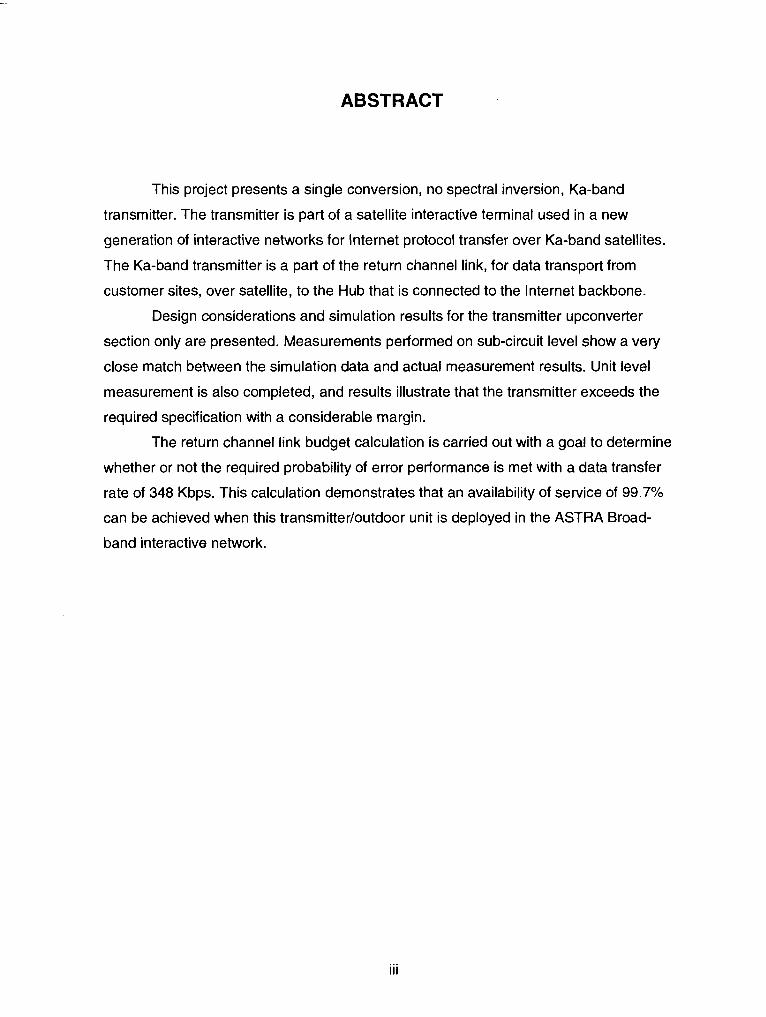
This project presents a single conversion, no spectral inversion, Ka-band
transmitter. The transmitter is part of a satellite interactive terminal used in a new
generation of interactive networks for lnternet protocol transfer over Ka-band satellites.
The Ka-band transmitter is a part of the return channel link, for data transport from
customer sites, over satellite, to the Hub that is connected to the lnternet backbone.
Design considerations and simulation results for the transmitter upconverter
section only are presented. Measurements performed on sub-circuit level show a very
close match between the simulation data and actual measurement results. Unit level
measurement is also completed, and results illustrate that the transmitter exceeds the
required specification with a considerable margin.
The return channel link budget calculation is carried out with a goal to determine
whether or not the required probability of error performance is met with a data transfer
rate of 348 Kbps. This calculation demonstrates that an availability of service of 99.7%
can be achieved when this transmitter/outdoor unit is deployed in the ASTRA Broad-
band interactive network.
iii

DEDICATION
To my mother and sister,
and
my wife Snezana

ACKNOWLEDGMENTS
I would like to thank my supervisor Dr. Shawn Stapleton for all the help and guidance.
Also, my wife Snezana deserves a big credit for her understanding, encouragement and
help during my work on this project.
Finally, special thanks to my dear colleagues from Norsat - Dr. Amiee Chan, Beven
Kocay, Pieter Bezuidenhout, and all the others for their constant support and help.

TABLE OF CONTENTS
APPROVAL .................................................................................................................... ii
... ................................................................................................................... ABSTRACT 111
DEDICATION .............................................................................................................. iv
ACKNOWLEDGMENTS ................................................................................................ v
TABLE OF CONTENTS ............................................................................................. vi
. . LIST OF TABLES ...................................................................................................... VII
... LIST OF FIGURES ...................................................................................................... VIII
1 INTRODUCTION .................................................................................................... 1
2 BACKGROUND ..................................................................................................... 2
......................................................................................... 2.1 Internet Over Satellite 2
2.1.1 Historical Review ......................................................................................... 2
2.1.2 Internet Applications .................................................................................... 3
2.2 Geostationary Satellite Networks ....................................................................... 6
.................................... 2.2.1 Review of Current Geostationary Satellite Networks 7
........................................................................ 2.2.2 Ka-band Satellite Networks 12
3 SATELLITE INTERACTIVE TERMINAL ............................................................ 19
3.1 General Description ......................................................................................... 19
3.2 Outdoor Unit Overview ..................................................................................... 21
3.3 Ka-band Transmitter ........................................................................................ 25
3.3.1 Block Diagram ........................................................................................... 27
3.3.2 Up-converter Circuitry Description ............................................................. 28
...................................................................................... 3.4 Measurement Results 49
......................................................... 3.4.1 Sub-circuit Level Measurement Results 49
3.4.2 Unit Level Measurement Results ................................................................... 60
........................................... 4 RETURN CHANNEL LINK BUDGET CALCULATION 66
4.1 Introduction .......................................................................................................... 66
4.2 Link Budget ......................................................................................................... 66
5 CONCLUSION .................................................................................................... 72
............................................................................................................. REFERENCES 73
LIST OF TABLES
Table 1: Internet applications grouped by commonly used protocols ............................... 5
Table 2: Comparison table of geostationary satellite networks ...................................... 18
Table 3: Main parameters of the outdoor unit ................................................................ 22
Table 4: Properties of the different outdoor units ........................................................... 23
Table 5: Main electrical and mechanical parameters of the Ka-band transmitter ........... 25
Table 6: Measurement results collected using automated measurement setup ............. 65
Table 7: Link budget calculation for clear sky and 0.3% rain rate exceeded conditions . 68
vii
LIST OF FIGURES
Figure 1: Internet network topology ................................................................................. 4
Figure 2: Dedicated single channel per carrier satellite network topology ........................ 7
Figure 3: Very small aperture terminal satellite network topology .................................... 9
Figure 4: Demand assigned multiple access satellite network topology ......................... 11
Figure 5: Hot Bird 6 satellite Ka-band uplink coverage .................................................. 14
Figure 6: Hot Bird 6 satellite Ka-band downlink coverage ............................................. 14
Figure 7: ASTRA broadband interactive network for IP transfer over Ka-band satellite . 16
Figure 8: ASTRA network return link frequency plan ..................................................... 17
Figure 9: Block diagram of the satellite interactive terminal ........................................... 20
................................................................. Figure 10: Block diagram of the outdoor unit 21
Figure 11: Norsat outdoor unit with 76 cm Gregorian dual offset parabola antenna
................................................ system. transmitter and receiver with feedldiplexer 24
Figure 12: Norsat outdoor unit - boom arm assembly detail .......................................... 24
Figure 13: Simplified block diagram of the Ka-band transmitter ..................................... 27
Figure 14: Frequency spectrum content presentation at the different points of the up-
converter chain ....................................................................................................... 29
Figure 15: Block diagram of the intermediate frequency section ................................... 29
Figure 16: Schematic diagram of the diplexer stage ...................................................... 30
Figure 17: Schematic diagram of the attenuator ATT1 .................................................. 31
Figure 18:Schematic diagram of the low-pass filter LP1 with lumped elements ............. 32
Figure 19: Schematic diagram of the low-pass filter LP1 with distributed elements ....... 32
Figure 20: Simulated return loss and S21 transfer characteristics of the low-pass filter
......................................................................................................................... LP1 33
Figure 21 : Schematic diagram of the high-pass filter HP1 with lumped elements .......... 34
Figure 22: Schematic diagram of the high-pass filter with distributed elements ............. 35
Figure 23: Simulated return loss and S21 transfer characteristics of the high-pass filter
HP1 ........................................................................................................................ 35
Figure 24: Schematic diagram of the MMlC amplifier A1 and biasing circuitry .............. 36
viii

Figure 25: Simulated inputloutput return loss and S21 transfer characteristics of the
amplifier A1 ........................................................................................................... 38
Figure 26: Schematic diagram of the band-pass shunt nonconstant-impedance type
amplitude equalizer ................................................................................................ 39
Figure 27: Simulated inputloutput return loss and S21 transfer characteristics of the
equalizer stage with resonant frequency set to 3 GHz ......................................... 39
Figure 28: Simulated inputloutput return loss and S21 transfer characteristics of the
amplifier A2 ............................................................................................................ 40
Figure 29: Simulated inputloutput return loss and S21 transfer characteristics of the
intermediate frequency stage ................................................................................. 41
Figure 30: Block diagram of the resistive FET mixer ..................................................... 42
Figure 31 : Schematic diagram of the resistive FET mixer ......................................... 43
Figure 32: Simulated mixer RF output power as a function of RF frequency ................. 44
Figure 33: Simulated mixer conversion loss as a function of IF frequency ..................... 44
Figure 34: Simulated mixer compression characteristic - output RF power as a function
..................................................................................................... of input IF power 45
Figure 35: Simulated input impedances of the IF, LO and RF port ................................ 45
Figure 36: Block Diagram of the MMlC Mixer section .................................................... 46
Figure 37: Block diagram of the solid-state power amplifier section .............................. 48
Figure 38: Measurement setup diagram of the intermediate frequency section ............. 49
Figure 39: Test Jig used for measurement of the intermediate frequency section ......... 49
Figure 40: Measured input return loss of the intermediate frequency section (1 0 dB per
division scale) ...................................................................................................... 50
Figure 41: Measured output return loss of the intermediate frequency section (1 0 dB per
division scale) ......................................................................................................... 51
Figure 42: Measured intermediate frequency section transfer function S21 as a function
of frequency (1 0 dB per division scale) ................................................................... 52
Figure 43: Measured intermediate frequency section transfer function S21 as a function
............................................................... of frequency, with 1 dB per division scale 53
Figure 44: Test jig used for measurement of the mixer section ..................................... 53
Figure 45: Measurement setup diagram of the mixer section ........................................ 54
Figure 46: Measured mixer RF port power spectrum as a function of frequency ........... 54
Figure 47: Measured mixer RF output power variation as a function of frequency (1 dB
per division scale) ................................................................................................... 55

Figure 48: Measurement setup diagram of the band-pass filter section ......................... 56
Figure 49: Measured filter input return loss as a function of frequency .......................... 56
Figure 50: Measured filter transfer function S21 as a function of frequency ................... 57
Figure 51: Measured power amplifier input and output return loss (S11 and S22). and
forward (S21) and reverse (S12) transfer characteristics. as a function of frequency . 58 ...............................................................................................................................
Figure 52: Measured input-versus-output power response. over temperature. for 29.75
.............................................................................................. GHz signal frequency 59
Figure 53: Picture of the Ka-band transmitter RF circuitry ............................................. 60
.................... Figure 54: Automated measurement setup diagram of the transmitter unit 60
Figure 55: Measured transmitter gain variation over frequency and temperature .......... 61
Figure 56: Measured transmitter input-versus-output power response at 50 O C ambient
temperature ............................................................................................................ 62
Figure 57: Measured transmitter phase noise response as a function of the offset
frequency from carrier ............................................................................................ -63
Figure 58: Measured transmitter output power spectrum as a function of frequency at - 30 OC ambient temperature ..................................................................................... 64
Figure 59: Return channel link between terminal located in Paris. France and hub
........................ located in Betzdorf. Luxemburg. over Ka-band satellite ASTRA 1 H 67
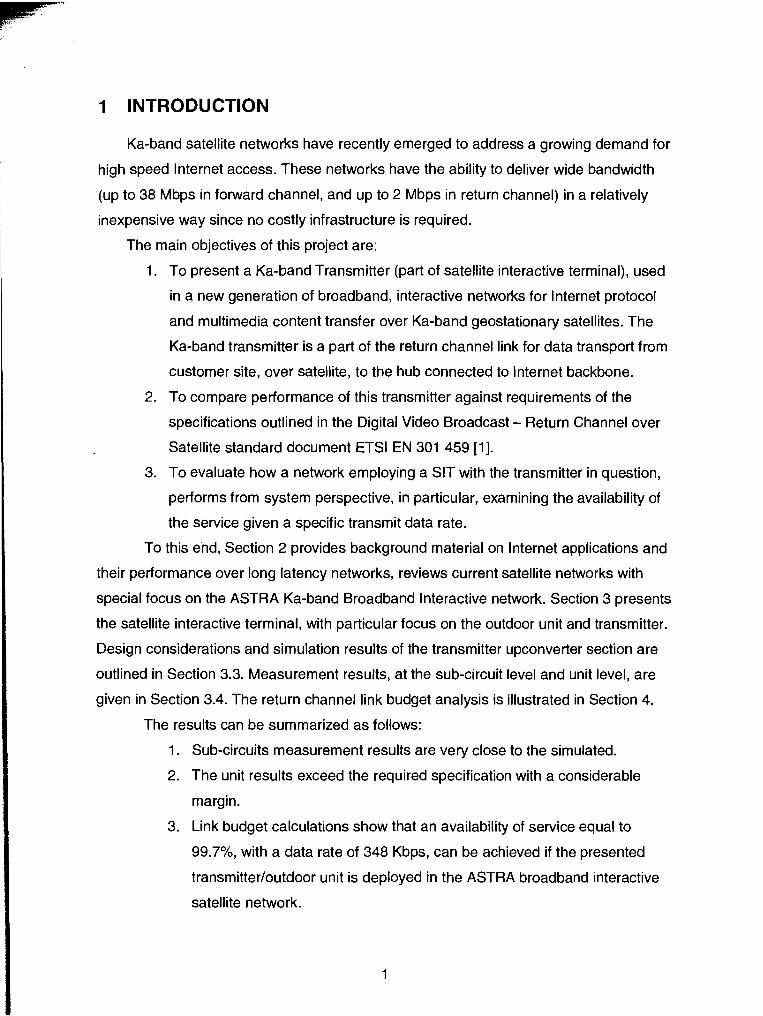
1 INTRODUCTION
Ka-band satellite networks have recently emerged to address a growing demand for
high speed lnternet access. These networks have the ability to deliver wide bandwidth
(up to 38 Mbps in forward channel, and up to 2 Mbps in return channel) in a relatively
inexpensive way since no costly infrastructure is required.
The main objectives of this project are:
1. To present a Ka-band Transmitter (part of satellite interactive terminal), used
in a new generation of broadband, interactive networks for lnternet protocol
and multimedia content transfer over Ka-band geostationary satellites. The
Ka-band transmitter is a part of the return channel link for data transport from
customer site, over satellite, to the hub connected to lnternet backbone.
2. To compare performance of this transmitter against requirements of the
specifications outlined in the Digital Video Broadcast - Return Channel over
Satellite standard document ETSl EN 301 459 [I].
3. To evaluate how a network employing a SIT with the transmitter in question,
performs from system perspective, in particular, examining the availability of
the service given a specific transmit data rate.
To this end, Section 2 provides background material on lnternet applications and
their performance over long latency networks, reviews current satellite networks with
special focus on the ASTRA Ka-band Broadband Interactive network. Section 3 presents
the satellite interactive terminal, with particular focus on the outdoor unit and transmitter.
Design considerations and simulation results of the transmitter upconverter section are
outlined in Section 3.3. Measurement results, at the sub-circuit level and unit level, are
given in Section 3.4. The return channel link budget analysis is illustrated in Section 4.
The results can be summarized as follows:
1. Sub-circuits measurement results are very close to the simulated.
2. The unit results exceed the required specification with a considerable
margin.
3. Link budget calculations show that an availability of service equal to
99.7%, with a data rate of 348 Kbps, can be achieved if the presented
transmitter/outdoor unit is deployed in the ASTRA broadband interactive
satellite network.

2 BACKGROUND
This section presents a quick historical review of the Internet, and outlines lnternet
applications and their performance over long latency networks. Secondly, current and
emerging Ka-band satellite networks are described.
2.1 lnternet Over Satellite
The lnternet is a group of computer networks, each containing multiple sub-
networks and computers that are organized in a tiered hierarchy. As a growing number
of people are connecting to this vast information pool, providing new, high-speed data
access methods is imperative.
lnternet service providers have customers worldwide. Corporations are
interconnecting geographically dispersed server networks. Universities are
communicating across countries, sharing research information and their libraries.
Geostationary Earth orbit (GEO) satellite networks are ideal for interconnecting
these widely dispersed servers, many of them in isolated geographical areas (islands)
and or in places where cable infrastructure does not exist.
2.1.1 Historical Review
In the 1960s the US Defense Advanced Research Project Agency (DARPA)
started research on linking computers in networks. Bolt, Beranek and Newman (BBN)
were assigned the task of designing a communication protocol. The original network
connected four sites in California and was the first to use Network Control Protocol
(NCP), the first packet switching scheme for transferring data between computers.
In 1983, DARPA adopted TCPIIP (Transmission Control Protocolllnternet
Protocol), which provided the robust protocol needed to support information transfer
between different networks with different types of media. TCPIIP is still in use today.
In 1983 the network was split into two networks, Milnet and ARPANET. At the
same time several other networks, like CSNET (Computer and Science Network) and
BITNET, became a part of this growing network.
In 1987 the National Science Foundation (NSF) creates a high-speed backbone
network connecting several super computer centers across the US. System also
includes a number of mid level networks that provide access to a high-speed backbone

network. This backbone network is served by a non-profit organization, Advanced
Networks and Services (ANS). At the same time profit companies began to develop the
regional networks that provided access to backbone lnternet and started carrying
commercial traffic as well as NSF traffic. As a result, NSF established an "appropriate
use policy", which limited the traffic through their backbone to non-commercial traffic
only. Because of that policy, a group of regional networks formed the Commercial
lnternet Exchange (CIX) system, to create connection between the regional networks
without using the NSF backbone.
The traffic on the lnternet today is primarily carried through the commercial
network with links to the NSF network.
2.1.2 lnternet Applications
TELNET was one of the first lnternet applications. It provided users at remote
locations the ability to log on to another computer (host) and interact with it just as he
would by using terminal he was directly connected to.
FTP (File Transfer Protocol) was the second lnternet application. It enabled
users at remote locations to search directories of any host computer on the lnternet and
transfer desired files from the host computer to his remote computer.
SMTP (Simple Mail Transfer Protocol) was developed to manage the transfer of
electronic mail messages from one location to another.
HTTP (Hypertext Transfer Protocol) establishes the rules for transmitting
hypermedia documents electronically and is associated with the World Wide Web
(WWW) traffic.
WWW is a cataloging tool, and is successor of Archie, Gopher and Veronica,
whose user-friendly interface allowed non-technical people to use this valuable resource.
Newer lnternet applications include email, video teleconferencing and broadcast.
They all use IP (Internet Protocol) as the transmission mechanism, so that they
can effortlessly run over satellite networks. However, performance levels vary from
application to application as their requirements for network bandwidth and delay and
implementation techniques are different.

Figure 1: lnternet network topology.
Data broadcast, such as webcasting, network news, TV and radio programs, is
ideally suited for GEO satellites. Satellite networks can bypass tens of intermediate
nodes, which significantly reduce the chances for packet drop and large delay jitter due
to congestion. Compared to this, broadcast over terrestrial lnternet can be very
expensive.
Electronic mail is not interactive, so it can work over any network.
Videoconferencing and video distribution can be built on user datagram protocol
(UDP). This protocol does not require bi-directional synchronization, so delays can be
tolerated. Compared with terrestrial Internet, GEO satellites can provide better quality
thanks to network simplicity and available bandwidth.

Remote control and login are delay sensitive, but if the user can accept a half-
second to one-second delay, the application can run efficiently, as the response over
GEO satellite is more stable.
Because data retrieval requires reliable transmission, many applications (such as
WWW, FTP) use Transmission Control Protocol (TCP), which is sensitive to
transmission delays, since "acknowledge-and-retransmit" method is used.
This limitation can be mitigated, with special processing techniques. Some of
these techniques are presented in [2]. With special attention to design, the
compensations can be made transparent to the end user application.
Table 1: lnternet applications grouped by commonly used protocols.
GEO Satellite
lnternet Protocol (IP)
TCP
Remote Login
Electronic Mail
On-line Information Retrieval
UDP
Reliable Multicast
- lnformation Dissemination
- Broadcast
Real-time Protocols
- Video Conferencing
Gaming

2.2 Geostationary Satellite Networks
Current lnternet backbones and sub-networks are mostly wired terrestrial
networks, using cable, fiber optics and telephone lines. Bandwidth available in these
networks ranges from 1.5 Mbps (11) to 622 Mbps (OC-12).
Among emerging mobile/wireless networks, GEO satellite networks present great
potential with their ability to broadcast and multicast large amounts of data over a
widespread area.
Geostationary Earth orbit (GEO) satellites have a circular orbit on a plane
equivalent to Earth's equatorial plane, at synchronous altitude of 35,800 km. Since a
satellite's orbital period is identical to the Earth's rotational period, the satellites appear
stationary from the Earth's perspective.
lnternet distribution over GEO satellite has following advantages:
- Relatively inexpensive because no costly infrastructure (cable-laying)
is needed; one satellite covers a large area
- High bandwidth allows transfers at high rates
- In comparison with the terrestrial mesh interconnection network, GEO
satellite networks have simpler path (fewer hops), which often results
in better network performance.
As discussed in [2], the major challenge that GEO satellite networks present to
the performance of lnternet applications is the communication delay (latency) between
two Earth stations connected by satellite. The delay ranges from 250 ms to 400ms
(including on-satellite processing). This delay is 10 times higher than a multi-hop, fiber
optics path across North America, and may affect interactive applications (like TCP) that
require synchronization (handshaking) between two sites.
Use of low Earth orbit (LEO) and medium Earth orbit (MEO) satellites can
circumvent this problem, because their communication delays are just two times higher
than those with terrestrial fiber optics connections. Because of the nature of their orbits,
a constellation of satellites is required to provide a full coverage. The analysis presented
in [3] shows that the result is complex network management at greater cost. The initial
investment required for a LEO or ME0 satellite network is well above $1 billion, whereas
the GEO's is below $200 million. In addition, Earth terminals will be impacted, because

the use of phased array antennas (tracking capability) will be necessary. A phased array
antenna is significantly more expensive option than the classic offset parabola dish.
2.2.1 Review of Current Geostationary Satellite Networks
2.2.1.1 Dedicated Single Channel per Carrier Satellite Network Description
This type of network has dedicated point-to-point single channel per carrier
(SCPC) links over satellite, to connect local point of presence (POP) servers to lnternet
gateway points.
Figure 2 shows a typical SCPC network topology.
INTERNET SERVICE PROVIDER
PORT
T GATEWAY
C TERMINAL
Figure 2: Dedicated single channel per carrier satellite network topology.
The satellite link establishes a full-time data connection between the lnternet
backbone and the local access point, at speed from 64 to 256 Kbps.

Users may access a server over a local area network (LAN), or through dial-up
telephone lines connected to the public switch telephone network (PSTN). At any time
there may be several simultaneous IP sessions. The routers located at either end
provide session management.
As discussed in [4], constraints of this type of network are:
- Web browsing traffic and multimedia server transactions are more
intensive from the server to the end user than in the opposite direction
(10:l). These symmetrical satellite links are not needed since
asymmetrical links are more efficient.
- In systems where traffic load varies widely, use of full-time fixed
circuits is not economical because service provider's operating cost is
high.
- For networks where there are multiple service sites, the use of
dedicated links from the gateway to POP is inefficient and costly
because of the need for dedicated hardware, associated overhead,
etc.
In conclusion, implementation of some kind of resource sharing can be very cost
effective and will provide improved service and performance.
2.2.1.2 Very Small Aperture Terminal Satellite Network Description
Traditional very small aperture terminal (VSAT) network, providing a service to
variety of different sites, is shown at Figure 3.
Different sites shown are:
- Single client site, where the user is connected directly to a terminal
- Corporate access site, where the users are connected through a local
area network, and
- Internet service provider site with wired dial-up access through a
public switch telephone network.
For traffic from a gateway, time division multiplex (TDM) is used for capacity
sharing. A single 256 or 512 Kbps data link is time shared among a large number of
users. For each IP session the system allocates a portion of the total bandwidth, usually
16 to 32 Kbps.
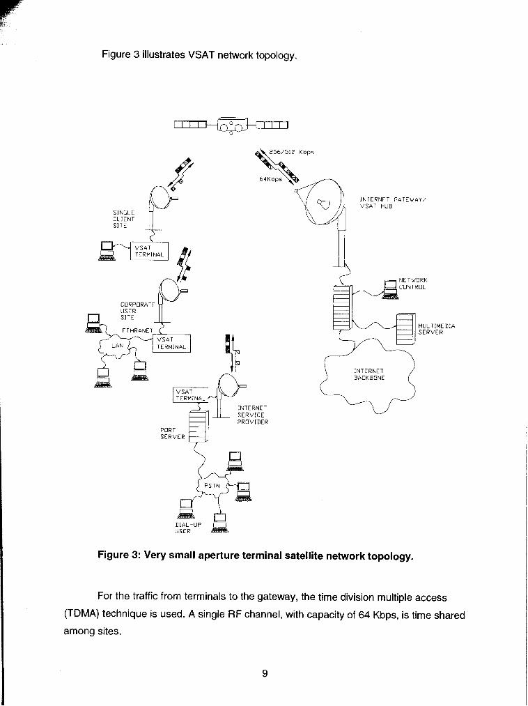
Figure 3 illustrates VSAT network topology.
SINGLE CLIENT S ITE
CORPORATE @
1 VSAT 1 I TERMINAL 1 INTERNET SERVICE i? PROVIDER
INTERNET GATEWAY/ VSAT HUB
MULTIMEDIA
SERVER F'
Figure 3: Very small aperture terminal satellite network topology.
For the traffic from terminals to the gateway, the time division multiple access
(TDMA) technique is used. A single RF channel, with capacity of 64 Kbps, is time shared
among sites.

Special protocols, in addition to TCPIIP protocol, are used to support this
resource sharing technique.
TDMDMA VSAT systems are example of star network configuration, where all
traffic passes through central hub (gateway). This traffic pattern may be acceptable for a
single gateway, but for services that have many multimedia server locations, this is not
the best solution.
VSAT systems were designed to be effective in transporting a small amount of
data, associated with services like automated teller machines, credit card validation,
point-of-sale and inventory. As a result, high bandwidth and more constant connections,
needed for lnternet and multimedia users, are not well matched for VSAT systems.
Although they can provide a reasonable level of service, they are not cost effective
solution.
2.2.1.3 Demand Assigned Multiple Access Satellite Network
Single channel per carrier (SCPC) demand assigned multiple access (DAMA)
network is actually a hybrid between the SCPC point-to-point system and VSAT system.
SCPC DAMA system is an example of a mesh network configuration - resources are
allocated on user demand by connecting any two sites in the network using single carrier
per channel link. This connection can be a full-duplex equal rate, unbalanced rate, one-
way broadcast or multicast.
The control organization of the SCPC DAMA network is similar to the VSAT
system in the sense that the resources allocation, type of connection and the
administration are provided by a central controller, using TDM/TDMA VSAT
communication at 19.2 Kbps rates.
Figure 4 shows a multi-gateway and multi-server network for lnternet and
multimedia data transfer.
The traffic from the gateway uses wide-band, one-way channel (256 to 2,048
Kbps), which is shared among all lnternet user sites, with individual sessions having
access to the full-bandwidth. If greater capacity is required, multiple 2 Mbps carriers can
originate from the gateway. The users are charged for the quantity of data transferred.
Figure 4 presents SCPC DAMA network topology.
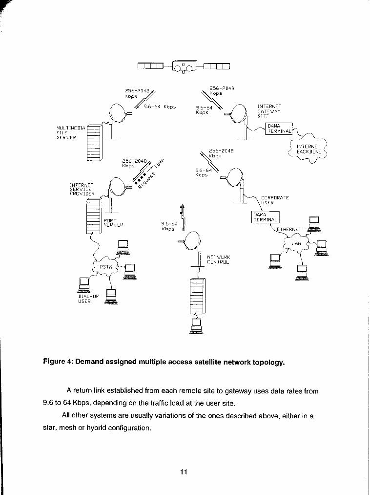
/-', 9 . 6 - 6 4 Kbps
MULTIMEDIA
INTERNE1 GATEWAY
TERMINAL -k---f-k
INTERNET
DIAL-UP USER
9 . 6 - 6 4 Kbps
NETWORK CONTROL
INTERNET
o"z TERMINAL
Figure 4: Demand assigned multiple access satellite network topology.
A return link established from each remote site to gateway uses data rates from
9.6 to 64 Kbps, depending on the traffic load at the user site.
All other systems are usually variations of the ones described above, either in a
star, mesh or hybrid configuration.

2.2.2 Ka-band Satellite Networks
The Ka-band multimedia satellites are a new generation of satellites. As discussed
in [3], they use on-board processing and switching as well as multiple pencil-like spot
Beams, to provide full two-way services, to and from small satellite interactive terminals
(SIT'S), located at the customer's premises. The SITS use antennas comparable in size
with the current direct broadcast dishes. These satellites are also equipped with inter-
satellite links operating at V-band (60 GHz).
The main advantage of multiple spot beams, each covering only a small area of
the Earth, is frequency re-use, similar to a cellular phone network re-using a spectrum.
The SITS request bandwidth only when there is data to be sent ("bit rate on
demand), so that users pay only for the time that they use the link. This provides a
flexible and cost effective solution, in contrast with conventional satellites where users
usually pay for permanent leases.
Ka-band is subject to substantial interference from rain, which was a concern.
NASA launched a Ka-band satellite in 1993, that uses all of the key technologies
required for new commercial Ka-band satellites. The tests performed were successful,
which allowed for further developments to proceed.
It was initially expected that 2.5 -3.5 GHz would be available for GSO satellites,
but this was reduced by demands from non-geostationary satellites (LEO and MEO),
Local Multipoint Distribution Systems (LMDS) and Mobile Satellite Service (MSS) links.
In addition, high-speed internet delivery systems that are competing with Ka-
band satellite systems, like high-speed digital cable networks, asymmetric differential
subscriber line (ADSL) and LMDS, are entering the marketplace.
Apart from high speed Internet access, a series of applications like
videoconferencing and video telephony, data broadcasting, tele-medicine, tele-
education, local television, news on demand and multimedia for businesses and
personal use, are expected to develop as a result of this satellite technology.
This will have an interesting impact on the fast growing European market,
discussed in the next section.

2.2.2.1 Ka-band Satellites
SES ASTRA is the first European satellite operator to commercially use Ka-band
frequencies for interactive broadband services, over ASTRA 1 H satellite at orbital
position 19.2' East. In Q4 2000, SES commenced commercial Beta trials of the
Broadband Interactive (BBI) system, for two-way asymmetric broadband collection and
delivery of multimedia. ASTRA 1 K, scheduled for launch in 2002, will add another 52 Ku
and 2 Ka transponders, will provide full back-up for ASTRA 1 H return path, and will
extend geographical coverage (reference [5]).
Eutelsat Hot Bird 6 (HB6) satellite, will be located at orbital position 13' East, and
will carry total of 32 channels, including 4 at Ka-band frequencies for internet and
multimedia services. The satellite launch is scheduled for 2nd quarter of 2002. See
reference [6] for details.
Figures 5 and 6 demonstrate the Ka-band uplink and downlink coverage. HB6
uses 4 spot beams for uplink coverage.
Alenia Spazio EuroSkyWay satellite will be located at orbital position 16.4' East.
Scheduled for launch in 2003, this satellite will cover Europe and the Mediterranean
Basin (see reference [7]). The satellite will have on board processing (OBP), and will
provide bi-directional bandwidth on demand, dynamic resources allocation and pay per
use.

@f eutelsat
Figure 5: Hot Bird 6 satellite Ka-band uplink coverage.
r HBGTM Ka-band downlink
eutelsat a, -
Figure 6: Hot Bird 6 satellite Ka-band downlink coverage.

2.2.2.2 ASTRA Broadband Interactive Network Overview
The ASTRA broadband interactive (BBI) network is a 2-way satellite-based
broadband platform, specifically designed to provide lnternet access and distribution of
multimedia rich files. BBI is the first commercial implementation of the Digital Video
Broadcast - Return Channel over Satellite (DVB-RCS) open standard.
The BBI system is an example of the star network configuration, where all traffic
passes through a central hub (gateway).
This network supports all standard IP-based needs, such as file transfers, e-mail,
database access and lnternet access. The network contains:
- Single client sites, where the user is connected directly to terminal
- Corporate access site, where the users are connected through the
local area network
- lnternet service provider sites (cable operators and telcos) for easy
extension of their terrestrial backbone to remote communities.
BBI can also support Tele-medicine and Tele-education services and monitoring
of remote sites.
The Forward Path carries user traffic and signaling from the Hub to the SITS.
Framing structure-, channel coding and modulation is based on the standard digital video
broadcast over satellite (DVB-S) transmission system.
The BBI Hub is capable of delivering up to 38 Mbps of IP data or multimedia
content. The transmission is done at Ku frequency (1 0.7 to 12.75 GHz), over 120
channels, with 1dB bandwidth of 26 and 33 MHz. Orthogonal-linear polarization is
applied. Odd numbered channels have nominally Horizontal polarization, while even
numbered channels have nominally Vertical polarization.
The Return path carries user traffic and signaling from SITS to the Hub. The
return path is based on a multi-frequency time division multiple access (MF-TDMA)
scheme.
At the present time, fixed-slot MF-TDMA is in use, meaning that the bandwidth
and duration of successive traffic slots used by return channel terminal is fixed.
In the near future, dynamic-slot MF-TDMA will be deployed. When this occurs, return
channel terminal may vary the bandwidth and duration of successive traffic slots, and
may also change transmission rate and coding rate between successive bursts.

Figure 7 describes BBI network topology.
ASTRA I H
INTERNET GATEWAY SITE 1
B B 8 SERVER
INTERNET
SINGLE
CORPORATE USER
SIT
INTERNET SERVICE
Figure 7: ASTRA broadband interactive network for IP transfer over Ka-band
satellite.
The signal is modulated using conventional gray-coded quadrature phase shift
keying (QPSK) modulation scheme, with baseband shaping performed using square root
raised cosine filter with roll-off factor of 35%.

The return link transmission is done at Ka band (29.5 to 30 GHz), with data rates
between 144 and 2,048 Kbps.
By combining polarization-division multiple access (PDMA) and space-division
multiple access (SDMA), available frequency band is reused. The frequency band is
divided into 8 orthogonal-linearly polarized channels (4 vertical and 4 horizontal). Each
channel is received by satellite by separate receive spot beams. See figure 8 for details.
29.5 GHz 30.0 GHz
160 MHz 80 MHz 80 MHz / E z t ~ : r o p / / Germany / / Scondinovia / 1 I t a l y I
80 MHz P o r t u g a l
I 29.56 29.70 29.84 29.94 1 Figure 8: ASTRA network return link frequency plan.
The Air Interface of the BBI system is designed in accordance with the direct video
broadcast return channel over satellite (DVB-RCS) system specification. This document
has been published as a European Norm EN 301 790 by the European
Telecommunications Standards Institute (ETSI).
The receive characteristics of the SITS are contained in the ASTRA Reception
Equipment Recommendations.
Table 2 shows comparison between different GEO satellite networks.
80 MHz Spoin
I I I I
120 MHz I U K
120 MHz F r a n c e
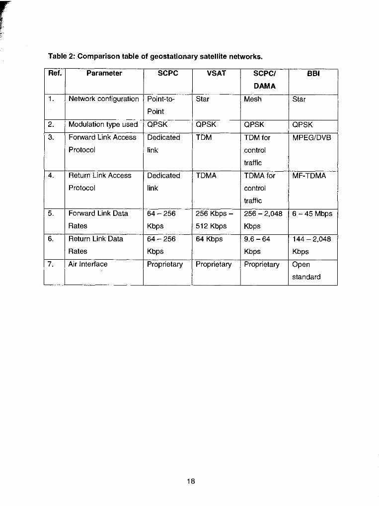
Table 2: Comparison table of geostationary satellite networks.
Ref.
1.
2.
3.
4.
5.
6.
7.
Parameter SCPC VSAT
I Network configuration Point-to- I Star
I Point I I I
Modulation type used / QPSK I QPSK I I
Forward Link Access Dedicated TDM
Protocol I link I Protocol link
Forward Link Data 64 - 256
Rates Kbps
Return Link Data 64 - 256
Rates Kbps
Air Interface Proprietary
51 2 Kbps
SCPCI
DAMA
Mesh
QPSK
TDM for
control
traffic
TDMA for
control
traffic
256 - 2,048
Kbps
9.6 - 64
Kbps
Proprietary
BBI
Star
QPSK
MPEGIDVB
MF-TDMA
6 - 45 Mbps
144 - 2,048
Kbps
Open
standard
3 SATELLITE INTERACTIVE TERMINAL
This section outlines the Satellite lnteractive Terminal (SIT), part of the Ka-band
interactive network, with special attention to the outdoor unit and transmitter. Detailed
design and simulation results of the transmitter's upconverter section are presented in
Section 3.3. Measurement results are illustrated in Section 3.4.
3.1 General Description
The Satellite lnteractive Terminal, illustrated in Figure 9, consists of:
- a fixed, small antenna with the transceiver - outdoor unit (ODU),
located outside (roof) and pointed towards the satellite,
- an indoor unit (IDU), placed inside customer premises, and
- two-cable interfaculty link (IFL), connecting ODU and IDU together.
The IDU can be connected to a standalone multimedia PC or a local area network
through 10BaseT Ethernet interface. ODU, on the other hand, receives and transmits
data fromlto satellite.
In the IDU, the data stream received from multimedia PC is encoded, modulated
and translated to S-band (2.5 to 3 GHz) frequency. The S-band signal is then delivered
to the ODU transmitter via IFL, where it is upconverted to Ka-band, and, using antenna
interface, delivered to the satellite.
The SIT can transmit at data rates from 144 Kbps to 2,048 Kbps, depending on
transmitter power levels and antenna sizes used.
The Ku-band signal from the satellite is received and down-converted by ODU, to
L-band (950 to 21 50 MHz) frequency. The L-band signal is then delivered to IDU via a
second IFL cable, where it is demodulated to the base band (IF and baseband
demodulators) data stream, decoded and delivered to a multimedia PC.

. , TRANSMITTER
r) RECEIVER L I I
ANTENNA ASSEMBLY -
IF Modulator Demodulator
Modulator Demodulator
I Coder
CC(2,1,7) Interliver Id2 RS(204,188,8)
User lnterface Unit
IDU / I I I I I I
10 Base T Ethernet Interface
Figure 9: Block diagram of the satellite interactive terminal.

3.2 Outdoor Unit Overview
The outdoor unit (ODU), part of Ku/Ka-band satellite interactive terminal, as
described by Fikart and Chan [8, 91, is composed of the following elements:
- Gregorian dual offset parabolic antenna with mount subsystem,
- 12/30 GHz dual feedldiplexer,
- Ku-band low noise block down-converter (LNB), and
- Ka-band transmitter
- Tx lFIDCM2KHz In
REF Out
TRANSMITTER
Figure 10: Block diagram of the outdoor unit.
ANTENNA ASSEMBLY
The Ku-band LNB is attached to a diplexer via a C120 wave-guide flange. The Ka-
band transmitter is mounted on the antenna boom, and attached to the diplexer via a
flexible WR28 wave-guide.
The ODU is interconnected to IDU via an IFL, consisting of two coaxial cables.

Transmit IFL cable carries multiplexed:
- from IDU to transmitter: Tx IF signal, DC power and 22KHz Control
and Monitoring signal,
- from transmitter to IDU: 10 MHz reference signal and 22 KHz Control
and Monitoring signal.
Receive IFL cable carries multiplexed:
- from IOU to LNB: DC power and 22 KHz control (polarizationlbend)
signal
- from LNB to IDU: Rx IF signal
The Ku-band signal, received from the satellite by the antenndfeed system, is
separated from transmit signal in the waveguide diplexer and delivered to the LNB. Two
separate waveguide probes receive horizontally and vertically polarized signals, which
are amplified with low-noise amplifiers (LNAs). One of the signals is selected (DC control
received from IDU) and fed to the mixer for down-conversion. Ku low-band (10.7-1 1.7
GHz) is converted to the 950-1950 MHz, and Ku high-band (11.7 to 12.75 GHz) is
converted to the 1100-2150 MHz band IF. Selection between low and high band is
performed by a local oscillator (LO) signal selection (22 KHz control signal from the
IDU). See Figure 10 for details.
The main ODU parameters are outlined in Table 3.
I I
1. I Tx IF input frequency 1 2.5 - 3 GHz
Table 3: Main parameters of the outdoor unit.
I I
2. I Tx RF output frequency 1 29.5 - 30 GHz
I Ref. I Parameter Specification
I I I factory set
I I
I I
4. I Rx RF input frequency 1 10.7 - 12.75 GHz
3.
5. I Rx IF output frequency 1 0.95 to 2.1 5 GHz
Tx polarization Linear, H or V,
Linear, H or V
controlled by IDU
6.
7.
8.
9.
Rx polarization
Minimum G/l
Rx Noise Figure
LNB Gain
15 dBPK
1 dB max.
56 dB typical

Three different types of ODUs, with different Effective Isotropic Radiated
Transmitted Power (EIRP) capabilities, are employed in the BBI network. These EIRP
values must be achieved with adjacent channel spectral re-growth of less than -20 dBc.
The properties of different ODUs are outlined in Table 4.
Table 4: Properties of the different outdoor units.
2. 1 Max. Antenna size 1 76 cm
Ref.
1.
I I
3. 1 Antenna Gain 1 44 dBi I I
4. I Tx Power 1 26.5 dBm
Parameter
ElRP
ODU 1
40 dBW
I (Return Channel) I 5.
A picture of assembled Norsat ODU, with 76 cm antenna is presented in Figures 11 and
12.
90 cm
46 dBi
29.5 dBm
384 Kbps Max. data rate
120 cm
48 dBi
32.5 dBm
2048 Kbps 144 Kbps

Figure 11: Norsat outdoor unit with 76 cm Gregorian dual offset parabola antenna
system, transmitter and receiver with feedldiplexer.
Figure 12: Norsat outdoor unit - boom arm assembly detail.

3.3 Ka-band Transmitter
Norsat Nl-25512-01 Ka-band transmitter, part of the outdoor unit, designed for the
ASTRA Broadband Interactive Network, enables return channel over satellite (RCS) IP
transfer. Depending on the transmitter output power and antenna size used, data rates
from 144 Kbps to 2048 Kbps can be transferred from the customer site, over satellite, to
a gatewaylhub.
The transmitter is designed to be compliant with ETSI EN 301 459 standard.
Main transmitter parameters are presented in Table 5.
Table 5: Main electrical and mechanical parameters of the Ka-band transmitter.
Parameter
lnput frequency band
lnput Impedance
lnput Return Loss
2.5 to 3 GHz
10 MHz
Maximum lnput Power
Output Frequency Band
Nominal Output Power
(20 dBc side band re-growth)
Gain at any condition
(small signal)
Gain Variation over Temperature
(at any constant frequency)
over total operating temperature
range
Specification

Parameter
Gain Variation in band
(at any constant temperature)
In any 20 MHz Band
In full 500 MHz Band
Phase Noise
@ 10Hz/100Hz/l kHz11 OkHzbl OOkHz
In Band Noise Emissions SSPA ON
Output Spurious Level
In band IF ON
In band IF OFF
Out of band, up to 40 GHz
Reference Signal Frequency
Reference Signal accuracylstability
Reference Signal Level
Alarm Processing
DC Power
Power Consumption
Input Interface
Output Interface
Size (envelope dimension)
Mass
Operating Temperature
Specification
< 1.0 dB p-p - 5 5.0 dB p-p
2 60 dBc below single CW carrier
nominal output power
< -40 dBm (measured with 100 K - RBW)
10 MHz
-10 5 2 dBm
Output amplifier and 10 MHz reference
signal muted in event of LO alarm
13-30 VDC I 2.3 A max
5 30 W
4 hole flange mount "F' female
connector
W R-28 waveguide flange
301 x 184 x 96 mm

3.3.1 Block Diagram
The transmitter upconverts the S-band (2.5-3 GHz) signal received from the indoor
unit, and delivers a Ka-band (29.5-30 GHz) signal to diplexerlfeedlantenna sub-system.
DC signal and 22 KHz pals width modulated (PWM) control signal are de-multiplexed
and delivered to DC-DC and Monitoring and Control (MAC) circuitries, respectively.
Figure 13 shows transmitter block diagram.
0
IF/DC/Control In Ref Out
MIX BPF SSPA - RF Out
g T
xo 50 MHz Lock Alarm
I DC-DC I - ' MUTE
Figure 13: Simplified block diagram of the Ka-band transmitter.
Local oscillator (LO) circuitry generates a signal at 13.5 GHz, by doubling the 6.75
GHz signal from phase locked voltage controlled dielectric resonator oscillator (VCDRO).
VCDRO is locked to internal 50 MHz reference using a sampling phase detector (SPD).
A 50 MHz modified Colpitts crystal oscillator is used to generate reference frequency
for LO locking. The reference signal is also divided by 5, and sent back to IDU, via IFL
cable. In the IDU, Tx 10 MHz reference signal is compared with the master reference
received from the satellite, through a forward path. After error determination, the
transmitter output frequency is corrected by adjusting the IF signal frequency.
The MAC circuitry is the monitoring and control module of the transmitter, and it uses
a modified 22 KHz DiSeq protocol to act as a communication interface with IDU.
Internally, in the case of the LO alarm (LO out of lock), the output amplifier section and
10 MHz reference signal output are muted immediately.
MAC circuitry provides following functions:
- LO Alarm (LO out of lock) monitoring
- Low voltage alarm (input DC voltage below 11 V) monitoring
- Output amplifier ONIOFF status monitoring
- Tx EnableIDisable command
- Remote software update
The transmitter can be enabled only when the appropriate password is entered.
The DC-DC circuitry converts incoming 13-30 VDC, into six different regulated
voltages, required by other sub-circuits.
3.3.2 Up-converter Circuitry Description
A detailed description, containing block diagram, schematics and design
considerations, of IF, MIX, BPF and SSPA stage is presented in this section.
This unit is standard a single conversion, no spectral inversion, block up-
converter. The intermediate frequency (IF) signal received from IDU is processed in the
IF section and then mixed with the local oscillator (LO), in the mixer section. The upper
side band mixing product (2L0 +IF), our desired signal, is then filtered and amplified.
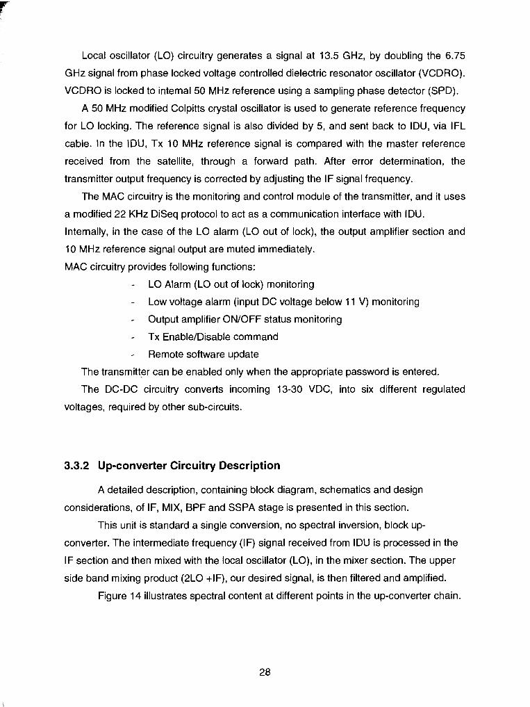
Figure 14 illustrates spectral content at different points in the up-converter chain.
IF SECTION
4 0
MIXER OUTPUT 2LO-IF
2LO-21F
13.5 f (GHz)
Figure 14: Frequency spectrum content presentation at the different points
of the up-converter chain.
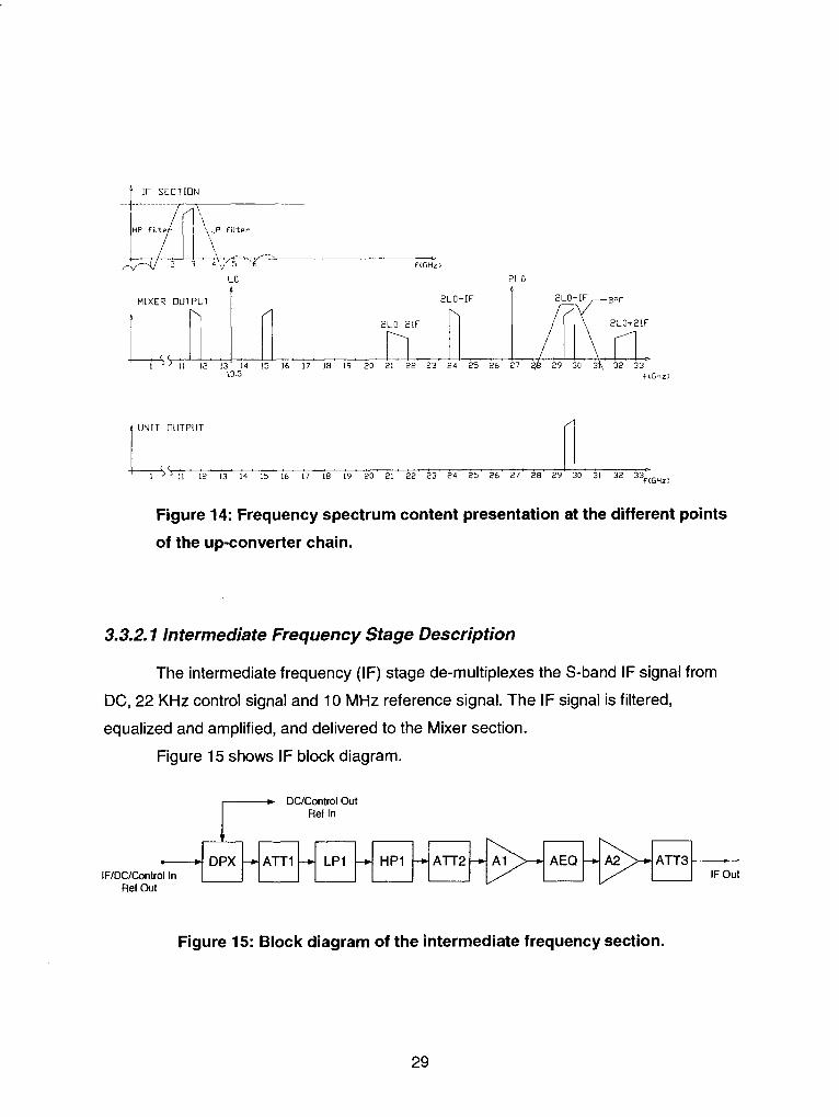
3.3.2.1 Intermediate Frequency Stage Description
The intermediate frequency (IF) stage de-multiplexes the S-band IF signal from
DC, 22 KHz control signal and 10 MHz reference signal. The IF signal is filtered,
equalized and amplified, and delivered to the Mixer section.
Figure 15 shows IF block diagram.
Figure 15: Block diagram of the intermediate frequency section.
4
Ref Out
-, - IFIDClControl In
-- -t DPX ATT2
IF Out ATT1 -c LP1 - -+ HP1

3.3.2.1.1 Diplexer Section
The diplexer (DPX) is the first stage in the IF section chain, and it's main task is
to de-multiplex the IF signal from the other signals (DC, 22 KHz control and 10 MHz
reference) with minimum insertion loss.
IF, DC and 22KHz control signals are received through a 75 SZ, F female
connector (port P1 on schematic). A shortened, high impedance, 3J4 microstrip line (at
1.25 GHz), is used to split the IF frequency from other signals. For IF signal this line
represents high impedance (parallel resonant circuit with resonance at 1.25 GHz), so the
signal passes through the serial capacitor C2, to port P2 with minimum loss. At the same
time, capacitors C1 and C2 present high impedance for all other signals (infinite for DC,
>I .5 MSZ for 22 KHz and >3.39 KR for 10 MHz), so they are delivered to port P3 with
minimum loss (10 MHz delivered from port P3 to port PI).
The diplexer schematic is shown in Figure 16.
Figure 16: Schematic diagram of the diplexer stage.

3.3.2.1.2 Attenuator ATT1
The attenuator ATT1 is 2 dB, 75 R, T configuration attenuator, placed between
diplexer circuitry and low-pass filter LP1 to improve matching.
Figure 17: Schematic diagram of the attenuator ATTI.
3.3.2.1.3 Low-pass Filter LP1
The Low-pass filter LP1 is gth order Elliptical, microstrip filter designed to
transform input 75 R impedance to 50 R system impedance, and to prevent unwanted
signals above 3.6 GHz to appear at the input of the first IF amplifier.
The Elliptical (also known as Caurer-Chebyshev) filter transfer function is
characterized by equiripple response in the pass-band, and with the poles placed in
such a way that minima of attenuation in the stop-band are identical (equripple in the
stop band). These filters are extensively discussed in literature. The catalog of
normalized low-pass prototypes, with instructions for transformation to desired
impedance and frequency is discussed by Zverev [I 01.
Modern simulation/synthesis CAD tools offer a much faster approach to the
desired filter realization. In this case, the Ansoft [ I 11 Serenade filter synthesis tool is
used to generate lamped Elliptical filter with fc3dB = 3.2 GHz, 0.4 dB insertion loss and
0.25 dBpp flatness in the pass band.
The filter schematic is shown in Figure 18.

Figure 18:Schematic diagram of the low-pass filter LP1 with lumped
elements.
Lumped elements are then substituted with microstrip distributed elements, and
filter optimized using a simulation tool.
Series inductors are modeled as high impedance microstrip lines (< h/4 long),
while shunt series resonant circuits to ground, are replaced with shunt U4 microstrip
open lines (at pole frequency). Step discontinuities (50 i2 to high impedance line
interface) and T djscontinuities (junction between two high impedance microstrip lines
and shunt open stub) are taken into account by adding appropriate microstrip
discontinuity models to simulation circuit (see Figure 19).
The ground plane is inserted between the shunt stubs, to decrease the amount of
inter-coupling.
Figure 19: Schematic diagram of the low-pass filter LP1 with distributed
elements.

Figure 20 shows the simulation results. Inputfoutput return loss (S11 and S22) is
< -20dB in band, and transfer function S21 shows insertion loss of 0.6 dB at the band - edge and in band flatness of 0.28 dBpp.
Figure 20: Simulated return loss and S21 transfer characteristics of the low-pass
filter LP1.

3.3.2.1.4 High-pass Filter HPI
The high-pass filter HPI is 7'h order Elliptical microstrip filter; the next stage in the
IF chain. The main task of this filter is to prevent unwanted signals below 2 GHz to
appear at the first amplifier input, and cause in and out of band spurious signals upon
mixing. 50-50 R, lumped Elliptical filter with fc3dB = 2.35 GHz, insertion loss of 0.25 dB
and 0.2 dB flatness is synthesized using Ansoft Serenade filter synthesis tool (see
Figure 21).
Figure 21: Schematic diagram of the high-pass filter HP1 with lumped elements.
Surface mount, lumped ceramic capacitors are used as series capacitances.
Shunt series resonant circuits to ground are replaced with shunt U4 microstrip open
lines (at pole frequency), except in a case of the last resonant circuit, which is replaced
with high impedance microstrip line (inductance) followed by a lumped ceramic capacitor
to ground. This approach is taken in attempt to decrease required board space.
This hybrid structure is then optimized using Ansoft Serenade simulation tool. As
described in LPI, microstrip step and T discontinuities are taken into consideration by
adding appropriate discontinuity models to simulation circuitry.
Figure 22 shows the HPI filter simulation schematic. Filter simulation results are
illustrated in Figure 23. Input,output return loss is 2-20dB in band, and transfer function
S21 shows insertion loss of 0.92 dB at the band edge and in band flatness of 0.35 dBpp.
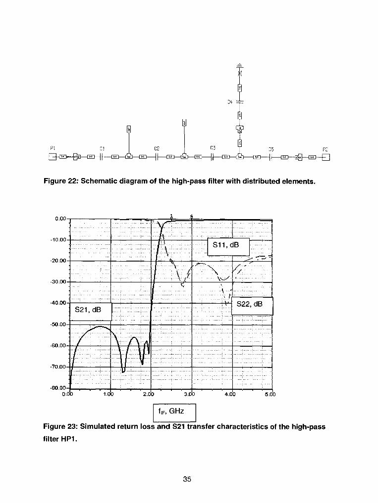
Figure 22: Schematic diagram of the high-pass filter with distributed elements.
I I
Figure 23: Simulated return loss and S21 transfer characteristics of the high-pass
filter HP1.

3.3.2.1.5 Attenuator ATT2
Attenuator ATT2 is 2 dB, 50 R, T configuration attenuator placed between high-
pass filter HP1 and amplifier A1 to improve matching. Schematic is similar to schematic
diagram of the attenuator ATTI.
3.3.2.1.6 Amplifier A1
Sirenza Microdevices [I21 SGA series, DC-3.2 GHz, Silicone Germanium Hetero-
structure Bipolar Transistor (HBT) microwave monolithic integrated circuit (MMIC) is
used as the first gain block. The SGA series uses a Darlington pair transistor
configuration with properly chosen bias and feedback resistor. This specific amplifier is
chosen since has good return loss, low noise figure (NFs 4dB) and output 3d order
Intercept Point (IP3) of >27 dBm (with 3.6V I 6 0 mA bias). Figure 24 shows schematic
diagram of the MMlC amplifier with surrounding circuitry.
Figure 24: Schematic diagram of the MMlC amplifier A1 and biasing circuitry.
The output node of the MMlC is also used to provide bias voltage. In order to
prevent loading of the output of the amplifier, the DC bias is fed to the amplifier through

a U4 (at 2.75 GHz), high characteristic impedance microstrip line, shorted with capacitor
C3.
Looking from the amplifier perspective, this line has high input impedance
(represents parallel resonant circuit, with resonance at the middle of the IF band), so IF
power is delivered to port P2 with no loss at biasing point. Reactance of 10 times higher
than system characteristic impedance (50R) is desired to prevent amplifier loading by
the bias circuitry. Capacitor C3 self-resonance frequency is taken into consideration
during capacitor selection (fsr > 4GHz).
Since the output voltage is determined by design, the amplifier is biased using a
current source. The simplest current source is a voltage source (Vcc) with resistor in
series (RI). Resistor value is selected in such a way that required DC voltage (Vd)
appears at the output with a desired Icc current (3.6 V with 60 mA).
Power dissipation in the resistor R1 must also be considered during resistor
packagelsize selection. The chosen package must have at least 40% higher power
dissipation capabilities than the actual power dissipation.
It is important to maintain the desired bias current Icc, since any changes in the
current will change amplifier parameters such as Pldb and IP3. Amplifier output DC
voltage (Vd) varies with temperature with negative coefficient. Resistor R1 compensates
that change since Icc = (Vcc - Vd)/R1. Bigger resistor R1 provides more compensation,
but at the same time higher supply voltage Vcc is required.
Two blocking capacitors, C1 and C2, are preventing DC loading of the amplifier
by adjacent circuits.
Capacitor C4 with resistor R1 forms RC low-pass filter which function is to
prevent low frequency components, like 300 KHz power supply switching signal, to
reach amplifier and cause intermodulation spurious.
Amplifier simulation results are illustrated in Figure 25.
Input return loss is 5 -18 dB in band, output return loss is 5 -9.5 dB, and transfer function
S21 shows minimum gain 13.7 dB and in band flatness of 0.85 dBpp.

Figure 25: Simulated inputloutput return loss and S21 transfer characteristics of
the amplifier Al .
3.3.2.1.7 Equalizer EQ
Amplifier A1 is followed by amplitude equalizer section. Equalizer function is to
optimize overall frequency response and compensate amplitude roll-off caused by
amplifiers A1 and A2, and other circuits in the upconverter signal path.
EQ is designed as a band-pass shunt nonconstant-impedance type amplitude
equalizer, described by Williams [13], with tunable resonant frequency from 2.35 to 3.25
GHz. Shunt parallel resonant circuit is built using distributed capacitor (low impedance
microstrip line) and distributed inductor to ground (high impedance microstrip line
shorted at the end using via to ground). The equalizer circuit is illustrated in Figure 26.
The amount of correction (0.2 to 2 dB), or maximum insertion loss, is adjusted by
selecting resistor R1. This circuit can compensate positive or negative slope, or dip in
the middle of the band, by setting resonant frequency of shunt parallel resonant circuit to
the lower or higher edge of the band, or in the middle of the band.
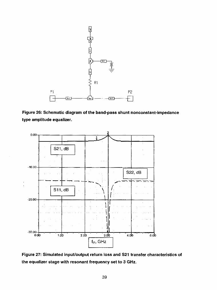
Figure 26: Schematic diagram of the band-pass shunt nonconstant-impedance
type amplitude equalizer.
Figure 27: Simulated inputloutput return loss and S21 transfer characteristics of
the equalizer stage with resonant frequency set to 3 GHz.

Figure 27 shows equalizer simulation results with resonance set to 3 GHz.
Inputloutput return loss is 5 -14 dB in band, and transfer function S21 shows a positive
slope of 1.52 dB per 500 MHz.
3'.3.2.1.8 Amplifier A2
Sirenza Microdevices [ I 21 SGA series, DC-4.5 GHz, SiGe HBT MMlC amplifier is
used as the second gain block. Good return loss, low noise figure (NFs 3.3dB) and
output IP3 of >31 dBm (with 4 V / 75 mA bias), are the main characteristics of this
device. The amplifier schematic with surrounding circuits is identical to amplifier A1
schematic. All design considerations expressed in amplifier A1 description are also valid
for amplifier A2.The amplifier simulation results are illustrated in Figure 28. The input
return loss is 5 -1 6 dB in band, the output return loss is 5 -1 1 dB, and transfer function
S21 shows minimum gain 11.3 dB and in band flatness of 0.51 dBpp.
Figure 28: Simulated inputloutput return loss and S21 transfer characteristics of
the amplifier A2.
3.3.2.1.9 Attenuator ATT3
5 dB, 50 Q, T attenuator is placed at the end of the IF chain, to improve matching
between amplifier A2 and mixer section and to bring IF section gain to desired level.
Schematic diagram is similar to schematic diagram of the attenuator ATT1.
This concludes the description of the intermediate frequency stage.
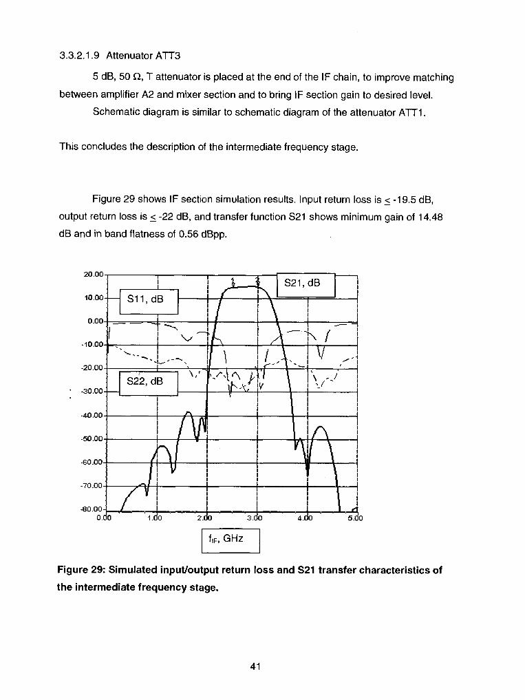
Figure 29 shows IF section simulation results. Input return loss is 5 -1 9.5 dB,
output return loss is 5 -22 dB, and transfer function S21 shows minimum gain of 14.48
dB and in band flatness of 0.56 dBpp.
Figure 29: Simulated inputloutput return loss and S21 transfer characteristics of
the intermediate frequency stage.

3.3.2.2 Mixer Stage
The mixer stage takes the intermediate frequency signal and converts it to output
RF signal (29.5 to 30 GHz), using the local oscillator signal from LO circuitry. The main
goal is to design a mixer with high output power capabilities ( I dB compression point or
IP3), as that decreases the required gain at Ka frequencies, which is equivalent to
number of required Ka amplifier stages.
Two mixer versions are considered below, FET resistive mixer and chip sub-
harmonic MMlC mixer.
3.3.2.2.1 GaAs FET Resistive Mixer
This resistive mixer, which uses the channel resistance of an unbiased GaAs
FET to perform frequency mixing (down-conversion) at X band (1 0 GHz), is described by
Mass [14]. The principles depicted in his paper are used to design a 30 GHz mixer for
upconversion.
The unbiased channel operates as a resistor controlled by the gate voltage in the
FET's IN curve region commonly called linear. Since this resistance is weakly nonlinear,
the mixer generates low intermodulation, hence it is capable of delivering high output
power with moderate LO levels.
4
DC bias Vg = -2.5 V
FET D RF OUT
LO IN G , 29.5 - 30 GHz
Figure 30: Block diagram of the resistive FET mixer.
27 GHz
-

The mixer realization is presented in Figure 30. The FET operates in a common-
source configuration; the LO and negative bias are applied to the gait, and IF is applied
to the drain. The RF signal is then filtered from the drain. The RFIIF filters are designed
to short-circuit the drain at LO frequency, to prevent LO voltage coupling to the drain,
which will cause operating point translation in more nonlinear region. LO filter (matching
circuit) is designed to short-circuit the RF signal at the gate, and prevent intermodulation.
27 GHz
- RFOUT 29.5 - 30 GHz
DC bias IF IN vg = -2.5 v 2.5 - 3 GHz
Figure 31: Schematic diagram of the resistive FET mixer.
The mixer consists of NEC [15] NE32400 die FET and three filters; see Figure 31
for details. Required filters are first designed, and then put together with FET nonlinear
model.
The NE32400 is a Hetero-Junction FET with pinch-off voltage between -2V and
-0.2 V, when biased (Vds=2V). The packaged FET cannot be used since package
parasitics at 30 GHz are destroying response characteristics. The RF filter is a 5'h order,
Edge Coupled Half Wave microstrip band-pass filter, with BWldB =1.2GHz and 2.5 to
2.75 dB insertion loss in a pass band (29.5 to 30 GHz), in 50 52, system. The IF filter is a
4'h order Elliptical microstrip filter, with cut-off frequency of 5 GHz, insertion loss of 0.35
dB in band (2.5 to 3 GHz), and poles positioned at 27 GHz and 29.75 GHz. The LO filter
is a simple two stub design, tuned to match the LO source to gait input impedance.
With the LO drive of +10 dBm, gait bias is adjusted for minimum conversion loss
and best IF port match (Vg = -2.5 V). The Ansoft Serenade simulation tool is used to
perform nonlinear simulation and tuning.
Figure 32 demonstrates the simulated output spectrum. Mixing product analysis
and nonlinear simulation shows that the components closest to the band of interest are
2L0 (27 GHz) and 2L0+21F (32 - 33 GHz). Undesired in-band mixing products, with

order c10, are not found. The achieved conversion loss of 10.6 dB maximum, and
flatness of 0.46 dB, is shown in Figure 33.
- Figure 32: Simulated mixer RF output power as a function of RF frequency.
Figure 33: Simulated mixer conversion loss as a function of IF frequency.

Figure 34 shows the compression characteristic of the mixer as sinusoidal IF
power is swept (from -20 to +20 dBm). PldB input compression point is +6 dBm and
P l dB output compression point is 4 . 1 5 dBm. Figure 35 shows input impedances on all
three ports.
Figure 34: Simulated mixer compression characteristic - output RF power as a
function of input IF power.
Figure 35: Simulated input
impedances of the IF, LO and RF
port.

3.3.2.2.2 Sub-harmonic MMlC mixer
A Hittite [16] chip sub-harmonically pumped mixer with an integrated LO amplifier
is used to upconvert IF signal to Ka band (RF = 2LO+IF). Since this is a sub-harmonic
mixer, a 13.5 GHz LO signal is required for conversion. The integrated LO amplifier is
single biased (+4V), dual stage design, so only -4 dBm LO drive is necessary. A GaAs
PHEMT technology is utilized in the MMlC design, resulting in a small chip size (0.97 x
1.32 mm).
Other mixer parameters are:
- RF Frequency Range: 24 - 32 GHz
- LO Frequency Range: 12- 16GHz
- IF Frequency Range: DC - 6 GHz
- Conversion Loss: 10 dB typ.
- 1 dB compression out: -4 dBm typ.
- 2L0 to RF Isolation: 35 dB typ.
- LO power: 0 dBm
Mixing product analysis shows that components closest to the required band are
2L0 (27 GHz) and 2L0+21F (32 - 33 GHz). In addition, 7th order in band mixing
spurious, 3LO-41F (30.5 - 28.5 GHz) and L0+61F (28.5 - 31.5 GHz), are discovered.
DC bias +4 v
I mmWave ceramic package
mixer die I---------
LO IN 13.5 GHz
t OUT 30 GHz
Figure 36: Block Diagram of the MMlC Mixer section.

Mixer die, combined with 2dB attenuator die and amplifier die, is packaged in the
ceramic mmwave package. This package is then attached to printed circuit board where
it is interfaced with the IF board, LO board and output band-pass filter, using 50 W
microstrip transmission lines.
A1 is a two-stage wide band (20 to 30 GHz), monolithic low noise (3 dB
maximum) amplifier with 13 dB gain and flatness of 2 dBpp. The amplifier is placed
between the mixer output and the band-pass filter input, to improve isolation and offer
broader matching to mixer RF port.
To conclude, the two mixers under consideration have similar conversion loss
and power handling capabilities (Pl dBcp), and require a clean room environment for
assembly. The MMlC mixer is implemented since it has smaller size, lower LO frequency
(13.5 compared to 27 GHz) and LO power requirement (0 dBm compared to +10 dBm).
3.3.2.3 Output Band-pass Filter
The 5th order Finline band-pass filter (BPF) is the next stage in the upconverter
chain. The main BPF task is to filter upper side mixing band (2LO+IF) and to reject 2L0
(27 GHz) and 2L0+21F (32 to 33 GHz) signals and other undesired mixing products.
The main filter requirements are:
- 1 dB Pass band: 29.3 - 30.2
- Insertion Loss: - < 3 d B
- InputlOutput Return Loss: > 15 dB
- Rejection Q 27 GHz > 60 dB
Q 32 GHz > 40dB
3.3.2.4 Solid State Power Amplifier Module
The solid-state power amplifier (SSPA) module is a multi-stage unit whose main
function is to amplify microwave signals to the desired +32 dBm (1 dBcp) output power.
GaAs MMlC amplifiers, designed for 50 R system, are used as building blocks.
MMlC chips are first die-attached and wire-bonded into ceramic mm-wave packages, in
a clean room environment, and then assembled with printed circuit board to the

aluminum sub-base plate. Altogether there are four packages inside the SSPA module.
Package 1 contains the low noise MMlC amplifier die (LNA). Package 2 holds the LNA
with integrated variable attenuator used for module temperature compensation. Package
3 contains the driver MMlc amplifier with PldB around +23 dBm. Package 4 carries the
power amplifier pair in a balanced configuration. Each of the power amplifier MMlCs has
PldB of +30 dBm. At the end of the amplifier chain, the microwave signal is launched
into WR28 wave-guide. Figure 37 presents SSPA block diagram.
Package 4
1 RFOUT
Gain Control DC Power Supply
Figure 37: Block diagram of the solid-state power amplifier section.
Other module parameters are:
- Frequency range: 25 - 30 GHz
- Gain at 25 deg. C (att=OdB): 60+ 1 dB
- Gain Variation Over Temperature: 14 dB
- Output P I dBcp: - > 32 dBm
- Gain Tuning Range: > 15dB
- Input Return Loss: > 12 dB
- Output Return Loss: > 8 d B

3.4 Measurement Results
The measurement results of the upconverter sub-circuits, as well as the unit level
results are presented in this section.
3.4.1 Sub-circuit Level Measurement Results
3.4.1.1 intermediate Frequency Section
Figure 38 presents the measurement setup used during the IF section evaluation
measurement. Since the IF input impedance is 75 R, a 50-75 R minimum loss pad is
used to transform Network Analyzer 50 Q impedance (port P I ) into 75 R. The pad
output is then calibrated using a 75 R calibration kit. Calibration is also performed at the
end of cable from port P2, using a 50 R coaxial calibration kit.
Network Analyzer
DC Power Supply
m
Figure 38: Measurement
setup diagram of the
intermediate frequency
section. L I
50 -75Ohm Minimum Loss Pad
Figure 39: Test Jig used for measurement of the intermediate frequency section.

Figure 39 shows the Test Jig used to secure the IF PCB, and to provide an
interface to measurement equipment. Figures 40 shows IF section measured input
return loss (S11) as a function of frequency. Desired frequency range is between maker
1 (2.5 GHz) and marker 2 (3GHz). Result is consistent with the simulation. Worst-case
return loss result of -17.1 dB is recorded at 3 GHz frequency.
Figure 40: Measured input return loss of the intermediate frequency section (10
dB per division scale).

Figures 41 shows IF section measured output return loss (S22) as a function of
frequency. Desired frequency range is between maker 1 (2.5 GHz) and marker 2
(3GHz). Worst-case return loss result of -19.565 dB is recorded at 2.728 GHz frequency
(marker 3).
Figure 41: Measured output return loss of the intermediate frequency section (10
dB per division scale).

Figures 42 and 43 demonstrate the IF section transfer characteristics as a
function of frequency. General shape and pole positions are very close to simulation
(see Figure 29). A minimum gain of 13.57 dB and flatness of 0.34 dBpp, are recorded.
START 3.000 000 M H z STOP 5 000.000 000 MHz
Figure 42: Measured intermediate frequency section transfer function S21 as a
function of frequency (10 dB per division scale).

Figure 43: Measured intermediate frequency section transfer function S21 as a function
of frequency, with 1 dB per division scale.
3.4.1.2 Mixer
Figures 44 and 45 show the mixer test jig and equipment setup diagram used for
circuit evaluation.
Figure 44: Test jig used for measurement of the mixer section.
53

Signal Generator #2 I I 40 GHz
-1 dBrn
DC Power Supply
I
Figure 45: Measurement setup diagram of the mixer section
The spectral content at the mixer RF port, with injected IF frequency of 2.5 GHz,
is presented in Figure 46. The closest spurious signals, 2L0 and 2L0+21F are -2 dBc
and -35 dBc, respectively, below the desired 29.5 GHz signal.
Figure 46: Measured mixer RF port power spectrum as a function of frequency.

CENTER 29 .7500EHz S P A N 6 0 0 . 0 M H z R E 3 W 1 . O M H z V R W 1 . O M H z S W P S O . O m s
Figure 47: Measured mixer RF output power variation as a function of frequency (1
dB per division scale).
To produce the conversion loss response illustrated in Figure 47, the IF signal
generator is swept from 2.5 to 3 GHz. A flatness of only 1 dB, in full 500 MHz band, is
recorded. Delta marker spectrum analyzer function is used to measure difference
between maximum and minimum power level.
3.4.1.3 Band-Pass Filter
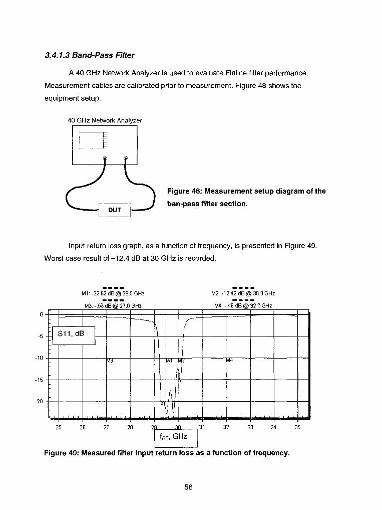
A 40 GHz Network Analyzer is used to evaluate Finline filter performance.
Measurement cables are calibrated prior to measurement. Figure 48 shows the
equipment setup.
40 GHz Network Analyzer
? P I Figure 48: Measurement setup diagram of the
ban-pass filter section. DUT
Input return loss graph, as a function of frequency, is presented in Figure 49.
Worst case result of -12.4 dB at 30 GHz is recorded.
Figure 49: Measured filter input return loss as a function of frequency.
56

The filter frequency response is shown in Figure 50. Insertion loss of only 2.3 dB
is recorded (between markers MI and M2). Rejections of more than 70 dB at 27 GHz
(marker M3), and more than 50 dB at 32 GHz (marker M4), are more than adequate for
the complete elimination of unwanted spurious signals (2L0 and 2L0+21F).
1-11
MI: -2 25 dB @ 29.5 GHz 1-11
11-1
M2: -2.32 dB @ 30.0 GHz 1111
Figure 50: Measured filter transfer function S21 as a function of frequency.
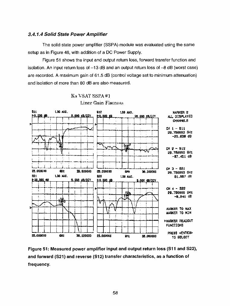
3.4.1.4 Solid State Power Amplifier
The solid state power amplifier (SSPA) module was evaluated using the same
setup as in Figure 48, with addition of a DC Power Supply.
Figure 51 shows the input and output return loss, forward transfer function and
isolation. An input return loss of -13 dB and an output return loss of -8 dB (worst case)
are recorded. A maximum gain of 61.5 dB (control voltage set to minimum attenuation)
and isolation of more than 80 dB are also measured.
Figure 51: Measured power amplifier input and output return loss (S11 and S22),
and forward (S21) and reverse (S12) transfer characteristics, as a function of
frequency.
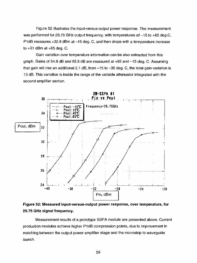
Figure 52 illustrates the input-versus-output power response. The measurement
was performed for 29.75 GHz output frequency, with temperatures of -1 5 to +65 deg.C.
P l dB measures +32.8 dBm at -1 5 deg. C, and then drops with a temperature increase
to +31 dBm at +65 deg. C.
Gain variation over temperature information can be also extracted from this
graph. Gains of 54.8 dB and 65.6 dB are measured at +65 and -1 5 deg. C. Assuming
that gain will rise an additional 2.1 dB, from -15 to -30 deg. C, the total gain variation is
13 dB. This variation is inside the range of the variable attenuator integrated with the
second amplifier section.
Figure 52: Measured input-versus-output power response, over temperature, for
29.75 GHz signal frequency.
Measurement results of a prototype SSPA module are presented above. Current
production modules achieve higher P l dB compression points, due to improvement in
matching between the output power amplifier stage and the microstrip towaveguide
launch.

3.4.2 Unit Level Measurement Results
Unit level measurement results are collected using Automated Test Equipment
(ATE) setup and they are presented in this subsection.
Figure 53 shows a picture of the transmitter RF section. Beside the upconverter
chain, Reference, LO and SSPA Power Supply PCBs are illustrated.
Figure 53: Picture of the Ka-band transmitter RF circuitry.
Temperature Chamber
Figure 54: Automated measurement setup diagram of the transmitter unit.
60

Figure 54 illustrates the ATE measurement setup, which enables completely
automated unit evaluation over temperature (-30 to +50 OC). A software application
controls all instruments and temperatures via a HPlB interface. The duration of the entire
test is approximately 4 hours.
Measured transmitter unit gain variation over frequency and temperature is
shown in Figure 55. Overall gain variation should be between 52 and 63 dB (straight limit
lines). Maximum and minimum measured gains of 62 dB and 57.34 dB, respectively, are
recorded. Maximum gain variation over temperature of 3.23 dB, and maximum gain
variation over frequency of 2.77 dB, over full 500 MHz band (29.5 to 30 GHz), are
measured.
Figure 55: Measured transmitter gain variation over frequency and temperature.

Figure 56 illustrates input-versus-output power at 50 OC. Power of the input IF
signal at 2.75 GHz is swept from -49.5 dBm to -23.5 dBm. Output RF signal at 29.75
GHz saturated power of +33 dBm is recorded. Measurement is performed at +50 OC
ambient temperature since that is the worst-case condition for power amplifier operation
(lowest unit gain - highest input level).
I PRF OUT, dBm I
Figure 56: Measured transmitter input-versus-output power response at 50 O C
ambient temperature.
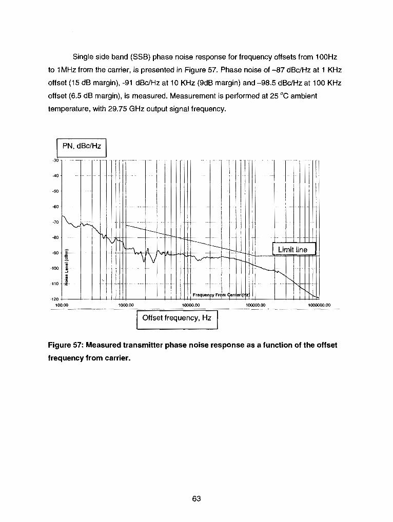
Single side band (SSB) phase noise response for frequency offsets from 1 OOHz
to 1 MHz from the carrier, is presented in Figure 57. Phase noise of -87 dBcIHz at 1 KHz
offset (15 dB margin), -91 dBcIHz at 10 KHz (9dB margin) and -98.5 dBc/Hz at 100 KHz
offset (6.5 dB margin), is measured. Measurement is performed at 25 OC ambient
temperature, with 29.75 GHz output signal frequency.
Figure 57: Measured transmitter phase noise response as a function of the offset
frequency from carrier.

Figure 58 shows RF output power spectrum as a function of frequency. No in-
band or out of band spurious signals are recorded. Measurement is performed at -30 OC
ambient temperature since that is the worst-case condition for unit spurious content
(highest unit gain - highest 2L0 signal leakage).
Figure 58: Measured transmitter output power spectrum as a function of
frequency at -30 OC ambient temperature.

Table 6 presents part of the automatically generated measurement report.
It should be noted that the unit exceeds specifications on all parameters with a
considerable margin.
Table 6: Measurement results collected using automated measurement setup.
Test Description
In Band Out of Band
7
Frequency Stability over Temperature (referenced to 25' C.)
Spec.
Operational Temperature Test Power Consumption Gain Variation Over Frequency
In any 20 MHz Band In Full 500 MHz Band
Max Gain Min Gain Gain Variation over Temperature
Saturation Point
Phase Noise @
1 KHz/ 1 OKHz/ 100KHz
Hot Start Cold Start
3 5 W I - 25.95W I [XI PASS [ ] FAIL I Results Comment
"7z -8z -92 1 < -721 -821 -92dBcMz 1 [XI PASS [ ] FAIL dBc/Hz
< 1 dB - < 5dB - < 63dB - > 52dB - < 6dB -
> 31.3dBm -
0.88dB 2.77dB
62.00dB 57.34dB 3.23dB
33.07dBm
> 60 dBc c--31 dBm - < -40 dBm -
< -95dBmIHz -
[XI PASS [ ] FAIL [XI PASS [ ] FAIL
[XI PASS [ ] FAIL [XI PASS [ ] FAIL [XI PASS [ ] FAIL
[XI PASS [ ] FAIL
< + lOppm --
> 6OdBc < -31 dBm < -40dBm
-99.92dBmIHz
[XI PASS [ ] FAIL [XI PASS [ ] FAIL [XI PASS [ ] FAIL
[XI PASS [ ] FAIL
-7.03ppm
[XI PASS [ ] FAIL [XI PASS [ ] FAIL
[XI PASS [ ] FAIL

4 RETURN CHANNNEL LINK BUDGET CALCULATION
The measurements results presented in Section 3 demonstrated the actual
Transmitter performance. Using these results, an ASTRA BBI RCS link budget
calculation is performed, to evaluate system performance using a Norsat ODU.
4.1 Introduction
The Return Channel link is the communication path from the information source,
through SIT to satellite (uplink), and from satellite, through the hub receiver, to the
information sink (downlink).
For the chosen modulation scheme, the desired probability of error can be
achieved only if sufficient signal to noise ratio is presented at the input of the receiver.
As discussed by Skalar [ I 71, the goal of a link analysis is to determine whether or
not the required probability of error performance is met. Since some of the budget
parameters are statistical, analysis estimates available Carrier-to-Noise ratio or C/N. The
difference between estimated and required C/N represents the safety margin.
4.2 Link Budget
Figure 59 depicts Ka-band, return channel link.
Paris, France (Longitude 2.3 deg. East, Latitude 48.8 deg. North) is chosen as a
SIT site. Uplink frequency of 29.92 GHz is selected. This signal is picked up by ASTRA
1 H GEO satellite Ka transponder (France beam; see Figure 8), positioned at 19.2 deg
East. At the satellite, the signal is translated to 20.12 GHz frequency and beamed down
to the BBI Hub. The Hub installation is located in Betzdorf, Luxemburg (Longitude 6 deg.
East, Latitude 49.7 deg. North).
The calculation is performed for both a clear sky case, and a rain case. Paris and
Betzdorf are both part of CClR Rain Climate Zone E (from CClR Recommendation 837)
with 0.3% rain rate exceeded = 2.4mmIh.

Downlink 20.12 GHz
Slant Range 38,469 Krn Path Loss 21 0 dB
ASTRA 1 H Ka-band transponder
1
Uplink 29.92 GHz
Slant Range 38,465 Krn Path Loss 213.5 dB
SIT I I I I
, Site: Betzdorf Site: Paris Antenna size: 5.6 rn Antenna size: 76 crn
Elevation angle: 31.6 deg. Elevation angle: 31.7 deg. Antenna Gain: 59.6 dBi Antenna Gain: 45 dBi Receiver G/T: 37.7 dB/K Transmitter Power: 2 dBW
Noise Emission: -78 dBW/Hz
Figure 59: Return channel link between terminal located in Paris, France and hub
located at Betzdorf, Luxemburg, over Ka-band satellite ASTRA 1H.

Table 7: Link budget calculation for clear sky and 0.3% rain rate exceeded
conditions.
I Uplink Q29.92 GHz Downlink Q 20.12 GHz 1

The link budget calculation for Ka-band return link path, in ASTRA BBI network,
is illustrated in Table 2.
As discussed in the literature 117, 181, carrier-to-noise power density (CINo) equation for
uplink and downlink can be expressed as
C/NO = ElRP - OBO - Lp + G/T- k [dB- HZ]
Effective Isotropic Radiated Power (EIRP) is calculated as
EIRP = Pt - Li + Ga [dBw]
where Pt is transmitter output power [dBW],
Li is loss due to feed cable [dB],
Ga is antenna gain [dBi],
Satellite manufacturer specifies EIRP for satellite downlink
OBO represents output amplifier back-off [dB].
Lp is space loss - decrease in signal strength due to the distance between the
satellite and an Earth station. This is the largest signal loss in the link.
Lp = (4 * K * dlh); where d is slant distance and h is wavelength at transmission
frequency.
Other losses that are degrading link quality are:
- Antenna Pointing Loss is loss due to the transmitter or receiver antenna not
being optimally pointed. Antenna gain pattern, as a function of pointing error
angle, is given by
Ga = 29 - 25*log (error angle) [dBi].
- Atmospheric absorption is loss due to oxygen and water vapor absorption.
- Rain is the main atmospheric cause for signal loss. To calculate rain loss,
equations from reference [ I 81 (1.20a and 1.20b) are used. Signal loss
increases with rain intensity, due to absorption. In addition, the amount of
noise radiated in to the receiver antenna (sky noise temperature), also
increases with the rain intensity.
G/T is receiver antenna gain and system effective temperature (noise radiated
into antenna and the thermal noise of the receiver front end) grouped together,
sometimes called the receiver sensitivity.
k is Boltzmann's constant.

Another source of degradation in a satellite link is interference caused by unwanted
signals injecting energy in the band of interest. The following interference sources are
considered:
- Cross-polar Interference is characterized by an undesired signal appearing
within the signal bandwidth due to inadequate discrimination between
horizontal and vertical polarization by the antenna. Measured cross-polar
level for the 76 cm antenna is 26 dB. Cross-polar performance of the hub's
5.6m antenna is estimated to be 17 dB.
Cllo = CII + I0 log (signal BW) [dB-Hz]
- SIT noise interference is a ratio between ElRP and noise spectral density at
the SIT antenna output. For this type of SIT (type 2 - ElRP 2 45 dBW)
required NSD is -78 dBW1Hz. This interference is calculated with assumption
that 10,000 users will simultaneously operate (per one beam).
Cllo = ElRP - (NSD + 10 log (# of users)) [dB-Hz]
- Adjacent Channel lnterference is interference caused by energy spilling from
an adjacent frequency channel, due to output stage nonlinearity (spectral re-
growth). -20 dBc adjacent channel interference is present at the output of the
SIT antenna when the terminal operates at specified ElRP level.
- Transponder Intermodulation-is estimated to 17dB.
Uplink and Downlink carrier to noise and interference, is calculated using:
CI(No+lo) = ( ( ~ 1 ~ 0 ) - ' + (~110)-' )-' [dB-HZ]
The same formula is used when uplink and downlink ratios are combined to
generate Available C/(No+lo).
Required CIN can be expressed as:
CIN req = EbINo - Gc + r*R + Mi +Ms - BW [dB]
EbINo is bit energy per noise power spectral density, required to yield to desired
bit error probability performance, without coding. As discussed in [ I 9, 201 can be
expressed as:
P = BER = 112 erfc( SQR(Eb1No)) for QPSK (Gray encoded)
Gc is coding gain and represents decrease in required EbINo value, for same
BER, due to coding implementation. Powerful concatenated code, formed of the outer
Reed-Solomon RS(224, 188, 8) code and inner convolutional code rate 112 with
constraints length 7, is applied to traffic and control data, to provide channel error

protection. The inner CC(2, 1 ,7) Viterby soft decision decoder correct random errors.
The errors at convolutional decoder output are busty in nature, and outer RS code is
used to correct them. ETSl EN 300 421 European standard document is specifying
required EbINo to 3.7 dB, for BER = 2 x 1 after Viterby and Quasi-Error-Free (QEF -
corresponding to 1 0*1•‹) after Reed-Solomon decoder.
r is coding rate and R represents transmission rate. This calculation is performed
for data rate of 384 Kbps (specified rate for SIT2) and symbol bandwidth of 0.618 MHz.
Mi stands for implementation margin, performance degradation due to the
difference between the theoretical and the actual detection performance, caused by
frequency offsets, timing errors and so on.
Ms corresponds to system margin, performance degradation due to imperfect
synchronization reference.
BW is receiver noise bandwidth, and is equal to symbol rate.
The difference between available C/(N+I) and required CIN represents margin.
A margin of 3.9 dB for clear sky condition, and 1.4 dB for rain with 0.3% rain rate
exceeded, is the result of the link budget calculation.
The conclusion is that the Norsat transmitter1ODU deployed in ASTRA BBI
network can yield to an availability of service equal to 99.7% for a transfer data rate of
348 Kbps.

5 CONCLUSION
Internet and multimedia applications have experienced tremendous growth in the
last few years. Demand for high-speed access to widely dispersed servers is growing
every day.
Among emerging mobile/wireless networks, geostationary Ka-band satellite
networks, with their ability to deliver wide bandwidth independent of geography and local
infrastructure, represent an ideal solution to handle this increasing demand.
The Ka-band transmitter, part of the satellite interactive terminal used for IP transfer
over satellite, was reviewed. A detailed description of transmitters upconverter section,
containing design considerations, block diagrams, schematics and simulation results,
was conveyed. The measurement results matched very closely to simulation data. Unit
level measurement results, obtained using an automated measurement system, illustrate
that transmitter exceeds specification outlined by DVB-RCS standard, with a
considerable margin on all parameters.
The return channel link budget calculation outlines that an availability of service
equal to 99.7% at a data rate of 348 Kbps, can be achieved if the Norsat
transmitter1ODU is deployed in the ASTRA BBI network.
Development work on new generation of Ka-transmitters, half the size and cost, is
currently underway.

REFERENCES
[ I ] ETSl Telecom Standards, http://www.etsi.or~/aetastandard/home.htm (accessed
March 13, 2002).
[2] Y. Zhang, D.D. Lucia, B. Ryu, and S. K. Dao, "Satellite Communications in the
Global Internet: Issues, Pitfalls, and Potential," Hughes Research Laboratories, USA,
http://www.iif. hu/rendezvenvek/inet97/F5/F5 1 .HTM (accessed March 10, 2002).
[3] Ka-band Report - Management Summary, http://www.s~otbeam.com (accessed
March 5, 2002).
[4] J. Puetz, "Comparative Approaches in Implementing Wide Area Satellite Networks,"
Pacific Telecommunication Conference, Honolulu, Hawaii, January 1997.
[5] ASTRA Satellites - The Footprints, http://www.astra.lu/satellites/footprints.shtmI#
(accessed March 15,2002).
[6] Eutelsat HotBird 6 satellite Information,
http:Nwww.eutelsat.com/satellitesll3ehb6.html# (accessed March 15, 2002).
[7] EuroSkyWay Network Information, http://www.eurosk~vav.itl (accessed March 15,
2002).
[8] J. L. Fikart and A. Chan, "Outdoor Units for Ka/Ku-band Satellite lnteractive
Terminals," Fifth Ka-band Utilization Conference Proceedings, Taormina, Italy, Oct.
1999, pp. 437-444.
[9] J. L. Fikart, "Outdoor Units For KaJKu-Band Satellite lnteractive Terminals," IEEE
MTT-S International Microwave Symposium Digest, 2001, vol. 2, pp. 1 141-1 144.
[ I 01 A. I. Zverev, Handbook of Filter Synthesis. New York: John Wiley and Sons, 1967,
Chapter 4, pp. 107-1 36.
[ I 11 Ansoft Design Environment, htt~://www.ansoft.com/~roducts/hf/serenade/index.cfm
(accessed March 20,2002).
[ I 21 Sirenza Microdevices Gain Blocks,
htt~://www.sirenza.com/products/function/aain blocks.htmi (accessed March 20, 2002)
[ I 31 A. Williams, Electronic Filter Design Handbook. New York: McGraw-Hill Book
Company, 1981, pp. 8-1 2 to 8-1 5.
[14] S. A. Maas, "A GaAs MESFET Mixer with Very Low Intermodulation," IEEE
Transaction on MTT, April 1 987, vol. MTT-35, no. 4, pp. 425-429.

[ I 51 NEC - CEL products, http://www.cel.com/prod/prod smallsiq.asp (accessed March
20, 2002).
[ I 61 Hittite Microwave Corporation - Mixer Products,
http:Nwww.hittite.com/index.cfm?bodv content=products&type=mixer&catid=4&sort=fun
ction&source=leftnav (accessed March 20, 2002).
[ I 71 B. Skalar, Digital Communications- Fundamentals and Applications. New Jersey:
Prentice Hall, 1988, pp. 188-240.
[18] V. K. Bhargava, D. Haccoun, R. Matyas, and P. P. Nuspl, Digital Communications
by Satellite. New York: John Wiley and Sons, 1981, pp. 10-28.
[ I 91 R. Steele, Mobile Radio Communications. London: Pentech Press,1992 , Chapter
4, pp. 347-484.
[20] J. G. Proakis, Digital Communications, New York: McGraw-Hill, 1995, pp. 506-51 0.