
JIM Kwok Lung - PolyU Electronic Theses
204
-
Upload
khangminh22 -
Category
Documents
-
view
3 -
download
0
Transcript of JIM Kwok Lung - PolyU Electronic Theses


The Hong Kong Polytechnic University
Department of Applied Physics
BARIUM STRONTIUM TITANATE FERROELECTRIC
TUNABLE PHOTONIC AND PHONONIC CRYSTALS
JIM Kwok Lung
A thesis submitted in partial fulfillment of the requirements
for the degree of Doctor of Philosophy
January 2009

ABSTRACT
JIM Kwok Lung i
ABSTRACT
This thesis presents the results of theoretical simulations and experimental
investigations on developing electro-optically tunable photonic crystals and thermally
tunable phononic crystals based on the ferroelectric materials, Barium Strontium
Titanate (Ba0.7Sr0.3TiO3, BST).
One-dimensional photonic crystal (PC) consists of five periods, with each period
consisting of a 90 nm thick Ba0.7Sr0.3TiO3 layer and a 10 nm thick MgO layer, was
fabricated using pulsed laser deposition. X-ray diffraction study confirmed the epitaxial
growth of the Ba0.7Sr0.3TiO3 layers with good crystalline quality. A photonic bandgap
(transmission dip) with a centre wavelength at ~464 nm has been observed in the
transmission measurement which is consistent with simulation using the plane wave
expansion (PWE) method and the transfer matrix method. A 2-nm shift towards the
longer wavelength is observed when a dc voltage of 240 V (corresponding to an electric
field of about 12 MV/m) has been applied across the coplanar electrodes on the film
surface. The experimental result suggests that the electric field induced change in the
refractive index of Ba0.7Sr0.3TiO3 is about 0.5 %.
Photonic bandstructures and photonic bandgap maps of two-dimensional (2D)
Ba0.7Sr0.3TiO3-based photonic crystals with different cavity geometries (square or

ABSTRACT
JIM Kwok Lung ii
circular air rods) in square lattice were calculated using the PWE method. Simulation
results suggested comparable bandstructures and bandgap maps for square or circular air
rod photonic crystals, if (1) the dimension of the air rod is small compared to the
electromagnetic wavelengths inside the PC being considered, or (2) the frequencies of
the electromagnetic waves are less than 0.35(2c/a). The photonic bandgap maps of two
types of 2D Ba0.7Sr0.3TiO3-based PC, namely, the air-hole-in-BST type and the BST-rod-
in-air type both in square lattice and in triangular lattice were calculated. It is found that
PCs in triangular lattice contain richer bandgap feature in general. Bandgap features
along different symmetry directions have also been compared.
The refractive indices of the Ba0.7Sr0.3TiO3 thin film on a MgO (001) substrate
was measured using the prism coupling technique. The appropriate geometry of a single-
mode rib waveguide based on Ba0.7Sr0.3TiO3 thin film was determined by applying the
effective index method. A photonic crystal cavity embedded Ba0.7Sr0.3TiO3 rib
waveguide which functions as a tunable filter (on-off switch) for λ = 1550 nm was
designed with the help of the finite-difference time-domain (FDTD) simulation. The
required PC cavity is composed of two 5-row-4 PC mirrors, which is formed by air holes
arranged in triangular lattice in the Ba0.7Sr0.3TiO3 matrix, with cavity length of 800 nm.
The radius of the air holes is 250 nm and the periodicity is 625 nm. A 6-nm shift in the
resonant peak for a 0.5% change in the refractive index of the Ba0.7Sr0.3TiO3 was
illustrated in the simulation. Photonic crystal cavities were fabricated on a Ba0.7Sr0.3TiO3
rib waveguide by focused ion beam etching with satisfactory results.

ABSTRACT
JIM Kwok Lung iii
The shear and transverse wave velocities of Ba0.7Sr0.3TiO3 ceramic as a function
of temperature were determined using the ultrasonic through-transmission technique. A
drastic variation in the wave velocities was observed across the Curie temperature of
Ba0.7Sr0.3TiO3. Phononic crystal composed of Ba0.7Sr0.3TiO3 square rods in a matrix of
epoxy were fabricated using the dice-and-fill method. The width of the Ba0.7Sr0.3TiO3
rods is 200 µm with periodicity of 265 µm. The temperature dependence of the phononic
bandgaps of the phononic crystal was characterized by the reflection spectra which were
obtained using the ultrasonic pulse-echo technique. Thermal tuning of the phononic
bandgap was observed and the results were in good agreement with the phononic
bandstructure calculation by the plane wave expansion method.

LIST OF PUBLICATIONS
JIM Kwok Lung iv
LIST OF PUBLICATIONS
1. K. L. Jim, D. Y. Wang, C. W. Leung, C. L. Choy, and H. L. W. Chan, “One-
dimensional tunable ferroelectric photonic crystals based on
Ba0.7Sr0.3TiO3/MgO multilayer thin films,” Journal of Applied Physics 103,
083107-6 (2008).
2. K. L. Jim, C. W. Leung, S. T. Lau, S. H. Choy, and H. L. W. Chan, “Thermal
tuning of phononic bandstructure in ferroelectric ceramic/epoxy phononic
crystal,” Applied Physics Letters 94, 193501-3 (2009).
3. K. L. Jim, F. K. Lee, J. Z. Xin, C. W. Leung, H. L. W. Chan, and Y. Chen,
“Fabrication of two-dimensional nanoscaled patterns on ceramic thin films by
soft ultraviolet nanoimprint lithography,” submitted to Microelectronic
Engineering, (2009).
4. K. L. Jim, C. W. Leung, and H. L. W. Chan, “Photonic crystal cavity
embedded barium strontium titanate thin-film rib waveguide prepared by
focused ion beam etching,” submitted to Thin Solid Films (2009).

LIST OF PUBLICATIONS
JIM Kwok Lung v
5. K. L. Jim, D. Y. Wang, C. W. Leung, C. L. Choy, and H. L. W. Chan,
“Theoretical study of ferroelectric barium-strontium-titanate-based one-
dimensional tunable photonic crystals,” Proceedings of the Society of Photo-
Optical Instrumentation Engineers (SPIE) 6556, R5560 (2007).
6. D. Y. Wang, K. L. Jim, C. W. Leung, H. L. W. Chan, and C. L. Choy,
“Tunable ferroelectric photonic crystals based on Ba0.7Sr0.3TiO3/MgO
multilayer thin films,” Proceedings of the Society of Photo-Optical
Instrumentation Engineers (SPIE) 6556, Q5560 (2007).
7. K. L. Jim, D. Y. Wang, C. W. Leung, C. L. Choy, and H. L. W. Chan, “(Ba,
Sr)TiO3-based planar photonic bandgap crystal,” Proceedings of the Society
of Photo-Optical Instrumentation Engineers (SPIE) 6640, P6400 (2007).
8. K. L. Jim, C. W. Leung, C. L. Choy, and H. L. W. Chan, “Thermal shifting of
phononic bandgaps in barium strontium titanate-based structures,”
Acoustics’08, 1945 (2008).

ACKNOWLEDGEMENTS
JIM Kwok Lung vi
ACKNOWLEDGEMENTS
During my three years of Ph.D. study at the Hong Kong Polytechnic University, I
enjoyed my research and personal life everyday because of all the people who gave
endless support to me. First of all, I sincerely would like to express my gratitude to my
supervisors, Prof. H. L. W. Chan and Dr. C. W. Leung, for their invaluable guidance,
support, encouragement and patience throughout the whole period of my research study.
I would also like to thank Prof. K. H. Wong, Prof. J. Zhou (Tsinghua University)
and Prof. W. Y. Tam (HKUST), being the Board of Examiners of my thesis
examination, for their valuable comments which add advantages to this thesis.
I wish to show my appreciation to Prof. Y. Chen for his cordial welcome during
my exchange to the École Normale Supérieure in Paris. My thanks also go to friends I
made there including Ms. X. F. Ni, Mr. X. T. Zhou, Mr. L. Lei, Ms. Li Wang, Ms. Lu
Wang and Mr. Q. Zeng.
I would like to thank Prof. K. S. Chiang from the Optoelectronic Research Centre
in the Department of Electronic Engineering at the City University of Hong Kong who
has contributed resources to the success of this research work. My thanks are also

ACKNOWLEDGEMENTS
JIM Kwok Lung vii
extended to the members of his research team including Mr. K. P. Lor for his helpful
assistance in waveguide characterization.
I wish to thank Mr. Y. F. Chan from the Electron Microscope Unit at the
University of Hong Kong for his support in FIB etching.
My genuine thanks go to Dr. D. Y. Wang for his helpful advices and kind
assistance in pulsed laser deposition and prism coupling measurement, Dr. F. K. Lee for
his thoughtful assistance in waveguide fabrication and AFM investigations, Dr. K. C.
Cheng for his kind assistance in waveguide characterization, Dr. S. H. Choy for his
gentle help in fabrication of phononic crystals, and Dr. S. T. Lau for her helpful
assistance in reflection spectrum measurement of phononic crystals.
I wish to acknowledge the academic members in our department: Prof. C. L.
Choy and Dr. J. Y. Dai for their insightful suggestions during the group meeting
discussions. Thanks are due to Dr. P. F. Lee for his helpful advices in laser operation and
Mr. M. N. Yeung of the Materials Research Centre for his assistance in XRD
investigations.
I would like to thank my former and present colleagues in our department of their
assistance and discussions in the research work. They include (in no particular order):
Mr. Y. M. Tang, Ms. M. K. Li, Mr. C. K. Chow, Mr. S. M. Mok, and Dr. C. Y. Lam.

ACKNOWLEDGEMENTS
JIM Kwok Lung viii
I gratefully acknowledge the financial support from the Department of Applied
Physics and the Centre for Smart Materials of the Hong Kong Polytechnic University.
Most of all, I would like to express my deepest appreciations to my family
members for their continuous love, support, understanding and patience that inspired me
to continue and to mature both as a person and as a professional.

TABLE OF CONTENTS
JIM Kwok Lung ix
TABLE OF CONTENTS
ABSTRACT i
LIST OF PUBLICATIONS iv
ACKNOWLEDGEMENTS vi
TABLE OF CONTENTS ix
LIST OF FIGURE CAPTIONS xiv
LIST OF TABLE CAPTIONS xxii
LIST OF SYMBOLS xxiii
LIST OF ACRONYMS xxv
CHAPTER 1 INTRODUCTION 1
1.1 Background 1
1.2 Electro-optic effect in crystals 4
1.2.1 Refractive index 4
1.2.2 Optical birefringence 5
1.2.3 Electro-optic effect and electro-optic coefficients 7
1.3 Elastic properties during phase transition in ferroelectric materials 12
1.4 Barium strontium titanate in bulk and thin film forms 13
1.4.1 Bulk barium strontium titanate 13
1.4.2 Barium strontium titanate thin films 15
1.5 Photonic crystals 17
1.5.1 Theoretical tools for analyzing photonic crystals 19
1.5.1.1 Plane wave expansion method 20
TABLE OF CONTENTS
JIM Kwok Lung x
1.5.1.2 Scattering matrix method 22
1.5.1.3 Finite-difference time-domain method 23
1.5.1.4 Transfer matrix method 25
1.5.1.5 Comparison of the four methods 26
1.5.2 Tunable photonic crystals 28
1.5.2.1 Ferroelectric photonic crystals 29
1.6 Phononic crystals 30
1.6.1 Tunable phononic crystals 31
1.7 Scope of the present study 32
1.8 Statement of original contributions 34
CHAPTER 2 ONE-DIMENSIONAL TUNABLE PHOTONIC CRYSTAL
BASED ON BARIUM STRONTIUM TITANATE &
MAGNESIUM OXIDE MULTILAYERED THIN FILMS
35
2.1 Introduction 35
2.2 Simulation methods for one-dimensional photonic crystals 37
2.2.1 Computation of photonic bandstructure of one-dimensional
photonic crystal by the plane wave expansion method
37
2.2.2 Computation of transmission spectrum of one-dimensional
photonic crystal by the transfer matrix method
38
2.3 Theoretical study of Ba0.7Sr0.3TiO3/MgO one-dimensional photonic
crystals
40
2.4 Fabrication of Ba0.7Sr0.3TiO3/MgO one-dimensional photonic crystals 50
2.5 Characterization of one-dimensional Ba0.7Sr0.3TiO3/MgO photonic crystals 52
2.5.1 Structural characterization of the one-dimensional photonic
crystals
52
2.5.2 Optical characterization of the one-dimensional photonic crystals 53
2.6 Summary 59

TABLE OF CONTENTS
JIM Kwok Lung xi
CHAPTER 3 PHOTONIC BANDSTRUCTURE STDUY ON TWO-
DIMENSIONAL BARIUM STRONTIUM TITANATE-
BASED PHOTONIC CRYSTALS
60
3.1 Introduction 60
3.2 Plane wave expansion method for two-dimensional photonic bandstructure
calculation
61
3.3 Photonic bandgap maps of two-dimensional Ba0.7Sr0.3TiO3-based photonic
crystals with different configurations
65
3.4 Photonic bandstructures and photonic bandgap maps of two-dimensional
Ba0.7Sr0.3TiO3-based photonic crystals with different shapes of air rods
70
3.5 Summary 76
CHAPTER 4 PHOTONIC CRYSTAL CAVITY EMBEDDED BARIUM
STRONTIUM TITANATE RIB WAVEGUIDES
77
4.1 Introduction 77
4.2 Characterization of Ba0.7Sr0.3TiO3 thin films 78
4.2.1 Structural characterization of Ba0.7Sr0.3TiO3 thin films 78
4.2.2 Optical characterization of Ba0.7Sr0.3TiO3 thin films 79
4.2.2.1 Basic principles of prism coupling technique 81
4.2.2.2 Guided modes in Ba0.7Sr0.3TiO3 thin films 85
4.3 Ba0.7Sr0.3TiO3 thin film optical rib waveguides 87
4.3.1 Light propagation in slab waveguides 87
4.3.1.1 Basic concepts of slab waveguides 87
4.3.1.2 Guided modes of slab waveguides 89
4.3.1.3 Cutoffs of asymmetric slab waveguides 93
TABLE OF CONTENTS
JIM Kwok Lung xii
4.3.2 Design of Ba0.7Sr0.3TiO3 rib waveguides using the effective index
method
96
4.3.3 Fabrication of Ba0.7Sr0.3TiO3 rib waveguides 101
4.3.4 Optical characterization of Ba0.7Sr0.3TiO3 rib waveguides 104
4.4 Photonic crystal cavity embedded rib waveguides 106
4.4.1 Fabry-Perot cavity 106
4.4.2 Photonic crystal cavity 109
4.4.3 Design of photonic crystal cavity embedded Ba0.7Sr0.3TiO3 rib
waveguides
111
4.4.3.1 Appropriate geometry of the photonic crystal pattern 112
4.4.3.2 Effect of number of row 115
4.4.3.3 Effect of row configuration 118
4.4.3.4 Determination of cavity length 121
4.4.3.5 Electro-optic tuning of the resonant peak 122
4.4.4 Photonic crystal cavity preparation by focused ion beam etching 124
4.5 Summary 128
CHAPTER 5 THERMAL TUNING OF PHONONIC BANDGAPS
IN BARIUM STRONTIUM TITANATE/EPOXY
PHONONIC CRYSTALS
129
5.1 Introduction 129
5.2 Computation of phononic bandstructure by plane wave expansion method 130
5.2.1 Wave equation for an inhomogeneous elastic medium 131
5.2.2 Plane wave expansion for periodic elastic structure 132
5.2.3 Binary composite 134
5.3 Determination of temperature dependence of longitudinal and shear wave
velocities by ultrasonic through-transmission technique
138
5.3.1 Ultrasonic through-transmission technique 138

TABLE OF CONTENTS
JIM Kwok Lung xiii
5.3.2 Determination of longitudinal wave velocity 139
5.3.3 Determination of shear wave velocity 140
5.3.4 Temperature dependence of longitudinal and shear wave
velocities in Ba0.7Sr0.3TiO3 bulk sample
142
5.3.5 Temperature dependence of longitudinal and shear wave
velocities in epoxy sample
145
5.4 Barium strontium titanate/epoxy phononic crystals 146
5.4.1 Fabrication of the Ba0.7Sr0.3TiO3/epoxy phononic crystals 146
5.4.2 Reflection spectrum measurement by ultrasonic pulse-echo
technique
148
5.4.3 Phononic bandstructure computation of the Ba0.7Sr0.3TiO3/epoxy
phononic crystals
152
5.5 Summary 155
CHAPTER 6 CONCLUSIONS 156
6.1 Conclusions 156
REFERENCES 159

LIST OF FIGURE CAPTIONS
JIM Kwok Lung xiv
LIST OF FIGURE CAPTIONS
Figure 1.1 (a) Conceptual diagram of a photonic crystal circuit [Noda,
1999]. (b) Schematic diagram of add-drop wavelength-division
multiplexed (WDM) circuit composed of photonic crystals
[Kosaka, 1999b]. 2
Figure 1.2 Refractive index ellipsoid (optical indicatrix) for a positive
uniaxial crystal, 321 nnn . The optical axis is parallel to the
z-axis [Syms, 1992]. 7
Figure 1.3 Ultrasonic attenuations and velocities of a Ba0.7Sr0.3TiO3
ceramic for (a) longitudinal waves and (b) transverse waves
[Moreno-Gobbi, 2006]. 13
Figure 1.4 Lattice structure of Ba1-xSrxTiO3. Ba and Sr atoms occupy the
corner positions with Ti atom at the body center, surrounded by
the oxygen octahedron [Wang,2006a]. 14
Figure 1.5 (a) Room temperature lattice parameters [McQuarrie, 1955]
and (b) Relative permittivity versus temperature for Ba1-
xSrxTiO3 with different SrTiO3 contents [Smolenskii, 1954]. 15
Figure 1.6 Electro-optic coefficients as a function of x for Ba1-xSrxTiO3
thin films deposited on MgO (001) substrates at 650 ˚C [Wang,
2006a]. 17
Figure 1.7 Schematic diagrams of 1D, 2D, and 3D PCs. 18

LIST OF FIGURE CAPTIONS
JIM Kwok Lung xv
Figure 1.8 Transverse electric (TE) polarization photonic bandstructure of
a 2D PC in triangular lattice computed by the plane wave
expansion method. 21
Figure 1.9 Calculation model of the scattering matrix method for a 2D PC. 23
Figure 1.10 E
and H
field components in a Yee cell of dimensions x ,
y , and z [Yee, 1966]. 24
Figure 2.1 Schematic diagram of a one-dimensional photonic crystal
composed of alternative layers of dielectric material 1 and
material 2. 40
Figure 2.2 (a) Photonic bandstructure of a Ba0.7Sr0.3TiO3/MgO 1D PC
with f = 0.1. The shaded areas represent the photonic bandgaps.
(b) Transmission spectrum of a Ba0.7Sr0.3TiO3/MgO 1D PC (f =
0.1) with 1000 periods. 42
Figure 2.3 Photonic bandgap map of the first bandgap of the
Ba0.7Sr0.3TiO3/MgO 1D PC with different changes in the
refractive index of Ba0.7Sr0.3TiO3. 44
Figure 2.4 Changes of photonic bandgap edges of a Ba0.7Sr0.3TiO3/MgO
1D PC (f = 0.1) with different changes in the refractive index of
Ba0.7Sr0.3TiO3. 44
Figure 2.5 Photonic bandgap shift of a Ba0.7Sr0.3TiO3/MgO 1D PC (period
= 356 nm) with 1% change in refractive index of Ba0.7Sr0.3TiO3
(from n = 2.200 to n = 2.222). A small circle is placed for
illustration purpose. 47

LIST OF FIGURE CAPTIONS
JIM Kwok Lung xvi
Figure 2.6 Transmission spectrum of a Ba0.7Sr0.3TiO3/MgO 1D PC with
different numbers of periods (N). 49
Figure 2.7 Transmission spectrum of a 5-period Ba0.7Sr0.3TiO3/MgO 1D
PC for different angles of incidence. 49
Figure 2.8 Schematic diagram showing the experiment for observing the
photonic bandgap shift of a Ba0.7Sr0.3TiO3/MgO multilayered
thin films. 51
Figure 2.9 XRD θ/2θ scan of a Ba0.7Sr0.3TiO3/MgO multilayered thin
films. The inset shows the φ scan of the Ba0.7Sr0.3TiO3 (202)
and substrate (202) reflections. 53
Figure 2.10 (a) Observed transmission spectrum of the Ba0.7Sr0.3TiO3/MgO
multilayered thin films. The inset shows the transmissions
spectrum of a Ba0.7Sr0.3TiO3 thin film grown on MgO (001)
substrate; (b) Calculated transmission spectra of the
Ba0.7Sr0.3TiO3/MgO multilayered thin films and the
corresponding effective single film by TMM. The inset shows
the complex refractive index profile of the Ba0.7Sr0.3TiO3 used
for the calculation. 57
Figure 2.11 Measured transmission spectrum of the Ba0.7Sr0.3TiO3/MgO
multilayered thin films with (dotted curve) and without (solid
curve) the application of a dc voltage of 240 V. 58
Figure 3.1 High symmetry points in the first Brillouin zones of the (a)
square lattice and the (b) triangular lattice. 66

LIST OF FIGURE CAPTIONS
JIM Kwok Lung xvii
Figure 3.2 Photonic bandgap maps of 2D air-hole-in-BST type PC
(Ba0.7Sr0.3TiO3 matrix with circular air rods) in square lattice
along (a) Γ-X-M-Γ, (b) Γ-M, (c) Γ-X; in triangular lattice along
(d) Γ-M-K-Γ, (e) Γ-K, (f) Γ-M. The insets show the
configurations of the PCs and their corresponding Brillouin
zones. 68
Figure 3.3 Photonic bandgap maps of 2D BST-rod-in-air type PC (circular
Ba0.7Sr0.3TiO3 rods in air) in square lattice along (a) Γ-X-M-Γ,
(b) Γ-M, (c) Γ-X; in triangular lattice along (d) Γ-M-K-Γ, (e) Γ-
K, (f) Γ-M. The insets show the configurations of the PCs and
their corresponding Brillouin zones. 69
Figure 3.4 Photonic bandstructures of square lattice type 2D
Ba0.7Sr0.3TiO3-based PC with circular air rods, (a) 2r = 0.2a, (b)
2r = 0.5a, (c) 2r = 0.8a; with square air rods, (d) w = 0.2a, (e)
w = 0.5a, (f) w = 0.8a. 74
Figure 3.5 Photonic bandgap maps along the high symmetry direction of
square lattice type 2D Ba0.7Sr0.3TiO3-based PC with circular air
rods, (a) Γ-X-M-Γ, (b) Γ-M, (c) Γ-X; with square air rods, (d)
Γ-X-M-Γ, (e) Γ-M, (f) Γ-X. The dark green lines indicate the
position of w = 0.89a for visualization. 75
Figure 4.1 XRD θ/2θ scan of a Ba0.7Sr0.3TiO3 thin film grown on a MgO
(001) substrate. The inset shows the φ scan of the
Ba0.7Sr0.3TiO3 (202) and substrate (202) reflections. 79
Figure 4.2 Schematic diagram of the Metricon model 2010 prism coupler
system. 81
LIST OF FIGURE CAPTIONS
JIM Kwok Lung xviii
Figure 4.3 Intensity of reflected light against internal incident angle for
transverse electric (TE) modes. The knee corresponds to the
substrate mode. The inset shows the vibration directions of the
electric field for the TE and the TM modes. 83
Figure 4.4 Guided mode spectra excited at (a) λ = 632.8 nm and (b) λ =
1550 nm in the TE polarization for a ~550 nm thick
Ba0.7Sr0.3TiO3 film deposited on MgO (001) substrate. 86
Figure 4.5 A step-index slab waveguide of thickness d with a guided
mode. 88
Figure 4.6 Graphical solution of TE mode eigenvalue equation (Eq.
(4.24)). The intersections of the solid and dashed lines
correspond to the solutions. 94
Figure 4.7 Field profiles associated with the first four TE modes of an
asymmetric slab waveguide [Hunsperger, 2002]. 96
Figure 4.8 The effective index method on a rib waveguide. (a) The
original rib waveguide. (b) Transform the original rib
waveguide into three slab waveguides with effective index Neff1
and Neff2. (c) Transform the system into a symmetric slab
waveguide to determine the effective index Neff of the whole
structure. 98
Figure 4.9 Effective index Nm as function of thickness for a
Ba0.7Sr0.3TiO3/MgO slab waveguide at a wavelength of λ =
1550 nm. The refractive index of the film is 2.20. 99

LIST OF FIGURE CAPTIONS
JIM Kwok Lung xix
Figure 4.10 Effective index Nm versus rib width W for various rib height h
of a Ba0.7Sr0.3TiO3/MgO rib waveguide at a wavelength of λ =
1550 nm. Thickness of the film d is 550 nm. 100
Figure 4.11 Fabrication flow chart of thin film rib waveguides. 102
Figure 4.12 Atomic force micrograph of the Ba0.7Sr0.3TiO3 rib waveguide. 103
Figure 4.13 Schematic diagram of the transmission spectrum measurement
by end-fire coupling technique. 105
Figure 4.14 CCD image showing the output light spot from the rib
waveguide. The arrow indicates the position of the rib
waveguide. 105
Figure 4.15 Transmission spectrum of the Ba0.7Sr0.3TiO3 rib waveguide. 106
Figure 4.16 (a) Schematic diagram of a Fabry-Perot cavity. (b) Allowed
field distributions of different modes inside the cavity. (c)
Transmission spectrum of a Fabry-Perot resonator [Kasap,
2001]. 108
Figure 4.17 (a) Schematic diagram of a PC cavity formed by a pair of 3-
row PC mirrors. (b) Typical transmission spectrum of a PC
cavity. 110
Figure 4.18 PC pattern of triangular lattice type in a rib waveguide with the
Γ-M and Γ-K directions emphasized. 113
LIST OF FIGURE CAPTIONS
JIM Kwok Lung xx
Figure 4.19 (a) Simulation model and (b) transmission spectrum of the
PCCRWG in the FDTD calculation. 114
Figure 4.20 Transmission spectra for the PCCRWG with (a) 3-row, (b) 5-
row, (c) 7-row, (d) 9-row PC mirrors. 117
Figure 4.21 Two possible configurations of the 3-row PC mirrors: (a) 3-
row-3 PC mirrors, (b) 3-row-4 PC mirrors. 118
Figure 4.22 Transmission spectra of PCCRWG with different n-row-m PC
mirrors: (a) 3-row-3, (b) 3-row-4, (c) 4-row-3, (d) 4-row-4, (e)
5-row-3, (f) 5-row-4. 120
Figure 4.23 Schematic design of the PC cavity embedded Ba0.7Sr0.3TiO3 rib
waveguide with 5-row-4 PC mirrors. 123
Figure 4.24 Shifting of transmission resonant peaks for the PCCRWG
shown in Figure 4.23 when the refractive index of
Ba0.7Sr0.3TiO3 (nBST) is changed by +0.5% (red line) and -0.5%
(blue line). The green line corresponds to the effective
refractive index (nBST = 2.005). 124
Figure 4.25 Scanning electron micrograph of the Ba0.7Sr0.3TiO3 rib
waveguide with PC cavity prepared by FIB etching. 125
Figure 4.26 (a) Measured transmission spectra of the Ba0.7Sr0.3TiO3 rib
waveguide with and without PC cavity and (b) simulated
transmission spectrum of the Ba0.7Sr0.3TiO3 rib waveguide with
PC cavity. 127

LIST OF FIGURE CAPTIONS
JIM Kwok Lung xxi
Figure 5.1 Schematic diagram of the ultrasonic through-transmission
technique. 139
Figure 5.2 Geometry of the propagation path of the ultrasonic wave. 141
Figure 5.3 Velocity of sound in silicone oil voil as a function of
temperature. 143
Figure 5.4 (a) Longitudinal and (b) Shear wave velocities as a function of
temperature for a Ba0.7Sr0.3TiO3 ceramic disc. Dotted lines are
added as visual aid. 144
Figure 5.5 Longitudinal and shear wave velocities as a function of
temperature for the epoxy (Epotek 301). 145
Figure 5.6 Fabrication flow chart of Ba0.7Sr0.3TiO3/epoxy phononic
crystals using a dice-and-fill technique. 147
Figure 5.7 Reflection spectra of the Ba0.7Sr0.3TiO3/epoxy phononic crystal
at different temperatures range from (a) 32 ˚C to 35 ˚C, (b) 35
˚C to 45 ˚C, and (c) 45 ˚C to 50 ˚C. The inset in (b) shows the
reflection spectra of the Ba0.7Sr0.3TiO3 ceramics at temperatures
range from 32 ˚C to 50 ˚C. 151
Figure 5.8 Simulation model of the Ba0.7Sr0.3TiO3/epoxy phononic crystal. 153
Figure 5.9 Computed phononic bandstructures for mixed mode along the
Γ-X direction of the phononic crystal with configuration shown
in Figure 5.8 at (a) 35 ˚C, and (b) 45 ˚C. The shaded areas
indicate the position of the phononic bandgaps. 154

LIST OF TABLE CAPTIONS
JIM Kwok Lung xxii
LIST OF TABLE CAPTIONS
Table 2.1 Photonic bandgap shift in wavelength at λ = 1550 nm for 0.3%
and 1.0% changes in the refractive index of Ba0.7Sr0.3TiO3. 46
Table 2.2 PLD conditions for Ba0.7Sr0.3TiO3 and MgO multilayered thin
films. 51
Table 4.1 Resonant peak values and locations of a 5-row-4 PCCRWG with
different cavity lengths. 121
Table 5.1 Material parameters of Ba0.7Sr0.3TiO3 & epoxy (Epotek 301) used
for the phononic crystal bandstructure computation. 146

LIST OF SYMBOLS
JIM Kwok Lung xxiii
LIST OF SYMBOLS
Symbol Description SI unit
a Period m
B Magnetic flux density T
c Speed of light ms-1
cl Longitudinal wave speed ms-1
ct Transverse wave speed ms-1
E Electric field strength Vm-1
f Filling fraction -
g
Reciprocal lattice vector m-1
H Magnetic field strength Am-1
k
Wave vector m-1
n Refractive index -
nBST Refractive index of Ba0.7Sr0.3TiO3 -
ne Extraordinary refractive index -
no Ordinary refractive index -
N Number of period -
Nm Effective index -
r Radius m
rc Effective linear electro-optic coefficient mV-1
rijk Linear electro-optic coefficient mV-1
Rc Effective quadratic electro-optic coefficient m2V-2
Tc Curie temperature K
u Displacement m
w Width m
ε Relative permittivity -
ηij Impermittivity -

LIST OF SYMBOLS
JIM Kwok Lung xxiv
λ Wavelength m
μ Relative permeability -
ρ Density kgm-3
ω Angular frequency s-1
Ω Dimensionless frequency -

LIST OF ACRONYMS
JIM Kwok Lung xxv
LIST OF ACRONYMS
Acronyms Description
1D One-dimensional
2D Two-dimensional
3D Three-dimensional
AFM Atomic force microscopy
BST Barium strontium titanate, Ba1-xSrxTiO3
BTO Barium titanate, BaTiO3
CCD Charge-coupled device
EM Electromagnetic
E-O Electro-optic
FDTD Finite-difference time-domain
FIB Focused ion beam
FP Fabry-Perot
FWHM Full width at half maximum
ICP Inductive coupled plasma
IR Infra-red
MST Multiple scattering theory
PBG Photonic bandgap
PBS Photonic bandstructure
PC Photonic crystal
PCCRWG Photonic crystal cavity embedded rib waveguide
PLZT Lanthanum modified lead zirconate titanate, Pb1-xLax(ZryTi1-y)1-0.25xO3
PWE Plane wave expansion
RF Radio frequency
RIE Reactive ion etching
SEM Scanning electron microscopy

LIST OF ACRONYMS
JIM Kwok Lung xxvi
STO Strontium titanate, SrTiO3
TE Transverse electric
TM Transverse magnetic
TMM Transfer matrix method
XRD X-ray diffraction
WDM Wavelength-division multiplexed

CHAPTER 1 INTRODUCTION
JIM Kwok Lung 1
CHAPTER 1
INTRODUCTION
1.1 Background
Over the past decade, there has been great research interest in the physical
properties of artificial structures comprised of two or more materials which differ in
certain properties. In the 1980’s, extensive efforts has been put on microstructures of
reduced dimensionality, such as quantum wells, quantum wires, and quantum dots. More
recently there has been increasing interest in macrostructures known as photonic crystals
(PCs) since Yablonovitch [Yablonovitch, 1987] and John [John, 1987] initiated the idea
of manipulating the photonic density of states by suitable geometric design of ‘photonic’
materials in a similar way of the well established quantum heterostructures studies on the
electronic bandstructure engineering in 1987. One of the distinctive features of PCs is
the creation of photonic bandgaps in which optical modes are forbidden in those regions.
Light with frequencies within the photonic bandgaps cannot propagate inside the PC
which can lead to interesting physical phenomena. For instance, atoms embedded inside
a PC can be locked in an excited state if the energy of this state falls within the photonic
bandgaps [Kurizki, 1988]. Anomalous Lamb shift is also suggested in the PC [John,
1990]. Moreover, observation of Anderson localization of light could be facilitated by
weak disordering of the perfect periodicity of a PC [John, 1987].

CHAPTER 1 INTRODUCTION
JIM Kwok Lung 2
In addition to the research interest on the more fundamental physical phenomena,
a new concept of photonic integrated circuits (Figure 1.1) based on the PCs has been
developed rapidly in the recent decade [Joannopoulos, 1997; Noda, 1999; Kosaka,
1999b; McGurn, 2000; McGurn, 2002]. The goal is to build ultrasmall and high-density
photonic integrated circuits that combine light emitters, waveguides and functional
devices all based on the PC elements.
(a) (b)
Figure 1.1 (a) Conceptual diagram of a photonic crystal circuit [Noda, 1999]. (b)
Schematic diagram of add-drop wavelength-division multiplexed (WDM)
circuit composed of photonic crystals [Kosaka, 1999b].
The light sources of photonic integrated circuits can be lasers. There are two
types of photonic crystal-based lasers. One of them is utilizing defect levels inside the
photonic bandgaps [Yablonovitch, 1991; Baba, 1996; Hirayama, 1996; Yoshie, 2001].
Painter et al. fabricated a 2D PC defect mode laser in InGaAsP which shows pulsed

CHAPTER 1 INTRODUCTION
JIM Kwok Lung 3
lasing oscillation by photopumping at room temperature [Painter, 1999]. Hwang et al.
demonstrated a photonic band gap laser, composed of GaInAsP/InP film on alumina,
operating at 1.54 μm at room temperature [Hwang, 2000]. The other type of photonic
crystal-based lasers is utilizing the photonic band-edge effect [Imada, 1999; Evans,
1997]. Notomi et al. illustrated directional lasing oscillation in a 2D organic PC lasers
[Notomi, 2001a]. Imada et al. showed the coherent lasing action in a surface-emitting
laser with PC structure by current injection.
A characteristic advantage of PC waveguides is the feasibility of ultrasmall bend
radii which leads to the possibility of very sharp bend waveguide and hence the
realization of a very compact photonic circuit. After theoretical prediction of sharp bend
PC waveguide by Mekis et al. [Mekis, 1996] in 1996, it was first achieved in microwave
regime [Lin, 1998], followed by the demonstration in optical regime [Baba, 1999]. PC
waveguides fabricated on silicon-on-insulator [Notomi, 2001b], AlGaAs/GaAs
[Yamada, 2001], and polymer [Liguda, 2001] are also investigated.
Many other PC elements such as channel drop filters [Fan, 1999; Noda, 2000;
Chutinan, 2001], superprisms [Kosaka, 1998; Kosaka, 1999a; Halevi, 1999; Notomi,
2000; Ochiai, 2001], and polarization splitters [Ohtera, 1999] are also studied
extensively.
An essential component of a photonic integrated circuit is the optical switch.
Without it, the photonic integrated circuit is not controllable. To realize PC-based optical

CHAPTER 1 INTRODUCTION
JIM Kwok Lung 4
switches, it is necessary for the PC to be tunable. Therefore, many schemes have been
proposed to realize tunable PCs [Villeneuve, 1996; Tran, 1996; Figotin, 1998; Leonard,
2000; de Lustrac, 1999; Halevi, 2000; Kee, 2001; Kang, 2001, Kim, 2001; Jia, 2003; Xu,
2003; Liu, 2005]. Among different tuning mechanisms, the scheme utilizing the electro-
optic (E-O) effect [Schmidt, 2005; Roussey, 2006] has an outstanding advantage because
the modulation frequency of the E-O effect can reach up to GHz [Taylor, 1999; Turner,
1966].
1.2 Electro-optic effect in crystals
1.2.1 Refractive index
The refractive index of a linear homogeneous medium is defined as:
v
cn , (1.1)
where c is the speed of light in vacuum and v is the speed of light inside the medium
[Griffiths, 1989]. According to Maxwell’s equations, v is given by:
c
v , (1.2)
where is the relative permittivity and is the relative magnetic permeability.
Combining Eq. (1.1) and Eq. (1.2) and setting to be 1 for nonmagnetic medium, the
refractive index can be expressed as:
n . (1.3)

CHAPTER 1 INTRODUCTION
JIM Kwok Lung 5
1.2.2 Optical birefringence
Crystals, in general, are anisotropic. That is, many of their properties depend on
the crystal direction. The relative permittivity which is related to the electronic
polarization depends on the crystal direction inasmuch as it is easier to displace electrons
along certain crystal directions. This means that the refractive index n of a crystal
depends on the direction of the electric field in the propagating light beam, i.e. the
directions of the wave vector and the polarization vectors. Maxwell’s equations allow
two waves with different polarizations to be propagated through the medium with
different velocities for a given wave vector. The refractive indices of the two waves as
functions of the wave vector k
can be obtained from the refractive index ellipsoid,
called the optical indicatrix [Syms, 1992] (Figure 1.2). If x, y, and z are the principal
axes of the relative permittivity tensor, the index ellipsoid is defined by the equation:
12
3
2
22
2
21
2
n
z
n
y
n
x, (1.4)
where xn 1 , yn 2 , zn 3 , and x , y , z are the principal relative
permittivities.
To determine the refractive indices of the medium for a light wave propagating
with wave vector k
, it is convenient to establish the central section which is formed by
the intersection of the index ellipsoid and a plane through the origin and normal to k
.
Generally, the central section is an ellipse. The major (OB) and minor (OA) axes of the
ellipse correspond to the two refractive indices of the medium for the two polarizations

CHAPTER 1 INTRODUCTION
JIM Kwok Lung 6
of the light wave. As a special case, the two possible waves with wave vector xkk ˆ
have refractive indices n2 and n3; and the displacement vectors D
for the two waves are
parallel to y and z , respectively. Similar arguments apply on ykk ˆ
and zkk ˆ
cases.
For this reason, n1, n2 and n3 are called the principal refractive indices.
The optical properties of a crystal are closely related to its crystal symmetry. For
a cubic crystal, the indicatrix is a sphere and all central sections are just circles with
radius 321 nnn .
For hexagonal, tetragonal and trigonal crystals, the indicatrix is an ellipsoid of
revolution about the principal symmetry axis z , as shown in Figure 1.2. The principal
axis is called the optic axis and all waves traveling along the optic axis have the same
phase velocity (refractive index) irrespective of their polarization. This group of crystals
is categorized as uniaxial with onnn 21 as the ordinary refractive index and enn 3
as the extraordinary refractive index. The difference between the two indices,
oe nnn , is called the birefringence. If the wave vector k
makes an angle with the
principal axis, the ordinary index (minor axis of the ellipse) is independent of while
the extraordinary index en varies with the angle as:
2
2
2
2
2
sincos1
eoe nnn
. (1.5)

CHAPTER 1 INTRODUCTION
JIM Kwok Lung 7
For the three remaining crystal systems with crystal symmetry of orthorhombic,
monoclinic and triclinic, the indicatrix is a triaxial ellipsoid. There are two circular
central sections and thus two optic axes. This group of crystals is categorized as biaxial.
Figure 1.2 Refractive index ellipsoid (optical indicatrix) for a positive uniaxial crystal,
321 nnn . The optical axis is parallel to the z-axis [Syms, 1992].
1.2.3 Electro-optic effect and electro-optic coefficients
Electro-optic (E-O) effects refer to changes in the refractive index of a material
induced by the application of an external electric field. When an electric field is applied,
both the size and the orientation of the indicatrix change. The modified equation of the
indicatrix under an applied field is given by [Syms, 1992]:
z
x
y k
A
B
O n1
n2
n3
ne()
no

CHAPTER 1 INTRODUCTION
JIM Kwok Lung 8
11323122
332
222
11 xzyzxyzyx , (1.6)
where ij is the impermittivity tensor which is related to the relative permittivity tensor
by:
ijij1 . (1.7)
A redistribution of the charges in the crystal, due to the presence of an external electric
field E
, leads to a change of the impermittivity tensor which can be expressed as:
lk
lkijklk
kijkij EEREr,
, (1.8)
where the first term and the second term represent the linear E-O effect (Pockels effect)
and quadratic E-O effect (Kerr effect), respectively. The coefficients ijkr and ijklR are the
corresponding linear and quadratic E-O coefficients. Since ij is a symmetric tensor, the
number of independent elements is limited and the subscript indices in ijkr and ijklR can
be reduced. For the third-rank tensor ijkr , the first and second indices are replaced by a
single index running from 1 to 6 in the following rule: 11 1, 22 2, 33 3, 23 or 32
4, 13 or 31 5, 12 or 21 6.
The linear E-O effect usually outweighs the quadratic E-O effect in magnitude.
The quadratic effect is, however, present in all materials [American national & IEEE
standard, 2003]. For materials with centrosymmetric structure such as ferroelectric
crystals in the paraelectric state, the linear component vanishes according to symmetry
consideration. The change in the impermittivity tensor ij is dominated by the

CHAPTER 1 INTRODUCTION
JIM Kwok Lung 9
quadratic term. In practice, the E-O effect is therefore either predominately linear or
quadratic with respect to E
and is thus characterized by either ijkr or ijklR only.
If the linear E-O effect is predominant, the change in the impermittivity tensor
ij , induced by an electric field ,,, zyx EEEE
, can be expressed as:
z
y
x
E
E
E
rrr
rrr
rrr
rrr
rrr
rrr
636261
535251
434241
333231
232221
131211
12
13
23
33
22
11
, (1.9)
where the 6 3 matrix ijr is called the electro-optic tensor. Taking into account the
crystal symmetry, some of the coefficients in the E-O tensor are zero and some of them
are equal in value or opposite in sign [Yariv, 1984]. For example, the E-O tensor of a
uniaxial crystal such as BaTiO3 which belongs to the point group 4mm has the form:
000
00
00
00
00
00
51
51
33
13
13
r
r
r
r
r
r . (1.10)
The complication of the cross-terms can often be avoided by applying the external field
parallel to one of the principal axes of the crystal. If the electric field is applied along the
z-axis of a uniaxial crystal EE ,0,0
, Eq. (1.6) together with Eq. (1.9) can be
reduced to:

CHAPTER 1 INTRODUCTION
JIM Kwok Lung 10
111 2
33222
132
zEr
nyxEr
n eo
. (1.11)
In this case, the principal axes of the indicatrix change their lengths without rotation.
Therefore, no cross terms are included. The modified indicatrix gives Eno and Ene
as:
ErnEn oo
1322
11 , and (1.12)
ErnEn ee
3322
11 . (1.13)
Applying the relation:
23 1
2
1
ndndn , (1.14)
Eq. (1.12) and Eq. (1.13) can be rewritten as:
ErnnEn ooo 133
2
1 , and (1.15)
ErnnEn eee 333
2
1 . (1.16)
The electric field induced birefringence can then be obtained by:
Ernrn
nrEnEnEn ce
e
oeeo
313
3
333
2
1
2
1
, (1.17)
where rc is the effective linear electro-optic coefficient (or linear electro-optic coefficient
for brevity) and is given by:
13
3
33 rn
nrr
e
oc
. (1.18)

CHAPTER 1 INTRODUCTION
JIM Kwok Lung 11
An effective quadratic E-O coefficient cR can be derived in a similar manner. For
materials exhibiting linear and quadratic E-O effect, the change of birefringence n
induced by an electric field with field strength E is then given by:
Ernn c3
2
1 , and (1.19(a))
23
2
1ERnn c , (1.19(b))
respectively and n is the relevant refractive index. crn3 and cRn3 are called the electro-
optic figures of merit. If crn3 or cRn3 is large, a significant change in refractive index
can be obtained even the applied electric field is moderate.
Typically, the linear E-O coefficients are in the order of 10-12 to 10-10 m/V. The
corresponding refractive index changes induced by a field of 106 V/m are in the range of
10-6 to 10-4. The typical quadratic E-O coefficients range from 10-18 to 10-14 m2/V2 in
crystals and 10-22 to 10-19 m2/V2 in liquids. For a field of 106 V/m, the corresponding
refractive index changes are 10-6 to 10-2 in crystals and 10-10 to 10-7 in liquids [Saleh,
1991]. In practice, both the linear and quadratic E-O effects are utilized to modulate
lightwave in telecommunication applications.
One class of the promising candidates for E-O applications comes from the
ferroelectric materials such as lanthanum modified lead zirconium titanate (PLZT)
[Haertling, 1971], lithium niobate (LNO) [de Toro, 1998], and barium strontium titanate
(BST) [Wang, 2006b].

CHAPTER 1 INTRODUCTION
JIM Kwok Lung 12
1.3 Elastic properties during phase transition in ferroelectric materials
Ferroelectric ceramics undergo a phase transition from tetragonal (ferroelectric)
phase to cubic (paraelectric) phase across the Curie temperature (Tc). In addition to the
lattice change, an elastic modulus anomaly, which results in drastic variations in the
longitudinal and transverse sound velocities and attenuations, is induced during the
phase transition [Huibregtse, 1959; Moreno-Gobbi, 2006; Frayssignes, 2005]. Figure 1.3
shows the sound velocities and attenuations of a Ba0.7Sr0.3TiO3 ceramic sample as a
function of temperature. It can be observed that there are three anomalies occur at
around 300, 220, and 130 K which correspond to the three phase transitions: cubic to
tetragonal, tetragonal to orthorhombic and orthorhombic to rhombohedral, respectively.
Since the Curie temperature of the Ba0.7Sr0.3TiO3 ceramic is at ~ 300 K, it is expected
that a device composed of Ba0.7Sr0.3TiO3 is thermally tunable at room temperature if the
characteristics of the device is related to the sound velocities of the constituting materials.

CHAPTER 1 INTRODUCTION
JIM Kwok Lung 13
Figure 1.3 Ultrasonic attenuations and velocities of a Ba0.7Sr0.3TiO3 ceramic for (a)
longitudinal waves and (b) transverse waves [Moreno-Gobbi, 2006].
1.4 Barium strontium titanate in bulk and thin film forms
1.4.1 Bulk barium strontium titanate
Barium strontium titanate (Ba1-xSrxTiO3 or BST), a solid solution system between
barium titanate (BaTiO3 or BTO) and strontium titanate (SrTiO3 or STO), is a
ferroelectric material. It has a perovskite (ABO3) structure (Figure 1.4) which may be
regarded as being formed by the substitution of Sr atoms for the Ba atoms in the barium
titanate lattice over the entire range of concentration x [Baumert, 1998]. The introduction
of Sr atoms into the barium titanate lattice influences both the crystalline structure and
the properties. The structure and properties of bulk Ba1-xSrxTiO3 have been reported in
the literature [Baumert, 1998; Landolt, 2002]. The ferroelectric-to-paraelectric phase

CHAPTER 1 INTRODUCTION
JIM Kwok Lung 14
transition (Curie transition) occurs at about 120 ˚C for BaTiO3 and -233 ˚C for SrTiO3.
Figure 1.5 shows the room-temperature lattice parameters and the relative permittivity
versus temperature for the Ba1-xSrxTiO3 as a function of the SrTiO3 content x. Taken as
the temperature location of the peak in the relative permittivity, the Curie temperature Tc
of Ba1-xSrxTiO3 exhibits an approximately linear relationship with the content of SrTiO3.
As can be seen from Figure 1.5(a), Ba1-xSrxTiO3 with x < 0.3 has a tetragonal (non-
centrosymmetric) structure at room temperature (~ 25 ˚C) and is thus in the ferroelectric
state. By contrast, Ba1-xSrxTiO3 with x > 0.3 has a cubic (centrosymmetric) structure and
is in the paraelectric state. Nevertheless, Figure 1.5(b) shows that the peak in the
permittivity for Ba0.7Sr0.3TiO3 occurs at about 35 ˚C, although the ferroelectric-to-
paraelectric transition has already started at room temperature. Therefore Ba0.7Sr0.3TiO3
should still exhibit ferroelectric behavior at room temperature.
Figure 1.4 Lattice structure of Ba1-xSrxTiO3. Ba and Sr atoms occupy the corner
positions with Ti atom at the body center, surrounded by the oxygen
octahedron [Wang,2006a].

CHAPTER 1 INTRODUCTION
JIM Kwok Lung 15
Figure 1.5 (a) Room temperature lattice parameters [McQuarrie, 1955] and (b)
Relative permittivity versus temperature for Ba1-xSrxTiO3 with different
SrTiO3 contents [Smolenskii, 1954].
1.4.2 Barium strontium titanate thin films
The research interests in Ba1-xSrxTiO3 thin films have originated from their
potential applications in integrated devices [Damjanovic, 1998]. For use in microwave
devices, Ba1-xSrxTiO3 thin films are more attractive than bulk materials due to the lower
operation voltage, smaller size and higher level of integration [Chang, 1999; Tseng,
1999]. Many thin film deposition techniques have been developed in the fabrication of
Ba1-xSrxTiO3 thin films and the properties of the films are strongly dependent on the
processing techniques.

CHAPTER 1 INTRODUCTION
JIM Kwok Lung 16
Early reports on Ba1-xSrxTiO3 thin films have focused on the dielectric properties.
The excellent dielectric properties of Ba1-xSrxTiO3 thin films motivated some researchers
to investigate their optical properties [Panda, 1998; Tcheliebou, 1997; Wang, 2004] and
electro-optic characteristics. Li et al. [Li, 2000] studied the E-O effects in Ba1-xSrxTiO3
thin films deposited on LAO (001) substrates. Both the Pockels and Kerr effects were
observed and the E-O coefficients were quite high. From then on, Ba1-xSrxTiO3 thin
films have been considered as promising candidates not only in microwave but also in
electro-optic applications.
The properties of Ba1-xSrxTiO3 thin films also depend on the composition. Wang
[Wang, 2006a] investigated the compositional dependence of the E-O properties of Ba1-
xSrxTiO3 thin films. The Ba1-xSrxTiO3 thin films exhibited a predominantly quadratic E-
O behavior, for which the quadratic E-O coefficients of Ba1-xSrxTiO3 thin films are in the
order of 10-17 to 10-18 m2/V2, in the entire composition range and the highest E-O
coefficient was found at x = 0.3 (Figure 1.6).
Owing to its relatively high E-O coefficient and room-temperature range Curie
temperature, Ba0.7Sr0.3TiO3 is chosen for device development in electro-optically tunable
photonic crystal applications and thermally tunable phononic crystal applications in this
study.

CHAPTER 1 INTRODUCTION
JIM Kwok Lung 17
Figure 1.6 Electro-optic coefficients as a function of x for Ba1-xSrxTiO3 thin films
deposited on MgO (001) substrates at 650 ˚C [Wang, 2006a].
1.5 Photonic crystals
Since the pioneering work of Yablonovitch [Yablonovitch, 1987] and John
[John, 1987], intensive research efforts have focused on the realization of photonic
crystals (PCs). Photonic crystals represent a special class of structured materials in
which the dielectric constant exhibits spatial periodic modulation with periodicity
comparable to the wavelength of electromagnetic (EM) waves (Figure 1.7). This type of
spatially modulated materials have been receiving particular attention in recent decades
due to their very promising applications in a number of fields, where EM wave is
employed as an information and energy carrier, such as optical communications, lasing ,
data storage and processing etc. These applications may find their motivations as an
analogy to the electronic industry, and are thus categorized as photonics in compliment
to electronics.

CHAPTER 1 INTRODUCTION
JIM Kwok Lung 18
Figure 1.7 Schematic diagrams of 1D, 2D, and 3D PCs.
The transmission of EM waves in PCs is conceptually the same as that of
electrons in atomic lattices. While the EM wave propagation obeys the Maxwell’s
equations, the electronic wave follows the Schrödinger equation in the framework of
quantum mechanics [Angelakis, 2004]. Therefore, a series of physical phenomena as
observed for electron propagation in atomic lattices, such as diffraction, dispersion,
localization, band and bandgap as well as excitations, can be one to one mapped onto
EM wave propagation in PCs. The solid state physics as the basis of modern electronics
thus provides a broad analogy platform on which photons and PCs may find their
functions for photonic industry and are also of some fundamental research interest.
Consequently, it is optimistically expected that the technology of photonics stemming
from PCs may find applications as extensive as modern electronics. Along this line, it
should be emphasized that the predominant advantages of photonics for information
processing and carrying are high speed, high reliability and huge capacity, which are
unrivaled by electronics.
One-dimensional (1D) Two-dimensional (2D) Three-dimensional (3D)
CHAPTER 1 INTRODUCTION
JIM Kwok Lung 19
Furthermore, there is no absolute length scale or dielectric function scale in PCs
such that the rescaled photonic energy dispersion spectrum becomes size dependent.
Therefore, rescaled spectra for all PCs of the same lattice alignment remain the same, no
matter how the PC lattice size changes [Joannopoulos, 1995]. These advantages allow
one to predict accurately the EM propagation in PCs without losing any physical
essence. This makes the structure design of PCs realistic and reliable.
By calculating the photonic bandstructures, Ho et al. [Ho, 1990] showed that
dielectric spheres arranged in a diamond structure possess a full photonic bandgap.
Utilizing this insulating property of PCs which arise from the existence of photonic
bandgaps, various applications, including large angle bending waveguides and resonant
cavities, are proposed.
1.5.1 Theoretical tools for analyzing photonic crystals
It is worth noted that theoretically the Maxwell equation description of EM wave
propagation in PCs is much more reliable than the issue of electrons in ionic crystals,
because electrons show high-order many-body interactions which do not exist for EM
radiations in PCs. Various theoretical approaches to analyze the properties of photonic
crystals through computation of photonic bandstructures and EM wave propagation in
PCs have been well developed. The three most commonly used techniques are the plane
wave expansion (PWE) method [Cassagne, 1996; Meade, 1992], the scattering matrix
method [Yonekura, 1999], and the finite-difference time-domain (FDTD) method

CHAPTER 1 INTRODUCTION
JIM Kwok Lung 20
[Tavlove, 1995; Yee, 1966]. Besides, transfer matrix method (TMM) is often used to
calculate the transmission and reflection properties of one-dimensional PCs [Li, 2007;
Wang, 2008] due to its simple algorithm and fast computation time.
1.5.1.1 Plane wave expansion method
The Maxwell’s equations can be rearranged to yield an eigenvalue equation:
rHc
rHr
2
21
. (1.40)
where r is the position-dependent dielectric function, H
the magnetic field, the
frequency, and c is the speed of light in vacuum. If the system is spatially periodic, the
magnetic field function rH
should be a Bloch function just like the electron wave
function in a lattice. Thus, the magnetic field function rH
together with the inverse
dielectric function r1 can be expressed by the Fourier expansion (plane wave
expansion) as:
g
rgig e
r
1
)(
1
, (1.41a)
g
rgkig eHrH
)()( , (1.41b)
where k
is the wave vector and g
the reciprocal lattice vector. Combining Eq. (1.41)
and Eq. (1.40) to obtain an eigenvalue equation:
gg
ggg Hc
aHgkgk
2
1
2
, (1.42)

CHAPTER 1 INTRODUCTION
JIM Kwok Lung 21
which can then be solved to yield the normal mode coefficients and frequencies of the
electromagnetic modes for each wave vector k
where a is the period of the photonic
crystal. The dispersion relation between frequency and wave vector k
(often called
the photonic bandstructure) with transverse electric (TE) polarization for a two-
dimensional (2D) PC in triangular lattice is shown in Figure 1.8. The shaded area
highlights the photonic bandgaps where EM waves with frequencies within the gaps
cannot propagate inside the photonic crystal. More elaborated discussions on the
photonic bandstructure calculation of 1D and 2D PCs are given in Chapter 2 and Chapter
3, respectively.
0
0.2
0.4
0.6
0.8
1Wave vector
Fre
que
ncy
( wa
/2pc
)
G M K G
TE Photonic Bandgap
Figure 1.8 Transverse electric (TE) polarization photonic bandstructure of a 2D PC in
triangular lattice computed by the plane wave expansion method.
Γ
MΓ
K

CHAPTER 1 INTRODUCTION
JIM Kwok Lung 22
1.5.1.2 Scattering matrix method
The general calculation model of a 2D PC for scattering matrix method is shown
in Figure 1.9. The refractive index of the columns is nc. Fields are calculated by solving
the Helmholtz equation using the Fourier-Bessel expansion of scattered fields from all
atoms. When P is located outside the columns, the field P is generally expressed as:
N
v mvvmmvinc PjmPrkHbPP
10
)1(, exp , (1.43)
where Pinc is the field of an incident wave from excitation points. v and N are the
index and total number of columns, respectively. )1(mH is the mth-order Hankel function
of the first kind, corresponding to the time-dependent function tje . 0k is the wave
number in vacuum, which is related to the vacuum wavelength , the angular frequency
, and the vacuum velocity of light c as ck //20 . Prv is the distance from
column v to point P, and Pv is the angle of line Pv against the x-axis. The
scattering matrix S can then be derived and its matrix elements mvS , are given by
[Yonekura, 1999]:
PrkJPrkHPrkJPrkHn
PrkJPrkJPrkJPrkJnS
vmvmvmvmc
vmvmvmvmcmv
0000
0000,
, (1.44)
where 1 for TE polarization and 2cn for TM polarization. The field distribution
and also the transmission spectrum can be obtained by the manipulation of the scattering
matrix S.

CHAPTER 1 INTRODUCTION
JIM Kwok Lung 23
Figure 1.9 Calculation model of the scattering matrix method for a 2D PC.
1.5.1.3 Finite-difference time-domain method
Maxwell’s equations describe the temporal change in the electric field E
upon
the spatial variation of the magnetic field H
, and vice versa. The finite-difference time-
domain (FDTD) is a method to solve the Maxwell’s equations by first discretizing the
equations via central differences in time and space and then numerically evaluating the
equations to obtain the temporal and spatial evolution of the electric field and magnetic
field. Taking the Maxwell’s curl equations as an example, they can be written in
Cartesian coordinates as six scalar equations. Two examples are:
y
E
z
E
t
H zyx
1
, and (1.45a)
x
H
z
H
t
Ezxy
1
. (1.45b)
P.
. xz
y
(P)
inc
r(P)

CHAPTER 1 INTRODUCTION
JIM Kwok Lung 24
The other four are symmetric equivalents of the above and are obtained by cyclic
permutation of x, y, and z.
The standard FDTD method is to solve Eq. (1.45) based on Yee’s mesh and
calculates the E
and H
field components at points on a grid with grid points spaced x ,
y , and z apart. The E
and H
field components are then interlaced in all three
spatial dimensions as shown in Figure 1.10. Furthermore, time is discretized in steps of
t . The E
field components are then evaluated at time tnt and the H
field
components at time tnt 2/1 , where n is an integer representing the computing
step.
Figure 1.10 E
and H
field components in a Yee cell of dimensions x , y , and z
[Yee, 1966].
(i, j, k)
Ex
Ez
Hx
Ey Ex
Ez
Ez
Hy
Hz Ey
EyEx
y
z
x
z
y
x
CHAPTER 1 INTRODUCTION
JIM Kwok Lung 25
Eq. (1.45) is then transformed to:
nkjiz
nkjiz
nkjiy
nkjiy
nkjix
nkjix EE
y
tEE
z
tHH ,1,,,1,,,,
2/1,,
2/1,,
, and(1.46a)
2/1,,
2/11,,
2/1,,
2/1,1,,,
1,,
nkjiy
nkjiy
nkjiz
nkjiz
nkjix
nkjix HH
z
tHH
y
tEE
. (1.46b)
The fields at a given mesh point, denoted by integers i, j, k at subsequent time interval
2/t can be solved iteratively in a leapfrog manner.
1.5.1.4 Transfer matrix method
The transfer matrix of a homogenous film is given by:
)coscos()cossin(cos
)cossin(cos
)coscos(
00
00
ndkndkin
ndkn
indk
M TE (1.47)
for TE polarization, where k0 is the wave vector of the EM wave, ψ the angle between k0
and the normal of the film, n and d the complex refractive index and the thickness of the
film, respectively. The transfer matrix of a multilayer film (Mmultilayer) consisting of N
layers is obtained by multiplication of the transfer matrices of the layers:
N
jjjjmultilayer dnM
mm
mmM
12221
1211 ),( . (1.48)
The transmittance and reflectance of the 1D PC (alternating multilayered films) can then
be calculated from the matrix elements of the matrix Mmultilayer. A more detailed
description on the computation of transmission spectrum of 1D PCs by the transfer
matrix method can be found in Section 2.2.2 in Chapter 2.

CHAPTER 1 INTRODUCTION
JIM Kwok Lung 26
1.5.1.5 Comparison of the four methods
Plane wave expansion (PWE) method is the most popular method for photonic
bandstructure computation where Maxwell’s equations are transformed to a set of
eigenvalue equations which are readily solved by many existing free software routines
such as LAPACK. This makes it extremely easy to implement computationally. PWE
has the distinctive advantages that it is easy to automate the identification of photonic
bands and bandgaps, and obtain the mode profiles with no additional efforts. The major
drawback of the PWE method is that the computational cost (storage and computation
time) increases parabolically with the number of plane waves. To achieve convergence,
more plane waves are required especially when the dielectric contrast is large.
Finite-difference time-domain (FDTD) method is well-suited for computing
properties that involve evolution of the fields, such as transmission and resonance decay-
time calculations. It also has the capacity for calculating photonic bandstructures and
finding resonant modes, by mapping the peaks in the Fourier transform of the time
response to some input. The main advantage of this is that all the frequencies (peaks) are
obtained at only one calculation. Furthermore, the FDTD method is capable of including
nonlinear effect and dispersion effect in the calculation. There are, however, several
disadvantages for the FDTD method. Some modes may be missed, which is especially
problematic in higher-order resonant cavity and waveguide calculations, due to weak
coupling or degeneracy of states. Although it is possible to obtain photonic bandstructure
information via Fourier transform of the time response, the frequency resolution is

CHAPTER 1 INTRODUCTION
JIM Kwok Lung 27
inversely related to the simulation time. Furthermore, single wavelength simulation is
needed for each mode in order to obtain the mode profile. For numerical stability reason,
the time-step size must be proportional to the spatial-grid size.
Scattering matrix method is usually employed to obtain the transmission
spectrum and the static electromagnetic field distribution of a PC. A distinctive
advantage of the scattering matrix method is its low computation cost. Usually, the
calculation converges rapidly for a round object with only -2 to +2 degree values
[Yonekura, 1999]. The calculation volume is proportional to the square of the number of
objects, so it is more advantageous for system with fewer numbers of period. However,
there are several limitations to the method. The major one is that it can only be applied
to 2D cases. Also, the scattering objects must be isolated from each other and must be
homogeneous. The obtained field distributions are static without time evolution.
The transfer matrix method (TMM) is mostly suitable for the calculation of the
transmission and reflection spectra of the one dimensional photonic crystals. The
algorithm is simple and the computation cost is extremely low. The TMM is also capable
of computing the transmission property in the case of off-axis incidence and PC with
finite numbers of period. However, photonic bandstructures and the EM field
distributions are not attainable using TMM.
Among different numerical methods, PWE method and the FDTD method are the
two most commonly adopted computational approaches to study PCs.
CHAPTER 1 INTRODUCTION
JIM Kwok Lung 28
1.5.2 Tunable photonic crystals
In the early studies of PCs, investigations are mainly focused on the passive
device applications such as sharply bent PC waveguides [Lin, 1998; Mekis, 1996], and
channel drop filters [Noda, 2000; Qiu, 2003] etc. If the photonic bandstructures of the
PCs can be modulated externally by external fields, more functional active PC devices
can be realized. In fact, different schemes have been proposed to realize the tunability of
PCs by external parameters. Schuller et al. [Schuller, 2003] fabricated a PC microcavity
structure in semiconductor slab waveguides infiltrated with liquid. A 9-nm shift in the
resonant peak is achieved when the temperature is risen from 20 ˚C to 70 ˚C. Utilizing
the rotating directors of the liquid crystals, Liu et al. [Liu, 2005] showed that the
photonic bandgaps of a PC structure infiltrated nematic liquid crystals are tunable under
an applied electric field. Yoshino et al. [Yoshino, 1999] demonstrated a nearly 20% shift
of wavelength in the reflection peak for an elastic polymer opal under a strain of 0.38.
Magnetically tunable PCs based on the Faraday and Voigt effects are also investigated
[Jia, 2003; Xu, 2003]. Different tuning mechanisms have their own benefits in various
applications. However, if high modulation speed is required, it is advantageous to
achieve the tunability through the E-O effect, for which the intrinsic response speed is
known to be in the gigahertz range [Taylor, 1999; Turner, 1966].

CHAPTER 1 INTRODUCTION
JIM Kwok Lung 29
1.5.2.1 Ferroelectric photonic crystals
Ferroelectric materials usually exhibit remarkable E-O effect and offer high
refractive indices and low photonic energy loss, which are desirable properties in PC
applications. It is therefore expected that high speed index-tunable PCs can be realized if
one fabricates PCs using ferroelectric materials.
Increasing research efforts have been put on the realization of ferroelectric PCs in
recent years. For example, controllable superprism effect [Scrymegeour, 2003; Xiong,
2003] and temporal modulation of the photonic bandgaps in 2D PCs [Takeda, 2004]
based on the E-O effect are studied theoretically. Schmidt et al. [Schmidt, 2005]
demonstrated an electro-optically tunable PC with a sub-1-V sensitivity using a polymer-
based PC slab waveguide resonator structure. Roussey et al. [Roussey, 2006] illustrated
the enhanced E-O effect due to slow light effect in lithium niobate PCs. Due to its high
E-O coefficient, lanthanum modified lead zirconium titanate (PLZT) is commonly used
for fabricating ferroelectric tunable PCs. Okamura et al. [Okamura, 2005] and Li et al.
[Li, 2003] demonstrated the fabrication of PLZT-based 2D and 3D ferroelectric PCs,
respectively. However, lead-containing materials are environmentally hazardous.
Therefore, lead-free material barium strontium titanate (BST), which have comparable
E-O properties with PLZT [Kim, 2003; Li, 2000], is one of the promising candidates for
building tunable ferroelectric PCs.

CHAPTER 1 INTRODUCTION
JIM Kwok Lung 30
1.6 Phononic crystals
Phononic crystals are periodic composite materials which have different acoustic
velocities and densities, with lattice constants on the scale of the acoustic wavelength.
They are the acoustic or elastic analogue of photonic crystals for light. As in the case of
photonic crystals, interest in phononic crystals, especially in two and three dimensions,
has grown especially rapidly during the last decade. This may be attributed to the distinct
advantages of using phononic crystals for studying the effects of lattice structure on the
propagation of classical waves. Moreover, the existence of both longitudinal and
transverse bulk waves, as well as surface waves, enriches the underlying physics. From
the experimental point of view, since both velocity and density differences contribute to
the acoustic contrast, phononic crystals with a wide range of acoustic properties can be
fabricated experimentally. In addition, well established pulsed ultrasonic and acoustic
techniques for the extraction of both amplitude and phase information make the
characterization of phononic crystals relatively easy and reliable to perform.
Much of the initial research in phononic crystals focused on phononic bandgaps,
which have their origin in the destructive interference of multiple scattered waves in
periodic structures. As a result, many phononic crystals with complete bandgaps can
now be fabricated, allowing wave transport in this frequency range to be investigated
and novel acoustic waveguides to be constructed [Torres, 2001; Vasseur, 2001].
Interesting ideas on how to construct compact phononic crystal sound insulators have
also been proposed and demonstrated [Liu, 2000]. When the periodicity of the phononic

CHAPTER 1 INTRODUCTION
JIM Kwok Lung 31
crystals is in the range of micron, the corresponding frequency range is in the MHz
regime, which is useful in the applications of medical imaging.
1.6.1 Tunable phononic crystals
In order to enhance functionality, it is desirable to tune the phononic bandgaps
actively. Several schemes have been proposed. The suggested bandgap tuning
mechanism is mainly achieved by changing the dimensions of the constituent materials
of the phononic crystals, such as by rotating the constituent steel rods placed in air [Feng,
2006], or through mechanical deformation of the elastomer/air phononic crystal
[Bertoldi, 2008], while Huang et al. [Huang, 2005] utilized the thermal expansion of the
quartz cylinders in the quartz/air system.
As discussed in Section 1.3, the sound velocities of ferroelectric materials exhibit
strong changes during phase transition across the Curie temperature. The sound
velocities of Ba0.7Sr0.3TiO3 ceramic undergo a drastic variation (>10%) across the Curie
temperature at around 30 ˚C. It is, therefore, expected that Ba0.7Sr0.3TiO3-based phononic
crystals are promising candidates for realizing thermally tunable phononic crystals.

CHAPTER 1 INTRODUCTION
JIM Kwok Lung 32
1.7 Scope of the present study
The main objective of the present research is to develop electro-optically tunable
photonic crystals and thermally tunable phononic crystals based on the ferroelectric
material, barium strontium titanate (Ba0.7Sr0.3TiO3).
This thesis consists of six Chapters. Following the introduction given in this
Chapter, the fabrication and characterization of one-dimensional photonic crystals
composed of alternating layers of Ba0.7Sr0.3TiO3 and magnesium oxide (MgO) grown on
MgO (001) substrates are discussed in Chapter 2. The tunability of the 1D PCs is
measured and the results are compared to the theoretical simulations by the plane wave
expansion method and the transfer matrix method.
In Chapter 3, the photonic bandstructures and photonic bandgap maps of two-
dimensional Ba0.7Sr0.3TiO3-based photonic crystals are studied. The effects on the
photonic bandstructures of different shapes of air rods arranged in different
configurations are studied.
Chapter 4 describes the investigation on the photonic crystal cavity embedded rib
waveguides. Photonic crystal cavity is embedded in the Ba0.7Sr0.3TiO3 rib waveguides.
The behaviour of the resonant peak in the transmission spectrum is simulated using the
finite-difference time-domain method. The fabrication and the characterization of the
Ba0.7Sr0.3TiO3-based photonic crystal cavity embedded rib waveguides are discussed.

CHAPTER 1 INTRODUCTION
JIM Kwok Lung 33
In Chapter 5, the thermal tuning of phononic bandstructure in phononic crystals
realized as Ba0.7Sr0.3TiO3 ceramic rods in an epoxy matrix is examined. The phononic
bandstructures are calculated and the shifting of the reflection dips in the reflection
spectrum of the phononic crystal at different temperatures measured by the ultrasonic
pulse-echo technique is demonstrated.
Conclusions are then given in Chapter 6.

CHAPTER 1 INTRODUCTION
JIM Kwok Lung 34
1.8 Statement of original contributions
To the best of my knowledge, the present work has made the following original
contributions:
1. The electro-optic tunability of one-dimensional photonic crystals composed of
multilayers of alternating Ba0.7Sr0.3TiO3 and MgO thin films was demonstrated.
A photonic bandgap shift of 2 nm, corresponding to a 0.5 % change in the
refractive index of Ba0.7Sr0.3TiO3 which is comparable to that of PLZT, was
measured under an applied dc voltage of 240 V (E ~ 12 MV/m).
2. Photonic crystal cavity structure was etched on a Ba0.7Sr0.3TiO3 rib waveguide by
a focused ion beam technique. A resonant peak located at ~1550nm in the
transmission spectrum was observed.
3. Two-dimensional phononic crystal realized as Ba0.7Sr0.3TiO3 ceramic rods in an
epoxy matrix was fabricated. The reflection dip in the reflection spectrum shifted
from 12 MHz to 14 MHz when the temperature increased from 35 ˚C to 45 ˚C.

ONE-DIMENSIOANL TUNABLE PHOTONIC CRYSTAL BASED ON BARIUM
CHAPTER 2 STRONTIUM TITANATE & MAGNESIUM OXIDE MULTILAYERED THIN FILMS
JIM Kwok Lung 35
CHAPTER 2
ONE-DIMENSIONAL TUNABLE PHOTONIC CRYSTAL
BASED ON BARIUM STRONTIUM TITANATE &
MAGNESIUM OXIDE MULTILAYERED THIN FILMS
2.1 Introduction
Over the past decade, there has been great interest in the study of photonic
crystals (PCs) due to their ability in manipulating photons and potential applications in
photonics information technology [Chow, 2000; Erchak, 2001; Mekis, 1996; Noda,
2000; Ren, 2006]. The properties of PCs depend on the configuration of the constituent
materials, which cannot be modified after fabrication. On the other hand, the photonic
bandstructures are also dependent on the refractive indices of the constituent materials. If
the photonic bandstructures of the PCs can be modulated externally by some other
means, the PCs may be applicable as active optical devices. Indeed, many schemes have
been proposed to realize the tunability of PCs by external parameters such as electric
field, magnetic field, temperature and strain [Jia, 2003; Leonard, 2000; Schuller, 2003;
Yoshino, 1999]. Different tuning mechanisms have their own benefits in various
applications. Recently, fast-response tunable photonic crystal filters [Alagappan, 2006;
Ha, 2001; Villar, 2003] have attracted much attention due to their important applications
in chip-to-chip and on-chip optical communications. For such applications, it is

ONE-DIMENSIOANL TUNABLE PHOTONIC CRYSTAL BASED ON BARIUM
CHAPTER 2 STRONTIUM TITANATE & MAGNESIUM OXIDE MULTILAYERED THIN FILMS
JIM Kwok Lung 36
advantageous to achieve tunability through the electro-optic effect, for which the
intrinsic response speed is known to be in the gigahertz range [Taylor, 1999; Turner,
1966].
The electro-optic (E-O) effect is one of the interesting characteristics of
ferroelectric materials. The refractive index of a ferroelectric material can be modulated
by applying an external electric field. Therefore, it is expected that index-tunable PCs
can be realized if one fabricates PCs using ferroelectric materials. Barium strontium
titanate (BST) is considered to be a promising E-O material since the discovery of high
E-O coefficient in BST thin films [Li, 2000]. In some previous studies, Ba0.7Sr0.3TiO3
thin films epitaxially grown on single-crystal substrates showed low optical losses and
good E-O performances, indicating their potential uses in active optical devices [Wang,
2006b; Wang, 2007]. Many recent work have focused on self-assembled PC structures,
such as colloidal crystals and inverse opal structures [Bormashenko, 2005; Li, 2003].
Both of these structures have limited tunability and the fabrication processes are
relatively complicated. In comparison, periodic multilayered structures (1D PC) have
many advantages in terms of material properties, processability [Hong, 2006; Hu, 2005],
as well as cost [Urbas, 2000]. Moreover, it is possible to fabricate large-area PCs by
using multilayer structures. Therefore, one-dimensional photonic crystal is a good
starting point to investigate the tunability of the ferroelectric Ba0.7Sr0.3TiO3-based
photonic crystals.

ONE-DIMENSIOANL TUNABLE PHOTONIC CRYSTAL BASED ON BARIUM
CHAPTER 2 STRONTIUM TITANATE & MAGNESIUM OXIDE MULTILAYERED THIN FILMS
JIM Kwok Lung 37
In this Chapter, we first briefly present the plane wave expansion (PWE) method
and the transfer matrix method (TMM) for calculations of the photonic bandstructure
and transmission spectrum of a one-dimensional photonic crystal (1D PC) structure,
respectively. The shift of photonic bandgaps with the change of the refractive index of
Ba0.7Sr0.3TiO3 is then discussed. The influence of number of period and the angle of
incidence on the transmission spectrum are also examined. Finally, the fabrication
details of a 1D PC composed of a Ba0.7Sr0.3TiO3/MgO multilayered thin films and its
characterization will be given.
2.2 Simulation methods for one-dimensional photonic crystals
2.2.1 Computation of photonic bandstructure of one-dimensional photonic crystal
by the plane wave expansion method
The photonic bandstructure of PCs can be calculated by using the plane wave
expansion (PWE) method [Ho, 1990; Plihal, 1991]. The Maxwell’s equations for
electromagnetic (EM) waves in a system with periodic distribution of dielectric
constants can be simplified to:
Hc
Hr
2
21
. (2.1)
Here, r is the position-dependent dielectric function, H
the magnetic field, the
frequency, and c is the speed of light in vacuum. As the system is periodic, the dielectric
function and the H
field can be expanded in terms of plane waves:

ONE-DIMENSIOANL TUNABLE PHOTONIC CRYSTAL BASED ON BARIUM
CHAPTER 2 STRONTIUM TITANATE & MAGNESIUM OXIDE MULTILAYERED THIN FILMS
JIM Kwok Lung 38
g
rgig e
r
1
)(
1
, (2.2a)
g
rgkig eHrH
)()( , (2.2b)
where k
is the wave vector and g
is the reciprocal lattice vector. Both vectors are in
units of 2/a, where a is the period of the PC. For the propagation of light along the
normal (z) direction of a 1D PC composed of alternating layers of dielectric materials (ε1
and ε2), the transverse electric (TE) mode and the transverse magnetic (TM) mode are
degenerate. Combining Eq. (2.1) and Eq. (2.2), we obtain the following matrix equation:
gg
ggg HHgkgk
21
, (2.3)
with
,0,)sin(11
0),1(11
21
211
gforfg
fgf
gforff
g
(2.4)
where Ω=a/2c is the normalized frequency and f is the filling (volume) fraction of
material 1. The photonic bandstructure of the 1D PC (Ω against k) is then obtained by
solving the eigenvalue equation (Eq. (2.3)).
2.2.2 Computation of transmission spectrum of one-dimensional photonic crystal
by the transfer matrix method
The transfer matrix method (TMM) [Stenzel, 2005] utilizes the transfer
(characteristic) matrix to describe the propagation of electromagnetic (EM) waves inside

ONE-DIMENSIOANL TUNABLE PHOTONIC CRYSTAL BASED ON BARIUM
CHAPTER 2 STRONTIUM TITANATE & MAGNESIUM OXIDE MULTILAYERED THIN FILMS
JIM Kwok Lung 39
a single homogenous film including the interfacial effects. Knowing the propagation
details of the EM waves inside a system, it is straightforward to obtain the transmission
spectrum of that system. The transfer matrix of a homogenous film is given by:
)coscos()cossin(cos
)cossin(cos
)coscos(
00
00
ndkndkin
ndkn
indk
M TE (2.5)
for TE-polarization, where k0 is the wave vector of the EM wave, ψ the angle between k0
and the normal of the film, n and d the complex refractive index and the thickness of the
film, respectively. The transfer matrix of a stack of multilayered films (Mmultilayer)
consisting of N layers is obtained by multiplication of the transfer matrices of the layers:
N
jjjjmultilayer dnM
mm
mmM
12221
1211 ),( . (2.6)
The transmission coefficient (t) and the transmittance (T) are then given by:
SSiiSS
iiTE nmmnnmm
nt
coscos)cos(
cos2
22211211 , and (2.7)
2
)cosRe(
)cosRe(TE
ii
SSTE t
n
nT
, (2.8)
where i and S denote the first (incident) layer and last (substrate) layer, respectively. The
transfer matrix and the expressions of transmission and transmittance for TM-
polarization are given by:
)coscos()cossin(cos
)cossin(cos
)coscos(
00
00
ndkndkn
i
ndkin
ndkM TM , (2.9)

ONE-DIMENSIOANL TUNABLE PHOTONIC CRYSTAL BASED ON BARIUM
CHAPTER 2 STRONTIUM TITANATE & MAGNESIUM OXIDE MULTILAYERED THIN FILMS
JIM Kwok Lung 40
S
S
i
i
S
S
i
i
TM
nmm
nnmm
nt
coscos)
cos(
cos2
22211211 , and (2.10)
2
)cos
Re(
)cos
Re(
TM
i
i
S
S
TM t
n
nT
. (2.11)
2.3 Theoretical study of Ba0.7Sr0.3TiO3/MgO one-dimensional photonic crystals
A schematic diagram of a typical 1D PC is shown in Figure 2.1. One-
dimensional PCs are characterized by the refractive index contrast and the filling
fraction. The refractive index contrast is the ratio of the higher refractive index to the
lower refractive index (n2/n1) in the multilayered system. The filling fraction, f, is the
ratio between the thickness of the lower refractive index layer (the MgO layer in the
present case) and the period of the PC, i.e. f = d1/(d1+d2).
Figure 2.1 Schematic diagram of a 1D PC composed of alternating layers of dielectric
material 1 and material 2.
d1 d2 a=d1+d2
ε1 ε 2

ONE-DIMENSIOANL TUNABLE PHOTONIC CRYSTAL BASED ON BARIUM
CHAPTER 2 STRONTIUM TITANATE & MAGNESIUM OXIDE MULTILAYERED THIN FILMS
JIM Kwok Lung 41
The photonic bandstructure of a Ba0.7Sr0.3TiO3/MgO 1D PC with f = 0.1
calculated by the plane wave expansion (PWE) method is given in Figure 2.2(a) as an
example. The refractive indices of Ba0.7Sr0.3TiO3 and MgO are taken to be 2.20 and 1.73,
respectively. The vertical axis represents the normalized frequency, Ω = a/2πc = a/λ,
where a is the period of the 1D PC and λ is the wavelength. The horizontal axis
represents the k-point along the symmetry direction of the first Brillouin zone. The
shaded areas illustrate the photonic bandgaps. Normally, the photonic bandgaps are
wider if the refractive index contrast is larger. One important aspect to be considered
when using the PWE method is the convergence of the normalized frequencies. As can
be seen from Figure 2.2(a), the photonic band edges appear at the Brillouin zone center
(k = 0) and the Brillouin zone edge (k = π/a) only for a 1D PC. Therefore, the
convergence of the normalized frequencies at the Brillouin zone center and the Brillouin
zone edge was tested by using 21 to 71 plane waves increasing in steps of 10. It was
found that the normalized frequencies converged to within 10-4 for 41 and more plane
waves. Thus, the photonic bandstructures of the 1D PC in this Chapter were calculated
using 71 plane waves to ensure convergence.
Figure 2.2(b) shows the transmission spectrum of the Ba0.7Sr0.3TiO3/MgO 1D PC
(f = 0.1) with 100 periods calculated by the transfer matrix method (TMM) for
comparison with Figure 2.2(a). It is clear that the two Figures are in excellent agreement
with each other, as the positions of the photonic bandgaps in Figure 2.2(a) correspond to
the frequencies at which there is no transmission in Figure 2.2(b).

ONE-DIMENSIOANL TUNABLE PHOTONIC CRYSTAL BASED ON BARIUM
CHAPTER 2 STRONTIUM TITANATE & MAGNESIUM OXIDE MULTILAYERED THIN FILMS
JIM Kwok Lung 42
0
0.1
0.2
0.3
0.4
0.5
0.6
0.7
0.8
0.9
1
0 0.1 0.2 0.3 0.4 0.5
Normalized wave vector, kz (2π /a )
No
rmal
ized
fre
qu
en
cy
(ωa
/2πc
)
(a)
0
0.2
0.4
0.6
0.8
1
0 0.1 0.2 0.3 0.4 0.5 0.6 0.7 0.8 0.9 1
Normalized frequency (Ω)
Tra
nsm
itta
nce
(b)
Figure 2.2 (a) Photonic bandstructure of a Ba0.7Sr0.3TiO3/MgO 1D PC with f = 0.1.
The shaded areas represent the photonic bandgaps. (b) Transmission
spectrum of a Ba0.7Sr0.3TiO3/MgO 1D PC (f = 0.1) with 1000 periods.

ONE-DIMENSIOANL TUNABLE PHOTONIC CRYSTAL BASED ON BARIUM
CHAPTER 2 STRONTIUM TITANATE & MAGNESIUM OXIDE MULTILAYERED THIN FILMS
JIM Kwok Lung 43
When an external voltage is applied across the 1D PC, the refractive index of
Ba0.7Sr0.3TiO3 (nBST) would change due to the electro-optic effect. It will be shown later
that even a small variation (0.3%) in nBST would give rise to a bandgap shift in
wavelength of ~5 nm at λ = 1550 nm. Such a bandgap shift is sufficient for tunable
optical filter applications in wavelength division multiplexing technology [Limberger,
1998]. Ba0.7Sr0.3TiO3 thin film grown on MgO substrate exhibits a quadratic electro-
optic behavior [Wang 2006b; Wang 2007].
In order to examine how a change in the refractive index of Ba0.7Sr0.3TiO3 (nBST)
affects the photonic bandgap of the 1D PC, photonic bandgap maps of the first bandgap
in the Ba0.7Sr0.3TiO3/MgO 1D PC with different percentage changes in the refractive
index of Ba0.7Sr0.3TiO3 were calculated. The results are shown in Figure 2.3. It can be
seen from Figure 2.3 that when the refractive index of Ba0.7Sr0.3TiO3 increases, the
bandgap shifts to lower frequency. Moreover, the magnitude of the shift depends weakly
on the filling fraction, f, for f = 0-0.2. In the fabrication of Ba0.7Sr0.3TiO3/MgO 1D PC by
the pulsed laser deposition, it is more convenient to prepare samples with lower filling
fraction because the deposition rate of MgO is much lower than that of Ba0.7Sr0.3TiO3.
Therefore we concentrate our discussion on the case of f = 0.1. The changes in the
positions for the first and second bandgaps of a Ba0.7Sr0.3TiO3/MgO 1D PC with changes
in nBST is shown in Figure 2.4. It can be seen that the frequencies of the bandgaps
decrease linearly with increasing refractive index of Ba0.7Sr0.3TiO3, which is consistent
with the result in Figure 2.3.

ONE-DIMENSIOANL TUNABLE PHOTONIC CRYSTAL BASED ON BARIUM
CHAPTER 2 STRONTIUM TITANATE & MAGNESIUM OXIDE MULTILAYERED THIN FILMS
JIM Kwok Lung 44
Figure 2.3 Photonic bandgap map of the first bandgap of the Ba0.7Sr0.3TiO3/MgO 1D
PC with different changes in the refractive index of Ba0.7Sr0.3TiO3.
y = -0.0041x + 0.4726
y = -0.0045x + 0.4552
y = -0.0021x + 0.2364
y = -0.0023x + 0.2274
0
0.1
0.2
0.3
0.4
0.5
0.6
-2 -1.5 -1 -0.5 0 0.5 1 1.5 2
Percentage change of refractive index of Ba0.7Sr0.3TiO3 (%)
Ban
dg
ap e
dg
e (Ω
)
1st bandgap
2nd bandgap
Figure 2.4 Changes of photonic bandgap edges of a Ba0.7Sr0.3TiO3/MgO 1D PC (f =
0.1) with different changes in the refractive index of Ba0.7Sr0.3TiO3.

ONE-DIMENSIOANL TUNABLE PHOTONIC CRYSTAL BASED ON BARIUM
CHAPTER 2 STRONTIUM TITANATE & MAGNESIUM OXIDE MULTILAYERED THIN FILMS
JIM Kwok Lung 45
Usually, the bandgap ratio, defined as the ratio of the bandgap width to the mid-
gap value, is the crucial quantity to be considered. It is often chosen to be as large as
possible in applications such as perfect mirrors and optical filters. However, the amount
of bandgap shift may be a more critical quantity in tunable optical filter application.
Therefore, we define the bandgap shift ratio, Rshift, as the ratio of the shift in the bottom
edge of the bandgap, shiftd , to the average of the shifted and unshifted bandgap bottom
edges, . Then, the bandgap shift in wavelength, dλshift, can be calculated as:
shiftshift
shift Rd
d
(2.12)
where λ is the fundamental wavelength to be filtered. The bandgap shift, dΩshift, is related
to the slope in Figure 2.4. As seen from the Figure, both the slope and the mid-gap value
of the second bandgap are approximately twice those of the first bandgap. These imply
that the bandgap shift ratios, Rshift, of the two gaps are almost the same. However, if a
specific wavelength is to be filtered, the periods of the 1D PC is doubled if the second
bandgap, instead of the first bandgap, is utilized.
As an example, we will illustrate a design of a 1D tunable PC. The mid-gap value
of the first bandgap is around 0.23. Therefore, the period of the 1D PC should be about
356 nm for a filtering-wavelength of 1550 nm. From Figure 2.4, the bandgap shift ratio,
Rshift, is approximately equal to the negative fractional change of the refractive index of
Ba0.7Sr0.3TiO3, ΔnBST/nBST. Replacing Rshift, by ΔnBST/nBST in Eq. (2.12), the bandgap shift
in wavelength, dλshift, can be obtained by:

ONE-DIMENSIOANL TUNABLE PHOTONIC CRYSTAL BASED ON BARIUM
CHAPTER 2 STRONTIUM TITANATE & MAGNESIUM OXIDE MULTILAYERED THIN FILMS
JIM Kwok Lung 46
BST
BSTshift n
nd
. (2.13)
The bandgap shifts in wavelength, dλshift, for a filtering wavelength of 1550 nm for
different percentage change in nBST are given in Table 2.1.
Table 2.1 Photonic bandgap shift in wavelength at λ = 1550 nm for 0.3% and 1.0%
changes in the refractive index of Ba0.7Sr0.3TiO3.
Figure 2.5 shows the photonic bandgap shift of a Ba0.7Sr0.3TiO3/MgO 1D PC
with 1% change in refractive index of Ba0.7Sr0.3TiO3 (from n = 2.200 to n = 2.222). The
period of the 1D PC is 356 nm. A small circle is placed at the wavelength of 1550 nm
and the filling fraction of 0.1 for illustration purpose. When no voltage is applied across
the 1D PC, the refractive index of Ba0.7Sr0.3TiO3 is 2.200. The photonic bandgap of the
1D PC is between 1480 nm and 1540 nm. A light wave of wavelength 1550 nm is thus
able to propagate through the 1D PC. On the other hand, when an external voltage,
applied across the 1D PC, causes a 1% change in the refractive index of Ba0.7Sr0.3TiO3
due to the electro-optic effect, the bandgap of the 1D PC will shift about 15 nm towards
the longer wavelength. The light wave of wavelength 1550 nm then cannot propagate
inside the 1D PC in this situation. Thus the 1D PC acts as an optical filter with a tunable
Fractional change of the refractive
index of Ba0.7Sr0.3TiO3, ΔnBST/nBST (%)
Photonic bandgap shift in wavelength,
dλshift, at 1550 nm
0.3% 4.6 nm
1.0% 15.5 nm

ONE-DIMENSIOANL TUNABLE PHOTONIC CRYSTAL BASED ON BARIUM
CHAPTER 2 STRONTIUM TITANATE & MAGNESIUM OXIDE MULTILAYERED THIN FILMS
JIM Kwok Lung 47
filtering window of width 15 nm. As can be seen from Figure 2.5, the band edge around
1550 nm is nearly horizontal in the filling fraction range between 0 and 0.2. Therefore
the 1D PC will work well as a tunable optical filter even if there is a deviation in the
filling fraction during the fabrication process.
1400
1450
1500
1550
1600
0 0.1 0.2Filling fraction
Wav
ele
ng
th (
nm
)
nBST=2.2
nBST=2.222(1% increase)
Band gap
Figure 2.5 Photonic bandgap shift of a Ba0.7Sr0.3TiO3/MgO 1D PC (period = 356 nm)
with 1% change in refractive index of Ba0.7Sr0.3TiO3 (from n = 2.200 to n
= 2.222). A small circle is placed for illustration purpose.
One of the drawbacks of the PWE method is the assumption of infinite extension
of the 1D PC. In practice, all 1D PCs are finite. In order to examine the effect of the
number of periods on the performance of the 1D PC filter, the transmission spectrum of
the 1D PC is calculated using the transfer matrix method (TMM). Figure 2.6 shows the
transmission spectrum of a Ba0.7Sr0.3TiO3/MgO 1D PC with a filling fraction of 0.1 for

ONE-DIMENSIOANL TUNABLE PHOTONIC CRYSTAL BASED ON BARIUM
CHAPTER 2 STRONTIUM TITANATE & MAGNESIUM OXIDE MULTILAYERED THIN FILMS
JIM Kwok Lung 48
different numbers of periods. The 1D PC is assumed to be grown on a MgO substrate.
As can be seen from Figure 2.6, there are two dips at around Ω = 0.22 and Ω = 0.45,
which correspond to the two photonic bandgaps of the 1D PC (see Figure 2.2(a)). As the
number of periods of the 1D PC increases, the dips become deeper and the positions of
the dips shift toward the bandgap positions obtained by using the PWE method. The
smallest number of periods for achieving a transmittance of 0.5, which corresponds to -3
dB, is 5 if the second bandgap is considered. This means that the Ba0.7Sr0.3TiO3/MgO 1D
PC should have at least 5 periods in order to exhibit a significant filtering function.
Figure 2.7 shows the transmission spectrum of a 5-period Ba0.7Sr0.3TiO3/MgO 1D
PC for different angles of incidence. It can be observed that a small deviation (<5˚) from
normal incidence causes no significant difference in the transmission spectrum. When
the angle of incidence increases, the transmission dip (photonic bandgap) shifts to higher
normalized frequency (Ω = a/λ). An increase in angle of incidence is equivalent to a
longer period of the 1D PC experienced by the incident light wave since it will be
refracted inside the 1D PC. As Ω = a/λ, an increase of period corresponds to a higher
normalized frequency. Hence, the photonic bandgap shifts to higher normalized
frequency when the angle of incidence increases.

ONE-DIMENSIOANL TUNABLE PHOTONIC CRYSTAL BASED ON BARIUM
CHAPTER 2 STRONTIUM TITANATE & MAGNESIUM OXIDE MULTILAYERED THIN FILMS
JIM Kwok Lung 49
0
0.2
0.4
0.6
0.8
1
0 0.1 0.2 0.3 0.4 0.5Normalized frequency (Ω )
Tra
nsm
itta
nce
N = 3
N = 5
N = 7
N = 9
Figure 2.6 Transmission spectrum of a Ba0.7Sr0.3TiO3/MgO 1D PC with different
numbers of periods (N).
0
0.2
0.4
0.6
0.8
1
0.3 0.4 0.5 0.6
Normalized frequency (Ω )
Tra
nsm
itta
nce
0˚
5˚
10˚
15˚
20˚
Figure 2.7 Transmission spectrum of a 5-period Ba0.7Sr0.3TiO3/MgO 1D PC for
different angles of incidence.

ONE-DIMENSIOANL TUNABLE PHOTONIC CRYSTAL BASED ON BARIUM
CHAPTER 2 STRONTIUM TITANATE & MAGNESIUM OXIDE MULTILAYERED THIN FILMS
JIM Kwok Lung 50
2.4 Fabrication of Ba0.7Sr0.3TiO3/MgO one-dimensional photonic crystals
The pulsed laser deposition (PLD) technique was employed to prepare a one-
dimensional photonic crystal, which consist of epitaxial Ba0.7Sr0.3TiO3/MgO
multilayered thin films. Alternating layers of Ba0.7Sr0.3TiO3 and MgO were deposited on
MgO (001) single crystal substrates by irradiating stoichiometric targets with a laser
beam of 248 nm wavelength and 25 ns pulse duration from a KrF excimer laser (Lambda
Physik COMPex 205). The pulse energy of the laser beam was 250 mJ and 350 mJ for
the deposition of the Ba0.7Sr0.3TiO3 and MgO layers, respectively, and the repetition rate
was 10 Hz. The distance between the target and the substrate was fixed at 50 mm. The
substrate temperature was maintained at 750 oC. The oxygen partial pressure was kept at
27 Pa during the laser ablation process. The deposition rate for Ba0.7Sr0.3TiO3 and MgO
was found to be about 20 nm/min and 5 nm/min, respectively. Table 2.2 summarizes the
PLD conditions for the fabrication of the Ba0.7Sr0.3TiO3 and MgO multilayered thin
films. Considering the increased difficulty in depositing thicker films by the PLD
technique, the fabricated 1D PC has five periods, with each period consisting of a ~90
nm thick Ba0.7Sr0.3TiO3 layer and a ~10 nm thick MgO layer. After deposition, the PC
was post-annealed at 1000 oC in a tube furnace for 3 h under oxygen atmosphere. The
crystal structure of the Ba0.7Sr0.3TiO3/MgO multilayered thin films was examined using
an X-ray diffractometer (Bruker D8 Discover) equipped with Cu Kα radiation.
The optical transmission spectrum of the Ba0.7Sr0.3TiO3/MgO multilayered thin
films was measured using a Perkin Elmer Lambda 18 UV-visible spectrometer. The

ONE-DIMENSIOANL TUNABLE PHOTONIC CRYSTAL BASED ON BARIUM
CHAPTER 2 STRONTIUM TITANATE & MAGNESIUM OXIDE MULTILAYERED THIN FILMS
JIM Kwok Lung 51
electrode configuration used for applying an electric field consisted of two coplanar
electrodes of dimensions 1.0 × 8.0 mm2 separated by a 20 µm wide gap (see Figure 2.8).
Table 2.2 PLD conditions for Ba0.7Sr0.3TiO3 and MgO multilayered thin films.
Ba0.7Sr0.3TiO3 MgO
Target- substrate distance 50 mmLaser energy 250 mJ 350 mJ
Repetition rate of pulsed laser 10 HzAmbient gas O2
Total pressure of ambient gas 27 PaSubstrate temperature 750 oC
Growth rate ~ 20 nm/min ~ 5 nm/min
Figure 2.8 Schematic diagram showing the experiment for observing the photonic
bandgap shift of a Ba0.7Sr0.3TiO3/MgO multilayered thin films.

ONE-DIMENSIOANL TUNABLE PHOTONIC CRYSTAL BASED ON BARIUM
CHAPTER 2 STRONTIUM TITANATE & MAGNESIUM OXIDE MULTILAYERED THIN FILMS
JIM Kwok Lung 52
2.5 Characterization of one-dimensional Ba0.7Sr0.3TiO3/MgO photonic crystals
2.5.1 Structural characterization of the one-dimensional photonic crystals
Figure 2.9 shows the θ/2θ x-ray diffraction (XRD) pattern of the
Ba0.7Sr0.3TiO3/MgO multilayered thin films. The fact that only (00l) peaks of the
Ba0.7Sr0.3TiO3 layers appear in the XRD patterns suggests a pure perovskite phase in the
Ba0.7Sr0.3TiO3 layers. It is believed that the diffraction peaks of the MgO layers are
submerged in the peaks of the MgO single crystal substrate, so no peaks of the MgO
layers can be observed. Rocking curve measurements of the Ba0.7Sr0.3TiO3 (002)
reflections revealed that the full width at half maximum (FWHM) is about 0.53o, which
reveals that the crystallites are of high quality. The in-plane alignment of the
Ba0.7Sr0.3TiO3 thin films with respect to the major axes of the (001) substrates was
confirmed by the XRD off-axis φ scan of the Ba0.7Sr0.3TiO3 (202) and MgO (202)
reflections, as shown in the inset of Figure 2.9, indicating epitaxial growth of the
Ba0.7Sr0.3TiO3 layers. Losses in optical devices usually originate from various structural
defects, such as point defects, grain boundaries, misorientation, and surface roughness.
Hence, fabrication of defect-free films, such as epitaxial single crystalline thin films, is
required for optical device applications.
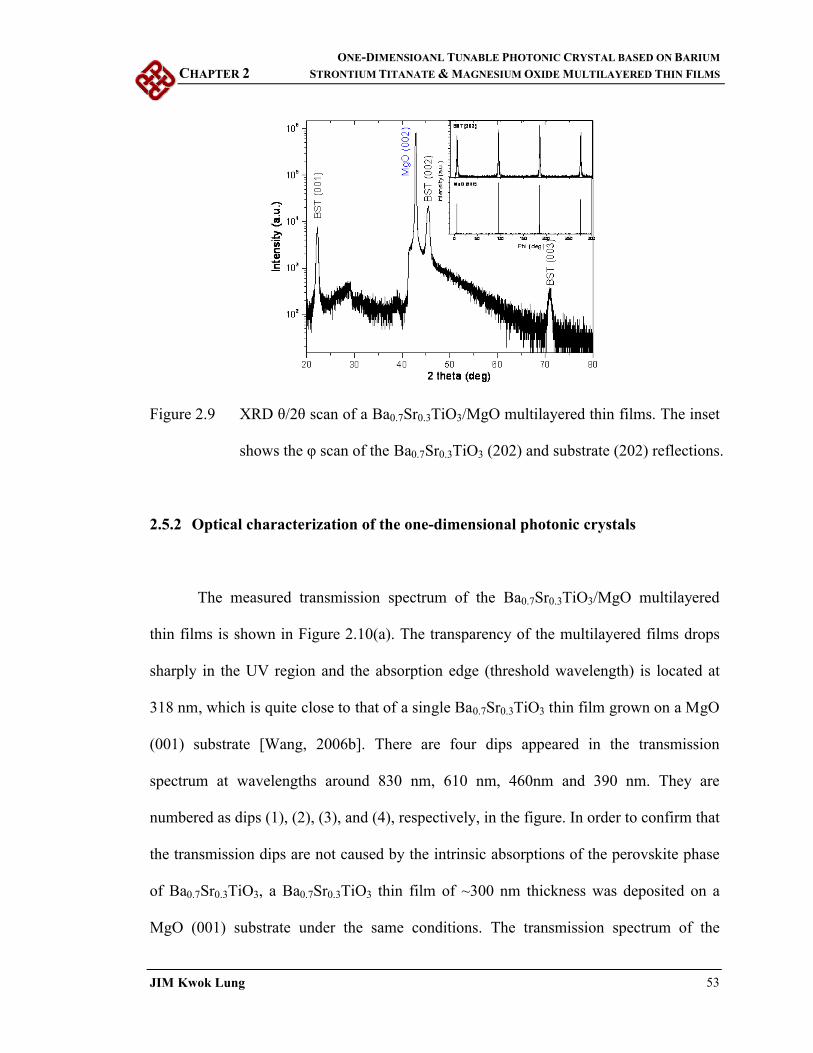
ONE-DIMENSIOANL TUNABLE PHOTONIC CRYSTAL BASED ON BARIUM
CHAPTER 2 STRONTIUM TITANATE & MAGNESIUM OXIDE MULTILAYERED THIN FILMS
JIM Kwok Lung 53
Figure 2.9 XRD θ/2θ scan of a Ba0.7Sr0.3TiO3/MgO multilayered thin films. The inset
shows the φ scan of the Ba0.7Sr0.3TiO3 (202) and substrate (202) reflections.
2.5.2 Optical characterization of the one-dimensional photonic crystals
The measured transmission spectrum of the Ba0.7Sr0.3TiO3/MgO multilayered
thin films is shown in Figure 2.10(a). The transparency of the multilayered films drops
sharply in the UV region and the absorption edge (threshold wavelength) is located at
318 nm, which is quite close to that of a single Ba0.7Sr0.3TiO3 thin film grown on a MgO
(001) substrate [Wang, 2006b]. There are four dips appeared in the transmission
spectrum at wavelengths around 830 nm, 610 nm, 460nm and 390 nm. They are
numbered as dips (1), (2), (3), and (4), respectively, in the figure. In order to confirm that
the transmission dips are not caused by the intrinsic absorptions of the perovskite phase
of Ba0.7Sr0.3TiO3, a Ba0.7Sr0.3TiO3 thin film of ~300 nm thickness was deposited on a
MgO (001) substrate under the same conditions. The transmission spectrum of the

ONE-DIMENSIOANL TUNABLE PHOTONIC CRYSTAL BASED ON BARIUM
CHAPTER 2 STRONTIUM TITANATE & MAGNESIUM OXIDE MULTILAYERED THIN FILMS
JIM Kwok Lung 54
Ba0.7Sr0.3TiO3 thin film was measured and the result is shown in the inset of Figure
2.10(a). The film is highly transparent and does not show any absorption in the visible
region.
According to the PWE calculation (see Figure 2.2(a)), the fabricated 1D PC with
period of 100 nm should produce one photonic bandgap at around 440 nm (dip (3) in
Figure 2.10(a)), which corresponds to ~ 0.23, in the wavelength ranged from 300 nm
to 1100 nm. Other higher order PBGs (e.g. 220 nm which corresponds to ~ 0.46)
would fall below the absorption edge (318 nm). In fact, the four transmission dips
appeared in the measured transmission spectrum should be attributed to the Fabry-Perot
oscillation arisen from a stack of multilayered films of 500 nm thick in addition to the
photonic bandgap located at around 440nm. To verify this idea, a theoretical calculation
of the transmission spectra of the Ba0.7Sr0.3TiO3/MgO multilayered thin films and its
corresponding effective single film were conducted using the transfer matrix method
(TMM). Both the multilayered films and the effective single film are assumed to be
grown on a MgO substrate. The modeled multilayered films is composed of 5 periods of
alternating Ba0.7Sr0.3TiO3 and MgO layers with thicknesses of 90 nm and 10 nm,
respectively. The effective single film is modeled by a 500 nm thick film with refractive
index, )(ireffn , which is given by:
)()()( 1.09.0 irMgO
irBST
ireff nnn , (2.14)
where BSTn and MgOn are the refractive indices of Ba0.7Sr0.3TiO3 and MgO, respectively.
)(irn represents the real (imaginary) part of refractive index. The calculated spectra of
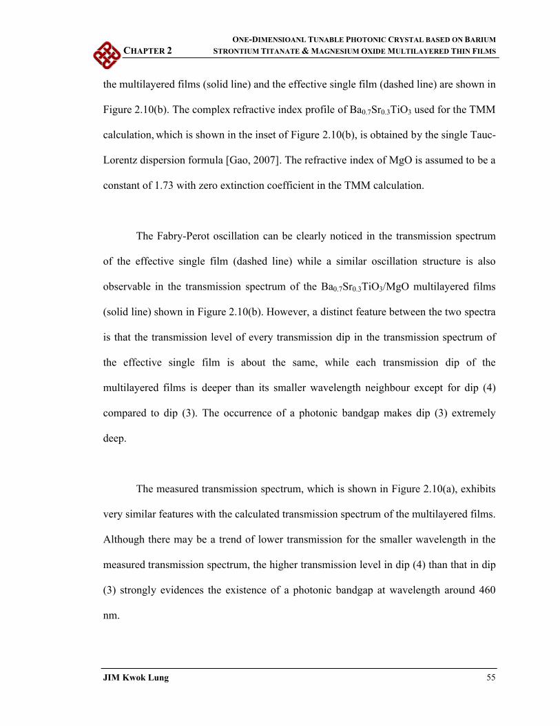
ONE-DIMENSIOANL TUNABLE PHOTONIC CRYSTAL BASED ON BARIUM
CHAPTER 2 STRONTIUM TITANATE & MAGNESIUM OXIDE MULTILAYERED THIN FILMS
JIM Kwok Lung 55
the multilayered films (solid line) and the effective single film (dashed line) are shown in
Figure 2.10(b). The complex refractive index profile of Ba0.7Sr0.3TiO3 used for the TMM
calculation, which is shown in the inset of Figure 2.10(b), is obtained by the single Tauc-
Lorentz dispersion formula [Gao, 2007]. The refractive index of MgO is assumed to be a
constant of 1.73 with zero extinction coefficient in the TMM calculation.
The Fabry-Perot oscillation can be clearly noticed in the transmission spectrum
of the effective single film (dashed line) while a similar oscillation structure is also
observable in the transmission spectrum of the Ba0.7Sr0.3TiO3/MgO multilayered films
(solid line) shown in Figure 2.10(b). However, a distinct feature between the two spectra
is that the transmission level of every transmission dip in the transmission spectrum of
the effective single film is about the same, while each transmission dip of the
multilayered films is deeper than its smaller wavelength neighbour except for dip (4)
compared to dip (3). The occurrence of a photonic bandgap makes dip (3) extremely
deep.
The measured transmission spectrum, which is shown in Figure 2.10(a), exhibits
very similar features with the calculated transmission spectrum of the multilayered films.
Although there may be a trend of lower transmission for the smaller wavelength in the
measured transmission spectrum, the higher transmission level in dip (4) than that in dip
(3) strongly evidences the existence of a photonic bandgap at wavelength around 460
nm.

ONE-DIMENSIOANL TUNABLE PHOTONIC CRYSTAL BASED ON BARIUM
CHAPTER 2 STRONTIUM TITANATE & MAGNESIUM OXIDE MULTILAYERED THIN FILMS
JIM Kwok Lung 56
Figure 2.11 shows the shift in the transmission spectrum when a dc voltage of
240 V (corresponding to an electric field of about 12 MV/m) is applied. With the applied
voltage, the photonic bandgap (transmission dip) at ~464 nm shifts slightly (~2 nm) to
longer wavelength. The electro-optic effect could be the origin of the bandgap tunable
phenomenon, as the refractive index of a ferroelectric material changes when it is
subjected to an external electric field. Since Ba0.7Sr0.3TiO3 thin films have good E-O
properties [Wang 2006b; Wang 2007], it is reasonable that the photonic bandgap is
shifted when an electric field is applied to the Ba0.7Sr0.3TiO3/MgO multilayered thin
films. Calculated from Eq. (2.13), a 2 nm shift of the gap-center corresponds to a 0.43%
change in nBST. Therefore, the experimental result suggests that the electric field induced
change in the refractive index of Ba0.7Sr0.3TiO3 is about 0.5 %, which is comparable to
that of (Pb, La)TiO3 thin films [Boudrioua, 1999].

ONE-DIMENSIOANL TUNABLE PHOTONIC CRYSTAL BASED ON BARIUM
CHAPTER 2 STRONTIUM TITANATE & MAGNESIUM OXIDE MULTILAYERED THIN FILMS
JIM Kwok Lung 57
200 300 400 500 600 700 800 900 1000 11000
10
20
30
40
50
60
70
80
90
100
110
300 400 500 600 700 8000
20
40
60
80
100
Tra
nsm
ittan
ce (%
)
Wavelength ( nm )
Tra
nsm
issi
on
(%)
W avelength (nm)
200 300 400 500 600 700 800 900 1000 11000
10
20
30
40
50
60
70
80
90
100
110
BST/MgO multilayered films
Effective single film
1.6
1.8
2.0
2.2
2.4
2.6
200 400 600 800 1000 1200
0.0
0.2
0.4
0.6
0.8
1.0
Ref
ract
ive
inde
x n
Ext
inct
ion
coef
ficie
nt k
Wavelength (nm)
Tra
nsm
issi
on (
%)
Wavelength (nm)
Figure 2.10 (a) Observed transmission spectrum of the Ba0.7Sr0.3TiO3/MgO
multilayered thin films. The inset shows the transmissions spectrum of a
Ba0.7Sr0.3TiO3 thin film grown on MgO (001) substrate; (b) Calculated
transmission spectra of the Ba0.7Sr0.3TiO3/MgO multilayered thin films and
the corresponding effective single film by TMM. The inset shows the
complex refractive index profile of the Ba0.7Sr0.3TiO3 used for the
calculation.
(a)
(b)
(1)(2)(3)(4)
(1)(2)(3)(4)(5)

ONE-DIMENSIOANL TUNABLE PHOTONIC CRYSTAL BASED ON BARIUM
CHAPTER 2 STRONTIUM TITANATE & MAGNESIUM OXIDE MULTILAYERED THIN FILMS
JIM Kwok Lung 58
0
20
40
60
80
100
200 300 400 500 600 700 800 900
Wavelength (nm)
Tra
ns
mis
sio
n (
%)
0V
240V
Figure 2.11 Measured transmission spectrum of the Ba0.7Sr0.3TiO3/MgO multilayered
thin films with (dotted curve) and without (solid curve) the application of a
dc voltage of 240 V.

ONE-DIMENSIOANL TUNABLE PHOTONIC CRYSTAL BASED ON BARIUM
CHAPTER 2 STRONTIUM TITANATE & MAGNESIUM OXIDE MULTILAYERED THIN FILMS
JIM Kwok Lung 59
2.6 Summary
In this Chapter, we investigated the tunability of the photonic bandgap of a
Ba0.7Sr0.3TiO3/MgO 1D PC arising from the electro-optic effect. The relation between
the shift of the photonic bandgap and the change of the refractive index of Ba0.7Sr0.3TiO3
was examined using the plane wave expansion method. It is found that the gap-center
shifts linearly with the change of the refractive index of Ba0.7Sr0.3TiO3. A ferroelectric
one-dimensional photonic crystal consisting of five layers of Ba0.7Sr0.3TiO3 and five
layers of MgO alternately deposited on a MgO substrate was successfully fabricated by
the pulsed laser deposition technique. X-ray diffraction reveals that all the layers were
epitaxially grown on the MgO (001) single crystal substrate. A photonic bandgap at
~464 nm was observed in the transmission spectrum, which agrees well with the
theoretical calculation by the transfer matrix method. It is observed that the photonic
bandgap of the multilayered films could be tuned by an external electric field E. The
photonic bandgap shifts by about 2 nm when the PC is subjected to a dc voltage of 240
V (E ~ 12 MV/m). This shift corresponds to a 0.5% change in the refractive index of
Ba0.7Sr0.3TiO3.

PHOTONIC BANDSTRUCTURE STUDY ON TWO-DIMENSIONAL
CHAPTER 3 BARIUM STRONTIUM TITANATE-BASED PHOTONIC CRYSTALS
JIM Kwok Lung 60
CHAPTER 3
PHOTONIC BANDSTRUCTURE STDUY ON
TWO-DIMENSIONAL BARIUM STRONTIUM
TITANATE-BASED PHOTONIC CRYSTALS
3.1 Introduction
In order to investigate a photonic crystal (PC), it is always effective to first study
its photonic bandstructure (PBS) since the effect of the PC on the electromagnetic (EM)
waves is entirely characterized by the PBS. Consider a PC composed of a Ba0.7Sr0.3TiO3
matrix with air rods, two commonly prepared cross sections of the air rods are square
and circular. In order to decide which cross section has better performance in certain
applications, it is worth to examine how the shape of the air rods would affect the PBSs.
Many compact optical devices such as filters and waveguides have been
proposed in utilizing PCs [Mekis, 1996; Lončar, 2000; Qiu, 2003; Ren, 2006]. In such
applications, it is advantageous for the PC to possess large photonic bandgaps (PBGs).
To optimize the design in such applications, it is efficient to calculate the PBG maps in
order to obtain the configuration for the largest PBGs.

PHOTONIC BANDSTRUCTURE STUDY ON TWO-DIMENSIONAL
CHAPTER 3 BARIUM STRONTIUM TITANATE-BASED PHOTONIC CRYSTALS
JIM Kwok Lung 61
In this Chapter, the plane wave expansion (PWE) for two-dimensional (2D)
photonic bandstructure calculation is briefly reviewed. Then, we will study the effects of
different shapes of air rods on the PBSs and the PBG maps of the Ba0.7Sr0.3TiO3-based
PCs. After that, the PBG maps of the Ba0.7Sr0.3TiO3-based PCs with different
configurations are discussed.
3.2 Plane wave expansion method for two-dimensional photonic bandstructure
calculation
The PBSs of PCs can be calculated by using the PWE method. The Maxwell’s
equations for EM waves in a system with periodic distribution of dielectric constants can
be simplified as:
Hc
Hr
2
21
, and (3.1a)
Ec
Er
2
21
. (3.1b)
Here, r is the position-dependent dielectric function, H
the magnetic field, E
the
electric field, the angular frequency, and c is the speed of light in vacuum. As the
system is periodic, the dielectric function, the magnetic field and the electric field can be
expanded in terms of plane waves:
g
rgig e
r
1
)(
1
, (3.2a)
g
rgkig eHrH
)()( , (3.2b)

PHOTONIC BANDSTRUCTURE STUDY ON TWO-DIMENSIONAL
CHAPTER 3 BARIUM STRONTIUM TITANATE-BASED PHOTONIC CRYSTALS
JIM Kwok Lung 62
g
rgkig eErE
)()( , (3.2c)
where k
is the wave vector, g
the reciprocal lattice vector and r
is the position vector.
Throughout this Chapter, the wave vectors and the reciprocal lattice vectors are
measured in unit of 2/a where a is the period of the PC in consideration, and the lengths
(position vectors) are measured in unit of a. In other words, all k-space vectors and
lengths are dimensionless.
Combining Eq. (3.1) and Eq. (3.2), we obtain the following matrix equations:
gg
ggg HHgkgk
21
, and (3.3a)
gg
ggg EEgkgk
21
, (3.3b)
where the Fourier coefficient of the inverse dielectric function can be calculated by the
integral:
Ag rgir
drA
exp
111
, (3.4)
and A is the area of the unit cell. The normalized frequency is give by:
a
c
a
2, (3.5)
where is the wavelength in vacuum. The PBS of the 2D PC (Ω against k) is then
obtained by solving Eq. (3.3) after evaluating the Fourier coefficient of the inverse
dielectric function given in Eq. (3.4). In general, the integral in Eq. (3.4) needs to be
calculated numerically. However, if the shapes of the dielectric components in the unit

PHOTONIC BANDSTRUCTURE STUDY ON TWO-DIMENSIONAL
CHAPTER 3 BARIUM STRONTIUM TITANATE-BASED PHOTONIC CRYSTALS
JIM Kwok Lung 63
cell are simple enough, we can calculate the integral analytically. We will show two
cases of different air rod shapes for a 2D PC with square lattice in the following. The
first one contains circular air rods, and the second one contains square air rods in the unit
cells.
Circular air rod
We denote the radius and the dielectric constant of the circular air rod by ra and
a , respectively, and the dielectric constant of the background material by b . The
inverse dielectric function is thus given by:
rSr bab
1111
, (3.6)
where rS
is the structure factor which is defined such that:
.0
,1
a
a
rrfor
rrforrS
(3.7)
Substituting Eq. (3.6) and Eq. (3.7) into Eq. (3.4), the Fourier coefficient of the inverse
dielectric function for the circular rod, gc1 , has the form of:
,011
2
,01
1
1,
gforrg
rgJf
gforff
a
a
bac
b
c
a
c
cg
(3.8)
where J1 is the Bessel function of the first kind, and:
2
2
a
rf a
c
, (3.9)
PHOTONIC BANDSTRUCTURE STUDY ON TWO-DIMENSIONAL
CHAPTER 3 BARIUM STRONTIUM TITANATE-BASED PHOTONIC CRYSTALS
JIM Kwok Lung 64
is the volume fraction of the circular air rod.
Square air rod
The calculation of the Fourier coefficient for the case of square air rod is similar
to that of circular one. In this case, we denote the width and the dielectric constant of the
square air rod by wa and a , respectively, and the dielectric constant of the background
material is denoted by b . The inverse dielectric function is again given by Eq. (3.6)
while rS
is defined in this case as:
.2
0
,2
1
a
a
wrfor
wrfor
rS
(3.10)
Substituting Eq. (3.6) and Eq. (3.10) into Eq. (3.4), the Fourier coefficient of the inverse
dielectric function for the square rod, 1,
sg , has the form of:
,0sinsin11
,01
1,
gforwg
wg
wg
wgf
gforff
ay
ay
ax
ax
bas
b
s
a
s
sg
(3.11)
where gx and gy are the x- and y-components of the reciprocal lattice vector, respectively,
and:
2
2
a
wf a
s , (3.12)
is the volume fraction of the square air rod.

PHOTONIC BANDSTRUCTURE STUDY ON TWO-DIMENSIONAL
CHAPTER 3 BARIUM STRONTIUM TITANATE-BASED PHOTONIC CRYSTALS
JIM Kwok Lung 65
3.3 Photonic bandgap maps of two-dimensional Ba0.7Sr0.3TiO3-based photonic
crystals with different configurations
In many applications such as filters and waveguides, it is advantageous for the
photonic crystal to possess large photonic bandgaps. It is thus worth to investigate the
photonic bandgap features of a PC in different configurations. Two most commonly
chosen configurations in 2D PC are square lattice and triangular lattice [Villeneuve,
1992; Plihal, 1991]. The high symmetry points in the first Brillouin zone for both lattices
are shown in Figure 3.1. The computation of the photonic bandstructures (PBSs) and
photonic bandgap (PBG) maps were performed using the software BandSOLVETM 3.0
from RSoft Design Group, Inc. which utilizes PWE method for the calculation. The
dielectric constants of the air and the Ba0.7Sr0.3TiO3 at optical frequency were assumed to
be 1.00 and 4.84 ( 2BSTn ), respectively. All PBSs were obtained using 64 x 64 plane
waves. The eigenvalue tolerance was set to be 10-8. The first 60 bands were calculated
for each of the transverse electric (TE) mode and transverse magnetic (TM) mode.
Figure 3.2 shows the PBG maps of 2D air-hole-in-BST type PC (Ba0.7Sr0.3TiO3 matrix
with circular air rods) in square and triangular lattices while Figure 3.3 shows the PBG
maps of 2D BST-rod-in-air type PC (circular Ba0.7Sr0.3TiO3 rods in air) in square and
triangular lattices.
To illustrate how the PBG maps can facilitate the design of photonic crystals,
consider Figure 3.2(d) which shows the PBG map of the 2D air-hole-in-BST type PC

PHOTONIC BANDSTRUCTURE STUDY ON TWO-DIMENSIONAL
CHAPTER 3 BARIUM STRONTIUM TITANATE-BASED PHOTONIC CRYSTALS
JIM Kwok Lung 66
(Ba0.7Sr0.3TiO3 matrix with circular air rods) in triangular lattice along all the high
symmetry directions Γ-M-K-Γ (Figure 3.1). It can be seen from Figure 3.2(d) that there
(a) (b)
Figure 3.1 High symmetry points in the first Brillouin zones of the (a) square lattice
and the (b) triangular lattice.
is a large TE photonic bandgap at r = 0.4 a. The TE PBG extends from Ω = 0.35 to Ω =
0.50 with the mid-gap as Ωmid-gap = 0.425. If we aim to design a PC pattern which
possesses a TE PBG around λ = 1550 nm, we can calculate the required period of PC by
Ω = a/λ by setting Ω = Ωmid-gap. The required period of PC is thus given by a = Ωmid-gap ·
λ = 0.425 · 1550 nm ≈ 660 nm. The radius of the air hole is given by r = 0.4 a = 264 nm.
The corresponding TE PBG, which can be calculated by λ = a/Ω, extends from λ = 1320
nm (Ω = 0.50) to λ = 1886 nm (Ω = 0.35).
In literature, usually only the PBG maps along all the high symmetry directions
(Γ-X-M-Γ in square lattice and Γ-M-K-Γ in triangular lattice) are considered. However,
we can control the direction of the incident light in some applications. It may be,
therefore, reasonable to relax the all-direction PBG requirement, but focus only on a
Γ
X M
Γ
M K

PHOTONIC BANDSTRUCTURE STUDY ON TWO-DIMENSIONAL
CHAPTER 3 BARIUM STRONTIUM TITANATE-BASED PHOTONIC CRYSTALS
JIM Kwok Lung 67
certain direction each time. The Γ-X and Γ-M PBG maps for square lattice and the Γ-M
and Γ-K PBG maps for triangular lattice are thus calculated for comparison. It can be
observed from Figure 3.2 and Figure 3.3 that 2D PCs in triangular lattice contain richer
photonic bandgap features in general. This is consistent with previous studies which
show that PCs with a more circular-like Brillouin zone usually contain richer PBG
features [Cassagne, 1996; Wang, 2001]. Also, BST-rod-in-air type PCs contain much
richer PBG features than the air-hole-in-BST type PCs. Complete photonic bandgaps
(Simultaneous TE and TM PBGs along all high symmetry directions in the first
Brillouin zone) are absent in the considered configurations. For square lattice PCs, there
are much more PBGs along the Γ-X direction than the Γ-M direction and significant
simultaneous PBGs can merely be found in the Γ-X direction. For triangular lattice PCs,
more PBGs can be found along the Γ-M direction than the Γ-K direction and significant
simultaneous PBGs can be found in the Γ-M direction only.

PHOTONIC BANDSTRUCTURE STUDY ON TWO-DIMENSIONAL
CHAPTER 3 BARIUM STRONTIUM TITANATE-BASED PHOTONIC CRYSTALS
JIM Kwok Lung 68
(a) (d)
(b) (e)
(c) (f)
Figure 3.2 Photonic bandgap maps of 2D air-hole-in-BST type PC (Ba0.7Sr0.3TiO3
matrix with circular air rods) in square lattice along (a) Γ-X-M-Γ, (b) Γ-M,
(c) Γ-X; in triangular lattice along (d) Γ-M-K-Γ, (e) Γ-K, (f) Γ-M. The
insets show the configurations of the PCs and their corresponding
Brillouin zones.

PHOTONIC BANDSTRUCTURE STUDY ON TWO-DIMENSIONAL
CHAPTER 3 BARIUM STRONTIUM TITANATE-BASED PHOTONIC CRYSTALS
JIM Kwok Lung 69
(a) (d)
(b) (e)
(c) (f)
Figure 3.3 Photonic bandgap maps of 2D BST-rod-in-air type PC (circular
Ba0.7Sr0.3TiO3 rods in air) in square lattice along (a) Γ-X-M-Γ, (b) Γ-M, (c)
Γ-X; in triangular lattice along (d) Γ-M-K-Γ, (e) Γ-K, (f) Γ-M. The insets
show the configurations of the PCs and their corresponding Brillouin
zones.

PHOTONIC BANDSTRUCTURE STUDY ON TWO-DIMENSIONAL
CHAPTER 3 BARIUM STRONTIUM TITANATE-BASED PHOTONIC CRYSTALS
JIM Kwok Lung 70
3.4 Photonic bandstructures and photonic bandgap maps of two-dimensional
Ba0.7Sr0.3TiO3-based photonic crystals with different shapes of air rods
Beside different lattice types, photonic bandstructures and photonic bandgap
maps of 2D air-hole-in-BST type PCs with different shapes (circular and square) of air
rods are also investigated. In order to facilitate the discussion, we define the diameter of
the circular air rod (2ra) and the width of the square air rod (wa) as the characteristic
lengths (l). They will be expressed in unit of the period of the PC, a.
Figure 3.4 shows the photonic bandstructures of the 2D Ba0.7Sr0.3TiO3-based PCs
containing circular and square air rods with characteristic lengths of 0.2a, 0.5a and 0.8a.
It can be seen that the corresponding PBSs of the circular-air-rod PC and the square-air-
rod PC with the same characteristic length are very similar. For l = 0.2a (Figure 3.4(a)
and Figure 3.4(d)), the two corresponding PBSs are almost identical in the whole range
of frequency from Ω = 0.0 to Ω = 1.0. If we focus only on the small frequency range (Ω
< 0.35), the corresponding PBSs are nearly the same even for different characteristic
lengths. By contrast, the discrepancies between the PBSs become increasingly apparent
with larger characteristic lengths (Figure 3.4(c) and Figure 3.4(f)).
The results may not be unexpected, if we consider the wavelengths of the EM
waves inside the 2D PC ( ). For frequencies small than 1.0 (Ω < 1.0), the
corresponding obtained from Eq. (5) are greater than the period of the PC, a. As the
refractive index (n) of Ba0.7Sr0.3TiO3 is about 2.20, the wavelengths of the EM waves

PHOTONIC BANDSTRUCTURE STUDY ON TWO-DIMENSIONAL
CHAPTER 3 BARIUM STRONTIUM TITANATE-BASED PHOTONIC CRYSTALS
JIM Kwok Lung 71
inside the 2D PC ( n/ ) are still larger than 0.45a. It could be imagined that the EM
waves with Ω < 1.0 ( > 0.45a) are not sensitive to the slight difference in shapes of
the air rods, if the characteristic length of the air rods is much less than . It is therefore
not surprising that the PBSs between the circular- and square-air-rod PCs would appear
similar when the characteristic length of the air rods is 0.2a only. As the characteristic
length becomes comparable (l = 0.5a) or even larger (l = 0.8a) than the wavelengths of
EM waves inside the 2D PC ( ), the discrepancies between the photonic bandstructures
of the circular- and square-air-rod PCs become apparent.
A more concrete interpretation of the results can be made by examining the
Fourier coefficients of the inverse dielectric function for the two cases of circular air
rods and the square air rods, which are given by Eq. (3.8) and Eq. (3.11) respectively.
The two equations, containing all the geometric information of the PCs, are the only
differences in the photonic bandstructure calculation for the two cases. If the reciprocal
lattice vectors, g
, or the characteristic length of the air rod, l, are small ( 1lg
), the
sinc function (sin x/x) for the square-air-rod case and the Bessel function of the first kind
for the circular-air-rod case can be approximated as the following:
21
xxJ , for small x, (3.13)
1sin
x
x, for small x. (3.14)
Putting Eq. (3.13) into Eq. (3.8) and Eq. (3.14) into Eq. (3.11), the Fourier coefficients
of the inverse dielectric function for the circular-air-rod and the square-air-rod have the
forms of:

PHOTONIC BANDSTRUCTURE STUDY ON TWO-DIMENSIONAL
CHAPTER 3 BARIUM STRONTIUM TITANATE-BASED PHOTONIC CRYSTALS
JIM Kwok Lung 72
,011
,01
1
gforf
gforff
g
bac
b
c
a
c
c
(3.15)
,011
,01
1
gforf
gforff
g
bas
b
s
a
s
s
(3.16)
in cases of small g
vectors or small characteristic length l of air rods. Under such
approximation, the Fourier coefficients of the inverse dielectric function for the circular-
air-rod and the square-air-rod attain identical forms. The different definitions of fs and fc,
however, should be carefully noted, as will be discussed later. Since the photonic
bandstructure depends highly on the Fourier coefficients of the inverse dielectric
function, the PBSs for the circular-air-rod PC and the square-air-rod PC would therefore
be very similar in situations whenever the 1lg
approximation is valid. It is known
that small g
vectors correspond to low frequencies. Thus, for cases of low frequencies
or small characteristic length of air rods, the photonic bandstructures of the circular-air-
rod PC and the square-air-rod PC would be very similar.
Nevertheless, the consistency of the photonic bandstructures for the two different
geometries at large characteristic lengths of air rods is not as good as that for the small
ones. We have calculated the photonic bandgap maps of the 2D Ba0.7Sr0.3TiO3-based
PCs with circular air rods and square air rods along the symmetry directions Γ-X-M-Γ,
Γ-M and Γ-X to further illustrate this point. As shown in Figure 3.5, there are significant

PHOTONIC BANDSTRUCTURE STUDY ON TWO-DIMENSIONAL
CHAPTER 3 BARIUM STRONTIUM TITANATE-BASED PHOTONIC CRYSTALS
JIM Kwok Lung 73
discrepancies in the corresponding PBG maps for large characteristic lengths of air rod
even for small frequencies. If we simply compare the PBG maps at la =1.0 [i.e. ra = 0.5
(2ra = 1.0) and wa = 1.0], the PBG features are actually quite different. It seems to
contradict to the previous conclusion that the PBSs should be the same if the Fourier
coefficients of the inverse dielectric function are the same. In fact, Eq. (3.15) and Eq.
(3.16) are not exactly the same because the volume fractions for the circular air rod [Eq.
(3.9)] and the square air rod [Eq. (3.12)] are not identical indeed. In order to acquire
equal volume fractions, the diameter of the circular air rod should correlate with 0.89
times of the width of the square air rod [e.g. ra = 0.5 (2ra = 1) should correlate with wa =
0.89]. We have highlighted the positions of wa = 0.89 with dark green lines in the
bandgap maps for visualization. It can be observed that the corresponding PBG maps
show better consistency when we take into account the volume fraction correction.

PHOTONIC BANDSTRUCTURE STUDY ON TWO-DIMENSIONAL
CHAPTER 3 BARIUM STRONTIUM TITANATE-BASED PHOTONIC CRYSTALS
JIM Kwok Lung 74
(a) (d)
(b) (e)
(c) (f)
Figure 3.4 Photonic bandstructures of square lattice type 2D Ba0.7Sr0.3TiO3-based PC
with circular air rods, (a) 2r = 0.2a, (b) 2r = 0.5a, (c) 2r = 0.8a; with
square air rods, (d) w = 0.2a, (e) w = 0.5a, (f) w = 0.8a.
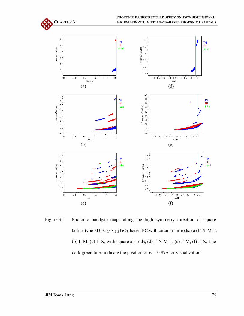
PHOTONIC BANDSTRUCTURE STUDY ON TWO-DIMENSIONAL
CHAPTER 3 BARIUM STRONTIUM TITANATE-BASED PHOTONIC CRYSTALS
JIM Kwok Lung 75
(a) (d)
(b) (e)
(c) (f)
Figure 3.5 Photonic bandgap maps along the high symmetry direction of square
lattice type 2D Ba0.7Sr0.3TiO3-based PC with circular air rods, (a) Γ-X-M-Γ,
(b) Γ-M, (c) Γ-X; with square air rods, (d) Γ-X-M-Γ, (e) Γ-M, (f) Γ-X. The
dark green lines indicate the position of w = 0.89a for visualization.

PHOTONIC BANDSTRUCTURE STUDY ON TWO-DIMENSIONAL
CHAPTER 3 BARIUM STRONTIUM TITANATE-BASED PHOTONIC CRYSTALS
JIM Kwok Lung 76
3.5 Summary
In this Chapter, we have studied the photonic bandgap maps of two types of 2D
Ba0.7Sr0.3TiO3-based PC, namely, the air-hole-in-BST type and the BST-rod-in-air type
both in square lattice and in triangular lattice. The photonic bandstructures and photonic
bandgap maps of the PC were computed using the plane wave expansion method. It is
found that PCs in triangular lattice contain richer PBG feature in general. Photonic
bandgap features along different symmetry directions have also been compared.
We have also compared the photonic bandstructures and the photonic bandgap
maps of the square lattice type 2D Ba0.7Sr0.3TiO3-based PC with circular air rods and
square air rods. It was found that there are two situations at which the photonic
bandstructures and the photonic bandgap maps of the circular air rod PCs and square air
rod PCs would be nearly identical: (1) if the characteristic length of the air rod is small (l
< 0.45a), and (2) if the frequency range is low enough (Ω < 0.35). Furthermore, a better
correlation in the photonic bandstructures and the photonic bandgap maps between the
circular and square air rod 2D PC can be obtained if the volume fraction correction, i.e.
fc = fs wa = 0.89 x (2ra), has been taken into account.

PHOTONIC CRYSTAL CAVITY EMBEDDED
CHAPTER 4 BARIUM STRONTIUM TITANATE RIB WAVEGUIDES
JIM Kwok Lung 77
CHAPTER 4
PHOTONIC CRYSTAL CAVITY EMBEDDED
BARIUM STRONTIUM TITANATE
RIB WAVEGUIDES
4.1 Introduction
Photonic crystal (PC) devices have received much attention over the past decade
for their great potentials of creating miniaturised photonic components essential for
compact photonic integrated circuits. One of the crucial PC devices is the photonic
crystal filter which is very promising in wavelength division multiplexing (WDM)
applications [Hu, 2007; Jugessur, 2004; Pustai, 2002]. The realization of good
nanometric optical structures on ceramic materials continues to be a difficult task due to
its well-known resistance towards standard machining techniques like wet etching or
even dry etching by reactive ion etching (RIE). Focused ion beam (FIB) etching is an
efficient technique to fabricate nanosized holes with high aspect ratio [Roussey, 2005].
Since the etching time for FIB greatly depends on the area of the PC pattern, it is
advantageous for the required area of PC patterns to be as small as possible. Patterning
PC cavities on rib waveguides may alleviate the problem. Therefore, this Chapter aims
to demonstrate the feasibility of developing PC cavity embedded Ba0.7Sr0.3TiO3 rib
waveguides to function as a tunable optical filter at the telecommunication wavelength,
1550 nm.
PHOTONIC CRYSTAL CAVITY EMBEDDED
CHAPTER 4 BARIUM STRONTIUM TITANATE RIB WAVEGUIDES
JIM Kwok Lung 78
In this Chapter, we first discuss the characterization of BST thin films both
structurally by XRD and optically by prism coupling technique. Then, the required
dimension of Ba0.7Sr0.3TiO3 rib waveguides supporting single mode wave propagation is
examined after the introduction of dielectric waveguide theory. Next, fabrication and
characterization of Ba0.7Sr0.3TiO3 rib waveguides are discussed. Finally, the design and
fabrication of photonic crystal cavity embedded Ba0.7Sr0.3TiO3 rib waveguides are
illustrated.
4.2 Characterization of Ba0.7Sr0.3TiO3 thin films
4.2.1 Structural characterization of Ba0.7Sr0.3TiO3 thin films
The θ/2θ x-ray diffraction (XRD) pattern of the Ba0.7Sr0.3TiO3 thin film grown on
a MgO (001) substrate is shown in Figure 4.1. Since only (00l) peaks of the
Ba0.7Sr0.3TiO3 appear in the XRD patterns, it indicates a pure perovskite phase in the
Ba0.7Sr0.3TiO3 thin film. The in-plane alignment of the Ba0.7Sr0.3TiO3 thin films with
respect to the major axes of the (001) substrates was confirmed by the XRD off-axis φ
scan of the Ba0.7Sr0.3TiO3 (202) and MgO (202) reflections, as shown in the inset of
Figure 4.1, confirming an epitaxial growth of the Ba0.7Sr0.3TiO3 film.

PHOTONIC CRYSTAL CAVITY EMBEDDED
CHAPTER 4 BARIUM STRONTIUM TITANATE RIB WAVEGUIDES
JIM Kwok Lung 79
Figure 4.1 XRD θ/2θ scan of a Ba0.7Sr0.3TiO3 thin film grown on a MgO (001)
substrate. The inset shows the φ scan of the Ba0.7Sr0.3TiO3 (202) and
substrate (202) reflections.
4.2.2 Optical characterization of Ba0.7Sr0.3TiO3 thin films
The photonic bandstructures, and thus the optical properties, of photonic crystals
(PCs) depend merely on the geometric arrangement and the refractive indices of the
constituent materials. It is therefore very important to first obtain the refractive index
information of the constituent materials before we can design the appropriate
configuration of the PCs.
1.0E+00
1.0E+01
1.0E+02
1.0E+03
1.0E+04
1.0E+05
1.0E+06
20 25 30 35 40 45 50
2 Theta (degree)
Inte
ns
ity
(a.
u.)
BST (001)
MgO (002)
BST (002)
0
500
1000
1500
2000
2500
3000
3500
4000
4500
5000
-120 -90 -60 -30 0 30 60 90 120 150 180 210 240
Phi (degree)
Inte
ns
ity
(a.
u.)

PHOTONIC CRYSTAL CAVITY EMBEDDED
CHAPTER 4 BARIUM STRONTIUM TITANATE RIB WAVEGUIDES
JIM Kwok Lung 80
In order to measure the refractive indices of the Ba0.7Sr0.3TiO3 thin films grown
on MgO (001) substrates, the prism coupling technique was employed. A prominent
advantage of this method is that no further processing on the thin film is needed since
the film acts as a planar waveguide during the measurement.
Prism coupling is an advanced optical waveguiding technique for measuring both
the thickness and the refractive index/birefringence of dielectric films rapidly and
accurately [Tien, 1969; Ulrich, 1973]. For many thin film and optical waveguide
applications, the prism coupling technique offers unique advantages over conventional
measurements based on ellipsometry or spectrophotometry. One prominent advantage of
the prism coupling measurement is that the thickness of the films needs not be known in
advance. Moreover, a resolution in refractive index of ±0.0005 can be achieved, which is
an order or magnitude better than other techniques. For simultaneous measurements of
the thickness and the refractive index using the prism coupling method, the film should
be sufficiently thick to support two or more guided modes.
The thickness of the film to be studied is the single most important factor
determining whether ellipsometry or prism coupling is the preferred technique. In
general, ellipsometry is the clear choice for investigating thin films with thicknesses
smaller than a few hundred nanometers. For studying moderate-to-thick films, prism
coupling technique is usually superior. Consequently, ellipsometry and prism coupling
can be viewed as complementary techniques.

PHOTONIC CRYSTAL CAVITY EMBEDDED
CHAPTER 4 BARIUM STRONTIUM TITANATE RIB WAVEGUIDES
JIM Kwok Lung 81
4.2.2.1 Basic principles of prism coupling technique
The prism coupling measurements were carried out using a Metricon Model 2010
prism coupler equipped with a 45˚-45˚-90˚ rutile (TiO2) prism (Metricon corporation,
Pennington, USA). The schematic diagram of the instrument is shown in Figure 4.2.
Figure 4.2 Schematic diagram of the Metricon model 2010 prism coupler system.
Two laser systems are installed to generate the light beam. The first one is a He-
Ne laser with a wavelength of 632.8 nm, which is the commonly used wavelength for
optical characterizations of ferroelectric thin films. The other laser system is a laser
diode with a wavelength of 1550 nm, since the optical waveguide may have potential use
in the near infrared (IR) region for telecommunication applications. To conduct a
α
αp
σ
np
Waveguide, n1
Substrate, n2
Air gap, n3
Laser beam
Rutile prism
Photodector

PHOTONIC CRYSTAL CAVITY EMBEDDED
CHAPTER 4 BARIUM STRONTIUM TITANATE RIB WAVEGUIDES
JIM Kwok Lung 82
measurement, the film was brought into contact with the base of the rutile prism by
means of a pneumatically-operated coupling head, creating a small air gap between the
film and the prism. The laser beam struck the base of the prism and was totally reflected
at the prism base onto a photodetector. At certain discrete values of incident angle,
known as mode angles (m), photons can tunnel through the air gap into a guided optical
propagation mode of the film, causing a sharp dip in the intensity of light reaching the
detector as illustrated in Figure 4.3. The mode angle m is given by:
pp
pm nn
n sinsinsinsinsin 1
1
, (4.1)
where np is the refractive index of the prism, n1 the refractive index of the film, σ the
incident angle of the laser beam at the prism-film interface (internal incident angle), α
the incident angle of the laser beam at the air-prism interface (external incident angle)
and αp is the base angle of the prism (αp = 45˚ in this case). Figure 4.3 shows the
transverse electric (TE) mode measurement only. The Metricon 2010 prism coupler
system actually supports two polarizations, namely the transverse electric (TE)
polarization, and the transverse magnetic (TM) polarization (see inset of Figure 4.3). The
electric field of the laser beam is vibrating parallel to the film (in-plane direction) for TE
polarization, while the electric field of the laser beam is vibrating perpendicular to the
film (out-of-plane direction) for TM polarization. Therefore, a TE mode measurement is
used for measuring the refractive index along the in-plane direction, and a TM mode
measurement is used for measuring the refractive index along the out-of-plane direction.

PHOTONIC CRYSTAL CAVITY EMBEDDED
CHAPTER 4 BARIUM STRONTIUM TITANATE RIB WAVEGUIDES
JIM Kwok Lung 83
3436384042444648505254Internal angle of incidence (degree)
Ref
lect
ed in
ten
sity
(a
. u.)
TE0
knee
TE1
Figure 4.3 Intensity of reflected light against internal incident angle for transverse
electric (TE) modes. The knee corresponds to the substrate mode. The
inset shows the vibration directions of the electric field for the TE and the
TM modes.
Refractive index and thickness of the film are the two parameters that can be
measured using the prism coupling technique. For a given substrate type, the mode angle
of a given order of mode is related to the refractive index and thickness of the film by the
“transverse resonance condition” [Syms, 1992] which is expressed as:
mdkn m 222cos2 13122
1 , (4.2)
TETM

PHOTONIC CRYSTAL CAVITY EMBEDDED
CHAPTER 4 BARIUM STRONTIUM TITANATE RIB WAVEGUIDES
JIM Kwok Lung 84
where d is the thinkness of the film, n1 the refractive index of of the film, 2
k the
free-space wavenumber with λ the free-space wavelength of the incident light, m = 0, 1,
2, 3 …, the order of the mode, and 12 and 13 are the Fresnel phase shift at the film-
substrate and film-air interfaces, respectively. The phase shift terms 12 and 13 can be
evaluated by considering the total internal reflections at the film-substrate and film-air
interfaces and are given by:
m
m
i
n
nn
n
n
cos
sinarctan
1
22
21
2
2
112
, and (4.3a)
m
m
i
n
nn
n
n
cos
sinarctan
1
23
21
2
3
113
, (4.3b)
where n1, n2, n3 are refractive indices of the film, the substrate and the air gap,
respectively, i = 0 for TE modes and i = 1 for TM modes. Eq. (4.2) is transcendental
which needs to be solved numerically. Two measured mode angles, which give two Eq.
(4.2) corresponding to two orders of mode, are sufficient to determine simultaneously
the refractive index n1 and thickness d of the film. If more than two modes are observed,
the problem is overspecified. It is possible to calculate the independent refractive index
and thickness of the film from each pair of modes and compare them to obtain the mean
and standard deviation of the refractive index and thickness from all the pairs of modes
for consistency check.
After the reflected intensity spectrum is measured, the mode angles can be
located using the software incorporated in the prism coupler system which then

PHOTONIC CRYSTAL CAVITY EMBEDDED
CHAPTER 4 BARIUM STRONTIUM TITANATE RIB WAVEGUIDES
JIM Kwok Lung 85
calculates the refractive index and thickness (with mean and standard deviation if more
than two mode angles are observed) of the film.
4.2.2.2 Guided modes in Ba0.7Sr0.3TiO3 thin films
Figure 4.4 shows the guided mode spectra of a 550 nm thick Ba0.7Sr0.3TiO3 thin
film grown on MgO (001) substrate in TE polarization. There are three TE modes for λ =
632.8 nm, while there is only one for λ = 1550 nm. The reflectivity dips of each guided
mode are very sharp, indicating that good confinement of lightwave is achieved and the
film is potentially useful for waveguide device applications. At the end of the spectra, a
sharp fall of the reflected intensity (knee) is observed, which is associated with the
substrate mode.
Using the mode equations (Eq. (4.2) and Eq. (4.3)) and the observed angular
positions of the TE modes at λ = 632.8 nm (Figure 4.4(a)), the refractive indices and the
thickness can be computed. The calculated film thickness and ordinary refractive index
(n0) are 547 ± 4 nm and 2.3107 ± 0.0006. Using the thickness obtained, the refractive
index at λ = 1550 nm can also be calculated even though only one guided TE mode is
measured. The calculated refractive index at at λ = 1550 nm is 2.2209. Since there is
only one mode being observed, no standard deviation can be obtained.

PHOTONIC CRYSTAL CAVITY EMBEDDED
CHAPTER 4 BARIUM STRONTIUM TITANATE RIB WAVEGUIDES
JIM Kwok Lung 86
20
30
40
50
60
70
80
40 42 44 46 48 50 52 54 56
Internal angle of incidence (degree)
Ref
lect
ed in
ten
sity
(a
. u.)
(a)
10
20
30
40
50
60
40 42 44 46 48 50 52 54 56
Internal angle of incidence (degree)
Ref
lect
ed in
ten
sity
(a
. u.)
(b)
Figure 4.4 Guided mode spectra excited at (a) λ = 632.8 nm and (b) λ = 1550 nm in
the TE polarization for a ~550 nm thick Ba0.7Sr0.3TiO3 film deposited on
MgO (001) substrate.

PHOTONIC CRYSTAL CAVITY EMBEDDED
CHAPTER 4 BARIUM STRONTIUM TITANATE RIB WAVEGUIDES
JIM Kwok Lung 87
4.3 Ba0.7Sr0.3TiO3 thin film optical rib waveguides
4.3.1 Light propagation in slab waveguides
4.3.1.1 Basic concepts of slab waveguides
Dielectric slabs are the simplest optical waveguides. By studying the properties
of the slab waveguides, an insight into the waveguide properties of more complicated
dielectric waveguides can be gained. Consider a step-index waveguide (Figure 4.5), in
which the refractive index changes abruptly along the thickness direction at the surface
of the core, it has finite dimension in the thickness direction but infinite dimension in the
length and width directions. The core region of the waveguide, with a refractive index
n1, is deposited on a substrate with refractive index n2. The refractive index of the
medium above the core (cladding) is n3. The refractive index n3 may be unity if the
region above the core is air, or it may have some other value if the core is surrounded by
dielectric materials on both sides. For true mode guidance to occur, it is necessary that n1
is larger than n2 and n3.
Without loss of generality, we assume that n1 > n2 ≥ n3. A slab waveguide is
called symmetric if n2 = n3 and asymmetric if n2 ≠ n3. The modes of symmetric slab
waveguides are simpler than those of the asymmetric ones because they can be
expressed either as even or odd field distributions. Moreover, the lowest-order mode of a
symmetric slab waveguide does not have a cutoff frequency, which implies such mode
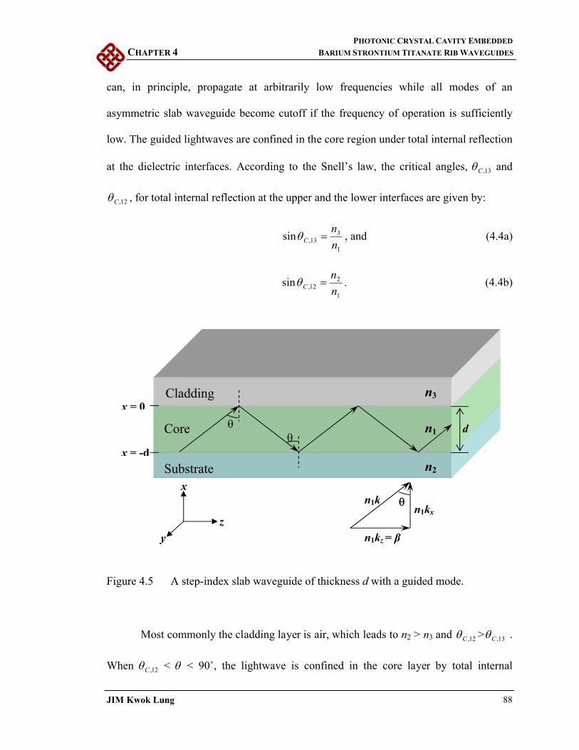
PHOTONIC CRYSTAL CAVITY EMBEDDED
CHAPTER 4 BARIUM STRONTIUM TITANATE RIB WAVEGUIDES
JIM Kwok Lung 88
can, in principle, propagate at arbitrarily low frequencies while all modes of an
asymmetric slab waveguide become cutoff if the frequency of operation is sufficiently
low. The guided lightwaves are confined in the core region under total internal reflection
at the dielectric interfaces. According to the Snell’s law, the critical angles, 13,C and
12,C , for total internal reflection at the upper and the lower interfaces are given by:
1
313,sin
n
nC , and (4.4a)
1
212,sin
n
nC . (4.4b)
Figure 4.5 A step-index slab waveguide of thickness d with a guided mode.
Most commonly the cladding layer is air, which leads to n2 > n3 and 12,C > 13,C .
When 12,C < < 90˚, the lightwave is confined in the core layer by total internal
n1kn1kx
n1kz = β
d
n3
n1
n2
Cladding
Substrate
Core
x
y
z
x = 0
x = -d

PHOTONIC CRYSTAL CAVITY EMBEDDED
CHAPTER 4 BARIUM STRONTIUM TITANATE RIB WAVEGUIDES
JIM Kwok Lung 89
reflection at both interfaces and it propagates along a zig-zag path as shown in Figure
4.5. This is called a guided mode. For a slab waveguide, the plane wave propagation
constant in the wave-normal direction is kn1, where 2
k and is the wavelength of
light in free space. The propagation constant along the z-direction is obtained by:
sin11 knnkz . (4.5)
The speed of the lightwave parallel to the waveguide is given by:
/0 kc , (4.6)
where 0c is the speed of light in free space. Another frequently used quantity is the
effective index of refraction of a slab waveguide Nm, which is defined as the ratio of the
speed of light in free space to the speed of the lightwave parallel to the waveguide:
k
cNm
0 . (4.7)
4.3.1.2 Guided modes of slab waveguides
An optical mode is a discrete solution of Maxwell’s equations which satisfies all
the boundary conditions and remains the same spatial distribution during propagation.
Maxwell’s equations for plane waves in an isotropic, lossless dielectric medium is given
by [Agrawal, 2004]:
HiE
0 , and (4.8)
EniH
20 , (4.9)
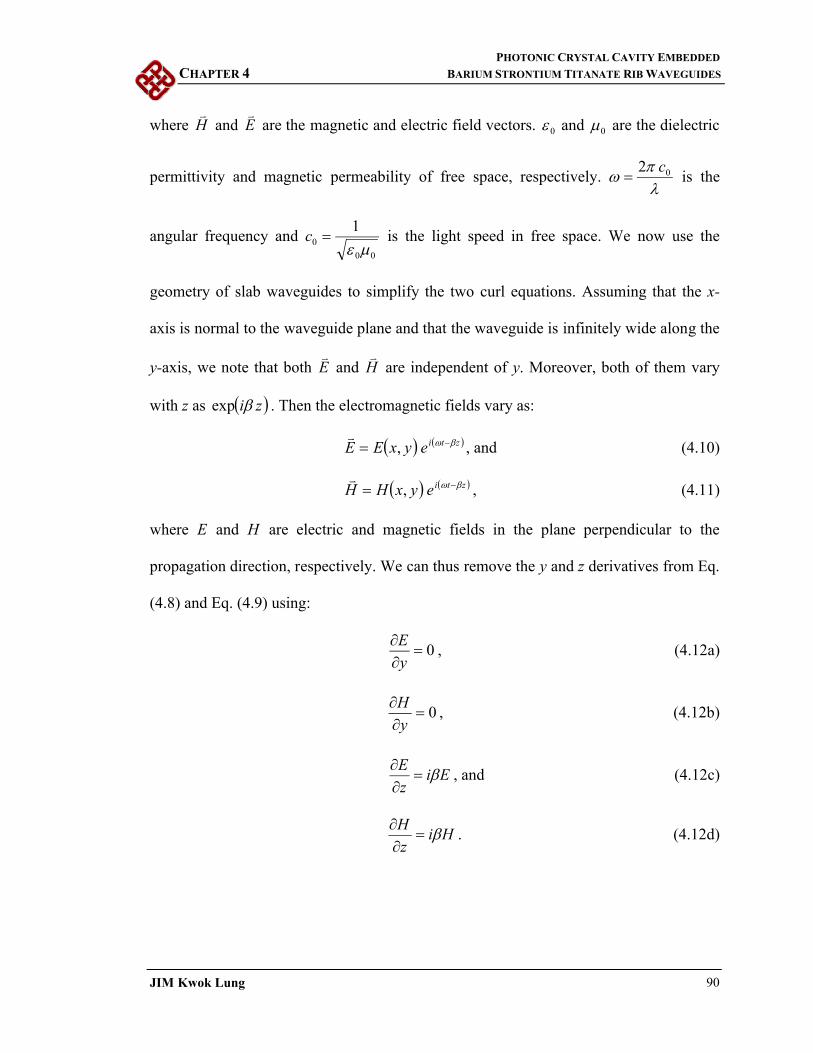
PHOTONIC CRYSTAL CAVITY EMBEDDED
CHAPTER 4 BARIUM STRONTIUM TITANATE RIB WAVEGUIDES
JIM Kwok Lung 90
where H
and E
are the magnetic and electric field vectors. 0 and 0 are the dielectric
permittivity and magnetic permeability of free space, respectively. 02 c
is the
angular frequency and 00
0
1
c is the light speed in free space. We now use the
geometry of slab waveguides to simplify the two curl equations. Assuming that the x-
axis is normal to the waveguide plane and that the waveguide is infinitely wide along the
y-axis, we note that both E
and H
are independent of y. Moreover, both of them vary
with z as ziexp . Then the electromagnetic fields vary as:
ztieyxEE ,
, and (4.10)
ztieyxHH ,
, (4.11)
where E and H are electric and magnetic fields in the plane perpendicular to the
propagation direction, respectively. We can thus remove the y and z derivatives from Eq.
(4.8) and Eq. (4.9) using:
0
y
E, (4.12a)
0
y
H, (4.12b)
Eiz
E
, and (4.12c)
Hiz
H
. (4.12d)

PHOTONIC CRYSTAL CAVITY EMBEDDED
CHAPTER 4 BARIUM STRONTIUM TITANATE RIB WAVEGUIDES
JIM Kwok Lung 91
The resulting set of six equations, when written in Cartesian coordinates, has two distinct
sets of linearly polarized solutions, known as the transverse electric (TE) and transverse
magnetic (TM) modes, depending on whether we choose Ez = 0 or Hz = 0.
In the case of TE modes, Ex = Ez = 0, while Ey satisfies:
02222
2
y
y Enkx
E . (4.13)
The magnetic field H
is related to yE as:
x
EiEHHHH y
yzyx00
,0,,,
. (4.14)
In the case of TM modes, 0 zx HH , while yH satisfies:
02222
2
y
y Hnkx
H . (4.15)
The electric field E
is related to yH as:
x
H
n
iH
nEEEE y
yzyx 20
20
,0,,,
. (4.16)
The two orthogonal TE and TM modes are distinguished in order to discuss the
dispersion characteristics of the guided modes. Here we consider the TE mode first. The
same analysis can be made for TM mode. Assuming that the core layer has a thickness d,
Eq. (4.13) can be solved within each layer using n = n1, n2, or n3 for the three layers
shown in Figure 4.5. Since the refractive index is constant in each layer, the general
solution can be written in terms of sinusoidal and exponential functions as:
dx
x
y
edBdA
xBxA
Ae
E
sincos
sincos
dxfor
dxfor
xfor
0
0
),(
),(
),(
substrate
core
cladding
(4.17)

PHOTONIC CRYSTAL CAVITY EMBEDDED
CHAPTER 4 BARIUM STRONTIUM TITANATE RIB WAVEGUIDES
JIM Kwok Lung 92
with the abbreviations:
11222
1 cos knkn , (4.18)
2222
21
222
2 knnkn , and (4.19)
2223
21
223
2 knnkn (4.20)
The constants A and B can be determined from the boundary conditions at the two
interfaces which require the tangential components of E
and H
being continuous
across them. In the case of TE modes, these boundary conditions are satisfied if yE and
zH are continuous at x = 0 and x = -d, provided:
0 BA , and (4.21)
0sincoscossin BddAdd . (4.22)
This homogeneous system of equations has a solution only if its determinant vanishes,
i.e.:
0cossinsincos dddd . (4.23)
This eigenvalue equation for TE modes can be rewritten in a simpler form as:
2
tan d . (4.24)
Similarly, the eigenvalue equation for TM modes can be derived as:
4
122
32
2
22
23
21tan
nnn
nnnd
. (4.25)

PHOTONIC CRYSTAL CAVITY EMBEDDED
CHAPTER 4 BARIUM STRONTIUM TITANATE RIB WAVEGUIDES
JIM Kwok Lung 93
4.3.1.3 Cutoffs of asymmetric slab waveguides
In the case of an asymmetric slab with 32 nn , cutoff frequencies exist in the
waveguide. The eigenvalue equations, Eq. (4.24) and Eq. (4.25), are solved in order to
determine the cutoff frequencies for the TE and TM modes supported by the waveguide.
Some information can be obtained about the solutions of the TE mode eigenvalue
equation, Eq. (4.24), by considering Figure 4.6. The solid lines in the figure are the
branches of the tangent function of d . The dashed lines show the function dF that
represents the right hand side of Eq. (4.25). From Eq. (4.18) to Eq. (4.20), we obtain:
ddd
ddkddF
2
2223
21
2222
21
2
2223
21
2222
21
dkdnndkdnnd
dkdnndkdnnd
. (4.26)
Figure 4.6 was drawn for 1122
21 kdnn , and 242
32
1 kdnn . The pole in the
dF curve occurs at the point where the denominator of Eq. (4.26) vanishes. The
dF curve ends at the point:
dkdnn 22
21 , (4.27)
since one of the square root expression in Eq. (4.26) becomes imaginary as d exceeds
the value given by Eq. (4.27). The d coordinates of intersections of the solid and
dashed lines give the solutions of the eigenvalue Eq. (4.24). Each solution gives one TE
mode of the slab waveguide. As shown in Figure 4.6, four guided modes were obtained
for the conditions that were used to draw the figure.

PHOTONIC CRYSTAL CAVITY EMBEDDED
CHAPTER 4 BARIUM STRONTIUM TITANATE RIB WAVEGUIDES
JIM Kwok Lung 94
Figure 4.6 Graphical solution of TE mode eigenvalue equation (Eq. (4.24)). The
intersections of the solid and dashed lines correspond to the solutions.
We define a parameter V that combines the difference of the squares of the
refractive indices of the core and substrate with information about the operating
wavelength and the thickness of the core as:
kdnnV 22
21 . (4.28)
As the value of V decreases, the endpoint of the dashed lines moves to the left, so that it
crosses fewer braches of the tangent function. If V decreases, the number of guided
modes is thus reduced. Hence, the total number of modes supported by a waveguide
depends on the thickness d, the refractive indices (n1, n2, and n3) and wavelength of

PHOTONIC CRYSTAL CAVITY EMBEDDED
CHAPTER 4 BARIUM STRONTIUM TITANATE RIB WAVEGUIDES
JIM Kwok Lung 95
the propagation light. In case of sufficiently thin core, low frequency, or small refractive
index difference, no guided mode can exist.
The cutoff value of V, Vc, for each guided TE mode can be calculated from Eq.
(4.24) where the cutoff points occur when 0 . We thus can obtain Vc from Eq. (4.18),
Eq. (4.20) and Eq. (4.24):
mnn
nnTEVc
22
21
23
22arctan , (4.29)
where the integer m is the mode number with m = 0, 1, 2, 3…. Similarly, the cutoff value
of cV for the TM mode is,
mnn
nn
n
nTMVc
22
21
23
22
23
21arctan . (4.30)
A waveguide will support a single TE and a single TM mode when its thickness
is chosen such that10
mcmc VVV . This is the single-mode condition for slab
waveguides. A single propagation mode is generally required in a practical waveguide
device since this mode possesses the lowest optical loss. The field distribution for each
TE mode is completely specified in terms of xEy as given in Eq. (4.17). Figure 4.7
shows, as an example, the mode profiles for the first four TEm modes (m = 0, 1, 2 and 3)
for an asymmetric slab waveguide. The value of m denotes the number of nodes within
the core layer at which the field amplitude vanishes. For the fundamental modes, TE0
and TM0, there are no nodes within the core.
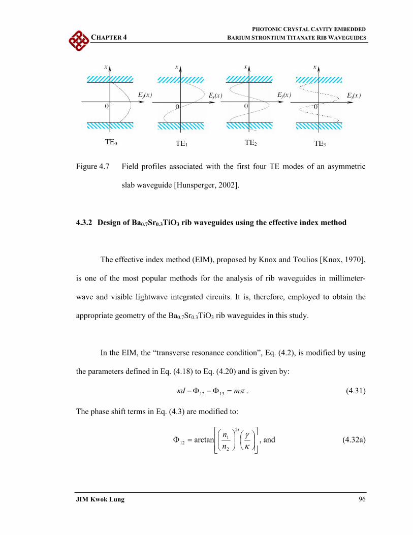
PHOTONIC CRYSTAL CAVITY EMBEDDED
CHAPTER 4 BARIUM STRONTIUM TITANATE RIB WAVEGUIDES
JIM Kwok Lung 96
Figure 4.7 Field profiles associated with the first four TE modes of an asymmetric
slab waveguide [Hunsperger, 2002].
4.3.2 Design of Ba0.7Sr0.3TiO3 rib waveguides using the effective index method
The effective index method (EIM), proposed by Knox and Toulios [Knox, 1970],
is one of the most popular methods for the analysis of rib waveguides in millimeter-
wave and visible lightwave integrated circuits. It is, therefore, employed to obtain the
appropriate geometry of the Ba0.7Sr0.3TiO3 rib waveguides in this study.
In the EIM, the “transverse resonance condition”, Eq. (4.2), is modified by using
the parameters defined in Eq. (4.18) to Eq. (4.20) and is given by:
md 1312 . (4.31)
The phase shift terms in Eq. (4.3) are modified to:
i
n
n2
2
112 arctan , and (4.32a)

PHOTONIC CRYSTAL CAVITY EMBEDDED
CHAPTER 4 BARIUM STRONTIUM TITANATE RIB WAVEGUIDES
JIM Kwok Lung 97
i
n
n2
3
113 arctan , (4.32b)
where m = 0, 1, 2 , 3 …, i = 0 for TE mode and i = 1 for TM mode. By substituting Eq.
(4.7) into Eq. (4.18) to Eq. (4.20), , , and take the forms as:
kNn m 221 , (4.33)
knN m 22
2 , and (4.34)
knN m 23
2 . (4.35)
Combining Eq. (4.31) to Eq. (4.35), one can obtain the “transverse resonance condition”
in terms of the effective refractive index Nm:
imdnnnNN m ,,,,,, 321 . (4.36)
Knox and Toulios [Knox, 1970] proposed to consider a rib waveguide, which is shown
in Figure 4.8(a), as consisting of three regions: the rib region in the center, and the two
regions on the left and the right of the rib. The rib region is then regarded as a slab
waveguide of thickness d while the two regions on the left and the right as a slab
waveguide of thickness d-h (Figure 4.8(b)). Applying Eq. (4.31) to Eq. (4.35), the
effective index of the rib region, Neff1, and the effective index of the region on the left
and the right hand sides, Neff2 can be evaluated. Finally, the whole system can be
considered as a symmetric waveguide with a “core” layer having an effective index Neff1
and thickness of W, and “substrate” and “cladding” layers with effective index Neff2
(Figure 4.8(c)). The effective index of the whole system can then be calculated.

PHOTONIC CRYSTAL CAVITY EMBEDDED
CHAPTER 4 BARIUM STRONTIUM TITANATE RIB WAVEGUIDES
JIM Kwok Lung 98
Figure 4.8 The effective index method on a rib waveguide. (a) The original rib
waveguide. (b) Transform the original rib waveguide into three slab
waveguides with effective index Neff1 and Neff2. (c) Transform the system
into a symmetric slab waveguide to determine the effective index Neff of
the whole structure.
W
h
d
n3
n1
n2
W
Neff1 Neff2Neff2
Neff
(a)
(b)
(c)
n1
n2
Neff2 Neff1 Neff2
d
n3
d-h d-h

PHOTONIC CRYSTAL CAVITY EMBEDDED
CHAPTER 4 BARIUM STRONTIUM TITANATE RIB WAVEGUIDES
JIM Kwok Lung 99
In order to determine the appropriate height of the rib for the Ba0.7Sr0.3TiO3 rib
waveguides to maintain single mode wave propagation, the effective index Nm as a
function of d at λ = 1550 nm is plotted and the result is shown in Figure 4.9. It can be
seen from Figure 4.9 that only the first TE mode (TE0) is supported if the waveguide has
a thickness d between 150 nm and 700 nm. To develop the Ba0.7Sr0.3TiO3 rib waveguides
used at λ = 1550 nm, the thickness d of the Ba0.7Sr0.3TiO3 films is chosen to be 550 nm.
The corresponding effective index Nm of this chosen d value, which is in fact Neff1, can
be obtained from Figure 4.9 to be 2.015.
1.65
1.70
1.75
1.80
1.85
1.90
1.95
2.00
2.05
2.10
2.15
2.20
2.25
0.0 0.1 0.2 0.3 0.4 0.5 0.6 0.7 0.8 0.9 1.0
Thickness (mm)
Eff
ecti
ve in
de
x N
m
TE0
TE1
nBST
nMgO
Figure 4.9 Effective index Nm as function of thickness for a Ba0.7Sr0.3TiO3/MgO slab
waveguide at a wavelength of λ = 1550 nm. The refractive index of the
film is 2.20.

PHOTONIC CRYSTAL CAVITY EMBEDDED
CHAPTER 4 BARIUM STRONTIUM TITANATE RIB WAVEGUIDES
JIM Kwok Lung 100
To determine the appropriate width of rib for maintaining single mode wave
propagation, we need to obtain Neff1 and Neff2, which can actually be read from Figure
4.9 directly. As an example, take h = 50 nm (with the chosen d = 550 nm), d-h = 500 nm.
Neff2 is the Nm value corresponds to the thickness of 500 nm which gives 1.99. With the
values of Neff1 and Neff2 known, the effective index of the rib waveguide as function of
rib width W can be obtained by applying Eq. (4.31) to Eq. (4.35) again. Similar
calculations can be performed for other values of h and the results are shown in Figure
4.10.
1.96
1.97
1.98
1.99
2.00
2.01
2.02
0.0 0.5 1.0 1.5 2.0 2.5 3.0 3.5 4.0 4.5 5.0
Rib width W (mm)
Eff
ecti
ve In
dex
Nm
a
bc
a
b
c
TE00TE01
a: h = 50 nmb: h = 60 nmc: h = 70 nmd: h = 90 nm
dd
Figure 4.10 Effective index Nm versus rib width W for various rib height h of a
Ba0.7Sr0.3TiO3/MgO rib waveguide at a wavelength of λ = 1550 nm.
Thickness of the film d is 550 nm.
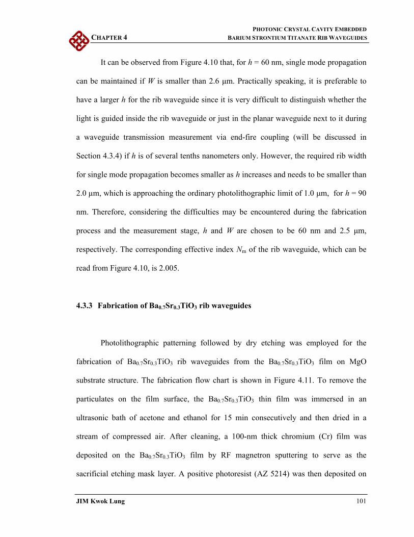
PHOTONIC CRYSTAL CAVITY EMBEDDED
CHAPTER 4 BARIUM STRONTIUM TITANATE RIB WAVEGUIDES
JIM Kwok Lung 101
It can be observed from Figure 4.10 that, for h = 60 nm, single mode propagation
can be maintained if W is smaller than 2.6 μm. Practically speaking, it is preferable to
have a larger h for the rib waveguide since it is very difficult to distinguish whether the
light is guided inside the rib waveguide or just in the planar waveguide next to it during
a waveguide transmission measurement via end-fire coupling (will be discussed in
Section 4.3.4) if h is of several tenths nanometers only. However, the required rib width
for single mode propagation becomes smaller as h increases and needs to be smaller than
2.0 μm, which is approaching the ordinary photolithographic limit of 1.0 μm, for h = 90
nm. Therefore, considering the difficulties may be encountered during the fabrication
process and the measurement stage, h and W are chosen to be 60 nm and 2.5 μm,
respectively. The corresponding effective index Nm of the rib waveguide, which can be
read from Figure 4.10, is 2.005.
4.3.3 Fabrication of Ba0.7Sr0.3TiO3 rib waveguides
Photolithographic patterning followed by dry etching was employed for the
fabrication of Ba0.7Sr0.3TiO3 rib waveguides from the Ba0.7Sr0.3TiO3 film on MgO
substrate structure. The fabrication flow chart is shown in Figure 4.11. To remove the
particulates on the film surface, the Ba0.7Sr0.3TiO3 thin film was immersed in an
ultrasonic bath of acetone and ethanol for 15 min consecutively and then dried in a
stream of compressed air. After cleaning, a 100-nm thick chromium (Cr) film was
deposited on the Ba0.7Sr0.3TiO3 film by RF magnetron sputtering to serve as the
sacrificial etching mask layer. A positive photoresist (AZ 5214) was then deposited on

PHOTONIC CRYSTAL CAVITY EMBEDDED
CHAPTER 4 BARIUM STRONTIUM TITANATE RIB WAVEGUIDES
JIM Kwok Lung 102
top of the Cr layer by spin coating at a spinning speed of 4000 rpm for 40 s, resulting in
a photoresist layer of 1.5 μm thick. After baking at 100 ˚C for 1 min, the photoresist
layer was exposed under a mask to high intensity ultraviolet light for 15 s in a Model
800 MBA double side mask aligner (OAI). The exposed photoresist was then immersed
in a developer (AZ300 Mif) for 30 s. Using an etching solution of Ce(NO3)4 in aceric
acid, the Cr layer without the protection of photoresist was removed. An O2 plasma
etching was then carried out for 10 min in order to strip off the photoresist residue,
leaving the bare waveguide patterns of the Cr layer on the film surface.
Figure 4.11 Fabrication flow chart of thin film rib waveguides.
BST
MgO
CrBST
MgO
Cr PR
BST
MgO
Mask
UV light
Cr PR
BST
MgO
CrPR
BST
MgO
CrBST
MgO
Cr
MgO
BST
MgO
BSTFilm deposition (PLD)
Sputtering ofCr layer
Spin coating of photoresist (PR)
UV exposure of photoresist (PR)
Developing of photoresist (PR)
Wet etching Cr followed byO2 plasma
ICP-RIE of BST
Removal of Cr
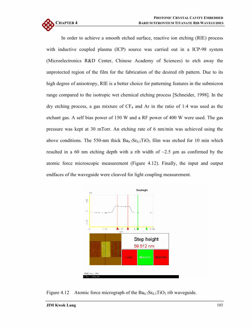
PHOTONIC CRYSTAL CAVITY EMBEDDED
CHAPTER 4 BARIUM STRONTIUM TITANATE RIB WAVEGUIDES
JIM Kwok Lung 103
In order to achieve a smooth etched surface, reactive ion etching (RIE) process
with inductive coupled plasma (ICP) source was carried out in a ICP-98 system
(Microelectronics R&D Center, Chinese Academy of Sciences) to etch away the
unprotected region of the film for the fabrication of the desired rib pattern. Due to its
high degree of anisotropy, RIE is a better choice for patterning features in the submicron
range compared to the isotropic wet chemical etching process [Schneider, 1998]. In the
dry etching process, a gas mixture of CF4 and Ar in the ratio of 1:4 was used as the
etchant gas. A self bias power of 150 W and a RF power of 400 W were used. The gas
pressure was kept at 30 mTorr. An etching rate of 6 nm/min was achieved using the
above conditions. The 550-nm thick Ba0.7Sr0.3TiO3 film was etched for 10 min which
resulted in a 60 nm etching depth with a rib width of ~2.5 μm as confirmed by the
atomic force microscopic measurement (Figure 4.12). Finally, the input and output
endfaces of the waveguide were cleaved for light coupling measurement.
Figure 4.12 Atomic force micrograph of the Ba0.7Sr0.3TiO3 rib waveguide.

PHOTONIC CRYSTAL CAVITY EMBEDDED
CHAPTER 4 BARIUM STRONTIUM TITANATE RIB WAVEGUIDES
JIM Kwok Lung 104
4.3.4 Optical characterization of Ba0.7Sr0.3TiO3 rib waveguides
The transmission spectrum of the Ba0.7Sr0.3TiO3 film/MgO rib waveguide was
measured (at the Optoelectronic Research Centre, Department of Electronic Engineering
of the City University of Hong Kong) using the end-fire coupling technique. The
schematic diagram of the end-fire coupling method is shown in Figure 4.13. The light
source used was a TE-polarized laser diode (Amonic ALS-15CL, C+L band ASE
broadband source) which can produce a light spectrum of wavelength from 1500 nm to
1620 nm. The laser beam was butt-coupled to the cleaved input endface of the
waveguide by a polarization-maintaining single mode optical fiber (diameter ~ 8 μm).
The transmitted light at the output endface of the waveguide was measured using an
infrared charge-coupled device (CCD) camera after the light beam had passed through a
micro-objective lens. Since the size of the waveguide is very small, the positions of the
fibers, the micro-objective lens and the waveguide were carefully adjusted using three
xyz micron-positioners mounted on an optical vibration isolator. The optimum alignment
between the input fiber and the waveguide was accomplished by maximizing the
intensity of the output light spot (Figure 4.14). After the alignment between the input
fiber and the waveguide, the CCD camera was replaced by another optical fiber which
was connected to an optical spectrum analyzer (Agilent 86140) for signal processing.
The output fiber was butt-coupled to the cleaved output endface in order to collect output
signal. The transmission spectrum (with wavelength from 1500 nm to 1620 nm) of the
Ba0.7Sr0.3TiO3 rib waveguide is shown in Figure 4.15. It can be seen that the waveguide
can guide light of wavelength from 1530 nm to 1600 nm reliably.
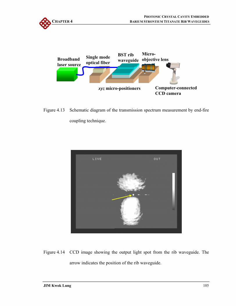
PHOTONIC CRYSTAL CAVITY EMBEDDED
CHAPTER 4 BARIUM STRONTIUM TITANATE RIB WAVEGUIDES
JIM Kwok Lung 105
Figure 4.13 Schematic diagram of the transmission spectrum measurement by end-fire
coupling technique.
Figure 4.14 CCD image showing the output light spot from the rib waveguide. The
arrow indicates the position of the rib waveguide.
Computer-connected CCD camera
Micro-objective lens
BST rib waveguide
Single mode optical fiber
Broadband laser source
xyz micro-positioners

PHOTONIC CRYSTAL CAVITY EMBEDDED
CHAPTER 4 BARIUM STRONTIUM TITANATE RIB WAVEGUIDES
JIM Kwok Lung 106
-80
-70
-60
-50
-40
-30
1500 1520 1540 1560 1580 1600 1620
Wavelength (nm)
Inte
nsi
ty (
dB
m)
Figure 4.15 Transmission spectrum of the Ba0.7Sr0.3TiO3 rib waveguide.
4.4 Photonic crystal cavity embedded rib waveguides
4.4.1 Fabry-Perot cavity
Figure 4.16(a) shows a Fabry-Perot (FP) cavity consisting of two parallel perfect
plane mirrors, M1 and M2, separated by a distance L [Kasap, 2001]. Assume that the
cavity is filled with a dielectric of refractive index n. A plane wave with free-space
wavenumber /20 k travelling inside the cavity will reflect back and forth, and the
total field travelling in both directions must everywhere be given by the sum of one
combined field travelling in the +z direction and a similar field travelling in the –z
direction as:
nzikEnzikEzE 00 expexp , (4.37)
PHOTONIC CRYSTAL CAVITY EMBEDDED
CHAPTER 4 BARIUM STRONTIUM TITANATE RIB WAVEGUIDES
JIM Kwok Lung 107
The boundary conditions require that E = 0 at z = 0 and z = L. The former condition
gives E- = -E+, which allows us to write Eq. (4.37) as:
nzkEzE 00 sin . (4.38)
The latter condition is satisfied when:
mnLk 0 (4.39a)
Ln
m
2
, (4.39b)
where m = 1, 2, 3 …, is the mode number. Eq. (4.39) is often called the longitudinal
resonance condition. The field distributions for different mode number are shown in
Figure 4.16(b). If the two mirrors are not perfect but partially reflecting with reflectance
R, light outside the cavity can couple into the cavity and light being resonant inside the
cavity can transmit to the outside (Figure 4.16(c)). The output intensity will be a fraction
of the input intensity. The amount of transmitted light is determined by the reflectance R.
A fraction of the incident light (1-R) will enter the cavity as Iincident, of which part (again
1-R) will leave the cavity as Itransmitted. Thus the ratio of transmitted to incident light is
given by:
LnkRR
R
I
I
incident
dtransmitte
022
2
sin41
1
. (4.40)
It can be observed, from Eq. (4.40), that resonant peaks will occur in the transmission
spectrum of a Fabry-Perot resonator when the longitudinal resonance condition, Eq.
(4.39), is fulfilled.

PHOTONIC CRYSTAL CAVITY EMBEDDED
CHAPTER 4 BARIUM STRONTIUM TITANATE RIB WAVEGUIDES
JIM Kwok Lung 108
(a) (b)
(c)
Figure 4.16 (a) Schematic diagram of a Fabry-Perot cavity. (b) Allowed field
distributions of different modes inside the cavity. (c) Transmission
spectrum of a Fabry-Perot resonator. [Kasap, 2001]
Partially reflecting mirrorsTransmission

PHOTONIC CRYSTAL CAVITY EMBEDDED
CHAPTER 4 BARIUM STRONTIUM TITANATE RIB WAVEGUIDES
JIM Kwok Lung 109
4.4.2 Photonic crystal cavity
If a light beam with frequencies within the photonic bandgap of a PC strikes on
that PC which is semi-infinite extended, it will be totally reflected. The PC acts like a
perfect mirror. If the PC is, however, finite, the reflection will not be perfect and there is
chance for the light to tunnel through the PC. In this way, the PC acts like a partially
reflecting mirror and is denoted as a PC mirror. A photonic crystal cavity, which is
similar to a Fabry-Perot (FP) cavity, is formed by separating two sets of PC mirror
(finite PC) by a distance. The cavity length is defined by the center-to-center distance
between the nearest rows of the two PC mirrors. Figure 4.17(a) shows the schematic
diagram of a photonic crystal cavity. Similar to the situation in FP cavity, a fraction of
light, although with frequencies within the photonic bandgap, can tunnel through the PC
mirror and enter the cavity. Being reflected back and forth inside the cavity, most light
interferes destructively. Only light with certain wavelengths satisfying the longitudinal
resonance condition (Eq. (4.39)) is allowed inside the cavity. Therefore, the transmission
spectrum of a PC cavity resembles that of a FB cavity in such a way that transmission
peaks appear at certain resonant wavelengths inside the region of the photonic bandgap.
A typical transmission spectrum of a PC cavity is shown in Figure 4.17(b).

PHOTONIC CRYSTAL CAVITY EMBEDDED
CHAPTER 4 BARIUM STRONTIUM TITANATE RIB WAVEGUIDES
JIM Kwok Lung 110
(a)
(b)
Figure 4.17 (a) Schematic diagram of a PC cavity formed by a pair of 3-row PC
mirrors. (b) Typical transmission spectrum of a PC cavity.
Photonic
bandgap
Resonant peak
PC mirrorsPC cavity

PHOTONIC CRYSTAL CAVITY EMBEDDED
CHAPTER 4 BARIUM STRONTIUM TITANATE RIB WAVEGUIDES
JIM Kwok Lung 111
4.4.3 Design of photonic crystal cavity embedded Ba0.7Sr0.3TiO3 rib waveguides
The photonic crystal cavity embedded Ba0.7Sr0.3TiO3 rib waveguide (PCCRWG)
is planned to function as a tunable filter (on-off switch) for λ = 1550 nm. Therefore, the
main purpose of the design is to determine the appropriate geometry of the PC cavity so
that it possesses a photonic bandgap (approximate zero transmission) at the wavelengths
around but contains a resonant peak at λ = 1550 nm, which corresponds to an “on” state
of the device. By changing the refractive index of Ba0.7Sr0.3TiO3 via the electro-optic
effect, the resonant peak should be shifted away from λ = 1550 nm, which corresponds
to an “off” state, since the longitudinal resonance condition for the cavity is altered.
The design flow is thus set as the following: First, the appropriate geometry of
the PC pattern for a larger photonic bandgap at wavelength around 1550 nm was
determined. Then, the effects on the resonant peak for different numbers of row and row
configurations in the PC mirror were examined. After that, the required cavity length for
the 1550-nm resonant peak was studied. Finally, the electro-optic tuning of the resonant
peak was illustrated. The transmission spectra of the photonic crystal cavity embedded
Ba0.7Sr0.3TiO3 rib waveguide were simulated by the software FullWAVETM 6.0 (RSoft
Design Group, Inc.) which utilizes the finite-difference time-domain (FDTD) algorithm.
Two-dimensional FDTD simulations were used in order to keep the computation time in
a reasonable range. An effective index Nm of 2.005 was assumed for the Ba0.7Sr0.3TiO3
rib waveguide.

PHOTONIC CRYSTAL CAVITY EMBEDDED
CHAPTER 4 BARIUM STRONTIUM TITANATE RIB WAVEGUIDES
JIM Kwok Lung 112
4.4.3.1 Appropriate geometry of the photonic crystal pattern
As the PC pattern is constructed by focused ion beam technique, it is obvious that
hole-type PC pattern is a better choice than rod-type PC in view of fabrication process.
Therefore, only hole-type PC pattern is considered. Since the Ba0.7Sr0.3TiO3 rib
waveguide is designed for light propagation of TE fundamental mode, larger TE
bandgaps in the PC pattern is preferred. Refer to Figure 3.2, Ba0.7Sr0.3TiO3 PCs with air
holes arranged in triangular lattice possess larger TE gaps than those in square lattice.
Hence, Ba0.7Sr0.3TiO3 PCs with air holes arranged in triangular lattice is chosen as the
required photonic crystal pattern.
If we arrange the PC pattern such that the Γ-M direction of the triangular lattice
is along the waveguide direction (Figure 4.18), the light guided in the waveguide will
then strike the PC pattern mostly along the Γ-M direction. Therefore we can consider the
photonic bandgap map for the Γ-M direction (Figure 3.2(f)) only. It can be observed
from Figure 3.2(f) that there is a large TE gap (including the joint gap) at r = 0.4 a (a is
the period of the PC). The bandgap extends from Ω = 0.30 to Ω = 0.45. Choosing a =
625 nm (then r = 0.4a = 250 nm), the corresponding bandgap in term of wavelength,
which can be calculated from Ω = a/λ, extends from λ = 1390 nm to λ = 2080 nm.
The simulation model and the transmission spectrum of the PC cavity embedded
Ba0.7Sr0.3TiO3 rib waveguide (PCCRWG) with the above-mentioned PC pattern (a = 625
nm and r = 250 nm) are shown in Figure 4.19. The cavity length was set to be 770 nm

PHOTONIC CRYSTAL CAVITY EMBEDDED
CHAPTER 4 BARIUM STRONTIUM TITANATE RIB WAVEGUIDES
JIM Kwok Lung 113
(which is estimated according to Eq. (4.39) for λ = 1550 nm, n = 2.005, and m = 2). It
can be seen from Figure 4.19 that the transmission is approximate zero from 1300 nm to
1800 nm, and a transmission peak occurs at λ = 1550 nm. This confirms the proof-of-
concept of the photonic crystal cavity embedded Ba0.7Sr0.3TiO3 rib waveguide.
Figure 4.18 PC pattern of triangular lattice type in a rib waveguide with the Γ-M and
Γ-K directions emphasized.
Γ
M K
Waveguide direction

PHOTONIC CRYSTAL CAVITY EMBEDDED
CHAPTER 4 BARIUM STRONTIUM TITANATE RIB WAVEGUIDES
JIM Kwok Lung 114
(a)
(b)
Figure 4.19 (a) Simulation model and (b) transmission spectrum of the PCCRWG in
the FDTD calculation.
625 nm
250 nm
770 nm
Monitor
Incident light
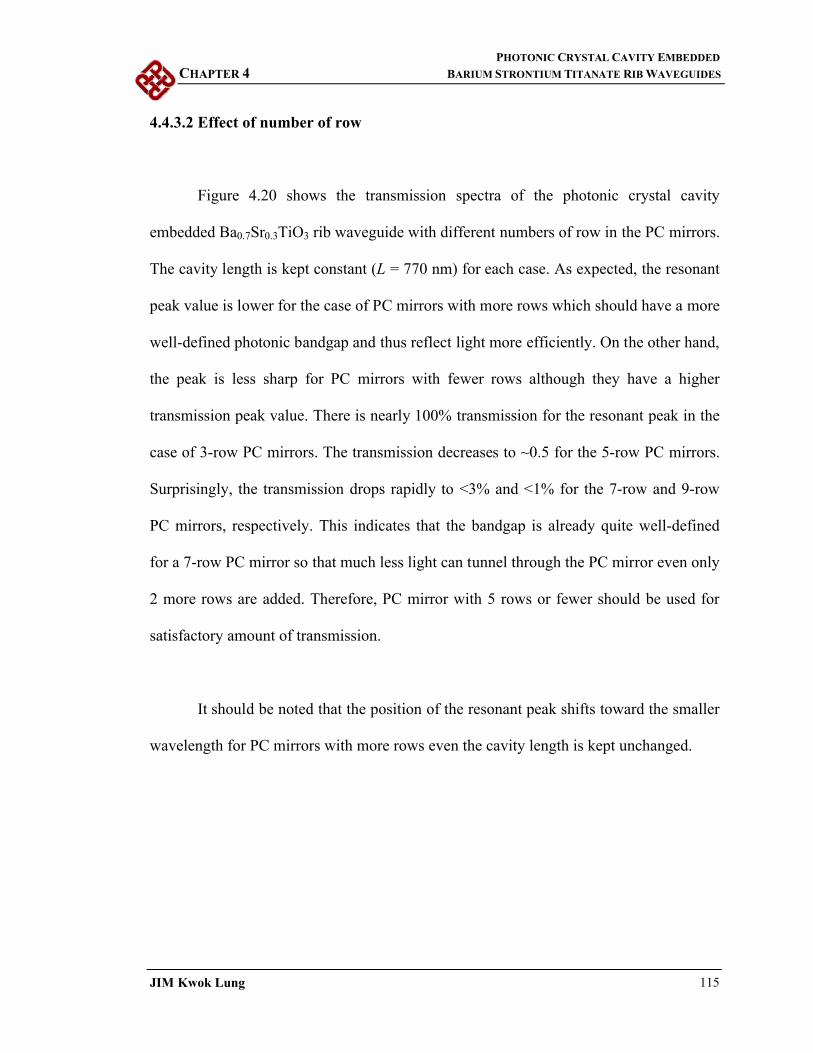
PHOTONIC CRYSTAL CAVITY EMBEDDED
CHAPTER 4 BARIUM STRONTIUM TITANATE RIB WAVEGUIDES
JIM Kwok Lung 115
4.4.3.2 Effect of number of row
Figure 4.20 shows the transmission spectra of the photonic crystal cavity
embedded Ba0.7Sr0.3TiO3 rib waveguide with different numbers of row in the PC mirrors.
The cavity length is kept constant (L = 770 nm) for each case. As expected, the resonant
peak value is lower for the case of PC mirrors with more rows which should have a more
well-defined photonic bandgap and thus reflect light more efficiently. On the other hand,
the peak is less sharp for PC mirrors with fewer rows although they have a higher
transmission peak value. There is nearly 100% transmission for the resonant peak in the
case of 3-row PC mirrors. The transmission decreases to ~0.5 for the 5-row PC mirrors.
Surprisingly, the transmission drops rapidly to <3% and <1% for the 7-row and 9-row
PC mirrors, respectively. This indicates that the bandgap is already quite well-defined
for a 7-row PC mirror so that much less light can tunnel through the PC mirror even only
2 more rows are added. Therefore, PC mirror with 5 rows or fewer should be used for
satisfactory amount of transmission.
It should be noted that the position of the resonant peak shifts toward the smaller
wavelength for PC mirrors with more rows even the cavity length is kept unchanged.

PHOTONIC CRYSTAL CAVITY EMBEDDED
CHAPTER 4 BARIUM STRONTIUM TITANATE RIB WAVEGUIDES
JIM Kwok Lung 116
(a)
(b)

PHOTONIC CRYSTAL CAVITY EMBEDDED
CHAPTER 4 BARIUM STRONTIUM TITANATE RIB WAVEGUIDES
JIM Kwok Lung 117
(c)
(d)
Figure 4.20 Transmission spectra for the PCCRWG with (a) 3-row, (b) 5-row, (c) 7-
row, (d) 9-row PC mirrors.

PHOTONIC CRYSTAL CAVITY EMBEDDED
CHAPTER 4 BARIUM STRONTIUM TITANATE RIB WAVEGUIDES
JIM Kwok Lung 118
4.4.3.3 Effect of row configuration
In the previous Section, an example of a PC cavity embedded Ba0.7Sr0.3TiO3 rib
waveguide with 3-row PC mirrors is illustrated. In fact, there are two possible
configurations to set up the 3-row PC mirrors which are shown together in Figure 4.21.
The one in Figure 4.21(a) has a pair of 3-row PC mirrors with the first row containing 3
air holes, while the one in Figure 4.21(b) has a pair of 3-row PC mirrors with the first
row containing 4 air holes. We denote the former one as 3-row-3 PC mirror and the latter
one as 3-row-4 PC mirror. In other words, a n-row-m PC mirror represents a n-row PC
mirror with m air holes in the first row.
(a) (b)
Figure 4.21 Two possible configurations of the 3-row PC mirrors: (a) 3-row-3 PC
mirrors, (b) 3-row-4 PC mirrors.
The transmission spectra for PC cavity embedded Ba0.7Sr0.3TiO3 rib waveguide
with different n-row-m PC mirrors (n = 3, 4, 5 and m = 3, 4) are calculated. The results
are shown in Figure 4.22. The distinctness of the photonic bandgaps and the sharpness of
3-row-43-row-3

PHOTONIC CRYSTAL CAVITY EMBEDDED
CHAPTER 4 BARIUM STRONTIUM TITANATE RIB WAVEGUIDES
JIM Kwok Lung 119
the resonant peaks are similar for the corresponding pairs having the same n (number of
row in the PC mirror) but different m (number of air hole in the first row). However,
their resonant peak values are usually of great difference. It is interesting to note that the
resonant peak value is always higher when (n+m) is odd for the same n. Taking into
consideration the tradeoff between the resonant peak value and the sharpness of the
resonant peak, the 5-row-4 configuration is chosen for its relatively sharp resonant peak
which still have a transmission peak value ~ 0.5.

PHOTONIC CRYSTAL CAVITY EMBEDDED
CHAPTER 4 BARIUM STRONTIUM TITANATE RIB WAVEGUIDES
JIM Kwok Lung 120
Figure 4.22 Transmission spectra of PCCRWG with different n-row-m PC mirrors: (a)
3-row-3, (b) 3-row-4, (c) 4-row-3, (d) 4-row-4, (e) 5-row-3, (f) 5-row-4.
3row3 3row4
4row44row3
5row3 5row4

PHOTONIC CRYSTAL CAVITY EMBEDDED
CHAPTER 4 BARIUM STRONTIUM TITANATE RIB WAVEGUIDES
JIM Kwok Lung 121
4.4.3.4 Determination of cavity length
After the configuration of the PC pattern is settled, the cavity length needs to be
fine tuned so that the resonant peak is situated at λ = 1550 nm. The transmission spectra
of the 5-row-4 PCCRWG with different cavity lengths were simulated. The peak values
and the locations of the resonant peaks with different cavity lengths are summarized in
Table 4.1. It is found that, for resonant peak situated at λ = 1550 nm, the required cavity
length should be 800 nm. The peak value is coincidently the highest among the
simulated cases.
Table 4.1 Resonant peak values and locations of a 5-row-4 PCCRWG with different
cavity lengths.
Cavity length
(nm)
Location of the
resonant peak (nm)
Transmission value
of the peak
770 1520 0.43
780 1530 0.29
790 1540 0.30
800 1550 0.52
810 1560 0.38

PHOTONIC CRYSTAL CAVITY EMBEDDED
CHAPTER 4 BARIUM STRONTIUM TITANATE RIB WAVEGUIDES
JIM Kwok Lung 122
4.4.3.5 Electro-optic tuning of the resonant peak
The schematic design of the PC cavity embedded Ba0.7Sr0.3TiO3 rib waveguide
with 5-row-4 PC mirrors is shown in Figure 4.23. Two coplanar electrodes are placed
parallel to the rib waveguide. When an external voltage is applied across the electrodes,
the refractive index of the Ba0.7Sr0.3TiO3 (nBST) will change due to the electro-optic
effect. The transmission resonant peak should be shifted accordingly. Figure 4.24
illustrates such shift in the resonant peak assuming the refractive index of Ba0.7Sr0.3TiO3
is changed by ±0.5% for an applied electric field of about 12 MV/m (suggested by the
1D PC results discussed in Section 2.5.2). It can be seen from Figure 4.24 that the
resonant peak is situated at λ = 1551 nm for nBST = 2.005. If the refractive index of the
Ba0.7Sr0.3TiO3 varies through the electro-optic effect, the resonant peak shifts 6 nm
toward the smaller wavelength (λ = 1545 nm) if nBST is decreased by 0.5%, while it
shifts 6 nm toward the larger wavelength (λ = 1557 nm) if nBST is increased by 0.5%. For
nBST = 2.005, the transmission value at λ = 1551 nm is 0.53 while the transmission values
at λ = 1545 and 1557 nm are both 0.26 which is half of the transmission value
(corresponds to -3 dB) at λ = 1551 nm. It should, thus, provide sufficient difference in
the transmission value to distinguish the “on” and “off” states for the PC cavity
embedded Ba0.7Sr0.3TiO3 rib waveguide to be functioned as a tunable filter for λ = 1550
nm.

PHOTONIC CRYSTAL CAVITY EMBEDDED
CHAPTER 4 BARIUM STRONTIUM TITANATE RIB WAVEGUIDES
JIM Kwok Lung 123
Figure 4.23 Schematic design of the PC cavity embedded Ba0.7Sr0.3TiO3 rib waveguide
with 5-row-4 PC mirrors.
W 2.5 μm
L 800 nm
a 625 nm
r 250 nm
L
W
a
r
Electrodes
Ba0.7Sr0.3TiO3
Rib waveguide

PHOTONIC CRYSTAL CAVITY EMBEDDED
CHAPTER 4 BARIUM STRONTIUM TITANATE RIB WAVEGUIDES
JIM Kwok Lung 124
Figure 4.24 Shifting of transmission resonant peaks for the PCCRWG shown in Figure
4.23 when the refractive index of Ba0.7Sr0.3TiO3 (nBST) is changed by
+0.5% (red line) and -0.5% (blue line). The green line corresponds to the
effective refractive index (nBST = 2.005).
4.4.4 Photonic crystal cavity preparation by focused ion beam etching
The photonic crystal cavity pattern is prepared on the Ba0.7Sr0.3TiO3 rib
waveguide using focused ion beam (FIB) etching. The etching process is carried out in a
Quanta 200 3D DualBeam (FIB/SEM) system (at the Electron Microscope Unit, The
University of Hong Kong). Figure 4.25 shows the scanning electron micrograph of the
Ba0.7Sr0.3TiO3 rib waveguide with PC cavity patterns prepared by FIB etching. It can be
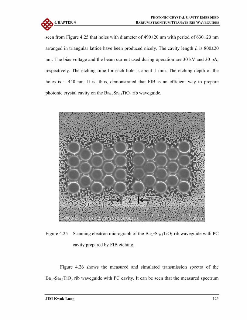
PHOTONIC CRYSTAL CAVITY EMBEDDED
CHAPTER 4 BARIUM STRONTIUM TITANATE RIB WAVEGUIDES
JIM Kwok Lung 125
seen from Figure 4.25 that holes with diameter of 490±20 nm with period of 630±20 nm
arranged in triangular lattice have been produced nicely. The cavity length L is 800±20
nm. The bias voltage and the beam current used during operation are 30 kV and 30 pA,
respectively. The etching time for each hole is about 1 min. The etching depth of the
holes is ~ 440 nm. It is, thus, demonstrated that FIB is an efficient way to prepare
photonic crystal cavity on the Ba0.7Sr0.3TiO3 rib waveguide.
Figure 4.25 Scanning electron micrograph of the Ba0.7Sr0.3TiO3 rib waveguide with PC
cavity prepared by FIB etching.
Figure 4.26 shows the measured and simulated transmission spectra of the
Ba0.7Sr0.3TiO3 rib waveguide with PC cavity. It can be seen that the measured spectrum
L

PHOTONIC CRYSTAL CAVITY EMBEDDED
CHAPTER 4 BARIUM STRONTIUM TITANATE RIB WAVEGUIDES
JIM Kwok Lung 126
agrees well with the simulated one. A resonant peak is situated at λ ~ 1560 nm in the
measured transmission. The small discrepancy in the position of the resonant peak
between the measured spectrum and the simulated spectrum may be due to the
fabrication deviation of the cavity length from 800 nm. Also, the intensity of the
resonant peak is ~ 20 dBm larger than those of other wavelengths for both measured and
simulated spectra. In addition, the bandgap effect of the PC pattern can be evaluated
when compared the transmission spectrum of the Ba0.7Sr0.3TiO3 waveguide with PC
cavity to that of the Ba0.7Sr0.3TiO3 waveguide without PC cavity. The transmission
intensity level of the Ba0.7Sr0.3TiO3 waveguide with PC cavity drops by ~ 30 dBm
relative to that of the Ba0.7Sr0.3TiO3 waveguide without PC cavity. Such a great decrease
in the transmission intensity should be attributed to the photonic bandgap effect due to
the PC pattern on the Ba0.7Sr0.3TiO3 waveguide.
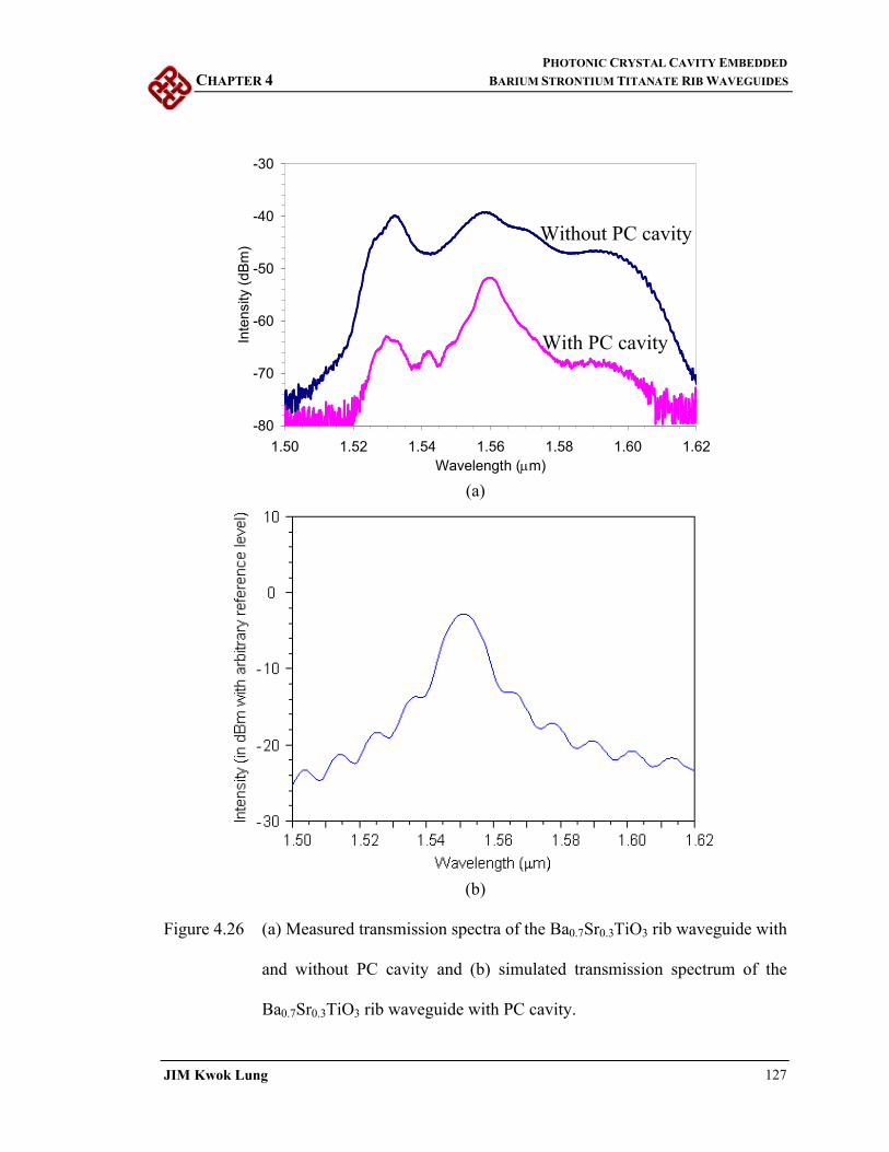
PHOTONIC CRYSTAL CAVITY EMBEDDED
CHAPTER 4 BARIUM STRONTIUM TITANATE RIB WAVEGUIDES
JIM Kwok Lung 127
-80
-70
-60
-50
-40
-30
1.50 1.52 1.54 1.56 1.58 1.60 1.62Wavelength (mm)
Inte
nsity
(dB
m)
(a)
(b)
Figure 4.26 (a) Measured transmission spectra of the Ba0.7Sr0.3TiO3 rib waveguide with
and without PC cavity and (b) simulated transmission spectrum of the
Ba0.7Sr0.3TiO3 rib waveguide with PC cavity.
With PC cavity
Without PC cavity
PHOTONIC CRYSTAL CAVITY EMBEDDED
CHAPTER 4 BARIUM STRONTIUM TITANATE RIB WAVEGUIDES
JIM Kwok Lung 128
4.5 Summary
The refractive indices of the Ba0.7Sr0.3TiO3 thin film on a MgO (001) substrate is
measured using the prism coupling technique. The rib waveguide dimensions for single
mode TE wave propagation is determined by applying the effective index method. A
photonic crystal cavity embedded Ba0.7Sr0.3TiO3 rib waveguide which functions as a
tunable filter (on-off switch) for λ = 1550 nm is designed with the help of FDTD
simulation. The photonic crystal cavity is composed of two 5-row-4 PC mirrors, which is
formed by air holes arranged in triangular lattice in the Ba0.7Sr0.3TiO3 matrix. The radius
of the air holes is 250 nm and the periodicity is 625 nm. The required cavity length for
the resonant peak to be situated at λ = 1550 nm is 800 nm. Photonic crystal cavities are
fabricated on a Ba0.7Sr0.3TiO3 rib waveguide by focused ion beam etching with
satisfactory results. The transmission properties of the Ba0.7Sr0.3TiO3 rib waveguide with
PC cavity have been measured. The results agree well with the FDTD simulation.
THERMAL TUNING OF PHONONIC
CHAPTER 5 BANDGAPS IN BST/EPOXY PHONONIC CRYSTALS
JIM Kwok Lung 129
CHAPTER 5
THERMAL TUNING OF PHONONIC BANDGAPS
IN BARIUM STRONTIUM TITANATE/EPOXY
PHONONIC CRYSTALS
5.1 Introduction
Phononic crystals, which are the elastic and acoustic analogs of photonic crystals,
are periodic composite materials having different acoustic velocities and densities with
lattice constants on the scale of the wavelength of sound or ultrasound [Page, 2004].
Extending the concept of photonic bandgaps to acoustic waves, phononic crystals
possesses phononic bandgaps for which the acoustic waves at these frequencies cannot
propagate and lead to a total reflection regime in such frequency range. This makes
phononic crystal very attractive for the design of acoustic band-pass filters [Wu, 2009].
If frequency and the width of the phononic bandgaps can be tuned, promising
applications such as tunable filters can be realized [Khelif, 2003; Pennec, 2004]. Since
the phononic bandstructures of a phononic crystal depend on the acoustic velocities and
densities of the constituent materials, changes in such properties would cause
modification in the phononic bandgaps. Ferroelectric materials will undergo phase
transition, at which the longitudinal and shear acoustic wave velocities change

THERMAL TUNING OF PHONONIC
CHAPTER 5 BANDGAPS IN BST/EPOXY PHONONIC CRYSTALS
JIM Kwok Lung 130
significantly, across the Curie temperature [Wu, 1992; Cheng, 1994; Frayssignes, 2005].
Since Ba0.7Sr0.3TiO3 has its ferroelectric-to-paraelectric phase transition at ~35 ˚C
[Zhang, 1998; Wang, 2005], it becomes a promising candidate as a building block of
thermally tunable phononic crystal near room temperature.
In this Chapter, we first present the calculation of phononic bandstructure using
the plane wave expansion method, and then we describe the measurement of the
longitudinal and shear wave velocities of Ba0.7Sr0.3TiO3 bulk ceramics by the ultrasonic
through-transmission technique. The fabrication of Ba0.7Sr0.3TiO3/epoxy phononic
crystals with the corresponding phononic bandstructures and the characterization of the
phononic bandgaps by ultrasonic pulse-echo technique are then discussed.
5.2 Computation of phononic bandstructure by plane wave expansion method
Similar to the case in photonic crystals, several theoretical methods have been
developed to study phononic crystals. They include the plane wave expansion (PWE)
method [Kushwaha, 1994], the multiple scattering theory (MST) method [Kafesaki,
1999], and the finite-difference time-domain (FDTD) method [Cao, 2004]. Among these
methods, the PWE method is extensively used to calculate phononic bandstructures
because of its convenience and easiness to apply. Therefore, we also employed the PWE
method for the calculation of phononic bandstructures. In this Section, we describe
briefly the computation of phononic bandstructures of two-dimensional phononic
crystals by the PWE method.
THERMAL TUNING OF PHONONIC
CHAPTER 5 BANDGAPS IN BST/EPOXY PHONONIC CRYSTALS
JIM Kwok Lung 131
5.2.1 Wave equation for an inhomogeneous elastic medium
Consider an inhomogeneous but isotropic elastic medium which is characterized by
three material parameters: the mass density r , the longitudinal speed of sound rcl
,
and the transverse speed of sound rct
, the equation of motion governing the lattice
displacement tru ,
is given by:
2
2
t
ui
j
ij
x
)2()(2)2(2 222222tl
jijkkt
jijij
j
kktl
j
ijt cc
xuc
xu
x
ucc
x
uc
, (5.1)
where σij is the stress tensor which is given by:
ijkktlijtij uccuc )2(2 222 . (5.2)
j
k
i
k
i
j
j
iij x
u
x
u
x
u
x
uu
2
1(5.3)
is the deformation tensor, and 3,2,1iui being the components of the displacement
vector tru ,
. The convention of summation over equal indices applies.
Assume that the medium is linear, the quadratic term in uij in Eq. (5.3) can
thereby be omitted. Then Eq. (5.1) can be simplified to a more compact form as:
2
2
t
ui
iti
tlit ucux
ccuc
)()2( 22222
uccxx
uc tl
iit
)2()( 222

THERMAL TUNING OF PHONONIC
CHAPTER 5 BANDGAPS IN BST/EPOXY PHONONIC CRYSTALS
JIM Kwok Lung 132
uccxx
ucuc tl
iitit
)2( 2222 . (5.4)
It should be noted that this equation is valid for arbitrary inhomogeneity. Since r ,
rcl
, and rct
are, however, position dependent, Eq. (5.4) cannot be separated into
two equations, one for the longitudinal displacement which satisfies 0 u
, and the
other for the transverse displacement which satisfies 0 u
, as in the case for
homogeneous medium [Kushwaha, 1994].
5.2.2 Plane wave expansion for periodic elastic structure
If the inhomogeneous elastic medium exhibits spatial periodicity, the three material
parameters, r , rcl
, and rct
, can then be expanded in the Fourier series. In fact,
the algebra would be less complicated if we expand 2lc and 2
tc , rather than lc and tc ,
as the speeds of sound always appear in Eq. (5.4) in the forms of 2lc and 2
tc .
Therefore the three material parameters are expanded as
G
rGieGr
, (5.5a)
G
rGil eGrcr
2 , and (5.5b)
G
rGit eGrcr
2 . (5.5c)
where G
represent the reciprocal lattice vectors with corresponding periodicity of the
medium which may be one, two, or three dimensional. The summation in Eq. (5.5)

THERMAL TUNING OF PHONONIC
CHAPTER 5 BANDGAPS IN BST/EPOXY PHONONIC CRYSTALS
JIM Kwok Lung 133
covers all reciprocal lattice vectors which correspond to the Bravais lattice vectors in the
real space. The Fourier coefficients G
, G
, and G
, are given by:
rGi
C
errdV
G
31, (5.6a)
rGil
C
ercrrdV
G
231 , and (5.6b)
rGit
C
ercrrdV
G
231 , (5.6c)
where the integration is over the unit cell and Vc is its volume. Since the medium is
periodic, the displacement tru ,
must satisfy the Bloch theorem which states as:
G
rGiK
trKi eGuetru
, , (5.7)
where K
is the Bloch wave vector, and is the angular frequency of the wave.
Substituting Eq. (5.5) and Eq. (5.7) into Eq. (5.4), followed by multiplication by
rGiexp , and integration over the unit cell, Eq. (5.4) transforms to an infinite set of
linear equations as:
G
K GKGKGuGG
GKGKGuGG K
02 2 GuGGGKGKGuGGGG KK
, (5.8)
for the eigenvectors GuK
. For each given Bloch vector K
, Eq. (5.8) has solutions for
some eigenvalues Kn
, where n = 1, 2, … is the first, second, etc. vibrational band.

THERMAL TUNING OF PHONONIC
CHAPTER 5 BANDGAPS IN BST/EPOXY PHONONIC CRYSTALS
JIM Kwok Lung 134
5.2.3 Binary composite
Let us consider phononic crystal composed of binary composite for which there are
only two materials, labeled as a and b, in every unit cell. Material a (b) is characterized
by the three parameters a ( b ), lac ( lbc ), and tac ( tbc ). The filling ratio, f, is defined as
the occupancy ratio for material a in the unit cell. Thus, the occupancy ratio for material
b is (1-f). The Fourier coefficients in Eq. (5.6) can be calculated. To illustrate, we will
take G
as an example. For 0G
,
ffG ba 10
, (5.9)
which is actually the average density. If 0G
,
b
rGib
ca
rGia
c
erdV
erdV
G
33 11
a
rGiba
cba
rGib
c
erdV
erdV
33 11 . (5.10)
The first term in the right hand side is zero. The integral in the second term defines a
structure function:
a
rGi
c
erdV
GF
31. (5.11)
Therefore we have,
,
,1
GFGF
ffG
ba
ba
.0
,0
Gfor
Gfor
(5.12)
Similarly, G
and G
can be expressed by:

THERMAL TUNING OF PHONONIC
CHAPTER 5 BANDGAPS IN BST/EPOXY PHONONIC CRYSTALS
JIM Kwok Lung 135
,
1222
222
GFGFcGFcc
cfcfcG
llbblaa
llbblaa
.0
,0
Gfor
Gfor
(5.13)
,
1222
222
GFGFcGFcc
cfcfcG
llbblaa
llbblaa
.0
,0
Gfor
Gfor
(5.14)
Notice that the structure function GF
, given in Eq. (5.11), contains all the required
geometrical information of the binary system for the computation of phononic
bandstructure. Moreover, the form of GF
depends only on the geometry of material a
but not on the type of the Bravais lattice considered since the vector G
in evaluating
GF
is arbitrary.
To proceed further, we first single out the term GG
in the summation in Eq.
(5.8) as:
GuGKGKGuGK KK
22
GG
K GuGKGKGGF
GuGKGK K
GuGKGK K
2
02 GuGuGKGK KK
. (5.15)
Eq. (5.15) can be further rewritten in dimensionless quantities if we introduce a lattice
parameter a for normalization purpose and define the following quantities:
2/aKk
, (5.16a)
THERMAL TUNING OF PHONONIC
CHAPTER 5 BANDGAPS IN BST/EPOXY PHONONIC CRYSTALS
JIM Kwok Lung 136
2/aGg , (5.16b)
tCa 2/ , (5.16c)
2/122/1 // tt cC , (5.16d)
2/122/1
// tl cC , (5.16e)
tb
lb
tbbtaa
lbblaa
c
c
fccf
fccf2/1
22
222/1
1/
1/
, (5.16f)
ff ba
ba
1/
1/
, (5.16g)
fccf
cc
lbblaa
lbblaa
1/
1/22
22
, and (5.16h)
fccf
cc
tbbtaa
tbbtaa
1/
1/22
22
. (5.16i)
The dimensionless version of Eq. (5.15) is then given by:
gugkgkgugkkk
1222
gg
kgugkgkggF
gugkgkk
gugkgkk
2
022 gugugkgkkk
. (5.17)
In principle the phononic bandstructure (normalized frequency, , versus normalized
wave vector, k
) can be obtained by solving Eq. (5.17). It is, however, computationally
inconvenient to handle Eq. (5.17) because the matrix operating on k
u
itself depends on

THERMAL TUNING OF PHONONIC
CHAPTER 5 BANDGAPS IN BST/EPOXY PHONONIC CRYSTALS
JIM Kwok Lung 137
the normalized frequency which is exactly what we propose to obtain. Therefore it is
advantageous to transform Eq. (5.17) into the form:
g
kkgg gugukA
2 , (5.18)
where the dyadic matrix kA gg
is independent of . After some algebra, Eq. (5.17) can
be expressed in the form of Eq. (5.18) with:
gggggg MNkA
1 , (5.19a)
gggg gkgkIgkMgg
122
gkgkggF gg
21
gkgkIgkgk
gkgk 2 , (5.19b)
gggggg ggFN
1 . (5.19c)
With specified crystalline symmetry and the structure of the unit cell, the corresponding
phononic bandstructure can be obtained by solving Eq. (5.18), with quantities defined in
Eq. (5.19).
A home written computer programme, based on the plane wave expansion described
in this section, has been developed for the computation of phononic bandstructure of a
phononic crystal composed of binary composites with square or circular rods arranged in
square lattice.

THERMAL TUNING OF PHONONIC
CHAPTER 5 BANDGAPS IN BST/EPOXY PHONONIC CRYSTALS
JIM Kwok Lung 138
5.3 Determination of temperature dependence of longitudinal and shear wave
velocities by ultrasonic through-transmission technique
5.3.1 Ultrasonic through-transmission technique
The longitudinal and shear wave velocities of a solid can be measured by the
ultrasonic through-transmission technique [Freemantle, 1998]. The experimental setup
for the ultrasonic through-transmission technique is shown in Figure 5.1. The sample,
mounted in a sample holder, is placed in between two ultrasonic transducers. The sample
holder and the transducers are supported by a rigid stainless steel frame. The vertical
position of the sample holder can be adjusted and the angle of incidence of the ultrasonic
beam on the sample can be varied. The whole setup is placed into a tank filled with
silicone oil which is used to improve coupling ultrasound to the sample. The silicone oil
has been supplied by Phone-Poulenc in France and has a known sound velocity of 998.2
m/s at 24˚C. The ultrasonic transducers used are a pair of plane immersion transducers
with diameter of 8 mm and have a center frequency of 10 MHz. The maximum operating
temperature of the transducers is about 100˚C. One transducer functions as the
transmitter and the other as the receiver. An ultrasonic analyzer (Panametrics 5900PR) is
employed to generate a sharp pulse to provide a broadband excitation to the transmitting
transducer. The ultrasonic beam, transmitted through the sample, is then picked up by
the receiving transducer. The received signal is amplified by the analyzer (voltage gain =
40 dB) before displaying on a digitizing oscilloscope (HP Infinium). In order to adjust
the temperature of the silicone oil bath, a temperature controlling system, which consists
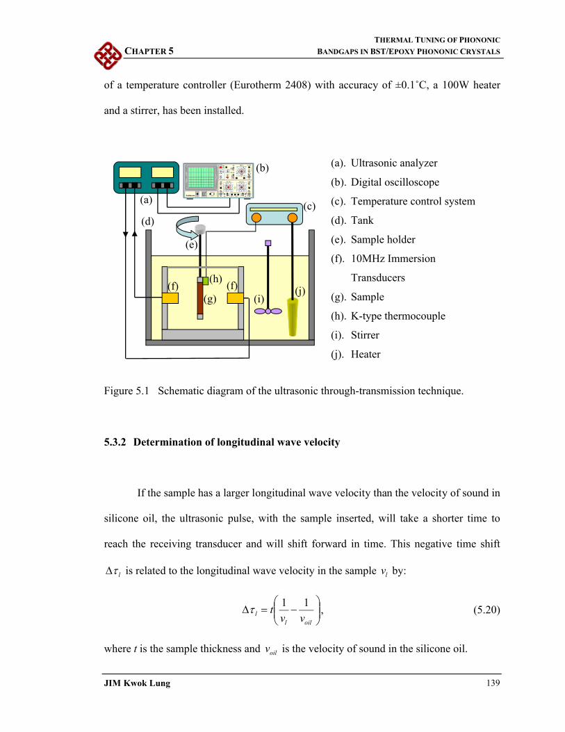
THERMAL TUNING OF PHONONIC
CHAPTER 5 BANDGAPS IN BST/EPOXY PHONONIC CRYSTALS
JIM Kwok Lung 139
of a temperature controller (Eurotherm 2408) with accuracy of ±0.1˚C, a 100W heater
and a stirrer, has been installed.
Figure 5.1 Schematic diagram of the ultrasonic through-transmission technique.
5.3.2 Determination of longitudinal wave velocity
If the sample has a larger longitudinal wave velocity than the velocity of sound in
silicone oil, the ultrasonic pulse, with the sample inserted, will take a shorter time to
reach the receiving transducer and will shift forward in time. This negative time shift
l is related to the longitudinal wave velocity in the sample lv by:
oilll vv
t11 , (5.20)
where t is the sample thickness and oilv is the velocity of sound in the silicone oil.
(a)
(b)
(c)(d)
(f)(h)
(e)
(i)(j)
(a). Ultrasonic analyzer
(b). Digital oscilloscope
(c). Temperature control system
(d). Tank
(e). Sample holder
(f). 10MHz Immersion
Transducers
(g). Sample
(h). K-type thermocouple
(i). Stirrer
(j). Heater
(g)(f)

THERMAL TUNING OF PHONONIC
CHAPTER 5 BANDGAPS IN BST/EPOXY PHONONIC CRYSTALS
JIM Kwok Lung 140
Starting with no sample placed in the path of the ultrasonic beam, the received
signal was displayed on the oscilloscope while the position of the first pulse peak was
noted. The sample was then inserted in the path, and the negative time shift l in the
first pulse peak was recorded. The longitudinal wave velocity in the sample Lv was
readily calculated using Eq. (5.20).
5.3.3 Determination of shear wave velocity
Both the shear and longitudinal waves are excited in the sample if the ultrasonic
beam impinges on the sample at an off-normal angle. The longitudinal and the shear
waves in the sample will be refracted since their velocities are different from the sound
wave velocity in the silicone oil. The angle of refraction )(, lsr corresponds to shear
(longitudinal) wave is given by the Snell’s law:
)()(,sin
sin
ls
oil
lsr
i
v
v
. (5.21)
where i is the angle of incidence, oilv is the velocity of sound in silicon oil, and )(lsv is
the shear (longitudinal) wave velocity in the sample. If the velocity of sound in the
silicone oil is less than the wave velocity in the sample, there exists a critical angle
beyond which a total internal reflection of the wave occurs. Since the longitudinal wave
velocity is always larger than the shear wave velocity in solid, the critical angle for
longitudinal wave is smaller than that of shear wave. This opens a window of angles
where only the shear wave can propagate through the sample while the longitudinal
wave is totally reflected.

THERMAL TUNING OF PHONONIC
CHAPTER 5 BANDGAPS IN BST/EPOXY PHONONIC CRYSTALS
JIM Kwok Lung 141
Starting with normal incidence of the ultrasonic beam on the sample as described
in the previous Section, the received signal due to the longitudinal wave will decrease in
amplitude when the sample is rotated off-normal and finally disappear when the incident
angle is beyond the critical angle for the longitudinal wave in the sample. The incident
angle of the ultrasonic beam is varied by rotating the sample through the sample holder.
Figure 5.2 Geometry of the propagation path of the ultrasonic wave.
Refer to Figure 5.2, the path length x through the sample is given by:
2
sin1
oil
si v
v
tx
. (5.22)
The difference in transit time s with and without the sample in place can be expressed
as:
oil
isr
ss vv
x
,cos1. (5.23)
Substituting Eq. (5.21) and Eq. (5.22) into Eq. (5.23), the shear wave velocity sv is
given by:
t
x
θr
θi

THERMAL TUNING OF PHONONIC
CHAPTER 5 BANDGAPS IN BST/EPOXY PHONONIC CRYSTALS
JIM Kwok Lung 142
oilsi
i
i
oils vt
tvv
cos
sinarctansin
sin. (5.24)
5.3.4 Temperature dependence of longitudinal and shear wave velocities in
Ba0.7Sr0.3TiO3 bulk sample
The longitudinal and shear wave velocities of a Ba0.7Sr0.3TiO3 bulk sample as a
function of temperature were measured using the ultrasonic through-transmission
technique. The sample used was a Ba0.7Sr0.3TiO3 ceramic disc with a diameter of 20 mm
and thickness of 2.38 mm. Since the velocity of sound in silicone oil is also a function of
temperature, such temperature dependence was measured first and was taken into
account when using Eq. (5.20) later. The velocity of sound in the silicone oil as a
function of temperature is shown in Figure 5.3. The Ba0.7Sr0.3TiO3 sample was then
inserted in between the transducers for the longitudinal wave velocity measurement. It
should be noted that in order to accurately measure the longitudinal wave velocity in the
sample, the incident ultrasonic beam should be normal to the sample face. This could be
confirmed by maximizing the amplitude of the received signal. Figure 5.4(a) shows the
longitudinal wave velocity of the Ba0.7Sr0.3TiO3 ceramic disc as a function of
temperature. It can be observed from Figure 5.4(a) that the Ba0.7Sr0.3TiO3 ceramic disc
has a relatively steady longitudinal velocity vl of ~5100 m/s below 35 ˚C which is the
Curie temperature of Ba0.7Sr0.3TiO3. When the temperature rises from 35 ˚C, vl increases
gradually until reaches a saturation of ~6300 m/s at 45 ˚C (see Table 5.1).

THERMAL TUNING OF PHONONIC
CHAPTER 5 BANDGAPS IN BST/EPOXY PHONONIC CRYSTALS
JIM Kwok Lung 143
In order to perform the shear wave velocity measurement, the angle of incidence
should be larger than the critical angle for the longitudinal wave. The critical angle for
the longitudinal wave lC , , which can be calculate by
l
oillC v
varcsin, , (5.25)
is 11.5˚ for vl = 5000 m/s. To ensure that all longitudinal waves were totally reflected,
the angle of incidence is set to be 15˚, which is larger than the critical angle corresponds
to vl = 4000 m/s. The shear wave velocity as a function of temperature is shown in
Figure 5.4(b). Similar to the trend of the longitudinal wave velocity shown in Figure
5.4(a), the shear wave velocity has a steady value of ~3000 m/s below the Curie
temperature (35 ˚C) and increases with temperature until saturates at ~4000 m/s at 45 ˚C
(see Table 5.1).
850
900
950
1000
1050
20 25 30 35 40 45 50 55
Temperature (˚C)
v oil (
m/s
)
Figure 5.3 Velocity of sound in silicone oil voil as a function of temperature.

THERMAL TUNING OF PHONONIC
CHAPTER 5 BANDGAPS IN BST/EPOXY PHONONIC CRYSTALS
JIM Kwok Lung 144
4000
4500
5000
5500
6000
6500
7000
20 25 30 35 40 45 50 55Temperature (˚C)
Vel
oci
ty (
m/s
)
(a)
2000
2500
3000
3500
4000
4500
20 25 30 35 40 45 50 55Temperature (˚C)
Vel
ocity
(m
/s)
(b)
Figure 5.4 (a) Longitudinal and (b) Shear wave velocities as a function of temperature
for a Ba0.7Sr0.3TiO3 ceramic disc. Dotted lines are added as visual aid.

THERMAL TUNING OF PHONONIC
CHAPTER 5 BANDGAPS IN BST/EPOXY PHONONIC CRYSTALS
JIM Kwok Lung 145
5.3.5 Temperature dependence of longitudinal and shear wave velocities in epoxy
sample
The longitudinal and shear wave velocities of the epoxy (Epotek 301) were
measured using the ultrasonic through-transmission technique as described in the
previous Section. The results are shown in Figure 5.5. It can be seen that the longitudinal
and the shear wave velocities of the epoxy decrease slightly as temperature increases
(see Table 5.1).
500
1000
1500
2000
2500
3000
3500
30 32 34 36 38 40 42 44 46 48 50 52
Temperature (˚C)
Vel
oci
ty (
m/s
)
Longitudinal waveShear wave
Figure 5.5 Longitudinal and shear wave velocities as a function of temperature for the
epoxy (Epotek 301).

THERMAL TUNING OF PHONONIC
CHAPTER 5 BANDGAPS IN BST/EPOXY PHONONIC CRYSTALS
JIM Kwok Lung 146
Table 5.1 Material parameters of Ba0.7Sr0.3TiO3 & epoxy (Epotek 301) used for the
phononic crystal bandstructure computation.
Ba0.7Sr0.3TiO3
= 6050 kgm-3
Epoxy (Epotek 301)
= 1130 kgm-3
Temperature vs (m/s) vl (m/s) vs (m/s) vl (m/s)
35 ˚C 3008 5233 1180 2580
45 ˚C 3892 (29.4%) 6317 (20.7%) 1150 (2.5%) 2530 (2.0%)
5.4 Barium strontium titanate/epoxy phononic crystals
5.4.1 Fabrication of the Ba0.7Sr0.3TiO3/epoxy phononic crystals
Ba0.7Sr0.3TiO3/epoxy phononic crystals were fabricated using the dice-and-fill
technique [Taunaumang, 1994]. The fabrication flow chart is shown in Figure 5.6. A
Ba0.7Sr0.3TiO3 ceramic disc with diameter of 20 mm and thickness of 2.38 mm was diced
using an automatic wafer dicing saw (Disco DAD 321) equipped with a diamond blade
(Disco NBC-Z 2050 55 x 0.06 x 40) of width 60 µm giving a groove width of 65 µm due
to blade vibration. The periodicity of subsequent cuttings was set to be 265 µm. After a
set of parallel cuttings, epoxy (Epotek 301 supplied by Epoxy Technology) was filled
into the grooves. The sample was, subsequently, degassed in a vacuum chamber for 30
min and then cured at 40 ˚C for 30 min. A second set of identical cutting was then
performed in a direction perpendicular to the first set of cutting. After filling epoxy into
the grooves again, the sample was degassed in a vacuum chamber for 30 min and cured

THERMAL TUNING OF PHONONIC
CHAPTER 5 BANDGAPS IN BST/EPOXY PHONONIC CRYSTALS
JIM Kwok Lung 147
at 40 ˚C for 12 hours. Grinding was performed on both sides of the sample to remove
excess Ba0.7Sr0.3TiO3 and epoxy.
Figure 5.6 Fabrication flow chart of Ba0.7Sr0.3TiO3/epoxy phononic crystals using a
dice-and-fill technique.
Dicing
Dicing after 90˚ rotation
Filling epoxy
Grinding
Filling epoxy
BST

THERMAL TUNING OF PHONONIC
CHAPTER 5 BANDGAPS IN BST/EPOXY PHONONIC CRYSTALS
JIM Kwok Lung 148
5.4.2 Reflection spectrum measurement by ultrasonic pulse-echo technique
The reflection spectrum of a phononic crystal can be obtained by the ultrasonic
pulse-echo technique. Compared to the through-transmission technique, ultrasonic pulse-
echo technique is more suitable for the characterization of phononic bandgaps in
phononic crystals for frequency in the MHz range where the attenuation loss is very high.
Consider a phononic crystal composed of lossless materials, ultrasonic beam with
frequencies outside the phononic bandgaps will transmit through it while beam with
frequencies inside the phononic bandgaps will be reflected entirely. Therefore, a peak in
the reflection spectrum, which implies a phononic bandgap, corresponds to a dip in the
transmission spectrum for an ideal phononic crystal. However, the composite materials
in real situation are not lossless, especially at high frequency. The ultrasonic beam will
suffer attenuation inside the phononic crystal. This diminishes the transmission signal
significantly which makes the detection much more difficult. Also, a dip in the
transmission spectrum can now be attributed to phononic bandgap reflection or/and
material absorption. This causes the interpretation of a transmission dip ambiguous.
Therefore the fabricated Ba0.7Sr0.3TiO3/epoxy phononic crystal was characterized by the
ultrasonic pulse-echo reflection technique.
The experimental setup for the ultrasonic pulse-echo technique is identical to the
one used for the through-transmission technique shown in Figure 5.1 except that only
one transducer is used for both transmitting and receiving purposes. Since the thickness
of our samples was about 1 mm only and the ultrasonic beam was intended to impinge

THERMAL TUNING OF PHONONIC
CHAPTER 5 BANDGAPS IN BST/EPOXY PHONONIC CRYSTALS
JIM Kwok Lung 149
the sample in the in-plane direction so that the beam can experience the periodicity of
the phononic crystal, a transducer with diameter of 1 mm was used in order to provide a
more confined ultrasonic beam. The center frequency of the transducer was 10 MHz. A
phononic crystal with 10 periods of Ba0.7Sr0.3TiO3/epoxy was placed in front of the
transducer at a distance of about 10 mm in water. Similar to the case in through-
transmission technique, an ultrasonic analyzer (Panametrics 5900PR) was employed to
generate a sharp pulse to provide a broadband excitation to the transducer. The ultrasonic
beam, reflected from the sample, was then picked up by the same transducer. The
received signal was amplified by the analyzer (voltage gain = 40 dB) before displaying
on a digitizing oscilloscope (HP Infinium). A Fast Fourier Transform was then
performed on the received signal (time response) to obtain the reflection spectrum
(frequency response). The measurement was repeated at different temperatures range
from 32 ˚C to 50 ˚C. The reflection spectra of the Ba0.7Sr0.3TiO3/epoxy phononic crystal
at different temperatures are shown in Figure 5.7. As can be seen from Figure 5.7(a), a
reflection peak is situated at ~9.5 MHz. Away from the reflection peak, two dips can be
observed at around 7.5 MHz and 12 MHz. The positions of the reflection peak and the
two dips remain nearly unchanged for the temperature from 32 ˚C to 35 ˚C. When the
temperature rises from 35 ˚C to 45 ˚C, it can been observed from Figure 5.7(b) that the
high frequency dip is moving from 12 MHz to 14 MHz gradually, while the low
frequency dip and the reflection peak remain approximately the same positions at 7.5
MHz and 9.5 MHz, respectively. When the temperature further increases from 45 ˚C to
50 ˚C, the reflection peak and the two dips are again remain almost unmoved as can be
noted in Figure 5.7(c).

THERMAL TUNING OF PHONONIC
CHAPTER 5 BANDGAPS IN BST/EPOXY PHONONIC CRYSTALS
JIM Kwok Lung 150
As mentioned previously in this Section, ultrasonic beam with frequencies inside
the phononic bandgaps would reflect totally if impinged on the phononic crystal.
Therefore, a peak in the reflection spectrum should be an indication of a phononic
bandgap. Moreover, the positions of the dips around the peak should be related to the
positions of the phononic bandgap edges, although they should not simply be considered
as the exact locations of the bandgap edges. The low frequency bandgap edge does not
shift while the high frequency bandgap edge shifts towards higher frequencies when the
temperature rises from 35 ˚C to 45 ˚C.
(a)
-60
-50
-40
-30
-20
-10
0
5 6 7 8 9 10 11 12 13 14 15 16 17 18 19
Frequency (MHz)
Inte
nsi
ty (
dB
m)

THERMAL TUNING OF PHONONIC
CHAPTER 5 BANDGAPS IN BST/EPOXY PHONONIC CRYSTALS
JIM Kwok Lung 151
(b)
(c)
Figure 5.7 Reflection spectra of the Ba0.7Sr0.3TiO3/epoxy phononic crystal at different
temperatures range from (a) 32 ˚C to 35 ˚C, (b) 35 ˚C to 45 ˚C, and (c) 45
˚C to 50 ˚C. The inset in (b) shows the reflection spectra of the
Ba0.7Sr0.3TiO3 ceramics at temperatures range from 32 ˚C to 50 ˚C.
-60
-50
-40
-30
-20
-10
0
5 6 7 8 9 10 11 12 13 14 15 16 17 18 19
Frequency (MHz)
Inte
nsi
ty (
dB
m)
35˚C
45˚C
Increasing temperature
-60
-50
-40
-30
-20
-10
0
5 6 7 8 9 10 11 12 13 14 15 16 17 18 19
Frequency (MHz)
Inte
ns
ity
(d
Bm
)-60
-50
-40
-30
-20
-10
0
5 6 7 8 9 10 11 12 13 14 15 16 17 18 19
Frequency (MHz)
Inte
ns
ity
(d
Bm
)

THERMAL TUNING OF PHONONIC
CHAPTER 5 BANDGAPS IN BST/EPOXY PHONONIC CRYSTALS
JIM Kwok Lung 152
5.4.3 Phononic bandstructure computation of the Ba0.7Sr0.3TiO3/epoxy phononic
crystals
In order to interpret the measured reflection spectra of the phononic crystal as
discussed in the previous Section, the phononic bandstructures of a Ba0.7Sr0.3TiO3/epoxy
phononic crystal were calculated using the home written computer programme. The
simulation model is illustrated in Figure 5.8. The phononic crystal was composed of
square Ba0.7Sr0.3TiO3 rods with widths of 200 µm arranged in a square lattice with a
period of 265 µm in a matrix of epoxy. The material parameters used for the simulation
are summarized in Table 5.1. As the experiment was performed with ultrasonic pulses
directed to the sample along the dicing direction through water, it is expected that mixed
mode waves, with wave vectors along the Γ-X direction, are predominately excited
along the Γ-X direction during measurement. Thus, the phononic bandstructures for
mixed mode along the Γ-X direction of the phononic crystal at 35 ˚C and 45 ˚C in the
frequency range of interest (0-18MHz) are calculated and the results are shown in Figure
5.9. As can be seen from Figure 5.9, the phononic crystal possesses many phononic
bandgaps. The lowest bandgap starts at 3 MHz for both temperature while the highest
bandgap positioned at ~12 MHz and ~16 MHz for T = 35 ˚C and 45 ˚C, respectively.
Since the longitudinal and transverse wave velocities in Ba0.7Sr0.3TiO3 change greatly
when the temperature rises from 35 ˚C to 45 ˚C, it is not surprised that the phononic
bandgaps have been modified accordingly. One interesting point to note is that if the
phononic bands in between the bandgaps are ignored for which all bandgaps are viewed
as combined to form one larger bandgap, the lower edge of the combined phononic

THERMAL TUNING OF PHONONIC
CHAPTER 5 BANDGAPS IN BST/EPOXY PHONONIC CRYSTALS
JIM Kwok Lung 153
bandgap does not shift at all while the upper edge of it shifts from 12 MHz to 16 MHz
when the temperature changes from 35 ˚C to 45 ˚C. This agrees very well with the
observations from the reflection spectra of the phononic crystal discussed in the previous
Section.
Figure 5.8 Simulation model of the Ba0.7Sr0.3TiO3/epoxy phononic crystal.
Configurationd
a
Ba0.7Sr0.3TiO3
Epoxy
d = 200 μm
a = 265 μm
f = (d/a)2 = 0.57

THERMAL TUNING OF PHONONIC
CHAPTER 5 BANDGAPS IN BST/EPOXY PHONONIC CRYSTALS
JIM Kwok Lung 154
0
2
4
6
8
10
12
14
16
18
0
Fre
quen
cy (
MH
z)
(a)
0
2
4
6
8
10
12
14
16
18
0
Fre
quen
cy (
MH
z)
(b)
Figure 5.9 Computed phononic bandstructures for mixed mode along the Γ-X
direction of the phononic crystal with configuration shown in Figure 5.8 at
(a) 35 ˚C, and (b) 45 ˚C. The shaded areas indicate the position of the
phononic bandgaps.
X
X

THERMAL TUNING OF PHONONIC
CHAPTER 5 BANDGAPS IN BST/EPOXY PHONONIC CRYSTALS
JIM Kwok Lung 155
5.5 Summary
The shear and transverse wave velocities of Ba0.7Sr0.3TiO3 ceramic as a function
of temperature were determined using the ultrasonic through-transmission technique. A
drastic variation in the wave velocities was observed across the Curie temperature of
Ba0.7Sr0.3TiO3.
Phononic crystals composed of Ba0.7Sr0.3TiO3 rods in a matrix of epoxy were
fabricated using the dice-and-fill method. The width of the Ba0.7Sr0.3TiO3 rods was 200
µm with periodicity of 265 µm. The temperature dependence of the phononic bandgaps
of the phononic crystal was characterized by the reflection spectra which were obtained
using the ultrasonic pulse-echo technique. Thermal tuning of the phononic bandgap was
observed and the results were in good agreement with the phononic bandstructure
calculation by the plane wave expansion method.
CHAPTER 6 CONCLUSIONS
JIM Kwok Lung 156
CHAPTER 6
CONCLUSIONS
6.1 Conclusions
The present research focused on the feasibility of developing electro-optically
tunable photonic crystals and thermally tunable phononic crystals based on the
ferroelectric materials Ba0.7Sr0.3TiO3.
The tunability of the photonic bandgap of a Ba0.7Sr0.3TiO3/MgO one-dimensional
(1D) photonic crystal (PC) arising from the electro-optic effect was investigated. The
relation between the shift of the photonic bandgap and the change of the refractive index
of Ba0.7Sr0.3TiO3 was examined using the plane wave expansion (PWE) method. It is
found that the gap-center shifts linearly with the change of the refractive index of
Ba0.7Sr0.3TiO3. One-dimensional PC consisting of five periods, with each period having a
90 nm thick Ba0.7Sr0.3TiO3 layer and a 10 nm thick MgO layer, was fabricated using
pulsed laser deposition. X-ray diffraction revealed that all the layers were epitaxially
grown on the MgO (001) single crystal substrate. A photonic bandgap at ~464 nm was
observed in the transmission spectrum, which agreed well with the theoretical
calculation by the transfer matrix method. A 2-nm shift towards the longer wavelength
was shown when a dc voltage of 240 V (corresponding to an electric field of about 12

CHAPTER 6 CONCLUSIONS
JIM Kwok Lung 157
MV/m) is applied across the coplanar electrodes on the film surface. This shift
corresponds to a 0.5% change in the refractive index of Ba0.7Sr0.3TiO3.
The photonic bandstructures and the photonic bandgap maps of the square lattice
type two-dimensional Ba0.7Sr0.3TiO3-based PC with circular air rods and square air rods.
The photonic bandstructures of the PC were computed using the PWE method. It was
found that there were two situations at which the photonic bandstructures and the
photonic bandgap maps of the circular air rod PCs and square air rod PCs would be
nearly identical: (1) if the characteristic length of the air rod is small (l < 0.45a), and (2)
if the frequency range is low enough (Ω<0.35). Furthermore, a better correlation in the
photonic bandstructures and the photonic bandgap maps between the circular and square
air rod 2D PC was obtained if the volume fraction correction, i.e. fc = fs wa = 0.89 x
(2ra), was considered. The photonic bandgap maps of two types of 2D Ba0.7Sr0.3TiO3-
based PC, namely, the air-hole-in-BST type and the BST-rod-in-air type both in square
lattice and in triangular lattice were studied. The result suggested that PCs in triangular
lattice contain richer bandgap feature in general. Bandgap features along different
symmetry directions have also been compared.
The refractive indices of the Ba0.7Sr0.3TiO3 thin film on a MgO (001) substrate
were measured using the prism coupling technique. The rib waveguide dimensions for
single mode TE wave propagation was determined by applying the effective index
method. A photonic crystal cavity embedded Ba0.7Sr0.3TiO3 rib waveguide which
functioned as a tunable filter (on-off switch) for λ = 1550 nm was designed using the
CHAPTER 6 CONCLUSIONS
JIM Kwok Lung 158
finite-difference time-domain (FDTD) simulation. The required PC cavity was
composed of two 5-row-4 PC mirrors, which was formed by air holes arranged in a
triangular lattice in the Ba0.7Sr0.3TiO3 matrix, with cavity length of 800 nm. The radius
of the air holes was 250 nm and the periodicity was 625 nm. A 6-nm shift in the resonant
peak for a 0.5% change in the refractive index of the Ba0.7Sr0.3TiO3 was demonstrated in
the simulation. Photonic crystal cavities were fabricated on a Ba0.7Sr0.3TiO3 rib
waveguide by focused ion beam etching with satisfactory results.
The shear and transverse wave velocities of Ba0.7Sr0.3TiO3 ceramics as a function
of temperature were measured using the ultrasonic through-transmission technique. A
drastic variation in the wave velocities was observed across the Curie temperature of
Ba0.7Sr0.3TiO3. Phononic crystal composed of Ba0.7Sr0.3TiO3 rods in a matrix of epoxy
was fabricated using the dice-and-fill method. The width of the Ba0.7Sr0.3TiO3 rods was
200 µm with a periodicity of 265 µm. The temperature dependence of the phononic
bandgaps of the phononic crystal was characterized by the reflection spectra which were
obtained using the ultrasonic pulse-echo technique. The reflection dip shifted from 12
MHz to 14 MHz when the temperature increased from 35 ˚C to 45 ˚C. Thermal tuning of
the phononic bandgap was observed and the results were in good agreement with the
phononic bandstructure calculation by the plane wave expansion method.

REFERENCES
JIM Kwok Lung 159
REFERENCES
Agrawal, G. P., Lightwave technology: components and devices, Wiley-Interscience,
John Wiley & Sons, Inc. (2004).
An American national standard & IEEE standard definitions of terms associated with
ferroelectrics and related materials, IEEE Transactions on Ultrasonic, Ferroelectrics,
and Frequency Control 50, 1-32 (2003).
Alagappan, G., Sun, X. W., Shum, P., Yu, M. B., and Doan, M. T., “One-dimensional
anisotropic photonic crystal with a tunable bandgap,” Journal of the Optical Society of
America B 23, 159-167 (2006).
Angelakis, D. G., Knight, P. L., and Paspalakis, E., “Photonic crystals and inhibition of
spontaneous emission: an introduction,” Contemporary Physics 45, 303-318 (2004).
Baba, T., Fukaya, N., and Yonekura, J., “Observation of light propagation in photonic
crystal optical waveguides with bends,” Electronics Letters 35, 654-655 (1999).
Baba, T., and Matsuzaki, T., “Fabrication and photoluminescence studies of
GaInAsP/InP 2-dimensional photonic crystals,” Japanese Journal of Applied Physics 35,
1348-1352 (1996).
Baumert, B. A., Chang, L. H., Matsuda, A. T., Tracy, C. J., Cave, N. G., Gregory, R. B.,
and Fejes, P. L., “A study of barium strontium titanate thin films for use in bypass
capacitors,” Joruanl of Matericals Research 13, 197-204 (1998).

REFERENCES
JIM Kwok Lung 160
Bertoldi, K., and Boyce, M. C., “Mechanically triggered transformations of phononic
band gaps in periodic elastomeric structures,” Physical Review B 77, 052105-4 (2008).
Bormashenko, E., Pogreb, R., Stanevsky, O., Bormashenko, Y., Socol, Y., and
Gendelman, O., “Self-assembled honeycomb polycarbonate films deposited on polymer
piezoelectric substrates and their applications,” Polymers for Advanced Technologies 16,
299-304 (2005).
Boudrioua, A., Loulergue, J. C., Dogheche, E., and Remiens, D., “Electro-optic
characterization of (Pb,La)TiO3 thin films using prism-coupling technique,” Journal of
Applied Physics 85, 1780-1783 (1999).
Cao, Y. J., Hou, Z. L., and Liu, Y. Y., “Finite difference time domain method for band-
structure calculations of two-dimensional phononic crystals,” Solid State
Communications 132, 539-543 (2004).
Cassagne, D., Jouanin, C., and Bertho, D., “Hexagonal photonic-band-gap structures,”
Physical Review B 53, 7134-7142 (1996).
Chang, W., Horwitz, J. S., Carter, A. C., Pond, J. M., Kirchoefer, S. W., Gilmore, C. M.,
and Chrisey, D. B., “The effect of annealing on the microwave properties of
Ba0.5Sr0.5TiO3 thin films,” Applied Physics Letters 74, 1033-1035 (1999).
Cheng, B. L., Gabbay, M., Fantozzi, G., and Duffy Jr., W. “Mechanical loss and elastic
modulus associated with phase transitions of barium titanate ceramics”. Journal of
Alloys and Compounds 211/212, 352-355 (1994).
Chow, E., Lin, S. Y., Johnson, S. G., Villeneuve, P. R., Joannopoulos, J. D., Wendt, J.
R., Vawter, G. A., Zubrzycki, W., Hou, H., and Alleman, A., “Three-dimensional
control of light in a two-dimensional photonic crystal slab,” Nature 407, 983-986 (2000).
REFERENCES
JIM Kwok Lung 161
Chutinan, A., Mochizuki, M., Imada, M., and Noda, S., “Surface-emitting channel drop
filters using single defects in two-dimensional photonic crystal slabs,” Applied Physics
Letters 79, 2690-2692 (2001).
Damjanovic, D., “Ferroelectric, dielectric and piezoelectric properties of ferroelectric
thin films and ceramics,” Reports on Progress in Physics 61, 1267-1324 (1998).
de Lustrac, A., Gadot, F., Cabaret, S., Lourtioz, J. M., Brillat, T., Priou, A., and
Akmansoy, E., “Experimental demonstration of electrically controllable photonic crystal
at centimeter wavelength,” Applied Physics Letters 75, 1625-1627 (1999).
de Toro, J. A., Serrano, M. D., Garcia Gabaňes, A., and Cabrera, J. M., “Accurate
interferometric measurement of electro-optic coefficients: application to quasi-
stoichiometric LiNbO3,” Optics Communications 154, 23-27 (1998).
Erchak, A. A., Ripin, D. J., Fan, S., Rakich, P., Joannopoulos, J. D., Ippen, E. P., Petrich,
G. S., and Kolodziejski, L. A., “Enhanced coupling to vertical radiation using a two-
dimensional photonic crystal in a semiconductor light-emitting diode,” Applied Physics
Letter 78, 563-565 (2001).
Evans, P. W., Wierer, J. J., and Holonyak, N., “Photopumped laser operation of an oxide
post GaAs-AlAs superlattice photonic lattice,” Applied Physics Letters 70, 1119-1121
(1997).
Fan, S., Villeneuve, P. R., Joannopoulos, J. D., Khan, M. J., Manolatou, C., and Haus, H.
A., “Theoretical analysis of channel drop tunneling processes,” Physical Review B 59,
15882-15892 (1999).
Feng, L, Liu, X. P., Lu, M. H., Chen, Y. B., Chen, Y. F., Mao, Y. W., Zi, J., Zhu, Y. Y.,
Zhu, S. N., and Ming, N. B., “Refraction control of acoustic waves in a square-rod-
constructed tunable sonic crystal,” Physical Review B 73, 193101-4 (2006).

REFERENCES
JIM Kwok Lung 162
Figotin, A., Godin, Y. A., and Vitebsky, I., “Two-dimensional tunable photonic
crystals,” Physical Review B 57, 2841-2848 (1998).
Frayssignes, H., Cheng, B. L., Fantozzi, G., and Button, T. W., “Phase transformation in
BST ceramics investigated by internal friction measurements,” Journal of the European
Ceramic Society 25, 3203-3206 (2005).
Freemantle, R. J., and Challis, R. E., “Combined compression and shear wave ultrasonic
measurements on curing adhesive”. Measurement Science & Technology 9, 1291-1302
(1998).
Gao, Y. H., Shen, H., Ma, J. H., Xue, J. Q., Sun, J. L., Meng, X. J., and Chu, J. H.,
“Surface chemical composition and optical properties of nitrogen-doped Ba0.6Sr0.4TiO3
thin films,” Journal of Applied Physics 102, 064106-7 (2007).
Griffiths, D. J., Introduction to electrodynamics (2nd edition), Prentice-Hall, Englewood
Cliffs, NJ (1989).
Ha, Y. K., Yang, Y. C., Kim, J. E., Park, H. Y., Kee, C. S., Lim, H., and Lee, J. C.,
“Tunable omnidirectional reflection bands and defect modes of a one-dimensional
photonic band gap structure with liquid crystals,” Applied Physics Letters 79, 15-17
(2001).
Haertling, G. H., and Land, C. E., “Hot-pressed (Pb, La)(Zr, Ti)O3 ferroelectric ceramics
for electrooptic applications,” Journal of the American Ceramic Society 54, 1-11 (1971).
Halevi, P., Krokhin, A. A., and Arriaga, J., “Photonic crystal optics and homogenization
of 2D periodic composites,” Physical Review Letters 82, 719-722 (1999).

REFERENCES
JIM Kwok Lung 163
Halevi, P., and Mendieta, F. R., “Tunable photonic crystal with semiconductor
constituents,” Physical Review Letters 85, 1875-1878 (2000).
Hirayama, H., Hamano, T., and Aoyagi, Y., “Novel surface emitting laser diode using
photonic band-gap crystal cavity,” Applied Physics Letters 69, 791-793 (1996).
Ho, K. M., Chan, C. T., and Soukoulis, C. M., “Existence of a photonic gap in periodic
dielectric structures,” Physics Review Letters 65, 3152-3155 (1990).
Hong, X. K., Hu, G. J., Chen, J., Chu, J. H., Dai, N., and Wu, H. Z., “Ba0.9Sr0.1TiO3-
based Bragg reflectors fabricated from one single chemical solution,” Applied Physics
Letters 89, 082902-3 (2006).
Hu, G. J., Chen, G. J., An, D. L., Chu, J. H., and Dai, N., “Fabrication of ferroelectric
PbZr0.4Ti0.6O3 multilayers by sol-gel process,” Applied Physics Letters 86, 162905-3
(2005).
Hu, X., Jiang, P., Ding, C., and Gong, Q., “All-optical tunable narrow-band organic
photonic crystal filters,” Applied Physics B 87, 255-258 (2007).
Huang, Z. G., and Wu, T. T., “Temperature effect on the bandgaps of surface and bulk
acoustic waves in two-dimensional phononic crystals,” IEEE Transactions on
Ultrasonics Ferroelectrics and Frequency Control 52, 365-370 (2005).
Huibregtse, E. J., Bessey, W. H., and Drougard, M. E., “Electromechanical behavior of
single crystals of barium titanate from 25 to 160˚C,” Journal of Applied Physics 30, 899-
905 (1959).
Hunsperger, R. G., Integrated optics: theory and technology, Springer-Verlag, Berlin
(2002).

REFERENCES
JIM Kwok Lung 164
Hwang, J. K., Ryu, H. Y., Song, D. S., Han, I. Y., Song, H. W., Park, H. K., and Lee, Y.
H., “Room temperature triangular-lattice two-dimensional photonic band gap lasers
operating at 1.54μm,” Applied Physics Letters 76, 2982-2984 (2000).
Imada, M., Noda, S., Chutinan, A., Tokuda, T., Murata, M., and Sasaki, G., “Coherent
two-dimensional lasing action in surface-emitting laser with triangular-lattice photonic
crystal structure,” Applied Physics Letters 75, 316-318 (1999).
Jia, W., Li, Y., Xi, Y., Jiang, P., Xu, X., Liu, X., Fu, R., Zi, J., “Tunability of photonic
crystals based on the Faraday effect,” Journal of Physics: Condensed Matter 15, 6731-
6737 (2003).
Joannopoulos, J. D., Meade, R. D., and Winn, J. N., Photonic crystals: molding the flow
of light, Princeton, Princeton University Press, NJ (1995).
Joannopoulos, J. D., Villenuve, P. R., and Fan, S., “Photonic crystals: putting a new
twist on light,” Nature 386, 143-149 (1997).
John, S., “Strong localization of photons in certain disordered dielectric superlattices,”
Physical Review Letters 58, 2486-2489 (1987).
John, S., and Wang, J., “Quantum electrodynamics near a photonic band gap: Photon
bound states and dressed atoms,” Physical Review Letters 64, 2418-2421 (1990).
Jugessur, A. S., Pottier, P., and De La Rue, R. M., “Engineering the filter response of
photonic crystal microcavity filters,” Optics Express 12, 1304-1312 (2004).
Kafesaki, M., and Economou, E. N., “Multiple-scattering theory for three-dimensional
periodic acoustic composites,” Physical Review B 60, 11993-12001 (1999).

REFERENCES
JIM Kwok Lung 165
Kang, D., Maclennan, J. E., Clark, N. A., Zakhidov, A. A., and Baughman, R. H.,
“Electro-optic behavior of liquid-crystal-filled silica optical photonic crystals: effect of
liquid crystal alignment,” Physical Review Letters 86, 4052-4055 (2001).
Kasap, S. O., Optoelectronic devices and photonics: principles and practices, Prentice-
Hall Inc., NJ (2001).
Kee, C. S., Lim, H., Ha, Y. K., Kim, J. E., and Park, H. Y., “Two-dimensional tunable
metallic photonic crystals infiltrated with liquid crystals,” Physical Review B 64,
085114-7 (2001).
Khelif, A., Deymier, P. A., Djafari-Rouhani, B., Vasseur, J. O., and Dobrzynski, L.,
“Two-dimensional phononic crystal with tunable narrow pass band: Application to a
waveguide with selective frequency,” Journal of Applied Physics 94, 1308-1311 (2003).
Kim, D. Y., Moon, S. E., Kim, E. K., Lee, S. J., Choi, J. J., Kim, H. E., and Kwun, S. I.,
“High electro-optic coefficient of Ba0.6Sr0.4TiO3 /MgO(001) dielectric thin film,” Journal
of the Korean Physical Society 42, S1347-S1349 (2003).
Kim, S., and Gopalan, V., “Strain-tunable photonic band gap crystals,” Applied Physics
Letters 78, 3015-3017 (2001).
Knox, R. M., and Toulios, P. P., “Integrated circuits for the millimeter through optical
frequency range,” Proceedings of the Microwave Research Institute of the Symposium on
Submillimeter Waves, 497-516 (1970).
Kosaka, H., Kawashima, T., Tomita, A., Notomi, M., Tamamura, T., Sato, T., and
Kawakami, S., “Superprism phenomena in photonic crystals,” Physical Review B 58,
R10096-R10099 (1998).
REFERENCES
JIM Kwok Lung 166
Kosaka, H., Kawashima, T., Tomita, A., Notomi, M., Tamamura, T., Sato, T., and
Kawakami, S., “Self-collimating phenomena in photonic crystals,” Applied Physics
Letters 74, 1212-1214 (1999a)
Kosaka, H., Kawashima, T., Tomita, A., Notomi, M., Tamamura, T., Sato, T., and
Kawakami, S., “Photonic crystals for micro lightwave circuits using wavelength-
dependent angular beam steeling,” Applied Physics Letters 74, 1370-1372 (1999b).
Kurizki, G., and Genack, A. Z., “Suppression of molecular interactions in periodic
dielectric structures,” Physical Review Letters 61, 2269-2271 (1988).
Kushwaha, M. S., Halevi, P., Martínez, G., Dobrzynski, L., and Djafari-Rouhani, B.
“Theory of acoustic band structure of periodic elastic composites”. Physical Review B 49,
2313-2321 (1994).
Landolt, H., Ferroelectrics and related substances. Landolt-Börstein, New Series, Group
III, Vol. 36, Springer-Verlag, Berlin (2002).
Leonard, S. W., Mondia, J. P., van Driel, H. M., Toader, O., John, S., Busch, K., Birner,
A., Gosele, U., and Lehmann, V., “Tunable two-dimensional photonic crystal using
liquid-crystal infiltration,” Physical Review B 61, R2389-R2932 (2000).
Li, B., Zhou, J., Li, L., Wang, X. J., Liu, X. H., and Zi, J., “Ferroelectric inverse opals
with electrically tunable photonic band gap,” Applied Physics Letters 83, 4704-4706
(2003).
Li, J., Duewer, F., Gao, C., Chang, H., Xiang, X. D., and Lu, Y., “Electro-optic
measurements of the ferroelectric-paraelectric boundary in Ba1-xSrxTiO3 materials
chips,” Applied Physics Letters 76, 769-771 (2000).

REFERENCES
JIM Kwok Lung 167
Li, J. J., Li, Z. Y., and Zhang, D. Z., “Second harmonic generation in one-dimensional
nonlinear photonic crystals solved by the transfer matrix method,” Physical Review E 75,
056606-7 (2007).
Liguda, C., Bottger, G., Kuligk, A., Blum, R., Eich, M., Roth, H., Kunert, J.,
Morgenroth, W., Elsner, H., and Meyer, H. G., “Polymer photonic crystal slab
waveguides,” Applied Physics Letters 78, 2434-2436 (2001).
Limberger, H. G., Hong Ky, N., Costantini, D. M., Salathé, R. P., Muller, C. A. P., and
Fox, G. R., “Efficient miniature fiber-optic tunable filter based on intracore Bragg
grating and electrically resistive coating,” IEEE Photonics Technology Letters 10, 361-
363 (1998).
Lin, S. Y, Chow, E., Hietala, V., Villeneuve, P. R., and Joannopoulos, J.
D., “Experimental demonstration of guiding and bending of electromagnetic waves in a
photonic crystal,” Science 282, 274-276 (1998).
Liu, C. Y., and Chen, L. W., “Tunable band gap in a photonic crystal modulated by a
nematic liquid crystal,” Physical Review B 72, 045133-5 (2005).
Liu, Z., Zhang, X., Mao, Y., Zhu, Y. Y., Yang, Z., Chan, C. T., and Sheng, P., “Locally
resonant sonic materials,” Science 289, 1734-1736 (2000).
Lončar, M., Doll, T., Vučković, J., and Scherer, A., “Design and fabrication of silicon
photonic crystal optical waveguides,” Jouranl of Lightwave Technology 18, 1402-1411
(2000).
McGurn, A. R., “Photonic crystal circuits: a theory for two- and three-dimensional
networks,” Physical Review B 61, 13235-13249 (2000).

REFERENCES
JIM Kwok Lung 168
McGurn, A. R., “Photonic crystal circuits: localized modes and waveguide couplers,”
Physical Review B 65, 075406-11 (2002).
McQuarrie, M., “Structure behavior in the system (Ba, Ca, Sr) TiO3 and its relation to
certain dielectric characteristics,” Journal of the American Ceramic Society 38, 444-449
(1955).
Meade, R. D., Brommer, K. D., Rappe, A. M., and Joannopoulos, J. D., “Existence of a
photonic band gap in two dimensions,” Applied Physics Letters 61, 495-497 (1992).
Mekis, A., Chen, J. C., Kurland, I., Fan, S., Villeneuve, P. R., and Joannopoulos, J. D.,
“High transmission through sharp bends in photonic crystal waveguides,” Physical
Review Letters 77, 3787-3790 (1996).
Moreno-Gobbi, A., Garcia, D., Eiras, J. A.,, and Bhalla, A. S., “Study by ultrasonic
techniques of the phase diagram of BST ceramic family mainly for high Sr
concentrations,” Ferroelectrics 337, 197-206 (2006).
Noda, S., Chutinan, A., and Imada, M., “Trapping and emission of photons by a single
defect in a photonic bandgap structure,” Nature 407, 608-610 (2000).
Noda, S., Yamamoto, N., Imada, M., Kobayashi, H., and Okano, M., “Alignment and
stacking of semiconductor photonic bandgaps by wafer-fusion,” Journal of Lightwave
Technology 17, 1948-1955 (1999).
Notomi, M., “Theory of light propagation in strongly modulated photonic crystals:
refraction-like behavior in the vicinity of the photonic band gap,” Physical Review B 62,
10696-10705 (2000).

REFERENCES
JIM Kwok Lung 169
Notomi, M., Suzuki, H., and Tamamura, T., “Directional lasing oscillation of two-
dimensional organic photonic crystal lasers at several photonic band gaps,” Applied
Physics Letters 78, 1325-1327 (2001a).
Notomi, M., Yamada, K., Shinya, A., Takahashi, J., Takahashi, C., and Yokohama, I.,
“Singlemode transmission within photonic bandgap of width-varied single-line-defect
photonic crystal waveguides on SOI substrates,” Electronics Letters 37, 293-295
(2001b).
Ochiai, T., and Sanchez-Dehesa, J., “Superprism effect in opal-based photonic crystals,”
Physical Review B 64, 245113-7 (2001).
Ohtera, Y., Sato, T., Kawashima, T., Tamamura, T., and Kawakami, S., “Photonic
crystal polarization splitters,” Electronics Letters 35, 1271-1272 (1999).
Okamura, S., Mochiduki, Y., Motohara, H., and Shiosaki, T., “Fabrication of
ferroelectric photonic crystals,” Integrated Ferroelectrics 69, 303-313 (2005).
Page, J. H., Sukhovich, A., Yang, S., Cowan, M. L., Van Der Biest, F., Tourin, A., Fink,
M., Liu, Z., Chan, C. T., and Sheng, P., “Phononic crystals,” Physica Status Solidi (b)
241, 3454-3462 (2004).
Painter, O. J., Husain, A., Scherer, A., O’Brien, J. D., Kim, I., and Dapkus, P. D., “Room
temperature photonic crystal defect lasers at near-infrared wavelength in InGaAsP,”
Journal of Lightwave Technology 17, 2082-2088 (1999).
Panda, B., Dhar, A., Nigam, G. D., Bhattacharya, D., and Ray, S. K., “Optical properties
of RF sputtered strontium substituted barium titanate thin films,” Thin Solid Flims 332,
46-49 (1998).

REFERENCES
JIM Kwok Lung 170
Pennec, Y., Djafari-Rouhani, B., Vasseur, J. O., Khelif, A., and Deymier, P. A.,
“Tunable filtering and demultiplexing in phononic crystals with hollow cylinders,”
Physical Review E 69, 046608-6 (2004).
Plihal, M., and Maradudin, A. A., “Photonic band structure of two-dimensional systems:
The triangular lattice,” Physical Review B 44, 8565-8571 (1991).
Pustai, D. M., Sharkawy, A., Shi, S., and Prather, D. W., “Tunable photonic crystal
microcavities,” Applied Optics 41, 5574-5579 (2002).
Qiu, M., and Jaskorzynska, B., “Design of a channel drop filter in a two-dimensional
triangular photonic crystal,” Applied Physics Letters 83, 1074-1076 (2003).
Roussey, M., Bernal, M. P., Courjal, N., and Baida, F. I., “Experimental and theoretical
characterization of a lithium niobate photonic crystal,” Applied Physics Letters 87,
241101-3 (2005).
Roussey, M., Bernal, M. P., Courjal, N., Van Labeke, D., Baida, F. I., and Salut, R.,
“Electro-optic effect exaltation on lithium niobate photonic crystals due to slow
photons,” Applied Physics Letters 89, 241110-3 (2006).
Ren, C., Tian, J., Feng, S., Tao, H., Liu, Y., Ren, K., Li, Z., Cheng, B., Zhang, D., and
Yang, H., “High resolution three-port filter in two dimensional photonic crystal slabs,”
Optics Express 14, 10014-10020 (2006).
Saleh, B. E. A., and Teich, M. C., Fundamentals of photonics, New York: Wiley (1991).
Schmidt, M., Eich, M., Huebner, U., and Boucher, R., “Electro-optically tunable
photonic crystals,” Applied Physics Letters 87, 121110-3 (2005).

REFERENCES
JIM Kwok Lung 171
Schneider, S., Mono, T., Albrethsen-Keck, B., Melaku, Y., and Waser, R., “Dry-etching
of barium-strontium-titanate thin films,” Proceedings of the 11th IEEE International
Symposium on Applications of Ferroelectrics 1, 51-54 (1998).
Schuller, Ch., Klopf, F., Reithmaier, J. P., Kamp, M., and Forchel, A., “Tunable
photonic crystal crystals fabricated in III-V semiconductor slab waveguides using
infiltrated liquid crystals,” Applied Physics Letters 82, 2767-2769 (2003).
Scrymgeour, D., Malkova, N., Kim, S., and Gopalan, V., “Electro-optic control of the
superprism effect in photonic crystals,” Applied Physics Letters 82, 3176-3178 (2003).
Smolenskii, G. A., and Rozgachev, K. I., “Ferroelectric properties of solid solution in the
system BaTiO3-SrTiO3,” Zh. Tekh. Fiz. 24, 1751 (1954) (in Russian).
Stenzel, O., The physics of thin film optical spectra: an introduction, Springer-Verlag
Berlin Heidelberg (2005).
Syms, R., and Cozens, J., Optical guided waves and devices, McGraw-Hill book
company Europe, UK (1992).
Takeda, H., and Yoshino, K., “Tunable photonic band gaps in two-dimensional photonic
crystals by temporal modulation based on the Pockels effect,” Physical Review E 69,
016605-5 (2004).
Taunaumang, H., Guy, I. L., and Chan, H. L. W., “Electromechanical properties of 1-3
piezoelectric ceramic/piezoelectric polymer composites,” Journal of Applied Physics 76,
484-489 (1994).
Tavlove, A., Computational electrodynamics: the finite-difference time-domain method,
Artech House, Norwwod, MA (1995).
REFERENCES
JIM Kwok Lung 172
Taylor, H. F., “Enhanced electrooptic modulation efficiency utilizing slow-wave optical
propagation,” Journal of Lightwave Technology 17, 1875-1883 (1999).
Tcheliebou, F., Ryu, H. S., Hong, C. K., Park, W. S., and Baik, S., “On the
microstructure and optical properties of Ba0.5Sr0.5TiO3 films,” Thin Solid Flims 305, 30-
34 (1997).
Tien, P. K., Ulrich, R., and Martin, R. J., “Modes of propagating light waves in thin
deposited semiconductor,” Applied Physics Letters 14, 291-294 (1969).
Torres, M., Montero de Espinosa, F. R., and Aragón, “Ultrasonic wedges for elastic
wave bending and splitting without requiring a full band gap,” Physical Review Letters
86, 4282-4285 (2001).
Tran, P., “Optical switching with a nonlinear photonic crystal: a numerical study,”
Optics Letters 21, 1138-1140 (1996).
Tseng, T. Y., “(Ba, Sr)TiO3 thin films: preparation, properties and reliability,”
Ferroelectrics 232, 1-13 (1999).
Turner, E. H., “High-frequency electro-optic coefficients of lithium niobate,” Applied
Physics Letters 8, 303-304 (1966).
Ulrich, R., and Torge, R., “Measurement of thin film parameters with a prism coupler,”
Applied Optics 12, 2901-2908 (1973).
Urbas, A., Sharp, R., Fink, Y., Thomas, E. L., Xenidou, M., and Fetters, L. J., “Tunable
block copolymer/homopolymer photonic crystals,” Advanced Materials 12, 812-814
(2000).

REFERENCES
JIM Kwok Lung 173
Vasseur, J. O., Deymier, P. A., Chenni, B., Djafari-Rouhani, B., Dobrzynski, L., and
Prevost, D., “Experimental and theoretical evidence for the existence of absolute
acoustic band gaps in two-dimensional solid phononic crystals,” Physical Review Letters
86, 3012-3015 (2001).
Villar, I. D., Matías, I. R., and Arregui, F. J., “Analysis of one-dimensional photonic
band gap structures with a liquid crystal defect towards development of fiber-optic
tunable wavelength filters,” Optics Express 11, 430-436 (2003).
Villeneuve, P. R., Abrams, D. S., Fan, S., and Joannopoulos, J. D., “Single-mode
waveguide microcavity for fast optical switching,” Optics Letters 21, 2017-2019 (1996).
Villeneuve, P. R., and Piché, M., “Photonic band gaps in two-dimensional square and
hexagonal lattices,” Physical Review B 46, 4969-4972 (1992).
Wang, D. Y., Barium strontium titanate thin Films for electro-optic applications, PhD
Thesis, The Hong Kong Polytechnic University (2006a).
Wang, D. Y., Chan, H. L. W., and Choy, C. L., “Fabrication and characterization of
epitaxial Ba0.5Sr0.5TiO3 thin films for optical waveguide applications,” Applied Optics 45,
1972-1978 (2006b).
Wang, D. Y., Mak, C. L., Wong, K. H., Chan, H. L. W., and Choy, C. L., “Optical
properties of Ba0.5Sr0.5TiO3 thin films grown on MgO substrates by pulsed laser
deposition,” Ceramics International 30, 1745-1748 (2004).
Wang. D. Y., Wang, J., Chan, H. L. W., Choy, C. L., “Structural and electro-optic
Ba0.7Sr0.3TiO3 thin films grown on various substrates using pulsed laser deposition,”
Journal of Applied Physics 101, 043515-6 (2007).

REFERENCES
JIM Kwok Lung 174
Wang, D. Y., Wang, Y., Zhou, X. Y., Chan, H. L. W., and Choy, C. L., “Enhanced in-
plane ferroelectricity in Ba0.7Sr0.3TiO3 thin films grown on MgO (001) single-crystal
substrate,” Applied Physics Letters 86, 212904-3 (2005).
Wang, R., Wang, X. H., Gu, B. Y., and Yang, G. Z., “Effects of shapes and orientations
of scatters and lattice symmetries on the photonic band gap in two-dimensional photonic
crystals,” Journal of Applied Physics 90, 4307-4313 (2001).
Wang, Z. Y., Chen, X. M., He, X. Q., Fan, S. L., and Yan, W. Z., “Photonic crystal
narrow filters with negative refractive index structural defects,” Progress In
Electromagnetics Research, PIER 80, 421-430 (2008).
Wu, A. Y., Nicolaides, G., and Hwang, D. M., “The temperature dependence of sound
velocities, elastic constants and acoustic attenuation of lead lanthanum zirconate titanate
(Pb,La)(Zr,Ti)O3,” Application of Ferroelectrics, 1992. ISAF ’92., Proceedings of the
Eighth IEEE International Symposium on 92, 392-394 (1992).
Wu, L. Y., Wu, M. L., and Chen, L. W., “The narrow pass band filter of tunable 1D
phononic crystals with a dielectric elastomer layer,” Smart Materials and Structures 18,
015011-8 (2009).
Xiong, S., and Fukshima, H., “Analysis of light propagation in index-tunable photonic
crystals,” Journal of Applied Physics 94, 1286-1288 (2003).
Xu, C., Hu, X., Li, Y., Liu, X., Fu, R., and Zi, J., “Semiconductor-based tunable
photonic crystals by means of an external magnetic field,” Physical Review B 68,
193201-4 (2003).
Yablonovitch, E., “Inhibited spontaneous emission in solid-state physics and
electronics,” Physical Review Letters 58, 2059-2062 (1987).

REFERENCES
JIM Kwok Lung 175
Yablonovitch, E., Gmitter, T. J., Meade, R. D., Rappe, A. M., Brommer, K. D., and
Joannopoulos, J. D., “Donor and acceptor modes in photonic band structure,” Physical
Review Letters 67, 3380-3383 (1991).
Yamada, S. Koyama, T., Katayama, Y., Ikeda, N., Sugimoto, Y., Asakawa, K., Kawai,
N., and Inoue, K., “Observation of light propagation in two-dimensional photonic
crystal-based bent optical waveguides,” Journal of Applied Physics 89, 855-858 (2001).
Yariv, A., and Yeh, P., “Optical wave in crystals,” Optical Electronics. New York:
Wiley (1984).
Yonekura, J., Ikeda, M., and Baba, T., “Analysis of finite 2-D photonic crystals of
columns and lightwave devices using the scattering matrix method,” Journal of
Lightwave Technology 17, 1500-1508 (1999).
Yee, K. S., “Numerical solutions of initial boundary value problems involving
Maxwell’s equations in isotropic media,” IEEE Transactions on Antennas and
Propagation AP-14, 302-307 (1966).
Yoshie, T., Vuckovic, J., Scherer, A., Chen, H., and Deppe, D., “High quality two-
dimensional photonic crystal slab cavities,” Applied Physics Letters 79, 4289-4291
(2001).
Yoshino, K., Kawagishi, Y., Ozaki, M., and Kose, A., “Mechanical tuning of the optical
properties of plastic opal as a photonic crystal,” Japanese Journal of Applied Physics 38,
L786-L788 (1999).
Zhang, L., Zhong, W. L., Wang, C. L., Zhang, P. L. and, Wang, Y. G., “Dielectric
properties of Ba0.7Sr0.3TiO3 ceramics with different grain size,” Physica Status Solidi (a)
168, 543-548 (1998).