Isolation and Gain Improvement of a Rectangular Notch UWB ...
14
Citation: Abbas, A.; Hussain, N.; Sufian, M.A.; Jung, J.; Park, S.M.; Kim, N. Isolation and Gain Improvement of a Rectangular Notch UWB-MIMO Antenna. Sensors 2022, 22, 1460. https://doi.org/10.3390/ s22041460 Academic Editor: Filippo Costa Received: 17 January 2022 Accepted: 10 February 2022 Published: 14 February 2022 Publisher’s Note: MDPI stays neutral with regard to jurisdictional claims in published maps and institutional affil- iations. Copyright: © 2022 by the authors. Licensee MDPI, Basel, Switzerland. This article is an open access article distributed under the terms and conditions of the Creative Commons Attribution (CC BY) license (https:// creativecommons.org/licenses/by/ 4.0/). sensors Communication Isolation and Gain Improvement of a Rectangular Notch UWB-MIMO Antenna Anees Abbas , Niamat Hussain , Md. Abu Sufian, Jinkyu Jung, Sang Myeong Park and Nam Kim * Department of Information and Communication Engineering, Chungbuk National University, Cheongju 28644, Korea; [email protected] (A.A.); [email protected] (N.H.); sufi[email protected] (M.A.S.); [email protected] (J.J.); [email protected] (S.M.P.) * Correspondence: [email protected] Abstract: This paper presents the performance improvement of a co-planar waveguide rectangularly notched UWB-MIMO antenna. The isolation and gain of the antenna are enhanced by using a parasitic isolator. The antenna consists of four microstrip patch antennas and an isolator. The UWB characteristic of the antenna is achieved by truncating the lower ends of the radiating patch by a semicircle. The rectangular notch characteristic is obtained by adding two electromagnetic bandgap structures on the backside of the antenna, which is attached to the radiator via shorting pin. The performance, especially the decoupling of the MIMO antenna is improved by using a novel parasitic decoupler, which is placed between the antennas to receive uncorrelated signals. The decoupling structure consists of a square shape metallic element with a circular slot inside and a half-semicircle slot edged at each corner. Four rectangular metallic stubs are extended from opposite parallel sides to improve further isolation. The simulated and measured results show that the antenna has a rectangular notch band (5.25–5.85 GHz) across the working band of 3–12.8 GHz. In addition, the antenna has a planar structure with an overall size of 60 × 60 × 1.52 mm 3 and offers stable gain, reduced mutual coupling (<-21 dB), and lower envelop correlation (<0.001). Keywords: rectangular notch; UWB antenna; UWB-MIMO antenna; decoupling structure; mutual coupling 1. Introduction In radio communication, an antenna is an interface between radio waves propagating through space and electric currents moving in metal conductors, used as transmitters or receivers. Because of the simple geometry and low fabrication cost, microstrip technology is a mature and known technology in manufacturing and electromagnetic devices. Hence, it is widely used in designing various microwave and electromagnetic devices such as filters, power dividers, and artificial magnetic surfaces [1–3]. Since the Federal Communication Commission (FCC) has set 3.1–10.6 GHz as ultra- wideband technology, this has attracted the interest of researchers by offering features like short-range, high bandwidth, low energy usage, low complexity, and high data rate communications [4]. The applications of UWB include short-range communications, sensor networks, tracking, and positioning systems [5,6]. In the multi-path environment, signal fading degrades the performance of UWB systems, which affects the efficiency and quality of signal transmission. To address this problem, Multi-Input-Multi-Output (MIMO) tech- nology has been used to provide a multi-element patch antenna for signal transmission or reception. It can significantly increase spectral efficiency, reliability, and channel capacity without utilizing extra power and spectrum. Hence it is widely used in the design of antennas in different networks to enhance the performance of communication systems. However, the usage of more than one radiating element, closely arranged to one another in MIMO degrades the performance of the system. Therefore, the design of a MIMO system with better isolation is required in modern communications. The UWB-MIMO design with Sensors 2022, 22, 1460. https://doi.org/10.3390/s22041460 https://www.mdpi.com/journal/sensors
-
Upload
khangminh22 -
Category
Documents
-
view
2 -
download
0
Transcript of Isolation and Gain Improvement of a Rectangular Notch UWB ...

Citation: Abbas, A.; Hussain, N.;
Sufian, M.A.; Jung, J.; Park, S.M.;
Kim, N. Isolation and Gain
Improvement of a Rectangular Notch
UWB-MIMO Antenna. Sensors 2022,
22, 1460. https://doi.org/10.3390/
s22041460
Academic Editor: Filippo Costa
Received: 17 January 2022
Accepted: 10 February 2022
Published: 14 February 2022
Publisher’s Note: MDPI stays neutral
with regard to jurisdictional claims in
published maps and institutional affil-
iations.
Copyright: © 2022 by the authors.
Licensee MDPI, Basel, Switzerland.
This article is an open access article
distributed under the terms and
conditions of the Creative Commons
Attribution (CC BY) license (https://
creativecommons.org/licenses/by/
4.0/).
sensors
Communication
Isolation and Gain Improvement of a Rectangular NotchUWB-MIMO AntennaAnees Abbas , Niamat Hussain , Md. Abu Sufian, Jinkyu Jung, Sang Myeong Park and Nam Kim *
Department of Information and Communication Engineering, Chungbuk National University,Cheongju 28644, Korea; [email protected] (A.A.); [email protected] (N.H.);[email protected] (M.A.S.); [email protected] (J.J.); [email protected] (S.M.P.)* Correspondence: [email protected]
Abstract: This paper presents the performance improvement of a co-planar waveguide rectangularlynotched UWB-MIMO antenna. The isolation and gain of the antenna are enhanced by using aparasitic isolator. The antenna consists of four microstrip patch antennas and an isolator. The UWBcharacteristic of the antenna is achieved by truncating the lower ends of the radiating patch by asemicircle. The rectangular notch characteristic is obtained by adding two electromagnetic bandgapstructures on the backside of the antenna, which is attached to the radiator via shorting pin. Theperformance, especially the decoupling of the MIMO antenna is improved by using a novel parasiticdecoupler, which is placed between the antennas to receive uncorrelated signals. The decouplingstructure consists of a square shape metallic element with a circular slot inside and a half-semicircleslot edged at each corner. Four rectangular metallic stubs are extended from opposite parallel sidesto improve further isolation. The simulated and measured results show that the antenna has arectangular notch band (5.25–5.85 GHz) across the working band of 3–12.8 GHz. In addition, theantenna has a planar structure with an overall size of 60 × 60 × 1.52 mm3 and offers stable gain,reduced mutual coupling (<−21 dB), and lower envelop correlation (<0.001).
Keywords: rectangular notch; UWB antenna; UWB-MIMO antenna; decoupling structure; mutualcoupling
1. Introduction
In radio communication, an antenna is an interface between radio waves propagatingthrough space and electric currents moving in metal conductors, used as transmitters orreceivers. Because of the simple geometry and low fabrication cost, microstrip technologyis a mature and known technology in manufacturing and electromagnetic devices. Hence,it is widely used in designing various microwave and electromagnetic devices such asfilters, power dividers, and artificial magnetic surfaces [1–3].
Since the Federal Communication Commission (FCC) has set 3.1–10.6 GHz as ultra-wideband technology, this has attracted the interest of researchers by offering featureslike short-range, high bandwidth, low energy usage, low complexity, and high data ratecommunications [4]. The applications of UWB include short-range communications, sensornetworks, tracking, and positioning systems [5,6]. In the multi-path environment, signalfading degrades the performance of UWB systems, which affects the efficiency and qualityof signal transmission. To address this problem, Multi-Input-Multi-Output (MIMO) tech-nology has been used to provide a multi-element patch antenna for signal transmission orreception. It can significantly increase spectral efficiency, reliability, and channel capacitywithout utilizing extra power and spectrum. Hence it is widely used in the design ofantennas in different networks to enhance the performance of communication systems.However, the usage of more than one radiating element, closely arranged to one another inMIMO degrades the performance of the system. Therefore, the design of a MIMO systemwith better isolation is required in modern communications. The UWB-MIMO design with
Sensors 2022, 22, 1460. https://doi.org/10.3390/s22041460 https://www.mdpi.com/journal/sensors

Sensors 2022, 22, 1460 2 of 14
low isolation by keeping a minimum distance between antennas is challenging. So far,different isolation techniques have been used by researchers to reduce mutual coupling inthe MIMO antennas [7,8].
These techniques are, defected ground structure [9,10], decoupling network [11,12],space diversity [13], parasitic elements [14,15], neutralization rings [16], different stub andslots [17–22], shorting pins [23], metamaterials [24], and non-uniform transmission lineusing nonlinear model predictive to reduce mutual coupling [25].
The defective ground systems have been widely used in the literature to improve iso-lation [9,10]. Moreover, a T-shaped ground stub is used in [11] and a strip is placed beneaththe radiation patch which is connected through via serving as a decoupler to improveisolation [12]. In addition, with the help of polarization and space diversity, electromagneticinterference has been minimized in [13]. Amin et al. have recommended various parasiticstructures to ensure minimal mutual coupling in a 4-port MIMO system [14]. The isolationin [15] is achieved by using parasitic strips and microstrip-fed lines perpendicular to eachother. Furthermore, the neutralization line technique is used to solve deterioration in theperformance in the MIMO antenna system [16]. Furthermore, to produce high isolationbetween MIMO antenna elements F-shaped stubs are introduced in the ground planein [17], and a pair of L-shaped slots are introduced in the feed line for good agreementsof isolation in [18]. In [19–22] high isolation is realized by using slotted stubs decouplingstructure. The mutual coupling between antenna elements of the MIMO system is keptdown by utilizing different types of metamaterials configurations [24].
In this paper, the performance enhancement of a co-planar waveguide fed (CPW)rectangular notched 2 × 2 UWB–MIMO antenna using a new decoupling structure ispresented. The antenna provides good impedance matching from 3–12.8 GHz with arectangular notch at WLAN-band (5.25–5.85 GHz). We use four antenna elements, whichare arranged orthogonally to achieve spatial and pattern diversity. The proposed MIMOantenna follows all MIMO system characteristics with low mutual coupling, reduced ECC,and high diversity gain
2. Design Procedure of New UWB-MIMO Antenna
In this section, the UWB MIMO antenna design procedure is discussed step by step. Atfirst, we explain the single element antenna and then, the proposed UWB-MIMO antenna.
2.1. Single-Element UWB Antenna
Initially, a simple patch antenna is designed which has a very narrow bandwidth,then the lower end of the patch is truncated with a semicircle to achieve UWB antennabandwidth. The WLAN band is rejected with high selectivity using a pair of EBG struc-tures [26]. The notched band and frequency can be shifted to the desired interfering bandsand frequencies to avoid all kinds of interferences [27].
The single-element antenna is shown in Figure 1. The antenna has an operationalbandwidth of 3–12.8 GHz for |S11| < −10 rejecting WLAN band signals rectangularly withhigh selectivity. The size of the single element antenna is 16 × 25 × 1.52 mm3 and it hasstable gain and radiation patterns. The impedance characteristics of the antenna in termsof |S11| and gain are shown in Figure 2. The gain curve is stable with the maximum valueof 4.5 dBi until rejected band where it sharply decreased to about −6 dBi.
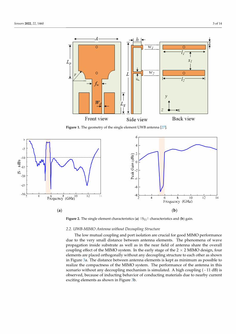
Sensors 2022, 22, 1460 3 of 14Sensors 2022, 22, x FOR PEER REVIEW 3 of 14
Figure 1. The geometry of the single element UWB antenna [27].
(a) (b)
Figure 2. The single element characteristics (a) |S11| characteristics and (b) gain.
2.2. UWB‐MIMO Antenna without Decoupling Structure
The low mutual coupling and port isolation are crucial for good MIMO performance
due to the very small distance between antenna elements. The phenomena of wave prop‐
agation inside substrate as well as in the near field of antenna share the overall coupling
effect of the MIMO system. In the early stage of the 2 × 2 MIMO design, four elements are
placed orthogonally without any decoupling structure to each other as shown in Figure
3a. The distance between antenna elements is kept as minimum as possible to realize the
compactness of the MIMO system. The performance of the antenna in this scenario with‐
out any decoupling mechanism is simulated. A high coupling (−11 dB) is observed, be‐
cause of inducting behavior of conducting materials due to nearby current exciting ele‐
ments as shown in Figure 3b.
Figure 1. The geometry of the single element UWB antenna [27].
Sensors 2022, 22, x FOR PEER REVIEW 3 of 14
Figure 1. The geometry of the single element UWB antenna [27].
(a) (b)
Figure 2. The single element characteristics (a) |S11| characteristics and (b) gain.
2.2. UWB‐MIMO Antenna without Decoupling Structure
The low mutual coupling and port isolation are crucial for good MIMO performance
due to the very small distance between antenna elements. The phenomena of wave prop‐
agation inside substrate as well as in the near field of antenna share the overall coupling
effect of the MIMO system. In the early stage of the 2 × 2 MIMO design, four elements are
placed orthogonally without any decoupling structure to each other as shown in Figure
3a. The distance between antenna elements is kept as minimum as possible to realize the
compactness of the MIMO system. The performance of the antenna in this scenario with‐
out any decoupling mechanism is simulated. A high coupling (−11 dB) is observed, be‐
cause of inducting behavior of conducting materials due to nearby current exciting ele‐
ments as shown in Figure 3b.
Figure 2. The single element characteristics (a) |S11| characteristics and (b) gain.
2.2. UWB-MIMO Antenna without Decoupling Structure
The low mutual coupling and port isolation are crucial for good MIMO performancedue to the very small distance between antenna elements. The phenomena of wavepropagation inside substrate as well as in the near field of antenna share the overallcoupling effect of the MIMO system. In the early stage of the 2 × 2 MIMO design, fourelements are placed orthogonally without any decoupling structure to each other as shownin Figure 3a. The distance between antenna elements is kept as minimum as possible torealize the compactness of the MIMO system. The performance of the antenna in thisscenario without any decoupling mechanism is simulated. A high coupling (−11 dB) isobserved, because of inducting behavior of conducting materials due to nearby currentexciting elements as shown in Figure 3b.

Sensors 2022, 22, 1460 4 of 14Sensors 2022, 22, x FOR PEER REVIEW 4 of 14
G = 19 mm
G = 19 mm
G =
19
mm
G =
19
mm
antenna 1
ante
nna
2
antenna 3
ante
nna
4
(a) (b)
Figure 3. MIMO antenna without decoupling structure (a) geometry (b) transmission coefficient.
2.3. UWB‐MIMO Antenna with Square Shaped Decoupler
The design process of the decoupling structure started with square shape metallic
patch in the center of the substrate which is diagonally centered for all four elements of
this MIMO antenna. In the center of the square shape isolator, a circle is etched, and all
four corners truncated by half‐semicircles shown in Figure 4. The simulation results show
that this design reduces the mutual coupling between elements located diagonally shown
in Figure 5. It can be seen that the reflection coefficient for the adjacent antennas (|S21|,
|S23|) did not change significantly, however, it is improved for the diagonally located an‐
tennas (|S31|, |S24|). Somehow, this design does not reduce the mutual coupling caused
due to adjacent elements efficiently. Therefore, the design of the effective parasitic isolator
is required to improve the |S21| and |S23|.
antenna 1
antenna 3
G = 19 mm
G = 19 mm
Figure 4. The geometry of the UWB‐MIMO antenna with square‐shaped decoupler.
Figure 3. MIMO antenna without decoupling structure (a) geometry (b) transmission coefficient.
2.3. UWB-MIMO Antenna with Square Shaped Decoupler
The design process of the decoupling structure started with square shape metallicpatch in the center of the substrate which is diagonally centered for all four elements of thisMIMO antenna. In the center of the square shape isolator, a circle is etched, and all fourcorners truncated by half-semicircles shown in Figure 4. The simulation results show thatthis design reduces the mutual coupling between elements located diagonally shown inFigure 5. It can be seen that the reflection coefficient for the adjacent antennas (|S21|, |S23|)did not change significantly, however, it is improved for the diagonally located antennas(|S31|, |S24|). Somehow, this design does not reduce the mutual coupling caused dueto adjacent elements efficiently. Therefore, the design of the effective parasitic isolator isrequired to improve the |S21| and |S23|.
Sensors 2022, 22, x FOR PEER REVIEW 4 of 14
G = 19 mm
G = 19 mm
G =
19
mm
G =
19
mm
antenna 1
ante
nna
2
antenna 3
ante
nna
4
(a) (b)
Figure 3. MIMO antenna without decoupling structure (a) geometry (b) transmission coefficient.
2.3. UWB‐MIMO Antenna with Square Shaped Decoupler
The design process of the decoupling structure started with square shape metallic
patch in the center of the substrate which is diagonally centered for all four elements of
this MIMO antenna. In the center of the square shape isolator, a circle is etched, and all
four corners truncated by half‐semicircles shown in Figure 4. The simulation results show
that this design reduces the mutual coupling between elements located diagonally shown
in Figure 5. It can be seen that the reflection coefficient for the adjacent antennas (|S21|,
|S23|) did not change significantly, however, it is improved for the diagonally located an‐
tennas (|S31|, |S24|). Somehow, this design does not reduce the mutual coupling caused
due to adjacent elements efficiently. Therefore, the design of the effective parasitic isolator
is required to improve the |S21| and |S23|.
antenna 1
antenna 3
G = 19 mm
G = 19 mm
Figure 4. The geometry of the UWB‐MIMO antenna with square‐shaped decoupler. Figure 4. The geometry of the UWB-MIMO antenna with square-shaped decoupler.

Sensors 2022, 22, 1460 5 of 14Sensors 2022, 22, x FOR PEER REVIEW 5 of 14
(a) (b)
Figure 5. Transmission coefficient for UWB‐MIMO antenna with and without square‐shaped de‐
coupler (a) adjacent antennas (|S12|, |S14|, |S23|, |S34|) and (b) diagonally located antennas (|S13|,
and |S24|).
2.4. Proposed UWB‐MIMO Antenna
For further isolation improvement in the UWB‐MIMO, especially for the adjacent an‐
tennas, four rectangular metallic stubs extended from opposite parallel sides of the square
shape metal are placed between adjacent antennas. The metallic stubs are connected to
square metallic metal which completes the decoupling structure shown in Figure 6. The
optimized parameter of the proposed antenna is shown in Table 1. The isolation improve‐
ment due to the proposed decoupling structure is shown in Figure 7. The transmission
coefficient for the adjacent antennas for all antennas is less than −21 dB in the entire UWB
bandwidth.
To understand the electromagnetic behavior of antenna elements and decoupling
structure, the surface current distribution for both adjacent and diagonally placed ele‐
ments is studied. The effectiveness of the decoupling structure can be observed from Fig‐
ure 8a in which a current at frequency 3.5 GHz has been shown with and without decou‐
pling structure for port 1. While Figure 8b shows the current at frequency 9 GHz with and
without decoupling structure for port 3. It can be seen that without decoupling structure,
the non‐exciting ports also show current which is because of inducting behavior of con‐
ducting materials due to nearby current exciting elements. While after introducing a de‐
coupling structure in between these elements, the non‐exciting element does not show
current flow, because the decoupling structure minimizes the current flow towards oth‐
ers.
Table 1. The optimized parameter of the proposed antenna.
Parameters sw sl h pw pl lg fw wd r l3 l5 l6
Units (mm) 60 60 1.5 15 12 7.4 4.1 0.9 0.3 20 10 4.1
Parameters w1 w2 l1 l2 s s1 via l4 r1 r2 l7 w3
Units (mm) 1 1.8 15.2 15.2 3.5 11.3 0.2 20 6 5 2.9 3
Figure 5. Transmission coefficient for UWB-MIMO antenna with and without square-shaped decou-pler (a) adjacent antennas (|S12|, |S14|, |S23|, |S34|) and (b) diagonally located antennas (|S13|,and |S24|).
2.4. Proposed UWB-MIMO Antenna
For further isolation improvement in the UWB-MIMO, especially for the adjacent an-tennas, four rectangular metallic stubs extended from opposite parallel sides of the squareshape metal are placed between adjacent antennas. The metallic stubs are connected tosquare metallic metal which completes the decoupling structure shown in Figure 6. The op-timized parameter of the proposed antenna is shown in Table 1. The isolation improvementdue to the proposed decoupling structure is shown in Figure 7. The transmission coefficientfor the adjacent antennas for all antennas is less than −21 dB in the entire UWB bandwidth.
Sensors 2022, 22, x FOR PEER REVIEW 6 of 14
(a) (b)
Figure 6. The geometry of the proposed MIMO antenna. (a) Front side (b) backside.
(a) (b)
Figure 7. Transmission coefficient for the UWB‐MIMO with and without proposed decoupling
structure (a) adjacent antennas (|S12|, |S14|, |S23|, |S34|) and (b) diagonally located antennas (|S13|,
and |S24|.
Figure 6. The geometry of the proposed MIMO antenna. (a) Front side (b) backside.
Table 1. The optimized parameter of the proposed antenna.
Parameters sw sl h pw pl lg f w wd r l3 l5 l6
Units (mm) 60 60 1.5 15 12 7.4 4.1 0.9 0.3 20 10 4.1
Parameters w1 w2 l1 l2 s s1 via l4 r1 r2 l7 w3
Units (mm) 1 1.8 15.2 15.2 3.5 11.3 0.2 20 6 5 2.9 3

Sensors 2022, 22, 1460 6 of 14
Sensors 2022, 22, x FOR PEER REVIEW 6 of 14
(a) (b)
Figure 6. The geometry of the proposed MIMO antenna. (a) Front side (b) backside.
(a) (b)
Figure 7. Transmission coefficient for the UWB‐MIMO with and without proposed decoupling
structure (a) adjacent antennas (|S12|, |S14|, |S23|, |S34|) and (b) diagonally located antennas (|S13|,
and |S24|.
Figure 7. Transmission coefficient for the UWB-MIMO with and without proposed decouplingstructure (a) adjacent antennas (|S12|, |S14|, |S23|, |S34|) and (b) diagonally located antennas(|S13|, and |S24|).
To understand the electromagnetic behavior of antenna elements and decouplingstructure, the surface current distribution for both adjacent and diagonally placed elementsis studied. The effectiveness of the decoupling structure can be observed from Figure 8ain which a current at frequency 3.5 GHz has been shown with and without decouplingstructure for port 1. While Figure 8b shows the current at frequency 9 GHz with and withoutdecoupling structure for port 3. It can be seen that without decoupling structure, the non-exciting ports also show current which is because of inducting behavior of conductingmaterials due to nearby current exciting elements. While after introducing a decouplingstructure in between these elements, the non-exciting element does not show current flow,because the decoupling structure minimizes the current flow towards others.
Sensors 2022, 22, x FOR PEER REVIEW 7 of 14
Figure 8. Surface current distribution with and without decoupling structure of different
port excitation at (a) port‐1 and (b) port‐3.
3. Results and Discussion
The proposed antenna was fabricated on Taconic TLY 5 lossy (thickness = 1.52 mm)
(εr = 3.55 and tanδ = 0.0009) for experimental verification, which is shown in Figure 9. The
impedance and radiation characteristics of the designed antenna are measured by an Ag‐
ilent vector network. To measure the peak gains of the antenna, a well‐calibrated standard
horn antenna was used as the source antenna while the fabricated prototype was meas‐
ured as the receiving antenna. The antenna under test was rotated to measure the peak
gain at different orientations. To supply a stable power reception, transmit and receiving
amplifiers are used. A stable peak gain curve is obtained in the frequency range of interest
with a maximum value of 6.94 dBi, but it sharply decreased at the WLAN band which is
filtered. This demonstrates the effectiveness of the antenna’s rectangular notching charac‐
teristics. The simulated and measured values of |S11|, |S22|, |S33| and, |S44| are compared
in Figure 10. Both the simulated and measured results show similar behavior.
Figure 8. Surface current distribution with and without decoupling structure of different portexcitation at (a) port-1 and (b) port-3.

Sensors 2022, 22, 1460 7 of 14
3. Results and Discussion
The proposed antenna was fabricated on Taconic TLY 5 lossy (thickness = 1.52 mm)(εr = 3.55 and tanδ = 0.0009) for experimental verification, which is shown in Figure 9.The impedance and radiation characteristics of the designed antenna are measured byan Agilent vector network. To measure the peak gains of the antenna, a well-calibratedstandard horn antenna was used as the source antenna while the fabricated prototypewas measured as the receiving antenna. The antenna under test was rotated to measurethe peak gain at different orientations. To supply a stable power reception, transmit andreceiving amplifiers are used. A stable peak gain curve is obtained in the frequency rangeof interest with a maximum value of 6.94 dBi, but it sharply decreased at the WLAN bandwhich is filtered. This demonstrates the effectiveness of the antenna’s rectangular notchingcharacteristics. The simulated and measured values of |S11|, |S22|, |S33| and, |S44| arecompared in Figure 10. Both the simulated and measured results show similar behavior.
Sensors 2022, 22, x FOR PEER REVIEW 8 of 14
(a) (b)
Figure 9. Fabricated proposed antenna: (a) Front view (b) backside view.
The entire UWB spectrum (3–12.8 GHz) shows good impedance matching except for
the notched band. The proposed fabricated antenna under measurement was rotating to
measure the values of peak gain at different orientations. The simulated and measured
gains of the antenna elements at 3 GHz, 5 GHz, 7 GHz, and 9 GHz are shown in Table 2.
During the measurement, only one port excited the remaining ports are terminated with
a 50‐Ω load. The peak gain in the MIMO antenna is 6.94 dBi, increased by 2.44 dBi than a
single element which is 4.5 dBi. This increase of the gain in the MIMO antenna system is
due to the current redistribution, of more than one radiation element. In literature, there
are various techniques used to enhance the gain of antennas such as using metasurface in
the near‐field of the antenna, additive manufacturing, and more [28–33]. However, this
work utilizes a parasitic isolator for isolation as well as gain improvements.
Table 2. Simulated and measured gains of the MIMO antenna.
Freq
(GHz)
Gain (dBi) of Antenna Element
Simulated Values Measured Values
Port 1 Port 2 Port 3 Port 4 Port 1 Port 2 Port 3 Port 4
3 4.42 4.49 4.49 4.35 4.3 4.4 4.4 4.25
5 3.5 3.63 3.56 4.02 3.3 3.45 3.4 3.8
7 5.42 5.47 5.62 5.69 5.35 5.32 5.4 5.6
9 6.77 6.8 6.94 6.75 6 6.5 6.6 6.55
(a) (b)
Figure 10. Reflection coefficient of proposed MIMO antenna (a) Simulated (b) measured.
Figure 9. Fabricated proposed antenna: (a) Front view (b) backside view.
Sensors 2022, 22, x FOR PEER REVIEW 8 of 14
(a) (b)
Figure 9. Fabricated proposed antenna: (a) Front view (b) backside view.
The entire UWB spectrum (3–12.8 GHz) shows good impedance matching except for
the notched band. The proposed fabricated antenna under measurement was rotating to
measure the values of peak gain at different orientations. The simulated and measured
gains of the antenna elements at 3 GHz, 5 GHz, 7 GHz, and 9 GHz are shown in Table 2.
During the measurement, only one port excited the remaining ports are terminated with
a 50‐Ω load. The peak gain in the MIMO antenna is 6.94 dBi, increased by 2.44 dBi than a
single element which is 4.5 dBi. This increase of the gain in the MIMO antenna system is
due to the current redistribution, of more than one radiation element. In literature, there
are various techniques used to enhance the gain of antennas such as using metasurface in
the near‐field of the antenna, additive manufacturing, and more [28–33]. However, this
work utilizes a parasitic isolator for isolation as well as gain improvements.
Table 2. Simulated and measured gains of the MIMO antenna.
Freq
(GHz)
Gain (dBi) of Antenna Element
Simulated Values Measured Values
Port 1 Port 2 Port 3 Port 4 Port 1 Port 2 Port 3 Port 4
3 4.42 4.49 4.49 4.35 4.3 4.4 4.4 4.25
5 3.5 3.63 3.56 4.02 3.3 3.45 3.4 3.8
7 5.42 5.47 5.62 5.69 5.35 5.32 5.4 5.6
9 6.77 6.8 6.94 6.75 6 6.5 6.6 6.55
(a) (b)
Figure 10. Reflection coefficient of proposed MIMO antenna (a) Simulated (b) measured. Figure 10. Reflection coefficient of proposed MIMO antenna (a) Simulated (b) measured.
The entire UWB spectrum (3–12.8 GHz) shows good impedance matching except forthe notched band. The proposed fabricated antenna under measurement was rotating tomeasure the values of peak gain at different orientations. The simulated and measuredgains of the antenna elements at 3 GHz, 5 GHz, 7 GHz, and 9 GHz are shown in Table 2.

Sensors 2022, 22, 1460 8 of 14
During the measurement, only one port excited the remaining ports are terminated with a50-Ω load. The peak gain in the MIMO antenna is 6.94 dBi, increased by 2.44 dBi than asingle element which is 4.5 dBi. This increase of the gain in the MIMO antenna system isdue to the current redistribution, of more than one radiation element. In literature, thereare various techniques used to enhance the gain of antennas such as using metasurface inthe near-field of the antenna, additive manufacturing, and more [28–33]. However, thiswork utilizes a parasitic isolator for isolation as well as gain improvements.
Table 2. Simulated and measured gains of the MIMO antenna.
Freq (GHz)
Gain (dBi) of Antenna Element
Simulated Values Measured Values
Port 1 Port 2 Port 3 Port 4 Port 1 Port 2 Port 3 Port 4
3 4.42 4.49 4.49 4.35 4.3 4.4 4.4 4.25
5 3.5 3.63 3.56 4.02 3.3 3.45 3.4 3.8
7 5.42 5.47 5.62 5.69 5.35 5.32 5.4 5.6
9 6.77 6.8 6.94 6.75 6 6.5 6.6 6.55
3.1. Reflection Coefficients
The measured and simulated results of reflection coefficient plots of the MIMO antennahave been shown in Figure 10. The placement of MIMO elements and antenna elementsare symmetrical in geometry; therefore, the antennas show the same reflection coefficients.
The MIMO antennas have a similar UWB bandwidth with the WLAN band-notchedproposed for the single-element antenna.
3.2. Transmission Coefficients
In MIMO systems, the mutual coupling between the single elements can be ex-pressed as a transmission coefficient. The measured and simulated results are compared inFigure 11. The antenna elements have high isolation characteristics without the proposeddecoupling structure.
Sensors 2022, 22, x FOR PEER REVIEW 9 of 14
3.1. Reflection Coefficients
The measured and simulated results of reflection coefficient plots of the MIMO an‐
tenna have been shown in Figure 10. The placement of MIMO elements and antenna ele‐
ments are symmetrical in geometry; therefore, the antennas show the same reflection co‐
efficients.
The MIMO antennas have a similar UWB bandwidth with the WLAN band‐notched
proposed for the single‐element antenna.
3.2. Transmission Coefficients
In MIMO systems, the mutual coupling between the single elements can be expressed
as a transmission coefficient. The measured and simulated results are compared in Figure
11. The antenna elements have high isolation characteristics without the proposed decou‐
pling structure.
The proposed parasitic decoupling structure has minimized the isolation of the an‐
tennas to >21 dB and the maximum isolation is 50 dB in the entire operating bandwidth.
(a) (b)
Figure 11. The transmission coefficient of the proposed UWB‐MIMO antenna (a) simulation and (b)
measurement.
3.3. Envelope Correlation Coefficient
The envelope correlation coefficient of the proposed UWB‐MIMO antenna is shown
in Figure 12. In MIMO systems the envelope correlation coefficient (ECC) expresses the
independence of the single element performance, such as radiation pattern and polariza‐
tion.
Figure 11. The transmission coefficient of the proposed UWB-MIMO antenna (a) simulation and(b) measurement.
The proposed parasitic decoupling structure has minimized the isolation of the anten-nas to >21 dB and the maximum isolation is 50 dB in the entire operating bandwidth.

Sensors 2022, 22, 1460 9 of 14
3.3. Envelope Correlation Coefficient
The envelope correlation coefficient of the proposed UWB-MIMO antenna is shownin Figure 12. In MIMO systems the envelope correlation coefficient (ECC) expresses theindependence of the single element performance, such as radiation pattern and polarization.
Sensors 2022, 22, x FOR PEER REVIEW 10 of 14
Figure 12. The envelope correlation coefficient of the proposed UWB‐MIMO antenna.
The ECC of MIMO can be calculated using S‐parameters and far‐field radiation pat‐
terns using Equations (1) and (2), respectively.
ρ|S ∗ S S ∗ S |
1 |S | S 1 S S (1)
ρ| ∬ R θ, φ R θ, φ dΩ |
∬ |R θ, φ | dΩ ∬ |R θ, φ | dΩ (2)
3.4. Diversity Gain
Using diversity gain, the effect of the diversity scheme on the radiated power can be
described. Figure 13 shows the diversity gain of the proposed MIMO antenna which is a
flat line in the ideal value for 10 dB for all four elements except the notched band. The DG
is computed as a function frequency using relation (3).
DG 10 1 |𝜌𝑖𝑗| (3)
Figure 13. Diversity gain of the proposed UWB‐MIMO antenna.
Figure 12. The envelope correlation coefficient of the proposed UWB-MIMO antenna.
The ECC of MIMO can be calculated using S-parameters and far-field radiation pat-terns using Equations (1) and (2), respectively.
ρeij =
∣∣Sii∗Sij + Sji∗Sjj∣∣2(
1− |Sii|2 − Sij2)(
1−∣∣Sji∣∣2 − Sjj
2) (1)
ρeij =
|s 4π
0
[→Ri(θ, ϕ)×
→Rj(θ, ϕ)
]dΩ|
2
s 4π0 |
→Ri(θ, ϕ)|
2dΩ
s 4π0 |
→Rj(θ, ϕ)|
2dΩ
(2)
3.4. Diversity Gain
Using diversity gain, the effect of the diversity scheme on the radiated power can bedescribed. Figure 13 shows the diversity gain of the proposed MIMO antenna which is aflat line in the ideal value for 10 dB for all four elements except the notched band. The DGis computed as a function frequency using relation (3).
DG = 10√
1− |ρij|2 (3)

Sensors 2022, 22, 1460 10 of 14
Sensors 2022, 22, x FOR PEER REVIEW 10 of 14
Figure 12. The envelope correlation coefficient of the proposed UWB‐MIMO antenna.
The ECC of MIMO can be calculated using S‐parameters and far‐field radiation pat‐
terns using Equations (1) and (2), respectively.
ρ|S ∗ S S ∗ S |
1 |S | S 1 S S (1)
ρ| ∬ R θ, φ R θ, φ dΩ |
∬ |R θ, φ | dΩ ∬ |R θ, φ | dΩ (2)
3.4. Diversity Gain
Using diversity gain, the effect of the diversity scheme on the radiated power can be
described. Figure 13 shows the diversity gain of the proposed MIMO antenna which is a
flat line in the ideal value for 10 dB for all four elements except the notched band. The DG
is computed as a function frequency using relation (3).
DG 10 1 |𝜌𝑖𝑗| (3)
Figure 13. Diversity gain of the proposed UWB‐MIMO antenna. Figure 13. Diversity gain of the proposed UWB-MIMO antenna.
3.5. Channel Capacity Loss
Channel capacity is the data rate supported in a particular channel in a fading envi-ronment. The channel capacity loss is the maximum available transmission for which asignal can be transmitted over a particular MIMO antenna system. In practice, the valueof CCL should be less than 0.4 bps/Hz. The capacity loss can be determined by using thefollowing Equation (4):
CCL = − log2 det∣∣∣ψR
∣∣∣ (4)
where ψR is the receiving antenna correlation matrix, which is given as:
ψR =
ρ11 ρ12 ρ13ρ21 ρ22 ρ23ρ31 ρ32 ρ33
ρ14ρ24ρ34
ρ41 ρ42 ρ43 ρ44
(5)
ρii = (1 − |Sii|2 − |Sij|2) and ρij = −(S∗iiSij + S∗jiSij) for i, j = 1 2, 3 or 4.The CCL graph shown in Figure 14 demonstrates that the antenna CCL is than
0.4 bps/Hz for the entire UWB band except for the rectangularly notched WLAN band.
3.6. Mean Effective Gain
The mean effective gain is the measure of receipt power levels of a MIMO antennasystem to an isotropic radiator. The difference between MEG of ports of antenna alwaysshould be less than −3 dB. Equation (6) is used to calculate the MEG values:
MEGi = 0.5
(1−
N
∑i=1|Sij|
)(6)
where i represent the port under observation and N is the number of antennas in the MIMOsystem. The MEG of the proposed MIMO antenna is shown in Figure 15. The MEG valuesare very low (less than −12 dB) at the stop-band, while it is around −7 dB within thefrequency range of interest.

Sensors 2022, 22, 1460 11 of 14
Sensors 2022, 22, x FOR PEER REVIEW 11 of 14
3.5. Channel Capacity Loss
Channel capacity is the data rate supported in a particular channel in a fading envi‐
ronment. The channel capacity loss is the maximum available transmission for which a
signal can be transmitted over a particular MIMO antenna system. In practice, the value
of CCL should be less than 0.4 bps/Hz. The capacity loss can be determined by using the
following Equation (4):
CCL log det|ψ | (4)
where ψR is the receiving antenna correlation matrix, which is given as:
ψR
ρ11 ρ12 ρ13ρ21 ρ22 ρ23ρ31 ρ32 ρ33
ρ14ρ24ρ34
ρ41 ρ42 ρ43 ρ44
(5)
𝜌ii = (1 − |Sii|2 − |Sij|2) and 𝜌ij = −(S∗iiSij + S∗jiSij) for i, j = 1 2, 3 or 4. The CCL graph shown in Figure 14 demonstrates that the antenna CCL is than 0.4
bps/Hz for the entire UWB band except for the rectangularly notched WLAN band.
Figure 14. Chanel capacity loss analysis of the proposed UWB‐MIMO antenna.
3.6. Mean Effective Gain
The mean effective gain is the measure of receipt power levels of a MIMO antenna
system to an isotropic radiator. The difference between MEG of ports of antenna always
should be less than −3 dB. Equation (6) is used to calculate the MEG values:
MEG𝑖 0.5 1 |Sij| (6)
where i represent the port under observation and N is the number of antennas in the
MIMO system. The MEG of the proposed MIMO antenna is shown in Figure 15. The MEG
values are very low (less than −12 dB) at the stop‐band, while it is around −7 dB within
the frequency range of interest.
Figure 14. Chanel capacity loss analysis of the proposed UWB-MIMO antenna.
Sensors 2022, 22, x FOR PEER REVIEW 12 of 14
Frequency (GHz)
MEG 1MEG 2MEG 3MEG 4
2 4 6 8 10 12 14-16
-12
-8
-4
Figure 15. Variation of MEG with frequency.
3.7. Comparison with State‐of‐Artwork
The performance comparison of proposed rectangularly notched UWB‐MIMO with
stat‐of‐artwork is summarized and shown in Table 3.
Table 3. Comparison of the proposed UWB‐MIMO antenna with state‐of‐the‐art works.
Ref. Isolation Enhancement Technique Antenna Size
(mm3) ECC Minimum Isolation (dB) Peak Gain (dBi)
[10] Defected ground 29 × 40 × 0.508 0.0005 18 4.9
[11] Defected ground 22 × 29 × 0.8 0.03 17 6
[12] Decoupling element 30 × 40 × 0.8 0.05 15 4.2
[13] Space diversity 25 × 50 × 1.6 0.43 17 3.5
[14] Parasitic decoupler 40 × 43 × 1 0.2 20 4
[15] Parasitic strip 34 × 34 × 1.6 0.05 15 5.5
[16] Neutralization rings 75.19 × 75.19 × 1.6 0.1 14.5 5
[17] F shaped stub 50 × 30 × 1.6 0.04 18 2.91
[18] Used slots 15 × 25 × 1.6 0.02 20 NG
[19] Inverted‐Y shaped stub 58 × 45 × 1.6 0.02 15 NG
[21] Inverted‐Y shaped stub 33 × 38 × 1.6 0.08 17 6.2
[24] Metamaterial 30 × 60 × 1.6 0.01 20 5.5
This
work Parasitic decoupler 60 × 60 × 1.52 >0.001 21 6.94
The comparison is made with other UWB‐MIMO antennas to the isolation enhance‐
ment technique, peak gain, and minimum isolation. The UWB−MIMO antenna [9] consists
of two slot antennas, a T‐shaped slot is etched on the ground to improve isolation. The
antenna acquires a low mutual coupling of less than 18 dB in operating bandwidth.
Whereas the references [10] are designed to use defected ground approach, that offers
minimum isolation of 18 dB and peak gain of 4.9 dBi. Moreover, 2 port MIMO antennas
reported in [11−12] have reached maximum isolation of 17 dB and 15 dB, respectively.
Moreover, a 2 port UWB MIMO in [13] has shown a good isolation agreement of 17 dB
and a peak gain of 3.5 dBi without any utilization of radiating elements. Furthermore, the
Figure 15. Variation of MEG with frequency.
3.7. Comparison with State-of-Artwork
The performance comparison of proposed rectangularly notched UWB-MIMO withstat-of-artwork is summarized and shown in Table 3.

Sensors 2022, 22, 1460 12 of 14
Table 3. Comparison of the proposed UWB-MIMO antenna with state-of-the-art works.
Ref. Isolation EnhancementTechnique
Antenna Size(mm3) ECC Minimum
Isolation (dB) Peak Gain (dBi)
[10] Defected ground 29 × 40 × 0.508 0.0005 18 4.9
[11] Defected ground 22 × 29 × 0.8 0.03 17 6
[12] Decoupling element 30 × 40 × 0.8 0.05 15 4.2
[13] Space diversity 25 × 50 × 1.6 0.43 17 3.5
[14] Parasitic decoupler 40 × 43 × 1 0.2 20 4
[15] Parasitic strip 34 × 34 × 1.6 0.05 15 5.5
[16] Neutralization rings 75.19 × 75.19 × 1.6 0.1 14.5 5
[17] F shaped stub 50 × 30 × 1.6 0.04 18 2.91
[18] Used slots 15 × 25 × 1.6 0.02 20 NG
[19] Inverted-Y shaped stub 58 × 45 × 1.6 0.02 15 NG
[21] Inverted-Y shaped stub 33 × 38 × 1.6 0.08 17 6.2
[24] Metamaterial 30 × 60 × 1.6 0.01 20 5.5
This work Parasitic decoupler 60 × 60 × 1.52 >0.001 21 6.94
The comparison is made with other UWB-MIMO antennas to the isolation enhance-ment technique, peak gain, and minimum isolation. The UWB−MIMO antenna [9] consistsof two slot antennas, a T-shaped slot is etched on the ground to improve isolation. The an-tenna acquires a low mutual coupling of less than 18 dB in operating bandwidth. Whereasthe references [10] are designed to use defected ground approach, that offers minimumisolation of 18 dB and peak gain of 4.9 dBi. Moreover, 2 port MIMO antennas reportedin [11,12] have reached maximum isolation of 17 dB and 15 dB, respectively. Moreover,a 2 port UWB MIMO in [13] has shown a good isolation agreement of 17 dB and a peakgain of 3.5 dBi without any utilization of radiating elements. Furthermore, the MIMOantennas [14,15] contribute a customized parasitic decoupling structure on the backsideof the antenna, which has an isolation of 20 dB and 15 dB correspondingly. Moreover,using neutralization lines, the mutual coupling is reduced up to 14.5 dB and peak gain of5 in [13]. However, different UWB-MIMO antennas from [17–20] enhanced isolation usingdifferent-shaped stubs between single antenna elements. Finally, the paper [24] presentsa UWB-MIMO antenna with the isolation of −20 dB using metamaterials. It is noted theantenna size is larger than the conventional antennas due to the presence of the EBGs,which have been used to realize the rectangular notch features.
The proposed antenna has better performance than the aforesaid antennas. Thisproposed antenna offers very high isolation and stable gain curve with a maximum gainof 6.94 dBi. Overall, our antenna is rectangularly notched and offers higher operatingbandwidth while maintaining high gain and high isolation.
4. Conclusions
A rectangularly notched band UWB-MIMO antenna with an overall size of60 × 60 × 1.52 mm3 is presented in this paper. Initially, the UWB antenna with a rectangu-lar notching characteristic is designed. The notching characteristic is achieved by usingtwo EBG structures. The proposed single-element is remodeled to a 2 × 2 UWB-MIMOsystem by translating each antenna element perpendicular to each other. The performance,particularly the isolation of the antenna is improved by using a novel parasitic structure.The simulated and measured results of the proposed antenna show a good agreement. Theantenna offers a stable gain with a peak gain of 6.8 dBi, low isolation (12 dB improvedcompared without decoupling structure), low ECC value (0.001), and high diversity gain of

Sensors 2022, 22, 1460 13 of 14
9.99. Hence the performance criteria indicate the stability of the proposed antenna for theUWB-MIMO application.
Author Contributions: Conceptualization, A.A.; writing—original draft preparation, A.A.; writing—reviewand editing, N.H. and M.A.S.; visualization, J.J. and S.M.P.; project administration, N.K. All authorshave read and agreed to the published version of the manuscript.
Funding: This work was supported by an Institute for Information and Communications TechnologyPromotion (IITP), funded by the Korean government (MSIP) (No. 2021-0-00490, Development ofprecision analysis and imaging technology for biological radio waves).
Institutional Review Board Statement: Not applicable.
Informed Consent Statement: Not applicable.
Data Availability Statement: Not applicable.
Conflicts of Interest: The authors declare no conflict of interest.
References1. Naeem, U.; Iqbal, A.; Shafique, M.F.; Bila, S. Efficient Design Methodology for a Complex DRA-SIW Filter-Antenna Subsystem.
Int. J. Antennas Propag. 2017, 2017, 6401810. [CrossRef]2. Iqbal, A.; Tiang, J.J.; Lee, C.K.; Mallat, N.K.; Wong, S.W. Dual-band half mode substrate integrated waveguide filter with
independently tunable bands. IEEE Trans. Circuits Syst. II Express Briefs 2019, 67, 285–289. [CrossRef]3. Lalbakhsh, A.; Mohamadpour, G.; Roshani, S.; Ami, M.; Roshani, S.; Sayem, A.S.M.; Koziel, S. Design of a Compact Pla-
narTransmission Line for Miniaturized Rat-Race Coupler with Harmonics Suppression. IEEE Access 2021, 9, 129207–129217.[CrossRef]
4. Fontana, R.J. Recent system applications of short-pulse ultra-wideband (UWB) technology. IEEE Trans. Microw. Theory Tech. 2004,52, 2087–2104. [CrossRef]
5. Hussain, N.; Jeong, M.; Park, J.; Rhee, S.; Kim, P.; Kim, N. A compact size 2.9–23.5 GHz microstrip patch antenna with WLANband-rejection. Microw. Opt. Technol. Lett. 2019, 61, 1307–1313. [CrossRef]
6. Ramakrishna, C.; Kumar, G.A.R.P.; Sekhar, C. Quadruple Band-Notched Compact Monopole UWB Antenna for WirelessApplications. J. Electromagn. Eng. Sci. 2021, 21, 406–416. [CrossRef]
7. Chen, X.; Zhang, S.; Li, Q. A review of mutual coupling in MIMO systems. IEEE Access 2018, 6, 24706–24719. [CrossRef]8. Nadeem, I.; Choi, D.Y. Study on mutual coupling reduction technique for MIMO antennas. IEEE Access 2018, 7, 563–586.
[CrossRef]9. Luo, C.M.; Hong, J.S.; Zhong, L.L. Isolation enhancement of a very compact UWB-MIMO slot antenna with two defected ground
structures. IEEE Antennas Wirel. Propag. Lett. 2015, 14, 1766–1769. [CrossRef]10. Masoodi, I.S.; Ishteyaq, I.; Muzaffar, K.; Magray, M.I. A compact band-notched antenna with high isolation for UWB MIMO
applications. Int. J. Microw. Wirel. Technol. 2021, 13, 634–640. [CrossRef]11. Malekpour, N.; Amin, H.M.; Dadgarpur, A.; Virdee, B.S.; Denidni, T.A. Compact UWB MIMO antenna with band-notched
characteristic. Microw. Opt. Technol. Lett. 2017, 59, 1037–1041. [CrossRef]12. Tang, T.C.; Lin, K.H. An ultrawideband MIMO antenna with dual band-notched function. IEEE Antennas Wirel. Propag. Lett. 2014,
13, 1076–1079. [CrossRef]13. Khan, M.S.; Iftikhar, A.; Shubair, R.M.; Capobianco, A.D.; Asif, S.M.; Braaten, B.D.; Anagnostou, D.E. Ultra-compact reconfigurable
band-reject UWB MIMO antenna with four radiators. Electronics 2020, 9, 584. [CrossRef]14. Amin, F.; Saleem, R.; Shabbir, T.; Bilal, M.; Shafique, M.F. A compact quad-element UWB-MIMO antenna system with parasitic
decoupling mechanism. Appl. Sci. 2019, 9, 2371. [CrossRef]15. Chen, Z.; Zhou, W.; Hong, J. A Miniaturized MIMO Antenna with Triple Band-Notched Characteristics for UWB Applications.
IEEE Access 2021, 9, 63646–63655. [CrossRef]16. Kayabasi, A.; Toktas, A.; Yigit, E.; Sabanci, K. Triangular quad-port multi-polarized UWB MIMO antenna with enhanced isolation
using neutralization ring. AEU-Int. J. Electron. Commun. 2018, 85, 47–53. [CrossRef]17. Iqbal, A.; Saraereh, O.A.; Ahmad, A.W.; Bashir, S. Mutual coupling reduction using F-shaped stubs in UWB-MIMO antenna. IEEE
Access 2017, 6, 2755–2759. [CrossRef]18. Khan, M.I.; Khattak, M.I.; Al-Hasan, M. Miniaturized MIMO Antenna with Low Inter-radiator Transmittance and Band Rejection
Features. J. Electromagn. Eng. Sci. 2021, 21, 307–315. [CrossRef]19. Jaglan, N.; Kanaujia, B.K.; Gupta, S.D.; Srivastava, S. Dual band notched EBG structure based UWB MIMO/diversity antenna
with reduced wideband electromagnetic coupling. Frequenz 2017, 71, 555–565. [CrossRef]20. Najam, A.I.; Duroc, Y.; Tedjini, S. UWB-MIMO antenna with novel stub structure. Prog. Electromagn. Res. C 2011, 19, 245–257.
[CrossRef]

Sensors 2022, 22, 1460 14 of 14
21. Yin, W.; Chen, S.; Chang, J.; Li, C.; Khamas, S.K. CPW fed Compact UWB 4-Element MIMO Antenna with High Isolation. Sensors2020, 21, 2688. [CrossRef]
22. Gorai, A.; Dasgupta, A.; Ghatak, R. A compact quasi-self-complementary dual band notched UWB MIMO antenna with enhancedisolation using Hilbert fractal slot. AEU-Int. J. Electron. Commun. 2018, 94, 36–41. [CrossRef]
23. Sufian, M.A.; Hussain, N.; Askari, H.; Park, S.G.; Shin, K.S.; Kim, N. Isolation Enhancement of a Metasurface-Based MIMOAntenna Using Slots and Shorting Pins. IEEE Access 2021, 9, 73533–73543. [CrossRef]
24. Jabire, A.H.; Ghaffar, A.; Li, X.J.; Abdu, A.; Saminu, S.; Alibakhshikenari, M.; Falcone, F.; Limiti, E. Metamaterial Based Design ofCompact UWB/MIMO Monopoles Antenna with Characteristic Mode Analysis. Appl. Sci. 2021, 11, 1542. [CrossRef]
25. Farahani, M.; Mohammad-Ali-Nezhad, S. A novel UWB printed monopole MIMO antenna with non-uniform transmission lineusing nonlinear model predictive. Int. J. Eng. Sci. Technol. 2020, 23, 1385–1396. [CrossRef]
26. Abbas, A.; Hussain, N.; Jeong, M.-J.; Park, J.; Shin, K.S.; Kim, T.; Kim, N. A Rectangular Notch-Band UWB Antenna withControllable Notched Bandwidth and Centre Frequency. Sensors 2020, 20, 777. [CrossRef]
27. Abbas, A.; Hussain, N.; Lee, J.; Park, S.G.; Kim, N. Triple Rectangular Notch UWB Antenna Using EBG and SRR. IEEE Access2020, 9, 2508–2515. [CrossRef]
28. Hussain, N.; Jeong, M.J.; Abbas, A.; Kim, N. Metasurface-based single-layer wideband circularly polarized MIMO antenna for 5Gmillimeter-wave systems. IEEE Access 2020, 8, 130293–130304. [CrossRef]
29. Lalbakhsh, A.; Afzal, M.U.; Hayat, T.; Esselle, K.P.; Mandal, K. All-metal wideband metasurface for near-field transformation ofmedium-to-high gain electromagnetic sources. Sci. Rep. 2021, 11, 9421. [CrossRef]
30. Lalbakhsh, A.; Afzal, M.U.; Zeb, B.A.; Esselle, K.P. Design of a dielectric phase-correcting structure for an EBG resonator antennausing particle swarm optimization. In Proceedings of the International Symposium on Antennas Propagation (ISAP), Hobart,TAS, Australia, 9–12 November 2015; pp. 408–410.
31. Jeong, M.J.; Hussain, N.; Park, J.W.; Park, S.G.; Rhee, S.Y.; Kim, N. Millimeter-wave microstrip patch antenna using verticallycoupled split ring metaplate for gain enhancement. Microw. Opt. Technol. Lett. 2019, 61, 2360–2365. [CrossRef]
32. Lalbakhsh, A.; Afzal, M.U.; Esselle, K.P. Multiobjective particle swarm optimization to design a time-delay equalizer metasurfacefor an electromagnetic band-gap resonator antenna. IEEE Antennas Wirel. Propag. Lett. 2016, 16, 912–915. [CrossRef]
33. Hussain, N.; Jeong, M.J.; Abbas, A.; Kim, T.J.; Kim, N. A metasurface-based low-profile wideband circularly polarized patchantenna for 5G millimeter-wave systems. IEEE Access 2020, 8, 22127–22135. [CrossRef]