
IoT-Oriented Design of an Associative Memory Based ... - MDPI
19
electronics Article IoT-Oriented Design of an Associative Memory Based on Impulsive Hopfield Neural Network with Rate Coding of LIF Oscillators Petr Boriskov Institute of Physics and Technology, Petrozavodsk State University, 33 Lenin str., Petrozavodsk 185910, Russia; [email protected]; Tel.: +7-906-206-7901 Received: 16 July 2020; Accepted: 4 September 2020; Published: 8 September 2020 Abstract: The smart devices in Internet of Things (IoT) need more effective data storage opportunities, as well as support for Artificial Intelligence (AI) methods such as neural networks (NNs). This study presents a design of new associative memory in the form of impulsive Hopfield network based on leaky integrated-and-fire (LIF) RC oscillators with frequency control and hybrid analog–digital coding. Two variants of the network schemes have been developed, where spiking frequencies of oscillators are controlled either by supply currents or by variable resistances. The principle of operation of impulsive networks based on these schemes is presented and the recognition dynamics using simple two-dimensional images in gray gradation as an example is analyzed. A fast digital recognition method is proposed that uses the thresholds of zero crossing of output voltages of neurons. The time scale of this method is compared with the execution time of some network algorithms on IoT devices for moderate data amounts. The proposed Hopfield algorithm uses rate coding to expand the capabilities of neuromorphic engineering, including the design of new hardware circuits of IoT. Keywords: spike neural networks; Hopfield neural network; LIF neuron; firing rate coding; analog–digital coding; IoT devices 1. Introduction The number of real-world Internet of Things (IoT) deployments is continuously and steadily increasing, but the capabilities of single IoT devices cannot yet be exploited for the purpose of artificial intelligence (AI). The main reason is computation complexity and energy consumption, which are the constraining requirements for the development and implementation of truly intelligent IoT devices with AI [1,2]. A solution to address this problem could be to use the chips for IoT devices based on NNs with low energy consumption and simplified computing base. In recent decades spike neural networks (SNNs) have been intensively developed in this direction [3,4], although they are still inferior to classical NNs using threshold adders in speed and accuracy of doing tasks in most application areas. Nevertheless, the obvious proximity to the operation of real biological neurons combined with greater variability in learning and coding make SNNs ultimately more promising than traditional NNs of first- and second-generation. There are two main coding methods in SNNs: temporal coding and firing rate coding [5–11]. The first one, which consists of recording and comparing the intervals between neural spikes, is very widespread because of the diversity of coding and its high informative content. In particular, the spike synchronization in SNNs is also associated with this method [9,10]. The second one (rate coding) is characterized by neglecting accurate information about the appearance of spikes—only their average number in some time windows is important. Which of these methods of coding plays a decisive role in nervous activity remains a subject of discussion [5,11]. However, at least, rate coding is more practical Electronics 2020, 9, 1468; doi:10.3390/electronics9091468 www.mdpi.com/journal/electronics
-
Upload
khangminh22 -
Category
Documents
-
view
0 -
download
0
Transcript of IoT-Oriented Design of an Associative Memory Based ... - MDPI
electronics
Article
IoT-Oriented Design of an Associative MemoryBased on Impulsive Hopfield Neural Network withRate Coding of LIF Oscillators
Petr Boriskov
Institute of Physics and Technology, Petrozavodsk State University, 33 Lenin str., Petrozavodsk 185910, Russia;[email protected]; Tel.: +7-906-206-7901
Received: 16 July 2020; Accepted: 4 September 2020; Published: 8 September 2020
Abstract: The smart devices in Internet of Things (IoT) need more effective data storage opportunities,as well as support for Artificial Intelligence (AI) methods such as neural networks (NNs). This studypresents a design of new associative memory in the form of impulsive Hopfield network basedon leaky integrated-and-fire (LIF) RC oscillators with frequency control and hybrid analog–digitalcoding. Two variants of the network schemes have been developed, where spiking frequenciesof oscillators are controlled either by supply currents or by variable resistances. The principle ofoperation of impulsive networks based on these schemes is presented and the recognition dynamicsusing simple two-dimensional images in gray gradation as an example is analyzed. A fast digitalrecognition method is proposed that uses the thresholds of zero crossing of output voltages of neurons.The time scale of this method is compared with the execution time of some network algorithms onIoT devices for moderate data amounts. The proposed Hopfield algorithm uses rate coding to expandthe capabilities of neuromorphic engineering, including the design of new hardware circuits of IoT.
Keywords: spike neural networks; Hopfield neural network; LIF neuron; firing rate coding;analog–digital coding; IoT devices
1. Introduction
The number of real-world Internet of Things (IoT) deployments is continuously and steadilyincreasing, but the capabilities of single IoT devices cannot yet be exploited for the purpose of artificialintelligence (AI). The main reason is computation complexity and energy consumption, which are theconstraining requirements for the development and implementation of truly intelligent IoT deviceswith AI [1,2]. A solution to address this problem could be to use the chips for IoT devices based onNNs with low energy consumption and simplified computing base. In recent decades spike neuralnetworks (SNNs) have been intensively developed in this direction [3,4], although they are still inferiorto classical NNs using threshold adders in speed and accuracy of doing tasks in most application areas.Nevertheless, the obvious proximity to the operation of real biological neurons combined with greatervariability in learning and coding make SNNs ultimately more promising than traditional NNs of first-and second-generation.
There are two main coding methods in SNNs: temporal coding and firing rate coding [5–11].The first one, which consists of recording and comparing the intervals between neural spikes, is verywidespread because of the diversity of coding and its high informative content. In particular, the spikesynchronization in SNNs is also associated with this method [9,10]. The second one (rate coding) ischaracterized by neglecting accurate information about the appearance of spikes—only their averagenumber in some time windows is important. Which of these methods of coding plays a decisive role innervous activity remains a subject of discussion [5,11]. However, at least, rate coding is more practical
Electronics 2020, 9, 1468; doi:10.3390/electronics9091468 www.mdpi.com/journal/electronics

Electronics 2020, 9, 1468 2 of 19
because recording of oscillation frequencies (rates) is technically easier than recording of their phases,and so this method can be implemented to hardware circuits using simple (standard) schemes ofsignal processing.
Among the many models of spike neurons, the simplest and most popular model is the leakyintegrated-and-fire (LIF) model of a neuron with a threshold activation function [12,13]. A LIF neuroncan be created on the basis of a simple relaxation RC generator with an element, which has S-typeI–V characteristic [14]. S-switch element can be a silicon trigger diode or a thin film switch based ontransition metal oxides [15–17]. A LIF neuron oscillator based on the S-switch element can control thefrequency of spikes by the circuit source (current or voltage), similar to conventional RC generators, or,as shown in the study [18], by a variable resistor connected in parallel with the capacitance. A featureof the operation of the circuit [18] is the strong nonlinear dependence of the relaxation oscillationfrequency on this resistance, which has a sigmoid-like form.
The Hopfield network (HN) [19,20] is an important algorithm of NN development [21] which canaccurately identify the object and accurately identify digital signals even if they are contaminated bynoise. This algorithm can be fast, which takes an analog circuit processing advantage rather than digitalcircuit [22]. Unlike the software realization of HN, the hardware implementation of the algorithmmakes brain-like computations possible [23].
The main disadvantage of HN is a low information capacity, and for large networks the requirednumber of neurons should exceed the number of classified images (signals) by more than 6 times [24].Therefore, one of the direction of HN applications is the development of small compact networkmodules for moderate data processing [25–27], using the advantages of HN in recognition accuracy andone step learning process [19]. In applications of IoT, for example, the relationship between the faultset and the alarm set of multiple links can be established through the proposed HN [26]. The built-inHopfield algorithm of the energy function is used to resolve fault location in smart cities [27].
In this paper, we developed a design of new associative memory, which is an SNN of oscillatortype and has Hopfield architecture and algorithm of the energy function. Two variants of these networkschemes in the form of impulsive HN (IHN) use the rate coding of LIF neurons with S-switch elementsand a hybrid analog–digital processing and coding method. Based on the analysis of the dynamics ofthe output voltages of IHN neurons, a fast digital method of recognition indication is proposed on theexample of simple two-dimensional images in gray color gradation.
The paper is organized as follows: Section 2 describes the model of LIF oscillators in two variantsfor rate coding based on a generalized S-switches (Section 2.1) and the implementation feedbacks (FBs)of LIF neurons (Section 2.2). Section 2 also introduces the principles of operation of IHNs based onrate coding (Section 2.3). Section 3 presents the results of recognition dynamics of IHNs with four(Section 3.1) and nine (Section 3.2) LIF neurons. Section 4 discusses some of the research challenges,where the proposed Hopfield algorithm compares with others methods of IoT devices for processingsmall amounts of data. All circuit simulations were performed in the MatLab/Simulink software tool.
2. Materials and Methods
2.1. Relaxation Oscillators Based on S-Switch Elements
The generalized switch has I–V characteristic of an S-type [18] with an unstable NDR section, as itis shown in Figure 1a, where the dependence of current on voltage Isw(Usw) can be represented by thefollowing mathematical model:
Isw(Usw) ≈
Usw/Roff, state = OFFUsw/Ron, state = ON
(1)
Electronics 2020, 9, 1468 3 of 19
Switching in (1) between OFF and ON states is implemented as follows:
state =
OFF, if (state = ON) and (U < Uh)
ON, if (state = OFF) and (U > Uth)(2)
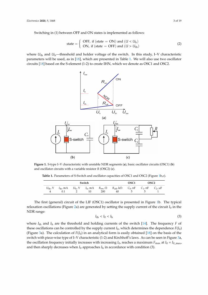
where Uth and Uh—threshold and holder voltage of the switch. In this study, I–V characteristicparameters will be used, as in [18], which are presented in Table 1. We will also use two oscillatorcircuits [18] based on the S-element (1-2) to create IHN, which we denote as OSC1 and OSC2.
Electronics 2020, 9, x FOR PEER REVIEW 3 of 19
where Uth and Uh—threshold and holder voltage of the switch. In this study, I–V characteristic parameters will be used, as in [18], which are presented in Table 1. We will also use two oscillator circuits [18] based on the S-element (1-2) to create IHN, which we denote as OSC1 and OSC2.
(a)
(b) (c)
Figure 1. S-type I–V characteristic with unstable NDR segments (a), basic oscillator circuits (OSC1) (b) and oscillator circuits with a variable resistor R (OSC2) (c).
Table 1. Parameters of S-Switch and oscillator capacities of OSC1 and OSC2 (Figure 1b,c).
Switch OSC1 OSC2 Uth, V Ith, mA Uh, V Ih, mA Ron, Ω Roff, kΩ C0, nF C1, nF C2, µF
4 0.1 2 10 200 40 5 5 1
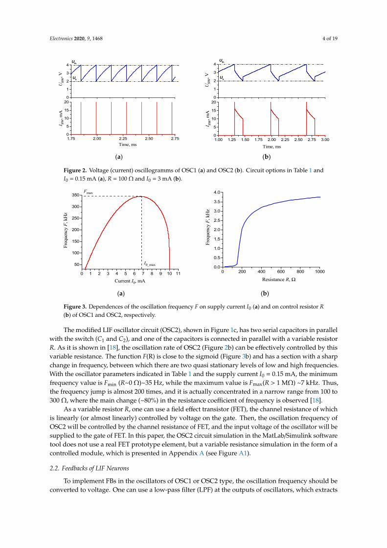
The first (general) circuit of the LIF (OSC1) oscillator is presented in Figure 1b. The typical relaxation oscillations (Figure 2a) are generated by setting the supply current of the circuit I0 in the NDR range:
< <I I Ith 0 h (3)
where Ith and Ih are the threshold and holding currents of the switch [14]. The frequency F of these oscillations can be controlled by the supply current I0, which determines the dependence F(I0) (Figure 3a). The calculation of F(I0) in an analytical form is easily obtained [18] on the basis of the switch with piece-wise type of I–V characteristic (1-2) and Kirchhoff’s laws. As can be seen in Figure 3a, the oscillation frequency initially increases with increasing I0, reaches a maximum Fmax at I0 = I0_max, and then sharply decreases when I0 approaches Ih in accordance with condition (3).
Figure 1. S-type I–V characteristic with unstable NDR segments (a), basic oscillator circuits (OSC1) (b)and oscillator circuits with a variable resistor R (OSC2) (c).
Table 1. Parameters of S-Switch and oscillator capacities of OSC1 and OSC2 (Figure 1b,c).
Switch OSC1 OSC2
Uth, V Ith, mA Uh, V Ih, mA Ron, Ω Roff, kΩ C0, nF C1, nF C2, µF4 0.1 2 10 200 40 5 5 1
The first (general) circuit of the LIF (OSC1) oscillator is presented in Figure 1b. The typicalrelaxation oscillations (Figure 2a) are generated by setting the supply current of the circuit I0 in theNDR range:
Ith < I0 < Ih (3)
where Ith and Ih are the threshold and holding currents of the switch [14]. The frequency F ofthese oscillations can be controlled by the supply current I0, which determines the dependence F(I0)(Figure 3a). The calculation of F(I0) in an analytical form is easily obtained [18] on the basis of theswitch with piece-wise type of I–V characteristic (1-2) and Kirchhoff’s laws. As can be seen in Figure 3a,the oscillation frequency initially increases with increasing I0, reaches a maximum Fmax at I0 = I0_max,and then sharply decreases when I0 approaches Ih in accordance with condition (3).
Electronics 2020, 9, 1468 4 of 19Electronics 2020, 9, x FOR PEER REVIEW 4 of 19
(a) (b)
Figure 2. Voltage (current) oscillogramms of OSC1 (a) and OSC2 (b). Circuit options in Table 1 and I0 = 0.15 mA (a), R = 100 Ω and I0 = 3 mA (b).
(a) (b)
Figure 3. Dependences of the oscillation frequency F on supply current I0 (a) and on control resistor R (b) of OSC1 and OSC2, respectively.
The modified LIF oscillator circuit (OSC2), shown in Figure 1c, has two serial capacitors in parallel with the switch (C1 and C2), and one of the capacitors is connected in parallel with a variable resistor R. As it is shown in [18], the oscillation rate of OSC2 (Figure 2b) can be effectively controlled by this variable resistance. The function F(R) is close to the sigmoid (Figure 3b) and has a section with a sharp change in frequency, between which there are two quasi stationary levels of low and high frequencies. With the oscillator parameters indicated in Table 1 and the supply current I0 = 0.15 mA, the minimum frequency value is Fmin (R~0 Ω)~35 Hz, while the maximum value is Fmax(R > 1 MΩ) ~7 kHz. Thus, the frequency jump is almost 200 times, and it is actually concentrated in a narrow range from 100 to 300 Ω, where the main change (~80%) in the resistance coefficient of frequency is observed [18].
As a variable resistor R, one can use a field effect transistor (FET), the channel resistance of which is linearly (or almost linearly) controlled by voltage on the gate. Then, the oscillation frequency of OSC2 will be controlled by the channel resistance of FET, and the input voltage of the oscillator will be supplied to the gate of FET. In this paper, the OSC2 circuit simulation in the MatLab/Simulink software tool does not use a real FET prototype element, but a variable resistance simulation in the form of a controlled module, which is presented in Appendix A (see Figure A1).
2.2. Feedbacks of LIF Neurons
To implement FBs in the oscillators of OSC1 or OSC2 type, the oscillation frequency should be converted to voltage. One can use a low-pass filter (LPF) at the outputs of oscillators, which extracts
0
1
2
3
4
1.75 2.00 2.25 2.50 2.750
5
10
15
20
Uth
Uh
Usw
, VI s
w, m
A
Time, ms
0
1
2
3
4
1.00 1.25 1.50 1.75 2.00 2.25 2.50 2.75 3.000
5
10
15
20
Uh
Uth
Usw
, VI s
w, m
A
Time, ms
0 1 2 3 4 5 6 7 8 9 10 11
50
100
150
200
250
300
350Fmax
Freq
uenc
y F,
kH
z
Current I0, mA
I0_max
0 200 400 600 800 10000.0
0.5
1.0
1.5
2.0
2.5
3.0
3.5
4.0
Fre
quen
cy F
, kH
z
Resistance R, Ω
Figure 2. Voltage (current) oscillogramms of OSC1 (a) and OSC2 (b). Circuit options in Table 1 andI0 = 0.15 mA (a), R = 100 Ω and I0 = 3 mA (b).
Electronics 2020, 9, x FOR PEER REVIEW 4 of 19
(a) (b)
Figure 2. Voltage (current) oscillogramms of OSC1 (a) and OSC2 (b). Circuit options in Table 1 and I0 = 0.15 mA (a), R = 100 Ω and I0 = 3 mA (b).
(a) (b)
Figure 3. Dependences of the oscillation frequency F on supply current I0 (a) and on control resistor R (b) of OSC1 and OSC2, respectively.
The modified LIF oscillator circuit (OSC2), shown in Figure 1c, has two serial capacitors in parallel with the switch (C1 and C2), and one of the capacitors is connected in parallel with a variable resistor R. As it is shown in [18], the oscillation rate of OSC2 (Figure 2b) can be effectively controlled by this variable resistance. The function F(R) is close to the sigmoid (Figure 3b) and has a section with a sharp change in frequency, between which there are two quasi stationary levels of low and high frequencies. With the oscillator parameters indicated in Table 1 and the supply current I0 = 0.15 mA, the minimum frequency value is Fmin (R~0 Ω)~35 Hz, while the maximum value is Fmax(R > 1 MΩ) ~7 kHz. Thus, the frequency jump is almost 200 times, and it is actually concentrated in a narrow range from 100 to 300 Ω, where the main change (~80%) in the resistance coefficient of frequency is observed [18].
As a variable resistor R, one can use a field effect transistor (FET), the channel resistance of which is linearly (or almost linearly) controlled by voltage on the gate. Then, the oscillation frequency of OSC2 will be controlled by the channel resistance of FET, and the input voltage of the oscillator will be supplied to the gate of FET. In this paper, the OSC2 circuit simulation in the MatLab/Simulink software tool does not use a real FET prototype element, but a variable resistance simulation in the form of a controlled module, which is presented in Appendix A (see Figure A1).
2.2. Feedbacks of LIF Neurons
To implement FBs in the oscillators of OSC1 or OSC2 type, the oscillation frequency should be converted to voltage. One can use a low-pass filter (LPF) at the outputs of oscillators, which extracts
0
1
2
3
4
1.75 2.00 2.25 2.50 2.750
5
10
15
20
Uth
Uh
Usw
, VI s
w, m
A
Time, ms
0
1
2
3
4
1.00 1.25 1.50 1.75 2.00 2.25 2.50 2.75 3.000
5
10
15
20
Uh
Uth
Usw
, VI s
w, m
A
Time, ms
0 1 2 3 4 5 6 7 8 9 10 11
50
100
150
200
250
300
350Fmax
Freq
uenc
y F,
kH
z
Current I0, mA
I0_max
0 200 400 600 800 10000.0
0.5
1.0
1.5
2.0
2.5
3.0
3.5
4.0
Fre
quen
cy F
, kH
z
Resistance R, Ω
Figure 3. Dependences of the oscillation frequency F on supply current I0 (a) and on control resistor R(b) of OSC1 and OSC2, respectively.
The modified LIF oscillator circuit (OSC2), shown in Figure 1c, has two serial capacitors in parallelwith the switch (C1 and C2), and one of the capacitors is connected in parallel with a variable resistorR. As it is shown in [18], the oscillation rate of OSC2 (Figure 2b) can be effectively controlled by thisvariable resistance. The function F(R) is close to the sigmoid (Figure 3b) and has a section with a sharpchange in frequency, between which there are two quasi stationary levels of low and high frequencies.With the oscillator parameters indicated in Table 1 and the supply current I0 = 0.15 mA, the minimumfrequency value is Fmin (R~0 Ω)~35 Hz, while the maximum value is Fmax(R > 1 MΩ) ~7 kHz. Thus,the frequency jump is almost 200 times, and it is actually concentrated in a narrow range from 100 to300 Ω, where the main change (~80%) in the resistance coefficient of frequency is observed [18].
As a variable resistor R, one can use a field effect transistor (FET), the channel resistance of whichis linearly (or almost linearly) controlled by voltage on the gate. Then, the oscillation frequency ofOSC2 will be controlled by the channel resistance of FET, and the input voltage of the oscillator will besupplied to the gate of FET. In this paper, the OSC2 circuit simulation in the MatLab/Simulink softwaretool does not use a real FET prototype element, but a variable resistance simulation in the form of acontrolled module, which is presented in Appendix A (see Figure A1).
2.2. Feedbacks of LIF Neurons
To implement FBs in the oscillators of OSC1 or OSC2 type, the oscillation frequency should beconverted to voltage. One can use a low-pass filter (LPF) at the outputs of oscillators, which extracts
Electronics 2020, 9, 1468 5 of 19
the DC component from the relaxation oscillations. The best option for LPF is a second-order filterwith a transfer characteristic:
K(s) =1
a2s2 + a1s + a0(4)
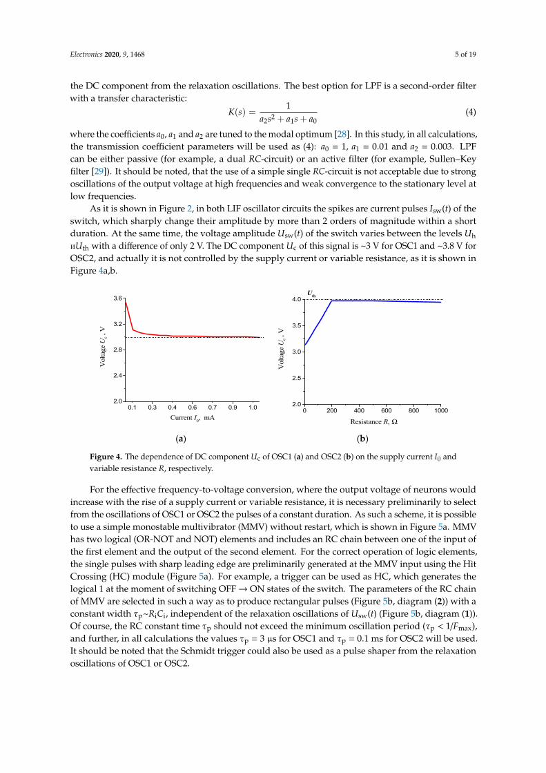
where the coefficients a0, a1 and a2 are tuned to the modal optimum [28]. In this study, in all calculations,the transmission coefficient parameters will be used as (4): a0 = 1, a1 = 0.01 and a2 = 0.003. LPFcan be either passive (for example, a dual RC-circuit) or an active filter (for example, Sullen–Keyfilter [29]). It should be noted, that the use of a simple single RC-circuit is not acceptable due to strongoscillations of the output voltage at high frequencies and weak convergence to the stationary level atlow frequencies.
As it is shown in Figure 2, in both LIF oscillator circuits the spikes are current pulses Isw(t) of theswitch, which sharply change their amplitude by more than 2 orders of magnitude within a shortduration. At the same time, the voltage amplitude Usw(t) of the switch varies between the levels Uh
иUth with a difference of only 2 V. The DC component Uc of this signal is ~3 V for OSC1 and ~3.8 V forOSC2, and actually it is not controlled by the supply current or variable resistance, as it is shown inFigure 4a,b.
Electronics 2020, 9, x FOR PEER REVIEW 5 of 19
the DC component from the relaxation oscillations. The best option for LPF is a second-order filter with a transfer characteristic:
K sa s a s a2
2 1 0
1( ) =+ +
(4)
where the coefficients a0, a1 and a2 are tuned to the modal optimum [28]. In this study, in all calculations, the transmission coefficient parameters will be used as (4): a0 = 1, a1 = 0.01 and a2 = 0.003. LPF can be either passive (for example, a dual RC-circuit) or an active filter (for example, Sullen–Key filter [29]). It should be noted, that the use of a simple single RC-circuit is not acceptable due to strong oscillations of the output voltage at high frequencies and weak convergence to the stationary level at low frequencies.
As it is shown in Figure 2, in both LIF oscillator circuits the spikes are current pulses Isw(t) of the switch, which sharply change their amplitude by more than 2 orders of magnitude within a short duration. At the same time, the voltage amplitude Usw(t) of the switch varies between the levels Uh и Uth with a difference of only 2 V. The DC component Uc of this signal is ~3 V for OSC1 and ~3.8 V for OSC2, and actually it is not controlled by the supply current or variable resistance, as it is shown in Figure 4a,b.
(a) (b)
Figure 4. The dependence of DC component Uc of OSC1 (a) and OSC2 (b) on the supply current I0 and variable resistance R, respectively.
For the effective frequency-to-voltage conversion, where the output voltage of neurons would increase with the rise of a supply current or variable resistance, it is necessary preliminarily to select from the oscillations of OSC1 or OSC2 the pulses of a constant duration. As such a scheme, it is possible to use a simple monostable multivibrator (MMV) without restart, which is shown in Figure 5a. MMV has two logical (OR-NOT and NOT) elements and includes an RC chain between one of the input of the first element and the output of the second element. For the correct operation of logic elements, the single pulses with sharp leading edge are preliminarily generated at the MMV input using the Hit Crossing (HC) module (Figure 5a). For example, a trigger can be used as HC, which generates the logical 1 at the moment of switching OFF → ON states of the switch. The parameters of the RC chain of MMV are selected in such a way as to produce rectangular pulses (Figure 5b, diagram (2)) with a constant width τp~RiCi, independent of the relaxation oscillations of Usw(t) (Figure 5b, diagram (1)). Of course, the RC constant time τp should not exceed the minimum oscillation period (τp < 1/Fmax), and further, in all calculations the values τp = 3 µs for OSC1 and τp = 0.1 ms for OSC2 will be used. It should be noted that the Schmidt trigger could also be used as a pulse shaper from the relaxation oscillations of OSC1 or OSC2.
0.1 0.4 0.7 1.00.3 0.6 0.92.0
2.4
2.8
3.2
3.6
Vol
tage
Uc ,
V
Current I0, mA0 200 400 600 800 1000
2.0
2.5
3.0
3.5
4.0Uth
Vol
tage
Uc ,
V
Resistance R, Ω
Figure 4. The dependence of DC component Uc of OSC1 (a) and OSC2 (b) on the supply current I0 andvariable resistance R, respectively.
For the effective frequency-to-voltage conversion, where the output voltage of neurons wouldincrease with the rise of a supply current or variable resistance, it is necessary preliminarily to selectfrom the oscillations of OSC1 or OSC2 the pulses of a constant duration. As such a scheme, it is possibleto use a simple monostable multivibrator (MMV) without restart, which is shown in Figure 5a. MMVhas two logical (OR-NOT and NOT) elements and includes an RC chain between one of the input ofthe first element and the output of the second element. For the correct operation of logic elements,the single pulses with sharp leading edge are preliminarily generated at the MMV input using the HitCrossing (HC) module (Figure 5a). For example, a trigger can be used as HC, which generates thelogical 1 at the moment of switching OFF→ ON states of the switch. The parameters of the RC chainof MMV are selected in such a way as to produce rectangular pulses (Figure 5b, diagram (2)) with aconstant width τp~RiCi, independent of the relaxation oscillations of Usw(t) (Figure 5b, diagram (1)).Of course, the RC constant time τp should not exceed the minimum oscillation period (τp < 1/Fmax),and further, in all calculations the values τp = 3 µs for OSC1 and τp = 0.1 ms for OSC2 will be used.It should be noted that the Schmidt trigger could also be used as a pulse shaper from the relaxationoscillations of OSC1 or OSC2.

Electronics 2020, 9, 1468 6 of 19Electronics 2020, 9, x FOR PEER REVIEW 6 of 19
(a) (b)
(c) (d)
Figure 5. Monostable multivibrator (MMV) circuit with input Hit Crossing (HC) module (a): Uin ≡ Usw(t), Ri and Ci—parameters of the RC chain. Voltage diagrams by example of OSC2 (b): Usw(t) (1) and pulses of MMV with τp~RiCi = 0.2 ms (2). The dependence of the output voltage Ulpf of leaky integrated-and-fire (LIF) neurons with low-pass filter (LPF) and MMV modules on the supply current I0 of OSC1 (c) and variable resistance R of OSC2 (d). The inset of Figure 5c shows an example of an amplifier with output voltage limiters (Umax and Umin) based on zener diodes in a chain of negative feedback (FB). The arrow in Figure 5d shows the trend of Ulpf (R) to Umax = 0.69 V with R→∞. Calculation parameters: Table 1 and I0 = 0.15 mA for OSC2.
2.3. Neuron Based on OSC1 (Neuron 1)
In any section of F(I0) (Figure 3a), where the frequency monotonically depends on the supply current, LPF will, in turn, monotonically convert the pulses of MMV into voltage levels (Ulpf). It is advisable to use the initial section F(I0) close to linear, where I0 << I0_max. As can be seen in Figure 5c, the dependence of the voltage on the supply current after passing MMV and LPF Ulpf(I0) is also linear.
It is possible to build a linear activation function (lin) of the LIF neuron (Neuron 1) based on OSC1:
y x xy y y x y
lin x x x x < xx x x xy x x
max max
max min max min min maxmin max
max max max max
min min
,x
( ) ,
,
≥ − −= ⋅ + < − − ≤
(5)
where x ≡ I0, ymax ≡ Umax and ymin ≡ Umin—maximum and minimum values of output voltage levels Ulpf, xmax ≡ Imax and xmin ≡ Imin—maximum and minimum values of supply current I0, that correspond to Umax and Umin. To obtain the activation function (5) at the output of the neuron, it is necessary to add a limiter module controlling the lower and upper levels of the output voltage after the LPF (see, insert to Figure 5c). This is a fundamental outcome in the design of IHN with oscillators of the OSC1 type,
0
1
2
3
4
0.00 0.05 0.10 0.15 0.200.0
0.2
0.4
0.6
0.8
1.0 (2)
Usw
, V
(1)
MM
V,
V
Time, s
0.0 0.5 1.0 1.5 2.0 2.5 3.00.0
0.1
0.2
0.3
0.4
0.5
0.6
+- UoutUin
Imin Imax
Umin
Vol
tage
Ulp
f , V
Current I0, mA
Umax
0 200 400 600 800 1000-0.1
0.0
0.1
0.2
0.3
0.4
0.5
0.6
0.7
Umin
Umax
Ro∼200 ΩV
olta
ge U
lpf ,
V
Resistance R, Ω
Uo~0.15 V
Figure 5. Monostable multivibrator (MMV) circuit with input Hit Crossing (HC) module (a):Uin ≡ Usw(t), Ri and Ci—parameters of the RC chain. Voltage diagrams by example of OSC2(b): Usw(t) (1) and pulses of MMV with τp~RiCi = 0.2 ms (2). The dependence of the output voltageUlpf of leaky integrated-and-fire (LIF) neurons with low-pass filter (LPF) and MMV modules on thesupply current I0 of OSC1 (c) and variable resistance R of OSC2 (d). The inset of Figure 5c shows anexample of an amplifier with output voltage limiters (Umax and Umin) based on zener diodes in a chainof negative feedback (FB). The arrow in Figure 5d shows the trend of Ulpf (R) to Umax = 0.69 V withR→∞. Calculation parameters: Table 1 and I0 = 0.15 mA for OSC2.
2.3. Neuron Based on OSC1 (Neuron 1)
In any section of F(I0) (Figure 3a), where the frequency monotonically depends on the supplycurrent, LPF will, in turn, monotonically convert the pulses of MMV into voltage levels (Ulpf). It isadvisable to use the initial section F(I0) close to linear, where I0 << I0_max. As can be seen in Figure 5c,the dependence of the voltage on the supply current after passing MMV and LPF Ulpf(I0) is also linear.
It is possible to build a linear activation function (lin) of the LIF neuron (Neuron 1) based on OSC1:
lin(x) =
ymax, x ≥ xmaxymax−yminxmax−xmax
·x + xmax ymin−xmin ymaxxmax−xmax
, xmin < x < xmax
ymin, x ≤ xmin
(5)
where x ≡ I0, ymax ≡ Umax and ymin ≡ Umin—maximum and minimum values of output voltage levelsUlpf, xmax ≡ Imax and xmin ≡ Imin—maximum and minimum values of supply current I0, that correspondto Umax and Umin. To obtain the activation function (5) at the output of the neuron, it is necessary toadd a limiter module controlling the lower and upper levels of the output voltage after the LPF (see,insert to Figure 5c). This is a fundamental outcome in the design of IHN with oscillators of the OSC1
Electronics 2020, 9, 1468 7 of 19
type, since output voltages of neurons are proportional to oscillation frequencies and are limited totwo levels in accordance with (5).
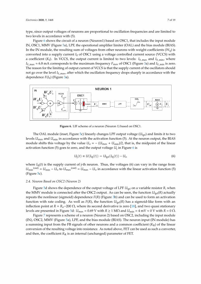
Figure 6 shows the circuit of a neuron (Neuron1) based on OSC1, that includes the input moduleIN, OSC1, MMV (Figure 5a), LPF, the operational amplifier limiter (OAL) and the bias module (BIAS).In the IN module, the resulting sum of voltages from other neurons with weight coefficients (Wij) isconverted into a supply current I0 of OSC1 using a voltage controlled current source (VCCS) witha coefficient (KI). In VCCS, the output current is limited to two levels: I0_max and I0_min, whereI0_max ≈ 6.8 mA corresponds to the maximum frequency Fmax of OSC1 (Figure 3a) and I0_min is zero.The reason for the limiting of output current of VCCS is that the supply current of the oscillators shouldnot go over the level I0_max, after which the oscillation frequency drops sharply in accordance with thedependence F(I0) (Figure 3a).
Electronics 2020, 9, x FOR PEER REVIEW 7 of 19
since output voltages of neurons are proportional to oscillation frequencies and are limited to two levels in accordance with (5).
Figure 6 shows the circuit of a neuron (Neuron1) based on OSC1, that includes the input module IN, OSC1, MMV (Figure 5a), LPF, the operational amplifier limiter (OAL) and the bias module (BIAS). In the IN module, the resulting sum of voltages from other neurons with weight coefficients (Wij) is converted into a supply current I0 of OSC1 using a voltage controlled current source (VCCS) with a coefficient (KI). In VCCS, the output current is limited to two levels: I0_max and I0_min, where I0_max ≈ 6.8 mA corresponds to the maximum frequency Fmax of OSC1 (Figure 3a) and I0_min is zero. The reason for the limiting of output current of VCCS is that the supply current of the oscillators should not go over the level I0_max, after which the oscillation frequency drops sharply in accordance with the dependence F(I0) (Figure 3a).
Figure 6. LIF scheme of a neuron (Neuron 1) based on OSC1.
The OAL module (inset, Figure 5c) linearly changes LPF output voltage (Ulpf) and limits it to two levels Umax and Umin in accordance with the activation function (5). At the neuron output, the BIAS module shifts this voltage by the value Uo = − (Umax + Umin)/2, that is, the midpoint of the linear activation function (5) goes to zero, and the output voltage Uj in Figure 6 is
0 0U t U I t U I t Uj j lpf j o( ) ( ( )) ( ( ))≡ = − (6)
where I0j(t) is the supply current of j-th neuron. Thus, the voltages (6) can vary in the range from Umin(out) = Umin − Uo to Umax(out) = Umax − Uo in accordance with the linear activation function (5) (Figure 5c).
2.4. Neuron Based on OSC2 (Neuron 2)
Figure 5d shows the dependence of the output voltage of LPF Ulpf on a variable resistor R, when the MMV module is connected after the OSC2 output. As can be seen, the function Ulpf(R) actually repeats the nonlinear (sigmoid) dependence F(R) (Figure 3b) and can be used to form an activation function with rate coding. As well as F(R), the function Ulpf(R) has a sigmoid-like form with an inflection point at R = Ro~200 Ω, where its second derivative is zero [18], and two quasi stationary levels are presented in Figure 5d: Umax = 0.69 V with R ≥ 1 MΩ and Umin = 4 mV ≈ 0 V with R = 0 Ω.
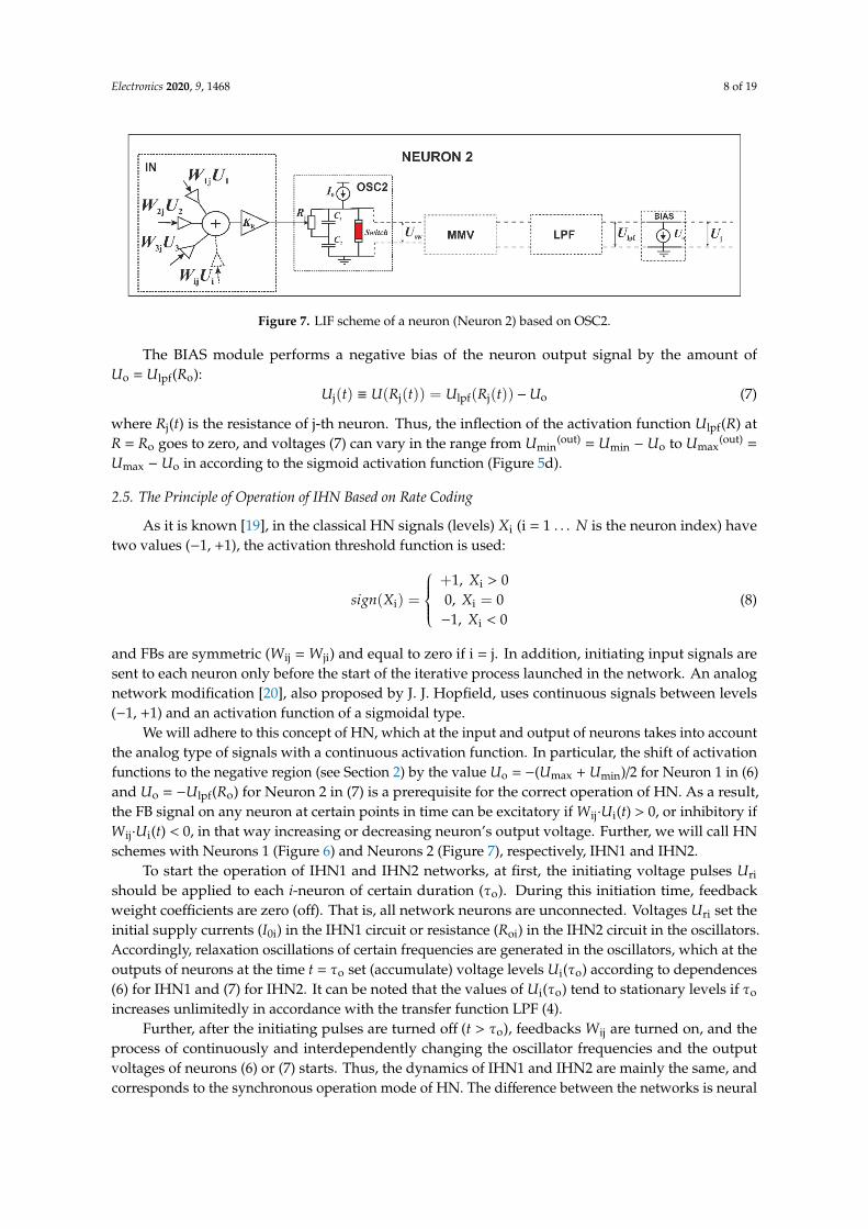
Figure 7 represents a scheme of a neuron (Neuron 2) based on OSC2, including the input module (IN), OSC2, MMV (Figure 5a), LPF, and the bias module (BIAS). The neuron input (IN module) has a summing input from the FB signals of other neurons and a common coefficient (KR) of the linear conversion of the resulting voltage into resistance. As noted above, FET can be used as such a converter, and then, the coefficient KR is an internal (unchanged) parameter of FET.
Figure 6. LIF scheme of a neuron (Neuron 1) based on OSC1.
The OAL module (inset, Figure 5c) linearly changes LPF output voltage (Ulpf) and limits it to twolevels Umax and Umin in accordance with the activation function (5). At the neuron output, the BIASmodule shifts this voltage by the value Uo = − (Umax + Umin)/2, that is, the midpoint of the linearactivation function (5) goes to zero, and the output voltage Uj in Figure 6 is
Uj(t) ≡ U(I0j(t)) = Ulpf(I0j(t)) −Uo (6)
where I0j(t) is the supply current of j-th neuron. Thus, the voltages (6) can vary in the range fromUmin
(out) = Umin − Uo to Umax(out) = Umax − Uo in accordance with the linear activation function (5)
(Figure 5c).
2.4. Neuron Based on OSC2 (Neuron 2)
Figure 5d shows the dependence of the output voltage of LPF Ulpf on a variable resistor R, whenthe MMV module is connected after the OSC2 output. As can be seen, the function Ulpf(R) actuallyrepeats the nonlinear (sigmoid) dependence F(R) (Figure 3b) and can be used to form an activationfunction with rate coding. As well as F(R), the function Ulpf(R) has a sigmoid-like form with aninflection point at R = Ro~200 Ω, where its second derivative is zero [18], and two quasi stationarylevels are presented in Figure 5d: Umax = 0.69 V with R ≥ 1 MΩ and Umin = 4 mV ≈ 0 V with R = 0 Ω.
Figure 7 represents a scheme of a neuron (Neuron 2) based on OSC2, including the input module(IN), OSC2, MMV (Figure 5a), LPF, and the bias module (BIAS). The neuron input (IN module) hasa summing input from the FB signals of other neurons and a common coefficient (KR) of the linearconversion of the resulting voltage into resistance. As noted above, FET can be used as such a converter,and then, the coefficient KR is an internal (unchanged) parameter of FET.
Electronics 2020, 9, 1468 8 of 19
Electronics 2020, 9, x FOR PEER REVIEW 8 of 19
Figure 7. LIF scheme of a neuron (Neuron 2) based on OSC2.
The BIAS module performs a negative bias of the neuron output signal by the amount of Uo = Ulpf(Ro):
U t U R t U R t Uj j lpf j o( ) ( ( )) ( ( ))≡ = − (7)
where Rj(t) is the resistance of j-th neuron. Thus, the inflection of the activation function Ulpf(R) at R = Ro goes to zero, and voltages (7) can vary in the range from Umin(out) = Umin − Uo to Umax(out) = Umax − Uo in according to the sigmoid activation function (Figure 5d).
2.5. The Principle of Operation of IHN Based on Rate Coding
As it is known [19], in the classical HN signals (levels) Xi (i = 1…N is the neuron index) have two values (−1, +1), the activation threshold function is used:
1 00 0
1 0
Xsign X X
X
i
i i
i
,( ) ,
,
+ >= =− <
(8)
and FBs are symmetric (Wij = Wji) and equal to zero if i = j. In addition, initiating input signals are sent to each neuron only before the start of the iterative process launched in the network. An analog network modification [20], also proposed by J. J. Hopfield, uses continuous signals between levels (−1, + 1) and an activation function of a sigmoidal type.
We will adhere to this concept of HN, which at the input and output of neurons takes into account the analog type of signals with a continuous activation function. In particular, the shift of activation functions to the negative region (see Section 2) by the value Uo = −(Umax + Umin)/2 for Neuron 1 in (6) and Uo = −Ulpf(Ro) for Neuron 2 in (7) is a prerequisite for the correct operation of HN. As a result, the FB signal on any neuron at certain points in time can be excitatory if Wij⋅Ui(t) > 0, or inhibitory if Wij⋅Ui(t) < 0, in that way increasing or decreasing neuron’s output voltage. Further, we will call HN schemes with Neurons 1 (Figure 6) and Neurons 2 (Figure 7), respectively, IHN1 and IHN2.
To start the operation of IHN1 and IHN2 networks, at first, the initiating voltage pulses Uri should be applied to each i-neuron of certain duration (τo). During this initiation time, feedback weight coefficients are zero (off). That is, all network neurons are unconnected. Voltages Uri set the initial supply currents (I0i) in the IHN1 circuit or resistance (Roi) in the IHN2 circuit in the oscillators. Accordingly, relaxation oscillations of certain frequencies are generated in the oscillators, which at the outputs of neurons at the time t = τo set (accumulate) voltage levels Ui(τo) according to dependences (6) for IHN1 and (7) for IHN2. It can be noted that the values of Ui(τo) tend to stationary levels if τo increases unlimitedly in accordance with the transfer function LPF (4).
Further, after the initiating pulses are turned off (t > τo), feedbacks Wij are turned on, and the process of continuously and interdependently changing the oscillator frequencies and the output voltages of neurons (6) or (7) starts. Thus, the dynamics of IHN1 and IHN2 are mainly the same, and corresponds to the synchronous operation mode of HN. The difference between the networks is neural schemes (Figures 6 and 7) and control signals: supply currents I0i(t) for IHN1 and variable resistances Ri(t) for IHN2.
Figure 7. LIF scheme of a neuron (Neuron 2) based on OSC2.
The BIAS module performs a negative bias of the neuron output signal by the amount ofUo = Ulpf(Ro):
Uj(t) ≡ U(Rj(t)) = Ulpf(Rj(t)) −Uo (7)
where Rj(t) is the resistance of j-th neuron. Thus, the inflection of the activation function Ulpf(R) atR = Ro goes to zero, and voltages (7) can vary in the range from Umin
(out) = Umin − Uo to Umax(out) =
Umax − Uo in according to the sigmoid activation function (Figure 5d).
2.5. The Principle of Operation of IHN Based on Rate Coding
As it is known [19], in the classical HN signals (levels) Xi (i = 1 . . . N is the neuron index) havetwo values (−1, +1), the activation threshold function is used:
sign(Xi) =
+1, Xi > 00, Xi = 0−1, Xi < 0
(8)
and FBs are symmetric (Wij = Wji) and equal to zero if i = j. In addition, initiating input signals aresent to each neuron only before the start of the iterative process launched in the network. An analognetwork modification [20], also proposed by J. J. Hopfield, uses continuous signals between levels(−1, +1) and an activation function of a sigmoidal type.
We will adhere to this concept of HN, which at the input and output of neurons takes into accountthe analog type of signals with a continuous activation function. In particular, the shift of activationfunctions to the negative region (see Section 2) by the value Uo = −(Umax + Umin)/2 for Neuron 1 in (6)and Uo = −Ulpf(Ro) for Neuron 2 in (7) is a prerequisite for the correct operation of HN. As a result,the FB signal on any neuron at certain points in time can be excitatory if Wij·Ui(t) > 0, or inhibitory ifWij·Ui(t) < 0, in that way increasing or decreasing neuron’s output voltage. Further, we will call HNschemes with Neurons 1 (Figure 6) and Neurons 2 (Figure 7), respectively, IHN1 and IHN2.
To start the operation of IHN1 and IHN2 networks, at first, the initiating voltage pulses Uri
should be applied to each i-neuron of certain duration (τo). During this initiation time, feedbackweight coefficients are zero (off). That is, all network neurons are unconnected. Voltages Uri set theinitial supply currents (I0i) in the IHN1 circuit or resistance (Roi) in the IHN2 circuit in the oscillators.Accordingly, relaxation oscillations of certain frequencies are generated in the oscillators, which at theoutputs of neurons at the time t = τo set (accumulate) voltage levels Ui(τo) according to dependences(6) for IHN1 and (7) for IHN2. It can be noted that the values of Ui(τo) tend to stationary levels if τo
increases unlimitedly in accordance with the transfer function LPF (4).Further, after the initiating pulses are turned off (t > τo), feedbacks Wij are turned on, and the
process of continuously and interdependently changing the oscillator frequencies and the outputvoltages of neurons (6) or (7) starts. Thus, the dynamics of IHN1 and IHN2 are mainly the same, andcorresponds to the synchronous operation mode of HN. The difference between the networks is neural

Electronics 2020, 9, 1468 9 of 19
schemes (Figures 6 and 7) and control signals: supply currents I0i(t) for IHN1 and variable resistancesRi(t) for IHN2.
Without loss of generality, we will further study the schemes of IHN1 and IHN2 as IoT devicesfor dynamic data processing using the example of the templates identification of two-dimensionalimages. For this task, the signal value at the output of each neuron is identified with a specific pixelcolor. There can be only black and white reference images in the classical HN, for example, +1—blackpixel color, −1—white pixel color. In our case, for IHN1, the supply currents of the reference imagesIiα (α = 1 . . . M is the number of images) at the inputs of neurons must be set in accordance with (5)
either Iiα≤ Imin for the white color of the pixel, or Ii
α≥ Imax for the black color. Similarly, for IHN2 the
resistance of the α-reference image Riα for i-th oscillator (pixel) must be set either close to zero (Ω’s)
for the white color of the pixel, or higher than Rmax (MΩ’s) for the black color of the pixel.Then, the weight coefficients Wij of these networks will be adjusted in accordance with the Hebb
rule [30]:
Wij =
1M
∑α
sign(U(Rαi )
)·sign
(U(Rαj )
), for IHN1
1M
∑α
sign(U(Iα0i)
)·sign
(U(Iα0j)
), for IHN2
(9)
where U(I0iα) and U(Ri
α) are limit (positive or negative) values of the output voltages of neurons inthe circuits IHN1 and IHN2, respectively.
At the same time, the initial supply currents for IHN1 or resistance for IHN2 of recognizable(non-reference) patterns can have arbitrary values, that is, have a gray gradation (see Figure 8).In accordance with the initial values (I0i or Roi) of patterns, the output voltages Ui(τo) of neurons areset at the time t = τo, which can also be arbitrary from Umin
(out) to Umax(out) as follows to formula (6)
or (7).
Electronics 2020, 9, x FOR PEER REVIEW 9 of 19
Without loss of generality, we will further study the schemes of IHN1 and IHN2 as IoT devices for dynamic data processing using the example of the templates identification of two-dimensional images. For this task, the signal value at the output of each neuron is identified with a specific pixel color. There can be only black and white reference images in the classical HN, for example, +1—black pixel color, −1—white pixel color. In our case, for IHN1, the supply currents of the reference images Iiα (α = 1…M is the number of images) at the inputs of neurons must be set in accordance with (5) either Iiα ≤ Imin for the white color of the pixel, or Iiα ≥ Imax for the black color. Similarly, for IHN2 the resistance of the α-reference image Riα for i-th oscillator (pixel) must be set either close to zero (Ω’s) for the white color of the pixel, or higher than Rmax (MΩ’s) for the black color of the pixel.
Then, the weight coefficients Wij of these networks will be adjusted in accordance with the Hebb rule [30]:
( ) ( )( ) ( )0 0
1 1
1 2
sign U R sign U R MW
sign U I sign U I M
i j
ij
i j
( ) ( ) , for IHN
( ) ( ) , for IHN
α α
α
α α
α
⋅= ⋅
(9)
where U(I0iα) and U(Riα) are limit (positive or negative) values of the output voltages of neurons in the circuits IHN1 and IHN2, respectively.
At the same time, the initial supply currents for IHN1 or resistance for IHN2 of recognizable (non-reference) patterns can have arbitrary values, that is, have a gray gradation (see Figure 8). In accordance with the initial values (I0i or Roi) of patterns, the output voltages Ui(τo) of neurons are set at the time t = τo, which can also be arbitrary from Umin(out) to Umax(out) as follows to formula (6) or (7).
Figure 8. The gray gradation of patterns for the initial supply currents I0 (impulsive HN1, IHN1) and resistances R (IHN2) (left). The numbering of neurons in the network, symmetrical reference images and input patterns (A–D) (right). (A) and (B) are recognized as Reference Image 1, (C) and (D) are recognized as Reference Image 2.
The recognition process in both network variants consists of increasing (or decreasing) the gradation of pixels of such patterns to black (or white) color, that is, to stationary values at the output of each neuron, that is close to either Umax(out), or Umin(out). Thus, IHN acts as a corrector for a noisy image, where noise means the background of the template in the form of a gradation of gray, as well as the presence of “false” pixels. As a result of the operation of the networks, that is, the continuous change of frequency Fi(t) and output voltage Ui(t) of each oscillator, IHN1 and IHN2 should come to a steady state corresponding to the minimum of HN energy [20] of a certain reference of strictly black and white image.
Figure 8. The gray gradation of patterns for the initial supply currents I0 (impulsive HN1, IHN1) andresistances R (IHN2) (left). The numbering of neurons in the network, symmetrical reference imagesand input patterns (A–D) (right). (A) and (B) are recognized as Reference Image 1, (C) and (D) arerecognized as Reference Image 2.
The recognition process in both network variants consists of increasing (or decreasing) thegradation of pixels of such patterns to black (or white) color, that is, to stationary values at the outputof each neuron, that is close to either Umax
(out), or Umin(out). Thus, IHN acts as a corrector for a noisy
image, where noise means the background of the template in the form of a gradation of gray, as wellas the presence of “false” pixels. As a result of the operation of the networks, that is, the continuous
Electronics 2020, 9, 1468 10 of 19
change of frequency Fi(t) and output voltage Ui(t) of each oscillator, IHN1 and IHN2 should come to asteady state corresponding to the minimum of HN energy [20] of a certain reference of strictly blackand white image.
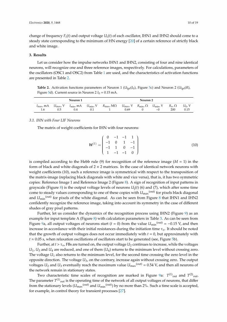
3. Results
Let us consider how the impulse networks IHN1 and IHN2, consisting of four and nine identicalneurons, will recognize one and three reference images, respectively. For calculations, parameters ofthe oscillators (OSC1 and OSC2) from Table 1 are used, and the characteristics of activation functionsare presented in Table 2.
Table 2. Activation functions parameters of Neuron 1 (Ulpf(I0), Figure 5c) and Neuron 2 (Ulpf(R),Figure 5d). Current source in Neuron 2 I0 = 0.15 mA.
Neuron 1 Neuron 2
Imax, mA Umax, V Imin, mA Umin, V Rmax, MΩ Umax, V Rmin, Ω Umin, V Ro, Ω U0, V1.6 0.5 0.4 0.1 1 0.69 0 ~0 200 0.15
3.1. IHN with Four LIF Neurons
The matrix of weight coefficients for IHN with four neurons:
W(1) =
0 −1 −1 1−1 0 1 −1−1 1 0 −11 −1 −1 0
(10)
is compiled according to the Hebb rule (9) for recognition of the reference image (M = 1) in theform of black and white diagonals of 2 × 2 matrices. In the case of identical network neurons withweight coefficients (10), such a reference image is symmetrical with respect to the transposition ofthe matrix-image (replacing black diagonals with white and vice versa), that is, it has two symmetriccopies: Reference Image 1 and Reference Image 2 (Figure 8). A sign of recognition of input patterns ingrayscale (Figure 8) is the output voltage levels of neurons Uj(t) (6) and (7), which after some timecome to steady values corresponding to one of these copies with Umax
(out) for pixels black diagonaland Umin
(out) for pixels of the white diagonal. As can be seen from Figure 8 that IHN1 and IHN2confidently recognize the reference image, taking into account its symmetry in the case of differentshades of gray pixel patterns.
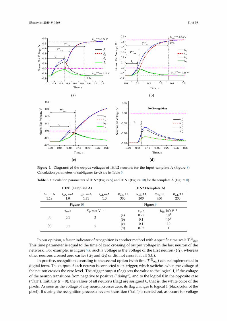
Further, let us consider the dynamics of the recognition process using IHN2 (Figure 9) as anexample for input template A (Figure 8) with calculation parameters in Table 3. As can be seen fromFigure 9a, all output voltages of neurons start (t = 0) from the value Umin
(out) = −0.15 V, and thenincrease in accordance with their initial resistances during the initiation time τo. It should be notedthat the growth of output voltages does not occur immediately with t = 0, but approximately witht ≈ 0.05 s, when relaxation oscillations of oscillators start to be generated (see, Figure 5b).
Further, at t > τo, FBs are turned on, the output voltage U2 continues to increase, while the voltagesU1, U3 and U4 are reduced, and one of them (U4) returns to the minimum level without crossing zero.The voltage U1 also returns to the minimum level, for the second time crossing the zero level in theopposite direction. The voltage U3, on the contrary, increase again without crossing zero. The outputvoltages U2 and U3 eventually reach the maximum value Umax
(out) = 0.54 V, and then all neurons ofthe network remain in stationary states.
Two characteristic time scales of recognition are marked in Figure 9a: T(1)out and T(2)
out.The parameter T(1)
out is the operating time of the network of all output voltages of neurons, that differfrom the stationary levels (Umax
(out) and Umin(out)) by no more than 2%. Such a time scale is accepted,
for example, in control theory for transient processes [27].
Electronics 2020, 9, 1468 11 of 19
Electronics 2020, 9, x FOR PEER REVIEW 10 of 19
3. Results
Let us consider how the impulse networks IHN1 and IHN2, consisting of four and nine identical neurons, will recognize one and three reference images, respectively. For calculations, parameters of the oscillators (OSC1 and OSC2) from Table 1 are used, and the characteristics of activation functions are presented in Table 2.
Table 2. Activation functions parameters of Neuron 1 (Ulpf(I0), Figure 5c) and Neuron 2 (Ulpf(R), Figure 5d). Current source in Neuron 2 I0 = 0.15 mA.
Neuron 1 Neuron 2 Imax, mA Umax, V Imin, mA Umin, V Rmax, MΩ Umax, V Rmin, Ω Umin, V Ro, Ω U0, V
1.6 0.5 0.4 0.1 1 0.69 0 ~0 200 0.15
3.1. IHN with Four LIF Neurons
The matrix of weight coefficients for IHN with four neurons:
W =(1)
0 1 1 11 0 1 11 1 0 1
1 1 1 0
− − − − − − − −
(10)
is compiled according to the Hebb rule (9) for recognition of the reference image (M = 1) in the form of black and white diagonals of 2 × 2 matrices. In the case of identical network neurons with weight coefficients (10), such a reference image is symmetrical with respect to the transposition of the matrix-image (replacing black diagonals with white and vice versa), that is, it has two symmetric copies: Reference Image 1 and Reference Image 2 (Figure 8). A sign of recognition of input patterns in grayscale (Figure 8) is the output voltage levels of neurons Uj(t) (6) and (7), which after some time come to steady values corresponding to one of these copies with Umax(out) for pixels black diagonal and Umin(out) for pixels of the white diagonal. As can be seen from Figure 8 that IHN1 and IHN2 confidently recognize the reference image, taking into account its symmetry in the case of different shades of gray pixel patterns.
Further, let us consider the dynamics of the recognition process using IHN2 (Figure 9) as an example for input template A (Figure 8) with calculation parameters in Table 3. As can be seen from Figure 9a, all output voltages of neurons start (t = 0) from the value Umin(out) = −0.15 V, and then increase in accordance with their initial resistances during the initiation time τo. It should be noted that the growth of output voltages does not occur immediately with t = 0, but approximately with t ≈ 0.05 s, when relaxation oscillations of oscillators start to be generated (see, Figure 5b).
(a) (b)
0.0 0.1 0.2 0.3 0.4 0.5 0.6 0.7 0.8
-0.2
-0.1
0.0
0.1
0.2
0.3
0.4
0.5
0.6
Τ (2)out
~2 %
Umin(out)=− 0.15 V
Umax(out)=0.54 V
τo
Τ (1)out
U1
U2
U3
U4
Neu
ron
Out
Vol
tage
, V
Time, s0.0 0.1 0.2 0.3 0.4 0.5
-0.2
-0.1
0.0
0.1
0.2
0.3
0.4
0.5
0.6
Umin(out)=− 0.15 V
Umax(out)=0.54 V
~2 %
τo
Τ (2)out
Τ (1)out
U1
U2
U3
U4
Neu
ron
Out
Vol
tage
, V
Time, sElectronics 2020, 9, x FOR PEER REVIEW 11 of 19
(c) (d)
Figure 9. Diagrams of the output voltages of IHN2 neurons for the input template A (Figure 8). Calculation parameters of subfigures (a–d) are in Table 3.
Further, at t > τo, FBs are turned on, the output voltage U2 continues to increase, while the voltages U1, U3 and U4 are reduced, and one of them (U4) returns to the minimum level without crossing zero. The voltage U1 also returns to the minimum level, for the second time crossing the zero level in the opposite direction. The voltage U3, on the contrary, increase again without crossing zero. The output voltages U2 and U3 eventually reach the maximum value Umax(out) = 0.54 V, and then all neurons of the network remain in stationary states.
Two characteristic time scales of recognition are marked in Figure 9a: T(1)out and T(2)out. The parameter T(1)out is the operating time of the network of all output voltages of neurons, that differ from the stationary levels (Umax(out) and Umin(out)) by no more than 2%. Such a time scale is accepted, for example, in control theory for transient processes [27].
In our opinion, a faster indicator of recognition is another method with a specific time scale T(2)out. This time parameter is equal to the time of zero crossing of output voltage in the last neuron of the network. For example, in Figure 9a, such a voltage is the voltage of the first neuron (U1), whereas other neurons crossed zero earlier (U2 and U3) or did not cross it at all (U4).
In practice, recognition according to the second option (with time T(2)out) can be implemented in digital form. The output of each neuron is connected to its trigger, which switches when the voltage of the neuron crosses the zero level. The trigger output (flag) sets the value to the logical 1, if the voltage of the neuron transitions from negative to positive (“rising”), and to the logical 0 in the opposite case (“fall”). Initially (t = 0), the values of all neurons (flag) are assigned 0, that is, the white color of the pixels. As soon as the voltage of any neuron crosses zero, its flag changes to logical 1 (black color of the pixel). If during the recognition process a reverse transition (“fall”) is carried out, as occurs for voltage U1 (Figure 9a), the flag will switch back to 0. Eventually, all neurons for pattern A take a flag that corresponds to the reference image: U1 (0), U2 (1), U3 (1) and U4 (0), the last of which never switched and remained in the initial state of logical zero.
Obviously, the final setting of neuron flags always occurs earlier than the output of their stresses to stationary (minimum or maximum) levels, that is, the time T(2)out is less than T(1)out. This becomes especially noticeable if you reduce the parameter KR in the oscillators and the network initiation time (τo). So, Figure 9b shows that T(2)out is 3.5 times smaller than T(1)out, if τo decreases 2.5 times. In the case when both τo, and KR (Figure 9c) decrease, the recognition by the method of zero crossing occurs for ~30 ms, while stationary levels of neurons cannot be detected for 200 ms. Figure 9d represents that there is a limit to reducing the parameters KR and τo, when pattern recognition is not possible. In this case, after a certain time of the network start, the voltage of all neurons returns to the initial (minimum) level, and the values of the triggers (flag) remain equal to 0.
0.00 0.05 0.10 0.15 0.20 0.25 0.30-0.2
-0.1
0.0
0.1
0.2
0.3
0.4
Τ (2)out
τo
U1
U2
U3
U4
Neu
ron
Out
Vol
tage
, V
Time, s0.00 0.05 0.10 0.15 0.20 0.25 0.30
-0.15
-0.10
-0.05
0.00
0.05
τo
U1
U2
U3
U4
Neu
ron
Out
Vol
tage
, V
Time, s
No Recognition
Figure 9. Diagrams of the output voltages of IHN2 neurons for the input template A (Figure 8).Calculation parameters of subfigures (a–d) are in Table 3.
Table 3. Calculation parameters of IHN2 (Figure 9) and IHN1 (Figure 10) for the template A (Figure 8).
IHN1 (Template A) IHN2 (Template A)
Io1, mA Io2, mA Io3, mA Io4,mA Ro1, Ω Ro2, Ω Ro3, Ω Ro4, Ω1.18 1.0 1.31 1.0 300 200 450 200
Figure 10 Figure 9
τo, s KI, mA·V−1 τo, s KR, kΩ·V−1
(a) 0.1 3(a) 0.25 103
(b) 0.1 103
(b) 0.1 5(c) 0.1 10(d) 0.07 1
In our opinion, a faster indicator of recognition is another method with a specific time scale T(2)out.
This time parameter is equal to the time of zero crossing of output voltage in the last neuron of thenetwork. For example, in Figure 9a, such a voltage is the voltage of the first neuron (U1), whereasother neurons crossed zero earlier (U2 and U3) or did not cross it at all (U4).
In practice, recognition according to the second option (with time T(2)out) can be implemented in
digital form. The output of each neuron is connected to its trigger, which switches when the voltage ofthe neuron crosses the zero level. The trigger output (flag) sets the value to the logical 1, if the voltageof the neuron transitions from negative to positive (“rising”), and to the logical 0 in the opposite case(“fall”). Initially (t = 0), the values of all neurons (flag) are assigned 0, that is, the white color of thepixels. As soon as the voltage of any neuron crosses zero, its flag changes to logical 1 (black color of thepixel). If during the recognition process a reverse transition (“fall”) is carried out, as occurs for voltage
Electronics 2020, 9, 1468 12 of 19
U1 (Figure 9a), the flag will switch back to 0. Eventually, all neurons for pattern A take a flag thatcorresponds to the reference image: U1 (0), U2 (1), U3 (1) and U4 (0), the last of which never switchedand remained in the initial state of logical zero.
Obviously, the final setting of neuron flags always occurs earlier than the output of their stressesto stationary (minimum or maximum) levels, that is, the time T(2)
out is less than T(1)out. This becomes
especially noticeable if you reduce the parameter KR in the oscillators and the network initiation time(τo). So, Figure 9b shows that T(2)
out is 3.5 times smaller than T(1)out, if τo decreases 2.5 times. In the
case when both τo, and KR (Figure 9c) decrease, the recognition by the method of zero crossing occursfor ~30 ms, while stationary levels of neurons cannot be detected for 200 ms. Figure 9d representsthat there is a limit to reducing the parameters KR and τo, when pattern recognition is not possible.In this case, after a certain time of the network start, the voltage of all neurons returns to the initial(minimum) level, and the values of the triggers (flag) remain equal to 0.
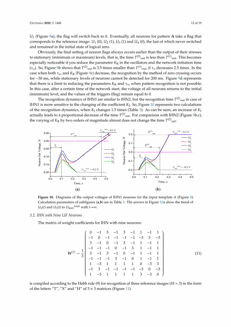
The recognition dynamics of IHN1 are similar to IHN2, but the recognition time T(2)out in case of
IHN1 is more sensitive to the changing of the coefficient KI. So, Figure 10 represents two calculationsof the recognition dynamics, when KI changes 1.5 times (Table 3). As can be seen, an increase of KI
actually leads to a proportional decrease of the time T(2)out. For comparison with IHN2 (Figure 9b,c),
the varying of KR by two orders of magnitude almost does not change the time T(2)out.
Electronics 2020, 9, x FOR PEER REVIEW 12 of 19
Table 3. Calculation parameters of IHN2 (Figure 9) and IHN1 (Figure 10) for the template A (Figure 8).
IHN1 (Template A) IHN2 (Template A) Io1, mA Io2, mA Io3, mA Io4,mA Ro1, Ω Ro2, Ω Ro3, Ω Ro4, Ω
1.18 1.0 1.31 1.0 300 200 450 200 Figure 10 Figure 9
τo, s KI, mA·V−1 τo, s KR, kΩ·V−1
(a) 0.1 3 (a) 0.25 103 (b) 0.1 103
(b) 0.1 5 (c) 0.1 10 (d) 0.07 1
(a) (b)
Figure 10. Diagrams of the output voltages of IHN1 neurons for the input template A (Figure 8). Calculation parameters of subfigures (a,b) are in Table 3. The arrows in Figure 10a show the trend of U2(t) and U3(t) to Umax(out) with t→∞.
The recognition dynamics of IHN1 are similar to IHN2, but the recognition time T(2)out in case of IHN1 is more sensitive to the changing of the coefficient KI. So, Figure 10 represents two calculations of the recognition dynamics, when KI changes 1.5 times (Table 3). As can be seen, an increase of KI actually leads to a proportional decrease of the time T(2)out. For comparison with IHN2 (Figure 9b,c), the varying of KR by two orders of magnitude almost does not change the time T(2)out.
3.2. IHN with Nine LIF Neurons
The matrix of weight coefficients for IHN with nine neurons: − − − − − − − − − − − − − − − − − − − − ⋅ − − − − − − − − − − − − − − − − − − − −
W =(3)
0 1 3 1 3 1 1 1 11 0 1 1 1 1 3 3 3
3 1 0 1 3 1 1 1 11 1 1 0 1 3 1 1 1
1 3 1 3 1 0 1 1 1 13
1 1 1 3 1 0 1 1 11 3 1 1 1 1 0 3 31 3 1 1 1 1 3 0 3
1 3 1 1 1 1 3 3 0
(11)
is compiled according to the Hebb rule (9) for recognition of three reference images (M = 3) in the form of the letters “T”, “X” and “H” of 3 × 3 matrices (Figure 11).
0.0 0.1 0.2 0.3 0.4 0.5
-0.20
-0.15
-0.10
-0.05
0.00
0.05 Τ (2)out
τo
Umin(out) = −0.2 V
Umax(out) = 0.2 V
U1
U2
U3
U4
Neu
ron
Out
Vol
tage
, V
Time, s
0.0 0.1 0.2 0.3 0.4 0.5
-0.2
-0.1
0.0
0.1
0.2
τo
Umin(out) = −0.2 V
Umax(out) = 0.2 VΤ (1)
out
Τ (2)out
U1
U2
U3
U4
Neu
ron
Out
Vol
tage
, V
Time, s
Figure 10. Diagrams of the output voltages of IHN1 neurons for the input template A (Figure 8).Calculation parameters of subfigures (a,b) are in Table 3. The arrows in Figure 10a show the trend ofU2(t) and U3(t) to Umax
(out) with t→∞.
3.2. IHN with Nine LIF Neurons
The matrix of weight coefficients for IHN with nine neurons:
W(3) =13·
0 −1 3 −1 3 −1 1 −1 1−1 0 −1 −1 −1 −1 −3 3 −33 −1 0 −1 3 −1 1 −1 1−1 −1 −1 0 −1 3 1 −1 13 −1 3 −1 0 −1 1 −1 1−1 −1 −1 3 −1 0 1 −1 11 −3 1 1 1 1 0 −3 3−1 3 −1 −1 −1 −1 −3 0 −31 −3 1 1 1 1 3 −3 0
(11)
is compiled according to the Hebb rule (9) for recognition of three reference images (M = 3) in the formof the letters “T”, “X” and “H” of 3 × 3 matrices (Figure 11).

Electronics 2020, 9, 1468 13 of 19
Electronics 2020, 9, x FOR PEER REVIEW 13 of 19
Figure 11. The numbering of neurons in the networks (IHN1 and IHN2), reference images (“T”, “X” and “H”) and input patterns (A–F) with gray gradation as in Figure 8. (A) and (B) are recognized as Reference Image 1, (C) and (D) are recognized as Reference Image 2, (E) and (F) are recognized as Reference Image 3.
The calculation results for some variants of input templates are presented in image form in the Figure 11. As can be seen, all input patterns (A–F) are confidently recognized as one of the three standard options (letters “T”, “X” or “H”). The recognition dynamics using the example of pattern C for one of 9 network neurons is shown in Figure 12 with calculation parameters in Table 4. There is a selected neuron (j = 9) that has a maximum zero crossing time for the output voltage (T(2)out). This parameter T(2)out for both networks (IHN1 and IHN2) determines the time of fast recognition similarly to the previous examples of a network with four neurons. With increasing voltage transfer coefficients KI (Figure 12a) or KR (Figure 12b) the time T(2)out decreases, but more for IHN1 than for IHN2, as well as in IHNs with four neurons (Figures 9 and 10). Let us note that there is also a limit to reducing voltage transfer coefficients (KI or KR) and the initiation time of networks τo, when the recognition of input patterns becomes impossible.
(a) (b)
Figure 12. Diagrams of the output voltages of the neuron U9(t) of the networks IHN1 (a) and IHN2 (b) for the input template C (Figure 11) for various voltage transfer coefficients: KI (a) and KR (b).
0.00 0.05 0.10 0.15 0.20 0.25 0.30
-0.2
-0.1
0.0
0.1
0.2
τo
Τ (2)out(U9
(1))
Τ (2)out(U9
(2)) ≅Τ (2)out(U9
(3))
Umin(out) = −0.2 V
Umax(out) = 0.2 V
U9(1)
U9(2)
U9(3)
Neu
ron
Out
Vol
tage
U9,
V
Time, s0.00 0.05 0.10 0.15 0.20 0.25 0.30
-0.2
-0.1
0.0
0.1
0.2
0.3
τo
Τ (2)out(U9
(3))
Τ (2)out(U9
(1)) =Τ (2)out(U9
(2))
Umin(out) = −0.15 V
U9(1)
U9(2)
U9(3)
Neu
ron
Out
Vol
tage
U9,
V
Time, s
Umax(out) = 0.54 V
Figure 11. The numbering of neurons in the networks (IHN1 and IHN2), reference images (“T”, “X”and “H”) and input patterns (A–F) with gray gradation as in Figure 8. (A) and (B) are recognized asReference Image 1, (C) and (D) are recognized as Reference Image 2, (E) and (F) are recognized asReference Image 3.
The calculation results for some variants of input templates are presented in image form in theFigure 11. As can be seen, all input patterns (A–F) are confidently recognized as one of the threestandard options (letters “T”, “X” or “H”). The recognition dynamics using the example of patternC for one of 9 network neurons is shown in Figure 12 with calculation parameters in Table 4. Thereis a selected neuron (j = 9) that has a maximum zero crossing time for the output voltage (T(2)
out).This parameter T(2)
out for both networks (IHN1 and IHN2) determines the time of fast recognitionsimilarly to the previous examples of a network with four neurons. With increasing voltage transfercoefficients KI (Figure 12a) or KR (Figure 12b) the time T(2)
out decreases, but more for IHN1 than forIHN2, as well as in IHNs with four neurons (Figures 9 and 10). Let us note that there is also a limitto reducing voltage transfer coefficients (KI or KR) and the initiation time of networks τo, when therecognition of input patterns becomes impossible.
Electronics 2020, 9, x FOR PEER REVIEW 13 of 19
Figure 11. The numbering of neurons in the networks (IHN1 and IHN2), reference images (“T”, “X” and “H”) and input patterns (A–F) with gray gradation as in Figure 8. (A) and (B) are recognized as Reference Image 1, (C) and (D) are recognized as Reference Image 2, (E) and (F) are recognized as Reference Image 3.
The calculation results for some variants of input templates are presented in image form in the Figure 11. As can be seen, all input patterns (A–F) are confidently recognized as one of the three standard options (letters “T”, “X” or “H”). The recognition dynamics using the example of pattern C for one of 9 network neurons is shown in Figure 12 with calculation parameters in Table 4. There is a selected neuron (j = 9) that has a maximum zero crossing time for the output voltage (T(2)out). This parameter T(2)out for both networks (IHN1 and IHN2) determines the time of fast recognition similarly to the previous examples of a network with four neurons. With increasing voltage transfer coefficients KI (Figure 12a) or KR (Figure 12b) the time T(2)out decreases, but more for IHN1 than for IHN2, as well as in IHNs with four neurons (Figures 9 and 10). Let us note that there is also a limit to reducing voltage transfer coefficients (KI or KR) and the initiation time of networks τo, when the recognition of input patterns becomes impossible.
(a) (b)
Figure 12. Diagrams of the output voltages of the neuron U9(t) of the networks IHN1 (a) and IHN2 (b) for the input template C (Figure 11) for various voltage transfer coefficients: KI (a) and KR (b).
0.00 0.05 0.10 0.15 0.20 0.25 0.30
-0.2
-0.1
0.0
0.1
0.2
τo
Τ (2)out(U9
(1))
Τ (2)out(U9
(2)) ≅Τ (2)out(U9
(3))
Umin(out) = −0.2 V
Umax(out) = 0.2 V
U9(1)
U9(2)
U9(3)
Neu
ron
Out
Vol
tage
U9,
V
Time, s0.00 0.05 0.10 0.15 0.20 0.25 0.30
-0.2
-0.1
0.0
0.1
0.2
0.3
τo
Τ (2)out(U9
(3))
Τ (2)out(U9
(1)) =Τ (2)out(U9
(2))
Umin(out) = −0.15 V
U9(1)
U9(2)
U9(3)
Neu
ron
Out
Vol
tage
U9,
V
Time, s
Umax(out) = 0.54 V
Figure 12. Diagrams of the output voltages of the neuron U9(t) of the networks IHN1 (a) and IHN2(b) for the input template C (Figure 11) for various voltage transfer coefficients: KI (a) and KR (b).Calculation parameters are in Table 4. The arrow in Figure 12b shows the trend of U9(t) to Umax
(out)
with t→∞.

Electronics 2020, 9, 1468 14 of 19
Table 4. Calculation parameters of IHN1 (Figure 12a) and IHN2 (Figure 12b) for the template C(Figure 11).
IHN1 (Figure 12a) IHN2 (Figure 12b)
Template C,Figure 11 Neuron out
voltage (j = 9)τo, s KI,
mA·V−1
Template C,Figure 11 Neuron out
voltage (j = 9)τo, s KR,
kΩ·V−1Neuron,number Ioi, mA Neuron,
number Roi, Ω
1 1.55U9
(1) 0.1 31 1000
U9(1) 0.1 1052 0.45 2 50
3 1.4 3 500
4 0.4U9
(2) 0.1 54 30
U9(2) 0.1 1035 1.5 5 800
6 1 6 200
7 1.2U9
(3) 0.1 97 350
U9(3) 0.1 18 0.48 8 80
9 0.9 9 150
4. Discussion
The IHNs that are presented in this study are essentially the same as conventional HN with acontinuous activation function [20]. For the existence of stable energy minima of such a network,the internal structure and type of control parameters of neurons are not important. Therefore, thecalculation results are quite predictable: both networks (IHN1 and IHN2) have associative memory,like regular analog NHs, and have the same advantages (one-step learning process) and disadvantages(low information capacity).
Both networks (IHN1 and IHN2) are mainly the same in dynamics and recognition results.Their difference is the circuits of neural oscillators and the implementation of frequency activationfunctions. For Neuron 1 it is necessary to artificially compile a linear change in the frequency (voltage)from the supply current into a threshold-linear activation function (5) by the limiting of the outputsignal (Figures 5c and 6). For Neuron 2 the limiting frequency (voltage) levels are set due to thesigmoid-like type of rate coding function F(R) (Figure 3b).
However, the main advantage of Neuron 2 is a high jump of the frequency and a wide variation inthe control resistance (from 0 to 10 MΩ) of OSC2 with a relatively low supply current. Indeed, one cansee in Figure 3a that the changing of frequency from 50 to 350 kHz (Fmax) in OSC1, that is, less than oneorder of magnitude, requires an increase in supply current by a factor of ~7 times. Whereas for OSC2,it is easy to obtain a frequency jump of more than two orders of magnitude (Figure 3b), while thesupply current remains at a constant and low level. Thus, for an energy-efficient implementation ofrate coding, the OSC2 circuit is certainly preferable to OSC1.
The concept of associative memory proposed in the study is not a purely mathematical project,but an already defined circuit solution. The LIF oscillators in neurons are circuits that are modeledby MatLab softare and have signals that correspond to experimental signals for the selected switchparameters [18]. As mentioned in the Introduction, the switches can be implemented at the level oflaboratory samples (for example, VO2 films [17]), and at the industrial scale (trigger diodes). The triggerdiodes can be replaced with a complementary pair of bipolar transistors [18]. It opens a wide range ofactivities for tuning the parameters of such a combined switch using the selection of complementarypair of transistors.
The design of FBs of neurons is also a circuitry and not purely mathematical solution. For example,a constant-duration pulse shaper on logic elements (MMV module), a low frequency filter and VCCSare proposed. These modules have a wide variety of already available implementations (at the levelof transistors, operational amplifiers, etc.). Some modules in the form of emulating electronic blocks(MMV module, VCCS) are used in MatLab software, other modules are mathematical blocks (limiters,transmission coefficients for LPF). A similar example of design amenable to practical realization

Electronics 2020, 9, 1468 15 of 19
is presented in [31], where an associative memory based on coupled oscillators is investigated.The associative memory proposed in our study is closer to a circuit solution and its hardwiredevelopment would be the next proposed step in future researches.
In general, both networks (IHN1 and IHN2) use a hybrid analog–digital method for signalprocessing and encoding. In particular, a digital method of recognition indication by zero crossing ofoutput voltages is proposed. Oddly enough, this digital indication is based on the analog mode ofoperation with continuous signals and an activation function of HN that can be explained as follows.At any time, the input voltage of each HN neuron is linear sum of voltages from other neurons:
Ui(t) =∑j,i
Wij·Uj(t) (12)
and likewise their derivatives:dUi(t)
dt=
∑j,i
Wij·dUj(t)
dt(13)
An important point is that the linear sum of the derivatives (13) for the last of neurons by thetime t = T(2)
out will already be either positive if its voltage tends to the maximum of the stationarylevel (Umax
(out)), or negative if the voltage tends to a minimum (Umin(out)). Thus, further (t > T(2)
out),it makes no sense to monitor the output voltages of neurons to stationary levels, that is, to a minimumof network energy. All neurons of the network will be divided into two groups in accordance witha recognizable reference image: some neurons, tending to Umax
(out), will have positive voltages andtheir derivatives, and for other neurons, on the contrary, output voltages and their derivatives willalready be negative and tend to Umin
(out). The inclusion of a trigger at the outputs of each neuron thatrecords zero crossings is a small “fee” for a faster indication of pattern recognition.
The general scheme of an associative memory module based on IHN of N neurons that classifies Mimages represented in Figure 13. The memory module uses a trigger block with N triggers, which areconnected to each IHN neuron, and a classifier–decoder (CD) out block. The switch triggers whenoutput voltages of neurons cross the zero level, and output signals of the trigger block as a combinationof binary numbers are generated. The CD block is a highly incomplete decoder, since the numberof inputs of the memory module (N) must be greater than outputs (M). The combination of binarynumbers of CD inputs (outputs of the trigger block) during the recognition process can change. But ifthere is a combination, for which “1” is registered only on one of the M outputs of the CD block (see redOut 3, Figure 13), then this combination will not change. This means that the recognition process iscompleted, and the input pattern has been classified as one of the M stored images of the associativememory module.
The algorithms of Perceptron, Adaptative Neural Network (ADALINE) and HN are comparedand analyzed in work [32], where these are implemented to different development boards of IoT.As shown in [32], HN is excellent for processing small amounts of data, having the highest speed of thethree compared algorithms. Table 5 represents the execution time of networks algorithms in ArduinoUNO [32] and the recognition time of our IHNs without an account of the initiation time τo. As canbe seen, the processing speed of IHNs is comparable to ADALINE, but significantly inferior to theperception module and, especially, to the discrete HN. The initiation time of IHNs (τo) significantlyincreases the recognition time to 150–200 ms. This time scale can be reduced by using extremely smallcapacitances in oscillator circuits (Figure 1b,c) and the S-switches with low threshold voltages (Uth andUh). Threshold voltages can be reduced by the nanoscaling of thin film oxide switches, for example,the nanoscaling of switches based on vanadium dioxide [17]. However, let us note that currently, onlysilicon-type S-elements (trigger diodes, complementary pairs of bipolar transistors) are highly stableand are produced on an industrial scale.

Electronics 2020, 9, 1468 16 of 19
Electronics 2020, 9, x FOR PEER REVIEW 15 of 19
mathematical blocks (limiters, transmission coefficients for LPF). A similar example of design amenable to practical realization is presented in [31], where an associative memory based on coupled oscillators is investigated. The associative memory proposed in our study is closer to a circuit solution and its hardwire development would be the next proposed step in future researches.
In general, both networks (IHN1 and IHN2) use a hybrid analog–digital method for signal processing and encoding. In particular, a digital method of recognition indication by zero crossing of output voltages is proposed. Oddly enough, this digital indication is based on the analog mode of operation with continuous signals and an activation function of HN that can be explained as follows. At any time, the input voltage of each HN neuron is linear sum of voltages from other neurons:
U t W U ti ij jj i
( ) ( )≠
= ⋅ (12)
and likewise their derivatives:
dU tdU tW
dt dtji
ijj i
( )( )≠
= ⋅ (13)
An important point is that the linear sum of the derivatives (13) for the last of neurons by the time t = T(2)out will already be either positive if its voltage tends to the maximum of the stationary level (Umax(out)), or negative if the voltage tends to a minimum (Umin(out)). Thus, further (t > T(2)out), it makes no sense to monitor the output voltages of neurons to stationary levels, that is, to a minimum of network energy. All neurons of the network will be divided into two groups in accordance with a recognizable reference image: some neurons, tending to Umax(out), will have positive voltages and their derivatives, and for other neurons, on the contrary, output voltages and their derivatives will already be negative and tend to Umin(out). The inclusion of a trigger at the outputs of each neuron that records zero crossings is a small “fee” for a faster indication of pattern recognition.
The general scheme of an associative memory module based on IHN of N neurons that classifies M images represented in Figure 13. The memory module uses a trigger block with N triggers, which are connected to each IHN neuron, and a classifier–decoder (CD) out block. The switch triggers when output voltages of neurons cross the zero level, and output signals of the trigger block as a combination of binary numbers are generated. The CD block is a highly incomplete decoder, since the number of inputs of the memory module (N) must be greater than outputs (M). The combination of binary numbers of CD inputs (outputs of the trigger block) during the recognition process can change. But if there is a combination, for which “1” is registered only on one of the M outputs of the CD block (see red Out 3, Figure 13), then this combination will not change. This means that the recognition process is completed, and the input pattern has been classified as one of the M stored images of the associative memory module.
Figure 13. The scheme of an associative memory module based on IHN of N neurons for recognition(classification) of M images (N > M) using the trigger block and the classifier–decoder (CD) out block.
Table 5. The execution time of networks algorithms in Arduino UNO [32] and the recognition time ofour IHNs.
Perceptron ADALINE HN IHN (Figure 9b,c, Figures 10b and 12)
3 ms 47 ms 0.412 ms 25–40 ms
New modern information systems architectures such as the IoT require that neural algorithmscan be executed using compact and energy efficient electronic devices that do not have much capacityfor storing or processing information, but can function as intelligent control centers for various“things” connected to The Internet. Such compact peripheral IoT devices make it possible, for example,to delegate computations to other devices, including cloud systems, process data (filtering, classification,ranking by importance) immediately upon receipt from other devices, and control access to informationon the side of other devices [33]. The modeling of a general (large) circuit in Figure 13 is a directionfor future research that will demonstrate the benefits and limitations of functionality in terms of theaccuracy and energy efficiency of recognition of the proposed associative memory. The reduction ofexecution time of the proposed IHN algorithm based on rate coding may also be the subject of furtherresearch, including optimization of the frequency characteristics of activation functions and tuningthe FB coefficients of LIF neurons. Thus, the proposed scheme of the associative memory module(Figure 13), after functional modifications, can be one of the similar IoT control centers for signalswitching, online data storage, error checking, alarm generation, etc.
5. Conclusions
The variants of impulsive Hopfield type networks that are developed and studied in this papercan be used as associative memory modules in more complex (multifunctional) neural pulse systemsand will give the direction to the development of fundamentally new IoT devices with AI based on thethird generation neural networks (SNNs). Also, the proposed concept of rate coding can significantlyexpand the range of applications of pulsed neurons in other recurrent architectures (for example,Kosko [34], Jordan [35], echo state networks [36,37], etc.) and switching networks [38,39].
Funding: This research was supported by the Russian Science Foundation (grant No. 16-19-00135).

Electronics 2020, 9, 1468 17 of 19
Acknowledgments: The author is grateful to Elizabeth Boriskova for valuable comments in the course of articletranslation and to leading engineer of PetrSU Nikolay Shilovsky for valuable comments in circuits design.
Conflicts of Interest: The author declares no conflict of interest.
Appendix A
The variable resistor module consists of a voltage source Uvar, which is regulated by the voltage,and a load resistor RL. A control voltage that is equal to U·(m−1)/m (Figure A1) is formed, in turn, as aresult in multiplying the signal (m−1)/m and the voltage U of the module itself.
Electronics 2020, 9, x FOR PEER REVIEW 17 of 19
The variable resistor module consists of a voltage source Uvar, which is regulated by the voltage, and a load resistor RL. A control voltage that is equal to U·(m−1)/m (Figure A1) is formed, in turn, as a result in multiplying the signal (m−1)/m and the voltage U of the module itself.
Figure A1. The circuit of the block of a variable resistor R in the chain of OSC2 that is used in the simulation (MatLab/Simulink).
Based on Kirchhoff’s laws, it is easy to show that the control dimensionless signal m models the changing of the total variable resistance R of the module according to the linear law:
L= = ⋅UR m RI
(A1)
where I is the current passing through the circuit. It is convenient to use RL = 1 Ω.
References
1. Korzun, D.; Kashevnik, A.; Balandin, S.; Viola, F. Ambient Intelligence Services in IoT Environments: Emerging Research and Opportunities. In Advances in Wireless Technologies and Telecommunication (AWTT) Book Series; IGI Global: Hershey, PA, USA, 2019; p. 199, doi:10.4018/978-1-5225-8973-0.
2. Prutyanov, V.; Melentev, N.; Lopatkin, D.; Menshchikov, A.; Somov, A. Developing IoT Devices Empowered by Artificial Intelligence: Experimental Study. In Proceedings of the 2019 Global IoT Summit (GIoTS), Aarhus, Denmark, 17–21 June 2019; pp. 1–6, doi:10.1109/GIOTS.2019.8766355.
3. Cassidy, A.; Georgiou, J.; Andreou, A. Design of silicon brains in the nano-CMOS era: Spiking neurons, learning synapses and neural architecture optimization. Neural Netw. 2013, 45, 4–26, doi:10.1016/j.neunet.2013.05.011.
4. Pfeiffer, M.; Pfeil, T. Deep learning with spiking neurons: Opportunities & Challenges. Front. Neurosci. 2018, 12, 774, doi:10.3389/fnins.2018.00774.
5. Mausfeld, R. The Biological Function of Sensory Systems. In Neurosciences—From Molecule to Behavior: A University Textbook; Giovanni, G., Pierre-Marie, L., Eds.; Springer: Berlin/Heidelberg, Germany, 2013; pp. 239–252, doi:10.1007/978-3-642-10769-6.
6. Maass, W.; Natschläger, T. Emulation of Hopfield Networks with Spiking Neurons in Temporal Coding. In Computational Neuroscience: Trends in Research; Bower, J., Ed.; Springer: Berlin/Heidelberg, Germany, 1998; pp. 221–226.
7. Maass, W. Networks of spiking neurons: The third generation of neural network models. Neural Netw. 1997, 10, 1659–1671, doi:10.1016/S0893-6080(97)00011-7.
8. Paugam-Moisy, H.; Bohte, S. Computing with spiking neuron networks. In Handbook of Natural Computing; Rozenberg, G., Bäck, T., Kok, J.N., Eds.; Springer: Berlin/Heidelberg, Germany, 2012; pp. 335–376, doi:10.1007/978-3-540-92910-9_10.
9. Thorpe, S.; Delorme, A.; Van Rullen, R. Spike-based strategies for rapid processing. Neural Netw. 2001, 14, 715–725, doi:10.1016/S0893-6080(01)00083-1.
10. Velichko, A.; Belyaev, M.; Boriskov, P. A Model of an Oscillatory Neural Network with Multilevel Neurons for Pattern Recognition and Computing. Electronics 2019, 8, 75, doi:10.3390/electronics8010075.
11. Brette, R. Philosophy of the Spike: Rate-Based vs. Spike-Based Theories of the Brain. Front. Syst. Neurosci. 2015, 9, 151, doi:10.3389/fnsys.2015.00151.
12. Koch, C.; Segev, I. Methods in Neuronal Modeling: From Ions to Networks, 2nd ed.; MIT Press: Cambridge, MA, USA, 1998.
Figure A1. The circuit of the block of a variable resistor R in the chain of OSC2 that is used in thesimulation (MatLab/Simulink).
Based on Kirchhoff’s laws, it is easy to show that the control dimensionless signal m models thechanging of the total variable resistance R of the module according to the linear law:
R =UI= m ·RL (A1)
where I is the current passing through the circuit. It is convenient to use RL = 1 Ω.
References
1. Korzun, D.; Kashevnik, A.; Balandin, S.; Viola, F. Ambient Intelligence Services in IoT Environments:Emerging Research and Opportunities. In Advances in Wireless Technologies and Telecommunication (AWTT)Book Series; IGI Global: Hershey, PA, USA, 2019; p. 199. [CrossRef]
2. Prutyanov, V.; Melentev, N.; Lopatkin, D.; Menshchikov, A.; Somov, A. Developing IoT Devices Empoweredby Artificial Intelligence: Experimental Study. In Proceedings of the 2019 Global IoT Summit (GIoTS),Aarhus, Denmark, 17–21 June 2019; pp. 1–6. [CrossRef]
3. Cassidy, A.; Georgiou, J.; Andreou, A. Design of silicon brains in the nano-CMOS era: Spiking neurons,learning synapses and neural architecture optimization. Neural Netw. 2013, 45, 4–26. [CrossRef]
4. Pfeiffer, M.; Pfeil, T. Deep learning with spiking neurons: Opportunities & Challenges. Front. Neurosci. 2018,12, 774. [CrossRef]
5. Mausfeld, R. The Biological Function of Sensory Systems. In Neurosciences—From Molecule to Behavior:A University Textbook; Giovanni, G., Pierre-Marie, L., Eds.; Springer: Berlin/Heidelberg, Germany, 2013;pp. 239–252. [CrossRef]
6. Maass, W.; Natschläger, T. Emulation of Hopfield Networks with Spiking Neurons in Temporal Coding.In Computational Neuroscience: Trends in Research; Bower, J., Ed.; Springer: Berlin/Heidelberg, Germany, 1998;pp. 221–226.
7. Maass, W. Networks of spiking neurons: The third generation of neural network models. Neural Netw. 1997,10, 1659–1671. [CrossRef]
8. Paugam-Moisy, H.; Bohte, S. Computing with spiking neuron networks. In Handbook of Natural Computing;Rozenberg, G., Bäck, T., Kok, J.N., Eds.; Springer: Berlin/Heidelberg, Germany, 2012; pp. 335–376. [CrossRef]
9. Thorpe, S.; Delorme, A.; Van Rullen, R. Spike-based strategies for rapid processing. Neural Netw. 2001, 14,715–725. [CrossRef]

Electronics 2020, 9, 1468 18 of 19
10. Velichko, A.; Belyaev, M.; Boriskov, P. A Model of an Oscillatory Neural Network with Multilevel Neuronsfor Pattern Recognition and Computing. Electronics 2019, 8, 75. [CrossRef]
11. Brette, R. Philosophy of the Spike: Rate-Based vs. Spike-Based Theories of the Brain. Front. Syst. Neurosci.2015, 9, 151. [CrossRef]
12. Koch, C.; Segev, I. Methods in Neuronal Modeling: From Ions to Networks, 2nd ed.; MIT Press: Cambridge, MA,USA, 1998.
13. Wang, D. Relaxation Oscillators and Networks. In Wiley Encyclopedia of Electrical and Electronics Engineering(18); Webster, J.G., Ed.; Wiley & Sons: New York, NY, USA, 1999; pp. 396–405. [CrossRef]
14. Borkisov, P.; Velichko, A. Switch Elements with S-Shaped Current-Voltage Characteristic in Models of NeuralOscillators. Electronics 2019, 8, 922. [CrossRef]
15. Del Valle, J.; Ramírez, J.G.; Rozenberg, M.J.; Schuller, I.K. Challenges in materials and devices forresistive-switching-based neuromorphic computing. J. Appl. Phys. 2018, 124, 211101. [CrossRef]
16. Xia, Q.; Yang, J.J. Memristive crossbar arrays for brain-inspired computing. Nat. Mater. 2019, 18, 309–323.[CrossRef] [PubMed]
17. Pergament, A.; Velichko, A.; Belyaev, M.; Putrolaynen, V. Electrical switching and oscillations in vanadiumdioxide. Phys. B Condens. Matter 2018, 536, 239–248. [CrossRef]
18. Velichko, A.; Boriskov, P. Concept of LIF Neuron Circuit for Rate Coding in Spike Neural Networks.IEEE Trans. Circuits Syst. II Express Briefs 2020. [CrossRef]
19. Hopfield, J.J. Neural networks and physical systems with emergent collective computational abilities.Proc. Nat. Acad. Sci. USA 1982, 79, 2554–2558. [CrossRef] [PubMed]
20. Hopfield, J.J. Neurons with graded response have collective computational properties like those of two-stateneurons. Proc. Nat. Acad. Sci. USA 1984, 81, 3088–3092. [CrossRef]
21. Yu, Z.; Abdulghani, A.M.; Zahid, A.; Heidari, H.; Imran, M.A.; Abbasi, Q.H. An Overview of NeuromorphicComputing for Artificial Intelligence Enabled Hardware-based Hopfield Neural Network. IEEE Access 2020,8, 67085–67099. [CrossRef]
22. Tankimanova, A.; James, A.P. Neural network-based analog-to-digital converters. In Memristor and MemristiveNeural Networks; James, A.P., Ed.; Nazarbayev University: Astana, Kazakhstan, 2018; pp. 297–314. [CrossRef]
23. Marblestone, A.H.; Wayne, G.; Kording, K.P. Toward an integration of deep learning and neuroscience.Front. Syst. Neurosci. 2016, 10, 94. [CrossRef] [PubMed]
24. Keeler, J.D. Basins of Attraction of Neural Network Model. AIP Conf. Proc. 1986, 151, 259–264. [CrossRef]25. Yang, X.; Zhao, L.; Megson, G.M.; Evans, D.J. A system-level fault diagnosis algorithm based on preprocessing
and parallel Hopfield neural network. In Proceedings of the 4th IEEE Workshop RTL High Level Test, Xi’an,China, 20–21 November 2003; pp. 189–196.
26. Yang, H.; Wang, B.; Yao, Q.; Yu, A.; Zhang, J. Eficient hybrid multifaults location based on hopfield neuralnetwork in 5G coexisting radioand optical wireless networks. IEEE Trans. Cogn. Commun. Netw. 2019, 5,1218–1228. [CrossRef]
27. Wang, B.; Yang, H.; Yao, Q.; Yu, A.; Hong, T.; Zhang, J.; Kadoch, M.; Cheriet, M. Hopfield neural network-basedfault location in wireless and optical networks for smart city IoT. In Proceedings of the 15th InternationalWireless Communications & Mobile Computing Conference (IWCMC), Tangier, Morocco, 24–28 June 2019;pp. 1696–1701.
28. Levine, W.S. The Control Handbook, 1st ed.; CRC Press: New York, NY, USA, 1996.29. Darabi, H. Radio Frequency Integrated Circuits and Systems, 2nd ed.; University of California: Los Angeles, CA,
USA, 2020.30. Hebb, D.O. The organization of behavior. In Neurocomputing: Foundations of Research; Anderson, J.A.,
Rosenfeld, E., Eds.; MIT Press: Cambridge, MA, USA, 1988.31. Nikonov, D.E.; Csab, G.; Porod, W.; Shibata, T.; Voils, D.; Hammerstrom, D.; Young, I.A.; Bourianoff, G.
Coupled-oscillator associative memory array operation for pattern recognition. IEEE J. Explor. Solid StateComput. Devices Circuits 2015, 1, 85–93. [CrossRef]
32. López, A.; Suarez, J.; Varela, D. Execution and analysis of classic neural network algorithms when theyare implemented in embedded systems. In Proceedings of the 23rd International Conference on Circuits,Systems, Communications and Computers (CSCC 2019), Marathon Beach, Athens, 14–17 July 2019; EDPSciences: Paris, France, 2019; Volume 292, pp. 1–8. [CrossRef]

Electronics 2020, 9, 1468 19 of 19
33. Korzun, D.; Voronin, A.; Shegelman, I. Semantic Data Mining Based on Ranking in Internet-EnabledInformation Systems. In Frontiers in Artificial Intelligence and Applications, Book Series; IOS Press: Amsterdam,The Netherlands, 2020; Volume 320, pp. 237–242. [CrossRef]
34. Kosko, B. Bi-directional associative memories. IEEE Trans. Syst. Man Cybern. 1987, 18, 49–60. [CrossRef]35. Jordan, M.I. Serial Order: A Parallel Distributed Processing Approach. Adv. Psychol. 1997, 121, 471–495.
[CrossRef]36. Jaeger, H.; Haas, H. Harnessing Nonlinearity: Predicting Chaotic Systems and Saving Energy in Wireless
Communication. Science 2004, 304, 78–80. [CrossRef] [PubMed]37. Maass, W.; Natschläger, T.; Markram, H. Real-time computing without stable states: A new framework for
neural computation based on perturbations. Neural Comput. 2002, 14, 2531–2560. [CrossRef] [PubMed]38. Zhang, X.; Li, C.; Huang, T. Hybrid impulsive and switching Hopfield neural networks with state-dependent
impulses. Neural Netw. 2017, 93, 176–184. [CrossRef] [PubMed]39. Nagamani, G.; Ramasamy, S.; Meyer-Baese, A. Robust dissipativity and passivity based state estimation for
discrete-time stochastic Markov jump neural networks with discrete and distributed time-varying delays.Neural Comput. Appl. 2015, 28, 717–735. [CrossRef]
© 2020 by the author. Licensee MDPI, Basel, Switzerland. This article is an open accessarticle distributed under the terms and conditions of the Creative Commons Attribution(CC BY) license (http://creativecommons.org/licenses/by/4.0/).