
Investigation of MIMO Communications - CORE
161
Investigation of MIMO Communications By: William Tran Patrick Kezer Jeannie Whitmore Rodrigo Mendez Advisor: Dennis Derickson California Polytechnic State University San Luis Obispo, CA June 2017
-
Upload
khangminh22 -
Category
Documents
-
view
0 -
download
0
Transcript of Investigation of MIMO Communications - CORE

Investigation of MIMO Communications
By: William Tran
Patrick Kezer
Jeannie Whitmore
Rodrigo Mendez
Advisor: Dennis Derickson
California Polytechnic State University
San Luis Obispo, CA
June 2017

i
Table of Contents
List of Tables and Figures iii
Acknowledgements ix
Abstract x
Chapter 1: Introduction to MIMO 1
1.1 Digital Communications 1
1.2 OFDM 5
1.3 Multipath and Fading 8
1.4 MIMO Overview 12
1.6 How Adding Antennas Improves Data Transmission 15
1.7 Beamforming 27
1.8 Precoding 29
1.9 Diversity Coding 29
1.10 Spatial Multiplexing 32
1.11 MIMO In Wi-Fi 34
Chapter 2: Keysight VSA/VSG Overview 35
2.1 VSG Overview 35
2.2 VSA Overview 35
2.3 Testing Hardware 36
2.4 Testing Software 39
Multi-Channel PXIe Config Utility 39
Multi-Channel Demo Tool 40
89600 VSA 40
Waveform Creator 40
2.5 Configuration Generation Walkthrough 41
2.6 Using C# to Generate Testing Environment 44
Chapter 3: Antennas and Pre-Amplifiers 55
3.1 Antennas Overview 56
Frequency 56
Radiation Pattern 57
Field Regions 59
Directivity 60
Efficiency 60
Gain 60
Beamwidth 61
Bandwidth 62

ii
Polarization 62
Temperature 63
Friis Transmission Equation & the Wireless Domain 64
3.2 Anechoic Chamber Overview 66
3.3 Antenna Hardware 69
Cantenna Overview 69
Cantenna Implementation 70
Patch Antenna Overview 77
Patch Antenna Implementation 79
3.4 Preamplifiers Overview and Implementation 91
Overview 91
Implementation 92
Chapter 4: Test Data 98
4.1 SISO 98
SISO Experiment 1: 98
Purpose: 98
Procedure 98
Data 100
Discussion 103
SISO Experiment 2: Relationship between EVM and SNR 104
Purpose 104
Procedure 104
Discussion 110
SISO Experiment 3: Effects of modulation on EVM and SNR 110
Purpose 110
Procedure 110
Data 113
Discussion 118
4.2 MISO 119
Purpose: 119
Procedure 119
Data 121
Discussion 123
4.3 SIMO 124
Purpose: 124
Procedure 124
Data 126
Discussion 128
4.4 2x2 MIMO 128
Purpose: 128

iii
Procedure: 128
Data: 130
Discussion: 133
Chapter 5: Conclusion and Recommendations 134
Appendix A: Senior Project Analysis 135
1. Summary of Functional Requirements: 135
2. Primary Constraints: 136
3. Economic: 136
4. If Manufactured on a Commercial Basis: 136
5. Environmental: 137
6. Manufacturability: 137
7. Sustainability: 137
8. Ethics: 138
9. Health and Safety: 138
10. Social and Political: 139
11. Development: 139
12. Bill of Materials: 140
Appendix B: References 141
MIMO Resources 141
Keysight and VSA/VSG resources 142
Antenna and Preamplifier Resources 144
Appendix C: Vector Signal Generator C# Code 145

iv
List of Tables and Figures
Figures
Chapter 1: Introduction to MIMO
Figure 1.1: BPSK Data Stream 1
Figure 1.2: QPSK Constellation Diagram 2
Figure 1.3: 16-Point Constellation Diagram 3
Figure 1.4: Graphical Interpretation of Error Vector Magnitude (EVM) 4
Figure 1.5: FFT/IFFT Linearity 6
Figure 1.6: OFDM Communication Link 8
Figure 1.7: Probability Density Function of a Rayleigh Distribution 9
Figure 1.8: Doppler Shift Effect on Rayleigh Faded Signal 10
Figure 1.9: Probability Density Function of a Rice Distribution 11
Figure 1.10: Channel Capacity of SISO 14
Figure 1.11: 2x1 MISO Link 16
Figure 1.12: 1x2 SIMO Link 17
Figure 1.14: Waterfall Curve Example 24
Figure 1.15: BER Performance for Different Diversities 25
Figure 1.16: Increased Channel Diversity From Figure 1.15 26
Figure 1.17: Simplified Convolutional Encoder 30
Figure 1.18: Convolutional Encoded BPSK vs. Uncoded BPSK 31
Chapter 2: Keysight VSA/VSG Overview
Figure 2.1: Block Diagram of the M9381A VSG module from Keysight M9381A datasheet 37
Figure 2.2: Block Diagram of M9391A PXIe VSA module from Keysight M9381A datasheet 39
Figure 2.3: Shared LO wiring and module locations 41
Figure 2.4: Creating Driver Instances 46
Figure 2.5: VSG 1 and 2 Resource Names 46
Figure 2.6: Initialization 47
Figure 2.7: Configuring external triggers 48
Figure 2.8: Setting the Modulation Frequency 48
Figure 2.9: Uploading an Arbitrary Waveform 50
Figure 2.10: User Prompts 50
Figure 2.11: How to open Configurations 51
Figure 2.12: Configuration Window 52
Figure 2.13: VSA Instrument Selection 52
Figure 2.14: Channel Configuration 54
Figure 2.15: WLAN_11ac_256QAM_80MHz.setx 54
Figure 2.16: Change Measurement Type 55

v
Chapter 3: Antennas and Pre-Amplifiers
Figure 3.1: Frequency bands 57
Figure 3.2: Radiation pattern example 57
Figure 3.3: Types of radiation patterns 58
Figure 3.4: Visualizing Field Regions 59
Figure 3.5: Lobes visualized 61
Figure 3.6: Atmospheric attenuation, based on frequency 65
Figure 3.7: Block diagram of anechoic chamber 66
Figure 3.8: Anechoic chamber. 67
Figure 3.9: Inside of anechoic chamber 68
Figure 3.10: Transmit antenna for anechoic chamber. 68
Figure 3.11: The vector network analyzer used for antenna pattern measurements 68
Figure 3.12: Waveguide propagating modes visualized 69
Figure 3.13: Cantenna with SMA feed installed 71
Figure 3.14: Feed length, untuned 72
Figure 3.15: Uncalibrated feed, poor return loss and efficiency 72
Figure 3.16: Feed length, tuned 73
Figure 3.17: Calibrated feed, better return loss and efficiency 73
Figure 3.18: Cantenna Radiation Patterns, E-co and E-cross 75
Figure 3.19: Cantenna Radiation Patterns, H-Co and H-Cross 76
Figure 3.20: Differing microstip patch elements 77
Figure 3.21: Differing feed methods 78
Figure 3.22: Design dimensions of patch antenna. A transmission line feed is chosen. 80
Figure 3.23: 3-D view of patch antenna. 81
Figure 3.24: 3-D Radiation pattern of patch antenna. 81
Figure 3.25: Return loss of patch antenna. 82
Figure 3.26: Power characteristics of patch antenna. 82
Figure 3.27: Field characteristics of patch antenna. 83
Figure 3.28: Polarization characteristics of patch antenna. 83
Figure 3.29: Circuit board utilized 84
Figure 3.30: Othermill Pro milling machine 84
Figure 3.31: First prototype of the designed patch antennas.. 85
Figure 3.32: First prototype return loss. 87
Figure 3.33: Second prototype of patch antennas. 88
Figure 3.34: Second prototype of patch antennas. 89
Figure 3.35: Radiation Pattern, E-Co and E-Cross 90
Figure 3.36: Radiation Pattern, H-Co and H-Cross 91
Figure 3.37: ERA-3+ Datasheet 1/3 93
Figure 3.38: ERA-3+ Datasheet 2/3 94
Figure 3.39: ERA-3+ Layout and Materials List 3/3 95
Figure 3.40: ERA-3+ first prototype implementation. 95

vi
Figure 3.41: ERA-3+ characterization of the first prototype 96
Figure 3.42: ERA-3+ second prototype implementation 96
Figure 3.43: ERA-3+ second characterization 97
Chapter 4: Test Data
Figure 4.1: SISO Experiment Setup 99
Figure 4.2: SISO Experiment Physical Setup 99
Figure 4.3: An instance of the IQ diagram, spectrum analyzer view, error vector spectrum 100
Figure 4.4: An instance of error vector summary, impulse response, and channel freq resp. 101
Figure 4.5: 2nd instance of IQ diagram, spectrum analyzer view, error vector spectrum 102
Figure 4.6: 2nd instance of error vector summary, impulse response, and channel freq resp 103
Figure 4.7: EVM-SNR Experiment Setup 105
Figure 4.8: QPSK 5 MHz bandwidth, center frequency at 1.28 GHz at 1 meter separation. 105
Figure 4.9: QPSK 5 MHz bandwidth, center frequency at 1.28 GHz at 2 meter separation. 106
Figure 4.10: QPSK 5 MHz bandwidth, center frequency at 1.28 GHz at 3 meter separation. 106
Figure 4.11: QPSK 5 MHz bandwidth, center frequency at 1.28 GHz at 4 meter separation. 107
Figure 4.12: QPSK 5 MHz bandwidth, center frequency at 1.28 GHz at 5 meter separation. 107
Figure 4.13: QPSK 5 MHz bandwidth, center frequency at 1.28 GHz at 6 meter separation. 108
Figure 4.14: SNR versus distance. 109
Figure 4.15: EVM versus SNR 109
Figure 4.16: Modulation experiment setup 111
Figure 4.17: Modulation experiment physical setup 111
Figure 4.18: Transmitter and receiver, along with amplifier 112
Figure 4.19: QPSK test case 113
Figure 4.20: 16 QAM test case 113
Figure 4.21: 64QAM test case 114
Figure 4.22: 128 QAM test case 114
Figure 4.23: 256 QAM test case 115
Figure 4.24: 512 QAM test case 115
Figure 4.25: 1024 QAM test case 116
Figure 4.26: 2048 QAM test case 116
Figure 4.27: EVM vs QAM Modulation relationship. 117
Figure 4.28: MISO experimental setup 120
Figure 4.29: MISO experiment physical setup 120
Figure 4.30: MISO 10 cm horizontal separation case 121
Figure 4.31: MISO 40 cm horizontal separation case 121
Figure 4.32: MISO no separation case 122
Figure 4.33: MISO 16 cm separation case 122
Figure 4.34: MISO experimental setup 125
Figure 4.35: MISO experiment physical setup 125
Figure 4.36: SIMO test case results. 126
Figure 4.37: SIMO test case results. 127

vii
Figure 4.38: MIMO experimental setup 129
Figure 4.39: 802.11n OFDM 64 QAM Constellation Diagram 130
Figure 4.40: OFDM Error Summary 130
Figure 4.41: Channel 1 Spectrum 131
Figure 4.42: Channel 2 Spectrum 131
Figure 4.43: OFDM MIMO Channel Information Matrix 132
Equations
Chapter 1: Introduction to MIMO
Equation 1.1: Fast Fourier Transform (FFT) and Inverse Fast Fourier Transform (IFFT) 6
Equation 1.2: Received signal in a Rician faded channel. 11
Equation:1.3: Information in event with probability Pi 13
Equation 1.4: Information transmission equation 13
Equation 1.5: Mutual Information Function 13
Equation 1.6: Shannon Capacity 14
Equation 1.7: Channel Capacity of MISO 16
Equation 1.8: Channel Capacity of SIMO 17
Equation 1.9: Channel Capacity of SIMO, adjusted 17
Equation 1.10: Channel Capacity of MIMO 19
Equation 1.11: Direct Transmission Model 20
Equation 1.12: Channel State Matrix 20
Equation 1.13:Direct Transmission Model, substituted 21
Equation 1.14: Channel Capacity of MIMO, simplfied 21
Equation 1.15: Spatial Multiplexing Gain 33
Chapter 3: Antennas and Pre-Amplifiers
Equation 3.1: Thermal Noise Equation 63
Equation 3.2: Friis Transmission Equation 64
Equation 3.3: Friis Transmission Equation, logarithmic form 64
Equation 3.4: Friis Transmission Equation, polarization factor 65
Equation 3.5: Circular waveguide cutoff wavelength 70
Equation 3.6: Relative permittivity adjusted half wavelength 79
Equation 3.7: Friis Noise Equation 92
Chapter 4: Test Data
Equation 4.1: EVM-SNR theoretical equation 104
Equation 4.2: EVM-SNR theoretical equation, 64 QAM 104
Tables
Chapter 3: Antennas and Pre-Amplifiers

viii
Table 3.1: Transverse magnetic field mode constants 70
Table 3.2: Transverse electric field mode constants 70
Table 3.3: Computing cutoff wavelengths for TM modes 70
Table 3.4: Computing cutoff wavelengths for TE modes 70
Table 3.5: Physical dimensions of simulation-tuned patch antenna 80
Chapter 4: Test Data
Table 4.1: Compiled data of SNR-EVM experiment 108
Table 4.2: Compiled modulation 117
Table 4.3: Compiled MISO cases 123
Table 4.4: Compiled cases of EVM: SISO through MIMO 132

ix
Acknowledgements
We would like to first thank all our family for their support and understanding. We would also like
to thank Dr. Clay McKell, Dr. Dean Arakaki, and Dr. Tina Smilkstein for their tutorage in covering
the topics of MIMO. We cannot forget the help and support from the staff at Keysight
Technologies, as they have provided the equipment in the Advanced Communications
Laboratory necessary to complete this project. And last but not least, we would like to thank Dr.
Dennis Derickson for accepting to be our senior project advisor and encouraging us to push
forward when the project goals seemed unreachable.

x
Abstract
The goal of this project is to investigate the multiple input multiple output (MIMO) wireless
communication technique by incorporating multiple antennas to develop a 2x2 MIMO link. This
consists of multiple antennas at both ends of the link, 2 transmitting and 2 receiving. The MIMO
system should then be able to send and receive a message signal. Additionally, at various
constructions of the system, data can be acquired to observe exactly how the increase in the
number of antennas affects the performance of the system to form an overall base of
performance, from start to finish. The various stages of the system are single input single output
(SISO), single input multiple output (SIMO) and multiple input single output (MISO) systems.
MIMO addresses the capacity (capacity = b/s/Hz) issue with these various systems. The
capabilities of MIMO communication systems are a linear improvement in capacity without
increasing transmit power, the trade-off being complexity introduced through the multiple
transmitters and receivers. In MIMO communication, the transmit power is evenly split between
the antennas of the system. Furthermore, MIMO enhances the dimensions of communication
through the use of multiple channels, so that bits can be sent in a parallel fashion. By using
multiple channels, the same data can be sent through these channels to increase probability of
successful transmission should one of the channels fail. An understanding of all these concepts
is the scope of this project through research, implementation and measurements. MIMO is an
important topic for communications as 4G, LTE, and 5G all apply this idea.

Chapter 1: Introduction to MIMO
1.1 Digital Communications
Before we talk about the most common methods for MIMO modulation, it is important to first
look at how digital communication works. The most primitive form of digital modulation is called
Binary Phase-Shift Keying, more commonly referred to as BPSK. In BPSK a binary data stream
is modulated with a sine wave carrier signal. The binary data stream has values of either ‘1’, to
represent a binary 1, or ‘-1’, to represent a binary 0. Figure 1.1 shows where BPSK gets its
name from; the sine of the carrier signal undergoes a 180° phase shift when the data stream
goes from a binary 0 to a binary 1.
Figure 1.1: BPSK Data Stream
The data being transmitted in BPSK can only take on two values which makes it the most robust
form of digital communications. However, one drawback is that only one bit can be transmitted
at a time which limits the data throughput thus advocating slow data rates.
1
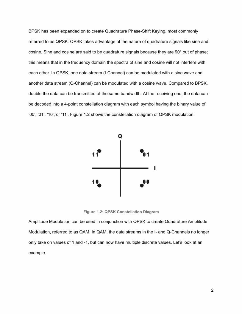
BPSK has been expanded on to create Quadrature Phase-Shift Keying, most commonly
referred to as QPSK. QPSK takes advantage of the nature of quadrature signals like sine and
cosine. Sine and cosine are said to be quadrature signals because they are 90° out of phase;
this means that in the frequency domain the spectra of sine and cosine will not interfere with
each other. In QPSK, one data stream (I-Channel) can be modulated with a sine wave and
another data stream (Q-Channel) can be modulated with a cosine wave. Compared to BPSK,
double the data can be transmitted at the same bandwidth. At the receiving end, the data can
be decoded into a 4-point constellation diagram with each symbol having the binary value of
‘00’, ‘01’, ‘10’, or ‘11’. Figure 1.2 shows the constellation diagram of QPSK modulation.
Figure 1.2: QPSK Constellation Diagram
Amplitude Modulation can be used in conjunction with QPSK to create Quadrature Amplitude
Modulation, referred to as QAM. In QAM, the data streams in the I- and Q-Channels no longer
only take on values of 1 and -1, but can now have multiple discrete values. Let’s look at an
example.
2

In a QAM system there are an I-Channel and a Q-Channel, each of which has 2 bits to
represent the analog voltage of the digital waveform: ‘00’ represents -1, ‘01’ represents -0.33,
‘10’ represents 0.33, and ‘11’ represents 1. The I-Channel is then modulated with a sine wave
and the Q-Channel is modulated with a cosine wave. The received symbols are represented
with 4 bits (2 bits from each channel) to create a 16 point constellation diagram, seen in Figure
1.3. This type of modulation is called 16QAM because it yields a constellation diagram of 16
points.
Figure 1.3: 16-Point Constellation Diagram
Larger constellation diagrams can be achieved by increasing the number of bits in the I- and
Q-Channels: 64QAM, 256QAM, 1024QAM, etc. With a higher number of bits in the I- and
Q-Channels comes a higher data transmission rate, however, the integrity of the correct symbol
being decoded is at risk.
3

The constellation diagrams shown in Figures 1.2 and 1.3 are the ideal depiction of what the
constellation diagram should look like. In practice, a decoded symbol may not fall directly on the
referenced symbol location; this can be quite problematic in higher QAM systems. A
measurement called Error Vector Magnitude, EVM, is used to represent this deviation from
ideality. As seen in the Figure 1.4 below, the ideal symbol location is at ‘11’, however, the
transmitted symbol was decoded at a much different location.
Figure 1.4: Graphical Interpretation of Error Vector Magnitude (EVM)
A magnitude vector labeled P ref is used to represent the location of the ideal symbol, P error
denotes the actual location of the transmitted symbol. EVM is a calculated measurement that
displays the ratio of P error to P ref . Often displayed in dB of a percentage, the two most common
calculations for EVM are: EVM(dB) = 10log 10 (P error /P ref ) and EVM(%) = (P error /P ref ) ½ *100. One
drawback of this measurement is that it only shows the deviation from the intended location. In
higher QAM systems, the intended location on the constellation diagram may become quite
ambiguous. This ambiguity implies that the EVM may not be the most reliable error
measurement.
4

1.2 OFDM
Orthogonal Frequency Division Multiplexing (OFDM) is a digital data encoding method that
allocates data to various different frequencies. This is done by splitting the data stream into
multiple lower bit rate streams each of which is placed onto a predetermined frequency. Each of
the split data streams occupy their own bandwidth such that there is no channel interference
due to the orthogonality of the signals. In OFDM we call each of the carrier frequencies
sub-carriers; for OFDM to work, it is important that each of these sub-carriers are orthogonal.
Orthogonality allows for simultaneous data transmission on adjacent channels with minimal
interference.
Let’s go through an example to better understand how OFDM works. Say wey have a binary
data stream of 1, 1, 1, -1, 1, -1, 1, -1, -1 and an OFDM link with three sub carriers: c1, c2, and
c3. The data stream first undergoes a serial-to-parallel conversion, each sub-carriers handles a
third of the data. c1 will be transmitting bits 1, -1, and 1, c2 will be transmitting bits 1, 1, and -1,
and c3 will be transmitting bits 1, -1, and -1. The data in c1, c2, and c3 all make up their own
symbol, which is different from the ‘symbol’ we discussed in the previous section. The
modulation frequencies are chosen such that it satisfies the Nyquist Criterion; in order to
minimize distortion between symbols the frequency of c2 and c3 are harmonics of c1. Each
symbol then undergoes an Inverse Fast Fourier Transform (IFFT). The equation for the FFT and
IFFT can be seen below:
5

Equation 1.1: Fast Fourier Transform (FFT) and Inverse Fast Fourier Transform (IFFT)
Performing an IFFT here seems to be counter-intuitive. Usually when we think of an IFFT we
imagine a function that converts a spectrum to a time domain signal, however, this is not always
the case. In reality, this block can be either the FFT or IFFT, the latter is chosen simply because
it produces a time domain signal. One must remember that the FFT and IFFT are linear
functions, this means that it does not matter which is used on the transmit end as long as the
other is used on the receive end. Figure 1.5 show the linear property of the FFT and IFFT.
Figure 1.5: FFT/IFFT Linearity
The IFFT block quickly computes the time domain signal of the parallel inputs simultaneously
rather than doing each carrier individually. The signals are then added together using a parallel
to serial converter.
6

The final step before transmitting the data is called cyclic prefixing. Generally in OFDM signals,
the last 10% to 25% of the data is copied and added to the beginning of the data stream. Ideally,
we would want to do this for each of the carriers, but since the data is a linear combination of all
the carriers we can only do it on the aggregation of the package. Adding a cyclic prefix is
important because it reduces intersymbol interference (ISI), as well as mitigates the possibility
of circular convolution (important for frequency domain data processing). We must remember
that adding a cyclic prefix increases the length of the data we wish to transmit, this will increase
the bandwidth of signals’ spectrum. This increase in bandwidth must be accounted for such that
our signal does not interfere with other signals operating at adjacent bands.
At the receiving end, the data is first brought back down to baseband using a demodulator. The
cyclic prefix is then removed from the data stream. The data stream is then fed into a
serial-to-parallel converter so that an FFT can be performed. The FFT is used to undo the
effects of the IFFT in the transmitter side; this also removes carriers c1, c2 and c3. Finally, the
data goes through a parallel-to-serial converter to recreate the starting data stream. Figure 1.6
shows a basic block diagram of an OFDM link.
7

Figure 1.6: OFDM Communication Link
1.3 Multipath and Fading
Recently, MIMO systems have been designed to exploit
the phenomena of multipath propagation, commonly
referred to as just multipath; but what is multipath? Why
is it problematic? And how can it be used to our
advantage? In simple terms, multipath is phenomena of wireless signals arriving at a receiver
through various different paths. In the past, when using SISO links, this phenomena became
very problematic because multipath propagation leads to multipath interference. Imagine that
we are transmitting a signal and the signal that propagates along the secondary path arrives at
the receiver with a 180 o delay relative to the signal that propagates along the primary path. In
this scenario, destructive interference would occur and our signal would be entirely wiped out;
any chance of accurately decoding the signal would be lost! This destructive interference
causes channel fading. The two most common forms of fading are Rayleigh fading and Rician
8

fading. Rayleigh fading occurs when signals from various paths arrive at the receiver with a
Rayleigh distribution.
Figure 1.7: Probability Density Function of a Rayleigh Distribution
Figure 1.7 shows a probability density function for a Rayleigh distribution with multiple 𝜎
(standard deviation) values. In our case, the random variable is the incoming signals, the x-axis
refers to time progression and the y-axis refers to signal magnitude; each secondary path would
have a different standard deviation of attenuation. The fading is said to be Rayleigh if there is no
apparent direct path; in other words, the arriving signals all appear to be propagating along
secondary paths. Rayleigh fading is most common in densely packed cities where the signal
can bounce off many objects such as buildings and cars. When the moving signal bounces off
successive objects, doppler shifts occur. Figure 1.8 shows a time domain Rayleigh faded signal
with a 10 Hz maximum doppler shift (left) and a 100 Hz maximum doppler shift (right).
9

10 Hz Maximum Doppler Shift
100 Hz Maximum Doppler Shift
Figure 1.8: Doppler Shift Effect on Rayleigh Faded Signal
As shown in Figure 1.8 as the doppler shift increases, the ‘uglier’ the arriving signal becomes. At
higher doppler shifts, the signal can become almost impossible to decode.
On the receiving end, if there appears to be a signal that propagates along a direct primary
path, Rician fading occurs (as opposed to Rayleigh fading where all signals appear to propagate
along a secondary path). In Rician fading, the signals arriving at the receiver have a Rice
distribution (often referred to as Rician or Ricean distribution), Figure 1.9 shows the probability
density function of a Rice distribution.
10

Figure 1.9: Probability Density Function of a Rice Distribution
In our case for the probability density function shown in Figure 1.9, the random variable is the
incoming signals, the x-axis refers to time progression, and the y-axis refers to signal
magnitude; each of the paths, primary and secondary, has its own 𝜎, which refers to path
attenuation. The received signal in a Rician faded channel can be described by the following
equation:
Equation 1.2: Received signal in a Rician faded channel.
This function has two main parameter: 𝑲 and 𝛀. 𝑲 is the ratio of the power in the direct path to
the cumulative power in the secondary paths. 𝛀 is the power in all paths and can be defined by
11

𝛀 = v 2 + 𝜎 2 , where v = (𝑲 *𝛀)/(1 + 𝑲) and 𝜎 = 𝛀/2(1 + 𝑲). In the above function, I 0 refers to the
0th order modified bessel function. Due to Rician fading having an apparent direct path, it can
be less problematic than Rayleigh fading.
While fading is both important and problematic, it is not the only aspect of multipath we should
be aware of. In digital communications, multipath can cause intersymbol interference (ISI),
which refers to adjacent symbols interfering with each other in the channel; ISI is the main
reason OFDM is often used with MIMO systems (see section 1.2). As will be discussed in
further sections, channel capacity is increased when we use MIMO systems; we can exploit the
new multiple paths to increase the capacity of our communication link. In the past multipath was
a phenomena that was unable to be dealt with, however, with the use of MIMO each of the
transmitters in a MIMO link have their own space-time code which ensures signal orthogonality.
If the transmitter end of a MIMO link has knowledge of the channel, it can use the multiple paths
in which the signal will propagate along by employing a certain amount of power to a particular
transmitter.
1.4 MIMO Overview
Multiple-input multiple-output, commonly referred to as MIMO, is a data transmission technique
which utilizes multiple antennas on the transmit and receive ends. MIMO was first introduced in
the 1970s, however, it wasn’t used until later to exploit multipath. MIMO relies on the theory of
full channel state information (CSI), which means it is important to know the behavior of the
channel. By having first-hand knowledge of the channel’s behavior, the transmit power can be
allocated in such a way as to utilize the multipath to an advantage. This was a revolutionary
12

concept as these factors that were detrimental to the loss of communication efficiency were now
being used to beneficial purposes.
Crucial to the understanding of MIMO and why it’s a more effective communication technique is
a quick overview of the Shannon Capacity. Information theorists define information in bits as:
I = log 2 P i -1
Equation: 1.3: Information in event with probability Pi
An event with probability P i offers more information bits, the smaller its probability is or the more
uncertain it is. The expected number of bits offered by an event with probability P i is called its
entropy and is denoted by H(P i ). A communication channel is modeled by these two important
equations:
y = x + n
Equation 1.4: Information transmission equation
I(x;y) = H(y) - H(y|x)
Equation 1.5: Mutual Information Function
‘y’ denotes the received information and ‘x’ is the sent information. Ideally, the two would be
equal but noise ‘n’ is added by the channel. H(y) is the entropy of the received symbol ‘y’ and
H(y|x) is the entropy of the received symbol ‘y’, knowing that symbol x was sent. This function is
called the mutual information function and maximizing it means finding the Shannon capacity of
the channel. Since we are aiming to maximize the mutual information function I(x;y) and since
entropy is proportional to uncertainty, the subtraction means finding the maximum reduction in
uncertainty in the channel from sent random variable x and received random variable y. In other
words, the received information y should tell one as much as possible about the sent
information x. The Shannon capacity, therefore, represents a benchmark of the maximum
amount of information that can be transmitted through a channel with zero errors by picking
13

intelligent coding techniques. It is not derived here, but H(y) can be proven mathematically to
max out when ‘y’ is a Gaussian distribution, while H(y|x) becomes the entropy of the additive
white Gaussian noise added by the channel, H(n). Using in information theory what is called the
Sterling approximation results in the well-known Shannon capacity for a single transmit and
single receive communication link:
C s = I max (x;y) = ½*log 2 (1+S/N) bits/sample
Equation 1.6: Shannon Capacity
Assuming the sampling rate satisfies the Nyquist Criterion and normalizing by the bandwidth
under design expresses the Shannon capacity in bits/sec/hz, referred to as just the capacity of
the channel. Unfortunately, while the capacity of the channel does represent the maximum
upper limit on communication performance it is not actually attainable in practice. The reason
lies in the Sterling approximation, which implies that one must wait an infinite amount of time
before the data can be transmitted to reach the capacity of the channel. However, even though
the theoretical upper limit cannot be obtained, finite time delays still give excellent performance
reaching to within 70% of the maximum capacity. This was the approach in single antenna
communication.
Figure 1.10: Channel Capacity of SISO
Up until the 1990’s, the only method used for wireless data transmission has been one antenna
at the transmit end and one antenna at the receive end; this is referred to as single input single
output (SISO). As seen in Figure 1.10, the channel capacity of a generic SISO link can be
modeled by the capacity equation discussed earlier C = Log 2 (1 + SNR); this implies that since
14

channel capacity is a function of SNR (signal to noise ratio) a higher capacity can be achieved
simply by increasing the power of the transmitter. The channel capacity is represented as a
logarithmic function which means that in order to achieve high capacities, the power of the
transmitter must be extremely large. It became apparent that higher channel capacities could
not be achieved with a SISO link. It was soon realized that higher channel capacities could be
obtained by increasing the number of antennas on the transmit and receive ends of a wireless
communication link. When the number of antennas on the transmit and receive ends are
increased, more channels are created. This sounds quite intuitive, however, it’s much more than
a channel forming between a transmit antenna and its respective receive antenna. This is the
topic of the following section.
1.6 How Adding Antennas Improves Data Transmission
As mentioned previously, the channel capacity of a wireless communication link increases when
we add antennas. If we look at a SISO link, we can see that a single beam forms between the
transmit and receive antennas; in other words, there is no diversity. In digital communications,
diversity refers to the number of different paths that the same data has traveled to in order to get
to the receiver. The transmit diversity increases as antennas are added to the receiver end of a
SISO link. A SISO link is not only limited by channel diversity, but also limited by noise,
interference, and channel fading. As discussed before, these limitations can be overcome
simply by adding antennas.
To expand on this statement, let’s take a look at a 2x1 MISO link, 2 transmit antennas and 1
receive antenna, shown in Figure 1.11.
15

Figure 1.11: 2x1 MISO Link
If the path from T 1 to R 1 was to be lossy, we could always rely on T 2 to successfully transmit the
data to R 1 . Imagine that two people are looking for a person, a person has a much higher
probability of hearing their name being called by two people rather than just 1. The multiple
channels can be represented by a matrix called the channel matrix. This matrix consists the sub
channel elements. To better understand the concept of MISO, let’s take a look at the channel
capacity equation for an arbitrary link:
Equation 1.7: Channel Capacity of MISO
Where:
● N T - number of transmit antennas
● || h || 2 = (h 1 2 + h 2
2 … + h NT 2 ) - average channel gain over all paths
Generally in MISO systems power is distributed equally amongst the all of the transmit
antennas; this is why in the above equation, we divide SNR by N T . As N T increases the SNR at
the receiving end decreases. The benefits of a MISO communication system can be
compromised if we do not know the channel information (h matrix). If the transmitter has no idea
16

what the channel looks like, we can make the assumption that N T = ||h|| 2 which then yields the
same capacity equation for a SISO system; thus making a MISO system obsolete.
Next, let’s take a look at a SIMO link, shown in Figure 1.12.
Figure 1.12: 1x2 SIMO Link
A SIMO link is defined by a communication link that has one transmit antenna, and multiple
receive antennas. To conceptualize how a SIMO link can be better than a SISO link, imagine
that a person are looking for their friends in a crowded area--the person has a much higher
probability of finding them if that person shout all of their names instead of just shouting one.
The capacity equation for a SIMO link can be seen below:
Equation 1.8: Channel Capacity of SIMO
Since the channel only has as many paths as it does receivers, the value of || h || 2 is limited by
the number of receive antennas (N R ). Knowing this, we can rewrite the above equation as:
Equation 1.9: Channel Capacity of SIMO, adjusted
We can increase the channel capacity simply by increasing the number of receive antennas,
however, this approach can become quite costly if we only manage to increase the capacity
17

logarithmically. Unlike a MISO link, the benefits of a SIMO link are not dependant on the
transmit antenna having any knowledge of the channel; in other words, the transmitter is blindly
throwing out data in hopes that at least one of the receiver antennas will pick it up. We can also
observe the usefulness of a SIMO link from a statistical standpoint.
Let’s say we have SISO link and a SIMO link. Each receiver antenna has 50% chance to
decode the correct bit. We’ll use the following conventions:
● P[R] = 0.5, probability that correct bit arrives at SISO receiver
● P[R 1 ] = 0.5, probability that correct bit arrives at SIMO receiver 1
● P[R 2 ] = 0.5, probability that correct bit arrives at SIMO receiver 2
● P[R SIMO ] - probability that correct bit arrives at one of the 2 receive antennas in the SIMO
link
P[R SIMO ] = P[R 1 or R 2 ] = P[R 1 ] + P[R 2 ] - P[R 1 R 2 ]
Where P[R 1 R 2 ] = P[R 1 ] * P[R 2 ] = 0.25
P[R SIMO ] = 0.5 + 0.5 - 0.25
P[R SIMO ] = 0.75
From the above derivation we can see that a 1x2 SIMO link greatly increases the probability of
the correct bit arriving at the receiver from a simple SISO link. The above example, while
simple, is a surface level representation of the usefulness of a SIMO link. However, this seems
like a lot of hardware to only achieve a logarithmic increase in channel capacity.
A MIMO link seeks to overcome the limited channel capacity of SISO, MISO, and SIMO by
adding antennas to both the transmit and receive ends. MIMO is like a combination of MISO
18

and SIMO channels; it can reach higher capacities either with channel information (like MISO)
or with no channel information (like SIMO). To expand on this claim, if there is no known
channel information at the transmitter end of a MIMO link, the channel capacity equation can be
simplified to:
Equation 1.10: Channel Capacity of MIMO
One thing to note from the above equation is that it is used for calculating the channel capacity
limit. In this equation, ‘M’ is used to denote the minimum number of antennas, for example: if
N T =3 and N R =4, then M=3. We can see that the channel capacity limit increases linearly as we
add antennas while holding a constant SNR.
Now, let’s look at a 2x2 MIMO link where the channel information is known, as seen in the
following figure. We’ll use ‘T’ to represent a transmit antenna, ‘R’ to represent a receive
antenna, and ‘h’ to represent a subchannel. As seen in Figure 1.13, additional subchannels
have formed between cross antennas. A 2x2 MIMO system has created a 4 channel link,
similarly a 3x3 MIMO system has 9 channels, and a 4x4 MIMO system has 16 channels.
Figure 1.13: 2x2 MIMO Link
19
Furthermore, if the transmitting and receiving antennas are spaced very far apart with respect to
the wavelength of the transmitting frequency, then MIMO reduces to N SISO links. Therefore,
the worse MIMO can perform is as a multiple of SISO links. It might be beneficial to the reader
to see mathematical description of the advantages of MIMO. This description centers on the
assumption that the channel is deterministic and constant at all times.
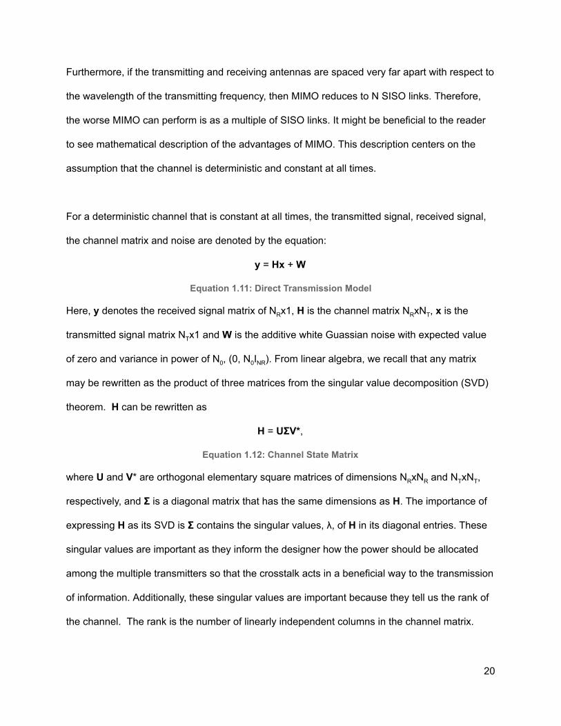
For a deterministic channel that is constant at all times, the transmitted signal, received signal,
the channel matrix and noise are denoted by the equation:
y = Hx + W
Equation 1.11: Direct Transmission Model
Here, y denotes the received signal matrix of N R x1, H is the channel matrix N R xN T , x is the
transmitted signal matrix N T x1 and W is the additive white Guassian noise with expected value
of zero and variance in power of N 0 , (0, N 0 I NR ). From linear algebra, we recall that any matrix
may be rewritten as the product of three matrices from the singular value decomposition (SVD)
theorem. H can be rewritten as
H = UΣV* ,
Equation 1.12: Channel State Matrix
where U and V * are orthogonal elementary square matrices of dimensions N R xN R and N T xN T ,
respectively, and Σ is a diagonal matrix that has the same dimensions as H . The importance of
expressing H as its SVD is Σ contains the singular values, λ, of H in its diagonal entries. These
singular values are important as they inform the designer how the power should be allocated
among the multiple transmitters so that the crosstalk acts in a beneficial way to the transmission
of information. Additionally, these singular values are important because they tell us the rank of
the channel. The rank is the number of linearly independent columns in the channel matrix.
20

Ideally, the rank is equal to the minimum of (N T , N R ), the dimensions of the receive and transmit
antennas. It is possible, though, to have a channel matrix H with a rank less than the minimum
of the (N T , N R ); this occurs when one or more of the singular values evaluate to zero. Having a
channel that is not full rank means the columns of the channel matrix may not be fully
independent, rather they are linearly related. This highlights the fact that to fully take advantage
of MIMO, we need channels that have diverse crosstalk. This affects diversity gain and the
spatial multiplex gain, as discussed later. Substituting the SVD of H into equation 1.11 and
multiplying both sides by the conjugate transposed U* , it can be shown that the expanded result
is:
y i ’ = x i ’λ i + w i ’, i = 1, 2, …, n min
Equation 1.13:Direct Transmission Model, substituted
The reason behind performing the SVD of H is it performs two coordinate transformations by
expressing the input x with columns of V and the output y with columns of U . This results in an
easier relationship between the inputs and the outputs of the communication link, similar to a
SISO relation. The SISO -like form allows substitution into the capacity equation of a SISO link.
The capacity equation for a MIMO link results in:
C = log 2 (1+ ) bits/s/Hz ∑nmin
i = 1NoP iλi2
Equation 1.14: Channel Capacity of MIMO, simplfied
The capacity equation reveals the singular values in the design of the MIMO communication
link. Since the singular values are involved in the capacity equation, it reveals how the power
should be distributed among the channels of the link. The subchannels with the larger singular
values are favored for transmission power. Furthermore, we see that this capacity relation grows
a lot easier for a certain combination of input power as opposed to the capacity of a SISO link.
21

For a SISO link, the capacity grew logarithmically with the input power. Here, we have extra
terms being added to the capacity of a MIMO link. Also, because of the ability to allocate the
power among the transmitters with the largest singular value, the designer can maximize the
capacity of the link.
A graphical interpretation of this can be seen through the logarithmic curves shown below. As
shown on the graph, all of the logarithmic curves have a larger slope initially, but as they grow
they start rising much slower and slower. If one can imagine these curves representing the
various log terms in the capacity of the MIMO link, the largest curve represents the subchannel
with the highest singular value, the second largest curve is the 2nd largest singular value, and
so on. By allocating the power to favor the subchannels with the bigger singular values,
effectively, we are taking advantage of this brief, faster rise in the log curves. By allocating the
power, just enough is given to the highest log(x) curve to utilize this higher slope region. Once
the largest log(x) curve slows its growth, rather than keep feeding this subchannel power, the
remaining power is allocated to the next subchannel log(x) curve while it’s still in that fast
transition region, and so on for the next subchannel log(x) curve. This is how MIMO can attain a
much better capacity relation with power. In SISO, all of the transmit power was used on the
single channel and it resulted in logarithmic increase in capacity. Here, with multiple capacity
terms, the singular values tells us how to allocate the transmit power to utilize crosstalk in an
effective manner. This process of allocating the power among the channels is called water filling.
22

Figure 1.13: Example of Waterfilling
Now, being able to fit more bits of information onto a single channel is very important, but what
does it matter if the bits arriving at the receiver are incorrect? Although capacity is very
important to know about, it is not the only aspect of a wireless communication link we should be
aware of. Capacity tells us how many bits can fit in a channel, it does not, however, tell us how
well the link successfully and accurately transmits bits. A measurement called Bit Error Rate,
BER, was created to determine how many errors there are in bits that have been transmitted
across a channel. In order to calculate the BER the data received is compared to the data that
was sent. Usually this is done in Matlab using a Monte Carlo simulation, which allows for the
test to be run thousands of times; this ensures that the data measurement is reliable. The most
common way to display the BER is through the use of a ‘Waterfall’ curve. A Waterfall curve is a
graph that has BER as the dependent variable and E b /N o as the independent variable. E b /N o is
the energy per bit, but is commonly referred to as SNR. To generate a Waterfall curve E b /N o is
swept and BER is calculated and plotted. An example of Waterfall curve can be seen in Figure
1.14.
23

Figure 1.14: Waterfall Curve Example
Figure 1.14 shows the Waterfall Curve for QPSK and 16, 64, 256, 1024, and 4096 QAM
(modulations explained earlier). We can see that QPSK has the lowest BER per E b /N o input,
which makes sense due QPSK being the simplest modulation form of the ones listed in the
following section. Fortunately, Matlab created a MIMO channel diversity demo in which Waterfall
Curves were constructed. Figure 1.15 shows the Waterfall curves for various channel
diversities.
24

Figure 1.15: BER Performance for Different Diversities
The Waterfall curve in Figure 1.15 allows the viewer to compare the BER of a SISO link, a 2x1
MISO link, and a 1x2 SIMO link. It is not much of a surprise that the MISO and SIMO systems
greatly out-performed the SISO system. Each of the systems were BPSK modulated and all
have 2nd order diversity (except for the SISO link). These systems are said to have 2nd-order
diversity because the same data travels across two different paths to the receiver. As discussed
earlier in the chapter, for a MISO link to be advantageous, the transmit antennas must have
knowledge of the channel and its frequency response. A SIMO link does not require that the
antennas be aware of the channel behavior, this is why the SIMO simulation (blue plot) has the
lowest BER of all the other systems. As we increase the number of receiver antennas, we also
increase the likelihood that at least one of them will properly decode the incoming data, which is
all we need for robust data transmission. We can see that for all three system that as we
25

increase the E b /N o , the BER decreases. However, increasing E b /N o can become quite costly
especially if we are transmitting a lot of data, let’s see what happens when we increase the
channel diversity.
Figure 1.16: Increased Channel Diversity From Figure 1.15
Figure 1.16 shows the waterfall curve for multiple 4th-order diversity systems; the same SISO
plot from Figure 1.15 has been added to the plot for reference. We can immediately notice that
increasing diversity decreases the BER. If we compare the 4th-order diversity SIMO system with
the 2nd-order diversity SIMO system we can see that the former achieves a BER of 10 -4 when
E b /N o =10.5 dB while the latter achieves a 10 -4 BER when E b /N o =16 dB. What may be a surprise
to us is that the 1x4 SIMO system outperforms the 2x2 MIMO system. Having discussed the
26

basic concepts of MIMO, it is beneficial to provide an overview of beamforming and the different
flavors of MIMO: Precoding, Diversity Coding, and Spatial Multiplexing (SM).
1.7 Beamforming
In beamforming the phase and amplitude of a signal can be adjusted at the transmitting end
such that certain interferences can be achieved at the receiving ends. It is utilized when one has
more than one antenna at either end or both ends of the communication link due to the extra
subchannels created by the multiple antennas.
The concept of beamforming is possible based on the spatial diversity or extra possible paths
created by the multiple antennas discussed in section 1.6. Spatial diversity is analogous to the
magnitude of a vector. If one can imagine a 2D vector with x and y components, the magnitude
of the vector is the root sum square of the components x and y. Ideally, x and y should be such
that they maximize the magnitude of the vector but also stay as diversely distributed as
possible. The reason for this is, if x, in the extreme case that it dominates the magnitude of the
vector such that y approaches zero, then the combination of x and y starts becoming more like a
single direction. Similarly, in beamforming the diversity is proportional to the norm of the
subchannels vectors. The diversity gain should be as large as possible so that crosstalk
becomes advantageous for beamforming. Once the antennas are placed closer and closer
together, though, they start experiencing the same channel and this diversity gain is lost and no
beamforming can be performed. A diversity gain is preferred as one channel may be lossy and
then all the transmit power would be forced through this lossy channel. If there are multiple
subchannels, then if one channel looks worse in terms of performance than power can instead
be transmitted through the better channel. These are the concepts of transmit and receive
27

beamforming with the norm || h || factor in the capacities of SIMO and MISO discussed in
sections 1.2.
Let’s look at an example to better conceptualize what is happening: take a 2x2 MIMO link , if we
are aware that channel h 11 is quite lossy, we can adjust the phase and relative power of the
signal coming from T 2 such that it constructively interferes with the signal coming from T 1 , thus
allowing R 1 to receive a clean and readable/decodable signal. Again, this is possible only
through the spatial diversity created by adding multiple antennas.
Beamforming should not be confused with the water filling method using the singular values of
the subchannels. The difference between waterfilling and beamforming is hardware. For
example, if beamforming is desired, the antennas could oriented in a certain configuration such
that the radiation pattern points in a preferred direction. This would create a channel matrix
which could then be analyzed using the SVD method to find the singular values and perform
water filling. In other words, beamforming would form your channel matrix based on the
orientations of the antennas and water filling would then be used to determine how to
appropriately ratio the power. Beamforming is not limited to MIMO applications, in fact, it is
actually quite hard to implement and has many other uses: radar, sonar, seismology, radio
astronomy, acoustics, and biomedicine. In order for beamforming to be successful in digital
communications the channel information must remain constant, which is an incredibly rare
occurrence.
One of the most common applications for beamforming found today is beamforming routers. In
the past, Wi-Fi routers would transmit data equally in all directions, similar to the way a lightbulb
28

emanates light. A beamforming Wi-Fi router aims the data transmission beams at points of
interest such as computers, laptops, and other devices with Wi-Fi access. However, for
beamforming routers to work, the devices at the receiving end of the data must have the
hardware to accommodate this. Think of a beamforming router as a lightbulb with a shade over
it such that the light only goes to the directed locations.
1.8 Precoding
Precoding uses beamforming for successful transmission of data of wireless communication
systems. The idea behind precoding is that the transmit end can anticipate the loss in the
channel. Let’s say that the received signal is ‘r’, the sent signal is ‘s’. Ideally, r=s, however, in
wireless communications, this would be impossible due to loss in the channel as well as
channel noise. We’ll use ‘h’ to represent the transfer function of the channel and ‘n’ to represent
the random white gaussian noise. Without precoding, the equation for the received signal is r =
s*h + n. To apply precoding, the sent signal ‘s’ is divided by the anticipated transfer function of
the channel ‘h pre ’; the new transmitted signal is ‘s/h pre ’. The equation for the received signal is
now r = (h/h pre )*s + n. If ‘h pre ’ is properly chosen (h = h pre ), we get r = s + n. This implies that the
only effect on the transmitted signal is the noise of the channel which can be easily mitigated by
increasing signal power on the transmit end. Precoding can be done linearly and nonlinearly.
1.9 Diversity Coding
Diversity Coding is a flavor of MIMO that is primarily used when the transmitter has no
knowledge of the channel. Diversity coding takes advantage of independent fading as well as
signal orthogonality to transmit data. The same signal is emitted from each of the transmit
29

antennas. However, before the signal is transmitted it undergoes a coding technique called
Space-Time Coding (STC). STCs transmitted multiple copies of the same data in hopes that at
least one of the data streams arrive at the receiver with minimal amounts of interference such
that the receiver can accurately decode the data, much like a SIMO link. This coding method
can be subdivided into two main types: Space-Time Trellis Codes (STTCs) and Space-Time
Block Codes (STBCs).
STTCs apply multiple Trellis/Convolutional codes to the data and send the coded data to each
of the transmit antennas, with each antenna receiving a different copy of the encoded data.
Arriving at the receiver are multiple packets of diverse data; while this data may seem diverse,
the content is all the same. An example of a simplified Convolutional encoder can be seen in
Figure 1.17:
Figure 1.17: Simplified Convolutional Encoder
A convolutional encoder uses a finite state machine to encode an incoming data stream.
Conventionally, it consists of shift registers, adders, and XOR gates. The shift registers continue
to shift until each has no remaining bits; once this happens, the data has been successfully
encoded. As seen in figure 1.17, ‘Output 1’ is the encoded data stream and ‘Output 2’ is the
30
data before it was encoded. Output 1 is the aggregation of multiple shift registers and adders
applied to the input data. If the data at Output 1 were compared with the data at Output 2, they
would appear to be very different. A convolutional encoder can be recursive or nonrecursive;
Figure 1.17 is an example of a recursive encoder. An encodement sequence for a convolutional
encoder can be represented using a trellis diagram which explains why this method is often
called Trellis coding. On the receiver end, Convolutional encoded data is most often decoded
using the Viterbi Algorithm, however, when the encoded data appears to be long, the Fano
Algorithm is most often used.
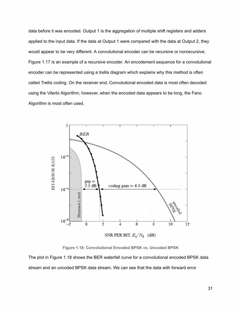
Figure 1.18: Convolutional Encoded BPSK vs. Uncoded BPSK
The plot in Figure 1.18 shows the BER waterfall curve for a convolutional encoded BPSK data
stream and an uncoded BPSK data stream. We can see that the data with forward error
31

correction, FER, has very few errors; we can see that as the energy per bit is slightly increase
the BER falls drastically. Compared to STBCs, STTCs have better coding gain as well as
diversity gain. STTCs are also far superior at achieving lower BER per E b /N o . One of the main
drawbacks of STTCs is that they require convolutional codes which can make the hardware
quite complex and intricate; this issue also carries over to the receiver end in that the viterbi
decoder must be just as complex. STBCs are easy to implement and can also be processed
linearly.
As stated earlier, diversity coding does not rely on any channel knowledge at the transmitter,
this implies that useful aspects of MIMO like beamforming and array gain are unusable in
diversity coding systems. However, if there is slight knowledge of the channel at the transmitter,
diversity coding can be used in conjunction with spatial multiplexing.
1.10 Spatial Multiplexing
Another flavor of a MIMO system is a spatial multiplex system. Because MIMO consists of
multiple antennas on the transmit side and the receive side, this opens up a spatial degree of
freedom in which data streams can be divided in the MIMO channel. This is the concept of
Spatial Multiplexing. Spatial Multiplexing focuses on enhancing the data rate by allocating data
among the multiple transmit antennas of the channel. By using the various transmitters available
in the MIMO system, segments of the signal information essentially travel in parallel and
recombine at the receiver. This is analogous to a backed up highway in which a second lane
opens up allowing space for other cars to travel in parallel. A contrast to this example is a SISO
link which sends data serially.
32

A measure of this enhancement in data rate is called the spatial multiplexing gain (SMG).
Intuitively, the SMG is dependent on the minimum of the number of antennas on either the
transmitter or the receiver end of the MIMO link. For example, if there are three antennas on the
transmit side and four on the receive side, the SMG will equal the minimum of both numbers,
three as discussed in previous sections. This is due to the fact that even though the receiving
end has a greater number of antennas, the signal can only be split up three ways on the
transmitting end. A similar argument follows for when the transmitting side has a greater number
of antennas than the receiving side. A second relationship for the diversity gain comes through
knowledge of the data rate and the SNR of the channel. This relationship is expressed as:
MG S = limSNR→∞
rlog(SNR)
Equation 1.15: Spatial Multiplexing Gain
A real benefit of MIMO communication comes when both a diversity gain and SMG are
introduced into the design of the MIMO link. Since a diversity gain and a multiplex gain are both
benefits available to us through the multiple number of antennas on both sides of the
communication link, it makes sense that both, together, should and enhance the communication
link. In this case, however, one must decide on which gain is more important since both gains,
fully, cannot be applied to the system. The intuition behind this limitation can be explained as
follows. If diversity gain works by allocating the same dataflow on each transmitting antenna
while spatial multiplexing works by splitting up sections of that dataflow and then sending them
through the different multiple transmitting antennas, then it makes sense that one cannot fully
apply both. In other words, one must decide whether one’s transmitting antennas are each
sending the same data or if they are each sending a different section of a cumulative dataflow.
33
For example, let’s say one have a MIMO communication link consisting of 2 antennas on the
transmit side (N T = 2) and 3 antennas on the receive side (N R = 3). The diversity gain is
calculated as the product of both N T xN R which comes out to 6 for this case. The SMG is the
minimum of the two, so the SMG equals 2. This MIMO link cannot be designed to have both a
diversity gain of 6 and also an SMG of 2 due to the limitations described earlier. However,
depending on the system goal, often the MIMO link can be designed on an optimal tradeoff of
both diversity gain and SMG. In this example, a trade-off is a diversity gain of 3 and an SMG of
3.
1.11 MIMO In Wi-Fi
MIMO is commonly used in wireless local area networks (WLAN). In 2009, IEEE developed the
WLAN 802.11n protocol which gave rise to MIMO, however, it wasn’t until 2013 when IEEE
developed WLAN 802.11n that MIMO came into use. The introduction of MIMO in 802.11n
increased the data rates from 20 Mbps to around 200 Mbps and the range of reception over the
standards of old 802.11a/g from ~25m to ~50m. The concepts discussed thus far crucial to the
operation of 802.11n are transmitter beamforming, spatial division multiplexing and spatial
diversity. To apply the theory of spatial diversity and spatial division multiplexing, 802.11n utilizes
the space-time block coding (STBC) discussed earlier. The 802.11n protocol utilizes OFDM to
transmit data across wireless channels, operates at the 5 GHz band, and can obtain bandwidths
of 20, 40, 80, or 160 MHz.
34

Chapter 2: Keysight VSA/VSG Overview
2.1 VSG Overview
The purpose of the vector signal generator (VSG) is to generate radio, wireless, or cellular
signals to test a system. The generated signals usually have digital modulation since radio,
wireless, and cellular signals require modulation when being transmitted. The VSG allows for
OFDM signals to be transmitted which are essential to testing digital communication systems.
The reason the VSG is integral to testing the communication methods is because it allows for a
known reference signal to be sent through a channel. Since the signal is a known reference it
allows for comparison between the propagated and the received signal to determine if the
communication system is performing to specifications. This project specifically uses the
Keysight PXIe M9381A VSG because it can send a reference 802.11n signal through the
channel. As discussed previously in section 1.5 one of the current applications using MIMO is
WiFi, which uses the 802.11n signal, so the M9381A VSG utilized is compatible with the current
application of MIMO analyzed.
2.2 VSA Overview
A vector network analyzer displays the magnitude and phase of the received input signal at a
single specified frequency. The purpose of the vector signal analyzer is to make in-channel
measurements of error vector magnitude which is used to derive the SNR. The SNR rate is the
35

parameter which is being used in this project to evaluate a test antenna’s configuration
performance.
The purpose of the vector signal analyzer (VSA) is to see what distortions occur in the desired
signal after sending it through some sort of path. A VSA displays the magnitude and phase of
the received signal so an engineer can see if the distortion is acceptable or not and how to
design to account for the distortion. Some vector signal analyzers can also perform
measurements like error vector magnitude (EVM) of the received signal to known signals.
The evaluation of communication systems relies heavily on the SNR. Since SNR describes the
communication system’s sensitivity to noise, the higher the SNR rate the less sensitive the
channel is to noise. To be less sensitive to noise means that it is easier for the receiver to
discern the desired signal from the noise in the channel. The SNR rate can be found from the
EVM using the equation EVM (%) = sqrt[ 1/10^(SNRdB/10) ] x 100 and solving for SNR. The
reason the Keysight M9391A VSA is used for the testing portion of the project is because the
VSA has software that can display the EVM, constellation diagram, and frequency response of
the 802.11n signal. Since the VSA has these measurements calculating the SNR and observing
the performance of the digital communication system is far easier.
2.3 Testing Hardware
To test the performance of the digital communication systems the following Keysight hardware
was used: M9381A VSG, M9391A VSA, and the M9018A PXIe Chassis. The hardware
generates a reference signal and evaluates it after propagation through each of the antenna
configurations. The chassis acts as a mount for the VSG and VSA, and it includes a module that
36

allows for computer interface to be established. This allows the user to interact with the VSG
and VSA hardware and software.
Figure 2.1: Block Diagram of the M9381A VSG module from Keysight M9381A datasheet
The M9381A PXIe VSG (shown in Figure 2.1) consists of the M9300A frequency reference,
M9301A synthesizer, M9311A digital vector modulator, and M9310A source output to generate
the reference signal. An important aspect of the M9300A frequency reference is only one is
required per chassis because the frequency reference is used to provide a 100 MHz signal to
each of the synthesizers. Since the same signal is used to drive both the VSA and VSG
synthesizers, there should be no variance in the signal because the other components use the
100 MHz signal and the local oscillator signal (LO) from the synthesizer to perform their tasks.
37

The M9301A synthesizer uses 100 MHz signal to transmit a signal at a frequency given by the
user to the source output. The M9311A digital vector modulator receives the LO signal from the
synthesizer at the LO input and at the 100 MHz input accepts the 100 MHz signal from the
M9310A source output. The digital vector modulator modulates the LO signal and uses the 100
MHz from the source output to run its internal clock. The modulated signal is then sent to the
source output through the RF output to RF input. The M9310A source output adds power and
sends it out to the environment through the RF out port using the 100 MHz signal from the
M9301A synthesizer and the RF signal from the M9311A digital vector modulator.
The M9391A PXIe VSA comprises of the M9300A frequency reference, M9301A synthesizer,
M9350A RF downconverter, and M9214A IF digitizer (shown in Figure 2.2). The VSA is used to
evaluate the reference signal after it has propagated through the selected antenna test
configuration. The M9300A is the same as the one used in the M9381A PXIe VSG and
performs the same function. The M9301A synthesizer uses the 100 MHz signal to transmit a
desired LO signal and the original 100 MHz signal to the downconverter. The downconverter
receives the LO signal from the synthesizer at the LO input and at the 100 MHz input accepts
the 100 MHz signal from the synthesizer. The purpose of the down converter is to bring the
received signal down to the intermediate frequency (IF), which is significantly lower than the
signal received at the input of the downconverter. The reason the IF is used is because the low
frequency allows for circuitry to perform well without the use of waveguides, less hardware
needs to be used to process the received signal, and it improves frequency selectivity. The
downconverter passes the IF signal to the IF digitizer along with the 100MHz signal. The IF
digitizer takes the 100MHz signal and uses it as an internal clock to perform signal processing
on the receive IF signal. For the purposes of this project, the IF signal is converted by the
38
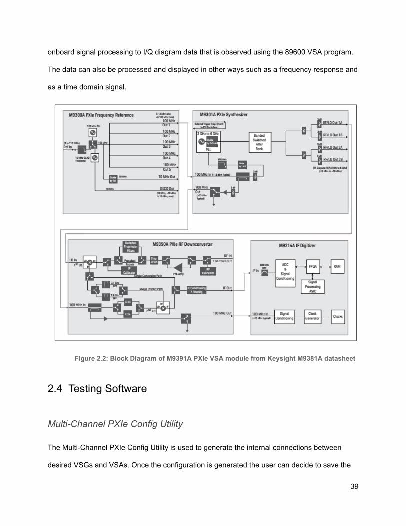
onboard signal processing to I/Q diagram data that is observed using the 89600 VSA program.
The data can also be processed and displayed in other ways such as a frequency response and
as a time domain signal.
Figure 2.2: Block Diagram of M9391A PXIe VSA module from Keysight M9381A datasheet
2.4 Testing Software
Multi-Channel PXIe Config Utility
The Multi-Channel PXIe Config Utility is used to generate the internal connections between
desired VSGs and VSAs. Once the configuration is generated the user can decide to save the
39

configuration and develop a 89600 VSA configuration. Also, after a successful configuration a
file called Persisted.xml should appear in the same directory as the Multi-Channel PXIe Config
Utility. The Persisted.xml is used by the Multi-channel Demo Tool to configure the back panel
connections in the Multi-Channel PXIe Config Utility created at the end of the configuration
generation.
Multi-Channel Demo Tool
The Multi-Channel Demo Tool allows for a user to select MIMO signals and send them into the
system. The user can also control the power and phase of the signal sent through each
channel.
89600 VSA
The 89600 VSA is a program where the received signals can be viewed and analyzed. Useful
tools include I/Q diagram, H-matrix, frequency response, impulse response, and EVM
measurements. These measurements, especially the EVM and I/Q diagrams, help determine
the overall performance of the data transmission method. Accurate measurements require the
user to specify what waveform the M9391A VSA is expected to receive, so the program knows
what the desired results are. Configuration of the 89600 VSA program is discussed in more
detail in Section 2.6.
Waveform Creator
Waveform creator is an application which allows the user to create their own signals using
different types of modulation, added noise, input power, among other settings. The waveform
then can be sent to the M9381A VSG and transmitted to the M9391A VSA and analyzed.
40

2.5 Configuration Generation Walkthrough
To focus on the beam-forming techniques of MIMO the Keysight VSA and VSG modules had to
be wired in shared-LO configuration to ensure the references are in phase. The shared LO
configuration requires the two VSGs to share a single synthesizer and the two VSAs to share a
single synthesizer. The reason for sharing the synthesizer between common components is to
preserve phase coherence, meaning there is no phase difference between the two components.
So the only phase shifting that could occur would be if the user or the propagation method
introduced a phase shift. Originally, the modules were not in the proper places, which did not
allow for a proper configuration. The modules were removed and placed in the proper
configuration as shown in the Keysight LTE/LTE-A Multi-Channel Reference Solution Startup
guide.
41

Figure 2.3: Shared LO wiring and module locations
To remove the modules safely, the chassis was turned off and unplugged and a wrist strap was
used to prevent electrostatic discharge (ESD). Next, all the wire and semi rigid connections
were removed. To move the modules around, the screws were removed and the black extension
was pushed down until the module popped out of the chassis. Once a module popped out it was
removed and placed next to the other components that made up the individual VSAs and VSGs.
Some important things to remember when removing the modules are to keep the individual
components that make up a VSA or a VSG module together; to remove and place the blanks in
correct places; and to always put the reference module in slot 10.
42
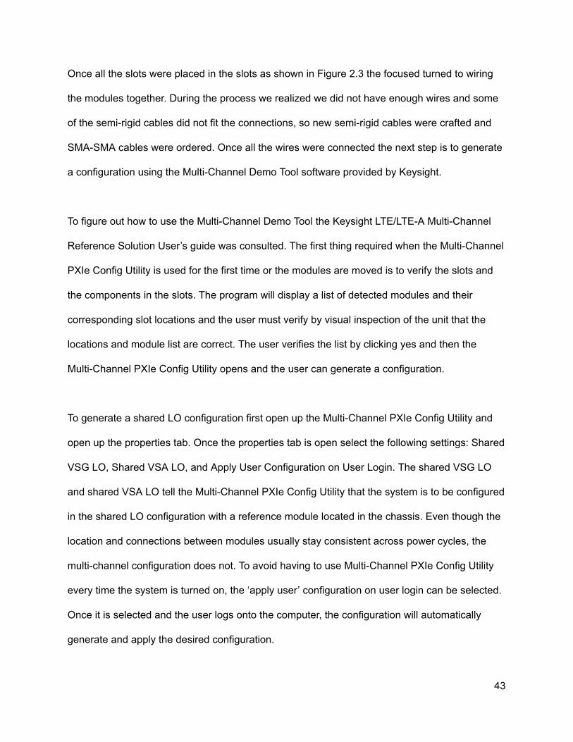
Once all the slots were placed in the slots as shown in Figure 2.3 the focused turned to wiring
the modules together. During the process we realized we did not have enough wires and some
of the semi-rigid cables did not fit the connections, so new semi-rigid cables were crafted and
SMA-SMA cables were ordered. Once all the wires were connected the next step is to generate
a configuration using the Multi-Channel Demo Tool software provided by Keysight.
To figure out how to use the Multi-Channel Demo Tool the Keysight LTE/LTE-A Multi-Channel
Reference Solution User’s guide was consulted. The first thing required when the Multi-Channel
PXIe Config Utility is used for the first time or the modules are moved is to verify the slots and
the components in the slots. The program will display a list of detected modules and their
corresponding slot locations and the user must verify by visual inspection of the unit that the
locations and module list are correct. The user verifies the list by clicking yes and then the
Multi-Channel PXIe Config Utility opens and the user can generate a configuration.
To generate a shared LO configuration first open up the Multi-Channel PXIe Config Utility and
open up the properties tab. Once the properties tab is open select the following settings: Shared
VSG LO, Shared VSA LO, and Apply User Configuration on User Login. The shared VSG LO
and shared VSA LO tell the Multi-Channel PXIe Config Utility that the system is to be configured
in the shared LO configuration with a reference module located in the chassis. Even though the
location and connections between modules usually stay consistent across power cycles, the
multi-channel configuration does not. To avoid having to use Multi-Channel PXIe Config Utility
every time the system is turned on, the ‘apply user’ configuration on user login can be selected.
Once it is selected and the user logs onto the computer, the configuration will automatically
generate and apply the desired configuration.
43

Once the settings are selected click the generate configuration button. When pressed, the
program will ask for devices that are part of the multi-channel configuration. For the 2x2 shared
LO configuration all the devices are selected. Next, the Config Utility will ask for which
synthesizer to use for the VSA and VSG. Select the synthesizer located in slot 7 for the VSA
and slot 14 for the VSG. Once the slots are selected the Config Utility should have a green
circle next to generate configuration. Click the apply button and the Config Utility to connect the
chassis to the reference module and to make changes to connect the other devices in the
desired configuration. Once the configuration is applied successfully, a green dot will appear to
the left. If there is a red dot, go back to the previous step and make sure everything is selected
properly. Next select run alignments and follow the instructions given and make any additional
connections necessary to do the tests. If errors occur, consult the Keysight manuals for
assistance. When the alignments are passed a green circle will appear on the left of the run
alignments button. The final step in the configuration is to run a self test. If any errors result
consult either Keysight or the manual.
The Multi-Channel PXIe Config Utility also allows the user to run a sample waveform through
the configuration. To run the sample waveform first the 89600 VSA software must be configured,
which can be done by selecting the configure 89600 button. When the button is clicked a name
needs to be specified and auto calibrate should be selected. The Config Utility will then open
and configure the 89600 VSA software. When the software opens, connect a BNC-BNC cable
from each VSG to VSA and click the “Play Sample Waveform” button. After the button is
pressed, a square waveform should appear on both the channels of the 89600 VSA software. If
44

these do not appear, make sure all the cables connecting the VSA and VSG modules are
connected correctly.
Some issues that were encountered when running the self test was the firmware for the chassis
needed to be updated, but once it was updated the MIMO Demo Tool would not connect to the
chassis. After communicating to Keysight about the connection issue, it was determined to be a
hardware problem. The exact hardware problem could not be found and remains a mystery. So
the focus turned to using coding to control the VSAs and VSGs instead of the programs.
2.6 Using C# to Generate Testing Environment
While the chassis containing the VSA and VSG modules were being configured for the MIMO
Demo Tool, another approach was used to run MIMO tests: through the use of Visual Studio and
C#, the components that make up the VSA and VSG modules can be manipulated on a much
lower level.
To start a new project: ‘File’ → ‘New’ → ‘New Project’. After selecting new project a large list of
various different project types will appear, be sure to select ‘Console Application’. This will start
a new project and an open text editor will appear. One will immediately see at the top of the
page several ‘using’ statements. In order to allow this source code to communicate with the
hardware, references must be added. To add a reference right-click the ‘Reference’ tab at the
far right end of Visual Studio and select ‘Add References’. Next, select the tab labeled ‘COM’
and type in IVI AgM9018 1.3 Type Library, IVI AgM9300 2.1 Type Library, and IVI AgM938x 2.1
Type Library , select the box next to each and then click ‘OK’. The required references have now
been added!
45

The code written has several regions: Create Driver Instances, Initialize Driver Instances and
Check for Errors, Route Backplane Triggers from M9300A to VSGs, Setting Up the M9381A
PXIe VSGs for WLAN Rx Testing, Start Waveform Playback on the M9381A PXIe VSGs, and
Close Driver Instances.
In many cases when writing code, we begin by creating variables such as ints, doubles, chars,
etc. Figure 2.4 shows how instances of the VSGs, Reference, and the Chassis are created; one
may notice ‘IAgM938xEx’, ‘IAgM9300Ex’, and ‘IAgM9018’ ; these data types allow us to
communicate with and drive the VSGs, Reference, and Chassis. This portion of the code simply
creates empty instances of the modules, objects, that will be used for later tests and
measurements. Note that if this program were to drive the VSA modules, it would need to create
empty instances of the ‘ IAgM9391Ex’ data type.
Figure 2.4: Creating Driver Instances
The next region of the code initializes the driver instances and checks for errors. The code
starts out by declaring the the resource names of all the drivers. Figure 2.5 shows how the
resource names for VSG 1 and VSG 2 are declared. The resource name indicates which
modules belong to each driver instance. For example, the components that make up the
M9381A VSG are the M9311A Modulator, M9310A Source Output, and M9301A Synthesizer,
which are located in slots 3 through 6 (for VSG 1). The resource name tells the program which
46

slots these components are placed in such that commands are sent to the correct modules.
Notice that the resource name for VSG 1 is longer than that of VSG 2, this is because only one
of the VSGs resource names must include the M9300A Reference located in slot 10. The
resource names can be obtained using the M9381 SFP software by selecting which slots
contain the required components.
Figure 2.5: VSG 1 and 2 Resource Names
C# is an object oriented programing language; back in the first region, objects were created.
Objects can be manipulated/acted upon using methods. In Figure 2.6, the Initialize() method is
used on the M9381A_VSG1 object. This method initializes VSG 1 and checks for errors; if any
errors are present the initialization process will fail. However, if the initialization passes “M9381A
PXIe VSG Channel 1 - Driver Initialized” will be written to the console.
Figure 2.6: Initialization
The next region of the code routes the back panel trigger busses of the M9018A PXIe Chassis.
Each chassis has 3 back panel trigger busses: bus segment 1 which extends from slot 1 to 6,
bus segment 2 which extends from slot 7 to 12, and bus segment 3 which extends from slot 13
47

to 18. Each bus segment has 8 trigger lines. In order for the system to be configured for MIMO,
the bus triggers must satisfy three conditions: there must be a PXI trigger from M9301A
(Synthesizer) to M9311A (Modulator), there must be a PXI trigger from M9311A to M9310A
(Source Output), and none of the triggers can conflict with each other. The last condition refers
to if there are multiple M9381A VSGs in a single chassis; if there are two M9381A VSGs
present, then they cannot both use the default trigger lines.
After the back panel trigger busses have been properly routed, the program then proceeds to
ready the M9381A VSGs for outputting a signal. Figure 2.6.4 shows the sequence of methods
used on the M9381A_VSG1 object to configure the external triggers; the same sequence of
methods are used on the M9381A_VSG2 object. The methods used are ‘.Triggers’,
‘.ExternalTrigger’, and ‘.Configure()’. This allows for VSG 1 and 2 to be synchronized with the
reference and enable waveform playback.
Figure 2.7: Configuring external triggers
The code in Figure 2.8 prompts the user for his/her desired modulation frequency. The user
must enter the frequency in the console in units of Hertz. The frequency is read in as a string
using the ‘Console.Readline()’ method, and then converted to a double using the
‘Convert.ToDouble()’ method. Using the ‘RF’ and ‘Frequency’ methods, the modulation
frequency of M9381A_VSG1 and M9381A_VSG2 are set.
48

Figure 2.8: Setting the Modulation Frequency
Following the user input frequency, the program then prompts the user to input the desired
power level for both VSG 1 and 2, the code for which looks quite similar to that shown in Figure
2.8. Adjusting the power of VSG 1 and VSG 2 will allow for the user to run various different
types of tests such as beamforming. Modulation and RF Output for objects M9381A_VSG1 and
M9381A_VSG2 and enabled using the following commands:
M9381A_VSG1.Modulation.Enabled = true; and M9381A_VSG1.RF.OutputEnabled = true; . The
system is now ready to play a signal!
Now that both VSG drivers have been initialized, the next step is to upload a waveform
for the them to play. Unfortunately, the ‘Ctrl+V’ paste command does not work in the C#
command window. The user has two choices: type out the name of the waveform or paste the
waveform name using an alternative method. To paste the name of the desired waveform the
user must right-click the top of the command window, click ‘Edit’, and then select ‘Paste’. The
figure below shows what this sequence of events looks like:
49

Figure 2.9: Uploading an Arbitrary Waveform
Figure 2.10: User Prompts
Figure 2.10 shows what the command window will look like once the user has
responded to all the prompts. As seen above, the user is first asked to specify his/her desired
50

modulation frequency in ‘Hz’; for this example we chose 1.28 GHz. The next two prompts ask
for ask for the user to specify the desired output power level for VSG1 and VSG2 in dBm. The
output power level of both VSGs do not need to be the same, however for this example they
were both chosen to be -10 dBm. The final user input required is the desired arbitrary waveform.
It is important that the waveform comes from ‘C:\Program Files (x86)\Agilent\M938x\Example
Waveforms’, otherwise the code will not run. For this example we chose to upload
‘WLAN_11n_64QAM_40MHz.wfm’. Once the user presses enter after uploading the waveform
the VSGs will begin to continuously play the signal until stopped.
Now that the VSGs are playing a waveform let’s go over how to configure the VSAs to read the
generated signals. To read these generated signals, we used the ‘Keysight 89600 VSA 21.0’
software. Before we could use it to read our waveforms, we first needed to have it drive two
VSAs simultaneously, this software is defaulted to only drive VSA1. To do this, first open
Keysight 89600 VSA 21.0, then click on ‘Utilities’ → ‘Hardware’ → ‘Configurations…’ as seen in
Figure 2.11.
Figure 2.11: How to open Configurations
Selecting ‘Configurations…’ will bring the user to a new window that allows for him/her to select
which components are used for each VSA. This window can be seen in Figure 2.12.
51

Figure 2.12: Configuration Window
To add a new configuration, click the green plus sign near the top left part of the window. This
will bring one to the window named ‘New Hardware Configuration’. Under ‘Possible Logical
Instruments’ click and drag ‘Keysight M9391 Analyzer’ over to the tab labeled ‘Configuration’: do
this twice. Under the ‘Configuration’ tab click on either of the analyzers and select which
instruments belong to it, do this for each of the VSAs. Just like with the VSGs only one may
have the reference included as a component. Be sure that no individual component is used for
both of the VSAs. Figure 2.13 shows what the above steps look like when implemented.
52

Figure 2.13: VSA Instrument Selection
For our tests, we chose VSA1 to be the master and VSA2 to be the slave, all this means is that
VSA1 will have the reference as one of its components while VSA2 will not. As discussed
above, the instruments in slots 3, 4, 5, 6, 14, 15, 16, and 17 are used for VSG1 and VSG2, we
must be sure to not select the M9301A Synthesizer from slots 6 or 17 to be a components in
either of our VSAs (this is the only instrument that is used in both VSA and VSG). For our
experiments we chose VSA1 to consist of M9301A Synthesizer in slot 7, M9350A
Downconverter in slot 8, M9214A IF Digitizer in slot 9, and M9300A Reference in slot 10; we
chose for VSG2 to consist of M9301A Synthesizer in slot 11, M9350A Downconverter in slot 12,
and M9214A IF Digitizer in slot 13. After selecting the instruments, give the configuration a
name and then finally select ‘OK’. After creating one’s own configuration, implement it by
selecting ‘Utilities’ → ‘Hardware’ and select the new configuration.
53

Now that the proper hardware configurations have been made, we must now change the inputs.
To do this select ‘Input’ → ‘Channel’ → ‘Custom’, this will cause a window named ‘Channel
Configuration’ to open. Change the connections in this window to look like they do in Figure
2.14.
Figure 2.14: Channel Configuration
Click ‘Apply’ and confirm that it is a valid configuration. The connection shown above tells the
Keysight 89600 VSA software to expect data streams arriving at both VSA1 and VSA2; this
allows for both VSAs to be active simultaneously.
The final configuration step is to chose a setup. This is done by clicking ‘File’ → ‘Recall’ →
‘Recall Setup…’. The user will be prompted to chose a setup for his/her test. Navigate to the
same folder in which the waveform file was taken from and choose the setup that corresponds
to the waveform that the was specified in the command window. For example: if we chose
54

WLAN_11ac_256QAM_80MHz.wfm to be our arbitrary waveform, the setup file would be
WLAN_11ac_256QAM_80MHz.setx, which can be seen in Figure 2.15.
Figure 2.15: WLAN_11ac_256QAM_80MHz.setx
The user must change the ‘Center’ on the channel spectrum such that it matches the
modulation frequency chosen; this will cause the 89600 software to start displaying data. The
user can also change the measurement types by selecting the window tab and specifying
his/her desired measurement, as shown in Figure 2.16.
55

Figure 2.16: Change Measurement Type
Chapter 3: Antennas and Pre-Amplifiers
Since antennas are crucial to the study of the various communication links, the team also spent
some time developing and creating various antennas to use for the implementation of this
project. The following chapter emphasizes some of the important concepts of antennas
necessary to their construction. In this MIMO project, antennas and other hardware will be
created at 1.3 GHz due to ease of design and cheaper available hardware at lower frequencies.
3.1 Antennas Overview
Antennas are the primary means of transferring information wirelessly. An antenna is defined as
an electrical conductor for radiating electromagnetic energy or receiving electromagnetic energy.
56

Upon transmission of a signal, radio frequency current is converted into electromagnetic energy
by the antenna and radiated out into the environment. Upon reception, an electromagnetic
signal is converted back into a radio-frequency current and fed into the receiving circuitry There
are a few concepts that will help you understand antennas. Antennas can be characterized by
multitudes of properties: frequency, radiation pattern, field regions, directivity, efficiency, gain,
beamwidth, bandwidth, polarization, effective aperture, and temperature.
Frequency
Antennas operate by transmitting or receiving electromagnetic waves in the radiowave to
mmwave region. However, antennas do not work over a large range of frequencies typically,
just as human vision can only detect red to violet on the electromagnetic spectrum. In the
design of an antenna, it is important to know the frequency of operation--otherwise information
may not be correctly received. For example, for AT&T cellular devices, AT&T uses their
licensed 1.9 GHz band, along with the WiFi bands of 2.4 GHz and 5.8 GHz. The designer of
those cellular devices must create an antenna that is able to receive energy at those select
frequencies. Figure 3.1 shows how frequency bands have been allocated in industry.
57

Figure 3.1: Frequency bands, taken from
http://www.esa.int/spaceinimages/Images/2013/11/Satellite_frequency_bands
Radiation Pattern
Radiation pattern describes a plot that visualizes where an antenna transmits or receives power.
The plots are usually 3-dimensional and sometimes 2-dimensional, where the 2-dimensional
plots are slices of the 3-dimensional plot. This kind of plot uses standard spherical coordinates
where the angle Θ is measured off the z-axis and the angle ɸ is measured counterclockwise off
the x-axis. An example radiation pattern is displayed in Figure 3.2.
Figure 3.2: Radiation pattern example, taken from
https://www.mathworks.com/help/antenna/ref/patterncustom_3dpolar.png
58

There are a certain radiation patterns denoted: isotrophic, omnidirectional, and directional.
Isotrophic refers to a radiation pattern that is uniform in all directions--imagine a spherical
radiation pattern. In practice this does not exist, but it is useful to compare the gain of different
antennas. Omnidirectional refers to an antenna that is isotrophic in a single plane, such as x-y
or y-z. Some examples include dipole, helical, and umbrella antennas. Directional refers to an
antenna typically has a single peak direction in the pattern of radiation. Some examples
include patch, Yagi-Uda, phased-array, and cantennas. Directional antennas are the most
common types of antennas. Examples of all types are shown in Figure 3.3
Isotropic Omnidirectional Directional
Figure 3.3: Types of radiation patterns , taken from
https://wisense.files.wordpress.com/2014/12/isotropic-12.png?w=418&h=428
http://bpastudio.csudh.edu/FAC/LPRESS/471/hout/wireless/omni1.jpg
http://www.mtiwe.com/_uploads/imagesgallery/antennafundamentals5.jpg
59

Field Regions
There are three field regions: reactive near field, radiating near field, and far field. The far field
is the most important region, since antennas are used to communicate wireless from lengthy
distances.
The reactive near field is where the electric field and magnetic field may not be in phase, and
angular field distribution is dependent upon the distance from the antenna. Determining these
patterns at such a close range involves heavy calculus and mathematical techniques. The
radiating near field, or Fresnel region is better, but angular field distribution is still dependent
upon the distance from the antenna. In the far field region, the phase difference between
electric and magnetic field is almost constant, and angular field distribution is independent upon
the distance from the antenna. The far field region is the region of which anechoic chambers
measure antenna patterns. Figure 3.4 visualizes the three different field regions.
Figure 3.4: Visualizing Field Regions. R is distance, D is largest feature of antenna, and ƛ
is wavelength . Taken from
https://www.everythingrf.com/rf-calculators/antenna-near-field-distance-calculator
60

Directivity
Directivity is the measure of the peak value of radiated power divided by the average. Peak
directivity is most often used to describe directivity; note that directivity is a function of angle.
Unlike antenna gain, directivity does not take into account actual losses that may occur. High
directivity is wanted to maximize transmit power. Examples include remote sensing
applications, beamforming, and radar. However, low directivity may also be desired for cases
such as cell phones, radio, and WiFi. In the context of MIMO, cellular base stations may want
to have highly directive antennas. Receivers, such as cell phones may want to have low
directivity in order to receive the signal from varying angles. However, something such as WiFi
may require low directivity as well, since the target device’s location may not be in one direction.
Efficiency
Efficiency is a measure of how well input power is transferred over to an antenna. This is the
same in concept compared to transmission lines. One would want all the input power to be
transmitted, and none to be reflected for highest efficiency. This implies to well-match the
impedance of the antenna (the load) to the impedance of the source. On a network analyzer,
this can be measured as S11, the return loss. The closer an antenna’s input impedance at the
target frequency is to the characteristic impedance of a system (ex. 50 Ω or 75 Ω), the higher
the efficiency.
Gain
Antenna gain denotes the power transmitted in the peak radiation direction relative to an
isotropic source. Essentially, gain is the concept of directivity combined with efficiency. This is
61
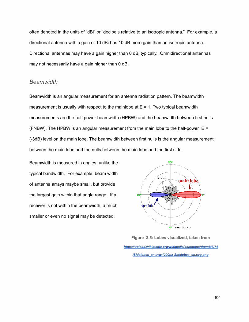
often denoted in the units of “dBi” or “decibels relative to an isotropic antenna.” For example, a
directional antenna with a gain of 10 dBi has 10 dB more gain than an isotropic antenna.
Directional antennas may have a gain higher than 0 dBi typically. Omnidirectional antennas
may not necessarily have a gain higher than 0 dBi.
Beamwidth
Beamwidth is an angular measurement for an antenna radiation pattern. The beamwidth
measurement is usually with respect to the mainlobe at E = 1. Two typical beamwidth
measurements are the half power beamwidth (HPBW) and the beamwidth between first nulls
(FNBW). The HPBW is an angular measurement from the main lobe to the half-power E =
(-3dB) level on the main lobe. The beamwidth between first nulls is the angular measurement
between the main lobe and the nulls between the main lobe and the first side.
Beamwidth is measured in angles, unlike the
typical bandwidth. For example, beam width
of antenna arrays maybe small, but provide
the largest gain within that angle range. If a
receiver is not within the beamwidth, a much
smaller or even no signal may be detected.
Figure 3.5: Lobes visualized, taken from
https://upload.wikimedia.org/wikipedia/commons/thumb/7/74
/Sidelobes_en.svg/1200px-Sidelobes_en.svg.png
62

Another measurement of beamwidth is null-to-null beamwidth. This is where the radiation
pattern decreases to 0, or negative infinity dBi.
Sidelobes are smaller beams that occur besides the main beam. These side lobe may not be
completely eliminated; in the context of directivity, this is wasted power. Side lobe level (SLL) is
another measurement to characterize side lobes. It measures the maximum gain of a side lobe
relative to the main lobe’s maximum.
Bandwidth
In the frequency domain, this is where the antenna is 3 dB (half the power) lower than its
maximum gain. If the bandwidth is not large enough for the information signal, some information
will be lost. Another specification in design of an antenna is not to make the bandwidth too
large; this may pick up undesired signals. However, a filter following the receiver may be used
to remedy this problem.
Bandwidth and antenna efficiency usually have an inverse relationship. Highly efficient
antennas have low bandwidth. High bandwidth antennas have low efficiency. This design
consideration is a tradeoff important to consider when creating specifications for an antenna.
Polarization
Depending on the type of application, antennas can be designed to contain a specific
polarization ideal for the transmission desired. Three types of polarizations common in
communications systems are vertical, horizontal and circular. The polarization and orientation of
the radio wave radiated by the antenna is determined by the electric field plane. If the antenna’s
electric field plane is perpendicular to the surface of the earth, the antenna possesses vertical
polarization. Similarly, if the electric field plane is parallel to the surface of the Earth, the antenna
63

contains a horizontal polarization. Lastly, circular polarization rotates through all the planes
including the horizontal and vertical planes. Its bias in radiation towards a certain plane
determines what is called the axial ratio measured in dB. An axial ratio 1-2dB indicates that
radiation is tilted more towards a certain plain creating an elliptical-like polarization, while an
axial ratio of 0dB indicates that the radiation is equal in all planes, forming a circular
polarization.
Temperature
Antenna noise temperature is a characterization of the antenna with regards to the amount of
noise it introduces at the input of a receiver. Usually, this is modeled in a system diagram by
replacing the antenna with a resistor that produces the equivalent noise power. The higher the
temperature, the more noise there is. The equations below model this noise; note that these
are the thermal noise equations.
,
here P oise power, v RMS noise voltage, k oltzmann s constant, T temperature W = n n = B = B ′ =
Δf bandwidth, and R ntenna impedance = = a
Equation 3.1: Thermal Noise Equation
Note that the antenna noise temperature models thermal noise. The two other prominent noise
sources typical in circuits are flicker noise (dependent on active components) and shot noise
(more relevant in circuits with small current).
http://ieeexplore.ieee.org/stamp/stamp.jsp?arnumber=7485875
64
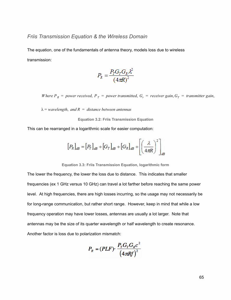
Friis Transmission Equation & the Wireless Domain
The equation, one of the fundamentals of antenna theory, models loss due to wireless
transmission:
here P power received, P power transmitted, G receiver gain, transmitter gain,W R = T = r = GT =
λ avelength, and R distance between antennas = w =
Equation 3.2: Friis Transmission Equation
This can be rearranged in a logarithmic scale for easier computation:
Equation 3.3: Friis Transmission Equation, logarithmic form
The lower the frequency, the lower the loss due to distance. This indicates that smaller
frequencies (ex 1 GHz versus 10 GHz) can travel a lot farther before reaching the same power
level. At high frequencies, there are high losses incurring, so the usage may not necessarily be
for long-range communication, but rather short range. However, keep in mind that while a low
frequency operation may have lower losses, antennas are usually a lot larger. Note that
antennas may be the size of its quarter wavelength or half wavelength to create resonance.
Another factor is loss due to polarization mismatch:
65

Equation 3.4: Friis Transmission Equation, polarization factor
There are more loss factors such as those due to effective aperture and cross-section of an
antenna; even atmospheric conditions may be a factor. Other factors that may occur include a
doppler shift or frequency change, as well as multipath (signals bouncing around).
In Figure 3.6 to the right, resonance
with the molecular oxygen structure
creates heavy attenuation at radio
frequency bands such as around 60
and 120 GHz. The Friis equation
does not account for this. A
general trend to note is that the higher the frequency, the more
Figure 3.6: Atmospheric attenuation, based on
frequency
attenuation per km. Certain frequencies have resonance with the water and oxygen in the
atmosphere, proving difficult to transmit signals at those frequencies without higher
transmission power.
66

3.2 Anechoic Chamber Overview
Figure 3.7: Block diagram of anechoic chamber in room 20-113 located in Cal Poly San
Luis Obispo.
An anechoic chamber measures an antenna radiation pattern using a vector network analyzer.
This is done by measuring the loss at a single-point frequency, and taking measurements every
few degrees, until a full rotation of the positioner is completed. Given the distance of
separation, gain of the transmit antenna, loss of both wires, the system can be de-embedded to
be normalized to the gain of the antenna-under test. Using Friis’ transmission equation will
assist in determining the loss of air. The gain of the transmit antenna is typically given. Wire
loss can be determined using a vector network analyzer. Assuming all components are
well-matched, one does not need to de-embed the system by undoing scattering parameter
systems. Rather, the S21 data will tell the overall loss of the setup. The only unknown is the
gain of the antenna-under-test, which can be determined by simple arithmetic (in the logarithmic
67

scale) of subtracting cable and air losses, and adding antenna gain. In the anechoic chamber
used, there is a program that will automate the process. The full block diagram is seen in Figure
3.7.
Figure 3.8: Anechoic chamber in room 20-113 located in Cal Poly San Luis Obispo.
The overall chamber is shown in Figure 3.8. To prevent unwanted interference, put covers on
the viewing windows when the device is under test. Otherwise, it is acceptable to leave these
covers open when loading antennas or tests are not running.
68

Ensure that the antennas are directly facing
one another. If misaligned, the radiation
pattern will not be centered correctly. The
transmit side (side with the known antenna
gain) has a wooden frame that assists in
getting as close to a perpendicular fit as
possible. Figure 3.10 shows this fit.
Unfortunately, one will have to eyeball the
receive antenna (antenna-under-test). This is
where removing the hatches for better viewing
will help, as seen in Figure 3.9.
Figure 3.9: Inside of anechoic chamber
Figure 3.10: Transmit antenna for anechoic
chamber.
Figure 3.11: The vector network analyzer used
for antenna pattern measurements
Ensure that this vector network analyzer and the positioner power are on. Figure 3.11 shows the
the specific VNA. Also, ensure the cables are plugged into Port 1 and Port 2. The program on
the computer will control the VNA and positioner using LabView to take data. The instructions
69

to use the program are on the wall panel of the anechoic chamber and will not be discussed in
this report. Contact Dr. Arakaki for more assistance in using the anechoic chamber.
3.3 Antenna Hardware
Cantenna Overview
The cantenna is designed with the purpose of being a jammer, due to its high directivity. The
cantenna is based on a circular waveguide design. This is a directional antenna with circular
polarization. The frequency of operation is directly related to the dimensions of the can. Most
cantenna designs recommend that the feed length and location be determined experimentally.
Furthermore, the feed’s location determines the
propagating mode. TE11 is the desired
propagating mode, as it is the lowest propagating
mode. The waveguide must be able to pass
frequencies above TE11’s cutoff limit. Also, the
waveguide must be designed such that
higher-order modes do not propagate. The
waveguide propagating modes are visualized in
Figure 3.12 . The target frequency of operation is
1.3 GHz. The metal can selected has a radius of
7.75 centimeters. From this, the lower and upper
frequencies of operation can be determined, using
circular waveguide cutoff frequency formulas.
Figure 3.12: Waveguide propagating
modes visualized, taken from
https://www.nap.edu/openbook/0309050278/xhtml/im
ages/img00056.jpg
70

Cantenna Implementation
Tables 3.1, 3.2: Transverse magnetic and transverse electric field mode constants
Radius , a = 7.75 cm
Free space wavenumber, k = 2 pi/ ƛ= 50.2655 (1/m)
Circumference, c = 0.48695 m
Equation 3.5: Circular waveguide cutoff wavelength
Tables 3.3, 3.4: Computing cutoff wavelengths for transverse magnetic and transverse
electric modes after applying equations
The lower and upper frequencies from the selected can are computed to be 1.13 GHz to 1.48
GHz, seen in Table 3.3 and 3.4 using the provided circular waveguide formula and the mode
order constants seen in Tables 3.1 and 3.2. This fits our frequency of operation. The next step
is to experimentally determine a working feed. TE modes will require the feed to be
71

perpendicular to the side of the can. TM modes will require a feed perpendicular to the bottom
of the can. Some typical suggestions is to install the feed a quarter-wavelength from the end of
the can. The quarter wavelength for 1.3 GHz is 5.77 cm. In Figure 3.13, a hole is drilled where
a feed is applied at this location. The length of the exposed feed is determined by trial and
error. A semi-rigid coax’s outer conductor is removed, along with the PTFE material to expose
the feed, seen in Figure 3.14. This is akin to a quarter-wavelength monopole, radiating inside a
circular waveguide. Simulation in an antenna simulation program such as High Frequency
Structure Simulator (HFSS) by ANSYS may provide better results, but may require additional
time.
Figure 3.13: Cantenna with SMA feed installed
72

Figure 3.14: Feed length, untuned
Figure 3.14 displays the initial feed,
uncalibrated. Measuring return loss, or S11
to check efficiency shows that this cantenna
is not well matched to 50 ohms, as seen in
Figure 3.15. Tuning is the next step to
perform.
Figure 3.15: Uncalibrated feed, poor return loss and efficiency
73

Figure 3.16: Feed length, tuned
Figure 3.16 displays the feed, tuned.
Measuring return loss, or S11 to check
efficiency shows that this cantenna is
better-matched to 50 ohms, as seen in Figure
3.17. To better match this, simulations using
a program may yield better results.
Figure 3.17: Calibrated feed, better return loss and efficiency
74

Here calibrating the feed has resulted in better power delivery at the select frequency of 1.3
GHz, as seen in a comparison between Figures 3.15 and 3.17. S11 reached -7.8 dB in the
tuned cantenna, whereas the untuned cantenna did not reach even -4 dB. Bending the feed
yielded in a better return loss. The result of bending the feed is “shortening” the feed. Cutting
the bent portion may be beneficial for a final design; however, this is acceptable for a prototype
structure. Note that high directivity is useless if efficiency is not sufficient; the overall antenna
gain will suffer if efficiency is low.
With an acceptable efficiency achieved, where more power is delivered to the antenna, the
radiation pattern is taken, seen in Figure 3.18 and 3.19. The separation between the cantenna
and transmit (patch) antenna is 57 inches. Using Friis transmission equation will determine the
air transmission loss. The rest, such as cable loss and gain of the patch antenna are known.
The anechoic chamber has a program that allows these losses and gains to be inputted,
simplifying the data to the gain of the receive antenna. Note that some radiation setups have a
higher gain than others.
75

Figure 3.18: Cantenna Radiation Patterns, E-co and E-cross
The max estimated gain is 8 dBi for E-coplanar, and -6.1 dBi for E-cross, assuming the
transmitter patch antenna is accurately measured to be 5.2 dBi. E-coplanar is blue, E-cross is
orange. The 3-dB beamwidth of E-co is 100 degrees.
76

Figure 3.19: Cantenna Radiation Patterns, H-Co and H-Cross
The max estimated gain 8.1 dBi for H-coplanar and -5.7 dBi for H-cross, assuming the
transmitter patch antenna is accurately measured to be 5.2 dBi. H-coplanar is blue, H-cross is
orange. The 3-dB beamwidth of H-co is 75 degrees.
The cantenna is finally finished to be used as a jammer. Note that in later experiments, Chapter
4, the cantenna is not used. This is primarily because the licenses for the other VSA/VSGs
(non-MIMO VSA/VSGs) expired after fall quarter, only providing the demo license. The demo
license did not permit frequencies at 1.3 GHz to be generated, only allowing lower MHz
frequency signals to be created.
77

Patch Antenna Overview
Patch antennas, also known microstrip antennas, are antennas known for convenience of
design, due to its low cost of printing onto circuit boards. Other advantages include its low
profile, being mechanically sturdy, and flexible in relation to antenna characteristics, such as
polarization, frequency, pattern, and impedance. The disadvantages include narrow bandwidth,
low efficiency, low power, and spurious feed radiation. There are many different shapes and
sizes used to create the patch antenna, as seen in Figure 3.20.
Figure 3.20: Differing microstip patch elements, taken from Balanis, Antenna Theory,
Analysis and Design (Second Edition).
There are four common feed methods to radiate the signal onto the antenna. They are the
microstrip transmission line, coaxial probe, aperture coupling, and proximity coupling, as seen in
Figure 3.21. Each feed method has its benefits and disadvantages. For instance, a microstrip
transmission line feed and a coaxial probe are easy to make and match. Aperture coupling and
proximity coupling are harder to make and match. The microstrip transmission line feed, coaxial
probe, and aperture coupling have lower bandwidths, ranging from 2% to 5%, whereas
78

proximity coupling can reach 13%. Microstrip transmission lines and coaxial probes may suffer
from asymmetric feeds, resulting in cross-polarization problems. Microstrip transmission lines
have the highest spurious radiation, whereas probe feed has less, and the other two even less.
Figure 3.21: Differing feed methods, taken from Balanis, Antenna Theory, Analysis and
Design (Second Edition).
79

There are general guidelines for analyzing microstrip antennas, with three primary models.
Transmission line modeling is the easiest to model, but may not be accurate due to inaccuracies
in the lack of modeling coupling. The second model is cavity modeling, which is more accurate,
but like the transmission line model, is hard to analyze coupling. The third and best model is the
full-wave. This may be seen in 3-D simulators such as Advance Design System’s Momentum.
Equation 3.6: Relative permittivity adjusted half wavelength
In general, the antenna’s designed dimensions are related to a half-wavelength or
quarter-wavelength of the desired frequency. This is dependent on the design chosen. Also
taken into the dielectric material. This is modeled in the equation above, where the width and
length are of a rectangular microstrip antenna is half the wavelength of the design frequency.
Patch Antenna Implementation
A patch antenna is designed using the formulas as initial starting points. The transmission line
feed is chosen due to easy fabrication, seen in Figure 3.22. Design verification is performed
using Advanced Design Simulation’s Momentum simulator. In this simulator, different cases are
simulated until the desired width and length are reached, as well as feed length, feed width, and
slot width.
80

Figure 3.22: Design dimensions of patch antenna. A transmission line feed is chosen.
The target frequency of the patch antenna design is 1.3 GHz . The relative permittivity of the
available material is er =2.55. The conductor is 1 ounce copper, and the dielectric height is not
important, as long as it is less than 5% of the wavelength. The antenna is matched to 50 ohms.
The table below, Table 3.5, shows the final dimensions of the patch antenna. The simulations
are shown in Figures 3.23 through 3.28.
Table 3.5: Physical dimensions of simulation-tuned patch antenna
81

Figure 3.23: 3-D view of patch antenna.
Figure 3.24: 3-D Radiation pattern of patch antenna.
82

Figure 3.25: Return loss of patch antenna.
The return loss of -17.8 dB corresponds to a 7% loss. Note that at 1.3 GHz the return loss is
about -5.8 dB corresponds to a 27% loss.
Figure 3.26: Power characteristics of patch antenna.
Here, the gain is 5.8 dBi at its maximum. Note that the efficiency of 73% is largely dependent
on the return loss. This is tested at 1.3 GHz.
83

Figure 3.27: Field characteristics of patch antenna.
These fields are harder to directly measure; a simulation can better accomplish this than
physically.
Figure 3.28: Polarization characteristics of patch antenna.
84

The physically-milled antenna uses a double sided copper-clad board, shown below in Figure
3.29. The duroid material has low loss. The height is 60 mils, and as mentioned earlier has a
relative permittivity of 2.55 and has 1 ounce copper.
Figures 3.29, 3.30: Circuit board utilized (left) and Othermill Pro milling machine (right) to
produce antenna.
The Othermill Pro has a limit of 1 mil and ability to creating 6 mil slots with its smallest drill, seen
in Figure 3.30. The maximum size of a board that will fit in the machine is 5.5” x 4.5”.
Understanding the limitations of manufacturing is important for a designer. The antenna design
needs to be dimensionally sound to be produced--otherwise special processes must be used to
85

create the prototype. In practice, almost all circuit boards must pass design-for-manufacturing
before being mass-produced. This milling machine, great for quick prototypes, is available in
the Cal Poly IEEE room, and costs money per time used. Visit calpolyieee.org or room 20-115
on campus for more information.
Figure 3.31: First prototype of the designed patch antennas. Copper tape is used to
tune the antenna. The layout dimensions were drawn incorrectly.
86

The first batch of antennas, seen in Figure 3.31, were incorrectly produced, due to the layout
producer not checking the specified dimensions carefully. The result is tuning by copper tape;
however, the tape would sometimes come loose, demonstrating that the “fixed” antennas were
not structurally sound. Visually on a vector network analyzer, the return loss would be
acceptable, such as -11 dB, but as soon as the antenna is slightly budged, the return loss turns
to -3 dB. Figure 3.32 demonstrates the return loss measurement. The resonance at 1.36 GHz
might be due to the length L dimension being shorter; higher frequencies correspond to shorter
wavelengths. Also note that if the board bends during the milling process, some parts of the
dielectric might be lower than others, seen in Figure 3.31. Photo-chemical etching, a common
circuit board design method, would not encounter this mechanical problem.
87

Figure 3.32: First prototype return loss. Note that it does not resonate at 1.30 GHz as intended.
After some tape it did resonate, but was not mechanically sturdy.
The boards were remilled for a second prototype after troubles with consistent return loss. Be
sure to double-check dimensions; errors could cost a lot of money and time of the layout is more
complex. The resulting look is shown in Figure 3.33 and the improved return loss is seen in
Figure 3.34.
88

Figure 3.33: Second prototype of patch antennas.
89

Figure 3.34: Second prototype of patch antennas.
With sufficient efficiency achieved, the antenna is tested in the chamber. The radiation patterns
are seen in Figures 3.35 and 3.36. The antenna gain is close to the simulation results; 5.8 dBi
and 5.2 dBi are very close. The sidelobes of the simulation are not as visible relative to real life.
Another aspect to note is that those sidelobes are not necessarily symmetric.
90

Figure 3.35: E-co is blue, E-cross is orange. 3-dB Beamwidth of E-Co is 120 degrees, max
gain is 5.2 dBi.
91

Figure 3.36: H-co is blue, H-cross is orange. 3-dB Beamwidth of H-Co is 100 degrees, max
gain is 4.8 dBi.
3.4 Preamplifiers Overview and Implementation
Overview
There are many types of amplifiers, each used for different circumstances. For example, a
transmitter amplifier may require high gain and a high power limit before distortion occurs. On
the other hand, preamplifiers require as low as possible noise figure to preserve the quality of
the signal. The purpose of a preamplifier is to convert a weak incoming signal into an output
signal that is adequate for further processing and noise-tolerant. An ideal preamplifier would
have as low as possible noise figure, matched input and output impedance with respect to the
92

system, high IP3, as well as high gain. The input and output impedance are matched to prevent
reflections at the input and output of the amplifier, while a high IP3 is required to minimize the
effects of distortion provided by the amplifier. A high-gain amplifier may offset the effects of
noise; however, note that high-gain amplifiers maybe too costly depending on the application.
Below shows Friis’ noise equation to determine the overall noise figure of cascaded elements.
The noise of passive components is approximately equal to the loss of the component. This
equation is especially useful for determining signal-to-noise before the digital processing units.
Equation 3.6: Friis Noise Equation
Note that in designing a receiver, this equation needs to be taken into account with more
consideration. However, for the purposes of the MIMO project, the only noise one would need
to account for is at the antenna and after the pre-amplifier. The contribution to noise in the VSA
is unknown.
Implementation
The Mini-Circuits amplifier ERA-3+ is selected due to its packaging type. Surface-mount
technology (SMT) may require layout and a surface-mount soldering station, both which may
require more time and additional resources. Unlike the common SMT-packaged amplifiers
commonly used in industry, the ERA-3+ comes in a Micro-X packaging, which is convenient for
dead-bug style prototyping. The benefit of dead-bug style prototyping is that a simple copper
clad board and soldering iron will produce the platform for the circuit. Figures 3.37 through 3.39
display the characteristics of the ERA-3+, along with the physical implementation requirements.
93

Figure 3.37: ERA-3+ Datasheet 1/3
94

Figure 3.38: ERA-3+ Datasheet 2/3
95

Materials List
● 2x 0.1 μF ● 1x 1 μ F ● 1x 10 μH ● 2x 215Ω ● Semi-Rigid Coax Cables ● SMA Connectors ● Copper Clad board
Figure 3.39: ERA-3+ Layout and Materials List 3/3
With a schematic shown in Figure 3.39, the first prototype is implemented, shown in Figure
3.40. With a supply voltage of 10 volts, the measured scattering parameters are displayed in
Figure 3.41.
Figure 3.40: ERA-3+ first prototype implementation.
96

Figure 3.41: ERA-3+ characterization of the first prototype, Vcc=10 V. Multiple ERA-3+
were constructed. It is not as clean as the one shown in Figure 3.43. Note that this vector
network analyzer measures from 10 MHz to 3 GHz.
The results in Figure 3.41 indicate that the lead lines are too long, creating resonances at
certain frequencies while blocking out others. A different layout minimizing length is shown in
Figure 3.42.
Figure 3.42: ERA-3+ second prototype implementation underway; only the semi-rigid coax
cables need to be soldered on.
97

Figure 3.43: ERA-3+ second characterization, Vcc=7 V. The physical implementation is
shown in Figure 3.42. Note that this vector network analyzer measures from 10 MHz to 9
GHz, unlike the one shown in Figure 3.41.
In higher frequency circuits, cleaner-laid out circuits matter more, due to wavelengths matching
physical dimensions of circuits. This may create unwanted reflections, as seen in a comparison
of Figure 3.41 vs Figure 3.43.
Two amplifiers were successfully created, while others gain; the gain is between 12-13 dB with
a voltage set at 7 volts. The noise figure could not be measured using the vector network
analyzers. Crude methods such as observing the noise floor rise could be used but may not
give 0.1 dB accuracy. It is expected based on the datasheet that the noise figure is around 2.7
dB. The amplifiers are used on the receiver end after the antennas.
98

Chapter 4: Test Data
4.1 SISO
SISO Experiment 1:
Purpose:
Evaluate a SISO test case to compare later on to MISO, SIMO, and MIMO test cases.
Procedure
The purpose of this experiment is to set a standard and collect data to later compare to other
cases. The data of interest is the channel matrix, and a metric related to signal-to-noise. The
setup is shown in Figure 4.1 and 4.2. The Figures 4.3 through 4.6 display the data collected.
Figure 4.1: Experiment 1 Setup and Loss Analysis
99

Figure 4.2: Physical Setup
100

Data
Figure 4.3: An instance of the IQ diagram, spectrum analyzer view, error vector spectrum
are displayed.
101

Figure 4.4: An instance of error vector summary, impulse response, and channel
frequency response are displayed. The error vector magnitude reads -30.955 dB.
102

Figure 4.5: A second instance of the IQ diagram, spectrum analyzer view, error vector
spectrum are displayed.
103

Figure 4.6: The second instance of error vector summary, impulse response, and channel
frequency response are displayed. The error vector magnitude reads -32.47 dB.
Discussion
The SISO test case data is collected for comparison to higher input-output orders. Error vector
magnitude is directly related to signal-to-noise ratio. Imagine noise as the error vector; the
larger the noise, the larger the error vector. In a log scale, a larger EVM is not sought for. The
104
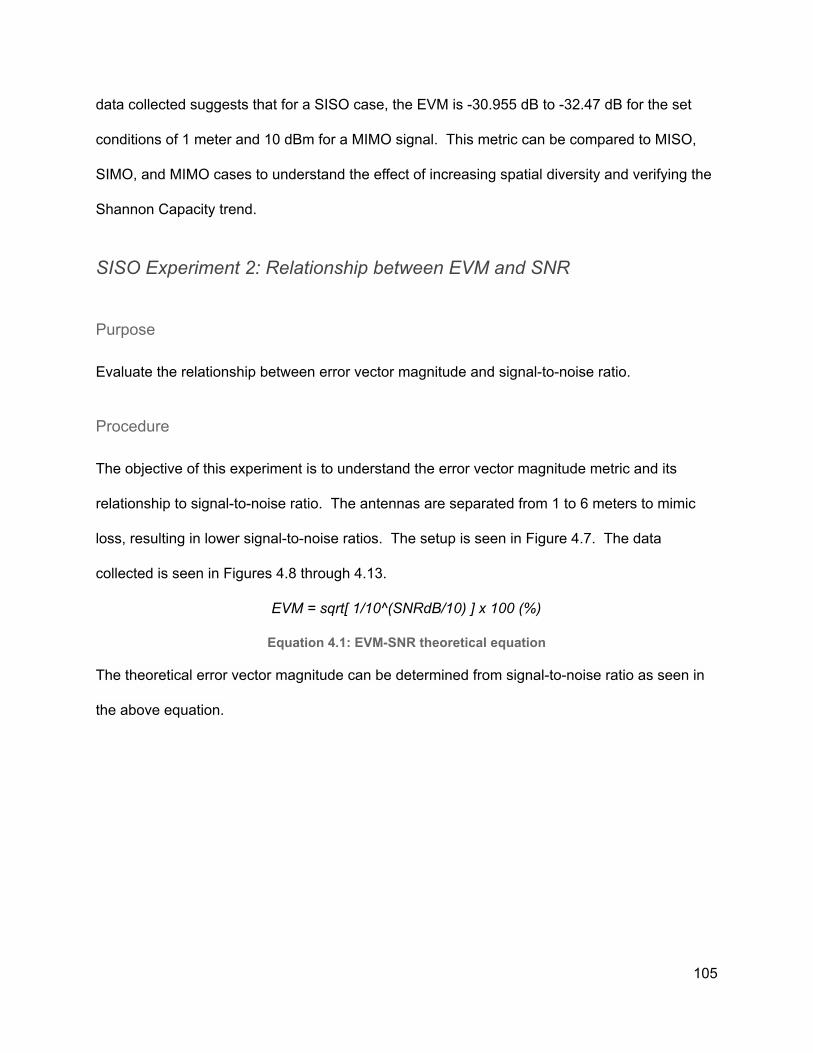
data collected suggests that for a SISO case, the EVM is -30.955 dB to -32.47 dB for the set
conditions of 1 meter and 10 dBm for a MIMO signal. This metric can be compared to MISO,
SIMO, and MIMO cases to understand the effect of increasing spatial diversity and verifying the
Shannon Capacity trend.
SISO Experiment 2: Relationship between EVM and SNR
Purpose
Evaluate the relationship between error vector magnitude and signal-to-noise ratio.
Procedure
The objective of this experiment is to understand the error vector magnitude metric and its
relationship to signal-to-noise ratio. The antennas are separated from 1 to 6 meters to mimic
loss, resulting in lower signal-to-noise ratios. The setup is seen in Figure 4.7. The data
collected is seen in Figures 4.8 through 4.13.
EVM = sqrt[ 1/10^(SNRdB/10) ] x 100 (%)
Equation 4.1: EVM-SNR theoretical equation
The theoretical error vector magnitude can be determined from signal-to-noise ratio as seen in
the above equation.
105

Figure 4.7: Setup for EVM and SNR experiment.
Figure 4.8: QPSK 5 MHz bandwidth, center frequency at 1.28 GHz at 1 meter separation.
106

Figure 4.9: QPSK 5 MHz bandwidth, center frequency at 1.28 GHz at 2 meter separation.
Figure 4.10: QPSK 5 MHz bandwidth, center frequency at 1.28 GHz at 3 meter separation.
107

Figure 4.11: QPSK 5 MHz bandwidth, center frequency at 1.28 GHz at 4 meter separation.
Figure 4.12: QPSK 5 MHz bandwidth, center frequency at 1.28 GHz at 5 meter separation.
108
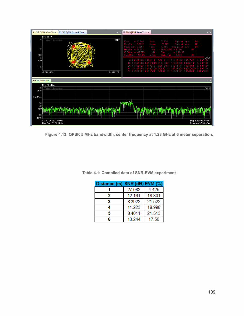
Figure 4.13: QPSK 5 MHz bandwidth, center frequency at 1.28 GHz at 6 meter separation.
Table 4.1: Compiled data of SNR-EVM experiment
109
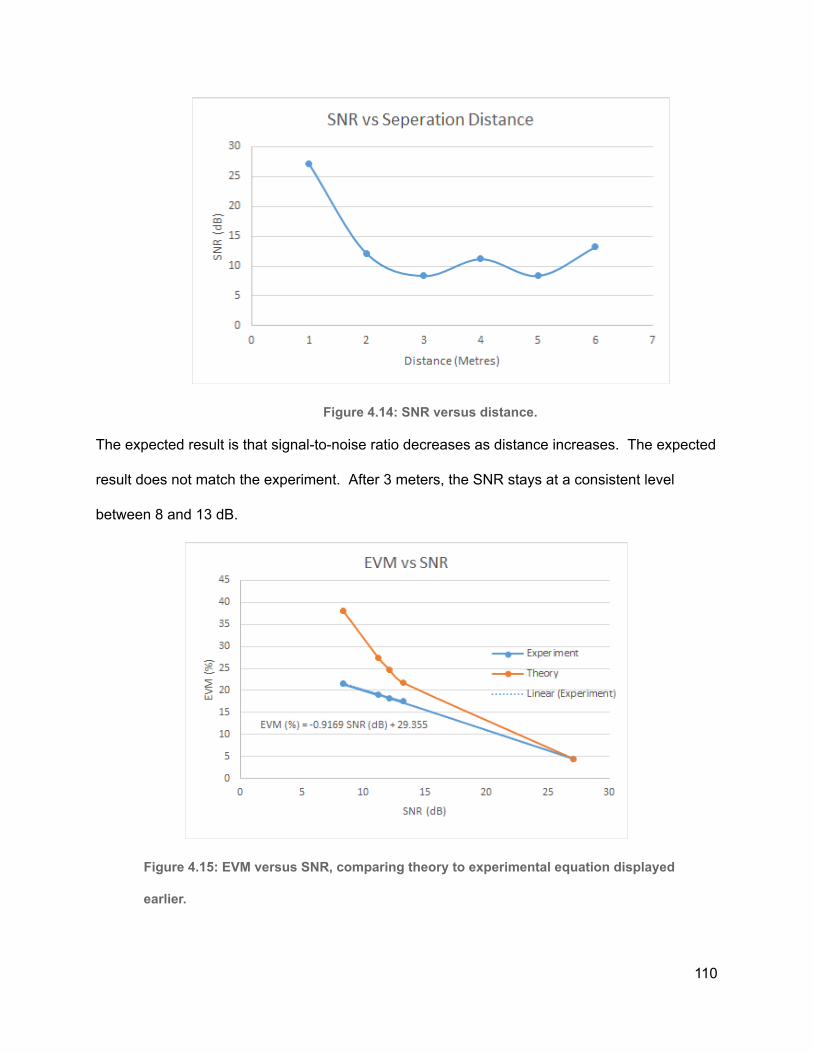
Figure 4.14: SNR versus distance.
The expected result is that signal-to-noise ratio decreases as distance increases. The expected
result does not match the experiment. After 3 meters, the SNR stays at a consistent level
between 8 and 13 dB.
Figure 4.15: EVM versus SNR, comparing theory to experimental equation displayed
earlier.
110

Discussion
The data shown in Table 4.1 is graphed in Figure 4.14 and 4.15 to display the relationships and
trends in data. The goal of this test was to understand the relationship between EVM and SNR.
The experiment displayed lower EVM for a lower SNR than when compared with the theoretical
equation, surprisingly. The general trend still holds true: increasing SNR decreases EVM in
general. At higher SNRs, the EVM converges, as seen in Figure 4.15.
The distance versus signal-to-noise ratio did not meet expectations or predictions. As distance
increased, the SNR started to stay at the same level, seen in Figure 4.14. Perhaps larger
magnitudes of distance separation are needed to demonstrate the expended trend of a lower
SNR. The experiment had a linear sweep of distance. A logarithmic sweep of distance (1 m, 10
m, 100 m) could be a better method of setting up an improved experiment. However, cable
lengths may be a limiter in this situation.
SISO Experiment 3: Effects of modulation on EVM and SNR
Purpose
Evaluate the effects of increasing modulation on error vector magnitude and signal-to-noise
ratio.
Procedure
The objective of this experiment is to understand the error vector magnitude metric and its
relationship to increasing modulation. The antennas are separated from 3 meters constantly,
111

while the generator generates different modulation types. The setup is seen in Figure 4.16 to
4.18. The data collected is seen in Figures 4.19 through 4.26.
Figure 4.16: Modulation experiment setup
Figure 4.17: Modulation experiment physical setup
112

Figure 4.18: Transmitter and receiver, along with amplifier
113

Data
Figure 4.19: QPSK test case
Figure 4.20: 16 QAM test case
114
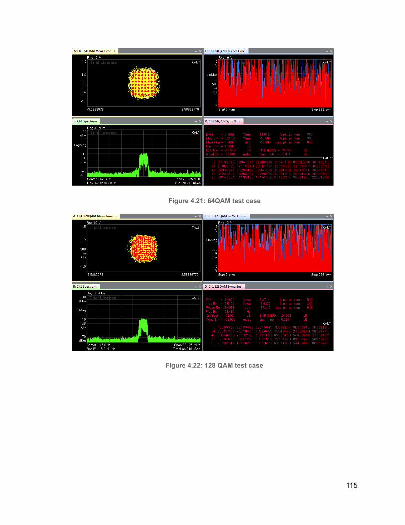
Figure 4.21: 64QAM test case
Figure 4.22: 128 QAM test case
115

Figure 4.23: 256 QAM test case
Figure 4.24: 512 QAM test case
116

Figure 4.25: 1024 QAM test case
Figure 4.26: 2048 QAM test case
117

Table 4.2: Compiled results
Figure 4.27: EVM vs QAM Modulation relationship.
Note that this is misleading based on how the vector signal analyzer determines EVM. The
trendline should be increasingly worse EVM.
118
Discussion
The goal of this test was to see how the increasing the modulation of a SISO system affects the
EVM and SNR. Looking at the graph in Figure 4.27, the maximum EVM occurs at approximately
16 QAM and after decreases sharply. Originally it was believed that increasing the QAM
modulation would increase the EVM, but upon closer inspection the experimental trend is valid.
Looking at 16 QAM constellation diagram in Figure 4.20 has a very chaotic pattern, where the
points are not lined up with the expected position. When 16 QAM is compared to 64 QAM there
is a very stark difference in clarity. The 64 QAM constellation shown in Figure 4.21 had point
almost exactly on the expected spots, thus the 64 QAM case had a better EVM than the 16
QAM case. After the 64 QAM case the 128 QAM was tested and had a worse EVM, which is
expected, but when higher modulations were tested the trend failed. When looking at the
constellation diagrams for the 256 to 4096 cases (Figure 4.23 to Figure 4.26) the constellation
diagrams are just as messy and chaotic as the 16 QAM case, but the EVM was better than the
16 QAM case.
This suggests that the EVM for the higher cases of modulation is not an accurate way to
measure the performance of the SISO system. The reason the EVM may fail is because the
error is determined by the distance from the experimental point to the closest expected
constellation point. In cases above 128 QAM the points are far closer together, which provides
more points to be closer to the experimental point than for lower modulations such as 16QAM.
SInce the points are closer together the error distances is significantly smaller and thus the ratio
of error to the constellation point difference to the origin is extremely smaller than lower QAM
cases. The SNR is inversely proportional to the EVM so SNR should be worse at higher QAM
119

modulations, but since the SNR was calculated from the experimental data the SNR will have
the same faults at higher frequencies. Thus modulation used in future tests should only be with
modulations less than 128 QAM to prevent misconceptions about EVM.
4.2 MISO
Purpose:
Evaluate a MISO test case to compare later on to MISO, SIMO, and MIMO test cases.
Procedure
The purpose of this experiment is to set a standard and collect data to later compare to other
cases. The data of interest is the channel matrix, and a metric related to signal-to-noise.
To perform our MISO test, we drove each VSG with the WLAN_11n_64QAM_40MHz.wfm
waveform using the C# program. The next step was to change the setup of the 89600 software
such that it could read the waveform we are sending. Once the setup was complete we then
adjusted the center frequency to allow for the program to run.
Once both VSGs and the VSA were being driven we then separated the transmit antennas and
receive antennas by a length of 1 meter, shown in Figures 4.28 and 4.29. . The data was
recorded in the following section, Figures 4.30 through 4.33 .
120

Figure 4.28: MISO experimental setup
Figure 4.29: MISO experiment physical setup
121
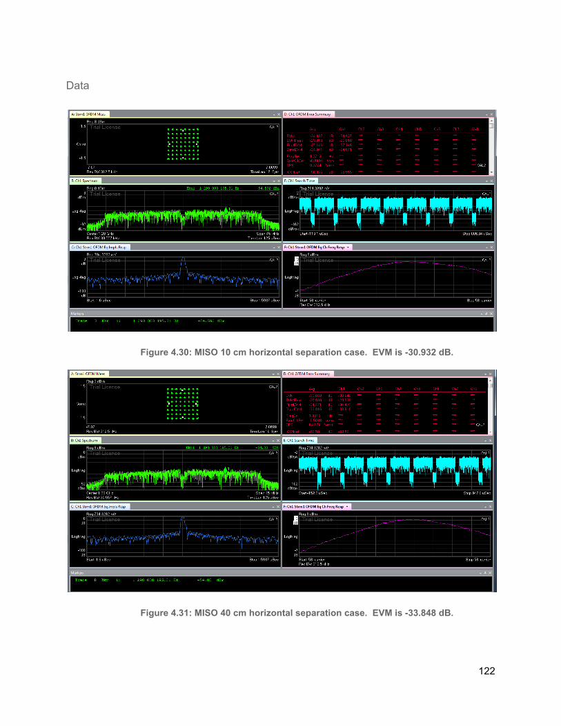
Data
Figure 4.30: MISO 10 cm horizontal separation case. EVM is -30.932 dB.
Figure 4.31: MISO 40 cm horizontal separation case. EVM is -33.848 dB.
122

Figure 4.32: MISO no separation case where antennas are back-to-back, front antenna is 1
m away from receivers’ centroid. EVM is -31.551 dB.
Figure 4.33: MISO 16 cm separation case where antennas are back-to-back, front antenna
is 1 m away receivers centroid. EVM is -20.421 dB.
123

Table 4.3: Compiled MISO cases and EVM
Discussion
The MISO cases demonstrated better signal-to-noise ratio, based on configurations. Examining
the horizontal cases, the separation distance effects the error-vector-magnitude. With a meter
distance to the receiver held constant, increasing horizontal separation distance between the
transmit antennas resulted in better signal received at certain points. In the experiment, 40 cm
separation resulted in an EVM of -33.848 dB, whereas the close distance of 10 cm resulted in
-30.932 dB, as tabulated in Table 4.3. Different separation distances resulted in EVM around
-30 dB as well. Separation distances greater than half a meter started to exhibit a decay, rising
to -20 dB for instance. Overall, this method of spatial diversity may prove cheaper and more
effective than controlling power and phase (in beamforming), as long as the number of array
elements is low and cost of mechanical parts does not outweigh the cost of variable amplifiers
and phase shifters.
The back-to-back cases explores the effect of another patch antenna back lobe on the transmit
signal. For the back-to-back case of 0 cm separation, the error vector magnitude was
comparable to the horizontal cases between 10 and 40 cm; the error vector magnitude was
below -30 dB. For the case of 16 cm, or approximately ¾ of the wavelength, the EVM suffered,
dropping to -20 dB. This experiment demonstrates that in a MIMO system with multiple patch
124

antennas facing different directions, the back lobe of the radiation may affect other patch
antennas unintentionally in a negative manner.
4.3 SIMO
Purpose:
Evaluate a SIMO test case to compare later on to MISO, SIMO, and MIMO test cases.
Procedure
The purpose of this experiment is to set a standard and collect data to later compare to other
cases. The data of interest is the channel matrix, and EVM, a metric related to signal-to-noise.
The physical setup is shown in Figures 4.34 and 4.35.
To perform the SIMO test, we drove one VSG with the WLAN_11n_64QAM_40MHz.wfm
waveform using the C# program. The next step was to change the setup of the 89600 software
such that it could read the waveform we are sending. Once the setup was complete we then
adjusted the center frequency to allow for the program to run.
Once the VSG and both VSAs were being driven we then separated the transmit antenna and
receive antennas by a length of 1 meter. The data was recorded in the following section, seen in
Figures 4.36 and 4.37.
125

Figure 4.34: MISO experimental setup
Figure 4.35: MISO experiment physical setup
126

Data
Figure 4.36: SIMO test case results. IQ diagram, spectrum analyzer view, error vector
spectrum are displayed.
127

Both received signals were about the same power, with the second spectrum slightly lower. The
IQ diagram shown was clean, suggesting that EVM measurement error would not occur from
overlap.
Figure 4.37: SIMO test case results. Error vector summary, impulse response, and channel
frequency response are displayed. The error vector magnitude reads -30.932 dB.
The channel frequency response differed, with one channel being more even across the board,
while the other attenuated lower carriers more. This could be dependent on the antenna
128

bandwidth. Perhaps one antenna’s center frequency was slightly different by a few megahertz,
causing higher carriers to have the highest channel frequency response, rather than the center.
The error vector magnitude for one channel was slightly better. This is perhaps due to less
multipath for that antenna, or even less lossy wires before entering the demodulation of inside
the VSAs.
Discussion
The error vector magnitude of -30.932 dB, as seen in Figure 4.37, is comparable to the SISO
case. This makes sense, as there is no spatial diversity on the transmitter side. Although the
results for SISO and SIMO were similar, note that SIMO has a superior worst-case. For
example, if multipath or a jammer disabled the quality of the signal going into one antenna, the
second antenna could still potentially pick up a usable signal in the case of SIMO. For SISO,
the receiver under the same conditions may not be able to render a usable signal.
4.4 2x2 MIMO
Purpose:
The purpose of this portion of the experiment was to implement and test a 2x2 MIMO system.
This was done by running the C# program via Microsoft’s Visual Studio.
Procedure:
To perform our MIMO test, we drove each VSG with the WLAN_11n_64QAM_40MHz.wfm
waveform using the C# program. The next step was to change the setup of the 89600 software
such that it could read the waveform we are sending. Once the setup was complete we then
adjusted the center frequency to allow for the program to run.
129

Once both VSGs and both VSAs were being driven we then separated the transmit antennas
and receive antennas by a length of 1 meter, seen in Figure 4.38. The data was recorded in the
following section, seen in Figures 4.39 through 4.43.
Figure 4.38: MIMO experimental setup
130

Data:
Figure 4.39: 802.11n OFDM 64 QAM Constellation Diagram
Figure 4.39 shows the WLAN 802.11n 64 QAM constellation diagram for a 2x2 MIMO system
with a modulation frequency of 1.28 GHz. This particular constellation diagram appears to be
rather clean. The constellation points are tightly knit, in other words, the demodulated symbols
are rather close to the predetermined reference points.
Figure 4.40 : OFDM Error Summary
Figure 4.40 shows the OFDM error summary for our WLAN signal. We can immediately notice
that the EVM of channel 2 is lower than that of channel 1; both VSG 1 and VSG 2 are outputting
the same signal and no diversity coding is taking place, so this difference in channel EVM can
most likely be attributed to antenna orientation as well as signal interference.
131

Figure 4.41: Channel 1 Spectrum
Figure 4.42: Channel 2 Spectrum
Figures 4.41 and 4.42 show the spectrums of channel 1 and channel 2. We can immediately
see that both spectrums look very similar to each other. However, the upper sideband of
channel 2 spectrum appears to be higher than its lower sideband. This deviation in sideband
flatness is not seen in channel 1 spectrum.
132

Figure 4.43: OFDM MIMO Channel Information Matrix
Figure 4.43 shows the channel information for stream 1. There were some issues with getting
the 89600 software to receive and display data from stream 2. Stream 2 corresponds to the
secondary incoming signals. Knowing this we can say that h 11 =0.55+j0.00 and h 22 =-1.03+j0.59
with h 12 and h 21 having unknown values.
Table 4.4: Compiled cases of EVM: SISO through MIMO
SNR = - [3.7 + 20 * log10 ( EVM / 100% )] for 64 QAM
Equation 4.2: EVM-SNR theoretical equation, 64 QAM specific
133

Discussion:
Table 4.4 shows the compiled results for every single case. The equation underneath the table
is specific for 64 QAM and is used to determine the SNR. The transmitter and receiver distance
is kept constant at 1 meter, while the antenna separation for input or output are close to half a
wavelength, at 10 cm. SNR is about the same for SISO, SIMO, and MISO. Note that for SIMO
the second channel has a lower EVM, resulting in a higher SNR; however, the EVM column only
takes into account the average of the two. The MIMO case has 2 dB higher signal power than
noise relative all the other cases. While this may seem small, keep in mind that 2 dB greater in
SNR for the same amount of input power will result in lower bit-error rate, allowing for faster and
more robust communication. Also note that MIMO is an improvement over SIMO. Individually
looking at the two channels, the EVM was lower for both channel 1 and channel 2 in the MIMO
case by 2 to 3 dB. Although not intuitive from the data, MISO is a better case than SISO.
Although the results based on SNR look the same, MISO’s worst case is better than SISO’s
worst case. For example, if one transmitter antenna was blocked physically, another antenna
could send the signal. This could not be said about SISO. Real life examples where this
situation may occur includes birds building nests around antennas, degrading the signal integrity
of that antenna. Combining both SIMO and MISO produce the best case overall. The
conclusion drawn from this data is that increasing spatial diversity results in a better signal
overall.
134
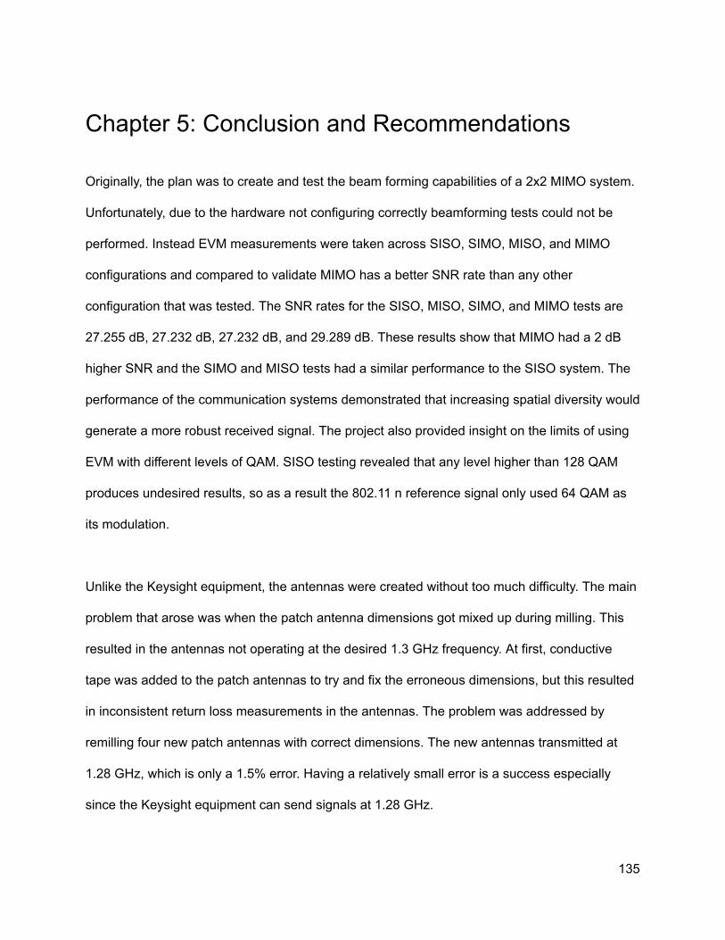
Chapter 5: Conclusion and Recommendations
Originally, the plan was to create and test the beam forming capabilities of a 2x2 MIMO system.
Unfortunately, due to the hardware not configuring correctly beamforming tests could not be
performed. Instead EVM measurements were taken across SISO, SIMO, MISO, and MIMO
configurations and compared to validate MIMO has a better SNR rate than any other
configuration that was tested. The SNR rates for the SISO, MISO, SIMO, and MIMO tests are
27.255 dB, 27.232 dB, 27.232 dB, and 29.289 dB. These results show that MIMO had a 2 dB
higher SNR and the SIMO and MISO tests had a similar performance to the SISO system. The
performance of the communication systems demonstrated that increasing spatial diversity would
generate a more robust received signal. The project also provided insight on the limits of using
EVM with different levels of QAM. SISO testing revealed that any level higher than 128 QAM
produces undesired results, so as a result the 802.11 n reference signal only used 64 QAM as
its modulation.
Unlike the Keysight equipment, the antennas were created without too much difficulty. The main
problem that arose was when the patch antenna dimensions got mixed up during milling. This
resulted in the antennas not operating at the desired 1.3 GHz frequency. At first, conductive
tape was added to the patch antennas to try and fix the erroneous dimensions, but this resulted
in inconsistent return loss measurements in the antennas. The problem was addressed by
remilling four new patch antennas with correct dimensions. The new antennas transmitted at
1.28 GHz, which is only a 1.5% error. Having a relatively small error is a success especially
since the Keysight equipment can send signals at 1.28 GHz.
135

This project provides a solid base for future projects pertaining to MIMO. Future projects could
include beamforming, investigations into more complex configurations such as 3x3 MIMO and
4x4 MIMO, and observing the effects a jammer signal has on the different communication
systems. The background concepts discussed in this report provide a solid basic understanding
of the key concepts of MIMO a person need to know before performing any MIMO experiments.
The discussions on how to configure the VSAs and VSGs, build and characterize antennas, and
how to use signal studio to communicate to the VSAs and VSGs are also integral concepts
which form the base of a majority of future MIMO projects. Finally the collection of Keysight
M9381A VSG and M9391A VSA will be very useful for future projects since they explain how to
run basic tests and how to configure multiple chassis and the limitations for higher order MIMO
system testing.
Appendix A: Senior Project Analysis
Advisor: Dr. Dennis Derickson
1. Summary of Functional Requirements:
As stated previously, this project is to build several unique communication systems and test
them. The results of these test will be recorded, analyzed, and compiled into a final research
report. Our findings will provide insight primarily to cellular service providers who may use our
results to design the optimal method for cellular communication.
136

2. Primary Constraints:
The first challenge faced in this project was the understanding of digital communications. Digital
Communications is considered to be a rather abstract concept and can be quite hard to grasp.
Another aspect of this project that will prove to be difficult is understanding which MIMO
implementations are the most important to analyze. MIMO designs are already in existence and
being used today; determining ways to better these systems is a difficult task.
3. Economic:
Target of $200 budget for the construction of all systems. Construct the hardware with materials
available in the lab, and order the rest from vendors. Materials available in the lab include
coaxial connectors, coaxial cables, wires, and some amplifiers. With the modulation and
demodulation of the signal taken care of by the VSA and VSG, we will aim to construct the RF
path. The ordered parts include amplifiers, an empty paint can and connectors. Since this is a
research project, students will be unpaid. The main people that will benefit from our product are
not the consumer, but whichever company uses our research to develop MIMO. Fortunately, our
project will be primarily be done on the VSGs and VSAs in the Networks Lab. We will need to
implement discrete hardware components such as antennas and amplifiers. The cost for these
external components will be quite small.
4. If Manufactured on a Commercial Basis:
Our final product is not something that a typical consumer would purchase, however, how it is
implemented may have a very large effect on the common consumer. In 2015, a total of 403
137

million smartphones were purchased; the total number sold increased by 9.7% in the fourth
quarter of that year. Currently the average production cost for smartphones is $220, the
implementation of MIMO will raise that cost slightly (the main difference is adding antennas).
5. Environmental:
Lead-free designs will be used in the construction of the MIMO hardware. The European
market disallows anything with Lead inside the design; if the product were to include lead, our
customer base will disclude the entire European communications market. Furthermore, the
power of the antennas will not exceed more than 1 watt for each transmission antenna. This is
to comply with the Federal Communications Commission’s standards.
6. Manufacturability:
The manufacturing process for smartphones has already been developed quite some time ago.
If MIMO were to be implemented in the common modern phone, the manufacturing process
would change very little. As stated in the previous section, the main change for cellular devices
would be the increase in antennas. The manufacturing process would need to be adjusted such
that the implementation of additional antennas could be accommodated. This change in process
does not pose much of a threat to achieving MIMO integration into cellular devices.
7. Sustainability:
The designs will involve hardware that is not the newest but not obsolete either. This will ensure
that hardware such as power amplifiers will be available to purchase over the course of 5 to 10
years. An upgrade that we could implement are multi-frequency amplifiers, this could allow for
138

the design to last longer when put into a cell phone. Upgrading the system would be a step that
our customers would take. They would choose alternative ways to use MIMO.
8. Ethics:
There are a few ethical dilemmas that this MIMO research can encounter. The first covers the
thought of ‘who can this research be sold to?’: Many people believe that MIMO is the future for
digital communications. Depending on how MIMO is implemented, we may be encouraging a
monopoly for cellular service providers. If a cellular service provider uses our research to
implement the best method for digital communications, many consumers would change their
provider to that company. Economic monopoly has been a major ethical issue for quite some
time. Depending on how successful MIMO is, many companies that cannot compete will lose
customers.
Eventually, most of the companies will cease to exist which will result in thousands of
unemployed people. We are well aware that the concept of a monopoly is illegal, however there
are many ‘loopholes’ that companies take advantage of. One of our potential customers are
several branches of the military. When selling to the government, one often faces many ethical
dilemmas due to the secrecy of the government. On one hand ‘could our research assist in
saving lives?’ on the other hand ‘will our research be put to unethical use that will lead to the
loss of innocent lives?’
9. Health and Safety:
The implementation of MIMO poses little to no health threats. Even though MIMO itself does not
directly pose any threats, cell phones still do. There have been many studies linking cell phone
139

use to an increased risk of certain types of cancer. Many people are concerned with the radio
waves that come with cell phones. The increased number of antennas may facilitate an increase
in the intensity of these radio wave, however, this is unlikely. As a safeguard, the research will
comply with FCC standards of no more than one Watt of power delivered to the transmit
antenna. Higher power may be detrimental to the health of living organisms around the RF
device. For example, radiation from WiFi bands have been found to have negative effects on the
body, such as altered brain tissue and lower sperm count.
10. Social and Political:
The implementation of MIMO should be in accordance to the Federal Communications
Commission’s standards. This means that the research will utilize amateur radio bands, and
avoid bands not available to the public. Violating the FCC standards may result in heavy fines.
The social analysis is that cellular providers are able to view this research equally. For
companies that already use a MIMO implementation in their system, this may be seen as
detrimental to their business, as competitors may gain insight to MIMO technology. For cellular
companies that have not utilized MIMO, this will provide valuable knowledge to their research
and development groups. For researchers, this MIMO research may confirm their theoretical
MIMO models and prove to be beneficial to the research community.
11. Development:
At the conclusion of the project a working understanding of the basic principles of characterizing
the performance of different communication system was obtained. To put these principles into
use a greater understanding of antennas, how to configure the Keysight PXIe vector signal
140

analyzers and vector signal generators, and how to use the 89600 VSA and signal studio
programs to transmit and analyze a received modulated WiFi signal was necessary. Specifically
the project required understanding on how to build a patch and a can antenna, as well as how to
determine the transmitting frequencies. Also to gether the radiation patterns an understanding of
how to use the anechoic chamber was also acquired. To generate the testing configuration of
the Keysight PXIe vector signal analyzers and vector signal generators a greater understanding
of how the VSA and VSG are connected both internally and externally was acquired. Also how
to use Visual Studio to open drivers and control the individual VSA and VSG signals was also
obtained. Finally, good communication, problem solving, and time management skills were also
improved.
12. Bill of Materials:
# Part/Process Description Quantity Price Cost
1 ACX1230-ND Connector SMA JACK, 50 OHM
4 $4.68 $18.72
2 ERA-3+ TB, ERA-3, VV105,50 OHM /ROHS
4 $1.80 $7.20
3 Patch Antenna Milling Process
IEEE Milling 8 $8.00 $64.00
4 Copper Tape Copper Tape 1 $16.00 $16.00
5 Empty Quart Paint Can Cantenna can
1 $11.75 $11.75
Total: $116.92
141

Appendix B: References
MIMO Resources
[1] Langton Charan and Bernard Sklar. (2011). Tutorial 27 -Finding MIMO [Online]. Available
FTP:http://complextoreal.com/wp-content/uploads/2013/01/mimo.pdf
[2] D. Tse and P. Viswanath, https://people.eecs.berkeley.edu , 2005. [Online]. Available:
https://people.eecs.berkeley.edu/~dtse/Chapters_PDF/Fundamentals_Wireless_Communication
_chapter7.pdf. [Accessed: 07- Jun- 2017].
[3 ]J. Proakis and M. Salehi, "Digital Transmission on Fading Multipath Channels - National
Instruments", Ni.com , 2017. [Online]. Available: http://www.ni.com/white-paper/14931/en/.
[Accessed: 07- Jun- 2017].
[4]C.McKell,"https://polylearn.calpoly.edu/AY_2016-2017/pluginfile.php/328798/mod_resource/content/0/
MIMO%20and%20Info%20Theory.pdf", 186-C102, 2016.
[5]"Singular Value Decomposition (SVD) tutorial", Web.mit.edu , 2017. [Online]. Available:
http://web.mit.edu/be.400/www/SVD/Singular_Value_Decomposition.htm. [Accessed: 07- Jun- 2017]
[6] C. Beard and W. Stallings, Wireless Communication Networks and Systems. 2016, p. 9, 22, 40,
93-146, 156, 236-250, and 282.
http://study.com/academy/lesson/stretching-compression-of-logarithmic-graphs.html
[7] “MIMO”, en.wikipedia.org, 2017. [Online]. Available:
https://en.wikipedia.org/wiki/MIMO [Accessed: 02-October-2016].
[8] “Convolutional Code”, en.wikipedia.org, 2017. [Online]. Available:
https://en.wikipedia.org/wiki/Convolutional_code [Accessed: 25-May-2017].
142

[9] “Multipath Propagation”, en.wikipedia.org, 2017. [Online]. Available:
https://en.wikipedia.org/wiki/Multipath_propagation [Accessed: 03-October-2016].
[10] “Fading”, en.wikipedia.org, 2017. [Online]. Available:
https://en.wikipedia.org/wiki/Fading [Accessed: 28-May-2017].
[11] “Rayleigh Distribution”, en.wikipedia.org, 2017. [Online]. Available:
https://en.wikipedia.org/wiki/Rayleigh_distribution [Accessed: 05-June-2017].
[12] “Rayleigh Fading”, en.wikipedia.org, 2017. [Online]. Available:
https://en.wikipedia.org/wiki/Rayleigh_fading [Accessed: 05-June-2017].
[13] “Rice Distribution”, en.wikipedia.org, 2017. [Online]. Available:
https://en.wikipedia.org/wiki/Rice_distribution [Accessed: 05-June-2017].
[14] “Rician Fading”, en.wikipedia.org, 2017. [Online]. Available:
https://en.wikipedia.org/wiki/Rician_fading [Accessed: 05-June-2017].
[15] Charan Langton. (2013). Tutorial 22 -Orthogonal Frequency Division Multiplexing [Online].
Available FTP:http://complextoreal.com/wp-content/uploads/2013/01/ofdm2.pdf
Keysight and VSA/VSG resources
[16] "Vector Signal Analyzer", en.wikipedia.org , 2017. [Online]. Available:
https://en.wikipedia.org/wiki/Vector_signal_analyzer [Accessed: 07- Jun- 2017].
[17]I. Poole, "Vector Signal Generator | VSG Generator | Radio-Electronics.Com",
Radio-electronics.com , 2017. [Online]. Available:
http://www.radio-electronics.com/info/t_and_m/generators/vector-signal-generator-vsg.php.
[Accessed: 07- Jun- 2017].
[18] "Intermediate Frequency", en.wikipedia.org , 2017. [Online]. Available:
https://en.wikipedia.org/wiki/Intermediate_frequency [Accessed: 07- Jun- 2017].
143

[19]"Keysight Technologies M9381A PXIe Vector Signal Generator 1 MHz to 3 GHz or 6 GHz
Data Sheet", Literature.cdn.keysight.com , 2017. [Online]. Available:
http://literature.cdn.keysight.com/litweb/pdf/5991-0279EN.pdf. [Accessed: 07- Jun- 2017].
[20]"Keysight Technologies M9391A PXIe Vector Signal Analyzer 1 MHz to 3 GHz or 6 GHz
Data Sheet", Literature.cdn.keysight.com , 2017. [Online]. Available:
http://literature.cdn.keysight.com/litweb/pdf/5991-2603EN.pdf. [Accessed: 07- Jun- 2017].
[21]"Keysight LTE/LTE-A Multi-Channel Reference Solution Startup Guide",
Literature.cdn.keysight.com , 2017. [Online]. Available:
http://literature.cdn.keysight.com/litweb/pdf/Y1299-90001.pdf?id=2413851. [Accessed: 07- Jun-
2017].
[22]"Keysight LTE/LTE-A Multi-Channel Reference Solution User’s Guide",
Literature.cdn.keysight.com , 2017. [Online]. Available:
http://literature.cdn.keysight.com/litweb/pdf/Y1299-90005.pdf?id=2655403. [Accessed: 07- Jun-
2017].
[23]"Keysight M9391A PXIe Signal Analyzer & M9381A PXIe Vector Signal Generator 1 MHz to
3 GHz or 6 GHz Startup Guide", keysight.com , 2017. [Online]. Available:
http://edadownload.software.keysight.com/Modular/M938XA/2.1/M9391_and_M9381_StartupGu
ide.pdf?__gda__=1496885723_d25bf157871f111fb6d27d15da2cd2b8&fileExt=.pdf. [Accessed:
07- Jun- 2017].
[24]"Keysight M9391A PxIe Vector Signal Analyzer & M9381A PXIe Vector Signal Generator
Programming Guide", www.keysight.com , 2017. [Online]. Available:
http://edadownload.software.keysight.com/Modular/M938XA/2.1/M9391_and_M9381_Program
mingGuide.pdf?__gda__=1496884677_697c82329541458461f97c9851df42a1&fileExt=.pdf.
[Accessed: 07- Jun- 2017].
144

Antenna and Preamplifier Resources
[25] P. Bevelacqua, "The Antenna Theory Website", Antenna-theory.com , 2017. [Online]. Available:
http://www.antenna-theory.com/. [Accessed: 07- Jun- 2017].
[26]"Satellite frequency bands", European Space Agency , 2017. [Online]. Available:
http://m.esa.int/spaceinimages/Images/2013/11/Satellite_frequency_bands. [Accessed: 07- Jun- 2017].
[27]I. Giangrandi, "Field regions around an antenna", Giangrandi.ch , 2017. [Online]. Available:
http://www.giangrandi.ch/electronics/anttool/regions.shtml. [Accessed: 07- Jun- 2017].
[283]"Antenna Near Field & Field Distance Calculator", everythingRF , 2015. [Online]. Available:
https://www.everythingrf.com/rf-calculators/antenna-near-field-distance-calculator. [Accessed: 07- Jun-
2017].
[29] Wisense.files.wordpress.com , 2017. [Online]. Available:
https://wisense.files.wordpress.com/2014/12/isotropic-12.png?w=418&h=428. [Accessed: 07- Jun- 2017].
Appendix C: Vector Signal Generator C# Code
Adapted from Keysight’s ‘Example_MIMOConsoleApp.cs’ located in:
C:\Program Files (x86)\Agilent\M938x\Help\Examples
To open this code, open Visual Studio ‘File’ → ‘Open’ → ‘Project/Solution…’ →
‘ConsoleApplication14’ → ‘ConsoleApplication14’
145

146
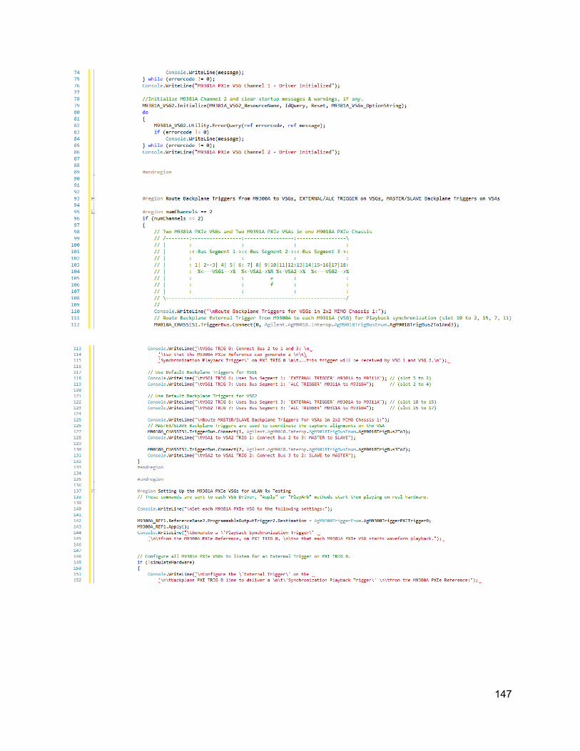
147

148

149

150