Introduction A computer consists of a set of physical ...
75
1 Introduction A computer consists of a set of physical components (hardware) and system programs (system software) that are responsible for data processing according to an algorithm, specified by the user through an application program (application software). Computer systems have conventionally been defined through their interfaces at a number of abstraction levels, each providing functional support to its predecessor. Included among the levels are the application programs, the high-level languages, and the set of machine instructions. In the past, the term computer architecture often referred only to instruction set design that represents an interface between hardware and the lowest level software - machine instructions (binary coded programs). A different definition of computer architecture is built on four basic viewpoints: - structure (defines the interconnection of various hardware components), - organization (defines the dynamic interplay and management of the various components), - implementation (defines the detailed design of hardware components), - performance (specifies the behavior of the computer system). Computer’s generations First manual calculator – abacus, appears in China in about 2600 BC (before Christ). First mechanical calculator that can add and subtract was invented in 1642 by the French philosopher Blaise Pascal. Modern electronic computers are typically grouped into four "generations." Each generation is marked by improvements in basic technology. Each advance has resulted in computers of lower cost, higher speed, greater memory capacity, smaller size and power consumption. 1. First Generation (1945–1954) based on vacuum tube invented in 1906 by an electrical engineer named Lee De Forest. (general-purpose computers: ENIAC (Electronic Numerical Integrator and Computer)- 18,000 vacuum tubes, 30.5 meters, 10- digit registers for temporary calculations; Colossus - 1,500 vacuum tubes, UNIVAC - 5,000 vacuum tubes). These early machines were typically controlled by plug board wiring. 2. Second Generation (1955–1964) based on transistors invented in the mid- 1940s by John Bardeen (1908–1991), William B. Shockley (1910–1989), and Walter H. Brattain (1902–1987). In this period appears and first supercomputers: UNIVAC LARC - Livermore Atomic Research Computer and IBM 7030 - named Strech Computer), used for weather prediction, nuclear research and artificial intelligence. These second generation machines were programmed in languages such as COBOL (Common
-
Upload
khangminh22 -
Category
Documents
-
view
5 -
download
0
Transcript of Introduction A computer consists of a set of physical ...

1
Introduction
A computer consists of a set of physical components (hardware) and system programs (system software) that are responsible for data processing according to an algorithm, specified by the user through an application program (application software).
Computer systems have conventionally been defined through their interfaces at a number of abstraction levels, each providing functional support to its predecessor. Included among the levels are the application programs, the high-level languages, and the set of machine instructions.
In the past, the term computer architecture often referred only to instruction set design that represents an interface between hardware and the lowest level software - machine instructions (binary coded programs).
A different definition of computer architecture is built on four basic viewpoints: - structure (defines the interconnection of various hardware components), - organization (defines the dynamic interplay and management of the various
components), - implementation (defines the detailed design of hardware components), - performance (specifies the behavior of the computer system).
Computer’s generations
First manual calculator – abacus, appears in China in about 2600 BC (before Christ). First mechanical calculator that can add and subtract was invented in 1642 by the French philosopher Blaise Pascal.
Modern electronic computers are typically grouped into four "generations." Each generation is marked by improvements in basic technology. Each advance has resulted in computers of lower cost, higher speed, greater memory capacity, smaller size and power consumption.
1. First Generation (1945–1954) based on vacuum tube invented in 1906 by an electrical engineer named Lee De Forest. (general-purpose computers: ENIAC (Electronic Numerical Integrator and Computer)- 18,000 vacuum tubes, 30.5 meters, 10-digit registers for temporary calculations; Colossus - 1,500 vacuum tubes, UNIVAC - 5,000 vacuum tubes). These early machines were typically controlled by plug board wiring.
2. Second Generation (1955–1964) based on transistors invented in the mid-1940s by John Bardeen (1908–1991), William B. Shockley (1910–1989), and Walter H. Brattain (1902–1987). In this period appears and first supercomputers: UNIVAC LARC - Livermore Atomic Research Computer and IBM 7030 - named Strech Computer), used for weather prediction, nuclear research and artificial intelligence. These second generation machines were programmed in languages such as COBOL (Common
2
Business Oriented Language) and FORTRAN (Formula Translator). Magnetic disks and tape were often used for data storage. Appears the concept of parallel processing.
3. Third Generation (1965–1978) based on integrated circuits invented by Jack Kilby and Robert Noyce. The integrated circuit is a single device that contains many transistors. Computers: IBM System/360 - was able to execute 500,000 additions per second. This computer was about 263 times as fast as the ENIAC. During the third generation of computers, the central processor was constructed by using many integrated circuits. It introduced single computer architecture over a range or family of devices. In other words, a program designed to run on one machine in the family could also run on all of the others. IBM spent approximately $5 billion to develop the System/360. Appears first minicomputers. The important characteristics of the computers of this generation: operating systems, multiprogramming, multiprocessing and virtual memory.
4. Fourth Generation (1979–?) based on the microprocessors. Microprocessors used Large Scale Integration (LSI) and Very Large Scale Integration (VLSI) techniques to pack thousands or millions of transistors on a single chip. Advantages: speed, high integration ratio, high reliability, small costs and dimensions.
A common law that governs the world of microprocessors is Moore's Law. Moore's Law states that the numbers of transistors on a single chip at the same price will double every 18 to 24 months. Current microprocessor chips contain millions of transistors and the number is growing rapidly.
First microprocessor: Intel Company, I4004 – 4 bits organization (built in 1971) was the first processor to be built on a single silicon chip. It contained 2,300 transistors. First successful microprocessor: Intel I8080 – 8 bits processor (1972). First 16 bits processor: Intel I8086 (1978). First 32 bit processor: Intel I80386 (1985). Superscalar microprocessor architecture: Pentium Pro (1990) 64 bits processors, multi-core architectures: Pentium D, Core 2 Duo, Xeon (Intel), Other microprocessor families: Motorola: 6800 (8 biti), 68000 (16 biti), 68020, 68030 (32 biti), 68040, Zilog: Z80, Z8000
Texas Instruments: - digital signal processors: TMS320c10/20/30/50/80 Microchip: microcontrollers: PIC12/16/18 MIPS (Microprocessor without Interlocked Pipeline Stages) , ARM (Advanced RISC Machine), etc.
Tendencies and perspectives
1. Increase of integration ration - smaller switching elements (transistors): 45->35nm, increase of switching elements’ number, processors - over 1 billion transistors, memory – over 64-512 billion;
2. Power reduction - intelligent power distribution, dynamic power control: energy where and when it is needed, frequency limitation;
3
3. Multi-core and multi-thread architectures (from 2 cores/chip to 128 cores and more, symmetric and asymmetric architectures (see Intel and Power PC);
4. Network-on-chip - network communication inside the chip instead of parallel buses;
5. Memory hierarchies - more cache memory levels (inside the processor), virtual memory, access request anticipation;
6. External memories of silicon - no more hard and floppy disks of DVDs, flash instead;
7. Multi-processor architectures - parallel architectures, distributed architectures; 8. Computer networks - Internet – an indispensable computer resource, wireless
networks; 9. Mobile and portable computers: laptops, graphic tablets, PDA (personal digital
assistant) also known as a palmtop computer, or personal data assistant, is a mobile device that functions as a personal information manager. , GPS (Global Positioning System), intelligent phones.
Technological development
Computer technology has shown an unprecedented rate of improvement. This
includes the development of processors and memories. The integration of numbers of transistors into a single chip has increased from a few hundred to millions. This impressive increase has been made possible by the advances in the fabrication technology of transistors.
The scale of integration has grown from small-scale (SSI) to medium-scale (MSI), then to large-scale (LSI), then to very large-scale integration (VLSI), and currently to wafer scale integration (WSI). Numbers of Devices per Chip Integration Technology Typical number of devices Typical functions SSI Bipolar 10–20 Gates and flip-flops MSI Bipolar & MOS 50–100 Adders & counters LSI Bipolar & MOS 100–10,000 ROM & RAM VLSI CMOS (mostly) 10,000–5,000,000 Processors WSI CMOS 5,000,000 DSP & special purposes
1. Computer components Virtually, all contemporary computer designs are based on concepts developed by John von Neumann. Such a design is referred to as the von Neumann architecture and is based on three concepts:
1. Data and instructions are stored in a single read/write memory.

4
2. The contents of this memory are addressable by location, without regard to the type of data contained there.
3. Execution occurs in a sequential fashion from one instruction to the next.
The basic Von Neumann architecture:
Computer
Central Unit
CPUMain
Memory
ALU Reg
Control Unit
Buffers
Peripheral Devices
I/O system
SystemBus
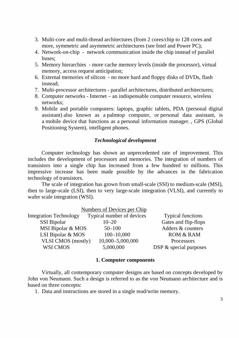
The structural description of a computer consists of the following three basic blocks: 1. CPU (Central Processing Unit). 2. Main memory. 3. Input/Output system.
CPU consists of Control Unit, ALU (Arithmetic and Logic Unit) and registers and represents a general purpose processor in contrast with specialised processors (I/O processor, arithmetic processor) with a set of instructions, which means that it recognize and execute a set of instructions in a binary form.
CPU and main memory forms a Central Unit . A Central Unit, Input/Output System and a set of system programs forms a
computer. A computer and peripheral devices forms a computer system. If a microprocessor
is used, it can be named also and a microcomputer system. Main memory (also named and internal memory) consists of a set of locations,
defined by sequentially numbered addresses. Each location contains a binary number that can be interpreted as either an instruction or data. The internal memory can be of 2 types: ROM (Read Only Memory) and RAM (Random Access Memory).

5
I/O system transfers data from external devices to CPU and memory and vice versa. It contains internal buffers for temporarily holding these data until they can be sent on.
Peripheral devices: External memory devices (hard-disc, floppy-disc, compact-disc); input devices (keyboard, mouse); output devices (printer, monitor).
Data and instructions are communicated with the computer using input devices, the results are sent to output devices. CPU interchanges with other components with data (operands and results), instructions, addresses, control signals. The communication is executed through buses. There are 3 types of buses: Address, Data and Control buses. Al they form the system bus.
Address bus: carries the address of a unique memory or input/output (I/O) device.
Data bus: carries data stored in memory (or in I/O device) to the CPU or from the CPU to the memory (or I/O device).
Control bus: is a collection of control signals that coordinate and synchronize the whole system.
CPUMain
memoryI/O
system
Data Bus
Address Bus
Control BusSys
tem
Bus
2. Central Processing Unit 2.1. CPU basics
A typical CPU has three major components: (1) register set, (2) arithmetic logic unit (ALU), (3) control unit (CU). The register set differs from one computer architecture to another. It is usually a
combination of general-purpose and special purpose registers. The ALU provides the circuitry needed to perform the arithmetic, logical and shift
operations demanded of the instruction set. It also generates information about carry, overflow and other special cases. It consists of combinational logic circuits: adders, decoders, encoders, multiplexers and a set of registers (ex. accumulator), used as a fast memory in arithmetic and logic operations.
The control unit is the entity responsible for fetching the instruction to be executed from the main memory and decoding and then executing it.
6
The main components of the CPU and its interactions with the memory system and the input/output devices:
2.2. The register set The register set is usually a combination of general-purpose and special purpose
registers. General-purpose registers can be used for multiple purposes and assigned to a
variety of functions by the programmer. Special-purpose registers are restricted to only specific functions.
Examples of special purpose registers Two main registers are involved in fetching an instruction for execution: - the program counter (PC) (is the register that contains the address of the next
instruction to be fetched). After a successful instruction fetch, the PC is updated to point to the next instruction to be executed.
-the instruction register (IR) in which the fetched instruction is loaded Two registers are essential in memory write and read operations: - the memory data register (MDR) - memory address register (MAR). The MDR and MAR are used exclusively by the CPU and are not directly
accessible to programmers. In order to perform a write operation into a specified memory location, the MDR
and MAR are used as follows: 1. The word to be stored into the memory location is first loaded by the CPU into MDR. 2. The address of the location into which the word is to be stored is loaded by the
CPU into a MAR.

7
3. A write signal is issued by the CPU. Similarly, to perform a memory read operation, the MDR and MAR are used as
follows: 1. The address of the location from which the word is to be read is loaded into the MAR. 2. A read signal is issued by the CPU. 3. The required word will be loaded by the memory into the MDR ready for use
by the CPU. Some architectures contain a special program status word (PSW) register or a
Flag register. The PSW contains bits that are set by the CPU to indicate the current status of an executing program. These indicators are typically for arithmetic operations, interrupts, memory protection information, or processor status.
2.3. Instruction cycle
The basic function performed by a computer is execution of a program, which
consists of a set of instructions stored in memory. The CPU reads (fetch) instructions from memory one at a time and executes each instruction. Program execution consists of repeating the process of instruction fetch and execution.
The processing required for a single instruction is called an instruction cycle. It consists of two steps: fetch cycle and execute cycle. The instruction cycle is the multiple of the clock signal.
The fetched instruction is loaded into the IR. The processor interprets a binary code of the instruction and executes the required action: reads and writes data from and to memory, and transfers data from and to input/output devices.
A typical and simple instruction cycle can be summarized as follows: 1. Instruction address calculation: determine the address of the next instruction
to be executed by adding a fixed number to the address of the previous instruction in PC. 2. Instruction fetch: Read the instruction from its memory location and store it
into IR. 3. Instruction decoding: analyze instruction to determine type of operation to be
performed and operands to be used. 4. Operands address calculation, if needed. 5. Operand fetch: fetch the operand from memory and store it in CPU registers,
if needed. 6. Instruction execution. 7. Results store: results are transferred from CPU registers to memory, if needed. The instruction cycle is repeated as long as there are more instructions to execute. A check for pending interrupts is usually included in the cycle. Examples of
interrupts include I/O device request, arithmetic overflow, division by zero, etc. Interrupts are provided primarily as a way to improve processing efficiency. For example, most external devices are much slower than a processor. With interrupts; the
8
processor can be engaged in executing other instructions while an I/O operation is in progress. .
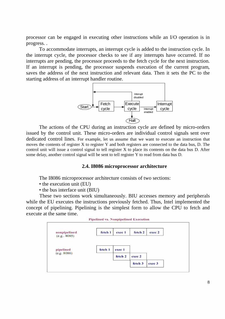
To accommodate interrupts, an interrupt cycle is added to the instruction cycle. In the interrupt cycle, the processor checks to see if any interrupts have occurred. If no interrupts are pending, the processor proceeds to the fetch cycle for the next instruction. If an interrupt is pending, the processor suspends execution of the current program, saves the address of the next instruction and relevant data. Then it sets the PC to the starting address of an interrupt handler routine.
StartFetchcycle
Executecycle
Halt
Interruptenabled
Interuptdisabled
Interruptcycle
The actions of the CPU during an instruction cycle are defined by micro-orders
issued by the control unit. These micro-orders are individual control signals sent over dedicated control lines. For example, let us assume that we want to execute an instruction that moves the contents of register X to register Y and both registers are connected to the data bus, D. The control unit will issue a control signal to tell register X to place its contents on the data bus D. After some delay, another control signal will be sent to tell register Y to read from data bus D.
2.4. I8086 microprocessor architecture
The I8086 microprocessor architecture consists of two sections: • the execution unit (EU) • the bus interface unit (BIU) These two sections work simultaneously. BIU accesses memory and peripherals
while the EU executes the instructions previously fetched. Thus, Intel implemented the concept of pipelining. Pipelining is the simplest form to allow the CPU to fetch and execute at the same time.
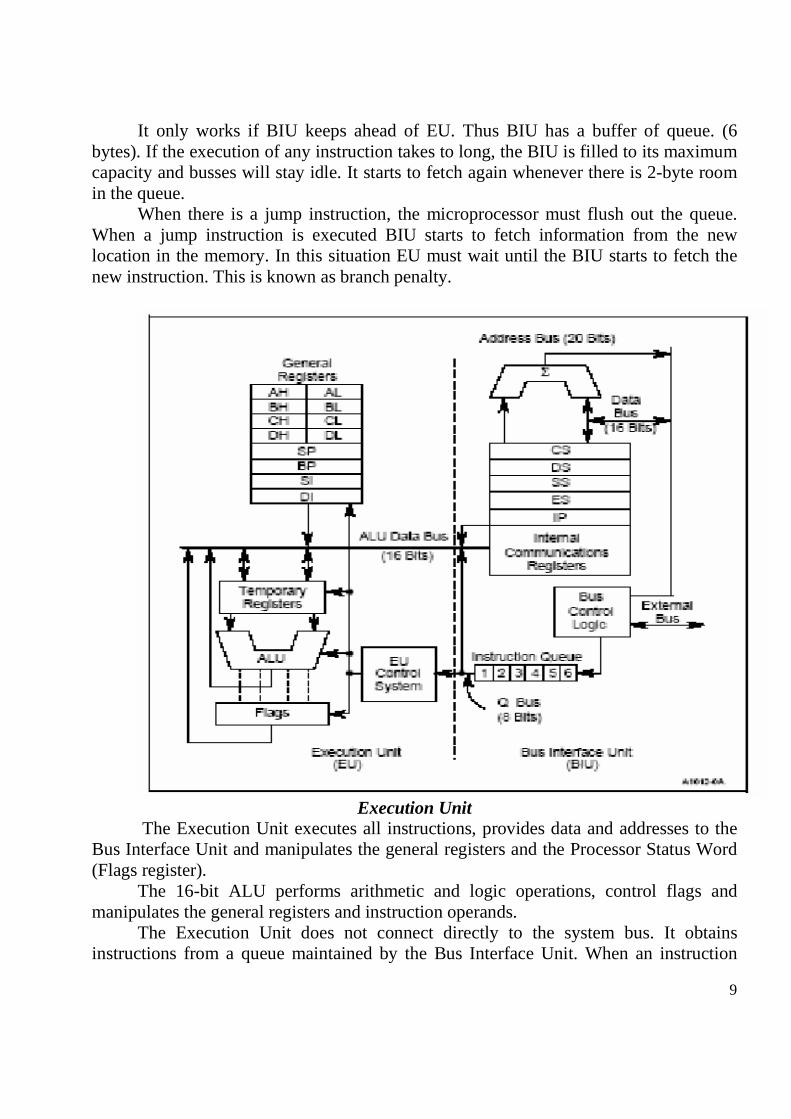
9
It only works if BIU keeps ahead of EU. Thus BIU has a buffer of queue. (6 bytes). If the execution of any instruction takes to long, the BIU is filled to its maximum capacity and busses will stay idle. It starts to fetch again whenever there is 2-byte room in the queue.
When there is a jump instruction, the microprocessor must flush out the queue. When a jump instruction is executed BIU starts to fetch information from the new location in the memory. In this situation EU must wait until the BIU starts to fetch the new instruction. This is known as branch penalty.
Execution Unit The Execution Unit executes all instructions, provides data and addresses to the
Bus Interface Unit and manipulates the general registers and the Processor Status Word (Flags register).
The 16-bit ALU performs arithmetic and logic operations, control flags and manipulates the general registers and instruction operands.
The Execution Unit does not connect directly to the system bus. It obtains instructions from a queue maintained by the Bus Interface Unit. When an instruction
10
requires access to memory or a peripheral device, the Execution Unit requests the Bus Interface Unit to read and write data.
Bus Interface Unit The Bus Interface Unit facilities communication between the EU and memory or I/O circuits. It is responsible for transmitting address, data, and control signals on the buses. This unit consists of the segment registers, the Instruction Pointer, internal communication registers, a logic circuit to generate a 20 bit address, bus control logic that multiplexers data and address lines, the instruction code queue (6 bytes RAM).
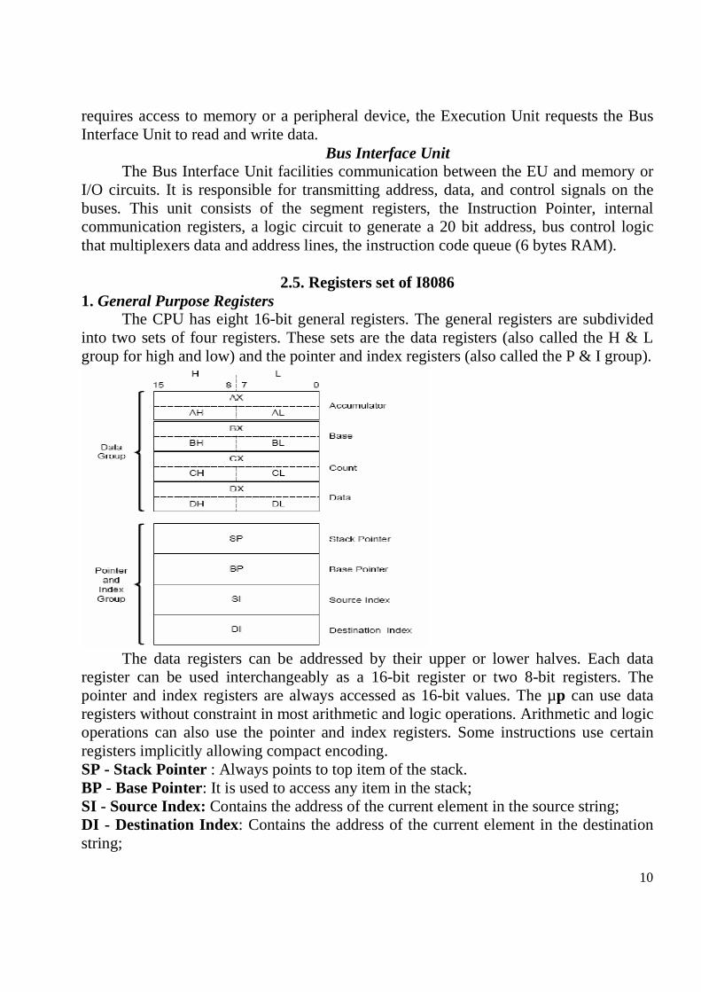
2.5. Registers set of I8086 1. General Purpose Registers The CPU has eight 16-bit general registers. The general registers are subdivided into two sets of four registers. These sets are the data registers (also called the H & L group for high and low) and the pointer and index registers (also called the P & I group).
The data registers can be addressed by their upper or lower halves. Each data register can be used interchangeably as a 16-bit register or two 8-bit registers. The pointer and index registers are always accessed as 16-bit values. The µp can use data registers without constraint in most arithmetic and logic operations. Arithmetic and logic operations can also use the pointer and index registers. Some instructions use certain registers implicitly allowing compact encoding. SP - Stack Pointer : Always points to top item of the stack. BP - Base Pointer: It is used to access any item in the stack; SI - Source Index: Contains the address of the current element in the source string; DI - Destination Index: Contains the address of the current element in the destination string;

11
2. Segment registers
The mp 8086 has a 20-bit address bus for 1 Mbyte external memory but inside the CPU registers have 16 bits that can access 64 Kbytes. The 8086 family memory space is divided into logical segments of up to 64 Kbytes each. The segment registers contain the base addresses (starting locations) of these memory segments.
• CS (code segment) - points at the segment containing the current program. • DS (data segment)- generally points at the segment where variables are defined. • ES (extra segment)- extra segment register, it's up to a coder to define its usage. • SS (stack segment)- points at the segment containing the stack.
3. Special purpose registers
IP - the instruction pointer or program counter: Always points to next instruction to be executed. It contains the offset (displacement) of the next instruction from the start address of the code segment. Flags Register - determines the current state of the processor. It is also called PSW (processor state word). From 16 bits are used only 9. Flags Register is modified automatically by CPU after mathematical operations, this allows to determine the type of the result, and to determine conditions to transfer control to other parts of the program. Generally you cannot access these registers directly. 15 14 13 12 11 10 9 8 7 6 5 4 3 2 1 0 Of df if tf sf Zf Af pf cf All flags can be divided into condition (status) flags and control (system) flags.
Condition flags: • 0 bit -Carry Flag (CF) - this flag is set to 1 when there is a carry (borrow) from
the 8 or 16 bit in addition or subtraction operation. For example when you add
12
bytes 255 + 1 (result is not in range 0...255). When there is no a carry or borrow this flag is set to 0. It is also used to store the value of the MSB in shift operations.
• 2 bit - Parity Flag (PF) - this flag is set to 1 when there is even number of one bits in result, and to 0 when there is odd number of one bits. Even if result is a word only 8 low bits are analyzed!
• 4 bit - Auxiliary Flag (AF) - set to 1 when there is an unsigned overflow for low nibble (4 bits).
• 6 bit - Zero Flag (ZF) - set to 1 when result is zero. For none zero result this flag is set to 0.
• 7 bit - Sign Flag (SF) - set to 1 when result is negative. When result is positive it is set to 0. Actually this flag take the value of the most significant bit.
• 11 bit - Overflow Flag (OF) - set to 1 when there is a signed overflow. For example, when you add bytes 100 + 50 (result is not in range -128...127).
Control flags: • 8 bit - Trap Flag (TF) System flag - Used for on-chip debugging (pas cu pas)
when TF=1. In this case the interrupt is generated (int 1) which calls a special routine to show the state of internal registers. There are no instructions to change this flag. The content of PSW is written in one general Rg through the stack to can change it.
• 9 bit - Interrupt enable Flag (IF) System flag - when this flag is set to 1 CPU reacts ( se permit) to interrupts on INTR input of the mp from external devices. When IF=0 interrupts are not allowed (masked). IF do not react to NMI (non maskable) interrupts and to internal interrupts performed by instruction INT. Instructions CLI (clear interrupt) and STI (set interrupt) are used to control this flag.
• 10 bit - Direction Flag (DF) - this flag is used by some instructions to process data chains, when this flag is set to 0 - the processing is done forward (increment of SI and DI registers), when this flag is set to 1 the processing is done backward - decrement (instructions CLD and STD).
Exercises
Determine the value of CF, ZF, SF, OF, PF and AF after the following addition operations: 1. 342Ah+57E2h=8C0Ch 2. E42Ah+96B8h=7AE2h 3. C739h+38C7h=0000h 4. F502h+1A7h =F6A9h 5. 6BD3h+90F1h=FCC4h
13
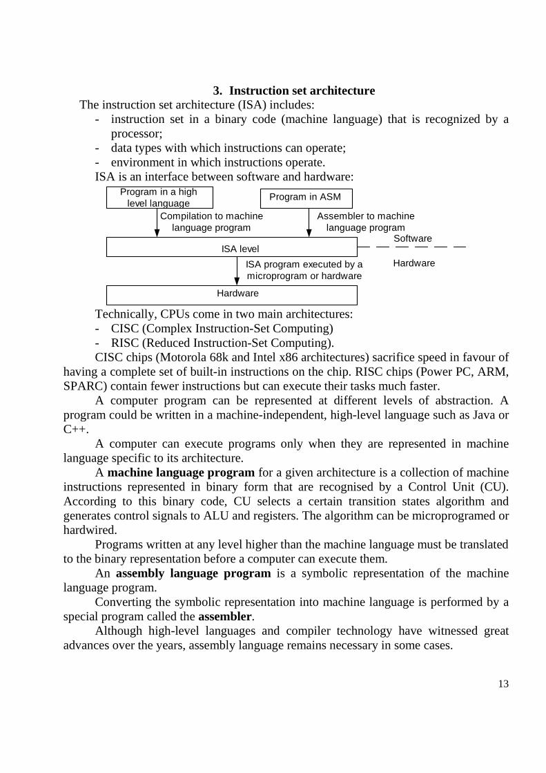
3. Instruction set architecture The instruction set architecture (ISA) includes:
- instruction set in a binary code (machine language) that is recognized by a processor;
- data types with which instructions can operate; - environment in which instructions operate. ISA is an interface between software and hardware:
Program in a highlevel language
Program in ASM
ISA level
Hardware
Compilation to machinelanguage program
Assembler to machinelanguage program
ISA program executed by amicroprogram or hardware
Software
Hardware
Technically, CPUs come in two main architectures: - CISC (Complex Instruction-Set Computing) - RISC (Reduced Instruction-Set Computing). CISC chips (Motorola 68k and Intel x86 architectures) sacrifice speed in favour of
having a complete set of built-in instructions on the chip. RISC chips (Power PC, ARM, SPARC) contain fewer instructions but can execute their tasks much faster.
A computer program can be represented at different levels of abstraction. A program could be written in a machine-independent, high-level language such as Java or C++.
A computer can execute programs only when they are represented in machine language specific to its architecture.
A machine language program for a given architecture is a collection of machine instructions represented in binary form that are recognised by a Control Unit (CU). According to this binary code, CU selects a certain transition states algorithm and generates control signals to ALU and registers. The algorithm can be microprogramed or hardwired.
Programs written at any level higher than the machine language must be translated to the binary representation before a computer can execute them.
An assembly language program is a symbolic representation of the machine language program.
Converting the symbolic representation into machine language is performed by a special program called the assembler.
Although high-level languages and compiler technology have witnessed great advances over the years, assembly language remains necessary in some cases.
14
- Programming in assembly can result in machine code that is much smaller and much faster than that generated by a compiler of a high-level language. Small and fast code could be critical in some embedded and portable applications, where resources may be very limited. In such cases, small portions of the program that may be heavily used can be written in assembly language. - Assembly programmers have access to all the hardware features of the target machine that might not be accessible to high-level language programmers. - learning assembly languages can be of great help in understanding the low level details of computer organization and architecture.
Machine language is the native language of a given processor. Since assembly language is the symbolic form of machine language, each different type of processor has its own unique assembly language. Before we study the assembly language of a given processor, we need first to understand the details of that processor. We need to know the memory size and organization, the processor registers, the instruction format, and the entire instruction set.
3.1 Main memory model
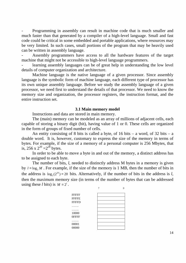
Instructions and data are stored in main memory. The (main) memory can be modeled as an array of millions of adjacent cells, each capable of storing a binary digit (bit), having value of 1 or 0. These cells are organized in the form of groups of fixed number of cells.
An entity consisting of 8 bits is called a byte, of 16 bits – a word, of 32 bits – a double word. It is, however, customary to express the size of the memory in terms of bytes. For example, if the size of a memory of a personal computer is 256 Mbytes, that is, 256 x 220 =228 bytes.
In order to be able to move a byte in and out of the memory, a distinct address has to be assigned to each byte.
The number of bits, l, needed to distinctly address M bytes in a memory is given by 2logl M= . For example, if the size of the memory is 1 MB, then the number of bits in the address is 20
2log (2 ) 20= bits. Alternatively, if the number of bits in the address is l, then the maximum memory size (in terms of the number of bytes that can be addressed using these l bits) is 2lM = . 7 0
FFFFF FFFFE FFFFD ……. ……. 10000 0FFFF ……. 00001 00000

15
The addressable memory of I8086 contains 220 bytes (1 Mb). The physical addresses are within the range 00000-FFFFFh.
Locations 0H-7FH (128 bytes) and FFFF0-FFFFF (16 bytes) are reserved for special use (interrupts and system start after reset)
Any 2 neighbour bytes can store a word (16 bits). The smaller address contains the smaller byte. The address of the word is the address of its smaller byte. So, one address can be viewed as a byte address and a word address. This strategy to store data is called Little Endian (the opposite strategy is called Big Endian and it applied by Motorola, Spark and most RISC machines).
22 H Unaligned 21 H DW 20 h DB 24B H 46 1F H Aligned 24A H 00 1E H DW 249 H 65 1D H DB 248 H 3A 1C H DB
247 H 8C 1B H Instruction 246 H 04 1A H
19 H Instruction The value of a binary word at address 246H is 8C04 H, of a DD at address 248 H
- 4600653A. The word with even address is called aligned. The word with odd address is called
unaligned. The mp transfer words with even addresses in 1 memory access cycle and words with odd addresses in 2 cycles. That’s why it’s recommended to store data on even addresses.
3.2 Memory segmentation
Segmentation provides a powerful memory management mechanism: 1. It allows programmers to partition their programs into modules that operate
independently of one another. 2. Segments provide a way to easily implement object-oriented programs. 3. Segments allow two processes to easily share data. 4. It allows extending the addressability of a processor. In the case of the
8086, segmentation let Intel's designers extend the maximum addressable memory from 64KB to 1MB.
Disadvantage: Difficulties with physical address manipulation in programs.
16
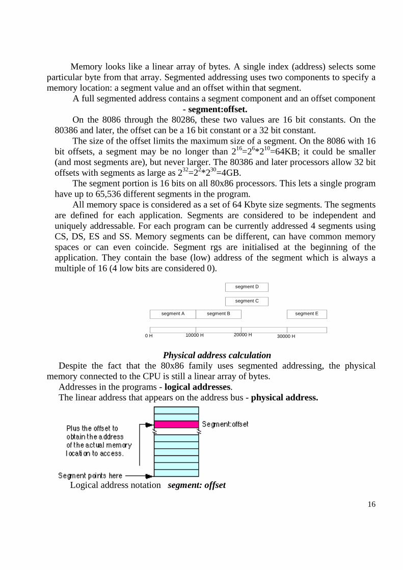
Memory looks like a linear array of bytes. A single index (address) selects some particular byte from that array. Segmented addressing uses two components to specify a memory location: a segment value and an offset within that segment.
A full segmented address contains a segment component and an offset component - segment:offset.
On the 8086 through the 80286, these two values are 16 bit constants. On the 80386 and later, the offset can be a 16 bit constant or a 32 bit constant.
The size of the offset limits the maximum size of a segment. On the 8086 with 16 bit offsets, a segment may be no longer than 216=26*210=64KB; it could be smaller (and most segments are), but never larger. The 80386 and later processors allow 32 bit offsets with segments as large as 232=22*230=4GB.
The segment portion is 16 bits on all 80x86 processors. This lets a single program have up to 65,536 different segments in the program.
All memory space is considered as a set of 64 Kbyte size segments. The segments are defined for each application. Segments are considered to be independent and uniquely addressable. For each program can be currently addressed 4 segments using CS, DS, ES and SS. Memory segments can be different, can have common memory spaces or can even coincide. Segment rgs are initialised at the beginning of the application. They contain the base (low) address of the segment which is always a multiple of 16 (4 low bits are considered 0).
segment A segment B
segment C
segment D
segment E
0 H 10000 H 20000 H 30000 H
Physical address calculation Despite the fact that the 80x86 family uses segmented addressing, the physical
memory connected to the CPU is still a linear array of bytes. Addresses in the programs - logical addresses. The linear address that appears on the address bus - physical address.
Logical address notation segment: offset
17
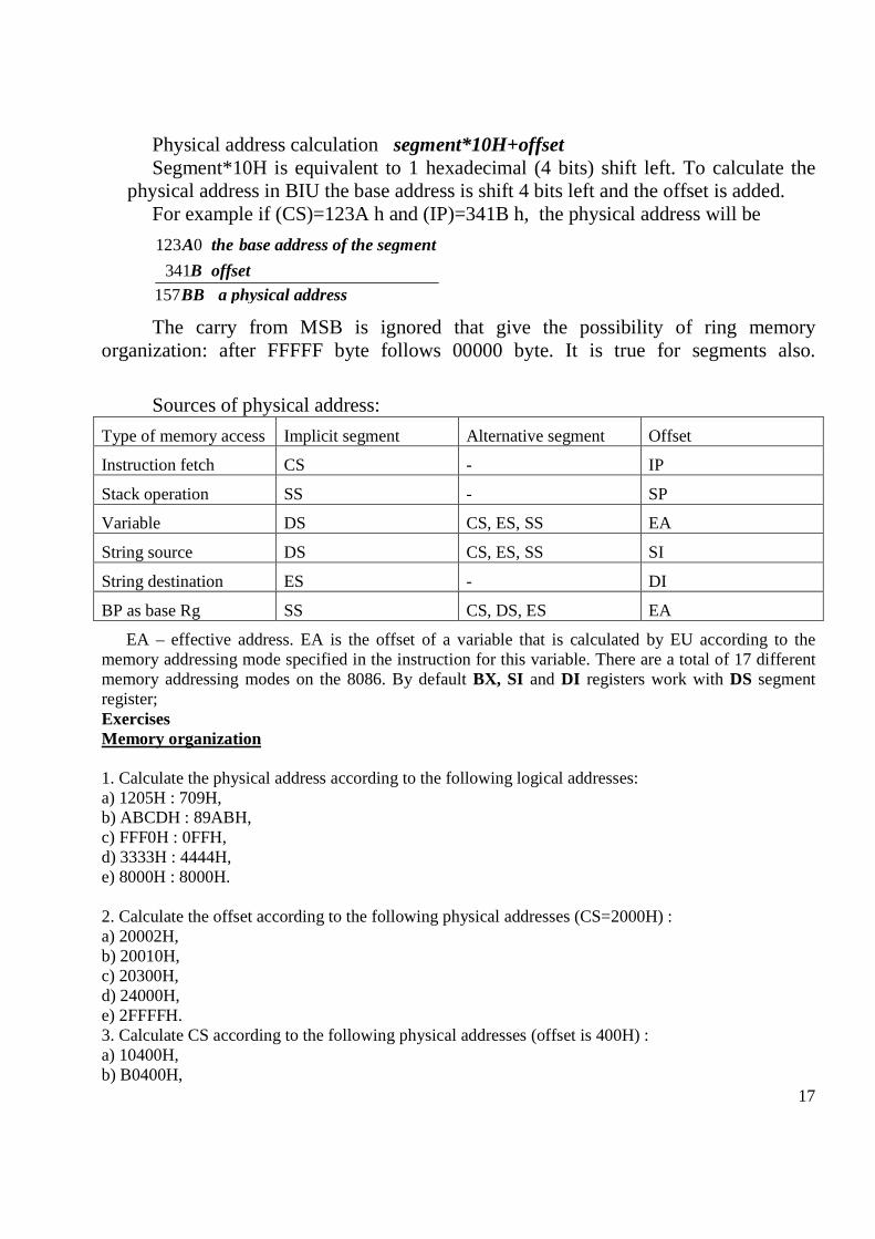
Physical address calculation segment*10H+offset Segment*10H is equivalent to 1 hexadecimal (4 bits) shift left. To calculate the
physical address in BIU the base address is shift 4 bits left and the offset is added. For example if (CS)=123A h and (IP)=341B h, the physical address will be
123 0
341
157
A the base address of the segment
B offsetBB a physical address
The carry from MSB is ignored that give the possibility of ring memory organization: after FFFFF byte follows 00000 byte. It is true for segments also.
Sources of physical address:
Type of memory access Implicit segment Alternative segment Offset
Instruction fetch CS - IP
Stack operation SS - SP
Variable DS CS, ES, SS EA
String source DS CS, ES, SS SI
String destination ES - DI
BP as base Rg SS CS, DS, ES EA
EA – effective address. EA is the offset of a variable that is calculated by EU according to the memory addressing mode specified in the instruction for this variable. There are a total of 17 different memory addressing modes on the 8086. By default BX, SI and DI registers work with DS segment register; Exercises Memory organization 1. Calculate the physical address according to the following logical addresses: a) 1205H : 709H, b) ABCDH : 89ABH, c) FFF0H : 0FFH, d) 3333H : 4444H, e) 8000H : 8000H. 2. Calculate the offset according to the following physical addresses (CS=2000H) : a) 20002H, b) 20010H, c) 20300H, d) 24000H, e) 2FFFFH. 3. Calculate CS according to the following physical addresses (offset is 400H) : a) 10400H, b) B0400H,

18
c) 30800H, d) CDE00H, e) FFFF0H. 4. Which of the following physical addresses belong to the segment with CS=2400H: a) 33FFFH, b) 23000H, c) 27890H, d) 33000H, e) 34000H. 5. Physical address of the variable is 358BC H when CS=3234 H. Calculate the physical address of the variable when CS is changing 4310 H.
3.3. Stack memory
A stack memory is a small area of reserved memory used in the following cases: 1. To store temporary the data from general purpose registers; 2. To store the content of PSW, CS and IP when an interrupt or a procedure is
processed: 3. To transmit the procedures parameters. The stack organization principle is LIFO. Stack location is determined by SS:SP. SS holds the base address of stack and SP
holds the offset of the top of the stack (the most recent stack entry). Instructions to operate with stack are:
PUSH - Copy specified word to top of the stack. POP - Copy word from top of the stack to specific location.
SS (Base)
SP(Top)
Stack limit
Main memory
Reservedstackblock
000000
FFFFFF
CPU registers
Free
In use
According to Intel convention the stack grows from higher addresses to lower
addresses ( according to Motorola convention the stack grows from lower addresses to higher addresses). The base of the stack (SS) is at the high address end of the reserved stack block and the limit is at the low address end. If all stack elements are 16-bit words (2 bytes), instruction PUSH will cause the decrement of SP with 2 and POP will cause the increment of SP with 2.

19
Instruction format
Assembly language is the symbolic form of machine language. Assembly programs are written with short abbreviations that represents the actual machine instruction called mnemonics. . The use of mnemonics is more meaningful than that of hex or binary values, which would make programming at this low level easier and more manageable. Examples: Mov - move, Add – addition, Sub – subtraction, Mul – multiplication.
An assembly program consists of a sequence of assembly statements, where statements are written one per line. Each line of an assembly program is split into the following four fields: label, operation code (opcode), operand, and comments.
Labels are used to provide symbolic names for memory addresses. A label is an
identifier that can be used on a program line in order to branch to the labeled line. It can also be used to access data using symbolic names. The operation code (opcode) field contains the symbolic abbreviation of a given operation. The operand field consists of additional information or data that the opcode requires. The operand field may be used to specify constant, label, immediate data, register, or a memory address. The comments field provides a space for documentation to explain what has been done for the purpose of debugging and maintenance. In I8086 instruction consists from one to six bytes.
According to the length of the instructions exists two types of ISA: 1. With fixed length instructions (commonly used in RISC architectures) 2. With variable length instructions (commonly used in CISC architectures) The advantage of using variable length instructions is that they reduce the amount
of memory space required for a program. In I8086 instructions are from one byte to a maximum of 6 bytes in length.
The advantage of fixed length instructions is that they make the job of fetching and decoding instructions easier and more efficient, which means that they can be executed in less time than the corresponding variable length instructions.
Instructions can be classified based on the number of operands as: three-address, two-address, one-address, and zero-address.
Examples: 3 addresses Add x,y,z (z)=( x)+(y) 2 addresses Add ax,bx (Ax)=(ax)+(bx) 1 addresses Mul bl (Ax)=(al)*(bl) 0 addresses Push bx Top of the stack ← (bx)

20
Three-address instruction formats are not common, because they require a relatively long space to hold all addresses.
In two-address instruction one address is an operand and also a result. In one-address instruction a second address is implicit. Usually it is the
accumulator AX. It is used for one operand and the result. Zero-address instructions are applicable to stack memory and use as address the
content of SP (top of the stack). The number of addresses per instruction is a basic design decision. Fewer
addresses per instruction result in more primitive instructions, which require a less complex CPU. It also results in instruction of shorter length. On the other hand programs contain more total instructions and have a longer execution time. Another problem: with one-address instructions, the programmer has available only one general-purpose register – the accumulator, with multiple address instructions it is common to have multiple general-purpose registers. Because register references are faster than memory references this speeds up execution. Most contemporary machines employ a mixture of two- and three- address instructions.
3.5. Addressing Modes
The different ways in which operands can be addressed are called the addressing modes. Addressing modes differ in the way the address information of operands is specified.
EA - actual (effective) address (EA) of the location containing the operand; The addressing modes available in 8086 are:
1. Immediate Addressing Mode: According to this addressing mode, the value of the operand is (immediately)
available in the instruction itself. Operand=A,
where A - the content of the address field in the instruction Typically immediate operand represents constant data (a byte or word). The
number is stored in two’s complement form. Examples:
mov al, 48 ; load 30H in AL; mov cx,2056H xor si,1 ; invert LSB in SI register; and al,80H ; highlight MSB of AL or di, 8000H ; set to 1 MSB of DI
The advantage of immediate addressing is that no memory reference other than the instruction fetch is required to obtain the operand. The disadvantages: the size of the number is restricted to the size of the address field; a change in the value of an operand requires a change in every instruction that uses the immediate value of such an operand.

21
2. Register Addressing Mode:
To access the content of the register it is necessary to specify the name of the register. The eight and 16 bit registers are certainly valid operands for this instruction. The only restriction is that both operands must be of the same size. mov ax, bx ;Copies the value from BX into AX mov dl, al ;Copies the value from AL into DL mov ax, ax ;Yes, this is legal and it performs nothing! add bx,di; bx=bx+di sub cl,ah ; cl=cl-ah Advantage: the registers are the best place to keep often used variables. Instructions using the registers are shorter and faster than those that access memory. Disadvantage: limited address space and the limited number of general purpose registers. 3. Direct Addressing mode (displacement only) (6 clock cycles)
In the direct addressing mode the address field contains the EA of the operand. EA=A
It consists of a 16 bit constant that specifies the address of the target location. mov al, [8088h]; loads the Al register with a copy of the byte at memory location 8088h. mov [1234h],dl ; stores the value from the Dl register to memory location 1234h:
By default, all displacement-only values provide offsets into the data segment. If
you want to provide an offset into a different segment, you must use a segment override prefix before your address. For example, to access location 1234h in the extra segment (es) you would use an instruction of the form
mov ax,es:[1234h].
You can also access words on the 8086 processors :

22
Other examples: BETA dw 1234h ............................ MOV CX, BETA ; move the contents of the memory location, which is offset by
BETA from the current value in DS into internal register CX. Inc COUNT Mul X ; multiply ax with variable X Ror TEMP ; shift right variable TEMP
In inc, mul, ror instructions it is impossible to determine the size of a variable Inc word ptr COUNT
Ror byte ptr TEMP The technique was common in earlier generations of computers but is not
common on contemporary architectures. It requires only one memory reference and no special calculation. The disadvantage is that it provides only a limited address space.
4. Register Indirect Addressing mode: (5 clock c) In the register indirect mode, in the instruction is included a name of a register
that holds the EA of the operand. In this case name of the register is included in parentheses. EA=[R]
There are four forms of this addressing mode on the 8086, best demonstrated by the following instructions: mov al, [bx] mov al, [bp] mov al, [si] mov al, [di] The [bx], [si], and [di] modes use the ds segment by default. The [bp] mode uses the stack segment (ss) by default. Example: MOV AL, [BX] ; This instruction moves the contents of the memory location DS:BX to the AL register.
MOV AL, [BP] ; This instruction moves the contents of the memory location SS:BP to the AL register.
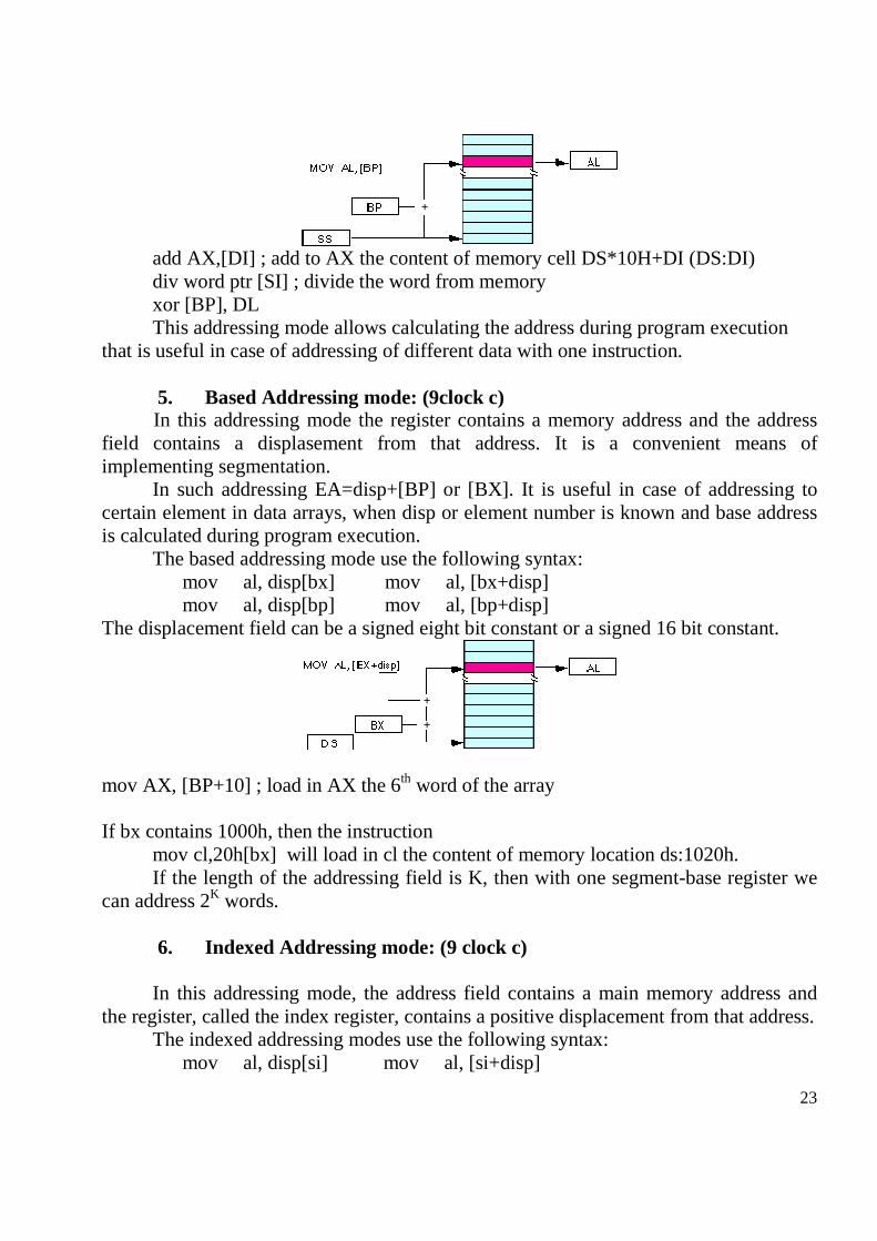
23
add AX,[DI] ; add to AX the content of memory cell DS*10H+DI (DS:DI)
div word ptr [SI] ; divide the word from memory xor [BP], DL This addressing mode allows calculating the address during program execution that is useful in case of addressing of different data with one instruction.
5. Based Addressing mode: (9clock c) In this addressing mode the register contains a memory address and the address
field contains a displasement from that address. It is a convenient means of implementing segmentation.
In such addressing EA=disp+[BP] or [BX]. It is useful in case of addressing to certain element in data arrays, when disp or element number is known and base address is calculated during program execution.
The based addressing mode use the following syntax: mov al, disp[bx] mov al, [bx+disp] mov al, disp[bp] mov al, [bp+disp] The displacement field can be a signed eight bit constant or a signed 16 bit constant.
mov AX, [BP+10] ; load in AX the 6th word of the array If bx contains 1000h, then the instruction
mov cl,20h[bx] will load in cl the content of memory location ds:1020h. If the length of the addressing field is K, then with one segment-base register we
can address 2K words. 6. Indexed Addressing mode: (9 clock c) In this addressing mode, the address field contains a main memory address and
the register, called the index register, contains a positive displacement from that address. The indexed addressing modes use the following syntax:
mov al, disp[si] mov al, [si+disp]
24
mov al, disp[di] mov al, [di+disp] The displacement field can be a signed eight bit constant or a signed 16 bit constant.
In such addressing EA=disp+[SI] or [DI]. It is useful in case of itterative operations, when disp is the address of the first element and SI or DI value specified the element. First they are initialised to 0 and after each operation the index register is incremented.
Inc DI …… Mov Z[DI], AX; move the content of AX to array element add AX, ARRAY[SI] ; add AX with the element of ARRAY,
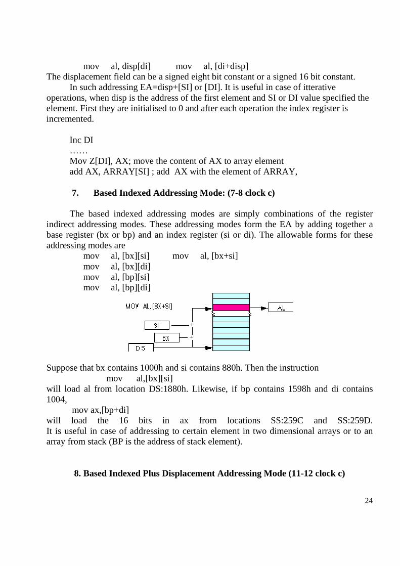
7. Based Indexed Addressing Mode: (7-8 clock c) The based indexed addressing modes are simply combinations of the register
indirect addressing modes. These addressing modes form the EA by adding together a base register (bx or bp) and an index register (si or di). The allowable forms for these addressing modes are mov al, [bx][si] mov al, [bx+si] mov al, [bx][di] mov al, [bp][si] mov al, [bp][di]
Suppose that bx contains 1000h and si contains 880h. Then the instruction mov al,[bx][si] will load al from location DS:1880h. Likewise, if bp contains 1598h and di contains 1004,
mov ax,[bp+di] will load the 16 bits in ax from locations SS:259C and SS:259D. It is useful in case of addressing to certain element in two dimensional arrays or to an array from stack (BP is the address of stack element).
8. Based Indexed Plus Displacement Addressing Mode (11-12 clock c)

25
These addressing modes are a slight modification of the base/indexed addressing modes with the addition of an eight bit or sixteen bit constant. The following are some examples of these addressing modes: mov al, disp[bx][si] mov al, disp[bx+di] mov al, [bp+si+disp] mov al, [bp][di][disp]
Suppose bp contains 1000h, bx contains 2000h, si contains 120h, and di contains 5. Then mov al,10h[bx+si] loads al from address DS:2130;
mov ch,125h[bp+di] loads ch from location SS:112A; mov bx,cs:2[bx][di] loads bx from location CS:2007. Generally, the more complex an addressing mode is, the longer it takes to
compute the effective address. Complexity of an addressing mode is directly related to the number of terms in the addressing mode. For example, disp[bx][si] is more complex than [bx].
The displacement field in all addressing modes except displacement-only can be a signed eight bit constant or a signed 16 bit constant. If your offset is in the range -128...+127 the instruction will be shorter (and therefore faster) than an instruction with a displacement outside that range. The size of the value in the register does not affect the execution time or size. So if you can arrange to put a large number in the register(s) and use a small displacement, that is preferable over a large constant and small values in the register(s).
If the effective address calculation produces a value greater than 0FFFFh, the CPU ignores the overflow and the result wraps around back to zero. For example, if bx contains 10h, then the instruction mov al,0FFFFh[bx] will load the al register from location ds:0Fh, not from location ds:1000Fh.
3.6. Data types
Machine instructions operate on data. The most important categories of data are:
Addresses (can be considered to be unsigned integers) Numbers (integer or fixed point, floating point and decimal) Characters (The most commonly used character code is ASCII code)
26
Logical data A variable can be viewed in any numbering system:
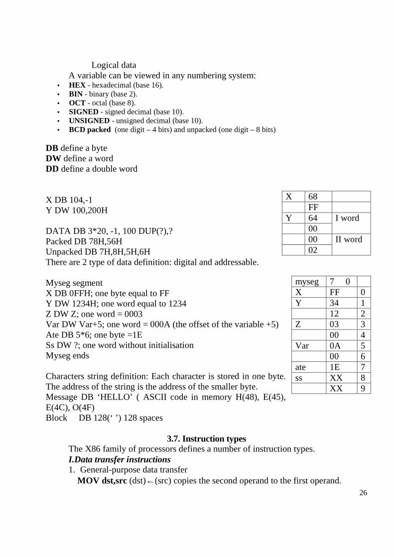
• HEX - hexadecimal (base 16). • BIN - binary (base 2). • OCT - octal (base 8). • SIGNED - signed decimal (base 10). • UNSIGNED - unsigned decimal (base 10). • BCD packed (one digit – 4 bits) and unpacked (one digit – 8 bits)
DB define a byte DW define a word DD define a double word X DB 104,-1 Y DW 100,200H DATA DB 3*20, -1, 100 DUP(?),? Packed DB 78H,56H Unpacked DB 7H,8H,5H,6H There are 2 type of data definition: digital and addressable. Myseg segment X DB 0FFH; one byte equal to FF Y DW 1234H; one word equal to 1234 Z DW Z; one word = 0003 Var DW Var+5; one word = 000A (the offset of the variable +5) Ate DB 5*6; one byte =1E Ss DW ?; one word without initialisation Myseg ends Characters string definition: Each character is stored in one byte. The address of the string is the address of the smaller byte. Message DB ‘HELLO’ ( ASCII code in memory H(48), E(45), E(4C), O(4F) Block DB 128(‘ ’) 128 spaces
3.7. Instruction types The X86 family of processors defines a number of instruction types. I.Data transfer instructions 1. General-purpose data transfer
MOV dst,src (dst)←(src) copies the second operand to the first operand.
X 68 FF Y 64 00
I word
00 02
II word
myseg 7 0 X FF 0 Y 34 1 12 2 Z 03 3 00 4 Var 0A 5 00 6 ate 1E 7 ss XX 8 XX 9

27
XCHG dst,src (dst)↔(src) Exchange bytes or exchange words. 2. Data transfer with stack
PUSH src Copy specified word to top of stack. POP dst Copy word from top of stack to specific location. 3. Flag transfer PUSHF Copy flag register to top of stack. POPF Copy word at top of stack to flag register LAHF Load AH with the low byte of the flag register. No operands SAHF Store AH register into low 8 bits of Flags register. No operands
4. Address transfer LEA reg,src Load effective address of operand in specified register. Lea SI, X LDS reg, src Load DS register and other specified register from memory. LDS SI, Y where Y is dd- double word LES reg,src Load ES register and other specified register from memory.
5. I/O port transfer IN ac, port ; Copy a byte or word from specified port to accumulator (AX or AL). IN ac, DX OUT port, ac Copy a byte or word from accumulator to specified port. OUT DX, ac
II. Arithmetic instructions
Arithmetic operations are executed on integer numbers in 4 formats: unsigned binary (byte or word ) 5h - 0000 0101 signed binary (byte or word), -5h or FAh 1111 1011 packed decimal ( the string of decimal digits are stored in consecutive 4-bit groups : 3251- 0011 0010 0101 0001) unpacked decimal ( each digit is stored in low 4-bit part of the byte: 3251 - ****0011 ****0010 ****0101 ****0001) All arithmetic instructions influence flags that can be checked with conditional transfer instructions. Arithmetic operations can use all addressing modes but one operand should be a register. ADD dst, src, dst←(dst)+(scr) src can be also immediate value of 8 or 16 bits ADC dst,src, dst←(dst) + (src)+CF. It is used in multiple precision operations SUB dst, src dst←(dst)-(src Subtract byte from byte or word from word. SBB dst, src dst← (dst)-(src)-CF INC opr , opr←(opr)+1 do not change CF. DEC opr, opr←(opr)-1
28
NEG opr opr←-(opr) Negate – invert each bit of a specified byte or word and add 1 (form 2’s complement). CMP opr1, opr2 opr1-opr2 Compare two specified bytes or two specified words and do not keep the result, just for flags(OF, SF, ZF, AF, PF, CF according to result). It is used with conditional jump instructions. CBW (no opr) (for signed binary) converts byte to word. If the high digit in AL is 0 then all AH bits are 0, if high bit in AL is 1 then all AH bits are 1. .model small .data x db -10 y dw 1234h z dw ? .code start: mov ax,@data mov ds,ax mov al, x ;AL=F6 cbw ; converteste octetul la cuvant AX=FFF6 h add ax, y ;AX=122Ah mov z, ax end start
CWD convert word to double word. Works with AX and DX (high word) MUL src (AX) ←(AL)*(src) for bytes CF and OF =1 if the high byte is not 0 (DX:AX) ←(AX)*(src) for words IMUL src Multiply signed byte by byte or signed word by word CF and OF =1 if the high byte is not the extension of sign EX. (AL)=B4 1011 0100cc (11001100)cd -76 (signed) or 180(unsigned) (BL)=11h(17 decimal) IMUL will form FAF4=-129210 CF=OF=1 MUL will form 0BF4=306010 CF=OF=1 DIV src divisor is a byte (AL) ) ← quotient (AX)/(src) (AH) ) ←remainder (AX)/(src) divisor is a word (AX) ) ← quotient (DX:AX)/(src) (DX) ) ←remainder (DX:AX)/(src) IDIV src Divide signed word by byte or signed double word by word. (AX)=0400 102410 (BL)=B4 (-76 or 180) DIV BL quotient (AL)=05=510 remainder (AH)=7C=12410
IDIV BL quotient (AL)=F3=-1310 remainder (AH)=24=3610
29
Packed BCD arithmetic DAA Decimal adjust After Addition. DAS Decimal adjust After Subtraction.
Unpacked BCD arithmetic
AAA - ASCII (Unpacked) BCD correction after addition AAS - ASCII (Unpacked) BCD correction after subtraction. AAM - ASCII adjust after multiplication Corrects the result of multiplication of two BCD values. Algorithm:
• AH = AL / 10 • AL = remainder
Example: MOV AL, 15 ; AL = 0Fh AAM ; AH = 01, AL = 05 RET
AAD - ASCII adjust before division; Prepares two BCD values for division. Algorithm:
• AL = (AH * 10) + AL • AH = 0
Example: MOV AX, 0105h ; AH = 01, AL = 05 AAD ; AH = 00, AL = 0Fh (15) RET
III. Unconditional transfer instructions: JMP operand , where operand can be a short, near, or far address
A jump operation reaches a short address by a one-byte offset, limited to a distance of -128 to 127 bytes (the same segment). A jump operation reaches near address by a one-word offset, limited to a distance of -32,768 to 32767 bytes within the same segment (the same segment). A far address may be another segment and is reached by a segment address and offset; Address specification: a) implicit b) using PTR directive:
JMP SHORT PTR operand JMP NEAR PTR operand JMP FAR PTR operand IV. Conditional transfer instructions All instructions have the following format: opcode data8

30
The first byte is the operation code and the second byte is the 8- bit displacement to the next instruction in 2-s complement system. The negative displacement means go back and positive disp. means go forward. 8-bit displacement constraint the distance of jumping in range of -128…127. Address of jumping (IP)-128 ... (IP)+127
These instructions are often used after a compare instruction. The terms B (below) and A (above) refer to unsigned binary numbers. Above means larger in magnitude. The terms G (greater than) or L (less than) refer to signed binary numbers. Greater than means more positive.
instruction Jump condition
function
JE, JZ ZF=1 Jump if equal/Jump if zero JNE, JNZ ZF=0 Not Zero, Not Equal
JS SF=1 Sign JNS SF=0 Not Sign JO OF=1 Overflow
JNO OF=0 Not Overflow JP, JPE PF=1 Parity, Parity Even
JNP, JPO PF=0 Not Parity, Parity Odd JB, JNAE,
JC CF=1 Below, Not Above or
Equal, Carry JNB, JAE,
JNC CF = 0 Not Below, Above or
Equal, Not Carry JL, JNGE SF≠OF Less, Not Greater or Equal JLE,JNG SF≠OF sau
ZF=1 Less or Equal, Not Greater
JBE, JNA CF=1 sau ZF=1
Below or Equal, Not Above
JNL, JGE SF=OF Not Less, Greater or Equal JNLE, JG SF=OF şi
ZF=0 Not Less or Equal, Greater
JNBE, JA CF=0 şi ZF=0 Not Below or Equal, Above
JNP, JPO PF=0 Not Parity, Parity Odd Ex1.
; IF ((X > Y) AND (Z < T)) OR (A <> B) THEN C := D; ; Test the boolean expression: mov ax, A cmp ax, B jne DoIF

31
mov ax, X cmp ax, Y jng EndOfIf mov ax, Z cmp ax, T jnl EndOfIf
DoIf: mov ax, D mov C, ax
; End of IF statement EndOfIF: Ex. 2 mov al, 25 ; set al to 25. mov bl, 10 ; set bl to 10. cmp al, bl ; compare al - bl. je equal ; jump if al = bl (zf = 1). mov ah,6 mov dl, 'n' int 21h jmp stop ; so print 'n', and jump to stop. equal: ; if gets here, mov ah,6 mov dl, 'y' int 21h stop: ret ; gets here no matter what. V. Control instructions: a) Iteration control instructions: These instructions can be used to execute a series of instructions some number of times. LOOP opr ;Loop through a sequence of instructions until CX= 0 LOOPE/LOOPZ opr ; Loop through a sequence instructions while ZF= l and CX ≠ 0 LOOPNE/LOOPNZ opr ;Loop through a sequence instructions while ZF=0 and CX ≠ 0 JCXZ ; Jump to specified address if CX=0 b) Processor control instructions STC ;Set carry flag CF to 1 CLC ;Clear carry flag CF to 0 CMC ;Complement the state of the carry flag CF STD ;Set direction flag DF to l (decrement string pointers) CLD ;Clear direction flag DF to 0
32
STI ;Set interrupt enable flag to 1 (enable INTR input) CLI ;Clear interrupt enable flag to 0 (disable INTR input) c) Execution control instructions: HLT ;Halt (do nothing) until interrupt or reset WAIT ; Wait (do nothing) until signal on the test pin is low ESC ;Escape to external coprocessor such as 8087 or 8089 LOCK ;An instruction prefix. Prevents another processor from taking the bus while the adjacent instruction executes NOP ;No action except fetch and decode (the same function as CONTINUE in loop operations) VI. Logic instructions NOT opr ; Invert each bit in a byte or word. Do not change the flags. AND dst, src (dst) ←(dst) ∧ (src) CF=0 OF=0 ; AND the content of a byte or a word with another byte or word. AND al,5Bh (al)= 95h=10010111 mask =01011010 reset to 0 bits 0,2,5,7 al =00010010 OR dst, src (dst) ←(dst) ∨ (src) CF=0 OF=0 ; OR the content of a byte or a word with another byte or word. OR al,80h OR al, 10000000B (al) = 1Ah=00011010 mask =10000000 set to 1 7-th bit al 10011010 XOR dst, src (dst) ←(dst)⊕(src) CF=0 OF=0 ; Exclusive OR the content of a byte or a word with another byte or word. XOR al, 0FFh; invert all bits in AL TEST opr1,opr2 opr1∧opr2 ; Do not store the result. It is used for flags setting. It can be used with a mask. If any 1s bits of mask correspond to 1s bits of operand then ZF=0, over wise ZF=1. As usual after TEST are used JZ or ZNZ instructions Example : al=10101101 not al al=01010010 Test al,81h mask=10000001 jz exit test =00000000 Example. Find the absolute value of the number. Mov ax, 8111h 1000 0001 0001 0001

33
cwd ; replicate the high bit into DX 1111111….. xor ax, dx ; take 1's complement if negative; no change if positive 7EEEh sub ax, dx ; AX is 2's complement if it was negative The standard 7EEFh mov bx,8111h and bx, bx ; see if number is negative jns notneg ; if it is negative... jump not sign neg bx ; ...absolute value or make it positive if SF=1 notneg: ; jump to here if positive
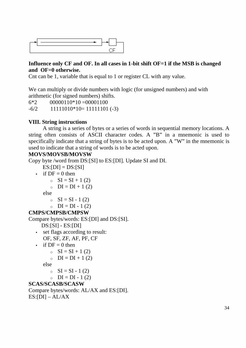
VII. Shift instructions SHL/SAL opr, cnt ;Logic/arithmetic shift left
SHR opr, cnt ;Logic shift right, put zero(s) in MSB(s)
SAR opr,cnt ; Arithmetic shift right, copy old MSB into new MSB
Influence all flags except AF
Rotate instructions ROL opr, cnt ;Rotate bits of byte or word left, MSB to LSB and to CF
ROR opr, cnt ;Rotate bits of byte or word right, LSB to MSB and to CF
RCL opr, cnt ;Rotate bits of byte or word left, MSB to CF and CF to LSB
RCR opr, cnt ;Rotate bits of byte or word right, LSB to CF and CF to MSB
34
Influence only CF and OF. In all cases in 1-bit shift OF=1 if the MSB is changed and OF=0 otherwise. Cnt can be 1, variable that is equal to 1 or register CL with any value. We can multiply or divide numbers with logic (for unsigned numbers) and with arithmetic (for signed numbers) shifts. 6*2 00000110*10 =00001100 -6/2 11111010*10= 11111101 (-3) VIII. String instructions
A string is a series of bytes or a series of words in sequential memory locations. A string often consists of ASCII character codes. A ”B” in a mnemonic is used to specifically indicate that a string of bytes is to be acted upon. A ”W” in the mnemonic is used to indicate that a string of words is to be acted upon. MOVS/MOVSB/MOVSW Copy byte /word from DS:[SI] to ES:[DI]. Update SI and DI. ES:[DI] = DS:[SI]
• if DF = 0 then o SI = SI + 1 (2) o DI = DI + 1 (2)
else o SI = SI - 1 (2) o DI = DI - 1 (2)
CMPS/CMPSB/CMPSW Compare bytes/words: ES:[DI] and DS:[SI]. DS:[SI] - ES:[DI]
• set flags according to result: OF, SF, ZF, AF, PF, CF
• if DF = 0 then o SI = SI + 1 (2) o DI = DI + 1 (2)
else o SI = SI - 1 (2) o DI = DI - 1 (2)
SCAS/SCASB/SCASW Compare bytes/words: AL/AX and ES:[DI]. ES:[DI] – AL/AX
35
• set flags according to result: OF, SF, ZF, AF, PF, CF
• if DF = 0 then o DI = DI + 1 (2)
else o DI = DI - 1 (2)
LODS/LODSB/LODSW Load byte from DS:[SI] into AL or string word into AX. Update SI. AL/AX = DS:[SI]
• if DF = 0 then o SI = SI + 1 (2)
else o SI = SI - 1 (2)
STOS/STOSB/STOSW Store byte from or word from AL/ AX into ES:[DI]. Update DI. ES:[DI] = AL/AX
• if DF = 0 then o DI = DI + 1(2)
else o DI = DI - 1 (2)
XLATB Translate byte from table. Copy value of memory byte at DS:[BX + unsigned AL] to AL register. Algorithm: AL = DS:[BX + unsigned AL] Example: ORG 100h x DB 11h, 22h, 33h, 44h, 55h LEA BX, x MOV AL, 2 XLATB ; AL = 33h RET REP chain instruction Repeat following MOVSB, MOVSW, LODSB, LODSW, STOSB, STOSW instructions CX times. Algorithm: check_cx: if CX <> 0 then
• do following chain instruction • CX = CX - 1 • go back to check_cx
36
else • exit from REP cycle
REPE/REPZ Repeat following CMPSB, CMPSW, SCASB, SCASW instructions while ZF = 1 (result is Equal/Zero), maximum CX times. Algorithm: check_cx: if CX <> 0 then
• do following chain instruction • CX = CX - 1 • if ZF = 1 then:
o go back to check_cx else
o exit from REPE/REPZ cycle else
• exit from REPE/REPZ cycle REPNE/REPNZ Repeat following CMPSB, CMPSW, SCASB, SCASW instructions while ZF = 0 (result is Not Equal/Not Zero), maximum CX times. Algorithm: check_cx: if CX <> 0 then
• do following chain instruction • CX = CX - 1 • if ZF = 0 then:
o go back to check_cx else
o exit from REPNE/REPNZ cycle else
• exit from REPNE/REPNZ cycle
3.8. PROCEDURES
The basic mechanism for declaring a procedure is: procname proc {NEAR or FAR} <statements> procname endp A simple procedure may consist of nothing more than a sequence of instructions ending with a ret instruction. For example, the following “procedure” zeros out the 256 bytes starting at the address in the bx register: ZeroBytes proc xor ax, ax mov cx, 128
37
ZeroLoop: mov [bx], ax add bx, 2 loop ZeroLoop ret ZeroBytes endp CALL and RETn Operations
The 80x86 supports near and far subroutines. Near calls and returns transfer control between procedures in the same code segment. Far calls and returns pass control between different segments. The two calling and return mechanisms push and pop different return addresses.
The CALL instructions provides for the transfer of control to a called procedure. The RET returns control back to the calling procedure.
The assembler can tell from the procedure whether RET is near or far and generates the appropriate object code or it can be explicitly denoted by using RETN or RETF.
Near Call and Return
When a near procedure is called: 1. The IP is pushed onto the stack. 2. The IP is loaded with the address of the called procedure. 3. Upon executing the return the IP is popped off the stack. CALL (SP) ← (SP) – 2 SS: ((SP) + 1:(SP)) ← (IP) RET (IP) ← SS: ((SP) + 1:(SP)) (SP) ← (SP) + 2 [(SP) ← (SP) + n]
Far Call and Return
1. The CS and IP are pushed onto the stack. 2. The IP and CS of the procedure are placed in the IP and CS registers. 3. Upon executing the return the IP and CS are popped off the stack. CALL (SP) ← (SP) – 2 SS: ((SP) + 1:(SP)) ← (CP) (SP) c (SP) – 2 SS: ((SP) + 1:(SP)) ← (IP)
38
RET (IP) ← SS: ((SP) + 1:(SP)) (SP) ← (SP) + 2 (CP) ← SS: ((SP) + 1:(SP)) (SP) ← (SP) + 2 [(SP) ← (SP) + n]
3.9. Interrupts The 8086/88 microprocessors allow normal program execution to be interrupted by external signals or by special instructions embedded in the program code. When the microprocessor is interrupted, it stops executing the current program and calls a procedure which services the interrupt. At the end of the interrupt service routine (ISR), the code execution sequence is returned to the original, interrupted program.
Interrupt sources: Hardware interrupts (external) generated by an external device request service
1. mascable - (INTR). 2. non-maskable interrupt - (NMI)
Software interrupts: 1. Generated by specific instruction INT or INTO; 2. Generated when special conditions at the microprocessor level appear
– internal interrupts or traps (divide error, single step). Each interrupt has a number called the interrupt type or interrupt vector. Interrupt numbers are always in the rate 0 to 255 decimal (00H to FFH). Some
interrupt numbers are fixed by the 8088/8086 hardware, others are chosen by the designer.
Dedicated (predefined) interrupts: INT 0 - divide error (generated by CPU after execution of DIV and IDIV
instructions if the quotient is too large); INT 1 - single step (if TF=1 this interrupt occurs after each instruction and allows
program debugging); INT 2 - NMI (external non-maskable interrupt. Is the only interrupt which is not
disabled by the CLI instruction. It is designed to handle catastrophic problems such as a power failure in order to save data before all is lost);
INT 3 - breakpoint (A break point is used to examine the CPU and memory after the execution of a group of Instructions);
INT 4 – signed number overflow. When an interrupt occurs, the location to which execution jumps is given in the
interrupt vector table. Each entry in the table is 4 bytes long - 2 bytes for a new CS value and 2 bytes for
a new IP value. There are 256 entries in the table, one for each interrupt number.
39
The table resides at physical memory addresses 00000H through 003FFH (1 KB of table).
As the address of each memory byte is defined by initial segment address (2 bytes) and offset (2 bytes), the interrupt vector has 4 bytes. The interrupt vector contains the address of the first instruction of the ISR. CPU calculates the location of the interrupt vector by multiplying by four the interrupt type.
1 byte 2 byte 3 byte 4 byte Offset (to be written in IP) Segment (to be written in CS)
The structure of interrupt vector.
Interrupt vector table:
INT 0- INT 4 – dedicated INT 5 - INT 31 are reserved by INTEL (27); INT 32 - INT 255 depend on users (224). Interrupts have priority: interrupts with lower interrupt numbers have higher
priority. An interrupt with higher priority can interrupt an interrupt with lower priority. Interrupt routine When an interrupt occurs, the processor
• stores FLAGS register, current IP and CS values into stack, • disables further interrupts, (IF) <—— О (TF) <—— О • fetches from the bus one byte representing interrupt number, • jumps to ISR, address of which is stored in location
4 * <interrupt type>. (CS) <—— (n * 4 + 2), (IP) <—— (n * 4) ISR should return with the IRET instruction. The IRET instruction: Restore CS, IP and FLAGS register from stack.
Interrupts •Initiated by both software and hardware •Can handle anticipated and unanticipated internal as well as external events •ISRs or interrupt handlers are memory resident •Use numbers to identify an interrupt service •FLAGS register is saved automatically
Procedures •Can only be initiated by software •Can handle anticipated events that are coded into the program •Typically loaded along with the program •Use meaningful names to indicate their function •Do not save the FLAGS register
40
Software interrupts Software interrupts can be used to call commonly used procedures from many
different programs. BIOS procedures. The ROM BIOS (Basic Input Output System) is part of the ROM based control -
system of an IBM PC or compatible that both defines the architecture of the computer to the software, and provides the fundamental I/O services that are needed for the operation of the computer.
The BIOS is actually a collection of procedures. Each procedure performs a specific function such as reading a character from the keyboard, writing characters to the screen, or reading information from disk.
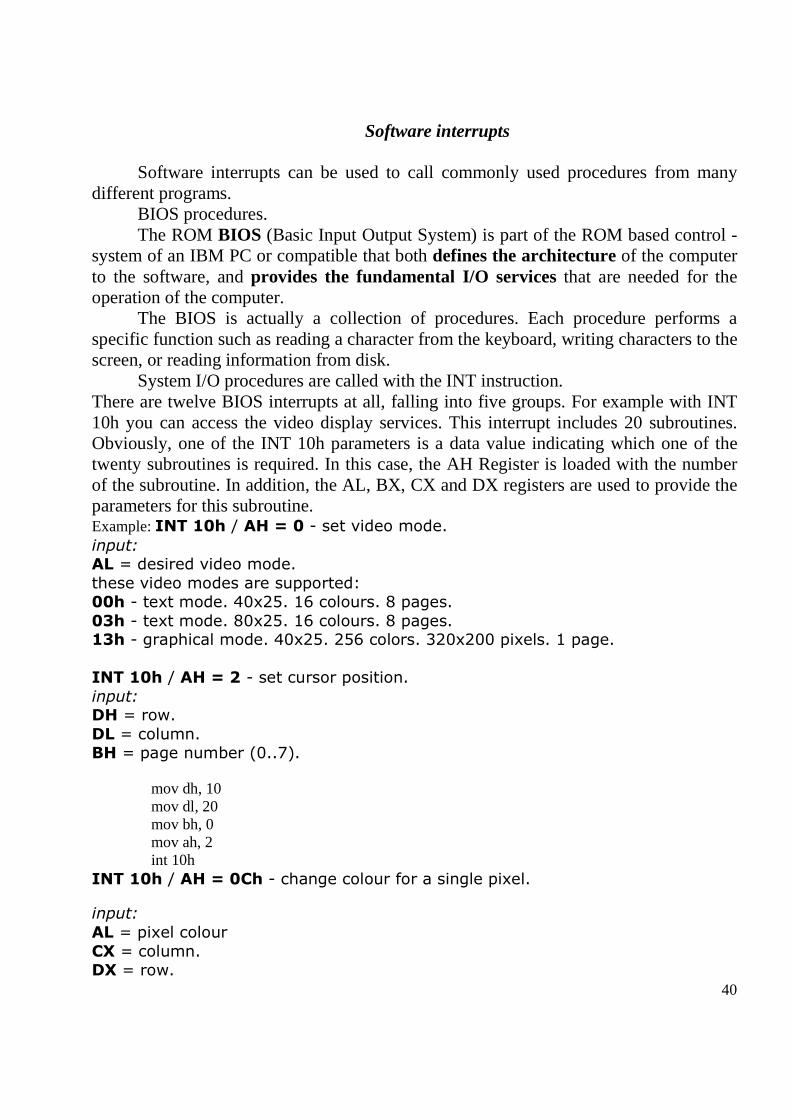
System I/O procedures are called with the INT instruction. There are twelve BIOS interrupts at all, falling into five groups. For example with INT 10h you can access the video display services. This interrupt includes 20 subroutines. Obviously, one of the INT 10h parameters is a data value indicating which one of the twenty subroutines is required. In this case, the AH Register is loaded with the number of the subroutine. In addition, the AL, BX, CX and DX registers are used to provide the parameters for this subroutine. Example: INT 10h / AH = 0 - set video mode.
input: AL = desired video mode.
these video modes are supported: 00h - text mode. 40x25. 16 colours. 8 pages.
03h - text mode. 80x25. 16 colours. 8 pages. 13h - graphical mode. 40x25. 256 colors. 320x200 pixels. 1 page.
INT 10h / AH = 2 - set cursor position.
input: DH = row.
DL = column. BH = page number (0..7). mov dh, 10 mov dl, 20 mov bh, 0 mov ah, 2 int 10h INT 10h / AH = 0Ch - change colour for a single pixel.
input:
AL = pixel colour
CX = column. DX = row.
41
mov al, 13h mov ah, 0 int 10h ; set graphics video mode. mov al, 1100b mov cx, 30 mov dx, 50 mov ah, 0ch int 10h ; set pixel. DOS interrupts There are nine DOS interrupt services. Dec Hex Description 32 20 Program terminate: come to normal ending 33 21 Function-call umbrella interrupt 34 22 Terminate address 35 23 Break address 36 24 Critical error-handler address 37 25 Absolute disk read 38 26 Absolute disk write 39 27 Terminate-but-stay-resident 47 2F Print spool control (DOS-3 versions only) INT 20h "Program Terminate"
This interrupt terminates the current process and returns control back to the parent process. For example, if you run a com.file program, INT 20 terminates your program and returns to DOS. INT 21h
All of the DOS function calls are invoked by INT 21h. Individual functions are selected in the same way as BIOS functions, placing the function number in the AH-Register.
INT 21h / AH=5 - output character to printer. entry: DL = character to print, after execution AL = DL. mov ah, 5 mov dl, 'a' int 21h
42
INT 21h / AH=9 - output of a string at DS:DX. String must be terminated by
'$'. mov dx, offset msg mov ah, 9 int 21h ret msg db "hello world $"
4. Control Unit
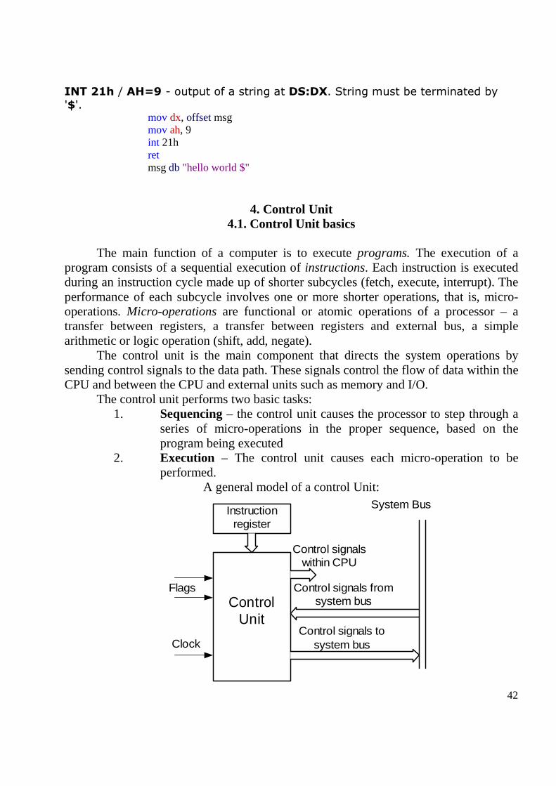
4.1. Control Unit basics The main function of a computer is to execute programs. The execution of a program consists of a sequential execution of instructions. Each instruction is executed during an instruction cycle made up of shorter subcycles (fetch, execute, interrupt). The performance of each subcycle involves one or more shorter operations, that is, micro-operations. Micro-operations are functional or atomic operations of a processor – a transfer between registers, a transfer between registers and external bus, a simple arithmetic or logic operation (shift, add, negate).
The control unit is the main component that directs the system operations by sending control signals to the data path. These signals control the flow of data within the CPU and between the CPU and external units such as memory and I/O.
The control unit performs two basic tasks: 1. Sequencing – the control unit causes the processor to step through a
series of micro-operations in the proper sequence, based on the program being executed
2. Execution – The control unit causes each micro-operation to be performed.
A general model of a control Unit:
Flags
Clock
Instructionregister
Control signalswithin CPU
Control signals fromsystem bus
Control signals tosystem bus
System Bus
ControlUnit

43
Inputs: 1. Clock – One or several micro-operations are executed at one clock pulse. It is
called a processor cycle. 2. Instruction register – The opcode of the current instruction is used to determine
which micro-operations to perform. 3. Flags – Are needed to determine the status of the processor and outcome of
previous ALU operations. 4. Control signals from Control Bus – interrupt signals, acknowledgments.
Outputs: 1. Control signals within the CPU – These are two types: those that cause data to be
moved from one register to another and those that activates specific CPU functions.
2. Control signals to Control Bus – also two types: control signals to memory and control signals to I/O system.
There are mainly two different types of control units: hardwired and microprogrammed.
Hardwired Control Unit
In hardwired control, fixed logic circuits that correspond directly to the Boolean expressions are used to generate the control signals.
Advantage: Hardwired control is very fast and CU has a small size. Disadvantage: Hardwired control could be very expensive and complicated for
complex systems. It will require a redesign of the entire systems in the case of any change (ex. add a new instruction).
General structure:
Instruction register
DC
Timinggenerator
Clock
Control signals
Flags
0 1 n
T0
T1
Tm
C1 C2 Ck
Control unit
According to the opcode of the instruction, the CU will generate a different combination of control signals. To simplify the CU logic, there should be a unique logic

44
input for each opcode. This function is performed by a decoder which takes an encoded input and produces a single output.
The CU emits different control signals at different time moments (T0, T1…) within a single instruction cycle. Timing generator is a counter of a clock pulses. The period of the clock pulses must be long enough to allow the propagation of signals along data paths and through processor circuitry. At the end of the instruction cycle, the CU must reinitialize the counter to T0.
In a hardwired implementation a CU produces output control signals as a function of its input signals.
Let consider a simple example: Assume that the instruction set of a machine has the three instructions: x, y, and z; and A, B, C, D, E, F, G, and H are signals that should be generated for the three instructions at the three steps T0 , T1 , and T2.
Step Instruction X Instruction Y Instruction Z T0 D,B,E F,H,G E,H T1 C,A.H G D,A,C T2 G,C B,C -
The Boolean expressions for control signals A, B, and C can be obtained as follows: A=X*T1+Z*T1=(X+Z)*T1 B=X*T0+Y*T2 C=X*T1+ Z*T1+ X*T2+Y*T2=(X+Z)*T1+ (X+Y)*T2
The logic circuits for these control signals:
Z A
C
B
T1
X
X
X
T0
Y
Y
T2
T2
4.3. Microprogrammed Control Unit
The idea of microprogrammed control units was introduced by M. V. Wilkes in the early 1950s. Microprogramming was motivated by the desire to reduce the complexities involved with hardwired control.
An instruction is implemented using a set of micro-operations. Associated with each micro-operation is a set of control lines that must be activated to carry out the
45
corresponding microoperation. The idea of microprogrammed control is to store the control signals associated with the implementation of a certain instruction as a microprogram in a special memory called a control memory (CM).
Advantage: It is flexible and could adapt easily to changes in the system design. We can easily add new instructions without changing hardware.
Disadvantage: It is slower than a harwired control unit of comparable technology. Microprogramming is the dominant technique in CISC processors, hardwired CU – in RISC processors.
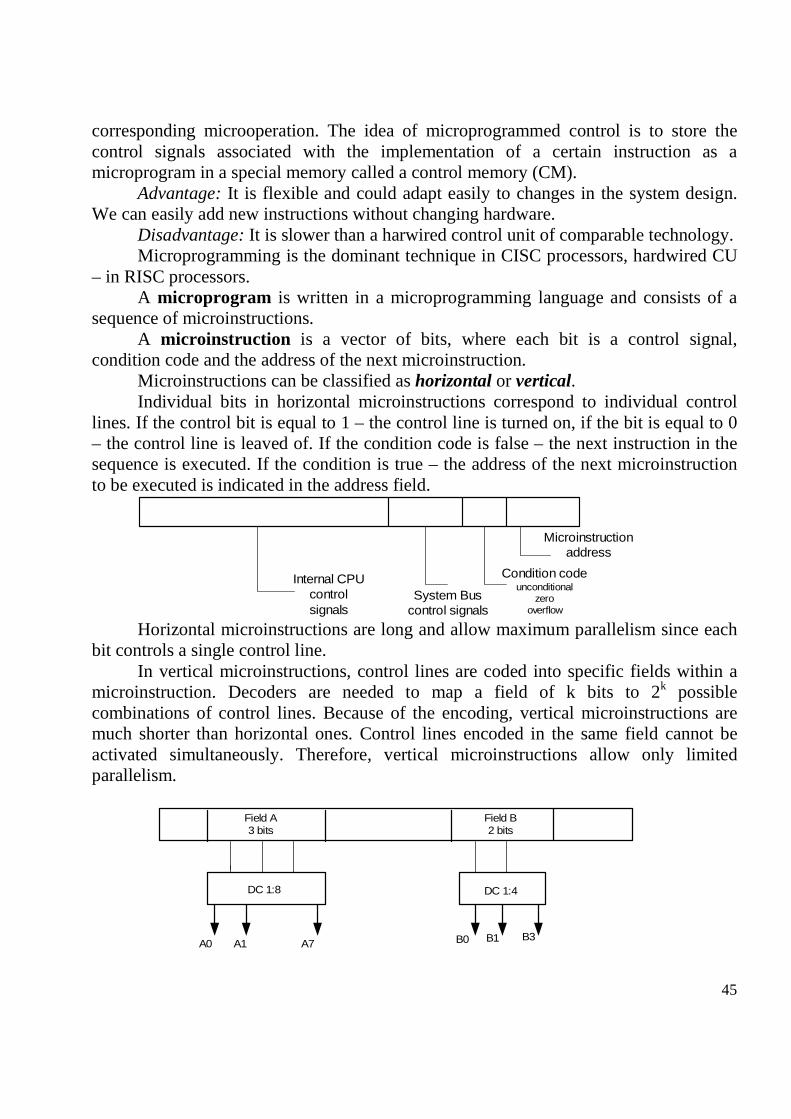
A microprogram is written in a microprogramming language and consists of a sequence of microinstructions.
A microinstruction is a vector of bits, where each bit is a control signal, condition code and the address of the next microinstruction.
Microinstructions can be classified as horizontal or vertical. Individual bits in horizontal microinstructions correspond to individual control
lines. If the control bit is equal to 1 – the control line is turned on, if the bit is equal to 0 – the control line is leaved of. If the condition code is false – the next instruction in the sequence is executed. If the condition is true – the address of the next microinstruction to be executed is indicated in the address field.
Microinstructionaddress
Condition codeunconditional
zerooverflow
System Buscontrol signals
Internal CPUcontrolsignals
Horizontal microinstructions are long and allow maximum parallelism since each bit controls a single control line.
In vertical microinstructions, control lines are coded into specific fields within a microinstruction. Decoders are needed to map a field of k bits to 2k possible combinations of control lines. Because of the encoding, vertical microinstructions are much shorter than horizontal ones. Control lines encoded in the same field cannot be activated simultaneously. Therefore, vertical microinstructions allow only limited parallelism.
Field A3 bits
Field B2 bits
DC 1:8 DC 1:4
A0 A1 A7 B0 B1 B3
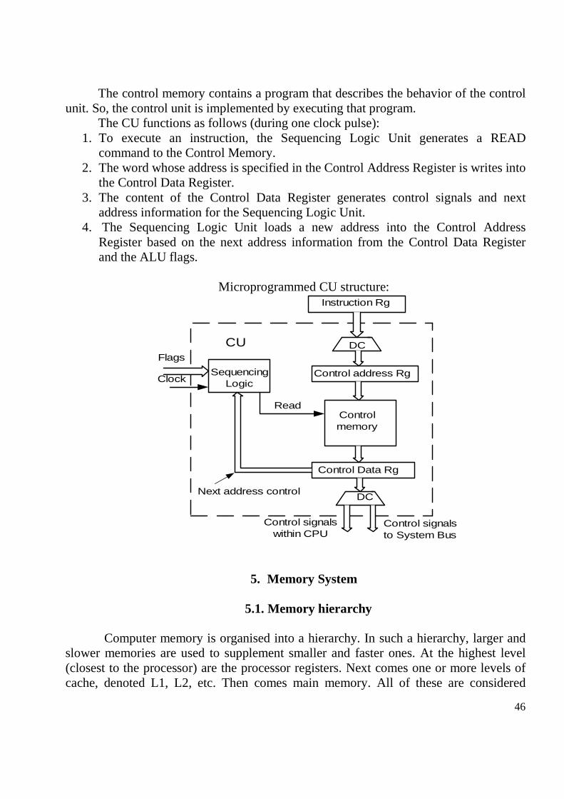
46
The control memory contains a program that describes the behavior of the control unit. So, the control unit is implemented by executing that program.
The CU functions as follows (during one clock pulse): 1. To execute an instruction, the Sequencing Logic Unit generates a READ
command to the Control Memory. 2. The word whose address is specified in the Control Address Register is writes into
the Control Data Register. 3. The content of the Control Data Register generates control signals and next
address information for the Sequencing Logic Unit. 4. The Sequencing Logic Unit loads a new address into the Control Address
Register based on the next address information from the Control Data Register and the ALU flags.
Microprogrammed CU structure:
Instruction Rg
DC
Control address RgSequencingLogic
Control Data Rg
Control signalswithin CPU
Control signalsto System Bus
Next address control
Read
Flags
Clock
DC
CU
Controlmemory
5. Memory System
5.1. Memory hierarchy
Computer memory is organised into a hierarchy. In such a hierarchy, larger and slower memories are used to supplement smaller and faster ones. At the highest level (closest to the processor) are the processor registers. Next comes one or more levels of cache, denoted L1, L2, etc. Then comes main memory. All of these are considered
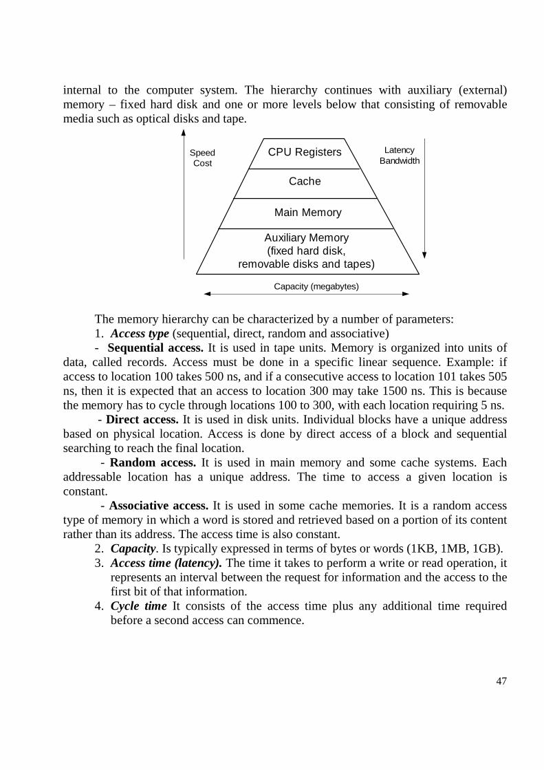
47
internal to the computer system. The hierarchy continues with auxiliary (external) memory – fixed hard disk and one or more levels below that consisting of removable media such as optical disks and tape.
CPU Registers
Cache
Main Memory
Auxiliary Memory(fixed hard disk,
removable disks and tapes)
SpeedCost
LatencyBandwidth
Capacity (megabytes)
The memory hierarchy can be characterized by a number of parameters: 1. Access type (sequential, direct, random and associative) - Sequential access. It is used in tape units. Memory is organized into units of
data, called records. Access must be done in a specific linear sequence. Example: if access to location 100 takes 500 ns, and if a consecutive access to location 101 takes 505 ns, then it is expected that an access to location 300 may take 1500 ns. This is because the memory has to cycle through locations 100 to 300, with each location requiring 5 ns.
- Direct access. It is used in disk units. Individual blocks have a unique address based on physical location. Access is done by direct access of a block and sequential searching to reach the final location.
- Random access. It is used in main memory and some cache systems. Each addressable location has a unique address. The time to access a given location is constant.
- Associative access. It is used in some cache memories. It is a random access type of memory in which a word is stored and retrieved based on a portion of its content rather than its address. The access time is also constant.
2. Capacity. Is typically expressed in terms of bytes or words (1KB, 1MB, 1GB). 3. Access time (latency). The time it takes to perform a write or read operation, it
represents an interval between the request for information and the access to the first bit of that information.
4. Cycle time It consists of the access time plus any additional time required before a second access can commence.

48
Access timeCycle time
Searchtime
Transfertime
Wait timeTime
5. Bandwidth (Transfer rate). This is the rate at which data can be transferred
into or out a memory unit. It is equal to 1/cycle time (words per second) or w/cycle time.
6. Cost (is usually specified in money per megabytes).
Memory hierarchy parameters
A variety of physical types of memory have been employed. The most common today are semiconductor memory, magnetic, used for disk and tape, and optical and magneto-optical. According to physical characteristics memory can be:
1. Volatile – information is lost when electrical power is switched off (RAM). 2. Non-volatile – information once recorded remains without deterioration until it
is changed (ROM). The effectiveness of a memory hierarchy during a program execution depends on
the principle called locality of reference, that is, within a given period of time, programs tend to reference a relatively confined area of memory repeatedly. So, according to this principle, the most frequently used information is temporarily moved into the faster memory.
There exist two forms of locality: spatial and temporal locality. Spatial locality refers to the phenomenon that when a given address has been
referenced, it is most likely that addresses near it will be referenced within a short period of time, for example, consecutive instructions in a straight-line program.

49
Temporal locality, on the other hand, refers to the phenomenon that once a particular memory item has been referenced, it is most likely that it will be referenced next, for example, an instruction in a program loop.
The sequence of events that takes place when the processor makes a request for an item is as follows. First, the item is sought in the first memory level of the memory hierarchy. The probability of finding the requested item in the first level is called the hit ratio. The probability of not finding (missing) the requested item in the first level of the memory hierarchy is called the miss ratio. When the requested item causes a “miss,” it is sought in the next subsequent memory level.
5.2. Semiconductor memory types
The main memory of a computer system should be fast enough to not degrade the performance of the system. To achieve this, the semiconductor type memories are used as main memory.
• read-only memory -ROM • read-write memory or random access memory - RAM
Among them ROM is a non-volatile memory type. I.e. they retain their contents when the power goes off. On the other hand, RAM type devices loss their contents when the power goes off, because of the technology used.
ROM memory In ROM, the data are permanently stored. They are available in many forms. • ROM. Its content cannot be erasable. • PROM (Programmable read only memory. Once programmed, they cannot be
erased. • EPROM (erasable programmable ROM). Erasable by ultraviolet lights. • EEPROM (byte-level electrically erasable programmable ROM ). • Flash memory (block-level electrically erasable programmable ROM ).
RAM memory • static random access memory (SRAM) • dynamic random access memory (DRAM)
In a SRAM binary values are stored using traditional flip-flops (6 transistors configuration).
A DRAM is made with cells that store data as charge on capacitors. Dynamic memory depends on storing logic values using a capacitor together with one transistor that acts as a switch. The use of dynamic memory leads to saving in chip area. The presence or absence of charge on a capacitor is interpreted as a binary 1 or 0. Because capacitors have a natural tendency to discharge, DRAMs require periodic charge refreshing by a special circuit.
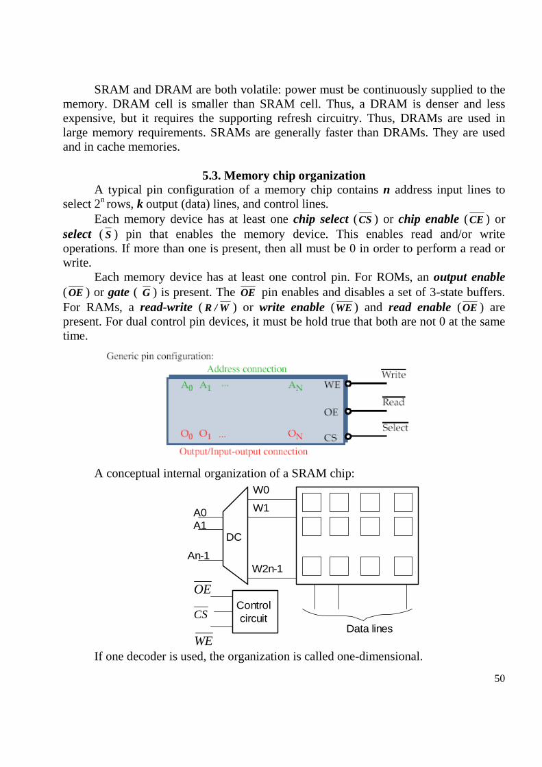
50
SRAM and DRAM are both volatile: power must be continuously supplied to the memory. DRAM cell is smaller than SRAM cell. Thus, a DRAM is denser and less expensive, but it requires the supporting refresh circuitry. Thus, DRAMs are used in large memory requirements. SRAMs are generally faster than DRAMs. They are used and in cache memories.
5.3. Memory chip organization A typical pin configuration of a memory chip contains n address input lines to
select 2n rows, k output (data) lines, and control lines. Each memory device has at least one chip select (CS) or chip enable (CE ) or
select ( S ) pin that enables the memory device. This enables read and/or write operations. If more than one is present, then all must be 0 in order to perform a read or write.
Each memory device has at least one control pin. For ROMs, an output enable (OE ) or gate ( G ) is present. The OE pin enables and disables a set of 3-state buffers. For RAMs, a read-write ( R / W ) or write enable (WE ) and read enable (OE ) are present. For dual control pin devices, it must be hold true that both are not 0 at the same time.
A conceptual internal organization of a SRAM chip:
A0A1
An-1
W0
W1
W2n-1
Data lines
DC
OE
CS
WE
Controlcircuit
If one decoder is used, the organization is called one-dimensional.

51
Cells belonging to a given row can be assumed to form the bits of a given memory word. Address lines An-1, An-2, …,A1, A0 are used as inputs to the address decoder in order to generate the word select lines W2
n-1, W2
n-2, …, W1, W0. A given word select line
is common to all memory cells in the same row. At any given time, the address decoder activates only one word select line. A word select line is used to enable all cells in a row for read or write. Data (bit) lines are used to input or output the contents of cells.
Example: A 1Kx4 memory chip indicates that the chip has 1K rows of cells and in each row there are 4 cells. The total number of cells is 4K. To address 1K=210 rows, log22
10=10 addresses are needed. However, this may not lead to the best utilization of the chip area.
Another possible organization of this memory cell array is as a 64x64, that is, to
organize the array in the form of 64 rows, each consisting of 64 cells. In this case, six address lines (forming what is called the row address) will be needed in order to select one of the 64 rows. The remaining four address lines (called the column address) will be used to select the appropriate 4 bits among the available 64 bits constituting a row. For this four 16-to-1 MUX are used.
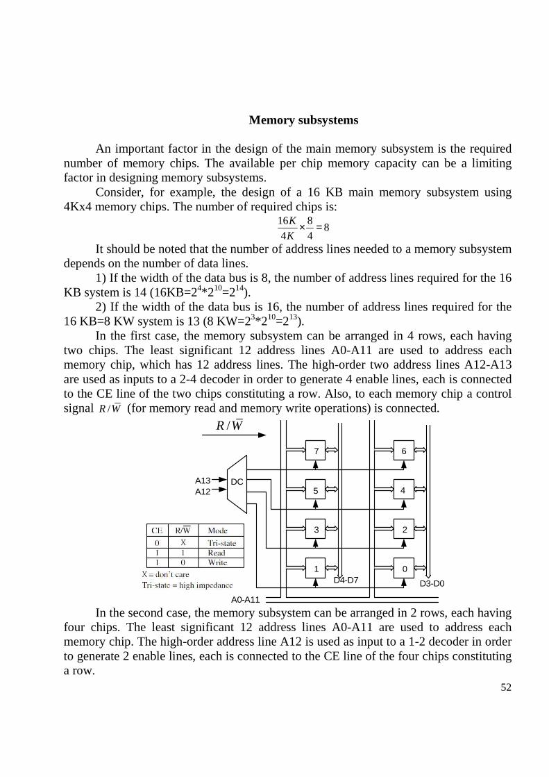
52
Memory subsystems
An important factor in the design of the main memory subsystem is the required number of memory chips. The available per chip memory capacity can be a limiting factor in designing memory subsystems.
Consider, for example, the design of a 16 KB main memory subsystem using 4Kx4 memory chips. The number of required chips is:
16 88
4 4
K
K× =
It should be noted that the number of address lines needed to a memory subsystem depends on the number of data lines.
1) If the width of the data bus is 8, the number of address lines required for the 16 KB system is 14 (16KB=24*210=214).
2) If the width of the data bus is 16, the number of address lines required for the 16 KB=8 KW system is 13 (8 KW=23*210=213).
In the first case, the memory subsystem can be arranged in 4 rows, each having two chips. The least significant 12 address lines A0-A11 are used to address each memory chip, which has 12 address lines. The high-order two address lines A12-A13 are used as inputs to a 2-4 decoder in order to generate 4 enable lines, each is connected to the CE line of the two chips constituting a row. Also, to each memory chip a control signal /R W (for memory read and memory write operations) is connected.
DC
A0-A11
D3-D0D4-D7
A12A13
01
23
45
67
/R W
In the second case, the memory subsystem can be arranged in 2 rows, each having
four chips. The least significant 12 address lines A0-A11 are used to address each memory chip. The high-order address line A12 is used as input to a 1-2 decoder in order to generate 2 enable lines, each is connected to the CE line of the four chips constituting a row.

53
DC
D3-D0D4-D7
A12 023
5
/R W
A0-A11
1
7 6 4
D15-D12 D11-D18
Cache memory
Cache memory is a small high-speed memory, situated between the processor and the main memory in which the information expected to be used more frequently by the CPU is kept (the term cache means a safe place for hiding or storing things).
CPU Cache MainMemory
Wordtransfer
Blocktransfer
The structure of a cache-memory system So, at any given time some active portion of the main memory is duplicated in the
cache. Therefore, when the processor makes a request for a memory reference, the request is first sought in the cache. If the request corresponds to an element that is currently residing in the cache, we call that a cache hit. If the request corresponds to an element that is not currently in the cache, we call that a cache miss. After a cache miss, a block of elements is brought from the main memory to cache. Because of the phenomenon of locality of reference, we can expect that the next requested element will be residing in the neighboring locality of the current requested element.
A request for accessing a memory element is made by the processor through issuing the logic address of the requested element. It may correspond to that of an element that exists currently in the cache (cache hit); otherwise, it may correspond to an element that is currently residing in the main memory. Therefore, address translation has to be made in order to determine where the requested element is. This is one of the functions performed by the memory management unit (MMU).
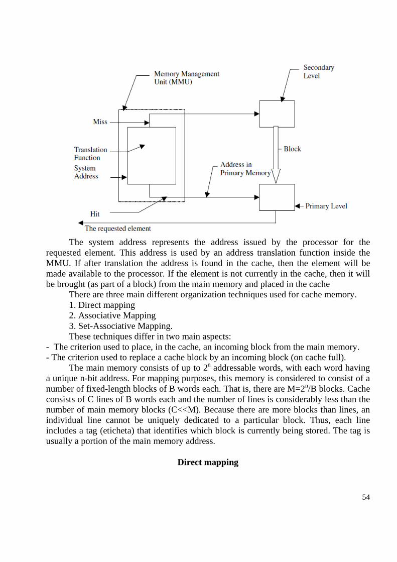
54
The system address represents the address issued by the processor for the
requested element. This address is used by an address translation function inside the MMU. If after translation the address is found in the cache, then the element will be made available to the processor. If the element is not currently in the cache, then it will be brought (as part of a block) from the main memory and placed in the cache
There are three main different organization techniques used for cache memory. 1. Direct mapping 2. Associative Mapping 3. Set-Associative Mapping. These techniques differ in two main aspects:
- The criterion used to place, in the cache, an incoming block from the main memory. - The criterion used to replace a cache block by an incoming block (on cache full).
The main memory consists of up to 2n addressable words, with each word having a unique n-bit address. For mapping purposes, this memory is considered to consist of a number of fixed-length blocks of B words each. That is, there are M=2n/B blocks. Cache consists of C lines of B words each and the number of lines is considerably less than the number of main memory blocks (C<<M). Because there are more blocks than lines, an individual line cannot be uniquely dedicated to a particular block. Thus, each line includes a tag (eticheta) that identifies which block is currently being stored. The tag is usually a portion of the main memory address.
Direct mapping
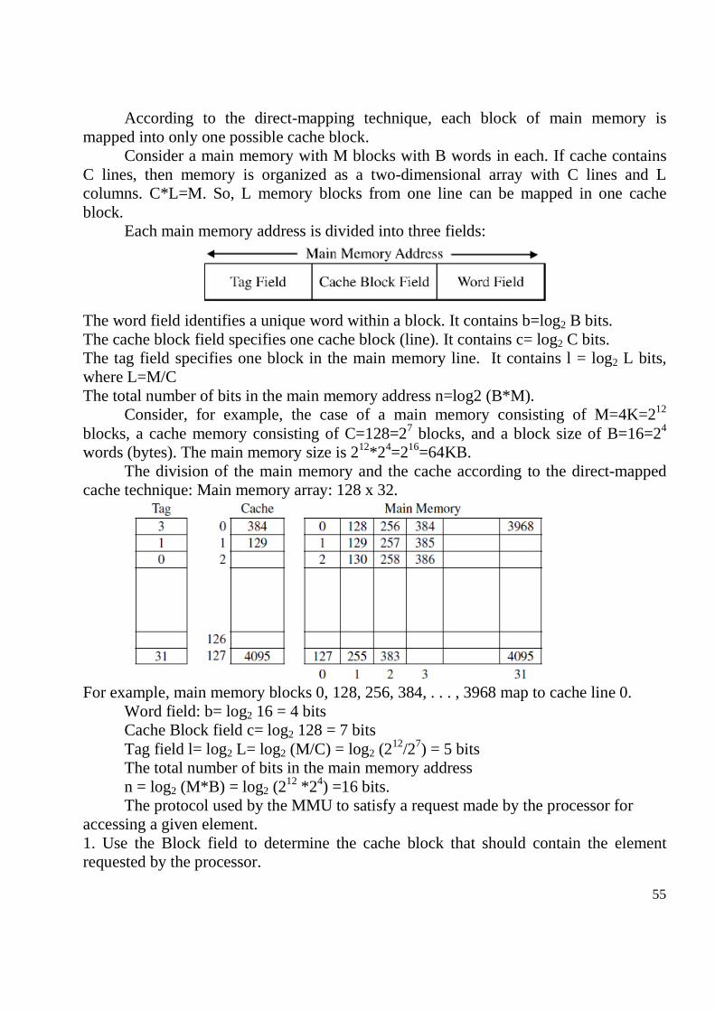
55
According to the direct-mapping technique, each block of main memory is mapped into only one possible cache block.
Consider a main memory with M blocks with B words in each. If cache contains C lines, then memory is organized as a two-dimensional array with C lines and L columns. C*L=M. So, L memory blocks from one line can be mapped in one cache block.
Each main memory address is divided into three fields:
The word field identifies a unique word within a block. It contains b=log2 B bits. The cache block field specifies one cache block (line). It contains c= log2 C bits. The tag field specifies one block in the main memory line. It contains l = log2 L bits, where L=M/C The total number of bits in the main memory address n=log2 (B*M).
Consider, for example, the case of a main memory consisting of M=4K=212 blocks, a cache memory consisting of C=128=27 blocks, and a block size of B=16=24 words (bytes). The main memory size is 212*24=216=64KB.
The division of the main memory and the cache according to the direct-mapped cache technique: Main memory array: 128 x 32.
For example, main memory blocks 0, 128, 256, 384, . . . , 3968 map to cache line 0.
Word field: b= log2 16 = 4 bits Cache Block field c= log2 128 = 7 bits Tag field l= log2 L= log2 (M/C) = log2 (2
12/27) = 5 bits The total number of bits in the main memory address n = log2 (M*B) = log2 (2
12 *24) =16 bits. The protocol used by the MMU to satisfy a request made by the processor for
accessing a given element. 1. Use the Block field to determine the cache block that should contain the element requested by the processor.
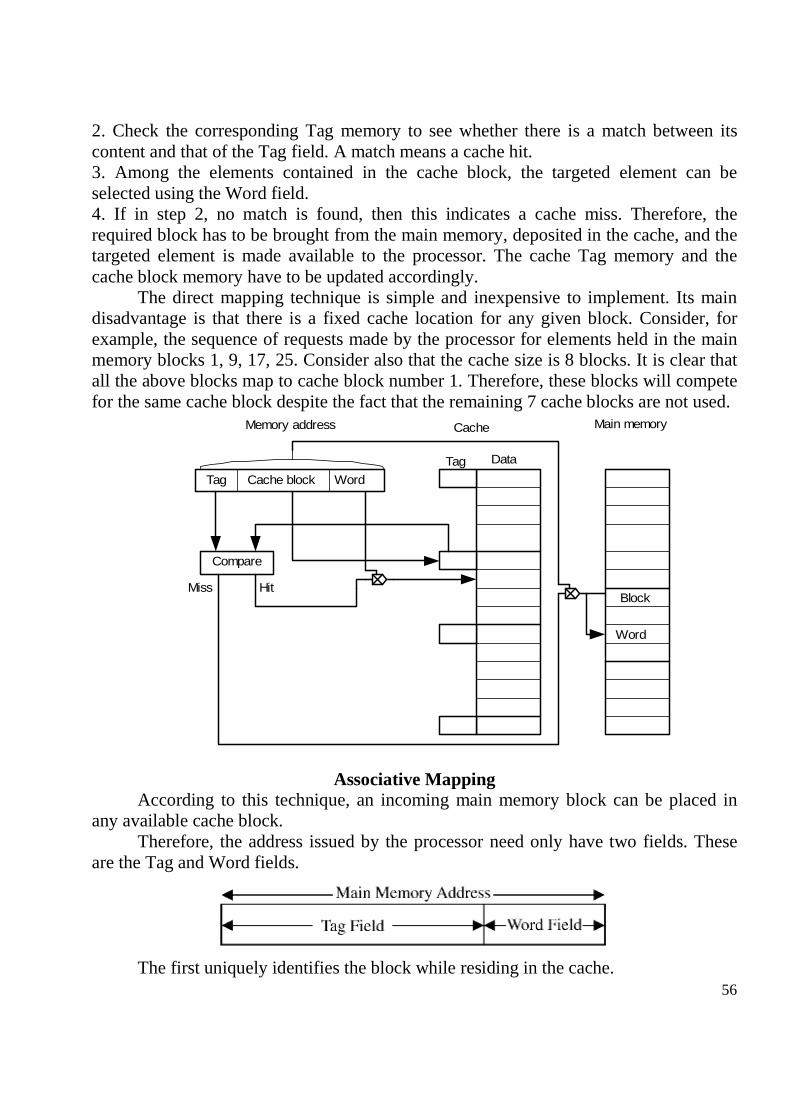
56
2. Check the corresponding Tag memory to see whether there is a match between its content and that of the Tag field. A match means a cache hit. 3. Among the elements contained in the cache block, the targeted element can be selected using the Word field. 4. If in step 2, no match is found, then this indicates a cache miss. Therefore, the required block has to be brought from the main memory, deposited in the cache, and the targeted element is made available to the processor. The cache Tag memory and the cache block memory have to be updated accordingly.
The direct mapping technique is simple and inexpensive to implement. Its main disadvantage is that there is a fixed cache location for any given block. Consider, for example, the sequence of requests made by the processor for elements held in the main memory blocks 1, 9, 17, 25. Consider also that the cache size is 8 blocks. It is clear that all the above blocks map to cache block number 1. Therefore, these blocks will compete for the same cache block despite the fact that the remaining 7 cache blocks are not used.
Tag
Tag Data
Cache Main memoryMemory address
Cache block Word
Compare
HitMiss
Word
Block
Associative Mapping According to this technique, an incoming main memory block can be placed in
any available cache block. Therefore, the address issued by the processor need only have two fields. These
are the Tag and Word fields.
The first uniquely identifies the block while residing in the cache.

57
The second field identifies the element within the block that is requested by the processor.
To determine whether a block is in the cache, the cache control logic must examine every block’s tag in parallel. Note that no field in the address corresponds to cache block number, so that the number of block in the cache is not determined by the address format.
The length, in bits, of each of the fields: 1. Word field b= log2 B, where B is the size of the block in words. 2. Tag field m= log2 M, where M is the size of the main memory in blocks. 3. The number of bits in the main memory address n= log2 (B * M)
Let’s compute these parameters for a memory system having the following specification: size of the main memory is 4K blocks, size of the cache is 128 blocks, and the block size is 16 words. Word field b= log2 B = log2 16= log2 2
4 = 4 bits Tag field m = log2 M = log2 4K= log2 2
12 = 12 bits The number of bits in the main memory address n=log2(B * M)=log2(2
4 * 212) = 16 bits.
The protocol used by the MMU to satisfy a request made by the processor for accessing a given element. 1. Use the Tag field to search in the Tag memory for a match with any of the tags stored. 2. A match in the tag memory indicates a cache hit. 3. Among the elements contained in the cache block, the targeted element can be selected using the Word field. 4. If in step 2, no match is found, then this indicates a cache miss. Therefore, the required block has to be brought from the main memory, deposited in the first available cache block, and the targeted element (word) is made available to the processor. The cache Tag memory and the cache block memory have to be updated accordingly.
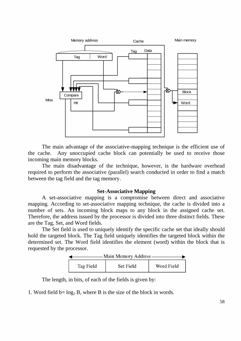
58
Tag
Tag Data
Cache Main memoryMemory address
Word
Compare
HitMiss
Word
Block
The main advantage of the associative-mapping technique is the efficient use of the cache. Any unoccupied cache block can potentially be used to receive those incoming main memory blocks.
The main disadvantage of the technique, however, is the hardware overhead required to perform the associative (parallel) search conducted in order to find a match between the tag field and the tag memory.
Set-Associative Mapping A set-associative mapping is a compromise between direct and associative
mapping. According to set-associative mapping technique, the cache is divided into a number of sets. An incoming block maps to any block in the assigned cache set. Therefore, the address issued by the processor is divided into three distinct fields. These are the Tag, Set, and Word fields.
The Set field is used to uniquely identify the specific cache set that ideally should hold the targeted block. The Tag field uniquely identifies the targeted block within the determined set. The Word field identifies the element (word) within the block that is requested by the processor.
The length, in bits, of each of the fields is given by:
1. Word field b= log2 B, where B is the size of the block in words.

59
2. Set field s= log2 S, where S is the number of sets in the cache. 3. Tag field m= log2 (M/S), where M is the size of the main memory in blocks. S = C/Bs, where C is the number of cache blocks and Bs is the number of blocks per set. 4. The number of bits in the main memory address n = log2 (B * M). Example. Compute the above three parameters (Word, Set, and Tag) for a memory system having the following specification: size of the main memory M is 4K blocks, size of the cache C is 128 blocks, and the block size B is 16 words. One cache set Bs has four blocks. Word field b= log2 B = log2 16= log2 2
4 = 4 bits Set field s=log2 (128/4) = log2 32 = 5 Tag field m = log2 (M/S) = log2 2
12/25= log2 27= 7 bits
The number of bits in the main memory address n=log2(B * M)=log2(24 * 212) = 16 bits.
The protocol used by the MMU to satisfy a request made by the processor for
accessing a given element. 1. Use the Set field (5 bits) to determine (directly) the specified set (1 of the 32 sets). 2. Use the Tag field to find a match with any of the (four) blocks in the determined set. A match in the tag memory indicates that the specified set determined in step 1 is currently holding the targeted block, that is, a cache hit. 3. Among the 16 words (elements) contained in hit cache block, the requested word is selected using a selector with the help of the Word field. 4. If in step 2, no match is found, then this indicates a cache miss. Therefore, the required block has to be brought from the main memory.
Replacement Techniques and Write Policies
When a new block is brought into the cache, one of the existing blocks must be replaced. For direct mapping, there is only one possible line for any particular block and no choice is possible. For the associative and set-associative techniques, a replacement algorithm is needed.
A number of replacement techniques can be used: 1. A randomly selected block (random selection). As the name indicates,
random selection of a cache block for replacement is done based on the output of the random number generator at the time of replacement. This technique is simple and does not require much additional overhead. However, its main shortcoming is that it does not take locality into consideration.
2. The block that has been in the cache the longest ( first-in, first- out, FIFO). This technique requires keeping track of the lifetime of a cache block. Therefore, it is not as simple as the random selection technique. Intuitively, the FIFO technique is reasonable to use for straight-line programs where locality of reference is not of concern.
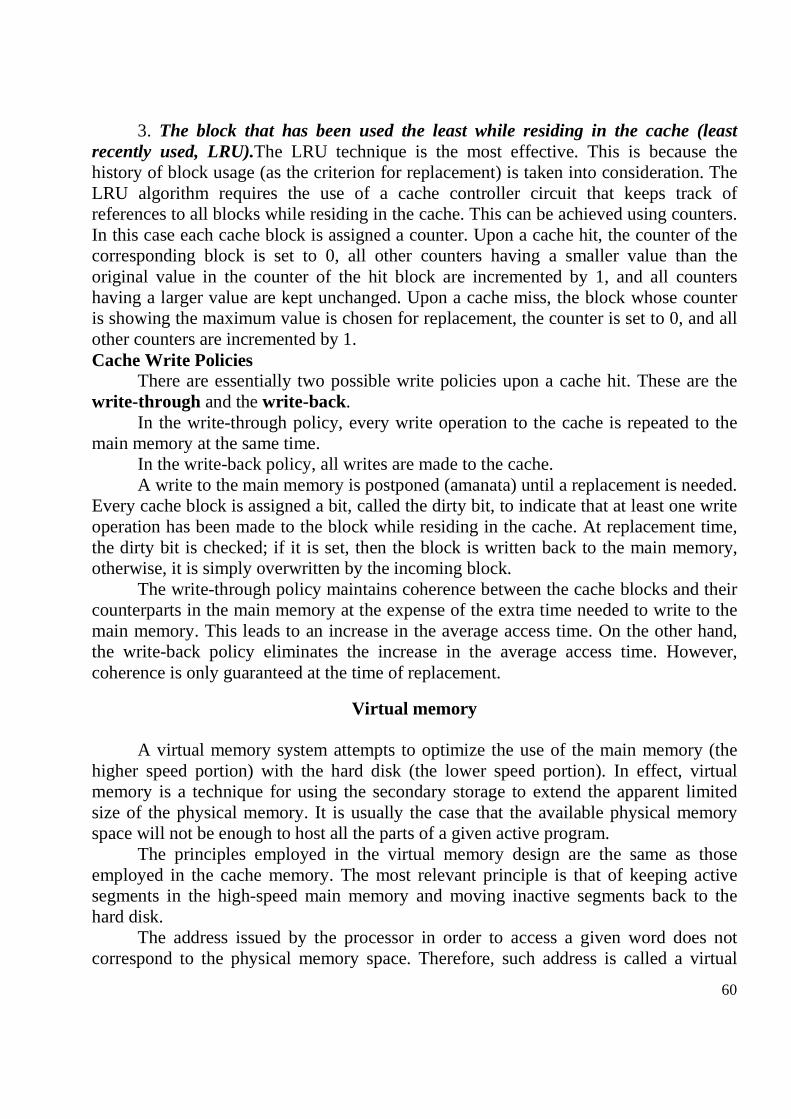
60
3. The block that has been used the least while residing in the cache (least recently used, LRU).The LRU technique is the most effective. This is because the history of block usage (as the criterion for replacement) is taken into consideration. The LRU algorithm requires the use of a cache controller circuit that keeps track of references to all blocks while residing in the cache. This can be achieved using counters. In this case each cache block is assigned a counter. Upon a cache hit, the counter of the corresponding block is set to 0, all other counters having a smaller value than the original value in the counter of the hit block are incremented by 1, and all counters having a larger value are kept unchanged. Upon a cache miss, the block whose counter is showing the maximum value is chosen for replacement, the counter is set to 0, and all other counters are incremented by 1. Cache Write Policies
There are essentially two possible write policies upon a cache hit. These are the write-through and the write-back.
In the write-through policy, every write operation to the cache is repeated to the main memory at the same time.
In the write-back policy, all writes are made to the cache. A write to the main memory is postponed (amanata) until a replacement is needed.
Every cache block is assigned a bit, called the dirty bit, to indicate that at least one write operation has been made to the block while residing in the cache. At replacement time, the dirty bit is checked; if it is set, then the block is written back to the main memory, otherwise, it is simply overwritten by the incoming block.
The write-through policy maintains coherence between the cache blocks and their counterparts in the main memory at the expense of the extra time needed to write to the main memory. This leads to an increase in the average access time. On the other hand, the write-back policy eliminates the increase in the average access time. However, coherence is only guaranteed at the time of replacement.
Virtual memory
A virtual memory system attempts to optimize the use of the main memory (the higher speed portion) with the hard disk (the lower speed portion). In effect, virtual memory is a technique for using the secondary storage to extend the apparent limited size of the physical memory. It is usually the case that the available physical memory space will not be enough to host all the parts of a given active program.
The principles employed in the virtual memory design are the same as those employed in the cache memory. The most relevant principle is that of keeping active segments in the high-speed main memory and moving inactive segments back to the hard disk.
The address issued by the processor in order to access a given word does not correspond to the physical memory space. Therefore, such address is called a virtual
61
(logical) address. The memory management unit (MMU) is responsible for the translation of virtual addresses to their corresponding physical addresses.
Three address translation techniques can be identified. These are: - direct-mapping; - associative- mapping; - set-associative-mapping. The logical addresses can be organized in three modes: - fixed length pages (from 2K to 16K bytes); - variable length segments (<64KB); - paged segmentation (one segment contains a few pages). In all these techniques, the translation from logical address to physical is done
using a translation table, stored in the main memory.
Address translation using pages Direct-mapping
In this case, the virtual address issued by the processor is divided into two fields: the virtual page number and the offset fields. If the number of bits in the virtual page number field is N, then the number of entries in the page table will be 2N.
The virtual page number field is used to directly address an entry in the page table. If the corresponding page is valid (as indicated by the valid bit), then the contents of the specified page table entry will correspond to the physical page address in the main memory. The latter is then extracted and concatenated with the offset field in order to form the physical address of the word requested by the processor. If, on the other hand, the specified entry in the page table does not contain a valid physical page number, then this represents a page fault. In this case, the MMU will have to bring the corresponding page from the hard disk, load it into the main memory, and indicate the validity of the page.
Example. Suppose that the virtual address contains 16 bits. One page has 212 words. Four most significant bits will specify one of 16 pages and last 12 bits – the word address in the page.
62
The main advantage of the direct-mapping technique is its simplicity measured in
terms of the direct addressing of the page table entries. Its main disadvantage is the expected large size of the page table and a lot of empty entries in it. Associative Mapping
The virtual address issued by the processor is divided into two fields: the virtual page number and the offset fields. However, the page table could be far shorter.
Every entry in the page table is divided into two parts: the virtual page number and the physical page number. A match is searched (associatively) between the virtual page number field of the address and the virtual page numbers stored in the page table. If a match is found, the corresponding physical page number stored in the page table is extracted and is concatenated with the offset field in order to generate the physical address of the word requested by the processor.
If a match could not be found, then this represents a page fault. In this case, the MMU will have to bring the corresponding page from the hard disk, load it into the main memory, and indicate the validity of the page.

63
The main advantage of the associative-mapping technique is the expected shorter
page table (compared to the direct-mapping technique) required for the translation process. Its main disadvantage is the associative search that requires the use of an added hardware overhead.
A possible compromise between the complexity of the associative mapping and the simplicity of the direct mapping is the set-associative mapping technique. Set-Associative Mapping
In this case, the virtual address issued by the processor is divided into three fields: the tag, the index, and the offset. The page table used in set-associative mapping is divided into sets, each consisting of a number of entries. Each entry in the page table consists of a tag and the corresponding physical page address.
Similar to direct mapping, the index field is used to directly determine the set in which a search should be conducted. If the number of bits in the index field is S, then the number of sets in the page table should be 2S. Once the set is determined, then a search (similar to associative mapping) is conducted to match the tag field with all entries in that specific set. If a match is found, then the corresponding physical page address is extracted and concatenated with the offset field in order to generate the physical address of the word requested by the processor. Translation Look-Aside Buffer (TLB)
In most modern computer systems a copy of a small portion of the page table is kept on the processor chip. This portion consists of the page table entries that correspond to the most recently accessed pages. This small portion is kept in the translation look-aside buffer (TLB) cache. A search in the TLB precedes that in the page table. A hit in the TLB will result in the generation of the physical address of the word requested by

64
the processor, thus saving the extra main memory access required to access the page table. It should be noted that a miss on the TLB is not equivalent to a page fault.
Segment Address Translation
In order to support segmentation, the address issued by the processor should consist of a segment number (base) and a displacement (or an offset) within the segment.
Address translation is performed directly via a segment table. The starting address of the targeted segment is obtained by adding the segment number to the contents of the segment table pointer. One important content of the segment table is the physical segment base address. Adding the latter to the offset yields the required physical address.
Paged Segmentation
Both segmentation and paging are combined in most systems. Each segment is divided into a number of equal sized pages. The basic unit of transfer of data between the main memory and the disk is the page, that is, at any given time, the main memory may consist of pages from various segments. In this case, the virtual address is divided into a segment number, a page number, and displacement within the page. Address translation is the same as explained above except that the physical segment base address obtained from the segment table is now added to the virtual page number in order to obtain the appropriate entry in the page table. The output of the page table is the page physical address, which when concatenated with the word field of the virtual address results in the physical address.
65

66
Input–Output system Basic concepts
Input–output (I/O) system is the interface to the outside world – external (peripheral) devices. Peripheral devices cannot be connected directly to the system bus, only through I/O interface circuits – I/O module. The reasons are:
1. There are a wide variety of peripherals with various methods of operation; 2. The data transfer rate is very different (the data transfer rate of a keyboard is
about 10 characters (bytes)/second, a scanner can send data at a rate of about 200,000 characters/second, a laser printer can output data at a rate of about 100,000 characters/second, a graphic display can output data at a rate of about 30,000,000 characters/second.);
3. Peripherals often use different data formats and word lengths than the computer to which they are attached.
The functions of an I/O module: 1. Control and timing to coordinate the flow of traffic between internal resources
and external devices. The control of the transfer of data from the peripheral to the processor: - The processor check the status of the device - The I/O module returns the status of the device - If the device is ready to transmit, the processor requests transfer of data by
means of a command to the I/O module - The I/O module obtains a unit of data (8 or 16 bits) from the device - The data are transferred from the I/O module to the processor. 2. Communication between the processor and the device. It involves commands
decoding, status information (common status signals are BUSY and READY), address recognition and data exchange.
3. Data buffering. The transfer rate of the processor and peripheral is different. So data are first stored in special input and output registers (ports).
Data Rg
Status/Control Rg
I/OLogic
ExternalDevice
InterfaceLogic
DataStatus
Control
Datalines
Addresslines
Controllines
ExternalDevice
InterfaceLogic
Data
Status
Control
Interface tosystem bus
Interface toexternal device
Block diagram of an I/O module
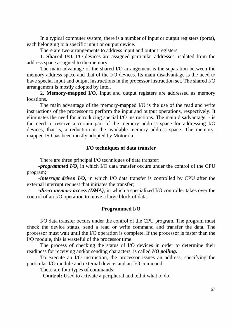
67
In a typical computer system, there is a number of input or output registers (ports), each belonging to a specific input or output device.
There are two arrangements to address input and output registers. 1. Shared I/O. I/O devices are assigned particular addresses, isolated from the
address space assigned to the memory. The main advantage of the shared I/O arrangement is the separation between the
memory address space and that of the I/O devices. Its main disadvantage is the need to have special input and output instructions in the processor instruction set. The shared I/O arrangement is mostly adopted by Intel.
2. Memory-mapped I/O. Input and output registers are addressed as memory locations.
The main advantage of the memory-mapped I/O is the use of the read and write instructions of the processor to perform the input and output operations, respectively. It eliminates the need for introducing special I/O instructions. The main disadvantage - is the need to reserve a certain part of the memory address space for addressing I/O devices, that is, a reduction in the available memory address space. The memory-mapped I/O has been mostly adopted by Motorola.
I/O techniques of data transfer
There are three principal I/O techniques of data transfer:
- programmed I/O, in which I/O data transfer occurs under the control of the CPU program;
- interrupt driven I/O, in which I/O data transfer is controlled by CPU after the external interrupt request that initiates the transfer;
- direct memory access (DMA), in which a specialized I/O controller takes over the control of an I/O operation to move a large block of data.
Programmed I/O
I/O data transfer occurs under the control of the CPU program. The program must check the device status, send a read or write command and transfer the data. The processor must wait until the I/O operation is complete. If the processor is faster than the I/O module, this is wasteful of the processor time. The process of checking the status of I/O devices in order to determine their readiness for receiving and/or sending characters, is called I/O polling.
To execute an I/O instruction, the processor issues an address, specifying the particular I/O module and external device, and an I/O command.
There are four types of commands: . Control: Used to activate a peripheral and tell it what to do.

68
. Test: Used to test various status conditions associated with an I/O module and its peripherals (if it is powered on, if the I/O operation is completed, if any errors occurred).
. Read: Causes the I/O module to obtain the word of data from the peripheral and place it in an internal buffer – data register and then to the data bus;
. Write: Causes the I/O module to take a word of data from the data bus and transmit it to the peripheral.
A flowchart of reading in a block of data: Issue read
command to I/Omodule
Read status ofI/O module
CPU -> I/O
I/O -> CPU
Check statusNot ready
Ready
Read word fromI/O module
Write word intomemory
Done
Next instruction
Yes
No
I/O -> CPU
Error
CPU -> memory
For each word that is read in, the processor must remain in status checking cycle until it determines that the word is available in the I/O module’s data register. This flowchart highlights the main disadvantage of this technique: it is a time-consuming process.
Interrupt-driven I/O
With interrupt driven I/O, the processor issues an I/O command, continues to execute other instructions, and is interrupted by the I/O module when the latter is ready to exchange data with the processor.
I/O module actions.
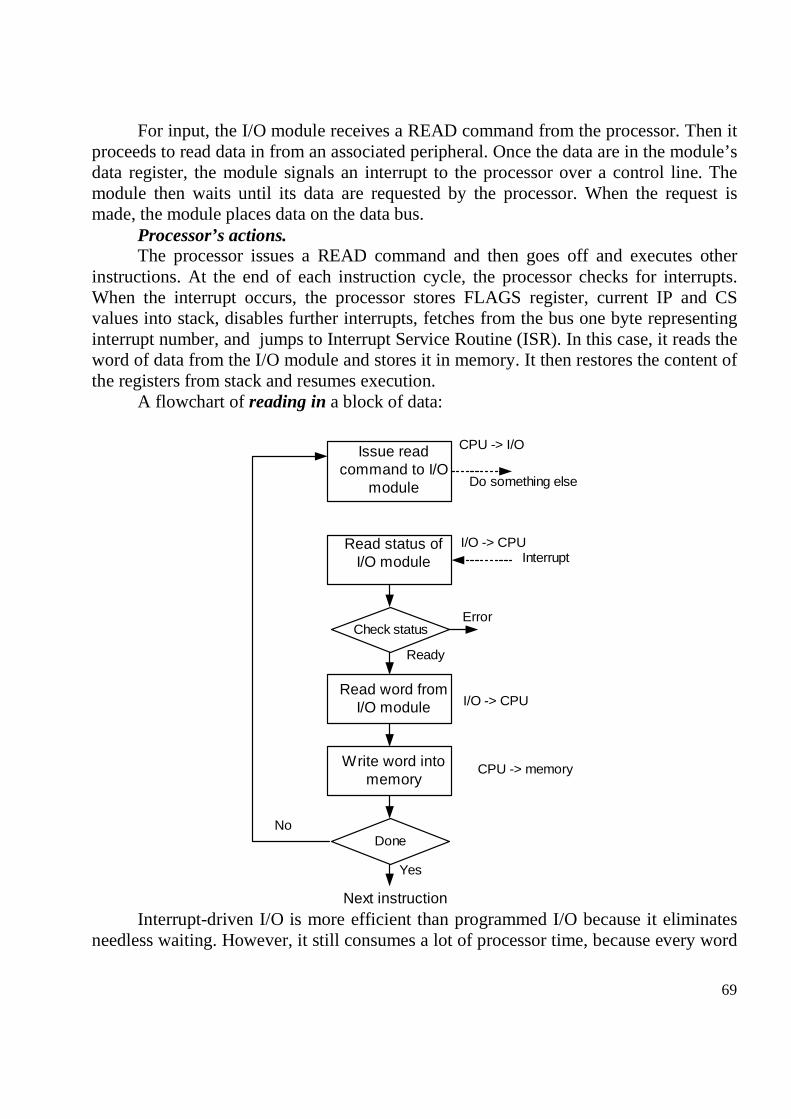
69
For input, the I/O module receives a READ command from the processor. Then it proceeds to read data in from an associated peripheral. Once the data are in the module’s data register, the module signals an interrupt to the processor over a control line. The module then waits until its data are requested by the processor. When the request is made, the module places data on the data bus.
Processor’s actions. The processor issues a READ command and then goes off and executes other
instructions. At the end of each instruction cycle, the processor checks for interrupts. When the interrupt occurs, the processor stores FLAGS register, current IP and CS values into stack, disables further interrupts, fetches from the bus one byte representing interrupt number, and jumps to Interrupt Service Routine (ISR). In this case, it reads the word of data from the I/O module and stores it in memory. It then restores the content of the registers from stack and resumes execution.
A flowchart of reading in a block of data:
Issue readcommand to I/O
module
Read status ofI/O module
CPU -> I/O
I/O -> CPU
Check status
Ready
Read word fromI/O module
Write word intomemory
Done
Next instruction
Yes
No
I/O -> CPU
Error
CPU -> memory
Do something else
Interrupt
Interrupt-driven I/O is more efficient than programmed I/O because it eliminates needless waiting. However, it still consumes a lot of processor time, because every word
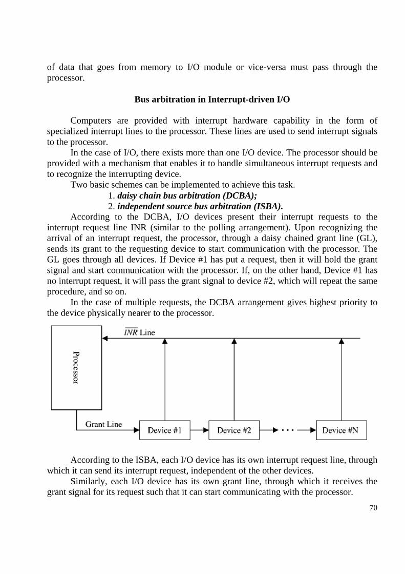
70
of data that goes from memory to I/O module or vice-versa must pass through the processor.
Bus arbitration in Interrupt-driven I/O Computers are provided with interrupt hardware capability in the form of
specialized interrupt lines to the processor. These lines are used to send interrupt signals to the processor.
In the case of I/O, there exists more than one I/O device. The processor should be provided with a mechanism that enables it to handle simultaneous interrupt requests and to recognize the interrupting device.
Two basic schemes can be implemented to achieve this task. 1. daisy chain bus arbitration (DCBA); 2. independent source bus arbitration (ISBA).
According to the DCBA, I/O devices present their interrupt requests to the interrupt request line INR (similar to the polling arrangement). Upon recognizing the arrival of an interrupt request, the processor, through a daisy chained grant line (GL), sends its grant to the requesting device to start communication with the processor. The GL goes through all devices. If Device #1 has put a request, then it will hold the grant signal and start communication with the processor. If, on the other hand, Device #1 has no interrupt request, it will pass the grant signal to device #2, which will repeat the same procedure, and so on.
In the case of multiple requests, the DCBA arrangement gives highest priority to the device physically nearer to the processor.
According to the ISBA, each I/O device has its own interrupt request line, through
which it can send its interrupt request, independent of the other devices. Similarly, each I/O device has its own grant line, through which it receives the
grant signal for its request such that it can start communicating with the processor.
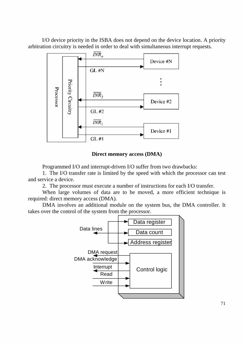
71
I/O device priority in the ISBA does not depend on the device location. A priority arbitration circuitry is needed in order to deal with simultaneous interrupt requests.
Direct memory access (DMA)
Programmed I/O and interrupt-driven I/O suffer from two drawbacks: 1. The I/O transfer rate is limited by the speed with which the processor can test
and service a device. 2. The processor must execute a number of instructions for each I/O transfer. When large volumes of data are to be moved, a more efficient technique is
required: direct memory access (DMA). DMA involves an additional module on the system bus, the DMA controller. It
takes over the control of the system from the processor.
Data register
Data count
Address register
Control logic
Data lines
DMA requestDMA acknowledge
InterruptRead
Write

72
When the processor wishes to read or write a block of data, it issues a command to the DMA controller, by sending the following information:
. If read or write is requested (read or write control lines).
. The address of the I/O device (data lines).
. The starting location in memory to read or write (it is stored in address register)
. The number of words to be read or written (send on data lines and stored in the data count register).
When the transfer is complete, The DMA controller sends an interrupt signal to the processor. Thus, the processor is involved only at the beginning and end of the transfer.
Issue read blockcommand to I/O
module
Read status ofDMA controller
CPU -> DMA
DMA -> CPU
Do somethingelse
Interrupt Direct memory access data transfer can be performed in burst mode or single
cycle mode. In burst mode, the DMA controller keeps control of the bus until all the data has
been transferred to (from) memory from (to) the peripheral device. This mode of transfer is needed for fast devices where data transfer cannot be stopped until the entire transfer is done.
In single-cycle mode (cycle stealing), the DMA controller relinquishes the bus after each transfer of one data word. This minimizes the amount of time that the DMA controller keeps the CPU from controlling the bus, but it requires that the bus request/acknowledge sequence be performed for every single transfer. This overhead can result in a degradation of the performance.
The following steps summarize the DMA operations: 1. DMA controller initiates data transfer. 2. Data is moved (increasing the address in memory, and reducing the count of
words to be moved). 3. When word count reaches zero, the DMA informs the CPU of the termination
by means of an interrupt. 4. The CPU regains access to the memory bus. A DMA controller may have multiple channels. Each channel has associated with
it an address register and a count register. To initiate a data transfer the device driver sets up the DMA channel’s address and count registers together with the direction of the
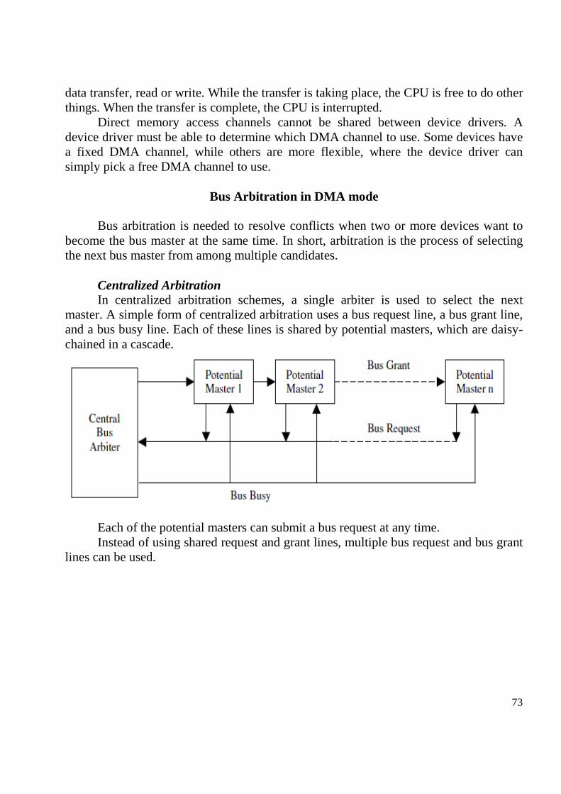
73
data transfer, read or write. While the transfer is taking place, the CPU is free to do other things. When the transfer is complete, the CPU is interrupted.
Direct memory access channels cannot be shared between device drivers. A device driver must be able to determine which DMA channel to use. Some devices have a fixed DMA channel, while others are more flexible, where the device driver can simply pick a free DMA channel to use.
Bus Arbitration in DMA mode
Bus arbitration is needed to resolve conflicts when two or more devices want to
become the bus master at the same time. In short, arbitration is the process of selecting the next bus master from among multiple candidates.
Centralized Arbitration In centralized arbitration schemes, a single arbiter is used to select the next
master. A simple form of centralized arbitration uses a bus request line, a bus grant line, and a bus busy line. Each of these lines is shared by potential masters, which are daisy-chained in a cascade.
Each of the potential masters can submit a bus request at any time. Instead of using shared request and grant lines, multiple bus request and bus grant
lines can be used.

74
Decentralized Arbitration In decentralized arbitration schemes, priority-based arbitration is usually used in a
distributed fashion. Each potential master has a unique arbitration number, which is used in resolving conflicts when multiple requests are submitted. For example, a conflict can always be resolved in favor of the device with the highest arbitration number. The question now is how to determine which device has the highest arbitration number? One method is that a requesting device would make its unique arbitration number available to all other devices. Each device compares that number with its own arbitration number. The device with the smaller number is always dismissed. Eventually, the requester with the highest arbitration number will survive and be granted bus access.
INPUT–OUTPUT INTERFACES
An interface is a data path between two separate devices in a computer system. Interface to buses can be classified based on the number of bits that are
transmitted at a given time to serial versus parallel ports. In a serial port, only 1 bit of data is transferred at a time. Mice and modems are usually connected to serial ports. A parallel port allows more than 1 bit of data to be processed at once. Printers are the most common peripheral devices connected to parallel ports.
A summary of the variety of buses and interfaces used in personal computers:
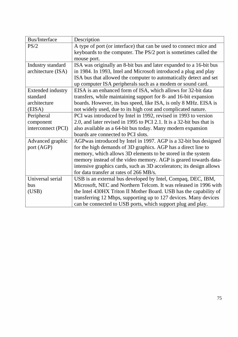
75
Bus/Interface Description PS/2 A type of port (or interface) that can be used to connect mice and
keyboards to the computer. The PS/2 port is sometimes called the mouse port.
Industry standard architecture (ISA)
ISA was originally an 8-bit bus and later expanded to a 16-bit bus in 1984. In 1993, Intel and Microsoft introduced a plug and play ISA bus that allowed the computer to automatically detect and set up computer ISA peripherals such as a modem or sound card.
Extended industry standard architecture (EISA)
EISA is an enhanced form of ISA, which allows for 32-bit data transfers, while maintaining support for 8- and 16-bit expansion boards. However, its bus speed, like ISA, is only 8 MHz. EISA is not widely used, due to its high cost and complicated nature.
Peripheral component interconnect (PCI)
PCI was introduced by Intel in 1992, revised in 1993 to version 2.0, and later revised in 1995 to PCI 2.1. It is a 32-bit bus that is also available as a 64-bit bus today. Many modern expansion boards are connected to PCI slots.
Advanced graphic port (AGP)
AGPwas introduced by Intel in 1997. AGP is a 32-bit bus designed for the high demands of 3D graphics. AGP has a direct line to memory, which allows 3D elements to be stored in the system memory instead of the video memory. AGP is geared towards data-intensive graphics cards, such as 3D accelerators; its design allows for data transfer at rates of 266 MB/s.
Universal serial bus (USB)
USB is an external bus developed by Intel, Compaq, DEC, IBM, Microsoft, NEC and Northern Telcom. It was released in 1996 with the Intel 430HX Triton II Mother Board. USB has the capability of transferring 12 Mbps, supporting up to 127 devices. Many devices can be connected to USB ports, which support plug and play.