
Interfacing Synchronous and Asynchronous Modules Within a High-Speed Pipeline
Upload
independentCategory
view
1download
0
Interfacing Synchronous and Asynchronous Modules Within aHigh-Speed Pipeline �Allen E. Sjogren and Chris J. MyersElectrical Engineering DepartmentUniversity of UtahSalt Lake City, UT 84112fsjogren, [email protected] paper describes a new technique for integrating asynchronous modules within a high-speedsynchronous pipeline. Our design eliminates potential metastability problems by using a clock gener-ated by a stoppable ring oscillator, which is capable of driving the large clock load found in present daymicroprocessors. Using the ATACS design tool, we designed highly optimized transistor-level circuitsto control the ring oscillator and generate the clock and handshake signals with minimal overhead.Our interface architecture requires no redesign of the synchronous circuitry. Incorporating asyn-chronous modules in a high-speed pipeline improves performance by exploiting data-dependent delayvariations. Since the speed of the synchronous circuitry tracks the speed of the ring oscillator underdi�erent processes, temperatures, and voltages, the entire chip operates at the speed dictated by thecurrent operating conditions, rather than being governed by the worst-case conditions. These twofactors together can lead to a signi�cant improvement in average-case performance. The interfacedesign is tested using the 0:6�m HP CMOS14B process in HSPICE.1: IntroductionCircuit designers are continually pushing the envelope in the race to design faster, more powerfulmicroprocessors. Present day synchronous microprocessors have clock speeds in excess of 300MHz.Distributing a clock signal to all areas of a large chip at this speed with minimal clock skew is atask of growing complexity. The circuit area, power consumption, and design time needed to drivethe clock signal to all parts of the chip without signi�cant clock skew are overwhelming [4, 1]. Theclock period must also be long enough to accommodate the worst-case delay in every module in theworst process run under the highest temperature and lowest supply voltage. Thus, any speed gainedfrom completing an operation early is lost waiting for the clock, which runs at a rate dictated by theslowest component running in the worst operating conditions.Asynchronous circuits have attracted new interest as an alternative to synchronous circuits dueto their potential to achieve average-case performance while eliminating the global synchronizingclock signal. In asynchronous circuits, an operation begins when all the operations that it dependson have occurred, rather than when the next clock signal arrives. This allows asynchronous cir-cuits to operate as fast as possible, taking advantage of delay variations due to data dependenciesand operating conditions. Thus, well-designed asynchronous circuits can achieve better average op-erating frequencies than synchronous circuits operating at frequencies dictated by the worst-caseconditions. Asynchronous circuits also eliminate the global clock, which can reduce circuit area,power consumption, and design time.�This research is supported by a grant from Intel Corporation and NSF CAREER award MIP-9625014.
The advantages of synchronous circuits though, cannot be overlooked. Some of these advantagesinclude: ease of implementing sequential circuits, simplicity in dealing with hazards, and maturedesign methods and tools. Also, asynchronous circuits come with their own set of challenges. Sincethere is no global clock to tell when outputs are stable, asynchronous circuits must prevent anyhazards, or glitches, on their outputs. A false transition on an output from one circuit can causethe next circuit to prematurely operate on meaningless results. Additional circuitry is used toprevent hazards. This circuitry can increase the area and delay of the asynchronous circuit. Inorder to achieve average-case performance, asynchronous circuits require additional circuitry tostart each computation and detect the completion of operations. The additional circuitry requiredfor asynchronous design can, in some cases, make the average-case delay of an asynchronous circuitbecome larger than the worst-case delay for the comparable synchronous circuit.The ideal system, therefore, uses a combination of both synchronous and asynchronous circuits.The most appropriate timing discipline could then be applied to each module. Combining the twotechnologies poses a great challenge. The key di�culty is found in trying to avoid synchronizationfailure. If a clock edge from a synchronous circuit changes too close in time to data arriving froman asynchronous circuit, the circuit may enter a metastable state [2]. A metastable state is a stablestate of the circuit, which is at neither a logic 0 or logic 1 level, but rather lies somewhere in-between.In this case, the data latched from the asynchronous circuit may be at an indeterminate value. Thecircuit can reside in this state for a non-deterministic amount of time. If this metastable state persistsuntil the next clock cycle, the indeterminate data may be interpreted as either a logic-0 or a logic-1 bydi�erent subsequent logic stages. This can lead the system into an illegal or incorrect state causingthe system to fail. Such a failure is traditionally called a synchronization failure [8]. If care is nottaken, the integration of more asynchronous circuitry and communication into a system can lead toan unacceptable probability of synchronization failure.Many techniques have been devised to address the metastability problem and avoid synchron-ization failure when interfacing between synchronous and asynchronous modules. The simplestapproach is to double-latch asynchronous signals being sampled by a synchronous module. Thisincreases the time allowed for a metastable condition to resolve. The cost though is an extra cycledelay when communicating data from an asynchronous module to a synchronous module, even whenthere is no metastability. This scheme only minimizes the probability and does not eliminate thepossibility of synchronization failure, as there is some chance that a metastable condition could per-sist longer than two clock cycles. To address this problem, pipeline synchronization can be used.Pipeline synchronization extends the double-latching idea by inserting more pipeline latches betweenthe asynchronous and synchronous module [9]. While each added latch reduces the probability offailure, it increases the latency of communication. Also, no matter how many latches are added, someprobability of failure always remains. Therefore, this scheme only works when large communicationlatencies and some failures can be tolerated. This is true of networks, but it is not true of high-speedmicroprocessor pipelines.To completely eliminate synchronization failures, it is necessary to be able to force the synchronoussystem to wait an arbitrary amount of time for a metastable input to stabilize. In order for thesynchronous circuit to wait, it is necessary for the asynchronous module to be able to cause thesynchronous circuit's clock to stop when it is either not ready to communicate new data or notready to receive new data. Stoppable clocks date back to the 1960s with work done by Chuck Seitzwhich was used in early display systems and other products of the Evans and Sutherland company[10, 8]. A stoppable clock is typically constructed from a gated ring oscillator as shown in Figure 1.The basic operation is that when the RUN signal is activated, the clock operates at a nominal rateset by the number of inverters in the ring. To stop the clock, the RUN signal must be deactivatedbetween two rising clock edges. The clock restarts as soon as the RUN signal is reactivated. In otherwords, the clock can be stopped synchronously and restarted asynchronously.Numerous researchers have developed globally asynchronous locally synchronous (GALS) archi-tectures based on the idea of a stoppable clock [8, 11, 3, 7, 5, 12]. In each of these approaches,communication between modules is done asynchronously using request/acknowledge protocols whilecomputation is done synchronously within the modules using a locally generated clock. The basic

RUNCLK
Odd number of inverters
Figure 1. A stoppable ring oscillator clock.structure of such a module is shown in Figure 2. The module's internal clock is stopped when itmust wait for data to arrive from, or to be accepted by, the other modules. The schemes proposed in[11, 7, 5, 12] allow an asynchronous module to request to communicate data to a synchronous mod-ule at arbitrary times. A mutual exclusion element is used to guarantee that a synchronous moduleeither receives data from a asynchronous unit or a pulse from the clock generator, but never both atthe same time. If the asynchronous data arrives too close to the next clock pulse, both the data andthe clock pulse may be delayed waiting for the metastability to resolve, before determining which isto be handled �rst. The schemes proposed in [8, 3] assume that the synchronous unit determineswhen data is to be transferred to/from the asynchronous modules. This assumption eliminates theneed for a mutual exclusion element, since the decision to wait on asynchronous communication issynchronized to the internal clock.Synchronous
ModuleData in Data out
CLK
Local
Clock
Generator
ReqIn
AckIn
ReqOut
AckOut
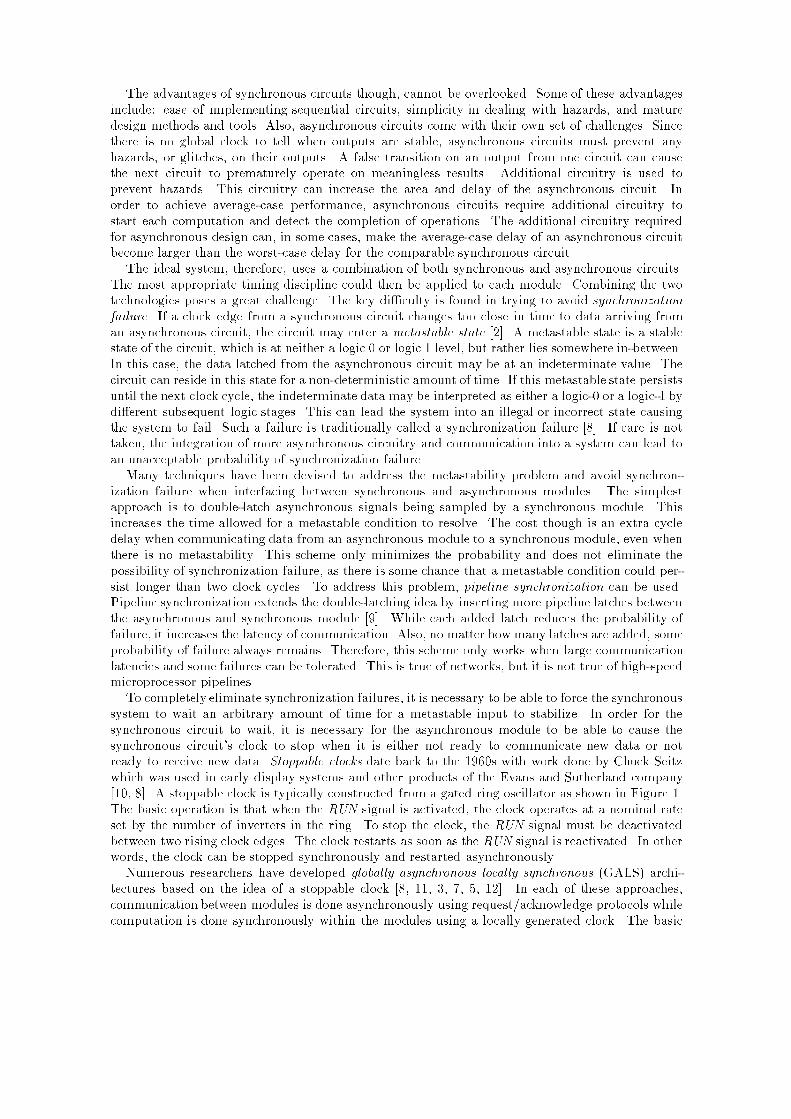
Figure 2. Basic module of a GALS architecture.This paper describes a new interface methodology for globally synchronous locally asynchronousarchitectures. At present almost every microprocessor is synchronous and pipelined. One viableapproach to increasing a microprocessor's speed for a given process is to replace the slowest pipelinestages with asynchronous modules that have a better average-case performance. If the interfacingproblem can be addressed, this allows a performance gain without redesigning the entire chip.While the entire system communicates synchronously, one or more local modules may computeasynchronously. In other words, the system is globally synchronous locally asynchronous.Our interface methodology, while similar to the GALS architectures described in [8, 3], allowsfor stages in high-speed pipelines to be either synchronous or asynchronous as depicted in Figure 3.In this paper, we use true single-phase clocking with Yuan/Svenson latches as in the Alpha [4],con�gured in such a way that data is latched into the next stage on the rising edge of the clock.The CLK signal is generated using a stoppable ring oscillator. Besides being used to sequence databetween pipeline stages, the CLK signal is also used to generate the handshake protocol that controlsthe asynchronous modules. The interface controller is composed of the stoppable clock generator,one handshake control circuit for each asynchronous module, and an AND gate to collect the ACKsignals to generate the RUN signal.The circuit behaviour of the interface controller is as follows. Shortly after the rising edge ofthe CLK signal, the RUN signal is set low. The RUN signal is set high again only after all the
asynchronous modules have completed their computation. Since data moves in and out of eachasynchronous module with every cycle in the pipeline, no mutual exclusion elements are necessary.Our interface controller uses new, highly optimized transistor-level circuits designed using theATACS design tool [6] to control the ring oscillator and generate the clock and handshake signals.By building the stoppable ring oscillator clock out of a clock bu�er network, our clock is capableof driving the large capacitive loads found in present day microprocessors. Our interface techniquedoes not require any redesign of the synchronous circuitry. Utilizing a ring-oscillator to generate theclock signal improves the performance of the circuit by allowing the integration of faster asynchronousmodules in the pipeline. Since the speed of the synchronous circuitry tracks the speed of the ringoscillator under di�erent processes, temperature, and voltage, the entire chip operates at the speeddictated by the current operating conditions, rather than being governed by the worst-case conditions.These two factors together can lead to a signi�cant improvement in average-case performance.ControllerHandshake
ControllerHandshake
Interface
Controller
Sync AsyncModule Sync
Module
AsyncModule
Reg. Reg. Reg. Reg.
ModuleREQ ACK REQ ACK
CLK
RUN
ClockStoppableAsync / Sync
Figure 3. Proposed interface methodology.This paper is divided into six sections. Section two describes the design of the basic circuits andoperation of the interface controller. Section three presents an analysis of a clock bu�er networksimilar to the one used in the 300 MHz DEC Alpha [1]. In section four, we incorporate the clockbu�er network into our interface controller so that it can be used in modern high-speed pipelines. Insection �ve, we add a pipeline latch and modify the interface protocol to reduce the control overhead.Section six gives our conclusions.2: Basic interface controllerThis section describes the basic circuits and operation of our asynchronous/synchronous interfacecontroller. We designed the interface circuits described here using ATACS [6], a tool for the synthesisof timed circuits. Timed circuits are a class of circuits in which speci�ed timing information isutilized in the design procedure to optimize the implementation. The resulting circuit is not onlymore e�cient, but ATACS also allows us to automatically check our timing assumptions. Sincethe circuits in the interface controller are highly time dependent, they cannot be designed usingtraditional untimed asynchronous design methods.
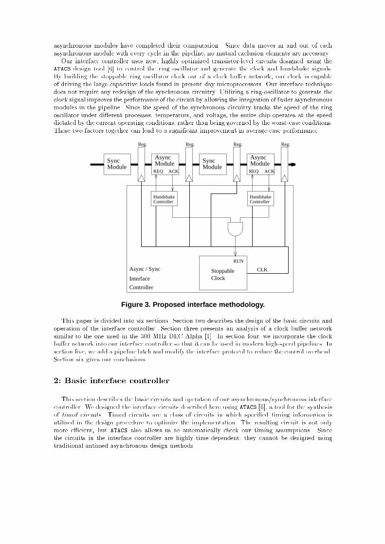
The interface controller is composed of two separate sections: the stoppable clock and the hand-shake controllers. Our stoppable clock, shown in Figure 4, is somewhat di�erent from the traditionalone [8]. Rather than using an AND gate to control the starting and stopping of the clock, we use astate-holding gate. Our state-holding gate sets CLK high when both RUN and PRECLK are high,and it resets CLK when PRECLK is low. When synthesizing this gate, we discovered a timingassumption in the original design that requires the RUN signal to be active until CLK goes low.In order to give more exibility in setting and resetting the RUN signal, we decided to remove thistiming assumption, resulting in the gate shown in Figure 4. In our implementation, the RUN signalcan be deactivated at any time after CLK goes high until just before the next rising clock edge. Asimilar observation is made in [10], and they add a pair of cross-coupled NAND gates to latch theclock in one of their designs. The overhead of the cross-coupled NAND gates is minimized in ourapproach by implementing the circuit at the transistor-level. The rest of the stoppable clock is a ringoscillator composed of inverters and one NAND gate which is used to set CLK to low during reset.The number of inverters should be set such that the delay through the ring oscillator is greater thanthe worst-case path through the slowest synchronous module.CLK
Reset
RUN
15 Inverters
PRECLK
weak
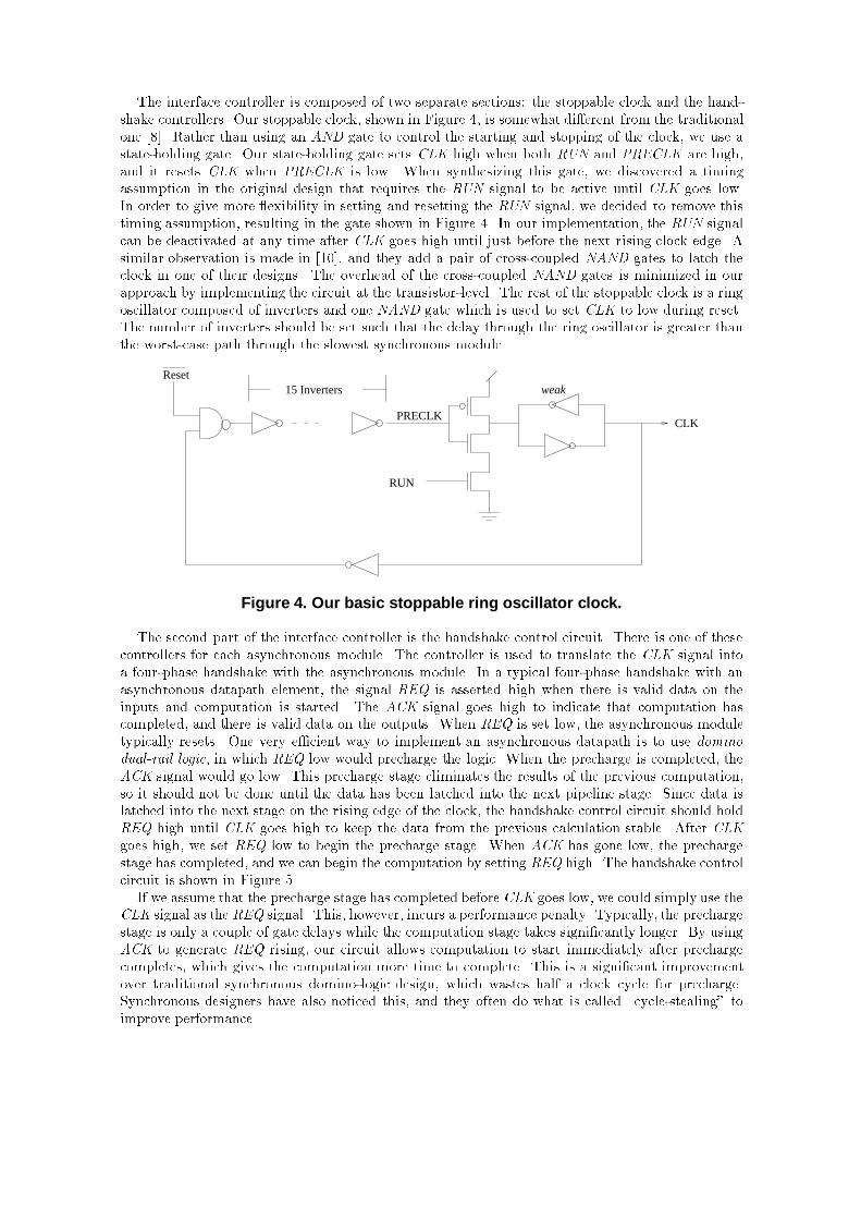
Figure 4. Our basic stoppable ring oscillator clock.The second part of the interface controller is the handshake control circuit. There is one of thesecontrollers for each asynchronous module. The controller is used to translate the CLK signal intoa four-phase handshake with the asynchronous module. In a typical four-phase handshake with anasynchronous datapath element, the signal REQ is asserted high when there is valid data on theinputs and computation is started. The ACK signal goes high to indicate that computation hascompleted, and there is valid data on the outputs. When REQ is set low, the asynchronous moduletypically resets. One very e�cient way to implement an asynchronous datapath is to use dominodual-rail logic, in which REQ low would precharge the logic. When the precharge is completed, theACK signal would go low. This precharge stage eliminates the results of the previous computation,so it should not be done until the data has been latched into the next pipeline stage. Since data islatched into the next stage on the rising edge of the clock, the handshake control circuit should holdREQ high until CLK goes high to keep the data from the previous calculation stable. After CLKgoes high, we set REQ low to begin the precharge stage. When ACK has gone low, the prechargestage has completed, and we can begin the computation by setting REQ high. The handshake controlcircuit is shown in Figure 5.If we assume that the precharge stage has completed before CLK goes low, we could simply use theCLK signal as the REQ signal. This, however, incurs a performance penalty. Typically, the prechargestage is only a couple of gate delays while the computation stage takes signi�cantly longer. By usingACK to generate REQ rising, our circuit allows computation to start immediately after prechargecompletes, which gives the computation more time to complete. This is a signi�cant improvementover traditional synchronous domino-logic design, which wastes half a clock cycle for precharge.Synchronous designers have also noticed this, and they often do what is called \cycle-stealing" toimprove performance.
From stoppableclock
ACK
Reset
REQ
CLK
From async
module
weak
To stoppableclock
To async
module
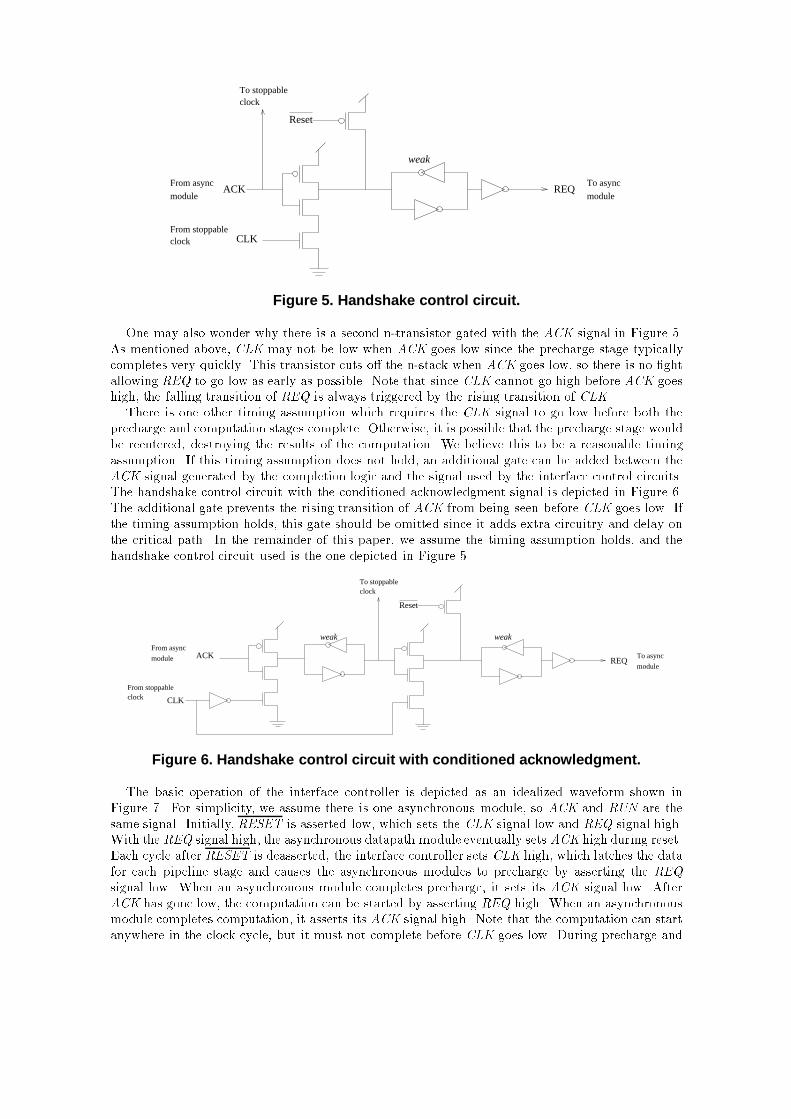
Figure 5. Handshake control circuit.One may also wonder why there is a second n-transistor gated with the ACK signal in Figure 5.As mentioned above, CLK may not be low when ACK goes low since the precharge stage typicallycompletes very quickly. This transistor cuts o� the n-stack when ACK goes low, so there is no �ghtallowing REQ to go low as early as possible. Note that since CLK cannot go high before ACK goeshigh, the falling transition of REQ is always triggered by the rising transition of CLK.There is one other timing assumption which requires the CLK signal to go low before both theprecharge and computation stages complete. Otherwise, it is possible that the precharge stage wouldbe reentered, destroying the results of the computation. We believe this to be a reasonable timingassumption. If this timing assumption does not hold, an additional gate can be added between theACK signal generated by the completion logic and the signal used by the interface control circuits.The handshake control circuit with the conditioned acknowledgment signal is depicted in Figure 6.The additional gate prevents the rising transition of ACK from being seen before CLK goes low. Ifthe timing assumption holds, this gate should be omitted since it adds extra circuitry and delay onthe critical path. In the remainder of this paper, we assume the timing assumption holds, and thehandshake control circuit used is the one depicted in Figure 5.From stoppableclock
module
From async
CLK
ACK
weak
Reset
REQ
weak
To stoppableclock
To async
module
Figure 6. Handshake control circuit with conditioned acknowledgment.The basic operation of the interface controller is depicted as an idealized waveform shown inFigure 7. For simplicity, we assume there is one asynchronous module, so ACK and RUN are thesame signal. Initially, RESET is asserted low, which sets the CLK signal low and REQ signal high.With the REQ signal high, the asynchronous datapath module eventually sets ACK high during reset.Each cycle after RESET is deasserted, the interface controller sets CLK high, which latches the datafor each pipeline stage and causes the asynchronous modules to precharge by asserting the REQsignal low. When an asynchronous module completes precharge, it sets its ACK signal low. AfterACK has gone low, the computation can be started by asserting REQ high. When an asynchronousmodule completes computation, it asserts its ACK signal high. Note that the computation can startanywhere in the clock cycle, but it must not complete before CLK goes low. During precharge and

computation, the CLK signal goes low and prepares to go high. If any of the asynchronous moduleshave not asserted their ACK signal, the rising edge of the CLK is delayed until all the asynchronousmodules have completed their computation.ACK
REQ
CLK
Reset
Figure 7. Idealized waveform for the basic interface controller.We simulated the basic interface controller in HSPICE using the 0:6�m HP CMOS14B process.This process is used for a 120 MHz HP PA-7200 RISC microprocessor. Therefore, we set the ringoscillator clock to run at approximately 120 MHz worst-case by using 19 gates in the ring (1 NANDgate, 16 inverters, the clock stopping gate, and its staticizer). We modeled the datapath using a chainof domino bu�ers as shown in Figure 8. This circuit has the property that after REQ goes high,ACK goes high after a delay through the entire bu�er chain while after REQ goes low, ACK goes lowafter the delay of one domino bu�er. Two waveforms are shown in Figure 9 under worst-case processand operating conditions. The �rst shows operation when the asynchronous unit �nishes early. Inthis case, the CLK signal runs at a �xed rate. The second shows operation when the asynchronousunit �nishes late which stops the clock until after ACK goes high.ACK
REQ
Figure 8. Domino buffer chain used to model the datapath.
Figure 9. HSPICE results for the basic interface controller.

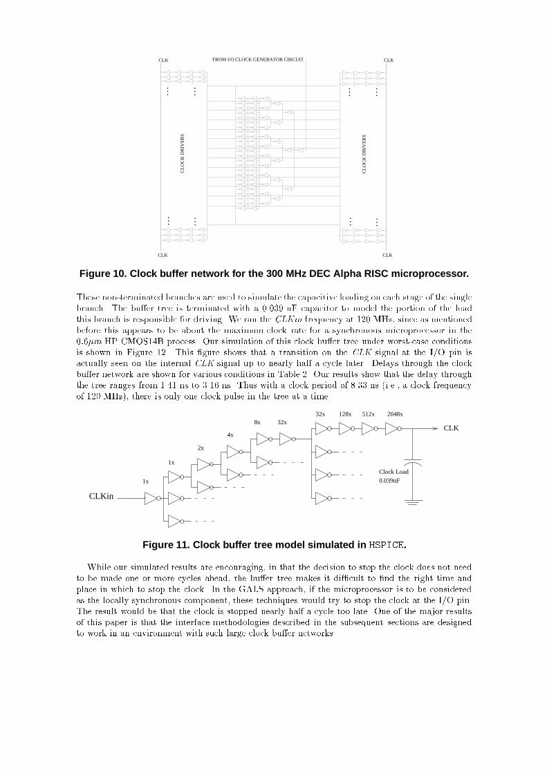
Table 1 shows the tabulated delay results under four di�erent process and operating conditions.The �rst column shows the worst-case conditions (high temperature, low voltage, worst-case n- andp-type transistors). The middle two columns show more typical process and operating conditionsrunning hot and cool, respectively. The last column shows the best-case conditions. The �rst rowshows the delay of the ring oscillator with RUN (i.e., ACK) set high early. The frequency of thering oscillator clock varies from 122 MHz to 285 MHz. Since the ring oscillator is built on the samechip as the rest of the circuits, the variation in delay of the other circuits track the variation in delayof the ring oscillator. This translates directly into an improvement in performance for not only theasynchronous circuitry, but also the synchronous circuitry. In other words, if the chip becomes hot,both the ring oscillator and logic circuits slow down. If the chip becomes cool, both the ring oscillatorand logic circuits speed up. The same e�ect would take place for voltage and process variations.The next three rows show the delays in the interface control gates. The last row shows the amountof time which is available from the clock cycle for precharge and computation without stopping theclock. This is calculated by subtracting the control overhead from the minimum ring oscillator delayunder the given conditions. This shows that the control overhead of using an asynchronous moduleis between 25 and 35 percent of the cycle. This means that an asynchronous module needs to havean average-case performance that is at least 25 percent less than the worst-case performance of thecomparable synchronous module in order to see a performance gain.Table 1. Clock period break down for the basic interface controller.Temperature 90�C 70�C 25�C 0�CVoltage 3.0V 3.3V 3.3V 3.6VProcess WCNWCP TYPICAL TYPICAL BCNBCPCLK" ! CLK " 8.22 ns 5.42 ns 4.02 ns 3.51 nsCLK" ! REQ # 0.99 ns 0.72 ns 0.58 ns 0.52 nsACK# ! REQ " 0.38 ns 0.28 ns 0.22 ns 0.19 nsACK" ! CLK " 0.75 ns 0.64 ns 0.57 ns 0.48 nsPrecharge & computation 6.10 ns 3.77 ns 2.65 ns 2.32 ns3: Clock bu�er tree analysisIn order to stop the clock signal in a modern high-speed microprocessor, one must �rst understandhow the clock signal is bu�ered. Ideally, a clock signal is distributed to every point in the chip atnearly the same time, in phase, with fast rise and fall times. However, this is not an easy task.The capacitive load seen by the clock can be astronomical. For example, the 300 MHz DEC Alphamicroprocessor has a clock load of 3.75nF [1]. In order to drive such a substantial load, the clock isbu�ered through 10 stages fanning out to 96 branches. The clock bu�er tree is depicted in Figure 10[1]. The crystal clock from the I/O pin is fed into the trunk of the network, and it is distributed to allpoints through bu�ered branches. There are shorting bars between the outputs of each bu�er stage,which smooth out any asymmetry in the incoming wavefront. The result is that each level of invertersin the clock tree is equivalent to a single parallel n-transistor and a single parallel p-transistor. The�nal CLK driver inverter has an equivalent transistor width of 58 cm.A concern with the bu�er tree is the amount of delay through it for one clock pulse. If the delay islong enough, multiple clock pulses would be propagating through the tree. In this case, if the clockneeds to be stopped, the decision may need to be made one or more clock cycles in advance. Tomeasure the severity of this problem, we measured the delay through a clock bu�er network similarto the 300 MHz DEC Alpha's. Since all branches are identical, we recreated one complete branchof the 96 branches and simulated it using HSPICE. The part of the clock tree simulated is shownin Figure 11. The non-terminated branches fan out to make up the other 95 individual branches.
. . .
CL
OC
K D
RIV
ER
S
. . .
. . .
. . .
. . .
CL
OC
K D
RIV
ER
S
. . .
. . .
. . .
FROM I/O CLOCK GENERATOR CIRCUITCLK CLK
CLK CLK
Figure 10. Clock buffer network for the 300 MHz DEC Alpha RISC microprocessor.These non-terminated branches are used to simulate the capacitive loading on each stage of the singlebranch. The bu�er tree is terminated with a 0.039 nF capacitor to model the portion of the loadthis branch is responsible for driving. We ran the CLKin frequency at 120 MHz, since as mentionedbefore this appears to be about the maximum clock rate for a synchronous microprocessor in the0:6�m HP CMOS14B process. Our simulation of this clock bu�er tree under worst-case conditionsis shown in Figure 12. This �gure shows that a transition on the CLK signal at the I/O pin isactually seen on the internal CLK signal up to nearly half a cycle later. Delays through the clockbu�er network are shown for various conditions in Table 2. Our results show that the delay throughthe tree ranges from 1.41 ns to 3.16 ns. Thus with a clock period of 8.33 ns (i.e., a clock frequencyof 120 MHz), there is only one clock pulse in the tree at a time.CLK
CLKin
1x
1x
2x
4x
8x 32x32x 128x 512x 2048x
Clock Load
0.039nF
Figure 11. Clock buffer tree model simulated in HSPICE.While our simulated results are encouraging, in that the decision to stop the clock does not needto be made one or more cycles ahead, the bu�er tree makes it di�cult to �nd the right time andplace in which to stop the clock. In the GALS approach, if the microprocessor is to be consideredas the locally synchronous component, these techniques would try to stop the clock at the I/O pin.The result would be that the clock is stopped nearly half a cycle too late. One of the major resultsof this paper is that the interface methodologies described in the subsequent sections are designedto work in an environment with such large clock bu�er networks.
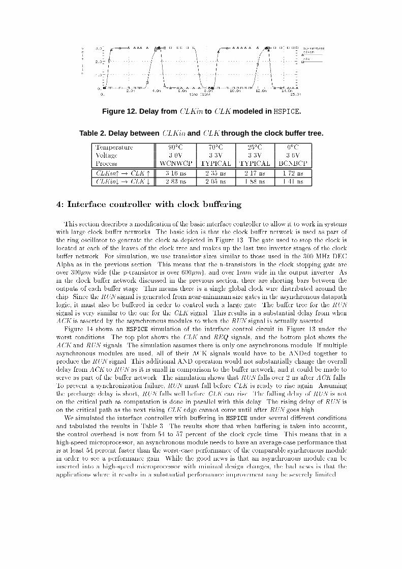
Figure 12. Delay from CLKin to CLK modeled in HSPICE.
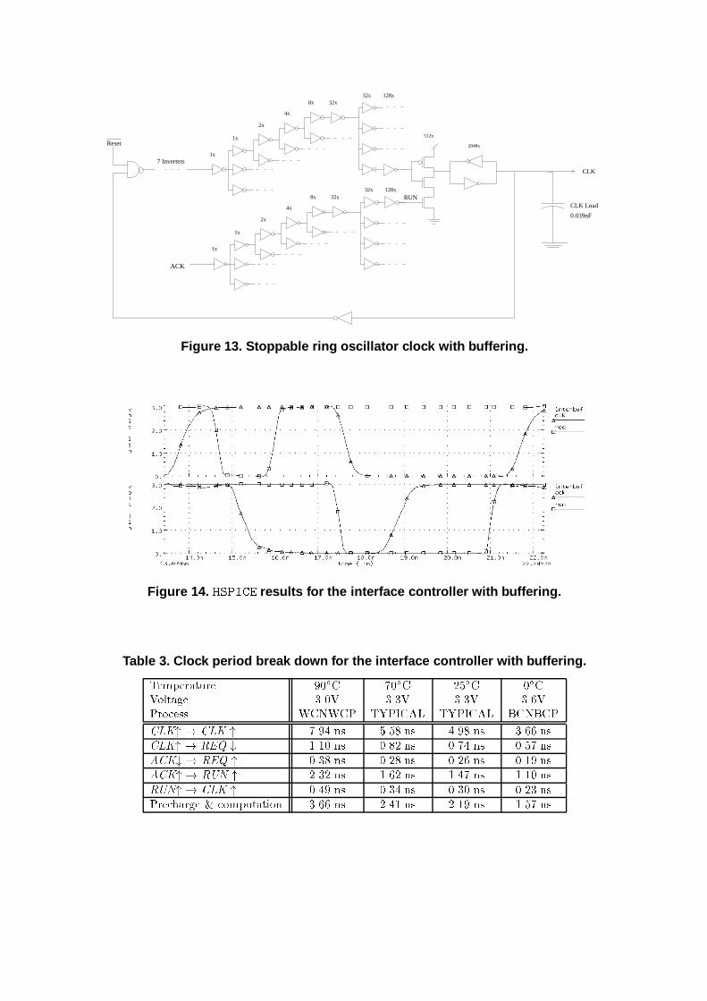
Table 2. Delay between CLKin and CLK through the clock buffer tree.Temperature 90�C 70�C 25�C 0�CVoltage 3.0V 3.3V 3.3V 3.6VProcess WCNWCP TYPICAL TYPICAL BCNBCPCLKin" ! CLK " 3.16 ns 2.35 ns 2.17 ns 1.72 nsCLKin# ! CLK # 2.83 ns 2.05 ns 1.88 ns 1.41 ns4: Interface controller with clock bu�eringThis section describes a modi�cation of the basic interface controller to allow it to work in systemswith large clock bu�er networks. The basic idea is that the clock bu�er network is used as part ofthe ring oscillator to generate the clock as depicted in Figure 13. The gate used to stop the clock islocated at each of the leaves of the clock tree and makes up the last two inverter stages of the clockbu�er network. For simulation, we use transistor sizes similar to those used in the 300 MHz DECAlpha as in the previous section. This means that the n-transistors in the clock stopping gate areover 300�m wide (the p-transistor is over 600�m), and over 1mm wide in the output inverter. Asin the clock bu�er network discussed in the previous section, there are shorting bars between theoutputs of each bu�er stage. This means there is a single global clock wire distributed around thechip. Since the RUN signal is generated from near-minimum size gates in the asynchronous datapathlogic, it must also be bu�ered in order to control such a large gate. The bu�er tree for the RUNsignal is very similar to the one for the CLK signal. This results in a substantial delay from whenACK is asserted by the asynchronous modules to when the RUN signal is actually asserted.Figure 14 shows an HSPICE simulation of the interface control circuit in Figure 13 under theworst conditions. The top plot shows the CLK and REQ signals, and the bottom plot shows theACK and RUN signals. The simulation assumes there is only one asynchronous module. If multipleasynchronous modules are used, all of their ACK signals would have to be ANDed together toproduce the RUN signal. This additional AND operation would not substantially change the overalldelay from ACK to RUN as it is small in comparison to the bu�er network, and it could be made toserve as part of the bu�er network. The simulation shows that RUN falls over 2 ns after ACK falls.To prevent a synchronization failure, RUN must fall before CLK is ready to rise again. Assumingthe precharge delay is short, RUN falls well before CLK can rise. The falling delay of RUN is noton the critical path as computation is done in parallel with this delay. The rising delay of RUN ison the critical path as the next rising CLK edge cannot come until after RUN goes high.We simulated the interface controller with bu�ering in HSPICE under several di�erent conditionsand tabulated the results in Table 3. The results show that when bu�ering is taken into account,the control overhead is now from 54 to 57 percent of the clock cycle time. This means that in ahigh-speed microprocessor, an asynchronous module needs to have an average-case performance thatis at least 54 percent faster than the worst-case performance of the comparable synchronous modulein order to see a performance gain. While the good news is that an asynchronous module can beinserted into a high-speed microprocessor with minimal design changes, the bad news is that theapplications where it results in a substantial performance improvement may be severely limited.
RUN
ACK
CLK
512x
2048x
1x
1x
2x
4x
8x 32x32x 128x
1x
1x
2x
4x
8x 32x32x 128x
7 Inverters
Reset
CLK Load
0.039nF
Figure 13. Stoppable ring oscillator clock with buffering.
Figure 14. HSPICE results for the interface controller with buffering.
Table 3. Clock period break down for the interface controller with buffering.Temperature 90�C 70�C 25�C 0�CVoltage 3.0V 3.3V 3.3V 3.6VProcess WCNWCP TYPICAL TYPICAL BCNBCPCLK" ! CLK " 7.94 ns 5.58 ns 4.98 ns 3.66 nsCLK" ! REQ # 1.10 ns 0.82 ns 0.74 ns 0.57 nsACK# ! REQ " 0.38 ns 0.28 ns 0.26 ns 0.19 nsACK" ! RUN " 2.32 ns 1.62 ns 1.47 ns 1.10 nsRUN" ! CLK " 0.49 ns 0.34 ns 0.30 ns 0.23 nsPrecharge & computation 3.66 ns 2.41 ns 2.19 ns 1.57 ns
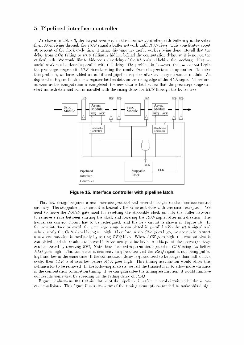
5: Pipelined interface controllerAs shown in Table 3, the largest overhead in the interface controller with bu�ering is the delayfrom ACK rising through the RUN signal's bu�er network until RUN rises. This constitutes about30 percent of the clock cycle time. During this time, no useful work is being done. Recall that thedelay from ACK falling to RUN falling is hidden behind the computation delay, so it is not on thecritical path. We would like to hide the rising delay of the RUN signal behind the precharge delay, souseful work can be done in parallel with this delay. The problem is, however, that we cannot beginthe precharge stage until CLK rises latching the results from the previous computation. To solvethis problem, we have added an additional pipeline register after each asynchronous module. Asdepicted in Figure 15, this new register latches data on the rising edge of the ACK signal. Therefore,as soon as the computation is completed, the new data is latched, so that the precharge stage canstart immediately and run in parallel with the rising delay for RUN through the bu�er tree.Reg. Reg.Reg.
ControllerHandshake
ControllerHandshake
SyncModule
AsyncModule
Reg. Reg.
REQ ACK
CLK
RUN
ClockStoppable
Interface
Controller
Pipelined
Sync AsyncModule
Reg.
ModuleREQ ACK
Figure 15. Interface controller with pipeline latch.This new design requires a new interface protocol and several changes to the interface controlcircuitry. The stoppable clock circuit is basically the same as before with one small exception. Weneed to move the NAND gate used for resetting the stoppable clock up into the bu�er networkto remove a race between starting the clock and lowering the RUN signal after initialization. Thehandshake control circuit has to be redesigned, and the new circuit is shown in Figure 16. Inthe new interface protocol, the precharge stage is completed in parallel with the RUN signal andsubsequently the CLK signal being set high. Therefore, when CLK goes high, we are ready to starta new computation immediately by setting REQ high. When ACK goes high, the computation iscompleted, and the results are latched into the new pipeline latch. At this point, the precharge stagecan be started by resetting REQ. Note there is an extra p-transistor gated on CLK being low beforeREQ goes high. This transistor is necessary to guarantee that the REQ signal is not being pulledhigh and low at the same time. If the computation delay is guaranteed to be longer than half a clockcycle, then CLK is always low before ACK goes high. This timing assumption would allow thisp-transistor to be removed. In the following analysis, we left the transistor in to allow more variancein the computation completion timing. If we can guarantee the timing assumption, it would improveour results somewhat by speeding up the falling delay of REQ.Figure 17 shows an HSPICE simulation of the pipelined interface control circuit under the worst-case conditions. This �gure illustrates some of the timing assumptions needed to make this design
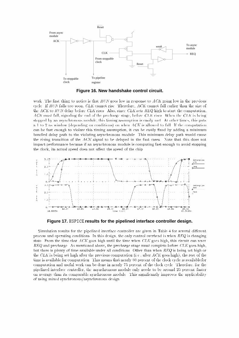
Reset
REQ
clockFrom stoppable
From asyncmodule
To asyncmodule
CLK
ACK
register
To pipelineTo stoppableclock
Reset
weak
Figure 16. New handshake control circuit.work. The �rst thing to notice is that RUN goes low in response to ACK going low in the previouscycle. If RUN falls too soon, CLK cannot rise. Therefore, ACK cannot fall earlier than the size ofthe ACK to RUN delay before CLK rises. Also, since CLK sets REQ high to start the computation,ACK must fall, signaling the end of the precharge stage, before CLK rises. When the CLK is beingstopped by an asynchronous module, this timing assumption is easily met. At other times, this putsa 1 to 2 ns window (depending on conditions) on when ACK is allowed to fall. If the computationcan be fast enough to violate this timing assumption, it can be easily �xed by adding a minimumbundled delay path to the violating asynchronous module. This minimum delay path would causethe rising transition of the ACK signal to be delayed in the fast cases. Note that this does notimpact performance because if an asynchronous module is computing fast enough to avoid stoppingthe clock, its actual speed does not a�ect the speed of the chip.Figure 17. HSPICE results for the pipelined interface controller design.Simulation results for the pipelined interface controller are given in Table 4 for several di�erentprocess and operating conditions. In this design, the only control overhead is when REQ is changingstate. From the time that ACK goes high until the time when CLK goes high, this circuit can resetREQ and precharge. As mentioned above, the precharge stage must complete before CLK goes high,but there is plenty of time available under all conditions. Other than when REQ is being set high orthe CLK is being set high after the previous computation (i.e., after ACK goes high), the rest of thetime is available for computation. This means that nearly 60 percent of the clock cycle is available forcomputation and useful work can be done in nearly 75 percent of the clock cycle. Therefore, for thepipelined interface controller, the asynchronous module only needs to be around 25 percent fasteron average than its comparable synchronous module. This signi�cantly improves the applicabilityof using mixed synchronous/asynchronous design.

Table 4. Clock period break down for the pipelined interface controller.Temperature 90�C 70�C 25�C 0�CVoltage 3.0V 3.3V 3.3V 3.6VProcess WCNWCP TYPICAL TYPICAL BCNBCPCLK" ! CLK " 7.79 ns 5.44 ns 4.93 ns 3.64 nsCLK" ! REQ " 0.54 ns 0.48 ns 0.45 ns 0.29 nsACK" ! REQ # 1.47 ns 1.04 ns 0.94 ns 0.71 nsACK" ! RUN " 2.18 ns 1.52 ns 1.39 ns 1.03 nsRUN" ! CLK " 0.45 ns 0.34 ns 0.30 ns 0.23 nsPrecharge 1.16 ns 0.82 ns 0.75 ns 0.55 nsComputation 4.61 ns 3.09 ns 2.80 ns 2.09 ns6: ConclusionsMixing synchronous and asynchronous modules within a high-speed pipeline shows a lot of promiseto improve processor performance. The challenge is to do so without synchronization failure whileminimizing communication latency and control overhead. This is further complicated by the largeclock bu�er tree networks in current high-speed microprocessors. Our analysis of a typical clock treeshows that while the delay in these networks is substantial, only one pulse is in the network at a time.This makes it possible to construct a stoppable clock based interface control. Our initial stoppableclock based interface controller integrates the clock bu�er network into the ring oscillator, but itloses over half of the clock cycle to control overhead. By adding additional registers, our pipelinedinterface controller can hide all of the control overhead due to the clock bu�er network, reducing thecontrol overhead to about 25 percent. While this limits the applicability of these methods to caseswhere there is a substantial performance gain due to data-dependence, this shows that it is feasible,even in a very adverse environment such as a modern high-speed microprocessor. The performancegains are achieved with only minimal design changes. In addition to performance gains due to data-dependence in asynchronous modules, a by-product of using a ring oscillator clock is that even thesynchronous circuitry adapts to operating conditions. This can improve performance by up to 100percent, and the design will typically run about 50 percent faster.In the future, we plan to investigate more complicated pipeline structures. We also plan to studythe implementation of these or similar methods to mixed synchronous and asynchronous design atthe system-level. Finally, we would like to design a test chip using this interface technology to controla pipelined processor.AcknowledgmentsWe are grateful to Professor Alain Martin and his research group at Caltech for their commentson an earlier version of this work. In particular, we would like to thank Dr. Peter Hofstee of IBM fordirecting us to consider the e�ects of large clock bu�er trees. We would also like to thank ProfessorGeorge Gray, Robert A. Thacker, Luli Josephson, Wendy Belluomini, Eric Mercer, and BrandonBachman of the University of Utah for their helpful comments on this paper. Finally, we thankProfessor Steve Nowick of Columbia University for his insightful comments.References[1] B. Benschneider, A. Black, W. Bowhill, S. Britton, D. Dever, D. Donchin, R. Dupcak, R. Fromm,M. Gowan, P. Gronowski, M. Kantrowitz, M. Lamere, S. Mehta, J. Meyer, R. Mueller, A. Olesin,R. Preston, D. Priore, S. Santhanam, M. Smith, and G. Wolrich. A 300-mhz 64-b quad-issue cmosRISC microprocessor. IEEE Journal of Solid-State Circuits, 30(11):1203{1211, November 1995.
[2] T. J. Chaney and C. E. Molnar. Anomalous behavior of synchronizer and arbiter circuits. IEEETransactions on Computers, C-22(4):421{422, April 1973.[3] Daniel M. Chapiro. Globally-Asynchronous Locally-Synchronous Systems. PhD thesis, Stanford Uni-versity, October 1984.[4] D. W. Dobberpuhl, R. T. Witek, R. Allmon, R. Anglin, R. Bertucci, S. Britton, L. Chao, R. A.Conrad, D. E. Dever, B. Gieseke, S. M. N. Hassoun, and G. Hoeppner. A 200 mhz 64 bit dual-issuecmos microprocessor. IEEE Journal of Solid-State Circuits, 27(11):1155{1167, November 1992.[5] G. Gopalakrisnan and L. Josephson. Towards amalgamating the synchronous and asynchronous styles,1993. In collection of papers of the ACM International Workshop on Timing Issues in the Speci�cationof and Synthesis of Digital Systems.[6] Chris J. Myers. Computer-Aided Synthesis and Veri�cation of Gate-Level Timed Circuits. PhD thesis,Dept. of Elec. Eng., Stanford University, October 1995.[7] Fred U. Rosenberger, Charles E. Molnar, Thomas J. Chaney, and Ting-Pien Fang. Q-modules: Intern-ally clocked delay-insensitive modules. IEEE Transactions on Computers, C-37(9):1005{1018, Septem-ber 1988.[8] Charles L. Seitz. System timing. In Carver A. Mead and Lynn A. Conway, editors, Introduction toVLSI Systems, chapter 7. Addison-Wesley, 1980.[9] Jakov N. Seizovic. Pipeline synchronization. In Proc. International Symposium on Advanced Researchin Asynchronous Circuits and Systems, pages 87{96, November 1994.[10] R.F. Sproull and I.E. Sutherland. Stoppable clock, January 1985. Technical Memo 3438, Sutherland,Sproull, and Associates.[11] M. J. Stucki and Jr. J. R. Cox. Synchronization strategies. In Charles L. Seitz, editor, Proceedings ofthe First Caltech Conference on Very Large Scale Integration, pages 375{393, 1979.[12] Kenneth Y. Yun and Ryan P. Donohue. Pausible clocking: A �rst step toward heterogeneous systems.In Proc. International Conf. Computer Design (ICCD), October 1996.
Copyright © 2022 FDOKUMEN