Lowering power consumption in clock by using globally asynchronous locally synchronous design style
6
40.4 Lowering power consumption in clock by using Globally Asynchronous Locally Synchronous design style. A.Hemani’ , T.Meincke’ , S.Kumar4, A.Postula5, T.01sson2, P.Nilsson2, J.Oberg’ , P.Ellervee’, D.Lundqvist3 ‘. ESD Lab, Department of Electronics, KTH, Sweden 2. Lund University, Sweden 3. Ericsson Radio Systems AB, Stockholm, Sweden 4. Indian Institute of Technology, New Delhi, India Department of CSEE, University of Queensland, Brisbane, Australia ABSTRACT Power consumption in clock of large high performance VLSIs can be reduced by adopting Globally Asynchro- nous, Locally Synchronous design style (GALS). GALS has small overheads for the global asynchronous com- munication and local clock generation. We propose methods to a ) evaluate the benefits of GALS and ac- count for its overheads, which can be used as the basis for partitioning the system into optimal number/size of synchronous blocks, and b) automate the synthesis of the global asynchronous communication. Three realis- tic ASICs, ranging in complexity from I to 3 million gates, were used to evaluate GALS beneJits and over- heads. The results show an average power saving of about 70% in clock with negligible overheads. 1 INTRODUCTION VLSI systems have reached a point in their evolution where they are big enough and are being clocked at high enough frequency that the overhead of the clock in the form of power consumption has become unacceptable. Fig. 1. Power breakdown in a high-performance CPU [9]. Permission to make digital or hard copies of all or part of this work for personal or classroom use is granted without fee provided that copies are not made or distrib- uted for profit or commercial advantage and that copies bear this notice and the full citation on the first page. To copy otherwise, to republish, to post on servers or to redistribute to lists, requires prior specific permission and/or a fee. DAC 99, New Orleans, Louisiana 01999 ACM 1-58113-092-9/99/0006..$5.00 This is confirmed by [12] for high performance micro- processors, see Fig. 1 We have performed similar experiments with 3 ASICs designed in .25 micron CMOS, ranging in complexity from approximately 1 million gates to 3 million gates and clocked at 250 MHZ. Our results substantiate the findings of [12] as shown in section 4. The VLSI systems should be divided into smaller au- tonomous sub-systems to contain the clock overhead. The extreme case being a fully asynchronous system. While this has been tried successfully in isolated cases e.g. [3], the design methodology for asynchronous sys- tems is far from mature for widespread acceptance [ 11. As a compromise, we propose a design style called Glo- bally Asynchronous and Locally Synchronous or GALS for short, see Fig. 2. GALS architectxe is composed of large synchronous blocks (SBs) which communicate with each other on an asynchronous basis. By eliminat- ing the global clock, we eliminate a major source of power consumption and a design bottleneck. Addition- aly, as SBs operate asynchronously with respect to each other, the frequency at which each SB is clocked can be tailored to the local needs, thus reducing the average frequency and the overall power consumption. dn Svnchronous ’Block3 \ Data c3 Handshake protocol Fig. 2. The GALS architecture. Power consumption in VLSI systems is reduced by re- ducing voltage, switched capacitance and switching ac- tivity. While the first two have been mostly technology 873
Transcript of Lowering power consumption in clock by using globally asynchronous locally synchronous design style
40.4
Lowering power consumption in clock by using Globally Asynchronous Locally Synchronous design style.
A.Hemani’ , T.Meincke’ , S.Kumar4, A.Postula5, T.01sson2, P.Nilsson2, J.Oberg’ , P.Ellervee’, D.Lundqvist3
‘. ESD Lab, Department of Electronics, KTH, Sweden 2. Lund University, Sweden 3. Ericsson Radio Systems AB, Stockholm, Sweden 4. Indian Institute of Technology, New Delhi, India
Department of CSEE, University of Queensland, Brisbane, Australia
ABSTRACT Power consumption in clock of large high performance VLSIs can be reduced by adopting Globally Asynchro- nous, Locally Synchronous design style (GALS). GALS has small overheads for the global asynchronous com- munication and local clock generation. We propose methods to a) evaluate the benefits of GALS and ac- count for its overheads, which can be used as the basis for partitioning the system into optimal number/size of synchronous blocks, and b) automate the synthesis of the global asynchronous communication. Three realis- tic ASICs, ranging in complexity from I to 3 million gates, were used to evaluate GALS beneJits and over- heads. The results show an average power saving of about 70% in clock with negligible overheads.
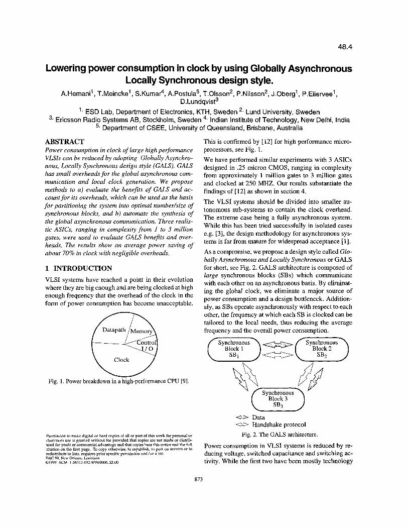
1 INTRODUCTION VLSI systems have reached a point in their evolution where they are big enough and are being clocked at high enough frequency that the overhead of the clock in the form of power consumption has become unacceptable.
Fig. 1. Power breakdown in a high-performance CPU [9].
Permission to make digital or hard copies of all or part of this work for personal or classroom use is granted without fee provided that copies are not made or distrib- uted for profit or commercial advantage and that copies bear this notice and the full citation on the first page. To copy otherwise, to republish, to post on servers or to redistribute to lists, requires prior specific permission and/or a fee. DAC 99, New Orleans, Louisiana 01999 ACM 1-58113-092-9/99/0006..$5.00
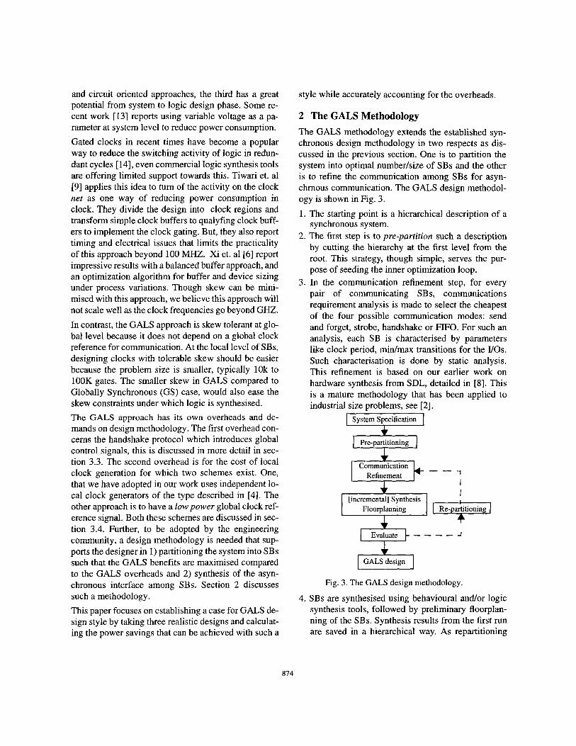
This is confirmed by [12] for high performance micro- processors, see Fig. 1 We have performed similar experiments with 3 ASICs designed in .25 micron CMOS, ranging in complexity from approximately 1 million gates to 3 million gates and clocked at 250 MHZ. Our results substantiate the findings of [12] as shown in section 4. The VLSI systems should be divided into smaller au- tonomous sub-systems to contain the clock overhead. The extreme case being a fully asynchronous system. While this has been tried successfully in isolated cases e.g. [3], the design methodology for asynchronous sys- tems is far from mature for widespread acceptance [ 11. As a compromise, we propose a design style called Glo- bally Asynchronous and Locally Synchronous or GALS for short, see Fig. 2. GALS architectxe is composed of large synchronous blocks (SBs) which communicate with each other on an asynchronous basis. By eliminat- ing the global clock, we eliminate a major source of power consumption and a design bottleneck. Addition- aly, as SBs operate asynchronously with respect to each other, the frequency at which each SB is clocked can be tailored to the local needs, thus reducing the average frequency and the overall power consumption.
d n Svnchronous ’Block3 \
Data c3 Handshake protocol
Fig. 2. The GALS architecture.
Power consumption in VLSI systems is reduced by re- ducing voltage, switched capacitance and switching ac- tivity. While the first two have been mostly technology
873
and circuit oriented approaches, the third has a great potential from system to logic design phase. Some re- cent work [ 131 reports using variable voltage as a pa- rameter at system level to reduce power consumption. Gated clocks in recent times have become a popular way to reduce the switching activity of logic in redun- dant cycles [14], even commercial logic synthesis tools are offering limited support towards this. Tiwari et. a1 [9] applies this idea to turn of the activity on the clock net as one way of reducing power consumption in clock. They divide the design into clock regions and transform simple clock buffers to qualyfing clock buff- ers to implement the clock gating. But, they also report timing and electrical issues that limits the practicality of this approach beyond 100 MHZ. Xi et. a1 [6] report impressive results with a balanced buffer approach, and an optimization algorithm for buffer and device sizing under process variations. Though skew can be mini- mised with this approach, we believe this approach will not scale well as the clock frequencies go beyond GHZ. In contrast, the GALS approach is skew tolerant at glo- bal level because it does not depend on a global clock reference for communication. At the local level of SBs, designing clocks with tolerable skew should be easier because the problem size is smaller, typically 1Ok to 100K gates. The smaller skew in GALS compared to Globally Synchronous (GS) case, would also ease the skew constraints under which logic is synthesised. The GALS approach has its own overheads and de- mands on design methodology. The first overhead con- cerns the handshake protocol which introduces global control signals, this is discussed in more detail in sec- tion 3.3. The second overhead is for the cost of local clock generation for which two schemes exist. One, that we have adopted in our work uses independent lo- cal clock generators of the type described in [4]. The other approach is to have a low power global clock ref- erence signal. Both these schemes are discussed in sec- tion 3.4. Further, to be adopted by the engineering community, a design methodology is needed that sup- ports the designer in 1) partitioning the system into SBs such that the GALS benefits are maximised compared to the GALS overheads and 2) synthesis of the asyn- chronous interface among SBs. Section 2 discusses such a methodology. This paper focuses on establishing a case for GALS de- sign style by taking three realistic designs and calculat- ing the power savings that can be achieved with such a
style while accurately accounting for the overheads.
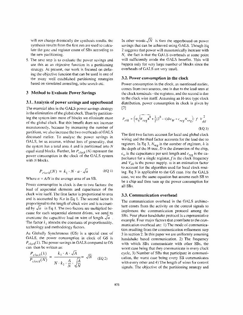
2 The GALS Methodology The GALS methodology extends the established syn- chronous design methodology in two respects as dis- cussed in the previous section. One is to partition the system into optimal numberkize of SBs and the other is to refine the communication among SBs for asyn- chrnous communication. The GALS design methodol- ogy is shown in Fig. 3.
1. The starting point is a hierarchical description of a synchronous system.
2. The first step is to pre-partition such a description by cutting the hierarchy at the first level from the root. This strategy, though simple, serves the pur- pose of seeding the inner optimization loop.
3. In the communication refinement step, for every pair of communicating SBs, communications requirement analysis is made to select the cheapest of the four possible communication modes: send and forget, strobe, handshake or FIFO. For such an analysis, each SB is characterised by parameters like clock period, midmax transitions for the VOs. Such characterisation is done by static analysis. This refinement is based on our earlier work on hardware synthesis from SDL, detailed in [SI. This is a mature methodology that has been applied to industrial size problems, see [2].
Communication Refinement
[incremental] Synthesis
Fig. 3. The GALS design methodology,
4. SBs are synthesised using behavioural andor logic synthesis tools, followed by preliminary floorplan- ning of the SBs. Synthesis results from the first run are saved in a hierarchical way. As repartitioning
874
will not change drastically the synthesis results, the synthesis results from the first run are used to calcu- late the gate and register count of SBs according to the new partitioning. The next step is to evaluate the power savings and use this as an objective function in a partitioning strategy. At present, our work is focused on defin- ing the objective function that can be used in one of the many well established partitioning strategies based on simulated annealing, tabu search etc.
Method to Evaluate Power Savings
In other words f i is then the upperbound on power savings that can be achieved using GALS. Though Eq 2 suggests that power will monotonically increase with N , the fact is that the GALS overheads at some point will sufficiently erode the GALS benefits. This will happen only for very large number of blocks since the overheads of GALS are very small.
3.2. Power consumption in the clock Power consumption in the clock, as mentioned earlier, comes from two sources, one is due to the load seen at the clock terminals - the registers, and the second is due to the clock wire itself. Assuming an H-tree tvDe clock v , I
3.1. Analysis of Power savings and upperbound The essential idea in the GALS power savings strategy is the elimination of the global clock. Thus by partition- ing the system into more of blocks we eliminate more of the global clock. But this benefit does not increase monotonously, because by increasing the number of
distribution, power consumption in clock is given by E71
h 3 h 2 P c l k = ( a d q + i ( ? - l ) D c w + c N w,, reg reg
(EO 3) partitions, we also increase the two overheads of GALS discussed earlier. To analyse the power savings in GALS, let us assume, without loss of generality, that the system has a total area A and is partitioned into N equal sized blocks. Further, let Pclock ( N ) represent the power consumption in the clock of the GALS system with N blocks.
Pclock (N) = k , . N . a . ,& (EQ 1)
Where n = A/N is the average area of an SB. Power consumption in clock is due to two factors: the load of sequential elements and capacitance of the clock wire itself. The first factor is proportional to area and is accounted by N.a in Eq 1. The second factor is proportional to the length of clock wire and is account- ed by ,& in Eq 1. The two factors are multiplied be- cause for each sequential element driven, we need to overcome the capacitive load on wire of length & . The factor k l absorbs the constants of proportionality, technology and methodology factors. As Globally Synchronous (GS) is a special case of GALS, the power consumption in clock of GS is Pclock(l). The power savings in GALS compared to GS can then be written as:
\ . I
The first two factors account for local and global clock wiring and the third factor accounts for the load due to registers. In Eq 3, Nres is the number of registers, h is the depth of the H-tree, D is the dimension of the chip, c, is the capacitance per unit length and creg is the ca- pacitance for a single register, f is the clock frequency and Vdd is the power supply. a is an estimation factor to account for the algorithm used for local clock rout- ing. Eq 3 is applicable to the GS case. For the GALS case, we use the same equation but assume each SB to be a chip and then sum up the power consumption for all SBs.
3.3, Communication overhead The communication overhead in the GALS architec- ture comes from the activity on the control signals to implement the communication protocol among the SBs. Four phase handshake protocol is a representative example. Four major factors that contribute to the com- munication overhead are: 1) The mode of communica- tion resulting from the communication refinement step 3 in section 2. In this paper we are uniformly assuming handshake based communication. 2) The frequency with which SBs communicate with other SBs, the worst case being that they communicate in every clock cycle, 3) Number of SBs that participate in communi- cation, the worst case being every SB communicates with every other and 4) The length of wires for control signals. The objective of the partitioning strategy and
875

the floorplanning step in the GALS methodology shown in Fig. 3. would be to minimise the external communication and place SBs that do communicate close to each other. As the data communication over- head would be the same for GALS and SBs, we are only interested in the communication overhead P,,,,, due to asynchronous protocol which is given by Eq 4.
(EQ 4)
where, B is the set of communicating SB pairs, X b is the set of communication instances for a particular pair - b - of communicating SBs, nsjg is the number of signals in the communication protocol, the handshake proto- col will have two signals. request and acknowledge; C, is the wire capacitance per unit length, Zb,; is the wire length for communication signal, nreg is the number of registers driven by the control signals and Cr, is the register capacitance,fb,i is the frequency at with which SBs communicate.
3.4. Local clock generation and its overhead In the GALS architecture local clocks are required for the SBs. There are two possibilities, either to have an independent local clock generator or to use a global ref- erence clock signal with frequency multiplier in SBs to achieve the desired higher frequency. When using the global reference clock signal, the pow- er consumption in it can be kept low by adopting three measures: 1) the signal swing can be a fraction of Vdd, for instance a few hundred millivolts, 2) the signal is distributed at a much lower frequency compared to the highest frequency required by any SB and then using a multiplier within SB to achieve the desired higher fre- quency and lastly 3) no effort is made to carefully de- sign the geometry of the signal to minimise skew, because the GALS architecture is not affected by the global clock skew. Traditionally, an analog PLL is used for frequency multiplication. However integrating a PLL in a noisy digital environment is difficult. In addition to noise is- sues, the PLL is also sensitive to process variations. Fully digital methods are more desirable for both low- voltage and low-power clock generation. For frequen- cy multiplication, a ring oscillator controlled by a glo- bal clock signal can be used instead of a PLL or a DLL
as suggested in [4]. In this design, a burst of a predeter- mined number of oscillations is produced for each pe- riod of the global reference clock followed by idle time for safety margin. Local clock generators based on ring oscillators have many advantages such as robustness, small size and low power consumption. The basic ring oscillator con- sists of an odd number of inverters connected in a cir- cularchain. This circuit will not have a stable operation point and will therefore oscillate. The frequency of the ring oscillator will be determined by the propagation time through the chain of inverters. There are many ways to manipulate the frequency of the ring oscillator. The most straightforward method is to change the prop- agation delay by changing the number of inverters. However, using only this method, the oscillation will be set to a fixed frequency. Other ways are to use cur- rent starved inverters [ 5 ] , or a delay line of controllable capacitors [ 1 I]. There are advantages of reducing the local oscillator frequency, using one of the suggested methods, instead of letting each SB operate fast and then be turned off when ready. One advantage is the possibility of making a low power design, since the timing demands on the hardware in the SB will be less severe. Ring oscillators are low cost solutions and the power consumption in them for the GALS architecture can be estimated by Eq 5.
8
(EQ 5) Where B is the set of SBs, Ci,lv is the capacitive load due to one inverter, Nitlvb is the number of inverters used by the ring oscillator in SB number b andfb is its frequency of operation. In [l I], dynamic voltage scaling of both the oscillators and the SBs, leading to an energy efficient design is proposed. Using a DCDC-converter, dynamic voltage scaling of the power supply voltage at each SB contain- ing a ring oscillator is made. In [ 121, a local ring oscillator is used for clock genera- tion by frequency multiplication in a digital 95 kHz In- termediate Frequency (IF) filter. This IF filter can be regarded as a typical SB in the GALS architecture. In this design, the clock generator including local clock buffer occupies only 3% of the total chip area. The clock power consumption in this example is about 12% of the total power consumption in the SB.
876

4 EXPERIMENTS & RESULTS In the previous sections, we have analytically reasoned about the benefits and overheads of GALS. In this sec- tion, we present experiment to quantify those reason- ings. We took three designs, with 1.125,2.09 and 3.04 million gates. These designs are in the initial stage of development. The focus of the experiment was to eval- uate the benefits of GALS and account for its over- heads. For this reason, we have followed the methodology outlined in section 2 in spirit, by manual- ly doing some of the steps outlined there. The experi- mental steps were as follows:
1 . The experiment started with a hierarchical RTL descriptiodmodels of the design in VHDL.
2. The description was cut at the first level of hierar- chy, resulting in 24, 46 and 52 partitions for the three designs respectively. These partitions were treated as the initial set of SBs for the three designs..
ui;
Table 1: Design Data
Millions Initial SBs 7.5 X 1.5
12.8 X 12.8
Table 2. Data used for the GALS experiment
3. The communication refinement step was skipped, because the existing tool works with SDL and we are in the process of adapting it for VHDL. All glo- bal communication is assumed to take place using a four phase handshake protocol. All SBs are clocked at the same frequency, internally some of them use gated clocks. This sets the value of nSig and nreg parameters in Eq 4 to 2
4. The communication refinement step was skipped, because the existing tool works with SDL and we are in the process of adapting it for VHDL. All glo- bal communication is assumed to take place using a four phase handshake protocol. All SBs are clocked at the same frequency, internally some of them use
gated clocks. This sets the value of nSig and nreg parameters in Eq 4 to 2Each of these SBs, which were synthesisable and not models corresponding to processor cores and memories, were synthesised using logic synthesis tools.
5. Each desigr. was floorplanned.
I 10 30 40 50 60
2o partitions /design Fig. 4. Power consumption in Clock as a function of par-
6. Keeping the floorplan fixed, we manually created multiple partitioning scenarios for each design. Starting with the initial set of SBs, we gradually increased the partion size by grouping neighbour- ing SBs into new larger SBs. These scenarios corre- spond to the design points shown in Fig. 4.
titioning.
7. For each partitioning scenario, the design data together with the synthesis result was used to find:
the number of registers, Nreg and the dimension D of each SB. These were then used in Eq 3 to calculate the power consumption in clock, plot- ted in Fig. 4. the set - B - of participating SBs and the set - x b - of communication instances. For the length of wires, we used manhattan distance as an esti- mate. These corresponds to the B, x b and lb,i parameters respectively in Eq 4.
8. For calculating the overhead due to ring oscillators, we estimated the number of inverters required to be 9 using equations in Ch. 3 of [5]. This was used in Eq 5. and added to Eq 4 to calculate the GALS overhead.
Fig. 4. shows how the power consumption reduces as the number of partitions increase. The gains are steep
877
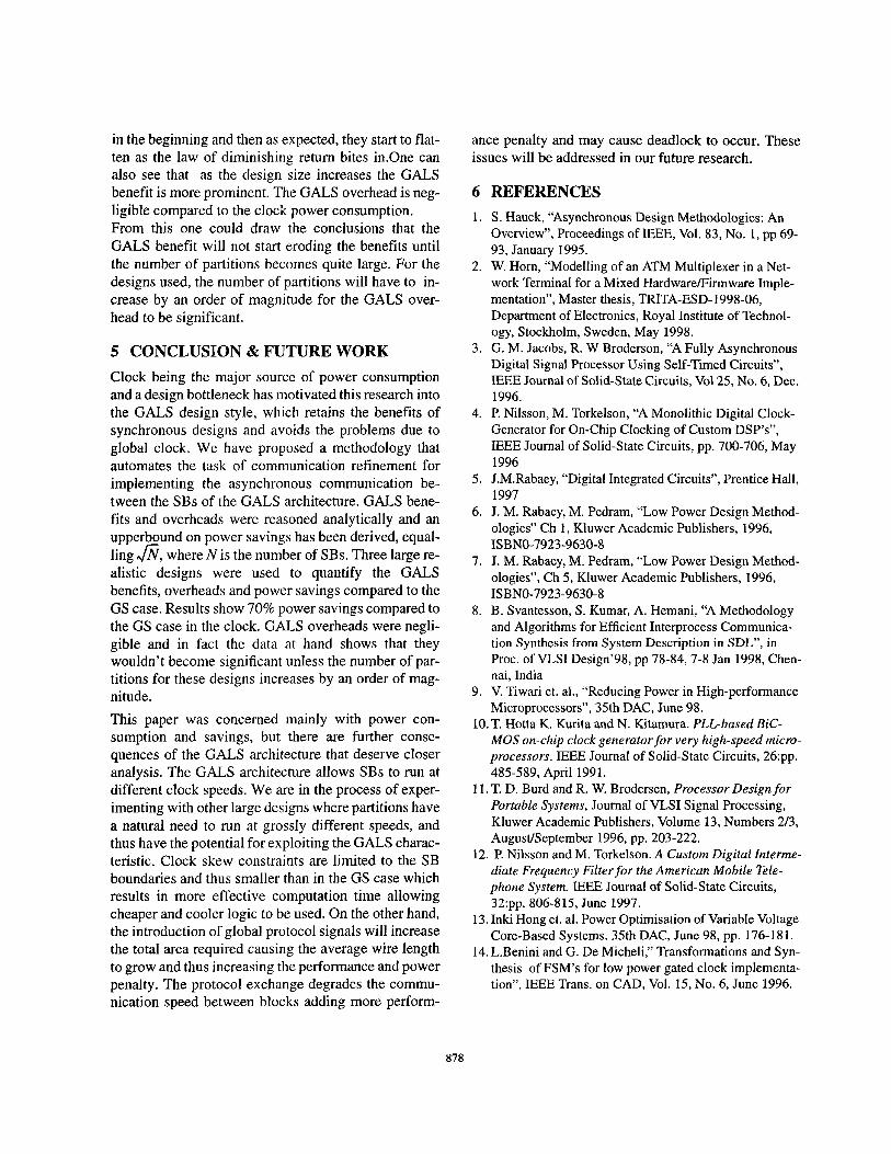
in the beginning and then as expected, they start to flat- ten as the law of diminishing return bites in.One can also see that as the design size increases the GALS benefit is more prominent. The GALS overhead is neg- ligible compared to the clock power consumption. From this one could draw the conclusions that the GALS benefit will not start eroding the benefits until the number of partitions becomes quite large. For the designs used, the number of partitions will have to in- crease by an order of magnitude for the GALS over- head to be significant.
5 CONCLUSION & FUTURE WORK Clock being the major source of power consumption and a design bottleneck has motivated this research into the GALS design style, which retains the benefits of synchronous designs and avoids the problems due to global clock. We have proposed a methodology that automates the task of communication refinement for implementing the asynchronous communication be- tween the SBs of the GALS architecture. GALS bene- fits and overheads were reasoned analytically and an upperbound on power savings has been derived, equal- ling @, where N is the number of SBs. Three large re- alistic designs were used to quantify the GALS benefits, overheads and power savings compared to the GS case. Results show 70% power savings compared to the GS case in the clock. GALS overheads were negli- gible and in fact the data at hand shows that they wouldn’t become significant unless the number of par- titions for these designs increases by an order of mag- nitude.
This paper was concerned mainly with power con- sumption and savings, but there are further conse- quences of the GALS architecture that deserve closer analysis. The GALS architecture allows SBs to run at different clock speeds. We are in the process of exper- imenting with other large designs where partitions have a natural need to run at grossly different speeds, and thus have the potential for exploiting the GALS charac- teristic. Clock skew constraints are limited to the SB boundaries and thus smaller than in the GS case which results in more effective computation time allowing cheaper and cooler logic to be used. On the other hand, the introduction of global protocol signals will increase the total area required causing the average wire length to grow and thus increasing the performance and power penalty. The protocol exchange degrades the commu- nication speed between blocks adding more perform-
ance penalty and may cause deadlock to occur. These issues will be addressed in our future research.
6 1.
2.
3.
4.
5.
6.
7.
8.
9.
REFERENCES S. Hauck, “Asynchronous Design Methodologies: An Overview”, Proceedings of IEEE, Vol. 83, No. 1, pp 69- 93, January 1995. W. Horn, “Modelling of an ATM Multiplexer in a Net- work Terminal for a Mixed HardwareFinnware Imple- mentation’’, Master thesis, TRITA-ESD- 1998-06, Department of Electronics, Royal Institute of Technol- ogy, Stockholm, Sweden, May 1998. G. M. Jacobs, R. W Broderson, “A Fully Asynchronous Digital Signal Processor Using Self-Timed Circuits”, IEEE Journal of Solid-state Circuits, Vol25, No. 6, Dec. 1996. P. Nilsson, M. Torkelson, “A Monolithic Digital Clock- Generator for On-Chip Clochng of Custom DSP’s”, IEEE Journal of Solid-state Circuits, pp. 700-706, May 1996 J.M.Rabaey, “Digital Integrated Circuits”, Prentice Hall, 1997 J. M. Rabaey, M. Pedram, “Low Power Design Method- ologies” Ch 1, Kluwer Academic Publishers, 1996,
J. M. Rabaey, M. Pedram, “Low Power Design Method- ologies’’, Ch 5, Kluwer Academic Publishers, 1996,
B. Svantesson, S. Kumar, A. Hemani, “A Methodology and Algorithms for Efficient Interprocess Communica- tion Synthesis from System Description in SDL”, in Proc. of VLSI Design’98, pp 78-84,7-8 Jan 1998, Chen- nai, India V. Tiwari et. al., “Reducing Power in High-performance Microprocessors”, 35th DAC, June 98.
ISBNO-7923-9630-8
ISBNO-7923-9630-8
10. T. Hotta K. Kurita and N. Kitamura. PLL-based BiC- MOS on-chip clock generator for very high-speed micro- processors. IEEE Journal of Solid-state Circuits, 26:pp. 485-589, April 1991.
1 1. T. D. Burd and R. W. Brodersen, Processor Designfor Portable Systems, Journal of VLSI Signal Processing, Kluwer Academic Publishers, Volume 13, Numbers 213, AugusVSeptember 1996, pp. 203-222.
12. P. Nilsson and M. Torkelson. A Custom Digital Interme- diate Frequency Filter for the American Mobile Tele- phone System. IEEE Journal of Solid-state Circuits, 32:pp. 806-815, June 1997.
13. Inki Hong et. al. Power Optimisation of Variable Voltage Core-Based Systems. 35th DAC, June 98, pp. 176-1 8 1.
14. L.Benini and G. De Micheli,” Transformations and Syn- thesis of FSM’s for low power gated clock implementa- tion”, IEEE Trans. on CAD, Vol. 15, No. 6, June 1996.
878