Interfacial and Mechanical Property Analysis of Waste Printed Circuit Boards Subject to Thermal...
8
Interfacial and Mechanical Property Analysis of Waste Printed Circuit Boards Subject to Thermal Shock Jinhui Li, Huabo Duan, Keli Yu, and Siting Wang Department of Environmental Science and Engineering, Tsinghua University, Beijing, People’s Republic of China ABSTRACT Waste printed circuit boards (PCBs) are the focal points for handling electric and electronic waste. In this paper, a thermal shock method was used to pretreat waste PCBs for the improvement of crushing performance. The influence of the thermal shock process on interfacial modification and mechanical property attenuation of PCB waste was studied. The appearance and layer spacing of the basal plane began to change slightly when the temperature reached 200 °C. By 250 °C, apparent bulging, cracking, and delamination were observed. However, pyrolysis of PCBs occurred when the temperature reached 275 °C, where PCBs were carbonized. The thermogravimetric analysis of PCB particles under vacuum showed that 270 °C was the starting point of pyrolysis. The tensile and impact strength of PCBs were reduced as shock tempera- ture rose gradually, with a reduction by 2.6 and 16.5%, respectively, at 250 °C from its unheated strength. The PCBs that were heated to 250 °C achieved 100% libera- tion, increasing linearly from 13.6% for unheated PCBs through a single-level shear-crusher (2-mm mesh) and resulting in an obvious reduction of 9.5% (dB) in dust and noise at 250 °C. These parameters could be helpful for establishing the operational setup for industrial- scale facilities with the aim of achieving a compact process and a highly efficient recovery for waste PCBs compared with those of the traditional combination mechanical technologies. INTRODUCTION As one of the indispensable parts in the electronics indus- try, printed circuit boards (PCBs) are widely used in all kinds of electric and electronic equipment (EEE). During the last decade, the average rate of worldwide PCB pro- duction has increased by 8.7% annually and is much higher in Southeast Asia (10.8%) and mainland China (14.4%). 1 Mass generation of waste EEEs and continued rapid expansion of the PCB industry have resulted in a large quantity of waste PCBs. The adverse impact of waste PCBs and their recycling is an important environmental problem, especially in developing countries such as China, Nigeria, and India. 2 Scrap PCBs are a heterogeneous mixture of organic materials, metal, and glass fiber and consume a large quantity of resources during their production. The crucial problem for PCB treatment is the separation or liberation of metal and nonmetallic materials. 3–6 Several recycling technologies have been developed and applied for waste PCBs. 7–9 During the 1990s, traditional technologies were used for recycling waste PCBs, including high-tempera- ture metallurgy and chemical metallurgy, but these have adverse environmental impacts and were gradually phased out. 10 For example, toxic organic pollutants and even dioxins can be generated if incineration or pyrolysis methods are used to recycle PCBs. 11–15 Previous research on PCBs has shown that toxic gases or liquid pollutants were likely to be generated if the temperature exceeded 300 °C under air or nitrogen (N 2 ) atmospheres because of pyrolysis. 15 In some developing countries, such as in China, India, and Nigeria, the primitive and traditional technologies are still used with serious environmental harm. 16 The mechanical treatment technique, which uses crushing and separation processes for PCB recovery and reclamation, is becoming more favored and widely used in industrial practice. Although many studies on the mechanical recycling of PCBs have been reported, most of the work has been carried out with a focus on separation. In general, after the multilevel crushing step, a magnetic, electric, air clas- sification, or shaking table separation is used to recover metallic materials from the waste bare PCBs or mounted PCBs. 17–21 However, the abovementioned mechanical combination technologies need fine particles of crushed materials. These provide a high degree of liberation, but separation is difficult. 22 Moreover, there are other prob- lems associated with the crushing process, such as dust and noise pollution and serious abrasion of the crushing machine’s cutting tools. 23 Zhao and Li 15 reported that direct and continual crushing of PCBs could result in pyrolysis and toxic substance release caused by locally high temperatures. The surface temperature of waste PCBs could reach 300 °C or even close to 350 °C for over 3-sec retention time during crushing. Last but not least, the vast investment in mechanical equipment prevents the ma- ture mechanical technology used in developed countries IMPLICATIONS The thermal expansion mismatch between polymeric resins and the glass reinforcement or metallic elements of a PCB can be used to create a thermal shock method to improve the crushing of lamination materials. Thus, this concept was introduced to promote the recyclability of scrap PCB for copper recovery. A pilot project has been established in Suzhou, China on the basis of the findings in this study. TECHNICAL PAPER ISSN:1047-3289 J. Air & Waste Manage. Assoc. 60:229 –236 DOI:10.3155/1047-3289.60.2.229 Copyright 2010 Air & Waste Management Association Volume 60 February 2010 Journal of the Air & Waste Management Association 229
-
Upload
independent -
Category
Documents
-
view
2 -
download
0
Transcript of Interfacial and Mechanical Property Analysis of Waste Printed Circuit Boards Subject to Thermal...
Interfacial and Mechanical Property Analysis of Waste PrintedCircuit Boards Subject to Thermal Shock
Jinhui Li, Huabo Duan, Keli Yu, and Siting WangDepartment of Environmental Science and Engineering, Tsinghua University, Beijing, People’sRepublic of China
ABSTRACTWaste printed circuit boards (PCBs) are the focal pointsfor handling electric and electronic waste. In this paper, athermal shock method was used to pretreat waste PCBs forthe improvement of crushing performance. The influenceof the thermal shock process on interfacial modificationand mechanical property attenuation of PCB waste wasstudied. The appearance and layer spacing of the basalplane began to change slightly when the temperaturereached 200 °C. By 250 °C, apparent bulging, cracking,and delamination were observed. However, pyrolysis ofPCBs occurred when the temperature reached 275 °C,where PCBs were carbonized. The thermogravimetricanalysis of PCB particles under vacuum showed that270 °C was the starting point of pyrolysis. The tensile andimpact strength of PCBs were reduced as shock tempera-ture rose gradually, with a reduction by 2.6 and 16.5%,respectively, at 250 °C from its unheated strength. ThePCBs that were heated to 250 °C achieved 100% libera-tion, increasing linearly from 13.6% for unheated PCBsthrough a single-level shear-crusher (2-mm mesh) andresulting in an obvious reduction of 9.5% (dB) in dustand noise at 250 °C. These parameters could be helpfulfor establishing the operational setup for industrial-scale facilities with the aim of achieving a compactprocess and a highly efficient recovery for waste PCBscompared with those of the traditional combinationmechanical technologies.
INTRODUCTIONAs one of the indispensable parts in the electronics indus-try, printed circuit boards (PCBs) are widely used in allkinds of electric and electronic equipment (EEE). Duringthe last decade, the average rate of worldwide PCB pro-duction has increased by 8.7% annually and is muchhigher in Southeast Asia (10.8%) and mainland China(14.4%).1 Mass generation of waste EEEs and continued
rapid expansion of the PCB industry have resulted in alarge quantity of waste PCBs. The adverse impact of wastePCBs and their recycling is an important environmentalproblem, especially in developing countries such asChina, Nigeria, and India.2
Scrap PCBs are a heterogeneous mixture of organicmaterials, metal, and glass fiber and consume a largequantity of resources during their production. The crucialproblem for PCB treatment is the separation or liberationof metal and nonmetallic materials.3–6 Several recyclingtechnologies have been developed and applied for wastePCBs.7–9 During the 1990s, traditional technologies wereused for recycling waste PCBs, including high-tempera-ture metallurgy and chemical metallurgy, but these haveadverse environmental impacts and were graduallyphased out.10 For example, toxic organic pollutants andeven dioxins can be generated if incineration or pyrolysismethods are used to recycle PCBs.11–15 Previous researchon PCBs has shown that toxic gases or liquid pollutantswere likely to be generated if the temperature exceeded300 °C under air or nitrogen (N2) atmospheres because ofpyrolysis.15 In some developing countries, such as inChina, India, and Nigeria, the primitive and traditionaltechnologies are still used with serious environmentalharm.16 The mechanical treatment technique, which usescrushing and separation processes for PCB recovery andreclamation, is becoming more favored and widely usedin industrial practice.
Although many studies on the mechanical recyclingof PCBs have been reported, most of the work has beencarried out with a focus on separation. In general, afterthe multilevel crushing step, a magnetic, electric, air clas-sification, or shaking table separation is used to recovermetallic materials from the waste bare PCBs or mountedPCBs.17–21 However, the abovementioned mechanicalcombination technologies need fine particles of crushedmaterials. These provide a high degree of liberation, butseparation is difficult.22 Moreover, there are other prob-lems associated with the crushing process, such as dustand noise pollution and serious abrasion of the crushingmachine’s cutting tools.23 Zhao and Li15 reported thatdirect and continual crushing of PCBs could result inpyrolysis and toxic substance release caused by locallyhigh temperatures. The surface temperature of waste PCBscould reach 300 °C or even close to 350 °C for over 3-secretention time during crushing. Last but not least, the vastinvestment in mechanical equipment prevents the ma-ture mechanical technology used in developed countries
IMPLICATIONSThe thermal expansion mismatch between polymeric resinsand the glass reinforcement or metallic elements of a PCBcan be used to create a thermal shock method to improvethe crushing of lamination materials. Thus, this conceptwas introduced to promote the recyclability of scrap PCBfor copper recovery. A pilot project has been established inSuzhou, China on the basis of the findings in this study.
TECHNICAL PAPER ISSN:1047-3289 J. Air & Waste Manage. Assoc. 60:229–236DOI:10.3155/1047-3289.60.2.229Copyright 2010 Air & Waste Management Association
Volume 60 February 2010 Journal of the Air & Waste Management Association 229

from being used in less-developed countries, which dis-pose of a great amount of PCB waste.
Because the crushing process of PCBs plays a key rolein mechanical technologies, research has been partlyshifted to improving the crushing efficiency. For example,Result Co., Ltd. from Switzerland studied the impact fac-tors and centrifugal characteristics of PCBs during thecrushing process. Daimler-Berz Co., Ltd. in Germany andother researchers studied cryogenic crushing of PCBs withthe aim of changing the mechanical properties of PCBsand promoting their crushing performance.24–27 Re-cently, recyclers have also started to develop special cut-ting tools to improve the crushing efficiency.28
In general, rapid temperature change (cooling orheating) can alter the interfacial and mechanical phys-ical properties of an object. Several publications havereported that thermal shock treatment can induce largeinternal stresses and cause cracking within a fiber-rein-forced polymer matrix.29,30 It was also reported thatthermal shock treatment reduced the material strengthof metals, such as copper foil.31,32 All of these materialsare typical elements of a PCB. In the authors’ work, thethermomechanical properties of copper foil, epoxyresin, and glass fiber are quite different. Actually, thethermomechanical properties of PCBs have attractedattention during the PCB manufacturing and surfacepackaging process, and thermal stability is a criticalaspect for PCB quality evaluation.33–35 Thermal shockon PCBs subjected to a specific temperature changecause the binding strength of the interface for eachlayer to decrease.33,36,37 Thus, thermal shock may resultin structural and mechanical changes of PCBs. How-ever, no research has been reported on the influences oflow-temperature thermal shock to discarded PCBs.Thus, taking into consideration these materials’ intrin-sic characteristics, this study tried to preprocess waste
PCBs by a thermal shock technique to change the phys-ical performance of PCB materials with the aim of sim-plifying the mechanical technology system and achiev-ing maximum efficiency for the recovery of metalsubstances.
EXPERIMENTAL PROCEDURESMaterials
In this study, the FR-4 (flame retardant) PCB bare boardswith multiple layers were selected, and 100–150 cm2 ofwhole PCBs were prepared for each experiment. This kindof FR-4 PCB is widely used in electronics, accounting formore than 50% of the total applications. The PCBs aremade from sheets of prepreg, which is constructed fromglass fiber matting impregnated with the epoxy resin. Astandard 1.6 mm of PCB is constructed from eight layersof prepreg with outer copper layers (Figure 1). The prepregand outer copper foil layer are stacked up together andplaced under considerable pressure, which bonds all ofthe layers into the final laminate.
The ultimate analysis of waste PCBs was by induc-tively coupled plasma (ICP)-atomic emissions spectros-copy (AES) and ICP-mass spectrometry (MS). The resultsare listed in Table 1. The moisture of the sample was0.44% by proximate analysis.
Methods and EquipmentA vacuum electronic resistance furnace (tube-type resis-tance furnace, SK2-18-12; Tianjin Electric Furnace Co.,China) equipped with an intelligent temperature controlinstrument (KSY-18-12; Tianjin Electric Furnace Co.,China) was used as a heater to form an environment witha temperature as high as 300 °C for PCB pretreatment. Theaccessory equipment included electric vacuum pumps(2XZ-8D; Shanghai Nanguang Vacuum Pump Factory,China), a vacuum gauge (ZDZ-52T; Core Chengdu ElectricTechnology Co., Ltd., China), and the exhaust gas collec-tion equipment (Figure 2).
Table 1. Elemental compositions of PCBs (FR-4, bare boards) as analyzed by ICP-AES and ICP-MS (wt %).
Elements C O Si Cu Al Ba Br N S H
Fraction wt % 24.80 24.16 14.76 26.30 2.88 0.12 4.30 0.48 0.28 1.94
Figure 1. Structure of PCB base laminates.
Figure 2. Key equipment used for thermal shock pretreatment: (1)pushing rod, (2) vacuum chamber, (3) tube-type electric resistancefurnace, (4) thermoelectric couple, (5) condensation chamber, (6)vacuum pipe, (7) hose pipe, (8) absorption chamber, (9) vacuumpumps, (10) gas collection chamber, and (11) steel bracket.
Li, Duan, Yu, and Wang
230 Journal of the Air & Waste Management Association Volume 60 February 2010
In this study, the influences of temperature, heatconservation time, initial power (the speed of tempera-ture rise), and vacuum degree were assessed. The resultswere analyzed based on single-factor experiments and anorthogonal experimental method. The experiments werecarried out from 175 to 300 °C with a 5 °C interval foreach experiment to continuously observe their perfor-mance during crushing. The representative temperatures(including 200, 225, 250, and 275 °C) and their pretreatedPCB samples were selected to observe the details ofchanges of various properties. Generally, replicated andmultiple experiments were designed and carried out toascertain the repeatability of the result. The shear-crush-ing machine was used to examine the effect of thermalshock pretreatment (HYP-250; Beijing HuanyatianyuanCo., Ltd., China). To conduct a comparative analysis, thewhole unheated or heated PCBs were directly fed into theshear-crushing machine. A noise meter (TES1350A; TESElectrical Electronic Co., Taiwan) was selected to measurethe noise during crushing, and an electron microscope(XTZ-E; Shanghai Optical Instrument Factory No. 6,China) and electronic vibration screen were used for as-certaining the degree of liberation. The impact specimenswere fractured, and the exposed surfaces were observedwith a scanning electron microscope (Hitachi S-520; Hi-tachi Co., Japan). The surfaces of the fractured specimenswere coated with gold to avoid charging under the elec-tron beam. Mechanical properties of unheated or ther-mal-shocked PCBs, including impact and tensile strengthand module, were examined by ISO 180 and 178 stan-dards, respectively.
In addition, thermogravimetric analysis (TGA) hasbeen conducted to identify the behavior of pyrolysis un-der vacuum atmosphere, particularly the initial tempera-ture. A NETZSCH-STA409PC TG-DSC (NETZSCH Group)was used to analyze the sample in a temperature range of40–400 °C with a rate of 10 °C min�1. The PCBs wereground and sieved into small particle mesh sizes of lessthan 0.15 mm for TGA experiments.
RESULTS AND DISCUSSIONInfluence of Thermal Shock on Appearance
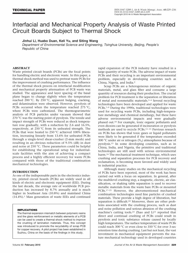
Changes of PCBsAfter thermal shock pretreatment using an orthogonalexperimental method and single-factor experiments, thechanges in PCB appearance and physical characteristicsare quite remarkable (Figure 3). Although the influence ofthe initial power of the heater on the change in PCBcharacteristics is insignificant, the impact of peak temper-ature is distinct and of prime importance. The other keyconditions of thermal shock were the heat conservationtime up to 10 min and the vacuum at or below the valueof 1000 Pa. A longer conservation time than 10 min hadno obvious effect on the appearance change of PCBs. Thevacuum condition could contribute to decreasing thetemperature of thermal shock and consequently a reduc-tion in the resynthesis of organic substances (e.g., dioxin)because less oxygen was involved. However, a furtherreduction of vacuum beyond 1000 Pa had no obviouseffect on the appearance change of PCBs.
Figure 3. Changes in PCB appearance with thermal shock under different test temperatures: (a) unheated, (b) 200 °C, (c) 250 °C, (d) 275 °C,and (e) 300 °C.
Figure 4. TGA curves of waste PCB thermal decomposition invacuum at 10 °C min�1.
Li, Duan, Yu, and Wang
Volume 60 February 2010 Journal of the Air & Waste Management Association 231
Through visual inspection as well as ordinary micro-scope and electron microscopy, the microstructure andlayer spacing of the basal plane were observed to changeabove 200 °C. At 250 °C, bulging, cracking, delamination,and the weight of the PCBs began to be reduced slightly,which might be attributed to the loss of moisture. Actu-ally, in PCB materials, the water vapor can enter micro-scopic interstitial voids between the glass fibers and theepoxy matrix, traveling great distances into the interior ofthe substrate. The bulging of the sample appearance bythermal shock partly results from the huge pressure dif-ferences between the inside and outside of PCB lamina-tion layers by vapor traveling under vacuum atmosphere.
In the presence of odorous gases, the PCB began totransform, carbonize, lose substantial weight, and sepa-rate into various layers at a temperature of 275 °C with avacuum lower than 1000 Pa (a similar phenomenon couldbe found when the temperature reached 300 °C under air
or N2 atmospheres). This phenomenon shows that phys-ical and chemical transformations occurred, includingpyrolysis.
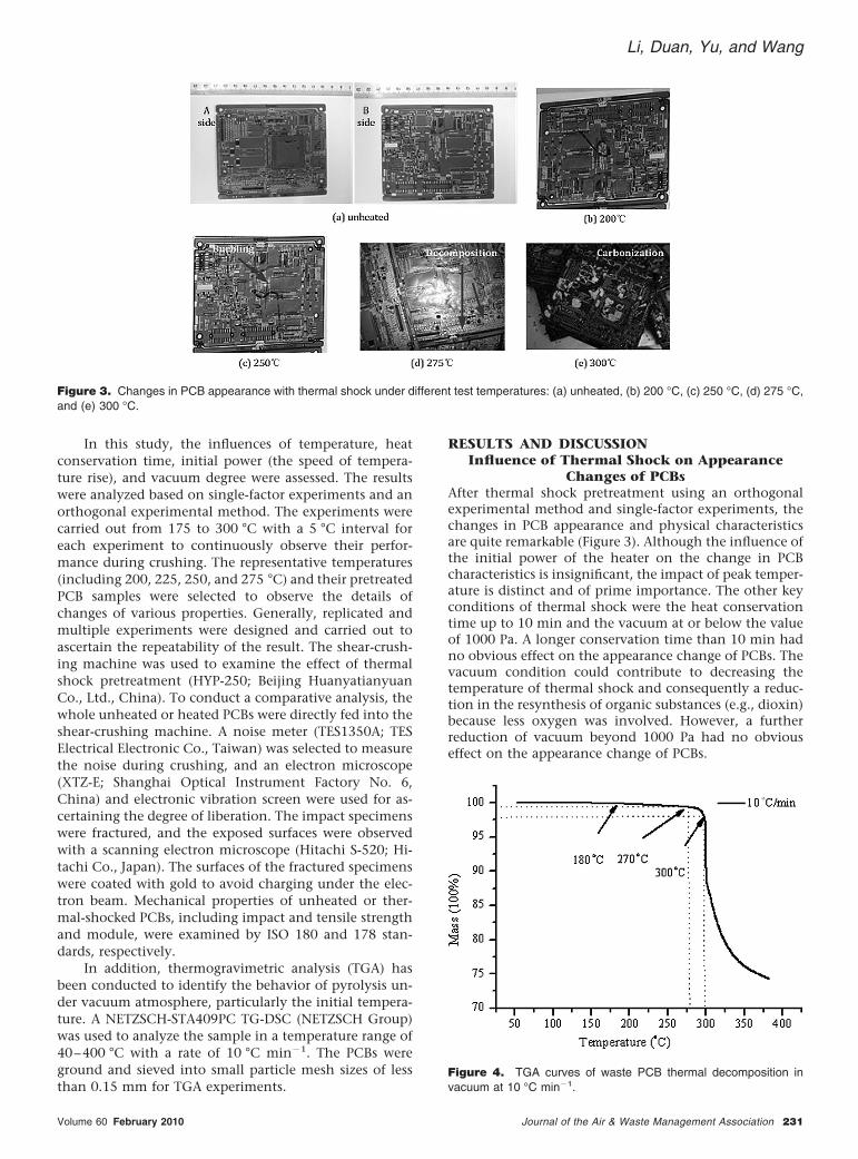
When a vacuum was introduced into the thermalshock experiment, the PCB was degraded in three steps asfound through TGA experiments. The described TGAcurve showed that the temperature of 270 °C was theinitial pyrolysis temperature (Figure 4).
Step 1 (�180–270 °C, slight mass loss) consistedmainly of the evolution of water from the PCB laminationwith an accumulated mass loss close to 0.4% (wt %). Thewater byproduct could be due to the original moisture inthe samples. Step 2 (�270–300 °C, minor mass loss),which is in the initial phase of pyrolysis, led to the vola-tile decomposition of additives (including couplingagents and curing accelerators) and gaseous products(e.g., hydrogen bromide [HBr], water vapor [H2O], carbondioxide [CO2], and other molecular hydrocarbons) werereleased. Step 3, which occurred at temperatures above300 °C, caused the decomposition and carbonization ofepoxy resin, accompanied with a significant mass loss.Similar results are found in published studies with regardto the pyrolysis of PCB waste using TGA and Fourier-transformation infrared (FTIR) integrated analysis.38–44
Thus, for the thermal shock pretreatment proposed in thisarticle, the appropriate temperature that most effectivelyinfluenced waste PCBs was below 270 °C.
Influence of Thermal Shock on the MechanicalCharacteristics of PCBs
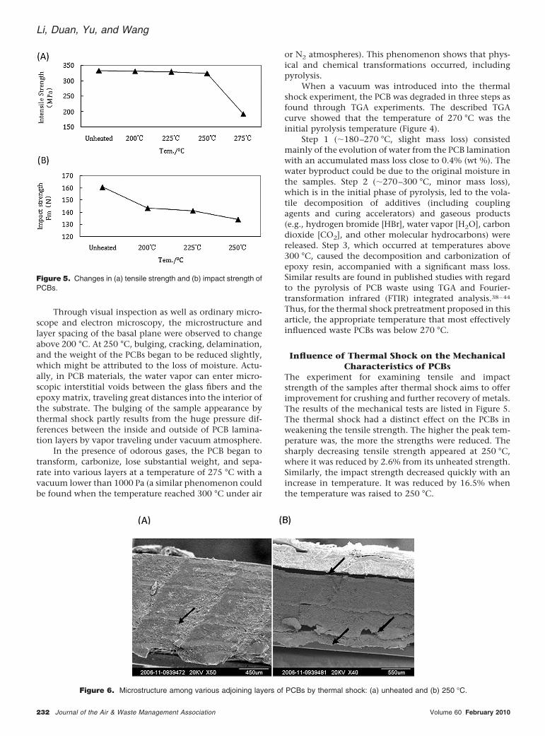
The experiment for examining tensile and impactstrength of the samples after thermal shock aims to offerimprovement for crushing and further recovery of metals.The results of the mechanical tests are listed in Figure 5.The thermal shock had a distinct effect on the PCBs inweakening the tensile strength. The higher the peak tem-perature was, the more the strengths were reduced. Thesharply decreasing tensile strength appeared at 250 °C,where it was reduced by 2.6% from its unheated strength.Similarly, the impact strength decreased quickly with anincrease in temperature. It was reduced by 16.5% whenthe temperature was raised to 250 °C.
Figure 5. Changes in (a) tensile strength and (b) impact strength ofPCBs.
Figure 6. Microstructure among various adjoining layers of PCBs by thermal shock: (a) unheated and (b) 250 °C.
Li, Duan, Yu, and Wang
232 Journal of the Air & Waste Management Association Volume 60 February 2010
For the laminar-like construction of the PCB, its me-chanical change comes in the strengthening phase. Whenfocal strength is placed on the lamination materials,transfer of stress will occur and the curvature radius is notthe same; when deformation accumulates to a certainextent, the PCBs cannot bear greater impact load andfracture will occur.32 As mentioned in the Introduction,copper foil, epoxy resin, and glass fiber compose the lam-ination structure in bare PCBs, and each laminate mayhave a different coefficient of thermal expansion (CTE) inthe x, y, and z axes. Because the thermal expansion be-havior of the three kinds of materials is different,33 thesolidifying shrinkage rate for each layer is also quite dif-ferent. The linear CTEs for common copper foil, epoxyresin, and E-glass fiber are 16.7, approximately 15–100,and 54 parts per million (ppm)/°C, respectively. Oncethermal shock on PCBs is carried out within a specifictemperature range, internal stresses are set up among PCBmaterials because of their different thermal expansioncapability. Combined with other mechanisms, the inter-nal stresses overcome the strength of the material, causinga crack or delamination to form and finally causing theboard’s structure to fail. Therefore, some of the mechanicproperties of bare PCBs were inevitably modified withthermal shock.
Influence of Thermal Shock on the InterfacialStructure of PCBs
Interface analysis could assess the influence of thermalshock on the microstructure and layer spacing of the basalplane. The waste PCBs were investigated for microdelami-nation after thermal shock under a scanning electronmicroscope. It was found that the microstructure of vari-ous adjoining layers changed significantly (Figure 6b) andthe linkages among different layers were weakened.
The mechanical strength of PCB substrate materialsmainly depends on the adhesion strength between thematrix and reinforcement. One way to increase the com-patibility between the glass fiber and polyolefin matrix isthe use of an organofunctional silane coupling agent,such as glass fiber surface modifiers, to obtain good me-chanical properties. Silane coupling agents that containthree inorganic reactive groups on silicon (usually me-thoxy-, ethoxy-, or acetoxy-) will bond well to the metalhydroxyl groups on most inorganic substrates, especiallyif the substrate contains silicon.45,46 For unheated PCBs,the adjoining layers were closely linked to each other andno apparent delamination among the various layers oc-curred. In comparison with the result shown in Figure 6a,a thermal shock temperature of 250 °C (Figure 6b) causedthe cross-linking of layers to become less effective. Upon
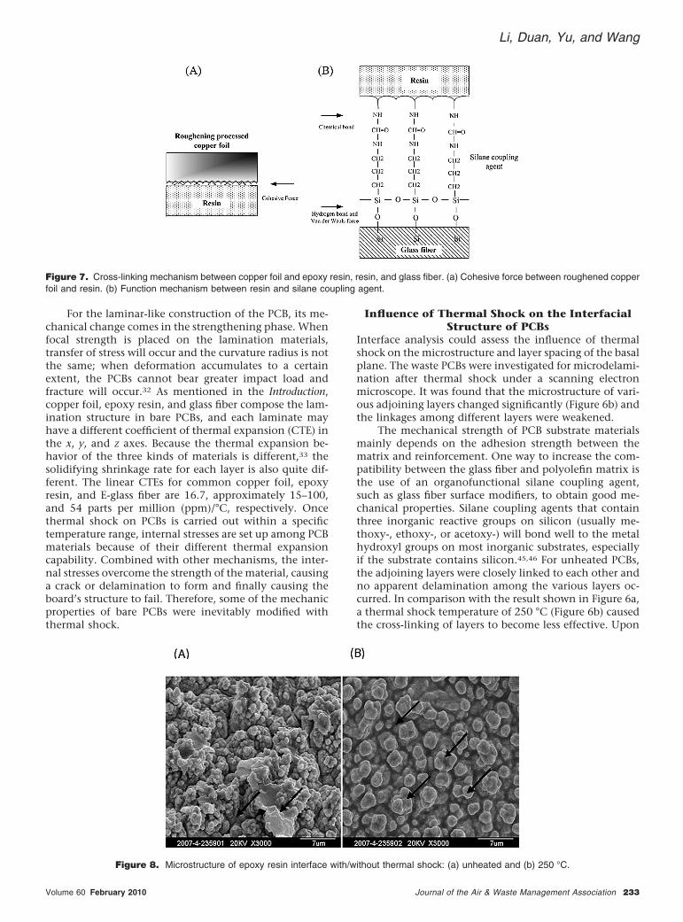
Figure 7. Cross-linking mechanism between copper foil and epoxy resin, resin, and glass fiber. (a) Cohesive force between roughened copperfoil and resin. (b) Function mechanism between resin and silane coupling agent.
Figure 8. Microstructure of epoxy resin interface with/without thermal shock: (a) unheated and (b) 250 °C.
Li, Duan, Yu, and Wang
Volume 60 February 2010 Journal of the Air & Waste Management Association 233
thermal shock pretreatment, large internal stresses wereset up among PCB materials because of their differentthermal expansion capability, which eventually led to thedelamination.
Figure 7 is a sketch that shows the cross-linkingmechanism between the copper foil and epoxy resin (Fig-ure 7a) and resin and glass fiber (Figure 7b). The surface ofa metal foil to be used as an intermediate layer in PCBs ischemically roughened, which is beneficial for forming acohesive force between copper foil and resin materials.Because of the thermal shock pretreatment, the thermalexpansion behavior could render the cohesive force inef-fective. Meanwhile, the hydrogen bonds of PCBs werebroken and the van der Waals force among layers did notenhance linking, which made PCBs vulnerable to theheating impact and caused a crack and delamination.
Influence of Thermal Shock on theMicrostructure of PCBs
It is known that the glass transition temperature (Tg) ofresin is an indication of molecular rigidity, cross-linkingdensity, and compatibility of the constituents. The phys-ical and chemical properties of epoxy resin, which func-tion as the cross-linking agent between copper foil andthe glass fiber, were easily modified when the thermalshock reached a certain temperature.
For the unheated PCBs, the structure/surface of theepoxy resin was complex and prone to function as across-linking agent (Figure 8a). Their structure changedwhen the temperature of the thermal shock reached250 °C. The resin maintained a regular arrangement (Fig-ure 8b), but the quantity of resin, which enhances cross-linking, decreased; therefore, its critical cross-linking rolewas lost. These observations explain the mechanical mod-ification for PCB materials subject to thermal shock.
Influence of Thermal Shock on the CrushingPerformance of PCBs
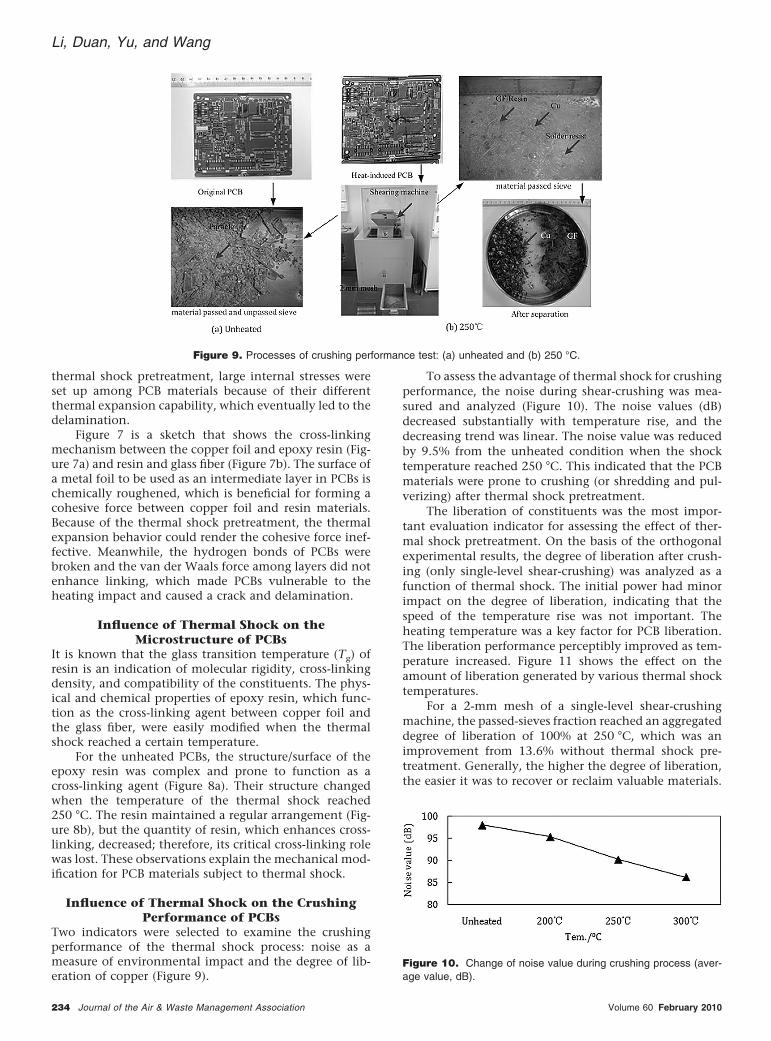
Two indicators were selected to examine the crushingperformance of the thermal shock process: noise as ameasure of environmental impact and the degree of lib-eration of copper (Figure 9).
To assess the advantage of thermal shock for crushingperformance, the noise during shear-crushing was mea-sured and analyzed (Figure 10). The noise values (dB)decreased substantially with temperature rise, and thedecreasing trend was linear. The noise value was reducedby 9.5% from the unheated condition when the shocktemperature reached 250 °C. This indicated that the PCBmaterials were prone to crushing (or shredding and pul-verizing) after thermal shock pretreatment.
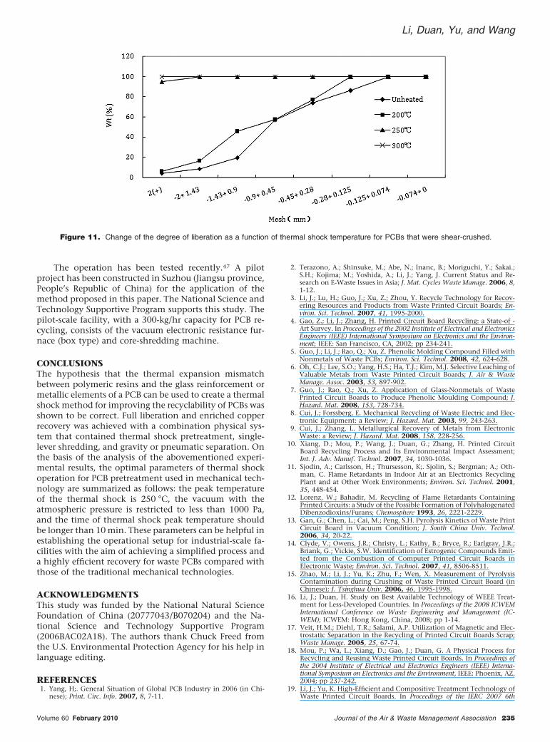
The liberation of constituents was the most impor-tant evaluation indicator for assessing the effect of ther-mal shock pretreatment. On the basis of the orthogonalexperimental results, the degree of liberation after crush-ing (only single-level shear-crushing) was analyzed as afunction of thermal shock. The initial power had minorimpact on the degree of liberation, indicating that thespeed of the temperature rise was not important. Theheating temperature was a key factor for PCB liberation.The liberation performance perceptibly improved as tem-perature increased. Figure 11 shows the effect on theamount of liberation generated by various thermal shocktemperatures.
For a 2-mm mesh of a single-level shear-crushingmachine, the passed-sieves fraction reached an aggregateddegree of liberation of 100% at 250 °C, which was animprovement from 13.6% without thermal shock pre-treatment. Generally, the higher the degree of liberation,the easier it was to recover or reclaim valuable materials.
Figure 9. Processes of crushing performance test: (a) unheated and (b) 250 °C.
Figure 10. Change of noise value during crushing process (aver-age value, dB).
Li, Duan, Yu, and Wang
234 Journal of the Air & Waste Management Association Volume 60 February 2010
The operation has been tested recently.47 A pilotproject has been constructed in Suzhou (Jiangsu province,People’s Republic of China) for the application of themethod proposed in this paper. The National Science andTechnology Supportive Program supports this study. Thepilot-scale facility, with a 300-kg/hr capacity for PCB re-cycling, consists of the vacuum electronic resistance fur-nace (box type) and core-shredding machine.
CONCLUSIONSThe hypothesis that the thermal expansion mismatchbetween polymeric resins and the glass reinforcement ormetallic elements of a PCB can be used to create a thermalshock method for improving the recyclability of PCBs wasshown to be correct. Full liberation and enriched copperrecovery was achieved with a combination physical sys-tem that contained thermal shock pretreatment, single-lever shredding, and gravity or pneumatic separation. Onthe basis of the analysis of the abovementioned experi-mental results, the optimal parameters of thermal shockoperation for PCB pretreatment used in mechanical tech-nology are summarized as follows: the peak temperatureof the thermal shock is 250 °C, the vacuum with theatmospheric pressure is restricted to less than 1000 Pa,and the time of thermal shock peak temperature shouldbe longer than 10 min. These parameters can be helpful inestablishing the operational setup for industrial-scale fa-cilities with the aim of achieving a simplified process anda highly efficient recovery for waste PCBs compared withthose of the traditional mechanical technologies.
ACKNOWLEDGMENTSThis study was funded by the National Natural ScienceFoundation of China (20777043/B070204) and the Na-tional Science and Technology Supportive Program(2006BAC02A18). The authors thank Chuck Freed fromthe U.S. Environmental Protection Agency for his help inlanguage editing.
REFERENCES1. Yang, H;. General Situation of Global PCB Industry in 2006 (in Chi-
nese); Print. Circ. Info. 2007, 8, 7-11.
2. Terazono, A.; Shinsuke, M.; Abe, N.; Inanc, B.; Moriguchi, Y.; Sakai.;S.H.; Kojima; M.; Yoshida, A.; Li, J.; Yang, J. Current Status and Re-search on E-Waste Issues in Asia; J. Mat. Cycles Waste Manage. 2006, 8,1-12.
3. Li, J.; Lu, H.; Guo, J.; Xu, Z.; Zhou, Y. Recycle Technology for Recov-ering Resources and Products from Waste Printed Circuit Boards; En-viron. Sci. Technol. 2007, 41, 1995-2000.
4. Gao, Z.; Li, J.; Zhang, H. Printed Circuit Board Recycling: a State-of -Art Survey. In Proceedings of the 2002 Institute of Electrical and ElectronicsEngineers (IEEE) International Symposium on Electronics and the Environ-ment; IEEE: San Francisco, CA, 2002; pp 234-241.
5. Guo, J.; Li, J.; Rao, Q.; Xu, Z. Phenolic Molding Compound Filled withNonmetals of Waste PCBs; Environ. Sci. Technol. 2008, 42, 624-628.
6. Oh, C.J.; Lee, S.O.; Yang, H.S.; Ha, T.J.; Kim, M.J. Selective Leaching ofValuable Metals from Waste Printed Circuit Boards; J. Air & WasteManage. Assoc. 2003, 53, 897-902.
7. Guo, J.; Rao, Q.; Xu, Z. Application of Glass-Nonmetals of WastePrinted Circuit Boards to Produce Phenolic Moulding Compound; J.Hazard. Mat. 2008, 153, 728-734.
8. Cui, J.; Forssberg, E. Mechanical Recycling of Waste Electric and Elec-tronic Equipment: a Review; J. Hazard. Mat. 2003, 99, 243-263.
9. Cui, J.; Zhang, L. Metallurgical Recovery of Metals from ElectronicWaste: a Review; J. Hazard. Mat. 2008, 158, 228-256.
10. Xiang, D.; Mou, P.; Wang, J.; Duan, G.; Zhang, H. Printed CircuitBoard Recycling Process and Its Environmental Impact Assessment;Int. J. Adv. Manuf. Technol. 2007, 34, 1030-1036.
11. Sjodin, A.; Carlsson, H.; Thursesson, K;. Sjolin, S.; Bergman; A.; Oth-man, C. Flame Retardants in Indoor Air at an Electronics RecyclingPlant and at Other Work Environments; Environ. Sci. Technol. 2001,35, 448-454.
12. Lorenz, W.; Bahadir, M. Recycling of Flame Retardants ContainingPrinted Circuits: a Study of the Possible Formation of PolyhalogenatedDibenzodioxins/Furans; Chemosphere 1993, 26, 2221-2229.
13. Gan, G.; Chen, L.; Cai, M.; Peng, S.H. Pyrolysis Kinetics of Waste PrintCircuit Board in Vacuum Condition; J. South China Univ. Technol.2006, 34, 20-22.
14. Clyde, V.; Owens, J.R.; Christy, L.; Kathy, B.; Bryce, R.; Earlgray, J.R.;Briank, G.; Vickie, S.W. Identification of Estrogenic Compounds Emit-ted from the Combustion of Computer Printed Circuit Boards inElectronic Waste; Environ. Sci. Technol. 2007, 41, 8506-8511.
15. Zhao, M.; Li, J.; Yu, K.; Zhu, F.; Wen, X. Measurement of PyrolysisContamination during Crushing of Waste Printed Circuit Board (inChinese); J. Tsinghua Univ. 2006, 46, 1995-1998.
16. Li, J.; Duan, H. Study on Best Available Technology of WEEE Treat-ment for Less-Developed Countries. In Proceedings of the 2008 ICWEMInternational Conference on Waste Engineering and Management (IC-WEM); ICWEM: Hong Kong, China, 2008; pp 1-14.
17. Veit, H.M.; Diehl, T.R.; Salami, A.P. Utilization of Magnetic and Elec-trostatic Separation in the Recycling of Printed Circuit Boards Scrap;Waste Manage. 2005, 25, 67-74.
18. Mou, P.; Wa, L.; Xiang, D.; Gao, J.; Duan, G. A Physical Process forRecycling and Reusing Waste Printed Circuit Boards. In Proceedings ofthe 2004 Institute of Electrical and Electronics Engineers (IEEE) Interna-tional Symposium on Electronics and the Environment, IEEE: Phoenix, AZ,2004; pp 237-242.
19. Li, J.; Yu, K. High-Efficient and Compositive Treatment Technology ofWaste Printed Circuit Boards. In Proceedings of the IERC 2007 6th
Figure 11. Change of the degree of liberation as a function of thermal shock temperature for PCBs that were shear-crushed.
Li, Duan, Yu, and Wang
Volume 60 February 2010 Journal of the Air & Waste Management Association 235
International Electronics Recycling Congress; International Congress &Marketing: Birrwil, Switzerland, 2007; pp 332-325.
20. Li, J.; Lu, H.; Xu, Z. A Model for Computing the Trajectories of theConducting Particles from Waste Printed Circuit Boards in CoronaElectrostatic Separators; J. Hazard. Mat. 2008, 151, 52-57.
21. Eswaraiah, C.; Kavitha, T.; Vidyasagar, S.; Narayanan, S.S. Classifica-tion of Metals and Plastics from Printed Circuit Boards (PCB) Using AirClassifier; Chem. Eng. Process. 2008, 47, 565-576.
22. Wen, X.; Zhao, Y.; Pan, Y.; He, Y.; Song, S.; Wang, Z. Metals Recoveryfrom Fine Printed Circuit Boards Using Falcon SB Concentrator;J. China Univ. Mining Technol. 2005, 15, 322-325.
23. Wen, X.; Zhao, Y.; Duan, C. Study on Metals Recovery from DiscardedPrinted Circuit Boards by Physical Methods. In Proceedings of the 2005Institute of Electrical and Electronics Engineers (IEEE) International Sym-posium on Electronics and the Environment & the IAER Electronics Recy-cling Summit; IEEE: Washington, DC, 2009; pp 121-128.
24. Shigeki, K.; Hitoshi, O. Effect of Impact Velocity Control on SelectiveGrinding of Waste Printed Circuit Boards; Adv. Powder Technol. 2006,17, 113-126.
25. Chris, Y.; Zhang, H.; McKenna, G.; Korzeniewski, C.; Li, J. Experimen-tal Studies on Cryogenic Recycling of Printed Circuit Board; Int. J. Adv.Manuf. Technol. 2007, 34, 657-666.
26. Zhu, L. Studies on Cryogenic Preprocessing during Printed CircuitBoard Waste Recycling; M.Sci. Thesis (in Chinese). Tsinghua Univer-sity, 2005.
27. Takanori, H.; Daisuke, N.; Ryuichi, A.; Yasuhiro, T.; Minoru, N.; Takao,A. Pulverization of Waste Printed Circuit Boards; J. Mat. Cycles WasteManage. 2003, 5, 137-142.
28. Li, J.; Zhu, F. Chinese Patent CN200510085221.4, 2005.29. Weinhold, M.; Yen, G. How Advanced Low Coefficient of Thermal
Expansion (CTE) Laminates and Prepregs Can Improve the Reliabilityof Printed Circuit Boards (PCBs); Circuit World 2002, 29, 24-31.
30. Wu, C.M.L.; Lai, J.K.L.; Wu, Y. Thermal-Mechanical Interface CrackBehavior of a Surface Mount Solder Joint; Finite Elements Anal. Design1998, 30, 19-30.
31. Takeda, T.; Shindo, Y.; Narita, F. The Thermo-Mechanical Problem ofInternal and Edge Cracks in Multi-Layered Woven GFRP Laminates atCryogenic Temperatures; AIP Conf. Proc. 2004, 711, 248-258.
32. Timmerman, J.F.; Hayes, B.S.; Seferis, J.C. Cryogenic Micro-Crackingof Carbon Fiber/Epoxy Composites: Influences of Fiber Matrix Adhe-sion; J. Compos. Mater. 2003, 37, 1939-1950.
33. Gu, X. Copper-Clad Laminates for Printed Wring Boards (in Chinese);Chemical Industry: Beijing, People’s Republic of China, 2002.
34. Polansky, R.; Mentlik, V.; Prosr, P.; Susir, J. Influence of ThermalTreatment on the Glass Transition Temperature of ThermosettingEpoxy Laminate; Polymer Test. 2009, 28, 428-436.
35. Harvest, J.; Fleischer, A.S.; Weinstein, R.D. Modeling of the ThermalEffects of Heat Generating Devices in Close Proximity on VerticallyOriented Printed Circuit Boards for Thermal Management Applica-tions; Int. J. Therm. Sci. 2007, 46, 253-261.
36. Li, J.; Yu, K. Chinese Patent CN200610113110.4, 2006.37. Li, J.; Yu, K. Chinese Patent CN200610113109.1, 2006.38. Peng, S.H.; Chen, L.; Gan, G.; Cai, M. Vacuum Pyrolysis of Waste
Printed Circuit Board; J. Chem. Ind. Eng. 2006, 57, 2720-2727.
39. Guan, J.; Li, Y.; Lu, M. Product Characterization of Waste PrintedCircuit Board by Pyrolysis; J. Anal. Appl. Pyrolysis. 2008, 83, 185-189.
40. Guido, G.; Masaaki, F.; Akitsugu, O.; Toshiaki, Y. Pyrolysis of Tetra-bromobisphenol-A Containing Paper Laminated Printed CircuitBoards; Chemosphere 2008, 71, 872-878.
41. Chen, K.S.; Chen, H.C.; Wu, C.H.; Chou, Y. M. Kinetics of Thermaland Oxidative Decomposition of Printed Circuit Boards; J. Environ.Eng. 1999, 125, 277-283.
42. Sanapala, R. M.Sci. Thesis, University of Maryland, August 2008.43. Chiang, H.; Lin, K.; Lai, M.; Chen, T.; Ma, S. Pyrolysis Characteristics
of Integrated Circuit Boards at Various Particle Sizes and Tempera-tures; J. Hazard. Mat. 2007, 149, 151-159.
44. Barontini, F.; Marsanich, K.; Petarca, L.; Cozzani, V. Thermal Degra-dation and Decomposition Products of Electronic Boards ContainingBFRs; Ind. Eng. Chem. Res. 2005, 44, 4186-4199.
45. Bikiaris, D.; Matzinos, P.; Prinos, J.; Flaris, V.; Larena, A.; Panayiotou,C. Use of Silanes and Copolymers as Adhesion Promoters in GlassFiber/Polyethylene Composites; J. Appl. Polymer Sci. 2001, 80, 2877-2888.
46. Feller, J.F.; Grohens, Y. Coupling Ability of Silane Grafted Poly(pro-pene) at Glass Fibers/Poly(propene) Interface; Compos. A: Appl. Sci.Manuf. 2004, 35, 1-10.
47. Li, J.; Duan, H.; Yuan, W. Case Study of a Suzhou Pilot Project on theSuitable Treatment Technology for Scrap Computers in China. InProceedings of the 2009 Institute of Electrical and Electronics Engineers(IEEE) Sustainable Systems and Technology (ISSST 2009) & IEEE Interna-tional Symposium on Electronics and the Environment; IEEE: Phoenix, AZ,2009; pp 1-5.
About the AuthorsJinhui Li is a professor in the Department of EnvironmentalScience and Engineering at Tsinghua University in Beijing,China. He is also the executive secretary at the BaselConvention Coordinating Centre for Asia and the Pacific.Huabo Duan is a Ph.D. candidate and Keli Yu and SitingWang are M.Sci. candidates in the Department of Environ-mental Science and Engineering at Tsinghua University.Please address correspondence to: Jinhui Li, Departmentof Environmental Science and Engineering, TsinghuaUniversity, 100084 Beijing, People’s Republic of China;phone: �8610-6279-4143; fax: �8610-6277-2048; e-mail:[email protected] or [email protected].
Li, Duan, Yu, and Wang
236 Journal of the Air & Waste Management Association Volume 60 February 2010