Canon iR 2020 printer user guide manual Operating Instructions
Upload
khangminh22Category
view
0download
0
Stepping & Servo Motor Controller
C-872Instructions Manual(For designers' use)
PR0777-2
Please ensure to read and understand this Instructions Manual before using the Product. Please keep this Instructions Manual at hand so that it is always available for reference.

- 2 -
Introduction
This User's Manual describes the method of dealing with "STEPPING AND SERVO MOTOR CONTROLLER C-872",
which set weight in specification in order to have a product used safely correctly for the designer
of the control system using the stepping motor or servo motor.
Before using this product, carefully read this User's Manual to have a sufficient understanding
of the functions.
Keep this User's Manual on hand so that you can refer to it whenever you want.
Description of Safety
Correct operation procedures are essential.
If you use in a wrong way, an unexpected accident may occur to cause personal injuries
or damage of your properties.
Many of the possible accidents can be avoided if you have a preliminary knowledge about
dangerous situations. For this purpose, this User's Manual describes the precautions if
any dangerous situation can be anticipated.
Such descriptions are given in terms of the following symbols and signal words.
WARNING Death or serious injury may be caused by
incorrect handling.
CAUTION Slight injury or damage of your properties
may be caused by incorrect handling.
Before use
■ This product is not designed for use in the equipment related to nuclear power,
aerospace equipment, vehicles, marine vessels, medical equipment directly in
touch with human body, equipment anticipated to give a serious impact to
properties, and other equipment required to provide high reliability.
■ If connection which was mistaken for this product is made, this product has a possibility of damaging.
Please make connection carefully. Refer to the 14. chapters for detailed contents.
■ This product is provided with a LIMIT (overtravel) signal to prevent mechanical
damage.
This signal is an ACTIVE OFF input. Accordingly, even if the system does not
use the LIMIT signal, connect an external power supply for coupler so that the
LIMIT signal may be put into the NORMAL ON state to output pulses.
For details, refer to 14-2.
■ This product is surely used for within this description of the specification method
of this manual, and the limits of specification.
■ Before connecting this product to the expansion slot, certain setting operations must
be done for the circuit board. Refer to the following sections for the setting:
4-2. Board identifier port page 14
10. Initial Specification page 65
11. Interrupts page 66
15-2. Board Shape and Dimensions page 85
■ For details of applied functions referred to in this manual, see the separately issued
the User's Manual [Applied Functions Part].

- 3 -
Contents
Page.
71.OVERVIEW
2.BASIC CONFIGURATION
2-1. Function Block Diagram 7
2-2. Description of Blocks 8
3.SPECIFICATIONS
3-1. PCI bus Specification 9
3-2. Basic Functions 9
3-3. Ratings 10
3-4. Options 10
3-5. Applied Functions 11
4.SETTING I/O PORTS
4-1. I/O Port Table 13
4-2. Setting the board identifier port and rotary switch 14
4-3. DRIVE COMMAND PORT 14
4-4. DRIVE DATA1,2,3 PORT (WRITE) 14
4-5. DRIVE DATA1,2,3 PORT (READ) 14
4-6. COUNTER COMMAND PORT 14
4-7. COUNTER DATA1,2,3 PORT (WRITE) 14
4-8. STATUS1 PORT 15
4-9. STATUS2 PORT 15
4-10. STATUS3 PORT 16
4-11. STATUS4 PORT 16
4-12. STATUS5 PORT 17
4-13. General-purpose I/O PORT 17
5.DETAILS OF DRIVE FUNCTIONS
5-1. JOG DRIVE Function 18
5-2. SCAN DRIVE Function 18
5-3. INDEX DRIVE Function 19
5-4. Drive Speed Change Function 19
5-5. Machine Origin Detecting Function (ORIGIN DRIVE) 20
5-6. Machine Origin Detecting Function Using Limit Sensor 20
5-7. S-RATE SCAN DRIVE Function 21
5-8. S-RATE INDEX DRIVE Function 21
5-9. S-RATE DRIVE Parameter Adjusting Function 22
5-10 Slow Stop Function 24
5-11. Fast Stop Function 24
5-12. LIMIT Stop Function 24
5-13. Function for Servo Driver 24
5-14. Current Position Reading Function 24
5-15. Interrupt Request Function 25
5-16. Speed Data Hz Unit Setting Function 25
5-17. DRIVE TYPE Switching Function 25
5-18. Present Speed Reading Function 26
5-19. Set Data Reading Function 26

- 4 -
6.DESCRIPTION OF BASIC FUNCTION DRIVE
COMMANDS AND OPERATION SEQUENCES
6-1. Basic Function DRIVE Command Table 27
6-2. Special Command Table 28
6-3. NO OPERATION Command 28
6-4. SPEC INITIALIZE1 Command 29
6-5. PULSE COUNTER INITIALIZE Command 30
6-6. ADDRESS INITIALIZE Command 33
6-7. ADDRESS READ Command 33
6-8. SERVO RESET Command 34
6-9. RATE SET Command 34
6-10. LSPD SET Command 34
6-11. HSPD SET Command 35
6-12. DFL COUNTER INITIALIZE Command 36
6-13. SET DATA READ Command 38
6-14. +/-JOG Command 39
6-15. +/-SCAN Command 39
6-16. INCREMENTAL INDEX Command 39
6-17. ABSOLUTE INDEX Command 40
6-18. CSPD SET Command 40
6-19. OFFSET PULSE SET Command 41
6-20. ORIGIN DELAY SET Command 41
6-21. ORIGIN FLAG RESET Command 41
6-22. ORIGIN Command 42
6-23. SRATE SET Command 42
6-24. SLSPD SET Command 43
6-25. SHSPD SET Command 43
6-26. SSRATE ADJUST Command 44
6-27. SERATE ADJUST Command 44
6-28. SCSPD1 ADJUST Command 45
6-29. SCSPD2 ADJUST Command 45
6-30. +/-S-RATE SCAN Command 46
6-31. S-RATE INCREMENTAL INDEX Command 46
6-32. S-RATE ABSOLUTE INDEX Command 46
6-33. ERROR STATUS READ Command 47
6-34. SPEED CHANGE Command 47
6-35. INT MASK Command 48
6-36. PORT SELECT Command 49
6-37. SLOW STOP Command 49
6-38. FAST STOP Command 49
6-39. COUNTER READ 50
6-40. SPEED READ 50
7.MACHINE ORIGIN DETECTING FUNCTION
7-1. Machine Origin Detection Types 51
7-2. ORG-0 Type 52
7-3. ORG-1 Type 52
7-4. ORG-2 Type 53
7-5. ORG-3 Type 53
7-6. ORG-4 Type 54
7-7. ORG-5 Type 54
7-8. ORG-10 Type 55
7-9. ORG-11 Type 56
7-10. ORG-12 Type 56
7-11 Sensor Arrangement 57
7-12. Detecting Conditions 57
7-13. Other Functions 57

- 5 -
8.DETAILS OF COUNTER FUNCTIONS
8-1. Function Block Diagram 58
8-2. ADDRESS COUNTER Function 59
8-3. PULSE COUNTER Function 59
8-4. DIFFERENTIAL COUNTER Function 60
8-5. Details of COMPARATOR Function 61
9.DESCRIPTION OF PULSE COUNTER AND
DIFFERENTIAL COUNTER COMMAND
9-1. Command Table 62
9-2. PULSE COUNTER PRESET Command 62
9-3. PULSE COUNTER COMPARE REGISTER1 SET Command 63
9-4. PULSE COUNTER COMPARE REGISTER2 SET Command 63
9-5. PULSE COUNTER COMPARE REGISTER3 SET Command 63
9-6. PULSE COUNTER COMPARE REGISTER4 SET Command 63
9-7. PULSE COUNTER COMPARE REGISTER5 SET Command 63
9-8. DFL COUNTER PRESET Command 63
9-9. DFL COUNTER COMPARE REGISTER1 SET Command 64
9-10. DFL COUNTER COMPARE REGISTER2 SET Command 64
6510.INITIAL SPECIFICATIONS TABLE
11.INTERRUPTS
11-1. Interrupt Request Signals upon Termination of Command 66
11-2. Interrupt Request Signal from PULSE COUNTER and DFL COUNTER 66
11-3. Interrupt Pin Arrangement 66
11-4. Precautions on Using Interrupts 66
12.TIMING
12-1. JOG DRIVE Timing 67
12-2. SCAN DRIVE/S-RATE SCAN DRIVE Timing 67
12-3. INDEX DRIVE/S-RATE INDEX DRIVE Timing 67
12-4. ORIGIN DRIVE Timing 67
12-5. SPEED CHANGE TIMING 68
12-6. DEND Signal Confirmation Timing 69
12-7. SLOW STOP Timing 69
12-8. FAST STOP Timing (1) 69
12-9. FAST STOP Timing (2) 70
12-10.LIMIT STOP Timing 70
12-11.EA/EB Clock Input Timing 71
12-12.RDYINT Timing 71
12-13.CNTINT Timing 72
12-14.DFLINT Timing 73
12-15.RESET Timing 74
12-16.BUS Timing 74
13.USER CONNECTOR AND I/O CIRCUIT
13-1. User Connector J1, 2 Pin Arrangement 76
13-2. J1 Signal Table 76
13-3. J2 Signal Table 78
13-4. I/O Circuit 80
14.CONNECTIONS
14-1. Connection to the Driver 81
14-2. Connection Examples of a LIMIT Switch or Sensor 82
14-3. Connection Example of the Origin Sensor 82
15.BOARD EDGE CONNECTOR
AND BOARD SHAPE
15-1. Board Connector(CN1) Signal Table 84
15-2. Board Shape and Dimensions 85
- 6 -
16.CONTROL PROGRAM EXAMPLES
16-1. INITIALIZE Program Example 88
16-2. JOG DRIVE Program Example 89
16-3. SCAN DRIVE Program Example 89
16-4. Example of INDEX DRIVE Program Specified in Absolute Value 90
16-5. ORIGIN DRIVE Program Example 91
16-6. PULSE COUNTER Read Program Example 92
9317.TROUBLESHOOTING
18.DATA TABLES
18-1. L-TYPE RATE Data Table 95
18-2. M-TYPE RATE Data Table 95
18-3. H-TYPE RATE Data Table 95
18-4. RATE Curve Graph 95
9719.SAFETY DESIGN PRECAUTIONS
20.C-872 ALL COMMAND TABLES
20-1. DRIVE Command Table 98
20-2. Special Command Table 99

- 7 -
1.OVERVIEW
The C-872, equipped with 8 independently functioning axes, is a high performance controller that can be
directly connected to the PCI bus expansion slot based on PCI Local Bus Specification Rev. 2.1.
It is designed to offer control for both servo and stepping motors. Its board is a compact half-size (107 x 175).
Equipped with our high grade chip controller MCC05v2, the pulse generator permits motor control using easier-to-
operate command type.
The multi-function PULSE COUNTER and DIFFERENTIAL COUNTER on the MCC05v2 enable chip controller to count
feedback pulses from a servo driver as well as detecting step-out of a stepping motor with the encoder.
Since the C-872 are provided with the 8 independent axes, the first axis, the second axis, the third axis,
the fourth axis, the fifth axis, the sixth axis, the seventh axis, and the eighth axis are called X1 axis,
Y1 axis, Z1 axis, A1 axis, X2 axis, Y2 axis, Z2 axis, and A2 axis respectively.
As a rule, the following description will be given about only the X1 axis.
2.BASIC CONFIGURATION
2-1. Function Block Diagram
X1 axis MCC05v2
(2) Drive control block
(3) Counter block
Y1 axis MCC05v2
(2) Drive control block
(3) Counter block
Z1 axis MCC05v2
(2) Drive control block
(3) Counter block
A1 axis MCC05v2
(2) Drive control block
(1) (3) Counter block (6)
PCI Bus Bus interface X2 axis MCC05v2 User interfaceblock block
(2) Drive control block
(3) Counter block
Y2 axis MCC05v2
(2) Drive control block
(3) Counter block
Z2 axis MCC05v2
(2) Drive control block
(3) Counter block
A2 axis MCC05v2
(2) Drive control block
(3) Counter block
(4) General-purpose I/O block
Input buffer, output buffer
(5)Board identifier port

- 8 -
2-2. Description of Blocks
(1) Bus interface block
Interface block with the PCI bus.
This block consists of the interface IC dedicated to PCI bus and a serial EEPROM, etc.
(2) Drive control blocks
These blocks output serial pulses for motor control. The blocks mount pulse generators MCC05v2 for
individual 8 axes, so the 8 axes can be independently driven.
For distinction among the 8 axes, these drive control blocks are called X1 axis MCC05v2, Y1 axis MCC05v2,
Z1 axis MCC05v2, A1 axis MCC05v2, X2 axis MCC05v2, Y2 axis MCC05v2, Z2 axis MCC05v2,and A2 axis MCC05v2
respectively.
(3) Counter blocks
This counter block consists of the ADDRESS COUNTER, general purpose PULSE COUNTER and DIFFERENTIAL COUNTER.
The ADDRESS COUNTER is used for counting pulses from the MCC05v2, the general purpose PULSE COUNTER is used
for counting external 90゜phase shifted clocks and the DIFFERENTIAL COUNTER is used for counting deviation
of these pulses.
This block allows to read a counting any time as needed, preset a count or interrupt at any counting
(or deviation level).
(4) General-purpose I/O block
This block is provided with 8 inputs and 8 outputs isolated by photo coupler.
Because of a +24V coupler interface, it can control relays and solenoid valves.
The host controls this block completely independent of the other blocks.
(5) Board identifier port
When more than two C-872s are used, the boards must be numbered. This is used only for the port.
(6) User interface block
Interface block for signals of the servo/stepping motor drivers and sensors, etc.

- 9 -
3.SPECIFICATIONS
3-1. Compact PCI Local Bus Specification
(1) PCI Local Bus Specification Rev. 2.1
(2) Bus interface
32 BIT BUS(inside 8 BIT), 5V signaling environment, 33MHz clock
(3) Compact PCI configuration register
31 16 15 0 Offset
Device ID Vendor ID 00h(1060h) (152Eh)
Status Command 04h
Base Class(0Eh) Sub Class(80h) Prog.I/F(00h) Revision ID(00h) 08h
BIST Header Type(00h) Latency Timer Cache Line Size 0Ch
Base Address Register0:Reserved(Cannot use) 10h
Base Address Register1: 14hBase Address of C-872
Base Address Register2:Reserved 18h
1Ch
Reserved 20h
24h
Cardbus CIS Pointer 28h
Subsystem ID(00h) Subsystem Vendor ID(00h) 2Ch
Expansion ROM Base Address:Reserved 30h
Reserved 34h
Reserved 38h
Max_Lat Min_Gnt Interrupt pin(01h) Interrupt Line 3Ch
(4) Interrupt
・INTA#
・Resets interrupt by STATUS PORT READ of the interrupt request axis.
(5) Dimensions
5V SHORT CARD (107m x 175mm x 17mm)
3-2. Basic Functions
(1) Drive function
JOG ………………… 1-pulse drive
SCAN ……………… Continuous drive until a stop command is input.
INDEX ……………… Positioning drive up to the specified number of pulses or the specified address.
ORIGIN …………… A series of drive until machine origin detection (9-type detection type).
S-RATE SCAN ……… The same as SCAN. Drive with S-shaped acceleration and deceleration.
S-RATE INDEX …… The same as INDEX. Drive with S-shaped acceleration and deceleration.
"SCAN DRIVE" and "INDEX DRIVE", as used in this manual, do not include "S-RATE SCAN DRIVE" and*
"S-RATE INDEX DRIVE", respectively.
(2) Number of drive pulses
JOG …………………………… 1 pulse/drive
SCAN,S-RATE SCAN ………… Up to infinite pulses/drive
INDEX,S-RATE INDEX ……… 0 to 8,388,607 pulses/drive (when relative is specified)
0 to 16,777,214 pulses/drive (when absolute is specified)
(3) Speed/rate range
Speed range ……… 1Hz to 3.3MHz
Rate range ……… 1030ms/1000Hz to 0.004ms/1000Hz
(4) Speed data Hz unit setting function
The output pulse speed can be set in 1 to 3,333,333Hz.
(5) Acceleration/deceleration time constant(RATE) individual setting function
An acceleration time constant and a deceleration time constant can be separately set.
(Enabled in applied function for S-RATE SCAN and S-RATE INDEX DRIVE.)

- 10 -
(6) DRIVE SPEED change function
You can change a SCAN DRIVE or INDEX DRIVE speed to any desired speed while the drive is taking place.
(This feature, however, is not available when different time constants are specified for the acceleration
and deceleration at INDEX DRIVE.)
(7) ADDRESS COUNTER function
The ADDRESS COUNTER counts the absolute address of the pulse output from the MCC05v2 and allows to read
the count data any time as needed.
(8) PULSE COUNTER function
The PULSE COUNTER can always read out output pulses and 90゜phase difference clocks or CW/CCW independent
clocks from the servo driver and read out count data. Five COMPARE REGISTERs are connected to the PULSE
COUNTER, so this permits detecting an optional count value.
(9) DIFFERENTIAL COUNTER function
The DIFFERENTIAL COUNTER counts deviation between the output pulse and the 90゜phase differentiated
external clock or the mutually independent external CW and CCW clocks. It allows to read the count data
any time as needed.
Two COMPARE REGISTERs on the DIFFERENTIAL COUNTER enables to detect any deviation level.
Other than determining deviation level, this counter offers independent counting of the external 90゜phase
differentiated clock or the mutually independent external CW and CCW clocks.
(10)Function for fast/slow stop by LIMIT STOP
Two stop types using the LIMIT signal, namely, fast and slow, are available and can be specified by
user program.
(11)Function for the servo driver
A function for the END signal and deviation COUNTER RESET signal of the servo driver is provided.
(12)Interrupt generating function
An interrupt can be generated for the PCI bus master.
RDYINT interrupt ……… Interrupt request signal (RDYINT) that is generated upon termination of a command.
CNTINT interrupt ……… Interrupt request signal (CNTINT) that is generated at an optional count value of
the PULSE COUNTER.
DFLINT interrupt ……… Interrupt request signal (DFLINT) that is generated at an optional count value of
the DIFFERENTIAL COUNTER.
(13)ORIGIN DRIVE function using the limit sensor
The ORIGIN DRIVE using the limit sensor is available, too.
(14)Current speed read function
You can read current speed during the drive.
(15)Setup data read function
It allows you to read the user program specified settings for HSPD, LSPD, RATE, SPEC INITIALIZE and such.
3-3. Ratings
(1) Power supply voltage : +5V±5% 1.6A max
+24V±2V 430mA max(at EXTV is +24V) (for photo coupler interface)
(2) Ambient temperature : 0℃ to 45℃
(3) Ambient humidity : 80%RH or less (without dew condensation)
(4) Mass : Approx 0.2 kg
3-4. Options
Optional functions are prepared for the C-872. For details, Please contact us.

- 11 -
3-5. Applied Functions
For the C-872, Applied functions are available in addition to the basic functions shown in 3-1. to order
to meet the requirements of various users' specifications.
For the details on these applied functions, refer to the User's Manual [Applied Functions Part].
(1) Applied Drive Functions
SPECIAL SCAN ……The drive is similar to SCAN DRIVE but the speed can be adjusted during the drive.
SPECIAL INDEX……The drive is similar to INDEX DRIVE but the speed can be adjusted during the drive.
SERIAL INDEX ……The drive executes previously set drive patterns continuously without stop.
SPECIAL SERIAL INDEX…SERIAL INDEX DRIVE where a rate can be set for each section.
SENSOR INDEX …Combining the INDEX DRIVE and SENSOR input detection, this drive implements the positioning.
SENSOR SCAN ……DRIVE where SCAN DRIVE and SENSOR input detections are combined to provide positioning.
* The description of "SCAN DRIVE" and "INDEX DRIVE" in this Manual does not include the application DRIVE.
(2) INDEX Change Function During Drive
It enables to change the specified pulse number or the address during the INDEX DRIVE.
(3) RATE Change Function During Drive
It enables to change an acceleration/deceleration time constant during the SCAN DRIVE.
(4) DIFFERENTIAL COUNTER Input Clock Change Function
It enables to change to divide input clocks (MCC05v2 output, or pulse or EA or EB input) to the DIFFEREN-
TIAL COUNTER. EA and EB are disabled for a controller not capable of accepting external clock input.
(5) DIFFERENTIAL COUNTER Comparator Detecting Condition Select Function
It enables to select detecting method of the DIFFERENTIAL COUNTER comparator1 and 2 from ≧, ≦ or =.
(6) DIFFERENTIAL COUNTER Compare Resistor Setup Switching Function
It enables to select an absolute value or signed value for the comparison made between the DIFFERENTIAL
COUNTER and the COMPARE REGISTER.
(7) Acceleration/Deceleration Time Constant Parameter Setting Function
Acceleration/deceleration time constant can be freely set by parameter.
(8) Speed Data Setting Method Changing Function
Output pulses are generally set in Hz in the Hz setting mode, but it is possible to change this mode to
the reference clock magnification setting mode, in which output pulses are set to any integer times of
the reference clock.
(9) First Output Pulse Width Selecting Function
The width of the first active pulse after drive start can be selected from any of half period,
100μs fixed period and 20μs fixed period.
(10)Pulse Output Pattern Changing Function
Pulse output pattern is generally separate between CW and CCW, but this can be changed to the
direction designated output pattern.
(11)Triangular Drive Prevention Function
In order to avoid the triangular drive which starts decelerating without reaching the high speed in the
S-RATE INDEX DRIVE due to shortage of pulse number, this function enables to designate pulse number for
the top constant speed in advance and to secure constant speed operating ranges.
(12)END PULSE Drive Function
In order to reduce damping at the end of the INDEX DRIVE and the S-RATE INDEX DRIVE, this function
enables to make a continuous drive of designated frequency and of designated pulse number after the end of
deceleration up to the low speed.

- 12 -
(13)Origin Drive Direction Changing Function
The precondition for origin drive is that the ORG (or NORG) sensor has been installed at the -(CCW)
limit side along works, but the origin drive direction changing function enables to install the ORG
(or NORG) sensor on the +(CW) limit side.
(14)Margin Time Function
In order to prevent the origin drive from malfunctioning due to hunting, this function enables to insert
a margin time between the sensor signal detection and the pulse stop.
(15)SOFT LIMIT Function
This function allows you to set up CW or CCW SOFT LIMIT.
(16)DEND ERROR Detection Function
If active level of DEND signal is not returned during the predetermined time span, this function ends the
drive forcibly by setting 1 to the error bit of STATUS1 PORT.
(17)Origin Sensor Type Select Function
This function allows you to switch the ORG sensor detection approach from the edge sensing to the level
sensing.
(18)ORIGIN ERROR Detection Function
Specifying the maximum number of pulses to be output during the CONSTANT SCAN DRIVE process and JOG DRIVE
process, this function can end the drive forcibly if the sensor fails to make detection during that range
of pulse number.
(19)PO Input Function
This function offers origin detection utilizing PO (excitation) output signal from stepping motor drivers.
When PO input is enabled, ANDing of PO signal and ORG signal is output as ORG signal.
(20)AUTO DRST Output Function
This function automatically outputs DRST signal as the machine origin detection completed.
(21)Special DRST Output Function
This function allows you to constantly generate DRST output.
(22) Asymmetric S-RATE DRIVE function
Acceleration/deceleration constant can be set separately in the S-shaped DRIVE.
(23) S-RATE DRIVE triangular drive workaround function
The DRIVE profile is rounded automatically when there are few output pulses in the S-shaped
DRIVE, thereby working around the triangular drive. It should be noted, however, that this
is disabled in the asymmetric S-RATE DRIVE.
(24) SPEED/RATE CHANGE speed increase function
The operation from the writing of CHANGE command is performed on the real time basis
in the SCAN DRIVE.
(25) AUTO CHANGE function
The SPEED and RATE are changed automatically according to the preset number of output
pulses, speed or time.
(26) DRIVE calculation function
The number of acceleration pulses, acceleration time and INDEX DRIVE drive time can be
obtained by simulated calculation.

- 13 -
4.I/O PORTS
4-1. I/O Port Table
Axis Low-order PORT name R/W Axis Low-order PORT name R/WAddress Address
00 DRIVE COMMAND 08 DRIVE COMMANDH H
01 DRIVE DATA1 w 09 DRIVE DATA1 wH H
02 DRIVE DATA2 r 0A DRIVE DATA2 rH H
03 DRIVE DATA3 i 0B DRIVE DATA3 iH H
04 COUNTER COMMAND t 0C COUNTER COMMAND tH H
05 COUNTER DATA1 e 0D COUNTER DATA1 eH HX1 axis X2 axis
06 COUNTER DATA2 0E COUNTER DATA2H HMCC05v2 MCC05v2
07 COUNTER DATA3 0F COUNTER DATA3H H
00 STATUS1 08 STATUS1H H
01 DRIVE DATA1 09 DRIVE DATA1H Hr r
02 DRIVE DATA2 0A DRIVE DATA2H He e
03 DRIVE DATA3 0B DRIVE DATA3H Ha a
04 STATUS2 0C STATUS2H Hd d
05 STATUS3 0D STATUS3H H
06 STATUS4 0E STATUS4H H
07 STATUS5 0F STATUS5H H
10 DRIVE COMMAND 18 DRIVE COMMANDH H
11 DRIVE DATA1 w 19 DRIVE DATA1 wH H
12 DRIVE DATA2 r 1A DRIVE DATA2 rH H
13 DRIVE DATA3 i 1B DRIVE DATA3 iH H
14 COUNTER COMMAND t 1C COUNTER COMMAND tH H
15 COUNTER DATA1 e 1D COUNTER DATA1 eH HY1 axis Y2 axis
16 COUNTER DATA2 1E COUNTER DATA2H HMCC05v2 MCC05v2
17 COUNTER DATA3 1F COUNTER DATA3H H
10 STATUS1 18 STATUS1H H
11 DRIVE DATA1 19 DRIVE DATA1H Hr r
12 DRIVE DATA2 1A DRIVE DATA2H He e
13 DRIVE DATA3 1B DRIVE DATA3H Ha a
14 STATUS2 1C STATUS2H Hd d
15 STATUS3 1D STATUS3H H
16 STATUS4 1E STATUS4H H
17 STATUS5 1F STATUS5H H
20 DRIVE COMMAND 28 DRIVE COMMANDH H
21 DRIVE DATA1 w 29 DRIVE DATA1 wH H
22 DRIVE DATA2 r 2A DRIVE DATA2 rH H
23 DRIVE DATA3 i 2B DRIVE DATA3 iH H
24 COUNTER COMMAND t 2C COUNTER COMMAND tH H
25 COUNTER DATA1 e 2D COUNTER DATA1 eH HZ1 axis Z2 axis
26 COUNTER DATA2 2E COUNTER DATA2H HMCC05v2 MCC05v2
27 COUNTER DATA3 2F COUNTER DATA3H H
20 STATUS1 28 STATUS1H H
21 DRIVE DATA1 29 DRIVE DATA1H Hr r
22 DRIVE DATA2 2A DRIVE DATA2H He e
23 DRIVE DATA3 2B DRIVE DATA3H Ha a
24 STATUS2 2C STATUS2H Hd d
25 STATUS3 2D STATUS3H H
26 STATUS4 2E STATUS4H H
27 STATUS5 2F STATUS5H H
30 DRIVE COMMAND 38 DRIVE COMMANDH H
31 DRIVE DATA1 w 39 DRIVE DATA1 wH H
32 DRIVE DATA2 r 3A DRIVE DATA2 rH H
33 DRIVE DATA3 i 3B DRIVE DATA3 iH H
34 COUNTER COMMAND t 3C COUNTER COMMAND tH H
35 COUNTER DATA1 e 3D COUNTER DATA1 eH HA1 axis A2 axis
36 COUNTER DATA2 3E COUNTER DATA2H HMCC05v2 MCC05v2
37 COUNTER DATA3 3F COUNTER DATA3H H
30 STATUS1 38 STATUS1H H
31 DRIVE DATA1 39 DRIVE DATA1H Hr r
32 DRIVE DATA2 3A DRIVE DATA2H He e
33 DRIVE DATA3 3B DRIVE DATA3H Ha a
34 STATUS2 3C STATUS2H Hd d
35 STATUS3 3D STATUS3H H
36 STATUS4 3E STATUS4H H
37 STATUS5 3F STATUS5H H
60 General-purpose I/O 1 R/W 68 General-purpose I/O 2 R/WH H
70 Board identifier RH

- 14 -
4-2. Setting the board identifier port and rotary switch
(1) Board identifier port
This is a port to read out the board number assigned by the rotary switch.
D D D D D D D D * "1" when active7 6 5 4 3 2 1 0
BITRotary switch 20
BITRotary switch 21
BITRotary switch 22
BITRotary switch 23
Reserved(0)
(2) Setting the rotary switch
C-872 board numbers are assigned by the rotary switch on the board.
If more than two C-872s are used, numbers must be assigned artificially.
Set them by avoiding possible overlaps. When only one C-872 is used, set
the rotary switch to "0". (This setting is made at the time of shipment).
The following sketch shows the example where the board is set to 2.
09 1 2
8
3
7 6 45
4-3. DRIVE COMMAND PORT
Used to write a drive command. For the details of commands, refer to Chapter 6.
4-4. DRIVE DATA1,2,3 PORT (WRITE)
Various data are written by each drive command.
4-5. DRIVE DATA1,2,3 PORT (READ)
Used to read various data.
When reading data by the ADDRESS READ command, SET DATA READ command and ERROR STATUS READ command,
confirm BUSY BIT=0 in STATUS1 after writing a command.
Reading the count data of the PULSE COUNTER, DIFFERENTIAL COUNTER and ADDRESS COUNTER is always enabled.
4-6. COUNTER COMMAND PORT
Used to write a command to control the PULSE COUNTER and DIFFERENTIAL COUNTER.
For the details of commands, refer to Chapter 9.
4-7. COUNTER DATA1,2,3 PORT (WRITE)
Used to write various data by counter command.
- 15 -
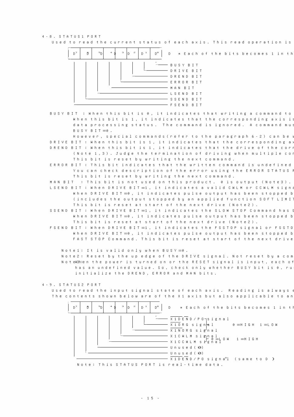
4-8. STATUS1 PORT
Used to read the current status of each axis. This read operation is always enabled.
D D D D D D D D * Each of the bits becomes 1 in the active state.7 6 5 4 3 2 1 0
BUSY BIT
DRIVE BIT
DREND BIT
ERROR BIT
MAN BIT
LSEND BIT
SSEND BIT
FSEND BIT
BUSY BIT : When this bit is 0, it indicates that writing a command to the corresponding axis is enabled.
When this bit is 1, it indicates that the corresponding axis is in the driving status or in the
data processing status. The command is ignored. A command must be written after confirming
BUSY BIT=0.
However, special commands(refer to the paragraph 6-2) can be written even when BUSY BIT=1.
DRIVE BIT : When this bit is 1, it indicates that the corresponding axis is in the driving status.
DREND BIT : When this bit is 1, it indicates that the drive of the corresponding axis has been terminated
(Note 1,3). Judge the termination of driving when multiple control.
This bit is reset by writing the next command.
ERROR BIT : This bit indicates that the written command is undefined or has a data error(Note 1,3).
You can check description of the error using the ERROR STATUS READ Command.
This bit is reset by writing the next command.
MAN BIT : This bit is not used on this product. 0 is output (Note3).
LSEND BIT : When DRIVE BIT=1, it indicates a valid CWLM or CCWLM signal has been entered.
When DRIVE BIT=0, it indicates pulse output has been stopped by CWLM or CCWLM signal
(includes the output stopped by an applied function SOFT LIMIT).
This bit is reset at start of the next drive (Note2).
SSEND BIT : When DRIVE BIT=1, it indicates the SLOW STOP Command has been entered.
When DRIVE BIT=0, it indicates pulse output has been stopped by the SLOW STOP Command.
This bit is reset at start of the next drive (Note2).
FSEND BIT : When DRIVE BIT=1, it indicates the FSSTOP signal or FSSTOP Command has been entered.
When DRIVE BIT=0, it indicates pulse output has been stopped by the FSSTOP signal or
FAST STOP Command. This bit is reset at start of the next drive (Note2).
Note1: It is valid only when BUSY=0.
Note2: Reset by the up edge of the DRIVE signal. Not reset by a command not accompanied by drive.
When the power is turned on or the RESET signal is input, each of DREND, ERROR and MAN bitsNote3:
has an undefined value. So, check only whether BUSY bit is 0, run an NOP command and then
initialize the DREND, ERROR and MAN bits.
4-9. STATUS2 PORT
Used to read the input signal state of each axis. Reading is always enabled.
The contents shown below are of the X1 axis but also applicable to another axis.
D D D D D D D D * Each of the bits becomes 1 in the active state.7 6 5 4 3 2 1 0
X1DEND/PO signal
X1ORG signal 0=HIGH 1=LOW
X1NORG signal
X1CWLM signal0=LOW 1=HIGH
X1CCWLM signal
Unused(0)
Unused(0)
X1DEND/PO signal (same to D )0
Note: This STATUS PORT is real-time data.

- 16 -
4-10.STATUS3 PORT
Used to read the status information from the PULSE COUNTER and DIFFERENTIAL COUNTER.
Reading is always enabled.
D D D D D D D D * Each of the bits becomes 1 in the active state.7 6 5 4 3 2 1 0
PLS COMP1 BIT
PLS COMP2 BIT
PLS COMP3 BIT
PLS COMP4 BIT
PLS COMP5 BIT
PLS OVF BIT
DFL COMP1 BIT
DFL COMP2 BIT
PLS COMP1 BIT : Indicates that the PULSE COUNTER has matched the COMPARE REGISTER1. (Note)*
PLS COMP2 BIT : Indicates that the PULSE COUNTER has matched the COMPARE REGISTER2. (Note)
PLS COMP3 BIT : Indicates that the PULSE COUNTER has matched the COMPARE REGISTER3. (Note)
PLS COMP4 BIT : Indicates that the PULSE COUNTER has matched the COMPARE REGISTER4. (Note)
PLS COMP5 BIT : Indicates that the PULSE COUNTER has matched the COMPARE REGISTER5. (Note)
PLS OVF BIT : Indicates that the PULSE COUNTER has overflowed.
DFL COMP1 BIT : Indicates the DIFFERENTIAL COUNTER≧DFL COMPARE REGISTER1 (excessive deviation). (Note)*
DFL COMP2 BIT : Indicates the DIFFERENTIAL COUNTER≦DFL COMPARE REGISTER2 (positioning complete).(Note)
Note: In the initial state, there bits are reset after this status has been read except for when the following
state is indicated matching between the PULSE COUNTER and REGISTER, excessive deviation or positioning
complete has been indicated. It is enable to reset all the time after status has been read by setting
each of the COUNTER INITIALIZE COMMAND.
* Throughout this manual, the abbreviations "PLS" and "DFL" stands for PULSE and DIFFERENTIAL, respectively.
4-11.STATUS4 PORT
Used to read the input signal state of each axis. Reading is always enabled.
D D D D D D D D * Each of the bits becomes 1 in the active state.7 6 5 4 3 2 1 0
FSSTOP1 signal (common to all axes) 0=LOW 1=HIGH
〃 (Note1)
A1SENSOR input signal (Note2) 0=HIGH 1=LOW
-X1EA input signal 0=LOW 1=HIGH
-X1EB input signal 0=LOW 1=HIGH
X1DRST output signal 0=HIGH 1=LOW
Unused (undefined)
Note1: FSSTOP1 input signal is set at X1 to A1 axes, and FSSTOP2 input signal is set at X2 to A2 axes.
Note2: SENSOR input signal is available for the A1, Z1, A2 and Z2 axes alone. 0 is output for other axes.
For details of SENSOR input signal, refer to the User's Manual [Applied Functions Part].
Note3: This status is real time data of input/output pins.

- 17 -
4-12.STATUS5 PORT
This port is used for reading current state of the SOFT LIMIT (An applied function, see Note) and speed
change. Data read is always enabled.
D D D D D D D D * Each of the bits becomes 1 in the active state.7 6 5 4 3 2 1 0
CCW SOFT LIMIT BIT (Note1)
CW SOFT LIMIT BIT (Note1)
Unused(0)
RDYINT BIT (Note2)
Unused(0)
SPEED CHANGE BUSY BIT
RATE CHANGE BUSY BIT (Note1)
INDEX CHANGE BUSY BIT (Note1)
Note1: For details, see User's Manual(Applied Functions Part).
Note2: When interrupt is used, RDYINT request axis is identified by this bit.
4-13.General-purpose I/O PORT 1, 2
The C-872 is provided with a general-purpose I/O with 4 input points (INx0 to INx3 input signals) and
4 output points (OUTx0 to OUTx3 output signals). Two modules is provided, So the argument `x' is `1' or
`2'. The user can freely use this general-purpose I/O.
These signals are active low. When each of them is in the active state, the LED on the board come on.
The following description will be given about only the first module.
(1) Input port
The input port consists of an input data division and an output data division as shown below.
The external input (IN10 to IN13) states are read into the input data division.
The output data division reads the current output port state (data previously output to the output port).
This below is
* Each of these bits becomes 1 in the active state.
OUT10
OUT11Output data division
OUT12
OUT13
IN10
IN11Input data division
IN12
IN13
(2) Output data port
The output port consists of the following bits and outputs the contents of the 4 low-order bits to the
outside (OUT10 to OUT13).
* Each of these bits becomes 1 in the active state.
OUT10
OUT11Output data division
OUT12
OUT13
The output port is put into the OFF output (NOT ACTIVE) state at POWER ON/RESET.
- 18 -
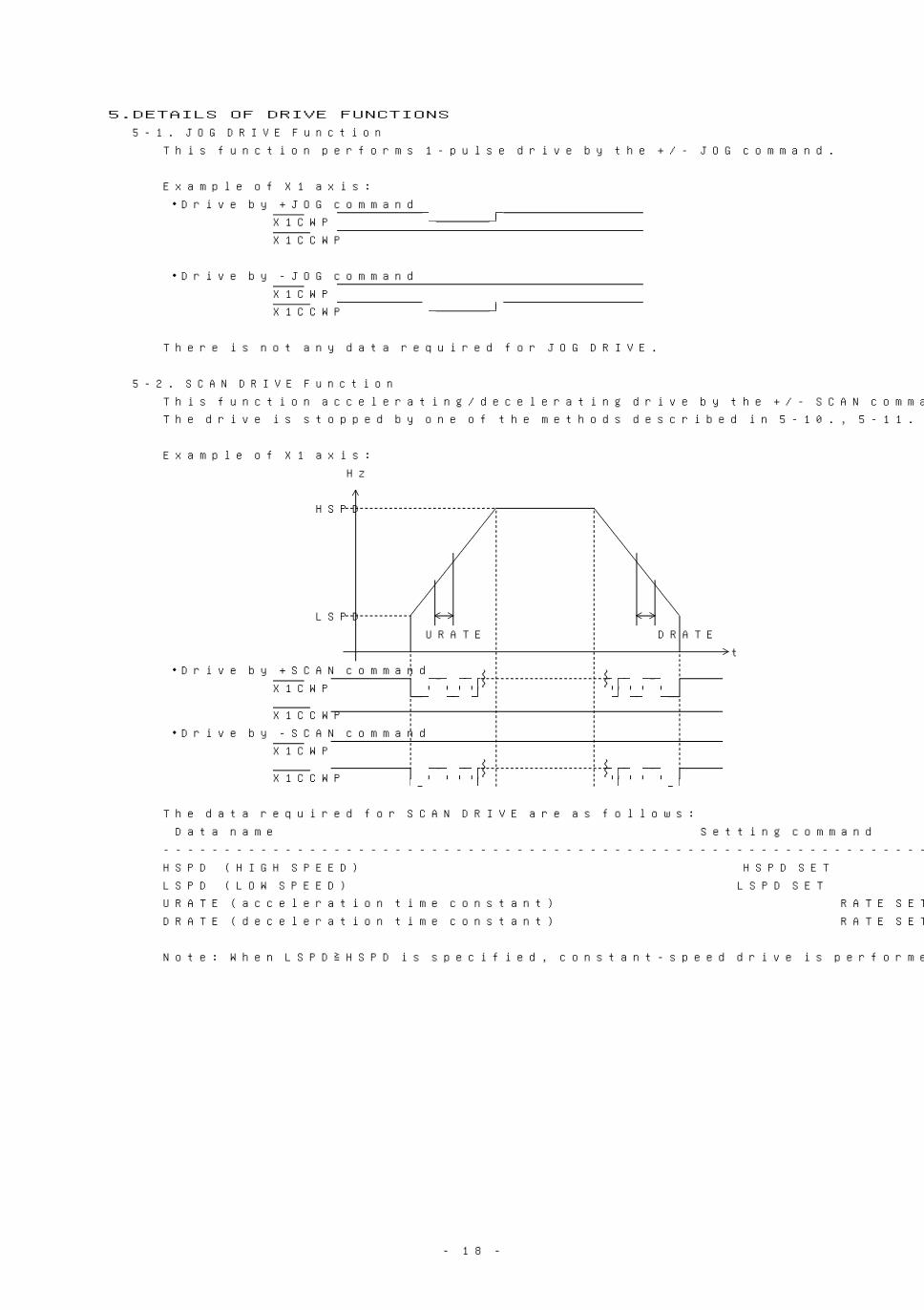
5.DETAILS OF DRIVE FUNCTIONS
5-1. JOG DRIVE Function
This function performs 1-pulse drive by the +/- JOG command.
Example of X1 axis:
・Drive by +JOG command
X1CWP
X1CCWP
・Drive by -JOG command
X1CWP
X1CCWP
There is not any data required for JOG DRIVE.
5-2. SCAN DRIVE Function
This function accelerating/decelerating drive by the +/- SCAN command.
The drive is stopped by one of the methods described in 5-10., 5-11. and 5-12.
Example of X1 axis:
Hz
HSPD
LSPD
URATE DRATE
t
・Drive by +SCAN command
X1CWP
X1CCWP
・Drive by -SCAN command
X1CWP
X1CCWP
The data required for SCAN DRIVE are as follows:
Data name Setting command
-----------------------------------------------------------------------------------------------
HSPD (HIGH SPEED) HSPD SET
LSPD (LOW SPEED) LSPD SET
URATE (acceleration time constant) RATE SET
DRATE (deceleration time constant) RATE SET
Note: When LSPD≧HSPD is specified, constant-speed drive is performed with HSPD.

- 19 -
5-3. INDEX DRIVE Function
Accelerating/decelerating drive is performed with the specified number of pulses by the INCREMENTAL INDEX
command. (or up to the target address by ABSOLUTE INDEX command).
Example of X1 axis:
Hz
HSPD
Specified number
of pulses
(target address)
LSPD
URATE DRATE
t
・When +(CW)direction is specified
X1CWP
X1CCWP
・When -(CCW)direction is specified
X1CWP
X1CCWP
The data required for INDEX DRIVE is as follows.
Data name Setting command
-----------------------------------------------------------------------------------------------
HSPD (HIGH SPEED) HSPD SET
LSPD (LOW SPEED) LSPD SET
URATE (acceleration time constant) RATE SET
DRATE (deceleration time constant) RATE SET
Specified number of pulses (target address) When INDEX DRIVE is started
Note1: When LSPD≧HSPD is specified, constant-speed drive is performed with HSPD.
Note2: When LSPD<HSPD and URATE≠DRATE are specified, the timing up to a pulse output is different from
that of URATE=DRATE. For details refer to Chapter 12. Timing.
For this reason, please use the same data unless specially required.
5-4. Drive Speed Change Function
Using the SPEED CHANGE command allows you to change speed of the SCAN or INDEX DRIVE currently taking place
(note that this command is valid only for these two drive types).
The drive is accelerated or decelerated to the speed specified by the SPEED CHANGE Command.
Note1: This speed change is not available when the INDEX DRIVE is taking place at URATE≠DRATE.
Note2: Speed change is available within the range of LSPD<Change speed<HSPD.
Note3: When the SPEED CHANGE Command has been executed, you must wait until the command is internally
accepted before requesting another speed change using this command. Check the SPEED CHANGE BUSY BIT
in the STATUS5 PORT to make sure that the SPEED CHANGE Command is executable.

- 20 -
5-5. Machine Origin Detecting Function (ORIGIN DRIVE)
Drive is performed up to machine origin detection by the ORIGIN command.
The drive up to machine origin detection is performed by a combination of JOG DRIVE, CONSTANT SCAN DRIVE,
SCAN DRIVE and ABSOLUTE INDEX DRIVE.
There are 9 types of machine origin detection. For the details of the types and processes, refer to
Chapter 7.
The data required for ORIGIN DRIVE is as follows:
Data name Setting command
-----------------------------------------------------------------------------------------------
HSPD (HIGH SPEED) HSPD SET
LSPD (LOW SPEED) LSPD SET
CSPD (CONSTANT SPEED) CSPD SET
URATE (acceleration time constant) RATE SET
DRATE (deceleration time constant) RATE SET
OFFSET PULSE OFFSET PULSE SET
LDELAY (LIMIT DELAY TIME) ORIGIN DELAY SET
SDELAY (SCAN DELAY TIME) ORIGIN DELAY SET
JDELAY (JOG DELAY TIME) ORIGIN DELAY SET
5-6. Machine Origin Detecting Function Using Limit Sensor
Two of the machine origin detection sensors can use CCW LIMIT signal as the origin sensor.
This function helps reducing number of sensors.
Refer to Chapter 7 for details of the models and processes.

- 21 -
5-7. S-RATE SCAN DRIVE Function
S-shaped accelerating/decelerating drive is performed by the +/- S-RATE SCAN command.
At the S-shaped accelerating/decelerating drive, the speed difference between SLSPD and SHSPD is divided
into 3 equal parts. In the mid-speed area of the 3 equally-divided parts, linear acceleration/deceleration
is performed by SRATE.
In the remaining areas, curvilinear smooth acceleration/deceleration is performed.
The drive is stopped by one of the methods described in 5-10., 5-11. and 5-12.
The data required for S-RATE SCAN DRIVE is as follows:
Data name Setting command
-----------------------------------------------------------------------------------------------
SHSPD (high speed for S-RATE DRIVE) SHSPD SET
SLSPD (low speed for S-RATE DRIVE) SLSPD SET
SRATE (acceleration/deceleration time constant for S-RATE DRIVE) SRATE SET
Note: When SLSPD≧SHSPD is specified, constant-speed drive is performed with SHSPD.
5-8. S-RATE INDEX DRIVE Function
S-shaped accelerating/decelerating drive is performed with the specified number of pulses
(or up to the target address) by the S-RATE INCREMENTAL INDEX command (or S-RATE ABSOLUTE INDEX command).
The acceleration/deceleration rate characteristics are the same as those of S-RATE SCAN DRIVE.
The data required for S-RATE INDEX DRIVE is as follows:
Data name Setting command
-----------------------------------------------------------------------------------------------
SHSPD (high speed for S-RATE DRIVE) SHSPD SET
SLSPD (low speed for S-RATE DRIVE) SLSPD SET
SRATE (acceleration/deceleration time constant for S-RATE DRIVE) SRATE SET
Specified number of pulses (target address) When S-RATE INDEX DRIVE is started
Note: When SLSPD≧SHSPD is specified, constant-speed drive is performed with SHSPD.

- 22 -
5-9. S-RATE DRIVE Parameter Adjusting Function
For S-RATE DRIVE, internal parameters can be adjusted. To perform S-RATE DRIVE, the 4 internal parameters
of SSRATE, SERATE, SCSPD1 and SCSPD2 are required first.
Usually, these parameters are automatically set to initial values when SRATE, SLSPD and SHSPD are set but
can be adjusted to optional values by respective adjust commands.
The adjustable parameters are as follows.
Data name Adjust command
----------------------------------------------------------------------------------------------------------
SSRATE (time constant at a start of acceleration and an end of deceleration) SSRATE ADJUST
SERATE (time constant at an end of acceleration and at a start of deceleration) SERATE ADJUST
SCSPD1 (linear rate start speed at acceleration and linear rate end speed at deceleration) SCSPD1 ADJUST
SCSPD2 (linear rate end speed at acceleration and linear rate start speed at deceleration) SCSPD2 ADJUST
(1) SSRATE
Explanation of data …… Indicates the momentary time constant at a start of acceleration and at a end of
deceleration.
The time constant changes smoothly from SSRATE to SRATE between SLSPD and SCSPD1.
Initial value …………… Automatically set nearly to an eightfold value of SRATE by the SRATE SET command.
Note1: When DRIVE TYPE is the fixed mode,the initial value of SSRATE may be a
nonexistent value in the rate data table depending on the SRATE value.
(Even if the eightfold value of SRATE does not exist in the rate data table,
the eightfold value of SRATE is adopted as an initial value of SSRATE.)
Note2: When the SRATE value is large, the SSRATE value cannot exceed the maximum
settable rate value. The maximum rate value in each drive type is approximately
as shown below.
L-TYPE ……………… Approx. 1030ms/1000Hz
M-TYPE ……………… Approx. 51.5ms/1000Hz
H-TYPE ……………… Approx. 5.15ms/1000Hz
Arithmetic mode … When resolution data is supposed to be D
Maximum rate value=1,030 ÷ D(ms/1000Hz)
(For the details of the arithmetic mode,
refer to the User's Manual [Applied Functions Part].)
Adjusting range ………… SSRATE≧SRATE
Note1: When SSRATE<SRATE, is specified, SSRATE=SRATE.
Note2: After the SRATE SET command is executed, the SSRATE value adjusted prior to the
execution is invalidated and reset to the initial value.
When DRIVE TYPE has been changed by the SPEC INITIALIZE1 command, the SSRATE
value is also reset to the initial value.
(2) SERATE
Explanation of data …… Indicates the time constant at an end of acceleration and at a start of
deceleration.
The time constant changes smoothly from SRATE to SERATE between SCSPD2 and SHSPD.
Initial value …………… The same as SSRATE.
Adjusting range ………… The same as SSRATE.

- 23 -
(3) SCSPD1
Explanation of data …… Indicates the linear rate start speed or linear rate end speed by SRATE.
Between SCSPD1 and SCSPD2, the time constant indicates a linear rate
characteristic because the SRATE value is fixed.
Initial value …………… Set to the following value represented by the following expression by the SLSPD
SET or SHSPD SET command.
1SCSPD1=SLSPD+(SHSPD-SLSPD)×
3
Adjusting range ………… SLSPD≦SCSPD1≦SCSPD2
Note1: When SCSPD1<SLSPD is specified, SCSPD1=SLSPD.
When SCSPD1>SCSPD2 is specified, SCSPD1=SCSPD2.
Note2: After the SLSPD SET or SHSPD SET command is executed,
the SCSPD1 value adjusted prior to the execution is invalidated and reset to
the initial value.
When DRIVE TYPE has been changed by the SPEC INITIALIZE1 command, the SCSPD1
value is reset to the initial value.
(4) SCSPD2
Explanation of data …… Indicates the linear rate end speed or linear rate start speed by SRATE.
Between SCSPD1 and SCSPD2, the time constant indicates a linear rate
characteristic because the SRATE value is fixed.
Initial value …………… Set to the value represented by the following expression by the SLSPD SET or
SHSPD SET command.
2SCSPD2=SLSPD+(SHSPD-SLSPD)×
3
Adjusting range ………… SCSPD1≦SCSPD2≦SHSPD
Note1: When SCSPD2<SCSPD1 is specified, SCSPD2=SCSPD1.
When SCSPD2>SHSPD is set, SCSPD2=SHSPD.
Note2: After the SLSPD SET or SHSPD SET command is executed,
the SCSPD2 value adjusted prior to the execution is invalidated and reset to
the initial value.
When DRIVE TYPE has been changed by the SPEC INITIALIZE1 command, the SCSPD2
value is also reset to the initial value.

- 24 -
5-10.Slow Stop Function
The pulse output can be put into a slow stop by the SLOW STOP command.
After the pulse output is stopped in the above way, SSEND becomes 1.
5-11.Fast Stop Function
When you use emergency stop in response to system failure, also turn off power of the
WARNING drive system. If an error has occurred to the controller or wiring system, the Fast Stop
may not work. This may lead to a serious accident. For details, refer to Chapter 19.
The pulse output can be put into an fast stop by the FSSTOP command or FSSTOP signal.
After the pulse output is stopped in the above way, FSEND becomes 1.
FSSTOP1 signal stops four axes, X1, Y1, Z1 and A1 immediately.
FSSTOP2 signal stops four axes, X2, Y2, Z2 and A2 immediately.
5-12.LIMIT Stop Function
When you use emergency stop in response to system failure, also turn off power of the
WARNING drive system. If an error has occurred to the controller or wiring system, LIMIT Stop
may not work. This may lead to a serious accident. For details, refer to Chapter 19.
If any error has occurred to the system or your setting is incorrect, the machine or
CAUTION workpiece damage and personal injury may occur. To prevent such an accident, be sure
to use the LIMIT Stop function for the equipment except on the rotation system.
When you use the LIMIT stop as slow stop, there may be a collision with the limit
CAUTION position of the mechanical device before stop. This may lead to machine or workpiece
damage. Note that the stop point will be changed if RATE, HSPD, etc. are changed.
The pulse output can be stopped by the CWLM signal when the pulse output is in the +(CW)direction or by
the CCWLM signal when the same output is in the -(CCW)direction. After the pulse output is stopped in the
above way, LSEND becomes 1. The LIMIT stop type can be switched between fast stop and slow stop by
the SPEC INITIALIZE1 command. "Fast stop" is selected at POWER ON/RESET.
5-13.Function for Servo Driver
The target motor can be switched by the SPEC INITIALIZE1 command. The target motor is a servo motor or
a stepping motor. "Stepping motor" is selected as the target motor at POWER ON/RESET.
The signals for servo motor are as follows.
DEND input signal: The deviation COUNTER END signal from the servo driver is input. Even after the
completion of pulse output, the driving status is kept until DEND=LOW is confirmed,
and the command is not terminated with BUSY and DRIVE BIT=1.
DRST output signal: The deviation COUNTER RESET signal is output to the servo driver. If the pulse output
is put into an fast stop, the DRST signal=LOW is output for 10ms and the deviation
COUNTER of the servo driver is reset. The DRST signal=LOW can also be output
optionally for 10ms by the SERVO RESET command.
The above signals are disabled when a stepping motor is selected as the target.
In this case, DEND input and DRST output can be used as a general purpose input and general purpose output,
respectively. For their usage, refer to the User's Manual [Applied Functions Part].
5-14.Current Position Reading Function
The current position can read by the ADDRESS READ command.
The guaranteed data range is a pulse area of +8,388,607 to -8,388,607. The current position is reset to
0 at POWER ON/RESET and can also be set to an optional value by the ADDRESS INITIALIZE command.

- 25 -
5-15.Interrupt Request Function
(1) After the termination of a command, an interrupt request (RDYINT signal) can be generated for the
initiator. RDYINT signal is generated too at the stop(the termination of a command) for FSSTOP,
STOP, and LIMIT, etc.
There are 3 interrupt request generation patterns as shown below.
One of them is selected by the SPEC INITIALIZE1 command. Item 1 is selected at POWER ON/RESET.
1. Output only when a command accompanied by pulse output is terminated.
2. Output when every command is terminated(except special commands).
3. No output in any case.
Note: This function is not effective when the COUNTER command is executed or when special commands are
executed. For details of special commands, Refer to the description of 6-2
(2) Interrupt request (CNTINT signal) may occur in response to any given count value of the PULSE COUNTER.
Interrupt request (DFLINT signal) may occur in response to the value above or below any given count value
of the DEFERENTIAL COUNTER. For details, refer to the description of PULSE/DEFERENTIAL COUNT COMPARE
function in DETAILS OF COUNTER FUNCTION in Chapter 8.
5-16.Speed Data Hz Unit Setting Function
Speed data (HSPD, LSPD, CSPD, SHSPD, SLSPD, and HSPD1 to 10 when an applied function is used) can be
set as 3-byte data in Hz.
The data setting range is 1 to 3,333,333 so the speed can be set in the range of 1Hz to 3.3MHz.
*Speed setting example
When 10000 (002710 ) has been set in the HSPD:H
HSPD=10000Hz
However, the MCC05v2 output frequency is controlled by counting the reference clocks (40MHz).
For this reason, a frequency that cannot be physically output may appear for the set value of speed data.
Consequently, there will be a difference,specially in a high speed area, between the set value and the real
output frequency.
Supposing that the set value of speed data is F', the real output frequency F is represented by the
following expression.
160,000,000F= (Hz)
Integer part of 〔160,000,000/F'〕
In the above expression, the part following the decimal point of the wavy-underlined number will be ignored,
so that the real output frequency becomes a little higher than the set value.
Take this point into consideration when accuracy is required between the set value and the real output.
5-17.DRIVE TYPE Switching Function
The acceleration/deceleration time constant method when the MCC05v2 is put in accelerating/decelerating
drive can be roughly classified into two modes, fixed data mode and arithmetic mode.
For the fixed data mode, the 3 types of L-TYPE, M-TYPE and H-TYPE are available for reasons of output
frequency,acceleration/deceleration time constant setting range and speed difference at acceleration/
deceleration, etc.
For the arithmetic mode, refer to the User's Manual [Applied Functions Part].
In the fixed data mode, the acceleration/deceleration time constant (URATE, DRATE) is fixed by the data
table beforehand, so the user must specify an appropriate time constant by No. of the data table.
For the rate data table, refer to Chapter 18. The speed range, rate range and speed difference at
acceleration/deceleration in each type are as follows.
Fixed data modeArithmetic mode
L-TYPE M-TYPE H-TYPE
Speed range10Hz~100kHz 10Hz~800kHz 10Hz~3.3MHz 10Hz~3.3MHz
(LSPD,SLSPD)
Speed range1Hz~100kHz 1Hz~800kHz 1Hz~3.3MHz 1Hz~3.3MHz
(except LSPD,SLSPD)
1000ms/1000Hz 50ms/1000Hz 5ms/1000Hz 1030ms/1000HzRate range
~1.0ms/1000Hz ~0.05ms/1000Hz ~0.005ms/1000Hz ~0.004ms/1000Hz
Speed difference 51Hz/STEP 1kHz/STEP 10kHz/STEP 51Hz/STEP
(Note1) ~62Hz/STEP ~4kHz/STEP ~68kHz/STEP ~68kHz/STEP
Note1: The speed difference indicates a speed difference between before and after speed change at
acceleration/deceleration. This speed difference is rather small at a low speed and gradually
increases as the speed is accelerated.

- 26 -
5-18.Present Speed Reading Function
Speed data can be read from the DRIVE DATA1, 2 and 3 PORTs during drive, and read data can be
converted into present speed by using the following formula:
160,000,000Present Speed = (Hz)
V
where, V : Read data
Note1: The range of speed to be read by using this function is from about 9.5Hz to 3.3MHz because the
data length is 3byte. Be careful in reading speeds in the slow area.
Note2: Since the DRIVE DATA1, 2 and 3 PORTs are generally dedicated to read values of the PULSE COUNTER,
it is necessary to change the port function to reading speed data in case of reading speed.
To change the function, the SPEED PORT SELECT Command is used.
5-19.Set Data Reading Function
The SET DATA READ Command allows you to read various set data or SPEC INITIALIZE DATA.
This function is helpful for debugging or for applications requiring high reliability since it enables to
re-confirm data already set to each axis.

- 27 -
6.DESCRIPTION OF BASIC FUNCTION DRIVE COMMANDS
AND OPERATION SEQUENCES
Execute each command to the port (refer to 4-1.) of the axis to which the command is executed.
In the following, a description is give about the X1 axis MCC05v2. The same is also applicable to another aixs.
6-1. Basic Function DRIVE Command Table
The mark * denotes a command accompanied by pulse output.
D D D D D D D D HEX C0DE COMMAND NAME Execution time7 6 5 4 3 2 1 0
0 0 0 0 0 0 0 0 00 NO OPERATION MAX 20μs
0 0 0 0 0 0 0 1 01 SPEC INITIALIZE1 MAX 1.2ms(Note1)
0 0 0 0 0 0 1 0 02 PULSE COUNTER INITIALIZE MAX 25μs
0 0 0 0 0 0 1 1 03 ADDRESS INITIALIZE MAX 30μs
0 0 0 0 0 1 0 0 04 ADDRESS READ MAX 25μs
0 0 0 0 0 1 0 1 05 SERVO RESET MAX 11ms
0 0 0 0 0 1 1 0 06 RATE SET MAX 60μs(Note1)
0 0 0 0 0 1 1 1 07 LSPD SET MAX 95μs(Note1)
0 0 0 0 1 0 0 0 08 HSPD SET MAX 85μs
0 0 0 0 1 0 0 1 09 DFL COUNTER INITIALIZE MAX 25μs
0 0 0 0 1 0 1 0 0A SET DATA READ MAX 35μs
0B~0F Setting is disabled. (Note3)
* 0 0 0 1 0 0 0 0 10 +JOG (Note2)
* 0 0 0 1 0 0 0 1 11 -JOG (Note2)
* 0 0 0 1 0 0 1 0 12 +SCAN (Note2)
* 0 0 0 1 0 0 1 1 13 -SCAN (Note2)
* 0 0 0 1 0 1 0 0 14 INCREMENTAL INDEX (Note2)
* 0 0 0 1 0 1 0 1 15 ABSOLUTE INDEX (Note2)
16~17 Setting is disabled.
18~19 Setting is disabled. (Note3)
0 0 0 1 1 0 1 0 1A CSPD SET MAX 55μs
0 0 0 1 1 0 1 1 1B OFFSET PULSE SET MAX 20μs
0 0 0 1 1 1 0 0 1C ORIGIN DELAY SET MAX 25μs
0 0 0 1 1 1 0 1 1D ORIGIN FLAG RESET MAX 25μs
* 0 0 0 1 1 1 1 0 1E ORIGIN (Note2)
0 0 0 1 1 1 1 1 1F Setting is disabled.
20~5F Setting is disabled. (Note3)
0 1 1 0 0 0 0 0 60 SRATE SET MAX 150μs
0 1 1 0 0 0 0 1 61 SLSPD SET MAX 150μs
0 1 1 0 0 0 1 0 62 SHSPD SET MAX 150μs
0 1 1 0 0 0 1 1 63 SSRATE ADJUST MAX 100μs
0 1 1 0 0 1 0 0 64 SERATE ADJUST MAX 100μs
0 1 1 0 0 1 0 1 65 SCSPD1 ADJUST MAX 100μs
0 1 1 0 0 1 1 0 66 SCSPD2 ADJUST MAX 100μs
67~6F Setting is disabled.
* 0 1 1 1 0 0 0 0 70 + S-RATE SCAN (Note2)
* 0 1 1 1 0 0 0 1 71 - S-RATE SCAN (Note2)
* 0 1 1 1 0 0 1 0 72 S-RATE INCREMENTAL INDEX (Note2)
* 0 1 1 1 0 0 1 1 73 S-RATE ABSOLUTE INDEX (Note2)
74~E1 Setting is disabled.
1 1 1 0 0 0 1 0 E2 ERROR STATUS READ MAX 25μs
E3~F1 Setting is disabled.
F2~F6 Setting is disabled. (Note3)
Note1: When URATE ≠ DRATE is specified, the execution time as follows.
L-TYPE M-TYPE H-TYPE
MAX100ms MAX 35ms MAX 15ms
Note2: The execution time cannot be specified. Refer to Chapter 12. Timing.
Note3: Applied function DRIVE commands are assigned.
For details, refer to the User's Manual [Applied Functions Part].

- 28 -
6-2. Special Command Table
Special commands can always be executed, except just behind not Special command executed in less than 4μs.
D D D D D D D D HEX C0DE COMMAND NAME Execution time7 6 5 4 3 2 1 0
1 1 1 1 0 1 1 1 F7 SPEED CHANGE (Note)
1 1 1 1 1 0 0 0 F8 INT MASK MAX 200ns
1 1 1 1 1 0 0 1 F9 ADDRESS COUNTER PORT SELECT MAX 200ns
1 1 1 1 1 0 1 0 FA DFL COUNTER PORT SELECT MAX 200ns
1 1 1 1 1 1 0 0 FC PULSE COUNTER PORT SELECT MAX 200ns
1 1 1 1 1 1 0 1 FD SPEED PORT SELECT MAX 200ns
1 1 1 1 1 1 1 0 FE SLOW STOP (Note)
1 1 1 1 1 1 1 1 FF FAST STOP (Note)
Note: The execution time cannot be specified. Refer to Chapter 12. Timing.
6-3. NO OPERATION Command
COMMAND……… 00 Function : No functionH
However, DREND BIT and ERROR BIT in STATUS1 are cleared.
Execution sequence
N BUSY=0 in
STATUS1?
Y
HCOMMAND 00
WRITE

- 29 -
6-4. SPEC INITIALIZE1 Command
COMMAND……… 01 Function : Defines operation specifications.H
Execution sequence
Drive control specifications are defined in DRIVE DATA1.
N BUSY=0 in
STATUS1? The contents of DRIVE DATA1 PORT is as follows.
Y DATA1 PORT7 0DATA1 PORT D D
WRITE
COMMAND 01 DRIVE TYPEH
WRITE LIMIT STOP TYPE
MOTOR TYPE
RDYINT TYPE
The bit marked slash may be set to 0 or 1.
The details of each bit are shown below. The bit is set to the underlined side at POWER ON/RESET.
(1) DRIVE TYPE (D ,D )1 0
Specifies DRIVE TYPE.
D D DRIVE TYPE1 0
0 0 L-TYPE
0 1 M-TYPE
1 0 H-TYPE Note: For the arithmetic mode, refer to
1 1 Arithmetic mode (Note) the User's Manual [Applied Functions Part].
(2) LIMIT STOP TYPE (D )2
Specifies the type of LIMIT STOP by the CWLM and CCWLM signals.
0: Fast stop 1: Slow stop
(3) MOTOR TYPE (D )3
Specifies the target motor.
0: SERVO 1: STEPPING
(4) RDYINT TYPE (D ,D )5 4
Specifies an interrupt request (RDYINT) generation pattern upon termination of a command.
D D Generation pattern5 4
0 0 Generated upon termination of a command accompanied by pulse output.
0 1 Generated upon termination of every command.
1 x Not output in any case.

- 30 -
6-5. PULSE COUNTER INITIALIZE Command
COMMAND……… 02 Function : Defines PULSE COUNTER operation specifications.H
Execution sequence PULSE COUNTER specifications are defined in DRIVE DATA1, DRIVE DATA2
and DRIVE DATA3 PORT.
N BUSY=0 in The contents of DRIVE DATA1 WRITE PORT are as follows.
STATUS1?
DATA1 PORT7 0Y D D
DATA1 PORT
WRITE
The order COMP STOP TYPE
DATA2 PORT may not CNTINT OUTPUT TYPE
WRITE be observed. CNTINT LATCH TRIGGER TYPE
DATA3 PORT
WRITE Note: The bit D to D must to be set 0.7 3
HCOMMAND 02
WRITE
The details of each bit are shown below. The bit is set to the underlined side at POWER ON/RESET.
(1) COMP STOP TYPE (D )0
When the "Stop Enable" is selected for the PULSE COUNTER COMP STOP ENABLE, this bit is used for specifying
the fast stop or slow stop. (The same specification is selected for the COMPARE REGISTER1 to 5).
0: Fast stop 1: Slow stop
(2) CNTINT OUTPUT TYPE (D )1
This bit is used for specifying a CNTINT output specification on the PULSE COUNTER.
(The same specification is selected for the COMPARE REGISTER1 to 5).
0: Latches and outputs detection done on each comparator (executing the STATUS3 READ resets the latch).
1: Detection done on each comparator is output without being latched.
Note: Selecting 1 outputs the comparator detection as it is, thus reset with the STATUS3 READ becomes
unavailable.
(3) CNTINT LATCH TRIGGER TYPE (D )2
When "Latch" is selected for the CNTINT output specification of the PULSE COUNTER, this bit is used for
selecting a latch type (the same specification is selected for the COMPARE REGISTER1 to 5).
0: Level latch (Even if you may execute the STATUS3 READ while the detection conditions are met,
current active state of CNTINT output remains the same).
1: Edge latch (Executing the STATUS3 READ generates CNTINT output reset even if the detection
conditions are met).
Note: When the output without latch is selected for CNTINT output, this bit does not have any effect.

- 31 -
The contents of DRIVE DATA2 WRITE PORT are as follows.
DATA2 PORT7 0D D
COUNT CLOCK TYPE
COUNT PATTERN TYPE
AUTO CLEAR ENABLE
RELOAD ENABLE
COMP1 INT ENABLE
COMP1 STOP ENABLE
The bit marked slash may be set 0 or 1.
The details of each bit are shown below. The bit is set to the underlined side at POWER ON/RESET.
(1) COUNT CLOCK TYPE (D )0
Selects an operation clock of the PULSE COUNTER.
0: Operated by DRIVE PULSE (X1CWP, X1CCWP) of the X1 axis MCC05v2.
1: Operated by external clocks from X1EA (X1 axis encoder A phase signal) and X1EB (X1
axis encoder B phase signal).
(2) COUNT PATTERN TYPE (D , D )1 2
These bits become effective only when D BIT=1, selecting an external input clock count method.0
D D Count pattern Input clock type2 1
0 0 Count by multiplying the X1EA and X1EB inputs by 1. 90゚ phase
0 1 Count by multiplying the X1EA and X1EB inputs by 2. difference clock
1 0 Count by multiplying the X1EA and X1EB inputs by 4.
1 1 Count-up by X1EA and count-down by X1EB. Independent clock
for each direction
(3) AUTO CLEAR ENABLE (D )3
Sets the AUTO CLEAR function.
0: No AUTO CLEAR is executed. 1: AUTO CLEAR is executed.
(4) RELOAD ENABLE (D )4
Sets the RELOAD function.
0: No RELOAD is executed. 1: RELOAD is executed.
(5) COMP1 INT ENABLE (D )5
Determines whether or not to output the match output X1CNTINT of COMPARE REGISTER1.
0: X1CNTINT is not output. 1: X1CNTINT is output.
(6) COMP1 STOP TYPE (D )6
Determines whether or not to put the pulse output into stop by the match output of COMPARE REGISTER1.
0: Not put into stop. 1: Put into stop.

- 32 -
The contents of DRIVE DATA3 WRITE PORT are as follows.
DATA3 PORT7 0D D
COMP2 INT ENABLE
COMP2 STOP TYPE
COMP3 INT ENABLE
COMP3 STOP TYPE
COMP4 INT ENABLE
COMP4 STOP TYPE
COMP5 INT ENABLE
COMP5 STOP TYPE
The details of each bit are shown below. The bit is set to the underlined side at POWER ON/RESET.
(1) COMP2 INT ENABLE (D )0
Determines whether or not to output the match output CNTINT of COMPARE REGISTER2.
0: CNTINT is not output. 1: CNTINT is output.
(2) COMP2 STOP TYPE (D )1
Determines whether or not to put the pulse output into stop by the match output of COMPARE REGISTER2.
0: Not put into stop. 1: Put into stop.
(3) COMP3 INT ENABLE (D )2
Determines whether or not to output the match output X1CNTINT of COMPARE REGISTER3.
0: X1CNTINT is not output. 1: X1CNTINT is output.
(4) COMP3 STOP TYPE (D )3
Determines whether or not to put the pulse output into stop by the match output of COMPARE REGISTER3.
0: Not put into stop. 1: Put into stop.
(5) COMP4 INT ENABLE (D )4
Determines whether or not to output the match output X1CNTINT of COMPARE REGISTER4.
0: X1CNTINT is not output. 1: X1CNTINT is output.
(6) COMP4 STOP TYPE (D )5
Determines whether or not to put the pulse output into stop by the match output of COMPARE REGISTER4.
0: Not put into stop. 1: Put into stop.
(7) COMP5 INT ENABLE (D )6
Determines whether or not to output the match output X1CNTINT of COMPARE REGISTER5.
0: X1CNTINT is not output. 1: X1CNTINT is output.
(8) COMP5 STOP TYPE (D )7
Determines whether or not to put the pulse output into stop by the match output of COMPARE REGISTER5.
0: Not put into stop. 1: Put into stop.

- 33 -
6-6. ADDRESS INITIALIZE Command
COMMAND……… 03 Function : Defines the current position as the specifiedH
absolute address and stores it into memory.
Execution sequence ADDRESS is specified in DRIVE DATA1 PORT, DRIVE DATA2 PORT and
DRIVE DATA3 PORT.
N BUSY=0 in The contents of DRIVE DATA1 to DRIVE DATA3 are as follows.
STATUS1?
DATA1 PORT DATA2 PORT DATA3 PORT7 0 7 0 7 0Y D D D D D D
DATA1 PORT
WRITE
DATA2 PORT The order ABSOLUTE ADDRESS (0~FFFFFF )H
WRITE may not
be observed. When ADDRESS is negative, it is represented in 2's complement form.
DATA3 PORT
WRITE ・Setting example of ADDRESS
ADDRESS(decimal) DATA1 PORT DATA2 PORT DATA3 PORT
H H H HCOMMAND 03 +8,388,607 7F FF FF
H H HWRITE +10 00 00 0A
H H H±0 00 00 00
H H H-10 FF FF F6
H H H-8,388,607 80 00 01
6-7. ADDRESS READ Command
COMMAND……… 04 Function : Reads the current position of MOTOR as ABSOLUTE ADDRESS.H
Execution sequence ABSOLUTE ADDRESS is read out from DRIVE DATA1 PORT, DRIVE DATA2 PORT and
DRIVE DATA3 PORT.
The contents of DRIVE DATA1 to DRIVE DATA3 are as follows.
N BUSY=0 in
STATUS1? DATA1 PORT DATA2 PORT DATA3 PORT7 0 7 0 7 0D D D D D D
Y
HCOMMAND 04
WRITE
ABSOLUTE ADDRESS (0~FFFFFF )H
N BUSY=0 in When ADDRESS is negative, it is represented in 2's complement form.
STATUS1? ・Output example of ADDRESS
ADDRESS(decimal) DATA1 PORT DATA2 PORT DATA3 PORT
H H HY +8,388,607 7F FF FF
H H HDATA1 PORT (Note) +10 00 00 0A
H H HREAD ±0 00 00 00
H H H-10 FF FF F6
H H HDATA2 PORT -8,388,607 80 00 01
READ
This command is provided for command compatibility with conventional products.
DATA3 PORT The address data to be read are same as the count data (see 6-39.) of the
READ ADDRESS COUNTER. Apply the COUNT DATA for general use.
Note: Data must be read in the order of DRIVE DATA1 to DRIVE DATA3 PORT. Usually, DRIVE DATA 1 PORT, DRIVE
DATA2 PORT and DRIVE DATA3 PORT are ports exclusively used for read out the counter value of the PULSE
COUNTER. The port functions of these ports are switched by writing the ADDRESS READ command and then
used for reading address data. The address data reading port functions are recovered to the original
port functions by reading DRIVE DATA3 PORT.
Accordingly, when the ADDRESS READ command has been written, be sure to perform a READ operation
for DRIVE DATA3 PORT.

- 34 -
6-8. SERVO RESET Command
COMMAND……… 05 Function : Outputs the DRST signal to the servo driver for 10ms.H
Execution sequence
When STEPPING MOTOR is selected, this command becomes equal to the
N BUSY=0 in NO OPERATION command.
STATUS1?
Y
HCOMMAND 05
WRITE
6-9. RATE SET Command
COMMAND……… 06 Function : Sets URATE (acceleration time constant) and DRATEH
(deceleration time constant) required for
Execution sequence accelerating/decelerating drive.
URATE and DRATE are set in DRIVE DATA2 PORT and DRIVE DATA3 PORT
N BUSY=0 in respectively in No. of the data table.
STATUS1?
The contents of DRIVE DATA2 PORT and DRIVE DATA3 PORT are as follows.
Y
DATA2 PORT DATA2 PORT DATA3 PORT7 0 7 0WRITE D D D D
DATA3 PORT
WRITE The order
may not DRATE No.(Set in a hexadecimal value)
COMMAND 06 be observed. URATE No.(Set in a hexadecimal value)H
WRITE
Once the RATE SET command has been executed, it does not need to be
set again unless the contents must be changed.
Each No. is 9(100ms/1000Hz) at POWER ON/RESET.
6-10.LSPD SET Command
COMMAND……… 07 Function : Sets LSPD (LOW SPEED) required for drive.H
Execution sequence LSPD is set in DRIVE DATA1 PORT, DRIVE DATA2 PORT and DRIVE DATA3 PORT
in 3-byte data in Hz.
N BUSY=0 in The contents of DRIVE DATA1 PORT to DRIVE DATA3 PORT are as follows.
STATUS1?
DATA1 PORT DATA2 PORT DATA3 PORT7 0 7 0 7 0Y D D D D D D
DATA1 PORT
WRITE
The order
DATA2 PORT may not LSPD DATA
WRITE be observed.
The LSPD DATA setting range is 10 (0A ) to 3,333,333 (32DCD5 ). (Note)H H
DATA3 PORT
WRITE Once the LSPD SET command has been executed, it does not need to be
set again unless the contents must be changed.
COMMAND 07 LSPD is 300Hz at POWER ON/RESET.H
WRITE
Note: The upper limit of the DATA setting range is the SPEED range shown
in 5-17. unlike DRIVE TYPE.

- 35 -
6-11.HSPD SET Command
COMMAND……… 08 Function : Sets HSPD (HIGH SPEED) required for drive.H
Execution sequence HSPD is set in DRIVE DATA1 PORT, DRIVE DATA2 PORT and DRIVE DATA3 PORT
in 3-byte data in Hz.
N BUSY=0 in The contents of DRIVE DATA1 PORT to DRIVE DATA3 PORT are as follows.
STATUS1?
DATA1 PORT DATA2 PORT DATA3 PORT7 0 7 0 7 0Y D D D D D D
DATA1 PORT
WRITE
The order
DATA2 PORT may not HSPD DATA
WRITE be observed.
The HSPD DATA setting range is 1 (1 ) to 3,333,333 (32DCD5 ). (Note)H H
DATA3 PORT
WRITE Once the HSPD SET command has been executed, it does not need to be
set again unless the contents must be changed.
COMMAND 08 HSPD is 3000Hz at POWER ON/RESET.H
WRITE
Note: The upper limit of the DATA setting range is the SPEED range shown
in 5-17. unlike DRIVE TYPE.

- 36 -
6-12.DFL COUNTER INITIALIZE Command
COMMAND……… 09 Function : Defines operation specification for the DIFFERENTIAL COUNTER.H
Execution sequence
DIFFERENTIAL COUNTER specifications are defined in DRIVE DATA1, DRIVE DATA2
and DRIVE DATA3 PORT.
N BUSY=0 in
STATUS1? The contents of DRIVE DATA1 WRITE PORT are as follows.
DATA1 PORT7 0Y D D
DATA1 PORT
WRITE The order
may not DFL COMP STOP TYPE
DATA2 PORT be observed. DFLINT OUTPUT TYPE
WRITE DFLINT LATCH TRIGGER TYPE
DATA3 PORT Note: Applied functions are assigned to D to D bits.7 3
WRITE They must be set to 0.
HCOMMAND 09
WRITE
The details of each bit are shown below. The bit is set to the underlined side at POWER ON/RESET.
(1) DFL COMP STOP TYPE (D )0
When "Stop Enable" is selected for the DIFFERENTIAL COUNTER COMP STOP ENABLE, this bit is used for
selecting the fast stop or slow stop through deceleration.
(the same specification applies to the COMPARATORs1 and 2).
0: Fast stop 1: Slow stop
(2) DFLINT OUTPUT TYPE (D )1
This bit is used for selecting the DFLINT output type on the DIFFERENTIAL COUNTER.
(the same specification applies to the COMPARATORs1 and 2).
0: Detection of each COMPARATOR is latched, then output (executing the STATUS3 READ resets the latch).
1: Detection of each COMPARATOR is output as it is without latch.
Note: Selecting 1 outputs detection of each COMPARATOR without latch, so reset of this mode with the
STATUS3 READ is not available.
(3) DFLINT LATCH TRIGGER TYPE (D )2
When "Latch" is selected for the DFLINT output specification, this bit is used for the latch type.
(the same specification applies to the COMPARATORs1 and 2).
0: Level latch (When the detection condition is valid, executing the STATUS3 READ does not change
active state of the DFLINT output).
1: Edge latch (When the detection condition is valid, executing the STATUS3 READ resets the DFLINT
output).
Note: When through-output is selected for the DFLINT, latch type selection with this bit is disabled.

- 37 -
Contents of the DRIVE DATA2 PORT are DATA2 PORT7 0as shown to the right. D D
COUNT CLOCK TYPE
COUNT PATTERN TYPE
COMP1 INT ENABLE
COMP1 STOP ENABLE
Note: 2 and 2 bits must be set to 0.3 4
Since an applied function assigned to 2 bit, it must be set to 0, too.7
The details of each bit are shown below. The bit is set to the underlined side at POWER ON/RESET.
(1) COUNT CLOCK TYPE (D )0
This bit is used for selecting the operation clock for the DIFFERENTIAL COUNTER.
0: The DIFFERENTIAL COUNTER is operated with the drive pulse (X1CWP and X1CCWP) from
the X1 axis MCC05v2 and external clock from the X1EA and X1EB.
1: The DIFFERENTIAL COUNTER is operated only with external clock from the X1EA (X1 axis encoder
A-phase signal) and X1EB (X1 axis B-phase signal).
(2) COUNT PATTERN TYPE (D ,D )1 2
This bit is used for selecting the external operation clock for the DIFFERENTIAL COUNTER.
D D Count pattern Input clock type2 1
0 0 Count by multiplying the X1EA and X1EB inputs by 1. 90゚ phase
0 1 Count by multiplying the X1EA and X1EB inputs by 2. difference clock
1 0 Count by multiplying the X1EA and X1EB inputs by 4.
1 1 Count-up by X1EA and count-down by X1EB. Independent clock
for each direction
Note: Output pulse from the MCC05v2 is counted down with the CW clock and counted up with CCW clock.
The following illustrates 90゜phase difference clock counting pattern.
See Section 12-11. for the detail.
EACount-up
EB
EACount-down
EB
(3) COMP1 INT ENABLE (D )5
Determines whether or not to output the match output DFLINT of COMPARE REGISTER1.
0: DFLINT is not output. 1: DFLINT is output.
(4) COMP1 STOP TYPE (D )6
Determines whether or not to put the pulse output into stop by the match output of COMPARE REGISTER1.
0: Not put into stop. 1: Put into stop.
Contents of the DRIVE DATA3 PORT are DATA3 PORT7 0as shown to the right. D D
COMP2 INT ENABLE
COMP2 STOP ENABLE
Note: 2 to 2 bits must be set to 0.2 7
(3) COMP2 INT ENABLE (D )0
Determines whether or not to output the match output DFLINT of COMPARE REGISTER2.
0: DFLINT is not output. 1: DFLINT is output.
(4) COMP3 STOP TYPE (D )1
Determines whether or not to put the pulse output into stop by the match output of COMPARE REGISTER2.
0: Not put into stop. 1: Put into stop.

- 38 -
6-13.SET DATA READ Command
COMMAND……… 0A Function : Reads SPEC DATA, speed data and other data being set onH
the MCC05v2 of each axis.
Execution sequence
On the DRIVE DATA3 PORT (WRITE), specify a command used for reading the
target set data. Part of the DRIVE DATA1 PORT(WRITE) is also used.
N BUSY=0 in (see Note2 and 3).
STATUS1? The contents of DRIVE DATA3 WRITE PORT are as follows.
DATA3 PORT7 0Y D D
DATA1 PORT (Note2 and 3)
WRITE
DATA3 PORT Command code for the data to be read.
WRITE
Data set on the DRIVE DATA1, 2 and 3 PORTs are read.
COMMAND 0A Data output procedure using the applicable commands is the same as the data setupH
WRITE procedure which is also implemented using the applicable commands.
Example: When you want to confirm the RATE setup number, write "06 " (RATE SETH
N BUSY=0 in Command) to the DATA3 PORT and "0A " (this command) to the COMMAND PORTH
STATUS1? to read the DATA2 and 3 PORTs. This will output the URATE No. to the DATA2
(Note1) PORT and the DRATE No. to the DATA3 PORT.
Y
DATA1 PORT The data available for confirmation are limited to those that have been set with the
READ following commands. Writing a command code other than those listed to the DRIVE
DATA3 PORT may not generate the desired data. In this case, the STATUS1 PORT ERROR
DATA2 PORT BIT is set to 1.
READCODE COMMAND NAME CODE COMMAND NAME
DATA3 PORT 01 SPEC INITIALIZE1 29 PART RATE SET (Note3) *H H
READ 02 PULSE COUNTER INITIALIZE 2B MARGIN TIME SET *H H
06 RATE SET (Note2) 2C PEAK PULSE SET *H H
07 LSPD SET 2D SEND PULSE SET *H H
08 HSPD SET 2E SESPD SET *H H
09 DFL COUNTER INITIALIZE 2F SPEC INITIALIZE4 *H H
0B CW SOFT LIMIT SET * 50 DEND TIME SET *H H
0C CCW SOFT LIMIT SET * 51 EXTEND ORIGIN SPEC SET *H H
0E DFL DIVISION DATA SET * 52 CONSTANT SCAN MAX PULSE*H H
18 END PULSE SET * 53 CHANGE POINT DATA SET *H H
19 ESPD SET * 54 CHANGE DATA SET *H H
1A CSPD SET 55 AUTO CHANGE SET *H H
1B OFFSET PULSE SET 5F SPEC INITIALIZE5 *H H
1C ORIGIN DELAY SET 60 SRATE SETH H
20 SPEC INITIALIZE3 * 61 SLSPD SETH H
22 RESOLUTION SET * 62 SHSPD SETH H
24 PART HSPD SET (Note3) * 63 SSRATE ADJUSTH H
25 INCREMENTAL DATA SET * 64 SERATE ADJUSTH H
26 ABSOLUTE DATA SET * 65 SCSPD1 ADJUSTH H
27 PART PULSE SET (Note3) * 66 SCSPD2 ADJUSTH H
Commands attached with an asterisks (*) are intended for the applied functions.
For details, see the User's Manual [Applied Functions Part].
Note1: Although number of data ports read and the DATA PORT No. vary according to the command used for the
reading, read of the DRIVE DATA3 PORT must not be ignored whenever this command has been executed.
Note2: When reading in the ARITHMETIC MODE, an URATE/DRATE must be set to the DRIVE DATA1 PORT(WRITE).
Note3: As for these commands, PART No. must be set to the DRIVE DATA1 PORT(WRITE).
Note4: All data are without conducting internal processingoutput in the same state as they are written
such as MIN/MAX process. And, once a piece of data has been written, you cannot change its DRIVE
TYPE between the FIXED and ARITHMETIC at its output.
Note5: Initial setting specified at the time of POWER ON/RESET is not read.

- 39 -
6-14.+/-JOG Command
H HCOMMAND……… Drive in +(CW)direction 10 Drive in -(CCW)direction 11
Execution sequence Function : Performs JOG DRIVE.
N BUSY=0 in
STATUS1?
Y
HCOMMAND 10
or 11 WRITEH
6-15.+/-SCAN Command
H HCOMMAND……… Drive in +(CW)direction 12 Drive in -(CCW)direction 13
Execution sequence Function : Performs SCAN DRIVE.
N BUSY=0 in
STATUS1?
Y
HCOMMAND 12
or 13 WRITEH
6-16.INCREMENTAL INDEX Command
COMMAND……… 14 Function : Performs INDEX DRIVE with relative specified.H
Execution sequence The number of output pulses and the direction are specified in DRIVE DATA1
PORT, DRIVE DATA2 PORT and DRIVE DATA3 PORT.
N BUSY=0 in The contents of DRIVE DATA1 PORT to DRIVE DATA3 PORT are as follows.
STATUS1?
DATA1 PORT DATA2 PORT DATA3 PORT7 0 7 0 7 0Y D D D D D D
DATA1 PORT
WRITE
The order
DATA2 PORT may not Number of output pulses (0~FFFFFF )H
WRITE be observed. When set to -(CCW)direction,
the number of output pulses is represented in 2's complement form.
DATA3 PORT
WRITE ・Setting example of the number of output pulses
Output pulse (decimal) DATA1 PORT DATA2 PORT DATA3 PORT
H H H HCOMMAND 14 +8,388,607 7F FF FF
H H HWRITE +10 00 00 0A
H H H±0 00 00 00
H H H-10 FF FF F6
H H H-8,388,607 80 00 01

- 40 -
6-17.ABSOLUTE INDEX Command
COMMAND……… 15 Function : Performs INDEX DRIVE with absolute specified.H
Execution sequence The absolute address of the target location is specified in DRIVE DATA1
PORT, DRIVE DATA2 PORT and DRIVE DATA3 PORT.
N BUSY=0 in The contents of DRIVE DATA1 PORT to DRIVE DATA3 PORT are as follows.
STATUS1?
DATA1 PORT DATA2 PORT DATA3 PORT7 0 7 0 7 0Y D D D D D D
DATA1 PORT
WRITE
The order
DATA2 PORT may not TARGET ADDRESS (0~FFFFFF )H
WRITE be observed. When TARGET ADDRESS is negative, it is represented in 2's complement
form.
DATA3 PORT
WRITE ・Setting example of TARGET ADDRESS
TARGET ADDRESS(decimal) DATA1 PORT DATA2 PORT DATA3 PORT
H H H HCOMMAND 15 +8,388,607 7F FF FF
H H HWRITE +10 00 00 0A
H H H±0 00 00 00
H H H-10 FF FF F6
H H H-8,388,607 80 00 01
6-18.CSPD SET Command
COMMAND……… 1A Function : Sets CSPD (constant speed) required for machine originH
detection drive.
Execution sequence CSPD is set in DRIVE DATA1 PORT, DRIVE DATA2 PORT and DRIVE DATA3 PORT
in 3-byte data in Hz.
N BUSY=0 in The contents of DRIVE DATA1 PORT to DRIVE DATA3 PORT are as follows.
STATUS1?
DATA1 PORT DATA2 PORT DATA3 PORT7 0 7 0 7 0Y D D D D D D
DATA1 PORT
WRITE
The order
DATA2 PORT may not CSPD DATA
WRITE be observed.
The CSPD DATA setting range is 1 (1 ) to 3,333,333 (32DCD5 ). (Note)H H
DATA3 PORT
WRITE Once the CSPD SET command has been executed, it does not need to be
set again unless the contents must be changed.
COMMAND 1A CSPD is 300Hz at POWER ON/RESET.H
WRITE
Note: The upper limit of the DATA setting range is the SPEED range shown
in 5-17. unlike DRIVE TYPE.

- 41 -
6-19.OFFSET PULSE SET Command
COMMAND……… 1B Function : Sets the number of OFFSET PULSES required for machine originH
detection drive.
Execution sequence The number of OFFSET PULSES is set in DRIVE DATA3 PORT.
The contents of DRIVE DATA3 PORT are as follows.
N BUSY=0 in
STATUS1? DATA3 PORT7 0D D
Y
DATA3 PORT
WRITE
Number of OFFSET PULSES
HCOMMAND 1B
WRITE The OFFSET PULSE number setting range is 0(0 ) to 255 (FF ).H H
The number of OFFSET PULSES is set to 0 at POWER ON/RESET.
Once the OFFSET PULSE SET command has been executed, it does not need
to be set again unless the contents must be changed.
6-20.ORIGIN DELAY SET Command
COMMAND……… 1C Function : Sets DELAY TIME at machine origin detection drive.H
Execution sequence The following data is set in each of DRIVE DATA1 PORT, DRIVE DATA2 PORT
and DRIVE DATA3 PORT.
DATA1 PORT ……… LIMIT DELAY TIME (300ms(3C ))H
N BUSY=0 in Delay time up to a start of reverse after a stop in the
STATUS1? CCW LIMIT.
DATA2 PORT ……… SCAN DELAY TIME ( 50ms(0A ))H
Y Delay time when the direction is reversed in the CONSTANT
DATA1 PORT SCAN and SCAN DRIVE processes.
WRITE DATA3 PORT ……… JOG DELAY TIME ( 20ms(04 ))H
The order Delay time per pulse in the JOG DRIVE process.
DATA2 PORT may not
WRITE be observed. In each port, the value in parentheses is set at POWER ON/RESET.
DATA3 PORT Each data is 00 to FF and set in units of 5ms.H H
WRITE Example) 00 ……… No delay timeH
0A ……… 50msH
COMMAND 1C FF ……… 1.275sH H
WRITE
Usually it is not need to change this data. Only something improvement
at the machine origin detection or the tact time, etc.
The ORIGIN DELAY SET command does not need to be set again unless the
contents must be changed.
6-21.ORIGIN FLAG RESET Command
COMMAND……… 1D Function : Resets the detection flag to be used for machine originH
detection drive.
Execution sequence
This command is used only when you don't desire to perform
ABSOLUTE INDEX DRIVE nearly up to the machine origin when machine origin
N BUSY=0 in detection drive is used.
STATUS1?
For details, refer to Chapter 7.
Y
COMMAND 1D Note: Execute this command before executing the ORIGIN command.H
WRITE

- 42 -
6-22.ORIGIN Command
COMMAND……… 1E Function : Performs DRIVE up to machine origin detection.H
Execution sequence
The ORG type to be executed is specified in DRIVE DATA1 PORT.
HN BUSY=0 in ORG-0 ………… 00
HSTATUS1? ORG-1 ………… 01
HORG-2 ………… 02
HY ORG-3 ………… 03
HDATA1 PORT ORG-4 ………… 04
HWRITE ORG-5 ………… 05
HORG-10 ……… 0A
H HCOMMAND 1E ORG-11 ……… 0B
HWRITE ORG-12 ……… 0C
If any data other than the above is set, a command error occurs
and no operation is performed.
When each bit of LSEND, SSEND and FEND in STATUS1 is 0 and DREND bit is 1 upon termination
of DRIVE, the machine origin has been detected normally.(04 )H
When any of the ERROR, LSEND, SSEND and FSEND is set to 1, the machine origin has not been
detected. If a detect is interrupted by the RESET entered during a drive, all bits in the
STATUS1 are set to 0 (00 ).H
6-23.SRATE SET Command
COMMAND……… 60 Function : Sets SRATE (acceleration/deceleration time constant)H
required for S-RATE DRIVE.
Execution sequence
SRATE is set in DRIVE DATA3 PORT in No. of data table.
N BUSY=0 in
STATUS1? The contents of DRIVE DATA3 PORT are as follows.
Y DATA3 PORT7 0DATA3 PORT D D
WRITE
HCOMMAND 60
WRITE SRATE No.
Once the SRATE SET command has been executed, it does not need to be
set again unless the contents must be changed.
SRATE No. is set at No.9(100ms/1000Hz) at POWER ON/RESET.
Note: After this command is executed, SSRATE and SERATE are reset to the initial values.
Be careful about this point after SSRATE and SERATE are compensated.

- 43 -
6-24.SLSPD SET Command
COMMAND……… 61 Function : Sets SLSPD (low speed) required for S-RATE DRIVE.H
Execution sequence SLSPD is set in DRIVE DATA1 PORT, DRIVE DATA2 PORT and DRIVE DATA3 PORT
in 3-byte data in Hz.
N BUSY=0 in The contents of DRIVE DATA1 PORT to DRIVE DATA3 PORT are as follows.
STATUS1?
DATA1 PORT DATA2 PORT DATA3 PORT7 0 7 0 7 0Y D D D D D D
DATA1 PORT
WRITE
The order
DATA2 PORT may not SLSPD DATA
WRITE be observed.
DATA3 PORT The SLSPD DATA setting range is 10(0A ) to 3,333,333 (32DCD5 ). (Note1)H H
WRITE Once the SLSPD SET command has been executed, it does not need to be
set again unless the contents must be changed.
COMMAND 61 SLSPD is 300Hz at POWER ON/RESET.H
WRITE
Note1: The upper limit of the data setting range depends on DRIVE TYPE. Refer to 5-17.
Note2: After this command is executed, SCSPD1 and SCSPD2 are reset to the initial values.
Be careful about this point after SCSPD1 and SCSPD2 are compensated.
6-25.SHSPD SET Command
COMMAND……… 62 Function : Sets SHSPD (high speed) required for S-RATE DRIVE.H
Execution sequence SHSPD is set in DRIVE DATA1 PORT, DRIVE DATA2 PORT and DRIVE DATA3 PORT
in 3-byte data in Hz.
N BUSY=0 in The contents of DRIVE DATA1 PORT to DRIVE DATA3 PORT are as follows.
STATUS1?
DATA1 PORT DATA2 PORT DATA3 PORT7 0 7 0 7 0Y D D D D D D
DATA1 PORT
WRITE
The order
DATA2 PORT may not SHSPD DATA
WRITE be observed.
The SHSPD DATA setting range is 1(1 ) to 3,333,333(32DCD5 ). (Note1)H H
DATA3 PORT
WRITE Once the SHSPD SET command has been executed, it does not need to be
set again unless the contents must be changed.
COMMAND 62 SHSPD is 3000Hz at POWER ON/RESET.H
WRITE
Note1: The upper limit of the data setting range depends on DRIVE TYPE. Refer to 5-17.
Note2: After this command is executed, SCSPD1 and SCSPD2 are reset to the initial values.
Be careful about this point after SCSPD1 and SCSPD2 are compensated.

- 44 -
6-26.SSRATE ADJUST Command
COMMAND……… 63 Function : Adjusts SSRATE (time constant at a start of accelerationH
or at an end of deceleration) required for S-RATE DRIVE.
Execution sequence
SSRATE is set in DRIVE DATA3 PORT in No. of data table.
N BUSY=0 in The contents of DRIVE DATA3 PORT are as follows.
STATUS1?
DATA3 PORT7 0Y D D
DATA3 PORT
WRITE
COMMAND 63 SSRATE No.H
WRITE
SSRATE is automatically set to an approximately eightfold value of SRATE by the SRATE SET command.
When the specification is satisfied with this data, this command does not need to be executed.
For the details of automatic setting value, refer to 5-9.
Note1: After the SRATE SET command is executed, SSRATE adjusted prior to the execution becomes ineffective
and is reset to the initial value. This is also applicable to the case in which DRIVE TYPE has been
changed by the SPEC INITIALIZE1 command.
Note2: The SSRATE adjusting range is SSRATE≧SRATE. When SSRATE<SRATE, SSRATE becomes equal to SRATE.
6-27.SERATE ADJUST Command
COMMAND……… 64 Function : Adjusts SERATE (at an end of acceleration or at a start ofH
deceleration) required for S-RATE DRIVE.
Execution sequence
SERATE is set in DRIVE DATA3 PORT in No. of data table.
N BUSY=0 in The contents of DRIVE DATA3 PORT are as follows.
STATUS1?
DATA3 PORT7 0Y D D
DATA3 PORT
WRITE
COMMAND 64 SERATE No.H
WRITE
SERATE is automatically set to an approximately eightfold value of SRATE by the SRATE SET command.
When the specification is satisfied with this data, this command does not need to be executed.
For the details of automatic setting value, refer to 5-9.
Note1: After the SRATE SET command is executed, SERATE adjusted prior to the execution becomes ineffective
and is reset to the initial value. This is also applicable to the case in which DRIVE TYPE has been
changed by the SPEC INITIALIZE1 command.
Note2: The SERATE adjusting range is SERATE≧SRATE. When SERATE<SRATE, SERATE becomes equal to SRATE.

- 45 -
6-28.SCSPD1 ADJUST Command
COMMAND……… 65 Function : Adjusts SCSPD1 (linear RATE start speed or linear RATE endH
speed) required for S-RATE DRIVE.
Execution sequence SCSPD1 is set in DRIVE DATA1 PORT, DRIVE DATA2 PORT and DRIVE DATA3 PORT
in 3-byte data in Hz.
N BUSY=0 in The contents of DRIVE DATA1 PORT to DRIVE DATA3 PORT are as follows.
STATUS1?
DATA1 PORT DATA2 PORT DATA3 PORT7 0 7 0 7 0Y D D D D D D
DATA1 PORT
WRITE
The order
DATA2 PORT may not SCSPD1 DATA
WRITE be observed.
SCSPD1 is reset to the value indicated by the following expression
DATA3 PORT at POWER ON/RESET or by the SLSPD SET command or SHSPD SET command.
WRITE When the specification is satisfied with the following data,
this command does not need to be executed.
COMMAND 65 1H
SCSPD1=SLSPD+(SHSPD-SLSPD)×WRITE 3
Note1: After the SLSPD SET command or the SHSPD SET command is executed, SCSPD1 set prior to the execution
becomes ineffective and is reset to the initial value. This is also applicable to the case in
which DRIVE TYPE has been changed by the SPEC INITIALIZE1 command.
Note2: The SCSPD1 adjusting range is SLSPD≦SCSPD1≦SCSPD2.
When SCSPD1<SLSPD is specified, SCSPD1 becomes equal to SLSPD.
When SCSPD1>SCSPD2 is specified, SCSPD1 becomes equal to SCSPD2.
6-29.SCSPD2 ADJUST Command
COMMAND……… 66 Function : Adjusts SCSPD2 (linear RATE end speed or linear RATEH
start speed) required for S-RATE DRIVE.
Execution sequence SCSPD2 is set in DRIVE DATA1 PORT, DRIVE DATA2 PORT and DRIVE DATA3 PORT
in 3-byte data in Hz.
N BUSY=0 in The contents of DRIVE DATA1 PORT to DRIVE DATA3 PORT are as follows.
STATUS1?
DATA1 PORT DATA2 PORT DATA3 PORT7 0 7 0 7 0Y D D D D D D
DATA1 PORT
WRITE
The order
DATA2 PORT may not SCSPD2 DATA
WRITE be observed.
SCSPD2 is reset to the value indicated by the following expression
DATA3 PORT at POWER ON/RESET or by the SLSPD SET command or SHSPD SET command.
WRITE When the specification is satisfied with the following data,
this command does not need to be executed.
COMMAND 66 2H
SCSPD2=SLSPD+(SHSPD-SLSPD)×WRITE 3
Note1: After the SLSPD SET command or the SHSPD SET command is executed, SCSPD2 set prior to the execution
becomes ineffective and is reset to the initial value. This is also applicable to the case in
which DRIVE TYPE has been changed by the SPEC INITIALIZE1 command.
Note2: The SCSPD2 adjusting range is SCSPD1≦SCSPD2≦SHSPD.
When SCSPD2<SCSPD1 is specified, SCSPD2 becomes equal to SCSPD1.
When SCSPD2>SHSPD is specified, SCSPD2 becomes equal to SHSPD.

- 46 -
6-30.+/-S-RATE SCAN Command
H HCOMMAND……… Drive in +(CW)direction 70 Drive in -(CCW)direction 71
Execution sequence Function : Performs S-RATE SCAN DRIVE.
N BUSY=0 in
STATUS1?
Y
HCOMMAND 70
or 71 WRITEH
6-31.S-RATE INCREMENTAL INDEX Command
COMMAND……… 72 Function : Performs S-RATE INDEX DRIVE with relative specified.H
Execution sequence The number of output pulses and the direction are specified in
DRIVE DATA1 PORT, DRIVE DATA2 PORT and DRIVE DATA3 PORT.
The contents of DRIVE DATA1 PORT to DRIVE DATA3 PORT are as follows.
N BUSY=0 in
STATUS1? DATA1 PORT DATA2 PORT DATA3 PORT7 0 7 0 7 0D D D D D D
Y
DATA1 PORT
WRITE The order
may not Number of output pulses (0~7FFFFF )H
DATA2 PORT be observed. When set to -(CCW)direction,
WRITE the number of output pulses is represented in 2's complement form.
・Setting example of the number of output pulses
DATA3 PORT Output pulse (decimal) DATA1 PORT DATA2 PORT DATA3 PORT
H H HWRITE +8,388,607 7F FF FF
H H H+10 00 00 0A
H H H HCOMMAND 72 ±0 00 00 00
H H HWRITE -10 FF FF F6
H H H-8,388,607 80 00 01
6-32.S-RATE ABSOLUTE INDEX Command
COMMAND……… 73 Function : Performs S-RATE INDEX DRIVE with absolute specified.H
Execution sequence The absolute address of the target location is specified in
DRIVE DATA1 PORT, DRIVE DATA2 PORT and DRIVE DATA3 PORT.
The contents of DRIVE DATA1 PORT to DRIVE DATA3 PORT are as follows.
N BUSY=0 in
STATUS1? DATA1 PORT DATA2 PORT DATA3 PORT7 0 7 0 7 0D D D D D D
Y
DATA1 PORT
WRITE The order
may not TARGET ADDRESS (0~7FFFFF )H
DATA2 PORT be observed. When TARGET ADDRESS is negative, it is represented in 2's complement
WRITE form.
・Setting example of TARGET ADDRESS
DATA3 PORT TARGET ADDRESS(decimal) DATA1 PORT DATA2 PORT DATA3 PORT
H H HWRITE +8,388,607 7F FF FF
H H H+10 00 00 0A
H H H HCOMMAND 73 ±0 00 00 00
H H HWRITE -10 FF FF F6
H H H-8,388,607 80 00 01

- 47 -
6-33.ERROR STATUS READ Command
COMMAND……… E2 Function : When the STATUS1 PORT ERROR BIT is set to 1, this commandH
reads cause of an error.
Execution sequence
Cause of an error is output to the DRIVE DATA3 PORT in hexadecimal value.
N BUSY=0 in
STATUS1?
00 ・・・・・ Error is not present.H
Y 01 ・・・・・ An undefined command has been executed.H
COMMAND E2 02 ・・・・・ The SET DATA READ has been executed by an irrelevant command.H H
WRITE 03 ・・・・・ The SPECIAL INDEX has been executed when the URATE≠DRATE specified. *H
Or, the SPECIAL SCAN at URATE≠DRATE has been executed when the
SOFT LIMIT is enabled.
04 ・・・・・ Section1 condition error in the SERIAL INDEX. *H
N BUSY=0 in 05 ・・・・・ A SOFT LIMIT error. *H
STATUS1? 06 ・・・・・ The drive has ended in a DEND ERROR. *H
07 ・・・・・ The drive has ended in an ORIGIN ERROR. *H
Y 08 ・・・・・ The SENSOR INDEX3 DATA SET has not been executed. *H
DATA3 PORT 09 ・・・・・ Data error in writing a command.H
READ ・The SET DATA READ has been executed by an undefined command.
・DATA1 PORT data error during the RATE SET in the Arithmetic mode. *
・The RESOLUTION SET has been executed in the fixed data mode. *
・PART No. error in the PART HSPD. *
・PART No. error in the PART PULSE. *
・PART No. error in the PART RATE. *
・PART No. error in the SERIAL INDEX CHECK. *
0A ・・・・・ The INDEX CHANGE has not been executed because the drive is ended. *H
0D ・・・・・ DEND ERROR and ORIGIN ERROR have occurred. *H
Those errors indicated with asterisks (*) are relevant to applied functions.
For details, see the User's Manual [Applied Functions Part].
As it is so with a STATUS1 PORT ERROR BIT, an error code can be cleared by any command other than this
command. When the command is being executed, the error code is cleared after the execution is complete.
6-34.SPEED CHANGE Command
COMMAND……… F7 Function : Changes speed of the SCAN DRIVE or INDEX DRIVEH
currently taking place.
Execution sequence
SPEED is set in DRIVE DATA1 PORT, DRIVE DATA2 PORT and DRIVE DATA3 PORT
(Note1) in 3-byte data in Hz.
N 2 BIT=0 in5
STATUS5 The contents of DRIVE DATA1 PORT to DRIVE DATA3 PORT are same as HSPD SET
command.
Y
DATA1 PORT (Note2) Note1: Before writing this command, make sure that the SPEED CHANGE BUSY BIT
WRITE on the STATUS5 is set to 0.
DATA2 PORT Note2: Speed data write to the ports must take place in the order of the
WRITE DATA1, 2 and 3 PORT.
(3-byte data is acquired while write to the DATA3 PORT is taking place.)
DATA3 PORT
WRITE Note3: This command is valid for the SCAN DRIVE and INDEX DRIVE alone.
HCOMMAND F7
WRITE

- 48 -
6-35.INT MASK Command
COMMAND……… F8 Function : Masks detection of each COMPARATOR at its output.H
Execution sequence
INT MASK is set on the DRIVE DATA3 PORT.
DATA3 PORT
WRITE Contents of the DRIVE DATA3 PORT is as follows.
COMMAND F8 DATA3 PORTH
7 0WRITE D D
PLS COMP1 INT MASK
PLS COMP2 INT MASK
Note: D bit must be set to 0. PLS COMP3 INT MASK7
PLS COMP4 INT MASK
PLS COMP5 INT MASK
DFL COMP1 INT MASK
DFL COMP2 INT MASK
Detail of the each bit on the DRIVE DATA3 PORT is as follows.
At POWER ON/RESET, the underlined side is selected.
(1) PLS COMP1 INT MASK (D )0
This bit is used for enabling or disabling masking of output of the detection from the PULSE COUNTER
COMPARATOR1.
0: Not masked. 1: Masked.
(2) PLS COMP2 INT MASK (D )1
This bit is used for enabling or disabling masking of output of the detection from the PULSE COUNTER
COMPARATOR2.
0: Not masked. 1: Masked.
(3) PLS COMP3 INT MASK (D )2
This bit is used for enabling or disabling masking of output of the detection from the PULSE COUNTER
COMPARATOR3.
0: Not masked. 1: Masked.
(4) PLS COMP4 INT MASK (D )3
This bit is used for enabling or disabling masking of output of the detection from the PULSE COUNTER
COMPARATOR4.
0: Not masked. 1: Masked.
(5) PLS COMP5 INT MASK (D )4
This bit is used for enabling or disabling masking of output of the detection from the PULSE COUNTER
COMPARATOR5.
0: Not masked. 1: Masked.
(6) DFL COMP1 INT MASK (D )5
This bit is used for enabling or disabling masking of output of the detection from the DIFFERENTIAL
COUNTER COMPARATOR1. (excessive deviation).
0: Not masked. 1: Masked.
(7) DFL COMP2 INT MASK (D )6
This bit is used for enabling or disabling masking of output of the detection from the DIFFERENTIAL
COUNTER COMPARATOR2. (in position)
0: Not masked. 1: Masked.
Note1: Even if "Masking" is specified, the COMPARATOR match stop function is not affected.
For details, refer to 8-5.
Note2: BUSY=0 may not be checked. But, you must not use this command when another command is being
written or written after(less than 4 μS) to the DATA3 PORT to rewrite it.

- 49 -
6-36.PORT SELECT Command
(1) ADDRESS COUNTER PORT SELECT Command
COMMAND……… F9 Function : Switches the DRIVE DATA1, 2 and 3 PORTs to the special portH
for reading count data on the ADDRESS COUNTER.
(2) DFL COUNTER PORT SELECT Command
HCOMMAND……… FA
Function : Switches the DRIVE DATA1, 2 and 3 PORTs to the special port
for reading count data on the DIFFERENTIAL COUNTER.
(3) PULSE COUNTER PORT SELECT Command
HCOMMAND……… FC
Function : Switches the DRIVE DATA1, 2 and 3 PORTs to the special port
for reading count data on the PULSE COUNTER.
(4) SPEED PORT SELECT Command
HCOMMAND……… FD
Function : Switches the DRIVE DATA1, 2 and 3 PORTs to the special port
for reading speed data of output pulse.
These commands are used for switching data to be read from the DRIVE DATA1, 2 and 3 PORTs.
There is no specified command execution sequence. however donot execute this command less than
4 μS after another command is executed.
Desired data will be provided from the DRIVE DATA1, 2 and 3 PORTs within 200ns from execution of a command.
Once executed, each port select command is valid until another port select command is executed.
At POWER ON/RESET, the DRIVE DATA1, 2 and 3 PORTs are set as the special port for reading count data on
the PULSE COUNTER.
If one of the following commands is written, the DRIVE DATA1, 2 and 3 PORTs temporarily output data
required by the command, then restore once selected the port function. Reading the DRIVE DATA3 PORT
restores them the preceding function.
Thus, whenever one of the following commands has been executed, you must read the DRIVE DATA3 PORT.
ADDRESS READ, SET DATA READ, ERROR STATUS READ and SERIAL INDEX CHECK (applied function).
6-37.SLOW STOP Command
COMMAND……… FE Function : Puts DRIVE into a slow stop.H
When DRIVE is of constant speed, this command puts it into
a fast stop.
Regarding the execution sequence, there is no special stipulation.
However, since this command stops DRIVE, it is ignored when it is written during BUSY=0.
This command can function only at DRIVE=1 but not at DRIVE=0.
6-38.FAST STOP Command
COMMAND……… FF Function : Puts DRIVE into a fast stop.H
Regarding the execution sequence, there is no special stipulation.
However, since this command stops DRIVE, it is ignored when it is written during BUSY=0.
This command can function only at DRIVE=1 but not at DRIVE=0.

- 50 -
6-39.COUNTER READ
COMMAND……… None Function : Reads the count data of the PULSE COUNTER or DIFFERENTIAL
COUNTER or ADDRESS COUNTER.(Note1)
Execution sequence
This function reads out the count data of the counter data from
DRIVE READ PORT after the PORT SELECT command. (Note1)
DATA1 PORT (Note2)
READ The contents of DRIVE DATA1 PORT to DRIVE DATA3 PORT are as follows.
DATA2 PORT DATA1 PORT DATA2 PORT DATA3 PORT7 0 7 0 7 0READ D D D D D D
DATA3 PORT
READ
COUNT DATA (0~FFFFFF )H
When the count data is negative, it is represented in 2's complement
form.
・Example of count data
COUNT DATA(decimal) DATA1 PORT DATA2 PORT DATA3 PORT
H H H+8,388,607 7F FF FF
H H H+10 00 00 0A
H H H±0 00 00 00
H H H-10 FF FF F6
H H H-8,388,607 80 00 01
Note1: The PULSE or DIFFERENTIAL or ADDRESS COUNTER select must be executed before count read by each
PORT SELECT Command.(6-36.)
Note2: Be sure to perform a DATA READ operation in the order of DRIVE DATA1 PORT, DRIVE DATA2 PORT and
DRIVE DATA3 PORT.
If this sequence is not observed, the data will not be guaranteed.
6-40.SPEED READ
COMMAND……… None Function : Reads speed data of a drive currently taking place.
Execution sequence After the SPEED PORT SELECT Command has been executed, this command is used
for reading current speed data from the DRIVE DATA1, 2 and 3 PORTs.
(Note1)
DRIVE=1 in N The contents of DRIVE DATA1 PORT to DRIVE DATA3 PORT are as follows.
STATUS1?
DATA1 PORT DATA2 PORT DATA3 PORT7 0 7 0 7 0Y D D D D D D
(Note2) DATA1 PORT
READ
DATA2 PORT SPEED DATA (30 ~FFFFF8 )H H
READ
Using this the data obtained through this function,
DATA3 PORT PULSE SPEED pulse speed can be determined as follows:
READ 0 SET
160,000,000PULSE SPEED= (Hz)
V V=READ DATA
(Example) When read data V=48(30 )H
160,000,000PULSE SPEED= ≒ 3.3(MHz)
48
Note1: DRIVE=1 may not be checked. But, note that speed data immediately before the stop will be
continuously generated ever after the drive has been stopped.
Note2: Be sure to perform a DATA READ operation in the order of DRIVE DATA1 PORT, DRIVE DATA2 PORT and
DRIVE DATA3 PORT.
If this sequence is not observed, the data will not be guaranteed.

- 51 -
7.MACHINE ORIGIN DETECTING FUNCTION
There are 9 MCC05v2 machine origin detection types in all, namely, ORG-0,ORG-1,ORG-2,ORG-3,ORG-4,ORG-5,ORG-10,
ORG-11 and ORG-12. The X1 axis, Y1 axis , Z1 axis A1 axis, X2 axis, Y2 axis , Z2 axis and A2 axis are
provided independently with this function, so mutual interference does not occur.
In each process of ORG-0 to ORG-5 and ORG-11 to ORG-12, the machine origin address once detected is stored in
memory, thereby permitting machine origin detection in a short time thereafter. Therefore, a detection flag is
prepared inside the MCC05v2.
When this flag is ON, movement is performed nearly up to the machine origin(ORIGIN + OFFSET PULSE) by
ABSOLUTE INDEX DRIVE, then DRIVE of the processes shown in and after 7-2. is performed.
When the flag is OFF, DRIVE of each process is directly performed without performing ABSOLUTE INDEX DRIVE.
The following description is given about the X1 axis but also applicable to another axis.
*Detection flag ON condition
① The machine origin was normally detected by ORG DRIVE.
*Detection flag OFF conditions
① POWER ON/RESET
② DRIVE was put into an fast stop by the FSSTOP signal or the FSSTOP command.
(Including an fast stop by the match output of COMPARE REGISTER)
③ ORIGIN DRIVE was stopped by the SLOW STOP command and etc.
(Including DEND ERROR or ORIGIN ERROR was occurred.)
④ When the LIMIT stop type was set to fast stop, DRIVE was stopped by the LIMIT signal.
⑤ ORG DRIVE different from the previous ORG DRIVE was started.
⑥ ADDRESS exceeds the range of +8,388,607 to -8,388,607.
⑦ The ORIGIN FLAG RESET command or SPEC INITIALIZE4 Command was executed.
・The machine near-origin address for making a return with the detection flag ON is controlled in the MCC05v2,
so the user does not need to consider anything. Even if ADDRESS has been updated by the ADDRESS INITIALIZE
command, the machine near-origin address is also update, so the physical location is stored in memory.
・The machine near-origin address depends on the ORG type. In the ORG-0 to ORG-3, ORG-11 and 12 types,
the machine near-origin address is the location of "machine origin detection end position + OFFSET PULSE".
In the ORG-4,5 types, the machine near-origin address is the location of "NORG signal + OFFSET PULSE".
The OFFSET PULSE is specified in the range of 0 to 255 pulses by the OFFSET PULSE SET command.
OFFSET PULSE becomes 0 at POWER ON/RESET.
7-1. Machine Origin Detection Types
There are 9 machine origin detection types, each of which is characterized as shown in the following table.
Detection Number of Sensor status Compensation Standard number Accuracy Time
Type sensors at completion of backlash of processes required
ORG-0,11 1 piece Sensor OFF Compensation 2 C Short
ORG-1 1 piece Sensor ON Compensation 2 C Short
ORG-2,12 1 piece Sensor OFF Compensation 4 B Long
ORG-3 1 piece Sensor ON Compensation 4 B Long
ORG-4 2 piece Sensor OFF Compensation 4 or 5 A Longest
ORG-5 2 piece Sensor ON Compensation 4 or 5 A Longest
ORG-10 2 piece Sensor ON No Compensation 2 C Shortest
・Standard number of processes
Indicates the number of DRIVEs of CONSTANT SCAN, SCAN and JOG started by ORIGIN DRIVE.
Regarding JOG DRIVE, however, the repeated JOG DRIVE process is 1.
・Accuracy
A denotes the top accuracy and the accuracy is lowered in the order of B and C.
In the following process drawings, the meaning of each symbol is as follows.
X1ORG,X1NORG Indicates a sensor signal. (Low with the sensor ON)
Mark ○ Indicates the detection start position.
Mark △ Indicates the detection end position.
→
Indicates SCAN DRIVE and its direction.
→
Indicates CONSTANT SCAN DRIVE and its direction.
→
Indicates repeated JOG DRIVE and its direction.
LD Indicates a stop during LIMIT DELAY TIME.
SD Indicates a stop during SCAN DELAY TIME.
JD Indicates a stop during JOG DELAY TIME.
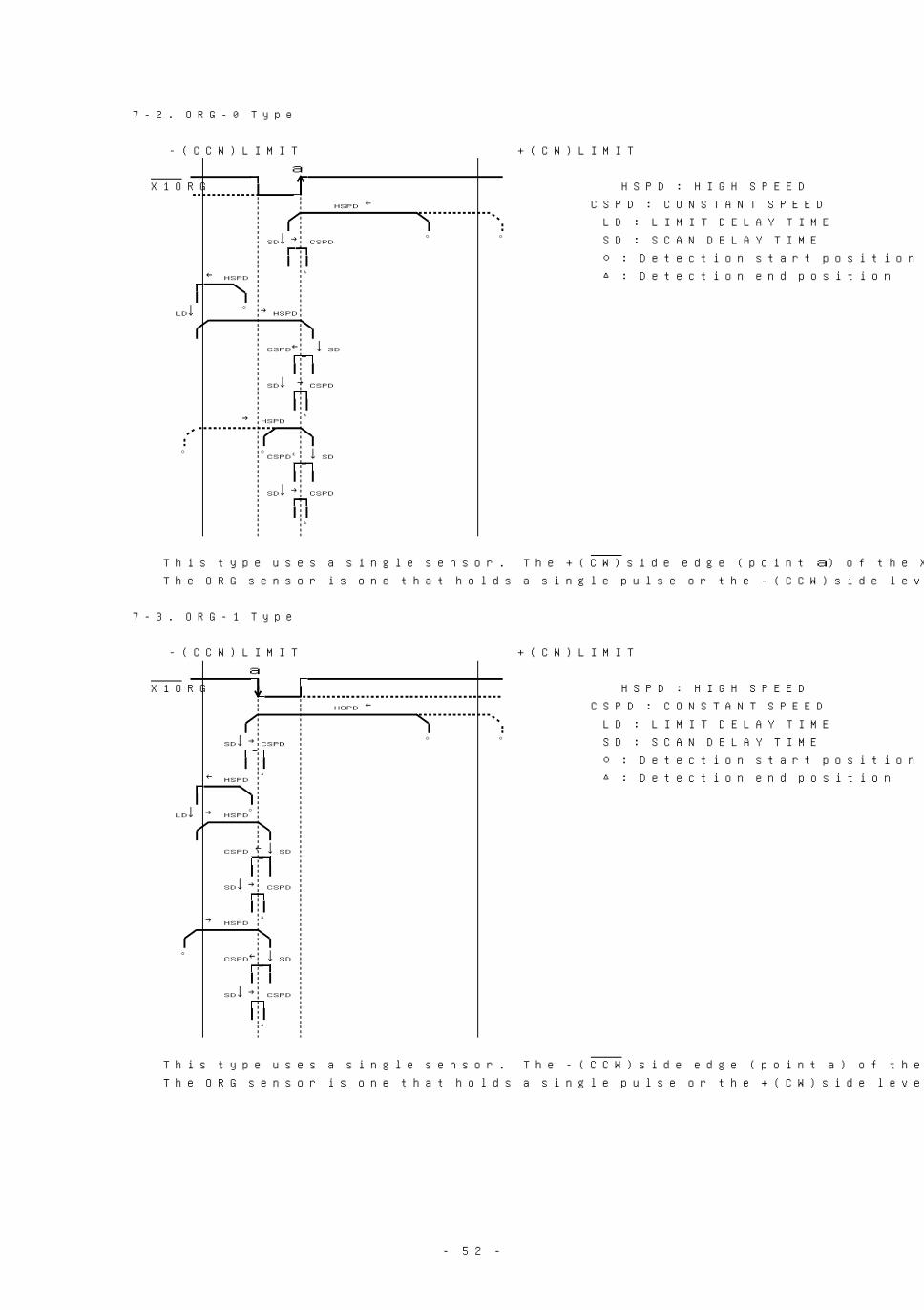
- 52 -
7-2. ORG-0 Type
-(CCW)LIMIT +(CW)LIMIT
a
X1ORG HSPD : HIGH SPEED
← CSPD : CONSTANT SPEEDHSPD
LD : LIMIT DELAY TIME
↓→ SD : SCAN DELAY TIMESD CSPD○ ○∀
○ : Detection start position
← △ : Detection end positionHSPD△
LD HSPD↓ →○
CSPD SD← ↓
SD CSPD↓ →
△→ HSPD
CSPD SD○ ○ ← ↓
SD CSPD↓→
△
This type uses a single sensor. The +(CW)side edge (point a) of the X1ORG signal is detected.
The ORG sensor is one that holds a single pulse or the -(CCW)side level.
7-3. ORG-1 Type
-(CCW)LIMIT +(CW)LIMIT
a
X1ORG HSPD : HIGH SPEED
← CSPD : CONSTANT SPEEDHSPD
LD : LIMIT DELAY TIME
↓→ SD : SCAN DELAY TIMESD CSPD○ ○
○ : Detection start position
← △ : Detection end positionHSPD△
○LD HSPD↓ →
CSPD SD←↓
SD CSPD↓→
△→ HSPD
CSPD SD○ ← ↓
SD CSPD↓→
△
This type uses a single sensor. The -(CCW)side edge (point a) of the X1ORG signal is detected.
The ORG sensor is one that holds a single pulse or the +(CW)side level.

- 53 -
7-4. ORG-2 Type
-(CCW)LIMIT +(CW)LIMIT
a
X1ORG HSPD : HIGH SPEED
← CSPD : CONSTANT SPEEDHSPD
LD : LIMIT DELAY TIME
↓→ SD : SCAN DELAY TIMESD CSPD○ ○
JD : JOG DELAY TIME
← ↓ ○ : Detection start positionCSPD SD
△ : Detection end position
↓→JD
△← HSPD
LD HSPD↓ →○
CSPD SD← ↓
↓→JD
△→ HSPD
CSPD SD○ ○ ← ↓
↓→JD
△
This type used a single sensor. The +(CW)side edge (point a) of the X1ORG signal is detected.
The ORG sensor is one that holds a single pulse or the -(CCW)side level.
7-5. ORG-3 Type
-(CCW)LIMIT +(CW)LIMIT
a
X1ORG HSPD : HIGH SPEED
← CSPD : CONSTANT SPEEDHSPD
LD : LIMIT DELAY TIME
↓→ SD : SCAN DELAY TIMESD CSPD○ ○
JD : JOG DELAY TIME
←↓ ○ : Detection start positionCSPD SD
△ : Detection end position
↓→JD
△← HSPD
○LD HSPD↓ →
CSPD SD←↓
↓→JD
△→ HSPD
CSPD SD○ ← ↓
↓→JD
△
This type uses a single sensor. The -(CCW)side edge (point a) of the X1ORG signal is detected.
The ORG sensor is one that holds a single pulse or the +(CW)side level.

- 54 -
7-6. ORG-4 Type
The NEAR ORG process is performed first. Next, the ORG process is performed.
(1) NEAR ORG process
-(CCW)LIMIT +(CW)LIMIT
a
X1NORG HSPD : HIGH SPEED
← CSPD : CONSTANT SPEEDHSPD
LD : LIMIT DELAY TIME
↓→ SD : SCAN DELAY TIMESD CSPD○ ○
JD : JOG DELAY TIME
← ○ : Detection start positionHSPD
△ : Detection end position
LD HSPD↓ →○
CSPD SD← ↓
HSPD→
CSPD SD○ ○ ← ↓
(2) ORG process
・X1ORG=HIGH upon detection of point a (sensor OFF) ・X1ORG=LOW upon detection of point a (sensor ON)
a a
X1NORG X1NORG
b c c b
X1ORG X1ORG
← ↓ ↓ →CSPD SD SD CSPD
JD CSPD SD↓→ ←↓
↓→△JD
△
This type uses two sensors. After the +(CW)side edge (point a) of the X1NORG signal is detected, the +(CW)
side edge (point b) of the X1ORG signal is detected.
The NORG sensor is one that holds a single pulse or the -(CCW)side level, and the ORG sensor is one that
generates a signal such as rotary axis slit cyclically.
7-7. ORG-5 Type
The NEAR ORG process is performed first. Next, the ORG process is performed.
(1) NEAR ORG工 process
-(CCW)LIMIT +(CW)LIMIT
a
X1NORG HSPD : HIGH SPEED
← CSPD : CONSTANT SPEEDHSPD
LD : LIMIT DELAY TIME
↓→ SD : SCAN DELAY TIMESD CSPD○ ○
JD : JOG DELAY TIME
← ○ : Detection start positionHSPD
△ : Detection end position
LD HSPD↓ →○
CSPD SD← ↓
HSPD→
CSPD SD○ ○ ← ↓

- 55 -
(2) ORG process
・X1ORG=HIGH upon detection of point a (sensor OFF) ・X1ORG=LOW upon detection of point a (sensor ON)
a a
X1NORG X1NORG
c b b c
X1ORG X1ORG
SD CSPD CSPD SD↓ → ← ↓
←↓ ↓→CSPD SD JD
△JD↓→
△
This type uses two sensors. After the +(CW)side edge (point a) of the X1NORG signal is detected, the -(CCW)
side edge (point b) of the X1ORG signal is detected.
The NORG sensor is one that holds a single pulse or the -(CCW)side level, and the ORG sensor is one that
generates a signal such as rotary axis slit cyclically.
7-8. ORG-10 Type
-(CCW)LIMIT +(CW)LIMIT
a
X1NORG HSPD : HIGH SPEED
b CSPD : CONSTANT SPEED
X1ORG LD : LIMIT DELAY TIME
← SD : SCAN DELAY TIMEHSPD
○ : Detection start position
← * *No DELAY TIME △ : Detection end positionCSPD○ ○
△
HSPD←
○LD HSPD↓ →
CSPD SDNote ← ↓○
△
Note: Detection has been started with both X1NORG signal and X1ORG signal ON.
This type uses two sensors. The +(CW)side edge (point a) of the X1NORG signal or the +(CW)side edge
(point b) of the X1ORG signal is detected and CONSTANT SCAN DRIVE is performed to point b.
Both NORG sensor and ORG sensor are ones that hold a single pulse or the -(CCW)side level.

- 56 -
7-9. ORG-11 Type
The drive is stopped at the Slow Stop irrespective of type of the LIMIT stop.
CAUTION So there may be a collision with the limit position of the mechanical device before stop.
This may lead to machine or workpiece damage.
Note that the stop point will be changed if RATE, HSPD, etc. are changed.
-(CCW)LIMIT +(CW)LIMIT
a
X1CCWLM HSPD : HIGH SPEED
(Note1) ← CSPD : CONSTANT SPEEDHSPD
SD : SCAN DELAY TIME
↓→ ○ : Detection start positionSD CSPD○ ○
△ : Detection end position△
HSPD→
CSPD SD○ ←↓
SD CSPD↓→
△
This is a detection done using a single sensor. +(CW) side edge of X1CCWLM signal (indicated as "a" in the
figure) is detected. -(CCW) LIMIT sensor is used as the ORG sensor.
X1CCWLM signal used must be the one that holds a single pulse or level.
Note: X1ORG signal is also enabled in this type, so make sure that it will not be turned active.
7-10.ORG-12 Type
The drive is stopped at the Slow Stop irrespective of type of the LIMIT stop.
CAUTION So there may be a collision with the limit position of the mechanical device before stop.
This may lead to machine or workpiece damage.
Note that the stop point will be changed if RATE, HSPD, etc. are changed.
-(CCW)LIMIT +(CW)LIMIT
a
X1CCWLM HSPD : HIGH SPEED
(Note1) ← CSPD : CONSTANT SPEEDHSPD
SD : SCAN DELAY TIME
↓→ JD : JOG DELAY TIMESD CSPD○ ○
○ : Detection start position
←↓ △ : Detection end positionCSPD SD
↓JD
△
HSPD→
CSPD SD○ ←↓
JD CSPD↓→
△
This is a detection done using a single sensor. +(CW) side edge of X1CCWLM signal (indicated as "a" in the
figure) is detected. -(CCW) LIMIT sensor is used as the ORG sensor.
X1CCWLM signal used must be the one that holds a single pulse or level.
This type of detection differs from the ORG-11 detection in that it repeats the JOG DIVE in the final
process.
Note: X1ORG signal is also enabled in this type, so make sure that it will not be turned active.

- 57 -
7-11.Sensor Arrangement
(1) Mount the X1ORG signal sensor for ORG-0, ORG-1, ORG-2 or ORG-3 and the X1NORG/X1ORG signal sensor
for ORG-10 on the -(CCW)LIMIT side along the work moving direction.
Example) For a ball screw table
-(CCW) Work +(CW)
X1NORG signal sensor for ORG-10 Use photo sensors.
X1ORG signal sensor They shall turn off when light enters.
(2) ORG-4 and ORG-5
・Mount the X1NORG signal sensor on the -(CCW)LIMIT side along the work moving direction in the same way
as (1).
・X1ORG signal sensor
When using a stepping motor:
Mount this sensor on the motor rotary shaft as shown below.
X1ORG signal sensor
MOTOR Use a photo sensor.
It shall turn on when light enters.
Disc with slit mounted on the rotary shaft.
When using a servo motor:
Connect the encoder Z phase (Cφ) output signals +Z and -Z of the servo driver to the +X1ZORG and
-X1ZORG of the C-872. For details, refer to Chapter 14.
The pulse width of the encoder Z phase (Cφ) output shall be 10μs or more.
(3) ORG-11,12
These types require the LIMIT sensor alone. X1CCWLM signal is used as the origin signal.
Since X1ORG signal is also enabled, make sure that it will not be turned active.
7-12.Detecting Conditions
(1) For the ORG-0, ORG-1, ORG-2 and ORG-3 types, the X1ORG signal should be detected for 1ms or more when it
passes the ORG sensor at the maximum speed. For the ORG-4, ORG-5 and ORG-10 types, the X1NORG signal
should be detected for 1ms or more when it passes the NORG sensor at the maximum speed.
(2) For the ORG-4 and ORG-5 types, the distance between point a and point b and the distance between point a
and point c should be N pulses or more in terms of the number of pulses.
*N=0.005×CSPD(Hz) Example) When CSPD=5KHz, N=0.005×5000=25.
(Minimum value of Accordingly, the distance should be 25 pulses or more.
N is 1.) Practically, give some allowance to it.
(3) Each of the X1ORG and X1NORG signals should have no chattering.(When photo sensors are used, this does not
matter.)
(4) The distance between point a and +(CW)LIMIT shown in each process drawing should be enough for a slow stop.
(5) The distance between point a and point b shown in the ORG-10 type should be enough for a slow stop.
(6) With the ORG-11 and 12 detection, sufficient distance must be provided between the point a and the
machine limit in CCW direction so that slow stop (through deceleration) is ensured for the drive.
There may be a collision with the limit position of the mechanical device before stop.
CAUTION his may lead to machine or workpiece damage.
Note that the stop point will be changed if RATE, HSPD, etc. are changed.
7-13.Other Functions
The following is additionally prepared as applied functions:
1.The ORIGIN DRIVE direction switch function for the time when you use the sensor in +(CW) side.
2.The MARGIN TIME function for preventing malfunction that can result from hunting.
3.The SENSOR TYPE select function used in the JOG DRIVE.
4.The ERROR DETECT function prepared for the time when the ORIGIN SENSOR detection ended unsuccessfully.
5.The function to produce X1DRST signal as the origin detection is completed.
6.The function of ANDing the X1ORG signal and PO signal from the stepping motor driver.
For details of the applied functions, refer to the User's Manual [Applied Functions Part].

- 58 -
8.DETAILS OF COUNTER FUNCTIONS
The following description is given about the X1 axis, but also applicable to another axis.
8-1. Functional Block Diagram
The MCC05v2 has three built-in 24-bit HARD COUNTERs each provided with different functions.
COUNTER
< X1EA,X1EB(External clock) Set data DATA1,2,3
< X1CWP,X1CCWP WRITE PORT
(Output pulse) PULSE COUNTER PULSE COUNTER PRESET
INITIALIZE Command (COUNTER Command)
24BIT PULSE COUNTER
COUNT PATTERN TYPE
PULSE COUNTER
INITIALIZE Command Count data
INT CONTROL 24BIT COMPARATOR × 5ch X1CNTINT OUTPUT
PULSE COUNTER
INITIALIZE Command
24BIT COMPARE
REGISTER × 5ch
COMP1~5 REG SET
(COUNTER Command)
DFL COUNTER DFL COUNTER PRESET
INITIALIZE Command (COUNTER Command) ADRS/DFL/PULSE
COUNTER PORT
SELECT Command24BIT DIFFERENTIAL COUNTER
COUNT PATTERN TYPE
DFL COUNTER
INITIALIZE Command DRIVE
Differential data SELECTOR DATA1,2,3
READ PORT
INT CONTROL 24BIT COMPARATOR×2ch X1DFLINT OUTPUT
DFL COUNTER
INITIALIZE Command
24BIT COMPARE
REGISTER×2ch
COMP1~2 REG SET
(COUNTER Command)
Address data
24BIT ADDRESS COUNTER
ADDRESS INITIALIZE Command
DRIVE
To another functional block 24bit data DATA1,2,3
WRITE PORT

- 59 -
8-2. ADDRESS COUNTER Function
(1) In order to control current address, the ADDRESS COUNTER offers absolute address of the output pulse from
the MCC05v2.
(2) The count data can be read from the DRIVE DATA1, 2 and 3 PORTs any time you want (as long as the ADDRESS
COUNTER PORT is selected). The ADDRESS READ command can also be used for reading the data.
The data guarantee range is pulse area of +8,388,607 to -8,388,607.
(3) The counter value is reset to 0 at POWER ON/RESET.
Using the ADDRESS INITIALIZE Command allows you to set optional value on the counter.
8-3. PULSE COUNTER Function
(1) Pulse counting function
a. The PULSE COUNTER offers counting of output pulse or external input clock to the MCC05v2.
b. Count data can always be read out from DRIVE DATA1, 2 and 3 PORT.
The data guaranty range is a pulse area of +8,388,607 to -8,388607. The data reaches (8,388,608, an
overflow occurs. When an overflow occurs, OVF BIT in STATUS3 PORT becomes 1.
c. The counter value is reset to 0 at POWER ON /RESET and can also be set to an optional value by the COUNTER
PRESET command.
d. When inputting external signal such as feed back pulses from the servo driver, a 90゚ phase difference
signal or CW/CCW independent clock can be used as an input clock. When the 90゚ phase difference signal
is selected, a count multiplier can also be set.
The above input clock selection and count multiplier selection are performed by the PULSE COUNTER
INITIALIZE command.
At RESET, output pulses of MCC05v2 are selected as input clocks.
(2) PULSE COUNT COMPARE Function
a. Five COMPARE REGISTERs and COMPARATORs connected to the PULSE COUNTER allows you to detect any count value.
b. Detection of matching between the counter and comparator is done with the STATUS signal or interrupt
request signal. You can select the through mode (detection done by the comparator is output as it is) or
the latch mode (holds the detection) for the STATUS and interrupt request signals.
In the latch mode, you can reset the STATUS signal or interrupt request signal by reading the STATUS3 PORT.
And, you can select a mode that enables the reset or another mode that disables it even when the condition
(matching established between the counter and comparator).
For details, refer to 8-5.
The interrupt request signal (X1CNTINT) is output from five comparators. You can enable or disable the
output on individual comparator basis.
c. The pulse output can also be stopped by match among comparators. You can specify the immediate output
stop or gradual stop through deceleration. The immediate stop sets the FSEND BIT to 1 and the SSEND BIT
is set to 1 when the gradual stop is specified.
d. The PULSE COUNTER INITIALIZE command is used for controlling the every PULSE COUNT COMPARE function.
Data for the COMPARE REGISTER is set on the COUNTER PORT. The COUNTER PORT is independent from the DRIVE
PORT, thus rewriting of the compare data is available any time.
e. Specific functions of COMPARE REGISTER1
Specific functions that are not provided in the other COMPARE REGISTERs are assigned to COMPARE REGISTER1.
The following functions can be automatically performed by a match of COMPARE REGISTER1.
These functions are also controlled by the PULSE COUNTER INITIALIZE command.
*AUTO CLEAR function
The PULSE COUNTER value is cleared to 0 concurrently with a match of COMPARE REGISTER1.
*RELOAD function
The data written in COUNTER DATA1 PORT, COUNTER DATA2 PORT and COUNTER DATA3 PORT is reset to COMPARE
REGISTER1 concurrently with a match of COMPARE REGISTER1.

- 60 -
8-4. DIFFERENTIAL COUNTER function
(1) Differential Count Function
a. The DIFFERENTIAL COUNTER offers counting of deviation between output pulse from the MCC05v2 and external
input clock, or counting of external clock alone.
b. Count data can be read from the DRIVE DATA1, 2 and 3 PORTs any time as needed (as long as the DFL COUNTER
PORT is selected). Data guarantee range is pulse area of +8,388,607 to -8,388,607.
c. The counter value is reset to 0 at POWER ON/RESET.
Using the DFL COUNTER PRESET Command of the COUNTER Commands allows you to set optional value on
the counter.
d. Any one of 90゚phase difference signal and respectively independent CW or CCW clock may be used as external
clock. For selecting type of external input clock and also for selecting its multiplication factor, the
DFL COUNTER INITIALIZE command is used.
At POWER ON/RESET, a single multiplication of 90゚phase difference signal is selected and the counter
functions as the differential counter.
(2) Differential Count Compare Function
a. The DIFFERENTIAL COUNTER is connected to two COMPARE REGISTERs and COMPARATORs. Its counting (in absolute
value) is constantly compared against the value set on these two registers (these registers are different
from COMPARE REGISTERs on the PULSE COUNTER).
The COMPARATOR1 is constantly available for detection of the "count in absolute value≧REGISTER1"
(excessive deviation) and the COMPARATOR2 is used for detecting the "count in absolute value≦REGISTER2"
(positioning complete).
+
REGISTER1
REGISTER2 Deviation counted
t
REGISTER2
REGISTER1
-
COMPARATOR1
COMPARATOR2
b. Each of above detection is implemented by the STATUS signal or interrupt request signal. You can select
the through mode (detection by the comparator is output as it is) or the latch mode (holds the detection)
for both the STATUS signal and the interrupt request signal.
In the latch mode, you can reset the STATUS signal or interrupt request signal by reading the STATUS3 PORT.
And, you can select a mode that enables the reset or another mode that disables it even when the condition
(COUNTER≧REGISTER1 or COUNTER≦REGISTER2).
For details, refer to 8-5.
The interrupt request signal (X1DFLINT) is output from two comparators. You can enable or disable the
output on individual comparator basis.
c. The pulse output can also be stopped by the COUNTER≧REGISTER1 or COUNTER≦REGISTER2.
You can specify the immediate output stop or gradual stop through deceleration.
The immediate stop sets the FSEND BIT to 1 and the SSEND BIT is set to 1 when the gradual stop is
specified.
d. The DFL COUNTER INITIALIZE command is used for controlling the DFL COUNT COMPARE function.
Data for the COMPARE REGISTER is set on the COUNTER PORT. The COUNTER PORT is independent from the DRIVE
PORT, thus rewriting of the compare data is available any time.

- 61 -
8-5. Detail of COMPARATOR Functions
Output of the detected condition from five COMPARATORs for the PULSE COUNTER and two COMPARATORs for the
DIFFERENTIAL COUNTER are connected to the following functional circuit and, thus, allows control according
to the user specification.
Output of ① Through-output circuit ③ ④
detection ②
Each COMPARATOR Level input Output of INT signal
Latch circuit
Edge input
Suppressed output Output of STATUS3 signal
(Note)
①: INT MASK Circuit
This circuit masks output from the COMPARATOR at its exit.
You can specify separate levels of masking for each comparator on the PULSE and DFL counters.
This circuit is turned on or off by the INT MASK command.
As one of the special commands, it provides real-time, fine-tuned control of the masking.
②: LATCH TYPE Switch Circuit
This circuit is used for selecting a latch trigger type when detection by the COMPARATOR is latched
before it is output.
The latch type selected commonly applies to five comparators on the PULSE COUNTER.
Likewise, the type selected applies commonly to two comparators on the DIFFERENTIAL COUNTER.
You can differentiate the latch type between the PULSE COUNTER and the DIFFERENTIAL COUNTER.
Latch-output reset condition varies according to the trigger type as described in the following.
・When the level latch is selected:
When output of the COMPARATOR detection is not taking place, reading the STATUS3 PORT resets the
output (returns to the initial state).
・When the edge latch is selected:
Reading the STATUS3 PORT necessarily resets the output.
This circuit is turned on or off by the PULSE or DFL COUNTER INITIALIZE Command.
③: INT OUTPUT TYPE Switch Circuit
This circuit is used for selecting whether the COMPARATOR detection is to be output as it is (through)
or after latch. The output type selected commonly applies to the five comparators on the PULSE COUNTER.
Likewise, the selected type commonly applies to the two comparators on the DIFFERENTIAL COUNTER.
You can differentiate the output type between the PULSE COUNTER and the DIFFERENTIAL COUNTER.
This circuit is turned on or off by the PULSE or DFL COUNTER INITIALIZE command
(initially, the latch is selected).
When the through-output of detection is selected, if you execute the COUNTER Command in the course of
the INT output, this output will be turned off for a duration of 50ns.
④: INT Output Enable Circuit
A signal that has passed through ① through ③ circuits above can be unconditionally confirmed from
the STATUS3 PORT. This circuit is used for selecting whether this signal is to be externally output as
it is (X1CNTINT or X1DFLINT signal).
Output of the INT signal can be separately enabled or disabled for each of the pulse or DFL comparator.
This circuit is turned on or off by the PULSE or DFL COUNTER INITIALIZE command.
All setups except for the ① INT MASK circuit are done by the COUNTER INITIALIZE command.
Thus, these setups must be complete before pulse output it turned on.
Note: Unlike the INT output or STATUS, comparator's pulse output stop function is directly enabled without
going through the above mentioned circuit.
The following shows pages in this manual that bear descriptions relevant to this function:
The PULSE COUNTER INITIALIZE Command page 30
The DFL COUNTER INITIALIZE Command page 36
The INT MASK Command page 48
Timing of each signal page 72, 73

- 62 -
9.DESCRIPTION OF PULSE COUNTER AND DFL COUNTER COMMAND
9-1. Command Table
The HEX code is for the case where all the x bits are set to 0.
D D D D D D D D HEX C0DE COMMAND NAME EXECUTION TIME7 6 5 4 3 2 1 0
0 0 0 0 00 PULSE COUNTER PRESET MAX 200ns× × × ×
0 0 0 1 01 PULSE COUNTER COMPARE REGISTER1 SET MAX 200ns× × × ×
0 0 1 0 02 PULSE COUNTER COMPARE REGISTER2 SET MAX 200ns× × × ×
0 0 1 1 03 PULSE COUNTER COMPARE REGISTER3 SET MAX 200ns× × × ×
0 1 0 0 04 PULSE COUNTER COMPARE REGISTER4 SET MAX 200ns× × × ×
0 1 0 1 05 PULSE COUNTER COMPARE REGISTER5 SET MAX 200ns× × × ×
0 1 1 0 06 DIFFERENTIAL COUNTER PRESET MAX 200ns× × × ×
0 1 1 1 07 DIFFERENTIAL COUNTER COMPARE REGISTER1 SET MAX 200ns× × × ×
1 0 0 0 08 DIFFERENTIAL COUNTER COMPARE REGISTER2 SET MAX 200ns× × × ×
9-2. PULSE COUNTER PRESET Command
COMMAND……… 00 Function : Initializes the count value of the PULSE COUNTER toH
a specified value.
Execution sequence
Preset data is specified in COUNTER DATA1 PORT, COUNTER DATA2 PORT
(Note) COUNTER DATA1 and COUNTER DATA3 PORT.
PORT WRITE The order
may not The contents of COUNTER DATA1 PORT to COUNTER DATA3 PORT are as follows.
COUNTER DATA2 be observed.
PORT WRITE DATA1 PORT DATA2 PORT DATA3 PORT7 0 7 0 7 0D D D D D D
COUNTER DATA3
PORT WRITE
COUNTER COMMAND PRESET DATA (0~FFFFFF )H
00 WRITEH
When preset data is negative, it is represented in 2's complement form.
Counter value is 0 at POWER ON/RESET.
・Setting example of preset data
PRESET DATA(decimal) DATA1 PORT DATA2 PORT DATA3 PORT
H H H+8,388,607 7F FF FF
H H H+10 00 00 0A
H H H±0 00 00 00
H H H-10 FF FF F6
H H H-8,388,607 80 00 01
Note: Note that the DATA and COMMAND PORTs described in this chapter are special ports for the counters
and their port addresses are different from that of the DRIVE PORTs. For the port address,
refer to 4-1.

- 63 -
9-3. PULSE COUNTER COMPARE REGISTER1 SET Command
COMMAND……… 01 Function : Sets a specified value in COMPARE REGISTER1.H
Execution sequence COMPARE DATA is specified in COUNTER DATA1 PORT, COUNTER DATA2 PORT
and COUNTER DATA3 PORT.
(Note) COUNTER DATA1
PORT WRITE The contents of COUNTER DATA1 PORT to COUNTER DATA3 PORT are as follows.
COUNTER DATA2 DATA1 PORT DATA2 PORT DATA3 PORT7 0 7 0 7 0PORT WRITE D D D D D D
COUNTER DATA3
PORT WRITE The order
may not COMPARE DATA (0~FFFFFF )H
COUNTER COMMAND be observed.
01 WRITEH
When COMPARE DATA is negative, it is represented in 2's complement form.
COMPARE DATA is 800000 at POWER ON/RESET.H
Note: Note that the DATA and COMMAND PORTs described in this chapter are special ports for the counters
and their port addresses are different from that of the DRIVE PORTs.
For the port address, refer to 4-1.
9-4. PULSE COUNTER COMPARE REGISTER2 SET Command
COMMAND……… 02 Function: Sets a specified value in COMPARE REGISTER2.H
The execution sequence is the same as that of the COMPARE REGISTER1 SET
command.
9-5. PULSE COUNTER COMPARE REGISTER3 SET Command
COMMAND……… 03 Function: Sets a specified value in COMPARE REGISTER3.H
The execution sequence is the same as that of the COMPARE REGISTER1 SET
command.
9-6. PULSE COUNTER COMPARE REGISTER4 SET Command
COMMAND……… 04 Function: Sets a specified value in COMPARE REGISTER4.H
The execution sequence is the same as that of the COMPARE REGISTER1 SET
command.
9-7. PULSE COUNTER COMPARE REGISTER5 SET Command
COMMAND……… 05 Function: Sets a specified value in COMPARE REGISTER5.H
The execution sequence is the same as that of the COMPARE REGISTER1 SET
command.
9-8. DFL COUNTER PRESET Command
COMMAND……… 06 Function : Modifies the DIFFERENTIAL COUNTER value to the specified one.H
The execution sequence is the same as that of the PULSE COUNTER RESET
command.
At POWER ON/RESET, the counter value is set to 0.

- 64 -
9-9. DFL COUNTER COMPARE REGISTER1 SET Command
COMMAND……… 07 Function : Sets a value specified for the DIFFERENTIAL COUNTER COMPARE1H
REGISTER in an absolute value.
Execution sequence
COMPARE DATA is specified in COUNTER DATA1 PORT, COUNTER DATA2 PORT and
(Note1) COUNTER DATA1 The order COUNTER DATA3 PORT.
PORT WRITE may not The contents of COUNTER DATA1 PORT to COUNTER DATA3 PORT are as follows.
be observed.
COUNTER DATA2 DATA1 PORT DATA2 PORT DATA3 PORT7 0 7 0 7 0PORT WRITE D D D D D D
COUNTER DATA3
PORT WRITE
COMPARE DATA (0~7FFFFF )H
COUNTER COMMAND
07 WRITE This bit must be set to 0 (Note 2).H
At POWER ON/RESET, it is set to 0.
Note1: Note that the DATA and COMMAND PORTs described in this chapter are special ports for the counters
and their port addresses are different from that of the DRIVE PORTs. For the port address,
refer to 4-1.
Note2: When the signed value detection, an applied function, is selected, this bit is replaced by 2 bit.23
9-10.DFL COUNTER COMPARE REGISTER2 SET Command
COMMAND……… 08 Function : Sets a value specified for the DIFFERENTIAL COUNTER COMPARE2H
REGISTER in an absolute value.
The execution sequence is the same as that of the DFL COUNTER REGISTER1
SET Command.

- 65 -
10.INITIAL SPECIFICATIONS TABLE
The initial specifications at POWER ON/RESET are shown in the following table.
The specifications related to SPEED can be switched between two types by jumpers JP1X1,2(X1,2 axis), JP1Y1,2
(Y1,2 axis), JP1Z1,2 (Z1,2 axis), and JP1A1,2 (A1,2 axis) on the board.
The specifications in which jumpers are provided are supplied at shipment.
Initial specification CorrespondingData name or specification
Jumper is provided(Note) No jumper is provided. Command
URATE(RATE DATA TABLE No.) No.9(100ms/1000Hz) No.12(30ms/1000Hz)RATE SET
DRATE(RATE DATA TABLE No.) No.9(100ms/1000Hz) No.12(30ms/1000Hz)
LSPD 300Hz 800Hz LSPD SET
HSPD 3000Hz 10000Hz HSPD SET
CSPD 300Hz 800Hz CSPD SET
SRATE(RATE DATA TABLE No.) No.9(100ms/1000Hz) No.12(30ms/1000Hz) SRATE SET
SLSPD 300Hz 800Hz SLSPD SET
SHSPD 3000Hz 10000Hz SHSPD SET
DRIVE TYPE L-TYPE
LIMIT STOP TYPE FAST STROPSPEC INITIALIZE1
MOTOR TYPE STEPPING
RDYINT generation pattern Generated only upon termination of a commandaccompanied by pulse output.
PULSE COUNTER operating clock Output pulse
CNTINT generation pattern Not generated in any case (all of COMP1 to 5)
COMP1 to 5 STOP TYPE Not put into stop (all of COMP1 to 5)
AUTO CLEAR function Not available PULSE COUNTER INITIALIZE
RELOAD function Not available
PLS COMP STOP TYPE Fast stop
CNTINT OUTPUT TYPE Detection of each comparator is latched and output
CNTINT LATCH TRIGGER TYPE Level latch
DIFFERENTIAL COUNTER Difference between MCC05v2 output pulseoperating clock and an external clock.
DIFFERENTIAL COUNTER Clock with 90゚phase differencecount pattern type 1 multiplication
DFLINT generation pattern Not generated in any case (both of COMP1 to 2)DFL COUNTER INITIALIZE
DFL COMP1,2 STOP ENABLE Not put into stop (both of COMP1 to 5)
DFL COMP STOP TYPE Fast stop
DFLINT OUTPUT TYPE Detection of each comparator is latched and output
DFLINT LATCH TRIGGER TYPE Level latch
COUNTER SELECT PORT PULSE COUNTER Each PORT SELECT
Current address(ADDRESS COUNTER) 0 ADDRESS INITIALIZE
OFFSET PULSE 0 OFFSET PULSE SET
LIMIT DELAY TIME 300ms
SCAN DELAY TIME 50ms ORIGIN DELAY SET
JOG DELAY TIME 20ms
PULSE COUNTER Value 0 PULSE COUNTER PRESET
PULSE COUNTER PULSE COUNTERCOMPARE REGISTER1 to 5 value 800000 COMPARE REGISTER1~5 SETH
DIFFERENTIAL COUNTER value 0 DFL COUNTER PRESET
DIFFERENTIAL COUNTER DFL COUNTERCOMPARE REGISTER1 to 2 value 0 COMPARE REGISTER1~2 SET
Note: Values with the jumpers are employed in descriptions offered in other parts of this manual.
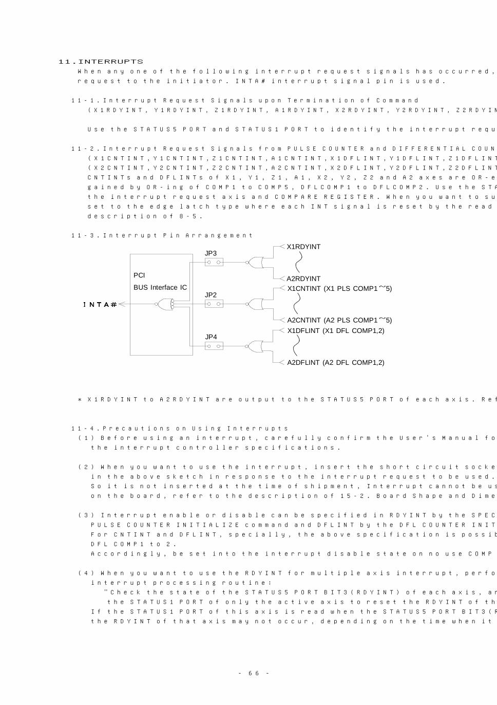
- 66 -
11.INTERRUPTS
When any one of the following interrupt request signals has occurred, the C-872 gives an interrupt
request to the initiator. INTA# interrupt signal pin is used.
11-1.Interrupt Request Signals upon Termination of Command
(X1RDYINT, Y1RDYINT, Z1RDYINT, A1RDYINT, X2RDYINT, Y2RDYINT, Z2RDYINT, A2RDYINT)
Use the STATUS5 PORT and STATUS1 PORT to identify the interrupt request axis.
11-2.Interrupt Request Signals from PULSE COUNTER and DIFFERENTIAL COUNTER
(X1CNTINT,Y1CNTINT,Z1CNTINT,A1CNTINT,X1DFLINT,Y1DFLINT,Z1DFLINT,A1DFLINT)
(X2CNTINT,Y2CNTINT,Z2CNTINT,A2CNTINT,X2DFLINT,Y2DFLINT,Z2DFLINT,A2DFLINT)
CNTINTs and DFLINTs of X1, Y1, Z1, A1, X2, Y2, Z2 and A2 axes are OR-ed. The output of each axis is
gained by OR-ing of COMP1 to COMP5, DFLCOMP1 to DFLCOMP2. Use the STATUS3 PORT of each axis to evaluate
the interrupt request axis and COMPARE REGISTER. When you want to such an interrupt function, it must be
set to the edge latch type where each INT signal is reset by the read of the STATUS3 PORT. Refer to the
description of 8-5.
11-3.Interrupt Pin Arrangement
* X1RDYINT to A2RDYINT are output to the STATUS5 PORT of each axis. Refer to the description of 4-12.
11-4.Precautions on Using Interrupts
(1) Before using an interrupt, carefully confirm the User's Manual for your initiator system and
the interrupt controller specifications.
(2) When you want to use the interrupt, insert the short circuit socket (an accessory) into the JP2 to JP4
in the above sketch in response to the interrupt request to be used.
So it is not inserted at the time of shipment, Interrupt cannot be used in that state. For the position
on the board, refer to the description of 15-2. Board Shape and Dimensions.
(3) Interrupt enable or disable can be specified in RDYINT by the SPEC INITIALIZE1 command, CNTINT by the
PULSE COUNTER INITIALIZE command and DFLINT by the DFL COUNTER INITIALIZE command.
For CNTINT and DFLINT, specially, the above specification is possible for each of COMP1 to COMP5 and
DFL COMP1 to 2.
Accordingly, be set into the interrupt disable state on no use COMP No.
(4) When you want to use the RDYINT for multiple axis interrupt, perform the following processing in the
interrupt processing routine:
"Check the state of the STATUS5 PORT BIT3(RDYINT) of each axis, and read
the STATUS1 PORT of only the active axis to reset the RDYINT of that axis."
If the STATUS1 PORT of this axis is read when the STATUS5 PORT BIT3(RDYINT) is not active,
the RDYINT of that axis may not occur, depending on the time when it is read.
X1RDYINT
A2RDYINT
A2CNTINT (A2 PLS COMP1~5)
X1DFLINT (X1 DFL COMP1,2)
X1CNTINT (X1 PLS COMP1~5)
A2DFLINT (A2 DFL COMP1,2)
PCI
BUS Interface IC
JP3
JP2
JP4

- 67 -
12.TIMING
Refer to the description of 12-16 for IOR# and IOW#.
[ ] : Timing of case SOFT LIMIT function in use.(applied function)
Those not in brackets remain unaffected by presence or absence of the SOFT LIMIT function.
12-1.JOG DRIVE Timing 12-2.SCAN DRIVE/S-RATE SCAN DRIVE Timing
Example) Drive in +(CW)direction for Example) Drive in -(CCW)direction for
a stepping motor a stepping motor
IOW# IOW#
Indicates that a command is written. Indicates that a command is written.
X1CWP X1CCWP
DRIVE in DRIVE in
STATUS1 STATUS1
BUSY in BUSY in
STATUS1 STATUS1
t1 t4 t5 t1
t2 t2
t3 t6 t3
t1<150ns t4≒100μs t1<150ns
t2<34μs[42μs] t5<23μs[31μs] t2<43μs[75μs Note]
t3<36μs[44μs] t6<35μs[43μs] t3<63μs[95μs Note]
Note: 1.3ms when URATE≠DRATE is specified.
12-3.INDEX DRIVE,S-RATE INDEX DRIVE Timing
Example) Drive in +(CW)direction for a stepping motor
IOW# (1) When URATE=DRATE is specified:
Indicates that a command is written.
t1<150ns t4<35μs[44μs]
X1CWP t2<71μs[79μs] t5<20μs
t3<93μs[101μs]
DRIVE in
STATUS1 (2) When URATE≠DRATE is specified:
t1<150ns t4<35μs[44μs]
BUSY in t2<1.3ms (L-TYPE) t5<18μs
STATUS1 630μs(M-TYPE)
t1 t4 t5 400μs(H-TYPE)
t2 t3≒t2+22μs
t3
12-4.ORIGIN DRIVE Timing
Example 1) Drive in -(CCW)direction without ABSOLUTE INDEX DRIVE(RETURN DRIVE up to the near-origin addres
s)
IOW#
Indicates that a command is written.
t1<150ns
X1CCWP t2<70μs
t3<82μs
DRIVE in
STATUS1
BUSY in
STATUS1
t1
t2
t3

- 68 -
Example 2) Drive in -(CCW)direction with ABSOLUTE INDEX DRIVE (RETURN DRIVE up to the near-origin address)
IOW# (1) When URATE=DRATE is specified:
Indicates that a command is written. t1<150ns
t2<71μs
X1CCWP t3<93μs
DRIVE in (2) When URATE≠DRATE is specified:
STATUS1 t1<150ns
t2<1.3ms (L-TYPE)
BUSY in 630μs(M-TYPE)
STATUS1 400μs(H-TYPE)
t1 t3≒t2+22μs
t2
t3
12-5.SPEED CHANGE Timing
IOW#
Indicates that a command is written.
CHANGE BUSY
in STATUS5 t1<200ns
51μs<t2<53ms
t1 t2
Note: t2 is determined by the specified RATE.
In the Fixed mode, t2 becomes shorter as a specified RATE No. increases, and in the Arithmetic mode,
it becomes shorter as the RATE data becomes smaller (in both cases, speed change rate is increased).
If, however, a pulse cycle greater than t2 at writing of the CHANGE command, t2 becomes equal with or
longer than the pulse cycle.

- 69 -
12-6.DEND Signal Confirmation Timing
Example 1) End of DRIVE in +(CW)direction for Example 2) End of DRIVE in +(CW)direction when the
a servo motor target is a servo motor and the DEND signal
is active or the target is a stepping motor
DEND DEND
X1CWP X1CWP
DRIVE in DRIVE in
STATUS1 STATUS1
BUSY in BUSY in
STATUS1 STATUS1
t1 t2 t3 t1 t2
t1:Depends on servo driver characteristics. t1<33μs[41μs]
t2<61μs t2<20μs
t3<20μs
Note: When the target is a servo motor, Note: When the target is a stepping motor,
the requirement for BUSY in STATUS1=0 DEND=0/1 does not matter.
is that DEND=0 must be input.
This is also applicable to a normal end of DRIVE,
a slow stop and an fast stop.
Accordingly, note that the time required for BUSY
in STATUS1=0 is different from that for the case
where the target is a stepping motor.
12-7.SLOW STOP Timing 12-8.FAST STOP Timing(1)
Example) Drive in +(CW)direction when the Example) DRIVE in +(CW)direction when
target is a stepping motor the target is a stepping motor
(Note1) (Note1)
IOW# IOW#
(Note2) (Note2)
X1CWP FSSTOP1
DRIVE in (Note3)
STATUS1 X1CWP
BUSY in DRIVE in
STATUS1 STATUS1
BUSY in
STATUS1
t1 t2 t1 t2 t3
t1<38μs[42μs] t1≧400μs
t2<20μs t2<38μs[46μs] or T(Note4)
t3<20μs
Note1: Indicates that the SLOW STOP command Note1: Indicates that the FAST STOP command
is written. is written.
Note2: The number of pulses to be output after Note2: Either command or signal may be used.
receipt of the SLOW STOP command is 1 pulse Note3: The number of pulses to be output after
or less at constant-speed DRIVE, or the receipt of the FAST STOP command is 1 pulse
number of pulses required for a slow stop at or less. (The pulse width is secured.)
acceleration/decelerating DRIVE. Note4: When T represents 1/2 of the pulse cycle
as the drive is stopped, t2 takes the
indicated value or T which ever is longer.
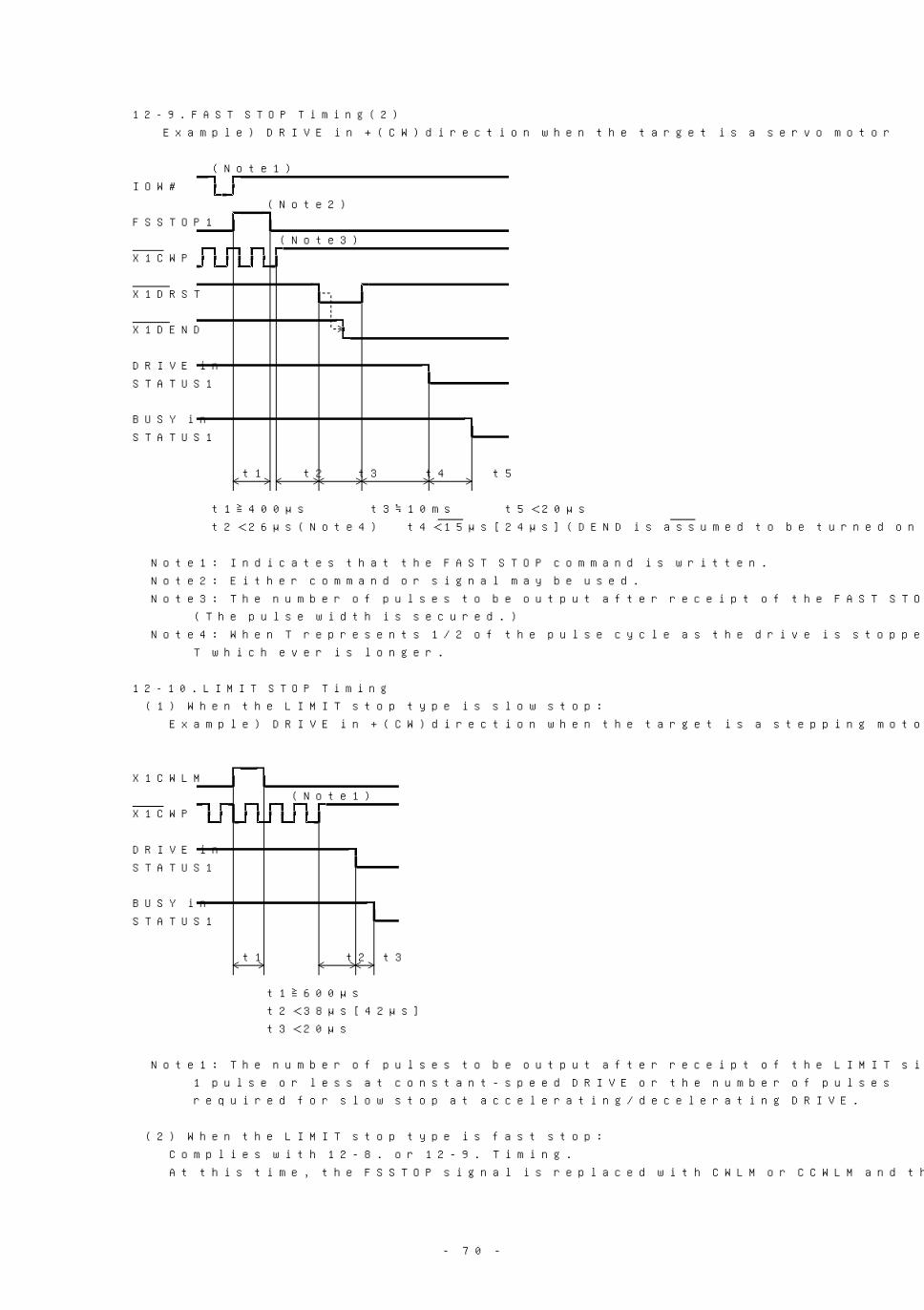
- 70 -
12-9.FAST STOP Timing(2)
Example) DRIVE in +(CW)direction when the target is a servo motor
(Note1)
IOW#
(Note2)
FSSTOP1
(Note3)
X1CWP
X1DRST
X1DEND
DRIVE in
STATUS1
BUSY in
STATUS1
t1 t2 t3 t4 t5
t1≧400μs t3≒10ms t5<20μs
t2<26μs(Note4) t4<15μs[24μs](DEND is assumed to be turned on while DRST is being produced.)
Note1: Indicates that the FAST STOP command is written.
Note2: Either command or signal may be used.
Note3: The number of pulses to be output after receipt of the FAST STOP command is 1 pulse or less.
(The pulse width is secured.)
Note4: When T represents 1/2 of the pulse cycle as the drive is stopped, t2 takes the indicated value or
T which ever is longer.
12-10.LIMIT STOP Timing
(1) When the LIMIT stop type is slow stop:
Example) DRIVE in +(CW)direction when the target is a stepping motor
X1CWLM
(Note1)
X1CWP
DRIVE in
STATUS1
BUSY in
STATUS1
t1 t2 t3
t1≧600μs
t2<38μs[42μs]
t3<20μs
Note1: The number of pulses to be output after receipt of the LIMIT signal is
1 pulse or less at constant-speed DRIVE or the number of pulses
required for slow stop at accelerating/decelerating DRIVE.
(2) When the LIMIT stop type is fast stop:
Complies with 12-8. or 12-9. Timing.
At this time, the FSSTOP signal is replaced with CWLM or CCWLM and the input signal width is set to 600μs.

- 71 -
12-11.EA/EB Clock Input Timing
(1) When 90゚ phase difference clocks are input:
EAPULSE COUNTER DIFFERENTIAL COUNTER
EB t1>(150×N)ns t1>(200×N)ns
t1 t1 t1 t1 t2>(330×N)ns t2>(430×N)ns
t >(660×N)ns t >(860×N)nscyc cyc
t2 t2However, N is a multiplier.
cyct
*The count timing of the PULSE COUNTER and DIFFERENTIAL COUNTER is as shown below.
Each is counted at or .
UP COUNT DOWN COUNTWhen the multiplier is 1:
-X1EA
-X1EB
UP COUNT DOWN COUNTWhen the multiplier is 2:
-X1EA
-X1EB
UP COUNT DOWN COUNTWhen the multiplier is 4:
-X1EA
-X1EB
(2) When independent clocks for each direction are input: (Counted at the edge marked ↓)
-X1EA t1>150ns (PULSE COUNTER)
t ≧330ns(PULSE COUNTER)cyc
-X1EB t1>200ns (DIFFERENTIAL COUNTER)
t1 t1 t1 t1 t ≧430ns(DIFFERENTIAL COUNTER)cyc
cyc cyct t
12-12.RDYINT Timing
BUSY in BUSY in① ③ ①
STATUS1 STATUS1
IOW# ② Or IOR# ④
RDYINT ⑤ RDYINT ⑤
t1 t2 t3 t4
t1<50ns t3<50ns
t2<150ns t4<100ns
①: Indicates that a command is executed.
②: Indicates a new command is written.
③: Indicates that a new command is executed.
④: Indicates that STATUS1 is read out.
⑤: Indicates that an interrupt signal is generated. Interrupt signal enable or disable is specified
by the SPEC INITIALIZE1 command. For details, refer to 6-4.

- 72 -
12-13.CNTINT Timing
The interrupt request signal (X1CNTINT) and STATUS signals (COMP1 to COMP5) are output and reset at the
following timing.
(1) When the CNTINT LATCH TRIGGER TYPE=0 is specified by the PULSE COUNTER INITIALIZE Command.
PLS COMPARE① 10
REGISTER
Counter value 7 8 9 10 11 12
IOR#
X1CNTINT② ③ ④ COMP1 to 5 in STATUS3
COMP1~5 in STATUS3
①: Indicates that the interrupt generation counter value is written by the COMPARABLE REGISTER SET command.
(In the example, the interrupt generation counter value is set to 10.)
②: When the counter value reaches the value set in ①, a X1CNTINT output is generated.
③: When COMPARABLE REGISTER matches the counter value,the X1CNTINT output and STATUS signal are not
cleared.
④: The X1CNTINT output is cleared by STATUS3 PORT is accessed when COMPARABLE REGISTER not matches the
counter value.
(2) When CNTINT LATCH TRIGGER TYPE=1 is specified by PULSE COUNTER INITIALIZE command.
PLS COMPARE① 10
REGISTER
Counter value 7 8 9 10
IOR#
X1CNTINT② ③ COMP1 to 5 in STATUS3
COMP1~5 in STATUS3
①: COMPARE REGISTER SET Command causes writing of the interrupt generating counter value.
②: As the counter value reaches the level specified in ① above, X1CNTINT is output.
③: CNTINT output is maintained until the STATUS3 PORT is accessed (reading the STATUS3 PORT clears
X1CNTINT even when the counter value is in agreement with the COMPARE REGISTER).
(3) When CNTINT OUTPUT TYPE=1 (through-output) is specified by PULSE COUNTER INITIALIZE Command.
PLS COMPARE① 10
REGISTER
Counter value 7 8 9 10 11 12
X1CNTINT② ③ ④
COMP1~5 in STATUS3
①: COMPARE REGISTER SET Command causes writing of the interrupt generating counter value.
②: As the counter value reaches the level specified in ① above, X1CNTINT is output.
③: When the counter value is in agreement with the COMPARE REGISTER, X1CNTINT is output.
④: When the counter value is not matching, X1CNTINT is cleared without requiring access to the STATUS3
PORT.
Example: When C-872 X1 axis drive pulse is used as the operation clock for the drive in +(CW) direction.
X1CWP
IOR# Note:Indicates the STATUS3 read timing.
X1CNTINT
Note: When the throught1 t2 t3
-output is selected.
t1<200ns t2<200ns t3<200ns

- 73 -
12-14.DFLINT Timing (DFL COMP1: An example. Detecting condition: DIFFERENTIAL COUNTER≧COMPARE REGISTER1)
The interrupt request signal(X1DFLINT) and STATUS signal are produced and reset at the following timing.
(1) When the DFLINT LATCH TRIGGER TYPE=0 is specified by the DFL COUNTER INITIALIZE Command.
DFL COMPARE① 10
REGISTER1
DFL COUNTER value 7 8 9 10 9 8
IOR#
X1DFLINT and② ③ ④ DFL COMP1 in STATUS3
DFL COMP1 in STATUS3
①: COMPARE REGISTER SET Command causes writing of the interrupt generating counter value.
(in this example, the interrupt generating counter value is set to 10).
②: As the counter value reaches the level specified in ① above, X1DFLINT is output.
③: When the counter value is in agreement with the detection condition, accessing the STATUS3 PORT
does not clear X1DFLINT output.
④: When the counter value is not meeting the detect condition, reading the STATUS3 PORT clears X1DFLINT.
(2) When the DFLINT LATCH TRIGGER TYPE=1 is specified by DFL COUNTER INITIALIZE Command.
DFL COMPARE① 10
REGISTER1
DFL COUNTER value 7 8 9 10 11 12 13 14
IOR#
X1DFLINT and② ③ DFL COMP1 in STATUS3
DFL COMP1 in STATUS3
①: COMPARE REGISTER SET Command causes writing of the interrupt generating counter value.
②: As the counter value reaches the level specified in ① above, X1DFLINT is output.
③: Output of X1DFLINT is maintained until the STATUS3 PORT is accessed
(reading the STATUS3 PORT clears X1DFLINT output even if the counter value meets the detect condition).
(3) When the DFLINT OUTPUT TYPE=1 (through-output) is specified by DFL COUNTER INITIALIZE Command.
DFL COMPARE① 10
REGISTER1
DFL COUNTER value 7 8 9 10 11 10 9 8
X1DFLINT and② ③ ④
DFL COMP1 in STATUS3
①: COMPARE REGISTER SET Command causes writing of the interrupt generating counter value.
②: As the counter value reaches the level specified in ① above, X1DFLINT is output.
③: When the counter value is in agreement with the detect condition, X1DFLINT is output.
④: When the counter value is not matching, X1DFLINT is cleared without requiring access to the STATUS3
PORT.
Example: When the by-direction independent clock is selected as the count pattern of DIFFERENTIAL COUNTER.
X1CWP/X1CCWP(Note)
or EA/EB
IOR# Note: Indicates the STATUS3 read timing.
X1DFLINT
Note: When the throught1 t2 t3
-output is selected.
t1<300ns t2<300ns t3<200ns
Note: Time from startup edge in case of X1CWP/X1CCWP.

- 74 -
12-15.RESET Timing
RESET
X1CWP
X1CCWP
X1DRST
X1RDYINT
X1CNTINT
X1DFLINT
BUSY
in STATUS1
t1 t3 t4 t5
t2
t1<5ms (Note 500ns) t4≒10.6ms
t2≧5ms (Note 1ms) t5<5μs
t3<5ms (Note 50μs)
Note: When the system is reset on the PC side.
12-16.BUS Timing
"READ TIMING ()" denotes the internal timing.
PCI CLK
C/BE#[3:0] 2h BE#
AD[31:0] A I N V A L I D D A T A D
FRAME#
IRDY#
TRDY#
DEVSEL#
(BCLK)
(CS#)
(ADDRESS)
(DATA)
(IOR#)

- 75 -
"WRITE TIMING ()" denotes the internal timing.
PCI CLK
C/BE#[3:0] 3h BE#
AD[31:0] A D
FRAME#
IRDY#
TRDY#
DEVSEL#
(BCLK)
(CS#)
(ADDRESS)
(DATA)
(IOW#)

- 76 -
13.USER CONNECTOR AND I/O CIRCUIT
13-1.User Connector J1, 2 Pin Arrangement
Connector Type HDRA-E100W1LFDT1EC-SL(HONDA TSUSHIN KOGYO CO.,LTD.)
Applicable outlets(not included in the accessories)
HDRA-E100MA1 , HDRA-E100M1(HONDA TSUSHIN KOGYO CO.,LTD.)
51 100
◎ ◎J 2
1 5050 1
◎ ◎J 1
100 51
(It corresponds to X1 axis , Y1 axis , Z1 axis , A1 axis.)13-2.J1 Signal Table
If +24V are connected to pins other than EXTV, there is a possibility of damaging
CAUTION this product. Please make connection carefully.
Signals are insulated by the coupler though there are some exceptions(※).
Pin Direction Signal Description Pin Direction Signal Description
name name
1 input X1CWLM X1 axis +(CW)direction 51 input Z1CWLM Z1 axis +(CW)direction
LIMIT signal. LIMIT signal.
2 input X1CCWLM X1 axis -(CCW)direction 52 input Z1CCWLM Z1 axis -(CCW)direction
LIMIT signal. LIMIT signal.
3 input X1NORG X1 axis near-origin signal. 53 input Z1NORG Z1 axis near-origin signal.
4 input X1ORG X1 axis origin signal.(Note1) 54 input Z1ORG Z1 axis origin signal.(Note1)
5 input Y1CWLM Y1 axis +(CW)direction 55 input A1CWLM A1 axis +(CW)direction
LIMIT signal. LIMIT signal.
6 input Y1CCWLM Y1 axis -(CCW)direction 56 input A1CCWLM A1 axis -(CCW)direction
LIMIT signal. LIMIT signal.
7 input Y1NORG Y1 axis near-origin signal. 57 input A1NORG A1 axis near-origin signal.
8 input Y1ORG Y1 axis origin signal.(Note1) 58 input A1ORG A1 axis origin signal.(Note1)
9 input Z1SENSOR Z1 axis sensor signal for 59 input A1SENSOR A1 axis sensor signal for
SENSOR INDEX Drive.(Note3) SENSOR INDEX Drive.(Note3)
10 input IN10 General purpose input. 60 output OUT10 General purpose output.
11 input IN11 General purpose input. 61 output OUT11 General purpose output.
12 input IN12 General purpose input. 62 output OUT12 General purpose output.
13 input IN13 General purpose input. 63 output OUT13 General purpose output.
14 - EXTV External power supply for 64 - EXTVGND External power supply
coupler. (Note2) GND for coupler. (Note2)15 - EXTV 65 - EXTVGND
Note1: This origin signal is for the case where a stepping motor is used.
To use the Z phase signal of the encoder as an origin signal when a servo motor is used,
never connect the above signal.
Note2: All signals are insulated by coupler HIC, so an external power supply is required.
The input voltage specification is +24V±2V and the current consumption is 430mA MAX(at +24v) .
The CWLM, CCWLM and FSSTOP signals of each axis are ACTIVE OFF inputs.
Accordingly,even if all the above signals are not used, an external power supply must be connected.
For details, refer to 14-2.
Note3: For details of these SENSOR signals, refer to User's Manual [Applied Functions Part].

- 77 -
Pin Direct- Signal Description Pin Direct- Signal Description
ion name ion name
16 output +COM ※ +COMMON for X1CWP,X1CCWP.(+5V) 66 output +COM ※ +COMMON for Z1CWP,Z1CCWP.(+5V)
17 output X1CWP ※ X1 axis +(CW)direction 67 output Z1CWP ※ Z1 axis +(CW)direction
positive logic output pulse. positive logic output pulse.
18 output X1CWP ※ X1 axis +(CW)direction 68 output Z1CWP ※ Z1 axis +(CW)direction
negative logic output pulse. negative logic output pulse.
19 output X1CCWP ※ X1 axis -(CCW)direction 69 output Z1CCWP ※ Z1 axis -(CCW)direction
positive logic output pulse. positive logic output pulse.
20 output X1CCWP ※ X1 axis -(CCW)direction 70 output Z1CCWP ※ Z1 axis -(CCW)direction
negative logic output pulse. negative logic output pulse.
21 output X1DRSTCOM +COMMON for X1DRST. (+24V) 71 output Z1DRSTCOM +COMMON for Z1DRST. (+24V)
22 output X1DRST X1 axis SERVO DRIVER RESET 72 output Z1DRST Z1 axis SERVO DRIVER RESET
signal. signal.
23 input X1DEND/ X1 axis positioning end 73 input Z1DEND/ Z1 axis positioning end
X1PO signal or PO signal. (Note4) Z1PO signal or PO signal. (Note4)
24 - N.C Using is disabled. 74 - N.C Using is disabled.
25 input +X1EA X1 axis encoder +A phase signal 75 input +Z1EA Z1 axis encoder +A phase signal
26 input -X1EA X1 axis encoder -A phase signal 76 input -Z1EA Z1 axis encoder -A phase signal
27 input +X1EB X1 axis encoder +B phase signal 77 input +Z1EB Z1 axis encoder +B phase signal
28 input -X1EB X1 axis encoder -B phase signal 78 input -Z1EB Z1 axis encoder -B phase signal
29 input +X1ZORG X1 axis encoder +Z phase signal 79 input +Z1ZORG Z1 axis encoder +Z phase signal
30 input -X1ZORG X1 axis encoder -Z phase signal 80 input -Z1ZORG Z1 axis encoder -Z phase signal
31 - N.C Using is disabled. 81 - N.C Using is disabled.
32 output +COM ※ +COMMON for Y1CWP,Y1CCWP.(+5V) 82 output +COM ※ +COMMON for A1CWP,A1CCWP.(+5V)
33 output Y1CWP ※ Y1 axis +(CW)direction 83 output A1CWP ※ A1 axis +(CW)direction
positive logic output pulse. positive logic output pulse.
34 output Y1CWP ※ Y1 axis +(CW)direction 84 output A1CWP ※ A1 axis +(CW)direction
negative logic output pulse. negative logic output pulse.
35 output Y1CCWP ※ Y1 axis -(CCW)direction 85 output A1CCWP ※ A1 axis -(CCW)direction
positive logic output pulse. positive logic output pulse.
36 output Y1CCWP ※ Y1 axis -(CCW)direction 86 output A1CCWP ※ A1 axis -(CCW)direction
negative logic output pulse. negative logic output pulse.
37 output Y1DRSTCOM +COMMON for Y1DRST. (+24V) 87 output A1DRSTCOM +COMMON for A1DRST. (+24V)
38 output Y1DRST Y1 axis SERVO DRIVER RESET 88 output A1DRST A1 axis SERVO DRIVER RESET
signal. signal.
39 input Y1DEND/ Y1 axis positioning end 89 input A1DEND/ A1 axis positioning end
Y1PO signal or PO signal. (Note4) Z1PO signal or PO signal. (Note4)
40 - N.C Using is disabled. 90 - N.C Using is disabled.
41 input +Y1EA Y1 axis encoder +A phase signal 91 input +A1EA A1 axis encoder +A phase signal
42 input -Y1EA Y1 axis encoder -A phase signal 92 input -A1EA A1 axis encoder -A phase signal
43 input +Y1EB Y1 axis encoder +B phase signal 93 input +A1EB A1 axis encoder +B phase signal
44 input -Y1EB Y1 axis encoder -B phase signal 94 input -A1EB A1 axis encoder -B phase signal
45 input +Y1ZORG Y1 axis encoder +Z phase signal 95 input +A1ZORG A1 axis encoder +Z phase signal
46 input -Y1ZORG Y1 axis encoder -Z phase signal 96 input -A1ZORG A1 axis encoder -Z phase signal
47 - N.C Using is disabled. 97 - N.C Using is disabled.
48 input FSSTOP1 Fast Stop signal for X1-A1 axis 98 input RESET1 RESET1 signal.
49 - N.C Using is disabled. 99 - N.C Using is disabled.
50 - N.C Using is disabled. 100 - N.C Using is disabled.
Note4: Each DEND/PO input is used as the positioning complete signal when a servo motor are selected,
and they are used as the PO (excitation) signal when a stepping motor is selected.

- 78 -
(It corresponds to X2 axis , Y2 axis , Z2 axis , A2 axis.)13-3.J2 Signal Table
Signals are insulated by the coupler though there are some exceptions(※).
Pin Direction Signal Description Pin Direction Signal Description
name name
1 input X2CWLM X2 axis +(CW)direction 51 input Z2CWLM Z2 axis +(CW)direction
LIMIT signal. LIMIT signal.
2 input X2CCWLM X2 axis -(CCW)direction 52 input Z2CCWLM Z2 axis -(CCW)direction
LIMIT signal. LIMIT signal.
3 input X2NORG X2 axis near-origin signal. 53 input Z2NORG Z2 axis near-origin signal.
4 input X2ORG X2 axis origin signal.(Note1) 54 input Z2ORG Z2 axis origin signal.(Note1)
5 input Y2CWLM Y2 axis +(CW)direction 55 input A2CWLM A2 axis +(CW)direction
LIMIT signal. LIMIT signal.
6 input Y2CCWLM Y2 axis -(CCW)direction 56 input A2CCWLM A2 axis -(CCW)direction
LIMIT signal. LIMIT signal.
7 input Y2NORG Y2 axis near-origin signal. 57 input A2NORG A2 axis near-origin signal.
8 input Y2ORG Y2 axis origin signal.(Note1) 58 input A2ORG A2 axis origin signal.(Note1)
9 input Z2SENSOR Z2 axis sensor signal for 59 input A2SENSOR A2 axis sensor signal for
SENSOR INDEX Drive.(Note3) SENSOR INDEX Drive.(Note3)
10 input IN20 General purpose input. 60 output OUT20 General purpose output.
11 input IN21 General purpose input. 61 output OUT21 General purpose output.
12 input IN22 General purpose input. 62 output OUT22 General purpose output.
13 input IN23 General purpose input. 63 output OUT23 General purpose output.
14 - EXTV External power supply for 64 - EXTVGND External power supply
coupler. (Note2) GND for coupler. (Note2)15 - EXTV 65 - EXTVGND
Note1, 2, and 3 is same to 13-2.

- 79 -
Pin Direct- Signal Description Pin Direct- Signal Description
ion name ion name
16 output +COM ※ +COMMON for X2CWP,X1CCWP.(+5V) 66 output +COM ※ +COMMON for Z2CWP,Z2CCWP.(+5V)
17 output X2CWP ※ X2 axis +(CW)direction 67 output Z2CWP ※ Z2 axis +(CW)direction
positive logic output pulse. positive logic output pulse.
18 output X2CWP ※ X2 axis +(CW)direction 68 output Z2CWP ※ Z2 axis +(CW)direction
negative logic output pulse. negative logic output pulse.
19 output X2CCWP ※ X2 axis -(CCW)direction 69 output Z2CCWP ※ Z2 axis -(CCW)direction
positive logic output pulse. positive logic output pulse.
20 output X2CCWP ※ X2 axis -(CCW)direction 70 output Z2CCWP ※ Z2 axis -(CCW)direction
negative logic output pulse. negative logic output pulse.
21 output X2DRSTCOM +COMMON for X1DRST. (+24V) 71 output Z2DRSTCOM +COMMON for Z2DRST. (+24V)
22 output X2DRST X2 axis SERVO DRIVER RESET 72 output Z2DRST Z2 axis SERVO DRIVER RESET
signal. signal.
23 input X2DEND/ X2 axis positioning end 73 input Z2DEND/ Z2 axis positioning end
X2PO signal or PO signal. (Note4) Z1PO signal or PO signal. (Note4)
24 - N.C Using is disabled. 74 - N.C Using is disabled.
25 input +X2EA X2 axis encoder +A phase signal 75 input +Z2EA Z2 axis encoder +A phase signal
26 input -X2EA X2 axis encoder -A phase signal 76 input -Z2EA Z2 axis encoder -A phase signal
27 input +X2EB X2 axis encoder +B phase signal 77 input +Z2EB Z2 axis encoder +B phase signal
28 input -X2EB X2 axis encoder -B phase signal 78 input -Z2EB Z2 axis encoder -B phase signal
29 input +X2ZORG X2 axis encoder +Z phase signal 79 input +Z2ZORG Z2 axis encoder +Z phase signal
30 input -X2ZORG X2 axis encoder -Z phase signal 80 input -Z2ZORG Z2 axis encoder -Z phase signal
31 - N.C Using is disabled. 81 - N.C Using is disabled.
32 output +COM ※ +COMMON for Y2CWP,Y2CCWP.(+5V) 82 output +COM ※ +COMMON for A2CWP,A2CCWP.(+5V)
33 output Y2CWP ※ Y2 axis +(CW)direction 83 output A2CWP ※ A2 axis +(CW)direction
positive logic output pulse. positive logic output pulse.
34 output Y2CWP ※ Y2 axis +(CW)direction 84 output A2CWP ※ A2 axis +(CW)direction
negative logic output pulse. negative logic output pulse.
35 output Y2CCWP ※ Y2 axis -(CCW)direction 85 output A2CCWP ※ A2 axis -(CCW)direction
positive logic output pulse. positive logic output pulse.
36 output Y2CCWP ※ Y2 axis -(CCW)direction 86 output A2CCWP ※ A2 axis -(CCW)direction
negative logic output pulse. negative logic output pulse.
37 output Y2DRSTCOM +COMMON for Y2DRST. (+24V) 87 output A2DRSTCOM +COMMON for A2DRST. (+24V)
38 output Y2DRST Y2 axis SERVO DRIVER RESET 88 output A2DRST A2 axis SERVO DRIVER RESET
signal. signal.
39 input Y2DEND/ Y2 axis positioning end 89 input A2DEND/ A2 axis positioning end
Y2PO signal or PO signal. (Note4) Z1PO signal or PO signal. (Note4)
40 - N.C Using is disabled. 90 - N.C Using is disabled.
41 input +Y2EA Y2 axis encoder +A phase signal 91 input +A2EA A2 axis encoder +A phase signal
42 input -Y2EA Y2 axis encoder -A phase signal 92 input -A2EA A2 axis encoder -A phase signal
43 input +Y2EB Y2 axis encoder +B phase signal 93 input +A2EB A2 axis encoder +B phase signal
44 input -Y2EB Y2 axis encoder -B phase signal 94 input -A2EB A2 axis encoder -B phase signal
45 input +Y2ZORG Y2 axis encoder +Z phase signal 95 input +A2ZORG A2 axis encoder +Z phase signal
46 input -Y2ZORG Y2 axis encoder -Z phase signal 96 input -A2ZORG A2 axis encoder -Z phase signal
47 - N.C Using is disabled. 97 - N.C Using is disabled.
48 input FSSTOP2 Fast Stop signal for X2-A2 axis 98 input RESET2 RESET2 signal.
49 - N.C Using is disabled. 99 - N.C Using is disabled.
50 - N.C Using is disabled. 100 - N.C Using is disabled.
Note4 is same to 13-2.

- 80 -
13-4.I/O Circuit
(The following description is given about the X1 axis but also applicable to the anoter axis.)
*However, SENSOR signal is prepared for Z1, A1, Z2, and A2 axis.
Note1: X1DRSTCOM cannot use with when the X1DRST is used for general-purpose output function.
(It cannot be used as 24V +COM).
Note2: Each +COM line has a built-in fuse resistor. If it is short-circuited with the GND,
the fuse will blow. A sufficient care must be taken to avoid this.
EXTV(+24V)
X1CWLM, X1CCWLM, FSSTOP1
X1NORG, X1ORG HIGH level 0.8mA or less
X1DEND/X1PO, LOW level 2.5mA or more
Z1SENSOR*,RESET1 20V or more HIGH
4V or less LOW
at EXTV=24V
IN10 ~ IN13 HIGH level 1.3mA or less
LOW level 7.0mA or more
20V or more HIGH
X1DRSTCOM 3V or less LOW
(Max15mA/axis) at EXTV=24V
OUT10 ~ OUT13 HIGH level High impedance
X1DRST LOW level 0.6V or less
(at SINK30mA)
EXTVGND
+X1EA,+X1EB,+X1ZORG HIGH level 1.0mA or less
LOW level 7.8mA or more
-X1EA,-X1EB,-X1ZORG 0.7V or less HIGH
3.2V or more LOW
5.25V MAX
pin to pin voltage
+COM (Max 20mA/axis)
X1CWP,X1CCWP HIGH level 2.4V or more
(at SOURCE20mA)
X1CWP, X1CCWP LOW level 0.5V or less
(at SINK20mA)
(1) J1
+5V
6.8KΩ
SINK current
MAX 50mA
Vce 2V or less
200Ω →( ≒16mA)
Coupler HIC
+5V
+5V
+5V
26LS31
J1
MAX
40mA
1.65KΩ
5 . 1 Ω
fusing resistor
Coupler HIC
Photo coupler
Photo Coupler
The line driver 26LS31 or
equivalent is connectable

- 81 -
14.CONNECTIONS
14-1.Connection to the Driver
If +24V are connected to pins other than EXTV, there is a possibility of damaging
CAUTION this product. Please make connection carefully.
(1) Connection example of the X1 axis to a negative logic pulse train CW/CCW independent input type driver.
a. When using as the negative logic TTL level output:
J1 Every wiring is 0.15SQ or more.16
+COM ○ +CW
18X1CWP ○ -CW
○ +CCW
20X1CCWP ○ -CCW
C-872 side Terminal base(connector)DRIVER side
b. When used as differential output (line driver):
J1 Every wiring is 0.15SQ or more.17
X1CWP ○ +CW
18X1CWP ○ -CW
19X1CCWP ○ +CCW
20X1CCWP ○ -CCW
C-872 side Terminal base(connector)DRIVER side
(2) Connection example of the X1 axis to a stepping motor.
23X1PO ○ +P.O
-P.OC-872 side Terminal base(connector) 24VGND
DRIVER side
When connecting to a stepping driver, X1DRST, +X1ZORG and -X1ZORG must be disconnected.
When excitation output is not used, X1PO must be disconnected, too.
(3) Connection example of the X1 axis to a servo driver
J1 Every wiring is 0.15SQ or more.21 150Ω(Note2)
X1DRSTCOM ○ +RESET
(Note3) 5V specification22
X1DRST ○ -RESET
23X1DEND ○ +END
-END24VGND
29+X1ZORG ○ +Z
Line driver(Note4)∀30 ○
-X1ZORG ○ -Z
25+X1EA ○ +A
(Note1)○26
-X1EA ○ -A
27+X1EB ○ +B
(Note1)○28
-X1EB ○ -B
C-872 side Terminal base(connector)DRIVER side
Notes 1 and 4: See the following page.

- 82 -
Note1: Required when the feedback pulses of the encoder are counted.
Note2: If current limiting resistor of the driver is less than 150Ω, provide an external resistor to
ensure 150Ω or above.
Note3: Connection example when the servo driver counter reset input is +24V interface.
21X1DRSTCOM ○ Not connected +24V +RESET
24V specification22
X1DRST ○ -RESET
Note4: Connection example when the servo driver encoder Z phase output is open collector output.
29+X1ZORG ○ +
24V P.S.-
30 2.2kΩ-X1ZORG ○ Z
GND
14-2.Connection Examples of a LIMIT Switch or Sensor
(1) Connection example of the X1 axis when LIMIT is unused
J114
EXTV
1X1CWLM
2X1CCWLM + -
24VP.S.48
FSSTOP1 Coupler power supply
C-872 side
Note: The FSSTOP input signal and LIMIT input signal are an ACTIVE OFF input.
Note that when there signal are not connected,the signal becomes active and no pulse is output.
(2) Connection example of the X1 axis when LIMIT is used
-(CCW)direction +(CW)direction
Recommendable sensors
+O- +O- (ON when light enters)J1
SUNX: PM-K53B14
EXTV PM-L53B
1 PM-T53BX1CWLM
OMRON: EE-SPX4012
X1CCWLM + - EE-SX670 series24VP.S.
etc.C-872 side Coupler power supply
14-3.Connection Example of the Origin Sensor
(1) For ORG-0, ORG-1, ORG-2 and ORG-3 types (X1 axis)
-(CCW)direction +(CW)direction
ORG sensor+O- Recommendable sensors(OFF when light enters)
J1SUNX: PM-K53
14EXTV PM-L53
3 PM-T53X1NORG
OMRON: EE-SPX3014
X1ORG + - EE-SX670 series24VP.S.
etc.29 Coupler power supply
+X1ZORGNever connect +X1ZORG and -X1ZORG.
30-X1ZORG
C-872 side

- 83 -
(2) For stepping driver ORG-4 and ORG-5 types (X1 axis)
Disc with slit mounted
on the rotary shaft-(CCW)direction +(CW)direction
ORG sensor NORG sensor Recommendable sensors+O- +O-
J1 NORG sensor ORG sensor
14 (OFF when light enters) (ON when light enters)EXTV
SUNX: PM-K53 SUNX: PM-K53B3
X1NORG PM-L53 PM-L53B
4 PM-T53 PM-T53BX1ORG
OMRON: EE-SPX301 OMRON: EE-SPX401+ -24VP.S. EE-SX670 series EE-SX670 series
29 Coupler power supply etc. etc.+X1ZORG
Never connect +X1ZORG and -X1ZORG.30
-X1ZORG
C-872 side
(3) For Servo driver ORG-4 and ORG-5 types (X1 axis)
Encoder -(CCW)direction +(CW)direction
SERVO DRIVER NORG sensor+O-
+Z -Z Recommendable sensors
J1 NORG sensor (OFF when light enters)
14 SUNX: PM-K53EXTV
PM-L533
X1NORG PM-T53
4 OMRON: EE-SPX301X1ORG Never connect X1ORG. + -
24VP.S. EE-SX670 series
Coupler power supply etc.
29+X1ZORG
30 *For line driver-X1ZORG
C-872 side
(4) For ORG-10 type (X1 axis)
-(CCW)direction +(CW)direction
ORG sensor NORG sensor+O- +O-
J1 Recommendable sensors(OFF when light enters)
14 SUNX: PM-K53EXTV
PM-L533
X1NORG PM-T53
4 OMRON: EE-SPX301X1ORG + -
24VP.S. EE-SX670 series
Coupler power supply etc.
29+X1ZORG
Never connect +X1ZORG and -X1ZORG.30
-X1ZORG
C-872 side

- 84 -
15.BOARD EDGE CONNECTOR AND BOARD SHAPE
15-1.Board Connector(J1) Signal Table
No. Name No. Name No. Name No. Name
A1 TRST# A32 AD[16] B1 -12V B32 AD[17]
A2 +12V A33 +3.3V B2 TCK B33 C/BE[2]#
A3 TMS A34 FRAME# B3 GND B34 GND
A4 TDI A35 GND B4 TDO B35 IRDY#
A5 +5V A36 TRDY# B5 +5V B36 +3.3V
A6 INTA# A37 GND B6 +5V B37 DEVSEL#
A7 INTC# A38 STOP# B7 INTB# B38 GND
A8 +5V A39 +3.3V B8 INTD# B39 LOCK#
A9 予約済 A40 SDONE B9 PRSNT1# B40 PERR#
A10 +5V(I/O) A41 SBO# B10 予約済 B41 +3.3V
A11 予約済 A42 GND B11 PRSNT2# B42 SERR#
A12 GND A43 PAR B12 GND B43 +3.3V
A13 GND A44 AD[15] B13 GND B44 C/BE[1]#
A14 予約済 A45 +3.3V B14 予約済 B45 AD[14]
A15 RST# A46 AD[13] B15 GND B46 GND
A16 +5V(I/O) A47 AD[11] B16 CLK B47 AD[12]
A17 GNT# A48 GND B17 GND B48 AD[10]
A18 GND A49 AD[09] B18 REQ# B49 GND
A19 予約済 A50 Key B19 +5V(I/O) B50 Key
A20 AD[30] A51 Key B20 AD[31] B51 Key
A21 +3.3V A52 C/BE[0]# B21 AD[29] B52 AD[08]
A22 AD[28] A53 +3.3V B22 GND B53 AD[07]
A23 AD[26] A54 AD[06] B23 AD[27] B54 +3.3V
A24 GND A55 AD[04] B24 AD[25] B55 AD[05]
A25 AD[24] A56 GND B25 +3.3V B56 AD[03]
A26 IDSEL A57 AD[02] B26 C/BE[3]# B57 GND
A27 +3.3V A58 AD[00] B27 AD[23] B58 AD[01]
A28 AD[22] A59 +5V(I/O) B28 GND B59 +5V(I/O)
A29 AD[20] A60 REQ64# B29 AD[21] B60 ACK64#
A30 GND A61 +5V B30 AD[19] B61 +5V
A31 AD[18] A62 +5V B31 +3.3V B62 +5V
Note: Signals marked by " " are not connected on this board.
+3.3V and 5V(I/O) is not used, but connected to the decoupling condenser.

- 85 -
15-2.Board Shape and Dimensions
MAX3.05 106.7
1.6 MAX14.5 98.4
RDY X2 JP1Y1 JP1Y2
Y2
Z2
A2 JP1X1 JP1X2
X1
Y1
Z1 JP1A1 JP1A2
A1
JP1Z1 JP1Z2
JP3 JP2 JP4
including the
thickness of a
OUT13 metal fitting
1OUT12
OUT11 .1N 9OUT10
C 7 4
IN10 .
3 2 1 0 6IN11
2 2 2 2 7IN12
5 12IN13 T T T T
U U U U 27 〇 S1
.8 O O O O
6-
0CIN20
1IN21
IN22
IN23
Product Name
J1・J2
Unit:mm
・S1………………………………………………………… Board identifier rotary switch
・JP1X1,JP1Y1,JP1Z1,JP1A1,…………………………… Speed initial setting jumper
JP1X2,JP1Y2,JP1Z2,JP1A2
・JP3,JP2,JP4 …………………………………………… Interrupt setting jumper
・RDY X1,Y1,Z1,A1,X2,Y2,Z2,A2 ……………………… RDY LED(Light on during ready)
・IN10,IN11,IN12,IN13,IN20,IN21,IN22,IN23 ……… IN LED(Light on at active)
・OUT10,OUT11,OUT12,OUT13,…………………………… OUT LED(Light on at active)
OUT20,OUT21,OUT22,OUT23
* Jumpers and connectors except above have been reserved. So don't manipulate these things.

- 86 -
16.CONTROL PROGRAM EXAMPLES
This chapter offers an example of the user program (coded in C language conformed to the ANSI standard) used
for controlling the C-872.
In the examples, base address of the C-872 I/O address have been asumed to be set at valiable "iobase".
Although the following is an example about X1 axis, Y1 axis, Z1 axis and A1 axis, it is the same also about
X2 axis, Y2 axis, Z2 axis and A2 axis.
/******************************/
/* DEFINITION */
/******************************/
#define UC unsigned char
#define UL unsigned long
#define US unsigned short
#define X1MCCCOM iobase+0x0 /* X1-AXIS MCC05 COMMAND PORT */
#define X1MCCDT1 iobase+0x1 /* X1-AXIS MCC05 DATA1 PORT */
#define X1MCCDT2 iobase+0x2 /* X1-AXIS MCC05 DATA2 PORT */
#define X1MCCDT3 iobase+0x3 /* X1-AXIS MCC05 DATA3 PORT */
#define X1CNTCOM iobase+0x4 /* X1-AXIS COUNTER COMMAND PORT */
#define X1CNTDT1 iobase+0x5 /* X1-AXIS COUNTER DATA1 PORT */
#define X1CNTDT2 iobase+0x6 /* X1-AXIS COUNTER DATA2 PORT */
#define X1CNTDT3 iobase+0x7 /* X1-AXIS COUNTER DATA3 PORT */
#define X1MCCST1 iobase+0x0 /* X1-AXIS MCC05 STATUS1 PORT */
#define X1MCCST2 iobase+0x4 /* X1-AXIS MCC05 STATUS2 PORT */
#define X1MCCST3 iobase+0x5 /* X1-AXIS MCC05 STATUS3 PORT */
#define X1MCCST4 iobase+0x6 /* X1-AXIS MCC05 STATUS4 PORT */
#define X1MCCST5 iobase+0x7 /* X1-AXIS MCC05 STATUS5 PORT */
#define Y1MCCCOM iobase+0x10 /* Y1-AXIS MCC05 COMMAND PORT */
#define Y1MCCDT1 iobase+0x11 /* Y1-AXIS MCC05 DATA1 PORT */
#define Y1MCCDT2 iobase+0x12 /* Y1-AXIS MCC05 DATA2 PORT */
#define Y1MCCDT3 iobase+0x13 /* Y1-AXIS MCC05 DATA3 PORT */
#define Y1CNTCOM iobase+0x14 /* Y1-AXIS COUNTER COMMAND PORT */
#define Y1CNTDT1 iobase+0x15 /* Y1-AXIS COUNTER DATA1 PORT */
#define Y1CNTDT2 iobase+0x16 /* Y1-AXIS COUNTER DATA2 PORT */
#define Y1CNTDT3 iobase+0x17 /* Y1-AXIS COUNTER DATA3 PORT */
#define Y1MCCST1 iobase+0x10 /* Y1-AXIS MCC05 STATUS1 PORT */
#define Y1MCCST2 iobase+0x14 /* Y1-AXIS MCC05 STATUS2 PORT */
#define Y1MCCST3 iobase+0x15 /* Y1-AXIS MCC05 STATUS3 PORT */
#define Y1MCCST4 iobase+0x16 /* Y1-AXIS MCC05 STATUS4 PORT */
#define Y1MCCST5 iobase+0x17 /* Y1-AXIS MCC05 STATUS5 PORT */
#define Z1MCCCOM iobase+0x20 /* Z1-AXIS MCC05 COMMAND PORT */
#define Z1MCCDT1 iobase+0x21 /* Z1-AXIS MCC05 DATA1 PORT */
#define Z1MCCDT2 iobase+0x22 /* Z1-AXIS MCC05 DATA2 PORT */
#define Z1MCCDT3 iobase+0x23 /* Z1-AXIS MCC05 DATA3 PORT */
#define Z1CNTCOM iobase+0x24 /* Z1-AXIS COUNTER COMMAND PORT */
#define Z1CNTDT1 iobase+0x25 /* Z1-AXIS COUNTER DATA1 PORT */
#define Z1CNTDT2 iobase+0x26 /* Z1-AXIS COUNTER DATA2 PORT */
#define Z1CNTDT3 iobase+0x27 /* Z1-AXIS COUNTER DATA3 PORT */
#define Z1MCCST1 iobase+0x20 /* Z1-AXIS MCC05 STATUS1 PORT */
#define Z1MCCST2 iobase+0x24 /* Z1-AXIS MCC05 STATUS2 PORT */
#define Z1MCCST3 iobase+0x25 /* Z1-AXIS MCC05 STATUS3 PORT */
#define Z1MCCST4 iobase+0x26 /* Z1-AXIS MCC05 STATUS4 PORT */
#define Z1MCCST5 iobase+0x27 /* Z1-AXIS MCC05 STATUS5 PORT */

- 87 -
#define A1MCCCOM iobase+0x30 /* A1-AXIS MCC05 COMMAND PORT */
#define A1MCCDT1 iobase+0x31 /* A1-AXIS MCC05 DATA1 PORT */
#define A1MCCDT2 iobase+0x32 /* A1-AXIS MCC05 DATA2 PORT */
#define A1MCCDT3 iobase+0x33 /* A1-AXIS MCC05 DATA3 PORT */
#define A1CNTCOM iobase+0x34 /* A1-AXIS COUNTER COMMAND PORT */
#define A1CNTDT1 iobase+0x35 /* A1-AXIS COUNTER DATA1 PORT */
#define A1CNTDT2 iobase+0x36 /* A1-AXIS COUNTER DATA2 PORT */
#define A1CNTDT3 iobase+0x37 /* A1-AXIS COUNTER DATA3 PORT */
#define A1MCCST1 iobase+0x30 /* A1-AXIS MCC05 STATUS1 PORT */
#define A1MCCST2 iobase+0x34 /* A1-AXIS MCC05 STATUS2 PORT */
#define A1MCCST3 iobase+0x35 /* A1-AXIS MCC05 STATUS3 PORT */
#define A1MCCST4 iobase+0x36 /* A1-AXIS MCC05 STATUS4 PORT */
#define A1MCCST5 iobase+0x37 /* A1-AXIS MCC05 STATUS5 PORT */
#define IOIN1 iobase+0x60 /* GENERAL PURPOSE INPUT PORT */
#define IOOUT1 iobase+0x60 /* GENERAL PURPOSE OUTPUT PORT */
void x1mcc05inz(void);
void x1jog(void);
void x1scan(void);
void x1absindex(void);
void x1org(void);
Frequently used MCC05v2 RDY check is coded as macroinstruction so that the program may be simplified.
#define x1mccrdy() while(inp(X1MCCST1) & 0x01) /* X1-AXIS MCC05 READY WAIT */
#define y1mccrdy() while(inp(Y1MCCST1) & 0x01) /* Y1-AXIS MCC05 READY WAIT */
#define z1mccrdy() while(inp(Z1MCCST1) & 0x01) /* Z1-AXIS MCC05 READY WAIT */
#define a1mccrdy() while(inp(A1MCCST1) & 0x01) /* A1-AXIS MCC05 READY WAIT */
RAM area used in the program is defined as follows.
/******************************/
/* RAM AREA */
/******************************/
US iobase; /* C-872 I/O BASE ADDRESS */
UC urate; /* UP RATE No. */
UC drate; /* DOWN RATE No. */
UL lspd; /* LOW SPEED DATA */
UL hspd; /* HIGH SPEED DATA */
UL cspd; /* CONSTANT SPEED DATA */
long absdt; /* OBJECT ADDRESS DATA FOR INDEX DRIVE */
UC orgno; /* ORG TYPE No. */
UC offset; /* OFFSET PULSE DATA */
UC ldelay; /* LIMIT DELAY TIME */
UC sdelay; /* SCAN DELAY TIME */
UC jdelay; /* JOG DELAY TIME */
The program offered in this manual is for your reference only, thus you may not strictly it.

- 88 -
16-1.INITIALIZE Program Example
Execute this program at POWER ON/RESET as needed.
This program is developed based on the following specifications.
(1) DRIVE Specification
DRIVE TYPE=L, LIMIT STOP TYPE=fast stop, MOTOR TYPE=Stepping motor and RDYINT=Not output in any case
shall be specified.
(2) PULSE COUNTER and Comparator Specification
The PULSE COUNTER is supposed to operate with drive pulse from the MCC05v2, and the COMPARE REGISTER1
output on the conferred matching is to output to the CNTINT. Address of the COMPARE REGISTER1 detection
shall be 10000(2710 ), and the deceleration-to-stop shall be selected for the COMP STOP TYPE.H
(3) Address Specification
Motor current address shall be defined as 1000(3E8 ), and 1000(3E8 ) shall also be preset for the pulseH H
counter.
/*-----------------------------------*/
/* X1-AXIS MCC05 INITIALIZE */
/*-----------------------------------*/
void x1mcc05inz( void )
{
/** SPEC INITIALIZE1 COMMAND **/
x1mccrdy(); /* X1-AXIS MCC05 RDY WAIT */
outp(X1MCCDT1 ,0x28); /* DRIVE SPEC DATA OUT */
outp(X1MCCCOM ,0x01); /* SPEC INITIALIZE1 COMMAND OUT */
/** PULSE COUNTER INITIALIZE COMMAND **/
x1mccrdy(); /* X1-AXIS MCC05 RDY WAIT */
outp(X1MCCDT1 ,0x01); /* COUNTER SPEC DATA1 OUT */
outp(X1MCCDT2 ,0x20); /* COUNTER SPEC DATA2 OUT */
outp(X1MCCDT3 ,0x00); /* COUNTER SPEC DATA3 OUT */
outp(X1MCCCOM ,0x02); /* PULSE COUNTER INITIALIZE COMMAND OUT */
/** ADDRESS INITIALIZE COMMAND **/
x1mccrdy(); /* X1-AXIS MCC05 RDY WAIT */
outp(X1MCCDT1 ,0x00); /* ADDRESS MSB OUT */
outp(X1MCCDT2 ,0x03);
outp(X1MCCDT3 ,0xe8); /* ADDRESS LSB OUT */
outp(X1MCCCOM ,0x03); /* ADDRESS INITIALIZE COMMAND OUT */
/** COUNTER PRESET COMMAND **/
outp(X1CNTDT1 ,0x00); /* COUNTER MSB OUT */
outp(X1CNTDT2 ,0x03);
outp(X1CNTDT3 ,0xe8); /* COUNTER LSB OUT */
outp(X1CNTCOM ,0x00); /* COUNTER PRESET COMMAND OUT */
/** COUNTER REGISTER1 SET COMMAND **/
outp(X1CNTDT1 ,0x00); /* COMPARE REGISTER1 MSB OUT */
outp(X1CNTDT2 ,0x27);
outp(X1CNTDT3 ,0x10); /* COMPARE REGISTER1 LSB OUT */
outp(X1CNTCOM ,0x01); /* COUNTER REGISTER1 SET COMMAND OUT */
}
Note: At POWER ON/RESET, above settings are all initialized their specific specification.
Thus, the above processing shall be done only when a modification is needed.
For details of the initial specifications, see Chapter 10.

- 89 -
16-2.JOG DRIVE Program Example
The JOG DRIVE does not need specific data, so you can directly turn on using the JOG DRIVE command.
/*-----------------------------------*/
/* X1-AXIS +JOG DRIVE */
/*-----------------------------------*/
void x1jog( void )
{
x1mccrdy(); /* X1-AXIS MCC05v2 RDY WAIT */
outp(X1MCCCOM ,0x10); /* +JOG COMMAND OUT */
}
16-3.SCAN DRIVE Program Example
The SCAN DRIVE requires URATE, DRATE, LSPD and HSPD data. You must set these data prior to the drive.
Once set, these rate and speed data remain valid until a change is needed of them.
/*-----------------------------------*/
/* X1-AXIS SCAN DRIVE */
/*-----------------------------------*/
void x1scan( void )
{
/** RATE SET COMMAND **/
x1mccrdy(); /* X1-AXIS MCC05 RDY WAIT */
outp(X1MCCDT2 ,urate); /* UP RATE No. OUT */
outp(X1MCCDT3 ,drate); /* DOWN RATE No. OUT */
outp(X1MCCCOM ,0x06); /* RATE SET COMMAND OUT */
/** LSPD SET COMMAND **/
x1mccrdy(); /* X1-AXIS MCC05 RDY WAIT */
outp(X1MCCDT1 ,*((UC *)&lspd + 2)); /* LOW SPEED DATA MSB SET */
outp(X1MCCDT2 ,*((UC *)&lspd + 1));
outp(X1MCCDT3 ,*((UC *)&lspd )); /* LOW SPEED DATA LSB SET */
outp(X1MCCCOM ,0x07); /* LSPD SET COMMAND OUT */
/** HSPD SET COMMAND **/
x1mccrdy(); /* X1-AXIS MCC05 RDY WAIT */
outp(X1MCCDT1 ,*((UC *)&hspd + 2)); /* HIGH SPEED DATA MSB SET */
outp(X1MCCDT2 ,*((UC *)&hspd + 1));
outp(X1MCCDT3 ,*((UC *)&hspd )); /* HIGH SPEED DATA LSB SET */
outp(X1MCCCOM ,0x08); /* HSPD SET COMMAND OUT */
/** SCAN DRIVE COMMAND **/
x1mccrdy(); /* X1-AXIS MCC05 RDY WAIT */
outp(X1MCCCOM ,0x12); /* +SCAN DRIVE COMMAND OUT */
}
Note: The above program is developed on the assumption that the RAM AREA URATE and DRATE contain the
RATE DATA TABLE No., and the LSPD and HSPD contain the speed data set in Hz.

- 90 -
16-4.Example of INDEX DRIVE Program Specified in Absolute Value
The INDEX DRIVE specified in absolute value requires URATE, DRATE, LSPD and HSPD data. You must set these
data prior to the drive. Once set, these rate and speed data remain valid until a change is needed of them.
And, the target address of the drive must be set before turning on the INDEX DRIVE.
Whenever starting the drive, the address data must be specified.
/*-----------------------------------*/
/* X1-AXIS ABSOLUTE INDEX DRIVE */
/*-----------------------------------*/
void x1absindex( void )
{
/** RATE SET COMMAND **/
x1mccrdy(); /* X1-AXIS MCC05 RDY WAIT */
outp(X1MCCDT2 ,urate); /* UP RATE No. OUT */
outp(X1MCCDT3 ,drate); /* DOWN RATE No. OUT */
outp(X1MCCCOM ,0x06); /* RATE SET COMMAND OUT */
/** LSPD SET COMMAND **/
x1mccrdy(); /* X1-AXIS MCC05 RDY WAIT */
outp(X1MCCDT1 ,*((UC *)&lspd + 2)); /* LOW SPEED DATA MSB SET */
outp(X1MCCDT2 ,*((UC *)&lspd + 1));
outp(X1MCCDT3 ,*((UC *)&lspd )); /* LOW SPEED DATA LSB SET */
outp(X1MCCCOM ,0x07); /* LSPD SET COMMAND OUT */
/** HSPD SET COMMAND **/
x1mccrdy(); /* X1-AXIS MCC05 RDY WAIT */
outp(X1MCCDT1 ,*((UC *)&hspd + 2)); /* HIGH SPEED DATA MSB SET */
outp(X1MCCDT2 ,*((UC *)&hspd + 1));
outp(X1MCCDT3 ,*((UC *)&hspd )); /* HIGH SPEED DATA LSB SET */
outp(X1MCCCOM ,0x08); /* HSPD SET COMMAND OUT */
/** ABSOLUTE INDEX DRIVE COMMAND **/
x1mccrdy(); /* X1-AXIS MCC05 RDY WAIT */
outp(X1MCCDT1 ,*((UC *)&absdt + 2)); /* ABS INDEX DATA MSB SET */
outp(X1MCCDT2 ,*((UC *)&absdt + 1));
outp(X1MCCDT3 ,*((UC *)&absdt )); /* ABS INDEX DATA LSB SET */
outp(X1MCCCOM ,0x15); /* ABS INDEX DRIVE COMMAND OUT */
}
Note: The above program is developed on the assumption that the RAM AREA URATE and DRATE contain the
RATE DATA TABLE No., and the LSPD and HSPD contain the speed data set in Hz.
And, the absdt is supposed to contain the target address.

- 91 -
16-5.ORIGIN DRIVE Program Example
The ORIGIN DRIVE requires data on URATE, DRATE, LSPD, HSPD, CSPD, OFFSET PULSE, LDELAY, SDELAY and JDELAY.
You must set these data prior to the drive. Once set, these data remain valid until a change is needed of
them.
Also, you must specify the machine origin detect type before turning on the ORIGIN DRIVE.
This data is needed whenever starting the drive.
/*-----------------------------------*/
/* X1-AXIS ORIGIN DRIVE */
/*-----------------------------------*/
void x1org( void )
{
/** RATE SET COMMAND **/
x1mccrdy(); /* X1-AXIS MCC05 RDY WAIT */
outp(X1MCCDT2 ,urate); /* UP RATE No. OUT */
outp(X1MCCDT3 ,drate); /* DOWN RATE No. OUT */
outp(X1MCCCOM ,0x06); /* RATE SET COMMAND OUT */
/** LSPD SET COMMAND **/
x1mccrdy(); /* X1-AXIS MCC05 RDY WAIT */
outp(X1MCCDT1 ,*((UC *)&lspd + 2)); /* LOW SPEED DATA MSB SET */
outp(X1MCCDT2 ,*((UC *)&lspd + 1));
outp(X1MCCDT3 ,*((UC *)&lspd )); /* LOW SPEED DATA LSB SET */
outp(X1MCCCOM ,0x07); /* LSPD SET COMMAND OUT */
/** HSPD SET COMMAND **/
x1mccrdy(); /* X1-AXIS MCC05 RDY WAIT */
outp(X1MCCDT1 ,*((UC *)&hspd + 2)); /* HIGH SPEED DATA MSB SET */
outp(X1MCCDT2 ,*((UC *)&hspd + 1));
outp(X1MCCDT3 ,*((UC *)&hspd )); /* HIGH SPEED DATA LSB SET */
outp(X1MCCCOM ,0x08); /* HSPD SET COMMAND OUT */
/** CSPD SET COMMAND **/
x1mccrdy(); /* X1-AXIS MCC05 RDY WAIT */
outp(X1MCCDT1 ,*((UC *)&cspd + 2)); /* CONSTANT SPEED DATA MSB SET */
outp(X1MCCDT2 ,*((UC *)&cspd + 1));
outp(X1MCCDT3 ,*((UC *)&cspd )); /* CONSTANT SPEED DATA LSB SET */
outp(X1MCCCOM ,0x1a); /* CSPD SET COMMAND OUT */
/** OFFSET PULSE SET COMMAND **/
x1mccrdy(); /* X1-AXIS MCC05 RDY WAIT */
outp(X1MCCDT3 ,offset); /* OFFSET PULSE DATA OUT */
outp(X1MCCCOM ,0x1b); /* OFFSET PULSE SET COMMAND OUT */
/** ORG DELAY SET COMMAND **/
x1mccrdy(); /* X1-AXIS MCC05 RDY WAIT */
outp(X1MCCDT1 ,ldelay); /* LIMIT DELAY TIME OUT */
outp(X1MCCDT2 ,sdelay); /* SCAN DELAY TIME OUT */
outp(X1MCCDT3 ,jdelay); /* JOG DELAY TIME OUT */
outp(X1MCCCOM ,0x1c); /* ORG DELAY SET COMMAND OUT */
/** ORIGIN DRIVE COMMAND **/
x1mccrdy(); /* X1-AXIS MCC05 RDY WAIT */
outp(X1MCCDT1 ,orgno); /* ORIGIN TYPE No. OUT */
outp(X1MCCCOM ,0x1e); /* ORIGIN DRIVE COMMAND OUT */
}
Note: The above program is developed on the assumption that the RAM AREA URATE and DRATE contain the
RATE DATA TABLE No., the LSPD and HSPD contain the speed data set in Hz and the OFFSET contains
the offset pulse number.
Likewise, the LDELAY, SDELAY and JDELAY are supposed to contain respective delay time, and the
ORGNO is supposed to contain the machine origin detection type.

- 92 -
16-6.PULSE COUNTER Read Program Example
The following offers an example of the function that utilizes the PULSE COUNTER counting as the return
value.
/*-----------------------------------*/
/* COUNTER READ */
/*-----------------------------------*/
long x1cntred( void )
{
long a;
outp(X1MCCCOM ,0xfc); /* PULSE COUNTER PORT SELECT COMMAND OUT */
*( (UC *)&a + 2 ) = inp(X1MCCDT1); /* COUNTER MSB IN */
*( (UC *)&a + 1 ) = inp(X1MCCDT2);
*( (UC *)&a ) = inp(X1MCCDT3); /* COUNTER LSB IN */
if( (*( (UC *)&a + 2 ) & 0x80 ) != 0 ) /* SIGN BIT ON ? */
{
*( (UC *)&a + 3) = 0xff;
} else {
*( (UC *)&a + 3) = 0x00;
}
return( a );
}
Note: The PULSE COUNTER PORT SELECT is valid only when other counter ports or the speed port is selected.
It is not needed when the PULSE COUNTER PORT is already selected.

- 93 -
17.TROUBLESHOOTING
This chapter describes probable types of trouble and check points for them in using the C-872.
Symptom Check point
1 *BUSY BIT in STATUS1 never becomes 0. *Isn't LOW LEVEL input to the RESET1,2 signal?
Or BUSY BIT in STATUS1 does not become 1 *Is BASE ADDRESS acquired correctly?
after a command is written. *Is the Board identifier rotary switchset up correctly?
2 *Access seems to have been made normally. *Isn't the output pulse 0 INDEX DRIVE?
However, even if a pulse output command (e.g., when the specified absolute address is the
is written, pulse output is not perform. current position)
At this time, both DRIVE BIT and BUSY BIT *Check each of ERROR, LSEND and FSEND BITS in STATUS1.
in STATUS1 are 0. For details, refer to 4-8.
3 *Access seems to have been made normally. *Refer to the check point in 2.
However, when a pulse output command is *Isn't HIGH LEVEL input to the DEND signal by SERVO
written, pulse output is not performed. specification?
At this time, both DRIVE BIT and BUSY BIT
in STATUS1 are 1.
4 *Pulse output was started but never *Isn't SCAN, SPECIAL SCAN or ORG DRIVE performed?
terminated. *In case of INDEX DRIVE:
When INCREMENTAL is specified
The specified number of pulses is large.
When ABSOLUTE is specified
The specified address is remote.
The above causes are probable.
In this case, DRIVE will stop before long.
5 *Pulse output was terminated. However, *Is SERVO MOTOR set? Isn't the DEND signal at HIGH LEVEL?
BUSY BIT in STATUS1 does not become 0. BUSY BIT in STATUS1 becomes 0 by causing this signal to go
to the low level.
6 *Machine origin detection (ORG DRIVE) *Is the sensor logic (ON when light enters or OFF when
cannot be performed normally. light enters) correct?
Or machine origin detection is never *Is sensor connection (specially GND line) correct?
terminated. *Isn't edge 1 formed in the CCWLM area because the shield
plate is too long in case of the ORG1 or ORG3 type?
*In case of the ORG2,ORG3,ORG4 or ORG5 type , be careful
about an effect of mechanical vibration.
If any vibration exists, use ORG0 or ORG1, or make LD,SD
and JD longer by the ORIGIN DELAY SET command.
*When SERVO MOTOR is set, check the DEND signal for each
process. Accordingly, if DEND is not returned, it will
stop at a process on the way.
*When ORG3 or ORG5 is selected to complete ORG DRIVE in
the ORG sensor, the sensor may be turned off by slight
mechanical vibration because it enters only 1 pulse
from the sensor edge a into the sensor area when ORG
DRIVE is completed. In this case,make a correction so
that INDEX DRIVE may be performed several pulses in
the +(CW)direction after ORG DRIVE is completed with
the result that it can enter surely into the sensor area.

- 94 -
Symptom Check point
7 *When the counter values of the pulse *Are the counter values read in the order of high-order
counter are always read out, some counter bytes (2 ~2 ) to low-order bytes (2 ~2 ) ?23 16 7 0
values seemed to be wrong. Unless the PULSE COUNTER is read out starting from
high-order bytes, the counter value may become wrong.
*In order to implement an optimized compilation, some
compilers may not compile data in the sequence provided
in the source list. In such case, the optimum compilation
function shall be canceled. When C language is used,
see Chapter 16, too.
8 *Sometimes incorrect speed data is *Are the speed data read in the order of high-order
indicated. bytes (2 ~2 ) to low-order bytes (2 ~2 ) ?23 16 7 0
Unless the speed data is read out starting from
high-order bytes, the counter value may become wrong.
*Aren't you trying to read an extremely low speed whose
data length exceeds 3 bytes?
Note that an extra low speed at or less than approximately
9.5 Hz cannot be read.
9 *The CNTINT interrupt seems to be *Does the counter value of the PULSE COUNTER overflow
generated at a counter value different because there is any PLS COMPARE REGISTER where data is
from the set value. not set yet?
PLS COMPARE REGISTER is initialized to the overflow value
of 800000 at POWER ON/RESET, so the CNTINT signal isH
generated at the overflow value if there is any
PLS COMPARE REGISTER where data is not set yet.
Put the unused COMP INT of COMPARE REGISTER into a
disabled state by the PULSE COUNTER INITIALIZE command.
10 *Output pulse speed deviates from *In the high speed area, there can be a conflict between
the specified value. the actual and specified speeds.
For details, see Section 5-16.
11 *The acceleration/deceleration constant *Is DRIVE TYPE different from the contents of the specified
seems to be different from the set data? Note that the contents of the data set in RATE
URATE/DRATE value. differ depending on the DRIVE TYPE selected by the
SPEC INITIALIZE1.
12 *The PULSE COUNTER failed to the count *Is a proper external clock counting method selected ?
external clock correctly. When you selected the external clock for the pulse
counter operation clock using the PULSE COUNTER INITIALIZE
Command, you must specify the clock counting type using
the same command. For details, see Section 6-5.
13 *The DIFFERENTIAL COUNTER failed to *Is a proper external clock counting method is selected ?
correctly count a deviation between Using the DFL COUNTER INITIALIZE Command, you must specify
the MCC05v2 pulse and the external clock. a proper clock counting approach on the DIFFERENTIAL
COUNTER. For details, see Section 6-12.
*Is the ratio between the MCC05v2 output clock and the
external clock is set to 1:1. If not, adjust them to 1:1
using the clock-to-DIFFERENTIAL COUNTER division function,
an applied function.
14 *The positioning complete signal by DFLINT *Check if both COMPARE REGISTERS1 and 2 are enabled.
is also generated for the excessive DFLINT is OR of the COMPARE REGISTERS1 and 2, thus if
deviation. both of them are made enable, it is difficult for DFLINT
to identify the positioning complete from the
excessive deviation.
This identification is available from the STATUS3.

- 95 -
18.DATA TABLES
18-1.L-TYPE RATE DATA TABLE 18-2.M-TYPE RATE DATA TABLE 18-3.H-TYPE RATE DATA TABLE
No. ms/1000Hz No. ms/1000Hz No. ms/1000Hz
0 1000 0 50 0 5.0
1 800 1 20 1 2.0
2 600 2 15 2 1.5
3 500 3 10 3 1.0
4 400 4 7.5 4 0.75
5 300 5 5.0 5 0.50
6 200 6 3.0 6 0.30
7 150 7 1.5 7 0.15
8 125 8 1.0 8 0.10
9 100 9 0.5 9 0.05
10 75 10 0.3 10 0.03
11 50 11 0.2 11 0.02
12 30 12 0.1 12 0.01
13 20 13 0.075 13 0.0075
14 15 14 0.05 14 0.005
15 10
16 7.5
17 5.0
18 4.0
19 2.0
20 1.5
21 1.0
Note: "ms/1000Hz" is the mean time required for the acceleration or deceleration of 1000Hz.
18-4.RATE CURVE GRAPH
(1) L-TYPE
t012
5
43
6
7
8
9
10
1112131918 17 16 15 14f
(Hz)
20K
10K
0.4 0.8 1.2 1.6 (s)
2021

- 96 -
(2) M-TYPE
(3) H-TYPE
t0
12
5
4
3
6
789101112f
(Hz)
100K
50K
50 100 150 200 (ms)
14 13
t0
1
2
5
4
3
6
789101112f
(Hz)
1.0M
0.5M
50 100 150 200 (ms)
1413

- 97 -
19.SAFETY DESIGN PRECAUTIONS
In order to ensure safety of the user system employing the C-872, the users are advised to develop suitable
safety measures considering vulnerability of the given system and reliability of the following possible
actions.
The C-872 or the system employing the C-872 due so a reason or anothermay fail to stop pulse output
(so called run-away).
The following table rates reliability of each possible measure in preventing the pulse output in such case.
1 Cutting off the drive The most safe and sure approach.
system power supply
2 Entry of the RESET1,2 Entering the RESET to the C-872 alone can save your system.
signal. This operation initializes the C-872.
The function for stopping the pulse output can also be adversely
affected by failure on a circuit connected to the system.
3 Entry of the FSSTOP1, 2 Entering the FSSTOP saves data stored on the MCC05v2.
signal. The function for stopping the pulse output can also be adversely
affected by failure on a circuit connected to the system.
4 Entry of the LIMIT signal This input signal also stops the pulse output.
Its reliability, however, is lower than the above two measures.
Considering circuit configurations of the C-872 and MCC05v2, reliability of each input signal can
be rated as shown below:
RESET>FSSTOP>LIMIT
When the above trouble on the system can involve personal injuries, the drive system power must be turned off
(the measure "1" in the table) immediately.
Measures 3 and 4 should be employed only when protection of the user system is the key issue.
In this case, too, you should consider replacing them with measures 2 or 1 if magnitude of actual damages
greater than anticipated.

- 98 -
20.C-872 ALL COMMAND TABLES
20-1.DRIVE Command Table
The mark *denotes a command accompanied by pulse output.
The reference pages shown by are found in the User's Manual [Applied Functions Part].
ReferenceD D D D D D D D HEX C0DE COMMAND NAME7 6 5 4 3 2 1 0
page
0 0 0 0 0 0 0 0 00 NO OPERATION 28
0 0 0 0 0 0 0 1 01 SPEC INITIALIZE1 29
0 0 0 0 0 0 1 0 02 PULSE COUNTER INITIALIZE 30
0 0 0 0 0 0 1 1 03 ADDRESS INITIALIZE 33
0 0 0 0 0 1 0 0 04 ADDRESS READ 33
0 0 0 0 0 1 0 1 05 SERVO RESET 34
190 0 0 0 0 1 1 0 06 RATE SET 34,
210 0 0 0 0 1 1 1 07 LSPD SET 34,
210 0 0 0 1 0 0 0 08 HSPD SET 35,
370 0 0 0 1 0 0 1 09 DFL COUNTER INITIALIZE 36,
0 0 0 0 1 0 1 0 0A SET DATA READ 38
390 0 0 0 1 0 1 1 0B CW SOFT LIMIT SET
390 0 0 0 1 1 0 0 0C CCW SOFT LIMIT SET
0 0 0 0 1 1 0 1 0D Setting is disabled. --------
400 0 0 0 1 1 1 0 0E DFL DIVISION DATA SET
400 0 0 0 1 1 1 1 0F SENSOR INDEX3 DATA SET
* 0 0 0 1 0 0 0 0 10 +JOG 39
* 0 0 0 1 0 0 0 1 11 -JOG 39
* 0 0 0 1 0 0 1 0 12 +SCAN 39
* 0 0 0 1 0 0 1 1 13 -SCAN 39
* 0 0 0 1 0 1 0 0 14 INCREMENTAL INDEX 39
* 0 0 0 1 0 1 0 1 15 ABSOLUTE INDEX 40
16~17 Setting is disabled. --------
410 0 0 1 1 0 0 0 18 END PULSE SET
410 0 0 1 1 0 0 1 19 ESPD SET
210 0 0 1 1 0 1 0 1A CSPD SET 40,
0 0 0 1 1 0 1 1 1B OFFSET PULSE SET 41
0 0 0 1 1 1 0 0 1C ORIGIN DELAY SET 41
0 0 0 1 1 1 0 1 1D ORIGIN FLAG RESET 41
* 0 0 0 1 1 1 1 0 1E ORIGIN 42
0 0 0 1 1 1 1 1 1F Setting is disabled. --------
420 0 1 0 0 0 0 0 20 SPEC INITIALIZE3
0 0 1 0 0 0 0 1 21 Setting is disabled. --------
430 0 1 0 0 0 1 0 22 RESOLUTION SET
440 0 1 0 0 0 1 1 23 PART HSPD BUFFER SET
440 0 1 0 0 1 0 0 24 PART HSPD SET
450 0 1 0 0 1 0 1 25 INCREMENTAL DATA SET
450 0 1 0 0 1 1 0 26 ABSOLUTE DATA SET
460 0 1 0 0 1 1 1 27 PART PULSE SET
470 0 1 0 1 0 0 0 28 SERIAL INDEX CHECK
480 0 1 0 1 0 0 1 29 PART RATE SET
480 0 1 0 1 0 1 0 2A SPECIAL SERIAL INDEX CHECK
490 0 1 0 1 0 1 1 2B MARGIN TIME SET
490 0 1 0 1 1 0 0 2C PEAK PULSE SET
500 0 1 0 1 1 0 1 2D SEND PULSE SET
500 0 1 0 1 1 1 0 2E SESPD SET
510 0 1 0 1 1 1 1 2F SPEC INITIALIZE4
52* 0 0 1 1 0 0 0 0 30 +SPECIAL SCAN1
52* 0 0 1 1 0 0 0 1 31 -SPECIAL SCAN1
52* 0 0 1 1 0 0 1 0 32 +SPECIAL SCAN2
52* 0 0 1 1 0 0 1 1 33 -SPECIAL SCAN2
53* 0 0 1 1 0 1 0 0 34 SPECIAL INCREMENTAL INDEX1
53* 0 0 1 1 0 1 0 1 35 SPECIAL ABSOLUTE INDEX1

- 99 -
ReferenceD D D D D D D D HEX C0DE COMMAND NAME7 6 5 4 3 2 1 0
page
54* 0 0 1 1 0 1 1 0 36 SPECIAL INCREMENTAL INDEX2
54* 0 0 1 1 0 1 1 1 37 SPECIAL ABSOLUTE INDEX2
55* 0 0 1 1 1 0 0 0 38 +SERIAL INDEX
55* 0 0 1 1 1 0 0 1 39 -SERIAL INDEX
55* 0 0 1 1 1 0 1 0 3A +SPECIAL SERIAL INDEX
55* 0 0 1 1 1 0 1 1 3B -SPECIAL SERIAL INDEX
55* 0 0 1 1 1 1 0 0 3C SENSOR INDEX1
56* 0 0 1 1 1 1 0 1 3D SENSOR INDEX2
56* 0 0 1 1 1 1 1 0 3E SENSOR INDEX3
3F Setting is disabled. --------
570 1 0 0 0 0 0 0 40 +SENSOR SCAN1
570 1 0 0 0 0 0 1 41 -SENSOR SCAN1
42~4F Setting is disabled. --------
Setting is disabled. --------
570 1 0 1 0 0 0 0 50 DEND TIME SET
580 1 0 1 0 0 0 1 51 EXTEND ORIGIN SPEC SET
580 1 0 1 0 0 1 0 52 CONSTANT SCAN MAX PULSE SET
590 1 0 1 0 0 1 1 53 CHANGE POINT SET
590 1 0 1 0 1 0 0 54 CHANGE DATA SET
600 1 0 1 0 1 0 1 55 AUTO CHANGE SET
56~5E Setting is disabled. --------
610 1 0 1 1 1 1 1 5F SPEC INITIALIZE5
210 1 1 0 0 0 0 0 60 SRATE SET 42,
210 1 1 0 0 0 0 1 61 SLSPD SET 43,
210 1 1 0 0 0 1 0 62 SHSPD SET 43,
210 1 1 0 0 0 1 1 63 SSRATE ADJUST 44,
210 1 1 0 0 1 0 0 64 SERATE ADJUST 44,
210 1 1 0 0 1 0 1 65 SCSPD1 ADJUST 45,
210 1 1 0 0 1 1 0 66 SCSPD2 ADJUST 45,
67~6E Setting is disabled. --------
620 1 1 0 1 1 1 1 6F SRATE DOWN POINT SET
* 0 1 1 1 0 0 0 0 70 + S-RATE SCAN 46
* 0 1 1 1 0 0 0 1 71 - S-RATE SCAN 46
* 0 1 1 1 0 0 1 0 72 S-RATE INCREMENTAL INDEX 46
* 0 1 1 1 0 0 1 1 73 S-RATE ABSOLUTE INDEX 46
74~CF Setting is disabled. --------
621 1 0 1 0 0 0 0 D0 DRIVE CALCULATE
631 1 0 1 0 0 0 1 D1 SRATE DRIVE CALCULATE
D2~E1 Setting is disabled. --------
1 1 1 0 0 0 1 0 E2 ERROR STATUS READ 47
20-2.Special Command Table
Special commands can always be executed.
ReferenceD D D D D D D D HEX C0DE COMMAND NAME7 6 5 4 3 2 1 0
page
641 1 1 1 0 0 1 1 F3 SIGNAL OUT
641 1 1 1 0 1 0 0 F4 INDEX CHANGE
651 1 1 1 0 1 0 1 F5 RATE CHANGE
651 1 1 1 0 1 1 0 F6 DRST OUT
1 1 1 1 0 1 1 1 F7 SPEED CHANGE 47
1 1 1 1 1 0 0 0 F8 INT MASK 48
1 1 1 1 1 0 0 1 F9 ADDRESS COUNTER PORT SELECT 49
1 1 1 1 1 0 1 0 FA DFL COUNTER PORT SELECT 49
1 1 1 1 1 1 0 0 FC PULSE COUNTER PORT SELECT 49
1 1 1 1 1 1 0 1 FD SPEED PORT SELECT 49
1 1 1 1 1 1 1 0 FE SLOW STOP 49
1 1 1 1 1 1 1 1 FF FAST STOP 49

R2
Technical Service
TEL.(042)664-5382 FAX.(042)666-5664E-mail [email protected]
Sales and Service
TEL.(042)664-5384 FAX.(042)666-2031URL:http://www.melec-inc.com
Melec Inc. Control equipment marketing department516-10,Higashiasakawa-cho,Hachioji-shi,Tokyo 193-0834,Japan
This Operating Manual is subject to change without prior notice
for the purpose of product improvement. Cロロロロ
Copyright © 2022 FDOKUMEN