Instruction Manual - Fluke Calibration
204
January 1989 Rev. 7, 06/02 © 1993, 2002 Fluke Corporation. All rights reserved. Specifications are subject to change without notice. All product names are trademarks of their respective companies. 5725A Amplifier Instruction Manual
-
Upload
khangminh22 -
Category
Documents
-
view
2 -
download
0
Transcript of Instruction Manual - Fluke Calibration

January 1989 Rev. 7, 06/02© 1993, 2002 Fluke Corporation. All rights reserved. Specifications are subject to change without notice. All product names are trademarks of their respective companies.
5725AAmplifier
Instruction Manual

LIMITED WARRANTY AND LIMITATION OF LIABILITY
Each Fluke product is warranted to be free from defects in material and workmanship under normal use and service. The warranty period is one year and begins on the date of shipment. Parts, product repairs, and services are warranted for 90 days. This warranty extends only to the original buyer or end-user customer of a Fluke authorized reseller, and does not apply to fuses, disposable batteries, or to any product which, in Fluke's opinion, has been misused, altered, neglected, contaminated, or damaged by accident or abnormal conditions of operation or handling. Fluke warrants that software will operate substantially in accordance with its functional specifications for 90 days and that it has been properly recorded on non-defective media. Fluke does not warrant that software will be error free or operate without interruption.
Fluke authorized resellers shall extend this warranty on new and unused products to end-user customers only but have no authority to extend a greater or different warranty on behalf of Fluke. Warranty support is available only if product is purchased through a Fluke authorized sales outlet or Buyer has paid the applicable international price. Fluke reserves the right to invoice Buyer for importation costs of repair/replacement parts when product purchased in one country is submitted for repair in another country.
Fluke's warranty obligation is limited, at Fluke's option, to refund of the purchase price, free of charge repair, or replacement of a defective product which is returned to a Fluke authorized service center within the warranty period.
To obtain warranty service, contact your nearest Fluke authorized service center to obtain return authorization information, then send the product to that service center, with a description of the difficulty, postage and insurance prepaid (FOB Destination). Fluke assumes no risk for damage in transit. Following warranty repair, the product will be returned to Buyer, transportation prepaid (FOB Destination). If Fluke determines that failure was caused by neglect, misuse, contamination, alteration, accident, or abnormal condition of operation or handling, including overvoltage failures caused by use outside the product’s specified rating, or normal wear and tear of mechanical components, Fluke will provide an estimate of repair costs and obtain authorization before commencing the work. Following repair, the product will be returned to the Buyer transportation prepaid and the Buyer will be billed for the repair and return transportation charges (FOB Shipping Point).
THIS WARRANTY IS BUYER'S SOLE AND EXCLUSIVE REMEDY AND IS IN LIEU OF ALL OTHER WARRANTIES, EXPRESS OR IMPLIED, INCLUDING BUT NOT LIMITED TO ANY IMPLIED WARRANTY OF MERCHANTABILITY OR FITNESS FOR A PARTICULAR PURPOSE. FLUKE SHALL NOT BE LIABLE FOR ANY SPECIAL, INDIRECT, INCIDENTAL, OR CONSEQUENTIAL DAMAGES OR LOSSES, INCLUDING LOSS OF DATA, ARISING FROM ANY CAUSE OR THEORY.
Since some countries or states do not allow limitation of the term of an implied warranty, or exclusion or limitation of incidental or consequential damages, the limitations and exclusions of this warranty may not apply to every buyer. If any provision of this Warranty is held invalid or unenforceable by a court or other decision-maker of competent jurisdiction, such holding will not affect the validity or enforceability of any other provision.
Fluke CorporationP.O. Box 9090 Everett, WA 98206-9090 U.S.A.
Fluke Europe B.V.P.O. Box 1186 5602 BD Eindhoven The Netherlands
11/99 To register your product online, visit register.fluke.com

i
Table of Contents
Chapter Title Page
1 Introduction and Specifications ......................................................... 1-1
1-1. Introduction ........................................................................................... 1-3 1-2. Where to Go From Here ....................................................................... 1-4 1-3. How to Use the Manuals ....................................................................... 1-5 1-4. 5725A Getting Started Manual ......................................................... 1-5 1-5. 5725A Instruction Manual ................................................................ 1-5 1-6. 5700A/5720A Series II Manual Set ................................................. 1-5 1-7. 5700A/5720A Series II Operator Manual ........................................ 1-5 1-8. 5700A/5720A Series II Operator Reference Guide .......................... 1-5 1-9. 5700A/5720A Series II Remote Programming Reference Guide ..... 1-6 1-10. 5700A/5720A Series II Service Manual ........................................... 1-6 1-11. Specifications ........................................................................................ 1-6 1-12. DC Voltage Specifications .................................................................... 1-7 1-13. AC Voltage Specifications .................................................................... 1-10 1-14. Resistance Specifications ...................................................................... 1-16 1-15. DC Current Specifications .................................................................... 1-20 1-16. AC Current Specifications .................................................................... 1-23 1-17. Wideband AC Voltage (Option 5700-03) Specifications ..................... 1-28 1-18. General Specifications .......................................................................... 1-29 1-19. Auxiliary Amplifier Specifications ....................................................... 1-30
2 Installation ........................................................................................... 2-1
2-1. Introduction ........................................................................................... 2-3 2-2. Unpacking and Inspection .................................................................... 2-3 2-3. Service Information .............................................................................. 2-5 2-4. Placement and Rack Mounting ............................................................. 2-5 2-5. Cooling Considerations......................................................................... 2-5 2-6. Connecting to the 5700A Calibrator ..................................................... 2-6 2-7. Selecting Line Voltage .......................................................................... 2-7 2-8. Accessing the Fuse ................................................................................ 2-8 2-9. Connecting to Line Power .................................................................... 2-9
3 Operating Notes................................................................................... 3-1
3-1. Introduction ........................................................................................... 3-3 3-2. Front Panel Features ............................................................................. 3-4

5725A Instruction Manual
ii
3-3. Rear Panel Features .............................................................................. 3-6 3-4. Turning on the 5725A Amplifier .......................................................... 3-8 3-5. Warm Up............................................................................................... 3-8 3-6. 5725A Operating Functions and Modes ............................................... 3-9 3-7. Standby ............................................................................................. 3-9 3-8. Voltage Standby ............................................................................... 3-10 3-9. Current Standby ................................................................................ 3-11 3-10. Voltage Operate ................................................................................ 3-12 3-11. Current Operate ................................................................................ 3-13 3-12. Conditions That Activate the 5725A .................................................... 3-14
4 Theory of Operation ............................................................................ 4-1
4-1. Introduction ...................................................................................... 4-3 4-2. Overall Functional Description ........................................................ 4-3 4-3. 1100V AC Range Functional Description ........................................ 4-5 4-4. 11A Range Functional Description .................................................. 4-6 4-5. Operation in the 11A DC Range .................................................. 4-7 4-6. Operation in the 11A AC Range .................................................. 4-7 4-7. Voltage and Current Standby Modes ............................................... 4-7 4-8. Voltage Standby ........................................................................... 4-7 4-9. Current Standby ........................................................................... 4-7 4-10. How the 5700A and 5725A Communicate ....................................... 4-8 4-11. Description of the Out-Guard Lines (5725A Side) ...................... 4-8 4-12. Description of the In-Guard Lines ............................................... 4-9 4-13. Functional Summaries by Assembly ................................................ 4-10 4-14. Detailed Circuit Description ............................................................. 4-11 4-15. Interconnect Assembly (A1) ............................................................. 4-11 4-16. Power Supply Assembly (A4) .......................................................... 4-12 4-17. High Voltage Supply Section ....................................................... 4-13 4-18. Switching Section ........................................................................ 4-14 4-19. Current-Limit Section .................................................................. 4-15 4-20. System Supply Section ................................................................. 4-15 4-21. Fan Supply Section ...................................................................... 4-16 4-22. Digital Assembly (A5) ..................................................................... 4-16 4-23. Microcomputer ............................................................................. 4-16 4-24. External RAM. ............................................................................. 4-16 4-25. External ROM .............................................................................. 4-16 4-26. EEROM ........................................................................................ 4-18 4-27. Data Latch .................................................................................... 4-18 4-28. Strobe Lines ................................................................................. 4-18 4-29. Led Driver .................................................................................... 4-18 4-30. Optoisolator Link ......................................................................... 4-18 4-31. Break-Detect Circuitry ................................................................. 4-18 4-32. Power Up and Reset Circuitry ...................................................... 4-19 4-33. Watchdog Timer........................................................................... 4-19 4-34. Current Amplifier Assembly (A2) .................................................... 4-19 4-35. Error Amplifier Section ................................................................ 4-21 4-36. Output Stage Section .................................................................... 4-22 4-37. Monitor Section ............................................................................ 4-22 4-38. Control and Switching Section..................................................... 4-23 4-39. Power Supply Section .................................................................. 4-23 4-40. High Voltage Amplifier (A3) ........................................................... 4-24 4-41. Input Amplifier ............................................................................ 4-24 4-42. Integrator ...................................................................................... 4-26

Contents (continued)
iii
4-43. Window Comparator .................................................................... 4-26 4-44. Input Clamp .................................................................................. 4-26 4-45. Transconductance and Cascode Stage .......................................... 4-27 4-46. Midstage ....................................................................................... 4-27 4-47. Midstage -400V Filter .................................................................. 4-27 4-48. High Voltage Heat Sink Assemblies ............................................ 4-27 4-49. Autobias Current Source .............................................................. 4-28 4-50. Autobias Sense Circuit ................................................................. 4-28 4-51. High Voltage Amplifier Feedback ............................................... 4-29 4-52. Signal Transformers ..................................................................... 4-29 4-53. Temperature Monitoring .............................................................. 4-29 4-54. High Voltage Sense Assembly (A6) ................................................. 4-30 4-55. Sense Amplifier Section ............................................................... 4-32 4-56. Analog Monitor Section ............................................................... 4-34 4-57. Serial Interface/Guard Crossing Section ...................................... 4-35 4-58. Analog Input Switching Section .................................................. 4-35 4-59. Control Section ............................................................................ 4-36 4-60. AC Line Voltage Selection Section ............................................. 4-37
5 Calibration and Verification ................................................................ 5-1
5-1. Introduction ........................................................................................... 5-3 5-2. Where to Find Further Information ...................................................... 5-3
6 Maintenance ......................................................................................... 6-1
6-1. Introduction ........................................................................................... 6-3 6-2. Replacing the Fuse ................................................................................ 6-3 6-3. Cleaning the Air Filter .......................................................................... 6-4 6-4. General Cleaning .................................................................................. 6-5 6-5. Cleaning PCA's ..................................................................................... 6-5 6-6. Access Procedures ................................................................................ 6-6 6-7. Initial Access Procedure ................................................................... 6-7 6-8. Accessing the Power Supply Assembly (A4) ................................... 6-9 6-9. Accessing the Digital Assembly (A5) .............................................. 6-9 6-10. Accessing the Current Amplifier Assembly (A2) ............................ 6-11 6-11. Accessing the High Voltage Amplifier (A3) .................................... 6-12 6-12. Accessing the High Voltage Sense Assembly (A6) ......................... 6-13 6-13. Accessing the High Voltage Output Transistors .............................. 6-14 6-14. Accessing the Interconnect Assembly (A1) ..................................... 6-14 6-15. Enabling Front or Rear Binding Posts .................................................. 6-15
7 Troubleshooting .................................................................................. 7-1
7-1. Introduction ........................................................................................... 7-3 7-2. 5725A Fault Codes ............................................................................... 7-3 7-3. Self Diagnostics .................................................................................... 7-3 7-4. Manual Tests for Fault Isolation ........................................................... 7-6 7-5. Problems 1 or 2: Fault at Power-Up or When Entering Voltage Standby ............................................................................... 7-7 7-6. Problem 3: Fault When Entering Voltage Operate ........................... 7-7 7-7. Problem 4: Fault When Entering Current Standby ........................... 7-8 7-8. Problem 5: Fault When Entering Current Operate ........................... 7-8 7-9. Reduced-Voltage Troubleshooting Mode ............................................. 7-8 7-10. Testing the Power Supply By Itself ...................................................... 7-9

5725A Instruction Manual
iv
8 List of Replaceable Parts .................................................................... 8-1
8-1. Introduction ........................................................................................... 8-3 8-2. How to Obtain Parts .............................................................................. 8-3 8-3. Manual Status Information ................................................................... 8-3 8-4. Newer Instruments ................................................................................ 8-3 8-5. Service Centers ..................................................................................... 8-3 8-6. Parts Lists .............................................................................................. 8-4
9 Schematic Diagrams ........................................................................... 9-1

v
List of Tables
Table Title Page
1-1. 5720A Series II DC Voltage Specifications: 99 % and 95 % Confidence Levels . 1-7 1-2. 5700A Series II DC Voltage Specifications: 99 % and 95 % Confidence Levels . 1-8 1-3. DC Voltage Secondary Performance Specifications and Operating
Characteristics ...................................................................................................... 1-9 1-4. 5720A Series II AC Voltage Specifications: 99 % Confidence Level ................... 1-10 1-5. 5720A Series II AC Voltage Specifications: 95 % Confidence Level ................... 1-11 1-6. 5700A Series II AC Voltage Specifications: 99 % Confidence Level ................... 1-12 1-7. 5700A Series II AC Voltage Specifications: 95 % Confidence Level ................... 1-13 1-8. AC Voltage Secondary Performance Specifications and Operating Characteristics ...................................................................................................... 1-14 1-9. 5720A Series II Resistance Specifications: 99 % and 95 % Confidence Levels ... 1-16 1-10. 5700A Series II Resistance Specifications: 99 % and 95 % Confidence Levels ... 1-17 1-11. Resistance Secondary Performance Specifications and Operating
Characteristics ...................................................................................................... 1-18 1-12. Current Derating Factors ........................................................................................ 1-19 1-13. 5720A Series II DC Current Specifications: 99 % and 95 % Confidence Levels .. 1-20 1-14. 5700A Series II DC Current Specifications: 99 % and 95 % Confidence Levels .. 1-21 1-15. DC Current Secondary Performance Specifications and Operating
Characteristics ...................................................................................................... 1-22 1-16. 5720A Series II AC Current Specifications: 99 % Confidence Level ................... 1-23 1-17. 5720A Series II AC Current Specifications: 95 % Confidence Level ................... 1-24 1-18. 5700A Series II AC Current Specifications: 99 % Confidence Level ................... 1-25 1-19. 5700A Series II AC Current Specifications: 95 % Confidence Level ................... 1-26 1-20. AC Current Secondary Performance Specifications and Operating
Characteristics ...................................................................................................... 1-27 1-21. Wideband AC Voltage (Option 5700-03) Specifications ....................................... 1-28 2-1. Standard Equipment ............................................................................................... 2-3 2-2. Line Power Cord Types Available from Fluke ...................................................... 2-4 3-1. Front Panel Features ............................................................................................... 3-5 3-2. Rear Panel Features ................................................................................................ 3-7 4-1. Internal Fuse Data .................................................................................................. 4-13 4-2. Signal Transformer Usage ...................................................................................... 4-29 4-3. High-Quality Reference Name Destination ........................................................... 4-33 4-4. Signals Monitored by the Analog Monitor Section ............................................... 4-34 7-1. 5725A Fault Codes ................................................................................................. 7-4

5725A Instruction Manual
vi
7-2. Analog Monitor Faults ........................................................................................... 7-7 8-1. Manual Status Information ..................................................................................... 8-4 8-2. Final Assembly ....................................................................................................... 8-4 8-3. A1 Interconnect PCA ............................................................................................. 8-15 8-4. A2 Current Amplifier PCA .................................................................................... 8-17 8-5. A3 High Voltage Amplifier PCA ........................................................................... 8-21 8-6. A4 Power Supply PCA ........................................................................................... 8-25 8-7. A5 Digital PCA ...................................................................................................... 8-29 8-8. A6 High Voltage Sense PCA ................................................................................. 8-31 8-9. A12 Transformer Enclosure Assembly .................................................................. 8-35 8-10. A30 Inductor PCA .................................................................................................. 8-40

vii
List of Figures
Figure Title Page
1-1. Volt-Hertz Capability ............................................................................................. 1-15 2-1. Line Power Cords Available for Fluke Instruments ............................................... 2-4 2-2. Correct Way to Dress Interface Cable .................................................................... 2-6 2-3. Line Power Label and Switch Location ................................................................. 2-7 2-4. Accessing the Fuse ................................................................................................. 2-8 3-1. Front Panel Features ............................................................................................... 3-4 3-2. Rear Panel Features ................................................................................................ 3-6 3-3. Standby Mode Indicator ......................................................................................... 3-9 3-4. Voltage Standby Mode ........................................................................................... 3-10 3-5. Current Standby Mode ........................................................................................... 3-11 3-6. Voltage Operate Mode ........................................................................................... 3-12 3-7. Current Operate Mode ............................................................................................ 3-13 4-2. Digital Assembly Block Diagram .......................................................................... 4-17 4-3. Current Amplifier Assembly Block Diagram......................................................... 4-20 4-4. High Voltage Amplifier Assembly Block Diagram .............................................. 4-25 4-5. High Voltage Sense Assembly Block Diagram ..................................................... 4-31 6-1. Accessing the Fuse ................................................................................................. 6-4 6-2. Accessing the Air Filter .......................................................................................... 6-5 6-3. Assembly Location Diagram .................................................................................. 6-6 6-4. Initial Access Procedure ......................................................................................... 6-8 6-5. Accessing the Digital Assembly ............................................................................ 6-10 6-6. Correct Way to Dress Cables ................................................................................. 6-12 6-7. Enabling Front or Rear Binding Posts.................................................................... 6-16 8-1. Final Assembly ....................................................................................................... 8-7 8-2. A1 Interconnect PCA ............................................................................................. 8-16 8-3. A2 Current Amplifier PCA .................................................................................... 8-20 8-4. A3 High Voltage Amplifier PCA ........................................................................... 8-24 8-5. A4 Power Supply PCA ........................................................................................... 8-28 8-6. A5 Digital PCA ...................................................................................................... 8-30 8-7. A6 High Voltage Sense PCA ................................................................................. 8-34 8-8. A12 Transformer Enclosure Assembly .................................................................. 8-36 9-1. A1 Interconnect PCA ............................................................................................. 9-3 9-2. A2 Current Amplifier PCA .................................................................................... 9-6 9-3. A3 High Voltage Amplifier PCA ........................................................................... 9-10 9-4. A4 Power Supply PCA ........................................................................................... 9-13

5725A Instruction Manual
viii
9-5. A5 Digital PCA ...................................................................................................... 9-16 9-6. A6 High Voltage Sense PCA ................................................................................. 9-18 9-7. A12 Transformer Enclosure Assembly .................................................................. 9-23

OPERATOR SAFETYSUMMARY
WARNING
HIGH VOLTAGEis used in the operation of this equipment
LETHAL VOLTAGEmay be present on the terminals, observe all safety precautions!
To avoid electrical shock hazard, the operator should not electricallycontact the output hi or sense hi binding posts. During operation, lethalvoltages of up to 1100V ac or dc may be present on these terminals.
Whenever the nature of the operation permits, keep one hand away fromequipment to reduce the hazard of current flowing thought vital organs ofthe body.
Terms in this ManualThis instrument has been designed and tested in accordance with IEC Publication 348,Safety Requirements for Electronic Measuring Apparatus. This manual contains informationand warnings which have to be followed by the user to ensure safe operation and to retainthe instrument in safe condition.
WWarning statements identify conditions or practices that could result in personal injury orloss of life.
WCaution statements identify conditions or practices that could result in damage to theequipment or other property.

Symbols Marked on Equipment
DANGER — High Voltage
Protective ground (earth) terminal
Attention — refer to the manual. This symbol indicates that information about
the usage of a feature is contained in the manual.
Power SourceThe 5725A is intended to operate from a power source that will not apply more than264V ac rms between the supply conductors or between either supply conductor andground. A protective ground connection by way of the grounding conductor in the powercord is essential for safe operation.
Use the Proper FuseTo avoid fire hazard, use only the fuse specified on the line voltage selection switchlabel, and which is identical in type voltage rating, and current rating.
Grounding the 5725AThe 5725A is Safety Class I (grounded enclosure) instruments as defined in IEC 348.The enclosure is grounded through the grounding conductor of the power cord. To avoidelectrical shock, plug the power cord into a properly wired earth grounded receptaclebefore connecting anything to any of the 5725A or 5700A terminals. A protective groundconnection by way of the grounding conductor in the power cord is essential for safeoperation.
Use the Proper Power CordUse only the power cord and connector appropriate for proper operation of a 5725A inyour country.
Use only a power cord that is in good condition.
Refer cord and connector changes to qualified service personnel.
Do Not Operate in Explosive AtmospheresTo avoid explosion, do not operate the 5725A in an atmosphere of explosive gas.
Do Not Remove CoverTo avoid personal injury or death, do not remove the 5725A cover. Do not operate the5725A without the cover properly installed. There are no user-serviceable parts insidethe 5725A, so there is no need for the operator to ever remove the cover.
Do Not Attempt to Operate if Protection May be ImpairedIf the 5725A appears damaged or operates abnormally, protection may be impaired. Donot attempt to operate it. When is doubt, have the instrument serviced.

SERVICING SAFETYSUMMARY
FOR QUALIFIED SERVICEPERSONNEL ONLY
Also refer to the preceding Operator Safety Summary
Do Not Service AloneDo not perform internal service or adjustment of this product unless another personcapable of rendering first aid and resuscitation is present.
Use Care When Servicing With Power OnDangerous voltage exist at many points inside this product. To avoid personal injury, donot touch exposed connections and components while power is on.
Whenever the nature of the operation permits, keep one hand away from equipment toreduce the hazard of current flowing through vital organs of the body.
Do not wear a grounded wrist strap while working on this product. A grounded wrist strapincrease the risk of current flowing through the body.
Disconnect power before removing protective panels, soldering, or replacing components.
High voltage may still be present even after disconnecting power.

FIRST AID FORELECTRIC SHOCK
Free the Victim From the Live ConductorShut off high voltage at once and ground the circuit. If high voltage cannot be turned offquickly, ground the circuit.
If the circuit cannot be broken or grounded, use a board, dry clothing, or othernonconductor to free the victim.
Get Help!Yell for help. Call an emergency number. Request medical assistance.
Never Accept Ordinary and General Tests for DeathSymptoms of electric shock may include unconsciousness, failure to breathe, absence ofpulse, pallor, and stiffness, and well as severe burns.
Treat the VictimIf the victim is not breathing, begin CPR or mouth-to-mouth resuscitation if you arecertified.

1-1
Chapter 1 Introduction and Specifications
Title Page
1-1. Introduction ........................................................................................... 1-3 1-2. Where to Go From Here ....................................................................... 1-4 1-3. How to Use the Manuals ....................................................................... 1-5 1-4. 5725A Getting Started Manual ......................................................... 1-5 1-5. 5725A Instruction Manual ................................................................ 1-5 1-6. 5700A/5720A Series II Manual Set ................................................. 1-5 1-7. 5700A/5720A Series II Operator Manual ........................................ 1-5 1-8. 5700A/5720A Series II Operator Reference Guide .......................... 1-5 1-9. 5700A/5720A Series II Remote Programming Reference Guide ..... 1-6 1-10. 5700A/5720A Series II Service Manual ........................................... 1-6 1-11. Specifications ........................................................................................ 1-6 1-12. DC Voltage Specifications .................................................................... 1-7 1-13. AC Voltage Specifications .................................................................... 1-10 1-14. Resistance Specifications ...................................................................... 1-16 1-15. DC Current Specifications .................................................................... 1-20 1-16. AC Current Specifications .................................................................... 1-23 1-17. Wideband AC Voltage (Option 5700-03) Specifications ..................... 1-28 1-18. General Specifications .......................................................................... 1-29 1-19. Auxiliary Amplifier Specifications ....................................................... 1-30

5725A Instruction Manual
1-2

Introduction and Specifications Introduction 1
1-3
1-1. Introduction The Fluke 5725A Amplifier enhances the 5700A Calibrator in the ac voltage, ac current, and dc current functions. The 5725A operates under complete control of the 5700A through an interface cable supplied with the 5725A.
A diagram in the specifications tables at the end of this section illustrates the extended ac volt-hertz product achieved by using a 5725A. Increased ac voltage load limits allow using the 5700A Calibrator in systems with long cables.
Voltage output from the 5725A is available at the 5700A Calibrator front or rear binding posts. This eliminates the need to move cables during a procedure that requires amplified as well as standard calibrator outputs.
The 5725A front or rear panel OUTPUT binding posts are only for current output. Extended-range ac and dc current is supplied through them. Since most meters with a high current range use a separate high current input terminal, this configuration normally eliminates the need to move cables during a procedure. If a single-point current output is needed, the 5700A Calibrator can be configured to source all current outputs through the 5725A binding posts.
Enhancements to 5700A ac voltage output capability provided by the 5725A are as follows:
• Frequency limits at higher voltage increase to 100 kHz at 750V, 30 kHz at 1100V.
• Load limits are to 70 mA for frequencies above 5 kHz, and to 50 mA for frequencies less than 5 kHz.
• Capacitive load limits are increased to 1000 pF.
Model 5725A operating functions and ranges are as follows:
• AC voltage: 220 to 1100V rms up to 70 mA (50 mA < 5 kHz), 40 Hz to 30 kHz; 220 to 750V rms up to 70 mA, 30 kHz to 100 kHz
• DC current: 0 to ±11A
• AC current: 1 to 11A rms, 40 Hz to 10 kHz
To contact Fluke, call one of the following telephone numbers: USA: 1-888-99-FLUKE (1-888-993-5853) Canada: 1-800-36-FLUKE (1-800-363-5853) Europe: +31 402-678-200 Japan: +81-3-3434-0181 Singapore: +65-738-5655 Anywhere in the world +1-425-446-5500
Or, visit Fluke’s web site at www.fluke.com.

5725A Instruction Manual
1-4
1-2. Where to Go From Here This manual is the operator and service manual for the 5725A. However, because the 5725A operates under the control of the 5700A Calibrator, most operating instructions for the 5725A are in the 5700A/5720A Series II manuals. Topics such as selecting output values, connecting to a UUT (Unit Under Test), and self calibration are covered in the 5700A/5720A Series II Operator Manual. The list below gives some specific pointers, and the text further on describes how to use all the manuals to find 5725A information.
For More Information About: Refer To:
• Unpacking and setup Section 2 of this manual
• Installation and rack mounting Section 2 of this manual and the Y5735/Y5737 Instruction Sheet
• AC line power and interface cabling Section 2 of this manual
• Controls, indicators, and binding posts
Section 3 of this manual
• 5725A service information Sections 4 through 9 of this manual
• Operating the amplifier Section 3 of this manual and Section 4 of the 5700A/5720A Series II Operator Manual
• Cabling to a Unit Under Test Section 4 of the 5700A/5720A Series II Operator Manual
• Self calibration Section 7 of the 5700A/5720A Series II Operator Manual
• Full verification Section 3 of the 5700A/5720A Series II Service Manual
• IEEE-488 or serial remote operation Section 5 of the 5700A/5720A Series II Operator Manual
• 5700A/5725A specifications Section 1 of this manual
• Theory of operation Section 4 and 9 of this manual
• Troubleshooting Section 6 of this manual
• Ordering a part Section 8 of this manual

Introduction and Specifications How to Use the Manuals 1
1-5
1-3. How to Use the Manuals The following paragraphs describe how each manual addresses the 5725A.
1-4. 5725A Getting Started Manual
Use this manual for basic getting started information, contacting Fluke, unpacking, and general specifications. This manual also provides setup and operation information for the 5725A Amplifier, descriptions of the 5725A front and rear-panel features, and information about setting up and powering up the 5725A. Please read this information before operating the amplifier.
1-5. 5725A Instruction Manual
Use the 5725A Instruction Manual for installing the 5725A, learning about its front and rear-panel features, and for all service-related topics such as maintenance, troubleshooting, parts lists, and schematics. (The 5725A Instruction Manual is the service and operator manual for the 5725A.)
Although the instruction manual also contains a section devoted to 5725A operating notes, once the 5725A is up and running you will find that the 5700A/5720A Operator Manual contains most of the information you need to operate the 5725A.
1-6. 5700A/5720A Series II Manual Set
The 5700A/5720A Series II Manual Set consists of a Getting Started Manual, an Operator Reference Guide, a Remote Programming Reference Guide and a CD-ROM containing an Operators Manual and Service Manual (in addition to all the other manuals provided in printed form).
1-7. 5700A/5720A Series II Operator Manual
The 5700A/5720A Series II Operator Manual contains the following information pertaining to the 5725A:
• Specifications for both the 5700A and 5725A (these same specifications are in this Instruction Manual)
• Cable connections to a UUT for amplified voltage and current • Front panel (local) operation • Remote control operation, IEEE-488 or RS-232 • Self calibration • Fault codes (these appear on the 5700A Control Display, or are read from the 5700A
in remote control operation) • Calibration constant symbolic names • Glossary of calibration-related terms
1-8. 5700A/5720A Series II Operator Reference Guide
The 5700A/5720A Series II Operator Reference Guide contains a summary of operating instructions from the Operator Manual. This booklet contains information needed to start up and operate the 5700A, but since the 5700A controls the 5725A, much of this information applies to the 5725A.

5725A Instruction Manual
1-6
1-9. 5700A/5720A Series II Remote Programming Reference Guide
The 5700A/5720A Series II Remote Programming Reference Guide contains a summary of remote commands for the 5700A. It also contains information needed to determine system status using the status byte and registers. Remote commands and system status apply to a 5725A under control of the 5700A.
1-10. 5700A/5720A Series II Service Manual
The 5700A/5720A Series II Service Manual is a maintenance guide for the 5700A. The following 5725A topics are included in the 5700A/5720A Series II Service Manual:
• Specifications for both the 5700A and 5725A
• Full verification of the 5700A and 5725A (recommended every two years)
• Calibration of the 5700A and 5725A
1-11. Specifications Specifications are valid after allowing a warm-up period of 30 minutes, or if the 5725A has been recently on, twice the time the 5725A has been turned off. For example, if the 5725A has been turned off for five minutes, the warm-up period is ten minutes.
Absolute uncertainty includes stability, temperature coefficient, linearity, line and load regulation, and traceability to external standards. You do not need to add anything to absolute uncertainty to determine the ratios between 5700A/5725A uncertainties and the uncertainties of your calibration workload.
Relative uncertainty specifications are provided for enhanced accuracy applications. These specifications apply when range constants are adjusted (see "Range Calibration" in the 5700A/5720A Series II Operator Manual). To calculate absolute uncertainty, you must combine the uncertainties of your external standards and techniques with relative uncertainty.
Secondary performance specifications and operating characteristics are included in the uncertainty specifications. They are also provided separately for special calibration requirements such as stability or linearity testing.
The specifications for the 5725A are provided in the following tables as subsets to the 5700A and 5720A Series II Calibrators.

Introduction and Specifications DC Voltage Specifications 1
1-7
1-12. DC Voltage Specifications
Table 1-1. 5720A Series II DC Voltage Specifications: 99 % and 95 % Confidence Levels
5720A99% 99 % Confidence Level
Range Resolution
Absolute Uncertainty
± 5 °C from calibration temperature
For fields strengths >1 V/m but ≤3 V/m,
add 0.01% of range.
Relative Uncertainty
± 1 °C
24 Hours 90 Days 180 Days 1 Year 24 Hours 90 Days
± (ppm output + μV) ± (ppm output + μV)
220 mV 10 nV 5 + 0.5 7 + 0.5 8 + 0.5 0 9 + 0.5 2 + 0.4 2.5 + 0.4
2.2 V 100 nV 3.5 + 0.8 4 + 0.8 4.5 + 0.8 0 6 + 0.8 2 + 0.8 2.5 + 0.8
11 V 1 μV 2.5 + 3 3 + 3 3.5 + 3 0 4 + 3 1 + 3 1.5 + 3
22 V 1 μV 2.5 + 5 3 + 5 3.5 + 5 0 4 + 5 1 + 5 1.5 + 5
220 V 10 μV 3.5 + 50 4 + 50 5 + 50 06 + 50 2 + 50 2.5 + 50
1100 V 100 μV 5 + 500 6 + 500 7 + 500 08 + 500 2.5 + 400 3 + 400
5720A95% 95% Confidence Level
Range Resolution
Absolute Uncertainty
± 5 °C from calibration temperature
For fields strengths >1 V/m but ≤3 V/m,
add 0.01 % of range.
Relative Uncertainty
± 1 °C
24 Hours 90 Days 180 Days 1 Year 24 Hours 90 Days
± (ppm output + μV) ± (ppm output + μV)
220 mV 10 nV 4 + 0.4 6 + 0.4 6.5 + 0.4 7.5 + 0.4 1.6 + 0.4 2 + 0.4
2.2 V 100 nV 3 + 0.7 3.5 + 0.7 4 + 0.7 5 + 0.7 1.6 + 0.7 2 + 0.7
11 V 1 μV 2 + 2.5 2.5 + 2.5 3 + 2.5 3.5 + 2.5 0.8 + 2.5 1.2 + 2.5
22 V 1 μV 2 + 4 2.5 + 4 3 + 4 3.5 + 4 0.8 + 4 1.2 + 4
220 V 10 μV 3 + 40 3.5 + 40 4 + 40 5 + 40 1.6 + 40 2 + 40
1100 V 100 μV 4 + 400 4.5 + 400 6 + 400 6.5 + 400 2 + 400 2.4 + 400

5725A Instruction Manual
1-8
Table 1-2. 5700A Series II DC Voltage Specifications: 99 % and 95 % Confidence Levels
5700A99% 99 % Confidence Level
Range Resolution
Absolute Uncertainty
± 5 °C from calibration temperature
For fields strengths >1 V/m but ≤3 V/m,
add 0.01 % of range.
Relative Uncertainty
± 1 °C
24 Hours 90 Days 180 Days 1 Year 24 Hours 90 Days
± (ppm output + μV) ± (ppm output + μV)
220 mV 10 nV 6.5 + .75 7 + .75 8 + .75 9 + .8 2.5 + .5 4 + .5
2.2 V 100 nV 3.5 + 1.2 6 + 1.2 7 + 1.2 8 + 1.2 2.5 + 1.2 4 + 1.2
11 V 1 μV 3.5 + 3 5 + 4 7 + 4 8 + 4 1.5 + 3 3.5 + 4
22 V 1 μV 3.5 + 6 5 + 8 7 + 8 8 + 8 1.5 + 6 3.5 + 8
220 V 10 μV 5 + 100 6 + 100 8 + 100 9 + 100 2.5 + 100 4 + 100
1100 V 100 μV 7 + 600 8 + 600 10 + 600 11 + 600 3 + 600 4.5 + 600
5700A95% 95 % Confidence Level
Range Resolution
Absolute Uncertainty
± 5 °C from calibration temperature
For fields strengths >1 V/m but ≤3 V/m,
add 0.01 % of range.
Relative Uncertainty
± 1 °C
24 Hours 90 Days 180 Days 1 Year 24 Hours 90 Days
± (ppm output + μV) ± (ppm output + μV)
220 mV 10 nV 5.5 + 0.6 6 + 0.6 7 + 0.6 8 + 0.6 2 + 0.4 3.5 + 0.4
2.2 V 100 nV 3.5 + 1 5 + 1 6 + 1 7 + 1 2 + 1 3.5 + 1
11 V 1 mV 3 + 3.5 4 + 3.5 6 + 3.5 7 + 3.5 1.2 + 3 3 + 3.5
22 V 1 mV 3 + 6.5 4 + 6.5 6 + 6.5 7 + 6.5 1.2 + 6 3 + 7
220 V 10 mV 4 + 80 5 + 80 7 + 80 8 + 80 2 + 80 3.5 + 80
1100 V 100 mV 6 + 500 7 + 500 8 + 500 9 + 500 2.4 + 500 4 + 500
Introduction and Specifications DC Voltage Specifications 1
1-9
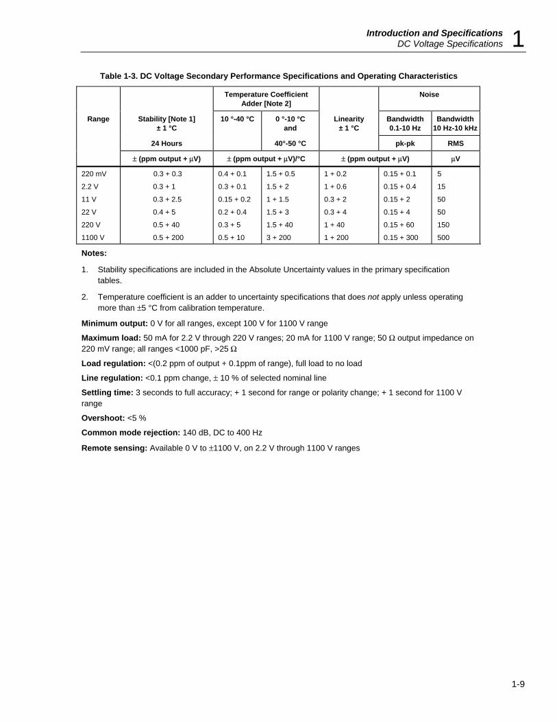
Table 1-3. DC Voltage Secondary Performance Specifications and Operating Characteristics
Temperature Coefficient Adder [Note 2]
Noise
Range Stability [Note 1] ± 1 °C
10 °-40 °C 0 °-10 °C and
Linearity ± 1 °C
Bandwidth 0.1-10 Hz
Bandwidth10 Hz-10 kHz
24 Hours 40°-50 °C pk-pk RMS
± (ppm output + μV) ± (ppm output + μV)/°C ± (ppm output + μV) μV
220 mV
2.2 V
11 V
22 V
220 V
1100 V
0.3 + 0.3
0.3 + 1
0.3 + 2.5
0.4 + 5
0.5 + 40
0.5 + 200
0.4 + 0.1
0.3 + 0.1
0.15 + 0.2
0.2 + 0.4
0.3 + 5
0.5 + 10
1.5 + 0.5
1.5 + 2
1 + 1.5
1.5 + 3
1.5 + 40
3 + 200
1 + 0.2
1 + 0.6
0.3 + 2
0.3 + 4
1 + 40
1 + 200
0.15 + 0.1
0.15 + 0.4
0.15 + 2
0.15 + 4
0.15 + 60
0.15 + 300
5
15
50
50
150
500
Notes:
1. Stability specifications are included in the Absolute Uncertainty values in the primary specification tables.
2. Temperature coefficient is an adder to uncertainty specifications that does not apply unless operating more than ±5 °C from calibration temperature.
Minimum output: 0 V for all ranges, except 100 V for 1100 V range
Maximum load: 50 mA for 2.2 V through 220 V ranges; 20 mA for 1100 V range; 50 Ω output impedance on 220 mV range; all ranges <1000 pF, >25 Ω
Load regulation: <(0.2 ppm of output + 0.1ppm of range), full load to no load
Line regulation: <0.1 ppm change, ± 10 % of selected nominal line
Settling time: 3 seconds to full accuracy; + 1 second for range or polarity change; + 1 second for 1100 V range
Overshoot: <5 %
Common mode rejection: 140 dB, DC to 400 Hz
Remote sensing: Available 0 V to ±1100 V, on 2.2 V through 1100 V ranges

5725A Instruction Manual
1-10
1-13. AC Voltage Specifications Table 1-4. 5720A Series II AC Voltage Specifications: 99 % Confidence Level
5720A99% 99 % Confidence Level
Range Resolution Frequency Absolute Uncertainty
± 5 °C from calibration temperature Relative Uncertainty
± 1 °C
24 Hours 90 Days 180 Days 1 Year 24 Hours 90 Days
Hz ± (ppm output + μV) ± (ppm output + μV)
2.2 mV
1 nV
0010 - 20 0020 - 40 0040 - 20 k 020 k - 50 k 050 k - 100 k 100 k - 300 k 300 k - 500 k 500 k - 1 M
0250 + 5 0100 + 5 0085 + 5 0220 + 5 0500 + 6 1000 + 12 1400 + 25 2900 + 25
0270 + 5 0105 + 5 0090 + 5 0230 + 5 0540 + 6 1200 + 12 1500 + 25 3100 + 25
0290 + 5 0110 + 5 0095 + 5 0240 + 5 0570 + 6 1250 + 12 1600 + 25 3250 + 25
00300 + 5 00115 + 5 00100 + 5 00250 + 5 00600 + 6 01300 + 12 01700 + 25 03400 + 25
0250 + 5 0100 + 5 0060 + 5 0085 + 5 0200 + 6 0350 + 12 0800 + 25 2700 + 25
0270 + 5 0105 + 5 0065 + 5 0095 + 5 0220 + 6 0400 + 12 1000 + 25 3000 + 25
22 mV 10 nV
0010 - 20 0020 - 40 0040 - 20 k 020 k - 50 k 050 k - 100 k 100 k - 300 k 300 k - 500 k 500 k - 1 M
0250 + 5 0100 + 5 0085 + 5 0220 + 5 0500 + 6 1000 + 12 1400 + 25 2900 + 25
0270 + 5 0105 + 5 0090 + 5 0230 + 5 0540 + 6 1200 + 12 1500 + 25 3100 + 25
0290 + 5 0110 + 5 0095 + 5 0240 + 5 0570 + 6 1250 + 12 1600 + 25 3250 + 25
00300 + 5 00115 + 5 00100 + 5 00250 + 5 00600 + 6 01300 + 12 01700 + 25 03400 + 25
0250 + 5 0100 + 5 0060 + 5 0085 + 5 0200 + 6 0350 + 12 0800 + 25 2700 + 25
0270 + 5 0105 + 5 0065 + 5 0095 + 5 0220 + 6 0400 + 12 1000 + 25 3000 + 25
220 mV 100 nV
0010 - 20 0020 - 40 0040 - 20 k 020 k - 50 k 050 k - 100 k 100 k - 300 k 300 k - 500 k 500 k - 1 M
0250 + 15 0100 + 8 0085 + 8 0220 + 8 0500 + 20 0850 + 25 1400 + 30 2700 + 60
0270 + 15 0105 + 8 0090 + 8 0230 + 8 0540 + 20 0900 + 25 1500 + 30 2900 + 60
0290 + 15 0110 + 8 0095 + 8 0240 + 8 0570 + 20 1000 + 25 1600 + 30 3100 + 60
00300 + 15 00115 + 8 00100 + 8 00250 + 8 00600 + 20 01100 + 25 01700 + 30 03300 + 60
0250 + 15 0100 + 8 0060 + 8 0085 + 8 0200 + 20 0350 + 25 0800 + 30 2600 + 60
0270 + 15 0105 + 8 0065 + 8 0095 + 8 0220 + 20 0400 + 25 1000 + 30 2800 + 60
2.2 V 1 mV
0010 - 20 0020 - 40 0040 - 20 k 020 k - 50 k 050 k - 100 k 100 k - 300 k 300 k - 500 k 500 k - 1 M
0250 + 50 0095 + 20 0045 + 10 0080 + 12 0120 + 40 0380 + 100 1000 + 250 1600 + 400
0270 + 50 0100 + 20 0047 + 10 0085 + 12 0125 + 40 0420 + 100 1100 + 250 1800 + 600
0290 + 50 0105 + 20 0050 + 10 0087 + 12 0127 + 40 0460 + 100 1150 + 250 1900 + 400
00300 + 50 00110 + 20 00052 + 10 00090 + 12 00130 + 40 00500 + 100 01200 + 250 02000 + 400
0250 + 50 0095 + 20 0030 + 10 0070 + 12 0100 + 40 0270 + 100 0900 + 250 1200 + 400
0270 + 50 0100 + 20 0040 + 10 0075 + 12 0105 + 40 0290 + 100 1000 + 250 1300 + 400
22 V 10 mV
0010 - 20 0020 - 40 0040 - 20 k 020 k - 50 k 050 k - 100 k 100 k - 300 k 300 k - 500 k 500 k - 1 M
0250 + 500 0095 + 200 0045 + 70 0080 + 120 0110 + 250 0300 + 800 1000 + 25001500 + 4000
0270 + 500 0100 + 200 0047 + 70 0085 + 120 0115 + 250 0310 + 800 1100 + 2500 1600 + 4000
0290 + 500 0105 + 200 0050 + 70 0087 + 120 0117 + 250 0320 + 800 1150 + 25001700 + 4000
00300 + 500 00110 + 200 00052 + 70 00090 + 120 00120 + 250 00325 + 800 01200 + 2500 01800 + 4000
0250 + 500 0095 + 200 0030 + 70 0070 + 120 0100 + 250 0270 + 800 0900 + 25001300 + 4000
0270 + 500 0100 + 200 0040 + 70 0075 + 120 0105 + 250 0290 + 800 1000 + 2500 1400 + 4000
± (ppm output + mV) ± (ppm output + mV)
220 V [Note 2]
100 mV
0010 - 20 0020 - 40 0040 - 20 k 020 k - 50 k 050 k - 100 k 100 k - 300 k 300 k - 500 k 500 k - 1 M
0250 + 5 0095 + 2 0057 + 0.7 0090 + 1.2 0160 + 3 0900 + 20 5000 + 50 8000 + 100
0270 + 5 0100 + 2 0060 + 0.7 0095 + 1.2 0170 + 3 1000 + 20 5200 + 50 9000 + 100
0290 + 5 0105 + 2 0062 + 0.7 0097 + 1.2 0175 + 3 1050 + 20 5300 + 50 9500 + 100
00300 + 5 00110 + 2 00065 + 0.7 00100 + 1.2 00 180 + 3 0 1100 + 20 0 5400 + 50 10,000 + 100
0250 + 5 0095 + 2 0045 + 0.7 0075 + 1.2 0140 + 3 0600 + 20 4500 + 50 8000 + 100
0270 + 5 0100 + 2 0050 + 0.7 0080 + 1.2 0150 + 3 0700 + 20 4700 + 50 8500 + 100
1100 V 1 mV [Note 1]
0015 - 50 0050 - 1 k
0300 + 20 0070 + 4
0320 + 20 0075 + 4
0340 + 20 0080 + 4
00 360 + 20 00085 + 4
0300 + 20 0050 + 4
0320 + 20 0055 + 4
5725A Amplifier:
1100 V 1 mV
0040 - 1 k 001 k - 20 k 020 k - 30 k
0075 + 4 0105 + 6 0230 + 11
0080 + 4 0125 + 6 0360 + 11
0085 + 4 0135 + 6 0440 + 11
000 90 + 4 00 165 + 6 00 600 + 11
0050 + 4 0085 + 6 0160 + 11
0055 + 4 0105 + 6 0320 + 11
750 V 030 k - 50 k 050 k - 100k
0230 + 11 0600 + 45
0360 + 11 1300 + 45
0440 + 11 1600 + 45
00600 + 11 02300 + 45
0160 + 11 0380 + 45
0320 + 11 1200 + 45
Notes: 1. Maximum output 250V from 15-50 Hz. 2. See Volt-Hertz capability in Figure 1-2.

Introduction and Specifications AC Voltage Specifications 1
1-11
Table 1-5. 5720A Series II AC Voltage Specifications: 95 % Confidence Level
5720A95% 95 % Confidence Level
Range Resolution Frequency Absolute Uncertainty
± 5 °C from calibration temperature Relative Uncertainty
± 1 °C
24 Hours 90 Days 180 Days 1 Year 24 Hours 90 Days
Hz ± (ppm output + μV) ± (ppm output + μV)
2.2 mV 1 nV
0010 - 20 0020 - 40 0040 - 20 k 020 k - 50 k 050 k - 100 k 100 k - 300 k 300 k - 500 k 500 k - 1 M
0200 + 4 0080 + 4 0070 + 4 0170 + 4 0400 + 5 0300 + 10 1100 + 20 2400 + 20
0220 + 4 0085 + 4 0075 + 4 0180 + 4 0460 + 5 0900 + 10 1200 + 20 2500 + 20
0230 + 4 0087 + 4 0077 + 4 0190 + 4 0480 + 5 1000 + 10 1300 + 20 2600 + 20
0240 + 4 0090 + 4 0080 + 4 0200 + 4 0500 + 5 1050 + 10 1400 + 20 2700 + 20
0200 + 4 0080 + 4 0050 + 4 0070 + 4 0160 + 5 0280 + 10 0650 + 20 2100 + 20
0220 + 4 0085 + 4 0055 + 4 0080 + 4 0180 + 5 0320 + 10 0800 + 20 2400 + 20
22 mV 10 nV
0010 - 20 0020 - 40 0040 - 20 k 020 k - 50 k 050 k - 100 k 100 k - 300 k 300 k - 500 k 500 k - 1 M
0200 + 4 0080 + 4 0070 + 4 0170 + 4 0400 + 5 0300 + 10 1100 + 20 2400 + 20
0220 + 4 0085 + 4 0075 + 4 0180 + 4 0460 + 5 0900 + 10 1200 + 20 2500 + 20
0230 + 4 0087 + 4 0077 + 4 0190 + 4 0480 + 5 1000 + 10 1300 + 20 2600 + 20
0240 + 4 0090 + 4 0080 + 4 0200 + 4 0500 + 5 1050 + 10 1400 + 20 2700 + 20
0200 + 4 0080 + 4 0050 + 4 0070 + 4 0160 + 5 0280 + 10 0650 + 20 2100 + 20
0220 + 4 0085 + 4 0055 + 4 0080 + 4 0180 + 5 0320 + 10 0800 + 20 2400 + 20
220 mV 100 nV
0010 - 20 0020 - 40 0040 - 20 k 020 k - 50 k 050 k - 100 k 100 k - 300 k 300 k - 500 k 500 k - 1 M
0200 + 12 0080 + 7 0070 + 7 0170 + 7 0400 + 17 0700 + 20 1100 + 25 2400 + 45
0220 + 12 0085 + 7 0075 + 7 0180 + 7 0420 + 17 0750 + 20 1200 +25 2500 + 45
0230 + 12 0087 + 7 0077 + 7 0190 + 7 0440 + 17 0800 + 20 1300 + 25 2600 + 45
0240 + 12 0090 + 7 0080 + 7 0200 + 7 0460 + 17 0900 + 20 1400 + 25 2700 + 45
0200 + 12 0080 + 7 0050 + 7 0070 + 7 0160 + 17 0280 + 20 0650 + 25 2100 + 45
0220 + 12 0085 + 7 0055 + 7 0080 + 7 0180 + 17 0320 + 20 0800 + 25 2400 + 45
2.2 V 1 mV
00010 - 20 0020 - 40 0040 - 20 k 020 k - 50 k 050 k - 100 k 100 k - 300 k 300 k - 500 k 500 k - 1 M
0200 + 40 0075 + 15 0037 + 8 0065 + 10 0100 + 30 0300 + 80 0800 + 200 1300 + 300
0220 + 40 0080 + 15 0040 + 8 0070 + 10 0105 + 30 0340 + 80 0900 + 200 1500 + 300
0230 + 40 0085 + 15 0042 + 8 0073 + 10 0107 + 30 0380 + 80 0950 + 200 1600 + 300
0240 + 40 0090 + 15 0045 + 8 0075 + 10 0110 + 30 0420 + 80 1000 + 200 1700 + 300
0200 + 40 0075 + 15 0025 + 8 0055 + 10 0080 + 30 0230 + 80 0700 + 200 1000 + 300
0220 + 40 0080 + 15 0035 + 8 0060 + 10 0085 + 30 0250 + 80 0800 + 200 1100 + 300
22V 10 mV
0010 - 20 0020 - 40 0040 - 20k 020k - 50k 050k - 100k 100k - 300k 300k - 500k 500k - 1M
0200 + 400 0075 + 150 0037 + 50 0065 + 100 0090 + 200 0250 + 600 0800 + 2000 1200 + 3200
0220 + 400 0080 + 150 0040 + 50 0070 + 100 0095 + 200 0260 + 600 0900 + 20001300 + 3200
0230 + 400 0085 + 150 0042 + 50 0073 + 100 0097 + 200 0270 + 600 0900 + 2000 1400 + 3200
0240 + 400 0090 + 150 0045 + 50 0075 + 100 0100 + 200 0275 + 600 1000 + 20001500 + 3200
0200 + 400 0075 + 150 0025 + 50 0055 + 100 0080 + 200 0250 + 600 0700 + 2000 1100 + 3200
0220 + 400 0080 + 150 0035 + 50 0060 + 100 0085 + 200 0270 + 600 0800 + 2000 1200 + 3200
± (ppm output + mV) ± (ppm output + mV)
220 V [Note 2]
100 mV
0010 - 20 0020 - 40 0040 - 20 k 020 k - 50 k 050 k - 100 k 100 k - 300 k 300 k - 500 k 500 k - 1 M
0200 +4 0075 + 1.5 0045 + 0.6 0070 + 1 0120 + 2.5 0700 + 16 4000 + 40 6000 + 80
0220 + 4 0080 + 1.5 0047 + 0.6 0075 + 1 0130 + 2.5 0800 + 16 4200 + 40 7000 + 80
0230 + 4 0085 + 1.5 0050 + 0.6 0077 + 1 0140 + 2.5 0850 + 16 4300 + 40 7500 + 80
0240 + 4 0090 + 1.5 0052 + 0.6 0080 + 1 0150 + 2.5 0900 + 16 4400 + 40 8000 + 80
0200 + 4 0075 + 1.5 0035 + 0.6 0060 + 1 0110 + 2.5 0500 + 16 3600 + 40 6500 + 80
0220 + 4 0080 + 1.5 0040 + 0.6 0065 + 1 0120 + 2.5 0600 + 16 3800 + 40 7000 + 80
1100 V 1 mV [Note 1]
0015 - 50 0050 - 1 k
0240 + 16 0055 + 3.5
0260 + 16 0060 + 3.5
0280 + 16 0065 + 3.5
0300 + 16 0070 + 3.5
0240 + 16 0040 + 3.5
0260 + 16 0045 + 3.5
5725A Amplifier:
1100 V
1 mV
0040 - 1 k 001 k - 20 k 020 k - 30 k
0075 + 4 0105 + 6 0230 + 11
0080 + 4 0125 + 6 0360 + 11
0085 + 4 0135 + 6 0440 + 11
0090 + 4 0165 + 6 0600 + 11
0050 + 4 0085 + 6 0160 + 11
0055 + 4 0105 + 6 0320 + 11
750 V 030 k - 50 k 050 k - 100 k
0230 + 11 0600 + 45
0360 + 11 1300 + 45
0440 + 11 1600 + 45
0600 + 11 2300 + 45
0160 + 11 0380 + 45
0320 + 11 1200 + 45
Notes: 1. Maximum output 250V from 15-50 Hz. 2. See Volt-Hertz capability in Figure 1-2.

5725A Instruction Manual
1-12
Table 1-6. 5700A Series II AC Voltage Specifications: 99 % Confidence Level
5700A99% 99 % Confidence Level
Range Resolution Frequency Absolute Uncertainty
± 5 °C from calibration temperature Relative Uncertainty
± 1 °C 24 Hours 90 Days 180 Days 1 Year 24 Hours 90 Days Hz ± (ppm output + μV) ± (ppm output + μV)
2.2 mV
1 nV
0010 - 20 0020 - 40 0040 - 20 k 020 k - 50 k 050 k - 100 k 100 k - 300 k 300 k - 500 k 500 k - 1 M
00 500 + 5 00200 + 5
00 100 + 5 00 340 + 5 00 800 + 8 01100 + 15 01500 + 30
0 4000 + 40
00 550 + 5 00 220 + 5 00 110 + 5 00 370 + 5 00 900 + 8 01200 + 15 01700 + 30 04400 + 40
00 600 + 5 00 230 + 5 00 120 + 5 00 390 + 5 00 950 + 8 0 1300 + 15 01700 + 30
0 4700 + 40
00 600 + 5 00 240 + 5 00 120 + 5 00 410 + 5 0 0950 + 8 0 1300 + 15 0 1800 + 30 0 4800 + 40
00 500 + 5 00 200 + 5 000 60 + 5 00 100 + 5 00 220 + 8 00 400 + 15 01000 + 30 00 400 + 30
00 550 + 5 0 0220 + 5 00 065 + 5 00 110 + 5 00 240 + 8 00 440 + 15 0 1100 + 30 0 4400 + 30
22 mV 10 nV 0010 - 20 0020 - 40 0040 - 20 k 020 k - 50 k 050 k - 100 k 100 k - 300 k 300 k - 500 k 500 k - 1 M
00 500 + 6 00 200 + 6 0 0100 + 6 0 0340 + 6 0 0800 + 8 0 1100 + 15 01500 + 30 04000 + 40
00 550 + 6 00 220 + 6 00 110 + 6 00 370 + 6 00 900 + 8 01200 + 15 01700 + 30 04400 + 40
00600 + 6 00 230 + 6 00 120 + 6 00 390 + 6 00 950 + 8 0 1300 + 15 0 1700 + 30 0 4700 + 40
0 0600 + 6 00 240 + 6 00 120 + 6 00 410 + 6 00 950 + 8 0 1300 + 15 0 1800 + 30 0 4800 + 40
00 500 + 6 00 200 + 6 000 60 + 6 00 100 + 6 00 220 + 8 00 400 + 15 01000 + 30 0 4000 + 30
00 550 + 6 00 220 + 6 000 65 + 6 00 110 + 6 00 240 + 8 00 440 + 15 0 1100 + 30 0 4400 + 30
220 mV 100 nV 0010 - 20 0020 - 40 0040 - 20 k 020 k - 50 k 050 k - 100 k 100 k - 300 k 300 k - 500 k 500 k - 1 M
0 0500 + 16 00 200 + 10 00 095 + 10 00 300 + 10 00 750 + 30 00 940 + 30 0 1500 + 40 0 3000 + 100
00 550 + 16 00 220 + 10 00 100 + 10 00 330 + 10 00 800 + 30 0 1000 + 30 01700 + 40 03300 + 100
00 600 + 16 00 230 + 10 00 110 + 10 00 350 + 10 00 850 + 30 01100 + 30
0 1700 + 40 0 3500 + 100
00 600 + 16 00240 + 10 00110 + 10 00360 + 10
0 0900 + 30 01100 + 30 01800 + 40 03600 + 100
00 500 + 16 00200 + 10 00060 + 10 00100 + 10 00220 + 30 00400 + 30 01000 + 40 03000 + 100
00550 + 16 00220 + 10 00065 + 10 00110 + 10 00240 + 30 00440 + 30 01100 + 40 03300 + 100
2.2 V 1 mV 0010 - 20 0020 - 40 0040 - 20 k 020 k - 50 k 050 k - 100 k 100 k - 300 k 300 k - 500 k 500 k - 1 M
00 500 + 100 00 150 + 30 000 70 + 7 00 120 + 20 00 230 + 80 00 400 + 150 0 1000 + 400 0 2000 + 1000
00 550 + 100 00 170 + 30 000 75 + 7 00 130 + 20 00 250 + 80 00 440 + 150 0 1100 + 400 0 2200 + 1000
00 600 + 100 00 170 + 30 000 80 + 7 00 140 + 20 00 270 + 80 00 470 + 150 0 1200 + 400 0 2300 + 1000
00 600 + 100 00 180 + 30 000 85 + 7 00 140 + 20 00 280 + 80 00 480 + 150 0 1200 + 400 0 2400 + 1000
00 500 + 100 00 150 + 30 000 40 + 7 00 100 + 20 00 200 + 80 00 400 + 150 0 1000 + 400 0 2000 + 1000
00 550 + 100 00 170 + 30 000 45 + 7 00 110 + 20 00 220 + 80 00 440 + 150 0 1100 + 400 0 2200 + 1000
22 V 10 mV 0010 - 20 0020 - 40 0040 - 20 k 020 k - 50 k 050 k - 100 k 100 k - 300 k 300 k - 500 k 500 k - 1 M
00 500 + 1000 00 150 + 300 000 70 + 70 00 120 + 200 00 230 + 400 00 500 + 1700 0 1200 + 5000 0 2600 + 9000
00 550 + 1000 00 170 + 300 000 75 + 70 00 130 + 200 00 250 + 400 00 550 + 1700 0 1300 + 5000 0 2800 + 9000
00 600 + 1000 00 170 + 300 000 80 + 70 00 140 + 200 00 270 + 400 00 550 + 1700 0 1300 + 5000 0 2900 + 9000
00 600 + 1000 00 180 + 300 000 85 + 70 00 140 + 200 00 280 + 400 00 600 + 1700 0 1400 + 5000 0 3000 + 9000
00 500 + 1000 00 150 + 300 000 40 + 70 00 100 + 200 00 200 + 400 00500 + 1700 01200 + 5000 02600 + 9000
00 550 + 1000 00 170 + 300 000 45 + 70 00 110 + 200 00 220 + 400 00 550 + 1700 0 1300 + 5000 0 2800 + 9000
± (ppm output + mV) ± (ppm output + mV)220 V
[Note 2] 100 mV 0010 - 20
0020 - 40 0040 - 20 k 020 k - 50 k 050 k - 100 k 100 k - 300 k 300 k - 500 k 500 k - 1 M
00 500 + 10 00 150 + 3 000 75 + 1 00 200 + 4 00 500 + 10 0 1500 + 110 0 5000 + 110 12,000 + 220
00 550 + 10 00 170 + 3 000 80 + 1 00 220 + 4 00 550 + 10 0 1500 + 110 0 5200 + 110 12,500 + 220
0 0600 + 10 00 170 + 3 000 85 + 1 00 240 + 4 00 600 + 10 0 1600 + 110 0 5300 + 110 12,500 + 220
00 600 + 10 00 180 + 3 000 90 + 1 00 250 + 4 00 600 + 10 0 1600 + 110 0 5400 + 110 13,000 + 220
00 500 + 10 00 150 + 3 000 45 + 1 00 100 + 1 00 300 + 10 01500 + 110 0 5000 + 110 12,000 + 220
00 550 + 10 00 170 + 3 000 50 + 1 00 110 + 1 00 330 + 10 0 1500 + 100 0 5200 + 110 12,000 + 220
1100 V 1 mV [Note 1]
00015 - 50 00050 - 1 k
00 400 + 20 000 75 + 4
00420 + 20 000 80 + 4
00440 + 20 000 85 + 4
00460 + 20 000 90 + 4
00400 + 20 000 50 + 4
00420 + 20 000 55 + 4
5725A Amplifier: 1100 V 1 mV 00040 - 1 k
0001 k - 20 k 0020 k - 30 k
000 75 + 4 00 105 + 6 00 230 + 11
000 80 + 4 00 125 + 6 00 360 + 11
000 85 + 4 00 135 + 6 00 440 + 11
000 90 + 4 00 165 + 6 00 600 + 11
000 50 + 4 000 85 + 6 00 160 + 11
000 55 + 4 00 105 + 6 00 320 + 11
750 V 0030 k - 50 k 0050 k - 100 k
00 230 + 11 00 600 + 45
00 360 + 11 0 1300 + 45
00 440 + 11 0 1600 + 45
00 600 + 11 0 2300 + 45
00 160 + 11 00 380 + 45
00 320 + 11 0 1200 + 45
Notes: 1. Maximum output 250V from 15-50 Hz. 2. See Volt-Hertz capability in Figure 1-2.

Introduction and Specifications AC Voltage Specifications 1
1-13
Table 1-7. 5700A Series II AC Voltage Specifications: 95 % Confidence Level
5700A95% 95% Confidence Level
Range Resolution Frequency Absolute Uncertainty
± 5 °C from calibration temperature
Relative Uncertainty
± 1 °C
24 Hours 90 Days 180 Days 1 Year 24 Hours 90 Days
Hz ± (ppm output + μV) ± (ppm output + μV)
2.2 mV
1 nV
0010 - 20 0020 - 40 0040 - 20 k 020 k - 50 k 050 k - 100 k 100 k - 300 k 300 k - 500 k 500 k - 1 M
00 400 + 4.5 00 170 + 4.5 000 85 + 4.5 00 300 + 4.5 00 700 + 7 00 900 + 13 0 1300 + 25 0 2800 + 25
00 500 + 4.5 00 190 + 4.5 000 95 + 4.5 00 330 + 4.5 0 0750 + 7 0 1000 + 13 0 1500 + 25 0 3100 + 25
00 530 + 4.5 00 200 + 4.5 00 100 + 4.5 00 350 + 4.5 00 800 + 7 0 1050 + 13 0 1600 + 25 0 3300 + 25
00 550 + 4.5 00 210 + 4.5 00 105 + 4.5 00 370 + 4.5 00 850 + 7 0 1100 + 13 0 1700 + 25 0 3400 + 25
00 400 + 4.5 00 170 + 4.5 000 55 + 4.5 000 90 + 4.5 00 210 + 7 00 380 + 13 00 900 + 25 0 2900 + 25
00 500 + 4.5 00 190 + 4.5 000 60 + 4.5 00 100 + 4.5 00 230 + 7 00 420 + 13 0 1000 + 25 0 3200 + 25
22 mV 10 nV
0010 - 20 0020 - 40 0040 - 20 k 020 k - 50 k 050 k - 100 k 100 k - 300 k 300 k - 500 k 500 k - 1 M
00 400 + 5 00 170 + 5 000 85 + 5 00 300 + 5 00 700 + 7 00 900 + 12 0 1300 + 25 0 2800 + 25
00 500 + 5 00 190 + 5 000 95 + 5 00 330 + 5 00 750 + 7 0 1000 + 12 0 1500 + 25 0 3100 + 25
00 530 + 5 00 200 + 5 00 100 + 5 00 350 + 5 00 800 + 7 0 1050 + 12 0 1600 + 25 0 3300 + 25
00 550 + 5 00 210 + 5 00 105 + 5 00 370 + 5 00 850 + 7 0 1100 + 12 0 1700 + 25 0 3400 + 25
00 400 + 5 00 170 + 5 000 55 + 5 000 90 + 5 00 210 + 7 00 380 + 12 00900 + 25 0 2900 + 25
00 500 + 5 00 190 + 5 000 60 + 5 00 100 + 5 00 230 + 7 00 420 + 12 0 1000 + 25 0 3200 + 25
220 mV 100 nV
0010 - 20 0020 - 40 0040 - 20 k 020 k - 50 k 050 k - 100 k 100 k - 300 k 300 k - 500 k 500 k - 1 M
00 400 + 13 00 170 + 8 000 85 + 8 00 250 + 8 00 700 + 25 00 900 + 25 0 1300 + 35 0 2800 + 80
00 500 + 13 00 190 + 8 000 95 + 8 00 280 + 8 00 750 + 25 0 1000 + 25 0 1500 + 35 0 3100 + 80
00 530 + 13 00 200 + 8 00 100 + 8 00 300 + 8 00 800 + 25 0 1050 + 25 0 1600 + 35 0 3300 + 80
00 550 + 13 00 210 + 8 00 105 + 8 00 320 + 8 00 850 + 25 0 1100 + 25 0 1700 + 35 0 3400 + 80
00 400 + 13 00 170 + 8 000 55 + 8 000 90 + 8 00 210 + 25 00 380 + 25 00 900 + 35 0 2900 + 80
00 500 + 13 00 190 + 8 000 60 + 8 00 100 + 8 00 230 + 25 00 420 + 25 0 1000 + 35 0 3200 + 80
2.2 V 1 mV
0010 - 20 0020 - 40 0040 - 20 k 020 k - 50 k 050 k - 100 k 100 k - 300 k 300 k - 500 k 500 k - 1 M
00 400 + 80 00 130 + 25 000 60 + 6 00 105 + 16 00 190 + 70 00 350 + 130 00 850 + 350 0 1700 + 850
00 450 + 80 00 140 + 25 000 65 + 6 00 110 + 16 00 210 + 70 00 390 + 130 0 0950 + 350 0 1900 + 850
00 480 + 80 00 150 + 25 000 70 + 6 00 115 + 16 00 230 + 70 00 420 + 130 0 1000 + 350 0 2100 + 850
00 500 + 80 00 160 + 25 000 75 + 6 00 120 + 16 00 250 + 70 00 430 + 130 0 1050 + 350 0 2200 + 850
00 400 + 80 00 130 + 25 000 35 + 6 000 85 + 16 00 170 + 70 00 340 + 130 00 850 + 350 0 1700 + 850
00 450 + 80 00 140 + 25 000 40 + 6 000 95 + 16 00 190 + 70 00 380 + 130 00 950 + 350 0 1900 + 850
22 V 10 mV
0010 - 20 0020 - 40 0040 - 20 k 020 k - 50 k 050 k - 100 k 100 k - 300 k 300 k - 500 k 500 k - 1 M
00 400 + 800 00 130 + 250 000 60 + 60 00 105 + 160 00 190 + 350 00 400 + 1500 0 1050 + 4300 0 2300 + 8500
00 450 + 800 00 140 + 250 000 65 + 60 00 110 + 160 00 210 + 350 00 450 + 1500 0 1150 + 4300 0 2500 + 8500
00 480 + 800 00 150 + 250 000 70 + 60 00 115 + 160 00 230 + 350 00 470 + 1500 0 1200 + 4300 0 2600 + 8500
00 500 + 800 00 160 + 250 000 75 + 60 00 120 + 160 00 250 + 350 00 500 + 1500 0 1250 + 4300 0 2700 + 8500
00 400 + 800 00 130 + 250 000 35 + 60 000 85 + 160 00 170 + 350 00 400 + 1500 0 1000 + 4300 0 2200 + 8500
00 450 + 800 00 140 + 250 000 40 + 60 000 95 + 160 00 190 + 350 00 450 + 1500 0 1100 + 4300 0 2400 + 8500
± (ppm output + mV) ± (ppm output + mV)
220 V [Note 2]
100 mV
0010 - 20 0020 - 40 0040 - 20 k 020 k - 50 k 050 k - 100 k 100 k - 300 k 300 k - 500 k 500 k - 1 M
00 400 + 8 00 130 + 2.5 000 65 + 0.8 00 170 + 3.5 00 400 + 8 0 1300 + 90 0 4300 + 90 10,500 + 190
00 450 + 8 00 140 + 2.5 000 70 + 0.8 00 190 + 3.5 00 450 + 8 0 1400 + 90 0 4500 + 90 11,000 + 190
00 480 + 8 00 150 + 2.5 000 75 + 0.8 00 210 + 3.5 00 480 + 8 0 1450 + 90 0 4600 + 90 11,300 + 190
00 500 + 8 00 160 + 2.5 000 80 + 0.8 00 220 + 3.5 00 500 + 8 0 1500 + 90 0 4700 + 90 11,500 + 190
00 400 + 8 00 130 + 2.5 000 40 + 0.8 000 85 + 3.5 00 270 + 8 0 1200 + 90 0 4200 + 90 10,500 + 190
00 450 + 8 00 140 + 2.5 000 45 + 0.8 000 95 + 3.5 00 300 + 8 0 1300 + 90 0 4500 + 90 11,000 + 190
1100 V 1 mV [Note 1]
0015 - 50 0050 - 1 k
00 340 + 16 000 65 + 3.5
00360 + 16 000 70 + 3.5
00380 + 16 000 75 + 3.5
00400 + 16 000 80 + 3.5
00340 + 16 000 45 + 3.5
00360 + 16 000 50 + 3.5
5725A Amplifier:
1100 V 1 mV
0040 - 1 k 001 k - 20 k 020 k - 30 k
000 75 + 4 00 105 + 6 00 230 + 11
000 80 + 4 00 125 + 6 00 360 + 11
000 85 + 4 00 135 + 6 00 440 + 11
000 90 + 4 00 165 + 6 00 600 + 11
000 50 + 4 000 85 + 6 00 160 + 11
000 55 + 4 00 105 + 6 00 320 + 11
750 V 030 k - 50 k 050 k - 100 k
00 230 + 11 00 600 + 45
00 360 + 11 0 1300 + 45
00 440 + 11 0 1600 + 45
00 600 + 11 0 2300 + 45
00 160 + 11 00 380 + 45
00 320 + 11 0 1200 + 45
Notes: 1. Maximum output 250V from 15-50 Hz. 2. See Volt-Hertz capability in Figure 1-2.

5725A Instruction Manual
1-14
Table 1-8. AC Voltage Secondary Performance Specifications and Operating Characteristics Stability
± 1 °C [Note 1] Temperature Coefficient Maximum
Distortion Range Frequency 24 Hours 10°-40 °C 0°-10 °C and
40°-50 °C Output Impedance Bandwidth
10 Hz-10 MHz
Hz ± μV ±μV/°C Ω ± (% output + μV)
2.2 mV
0010 - 20 0020 - 40 0040 - 20 k 020 k - 50 k 050 k - 100 k 100 k - 300 k 300 k - 500 k 500 k - 1 M
5 5 2 2 3 3 5 5
0.05 0.05 0.05 0.1 0.2 0.3 0.4 0.5
0.05 0.05 0.05 0.1 0.2 0.3 0.4 0.5
50
00.05 + 10 0.035 + 10 0.035 + 10 0.035 + 10 0.035 + 10 000.3 + 30 000.3 + 30 000 1 + 30
22 mV
0010 - 20 0020 - 40 0040 - 20 k 020 k - 50 k 050 k - 100 k 100 k - 300 k 300 k - 500 k 500 k - 1 M
5 5 2 2 3 5
10 15
0.2 0.2 0.2 0.4 0.5 0.6 1 1
0.3 0.3 0.3 0.5 0.5 0.6 1 1
50
00.05 + 11 0.035 + 11 0.035 + 11 0.035 + 11 0.035 + 11 000.3 + 30 000.3 + 30 000 1 + 30
± (ppm output + μV) ± (ppm output μV)/°C
220 mV
0010 - 20 0020 - 40 0040 - 20 k 020 k - 50 k 050 k - 100 k 100 k - 300 k 300 k - 500 k 500 k - 1 M
150 + 20 080 + 15 012 + 2 010 + 2 010 + 2 020 + 4 100 + 10 200 + 20
002 + 1 002 + 1 002 + 1 015 + 2 015 + 4 080 + 5 080 + 5 080 + 5
02 + 1 02 + 1 02 + 1 15 + 2 15 + 4 80 + 5 80 + 5 80 + 5
50
00.05 + 16 0.035 + 16 0.035 + 16 0.035 + 16 0.035 + 16 000.3 + 30 000.3 + 30 000 1 + 30
Load Regulation ±(ppm output+ μV)
2.2 V
0010 - 20 0020 - 40 0040 - 20 k 020 k - 50 k 050 k - 100 k 100 k - 300 k 300 k - 500 k 500 k - 1 M
150 + 20 080 + 15 012 + 4 015 + 5 015 + 5 030 + 10 070 + 20 150 + 50
050 + 10 015 + 5 002 + 1 010 + 2 010 + 4 080 + 15 080 + 40 080 + 100
50 + 10 15 + 5 05 + 2 15 + 4 20 + 4 80 + 15 80 + 40 80 + 100
0010 + 2 0010 + 2 0010 + 4 0030 + 10 0120 + 16 0300 ppm 0600 ppm 01200 ppm
00.05 + 80 0.035 + 80 0.035 + 80 0.035 + 80 0.035 + 80 000.3 + 110 000.3 + 110 000 1 + 110
22 V
0010 - 20 0020 - 40 0040 - 20 k 020 k - 50 k 050 k - 100 k 100 k - 300 k 300 k - 500 k 500 k - 1 M
150 + 20 080 + 15 012 + 8 015 + 10 015 + 10 030 + 15 070 + 100 150 + 100
050 + 100 015 + 30 002 + 10 010 + 20 010 + 40 080 + 150 080 + 300 080 + 500
50 + 100 15 + 40 04 + 15 20 + 20 20 + 40 80 + 150 80 + 300 80 + 500
0010 + 20 0010 + 20 0010 + 30 0030 + 50 0080 + 80 0100 + 700 0200 + 1100 0600 + 3000
00.05 + 700 0.035 + 700 0.035 + 700 0.035 + 700 0.035 + 700 000.3 + 800 000.3 + 800 000 2 + 800
220 V
0010 - 20 0020 - 40 0040 - 20 k 020 k - 50 k 050 k - 100 k 100 k - 300 k 300 k - 500 k 500 k - 1 M
150 + 200 080 + 150 012 + 80 015 + 100 015 + 100 030 + 400 100 + 10,000 200 + 20,000
0 50 + 1000 0 15 + 300 00 2 + 80 0 10 + 100 0 10 + 500 0 80 + 600 0 80 + 800 0 80 + 1000
50 + 1000 15 + 300 04 + 80 20 + 100 20 + 500 80 + 600 80 + 800 80 + 1000
0010 + 200 0010 + 200 0010 + 300 0030 + .600 0080 + 3,000 0250 + 25,000 0500 + 50,000 1000 + 110,000
00.05 + 10,000 00.05 + 10,000 00.05 + 10,000 00.05 + 10,000 000.1 + 13,000 001.5 + 50,000 001.5 + 50,000 003.5 + 100,000
±(ppm output + mV) ±(ppm output)/°C ±(% output)
1100 V 0015 - 50 0050 - 1 k
150 + 0.5 020 + 0.5
50 2
50 5
0010 + 2 0010 + 1
0.15 0.07
Note: 1. Stability specifications are included in Absolute Uncertainty values for the primary specifications.

Introduction and Specifications AC Voltage Specifications 1
1-15
Table 1-8. AC Voltage Secondary Performance and Operating Characteristics (continued)
5725A Amplifier:
Stability
±1 °C [Note 1] Temperature Coefficient
Adder
Distortion
Bandwidth
Range Frequency 24 Hours 10°-40 °C
0°-10 °C and
40°-50 °C
Load Regulation
[Note 2]
10 Hz-10 MHz
±(% output)
Hz ±(ppm output + mV) ±(ppm output)/°C ±(ppm output + mV) 150 pF 1000 pF
1100 V
040 - 1 k
01 k - 20 k
20 k - 50 k
50 k - 100 k
010 + .5
015 + 2
040 + 2
130 + 2
5
5
10
30
5
5
10
30
010 + 1
090 + 6
275 + 11
500 + 30
0.10
0.10
0.30
0.40
0.10
0.15
0.30
0.40
Voltage Range Maximum Current Limits Load Limits Output display formats: Voltage or dBm,
dBm reference 600 Ω.
2.2 V [Note 3]
22 V
220 V
50 mA, 0 °C-40 °C
20 mA, 40 °C-50 °C
>50 Ω,
1000 pF
Minimum output:: 10 % on each range
External sense: Selectable for 2.2 V, 22 V, 220 V, and 1100 V ranges; 5700A/5720A <100 kHz, 5725A <30 kHz
1100 V 6 mA 600 pF Settling time to full accuracy:
5725A Amplifier: 1000 pF [Note 2] Frequency (Hz) Settling time (seconds)
040 Hz-5 kHz 50 mA <20 7
1100 V 05 kHz-30 kHz 70 mA 300 pF 120-120 k 5
30 kHz-100 kHz 70 mA [Note 4]
150 pF >120 k 2
Notes:
1 Stability specifications are included in Absolute Uncertainty values for the primary specifications.
2. The 5725A will drive up to 1000 pF of load capacitance. Uncertainty specifications include loads to 300 pF and 150 pF as shown under "Load Limits." For capacitances up to the maximum of 1000 pF, add "Load Regulation."
3. 2.2 V Range, 100 kHz-1.2 MHz only: uncertainty specifications cover loads to 10 mA or 1000 pF. For higher loads, load regulation is added.
4. Applies from 0 °C to 40 °C
1000
100
10
0
3.5 V
10000
50 Hz10 Hz 1 kHz 100 kHz 1 MHz 30 MHz
Vo
ltag
e
Frequency
40 Hz 30 Hz 5725A
5700A-03
2.2 x 10⁷ V-Hz
15 Hz
5700A/5720A
Volt-Hertz Capability
ahp160f.eps
Figure 1-1. Volt-Hertz Capability
+ 1 second for amplitude or frequency range change; + 2 seconds for 5700A/5720A 1100 V range; + 4 seconds for 5725A 1100 V range
Overshoot:: <10% Common mode rejection: 140 dB, DC to 400 Hz
Frequency: Ranges (Hz):
10.000-119.99 0.1200 k-1.1999 k, 1.200 k-11.999 k 12.00 k-119.99 k,120.0 k-1.1999
Uncertainty: ±0.01 %
Resolution: 11.999 counts
Phase lock: Selectable rear panel BNC input Phase uncertainty (except 1100 V range):
>30 Hz: ±1° + 0.05°/kHz), <30 Hz: ±3° Input voltage: 1 V to 10 V rms sine wave (do not exceed 1 V for mV ranges)
Frequency range: 10 Hz to 1.1999 MHz
Lock range: ±2 % of frequency
Lock-in time: Larger of 10/frequency or 10 msec
Phase reference: Selectable, rear panel BNC output Range: ±180° Phase Uncertainty (except 1100 V range):
±1° at quadrature points (0°, ±90°, ±180°) elsewhere ±2°
Stability: ±0.1° Resolution: 1° Output level: 2.5 V rms ±0.2 V
Frequency range:
50 kHz to 1 kHz, usable 10 Hz to 1.1999 MHz

5725A Instruction Manual
1-16
1-14. Resistance Specifications
Table 1-9. 5720A Series II Resistance Specifications: 99 % and 95 % Confidence Levels
5720A99% 99% Confidence Level Nominal
Value Absolute Uncertainty of Characterized Value ±5 °C from calibration temperature [Note 1]
Relative Uncertainty ±1 °C
24 Hours 90 Days 180 Days 1 Year 24 Hours 90 Days
Ω ±ppm ±ppm
0
1
1.9
10
19
100
190
1 k
1.9 k
10 k
19 k
100 k
190 k
1 M
1.9 M
10 M
19 M
100 M
50 μΩ
85
85
23
23
10
10
8
8
8
9
9
9
16
17
33
43
100
50 μΩ
95
95
25
25
11
11
9
9
9
9
11
11
18
19
37
47
110
50 μΩ
100
100
26
26
11.5
11.5
9.5
9.5
9.5
9.5
12
12
20
21
40
50
115
50 μΩ
110
110
27
27
12
12
10
10
10
10
13
13
23
24
46
55
120
50 μΩ
32
25
5
4
2
2
2
2
2
2
2
2
2.5
3
10
20
50
50 μΩ
40
33
8
7
4
4
3
3
3
3
3
3
5
6
14
24
60
5720A95% 95 % Confidence Level Nominal
Value Absolute Uncertainty of Characterized Value ±5 °C from calibration temperature [Note 1]
Relative Uncertainty ±1 °C
24 Hours 90 Days 180 Days 1 Year 24 Hours 90 Days
Ω ±ppm ±ppm
0
1
1.9
10
19
100
190
1 k
1.9 k
10 k
19 k
100 k
190 k
1 M
1.9 M
10 M
19 M
100 M
40 μΩ
70
70
20
20
8
8
6.5
6.5
6.5
7.5
7.5
7.5
13
14
27
35
85
40 μΩ
80
80
21
21
9
9
7.5
7.5
7.5
7.5
9
9
15
16
31
39
95
40 μΩ
85
85
22
22
9.5
9.5
8
8
8
8
10
10
17
18
34
42
100
40 μΩ
95
95
23
23
10
10
8.5
8.5
8.5
8.5
11
11
20
21
40
57
100
40 μΩ
27
20
4
3.5
1.6
1.6
1.6
1.6
1.6
1.6
1.6
1.6
2
2.5
8
16
40
40 μΩ
35
26
7
6
3.5
3.5
2.5
2.5
2.5
2.5
2.5
2.5
4
4
12
20
50
Note: 1. Specifications apply to displayed value. 4-wire connections, except 100 MΩ.

Introduction and Specifications Resistance Specifications 1
1-17
Table 1-10. 5700A Series II Resistance Specifications: 99 % and 95 % Confidence Levels
5700A99% 99 % Confidence Level
Nominal Value
Absolute Uncertainty of Characterized Value ±5 °C from calibration temperature [Note 1]
Relative Uncertainty ±1 °C
24 Hours 90 Days 180 Days 1 Year 24 Hours 90 Days
Ω ±ppm ±ppm
0
1
1.9
10
19
100
190
1 k
1.9 k
10 k
19 k
100 k
190 k
1 M
1.9 M
10 M
19 M
100 M
50 μΩ
85
85
26
24
15
15
11
11
9
9
11
11
16
17
33
43
110
50 μΩ
95
95
28
26
17
17
12
12
11
11
13
13
18
19
37
47
120
50 μΩ
100
100
30
28
18
18
13
13
12
12
14
14
20
21
40
50
125
50 μΩ
110
110
33
31
20
20
15
15
14
14
16
16
23
24
46
55
130
50 μΩ
32
25
5
4
2
2
2
2
2
2
2
2
2.5
3.5
10
20
50
50 μΩ
40
33
8
7
4
4
3.5
3.5
3.5
3.5
3.5
3.5
5
6
14
24
60
5700A95% 95 % Confidence Level
Nominal Value
Absolute Uncertainty of Characterized Value ±5 °C from calibration temperature [Note 1]
Relative Uncertainty ±1 °C
24 Hours 90 Days 180 Days 1 Year 24 Hours 90 Days
Ω ±ppm ±ppm
0
1
1.9
10
19
100
190
1 k
1.9 k
10 k
19 k
100 k
190 k
1 M
1.9 M
10 M
19 M
100 M
50 μΩ
70
70
21
20
13
13
9
9
7.5
7.5
9
9
13
14
27
35
90
50 μΩ
80
80
23
22
14
14
10
10
9.5
9.5
11
11
15
16
31
39
100
50 μΩ
85
85
27
24
15
15
11
11
10.5
10.5
12
12
17
18
34
42
105
50 μΩ
95
95
28
27
17
17
13
13
12
12
14
14
20
21
40
47
110
50 μΩ
32
25
5
4
2
2
2
2
2
2
2
2
2.5
3
10
20
50
50 μΩ
40
33
8
7
4
4
3.5
3.5
3.5
3.5
3.5
3.5
5
6
14
24
60
Note: 1. Specifications apply to displayed value. 4-wire connections, except 100 MΩ.

5725A Instruction Manual
1-18
Table 1-11. Resistance Secondary Performance Specifications and Operating Characteristics
Nominal Value
Stability ±1 °C
[Note 1]
Temperature Coefficient Adder
[Note 2]
Full Spec Load Range
Maximum Peak
Current
Maximum Difference
of Characterized
Two-Wire Adder active
compensation [Note 4]
10°-40 °C 0°-10 °C and
[Note 3] to Nominal Value
Lead Resistance
24 Hours 40°-50 °C 0.1Ω 1ΩΩ ±ppm ±ppm/°C mA mA ±ppm ±mΩ
0 ⎯ ⎯ ⎯
00
8 - 500 500 ⎯ 2 + Im 4 Vμ
4 + Im 4 Vμ
1 32 4 5 00 8 - 100 700 500 2 + Im
4 Vμ4 + Im
4 Vμ
1.9 25 6 7 00 8 - 100 500 500 2 + Im
4 Vμ4 + Im
4 Vμ
10 5 2 3 00
8 - 11 220 300 2 + Im 4 Vμ
4 + Im 4 Vμ
19 4 2 3 00 8 - 11 160 300 2 + Im
4 Vμ4 + Im
4 Vμ
100 2 2 3 00 8 - 11 70 150 2 + Im
4 Vμ4 + Im
4 Vμ
190 2 2 3 00 8 - 11 50 150 2 + Im
4 Vμ4 + Im
4 Vμ
1 k 2 2 3 00 1 - 2 22 150 10 15
1.9 k 2 2 3 00 1 - 1.5 16 150 10 15
10 k 2 2 3 100 - 500 μA 7 150 50 60
19 k 2 2 3 0 50 - 250 μA 5 150 100 120
100 k 2 2 3 10 - 100 μA 1 150 Im= Current produced by Ohmmeter
190 k 2 2 3 00 5 - 50 μA 500 μA 150
1 M 2.5 2.5 6 00 5 - 20 μA 100 μA 200
1.9 M 3.5 3 10 02.5 - 10 μA 50 μA 200
10 M 10 5 20 00.5 - 2 μA 10 μA 300
19 M 20 8 40 0.25 - 1 μA 5 μA 300
100 M 50 12 100 0 50 - 200 nA 1 μA 500
Notes:
1. Stability specifications are included in the Absolute Uncertainty values in the primary specification tables.
2. Temperature coefficient is an adder to uncertainty specifications that does not apply unless operated morethan 5 °C from calibration temperature, or calibrated outside the range 19 °C to 24 °C. Two examples:
• Calibrate at 20 °C: Temperature coefficient adder is not required unless operated below 15 °C orabove 25 °C.
• Calibrate at 26 °C: Add 2 °C temperature coefficient adder. Additional temperature coefficient adder isnot required unless operated below 21 °C or above 31 °C.
3. Refer to current derating factors table for loads outside of this range.
4. Active two-wire compensation may be selected for values less than 100 kΩ, with either the front panel orthe meter input terminals as reference plane. Active compensation is limited to 11 mA load, and to 2 Vburden. Two-wire compensation can be used only with Ω-meters that source continuous (not pulsed) dccurrent.

Introduction and Specifications Resistance Specifications 1
1-19
Table 1-12. Current Derating Factors
Nominal Value Value of Derating Factor K for Over or Under Current
Ω
Two-Wire Comp
I < IL
[Note 1]
Four-Wire
I < IL
[Note 1]
Four-Wire
IU < I < Imax
[Note 2]
SHORT
1
1.9
10
19
100
190
1 k
1.9 k
10 k
19 k
100 k
190 k
1 M
1.9 M
10 M
19 M
100 M
4.4
4.4
4.4
4.4
4.4
4.4
4.4
4.4
4.4
5000
5000
⎯
⎯
⎯
⎯
⎯
⎯
0.3
300
160
30
16
3.5
2.5
0.4
0.4
50
50
7.5
4.0
1.0
0.53
0.2
0.53
0.1
⎯
4 x10⁻⁵
1.5 x 10⁻⁴
1.6 x 10⁻³
3 x 10⁻³
1 x 10⁻²
1.9 x 10⁻²
0.1
0.19
2.0
3.8
2 x 10⁻⁵
3.8 x 10⁻⁵
1.5 x 10⁻⁴
2.9 x 10⁻⁴
1 x 10⁻³
1.9 x 10⁻³
⎯
Notes:
1. For I < I L, errors occur due to thermally generated voltages within the 5720A. Use the followingequation to determine the error, and add this error to the corresponding uncertainty or stabilityspecification.
Error = K(I L - I)/( I L x I)
Where: Error is in mΩ for all two-wire comp values and four-wire short, and in ppm for the remainingfour-wire values.
K is the constant from the above table;
I and IL are expressed in mA for short to 1.9 kΩ;
I and IL are expressed in μA for 10 kΩ to 100 MΩ
2. For IU < I < IMAX errors occur due to self-heating of the resistors in the calibrator. Use the followingequation to determine the error in ppm and add this error to the corresponding uncertainty or stabilityspecification.
Error in ppm = K(I2-IU2)
Where: K is the constant from the above table;
I and IU are expressed in mA for short to 19 kΩ;
I and IU are expressed in μA for 100 kΩ to 100 MΩ

5725A Instruction Manual
1-20
1-15. DC Current Specifications
Table 1-13. 5720A Series II DC Current Specifications: 99 % and 95 % Confidence Levels
5720A99% 99 % Confidence Level
Range Resolution Absolute Uncertainty
±5 °C from calibration temperature.
For fields strengths >0.4 V/m but ≤3 V/m, add 1 % of range.
Relative Uncertainty ±1 °C
24 Hours 90 Days 180 Days 1 Year 24 Hours 90 Days
nA ± (ppm output + nA) ± (ppm output + nA)
220 μA
2.2 mA
22 mA
0.1
1
10
040 + 7
030 + 8
030 + 50
042 + 7
035 + 8
035 + 50
045 + 7
037 + 8
037 + 50
050 + 7
040 + 8
040 + 50
024 + 7
024 + 8
024 + 50
026 + 7
026 + 8
026 + 50
μA ± (ppm output + μA) ± (ppm output + μA)
220 mA
2.2 A
[Note 1]
0.1
1
040 + 0.8
060 + 15
045 + 0.8
070 + 15
047 + 0.8
080 + 15
050 + 0.8
090 + 15
026 + 0.5
040 + 12
030 + 0.5
045 + 12
5725A Amplifier:
11 A 10 330 + 470 340 + 480 350 + 480 360 + 480 100 + 130 110 + 130
5720A95% 95 % Confidence Level
Range Resolution Absolute Uncertainty
±5 °C from calibration temperature
For fields strengths >0.4 V/m but ≤3 V/m,
add 1 % of range.
Relative Uncertainty ±1 °C
24 Hours 90 Days 180 Days 1 Year 24 Hours 90 Days
nA ± (ppm output + nA) ± (ppm output + nA)
220 μA
2.2 mA
22 mA
0.1
1
10
032 + 6
025 + 7
025 + 40
035 + 6
030 + 7
030 + 40
037 + 6
033 + 7
033 + 40
040 + 6
035 + 7
035 + 40
020 + 6
020 + 7
020 + 40
022 + 6
022 + 7
022 + 40
μA ± (ppm output + μA) ± (ppm output + μA)
220 mA
2.2 A
[Note 1]
0.1
1
035 + 0.7
050 + 12
040 + 0.7
060 + 12
042 + 0.7
070 + 12
045 + 0.7
080 + 12
020 + 0.7
032 + 12
025 + 0.7
040 + 12
5725A Amplifier:
11 A 10 330 + 470 340 + 480 350 + 480 360 + 480 100 + 130 110 + 130
Note: Maximum output from calibrator terminals is 2.2 A. Uncertainty specifications for 220 mA and 2.2 mA ranges are increased by a factor of 1.3 when supplied through 5725A terminals.
Specifications are otherwise identical for all output locations.
1. Add to uncertainty specifications:
±200 x I2 ppm for >100 mA on 220 mA range
±10 x I2 ppm for >1 A on 2.2 A range

Introduction and Specifications DC Current Specifications 1
1-21
Table 1-14. 5700A Series II DC Current Specifications: 99 % and 95 % Confidence Levels
5700A99% 99 % Confidence Level
Range Resolution
Absolute Uncertainty ±5 °C from calibration temperature
For fields strengths >0.4 V/m but ≤3 V/m, add 1% of range.
Relative Uncertainty ±1 °C
24 Hours 90 Days 180 Days 1 Year 24 Hours 90 Days
nA ± (ppm output + nA) ± (ppm output + nA)
220 μA
2.2 mA
22 mA
0.1
1
10
045 + 10
045 + 10
045 + 100
050 + 10
050 + 10
050 + 100
055 + 10
055 + 10
055 + 100
060 + 10
060 + 10
060 + 100
024 + 2
024 + 5
024 + 50
026 + 2
026 + 5
026 + 50
μA ± (ppm output + μA) ± (ppm output + μA)
220 mA
2.2 A
[Note 1]
0.1
1
055 + 1
075 + 30
060 + 1
080 + 30
065 + 1
090 + 30
070 + 1
095 + 30
026 + .3
040 + 7
030 + .3
045 + 7
5725A Amplifier:
11 A 10 330 + 470 340 + 480 350 + 480 360 + 480 100 + 130 110 + 130
5700A95% 95 % Confidence Level
Range Resolution
Absolute Uncertainty ±5 °C from calibration temperature
For fields strengths >0.4 V/m but ≤3 V/m, add 1 % of range.
Relative Uncertainty ±1 °C
24 Hours 90 Days 180 Days 1 Year 24 Hours 90 Days
nA ± (ppm output + nA) ± (ppm output + nA)
220 μA
2.2 mA
22 mA
0.1
1
10
035 + 8
035 + 8
035 + 80
040 + 8
040 + 8
040 + 80
045 + 8
045 + 8
045 + 80
050 + 8
050 + 8
050 + 80
020 + 1.6
020 + 4
020 + 80
022 + 1.6
022 + 4
022 + 80
μA ± (ppm output + μA) ± (ppm output + μA)
220 mA
2.2 A
[Note 1]
0.1
1
045 + 0.8
060 + 25
050 + 0.8
065 + 25
055 + 0.8
075 + 25
060 + 0.8
080 + 25
022 + 0.25
035 + 6
025 + 0.25
040 + 6
5725A Amplifier:
11 A 10 330 + 470 340 + 480 350 + 480 360 + 480 100 + 130 110 + 130
Note: Maximum output from the calibrator’s terminals is 2.2 A. Uncertainty specifications for 220 mA and 2.2 mA ranges are increased by a factor of 1.3 when supplied through 5725A terminals.
Specifications are otherwise identical for all output locations.
1. Add to uncertainty specifications:
±200 x I2 ppm for >100 mA on 220 mA range
±10 x I2 ppm for >1A on 2.2A range

5725A Instruction Manual
1-22
Table 1-15. DC Current Secondary Performance Specifications and Operating Characteristics
TemperatureCoefficient [Note 2]
Noise
Range Stability ±1 °C [Note 1]
10 °-40 °C 0 °-10 °C
and
Compliance Limits
Burden Voltage Adder
[Note 3]
Maximum Load for
Full Accuracy
Bandwidth 0.1-10 Hz
Bandwidth 10 Hz-10 kHz
24 Hours 40 °-50 °C [Note 4] pk-pk RMS
± (ppm output + nA)
± (ppm output + nA)/ °C ±nA/V Ω ppm output + nA
nA
220 μA 2.2 mA 22 mA 220 mA 2.2 A
05 + 1 05 + 5 05 + 50 08 + 300 09 + 7 μA
01 + 0.40 01 + 2 01 + 20 01 + 200 01 + 2.5 μΑ
03 + 1 03 + 10 03 + 100 03 + 1 μA 03 + 10 μA
10 10 10 10
3 [Note 5]
0.2 0.2 10 100 2 μA
20k 2k 200 20 2
06 + .9 06 + 5 06 + 50 09 + 300 12 + 1.5 μA
10 10 50 500 20 μA
5725A ± (ppm output + μA)
± (ppm output + μA)/ °C
ppm output + μA
μA
11 A 25 + 100 20 + 75 30 + 120 4 0 4 15 + 70 175
Notes:
Maximum output from the calibrator’s terminals is 2.2 A. Uncertainty specifications for 220 mA and 2.2 mA ranges are increased by a factor of 1.3 when supplied through 5725A terminals.
1. Stability specifications are included in the Absolute Uncertainty values for the primary specifications.
2. Temperature coefficient is an adder to uncertainty specifications. It does not apply unless operating morethan ±5 °C from calibration temperature.
3. Burden voltage adder is an adder to uncertainty specifications that does not apply unless burden voltage isgreater than 0.5 V.
4. For higher loads, multiply uncertainty specification by: 10.1 x actual load
maximum load for full accuracy+
5. The calibrator’s compliance limit is 2 V for outputs from 1 A to 2.2 A. 5725A Amplifier may be used in range-lock mode down to 0 A.
Minimum output: 0 for all ranges, including 5725A.
Settling time to full accuracy: 1 second for mA and mA ranges; 3 seconds for 2.2 A range; 6 seconds for 11 A range; + 1 second for range or polarity change
Overshoot: <5 %

Introduction and Specifications AC Current Specifications 1
1-23
1-16. AC Current Specifications
Table 1-16. 5720A Series II AC Current Specifications: 99 % Confidence Level
5720A99% 99 % Confidence Level
Range Resolution Frequency Absolute Uncertainty
±5 °C from calibration temperature
For fields strengths >0.4 V/m but ≤3 V/m,
add 1 % of range.
Relative Uncertainty ±1 °C
24 Hours 90 Days 180 Days 1 Year 24 Hours 90 Days
Hz ± (ppm output + nA) ± (ppm output + nA)
220 μA 1 nA
010 - 20
020 - 40
040 - 1 k
01k - 5 k
05k - 10 k
0260 + 20
0170 + 12
0120 + 10
0300 + 15
1000 + 80
0280 + 20
0180 + 12
0130 + 10
0320 + 15
1100 + 80
0290 + 20
0190 + 12
0135 + 10
0340 + 15
1200 + 80
0300 + 20
0200 + 12
0140 + 10
0350 + 15
1300 + 80
0260 + 20
0130 + 12
0100 + 10
0250 + 15
0900 + 80
0280 + 20
0150 + 12
0110 + 10
0280 + 15
01000 + 80
2.2 mA 10 nA
010 - 20
020 - 40
040 - 1 k
01k - 5 k
05k - 10 k
0260 + 50
0170 + 40
0120 + 40
0210 + 130
1000 + 800
0280 + 50
0180 + 40
0130 + 40
0220 + 130
1100 + 800
0290 + 50
0190 + 40
0135 + 40
0230 + 130
1200 + 800
0300 + 50
0200 + 40
0140 + 40
0240 + 130
1300 + 800
0260 + 50
0130 + 40
0100 + 40
0250 + 130
0900 + 800
0280 + 50
0150 + 40
0110 + 40
0280 + 130
1000 + 800
22 mA 100 nA
010 - 20
020 - 40
040 - 1 k
01k - 5 k
05k - 10 k
0260 + 500
0170 + 400
0120 + 400
0210 + 700
1000 + 6000
0280 + 500
0180 + 400
0130 + 400
0220 + 700
1100 + 6000
0290 + 500
0190 + 400
0135 + 400
0230 + 700
1200 + 6000
0300 + 500
0200 + 400
0140 + 400
0240 + 700
1300 + 6000
0260 + 500
0130 + 400
0100 + 400
0250 + 700
0900 + 6000
0280 + 500
0150 + 400
0110 + 400
0280 + 700
1000 + 6000
Hz ± (ppm output + μA) ± (ppm output + μA)
220 mA 1 μA
010 - 20
020 - 40
040 - 1 k
01k - 5 k
05k - 10 k
0260 + 5
0170 + 4
0120 + 3
0210 + 4
1000 + 12
0280 + 5
0180 + 4
0130 + 3
0220 + 4
1100 + 12
0290 + 5
0190 + 4
0135 + 3
0230 + 4
1200 + 12
0300 + 5
0200 + 4
0140 + 3
0240 + 4
1300 + 12
0260 + 5
0130 + 4
0100 + 3
0250 + 4
0900 + 12
0280 + 5
0150 + 4
0110 + 3
0280 + 4
1000 + 12
2.2 A 10 μA 020 - 1 k
01 k - 5 k
05 k - 10 k
0290 + 40
0440 + 100
6000 + 200
0300 + 40
0460 + 100
7000 + 200
0310 + 40
0480 + 100
7500 + 200
0320 + 40
0500 + 100
8000 + 200
0300 + 40
0500 + 100
6000 + 200
0350 + 40
0520 + 100
7000 + 200
5725A Amplifier:
11 A 100 μA 040 - 1 k
01 k - 5 k
05 k - 10 k
0370 + 170
0800 + 380
3000 + 750
0400 + 170
0850 + 380
3300 + 750
0440 + 170
0900 + 380
3500 + 750
0460 + 170
0950 + 380
3600 + 750
0300 + 170
0700 + 380
2800 + 750
0330 + 170
0800 + 380
3200 + 750
Note: Maximum output from the calibrator’s terminals is 2.2 A. Uncertainty specifications for 220 μA and 2.2 mA ranges are increased by a factor of 1.3 plus 2 μA when supplied through 5725A terminals. Specifications are otherwise identical for all output locations.

5725A Instruction Manual
1-24
Table 1-17. 5720A Series II AC Current Specifications: 95 % Confidence Level
5720A95% 95 % Confidence Level
Range Resolution Frequency Absolute Uncertainty
±5 °C from calibration temperature
For fields strengths >0.4 V/m but ≤3 V/m,
add 1 % of range.
Relative Uncertainty ±1 °C
24 Hours 90 Days 180 Days 1 Year 24 Hours 90 Days
Hz ± (ppm output + nA) ± (ppm output + nA)
220 μA 1 nA
010 - 20
020 - 40
040 - 1 k
01k - 5 k
05k - 10 k
0210 + 16
0130 + 10
0100 + 8
0240 + 12
0800 + 65
0230 + 16
0140 + 10
0110 + 8
0250 + 12
0900 + 65
0240 + 16
0150 + 10
0115 + 8
0270 + 12
1000 + 65
0250 + 16
0160 + 10
0120 + 8
0280 + 12
1100 + 65
0210 + 16
0110 + 10
0080 + 8
0200 + 12
0700 + 65
0230 + 16
0130 + 10
0090 + 8
0230 + 12
0800 + 65
2.2 mA 10 nA
010 - 20
020 - 40
040 - 1 k
01k - 5 k
05k - 10 k
0210 + 40
0140 + 35
0100 + 35
0170 + 110
0800 + 650
0230 + 40
0140 + 35
0110 + 35
0180 + 110
0900 + 650
0240 + 40
0150 + 35
0115 + 35
0190 + 110
1000 + 650
0250 + 40
0160 + 35
0120 + 35
0200 + 110
1100 + 650
0210 + 40
0110 + 35
0080 + 35
0200 + 110
0700 + 650
0230 + 40
0130 + 35
0090 + 35
0230 + 110
0800 + 650
22 mA 100 nA
010 - 20
020 - 40
040 - 1 k
01k - 5 k
05k - 10 k
0210 + 400
0130 + 350
0100 + 350
0170 + 550
0800 + 5000
0230 + 400
0140 + 350
0110 + 350
0180 + 550
0900 + 5000
0240 + 400
0150 + 350
0115 + 350
0190 + 550
1000 + 5000
0250 + 400
0160 + 350
0120 + 350
0200 + 550
1100 + 5000
0210 + 400
0110 + 350
0080 + 350
0200 + 550
0700 + 5000
0230 + 400
0130 + 350
0090 + 350
0230 + 550
0800 + 5000
Hz ± (ppm output + μA) ± (ppm output + μA)
220 mA 1 μA
010 - 20
020 - 40
040 - 1 k
01k - 5 k
05k - 10 k
0210 + 4 0130 + 3.5 0100 + 2.5 0170 + 3.5 0800 + 10
0230 + 4 0140 + 3.5 0110 + 2.5 0180 + 3.5 0900 + 10
0240 + 4 0150 + 3.5 0115 + 2.5 0190 + 3.5 1000 + 10
0250 + 4 0160 + 3.5 0120 + 2.5 0200 + 3.5 1100 + 10
0210 + 4 0110 + 3.5 0080 + 2.5 0200 + 3.5 0700 + 10
0230 + 4 0130 + 3.5 090 + 2.5 0230 + 3.5 0800 + 10
2.2 A 10 μA 020 - 1 k 01 k - 5 k 05 k - 10 k
0230 + 35 0350 + 80 5000 + 160
0240 + 35 0390 + 80 6000 + 160
0250 + 35 0420 + 80 6500 + 160
0260 + 35 0450 + 80 7000 + 160
0250 + 35 0400 + 80 5000 + 160
0300 + 35 0440 + 80 6000 + 160
5725A Amplifier:
11 A 100 μA 040 - 1 k 01 k - 5 k 05 k - 10 k
0370 + 170 0800 + 380 3000 + 750
0400 + 170 0850 + 380 3300 + 750
0440 + 170 0900 + 380 3500 + 750
0460 + 170 0950 + 380 3600 + 750
0300 + 170 0700 + 380 2800 + 750
0330 + 170 0800 + 380 3200 + 750
Note: Maximum output from the calibrator’s terminals is 2.2 A. Uncertainty specifications for 220 μA and 2.2 mA ranges are increased by 1.3 x plus 2 μA when supplied through 5725A terminals. Specifications are otherwise identical for all output locations.

Introduction and Specifications AC Current Specifications 1
1-25
Table 1-18. 5700A Series II AC Current Specifications: 99 % Confidence Level
5700A99% 99 % Confidence Level
Range Resolution Frequency Absolute Uncertainty
±5 °C from calibration temperature
For fields strengths >0.4 V/m but ≤3 V/m,
add 1 % of range.
Relative Uncertainty ±1 °C
24 Hours 90 Days 180 Days 1 Year 24 Hours 90 Days
Hz ± (ppm output + nA) ± (ppm output + nA)
220 μA 1 nA
010 - 20
020 - 40
040 - 1 k
01k - 5 k
05k - 10 k
0650 + 30
0350 + 25
0120 + 20
0500 + 50
1500 + 100
0700 + 30
0380 + 25
0140 + 20
0600 + 50
1600 + 100
0750 + 30
0410 + 25
0150 + 20
0650 + 50
1700 + 100
00 800 + 30
00 420 + 25
00 160 + 20
00 700 + 50
0 1800 + 100
0450 + 30
0270 + 25
0110 + 20
0450 + 50
1400 + 100
0500 + 30
0300 + 25
0120 + 20
0500 + 50
1500 + 100
2.2 mA 10 nA
010 - 20
020 - 40
040 - 1 k
01k - 5 k
05k - 10 k
0650 + 50
0350 + 40
0120 + 40
0500 + 500
1500 + 1000
0700 + 50
0380 + 40
0140 + 40
0600 + 500
1600 + 1000
0750 + 50
0410 + 40
0150 + 40
0650 + 500
1700 + 1000
00 800 + 50
0 0420 + 40
00 160 + 40
00 700 + 500
0 1800 + 1000
0450 + 50
0270 + 40
0110 + 40
0450 + 500
1400 + 1000
0500 + 50
0300 + 40
0120 + 40
0500 + 500
1500 + 1000
22 mA 100 nA
010 - 20
020 - 40
040 - 1 k
01k - 5 k
05k - 10 k
0650 + 500
0350 + 400
0120 + 400
0500 + 5000
1500 + 10,000
0700 + 500
0380 + 400
0140 + 400
0600 + 5000
1600 + 10,000
0750 + 500
0410 + 400
0150 + 400
0650 + 5000
1700 + 10,000
00 800 + 500
00 420 + 400
00 160 + 400
00 700 + 5000
0 1800 + 10,000
0450 + 500
0270 + 400
0110 + 400
0450 + 5000
1400 + 10,000
0500 + 500
0300 + 400
0120 + 400
0500 + 5000
1500 +
10,000
Hz ± (ppm output + μA) ± (ppm output + μA)
220 mA 1 μA
010 - 20
020 - 40
040 - 1 k
01k - 5 k
05k - 10 k
0650 + 5
0350 + 4
0120 + 4
0500 + 50
1500 + 100
0700 + 5
0380 + 4
0150 + 4
0600 + 50
1600 + 100
0750 + 5
0410 + 4
0170 + 4
0650 + 50
1700 + 100
00 800 + 5
00 420 + 4
00 180 + 4
0 700 + 50
0 1800 + 100
0450 + 5
0280 + 4
0110 + 4
0450 + 50
1400 + 100
0500 + 5
0300 + 4
0130 + 4
0500 + 50
1500 + 100
2.2 A 10 μA
020 - 1 k
01 k - 5 k
05 k - 10 k
0600 + 40
0700 + 100
8000 + 200
0650 + 40
0750 + 100
9000 + 200
0700 + 40
0800 + 100
9500 + 200
0 750 + 40
00 850 + 100
10,000 + 200
0600 + 40
0650 + 100
7500 + 200
0650 + 40
0750 + 100
8500 + 200
5725A Amplifier:
11 A 100 μA
040 - 1 k
01 k - 5 k
05 k - 10 k
0370 + 170
0800 + 380
3000 + 750
400 + 170
850 + 380
3300 + 750
0440 + 170
0900 + 380
3500 + 750
00 460 + 170
00 950 + 380
0 3600 + 750
0300 + 170
0700 + 380
2800 + 750
0330 + 170
0800 + 380
3200 + 750
Note: Maximum output from the calibrator’s terminals is 2.2 A. Uncertainty specifications for 220 μA and 2.2 mA ranges are increased by 1.3 x plus 2 μA when supplied through 5725A terminals. Specifications are otherwise identical for all output locations.

5725A Instruction Manual
1-26
Table 1-19. 5700A Series II AC Current Specifications: 95 % Confidence Level
5700A95% 95 % Confidence Level
Range Resolution Frequency Absolute Uncertainty
±5 °C from calibration temperature
For fields strengths >0.4 V/m but ≤3 V/m,
add 1 % of range.
Relative Uncertainty
±1 °C
24 Hours 90 Days 180 Days 1 Year 24 Hours 90 Days
Hz ± (ppm output + nA) ± (ppm output + nA)
220 μA 1 nA
010 - 20
020 - 40
040 - 1 k
01k - 5 k
05k - 10 k
0550 + 25
0280 + 20
0100 + 16
0400 + 40
1300 + 80
0600 + 25
0310 + 20
0120 + 16
0500 + 40
1400 + 80
0650 + 25
0330 + 20
0130 + 16
0550 + 40
1500 + 80
0700 + 25
0350 + 20
0140 + 16
0600 + 40
1600 + 80
0375 + 25
0220 + 20
090 + 16
0375 + 40
1200 + 80
0400 + 25
0250 + 20
0100 + 16
0400 + 40
1200 +80
2.2 mA 10 nA
010 - 20
020 - 40
040 - 1 k
01k - 5 k
05k - 10 k
0550 + 40
0280 + 35
0100 + 35
0400 + 400
1300 + 800
0600 + 40
0310 + 35
0120 + 35
0500 + 400
1400 + 800
0650 + 40
0330 + 35
0130 + 35
0550 + 400
1500 + 800
0700 + 40
0350 + 35
0140 + 35
0600 + 400
1600 + 800
0375 + 40
0220 + 35
0090 + 35
0375 + 400
1200 + 800
0400 + 40
0250 + 35
0100 + 35
0400 + 400
1200 + 800
22 mA 100 nA
010 - 20
020 - 40
040 - 1 k
01k - 5 k
05k - 10 k
0550 + 400
0280 + 350
0100 + 350
0400 + 4000
1300 + 8000
0600 + 400
0310 + 350
0120 + 350
0500 + 4000
1400 + 8000
0650 + 400
0330 + 350
0130 + 350
0550 + 4000
1500 + 8000
0700 + 400
0350 + 350
0140 + 350
0600 + 4000
1600 + 8000
0375 + 400
0220 + 350
0090 + 350
0375 + 4000
1200 + 8000
0400 + 400
0250 + 350
0100 + 350
0400 + 4000
1200 + 8000
Hz ± (ppm output + μA) ± (ppm output + μA)
220 mA 1 μA
010 - 20
020 - 40
040 - 1 k
01k - 5 k
05k - 10 k
0550 + 4
0280 + 3.5
0100 + 3.5
0400 + 40
1300 + 80
0600 + 4
0310 + 3.5
0120 + 3.5
0500 + 40
1400 + 80
0650 + 4
0330 + 3.5
0130 + 3.5
0550 + 40
1500 + 80
0700 + 4
0350 + 3.5
0140 + 3.5
0600 + 40
1600 + 80
0375 + 4
0220 + 3.5
0090 + 3.5
0375 + 40
1200 + 80
0400 + 4
0250 + 3.5
0100 + 3.5
0400 + 40
1200 + 80
2.2 A 10 μA
020 - 1 k
01 k - 5 k
05 k - 10 k
0500 + 35
0600 + 80
6500 + 160
0550 + 35
0650 + 80
7500 + 160
0600 + 35
0700 + 80
8000 + 1600
0650 + 35
0750 + 80
8500 + 160
0500 + 35
0550 + 80
6000 + 160
0550 + 35
0650 + 80
7000 + 160
5725A Amplifier:
11 A 100 μA
040 - 1 k
01 k - 5 k
05 k - 10 k
0370 + 170
0800 + 380
3000 + 750
0400 + 170
0850 + 380
3300 + 750
0440 + 170
0900 + 380
3500 + 750
0460 + 170
0950 + 380
3600 + 750
0300 + 170
0700 + 380
2800 + 750
0330 + 170
0800 + 380
3200 + 750
Note: Maximum output from the calibrator’s terminals is 2.2 A. Uncertainty specifications for 220 μA and 2.2 mA ranges are increased by a factor of 1.3 plus 2 μA when supplied through 5725A terminals. Specifications are otherwise identical for all output locations.

Introduction and Specifications AC Current Specifications 1
1-27
Table 1-20. AC Current Secondary Performance Specifications and Operating Characteristics
Stability ±1 °C [Note 1]
Temperature Coefficient [Note 2]
ComplianceLimits
Maximum Resistive
Load
Noise and Distortion
Range Frequency 24 Hours 10°-40 °C 0°-10 °C and 40°-50 °C
For Full Accuracy [Note 3]
Bandwidth 10 Hz-50 kHz <0.5V Burden
Hz ± (ppm output + nA) ± (ppm output + nA)/°C V rms Ω ± (% output + μA)
220 μA 010 - 20
020 - 40
040 - 1 k
01k - 5 k
05k - 10 k
150 + 5 080 + 5 030 + 3 050 + 20 400 + 100
050 + 5 020 + 5 004 + 0.5 010 + 1 020 + 100
050 + 5 020 + 5 010 + 0.5 020 + 1 020 + 100
7 2k [Note 6]
0.05 + 0.1 0.05 + 0.1 0.05 + 0.1 0.25 + 0.5 00.5 + 1
2.2 mA 010 - 20
020 - 40
040 - 1 k
01k - 5 k
05k - 10 k
150 + 5 080 + 5 030 + 3 050 + 20 400 + 100
050 + 5 020 + 4 004 + 1 010 + 100 050 + 400
050 + 5 020 + 4 010 + 2 020 + 100 050 + 400
7 500 0.05 + 0.1 0.05 + 0.1 0.05 + 0.1 0.25 + 0.5 00.5 + 1
22 mA 010 - 20
020 - 40
040 - 1 k
01k - 5 k
05k - 10 k
150 + 50 080 + 50 030 + 30 050 + 500 400 + 1000
050 + 10 020 + 10 004 + 10 010 + 500 050 + 1000
050 + 10 020 + 10 010 + 20 020 + 400 050 + 1000
7 150 0.05 + 0.1 0.05 + 0.1 0.05 + 0.1 0.25 + 0.5 00.5 + 1
Hz ± (ppmutput + μA) ± (ppm output + μA)/°C 220 mA 010 - 20
020 - 40
040 - 1 k
01k - 5 k
05k - 10 k
150 + 0.5 080 + 0.5 030 + 0.3 050 + 3 400 + 5
050 + 0.05 020 + 0.05 004 + 0.1 010 + 2 050 + 5
050 + 0.05 020 + 0.05 010 + 0.1 020 + 2 050 + 5
7 15 0.05 + 10 0.05 + 10 0.05 + 10 0.25 + 50 00.5 + 100
2.2 A 20 - 1 k 1 k - 5 k 5 k - 10 k
050 + 5 080 + 20 800 + 50
004 + 1 010 + 5 050 + 10
010 + 1 020 + 5 050 + 10
1.4 [Note 4]
0.5 0.5 + 100 0.3 + 500 0 1 + 1 mA
5725A Amplifier: ± (% output) 11 A 40 - 1 k
1 k - 5 k 5 k - 10 k
075 + 100 100 + 150 200 + 300
020 + 75 040 + 75 100 + 75
030 + 75 050 + 75 100 + 75
3 3 0.05 0.12 0.5
[Note 5]
Notes: Maximum output from 5720A terminals is 2.2 A. Uncertainty specifications for 220 μA and 2.2 mA ranges are increased by a factor of 1.3, plus 2 μA when supplied through 5725A terminals. Specifications are otherwise identical for all output locations.
1. Stability specifications are included in the Absolute Uncertainty values for the primary specifications. 2. Temperature coefficient is an adder to uncertainty specifications that does not apply unless operating more than ±5 °C from
calibration temperature.
3. For larger resistive loads multiply uncertainty specifications by: ( actual load
maximum load for full accuracy)
2
4. 1.5 V compliance limit above 1 A. 5725A Amplifier may be used in range-lock mode down to 1 A. 5. For resistive loads within rated compliance voltage limits. 6. For outputs from the Aux Current terminals, the maximum resistive load for full accuracy is 1 kΩ. For larger resistive loads,
multiply the uncertainty as described in Note 3.
Minimum output: 9 μA for 220 μA range, 10 % on all other ranges. 1 A minimum for 5725A.
Inductive load limits: 400 μH (5700A/5720A, or 5725A). 20 μH for 5700A/5720A output >1 A.
Power factors: 5700A/5720A, 0.9 to 1; 5725A, 0.1 to 1. Subject to compliance voltage limits.
Frequency: Range (Hz): 10.000-11.999, 12.00-119.99, 120.0-1199.9, 1.200 k-10.000 k
Uncertainty: ±0.01 % Resolution: 11,999 counts
Settling time to full accuracy: 5 seconds for 5700A/5720A ranges; 6 seconds for 5725A 11 A range; +1 second for amplitude or frequency range change.
Overshoot: <10 %
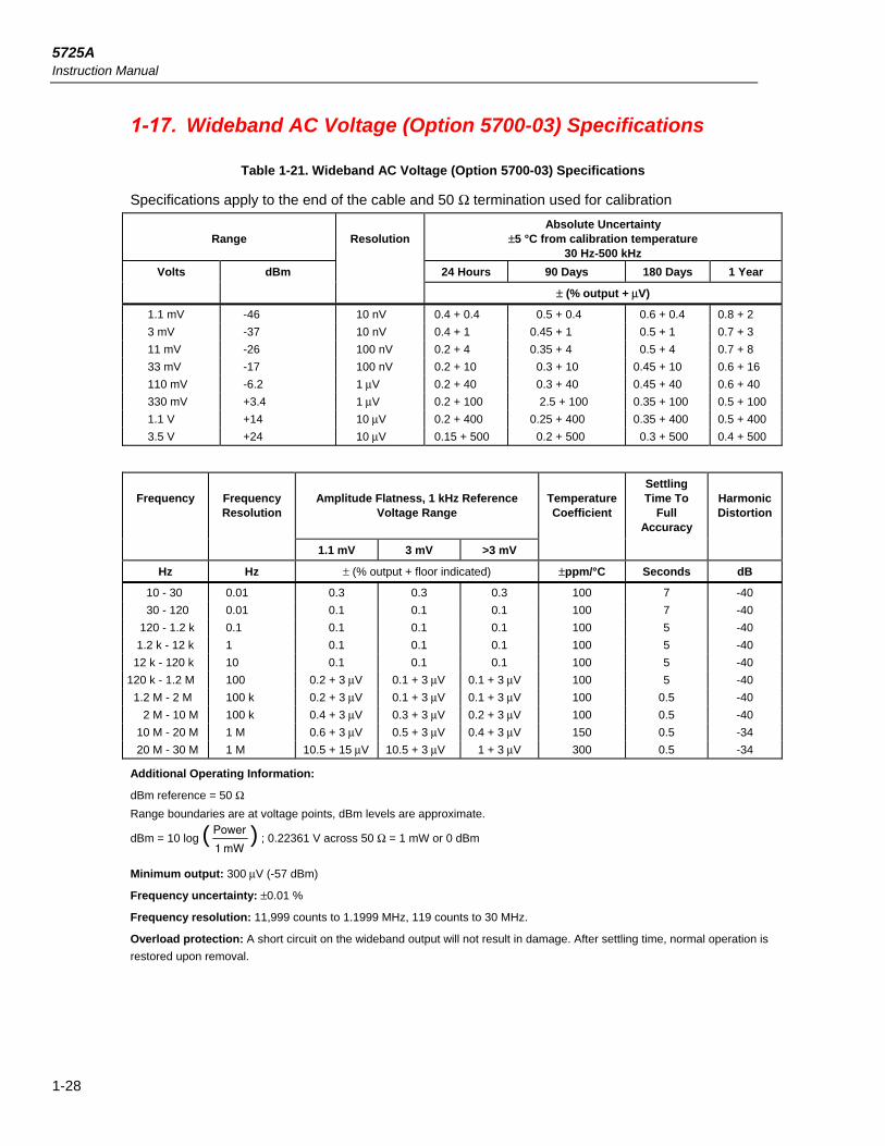
5725A Instruction Manual
1-28
1-17. Wideband AC Voltage (Option 5700-03) Specifications
Table 1-21. Wideband AC Voltage (Option 5700-03) Specifications
Specifications apply to the end of the cable and 50 Ω termination used for calibration
Range ResolutionAbsolute Uncertainty
±5 °C from calibration temperature 30 Hz-500 kHz
Volts dBm 24 Hours 90 Days 180 Days 1 Year
± (% output + μV)
1.1 mV -46 10 nV 0.4 + 0.4 00.5 + 0.4 00.6 + 0.4 0.8 + 2
3 mV -37 10 nV 0.4 + 1 0.45 + 1 00.5 + 1 0.7 + 3
11 mV -26 100 nV 0.2 + 4 0.35 + 4 00.5 + 4 0.7 + 8
33 mV -17 100 nV 0.2 + 10 00.3 + 10 0.45 + 10 0.6 + 16
110 mV -6.2 1 μV 0.2 + 40 00.3 + 40 0.45 + 40 0.6 + 40
330 mV +3.4 1 μV 0.2 + 100 0 2.5 + 100 0.35 + 100 0.5 + 100
1.1 V +14 10 μV 0.2 + 400 0.25 + 400 0.35 + 400 0.5 + 400
3.5 V +24 10 μV 0.15 + 500 00.2 + 500 00.3 + 500 0.4 + 500
Frequency Frequency Resolution
Amplitude Flatness, 1 kHz Reference Voltage Range
Temperature Coefficient
Settling Time To
Full Accuracy
Harmonic Distortion
1.1 mV 3 mV >3 mV
Hz Hz ± (% output + floor indicated) ±ppm/°C Seconds dB
00 10 - 30 0.01 0.3 0.3 0.3 100 7 -40
00 30 - 120 0.01 0.1 0.1 0.1 100 7 -40
0 120 - 1.2 k 0.1 0.1 0.1 0.1 100 5 -40
01.2 k - 12 k 1 0.1 0.1 0.1 100 5 -40
0 12 k - 120 k 10 0.1 0.1 0.1 100 5 -40
120 k - 1.2 M 100 00.2 + 3 μV 00.1 + 3 μV 0.1 + 3 μV 100 5 -40
1.2 M - 2 M 100 k 00.2 + 3 μV 00.1 + 3 μV 0.1 + 3 μV 100 0.5 -40
0 2 M - 10 M 100 k 00.4 + 3 μV 00.3 + 3 μV 0.2 + 3 μV 100 0.5 -40
10 M - 20 M 1 M 00.6 + 3 μV 00.5 + 3 μV 0.4 + 3 μV 150 0.5 -34
20 M - 30 M 1 M 10.5 + 15 μV 10.5 + 3 μV 0 1 + 3 μV 300 0.5 -34
Additional Operating Information:
dBm reference = 50 Ω
Range boundaries are at voltage points, dBm levels are approximate.
dBm = 10 log ( Power
1 mW) ; 0.22361 V across 50 Ω = 1 mW or 0 dBm
Minimum output: 300 μV (-57 dBm)
Frequency uncertainty: ±0.01 %
Frequency resolution: 11,999 counts to 1.1999 MHz, 119 counts to 30 MHz.
Overload protection: A short circuit on the wideband output will not result in damage. After settling time, normal operation is
restored upon removal.

Introduction and Specifications General Specifications 1
1-29
1-18. General Specifications Warm-Up Time: Twice the time since last warmed up, to a maximum of 30 minutes.
System installation: Rear output configuration and rack- mount kit available.
Standard interfaces: IEEE-488, RS-232, 5725A, 5205A or 5215A, 5220A, phase lock in (BNC), phase reference out (BNC).
Temperature performance: Operating: 0 °C to 50 °C. Calibration: 15 °C to 35 °C. Storage: -40 °C to 75 °C; DC Zeros calibration required every 30 days.
Relative humidity: Operating: <80 % to 30 °C, <70 % to 40 °C, <40 % to 50 °C. Storage: <95 %, non-condensing. A power stabilization period of four days may be required after extended storage at high temperature and humidity.
Safety: Designed to comply with UL3111; EN61010; CSA C22.2 No. 1010; ANSI/ISA S82.01-1994
Guard isolation: 20 V
EMI/RFI: Designed to comply with FCC Rules Part 15, Subpart B, Class B; EN50081-1, EN50082-1
Electro Static Discharge: This instrument meets criteria C for ESD requirements per EN61326
Line Power: 47 to 63 Hz; ±10 % allowed about selectable nominal line voltage: 100 V, 110 V, 115 V, 120 V, 200 V, 220 V, 230 V, 240 V. Maximum power: 5700A/5720A, 300 VA; 5725A, 750 VA.
Size: 5700A/5720A: Height 17.8 cm (7 in), standard rack increment, plus 1.5 cm (0.6 in) for feet; Width 43.2 cm (17 in), standard rack width; Depth 63.0 cm (24.8 in), overall; 57.8 cm (22.7 in), rack depth.
5725A: Height 13.3 cm, (5.25 in); Width and depth same as 5700A/5720A. Both units project 5.1 cm, (2 in) from rack front.
Weight: 5700A/5720A: 27kg (62 lbs); 5725A: 32kg (70 lbs).
43.2 cm (17 in)
17.8 cm (7 in)
63 cm (24.8 in)6.35 cm (2.5 in)
FOR CABLE ACCESS

5725A Instruction Manual
1-30
1-19. Auxiliary Amplifier SpecificationsFor complete specifications, see the 5205A and 5220A Operators Manuals.
5205A (220V - 1100 V ac, 0 V - 1100 V dc)
Overshoot: < 10 %
Distortion (bandwidth 10 Hz - 1 MHz):
10 Hz - 20 kHz
20 kHz - 50 kHz
50 kHz - 100 kHz
0.07 %
0.2 %
0.25 %
Frequency (Hz)
90 Day Accuracy at 23° ±5 °C
± (% output + % range)
Temperature Coefficient for 0°-18 °C and 28°-50 °C
± (ppm output + ppm range)/ °C
00 dc
010 - 40
040 - 20 k
20 k - 50 k
50 k - 100 k
0.05 + 0.005
0.15 + 0.005
0.04 + 0.004
0.08 + 0.006
00.1 + 0.01
15 + 3
45 + 3
15 + 3
50 + 10
70 + 20
5220A (AC Current, 180-day specifications):
Accuracy:
20 Hz - 1 kHz 1 kHz - 5 kHz
0.07% + 1 mA (0.07% + 1mA) x frequency in kHz
Temperature Coefficient (0° - 18 °C and 28° - 50 °C): (0.003 % + 100 μA)/°C
Distortion (bandwidth 300 kHz):
20 Hz - 1 kHz 1 kHz - 5 kHz
0.1% + 1 mA (0.1% + 1 mA) x frequency in kHz
Note: 5700A/5720A combined with 5220A is not specified for inductive loads.

2-1
Chapter 2 Installation
Title Page
2-1. Introduction ........................................................................................... 2-3 2-2. Unpacking and Inspection .................................................................... 2-3 2-3. Service Information .............................................................................. 2-5 2-4. Placement and Rack Mounting ............................................................. 2-5 2-5. Cooling Considerations......................................................................... 2-5 2-6. Connecting to the 5700A Calibrator ..................................................... 2-6 2-7. Selecting Line Voltage .......................................................................... 2-7 2-8. Accessing the Fuse ................................................................................ 2-8 2-9. Connecting to Line Power .................................................................... 2-9

5725A Instruction Manual
2-2

Installation Introduction 2
2-3
Warning The 5725A amplifier is capable of supplying lethal voltages. Do not touch the 5700A output terminals. Read this section before operating the 5725A.
2-1. Introduction This section provides instructions for unpacking and installing the 5725A. Procedures for line voltage selection, fuse replacement, and connection to line power and the 5700A Calibrator are provided here. Read this section before operating the 5725A.
Instructions for connecting cables to a UUT (Unit Under Test) are in Section 4 of the 5700A/5720A Series II Operator Manual.
2-2. Unpacking and Inspection The 5725A is shipped in a container that is specially designed to prevent damage during shipping. Inspect the 5725A carefully for damage, and immediately report any damage to the shipper. Instructions for inspection and claims are included in the shipping container.
If you need to reship the 5725A, use the original container. If it is not available, you can order a new container from Fluke by identifying the amplifier's model and serial number.
When you unpack the 5725A, check for all the standard equipment listed in Table 2-1. Report any shortage to the place of purchase or to the nearest Technical Service Center. If performance tests are required for your acceptance procedures, refer to Section 3 of the 5700A/5720A Series II Service Manual for instructions.
Line power cords available from Fluke are listed in Table 2-2 and illustrated in Figure 2-1.
Table 2-1. Standard Equipment
Item Model or Part Number
Amplifier 5725ALine Power Cord (See Table 2-2 and Figure 2-1) Shielded 5700A/5725A Interface Cable 842901 5725A Getting Started Manual 1780175 5725A CD-ROM (contains Instruction Manual) 1780182 Spare 4A, 250V Fuse 216846 Certificate of Calibration (No Part Number)

5725A Instruction Manual
2-4
Table 2-2. Line Power Cord Types Available from Fluke
TYPE VOLTAGE/CURRENT FLUKE OPTION NUMBER
North America 120V/15A LC-1 North America 240V/15A LC-2 Universal Euro 220V/16A LC-3 United Kingdom 240V/13A LC-4 Switzerland 220V/10A LC-5 Australia 240V/10A LC-6 South Africa 240V/5A LC-7
LC-1 LC-2 LC-3 LC-4
LC-5 LC-6 LC-7
aq2f.eps
Figure 2-1. Line Power Cords Available for Fluke Instruments

Installation Service Information 2
2-5
2-3. Service Information Each 5725A Amplifier is warranted to the original purchaser for a period of one year beginning on the date received. The warranty is located at the front of this manual.
Factory-authorized service and technical advice for the 5725A is available at Fluke Service Centers. A complete list of service centers is available at www.fluke.com.
Warning Servicing described in this manual is to be done by qualified service personnel only. To avoid electrical shock, do not service the 5725A unless you are qualified to do so.
The owner may choose to repair a 5725A using the troubleshooting information in Section 7 to isolate a faulty module, then use the Module Exchange Program. Refer to the Fluke catalog or contact a Service Center representative for the module exchange procedure.
2-4. Placement and Rack Mounting You can stack the 5725A on top of or below the 5700A Calibrator. (Choose the configuration that provides the easiest access to the 5700A Calibrator controls.) Or, you can mount the 5725A in a standard-width, 24-inch (61-cm) deep equipment rack. For bench-top stacking, the 5725A is equipped with non-skid feet. To mount the 5725A in an equipment rack, order the accessory 5725A Rack Mount Kit, Model Y5735. An instruction sheet is packed with the kit.
CautionUse only the rack mount slides included in the Y5735 kit. Rack mount slides intended for other instruments can block the side ventilation holes on the 5725A and cause overheating.
2-5. Cooling Considerations
CautionDamage caused by overheating may occur if the area around the air intake is restricted, the intake air is too warm, or the fan filter becomes clogged.
Accuracy and dependability of all internal parts of the 5725A are enhanced by maintaining the coolest possible internal temperature. By observing the following rules you can lengthen the life of the 5725A:
• The area around the fan filter must be at least 3 inches from nearby walls or rackenclosures.
• Exhaust perforations on the sides of the 5725A must be clear of obstructions. Most ofthe heat exits from the side vents near the front.
• Air entering the instrument must be room temperature. Make sure that exhaust fromanother instrument is not directed into the fan inlet.
• Clean the fan filter every 30 days, or more frequently if the 5725A is operated in adusty environment. (Instructions for cleaning the fan filter are in Section 6.)

5725A Instruction Manual
2-6
2-6. Connecting to the 5700A Calibrator Proceed as follows to connect the 5725A to the 5700A:
1. Turn the power off for both instruments and disconnect their line power cords.
2. Connect either end of the interface cable to the 5725A connector labeled 5700A. Dress the cable only as Figure 2-2 shows. The figure shows how to dress the cable in installation arrangements with the 5725A on top or bottom.
3. Connect the other end to the 5700A connector labeled 5725A.
The 5700A/5725A interface cable provides all the digital and analog control signals for the amplifier, and it provides conductors to route amplified voltage to the 5700A OUTPUT binding posts.
5700A
5725A
5700A
5725A
5725AAMPLIFIER
5700ACALIBRATOR
5700ACALIBRATOR
5725AAMPLIFIER
aq3f.eps
Figure 2-2. Correct Way to Dress Interface Cable

Installation Selecting Line Voltage 2
2-7
2-7. Selecting Line Voltage The 5725A arrives from the factory configured for the line voltage normally appropriate for the country of purchase, or as specified at the time of purchase. Check the line power label on the rear panel of the 5725A to verify that the line voltage matches local line power. Figure 2-3 shows the location of the line power label and switches, and the switch settings for each line voltage.
The 5725A can be set to operate from eight different nominal line voltages; each voltage setting has a voltage tolerance of ±10% and a frequency range of 47 to 63 Hz. The line voltage switches are located on the bottom left side of the rear panel.
To change the line voltage setting, set the line voltage selection switches to the correct setting shown in Figure 2-3.
100V110V115V120V
S2 S3 S4
VOLTAGESELECTION FUSE
F8A 250V(FAST)
200V220V230V240V
S2 S3 S4
F4A 250V(FAST)
JOHN FLUKE MFG. CO., INC.MADE IN U.S.A.
PATENTS PENDING
NO INTERNAL USER SERVICEABLEPARTS REFER SERVICE TOQUALIFIED SERVICE PERSONNEL
TO CLEAN FILTERREMOVE FROM INSTRUMENTAND FLUSH WITH WARMSOAPY WATER
5700A CALIBRATOR
20V PKMAX
CHASSISGROUND
FUSE
WARNING GROUNDINGCONNECTOR IN POWER CORDMUST BE CONNECTED TOENSURE PROTECTION FROMELECTRONIC SHOCK.
47-63 Hz750VA MAX
CAUTION FOR FIRE PROTECTIONREPLACE ONLY WITH A 250V FUSEOF INDICATED RATING.
S4S3S2
100V110V115V120V
S2 S3 S4
VOLTAGESELECTION FUSE
F8A 250V(FAST)
200V220V230V240V
S2 S3 S4
F4A 250V(FAST)
CAUTION FOR FIRE PROTECTIONREPLACE ONLY WITH A 250V FUSEOF INDICATED RATING.
11A MAX
HI
LO
CALIBRATION
ENABLE NORMAL
CURRENTOUTPUT
!
!!
!
!
aq4f.eps
Figure 2-3. Line Power Label and Switch Location

5725A Instruction Manual
2-8
2-8. Accessing the Fuse
CautionTo prevent instrument damage, verify that the correct fuse is installed for the line voltage setting. Acceptable fuse types are Bussman type MTH or Littelfuse type 312 or equivalent, of the appropriate amperage rating. Use only a 4A, 250V fast-blow fuse when the line voltage selection switches are set in the range 200-240V.
Note A spare 4A, 250V fuse is shipped with the 5725A to ensure that one is available for use on the 200-240V range.
The line power fuse is accessible on the rear panel. The fuse rating label to the right of the fuse holder (labeled FUSE) shows the correct replacement fuse rating for each line voltage setting. To check or replace the fuse, refer to Figure 2-4 and proceed as follows:
1. Turn off the POWER switch and disconnect the line power cord from ac line power.
2. Insert the blade of a standard screwdriver in the slot of the fuse holder labeled FUSE.
3. Turn the screwdriver counterclockwise until the cap and fuse pop free.
4. To reinstall the fuse, reverse this procedure.
100V110V115V120V
S2 S3 S4
VOLTAGESELECTION FUSE
F8A 250V(FAST)
200V220V230V240V
S2 S3 S4
F4A 250V(FAST)
JOHN FLUKE MFG. CO., INC.MADE IN U.S.A.
PATENTS PENDING
NO INTERNAL USER SERVICEABLEPARTS REFER SERVICE TOQUALIFIED SERVICE PERSONNEL
TO CLEAN FILTERREMOVE FROM INSTRUMENTAND FLUSH WITH WARMSOAPY WATER
5700A CALIBRATOR
20V PKMAX
CHASSISGROUND
FUSE
WARNING GROUNDINGCONNECTOR IN POWER CORDMUST BE CONNECTED TOENSURE PROTECTION FROMELECTRONIC SHOCK.
47-63 Hz750VA MAX
CAUTION FOR FIRE PROTECTIONREPLACE ONLY WITH A 250V FUSEOF INDICATED RATING.
S4S3S2
11A MAX
HI
LO
CALIBRATION
ENABLE NORMAL
CURRENTOUTPUT
!
!!
aq5f.eps
Figure 2-4. Accessing the Fuse

Installation Connecting to Line Power 2
2-9
2-9. Connecting to Line Power
Warning To avoid shock hazard, connect the factory-supplied, three-conductor line power cord to a properly grounded power outlet. Do not use a two-conductor adapter or extension cord; this will break the protective ground connection.
After verifying that the line voltage selection switches are correctly set, verify that the correct fuse is installed. Connect the 5725A to a properly grounded three-prong outlet.

5725A Instruction Manual
2-10

3-1
Chapter 3 Operating Notes
Title Page
3-1. Introduction ........................................................................................... 3-3 3-2. Front Panel Features ............................................................................. 3-4 3-3. Rear Panel Features .............................................................................. 3-6 3-4. Turning on the 5725A Amplifier .......................................................... 3-8 3-5. Warm Up............................................................................................... 3-8 3-6. 5725A Operating Functions and Modes ............................................... 3-9 3-7. Standby ............................................................................................. 3-9 3-8. Voltage Standby ............................................................................... 3-10 3-9. Current Standby ................................................................................ 3-11 3-10. Voltage Operate ................................................................................ 3-12 3-11. Current Operate ................................................................................ 3-13 3-12. Conditions That Activate the 5725A .................................................... 3-14

5725A Instruction Manual
3-2

Operating Notes Introduction 3
3-3
3-1. Introduction This section provides setup and operation information for the 5725A Amplifier. This section begins with a reference for the 5725A front and rear panel features. Information about setting up and powering up the 5725A follows. Please read this information before operating the amplifier. Also contained in this section is a description of all 5725A operating functions and modes. Because the amplifier operates under complete control of the 5700A Calibrator, operating instructions such as how to call up a specific output value are contained in Section 4 of the 5700A/5720A Series II Operator Manual. Operating the 5725A in remote control is covered in Section 5 of the 5700A/5720A Series II Operator Manual.

5725A Instruction Manual
3-4
3-2. Front Panel Features Front panel features are called out in Figure 3-1. Each front panel feature is described in Table 3-1.
CURRENTOUTPUT
HI
LO
VOLTAGE MODE
CURRENT MODE
5725A STANDBY
FAULT
OVERLOAD
CABLE OFF
POWER
1
2
34
567
8
11AMAX
2OVPK
MAX
aq6f.eps
Figure 3-1. Front Panel Features

Operating Notes Front Panel Features 3
3-5
Table 3-1. Front Panel Features
CURRENT OUTPUT Binding Posts
The source of all amplified current if the 5725A is configured for front output. You can set the 5700A to source all unamplified as well as amplified current through these binding posts. The LO binding post is isolated from ground when in the current function, and is open-circuited at other times. Cable and connection recommendations are made in Section 4 of the 5700A/5720A Series II Operator Manual.
5725A STANDBY Indicator
Lit whenever the 5725A is in any of three standby modes. This indicator is lit alone in standby mode; it is lit at the same time as VOLTAGE MODE in voltage standby mode; and it is lit at the same time as CURRENT MODE in current standby mode. (See "5725A Operating Functions and Modes," further on in this section.)
CURRENT MODE Indicator
Lit when the 5725A is in current standby or current operate mode. In current standby mode, the STANDBY indicator is also lit. (See "5725A Operating Functions and Modes," further on in this section.)
VOLTAGE MODE Indicator
Lit when the 5725A is in voltage standby or voltage operate mode. In voltage standby mode, the STANDBY indicator is also lit. (See "5725A Operating Functions and Modes," further on in this section.)
POWER Switch
Turns the power on and off. The switch is a push-push type; the first push turns the power on and locks the switch in, and the second push turns the power off and releases the switch.
CABLE OFF Indicator
Lit when the 5700A/5725A interface cable is not connected, or when the 5700A power is turned off. This condition also lights the FAULT indicator.
OVERLOAD Indicator
Lights on entering current operate mode in overcompliance conditions (load not connected to the proper binding posts, or load resistance too high). The OVERLOAD indicator also lights on entering voltage operate mode if the load resistance is too low.
FAULT Indicator
Lit whenever any fault condition is detected. Normally, a fault code and message appears on the 5700A Control Display when this happens. The FAULT indicator also comes on with the CABLE OFF indicator when the 5700A/5725A interface cable is not connected. In case of a FAULT indication, check the 5700A/5725A interface cable connections, make sure the 5700A power is on, and check that the load is appropriate and connected to the correct binding posts. Refer to "Service Information" in Section 2, or to Section 7, Troubleshooting, in case of a FAULT indication that appears to be a malfunction.

5725A Instruction Manual
3-6
3-3. Rear Panel Features Rear panel features are called out in Figure 3-2. Each rear panel feature is briefly described in Table 3-2.
1
234567
8
100V110V115V120V
S2 S3 S4
VOLTAGESELECTION FUSE
F8A 250V(FAST)
200V220V230V240V
S2 S3 S4
F4A 250V(FAST)
JOHN FLUKE MFG. CO., INC.MADE IN U.S.A.
PATENTS PENDING
NO INTERNAL USER SERVICEABLEPARTS REFER SERVICE TOQUALIFIED SERVICE PERSONNEL
TO CLEAN FILTERREMOVE FROM INSTRUMENTAND FLUSH WITH WARMSOAPY WATER
5700A CALIBRATOR
20V PKMAX
CHASSISGROUND
FUSE
WARNING GROUNDINGCONNECTOR IN POWER CORDMUST BE CONNECTED TOENSURE PROTECTION FROMELECTRONIC SHOCK.
47-63 Hz750VA MAX
CAUTION FOR FIRE PROTECTIONREPLACE ONLY WITH A 250V FUSEOF INDICATED RATING.
S4S3S2
11A MAX
HI
LO
CALIBRATION
ENABLE NORMAL
CURRENTOUTPUT
!
!!
9
aq7f.eps
Figure 3-2. Rear Panel Features

Operating Notes Rear Panel Features 3
3-7
Table 3-2. Rear Panel Features
CURRENT OUTPUT Binding Posts
The source of all amplified current if the 5725A is configured for rear output. You can set the 5700A to source all its unamplified as well as amplified current through these binding posts. The LO binding post is isolated from ground when in the current function, and is open-circuited at other times. Cable and connection recommendations are made in Section 4 of the 5700A/5720A Series II Operator Manual.
CALIBRATION Switch
A slide switch that enables and disables writing to the nonvolatile memory that stores 5725A calibration constants. Switching to ENABLE allows writing to the memory, and switching to NORMAL protects data in memory from being overwritten. The switch must be in the ENABLE position to store corrections generated during calibration. The switch is recessed to allow a metrologist to cover it with a calibration seal to guarantee calibrator integrity.
5700A CALIBRATOR Connector
Provides the analog and digital interface to the 5700A Calibrator. After connecting to the 5700A, you control the 5725A from the 5700A front panel or by sending remote commands to the 5700A. Refer to "Using an Auxiliary Amplifier" in Section 4, or for remote operation to Section 5, of the 5700A/5720A Series II Operator Manual for details.
Fan Filter
Covers the air intake to keep dust and debris out of the instrument. The fan directs a constant cooling air flow throughout the chassis.
Line Voltage/Fuse Rating Label
Shows the various settings of the line voltage switches, and the correct replacement fuse for operating voltages of 110 (90 to 132) and 220 (180 to 264) volts ac. Refer to "Accessing the Fuse" in Section 2 for the fuse replacement procedure.
Line Voltage Selection Switches
Select the operating line voltage. Refer to "Selecting Line Voltage" in Section 2 for instructions on how to select operating line voltage.
Fuse Holder
The line power fuse. Refer to "Accessing the Fuse" in Section 2 for fuse rating information and the fuse replacement procedure.
CHASSIS GROUND Connector
If the 5725A is the location of the ground reference point in a system, the CHASSIS GROUND binding post can be used for connecting other instruments to earth ground. (The chassis is connected to earth ground through the three-conductor line cord.)
Line Power Input
A grounded male three-prong connector that accepts the line power cord.

5725A Instruction Manual
3-8
3-4. Turning on the 5725A Amplifier
Warning To avoid electric shock, make sure the 5725A is safely grounded as described in section 2.
Caution Before turning the 5725A on, make sure that the line voltage selection switches are set properly for your line voltage. Refer to Figure 2-3 or the line voltage switch label and check the line voltage setting now if you have not already done so.
When you turn on the 5725A, all six front panel indicators light briefly and the 5725A undergoes a self test. If the self test fails, a fault message on the 5700A Control Display identifies the failure, indicating that you should service the 5725A.
After the 5725A passes its self test, it transfers its calibration constants to the 5700A. During the transfer, the BOOST indicator on the 5700A flashes. For the few seconds that the BOOST indicator is flashing, the 5725A is not usable. After the transfer is complete, the 5725A is in standby mode. (See "5725A Operating Functions and Modes" for more information about standby mode.)
3-5. Warm Up When you turn on a cold 5725A, warm it up for 30 minutes to allow the components inside to stabilize. This ensures that the 5725A meets or exceeds the specifications listed in Section 1.
If you turn off the 5725A after it has warmed up, allow it to warm up again for at least twice the length of time it was turned off (up to a maximum of 30 minutes of warm-up). For example, if the 5725A is turned off for 10 minutes, allow it to warm up again for at least 20 minutes.
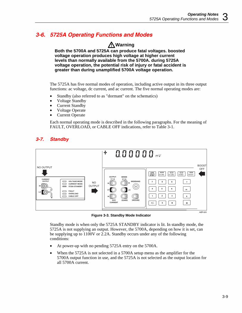
Operating Notes 5725A Operating Functions and Modes 3
3-9
3-6. 5725A Operating Functions and Modes
Warning Both the 5700A and 5725A can produce fatal voltages. boosted voltage operation produces high voltage at higher current levels than normally available from the 5700A. during 5725A voltage operation, the potential risk of injury or fatal accident is greater than during unamplified 5700A voltage operation.
The 5725A has five normal modes of operation, including active output in its three output functions: ac voltage, dc current, and ac current. The five normal operating modes are:
• Standby (also referred to as "dormant" on the schematics) • Voltage Standby • Current Standby • Voltage Operate • Current Operate
Each normal operating mode is described in the following paragraphs. For the meaning of FAULT, OVERLOAD, or CABLE OFF indications, refer to Table 3-1.
3-7. Standby
CURRENTOUTPUT
HI
LO
VOLTAGE MODECURRENT MODE5725A STANDBY
FAULTOVERLOADCABLE OFF
11AMAX
2OVPK
MAX
NO OUTPUT
HI HI
LO LO
AUXCURRENT
GUARD GROUND
WIDEBAND
SENSEV AΩ
OUTPUTV AΩ
EX SNS EX GRD BOOST
μ
m
k
987
5 6
M
3
0 •
21
OPRSTBY W BND
4
+/-
NOOUTPUT
HI
BOOSTOFF
aq8i.eps
Figure 3-3. Standby Mode Indicator
Standby mode is when only the 5725A STANDBY indicator is lit. In standby mode, the 5725A is not supplying an output. However, the 5700A, depending on how it is set, can be supplying up to 1100V or 2.2A. Standby occurs under any of the following conditions:
• At power-up with no pending 5725A entry on the 5700A.
• When the 5725A is not selected in a 5700A setup menu as the amplifier for the 5700A output function in use, and the 5725A is not selected as the output location for all 5700A current.

5725A Instruction Manual
3-10
3-8. Voltage Standby
aq9i.eps
Figure 3-4. Voltage Standby Mode
Voltage standby mode is when both VOLTAGE MODE and 5725A STANDBY indicators are lit. In voltage standby mode, the 5725A is not supplying an output. Voltage standby occurs if "5725A" is selected in a 5700A setup menu as the voltage amplifier, and the next two conditions are true:
• An ac voltage 220V or above is showing on the 5700A Output Display with theSTANDBY annunciator lit.
• The BOOST indicator on the 5700A is lit.
Note If condition 1 is true, the BOOST indicator can be toggled on and off by pressing the 5700A BOOST key. If the BOOST indicator is off, the 5725A is in standby mode, not voltage standby.

Operating Notes 5725A Operating Functions and Modes 3
3-11
3-9. Current Standby
CURRENTOUTPUT
HI
LO
VOLTAGE MODE
CURRENT MODE
5725A STANDBY
FAULT
OVERLOAD
CABLE OFF
11AMAX
2OVPK
MAX
NO OUTPUT
HI HI
LO LO
AUXCURRENT
GUARD GROUND
WIDEBAND
SENSEV AΩ
OUTPUTV AΩ
μ
•
NOOUTPUT
HI
BOOSTLIT
aq10i.eps
Figure 3-5. Current Standby Mode
Current standby mode is when both CURRENT MODE and 5725A STANDBY indicators are lit. In current standby mode, the 5725A is not supplying an output. Current standby occurs under any of the following conditions:
• When the 5700A current output location is set to "5725A", and any ac or dc currentlevel is showing on the 5700A Output Display with the STANDBY annunciator lit.
• If "5725A" is selected in a 5700A setup menu as the current amplifier, and any of thefollowing conditions are true:
1. An ac or dc current 2.2A or above is showing on the 5700A Output Display withthe STANDBY annunciator lit.
2. Any level of dc current is showing on the 5700A Output Display with theSTANDBY annunciator lit, and the BOOST key on the 5700A is pressed so thatthe BOOST indicator is lit.
3. An ac current 1A or above is showing on the 5700A Output Display with theSTANDBY annunciator lit, and the BOOST key on the 5700A is pressed so thatthe BOOST indicator is lit.
4. The 5700A is ranged locked on the 11A range, and any dc current or an accurrent 1A or above is showing on the Output Display with the STANDBYannunciator lit.

5725A Instruction Manual
3-12
3-10. Voltage Operate
CURRENTOUTPUT
HI
LO
VOLTAGE MODE
CURRENT MODE
5725A STANDBY
FAULT
OVERLOAD
CABLE OFF
11AMAX
2OVPK
MAX
NO OUTPUT
HI HI
LO LO
AUXCURRENT
GUARD GROUND
WIDEBAND
SENSEV AΩ
OUTPUTV AΩ
μ
•
VOLTAGEOUTPUT
HERE
HI
BOOSTLIT
aq11i.eps
Figure 3-6. Voltage Operate Mode
Warning Both the 5700A and 5725A can produce fatal voltages. boosted voltage operation produces high voltage at higher current levels than normally available from the 5700A. during voltage operation, the potential risk of injury or fatal accident is greater than during normal operation.
Voltage operate mode is when only the VOLTAGE MODE indicator is lit. In voltage operate mode, amplified voltage output is available at the 5700A binding posts. Voltage operate occurs if "5725A" is selected in a 5700A setup menu as the voltage amplifier, and the next two conditions are true:
• An ac voltage 220V or above is showing on the 5700A Output Display with theOPERATE annunciator lit.
• The BOOST indicator on the 5700A is lit.
Note If condition 1 is true, the BOOST indicator can be toggled on and off by pressing the 5700A BOOST key. If the BOOST indicator is off, then the 5725A is in standby mode.
Note Under certain settings of ac voltage, especially high voltage between 1 to 5 kHz, a whine from the 5725A is audible. This originates from the output transformer, and is normal.

Operating Notes 5725A Operating Functions and Modes 3
3-13
3-11. Current Operate
CURRENTOUTPUT
HI
LO
VOLTAGE MODE
CURRENT MODE
5725A STANDBY
FAULT
OVERLOAD
CABLE OFF
11AMAX
2OVPK
MAX
CURRENTOUTPUT
HERE
HI HI
LO LO
AUXCURRENT
GUARD GROUND
WIDEBAND
SENSEV AΩ
OUTPUTV AΩ
μ
•
NOOUTPUT
HI
BOOSTLIT
aq12i.eps
Figure 3-7. Current Operate Mode
Note An overcompliance fault occurs if a low-resistance load is not connected to the enabled 5725A binding posts when entering current operate mode.
Current operate mode is when only the CURRENT MODE indicator is lit. In current operate mode, current output (either 5725A amplified current or redirected 5700A current) is available at the 5725A binding posts. Current operate occurs under the following conditions:
• When, on the 5700A, the current output location is set to "5725A", and any ac or dc current level is showing on the 5700A Output Display with the OPERATE annunciator lit.
• If "5725A" is selected in a 5700A setup menu as the current amplifier, and any of the following conditions are true:
1. An ac or dc current 2.2A or above is showing on the 5700A Output Display with the OPERATE annunciator lit.
2. Any level of dc current is showing on the 5700A Output Display with the OPERATE annunciator lit, and the BOOST key on the 5700A is pressed so that the BOOST indicator is lit.
3. An ac current 1A or above is showing on the 5700A Output Display with the OPERATE annunciator lit, and the BOOST key on the 5700A is pressed so that the BOOST indicator is lit.
4. The 5700A is ranged locked on the 11A range, and any dc current or an ac current 1A or above is showing on the Output Display with the OPERATE annunciator lit.
Note Under certain settings of ac current, especially high current at frequencies above 1 kHz, a whine from the 5725A is audible. This is caused by a piezo effect in the current output transistors, and is normal.

5725A Instruction Manual
3-14
3-12. Conditions That Activate the 5725A When the 5725A is connected to the 5700A, and is selected as the amplifier for the active output function, it supplies an output under the conditions shown in the following list. (These conditions are the same as VOLTAGE OPERATE and CURRENT OPERATE as previously described.)
• Whenever current above 2.2A is selected and the 5700A is set to operate. (Outputavailable at the 5725A binding posts.)
• Whenever ac voltage in the 220-1100V range is selected and the 5700A is set tooperate. Note that the 5725A takes over the 1100V ac range of the 5700A if the5725A is selected as the voltage amplifier in a setup menu. (Output available at the5700A binding posts.)
• Whenever the 5700A BOOST key is toggled on while the 5700A output setting is inthe operating range of the 5725A, voltage or current. (Output location is 5725A forcurrent, 5700A for voltage.)
• If the "Range" softkey is set to "LOCKED" while supplying a current greater than2.2A, then the 5725A stays active if the 5700A output setting is adjusted down to 0Adc, or down to 1A ac. (Output available at the 5725A binding posts.)
Regardless of the "BOOST AMP TYPES" setting in the 5700A setup menus, all unamplified 5700A current is supplied through the 5725A binding posts when, on the 5700A, the current output location is set to "5725A"; the 5700A output is set to any ac or dc current level; and the 5700A OPERATE annunciator is lit.

4-1
Chapter 4 Theory of Operation
Title Page
4-1. Introduction ........................................................................................... 4-3 4-2. Overall Functional Description ............................................................. 4-3 4-3. 1100V AC Range Functional Description ........................................ 4-5 4-4. 11A Range Functional Description .................................................. 4-6 4-5. Operation in the 11A DC Range .................................................. 4-7 4-6. Operation in the 11A AC Range .................................................. 4-7 4-7. Voltage and Current Standby Modes ............................................... 4-7 4-8. Voltage Standby ........................................................................... 4-7 4-9. Current Standby ........................................................................... 4-7 4-10. How the 5700A and 5725A Communicate ....................................... 4-8 4-11. Description of the Out-Guard Lines (5725A Side) ...................... 4-8 4-12. Description of the In-Guard Lines ............................................... 4-9 4-13. Functional Summaries by Assembly ................................................ 4-10 4-14. Detailed Circuit Description ................................................................. 4-11 4-15. Interconnect Assembly (A1) ............................................................. 4-11 4-16. Power Supply Assembly (A4) .......................................................... 4-12 4-17. High Voltage Supply Section ....................................................... 4-13 4-18. Switching Section ........................................................................ 4-14 4-19. Current-Limit Section .................................................................. 4-15 4-20. System Supply Section ................................................................. 4-15 4-21. Fan Supply Section ...................................................................... 4-16 4-22. Digital Assembly (A5) ..................................................................... 4-16 4-23. Microcomputer ............................................................................. 4-16 4-24. External RAM. ............................................................................. 4-16 4-25. External ROM .............................................................................. 4-16 4-26. EEROM ........................................................................................ 4-18 4-27. Data Latch .................................................................................... 4-18 4-28. Strobe Lines ................................................................................. 4-18 4-29. Led Driver .................................................................................... 4-18 4-30. Optoisolator Link ......................................................................... 4-18
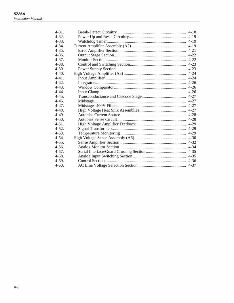
5725A Instruction Manual
4-2
4-31. Break-Detect Circuitry ................................................................. 4-18 4-32. Power Up and Reset Circuitry ...................................................... 4-19 4-33. Watchdog Timer........................................................................... 4-19 4-34. Current Amplifier Assembly (A2) .................................................... 4-19 4-35. Error Amplifier Section ................................................................ 4-21 4-36. Output Stage Section .................................................................... 4-22 4-37. Monitor Section ............................................................................ 4-22 4-38. Control and Switching Section..................................................... 4-23 4-39. Power Supply Section .................................................................. 4-23 4-40. High Voltage Amplifier (A3) ........................................................... 4-24 4-41. Input Amplifier ............................................................................ 4-24 4-42. Integrator ...................................................................................... 4-26 4-43. Window Comparator .................................................................... 4-26 4-44. Input Clamp .................................................................................. 4-26 4-45. Transconductance and Cascode Stage .......................................... 4-27 4-46. Midstage ....................................................................................... 4-27 4-47. Midstage -400V Filter .................................................................. 4-27 4-48. High Voltage Heat Sink Assemblies ............................................ 4-27 4-49. Autobias Current Source .............................................................. 4-28 4-50. Autobias Sense Circuit ................................................................. 4-28 4-51. High Voltage Amplifier Feedback ............................................... 4-29 4-52. Signal Transformers ..................................................................... 4-29 4-53. Temperature Monitoring .............................................................. 4-29 4-54. High Voltage Sense Assembly (A6) ................................................. 4-30 4-55. Sense Amplifier Section ............................................................... 4-32 4-56. Analog Monitor Section ............................................................... 4-34 4-57. Serial Interface/Guard Crossing Section ...................................... 4-35 4-58. Analog Input Switching Section .................................................. 4-35 4-59. Control Section ............................................................................ 4-36 4-60. AC Line Voltage Selection Section ............................................. 4-37

Theory of Operation Circuit Description 4
4-3
4-1. Introduction
This section presents theory of operation in increasing level of detail. The 5725A Amplifier is first broadly defined in an overall functional description and block diagram. The overall functional description continues in more detail with functional descriptions by function (ac V, dc I, ac I, and standby). The overall picture is completed with a detailed discussion of how the 5700A and 5725A communicate. The largest part of this section is devoted to detailed component-level circuit descriptions, grouped by assembly.
Warning Lethal voltage (±500V) appears on the internal heat sink assemblies, and at many other points inside the 5725A chassis. Do not open the 5725A cover without referring to the access procedures and warnings in section 6. Theory text in this section is here strictly for the purpose of describing how circuits work, and contains no access procedures.
4-2. Overall Functional Description
The 5725A provides three primary functions for the 5700A Calibrator:
• Extended frequency range for high ac voltage • High-range dc current • High-range ac current
The 5725A also has a secondary function of sourcing all 5700A current outputs (without the 5700A Current guard) through its own binding posts, if so selected at the 5700A front panel controls. Refer to Figure 4-1, the overall block diagram of the 5725A, for this discussion. Each 5725A function is described briefly next.
• 1100V AC Function:
The 1100V ac function can output 220 to 1100V, 40 Hz to 30 kHz; and 220 to 750V, 30 kHz to 100 kHz. The 1100V ac function is implemented with a gain of -100 amplifier. Input for the ac voltage function comes from the 5700A Oscillator, spanning the range of 2.2 to 11V. The 5725A returns an oscillator sense voltage of precisely -1/100 of the output voltage to the 5700A. Voltage outputs go through the 5725A/5700A interconnect cable to either the 5700A front or rear panel OUTPUT binding posts.

5725AInstruction Manual
4-4
Figure 4-1. 5725A Overall Block Diagram

Theory of Operation Circuit Description 4
4-5
• 11A DC Function:
The 11A dc function is implemented with a transconductance (voltage in/current out)amplifier with a gain of -5. If the 5700A outputs -2V into the 5725A, the 5725Aoutput is 10A. (This is transparent to the user.) The output range is 0 to 11A. The5725A delivers amplified current to either the front or rear panel binding posts of the5725A, depending on an internal hardware setup. Reconfiguration requires removingthe covers, and is described in Section 6.
• 11A AC Function
The 11A ac function is similar to the 11A dc function. The frequency range is 40 Hzto 10 kHz. The output range is 1 to 11A rms. As in the dc current function, alloutputs from the 5725A either go through the front or rear panel of the 5725A. Inputto the 5725A comes from the 5700A Oscillator assembly.
4-3. 1100V AC Range Functional Description
The 5700A Oscillator assembly generates the driving ac voltage, then sends it to the 5725A Power Amplifier for amplification. The 5725A returns an attenuated feedback voltage for output correction. The final output voltage is kept accurate by the high voltage sense amplifier and a real-time, software-controlled feedback loop within the 5700A, incorporating a 5700A ac/dc thermal rms converter. The 5700A Oscillator, DAC (digital-to-analog converter), and ac/dc thermal rms converter work together with the 5725A Power Amplifier and high voltage attenuator circuits to produce the desired output.
Active assemblies in the 5725A ac voltage function are as follows:
• In the 5700A: CPU, DAC, Oscillator, Oscillator Control, High-Resolution Oscillator,Switch Matrix, Motherboard, Rear Panel assemblies.
• In the 5725A: CPU, High Voltage Amplifier, High Voltage Sense, SignalTransformer, Power Supply, Digital, and Interconnect assemblies.
When an ac voltage in the 220 to 1100V range is selected, the 5700A calls the 5725A amplifier and leaves its own high voltage amplifier dormant. The 5725A takes over the 1100V ac range automatically. The 5725A produces ac voltage in the following sequence:
1. The 5700A sets the Oscillator assembly to the proper frequency and amplitude. The5700A sets the initial amplitude using an 8-bit resistive hybrid dac located on theOscillator amplifier assembly, yielding an Oscillator output accuracy of about 0.5%.
2. Next, the 5725A Power Amplifier amplifies this signal by -100 and returns anaccurately attenuated signal to the 5700A.
3. The 5700A thermal sensor and adc (analog-to-digital converter) monitoring systemfine tune the Oscillator amplitude. The DAC assembly output is switched directly tothe Oscillator assembly, controlling the dac output amplitude. AC voltage calibrationconstants stored in the 5725A determine the 5700A DAC voltage setting.

5725A Instruction Manual
4-6
The 5700A/5725A system uses the following method for ac amplitude control:
1. An rms thermal sensor alternately measures two signals: an unknown but adjustableac signal, and a known calibrated dc signal.
2. The output of the thermal sensor is measured by the adc, allowing settling time forthe sensor each time its input is changed. The ac signal is adjusted until the thermalsensor output is the same for both signals. Thus, the dc voltage at the output of thethermal sensor is not important, but differences in the dc voltage when the sensorinput is switched between the ac variable and dc reference are important.
To ensure safe, reliable operation, the High Voltage Amplifier is turned on in the following sequence:
1. The 5700A Oscillator is set to the 22V range and its output is channeled to the 5725AHigh Voltage Amplifier on line BOOST IN.
2. Then the output of the High Voltage Amplifier is connected to the appropriate highvoltage step-up transformer (one of three).
4-4. 11A Range Functional Description
The 5725A Current Amplifier is a transconductance amplifier that has a compliance voltage of 3.0V rms for the ac current function and 4.0V for the dc current function. The transconductance amplifier has a gain of -5 (e.g., 1V in gives -5A out). Either the 5700A 2V range for dc operation, or the Oscillator for ac operation, drives the transconductance amplifier. Input voltage to the transconductance amplifier comes in on BOOST IN (for ac current) or B-FEEDBACK (for dc current) and enters the High Voltage Sense assembly. From there it is routed to the error amplifier on the Current assembly whenever the 5725A is in the current function. The B-FEEDBACK line returns the current calibration amplifier output to OSC SENSE HI during ac current operation.
The following assemblies are active in the 5725A current function:
• In the 5700A: CPU, DAC, Oscillator, Switch Matrix, Motherboard, Rear Panelassemblies. (Plus the Oscillator assembly in the ac current function.)
• In the 5725A: CPU, Current, High Voltage Sense, Digital, and Power Supply.

Theory of Operation Circuit Description 4
4-7
4-5. Operation in the 11A DC Range
For the dc current function, the 5700A is configured for the dc 2.2V range. The 5700A 2V dc range drives an error amplifier with an input impedance of 40 kΩ. The gain of this amplifier is determined by this 40 kΩ resistor with a 4 kΩ feedback resistor, and the value of the precision shunt. The 5725A uses a 0.02Ω shunt for the 11A function. There is no feedback to the 5700A.
The 5725A monitors the error amplifier output voltage using the 16-channel multiplexer. One channel of the multiplexer, ICOMPL M, is scanned every 30 milliseconds or faster, with its output compared to -2V from the DAC. If the peak error amplifier output is more negative than the dac voltage, MONCOMP goes LOW and is read by bit 6 of port 5 of U507, the CPU. This indicates an overload condition, and lights the OVERLOAD LED. If a later scan shows the same result, the CPU trips the Current Amplifier into standby and reports this condition to the 5700A.
A soft-start from standby to operate transitions reduces sudden current changes. This allows the 5725A to drive inductive loads such as power meters and clamp-on type current probes.
4-6. Operation in the 11A AC Range
For ac current operation, input to the 5725A comes from the 5700A Oscillator. The 5700A Oscillator is configured for the 2.2V ac range, with sensing back to the 5700A Oscillator coming from the current shunt through the calibration amplifier circuit (on the Current Assembly).
4-7. Voltage and Current Standby Modes
When a change in output function is selected, the 5725A goes through voltage or current standby mode before connecting the output to the 5725A binding posts, or to the 5700A. Voltage or current standby allows for local sensing within the 5725A, and for establishment of a known input condition in current and ac voltage.
4-8. Voltage Standby
In voltage standby, the 5700A binding posts are completely disconnected from the rest of the instrument circuitry, and the 5725A high voltage output and sense lines (B-OUT HI and B-SENSE HI) are disconnected from the 5725A/5700A connector. The High Voltage Amplifier remains powered from the high voltage supply, but its input is grounded by pulling CLAMPD, and its output (MV OUT) is disconnected from the output transformers. Analog monitor circuitry continues to check the voltage and current on the high voltage supplies as well as the heat sink temperatures and cable integrity. It prevents the 5725A from switching to operate if a fault is present.
4-9. Current Standby
In current standby, the binding posts are disconnected from the instrument circuitry, but all 5725A/5700A connections are made as in the operate mode. In dc current standby, the 5700A DAC supplies a voltage that corresponds to the dc current selected. In ac current standby, 5725A relay settings are identical to those for dc current standby. The 5700A Oscillator supplies an ac voltage level that corresponds to the selected output current and frequency.

5725A Instruction Manual
4-8
4-10. How the 5700A and 5725A Communicate
The 5725A and 5700A maintain all analog and digital communication over an external cable connected to subminiature D-type connectors on the back of each instrument. All in-guard (analog) signals, except B-VGRD, connect to relays that isolate the 5725A and 5700A whenever the 5725A is not in use.
Digital communication occurs over five out-guard (digital) 5700A lines, B-SCT, B-SCR, B+5V, B+5VCOM, and B-CINT*. The B+5V and B+5VCOM lines power the 5725A guard crossing and allow the 5725A to detect when the cable is disconnected. Lines B-SCT and B-SCR provide serial communication of data over an RS-232 type line. Optoisolators on the 5725A maintain the integrity of the guard. Line B-CINT* is a hardwire loop that allows the 5700A to detect a cable off or 5725A power off condition.
4-11. Description of the Out-Guard Lines (5725A Side) The following list describes the five 5725A out-guard lines:
• B-RCV (Serial Communication Receive)
Receives serial data from the 5700A; connects to the B-SCT line of the 5700A.
• B-XMIT (Serial Communication Transmit)
Transmits serial data to the 5700A; connects to the B-SCR line of the 5700A.
• B+5V
5700A out-guard supply that powers optoisolators and 5725A CABLEOFF relay.
• B+5VCOM
5700A out-guard supply common for above.
• B-CINT* (Boost Cable Interlock)
Hardwire "loop around system" on the 5725A that is polled at least every 100 ms bythe 5700A to determine if the 5700A/5725A cable is connected and if the 5725A isturned on. Returns a low to the 5700A if above is true. A pull-up resistor on the5700A leaves this line high if the interconnect cable is open or if the 5725A is turnedoff.

Theory of Operation Circuit Description 4
4-9
4-12. Description of the In-Guard Lines
The following list describes the 11 5725A in-guard lines:
• B-RCL
High-quality analog line from the 5725A which carries critical signals to bemeasured by the 5700A adc during either 5725A calibration or 5725A selfdiagnostics. During calibration, these signals are ICAL (output of the currentcalibration amplifier), HVSENSE (DC output of the sense amplifier during dc gain accharacterization), AC/AC (buffered output of the 5725A thermal rms sensor that doesfrequency characterization).
• B-OUT HI
High voltage output from the 5725A step-up transformers, to be routed to either the5700A front or rear panel terminals.
• B-SENSE HI
High voltage sense line from the 5700A output terminals. This signal is thenattenuated -100:1 by the High Voltage Sense assembly.
• BOOST IN
During normal 5725A ac operation, carries the 5700A DAC outputs, which in turndrives either the High Voltage Amplifier or Current Amplifier. During 5725Acalibration, BOOST IN drives the High Voltage Sense assembly with up to -260Vfrom the 5700A Power Amplifier.
• B-CURRENT
Analog line that carries the current high output from the 5700A. When the user setsthe current output location to "5725A" in a 5700A menu, this signal is routed to the5725A binding posts. Under this operating condition, all 5700A/5725A currentranges are available from the same binding posts. Line B-CURRENT carries up to2.2A in normal operation. During current calibration, this line carries 1.3A tomeasure the value of the 0.02Ω 5725A current shunt.
• B-IRTN
Current return for B-CURRENT; carries up to 2.2A. Line B-IRTN eventually ties tothe same node as SCOM on the 5700A.
• B-IGRD
Current guard voltage from the 5700A; enables internal guarding within the 5725Aonly.
• B-VGRD
5700A guard. Enables discrete guarding/shielding within the 5725A.
• B-PACOM
System common from the 5700A. Once inside the 5725A, it becomes VCOM,HVCOM, DCOM, and KCOM. B-PACOM is the current return for signals from the5700A, including source current for driving the 5725A in the ac voltage function.Current output from the 5700A, when "5725A" is selected as the current outputlocation, returns via B-IRTN.
• B-SENSE LO
High quality ground from the 5700A that is the reference point for the 5700A DACand Oscillator assemblies.

5725A Instruction Manual
4-10
Inside the 5725A, B-SENSE LO is buffered by the 5725A, with the equivalent voltage called MCOM.
• B-FEEDBACK
During ac voltage operation, B-FEEDBACK is the output of the High Voltage Senseassembly; this signal represents B-SENSE HI divided by -100, and drives the 5700Aac/dc thermal sensor. During low-frequency ac voltage calibration, this is the sensepath for the -260V dc from the 5700A Power Amplifier.
During ac current operation, B-FEEDBACK is the output of the current calibrationamplifier. It represents the output current divided by -5 and drives the 5700AOscillator feedback.
During dc current operation, voltage from the 5700A 2V dc range is fed to the 5725Aon B-FEEDBACK.
If B-FEEDBACK is out of tolerance during 5725A ac voltage or current operationbut no other faults are reported, the 5700A sends a message to the 5725A asking for asequenced shutdown into standby, and displays a fault message on its ControlDisplay. The 5725A FAULT indicator lights. A faulty 5700A/5725A interfaceconnection could cause this problem.
4-13. Functional Summaries by Assembly
For an overview of all the assemblies in the 5725A and the functions contained on each, refer to Figure 4-1, the overall block diagram, and the following list:
• Interconnect Assembly (A1):
• Connectors and traces to link other assemblies and fan• High voltage transformer secondary switching circuitry
• Power Supply Assembly (A4):
• Rectifiers for high voltage supplies• Filters for high voltage supplies• High voltage current-limit circuitry• High voltage supply-monitoring circuitry• Rectifiers for system supplies• Filters for system supplies• Regulators for system supplies• Rectifiers for fan supply• Filter for fan supply
• Digital Assembly (A5)
• LED front panel status annunciators• CPU, RAM, ROM, EEROM, watchdog timer, logic
• Current Amplifier Assembly (A2):
• Transconductance amplifier• Current shunt• Heat sink and current power devices• 5700A current routing circuits• Filters for high current supply• Rectifier bridge for high current supply• Regulators for low current supply• Current heat sink temperature monitor

Theory of Operation Circuit Description 4
4-11
• High Voltage Power Amplifier Assembly (A3)
• Power amplifier• Harness to heat sink and its high voltage power devices• Connections to the output transformers• High voltage heat sink temperature monitoring circuitry
• High Voltage Sense Assembly (A6):
• High voltage sense (attenuator) and calibration circuits• 5725A input and output switching relays, relay drivers• Analog monitor, an 8-bit dac, latch for mux, latch for dac• Subminiature D-type connector to the 5700A• 5700A current routing circuits• Guard crossing• AC line power selection circuitry• AC line inrush current limiting circuitry
4-14. Detailed Circuit Description
Detailed circuit descriptions for each pca (printed circuit assembly) are provided next. Individual block diagrams are provided for the Current Amplifier (A2), High Voltage Amplifier (A3), High Voltage Sense (A6), and Digital (A5) assemblies. You may also find it helpful to refer to the schematic diagrams (Section 9) while reading theory for each assembly.
4-15. Interconnect Assembly (A1)
The Interconnect assembly (A1) links the other five assemblies in the 5725A. The interconnect assembly contains the following parts:
• Connectors and traces to interconnect the other assemblies and the fan. There arethree 32-pin DIN connectors on the Interconnect pca which connect the PowerSupply assembly (A4), High Voltage Amplifier assembly (A3), and CurrentAmplifier assembly (A2). A 64-pin DIN connector links the Interconnect assembly tothe High Voltage Sense assembly (A6). A 34-pin ribbon cable connector links theInterconnect assembly to the Digital assembly (A5). Other cable assemblies attachedto the Interconnect assembly go to the fan, High Voltage assembly output, and highvoltage transformers.
• High voltage transformer secondary-switching circuitry. Three high voltage reedrelays (K013, K014, and K015) select one of three ac voltage output transformers. Afourth relay (K001) is a high voltage armature type that connects the secondaries ofthe low-frequency transformer in either a series or parallel fashion.
The circuit board has four layers. Most connections are done on the inner two layers. One outer layer is an earth ground plane; the other outer layer is tied to the signal VCOM.
5725A Instruction Manual
4-12
4-16. Power Supply Assembly (A4)
The Power Supply assembly (A4) provides regulated system supplies for all 5725A assemblies except as noted below, as well as unregulated fan supply and high voltage supplies for the High Voltage Amplifier. The assembly also includes microprocessor-controlled switching and an independent current-limit circuit.
Note Other power supplies are contained on the Current Amplifier assembly (A2). The A2 assembly includes a high-current supply and a local ±20V supply.
The Power Supply assembly has four sections: high voltage supply, switching, current limit, and system supply section. Each section is first briefly described, then described in detail.
• High Voltage Supply Section
The high voltage supply section consists of a simple unregulated power supply withthe additional capability of being run at ±400V dc for normal instrument operation,or at ±50V dc for troubleshooting.
• Switching Section
The switching section behaves like an electronic DPST switch, which by commandof the microprocessor or the current-limit section, shuts down the high voltagesupplies. Microprocessor control alone can turn on the high voltage supplies innormal operation. At the board level, manual control of the switch is possible toenable stand-alone turn on of the Power Supply assembly (A4) and the High VoltageAmplifier assembly (A3).
• Current-Limit Section
The current-limit section shuts down the high voltage supply in a latching mode ifexcessive current is drawn by the High Voltage Amplifier or if the ±15V or +5Vsupplies fail. This section of the Power Supply assembly consists of a pair of shunts,a pair of comparators, and a system supply monitor.
• System Supply Section
The system supply section contains various regulated power supplies, and iscomprised of five linear regulators. In addition, the system supply section contains anunregulated supply for the fan.

Theory of Operation Circuit Description 4
4-13
4-17. High Voltage Supply Section
The high voltage supply allows normal operation from a pair of nominal 400V dc supplies, or troubleshooting operation in a reduced voltage mode with a pair of nominal 50V dc supplies. Switching between normal and reduced-voltage operation is done by removing the plug from J301 and inserting it into J303. See Section 7 for the procedure to do this. (Plug P301 is wired with both 400V and 50V transformer taps so that the 400V taps are connected in the circuit when P301 is plugged into J301, and the 50V taps are connected in the circuit when P301 is plugged into J303.)
Two sets of high voltage rectifiers, CR301 through CR304 and CR310 through CR313, form bridge rectifiers for the positive and negative supplies, respectively. The output from these bridges is filtered by C301/C321 and C320/C322. The capacitor pairs are configured in series to obtain the necessary working voltage. Bleeder resistors R303, R314, R315, and R 308 discharge C301/C321 when power is removed and form a voltage divider that equalizes the voltage across halves of C301. Resistors R335, R337, R336, and R339 do the same function for C302/C322.
Warning Do not rely on the power supply LEDs as an indication of the presence of high voltage. Always use a voltmeter to check for high voltage between TP307 and TP301, and between TP307 and TP304.
Components CR317 and CR318 are high intensity red LEDs that provide visual indication of the presence of high voltage. These LEDs have high luminosity at low current levels. They are located in series with the bleeders for the positive and negative supplies, using about 1 mA of current for bias. Under average lighting conditions, these LEDs are visibly lit with as little as 40V on C301/C321 and C320/C322. Zeners VR306 and VR307 are normally off, as their zener voltages are greater than the forward voltage of the LEDs. However, should an LED fail, these zeners carry enough current to allow the bleeder resistors to function.
Fuses F301 and F302 protect the transformer against overload in case the 400V supplies are shorted. Without these internal fuses, a short-circuit would cause excessive power dissipation in the power transformer, even though ac line current would be insufficient to blow the main fuse. Table 4-1 lists data for fuses F301 and F302, and the other internal fuses in the 5725A.
Caution For safety, replace internal fuses only with fuses of the rating and type specified in Table 4-1.
Surge arrestor E302 fires if the secondary voltage of the +400V supply exceeds 600V. This should only occur if the 5725A is plugged into an ac line voltage of 200V or more when it is set to 100-120V. E302 would then draw enough current to blow the main fuse, thereby protecting the 5725A.
Table 4-1. Internal Fuse Data
REF DES. ASSEMBLY RATING TYPE
F301 Power Supply (A4) 2A, 600V Littelfuse BLS or equivalent F302 Power Supply (A4) 2A, 600V Littelfuse BLS or equivalent F201 Current Amplifier (A2) 20A, 32V Bussman AGC or equivalent F202 Current Amplifier (A2) 20A, 32V Bussman AGC or equivalent

5725A Instruction Manual
4-14
4-18. Switching Section
MOSFETs Q301/Q317 and Q302/Q318 (each in parallel) are series-switch elements for the +400V supply. Similarly, Q312/Q319 and Q313/Q320 are series-switch elements for the -400V supply. Resistor pairs R301/R302 and R342/R343 equalize the voltage across the transistors in their "off" state. Series transistors guarantee operation within the MOSFET 500V absolute rating.
The MOSFET switches are controlled by the signal at TP305. When this point is at +5V, the series connected base-emitter junctions of Q305/Q307 and Q304/Q306 are zero biased. In this condition, only leakage current flows through Q305/Q307 and Q304/Q306, which is insufficient to develop enough source-gate voltage to turn on Q301/Q317, Q302/Q318, Q312/Q319, or Q313/Q320. When TP305 is taken low, the series base-emitter junctions are now forward biased sufficiently so that the Q305/Q307 and Q304/Q306 pairs conduct with about 0.5 mA collector current. This current flows through the source-gate resistor and zener diode bias networks of Q301/Q317, Q302/Q318, Q312/Q319, and Q313/Q320. The zener diodes limit the source-gate voltage to near 15V, which is enough to turn on the MOSFETs completely without exceeding their source-gate voltage ratings.
Transistors Q303/Q321, Q311/Q323, Q315/Q322, and Q316/Q324 are emitter followers that prevent Q305 and Q307 from experiencing excessive collector-emitter voltages in their "off" state. The networks of resistors, capacitors, and diodes formed by R344/C305/CR305, R327/C304/CR316 and R345/C306/CR309 are included to slow supply turn-on to prevent a transient current-limiting condition, while still allowing rapid supply turn-off.
Resistors R310/R311/R306 provide a divided voltage for low-level monitoring of the +400V supply by the analog monitor on the High Voltage Sense assembly (A6). Resistors R332/R346/R347 do the same for the -400V supply. Diodes CR314, CR315, CR319, and CR320 prevent damage to the series-switches from inductive kickback during shutdown.
Control over the potential at TP305 is controlled in one of the two following ways:
1. In normal operation (P301 plugged onto the E301 header where the label SYSappears, pins 1 and 2), the microprocessor strobes the control data HVSUPPLY* intoU302 by pulsing HVSTROBE. This action occurs in parallel with writingHVSUPPLY* information into a latch on the High Voltage Sense assembly (A6), butthere the sense of the HVSTROBE line is inverted.
Transistor Q304 provides correct polarity to the clock of U302. At any time, thesupply can be switched off (i.e., TP305 brought to +5V) independent of the processorby the current-limit circuitry or by SW301 pulling the "set" line of U302 high(TP306).
2. To turn on a Power Supply assembly (A4) by itself for troubleshooting, you can plugP301 onto the E302 header where the label MAN appears (pins 2 and 3). This allowsmomentary-contact pushbutton switch SW302 to generate a strobe signal for U302,turning the supplies on. You turn the supplies off by pressing switch SW301. Youmay wish to troubleshoot in the low-voltage mode by plugging the high voltagesecondary plug into J303. Section 7 contains the procedures to do this.

Theory of Operation Circuit Description 4
4-15
4-19. Current-Limit Section
Resistors R313 and R329 are current shunts for the high voltage supplies. These are connected in series with the bridge rectifiers, with the common point between the shunts being the high voltage supply common, HVCOM. The voltage developed across the +400V shunt is negative; the voltage across the -400V shunt is positive.
The shunt voltages, +400V IMON and -400V IMON, in addition to being monitored by comparators in the current-limit section, are routed via the Interconnect assembly (A1) to the High Voltage Sense assembly (A6), where they are scanned by the analog monitor, and to the High Voltage Amplifier assembly (A3) to control the autobias circuitry. The negative current monitor signal is clamped by CR307 and filtered by R328 and C308 before being directly compared to 0.36V by U301B. The positive current monitor is more complicated because of its negative value. To stay within the common-mode operating range of U301A, the shunt signal is first summed with a reference voltage via the R319/R318 network, after which it is clamped by CR306 and filtered by C308. The comparator switching level is 0.18V. The summing network scales the shunt signal for equal supply trip currents.
The outputs of U301A and U301B are open collector, which allows them to be wire-OR'ed with the open drain output of Q309. The output of this logic drives Q308, resetting the high voltage supply switches and signaling the processor via HVCLR. Transistor Q310 monitors the presence of the ±15V supplies. If either of these supplies fail, the high voltage supplies are switched off.
4-20. System Supply Section
The digital/relay power supply tap (+5V) is routed via J350 through RT350 and bridge rectifier CR351. A positive temperature-coefficient thermistor protects the instrument from the secondary supply short circuits. This prevents them from thermally stressing the power transformer. Three-terminal regulator U350 regulates the digital/relay supply with 1% initial tolerance and about 2% accuracy over temperature. Capacitor C350 filters the input of U350; C351 filters the output.
The +5V digital supply powers both logic and relays. The power for each routes away from the +5V regulator separately, via lines +5V and +5VK. This prevents relay drive currents from causing drops in the logic supply voltage.
Because the ±20V supplies draw little current, they can share power transformer secondary windings with the ±15V supply with little efficiency lost. This center-tapped winding is brought to the Power Supply assembly via J350, where each half of the winding is protected from short circuits by a thermistor. Bridge rectifier CR355, as well as filter capacitors C353 and C356 again serve both supplies. The center tap of this transformer winding forms VCOM, to which PACOM and HVCOM are tied to provide a common reference for the instrument.
An accurate +15V supply is obtained by using U351. Regulator U352 regulates the -15V supply.
An accurate +20V supply is obtained by regulating with U353, a 5V regulator, but referencing it to the accurate +15V supply. VR351 forces U353 to be forward biased as the +15V supply comes into regulation. This avoids powering up the +20V supply through CR359 (at the improper voltage), reverse biasing U353.
A discrete regulator makes the negative -20V supply accurate. U354 is an error amplifier that forces the junction of R352 and R350 to be 0V. In doing so, the -20V supply is forced to be the inverse of the +20V supply within the matching of R350 and R352. Transistor Q350 provides a pass element for the negative regulator; VR352 provides level shifting so that the drive required from U354 is within its output swing range.

5725A Instruction Manual
4-16
4-21. Fan Supply Section
The fan supply uses the same transformer secondary windings as the ±15 and ±20V supplies. Its own full-wave bridge rectifier diodes create a supply voltage of +25V. Transistor Q351 is operated near saturation, and provides the measurement point to tell the CPU whether the fan is running. The output of Q351 is sent to the analog multiplexer on line -FAN to accomplish this.
4-22. Digital Assembly (A5)
From a software standpoint, digital circuitry functions as a subset of the 5700A in-guard CPU. Digital circuitry resides on three assemblies within the 5725A: the Digital assembly (A5), the High Voltage Sense assembly (A6), and the Current Amplifier assembly (A2). All the 5725A hardware, including digital, is in-guard, except for the guard crossing and the CABLEOFF detection circuit.
Figure 4-2 is a block diagram of the Digital assembly. The Digital assembly contains most of the digital circuitry, including the following:
• Microcomputer (Hitachi 6303Y CMOS)• External RAM (CMOS static)• External ROM• EEROM (2Kb X 8)• Break-detect circuitry• Power up and reset circuitry• Watchdog timer circuitry• Front panel LEDs• LED decoder and driver
The High Voltage Sense assembly (A6) contains the optoisolator link (guard crossing) to the 5700A Main CPU and the CABLEOFF circuit.
The Current Amplifier assembly (A2) contains the interface to the digital bus (two latches and three relay drivers) and a relay driver chip.
4-23. Microcomputer The 6303Y CMOS microcomputer is configured for Mode 1 operation, with external RAM and external ROM. Port 3 provides a common data bus (D00-D07), while port 1 and bits 0 through 5 of port 4 provide the address bus (A0-A13). Bits 6 and 7 of port 4 are address lines A14 and A15.
4-24. External RAM. External RAM is enabled whenever A15 is high, A14 is low (hex 8000-BFFF), and either RD* or WR* is true. Reading and writing is controlled by bit 2 of port 7.
4-25. External ROM
The external ROM (U515) is enabled via ROMSEL* whenever A15 and A14 are high (hex C000-FFFF). Bit 0 of Port 7 (RD*) is OUTPUT ENABLE*.

Theory of Operation Circuit Description 4
4-17
aq19f.eps
Figure 4-2. Digital Assembly Block Diagram

5725A Instruction Manual
4-18
4-26. EEROM
A 2Kb X 8 EEROM (U512) stores 5725A calibration constants plus the date and temperature of calibration. If the rear panel CALIBRATION switch is in the NORMAL position, the EEROM is software write disabled. The 6303Y reads the CALIBRATION switch via bit 1 of port 5 and enables the EEROM when the switch is in the ENABLE position. The EEROM is selected when A15 and A14 are low, A13 is high (2000 through 3FFF), and either RD* or WR* is TRUE. Writing is controlled by bit 2 of port 7 and the RESET* line.
The 5725A does not automatically format its own EEROM. The 5725A informs the 5700A Calibrator if a problem has been encountered at power-up. The 5700A assumes responsibility for formatting the 5725A EEROM.
4-27. Data Latch
The Data Latch (U510) is enabled via LATCHSEL when three conditions are met: address bit A15 is 0, A14 is 1 (hex 4000-7FFF), and WR* is 0 (true). Data Latch U510 (a 74HCT373) latches information on the external data bus (D0-D7) and sends this information to the LED latch (U501), Current Amplifier assembly (A2), and the High Voltage Sense assembly (A6).
4-28. Strobe Lines
The Current Amplifier (A2) and High Voltage Sense (A6) assemblies tie to the Data Latch external data bus output with latching relay drivers and/or latches. Information is strobed into the respective relay drivers/latches by the state of any of the seven strobe lines. The seven strobe lines (STROBE 1-5,21,22) and a clear line (CLR), all asserted high, are buffered (U503) outputs on port 6. An additional strobe line called HVSTROBE, for use by the High Voltage Sense and Power Supply assemblies, is created from STROBE 2 combined with STROBE 2 ENABLE* and HVSUPPLY*.
Line HVSUPPLY* is generated on the High Voltage Sense assembly. The strobe rate varies from 50 ms for STROBE 2 to over 100 ms for the other strobe lines. The CLR line opens all relays except K202.
4-29. Led Driver Front panel LEDs are driven by U501, a 74HCT373 latch, which is capable of sinking 35 mA of LED operating current. An output LOW turns an LED on. The LED driver is selected by bit 7 of port 5, LEDSEL.
4-30. Optoisolator Link
An optoisolator circuit links the two-channel guard crossing. This guard crossing circuit and the related 5725A/5700A interconnection reside on the High Voltage Sense assembly (A6). Serial communication to and from this guard crossing uses the RECEIVE and TRANSMIT lines, respectively.
When the 5725A is not being used, all cable inputs into the 5700A are tied to the 5700A guard to shunt noise currents away.
4-31. Break-Detect Circuitry
The 6303Y divides the 4.9152-MHz crystal frequency by four to create the 1.2288-MHz ECLK. This signal serves as the clock for the 74HC4020 counter (U506), which is
Theory of Operation Circuit Description 4
4-19
configured as a divide-by-16384. The RECEIVE line is usually high, except for the brief interval when characters are being transmitted. As long as the low state is less than 13.34 ms, RECEIVE holds the CLR of the 74HC4020 TRUE. However, if communication between the 5725A Amplifier and the 5700A Calibrator fails, the 5700A attempts to reset the 5725A by sending a break (holding RECEIVE low for greater than 26.7 ms). This action causes the 74HC4020 counter output (BREAK) to go high. Signal BREAK is NOR'ed with CABLEOFF from the High Voltage Sense assembly (A6); either signal causes a NON-MASKABLE INTERRUPT to the 6303Y. The 5700A also uses BREAK to reset the 5725A.
4-32. Power Up and Reset Circuitry
Reset and glitch-detection circuitry primarily consists of U508, a TL7705A. This chip detects if the power supply falls below 4.5V, if a reset input from a momentary contact switch occurs, or if there is an output from the watchdog timer. Any combination of these conditions resets the board via RESET* for 130 ms.
4-33. Watchdog Timer Watchdog circuitry contains a 4538 Dual Monostable Multivibrator. The first multivibrator (U509A) is configured as a 300 ms retriggerable one-shot that can fire a second 3 ms one-shot (U509B). Control line STROBE 2 of the 6303 (bit 1, port 6) retriggers the first one-shot every 50 ms and refreshes the high voltage relay driver. If STROBE 2 is stuck high or low during operation, the first one-shot is no longer retriggered, and its output transitions low. The second one-shot, configured to trigger on a falling edge, now sends a pulse via RESIN* to the TL7705A reset IC U508. This action forces the reset circuit to pull a hard reset on the 6303Y for 130 ms.
The first trigger to the 4538 occurs when the 7705A RESET* line makes a transition from low to high. During normal operation, STROBE 2 prevents another reset by retriggering the first one-shot well before the 300 ms timeout. The watchdog fires only if the CPU is executing erroneous code which does not activate STROBE 2.
4-34. Current Amplifier Assembly (A2)
The Current Amplifier assembly enables the 5725A to extend the current output range of the 5700A Calibrator to ±11A dc or 11A ac. The 5700A drives the Current Amplifier assembly input through the 5725A interface cable. There are no user input terminals. Output current is available at binding posts on the 5725A front or rear panel. Selection of front or rear 5725A binding posts is done by unplugging one cable and plugging in another cable on the Current Amplifier assembly inside the 5725A chassis. Additionally, relays on the Current Amplifier assembly can route the 5700A current source to the 5725A output terminals, if so selected at the 5700A front panel (or by remote command).
The Current Amplifier assembly has five distinct sections: the error amplifier, output, control, monitor, and power supply. Each section is first briefly described, then described in detail in the following paragraphs. Refer to Figure 4-3, a block diagram of the Current Amplifier assembly, to see the interrelationship of the following function blocks.

5725A Instruction Manual
4-20
aq20f.eps
Figure 4-3. Current Amplifier Assembly Block Diagram

Theory of Operation Circuit Description 4
4-21
• Error Amplifier Section
The error amplifier section contains three differential amplifiers and a precision high-current shunt resistor. Two differential amplifiers set the gain and uncorrectedfrequency response of the current amplifier. The remaining differential amplifier isused during the internal portion of 5700A/5725A calibration and during ac currentoperation.
• Output Section
The output section contains several power transistors, a heat sink, two operationalamplifiers, a current buffer amplifier, two current sensing resistors and relatedcomponents. The output stage is driven by the error amplifier section, converting a±3V signal into a ±15A signal. The output section is powered by floating suppliesthat are referenced to the ICOM current common. The output stage is designed todrive inductive loads.
• Monitor Section
The monitor section contains several op amps and comparators, and a thermistor. Atemperature monitor circuit observes the temperature of the voltage outputtransistors. Excessive output compliance voltage is detected by the drive monitorcircuit. Both monitor circuits send scaled voltages to a multiplexed comparator on theHigh Voltage Sense assembly (A6), where abnormal operating conditions aredetected.
• Control Section
The control section contains nine relays, a latched relay driver, several transistors,and a quad comparator. The relays and transistors switch the Current Amplifier intoac current and dc current operating states, a standby state, and several self calibrationand diagnostics states during which 5725A operation is monitored and characterizedby measurement circuitry and software residing in the 5700A.
• Power Supply Section
The power supply section contains two bipolar power supplies. Regulated ±20Vsupplies and unregulated ±12V supplies are referenced to ICOM and power only theoutput section. The error amplifier section and control section are powered from the±15V and +5V 5725A system supplies.
4-35. Error Amplifier Section
Refer to page 1 of the Current Amplifier schematic. Components U201, Z201, R235, C230, and Q211 make up the "outer loop error amplifier," a differential amplifier with high common-mode rejection ratio. The outer loop error amplifier controls a first-order feedback loop that determines the dc accuracy and uncorrected ac frequency response of the current amplifier. Q211 shuts off the outer loop error amplifier during standby and, through modulation of its channel resistance by R255 and C210, yields a soft-start transition into the operate modes.
Components U202, R232, R241, R251, R252, R234, C213, and Q213 comprise the inner loop error amplifier. The inner loop error amplifier works with the outer loop amplifier in a second-order feedback loop that significantly diminishes the effects of output stage non-linearities. Q213 reduces the inner loop gain during standby.
Refer to page 2 of the Current Amplifier schematic. Resistor R272 is a specially constructed 0.02Ω shunt resistor that senses the Current Amplifier output. U208 and Z203 comprise a gain of ten differential amplifier called the calibration amplifier (Cal Amp). The calibration amplifier scales the voltage dropped across R272, creating a signal

5725A Instruction Manual
4-22
(ICAL, TP208) with the same amplitude and polarity as the current amplifier input voltage. The calibration amplifier output is measured by circuitry within the 5700A during calibration of the 5725A current amplifier. The calibration amplifier output is fed back to the 5700A Oscillator during ac current operation.
The feedback signal from the precision shunt is applied to both the inner and outer loop error amplifiers (ISENSE HI, ISENSE LO , pages 1 and 2). The error amplifier section drives the output stage (TP204) so that the voltage across R272 is one-tenth of the Current Amplifier input voltage (VINI). Thus, the Current Amplifier is a transconductance amplifier: output current is proportional to input voltage. This transconductance is -5A/V.
4-36. Output Stage Section
Refer to page 1 of the Current Amplifier schematic. Components U203, R203, R204, and R209 convert the bipolar ground-referenced output signal from the error amplifier section into two unipolar supply-referenced waveforms at the inputs to U204A and U204B. IC U203 also isolates the output stage, which is referenced to a floating common (ICOM), from the rest of the circuitry, which is referenced to circuit common (VCOM). The operation of the positive and negative output halves are similar. Only the positive output section is described below.
In response to a positive polarity error amplifier output (TP204), the current through R209 increases. This same current flows into pin 2 of U203, causing the voltage drop across R203 to increase. The voltage across R203 is applied to the positive input of U204A. U204A drives Q203, Q205, and Q207 until the voltage at the emitter of Q207 is identical to the voltage at the non-inverting input of U204A. Test point TP204 is a test input for the output stage when in standby mode. The resulting output stage current can be monitored at TP208 with a scaling of 200 mV/A.
The quiescent operating point of the output devices is fixed by the bias current of U203 and current source CR205 at about 1A. There is no output stage bias adjustment.
Capacitor C235 and resistors R256 through R260 provide a tertiary feedback path that guarantees stability when the 5725A is driving the specified inductive loads.
4-37. Monitor Section
Refer to page 1 of the Current Amplifier schematic. Components U211C and D, U210C, RT203, CR207, and associated resistors and capacitors make up the temperature-monitoring circuit. Heat sink temperatures above approximately 85°C signal the ITEMPM fault condition.
Components U207, R280 through 284, and C234 generate a negative voltage at TP207 (DRIVE MONITOR) that remains less than 3.1V in magnitude when the output compliance voltage is within the linear operating range of the output stage. The output compliance voltage is not measured by the drive monitor circuit; an overcompliance condition is inferred from excessive error amplifier output.

Theory of Operation Circuit Description 4
4-23
4-38. Control and Switching Section
Refer to page 2 of the Current Amplifier schematic. Relays K201 through 209, Q214 through 216, and U209 through 210 configure the Current Amplifier circuitry for the following six modes:
• Current Standby
Current Amplifier input is active through K201. Current Amplifier output isdisconnected from instrument output terminals but is routed through the sense paththrough K202.
• Operate1
Input is connected to BOOST IN and MCOM. Output is connected to front or rearoutput terminals. FET switches Q211 and Q213 are off, enabling the error amplifiercircuitry. Operate1 is the active mode for delivering up to 11A (ac or dc) to a UUT.
• Operate2
The Current Amplifier is configured as in standby mode, except K201 is off. 5700Acurrent source is routed to the 5725A current output terminals through K205.Operate2 is the active mode for delivering 2.2A or less to the 5725A terminals unlessthe 5725A 11A current range has been explicitly enabled from the 5700A front panelor by remote command.
• Calibrate1 (Shunt Calibration)
Input is shorted. Error amplifiers are disabled with Q211 and Q213. Output is routeddirectly to current return path through K207, bypassing sense circuits. 5700A currentsource is routed through K206 to the 5725A current sense path. Proceduresperformed during Calibrate1 determine the value of R272. This is one of the factorsin the dc gain and the only factor in the ac gain of the Current Amplifier.
• Calibrate2 (Offset Calibration)
The amplifier is configured as in Calibrate1, except with its output routed by K208 tothe 5700A. Procedures performed during Calibrate2 determine the dc offset of theCurrent Amplifier.
• Calibrate3 (Gain Calibration)
Input is connected to BOOST IN, B-FEEDBACK, and MCOM as in Operate1, butOutput is routed through the current sense path through K202. Output is notconnected to output terminals. Procedures performed during Calibrate3 determine thegain of the error amplifier, the other factor in the dc gain of the Current Amplifier.
4-39. Power Supply Section
Refer to page 3 of the Current Amplifier schematic. The unregulated, high-current supply is made from K208 through 209, F201 through 202, CR206, and C218 through C221.
The regulated ±20V supplies are composed of RT201 through 202, U205, U206, CR212 through 215, C222, C223, and associated components. Thermistors RT201 and RT202 are PTC thermistors for current limiting and transformer protection.

5725A Instruction Manual
4-24
4-40. High Voltage Amplifier (A3)
The High Voltage Amplifier assembly, operating with the step-up signal transformers, constitutes an amplifier with an inverting gain of 100. It amplifies 2.2V to 11V signals from the 5700A Oscillator and returns 220V to 1100V to the 5700A where they go to the 5700A OUTPUT HI/OUTPUT LO binding posts. The signals to and from the 5700A come through the High Voltage Sense assembly (A6) where they are switched.
The High Voltage Amplifier assembly consists of an input amplifier, integrator, window comparator, input clamp, transconductance and cascode stage, midstage, midstage -400V filter, high voltage heat sink assemblies, autobias current source, autobias sense circuit, high voltage amplifier feedback, and temperature monitoring circuits.
The High Voltage Amplifier drives the primary winding of the appropriate signal transformer depending on the frequency of operation. Signal transformers are interfaced to the High Voltage Amplifier via connector J604. Relays that select signal transformers are mentioned under the heading "Signal Transformers" further on.
The High Voltage Amplifier assembly uses the ±400V supplies from the Power Supply assembly. Lethal voltage appears on the heat sink assemblies. Do not open the 5725A cover without referring to the access procedures and warnings in Section 6.
Figure 4-4 is a block diagram of the High Voltage Amplifier assembly. Refer to the block diagram or the schematic to better understand theory of operation.
4-41. Input Amplifier The input amplifier, U602, is an op amp whose input comes from HV IN on J653 through R623 and R621. HV IN is the 2.2V to 11V ac signal generated by the 5700A and routed through the High Voltage Sense assembly. The input amplifier has a high-frequency gain of 5.5, but because feedback resistor R622 is ac-coupled through C615, the gain is much higher at low frequencies. The inverting input of U602 is buffered with Q601. The nominal output of the input amplifier, LVAMP TP602, is about 6V dc.

Theory of Operation Circuit Description 4
4-25
aq22f.eps
Figure 4-4. High Voltage Amplifier Assembly Block Diagram

5725A Instruction Manual
4-26
4-42. Integrator Op amp U601A is configured as an integrator to reduce the output offset of the input amplifier circuit. This integrator senses the output voltage of the amplifier (MVOUT) through R604 and R605 and forces it to be zero with respect to HVCOMM.
4-43. Window Comparator Comparators U604A and U604B form a window comparator that monitors the output of the input amplifier, U602. The window is set to about +2.2V to +9V by R626, VR602, and R636. If the output of U602 exceeds the window limits, the appropriate comparator turns on the clamp, Q604, shorting the input to ground. The comparator also pulls control line CLAMPS high via U604D, where the comparator routes to the Digital Assembly (A5) through the Interconnect assembly (A1). Comparator U604D is a level shifter to translate the window comparator output to a TTL level.
Exceeding the limits of the window comparator is an indication that the loop is in an abnormal condition when the instrument is in the ac voltage standby or ac voltage operate states. In current standby or current operate states, the comparator causes CLAMPS to be asserted, which turns off the +400V and -400V supplies.
4-44. Input Clamp
A FET clamp, Q604, is turned on until the output of U602 returns to the region within the window. When this occurs, the comparator turns off Q603. To avoid a large transient at the output of the High Voltage Amplifier assembly (A6), the clamp must be turned off slowly. Resistor R637 and C618 slow the clamp drive signal to accomplish this. Though Q604 can be turned off slowly by removing its gate drive slowly, it clamps asymmetrically in the transition region. The body of the FET is held at -7.5V. This keeps the FET from turning on at the negative peaks of the input waveform. The asymmetrical clamping appears as a dc shift in the waveform, which can cause the transformer to saturate. To alleviate this problem, a second clamp is placed in parallel with Q604.
This second clamp is the photoresistor portion of the optical isolator, U605. It has a considerably higher on resistance than Q604, so the two are used together. When the clamp is to be turned off, Q603 is turned off and the voltage on C618 begins its transition from nearly +15V to -15V. At +15V, Q604 is turned on but because Q605 is also on, shunting current from the input of U605, the photoresistor is in the high impedance state. When the voltage on C618 reaches about +9V, Q605 turns off and the optoisolator is turned on, putting the photoresistor into its low resistance state. This has little effect on the input signal because the photoresistor is a higher impedance than the FET. As the control voltage approaches zero, Q604 turns off and the input is clamped only by the photoresistor. As the control voltage continues toward -15V, the photoresistor makes the transition to its off, or high impedance state. The photoresistor clamps symmetrically, eliminating the dc transient on the input. A similar transition takes place when light turns on the clamp but it happens much faster, as the turn-on transition is controlled by the time constant R631*C618 which is about an order of magnitude faster than the R637*C618 turn-off time constant.
The microprocessor on the Digital assembly can also pull the clamp via control line CLAMPD, which is latched into a driver on the High Voltage Sense assembly (A6). Line CLAMPD is asserted during a sequenced turn on, power down of the High Voltage Amplifier assembly (A3), or during a transition to another frequency range. Comparator U604C level shifts CLAMPD and provides an OR function with the window comparator output.

Theory of Operation Circuit Description 4
4-27
4-45. Transconductance and Cascode Stage
The output voltage of the input amplifier U602, LVAMP, is transformed into a current by Q602. The nominal current is about 8.5 mA. This implies that the nominal output voltage of the input amplifier is about 6V; 15V - (.0085 * 1000) - .6 = 5.9V.
The current is passed through a cascode FET Q661, which can stand off the voltage required, about 400V. A zener diode similar to VR656 protects most of the power MOSFETs from damage to their gate oxide layer by excessive gate voltage (approximately ±20V). A gate resistor similar to R675 suppresses high frequency oscillations.
4-46. Midstage
The current from Q661 generates a voltage of about 8.5V across R698. The ac voltage gain from TP602, the LVAMP output, to R698 is unity. Transistor Q666 mirrors the current into the midstage with an ac gain of 5. The dc midstage current is about 28 mA.
The midstage current passes through two cascode FETs, Q662 and Q665, to bias resistor R674. Transistor Q660, VR658, and R678 form a 21 mA current source that, along with R674 establishes the midstage bias current at about 28 mA. FET Q653 is a current source from the +400V supply controlled by the auto-bias circuitry. The bias for Q654 and Q662 comes from the high voltage heat sink assemblies and is maintained about halfway between the output voltage and the +400V supply or -400V supply, respectively. The bias for Q665 comes from zener VR665, FET Q667, and its associated parts, which form a 3 mA current source to bias the zener.
Zener VR661 provides some additional protection for Q665 and Q666. Capacitor C660 and R612 provide the dominant pole to stabilize the midstage amplifier. Gain-bandwidth is set to about 7 MHz.
4-47. Midstage -400V Filter FET Q670 is a filter to reduce the 120 Hz and output signal ripple on the -400V supply. Zener VR663, acting as a normal diode, clamps the gate of Q670 at the positive peak of the ripple on the -400V supply. As soon as the -400V supply moves away from the positive peak, the gate voltage is heavily filtered by R695 and C663. The zener action of VR663 and VR664 prevents Q670 from being damaged by excessive gate voltage as the -400V supply is turned on.
4-48. High Voltage Heat Sink Assemblies
The output power MOSFET devices are mounted in pairs on the four high voltage heat sink assemblies. Each pair is driven with the same gate voltage. To ensure they equally divide the current, the MOSFETS are matched for gate-source voltage at 0.5A and have 3.9Ω source resistors. The push-pull output stage consists of Q655 and Q656 on the N-channel heat sink assembly #2 and Q663 and Q664 on the P-channel heat sink assembly #2. Their gates are driven with the voltage on R674. Resistors R670 through R673 sense the output current, while Q658 and Q659 limit the current to about 2.4A. Diodes CR652 and CR654 help to reduce the amount of stored charge in the power MOSFETs that must be driven when they are turned on and off.
The power MOSFETs on the #1 heat sink assemblies are driven cascode to share the voltage drop between the output (MVOUT) and their respective 400V supply. This also balances their power dissipation with the #2 heat sink assemblies. Their gates are driven from the voltage divider R654 and R661 or R684 and R692. Capacitors C654 and C661

5725A Instruction Manual
4-28
compensate for the capacitance seen at the gates of the power MOSFETs on the #1 heat sink assemblies. Their sources establish the voltage on the gates of the cascode FETs in the midstage, Q654 and Q662.
The power MOSFETs are in the TO3 package and are mounted to the heat sinks using a heat conductive pad (electrically conductive as well) to minimize thermal resistance to the heat sink. This means that the heat sinks can have ±400V on them during normal operation. Do not open the 5725A cover without referring to the access procedures and warnings in Section 6.
Lower voltage supplies of about ±50V are available on the board to replace the ±400V supplies during test and troubleshooting. How to power up in the reduced-voltage troubleshooting mode is described in Section 7.
The four heat sink assemblies are attached to the High Voltage Amplifier assembly (A3) via connectors P661-664. A thermistor is stud mounted to the P-channel heat sink assembly #2 and attaches to the High Voltage Amplifier Assembly through J603. The temperature monitoring circuit, described further on, uses this thermistor.
4-49. Autobias Current Source
FET Q653 is a current mirror that provides a dc current to bias the midstage. FET Q654 is a cascode stage to share the voltage and power. Since the loop forces the dc output of the amplifier back to zero if the midstage current is increased, the effect of increasing the midstage current is to increase the voltage drop across R674. Midstage current is increased until the gates of the output devices (connected to either end of R674) are driven just hard enough to establish the desired idle current in the output stage.
The current that Q653 mirrors comes from Q657, which is driven by BIAS from the Autobias Sense Circuit. FET Q657 stands off the high voltage to the +400V supply and makes the autobias circuit less sensitive to its ripple.
4-50. Autobias Sense Circuit The autobias sense circuit senses the +400V IM from the Power Supply assembly (A4). Signal +400V IM is a voltage developed across a R313 in the low side of the +400V supply, which provides a voltage proportional to the current in the 400V supply. If the High Voltage Amplifier were operating Class B, the +400V IM waveform would be half sines for a sinusoidal output current waveform.
The autobias sense circuit forces the average current in the +400V supply to be greater than the average of a half sine to produce Class A-B operation. This results in Class A operation for small output currents and for high output currents, a +400V IM waveform that looks like a half sine at the peak but is more rounded at the base. The autobias sense circuit does this by measuring the average of +400V IM and comparing it to the peak of +400V IM / pi (the average that would have been obtained for Class B operation), plus an offset.
Op amp U606A and C621 are configured as a peak detector. Resistors R647 and R648 divide the peak by pi. Resistor R643 and the 15V supply provide the offset: (15V * 10K) / (4.3M * 0.39) = 90 mA.
These signals are summed into integrator U601B. The integrator is an error amplifier that drives the autobias current source circuitry, via BIAS, to achieve the desired relationship between the peak and average values of the current delivered by the +400V supply.

Theory of Operation Circuit Description 4
4-29
Op amp U606B senses the -400V supply and forces the autobias to the minimum bias condition when the ±400V supplies are turned off. Transistor Q606 forces the minimum bias condition when the window comparator is activated.
4-51. High Voltage Amplifier Feedback
Feedback for the High Voltage Amplifier is provided by R606, R607, and R608 from the output signal MVOUT. This means that the high voltage signal transformers are driven open loop by the High Voltage Amplifier. Feedback for amplitude leveling is provided on the High Voltage Sense Assembly (A6).
The turns ratio of the hf transformer is less than the other transformers. Resistor R608 compensates for the difference in turns ratio so the overall gain of the High Voltage Amplifier, plus the signal transformers, is -100 independent of frequency range. Resistor R608 is switched in by K601 only in standby mode and in hf operation.
4-52. Signal Transformers
Three transformers cover the four frequency ranges as shown in Table 4-2. The lf transformer is a C-core. The mf and hf transformers are toroids. All three signal transformers are located in the transformer box on the left side of the instrument when viewed from the front.
Table 4-2. Signal Transformer Usage
Frequency Range Transformer Turns Ratio High Voltage
Amplifier Output (MVOUT)
High Voltage Transformer
Output
40 Hz to 120 Hz LF (Series) 1:5.5 40 to 200V 220 to 1100V 120 Hz to 3.4 kHz LF (Parallel) 1:5.5 40 to 200V 220 to 1100V 3.4 kHz to 30 kHz MF 1:5.5 40 to 200V 220 to 1100V 30 kHz to 100 kHz H F 1:4.5 49 to 167V 220 to 750V
Four control lines: HFPD, MFPD, LFPD, and VLFPD, control the frequency ranges. The control lines are generated on the High Voltage Sense assembly. These lines control relays K601 to K604, which direct the High Voltage Amplifier output to the primary of the appropriate transformer and switch in feedback resistor R608 to compensate for the hf transformer turns ratio. Relay K604 switches the primary windings of the lf transformer into a series connected configuration for 40 to 120 Hz operation, and into a parallel connected configuration for 120 Hz to 3.5 kHz operation.
Relays on the Interconnect assembly (A1) switch the secondary transformer windings. These Interconnect relays are driven by the same control lines as the High Voltage Amplifier assembly. These lines originate from latch/driver U157 on the High Voltage Sense assembly (A6).
4-53. Temperature Monitoring
The temperature monitoring circuit estimates the junction temperature of the power MOSFETs by measuring the temperature of one of the high voltage heat sinks and adding a calculated temperature rise from heat sink to junction, based on the current in the +400V supply.
The heat sink temperature is sensed with a stud-mounted thermistor mounted into the P-channel heat sink #2 via connector J603. Its negative temperature coefficient is linearized

5725A Instruction Manual
4-30
to approximately 33Ω/°C by R615. Op amp U603A provides a reference voltage of about -0.77V. This reference voltage is applied to the circuit containing summing amplifier U603B, R611, and the linearized thermistor. The output of U603B is signal HV TEMP M, equal to 10 mV/°C.
A voltage proportional to the temperature rise from the heat sink to the junction of the transistor is added to HV TEMP M through R610. This is done via +400V IM from the Power Supply assembly. Resistor R610 is selected to properly scale this contribution to the 10 mV/°C output of U603B. Capacitor C610 provides averaging for the ripple on the current-sensing resistor, and CR604 prevents C610, an electrolytic capacitor from being reverse charged.
4-54. High Voltage Sense Assembly (A6)
In addition to ac voltage sensing for which it is named, the High Voltage Sense assembly provides four major functions for the 5725A. These additional functions are the following:
• Analog monitoring of the 5725A status• Interface with the 5700A controller• Switching input signals from the 5700A• AC Line Power switching
Because it performs all the above functions, the High Voltage Sense assembly plays a primary role in controlling the instrument, attaining ac voltage specifications, performing 5725A calibration, and maintaining instrument safety.
The High Voltage Sense assembly has the following six sections: sense amplifier, analog monitor, serial interface/guard crossing, analog input switching, control, and mains switching. Each section is first briefly described, then described in detail. For reference, see Figure 4-5, the block diagram for the High Voltage Sense assembly.
• Sense Amplifier Section
The sense amplifier section consists of a precision ac amplifier configured as anactive attenuator, a buffer amplifier that isolates the 5725A high quality ground fromthe 5700A ground reference, and a precision true rms converter circuit for 5725Acalibration. Together, these circuits accurately attenuate the output of the 5725A in acvoltage function to drive the 5700A Oscillator control circuitry. The sense amplifiersection is essentially a gain-determining feedback element of a loop whose forwardpath consists of the 5700A Oscillator and the High Voltage Amplifier assembly (A3).
• Analog Monitor Section
The analog monitor section is comprised of a bipolar output dac, a comparator, and a16-channel multiplexer. The inputs to the multiplexer are scaled voltagesrepresenting critical parameters in the other 5725A assemblies, particularly thoseinvolving high voltage and/or current. Each input can be compared to programmedlimits set by the dac under microprocessor control. The comparator gives simplego/no go decisions, which are then acted on in a more sophisticated way by thesoftware. An additional function of the analog monitor section is to provide access tothe B-RCL line used by the 5700A during 5725A calibration.

Theory of Operation Circuit Description 4
4-31
aq21f.eps
Figure 4-5. High Voltage Sense Assembly Block Diagram

5725A Instruction Manual
4-32
• Serial Interface/Guard Crossing Section
The serial interface/guard crossing section consists of an RS-232 interface integratedcircuit that provides the hardware for 5700A/5725A communication within the5725A. Two optoisolators provide the serial guard crossing to the Digital assembly(A5), and two more provide integrity checks for the interface. A relay remotelypowered by the 5700A provides a software independent path to guarantee 5725Ashutdown if the 5700A/5725A cable is disconnected.
• Analog Input Switching Section
The analog input switching section consists of a bank of relays that route ac and dcvoltages and dc currents from the 5700A to various functional blocks inside the5725A. Assemblies that receive inputs from the Analog Input Switching Section arethe High Voltage Amplifier assembly (A3); the Current Amplifier assembly (A2);and the sense amplifier section of the High Voltage Sense assembly.
• Control Section
The control section is implemented with a bank of four latches connected to themicroprocessor data bus. A pair of latches with their integral drivers control relays, apair of latches control the 16-channel multiplexer and the bipolar output dac in theanalog monitor section.
• AC Line Voltage Switching Section
The ac line voltage switching section is independent of the other five sections of theHigh Voltage Sense assembly. The ac line voltage section contains three switches(labeled S2, S3, and S4 on the rear panel) that configure the input to the transformerto accept one of eight nominal line voltage levels. Also included in this section are asimple unregulated power supply and a time delayed relay driver circuit. Thesecircuits control a shunt switch around a pair of surge current-limiting NTCthermistors.
Caution To avoid meter damage, do not measure the ac line voltage section unregulated supply with a meter tied to earth ground.
4-55. Sense Amplifier Section
Op amp U102, transistors Q100 through Q103, and their associated parts comprise the forward gain elements of a precision ac amplifier. Since this monolithic device does not accept supply voltages large enough to accommodate output swings of ±15.6V, a quartet of discrete transistors is configured as an output stage with voltage gain. This provides the necessary output swing of 11V rms as well as limits the additional forward gain of the overall amplifier to simplify frequency compensation.
Inputs to the output voltage stage are derived from deviations of the supply current of U102 from its quiescent value. This topology depends on the increase in current from a particular power supply as the output of the monolithic op amp moves toward the value of that power supply. This increasing current develops a drop across R108 for positive output voltages or a drop across R116 for negative output voltages. These drops are amplified by Q100 and Q103. Transistors Q101 and Q102 buffer the output signal to present a low source impedance to the load.
Overall gain at low frequencies is controlled by Z100, a resistor network designed for good ac frequency response, low power coefficient, and low thermal settling time. This network provides a feedback ratio of 0.99, or a closed-loop gain of 0.01. As a result, the entire sense amplifier is running in a virtual unity gain configuration. Zeners VR103 and

Theory of Operation Circuit Description 4
4-33
VR105 reduce apparent supply voltage seen by U102. Transistors Q105 and Q106 along with R131/C117 and R132/C118 filter the supply to reduce common mode errors at high frequency.
Capacitor C108 provides ac tuning for the sense amplifier. This capacitor balances most of the parasitic capacitance picked up across the input resistor portion of Z100. Capacitor C109, in parallel, provides fine adjustment of response if needed.
Components L105 and R130 isolate capacitive loads from the output of the sense amplifier to aid in achieving stability. Transistor Q104 is necessary to route the output of the sense amplifier to the 5700A during calibration. The signal routes to the B-RCL line (the high-quality dc line to the 5700A calibration circuitry) through the analog monitor section's 16-channel multiplexer. This device cannot handle the output swing of the sense amplifier (±15.6V) without risking inadvertent functional failure because of its ±15V supply limits. The result is to isolate the multiplexer from the sense amplifier output during normal operation with the JFET switch Q104, which is then also turned on during calibration. This is possible because the output of the sense amplifier is nominally ±3.2V during calibration.
During ac voltage operation, the input of the sense amplifier is either locally driven via K104, or remotely driven via K105 and K109, by the High Voltage Amplifier assembly (A3).
Op amp U103 forms a simple low offset voltage, low input current buffer to isolate the B-SENSE LO line from the rest of the 5725A circuitry. B-SENSE LO is the reference sense signal from the load provided through the 5700A and 5700A/5725A cable. Buffering B-SENSE LO ensures that the current flowing between the load and the 5700A Switch Matrix assembly along this reference sense line is minimized, and as a result, the series voltage drop is minimized.
The buffered B-SENSE LO line is distributed throughout the 5725A as MCOM, MCOMI, MCOMV, and MCOMC. These lines are all at the same potential, but they have different names corresponding to different paths taken to control the flow of ground currents. These names correspond to destinations as shown in Table 4-3.
Table 4-3. High-Quality Reference Name Destination
Reference Name Destination (Assembly)
MCOM High Voltage Sense (A6)
MCOMI Current (A2)
MCOMV Reference for high voltage input to calibration circuit, High Voltage Sense (A6)
MCOMC Calibration circuit section of the High Voltage Sense (A6)
The ac calibration circuit is also in the sense amplifier section. This circuit provides an extremely flat ac response for 5725A calibration of the sense amplifier. This flat ac response is made possible by the use of U101, the Fluke rms sensor, and a low-impedance ranging resistor, R103. The value of this resistor is 50 times less than the input resistor within Z100; as a result, the effect of parasitic capacitances is reduced by 2500. A protection circuit made up of CR101, CR102, VR101, and VR102 clamp input voltages.
Op amp U100 is a forward gain block, configured as an integrator with U101. A feedback circuit results, whose output at TP106 is a dc voltage proportional to the rms value of the signal applied to R103 and the input sensing resistor of U101. Resistor R112 provides a simple means of protecting the output half of U101, while CR100 prevents latch up by

5725A Instruction Manual
4-34
eliminating positive feedback resulting from positive output voltages from U100. Op amp U105 is simply a low-noise inverting amplifier that scales the sensor output to 10 dB below the 5700A Oscillator output level. The output of the calibration circuit, AC/AC, goes to the 5700A during calibration through the analog monitor section.
4-56. Analog Monitor Section
The 16-channel multiplexer, U151, takes a variety of inputs from all analog assemblies and provides a means of switching them to either a comparator, U154A, or to the B-RCL line via K152. During normal operation, the multiplexer output is routed exclusively to the comparator. Calibration requires routing the multiplexer output to the B-RCL line, which is routed back to the 5700A. The B-RCL line is measured by the precision adc circuit on the 5700A DAC assembly. All inputs to the multiplexer are scaled so that inputs are within its ±15V power supply range. Table 4-4 shows the signal name of the multiplexer input, its description, origin, and purpose.
The state of the multiplexer is controlled by the microprocessor via data latched into U152.
Table 4-4. Signals Monitored by the Analog Monitor Section
Standby Voltage
Limits (1) Signal Name Physical Perameter Source Purpose
-0.125V +400V IM Supply Current Power Supply Monitoring
+0.125V -400V IM Supply Current Power Supply Monitoring
0.26V +400V M Supply Voltage Power Supply Monitoring
-0.26V -400V M Supply Voltage Power Supply Monitoring
⎯ VCOM System Supply Common Power Supply Monitoring
⎯ HVCOM M High Voltage Supply Common
Power Supply Monitoring
1.7V HVTEMP M Voltage Amp Heat Sink Temp.
High Voltage Amplifier Monitoring
2.0V ITEMP M Current Amp Heat Sink Temp.
Current Amplifier Monitoring
-2.2V ICOMPL M Current Output Stage Drive Level
Current Amplifier Monitoring
⎯ I CAL/I FB Shunt Voltage Current Amplifier Calibration, AC I Operation
⎯ AC/AC Calibrator Output High Voltage Sense Calibration
⎯ HVSENSE Sense Amp Output High Voltage Sense Calibration
⎯ DAC OUT DAC Output High Voltage Sense Monitoring
0.08, 2.0V FAN M Fan is On or Off Power Supply Monitoring
Note 1: For single limit values, the limit is equal to, or smaller in magnitude to, the value shown.

Theory of Operation Circuit Description 4
4-35
IC U156 is a dac whose digital input is under microprocessor control via data latch U155. The +15V supply is the dac's reference voltage. Op amp U153A acts as a current-to-voltage converter, providing outputs between 0V and -6.375V. The desired output for the analog monitor function ranges from -2.56V to +2.56V. Level shifting and scaling is accomplished by U153B, by summing the output of U153A and the reference voltage for U156. Op amp U153B also forms an active two-pole filter to reduce wideband noise. The output of the dac is routed to both the multiplexer, U151, and the analog monitor comparator, U154A.
Resistors R171 and R170 provide a small amount of positive feedback around U154A to ensure noise-free operation for small input voltages. Q150 forms a simple inverter that converts the comparator output to 5V logic levels. This output, MONCOMP, is routed back to the 5725A Digital assembly (A5), where it is acted on by the microprocessor.
4-57. Serial Interface/Guard Crossing Section
The control link between the 5700A and the 5725A consists of a serial interface at the hardware level. Serial data signals arrive via B-RCV and leave via B-XMIT. These are translated to and from standard 5V logic levels by U160, an RS-232 interface chip that runs from a single 5V supply. Internal charge pumps use C158 through C161 to generate RS-232 compatible supply levels of ±10V.
A pair of dual optoisolators, U159 and U161, isolate the serial interface signals from the remainder of the 5725A circuitry. The serial interface uses half of each pair. The other half of U161 signals the status of the 5700A/5725A interface cable to the microprocessor.
A 5V supply is available from the 5700A via pins 19 and 20 of J101. This supply drives the optoisolator LED when the cable connections are intact. The 5V supply also provides coil drive for K153. This relay's contacts are in series with the coils of the other relays on the High Voltage Sense assembly. Thus, if the cable becomes disconnected, all relays on the High Voltage Sense assembly automatically open. The relays are configured so that safety is maximized when they are open.
The remaining half of U159 signals to the 5700A when the 5725A is powered up. The 5725A +5V supply powers the LED of the optoisolator, whose output pulls B-CINT* (pin 21 of J101) toward the 5700A supply common, B+5VCOM. This system is a complement to the CABLEOFF signal provided to the 5725A processor.
4-58. Analog Input Switching Section
The analog input switching section is the primary analog interface with the 5700A output functions. Relay K108 serves exclusively to connect the output low lead of the 5725A to the load. Relay K106 does the same for the low sense line. Line MCOM, when switched to B-SENSE LO, serves as the low sense lead for the 5725A. Similarly, PACOM, which ties to the 5725A system ground VCOM at the power supply, is switched to B-PACOM, serving as the 5725A output low lead.
Signal BOOST IN is the input high lead from the 5700A signal sources, and is switched from the inputs to the High Voltage Amplifier or Current Amplifier and sense amplifier by K107. Relay K101 also selects the proper source for the B-FEEDBACK signal. Signal B-FEEDBACK corresponds to the input high sense lead. Relay K111 provides the capability to provide local sensing directly by the 5700A on the 5725A High Voltage Sense assembly. Local sensing is used during ac voltage standby mode. This prevents the 5700A Oscillator from running without feedback when the 5725A High Voltage Amplifier assembly is in standby.

5725A Instruction Manual
4-36
Relays K102 and K103 provide switching that allows direct drive of the sense amplifier and its calibration circuitry by the 5700A. These switches are used only during calibration.
Relays K105 and K109 are high voltage reed relays that provide output to the 5700A binding posts and remote sensing from the binding posts, respectively, during ac voltage operation. These connections are accomplished by connecting the output of the High Voltage Amplifier to B-OUT HI and the input of the sense amplifier to B-SENSE HI. Local sensing for standby and calibration is accomplished by K104, which enables the High Voltage Amplifier to drive the sense amplifier and its calibration circuitry directly.
While 5700A current is sourced through the 5725A OUTPUT binding posts of the 5725A, relay K151 is energized to provide current guarding within the 5725A. 5700A output current comes to the High Voltage Sense assembly via J101 and is routed to a guarded coaxial cable through J152. The current return path is via E155. While 5700A current is sourced at its own binding posts, relay K151 is de-energized to prevent compromising of the 5700A internal guard.
4-59. Control Section
The relay and switch control section consists simply of a pair of latched relay drivers, U157 and U158. Each of these latches receives its input from the microprocessor bus and drives a bank of relays. Additionally, the microprocessor has a ready means to quickly open all relays via a CLR signal that synchronously clears the driver latches. The outputs of relay driver U157 control six relays on the High Voltage Sense assembly (A6), four relays on the Interconnect assembly (A1), and four relays on the High Voltage Amplifier assembly (A3). Relays on the Interconnect and High Voltage Amplifier assemblies are controlled via HFPD, VLFPD, LFPD, and MFPD. Relay driver U158 is unique because all the high voltage relays connected directly to the outside world are driven from this latch. This provides a way for hardware to clear the instrument to a safe state independently of the microprocessor. This can happen in the following two ways:
• Via the CABLEOFF signal that is asserted when the 5700A/5725A link is physicallydisabled as described under "Serial Interface/Guard Crossing Section".
• By detecting an overcurrent condition in the high voltage power supply, which notonly shuts down the high voltage supply, but also clears latch U158 via the signalHVCLR. Note that HVCLR, CABLEOFF, and CLR are diode-OR'ed to provide thecomposite clear function for U158.
In addition to controlling all the high voltage relays, U158 also generates control line CLAMPD for the High Voltage Amplifier assembly, and HVSUPPLY* for the Power Supply and Digital assemblies.
Comparator U150A provides level shifting of the output of the latch U158 so that the JFET switch Q104 can be controlled.
Switch SW150 is simply a contact closure that indicates to the processor whether 5725A calibration is enabled.

Theory of Operation Circuit Description 4
4-37
4-60. AC Line Voltage Selection Section
In addition to the primary power switch, S401, this section contains three line-voltage selection switches, S402 through S404. These three switches allow the 5725A to be set to eight nominal ac line voltage levels, each with a 10% tolerance.
Thermistors RT401 and RT402 have negative temperature coefficients, and limit inrush current at power-up. Relay K401 provides a pair of shunt switches to bypass thermistors after about a half second. This allows greater efficiency than with thermistors alone, and the use of thermistors allows operation if the relay fails. CR401 through CR404 and C401 form an unregulated power supply that is not isolated from ac line power for controlling K401. R401, R402, and C402 provide a time delay that prevents Q401, and hence K401 from switching before the effective power supply capacitance is sufficiently charged.
Metal Oxide Varistor RV401 prevents high voltage transients on the ac line from reaching the transformer by clamping voltages above 275V ac.

5725A Instruction Manual
4-38

5-1
Chapter 5 Calibration and Verification
Title Page
5-1. Introduction ............................................................................................. 5-3 5-2. Where to Find Further Information ........................................................ 5-3

5725A Instruction Manual
5-2
Calibration and Verification Introduction 5
5-3
5-1. Introduction The 5725A is calibrated at the factory before shipping. Calibration is traceable to the U.S. National Bureau of Standards. All that is required to maintain traceability is to run 5700A calibration to external standards at the beginning of the calibration cycle and do performance verification every two years. Calibration check and range calibration are optional procedures that are available for special needs. The 5725A is calibrated whenever an attached 5700A is calibrated.
5-2. Where to Find Further Information Information about 5700A calibration, and therefore 5725A calibration, is contained in the following sections of the 5700A/5720A Series II manual set:
• Section 7 of the 5700A/5720A Series II Operator Manual presents procedures forcalibration, calibration check, and range calibration.
• Section 1 of the 5700A/5720A Series II Operator Manual describes the calibrationprocess and the theory behind its use to establish traceability to national standards.The same section includes a description of the calibration check feature, and suggestsusing it to develop a performance history for your 5700A. (This applies equally to a5725A.)
• Section 3 of the 5700A/5720A Series II Service Manual contains a performanceverification procedure recommended every two years to maintain traceability.

5725A Instruction Manual
5-4

6-1
Chapter 6 Maintenance
Title Page
6-1. Introduction ........................................................................................... 6-3 6-2. Replacing the Fuse ................................................................................ 6-3 6-3. Cleaning the Air Filter .......................................................................... 6-4 6-4. General Cleaning .................................................................................. 6-5 6-5. Cleaning PCA's ..................................................................................... 6-5 6-6. Access Procedures ................................................................................ 6-6 6-7. Initial Access Procedure ................................................................... 6-7 6-8. Accessing the Power Supply Assembly (A4) ................................... 6-9 6-9. Accessing the Digital Assembly (A5) .............................................. 6-9 6-10. Accessing the Current Amplifier Assembly (A2) ............................ 6-11 6-11. Accessing the High Voltage Amplifier (A3) .................................... 6-12 6-12. Accessing the High Voltage Sense Assembly (A6) ......................... 6-13 6-13. Accessing the High Voltage Output Transistors .............................. 6-14 6-14. Accessing the Interconnect Assembly (A1) ..................................... 6-14 6-15. Enabling Front or Rear Binding Posts .................................................. 6-15

5725A Instruction Manual
6-2

Maintenance Introduction 6
6-3
Warning Servicing described in this section is to be done by qualified service personnel only. To avoid electrical shock, do not service the 5725A unless you are qualified to do so.
6-1. Introduction This section explains how to do routine maintenance tasks and how to access internal modules for troubleshooting and repair. This section tells you how to do the following:
• Replace the line power fuse• Clean the air filter, and how often to do so• Clean external surfaces and internal pca's• Access internal modules for servicing
For troubleshooting information, refer to Section 7. For pointers to calibration information, refer to Section 5.
6-2. Replacing the Fuse
Caution To prevent instrument damage, verify that the correct fuse is installed for the line voltage setting. Acceptable fuse types are Bussman type MTH or Littelfuse type 312 or equivalent, of the appropriate amperage rating. Use only a 4A, 250V fast-blow fuse when the line voltage selection switches are set in the range 200-240V.
Note A spare 4A, 250V fuse is shipped with the 5725A to ensure that one is available for use on the 200 to 240V range.
The line power fuse is accessible on the rear panel. The fuse rating label to the right of the fuse holder (labeled FUSE) shows the correct replacement fuse rating for each line voltage setting. To replace the fuse, refer to Figure 6-1, and proceed as follows:
1. Turn off the POWER switch and disconnect the line power cord from ac line power.
2. Insert the blade of a standard screwdriver into the slot of the fuse holder labeledFUSE.
3. Turn the screwdriver counterclockwise until the cap and fuse pop free.
4. To install a new fuse, reverse this procedure.

5725A Instruction Manual
6-4
100V110V115V120V
S2 S3 S4
VOLTAGESELECTION FUSE
F8A 250V(FAST)
200V220V230V240V
S2 S3 S4
F4A 250V(FAST)
JOHN FLUKE MFG. CO., INC.MADE IN U.S.A.
PATENTS PENDING
NO INTERNAL USER SERVICEABLEPARTS REFER SERVICE TOQUALIFIED SERVICE PERSONNEL
TO CLEAN FILTERREMOVE FROM INSTRUMENTAND FLUSH WITH WARMSOAPY WATER
5700A CALIBRATOR
20V PKMAX
CHASSISGROUND
FUSE
WARNING GROUNDINGCONNECTOR IN POWER CORDMUST BE CONNECTED TOENSURE PROTECTION FROMELECTRONIC SHOCK.
47-63 Hz750VA MAX
CAUTION FOR FIRE PROTECTIONREPLACE ONLY WITH A 250V FUSEOF INDICATED RATING.
S4S3S2
11A MAX
HI
LO
CALIBRATION
ENABLE NORMAL
CURRENTOUTPUT
!
!!
aq13f.eps
Figure 6-1. Accessing the Fuse
6-3. Cleaning the Air Filter
Caution Damage caused by overheating may occur if the area around the fan is restricted, the intake air is too warm, or the air filter becomes clogged.
The air filter must be removed and cleaned every 30 days, or more frequently if the calibrator is operated in a dusty environment. The air filter is accessible from the rear panel of the calibrator.
To clean the air filter, refer to Figure 6-2 and proceed as follows:
1. Turn off the POWER switch and disconnect the line power cord from ac line power.
2. Squeeze together the sides of the air filter housing and pull it off.
3. Wash the filter element and housing in soapy water.
4. Rinse the filter element and housing in fresh running water.
5. Shake out excess water, then allow the filter element to dry thoroughly beforereinstalling it.
6. Snap the filter housing back into place.

Maintenance General Cleaning 6
6-5
aq14f.eps
Figure 6-2. Accessing the Air Filter
6-4. General Cleaning To keep the 5725A looking like new, clean the case, front panel, and rear panel using a soft cloth slightly dampened with water or a non-abrasive mild cleaning solution that does not harm plastics.
Caution Do not use aromatic hydrocarbons or chlorinated solvents for cleaning. They can damage the plastic materials used in the amplifier.
6-5. Cleaning PCA Printed circuit assemblies only need cleaning after repair work. After soldering on a pca, remove flux residue using isopropyl alcohol and a cotton swab.
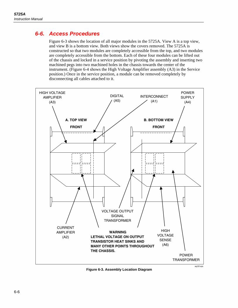
5725A Instruction Manual
6-6
6-6. Access Procedures Figure 6-3 shows the location of all major modules in the 5725A. View A is a top view, and view B is a bottom view. Both views show the covers removed. The 5725A is constructed so that two modules are completely accessible from the top, and two modules are completely accessible from the bottom. Each of these four modules can be lifted out of the chassis and locked in a service position by pivoting the assembly and inserting two machined pegs into two machined holes in the chassis towards the center of the instrument. (Figure 6-4 shows the High Voltage Amplifier assembly (A3) in the Service position.) Once in the service position, a module can be removed completely by disconnecting all cables attached to it.
A. TOP VIEW
FRONT
B. BOTTOM VIEW
FRONT
CURRENTAMPLIFIER
(A2)
HIGH VOLTAGEAMPLIFIER
(A3)
POWERSUPPLY
(A4)
HIGHVOLTAGE
SENSE(A6)
INTERCONNECT(A1)
DIGITAL(A5)
POWERTRANSFORMER
VOLTAGE OUTPUTSIGNAL
TRANSFORMER
WARNINGLETHAL VOLTAGE ON OUTPUT TRANSISTOR HEAT SINKS ANDMANY OTHER POINTS THROUGHOUTTHE CHASSIS.
aq15f.eps
Figure 6-3. Assembly Location Diagram

Maintenance Access Procedures 6
6-7
Warning Follow the instructions under "Initial Access Procedure" to make sure high voltage has been bled off before you touch anything inside the 5725A.
If you work on a 5725A with the power cord attached, and/or you are not certain the high voltage has not bled off, do not wear a grounded wrist strap. Wearing a strap increases risk of dangerous electrical shock.
Use extreme caution when you are working inside the 5725A with the power connected. Use only non-conductive tools, and keep one hand behind your back to avoid making a circuit through your body.
The voltage output transistor heat sinks are at lethal voltage potential in ac V standby and ac V operate modes during normal operation, and possibly in any other mode after a failure. The heat sinks are exposed when any assembly is in the service position, and when the heat sink cover is removed.
6-7. Initial Access Procedure
Before accessing any module from the top or bottom of the instrument, proceed as follows to remove the top cover and verify that high voltage on the power supply capacitors has been bled off:
1. Turn off the POWER switch.
2. Remove the line power cord from ac line power.
3. Wait three minutes.
4. Remove the top cover by removing the screws accessible on the top surface (threefront, three rear).
Warning Before touching anything inside the 5725A, do the following steps to make sure high voltage has been bled off.
5. Refer to Figure 6-4 for the location of items mentioned in this procedure. Remove thefive retaining screws on the High Voltage Amplifier assembly (A3). (Two screwssecure each side rail, and one seats the board into a mating connector on theInterconnect assembly.) Lift the High Voltage assembly by pulling on the plasticwire-tie loops, pivot it, and insert its metal pegs in the two holes on the chassis asFigure 6-4 shows. This puts the High Voltage Amplifier assembly in the serviceposition.

5725A Instruction Manual
6-8
CURRENT MODE
5725A STANDBY
FAULT
OVERLOAD
CABLE OFF
POWER
11A
MAX
2OV
PK
MAX
LEDCR317
TP301
FRONT PANEL
TP307
TP304LEDCR318
HIGH VOLTAGEAMPLIFIER
(A3)
POWER SUPPLY(A4)
aq16f.eps
Figure 6-4. Initial Access Procedure
6. Verify that both LEDs CR317 and CR318 on the Power Supply assembly (A4) areoff. If either is lit after three minutes, there is a fault in the high voltage capacitorbleed-off path.
Warning Do not rely on an off condition as an indication that dangerous voltage no longer exists on the filter capacitors. Always use a voltmeter to check for high voltage between TP307 and TP301, and between TP307 and TP304.
7. To confirm that high voltage has dissipated, set a DMM to the 1000V dc range, andtake a reading with the common lead to TP307 and the high lead to TP301 on the Power Supply assembly. This is the +400V filter capacitor test point, and it should be at a safe level near zero.

Maintenance Access Procedures 6
6-9
8. Take another DMM reading with the common lead to TP307 and the high lead toTP304 on the Power Supply assembly. This is the -400V filter capacitor test point,and it should be at a safe level near zero. This completes the initial access procedure.
6-8. Accessing the Power Supply Assembly (A4)
Warning To avoid electrical shock, do not proceed with the following access procedure until you have completed the initial access procedure, which removes line power and checks for high voltage on the power supply.
The Power Supply assembly lays flat on the bottom of the instrument, toward the front. Proceed as follows to access the Power Supply assembly:
1. Perform the Initial Access Procedure.
2. Return the High Voltage Amplifier assembly (A3) (and the Current Amplifierassembly (A2) if it has been accessed) to the normal position, and reinstall theassembly retaining screws.
Note When reinstalling assemblies, lower them in place squarely to make sure their connectors seat correctly in the Interconnect assembly connectors.
3. Turn over the 5725A so that the bottom is facing up.
4. Remove the five retaining screws on the Power Supply assembly. Lift the PowerSupply assembly by pulling on the plastic wire-tie loops, and place the assembly inthe service position.
Note When reinstalling the assembly, lower it into place squarely to make sure its connector seats correctly in the Interconnect assembly connector. Ensure that both J301 and J303 are properly aligned and connected to their respective cables.
6-9. Accessing the Digital Assembly (A5)
Warning To avoid electrical shock, do not proceed with the following access procedure until you have completed the initial access procedure, which removes line power and checks for high voltage on the power supply.
The Digital assembly is oriented vertically just behind the front panel. Proceed as follows to access the Digital Assembly:
1. Perform the Initial Access Procedure.
2. Refer to Figure 6-5 for accessing the Digital assembly. Remove the six Allen-headscrews from the sides of the front handles, and remove the three screws from thefront edge of the bottom cover. (You have already removed the top cover in step 1.)
3. The front panel remains connected by the Digital assembly ribbon cable and thecurrent output cable. Remove the screw in the center of the Digital assembly to freethe pca.

5725A Instruction Manual
6-10
CAUTIONWHEN REINSTALLING DIGITAL ASSEMBLY,PULL RIBBON CABLE SLACK COMPLETELYINTO CHASSIS.
aq17f.eps
Figure 6-5. Accessing the Digital Assembly

Maintenance Access Procedures 6
6-11
4. If you want to completely remove the Digital assembly, remove the ribbon cable byreleasing the catches on the board-mounted connector.
Caution When replacing the Digital assembly, make sure the ribbon cable is pulled fully into the 5725A chassis. Be sure to leave no fold trapped between the back of the pca and the metal panel or else shorting to the component leads can occur.
6-10. Accessing the Current Amplifier Assembly (A2)
Warning To avoid electrical shock, do not proceed with the following access procedure until you have completed the initial access procedure, which removes line power and checks for high voltage on the power supply. This assembly drops into an area of live line voltage.
The Current Amplifier assembly lays flat on the top of the instrument, toward the rear. Proceed as follows to access the Current Amplifier assembly:
1. Perform the Initial Access Procedure.
2. Turn over the 5725A so that the bottom is facing up.
3. Remove the bottom cover by removing the six screws on the bottom surface.
4. Remove the two screws labeled _A and _B and turn the 5725A over again.
5. Remove the five retaining screws on the Current Amplifier assembly. Lift the CurrentAmplifier assembly by pulling on the plastic wire-tie loops, and place the assemblyin the service position.
Caution When reinstalling the assembly, refer to Figure 6-6 and make sure cable harnesses are dressed as shown, to avoid shorting wires to the bridge rectifier heat sink or chassis.
Note When reinstalling the assembly, lower it into place squarely to make sure its connector seats correctly in the Interconnect assembly connector.

5725A Instruction Manual
6-12
CURRENTAMPLIFIER
(A2)
BRIDGERECTIFIERHEAT SINK
DRESS CABLESAS SHOWN
aq18f.eps
Figure 6-6. Correct Way to Dress Cables
6-11. Accessing the High Voltage Amplifier (A3)
The High Voltage Amplifier assembly lays flat on the top of the instrument, toward the front. To access the High Voltage Amplifier assembly, simply do the Initial Access Procedure. This leaves the assembly in the service position.
Note When reinstalling the assembly, lower it into place squarely to make sure its connector seats correctly in the Interconnect assembly connector.

Maintenance Access Procedures 6
6-13
6-12. Accessing the High Voltage Sense Assembly (A6)
Warning To avoid electrical shock, do not proceed with the following access procedure until you have completed the initial access procedure, which removes line power and checks for high voltage on the power supply. Line voltage comes directly to this assembly.
The High Voltage Sense assembly lays flat on the bottom of the instrument, toward the rear. Proceed as follows to access the High Voltage Sense assembly:
1. Perform the Initial Access Procedure.
2. Follow the Current Amplifier Assembly (A2) access procedure to gain access to theconnectors on the High Voltage Sense Assembly (A6). Remove the connectors andsecure the Current Amplifier Assembly before proceeding.
3. Return the High Voltage Amplifier assembly (and the Current Amplifier assembly ifit has been accessed) to the normal position, and reinstall the assembly retainingscrews.
Note When reinstalling assemblies, lower them in place squarely to make sure their connectors seat correctly in the Interconnect assembly connectors.
4. Turn over the 5725A so that the bottom is facing up.
5. Remove the bottom cover by removing the six screws on the bottom surface.
6. Remove the two jack screws from the 5700A subminiature D-connector.
7. Remove the five retaining screws on the High Voltage Sense assembly. Lift the HighVoltage Sense assembly by pulling on the plastic wire-tie loops, and place theassembly in the service position.
Caution When reinstalling the assembly, refer to Figure 6-6 and make sure cable harnesses are dressed as shown, to avoid shorting wires to the bridge rectifier heat sink or chassis.

5725A Instruction Manual
6-14
6-13. Accessing the High Voltage Output Transistors
Warning During normal operation, the high voltage heat sinks are at lethal voltage. To avoid electrical shock, do not proceed with the following access procedure until you have completed the initial access procedure, which removes line power and checks for high voltage on the power supply.
To access the high voltage output transistors (attached to four separate, large heat sinks in the center of the instrument), proceed as follows:
1. Perform the Initial Access Procedure.
2. Disconnect the heat sinks from the High Voltage Amplifier assembly by unpluggingconnectors J661, J662, J663, J664. Disconnect the temperature monitor byunplugging connector J603.
3. Remove the four screws that retain the high voltage heat sink assembly at the bottomrails.
4. Lift out the heat sink assembly, being careful to keep the cables clear of obstructionsduring removal.
5. Each of the four heat sinks is held in place by two screws, one at the top rail and oneat the bottom rail. Labels on each heat sink identify it as P1, P2, N1, or N2. Toremove a heat sink, remove its two retaining screws, and slide it out of the assembly.
6-14. Accessing the Interconnect Assembly (A1)
Warning To avoid electrical shock, do not proceed with the following access procedure until you have completed the initial access procedure, which removes line power and checks for high voltage on the power supply.
The Interconnect assembly is a vertical board oriented front-to-rear, and is accessible for test probing by placing any other assembly into the service position. To completely remove the Interconnect assembly, as would be required to replace a relay, proceed as follows:
1. Perform the Initial Access Procedure.
2. Completely remove the High Voltage Amplifier (A3) and the Current Amplifier (A2)assemblies by first placing each in the service position, then disconnecting all cablesattached to each of them.
3. Turn over the 5725A so that the bottom is facing up.
4. Remove the bottom cover by removing the six screws on the bottom surface.
5. Completely remove the Power Supply (A4) and the High Voltage Sense assemblies(A6) by first placing each in the service position, then disconnecting all cablesattached to each of them.

Maintenance Enabling Front or Rear Binding Posts 6
6-15
6. Turn over the 5725A so that the top is facing up.
7. Remove the high voltage heat sink assembly as described under “Accessing the HighVoltage Output Transistors", steps 2 through 4.
8. Remove the two screws that secure the Interconnect assembly and pop the assemblyfree of the two bosses.
6-15. Enabling Front or Rear Binding Posts The 5725A comes from the factory configured for front or rear current output as requested by the purchaser when the system was ordered. Only one output location can be enabled at a time. You can reconfigure the output location by opening the chassis, detaching a cable and tying it away, and attaching another cable to a jack on the Current Amplifier assembly.
Warning To avoid electrical shock, proceed only after completing the initial access procedure, which removes line power and checks for high voltage on the power supply.
Proceed as follows to change the current output location:
1. Perform the Initial Access Procedure.
2. Remove the five retaining screws on the Current Amplifier assembly. Lift the currentamplifier assembly by pulling on the plastic wire-tie loops, and place the assembly inthe service position.
3. Refer to Figure 6-7, and locate J222 on the Current Amplifier assembly.
4. Perform step 5 to change from front to rear, or perform step 6 to change from rear tofront.
5. To enable the rear binding posts and disable the front, remove the cable that goes tothe front binding posts from J222, and plug the cable that goes to the rear bindingposts into J222.
6. To enable the front binding posts and disable the rear, remove the cable that goes tothe rear binding posts from J222, and plug the cable that goes to the front bindingposts into J222.
Use a non-conductive plastic wire tie to secure the unused cable to the right side ventilation slots.

5725A Instruction Manual
6-16
J222
FRONT OUTPUTCABLE
REAR OUTPUTCABLE
CURRENTAMPLIFIER
(A2)
SECURE UNUSEDCABLE
aq23f.eps
Figure 6-7. Enabling Front or Rear Binding Posts
Caution Make sure that the unused connector is neatly secured in the recessed area of the chassis side, away from the High Voltage Sense assembly as Figure 6-7 shows. If it is allowed to hang down, shorting can occur.
8. Reconfiguration is complete. Reinstall the Current Amplifier and High VoltageAmplifier assemblies, being careful to correctly seat each assembly into the connector on the Interconnect assembly.
9. Reinstall the top cover.

7-1
Chapter 7 Troubleshooting
Title Page
7-1. Introduction .......................................................................................... 7-3 7-2. 5725A Fault Codes ............................................................................... 7-3 7-3. Self Diagnostics .................................................................................... 7-3 7-4. Manual Tests for Fault Isolation .......................................................... 7-6 7-5. Problems 1 or 2: Fault at Power-Up or When Entering
Voltage Standby ............................................................................... 7-7 7-6. Problem 3: Fault When Entering Voltage Operate .......................... 7-7 7-7. Problem 4: Fault When Entering Current Standby .......................... 7-8 7-8. Problem 5: Fault When Entering Current Operate ........................... 7-8 7-9. Reduced-Voltage Troubleshooting Mode ............................................ 7-8 7-10. Testing the Power Supply By Itself ...................................................... 7-9

5725A Instruction Manual
7-2

Troubleshooting Introduction 7
7-3
7-1. Introduction This section provides troubleshooting information in three parts. First a listing of all 5725A fault codes is provided for reference in Table 7-1. Following that is a description of 5725A automated self-diagnostics that you run from the 5700A. Finally, some manual tests are provided that can help you isolate a fault.
7-2. 5725A Fault Codes Table 7-1 lists all 5725A fault codes. Fault codes and descriptions appear on the 5700A Control Display in fault conditions. The codes and descriptions can also be transferred from the 5700A in remote control operation. Where fault messages are not self-explanatory, additional explanation is given in the table.
7-3. Self Diagnostics The best way to begin looking for the source of a fault is to run self diagnostics from the 5700A diagnostics menu. To run self diagnostics, proceed as follows:
1. Press the "Setup Menus" softkey. (If "Setup Menus" is not showing on the Control Display,press RESET first to return to the 5700A power-up state.)
2. Press the "Self Test & Diags" softkey.
3. Press the "5725A Self Diags" softkey.
4. Begin testing with the voltage function. Press the "Voltage" softkey. A sequence of self testsis run. A brief description of each test follows:
a. 5725A ACV Sense Amp: Checks for proper operation of the high voltage sense amplifieron the High Voltage Sense Assembly (A6).
b. 5725A ACV Standby: Puts the 5725A into voltage standby mode, and causes the analogmonitor circuit on the High Voltage Sense Assembly (A6) to cycle through thecontinuous tests it does during normal operation.
c. 5725A ACV Operate: Puts the 5725A into voltage operate mode, but disconnects theoutput from the 5700A binding posts. This test makes sure that the High VoltageAmplifier (A3) works correctly, and checks the analog monitor circuit on the HighVoltage Sense Assembly (A6) for correct operation.
d. 5725A Cal Sensor: Verifies that the calibration circuitry on the High Voltage SenseAssembly (A6) is working correctly.
5. This completes voltage function testing. If any of the self tests fail, a fault code and messageis displayed.

5725A Instruction Manual
7-4
Table 7-1. 5725A Fault Codes
Fault No.
Message Explanation
201 5725 Self-Test ROM Failure Requires service
202 5725 Self-Test RAM Failure Requires service
203 5725 Self-Test EEPROM Failure Requires service
204 5725 Self-Test Data Bus Failure Requires service
205 5725 Self-Test CLAMPS Circuit Failure Requires service
206 5725 Self-Test HVCLR Circuit Failure Requires service
207 5725 Self-Test DAC Failure Requires service
208 5725 Self-Test Watchdog Timer Failure Requires service
209 5725 Current Heatsink Too Hot Requires service
210 Output Tripped To Standby Current heat sink too hot in operate
211 5725 Current Compliance Voltage Too High Internal fault, requires service
212 5725 Current Compliance Voltage Too High Most likely an external fault
213 5725 +400V Supply Did Not Shut Off Requires service
214 5725 -400V Supply Did Not Shut Off Requires service
215 5725 Voltage Heatsink Too Hot Requires service
216 5725 Voltage Heatsink Too Hot Voltage heat sink too hot in operate
217 5725 +400V Supply Too Small Requires service, or improper line voltage selected
218 5725 +400V Supply Too Large Requires service, or improper line voltage selected
219 5725 -400V Supply Too Large Requires service, or improper line voltage selected
220 5725 -400V Supply Too Small Requires service, or improper line voltage selected
221 5725 +400V Supply Current Too High Internal fault, requires service
222 Output Tripped To Standby +400V supply too high in operate, most likely an external fault
223 5725 -400V Supply Current Too High Internal fault, requires service
224 Output Tripped To Standby -400V supply magnitude too high in operate, most likely an external fault
225 5725 Fan Not Working Requires service
226 5725 CLAMPS Fault Internal fault, requires service
227 Output Tripped To Standby CLAMPS circuit activated most likely because of external transient condition

Troubleshooting Self Diagnostics 7
7-5
Table 7-1. 5725A Fault Codes (cont)
Fault No.
Message Explanation
228 5725 Software TRAP ⎯
229 5725 Cable Was Off ⎯
230 5725 RESET (power-up or watchdog timer) ⎯
231 5725 Guard-Crossing Timeout ⎯
232 5725 Illegal/Unexecutable Command ⎯
233 5725 Non-Maskable Interrupt Occurred Either internal fault or external transient condition
234 5725 HVCLEAR Circuit Activated Internal fault, requires service
235 Output Tripped To Standby HVCLEAR circuit activated most likely because of external transient condition
841 No 5725 Available For Selected Output ⎯
850 Can't Store, 5725 Switch In NORMAL ⎯
851 Can't Format, 5725 Switch In NORMAL ⎯
3202 5725 ACV Sense Amp Fault Requires service
3203 5725 ACV Standby 5725 Fault Requires service
3204 5725 ACV Operate Wouldn't Converge Requires service
3205 5725 ACV Operate 5725 Fault Requires service
3206 5725 ACV Cal Sensor Test Died Requires service
3207 5725 ACV Cal Sensor Fault Requires service
3208 5725 Current Path To Shunt Open Requires service
3209 5725 Shunt Sense Open Requires service
3210 5725 Shunt Measurement Out Of Tolerance Requires service
3211 5725 Current Amplifier Offset Too Large Requires service
3212 5725 Current Drive Path Open Requires service
3213 5725 Current Error Amplifier Failure Requires service
6. To test the current function, press the "Current" softkey. A sequence of self tests is run. Abrief description of each test follows:
a. 5725A Current Shunt: Checks the current cabling and the calibration amplifier on theCurrent Amplifier assembly (A2).
b. 5725A Current Zero: Grounds the input and shorts the output of the Current Amplifier,and verifies that the output is close to 0A.
c. 5725A Current Gain: Shorts the output of the Current Amplifier, applies a voltage input,and verifies the output current. This confirms integrity of the error amplifier circuit in theCurrent Amplifier assembly.
d. 5725A Current Monitor: Runs the analog monitor circuit on the High Voltage SenseAssembly (A6) in the current function and verifies that it operates correctly.

5725A Instruction Manual
7-6
7-4. Manual Tests for Fault Isolation
Warning The following servicing is to be done by qualified service personnel only. To avoid electrical shock, do not service the 5725A unless you are qualified to do so.
Follow the access procedures and warnings in section 6 to open the 5725A covers.
The voltage output transistor heat sinks are at lethal voltage potential in ac v standby and ac v operate modes during normal operation, and possibly in any other mode after a failure. The heat sinks are exposed when any assembly is in the service position, and when the heat sink cover is removed.
Use only non-conductive tools, and keep one hand behind your back to avoid making a circuit through your body. If you work on a 5725A with the power cord attached, and/or you are not certain the high voltage has not bled off, do not wear a grounded wrist strap. Wearing a strap increases risk of dangerous electrical shock.
If self-diagnostics does not identify a faulty module, you can perform these manual tests. Five different fault conditions are addressed. The following numbered list describes each type of fault condition. Following that are troubleshooting tests to do for each type of condition.
1. Fault at power-up (STANDBY and FAULT indicators lit).
2. Normal at power-up (STANDBY indicator ON), but trips out when trying to enter voltage standby mode. (VOLTAGE MODE indicator momentarily lights, then STANDBY and FAULT indicators light.)
3. Normal at power-up (STANDBY indicator ON) and ACV STANDBY (ACV and STANDBY indicator ON), but trips out when trying to enter ACV OPERATE.
4. Normal at power-up, but trips out when entering current standby
5. Normal at power-up and CURRENT STANDBY, but trips out when entering current operate.

Troubleshooting Manual Tests for Fault Isolation 7
7-7
7-5. Problems 1 or 2: Fault at Power-Up or When Entering Voltage Standby
Proceed as follows to isolate the problem in these conditions:
1. If the 5700A is reporting a fault, determine if it is an analog monitor fault from Table 7-2. Ifthe fault is not in Table 7-2, skip to step 2. (See Table 7-1 for explanations of fault codes.)
Table 7-2. Analog Monitor Faults
Fault No. Message
209 5725 Current Heatsink Too Hot 210 Output Tripped To Standby 211 5725 Current Compliance Voltage Too High 212 5725 Current Compliance Voltage Too High 213 5725 +400V Supply Did Not Shut Off 214 5725 -400V Supply Did Not Shut Off 215 5725 Voltage Heatsink Too Hot 216 Output Tripped To Standby 217 5725 +400V Supply Too Low 218 5725 +400V Supply Too High 219 5725 -400V Supply Too Negative 220 5725 -400V Supply Too Positive 221 5725 +400V Supply Current Too High 222 Output Tripped To Standby 223 5725 -400V Supply Current Too High 224 Output Tripped To Standby 225 5725 Fan Not Working
a. With an oscilloscope, check TP152 (DAC OUT) for the waveform shown facing Section9 with the High Voltage Sense Assembly (A6) schematic.
b. If the waveform is present, suspect an abnormal analog input into U151 on the HighVoltage Sense Assembly (A6). See Table 4-3 for voltage limits of the analog inputs forstandby operation.
c. If the waveform is not present, short TP510 to DCOM on the Digital assembly. This tellsthe CPU to ignore all analog monitor faults and run all other tests. Check for any newfault codes that indicate the problem.
d. If the waveform is still not present, the High Voltage Sense Assembly (A6) is likely to beat fault, specifically, the circuitry that includes U151, U155, U156, U153, and U154.
2. If not an analog monitor fault, is it a high voltage supply (Fault 234) or CLAMPS* (Fault226) fault? If yes and in standby mode, suspect the Power Supply assembly (A4). If yes andin voltage standby mode, suspect the High Voltage Amplifier (A3) and the high voltageoutput transistors.
3. If the error on the 5700A is not an analog monitor fault, high voltage supply (Fault 234), orCLAMPS* (Fault 226) fault, or if no fault is reported by the 5700A, check forcommunications activity at pins 12 and 13 of U507 on the Digital assembly (A5). Thewaveform should appear as shown facing the Digital schematic as waveform 4. If there is noactivity, suspect the communication circuitry on the High Voltage Sense Assembly or theDigital assembly.
7-6. Problem 3: Fault When Entering Voltage Operate
Proceed as follows to isolate the problem in this condition:

5725A Instruction Manual
7-8
1. Suspect the 5700A/5725A interface cable.
2. Check the analog monitor circuit on the High Voltage Sense Assembly as in step 1 onconditions 1 and 2.
3. Suspect the High Voltage Amplifier assembly and the output transistor heat sink assemblies.
7-7. Problem 4: Fault When Entering Current Standby
Proceed as follows to isolate a problem in this condition:
1. If an overcompliance error is showing (fault 211), check for proper closing of the standbyrelay on the Current assembly (K202).
2. Check the analog monitor circuit on the High Voltage Sense Assembly as in step 1 onconditions 1 and 2.
7-8. Problem 5: Fault When Entering Current Operate
Proceed as follows to isolate a problem in this condition:
1. If an overcompliance error is showing (fault 212):
a. Check for an open or too high resistance load.
b. Suspect an open internal current output cable, or the Current Amplifier assembly.
2. Check the analog monitor circuit on the High Voltage Sense Assembly as in step 1 onconditions 1 and 2.
7-9. Reduced-Voltage Troubleshooting Mode The high voltage supply on the Power Supply assembly (A4) allows normal operation from a pair of nominal 400V dc supplies, or troubleshooting operation in a reduced voltage mode with a pair of nominal 50V dc supplies. To switch between normal and reduced-voltage operation, proceed as follows:
1. Turn off the POWER switch and disconnect the line power cord from ac line power.
Warning Follow the instructions under "Initial Access Procedure" in section 6 to make sure high voltage has been bled off before you touch anything inside the 5725A.
The power supply assembly generates lethal voltages. Use extreme caution when you are working inside the 5725A with the power connected. Use only non-conductive tools, and keep one hand behind your back to avoid making a circuit through your body. If you work on a 5725A with the power cord attached, and/or you are not certain the high voltage has not bled off, do not wear a grounded wrist strap. Wearing a strap increases risk of dangerous electrical shock.
2. Place the Power Supply assembly in the service position as described in the accessprocedures in Section 6.
3. Remove plug P301 from J301 and inserting it into J303. Now the high voltage power supplywill power up in the ±50V mode. The high voltage amplifier may also be serviced in the±50V mode.

Troubleshooting Testing the Power Supply By Itself 7
7-9
7-10. Testing the Power Supply By Itself To turn on a Power Supply assembly (A4) by itself for troubleshooting, proceed as follows:
1. Turn off the POWER switch and disconnect the line power cord from ac line power.
Warning Follow the instructions under "initial access procedure" in section 6 to make sure high voltage has been bled off before you touch anything inside the 5725A.
The power supply assembly generates lethal voltages. Use extreme caution when you are working inside the 5725A with the power connected. Use only non-conductive tools, and keep one hand behind your back to avoid making a circuit through your body. If you work on a 5725A with the power cord attached, and/or you are not certain the high voltage has not bled off, do not wear a grounded wrist strap. Wearing a strap increases risk of dangerous electrical shock.
2. Place the Power Supply assembly in the service position as described in the access procedures in Section 6.
3. Plug P301 onto the E302 header where the label MAN appears (pins 2 and 3).
4. This allows momentary-contact pushbutton switch SW302 to generate a strobe signal for U302, turning the supplies on. You turn the supplies off by pressing switch SW301.
5. You may want to troubleshoot in the low-voltage mode by plugging the high voltage secondary plug into J303. The previous procedure describes how to do this.

5725A Instruction Manual
7-10

8-1
Chapter 8 List of Replaceable Parts
Title Page
8-1. Introduction ........................................................................................... 8-3 8-2. How to Obtain Parts .............................................................................. 8-3 8-3. Manual Status Information ................................................................... 8-3 8-4. Newer Instruments ................................................................................ 8-3 8-5. Service Centers ..................................................................................... 8-3 8-6. Parts Lists .............................................................................................. 8-4

5725A Instruction Manual
8-2
List of Replaceable Parts Introduction 8
8-3
8-1. Introduction This chapter contains an illustrated list of replaceable parts for the 7-300, 7-600, 12B, and 18 Meters. Parts are listed by assembly; alphabetized by reference designator. Each assembly is accompanied by an illustration showing the location of each part and its reference designator. The parts lists give the following information:
• Reference designator• An indication if the part is subject to damage by static discharge• Description• Fluke stock number• Total quantity• Any special notes (i.e., factory-selected part)
Caution A * symbol indicates a device that may be damaged by staticdischarge.
8-2. How to Obtain Parts Electrical components may be ordered directly from the manufacturer by using the manufacturers part number, or from the Fluke Corporation and its authorized representatives by using the part number under the heading FLUKE STOCK NO. In the U.S., order directly from the Fluke Parts Dept. by calling 1-800-526-4731. Parts price information is available from the Fluke Corporation or its representatives. Prices are also available in a Fluke Replacement Parts Catalog which is available on request.
In the event that the part ordered has been replaced by a new or improved part, the replacement will be accompanied by an explanatory note and installation instructions, if necessary.
To ensure prompt delivery of the correct part, include the following information when you place an order:
• Instrument model and serial number• Part number and revision level of the pca containing the part.• Reference designator• Fluke stock number• Description (as given under the DESCRIPTION heading)• Quantity
8-3. Manual Status Information The Manual Status Information table that precedes the parts list defines the assembly revision levels that are documented in the manual. Revision levels are printed on the component side of each pca.
8-4. Newer Instruments Changes and improvements made to the instrument are identified by incrementing the revision letter marked on the affected pca. These changes are documented on a manual supplement which, when applicable, is included with the product.
8-5. Service Centers A list of service centers is available on the Fluke web sit at www.fluke.com.

5725A Instruction Manual
8-4
Note
This instrument may contain a Nickel-Cadmium battery. Do not mix with the sold waste stream. Spent batteries should be disposed of by a qualified recycler or hazardous materials handler. Contact your authorized Fluke service center for recycling information.
Table 8-1. Manual Status Information
Ref or Option No.
Assembly Name Fluke Part No. Revision Level
A1
A2
A3
A4
A5
A6
A30
Interconnect PCA
Current Amplifier PCA
High Voltage Amplifier PCA
Power Supply PCA
Digital PCA
High Voltage Sense PCA
Inductor PCA
843065
843073
843086
843078
843081
843060
860119
101
102
101
101
101
105
A
8-6. Parts Lists
Table 8-2. Final Assembly
Reference
Designator Description
Fluke Stock
No Tot Qty Notes
A1 * INTERCONNECT PCA 843065 1
A2 * CURRENT AMPLIFIER PCA 843073 1
A3 * HIGH VOLTAGE AMPLIFIER PCA 843086 1
A4 * POWER SUPPLY PCA 843078 1
A5 * DIGITAL PCA 843081 1
A6 * HIGH VOLTAGE SENSE PCA 843060 1
A12 TRANSFORMER ENCLOSURE ASSEMBLY 842984 1
A30 INDUCTOR PCA 890116 1
F501 FUSE,.25X1.25,8A,250V,FAST 561506 1
F502 FUSE,.25X1.25,4A,250V,FAST 216846 1
H1 SCREW,PH,P,SEMS,STL,6-32,.375 177022 22
H30 SCREW,PH,P,LOCK,STL,6-32,.500 152173 8
H301 SCREW,PH,P,LOCK,MAG SS,6-32,.2 772236 30
H302 WASHER,FLAT,BRASS,#8,0.032 THK 631606 4
H304 NUT, #8 LOW THERMAL 850334 8
H308 WASHER,FLAT,COPPER,#8,.020 721688 4
H331 SCREW,CAP,SCKT,SS,8-32,.375 295105 24
H424 SCREW,PH,P,LOCK,SS,6-32,.375 334458 2
H425 SCREW,FHU,P,LOCK,SS,6-32,.250 320093 12

List of Replaceable Parts Parts Lists 8
8-5
Table 8-2. Final Assembly (cont)
Reference
Designator Description
Fluke Stock
No Tot Qty Notes
H437 SCREW,PH,P,LOCK,SS,6-32,.750 376822 2
H439 SCREW,TH,P,LOCK,STL,8-32,.250 853622 4
H443 SCREW,PH,P,LOCK,STL,6-32,.625 152181 4
H505 NUT,HEX,BR,1/4-28 110619 1
H506 WASHER,LOCK,INTRNL,STL,.267ID 110817 1
H513 WASHER,FLAT,SS,.119,.187,.010 853296 2
H545 NUT,EXT LOCK,STL,6-32,.344OD 152819 1
L3-6 CORE,TOROID,FERRITE,.047X.138X 321182 4
MP1 TRANSISTOR SET 842880 2
MP2 LABEL, CE MARK, BLACK 600707 1
MP3 TRANSISTOR SET 842992 2
MP5 HEATSINK, HIGH VOLTAGE 843115 4
MP9 DECAL,HEATSINK 850230 4
MP15 ASSY, THERMISTOR 843032 1
MP16 CABLE ACCESS,TIE,4.00L,.10W,.7 172080 24
MP39 HEAT DIS,ACC,AL FOIL,TO-3 838169 8
MP47 SLEEV,POLYOL,SHRINK,.187-.093I 113852 1
MP302 HANDLE,INSTRUMENT, GRAY #7 886341 4
MP304 INSULATOR,BINDING POST,FRONT,G 885459 4
MP306 REAR INSULATOR GRAY #3 894183 4
MP308 BINDING POST-RED 886382 2
MP309 BINDING POST-BLACK 886379 2
MP310 DECAL,FRONT 886317 1
MP311 NAMEPLATE,TITTLE 850164 1
MP312 POWER BUTTON, ON/OFF 775338 1
MP405 DECAL,WARNING 850243 2
MP410 SIDE EXTRUSION 886288 2
MP412 INSERT EXTRUSION 886283 2
MP414 ADHESIVE SIDE TRIM 698316 2
MP416 BOTTOM FOOT, MOLDED, GRAY #7 868786 4
MP501 DECAL, CSA 864470 1
MP510 LINE FILTER ASSEMBLY 850172 1
MP511 FAN ASSEMBLY 843029 1
MP512 BINDING HEAD, PLATED 102889 1
MP513 BINDING POST, STUD, PLATED 102707 1
MP514 LABEL,VINYL,1.500,.312 844712 1
MP516 FAN GUARD AND AIR FILTER 886416 1
MP600 FRONT PANEL 886408 1
MP601 REAR PANEL 886411 1
MP602 HOUSING, AIR FILTER 886416 1
MP603 COVER, TOP 660951 1
MP604 COVER, BOTTOM 660958 1
MP605 DIVIDER, HIGH VOLTAGE MODULE 860176 1
MP606 TOP INSULATOR ASSY, HIGH VOLTAGE MODULE 860192 1
MP607 BOTTOM INSULATOR ASSY, HIGH VOLTAGE MODULE 860197 1

5725A Instruction Manual
8-6
Table 8-2. Final Assembly (cont)
Reference
Designator Description
Fluke Stock
No Tot Qty Notes
TM1 5725 INSTRUCTION MANUAL 823435 1
W1 CORD,LINE,5-15/IEC,3-18AWG,SVT 284174 1
W13 HARNESS, TRANSISTOR P661 843040 1
W14 HARNESS, TRANSISTOR P662 843045 1
W15 HARNESS, TRANSISTOR P663 843052 1
W16 HARNESS, TRANSISTOR P664 843057 1
W44 CABLE ASSY, 5700A/5725A I/F 859897 1
XF501 HLDR,FUSE,1/4 X 1-1/4,LOPROFIL 424416 1

List of Replaceable Parts Parts Lists 8
8-7
aq24f.tif
Figure 8-1. Final Assembly

5725A Instruction Manual
8-8
aq25f.tif
Figure 8-1. Final Assembly (cont)

List of Replaceable Parts Parts Lists 8
8-9
aq26f.tif
Figure 8-1. Final Assembly (cont)

5725A Instruction Manual
8-10
aq27f.tif
Figure 8-1. Final Assembly (cont)

List of Replaceable Parts Parts Lists 8
8-11
aq28f.tif
Figure 8-1. Final Assembly (cont)

5725A Instruction Manual
8-12
aq29f.tif
Figure 8-1. Final Assembly (cont)

List of Replaceable Parts Parts Lists 8
8-13
aq30f.tif
Figure 8-1. Final Assembly (cont)
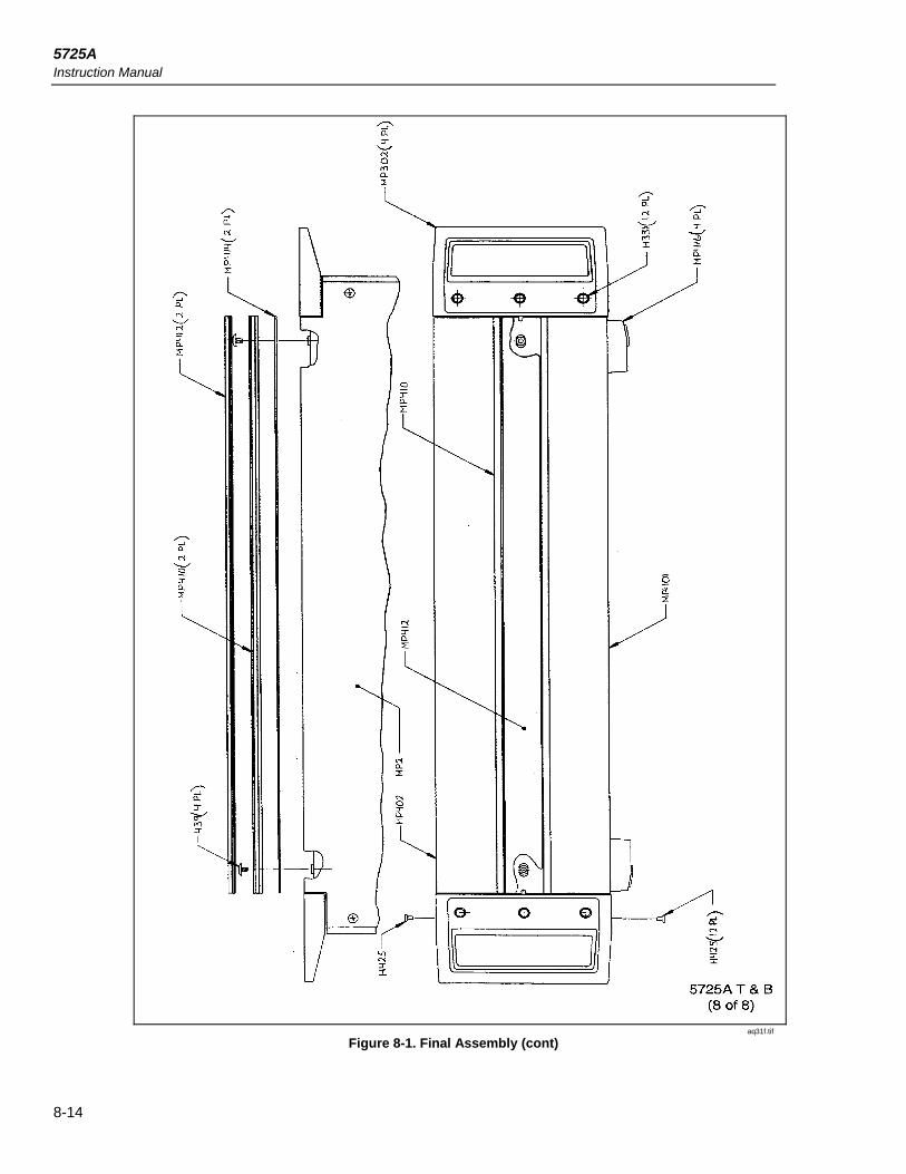
5725A Instruction Manual
8-14
aq31f.tif
Figure 8-1. Final Assembly (cont)

List of Replaceable Parts Parts Lists 8
8-15
Table 8-3. A1 Interconnect PCA
Reference
Designator Description
Fluke Stock
No Tot Qty Notes
CR1,CR13-15 * DIODE,SI,BV=75V,IO=150MA,500MW 203323 4
H13 RIVET,S-TUB,OVAL,AL,.087,.343 838458 8
H22 RIVET,S-TUB,OVAL,STL,.118,.218 103606 4
J1 HEADER,2 ROW,.100CTR,34 PIN 836577 1
J2 HEADER,1 ROW,.156CTR,10 PIN 446724 1
J100,J103 HEADER,1 ROW,.100CTR,RT ANG,2 851667 2
K1 RELAY,ARMATURE,2 FORM C,5VDC 810911 1
K13-15 RELAY,REED,1 FORM A,5VDC 806950 3
MP1 BRACKET,RIGHT ANGLE,TAPPED,BRA 404525 4
MP5 GUIDE, HEATSINK 860205 2
P102 CONN,DIN41612,TYPE R,RT ANG,64 782102 1
P202,P351,P653 CONN,DIN41612,TYPE 1/2R,RT ANG 836882 3
TP1,TP2 JUMPER,WIRE,NONINSUL,0.200CTR 816090 2

5725A Instruction Manual
8-16
5725A-1611
aq36f.eps
Figure 8-2. A1 Interconnect PCA

List of Replaceable Parts Parts Lists 8
8-17
Table 8-4. A2 Current Amplifier PCA
Reference
Designator Description
Fluke Stock
No Tot Qty Notes
C201,C202,C207,
C208,C211,C212,
C226,C227,C236
CAP,AL,22UF,+-20%,35V 817056
817056
817056
9
C203,C204,C216,
C217,C238-240
CAP,POLYES,0.1UF,+-10%,50V 649913
649913
7
C205,C206 CAP,POLYES,0.001UF,+-10%,50V 720938 2
C210,C214,C215,
C234
CAP,POLYES,0.47UF,+-10%,50V 697409
697409
4
C213 CAP,CER,22PF,+-2%,50V,C0G 714832 1
C218-221 CAP,AL,50000UF,+100-10%,20V,LO 830539 4
C222,C223 CAP,AL,470UF,+-20%,35V,SOLV PR 756700 2
C224,C225 CAP,AL,10UF,+-20%,63V,SOLV PRO 816843 2
C228 CAP,CER,100PF,+-5%,50V,C0G 831495 1
C230 CAP,CER,47PF,+-2%,100V,C0G 832295 1
C233 CAP,TA,2.2UF,+-20%,16V 706804 1
C235 CAP,POLYES,1UF,+-10%,100V 447847 1
C237 CAP,CER,39PF,+-2%,50V,C0G 714840 1
CR201-204,
CR207,CR220,
CR221
*
*
*
DIODE,SI,BV=75V,IO=150MA,500MW 203323
203323
203323
7
CR205 * DIODE,SI,N-JFET,CURRENT REG,IF 334839 1
CR206 DIODE,SI,RECT,BRIDGE,BV=50V,IO 886945 1
CR208-219,
CR222
DIODE,SI,400 PIV,1 AMP 831586
831586
13
E255 TERM,FASTON,TAB,.110,SOLDER 512889 1
F201,F202 FUSE,.25X1.25,20A,32V,FAST 518860 2
H16 WASHER,FLAT,STL,.170,.375,.031 110288 1
H25 RIVET,POP,DOME,AL,.125,.316 807347 4
H201 LABEL,C-MOS INSTRUCTION 464016 1
H207 RIVET,S-TUB,OVAL,AL,.087,.250 838482 2
H209 SCREW,PH,P,LOCK,STL,8-32,.625 114983 1
H210 SCREW,PH,P,SEMS,STL,6-32,.375 177022 6
H216 SCREW,PH,P,LOCK,MAG SS,6-32,.2 772236 8
H230 NUT,BROACH,STL,6-32 393785 2
H232 SCREW,PH,P,SS,10-32,.250 855184 8
J201 CONN,MATE-N-LOK,HEADER,8 PIN 570515 1
J202 CONN,DIN41612,TYPE 1/2R,32 PIN 836874 1
J204 HEADER,1 ROW,.100CTR,2 PIN 643916 1
J205 HEADER,1 ROW,.100CTR,2 PIN 602698 1
J222 CONN,MATE-N-LOK,HEADER,4 PIN 512269 1
J252 CONN,COAX,SMB(M),PWB 352450 1
K201,K205-209 RELAY,ARMATURE,2 FORM C,5V 733063 6
K202-204 RELAY,ARMATURE,2 FORM A,5VDC 830547 3
L201 CHOKE, 3 TURN 452888 1

5725A Instruction Manual
8-18
Table 8-4. A2 Current Amplifier PCA (cont)
Reference
Designator Description
Fluke Stock
No Tot Qty Notes
MP2 INSULATOR, CURRENT 850151 1
MP28 INSULATOR, CURRENT 850156 1
MP38 BUMPER, HI-TEMP, SILICONE 16018701 1
MP81 CLAMP,PWB MOUNTING 823039 1
MP82 CLAMP,PWB MOUNTING 842948 1
MP203 HEAT DIS,PRESS ON,TO-5 418384 2
MP205 HEAT DIS,VERT,.83,.50,.395,TO- 800144 1
MP206 HEAT DIS,ACC,AL FOIL,TO-3 838169 2
MP211 FUSE CLIP PCB 756460 4
MP215 SOCKET,SINGLE,PWB,FOR .042-.04 544056 4
MP225 AIDE,PCB PULL 541730 2
MP256 INSUL PT,TRANSISTOR MOUNT,DAP, 152207 2
MP812 HEATSINK, CURRENT 843110 1
MP816 HEATSINK, RECTIFIER 850169 1
Q201 * TRANSISTOR,SI,PNP,40V,0.35W,TO 698233 1
Q202 * TRANSISTOR,SI,NPN,SMALL SIGNAL 698225 1
Q203 * TRANSISTOR,SI,PNP,SMALL SIGNAL 402586 1
Q204 * TRANSISTOR,SI,NPN,SMALL SIGNAL 346916 1
Q205 * TRANSISTOR,SI,BV=100V,50W,TO-2 454041 1
Q206 * TRANSISTOR,SI,BV=100V,40W,TO-2 454033 1
Q207 * TRANSISTOR,SI,BV=60V,200W,TO-3 483222 1
Q208 * TRANSISTOR,SI,BV=60V,200W,TO-3 483230 1
Q211 * TRANSISTOR,SI,N-JFET,TO-92 832154 1
Q212,Q213 * TRANSISTOR,SI,N-JFET,REMOTE CU 697987 2
Q214,Q215 * TRANSISTOR,SI,PNP,80V,0.625W,T 816272 2
Q216 * TRANSISTOR,SI,N-MOS,350MW,TO-9 783449 1
R201,R202 RESISTOR .086 OHM 1% 4 TERM 10 490771 2
R203,R204 RES,MF,43.2,+-1%,0.5W,100PPM 601823 2
R205 RES,MF,1K,+-1%,0.125W,100PPM 168229 1
R206,R234,R274,
R275
RES,MF,31.6K,+-1%,0.125W,100PP 261610
261610
4
R207,R222,R232,
R235,R239-241
RES,MF,39.2K,+-0.1%,0.125W,25P 344507
344507
7
R209 RES,MF,90.9,+-0.1%,0.5W,25PPM 423947 1
R211,R251,R252 RES,MF,3.92K,+-0.1%,.125W,25PP 844662 3
R212 RES,MF,2K,+-0.1%,0.125W,25PPM 340174 1
R213,R214,R217,
R218,R231,R271
RES,CF,330,+-5%,0.25W 368720
368720
6
R215,R216,R249,
R250
RES,MF,3.48K,+-1%,0.125W,100PP 260687
260687
4
R219,R220 RES,CC,5.1,+-5%,1W 219071 2
R221,R225,R226 RES,CC,51,+-5%,0.5W 687829 3
R223,R224,R227,
R228
RES,CF,1,+-5%,0.25W 357665
357665
4

List of Replaceable Parts Parts Lists 8
8-19
Table 8-4. A2 Current Amplifier PCA (cont)
Reference
Designator Description
Fluke Stock
No Tot Qty Notes
R233,R237,R238,
R273
RES,MF,2K,+-1%,0.125W,100PPM 235226
235226
4
R243,R244 RES,CF,100K,+-5%,0.25W 348920 2
R247,R248 RES,MF,232,+-1%,0.125W,100PPM 289975 2
R253,R277,R282,
R283,R285,R286
RES,MF,10K,+-1%,0.125W,100PPM 168260
168260
6
R255,R267,R268 RES,CF,470K,+-5%,0.25W 342634 3
R256-259 RES,MF,1M,+-1%,0.125W,100PPM 268797 4
R260 RES,LF,5.1,+-5%,0.5W 687779 1
R261,R263, R290-
295
RES,CF,4.7K,+-5%,0.25W 348821
348821
8
R262 RES,CF,150,+-5%,0.25W 343442 1
R264 RES,CF,1K,+-5%,0.25W 343426 1
R272 SHUNT ASSY 842877 1
R276 RES,MF,9.09K,+-1%,0.125W,100PP 221663 1
R281 RES,MF,24.9K,+-1%,0.125W,100PP 291369 1
R284 RES,MF,44.2K,+-1%,0.125W,25PPM 706317 1
RT201,RT202 THERMISTOR,DISC,4.85,25C 838102 2
TP201-
205,TP207-215
JUMPER,WIRE,NONINSUL,0.200CTR 816090
816090
17
U201 * IC,OP AMP,PRECISION,LOW NOISE 866637 1
U202 * IC,OP AMP,PRECISION,LOW NOISE 816744 1
U203 * IC,OP AMP,CURRENT AMP,TO-99 CA 260422 1
U204 * IC,OP AMP,DUAL,PRECISION MATCH 782375 1
U205 * IC,VOLT REG,ADJ,1.2 TO 37 V,1. 460410 1
U206 * IC,VOLT REG,ADJ,NEG,-1.2VT0-37v, 1.5A 772996 1
U207 * IC,COMPARATOR,DUAL,LO-PWR,8 PI 478354 1
U208 * IC,OP AMP,PRECISION,LOW NOISE 782920 1
U209 * IC,BIMOS,8 CHNL HI-VOLT DRVR W 782912 1
U210 * IC,COMPARATOR,QUAD,14 PIN DIP 387233 1
U211 * IC,OP AMP,QUAD,JFET INPUT,14 P 483438 1
VR201,VR202 * ZENER,UNCOMP,6.8V,5%,20.0MA,0. 260695 2
W6 HARNESS, MFC CURRENT 843008 1
w206 ASSY, THERMISTOR 843032 1
Z201,Z203 * RNET,MF,HERM,SIP,5700 LO V INS 809418 2

5725A Instruction Manual
8-20
5725A-1650
aq37f.eps
Figure 8-3. A2 Current Amplifier PCA

List of Replaceable Parts Parts Lists 8
8-21
Table 8-5. A3 High Voltage Amplifier PCA
Reference
Designator Description
Fluke Stock
No Tot Qty Notes
C601 CAP,POLYES,1UF,+-10%,50V 733089 1
C602 CAP,CER,100PF,+-5%,50V,C0G 831495 1
C603,C606,C609-
611,C620
CAP,AL,10UF,+-20%,63V,SOLV PRO 816843
816843
6
C604,C605 CAP,CER,1.5PF,+-0.25PF,1000V,C 836346 2
C607,C614,C654,
C662
CAP,CER,22PF,+-10%,1000V,C0G 817023
817023
4
C608,C612,C619,
C655,C656,C658,
C659,C665,C666,
C668
CAP,POLYES,0.1UF,+-10%,50V 649913
649913
649913
649913
10
C613 CAP,CER,3.3PF,+0.25PF,100V,C0J 816678 1
C615,C621,C622,
C652,C657
CAP,POLYES,0.01UF,+-10%,50V 715037
715037
5
C616 CAP,POLYES,0.001UF,+-10%,50V 720938 1
C617 CAP,AL,1UF,+-20%,50V 782805 1
C618 CAP,AL,2.2UF,+-20%,50V 769687 1
C651,C664,C667 CAP,CER,0.005UF,+-20%,3000V,Z5 188003 3
C653 CAP,CER,10PF,+-10%,3000V,C0G 817049 1
C660,C661 CAP,CER,39PF,+-5%,1000V,C0G 817031 2
C663 CAP,CER,0.01UF,+100-0%,1600V,Z 106930 1
CR602-605,
CR607-612,
CR651,CR653,
CR655, CR658,
CR659
*
*
*
*
DIODE,SI,BV=75V,IO=150MA,500MW 203323
203323
203323
203323
15
CR652,CR654,
CR656,CR657
DIODE,SI,1K PIV,1.0 AMP 707075
707075
4
H601 RIVET,S-TUB,OVAL,AL,.087,.250 838482 2
H603 RIVET,POP,DOME,AL,.125,.316 807347 4
H626 LABEL,C-MOS INSTRUCTION 464016 1
J603 HEADER,1 ROW,.100CTR,2 PIN 602698 1
J604 HEADER,1 ROW,.156CTR,10 PIN 446724 1
J605,J661-664 HEADER,1 ROW,.156CTR,8 PIN 385435 5
J653 CONN,DIN41612,TYPE 1/2R,32 PIN 836874 1
K601-604 RELAY,ARMATURE,2 FORM C,5V 733063 4
L601,L602 CHOKE, 3 TURN 452888 2
L603 INDUCTOR,2.2UH,+-5%,108MHZ,SHL 806547 1
MP28 * INSULATOR,PWR SUPPY HIGH VOLT 843102 1
MP81 CLAMP,PWB MOUNTING 823039 1
MP82 CLAMP,PWB MOUNTING 842948 1
MP601 AIDE,PCB PULL 541730 2
MP658 INSUL PT,TRANSISTOR MOUNT,DAP, 152207 3

5725A Instruction Manual
8-22
Table 8-5. A3 High Voltage Amplifier PCA (cont)
Reference
Designator Description
Fluke Stock
No Tot Qty Notes
Q601 * TRANSISTOR,SI,N-JFET,TO-92 816314 1
Q602,Q603,Q606 * TRANSISTOR,SI,PNP,40V,0.35W,TO 698233 3
Q604 * TRANSISTOR,SI,N-DMOS FET,TO-72 394122 1
Q605,Q660 * TRANSISTOR,SI,NPN,SMALL SIGNAL 698225 2
Q653, Q654, Q661 HEAT SINK ASSY 665521 2
Q667, Q670 HEAT SINK ASSY 665536 2
Q657 HEAT SINK ASSY 665554 1
Q662, Q665 HEAT SINK ASSY 665528 2
Q658,Q666 * TRANSISTOR,SI,NPN,SMALL SIGNAL 346916 2
Q659 * TRANSISTOR,SI,PNP,SMALL SIGNAL 402586 1
R600 RES,WW,1.2,+-5%,2W 248658 1
R601,R609,R612,
R617,R620,R649,
R650,R659,R674,
R694,R698,R753
RES,CF,1K,+-5%,0.25W 343426
343426
343426
343426
12
R602,R603,R664,
R683,R688
RES,CF,4.7K,+-5%,0.25W 348821
348821
5
R604,R605 RES,CF,680K,+-5%,0.25W 442517 2
R606,R607 RES,MF,100K,+-1%,0.125W,100PPM 248807 2
R608 RES,MF,44.2K,+-1%,0.125W,25PPM 706317 1
R610 RES,MF,649,+-1%,0.125W,100PPM 309955 1
R611,R614 RES,MF,2K,+-0.1%,0.125W,25PPM 340174 2
R613 RES,MF,39.2K,+-0.1%,0.125W,25P 344507 1
R615 RES,MF,3.92K,+-0.1%,.125W,25PP 844662 1
R616 RES,CF,6.8K,+-5%,0.25W 368761 1
R618,R665,R675,
R690,R691,R697,
R699-701,R751,
R752
RES,CF,51,+-5%,0.25W 414540
414540
414540
414540
11
R619,R653,R655,
R656,R662,R663,
R679-681,R685,
R689,R693,R696
RES,CF,100,+-5%,0.25W 348771
348771
348771
348771
13
R621,R623,R626 RES,MF,5.49K,+-1%,0.125W,100PP 334565 3
R622 RES,MF,60.4K,+-1%,0.125W,100PP 291419 1
R624,R625 R627-
630,R632-635,
R644-646,R652
RES,CF,10K,+-5%,0.25W 348839
348839
348839
14
R631,R660,R678,
R682
RES,CF,330,+-5%,0.25W 368720
368720
4
R636 RES,MF,2K,+-1%,0.125W,100PPM 235226 1
R637 RES,CC,1.2K,+-5%,1W 109892 1
R638,R639 RES,CF,1.5M,+-5%,0.25W 349001 2
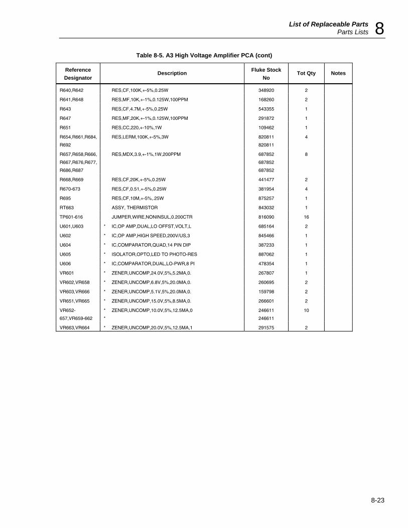
List of Replaceable Parts Parts Lists 8
8-23
Table 8-5. A3 High Voltage Amplifier PCA (cont)
Reference
Designator Description
Fluke Stock
No Tot Qty Notes
R640,R642 RES,CF,100K,+-5%,0.25W 348920 2
R641,R648 RES,MF,10K,+-1%,0.125W,100PPM 168260 2
R643 RES,CF,4.7M,+-5%,0.25W 543355 1
R647 RES,MF,20K,+-1%,0.125W,100PPM 291872 1
R651 RES,CC,220,+-10%,1W 109462 1
R654,R661,R684,
R692
RES,LERM,100K,+-5%,3W 820811
820811
4
R657,R658,R666,
R667,R676,R677,
R686,R687
RES,MDX,3.9,+-1%,1W,200PPM 687852
687852
687852
8
R668,R669 RES,CF,20K,+-5%,0.25W 441477 2
R670-673 RES,CF,0.51,+-5%,0.25W 381954 4
R695 RES,CF,10M,+-5%,.25W 875257 1
RT663 ASSY, THERMISTOR 843032 1
TP601-616 JUMPER,WIRE,NONINSUL,0.200CTR 816090 16
U601,U603 * IC,OP AMP,DUAL,LO OFFST,VOLT,L 685164 2
U602 * IC,OP AMP,HIGH SPEED,200V/US,3 845466 1
U604 * IC,COMPARATOR,QUAD,14 PIN DIP 387233 1
U605 * ISOLATOR,OPTO,LED TO PHOTO-RES 887062 1
U606 * IC,COMPARATOR,DUAL,LO-PWR,8 PI 478354 1
VR601 * ZENER,UNCOMP,24.0V,5%,5.2MA,0. 267807 1
VR602,VR658 * ZENER,UNCOMP,6.8V,5%,20.0MA,0. 260695 2
VR603,VR666 * ZENER,UNCOMP,5.1V,5%,20.0MA,0. 159798 2
VR651,VR665 * ZENER,UNCOMP,15.0V,5%,8.5MA,0. 266601 2
VR652-
657,VR659-662
*
*
ZENER,UNCOMP,10.0V,5%,12.5MA,0 246611
246611
10
VR663,VR664 * ZENER,UNCOMP,20.0V,5%,12.5MA,1 291575 2

5725A Instruction Manual
8-24
5725A-1661
aq38f.eps
Figure 8-4. A3 High Voltage Amplifier PCA

List of Replaceable Parts Parts Lists 8
8-25
Table 8-6. A4 Power Supply PCA
Reference
Designator Description
Fluke Stock
No Tot Qty Notes
C301,C302,C321,
C322
CAP,AL,220UF,+-20%,350V 854075
854075
4
C303,C304,C308,
C317-319,C352,
C355,C358,C360,
C362
CAP,POLYES,0.1UF,+-10%,50V 649913
649913
649913
649913
11
C305,C306 CAP,AL,0.47UF,+-20%,50V 769695 2
C307 CAP,POLYES,0.047UF,+-10%,50V 820548 1
C309 CAP,CER,82PF,+-2%,50V,C0G 714857 1
C310,C311,C313,
C320
CAP,CER,0.04UF,+-20%,3000V,Y5V 851725
851725
4
C312,C363 CAP,CER,33PF,+-5%,50V,C0G 714543 2
C314 CAP,POLYES,0.47UF,+-10%,50V 697409 1
C315,C316 CAP,POLYES,0.01UF,+-10%,50V 715037 2
C350 CAP,AL,10000UF,+-20%,25V 816819 1
C351,C354,C357,
C359,C361
CAP,AL,10UF,+-20%,63V,SOLV PRO 816843
816843
5
C353,C356,C369 CAP,AL,3300UF,+-20%,50V 782458 3
C364-368 CAP,POLYES,0.33UF,+-10%,50V 715284 5
CR301-304,
CR310-313
*
*
DIODE,SI,1K PIV,1.0 AMP 707075
707075
8
CR305-309,
CR316,CR321
DIODE,SI,BV=75V,IO=150MA,500MW 203323
203323
7
CR314,CR315,
CR319,CR320,
CR322-325,
CR350, CR352-
354,CR356-363
DIODE,SI,400 PIV,1 AMP 831586
831586
831586
831586
831586
20
CR317,CR318 LED,RED,T1,40 MCD 845412 2
CR351,CR355 DIODE,SI,RECT,BRIDGE,BV=50V,IO 586115 2
E301 HEADER,1 ROW,.100CTR,4 PIN 417329 1
E302 SURGE PROTECTOR,630V,+-15% 853767 1
F301,F302 FUSE,.406X1.375,2A,600V,FAST 747600 2
H301 RIVET,S-TUB,OVAL,AL,.087,.250 838482 1
H302 RIVET,S-TUB,OVAL,AL,.087,.250 838482 1
H303- RIVET,POP,DOME,AL,.125,.316 807347 4
H307 RIVET,S-TUB,OVAL,STL,.118,.156 103424 4
J301,J303 CONN,MATE-N-LOK,HEADER,8 PIN 570515 2
J302,J350 HEADER,1 ROW,.156CTR,8 PIN 385435 2
J351 CONN,DIN41612,TYPE 1/2R,32 PIN 836874 1
MP28 * INSULATOR,PWR SUPPY HIGH VOLT 843102 1
MP81 CLAMP,PWB MOUNTING 823039 1
MP82 CLAMP,PWB MOUNTING 842948 1
MP301 HLDR,FUSE,13/32,PWB MT 516880 4

5725A Instruction Manual
8-26
Table 8-6. A4 Power Supply PCA (cont)
Reference
Designator Description
Fluke Stock
No Tot Qty Notes
MP310 AIDE,PCB PULL 541730 2
MP350 HEAT DIS,VERT,1.13X1.90X0.95,T 830844 3
MP398 PAD, ADHESIVE 735365 2
P301 JUMPER,REC,2 POS,.100CTR,.025 530253 1
Q301,Q302,Q317,
Q318
*
*
HEAT SINK ASSY 665536
665536
4
Q303-305,Q315,
Q321,Q322
*
*
TRANSISTOR,SI,NPN,HI-VOLTAGE,T 722934
722934
6
Q306,Q307,Q311,
Q316,Q323,Q324
*
*
TRANSISTOR,SI,PNP,SM SIG,SELEC 602961
602961
6
Q308 * TRANSISTOR,SI,PNP,40V,0.35W,TO 698233 1
Q309 * TRANS,SI,N-JFET,REMOTE CUTOFF, 707968 1
Q310,Q314 * TRANSISTOR,SI,NPN,SMALL SIGNAL 698225 2
Q312,Q313,Q319,
Q320
*
*
HEAT SINK ASSY 66554
66554
4
Q350,Q351 * TRANSISTOR,SI,BV= 40V, 40W,TO- 418459 2
R301,R302,R342,
R343
RES,CF,470K,+-5%,0.25W 342634
342634
4
R303,R308,R335,
R339
RES,MOX,33K,+-5%,1W 644952
644952
4
R304,R305,R340,
R341
RES,CF,33K,+-5%,0.25W 348888
348888
4
R306,R332,R349 RES,MF,10K,+-1%,0.125W,100PPM 168260 3
R307,R309,R356 RES,CF,6.8K,+-5%,0.25W 368761 3
R310,R311,R346,
R347
RES,CF,1.5M,+-5%,0.25W 349001
349001
4
R312,R317,R330,
R331,R353 R357-
360
RES,CF,100,+-5%,0.25W 348771
348771
348771
9
R313,R329 RES,MF,0.39,+-5%,2W 219386 2
R314,R315,R336,
R337
RES,CF,15K,+-5%,0.5W 687795
687795
4
R316,R324,R338 RES,CF,100K,+-5%,0.25W 348920 3
R318 RES,MF,86.6K,+-1%,0.125W,25PPM 257402 1
R319 RES,MF,28.7K,+-1%,0.125W,100PP 235176 1
R320,R325,R328,
R348,R354
RES,CF,10K,+-5%,0.25W 348839
348839
5
R321 RES,MF,40.2K,+-1%,0.125W,100PP 235333 1
R322,R333 RES,MF,499,+-1%,,0.125W,100PM 168211 2
R323 RES,MF,6.19K,+-1%,0.125W,100PP 283911 1
R326 RES,MF,604,+-1%,0.125W,100PPM 320309 1
R327 RES,MF,60.4K,+-1%,0.125W,100PP 291419 1
R334 RES,CF,2K,+-5%,0.25W 441469 1
R344,R345 RES,CF,240K,+-5%,0.25W 442459 2
R350,R352 RES,MF,20K,+-1%,0.125W,100PPM 291872 2

List of Replaceable Parts Parts Lists 8
8-27
Table 8-6. A4 Power Supply PCA (cont)
Reference
Designator Description
Fluke Stock
No Tot Qty Notes
R351 RES,CF,1K,+-5%,0.25W 343426 1
R355 RES,CF,4.7K,+-5%,0.25W 348821 1
R361,R362 RES,CF,4.7,+-5%,0.25W 441584 2
RT350 THERMISTOR,DISC,O.12,25C 838144 1
RT351-354 THERMISTOR,DISC,0.81,25C 838136 4
SW301,SW302 SWITCH,PUSHBUTTON,SPST,MOMENTA 782656 2
TP301-307,TP350-
355,TP357-360
JUMPER,WIRE,NONINSUL,0.200CTR 816090
816090
17
U301 IC,COMPARATOR,DUAL,LO-PWR,8 PI 478354 1
U302 IC,CMOS,DUAL D F/F,+EDG TRG W/ 536433 1
U350,U353 IC,VOLT REG,FIXED,+5 VOLTS,1.5 647073 2
U351 IC,VOLT REG,FIXED 15VOLTS,1.5A 772830 1
U352 IC,VOLT REG,FIXED,-15 VOLTS,1. 413179 1
U354 IC,OP AMP,GENERAL PURPOSE,8 PI 478107 1
VR301,VR302,
VR304,VR305
ZENER,UNCOMP,15.0V,5%,8.5MA,0. 266601
266601
4
VR303 ZENER,UNCOMP,16.0V,5%,7.8MA,0. 325837 1
VR306,VR307 ZENER,UNCOMP,3.9V,10%,20.0MA,0 113316 2
VR351 ZENER,UNCOMP,3.9V,5%,320.0MA,5 386995 1
VR352 ZENER,UNCOMP,24.0V,5%,5.2MA,0. 267807 1
W8 HARNESS, HIGH VOLTAGE SUPPLY 843016 1

5725A Instruction Manual
8-28
5725A-1631
aq39f.eps
Figure 8-5. A4 Power Supply PCA

List of Replaceable Parts Parts Lists 8
8-29
Table 8-7. A5 Digital PCA
Reference
Designator Description
Fluke Stock
No Tot Qty Notes
C501,C503-511,
C516,C518,C519,
C521
CAP,POLYES,0.1UF,+-10%,50V 649913
649913
649913
14
C502,C520 CAP,AL,22UF,+-20%,35V 817056 2
C512,C513 CAP,CER,15PF,+-20%,50V,C0G 697524 2
C514,C517 CAP,POLYES,0.33UF,+-10%,50V 715284 2
C515 CAP,TA,10UF,+-20%,35V 816512 1
C522-530 CAP,CER,470PF,+-5%,50V,C0G 830430 9
C531 CAP,CER,100PF,+-5%,50V,C0G 831495 1
CR501,CR504,
CR505
LED,GREEN,LIGHT BAR,5.0 MCD 845136
845136
3
CR502,CR506,
CR507
LED,RED,LIGHT BAR,6.0 MCD 534834
534834
3
CR508,CR509 * DIODE,SI,SCHOTTKY,40V,DO-34 313247 2
E501 HEADER,1 ROW,.100CTR,4 PIN 417329 1
J501 SOCKET,IC,0.070 CTR,64 PIN 783688 1
J502 HEADER,2 ROW,.100CTR,RT ANG,34 836551 1
J504 SOCKET,IC,28 PIN 448217 1
J506-509 SOCKET,IC,8 PIN 478016 4
J512,J515 SOCKET,IC,24 PIN 376236 2
L501 CHOKE, 3 TURN 452888 1
MP501 PAD, ADHESIVE 735365 1
MP502 SLEEVING 142554 1
MP815 CABLE, INTERCONNECT - FRONT PA 843123 1
R501 RES,MF,1M,+-1%,0.125W,100PPM 268797 1
R502,R509 RES,CF,1K,+-5%,0.25W 343426 2
R503-507 RES,CF,47K,+-5%,0.25W 348896 5
R508 RES,MF,11.5,+-1%,0.125W,100PPM 339796 1
R510 RES,CF,10K,+-5%,0.25W 348839 1
SW502 SWITCH,PUSHBUTTON,SPST,MOMENTA 782656 1
TP501-510 JUMPER,WIRE,NONINSUL,0.200CTR 816090 10
U501,U510 * IC,CMOS,OCTAL D TRANSPARENT LA 743294 2
U502 * IC,CMOS,HEX INVERTERS 799924 1
U503 * IC,CMOS,OCTL LINE DRVR W/3-ST 741892 1
U504 * IC, 2K X 8 STAT RAM 647222 1
U505 * IC,CMOS,QUAD INPUT NOR GATE 811158 1
U506 * IC,CMOS,14 STAGE BINARY COUNTE 807701 1
U507 * IC,CMOS,8-BIT MPU,2.0 MHZ,256 876326 1
U508 * IC,VOLT SUPERVISOR,4.55V SENSE 780577 1
U509 * IC,CMOS,DUAL MONOSTABLE MULTIB 454017 1
U511,U514 * IC,CMOS,QUAD 2 INPUT NAND GATE 707323 2
U512 IC, NMOS, 2K X 8 EEPROM, 350 N 811075 1
U513 * IL,CMOS,QUAD 2 INPUT AND GATE 741801 1
U515 * EPROM,PROGRAMED 27128A-150 U51 860148 1
Y501 CRYSTAL,4.9152 MHZ,+/- 0.005%, 800367 1
Z501 RES,CERM,DIP,16 PIN,15 RES,10K 355305 1
Z502 RES,CERM,DIP,16 PIN,8 RES,24,+ 806406 1

5725A Instruction Manual
8-30
5725A-1650
aq40f.eps
Figure 8-6. A5 Digital PCA

List of Replaceable Parts Parts Lists 8
8-31
Table 8-8. A6 High Voltage Sense PCA
Reference
Designator Description
Fluke Stock
No Tot Qty Notes
C98,C99 CAP,CER,470PF,+-10%,50V,C0G 733071 2
C100,C121 CAP,POLYCA,1UF,+-10%,50V 271619 2
C101,C103,C106,
C107,C109,C111,
C114,C115 C117-
119,C124,C125,
C150-152,C154,
C157,C163,C166,
C167,C169-176,
C181-183
CAP,POLYES,0.1UF,+-10%,50V 649913
649913
649913
649913
649913
649913
649913
649913
32
C102 CAP,POLYCA,0.15UF,+-5%,50V 343616 1
C104,C127 CAP,CER,680PF,+-5%,50V,C0G 743351 2
C105 CAP,PORC,1.0PF,+-0.25PF,1000V 603571 1
C108 CAP,CER,10PF,+-2%,50V,C0G 713875 1
C110,C112,C122,
C123,C177
CAP,TA,10UF,+-20%,35V 816512
816512
5
C113,C128 CAP,CER,100PF,+-5%,50V,C0G 831495 2
C120 CAP,POLYES,0.1UF,+-10%,50V 649913 1
C153 CAP,CER,3300PF,+-5%,50V,C0G 830612 1
C155 CAP,POLYES,0.01UF,+-10%,50V 715037 1
C156,C158-161 CAP,AL,22UF,+-20%,35V 817056 5
C162,C164,C165,
C168
CAP,CER,39PF,+-2%,50V,C0G 714840
714840
4
C180 CAP,POLYES,0.47UF,+-10%,50V 697409 1
C401 CAP,AL,600UF,+75-10%,15V,SOLV 557660 1
C402 CAP,AL,47UF,+-20%,50V,SOLV PRO 822403 1
C403 CAP,CER,0.22UF,+80-20%,50V,Z5U 649939 1
CR100,CR103,
CR104,CR150-153
*
*
DIODE,SI,BV=75V,IO=150MA,500MW 659516
659516
7
CR101,CR102 * DIODE,SI,BV=20V,IO=50MA,250MW 836288 2
CR105-108 * DIODE,SI,BV=35V, LOW LEAKAGE 723817 4
CR401-404 DIODE,SI,400 PIV,1 AMP 831586 4
CR405 * DIODE,SI,BV=75V,IO=150MA,500MW 203323 1
E105 SOCKET,SINGLE,SOLDER,FOR .064 851287 1
E155 TERM,FASTON,TAB,.110,SOLDER 512889 1
H27 GROUND STRIP,BECU,SPRING FINGE 370619 1
H108 RIVET,S-TUB,OVAL,AL,.087,.250 838482 2
H110 RIVET,S-TUB,OVAL,STL,.118,.281 650283 2
H121 RIVET,POP,DOME,AL,.125,.316 807347 4
H126 LABEL,C-MOS INSTRUCTION 464016 1
J102 CONN,DIN41612,TYPE R,64 PIN 782094 1
J118-124 SOCKET,SINGLE,SOLDER,FOR .021 851290 7
J152 CONN,COAX,SMB(M),PWB 352450 1
J401 CONN,MATE-N-LOK,HEADER,4 PIN 512269 1
J402 HEADER,1 ROW,.156CTR,12 PIN 831354 1

5725A Instruction Manual
8-32
Table 8-8. A6 High Voltage Sense PCA (cont)
Reference
Designator Description
Fluke Stock
No Tot Qty Notes
J403 HEADER,1 ROW,.156CTR,RT ANG,5 844717 1
K101,K106-108,
K111,K151-153
RELAY,ARMATURE,2 FORM C,5V 733063
733063
8
K102-105,K109 RELAY,REED,1 FORM A,5VDC 806950 5
K401 RELAY,ARMATURE,2 FORM A,5VDC 830547 1
L100-105 CHOKE, 3 TURN 452888 6
MP1 CABLE ACCESS,TIE,4.00L,.10W,.7 172080 2
MP25 SHIELD, DIGITAL 842930 1
MP26 SHIELD, SENSOR 842935 1
MP27 INSULATOR, SENSE 843099 1
MP36 SUPPORT,ATTENUATOR 823195 2
MP038 BUMPER, HI-TEMP 1601870 1
MP81 CLAMP,PWB MOUNTING 823039 1
MP82 CLAMP,PWB MOUNTIN 842948 1
MP101 AIDE,PCB PULL 541730 2
MP813 WIRE, ATTENUATOR 843094 1
Q100,Q102 * TRANSISTOR,SI,PNP,80V,0.625W,T 816272 2
Q101,Q103 * TRANSISTOR,SI,NPN,SMALL SIGNAL 816298 2
Q104,Q107,Q401 * TRANSISTOR,SI,N-MOS,350MW,TO-9 783449 3
Q105 * TRANSISTOR,SI,PNP,40V,0.35W,TO 698233 1
Q106,Q150 * TRANSISTOR,SI,NPN,SMALL SIGNAL 698225 2
R100,R123,R124,
R157,R159-161,
R163-167,R177
RES,CF,1.5K,+-5%,0.25W 810432
810432
810432
13
R101,R102 RES,MF,86.6K,+-1%,0.125W,100PP 772046 2
R103 RES,MF,40.2K,+-1%,2W,10PPM 811042 1
R104,R108,R116 RES,CF,330,+-5%,0.25W 830596 3
R105,R114 RES,MF,2K,+-1%,0.125W,100PPM 816629 2
R106 RES,MF,402K,+-0.1%,0.125W,100P 714329 1
R107,R117 RES,CF,240,+-5%,0.25W 830588 2
R110,R113,R115,
R119,R121,R122,
R128,R129,R150
RES,CF,47,+-5%,0.25W 822189
822189
822189
9
R112 RES,MF,1.21K,+-1%,0.125W,100PP 810507 1
R118 RES,CF,4.7,+-5%,0.25W 816637 1
R120,R170 RES,MF,619,+-0.1%,0.125W,100PP 810515 2
R125,R174,R179 RES,CF,100K,+-5%,0.25W 658963 3
R126 RES,CF,3.9,+-5%,0.25W 810473 1
R127 RES,CF,20K,+-5%,0.25W 697110 1
R130 RES,CF,100,+-5%,0.25W 810465 1
R131,R132 RES,MF,2.67K,+-1%,0.125W,100PP 820290 2
R133,R134 RES,MF,1K,+-1%,0.125W,100PPM 816595 2
R151,R169 RES,MF,18.2K,+-1%,0.125W,100PP 756429 2
R153 RES,MF,80.27K,+-0.1%,0.125W,25 851337 1

List of Replaceable Parts Parts Lists 8
8-33
Table 8-8. A6 High Voltage Sense PCA (cont)
Reference
Designator Description
Fluke Stock
No Tot Qty Notes
R154 RES,MF,20K,+-0.1%,0.25W,25PPM 810564 1
R155 RES,MF,13.7K,+-0.1%,0.125W,25P 851340 1
R156,R158,R168,
R173
RES,CF,3.9K.+-5%,0.25W 810416
810416
4
R162 RES,CF,10K,+-5%,0.25W 697102 1
R171 RES,CF,3M,+-5%,0.25W 746172 1
R172,R175 RES,CF,4.7K,+-5%,0.25W 721571 2
R178 RES,CF,2K,+-5%,0.25W 810457 1
R401 RES,MF,6.19K,+-1%,0.125W,100PP 283911 1
R402 RES,CF,20K,+-5%,0.25W 441477 1
R403 RES,CC,56,+-10%,0.5W 642907 1
R404 RES,CF,47K,+-5%,0.25W 348896 1
RT401,RT402 THERMISTOR,DISC,NEG.,10,+-15%, 500371 2
RT403 THERMISTOR,DISC,4.85,25C 838102 1
RV101,RV155 VARISTOR,33V,+-10%,1.0MA 816421 2
RV151-154 VARISTOR,8.2V,+-35%,1.0MA 715052 4
RV401 VARISTOR,430V,+-10%,1.0MA 519355 1
SW150 SWITCH,SLIDE,DPDT 697466 1
SW402-404 SWITCH,SLIDE,DPDT,LINE SELECT, 817353 3
TP100,TP101
TP103-107,TP151-
154 TP156,TP157,
TP159-161,
JUMPER,WIRE,NONINSUL,0.200CTR 816090
816090
816090
816090
20
U100 * IC,OP AMP,VLOW IB,LOW VOS,8 PI 875760 1
U101 RMS CONVERTER TESTED 400 OHM-A 842591 1
U102 * IC,OP AMP,LOW BIAS,HIGH BANDWI 854133 1
U103 * IC,OP AMP,LO-OFFSET VOLTAGE,LO 605980 1
U105 * IC,OP AMP,PRECISION,LOW NOISE 782920 1
U150 * IC,COMPARATOR,DUAL,LO-PWR,8 PI 478354 1
U151 * IC,CMOS, 16 CHANNEL ANALOG MUX 723684 1
U152,U155 * IC,CMOS,OCTAL D TRANSPARENT LA 743294 2
U153,U154 * IC,OP AMP,DUAL,LO OFFST,VOLT,L 685164 2
U156 * IC,CMOS,10BIT DAC,8BIT ACCUR,C 524868 1
U157,U158 * IC,BIMOS,8 CHNL HI-VOLT DRVR W 782912 2
U159,U161 * ISOLATOR,OPTO,LED TO DARLINGTO 640664 2
U160 * IC,CMOS,DUAL RS-232 TRANS/RECE 799445 1
VR100-103,VR105 * ZENER,UNCOMP,3.3V,5%,20.0MA,0. 820423 5
VR151 * ZENER,UNCOMP,5.1V,5%,20.0MA,0. 853700 1
W002 CABLE,HIGH VOLTAGE OUTPUT 842950 1
W006 HARNESS,MFC CURRENT 843008 1
W009 HARNESS, SUB D 843024 1
Z100 * RNET,MF,HERM,SIP,5700 HI V AMP 803536 1
Z150 RES,CERM,DIP,16 PIN,8 RES,1M,+ 461731 1

5725A Instruction Manual
8-34
5725A-1601
aq41f.eps
Figure 8-7. A6 High Voltage Sense PCA

List of Replaceable Parts Parts Lists 8
8-35
Table 8-9. A12 Transformer Enclosure Assembly
Reference
Designator Description
Fluke Stock
No Tot Qty Notes
H1 SCREW,FHU,P,LOCK,SS,6-32,.250 320093 4
H5 SCREW,PH,P,LOCK,MAG SS,6-32,.2 772236 20
H39 SCREW,PH,P,LOCK,STL,6-32,.625 152181 2
H41 SCREW,PH,P,LOCK,SS,4-40,.187 149567 2
H43 SCREW,PH,P,LOCK,SS,6-32,.500 320051 1
H44 SCREW,PH,P,LOCK,STL,6-32,.750 114223 5
H49 WASHER,FLAT,STL,.149,.375,.031 110270 2
H51 SCREW,HH,H,LOCK,STL,10-32,.375 854794 2
H53 SCREW,PH,P,LOCK,STL,6-32,.187 381087 4
H61 SCREW,HH,H,STL,1/4-20,4.00 845078 4
H65 WASHER,LOCK,SPLIT,STL,.255,.49 111518 4
H69 WASHER,FLAT,STL,.260,.375,.032 312538 4
H73 SCREW,PH,P,LOCK,STL,6-32,.375 152165 2
H75 SCREW,PH,P,LOCK,STL,10-32,.625 114066 2
MP1 BUSHING,SNAP-IN,NYL,.500 ID 102780 3
MP4 CABLE ACC,CLAMP,.687 DIA,SCREW 853775 2
MP12 MACHINED SHEET METAL XFORMER A 860143 1
MP13 SHEET METAL XFORMER ASSY 850300 1
MP18 SUPPORT,TRANSFORMER MTG 842919 2
MP403 CABLE, POWER SWITCH 881847 1
MP802 SHIELD, TRANSFORMER, BASE 842898 1
MP803 SHIELD,PWR,TRANSFORMER,COVER 850185 1
MP804 CUSHION,TRANSFORMER MTG. 842914 2
P2,P604 HOUSING,1 ROW,0.156 CTR,LOCK,1 446716 2
P403 HOUSING,1 ROW,0.156 CTR,LOCK,5 831164 1
T1 LOW FREQ 823336 1
T2 XFORMER MED FREQUENCY 823344 1
T3 HIGH FREQ 823351 1
T101 POWER TRANSFORMER 823369 1
TB001 TERM STRIP,BULKHEAD,.375CTR,2 276519 1
W4 HARNESS, CURRENT, FRONT 842997 1
W5 HARNESS,CURRENT,REAR 843003 1
W17 CABLE, TRANSFORMER BLACK 850222 1
W18 CABLE, TRANSFORMER WHITE 850227 1

5725A Instruction Manual
8-36
aq32f.tif
Figure 8-8. A12 Transformer Enclosure Assembly

List of Replaceable Parts Parts Lists 8
8-37
aq33f.tif
Figure 8-8. A12 Transformer Enclosure Assembly (cont)

5725A Instruction Manual
8-38
aq34f.tif
Figure 8-8. A12 Transformer Enclosure Assembly (cont)

List of Replaceable Parts Parts Lists 8
8-39
aq35f.tif
Figure 8-8. A12 Transformer Enclosure Assembly (cont)

5725A Instruction Manual
8-40
Table 8-10. A30 Inductor PCA
Reference
Designator Description
Fluke Stock
No Tot Qty Notes
J1 CONN,MATE-N-LOK,HEADER,4 PIN 512269 1
L1,L2 CHOKE 490888 2
W1 HARNESS, LINE VOLTAGE 843011 1
1. For schematic, See A6 section 9.
5725A-1603
aq42f.eps
Figure 8-9. A30 Inductor PCA
9-1
Chapter 9 Schematic Diagrams
Figure No. Title Page
9-1. A1 Interconnect PCA......................................................................... 9-3 9-2. A2 Current Amplifier PCA ................................................................ 9-6 9-3. A3 High Voltage Amplifier PCA ...................................................... 9-10 9-4. A4 Power Supply PCA ...................................................................... 9-13 9-5. A5 Digital PCA ................................................................................. 9-16 9-6. A6 High Voltage Sense PCA ............................................................. 9-18 9-7. A12 Transformer Enclosure Assembly ................................................ 9-23

5725A Instruction Manual
9-2

Schematic Diagrams 9
9-3
Figure 9-1. A1 Interconnect PCA
aq48f.eps

5725AInstruction Manual
9-4Figure 9-1. A1 Interconnect PCA (cont)

Schematic Diagrams 9
9-5Figure 9-1. A1 Interconnect PCA (cont)
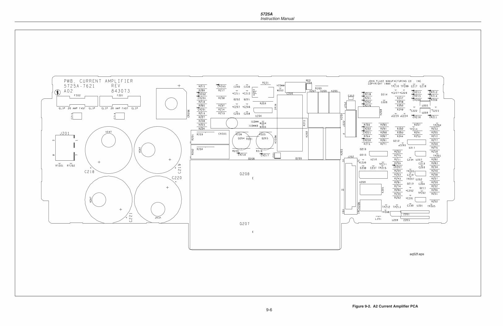
5725AInstruction Manual
9-6Figure 9-2. A2 Current Amplifier PCA
aq52f.eps

Schematic Diagrams 9
9-7Figure 9-2. A2 Current Amplifier PCA (cont)
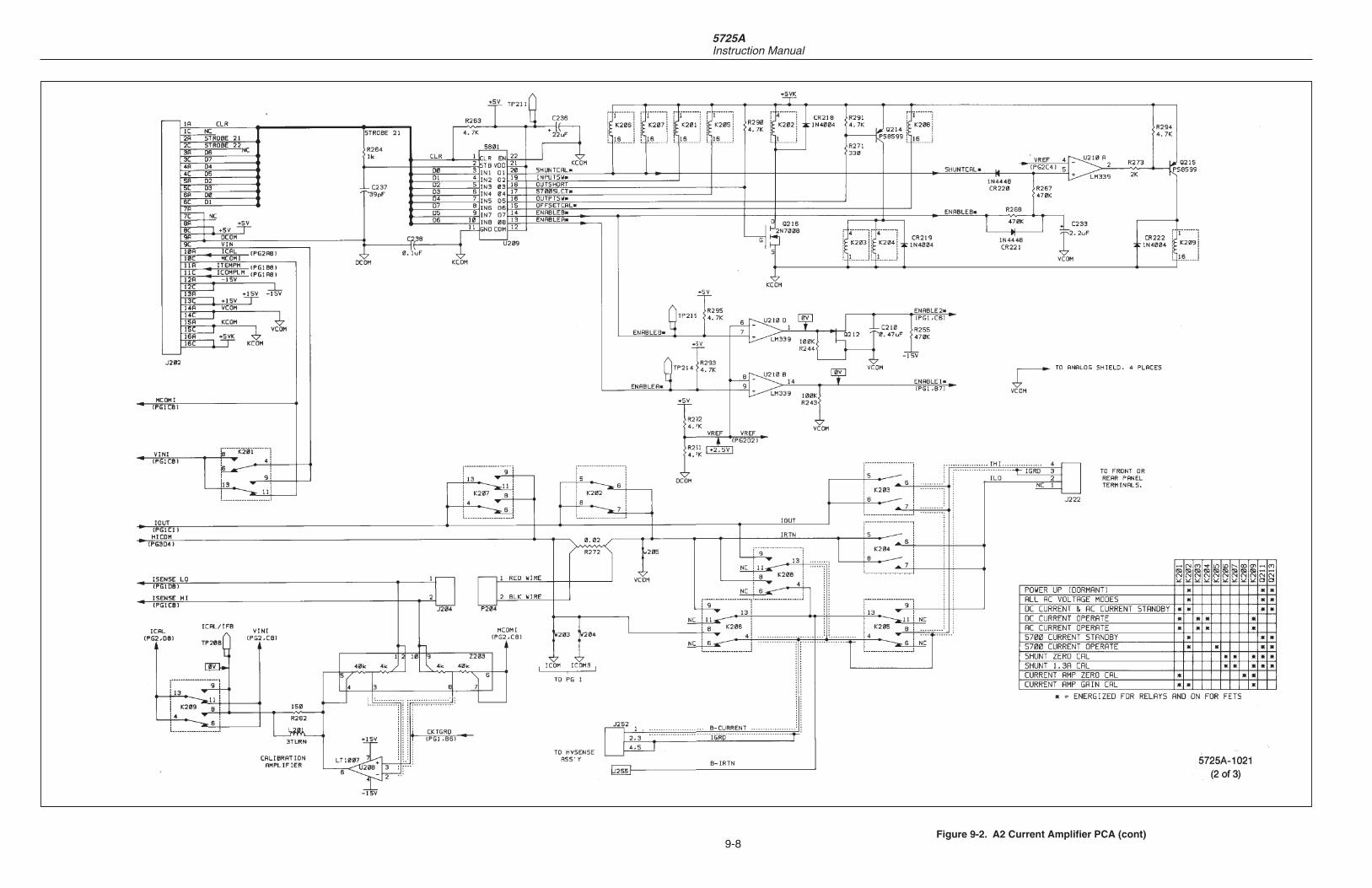
5725AInstruction Manual
9-8Figure 9-2. A2 Current Amplifier PCA (cont)

Schematic Diagrams 9
9-9Figure 9-2. A2 Current Amplifier PCA (cont)

5725AInstruction Manual
9-10Figure 9-3. A3 High Voltage Amplifier PCA (cont)
aq56f.eps

Schematic Diagrams 9
9-11Figure 9-3. A3 High Voltage Amplifier PCA (cont)

5725AInstruction Manual
9-12Figure 9-3. A3 High Voltage Amplifier PCA (cont)

Schematic Diagrams 9
9-13Figure 9-4. A4 Power Supply PCA
aq59f.eps

5725AInstruction Manual
9-14Figure 9-4. A4 Power Supply PCA (cont)

Schematic Diagrams 9
9-15Figure 9-4. A4 Power Supply PCA (cont)

5725AInstruction Manual
9-16Figure 9-5. A5 Digital PCA
5725
A-1
650
100
90
10
02 V
10 ms
TYPICAL COMMUNICATIONS ACTIVITYAT PINS 12 AND 13 OF U507.
aq62f.eps
aq43f.eps
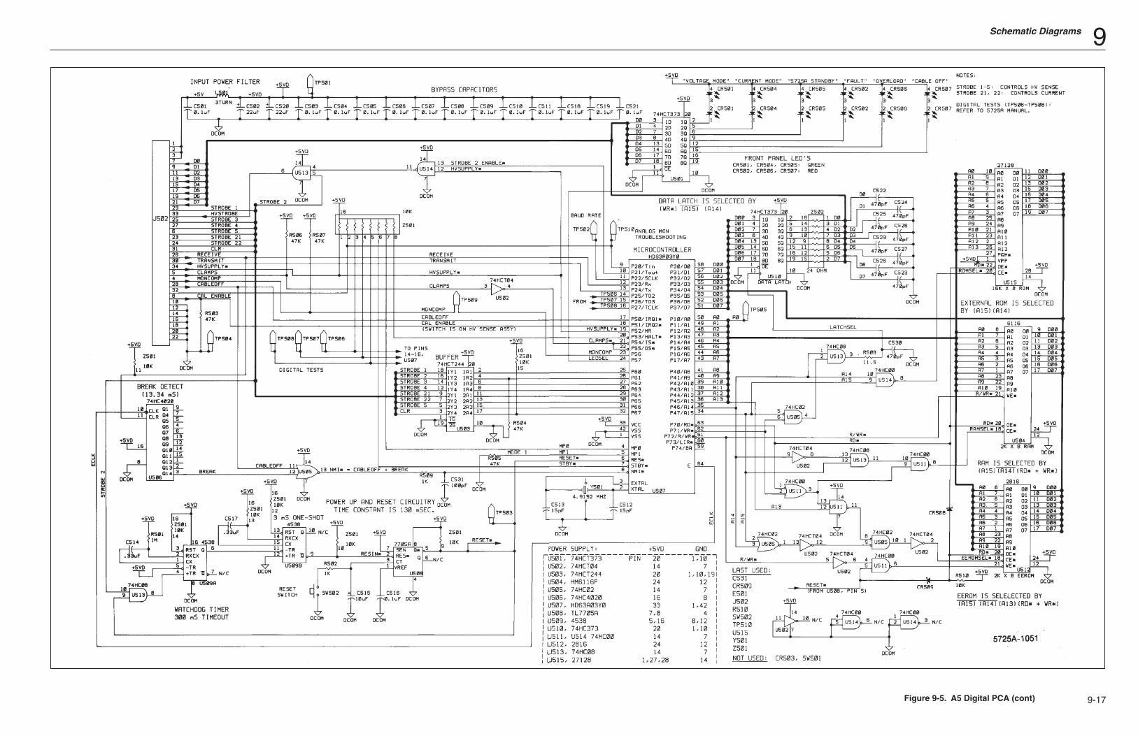
Schematic Diagrams 9
9-17Figure 9-5. A5 Digital PCA (cont)

5725AInstruction Manual
9-18Figure 9-6. A6 High Voltage Sense PCA
100
90
10
01 V
10 ms
100
90
10
01 V
10 ms
VOLTAGE STANDBYSTANDBY
100
90
10
01 V
10 ms
CURRENT STANDBY
A
5725A-1601
aq63f.eps
aq44f.eps

Schematic Diagrams 9
9-19Figure 9-6. A6 High Voltage Sense PCA (cont)

5725AInstruction Manual
9-20Figure 9-6. A6 High Voltage Sense PCA (cont)

Schematic Diagrams 9
9-21Figure 9-6. A6 High Voltage Sense PCA (cont)
C98470pF
C99470pF

5725AInstruction Manual
9-22Figure 9-6. A6 High Voltage Sense PCA (cont)

Schematic Diagrams 9
9-23
aq45f.eps
Figure 9-7. A12 Transformer Enclosure Assembly

5725A Instruction Manual
9-24

1
Index
—5—5700A
CALIBRATOR connector, 2-6, 3-7Connecting to, 2-6
5725A STANDBY indicator, 3-5
—A—A1. See Interconnect assemblyA2. See Current Amplifier assemblyA3. See High Voltage Amplifier assemblyA4. See Power Supply assemblyA5. See Digital assemblyA6. See High Voltage Sense assemblyAC current. See currentAC line power, 2-7AC voltage. See voltageAccess procedures, 6-6
Air filter, 6-4Current Amplifier assembly (A2), 6-11Digital assembly (A5), 6-9Fuse, main, 2-8High Voltage Amplifier assembly (A3), 6-12High voltage output transistors, 6-14High Voltage Sense assembly (A6), 6-13Initial access procedure, 6-7Interconnect assembly (A1), 6-14Power Supply assembly (A4), 6-9
Activating the 5725A output, 3-12, 3-13, 3-14Analog monitor (on High Voltage Senseassembly) faults, 7-7Assembly location, internal, 6-6Autobias sense circuit, 4-28
High voltage amplifier feedback, 4-29High voltage heat sink assemblies, 4-27Input amplifier, 4-24
Input clamp, 4-26Integrator, 4-26Midstage, 4-27Midstage -400V filter, 4-27Signal transformers, 4-29Temperature monitoring, 4-29Transconductance and cascode stage, 4-27Window comparator, 4-26
—B—Binding posts, 3-5
CURRENT OUTPUT, 3-5Enabling front or rear, 6-15HI, 3-5LO, 3-5
Block diagramsCurrent assembly, 4-20Digital assembly, 4-17High Voltage Amplifier assembly, 4-25High Voltage Sense assembly, 4-31Overall, 4-4
—C—CABLE OFF indicator, 3-5Cables
5700A Calibration interface, 2-6Line power, 2-7
Cables,UUT, 1-4
Calibration, 5-3CALIBRATION switch, 3-3CHASSIS GROUND connector, 3-7Cleaning, 6-5
Air filter, 6-4General, 6-5

5725AInstruction Manual
2
PCAs, 6-5Clearance requirements, 2-5Communication, 5700A and 5725A, 4-8Connectors, (also see binding posts, Terminals), 3-5
5700A CALIBRATOR, 2-6, 3-7Line power, 3-7
Controls. See switchesCooling considerations, 2-5Cord, line power, 2-4, 2-9Current
Output, 3-5, 3-7Standby, 3-11, 4-7
Current Amplifier assembly (A2), 4-19Access procedure, 6-11Block diagram, 4-20Theory of operation, 4-19
CURRENT MODE indicator, 3-5CURRENT OUTPUT binding posts, 3-5, 3-7
—D—DC current. See currentDiagnostics, 7-3Digital assembly (A5), 4-16
Access procedure, 6-9Block diagram, 4-17Theory of operation, 4-16
—F—Fan, 2-5, 3-7
Cooling considerations, 2-5Filter, 3-7, 6-4Power supply, 4-15
FaultCodes, 7-3Indicator (FAULT), 3-5Isolation procedure, 7-6
Filter fan, 6-4Filter, fan, 3-7Front panel. See indicatorsFront panel features, 3-4Functional description, overall, 4-3
1100V ac range functional description, 4-511A range functional description, 4-6
Functions and modes, 3-9Current operate, 3-13Current standby, 3-11Standby, 3-9Voltage operate, 3-12Voltage standby, 3-10
Fuse, 2-8, 3-5Accessing the main fuse, 2-8, 6-3Internal fuse data, 4-13Replacing the main fuse, 6-3
—H—High Voltage Amplifier assembly (A3), 4-24
Access procedure, 6-12Block diagram, 4-25Theory of operation, 4-24
High Voltage Sense assembly (A6), 4-30Access procedure, 6-13Block diagram, 4-31Theory of operation, 4-30
—I—IEEE-488 remote control, 3-3Indicators, 3-5
5725A STANDBY, 3-5CABLE OFF, 3-5CURRENT MODE, 3-5FAULT, 3-5High voltage warning LEDs, 4-13, 6-8OVERLOAD, 3-5VOLTAGE MODE, 3-5
In-guard lines, 4-9Installation, 2-3Interconnect assembly (A1), 4-11
Access procedure, 6-14Theory of operation, 4-11
—L—LEDs
High voltage warning, 4-13, 6-8Line power input, 3-7Line voltage selection switches, 2-7, 3-7Line voltage, selecting, 2-7
—M—Maintenance, 6-3Modes. See functions and modesMounting, rack, 2-5
—O—Operation in the 11A ac range, 4-7Operation in the 11A dc range, 4-7Out-guard lines (5725A side), 4-8OVERLOAD indicator, 3-5
—P—Performance testing, 5-3Placement, 2-5Power Supply assembly (A4), 4-12
Access procedure, 6-9Reduced voltage troubleshooting mode, 7-8Theory of operation, 4-12Troubleshooting, 7-9

Index (continued)
3
POWER switch, 3-5Problems, 2-5, 7-3
—R—Rack mounting, 2-5Rear panel features, 3-6Remote control, 3-3Replacing the fuse, 6-3
—S—Selecting line voltage, 2-7Self diagnostics, 7-3Service information, 2-5Setting the output, 3-3Setting up, 2-3Signal transformer usage (High VoltageAmplifier), 4-29Specifications, 1-7Standard equipment, 2-3Standby mode, 3-9, 4-7
Current standby mode, 3-11, 4-7Voltage standby mode, 3-10, 4-7
SwitchesCALIBRATION, 3-7Line voltage selection, 2-7, 3-7POWER, 3-5
—T—Terminals
CHASSIS GROUND, 3-7CURRENT OUTPUT, 3-5, 3-7HI, 3-5, 3-7LOW, 3-5, 3-7
Troubleshooting, 7-3Fault at power-up, 7-7Fault when entering current operate, 7-8Fault when entering current standby, 7-8Fault when entering voltage operate, 7-8Fault when entering voltage standby, 7-7
Turning on the 5725A, 3-8
—U—Unpacking and inspection, 2-3
—V—Ventilation, clearance needed for, 2-5Verification, 5-3Voltage
Output, 3-3Selecting line, 2-7Standby, 3-10, 4-7
VOLTAGE MODE indicator, 3-5
—W—Warm up period, 3-8

5725AInstruction Manual
4